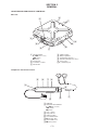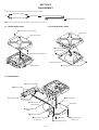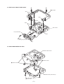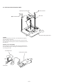
1
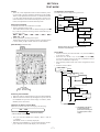
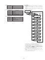
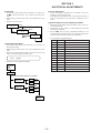
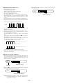
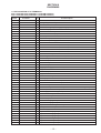
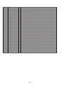
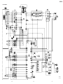
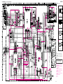
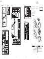
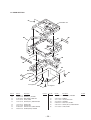
MZ-E44/E45
SERVICE MANUAL
US Model
AEP Model
UK Model
Australian Model
Tourist Model
Ver 1.1 1999.01
MZ-E44
E Model
MZ-E44/E45
Photo : MZ-E44 (SILVER)
Photo : MZ-E45 (GRAY)
US and foreign patents licensed from Dolby
Laboratories Licensing Corporation
Model Name Using Similar Mechanism
NEW
MD Mechanism Type
MT-MZE44-140
Optical Pick-up Mechanism Type
ODX-1A/1B
SPECIFICATIONS
MD Section
Audio playing system
Minidisc digital audio system
Laser diode properties
Material : GaAlAs
Wavelength : λ =790nm
Emission duration : continuous
Laser output : less than 44.6 µW*
* This output is the value measured at a distance of 200 mm from the
objective lens surface on the optical pick-up block with 7mm aperture.
Revolutions
400 rpm to 900 rpm (CLV)
Error correction
Advanced Cross Interleave Reed Solomon Code (ACIRC)
Sampling frequency
44.1kHz
Coding
Adaptive Transform Acoustic Coding (ATRAC)
Modulation system
EFM (Eight to Fourteen Modulation)
Number of channels
2 stereo channels
1 monaural channel
Frequency response
20 to 20,000 Hz ± 3 dB
Wow and Flutter
Below measurable limit
Outputs
Headphones : stereo mini-jack, maximum output level 5mW+5mW,
load impedance 16 ohm
General
Power requirements
Rechageable battery (supplied)
Nickel metal hydride rechargeable battery NH-9WM (N)
One LR6 (size AA) alkaline battery (not supplied)
Sony AC Power Adaptor AC-E15L (not supplied) connected at the
DC IN 1.5V jack
Battery operation time
Batteries
Playback
Nickel metal hydride
Approx.
Rechargeable battery (NH-9WM (N))
5.5 hours
One LR6 (size AA)
Approx.
Sony alkaline dry batteries
8.5 hours
Nickel metal hydride (NH-9WM (N)) +
Approx.
One LR6 (size AA)
16 hours
Dimensions
Approx. 87 x 17.8 x 91.5 mm (w/h/d)
(3 1/2 x 23/32 x 3 5/8 in) not including projecting parts and controls
Mass
Approx. 115 g (4.1 oz.) the player only
Approx. 155 g (5.5 oz.) incl. a premastered MD and a nickel
metal hydride rechargeable battery NH-9WM (N)
Supplied accessories
Battery charger (1)
Rechargeable battery (1)
Rechargeable battery carrying case (1)
Headphones with a remote control (1)
Dry battery case (1)
Handstrap (1)
Carrying pouch (1)
LR6 (size AA) alkaline battery (1) (Tourist model only)
Design and specifications are subject to change without notice.
PORTABLE MINIDISC PLAYER
MICROFILM
TABLE OF CONTENTS
Specifications ........................................................................... 1
5. ELECTRICAL ADJUSTMENTS ............................ 10
1. SERVICING NOTE ....................................................... 2
6. DIAGRAMS
6-1. Explanation of IC Terminals .....................................
6-2. Block Diagram ..........................................................
6-3. Printed Wiring Boards ..............................................
6-4. Schematic Diagram ...................................................
2. GENERAL
Location and Function of Controls .................................... 3
3. DISASSEMBLY
3-1. Upper Panel Assy .......................................................
3-2. Bottom Panel Assy .....................................................
3-3. Main board ..................................................................
3-4. Belt Assy, Front Panel Assy ........................................
3-5. Mechanism Deck Section ...........................................
3-6. Optial Pick-up Block Assy .........................................
13
15
18
21
7. EXPLODED VIEWS
4
4
4
5
5
6
7-1. Panel Section ............................................................ 28
7-2. Main Section ............................................................. 29
7-3. Mechanism Deck Section ......................................... 30
8. ELECTRICAL PARTS LIST ................................ 31
4. TEST MODE ................................................................... 7
This Mini Disc player is classified as a CLASS 1 LASER
product.
The CLASS 1 LASER
PRODUCT label is located on
the bottom exterior.
IN NO EVENT SHALL SELLER BE
LIABLE FOR ANY DIRECT,
INCIDENTAL OR CONSEQUENTIAL
DAMAGES OF ANY NATURE, OR
LOSSES OR EXPENSES RESULTING
FROM ANY DEFECTIVE PRODUCT
OR THE USE OF ANY PRODUCT.
Flexible Circuit Board Repairing
• Keep the temperature of the soldering iron around 270°C during
repairing.
• Do not touch the soldering iron on the same conductor of the
circuit board (within 3 times).
• Be careful not to apply force on the conductor when soldering
or unsoldering.
Notes on chip component replacement
• Never reuse a disconnected chip component.
• Notice that the minus side of a tantalum capacitor may be damaged by heat.
SAFETY-RELATED COMPONENT WARNING!!
“MD WALKMAN” is a trademark of Sony
Corporation.
COMPONENTS IDENTIFIED BY MARK ! OR DOTTED LINE WITH
MARK ! ON THE SCHEMATIC DIAGRAMS AND IN THE PARTS
LIST ARE CRITICAL TO SAFE OPERATION.
REPLACE THESE COMPONENTS WITH SONY PARTS WHOSE
PART NUMBERS APPEAR AS SHOWN IN THIS MANUAL OR IN
SUPPLEMENTS PUBLISHED BY SONY.
CAUTION
Use of controls or adjustments or performance of procedures
other than those specified herein may result in hazardous
radiation exposure.
SECTION 1
SERVICING NOTE
When repairing this device with the power on, if you remove the main board, this device stops working.
In this case, you work without the device stopping by fastening the hook of the Open/Close detection switch (S801) with tape.
Chassis ASSY
Main board
Tape
Open/Close switch (S801)
–2–
SECTION 2
GENERAL
LOCATION AND FUNCTION OF CONTROLS
Main Unit
6
5
7
4
9
3
2
!º
1
1 MD operate buttons
” • + (PLAY • FF )
= (REW )
p (STOP)
2 HOLD switch
3 VOLUME +/– buttons
4 EJECTbutton
5 OPERA TE lamp
6 Batterycompartment
7 External battery terminal (+/–)
8 DIGITAL MEGA B ASS s witc h
9 AVLS s witc h
! º 2 / REMOTE jack
Headphones with Remote Control
5
6
8
7 8
4
9
3
2
1 Headphones
2 MD operate switch and buttons
” • + (PLAY • FF)
= (REW)
p (STOP)
3 VOL +/– button
4 Display indicator
5 DISPLAY button
6 PLAYMODE button
7 P(PAUSE) b utton
8 HOLD cswitch
9 p(STOP) b utton
–3–
1
SECTION 3
DISASSEMBLY
r
The equipment can be removed using the following procedure.
Upper panel ASSY
set
Main board
Belt ASSY, Front panel ASSY
Bottom panel ASSY
Mechanism deck section
Optical pick-up block ASSY
Note : Follow the disassembly procedure in the numerical order given.
3-2. BOTTOM PANEL ASSY
3-1. UPPER PANEL ASSY
2 Screws (M1.4) pan precision
Main section
Upper panel ASSY
1 Screws (M1.4)
pan precision
3
2 Screws (M1.4) pan precision
2
Bottom panel ASSY
1
Main section
1 Screws (M1.4) pan precision
3-3. MAIN BOARD
4 Switch unit (CN801)
9 Remove solder
Battery case ASSY
9 Remove solder
!º
3 Screw (M1.4)
pan precision
8
6 Flexible (CLV)
board (CN551)
Main board
5 Flexible board
(CN501)
9 Remove solder
2 Screw
1 Screw (M1.4x2)
toothed lock
7 Screw tapping (M1.7)
–4–
1 Screws (M1.4x2)
toothed lock
3-4. BELT ASSY, FRONT PANEL ASSY
3
2
5 Belt ASSY
Boss
Boss
4
7 Claws
1
Claws
Main section
Front panel ASSY
8
Claw
6 Screw
(M1.4) pan precision
Boss
3-5. MECHANISM DECK SECTION
Mechanism deck section
1 Remove claws
1 Remove claws
3
Chassis ASSY (main section)
2 Step screws
–5–
3-6. OPTICAL PICK-UP BLOCK ASSY
Optical pick-up block ASSY
1 Screw precision
3
Main shaft
2 OP flexible board
4
5
Chassis ASSY (MD section)
r NOTE
When replacing the optical block, the OP flexible board protective sheet (SW) is necessary.
Before replacing, check where the sheet (SW) is pasted onto the
old OP flexible board and paste it on the new OP flexible board in
the same way.
Pasting on the sheet (SW) :
Paste on aligning the sheet (SW) center section with the edge of
the OP flexible board as in the figure and folding the excess over
onto the opposite side.
OP flexible board
Optical pick-up ASSY
5 mm
Sheet (SW)
–6–
SECTION 4
TEST MODE
Configuration of Test Mode
The test mode has the configuration given below.
Display when test mode
is set
Setting the Test Mode
To enter the test mode, two methods are available :
1. Entering method with key input.
Turn on the HOLD switch on the set. While holding down the p
key on the set, press the following remote commander keys in
the following order :
+n +n =n =n +n =n +n
=
n P n P
2. Entering method by shorting the test point
Solder bridge the test point TAP801 (TEST) on the main board
(connect IC801 pin #™ to GND), and turn on the POWER.
VOL
+ key
Overall
adjustment
mode (Auto?)
p key
” key
(Start ?)
p key
p key
VOL
– key
Adjustment ” key
mode
(Manu ?)
p key
Servo mode
0 0 0
+, – keys
Audio mode
1 0 0
+, – keys
Outline
• In this set, overall adjustment mode is made available by entering test mode to perform automatic adjustment of CD and MO.
In the overall adjustment mode, the disc is determined whether
it is CD or MO and adjustments are performed in sequence. If a
fault is found, the location of the fault is displayed. Also, in servo
mode, each adjustment can be automatically made.
+, – keys
Servo mode
3 0 0
[MAIN BOARD] (Conductor side)
Displays of the LCD on the remote commander
are shown in parentheses.
Servo Mode
• Set the test mode, press the VOLUME – key and use the ”key
to set the servo mode.
• When the servo mode is set, use the +
key and the =
key
to move the optical pick-up to the outer circumference and to
the inner circumference respectively.
• When entering another mode, refer to the configuration of test
mode.
1. Structure of Servo Mode
Servo mode
0 0 0
Offset adjustment
0 1 0
+, – keys
p key
” key
Test mode
Short : Test mode
Open : Normal mode
Releasing the Test Mode
1. When test mode was entered with key input, turn off the POWER.
2. When test mode was entered by shorting the test point, turn off
the POWER and open the solder bridge of TAP801 (TEST
MODE) on the main board.
1
2
011 to 013
*1
” key
Laser power
adjustment
0 2 0
+, – keys
p key
p key
” key
p key
” key
021 to 024
*1
” key
3
(See page 8)
Operation of Setting on Test Mode
When the test mode is set, the LCD displays the following :
*1 Repeatedly press ” key
to change the mode.
(Refer to the following list
for a description of each
mode.)
V3. 300
ROM version display
LCD on remote commander
• The cycle - the above ROM version display nAll lit nAll off
- is repeated.
(The ROM version is constantly displayed.)
• When the PLAY MODE key is pressed and hold down, the display at that time is held so that display can be checked.
–7–
2. Description of Each Mode
010 Offset adjustment
(See page 7.)
1
2
p key
3
MO adjustment
0 3 0
Mode
” key
Description
011
FE offset
012
TE offset
013
All servo ON
+, – keys
020 Laser power adjustment
p key
Low reflection
CD adjustment
0 4 0
CD adjustment
0 5 0
MO power E
023
CDL power
024
CD power
061 , 062
*1
071, 072,
073, 074
*1
p key
Description
031
MO EF balance
032
MO EF gain
033
MO ABCD gain
034
MO focus gain
035
MO tracking gain
036
MO RF gain
037
MO ADIP gain
038
MO focus bias E
039
CD focus bias A
Mode
” key
Description
041
Lower reflection CD EF balance
042
Lower reflection CD EF gain
043
Lower reflection CD ABCD gain
044
Lower reflection CD focus gain
045
Lower reflection CD tracking gain
046
Lower reflection CD RF offset
047
Lower reflection CD RF gain
048
Lower reflection CD focus bias
050 CD adjustment
Mode
” key
” key
p key
MO power A
022
040 Lower reflection CD adjustment
” key
” key
NV relation
0 9 0
+, – keys
051 to 058
*1
p key
+, – keys
p key
” key
” key
Automatic
adjustment
0 7 0
p key
021
Mode
041 to 048
*1
p key
Sled movement
0 6 0
Description
030 MO adjustment
” key
+, – keys
p key
” key
p key
+, – keys
p key
Mode
” key
+, – keys
p key
031 to 039
*1
091, 092,
093
*1
” key
*1 : Repeatedly press ” key
to change the mode.
Retern the Offset
(Refer to the following list
adjustment (0 1 0)
for a description of each
mode.)
–8–
Description
051
CD EF balance
052
CD EF gain
053
CD ABCD gain
054
CD focus gain
055
CD tracking gain
056
CD RF offset
057
CD RF gain
058
CD focus bias
060 Sled movement
Mode
Description
061
Sled in
062
Sled out 5
070 Automatic adjustment
Mode
Audio Mode
• Enter the test mode and press the VOLUME – key. Then, press
the (
key and the VOLUME + key in this turn to enter audio
mode.
• When entering another mode, refer to the configuration of test
mode.
1. Structure of Audio Mode
Description
071
Focus search
072
Access 32
073
ADER check
074
Tracking sensitivity adjust
Audio mode
1 0 0
p key
” key
Audio playback test
1 1 0
p key
090 NV relation
Mode
NV clear
092
Power OFF
093
Function code change
headphones
output
1kHz 0dB L/R
1 1 1
–12dB
” key
Description
091
” key
p key
Infinity Zero
1 1 2
–
” key
p key
1kHz 0dB L
1 1 3
–12dB
” key
p key
1kHz 0dB R
1 1 4
–12dB
” key
p key
1kHz –20dB L/R
1 1 5
p key
20Hz –20dB L/R
1 1 6
–20dB
” key
–20dB
” key
p key
20kHz –20dB L/R
1 1 7
–20dB
” key
p key 16kHz De-Emphasis
L/R
1 1 8
–20dB
” key
p key
100Hz 0dB L/R
1 1 9
–40dB
” key
• The mode No. 111 is for S/N and crosstalk. The mode No. 115 is
for distortion factor and frequency characteristics.
• When the VOLUME +/– keys is pressed in any mode, the volume of the headphones is changed (increased/decreased) in units
of one step. When the +
/=
keys is pressed, the volume of
the headphones is maximized/minimized.
• For the volume value, any changed value remains as it is basically.
However, when the volume is switched from 114 to 115 or 118
to 119, it returns the default value.
–9–
SECTION 5
ELECTRICAL ADJUSTMENTS
Power Mode
• Enter the test mode and press the VOLUME – key. Then, press
the (
key and the VOLUME – key in this turn to enter power
mode.
• When entering another mode, refer to the configuration of test
mode.
1. Structure of Power Mode
Power mode
3 0 0
p key
Adjustment Method in Overall Adjustment Mode
1. Enter the test mode and press the VOLUME + key to enter overall adjustment mode.
2. Insert the CD test disc (TGYS-1) or SONY MO disc (recorded)
commercially available.
3. Press the (
key twice. The disc is determined whether it is CD
or MO and each adjustment mode is set. Automatic adjustments
are performed in the order of the items listed below.
” key
UNREG check
31 0
” key
Power OFF
3 1 1
p key
Notes for Adjustment
• In this set, automatic adjustment of CD and MO can be performed by entering the test mode.
• Adjustments are performed in the overall adjustment mode. If
an item is determined as NG, the item is readjusted in servo
mode.
” key
• In CD Automatic adjustment Mode
Overall Adjustment Mode
• Enter the test mode and press the VOLUME + key to enter overall adjustment mode.
• When entering another mode, refer to the configuration of test
mode.
• When the overall adjustment mode is entered, the LCD on the
remote commander display the following :
040
Auto?
1. Structure of Overall Adjustment Mode
Overall
adjustment
mode
Auto?
” key
Start ?
” key (to discriminate between CD and MO)
CD automatic
adjustment
OK
NG
MO automatic
adjustment
OK
NG
p key
p key
p key
p key
Adjustment
mode
Manu ?
– 10 –
No.
Mode
Description
1
061
Sled in
2
071
Focus search
3
062
Sled out 5
4
051
CD EF balance
5
052
CD EF gain
6
051
CD EF balance
7
053
CD ABCD gain
8
054
CD focus gain
9
055
CD tracking gain
10
056
CD RF offset
11
057
CD RF gain
12
056
CD RF offset
13
058
CD Focus bias
• In MO Automatic adjustment Mode
* Remote commander display during automatic adjustment
No.
Mode
Description
1
061
Sled in
2
071
Focus search
3
062
Sled out
4
031
MO EF balance
5
032
MO EF gain
6
031
MO EF balance
7
033
MO ABCD gain
8
034
MO focus gain
9
035
MO tracking gain
10
036
MO RF gain
11
037
MO ADIP gain
12
039
MO focus bias A
13
073
ADER check
14
071
Focus search
15
031
MO EF balance
16
032
MO EF gain
17
031
MO EF balance
18
033
MO ABCD gain
19
034
MO focus gain
20
035
MO tracking gain
21
036
MO RF gain
22
037
MO ADIP gain
23
039
MO focus bias A
24
073
ADER check
25
061
Sled in
26
071
Focus search
27
041
Low reflection CD EF balance
28
042
Low reflection CD EF gain
29
041
Low reflection CD EF balance
30
043
Low reflection CD ABCD gain
31
044
Low reflection CD focus gain
32
045
Low reflection CD tracking gain
33
046
Low reflection CD RF offset
34
047
Low reflection CD RF gain
35
061
Sled in
36
071
Focus search
37
041
Low reflection CD EF balance
38
042
Low reflection CD EF gain
39
041
Low reflection CD EF balance
40
043
Low reflection CD ABCD gain
41
044
Low reflection CD focus gain
42
045
Low reflection CD tracking gain
43
046
Low reflection CD RF offset
44
047
Low reflection CD RF gain
057
Adjustment value (flashing)
Mode No. under adjustment
4. If result of automatic adjustment is OK, the following display
appears.
047
End-OK 5. If result of automatic adjustment is NG, the following display
appears.
051
NG
Error code
NG mode No.
* If NG, enter servo mode to perform automatic adjustment of the
item determined as NG.
– 11 –
Adjusting the OFF-track threshold
• Perform only for Ver. 1.000.
• Only for MO (use AU-1 disk).
• Use the following procedure.
• Monitor (adjust) with a storage oscilloscope.
1. Set in Test mode (Manual mode).
2. Press the PLAYMODE key per 030.
(2.6 volt operating mode • • • • • • Two battery marks light up.)
3. Check that the OP is at the center (not the outermost or innermost circumference) and then play the AU-1 disk (031 n032
n 033).
4. Press the PAUSE key at 033 and adjust the MO ABCD gain.
5. Press the STOP key (030), monitor the OFTRK (SP508) signal
and set the focus ON at 031 with the PLAY key.
3. When the automatic adjustment is completed, the flashing adjustment value is lit.
H
OFTRK
L
6. The adjustment is okay when the periods for “H” and “L” of the
OFTRK is about equal.
7. Perform an overall adjustment without turning off the power.
8. Perform the following operation when the periods for “H” and
“L” of the OFTRK are not equal.
Press the DISPLAY key 6 times per “030” to set in Memory
mode.
[5C ø] is displayed. Press the remote control pkey 6 times and
use the ”key 9 times to align at [629].
Shift the figure with the remote control ’
, ‘keys per the “629”
address and press PAUSE < set > (reset value “OA”).
(1) This figure is small when “H” is long.
ø A nø 9 nø 8 n • • • • • • • •
(2) This figure is large when “L” is long.
ø A nø 9 nø 8 n • • • • • • • •
Press the DISPLAY key one time to return to [030].
9. Return to 5. Press the PLAY key (remote control ”key) again
to set to 031 (Focus ON).
Adjustment in Servo Mode Method
1. When each adjustment mode is set according to the structure of
servo mode, the lower two digits of the mode No. and the adjustment value written in EEPROM are displayed and lit on the
LCD on the remote commander.
052
Adjustment value (lit)
Mode No.
2. When the P key is pressed, the following display appears and
the automatic adjustment is performed.
052
Adjustment value (flashing)
Note) Although the VOLUME +/– keys can be used to change
the adjustment value to any value, they should not be
used whenever possible.
– 12 –
052
Adjustment value (lit)
SECTION 6
DIAGRAMS
6-1. EXPLANATION OF IC TERMINALS
IC801 RU6815MF-0004 (VERSION 3.0) (SYSTEM CONTROL)
IC801 RU6815MF-0006 (VERSION 3.3) (SYSTEM CONTROL)
Pin No.
Pin Name
1
2
UREG MON
3
4
VREF
I/O
Pin Description
–
Not used (Fixed at “L” ).
I
Unreg voltage monitor input.
–
Not used (Fixed at “L” ).
I
Reference voltage for power supply voltage adjustlment.
5
PLAY KEY
I
Set PLAY key input.
6
OPEN/CLS SW
I
OPEN/CLOSE switch input.
7
RMC KEY
I
Remote commander key input.
8
SET KEY
I
Set key input.
9
XRESET
I
Systen reset input (At reset : “L” ).
10
AVDD
–
A/D converter power supply (+2.6V or +2.8V).
L : Close
11
AVSS
–
A/D converter Ground.
12
TYPE 0
I
Model discrimination terminal (Fixed at “L” ).
13
TYPE 1
I
Model discrimination terminal (Fixed at “L” ).
14
TYPE 2
I
Model discrimination terminal (Fixed at “L” ).
15
MODEL
I
Model discrimination terminal (Fixed at “L” ).
16
HOLD SW
I
Set HOLD switch input.
17
VREG CON
O
2.5V voltage on/off switch (Sub terminal) (not used).
–
Not used (Open).
18
19
–
Not used (Open).
MCK
I
Master clock input.
–
Not used (Open).
22
VDD
–
Digital power supply (+2.6V or +2.8V).
23
VSS
20
21
24
–
Digital Ground.
–
Not used (Open).
25
VSS
–
Digital Ground.
26
AVLS SW
I
Set AVLS switch input.
27
DSP SINT
I
Interrupt input from DSP.
28
DBB 0
I
DIGITAL MEGA BASS switch input (MID).
29
DBB 1
I
DIGITAL MEGA BASS switch input (MAX).
30
OPR LED
O
LED drive output.
31
XWK CLR
O
Power IC wakeup factor latch clear output and motor driver IC control signal outpt.
32
ADJUST
I
“Normally, Test mode select input (“L” : Test mode)
33
SLEEP
O
Power supply circuit OFF signal output.
34
SBUS CLK
O
SBB serial clock output.
35
SBUS DATA
O
SBB serial data output.
–
Not used (Open).
36
37
SLD 1 MON
I
Sled servo timing signal input.
38
SLD 2 MON
I
Sled servo timing signal input.
39
CLV VCON
O
Spindle servo drive voltage control output.
40
APC REF
O
Laser power control output.
41
V28-CON
O
Power voltage (+2.6V or +2.8V) correction control output.
42
CLV U MON
I
Spindle servo timing signal input.
43
CLV V MON
I
Spindle servo timing signal input.
44
CLV W MON
I
Spindle servo timing signal input.
45
CLV U CON
O
Spindle servo drive signal output.
46
CLV V CON
O
Spindle servo drive signal output.
47
CLV W CON
O
Spindle servo drive signal output.
– 13 –
Pin No.
Pin Name
I/O
Pin Description
48
–
Not used (Open).
49
–
Not used (Open).
50
VDD
–
Digital power supply (+2.6V or +2.8V).
51
VPP
–
Power for on board light.
52
VSS
–
Digital ground.
53
SLD 1R CON
O
Sled motor control signal output.
54
SLD 1F CON
O
Sled motor control signal output.
55
SLD 2R CON
O
Sled motor control signal output.
56
SLD 2F CON
O
Sled motor control signal output.
57
–
Not used (Open).
58
–
Not used (Open).
59
–
Not used (Open).
60
–
Not used (Open).
61
SPCK
O
Serial clock output for Remote control communication. Not used (Open).
62
RMC DTCLK
I/O
63 – 66
Serial data input/output for Remote control communication.
–
Not used (Open).
67
SLD VCON
O
Sled servo outer voltage control output.
68
SLD PWR-UP
O
Baypass transistor control output for sled drive power supply.
69
HP MUTE
O
Headphone amplifier mute output.
70
HP STBY
O
Headphone amplifier standby output.
71
RMC SEL
O
TSB/SSB selection signal output to remote commander terminal. Not used (Open).
72
NV D0
O
Serial data signal output for NVRAM.
73
NV D1
I
Serial data signal input from NVRAM.
74
NV CLK
O
Serial clock signal output for NVRAM.
75
NV CS1
O
Chip select signal output for NVRAM.
76
VDD
–
Digital power supply (+2.6V or +2.8V).
77 – 79
LCD VL2 – 0
I
LCD drive level power supply (Connected ground).
80
VSS
–
Digital ground.
81 – 87
–
Not used (Open).
88 – 96
LCD SEG0 – 8
–
LCD Segment terminal. Not used (Open).
97 – 100
LCD COM0 – 3
–
LCD common terminal. Not used (Open).
– 14 –
MZ-E44/E45
6-2. BLOCK DIAGRAM
• Signal path.
J : PLAY
– 15 –
– 16 –
– 17 –
MZ-E44/E45
6-3. PRINTED WIRING BOARDS
r
Semiconductor
Location
Ref. No.
Location
D351
D352
D801
D841
D901
I-10
H-11
I-5
F-10
D-5
D902
H-14
IC301
IC302
IC501
IC551
IC552
C-7
D-7
H-12
G-14
F-14
IC601
IC603
IC801
IC802
IC901
F-12
F-6
C-13
C-15
E-4
Q501
Q551
Q552
I-12
G-3
F-3
*Note:
Use R1001 only with Ver.3.0 of microprocessor (IC801).
Using R1001 with other microprocessor versions will
cause operating errors so be sure to remove it.
You can check the version with Test Mode (page 7).
Note:
• X : parts extracted from the component side.
r
•
: Through hole.
• b : Pattern from the side which enables seeing.
(The other layers' patterns are not indicated.)
Caution:
Pattern face side:
Parts on the pattern face side seen from the
(Side B)
pattern face are indicated.
Parts face side:
Parts on the parts face side seen from the
(Side A)
parts face are indicated.
– 18 –
– 19 –
– 20 –
6-4. SCHEMATIC DIAGRAM
r
Refer to page 25 for IC Block Diagrams.
MZ-E44/E45
r Waveforms
1
800mVp-p
IC501 @•
VOLT/DIV : 200mV AC
TIME/DIV : 5 µsec
2
2.7Vp-p
23µsec
IC601 #ª
VOLT/DIV : 1V AC
TIME/DIV : 10 µsec
3
2.6Vp-p
482nsec
IC601 $¡
VOLT/DIV : 500mV AC
TIME/DIV : 200nsec
4
2.0 Vp-p
16.9344 MHz
IC601 $ª
VOLT/DIV : 500mV AC
TIME/DIV : 20nsec
Note:
• All capacitors are in µF unless otherwise noted. pF: µµF
50 WV or less are not indicated except for electrolytics
and tantalums.
• All resistors are in Ω and 1/4 W or less unless otherwise
specified.
• C : panel designation.
*Note:
Use R1001 only with Ver.3.0
of microprocessor (IC801).
Using R1001 with other microprocessor versions will cause
operating errors so be sure to
remove it.
You can check the version with
Test Mode (page 7).
Note: The components identified by mark ! or dotted
line with mark ! are critical for safety.
Replace only with part number specified.
• A: B+ Line.
• Power voltage is dc 1.5V and fed with regulated dc power
supply from battery terminal.
• Voltages and waveforms are dc with respect to ground
under no-signal conditions.
no mark : PLAY
• Voltages are taken with a VOM (Input impedance 10 MΩ).
Voltage variations may be noted due to normal production tolerances.
• Waveforms are taken with a oscilloscope.
Voltage variations may be noted due to normal production tolerances.
• Circled numbers refer to waveforms.
• Signal path.
J : PLAY
– 21 –
– 22 –
– 23 –
– 24 –
MZ-E44/E45
GND
H12
FO1
VM1
RO1
GND
H13
FO3
VM3
RO3
GND
H34
FO4
VM4
RO4
GND
H4
VC
49
48
47
46
45
44
43
42
41
40
39
38
37
CS
PRE DRIVER
17 +B
VG
PRE DRIVER
PRE DRIVER
INSTRUCTION
DECODE
CONTROL
AND
CLOCK
GENERATION
PRE DRIVER
VC
+B
SK
2
16 NF1
4
V IN1
5
15 OUT1
1
V–
4
3
2
14 GND
V IN2
6
VC
VC
HI–BRIDGE
CONTROL
F12 55
R12 56
DI
DO
1ntOE
1ntSTB
8
VC
BEEP
11 BEEP IN
9
VC
PWM
DRIVER
REN
VREG 64
VC
VC
VC
36
HIU
35
HIV
34
HIW
33
P11
32
P12
31
VPS2
30
PO2
29
GND
PS
VC 68
EFM
PLCK
VPS1
26
GND
3P2
25
HOW
24
VD2
VC 10
23
HOV
SPCK0 11
SPCK1 12
22
GND
3PI
21
HOU
RF 5
5
NC 20
TFOUT 21
TROUT 22
SSB CONTROL
MONITOR I/O etc.
FROUT 23
FFOUT 24
8
RD DT ECC
8
ATDT
16
10
67 DRA7
19
66 DRA8
XRST 8
VBMON
9
29 VBSEL
27 VB2
26 VB1
VB SELECT
SPCK
BUFF
C1L 14
VB 15
C1H 16
C2H 17
CHARGE
PUMP
24 PGND
PWM1
22 PWM1
MODE
SELECT
21 D1
SAW
20 D0
OSC2
19 VCON
23 SW
1
VC
1
2
3
4
5
6
7
8
9
10
11
12
13
14
15
16
17
18
LI
GND
DCC1
GND
DCC1
LI
UO
VO
WO
61 XOE2
60 XOE
VD
63 XRAS
62 DRA9
VD
64 DRA11
Ref. No.
59 XCAS
58 DRD2
1
57 DRD3
56 VSS
Part No.
Description
Remark
3
3
3
4-963-883-21 SCREW (M1.4), PRECISION PAN (SILVER)
(MZ-E44)
4-963-883-31 SCREW (M1.4), PRECISION PAN
(MZ-E44:BLUE, MZ-E45:ORANGE, GRAY)
X-4951-601-1 PANEL ASSY, UPPER (SILVER) (MZ-E44)
X-4951-601-2 PANEL ASSY, UPPER (BLUE) (MZ-E44)
X-4951-601-3 PANEL ASSY, UPPER (GRAY) (MZ-E45)
3
X-4951-601-4 PANEL ASSY, UPPER (ORANGE) (MZ-E45)
1
Ref. No.
Part No.
Description
4
5
6
7
4-963-883-81
X-4950-237-1
X-4950-236-1
X-4950-235-1
SCREW (M1.4), PRECISION PAN
PANEL ASSY, FRONT
BELT ASSY
PANEL ASSY, BOTTOM (SILVER) (MZ-E44)
7
7
7
X-4950-239-1 PANEL ASSY, BOTTOM (BLUE) (MZ-E44)
X-4950-240-1 PANEL ASSY, BOTTOM (GRAY) (MZ-E45)
X-4950-241-1 PANEL ASSY, BOTTOM (ORANGE) (MZ-E45)
MCK
X0
X1
MCK I-O
VSS
MCK/2
PMCK
DOUT
VSS
BCK
AUDATA
LRCK
EMP
VDD
NC
NC
XBUSY
SINT
SCK
SBUS
RESET
VDD
MC
NC
NC
26 27 28 29 30 31 32 33 34 35 36 37 38 39 40 41 42 43 44 45 46 47 48 49 50
– 25 –
7
1
1
IN
CLOCK
GENERATOR
ATRAC
DECODER
OSC1
STEP-UP
DC / DC
CONVERTER
C2L 13
51 VDD
CK176 25
3
1
25 VBH
53 DRD1
52 DRD0
XBUSY
MZ-E45
28 CLK
RESET
55 XWE2
54 XWE
XATWE
DREQ
31 FFCLR
65 DRA10
L2L
12
WR REQ etc.
8 8
VD
7
32 XWK4
30 SLEEP
DTC 6
CRST
1
33 XWK3
SYSTEM
CONTROL
STEP–UP
PRE DRIVER
GND
DCC2
8
68 DRA6
35 XWK1
34 XWK2
BAND GAP
REFERENCE
VREF 3
VG 18
L2H
SBW
SBR
NC 16
NC 17
SBA
SBD
NC 15
8
16
EFM DATA A/B
ECC DATA
EBA
STEP UP/DOWN
PRE DRIVER
POWER SW
PRE DRIVER
36 VSTB
VRMC 2
27
VG
VB2
S DATA
AC DATA
8
VSS 14
NC 18
NC 19
AC
WDCK
69 DRA5
VG
VB
AC BYCK
SECTOR
DECODER
VG
3
6
PO1
71 DRA0
70 DRA4
5
4
IC901 MPC1830ADTBEL
INM 4
20
VB
AC LRCK
AC WDCK
EFM ACIRC
DECODER
DEFECT 12
OFTRK 13
SLEEP UP/DOWN
/POWER SW
DECODER
DI 72
VB1
FLAG
9
VSS ADC 10
T-COUNT 11
DO or DI
VB1
4
3
VG
DO
VRT 8
VRB
DRAM & PERIPHERAL CONTROL ADDRESS GENERATOR
7
VG 70
PWM 71
72 DRA1
SQREQ
ADIP
VG
73 DRA2
SUBQ/ADIP
DECODER
DSSP
TE
TE 6
75 VDD
74 DRA3
2nd MSB
FE 4
ABCD 5
EFM
PLL
FE
ABCD
ADC
VREF 2
RF 3
RF
GND 69
1
VG
PRE DRIVER
3 PHASE CONTROL
VC
VDD ADC 1
6 NC
5 GND
28
100 99 98 97 96 95 94 93 92 91 90 89 86 87 86 85 84 83 82 81 80 79 78 77 76
ADIP
PLL
EEPROM
2048bit
128 X 16
The components identified by mark !
or dotted line with mark ! are critical
for safety.
Replace only with part number specified.
7-1. PANEL SECTION
4
GND 1
VG
VSS
MI0
MI1
MI2
CLPF 67
MI3
MICK
MOCK
MO0
MO1
MO2
MO3
VDD
PLCK
EFM
ADPLCK
ADIP–DATA
TEST
CRCF
ERFLAG
FON
FOK
RGND 66
ID3
ID2
ID1
ID0
IC601 µPD63731GC-9EU
VC
PWM
DRIVER
VREG
65
CONT
ADIP
R/W AMPS
AND
AUTO ERASE
• The mechanical parts with no reference
number in the exploded views are not
supplied.
• Accessories and packing materials are given
in the last of this parts list.
VG
1ntSTB
VC
MUTE T 10
VC
PRE
DRIVER
MUTE
BIAS
CONTROL
VC
PRE
DRIVER
MUTE
3
7 NC
DECODER
NOTE :
• -XX, -X mean standardized parts, so they
may have some difference from the original
one.
• Color indication of Appearance Parts
Example :
KNOB, BALANCE (WHITE) ••• (RED)
↑
↑
Parts color Cabinet's color
• Items marked “ * ”are not stocked since they
are seldom required for routine service. Some
delay should be anticipated when ordering
these items.
MZ-E44
OE 63
ROE
PWSTB T
8 VCC
DATA
REGISTER
F13 60
R14 61
F14 62
12 NF2
ADD
BUFFERS
INSTRUCTION
REGISTER
R11 58
R13 59
13 OUT2
7
HI–BRIDGE
CONTROL
F11 57
PWSTB
PWSTB
HI–BRIDGE
CONTROL
VC
HI–BRIDGE
CONTROL
VC
BIAS OUT
VPP
GENERATOR
VREF
1
VPP
SW
18 VCC
3
50
VG
2
51
VC
VCC
52
VG
R/F
53
VC
1
54
VG
RF OUT
BIAS IN
V+
20 NC
19 NC
VC
RF IN
5
6
7
RO2
8
IC802 AK93C55AV-L
VM2
IC551 MPC17A55FTA
IC552 TLC372CPWR
FO2
IC Block Diagrams
IC301 BA3577FS-E2
GND
H2
r
SECTION 7
EXPLODED VIEWS
– 26 –
– 27 –
– 28 –
Remark
7-2. MAIN SECTION
61
MT-MZE44-140
66
58
61
59
60
57
57
62
65
56
53
64
63
54
55
not supplied
55
52
not supplied
51
Ref. No.
Part No.
Description
51
52
53
54
55
3-703-502-11
4-984-017-01
A-3293-984-A
4-211-392-01
3-335-797-91
SCREW
SCREW (1.7), TAPPING
MAIN BOARD, COMPLETE
PLATE, BLIND
SCREW (M1.4), TOOTHED LOCK
56
57
58
59
1-475-804-11
4-211-119-01
X-4950-229-1
4-989-078-01
SWITCH UNIT
SCREW, STEP
CHASSIS ASSY (MAIN SECTION)
SPRING (OPEN), TENSION
Remark
Ref. No.
Part No.
Description
60
4-995-274-11 SPRING (O-C), TORSION
61
62
63
64
65
4-982-418-01
4-211-118-01
4-212-087-01
X-4950-232-1
4-963-883-41
66
4-217-305-01 SHEET, BLIND
– 29 –
DAMPER
LID, BATTERY CASE
TERMINAL
CASE ASSY, BATTERY
SCREW (M1.4), PRECISION PAN
Remark
7-3. MECHANISM DECK SECTION
(MT-MZE44-140)
107
113
106
M902
M901
109
104
111
104
114
103
110
*
R1001
102
not
supplied
112
108
101
105
*Note :
Use R1001 only with Ver.3.0 of microprocessor
(IC801).
Using R1001 with other microprocessor versions will
cause operating errors so be sure to remove it.
You can check the version with Test Mode (page 7).
Ref. No.
Part No.
Description
101
102
103
104
105
4-963-883-61
4-982-563-01
1-666-784-13
4-963-883-21
4-965-893-01
SCREW (M1.4), PRECISION PAN
SPRING, THRUST
FLEXIBLE (CLV) BOARD
SCREW (M1.4), PRECISION PAN
WASHER, GEAR (A) STOPPER
106
107
108
109
110
X-4950-157-1
X-4948-010-1
4-982-555-01
4-210-659-01
3-349-825-82
CHASSIS ASSY (MD SECTION)
HOLDER ASSY
GEAR (A)
SPRING, TENSION
SCREW, PRECISION
101
115
116
The components identified by mark ! or dotted
line with mark ! are critical for safety.
Replace only with part number specified.
Remark
Ref. No.
Part No.
Description
111
112
113
! 114
115
4-993-251-01
4-982-561-11
4-995-532-11
X-4949-164-1
4-988-858-01
SHAFT, MAIN
SPRING, RACK
COVER, MD
OPTICAL PICK-UP BLOCK ASSY
SHEET (SW)
3-309-595-11
1-698-991-11
1-698-764-21
1-216-789-11
SHEET, INSULATING, PACK
MOTOR, DC (including PULLEY) (SPINDLE)
MOTOR, SLED (including PULLEY) (SLED)
METAL CHIP
2.2
5%
1/16W
116
M901
M902
R1001
– 30 –
Remark
SECTION 8
ELECTRICAL PARTS LIST
NOTE :
• Due to standardization, replacements in the
parts list may be different from the parts
specified in the diagrams or the components
used on the set.
• -XX, -X mean standardized parts, so they
may have some difference from the original
one.
• RESISTORS
All resistors are in ohms
METAL : Metal-film resistor
METAL OXIDE :Metal oxide-film resistor
F : nonflammable
• Items marked “ * ”are not stocked since
they are seldom required for routine service.
Some delay should be anticipated when
ordering these items.
Ref. No.
Part No.
• SEMICONDUCTORS
In each case, u : µ , for example :
uA.... : µ A.... , uPA.... : µ PA....
uPB.... : µ PB.... , uPC.... : µ PC....
uPD.... : µ PD....
• CAPACITORS
uF : µ F
• COILS
uH : µ H
• Abbreviation
AUS : Australian
HK
: Hong Kong
JE
: Tourist
Description
Remark
A-3293-984-A MAIN BOARD, COMPLETE
*********************
< CAPACITOR >
C101
C102
C103
C201
C202
1-135-181-21
1-125-899-11
1-115-156-11
1-135-181-21
1-125-899-11
TANTALUM CHIP
TANTAL. CHIP
CERAMIC CHIP
TANTALUM CHIP
TANTAL. CHIP
4.7uF
220uF
1uF
4.7uF
220uF
C203
C301
C302
C303
C304
1-115-156-11
1-135-259-11
1-119-750-11
1-109-982-11
1-104-912-11
CERAMIC CHIP
TANTAL. CHIP
TANTAL. CHIP
CERAMIC CHIP
TANTAL. CHIP
1uF
10uF
22uF
1uF
3.3uF
C305
C306
C307
C308
C311
1-109-982-11
1-109-982-11
1-135-149-21
1-115-156-11
1-135-259-11
CERAMIC CHIP
CERAMIC CHIP
TANTALUM CHIP
CERAMIC CHIP
TANTAL. CHIP
1uF
1uF
2.2uF
1uF
10uF
C312
C313
C314
C315
C501
1-135-259-11
1-115-156-11
1-119-750-11
1-164-156-11
1-107-826-11
TANTAL. CHIP
CERAMIC CHIP
TANTAL. CHIP
CERAMIC CHIP
CERAMIC CHIP
10uF
1uF
22uF
0.1uF
0.1uF
C502
C503
C504
C505
C506
1-117-720-11
1-164-227-11
1-162-962-11
1-164-156-11
1-162-970-11
CERAMIC CHIP
CERAMIC CHIP
CERAMIC CHIP
CERAMIC CHIP
CERAMIC CHIP
4.7uF
0.022uF
470PF
0.1uF
0.01uF
C508
C509
C510
C511
C551
1-164-227-11
1-164-156-11
1-164-156-11
1-107-826-11
1-162-964-11
CERAMIC CHIP
CERAMIC CHIP
CERAMIC CHIP
CERAMIC CHIP
CERAMIC CHIP
0.022uF
0.1uF
0.1uF
0.1uF
0.001uF
10%
10%
10%
25V
25V
25V
16V
50V
C552
C553
C554
C555
C556
1-162-964-11
1-104-850-11
1-104-850-11
1-104-912-11
1-104-912-11
CERAMIC CHIP
TANTAL. CHIP
TANTAL. CHIP
TANTAL. CHIP
TANTAL. CHIP
0.001uF
6.8uF
6.8uF
3.3uF
3.3uF
10%
20%
20%
20%
20%
50V
10V
10V
16V
16V
C557
C558
C559
1-117-720-11 CERAMIC CHIP
1-117-720-11 CERAMIC CHIP
1-115-566-11 CERAMIC CHIP
10%
10V
10V
10V
4.7uF
4.7uF
4.7uF
20%
20%
20%
20%
6.3V
4V
10V
6.3V
4V
20%
20%
10%
20%
10V
6.3V
6.3V
10V
6.3V
10%
10%
20%
20%
20%
20%
10%
10%
10%
10%
10V
10V
10V
10V
6.3V
6.3V
10V
6.3V
25V
16V
10V
25V
50V
25V
25V
Ref. No.
MAIN
The components identified by mark !
or dotted line with mark ! are critical
for safety.
Replace only with part number specified.
When indicating parts by reference number, please include the board.
Part No.
Description
Remark
C560
C561
1-115-566-11 CERAMIC CHIP
1-115-566-11 CERAMIC CHIP
4.7uF
4.7uF
10%
10%
10V
10V
C562
C563
C564
C565
C568
1-109-982-11
1-117-720-11
1-117-232-11
1-135-259-11
1-117-370-11
CERAMIC CHIP
CERAMIC CHIP
TANTALUM
TANTAL. CHIP
CERAMIC CHIP
1uF
4.7uF
22uF
10uF
10uF
10%
10V
10V
4V
6.3V
10V
C569
C601
C602
C603
C604
1-117-370-11
1-164-156-11
1-162-970-11
1-162-970-11
1-162-970-11
CERAMIC CHIP
CERAMIC CHIP
CERAMIC CHIP
CERAMIC CHIP
CERAMIC CHIP
10uF
0.1uF
0.01uF
0.01uF
0.01uF
C605
C607
C608
C609
C801
1-117-720-11
1-164-156-11
1-164-156-11
1-164-156-11
1-162-962-11
CERAMIC CHIP
CERAMIC CHIP
CERAMIC CHIP
CERAMIC CHIP
CERAMIC CHIP
4.7uF
0.1uF
0.1uF
0.1uF
470PF
C803
C804
C805
C806
C807
1-162-970-11
1-162-964-11
1-164-156-11
1-164-227-11
1-164-227-11
CERAMIC CHIP
CERAMIC CHIP
CERAMIC CHIP
CERAMIC CHIP
CERAMIC CHIP
0.01uF
0.001uF
0.1uF
0.022uF
0.022uF
C808
C809
C811
C812
C831
1-164-156-11
1-164-156-11
1-162-964-11
1-162-964-11
1-115-156-11
CERAMIC CHIP
CERAMIC CHIP
CERAMIC CHIP
CERAMIC CHIP
CERAMIC CHIP
0.1uF
0.1uF
0.001uF
0.001uF
1uF
C832
C833
C834
C846
C901
1-162-964-11
1-162-964-11
1-164-156-11
1-162-964-11
1-162-964-11
CERAMIC CHIP
CERAMIC CHIP
CERAMIC CHIP
CERAMIC CHIP
CERAMIC CHIP
0.001uF
0.001uF
0.1uF
0.001uF
0.001uF
10%
10%
10%
10%
50V
50V
25V
50V
50V
C902
C903
C904
C905
C906
1-162-970-11
1-107-826-11
1-109-982-11
1-162-964-11
1-107-826-11
CERAMIC CHIP
CERAMIC CHIP
CERAMIC CHIP
CERAMIC CHIP
CERAMIC CHIP
0.01uF
0.1uF
1uF
0.001uF
0.1uF
10%
10%
10%
10%
10%
25V
16V
10V
50V
16V
C907
C908
C909
C910
C911
1-107-826-11
1-109-982-11
1-107-826-11
1-162-970-11
1-135-259-11
CERAMIC CHIP
CERAMIC CHIP
CERAMIC CHIP
CERAMIC CHIP
TANTAL. CHIP
0.1uF
1uF
0.1uF
0.01uF
10uF
10%
10%
10%
10%
20%
16V
10V
16V
25V
6.3V
– 31 –
20%
20%
10%
10%
10%
10V
25V
25V
25V
25V
10%
10V
25V
25V
25V
50V
10%
10%
10%
10%
10%
10%
25V
50V
25V
25V
25V
25V
25V
50V
50V
10V
MAIN
Ref. No.
C914
C918
C919
Part No.
Description
1-126-246-11 ELECT CHIP
1-115-156-11 CERAMIC CHIP
1-115-156-11 CERAMIC CHIP
Remark
220uF
1uF
1uF
20%
< CONNECTOR >
CN501
CN551
CN801
1-573-360-21 CONNECTOR, FFC/FPC 20P
1-784-226-21 CONNECTOR, FFC/FPC 8P
1-778-154-21 CONNECTOR, FFC/FPC 6P
< DIODE >
D351
D352
D801
D841
D901
8-719-017-58
8-719-045-87
8-719-052-72
8-719-066-17
8-719-420-51
DIODE MA8068
DIODE MA4Z082WA-TX
LED CL-220HR-C (OPERATE)
DIODE FTZ6.8E-T148
DIODE MA729
D902
8-719-066-16 DIODE RB491D-T146
< FERRITE BEAD >
FB841
FB842
1-414-228-11 INDUCTOR CHIP
1-414-228-11 INDUCTOR CHIP
4V
10V
10V
Ref. No.
Part No.
Description
Remark
< RESISTOR >
R101
R102
R103
R104
R201
1-216-835-11
1-216-831-11
1-216-829-11
1-216-864-11
1-216-835-11
METAL CHIP
METAL CHIP
METAL CHIP
METAL CHIP
METAL CHIP
15K
6.8K
4.7K
0
15K
5%
5%
5%
5%
5%
1/16W
1/16W
1/16W
1/16W
1/16W
R202
R203
R204
R301
R302
1-216-831-11
1-216-829-11
1-216-864-11
1-216-809-11
1-216-803-11
METAL CHIP
METAL CHIP
METAL CHIP
METAL CHIP
METAL CHIP
6.8K
4.7K
0
100
33
5%
5%
5%
5%
5%
1/16W
1/16W
1/16W
1/16W
1/16W
R303
R501
R502
R503
R505
1-216-797-11
1-216-817-11
1-216-827-11
1-216-853-11
1-216-841-11
METAL CHIP
METAL CHIP
METAL CHIP
METAL CHIP
METAL CHIP
10
470
3.3K
470K
47K
5%
5%
5%
5%
5%
1/16W
1/16W
1/16W
1/16W
1/16W
R506
R507
R508
R553
R554
1-216-864-11
1-216-864-11
1-216-793-11
1-216-833-11
1-216-833-11
METAL CHIP
METAL CHIP
RES,CHIP
METAL CHIP
METAL CHIP
0
0
4.7
10K
10K
5%
5%
5%
5%
5%
1/16W
1/16W
1/16W
1/16W
1/16W
R555
R556
R601
R602
R801
1-216-809-11
1-216-853-11
1-216-833-11
1-216-809-11
1-216-845-11
METAL CHIP
METAL CHIP
METAL CHIP
METAL CHIP
METAL CHIP
100
470K
10K
100
100K
5%
5%
5%
5%
5%
1/16W
1/16W
1/16W
1/16W
1/16W
R802
R803
R804
R808
R810
1-216-845-11
1-216-853-11
1-216-853-11
1-216-825-11
1-216-827-11
METAL CHIP
METAL CHIP
METAL CHIP
METAL CHIP
METAL CHIP
100K
470K
470K
2.2K
3.3K
5%
5%
5%
5%
5%
1/16W
1/16W
1/16W
1/16W
1/16W
R811
R812
R814
R815
R816
1-216-827-11
1-216-841-11
1-216-825-11
1-216-829-11
1-216-831-11
METAL CHIP
METAL CHIP
METAL CHIP
METAL CHIP
METAL CHIP
3.3K
47K
2.2K
4.7K
6.8K
5%
5%
5%
5%
5%
1/16W
1/16W
1/16W
1/16W
1/16W
R817
R818
R819
R820
R821
1-216-835-11
1-216-839-11
1-216-853-11
1-216-845-11
1-216-857-11
METAL CHIP
METAL CHIP
METAL CHIP
METAL CHIP
METAL CHIP
15K
33K
470K
100K
1M
5%
5%
5%
5%
5%
1/16W
1/16W
1/16W
1/16W
1/16W
R841
R842
R901
R902
R903
1-216-809-11
1-216-809-11
1-216-845-11
1-216-853-11
1-216-863-11
METAL CHIP
METAL CHIP
METAL CHIP
METAL CHIP
RES,CHIP
100
100
100K
470K
3.3M
5%
5%
5%
5%
5%
1/16W
1/16W
1/16W
1/16W
1/16W
R904
R906
R909
R910
1-216-845-11
1-216-827-11
1-216-847-11
1-218-871-11
METAL CHIP
METAL CHIP
METAL CHIP
RES,CHIP
100K
3.3k
150K
10K
5%
5%
5%
0.50%
1/16W
1/16W
1/16W
1/16W
< IC >
IC301
IC302
IC501
IC551
IC552
8-759-431-56
8-759-541-32
8-759-538-56
8-759-390-25
8-759-358-40
IC
IC
IC
IC
IC
BA3577FS-E2
AK4350-VF-E1
SN761054
MPC17A55FTA
TLC372CPWR
IC601
IC603
IC801
IC801
IC802
8-759-538-55
8-759-527-01
8-759-564-20
8-759-580-35
8-759-449-23
IC
IC
IC
IC
IC
uPD63731GC-9EU
MN41X4400TT-10L
RU6815MF-0004 (VERSION 3.0)
RU6815MF-0006 (VERSION 3.3)
AK93C55AV-L
IC901
8-759-538-57 IC MPC1830ADTBEL
< JACK >
J301
1-778-179-11 JACK (2 /REMOTE)
< COIL >
L301
L501
L551
L552
L553
1-414-754-11
1-414-754-11
1-412-031-11
1-412-031-11
1-414-400-11
INDUCTOR
INDUCTOR
INDUCTOR CHIP
INDUCTOR CHIP
INDUCTOR
10uH
10uH
47uH
47uH
22uH
L554
L555
L556
L601
L901
1-414-400-11
1-412-031-11
1-414-410-21
1-414-754-11
1-412-032-11
INDUCTOR
INDUCTOR CHIP
INDUCTOR
INDUCTOR
INDUCTOR CHIP
22uH
47uH
10uH
10uH
100uH
L902
L903
1-416-740-11 INDUCTOR
1-414-410-21 INDUCTOR
10uH
10uH
< COMPOSITION CIRCUIT BLOCK >
< TRANSISTOR >
Q501
Q551
Q552
8-729-922-10 TRANSISTOR 2SA1577-QR
8-729-904-87 TRANSISTOR 2SB1197K-R
8-729-929-11 TRANSISTOR DTC143ZE-TL
RB551
RB552
RB801
– 32 –
1-233-961-11 RES, NETWORK (CHIP TYPE) 1K
1-233-979-11 RES, NETWORK (CHIP TYPE) 1M
1-233-977-11 RES, NETWORK (CHIP TYPE) 470K
MAIN
Ref. No.
Part No.
Description
Remark
< SWITCH >
S301
S801
S802
S803
1-762-079-11
1-572-688-11
1-762-078-11
1-762-078-11
SWITCH, SLIDE (DIGITAL MEGABASS)
SWITCH, PUSH (1 KEY) (OPEN/CLOSE)
SWITCH, SLIDE (HOLD c)
SWITCH, SLIDE (AVLS)
< VIBRATOR >
X601
1-767-621-11 VIBRATOR, CERAMIC (16.9344MHz)
************************************************************
MISCELLANEOUS
**************
56
103
! 114
M901
M902
1-475-804-11
1-666-784-13
X-4949-164-1
1-698-991-11
1-698-764-21
SWITCH UNIT
FLEXIBLE (CLV) BOARD
OPTICAL PICK-UP BLOCK ASSY
MOTOR, DC (SPINDLE)
MOTOR, SLED (SLED)
R1001 1-216-789-11 METAL CHIP
2.2
5%
1/16W
*Note :
Use R1001 only with Ver.3.0 of microprocessor (IC801).
Using R1001 with other microprocessor versions will cause operating
errors so be sure to remove it.
You can check the version with Test Mode (page 7).
************************************************************
ACCESSORIES & PACKING MATERIALS
********************************
!
!
!
!
!
!
1-475-831-11
1-475-831-42
1-528-580-21
1-528-743-11
1-528-865-11
REMOTE CONTROL UNIT (EXCEPT HK,JE)
REMOTE CONTROL UNIT (HK,JE)
BATTERY CHARGER (BC-7HT) (E,JE)
BATTERY, NICKEL HYDROGEN
BATTERY CHARGER (BC-9HY2) (AEP)
1-528-866-11
1-528-867-11
1-528-891-12
1-569-007-11
1-759-628-11
BATTERY CHARGER (BC-9HP2) (UK,HK)
BATTERY CHARGER (BC-9HG2) (AUS)
BATTERY CHARGER (BC-9HU2) (US)
ADAPTOR, CONVERSION 2P (E,JE)
CASE, BATTERY
3-008-521-01 CASE, BATTERY CHARG
3-864-524-11 MANUAL, INSTRUCTION (SPANISH, CHINESE)
(AEP,E, HK,JE)
3-864-524-21 MANUAL, INSTRUCTION (ENGLISH, FRENCH)
3-864-524-31 MANUAL, INSTRUCTION (GERMAN, DUTCH)
(MZ-E44:AEP)
3-864-524-41 MANUAL, INSTRUCTION
(ITALIAN, PORTGUESE)
(MZ-E44:AEP)
3-864-524-51 MANUAL, INSTRUCTION (SWEDISH, FINNISH)
(MZ-E44:AEP)
3-864-524-61 MANUAL, INSTRUCTION (JAPANESE,
KOREAN) (JE)
4-212-536-01 STRAP, HAND
4-972-888-01 CASE, CARRYING
8-953-304-90 HEADPHONE MDR-E805SP//K SET
(EXCEPT US)
8-953-278-90 HEADPHONE MDR-A34SP SET (US)
The components identified by mark ! or dotted
line with mark ! are critical for safety.
Replace only with part number specified.
– 33 –
MZ-E44/E45
Sony Corporation
9-924-929-12
Personal A&V Products Company
– 34 –
99A0280-1
Printed in Japan © 1999.1
Published by Quality Engineering Dept.
(Shibaura)