1
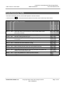
Date of Issue: 12-Nov-2008
Cortex-M3 / Cortex-M3 with ETM (AT420/AT425)
ARM Errata Notice
Document Revision 2.0
ARM Core
Cortex-M3 / Cortex-M3 with ETM (AT420/AT425)
Errata Notice
This document contains the errata known at the date of issue covering supported releases from r1p1 up to and
including revision r2p0 of Cortex-M3 (AT420) and Cortex-M3 with ETM (AT425) products.
PR326-PRDC-009450 v2.0
© Copyright ARM Limited 2008. All rights reserved.
Non Confidential
Page 1 of 20
Cortex-M3 / Cortex-M3 with ETM (AT420/AT425)
ARM Errata Notice
Document Revision 2.0
Date of Issue: 12-Nov-2008
Proprietary notice
Words and logos marked with ® or ™ are registered trademarks or trademarks of ARM Limited in the EU and
other countries, except as otherwise stated below in this proprietary notice. Other brands and names mentioned
herein may be the trademarks of their respective owners.
Neither the whole nor any part of the information contained in, or the product described in, this document may
be adapted or reproduced in any material form except with the prior written permission of the copyright holder.
The product described in this document is subject to continuous developments and improvements. All
particulars of the product and its use contained in this document are given by ARM Limited in good faith.
However, all warranties implied or expressed, including but not limited to implied warranties of merchantability,
or fitness for purpose, are excluded.
This document is intended only to assist the reader in the use of the product. ARM Limited shall not be liable for
any loss or damage arising from the use of any information in this document, or any error or omission in such
information, or any incorrect use of the product.
Document confidentiality status
This document is Non Confidential.
Web address
http://www.arm.com/
PR326-PRDC-009450 v2.0
© Copyright ARM Limited 2008. All rights reserved.
Non Confidential
Page 2 of 20
Cortex-M3 / Cortex-M3 with ETM (AT420/AT425)
ARM Errata Notice
Document Revision 2.0
Date of Issue: 12-Nov-2008
Feedback on the product
If you have any comments or suggestions about this product, contact your supplier giving:
•
The product name
•
A concise explanation of your comments.
Feedback on this document
If you have any comments on about this document, please send email to mailto:[email protected] giving:
•
The document title
•
The documents number
•
The page number(s) to which your comments refer
•
A concise explanation of your comments
General suggestion for additions and improvements are also welcome.
PR326-PRDC-009450 v2.0
© Copyright ARM Limited 2008. All rights reserved.
Non Confidential
Page 3 of 20
Cortex-M3 / Cortex-M3 with ETM (AT420/AT425)
ARM Errata Notice
Document Revision 2.0
Date of Issue: 12-Nov-2008
Contents
INTRODUCTION
5
ERRATA SUMMARY TABLE
7
ERRATA PRESENT ON RELEASE R2P0-00REL0
8
563915: Event Register is not set by interrupts and debug
602117:
8
LDRD with base in list may result in incorrect base register when interrupted or
faulted
ERRATA FIXED ON RELEASE R2P0-00REL0
9
11
531064:
SWJ-DP missing POR reset sync
11
511864:
Cortex-M3 may fetch instructions using incorrect privilege on return from an
exception
12
532314:
DWT CPI counter increments during sleep
13
538714:
Cortex-M3 TPIU Clock Domain crossing
14
548721:
Internal write buffer could be active whilst asleep
15
463763:
BKPT in debug monitor mode can cause DFSR mismatch
16
463764:
Core may freeze for SLEEPONEXIT single instruction ISR
17
463769:
Unaligned MPU fault during a write may cause the wrong data to be written to a
successful first access
18
ERRATA FIXED ON RELEASE R1P1-01REL0
19
429964: Async not generated if no trace in previous session
19
429965:
20
Trigger packets sometimes not inserted in trace stream
PR326-PRDC-009450 v2.0
© Copyright ARM Limited 2008. All rights reserved.
Non Confidential
Page 4 of 20
Cortex-M3 / Cortex-M3 with ETM (AT420/AT425)
ARM Errata Notice
Document Revision 2.0
Date of Issue: 12-Nov-2008
Introduction
Scope
This document describes errata categorised by level of severity. Each description includes:
•
a unique defect tracking identifier
•
the current status of the defect
•
where the implementation deviates from the specification and the conditions under which erroneous
behavior occurs
•
the implications of the erratum with respect to typical applications
•
the application and limitations of a ‘work-around’ where possible
Categorisation of Errata
Errata recorded in this document are split into three levels of severity:
Category 1
Behavior that is impossible to work around and that severely restricts the use of
the product in all, or the majority of applications, rendering the device unusable.
Category 2
Behavior that contravenes the specified behavior and that might limit or severely
impair the intended use of specified features, but does not render the product
unusable in all or the majority of applications.
Category 3
Behavior that was not the originally intended behavior but should not cause any
problems in applications.
PR326-PRDC-009450 v2.0
© Copyright ARM Limited 2008. All rights reserved.
Non Confidential
Page 5 of 20
Date of Issue: 12-Nov-2008
PR326-PRDC-009450 v2.0
Cortex-M3 / Cortex-M3 with ETM (AT420/AT425)
ARM Errata Notice
Document Revision 2.0
© Copyright ARM Limited 2008. All rights reserved.
Non Confidential
Page 6 of 20
Cortex-M3 / Cortex-M3 with ETM (AT420/AT425)
ARM Errata Notice
Document Revision 2.0
Date of Issue: 12-Nov-2008
Errata Summary Table
The errata associated with this product affect product versions as below.
A cell shown thus X indicates that the defect affects the revision shown at the top of that column.
602117
Cat 2
LDRD with base in list may result in incorrect base register when
interrupted or faulted
X
X
X
563915
Cat 2
Event Register is not set by interrupts and debug
X
X
X
531064
Impl
SWJ-DP missing POR reset sync
X
X
511864
Cat 3
Cortex-M3 may fetch instructions using incorrect privilege on return from
an exception
X
X
532314
Cat 3
DWT CPI counter increments during sleep
X
X
538714
Cat 3
Cortex-M3 TPIU Clock Domain crossing
X
X
548721
Cat 3
Internal write buffer could be active whilst asleep
X
X
463763
Cat 3
BKPT in debug monitor mode can cause DFSR mismatch
X
X
463764
Cat 3
Core may freeze for SLEEPONEXIT single instruction ISR
X
X
463769
Cat 3
Unaligned MPU fault during a write may cause the wrong data to be
written to a successful first access
X
X
429964
Cat 2
Async not generated if no trace in previous session
X
429965
Cat 2
Trigger packets sometimes not inserted in trace stream
X
PR326-PRDC-009450 v2.0
© Copyright ARM Limited 2008. All rights reserved.
Non Confidential
r2p0-00rel0
Summary of Erratum
r1p1-01rel0
Cat
r1p1-00rel0
ID
Page 7 of 20
Cortex-M3 / Cortex-M3 with ETM (AT420/AT425)
ARM Errata Notice
Document Revision 2.0
Date of Issue: 12-Nov-2008
Errata present on release r2p0-00rel0
563915: Event Register is not set by interrupts and debug
Status
Affects:
product Cortex-M3, Cortex-M3 with ETM.
Fault status:
Cat 2, Present in: r0p0,r1p0,r1p1,r1p1-00rel0,r1p1-01rel0,r2p0-00rel0, Open.
Description
The event register used for WFE wake-up events should be set for the following conditions:
1. Event communication (including SEV on local processor)
2. Any exception entering pending state when SEVONPEND is set
3. Exception entry
4. Exception exit
5. Debug event when debug is enabled
In r0p0, r1p0, r1p1 and r2p0 versions of Cortex-M3 the event register is not set for the exception entry,
exception exit or debug events.
Conditions
1. An interrupt or debug event occurs whilst the internal event register is clear and the core is not sleeping
2. A WFE is executed
3. No further interrupts or events occur
Implications
If interrupts related to a WFE sleep can be generated before the WFE is executed then it may be possible for
the event to be missed. The interrupt will occur and the handler will be executed for that interrupt but the event
register will not be set. When the WFE is executed it will go to sleep and not wake up if no other events or
interrupts occur.
Workaround
An implementation time workaround is to connect up the missing events to the RXEV input of Cortex-M3. This
can be achieved by decoding interrupt events using ETMINTSTAT as well as using the HALTED output. RXEV
needs to be asserted whenever ETMINTSTAT is equal to 3'b001 or 3'b010 or when HALTED is asserted. Since
ETMINTSTAT is part of the ETM interface the ETM interface needs to be enabled for this workaround. This is
achieved by asserting the ETMPWRUP input on Cortex-M3.
A software workaround is to insert the SEV instruction at the beginning and end of all exception handlers.
PR326-PRDC-009450 v2.0
© Copyright ARM Limited 2008. All rights reserved.
Non Confidential
Page 8 of 20
Cortex-M3 / Cortex-M3 with ETM (AT420/AT425)
ARM Errata Notice
Document Revision 2.0
Date of Issue: 12-Nov-2008
602117:
LDRD with base in list may result in incorrect base register when interrupted
or faulted
Status
Affects:
product Cortex-M3, Cortex-M3 with ETM.
Fault status:
Cat 2, Present in: r0p0,r1p0,r1p1,r1p1-00rel0,r1p1-01rel0,r2p0-00rel0, Open.
Description
LDRD with the base register in the list of the form LDRD Ra, Rb, [Ra, #imm] may not complete after the
load of the first destination register due to an interrupt before the completion of the second load or due to the
second load getting a bus fault or an MPU fault. Since the base register has been updated the base register
must be restored to its original value before entering the appropriate interrupt or fault handler so that the
instruction can restart correctly upon return from the handler. In certain circumstances this may not occur as
required.
When the LDRD is interrupted in between the two loads then the base register may not be restored as required.
This can only happen when the instructions are being executed from the system bus (address 0x20000000 and
above) and the loaded data is also being read from the system bus.
For the fault case where the second load gets a bus fault or an MPU fault then the base register is never
restored and there is no dependence on which bus the instructions are being executed from.
When the base register is the second register in the LDRD list, of the form LDRD Rb, Ra, [Ra, #imm], then
this erratum cannot occur.
You will not be affected by this erratum if:
1. you do not execute code from the system bus and if your code bus does not generate bus faults and
you do not execute LDRD’s that cross MPU boundaries, or
2. if your compiler does not generate LDRD’s
Conditions
Either:
1. An LDRD is being executed where the base register is in the list and write-back is not used:
LDRD Ra, Rb, [Ra, #imm]
2. Instructions and data are both being fetched via the system bus. This occurs for locations in memory
greater than 0x20000000.
3. The first LDRD address is prioritised and issued to the system bus, whilst the instruction fetch is
internally waited. The instruction fetch is issued to the system bus upon completion of the first part of
the LDRD. The second part of the LDRD is issued to the system bus upon completion of the instruction
fetch.
4. An interrupt occurs in between the two load operations.
Or:
1. An LDRD is being executed where the base register is in the list and write-back is not used:
LDRD Ra, Rb, [Ra, #imm]
2. A bus fault or MPU fault occurs for the second load.
PR326-PRDC-009450 v2.0
© Copyright ARM Limited 2008. All rights reserved.
Non Confidential
Page 9 of 20
Date of Issue: 12-Nov-2008
Cortex-M3 / Cortex-M3 with ETM (AT420/AT425)
ARM Errata Notice
Document Revision 2.0
Implications
The base register will not be restored as expected preventing the instruction from being restarted correctly upon
return from the interrupt service routine or from the fault handler.
Workaround
There are two workarounds for this erratum. However, if the instructions are always executed from the code
space and faults cannot occur then a workaround is not required.
The first workaround is to replace the LDRD instruction affected by this erratum with other suitable instructions.
LDRD Ra, Rb, [Ra, #imm]
may be directly replaced by two LDR instructions which will produce exactly the same functionality:
LDR Rb, [Ra, #imm + 4]
LDR Ra, [Ra, #imm]
Alternatively, an LDRD with base in list may still be used if the base register is the second register in the list:
LDRD Rb, Ra, [Ra, #imm]
However, in order to achieve the same functionality this requires that the data at the two addresses are
swapped, or that the following instructions using Ra or Rb swap their source registers.
The second workaround can be applied when using Cortex-M3 r2p0. It is possible to prevent this erratum
occurring for the interrupt case by setting DISMCYCINT (bit[0]) in the Auxiliary Control Register which is located
at address 0xE000E008. This bit prevents the interruption of multi-cycle instructions and will therefore increase
the interrupt latency of Cortex-M3.
Setting DISMCYCINT does not prevent the second load being faulted which means that the base will still be
incorrect for bus faults or MPU faults.
Due to the performance impact of workaround two, and because workaround two does not address the fault
conditions of this erratum, ARM recommends that workaround one is used.
PR326-PRDC-009450 v2.0
© Copyright ARM Limited 2008. All rights reserved.
Non Confidential
Page 10 of 20
Cortex-M3 / Cortex-M3 with ETM (AT420/AT425)
ARM Errata Notice
Document Revision 2.0
Date of Issue: 12-Nov-2008
Errata fixed on release r2p0-00rel0
531064:
SWJ-DP missing POR reset sync
Status
Affects:
product Cortex-M3, Cortex-M3 with ETM.
Fault status:
Impl, Present in: r1p1,r1p1-00rel0,r1p1-01rel0, Fixed in r2p0-00rel0.
Description
In Cortex-M3 r0p0 and r1p0, the SWJ-DP has an internal reset synchronizer for the power on reset signal.
Version r1p1 was upgraded to a newer version of SWJ-DP and this SWJ-DP did not have the same reset
synchronizer inside. As a result of that the timing of the power on reset could potentially be a problem.
Implications
none
Workaround
The r1p1 CortexM3Integration level can be modified to add the reset synchronizer.
The signal which has the problem is the nPOTRST input on SWJ-DP. Add a few new signals:
reg nPOTRSTQ; // DFF #1
reg nPOTRSTQQ; // DFF #2
wire inPOTRST; // reset bypass MUX
// Add the synchroniser DFFs:
always @ (posedge SWCLKTCK or negedge PORESETn)
// nPOTRST synchroniser
if (!PORESETn) begin
nPOTRSTQ <= 1'b0;
nPOTRSTQQ <= 1'b0;
end
else begin
nPOTRSTQ <= 1'b1;
nPOTRSTQQ <= nPOTRSTQ;
end
// And a reset bypass MUX:
assign inPOTRST = RSTBYPASS ? PORESETn : nPOTRSTQQ;
// And connect the MUX output inPOTRST to the nPOTRST input of SWJ-DP:
DAPSWJDP uDAPSWJDP
(// Inputs
.nPOTRST
(inPOTRST),
PR326-PRDC-009450 v2.0
© Copyright ARM Limited 2008. All rights reserved.
Non Confidential
Page 11 of 20
Cortex-M3 / Cortex-M3 with ETM (AT420/AT425)
ARM Errata Notice
Document Revision 2.0
Date of Issue: 12-Nov-2008
511864:
Cortex-M3 may fetch instructions using incorrect privilege on return from an
exception
Status
Affects:
product Cortex-M3, Cortex-M3 with ETM.
Fault status:
Cat 3, Present in: r0p0,r1p0,r1p1,r1p1-00rel0,r1p1-01rel0, Fixed in r2p0-00rel0.
Description
Whilst unstacking registers on return from an exception to a User-privilege thread, Cortex-M3 attempts to
simultaneously prefetch the thread's instruction stream. Before the register unstacking is complete, upto the first
three memory transactions used to perform instruction prefetching may be erroneously marked as Privileged.
This may allow between three and six instructions from a Privileged-access-only region to be executed by a
User-privilege thread.
Once fetched, the instructions are executed with User-privilege. Instruction fetches performed after register
unstacking has completed will be performed with User-privilege. Both the register unstacking, and any datatransactions generated by executing the erroneously executed instructions will be performed and correctly
marked as User-privilege.
Conditions
1. Exception return is executed
2. The exception return is to user code
Implications
User-privileged code may contrive a situation in order to allow execution of up to three words worth of
instructions intended to be accessible to Privileged-only execution; however, execution of said instructions will
always be performed with User-privilege, thus there are no additional capabilities provided to User-privilege
through this erratum.
There exists a theoretical possibility that User-privilege code could use this erratum to allow limited extraction of
code and or data from Privileged-access only memory.
Note that read sensitive Privileged-access only peripherals should always be placed in an XN region either via
the default memory map, or via the optional memory-protection-unit. Alternatively such peripherals should
ignore transactions with HPROT[0] indicating that the transaction is an instruction fetch.
Workaround
None.
PR326-PRDC-009450 v2.0
© Copyright ARM Limited 2008. All rights reserved.
Non Confidential
Page 12 of 20
Cortex-M3 / Cortex-M3 with ETM (AT420/AT425)
ARM Errata Notice
Document Revision 2.0
Date of Issue: 12-Nov-2008
532314: DWT CPI counter increments during sleep
Status
Affects:
product Cortex-M3, Cortex-M3 with ETM.
Fault status:
Cat 3, Present in: r0p0,r1p0,r1p1,r1p1-00rel0,r1p1-01rel0, Fixed in r2p0-00rel0.
Description
The DWT contains a number of counters for the profiling of applications. The CPI counter is used to indicate the
total number of clock cycles beyond the first cycle of each instruction. The counter is specified to not increment
whilst the core is sleeping but for previous revisions it does increment. This results in sleep cycles being
counted as program execution cycles.
Conditions
1. The CPI counter in the DWT is enabled
2. Core sleeps during profiling
Implications
Profiling information could be calculated incorrectly if the following calculation is used:
InstructionCount = CycleCount – (CPIcount+LSUcount+INTcount+SLEEPcount) + FOLDcount
Workaround
The number of sleep cycles given by SLEEPCNT can be subtracted from the CPI cycle count to obtain the
correct CPI cycle information. Use the following equation:
InstructionCount = CycleCount – (CPIcount+LSUcount+INTcount) + FOLDcount
PR326-PRDC-009450 v2.0
© Copyright ARM Limited 2008. All rights reserved.
Non Confidential
Page 13 of 20
Date of Issue: 12-Nov-2008
Cortex-M3 / Cortex-M3 with ETM (AT420/AT425)
ARM Errata Notice
Document Revision 2.0
538714: Cortex-M3 TPIU Clock Domain crossing
Status
Affects:
product Cortex-M3, Cortex-M3 with ETM.
Fault status:
Cat 3, Present in: r0p0,r1p0,r1p1,r1p1-00rel0,r1p1-01rel0, Fixed in r2p0-00rel0.
Description
Combinatorial paths exist in control signals crossing the asynchronous clock boundary between FCLK and
TRACECLKIN.
Some of these signals control the reading and writing of data in the trace data FIFO on both sides of the FCLK
and TRACECLKIN clock boundary and therefore could cause old data to be repeated or new data to be lost.
Conditions
1.
FCLK/HCLK is asynchronous to TRACECLKIN
Implications
When FCLK and TRACECLKIN are asynchronous and depending on the silicon implementation of the block,
trace data might become corrupted.
Workaround
This is a workaround for system implementers. System implementers should make FCLK and TRACECLKIN
operate synchronously. To avoid the possibility of corrupted trace data, the Trace Port must be fed with a clock
synchronous to FCLK. Any crossing to an asynchronous TRACECLKIN domain should be done externally
before the TPIU via a separate ATB asynchronous bridge.
PR326-PRDC-009450 v2.0
© Copyright ARM Limited 2008. All rights reserved.
Non Confidential
Page 14 of 20
Date of Issue: 12-Nov-2008
Cortex-M3 / Cortex-M3 with ETM (AT420/AT425)
ARM Errata Notice
Document Revision 2.0
548721: Internal write buffer could be active whilst asleep
Status
Affects:
product Cortex-M3, Cortex-M3 with ETM.
Fault status:
Cat 3, Present in: r0p0,r1p0,r1p1,r1p1-00rel0,r1p1-01rel0, Fixed in r2p0-00rel0.
Description
If a store immediate that is marked as not strongly ordered is used immediately before a WFE or WFI then the
store may still be in progress when the core has asserted the SLEEPING signal. This will only occur if waitstates are applied to the store operation. This will not cause a problem unless the location that the store was
accessing was using a free-running clock whilst a clock-gating cell has been used to gate FCLK to form HCLK.
Conditions
1. A store with immediate offset is executed
2. The store operation is allowed to be bufferable
3. The store is followed immediately by a WFI or WFE
4. Wait-states are used to delay the data-phase of the store
5. A clock-gate is used to produce HCLK which is gated when SLEEPING is asserted
6. The location the store was to is using a free-running version of the core clock (FCLK)
Implications
An imprecise error response could be missed if it is issued by the peripheral whilst the core is asleep when the
peripheral is not using a gated clock but the core is. The stored data will be correct as the core will hold
HWDATA at the correct value until it wakes from sleep and completes the transaction.
Workaround
A software workaround is to insert DSB instructions before any WFE and WFI instructions in the application
code.
PR326-PRDC-009450 v2.0
© Copyright ARM Limited 2008. All rights reserved.
Non Confidential
Page 15 of 20
Date of Issue: 12-Nov-2008
463763:
Cortex-M3 / Cortex-M3 with ETM (AT420/AT425)
ARM Errata Notice
Document Revision 2.0
BKPT in debug monitor mode can cause DFSR mismatch
Status
Affects:
product Cortex-M3, Cortex-M3 with ETM.
Fault status:
Cat 3, Present in: r0p0,r1p0,r1p1,r1p1-00rel0,r1p1-01rel0, Fixed in r2p0-00rel0.
Description
A BKPT may be executed in debug monitor mode which will cause the debug monitor handler to be run but the
Debug Fault Status Register (DFSR) at address 0xE000ED30 will not have bit 1 set to indicate the cause was a
BKPT instruction. This will only occur if an interrupt other than the Debug Monitor is already being processed
just before the BKPT is executed.
Conditions
1. C_DEBUGEN (bit 0) in the Debug Halting Control and Status Register at address 0xE000EDF0 is 0.
2. MON_EN (bit 16) in the Debug Exception and Monitor Control Register at address 0xE000EDFC is 1.
3. An enabled interrupt occurs two cycles before the BKPT is executed that causes a pre-emption.
Implications
The Debug Monitor handler may be entered without the DFSR revealing the cause of the handler being entered.
Workaround
Should a workaround be required, it can be deduced that if the DFSR does not have any bits set when the
debug monitor has been entered then the cause must be due to this corner case and that it was the result of a
BKPT.
PR326-PRDC-009450 v2.0
© Copyright ARM Limited 2008. All rights reserved.
Non Confidential
Page 16 of 20
Date of Issue: 12-Nov-2008
Cortex-M3 / Cortex-M3 with ETM (AT420/AT425)
ARM Errata Notice
Document Revision 2.0
463764: Core may freeze for SLEEPONEXIT single instruction ISR
Status
Affects:
product Cortex-M3, Cortex-M3 with ETM.
Fault status:
Cat 3, Present in: r0p0,r1p0,r1p1,r1p1-00rel0,r1p1-01rel0, Fixed in r2p0-00rel0.
Description
The SLEEPONEXIT functionality causes the core to enter the sleep mode when the exit from the sole active
interrupt occurs. This means that there are no more interrupts active and the exit would have caused a return to
the thread.
It is possible for the core to become frozen if the SLEEPONEXIT functionality is used and the interrupt service
routine (ISR) concerned only contains a single instruction. This freezing may occur if only one interrupt is active
and it is pre-empted by an interrupt whose handler only contains the single instruction. This instruction must be
a legal ISR exit instruction that takes one cycle to execute (either a BX or a BLX). In this case the unstacking
would occur after the single instruction had been executed as normal to return to the now only active interrupt
handler. However, once it has returned no more instructions will be processed and the core will be frozen. Any
new pre-empting interrupt will unfreeze the processor.
Conditions
1. SLEEPONEXIT (bit 1) in the System Control Register at address 0xE000ED10 is set.
2. An interrupt occurs that causes a pre-emption of the current ISR which is the only interrupt that is
currently active.
3. The interrupt service routine that is entered consists of only one instruction (either BX or BLX) which
causes a legal exit from that ISR.
Implications
The core may freeze and stop processing instructions when it returns to the only currently active ISR. Note that
a new interrupt that causes a pre-emption would cause the core to become unfrozen and behave correctly
again.
Workaround
If the SLEEPONEXIT functionality is required then do not allow an ISR to contain only one instruction. If an
empty ISR is used then insert a NOP before the exit instruction.
PR326-PRDC-009450 v2.0
© Copyright ARM Limited 2008. All rights reserved.
Non Confidential
Page 17 of 20
Cortex-M3 / Cortex-M3 with ETM (AT420/AT425)
ARM Errata Notice
Document Revision 2.0
Date of Issue: 12-Nov-2008
463769: Unaligned MPU fault during a write may cause the wrong data to be written
to a successful first access
Status
Affects:
product Cortex-M3, Cortex-M3 with ETM.
Fault status:
Cat 3, Present in: r0p0,r1p0,r1p1,r1p1-00rel0,r1p1-01rel0, Fixed in r2p0-00rel0.
Description
When an unaligned store is executed by Cortex-M3 the transaction is split up into either two or three aligned
transactions forming constituent parts of the larger transaction. The MPU will check that these transactions are
permitted and will block them if necessary. If an unaligned transaction occurs where it overlaps two MPU
regions then each region relating to the part of the transaction that hits that region will be checked.
If an unaligned store occurs that crosses an MPU region boundary and has an MPU permission fault for the
second region check but not for the first region then it is possible for the second component’s data to be written
for the first successful transaction in place of the first transaction’s data. This can occur for writes to either the
D-Code or system bus but will only occur if one or more wait-states are applied for the first component of the
store.
Conditions
1. The full MPU is present and enabled with at least one region programmed and enabled.
2. An unaligned store is executed by the processor. The store can be to either the D-Code or the System
bus.
3. The store crosses an MPU region boundary.
4. The first region lookup passes, the second region lookup fails.
5. One or more wait states are applied via HREADYS or HREADYD.
Implications
The wrong data will be stored to a permitted address. However, a MemManage fault will occur immediately
pointing to the instruction that caused the fault. This may lead to the instruction being re-executed and the store
occurring successfully if it is for non-device memory. This would mean that the previously stored data would be
overwritten and the wrong value would never be seen. This may not be true for a shared memory system.
Workaround
A workaround is only required if the MPU is present and enabled. Either:
1. do not allow accesses to span more than one region or
2. do not allow unaligned accesses at all or
3. program the MPU correctly if applicable
PR326-PRDC-009450 v2.0
© Copyright ARM Limited 2008. All rights reserved.
Non Confidential
Page 18 of 20
Cortex-M3 / Cortex-M3 with ETM (AT420/AT425)
ARM Errata Notice
Document Revision 2.0
Date of Issue: 12-Nov-2008
Errata fixed on release r1p1-01rel0
429964: Async not generated if no trace in previous session
Status
Affects:
product Cortex-M3 with ETM.
Fault status:
Cat 2, Present in: r0p0,r1p0,r1p1,r1p1-00rel0, Fixed in r1p1-01rel0.
Description
The ETM is required to generate an alignment synchronisation packet as the first packet every time the
programming bit is cleared, in order to allow the tools to synchronise with the protocol stream.
If no trace is generated in a session, the A-sync packet will be correctly generated as the progbit is cleared, but
if the progbit is then set and cleared again, second and subsequent A-sync packets are not generated. No other
aspects of the trace generation are affected by this, and once any other trace packet is generated the A-sync
logic will be correctly reset.
Conditions
This erratum only occurs when the following sequence of events occurs:
1. The ETM is programmed and enabled
2. No instructions are traced
3. The ETM programming bit is set
4. The ETM programming bit is cleared.
The absence of any traced instructions can be due either to the Trace Enable conditions not being satisfied, or
the core not executing any instructions.
Implications
This erratum only affects the trace stream which is generated by the ETM. There is no impact on the normal
processing operation of the core.
The conditions which cause this erratum are expected to occur whilst debug is being performed.
The A-sync packet may be missing at the start of a trace session. All trace packets which are generated will still
be correct, and there is no corruption of the trace stream. If the A-sync from a previous session was captured, it
can be used for synchronisation.
Tools will typically fail to capture the trace relating to any bytes of trace before the next periodic A-sync packet is
seen. For short trace sessions, it is possible to lose the whole trace session.
Workaround
There is no tools workaround.
Users may attempt to work around this erratum by forcing the generation of trace packets as part of an
initialisation sequence. This is only possible if the core is not in debug state, and so may not be applicable in all
cases. With this ETM it is also possible to deduce that the first byte of trace captured after the progbit is cleared
will be the start of a packet, provided that the formatter in the TPIU is enabled.
PR326-PRDC-009450 v2.0
© Copyright ARM Limited 2008. All rights reserved.
Non Confidential
Page 19 of 20
Date of Issue: 12-Nov-2008
Cortex-M3 / Cortex-M3 with ETM (AT420/AT425)
ARM Errata Notice
Document Revision 2.0
429965: Trigger packets sometimes not inserted in trace stream
Status
Affects:
product Cortex-M3 with ETM.
Fault status:
Cat 2, Present in: r0p0,r1p0,r1p1,r1p1-00rel0, Fixed in r1p1-01rel0.
Description
It is possible to configure a trigger event for the ETM which is used to assist with trace capture and the
subsequent analysis of trace by the user. The trigger condition is indicated by a pulse on the ETMTRIGOUT
signal, and is also inserted in the trace stream using a special packet.
If a trigger condition occurs when there is no data in the ETM's FIFO and there are no instructions yet to be
traced, the ETMTRIGOUT signal is pulsed correctly, but the trigger packet is not inserted in the trace stream.
Conditions
1. The ETM is enabled
2. The trace FIFO is empty
3. There are no instructions already executed but not yet entered in the trace fifo.
Implications
This erratum only affects the trace stream which is generated by the ETM. There is no impact on the normal
processing operation of the core.
This erratum only affects the inclusion of the trigger packet in the trace stream. It does not affect the visibility of
the trigger condition through the ETM's programmers model (bit 2 of the ETM Status Register, register 4).
It does not affect the indication of the trigger condition to the trace capture device, and a formatter trigger packet
will be inserted if enabled.
The erratum does not occur if a trigger is generated using DWT to detect an instruction address if Trace Enable
is high.
When this erratum occurs, the user will not be able to determine the location in the executed instruction
sequence at which the trigger condition occurred. Due to the conditions which are required for this erratum to
occur, it is more likely that the erratum occurs when an external input is being used to generate the trigger
condition.
Workaround
There is no workaround to force the trigger packet to be included in the trace stream. If using the CoreSight
formatter protocol, e.g. TPIU/ETB with trigger embedded, then the position of the embedded trigger can be
used, however the location of the embedded trigger is approximate.
PR326-PRDC-009450 v2.0
© Copyright ARM Limited 2008. All rights reserved.
Non Confidential
Page 20 of 20
IMPORTANT NOTICE
Texas Instruments Incorporated and its subsidiaries (TI) reserve the right to make corrections, modifications, enhancements, improvements,
and other changes to its products and services at any time and to discontinue any product or service without notice. Customers should
obtain the latest relevant information before placing orders and should verify that such information is current and complete. All products are
sold subject to TI’s terms and conditions of sale supplied at the time of order acknowledgment.
TI warrants performance of its hardware products to the specifications applicable at the time of sale in accordance with TI’s standard
warranty. Testing and other quality control techniques are used to the extent TI deems necessary to support this warranty. Except where
mandated by government requirements, testing of all parameters of each product is not necessarily performed.
TI assumes no liability for applications assistance or customer product design. Customers are responsible for their products and
applications using TI components. To minimize the risks associated with customer products and applications, customers should provide
adequate design and operating safeguards.
TI does not warrant or represent that any license, either express or implied, is granted under any TI patent right, copyright, mask work right,
or other TI intellectual property right relating to any combination, machine, or process in which TI products or services are used. Information
published by TI regarding third-party products or services does not constitute a license from TI to use such products or services or a
warranty or endorsement thereof. Use of such information may require a license from a third party under the patents or other intellectual
property of the third party, or a license from TI under the patents or other intellectual property of TI.
Reproduction of TI information in TI data books or data sheets is permissible only if reproduction is without alteration and is accompanied
by all associated warranties, conditions, limitations, and notices. Reproduction of this information with alteration is an unfair and deceptive
business practice. TI is not responsible or liable for such altered documentation. Information of third parties may be subject to additional
restrictions.
Resale of TI products or services with statements different from or beyond the parameters stated by TI for that product or service voids all
express and any implied warranties for the associated TI product or service and is an unfair and deceptive business practice. TI is not
responsible or liable for any such statements.
TI products are not authorized for use in safety-critical applications (such as life support) where a failure of the TI product would reasonably
be expected to cause severe personal injury or death, unless officers of the parties have executed an agreement specifically governing
such use. Buyers represent that they have all necessary expertise in the safety and regulatory ramifications of their applications, and
acknowledge and agree that they are solely responsible for all legal, regulatory and safety-related requirements concerning their products
and any use of TI products in such safety-critical applications, notwithstanding any applications-related information or support that may be
provided by TI. Further, Buyers must fully indemnify TI and its representatives against any damages arising out of the use of TI products in
such safety-critical applications.
TI products are neither designed nor intended for use in military/aerospace applications or environments unless the TI products are
specifically designated by TI as military-grade or "enhanced plastic." Only products designated by TI as military-grade meet military
specifications. Buyers acknowledge and agree that any such use of TI products which TI has not designated as military-grade is solely at
the Buyer's risk, and that they are solely responsible for compliance with all legal and regulatory requirements in connection with such use.
TI products are neither designed nor intended for use in automotive applications or environments unless the specific TI products are
designated by TI as compliant with ISO/TS 16949 requirements. Buyers acknowledge and agree that, if they use any non-designated
products in automotive applications, TI will not be responsible for any failure to meet such requirements.
Following are URLs where you can obtain information on other Texas Instruments products and application solutions:
Products
Amplifiers
Data Converters
DLP® Products
DSP
Clocks and Timers
Interface
Logic
Power Mgmt
Microcontrollers
RFID
RF/IF and ZigBee® Solutions
amplifier.ti.com
dataconverter.ti.com
www.dlp.com
dsp.ti.com
www.ti.com/clocks
interface.ti.com
logic.ti.com
power.ti.com
microcontroller.ti.com
www.ti-rfid.com
www.ti.com/lprf
Applications
Audio
Automotive
Broadband
Digital Control
Medical
Military
Optical Networking
Security
Telephony
Video & Imaging
Wireless
www.ti.com/audio
www.ti.com/automotive
www.ti.com/broadband
www.ti.com/digitalcontrol
www.ti.com/medical
www.ti.com/military
www.ti.com/opticalnetwork
www.ti.com/security
www.ti.com/telephony
www.ti.com/video
www.ti.com/wireless
Mailing Address: Texas Instruments, Post Office Box 655303, Dallas, Texas 75265
Copyright © 2009, Texas Instruments Incorporated