1
MVME167
Single Board Computer
Installation Guide
MVME167IG/D4
Notice
While reasonable efforts have been made to assure the accuracy of this document,
Motorola, Inc. assumes no liability resulting from any omissions in this document,
or from the use of the information obtained therein. Motorola reserves the right to
revise this document and to make changes from time to time in the content hereof
without obligation of Motorola to notify any person of such revision or changes.
No part of this material may be reproduced or copied in any tangible medium, or
stored in a retrieval system, or transmitted in any form, or by any means, radio,
electronic, mechanical, photocopying, recording or facsimile, or otherwise,
without the prior written permission of Motorola, Inc.
It is possible that this publication may contain reference to, or information about
Motorola products (machines and programs), programming, or services that are
not announced in your country. Such references or information must not be
construed to mean that Motorola intends to announce such Motorola products,
programming, or services in your country.
Restricted Rights Legend
If the documentation contained herein is supplied, directly or indirectly, to the U.S.
Government, the following notice shall apply unless otherwise agreed to in
writing by Motorola, Inc.
Use, duplication, or disclosure by the Government is subject to restrictions as set
forth in subparagraph (c)(1)(ii) of the Rights in Technical Data and Computer
Software clause at DFARS 252.227-7013.
Motorola, Inc.
Computer Group
2900 South Diablo Way
Tempe, Arizona 85282-9602
Preface
This manual provides a general board level hardware description, hardware
preparation and installation instructions, debugger general information, and
information on using the debugger.
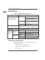
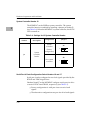
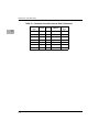
This manual applies to the following MVME167 Single Board Computers:
Assembly Item
Board Description
MVME167-001B
25MHZ, 4MB Parity
MVME167-002B
25MHZ, 8MB Parity
MVME167-003B
25MHZ, 16MB Parity
MVME167-004B
25MHZ, 32MB Parity
MVME167-031B
33MHZ, 4MB ECC
MVME167-032B
33MHZ, 8MB ECC
MVME167-033B
33MHZ, 16MB ECC
MVME167-034B
33MHZ, 32MB ECC
MVME167-035B
33MHZ, 64MB ECC
MVME167-036B
33MHZ, 128MB ECC
This manual is intended for anyone who wants to provide OEM systems, supply
additional capability to an existing compatible system, or work in a lab
environment for experimental purposes.
Anyone using this manual should have a basic knowledge of computers and
digital logic.
Safety Summary
Safety Depends On You
The following general safety precautions must be observed during all phases of operation, service, and
repair of this equipment. Failure to comply with these precautions or with speciÞc warnings elsewhere in
this manual violates safety standards of design, manufacture, and intended use of the equipment.
Motorola, Inc. assumes no liability for the customer's failure to comply with these requirements.
The safety precautions listed below represent warnings of certain dangers of which Motorola is aware. You,
as the user of the product, should follow these warnings and all other safety precautions necessary for the
safe operation of the equipment in your operating environment.
Ground the Instrument.
To minimize shock hazard, the equipment chassis and enclosure must be connected to an electrical ground.
The equipment is supplied with a three-conductor ac power cable. The power cable must be plugged into
an approved three-contact electrical outlet. The power jack and mating plug of the power cable meet
International Electrotechnical Commission (IEC) safety standards.
Do Not Operate in an Explosive Atmosphere.
Do not operate the equipment in the presence of ßammable gases or fumes. Operation of any electrical
equipment in such an environment constitutes a deÞnite safety hazard.
Keep Away From Live Circuits.
Operating personnel must not remove equipment covers. Only Factory Authorized Service Personnel or
other qualiÞed maintenance personnel may remove equipment covers for internal subassembly or
component replacement or any internal adjustment. Do not replace components with power cable
connected. Under certain conditions, dangerous voltages may exist even with the power cable removed. To
avoid injuries, always disconnect power and discharge circuits before touching them.
Do Not Service or Adjust Alone.
Do not attempt internal service or adjustment unless another person capable of rendering Þrst aid and
resuscitation is present.
Use Caution When Exposing or Handling the CRT.
Breakage of the Cathode-Ray Tube (CRT) causes a high-velocity scattering of glass fragments (implosion).
To prevent CRT implosion, avoid rough handling or jarring of the equipment. Handling of the CRT should
be done only by qualiÞed maintenance personnel using approved safety mask and gloves.
Do Not Substitute Parts or Modify Equipment.
Because of the danger of introducing additional hazards, do not install substitute parts or perform any
unauthorized modiÞcation of the equipment. Contact your local Motorola representative for service and
repair to ensure that safety features are maintained.
Dangerous Procedure Warnings.
Warnings, such as the example below, precede potentially dangerous procedures throughout this manual.
Instructions contained in the warnings must be followed. You should also employ all other safety
precautions which you deem necessary for the operation of the equipment in your operating environment.
!
WARNING
Dangerous voltages, capable of causing death, are
present in this equipment. Use extreme caution when
handling, testing, and adjusting.
All Motorola PWBs (printed wiring boards) are manufactured by UL-recognized
manufacturers, with a ßammability rating of 94V-0.
!
WARNING
This equipment generates, uses, and can radiate electromagnetic energy. It may cause or be susceptible to
electro-magnetic interference (EMI) if not installed and
used in a cabinet with adequate EMI protection.
European Notice: Board products with the CE marking comply with the
EMC Directive (89/336/EEC). Compliance with this directive implies
conformity to the following European Norms:
EN55022 (CISPR 22) Radio Frequency Interference
EN50082-1 (IEC801-2, IEC801-3, IEEC801-4) Electromagnetic Immunity
The product also fulÞlls EN60950 (product safety) which is essentially
the requirement for the Low Voltage Directive (73/23/EEC).
This board product was tested in a representative system to show
compliance with the above mentioned requirements. A proper
installation in a CE-marked system will maintain the required
EMC/safety performance.
The computer programs stored in the Read Only Memory of this device contain
material copyrighted by Motorola Inc., 1995, and may be used only under a license
such as those contained in MotorolaÕs software licenses.
Motorola¨ and the Motorola symbol are registered trademarks of Motorola, Inc.
All other products mentioned in this document are trademarks or registered
trademarks of their respective holders.
©Copyright Motorola 1997
All Rights Reserved
Printed in the United States of America
March 1997
Contents
This Chapter Covers 1-1
About this Manual 1-1
Terminology, Conventions, and DeÞnitions Used in this Manual 1-2
Data and Address Parameter Numeric Formats 1-2
Signal Name Conventions 1-2
Assertion and Negation Conventions 1-3
Data and Address Size DeÞnitions 1-3
Control and Status Bit DeÞnitions 1-4
True/False Bit State DeÞnitions 1-4
Bit Value Descriptions 1-4
Related Documentation 1-5
Document Set for MVME167-0xx Board 1-5
Additional Manuals for this Board 1-6
Other Applicable Motorola Publications 1-6
Non-Motorola Peripheral Controllers Publications Bundle 1-7
Applicable Non-Motorola Publications 1-8
This Chapter Covers 2-1
General Description 2-1
Onboard Memory Mezzanine Module 2-2
SCSI Mass Storage Interface 2-2
Serial Ports 2-3
Parallel (Printer) Port 2-3
Ethernet Transceiver Interface 2-3
167Bug Firmware 2-4
Features 2-4
SpeciÞcations 2-6
Conformance to Requirements 2-6
Board Level Overview 2-7
Connectors 2-7
Adapters 2-7
Transition Modules 2-8
ASICs 2-8
VMEchip2 ASIC 2-9
PCCchip2 ASIC 2-9
MEMC040 Memory Controller ASIC 2-10
MCECC Memory Controller ASIC 2-10
Functional Description 2-10
Front Panel Switches and LEDs 2-11
Data Bus Structure 2-12
Local Bus Arbitration 2-12
MC68040 MPU 2-12
EPROM 2-13
Programmable EPROM features 2-13
Static RAM 2-13
Optional SRAM Battery Backup 2-14
Onboard DRAM 2-15
Stacking Mezzanines 2-16
DRAM Programming Considerations 2-16
Battery Backed Up RAM and Clock 2-17
VMEbus Interface 2-18
I/O Interfaces 2-18
Serial Port Interface 2-18
Parallel Port Interface 2-20
Ethernet Interface 2-21
SCSI Interface 2-22
Local Resources 2-23
Programmable Tick Timers 2-23
Watchdog Timer 2-23
Software-Programmable Hardware Interrupts 2-23
Local Bus Timeout 2-23
Memory Maps 2-24
Local Bus Memory Map 2-24
Normal Address Range 2-24
VMEbus Memory Map 2-28
VMEbus Accesses to the Local Bus 2-28
VMEbus Short I/O Memory Map 2-28
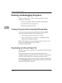
This Chapter Covers 3-1
Unpacking the Equipment 3-1
Overview of Startup Procedure 3-2
Preparing the Hardware 3-5
Modifying ConÞguration before Installation 3-5
Option Modification 3-5
Checking the 167Bug EPROMs 3-7
EPROM Location 3-7
EPROM Orientation 3-7
User-programmed EPROMs 3-7
Jumper Settings 3-7
Optional Jumper Settings 3-8
General Purpose Software Readable Header J1 3-8
System Controller Header J2 3-10
Serial Port 4 Clock Configuration Select Headers J6 and J7 3-10
Optional SRAM Backup Power Source Select Header J8 3-12
Preparing the MVME167 for Installation 3-13
Preparing the System Chassis 3-14
Installing the Hardware 3-15
Installing the MVME167 in the Chassis 3-15
Transition Modules and Adapter Boards Overview 3-16
Equipment Connections 3-18
Installing Transition Modules and Adapter Boards 3-19
Connecting Peripherals 3-19
Completing the Installation 3-23
Starting the System 3-23
Powering Up the System 3-24
Initializing the Real-Time Clock 3-24
Examining and/or Changing Environmental Parameters 3-24
Programming the PCCchip2 and VMEchip2 3-25
System Considerations 3-26
Backplane Power Connections 3-26
Memory Address Ranges 3-26
DRAM Addressing 3-26
Global Bus Timeout 3-26
Multiple Module Cage Configuration 3-27
GCSR Location Monitor Register 3-27
Ethernet LAN (+12 Vdc) Fuse 3-27
SCSI Bus Termination 3-28
Storage and the Real-Time Clock 3-28
This Chapter Covers 4-1
Introduction to MVME167Bug 4-1
Overview of M68000 Firmware 4-1
Description of 167Bug 4-2
Command Facilities 4-2
Trap #15 System Calls 4-2
Debugger or Diagnostic Directories 4-3
Keyboard Control 4-3
Similarity to other Motorola Debugging Firmware 4-4
167Bug Implementation 4-4
Memory Requirements 4-5
Booting and Restarting 167Bug 4-5
Starting Up 167Bug 4-6
Autoboot 4-6
Autoboot Sequence 4-6
ROMboot 4-7
ROMboot Sequence 4-7
Network Boot 4-8
Network Boot Sequence 4-8
Restarting the System 4-9
Reset 4-10
Abort 4-10
Break 4-11
SYSFAIL* Assertion/Negation 4-12
MPU Clock Speed Calculation 4-12
Disk I/O Support 4-13
Disk Support Facilities 4-13
Parameter Tables 4-13
Supported Controllers 4-13
Blocks Versus Sectors 4-14
Device Probe Function 4-14
Disk I/O via 167Bug Commands 4-15
IOI (Input/Output Inquiry) 4-15
IOP (Physical I/O to Disk) 4-15
IOT (I/O Teach) 4-15
IOC (I/O Control) 4-15
BO (Bootstrap Operating System) 4-15
BH (Bootstrap and Halt) 4-16
Disk I/O via 167Bug System Calls 4-16
Controller Command Packets 4-16
Default 167Bug Controller and Device Parameters 4-17
Disk I/O Error Codes 4-18
Network I/O Support 4-19
Intel 82596 LAN Coprocessor Ethernet Driver 4-19
UDP/IP Protocol Modules 4-19
RARP/ARP Protocol Modules 4-20
BOOTP Protocol Module 4-20
TFTP Protocol Module 4-20
Network Boot Control Module 4-20
Network I/O Error Codes 4-21
Multiprocessor Support 4-21
Multiprocessor Control Register (MPCR) Method 4-21
MPCR Status Codes 4-22
Multiprocessor Address Register (MPAR) 4-22
MPCR Powerup sequence 4-22
Global Control and Status Register (GCSR) Method 4-24
Diagnostic Facilities 4-25
167Bug Diagnostic Test Groups 4-27
This Chapter Covers 5-1
Entering Debugger Command Lines 5-1
Terminal Input/Output Control 5-1
Debugger Command Syntax 5-3
Syntactic Variables 5-4
Expression as a Parameter 5-4
Address as a Parameter 5-5
Address Formats 5-6
Offset Registers 5-7
Port Numbers 5-9
Entering and Debugging Programs 5-10
Creating a Program with the Assembler/Disassembler 5-10
Downloading an S-Record Object File 5-10
Read the Program from Disk 5-11
Calling System Utilities from User Programs 5-11
Preserving the Debugger Operating Environment 5-11
167Bug Vector Table and Workspace 5-12
Examples 5-13
Hardware Functions 5-13
Exception Vectors Used by 167Bug 5-13
Example: Trace one instruction using debugger. 5-15
Exception Vector Tables 5-15
Using 167Bug Target Vector Table 5-15
Creating a New Vector Table 5-16
167Bug Generalized Exception Handler 5-17
Floating Point Support 5-18
Single Precision Real 5-20
Double Precision Real 5-20
Extended Precision Real 5-20
Packed Decimal Real 5-21
ScientiÞc Notation 5-21
The 167Bug Debugger Command Set 5-22
This Appendix Covers A-1
ConÞgure Board Information Block A-1
Setting Environment to Bug/Operating System A-3
Disk/Tape Controller Modules Supported B-1
Disk/Tape Controller Default ConÞgurations B-2
IOT Command Parameters for Supported Floppy Types B-4
Network Controller Modules Supported C-1
Introduction E-1
Levels of Implementation E-3
Signal Adaptations E-4
Sample ConÞgurations E-4
Proper Grounding E-7
List of Figures
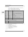
MVME167 General Block Diagram 2-7
MVME167 Switches, Headers, Connectors, Fuses, and LEDs 3-6
Typical Internal SCSI and Serial Port Connections 3-17
Using MVME712A/AM and MVME712B 3-21
Typical Transition Module Peripheral Port Connectors 3-22
List of Tables
MVME167 General SpeciÞcations 2-6
Bus Transfers 2-9
Front Panel Switches 2-11
Front Panel LEDs 2-11
Local Bus Memory Map 2-25
Local I/O Devices Memory Map 2-26
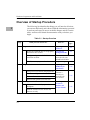
Startup Overview 3-2
J1 Bit Descriptions 3-9
Factory Settings for J1 General Purpose Readable Jumpers 3-9
Settings for J2 System Controller Header 3-10
Settings for J6 and J7 Serial Port 4 Clock ConÞguration Select Headers 3-11
Settings for Optional J8 SRAM Backup Power Source
Select Header 3-12
MVME167 Preparation Procedure 3-13
Chassis Preparation/Slot Selection Procedure 3-14
MVME167 Installation Procedure 3-15
Peripheral Connections 3-18
Transition Module and Adapter Board Installation Overview 3-19
Peripheral Connection Procedures 3-20
Installation Completion Procedure 3-23
System Startup Overview 3-23
RTC Initialization Procedure 3-25
Diagnostic Monitor Commands/PreÞxes 4-25
Diagnostic Utilities 4-26
Diagnostic Test Groups 4-27
Debugger Address Parameter Formats 5-6
Exception Vectors Used by 167Bug 5-13
Debugger Commands 5-22
xiv
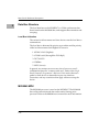
1Introduction to the MVME167
Installation Guide
1
This Chapter Covers
❏
Details about this manual
❏
Terminology, conventions, and definitions used
❏
Other publications relevant to the MVME167
About this Manual
This manual supports the setup, installation, and debugging of the
CISC-based MVME167 Single Board Computer; a highfunctionality VMEbus-based solution for scientific and industrial
embedded-controller applications.
This manual provides:
❏
A general Board Level Hardware Description in Chapter 2
❏
Hardware Preparation and Installation instructions in Chapter 3
❏
Debugger General Information in Chapter 4
❏
Debugger/monitor commands, and other information about
Using the 167Bug Debugger in Chapter 5
❏
Other information needed for startup and troubleshooting of
the MVME167 CISC Single Board Computer, including
Ð Configure and Environment Commands in Appendix A
Ð Disk/Tape Controller Data in Appendix B for controller
modules supported by 167Bug
Ð Network Controller Data in Appendix C
Ð Procedures for Troubleshooting CPU Boards in Appendix D
Ð EIA-232-D Interconnections in Appendix E
1-1
1
Introduction to the MVME167 Installation Guide
Terminology, Conventions, and Definitions
Used in this Manual
Data and Address Parameter Numeric Formats
Throughout this manual, a character identifying the numeric
format precedes data and address parameters as follows:
$
%
&
dollar
percent
ampersand
speciÞes a hexadecimal character
speciÞes a binary number
speciÞes a decimal number
For example, Ò12Ó is the decimal number twelve, and Ò$12Ó is the
decimal number eighteen.
Unless otherwise specified, all address references are in
hexadecimal.
Signal Name Conventions
An asterisk (*) follows signal names for signals which are level or
edge significant:
Term
1-2
* Indicates
level
signiÞcant
The signal is true or valid when the signal is low.
edge
signiÞcant
The actions initiated by that signal occur on high
to low transition.
Terminology, Conventions, and Definitions Used in this Manual
Assertion and Negation Conventions
Assertion and negation are used to specify forcing a signal to a
particular state. These terms are used independently of the voltage
level (high or low) that they represent.
Term
Indicates
Assertion and assert
The signal is active or true.
Negation and negate
The signal is inactive or false.
Data and Address Size Definitions
Data and address sizes are defined as follows:
Name
Size
Numbered
SigniÞcance
Called
Byte
8 bits
0 through 7
bit 0 is the
least
signiÞcant
byte
Two-byte
16 bits
0 through 15
bit 0 is the
least
signiÞcant
word
Four-byte
32 bits
0 through 31
bit 0 is the
least
signiÞcant
longword
1-3
1
1
Introduction to the MVME167 Installation Guide
Control and Status Bit Definitions
The terms control bit and status bit are used extensively in this
document to describe certain bits in registers.
Term
Describes
Control bit
The bit can be set and cleared under software
control.
Status bit
❏
The bit reßects a speciÞc condition.
The status bit can be read by software to determine
operational or exception conditions.
True/False Bit State Definitions
True and False indicate whether a bit enables or disables the
function it controls:
Term
Indicates
True
Enables the function it controls.
False
Disables the function it controls.
Bit Value Descriptions
In all tables, the terms 0 and 1 are used to describe the actual value
that should be written to the bit, or the value that it yields when
read.
1-4
Related Documentation
Related Documentation
The MVME167 ships with a startup installation guide
(MVME167IG/D, the document you are presently reading) which
includes installation instructions, jumper configuration
information, memory maps, debugger/monitor commands, and
any other information needed for startup of the board.
If you wish to develop your own applications or need more detailed
information about your MVME167 Single Board Computer, you
may purchase the additional documentation listed on the following
pages through your local Motorola sales office.
If any supplements have been issued for a manual or guide, they
will be furnished along with the particular document. Each
Motorola Computer Group manual publication number is suffixed
with characters which represent the revision level of the document,
such as Ò/D2Ó (the second revision of a manual); a supplement
bears the same number as a manual but has a suffix such as
Ò/D2A1Ó (the first supplement to the second edition of the
manual).
Document Set for MVME167-0xx Board
You may order the manuals in this list individually or as a set. The
manual set 68-M167SET includes:
Motorola
Publication Number
Description
MVME167/D
MVME167 Single Board Computer UserÕs Manual
68KBUG1/D
68KBUG2/D
Debugging Package for Motorola 68K CISC CPUs
UserÕs Manual (Parts 1 and 2)
MVME167BUG/D
MVME167Bug Debugging Package UserÕs Manual
VMESBCA1/PG
VMESBCA2/PG
Single Board Computer ProgrammerÕs Reference
Guide (Parts 1 and 2)
1-5
1
1
Introduction to the MVME167 Installation Guide
Motorola
Publication Number
SBCSCSI/D
Description
Single Board Computers SCSI Software UserÕs Manual
Additional Manuals for this Board
Also available but not included in the set:
Motorola
Publication Number
Description
MVME167IG/D
MVME167 Single Board Computer Installation Guide
(this manual).
SIMVME167/D
MVME167 Single Board Computer Support
Information.
The SIMVME167 manual contains the connector
interconnect signal information, parts lists, and the
schematics for the MVME167.
Other Applicable Motorola Publications
The following publications are applicable to the MVME167 and
may provide additional helpful information. They may be
purchased through your local Motorola sales office.
Motorola
Publication Number
1-6
Description
MVME712M
MVME712M Transition Module and P2 Adapter
Board User's Manual
MVME712A
MVME712-12, MVME712-13, MVME712A,
MVME712AM, and MVME712B Transition Modules
and LCP2 Adapter Board User's Manual
Related Documentation
Motorola
Publication Number
M68040UM
Description
MC68040 Microprocessors User's Manual
Non-Motorola Peripheral Controllers Publications Bundle
For your convenience, we have collected user's manuals for each of
the peripheral controllers used on the MVME167 from the
suppliers. This bundle, which can be ordered as part number 681X7DS, includes the following manuals:
Part Number
Description
NCR53C710DM
NCR 53C710 SCSI I/O Processor Data Manual
NCR53C710PG
NCR 53C710 SCSI I/O Processor ProgrammerÕs Guide
CL-CD2400/2401
Cirrus Logic CD2401 Serial Controller UserÕs Manual
UM95SCC0100
Zilog Z85230 Serial Communications Controller
UserÕs Manual
290218
Intel Networking Components Data Manual
290435
Intel i28F008 Flash Memory Data Sheet
290245
Intel i28F020 Flash Memory Data Sheet
292095
Intel i28F008SA Software Drivers Application Note
292099
Intel i28F008SA Automation and Algorithms
Application Note
MK48T08/18B
SGS-THOMSON MK48T08 Time Clock/NVRAM
Data Sheet
MC68230/D
MC68230 Parallel Interface Timer (PI/T) Data Sheet
SBCCOMPS/L
Customer Letter for Component Alternatives
1-7
1
1
Introduction to the MVME167 Installation Guide
Applicable Non-Motorola Publications
The following non-Motorola publications are also available from
the sources indicated.
Document Title
Versatile Backplane Bus: VMEbus,
ANSI/IEEE Std 1014-1987
(VMEbus SpeciÞcation) (This is also
Microprocessor System Bus for 1 to 4 Byte
Data, IEC 821 BUS)
Source
The Institute of Electrical and
Electronics Engineers, Inc.
345 East 47th St.
New York, NY 10017
Bureau Central de la Commission
Electrotechnique Internationale
3, rue de VarembŽ
Geneva, Switzerland
ANSI Small Computer System Interface-2
(SCSI-2), Draft Document X3.131-198X,
Revision 10c
Global Engineering Documents
15 Inverness Way East
Englewood, CO 80112-5704
CL-CD2400/2401 Four-Channel MultiProtocol Communications Controller Data
Sheet, order number 542400-003
Cirrus Logic, Inc.
3100 West Warren Ave.
Fremont, CA 94538
82596CA Local Area Network Coprocessor
Data Sheet, order number 290218; and
82596 User's Manual, order number 296853
Intel Corporation, Literature Sales
P.O. Box 58130
Santa Clara, CA 95052-8130
NCR 53C710 SCSI I/O Processor Data
Manual, order number NCR53C710DM
NCR Corporation
Microelectronics Products Division
1635 Aeroplaza Dr.
Colorado Springs, CO 80916
NCR 53C710 SCSI I/O Processor
ProgrammerÕs Guide, order number
NCR53C710PG
MK48T08(B) Timekeeper TM and 8Kx8
Zeropower TM RAM data sheet in Static
RAMs Databook, order number DBSRAM71
1-8
SGS-THOMSON Microelectronics
Group
Marketing Headquarters
1000 East Bell Rd.
Phoenix, AZ 85022-2699
2Board Level Hardware
Description
2
This Chapter Covers
❏
A general description of the MVME167 CISC Single Board
Computer
❏
Features and specifications
❏
A board-level hardware overview
❏
A detailed hardware functional description, including front
panel switches and indicators
❏
Memory maps
General Description
The MVME167, based on the MC68040 microprocessor, is a highfunctionality VMEbus-based solution for scientific and industrial
embedded-controller applications. It features:
❏
Onboard memory expansion mezzanine module with
4, 8, 16, 32, 64, or 128 MB of onboard DRAM
❏
SCSI bus interface with DMA
❏
Four serial ports with EIA-232-D interface
❏
Centronics (parallel) printer port
❏
Ethernet transceiver interface with DMA
❏
167Bug debug monitor firmware
2-1
Board Level Hardware Description
2
Onboard Memory Mezzanine Module
The MVME167 onboard DRAM mezzanine boards are available in
different sizes and with programmable parity protection or Error
Checking and Correction (ECC) protection.
❏
The main board and a single mezzanine board together take
one slot.
❏
Motorola software supports mixed parity and ECC memory
boards on the same main board.
❏
Mezzanine board sizes are 4, 8, 16, or 32MB (parity), or 4, 8,
16, 32, 64, or 128MB (ECC),
Ð Two mezzanine boards may be stacked to provide 256MB
of onboard RAM (ECC) or 64 MB (parity). The stacked
configuration requires two VMEbus slots.
❏
The DRAM is four-way interleaved to efficiently support
cache burst cycles.
❏
The parity mezzanines are only supported on 25 MHz main
boards.
A functional description of the Onboard DRAM starts on page 2-15.
SCSI Mass Storage Interface
The MVME167 provides for mass storage subsystems through the
industry-standard SCSI bus. These subsystems may include:
❏
Hard and floppy disk drives
❏
Streaming tape drives
❏
Other mass storage devices
A functional description of the SCSI Interface starts on page 2-22.
2-2
General Description
Serial Ports
2
The serial ports support standard baud rates of 110 to 38.4K baud.
Serial
Port
Function
Synchronous/
Asynchronous
1
Minimum
Asynchronous
RXD, CTS, TXD, and RTS
2
and
3
Full
Asynchronous
RXD, CTS, DCD, TXD, RTS,
and DTR
4
Full
Both
RXD, CTS, DCD, TXD, RTS,
and DTR
Signals
Bit Rates
Synchronous up
to 64 k bits per
second
All four serial ports use EIA-232-D drivers and receivers located on
the main board, and all the signal lines are routed to the I/O
connector.
A functional description of the Serial Port Interface starts on page
2-18.
Parallel (Printer) Port
The 8-bit bidirectional parallel port may be used as a Centronicscompatible parallel printer port or as a general parallel I/O port.
A functional description of the Printer Port interface starts on page
2-20.
Ethernet Transceiver Interface
The Ethernet transceiver interface is located on the MVME167, and
the industry standard connector is located on the MVME712X
transition module.
A functional description of the Ethernet Interface starts on page
2-21.
2-3
Board Level Hardware Description
2
167Bug Firmware
The MVME167Bug debug monitor firmware (167Bug) is provided
in two of the four EPROM sockets on the MVME167.
It provides:
❏
Over 50 debug commands
❏
Up/down load commands
❏
Disk bootstrap load commands
❏
A full set of onboard diagnostics
❏
A one-line assembler/disassembler
The 167Bug command-line interface accepts commands from the
system console terminal.
167Bug can also operate in a System Mode, which includes choices
from a service menu.
Features
2-4
❏
MC68040 Microprocessor
❏
4/8/16/32/64MB of 32-bit DRAM with parity protection or
4/8/16/32/64/128/256MB of 32-bit DRAM with ECC
protection
❏
Four 44-pin PLCC ROM sockets (organized as two banks of
32 bits)
❏
128KB Static RAM (with optional battery backup as a factory
build special request)
❏
Status LEDs for FAIL, STAT, RUN, SCON, LAN, +12V (LAN
power), SCSI, and VME.
❏
8K by 8 static RAM and time-of-day clock with battery
backup
Features
❏ RESET
and ABORT switches
❏
Four 32-bit tick timers for periodic interrupts
❏
Watchdog timer
❏
Eight software interrupts
❏
I/O
2
Ð SCSI Bus interface with DMA
Ð Four serial ports with EIA-232-D buffers with DMA
Ð Centronics printer port
Ð Ethernet transceiver interface with DMA
❏
VMEbus interface
Ð VMEbus system controller functions
Ð VMEbus interface to local bus (A24/A32, D8/D16/D32
and D8/D16/D32/D64BLT) (BLT = Block Transfer)
Ð Local bus to VMEbus interface (A16/A24/A32,
D8/D16/D32)
Ð VMEbus interrupter
Ð VMEbus interrupt handler
Ð Global CSR for interprocessor communications
Ð DMA for fast local memory - VMEbus transfers
(A16/A24/A32, D16/D32 and D16/D32/D64BLT)
2-5
Board Level Hardware Description
2
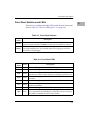
Specifications
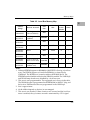
Table 2-1. MVME167 General Specifications
Characteristics
SpeciÞcations
Power requirements
(with all four EPROM sockets
populated and excluding
external LAN transceiver)
+5 Vdc (+/- 5%)
3.5 A (typical), 4.5 A (max.)
(at 25 MHz, with 32MB parity DRAM)
5.0 A (typical), 6.5 A (max.)
(at 33 MHz, with 128MB ECC DRAM)
+12 Vdc (+/- 5%)
100 mA (maximum)
(1.0 A (max.) with offboard LAN
transceiver)
-12 Vdc (+/- 5%)
100 mA (maximum)
Operating temperature
0û to 55û C at point of entry of forced air (approximately 490
LFM)
Storage temperature
-40û to +85û C
Relative humidity
5% to 90% (non-condensing)
Physical
dimensions
Double-high
VMEboard
Height
9.187 inches (233.35 mm)
Depth
6.299 inches (160.00 mm)
Thickness
0.662 inches (16.77 mm)
Height
10.309 inches (261.85 mm)
Depth
7.4 inches (188 mm)
Thickness
0.80 inches (20.32 mm)
PC board with
mezzanine
module only
PC board with
connectors and
front panel
Conformance to Requirements
These boards are designed to conform to the requirements of the
following specifications:
2-6
❏
VMEBus Specification (IEEE 1014-87)
❏
EIA-232-D Serial Interface Specification, EIA
❏
SCSI Specification
Board Level Overview
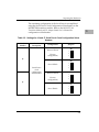
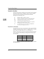
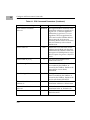
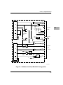
Board Level Overview
MC68040
82596CA
LAN
ETHERNET
53C710
SCSI
2
CD2401
SCC
SERIAL IO
PRINTER
PORT
PCCchip2
DRAM
VMEchip2
EPROM
MK48T08
BBRAM
& CLOCK
128KB
STATIC
RAM
VMEbus
bd068 9209
Figure 2-1. MVME167 General Block Diagram
Connectors
The MVME167 has two 96-position DIN connectors: P1 and P2.
❏
P1 rows A, B, C, and P2 row B provide the VMEbus
interconnection.
❏
P2 rows A and C provide the connection to the SCSI bus,
serial ports, Ethernet, and printer.
Adapters
I/O on the MVME167 is connected to the VMEbus P2 connector.
The main board is connected to the transition modules through a P2
adapter board and cables.
2-7
Board Level Hardware Description
2
Transition Modules
The MVME712X transition modules provide configuration headers
and provide industry standard connectors for the I/O devices.
Refer to Figure 3-3 on page 3-21.
❏
The MVME167 supports the transition modules MVME71212, MVME712-13, MVME712M, MVME712A, MVME712AM,
and MVME712B (referred to in this manual as MVME712X,
unless separately specified).
Transition modules and adapter boards are covered in the
MVME712M Transition Module and P2 Adapter Board User's Manual,
and the MVME712-12, MVME712-13, MVME712A, MVME712AM,
and MVME712B Transition Modules and LCP2 Adapter Board User's
Manual.
ASICs
The MVME167 board features several Application Specific
Integrated Circuits (ASICs) including:
❏
VMEchip2
❏
PCCchip2
❏
MEMC040
❏
MCECC
All programmable registers in the MVME167 that reside in ASICs
are covered in the Single Board Computers Programmer's Reference
Guide.
2-8
Board Level Overview
VMEchip2 ASIC
2
Provides the VMEbus interface. The VMEchip2 includes:
❏
Two tick timers
❏
A watchdog timer
❏
Programmable map decoders for the master and slave
interfaces, and a VMEbus to/from local bus DMA controller
❏
A VMEbus to/from local bus non-DMA programmed access
interface
❏
A VMEbus interrupter
❏
A VMEbus system controller
❏
A VMEbus interrupt handler
❏
A VMEbus requester.
Table 2-2. Bus Transfers
Transfer type
Can be...
Processor-to-VMEbus
D8, D16, or D32
VMEchip2 DMA to the
VMEbus
D16, D32, D16/BLT,
D32/BLT, or D64/MBLT
PCCchip2 ASIC
The PCCchip2 ASIC provides two tick timers and the interface to
the:
❏
LAN chip
❏
SCSI chip
❏
Serial port chip
❏
Printer port
❏
BBRAM
2-9
Board Level Hardware Description
2
MEMC040 Memory Controller ASIC
The MEMC040 memory controller ASIC provides the
programmable interface for the parity-protected DRAM mezzanine
board.
MCECC Memory Controller ASIC
The MCECC memory controller ASIC provides the programmable
interface for the ECC-protected DRAM mezzanine board.
Functional Description
The major functional blocks of the MVME167 covered in this
section are:
2-10
❏
Front panel switches and LED indicators
❏
Data bus structure
❏
MC68040 CPU
❏
EPROM
❏
SRAM
❏
Onboard DRAM
❏
Battery backed up RAM and clock
❏
VMEbus interface
❏
I/O interfaces
❏
Local resources
Functional Description
Front Panel Switches and LEDs
2
There are two switches and eight LEDs on the boardÕs front panel
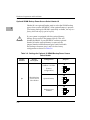
(refer to Table 2-3, Table 2-4, and Figure 3-1 on page 3-6).
Table 2-3. Front Panel Switches
Switch
Name
Description
RESET
The RESET switch resets all onboard devices and drives SYSRESET* if the
board is system controller. The RESET switch may be disabled by software.
ABORT
When enabled by software, the ABORT switch generates an interrupt at a
user-programmable level. It is normally used to abort program execution
and return to the debugger.
Table 2-4. Front Panel LEDs
LED
Name
Color
FAIL
Red
STAT
Yellow
The STAT LED lights when the MC68040 is halted.
RUN
Green
The RUN LED lights when the local bus TIP* signal line is low. This
indicates one of the local bus masters is executing a local bus cycle.
SCON
Green
The SCON LED lights when the MVME167 is the VMEbus system
controller.
LAN
Green
The LAN LED lights when the LAN chip is local bus master.
+12V
Green
The +12V LED lights when +12V power is available to the Ethernet
transceiver interface.
SCSI
Green
The SCSI LED lights when the SCSI chip is local bus master.
VME
Green
The VME LED lights when the board is using the VMEbus (VMEbus
AS* is asserted by the VMEchip2) or when the board is accessed by
the VMEbus (VMEchip2 is the local bus master).
Description
The FAIL LED lights when the BRDFAIL signal line is active.
2-11
Board Level Hardware Description
2
Data Bus Structure
The local data bus on the MVME167 is a 32-bit synchronous bus
that is based on the MC68040 bus, and supports burst transfers and
snooping.
Local Bus Arbitration
The various local bus master and slave devices use the local bus to
communicate.
The local bus is arbitrated by priority type arbiter and the priority
of the local bus masters from highest to lowest is:
1. 82596CA LAN (highest)
2. CD2401 serial (through the PCCchip2)
3. 53C710 SCSI
4. VMEbus
5. MPU (lowest)
In general, any master can access any slave; however, not all
combinations pass the Òcommon sense testÓ. Refer to the Single
Board Computers Programmer's Reference Guide and to the user's
guide for each device to determine its port size, data bus
connection, and any restrictions that apply when accessing the
device.
MC68040 MPU
The MC68040 processor is used on the MVME167. The MC68040
has onchip instruction and data caches and a floating point
processor. Refer to the M68040 user's manual for more information.
2-12
Functional Description
EPROM
2
Four 44-pin PLCC/CLCC EPROM sockets for 27C102JK or
27C202JK type EPROMs. They are:
❏
Organized as two 32-bit wide banks that support 8-, 16-, and
32-bit read accesses
❏
Controlled by the VMEchip2
❏
Mapped to local bus address 0 following a local bus reset
Ð This allows the MC68040 to access the stack pointer and
execution address following a reset
Programmable EPROM features
❏
Map decoder
❏
Access time
❏
When accessible at address 0
Static RAM
The MVME167 includes 128KB of 32-bit wide 100 ns static RAM
(SRAM), which:
❏
Supports 8-, 16-, and 32-bit wide accesses
❏
Allows the debugger operation and execution of limited
diagnostics without the DRAM mezzanine
❏
Is controlled by the VMEchip2; the access time is
programmable.
2-13
Board Level Hardware Description
2
Optional SRAM Battery Backup
SRAM battery backup is optionally available on the MVME167, but
only as a factory build and only by special request. (Contact your local
Motorola sales office for details.) The battery backup function is
provided by a Dallas DS1210S nonvolatile controller chip and a
Sanyo CR2430 battery.
The onboard power source is a Sanyo CR2430 battery which is
socketed for easy removal and replacement. A small capacitor is
provided to allow the battery to be quickly replaced without data
loss (i.e., the battery must be replaced within 30 seconds).
If your MVME167 is equipped with SRAM battery backup; when
the main board power fails, the DS1210S selects the battery as the
power source.
Each time the board is powered, the DS1210S checks the power
source, allowing software to provide an early warning to avoid
data loss:
❏
If the voltage of the backup source is less than two volts, the
second memory access cycle is blocked.
❏
Because the DS1210S may block the second access, the
software should do at least two accesses before relying on the
data.
With the optional battery backup, the MVME167 provides jumpers
(on Optional SRAM Backup Power Source Select Header J8 on page
3-12) that allow the power source of the DS1210S to be connected to
the VMEbus +5 V STDBY pin or to the onboard battery.
2-14
Functional Description
!
Caution
Lithium batteries incorporate inflammable materials
such as lithium and organic solvents. If lithium batteries
are mistreated or handled incorrectly, they may burst
open and ignite, possibly resulting in injury and/or fire.
2
When dealing with lithium batteries, carefully follow the
precautions listed below in order to prevent accidents.
❏
Do not short circuit.
❏
Do not disassemble, deform, or apply excessive pressure.
❏
Do not heat or incinerate.
❏
Do not apply solder directly.
❏
Do not use different models.
❏
Do not charge.
❏
Always check proper polarity.
To remove the battery from the module, carefully pull the battery
from the socket. (Data will be lost if a new battery is not installed
within 30 seconds.)
Before installing a new battery, ensure that the battery pins are
clean. Note the battery polarity and press the battery into the
socket.
Onboard DRAM
The MVME167 onboard DRAM is located on a mezzanine board.
The mezzanine boards are available in different sizes and with
parity protection or ECC protection.
Note
Parity mezzanines are only supported on 25MHz main
boards.
2-15
Board Level Hardware Description
Motorola software does support mixed parity and ECC memory
boards on the same main board.
2
The DRAM is four-way interleaved to efficiently support cache
burst cycles.
Onboard DRAM mezzanines are available in these configurations:
❏
4, 8, 16, or 32MB with parity protection
❏
4, 8, 16, 32, 64, or 128MB with ECC protection
Stacking Mezzanines
Two mezzanine boards may be stacked to provide up to 256MB of
onboard RAM (ECC).
❏
The main board and a single mezzanine board together take
one slot.
❏
The stacked configuration requires two VMEboard slots.
DRAM Programming Considerations
❏
The DRAM map decoder can be programmed to
accommodate different base address(es) and sizes of
mezzanine boards.
❏
The onboard DRAM is disabled by a local bus reset and must
be programmed before the DRAM can be accessed.
❏
Most DRAM devices require some number of access cycles
before the DRAMs are fully operational.
Ð Normally this requirement is met by the onboard refresh
circuitry and normal DRAM installation. However,
software should insure a minimum of 10 initialization
cycles are performed to each bank of RAM.
Refer to the MEMC040 or the MCECC in the Single Board Computers
Programmer's Reference Guide for detailed programming
information.
2-16
Functional Description
Battery Backed Up RAM and Clock
2
The MK48T08 RAM and clock chip is a 28-pin package that
provides:
❏
A time-of-day clock
❏
An oscillator
❏
A crystal
❏
Power fail detection
❏
Memory write protection
❏
8KB of RAM
❏
A battery
The clock provides
❏
Seconds, minutes, hours, day, date, month, and year in BCD
24-hour format
❏
Automatic corrections for 28-, 29- (leap year), and 30-day
months
No interrupts are generated by the clock.
The MK48T08 is an 8 bit device; however, the interface provided by
the PCCchip2 supports 8-, 16-, and 32-bit accesses to the MK48T08.
Refer to the MK48T08 data sheet for detailed programming
information.
2-17
Board Level Hardware Description
2
VMEbus Interface
The VMEchip2 provides:
❏
Local bus to VMEbus interface
❏
VMEbus to local bus interface
❏
Local-VMEbus DMA controller functions
❏
VMEbus system controller functions
I/O Interfaces
The MVME167 provides onboard I/O for many system
applications.
❏
The I/O functions include:
Ð Serial ports
Ð Printer port
Ð Ethernet transceiver interface
Ð SCSI mass storage interface.
❏
An external I/O transition module such as the MVME712X
should be used to convert the I/O connector pinout to
industry-standard connectors.
❏
The I/O interface configuration headers are located on the
MVME167 and the MVME712X transition module.
The I/O on the MVME167 is connected to the VMEbus P2
connector. The MVME712X transition module is connected to the
MVME167 through cables and a P2 adapter board.
Serial Port Interface
The CD2401 serial controller chip (SCC) implements the four serial
ports. The serial ports support the standard baud rates (110 to 38.4K
baud). The four serial ports are different functionally because of the
limited number of pins on the P2 I/O connector.
2-18
Functional Description
All four serial ports use EIA-232-D drivers and receivers located on
the MVME167, and all the signal lines are routed to the I/O
connector.
❏
Serial port 1 is a minimum function asynchronous port. It
uses RXD, CTS, TXD, and RTS.
❏
Serial ports 2 and 3 are full function asynchronous ports.
They use RXD, CTS, DCD, TXD, RTS, and DTR.
❏
Serial port 4 is a full function asynchronous or synchronous
port. It can operate at synchronous bit rates up to 64 k bits per
second. It uses RXD, CTS, DCD, TXD, RTS, and DTR. It also
interfaces to the synchronous clock signal lines.
Serial Interface Programming Considerations
❏
The MVME167 board hardware ties the DTR signal from the
CD2401 to the pin labeled RTS at connector P2. Likewise, RTS
from the CD2401 is tied to DTR on P2. Therefore, when
programming the CD2401, assert DTR when you want RTS,
and RTS when you want DTR.
❏
The interface provided by the PCCchip2 allows the 16-bit
CD2401 to appear at contiguous addresses
❏
Accesses to the CD2401 must be 8 or 16 bits: 32-bit accesses
are not permitted.
❏
The CD2401 supports DMA operations to local memory.
❏
Because the CD2401 does not support a retry operation
necessary to break VMEbus lockup conditions, the CD2401
DMA controllers should not be programmed to access the
VMEbus.
❏
The hardware does not restrict the CD2401 to onboard
DRAM.
Refer to the CD2401 data sheet for detailed programming
information.
2-19
2
Board Level Hardware Description
2
Parallel Port Interface
The PCCchip2 provides an 8-bit bidirectional parallel port. This
port may be used as a Centronics-compatible parallel printer port
or as a general parallel I/O port.
All eight bits of the port must be either inputs or outputs (no
individual bit selection).
In addition to the 8 bits of data, there are two control pins and five
status pins.
When used as a parallel printer port, these pins function as follows:
Status Pins
Printer Acknowledge (ACK*)
Printer Fault (FAULT*)
Printer Busy (BSY)
Printer Select (SELECT)
Printer Paper Error (PE)
Control Pins
Printer Strobe (STROBE*)
Input Prime (INP*)
Each of the status pins can generate an interrupt to the MPU in any
of the following programmable conditions:
2-20
❏
high level
❏
low level
❏
high-to-low transition
❏
low-to-high transition
Functional Description
The PCCchip2 provides an auto-strobe feature similar to that of the
MVME147 PCC.
❏
In auto-strobe mode, after a write to the Printer Data Register,
the PCCchip2 automatically asserts the STROBE* pin for a
selected time specified by the Printer Fast Strobe control bit.
❏
In manual mode, the Printer Strobe control bit directly
controls the state of the STROBE* pin.
Ethernet Interface
The 82596CA is used to implement the Ethernet transceiver
interface. The 82596CA accesses local RAM using DMA operations
to perform its normal functions.
The Ethernet transceiver interface is located on the MVME167, and
the industry-standard connector is located on the MVME712X
transition module.
Every MVME167 is assigned an Ethernet Station Address. The
address is $08003E2xxxxx where xxxxx is the unique 5-nibble
number assigned to the board (i.e., every MVME167 has a different
value for xxxxx).
Each module has the Ethernet Station Address displayed on a label
attached to the VMEbus P2 connector. In addition, the six bytes
including the Ethernet address are stored in the configuration area
of the BBRAM. That is, 08003E2xxxxx is stored in the BBRAM.
❏
At an address of $FFFC1F2C, the upper four bytes (08003E2x)
can be read.
❏
At an address of $FFFC1F30, the lower two bytes (xxxx) can
be read.
The MVME167 debugger has the capability to retrieve or set the
Ethernet address.
If the data in the BBRAM is lost, the user should use the number on
the VMEbus P2 connector label to restore it.
2-21
2
Board Level Hardware Description
Buffer Overruns
2
Because the 82596CA has small internal buffers and the VMEbus
has an undefined latency period, buffer overrun may occur if the
DMA is programmed to access the VMEbus. Therefore, the
82596CA should not be programmed to access the VMEbus.
Support functions for the 82596CA are provided by the PCCchip2.
Refer to the 82596CA user's guide for detailed programming
information.
SCSI Interface
The MVME167 provides for mass storage subsystems through the
industry-standard SCSI bus. These subsystems may include hard
and floppy disk drives, streaming tape drives, and other mass
storage devices.
The SCSI interface is implemented using the NCR 53C710 SCSI I/O
controller.
Support functions for the 53C710 are provided by the PCCchip2.
Refer to the 53C710 user's guide for detailed programming
information.
SCSI Termination
Because this board has no provision for SCSI termination, you must
ensure that the SCSI bus is terminated properly.
2-22
❏
If the SCSI bus ends at the P2 adapter board, then termination
resistors must be installed on the P2 adapter board. Note: +5V
power to the SCSI bus TERM power line and termination
resistors is provided through a fuse located on the P2 adapter
board.
❏
If there are additional SCSI mass storage devices in your
system ensure that terminators are installed on the last device
in the SCSI chain.
Functional Description
Local Resources
2
The MVME167 includes many resources for the local processor.
These include tick timers, software programmable hardware
interrupts, watchdog timer, and local bus timeout.
Programmable Tick Timers
Four 32-bit programmable tick timers with 1 µs resolution are
provided, two in the VMEchip2 and two in the PCCchip2. The tick
timers can be programmed to generate periodic interrupts to the
processor.
Watchdog Timer
A watchdog timer function is provided in the VMEchip2. When the
watchdog timer is enabled, it must be reset by software within the
programmed time or it times out. The watchdog timer can be
programmed to generate a SYSRESET signal, local reset signal, or
board fail signal if it times out.
Software-Programmable Hardware Interrupts
Eight software-programmable hardware interrupts are provided
by the VMEchip2. These interrupts allow software to create a
hardware interrupt.
Local Bus Timeout
The MVME167 provides a timeout function for the local bus. When
the timer is enabled and a local bus access times out, a Transfer
Error Acknowledge (TEA) signal is sent to the local bus master. The
timeout value is selectable by software for 8 µsec, 64 µsec, 256 µsec,
or infinite. The local bus timer does not operate during VMEbus
bound cycles. VMEbus bound cycles are timed by the VMEbus
access timer and the VMEbus global timer.
2-23
Board Level Hardware Description
2
Memory Maps
There are two points of view for memory maps:
1. Local bus memory map
Ð The mapping of all resources as viewed by local bus
masters
2. VMEbus memory map
Ð The mapping of onboard resources as viewed by VMEbus
masters
Local Bus Memory Map
The local bus memory map is split into different address spaces by
the transfer type (TT) signals. The local resources respond to the
normal access and interrupt acknowledge codes.
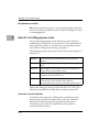
Normal Address Range
The memory map of devices that respond to the normal address
range is shown in the following tables. The normal address range is
defined by the Transfer Type (TT) signals on the local bus.
❏
On the MVME167, Transfer Types 0, 1, and 2 define the
normal address range.
Table 2-5 on page 2-25 is the entire map from $00000000 to
$FFFFFFFF. Many areas of the map are user-programmable, and
suggested uses are shown in the table.
❏
The cache inhibit function is programmable in the MMUs.
❏
The onboard I/O space must be marked cache inhibit and
serialized in its page table.
Table 2-6 on page 2-26 further defines the map for the local I/O
devices.
2-24
Memory Maps
Table 2-5. Local Bus Memory Map
Address
Range
Devices Accessed
Port
Size
$00000000 DRAMSIZE
User Programmable
(Onboard DRAM)
D32
DRAMSIZE $FF7FFFFF
User Programmable
(VMEbus)
D32/D16
$FF800000 $FFBFFFFF
ROM
$FFC00000 $FFDFFFFF
reserved
$FFE00000 $FFE1FFFF
SRAM
$FFE20000 $FFEFFFFF
SRAM (repeated)
$FFF00000 $FFFEFFFF
Local I/O Devices
(Refer to next table)
D32-D8
$FFFF0000 $FFFFFFFF
User Programmable
(VMEbus A16)
D32/D16
D32
-D32
D32
2
Size
Software
Cache
Inhibit
Notes
DRAMSIZE
N
1, 2
3GB
?
3, 4
4MB
N
1
2MB
--
5
128KB
N
--
896KB
N
--
1MB
Y
3
64KB
?
2, 4
Notes
1. Onboard EPROM appears at $00000000 - $003FFFFF following a local bus
reset. The EPROM appears at 0 until the ROM0 bit is cleared in the
VMEchip2. The ROM0 bit is located at address $FFF40030 bit 20. The
EPROM must be disabled at 0 before the DRAM is enabled. The VMEchip2
and DRAM map decoders are disabled by a local bus reset.
2. This area is user-programmable. The suggested use is shown in the table.
The DRAM decoder is programmed in the MEMC040 or MCECC chip, and
the local-to-VMEbus decoders are programmed in the VMEchip2.
3. Size is approximate.
4. Cache inhibit depends on devices in area mapped.
5. This area is not decoded. If these locations are accessed and the local bus
timer is enabled, the cycle times out and is terminated by a TEA signal.
2-25
Board Level Hardware Description
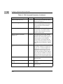
The following table focuses on the Local I/O Devices portion of the
local bus Main Memory Map.
2
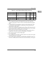
Table 2-6. Local I/O Devices Memory Map
Address Range
Devices Accessed
Port Size
Size
Notes
--
256KB
5
$FFF00000 - $FFF3FFFF
reserved
$FFF40000 - $FFF400FF
VMEchip2 (LCSR)
D32
256B
1,3
$FFF40100 - $FFF401FF
VMEchip2 (GCSR)
D32-D8
256B
1,3
$FFF40200 - $FFF40FFF
reserved
--
3.5KB
4,6
$FFF41000 - $FFF41FFF
reserved
--
4KB
4
$FFF42000 - $FFF42FFF
PCCchip2
D32-D8
4KB
1
$FFF43000 - $FFF430FF
MEMC040/MCECC #1
D8
256B
1
$FFF43100 - $FFF431FF
MEMC040/MCECC #2
D8
256B
1
$FFF43200 - $FFF43FFF
MEMC040s/MCECCs
(repeated)
--
3.5KB
1,6
$FFF44000 - $FFF44FFF
reserved
--
4KB
4
$FFF45000 - $FFF451FF
CD2401 (Serial Comm.
Cont.)
D16-D8
512B
1
$FFF45200 - $FFF45DFF
reserved
--
3KB
6,8
$FFF45E00 - $FFF45FFF
reserved
--
512B
8
$FFF46000 - $FFF46FFF
82596CA (LAN)
D32
4KB
1,7
$FFF47000 - $FFF47FFF
53C710 (SCSI)
D32/D8
4KB
1
$FFF48000 - $FFF4FFFF
reserved
--
32KB
4
$FFF50000 - $FFF6FFFF
reserved
--
128KB
4
$FFF70000 - $FFF76FFF
reserved
--
28KB
5
$FFF77000 - $FFF77FFF
reserved
--
4KB
2
$FFF78000 - $FFF7EFFF
reserved
--
28KB
5
$FFF7F000 - $FFF7FFFF
reserved
--
4KB
2
$FFF80000 - $FFF9FFFF
reserved
--
128KB
5
2-26
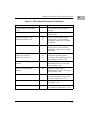
Memory Maps
Table 2-6. Local I/O Devices Memory Map (Continued)
Address Range
Devices Accessed
2
Port Size
Size
Notes
--
128KB
4
D32-D8
64KB
1
$FFFA0000 - $FFFBFFFF
reserved
$FFFC0000 - $FFFCFFFF
MK48T08 (BBRAM, TOD
Clock)
$FFFD0000 - $FFFDFFFF
reserved
--
64KB
4
$FFFE0000 - $FFFEFFFF
reserved
--
64KB
2
Notes
1. For a complete description of the register bits, refer to the Single Board
Computers Programmer's Reference Guide or to the data sheet for the specific
chip.
2. On the MVME167 this area does not return an acknowledge signal. If the
local bus timer on the MVME167 is enabled, the access times out and is
terminated by a TEA signal.
3. Writes to the LCSR in the VMEchip2 must be 32 bits. LCSR writes of 8 or 16
bits terminate with a TEA signal. Writes to the GCSR may be 8, 16 or 32 bits.
Reads to the LCSR and GCSR may be 8, 16 or 32 bits.
4. This area does not return an acknowledge signal. If the local bus timer is
enabled, the access times out and is terminated by a TEA signal.
5. This area does return an acknowledge signal.
6. Size is approximate.
7. Port commands to the 82596CA must be written as two 16-bit writes: upper
word first and lower word second.
8. The CD2401 appears repeatedly from $FFF45200 to $FFF45FFF. If the local
bus timer is enabled, the access times out and is terminated by a TEA signal.
2-27
Board Level Hardware Description
2
VMEbus Memory Map
This section describes the mapping of local resources as viewed by
VMEbus masters. Default addresses for the slave, master, and
GCSR address decoders are provided by the ENV command. Refer
to Appendix A.
VMEbus Accesses to the Local Bus
The VMEchip2 includes a user-p87grammable map decoder for the
VMEbus to local bus interface. The map decoder allows you to
program the starting and ending address and the modifiers the
MVME167 responds to.
VMEbus Short I/O Memory Map
The VMEchip2 includes a user-programmable map decoder for the
GCSR. The GCSR map decoder allows you to program the starting
address of the GCSR in the VMEbus short I/O space.
2-28
3Hardware Preparation and
Installation
3
This Chapter Covers
This chapter provides instructions on:
❏
Unpacking the equipment
❏
Preparing the hardware
❏
Installing the MVME167 CISC Single Board Computer
Note that hardware preparation instructions for the MVME712X
transition module are provided in separate userÕs manuals for each
model. Refer to the userÕs manual you received with your
MVME712X.
Unpacking the Equipment
Note
If the shipping carton is damaged upon receipt, request
that the carrier's agent be present during unpacking
and inspection of the equipment.
Unpack the equipment from the shipping carton. Refer to the
packing list and verify that all items are present. Save the packing
material for storing and reshipping of the equipment.
!
Avoid touching areas of integrated circuitry; static
discharge can damage circuits.
Caution
3-1
Hardware Preparation and Installation
Overview of Startup Procedure
The following list identifies the things you will need to do before
you can use this board, and where to find the information you need
to perform each step. Be sure to read this chapter and all Caution
notes, and have the related documentation with you before you
begin.
3
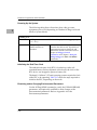
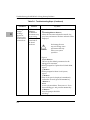
Table 3-1. Startup Overview
Stage
1
2
What you will need to do...
Prepare the MVME167.
3-5
Ensure that EPROM devices are properly
installed in their sockets.
Checking the
167Bug EPROMs
3-7
ConÞgure adapters and MVME712X
transition modules.
The userÕs manual you
received with your
MVME712X module
Install/remove jumpers on headers.
Jumper Settings
3-7
Preparing the
MVME167 for
Installation
3-13
The userÕs
manual you
received with
your chassis
3-13
Prepare the chassis.
Disconnect AC power cable.
Remove chassis cover.
Remove Þller panels from card slots.
Install your MVME167 in the chassis.
Remove IACK and BG jumpers from
backplane.
Slide the module into the chassis and
fasten it securely.
3-2
On
page...
Preparing the
Hardware
Turn power off to chassis and peripherals.
3
Refer to...
Installing
Transition
Modules and
Adapter Boards
3-15
Overview of Startup Procedure
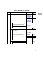
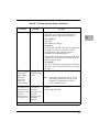
Table 3-1. Startup Overview (Continued)
Stage
4
What you will need to do...
Refer to...
On
page...
Install adapter boards and transition modules. Transition
Modules and
Adapter Boards
Overview
3-16
Installing
Transition
Modules and
Adapter Boards
3-19
Set jumpers on the transition module(s).
Connect and install the MVME712X
transition module.
The userÕs manual you
received with your
MVME712X
Connect and install the P2 adapter board.
5
Connect peripherals.
Connect and install any optional SCSI
device cables.
Connect a console terminal to the
MVME712X.
Connect any other optional devices or
equipment you will be using, such as
serial or parallel printers, host computers,
etc.
6
Complete the installation.
Reassemble chassis.
Reconnect AC power.
Connecting
Peripherals
3-19
You may also wish to
obtain the Single Board
Computer SCSI Software
UserÕs Manual
EIA-232-D
Interconnections
E-1
Port Numbers
5-9
Disk/Tape
Controller Data
B-1
The userÕs
manual you
received with
your chassis
3-23
3-3
3
Hardware Preparation and Installation
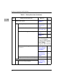
Table 3-1. Startup Overview (Continued)
Stage
3
7
What you will need to do...
Start up the system.
Refer to...
On
page...
Starting the
System
3-23
Front Panel
Switches and
LEDs
2-11
Initialize the real-time clock.
Initializing the
Real-Time Clock
3-24
Note that the debugger prompt appears.
Powering Up the
System
3-24
Starting Up
167Bug
4-6
Power up the system.
You may also wish to
obtain the Debugging
Package for Motorola 68k
CISC CPUs UserÕs Manual
and the 167Bug
Diagnostics UserÕs Manual
Examine and/or change environmental
parameters.
Program the PCCchip2 and VMEchip2.
Troubleshoot the system.
Solve any startup problems.
3-4
Examining
and/or Changing
Environmental
Parameters
3-24
Setting
Environment to
Bug/Operating
System
A-3
Memory Maps
2-24
Troubleshooting
the MVME167:
Solving Startup
Problems
D-1
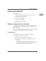
Preparing the Hardware
Preparing the Hardware
This section covers:
❏
Modifying hardware configurations before installation
❏
Checking the 167Bug EPROMs
❏
Factory jumper settings
❏
Preparing your MVME167
❏
Preparing the system chassis
3
Modifying Configuration before Installation
To select the desired configuration and ensure proper operation of
the MVME167, certain option modifications may be necessary
before installation.
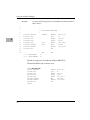
The location of the switches, jumper headers, connectors, and LED
indicators on the MVME167 is illustrated in Figure 3-1.
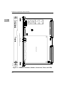
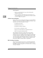
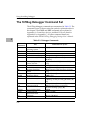
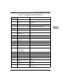
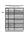
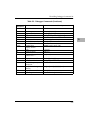
Option Modification
The MVME167 has provisions for option modification via:
❏
Software control for most options
❏
Jumper settings on headers for some options
❏
Bit settings in control registers after installation for most
other options
Ð Control registers are described in the Single Board
Computer Programmer's Reference Guide as listed in Related
Documentation in Chapter 1 of this manual.
3-5
Hardware Preparation and Installation
MVME
167
1
39
40
2
6
7
1
39
40
2
6
7
A1
B1
C1
XU4
SKT
XU3
SKT
XU2
29
28
18
17
29
28
18
17
29
28
18
17
1
39
40
2
29
28
6
7
DS2
1
18
17
16
2
J2
SCSI VME
XU1
DS1
39
40
7
RUN SCON
2
6
J1
DS3
1
P1
4
J8
3 2 1
(OPTIONAL)
19
20
J3
F1
A32
B32
C32
1
2
F2
S1
S2
60
59
J4
A1
B1
C1
60
59
MEZZANINE BOARD
2
1
P2
J5
2
1
A32
B32
C32
J6
3
1
3
1
J7
1379 9404
3-6
PRIMARY SIDE
RESET
COMPONENTS ARE REMOVED FOR CLARITY
ABORT
15
LAN +12V
2
1
FAIL STAT
3
DS4
Figure 3-1. MVME167 Switches, Headers, Connectors, Fuses, and LEDs
Preparing the Hardware
Checking the 167Bug EPROMs
Be sure that the two factory installed 128K x 16 167Bug EPROMs are
in the proper sockets.
EPROM Location
❏
Odd-numbered label (such as B01): EPROM in socket XU1
(for Least Significant Words)
❏
Even-numbered label (such as B02): EPROM in XU2 (for Most
Significant Words)
EPROM Orientation
Be sure that physical chip orientation is correct:
❏
The flatted corner of each EPROM aligns with the
corresponding portion of the EPROM socket on the
MVME167.
User-programmed EPROMs
There are two spare EPROM sockets, XU3 and XU4, available to
carry user-programmed EPROMs.
Jumper Settings
The MVME167 has been factory tested and is shipped with the
factory jumper settings described in the following sections. The
MVME167 operates with its required and factory-installed Debug
Monitor, 167Bug, with these factory jumper settings.
3-7
3
Hardware Preparation and Installation
Optional Jumper Settings
Most of the optional functions on your board can be changed
through software control or bit settings in control registers. If your
installation requires it, however, you may change jumper settings
on the following headers:
3
❏
Jumper pins 9 through 16 on header J1 are general purpose
software readable jumpers open to your application.
❏
Header J2 enables/disables the MVME167 as system
controller.
❏
Headers J6 and J7 select serial port 4 to drive or receive
TRXC4 and RTXC4 clock signals.
❏
Optional header J8 selects the SRAM backup power source
(this is only available as an optional factory build special
request).
General Purpose Software Readable Header J1
Each MVME167 may be configured with readable jumpers. They
can be read as a register (at $FFF40088) in the VMEchip2 LCSR. The
bit values are read as a one when the jumper is off, and as a zero
when the jumper is on.
Reserved/DeÞned Bits
Jumpers on header J1 affect 167Bug operation as listed in Table 3-2.
The factory (default) configuration is with all eight jumpers
installed (see Table 3-3).
The MVME167Bug reserves/defines the four lower order bits
(GPI3 to GPI0). Table 3-2 describes the bits reserved/defined by the
debugger:
3-8
Preparing the Hardware
Table 3-2. J1 Bit Descriptions
Bit
J1 Pins
Description
Bit #0 (GPI0)
1-2
When this bit is a one (high), it instructs the debugger to use
local Static RAM for its work page (i.e., variables, stack, vector
tables, etc.). This bit will be high when jumper is removed.
Bit #1 (GPI1)
3-4
When this bit is a one (high), it instructs the debugger to use
the default setup/operation parameters in ROM versus the
user setup/operation parameters in NVRAM. This is the same
as depressing the RESET and ABORT switches at the same
time. This feature can be used in the event the user setup is
corrupted or does not meet a sanity check. Refer to the ENV
command (Appendix A) for the ROM defaults. This bit will be
high when jumper is removed.
Bit #2 (GPI2)
5-6
Reserved for future use.
Bit #3 (GPI3)
7-8
Reserved for future use.
Bit #4 (GPI4)
9-10
Open to your application.
Bit #5 (GPI5)
11-12
Open to your application.
Bit #6 (GPI6)
13-14
Open to your application.
Bit #7 (GPI7)
15-16
Open to your application.
Table 3-3. Factory Settings for J1 General Purpose Readable Jumpers
Header
Number
GPI0
GPI1
GPI2
GPI3
GPI4
GPI5
GPI0 - GPI3:
Reserved
Jumpers
GPI6
General
purpose
software
readable
jumpers
ConÞguration
GPI7
J1
Header
Description
GPI4 - GPI7:
User-deÞnable
15
7
1
(Factory
conÞguration)
16
8
2
3-9
3
Hardware Preparation and Installation
System Controller Header J2
The MVME167 can be VMEbus system controller. The system
controller function is enabled by installing a jumper on header J2
(see Table 3-4). When the MVME167 is system controller, the SCON
LED is turned on.
3
Table 3-4. Settings for J2 System Controller Header
Header
Number
Header
Description
System
controller
header
J2
ConÞguration
Jumpers
System
controller
J2
(Factory
conÞguration)
1
2
J2
Not system
controller
1
2
Serial Port 4 Clock Configuration Select Headers J6 and J7
Serial port 4 can be configured to use clock signals provided by the
RTXC4 and TRXC4 signal lines.
Headers J6 and J7 on the MVME167 configure serial port 4 to drive
or receive RTXC4 and TRXC4, respectively (see Table 3-5).
3-10
❏
Factory configuration is with port 4 set to receive both
signals.
❏
The alternative configuration sets port 4 to drive both signals.
Preparing the Hardware
The remaining configuration of the clock lines is accomplished
using the Serial Port 4 Clock Configuration Select header on the
MVME712M transition module. Refer to the MVME712M
Transition Module and P2 Adapter Board User's Manual for
configuration of that header.
Table 3-5. Settings for J6 and J7 Serial Port 4 Clock Configuration Select
Headers
Header
Number
Header
Description
ConÞguration
Receive RTXC4
(Factory
conÞguration)
Jumpers
J6
1
2
3
J6
J6
1
Drive RTXC4
Serial Port 4
clock
conÞguration
select headers
2
3
J7
Receive TRXC4
1
(Factory
conÞguration)
2
3
J7
J7
1
Drive TRXC4
2
3
3-11
3
Hardware Preparation and Installation
Optional SRAM Backup Power Source Select Header J8
Header J8 is an optional header used to select the SRAM backup
power source on the MVME167, if the optional battery is present.
(The battery backup for SRAM is optionally available, but only as a
factory build and only by special request.)
3
!
Caution
If your system is equipped with the optional battery
backup, do not remove the jumper from J8. This will
disable the SRAM. If your MVME167 contains optional
header J8, but the optional battery is removed, the
jumper must be installed between pins 2 and 4 to disable
the backup or between pins 1 and 2 for the factory
configuration as shown in Table 3-6.
Table 3-6. Settings for Optional J8 SRAM Backup Power Source
Select Header
Header
Number
Header
Description
ConÞguration
VMEbus +5V STBY
(Factory
conÞguration)
Jumpers
J8
3
4
2
1
J8
J8
SRAM backup
power source
select header
Optional battery
3
2
1
Backup power
disabled
3
2
1
4
J8
3-12
4
Preparing the Hardware
Preparing the MVME167 for Installation
Refer to the setup procedures in the manuals for your particular
chassis or system for additional details concerning the installation
of the MVME167 into a VME chassis.
Table 3-7. MVME167 Preparation Procedure
Step
Action
1
Install/remove jumpers on headers according to the Jumper Settings in this
chapter and as required for your particular application.
❏ Jumpers on header J1 affect 167Bug operation as listed in Jumper
Settings. The default condition is with all eight jumpers installed.
❏ A jumper installed/removed on header J2 enables/disables the
system controller function of the MVME167.
❏ Install jumpers on headers J6 and J7 to configure serial port 4 to
use clock signals provided by the TRXC4 and RTXC4 signal lines.
2
ConÞgure adapters and transition modules according to the MVME712X
transition module user's manuals.
3
Ensure that EPROM devices are properly installed in their sockets.
❏
Factory configuration is with two EPROMs installed for the
MVME167Bug debug monitor, in sockets XU1 and XU2.
3-13
3
Hardware Preparation and Installation
Preparing the System Chassis
Now that the MVME167 is ready for installation, prepare the
system chassis and determine slot assignments (for peripherals,
transition modules, etc.) as follows:
3
Inserting or removing modules while power is applied
could result in damage to module components.
!
Caution
!
Warning
Dangerous voltages, capable of causing death, are
present in this equipment. Use extreme caution when
handling, testing, and adjusting.
Table 3-8. Chassis Preparation/Slot Selection Procedure
Step
Action
1
Turn all power OFF to chassis and peripherals.
2
Disconnect AC power cable from source.
3
Remove chassis cover as shown in the user's manual for your particular
chassis or system.
4
Remove the Þller panel(s) from the appropriate card slot(s) at the front and rear
of the chassis (if the chassis has a rear card cage).
3-14
If the MVME167 is conÞgured as
system controller:
If it is not conÞgured as system
controller:
It must be installed in the
left-most card slot (slot 1) to correctly
initiate the bus-grant daisy-chain and
to have proper operation of the IACKdaisy-chain driver.
It may be installed in any doubleheight unused card slot.
Installing the Hardware
Installing the Hardware
This section covers
3
❏
Installation of the MVME167 into a VME chassis
❏
Overview and installation of transition modules and adapter
boards
❏
Connection of peripheral equipment such as console
terminals, optional SCSI drives, and serial or parallel printers
Installing the MVME167 in the Chassis
Note that if the MVME167 is to be used as system controller, it must
installed in the left-most card slot (slot 1), otherwise it may be installed in
any unused double-height card slot.
Table 3-9. MVME167 Installation Procedure
Step
1
Action
Remove IACK and BG jumpers from backplane for the card slot that the
MVME167 is to be installed in.
2
Carefully slide the MVME167 into the card slot in the front of the chassis.
❏
❏
❏
The MVME167 requires power from both P1 and P2. Be sure the
module is seated properly into the P1 and P2 connectors on the
backplane.
Do not damage or bend connector pins.
Fasten the MVME167 in the chassis with screws provided, making
good contact with the transverse mounting rails to minimize RFI
emissions
3-15
Hardware Preparation and Installation
Transition Modules and Adapter Boards Overview
The MVME167 supports the MVME712-12, MVME712-13,
MVME712M, MVME712A, MVME712AM, and MVME712B
transition modules (referred to in this manual as MVME712X,
unless separately specified).
3
Note
Other modules in the system may have to be moved to
allow space for the MVME712M which has a doublewide front panel.
MVME712X transition modules provide configuration headers and
industry-standard connectors for internal and external I/O devices.
The I/O on the MVME167 is connected to the VMEbus P2
connector.
❏
Note
3-16
The MVME712X transition module is connected to the
MVME167 through cables and a P2 adapter board as shown
in Figure 3-2 on page 3-17.
Some cable(s) are not provided with the MVME712X
module(s), and therefore must be made or provided by
the user. (Motorola recommends using shielded cables
for all connections to peripherals to minimize
radiation.)
Installing the Hardware
MVME712X
TERMINATOR
MVME167
3
P1
LC P2
ADAPTER
J2
P2
P2
J3
J2, P2, OR J11
ENCLOSURE BOUNDARY
Figure 3-2. Typical Internal SCSI and Serial Port Connections
3-17
Hardware Preparation and Installation
Equipment Connections
Some connection diagrams are in the Single Board Computer
Programmer's Reference Guide.
3
The MVME712X transition modules and P2 adapter boards connect
peripheral equipment to the MVME167 as shown in Table 3-10:
Table 3-10. Peripheral Connections
Equipment Type
3-18
Connect Through...
Console terminals, host computer
systems, modems, or serial printers
EIA-232-D serial ports on the
transition module
Parallel printers
Centronics printer port on the
transition module
Optional internal modems (see the
userÕs manual for your transition
module for details)
Optional modem port, replacing serial
port 2 on the transition module
Internal SCSI drives
Adapter board and transition module
External SCSI drives
SCSI interface connector on the
transition module
Ethernet connections
Ethernet port on the transition module
Installing the Hardware
Installing Transition Modules and Adapter Boards
Table 3-11. Transition Module and Adapter Board Installation Overview
Stage
What you will need to do...
Refer to...
1
Set jumpers on the transition
module(s) and install SCSI
terminators (if needed) on the P2
adapter board.
Module Preparation in the userÕs
manual for your transition module
and adapter board, and SCSI Bus
Termination on page 3-28
2
Connect and install the MVME712X
transition module in the front or the
rear of the chassis.
Installation Instructions in the userÕs
manual for your transition module
and adapter board
3
Connect and install
❏
The P2 adapter board at the
P2 connector on the
backplane at the MVME167
slot.
Installation Instructions in the userÕs
manual for your transition module
and adapter board
❏
SCSI cable(s) from the P2
adapter board to the
MVME712X transition
module and internal SCSI
devices.
Module Preparation in the userÕs
manual for your transition module
and adapter board, and SCSI Bus
Termination on page 3-28
Connecting Peripherals
The MVME167 mates with (optional) terminals or other peripherals
at the EIA-232-D serial ports (marked SERIAL PORTS 1, 2, 3, and 4
on the MVME712X transition module), parallel port, SCSI ports,
and LAN Ethernet port, as shown in Figure 3-4 on page 3-22.
Note
Some cable(s) are not provided with the MVME712X
module(s), and therefore are made or provided by the
user. (Motorola recommends using shielded cables for
all connections to peripherals to minimize radiation.)
3-19
3
Hardware Preparation and Installation
Table 3-12. Peripheral Connection Procedures
3
Step
Action...
Refer to...
1
Connect and install any optional SCSI device
cables from J3 on the P2 Adapter to internal
devices and/or the MVME712B or MVME712M to
external SCSI devices (typical conÞgurations
shown in Figure 3-2 on page 3-17 and Figure 3-3 on
page 3-21).
The Single Board
Computer Programmer's
Reference Guide for some
possible connection
diagrams
2
Connect the terminal to be used as the 167Bug system console to the default
debug EIA-232-D port at serial port 1 on the MVME712X transition module.
3
Set up the terminal as follows:
❏
❏
❏
❏
eight bits per character
one stop bit per character
parity disabled (no parity)
baud rate 9600 baud (default baud rate of MVME167 ports at
powerup)
After powerup, the baud rate of the debug port can be reconÞgured by using
the Port Format (PF) command of the 167Bug debugger.
4
5
3-20
Connect devices such as a host computer system and/or a serial printer to the
other EIA-232-D port connectors with the appropriate cables and conÞguration
After powerup, these ports can be reconÞgured by programming the
MVME167 CD2401 Serial Controller Chip (SCC), or by using the 167Bug PF
command.
Set up the device serial ports as described in Step
3.
After powerup, the baud rate of the port can be
reconÞgured by using the Port Format (PF)
command of the 167Bug debugger.
ConÞguring a Port under
the PF (Port Format)
command in the
Debugging Package for
68K CISC CPUs UserÕs
Manual
Connect a parallel device, such as a printer, to the
printer port on the MVME712X transition module.
(You may also use a module such as the MVME335
for a parallel port connection.)
The Single Board
Computer Programmer's
Reference Guide for some
possible connection
diagrams
Installing the Hardware
In order for high-baud rate serial communication
between 167Bug and the terminal to work, the terminal
must do some form of handshaking. If the terminal
being used does not do hardware handshaking via the
CTS line, then it must do XON/XOFF handshaking. If
you get garbled messages and missing characters, you
should check the terminal to make sure XON/XOFF
handshaking is enabled. Refer to Configuring a Port
under the PF (Port Format) command in the Debugging
Package for 68K CISC CPUs UserÕs Manual.
Note
3
MVME712B
MVME712X
J1
J3
MVME167
J2
J7
J4
P1
J5
J10
P2 ADAPTER
J12
J2
J3
J15
J11
P2
P2
ENCLOSURE BOUNDARY
Figure 3-3. Using MVME712A/AM and MVME712B
3-21
Hardware Preparation and Installation
MVME
712A/12/13
SERIAL PORT 1
TTY01
SERIAL PORT 2
MVME
712B
To J10 on
Transition Module
SERIAL PORT 3
SERIAL PORT 4
MVME
712A
(MVME712M
similar)
ETHERNET
CONSOLE
3
Optional Modem
Port
MVME
712B
(if used)
To J2 on
Adapter Board
SCSI INTERFACE
PRINTER
Figure 3-4. Typical Transition Module Peripheral Port Connectors
3-22
Installing the Hardware
Completing the Installation
Table 3-13. Installation Completion Procedure
Step
3
Action...
1
Reassemble the chassis.
2
Reconnect the AC power.
Starting the System
After completing the preparation and installation procedures, you
are ready to start up your system.
Table 3-14. System Startup Overview
Stage
What you will need to do...
Refer to...
1
Power up the system and note that the
debugger prompt appears.
Page 3-24; Starting Up 167Bug on page
4-6; and the MVME167Bug Debugging
Package User's Manual.
2
Initialize the real-time clock.
Page 3-24.
3
Examine and/or change
environmental parameters.
Page 3-24 and ConÞgure and
Environment Commands on page A-1.
4
Program the PCCchip2 and
VMEchip2.
System Considerations on page 3-26;
Memory Maps on page 2-24; ASICs
on page 2-8; and the Single Board
Computer Programmer's Reference
Guide.
3-23
Hardware Preparation and Installation
Powering Up the System
The following table shows what takes place when you turn
equipment power ON (depending on whether 167Bug is in Board
Mode or System Mode):
3
If 167Bug is in...
Board Mode
167Bug executes some self-checks and displays the debugger prompt
167-Bug>
System Mode
The system performs a
selftest and tries to
autoboot.
If the conÞdence test fails, the test aborts
when the Þrst fault occurs. If possible, an
appropriate message is displayed, and
control then returns to the menu (refer to
Chapter 4, Debugger General
Information, and Chapter 5, Using the
167Bug Debugger for ENV and MENU
commands).
Initializing the Real-Time Clock
The onboard real-time clock (RTC) is backed up with a selfcontained battery. Before shipment of this board, the clock of the
RTC device was stopped to preserve battery life.
The boardÕs ÒSelftestsÓ (ST) and operating systems require the clock
of the RTC to be operating. Table 3-15 shows the steps required to
initialize the RTC, depending on the mode.
Examining and/or Changing Environmental Parameters
Use the 167BugÕs ENV command to verify the NVRAM (BBRAM)
parameters, and optionally use ENV to make changes to the
Environmental parameters. Refer to Appendix A for the
Environment parameters.
3-24
Installing the Hardware
Table 3-15. RTC Initialization Procedure
Step
Action
Board Mode
System Mode
3
1
Allow 167Bug to boot up normally.
Stop the auto-boot sequence by
pressing the <BREAK> key. (If the
system has already started and failed
a conÞdence test in system mode, you
should be in the debugger menu).
2
At the 167-Bug> prompt, enter
TIME to display the current date and
time of day.
Select (3) from the debugger menu to
get the debugger prompt.
3
At the 167-Bug> prompt, use the SET command to initialize the RTC and to
set the time and date. Use the following command line structure:
SET [<MMddyyhhmm>]|[<+/-CAL>;C]
For example:
167-Bug>SET 0522961037 <Return>
WED May 22 10:37:00.00 1996
167-Bug>
Where the arguments are: MM=month, dd=day of the month, yy=year,
hh=hour in ÒmilitaryÓ (24 hour) time, and mm=minutes.
Programming the PCCchip2 and VMEchip2
See System Considerations below, and refer to Memory Maps on
page 2-24, and the Single Board Computer Programmer's Reference
Guide for details on your particular system environment.
3-25
Hardware Preparation and Installation
System Considerations
3
Backplane Power Connections
The MVME167 needs to draw power from both P1 and P2 of the
VMEbus backplane. P2 is also used for the upper 16 bits of data for
32-bit transfers, and for the upper 8 address lines for extended
addressing mode. The MVME167 may not operate properly
without its main board connected to P1 and P2 of the VMEbus
backplane.
Memory Address Ranges
Whether the MVME167 operates as a VMEbus master or as a
VMEbus slave, it is configured for 32 bits of address and for 32 bits
of data (A32/D32). However, it handles A16 or A24 devices in
certain address ranges. D8 and/or D16 devices in the system must
be handled by the MC68040 software. Refer to the memory maps in
the Single Board Computer Programmer's Reference Guide as listed in
Related Documentation in Chapter 1.
DRAM Addressing
The MVME167 contains shared onboard DRAM whose base
address is software-selectable. Both the onboard processor and
offboard VMEbus devices see this local DRAM at base physical
address $00000000, as programmed by the MVME167Bug
firmware. This may be changed, by software, to any other base
address. Refer to the Single Board Computer Programmer's Reference
Guide for details.
Global Bus Timeout
If the MVME167 tries to access offboard resources in a non-existent
location, and is not system controller, and if the system does not
have a global bus timeout, the MVME167 waits forever for the
VMEbus cycle to complete. This would cause the system to hang
up.
3-26
System Considerations
Multiple Module Cage Configuration
Multiple MVME167s may be configured into a single VME card
cage. In general, hardware multiprocessor features are supported.
GCSR Location Monitor Register
Other MPUs on the VMEbus can interrupt, disable, communicate
with and determine the operational status of the CISC processor(s).
One register of the GCSR set includes four bits which function as
location monitors to allow one MVME167 processor to broadcast a
signal to other MVME167 processors, if any. All eight of the GSCR
registers are accessible from any local processor as well as from the
VMEbus.
Ethernet LAN (+12 Vdc) Fuse
The MVME167 provides +12 Vdc power to the Ethernet LAN
transceiver interface through a 1-amp fuse (F2) located on the
MVME167. The +12V LED lights when +12 Vdc is available. The
fuse is socketed and is located adjacent to diode CR1 near connector
P1. If the Ethernet transceiver fails to operate, check the fuse. When
using the MVME712M transition module, the yellow LED (DS1) on
the MVME712M front panel lights when LAN power is available,
indicating that the fuse is good.
Note
Your MVME167 may have a poly-switch instead of a 1amp fuse. If the Ethernet transceiver fails to operate
and the poly-switch is open, power off the chassis and
wait a while before re-applying power.
3-27
3
Hardware Preparation and Installation
SCSI Bus Termination
❏
The MVME167 provides SCSI terminator power through a 1amp fuse (F1) located on the P2 adapter board. The fuse is
socketed. If the fuse is blown, the SCSI devices may not
operate or may function erratically.
❏
When the P2 adapter board is used with an MVME712M and
the SCSI bus is connected to the MVME712M, the green LED
(DS2) on the MVME712M front panel lights when there is
SCSI terminator power. If the LED flickers during SCSI bus
operation, the fuse should be checked.
❏
Because this board has no provision for SCSI termination,
you must ensure that the SCSI bus is terminated properly. If
you use a P2 adapter, the adapter has sockets (R1, R2, R3) for
terminating the SCSI lines using three 8-pin SIP resistor
networks.
3
Storage and the Real-Time Clock
For storage of this product, be sure the RTC is put into the
power save mode. This will extend the life of the battery
contained in this part. To put the part into the power save
mode, use the PS command of the debugger. For example:
167-Bug>ps <Return>
(Clock is in Battery Save mode)
167-Bug>
3-28
4Debugger General
Information
4
This Chapter Covers
❏
An introduction to the MVME167Bug firmware package
❏
Booting and restarting 167Bug
❏
Disk input/output support capabilities
❏
Network support capabilities
Introduction to MVME167Bug
This section covers:
❏
Overview of M68000 firmware
❏
Description of 167Bug
❏
167Bug implementation
❏
Memory requirements
Overview of M68000 Firmware
The firmware for the M68000-based (68K) series of board and
system level products has a common genealogy, deriving from the
BUG firmware currently used on all Motorola M68000-based CPU
modules. The M68000 firmware family provides a high degree of
functionality and user friendliness, and yet stresses portability and
ease of maintenance. This member of the M68000 firmware family
is implemented on the MVME167 CISC Single Board Computer,
and is known as the MVME167Bug, or just 167Bug.
4-1
Debugger General Information
Description of 167Bug
The 167Bug package, MVME167Bug, is a powerful evaluation and
debugging tool for systems built around the MVME167 CISC-based
microcomputers.
167Bug consists of three parts:
4
❏
The ÒdebuggerÓ or Ò167BugÒ; a command-driven userinteractive software debugger, described in Chapter 5
❏
A command-driven diagnostic package for the MVME167
hardware
❏
A user interface which accepts commands from the system
console terminal
Command Facilities
Facilities are available for loading and executing user programs
under complete operator control for system evaluation.
167Bug includes commands for these tasks:
❏
Display and modification of memory
❏
Breakpoint and tracing capabilities
❏
A powerful assembler/disassembler useful for patching
programs
❏
A self-test at powerup feature which verifies the integrity of
the system.
Trap #15 System Calls
Various 167Bug routines that handle I/O, data conversion, and
string functions are available to user programs through the TRAP
#15 system calls.
4-2
Introduction to MVME167Bug
Debugger or Diagnostic Directories
When using 167Bug, you operate out of either the debugger
directory or the diagnostic directory.
If you are in ...
With the
prompt ...
The debugger directory
167-Bug>
All of the debugger
commands
The diagnostic directory
167-Diag>
All of the diagnostic
commands as well as
all of the debugger
commands
You have available ...
4
You may switch between directories by using the Switch
Directories (SD) command.
You may examine the commands in the current directory by using
the Help (HE) command.
Keyboard Control
167Bug is command-driven; it performs its various operations in
response to user commands entered at the keyboard. When you
enter a command, 167Bug executes the command and the 167-Bug>
prompt reappears. However, if you enter a command that causes
execution of user target code (e.g., "GO"), then control may or may
not return to 167Bug, depending on the outcome of the user
program.
4-3
Debugger General Information
Similarity to other Motorola Debugging Firmware
If you have used one or more of Motorola's other debugging
packages, you will find the CISC 167Bug very similar. Some effort
has also been made to make the interactive commands more
consistent. For example, delimiters between commands and
arguments may now be commas or spaces interchangeably.
4
167Bug Implementation
MVME167Bug is written largely in the "C" programming language,
providing benefits of portability and maintainability. Where
necessary, assembler has been used in the form of separately
compiled modules containing only assembler code - no mixed
language modules are used.
Physically, 167Bug is contained in two of the four 44-pin
PLCC/CLCC EPROMs, providing 512KB (128K longwords) of
storage. Both EPROMs are necessary regardless of how much space
is actually occupied by the firmware, because of the 32-bit
longword-oriented MC68040 memory bus architecture.
The executable code is checksummed at every power-on or reset
firmware entry, and the result (which includes a pre-calculated
checksum contained in the EPROMs), is tested for an expected zero.
Thus, users are cautioned against modification of the EPROMs
unless re-checksum precautions are taken.
4-4
Booting and Restarting 167Bug
Memory Requirements
The program portion of 167Bug is approximately 512KB of code,
consisting of download, debugger, and diagnostic packages and
contained entirely in EPROM. The EPROM sockets on the
MVME167 are mapped starting at location $FF800000.
4
167Bug requires a minimum of 64KB of contiguous read/write
memory to operate.
The ENV command controls where this block of memory is located.
Regardless of where the onboard RAM is located, the first 64KB is
used for 167Bug stack and static variable space and the rest is
reserved as user space.
Whenever the MVME167 is reset, the target PC is initialized to the
address corresponding to the beginning of the user space, and the
target stack pointers are initialized to addresses within the user
space, with the target Interrupt Stack Pointer (ISP) set to the top of
the user space.
At power up or reset, all 8KB of memory at addresses $FFE0C000
through $FFE0DFFF is completely changed by the 167Bug initial
stack.
Booting and Restarting 167Bug
This section covers the following tasks:
❏
Starting up 167Bug
❏
Autoboot
❏
ROMboot
❏
Network boot
❏
Restarting the system
4-5
Debugger General Information
Starting Up 167Bug
1. Verify that the MVME167 is properly installed and operating
as described in Table 3-1 on page 3-2.
2. Power up the system. 167Bug executes some self-checks and
displays the debugger prompt 167-Bug> (if 167Bug is in
Board Mode). However, if the ENV command (Appendix A)
has put 167Bug in System Mode, the system performs a
selftest and tries to autoboot. Refer to the ENV and MENU
commands listed in Table 5 -1.
4
If the confidence test fails, the test is aborted when the first
fault is encountered. If possible, an appropriate message is
displayed, and control then returns to the menu.
Autoboot
Autoboot is a software routine that is contained in the 167Bug
EPROMs to provide an independent mechanism for booting an
operating system.
Autoboot Sequence
1. The autoboot routine automatically scans for controllers and
devices in a specified sequence until a valid bootable device
containing a boot media is found or the list is exhausted.
2. If a valid bootable device is found, a boot from that device is
started.
The controller scanning sequence goes from the lowest
controller Logical Unit Number (LUN) detected to the
highest LUN detected. (Controllers, devices, and their LUNs
are listed in Appendix B).
3. At powerup, Autoboot is enabled, and if the drive and
controller numbers encountered are valid, the system console
displays the following message:
"Autoboot in progress... To abort hit <BREAK>"
4-6
Booting and Restarting 167Bug
4. Following this message there is a delay to allow you an
opportunity to abort the Autoboot process if you wish. To
gain control without Autoboot, you can press the BREAK key
or the software ABORT or RESET switches.
5. Then the actual I/O begins: the program pointed to within
the volume ID of the media specified is loaded into RAM and
control passed to it.
Autoboot is controlled by parameters contained in the ENV
command. These parameters allow the selection of specific boot
devices and files, and allow programming of the Boot delay. Refer
to the ENV command in Appendix A for more details.
ROMboot
There are two spare EPROM sockets, XU3 and XU4, available to
carry user-programmed EPROMs. Therefore, you do not have to
reprogram the 167Bug EPROMs in order to implement the
ROMboot feature.
One use of ROMboot might be resetting SYSFAIL* on an
unintelligent controller module. The NORB command disables the
function.
ROMboot Sequence
1. ROMboot is configured/enabled and executed at powerup
(optionally also at reset) in one of two ways:
a. By the Environment (ENV) command (refer to
Appendix A).
b. By the RB command assuming there is valid code in the
EPROMs (or optionally elsewhere on the module or
VMEbus) to support it.
2. If ROMboot code is installed, a user-written routine is given
control (if the routine meets the format requirements).
4-7
4
Debugger General Information
For a user's ROMboot module to gain control through the
ROMboot linkage, four requirements must be met:
4
Requirement ...
Optionally, with the ENV command ...
Power must have just been
applied.
Change this to respond to any reset.
Your routine must be located
within the MVME167 ROM
memory map.
Change this to any other portion of the onboard
memory, or even offboard VMEbus memory.
The ASCII string ÒBOOTÓ must be located within the speciÞed memory range.
Your routine must pass a checksum test, which ensures that this routine was really
intended to receive control at powerup.
For complete details on how to use ROMboot, refer to the
Debugging Package for Motorola 68K CISC CPUs User's Manual.
Network Boot
Network Auto Boot is a software routine contained in the 167Bug
EPROMs that provides a mechanism for booting an operating
system using a network (local Ethernet interface) as the boot device.
Network Boot Sequence
1. The Network Auto Boot routine automatically scans for
controllers and devices in a specified sequence until a valid
bootable device containing a boot media is found or the list is
exhausted.
2. If a valid bootable device is found, a boot from that device is
started.
The controller scanning sequence goes from the lowest
controller Logical Unit Number (LUN) detected to the
highest LUN detected. (Refer to Appendix C for default
LUNs.)
4-8
Booting and Restarting 167Bug
3. At powerup, Network Boot is enabled, and providing the
drive and controller numbers encountered are valid, the
following message is displayed on the system console:
"Network Boot in progress... To abort hit <BREAK>"
Following this message there is a delay to allow you to abort
the Network Boot process if you wish. To gain control
without Network Boot, you can press the BREAK key or the
software ABORT or RESET switches.
4. Then the actual I/O begins: the program pointed to within
the volume ID of the media specified is loaded into RAM and
control passed to it.
Network Auto Boot is controlled by parameters contained in the
NIOT and ENV commands. These parameters allow the selection
of specific boot devices, systems, and files, and allow programming
of the Boot delay. Refer to the ENV command in Appendix A.
Restarting the System
You can initialize the system to a known state in three different
ways: reset, abort, and break. Each has characteristics which make
it more appropriate than the others in certain situations.
The debugger has a special feature which can be used in the event
your setup/operation parameters are corrupted or do not meet a
sanity check. This feature:
❏
Is activated by pressing the RESET and ABORT switches at the
same time, then releasing the RESET switch before the ABORT
switch.
❏
Instructs 167Bug to use the default setup/operation
parameters in ROM instead of your setup/operation
parameters in NVRAM.
Refer to the ENV command (Appendix A) for the ROM defaults.
4-9
4
Debugger General Information
Reset
Pressing and releasing the MVME167 front panel RESET switch
initiates a system reset.
Reset must be used if the processor ever halts, or if the 167Bug
environment is ever lost (vector table is destroyed, stack corrupted,
etc.).
4
❏
COLD and WARM reset modes are available.
❏
By default, 167Bug is in COLD mode.
During COLD reset:
1. A total system initialization takes place, as if the MVME167
had just been powered up.
2. All static variables (including disk device and controller
parameters) are restored to their default states.
3. The breakpoint table and offset registers are cleared.
4. The target registers are invalidated.
5. Input and output character queues are cleared.
6. Onboard devices (timer, serial ports, etc.) are reset, and
7. The first two serial ports are reconfigured to their default
state.
During WARM reset:
1. The 167Bug variables and tables are preserved, as well as the
target state registers and breakpoints.
Abort
Abort is invoked by pressing and releasing the ABORT switch on the
MVME167 front panel.
Abort should be used to regain control if the program gets caught
in a loop, etc.
4-10
Booting and Restarting 167Bug
Whenever abort is invoked when executing a user program
(running target code), a "snapshot" of the processor state is
captured and stored in the target registers. For this reason, abort is
most appropriate when terminating a user program that is being
debugged. Abort should be used to regain control if the program
gets caught in a loop, etc. The target PC, register contents, etc., help
to pinpoint the malfunction.
Abort Sequence
Pressing and releasing the ABORT switch does the following:
1. Generates a local board condition which may interrupt the
processor if enabled.
2. Displays the target registers on the screen, reflecting the
machine state at the time the ABORT switch was pressed.
3. Removes any breakpoints installed in the user code and
keeps the breakpoint table intact.
4. Returns control to the debugger.
Break
A ÒBreakÓ is generated by pressing and releasing the BREAK key
on the console terminal keyboard.
❏
Break does not generate an interrupt.
❏
The only time break is recognized is when characters are sent
or received by the console port.
Many times it may be desirable to terminate a debugger command
prior to its completion; for example, during the display of a large
block of memory. Break allows you to terminate the command.
4-11
4
Debugger General Information
Break Sequence
1. Removes any breakpoints in your code and keeps the
breakpoint table intact.
2. Takes a snapshot of the machine state if the function was
entered using SYSCALL. This machine state is then accessible
to you for diagnostic purposes.
4
SYSFAIL* Assertion/Negation
Upon a reset/powerup condition the debugger asserts the VMEbus
SYSFAIL* line (refer to the VMEbus specification). SYSFAIL* stays
asserted if any of the following has occurred:
❏
Confidence test failure
❏
NVRAM checksum error
❏
NVRAM low battery condition
❏
Local memory configuration status
❏
Self test (if system mode) has completed with error
❏
MPU clock speed calculation failure
After debugger initialization is done and none of the above
situations have occurred, the SYSFAIL* line is negated. This
indicates to the user or VMEbus masters the state of the debugger.
In a multi-computer configuration, other VMEbus masters could
view the pertinent control and status registers to determine which
CPU is asserting SYSFAIL*. SYSFAIL* assertion/negation is also
affected by the ENV command. Refer to Appendix A.
MPU Clock Speed Calculation
The clock speed of the microprocessor is calculated and checked
against a user definable parameter contained in NVRAM (refer to
the CNFG command in Appendix A). If the check fails, a warning
message is displayed.
4-12
Disk I/O Support
Disk I/O Support
167Bug can initiate disk input/output by communicating with
intelligent disk controller modules over the VMEbus.
This section covers:
❏
Blocks Versus Sectors
❏
Device Probe Function
❏
Disk I/O via 167Bug Commands
❏
Disk I/O via 167Bug System Calls
❏
Default 167Bug Controller and Device Parameters
❏
Disk I/O Error Codes
4
Disk Support Facilities
Disk support facilities built into 167Bug consist of
❏
Command-level disk operations
❏
Disk I/O system calls (only via one of the TRAP #15
instructions) for use by user programs
❏
Defined data structures for disk parameters.
Parameter Tables
Parameters such as the address where the module is mapped and
the type and number of devices attached to the controller module
are kept in tables by 167Bug. Default values for these parameters
are assigned at powerup and cold-start reset, but may be altered as
described in the section on default parameters, later in this chapter.
Supported Controllers
Appendix B contains a list of the controllers presently supported, as
well as a list of the default configurations for each controller.
4-13
Debugger General Information
Blocks Versus Sectors
The logical block defines the unit of information for disk devices. A
disk is viewed by 167Bug as a storage area divided into logical
blocks. By default, the logical block size is set to 256 bytes for every
block device in the system. The block size can be changed on a per
device basis with the IOT command.
4
The sector defines the unit of information for the media itself, as
viewed by the controller. The sector size varies for different
controllers, and the value for a specific device can be displayed and
changed with the IOT command.
When a disk transfer is requested, the start and size of the transfer
is specified in blocks. 167Bug translates this into an equivalent
sector specification, which is then passed on to the controller to
initiate the transfer. If the conversion from blocks to sectors yields
a fractional sector count, an error is returned and no data is
transferred.
Device Probe Function
A device probe with entry into the device descriptor table is done
whenever a specified device is accessed; i.e., when system calls
.DSKRD, .DSKWR, .DSKCFIG, .DSKFMT, and .DSKCTRL, and
debugger commands BH, BO, IOC, IOP, IOT, MAR, and MAW
are used.
The device probe mechanism utilizes the SCSI commands "Inquiry"
and "Mode Sense". If the specified controller is non-SCSI, the probe
simply returns a status of "device present and unknown". The
device probe makes an entry into the device descriptor table with
the pertinent data. After an entry has been made, the next time a
probe is done it simply returns with "device present" status (pointer
to the device descriptor).
4-14
Disk I/O Support
Disk I/O via 167Bug Commands
These following 167Bug commands are provided for disk I/O.
Detailed instructions for their use are found in the Debugging
Package for Motorola 68K CISC CPUs User's Manual. When a
command is issued to a particular controller LUN and device LUN,
these LUNs are remembered by 167Bug so that the next disk
command defaults to use the same controller and device.
IOI (Input/Output Inquiry)
This command is used to probe the system for all possible
CLUN/DLUN combinations and display inquiry data for devices
which support it. The device descriptor table only has space for 16
device descriptors; with the IOI command, you can view the table
and clear it if necessary.
IOP (Physical I/O to Disk)
IOP allows you to read or write blocks of data, or to format the
specified device in a certain way. IOP creates a command packet
from the arguments you have specified, and then invokes the
proper system call function to carry out the operation.
IOT (I/O Teach)
IOT allows you to change any configurable parameters and
attributes of the device. In addition, it allows you to see the
controllers available in the system.
IOC (I/O Control)
IOC allows you to send command packets as defined by the
particular controller directly. IOC can also be used to look at the
resultant device packet after using the IOP command.
BO (Bootstrap Operating System)
BO reads an operating system or control program from the
specified device into memory, and then transfers control to it.
4-15
4
Debugger General Information
BH (Bootstrap and Halt)
BH reads an operating system or control program from a specified
device into memory, and then returns control to 167Bug. It is used
as a debugging tool.
4
Disk I/O via 167Bug System Calls
All operations that actually access the disk are done directly or
indirectly by 167Bug TRAP #15 system calls. (The command-level
disk operations provide a convenient way of using these system
calls without writing and executing a program.)
The following system calls are provided to allow user programs to
do disk I/O:
.DSKRD
Disk read. System call to read blocks from a disk into
memory.
.DSKWR
Disk write. System call to write blocks from memory onto
a disk.
.DSKCFIG
Disk conÞgure. This function allows you to change the
conÞguration of the speciÞed device.
.DSKFMT
Disk format. This function allows you to send a format
command to the speciÞed device.
.DSKCTRL
Disk control. This function is used to implement any
special device control functions that cannot be
accommodated easily with any of the other disk functions.
Refer to the Debugging Package for Motorola 68K CISC CPUs User's
Manual for information on using these and other system calls.
Controller Command Packets
To perform a disk operation, 167Bug must eventually present a
particular disk controller module with a controller command
packet which has been especially prepared for that type of
controller module. (This is accomplished in the respective
controller driver module.)
4-16
Disk I/O Support
A command packet for one type of controller module usually does
not have the same format as a command packet for a different type
of module. The system call facilities which do disk I/O accept a
generalized (controller-independent) packet format as an
argument, and translate it into a controller-specific packet, which is
then sent to the specified device.
Refer to the system call descriptions in the Debugging Package for
Motorola 68K CISC CPUs User's Manual for details on the format and
construction of these standardized "user" packets.
The packets which a controller module expects to be given vary
from controller to controller. The disk driver module for the
particular hardware module (board) must take the standardized
packet given to a trap function and create a new packet which is
specifically tailored for the disk drive controller it is sent to. Refer
to documentation on the particular controller module for the
format of its packets, and for using the IOC command.
Default 167Bug Controller and Device Parameters
167Bug initializes the parameter tables for a default configuration
of controllers and devices (refer to Appendix B). If the system needs
to be configured differently than this default configuration (for
example, to use a 70MB Winchester drive where the default is a
40MB Winchester drive), then these tables must be changed.
4-17
4
Debugger General Information
There are three ways to change the parameter tables:
When you invoke one of
these commands ...
Change
status is ...
Command
BO or BH
The conÞguration area of
the disk is read and the
parameters
corresponding to that
device are rewritten
according to the
parameter information
contained in the
conÞguration area.
Temporary
The default parameter
information is written back
into the tables.
Command
IOT
You can use this
command to reconÞgure
the parameter table
manually for any
controller and/or device
that is different from the
default.
Temporary
The default parameter
information is written back
into the tables.
The
source
In the source code, you
may change the
permanent conÞguration
Þles and rebuild 167Bug
so that it has different
defaults.
Permanent until changed again.
Using ...
4
code
If a cold-start reset occurs ...
Disk I/O Error Codes
167Bug returns an error code if an attempted disk operation is
unsuccessful.
4-18
Network I/O Support
Network I/O Support
The Network Boot Firmware provides the capability to boot the
CPU through the ROM debugger using a network (local Ethernet
interface) as the boot device.
The booting process is executed in two distinct phases.
4
❏
The first phase allows the diskless remote node to discover its
network identify and the name of the file to be booted.
❏
The second phase has the diskless remote node reading the
boot file across the network into its memory.
The various modules and the dependencies of these modules that
support the overall network boot function are described in the
following paragraphs.
Intel 82596 LAN Coprocessor Ethernet Driver
This driver manages/surrounds the Intel 82596 LAN Coprocessor.
Management is in the scope of the reception of packets, the
transmission of packets, receive buffer flushing, and interface
initialization.
This module ensures that the packaging and unpackaging of
Ethernet packets is done correctly in the Boot PROM.
UDP/IP Protocol Modules
The Internet Protocol (IP) is designed for use in interconnected
systems of packet-switched computer communication networks.
The Internet protocol provides for transmitting of blocks of data
called datagrams (hence User Datagram Protocol, or UDP) from
sources to destinations, where sources and destinations are hosts
identified by fixed length addresses.
The UDP/IP protocols are necessary for the TFTP and BOOTP
protocols; TFTP and BOOTP require a UDP/IP connection.
4-19
Debugger General Information
RARP/ARP Protocol Modules
The Reverse Address Resolution Protocol (RARP) basically consists
of an identity-less node broadcasting a "whoami" packet onto the
Ethernet, and waiting for an answer. The RARP server fills an
Ethernet reply packet up with the target's Internet Address and
sends it.
4
The Address Resolution Protocol (ARP) basically provides a
method of converting protocol addresses (e.g., IP addresses) to
local area network addresses (e.g., Ethernet addresses). The RARP
protocol module supports systems which do not support the
BOOTP protocol.
BOOTP Protocol Module
The Bootstrap Protocol (BOOTP) basically allows a diskless client
machine to discover its own IP address, the address of a server host,
and the name of a file to be loaded into memory and executed.
TFTP Protocol Module
The Trivial File Transfer Protocol (TFTP) is a simple protocol to
transfer files. It is implemented on top of the Internet User
Datagram Protocol (UDP or Datagram) so it may be used to move
files between machines on different networks implementing UDP.
The only thing it can do is read and write files from/to a remote
server.
Network Boot Control Module
The "control" capability of the Network Boot Control Module is
needed to tie together all the necessary modules and to sequence
the booting process. The booting sequence consists of two phases:
the first phase is labeled "address determination and bootfile
selection" and the second phase is labeled "file transfer". The first
phase will utilize the RARP/BOOTP capability and the second
phase will utilize the TFTP capability.
4-20
Multiprocessor Support
Network I/O Error Codes
167Bug returns an error code if an attempted network operation is
unsuccessful.
Multiprocessor Support
4
The MVME167 dual-port RAM feature makes the shared RAM
available to remote processors as well as to the local processor. This
can be done by either of the following two methods:
❏
The Multiprocessor Control Register (MPCR) Method
❏
The Global Control and Status Register (GCSR) Method
Either method can be enabled/disabled by the ENV command as
its Remote Start Switch Method (refer to Appendix A).
Multiprocessor Control Register (MPCR) Method
A remote processor can initiate program execution in the local
MVME167 dual-port RAM by issuing a remote GO command
using the Multiprocessor Control Register (MPCR).
The MPCR, located at shared RAM location of $800 offset from the
base address the debugger loads it at, contains one of two
longwords used to control communication between processors.
The MPCR contents are organized as follows:
Base Address + $800
*
N/A N/A N/A (MPCR)
4-21
Debugger General Information
MPCR Status Codes
The status codes stored in the MPCR are of two types:
4
❏
Status returned (from the 167Bug)
❏
Command set by the bus master (job requested by some
processor)
The status codes that may be returned from 167Bug are:
HEX
ASCII
ASCII
0
R
E
(HEX 00)
(HEX 52)
(HEX 45)
----
Wait. Initialization not yet complete.
Ready. The Þrmware monitor is watching for a change.
Code pointed to by the MPAR is executing.
The command code that may be set by the bus master is:
ASCII
ASCII
G
B
(HEX 47)
(HEX 42)
-- Use Go Direct (GD) logic specifying the MPAR address.
-- Recognize breakpoints using the Go (G) logic.
Multiprocessor Address Register (MPAR)
The Multiprocessor Address Register (MPAR), located in shared
RAM location of $804 offset from the base address the debugger
loads it at, contains the second of two longwords used to control
communication between processors. The MPAR contents specify
the physical address (as viewed from the local processor) at which
execution for this processor is to begin if the MPCR contains a G or
B. The MPAR is organized as follows:
Base Address + $804
*
*
*
*
(MPAR)
MPCR Powerup sequence
1. At powerup, the debug monitor self-test routines initialize
RAM, including the memory locations used for multiprocessor support ($800 through $807).
2. The MPCR contains $00 at powerup, indicating that
initialization is not yet complete.
4-22
Multiprocessor Support
3. As the initialization proceeds, the execution path comes to the
"prompt" routine.
Before sending the prompt, this routine places an R in the
MPCR to indicate that initialization is complete. Then the
prompt is sent.
Ð If no terminal is connected to the port, the MPCR is still
polled to see whether an external processor requires
control to be passed to the dual-port RAM.
Ð If a terminal does respond, the MPCR is polled for the
same purpose while the serial port is being polled for user
input.
Ð An ASCII G placed in the MPCR by a remote processor
indicates that the Go Direct type of transfer is requested.
Ð An ASCII B in the MPCR indicates that breakpoints are to
be armed before control is transferred (as with the GO
command).
In either sequence, an E is placed in the MPCR to indicate
that execution is underway just before control is passed to
RAM. (Any remote processor could examine the MPCR
contents.)
4. If the code being executed in dual-port RAM is to reenter the
debug monitor, a TRAP #15 call using function $0063
(SYSCALL .RETURN) returns control to the monitor with a
new display prompt.
Note that every time the debug monitor returns to the
prompt, an R is moved into the MPCR to indicate that control
can be transferred once again to a specified RAM location.
4-23
4
Debugger General Information
Global Control and Status Register (GCSR) Method
A remote processor can initiate program execution in the local
MVME167 dual-port RAM by issuing a remote GO command
using the VMEchip2 Global Control and Status Registers (GCSR).
1. The remote processor places the MVME167 execution
address in general purpose registers 0 and 1 (GPCSR0 and
GPCSR1).
4
2. The remote processor then sets bit 8 (SIG0) of the VMEchip2
LM/SIG register.
3. This causes the MVME167 to install breakpoints and begin
execution. The result is identical to the MPCR method (with
status code B) described in the previous section.
The GCSR registers are accessed in the VMEbus short I/O space.
Each general purpose register is two bytes wide, occurring at an
even address.
The general purpose register number 0 is at an offset of $8 (local
bus) or $4 (VMEbus) from the start of the GCSR registers. The local
bus base address for the GCSR is $FFF40100. The VMEbus base
address for the GCSR depends on the group select value and the
board select value programmed in the Local Control and Status
Registers (LCSR) of the MVME167. The execution address is
formed by reading the GCSR general purpose registers in the
following manner:
GPCSR0
GPCSR1
used as the upper 16 bits of the address
used as the lower 16 bits of the address
The address appears as:
GPCSR0
4-24
GPCSR1
Diagnostic Facilities
Diagnostic Facilities
Included in the 167Bug package is a complete set of hardware
diagnostics intended for testing and troubleshooting of the
MVME167. These diagnostics are completely described in the
MVME167Bug Debugging Package User's Manual.
❏
In order to use the diagnostics, you must switch directories to
the diagnostic directory.
❏
If you are in the debugger directory, you can switch to the
diagnostic directory by entering the debugger command
Switch Directories (SD). The diagnostic prompt
167-Diag>
should appear.
Table 4-1. Diagnostic Monitor Commands/Prefixes
Command/
PreÞx
Description
AEM
Append Error Messages Mode
CEM
Clear Error Messages
CF
Test Group ConÞguration Parameters Editor
DE
Display Error Counters
DEM
Display Errors
DP
Display Pass Count
HE
Help
HEX
Help Extended
LA
Loop Always Mode
LC
Loop Continuous Mode
LE
Loop on Error Mode
LF
Line Feed Suppression Mode
LN
Loop Non-Verbose Mode
MASK
Display/Revise Self Test Mask
4-25
4
Debugger General Information
Table 4-1. Diagnostic Monitor Commands/Prefixes
Command/
PreÞx
4
Description
NV
Non-Verbose Mode
SD
Switch Directories
SE
Stop on Error Mode
ST
Selftest
ZE
Clear (Zero) Error Counters
ZP
Zero Pass Count
Table 4-2. Diagnostic Utilities
Command
4-26
Description
WL
Write loop enable
RL
Read loop enable
Diagnostic Facilities
167Bug Diagnostic Test Groups
Refer to the MVME167Bug Debugging Package User's Manual for
complete descriptions of the diagnostic routines available and
instructions on how to invoke them. Note that some diagnostics
depend on restart defaults that are set up only in a particular restart
mode. Refer to the documentation on a particular diagnostic for the
correct mode.
Table 4-3. Diagnostic Test Groups
Test Set
Description
RAM
Local RAM Tests
SRAM
Static RAM Tests
RTC
MK48T0x Real-Time Clock Tests
PCC2
Peripheral Channel Controller Tests
MCECC
Memory Board Tests
MEMC1
MC040 Memory Controller 1 ASIC Tests
MEMC2
MC040 Memory Controller 2 ASIC Tests
ST2401
CD2401 Serial Port Tests
VME2
VME Interface ASIC VMEchip2 Tests
LANC
LAN Coprocessor (Intel 82596) Tests
NCR
NCR 53C710 SCSI I/O Processor Tests
DCAC
MC68040 Data Cache Tests
MMU
MC68040 MMU Tests
4-27
4
Debugger General Information
4
4-28
5Using the 167Bug
Debugger
5
This Chapter Covers
❏
Entering debugger command lines
❏
Entering and debugging programs
❏
Calling system utilities from user programs
❏
Preserving the debugger operating environment
❏
Floating point support
❏
The 167Bug debugger command set
Entering Debugger Command Lines
167Bug is command-driven and performs its various operations in
response to user commands entered at the keyboard. When the
debugger prompt
167-Bug>
appears on the terminal screen, then the debugger is ready to accept
commands.
Terminal Input/Output Control
As the command line is entered, it is stored in an internal buffer.
Execution begins only after the carriage return is entered, so that
you can correct entry errors, if necessary, using the control
characters described below.
5-1
Using the 167Bug Debugger
Note
5
The presence of the upward caret ( ^ ) before a
character indicates that the Control (CTRL) key must
be held down while striking the character key.
^X
^H
Delete
key
^D
(cancel line)
(backspace)
(delete)
The cursor is backspaced to the beginning of the line.
The cursor is moved back one position.
Performs the same function as ^H.
(redisplay)
^A
(repeat)
The entire command line as entered so far is
redisplayed on the following line.
Repeats the previous line. This happens only at the
command line. The last line entered is redisplayed
but not executed. The cursor is positioned at the end
of the line. You may enter the line as is or you can add
more characters to it. You can edit the line by
backspacing and typing over old characters.
When observing output from any 167Bug command, the XON and
XOFF characters which are in effect for the terminal port may be
entered to control the output, if the XON/XOFF protocol is enabled
(default). These characters are initialized to ^S and ^Q respectively
by 167Bug, but you may change them with the PF command. In the
initialized (default) mode, operation is as follows:
^S
^Q
(wait)
(resume)
Console output is halted.
Console output is resumed.
When a command is entered, the debugger executes the command
and the prompt reappears. However, if the command entered
causes execution of user target code, for example GO, then control
may or may not return to the debugger, depending on what the
user program does.
5-2
Entering Debugger Command Lines
For example, if a breakpoint has been specified, then control returns
to the debugger when the breakpoint is encountered during
execution of the user program. Alternately, the user program could
return to the debugger by means of the TRAP #15 function
".RETURN".
Debugger Command Syntax
In general, a debugger command is made up of the following parts:
❏
The command identifier (i.e., MD or md for the Memory
Display command). Note that either upper- or lowercase is
allowed.
❏
A port number if the command is set up to work with more
than one port.
❏
At least one intervening space before the first argument.
❏
Any required arguments, as specified by the command.
❏
An option field, set off by a semicolon (;) to specify conditions
other than the default conditions of the command.
The commands are shown using a modified Backus-Naur form
syntax. The metasymbols used are:
boldface strings
italic strings
|
[]
{}
A boldface string is a literal such as a command or a
program name, and is to be typed just as it appears.
An italic string is a "syntactic variable" and is to be
replaced by one of a class of items it represents.
A vertical bar separating two or more items
indicates that a choice is to be made; only one of the
items separated by this symbol should be selected.
Square brackets enclose an item that is optional. The
item may appear zero or one time.
Braces enclose an optional symbol that may occur
zero or more times.
5-3
5
Using the 167Bug Debugger
Syntactic Variables
The following syntactic variables are encountered in the command
descriptions which follow. In addition, other syntactic variables
may be used and are defined in the particular command
description in which they occur.
del
exp
addr
count
range
5
text
Delimiter; either a comma or a space.
Expression (described in detail in a following section).
Address (described in detail in a following section).
Count; the syntax is the same as for exp.
A range of memory addresses which may be speciÞed
either by addr del addr or by addr: count.
An ASCII string of up to 255 characters, delimited at
each end by the single quote mark (').
Expression as a Parameter
An expression can be one or more numeric values separated by the
arithmetic operators: plus (+), minus (-), multiplied by (*), divided
by (/), logical AND (&), shift left (<<), or shift right (>>).
Numeric values may be expressed in either hexadecimal, decimal,
octal, or binary by immediately preceding them with the proper
base identifier.
Base
Hexadecimal
Decimal
Octal
Binary
IdentiÞer
$
&
@
%
Examples
$FFFFFFFF
&1974, &10-&4
@456
%1000110
If no base identifier is specified, then the numeric value is assumed
to be hexadecimal.
5-4
Entering Debugger Command Lines
A numeric value may also be expressed as a string literal of up to
four characters. The string literal must begin and end with the
single quote mark ('). The numeric value is interpreted as the
concatenation of the ASCII values of the characters. This value is
right-justified, as any other numeric value would be.
String
Numeric Value
Literal (In Hexadecimal)
'A'
41
'ABC'
414243
'TEST'
54455354
5
Evaluation of an expression is always from left to right unless
parentheses are used to group part of the expression. There is no
operator precedence. Subexpressions within parentheses are
evaluated first. Nested parenthetical subexpressions are evaluated
from the inside out.
Valid expression examples:
Expression
FF0011
45+99
&45+&99
@35+@67+@10
%10011110+%1001
88<<4
AA&F0
Result (In Hex)
Notes
FF0011
DE
90
5C
A7
880
shift left
A0
logical AND
The total value of the expression must be between 0 and
$FFFFFFFF.
Address as a Parameter
Many commands use addr as a parameter. The syntax accepted by
167Bug is similar to the one accepted by the MC68040 one-line
assembler. All control addressing modes are allowed. An "address
+ offset register" mode is also provided.
5-5
Using the 167Bug Debugger
Address Formats
Table 5-1 summarizes the address formats that are acceptable for
address parameters in debugger command lines.
Table 5-1. Debugger Address Parameter Formats
Format
Example
Description
N
140
Absolute address+contents of automatic offset
register.
N+Rn
130+R5
Absolute address+contents of the speciÞed offset
register (not an assembler-accepted syntax).
(An)
(A1)
Address register indirect. (Also post-increment, predecrement)
(d,An) or
d(An)
(120,A1)
120(A1)
Address register indirect with displacement (two
formats accepted).
(d,An,Xn) or
d(An,Xn)
(&120,A1,D2)
&120(A1,D2)
Address register indirect with index and
displacement (two formats accepted).
5
([bd,An,Xn],od) ([C,A2,A3],&100) Memory indirect preindexed.
([bd,An],Xn,od)
([12,A3],D2,&10)
Memory indirect postindexed.
For the memory indirect modes, Þelds can be omitted.
For example, three of many permutations are as follows:
([,An],od)
([,A1],4)
([bd])
([FC1E])
([bd,,Xn])
([8,,D2])
Notes
N
An
Xn
d
bd
od
n
Rn
5-6
Ñ
Ñ
Ñ
Ñ
Ñ
Ñ
Ñ
Ñ
Absolute address (any valid expression).
Address register n.
Index register n (An or Dn).
Displacement (any valid expression).
Base displacement (any valid expression).
Outer displacement (any valid expression).
Register number (0 to 7).
Offset register n.
Entering Debugger Command Lines
Note
In commands with range specified as addr del addr, and
with size option W or L chosen, data at the second
(ending) address is acted on only if the second address
is a proper boundary for a word or longword,
respectively.
Offset Registers
Eight pseudo-registers (R0 through R7) called offset registers are
used to simplify the debugging of relocatable and positionindependent modules. The listing files in these types of programs
usually start at an address (normally 0) that is not the one at which
they are loaded, so it is harder to correlate addresses in the listing
with addresses in the loaded program. The offset registers solve
this problem by taking into account this difference and forcing the
display of addresses in a relative address+offset format. Offset
registers have adjustable ranges and may even have overlapping
ranges. The range for each offset register is set by two addresses:
base and top. Specifying the base and top addresses for an offset
register sets its range. In the event that an address falls in two or
more offset registers' ranges, the one that yields the least offset is
chosen.
Note
Relative addresses are limited to 1MB (5 digits),
regardless of the range of the closest offset register.
5-7
5
Using the 167Bug Debugger
Example:
A portion of the listing file of an assembled, relocatable module is
shown below:
1
2
3
4
5
6
7
8
9
10
11
12
13
14
5
*
*
*
0
0
0
0
0
0
0
0
00000000
00000004
00000006
00000008
0000000A
0000000C
00000010
00000014
MOVE STRING SUBROUTINE
48E78080
4280
1018
5340
12D8
51C8FFFC
4CDF0101
4E75
MOVESTR
LOOP
MOVS
****** TOTAL ERRORS
END
0——
****** TOTAL WARNINGS
0——
MOVEM.L
CLR.L
MOVE.B
SUBQ.W
MOVE.B
DBRA
MOVEM.L
RTS
D0/A0,—(A7)
D0
(A0)+,D0
#1,D0
(A0)+,(A1)+
D0,LOOP
(A7)+,D0/A0
END
The above program was loaded at address $0001327C.
The disassembled code is shown next:
167Bug>MD 1327C;DI
0001327C 48E78080
00013280 4280
00013282 1018
00013284 5340
00013286 12D8
00013288 51C8FFFC
0001328C 4CDF0101
00013290 4E75
167Bug>
5-8
MOVEM.L
CLR.L
MOVE.B
SUBQ.W
MOVE.B
DBF
MOVEM.L
RTS
D0/A0,—(A7)
D0
(A0)+,D0
#1,D0
(A0)+,(A1)+
D0,$13286
(A7)+,D0/A0
Entering Debugger Command Lines
By using one of the offset registers, the disassembled code
addresses can be made to match the listing file addresses as follows:
167Bug>OF R0
R0 =00000000 00000000? 1327C. <CR>
167Bug>MD 0+R0;DI <CR>
00000+R0 48E78080
MOVEM.L
00004+R0 4280
CLR.L
00006+R0 1018
MOVE.B
00008+R0 5340
SUBQ.W
0000A+R0 12D8
MOVE.B
0000C+R0 51C8FFFC
DBF
00010+R0 4CDF0101
MOVEM.L
00014+R0 4E75
RTS
167Bug>
D0/A0,—(A7)
D0
(A0)+,D0
#1,D0
(A0)+,(A1)+
D0,$A+R0
(A7)+,D0/A0
5
For additional information about the offset registers, refer to the
Debugging Package for Motorola 68K CISC CPUs User's Manual.
Port Numbers
Some 167Bug commands give you the option to choose the port to
be used to input or output. Valid port numbers which may be used
for these commands are as follows:
1. MVME167 EIA-232-D Debug (Terminal Port 0 or 00) (PORT 1
on the MVME167 P2 connector). Sometimes known as the
"console port", it is used for interactive user input/output by
default.
2. MVME167 EIA-232-D (Terminal Port 1 or 01) (PORT 2 on the
MVME167 P2 connector). Sometimes known as the "host
port", this is the default for downloading, uploading,
concurrent mode, and transparent modes.
Note
These logical port numbers (0 and 1) are shown in the
pinouts of the MVME167 as "SERIAL PORT 1" and
"SERIAL PORT 2", respectively. Physically, they are all
part of connector P2.
5-9
Using the 167Bug Debugger
Entering and Debugging Programs
There are various ways to enter a user program into system
memory for execution:
5
❏
Create the program with the assembler/disassembler
❏
Download an S-record object file
❏
Read the program from disk
Creating a Program with the Assembler/Disassembler
You can create a program using the Memory Modify (MM)
command with the assembler/disassembler option.
1. Enter the program one source line at a time.
2. After each source line is entered, it is assembled and the
object code is loaded to memory.
Refer to the Debugging Package for Motorola 68K CISC CPUs User's
Manual for complete details of the 167Bug
Assembler/Disassembler.
Downloading an S-Record Object File
Another way to enter a program is to download an object file from
a host system.
The program must be in S-record format (described in the
Debugging Package for Motorola 68K CISC CPUs User's Manual) and
may have been assembled or compiled on the host system.
Alternately, the program may have been previously created using
the 167Bug MM command as outlined above and stored to the host
using the Dump (DU) command.
5-10
Calling System Utilities from User Programs
A communication link must exist between the host system and the
MVME167 port 1. (Hardware configuration details are provided in
Connecting Peripherals on page 3-19.) The file is downloaded from
the host to MVME167 memory by the Load (LO) command.
Read the Program from Disk
Another way to enter a program is by reading the program from
disk, using one of the disk commands (BO, BH, IOP). Once the
object code has been loaded into memory, you can set breakpoints
if desired and run the code or trace through it.
Calling System Utilities from User Programs
A convenient way of doing character input/output and many other
useful operations has been provided so that you do not have to
write these routines into the target code. You can access various
167Bug routines via one of the MC68040 TRAP instructions, using
vector #15. Refer to the Debugging Package for Motorola 68K CISC
CPUs User's Manual for details on the various TRAP #15 utilities
available and how to invoke them from within a user program.
Preserving the Debugger Operating
Environment
This section explains how to avoid contaminating the operating
environment of the debugger. Topics covered include:
❏
167Bug Vector Table and workspace
❏
Hardware functions
❏
Exception vectors used by 167Bug
5-11
5
Using the 167Bug Debugger
167Bug uses certain of the MVME167 onboard resources and may
also use offboard system memory to contain temporary variables,
exception vectors, etc. If you disturb resources upon which 167Bug
depends, then the debugger may function unreliably or not at all.
If your application enables translation through the Memory
Management Units (MMUs), and if your application utilizes
resources of the debugger (e.g., system calls), your application must
create the necessary translation tables for the debugger to have
access to its various resources. The debugger honors the enabling of
the MMUs; it does not disable translation.
5
167Bug Vector Table and Workspace
As described in Memory Requirements on page 4-5, 167Bug needs
64KB of read/write memory to operate.
167Bug
reserves ...
For ...
1024-byte area
A user program vector table area
1024-byte area
An exception vector table for the debugger itself to use
Space for static variables and initializes these static variables to
predeÞned default values.
Space for the system stack then initializes the system stack pointer to
the top of this area.
With the exception of the first 1024-byte vector table area, you must
be extremely careful not to use the above-mentioned memory areas
for other purposes.
Refer to Memory Requirements on page 4-5 to determine how to
dictate the location of the reserved memory areas.
5-12
Preserving the Debugger Operating Environment
Examples
❏
If, for example, your program inadvertently wrote over the
static variable area containing the serial communication
parameters, these parameters would be lost, resulting in a
loss of communication with the system console terminal.
❏
If your program corrupts the system stack, then an incorrect
value may be loaded into the processor Program Counter
(PC), causing a system crash.
Hardware Functions
The only hardware resources used by the debugger are the EIA232-D ports, which are initialized to interface to the debug terminal
and a host. If these ports are reprogrammed, the terminal
characteristics must be modified to suit, or the ports should be
restored to the debugger-set characteristics prior to reinvoking the
debugger.
Exception Vectors Used by 167Bug
The exception vectors used by the debugger are listed below. These
vectors must reside at the specified offsets in the target program's
vector table for the associated debugger facilities (breakpoints,
trace mode, etc.) to operate.
Table 5-2. Exception Vectors Used by 167Bug
Vector
Offset
Exception
167Bug Facility
$10
Illegal instruction
Breakpoints
(used by GO, GN, GT)
$24
Trace
Trace operations
(such as T, TC, TT)
TRAP #0 - #14
Used internally
$80-$B8
5-13
5
Using the 167Bug Debugger
Table 5-2. Exception Vectors Used by 167Bug (Continued)
Vector
Offset
$BC
167Bug Facility
TRAP #15
System calls
NOTE
Level 7 interrupt
ABORT pushbutton
NOTE
Level 7 interrupt
AC Fail
FP Unimplemented Data
Type
Software emulation and data
type conversion of ßoating point
data.
$DC
5
Exception
Note
These depend on what the Vector Base Register (VBR)
is set to in the VMEchip2.
When the debugger handles one of the exceptions listed in Table
5-2, the target stack pointer is left pointing past the bottom of the
exception stack frame created; that is, it reflects the system stack
pointer values just before the exception occurred. In this way, the
operation of the debugger facility (through an exception) is
transparent to users.
5-14
Preserving the Debugger Operating Environment
Example: Trace one instruction using debugger.
167Bug>RD
PC =00010000 SR =2700=TR:OFF_S._7_.....
USP =0000DFFC MSP =0000EFFC ISP* =0000FFFC
DFC =0=F0
CACR =0=........
D0 =00000000 D1 =00000000 D2 =00000000
D4 =00000000 D5 =00000000 D6 =00000000
A0 =00000000 A1 =00000000 A2 =00000000
A4 =00000000 A5 =00000000 A6 =00000000
00010000 203C0000 0001
MOVE.L
#$1,D0
167Bug>T
PC =00010006 SR =2700=TR:OFF_S._7_.....
USP =0000DFFC MSP =0000EFFC ISP* =0000FFFC
DFC =0=F0
CACR =0=........
D0 =00000001 D1 =00000000 D2 =00000000
D4 =00000000 D5 =00000000 D6 =00000000
A0 =00000000 A1 =00000000 A2 =00000000
A4 =00000000 A5 =00000000 A6 =00000000
00010006 D280
ADD.L
D0,D1
167Bug>
VBR =00000000
SFC =0=F0
D3
D7
A3
A7
=00000000
=00000000
=00000000
=0000FFFC
5
VBR =00000000
SFC =0=F0
D3
D7
A3
A7
=00000000
=00000000
=00000000
=0000FFFC
Exception Vector Tables
Notice in the preceding example that the value of the target stack
pointer register (A7) has not changed even though a trace exception
has taken place. Your program may either use the exception vector
table provided by 167Bug or it may create a separate exception
vector table of its own. The two following sections detail these two
methods.
Using 167Bug Target Vector Table
The 167Bug initializes and maintains a vector table area for target
programs. A target program is any program started by the bug:
❏
Manually with GO command
❏
Manually with trace commands (T, TC, or TT)
❏
Automatically with the BO command.
5-15
Using the 167Bug Debugger
The start address of this target vector table area is the base address
($00) of the debugger memory. This address is loaded into the
target-state VBR at powerup and cold-start reset and can be
observed by using the RD command to display the target-state
registers immediately after powerup.
The 167Bug initializes the target vector table with the debugger
vectors listed in Table 5-2 on page 5-13 and fills the other vector
locations with the address of a generalized exception handler (refer
to the 167Bug Generalized Exception Handler on page 5-17 in this
chapter). The target program may take over as many vectors as
desired by simply writing its own exception vectors into the table.
If the vector locations listed in Table 5-2 are overwritten then the
accompanying debugger functions are lost.
5
The 167Bug maintains a separate vector table for its own use. In
general, you do not have to be aware of the existence of the
debugger vector table. It is completely transparent and you should
never make any modifications to the vectors contained in it.
Creating a New Vector Table
Your program may create a separate vector table in memory to
contain its exception vectors. If this is done, the program must
change the value of the VBR to point at the new vector table. In
order to use the debugger facilities you can copy the proper vectors
from the 167Bug vector table into the corresponding vector
locations in your program vector table.
The vector for the 167Bug generalized exception handler (described
in detail in 167Bug Generalized Exception Handler on page 5-17 in this
chapter) may be copied from offset $3C (uninitialized interrupt) in
the target vector table to all locations in your program vector table
where a separate exception handler is not used. This provides
diagnostic support in the event that your program is stopped by an
unexpected exception. The generalized exception handler gives a
formatted display of the target registers and identifies the type of
the exception.
5-16
Preserving the Debugger Operating Environment
*
*** EXCEPT - Exception handler ****
*
EXCEPT SUBQ.L
#4,A7
Save space in stack for a PC value.
LINK
A6,#0
Frame pointer for accessing PC space.
MOVEM.L
A0-A5/D0-D7,-(SP) Save registers.
:
: decide here if your code handles exception, if so, branch...
:
MOVE.L
BUFVBR,A0
Pass exception to debugger; Get saved VBR.
MOVE.W
14(A6),D0
Get the vector offset from stack frame.
AND.W
#$0FFF,D0
Mask off the format information.
MOVE.L
(A0,D0.W),4(A6)
Store address of debugger exc handler.
MOVEM.L
(SP)+,A0-A5/D0-D7 Restore registers.
UNLK
A6
RTS
Put addr of exc handler into PC and go.
167Bug Generalized Exception Handler
The 167Bug has a generalized exception handler which it uses to
handle all of the exceptions not listed in Table 5-2 on page 5-13. This
guarantees that all exceptions have an interrupt handler assigned to
handle it. The handler stops target code execution and displays the
register contents.
The following is an example of a routine which builds a separate
vector table and then moves the VBR to point at it:
*
*** BUILDX - Build exception vector
*
BUILDX MOVEC.L
VBR,A0
LEA
$10000,A1
MOVE.L
$3C(A0),D0
MOVE.W
$3FC,D1
LOOP
MOVE.L
D0,(A1,D1)
SUBQ.W
#4,D1
BNE.B
LOOP
MOVE.L
$8(A0),$8(A1)
MOVE.L
$10(A0),$10(A1)
MOVE.L
$24(A0),$24(A1)
MOVE.L
$BC(A0),$BC(A1)
LEA.L
COPROCC(PC),A2
MOVE.L
A2,$2C(A1)
MOVEC.L
A1,VBR
RTS
END
table ****
Get copy of VBR.
New vectors at $10000.
Get generalized exception vector.
Load count (all vectors.
Store generalized exception vector.
Initialize entire vector table
Copy bus error vector.
Copy breakpoints vector.
Copy trace vector.
Copy system call vector.
Get your exception vector.
Install as F-Line handler.
Change VBR to new table.
5-17
5
Using the 167Bug Debugger
It may turn out that your program uses one or more of the exception
vectors that are required for debugger operation. Debugger
facilities may still be used, however, if your exception handler can
determine when to handle the exception itself and when to pass the
exception to the debugger.
When an exception occurs which you want to pass on to the
debugger; i.e., ABORT, your exception handler must read the
vector offset from the format word of the exception stack frame.
This offset is added to the address of the 167Bug target program
vector table (which your program saved), yielding the address of
the 167Bug exception vector. The program then jumps to the
address stored at this vector location, which is the address of the
167Bug exception handler.
5
Your program must make sure that there is an exception stack
frame in the stack and that it is exactly the same as the processor
would have created for the particular exception before jumping to
the address of the exception handler.
Floating Point Support
The floating point unit (FPU) of the MC68040 microprocessor chip
is supported in 167Bug. For MVME167Bug, the commands MD,
MM, RM, and RS have been extended to allow display and
modification of floating point data in registers and in memory.
Floating point instructions can be assembled and disassembled
with the DI option of the MD and MM commands.
5-18
Floating Point Support
Valid data types that can be used when modifying a floating point
data register or a floating point memory location:
Integer Data Types
12
Byte
1234
Word
12345678
Longword
5
Floating Point Data Types
1_FF_7FFFFF
Single Precision Real Format
1_7FF_FFFFFFFFFFFFF
Double Precision Real Format
1_7FFF_FFFFFFFFFFFFFFFF
Extended Precision Real Format
1111_2103_123456789ABCDEF01 Packed Decimal Real Format
-3.12345678901234501_E+123
ScientiÞc Notation Format (decimal)
When entering data in single, double, extended precision, or
packed decimal format, the following rules must be observed:
1. The sign field is the first field and is a binary field.
2. The exponent field is the second field and is a hexadecimal
field.
3. The mantissa field is the last field and is a hexadecimal field.
4. The sign field, the exponent field, and at least the first digit of
the mantissa field must be present (any unspecified digits in
the mantissa field are set to zero).
5. Each field must be separated from adjacent fields by an
underscore.
6. All the digit positions in the sign and exponent fields must be
present.
5-19
Using the 167Bug Debugger
Single Precision Real
This format would appear in memory as:
1-bit sign Þeld
(1 binary digit)
8-bit biased exponent Þeld (2 hex digits. Bias = $7F)
23-bit fraction Þeld
(6 hex digits)
A single precision number takes 4 bytes in memory.
5
Double Precision Real
This format would appear in memory as:
1-bit sign Þeld
(1 binary digit)
11-bit biased exponent Þeld (3 hex digits. Bias = $3FF)
52-bit fraction Þeld
(13 hex digits)
A double precision number takes 8 bytes in memory.
Note
The single and double precision formats have an
implied integer bit (always 1).
Extended Precision Real
This format would appear in memory as:
1-bit sign Þeld
(1 binary digit)
15-bit biased exponent Þeld (4 hex digits. Bias = $3FFF)
64-bit mantissa Þeld
(16 hex digits)
An extended precision number takes 10 bytes in memory.
5-20
Floating Point Support
Packed Decimal Real
This format would appear in memory as:
4-bit sign Þeld
16-bit exponent Þeld
68-bit mantissa Þeld
(4 binary digits)
(4 hex digits)
(17 hex digits)
A packed decimal number takes 12 bytes in memory.
5
Scientific Notation
This format provides a convenient way to enter and display a
floating point decimal number. Internally, the number is assembled
into a packed decimal number and then converted into a number of
the specified data type.
Entering data in this format requires the following fields:
An optional sign bit (+ or -).
One decimal digit followed by a decimal point.
Up to 17 decimal digits (at least one must be entered).
An optional Exponent field that consists of:
An optional underscore.
The Exponent field identifier, letter ÒEÓ.
An optional Exponent sign (+, -).
From 1 to 3 decimal digits.
For more information about the MC68040 floating point unit, refer
to the MC68040 Microprocessor User's Manual.
5-21
Using the 167Bug Debugger
The 167Bug Debugger Command Set
The 167Bug debugger commands are summarized in Table 5-3. The
command syntax is shown using the symbols explained earlier in
this chapter. The CNFG and ENV commands are explained in
Appendix A. Controllers, devices, and their LUNs are listed in
Appendix B or Appendix C. All other command details are
explained in the MVME167Bug Debugging Package User's Manual.
5
Table 5-3. Debugger Commands
Command
Title
Mnemonic
AB
Automatic Bootstrap
Operating System
NOAB
No Autoboot
AS
One Line Assembler
BC
Block of Memory Compare
BF
Block of Memory Fill
BH
BI
BM
BO
BR
NOBR
BS
BV
CM
NOCM
CNFG
CS
5-22
Command Line Syntax
AB [;V]
NOAB
AS addr
BC range del addr [; B|W|L]
BF range del data [del increment]
[; B|W|L]
Bootstrap Operating
BH [del controller LUN] [del device LUN] [del
System and Halt
string]
Block of Memory Initialize BI range [; B|W|L]
Block of Memory Move
BM range del addr [; B|W|L]
Bootstrap Operating
BO [del controller LUN] [del device LUN] [del
System
string]
Breakpoint Insert
BR [addr [:count]]
Breakpoint Delete
NOBR [addr]
Block of Memory Search
BS range del text [; B|W|L]
or BS range del data [del mask] [; B|W|L [,N]
[,V]]
Block of Memory Verify
BV range del data [del increment] [; B|W|L]
Concurrent Mode
CM [[port] [del ID-string] [del baud]
[del phone-number]]|[; A]|[; H]
No Concurrent Mode
NOCM
ConÞgure Board
CNFG [; [I][M]]
Information Block
Checksum
CS range [; B|W|L]
The 167Bug Debugger Command Set
Table 5-3. Debugger Commands (Continued)
Command
Title
Mnemonic
DC
Data Conversion
DMA
DMA Block of Memory
Move
DS
One Line Disassembler
DU
Dump S-records
ECHO
ENV
GD
GN
GO
GT
HE
IOC
IOI
IOP
IOT
IRQM
LO
MA
NOMA
MAE
MAL
NOMAL
MAW
Echo String
Set Environment to
Bug/Operating System
Go Direct (Ignore
Breakpoints)
Go to Next Instruction
Go Execute User Program
Go to Temporary
Breakpoint
Help
I/O Control for Disk
I/O Inquiry
I/O Physical (Direct Disk
Access)
I/O "TEACH" for
ConÞguring
Disk Controller
Interrupt Request Mask
Load S-records from Host
Macro DeÞne/Display
Macro Delete
Macro Edit
Enable Macro Expansion
Listing
Disable Macro Expansion
Listing
Save Macros
Command Line Syntax
DC exp | addr [; [B][O][A]]
DMA range del addr del vdir del am del blk
[; B|W|L]
DS addr [:count | del addr]
DU [port] del range [del text]
[del addr] [del offset] [; B|W|L]
ECHO [port] del {hexadecimal number} {'string'}
ENV [; [D]]
GD [addr]
GN
GO [addr]
GT addr
HE [command]
IOC
IOI [; [C|L]]
IOP
IOT [; [A|F|H|T]]
IRQM [mask]
LO [port] [addr] [; [X] [C] [T]] [=text]
MA [name|; L]
NOMA [name]
MAE name del line# [del string]
MAL
NOMAL
MAW [controller LUN] [del [device LUN]
[del block #]]
5-23
5
Using the 167Bug Debugger
Table 5-3. Debugger Commands (Continued)
Command
Title
Mnemonic
MAR
Load Macros
5
MD
Memory Display
MENU
MM
MMD
MS
MW
NAB
Menu
Memory Modify
Memory Map Diagnostic
Memory Set
Memory Write
Automatic Network Boot
Operating System
Network Boot Operating
System and Halt
Network Boot Operating
System
Network I/O Control
Network I/O Physical
Network I/O Teach
Network Ping
NBH
NBO
NIOC
NIOP
NIOT
NPING
OF
PA
NOPA
PF
NOPF
PS
RB
NORB
RD
REMOTE
5-24
Offset Registers
Display/Modify
Printer Attach
Printer Detach
Port Format
Port Detach
Put RTC Into Power Save
Mode for Storage
ROMboot Enable
ROMboot Disable
Register Display
Connect the Remote
Modem to CSO
Command Line Syntax
MAR [controller LUN] [del [device LUN]
[del block #]]
MD [S] addr [:count | del addr]
[; [B|W|L|S|D|X|P|DI]]
MENU
MM addr [; [[B|W|L|S|D] [A] [N]]|[DI]]
MMD range del increment [; B|W|L]
MS addr {hexadecimal number} {'string'}
MW addr data [; B|W|L]
NAB
NBH [controller LUN] [device LUN]
[client IP Address] [server IP Address] [string]
NBO [controller LUN] [device LUN]
[client IP Address] [server IP Address] [string]
NIOC
NIOP
NIOT [; [H]|[A]]
NPING controller-LUN del device-LUN del
source-IP del destination-IP [del n-packets]
OF [Rn [; A]]
PA [port]
NOPA [port]
PF [port]
NOPF [port]
PS
RB [; V]
NORB
RD {[+|-|=] [dname] [/]} {[+|-|=]
[reg1[-reg2]] [/]} [; E]
REMOTE
The 167Bug Debugger Command Set
Table 5-3. Debugger Commands (Continued)
Command
Mnemonic
RESET
RL
RM
RS
SD
SET
SYM
NOSYM
SYMS
T
TA
TC
TIME
TM
TT
VE
VER
WL
Title
Cold/Warm Reset
Read Loop
Register Modify
Register Set
Switch Directories
Set Time and Date
Symbol Table Attach
Symbol Table Detach
Symbol Table
Display/Search
Trace
Terminal Attach
Trace on Change of
Control Flow
Display Time and Date
Transparent Mode
Trace to Temporary
Breakpoint
Verify S-Records Against
Memory
Display Revision/Version
Write Loop
Command Line Syntax
RESET
RL addr; [B|W|L]
RM [reg] [; [S|D]]
RS reg [del exp|del addr] [; [S|D]]
SD
SET mmddyyhhmm | n; C
SYM [addr]
NOSYM
SYMS [symbol-name]|[; S]
5
T [count]
TA [port]
TC [count]
TIME [; [C|L|O]]
TM [port] [del ESCAPE]
TT addr
VE [port] [addr] [; [X][C]] [=text]
VER [; E]
WL addr del data [; B|W|L]
5-25
Using the 167Bug Debugger
5
5-26
AConfigure and Environment
Commands
A
This Appendix Covers
❏
Configuring the board information block
❏
Setting the environment to Bug/Operating System
❏
Environment command parameters
Configure Board Information Block
CNFG [;[I][M]]
This command is used to display and configure the board
information block. This block is resident within the Non-Volatile
RAM (NVRAM). Refer to the MVME167 Single Board Computer
User's Manual for the actual location.
The information block contains various elements detailing specific
operation parameters of the hardware. The MVME167 Single Board
Computer User's Manual describes the elements within the board
information block, and lists the size and logical offset of each
element. The CNFG command does not describe the elements and
their use. The board information block contents are checksummed
for validation purposes. This checksum is the last element of the
block.
A-1
A
Configure and Environment Commands
Example: to display the current contents of the board information
block.
167-Bug>cnfg
Board (PWA) Serial Number = "000000061050"
Board Identifier
= "MVME167-03
Artwork (PWA) Identifier = "01-W3826B03A
MPU Clock Speed
= "2500"
Ethernet Address
= 08003E20A867
Local SCSI Identifier
= "07"
Optional Board 1 Artwork (PWA) Identifier
Optional Board 1 (PWA) Serial Number
Optional Board 2 Artwork (PWA) Identifier
Optional Board 2 (PWA) Serial Number
167-Bug>
"
"
=
=
=
=
"
"
"
"
"
"
"
"
Note that the parameters that are quoted are left-justified character
(ASCII) strings padded with space characters, and the quotes (") are
displayed to indicate the size of the string. Parameters that are not
quoted are considered data strings, and data strings are rightjustified. The data strings are padded with zeroes if the length is not
met.
In the event of corruption of the board information block, the
command displays a question mark "?" for nondisplayable
characters. A warning message (WARNING: Board Information Block
Checksum Error) is also displayed in the event of a checksum failure.
Using the I option initializes the unused area of the board
information block to zero.
Modification is permitted by using the M option of the command.
At the end of the modification session, you are prompted for the
update to Non-Volatile RAM (NVRAM). A Y response must be
made for the update to occur; any other response terminates the
update (disregards all changes). The update also recalculates the
checksum.
Be cautious when modifying parameters. These parameters are
initialized by the factory, and correct board operation relies upon
these parameters.
A-2
Setting Environment to Bug/Operating System
Once modification and update is complete, you can now display
the current contents as described earlier.
Setting Environment to Bug/Operating System
ENV [;[D]]
The Environment (ENV) command allows you to interactively
view and configure all Bug operational parameters that are kept in
Battery Backed Up RAM (BBRAM), also known as Non-Volatile
RAM (NVRAM). The operational parameters are saved in NVRAM
and used whenever power is lost.
Any time the Bug uses a parameter from NVRAM, the NVRAM
contents are first tested by checksum to insure the integrity of the
NVRAM contents. In the instance of BBRAM checksum failure,
certain default values are assumed as stated below.
The bug operational parameters (which are kept in NVRAM) are
not initialized automatically on power up/warm reset. It is up to
the Bug user to invoke the ENV command. Once the ENV
command is invoked and executed without error, Bug default
and/or user modified parameters are loaded into NVRAM along
with checksum data. The operational parameters that have been
modified will not be in effect until a reset/powerup condition.
If the ENV command is invoked with no options on the command
line, you are prompted to configure all operational parameters. If
the ENV command is invoked with the option D, ROM defaults
will be loaded into NVRAM.
A-3
A
A
Configure and Environment Commands
The parameters to be configured are listed in the following table:
Table A-1. ENV Command Parameters
ENV Parameter and Options
Default
Bug or System environment [B/S]
S
System mode
Field Service Menu Enable [Y/N]
Y
Display Þeld service menu.
Remote Start Method Switch
[G/M/B/N]
B
Use both the Global Control and
Status Register (GCSR) in the
VMEchip2, and the Multiprocessor
Control Register (MPCR) in shared
RAM, methods to pass and start
execution of cross-loaded program.
Probe System for Supported I/O
Controllers [Y/N]
Y
Accesses will be made to VMEbus to
determine presence of supported
controllers.
Negate VMEbus SYSFAIL*
Always [Y/N]
N
Negate VMEbus SYSFAIL after
successful completion or entrance into
the bug command monitor.
Local SCSI Bus Reset on Debugger
Startup [Y/N]
N
Local SCSI bus is not reset on
debugger startup.
Local SCSI Bus Negotiations Type
[A/S/N]
A
Asynchronous
Ignore CFGA Block on a Hard
Disk Boot [Y/N]
Y
Enable the ignorance of the
ConÞguration Area (CFGA) Block on
a hard disk only
Auto Boot Enable [Y/N]
N
Auto Boot function is disabled.
Auto Boot at power-up only
[Y/N]
Y
Auto Boot is attempted at power up
reset only.
Auto Boot Controller LUN
00
LUN of a disk/tape controller module
currently supported by the Bug.
Default is 00.
Auto Boot Device LUN
00
LUN of a disk/tape device currently
supported by the Bug. Default is 00.
A-4
Meaning of Default
Setting Environment to Bug/Operating System
Table A-1. ENV Command Parameters (Continued)
ENV Parameter and Options
Auto Boot Abort Delay
Default
Meaning of Default
15
This is the time in seconds that the
Auto Boot sequence will delay before
starting the boot. The purpose for the
delay is to allow you the option of
stopping the boot by use of the Break
key. The time value is from 0 through
255 seconds.
Auto Boot Default String [NULL
for an empty string]
You may specify a string (Þlename)
which is passed on to the code being
booted. Maximum length is 16
characters. Default is the null string.
ROM Boot Enable [Y/N]
N
ROMboot function is disabled.
ROM Boot at power-up only
[Y/N]
Y
ROMboot is attempted at power up
only.
ROM Boot Enable search of
VMEbus [Y/N]
N
VMEbus address space will not be
accessed by ROMboot.
ROM Boot Abort Delay
0
This is the time in seconds that the
ROMboot sequence will delay before
starting the boot. The purpose for the
delay is to allow you the option of
stopping the boot by use of the Break
key. The time value is from 0 through
255 seconds.
ROM Boot Direct Starting
Address
FF800000
First location tested when the Bug
searches for a ROMboot Module.
ROM Boot Direct Ending Address
FFBFFFFC
Last location tested when the Bug
searches for a ROMboot Module.
Network Auto Boot Enable [Y/N]
N
Network Auto Boot function is
disabled.
Network Auto Boot at power-up
only [Y/N]
Y
Network Auto Boot is attempted at
power up reset only.
A-5
A
A
Configure and Environment Commands
Table A-1. ENV Command Parameters (Continued)
ENV Parameter and Options
Default
Meaning of Default
Network Auto Boot Controller
LUN
00
LUN of a network controller module
currently supported by the Bug.
Default is 00.
Network Auto Boot Device LUN
00
LUN of a network device currently
supported by the Bug. Default is 00.
Network Auto Boot Abort Delay
5
This is the time in seconds that the
Network Boot sequence will delay
before starting the boot. The purpose
for the delay is to allow you the option
of stopping the boot by use of the
Break key. The time value is from 0
through 255 seconds.
A-6
Setting Environment to Bug/Operating System
Table A-1. ENV Command Parameters (Continued)
ENV Parameter and Options
Default
Meaning of Default
Network Auto Boot ConÞguration
Parameters Pointer (NVRAM)
00000000
This is the address where the network
interface conÞguration parameters
are to be saved in NVRAM; these
parameters are the necessary
parameters to perform an unattended
network boot.
!
Caution
Memory Search Starting Address
00000000
If you use the NIOT
debugger command, these
parameters need to be
saved in the NVRAM,
somewhere in the address
range $FFFC0000 through
$FFFC0FFF. The NIOT
parameters do not exceed
128 bytes in size. The
location for these
parameters is determined
by setting this ENV
pointer. If you have used
the exact same space for
your own program
information or
commands, they will be
overwritten and lost.
Where the Bug begins to search for a
work page (a 64KB block of memory)
to use for vector table, stack, and
variables. This must be a multiple of
the debugger work page, modulo
$10000 (64KB). In a multi-167
environment, each MVME167 could
be set to start its work page at a
unique address to allow multiple
debaters to operate simultaneously
from the same memory.
A-7
A
A
Configure and Environment Commands
Table A-1. ENV Command Parameters (Continued)
ENV Parameter and Options
Default
Meaning of Default
Memory Search Ending Address
02000000
Top limit of the Bug's search for a
work page. If a contiguous block of
memory, 64KB in size, is not found in
the range speciÞed by Memory Search
Starting Address and Memory Search
Ending Address parameters, then the
bug will place its work page in the
onboard static RAM on the
MVME167. Default Memory Search
Ending Address is the calculated size
of local memory.
Memory Search Increment Size
00010000
This multi-CPU feature is used to
offset the location of the Bug work
page. This must be a multiple of the
debugger work page, modulo $10000
(64KB). Typically, Memory Search
Increment Size is the product of CPU
number and size of the Bug work
page. Example: Þrst CPU $0 (0 x
$10000), second CPU $10000 (1 x
$10000), etc.
N
There will be no delay before the Bug
begins its search for a work page.
FFFFCE0F
The process of using the Memory
Search Delay Address was
implemented on the MVME188. It has
not been used on the MVME167.
Memory Search Delay Enable
[Y/N]
Memory Search Delay Address
Memory Size Enable [Y/N]
Y
Memory will be sized for Self Test
diagnostics.
Memory Size Starting Address
00000000
Default Starting Address is $0.
Memory Size Ending Address
02000000
Default Ending Address is the
calculated size of local memory.
A-8
Setting Environment to Bug/Operating System
Table A-1. ENV Command Parameters (Continued)
ENV Parameter and Options
Default
Meaning of Default
Base Address of Local Memory
00000000
Beginning address of Local Memory. It
must be a multiple of the Local
Memory board size, starting with 0.
The Bug will set up hardware address
decoders so that Local Memory
resides as one contiguous block at this
address. Default is $0.
Size of Local Memory Board #0
Size of Local Memory Board #1
02000000
00000000
You are prompted twice, once for each
possible MVME167 memory
mezzanine board. Default is the
calculated size of the memory board.
Slave address decoders setup.
The slave address decoders are used to allow another VMEbus master to access a local
resource of the MVME167. There are two slave address decoders. They are set up as
follows.
Slave Enable #1 [Y/N]
Y
Yes, Setup and enable the Slave
Address Decoder #1.
Slave Starting Address #1
00000000
Base address of the local resource that
is accessible by the VMEbus, as
viewed by the VMEbus. Default is the
base of local memory, $0.
Slave Ending Address #1
01FFFFFF
Ending address of the local resource
that is accessible by the VMEbus, as
viewed by the VMEbus. Default is the
end of calculated memory.
Slave Address Translation
Address #1
00000000
This register will allow the VMEbus
address and the local address to be
different. The value in this register is
the base address of the local resource
that is associated with the starting and
ending address selection from the
previous questions. Default is $0.
A-9
A
A
Configure and Environment Commands
Table A-1. ENV Command Parameters (Continued)
ENV Parameter and Options
Slave Address Translation
Select #1
Slave Control #1
Slave Enable #2 [Y/N]
Default
Meaning of Default
00000000
This register deÞnes which bits of the
Translation Address are signiÞcant. A
logical one "1" indicates signiÞcant
address bits, logical zero "0" is nonsigniÞcant. The non-signiÞcant bits
will come from the VMEbus address
that accesses the local resource.
Normally, MS bits will be set, down to
the size of memory to be accessed.
Default is $0.
03FF
DeÞnes the access restriction for the
address space deÞned with this slave
address decoder. Default is $03FF. See
description of VMEchip2 bits in Single
Board Computer ProgrammerÕs Reference
Guide.
Y
Yes, Setup and enable the Slave
Address Decoder #2.
Slave Starting Address #2
FFE00000
Base address of the local resource that
is accessible by the VMEbus, as
viewed by the VMEbus. Default is the
base address of static RAM,
$FFE00000.
Slave Ending Address #2
FFE1FFFF
Ending address of the local resource
that is accessible by the VMEbus, as
viewed by the VMEbus. Default is the
end of static RAM, $FFE1FFFF.
Slave Address Translation
Address #2
00000000
Works the same as Slave Address
Translation Address #1. Default is $0.
Slave Address Translation
Select #2
00000000
Works the same as Slave Address
Translation Select #1. Default is $0.
Slave Control #2
A-10
01EF
Works the same as Slave Control #1.
Default is $01EF.
Setting Environment to Bug/Operating System
Table A-1. ENV Command Parameters (Continued)
ENV Parameter and Options
Master Enable #1 [Y/N]
Default
Y
Meaning of Default
Yes, Setup and enable the Master
Address Decoder #1.
Master Starting Address #1
02000000
Base address of the VMEbus resource
that is accessible from the local bus.
Default is the end of calculated local
memory.
Master Ending Address #1
EFFFFFFF
Ending address of the VMEbus
resource that is accessible from the
local bus. Default is the end of
calculated memory.
Master Control #1
0D
Works the same as Slave Control #1.
Default is $0D.
Master Enable #2 [Y/N]
N
Do not set up and enable the Master
Address Decoder #2.
Master Starting Address #2
00000000
Base address of the VMEbus resource
that is accessible from the local bus.
Default is $0.
Master Ending Address #2
00000000
Ending address of the VMEbus
resource that is accessible from the
local bus. Default is $0.
Master Control #2
00
Works the same as Slave Control #1.
Default is $00.
Master Enable #3 [Y/N]
N
Do not set up and enable the Master
Address Decoder #3.
Master Starting Address #3
00000000
Base address of the VMEbus resource
that is accessible from the local bus.
Default is $0.
Master Ending Address #3
00000000
Ending address of the VMEbus
resource that is accessible from the
local bus. Default is $0.
Master Control #3
00
Works the same as Slave Control #1.
Default is $00.
A-11
A
A
Configure and Environment Commands
Table A-1. ENV Command Parameters (Continued)
ENV Parameter and Options
Master Enable #4 [Y/N]
Default
Meaning of Default
N
Do not set up and enable the Master
Address Decoder #4.
Master Starting Address #4
00000000
Base address of the VMEbus resource
that is accessible from the local bus.
This will be the local bus address.
Default is $0.
Master Ending Address #4
00000000
Ending address of the VMEbus
resource that is accessible from the
local bus. This will be the local bus
address. Default is $0.
Master Address Translation
Address #4
00000000
This register will allow the VMEbus
address and the local address to be
different. The value in this register is
the base address of the VMEbus
resource that is associated with the
starting and ending address selection
from the previous questions. Default
is $0.
Master Address Translation Select
#4
00000000
This register deÞnes which bits of the
Translation Address are signiÞcant. A
logical one "1" indicates signiÞcant
address bits, logical zero "0" is nonsigniÞcant. The non-signiÞcant bits
will come from the local bus address
that accesses the VMEbus. Normally,
MS bits will be set, down to the size of
memory to be accessed. Default is $0.
Master Control #4
00
Works the same as Slave Control #1.
Default is $00.
Short I/O (VMEbus A16) Enable
[Y/N]
Y
Yes, Enable the Short I/O Address
Decoder.
Short I/O (VMEbus A16) Control
01
Works the same as Slave Control #1.
Default is $01.
A-12
Setting Environment to Bug/Operating System
Table A-1. ENV Command Parameters (Continued)
ENV Parameter and Options
Default
Meaning of Default
F-Page (VMEbus A24) Enable
[Y/N]
Y
Yes, Enable the F-Page Address
Decoder.
F-Page (VMEbus A24) Control
02
Works the same as Slave Control #1.
Default is $02.
ROM Speed Bank A Code
ROM Speed Bank B Code
05
05
Used to set up the ROM speed.
Default is $05 = 165 ns (25 MHz
MVME187) or $04=145 ns (33 MHz
MVME187).
Static RAM Speed Code
01
Used to set up the SRAM speed.
Default is $01 = 125 ns (25 MHz
MVME167) or $00=115 ns (33 MHz
MVME187)
PCC2 Vector Base
VMEC2 Vector Base #1
VMEC2 Vector Base #2
05
06
07
Base interrupt vector for the
component speciÞed. Default:
PCCchip2 = $05, VMEchip2 Vector 1 =
$06, VMEchip2 Vector 2 = $07.
VMEC2 GCSR Group Base
Address
CC
SpeciÞes the group address
($FFFFXX00) in Short I/O for this
board. Default = $CC.
VMEC2 GCSR Board Base
Address
00
SpeciÞes the base address
($FFFFCCXX) in Short I/O for this
board. Default = $00.
VMEbus Global Time Out Code
01
This controls the VMEbus timeout
when this MVME167 is the system
controller. Default $01 = 64 µs.
Local Bus Time Out Code
00
This controls the local bus timeout.
Default $00 = 8 µs.
VMEbus Access Time Out Code
02
This controls the local bus to VMEbus
access timeout. Default $02 = 32 ms.
A-13
A
A
Configure and Environment Commands
A-14
BDisk/Tape Controller
Data
B
Disk/Tape Controller Modules Supported
The following VMEbus disk/tape controller modules are
supported by the 167Bug. The default address for each controller
type is First Address and the controller can be addressed by First
CLUN during commands BH, BO, or IOP, or during TRAP #15 calls
.DSKRD or .DSKWR.
Note that if another controller of the same type is used, the second
one must have its address changed by its onboard jumpers and/or
switches, so that it matches Second Address and can be called up by
Second CLUN.
First
CLUN
First
Address
Second
CLUN
Second
Address
CISC Single Board Computer
(MVME167)
$00
--
--
--
MVME320 - Winchester/Floppy
Controller
$11
$FFFFB000
$12
$FFFFAC00
MVME323 - ESDI Winchester
Controller
$08
$FFFFA000
$09
$FFFFA200
MVME327A - SCSI Controller
$02
$FFFFA600
$03
$FFFFA700
MVME328 - SCSI Controller
$06
$FFFF9000
$07
$FFFF9800
MVME328 - SCSI Controller
$16
$FFFF4800
$17
$FFFF5800
MVME328 - SCSI Controller
$18
$FFFF7000
$19
$FFFF7800
MVME350 - Streaming Tape
Controller
$04
$FFFF5000
$05
$FFFF5100
Controller Type
B-1
Disk/Tape Controller Data
B
Disk/Tape Controller Default Configurations
Note
SCSI Common Command Set (CCS) devices are only
the ones tested by Motorola Computer Group.
CISC Single Board Computers -- 7 Devices
Controller LUN
Address
Device LUN
0
$XXXXXXXX
00
10
20
30
40
50
60
Device Type
SCSI Common Command Set
(CCS), which may be any of these:
- Fixed direct access
- Removable ßexible direct access
(TEAC style)
- CD-ROM
- Sequential access
MVME320 -- 4 Devices
Controller LUN
Address
Device LUN
11
$FFFFB000
12
$FFFFAC00
0
1
2
3
Device Type
Winchester hard drive
Winchester hard drive
5-1/4" DS/DD 96 TPI ßoppy drive
5-1/4" DS/DD 96 TPI ßoppy drive
MVME323 -- 4 Devices
Controller LUN
Address
Device LUN
8
$FFFFA000
9
$FFFFA200
0
1
2
3
B-2
Device Type
ESDI Winchester hard drive
ESDI Winchester hard drive
ESDI Winchester hard drive
ESDI Winchester hard drive
Disk/Tape Controller Default Configurations
MVME327A -- 9 Devices
B
Controller LUN
Address
Device LUN
Device Type
2
$FFFFA600
3
$FFFFA700
00
10
20
30
40
50
60
SCSI Common Command Set
(CCS), which may be any of these:
- Fixed direct access
- Removable ßexible direct access
(TEAC style)
- CD-ROM
- Sequential access
80
81
Local ßoppy drive
Local ßoppy drive
MVME328 -- 14 Devices
Controller LUN
Address
Device LUN
Device Type
6
$FFFF9000
7
$FFFF9800
16
$FFFF4800
00
08
10
18
20
28
30
SCSI Common Command Set
(CCS), which may be any of these:
- Removable ßexible direct access
(TEAC style)
- CD-ROM
- Sequential access
17
$FFFF5800
18
$FFFF7000
Same as above, but these
will only be available if
the daughter card for the
second SCSI channel is present.
19
$FFFF7800
40
48
50
58
60
68
70
B-3
Disk/Tape Controller Data
MVME350 -- 1 Device
B
Controller LUN
Address
4
$FFFF5000
5
$FFFF5100
Device LUN
Device Type
0
QIC-02 streaming tape drive
IOT Command Parameters for Supported
Floppy Types
The following table lists the proper IOT command parameters for
floppies used with boards such as the MVME328, MVME167, and
MVME187.
IOT Parameter
Floppy Types and Formats
DSDD5
PCXT8
PCXT9
PCXT9_3
PCAT
PS2
SHD
Sector Size:
0-128 1-256 2-512
3-1024 4-2048 5-4096
1
2
2
2
2
2
2
Block Size:
0-128 1-256 2-512
3-1024 4-2048 5-4096
1
1
1
1
1
1
1
Sectors/Track
10
8
9
9
F
12
24
Number of Heads
2
2
2
2
2
2
2
Number of
Cylinders
50
28
28
50
50
50
50
Precomp. Cylinder
50
28
28
50
50
50
50
Reduced Write
Current Cylinder
50
28
28
50
50
50
50
Step Rate Code
0
0
0
0
0
0
0
Single/Double
DATA Density
D
D
D
D
D
D
D
B-4
IOT Command Parameters for Supported Floppy Types
IOT Parameter
Floppy Types and Formats
B
DSDD5
PCXT8
PCXT9
PCXT9_3
PCAT
PS2
SHD
Single/Double
TRACK Density
D
D
D
D
D
D
D
Single/Equal_in_all
Track Zero Density
S
E
E
E
E
E
E
Slow/Fast Data Rate
S
S
S
S
F
F
F
Other Characteristics
Number of Physical
Sectors
0A00
0280
02D0
05A0
0960
0B40
1680
Number of Logical
Blocks (100 in size)
09F8
0500
05A0
0B40
12C0
1680
2D00
Number of Bytes in
Decimal
653312
327680
368460
737280
1228800
1474560
2949120
3.5/DD
5.25/HD 3.5/HD
3.5/ED
Media Size/Density
5.25/DD 5.25/DD 5.25/DD
Notes
1. All numerical parameters are in hexadecimal unless otherwise noted.
2. The DSDD5-type ßoppy is the default setting for the debugger.
B-5
Disk/Tape Controller Data
B
B-6
CNetwork Controller
Data
C
Network Controller Modules Supported
The following VMEbus network controller modules supported by
MVME167Bug are shown in Table C-1. The default address for each
type and position is shown to indicate where the controller must
reside to be supported by MVME167Bug.
The CLUNs and DLUNs are used in conjunction with the following
debugger commands and debugger system calls:
Debugger Commands Debugger System Calls
NBH
.NETRD
NBO
.NETWR
NIOC
.NETFOPN
NIOP
.NETFRD
NIOT
.NETCFIG
NPING
.NETCTRL
NAB
The controllers are accessed via the CLUNs and DLUNs specified
in the following table:
Table C-1. Network Controller Access Data
Controller
CLUN DLUN
Type
Address
Interface
Type
MVME167
$00
$00
$FFF46000
Ethernet
MVME376
$02
$00
$FFFF1200
Ethernet
MVME376
$03
$00
$FFFF1400
Ethernet
MVME376
$04
$00
$FFFF1600
Ethernet
MVME376
$05
$00
$FFFF5400
Ethernet
MVME376
$06
$00
$FFFF5600
Ethernet
C-1
Network Controller Data
Table C-1. Network Controller Access Data (Continued)
Controller
CLUN DLUN
Type
C
C-2
Address
Interface
Type
MVME376
$07
$00
$FFFFA400 Ethernet
MVME374
$10
$00
$FF000000
Ethernet
MVME374
$11
$00
$FF100000
Ethernet
MVME374
$12
$00
$FF200000
Ethernet
MVME374
$13
$00
$FF300000
Ethernet
MVME374
$14
$00
$FF400000
Ethernet
MVME374
$15
$00
$FF500000
Ethernet
DTroubleshooting the MVME167:
Solving Startup Problems
D
❏
Try these simple troubleshooting steps before calling for help
or sending your CPU board back for repair.
❏
Some of the procedures will return the board to the factory
debugger environment. (The board was tested under these
conditions before it left the factory.)
❏
Selftest may not run in all user-customized environments.
Table D-1. Troubleshooting Steps
Condition
I. Nothing
works. No
display on the
terminal.
Possible
Problem
A. If the RUN or
+12V LED is not
lit, the board
may not be
getting correct
power.
Try This:
1. Make sure the system is plugged in.
2. Check that the board is securely installed in its
backplane or chassis.
3. Check that all necessary cables are connected to
the board, per this manual.
4. Check for compliance with System
Considerations, in Chapter 3.
5. Review the Installation and Startup procedures,
in Chapter 3. The step-by-step powerup routine
for your board is on page 3-17. Try it.
1. The CPU board should be in the Þrst (leftmost)
B. If the LEDs
are lit, the board
slot if it is to be the system controller.
may be in the
2. The Òsystem controllerÓ function requires that
wrong slot.
header J2 be set properly. See Chapter 3.
C. The system
ConÞgure the system console terminal according to
console
the instructions in Chapter 3.
terminal may be
conÞgured
wrong.
D-1
Troubleshooting the MVME167: Solving Startup Problems
Table D-1. Troubleshooting Steps (Continued)
Possible
Problem
II. There is a
A. The
display on the
keyboard may
terminal, but
be connected
input from the
incorrectly.
keyboard has no B. Board
effect.
jumpers may be
conÞgured
incorrectly.
C. You may have
invoked ßow
control by
pressing a HOLD
or PAUSE key, or
by typing
^S
Also, a HOLD
LED may be lit
on the keyboard.
Condition
D
D-2
Try This:
Recheck the keyboard connections and power.
Check the board jumpers per this manual.
Press the HOLD or PAUSE key again.
If this does not free up the keyboard, type in
^Q
(Hold down the CONTROL key and type a ÒQÓ)
Table D-1. Troubleshooting Steps (Continued)
Possible
Problem
III. Debug
A. Debugger
prompt
EPROM may be
missing.
167-Bug>
does not appear B. The board
at powerup, and may need to be
reset.
the board does
not auto boot.
Condition
Try This:
1. Disconnect all power from your system.
2. Check that the proper debugger EPROM is
installed per this manual.
3. Reconnect power.
!
Caution
D
Performing the next
step will change some
parameters that may
affect your system
operation.
4. Restart the system by Òdouble-button resetÓ:
press the RESET and ABORT switches at the same
time; release RESET Þrst, wait Þve seconds, then
release ABORT.
5. If the debug prompt appears, go to step IV or step
V, as indicated. If the debug prompt does not
appear, go to step VI.
D-3
Troubleshooting the MVME167: Solving Startup Problems
Table D-1. Troubleshooting Steps (Continued)
Condition
D
IV. Debug
prompt
167-Bug>
appears at
powerup, but
the board does
not auto boot.
Possible
Try This:
Problem
A. The initial
1. Start the onboard calendar clock and timer. Type
debugger
in
environment
set mmddyyhhmm <Return>
parameters may
where the characters indicate the month, day,
be set wrong.
year, hour, and minute. The date and time will be
displayed.
B. There may be
some fault in
the board
hardware.
Performing the next
step will change some
parameters that may
Caution
affect your system
operation.
!
2. Type in
env;d <Return>
This sets up the default parameters for the
debugger environment.
3. When prompted to Update Non-Volatile RAM,
type in
y <Return>
4. When prompted to Reset Local System,
type in
y <Return>
5. After clock speed is displayed, immediately
(within Þve seconds) press the RETURN key
<Return> or
BREAK
to exit to System Menu. Then enter a 3 ÒGo to
System DebuggerÓ and press the RETURN key
3 <Return>
Now the prompt should be
167-Diag>
D-4
Table D-1. Troubleshooting Steps (Continued)
Condition
Possible
Problem
Try This:
6. You may need to use the cnfg command (see
Appendix A) to change clock speed and/or
Ethernet Address, and then later return to
env <Return>
and step 3.
7. Run selftest by typing in
st <Return>
The tests take as much as 10 minutes, depending
on RAM size. They are complete when the
prompt returns. (The onboard selftest is a
valuable tool in isolating defects.)
8. The system may indicate that it has passed all the
selftests. Or, it may indicate a test that failed. If
neither happens, enter
de <Return>
Any errors should now be displayed. If there are
any errors, go to step VI. If there are no errors, go
to step V.
V. The debugger A. No problems. No further troubleshooting steps are required.
is in system
Troubleshooting
mode and the
is done.
Even if the board passes all tests, it may
board auto
Note
still be bad. Selftest does not try out all
boots, or the
functions in the board (for example,
board has
SCSI, or VMEbus tests).
passed selftests.
VI. The board
A. There may be 1. Document the problem and return the board for
has failed one or some fault in
service.
more of the tests the board
2. Phone 1-800-222-5640.
listed above, and hardware or the
can not be
on-board
corrected using debugging and
the steps given. diagnostic
Þrmware.
YOU ARE FINISHED (DONE) WITH THIS TROUBLESHOOTING PROCEDURE.
D-5
D
Troubleshooting the MVME167: Solving Startup Problems
D
D-6
EEIA-232-D
Interconnections
E
Introduction
The EIA-232-D standard is the most common terminal/computer
and terminal/modem interface, and yet it is not fully understood
This may be because not all the lines are clearly defined, and many
users do not see the need to follow the standard in their
applications. Often designers think only of their own equipment,
but the state of the art is computer-to-computer or computer-tomodem operation. A system should easily connect to any other
system.
The EIA-232-D standard was originally developed by the Bell
System to connect terminals via modems. Several handshaking
lines were included for that purpose. Although handshaking is
unnecessary in many applications, the lines themselves remain part
of many designs because they facilitate troubleshooting.
Table E-1 lists the standard EIA-232-D interconnections. To
interpret this information correctly, remember that EIA-232-D was
intended to connect a terminal to a modem. When computers are
connected to each other without modems, one of them must be
configured as a terminal (data terminal equipment: DTE) and the
other as a modem (data circuit-terminating equipment: DCE). Since
computers are normally configured to work with terminals, they
are said to be configured as a modem in most cases.
Signal levels must lie between +3 and +15 volts for a high level, and
between -3 and -15 volts for a low level. Connecting units in parallel
may produce out-of-range voltages and is contrary to EIA-232-D
specifications.
E-1
EIA-232-D Interconnections
Table E-1. EIA-232-D Interconnections
E
Pin
Signal
Signal Name and Description
Number Mnemonic
1
CHASSIS GROUND. Not always used. See section Proper
Grounding.
2
TxD
TRANSMIT DATA. Data to be transmitted; input to the modem
from the terminal.
3
RxD
RECEIVE DATA. Data which is demodulated from the receive
line; output from the modem to the terminal.
4
RTS
REQUEST TO SEND. Input to the modem from the terminal
when required to transmit a message. With RTS off, the modem
carrier remains off. When RTS is turned on, the modem
immediately turns on the carrier.
5
CTS
CLEAR TO SEND. Output from the modem to the terminal to
indicate that message transmission can begin. When a modem is
used, CTS follows the off-to-on transition of RTS after a time
delay.
6
DSR
DATA SET READY. Output from the modem to the terminal to
indicate that the modem is ready to transmit data.
7
SIG-GND SIGNAL GROUND. Common return line for all signals at the
modem interface.
8
DCD
DATA CARRIER DETECT. Output from the modem to the
terminal to indicate that a valid carrier is being received.
9-14
Not used.
15
TxC
TRANSMIT CLOCK (DCE). Output from the modem to the
terminal; clocks data from the terminal to the modem.
16
17
RxC
18, 19
20
DTR
21
E-2
Not used.
RECEIVE CLOCK. Output from the modem to the terminal;
clocks data from the modem to the terminal.
Not used.
DATA TERMINAL READY. Input to the modem from the
terminal; indicates that the terminal is ready to send or receive
data.
Not used.
Levels of Implementation
Table E-1. EIA-232-D Interconnections (Continued)
Pin
Signal
Signal Name and Description
Number Mnemonic
22
RI
RING INDICATOR. Output from the modem to the terminal;
indicates to the terminal that an incoming call is present. The
terminal causes the modem to answer the phone by carrying
DTR true while RI is active.
23
Not used.
24
TxC
TRANSMIT CLOCK (DTE). Input to modem from terminal;
same function as TxC on pin 15.
25
BSY
BUSY. Input to modem from terminal. A positive EIA signal
applied to this pin causes the modem to go off-hook and make
the associated phone busy.
Levels of Implementation
There are several levels of conformance that may be appropriate for
typical EIA-232-D interconnections. The bare minimum
requirement is the two data lines and a ground. The full
implementation of EIA-232-D requires 12 lines; it accommodates:
❏
Automatic dialing
❏
Automatic answering
❏
Synchronous transmission
A middle-of-the-road approach is illustrated in Figure E-1.
E-3
E
EIA-232-D Interconnections
Signal Adaptations
One set of handshaking signals frequently implemented are RTS
and CTS. CTS is used in many systems to inhibit transmission until
the signal is high. In the modem application, RTS is turned around
and returned as CTS after 150 microseconds. RTS is programmable
in some systems to work with the older type 202 modem (half
duplex). CTS is used in some systems to provide flow control to
avoid buffer overflow. This is not possible if modems are used. It is
usually necessary to make CTS high by connecting it to RTS or to
some source of +12 volts such as the resistors shown in Figure E-1.
CTS is also frequently jumpered to an MC1488 gate which has its
inputs grounded (the gate is provided for this purpose).
E
Another signal used in many systems is DCD. The original purpose
of this signal was to inform the system that the carrier tone from the
distant modem was being received. This signal is frequently used
by the software to display a message such as CARRIER NOT PRESENT to
help the user diagnose failure to communicate. Obviously, if the
system is designed properly to use this signal and is not connected
to a modem, the signal must be provided by a pullup resistor or
gate as described above (see Figure E-1).
Many modems expect a DTR high signal and issue a DSR response.
These signals are used by software to help prompt the operator
about possible causes of trouble. The DTR signal is sometimes used
to disconnect the phone circuit in preparation for another automatic
call. These signals are necessary in order to communicate with all
possible modems (see Figure E-1).
Sample Configurations
Figure E-1 is a good middle-of-the-road configuration that almost
always works. If the CTS and DCD signals are not received from the
modem, the jumpers can be moved to artificially provide the
needed signal.
E-4
Levels of Implementation
SERIAL PORT
1488
RXD
TXD
3
1489A
TXD
RXD
2
39kΩ
-12V
RTS
NC
1
CONNECTOR
TO
TERMINAL
+12V
LS08
470Ω
CTS
470Ω
470Ω
CTS
5
DSR
OPTIONAL
HARDWARE
TRANSPARENT
MODE
DCD
DCD
SIG GND
6
8
7
TXC
RXC
LS08
+12V
CHASSIS GND
LOGIC
GND
SIG GND
470Ω
7
NC
DTR
1488
SERIAL PORT
TXD
TXD
1
20
2
1489A
RXD
3
RXD
39kΩ
-12V
1488
RTS
RTS
4
CONNECTOR
TO
MODEM
OR
HOST SYSTEM
470Ω
+12V
1489A
CTS
CTS
39kΩ
-12V
+12V
1489A
DCD
TXC
5
470Ω
DCD
6
39kΩ
-12V
RXC
cb181 9210
Figure E-1. Middle-of-the-Road EIA-232-D Configuration
E-5
E
EIA-232-D Interconnections
Figure E-2 shows a way of wiring an EIA-232-D connector to enable
a computer to connect to a basic terminal with only three lines. This
is feasible because most terminals have DTR and RTS signals that
are ON, and which can be used to pull up the CTS, DCD, and DSR
signals.
Two of these connectors wired back-to-back can be used. In this
implementation, however, diagnostic messages that might
otherwise be generated do not occur because all the handshaking is
bypassed. In addition, the TX and RX lines may have to be crossed
since TX from a terminal is outgoing but the TX line on a modem is
an incoming signal.
E
EIA-232-D
CONNECTOR
1
TxD
2
RxD
3
RTS
4
CTS
5
DSR
6
SIGNAL GND
7
DCD
8
.
....
CHASSIS GND
DTR
20
Figure E-2. Minimum EIA-232-D Connection
E-6
Levels of Implementation
Proper Grounding
Another subject to consider is the use of ground pins. There are two
pins labeled GND. Pin 7 is the SIGNAL GROUND and must be
connected to the distant device to complete the circuit. Pin 1 is the
CHASSIS GROUND, but it must be used with care. The chassis is
connected to the power ground through the green wire in the
power cord and must be connected to the chassis to be in
compliance with the electrical code.
The problem is that when units are connected to different electrical
outlets, there may be several volts of difference in ground potential.
If pin 1 of each device is interconnected with the others via cable,
several amperes of current could result. This condition may not
only be dangerous for the small wires in a typical cable, but may
also produce electrical noise that causes errors in data transmission.
That is why Figure E-1 shows no connection for pin 1.
Normally, pin 7 should only be connected to the CHASSIS
GROUND at one point; if several terminals are used with one
computer, the logical place for that point is at the computer. The
terminals should not have a connection between the logic ground
return and the chassis.
E-7
E
EIA-232-D Interconnections
E
E-8
Index
Symbols
+12V LED 2-11
Numerics
167Bug
(see debug monitor and
MVME167Bug)
command line 5-1
command-line interface 2-4
debugger command set 5-22
firmware 2-4
generalized exception handler 5-17
implementation 4-4
memory requirements 4-5
retrieve or set the Ethernet address
2-21
stack 4-5
static variable space 4-5
vector table and workspace 5-12
5-1/4 DS/DD 96 TPI floppy drive B-2
53C710 (SCSI Controller) 2-22
82596CA 2-21
82596CA (see Ethernet and LAN) 2-21
A
abort 4-10
ABORT switch 2-11
About this Manual 1-1
adapter board and transition module installation 3-19
adapters 2-7
address 5-4
as a parameter 5-5
formats 5-6
application specific integrated circuits
(ASICs) 2-8
arguments 5-3
arithmetic operators 5-4
ASCII string 5-4
ASICs 2-8
MCECC 2-10
MEMC040 2-10
PCCchip2 2-9
VMEchip2 2-9
assembler/disassembler 5-10
assertion 1-3
assertion and negation conventions 1-3
autoboot 4-6
auto-strobe feature 2-21
B
Backus-Naur 5-3
base and top addresses 5-7
base identifier 5-4
Battery Backed Up RAM (BBRAM) and
Clock (see MK48T08 and
NVRAM) 2-17, 2-21, A-1
BBRAM (Battery Backed Up RAM) (see
MK48T08 and NVRAM) 2-17
BH (Bootstrap and Halt) 4-16
big-endian byte ordering 1-4
binary number 1-2
bit value descriptions 1-4
block diagram 2-7
blocks versus sectors 4-14
BO (Bootstrap Operating System) 4-15
board level hardware description 1-1, 2-1
IN-9
Index
boldface strings 5-3
booting 167Bug 4-5
BOOTP protocol module 4-20
Bootstrap and Halt (BH) 4-16
Bootstrap Operating System (BO) 4-15
braces 5-3
break 4-11
BREAK key 4-11
buffer overruns 2-22
bus transfers 2-9
byte
definition 1-3
byte ordering 1-3, 1-4
C
I
N
D
E
X
C programming language 4-4
cable(s) 3-19
calling system utilities from user programs 5-11
card slot selection 3-14
CCS (SCSI Common Command Set) B-2
CD2401 Serial Controller Chip (SCC)
2-18, 3-20
CD2401 serial controller chip (SCC) 2-18
changing parameter table 4-18
chassis ground E-7
chassis preparation 3-14
checksum A-2
CISC Single Board Computer(s) (SBC)
B-1
Clear To Send (CTS) 3-21
clock 2-17
features 2-17
initializing 3-24
CLUN (controller LUN) B-2, C-1
command facilities 4-2
command identifier 5-3
command line 5-1
commands/prefixes, diagnostic monitor
4-25
comparison of M68000-based firmware
4-4
IN-10
configuration, default disk/tape controller B-2
configuration, hardware 3-8
Configure (CNFG) and Environment
(ENV) commands A-1
Configure Board Information Block (CNFG) A-1
connector P2 5-9
connectors 2-7
console port 5-9
console terminal D-1
control and status bit definitions 1-4
control bit 1-4
control pins 2-20
controller B-1
controller LUN (CLUN) B-2, C-1
count 5-4
creating a new vector table 5-16
creating a program with the assembler/disassembler 5-10
CTS (Clear To Send) 3-21
CTS/RTS E-4
D
Dallas DS1210S nonvolatile controller
chip 2-14
data and address parameter numeric format 1-2
data and address size definitions 1-3
data bus structure 2-12
data circuit-terminating equipment
(DCE) E-1
data terminal equipment (DTE) E-1
DCE (data circuit-terminating equipment) E-1
debug monitor (see 167Bug and
MVME167Bug) 3-13
debug port 5-9
debugger 3-9
address parameter formats 5-6
commands 5-22
directories 4-3
general information 4-1
prompt 5-1
setup/operation parameters stored
in ROM 3-9
decimal number 1-2
default 167Bug controller and device parameters 4-17
default baud rate 3-20
delimiter 5-4
description of 167Bug 4-2
device LUN (DLUN) B-2, C-1
device probe function 4-14
diagnostic directories 4-3
diagnostic facilities 4-25
diagnostics
monitor commands/prefixes 4-25
direct access device B-2, B-3
disk I/O
error codes 4-18
support 4-13
via 167Bug commands 4-15
disk I/O via 167Bug system calls 4-16
disk support facilities 4-13
disk/tape controller
data B-1
default configurations B-2
modules supported B-1
DLUN (device LUN) B-2, C-1
document set for MVME167-0xx 1-5
documentation
additional manuals for this board 1-6
applicable non-Motorola publications 1-8
available non-Motorola publications
bundle 1-7
other applicable Motorola publications 1-6
double precision real 5-20
download 5-10
downloading an S-record object file 5-10
DRAM
mezzanine boards 2-2
programming considerations 2-16
DRAM (dynamic RAM) 2-15
DRAM base address 3-26
DTE (data terminal equipment) E-1
dynamic RAM (DRAM) 2-15
E
EIA-232-D
interconnections E-1, E-2
middle-of-the-road
configuration
E-5
minimum connection E-6
ports 2-3, 2-19, 3-20, 5-13
standard E-1
entering and debugging programs 5-10
entering debugger command lines 5-1
ENV command parameters A-4
Environment (ENV) and Configure (CNFG) commands A-1
environmental parameters 3-24
EPROM(s) 2-13, 2-25, 3-7, 3-13
programmable features 2-13
socket installation 3-7
socket orientation 3-7
user-programmed 3-7
ESDI Winchester hard drive B-2
Ethernet
interface 2-21
LAN (+12vdc) fuse 3-27
station address 2-21
transceiver interface 2-3
Ethernet (see 82596CA and LAN) 3-27,
C-1
Examine and/or change environmental
parameters 3-24
exception vectors used by 167Bug 5-13
exponent field 5-19
expression 5-4
expression as a parameter 5-4
extended addressing 3-26
extended precision real 5-20
external connections 3-21
IN-11
I
N
D
E
X
Index
F
factory debugger environment D-1
FAIL LED 2-11
false 1-3
features 2-4
general description 2-1
flexible diskette B-2
floating point
instructions 5-18
support 5-18
floating point unit (FPU) 5-18, 5-21
floppy disk command parameters B-4
floppy diskette B-2
floppy drive B-2
flow control D-2
four-byte 1-3
FPU (floating point unit) 5-18, 5-21
Front 2-11
front panel
LEDs 2-11
switches 2-11
functional description 2-10
fuse F1 3-28
fuse F2 3-27
G
I
N
D
E
X
GCSR
location monitor register 3-27
method 4-24
GCSR (Global Control and Status Registers) 3-27, 4-24
general purpose readable jumpers
header J1 3-8
Global Control and Status Registers (GCSR) 3-27, 4-21, 4-24
grounding E-7
H
half duplex E-4
handshaking 3-21, E-1, E-4
hard disk drive B-2
hardware
IN-12
functions 5-13
interrupts 2-23
preparation and installation 3-1
headers 3-8
hexadecimal character 1-2
host port 5-9
host system 5-10
I
I/O interfaces 2-18
initialize the real time clock 3-24
installation and startup 4-6
installation instructions 3-15
Intel 82596 LAN Coprocessor Ethernet
driver 4-19
interconnections
EIA-232-D E-1
implementation E-3
sample configurations E-4
internal SCSI
connections (drawing) 3-17
internal SCSI connections 3-17
internal serial port connections 3-17
Interrupt Stack Pointer (ISP) 4-5
interrupt to the MPU 2-20
interrupt(s) 2-23
introduction 3-1
IOC (I/O Control) 4-15
IOI (Input/Output Inquiry) 4-15
IOP (Physical I/O to Disk) 4-15
IOT (I/O Teach) 4-15
IOT command parameters for supported
floppy types B-4
ISP (Interrupt Stack Pointer) 4-5
italic strings 5-3
J
J1 3-8, 3-9
J2 3-8, 3-10
J6 3-10, 3-12
J7 3-10, 3-11
J8 3-11
jumpers 3-8
K
keyboard control 4-3
L
LAN
LED 2-11
transceiver 3-27
LAN (local area network) (see 82596CA
and Ethernet) 2-21
LCSR (Local Control and Status Registers) (see VMEchip2 LCSR) 3-8
LEDs 2-11
loading and executing user programs 4-2
local area network (LAN) 2-21
local bus 2-23
arbitration priority 2-12
local bus arbitration 2-12
local bus memory map 2-24, 2-25
local bus timeout 2-23
local floppy drive B-3
local I/O devices memory map 2-26
local resources 2-23
location monitors 3-27
M
mantissa field 5-19
manual terminology 1-2
mass storage subsystems 2-2
MC68040 MPU 2-12
MC68040 TRAP instructions 5-11
MCECC memory controller 2-10
MEMC040 memory controller 2-10
memory maps 2-24
local bus 2-24
local I/O devices 2-26
VMEbus 2-28
VMEbus short I/O 2-28
memory requirements 4-5
metasymbols 5-3
mezzanine board 2-15
stacked configuration 2-2
MK48T08
RAM and clock chip 2-17
MK48T08 (see Battery Backed Up RAM,
BBRAM, and NVRAM) 2-16
modem(s) E-1
Motorola-style byte-ordering 1-4
MPAR (Multiprocessor Address Register) 4-22
MPCR (Multiprocessor Control Register)
Method 4-21
MPCR status codes 4-22
MPU clock speed calculation 4-12
multiple module cage configuration 3-27
Multiprocessor
Address
Register
(MPAR) 4-22
Multiprocessor Control Register (MPCR)
4-21
Multiprocessor Control Register (MPCR)
Method 4-21
multiprocessor support 4-21
MVME167 1-1, C-1
module installation 3-15
specifications 2-6
MVME167Bug debugging package (see
167Bug and debug monitor) 3-13
MVME320 - Winchester/Floppy Controller B-1, B-2
MVME323 - ESDI Winchester Controller
B-1, B-2
MVME327A - SCSI Controller B-1, B-3
MVME328 - SCSI Controller B-1, B-3
MVME350 - Streaming Tape Controller
B-1, B-4
MVME374 C-2
MVME376 C-1
MVME712-12 2-8, 3-16
MVME712-13 2-8, 3-16
MVME712A 2-8, 3-16
MVME712AM 2-8, 3-16
MVME712B 2-8, 3-16
MVME712M 2-8, 3-11, 3-16
IN-13
I
N
D
E
X
Index
NCR 53C710 SCSI I/O controller 2-22
negation 1-3
network boot 4-8
network boot control module 4-20
network controller data C-1
network controller modules supported
C-1
network I/O error codes 4-21
network I/O support 4-19
no display D-1
Non-Volatile RAM (NVRAM) (see Battery Backed Up RAM, BBRAM,
and MK48T08) A-1
normal address range 2-24
numeric value 5-4
NVRAM (Non-Volatile RAM) (see Battery Backed Up RAM, BBRAM,
and MK48T08) 2-16, A-1
parallel port interface 2-20
parameter tables 4-13, 4-18
parity mezzanines 2-15
PCCchip2 2-9, 2-20
8-, 16-, and 32-bit accesses to the
MK48T08 2-17
peripheral connection procedures 3-20
port 0 or 00 5-9
port 1 or 01 5-9
port number(s) 5-3, 5-9
power up the system 3-24
preserving the debugger operating environment 5-11
priority of local bus masters 2-12
programmable tick timers 2-23
programming the PPCchip2 and
VMEchip2 3-25
proper grounding E-7
pseudo-registers 5-7
publications
Non-Motorola 1-8
O
Q
object code 5-10
offset registers 5-7
onboard DRAM 2-15
onboard memory mezzanine module 2-2
operating environment 5-11
operational parameters A-3
option field 5-3
optional battery backup 2-14
overview of M68000 firmware 4-1
overview of MVME167 single board
computer 2-1
overview of start-up procedure 3-2
QIC-02 streaming tape drive B-2
MVME712X 2-8, 3-16
N
I
N
D
E
X
P
P1 2-7
P2 2-7
P2 adapter board 3-19
packed decimal real 5-21
parallel (printer) port 2-3
IN-14
R
range 5-4
RARP/ARP protocol modules 4-20
reading a program from disk 5-11
Real-Time Clock (RTC) 3-24
related documentation 1-5
relative address+offset 5-7
Remote Start Switch Method 4-21
reset 4-10
RESET switch 2-11
restarting 167Bug 4-5
restarting the system 4-9
RFI 3-15
ROMboot 4-7
RTC (real-time clock) 3-24
RTC power save mode 3-28
RTS/CTS E-4
RTXC4 (Receive Transmit Clock 4) 3-10,
3-13
RUN LED 2-11
S
Sanyo CR2430 battery 2-14
SBC (see CISC Single Board Computer(s)) B-1
SCC (Serial Controller Chip) (see
CD2401) 2-18
scientific notation 5-21
SCON LED 2-11
SCSI
bus termination 3-28
Common Command Set (CCS) B-2
Controller (53C710) 2-22
interface 2-22
LED 2-11
mass storage interface 2-2
specification 1-8
termination 2-22
terminator power 3-28
SCSI, internal connections 3-17
sequential access device B-2
Serial Controller Chip (SCC) (see
CD2401) 2-18
serial interface programming considerations 2-19
serial port 1 5-9
serial port 2 5-9
serial port 4 2-11, 3-7
serial port 4 clock configuration select
headers 3-11
serial port 4 clock configuration select
headers J6 and J7 3-10
serial port interface 2-18
serial ports 2-3
Set Environment to Bug/Operating System (ENV) A-3
settings
for J6 and J7 serial port 4 clock configuration select headers
3-11
for J6 SRAM Optional Backup Power
Select Header 3-12
settings for
J1 general purpose readable jumpers
3-9
J2 system controller header 3-10
setup/operation parameters
default
in NVRAM 3-9
shielded cables 3-16
sign field 5-19
signal
ground E-7
levels E-1
signal adaptations E-4
signal name conventions 1-2
edge significant 1-2
level significant 1-2
Single Board Computer (SBC) (see CISC
Single Board Computer(s)) B-1
single precision real 5-20
software-programmable hardware interrupts 2-23
source line 5-10
specifications 2-6
conformance to requirements 2-6
square brackets 5-3
SRAM
optional battery backup 2-14
SRAM (static RAM) 2-13
SRAM Backup Power Source Select
Header 3-12
S-record format 5-10
stacking mezzanines 2-16
start-up 4-6
startup 167Bug 4-6
start-up procedure overview 3-2
STAT LED 2-11
static RAM (SRAM) 2-13
IN-15
I
N
D
E
X
Index
static variable space 4-5
status bit 1-4
status pins 2-20
storage and the Real-Time Clock 3-28
streaming tape drive (see QIC-2 streaming tape drive) B-2
string literal 5-5
supported controllers 4-13
switches 2-11
syntactic variables 5-4
SYSFAIL* assertion/negation 4-12
system
controller header 3-10
controller header J2 3-8
system calls (see disk I/O via 167Bug
system calls) 4-16
system console 3-20, D-1
system controller 3-10
system controller function 3-13
system controller header J2 3-10
System Fail (SYSFAIL*) 4-7
system startup overview 3-23
T
I
N
D
E
X
target vector table (see using 167Bug target vector table) 5-15
terminal input/output control 5-1
terminal(s) E-1
TFTP protocol module 4-20
tick timers 2-23
time-of-day clock 2-17, 3-24
timeout 2-23
transfer type (TT) 2-24
transition module installation 3-19
transition modules 2-8
supported by MVME167 board 2-8
TRAP #15 5-11
troubleshooting steps D-1
true 1-3
True/false bit state definitions 1-4
TRXC4 (Transmit Receive Clock 4) 3-10,
3-13
IN-16
TT (transfer type) 2-24
two-byte 1-3
U
UDP/IP protocol modules 4-19
unpacking instructions 3-1
user-customized environments D-1
using 167Bug target vector table 5-15
using local SRAM for work space J6 3-9
using the 167Bug debugger 5-1
V
vector table 5-12
verify the NVRAM (BBRAM) parameters
3-24
vertical bar 5-3
VME LED 2-11
VMEbus
accesses to the local bus 2-28
interface 2-9, 2-18
memory map 2-28
short I/O memory map 2-28
specification 1-8
VMEchip2 2-9
VMEchip2 LCSR (Local control and Status Registers) 3-8
W
watchdog timer 2-23
Winchester hard drive B-2
word 1-3
work page 3-9
X
XON/XOFF 3-21