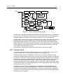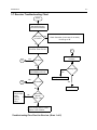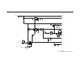
1
CDM™ and PRO SERIES™
Mobile Radios
contact
contact
PRO7100
control
control
C
A, Motorola, Professional Radio, CDM Series and CDM
Model numbers, PRO Series and PRO Series Model numbers are trademarks of Motorola.
© 1999 Motorola, Inc. All rights reserved. Printed in USA.
*6881091C63*
68P81091C63-O
Detailed
Service Manual
Professional Radio
CDM™ and PRO SERIES™
As Dedicated As You Are
Mobile Radios
Computer Software Copyrights
The Motorola products described in this manual may include copyrighted Motorola computer programs stored in
semiconductor memories or other media. Laws in the United States and other countries preserve for Motorola certain exclusive rights for copyrighted computer programs, including the exclusive right to copy or reproduce in any
form, the copyrighted computer program. Accordingly, any copyrighted Motorola computer programs contained in
the Motorola products described in this manual may not be copied or reproduced in any manner without the
express written permission of Motorola. Furthermore, the purchase of Motorola products shall not be deemed to
grant, either directly or by implication, estoppel or otherwise, any license under the copyrights, patents or patent
applications of Motorola, except for the normal non-exclusive royalty-free license to use that arises by operation of
law in the sale of a product.
Safety-1
SAFETY INFORMATION
Important information on safe and efficient operation is included in this manual. Read this information before
using your radio.
SAFE AND EFFICIENT OPERATION OF MOTOROLA TWO-WAY RADIOS
This document provides information and instructions for the safe and efficient operation of Motorola Portable and
Mobile Two-Way Radios.
The information provided in this document supercedes the general safety information contained in user guides
published prior to 1st. January 1998.
For information regarding radio use in hazardous areas, please refer to the Factory Mutual (FM) approval manual
supplement or Instruction Card which is included with radio models that offer this capability.
EXPOSURE TO RADIO FREQUENCY ENERGY
Your Motorola Two-Way Radio, which generates and radiates radio frequency (RF) electromagnetic energy
(EME) is designed to comply with the following National and International Standards and Guidelines regarding
exposure of human beings to radio frequency electromagnetic energy:
l
l
l
l
l
Federal Communications Commission Report and Order No. FCC 96-326 (August 1996)
American National Standards Institute (C95.1 - 1992)
National Council on Radiation Protection and Measurements (NCRP-1986)
International Commission on Non-Ionizing Radiation Protection (ICNRP- 1986)
European Committee for Electrotechnical Standardisation (CENELEC):
ENV 50166-1 1995 E
Human exposure to electromagnetic fields Low
frequency (0 Hz to 10 kHz)
ENV 50166-2 1995 E
Human exposure to electromagnetic fields High
frequency (10 kHz to 300 GHz)
Proceedings of SC211/B 1996
“Safety Considerations for Human Exposure to EMFs from
Mobile Telecommunication Equipment (MTE) in the Frequency Range 30MHz - 6 GHz.” (EMF - Electro-Magnetic
Fields)
To assure optimal radio performance and to ensure that your exposure to radio frequency electromagnetic energy
is within the guidelines in the above standards, always adhere to the following procedures:
PORTABLE RADIO OPERATION AND EME EXPOSURE
l
l
When transmitting with a portable radio, hold radio in a vertical position with the
microphone 2.5 to 5 centimeters (one or two inches) away from the mouth. Keep
antenna at least 2.5 centimeters (one inch) from your head or body when transmitting.
If you wear a portable Two-Way radio on your body, ensure that the antenna is at
least 2.5 centimeters (one inch) from the body when transmitting.
MAN WITH RADIO
ELECTROMAGNETIC INTERFERENCE/COMPATIBILITY
NOTE Nearly every electronic device is susceptible to electromagnetic interference (EMI) if inade-
quately shielded, designed or otherwise configured for electromagnetic compatibility
l
l
To avoid electromagnetic interference and/or compatibility conflicts, turn off your radio in any facility where
posted notices instruct you to do so. Hospital or health facilities may be using equipment that is sensitive to
external RF energy.
When instructed to do so, turn off your radio when on board an aircraft. Any use of a radio must be in accordance with airline regulations or crew instructions.
Safety-2
OPERATIONAL WARNINGS
Vehicles with an air bag
l
!
WARNING
Do not place a portable radio in the area over an air bag or in the air bag deployment area. Air bags inflate with
great force. If a portable radio is placed in the air bag deployment area and the air bag inflates, the radio may
be propelled with great force and cause serious injury to occupants of vehicle.
Potentially explosive atmospheres
l
Turn off your Two-Way radio when you are in any area with a potentially explosive atmosphere, unless it is a
radio type especially qualified for use in such areas (e.g. FM or Cenelec approved). Sparks in a potentially
explosive atmosphere can cause an explosion or fire resulting in bodily injury or even death.
Batteries
l
Do not replace or recharge batteries in a potentially explosive atmosphere. Contact sparking may occur while
installing or removing batteries and cause an explosion.
Blasting caps and areas
l
To avoid possible interference with blasting operations, turn off your radio when you are near electrical blasting
caps. In a “blasting area” or in areas posted “turn off two-way radio”, obey all signs and instructions.
NOTE The areas with potentially explosive atmospheres referred to above include fuelling areas
such as: below decks on boats; fuel or chemical transfer or storage facilities; areas where
the air contains chemicals or particles, such as grain, dust or metal powders; and any other
area where you would normally be advised to turn off your vehicle engine. Areas with potentially explosive atmospheres are often but not always posted.
OPERATIONAL CAUTIONS
Damaged antennas
l
!
Caution
Do not use any portable Two-Way radio that has a damaged antenna. If a damaged antenna comes into contact with your skin, a minor burn can result.
Batteries
l
All batteries can cause property damage and/or bodily injury such as burns if a conductive material such as
jewelery, keys or beaded chains touch exposed terminals. The conductive material may complete an electrical
circuit (short circuit) and become quite hot. Exercise care in handling any charged battery, particularly when
placing it inside a pocket, purse or other container with metal objects.
INTRINSICALLY SAFE RADIO INFORMATION
FMRC Approved Equipment
Anyone intending to use a radio in a location where hazardous concentrations of flammable material
exist (hazardous atmosphere) is advised to become familiar with the subject of intrinsic safety and
with the National Electric Code NFPA 70 (National Fire Protection Association) Article 500 (hazardous
[classified] locations).
An Approval Guide, issued by Factory Mutual Research Corporation (FMRC), lists manufacturers and
the products approved by FMRC for use in such locations. FMRC has also issued a voluntary
approval standard for repair service (“Class Number 3605”).
FMRC Approval labels are attached to the radio to identify the unit as being FM Approved for
specified hazardous atmospheres. This label specifies the hazardous Class/Division/Group along
with the part number of the battery that must be used. Depending on the design of the portable unit,
Safety-3
this FM label can be found on the back of the radio housing or the bottom of the radio housing.Their
Approval mark is shown below.
FM
APPROVED
!
WARNING
WARNING: Do not operate radio communications equipment in a hazardous atmosphere
unless it is a type especially qualified (e.g. FMRC Approved) for such use. An explosion or
fire may result.
WARNING: Do not operate the FMRC Approved Product in a hazardous atmosphere if it has
been physically damaged (e.g. cracked housing). An explosion or fire may result.
WARNING: Do not replace or charge batteries in a hazardous atmosphere. Contact sparking
may occur while installing or removing batteries and cause an explosion or fire.
WARNING: Do not replace or change accessories in a hazardous atmosphere. Contact
sparking may occur while installing or removing accessories and cause an explosion or fire.
WARNING: Do not operate the FMRC Approved Product unit in a hazardous location with the
accessory contacts exposed. Keep the connector cover in place when accessories are not
used.
WARNING: Turn radio off before removing or installing a battery or accessory.
WARNING: Do not disassemble the FMRC Approved Product unit in any way that exposes
the internal electrical circuits of the unit.
Radios must ship from the Motorola manufacturing facility with the hazardous atmosphere capability
and FM Approval labeling. Radios will not be “upgraded” to this capability and labeled in the field.
A modification changes the unit’s hardware from its original design configuration. Modifications can
only be done by the original product manufacturer at one of its FMRC audited manufacturing facilities.
!
WARNING
WARNING: Failure to use an FMRC Approved Product unit with an FMRC Approved battery
or FMRC Approved accessories specifically approved for that product may result in the dangerously unsafe condition of an unapproved radio combination being used in a hazardous
location.
Unauthorized or incorrect modification of an FMRC Approved Product unit will negate the Approval
rating of the product.
Repair of FMRC Approved Products
REPAIRS FOR MOTOROLA FMRC APPROVED PRODUCTS ARE THE RESPONSIBILITY OF THE
USER.
You should not repair or relabel any Motorola manufactured communication equipment bearing the
FMRC Approval label (“FMRC Approved Product”) unless you are familiar with the current FMRC
Approval standard for repairs and service (“Class Number 3605).
You may want to consider using a repair facility that operates under 3605 repair service approval.
!
WARNING: Incorrect repair or relabeling of any FMRC Approved Product unit could
adversely affect the Approval rating of the unit.
WARNING
WARNING: Use of a radio that is not intrinsically safe in a hazardous atmosphere could
result in serious injury or death.
Safety-4
FMRC’s Approval Standard Class Number 3605 is subject to change at any time without notice to
you, so you may want to obtain a current copy of 3605 from FMRC. Per the December, 1994
publication of 3605, some key definitions and service requirements are as follows:
Repair
A repair constitutes something done internally to the unit that would bring it back to its original
condition Approved by FMRC. A repair should be done in an FMRC Approved facility.
Items not considered as repairs are those in which an action is performed on a unit which does not
require the outer casing of the unit to be opened in a manner which exposes the internal electrical
circuits of the unit. You do not have to be an FMRC Approved Repair Facility to perform these actions.
Relabeling
The repair facility shall have a method by which the replacement of FMRC Approval labels are
controlled to ensure that any relabeling is limited to units that were originally shipped from the
Manufacturer with an FM Approval label in place. FMRC Approval labels shall not be stocked by the
repair facility. An FMRC Approval label shall be ordered from the original manufacturer as needed to
repair a specific unit. Replacement labels may be obtained and applied by the repair facility providing
satisfactory evidence that the unit being relabeled was originally an FMRC Approved unit. Verification
may include, but is not limited to: a unit with a damaged Approval label, a unit with a defective housing
displaying an Approval label, or a customer invoice indicating the serial number of the unit and
purchase of an FMRC Approved model.
Do Not Substitute Options or Accessories
The Motorola communications equipment certified by Factory Mutual is tested as a system and
consists of the FM Approved portable, FM Approved battery, and FM Approved accessories or
options, or both. This Approved portable and battery combination must be strictly observed. There
must be no substitution of items, even if the substitute has been previously Approved with a different
Motorola communications equipment unit. Approved configurations are listed in the FM Approval
guide published by FMRC, or in the product FM Supplement. This FM Supplement is shipped with FM
Approved radio and battery combination from the manufacturer. The Approval guide, or the Approval
standard Class Number 3605 document for repairs and service, can be ordered directly through
Factory Mutual Research Corporation located in Norwood, Massachusetts.
i
TABLE OF CONTENTS
Chapter 1
Introduction
1.1 Scope of Manual ........................................................................................................................... 1-1
1.2 Warranty and Service Support ...................................................................................................... 1-1
1.2.1 Warranty Period ..................................................................................................................... 1-1
1.2.2 Return Instructions ................................................................................................................. 1-1
1.2.3 After Warranty Period ............................................................................................................ 1-1
1.3 Related Documents ...................................................................................................................... 1-2
1.4 Technical Support ......................................................................................................................... 1-2
1.5 Warranty and Repairs.................................................................................................................... 1-2
1.6 Radio Model Chart and Specifications .......................................................................................... 1-4
1.7 Radio Model Information ............................................................................................................... 1-4
Chapter 2
Theory of Operation
2.1 Overview....................................................................................................................................... 2-1
2.2 Controller Section ......................................................................................................................... 2-1
2.2.1 Radio Power Distribution ....................................................................................................... 2-2
2.2.2 Automatic On/Off ................................................................................................................... 2-3
2.2.3 Emergency............................................................................................................................. 2-4
2.2.4 Mechanical On/Off ................................................................................................................. 2-4
2.2.5 Ignition ................................................................................................................................... 2-4
2.2.6 Microprocessor Clock Synthesizer......................................................................................... 2-5
2.2.7 Serial Peripheral Interface (SPI) ............................................................................................ 2-5
2.2.8 SBEP Serial Interface ............................................................................................................ 2-6
2.2.9 General Purpose Input/Output ............................................................................................... 2-6
2.2.10 Normal Microprocessor Operation ......................................................................................... 2-7
2.2.11 Static Random Access Memory (SRAM) ............................................................................... 2-8
2.3 Controller Board Audio and Signalling Circuits ............................................................................. 2-8
2.3.1 Audio Signalling Filter IC with Compander (ASFIC CMP) ..................................................... 2-8
2.3.2 Transmit Audio Circuits.......................................................................................................... 2-9
2.3.3 Microphone Input Path ........................................................................................................... 2-9
2.3.3.1 PTT Sensing and TX Audio Processing ........................................................................ 2-10
2.3.3.2 TX Secure Audio (optional) ........................................................................................... 2-10
2.3.3.3 Option Board Transmit Audio ........................................................................................ 2-10
2.3.4 Transmit Signalling Circuits ................................................................................................. 2-11
2.3.4.1 Sub-Audible Data (PL/DPL) .......................................................................................... 2-11
2.3.4.2 High Speed Data ........................................................................................................... 2-12
2.3.4.3 Dual Tone Multiple Frequency (DTMF) Data ................................................................ 2-12
2.3.5 Receive Audio Circuits......................................................................................................... 2-13
2.3.5.1 Squelch Detect .............................................................................................................. 2-13
2.3.5.2 Audio Processing and Digital Volume Control ............................................................... 2-14
2.3.5.3 Audio Amplification Speaker (+) Speaker (-) ................................................................. 2-14
2.3.5.4 Handset Audio ............................................................................................................... 2-15
2.3.5.5 Filtered Audio and Flat Audio ........................................................................................ 2-15
2.3.5.6 RX Secure Audio (Optional) .......................................................................................... 2-15
ii
2.3.5.7 Option Board Receive Audio
2-15
2.3.6 Receive Signalling Circuits................................................................................................... 2-16
2.3.6.1 Sub-audible Data (PL/DPL) and High Speed Data Decoder ........................................ 2-16
2.3.6.2 Alert Tone Circuits ......................................................................................................... 2-16
2.3.6.3 Voice Storage (Optional) .............................................................................................. 2-17
2.4 UHF (403-470 MHz) Receiver Front-End ................................................................................... 2-17
2.4.1 Front-End Band-Pass Filters & Pre-Amplifier....................................................................... 2-19
2.4.2 First Mixer and 1st Intermediate Frequency (IF) ................................................................... 2-19
2.4.3 2nd Intermediate Frequency (IF) and Receiver Back-End................................................... 2-19
2.5 Transmitter Power Amplifier (PA) 40 W ...................................................................................... 2-20
2.5.1 Power Controlled Stage ....................................................................................................... 2-20
2.5.2 Pre-Driver Stage .................................................................................................................. 2-20
2.5.3 Driver Stage ......................................................................................................................... 2-21
2.5.4 Final Stage ........................................................................................................................... 2-21
2.5.5 Bi-Directional Coupler .......................................................................................................... 2-21
2.5.6 Antenna Switch .................................................................................................................... 2-21
2.5.7 Harmonic Filter...................................................................................................................... 2-21
2.5.8 Power Control ....................................................................................................................... 2-21
2.6 Frequency Synthesis .................................................................................................................. 2-22
2.6.1 Reference Oscillator............................................................................................................. 2-22
2.6.2 Fractional-N Synthesizer...................................................................................................... 2-22
2.6.3 Voltage Controlled Oscillator (VCO) .................................................................................... 2-23
2.6.4 Synthesizer Operation.......................................................................................................... 2-25
2.7 VHF (136-174MHz) Receiver Front-End ..................................................................................... 2-26
2.7.1 Front-End Band-Pass Filters and Pre-Amplifier ................................................................... 2-27
2.7.2 First Mixer and 1st Intermediate Frequency (IF) .................................................................. 2-27
2.7.3 2nd Intermediate Frequency (IF) and Receiver Back-End................................................... 2-27
2.8 Transmitter Power Amplifier (PA) 45 W ...................................................................................... 2-28
2.8.1 Power Controlled Stage ....................................................................................................... 2-28
2.8.2 Pre-Driver Stage .................................................................................................................. 2-28
2.8.3 Driver Stage ......................................................................................................................... 2-29
2.8.4 Final Stage ........................................................................................................................... 2-29
2.8.5 Directional Coupler............................................................................................................... 2-29
2.8.6 Antenna Switch .................................................................................................................... 2-29
2.8.7 Harmonic Filter..................................................................................................................... 2-29
2.8.8 Power Control ...................................................................................................................... 2-30
2.9 Frequency Synthesis .................................................................................................................. 2-30
2.9.1 Reference Oscillator............................................................................................................. 2-30
2.9.2 Fractional-N Synthesizer...................................................................................................... 2-30
2.9.3 Voltage Controlled Oscillator (VCO) .................................................................................... 2-32
2.9.4 Synthesizer Operation.......................................................................................................... 2-33
2.10 Control Head (PRO3100, CDM750) ........................................................................................... 2-34
2.10.1 Power Supplies .................................................................................................................... 2-34
2.10.2 Power On/Off ....................................................................................................................... 2-34
2.10.3 Microprocessor Circuit ......................................................................................................... 2-34
2.10.4 SBEP Serial Interface .......................................................................................................... 2-35
2.10.5 Keypad Keys ........................................................................................................................ 2-35
2.10.6 Status LED and Back Light Circuit ....................................................................................... 2-35
2.10.7 Microphone Connector Signals ............................................................................................ 2-36
2.10.8 Speaker................................................................................................................................. 2-36
2.10.9 Electrostatic Transient Protection ........................................................................................ 2-36
2.11 Control Head (PRO5100, PRO7100, CDM1250, CDM1550) ..................................................... 2-37
2.11.1 Power Supplies .................................................................................................................... 2-37
2.11.2 Power On / Off ..................................................................................................................... 2-37
iii
2.11.3 Microprocessor Circuit .........................................................................................................
2.11.4 SBEP Serial Interface ..........................................................................................................
2.11.5 Keypad Keys........................................................................................................................
2.11.6 Status LED and Back Light Circuit.......................................................................................
2.11.7 Liquid Crystal Display (LCD)................................................................................................
2.11.8 Microphone Connector Signals............................................................................................
2.11.9 Speaker................................................................................................................................
2.11.10 Electrostatic Transient Protection ........................................................................................
Chapter 3
2-37
2-38
2-38
2-38
2-39
2-39
2-40
2-40
Maintenance
3.1 Introduction ................................................................................................................................... 3-1
3.2 Preventive Maintenance ............................................................................................................... 3-1
3.2.1 Inspection............................................................................................................................... 3-1
3.2.2 Cleaning................................................................................................................................. 3-1
3.3 Safe Handling of CMOS and LDMOS ........................................................................................... 3-2
3.4 General Repair Procedures and Techniques ............................................................................... 3-2
3.5 Recommended Test Tools ............................................................................................................ 3-5
3.6 Transmitter Troubleshooting Chart ................................................................................................ 3-6
3.7 Receiver Troubleshooting Charts ................................................................................................. 3-7
3.8 Synthesizer Troubleshooting Charts ............................................................................................. 3-9
3.9 VCO Troubleshooting Charts....................................................................................................... 3-11
Chapter 4
Schematic Diagrams, Overlays, and Parts Lists
4.1 Introduction ................................................................................................................................... 4-1
4.1.1 Notes For All Schematics and Circuit Boards ........................................................................ 4-1
List of Figures
2-1
2-2
2-3
2-4
2-5
2-6
2-7
2-8
2-9
2-10
2-11
2-12
2-13
2-14
Controller Block Diagram............................................................................................................... 2-1
DC Power Distribution Block Diagram ........................................................................................... 2-3
Transmit Audio Paths .................................................................................................................... 2-9
Transmit Signalling Paths ............................................................................................................ 2-11
Receive Audio Paths ................................................................................................................... 2-13
Receive Signalling Paths ............................................................................................................. 2-16
UHF Receiver Block Diagram ...................................................................................................... 2-18
UHF Transmitter Block Diagram.................................................................................................. 2-20
UHF Synthesizer Block Diagram ................................................................................................. 2-23
UHF VCO Block Diagram ............................................................................................................ 2-24
VHF Receiver Block Diagram ...................................................................................................... 2-26
VHF Transmitter Block Diagram .................................................................................................. 2-28
VHF Synthesizer Block Diagram ................................................................................................. 2-31
VHF VCO Block Diagram ............................................................................................................ 2-32
4-1
4-2
4-3
4-4
PRO3100/CDM750 Control Head Top Overlay ............................................................................ 4-3
PRO3100/CDM750 Control Head Bottom Overlay ....................................................................... 4-4
PRO3100CDM750 Control Head Schematic Diagram, Sheet 1 ................................................... 4-5
PRO3100CDM750 Control Head Schematic Diagram, Sheet 2 ................................................... 4-6
iv
4-5
4-6
4-7
4-8
4-9
4-10
4-11
4-12
4-13
4-14
4-15
4-16
4-17
4-18
4-19
4-20
4-21
4-22
4-23
4-24
PRO5100/PRO7100/CDM1250/CDM1550 Control Head Top
Overlay .......................................................................................................................................... 4-9
PRO5100/PRO7100/CDM1250/CDM1550 Control Head Bottom
Overlay ........................................................................................................................................ 4-10
PRO5100/PRO7100/CDM1250/CDM1550 Control Head
Schematic Diagram ..................................................................................................................... 4-11
PRO5100/PRO7100/CDM1250/CDM1550 Control Head Keypad
Schematic Diagram..................................................................................................................... 4-12
PRO5100/PRO7100/CDM1250/CDM1550 Control Head LCD
Schematic ................................................................................................................................... 4-13
PRO5100/PRO7100/CDM1250/CDM1550 Control Head Display
Schematic ................................................................................................................................... 4-14
Complete Controller Schematic Diagram .................................................................................... 4-17
Controller Control Schematic Diagram ...................................................................................... 4-18
Controller I/O Schematic Diagram .............................................................................................. 4-19
Controller Audio Schematic Diagram .......................................................................................... 4-20
Controller Supply Voltage Schematic Diagram ........................................................................... 4-21
UHF (403-470MHz) Voltage Controlled Oscillator Schematic Diagram ...................................... 4-25
UHF (403-470MHz) Fractal-N Schematic Diagram .................................................................... 4-26
UHF (403-470MHz) Power Amplifier Schematic Diagram .......................................................... 4-27
VHF (136-174MHz) Main Board Top Side PCB .......................................................................... 4-33
VHF (136-174MHz) Receiver Front End Schematic Diagram .................................................... 4-34
VHF (136-174MHz) Receiver IF Schematic Diagram ................................................................. 4-35
VHF (136-174MHz) Fractal-N Schematic Diagram ..................................................................... 4-36
VHF (136-174MHz) Voltage Controlled Oscillator Schematic Diagram ...................................... 4-37
VHF (136-174MHz) Power Amplifier Schematic Diagram .......................................................... 4-38
List of Tables
1-1
Radio Model Number ..................................................................................................................... 1-3
3-1
Recommended Test tools .............................................................................................................. 3-5
4-1
4-2
4-3
4-4
4-5
PRO3100/CDM750 Control Head Parts List.................................................................................. 4-7
PRO5100/PRO7100/CDM1250/CDM1550 Control Head Parts List............................................ 4-15
Controller Parts List ..................................................................................................................... 4-22
UHF B1 Radio Parts List.............................................................................................................. 4-28
VHF (136-174MHz) Radio Parts List ........................................................................................... 4-39
1-1
Chapter 1
Introduction
1.1
Scope of Manual
This manual is intended for use by service technicians familiar with similar types of equipment. It
contains service information required for the equipment described and is current as of the printing
date. Changes that occur after the printing date are incorporated by a complete manual revision or
alternatively, as additions.
NOTE Before operating or testing these units, please read the Safety Information Section in
the front of this manual.
1.2
Warranty and Service Support
Motorola offers long term support for its products. This support includes full exchange and/or repair of
the product during the warranty period, and service/repair or spare parts support out of warranty. Any
“return for exchange” or “return for repair” by an authorized Motorola dealer must be accompanied by
a warranty claim form. Warranty claim forms are obtained by contacting customer service.
1.2.1 Warranty Period
The terms and conditions of warranty are defined fully in the Motorola dealer or distributor or reseller
contract. These conditions may change from time to time and the following notes are for guidance
purposes only.
1.2.2 Return Instructions
In instances where the product is covered under a “return for replacement” or “return for repair”
warranty, a check of the product should be performed prior to shipping the unit back to Motorola. This
is to ensure that the product has been correctly programmed or has not been subjected to damage
outside the terms of the warranty.
Prior to shipping any radio back to a Motorola warranty depot, please contact the appropriate
customer service for instructions. All returns must be accompanied by a warranty claim form,
available from your customer services representative. Products should be shipped back in the original
packaging, or correctly packaged to ensure no damage occurs in transit.
1.2.3 After Warranty Period
After the Warranty period, Motorola continues to support its products in two ways:
Firstly, Motorola's Accessories and Aftermarket Division (ADD) offers a repair service to both end
users and dealers at competitive prices.
Secondly, Motorola’s service department supplies individual parts and modules that can be
purchased by dealers who are technically capable of performing fault analysis and repair.
1-2
1.3
Related Documents
Related Documents
The following documents are directly related to the use and maintainability of this product.
1.4
Title
Part Number
Service Manual, Basic, Engl
68P81091C62
Service Manual, Basic, Engl
68P81092C71
Service Manual, Basic, Port
68P81092C73
Service Manual, Basic,Span
68P81092C72
Service Manual, Detailed, Engl
68P81091C63
Service Manual, Detailed, Port
68P81092C76
Service Manual, Detailed, Span
68P81092C75
Technical Support
Technical support is available to assist the dealer/distributor and self-maintained customers in
resolving any malfunction which may be encountered. Initial contact should be by telephone to
customer resources wherever possible. When contacting Motorola technical support, be prepared to
provide the product model number and the unit’s serial number. The contact locations and telephone
numbers are listed below.
United States and Puerto Rico: 1-800-694-2161, Options 1, 3
Brasil: 000-811-682-0550
Colombia: 980-12-0451
Mexico: 001-800-694-2161
From other countries: (954)723-3008
1.5
Warranty and Repairs
For warranty and repairs, contact Motorola Technical Support as listed below. Be prepared to provide
the product model number and the unit’s serial number.
Some replacement parts, spare parts, and/or product information can be ordered directly. If a
complete Motorola part number is assigned to the part, and it is not identified as “Depot ONLY”, the
part is available from Motorola Accessories and Aftermarket Division (AAD). If no part number is
assigned, the part is not normally available from Motorola. If the part number is appended with an
asterisk, the part is serviceable by a Motorola depot only. If a parts list is not included, this generally
means that no user-serviceable parts are available for that kit or assembly.Technical Support the
product model number and the unit’s serial number.
Warranty and Repairs
1-3
Parts Order Entry
7:00 A. M. to 7:00 P. M. (Central Standard Time)
Monday through Friday (Chicago, U. S. A.)
To Order Parts in Latin America and the Caribbean:
1-847-538-8023
Motorola Parts
To Order Parts in the United States of America: Accessories and Aftermarket Division
(United States and Canada)
1-800-422-4210, or 847-538-8023
1-800-826-1913, or 410-712-6200 (U. S. Federal
Attention: Order Processing
Government)
1313 E. Algonquin Road
Schaumburg, IL 60196
TELEX: 280127
FAX: 1-847-538-8198
Accessories and Aftermarket Division
FAX: 1-410-712-4991 (U. S. Federal Government) Attention: Latin America and Caribbean
(U. S. A.) after hours or weekends:
1-800-925-4357
Order Processing
1313 E. Algonquin Road
Schaumburg, IL 60196
Parts Identification
1-847-538-0021 (Voice)
1-847-538-8194 (FAX)
Colombia
Motorola de Colombia
Diagonal 127A 17-64
Santa Fe de Bogota
Columbia
Telefono: 1-615-5759
Brazil
Motorola Do Brasil
Rua Bandeira Paulista, 580
Phone: (11)821-9991
Fax: (11)828-0157
Puerto Rico
Motorola de Puerto Rico
A BE. Chardon, Edificio Telemundo 2
Hato Rey, PR 00918
Telefono: (787)641-4100
Fax: (787)782-3685
Mexico
Motorola De Mexico
Blvd. Manuel Avila Camacho #32, Primer Piso
COL. Lomas de Chapultepec
Mexico D.F. 06700 CP 11000
Mexico
Phone: (5)387-0501
Fax: (5)387-0554
1-4
1.6
Radio Model Chart and Specifications
Radio Model Chart and Specifications
The radio model charts and specifications are located in the Basic Service Manual listed under the
Related Documents paragraph of this chapter.
1.7
Radio Model Information
The model number and serial number are located on a label attached to the back of your radio. You
can determine the RF output power, frequency band, protocols, and physical packages from these
numbers. The example below shows one portable radio model number and its specific characteristics.
Table 1-1.
Example: AAM25RHC9AA1AN
Type of Model
Unit
Series
M
M = Mobile
Motorola Internal Use
AA
or
LA
25
Freq.
Band
K
VHF
(136174MHz)
Power
Level
Radio Model Number
Physical
Packages
Channel
Spacing
H
A
1-25W No Display,
No Keypad
9
Programmable
R
K
C
UHF1 25-40W No Display
(403Basic Key470MHz)
pad
Protocol
Feature
Level
Model
Revision
Model
Package
AA
Conventional
1
4F
A
N
DU
LTR
2
64F
S
UHF2
(450512MHz)
D
1-Line Display, Limited Keypad
5
128F
B
Low
Band, R1
(29.736.0MHz)
F
1-Line Display, Standard
Keypad
8
160F
C
Low
Band, R2
(36.042.0MHz)
N
4-Line Display,
Enhanced
Keypad
D
Low
Band, R3
(42.050.0MHz)
2-1
Chapter 2
Theory of Operation
2.1
Overview
This chapter provides a detailed theory of operation for the radio and its components. The radio is
designed as a single board unit consisting of a transmitter, receiver, and controller circuits. The board
also accepts one additional option board that can provide functions such as secure voice/data, voice
storage, or a signalling decoder.
A control head mounted directly on the front of the radio or remotely connected by an extension
cable provides a user interface for controlling the various features of the radio.The control head
contains, LED indicators, microphone connector, and buttons depending on the radio type, display,
and speaker.
If a control head is not mounted directly on the front of the radio, an expansion board containing
circuits for special applications can be mounted in its place on the front of the radio. An additional
control head may be connected using an extension cable.
The rear of the radio provides connections for a power, antenna, and accessory cable. The
accessory cable provides connections for items such as an external speaker, emergency switch, foot
operated PTT, and ignition sensing, etc.
2.2
Controller
The radio controller, shown in Figure 2-1, is divided into three main functions:
n
Digital control
n
Audio processing
n
Voltage regulation.
The digital control section of the radio consists of a microprocessor (µP), support memory, support
logic, signal MUX ICs, on/off circuit, and general purpose input/output circuits.
To Synthesizer
16.8 MHz
Reference Clock
from Synthesizer
External
Microphone
Mod Out
Audio/Signalling
Recovered Audio
ASFIC_CMP
External
Speaker
Audio
PA
5V
from Synthesizer
Section (5V_RF)
Internal
Speaker
µP Clock
SPI
To RF Section
SCI to
Accessory &
Control Head
Connector
Digital
5V
Regulator
(5VD)
RAM
EEPROM
HC11FL0
FLASH
Figure 2-1. Controller Block Diagram
2-2
2.2.1
Theory of Operation
Radio Power Distribution
The dc power distribution throughout the radio board is shown in Figure 2-2. Voltage regulation for
the controller is provided by four separate devices:
n
U0651 (MC78M05) +5 volts
n
U0641 (LM2941) +9.3 volts
n
U0611 (LM2941) +12 volts
n
VSTBY 5V (a combination of R0621 and VR0621)
n
Additional 5 volt regulator located in the RF section.
The dc voltage applied to connector J0601 supplies power directly to the following:
n
Electronic on/off control
n
RF power amplifier
n
12 volt regulator
n
9.3 volt regulator
n
Audio PA
n
5.6 volt stabilization circuit
n
9.3 volt regulator (U0641) supplies power to the 5 volt regulator (U0651) and 6 volt voltage
divider Q0681
Regulator U0641 generates the 9.3 volts required by some audio circuits, the RF and power control
circuits. Input and output capacitors C0641 and C0644 / C0645 are used to reduce high frequency
noise. Resistors R0642 / R0643 set the output voltage of the regulator. If the voltage at pin 1 is
greater than 1.3 volts the regulator output decreases and if the voltage is less than 1.3 volts the
regulator output increases. This regulator output is enabled by a 0 volt signal on pin 2. Transistors
Q0661, Q0641, and R0641 are used to disable the regulator when the radio is turned off.
Voltage regulator U0651 provides 5 volts operating voltage for the digital circuits. Operating voltage
is from the regulated 9.3volts supply. Input and output capacitors (C0651 / C0652 and C0654 /
C0655) reduce high frequency noise and provide proper operation during battery transients. Voltage
sense device U0652 or alternatively U0653 provides a reset output that goes to 0 volts if the
regulator output goes below 4.5 volts. This resets the controller to prevent improper operation. Diode
D0651 prevents discharge of C0652 by negative spikes on the 9.3 volt supply.
Transistor Q0681 and resistors R0681 / R0682 divide the regulated 9.3 volts down to about 6 volts.
This voltage supplies the 5 volt regulator, located on the RF section. By reducing the supply voltage
of the regulator, the power dissipation is divided between the RF section and the controller section.
The VSTBY signal, derived directly from the supply voltage by components R0621 and VR0621,
buffers the internal RAM. Capacitor C0622 allows the battery voltage to be disconnected for several
seconds without losing RAM information. Dual diode D0621 prevents radio circuits from discharging
this capacitor. When the supply voltage is applied to the radio, C0622 is charged via R0621 and
D0621. When the radio is switched on, the µP enters the wrong mode if the voltage across C0622 is
still too low. The regulated 5 volts charges C0622 via diode D0621.
Theory of Operation
2-3
J0601
13.2V
PA, Driver
Antenna Switch
Accessories
20 Pin Connector
Control Head
12 Pin Connector
Option Board
40 Pin Connector
PASUPVLTG
12V
Regulator
SWB+
FLT_A+
ON / OFF
Control
Ignition
Emergency
ON/OFF
5VD
FLT_A+
9.3V
Regulator
Audio PA
5.6V
9V3
PCIC,
TX Amp
Temp Sense
RX RF Amp
IF Amp
6V
Regulator
5V
Regulator
5V
Regulator
5V_RF
5V/
VDDA
5VD
MCU
µP, RAM,
FLASH & EEPROM
ASFIC_CMP
FRACTN
VCOBIC
VSTBY
Figure 2-2. DC Power Distribution Block Diagram
The INT SW B+ voltage from switching transistor Q0661 provides power to the circuit controlling the
audio PA output. The voltage is monitored by the µP through voltage divider R0671/R0672 and the
line battery voltage. Diode VR0671 limits the divided voltage to 5.6 volts to protect the µP.
Regulator U0611 generates the voltage for the switched supply voltage output (SWB+) at accessory
connector J0501, pin 13. U0611 operates as a switch with voltage and current limit. Resistors
R0611/R0612 set the maximum output voltage to 16.5 volts. This limitation is only active at high
supply voltage levels. The regulator output is enabled by a 0 volt signal at Q0661, pin 2. Q0641 and
R0641 disable the regulator when the radio is turned off. Input and output capacitors C0603 and
C0611/C0612 reduce high frequency noise.
Diode VR0601 protects against transients and reverse polarity of the supply voltage.
2.2.2
Automatic On/Off
The radio software and/or external triggers turn the radio on or off without direct user action. For
example, automatic turn on when ignition is sensed and off when ignition is off.
Q0661 provides the INT SW B+ voltage to the various radio circuits and to enable the voltage
regulators via transistor Q0641 which contains a pnp and an npn transistor that provide an electronic
on/off switch. The switch is on when the collector of the npn transistor within Q0661 is low. When the
radio is off the collector is at supply voltage level. This effectively prevents current flow from emitter to
collector of the pnp transistor. When the radio is turned on the voltage at the base of the npn
transistor is pulled high and the pnp transistor switches on (saturation). With the INT SWB+ voltage
now at supply voltage level, transistor Q0641 pulls pin 2 of the voltage regulators U0611 and U 0641
to ground level, enabling their outputs.
The electronic on/off circuits are enabled by the µP through ASFIC CMP port GCB2, line DC
POWER ON, emergency switch (line EMERGENCY CONTROL), the mechanical On/Off/Volume
knob on the control head (line ON OFF CONTROL), or the ignition sense circuits (line IGNITION
CONTROL). If any of the four paths cause a low at the collector of the npn transistor within Q0661,
the electronic "ON" is engaged.
2-4
2.2.3
Theory of Operation
Emergency
The emergency switch (J0501, pin 9), when engaged, grounds the base of Q0662 via the
EMERGENCY CONTROL line. This switches Q0662 off and resistor R0662 pulls the collector of
Q0662 and the base of Q0663 to levels above two volts. Transistor Q0663 then switches on and pulls
the collector of the npn transistor within Q0661 to ground level This enables the voltage regulators
via Q0641. When the emergency switch is released, R0541 pulls the base of Q0662 up to 0.6 volts
causing the collector of transistor Q0662 to go low (0.2 volts), switching Q0663 off.
While the radio is on, the µP monitors the voltage at the emergency input on the accessory
connector via pin 60 and the GP5 IN ACC9 line. Three different conditions can exit: no emergency,
emergency, and open connection to the emergency switch. If no emergency switch is connected or
the connection to the emergency switch is broken, the resistive divider R0541/R0512 sets the
voltage to about 4.7 volts. If an emergency switch is connected, a resistor to ground within the
emergency switch reduces the voltage on line GP5 IN ACC9 to inform the µP that the emergency
switch is operational. An engaged emergency switch pulls line GP5 IN ACC9 to ground level. Diode
D0179 limits the voltage to protect the µP input.
While the EMERGENCY CONTROL signal is low and INT SW B+ is on, the µP starts execution,
reads that the emergency input is active through the voltage level of line GP5 IN ACC9, and sets the
DC POWER ON output of the ASFIC CMP, pin 13 to a logic high. This keeps Q0661 and Q0641
switched to allow a momentary press of the emergency switch to power up the radio. When the µP
has finished processing the emergency press, it sets the DC POWER ON line to a logic 0. This turns
off Q0661 and the radio turns off. Notice that the µP is alerted to the emergency condition via line
GP5 IN ACC9. If the radio is already on when the emergency is triggered, the DC POWER ON signal
is already high.
2.2.4
Mechanical On/Off
This refers to the on/off/volume knob located on the control head which is used to turn the radio on
and off and control the volume.
If the radio is turned off and the on/off/volume knob is pressed, line ON OFF CONTROL (J0401, pin
11) goes high and switches the radio’s voltage regulators on as long as the button is pressed. The µP
is alerted through line ON OFF SENSE (U0101, pin 6) which is pulled to low by Q0110 while the on/
off/volume knob is pressed. In addition, an interrupt is generated at µP, pin 96. The µP asserts line
DC POWER ON via ASFIC CMP, pin 13 high which keeps the radio switched on. The µP switches
the radio off by setting DC POWER ON to low via ASFIC CMP pin 13.
2.2.5
Ignition
Ignition sense prevents the radio from draining the vehicle’s battery because the engine is not
running.
When the IGNITION input (J0501, pin 10) goes above 5 volts, Q0661 is turned on via line IGNITION
CONTROL. Q0661 turns on INT SW B+ and the voltage regulators by turning on Q0641 and the µP
starts execution. The µP is alerted through line GP6 IN ACC10. While the on/off button is pressed, a
high signal turns Q0181 on, which pulls µP, pin 74 to low. If the software detects a low state it asserts
DC POWER ON via ASFIC, pin 13 high which keeps Q0661 and Q0641 and the radio switched on.
When the IGNITION input goes below 3 volts, Q0181 switches off and R0181 pulls µP, pin 74 to high.
This alerts the software to switch off the radio by setting DC POWER ON to low. The next time the
IGNITION input goes above 5 volts the above process is repeated.
Theory of Operation
2.2.6
2-5
Microprocessor Clock Synthesizer
The clock source for the µP system is generated by the ASFIC CMP (U0221). Upon power-up the
synthesizer IC (FRAC-N) generates a 16.8 MHz waveform that is routed from the RF section to the
ASFIC CMP, pin 34. For the main board controller the ASFIC CMP uses 16.8 MHz as a reference
input clock signal for its internal synthesizer. The ASFIC CMP, in addition to the audio circuit, has a
programmable synthesizer which can generate a synthesized signal ranging from 1200Hz to
32.769MHz in 1200Hz steps.
When power is first applied, the ASFIC CMP generates its default 3.6864MHz CMOS square wave
UP CLK (on U0221, pin 28) and this is routed to the µP (U0101, pin 90). After the µP starts
operation, it reprograms the ASFIC CMP clock synthesizer to a higher UP CLK frequency (usually
7.3728 or 14.7456 MHz) and continues operation.
The ASFIC CMP may be reprogrammed to change the clock synthesizer frequencies at various
times depending on the software features that are executing. In addition, the clock frequency of the
synthesizer is changed in small amounts if there is a possibility of harmonics of this clock source
interfering with the desired radio receive frequency.
The ASFIC CMP synthesizer loop uses C0245, C0246 and R0241 to set the switching time and jitter
of the clock output. If the synthesizer cannot generate the required clock frequency it switches back
to its default 3.6864MHz output.
Because the ASFIC CMP synthesizer and the µP do not operate without the 16.8 MHz reference
clock, the synthesizer and the voltage regulators should be checked first in debugging the system.
The µP uses crystal oscillator Y0131 and associated components to form a real time clock used to
display the time on control heads (with display) or as time stamp for incoming calls or messages. The
real time clock is powered from the voltage VSTBY to keep running while the radio is switched off. If
the radio is disconnected from the supply voltage, the time must be reset.
2.2.7
Serial Peripheral Interface (SPI)
The µP communicates to many of the IC’s through its SPI port. This port consists of SPI TRANSMIT
DATA (MOSI) (U0101, pin 100), SPI RECEIVE DATA (MISO) (U0101, pin 99), SPI CLK (U0101, pin
1) and chip select lines going to the various ICs. The BUS is a synchronous bus, in that the timing
clock signal CLK is sent while SPI data (SPI TRANSMIT or RECEIVE) is sent. Therefore, whenever
there is activity on either SPI TRANSMIT DATA or SPI RECEIVE DATA there should be a uniform
signal on CLK.
The SPI TRANSMIT DATA sends serial data from the µP to a device, and SPI RECEIVE DATA is
sends data from a device to the µP. On the controller there are two ICs on the SPI BUS: ASFIC CMP
(U0221, pin 22), and EEPROM (U0111, pin 5). In the RF section there are two ICs on the SPI BUS:
FRAC-N Synthesizer, and the Power Control IC (PCIC). The SPI TRANSMIT DATA and CLK lines
going to the RF section are filtered by L0481/R0481 and L0482/R0482 to minimize noise. The chip
select line CSX from U0101, pin 2 is shared by the ASFIC CMP, FRAC-N Synthesizer, and PCIC.
Each of these IC‘s check the SPI data and when the sent address information matches the IC’s
address, the data that follows is processed. The chip select lines for the EEPROM (EE CS), voice
storage (VS CS), expansion board (EXP1 CS, EXP2 CS) and option board (OPT CS) are decoded
by the address decoder U0141.
When the µP needs to program any of these IC’s it brings the chip select line CSX to a logic 0 and
then sends the proper data and clock signals. The amount of data sent varies, for example the
ASFIC CMP can receive up to 19 bytes (152 bits) while the PCIC can receive up to 6 bytes (48 bits).
After the data is sent, the chip select line is returned to logic 1.
2-6
Theory of Operation
The option board interfaces are different in that the µP can also read data back from devices
connected.The timing and operation of this interface is specific to the option connected, but the
general pattern is as follows:
n
n
2.2.8
Option board generates a service request via J0551, pin 29, line RDY, and µP, pin 79
The main board asserts a chip select for that option board via U0141,pin 14, line OPT CS,
J0551,pin 30
n
The main board µP generates the CLK (J0551, pin 3)
n
The main board µP writes serial data via J0551, pin 15 and reads serial data via J0551, pin 16
n
When data transfer is complete the main board terminates the chip select and CLK activity
SBEP Serial Interface
The SBEP serial interface allows the radio to communicate with the Customer Programming
Software (CPS), or the universal tuner via the Radio Interface Box (RIB). This interface connects to
the microphone connector via control head connector (J0401, pin 8) or to the accessory connector
J0401, pin 17 and comprises BUS+. The line is bi-directional, meaning that either the radio or the
RIB can drive the line. The µP sends serial data via pin 98 and D0101 and it reads serial data via pin
97. Whenever the µP detects activity on the BUS+ line, it starts communication.
In addition, the SBEP serial interface is used to communicate with a connected control head. When a
control head key is pressed or the volume knob is rotated, the line ON OFF CONTROL goes high.
This turns on transistor Q0110 which pulls line ON OFF SENSE and µP, pin 6 to ground level. In
addition, an interrupt is generated via R0109 (for SELECT 5 / MDC models) or R0128, U0125, pins
17/26 (for MPT models) and µP, pin 96. This indicates that the control head wants to start SBEP
communication. The µP then reads the registers of the Universal Asynchronous Receiver Transmitter
(UART) U0125 to determine whether the interrupt source was the control head or the UART (MPT
models only). If the interrupt source was from the control head, the µP requests the data from the
control head. The control head starts sending and after all data has been sent, the ON OFF
CONTROL line goes low. The control head ignores any data on BUS+ during SBEP communication
with the CPS or universal tuner.
2.2.9
General Purpose Input/Output
The controller provides eight general purpose lines (DIG1 through DIG8) available on the accessory
connector J0501 to interface the external options. Lines DIG IN 1,3,5,6, are inputs, DIG OUT 2 is an
output and DIG IN OUT 4,7,8 are bidirectional. The software and the hardware of the radio model
define the function of each port.
DIG IN 1 can be used as external PTT input or others, set by the CPS. The µP reads this port via pin
77 and Q0171.
DIG OUT 2 can be used as normal output or external alarm output, set by the CPS. Transistor Q0173
is controlled by the µP via ASFIC CMP, pin 14.
DIG IN 3 is read by µP, pin 63 via resistor R0176
DIG IN 5 can be used as normal input or emergency input, set by the CPS. The µP reads this port via
R0179 and µP, pin 60. Diode D0179 limits the voltage to protect the µP input.
DIG IN 6 can be used as normal input, set by the CPS. The µP reads this port via, pin 74 and Q0181.
DIG IN OUT 4,7,8 are bidirectional and use the same circuit configuration. Each port uses an output
transistor Q0177, Q0183, Q0185 controlled by µP, pins 46, 47, 53. The ports are read by µP, pins 75,
54, 76. To use one of the ports as input the µP must turn off the corresponding output transistor.
In addition the signals from DIG IN 1, DIG IN OUT 4 are fed to the option board connector J0551 and
the expansion board connector J0451.
Theory of Operation
2-7
2.2.10 Normal Microprocessor Operation
The µP is configured to operate in one of two modes: expanded or bootstrap. In expanded mode, the
µP uses external memory devices to operate. In bootstrap mode, the µP uses only its internal
memory.
During normal operation of the radio, the µP is operating in expanded mode and the µP (U0101) has
access to three external memory devices: U0121 (EEPROM), U0122 (SRAM), and U0111
(EEPROM). Also, within the µP there are three KBs of internal RAM, as well as logic to select
external memory devices.
The external EEPROM (U0111) space contains the information in the radio which is customer
specific, referred to as the codeplug. This information consists of items such as:
n
Band in which the radio operates
n
What frequencies are assigned to what channel
n
Tuning information.
The external SRAM (U0122) as well as the µP’s own internal RAM space are used for temporary
calculations required by the software during execution. All of the data stored in both of these
locations is lost when the radio powers off (See the particular device subsection for more details).
The µP provides an address bus of 16 address lines (ADDR 0 - ADDR 15), and a data bus of eight
data lines (DATA 0 - DATA 7). There are also three control lines: CSPROG (U0101, pin 38) to chip
select U0121, pin 30 (EEPROM), CSGP2 (U0101, pin 41) to chip select U0122, pin 20 (SRAM) and
PG7 R W (U0101, pin 4) to select whether to read or to write. The external EEPROM (U0111,pin 1),
the OPTION BOARD and EXPANSION BOARD are selected by three lines of the µP using address
decoder U0141. The chips ASFIC CMP / FRAC-N / PCIC are selected by line CSX (U0101, pin 2).
When the µP is functioning normally, the address and data lines are toggling at CMOS logic levels.
Specifically, the logic high levels should be between 4.8 to 5.0 volts, and the logic low levels should
be between 0 to 0.2 volts. No other intermediate levels should be observed, and the rise and fall
times should be <30ns.
The low-order address lines (ADDR 0 - ADDR 7) and the data lines (DATA 0-DATA 7) should be
toggling at a high rate, e. g., you should set your oscilloscope sweep to 1µs/div. or faster to observe
individual pulses. High speed CMOS transitions should also be observed on the µP control lines.On
the µP the lines XIRQ (U0101, pin 48), MODA LIR (U0101, pin 58), MODB VSTPY (U0101, pin 57)
and RESET (U0101, pin 94) should be high at all times during normal operation. Whenever a data or
address line becomes open or shorted to an adjacent line, a common symptom is that the RESET
line goes low periodically, with the period being in the order of 20msecs. In the case of shorted lines
you may also detect the line periodically at an intermediate level, i.e. around 2.5 volts when two
shorted lines attempt to drive to opposite rails.
The MODA LIR (U0101, pin 58) and MODB VSTPY (U0101, pin 57) inputs to the µP must be at a
logic 1 for it to start executing correctly. After the µP starts execution it periodically pulses these lines
to determine the desired operating mode. While the central processing unit (CPU) is running, MODA
LIR is an open-drain CMOS output which goes low whenever the µP begins a new instruction. One
instruction typically requires 2-4 external bus cycles, or memory fetches.
There are eight analog-to-digital converter ports (A/D) on U0101 labelled within the device block as
PE0-PE7. These lines sense the voltage level ranging from 0 to 5V of the input line and convert that
level to a number ranging from 0 to 255 which is read by the software to take appropriate action.
For example U0101, pin 67 is the battery voltage detect line. R0671 and R0672 form a resistor
divider on INT SWB+. With 30K and 10K and a voltage range of 11V to 17V, that A/D port is 2.74V to
4.24V which is then be converted to ~140 to 217 respectively.
2-8
Theory of Operation
U0101-69 is the high reference voltage for the A/D ports on the µP. Capacitor C0101 filters the +5
volt reference. If this voltage is lower than +5 volt, the A/D reading is incorrect. Likewise U0101, pin
68 is the low reference for the A/D ports. This line is normally tied to ground. If this line is not
connected to ground, the A/D readings could be incorrect.
2.2.11 Static Random Access Memory (SRAM)
The SRAM (U0121) contains temporary radio calculations or parameters that can change very
frequently, and which are generated and stored by the software during its normal operation. The
information is lost when the radio is turned off.
The device allows an unlimited number of write cycles. SRAM accesses are indicated by the CS
signal U0122, pin 20 which is the result of U0101-CSGP2 going low. U0122 is commonly referred to
as the external RAM as opposed to the internal RAM which is the 3 KBs of RAM (part of the
68HC11FL0). Both RAM spaces serve the purpose. However, the internal RAM is used for the
calculated values which are accessed most often.
Capacitor C0122 filters out any ac noise which may ride on +5V at U0122.
2.3
Controller Board Audio and Signalling Circuits
2.3.1
Audio Signalling Filter IC with Compander (ASFIC CMP)
The ASFIC CMP (U0221) used in the controller has the four following functions:
n
RX/TX audio shaping, i.e. filtering, amplification, attenuation
n
RX/TX signalling, PL/DPL/HST/MDC/MPT
n
Squelch detection
n
µP clock signal generation
The ASFIC CMP is programmable through the SPI BUS (U0221-20/21/22), normally receiving 19
bytes. This programming sets up various paths within the ASFIC CMP to route audio and/or
signalling signals through the appropriate filtering, gain, and attenuator blocks. The ASFIC CMP also
has six general control bits (GCB0-5) which are CMOS level outputs and used for NOISE BLANKER
(GCB0) in low band radios, EXTERNAL ALARM (GCB1), and DC POWER ON (GCB2) to switch the
voltage regulators (and the radio) on and off. GCB3 controls U0251, pin 11 to output either RX FLAT
AUDIO or RX FILTERED AUDIO on the accessory connector, pin 11. GCB4 controls U0251, pin 10
to use either the external microphone input or the voice storage playback signal. GCB5 switches the
audio PA on and off.
Theory of Operation
2.3.2
2-9
Transmit Audio Circuits
Refer to Figure 2-3 for the descriptions that follow.
J0551
J0451
FLAT
TX RTN
31
18
39
EXPANSION BOARD
33
IN
OPTION
OUT BOARD
IN
OUT
32
J0401
9
MIC
46
MIC
INT
J0501
EXT MIC
FLAT TX
AUDIO
36
TX RTN
TP0221
CONTROL HEAD
CONNECTOR
2
44
TX SND
TP0222
48
MIC
EXT
42
5
AUX
TX
ACCESSORY
CONNECTOR
FILTERS AND
PREEMPHASIS
MIC
ASFIC_CMP
IN
U0221 LIMITER
HS SUMMER
SPLATTER
FILTER
VCO
ATN
LS SUMMER
ATTENUATOR
MOD IN
40
TO
RF
SECTION
(SYNTHESIZER)
Figure 2-3. Transmit Audio Paths
2.3.3
Microphone Input Path
The radio supports two microphone input paths. One from the control head external microphone
accessory connector J0501, pin 2, and one from the microphone auxiliary path (FLAT TX AUDIO) via
accessory connector J0501, pin 5. The microphones require a DC biasing voltage provided by a
resistive network.
The two microphone audio input paths enter the ASFIC CMP at U0221, pin 48 (external microphone)
and U0221, pin 46 (auxiliary microphone).
The microphone is plugged into the radio control head which is connected to the controller board via
J0401, pin 9. The signal is then routed via R0409 and line INT MIC to R0205. Resistors R0201 and
R0202 provide 9.3Vdc bias. Resistive divider R0205/R0207 divide the input signal by 5.5 and provide
input protection for the CMOS amplifier input. R0202 and C0201 provide a 560 ohm AC path to
ground that sets the input impedance for the microphone and determines the gain based on the
emitter resistor in the microphone’s amplifier circuit.
Capacitor C0204 provides dc blocking. The audio signal at U0221, pin 46 (TP0221) is approximately
14mV for 1.5kHz or 3kHz of deviation with 12.5kHz or 25kHz channel spacing.
The external microphone signal enters the radio on accessory connector J0501, pin 5, then it is
routed via line EXT MIC to resistor R0206. Resistors R0201 and R0204 provide a 9.3Vdc bias.
Resistive divider R0206 / R0208 divide the input signal by 5.5 and provide input protection for the
CMOS amplifier input. R0204 and C0201 provide a 560 ohm AC path to ground that sets the input
impedance for the microphone and determines the gain based on the emitter resistor in the
microphone’s amplifier circuit. Capacitor C0254 provides dc blocking.
2-10
Theory of Operation
Multi switch U0251 controlled by ASFIC CMP port GCB4 selects either the external microphone
input signal or the voice storage playback signal for entering the ASFIC CMP at pin 48. The audio
signal at U0221-48 (TP0222) is approximately 14mVrms for 1.5kHz or 3kHz of deviation with
12.5kHz or 25kHz channel spacing.
The FLAT TX AUDIO signal from accessory connector J0501-5 is fed to the ASFIC CMP (U0221, pin
42) through C0541 and line FLAT TX RTN.
The ASFIC has an internal AGC that controls the gain in the microphone audio path. The AGC can
be disabled/enabled by the µP. Another feature that can be enabled/disabled in the ASFIC is the
VOX. This circuit, along with the capacitor at U0221, pin 7, provides a dc voltage allows the µP to
detect microphone audio. The ASFIC can also be programmed to route the microphone audio to a
speaker for public address operation.
2.3.3.1 PTT Sensing and TX Audio Processing
The microphone PTT signal coming from the control head is sent via the SBEP bus to the µP. An
external PTT can be generated by grounding pin 3 on the accessory connector if this input is
programmed for PTT by the CPS. When microphone PTT is sensed, the µP always configures the
ASFIC CMP for the "internal" microphone audio path, and external PTT results in the external
microphone audio path being selected.
Inside the ASFIC CMP, the microphone audio is filtered to eliminate frequency components outside
the 300-3000Hz voice band, and pre-emphasized if pre-emphasis is enabled. The signal is then
limited to prevent the transmitter from over deviating. The limited microphone audio is then routed
through a summer, which is used to add in signalling data, and then to a splatter filter to eliminate
high frequency spectral components that could be generated by the limiter. The audio is then routed
to an attenuator, which is tuned in the factory or the field to set the proper amount of FM deviation.
The TX audio emerges from the ASFIC CMP at U0221-40 MOD IN, at which point it is routed to the
RF section.
2.3.3.2 TX Secure Audio (optional)
The audio follows the normal transmit audio processing until it emerges from the ASFIC CMP TX
SND pin (U0221-44), which is fed to the Secure board residing at option connector J0551-33. The
Secure board contains circuits to amplify, encrypt, and filter the audio. The encrypted signal is then
fed back from J0551-32 to the ASFIC CMP TX RTN input (U0221-36). The signal level at this pin
should be about 65mVrms. The signal is then routed through the TX path in the ASFIC CMP and
emerges at MOD IN pin 40.
2.3.3.3 Option Board Transmit Audio
The audio follows the normal transmit audio processing until it emerges from the ASFIC CMP TX
SND pin (U0221-44), which is fed to the option board residing at option connector J0551-33. The
option board contains circuits to process the audio. The processed signal is then fed back from
J0551-32 to the ASFIC CMP TX RTN input (U0221-36). The signal level at this pin is approximately
65mVrms. The signal is then routed through the TX path in the ASFIC CMP and out at MOD IN, pin
40.
Theory of Operation
2.3.4
2-11
Transmit Signalling Circuits
Refer to Figure 2-4 for the descriptions that follow.
Figure 2-4. Transmit Signalling Paths
The three types of transmit signalling paths are as follows:
•
•
•
Sub-audible data (PL/DPL/connect tone) summed with transmit voice or signalling
DTMF data for telephone communication between trunked and conventional systems
Audible signalling
NOTE All three types are supported by the hardware while the radio software determines which
signalling type is available.
2.3.4.1 Sub-Audible Data (PL/DPL)
Sub-audible data implies signalling whose frequency/data rate is below 300Hz. PL and DPL
waveforms are used for conventional operation and connect tones for trunked voice channel
operation. The trunking connect tone is simply a PL tone at a higher deviation level than PL in a
conventional system. Although it is referred to as "sub-audible data," the actual frequency spectrum
of these waveforms may be as high as 250 Hz, which is audible to the human ear. However, the radio
receiver filters out any audio below 300Hz, so these tones are never heard in the actual system.
Only one type of sub-audible data can be generated by U0221 (ASFIC CMP) at any one time. The
process is as follows, using the SPI BUS, the µP programs the ASFIC CMP to set up the proper lowspeed data deviation and select the PL or DPL filters. The µP then generates a square wave which
strobes the ASFIC PL / DPL encode input LSIO U0221-18 at twelve times the desired data rate. For
example, for a PL frequency of 103Hz, the frequency of the square wave is 1236Hz.
This drives a tone generator inside U0221 which generates a staircase approximation to a PL sine
wave or DPL data pattern. This internal waveform is then low-pass filtered and summed with voice or
data. The resulting summed waveform then appears on U0221-40 (MOD IN), where it is sent to the
RF board as previously described for transmit audio. A trunking connect tone would be generated in
the same manner as a PL tone.
2-12
Theory of Operation
2.3.4.2 High Speed Data
High speed data refers to the 3600 baud data waveforms, known as inbound signalling words (ISWs)
used in a trunking system for high speed communication between the central controller and the
radio. To generate an ISW, the µP first programs the ASFIC CMP (U0221) to the proper filter and
gain settings. It then begins strobing U0221-19 (HSIO) with a pulse when the data is supposed to
change states. U0221’s 5-3-2 state encoder, which is in a 2-state mode, is then fed to the post-limiter
summer block and then the splatter filter. From that point, it is routed through the modulation
attenuators and then out of the ASFIC CMP to the RF board. MPT 1327 and MDC are generated in
much the same way as trunking ISW. However, in some cases these signals may also pass through
a data pre-emphasis block in the ASFIC CMP. Also these signalling schemes are based on sending
a combination of 1200 Hz and 1800 Hz tones only. Microphone audio is muted during high speed
data signalling.
2.3.4.3 Dual Tone Multiple Frequency (DTMF) Data
DTMF data is a dual tone waveform used during phone interconnect operation. It is the same type of
tones which are heard when using a "Touch Tone" telephone.
There are seven frequencies, with four in the low group (697, 770, 852, 941Hz) and three in the high
group (1209, 1336, 1477Hz).
The high-group tone is generated by the µP (U0101-44) strobing U0221-19 at six times the tone
frequency for tones less than 1440Hz or twice the frequency for tones greater than 1440Hz. The low
group tone is generated by the ASFIC CMP, controlled by the µP via SPI bus. Inside U0221 the lowgroup and high-group tones are summed (with the amplitude of the high group tone being
approximately 2 dB greater than that of the low group tone) and then pre-emphasized before being
routed to the summer and splatter filter. The DTMF waveform then follows the same path as
described for high-speed data
Theory of Operation
2.3.5
2-13
Receive Audio Circuits
Refer to Figure 2-5 for the descriptions that follow.
ACCESSORY
CONNECTOR
11
FLT RX AUDIO
J0501
1
AUDIO
PA
U0271
9
4
SPKR +
16
SPKR -
1
EXTERNAL
SPEAKER
6
INT
SPKR+
INT
SPKRCONTROLHEAD
CONNECTOR
3
INTERNAL
SPEAKER
2
J0401
10
39
U IO
URX OUT AUDIO
28
35
7
HANDSET
AUDIO
41
IN
IN
OUT
OPTION
BOARD
J0551
34
43 AUX RX
VOLUME
ATTEN.
ASFIC_CMP
U0221
FILTER AND
DEEMPHASIS
IN
7
DISC
FROM
AUDIO
RF
SECTION
(IF IC)
J0451
17
EXPANSION
BOARD
2 DISC
PL FILTER
LIMITER
LIMITER, RECTIFIER
FILTER, COMPARATOR
LS IO
18
SQUELCH
CIRCUIT
SQ DET
CH ACT
16
17
84
83
MICRO
CONTROLLER
80
U0101
85
Figure 2-5. Receive Audio Paths
2.3.5.1 Squelch Detect
The squelch detect circuits are all contained within the ASFIC CMP as shown in Figure 2-5. The
radio’s RF circuits are constantly producing an output (DISC AUDIO) at the discriminator IF IC. The
output signal is applied to the ASFIC CMP’s squelch detect circuits DISC input (U0221, pin 2). The
squelch signal entering the ASFIC CMP is amplified, filtered, attenuated, and rectified. It is then sent
to a comparator to produce an active high signal (CH ACT). The squelch circuit produces the SQ
DET signal at U0221, pin 17 from the CH ACT input signal. The state of CH ACT and SQ DET go
from a low (logic 0) to a high (logic 1) when an RF carrier is detected. The CH ACT and SQ DET
signals from the squelch circuit are applied to the µP pins 84 and 83 respectively.
SQ DET is used to determine all audio mute/unmute decisions except for conventional scan. In this
case CH ACT is a pre-indicator as it occurs slightly faster than SQ DET.
2-14
Theory of Operation
2.3.5.2 Audio Processing and Digital Volume Control
The receiver audio signal (DISC AUDIO) enters the controller section from the IF IC where it is AC
coupled by C0227 before entering the ASFIC CMP via the DISC input at U0221, pin 2. The signal is
then applied to both the audio and the PL/DPL paths.
The signal on the audio path is applied to a programmable amplifier, whose setting is based on the
channel bandwidth being received, an LPF filter to remove any frequency components above
3000Hz, and HPF filter to strip off any sub-audible data below 300Hz. The recovered audio passes
through a de-emphasis filter, if it is enabled, to compensate for pre-emphasis which is used to reduce
the effects of FM noise. The audio then goes through the 8-bit programmable attenuator whose level
is set depending on the value of the volume control. The resulting filtered audio signal is passed
through an output buffer within the ASFIC CMP and exits the ASFIC CMP at the AUDIO output
(U0221, pin 41).
The µP programs the attenuator, using the SPI BUS, based on the volume setting. The minimum/
maximum settings of the attenuator are set by codeplug parameters.
Since sub-audible signalling is summed with voice information on transmit, it must be separated from
the voice information before processing. Any sub-audible signal enters the ASFIC CMP from the IF
IC at DISC U0221, pin 2, then through the PL/DPL path. The signal first passes through one of two
low pass filters, either PL low pass filter, or DPL/LST low pass filter. Either signal is then filtered, goes
through a limiter, and exits the ASFIC CMP at LSIO (U0221, pin 18). At this point the signal appears
as a square wave version of the sub-audible signal the radio received. The µP (U0101, pin 80)
decodes the signal directly to determine if it is the tone/code currently active on that mode.
2.3.5.3 Audio Amplification Speaker (+) Speaker (-)
The output of the ASFIC CMP’s digital volume pot (U0221, pin 41) is routed through dc blocking
capacitor C0256 to a buffer formed by U0211, pin 1. Resistors R0256 and R0268 set the correct
input level to the audio PA (U0271). This is necessary because the gain of the audio PA is 46 dB and
the ASFIC CMP output is capable of overdriving the PA unless the maximum volume is limited.
Resistor R0267 and capacitor C0267 increase frequency components below 350 Hz.
The audio then passes through R0269 and C0272 which provides AC coupling and low frequency
roll-off. C0273 provides high frequency roll-off as the audio signal is routed to audio power amplifier
U0271, pins 1 and 9 which are both tied to the received audio. The audio power amplifier has one
inverted and one non-inverted output that produces the differential audio output SPK+/SPK- (U0271,
pins 4 and 6).
The audio PA’s dc biases are not activated until the audio PA is enabled at pin 8. The audio PA is
enabled via the ASFIC CMP (U0221, pin 38). When the base of Q0271 is low, the transistor is off and
U0271-8 is high via pull-up resistor R0273, and the audio PA is ON. The voltage at U0273-8 must be
above 8.5Vdc to properly enable the device. If the voltage is between 3.3 and 6.4V, the device is
active, but has its input (U0273, pins 1 and 9) off. This is a mute condition used to prevent an audio
pop when the PA is enabled.
The SPK+ and SPK- outputs of the audio PA are dc biased and vary proportionately with FLT A+
(U0271, pin 7). FLT A+ of 11V yields a dc offset of 5V, and FLT A+ of 17V yields a dc offset of 8.5V. If
either of these lines is shorted to ground, it is possible that the audio PA could be damaged. SPK+
and SPK- are routed to the accessory connector (J0501, pins 1 and 16) and to the control head
connector (J0401, pins 2 and 3).
Theory of Operation
2-15
2.3.5.4 Handset Audio
Certain accessories have a self contained speaker which requires a different voltage level than that
provided by U0271. For those devices, HANDSET AUDIO is available at control head connector
J0401, pin 7.
The received audio from the output of the ASFIC CMP’s digital volume attenuator and buffered by
U0211, pin 1, is also routed to U0211, pin 9 where it is amplified by 20 dB. This is set by the 10k/
100k combination of R0261 and R0262. This signal is routed from the output of the op amp U0211 to
J0401-7. The control head sends this signal directly out to the microphone jack. The maximum value
of this output is 6.6Vp-p.
2.3.5.5 Filtered Audio and Flat Audio
The ASFIC CMP audio output at U0221, pin 39 is filtered and de-emphasized, but has not yet gone
through the digital volume attenuator. From ASFIC CMP U0221, pin 39 the signal is routed via
R0251 through gate U0251, pin 12 and AC coupled to U0211, pin 2. The gate controlled by ASFIC
CMP port GCB3 (U0221, pin 35) selects between the filtered audio signal from the ASFIC CMP at
pin 39 (URXOUT) or the unfiltered flat audio signal from the ASFIC CMP, U10, pin 10. Resistors
R0251 and R0253 determine the gain of op amp U0211, pin 2 for the filtered audio while R0252 and
R0253 determine the gain for the flat audio.The output of U0253, pin 7 is then routed to J0501, pin
11 via dc blocking capacitor C0542. Note that any volume adjustment of the signal on this path must
be done by the accessory.
2.3.5.6 RX Secure Audio Option
Discriminator audio, which is now encrypted audio, follows the normal receive audio processing until
it is output from the ASFIC CMP UIO (U0221, pin 10), which is fed to the secure audio board at
option connector J0551, pin 35. On the secure board, the encrypted signal is converted back to
normal audio format, then fed back through J0551, pin 34 to AUX RX of the ASFIC CMP (U0221, pin
43). The signal then follows a path identical to the conventional receive audio, where it is filtered (0.3
- 3kHz) and deemphasized. The signal URX SND from the ASFIC CMP (U0221-39) also routed to
option connector J0551, pin 28, is not used for the secure board, but for other option boards.
2.3.5.7 Option Board Receive Audio
Unfiltered audio from the ASFIC CMP (U0221, pin 10) enters the option board at connector J0551,
pin 35. Filtered audio from the ASFIC CMP URXOUT (U0221, pin 39) enters the option board at
connector J0551, pin 28. On the option board, the signal is processed, then fed back through (J0551,
pin 34) to AUX RX of the ASFIC CMP (U0221, pin 43). The signal then follows a path identical to
conventional receive audio, where it is filtered (0.3 - 3kHz) and de-emphasized.
2-16
2.3.6
Theory of Operation
Receive Signalling Circuits
Refer to Figure 2-6 for the descriptions that follow.
DATA FILTER
AND DEEMPHASIS
DET AUDIO
DISCRIMINATOR AUDIO
FROM RF SECTION
(IF IC)
2
LIMITER
HSIO 19
82
44
DISC
MICRO
CONTROLLER
ASFIC_CMP
U0221
FILTER
LIMITER
U0101
LSIO 18
80
85
PLEAP
8
PLCAP2
25
Figure 2-6. Receive Signalling Paths
2.3.6.1 Sub-Audible Data (PL/DPL) and High Speed Data Decoder
The ASFIC CMP (U0221) filters and limits all received data. The data enters the ASFIC CMP at input
DISC (U0221, pin 2). Inside U0221 the data is filtered according to data type (HS or LS), then it is
limited to a 0-5V digital level. The MDC and trunking high speed data appear at U0221, pin 19, where
it connects to the µP U0101, pin 82
The low speed limited data output (PL, DPL, and trunking LS) appears at U0221, pin 18, where it
connects to the µP U0101, pin 80.
The low speed data is read by the µP at twice the frequency of the sampling waveform; a latch
configuration in the ASFIC CMP stores one bit every clock cycle. The external capacitors C0236, and
C0244 set the low frequency pole for a zero crossings detector in the limiters for PL and HS data.
The hysteresis of these limiters is programmed based on the type of received data.
2.3.6.2 Alert Tone Circuits
When the software determines that it needs to give the operator an audible feedback for a good key
press, or for a bad key press, or radio status (trunked system busy, phone call, circuit failures), it
sends an alert tone to the speaker. It does so by sending SPI BUS data to U0221 which sets up the
audio path to the speaker for alert tones. The alert tone itself can be generated in one of two ways:
internally by the ASFIC CMP, or externally using the µP and the ASFIC CMP.
The allowable internal alert tones are 304, 608, 911, and 1823Hz. In this case a code contained
within the SPI BUS load to the ASFIC CMP sets up the path and determines the tone frequency, and
at what volume level to generate the tone. (It does not have to be related to the voice volume setting).
For external alert tones, the µP can generate any tone within the 100-3000Hz audio band. This is
accomplished by the µP generating a square wave which enters the ASFIC CMP at U0221-19. Inside
the ASFIC CMP this signal is routed to the alert tone generator
The output of the generator is summed into the audio chain just after the RX audio de-emphasis
block. Inside U0221 the tone is amplified and filtered, then passed through the 8-bit digital volume
attenuator, which is typically loaded with a special value for alert tone audio. The tone exits at U022141 and is routed to the audio PA like receive audio.
Theory of Operation
2-17
2.3.6.3 Voice Storage Option
The Voice Storage (VS) option can be used to store audio signals coming from the receiver or from
the microphone. Any stored audio signal can be played back over the radio’s speaker or sent out via
the radio’s transmitter.
The Voice Storage option can by placed on the controller section or on an additional option board
which resides on option board connector J0551. Voice Storage IC U0301 provides all required
functionality and is powered from 3.3 volts regulator U0351 which is powered from the regulated 5
volts. Dual shottky diode D0301 reduces the supply voltage for U0301 to 3 volts. The µP controls
U0301 via SPI bus lines CLK (U0301-8), DATA (U0301-10) and MISO (U0301-11). To transfer data,
the µP first selects the U0301 via address decoder U0141, line VS CS and U0301 pin 9. Then the µP
sends data through line DATA and receives data through line MISO. Pin 2 (RAC) of U0301 indicates
the end of a message row by a low state for 12.5 ms and connects to µP pin 52. A low at pin 5 (INT),
which is connected to µP pin 55 indicates that the Voice Storage IC requires service from the µP.
Audio, either from the radio’s receiver or from one of the microphone inputs, emerges the ASFIC
CMP (U0221) at pin 43, is buffered by op-amp U0341-1, then enters the voice storage IC U0301 at
pin 25. During playback, the stored audio emerges U0301 at pin 20. To transmit the audio signal, it is
fed through resistive divider R0344 / R0345 and line VS MIC to input selector IC U0251. When this
path is selected by the µP via ASFIC CMP port GCB 4, the audio signal enters the ASFIC CMP at
pin 48 and is processed like normal transmit audio. To play the stored audio over the radio’s speaker,
the audio from U0301 pin 20 is buffered by op-amp U0341-2 and fed via switch U0342 and line FLAT
RX SND to ASFIC CMP pin 10 (UIO). In this case, this ASFIC CMP pin is programmed as input and
feeds the audio signal through the normal receiver audio path to the speaker or handset. Switch
U0342 is controlled by the µP via ASFIC CMP port GCB 4 and feeds the stored audio only to the
ASFIC CMP port UIO when it is programmed as input.
2.4
UHF (403-470 MHz) Receiver Front-End
The receiver is able to cover the UHF range from 403 to 470 MHz. It consists of four major blocks:
front-end bandpass filters and preamplifier,
•
•
•
•
First mixer
1st IF
2nd IF
Receiver back-end
Two varactor tuned bandpass filters perform antenna signal pre-selection. A cross over quad diode
mixer converts the signal to the 1st IF of 44.85 MHz. Low side first injection is used.
2-18
Theory of Operation
Pin Diode
Antenna
Switch
RF Jack
Harmonic
Filter
Varactor
Tuned Filter
Control Voltage
from PCIC
RF Amp
Varactor
Tuned Filter
Mixer
1. Crystal
Filter
1. IF Amp
First LO
from FGU
2. IF Amp 2. Crystal
Filter
Recovered Audio
Demodulator
Limiter
RSSI
455kHz Filter
(25kHz)
455kHz Filter
(12.5kHz)
Switch
455kHz Filter
(12.5kHz)
Switch
455kHz Filter
(25kHz)
Switch
Switch
Second LO
BWSELECT
Filter Bank Selection
from Synthesizer IC
Figure 2-7. UHF Receiver Block Diagram
The 2-pole 44.85 MHz crystal filters in the 1st IF section and two pairs of 455 kHz ceramic filters in
the 2nd IF section provide the required adjacent channel selectivity. The correct pair of ceramic filters
for 12.5 or 25 kHz channel spacing is selected via control line BWSELECT. The 2nd IF at 455 kHz is
mixed, amplified, and demodulated in the IF IC. The processing of the demodulated audio signal is
performed by an audio processing IC located in the controller section.
Theory of Operation
2.4.1
2-19
Front-End Band-Pass Filters and Pre-Amplifier
The received signal from the radio’s antenna connector is first routed through the harmonic filter and
antenna switch, which are part of the RF power amplifier circuits, before being applied to the receiver
pre-selector filter (C4001, C4002, D4001 and associated components). The 2-pole pre-selector filter
tuned by the varactor diodes D4001 and D4002 pre-selects the incoming signal (RXIN) from the
antenna switch to reduce spurious effects to following stages. The tuning voltage (FECTRL_1)
ranging from 2 volts to 8 volts is controlled by pin 20 of PCIC (U4501) in the Transmitter section. A
dual hot carrier diode (D4003) limits any inband signal to 0 dBm to prevent damage to the preamplifier.
The RF pre-amplifier is an SMD device (Q4003) with collector base feedback to stabilize gain,
impedance, and intermodulation. The collector current of approximately 11-16 mA is drawn from the
9.3 volt supply via L4003 and R4002. A 3dB pad (R4006,R4007,R4011 and R4008 - R4010)
stabilizes the output impedance and intermodulation performance.
A second 2-pole varactor tuned bandpass filter provides additional filtering of the amplified signal.
The varactor diodes D4004 and D4005 are controlled by the same signal FECTRL_1, which controls
the pre-selector filter. A following 1 dB pad (R4013 - R4015) stabilizes the output impedance and
intermodulation performance.
2.4.2
First Mixer and 1st Intermediate Frequency (IF)
The signal coming from the front-end is converted to the first IF (44.85 MHz) using a cross over quad
diode mixer (D4051). Its ports are matched for incoming RF signal conversion to the 44.85 MHz IF
using low side injection via matching transformers T4051 and T4052. The injection signal (RXINJ)
coming from the RX VCO buffer (Q4332) is filtered by the lowpass filter consisting of (L4053, L4054,
C4053 - C4055) followed by a matching transformer T4052 and has a level of approximately 15dBm.
The mixer IF output signal (IF) from transformer T4501pin 2 is fed to the first two pole crystal filter
FL3101. The filter output in turn is matched to the following IF amplifier.
The IF amplifier Q3101 is actively biased by a collector base feedback (R3101, R3106) to a current
drain of approximately 5 mA drawn from the 5 volt supply. Its output impedance is matched to the
second two pole crystal filter FL3102. The signal is further amplified by a preamplifier (Q3102) before
going into pin 1 of IFIC (U3101).
A dual hot carrier diode (D3101) limits the filter output voltage swing to reduce overdrive effects at
RF input levels above -27 dBm.
2.4.3
2nd Intermediate Frequency (IF) and Receiver Back-End
The 44.85 MHz 1st IF signal from the second IF amplifier feeds the IF IC (U3101) at pin1. Within the
IF IC the 44.85 MHz high IF signal mixes with the 44.395 MHz second local oscillator (2nd LO) to
produce the low IF signal at 455 kHz. The 2nd LO frequency is determined by crystal Y3101. The
2nd IF signal is amplified and filtered by an external pair of 455 kHz ceramic filters (FL3112, FL3114)
for 20/25 kHz channel spacing or FL3111 and FL3113/F3115 for 12.5 kHz channel spacing. These
pairs are selectable via BWSELECT. The filtered output from the ceramic filters is applied to the
limiter input pin of the IF IC (pin 14).
The IF IC contains a quadrature detector using a ceramic phase-shift element (Y3102) to provide
audio detection. Internal amplification provides an audio output level of 120 mV rms (at 60%
deviation) from U3103 pin 8 (DISCAUDIO) which is fed to the ASFIC_CMP (U0221) pin 2 (part of the
Controller circuits).
A received signal strength indicator (RSSI) signal is available at U3101 pin 5, having a dynamic
range of 70 dB. The RSSI signal is interpreted by the µP (U0101 pin 63) and is available at
accessory connector J0501-15.
2-20
2.5
Theory of Operation
Transmitter Power Amplifier (PA) 40 W
The radio’s 40W power amplifier (PA) is a four stage amplifier used to amplify the output from the
VCOBIC to the radio transmit level. It consists of the following four stages in the line-up. The first
stage is a LDMOS predriver (U4401) that is controlled by pin 4 of PCIC (U4501) via Q4473
(CNTLVLTG). It is followed by another LDMOS stage (Q4421), an LDMOS stage (Q4431), and a
bipolar final stage (Q4441).
Antenna
Pin Diode
Antenna
Switch
From VCO
Controlled
Stage
PA
Driver
PA-Final
Stage
Harmonic
Filter
RF Jack
Power
Sense
Bias 2
AS FI C _ C M P
SPI BUS
Bias 1
Vcontrol
PA
PWR
SET
PCIC
Temperature
Sense
To Microprocessor
To Microprocessor
Figure 2-8. UHF Transmitter Block Diagram
Device Q4401 is surface mounted. Q4421, Q4431 and Q4441 are directly attached to the heat sink.
2.5.1
Power Controlled Stage
The first stage (U4401) amplifies the RF signal from the VCO (TXINJ) and controls the output power
of the PA. The output power of the transistor U4401 is controlled by a voltage control line feed from
the PCIC pin4(U4501). The control voltage simultaneously varies the bias of two FET stages within
U4401. This biasing point determines the overall gain of U4401 and therefore its output drive level to
Q4421, which in turn controls the output power of the PA.
In receive mode the voltage control line is at ground level and turns off Q4473 which in turn switches
off the biasing voltage to U4401.
2.5.2
Pre-Driver Stage
The next stage is a 13dB gain LDMOS device (Q4421) which requires a positive gate bias and a
quiescent current flow for proper operation. The voltage of the line PCIC_MOSBIAS_1 is set in
transmit mode by PCIC pin 24 and fed to the gate of Q4421 via the resistive network R4407, R4408,
R4416 and R4415. The bias voltage is tuned in the factory.
Theory of Operation
2.5.3
2-21
Driver Stage
The following stage is an enhancement-mode N-Channel MOSFET device (Q4431) providing a gain
of 10dB. This device also requires a positive gate bias and a quiescent current flow for proper
operation. The voltage of the line Bias_2_UHF_PA_1 is set in transmit mode by the ASFIC and fed to
the gate of Q4431 via the resistive network R4630, R4631, and R4632. This bias voltage is also
tuned in the factory. If the transistor is replaced, the bias voltage must be tuned using the Customer
Programming Software (CPS). Care must be taken not to damage the device by exceeding the
maximum allowed bias voltage. The device’s drain current is drawn directly from the radio’s dc supply
voltage input, A+, via L4421.
2.5.4
Final Stage
The final stage uses the bipolar device Q4441. The device’s collector current is also drawn from the
radio’s dc supply voltage input. To maintain class C operation, the base is dc-grounded by a series
inductor (L4441) and a bead (L4440). A matching network consisting of C5541-C5544 and two
striplines transform the impedance to 50 Ohms and feeds the directional coupler.
2.5.5
Bi-Directional Coupler
The Bi-directional coupler is a microstrip printed circuit, which couples a small amount of the forward
and reverse power of the RF power from Q4441. The coupled signal is rectified to an output power
proportional dc voltage by the diodes D4451 & D4452 and sent to the RFIN of the PCIC. The PCIC
controls the gain of stage U4401 as necessary to hold this voltage constant. This ensures the
forward power out of the radio is held to a constant value.
2.5.6
Antenna Switch
The antenna switch utilizes the existing dc feed (A+) to the last stage device (Q4441). Basic
operation is to have both PIN diodes D4471 and D4472 turns on during key-up by forward biasing
them. It is achieve by pulling down the voltage at the cathode end of D4472 to around 11.8V (0.7V
drop across each diode). The current through the diodes needs to be set around 80mA to fully open
the transmit path through resistor R4496. Q4472 is a current source controlled by Q4471 and is
eventually connected to pin ANO of PCIC. VR4471 ensures the voltage at the resistor R4511 never
exceeds 5.6V
2.5.7
Harmonic Filter
Inductors L4491, L4492, L4493 and capacitors C4448, C4493,C4494, C4496 and C4498 form a lowpass filter to attenuate harmonic energy from the transmitter. R4491 is used to drain any electrostatic
charges that might otherwise build up on the antenna. The harmonic filter also prevents high level RF
signals above the receiver passband from reaching the receiver circuits, improving spurious
response rejection.
2.5.8
Power Control
The transmitter uses the Power Control IC (PCIC, U4501) to control the power output of the radio. A
portion of the forward RF power from the transmitter is sampled by the bi-directional coupler and
rectified, to provide a dc voltage to the RFIN port of the PCIC (pin 1) which is proportional to the
sampled RF power.
The PCIC has internal digital to analog converters (DACs) which provide the reference voltage of the
control loop. The reference voltage level is programmable through the SPI line of the PCIC. This
reference voltage is proportional to the desired power setting of the transmitter, and is factory
programmed at several points across the frequency range of the transmitter to offset frequency
response variations of the transmitter’s power detector circuits.
2-22
Theory of Operation
The PCIC provides a dc output voltage at pin 4 (INT) and applied as CNTLVLTG to the power-adjust
input pin of the first transmitter stage U4401. This adjusts the transmitter power output to the
intended value. Variations in forward or reflected transmitter power cause the dc voltage at pin 1 to
change, and the PCIC adjusts the control voltage above or below its nominal value to raise or lower
output power.
Capacitors C4502-4, in conjunction with resistors and integrators within the PCIC, control the
transmitter power-rise (key-up) and power-decay (de-key) characteristic to minimize splatter into
adjacent channels.
U4502 is a temperature-sensing device, which monitors the circuit board temperature in the vicinity
of the transmitter driver and final devices, and provides a dc voltage to the PCIC (TEMP, pin 29)
proportional to temperature. If the dc voltage produced exceeds the set threshold in the PCIC, the
transmitter output power is reduced so as to reduce the transmitter temperature.
2.6
Frequency Synthesis
The synthesizer subsystem consists of the reference oscillator (Y4261 or Y4262), the low voltage
fractional-N synthesizer (LVFRAC-N, U4201), and the Voltage Controlled Oscillator VCO.
2.6.1
Reference Oscillator
The reference oscillator (Y4262) contains a temperature compensated crystal oscillator with a
frequency of 16.8 MHz. An Analog-to-Digital (A/D) converter internal to U4201 (LVFRAC-N) and
controlled by the µP via serial interface (SRL) sets the voltage at the warp output of U4201, pin 25 to
set the frequency of the oscillator. The output of the oscillator (pin 3 of Y4262) is applied to pin 23
(XTAL1) of U4201 via an RC series combination.
In applications where less frequency stability is required the oscillator inside U4201 is used along
with an external crystal Y4261, varactor diode D4261, C4261, C4262 and R4262. In this case,
Y4262, R4263, C4235 and C4251 are not used. When Y4262 is used, Y4261, D4261, C4261,
C4262 and R4262 are not used, and C4263 is increased to 0.1 uF.
2.6.2
Fractional-N Synthesizer
The LVFRAC-N synthesizer IC (U4201) consists of a pre-scaler, a programmable loop divider, control
divider logic, a phase detector, a charge pump, an A/D converter for low frequency digital
modulation, a balanced attenuator to balance the high frequency analog modulation and low
frequency digital modulation, a 13V positive voltage multiplier, a serial interface for control, and
finally a super filter for the regulated 5 volts.
A voltage of 5V applied to the super filter input (U4201 pin 30) supplies an output voltage of 4.5 Vdc
(VSF) at pin 28. It supplies the VCO, VCO modulation bias circuit (via R4322) and the synthesizer
charge pump resistor network (R4251, R4252). The synthesizer supply voltage is provided by the 5V
regulator U4211.
In order to generate a high voltage to supply the phase detector (charge pump) output stage at pin
VCP (U5701-32), a voltage of 13 Vdc is being generated by the positive voltage multiplier circuitry
(D4201, C4202, C4203). This voltage multiplier is basically a diode capacitor network driven by two
signals (1.05MHz) 180 degrees out of phase (U4201-14 and -15).
Theory of Operation
2-23
DATA (U0101 PIN 100)
CLOCK (U0101 PIN 1)
CSX (U0101 PIN 2)
MOD IN (U0221 PIN 40)
7
8
9
10
13, 30
+5V (U4211 PIN 1)
+5V (U4211 PIN 1)
5, 20, 34, 36
23
REFERENCE
OSCILLATOR
24
FREFOUT
CLK
GND
CEX
MODIN
4
LOCK (U0101 PIN 56)
19
VCC, DC5V
IOUT
IADAPT
VDD, DC5V
MODOUT
41
XTAL1
U4201
XTAL2
FRACTIONAL-N
SYNTHESIZER
WARP
32
PREIN
LOW VOLTAGE
VCP
VMULT2
14
AUX4
AUX2
3
1 (NU)
AUX3
2
SFOUT
FREF (U0221 PIN 34)
6, 22, 33, 44
43
45
25
47
VOLTAGE
MULTIPLIER
LOCK
DATA
2-POLE
LOOP
FILTER
VCO Bias
STEERING
LINE
LO RF INJECTION
TRB
VOLTAGE
CONTROLLED
FILTERED
5V
28
OSCILLATOR
BIAS1
40
VMULT1
TX RF INJECTION
(1ST STAGE OF PA)
AUX1 BIAS2
39
15
48
BWSELECT
To IF
Section
PRESCALER IN
Figure 2-9. UHF Synthesizer Block Diagram
Output LOCK (U4201-4) provides information about the lock status of the synthesizer loop. A high
level at this output indicates a stable loop. IC U4201 provides the 16.8 MHz reference frequency at
pin 19.
The serial interface (SRL) is connected to the µP via the data line DATA (U4201-7), clock line CLK
(U4201-8), and chip enable line CSX (U4201-9).
2.6.3
Voltage Controlled Oscillator (VCO)
The Voltage Controlled Oscillator (VCO) consists of the VCO buffer IC (VCOBIC, U4301), the TX and
RX tank circuits, the external RX buffer stages, and the modulation circuits.
The VCOBIC together with Fractional-N synthesizer (U4201) generates the required frequencies in
both transmit and receive modes. The TRB line (U4301 pin 19) determines which tank circuits and
internal buffers are to be enabled. A high level on TRB enables TX tank and TX output (pin 10), and
a low enables RX tank and RX output (pin 8). A sample of the signal from the enabled output is
routed from U4301 pin 12 (PRESC_OUT), via a low pass filter, to pin 32 of U4201 (PREIN).
2-24
Theory of Operation
A steering line voltage (VCTRL) between 3.0V and 10.0V at varactor diode CR4311 will tune the full
TX frequency range (TXINJ) from 403 MHz to 470 MHz, and at varactor diodes CR4301, CR4302
and CR4303 will tune the full RX frequency range (RXINJ) from 358 MHz to 425 MHz. The tank
circuits uses the Hartley configuration for wider bandwidth. For the RX tank circuit, an external
transistor Q4301 is used in conjunction with the internal transistor for better side-band noise.
AUX3 (U4201 Pin2)
U4201 Pin 32
Prescaler Out
TRB IN
Pin 20
Rx-SW
Pin7
Tx-SW
Pin13
Pin 19
Pin 12
TX/RX/BS
Switching Network
LO RF INJECTION
Vcc-Superfilter
(U4201 Pin28)
Pin3
Presc
Matching
Network
Q4332
U4301
VCOBIC
Low Pass
Filter
Collector/RF in
Steer Line
Voltage
(VCTRL)
Pin4
RX
RX
RX Tank
RX VCO
Circuit
Q4301
Rx
Active Bias
Pin5
Pin8
(U4201 Pin28)
Pin14
Pin6
TX
TX Tank
TX VCO
Circuit
Tx
Active Bias
Pin16
TX
Pin10
VCC Buffers
TX RF Injection
Attenuator
Pin15
Vsens
Circuit
Pin18
Vcc-Logic
Pin2
Pin1
Rx-I adjust
Tx-I adjust
Pins 9,11,17
(U4201 Pin28)
Figure 2-10. UHF VCO Block Diagram
The external RX buffers (Q4332) are enabled by a high at U4201 pin 3 (AUX4) via transistor switch
Q4333. In TX mode the modulation signal (VCOMOD) from the LVFRAC-N synthesizer IC (U4201
pin41) is applied to the modulation circuits CR4321, R4321, R4322 and C4324. These modulate the
TX VCO frequency via coupling capacitor C4321. Varactor CR4321 is biased for linearity from the
VSF.
Theory of Operation
2.6.4
2-25
Synthesizer Operation
The complete synthesizer subsystem comprises mainly of a low voltage FRAC-N (LVFRACN) IC,
Reference Oscillator (crystal oscillator with temperature compensation), charge pump circuits, loop
filter circuits, and dc supply. The output signal (PRESC_OUT) of the VCOBIC (U4301, pin12) is fed
to of U4201, pin 32 (PREIN) via a low pass filter (C4229,L4225,C4226) which attenuates harmonics
and provides correct level to close the synthesizer loop.
The pre-scaler in the synthesizer (U4201) is basically a dual modulus pre-scaler with selectable
divider ratios. The divider ratio of the pre-scaler is controlled by the loop divider, which in turn
receives its inputs via the SRL. The output of the pre-scaler is applied to the loop divider. The output
of the loop divider is connected to the phase detector, which compares the loop divider´s output
signal with the reference signal.The reference signal is generated by dividing down the signal of the
reference oscillator (Y4261 or Y4262).
The output signal of the phase detector is a pulsed dc signal which is routed to the charge pump. The
charge pump outputs a current at pin 43 of U4201 (IOUT). The loop filter (which consists of R4221R4223, C4221-C4225,L4221) transforms this current into a voltage that is applied to the varactor
diodes CR4311 for transmit, CR4301, CR4302 & CR4303 for receive and alters the output frequency
of the VCO.The current can be set to a value fixed in the LVFRAC-N IC or to a value determined by
the currents flowing into BIAS 1 (U4201-40) or BIAS 2 (U4201-39). The currents are set by the value
of R4251 or R4252 respectively. The selection of the three different bias sources is done by software
programming.
To reduce synthesizer lock time when new frequency data has been loaded into the synthesizer the
magnitude of the loop current is increased by enabling the IADAPT (U4201-45) for a certain software
programmable time (Adapt Mode). The adapt mode timer is started by a low to high transient of the
CSX line. When the synthesizer is within the lock range the current is determined only by the
resistors connected to BIAS 1, BIAS 2, or the internal current source. A settled synthesizer loop is
indicated by a high level of signal LOCK (U4201-4).
LOCK (U4201-4) signal is routed to one of the µP´s ADCs input U101-56. From the voltage the µP
determines whether LOCK is active.
In order to modulate the PLL the two spot modulation method is utilized Via pin 10 (MODIN) on
U4201. The audio signal is applied to both the A/D converter (low frequency path) as well as the
balanced attenuator (high frequency path). The A/D converter converts the low frequency analog
modulating signal into a digital code which is applied to the loop divider, thereby causing the carrier
to deviate. The balance attenuator is used to adjust the VCO’s deviation sensitivity to high frequency
modulating signals. The output of the balance attenuator is present at the MODOUT port (U4201-41)
and connected to the VCO modulation diode CR4321 via R4321, C4325.
2-26
VHF (136-174MHz) Receiver Front-End
The receiver is able to cover the VHF range from 136 to 174 MHz. It consists of four major blocks:
front-end bandpass filters and pre-amplifier, first mixer, 1st IF, 2nd IF, and receiver back-end. Two
varactor-tuned bandpass filters perform antenna signal pre-selection. A cross over quad diode mixer
converts the signal to the first IF of 44.85 MHz. High-side injection is used.
RF Jack
Pin Diode
Antenna
Switch
Varactor
Tuned Filter
Control Voltage
from PCIC
RF Amp
Varactor
Tuned Filter
Mixer
1. Crystal
Filter
1. IF Amp
First LO
from FGU
2. IF Amp 2. Crystal
Filter
Recovered Audio
Demodulator
Limiter
RSSI
IF
455kHz Filter
(25kHz)
455kHz Filter
(12.5kHz)
Switch
455kHz Filter
(12.5kHz)
Switch
455kHz Filter
(25kHz)
Switch
Second LO
Switch
2.7
Theory of Operation
Filter Bank Selection
from Synthesizer IC
Figure 2-11. VHF Receiver Block Diagram
There are two 2-pole 44.85 MHz crystal filters in the 1st IF section and 2 pairs of 455 kHz ceramic
filters in the 2nd IF section to provide the required adjacent channel selectivity. The correct pair of
ceramic filters for 12.5 or 25kHz channel spacing is selected via control line BWSELECT. The
second IF at 455 kHz is mixed, amplified and demodulated in the IF IC. The processing of the
demodulated audio signal is performed by an audio processing IC located in the controller section.
Theory of Operation
2.7.1
2-27
Front-End Band-Pass Filters and Pre-Amplifier
The received signal from the radio’s antenna connector is first routed through the harmonic filter and
antenna switch, which are part of the RF power amplifier circuits, before being applied to the receiver
pre-selector filter (C3001, C3002, D3001 and associated components). The 2-pole pre-selector filter
tuned by the dual varactor diode D3001 pre-selects the incoming signal (RXIN) from the antenna
switch to reduce spurious effects to following stages. The tuning voltage (FECTRL_1) ranging from 2
volts to 8 volts is controlled by pin 20 of PCIC (U3501) in the Transmitter section. A dual hot carrier
diode (D3003) limits any inband signal to 0 dBm to prevent damage to the pre-amplifier.
The RF pre-amplifier is a surface mount device (SMD) Q3001 with collector-base feedback to
stabilize gain, impedance, and intermodulation. Transistor Q3002 compares the voltage drop across
resistor R3002 with a fixed base voltage from divider R3011, R3000 and R3012, and adjusts the
base current of Q3001 as necessary to maintain its collector current constant at approximately 15-20
mA. Operating voltage is from the regulated 9.3V supply (9V3). During transmit, 9.1 volts (K9V1)
turns off both transistors Q3002 and Q3001. This protects the RF pre-amplifier from excessive
dissipation during transmit mode. A following 3dB pad (R3006 – R3008 and R3016 – R3018)
stabilizes the output impedance and intermodulation performance.
A second 2-pole varactor tuned bandpass filter provides additional filtering of the amplified signal.
The dual varactor diode D3004 is controlled by the same signal FECTRL_1, which controls the preselector filter.
2.7.2
First Mixer and 1st Intermediate Frequency (IF)
The signal coming from the front-end is converted to the 1st IF frequency of 44.85 MHz using a cross
over quad diode mixer (D3031). Its ports are matched for incoming RF signal conversion to the 44.85
MHz IF using high side injection. The high-side injection signal (RXINJ) from the frequency
synthesizer circuit has a level of approximately +13 dBm and is injected via matching transformer
T3002.
The IF output signal (IF) from transformer T3001 pin 2 is fed to the first 2- pole crystal filter FL3101.
The filter output in turn is matched to IF amplifier Q3101 which is actively biased by a collector base
feedback (R3101, R3106) to a current drain of approximately 5 mA drawn from the 5 volt supply. Its
output impedance is matched to the second 2-pole crystal filter FL3102. The signal is further
amplified by a preamplifier (Q3102) before going into pin 1 of IFIC (U3101).
A dual hot carrier diode (D3101) limits the filter output voltage swing to reduce overdrive effects at
RF input levels above -27 dBm.
2.7.3
2nd Intermediate Frequency (IF) and Receiver Back-End
The 44.85 MHz 1st IF signal from the second IF amplifier feeds the IF IC (U3101) at pin1. Within the
IF IC, the 44.85 MHz high IF signal mixes with the 44.395 MHz second local oscillator (2nd LO) to
produce the 2nd IF signal at 455 kHz. The 2nd LO frequency is determined by crystal Y3101. The
2nd IF signal is amplified and filtered by an external pair of 455 kHz ceramic filters FL3112, FL3114
for 20/25 kHz channel spacing or FL3111, FL3113/F3115 for 12.5 kHz channel spacing. These pairs
are selectable via BWSELECT. The filtered output from the ceramic filters is applied to the limiter
input pin of the IF IC (pin 14).
The IF IC contains a quadrature detector using a ceramic phase-shift element (Y3102) to provide
audio detection. Internal amplification provides an audio output level of 120 mV rms (at 60%
deviation) from U3101 pin 8 (DISCAUDIO) which is fed to the ASFIC_CMP (U0221) pin 2 (part of the
Controller circuits).
A received signal strength indicator (RSSI) signal is available at U3101, pin 5, having a dynamic
range of 70 dB. The RSSI signal is interpreted by the µP (U0101, pin 63) and in addition is available
at accessory connector J0501-15.
2-28
2.8
Theory of Operation
Transmitter Power Amplifier (PA) 45 W
The radio’s 45 W PA is a four-stage amplifier used to amplify the output from the VCOBIC to the radio
transmit level. The line-up consists of three stages which utilize LDMOS and VMOS technology,
followed by a final stage using a bipolar device. The gain of the first stage (U3401) is adjustable,
controlled by pin 4 of PCIC (U3501) via Q3501 and Q3502 (VCONT). It is followed by an LDMOS
pre-driver stage (Q3421), a VMOS driver stage (Q3431) and a bipolar final stage (Q3441).
Antenna
Pin Diode
Antenna
Switch
From VCO
Controlled
Stage
PA
Driver
PA-Final
Stage
Harmonic
Filter
RF Jack
Power
Sense
Bias 2
AS FI C _ C M P
SPI BUS
Bias 1
Vcontrol
PA
PWR
SET
PCIC
Temperature
Sense
To Microprocessor
To Microprocessor
Figure 2-12. VHF Transmitter Block Diagram
Devices U3401 and Q3421 are surface mounted. The remaining devices are directly attached to the
heat sink.
2.8.1
Power Controlled Stage
The first stage (U3401) is a 20 dB gain integrated circuit containing two LDMOS FET amplifier
stages. It amplifies the RF signal from the VCO (TXINJ). The output power of stage U3401 is
controlled by a dc voltage applied to pin 1 from the power control circuit (U3501 pin 4, with transistors
Q3501 and Q3502 providing current gain and level-shifting). The control voltage simultaneously
varies the bias of two FET stages within U3401. This biasing point determines the overall gain of
U3401 and therefore its output drive level to Q3421, which in turn controls the output power of the
PA.
In receive mode the voltage control line is at ground level and turns off Q3501-2, which in turn
switches off the biasing voltage to U3401.
2.8.2
Pre-Driver Stage
The next stage is an LDMOS device (Q3421) providing a gain of +13 dB. This device requires a
positive gate bias and a quiescent current flow for proper operation. The voltage of the line
PCIC_MOSBIAS_1 is set during transmit mode by the PCIC pin 24, and fed to the gate of Q3421 via
the resistive network R3410, R3415, and R3416. The bias voltage is factory tuned.
Theory of Operation
2.8.3
2-29
Driver Stage
The following stage is an enhancement-mode N-Channel MOSFET device (Q3431) providing a gain
of 10 dB. This device also requires a positive gate bias and a quiescent current flow for proper
operation. The voltage of the line MOSBIAS_2 is set in transmit mode by the ASFIC and fed to the
gate of Q3431 via the resistive network R3404, R3406, and R3431-5. This bias voltage is also tuned
in the factory. If the transistor is replaced, the bias voltage must be tuned using the Customer
Programming Software (CPS). Care must be taken not to damage the device by exceeding the
maximum allowed bias voltage. The device’s drain current is drawn directly from the radio’s dc supply
voltage input, PASUPVLTG, via L3431 and L3432.
2.8.4
Final Stage
The final stage uses bipolar device Q3441. The device’s collector current is also drawn from the
radio’s dc supply voltage input. To maintain class C operation, the base is dc-grounded by a series
inductor (L3441) and a bead (L3442). A matching network consisting of C3446-52, C3467, L34445, and two striplines, transforms the impedance to approximately 50 ohms and feeds the directional
coupler.
2.8.5
Directional Coupler
The directional coupler is a microstrip printed circuit, which couples a small amount of the forward
and reflected power delivered by Q3441. The coupled signals are rectified by D3451-2 and
combined by R3463-4. The resulting dc voltage is proportional to RF output power and feeds the
RFIN port of the PCIC (U3501, pin 1). The PCIC controls the gain of stage U3401 as necessary to
hold this voltage constant, thus ensuring the forward power out of the radio to be held to a constant
value.
An abnormally high reflected power level, such as may be caused by a damaged antenna, also
causes the dc voltage applied to the PCIC to increase, and this will cause a reduction in the gain of
U3401, reducing transmitter output power to prevent damage to the final device due to an improper
load.
2.8.6
Antenna Switch
The antenna switch consists of two PIN diodes, D3471 and D3472. In the receive mode, both diodes
are off. Signals applied at the antenna jack J3401 are routed, via the harmonic filter, through network
L3472, C3474 and C3475, to the receiver input. In the transmit mode, the keyed 9 volts turns on
Q3471 which enables current sink Q3472, set to 96 mA by R3473 and VR3471. This completes a dc
path from PASUPVLTG, through L3473, D3471, L3477, L3472, D3472, L3471, R3474 and the
current sink, to ground. Both diodes are forward biased into conduction. The transmitter RF from the
directional coupler is routed via D3471 to the harmonic filter and antenna jack. D3472 also conducts,
shunting RF power and preventing it from reaching the receiver port (RXIN). L3472 is selected to
appear as a broadband guarter-wave transmission line, making the short circuit presented by D3472
appear as an open circuit at the junction of D3472 and the receiver path.
2.8.7
Harmonic Filter
Components L3491-L3494 and C3490-C3498 form a nine-pole Chebychev low-pass filter to
attenuate harmonic energy of the transmitter. R3490 is used to drain electrostatic charge that might
otherwise build up on the antenna. The harmonic filter also prevents high level RF signals above the
receiver passband from reaching the receiver circuits, improving spurious response rejection.
2-30
2.8.8
Theory of Operation
Power Control
The transmitter uses the power control IC (PCIC, U3501) to control the power output of the radio. A
portion of the forward and reflected RF power from the transmitter is sampled by the directional
coupler, rectified and summed, to provide a dc voltage to the RFIN port of the PCIC (pin 1) which is
proportional to the sampled RF power.
The ASFIC contains a digital to analog converter (DAC) which provides a reference voltage of the
control loop to the PCIC via R3517. The reference voltage level is programmable through the SPI
line of the PCIC. This reference voltage is proportional to the desired power setting of the transmitter,
and is factory programmed at several points across the frequency range of the transmitter to offset
frequency response variations of the transmitter’s power detector circuit.
The PCIC provides a dc output voltage at pin 4 (INT) which is amplified and shifted in dc level by
stages Q3501 and Q3502. The 0 to 4 Vdc range at U1503, pin 4 is translated to a 0 to 8.5 Vdc range
at the output of Q3501, and applied as VCONT to the power-adjust input pin of the first transmitter
stage U3401. This adjusts the transmitter power output to the intended value. Variations in forward or
reflected transmitter power cause the dc voltage at pin 1 to change, and the PCIC adjusts the control
voltage above or below its nominal value to raise or lower output power.
Capacitors C3502-4, in conjunction with resistors and integrators within the PCIC, control the
transmitter power-rise (key-up) and power-decay (de-key) characteristic to minimize splatter into
adjacent channels.
U3502 is a temperature-sensing device, which monitors the circuit board temperature in the vicinity
of the transmitter driver and final devices, and provides a dc voltage to the PCIC (TEMP, pin 29)
proportional to temperature. If the dc voltage produced exceeds the set threshold in the PCIC, the
transmitter output power is reduced so as to reduce the transmitter temperature.
2.9
Frequency Synthesis
The frequency synthesizer subsystem consists of the reference oscillator (Y3261 or Y3262), the Low
Voltage Fractional-N synthesizer (LVFRAC-N, U3201), and the voltage-controlled oscillators and
buffer amplifiers (U3301, Q3301-2 and associated circuits).
2.9.1
Reference Oscillator
The reference oscillator (Y3262) contains a temperature compensated crystal oscillator with a
frequency of 16.8 MHz. An analog-to-digital (A/D) converter internal to U3201 (LVFRAC-N) and
controlled by the µP via serial interface (SRL) sets the voltage at the warp output of U3201 (pin 25) to
set the frequency of the oscillator. The output of the oscillator (U3262 pin 3) is applied to pin 23
(XTAL1) of U3201 via R3263 and C3235.
In applications were less frequency stability is required, the oscillator inside U3201 is used along
with an external crystal Y3261, varactor diode D3261, C3261, C3262 and R3262. In this case,
Y3262, R3263, C3235 and C3251 are not used. When Y3262 is used, Y3261, D3261, C3261,
C3262 and R3262 are not used, and C3263 is increased to 0.1 uF.
2.9.2
Fractional-N Synthesizer
The LVFRAC-N synthesizer IC (U3201) consists of a pre-scaler, a programmable loop divider, control
divider logic, a phase detector, a charge pump, an A/D converter for low frequency digital
modulation, a balance attenuator to balance the high frequency analog modulation and low
frequency digital modulation, a 13 volt positive voltage multiplier, a serial interface for control, and
finally a super filter for the regulated 5 volts.
Theory of Operation
2-31
DATA (U0101 PIN 100)
CLOCK (U0101 PIN 1)
CSX (U0101 PIN 2)
MOD IN (U0221 PIN 40)
7
8
9
10
13, 30
+5V (U3211 PIN 1)
+5V (U3211 PIN 1)
5, 20, 34, 36
23
REFERENCE
OSCILLATOR
24
FREFOUT
CLK
GND
CEX
MODIN
4
LOCK (U0101 PIN 56)
19
VCC, DC5V
43
45
VDD, DC5V
MODOUT
41
XTAL1
U3201
XTAL2
FRACTIONAL-N
SYNTHESIZER
WARP
32
PREIN
LOW VOLTAGE
VCP
VMULT2
14
AUX4
AUX2
3
1
AUX3
2
SFOUT
BIAS1
VMULT1
FREF (U0221 PIN 34)
6, 22, 33, 44
IOUT
IADAPT
25
47
VOLTAGE
MULTIPLIER
LOCK
DATA
2-POLE
LOOP
FILTER
LO RF INJECTION
VOLTAGE
28 FILTERED 5V CONTROLLED
OSCILLATOR
40
TX RF INJECTION
(1ST STAGE OF PA)
AUX1 BIAS2
39
15
48
STEERING
LINE
TRB
PRESCALER IN
Figure 2-13. VHF Synthesizer Block Diagram
A voltage of 5V applied to the super filter input (U3201 pin 30) supplies an output voltage of 4.5 Vdc
(VSF) at pin 28. It supplies the VCO, VCO modulation bias circuit (via R3363) and the synthesizer
charge pump resistor network (R3251, R3252). The synthesizer supply voltage is provided by the 5V
regulator U3211.
In order to generate a high voltage to supply the phase detector (charge pump) output stage at pin
VCP (U3201-47), a voltage of 13 Vdc is being generated by the positive voltage multiplier circuits
(D3201, C3202, C3203). This voltage multiplier is basically a diode capacitor network driven by two
signals (1.05MHz) 180 degrees out of phase signals (U3201-14 and -15).
Output LOCK (U3201-4) provides information about the lock status of the synthesizer loop. A high
level at this output indicates a stable loop. IC U3201 provides the 16.8 MHz reference frequency at
pin 19.
The serial interface (SRL) is connected to the µP via the data line DATA (U3201-7), clock line CLK
(U3201-8), and chip enable line CSX (U3201-9).
2-32
2.9.3
Theory of Operation
Voltage Controlled Oscillator (VCO)
The Voltage Controlled Oscillator (VCO) consists of the VCO/Buffer IC (VCOBIC, U3301), the TX
and RX tank circuits, the external RX buffer stages, and the modulation circuits.
AUX3 (U3201 Pin2)
U3201 Pin 32
Prescaler Out
TRB IN
Pin 20
Rx-SW
Pin7
Tx-SW
Pin13
Pin 19
Pin 12
TX/RX/BS
Switching Network
LO RF INJECTION
Vcc-Superfilter
(U3201 Pin28)
Pin3
Presc
U3301
VCOBIC
Matching
Network
Q3301
Low Pass
Filter
Collector/RF in
Steer Line
Voltage
(VCTRL)
Pin4
RX
RX
RX Tank
RX VCO
Circuit
Q3304
Pin5
TX VCO
Circuit
Pin8
(U3211 Pin1)
Pin14
Pin6
TX Tank
Rx
Active Bias
TX
Tx
Active Bias
Pin16
TX
Pin10
VCC Buffers
TX RF Injection
Attenuator
Pin15
Vsens
Circuit
Pin18
Vcc-Logic
Pin2
Pin1
Rx-I adjust
Tx-I adjust
Pins 9,11,17
(U3211 Pin1)
Figure 2-14. VHF VCO Block Diagram
The VCOBIC together with the Fractional-N synthesizer (U3201) generates the required frequencies
in both the transmit and receive modes. The TRB line (U3301, pin 19) determines which tank circuits
and internal buffers are to be enabled. A high level on TRB enables the TX tank and TX output (pin
10), and a low enables the RX tank and RX output (pin 8). A sample of the signal from the enabled
RF output is routed from U3301, pin 12 (PRESC_OUT), via a low pass filter, to U3201, pin 32
(PREIN).
A steering line voltage (VCTRL) between 2.5 volts and 11 volts at varactor diode D3361 tune the full
TX frequency range (TXINJ) from 136 MHz to 174 MHz, and varactor diode D3341 tunes the full RX
frequency range (RXINJ) from 181 MHz to 219 MHz. The RX tank circuit uses a Hartley
configuration for wider bandwidth. For the RX tank circuit, an external transistor Q3304 is used for
better side-band noise.
Theory of Operation
2-33
The external RX buffers (Q3301 and Q3302) are enabled by a high at U3301, pin 7 (RX_SWITCH)
via transistor switch Q3303. In the TX mode, the modulation signal (VCOMOD) from the LVFRAC-N
synthesizer IC (U3201 pin 41) is applied to varactor diode D3362, which modulates the TX VCO
frequency via capacitor C3362. Varactor D3362 is biased for linearity from the VSF.
2.9.4
Synthesizer Operation
The complete synthesizer subsystem consists of the low voltage FRAC-N (LVFRACN), reference
oscillator (a crystal oscillator with temperature compensation), charge pump circuit, loop filter circuit
and a dc supply. The output signal PRESC from the VCOBIC (U3301 pin 12) is fed to U3201 pin 32
(PREIN) via a low pass filter (C3318, L3318 and C3226) which attenuates harmonics and provides
the correct level to close the synthesizer loop.
The pre-scaler in the synthesizer (U3201) is a dual modulus type with selectable divider ratios. The
divider ratio of the pre-scaler is controlled by the loop divider, which in turn receives its inputs via the
SRL. The output of the pre-scaler is applied to the loop divider. The output of the loop divider is
connected to the phase detector, which compares the loop divider´s output signal with the reference
signal. The reference signal is generated by dividing down the signal of reference oscillator Y3261 or
Y3262.
The output signal of the phase detector is a pulsed dc signal which is routed to the charge pump. The
charge pump outputs a current at U3201 pin 43 (IOUT). The loop filter (which consists of R3221R3223 and C3221-C3224) transforms this current into a voltage that is applied to the varactor diodes
(D3361 for transmit, D3341 for receive) to alter the output frequency of the appropriate VCO. The
current can be set to a value fixed within the LVFRAC-N IC, or to a value determined by the currents
flowing into BIAS 1 (U3201-40) or BIAS 2 (U3201-39). The currents are set by the value of R3251
and R3252 respectively. The selection of the three different bias sources is done by software
programming.
To reduce synthesizer lock time when new frequency data has been loaded into the synthesizer, the
magnitude of the loop current is increased by enabling the IADAPT pin (U3201-45) for a certain
software programmable time (adapt mode). The adapt mode timer is started by a low to high
transient of the CSX line. When the synthesizer is within the lock range, the current is determined
only by the resistors connected to BIAS 1 and BIAS 2, or by the internal current source. A settled
synthesizer loop is indicated by a high level signal at U3201-4 (LOCK).
The LOCK signal is routed to one of the µP´s ADC inputs (U0101-56). From the measured voltage,
the µP determines whether LOCK is active.
To modulate the PLL, the two spot modulation method is utilized. Via U3201, pin 10 (MODIN), the
audio signal is applied to both the A/D converter (low frequency path) as well as the balance
attenuator (high frequency path). The A/D converter changes the low frequency analog modulating
signal into a digital code that is applied to the loop divider, thereby causing the carrier to deviate. The
balance attenuator is used to adjust the VCO’s deviation sensitivity to high frequency modulating
signals. The output of the balance attenuator is present at the MODOUT port (U3201-41) and
connected to the VCO modulation diode D3362 via R3364.
2-34
Theory of Operation
2.10 Control Head (PRO3100, CDM750)
ThE Control Head Contains the internal speaker, the on/off/volume knob, the microphone connector,
several buttons to operate the radio and several indicator Light Emitting Diodes (LED) to inform the
user about the radio status. To control the LED’s and to communicate with the host radio the control
head uses the Motorola 68HC11E9 µP.
2.10.1 Power Supplies
The power supply to the control head is taken from the host radio’s FLT A+ voltage via connector
J0801, pin 3 and the regulated +5V via connector J0801 pin 7. The voltage FLT A+ is at battery level
and is used for the LED’s, the back light and to power up the radio via on / off / volume knob. The
stabilized +5 volt is used for µP and the keypad buttons. The voltage USW 5V derived from the FLT
A+ voltage and stabilized by the series combination of R0822, VR0822 is used to buffer the internal
RAM of the µP (U0831). C0822 allows the battery voltage to be disconnected for a couple of
seconds without losing RAM parameters. Dual diode D0822 prevents radio circuits from discharging
this capacitor. When the supply voltage is applied to the radio, C0822 is charged via R0822 and
D0822. To avoid the µP entering the wrong mode if the radio is switched on while the voltage across
C0822 is still too low, the regulated 5 volt supply charges C0822 via diode D0822.
2.10.2 Power On/Off
The on/off/Volume knob, when pressed, switches the radio’s voltage regulators on by connecting line
ON OFF CONTROL to line UNSW 5V via D0821. Additionally, 5 volts at the base of digital transistor
Q0822 informs the control head’s µP about the pressed knob. The µP asserts pin 62 and line CH
REQUEST low to hold the line ON OFF CONTROL at 5 volts via Q0823 and D0821. The high line
ON OFF CONTROL also informs the host radio that the control head’s µP wants to send data via the
SBEP bus. When the radio returns a data request message, the µP informs the radio about the
pressed knob. If the radio is switched off, the radio’s µP switches it on and vice versa. If the on/off/
volume knob is pressed while the radio is on, the software detects a low state on line ON OFF
SENSE, the radio is alerted via line ON OFF CONTROL and sends a data request message. The
control head µP informs the radio about the pressed knob and the radio’s µP switches the radio off.
2.10.3 Microprocessor Circuit
The control head uses the Motorola 68HC11E9 microprocessor (µP) (U0831) to control the LED’s
and to communicate with the host radio. RAM and ROM are contained within the µP.
The µP generates it’s clock using the oscillator inside the µP along with a 8 MHz ceramic resonator
(U0833) and R0920.
The µP’s RAM is always powered to maintain parameters such as the last operating mode. This is
achieved by maintaining 5V at uP, pin 25. Under normal conditions, when the radio is off, USW 5V is
formed by FLT A+ running to D0822. Capacitor C0822 allows the battery voltage to be disconnected
for a couple of seconds without losing RAM parameters. Diode D0822 prevents radio circuits from
discharging this capacitor.
There are eight analog-to-digital converter ports (A/D) on the uP. They are labeled within the device
block as PE0-PE7. These lines sense the voltage level ranging from 0 to 5 volts of the input line and
convert that level to a number ranging from 0 to 255 which can be read by the software to take
appropriate action.
The Pin VRH Pin is the high reference voltage for the A/D ports on the uP. If this voltage is lower than
+5V the A/D reading is incorrect. The VRL signal is the low reference for the A/D ports. This line is
normally tied to ground. If this line is not connected to ground, the A/D readings could be incorrect.
Theory of Operation
2-35
The µP determines the used keypad type and the control head ID by reading the levels at ports PC0
– PC7. Connections JU0852/3/4 are provided by the individual keypads.
The MODB / MODA input of the µP must be at a logic 1 to start executing correctly. The XIRQ and
the IRQ pins should also be at a logic 1.
Voltage sense device U0832 provides a reset output that goes to 0 volts if the regulated 5 volts goes
below 4.5 volts. This is used to reset the controller to prevent improper operation.
2.10.4 SBEP Serial Interface
The host radio (master) communicates to the control head µP (slave) through its SBEP bus. This bus
uses only line BUS+ for data transfer. The line is bi-directional meaning that either the radio or the
control head µP can drive the line. The µP sends serial data via pin 50 and D0831 and it reads serial
data via pin 47. Whenever the µP detects activity on the BUS+ line, it starts communication.
When the host radio needs to communicate to the control head uP, it sends data via line BUS+. Any
transition on this line generates an interrupt and the µP starts communication. The host radio may
send data like LED and back light status or it may request the control head ID or the keypad ID.
When the control head µP wants to communicate to the host radio, the uP brings the request line CH
REQUEST to a logic 0 via µP pin 62. This switches on Q0823, which pulls line ON OFF CONTROL
high through diode D0821. A low to high transition on this line informs the radio, that the control head
requires service. The host radio then sends a data request message via BUS+ and the control head
uP replies with the data it wanted to send. This data can be information like which key has been
pressed or that the volume knob has been rotated.
The control head uP monitors all messages sent via BUS+, but ignores any data communication
between the host radio and CPS or universal tuner.
2.10.5 Keypad Keys
The control head keypad is a 6-key design. All keys are configured as two analog lines read by µP
pins 13 and 15. The voltage on the analog lines varies between 0 volts and +5 volts depending on
which key has been pressed. If no key is pressed, the voltage at both lines is 5 volts. The key
configuration can be thought of as a matrix, where the two lines represent one row and one column.
Each line is connected to a resistive divider powered by +5 volts. If a button is pressed, it will connect
one specific resistor of each divider line to ground level and thereby reduce the voltages on the
analog lines The voltages of the lines are A/D converted inside the µP (ports PE 0 - 1) and specify
the pressed button. To determine which key is pressed, the voltage of both lines must be considered.
An additional pair of analog lines and A/D µP ports (PE 3 – 2) are available to support a keypad
microphone, connected to the microphone connector J0811. Any microphone key press is processed
the same way as a key press on a control head.
2.10.6 Status LED and Back Light Circuit
All indicator LED’s (red, yellow, green) are driven by current sources. To change the LED status the
host radio sends a data message via SBEP bus to the control head µP. The control head µP
determines the LED status from the received message and switches the LED’s on or off via port PB
7 – 0 and port PA4. The LED status is stored in the µP’s memory. The LED current is determined by
the resistor at the emitter of the respective current source transistor.
The back light for the keypad is controlled by the host radio the same way as the indicator LED’s
using uP port PA 5. The µP can switch the back light on and off under software control. The keypad
back light current is drawn from the FLT A+ source and controlled by 2 current sources. The LED
current is determined by the resistor at the emitter of the respective current source transistor.
2-36
Theory of Operation
2.10.7 Microphone Connector Signals
Signals BUS+, PTT IRDEC, HOOK, MIC, HANDSET AUDIO, FLT A+, +5V, and two A/D converter
inputs are available at the microphone connector J0811. Signal BUS+ (J0811-7) connects to the
SBEP bus for communication with the CPS or the Universal Tuner. Line MIC (J0811-5) feeds the
audio from the microphone to the radio’s controller via connector J0801-4. The Line HANDSET
AUDIO (J0811-8) feeds the receiver audio from the controller (J0801-6) to a connected handset. FLT
A+, which is at supply voltage level, and +5V are used to supply any connected accessory like a
microphone or a handset.
The two A/D converter inputs (J0811-9/10) are used for a microphone with keypad. A pressed key
changes the dc voltage on both lines. The voltages depend on which key is pressed. The µP
determines from the voltage on these lines which key is pressed and sends the information to the
host radio.
Line PTT IRDEC (J0811-6) is used to key µP the radio’s transmitter. While the PTT button on a
connected microphone is released, line PTT IRDEC is pulled to +5 volts level by R0843. Transistor
Q0843 is switched on and causes a low at µP port PA2. When the PTT button is pressed, signal PTT
IRDEC is pulled to ground level. This switches off Q0843 and the resulting high level at µP port PA2
informs the µP about the pressed PTT button. The µP informs the host radio about any status
change on the PTT IRDEC line via SBEP bus.
When line PTT IRDEC is connected to FLT A+ level, transistor Q0821 is switched on through diode
VR0821 and thereby pulls the level on line ON OFF CONTROL to FLT A+ level. This switches on the
radio and puts the radio’s µP in bootstrap mode. Bootstrap mode loads the firmware into the radio’s
flash memory.
The HOOK input (J0811-3) informs the µP when the microphone´s hang-up switch is engaged.
Depending on the CPS programming, the µP may take actions like turning the audio PA on or off.
While the hang µp switch is open, the line HOOK is pulled to +5 volts level by R0841. Transistor
Q0841 is switched on and causes a low at µp port PA1. When the HOOK switch is closed, the HOOK
signal is pulled to ground level. This switches off R0841and the resulting high level at µp port PA1
informs the µp about the closed hang µp switch. The µp informs the host radio about any status
change on the HOOK line via SBEP bus.
2.10.8 Speaker
The control head contains a speaker for the receiver audio. The receiver audio signal from the
differential audio output of the audio amplifier located on the radio’s controller, is fed via connector
J0801-10, 11 to the speaker connector P0801, pins 1 and 2. The speaker is connected to the
speaker connector P0801. The control head speaker can be disconnected only if an external
speaker, connected on the accessory connector, is used.
2.10.9 Electrostatic Transient Protection
Electrostatic transient protection is provided for the sensitive components in the control head by
diodes VR0811 VR00812 VR0816 - VR0817. The diodes limit any transient voltages. The associated
capacitors provide radio frequency interference (RFI) protection.
Theory of Operation
2-37
2.11 Control Head (PRO5100, PRO7100, CDM1250, CDM1550)
The control head contains the internal speaker, the on/off/volume knob, the microphone connector,
several buttons to operate the radio, several indicator light emitting diodes (LEDs) to inform the user
about the radio status, and a 14 character liquid crystal display (LCD) for alpha - numerical
information, e.g. channel number or call address name. To control the LED’s and the LCD, and to
communicate with the host radio the control head uses the Motorola 68HC11E9 µP.
2.11.1 Power Supplies
The power supply to the control head is taken from the host radio’s FLT A+ voltage via connector
J0801 pin 3 and the regulated +5V via connector J0801 pin 7. The voltage FLT A+ is at battery level
and is used for the LED’s, the back light and to power up the radio via on / off / volume knob. The
stabilized +5 volt is used for the µP, display, display driver, and keypad buttons. The voltage USW 5V
derived from the FLT A+ voltage and stabilized by the series combination of R0822, VR0822 is used
to buffer the internal RAM of the µP (U0831). C0822 allows the battery voltage to be disconnected
for a couple of seconds without losing RAM parameters. Dual diode D0822 prevents radio circuits
from discharging this capacitor. When the supply voltage is applied to the radio, C0822 is charged
via R0822 and D0822. To avoid that the µp enters the wrong mode when the radio is switched on
while the voltage across C0822 is still too low, the regulated 5V charge C0822 via diode D0822.
2.11.2 Power On / Off
The on/off/volume knob when pressed switches the radio’s voltage regulators on by connecting line
ON OFF CONTROL to line UNSW 5V via D0821. Additionally, 5 volts at the base of digital transistor
Q0822 informs the control head’s µP about the pressed knob. The µP asserts pin 62 and line CH
REQUEST low to hold line ON OFF CONTROL at 5 volts via Q0823 and D0821. The high line ON
OFF CONTROL also informs the host radio, that the control head’s µP wants to send data via SBEP
bus. When the radio returns a data request message, the µP informs the radio about the pressed
knob. If the radio was switched off, the radio’s µp switches it on and vice versa. If the on/off/volume
knob is pressed while the radio is on, the software detects a low state on line ON OFF SENSE, the
radio is alerted via line ON OFF CONTROL and sends a data request message. The control head µp
will inform the radio about the pressed knob and the radio’s µp switches the radio off.
2.11.3 Microprocessor Circuit
The control head uses the Motorola 68HC11E9 microprocessor (µp) (U0831) to control the LED’s
and the LCD and to communicate with the host radio. RAM and ROM are contained within the µP
itself.
The µP generates it’s clock using the oscillator inside the µP along with a 8 MHz ceramic resonator
(U0833) and R0920.
The µP’s RAM is always powered to maintain parameters such as the last operating mode. This is
achieved by maintaining 5 volts at µp, pin 25. Under normal conditions, when the radio is off, USW
5V is formed by FLT A+ running to D0822. C0822 allows the battery voltage to be disconnected for a
couple of seconds without losing RAM parameters. Diode D0822 prevents radio circuits from
discharging this capacitor.
There are eight analog-to-digital converter ports (A/D) on the µp. They are labeled within the device
block as PE0-PE7. These lines sense the voltage level ranging from 0 to 5V of the input line and
convert that level to a number ranging from 0 to 255 which can be read by the software to take
appropriate action.
Pin VRH is the high reference voltage for the A/D ports on the µP. If this voltage is lower than +5V the
A/D reading is incorrect. Likewise pin VRL is the low reference for the A/D ports. This line is normally
tied to ground. If this line is not connected to ground, the A/D readings could be incorrect.
2-38
Theory of Operation
The µP determines the used keypad type and the control head ID by reading the levels at ports PC0
– PC7. Connections JU0852/3/4 are provided by the individual keypads.
The MODB / MODA input of the µP must be at a logic 1 for it to start executing correctly. The XIRQ
and the IRQ pins should also be at a logic 1.
Voltage sense device U0832 provides a reset output that goes to 0 volts if the regulated 5 volts goes
below 4.5 volts. This is used to reset the controller to prevent improper operation.
2.11.4 SBEP Serial Interface
The host radio (master) communicates to the control head µP (slave) through its SBEP bus. This bus
uses only line BUS+ for data transfer. The line is bi-directional, meaning that either the radio or the
control head µP can drive the line. The µP sends serial data via pin 50 and D0831 and it reads serial
data via pin 47. Whenever the µP detects activity on the BUS+ line, it starts communication.
When the host radio needs to communicate to the control head µP, it sends data via line BUS+. Any
transition on this line generates an interrupt and the µP starts communication. The host radio may
send data like display information, LED and back light status or it may request the control head ID or
the keypad ID.
When the control head µP wants to communicate to the host radio, the µP brings request line CH
REQUEST to a logic 0 via µP, pin 62. This switches on Q0823, which pulls line ON OFF CONTROL
high through diode D0821. A low to high transition on this line informs the radio, that the control head
requires service. The host radio then sends a data request message via BUS+ and the control head
µP replies with the data it wanted to send. This data can be information such as a key is pressed or
the volume knob rotated.
The control head µP monitors all messages sent via BUS+, but ignores any data communication
between host radio and CPS or Universal Tuner.
2.11.5 Keypad Keys
The control head keypad is a 6-key keypad (Model B) or a 10- key keypad (model C). All keys are
configured as two analog lines read by µP, pins 13 and 15. The voltage on the analog lines varies
between 0 volts and +5 volts depending on which key has been pressed. If no key is pressed, the
voltage at both lines is 5 volts. The key configuration can be thought of as a matrix, where the two
lines represent one row and one column. Each line is connected to a resistive divider powered by +5
volts. If a button is pressed, it will connect one specific resistor of each divider line to ground level
and thereby reduce the voltages on the analog lines The voltages of the lines are A/D converted
inside the µP (ports PE 0 - 1) and specify the pressed button. To determine which key is pressed, the
voltage of both lines must be considered.
An additional pair of analog lines and A/D µP ports (PE 3 – 2) is available to support a keypad
microphone, connected to the microphone connector J0811. Any microphone key press is processed
the same way as a key press on the control head.
2.11.6 Status LED and Back Light Circuit
All the indicator LED’s (red, yellow, green) are driven by current sources. To change the LED status
the host radio sends a data message via SBEP bus to the control head µP. The control head µP
determines the LED status from the received message and switches the LED’s on or off via port PB
7 – 0 and port PA4. The LED status is stored in the µP’s memory. The LED current is determined by
the resistor at the emitter of the respective current source transistor.
The back light for the LCD and the keypad is controlled by the host radio the same way as the
indicator LED’s using µP port PA 5. This port is a Pulse Width Modulator (PWM) output. The output
signal charges capacitor C0843 through R0847. By changing the pulse width under software control,
the dc voltage of C0843 and thereby, the brightness of the back light can be changed in four steps.
Theory of Operation
2-39
The keypad back light current is drawn from the FLT A+ source and controlled by transistor Q0933.
The current flowing through the LED’s cause a proportional voltage drop across the parallel resistors
R0947, R0948. This voltage drop is amplified by the op-amp U0931-2. U0931-2 and Q0934 form a
differential amplifier. The voltage difference between the base of Q0934 and the output of U0931-2
determines the current from the base of the LED control transistor Q0933 and in turn the brightness
of the LED’s. The µP controls the LED’s by changing the dc level at the base of Q0934. If the base of
Q0934 is at ground level, Q0934 is switched off and no current flows through Q0933 and the LED’s.
If the base voltage of Q0934 rises a current flows through Q0934 and in turn through Q0933 causing
the LED’s to turn on and a rising voltage drop across R0947, R0948. The rising voltage causes the
output of the op-amp to rise and to reduce the base to emitter voltage of Q0934. This decreases the
current of Q0933 until the loop has settled.
2.11.7 Liquid Crystal Display (LCD)
The LCD H0971 uses the display driver U0971. The display is a single-layer super-twist pneumatic
(STN) LCD display. It has 14 characters with a 5*8 dot matrix for displaying alpha - numerical
information and a line with 21 pre - defined icons above the dot matrix
The driver contains a data interface to the µP, an LCD segment driver, an LCD power circuit, an
oscillator, data RAM and control logic. At power up the driver’s control logic is reset by a logic 0 at
input SR2 (U0971-15). The driver’s internal oscillator is set to about 20 kHz and can be measured at
pin 22. The driver’s µP interface is configured to accept 8 bit parallel data input (U0971-D0-D7) from
the control head µP (U0831 port PC0-PC7).
To write data to the driver’s RAM the µP sets chip select (U0971-20) to logic 0 via U0831-11, RD
(U0971-18) to logic 1 via (U0831-10) and WR (U0971-17) to logic 0 via U0831-9. With input A0
(U0971-21) set to logic 0 via U0831-12 the µP writes control data to the driver. Control data includes
the RAM start address for the following display data. With input A0 set to logic 1 the µP then writes
the display data to the display RAM. When data transfer is complete the µP terminates the chip
select, RD, and WD activities.
The display driver’s power circuit provides the voltage supply for the display. This circuit consists of a
voltage multiplier, voltage regulator and a voltage follower. The external capacitors C0971 - C0973
configure the multiplier to double the supply voltage. In this configuration the multiplier output VOUT
(U0971-8) supplies a voltage of -5V (2* -5V below VDD). The multiplied voltage VOUT is sent to the
internal voltage regulator. To set the voltage level of the regulator output V5 (U0971-5) this voltage is
divided by the resistors R0973 and R0974 and fed back to the reference input VR (U0971-6). In
addition the regulator output voltage V5 can be controlled electronically by a control command sent
to the driver. With the used configuration the voltage V5 is about –2V. The voltage V5 is resistively
divided by the driver’s voltage follower to provide the voltages V1 - V4. These voltages are needed
for driving the liquid crystals. The level of V5 can be measured by one of the µP’s analog-to-digital
converters (U0831-20) via resistive divider R0975, R0976. To stabilize the display brightness over a
large temperature range the µP measures the temperature via analog-to-digital converter (U083118) using temperature sensor U0834. Dependent on the measured temperature the µP adjusts the
driver output voltage V5, and in turn the display brightness, via parallel interface.
2.11.8 Microphone Connector Signals
Signals BUS+, PTT IRDEC, HOOK, MIC, HANDSET AUDIO, FLT A+, +5V and 2 A/D converter
inputs are available at the microphone connector J0811. Signal BUS+ (J0811-7) connects to the
SBEP bus for communication with the CPS or the Universal Tuner. Line MIC (J0811-5) feeds the
audio from the microphone to the radio’s controller via connector J0801-4. Line HANDSET AUDIO
(J0811-8) feeds the receiver audio from the controller (J0801-6) to a connected handset. FLT A+,
which is at supply voltage level, and +5V are used to supply any connected accessory like a
microphone or a handset.
2-40
Theory of Operation
The two A/D converter inputs (J0811-9/10) are used as a microphone with keypad. A pressed key
changes the dc voltage on both lines. The voltages depend on which key is pressed. The µP
determines, from the voltage on these lines, which key is pressed and sends this information to the
host radio.
Line PTT IRDEC (J0811-6) is used to key up the radio’s transmitter. While the PTT button on a
connected microphone is released, line PTT IRDEC line is pulled to a +5 volts level by R0843.
Transistor Q0843 is then switched on causing a low at µP port PA2. When the PTT button is pressed,
signal PTT IRDEC is pulled to ground level. This switches off Q0843 and the resulting high level at
µP port PA2 informs the µP about the pressed PTT button. The µP informs the host radio about any
status change on the PTT IRDEC line via the SBEP bus.
When line PTT IRDEC is connected to FLT A+ level, transistor Q0821 is switched on through diode
VR0821 pulling the level on the line ON OFF CONTROL to FLT A+ level. This switches on the radio
and puts the radio’s µP in bootstrap mode. Bootstrap mode is used to load the firmware into the
radio’s flash memory.
The HOOK input (J0811-3) is used to inform the µP when the microphone´s hang-up switch is
engaged. Dependent on the CPS programming the µP may take actions like turning the audio PA on
or off. While the hang up switch is open, line HOOK is pulled to +5 volts level by R0841. Transistor
Q0841 is switched on causing a low at µP port PA1. When the HOOK switch is closed, signal HOOK
is pulled to ground level. This switches off R0841 and the resulting high level at µP port PA1 informs
the µP about the closed hang up switch. The µP informs the host radio about any status change on
the HOOK line via SBEP bus.
2.11.9 Speaker
The control head contains a speaker for the receiver audio. The receiver audio signal from the
differential audio output of the audio amplifier located on the radio’s controller is fed via connector
J0801-10, -11 to the speaker connector P0801, pins 1 and 2. The speaker is connected to the
speaker connector P0801. The control head speaker can only be disconnected if an external
speaker, connected on the accessory connector, is used.
2.11.10Electrostatic Transient Protection
Electrostatic transient protection is provided for the sensitive components in the control head by
diodes VR0811 VR00812 and VR0816 - VR0817. The diodes limit any transient voltages. The
associated capacitors provide radio frequency interference (RFI) protection.
3-1
Chapter 3
Maintenance
3.1 Introduction
This chapter of the manual describes:
n
Preventive maintenance
n
Safe handling of CMOS and LDMOS devices
n
Repair procedures and techniques
3.2 Preventive Maintenance
The radios do not require a scheduled preventive maintenance program; however, periodic visual
inspection and cleaning is recommended.
3.2.1
Inspection
Check that the external surfaces of the radio are clean, and that all external controls and switches
are functional. It is not recommended to inspect the interior electronic circuitry.
3.2.2
Cleaning
The following procedures describe the recommended cleaning agents and the methods to be used
when cleaning the external and internal surfaces of the radio. External surfaces include the front
cover, housing assembly, and battery case. These surfaces should be cleaned whenever a periodic
visual inspection reveals the presence of smudges, grease, and/or grime.
NOTE Internal surfaces should be cleaned only when the radio is disassembled for
servicing or repair.
The only recommended agent for cleaning the external radio surfaces is a 0.5% solution of a mild
dishwashing detergent in water. The only factory recommended liquid for cleaning the printed circuit
boards and their components is isopropyl alcohol (70% by volume).
!
CAUTION: The effects of certain chemicals and their vapors can have harmful results on certain plastics. Aerosol sprays, tuner cleaners, and other chemicals should be avoided.
WARNING
Cleaning External Plastic Surfaces
The detergent-water solution should be applied sparingly with a stiff, non-metallic, short-bristled
brush to work all loose dirt away from the radio. A soft, absorbent, lintless cloth or tissue should be
used to remove the solution and dry the radio. Make sure that no water remains entrapped near the
connectors, cracks, or crevices.
Cleaning Internal Circuit Boards and Components
Isopropyl alcohol may be applied with a stiff, non-metallic, short-bristled brush to dislodge embedded
or caked materials located in hard-to-reach areas. The brush stroke should direct the dislodged
material out and away from the inside of the radio. Make sure that controls or tunable components
are
3-2
Maintenance
not soaked with alcohol. Do not use high-pressure air to hasten the drying process since this could
cause the liquid to collect in unwanted places. Upon completion of the cleaning process, use a soft,
absorbent, lintless cloth to dry the area. Do not brush or apply any isopropyl alcohol to the frame,
front cover, or back cover.
NOTE Always use a fresh supply of alcohol and a clean container to prevent contamination
by dissolved material (from previous usage).
3.3 Safe Handling of CMOS and LDMOS
Complementary metal-oxide semiconductor (CMOS) devices are used in this family of radios. CMOS
characteristics make them susceptible to damage by electrostatic or high voltage charges. Damage
can be latent, resulting in failures occurring weeks or months later. Therefore, special precautions
must be taken to prevent device damage during disassembly, troubleshooting, and repair.
Handling precautions are mandatory for CMOS circuits and are especially important in low humidity
conditions. DO NOT attempt to disassemble the radio without first referring to the CMOS CAUTION
paragraph in the Disassembly and Reassembly section of the manual.
!
WARNING
CAUTION: This radio contains static-sensitive devices. Do not open the radio unless you are properly
grounded. Take the following precautions when working on this unit:
n
n
n
n
n
Store and transport all CMOS devices in conductive material so that all exposed leads are
shorted together. Do not insert CMOS devices into conventional plastic “snow” trays used for
storage and transportation of other semiconductor devices.
Ground the working surface of the service bench to protect the CMOS device. We recommend using the Motorola Static Protection Assembly (part number 0180386A82), which
includes a wrist strap, two ground cords, a table mat, and a floor mat.
Wear a conductive wrist strap in series with a 100k resistor to ground. (Replacement wrist
straps that connect to the bench top covering are Motorola part number RSX-4015.)
Do not wear nylon clothing while handling CMOS devices.
Do not insert or remove CMOS devices with power applied. Check all power supplies used for
testing CMOS devices to be certain that there are no voltage transients present.
n
When straightening CMOS pins, provide ground straps for the apparatus used.
n
When soldering, use a grounded soldering iron.
n
If at all possible, handle CMOS devices by the package and not by the leads. Prior to touching
the unit, touch an electrical ground to remove any static charge that you may have accumulated. The package and substrate may be electrically common. If so, the reaction of a discharge to the case would cause the same damage as touching the leads.
3.4 General Repair Procedures and Techniques
Parts Replacement and Substitution
When damaged parts are replaced, identical parts should be used. If the identical replacement
component is not locally available, check the parts list for the proper Motorola part number and order
the component from the nearest Motorola Communications parts center listed in the Piece Parts
Availability section of this manual (See Chapter 1). You also need to review Motorola’s Rework and
Repair Technical Reference manual, P/N 6880309G53, which can be ordered from AAD at 1-800422-4210.
Rigid Circuit Boards
The family of radios uses bonded, multi-layer, printed circuit boards. Since the inner layers are not
accessible, some special considerations are required when soldering and unsoldering components.
Maintenance
3-3
The printed-through holes may interconnect multiple layers of the printed circuit. Therefore, care
should be exercised to avoid pulling the plated circuit out of the hole.
When soldering near the 20-pin and 40-pin connectors:
n
Avoid accidentally getting solder in the connector.
n
Be careful not to form solder bridges between the connector pins.
n
Closely examine your work for shorts due to solder bridges.
n
Do not exceed 210 degrees C when reworking boards.
n
Do not exceed 5 degrees temperature ramp rate.
Flexible Circuits
The flexible circuits are made from a different material than the rigid boards and different techniques
must be used when soldering. Excessive prolonged heat on the flexible circuit can damage the
material. Avoid excessive heat and excessive bending.
For parts replacement, use the ST-1087 R1319A Temperature-Controlled Solder Station with a 600700 degree tip for OMPAC (BGA) CSP, micro BGA and connectors. Use digital tweezers for all other
component. Use small diameter solder such as ST-633. The smaller size solder will melt faster and
require less heat to be applied to the circuit.
To replace a component on a flexible circuit:
1. Grasp the edge of the flexible circuit with seizers (hemostats) near the part to be removed.
2. Pull gently.
3. Apply the tip of the soldering iron to the component connections while pulling with the seizers.
NOTE Do not attempt to puddle out components. Prolonged application of heat may damage the flexible circuit.
Chip Components
Use either the RLN-4062 R1319A Chipmaster Hot-Air Repair Station or the Motorola 0180381B45
Repair Station R1364a digital heated tweezer system for chip component replacement. When using
the 0180381B45 Repair Station, select the TJ-65 mini-thermojet hand piece. On either unit, adjust
the temperature control to 700 degrees F. (370 degrees C), and adjust the airflow to a minimum
setting. Airflow can vary due to component density.
To remove a chip component:
1. Use a hot-air hand piece and position the nozzle of hand piece R1319A approximately 1/8" (0.3
cm) above the component to be removed.
2. Begin applying the hot air. Once the solder reflows, remove the component using the pair of tweezers contained in the SMD tool kit shipped with the R1319A.
3. Using a solder wick (Motorola P/N 6680334B25) and a soldering iron or a power desoldering station, remove the excess solder from the pads.
To replace a chip component using a soldering iron:
1. Select the appropriate micro-tipped soldering iron and apply fresh solder paste (Motorola P/N
6680333E72) to one of the solder pads.
2. Using a pair of tweezers, position the new chip component in place while heating the fresh solder.
3. Once solder wicks onto the new component, remove the heat from the solder.
4. Heat the remaining pad with the soldering iron and apply solder until it wicks to the component. If
necessary, touch up the first side. All solder joints should be smooth and shiny.
3-4
Maintenance
To replace a chip component using hot air:
1. Use the hot-air hand piece and reflow the solder on the solder pads to smooth it. For components
having two or three solder connections, apply a dot of NO-CLEAN solder paste to the lead joints
before removal.
2. Apply a drop of solder paste flux to each pad. For dual leaded devices such as SOICs, TSOPs,
and quad leaded devices less than 20 leads, such as PLCCs and QFPs, apply a bead of solder
paste.
3. Using a pair of tweezers, position the new component in place. As component is removed, it will
carry away excess solder, leaving the ideal amount on the pads for their surface area.
4. Position the hot-air hand piece approximately 1/8” (0.3 cm) above the component and begin
applying heat. For an extensive discussion of chip component rework and other technical procedures, order manual 6880309G53 from Motorola AAD.
5. Once the solder wicks to the component, remove the heat and inspect the repair. All joints should
be smooth and shiny.
Shields
Removing and replacing shields will be done with the R-1070 R1319A station with the temperature
control set to approximately 415°F (215°C) [445°F (230°C) maximum].
To remove the shield:
1. Place the circuit board in the R-1070’s holder.
2. Select the proper heat focus head and attach it to the heater chimney.
3. Add paste flux (Motorola P/N 6680333E71) around the base of the shield.
4. Position the shield under the heat-focus head.
5. Lower the vacuum tip and attach it to the shield by turning on the vacuum pump.
6. Lower the focus head until it is approximately 1/8” (0.3 cm) above the shield.
7. Turn on the heater and wait until the shield lifts off the circuit board.
8. Once the shield is off, turn off the heat, grab the part with a pair of tweezers, and turn off the vacuum pump.
9. Remove the circuit board from the R-1070’s circuit board holder.
To replace the shield:
1. Add solder to the shield if necessary, using a micro-tipped soldering iron.
2. Rub the soldering iron tip along the edge of the shield to smooth out any excess solder. Use solder wick and a soldering iron to remove excess solder from the solder pads on the circuit board.
3. Place the circuit board back in the R1070’s R1319A circuit board holder.
4. Place the shield on the circuit board using a pair of tweezers.
5. Place a small bead of no-clean flux (Motorola P/N 6680333E71) around the tinned surface.
6. Position the heat-focus head over the shield and lower it to approximately 1/8” (0.3 cm) above the
shield.
7. Turn on the heater and wait for the solder to reflow. The R1319A will record removal time, add 30
to 40 seconds for replacement.
8. Once complete, turn off the heat, raise the heat-focus head and wait approximately one minute for
the part to cool.
9. Remove the circuit board and inspect the repair. No cleaning should be necessary.
Maintenance
3-5
3.5 Recommended Test Tools
Table 3-1 lists the recommended tools used for maintaining this family of radios. These tools are also
available from Motorola.
Table 3-1. Recommended Test Tools
Motorola Part
Number
Description
Application
RSX4043
Torx Driver
Tighten and remove chassis screws
6680387A70
T-6 Torx Bit
Removable Torx driver bit
WADN4055A
6604008K01
6604008K02
Portable soldering station
0.4mm replacement tip
0.8mm replacement tip
Digitally controlled soldering Iron
For WADN4055A soldering Iron
0180386A78
Illuminated magnifying glass with
lens attachment.
0180302E51
Illuminated Magnification System
Illuminated and magnification of components
0180386A82
Anti-static grounding kit
Used during all radio assembly and disassembly
procedures
6684253C72
6680384A98
1010041A86
Straight prober
Brush
Solder (RMA type), 63/37, 0.5mm
diameter
1 lb. spool
SMD tool kit (Include with R1319A)
0180303E45
R-1321A R1319A
Shields and
surface-mounted
component and IC
removal/rework station
(order all heat-focus heads
separately)
Removal and assembly of surface-mounted
integrated circuits and shields. Includes five nozzles
6680334B49
6680334B50
6680334B51
6680334B52
6680334B53
6680370B51
6680370B54
6680370B57
6680370B58
6680371B15
6680371B74
6680332E45
6680332E46
0.410” x 0.410”
0.430” x 0.430”
0.492” x 0.492”
0.572” x 0.572”
0.670” x 0.790”
0.475” x 0.475”
0.710” x 0.710”
0.245” x 0.245”
0.340” x 0.340”
0.460” x 0.560”
0.470” x 0.570”
0.591” x 0.315”
0.862” x 0.350”
Heat-focus heads for R-1319A work station
R1364A
Digital Heated Tweezer System
Chip component removal
R1427A
Board Preheater
Reduces heatsink on multi-level boards
6680309B53
Rework Procedures Manual
Contains Application notes, procedures, and technical references regarding rework equipment
3-6
Maintenance
3.6 Transmitter Troubleshooting Chart
START
No power
No
Change
Q4573
Yes
No
No
Is Q4573
OK?
Is Vctrl
there?
Check
MOSBIAS_2
Yes
No
Check
ASFIC
Yes
Yes
Check voltage
on pin 4 U4501
Check R4422-5
and go back to top
No
Check
PCIC_MOSBIAS_1
No
No
Check
PCIC
Yes
Check voltage
on pin 5 U4501
Are D4471 &
D4472 OK?
No
Change
D4471 &
D4472
Change Q4431
Troubleshoot
ASFIC
Yes
Yes
No
No
Change
PCIC
Check voltage
on TP4531
Yes
Check Q4421 gate(open)
and drain resistances
(11kohm)
Check Q4431 gate(open)
and drain resistances
(11kohm)
Yes
No
Change Q4421
Yes
Check R4409 &
R4473 and go back
to top
Is Q4441 OK ?
No
No
Yes
Is voltage drop across
R4497 >4.5V ?
Change Q4441
No
Change U4401
Troubleshoot
VCO
Yes
Is drive from VCO
>+4dBm?
Do visual check
on all components
Maintenance
3-7
3.7 Receiver Troubleshooting Chart
START
Bad SINAD
Bad 20dB Quieting
No Recovered Audio
Audio at pin 8 Yes
of U3101?
Check Controller (in the case of no audio).
Or else go to “B”
No
Spray or inject 44.85MHz
into XTAL Filter FL3101.
A
Check Q3102 bias
for faults.
Yes
Audio heard?
B
No
Biasing OK?
Check 2nd LO
(44.395MHz) at C3135.
No
Replace Q3102.
Yes
B
LO present?
No
Check circuitry around
U3101.
Replace
U3101 if
defect.
No
Check voltages on
U3101. OK?
Yes
Check circuitry around Y3101.
Replace Y3101 if defect.
Troubleshooting Flow Chart for Receiver (Sheet 1 of 2)
Yes
Go to B
3-8
Maintenance
B
Inject RF into J4401
IF Signal at
C3101?
Trace IF signal
from C3101 to
Q3101. Check for
bad XTAL filter.
Yes
IF signal at
Q3102 collector?
Before replacing
U3101, check
U3101 voltages.
No
Yes
RF Signal at
T4051?
1st LO level
OK?
Locked?
No
Yes
Yes
RF Signal at
C4015?
No
Yes
No
Check FGU
Check T4051, T4052,
D4051, R4052, L4008.
Check filter between
C4015 & T4051.
Check for
5VDC
Yes
A
No
No
Yes
Check RF amp (Q4003)
RF Signal at
Stage.
C4009?
Is 9V3
present?
No or
weak RF
Check filter between
Yes C4025 & C4009. Check
tuning voltage at R4060.
RF Signal at
C4025?
A
No
Check Supply Voltage circuitry. Check U0611 and
U0641.
No
Check harmonic filters L4491-L4493, C4492
and ant.switch D4471,D4472,L4472.
Yes
Is tuning voltage OK?
Yes
Check varactor filter.
No
Check U4501.
Troubleshooting Flow Chart for Receiver (Sheet 2 of 2)
Maintenance
3-9
3.8 Synthesizer Troubleshooting Chart
5V at U4201
pins 5, 20, 34 &
36
Start
Check D4201, C4202,
C4203, & C4206
Check 5V
Regulator
U4211
YES
Visual
check of the
Board OK?
NO
Correct
Problem
NO
YES
YES
5V
NO
at pin 6 of
D4201
Is U4201 Pin 47
at = 13VDC
NO
NO
YES
Check
R4201
Check C4381
Is U4301 Pin 19
<40 mVDC in RX &
>4.5 VDC in TX?
(at VCO section)
+5V at U4201
Pin’s
13 & 30?
YES
NO
YES
Are signals
at Pin’s 14 &
15 of U4201?
YES
Replace
U4201
Check Y4261, C4261,
C4262, C4263, D4261
& R4261
NO
Are Waveforms
at Pins 14 & 15
triangular?
NO
YES
YES
YES
Is U4201 pin 2
>4.5 VDC in Rx &
<40 mVDC in Rx
YES
NO
NO
NO
Replace
U4201
Is there a short
between Pin 47 and
Pins 14 & 15 of
U4201?
Check programming
lines between U0101
and U4201 Pins 7,8 & 9
YES
NO
Remove
Shorts
Check uP U0101
Troubleshooting
Chart
Is RF level at
U4201 Pin 32
-12 < x <-25
dBm?
Is
16.8MHz
signal at
U4201 pin
23?
NO
Check 5V
R e g ul a t or
U4211
NO
Is 16.8MHz
Signal at
U4201 Pin 19?
If L4225, C4229 & C4227
are OK, then see VCO
troubleshooting chart
NO
Do Pins 7,8 & 9
of U4201 toggle
when channel is
changed?
YES
Is information
from µP U0101
correct?
YES
Replace
U4201
YES
Are R4221,R4222,
R4223,C4221,C4222,
& C4223 OK?
YES
Replace
U4201
NO
Replace or
resolder
necessary
components
Troubleshooting Flow Chart for UHF
Mobile Synthesizer Section
3-10
Maintenance
This page intentionally left blank
Maintenance
3-11
3.9 VCO Troubleshooting Chart
l
TX VCO
RX VCO
LOW OR NO RF SIGNAL
AT TP4003
VISUAL CHECK
OF BOARD
OK?
NO
CORRECT
PROBLEM
LOW OR NO RF SIGNAL
AT INPUT TO PA
POWER OK BUT
NO MODULATION
VISUAL CHECK
OF BOARD
OK?
AUDIO = 180 mVRMS
AT “-” SIDE OF
C4325
NO
4.5V DC AT
U4301 PIN 14&18
MAKE SURE SYNTHESIZER IS
WORKING CORRECTLY AND
RUNNER BETWEEN U4201 PIN
28 AND U4301 PIN 14&18 IS OK.
NO
NO
35mV DC AT
U4301 PIN 19
CHECK RUNNER
BETWEEN U4201 PIN 2
AND U4301 PIN 19
NO
YES
NO
NO
YES
IF C4321 AND R4321
ARE OK, THEN
REPLACE CR4321
4.8V DC AT
U4301 PIN 19
YES
ARE Q4301
BASE AT 2.4V
COLLECTOR AT 4.5V
EMITTER AT 1.7V
NO
REPLACE Q4301
ARE U251 PINS
13 AT 4.4V
15 AT 1.1V
10 AT 4.5V
16 AT 1.9V
NO
IF ALL PARTS ASSOCIATED
WITH THOSE PINS ARE
OK, REPLACE U4301
YES
YES
IS RF AVAILABLE
AT BASE OF Q4332
4.5VDC
AT CR4321
4.5V DC AT
U251 PIN 14&18
YES
YES
IF ALL PARTS FROM U4301
PIN 8 TO BASE OF Q4332 ARE
OK, REPLACE U4301
NO
YES
IF ALL PARTS FROM COLLECTOR
OF Q4332 TO TP4003 ARE
OK, REPLACE Q4332
NO
YES
YES
ARE Q4332
BASE AT 0.7V
COLLECTOR AT 4.5V
EMITTER AT 110mV
IS RF AVAILABLE
AT TP4534
NO
IF ALL PARTS ASSOCIATED
WITH THE PINS ARE
OK, REPLACE Q4332
REPLACE C4325
YES
YES
YES
NO
IF ALL PARTS FROM TP4534
TO U4401 PIN 16 ARE OK,
REPLACE U4301
IF R4361 AND L4361 ARE
OK, REPLACE U4301
REPLACE
R4322
3-12
Maintenance
This page intentionally left blank
4-1
Chapter 4
Schematic Diagrams, Overlays, and Parts Lists
4.1
Introduction
This chapter provides schematic diagrams, overlays, and parts lists for the radio circuit boards and
interface connections.
4.1.1 Notes For All Schematics and Circuit Boards
* Component is frequency sensitive. Refer to the Electrical Parts List for value and usage.
1. Unless otherwise stated, resistances are in Ohms (k = 1000), and capacitances are in picofarads
(pF) or microfarads (µF).
2. DC voltages are measured from point indicated to chassis ground using a Motorola DC multimeter or equivalent. Transmitter measurements should be made with a 1.2 µH choke in series with
the voltage probe to prevent circuit loading.
3. Reference Designators are assigned in the following manner:
800-900 = Control Heads
100/200/400/500/600 Series = Controller
100/200/400/500/600/3000/4000 Series = UHF Transmitter
3000 Series = VHF Transmitter
4. Interconnect Tie Point Legend:
UNSWB+
=
Unswitched Battery Voltage (12V)
SWB+
=
Switched Battery Voltage (12V)
R5
=
Receiver Five Volts
CLK
=
Clock
Vdda
=
Regulated 5 Volts (for analog)
Vddd
=
Regulated 5 Volts (for digital)
CSX
=
Chip Select Line (not for LVZIF)
SYN
=
Synthesizer
DACRX
=
Digital to Analog Voltage (For Receiver Front End Filter)
VSF
=
Voltage Super Filtered (5 volts)
VR
=
Voltage Regulator
4-2
Introduction
SIDE 1
LAYER 1 (L1)
LAYER 2 (L2)
LAYER 3 (L3)
LAYER 4 (L4)
LAYER 5 (L5)
LAYER 6 (L6)
SIDE 2
INNER LAYERS
6-LAYER CIRCUIT
BOARD DETAIL VIEWING
COPPER STEPS IN PROPER
LAYER SEQUENCE
4-3
D0879
D0878
D0877
D0872
D0873
R0823
4
S0866
5
S0865
D0886
D0884
JU0853
1
3
2
JU0852
D0874
JU0854
9
7
8
5
6
4
D0875
1
3
2
D0871
D0876
10
J0811
S0864
S0861
S0863
D0887
S0862
D0881
D0888
D0885
ZWG0130114
Figure 4-1. PRO3100/CDM750 Control Head Top Overlay
4-4
Q0872
Q0873
Q0877
Q0823
R0825
D0821
R0821
C0824
Q0822
R0873
R0879
C0821
1
U0833
3
TP0838
C0803
R0881
32
33
R0854
4
R0824
R0852
R0874
C0833
R0832
TP0833
R0815
R0853
1
8
R0871
R0816
Q0881
C0806
C0808
C0822
TP0835
17
16
Q0871
U0832
R0814
5
J0801
C0805
C0815
C0804
Q0821
R0812
C0802
R0822
C0823
R0831
C0813
R0878
D0822
VR0822
R0877
R0813
Q0878
R0872
Q0879
Q0874
U0831
C0811
TP0834
VR0811
R0835
C0809
TP0836
R0875
12
TP0831
R0876
Q0876
Q0875
C0810
R0833
1
64
48
49
R0834
R0841
R0837 TP0837
0
R0864
TP0832
1
P0801
R0861 R0862 R0880 R0866
D0831
Q0885
R0867
R0885
R0838
R0839
R0836
C0832
R0842
R0843
VR0817
C0843 C0816 C0817
C0818
R0847
Q0843
VR0816
R0844
VR0823
R0849
VR0821
R0845
2
R0810
R0811
Q0841
C0819
C0831
ZWG0130113
Figure 4-2. PRO3100/CDM750 Control Head Bottom Overlay
4-5
Microphone Interface
Radio Interface
5V
R0811
51K
C0810 C0811
470pF 470pF
NU
R0810
EXT_KP_COL J0811-10
FLT_A+
VR0823
5.6V
NU
J0801-14
J0801-13
EXT_KP_COL
J0801-12
J0811-1
22
J0811-2
J0801-11
P0801-1
J0801-10
P0801-2
C0809
82pF
NU
5V
22
HOOK
SCI_TX
FLT_A+
R0847
5V
C0813
470pF
J0801
CONTROLHEAD
CONNECTOR
R0812
13K
WARIS
GM300
9 8 7 6 5 4 3 2 1 10
C0843
470pF
VR0811
33V
J0811-3
HOOK
J0801-9
J0811-4
R0813
10
J0801-8
J0811-5
MIC
R0814
J0811-7
5V
J0801-6
HANDSET_AUDIO
J0801-5
BUS+
J0801-4
MIC
BUS+
270
HANDSET_AUDIO J0811-8
HANDSET_AUDIO
R0815
EXT_KP_ROW
J0801-3
FLT_A+
J0801-2
ON_OFF_CONTROL
VR0816
20V
C0808
470pF
ON/OFF Section
C0833
0.1uF
1
TP0833
RESET
TP0831
TP0832
TP0838
1
1
1
C0824
.01uF
NU
TP0836
SCI_RX
TAB
FLT_A+
5V
5V
R0836
10K
R0837
33K
13
15
17
19
14
16
18
20
PE0_AN0
PE1_AN1
PE2_AN2
PE3_AN3
PE4_AN4
PE5_AN5
PE6_AN6
PE7_AN7
PC0_AD0
PC1_AD1
PC2_AD2
PC3_AD3
PC4_AD4
PC5_AD5
PC6_AD6
PC7_AD7
34
36
37
38
39
40
41
42
47
50
51
52
53
54
PD0_RXD
PD1_TXD
PD2_MISO
PD3_MOSI
PD4_SCK
PD5_SS*
PB0_A8
PB1_A9
PB2_A10
PB3_A11
PB4_A12
PB5_A13
PB6_A14
PB7_A15
12 0
11 1
10 2
9 3
8 4
7 5
6 6
5 7
BUS+
D0822
R0824
USW_5V
4.7K
VR0822
5.6V
INT_KP_COL
INT_KP_ROW
EXT_KP_COL
EXT_KP_ROW
VOLUME
1
VOLUME
R0822
24K
FLT_A+
5V
ON_OFF_SENSE
28
30
1
64
63
62
59
58
57
56
C0821
470pF
NU
C0822
2.2uF
R0834
270
R0839
0
NU
D0831
5V
R0838
10K
R0844
10K
R0845
4.7K
ON_OFF_SENSE
CH_REQUEST
BL_GREEN
0
1
2
3
4
5
6
7
R0849
47K
5V
8
R0852
100K
CH_KP_ID(0:7)
R0853
100K
CONTROL HEAD ID
R0854
100K
0
POS
Q0822
R0821
10K
5V
BOOT_MODE 1
TP0835
USW_5V
29
STRA_AS
CLK_E
31 EXTAL
U0831 STRB_RW*
33 XTAL MC68HC711E9 PA0_IC3
CONTROLLER PA1_IC2
46 IRQ
PA2_IC1
45 XIRQ
PA3_OC5_OC1
43 RESET
PA4_OC4_OC1
PA5_OC3_OC1
27 MODA_LIR*
PA6_OC2_OC1
25 MODB_VSTBY
PA7_PA1_OC1
0
TAB1
VAR
R0823
50K
NEG
NC3 6
3
NC1
NC4 7
5 NC2
8
GND NC5
5V
R0831
1MEG
23 VSS1
24 VSS2
49 VSS3
5V
NU
INPUT RESET 1
4
CH_REQUEST
2
C2
1
5V
3
R0833
47K
1
ON_OFF_CONTROL
1K
GND
2
5V
Q0843
PTT_IRDEC
2
U0832
MC33064
R0825
1
R0835
100
R0832
2.2K
R0842
47K
R0843
10K
Q0841
HOOK
JU0852
JU0853
JU0854
1
D0821
C1 1
5V
R0841
10K
5V
2
TP0834
BOOT_VPP
5V
Q0823
VDD 55
VRH 22
VRL 21
PTT_IRDEC
C0823
.01uF
5V
C0832
0.1uF
C0831
3.3uF
2
U0833
CSTCC8.00MG
C0802
470pF
NU
2
VR0821
5.6V
NU
Controller Section
5V
Q0821
FLT_A+
C0806 C0805 C0804 C0803
470pF 82pF 470pF 470pF
J0801-1
1
VR0817
20V
3
5V
2
C0819
470pF
NU
1
C0817 C0818
470pF
82pF
NU
4
C0816
470pF
5
R0816
51K
C0815
470pF
6
13K
7
EXT_KP_ROW J0811-9
35
44
48
60
61
BUS+
J0801-7
PTT_IRDEC
NC6
NC7
NC8
NC9
NC10
MIC
PTT_IRDECODER J0811-6
2 NC1
3 NC2
4 NC3
26 NC4
32 NC5
GROUND
J0811
MICROPHONE
CONNECTOR
SCI_TX
TP0837
SCI_TX
1
LED_CNTRL(0:8)
KEYPAD ID
ZWG0130239
Figure 4-3. PRO3100/CDM750 Control Head Schematic Diagram, Sheet 1
4-6
Backlight
Keypad
FLT_A+
INT_KP_COL
R0866
R0867
51K
13K
5V
R0861
51K
5V
INT_KP_ROW
1
5
4
8
2
6
3
7
Keypad
Layout
P1
P5
P4
P8
P2
P6
P3
P7
F4
0V/0V
1
5
4
8
2
6
3
7
S0861
red
yellow
P1
P5
P4
P8
P2
P6
P3
P7
D0886
green
D0885
green
D0884
green
D0888
green
D0881
green
D0887
green
Q0885
Q0881
P2
1V/0V
R0862
13K
R0881
270
S0865
R0885
270
BL_GREEN
green
LED6
LED5
P1
S0866
P2
S0865
1
5
4
8
2
6
3
7
P1
P5
P4
P8
P2
P6
P3
P7
F3
0V/1V
S0862
LED1
LED2
LED3
LED4
F1
S0864
F2
S0863
F3
S0862
F4
S0861
1
5
4
8
2
6
3
7
P1
P5
P4
P8
P2
P6
P3
P7
1
5
4
8
2
6
3
7
P1
P5
P4
P8
P2
P6
P3
P7
1
5
4
8
2
6
3
7
P1
P5
P4
P8
P2
P6
P3
P7
Status LED
P1
1V/1V
FLT_A+
R0880
22K
LED_CNTRL(0:8)
F2
0V/2V
D0878
yellow
D0877
red
S0866
R0864
43K
Q0877
Q0878
R0877
270
R0878
270
D0879
green
Q0879
R0879
270
5
6
7
S0863
Sunction LED
FLT_A+
F1
0V/3V
LED1
D0874
red
LED2
D0875
red
LED3
D0876
red
LED4
D0871
red
LED5
D0872
red
LED6
D0873
red
Q0874
Q0875
Q0876
Q0871
Q0872
Q0873
S0864
4
R0874
270
3
R0875
270
2
R0876
270
1
R0871
270
0
R0872
270
8
R0873
270
LED_CNTRL(0:8)
ZWG0130240
Figure 4-4. PRO3100/CDM750 Control Head Schematic Diagram, Sheet 2
4-7
Table 4-1. PRO3100/CDM750 Control Head Parts List
Reference
Designator
C0803
C0804
C0805
C0808
C0811
C0813
C0815
C0816
C0817
C0822
C0823
C0831
C0832
C0833
C0843
D0821
D0822
D0831
D0871
D0872
D0873
D0874
D0875
D0876
D0877
D0878
D0879
D0881
D0884
D0885
D0886
D0887
D0888
J801
J811
Q0821
Q0822
Q0823
Q0841
Q0843
Q0871
Q0872
Q0873
Q0874
Q0875
Q0876
Q0877
Q0878
Q0879
Q0881
Motorola
Part No.
2113741F17
2113741F17
2113740F49
2113741F17
2113741F17
2113741F17
2113741F17
2113741F17
2113740F49
2311049A40
2113741F49
2311049A42
2113743E20
2113743E20
2113741F17
4813833C02
4813833C02
4880236E05
4886171B01
4886171B01
4880479B01
4886171B01
4886171B01
4886171B01
4886171B01
4886171B03
4886171B04
4886171B04
4886171B04
4886171B04
4886171B04
4886171B04
4886171B04
0902636Y02
2864287B01
4805921T02
4880048M01
4805921T02
4880048M01
4880048M01
4813824A10
4813824A10
4813824A10
4813824A10
4813824A10
4813824A10
4813824A10
4813824A10
4813824A10
4813824A10
Description
470pF
470pF
100pF
470pF
470pF
470pF
470pF
470pF
82pF
2.2uF
10nF
3.3uF
100nF
100nF
470pF
Dual Schottky
Dual Schottky
Schottky
LED, Red
LED, Red
LED, Red
LED, Red
LED, Red
LED, Red
LED, Red
LED, Yellow
LED, Green
LED, Green
LED, Green
LED, Green
LED, Green
LED, Green
LED, Green
12-Pin Connector
10-Pin Jack
Transistor, Dual
Transistor, NPN
Transistor, Dual
Transistor, NPN
Transistor, NPN
Transistor, NPN
Transistor, NPN
Transistor, NPN
Transistor, NPN
Transistor, NPN
Transistor, NPN
Transistor, NPN
Transistor, NPN
Transistor, NPN
Transistor, NPN
Reference
Designator
Q0885
R0810
R0811
R0812
R0813
R0814
R0815
R0816
R0821
R0822
R0823
R0824
R0825
R0831
R0832
R0833
R0834
R0835
R0836
R0837
R0838
R0841
R0842
R0843
R0844
R0845
R0847
R0849
R0852
R0853
R0854
R0861
R0862
R0864
R0866
R0867
R0871
R0872
R0873
R0874
R0875
R0876
R0877
R0878
R0879
R0880
R0881
R0885
U0831
U0833
VR0816
Motorola
Part No.
4813824A10
0662057A76
0662057A90
0662057A09
0662057A01
0662057A35
0662057A76
0662057A90
0662057A73
0662057A82
1805911V01
0662057A65
0662057A49
0662057B22
0662057A57
0662057A89
0662057A35
0662057A25
0662057A73
0662057A85
0662057A73
0662057A73
0662057A89
0662057A73
0662057A73
0662057A65
0662057A09
0662057A89
0662057A97
0662057A97
0662057A97
0662057A90
0662057A76
0662057A88
0662057A90
0662057A76
0660076A35
0660076A35
0660076A35
0660076A35
0660076A35
0660076A35
0660076A35
0660076A35
0660076A35
0662057A81
0662057A35
0662057A35
5113802A24
4886061B01
4805656W09
Description
Transistor, NPN
13K
51K
22
10
270
13K
51K
10K
24K
Volume Pot
4K
1K
1M
2K
47K
270
100
10K
33K
10K
10K
47K
10K
10K
4K
22
47K
100K
100K
100K
51K
13K
43K
51K
13K
270
270
270
270
270
270
270
270
270
22K
270
270
IC
8 MHz
Diode, Zener
Reference
Designator
VR0817
VR0821
VR0822
VR0823
Motorola
Part No.
4805656W09
4813830A15
4813830A15
4813830A15
Description
Diode, Zener
Diode, 5.6V
Diode, 5.6V
Diode, 5.6V
4-8
This page intentionally left blank
4-9
D0880
D0877
D0879
10
1
30
20
40
H0971
D0935 D0965
D0939 D0969
D0943 D0973
D0947 D0977
S0854
R0823
4
D0941 D0971
D0956 D0986
D0937 D0967
D0945 D0975
1
D0932
D0964
S0852
41
S0906
7
5
6
D0944 D0974
D0948 D0978
50
S0902
S0904
80
70
60
S0910
S0909
1
3
4
D0940 D0970
S0853
D0934
3
2
U0834
D0936 D0966
5
D0962
8
D0958 D0988
D0933 D0963
D0961 D0931
9
D0955 D0985
2
D0949
10
J0811
D0952
D0979
S0903
D0982
D0980
D0951
D0981
D0946
D0953
D0976
D0983
D0987
S0905
S0901
D0950
D0957
S0908
S0907
D0942
D0954
D0938
D0972
D0984
D0968
ZWG0130136
WARIS Controlhead B/C
8486155B04-P4 TOP SIDE
ILLUSTRATOR
RK
EDITOR
DATE
ENGINEER
DATE
30/March/99
DATE
LETTERING SIZE:
REQUIRES:
CHECKER
DWG. NO.
ZWG0130136
PROGRAM
DISK
CHECK
ONE
Illustrator
DATE
ISS.
(
)
O.K. AS MARKED (
)
O.K. AS IS
CORRECTED
AS
MARKED
REVISION
RLSE.
RLSE.
P4
Figure 4-5. PRO5100/PRO7100/CDM1250/CDM1550 Control Head Top Overlay
4-10
3
R0854
C0831
C0823
VR0822
R0824
D0822
17
33
C0806
TP0835
C0822
J0801
TP0972
R0973
TP0973
1
128
R0945
R0944
4
Q0933
R0977
C0972
C0982
R0978
R0972
R0976
R0941
R0905
R0931
2
1
4
Q0931
2
R0932
C0931
R0936
8
Q0932
1
R0933 R0935 R0934
1
5
C0933
R0842
R0844
R0848 R0849
TP0837
R0845
R0907
U0931
R0946
4
C0932
R0901 D0831
R0837
R0906
R0836
R0815
C0816
C0818
C0819
R0843
C0843
R0903 R0902
R0904
R0841
TP0833
R0847
C0842
R0943
3
C0810
1
64
R0838
C0973
R0942
1
P0801
R0812
R0810
R0833
TP0971
Q0934
2
C0833
R0832
R0835
49
TP0834
TP0836
R0974
VR0817
C0979
C0981
TP0975
VR0816
C0978
R0938 R0937 C0980
TP0974
C0971
C0812
C0977
Q0843
4
U0832
5
1
VR0811
3
C0974
C0976
R0817
C0984
C0975
R0816
C0985
R0813 R0814
VR0812
C0983
12
C0808
C0821
C0817
C0811 C0813
U0831
R0975
R0834
C0815
TP0838
R0859
R0858
R0811
102
103
R0862
Q0841
C0807
R0948
R0822
R0825
TP0832
R0864 R0861R0865
C0805
R0947
R0821
R0863
U0971
C0804
U0833
R0831
R0860
C0803
R0877
Q0821
R0853
1
C0802
Q0822
TP0831
VR0821
R0878
C0832
R0852
Q0877
R0879
D0821
R0857
R0856 R0851
R0850
Q0823
Q0879
Q0878
R0855
39
38
64
65
8
R0910
R0908 R0909
ZWG0130137
Figure 4-6. PRO5100/PRO7100/CDM1250/CDM1550 Control Head Bottom Overlay
4-11
WARIS
GM300
9 8 7 6 5 4 3 2 1 10
Transceiver Interface
J0801
CONTROLHEAD
CONNECTOR
Microphone Interface
J0801-14
J0801-13
J0811
MICROPHONE
CONNECTOR
SCI_TX
J0801-12
5V
R0811
51K
R0810
13K
C0810
C0811
470pF
NU
470pF
C0812
C0813
470pF
VR0811
33V
NU
470pF
ANALOG_INPUT_2 J0811-10
R0817
J0811-2
C0808
82pF
NU
Status LED
FLT_A+
J0801-8
22
J0811-3
GROUND J0811-4
FLT_A+
J0801-7
5V
5V
J0801-6
HANDSET_AUDIO
HOOK
J0801-5
J0811-5
PTT_IRDECODER J0811-6
D0877
red
MIC
MIC
J0801-3
FLT_A+
PTT_IRDEC
J0801-2
ON_OFF_CONTROL
BUS+
J0801-1
R0814
J0811-7
270
LED_CNTRL(0:8)
Q0877
Q0878
Q0879
R0877
270
R0878
270
R0879
270
HANDSET_AUDIO
HANDSET_AUDIO J0811-8
R0815
3
13K
AN(0:4)
VR0816
20V
5V
Q0822
ON_OFF_SENSE
TAB1
VOLTAGE_SENSE
POS
VAR
5V
R0836
10K
TAB
1
SCI_RX
TP0836
R0837
33K
18 PE6_AN6
20 PE7_AN7
47
50
51
52
53
54
PD0_RXD
PD1_TXD
PD2_MISO
PD3_MOSI
PD4_SCK
PD5_SS*
5V
BUS+
4
FLT_A+
D0831
AN(0:4)
R0834
270
D0822
R0822
22K
R0824
4.7K
VR0822
5.6V
5.6V
C0821
470pF
NU
C0822
2.2uF
R0838
10K
PB0_A8
PB1_A9
PB2_A10
PB3_A11
PB4_A12
PB5_A13
PB6_A14
PB7_A15
12
11
10
9
8
7
6
5
0
1
2
3
4
5
6
7
R0851 R0852
47K 47K
NU
5V
8
R0853
47K
NU
R0850
47K
NU
CH_KP_ID(0:7)
R0854
47K
NU
R0855
47K
R0858
47K
R0859
47K
R0856 R0857
47K 47K
NU
LED_CNTRL(0:8)
SCI_TX
R0860
100K
R0861
100K
R0862
100K
R0863
4.7K
R0864
4.7K
R0865
4.7K
S0852
0
R0823
50K
NEG
GND
3
BL_GREEN
BL_RED
C0843
2.2uF
0
5V
R0821
10K
VPP
TP0834
TP0835
BOOT_MODE
FLT_A+
TP0831
TP0832
5V
TP0838
GND
0
1
2
3
4
5
6
7
34
36
37
38
39
40
41
42
1
LM50
5V
PC0_AD0
PC1_AD1
PC2_AD2
PC3_AD3
PC4_AD4
PC5_AD5
PC6_AD6
PC7_AD7
R0848
68K
NU
C0842
2.2uF
NU
R0849
47K
S0854
S0853
SWITCH
2
5V
U0834
1
LM50
POS
FLT_A+ TEMP_SENSE 2
VOUT
5V
ON_OFF_CONTROL
CH_REQUEST
0 13 PE0_AN0
1 15 PE1_AN1
2 17 PE2_AN2
3 19 PE3_AN3
4 14 PE4_AN4
16 PE5_AN5
CH_REQUEST
R0847
68K
1
AN(0:4)
1
USW_5V
1
R0835
100
2
0.1uF
NU
2
C0833
2
R0825
1K
NC3 6
NC4 7
NC5 8
PTT_IRDEC
3
INPUT RESET 1
R0843
10K
Q0843
ON_OFF_SENSE
3
D0821
Q0823
2
3
NC1
5 NC2
28
30
1
64
63
62
59
58
57
56
4
MC33064
5V
CLK_E
STRA_AS
STRB_RW*
U0831
31
33 EXTAL MC68HC711E9
PA0_IC3
XTAL
CONTROLLER
PA1_IC2
46 IRQ
PA2_IC1
45 XIRQ
PA3_OC5_OC1
43 RESET
PA4_OC4_OC1
PA5_OC3_OC1
27
PA6_OC2_OC1
25 MODA_LIR*
MODB_VSTBY
PA7_PA1_OC1
MC68HC711E9
U0832
MC33064
C0823
.01uF
4 GND
10V
3
C2
Q0841
HOOK
R0845
4.7K
5
PTT_IRDEC
R0833
47K
R0844
10K
6
10V
R0841
10K
R0842
47K
4
R0832
2.2K
VR0821
29
2 GND
5V
FLT_A+
5V
5V
5V
5
C1 1
R0831
1MEG
7
Q0821
RESET
6
ON/OFF Section
?X
NC6 35
NC7 44
NC8 48
NC9 60
NC10 61
CSTCC8.00MG
RESET
TP0833
Controller Section
C0832
0.1uF
C0831
3.3uF
U0833
CSTCC8.00MG
VDD 55
22
VRH
VRL 21
VR0817
20V
C0815 C0816 C0817 C0818 C0819
470pF 470pF 82pF 470pF 470pF
NU
NU
C0806 C0805 C0804 C0803 C0802
470pF 82pF 470pF 470pF 470pF
NU
NU
C0807
470pF
R0816
51K
5V
5
6
7
23
VSS1
24 VSS2
49 VSS3
2
3 NC1
NC2
4 NC3
26 NC4
32 NC5
ANALOG_INPUT_3 J0811-9
7
BUS+
D0879
green
D0880
yellow
BUS+
J0801-4
R0813
10
2
MIC
2
P0801-2
1
HOOK
AN(0:4)
5.6V
P0801-1
J0801-10
J0801-9
33V
R0812 22
FLT_A+ J0811-1
5V
VR0812
5.6V
J0801-11
CONTROL HEAD ID
USW_5V
SCI_TX
TP0837
1
KEYPAD ID
ZWG0130241
R0850
R0851
R0852
R0853
R0855
R0856
CONTROLHEAD
PRO5100/CDM1250
NU
NU
NU
USED
USED
USED
R0857 R0858
USED
NU
CONTROLHEAD
PRO7100/CDM1550
NU
NU
USED
NU
USED
USED
NU
USED
Figure 4-7. PRO5100/PRO7100/CDM1250/CDM1550 Control Head Schematic Diagram
4-12
Keypad B
Layout
P1
SW0906
SW0905
P2
SW0903
1
5
4
8
2
6
3
7
P4
SW0908
1
5
4
8
2
6
3
7
P1
P5
P4
P8
P2
P6
P3
P7
5V
R0901
51K
AN(0:4)
P1
SW0906
SW0904
SW0902
SW0909
R0906
51K
SW0907
S0906
P1
P5
P4
P8
P2
P6
P3
P7
1
5
4
8
2
6
3
7
P1
P5
P4
P8
P2
P6
P3
P7
1
5
4
8
2
6
3
7
P1
P5
P4
P8
P2
P6
P3
P7
ROW1
P4
SW0908
COL1
R0902
13K
R0907
13K
ROW2
COL2
R0903
22K
ROW2
R0904
43K
R0909
43K
R0905
130K
NU
R0910
130K
NU
COL4
R0909
NU
USED
ROW5
P1
P5
P4
P8
P2
P6
P3
P7
1
5
4
8
2
6
3
7
P1
P5
P4
P8
P2
P6
P3
P7
COL5
S0910
S0909
COL3
ROW4
CONTROLHEAD
PRO7100/CDM1550
1
5
4
8
2
6
3
7
COL4
1
5
4
8
2
6
3
7
COL3
P1
P5
P4
P8
P2
P6
P3
P7
COL2
ZWG0130242
Figure 4-8. PRO5100/PRO7100/CDM1250/CDM1550 Control Head Keypad Schematic
ROW3
R0908
22K
ROW3
CONTROLHEAD
PRO5100/CDM1250
S0908
S0907
1
SW0901
1
5
4
8
2
6
3
7
P1
P5
P4
P8
P2
P6
P3
P7
ROW1
P1
P5
P4
P8
P2
P6
P3
P7
0
P3
SW0910
SW0905
P2
SW0903
1
5
4
8
2
6
3
7
P1
P5
P4
P8
P2
P6
P3
P7
S0905
S0904
1
5
4
8
2
6
3
7
Keypad C
Layout
S0903
S0902
S0901
P3
SW0910
SW0902
ROW4
4-13
BACKLIGHT GREEN
Q0931
NU
Q0933
FLT_A+
D0961
NU
HSMG-H690
D0965
D0969
D0973
D0977
D0985
R0941
10K
R0942
33K
D0962
NU
D0966
D0963
NU
D0967
BL_GREEN
D0970
D0974
D0978
D0982
D0971
D0975
D0979
D0983
R0932
33K
NU
D0987
D0972
D0976
D0980
D0984
D0988
Q0934
R0933
BL_RED
4.7K
R0944
100K
7
8
Q0932
NU
4.7K
NU
FLT_A+
6
R0946
10K
5
1
C0931
0.1uF
4
MC33072
U0931-1
8
2
R0947
10
R0948
10
D0943
NU
D0947
NU
D0951
NU
D0955
NU
D0932 D0936
NU
NU
D0940
NU
D0944
NU
D0948
NU
D0952
NU
D0956
NU
D0933
NU
D0937
NU
D0941
NU
D0945
NU
D0949
NU
D0953
NU
D0957
NU
D0934
NU
D0938
NU
D0942
NU
D0946
NU
D0950
NU
D0954
NU
D0958
NU
3
R0935
10K
R0936
10K
4
MC33072
C0933
0.1uF
D0939
NU
R0934
100K NU
R0945
10K
MC33072
U0931-2
FLT_A+
D0935
NU
D0931
NU
R0931
10K
NU
D0986
D0964 D0968
NU
R0943
FLT_A+
D0981
MC33072
C0932
0.1uF
NU
R0937
10
R0938
10
NU
D0981 D982 D0983 D0984
CONTROL HEAD
PRO5100/CDM1250
CONTROL HEAD
PRO7100/CDM1550
NU
NU
NU
USED USED USED
NU
USED
ZWG0130243
Figure 4-9. PRO5100/PRO7100/CDM1250/CDM1550 Control Head LCD Schematic
1
0
3
2
5V
22
23
14
12
11
10
9
6
8
15
16
17
18
19
20
21
RESET
C0971
1uF
C0973
1uF
TP0971
C0974
0.1uF
TP0972
Figure 4-10. PRO5100/PRO7100/CDM1250/CDM1550 Control Head Display Schematic
0
1
2
3
4
5
6
7
R0973
1.2MEG
C0975
0.1uF
C0977
0.1uF
NU
C0976
0.1uF
C0978
0.1uF
D0
D1
D2
D3
D4
D5
D6
D7
V1
V2
V3
V4
V5
U0971
C0972
1uF
NU
CH_KP_ID(0:7)
TP0973
LED_CNTRL(0:8)
R0972
0
R0975
200K
R0974
1.8MEG
R0976
100K
C0980
0.1uF
C0979
C0981
0.1uF
NU
0.1uF
NU
R0977
200K
NU
C0983
2.2uF
C0984
.01uF
COM8
COM9
COM10
COM11
COM12
COM13
COM14
COM15
40
41
42
43
44
45
46
47
49
50
51
52
53
54
55
56
57
58
59
60
61
62
63
64
65
66
67
68
69
70
71
72
73
74
75
76
77
78
79
80
81
82
83
84
85
86
87
88
89
90
91
92
93
94
95
96
97
98
99
100
101
102
103
104
105
106
107
108
109
110
111
112
113
114
115
116
117
118
119
120
121
122
123
124
125
126
127
128
32
33
34
35
36
37
38
39
SEG0_C1
SEG1_C2
SEG2_C3
SEG3_C4
SEG4_C5
SEG5_C6
SEG6_C7
SEG7_C8
SEG8_C9
SEG9_C10
SEG10_C11
SEG11_C12
SEG12_C13
SEG13_C14
SEG14_C15
SEG15_C16
SEG16_C17
SEG17_C18
SEG18_C19
SEG19_C20
SEG20_C21
SEG21_C22
SEG22_C23
SEG23_C24
SEG24_C25
SEG25_C26
SEG26_C27
SEG27_C28
SEG28_C29
SEG29_C30
SEG30_C31
SEG31_C32
SEG32_C33
SEG33_C34
SEG34_C35
SEG35_C36
SEG36_C37
SEG37_C38
SEG38_C39
SEG39_C40
SEG40_C41
SEG41_C42
SEG42_C43
SEG43_C44
SEG44_C45
SEG45_C46
SEG46_C47
SEG47_C48
SEG48_C49
SEG49_C50
SEG50_C51
SEG51_C52
SEG52_C53
SEG53_C54
SEG54_C55
SEG55_C56
SEG56_C57
SEG57_C58
SEG58_C59
SEG59_C60
SEG60_C61
SEG61_C62
SEG62_C63
SEG63_C64
SEG64_C65
SEG65_C66
SEG66_C67
SEG67_C68
SEG68_C69
SEG69_C70
NC
COM0_R1
COM1_R2
COM2_R3
COM3_R4
COM4_R5
COM5_R6
COM6_R7
COM7_NC
COMS
04B01
13 VSS
7 VDD
24
25
26
27
28
29
30
31
1
2
3
4
5
COM0
COM1
COM2
COM3
COM4
COM5
COM6
COM7
COMS 48
SEG0
SEG1
SEG2
SEG3
SEG4
SEG5
SEG6
SEG7
SEG8
SEG9
SEG10
SEG11
SEG12
SEG13
SEG14
SEG15
SEG16
SEG17
SEG18
SEG19
SEG20
SEG21
SEG22
SEG23
SEG24
SEG25
SEG26
SEG27
SEG28
SEG29
SEG30
SEG31
SEG32
SEG33
SEG34
SEG35
SEG36
SEG37
SEG38
SEG39
SEG40
SEG41
SEG42
SEG43
SEG44
SEG45
SEG46
SEG47
SEG48
SEG49
SEG50
SEG51
SEG52
SEG53
SEG54
SEG55
SEG56
SEG57
SEG58
SEG59
SEG60
SEG61
SEG62
SEG63
SEG64
SEG65
SEG66
SEG67
SEG68
SEG69
SEG70
SEG71
SEG72
SEG73
SEG74
SEG75
SEG76
SEG77
SEG78
SEG79
FR
CL
M_S
CAP1_POS
CAP1_NEG
CAP2_POS
CAP2_NEG
VR
VOUT
SR2
SR1
WR
RD
CS2
CS1
A0
4-14
DISPLAY
THE LCD IS OF HARDWAREKITS GLN7358A (EUR) and GLN7359A (US)
H0971
04B01
NU
SED1526F0A
Display Driver
SED1526F0A
5V
C0985
2.2uF
TP0974
R0978
100K
NU
VOLTAGE_SENSE
C0982
0.1uF
NU
TP0975
5V
ZWG0130244
4-15
Table 4-2: PRO5100/PRO7100/CDM1250/CDM1550 Control Head Parts List
Reference
Designator
C0803
C0804
C0805
C0807
C0811
C0812
C0813
C0815
C0816
C0817
C0822
C0823
C0831
C0832
C0843
C0931
C0933
C0971
C0973
C0974
C0975
C0976
C0978
C0980
C0983
C0984
C0985
D0821
D0822
D0831
D0877
D0879
D0880
D0951*
D0952*
D0953*
D0954*
D0965
D0966
D0967
D0968
D0969
D0970
D0971
D0972
D0973
D0974
D0975
D0976
Motorola
Part No.
2113741F17
2113741F17
2113740F49
2113741F17
2113741F17
2113741F17
2113741F17
2113741F17
2113741F17
2113740F49
2311049A40
2113741F49
2311049A42
2113743E20
2311049A40
2113743E20
2113743E20
2311049A07
2311049A07
2113743E20
2113743E20
2113743E20
2113743E20
2113743E20
2311049A09
2113741F49
2311049A40
4813833C02
4813833C02
4880236E05
4886171B01
4886171B04
4886171B03
4886171B02
4886171B02
4886171B02
4886171B02
4886171B04
4886171B04
4886171B04
4886171B04
4886171B04
4886171B04
4886171B04
4886171B04
4886171B04
4886171B04
4886171B04
4886171B04
Description
470pF
470pF
100pF
470pF
470pF
470pF
470pF
470pF
470pF
82pF
2.2uF
10nF
3.3uF
100nF
470pF
100nF
100nF
1uF
1uF
100nF
100nF
100nF
100nF
100nF
2.2uF
10nF
2.2 uF
Dual Schottky
Dual Schottky
Schottky
LED, Red
LED, Green
LED, Yellow
LED, Orange
LED, Orange
LED, Orange
LED, Orange
LED, Green
LED, Green
LED, Green
LED, Green
LED, Green
LED, Green
LED, Green
LED, Green
LED, Green
LED, Green
LED, Green
LED, Green
Reference
Designator
D0977
D0978
D0979
D0980
D0981*
D0982*
D0983*
D0984*
D0985
D0986
D0987
D0988
J801
J811
P0801
Q0821
Q0822
Q0823
Q0841
Q0843
Q0877
Q0878
Q0879
Q0933
Q0934
R0810
R0811
R0812
R0813
R0814
R0815
R0816
R0817
R0821
R0822
R0823
R0824
R0825
R0831
R0832
R0833
R0834
R0835
R0836
R0837
R0838
R0841
R0842
R0843
R0844
R0845
Motorola
Part No.
Description
4886171B04
4886171B04
4886171B04
4886171B04
4886171B04
4886171B04
4886171B04
4886171B04
4886171B04
4886171B04
4886171B04
4886171B04
0902636Y02
2864287B01
2809926G01
4805921T02
4880048M01
4805921T02
4880048M01
4880048M01
4813824A10
4813824A10
4813824A10
4813824A08
4813824A10
0662057A76
0662057A90
0662057A09
0662057A01
0662057A35
0662057A76
0662057A90
0662057A09
0662057A73
0662057A82
1805911V01
0662057A65
0662057A49
0662057B22
0662057A57
0662057A89
0662057A35
0662057A25
0662057A73
0662057A85
0662057A73
0662057A73
0662057A89
0662057A73
0662057A73
0662057A65
LED, Green
LED, Green
LED, Green
LED, Green
LED, Green
LED, Green
LED, Green
LED, Green
LED, Green
LED, Green
LED, Green
LED, Green
12-pin connector
10-pin connector
2-pin connector
Transistor, dual
Transistor, NPN
Transistor, dual
Transistor, NPN
Transistor, NPN
Transistor, NPN
Transistor, NPN
Transistor, NPN
Transistor, PNP
Transistor, NPN
13K
51K
22
10
270
13K
51K
22
10K
24K
Volume Pot
4K
1K
1M
2K
47K
270
100
10K
33K
10K
10K
47K
10K
10K
4K
Reference
Designator
Motorola
Part No.
R0847
R0849
R0852*
R0853**
R0855
R0856
R0857**
R0858*
R0859
R0860
R0861
R0862
R0863
R0864
R0865
R0877
R0878
R0879
R0901
R0902
R0903
R0904
R0906
R0907
R0908
R0909*
R0935
R0936
R0937
R0941
R0942
R0943
R0944
R0945
R0946
R0947
R0948
R0972
R0973
R0974
R0975
R0976
U0831
U0832
U0833
U0834
0662057A93
0662057A89
0662057A89
0662057A89
0662057A89
0662057A89
0662057A89
0662057A89
0662057A89
0662057A97
0662057A97
0662057A97
0662057A65
0662057A65
0662057A65
0660076A35
0660076A35
0660076A35
0662057A90
0662057A76
0662057A81
0662057A88
0662057A90
0662057A76
0662057A81
0662057A88
0662057A73
0662057A73
0660076A01
0662057A73
0662057A85
0662057A65
0662057A97
0662057A73
0662057A73
0660076A01
0660076A01
0662057B47
0662057B24
0662057B28
0662057G29
0662057G13
5113802A24
5113815A02
4886061B01
5185963A15
U0931
U0971
VR0812
VR0816
5113818A03
5186158B01
4813830A15
4805656W09
Description
22
47K
47K
47K
47K
47K
47K
47K
47K
100K
100K
100K
4K
4K
4K
270
270
270
51K
13K
22K
43K
51K
13K
22K
43K
10K
10K
10
10K
33K
4K
100K
10K
10K
10
10
0
1.2M
1.8M
200K
100K
IC
Voltage Sensor
8 MHz
Temperature Sensor
IC
LCD Driver
Diode, Zener
Reference
Designator
Motorola
Part No.
Description
VR0817
4805656W09 Diode, Zener
VR0821
4813830A23
Diode, 5.6V
VR0822
4813830A15
Diode, 5.6V
* Models PRO7100/CDM1550 Only
** Models PRO5100/CDM1250 Only
4-16
This page intentionally left blank
4-17
OPT_PTT
GP1
GP2
GP3
GP4
GP5
GP6
GP7
GP8
BUS+
RESET
CNTRL_AUDIO(0:7)
GPIO(0:13)
SPI(0:10)
OPT_PTT
GP1
GP2
GP3
GP4
GP5
GP6
GP7
GP8
BUS+
RESET
CNTRL_AUDIO(0:7)
PASUPVLTG
EXT_SWB+
INT_SWB+
9V3
5VD
VSTBY
BATTERY_VOLTAGE
IN_5V_RF_REG
EMERGENCY_CONTROL
IGNITION_CONTROL
DC_POWER_ON
ON_OFF_CONTROL
FLT_A+
PASUPVLTG
EXT_SWB+
INT_SWB+
9V3
5VD
VSTBY
5V_RF
BATTERY_VOLTAGE
IN_5V_RF_REG
ON_OFF_CONTROL
DC_POWER_ON
IGNITION_CONTROL
EMERGENCY_CONTROL
BOOT_CNTRL
INT_MIC
EXT_MIC
DISCAUDIO
RX_AUD_RTN
TX_AUD_RTN
FLAT_TX_RTN
FLAT_RX_SND
TX_AUD_SND
URX_SND
MODIN
SPKRSPKR+
HANDSET_AUDIO
RX_FLAT_FILTERED_AUDIO
MOSBIAS_3
MOSBIAS_2
PA_PWR_SET
NOISE_BLNKR
CNTLVLTG
TEMPSENSE
RX_ADAPT
16_8MHZ
LOCK
RSSI
CH_ACT
VS_RAC
VS_INT
VS_AUDSEL
VS_GAINSEL
VS_MIC
EXP_BD_REQ
UART_RX
UART_TX
SCI_TX
RDY
FLT_A+
INT_SWB+
9V3
CH_ACT
DC_POWER_ON
5VD
5V_RF
AUDIO
INT_MIC
EXT_MIC
VS_AUDSEL
NOISE_BLNKR
PA_PWR_SET
MOSBIAS_2
MOSBIAS_3
MODIN
URX_SND
DISCAUDIO
TX_AUD_SND
RX_AUD_RTN FLAT_RX_SND
TX_AUD_RTN
RX_FLAT_FILTERED_AUDIO
FLAT_TX_RTN
HANDSET_AUDIO
VS_MIC
SPKR+
16_8MHZ
SPKR-
TEMPSENSE
CNTLVLTG
UART_RX
MOSBIAS_2
MOSBIAS_3
VS_RAC
VS_GAINSEL
VS_AUDSEL
16_8MHZ
CH_ACT
MODIN
URX_SND
TX_AUD_SND
FLAT_RX_SND
RX_FLAT_FILTERED_AUDIO
HANDSET_AUDIO
SPKRSPKR+
VS_INT
RSSI
LOCK
INT_MIC
EXT_MIC
DISCAUDIO
RX_AUD_RTN
TX_AUD_RTN
FLAT_TX_RTN
OPT_PTT
GP5_IN_ACC9
GP8_IN_OUT_ACC14
SPI(0:10)
BUS+
GP1_IN_ACC3
GP2_OUT_ACC4
SPI(0:10)
ON_OFF_CONTROL
IO
GP6_IN_ACC10
GP7_IN_OUT_ACC12
IGNITION_CONTROL
UART_TX
RX_ADAPT
NOISE_BLNKR
PA_PWR_SET
GPIO(0:13)
BOOT_CNTRL
5V_RF
EMERGENCY_CONTROL
GP3_IN_ACC6
GP4_IN_OUT_ACC8
5VD
SCI_TX
GP6_IN_ACC10
GP4_IN_OUT_ACC8
GP5_IN_ACC9
RDY
EXP_BD_REQ
EXT_SWB+
9V3
CNTLR_AUDIO(0:7)
RESET
SPI(0:10)
GPIO(0:13)
FLT_A+
CNTLR_AUDIO(0:7)
RESET
SUPPLY_VOLTAGE
PASUPVLTG
INT_SWB+
GP7_IN_OUT_ACC12
IN_5V_RF_REG
VS_MIC
FLT_A+
GP8_IN_OUT_ACC14
OPT_PTT
RESET
BUS+
GP1_IN_ACC3
GP2_OUT_ACC4
GP3_IN_ACC6
SPI(0:10)
GPIO(0:13)
SPI(0:10)
FLT_A+
5VD
VSTBY
CONTROLLER
BOOT_CNTRL
BATTERY_VOLTAGE
VOICE_STORAGE
ON_OFF_CONTROL
UART_RX
RDY
VS_RAC
VS_INT
EXT_BD_REQ
RSSI
LOCK
TEMPSENSE
5VD
VS_GAINSEL
SCI_TX
UART_TX
RX_ADAPT
RX_AUD_RTN
VS_RAC
VS_INT
VS_MIC
VS_AUDSEL
FLAT_RX_SND
CNTLVLTG
FLT_A+
PASUPVLTG
EXT_SWB+
INT_SWB+
9V3
5VD
VSTBY
5V_RF
BATTERY_VOLTAGE
IN_5V_RF_REG
ON_OFF_CONTROL
DC_POWER_ON
IGNITION_CONTROL
EMERGENCY_CONTROL
BOOT_CNTRL
INT_MIC
EXT_MIC
DISCAUDIO
RX_AUD_RTN
TX_AUD_RTN
FLAT_TX_RTN
FLAT_RX_SND
TX_AUD_SND
URX_SND
MODIN
SPKRSPKR+
HANDSET_AUDIO
RX_FLAT_FILTERED_AUDIO
MOSBIAS_3
MOSBIAS_2
PA_PWR_SET
NOISE_BLNKR
CNTLVLTG
TEMPSENSE
RX_ADAPT
16_8MHZ
LOCK
RSSI
CH_ACT
VS_RAC
VS_INT
VS_AUDSEL
VS_GAINSEL
VS_MIC
EXP_BD_REQ
UART_RX
UART_TX
SCI_TX
RDY
ZWG0130228
Figure 4-11. Complete Controller Schematic Diagram
4-18
5VD
5VD
R0102
4.7K
R0101
10K
FLT_A+
R0115
10K
ON_OFF_CONTROL
R0116
0
NU
TP0101
1
ECLK
R0127
0
NU
2
3
12
27
R0126
27K
NU
DATA_BUS(0:7)
5VD
5VD
8
VCC
30
32 EN_CE
EN_OE
7 EN_WE
FLASH_OE
R_W
R0121
100K
0
1
2
3
4
5
6
7
8
9
10
11
12
13
14
15
16
17
18
20
19
18
17
16
15
14
13
3
2
31
1
12
4
5
11
10
6
9
A0
IO0
A1
IO1
A2
IO2
A3
IO3
A4
IO4
IO5
A5
IO6
A6
IO7
A7
A8
A9
A10
A11
A12 U0121
A13
A14 512kx8bit
A15
A16
A17
A18 GND
24
21
22
23
25
26
27
28
29
C0123
100pF
NU
C0122
0.1uF
C0121
0.1uF
FLASH_CE
VOX
CSX
CLK
DATA
MISO
47
46
45
44
43
UART_CS
NC_PH5_CSGP1 42
41
RAM_CS
38
FLASH_CE
UART_TX
7
6
5
4
3
2
1
0
GP7_OUT
GP4_OUT
FROM_U0101_47
FROM_U0101_46
0
1
2
3
4
5
6
7
28
VCC
20
EN_CS 22
EN_OE
EN_WE 27
0
1
2
3
4
5
6
7
11
12
13
15
16
17
18
19
A0 10
A1 9
A2 8
A3 7
A4 6
A5 5
A6 4
A7 3
A8 25
A9 24
U0122 A10
21
RAM A11 232
32kx8bit A12
A13 26
1
A14
GND
14
IO1
IO2
IO3
IO4
IO5
IO6
IO7
IO8
0
1
2
3
4
5
6
7
30
31
32
33
34
35
36
37
PH0_PW1
PH1_PW2
PH2_PW3
PH3_PW4
PH4_CSIO
PH5_CSGP1
PH6_CSGP2
PH7_CSPROG
16
VCC
EN_CS1 6
EN_CS2 4
EN_CS3 5
1HC138_A0
A0 HC138_A1
A1 2HC138_A2
3
GND A2
U0101
MC68HC11FL0
MICROPROCESSOR
PC0_DATA0
PC1_DATA1
PC2_DATA2
PC3_DATA3
PC4_DATA4
PC5_DATA5
PC6_DATA6
PC7_DATA7
18
RAM_CS 17
16
15
R_W
14
13
12
0
11
1
10
2
9
3
8
4
7
5
6
6
5
7
4
8
3
9
2
10
1
11
0
12
13
14
PJ0_CSGP3
PJ1_CSGP4
PJ2
PJ3
PJ4
PJ5
PJ6
PJ7
71
72
73
74
75
76
77
78
PE0_AN0
PE1_AN1
PE2_AN2
PE3_AN3
PE4_AN4
PE5_AN5
PE6_AN6
PE7_AN7
67
66
65
64
63
62
61
60
7
R0177
4.7K
4
RESET
12
GP4_IN
GP4_IN_OUT_ACC8
GP4_OUT
8
R0181
4.7K
R0105
100K
See
NOTE
R0106
0
See
NOTE
7
8
5VD
R0114
10K
GP5_IN_ACC9
R0179
GP5_IN
47K
R0117
R0113
10K
Q0177
5VD
5VD
GP3_IN
GP5_IN
R0178
47K
D0179
0
1
2
3
4
5
6
EXT_BD_REQ
BATTERY_VOLTAGE
CNTLVLTG
TEMPSENSE
TP0103
GP3_IN_ACC6
30K
5VD
RESET
C0107
1000pF
3.9K
R0176
R0170
10K
IRQ
1
GP3_IN
PE6
5VD
H/W-Version & Memory size
5VD
3
GP6_IN
Q0181
R0182
GP6_IN_ACC10
47K
R0183
5VD
9
13
GP7_IN
4.7K
R0184 47K
GP7_IN_OUT_ACC12
GP7_OUT
Q0183
R0185
5VD
5
GP7_IN
GP8_OUT
GP4_OUT
GP7_OUT
9
10
10
GP8_IN
4.7K
R0186
47K
GP8_IN_OUT_ACC14
GP8_OUT
Q0185
12
13
NOTE
10MEG
R0132
330K
R0105 R0106 R0128 R0109
MDC/Sel5
Y0131
XTAL
C0131
22pF
10K
0
1
2
R_W
FROM_U0101_46
FROM_U0101_47
1
4 OUT
IN
38.40KHz
NC1 NC
3
2
10K
R0175
ECLK
(EXT_BD_PTT & DATA_PTT)
Q0173
5VD
R0108
2.2K
HC138_A0
HC138_A1
HC138_A2
GP6_IN
GP4_IN
GP8_IN
GP1_IN
GP2_OUT_ACC4
R0174
GP2_OUT
GPIO(0:13)
C0106
100pF
NU
RSSI
LOCK
VS_INT
VS_RAC
VS_GAINSEL
R0131
11
5VD
VDD 12
VDDR 88
VDDL 39
AVDD 59
LVOUT 95
VRL 68
VRH 69
EXTAL 90
XTAL 91NC_XTAL
86
85
84
83
82
81
80
79
PA7_PA1_OC1
PA6_OC2_OC1
PA5_OC3_OC1
PA4_OC4_OC1
PA3_IC4_OC5_OC1
PA2_IC1
PA1_IC2
PA0_IC3
PG0_XA13
PG1_XA14
PG2_XA15
PG3_XA16
PG4_XA17
PG5_XA18
PG6_AS
13 VSS
87 VSSR
40 VSSL
70 AVSS
R_W
5VD
UART_CS
OPT_PTT
6
16
20
19
17
18
5
PI7
PI6
PI5
PI4
PI3
PI2
PI1
PI0
1
R0124
0
NU
13
14
28
26
10
7
11
8
25
24
23
22
21
20
19
18
5
Y0
Y1
Y2
Y3
Y4
Y5
Y6
7 Y7
R0104
10K
ECLK 89
IRQ 96
XIRQ 48
RESET 94
PG7_R_W 4
MODA_LIR 58
MODB_VSTBY 57
49
50
51
52
53
54
55
56
0
RD U0125
TD
DSR XTL0
CTS DTR
RTS
RS0
D7
RS1
D6
R_W*
D5
D4
CS0
D3
CS1
D2
D1
XTL1
D0
CLK
RC
VSS
1
EE_CS 15
OPT_CS 14
VS_CS 13
EXP1_CS12
EXP2_CS11
REF_CS 10
LVZIF_CS 9
C0101 C0102 C0103 C0104 C0105
100pF 100pF 100pF 100pF 100pF
NU
NU
NU
NU
NC_PB7_ADDR15 7 PB7_ADDR15
NC_PB6_ADDR14 8 PB6_ADDR14
15 PB5_ADDR13
21 PB4_ADDR12
9 PB3_ADDR11
11 PB2_ADDR10
10 PB1_ADDR9
14 PBO_ADDR8
17
9
15
VDD
DCD
0
1
2
3
4
5
6
8
PD6_LVIN
PD5_SS
PD4_SCK
PD3_MOSI
PD2_MISO
PD1_TXD
PD0_RXD
ON_OFF_SENSE
FLT_A+
C0141
0.1uF
5VD
22
23
24
25
26
27
28
29
12
5VD
R0173
4.7K
U0141
MC74HC138A
5VD
3
2
1
100
99
98
97
RX_ADAPT
IRQ
FLASH ROM
16
UART
R0125
27K
NU
UART_RX
5VD
SYN
HSIO
F1200
RDY
FLASH_OE
EEPROM
U0111 16Kx8bit
R0107
47K
NU
5VD
7
SPI(0:10)
0
NU
5VD
R0109 0
1
R0112
5VDC (0VDC during On/Off pressed
and during head request)
See NOTE
6
R0111
0
ON_OFF_CONTROL
See NOTE R0128 0
GP1_IN_ACC3
6 5 4 3
7 8 910
X25128_2.7V
GP1_IN
Q0171
PF7_ADDR7
PF6_ADDR6
PF5_ADDR5
PF4_ADDR4
PF3_ADDR3
PF2_ADDR2
PF1_ADDR1
PFO_ADDR0
4
5VD
Q0110
SPI(0:10)
SPI(0:10)
6
1
3
7
5
R0171
5VD
4.7K
6
1
0.1uF
8
VCC CLK
CS
WP
HOLD
VSS SI
5VD
10K
C0112
SO
R0110
10K
NU
2
CLK
DATA
EE_CS
MISO
C0111
NU
100pF
2
3
0
8 9
TP0102
LSIO
SPI(0:10)
10
5VD
GPIO(0:13)
R0172
CNTLR_AUDIO(0:7)
CNTLR_AUDIO(0:7)
SPI(0:10)
R0152
24K
C0151
.01uF
LSIO
CHACT
SQ_DET
HSIO
CNTLR_AUDIO(0:7)
5VD
VSTBY
Q0151
VR0151
5.6V
SCI_TX
C0125
0.1uF
NU
R0151
24K
D0151
BOOT_CNTRL
D0101
CNTLR_AUDIO(0:7)
TP0151
5VDC (0VDC during boot mode)
1
BUS+
VDDSYN 92
XFC 93
5VD
FLT_A+
MPT
U0125
Used
NU
NU
Used
NU
NU
Used
Used
NU
Used
C0132
22pF
ADDR_BUS(0:18)
ZWG0130229-A
Figure 4-12. Controller Control Schematic Diagram
R0521
220 NU
C0441
470pF
C0442
470pF
C0443
470pF
C0445
470pF
C0444
470pF
C0447
470pF
C0446
470pF
C0449
470pF
C0448
470pF
C0451
470pF
C0452
470pF
C0454
470pF
C0453
470pF
C0456
470pF
C0455
470pF
C0457
470pF
C0459
470pF
C0471
470pF
C0470
470pF
C0472
470pF
C0473
470pF
C0474
470pF
C0476
470pF
C0477
470pF
C0478
470pF
C0460
470pF
9 DATA
DATA
9
SPI_DATA
CLK
8
SPI_CLK
MISO
SPI_MISO
VS_CS
VS_CS
OPT_CS
OPT_CS
DATA_CNTLR_1
R0481 0
DATA_CNTLR_2
R0482 0
CLK_CNTLR_1
UART_RX
VS_MIC
INT_MIC
EXT_MIC
ON_OFF_CONTROL
FLAT_TX_RTN
EXP_BD_REQ
EXP_BD_PTT
RDY
RESET
BUS+
GP4_IN_OUT_ACC8
OPT_PTT
DATA
TO/FROM RF
DATA
8 CLK
L0482
390nH NU
CLK_CNTLR_2
CLK
CLK
5V_CNTLR_1
CSX_CNTLR_2
CSX
10
EXP1_CS
EXP1_CS
L0481
390nHNU
8 CLK
5V
5V_RF
DISCAUDIO_CNTLR_1
CSX
7
CSX_CNTLR_1
3
2
DISCAUDIO
DISCAUDIO
PA_PWR_SET_1_CNTLR_1
CSX
C0482
470pF
PA_PWR_SET
PA_PWR_SET
MOSBIAS_2_CNTLR_1
MOSBIAS_2
MOSBIAS_2
MOSBIAS_3_CNTLR_1
1
TP0481
1
RX_ADAPT
RX_ADAPT
MOSBIAS_3
MOSBIAS_3
NOISE_BLNKR_CNTLR_1
NOISE_BLNKR
NOISE_BLNKR
MODIN_CNTLR_1
RESET_CNTLR_1
RESET
RESET
MODIN
MODIN
16_8MHZ_CNTLR_1
CNTLVLTG_CNTLR_1
CNTLVLTG
CNTLVLTG
16_8MHZ
16_8MHZ
TEMPSENSE_CNTLR_1
PASUPVLTG
NU
9V3
C0488
470pF
C0487
470pF
9V3_CNTLR_1
9V3
C0499
470pF
C0497
470pF
C0495
470pF
C0496
470pF
LOCK
C0493
470pF
C0491
470pF
LOCK_CNTLR_1
PASUPVLTG_CNTRL_1
PASUPVLTG
INT_SWB
INT_SWB+
RSSI
RSSI
LOCK
C0494
470pF
RSSI_CNTLR_1
INT_SWB_CNTLR_1
C0492
470pF
TEMPSENSE
TEMPSENSE
9V3_CNTLR_2
9V3
J0501
ACCESSORY
20-PIN CONNECTOR
R0525
100K
NU
NU
NU
NU
NU
NU
C0526
470pF
NU
C0527
470pF
C0525
470pF
C0524
470pF
C0523
470pF
C0521
470pF
NU
C0522
470pF
C0505
470pF
C0504
470pF
C0503
470pF
C0502
470pF
VR0504
33V
C0501
.01uF
C0541
VR0501 0.47uF
20V
C0520
470pF
R0524
220
See NOTE
R0528 0
See NOTE
27K R0541
NU
NU
J0501-1
J0501-20
J0501-2
J0501-19
J0501-3
J0501-18
J0501-4
J0501-17
J0501-5
J0501-16
J0501-6
J0501-15
J0501-7
J0501-14
J0501-8
J0501-13
J0501-9
J0501-12
J0501-10
J0501-11
19
20
1
2
3
4
5
6
7
8
9
10
11
12
13
14
15
16
17
18
N.C.
PCB
N.C.
SPEAKEREXT_MIC_AUDIO
DIG_IN1
DIG_OUT2 (EXTERNAL_ALARM)
FLAT_TX_AUDIO
DIG_IN_3 = Sel5/MDC
UART_RX = MPT
GROUND
DIG_IN_OUT_4 = Sel5/MDC UART_TX = MPT
DIG_IN_5 WITH WAKEUP (EMERGENCY)
DIG_IN_6 WITH WAKEUP (IGNITION)
FLAT/FILTERED_RX_AUDIO
DIG_IN_OUT_7
SWB+
DIG_IN_OUT_8
RSSI
SPEAKER+
BUS+
BOOT_CNTRL
20
2
4
6
8
10
12
14
16
18
19
1
3
5
7
9
11
13
15
17
REAR VIEW
Pin 1 to 16 used for standard accessories
Pin 17 to 20 for special use
R0529
47K
R0531
NU
NU
NU
NU
NU
C0534
470pF
C0533
470pF
R0510
4.7K
C0532
470pF
VR0510
33V
VR0509
33V
VR0503
20V
C0531
470pF
R0512
15K
C0528
470pF
R0511
100K
VR0541
14V
C0530
470pF
GP7_IN_OUT_ACC12
C0512
470pF
560
C0511
470pF
C0542
47uF
C0510
470pF
R0530 0
RX_FLAT_FILTERED_AUDIO
UART_RX
VS_MIC
INT_MIC
EXT_MIC
ON_OFF_CONTROL
FLAT_TX_RTN
EXP_BD_REQ
EXP_BD_PTT
RDY
NU
9 DATA
SPI(0:10)
C0508
470pF
R0542
47K
0
NU
RSSI
CH_ACT
5VD
FLT_A+
SPKRSPKR+
DISCAUDIO
HANDSET_AUDIO
UART_TX
TO/FROM RF
C0509
470pF
FLT_A+
GP5_IN_ACC9
EMERGENCY_CONTROL
FLT_A+
GP6_IN_ACC10
IGNITION_CONTROL
R0527
NU
RSSI
CH_ACT
5VD
FLT_A+
SPKRSPKR+
DISCAUDIO
HANDSET_AUDIO
UART_TX
RESET
BUS+
GP4_IN_OUT_ACC8
OPT_PTT
VS_MIC
VS_CS
9V3
Vddd
VS_AUDSEL
Det_Aud_Snd
Rx_Aud_Rtn
Tx_Aud_Snd
Tx_Aud_Rtn
Flat_Tx_Rtn
Opt_Bd_En
Rdy/Req
Rx_Aud_Snd
ON
INT_EXT_Vdd
Key_Row
Key_Col
PTT
Key_Intrp
VS_INT
RST*
LED_EN
OFF_BATT_DATA_OUT
VS_GAINSEL
SrD_Rtn
SrD_Snd
R/W*
CS*
DB0
DB1
DB2
DB3
DB4
DB5
DB6
DB7
A0
SCK_Snd
VS_RAC
Gnd
C0506
470pF
See NOTE
GP3_IN_ACC6
GP4_IN_OUT_ACC8
NU
R0522
220 NU
R0523
VR0522
220
See NOTE 5.6V
See NOTE
VR0521
5.6V
See NOTE
NU
10
1 UART_RX
2 UART_TX
3 NC
4 NC
5 OPT_PTT
6 RDY
7 OPT_CS
8 GP4_IN_OUT_ACC8
9 EXP1_CS
10 EXP_BD_REQ
11 SPI_CLK
12 SPI_MISO
13 SPI_DATA
14 EXP_BD_PTT
15 GND
16 CH_ACT
17 DISCAUDIO
18 FLAT_TX_RTN
J0551-42
C0576
470pF
NU
UART_RX
UART_TX
SPKREXT_MIC
GP1_IN_ACC3
GP2_OUT_ACC4
FLAT_TX_RTN
NU
R0468
10
C0486
470pF
C0591
0.1uF
C0575
470pF
NU
NU
J0551
INTERNAL OPTION BOARD
40-PINS CONNECTOR
J0551-40
J0551-39
J0551-38
J0551-37
J0551-36
J0551-35
J0551-34
J0551-33
J0551-32
J0551-31
J0551-30
J0551-29
J0551-28
J0551-27
J0551-26
J0551-25
J0551-24
J0551-23
J0551-22
J0551-21
J0551-20
J0551-19
J0551-18
J0551-17
J0551-16
J0551-15
J0551-14
J0551-13
J0551-12
J0551-11
J0551-10
J0551-9
J0551-8
J0551-7
J0551-6
J0551-5
J0551-4
J0551-3
J0551-2
J0551-1
R0592
10
C0592
0.1uF
C0593
0.1uF
NU
C0519
470pF
NU
R0533 0
EXT_SWB+
GP8_IN_OUT_ACC14
RSSI
SPKR+
BUS+
BOOT_CNTRL
R0535
1K
MDC/Sel5
NU
NU
Used
NU
NU
Used
MPT
Used
Used
NU
Used
Used
NU
4.7K
NU
NU
NU
NU
C0540
470pF
C0538
470pF
NU
C0539
82pF
C0537
470pF
R0538
220
R0539
5VD
C0535
470pF
R0528
C0536
470pF
R0524
C0518
470pF
VR0522
C0517
82pF
R0527
C0516
.01uF
R0523
C0515
470pF
VR0521
VR0537
5.6V
C0514
470pF
220
R0537
VR0505
20V
NOTE
C0513
470pF
40
39
38
37
36
35
34
33
32
31
30
29
28
NC 27
NC 26
NC 25
NC 24
OPT_PTT 23
NC 22
VS_INT 21
RESET 20
5VD 19
NC 18
VS_GAINSEL 17
SPI_MISO 16
SPI_DATA 15
UART_RX 14
UART_TX 13
GP4_IN_OUT_ACC8 12
EXP1_CS 11
EXP_BD_REQ 10
EXP_BD_PTT 9
CH_ACT 8
DISCAUDIO 7
NC 6
FLT_A+ 5
NC 4
SPI_CLK 3
VS_RAC 2
GND 1
NU
J0551-41
24K
VS_MIC
VS_CS
9V3
5VD
VS_AUDSEL
FLAT_RX_SND
RX_AUD_RTN
TX_AUD_SND
TX_AUD_RTN
FLAT_TX_RTN
OPT_CS
RDY
URX_SND
NU
C0498
470pF
C0554
0.1uF
NU
C0558
470pF
NU
NU
NU
C0485
470pF
C0559
470pF
NU
NU
C0484
470pF
C0560
470pF
NU
NU
R0467
NU
R0591
NU
C0461
470pF
Note: Fuse is part of PCB
In case fuse is blowen, replace
it with R0410 P/N 0662057B47
470pF 470pF 470pF
NU
C0483
470pF
82pF
NU
C0462
470pF
0
NU
C0428 C0429 C0430 C0431
NU
C0463
470pF
R0410
C0408 C0409 C0410 C0411
NU
NU
NU
NU
82pF
470pF 470pF 470pF
NU
C0464
470pF
Note
NU
J0451-1
J0451-2
J0451-3
J0451-4
J0451-5
J0451-6
J0451-7
J0451-8
J0451-9
J0451-10
J0451-11
J0451-12
J0451-13
J0451-14
J0451-15
J0451-16
J0451-17
J0451-18
C0466
470pF
R0408
100
UART_RX
UART_TX
NC
NC
OPT_PTT
RDY
OPT_CS
GPIO
EXP1_CS
EXP_BD_REQ
CLK
MISO
DATA
EXP_BD_PTT
GND
FAST_SQ
DISCAUDIO
FLAT_TX_RTN
C0467
470pF
10
1 SCI_TX
2 SPKR+
3 SPKR4 GROUND
5 EXP_BD_PTT
6 5VD
7 HANDSET_AUDIO
8 BUS+
9 INT_MIC
10 FLT_A+
11 ON_OFF_CONTROL
12 NC
C0458
470pF
J0451
EXPANSION BOARD
18-PIN CONNECTOR
R0401
220
R0407
10
R0409
C0421
82pF
C0422
470pF
C0427
470pF
C0426
470pF
C0423
470pF
C0401
NU 82pF
C0402
NU 470pF
C0403
NU 470pF
J0401-1
J0401-2
J0401-3
J0401-4
J0401-5
J0401-6
J0401-7
J0401-8
J0401-9
J0401-10
J0401-11
J0401-12
C0468
470pF
SCI_TX
SPEAKER+
SPEAKERGROUND
EXP_BD_PTT
5VD
HANSET_AUDIO
BUS+
INT_MIC
FLT_A+
ON_OFF_CONTROL
NC
C0407
NU 470pF
J0401
CONTROL HEAD
12-PIN CONNECTOR
C0406
NU 470pF
4-19
NU
ZWG0130230 A
Figure 4-13. Controller I/O Schematic Diagram
4-20
9V3
9V3
R0201
100
R0202
R0204
C0201
10uF
80mV RMS
12
R0205
10K
C0204
11
VAG
C0212
10uF
R0212
7.5K
TP0221
U0211-4
4 MC3403
14
13
4.6VDC
560
560
9V3
C0211
0.1uF
NU
R0211
7.5K
1
INT_MIC
R0207
2.2K
C0203
2200pF
NU
80mV RMS
0.1uF
VS_MIC
R0206
EXT_MIC
10K
R0208
2.2K
C0205
2200pF
NU
MODIN
VS_AUDSEL
16_8MHZ
TX_AUD_RTN
TX_AUD_SND
C0243
100pF
C0221
C0251
0.1uF
RX_AUD_RTN
R0221
C0222
0.1uF
URX_SND
200mV RMS
R0252
56K
5V_RF
5V_RF
C0226
0.1uF
48
47
46
45
44
43
42
41
40
39
38
37
0.1uF
R0227
1M
1
2
3
4
5
6
7
8
9
10
11
12
PA_PWR_SET
MOSBIAS_3
MOSBIAS_2
C0236
.033uF
C0233
0.22uF
NU
C0231
4.7uF
5V_RF
5V_RF
D0201
NU
5V_RF
R0242
0
U0221
63A53
ASFIC CMP
TXRTN
GCB3
CLK168
VDDD
VDDCP
GNDD
GNDD0
F1200
SYN
VDDSYN
NC
13
14
15
16
17
18
19
20
21
22
23
24
C0232
0.1uF
VDDA
DISC
GNDA
DACU
DACR
DACG
VOX
PLCAP
SQIN
UIO
VDDDAC
AGCCAP
PLCAP2
R0226
1M
C0225
0.1uF
MICEXT
GNDRC
MICINT
VDDRC
TXSND
AUXRX
AUXTX
AUDIO
MOD
URXOUT
GCB5
GCB4
C0227
C0224
100pF
DISCAUDIO
C0237
2.2uF
NU
U0251
MC14053B
VCC EN
12
X0
X
13
A
C0254
2 X1
Y0
0.1uF
Y
1
B
Y1
5
C0255
Z0
0.1uF
Z
3
C
Z1
GND VEE
7
8
R0251
47K
C0223
0.1uF
FLAT_TX_RTN
145mV RMS @25kHz
72mV RMS @12.5kHz
5VD
C0242
0.1uF
C0265
0.1uF
NU
5V_RF
R0265
24K
R0266
24K
NU
9V3
6
VAG
15
10
4
9
C0267
.01uF
RX_FLAT_FILTERED_AUDIO
C0262
NU
82pF
R0268
10K
VAG
9
1
11 U0211-1
MC3403
8
VAG
HANDSET_AUDIO
11 U0211-3
MC3403
10
C0271
.01uF
C0272
0.1uF
U0271
PA 7
C0273
3300pF
VCC
9
INT_SWB+
4
10K
FLT_A+
R0269
470
4
3
9V3
R0261
R0267
47K
9V3
5VDC (0VDC during radio off)
630mV RX Filtered
330mV Flat
7
11 U0211-2
MC3403
100K
2
R0241
47K
4
5
5VDC RX Filtered
Audio (0V DC Flat)
0.1uF
5VD
DC_POWER_ON
100K
C0252
1uF
C0261
C0241
0.1uF
C0245
0.1uF
5VD
6
14
11
C0266
0.1uF
NU
C0246
.01uF
5VD
R0253
R0262
C0244
0.1uF
C0235
.022uF
C0234
0.1uF
36
35
34
33
32
31
30
29
28
27
26
25
NU
100pF
NU
R0223
30K
GCB2
GCB1
GCB0
CHACT
SQDET
LSIO
HSIO
CSX
CLK
DATA
GNDSYN
LCAP
FLAT_RX_SND
R0222
24K
R0224
8.2K
NU
C0253
1
24K
R0224
8.2K
TP0222
0.1uF
5V_RF
300mV RMS
0 VDC
R0273 13VDC unmuted
24K
5VDC muted
R0274
10K
NU
R0276
15K
INV
4
OUT1
1
NINV
3
RR
6
8
M_SS OUT2
GND1 GND2
2
5
C0276
1000pF
E0271
57R01
SPKR+
SPKR-
C0277
1000pF
E0272
57R01
Q0271
R0275
NOISE_BLNKR
10K
C0274
0.1uF
NU
DATA
CLK
CSX
GP2_OUT
CH_ACT
7 8 9
F1200
5 4 6 3
SYN
HSIO
LSIO
SQ_DET
SPI(0:10)
GPIO(0:13)
CH_ACT
VOX
11
7
C0275
47uF
1 2
CNTLR_AUDIO(0:7)
ZWG0130231-A
Figure 4-14. Controller Audio Schematic Diagram
4-21
PASUPVLTG
VR0601
24V
U0611
LM2941
C0601
470pF
4
C0603
10uF
5
VIN VOUT
1
2 ON_OFF
ADJ
GND1 GND2
3
6
EXT_SWB+
R0611
56K
C0611
22uF
C0612
0.1uF
R0612
4.7K
E0631
57R01
FLT_A+
D0621
R0621
5VDC
24K
VSTBY
C0621
470pF
NU
VR0621
5.6V
C0622
47uF
U0641
LM2941
4
C0641
470pF
R0641
10K
5
VOUT
1
2 ON_OFF
ADJ
GND1 GND2
3
6
VIN
9V3
R0642
7.5K
R0643
1.2K
C0644
33uF
C0645
0.1uF
U0653
NU
R0651
10
D0651
1
R0652
0V (13,8VDC when radio off)
10
C0651
NU
0.1uF
C0652
33uF
U0651
MC78M05
IN
OUT
GND
3
2
5VDC
C0654
10uF
5VD
C0655
0.1uF
U0652
MC33064
RESET 1
2
INPUT
6
NC3
3
7
NC1 NC4
5
8
NC2 NC5
Q0641
GND
J0601-1
J0601-2
J0601-3
RESET
5VDC (0VDC during reset)
4
Q0681
6VDC
IN_5V_RF_REG
R0671
18K
C0681
0.1uF
D0660
ON_OFF_CONTROL
R0682
68K
Q0661
INT_SWB+
D0661
DC_POWER_ON
IGNITION_CONTROL
R0661
1K
C0662
.01uF
C0661
47uF
R0671
30K
BATTERY_VOLTAGE
R0662
150K
R0672
10K
Q0663
C0671
0.1uF
VR0671
5.6V
NU
Q0662
EMERGENCY_CONTROL
C0663
0.1uF
ZWG0130232-A
DWG NO
Figure 4-15. Controller Supply Voltage Schematic Diagram
4-22
Table 4-3. Controller Parts List
Circuit
Ref
C0101
C0107
C0112
C0121
C0122
C0131
C0132
C0141
C0151
C0201
C0204
C0212
C0221
C0222
C0223
C0224
C0225
C0226
C0227
C0231
C0232
C0234
C0235
C0236
C0241
C0243
C0244
C0245
C0246
C0252
C0254
C0255
C0261
C0262
C0265
C0267
C0271
C0272
C0273
C0275
C0276
C0277
C0421
C0422
C0423
C0426
C0427
C0428
C0429
Motorola
Part No.
2113740F51
2113741F25
2113743E20
2113743E20
2113743E20
2113740F35
2113740F35
2113743E20
2113741F49
2311049A57
2113743E20
2311049A57
2113743E20
2113743E20
2113743E20
2113740F51
2113743E20
2113743E20
2113743E20
2113743B29
2113743E20
2113743E20
2113743E07
2113743E10
2113743E20
2113740F51
2113743E20
2113743E20
2113741F49
2311049A07
2113743E20
2113743E20
2113743E20
2113740F49
2113743E20
2113741F49
2113741F49
2113743E20
2113741F37
2311049A99
2113741F25
2113741F25
2113743N48
2113741F17
2113741F17
2113743L09
2113743L09
2113743N48
2113743L09
Circuit
Ref
Description
100pF
1nF
100nF
100nF
100nF
22pF
22pF
100nF
10nF
10uF
100nF
10uF
100nF
100nF
100nF
100pF
100nF
100nF
100nF
1UF
100nF
100nF
22nF
33nF
100nF
100pF
100nF
100nF
10nF
1uF
100nF
100nF
100nF
82pF
100nF
10nF
10nF
100nF
3.3nF
47uF
1nF
1nF
82.0pF
470pF
470pF
470pF
470pF
82pF
470pF
C0430
C0431
C0445
C0446
C0447
C0448
C0449
C0470
C0471
C0472
C0473
C0474
C0476
C0477
C0478
C0482
C0483
C0484
C0485
C0486
C0487
C0488
C0490
C0491
C0492
C0493
C0494
C0495
C0496
C0497
C0499
C0501
C0502
C0503
C0504
C0505
C0506
C0508
C0509
C0510
C0511
C0512
C0513
C0514
C0515
C0516
C0517
C0518
C0541
C0542
C0591
Motorola
Part No.
2113741F17
2113741F17
2113743L09
2113743L09
2113743L09
2113743L09
2113743L09
2113743L09
2113743L09
2113743L09
2113743L09
2113743L09
2113743L09
2113743L09
2113743L09
2113743L09
2113743L09
2113741F17
2113743L09
2113743L09
2113743L09
2113743L09
2113743L09
2113743L09
2113743L09
2113743L09
2113743L09
2113743L09
2113743L09
2113743L09
2113743L09
2113741F49
2113743L09
2113743L09
2113743L09
2113743L09
2113743L09
2113743L09
2113743L09
2113741F17
2113743L09
2113743L09
2113741F17
2113743L09
2113743L09
2113741F49
2113743N48
2113743L09
2311049A05
2311049A99
2113743E20
Description
470pF
470pF
470pF
470pF
470pF
470pF
470pF
470pF
470pF
470pF
470pF
470pF
470pF
470pF
470pF
470pF
470pF
470pF
470pF
470pF
470pF
470pF
470pF
470pF
470pF
470pF
470pF
470pF
470pF
470pF
470pF
10nF
470pF
470pF
470pF
470pF
470pF
470pF
470pF
470pF
470pF
470pF
470pF
470pF
470pF
10nF
82pF
470pF
470nF
47uF
100nF
Circuit
Ref
C0592
C0593
C0601
C0603
C0611
C0612
C0622
C0641
C0644
C0645
C0652
C0654
C0655
C0661
C0662
C0663
C0671
C0681
D0101
D0151
D0179
D0621
D0651
D0660
D0661
E0271
E0272
E0631
J0401
J0451
J0501
J0551
J0601
Q0110
Q0151
Q0171
Q0173
Q0177
Q0181
Q0183
Q0185
Q0271
Q0641
Q0661
Q0662
Q0663
Q0681
R0101
R0102
R0104
R0105
Motorola
Part No.
2113743E20
2113743E20
2113741F17
2380090M24
2311049C06
2113743E20
2311049A99
2113741F17
2311049A97
2113743E20
2311049A97
2311049A57
2113743E20
2311049C05
2113741F49
2113743E20
2113743E20
2113743E20
4880236E05
4813833C02
4813833C02
4813833C02
4813833C02
4813833C02
4813833C02
2484657R01
2484657R01
2484657R01
0902636Y02
0902636Y01
0986105B01
0905505Y04
0986165B01
4880048M01
4880048M01
4880048M01
4880052M01
4880048M01
4880048M01
4880048M01
4880048M01
4813824A10
4880048M01
4805921T02
4813824A10
4880048M01
4880052M01
0662057A73
0662057A65
0662057A73
0662057A97
Description
100nF
100nF
470pF
10uF
22uF
100nF
47uF
470pF
33uF
100nF
33uF
10uF
100nF
47uF
10nF
100nF
100nF
100nF
Diode, Schottky
Diode, Dual
Diode, Dual
Diode, Dual
Diode, Dual
Diode, Dual
Diode, Dual
Ferrite Bead
Ferrite Bead
Ferrite Bead
Connector, Flex, 12-pin
Connector, Flex, Side Entry
Connector, SMD, 20-Pin
Connector, Zif, Horizontal
DC Power Connector
NPN
NPN
NPN
NPN, Dalington
NPN
NPN
NPN
NPN
NPN
NPN
Dual
NPN
NPN
NPN, Dalington
10k 1/16W 5%
4k7 1/16W 5%
10K
100K
Circuit
Ref
R0108
R0109
R0111
R0113
R0114
R0115
R0117
R0121
R0131
R0132
R0151
R0152
R0170
R0171
R0172
R0173
R0174
R0175
R0176
R0177
R0178
R0179
R0181
R0182
R0183
R0184
R0185
R0186
R0201
R0202
R0204
R0205
R0206
R0207
R0208
R0211
R0212
R0221
R0222
R0223
R0224
R0226
R0227
R0241
R0242
R0251
R0252
R0253
R0261
R0262
R0265
Motorola
Part No.
0662057A57
0662057B47
0662057B47
0662057A73
0662057A73
0662057A73
0662057A63
0662057A97
0662057B46
0662057B10
0662057A82
0662057A82
0662057A73
0662057A65
0662057A73
0662057A65
0662057A73
0662057A73
0662057A84
0662057A65
0662057A89
0662057A89
0662057A65
0662057A89
0662057A65
0662057A89
0662057A65
0662057A89
0662057A25
0662057A43
0662057A43
0662057A73
0662057A73
0662057A57
0662057A57
0660076E70
0660076E70
0662057A82
0662057A82
0662057A84
0662057A71
0662057B22
0662057B22
0662057A89
0662057B47
0662057A89
0662057A91
0662057A97
0662057A73
0662057A97
0662057A82
Description
2K
0
0
10K
10K
10K
3K
100K
10M
330K
24K
24K
10K
4K
10K
4K
10K
10K
30K
4K
47K
47K
4K
47K
4K
47K
4K
47K
100
560
560
10K
10K
2K
2K
7.5K
7.5K
24K
24K
30K
8K
1M
1M
47K
0
47K
56K
100K
10K
100K
24K
4-23
Circuit
Ref
R0267
R0268
R0269
R0273
R0275
R0276
R0401
R0407
R0408
R0409
R0467
R0468
R0481
R0482
R0510
R0511
R0512
R0525
R0527
R0528
R0529
R0530
R0531
R0533
R0535
R0537
R0538
R0539
R0541
R0591
R0592
R0611
R0612
R0621
R0641
R0642
R0643
R0651
R0652
R0661
R0662
R0671
R0672
R0681
R0682
U0101
* U0111
* U0121
U0122
U0141
U0211
Motorola
Part No.
0662057A89
0662057A73
0662057A41
0662057A82
0662057A73
0662057A77
0662057A33
0662057M26
0662057A25
0662057M26
0662057M26
0662057M26
0662057B47
0662057B47
0662057A65
0662057A97
0662057A77
0662057A97
0662057B47
0662057B47
0662057A89
0662057B47
0662057A43
0662057B47
0662057A49
0662057A33
0662057A33
0662057A65
0662057A83
0662057A82
0662057A01
0662057A91
0662057A65
0662057A82
0662057A73
0660076E70
0660076E51
0662057A01
0662057A01
0662057A49
0662057B02
0662057A84
0662057A73
0662057A79
0662057A93
5102226J56
5102463J64
5186137B01
5185963A21
5113805A30
5183222M49
Description
47K
10K
470
24K
10K
15K
220
10
100
10
10
10
0
0
4K
100K
15K
100K
0
0
47K
0
560
0
1K
220
220
4K
27K
24K
10
56K
4k
24K
10k
7.5K
1.2K
10
10
1K
150K
30K
10K
18K
68K
Microprocessor
EEPROM
512KX8 ROM
32KX8 SRAM
Remux
Quad Opamp
Circuit
Ref
U0221
U0251
U0271
U0611
U0641
U0651
U0652
VR0151
VR0501
VR0503
VR0504
VR0505
VR0509
VR0510
VR0537
VR0541
VR0601
VR0621
Y0131
Motorola
Part No.
5185963A53
5113806A20
5109699X01
5183308X01
5183308X01
5113816A07
5113815A02
4813830A15
4805656W09
4805656W09
4813830A40
4805656W09
4813830A40
4813830A40
4813830A15
4813830A27
4813832C77
4813830A15
4880113R19
Description
ASFIC
Mux/Demux
Audio Power Amplifier
Adjustable Voltage Regulator
Adjustable Voltage Regulator
Regulator, +5V
Under Voltage Sensor
Diode, 5.6V
Zener Quad
Zener Quad
Auto Shutdown
Diode Zener Quad
Auto Shutdown
Auto Shutdown
Diode, 5.6V
Diode, 14V
Transient Supressor
Diode, 5.6V
Crystal 38.4KHz
* Motorola Depot Servicing only
Reference designators with an asterisk indicate
components which are not field replaceable
because they need to be calibrated with
specialized factory equipment after installation.
Radios in which these parts have been replaced in
the field will be off-frequency at temperature
extremes.
4-24
This page intentionally left blank
4-25
Q4333
VCOBIAS_2_UHF_VCO
R4346
1
0 VDC (Tx)
2.43 VDC (Rx)
VCOBIAS_2
10K
VSF
VSF_UHF_VC0
R4301
RXSW
0 VDC (Tx)
4.7 VDC (Rx)
5V
C4375
0.1uF 5V
4.58 VDC
VSF
6
2
3
4
R4341
5V_UHF_VCO
5.6K
0
C4308
L4305
390nH
0.1uF
C4371
0.22uF
R4302
10K
L4304
390nH
C4361
100pF
Q4301
P2
R4303
C4307
30
3 P3
1
2
3
4
5
6
16
15
20
119
1.91 VDC (Tx)
0 VDC (Rx)
100pF
TX_IADJ
RX_IADJ
SUPER_FLTR
COLL_RFIN
RX_BASE
RX_EMITTER
TX_BASE
TX_EMITTER
FLIP_IN
TRB_IN
R4304
L4302
390nH
CR4303
CR4302
TXSW
CR4301
180
C4318
0.22uF
C4381
0.1uF
R4312
5.6K
Vac
C4314
1.5pF
VCTRL_UHF_VCO
2.5 - 11 VDC
C4312
L4311
R4315
0
C4316
0.1uF
390nH
C4311
100pF
68nH
C4363
R4314
270
C4315
100pF
R4332
Vac
Vac
L4332
Vac
C4333
Vac
C4335
Vac R4339
51pF
13.5 to 16 dBm RXINJ_UHF_VCO
RXINJ
R4345
C4339
Q4332
C4331
6.8pF
R4331
100pF
Vac
Vac
R4343
1K
Q4331
22
Vac
R4338
Vac
C4373
Vac
R4344
10
R4347
C4374
U4301
L4333
390nH
C4337
R4336
Vac
Vac
C4338
51pF
0
R4340
Vac
50U54
R4333
R4334
Vac
Vac
TXSW
4.54 VDC (Tx)
0 VDC (Rx)
PRESC_UHF_VCO
PRESC
Vac
R4335
Vac
C4334
Vac
SH4301
SHIELD
4.42 VDC (Rx)
0 VDC (Tx)
RXSW
C4382
Vac
VCTRL
4.54 VDC
12 (Rx)
7
RX_SWITCH
13
TX_SWITCH
TXINJ_UHF_VCO
TXINJ
L4371
4 to 6 dBm
0 VDC (Rx)
4.97 VDC (Tx)
390nH
C4317
PRESC_OUT
2.35 VDC
10 (Tx)
8
TRB_UHF_VCO
TRB
L4313
C4301
100pF
TX_OUT
RX_OUT
R4342
2.2K
C4332
L4361
390nH Vac
-18 to -16 dBm (Rx)
-16 to -11 dBm (Tx)
R4311
7.5K
L4301
390nH
C4362
VCC_BUFFERS VCC_LOGIC
4.54 VDC
0 VDC (Tx)
2.45 VDC (Rx)
2
C4336
.022uF
R4337
14
18
C4306
2pF
C4304
3.9pF
C4303
8.2pF
R4361
180
L4331
33nH
10
1 P1 L4303
RESONATOR
C4302
8.2pF
C4353
0.1uF
R4305
100pF
C4305
Vac
C4354
2.2uF
C4351
100pF
Vac
C4309
Vac
C4352
0.1uF
9
GND_FLAG
11
GND_BUFFERS
17
GND_LOGIC
C4372
C4355
2.2uF
C4383
SH4302
SHIELD
GND
Vac
P1
1 RESONATOR
12pF
CR4311
L4312
C4313
Vac
R4313
30
2
P2
3 P3
C4321
1pF
2.6 VDC (Tx)
VCOMOD_UHF_VCO C4325 3.1 VDC (Rx)
R4321
R4322
56K
10K
4.58 VDC
ZWG0130272
VSF
VCOMOD
4.7uF
C4323
C4322
Vac
Vac
CR4321
C4324
2.4pF
R4323
100K
GROUND
Figure 4-16. UHF (403-470MHz) Voltage Controlled Oscillator Schematic Diagram
4-26
C4212
.018uF
U4211
LP2951
5V_UHF_FN_1 5V_UHF_FN_2
4.97 VDC
5V
1
OUTPUT
5
ERROR
2 SENSE
6
5V_TAP
6.68 VDC
C4216
C4213
2.2uF
10.87 VDC
L4201
390nH
C4203
IN_5V_RF_REG_UHF_FN_1
8
INPUT
7
FEEDBACK
3
SHUTDOWN
IN_5V_RF_REG
C4211
0.1uF
C4215
2.2uF
GND
4
12.7 VDC
.01uF
D4201
C4202
.01uF
3
2
1
4
A3
5
A2
6
A1
K3
K2
K1
R4201
VDDA_UHF_FN_1
R4211
150
VDDA
0
C4204
R4206
100pF
C4214
2.2uF
C4210
2.2uF
33K
C4208
C4205
.01uF
C4287
100pF
C4206
10uF
U4507
0.1uF
VCTRL
150
R4222
510
C4221
.01uF
LOCK_UHF_FN_1
LOCK
5 VDC (Locked)
TP4201
C4222
0.1uF
R4203
47
VCOBIAS_2
C4209
0.1uF
R4221
2.5 to 11 VDC
R4204
47
C4246
100pF
R4228
47K
25
16
28
46
4
45
43
WARP
INDMULT
SFOUT
ADAPTSW
LOCK
IADAPT
IOUT
U4201
38 TEST2
37 TEST1
1
0 VDC (Unlocked)
R4223
68
C4223
C4224
1uF
C4225
4.97 VDC (25KHZ Chan. Spacing)
0 VDC (12.5KHZ Chan. Spacing)
BWSELECT_UHF_FN_1
3 AUX4
2 AUX3
1 AUX2
48 AUX1
510pF
BWSELECT
VCOMOD_UHF_FN_1
VCOMOD
16_8MHz_UHF_FN_1
TRB_UHF_FN_1
TRB
R4241
220
C4288
C4241
1.28 VDC
3.48
VDC
0 VDC (RX)
4.97 VDC (TX)
24 XTAL2
23
XTAL1
C4227
U4506
PRESC
3.79 VDC
100pF
C4226
C4230
PREIN
2.2uF
32
SFBASE
27
SFCAP
26
1.76 VDC (Tx)
R4252
BIAS2
30K
39
BIAS1
40
R4251
39K
VBPASS
21
C4255
PVREF
1.78 VDC (Rx)
35
100pF
63A27
SFIN
30
DATA
7
MODIN
10
41 MODOUT
19 FREFOUT
16_8MHz
3.43 VDC
TP4202
-18 to -16 dBm (Rx)
-16 to -11 dBm (Tx)
CCOMP
42
REFSEL
18
11 VMULT4
12 VMULT3
14 VMULT2
15
VMULT1
2.48 VDC
2.48 VDC
3.05 VDC (RX)
2.63 VDC (TX)
1
NC3
31
NC2
29
NC1
17
VSF_UHF_FN_1
4.58 VDC
C4253
4.7uF
C4252
1000pF
DATA
4.97 VDC
MODIN_UHF_FN_1
2.52 VDC
CEX
9
CLK
8
MODIN
CSX_UHF_FN_1
CSX
0 VDC
C4244
100pF
VSF
C4254
0.1uF
DATA_UHF_FN_1
4.97 VDC
VCP
47
VRO
13
DVDD
36
AVDD
20
PRE_VDD
34
PD_VDD
5
VCTRL_UHF_FN_1
C4228
0.1uF
PD_GND
44
PRE_GND
33
AGND
22
DGND
6
C4207
Vac
CLK_UHF_FN_1
C4242
100pF
CLK
C4243
100pF
R4261
150K
L4231
2
C4289
0.1uF
C4231
.01uF
1
C4235
R4263
C4262
220pF
2.2uH
C4234
.01uF
D4261
Y4262
16.8MHz
R4262
C4233
2.2uF
C4263
1.5pF
16.8MHz
C4261
62pF
C4232
.01uF
TTS05V
1
VCNTL
VCC
2
4
GND
OUT
3
Figure 4-17. UHF (403-470MHz) Fractal-N Schematic Diagram
C4251
ZWG0130270
4-27
PASUPVLTG
L4402
PASUPVLTG
A+
C4489
C4495
1000pF
C4421
.033uF
C4490
Vac
R4633
C4478
1000pF
C4493
L4541
57R01
L4421
57R01
Vac
Vac
9V3
Vac
9V3_UHF_PA_1
L4436
57R01
L4474
9V3
C4423
1uF
L4403
C4404
L4401
11.03nH
L4543
13.85nH
C4487
30pF
C4412
100pF
C4409
0.1uF
4.7
R4601
Load
C4424
Vac
R4405
Q4421
15
R4401
300
C4461
C4447
4.7
30pF
C4453
7
G1
8
G2
9
G3
10
G4
C4432
30pF
Vac
C4419
36pF
1
L4441
13.85nH
Vac
R4421
10
R4486
120
R4631
1K
Vac
R4496
10K
82
R4511
51
VR4471
5.6V
L4473
43.67nH
C4473
100pF
C4472
36pF
C4510
36pF
C4426
100pF
R4408
C4457
R4512
Vac
Q4471
C4456
C4446
100pF
Vac
Vac
C4630
0.1uF
R4632
24K
R4630
Vac
C4476
R4411
PCIC_MOSBIAS_1
R4475
0
R4504
10K
BIAS_2_UHF_PA_1
R4455
Vac
C4451
CLK_VHF_PA_1
K9V1_UHF_PA_1
CLK
DATA_VHF_PA_1R4492 9V3
K9V1
DATA
CSX
Vac
10K
CSX_VHF_PA_1
TEMPSENSE_UHF_PA
R4431
TEMPSENSE
R4422
Vac
9V3
PA_PWR_SET_1_UHF_PA_1
620
R4423
PA_PWR_SET
9V3
U4502
2
VOUT
R4501
R4502
200K
3
Q4473 6.5 VDC (44W)
6.2 VDC (28W)
9V3
0.75 VDC
TP4532
5.6K
GND
620
R4424
620
PA_PWR_SET
LM50
C4479
100pF
9V3
9.2 VDC
TP4530
TP4531
3.11 VDC (44W)
2.2 VDC (28W)
MOSBIAS_2
10K
Q4472
470
C4520
Vac
Vac
TP4537
2.4 to 2.6 VDC
3.3K
R4513
R4507
10K
PCIC_MOSBIAS_1
CNTLVLTG_UHF_PA_1R4514
C4499
100pF
A+
C4475
2pF
C4480
R4472
Vac
R4476
R4480
CNTLVLTG
12pF
Vac
C4470
R4491
11K
RXIN
17nH
10K
C4507
100pF
C4496
5.6pF
RX_IN_VHF_PA_1
C4474
L4472
100K
Vac
Vac
Vac
4.5 VDC (44W)
4.4 VDC (28W)
TP4533
VR4473
5.6V
R4506
Vac R4481
R4488
3K
R4428
4.7K
17nH
C4448
12pF
D4472
C4464
Vac
R4607
R4485
120
Vac
TP4536
3.7 to 3.9 VDC
C4425
.022uF
17nH
C4494
10pF
Vac
D4403
Q4451
17nH
C4498
6.8pF
C4463
D4452
C4452
Vac
D4453
R4416
100
R4487
100K
C4414
1000pF
C4469
100pF
R4457
120
D4451
R4473
4.3K
C4437
Vac
D4402
R4412
5.6K
C4459
100pF
Vac
100K
R4459
Vac
C4491
10pF
C4442
39pF
L4492
L4491
L4493
100pF
C4465
C4455
R4415
100
R4427
C4492
Vac
Vac
R4409
L4440
57R01
Vac
Load
C4416
.022uF
C4444 C4466
9V3
C4420
43pF
C4434
39pF
C4450 C4449
33pF
16pF
C4443
6.8pF
R4474
R4403
300
10K
C4460
39pF
Vac
2
Vac
100pF
4
GND1
5
GND2
12
GND3
13
GND4
R4402
C4417
6
7
2
3
1
3
4
5
7
8
16
RFIN
RFOUT1
1
VCNTRL RFOUT2
14
VD1
VG1
11
G2
U4401 VG2
09Z67
8
NC1
9
NC2
10
NC3
15
NC4
3
G
6
Vac
C4401
100pF
4
Q4431
MRF5015
D
R4414
Vac
C4441
30pF
24
VAR3
23
RX
22
NA
21
RS
20
VAR1
19
VLIM
18
VAR2
17
V5EXT
C4462
Vac
Q4441
MRF650 2
C4435
27pF
4.7
R4602
C4431
200
4 to 6 dBm
C4410
100pF
1 J4401-1
2 J4401-2
3 J4401-3
D4471
C4483
100pF
R4600
C4407
0.1uF
R4433
R4471
100pF
L4411
390nH
TX_INJ_UHF_PA_1
L4437
17nH
Vac
C4403
3.9pF
TXINJ
C4439
100pF
C4422
100pF
R4495
51
S1
S2
S3
S4
C4488
100pF
R4497
51
390nH
C4486
30pF
C4418
0.1uF
C4438
0.1uF
C4482
30pF
Vac
Vac
VR4472
5.6V
ALT
9V3
C4436
10uF
C4497
1000pF
RESET_VHF_PA_1
RESET
FE_CNTL_1_VHF_PA_1
FECTRL_1
FE_CNTL_2_VHF_PA_1
FECTRL_2
C4484
30pF
C4522
1000pF
R4425
R4482
200K
GND2
25
CLK
26
BPOS
27
DATA
28
CEX
29
TEMP
30
RSET
31
ANO
32
U4501
H99S-4
1
RFIN
2
T1
3
CI
4
INT
5
CJ
6
VL
7
CL
8
GND1
57R01
C4632
C4481
3000pF
1
C4602
.033uF
POS
PASUPVLTG_UHF_PA_1
C4485
30pF
V45
16
VG
15
V10
14
CQX
13
CQ
12
Q
11
QX
10
F168
9
C4505
1uF
C4506
2200pF
R4484
68K
C4521 R4503
100pF 3.9K
C4502
.015uF
3.1 VDC (44W)
2.2 VDC (28W)
PA_PWR_SET
C4504
.02uF
R4483
100K
C4503
2200pF
R4523
ALT
Vac
620
ZWG0130271
Figure 4-18. UHF (403-470MHz) Power Amplifier Schematic Diagram
4-28
Table 4-4. UHF B1 Radio Parts List
Circuit
Ref
C0101
C0107
C0112
C0121
C0122
C0131
C0132
C0141
C0151
C0201
C0204
C0212
C0221
C0222
C0223
C0224
C0225
C0226
C0227
C0231
C0232
C0234
C0235
C0236
C0241
C0243
C0244
C0245
C0246
C0252
C0254
C0255
C0261
C0262
C0265
C0267
C0271
C0272
C0273
C0275
C0276
C0277
C0421
C0422
C0423
C0426
C0427
C0428
Circuit
Ref
Motorola
Part No.
2113740F51
2113741F25
2113743E20
2113743E20
2113743E20
2113740F35
2113740F35
2113743E20
2113741F49
2311049A57
2113743E20
2311049A57
2113743E20
2113743E20
2113743E20
2113740F51
2113743E20
2113743E20
2113743E20
2113743B29
2113743E20
2113743E20
2113743E07
2113743E10
2113743E20
2113740F51
2113743E20
2113743E20
2113741F49
2311049A07
2113743E20
2113743E20
2113743E20
2113740F49
2113743E20
2113741F49
2113741F49
2113743E20
2113741F37
2311049A99
2113741F25
2113741F25
2113743N48
2113741F17
2113741F17
2113743L09
2113743L09
2113743N48
Description
100pF
1nF
100nF
100nF
100nF
22pF
22pF
100nF
10nF
10uF
100nF
10uF
100nF
100nF
100nF
100pF
100nF
100nF
100nF
1uF
100nF
100nF
22nF
33nF
100nF
100pF
100nF
100nF
10nF
1uF
100nF
100nF
100nF
82pF
100nF
10nF
10nF
100nF
3.3nF
47uF
1nF
1nF
82.0pF
470pF
470pF
470pF
470pF
82.0pF
C0429
C0430
C0431
C0445
C0446
C0447
C0448
C0449
C0470
C0471
C0472
C0473
C0474
C0476
C0477
C0478
C0482
C0483
C0484
C0485
C0486
C0487
C0488
C0490
C0491
C0492
C0493
C0494
C0495
C0496
C0497
C0499
C0501
C0502
C0503
C0504
C0505
C0506
C0508
C0509
C0510
C0511
C0512
C0513
C0514
C0515
C0516
C0517
C0518
C0541
Motorola
Part No.
2113743L09
2113741F17
2113741F17
2113743L09
2113743L09
2113743L09
2113743L09
2113743L09
2113743L09
2113743L09
2113743L09
2113743L09
2113743L09
2113743L09
2113743L09
2113743L09
2113743L09
2113743L09
2113741F17
2113743L09
2113743L09
2113743L09
2113743L09
2113743L09
2113743L09
2113743L09
2113743L09
2113743L09
2113743L09
2113743L09
2113743L09
2113743L09
2113741F49
2113743L09
2113743L09
2113743L09
2113743L09
2113743L09
2113743L09
2113743L09
2113741F17
2113743L09
2113743L09
2113741F17
2113743L09
2113743L09
2113741F49
2113743N48
2113743L09
2311049A05
Description
470pF
470pF
470pF
470pF
470pF
470pF
470pF
470pF
470pF
470pF
470pF
470pF
470pF
470pF
470pF
470pF
470pF
470pF
470pF
470pF
470pF
470pF
470pF
470pF
470pF
470pF
470pF
470pF
470pF
470pF
470pF
470pF
10nF
470pF
470pF
470pF
470pF
470pF
470pF
470pF
470pF
470 PF
470 PF
470pF
470 PF
470pF
10nF
82pF
470pF
470nF
Circuit
Ref
C0542
C0591
C0592
C0593
C0601
C0603
C0611
C0612
C0622
C0641
C0644
C0645
C0652
C0654
C0655
C0661
C0662
C0663
C0671
C0681
C3100
C3102
C3103
C3104
C3110
C3111
C3112
C3114
C3115
C3116
C3121
C3122
C3123
C3132
C3133
C3134
C3135
C3136
C3137
C3138
C3139
C3140
C3141
C3142
C3143
C3144
C3145
C3146
C3147
C3151
Motorola
Part No.
2311049A99
2113743E20
2113743E20
2113743E20
2113741F17
2380090M24
2311049C06
2113743E20
2311049A99
2113741F17
2311049A97
2113743E20
2311049A97
2311049A57
2113743E20
2311049C05
2113741F49
2113743E20
2113743E20
2113743E20
2113741F25
2113740F31
2113740F39
2113743E20
2113740F37
2113743E20
2113740F49
2113740F33
2113740F35
2113743E20
2113743E20
2113743E11
2113743E11
2113743E20
2311049A57
2113743E20
2113740L30
2113740L29
2113743E11
2311049A40
2113743E20
2113743E20
2113743E20
2113743E20
2113740F53
2113743E20
2113743E20
2113741F41
2113743E20
2113741F49
Description
47uF
100nF
100nF
100nF
470pF
10uF
22uF
100nF
47uF
470pF
33 UF
100nF
33 UF
10uF
100nF
47uF
10nF
100nF
100nF
100nF
1nF
15pF
33pF
100nF
27pF
100nF
82pF
18pF
22pF
100nF
100nF
39nF
39nF
100nF
10uF
100nF
33pF
30pF
39nF
2.2uF
100nF
100nF
100nF
100nF
120pF
100nF
100nF
4.7nF
100nF
10nF
Circuit
Ref
C3152
C3155
C4001
C4002
C4003
C4004
C4005
C4006
C4007
C4008
C4009
C4010
C4011
C4012
C4013
C4014
C4015
C4017
C4018
C4019
C4020
C4021
C4021
C4022
C4023
C4024
C4025
C4026
C4027
C4029
C4030
C4031
C4051
C4052
C4053
C4054
C4202
C4203
C4204
C4205
C4206
C4208
C4209
C4210
C4211
C4212
C4213
C4214
C4215
C4221
Motorola
Part No.
2113741F49
2113741F49
2113740F09
2113740F39
2113740F41
2113740F42
2113740F42
2113740F42
2113740F41
2113741F25
2113740F51
2113741F13
2113741F37
2113741F13
2113741F37
2113740F51
2113740F51
2113740F09
2113740F29
2113740F35
2113740F40
2113740F40
2113740F51
2113740F40
2113740F35
2113741F25
2113740F11
2113740F09
2113740F09
2113740F09
2113740F09
2113740F30
2113740F27
2113740F49
2113740F32
2113740F32
2113741F49
2113741F49
2113740F51
2113741F49
2311049J25
2113743E20
2113743E20
2104993J02
2113743E20
2113743E05
2311049A09
2311049A09
2311049A09
2109720D01
Description
10nF
10nF
1.8pF
33pF
39pF
43pF
43pF
43pF
39pF
1nF
100pF
330pF
3.3nF
330pF
3.3nF
100pF
100pF
1.8pF
12pF
22pF
36pF
36pF
100pF
36pF
22pF
1nF
2.2pF
1.8pF
1.8pF
1.8pF
1.8pF
13pF
10pF
82pF
16pF
16pF
10 nF
10 nF
100pF
10nF
10uF
100nF
100nF
2.2uF
100nF
1.8nF
2.2uF
2.2uF
2.2uF
100nF
4-29
Circuit
Ref
C4222
C4224
C4225
C4227
C4228
C4230
C4231
C4232
C4233
C4234
C4242
C4243
C4244
C4245
C4246
C4252
C4253
C4254
C4255
C4261
C4262
C4263
C4287
C4289
C4301
C4302
C4303
C4304
C4305
C4306
C4307
C4308
C4309
C4311
C4312
C4313
C4314
C4315
C4316
C4317
C4318
C4321
C4322
C4323
C4324
C4325
C4331
C4332
C4333
C4334
Motorola
Part No.
2109720D14
0882422W23
2113741F18
2113740F51
2113743E20
2104993J02
2113741F49
2113741F49
2104993J02
2113741F49
2113740F51
2113740F51
2113740F51
2113740F51
2113740F51
2113741F25
2311049A56
2113743E20
2113740F51
2113740L37
2113740F59
2113740F07
2113740F51
2113743E20
2113740F51
2113740L16
2113740L16
2113740L08
2113740F03
2113740L01
2113740F51
2113743E20
2113740F51
2113740F51
2113740F29
2113740F03
2113740F07
2113740F51
2109720D14
2113740F51
2113743K16
2113740F03
2113740F51
2113741F25
2113740L05
2311049A56
2113740L14
2113743E20
2113740F44
2113740F44
Description
100nF
1.0uF
510pF
100pF
100nF
2.2uF
10nF
10nF
2.2uF
10nF
100pF
100pF
100pF
100pF
100pF
1nF
4.7uF
100nF
100pF
62pF
220pF
1.5pF
100pF
100nF
100pF
8.2pF
8.2pF
3.9pF
1pF
2pF
100pF
100nF
100pF
100pF
12pF
1pF
1.5pF
100pF
100nF
100pF
220nF
1pF
100pF
1.0nF
3pF
4.7uF
6.8pF
100nF
51pF
51pF
Circuit
Ref
C4335
C4336
C4337
C4338
C4339
C4351
C4352
C4353
C4354
C4355
C4361
C4362
C4363
C4371
C4372
C4373
C4374
C4375
C4381
C4382
C4383
C4401
C4403
C4404
C4407
C4409
C4410
C4412
C4414
C4416
C4417
C4418
C4419
C4421
C4422
C4423
C4425
C4426
C4431
C4432
C4435
C4436
C4438
C4439
C4441
C4442
C4443
C4446
C4448
C4449
Motorola
Part No.
2113740F51
2113743E07
2113740F44
2113740F44
2113740F03
2113740F51
2113743E20
2113743E20
2104993J02
2104993J02
2113740F51
2113743K16
2113740F03
2113743K16
2113740F51
2113740F03
2113740F03
2113743E20
2113743E20
2113740F51
2113740F51
2113740F51
2113740F17
2113740F51
2113743E20
2113743E20
2113740F51
2113740F51
2113741F25
2113743E07
2113740F51
2113743E20
2113740F40
2113741A57
2113740A55
2311049A08
2113743E07
2113740F51
2113740A40
2111078B27
2111078B25
2311049A45
2113743E20
2111078B42
2180464E40
2180464E34
2111078B09
2113740F51
2180464E65
2111078B23
Description
100pF
22nF
51pF
51pF
1pF
100pF
100nF
100nF
2.2uF
2.2uF
100pF
220nF
1pF
220nF
100pF
1pF
1pF
100nF
100nF
100pF
100pF
100pF
3.9pF
100pF
100nF
100nF
100pF
100pF
1nF
22nF
100pF
100nF
36pF
33nF
100pF
1uF
22nF
100pF
30pF
30pF
27pF
10uF
100nF
100pF
30pF
39pF
6.8pF
100pF
12pF
24pF
Circuit
Ref
Motorola
Part No.
C4450
C4459
C4460
C4472
C4473
C4474
C4475
C4479
C4482
C4483
C4484
C4485
C4486
C4487
C4488
C4491
C4492
C4494
C4496
C4498
C4499
C4502
C4503
C4504
C4505
C4506
C4507
C4510
C4521
C4602
C4630
C4632
CR4301
CR4302
CR4303
CR4311
CR4321
D0101
D0151
D0179
D0621
D0651
D0660
D0661
D3101
D4001
D4002
D4003
D4004
D4005
2111078B19
2113740A55
2111078B32
2111078B31
2113740F51
2113740F23
2113740F10
2113740F51
2113740F38
2113740A55
2113740F38
2113740F38
2113740F38
2113740F38
2113740F51
2111078B13
2111078B42
2180464E63
2111078B07
2111078B09
2113740F51
2113743E03
2113741F33
2113743E06
2311049A07
2113741F33
2113740F51
2111078B31
2113740F51
2113741A57
2113743E20
2113741F25
4805649Q13
4862824C01
4862824C01
4802245J22
4862824C01
4880236E05
4813833C02
4813833C02
4813833C02
4813833C02
4813833C02
4813833C02
4880154K03
4862824C01
4862824C01
4880154K03
4862824C01
4862824C01
Description
16pF
100pF
39pF
36pF
100pF
6.8pF
2.0pF
100pF
30pF
100pF
30pF
30pF
30pF
30pF
100pF
10pF
100pF
10pF
5.6pF
6.8pF
100 pF
15nF
2.2nF
22nF
1uF
2.2nF
100pF
36pF
100pF
33nF
100nF
1.0nF
Diode, Varactor
Diode, Varactor
Diode, Varactor
Diode, Varactor
Diode, Varactor
Diode Schottky
Diode Dual
Diode Dual
Diode Dual
Diode Dual
Diode Dual
Diode Dual
Diode Schottky
Diode, Varactor
Diode, Varactor
Dual Schottky
Diode, Varactor
Diode, Varactor
Circuit
Ref
Motorola
Part No.
D4051
D4201
D4261
D4451
D4452
D4453
D4471
D4472
E0271
E0272
E0631
FL3101
4886143B01
4802233J09
4802245J22
4880236E05
4880236E05
4880236E05
4802482J02
4802482J02
2484657R01
2484657R01
2484657R01
9180112R16
FL3102
9180112R16
FL3111
FL3112
FL3114
FL3115
J0401
J0451
9180469V04
9180469V06
9180468V06
9180469V03
0902636Y02
0902636Y01
J0501
J0551
J0601
J4401
L3101
L3111
L3112
L4003
L4008
L4051
L4053
L4054
L4201
L4221
L4225
L4231
L4301
L4302
L4303
L4304
L4305
L4311
L4312
L4313
L4331
L4332
L4333
L4361
0986105B01
0905505Y04
0986165B01
0986166B02
2462587T25
2462587T25
2462587T25
2462587T23
2462587T23
2462587T17
2462587X46
2462587X43
2462587Q42
2462587P25
2462587T40
2462587Q20
2462587T22
2462587T22
2460593C01
2462587T22
2462587T22
2462587T22
2460593C01
2462587T22
2462587T09
2462587T36
2462587T22
2462587T22
Description
Diode Mixer
Diode Tripple
Diode, Varactor
Diode Schottky
Diode Schottky
Diode Schottky
Diode
Diode
Ferrite Bead
Ferrite Bead
Ferrite Bead
2-Pole Crystal Filter,
44.85MHz
2-Pole Crystal Filter,
44.85MHz
Filter, 455kHz
Filter, 455kHz
Filter, 455kHz
Filter, 455kHz
12-Pin Flexible Connector
Flexible Connector, Side
Entry
20-Pin Connector
Connector, Zif Horizontal
DC Power Connector
Mini-UHF RF Connector
620nH
620nH
620nH
470nH
470nH
150nH
27nH
15nH
390nH
12uH
33nH
2.2uH
390nH
390nH
Teflon Resonator
390nH
390nH
390nH
Teflon Resonator
390nH
33nH
15nH
390nH
390nH
4-30
Circuit
Ref
L4371
L4401
L4402
L4403
L4411
L4421
L4436
L4437
L4440
L4441
L4472
L4473
L4491
L4492
L4493
L4543
Q0110
Q0151
Q0171
Q0173
Q0177
Q0181
Q0183
Q0185
Q0271
Q0641
Q0661
Q0662
Q0663
Q0681
Q3101
Q3102
Q3151
Q3152
Q4003
Q4301
Q4331
Q4332
Q4333
Q4421
Q4431
Q4441
Q4471
Q4472
Q4473
R0101
R0102
R0104
R0105
R0108
Motorola
Part No.
2462587T13
2460591B04
2484657R01
2462587T22
2462587T22
2484657R01
2484657R01
2460592A01
2484657R01
2460591C23
2460592A01
2460591N36
2460592A01
2460592A01
2460592A01
2460591C23
4880048M01
4880048M01
4880048M01
4880052M01
4880048M01
4880048M01
4880048M01
4880048M01
4813824A10
4880048M01
4805921T02
4813824A10
4880048M01
4880052M01
4813827A07
4813827A07
4880048M01
4880048M01
4813827A07
4805218N63
4813827A07
4813827A07
4802245J50
5105385Y91
4805537W01
4880225C30
4880048M01
4805128M27
4813824A10
0662057A73
0662057A65
0662057A73
0662057A97
0662057A57
Description
68nH
Airwound Coil, 4-turns
Ferrite Bead
390nH
390nH
Ferrite Bead
Ferrite Bead
Airwound Coil, 3-turns
Ferrite Bead
Airwound Coil, 5-turns
Airwound Coil, 3-turns
Airwound Coil, 5-turns
Airwound Coil, 3-turns
Airwound Coil, 3-turns
Airwound Coil, 3-turns
Airwound Coil, 5-turns
NPN
NPN
NPN
NPN Darlington
NPN
NPN
NPN
NPN
NPN
NPN
DUAL
NPN
NPN
NPN Darlington
NPN
NPN
NPN DIG
NPN DIG
NPN
Diode Dual Schottky
NPN
NPN
NPN
LDMOS Power Amplifier
Bipolar Power Amplifier
Bipolar Power Amplifier
NPN
PNP
MMBT3904
10K
4K
10K
100K
2K
Circuit
Ref
R0109
R0111
R0113
R0114
R0115
R0117
R0121
R0131
R0132
R0151
R0152
R0170
R0171
R0172
R0173
R0174
R0175
R0176
R0177
R0178
R0179
R0181
R0182
R0183
R0184
R0185
R0186
R0201
R0202
R0204
R0205
R0206
R0207
R0208
R0211
R0212
R0221
R0222
R0223
R0224
R0226
R0227
R0241
R0242
R0251
R0252
R0253
R0261
R0262
R0265
Motorola
Part No.
0662057B47
0662057B47
0662057A73
0662057A73
0662057A73
0662057A63
0662057A97
0662057B46
0662057B10
0662057A82
0662057A82
0662057A73
0662057A65
0662057A73
0662057A65
0662057A73
0662057A73
0662057A84
0662057A65
0662057A89
0662057A89
0662057A65
0662057A89
0662057A65
0662057A89
0662057A65
0662057A89
0662057A25
0662057A43
0662057A43
0662057A73
0662057A73
0662057A57
0662057A57
0660076E70
0660076E70
0662057A82
0662057A82
0662057A84
0662057A71
0662057B22
0662057B22
0662057A89
0662057B47
0662057A89
0662057A91
0662057A97
0662057A73
0662057A97
0662057A82
Description
0
0
10K
10K
10K
3k9
100K
10M
330k
24K
24K
10K
4K
10k
4K
10K
10K
30K
4K
47K
47K
4k
47K
4k
47K
4k
47K
100
560
560
10K
10K
2K
2K
7.5K
7.5K
24K
24K
30K
8K
1M
1M
47K
0
47K
56K
100K
10K
100K
24K
Circuit
Ref
R0267
R0268
R0269
R0273
R0275
R0276
R0401
R0407
R0408
R0409
R0467
R0468
R0481
R0482
R0510
R0511
R0512
R0525
R0527
R0528
R0529
R0530
R0531
R0533
R0535
R0537
R0538
R0539
R0541
R0591
R0592
R0611
R0612
R0621
R0641
R0642
R0643
R0651
R0652
R0661
R0662
R0671
R0672
R0681
R0682
R3101
R3102
R3105
R3106
R3107
Motorola
Part No.
0662057A89
0662057A73
0662057A41
0662057A82
0662057A73
0662057A77
0662057A33
0662057M26
0662057A25
0662057M26
0662057M26
0662057M26
0662057B47
0662057B47
0662057A65
0662057A97
0662057A77
0662057A97
0662057B47
0662057B47
0662057A89
0662057B47
0662057A43
0662057B47
0662057A49
0662057A33
0662057A33
0662057A65
0662057A83
0662057A82
0662057A01
0662057A91
0662057A65
0662057A82
0662057A73
0660076E70
0660076E51
0662057A01
0662057A01
0662057A49
0662057B02
0662057A84
0662057A73
0662057A79
0662057A93
0662057A75
0662057A01
0662057A25
0662057A83
0662057A69
Description
47K
10K
470
24K
10K
15K
220
10
100
10
10
10
0
0
4K
100K
15K
100K
0
0
47K
0
560
0
1K
220
220
4K
27K
24K
10
56K
4K
24K
10K
7.5K
1.2K
10
10
1K
150K
30K
10K
18K
68K
12K
10
100
27K
6.8K
Circuit
Ref
R3108
R3111
R3112
R3115
R3116
R3117
R3118
R3130
R3132
R3133
R3134
R3135
R3144
R3145
R3146
R3147
R3151
R3152
R3153
R3154
R4001
R4002
R4003
R4004
R4005
R4006
R4007
R4008
R4009
R4010
R4011
R4012
R4013
R4014
R4022
R4051
R4052
R4060
R4201
R4203
R4204
R4206
R4211
R4221
R4222
R4223
R4228
R4241
R4251
R4252
Motorola
Part No.
0662057A44
0662057A75
0662057A01
0662057A39
0662057A37
0662057A83
0662057A69
0662057A18
0662057A77
0662057A71
0662057A73
0662057A51
0662057A58
0662057A61
0662057A45
0662057A75
0662057A73
0662057A73
0662057A73
0662057A73
0662057A97
0662057A37
0662057A63
0662057A59
0662057A73
0662057A35
0662057A21
0662057A13
0662057A29
0662057A29
0662057A35
0662057A97
0662057A35
0662057A01
0662057B47
0662057A18
0662057B47
0662057B10
0662057A29
0662057A17
0662057A17
0662057A85
0662057B47
0662057A29
0662057A42
0662057A21
0662057A89
0662057A33
0662057A87
0662057A84
Description
620
12K
10
390
330
27K
6.8K
51
15K
8.2K
10K
1.2K
2.4K
3.3K
680
12K
10K
10K
10K
10K
100K
330
3.9K
2.7K
10K
270
68
33
150
150
270
100K
270
10
0
51
0
330K
150
47
47
33K
0
150
510
68
47K
220
39K
30K
4-31
Circuit
Ref
R4261
R4301
R4302
R4303
R4304
R4305
R4311
R4312
R4313
R4314
R4315
R4321
R4322
R4323
R4331
R4332
R4333
R4334
R4335
R4336
R4337
R4338
R4339
R4340
R4341
R4342
R4343
R4344
R4345
R4346
R4347
R4361
R4401
R4402
R4403
R4405
R4409
R4412
R4415
R4416
R4421
R4422
R4423
R4424
R4425
R4427
R4428
R4457
R4473
R4474
Motorola
Part No.
0662057B02
0662057A67
0662057A73
0662057A12
0662057A31
0662057A01
0662057A70
0662057A67
0662057A12
0662057A35
0662057B47
0662057A91
0662057A73
0662057A73
0662057A09
0662057A81
0662057A73
0662057B47
0662057A01
0662057A49
0662057B47
0662057A33
0662057A09
0662057A33
0662057B47
0662057A57
0662057A49
0662057A01
0662057B47
0662057A73
0662057B47
0662057A31
0662057A36
0662057A05
0662057A36
0662057A32
0662057A97
0662057A67
0662057A25
0662057A25
0680194M01
0611079A69
0611079A69
0611079A69
0611079A69
0662057A73
0662057A65
0683962T51
0662057A64
0662057A97
Description
150K
5.6K
10K
30
180
10
7.5K
5.6K
30
270
0
56K
10K
10K
22
22K
10K
0
10
1K
0
220
22
220
0
2.2K
1K
10
0
10K
0
180
300
15
300
200
100K
5.6K
100
100
10
620
620
620
620
10K
4.7K
120
4K
100K
Circuit
Ref
R4475
R4480
R4482
R4483
R4484
R4485
R4486
R4491
R4492
R4495
R4496
R4497
R4501
R4502
R4503
R4504
R4506
R4507
R4511
R4512
R4513
R4514
R4600
R4601
R4602
R4631
R4632
SH4301
SH4302
T4051
T4052
U0101
* U0111
* U0121
U0122
U0141
U0211
U0221
U0251
U0271
U0611
U0641
U0651
U0652
U3101
U3111
U3115
U4201
U4211
U4301
Motorola
Part No.
0662057B47
0662057A73
0662057B05
0662057A97
0662057A93
0662057C53
0662057C53
0662057A74
0662057A73
0680195M18
0680194M23
0680195M18
0662057A67
0662057B65
0662057A63
0662057A73
0662057A73
0662057A73
0680194M18
0662057A41
0662057A73
0662057A61
0662057C19
0662057C19
0662057C19
0662057A49
0662057A82
2605782V03
2605782V03
2505515V03
2505515V04
5102226J56
5102463J64
5186137B01
5185963A21
5113805A30
5183222M49
5185963A53
5113806A20
5109699X01
5183308X01
5183308X01
5113816A07
5113815A02
5186144B01
5113805A86
5113805A86
5185963A27
5185963A33
5105750U54
Description
0
100K
200K
100K
68K
120
120
11K
10K
51
82
51
5.6K
200K
3.9K
10K
10K
10K
51
470
10K
3.3K
4.7
4.7
4.7
1K
24K
VCO Shield
VCO Shield
Mixer 4:1
Mixer 5:1
Microprocessor
EEPROM
ROM
SRAM
REMUX
Quad Opamp
ASFIC
MUX/DEMUX
AUDIO PA
Adjustable Voltage Regulator
Adjustable Voltage Regulator
5V Regulator
Under-Voltage Sensor
IF IC
CMOS Switch
CMOS Switch
Fract-N
Voltage Regulator
VCO
Circuit
Ref
U4401
U4501
U4502
VR0151
VR0501
VR0503
VR0504
VR0505
VR0509
VR0510
VR0537
VR0541
VR0601
VR0621
VR4471
Y0131
Y3101
Y3102
Y4261
Motorola
Part No.
5105109Z67
5185765B01
5185963A15
4813830A15
4805656W09
4805656W09
4813830A40
4805656W09
4813830A40
4813830A40
4813830A15
4813830A27
4813832C77
4813830A15
4813830a15
4880113R19
4880606B09
9186145B02
4880114R04
Description
LDMOS
PC
Temperature Sensor
Diode
Zener Quad
Zener Quad
Diode
Zener Quad
Diode
Diode
Diode
Diode
Transient Suppressor
Diode
Zener Diode
Crystal Oscillator, 38.4 kHz
Crystal Oscillator
455 kHz Discriminator
Crystal Oscillator, 16.8 MHz
* Motorola Depot Servicing only
Reference designators with an asterisk indicate
components which are not field replaceable
because they need to be calibrated with
specialized factory equipment after installation.
Radios in which these parts have been replaced in
the field will be off-frequency at temperature
extremes.
4-32
This page is intentionally left blank.
4-33
L3232
5
R0268
C3475
L3413
C3420
3
2
4
Q3421
5
6
1
C3474
C3473
L3477
R3458
D3472
8
C3407
R3418
R3419
L3472
Q3471
C3491
R3424
C3492
C3472
L3474
U3502
L3411
L3412
R3425
C3507
C3418
R3506
R0510
VR0503
L3002
C3403
C3408
C3404
C3400
C3401
R0528
VR0505
D3003
R3461
1
C3428
R3415
C3002
C3008
L3471
R3471
C3410
U3401
C3409
L3414
R3505
C3478
D3001
R3014
R3003
R3013
R3004
9
C3417
R3512
C0516 C0513
C3009
R3005
C3012
C3501
R3409
VR0501
L3101
R3007
C3034
C3018
D3471
R3413
R3513 R3416
C3508
C3004
C3005
R3015
C3011
Q3001
L3032
6
C3013
R3405
R3411
16
R3515
R3508
R0538
1
20
D3004
1
C3006
R3001
R3006
L3401
C3414
C3413
L3403
Q3502
C0542
C3019
C3010
C3014
R3402
R3407
R3516
R3514
R0182
R0524
10
4
C3347
C3346
R3400
R3410
R3403
R3401
C3425
C3426
R3408
C3509
Q3501
R0181
R0522
R0535
C3007
R3002
R3008
C3412
R0539
11
2
C3021
C3510
R3507
C3411
C3506
Q0177
C3102
C3015
R3009
T3001
C3337
L3344
L3343
C3402
Q0181
1
14
L3341
3
C0493
1
6
R0185
7
8
4
6
5
C3020
C3035
R3031
C3336
C0483 C0494
U0641
Q0185
C3114
6
5
C0488 C0482
C0487
R0186
1
2
3
C3232
C3234
R3252
C3254
D3361
4
C3017
R3335
D3341
C3342 R3336
1
2
FL3101
4
3
L3333
R3341
L0481
L0482
C0486
5
2
D3031
C0654
U0271
9
T3002
1
C3344
L3346
3
C0655
3
Q3304
D0201
R0651
C0651
C3101
C3016
C3341
C3345
D0651
4
C3032
C3324
R3342
2
R0652
6
R3362
C0496
SH3301
1
U0651
C3137
R3111
C3115
2
3
FL3102
D3362
L3361
C3363
C0245
C0652
3
R3251
C3252
C0478
C0477
C0476
C0449
C0474
C0473
C0448
C0472
C0471
C0470
C0446
C0445
C0444
L3363
C0244
C0235
Y0131
14
8
C0468
C0467
C0466
C0421
C0464
C0463
C0462
C0461
C0460
C0459
C0458
C0457
C0443
C0246
L3034
R3361
C3361
C3362
R0170
2
C3131
R3117
C3142
R3101
R3363
R0241
25
13
C0223
C0102
R0114
C3136
R3132
R0242
R0105
C0131
C3135
C3103
R3364
L3364
C3364 C3357
U0221
C0234
4
C3133
U3101
U3111
R3106
L3362
R0106
R0132
1
C3134
C3141
FL3112
C3365
C0241
C0242
C0236
C0231
C3132
R3130
C3140
R3263
C3246
C3144
C3143
C0243
37
1
C0232
C0104
C0101
R0131
C3235
R0223
R0222
C0224 C0226
C0132
32
2
R3144
C3139
C3224
C0225
R0109
C0233
17
C3214
R0224
C0222
C0221
Y3102
U3115
C3223
C3244
C0495
C0107
76
C0447
R0221
R0110
R0116 C0227
C0106
51
C0456
R0115
R0101
R0108
R0104
C0442
C0441
1
R3145 C3145
FL3114
C3233
C3243
R3211
C3215
R0102
U0101
C3221
R3223
C3227
C3253
C3245
C3211
R0261
Q0110
U0121
C0455
C0262
R0262
R0128
1
C0454
C0253
C0453
8
R0269
C0452
C0451
C0261
7
9
8
C0252
26
C3226
C3255
R3227
U3211
R0253
16
C3231
C3242
4
U0211
R0212
18
C0121
7
14
1
1
R3221
R3222
L3201
C3213
R0211
R0251
C3222
C3210
R0267
C0212
8
C0267
C0211
R0252
U0251
C0105
R3242
C3209
J0451
C0251
16
1
C0255
8
VR0510
C0501
C0510
7
R3404
C0519
C0520
C0502
C0504
C0503
C0506
C0505
C0508
C0509
C0512
C0511
C0514
C0515
C0517
C0518
R3406
C3435
C3446
C3434
L3422
C0521
C0522
C0524
C0523
C0525
C0527
C0526
C0528
C0530
C0532
C0531
C0534
C0533
C0536
C0535
C0538
C0537
C0540
C0539
R0533 C0612
C3422
C3443
5
C0601
R3431
C3455
6
U0611
R0612 R0611
R3432
C3444
1
C3458
C3423
C0484
L3432
C3447
L3433
C0603
1
10
C3438
C3440
C3445
C3439
J0501
C3441
L3421
20
C3437
J3401
C3436
C3456
11
L3443
L3444
L3431
2
3
J0601
ZWG0130227P
Figure 4-19. VHF (136-174MHz) Main Board Top Side PCB
4-34
Note1: In case of interference caused by
strong offchannel inband carriers,
remove R3018 . This will improve
intermodulation performance, but will
decrease specified RX sensitivity.
For critical basestation applications
remove R3018, R3016, R3017. This
will further improve intermodulation
performance but will further decrease
specified RX sensitivity.
R3010
680
R3002
9V3_VHF_FE_1
9V3
9V3_VHF_FE_2
C3000
.0033uF
R3011
4.7K
R3000
1.5K
1
3
2
K9V1
C3011
.0033uF
C3010
330pF
L3031
IF_VHF_FE_1
IF
560nH
C3035
20pF
R3031
51
D3000
NC_D3000_1
K9V1__VHF_FE_1
560
C3007
.0033uF
R3006
390
L3002
470nH
Q3002
R3032
820
NU
R3008
390
R3030
10
NU
L3032
150nH
R3033
0
C3034
82pF
R3012
C3003
.0033uF
SP_1_2
C3002
SP_2_2 1K
9.1pF
SP_2_1
RXIN_VHF_FE_1 SP_1_1
RXIN
2
C3022
.01uF
R3013
3.3K
330pF
D3001
1
C3001
4.7pF
SP_1_3
C3008
.001uF
SP_2_3
3
R3005
R3007
10K
NU
30
3,6VDC
R3003
1K
Q3001
R3001
100K
C3004
56pF
C3005
100pF
C3006
56pF
D3003
R3004
1.5K
R3014
51
SP_3_2
R3016
100
R3017
100
C3009
R3015
10
C3014
SP_4_2
C3013
56pF
C3012 SP_3_1
1
4
SP_4_1
SP_3_3
SP_4_3
3
R3009
100K
C3015
56pF
C3016
100pF
C3017
43pF
C3018
4.7pF
NU
R3021
560
C3025
2.7pF
NU
L3025
150nH
NU
3
3
IO4
6
XFMR
T3001
C3023
330pF
NU
C3024
3300pF
NU
C3019
.001uF
3,0 -7,5VDC
4
2
2
IO2
IO1
1
1
6
IO3
R3034
820
NU
R3035
0
NU
FECNTL_1_VHF_FE_1VLTG R3019
47K
FECNTL_1
XFMR
T3002
D3031
D3004 2
.001uF
R3018
12
C3021
120pF
7.5pF
C3020
.001uF
L3034
RXINJ
33nH
NU
RXINJ_VHF_FE_1
C3031
18pF
NU
Figure 4-20. VHF (136-174MHz) Receiver Front End Schematic Diagram
C3032
13pF
NU
C3033
5.1pF
R3036
1K
NU
4-35
FL3115
CFWC455F
1
3
2
VDD
IN
13
U3111-1
MC74HC4066
9V3
9V3
Q3151
R3151
BWSELECT_VHF_IF_1
BWSELECT
4
IN
1
OUT
C3151
.01uF
14
8
2
9
VDD
12.5kHz 0VDC
20/25kHz 5VDC
9V3
VSS
CNTL
CNTL
7
6
GND
U3115-3
MC74HC4066
3
R3154
10K
R3152
10K
R3145
3.3K
R3144
2.4K
C3152
.01uF
C3145
0.1uF
Q3152
Q3102
5V
R3112
10
R3130
51
C3132
0.1uF
44.395MHz
1 IN
OUT
3
GND GND1
Y3101
2 4
12R17
6
C3133
10uF
C3136
30pF
U3101
3 20
C3135
33pF
C3131
1pF
NU
7 14 18 10 19
1 24 9
C3137
.039uF
IFIC
IFAMPOUT IFAMP_DEC1
GND
D3101
R3111
12K
R3153
10K
U3115-4
MC74HC4066
FL3114
CFUCJ455D
U3115-2
MC74HC4066
U3111-3
MC74HC4066
.039uF
22pF
C3114
18pF
7
C3123
.039uF
0.75VDC
12
GND
VSS
IFAMP_DEC2
C3113
9.1pF
NU
L3111
620nH
6
4
3
LIMIN
R3102
10
L3112
620nH
9V3
10
7
3
VDD
3
7
QUADIN
R3101
12K
C3115
6
9
VSS
CNTL
U3111-2
MC74HC4066
C3122
VDD
8
IFAMPIN
C3102
15pF
OUT
2
OUT
LIM_DEC2
IN
VDD
VSS
CNTL
14
LIM_DEC1
3
2 11
13
LIMOUT
0.75VDC
33pF
IN
3VDC
R3118
6.8K
0.1uF
FL3102
12R17
1
AUDIOOUT AUDIO_FEED
L3101
620nH
27pF
4
CNTL
RSSIOUT
C3103
6
3VDC
C3112
82pF
7
MIXOUT
Q3101
VDD
VSS
RFIN
RFIN_DEC
OSCIN
RSSI_FEED
6.8K
C3116
3
C3121
0.1uF
VCC
1
2
4
5
L3100
620nH
NU
0.1uF
R3117
27K
C3110
OUT
5
R3116
330
GND2
3.9VDC
390
C3134
0.1uF
OUT
GND1
GND2
GND3
GND4
IN
R3107
IN
U3115-1
MC74HC4066
14
OSCOUT
FL3101
12R16
C3104
C3111
0.1uF
1 GND1
2 GND2
4 GND3
5 GND4
R3106
27K
5V
3
R3108
620
1
CNTL
7
U3111-4
MC74HC4066
FL3112
CFWC455D
14
R3115
5V
100
1
VSS
7
12
4
GND1
R3105
3
5
5V_VHF_IF_1
5V
VDD
2
14
10K
R3114
100
NU
R3104
100
NU
10
VSS
CNTL
9V3
4
FL3113
CFUCJ455F
NU
14
VDD
2 11
OUT
GND2
9V3
C3101
2.2pF
NU
1
GND1
7
9V3_VHF_IF_2
1000pF
1
VSS
CNTL
9V3
IFIN_VHF_IF_1
C3100
IF
14
FL3111
CFWC455G
14
2
GND2
9V3
MC74HC4066
9V3_VHF_IF_1
OUT
GND1
IN
R3135
1.2K
10K
R3133
8.2K
C3138
2.2uF
Y3102
45B01
455KHz
2
C3143
120pF
C3144
0.1uF
5 8 11 13 12 17 16
R3132
15K
R3134
1
C3142
0.1uF
15
Q3155
NU
C3155
.01uF
R3155
1.2K
NU
C3139
0.1uF
C3141
0.1uF
C3140
0.1uF
C3146
4700pF
C3147
0.1uF
R3146
680
R3147
DISCAUDIO_VHF_IF_1
DISCAUDIO
RSSI
12K
RSSI_VHF_IF_1
Figure 4-21. VHF (136-174MHz)Receiver IF Schematic Diagram
4-36
C3212
.018uF
5V_VHF_FN_1 5V_VHF_FN_2
(SOURCE)
1
5
2
6
4.97VDC
5V
C3203
3
2
1
FEEDBACK
SHUTDOWN
C3213
2.2uF
L3201
390nH
4
A3 5
A2 6
A1
K3
K2
K1
U3211 INPUT
8
7
3
5V Reg
9V3_VHF_FN_1
9V3
GND
13.30VDC
6.83VDC
11.28VDC
C3202
.01uF
OUTPUT
ERROR
SENSE
5V_TAP
4
C3211
0.1uF
5V
C3215
2.2uF
R3201
R3211
VDDA_VHF_FN_1
VDDA
47
D3201
0
C3210
2.2uF
.01uF
C3214
2.2uF
VDDA
VCOBIAS_1_VHF_FN_1
VCOBIAS_1
R3206
33K NU
C3205
.01uF
C3206
10uF
C3208
R3226
47K
NU
C3225
0.1uF
VCOBIAS_2_VHF_FN_1
0.1uF
C3207
R3221
2.5 - 11VDC
22pF
NU
1.8K
C3221
.022uF
LOCK_VHF_FN_1
LOCK
5VDC (Locked)
TP3201
R3222
1K
VCOMOD_VHF_FN_1
VCOMOD
16_8MHz_VHF_FN_1
16_8MHz
TRB_VHF_FN_1
R3204
47
100
C3224
1uF
4,95VDC (R)
0VDC (T)
4.52VDC (R)
2.62VDC (T)
+1dBm
0VDC (R)
4.91VDC (T)
R3242
0
L3232
2.2uH
NU
C3246
220pF
R3228
47K
NU
25
16
28
46
4
45
43
1
WARP
NC3
INDMULT
NC2
SFOUT
NC1
ADAPTSW
LOCK
CCOMP
IADAPT
REFSEL
IOUT U3201
PREIN
38
SFBASE
37 TEST2
TEST1
SFCAP
FRACN
3
BIAS2
2 AUX4
AUX3
BIAS1
1
48 AUX2
VBPASS
AUX1
PVREF
11
VMULT4
SFIN
12
14 VMULT3
VMULT2
DATA
15 VMULT1
MODIN
R3241
41
MODOUT
100
CEX
19 FREFOUT
CLK
2.90VDC
24 XTAL2
3.42 23
XTAL1
C3241
VDC
56pF
NU
31
29
17
42
18
32
27
26
TP3202
- 2 to +7dBm
R3227
100K
NU
3.63
VDC
C3226
8.2pF
C3227
PRESC_VHF_FN_1
R3252
39
40
PRESC
C3255
100pF
2.2uF
VSF_VHF_FN_1
330K
21
35
VSF
R3251
200k
5VDC
30
7
10
5VDC
9
8
5VDC
0VDC
C3253
4.7uF
C3252
1000pF
C3254 DATA_VHF_FN_1
0.1uF
MODIN
CSX_VHF_FN_1
CSX
C3242
220pF
C3244
220pF
C3245
220pF
C3243
220pF
R3261
150K
2
CLK_VHF_FN_1
CLK
VDDA
C3261
62pF
L3231
2.2uH
1
Y3261
XTAL
16.8MHz
C3235
.01uF
NU
D3261
C3231
.01uF
C3263
1.5pF
Y3262
NU 2 OSC_16.8MHZ
R3262
6.2K
NU
C3262
220pF
R3263
100
NU
FADJ
4
GND
VDD 1
OUT
3
Figure 4-22. VHF (136-174MHz) Fractal-N Schematic Diagram
5V
C3251
0.1uF
NU
DATA
MODIN_VHF_FN_1
2.5VDC
47
13
36
20
34
5
TRB
R3203
47
R3223
C3223
1uF
NU
BWSELECT_VHF_FN_1
C3222
0.1uF
1
0VDC (Unlocked)
BWSELECT
1.1 - 4.1VDC
PD_GND 44
PRE_GND 33
AGND 22
DGND 6
VCTRL
VCOBIAS_2
C3228
0.1uF
VCP
VRO
DVDD
AVDD
PRE_VDD
PD_VDD
VCTRL_VHF_FN_1
C3209
0.1uF
C3232
.01uF
C3233
2.2uF
C3234
.01uF
4-37
Q3303
9.14VDC (R)
UMC5N
0VDC (T) 4
9.12VDC
3.83VDC (R)
0VDC (T)
9V3_VHF_VCO_3
2.18VDC (R)
0VDC (T)
6.8pF
C3301
15pF
NU
Q3301
R3301
75
R3308
0
330pF
NU
R3304
1K
1.49VDC (R)
0VDC (T)
R3302
100
C3304
R3316 0
R3306
22
NU
R3305
220 R3307
NU
220
NU
L3311
100nH
NU
TXINJ_VHF_VCO_1
PRESC_VHF_VCO_1
C3333
0.1uF
5.6pF
NU
4.78VDC (R)
4.22VDC (T)
R3314
10
NU
R3318
22
R3317
10K
NU
C3334
.022uF
18
C3314
10
8
6.8pF
12
7
13
17
2.56VDC (R)
2.66VDC (T)
0 - 5dBm (T)
R3341
L3317
33nH
FLIP_IN
TRB_IN
1
2
3
4
5
6
16
15
39
D3341
C3345
VCTRL_VHF_VCO_1
L3344 2.5 - 11VDC R3343
VCTRL
1uH
100
20pF
L3341
8nH
R3336
15K
C3342
3pF
L3343
180nH
C3346
.01uF
L3345
1uH
C3347
.01uF
20
19
VCOBIAS_1_VHF_VCO_1
R3351
20K
R3353
11 9
100K
C3351
4.52VDC (R)
0VDC (T)
.01uF
R3355
0VDC (R)
4.52VDC (T)
VCOBIAS_1
VCOBIAS_2_VHF_VCO_1
R3352
12K
R3354
C3352
.022uF
VCOBIAS_2
150K
0VDC (R)
1.92VDC (T) L3351
20K
C3355
1uH
- 2 to 7dBm (T)
L3318
R3323
100nH
1K
.01uF
VSF
R3356
12K
C3356
.022uF
C3357
7.5pF
C3361
C3318
5.6pF
TRB_VHF_VCO_1
L3346
35.5nH
R3342
220
TX_IADJ
RX_IADJ
SUPER_FLTR
COLL_RFIN
RX_BASE
RX_EMITTER
TX_BASE
TX_EMITTER
PRESC_OUT
RX_SW
TX_SW
C3344
1.8pF
C3341
1000pF
0.92VDC (R)
0VDC (T)
14
TX_OUT
RX_OUT
C3315
15pF
R3315
220
NU
1.53VDC (R)
0VDC (T)
U3301
VCO IC
C3316
3.3pF
C3303
.01uF
C3324
.01uF
Q3304
BFQ67W
VCC_LOGIC VCC_BUFFERS
4.78VDC (R)
4.27VDC (T)
Q3302
NU
C3348
.01uF
L3332
100nH
R3321
10K
C3317
33pF
PRESC
C3332
0.1uF
C3305
C3313
330pF
NU
TXINJ
C3331
10pF
NU
R3319
47K
NU
C3337
0.1uF
C3336
.01uF
4.40VDC
GND_FLAG
C3306
5.1pF
R3303
2.2K
R3313
1K
NU
L3331
68nH
GND_LOGIC
18nH
RXINJ
VSF
1uH
R3335
33
47
GND_BUFFERS
C3312
0.1uF
NU
C3302
C3335
.01uF
R3331
R3312
100
NU
C3311
.022uF
RXINJ_VHF_VCO_1
L3301
VDDA
VSF_VHF_VCO_1
L3333
R3311
100
L3302
100nH
VDDA_VHF_VCO_1
4.54VDC
VSF
9V3_VHF_VCO_1
9V3
9V3_VHF_VCO_2
4.97VDC
1
5
7.44VDC (R)
0VDC (T)
3
2
1000pF
0VDC (R)
4.91VDC (T)
R3361
47
220
C3362
5.6pF
D3361
L3364
C3364
R3362
1uH
C3363
68pF
18pF
L3361
56nH
L3362
68nH
L3363
56nH
C3365
1000pF
TRB
C3319
1000pF
R3363
R3364
VSF
39K
2.2K
4.52VDC (R)
2.62VDC (T)
VCOMOD
VCOMOD_VHF_VCO_1
D3362
Figure 4-23. VHF (136-174MHz)Voltage Controlled Oscillator Schematic Diagram
4-38
A+
L3402
57R01
PASUPVLTG_VHF_PA_1
PASUPVLTG
C3421
.01uF
C3406
1000pF
C3405
1000pF
C3437
0.1uF
C3436
10uF
L3421
57R01
C3457
1000pF
C3456
1000pF
L3443
57R01
L3431
57R01
L3473
1.2uH
9V3_VHF_PA_1
9V3
9V3
VCONT
R3425
68
L3403
68nH
C3404
2200pF
C3400
R3400
1.524x20.696
Q3431
MRF5015
L3433
C3413
.022uF
4 GND1
5 GND2
12 GND3
13 GND4
C3418
24pF
R3411
6.8K
NU
G
12.77nH
L3413
27nH
C3415 C3416
.022uF 2200pF
R3412
5.6K
C3422
1000pF
5.6K
NU
C3423
1uF
NU
C3428
C3444
220pF
C3449
36pF
C3447
56pF
R3441
51
L3441
30nH
R3459
0
NU
L3422
16.96nH
C3431
180pF
0.1uF
R3414
820
R3455
68K
R3431
51
33pF
C3429
20pF
NU
C3434
1uF
L3423
12.77nH
C3435
2200pF
C3491
16pF
NU
C3465
1000pF
L3476 R3460
L3475 120nH 0
150nH NU
D3452
R3457
43
C3489
130pF
C3488
150pF
NU
1.2uH
L3494
51nH
C3490
36pF
C3494
47pF
L3472
48nH
C3464
11pF
R3463
15K
R3475
VR3471
10K
3
2
C3471
.022uF
MOSBIAS_2_VHF_PA_1
R3404
MOSBIAS_2
10K
L3471
51
1.2uH
R3473
51
1
R3471
C3475
18pF
C3473
150pF
Q3472
K9V1_VHF_PA_1
8.87VDC
1
K9V1
RESET_VHF_PA_1
RESET
FECNTL_1_VHF_PA_1
PCIC_MOSBIAS_1
9V3
FECNTL_1
FECNTL_2_VHF_PA_1
FECNTL_2
24
23
22
21
20
19
18
17
RT3471
50K
NU
R3416
100
CNTLVLTG
R3413
C3426
2200pF
R3409
4.7K
NU
CNTLVLTG_VHF_PA_1
5.45VDC (50W)
5.20VDC (28W)
TP3402
R3513
620
9V3
CLK_VHF_PA_1
DATA_VHF_PA_1
9V3
2200pF
R3515
VCONT
620
R3516
620
D3455
NU
R3507
DATA
C3477
2200pF
NU
9V3
0.75VDC
1
TP3501
POS
Q3501
R3504
1K
Q3502
VOUT
2
1
R3501
R3511
100K
9V3 R3510
20K
6.8K
R3508
C3508
2200pF
680
R3506
680
R3509 10K
CSX_VHF_PA_1
CSX
680
0.1uF
R3514
620
3.3K
C3510
C3496
43pF
RXIN
C3472
150pF
470
CLK
C3425
1uF
C3498
47pF
TP3404
Q3471
R3406
150K
C3509
R3408
150K
51nH
1000pF
R3505
680
R3512
100K
C3478
2200pF
C3501
2200pF
Q3473
NU
R3477
43
NU
R3476
220
NU
GND
3 U3502
LM50
C3507
100pF
R3502
39K
2.77VDC (50W)
2.65VDC (28W)
25
26
27
28
29
30
31
32
VAR3
RX
NA
RS
VAR1
VLIM
VAR2
V5EXT
3.70 - 3.90VDC
1
L3493
51nH
C3474 RXIN_VHF_PA_1
D3472
C3420
82pF
R3415
100
TP3406
L3492
C3466
1000pF
R3474
GND2
CLK
BPOS
DATA
CEX
TEMP
RSET
ANO
U3501
H99S-4
R3503
1K
C3505
1uF
V45
VG
V10
CQX
CQ
Q
QX
F168
1 RFIN
2
C3502 2200pF 3 T1
CI
4 INT
5 CJ
6 VL
7 CL
8 GND1
R3410
68K
R3490
47K
L3491
51nH
39K
2.75 - 2.90VDC
R3432
51
TP3407
470pF
L3477
D3471
R3464
0
TP3403
C3461
2200pF
Spacing: 0.254
Center: 1.905x29.03
Reverse: 0.254x23.91
Forward: 0.254x22.674
C3492
L3474
12nH
D3451
R3462
C3432
82pF
C3430
Q3421
5105385Y70:
C3453
10pF
NU
C3460
0.1uF
R3453
820K
L3442
57R01
C3451
18pF
C3450
68pF
C3459 C3448
100pF 36pF
9V3
R3461
62
C3452
68pF
L3445
18nH
1.905x15.685
A+
PCIC_MOSBIAS_1
2200pF
C3443
220pF
R3458
0
C3468
18pF NU
C3467
82pF
R3444
1MEG
Q3441 C3446
MRF247 56pF
C3442
390pF
G1
G2
G3
G4
R3442
10
C3424
R3419
20
R3443
1MEG
L3444
33nH
C3433
10pF
R3433 R3434 R3435
56
56
56
R3418
C3445
1000pF
C3439
1uF
4.953x8.763
C3455
56pF
L3412 L3414
33nH 4.22nH
C3417
2200pF
R3417
5.6K
NU
C3410
.022uF
R3436
120
C3408
18pF
470
2200pF
TP3401
U3401
16
TXINJ_VHF_PA_1 R3402
C3401
1
6
TXINJ
RFIN RFOUT1
14
VD1 RFOUT2 7
43
2200pF
1 VCNTRL VG1 2
11
VG2 3
G2
R3403
R3401
5105109Z67:
0 to 5dBm
9
130
130
NC1
10
NC2
R3405 15
NC3
100
8
NC4
C3458
.01uF
R3437
120
C3407
2200pF
L3411
68nH
C3438
0.1uF
NU
L3432
36.54nH
S1
S2
S3
S4
L3401
39nH
C3441
1000pF
C3440
0.1uF
D
R3424
68
C3403
33pF
NU
C3412
2200pF
1.524x8.751
C3409
2200pF
C3411
.022uF
C3414
2200pF
C3402
.022uF
C3504
2200pF
C3503
2200pF
16
15
14
13
12
11
10
9
9V3
C3506
2200pF
3.77VDC (50W)
2.68VDC (28W)
R3517
100K
PA_PWR_SET_VHF_1
PA_PWR_SET
R3518
10K
NU
TEMPSENSE_CNTLR_1
TEMPSENSE
Figure 4-24. VHF (136-174MHz) Power Amplifier Schematic Diagram
J3401
C3497
20pF
4-39
Table 4-5. VHF (136-174MHz) Radio Parts List
Circuit
Ref
C3000
C3001
C3002
C3003
C3004
C3005
C3006
C3007
C3008
C3009
C3010
C3011
C3012
C3013
C3014
C3015
C3016
C3017
C3019
C3020
C3021
C3022
C3033
C3034
C3035
C3101
C3102
C3103
C3104
C3110
C3111
C3112
C3114
C3115
C3116
C3121
C3122
C3123
C3132
C3133
C3134
C3135
C3136
C3137
C3138
C3139
C3140
C3141
C3142
Motorola
Part No.
2113741F37
2113740F19
2113740F26
2113741F37
2113740F45
2113740F51
2113740F45
2113741F37
2313741F25
2313741F13
2313741F13
2113741F37
2313741F25
2313740F45
2313740F24
2313740F45
2313740F51
2313740F42
2313741F25
2313741F25
2313740F53
2313740F49
2313740F20
2113740F49
2113740F31
2113740F32
2113740F31
2113740F39
2113743E20
2113740F37
2113743E20
2113740F49
2113740F33
2113740F35
2113743E20
2113743E20
2113743E11
2113743E11
2113743E20
2311049A57
2113743E20
2113740L30
2113740L29
2113743E11
2311049A40
2113743E20
2113743E20
2113743E20
2113743E20
Description
3.3nF
4.7pF
9.1pF
3.3nF
56pF
100pF
56pF
3.3nF
10pF
330pF
330pF
3.3nF
10pF
56pF
7.5pF
56pF
100pF
43pF
10pF
10pF
82pF
10nF
5.1pF
10nF
15pF
16pF
15pF
33pF
100nF
27pF
100nF
82pF
18pF
22pF
100nF
100nF
0.1uF
39nF
39nF
10uF
100nF
33pF
30pF
39nF
2.2uF
100nF
100nF
100nF
100nF
Circuit
Ref
C3143
C3144
C3145
C3146
C3147
C3151
C3152
C3155
C3202
C3203
C3205
C3206
C3207
C3208
C3209
C3210
C3211
C3212
C3213
C3214
C3214
C3221
C3222
C3224
C3225
C3226
C3227
C3228
C3231
C3232
C3233
C3234
C3242
C3243
C3244
C3245
C3246
C3252
C3253
C3254
C3255
C3261
C3262
C3263
C3302
C3303
C3306
C3311
C3314
C3315
C3316
Motorola
Part No.
2113740F53
2113743E20
2113743E20
2113741F41
2113743E20
2113741F49
2113741F49
2113741F49
2113741F49
2113741F49
2113741F49
2311049A57
2113740F35
2113743E20
2113743E20
2311049A40
2113743E20
2113743E05
2311049A40
2311049A09
2311049A09
2113743E07
2113743E20
0882422W33
2113743E20
2313740F25
2313740F51
2113743E20
2113741F49
2113741F49
2311049A40
2113741F49
2113740F59
2113740F59
2113740F59
2113740F59
2113740F59
2313741F25
2311049A56
2113743E20
2311049A40
2313740L38
2313740F61
2313740F07
2113740F23
2113741F49
2113740F20
2113743E07
2113740F23
2113740F31
2113740F15
Description
120pF
100nF
100nF
4.7uF
100nF
10nF
10nF
10nF
10nF
10nF
10nF
10uF
22pF
100nF
100nF
2.2uF
100nF
18nF
2.2uF
2.2uF
2.2uF
22nF
100nF
1uF
100nF
8.2pF
100pF
100nF
10nF
10nF
2.2uF
10nF
220pF
220pF
220pF
220pF
220pF
1nF
4.7uF
100nF
2.2uF
68pF
270pF
1.5pF
6.8pF
10nF
5.1pF
22nF
6.8pF
15pF
3.3pF
Circuit
Ref
C3317
C3318
C3319
C3324
C3332
C3333
C3334
C3335
C3336
C3337
C3341
C3342
C3344
C3345
C3346
C3347
C3348
C3351
C3352
C3355
C3356
C3357
C3361
C3362
C3363
C3364
C3365
C3400
C3401
C3402
C3404
C3405
C3406
C3407
C3408
C3409
C3410
C3411
C3412
C3413
C3414
C3415
C3416
C3417
C3418
C3420
C3421
C3422
C3424
C3425
C3426
Motorola
Part No.
2113740F39
2113740F21
2113741F25
2113741F49
2113743E20
2113743E20
2113743E07
2113741F49
2311041F49
2113743E20
2113741F25
2113740L05
2113740F09
2113740L25
2311041F49
2311041F49
2311041F49
2311041F49
2113743E07
2311041F49
2113743E07
2113740F24
2113741F25
2113740F21
2113740F47
2113740F33
2113741F25
2113741F33
2113741F33
2113743E07
2113741F33
2113740A79
2113740A79
2113741F33
2113740F33
2113741F33
2113743E07
2113743E07
2113741F33
2113743E07
2113741F33
2113743E07
2113741F33
2113741F33
2113740F36
2113740F49
2113741A45
2113740A79
2113741A45
2113928E01
2113741F33
Description
33pF
5.6pF
1nF
10nF
100nF
100nF
22nF
10nF
10nF
100nF
1nF
3.0pF
1.8pF
20pF
10nF
10nF
10nF
10nF
22nF
10nF
22nF
7.5pF
1nF
5.6pF
68pF
18pF
1nF
2.2nF
2.2nF
22nF
2.2nF
1nF
1nF
2.2nF
18pF
2.2nF
22nF
22nF
2.2nF
22nF
2.2nF
22nF
2.2nF
2.2nF
24pF
82pF
10nF
1nF
68pF
1uF
2.2nF
Circuit
Ref
C3428
C3430
C3431
C3432
C3433
C3434
C3435
C3436
C3437
C3439
C3440
C3441
C3442
C3443
C3444
C3445
C3446
C3447
C3448
C3449
C3450
C3451
C3452
C3455
C3456
C3457
C3458
C3459
C3460
C3461
C3464
C3465
C3466
C3467
C3471
C3472
C3473
C3474
C3475
C3478
C3489
C3490
C3492
C3494
C3496
C3497
C3498
C3501
C3502
C3503
C3504
Motorola
Part No.
2113741F33
2113740A41
2113740A61
2113740A53
2113740A29
2113741A45
2113741F33
2113741A45
2113741M69
2113741W01
2113741M69
2113740A79
2111078B57
2111078B51
2111078B51
2113740A79
2180464E50
2180464E50
2111078B36
2111078B36
2111078B38
2111078B31
2111078B38
2111078B36
2113740A79
2113740A79
2113741A45
2180464E20
2113743E20
2113741F33
2113740F28
2113740A79
2113740A79
2111078B37
2113743E07
2111078B47
2111078B47
2113740A79
2113741F33
2113741F33
2111078B45
2111078B31
2111078B59
2111078B34
2111078B33
2111078B21
2111078B34
2113741F33
2113741F33
2113741F33
2113741F33
Description
2.2nF
33pF
82pF
220pF
10pF
10nF
2.2nF
10uF
0.1uF
.01uF
1uF
1nF
390F
1nF
56pF
56pF
56pF
56pF
68pF
36pF
68pF
56pF
1nF
1nF
10nF
82pF
100nF
2.2nF
11pF
1nF
1nF
62pF
22nF
150pF
150pF
1nF
18pF
18pF
130pF
36pF
470pF
47pF
43pF
20pF
47pF
2.2nF
2.2nF
2.2nF
2.2nF
4-40
Circuit
Ref
Motorola
Part No.
C3505
C3506
C3507
C3508
C3509
C3510
CR3301
CR3302
CR3303
2311049A07
2113741F33
2113740F51
2113741F33
2113741F33
2113743E20
4802245J42
4805129M96
4880154K03
CR411
CR412
CR413
CR440
CR501
CR503
D3000
D3001
D3003
D3004
D3031
D3101
D3201
D3261
D3341
D3361
D3362
D3451
D3452
D3471
D3472
FL3101
FL3102
FL3111
FL3112
FL3114
FL3115
L3002
L3025
L3032
L3100
L3101
L3111
L3112
L3201
L3231
L3301
L3302
L3317
L3318
L3331
4802245J47
4802245J47
4802245J47
4813833C02
4880107R01
4805729G49
4813833C02
4805649Q13
4880154K03
4805649Q13
4886143B01
4880154K03
4802233J09
4802245J22
4805649Q13
4805649Q13
4862824C01
4882290T02
4882290T02
4802482J02
4802482J02
9180112R16
9180112R16
9180469V04
9180469V06
9180469V06
9180469V03
2462587T23
2462587T17
2462587T17
2462587T22
2462587T25
2462587T25
2462587T25
2462587T23
2462587Q42
2462587N44
2462587N53
2462587V28
2462587V34
2462587H32
Description
1uF
2.2nF
100pF
2.2nF
2.2nF
100nF
Ring Quad Diode
SMBV1032
Dual Common Anode Cathode
Schottky Diode
Schottky Diode
Schottky Diode
Dual Diode Common Cathode
Rectifier
LED Red/Yel
Diode Dual
Varactor
Diode Dual
Varactor
Diode Mixer
Triple Diode
Triple Diode
Varactor
Dual Varactor
Dual Varactor
Varactor
Diode, Hot Carrier
Diode, Hot Carrier
Diode, Pin
Diode, Pin
Crystal Filter, 44.85MHz
Crystal Filter, 44.85MHz
Filter, 455kHz
Filter, 455kHz
Filter, 455kHz
Filter, 455kHz
470nH
150uH
150uH
390nH
620uH
620nH
620nH
390nH
2.2uH
18nH
100nH
33nH
100nH
68nH
Circuit
Ref
L3332
L3333
L3341
L3343
L3344
L3345
L3346
L3351
L3361
L3362
L3363
L3364
L3401
L3402
L3403
L3411
L3412
L3413
L3414
L3421
L3422
L3423
L3431
L3432
L3433
L3441
L3442
L3443
L3444
L3445
L3471
L3472
L3473
L3474
L3475
L3477
L3491
L3492
L3493
L3494
Q3001
Q3002
Q3101
Q3102
Q3151
Q3152
Q3301
Q3303
Q3304
Q3421
Q3431
Motorola
Part No.
2462587V15
2462587Q47
2484562T13
2462587N56
2462587N68
2460591N68
2484562T18
2462587N68
2462587N50
2462587N51
2462587N50
2462587N68
2462587X48
2484657R01
2462587T13
2462587T13
2462587X47
2462587X46
2460591A01
2462587R01
2460591C73
2460591B73
2462587R01
2460591F77
2460591B73
2460591E77
2462587R01
2462587R01
2460591X03
2460591X01
2462587X69
2460591X05
2462587X69
2462587N42
2462587N55
2462587X69
2460591B01
2460591B01
2460591B01
2460591B01
4813827A07
4813824A17
4813827A07
4813827A07
4880048M01
4880048M01
4813827A07
4802245J50
4805218N63
5105385Y70
4805537W01
Description
100nH
1uH
8nH
180nH
1uH
1uH
35.5nH
1uH
56nH
68nH
56nH
1uH
39nH
Ferrite Bead
68nH
68nH
33nH
27nH
4.22nH
Ferrite Bead
100nH
100nH
Ferrite Bead
35.5nH
12.77nH
30nH
Ferrite Bead
Ferrite Bead
nH
nH
1.2uH
48nH
1.2uH
12nH
150nH
1.2uH
51nH
51nH
51nH
51nH
NPN
PNP
NPN
NPN
NPN
NPN
NPN
Dual NPN/PNP
RF
LDMOS
MOS
Circuit
Ref
Q3441
Q3471
Q3472
Q3501
Q3502
R3000
R3001
R3002
R3003
R3004
R3006
R3007
R3008
R3009
R3010
R3011
R3012
R3013
R3014
R3015
R3016
R3017
R3018
R3019
R3021
R3031
R3033
R3101
R3102
R3105
R3106
R3107
R3108
R3111
R3112
R3115
R3116
R3117
R3118
R3130
R3132
R3133
R3134
R3135
R3144
R3145
R3146
R3147
R3151
R3152
R3153
Motorola
Part No.
4884411L04
480048M01
4805128M27
4813824A17
4813824A10
0662057A53
0662057A97
0662057A43
0662057A49
0662057A53
0662057A39
0662057A12
0662057A37
0662057A97
0662057A45
0662057A65
0662057A49
0662057A61
0662057A18
0662057A01
0662057A29
0662057A29
0662057A09
0662057A89
0662057A43
0662057A18
0662057B47
0662057A75
0662057A01
0662057A25
0662057A83
0662057A69
0662057A44
0662057A75
0662057A01
0662057A39
0662057A37
0662057A83
0662057A69
0662057A18
0662057A77
0662057A71
0662057A73
0662057A51
0662057A58
0662057A61
0662057A45
0662057A75
0662057A73
0662057A73
0662057A73
Description
RF Power
NPN
PNP
PNP
NPN
1K
100K
560
1K
1K
390K
30
390
100K
680
4K
1K
3K
51
10
150
150
22
47K
560
51
0
12K
10
100
27K
6K
620
12K
10
390
330
27K
6K
51
15K
8K
10K
1K
2K
3K
680
12K
10K
10K
10K
Circuit
Ref
R3154
R3201
R3203
R3204
R3211
R3221
R3222
R3223
R3227
R3241
R3242
R3251
R3252
R3261
R3301
R3302
R3303
R3304
R3308
R3311
R3316
R3318
R3321
R3323
R3331
R3335
R3336
R3341
R3342
R3343
R3351
R3352
R3353
R3354
R3355
R3356
R3361
R3362
R3363
R3364
R3400
R3401
R3402
R3403
R3404
R3405
R3406
R3408
R3410
R3412
R3413
Motorola
Part No.
0662057A73
0662057A17
0662057A17
0662057A17
0662057B47
0662057A55
0662057A49
0662057A25
0662057A97
0680539A25
0662057B47
0662057B05
0662057B10
0662057B02
0662057A22
0662057A25
0662057A57
0662057A49
0662057B47
0662057A25
0662057B47
0662057A09
0662057A73
0662057A49
0662057A17
0662057A13
0662057A77
0662057A33
0662057A15
0662057A25
0662057A80
0662057A75
0662057A97
0662057B02
0662057A80
0662057A75
0662057A33
0662057A17
0662057A87
0662057A57
0662057A41
0662057A28
0662057A16
0662057A28
0662057A73
0662057A25
0662057B02
0662057B02
0662057A73
0662057A67
0662057A61
Description
10K
47
47
47
0
1K
1K
100
100K
100
0
200K
330K
150K
75
100
2K
1K
0
100
0
22
10K
1K
47
33
15K
220
39
100
20K
12K
100K
150
20K
12K
220
47
39K
2K
470
130
43
130
10K
100
150K
150K
10K
5K
3K
4-41
Circuit
Ref
R3414
R3415
R3416
R3419
R3424
R3425
R3431
R3432
R3433
R3434
R3435
R3436
R3437
R3441
R3442
R3443
R3444
R3453
R3455
R3457
R3460
R3461
R3462
R3463
R3464
R3471
R3473
R3474
R3475
R3490
R3501
R3502
R3503
R3504
R3505
R3506
R3507
R3508
R3509
R3510
R3511
R3512
R3513
R3514
R3515
R3516
R3517
T3001
T3002
U3101
U3111
Motorola
Part No.
0662057T71
0662057A25
0662057A25
0662057C34
0662057K21
0662057K21
0662057M18
0662057M18
0662057C45
0662057C45
0662057C45
0662057T51
0662057T51
0662057M18
0662057C27
0662057D48
0662057D48
0662057B20
0662057A93
0662057M16
0662057C01
0662057M20
0662057A87
0662057D04
0662057C01
0662057A41
0662057M18
0662057M18
0662057A73
0662057A89
0662057A69
0662057A87
0662057A49
0662057A49
0662057C71
0662057C71
0662057C71
0662057C71
0662057A73
0662057A80
0662057A97
0662057A97
0662057A69
0662057A69
0662057A69
0662057A69
0662057A97
2508396X02
2508397X02
5186144B01
5113805A86
Description
820
100
100
20
68
68
51
51
56
56
56
120
120
51
10
1M
1M
820K
68K
0
62
39K
15K
0
470
51
51
10K
47K
6K
39K
1K
1K
680
680
680
680
10K
20K
100K
100K
6K
6K
6K
6K
100K
Transformer
Transformer
SA616
Quad Analog Mux/Demux
Circuit
Ref
Motorola
Part No.
Description
U3115
5113805A86 Quad Analog Mux/Demux
U3201
5185963A27 Ground Fault Protection
U3211
5185963A33 Voltage Regulator
U3301
5105750U54 VCO Buffer
U3401
5105109Z67 LDMOS UHF/VHF Driver
U3501
5105750U54 Power Control
U3502
5185963A15 Temperature Sensor
VR3471 4813830A15 Diode, 5.6V
T3001
2508396X02 Transformer
T3002
2508396X02 Transformer
Y3101
4880606B09 Crystal Oscillator, 44.395MHz
Y3102
9186145B02 Crystal Filter, 45.85MHz
Y3261
4880114R04 Crystal Oscillator, 16.8MHz
* Motorola Depot Servicing only
4-42
This page intentionally left blank
CDM™ and PRO SERIES™
Mobile Radios
contact
contact
PRO7100
control
control
C
A, Motorola, Professional Radio, CDM Series and CDM
Model numbers, PRO Series and PRO Series Model numbers are trademarks of Motorola.
© 1999 Motorola, Inc. All rights reserved. Printed in USA.
*6881091C63*
68P81091C63-O
Detailed
Service Manual
Professional Radio
CDM™ and PRO SERIES™
As Dedicated As You Are
Mobile Radios