1
LBI-33057
MAINTENANCE MANUAL
AEGIS
M-PA
UHF
SERVICE SECTION
TABLE OF CONTENTS
Page
DESCRIPTION ................................................................................................................................................ 3
TEST EQUIPMENT......................................................................................................................................... 3
GENERAL. ................................................................................................................................................... 3
SPECIALIZED.............................................................................................................................................. 3
PROGRAMMING ......................................................................................................................................... 4
FRONT COVER TEST ACCESSORY KIT...................................................................................................... 4
DISASSEMBLY / REASSEMBLY................................................................................................................... 4
TOOLS REQUIRED...................................................................................................................................... 4
FRONT AND REAR COVER SEPARATION............................................................................................... 5
RF BOARD ACCESS.................................................................................................................................... 5
CONTROL BOARD ACCESS ...................................................................................................................... 6
SPEAKER, MICROPHONE AND FLEX CIRCUIT ACCESS....................................................................... 6
UDC flex/UDC/Monitor Button/HT Switch Assembly Removal................................................................ 7
Earlier Front Cover Assembly Keypad Flex Removal................................................................................ 7
Later Front Cover Assembly Keypad flex Removal................................................................................... 7
Speaker Flex Removal.............................................................................................................................. 7
LCD BOARD ACCESS................................................................................................................................. 7
ALIGNMENT PROCEDURES......................................................................................................................... 8
SET-UP PROCEDURE.................................................................................................................................. 8
TRANSMITTER ALIGNMENT.................................................................................................................... 8
Reference Oscillator ................................................................................................................................. 9
Modulation Adjustments........................................................................................................................... 9
Transmitter Distortion Test .................................................................................................................... 10
RECEIVER ALIGNMENT.......................................................................................................................... 10
2nd Local Oscillator ............................................................................................................................... 10
Quadrature Detector ............................................................................................................................... 10
12 dB SINAD and Distortion Tests......................................................................................................... 10
TRACKING AND CHANNEL DATA............................................................................................................ 11
TROUBLESHOOTING .................................................................................................................................. 11
REAR COVER ASSEMBLY....................................................................................................................... 12
ericssonz
LBI-33057
TABLE OF CONTENTS (CONTINUED)
PAGE
Transmitter Troubleshooting...................................................................................................................12
Receiver Troubleshooting........................................................................................................................14
Synthesizer Troubleshooting ...................................................................................................................15
FRONT COVER ASSEMBLY.....................................................................................................................15
COMPONENT REPLACEMENT ...................................................................................................................16
SURFACE MOUNTED COMPONENTS.....................................................................................................16
SURFACE MOUNTED COMPONENT.......................................................................................................16
SURFACE MOUNTED COMPONENT.......................................................................................................16
SURFACE MOUNTED INTEGRATEDCIRCUIT REPLACEMENT...........................................................17
MODULE REPLACEMENT........................................................................................................................17
WEATHERPROOF INTEGRITY....................................................................................................................17
BATTERY PACKS.........................................................................................................................................17
CHARGING THE BATTERY PACKS.........................................................................................................19
REDUCED CAPACITY CONDITION ........................................................................................................19
CONTROL KNOB STOP PLATE...................................................................................................................19
STOP PLATE REPOSITIONING ................................................................................................................20
FIELD RF RETUNING PROCEDURES .........................................................................................................20
SET-UP PROCEDURE ................................................................................................................................21
SYNTHESIZER RETUNING.......................................................................................................................21
RECEIVER RETUNING..............................................................................................................................21
Network Analyzer Method........................................................................................................................22
Spectrum Analyzer And Best Quieting Methods .......................................................................................22
IC DATA ........................................................................................................................................................23
Copyright,May 1995, Ericsson Inc.
2
LBI-33057
DESCRIPTION
SPECIALIZED
• K19/A4WX01542
RF Test Cable (UDC
mount)
• K19/A4WX01543
Battery Eliminator
("Dummy Battery")
• K19/A4WX01544
RF/Logic Extender Cable
• K19/A4WX01604
Discharge Analyzer (checks
battery pack capacity and
battery chargers)
• LBI-38518
Front Cover Test Accessory
Kit Manual
• SPK9010
Front Cover Test Accessory
Kit:
See LBI-39157 for service information on the
Control Board. See LBI-38834 for service information on the Front Cover Assembly.
• 19D902562P5
Front Cover Test Cable
• 19D902562P1
LCD Extender Plate &
Clamp
TEST EQUIPMENT
• 19D902562P2
LCD Test Cable
• 19D902562P6
Test Program Diskette
• SPK9011
Front Cover Test Accessory
Kit:
This manual outlines service procedures for the Aegis
M-PA UHF portable radios. Information includes radio disassembly and reassembly procedures, RF alignment and RF
component-level troubleshooting steps. Information is also
included for tracking and channel data, surface mounted
component replacement, weatherproofing procedures, RF
retuning procedures, and service data on the batteries.
Module and integratedcircuit data sheets for the RF Board
components are listed at the end of this manual.
In order to perform many of the following alignments,
tests and troubleshooting checks, it will be necessary to
(re)program the radio. Further programming information
can be found in the Programming Manual and software.
NOTE
The following is a list of test equipment which may be
required to troubleshoot and/or align the portable radio.
GENERAL.
•
RF Signal Generator
•
RF Wattmeter with 10-Watt capability
•
Audio Distortion Analyzer with Vu Meter
•
Oscilloscope with x1 and x10 Probes
•
Audio Oscillator
•
Frequency Counter
•
Modulation Analyzer
•
SINAD Meter
•
Regulated DC Power Supply, 5 - 9 Vdc adjustable,
5 amperes maximum
•
Digital Muitimeter
19D902562P3
Adapter Board
19D902562P4
Control Board Extender
• ST3559
RF Antenna Adapter (top
jack to BNC female)
•
Test Box (simulates all external UDC options)
TQ-0609
19B219079P1
Alignment Tool, 0.1" slotted
(metal) tips
19B801640P1
Alignment Tool, 0.1" slotted
tips.
In addition to the above listed equipment, Aegis operational tests will require the appropriate test equipment and
a second Aegis portable or mobile radio. Also, radios will
require access to a local trunked site and a second portable
or mobile (trunked) radio to test trunked mode operation.
3
LBI-33057
screws when reassembling the unit. Torque specifications are listed in Table 1.
PROGRAMMING
•
IBM PC Compatible Computer
•
TQ-3364
•
•
TQ-3370
TQ-3311
EDACS Programming Manual
and Software (includes 5
1/4" and 3 1/2" disks)
PC Programming Adapter
(Serial Adapter Box and PCto-Adapter Box Interface
Cable)
CAUTION
Always remove the battery pack before
disassembling the unit to avoid blowing the fuse
or causing other component damage.
This radio contains CMOS ICs that can be damaged by static electricity. Observe static
handling precautions.
Radio Programming Cable
(Adapter Box-to-Radio Cable)
FRONT COVER TEST
ACCESSORY KIT
Table 1 - Torque Specifications
LOCATION
Rear/Front Cover Assembly
Screws
A Front Cover Test Accessory Kit is available for
exercising and troubleshooting the circuits in the front
cover. Connection to an IBM PC or compatible computer
(parallel printer port) allows all of the circuits in the
front cover, less Control Board, to be exercised via the
PC computer.
Rear Cover Assembly
An adapter and extender board in the kit allows the
Control Board to be extended out of the case for troubleshooting access. See the TEST EQUIPMENT section of
this manual for a breakdown of the kit.
Front Cover Assembly
The LCD Board and Keypad Flex can be exercised
without the Control Board while still in the radio's case.
All of the switches and the logic circuitry can be tested
via the PC connection. Status of the switches is displayed
on the PC. The LCD Board can be fully exercised by
sending it various patterns to display from the PC.
LCD/Keypad backlighting can also be toggled on and off.
Test points are provided for the volume control and microphone audio. A resistor network on the Front Cover
Test Cable provides a dc bias to the mic in the absence of
the Control Board's bias.
DISASSEMBLY / REASSEMBLY
In the event internal service is required, disassemble
the radio in accordance with the following outlined
steps. See Figures 1 - 5.
Reassemble the unit by following the steps in reverse
order. Observe screw lengths and do not over tighten the
4
Antenna Insert
UDC RF Connector
RF Board/Eggcrate Screws
PA Support Screws
Antenna Switch (SWI) Screw
LB-IN.
5.0
10.0
10.0
4.0
10.0
1.5
Knob Set Screws (earlier)
3.0
Knob Set Screws (later)
5.0
Group/Channel and Volume Nuts
8.0
UDC Ground Screw
4.0
All M1.6 and M2 Screws
3.0
TOOLS REQUIRED
•
TORX T6 Driver
•
M1 .5 Hex Driver or Wrench
•
Needle-Nose Pliers
•
Small Flat-Blade Screwdriver
•
Spanner Wrench (top antenna jack)
•
Spanner Wrench (UDC antenna jack)
Spanner Wrench (volume control and group/channel
switch)
LBI-33057
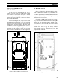
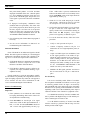
FRONT AND REAR COVER
SEPARATION
Lay the radio face down and loosen the four (4)
TORX screws (A) on the back of the radio; complete
screw removal is not necessary. See Figure 1. Separate
the covers by carefully lifting the Rear Cover Assembly
straight-up to avoid bending the connector pins between
the RF and Control Boards.
When reassembling the unit, verify the rubber gasket
surrounding the perimeter of the cover is in good condition and it is in the groove. Also verify the connector pins
align properly. For proper operation, the screws should
be tightened so there is no gap between the covers. It is
recommended that the top screws be tightened first while
squeezing the radio together to ensure the gap is completely closed. The bottom screws can then be tightened.
Figure 1 - Front and Rear Cover Separation
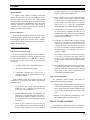
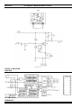
RF BOARD ACCESS
Holes are located in the RF Board shield for alignment of the Reference Oscillator (U3), Modulation Balance pot (R18), VCO Modulation pot (R19), 2nd Local
Oscillator Adjustment (T1), and the Quadrature Detector
Adjustment (T2). See Figure 2. To align these items,
shield removal is not necessary.
If removal of the RF Board from the case is necessary, first remove the UDC antenna jack and the top RF
antenna jack with appropriate spanner wrenches. Next,
remove the five (5) Torx screws (B) that secure the shield
then lift and remove the shield. Remove the two (2) remaining Torx screws (C) near the Power Amplifier
Module. The RF Board and eggcrate casting can now be
lifted from the Rear Cover to gain access to the chip
component side of the board.
Figure 2 - RF Board Access
5
LBI-33057
If necessary, the RF Board can be separated from the
eggcrate casting. Remove the two (2) Torx screws that
secure the Power Amplifier Module and remove the four
(4) screws on the chip component side of the board that
secure it to the casting.
Reassemble the unit in reverse order. Observe screw
lengths.
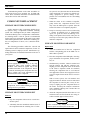
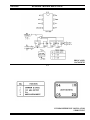
CONTROL BOARD ACCESS
To gain partial access to the Control Board, remove
the five (5) screws (D) securing the shield and board. An
earlier Front Cover Assembly has an additional screw located just below connectors J4/P4 (DD). See Figure 3.
Remove the shield.
Many of the test points on the Control Board are accessible at this point; however, the Front Cover Assembly
should not be powered-up without first reinstalling the
screw into the lower right-hand hole to ground the board.
Also, the three (3) screws securing the top flex connectors need to be reinstalled for good flex connections. USE
Figure 3 - Control Board Access
6
CAUTION: Installation of screws that are longer than
the originals may damage the LCD Board, flex circuits or
the threads.
To remove the Control Board, remove the Torx
screw (E) in the lower left-hand corner that supplies battery power to the board. An earlier Front Cover Assembly
has an additional screw located just below connectors
J1/PI (EE). Lift the board and carefully unplug Speaker
Flex plug P3 from J3 on the Control Board. Avoid bending this or any other flex circuits at sharp angles. The
Control Board can now be removed. Note the battery
power and groundconnections at the bottom of the board
where the screws have been removed.
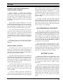
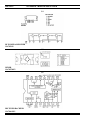
SPEAKER, MICROPHONE AND FLEX
CIRCUIT ACCESS
Remove the Control Board as previously stated and
then remove the six (6) Torx screws that secure the diecast shield. Remove the die-cast shield by lifting the top
end first and sliding it towards the top of the radio. The
internal speaker, microphone, Keypad and UDC Flex circuits are now partially accessible. See Figure 4.
Figure 4 - Speaker, Microphone and Flex Circuit Access
LBI-33057
UDC flex/UDC/Monitor Button/HT Switch Assembly
Removal
If UDC Flex/UDC/Monitor Button/PTT Switch assembly removal is necessary, first unsolder the microphone. With a spanner wrench, remove the UDC securing screw (the UDC ground pin). Remove the insulator
(foam or plastic type) on the inside side-rail of the case.
Lift the UDC/Monitor Button/PTT Switch assembly from
the side of the case and slide the flex through the slot.
Earlier Front Cover Assembly Keypad Flex Removal
To remove the Keypad Flex, first remove the UDC
Flex/UDC/Monitor Button/PTT Switch assembly as previously stated. Next remove the knobs using the hex
driver. Unscrew the two (2) screws securing the top panel
and lift and remove the panel. Lift the Emergency Button
Board by carefully unplugging J6 from P6. With a spanner wrench, remove the nuts securing the volume and
channel controls and carefully slide the controls inside
the radio. Unscrew the two (2) screws (G and GG) and
remove the J10/P10 Zebra strip securing plate (HH). See
Figure 5. The Keypad Flex is now free for removal.
LCD BOARD ACCESS
To remove the LCD Board, partial removal (actually
repositioning of the top areas) of the Keypad Flex is required. UDC Flex/UDC/Monitor Button/PTT Switch assembly removal is not necessary.
After the top areas of the Keypad Flex have been
freed as previously outlined, the LCD Board can be removed. At this point is the disassembly process an earlier
Front Cover Assembly has two (2) screws on the left side
as viewed from the back (J and JJ) and a later assembly
has a single screw in the upper left-hand side (J). See
Figure 5.
Later Front Cover Assembly Keypad flex Removal
To remove the Keypad Flex, first remove the UDC
Flex/UDC/Monitor Button/PTT Switch assembly as previously stated. Next remove the screw securing the emergency switch support (G) then remove the support. Remove the knobs using the hex driver. With a spanner
wrench, remove the nuts securing the volume and channel controls and carefully slide the controls inside the
radio. Unscrew the two (2) screws that secure the
J10/P10 connection at the bottom of the LCD Board.
Remove the screws, the plate and the rubber pad. The
Keypad Flex is now free for removal.
Speaker Flex Removal
In order to replace the Speaker Flex, it must be unsoldered from the speaker and the Battery Plate.
Figure 5 - Keypad Flex and LCD Board Access
7
LBI-33057
ALIGNMENT PROCEDURES
This section outlines alignment procedures for the
UHF RF Board located in the Rear Cover Assembly.
Alignment procedures must be performed in the order
presented to insure proper radio operation. Several test
procedures are presented which will help isolate a problem if it exists. The circuits in the Front Cover Assembly
contain no adjustments and therefore no alignment is
necessary.
SERVICE NOTES
Throughout the service procedures presented
in this manual, the following information
should be observed:
•
The bench power supply should be set for 7.5
±0.1 Vdc (unless otherwise noted) during
troubleshooting procedures presented in this
manual. If a battery pack is used, it should be
fully charged. Typical battery pack voltage
will be 7.5 Vdc ±20% over its full discharge
cycle.
•
Logic Levels:
•
Logic 1 = high = greater than 4.5 Vdc Logic 0
= low = less than 0.5 Vdc
•
•
•
The modules are not field repairable. Schematics and outline diagrams for the modules
are presented in this manual as a troubleshooting reference only.
The Front Cover Test Accessory Kit allows
the Control Board to be extended out of the
case for troubleshooting access. The LCD and
Keypad circuits can be tested in the case via a
PC computer connection.
The personality information stored in the radio should be backed-up on the PC computer
before any service procedure is performed.
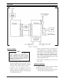
SET-UP PROCEDURE
1. Separate the Front and Rear Cover Assemblies
and connect the RF/Logic Extender cable between the RF Board and the Control Board. See
Figure 6.
2. Slide the Dummy Battery onto the Front Cover
and connect the audio output leads to the distortion analyzer. Place the Dummy Battery's on/off
8
switch in the OFF position to direct the speaker
audio to its speakers leads and to the distortion
analyzer. Connect the PC Programmer to the
UDC.
3. Set the power supply to 7.5 ±0.1 Vdc and connect
the Dummy Battery supply leads to the power
supply.
4. Program the radio with the LOW, MIDDLE and
HIGH-side test channels listed in Table 2. To
fully test the transmitter, program a channel pair
for each frequency, one at high-power and one at
low-power. It may be desirable to program more
test channels into the unit.
5. Remove power from the radio and replace the PC
programming cable with the TQ-0609 Test Box.
6. Connect the radio to the wattmeter using the RF
Antenna Adapter. Couple a small amount of the
RF signal to the frequency counter.
NOTE
LBI-38203 contains detailed information on the
TQ-0609 Test Box.
Table 2 - RF Test Channels
TEST FREQUENCY (MHz)
RF BAND
403-423 MHz
403.025
412.875
422.975
450-470 MHz
450.025
460.025
469.975
470-492 MHz
470.025
480.875
491.975
485-505 MHz
485.0125
500.000
504.9875
492-512 MHz
492.025
501.900
511.975
TRANSMITTER ALIGNMENT
The following information can be used to test and
align the transmitter's output frequency and its modulation characteristics. Completion of these tests/alignments
will verify a near 100% operating synthesizer and
transmitter stages.
LBI-33057
Figure 6 - Test Setup
3. Monitor transmitter frequency and adjust Reference Oscillator U3 to a frequency reading of
within 50 Hz (a small trimmer hole is located on
top of module). If the ±50 Hz maximum error (at
room temperature) cannot be established, Reference Oscillator replacement may be necessary.
Table 3 list maximum transmitter errors for the
specified temperature range.
Reference Oscillator
NOTE
Reference Oscillator U3 is factory adjusted and
should not normally need readjustment Use a
recently calibrated and stable frequency
counter to determine if oscillator alignment is
needed. This test/alignment should be done at a
room temperature of 25° C ±5°C.
1. On the TQ-0609 Test Box, select UDC switch
position 6 and apply power to the radio. This enables the radio's control circuits for an external
microphone and its internal speaker amplifier.
2. Channel the unit to the MIDDLE test channel
listed in Table 2 (low-power) and key the
transmitter using the TQ-0609. DO NOT apply
any modulation at this time.
4. Check all TX test channels for an error of less
than ±50 Hz.
Modulation Adjustments
1.
To align R18 and R19 it will be necessary to modify
the RF/Logic Extender cable as follows:
•
Add two 10K ohm resistors in series from 5.5
Vdc (J102 pin 6) to ground (J102 pin 7).
9
LBI-33057
•
Break the connection at TX MOD, J102/P2 pin
1.
alignment procedures will verify a near 100% operating
synthesizer and receiver stages.
•
Bias TX MOD into the RF Board to 2.7 Vdc by
connecting the junction of the 10K resistors to
J102 pin 1.
2nd Local Oscillator
2. Using a 100 µF (or greater) capacitor, couple a 1
kHz, 600 mV rms audio signal into TX MOD,
J102 pin 1.
NOTE
Modulation adjustments should only be necessary if changes in the Tracking Data values will
not compensate deviation levels to within specifications. Adjustment of R18 and R19 will obsolete all Tracking and Channel Data modulation
values. See the TRACKING AND CHANNEL
DATA section in this manual for further details.
The following procedure balances and "course
aligns" the VCO and the Reference Oscillator
deviation levels. The Audio Processor IC will
perform "fine level adjustment" of TX deviation
adjustment via the Tracking and Channel Data.
3. Connect the radio to the modulation analyzer and
key the transmitter at the MIDDLE test channel
listed in Table 2.
4. Adjust R19 (VCO modulation pot) for a deviation
of ± 2.5.0 kHz ± 50 Hz. Unkey the radio.
5. Remove the 1 kHz signal and apply a 20 Hz, 1
Vpp square wave. NOTE: The modulation analyzer should have a low-frequency response of
less than 1 Hz for this test.
6. Key the transmitter and monitor the demodulated
output from the modulation analyzer. Adjust R18
(modulation balance pot) for a good square wave
response.
Transmitter Distortion Test
Measure transmitter audio distortion on the LOW,
MIDDLE and HIGH-side test channels. Distortion readings should be less than 3% at ±1.5 kHz deviation with a
1000 Hz tone.
RECEIVER ALIGNMENT
The following information can be used to check and
align the receiver circuits. Successful completion of these
10
1. Check Reference Oscillator alignment as outlined
in the TRANSMITTER ALIGNMENT section.
2. Channel the radio to MIDDLE test channel listed
in Table 2.
3. Set the RF signal generator to corresponding
channel at a -20 dBm RF level and no modulation. Apply this signal to the radio.
4. To measure the IF signal, connect a frequency
counter to U6 pin 5. Use an appropriate high impedance probe (op-amp).
5. Adjust the signal generator level to achieve accurate counting of the IF signal. The RF signal generator should be set 10 dBm above the lowest
level which gives accurate counting.
6. Adjust the 2nd local oscillator via T1 for 455.000
kHz ±90 Hz.
Quadrature Detector
1. Modulate the signal generator with a 1 kHz tone,
±1.5 kHz deviation at the MIDDLE test channel
listed in Table 2. Set the RF level to -50 dBm.
2. Adjust T2 for maximum audio level at J101/P1
pin 4.
12 dB SINAD and Distortion Tests
1. Connect the distortion analyzer or SINAD meter
to the speaker load (in Dummy Battery).
2. With the RF signal generator and radio set to the
MIDDLE test channel listed in Table 2, modulate
the generator with a 1 kHz tone at ±1.5 kHz deviation. Measure the 12 dB SINAD sensitivity.
This reading should be equal to or better than 116 dBm (0.35 µV).
3. Return the signal level to -50 dBm.
4. Check audio distortion. Readings should be less
than 5% at rated audio output. Audio amplitude
should be 50-100 mVrms (≅200 mVp-p) at
J101/P1 pin 4.
LBI-33057
Table 3 - Maximum Transmitter Frequency Errors*
And Typical VCO Tx Tuning Voltages
CHANNEL (MHz)
TOLERANCE*(Hz)
LOWEST (MHz)
HIGHEST(MHz)
485.012500
±1213
485.011287
485.013713
1.5 Vdc
500.00000
±1250
499.998750
500.001250
2.5 Vdc
504.987500
±1263
504.986237
504.988763
3.5 Vdc
VCO TUNING
VOLTAGE (TX)
* Based on specified ±2.5 ppm over the entire operating temperature range
5. Repeat the 12 dB SINAD sensitivity and distortion check for the LOW and HIGH-side test
channels. See Table 2.
TRACKING AND CHANNEL DATA
The personality memory in the radio includes distinct areas which are reserved for Tracking and Channel
Data.
Tracking Data establishes individual radio parameters and tailors the operation of the unit across the band.
The parameters are: high RF power, low RF power,
modulation level and receiver squelch opening. This data
is programmed into the EEPROM on the Control Board
at the factory after the front and rear covers are
"married". The PC Programmer allows alteration of this
data if necessary.
Channel Data is the individual channel information
such as TX and RX frequencies, CG information, CCT
information, and the four previously mentioned parameters. This data is stored in the EEPROM on a per channel
basis as each channel is programmed. The PC Programmer allows alteration of this data on a per channel basis.
Low, middle and high-side of the band values are
programmed into the radio for each Tracking parameter.
When a channel is added to the radio, the Programmer
reads the Tracking Data stored in the radio and calculates necessary values for each parameter using a linear
interpolation technique. The Programmer then stores the
newly calculated values in the Channel Data area of
memory along with the associated channel information.
Changing the Tracking Data in the radio will not alter
Channel Data of previously programmed channels.
Tracking Data should not normally be altered; however,
it may be necessary to reprogram some of the values after
aligning circuitry, or replacing modules or other components which obsolete the previously programmed values.
Settings for each parameter are listed in Table 4. If
Tracking Data is altered for the above reason, it will be
necessary to reprogram all channels to establish the new
default data for each channel. See the Programming
Manual for further information on altering Tracking and
Channel Data.
Digital values stored for the PWR SET analog voltage are one example of tracking information. As no two
transmitter stages are exactly matched, the PWR SET dc
voltage will be slightly different with any two radios to
produce the same power output. Tracking and Channel
Data allows the microprocessor to tailor the PWR SET
line for RF stage gain differences from unit-to-unit and
across the band.
Table 4 - Tracking Data Parameters
PARAMETER
FACTORY
SETTING
High Power
3.0 Watts
Low Power
1.0 Watt
3F
Modulation
±2.4 kHz **
15
Squelch
ing
8-10 dB SINAD
A3
Open-
HEX
VALUE*
81
* Listed HEX values are approximate; final programmed values will vary from unit-to-unit and will
need to be adjusted as such.
** EXT MIC HI = 1 kHz, 110 mVrms
TROUBLESHOOTING
Troubleshooting procedures for the Rear Cover Assembly are located in this manual. See the manuals specific to the Front Cover Assembly, the Control Board or
the Aegis Module for detailed troubleshooting procedures
11
LBI-33057
on these assemblies. The troubleshooting test setup
should be identical to the set-up used in the
ALIGNMENT PROCEDURES section of this manual.
Table 5 lists common problems and most likely problem
areas.
REAR COVER ASSEMBLY
The troubleshooting procedures that follow primarily
assume a problem has been narrowed to a problem on the
RF Board. Transmitter, receiver and synthesizer symptoms/causes are outlined.
Transmitter Troubleshooting
Inoperative Or Low Power
Power sources and regulated power supplies should
be one of the first areas to check before troubleshooting
any transmitter problem. The radio's power source,
whether it is a battery or a bench power supply, is especially critical when troubleshooting a portable radio. Current consumption is an excellent troubleshooting tip
when troubleshooting a dead or weak transmitter. See the
Control Board maintenance manual for complete radio
current consumption data.
When the synthesizer is not locked the radio will
beep and flash "NO LOCK" in the display. If the synthesizer does not lock or stay locked at the start of or during
a transmission, I/O Microcontroller will not enable or
continue the transmission. Check LOCK DET at J102/P2
pin 8 for a low or pulsing (not locked) condition. See
Synthesizer Troubleshooting for further details.
4. If low RF power is a symptom, check the operation of Power Controller AI and Q1. PWR SET
on J101/PI pin 1 should be approximately 1.0
Vdc in low-power mode and 4.0 Vdc in highpower mode. If Q1 is saturated (collector voltage
is approximately 7.5 Vdc), troubleshoot the PA
for a gain problem. Also check the VCO for low
RF drive. Normal VCO power from A4 pin 1 is 8
dBm.
5. Check Tracking and Channel Data. Reprogram if
necessary.
Excessive Power Output
Short battery life and possible damage to the PA
module may result if a problem occurs in the power controlling circuitry.
1. Check PWR SET from the Control Board. PWR
SET on J101/PI pin 1 should be approximately
1.0 Vdc in low-power (1 Watt) mode and 4.0 Vdc
in high- power (5 Watts) mode. If incorrect,
troubleshoot the D/A converter circuits (in Audio
Processor U8) on the Control Board. Check
Tracking and Channel Data. Reprogram if necessary.
2. The collector of Q1 should be approximately 3.5
Vdc in low-power mode and 5.5 Vdc in highpower mode. If Q1’s collector stays near 7.5 Vdc
in receive mode, it is most likely shorted. Temporarily short the emitter and base while monitoring
the collector voltage. If the collector voltage falls,
there is a problem in Power Controller AI.
1. Check for battery power on l02/P2 pin 2.
2. Check for 5.5 Vdc ±0.1 Vdc at l02/P2 pin 6 with
the transmitter enabled. Also check the operation
of the TX 5.5V switch to insure 5.5 Vdc is being
delivered to the RF Board at J101/P1 pin 5 when
the PTT button is pressed.
3. Battery power should be present at the Power
Amplifier module pins 2 and 4; if not, suspect Q4
or A1. If current consumption appears normal for
both high and low-power modes, the problem
may be antenna T/R switch DI/D2, the low-pass
filter circuit, or antenna switch SWI. If the lowpass filter circuit or the antenna switch have a
problem, generally the receiver will also be weak.
A defective pin diode (DI or D2) can cause
transmitter and receiver problems.
12
Frequency Error
If transmit frequency error exists (greater than 2.5
ppm) when the synthesizer is locked, Reference Oscillator U3 alignment or replacement is necessary. See
ALIGNMENT PROCEDURES for details. The I/O Microcontroller will not enable a transmission if the synthesizer is not locked.
Modulation Problems
Modulation problems can be caused by a failures in
the audio circuits in the front cover or the modulating
circuitry of the RF Board.
1. Verify modulating audio is present on J102/P2
pin 1. A 1 kHz, 600 mV rms TX MOD signal at
LBI-33057
Table 5 - General Troubleshooting
SYMPTOM
Completely inoperative (no audio and no LCD indication)
At power up, radio beeps:
a. twice (once in addition to power up beep)
b. continuously at a 2 Hz rate
c. continuously at a 2 Hz rate and "NO LOCK" is
displayed
At power up, display:
a. flashes "PERS ERR"
b. flashes all segments and the radio beeps.
Receiver inoperative or weak(clear mode).
Transmitter inoperative or low range.
TX and RX inoperative on some channels only
TX and RX inoperative on all channels
Trunk Mode Problems (trunked radios only)
Aegis Mode Problems
POSSIBLE CAUSES
1. Dead Battery Pack.
2. Fuse blown: Check radio fuse in Battery Plate.
3. Control Board problem: See LBI-39157.
1a. Weak Battery Pack
1b. Unit is not programmed: Program radio.
1c. Synthesizer is not locked: Check LOCK DET line, synthesizer
loading and VCO tuning voltage.
1a. EEPROM problem on Control Board: See LBI-39157.
1b. Interprocessor communication failure on Control Board: See
LBI-39157.
1. Squelch levels programmed too high: Press Monitor Button to
disable squelch.
2. Channel Guard or Type 99 Enabled: See Operator's Manual.
3. Defective antenna.
4. RF Board problem: Troubleshoot Rear Cover Assembly.
1. Power levels programmed low: Check RF output and reprogram
unit if necessary.
2. Weak battery. Note "BAT" flag.
3. Defective antenna
4. RF Board problem: Troubleshoot Rear Cover Assembly.
1. Programming incorrect: Reprogram unit.
2. Synthesizer problem (VCO or prescaler): Check LOCK DET
line (high = lock), VCO tuning voltage and modulas control
line.
3. EEPROM Problem: Troubleshoot Control Board.
1. Programming incorrect: Reprogram unit.
2. Synthesizer problem: Check LOCK DET line (high = lock),
VCO tuning voltage and modulas control line.
3. Control Board problem: See LBI-39157.
4. Check SW1, and the low pass filter circuit on the RF Board
1. Modem circuitry problem: Check U19 and associated circuitry
on Control Board.
2. Low speed data problem: Troubleshoot the related encode or
decode circuitry on the Control Board
1. Verify outside addresses and data polarity.
2. If optionally equipped for encryption, verify correct keys are
loaded and selected.
3. Verify CUE codes.
4. Problem on Control Board with Aegis circuitry.
5. See "Trunked Mode Problems" above.
13
LBI-33057
this point should produce ±2.5 kHz deviation.
Improper modulation from 300 - 3000 Hz points
to a VCO modulation problem. Check the VCO
pin 4 for the TX MOD signal. Suspect the VCO
if the signal is present and incorrect modulation
exists.
2. If improper low-frequency modulation exists
(trunked mode low-speed data), first check J102
pin 1 for the proper tone. Next check U3 pin 4 for
the tone; suspect C30 if the tone is not present.
Replace U3 if the tone is present on pin 4 and incorrect low-frequency modulation exists. See the
ALIGNMENT PROCEDURES for details.
If the 1 kHz audio is present, troubleshoot the
audio circuits in the Front Cover Assembly. Noise
levels on RX DISC with no RF input should be
approximately 700 mV p-p.
3. Check for 7.5 Vdc at RF Amp A6 pin 5 and IF
Amp A2 pin 1. Check U6 pin 4 for 5.5 Vdc from
A5. Verify TX 5.5V is low in receive mode.
4. Verify mixer injection from the VCO is present at
U5 pin 8. Check the VCO output with a frequency counter. The VCO should be running 45
MHz below the RX frequency. VCO output
power level is typically +8 dBm at U5 pin 8.
3. Check Tracking and Channel Data. Reprogram if
necessary.
5. To test the back-end circuits, follow the below
procedure:
4. See the service information in LBI-39157 on
troubleshooting the Control Board.
•
Verify 5.5 Vdc is present on U6 pin 4.
•
Connect a frequency counter to U6 pin 5 to
monitor the IF. Use a high-impedance probe (or
amp).
•
Couple a 45 MHz signal (no modulation) from
an HF signal generator to the emitter of Q3.
Adjust the signal generator level to achieve accurate counting of the IF; the signal generator
should be set 10 dBm above the lowest level
which provides stable counting of the 455 kHz
IF. See ALIGNMENT PROCEDURES if the
2nd IF is in error by more than 90 Hz.
•
Modulate the HF signal generator and observe
the recovered audio on U6 pin 9 and J101/P1
pin 4.
Distorted Modulation
Check TX MOD for an undistorted signal to the RF
Board. The audio signal on J102/P2 pin 1 should appear
undistorted at maximum deviation and it should be riding on a 2.5 Vdc bias developed on the Control Board.
1. If TX MOD distortion is minimal and transmitter
distortion is excessive, suspect the VCO or the
Reference Oscillator on the RF Board.
2. If TX MOD is distorted, suspect a defective microphone, mic amps, modulation limiting, or preemphasis circuitry.
If audio sensitivity is good, the microphone, amplifiers and limiters are probably OK. Regeneration from an
open decoupling capacitor may make the unit appear to
be too sensitive. See the service information in LBI39157 on troubleshooting the Control Board.
Receiver Troubleshooting
Inoperative
1. If the synthesizer is not locked the radio should
be beeping and flashing "NO LOCK" in the LCD.
See Synthesizer Troubleshooting
2. Check RX DISC on J101/PI pin 4 for signal
and/or noise. With an RF input modulated at 1
kHz, ±1.5 kHz deviation, RX DISC should be
100 - 150 mV rms (approximately 350 mV p-p).
14
Low Sensitivity
Low receiver sensitivity and/or failure of a modulation acceptance bandwidth test indicates a receiver gain
or selectivity problem in the IF stages. An excessively
wide bandwidth will cause unnecessary noise, detracting
from the receiver quieting. If the bandwidth is too narrow
squelching could occur at the modulation peaks. Suspect
a defective IF filter if one of the above symptoms occurs.
A 12 dB SINAD sensitivity of around -90 dBm indicates a problem with High-IF Amp A2. The module provides a nominal gain of around 17 dB.
A 12 dB SINAD sensitivity of around -100 dBm
could be caused by a problem with RF Amp A6. This
module provides 8 dB of gain.
LBI-33057
Squelch Problem
A squelch circuit problem (assuming good signal
and/or noise is present at 101/P1 pin 4) indicates a problem with Audio Processor U8 on the Control Board.
Troubleshooting should begin at the discriminator output
Signal trace through the discriminator amp to the Audio
Processor. Check the operation of the noise rectifier to
verify the noise is being converted into the proper dc
voltage. See LBI-39157 for details.
Excessive Distortion
If the measured distortion exceeds the rated specification signal trace starting at the discriminator output
and through the audio stages until the fault is isolated.
Signal tracing with an oscilloscope proves very useful in
locating the trouble areas.
A5 pin II (input) for 7.5 Vdc. Replace A5 if the
inputs are good and the output is not.
4. Using a frequency counter with a high impedance
probe or amp, check U1 pin 2 for the 13.2 MHz
(±100 Hz at 25°C) signal from Reference Oscillator U3. Replace U3 if this signal is not present
and U3 pin 3 is 5.5 Vdc. See ALIGNMENT
PROCEDURES for oscillator alignment details.
5. If LOCK DET is low and not pulsing, temporarily pull it high by connecting J102/P2 pin 6 to
J102/P2 pin 8. If the radio now operates normally
on all test TX and RX channels, replace U1 - the
output on pin 9 is defective.
Will Not Lock Or Stay Locked
6. Check the VCO output with a frequency counter
at A4 pin 9 or by tuning a service monitor to the
radio's local oscillator (VCO) signal and loosely
coupling the VCO signal into the service monitor. The VCO should be running 45 MHz below
the RX frequency. VCO output power level is
typically +8 dBm.
Each time the channel is changed, the PTT Button is
pressed or the PTT Button is released, Synthesizer IC U1
is serially loaded with new TX or RX data. If the synthesizer does not lock or stay locked, the following will
be observed:
7. VCO tuning voltage can be monitored at A4 pin
5. See Table 3 for details. Also check A4 pin 6
for the -3.7 Vdc supply developed from the OSC
OUTput from U1, D3 and the associated components.
Synthesizer Troubleshooting
•
the radio continuously or intermittently beeps
•
"NO LOCK" will flash in the display
•
LOCK DET (J102/P2 pin 8) will be low or
pulsing to flag the I/O Microcontroller of the
unlocked condition
8. If a synthesizer lock problem cannot be narrowed
to a problem in the Rear Cover Assembly, reprogram the inoperative channels and test the unit
again. Also see the service information on the
Control Board for further details.
Excessive Switching Time
If this condition occurs, the I/O Microcontroller will
continue to try to reload U1 with channel data until the
synthesizer locks.
The synthesizer should generally lock within 10
milliseconds after a frequency change.
1. Verify the 5.5 Vdc supply to the RF Board is
within ±0.1 Vdc, 7.5 VBATT is present, and TX
5.5V is low (receive mode only).
1. Suspect leaky low-pass filter capacitors C25 or
C26 if slow switching time is a symptom. Replace
these components with original equipment parts
only. See the RF Board parts list for part numbers.
2. Monitor STROBE, DATA and ENABLE (on
J102 pins 11, 10 and 9 respectively) for pulse activity when the channel is changed. See the service information on the Control Board for specific
waveforms.
3. Check A5 pin 9 (output) for 5.5 Vdc to A4, U2,
and U6. If this power source is not present, check
A5 pins 7 and 13 (inputs) for 5.5 Vdc and check
2. Module A5 also influences switching time. Verify
the ENABLE pulse is present at A5 pin 4.
FRONT COVER ASSEMBLY
See maintenance manual LBl-39157 for componentlevel troubleshooting information on the Control Board.
15
LBI-33057
Troubleshooting details on the other assemblies located in the Front Cover Assembly can be found LBI38834. These assemblies include the LCD Board and the
various flex circuits used in the radio.
COMPONENT REPLACEMENT
SURFACE MOUNTED COMPONENTS
Surface mounted "chip" components should always
be replaced using a temperature-controlled soldering
system. The solderingtools may be either a temperaturecontrolled soldering iron or a temperature-controlled hotair soldering station. A hot-air system is recommended
for the removal of components on the multi- layer boards
utilized throughout the radio. With either soldering system, at a temperature of 700°F (371°C) should be maintained.
The following procedures outline the removal and
replacement of surface mounted components. If a hot- air
soldering system is employed, see the manufacture's operating instructions for detailed information on the use of
your system.
CAUTION
Avoid applying heat to the body of any chip
component when using standard soldering
methods. Heat should be applied only to the
metallized terminals of the components. Hot-air
systems do not damage the components since the
heat is quickly and evenly distributed to the
external surface of the component
CAUTION
As the radio contains many static sensitive
components, observe static handling precautions
during all service procedures.
SURFACE MOUNTED COMPONENT
Removal
16
air system is used, direct the heat to the terminals
of the component. Use extreme care with the soldering equipment to prevent damage to the
printed wire board (PWB) and the surrounding
components.
3. When the solder on all terminals is liquefied,
gently remove the component. Excessive force
may cause the PWB pads to separate from the
board if all solder is not completely liquefied.
4. It may be necessary to remove excess solder using
a vacuum de-soldering tool or Solderwick.
Again, use great care when de-soldering or soldering on the printed wire boards. It may also be
necessary to remove the epoxy adhesive that was
under the component.
SURFACE MOUNTED COMPONENT
Replacement
1. "Tin" one terminal end of the new component
and the corresponding pad on the PWB. Use as
little solder as possible.
2. Place the component on the PWB pads, observing
proper orientation for capacitors, diodes, transistors, etc.
3. Simultaneously touch the "tinned" terminal end
and the "tinned" pad with the soldering iron.
Slightly press the component down on the board
as the solder is liquefied. Solder all terminals,
allowing the component time to cool between
each application of heat. Do not apply heat for an
excessive length of time and do not use excessive
solder.
With a hot-air system, "tin" all terminals and
apply heat until all "tinned" areas are melted and
the component is seated in place. It may be necessary to slightly press the component down on
the board. Touch-up the soldered connections
with a standard soldering iron if needed. Do not
use excessive solder.
4. Allow the component and the board time to cool
and then remove all flux from the area using alcohol or another approved flux remover.
1. Grip the component with tweezers or small needle-nose pliers.
CAUTION
2. Alternately heat the metallized terminal ends of
the component with the soldering iron. If a hot-
Some chemicals may damage the internal and
external plastic and rubber parts of the radio.
LBI-33057
SURFACE MOUNTED INTEGRATED
CIRCUIT REPLACEMENT
Surface mounted IC soldering and de-soldering
techniques are similar to the above outlined procedures
for the surface mounted chip components. Use extreme
care and observe static precautions when removing or
replacing a defective (or suspect) IC. This will prevent
any damage to the printed wire board or the surrounding circuitry.
Replacement of a surface mounted IC is best completed using a hot-air soldering system. The IC can easily
be removed and installed using hot air. See the manufacturers instructions for complete details on tip selection
and other operating instructions unique to your system.
If a hot-air system is not available, the service technician may wish to clip the pins near the body of the defective IC and remove it. The pins can then be removed
from the PWB with a standard soldering iron and tweezers and then the new IC can be installed. It should not be
necessary to tin any of the IC pins before the installation
process.
The "chip-on-board" ICs used in the radio cannot be
replaced. Failure of this type of IC will require board replacement.
MODULE REPLACEMENT
The modules, all of which are located on the RF
Board, are very reliable devices. Before replacing any of
the modules, check the associated circuitry thoroughly to
insure there is not a problem elsewhere. If replacement is
necessary, follow the below procedures.
pins. If a hot-air system is employed, use an appropriate
tip that will localize the heat on the pins and not on surrounding chip components. Solderwick or a vacuum
de-soldering iron will also remove the solder if a hot-air
station is not available. When all solder has been removed or liquefied, the module should drop out of the
eggcrate casting.
To install a module, clean any solder from the
plated- through holes and clean all flux from the board.
Next, install the replacement module making sure that all
pins align in the proper holes. Resolder the pins to the
board. Clean the flux from the board using an approved
solvent. Clip any excess lead length.
WEATHERPROOF INTEGRITY
The M-PA radio is designed to meet the MIL-810C
& D environmental specifications. The internal circuitry
is protected from moisture by appropriate seals. Rear
Cover Assembly seals include the Front/Rear Cover Assembly gasket and the antenna insert gaskets. Front
Cover Assembly seals include the speaker/microphone
seal, the battery plate seal, and the volume and channel
control seals. The UDC/Monitor Button/PTT Assembly is
also designed to seal out moisture.
These seals should be inspected during any disassembly/reassembly process for cracks and tears. A defective seal warrants replacement. See the Mechanical Parts
breakdown drawings and the Parts Lists for locations and
part numbers for these seals. When installing a new seal,
make sure it is seated properly before reassembly.
BATTERY PACKS
All of the component lead holes for the modules on
the RF Board are plated through from the top to the bottom of the board. This allows for easy removal and replacement of the modules as long as appropriate soldering techniques are observed. Always observe static precautions when handling the board.
Battery packs available for use with the radio include
high and extra high capacity rechargeable units. All of
the rechargeable battery packs are factory sealed and are
not field serviceable other than properly charging them
and cleaning the contacts. Figure 8 outlines a typical
battery pack.
To remove the PA module, it is first necessary to remove the hardware which supports it. Two (2) Torx
screws and a support bracket secure the module to the
eggcrate casting. Two (2) Torx screws also secure the
VCO to the board.
Radio contacts located on the top of the pack include
switched power, ground, the speaker enabling (shorting)
contacts and a continuous power contact. Four (4)
charging contacts are located on the rear side of the battery pack. These contacts provide connections to the slipin type chargers or vehicular chargers/repeaters while the
battery pack is still connected to the unit. The battery
charging contacts are diode protected from external
shorts.
To remove a module, position the RF Board in a
work (face down, chip components up) and remove the
solder from the plated-through points at the appropriate
17
LBI-33057
Figure 8 - Battery Packs
18
LBI-33057
CHARGING THE BATTERY PACKS
2. Complete a full charge cycle using an Ericsson
charger.
After receiving a new battery pack from the factory,
it should be fully charged before it is placed into service.
This also applies to batteries that have been stored for
long periods.
3. Repeat steps 1 and 2. Performing this deep cycle
at least twice should be sufficient to restore battery pack capacity.
Chargers are available with nominal charge times of
1 hour (rapid) and 14 (standard) hours. Combinations
include single and multi position standard and rapid
charge units. The rapid chargers utilize an internal
thermistor in the battery pack to sense temperature and
automatically controlcharge rate of the battery. This allows a rapid charger to charge at a maximum rate without overheating the battery. All battery packs can be
charged in less than 1 1/2 hours in a rapid charger.
Nominal full charge time in a standard charger is 14
hours. For specific instructions for the particular charger,
refer to the applicable charger's Operating Manual.
A fully charged battery pack should provide an open
terminal voltage greater than 7.5 Vdc (typically 9 Vdc).
A fully discharged battery pack should be no less than 6
Vdc. When the battery pack drops below approximately
6.8 Vdc the radio will warn the operator with an alert
tone and the "BAT" flag will turn on.
REDUCED CAPACITY CONDITION
Rechargeable batteries can develop a condition of reduced capacity sometimes called "Memory Effect". This
condition can occur when a battery is continuously
charged for long periods of time or when a regularly
performed duty cycle allows the battery to expend only a
limited portion of its capacity.
If the battery pack is seldom used and left on a continuous charge for long periods it may develop reduced
capacity. On the first discharge cycle, the capacity may
be significantly lowered, reducing useful service hours.
NOTE
The above procedure is easily completed using
Discharge Analyzer 19B801506P9 and Rapid
Multi-Charger 19B801506P16 or P18.
RECHARGEABLE BATTERY PACK
DISPOSAL
Under specific state laws, it may be illegal
to dispose of rechargeable batteries, rechargeable batteries packs and/or products powered by rechargeable batteries
except in accordance with specific procedures. Special collection systems are in
place in certain states. Call Toll Free 1800-822-9363 for specific procedures for returning rechargeable batteries in your state.
CONTROL KNOB STOP PLATE
A stop plate is normally installed under the Control
Knob of the radio at the factory. It is used to limit the
maximum number of unique Control Knob positions to
less than sixteen (16). The stop plate is normally factory
placed for fifteen (15) positions unless sixteen unique
factory programmed positions are ordered. This stop
plate can be repositioned to limit the maximum number
of unique Control Knob positions to match personality
programming.
The reduced capacity condition should be suspected
on any rechargeable battery pack showing signs of reduced capacity. If reduced capacity is in fact a problem,
the following procedure may restore useful capacity:
1. Discharge the battery pack at a normal discharge
rate until the output voltage is approximately 1
Volt per cell. This equals 6 Volts output for the
battery packs. Refer to Figure 9. Note the flatness
of the discharge curve from 0% - 90%. Experience shows discharging below the "knee is not
necessary.
Figure 9 - Typical Cell Discharge Curve
19
LBI-33057
STOP PLATE REPOSITIONING
1. Remove the Control Knob using an M15 hex
wrench.
4. Replace the Control Knob and torque the set
screw per Table 1. The set screw must align on
the flat area of the switch shaft Rotate the knob to
test for proper operation.
2. Lift the stop plate using small needle-nose pliers.
3. Reposition the stop plate by aligning the raised
bar to the channel marking one (1) number
higher than the number of positions required. For
example, if eight (8) unique positions are required, align the raised bar to the "9". If sixteen
(16) positions are required, do not reinstall the
stop plate.
FIELD RF RETUNING
PROCEDURES
This section outlines field RF retuning procedures
which will be necessary if the factory tuned 20 MHz operating band does not meet needed requirements. Note
that the frequency range limits of the RF Board cannot be
exceeded. The procedures should be performed in the order presented.
Figure 10 - RF Board Retuning Areas
20
LBI-33057
SET-UP PROCEDURE
1. Program the radio with the low, middle and highside re tune channels in the desired operating frequency band. The low and high-side channels
should be 20 MHz apart and the middle channel
should be centered between the two. Do not exceed the frequency range limits for the RF Board.
2. Separate the Front and Rear Cover Assemblies
and connect the RF/Logic Extender cable between the RF Board and the Control Board.
SYNTHESIZER RETUNING
1. Set the radio to the middle retune channel.
Monitor the VCO tuning voltage at TP1 (A5 pin
3) with a dc voltmeter. Adjust the RX VCO coil
should be for a reading of 2.5 Vdc. See Figure 10.
2. Set the radio to the lowest retune channel. The
monitored voltage greater than 1.0 Vdc.
from the RF Board with a dc coupled oscilloscope. The monitoring point is J101 pin 4.
9. Apply a 110 mV rms, 1 kHz tone to the TQ3370's modulation input. Key the radio from the
TQ-3370 and adjust R19 on the RF Board for a
deviation of 2.5 kHz.
10. Modify the RF/Logic Extender cable so a lowfrequency signal can be injected directly into the
RF Board. This modification procedure is outlined in the TRANSMITTER ALIGNMENT section of this manual.
11. Using a 100 µF (or greater) capacitor, couple 20
Hz, 1.0 Vpp square wave signal into TX MOD
(J102 pin 1).
12. Key the radio and monitor the demodulated output from the modulation analyzer. Adjust R18
(modulation balance pot) for a good square wave
response as shown in Figure 11.
3. Set the radio to the highest retuned channel. The
monitored voltage should be less than 4.0 Vdc.
4. If the lowest and highest retune channels push
the VCO tuning voltage measured at TP1 outside
of the specified limits, slightly readjust the RX
VCO coil to center the low and high retuned
channel tuning voltages within or around this 1.0
- 4.0 Vdc window.
5. Repeat steps 1 - 4 for the TX VCO coil with the
following exceptions: The radio must be keyed
when adjustments are made to the TX VCO coil.
Also, connect an appropriate RF load to the antenna before keying.
6. Turn the radio off and connect the PC Programmer to the radio. Power the radio back up. Using
the PC Programmer, set the modulation Tracking
Data value to OD (hex).
7. Set the radio to the middle, retune channel. 8.
Couple a modulation analyzer (with a monitoring oscilloscope) to the RF output of the radio.
Set the modulation analyzer's filters as follows:
no high-pass filters and 20 kHz low-pass filter.
The modulation analyzer should have an almost
dc response. If it does not, an alternative is to use
a second M-PA monitoring the transmit frequency and monitor the discriminator output
Figure 11 - Typical TX Modulation Low-Frequency
Response Curves
RECEIVER RETUNING
Retuning the UHF M-PA receiver involves retuning
the two (2) helical filters at the input and output of RF
Amplifier module A6. There are three (3) different procedures that can be used to retune the receiver. The most
accurate method involves the use of a network analyzer.
If a network analyzer is not available, a spectrum analyzer and signal generator can be used, but with less accurate results. Finally, the receiver can be re tuned with
some compromise in receiver performance using a best
quieting (SINAD) tuning technique.
21
LBI-33057
Network Analyzer Method
1. Remove the solder mask on the solder side of the
RF Board at the thin run between the output of
FL4 and the input of A6 (A6 pin 1). Cut this run.
2. Solder the center conductor of a small 50-ohm
coax cable to FL4's output at the cut run. Solder
the coax shield near FL4.
3. Terminate the radio's antenna with a 50-ohm
load.
4. Connect the other end of the coax to the network
analyzer and tune FL4 (all three sections) for best
return loss over the desired receive frequency
range.
5. Unsolder the coax cable from the output of FL4
and solder it to the input of A6. Ground the
shield near A6.
6. With the network analyzer's output at -30 dBm or
lower, adjust FL1 (all three sections) for best return loss over the desired receive frequency
range. The receiver must be powered-up during
this adjustment.
7. With a small jumper, reconnect the output of FL4
to the input of A6. Test the radio over the new
frequency range.
Spectrum Analyzer And Best Quieting Methods
This procedure involves retuning the receiver's helical filters at the low, middle and high-side frequencies.
The same frequencies used to retune the VCO can be
used.
The preferred method is to connect a small 50-ohm
coax to the output of IF crystal filter FL2, ground, and
connect this cable to a spectrum analyzer tuned to 45
MHz and set to 2 dB/division.
22
A less desirable alternative using the same tuning
sequence can be achieved by varying the signal generator's level and tuning for best quieting (SINAD). No coax
cable connections are required using this procedure.
1. Remove the input and output (outer) tuning cores
from both FL1 and FL4 (four cores total).
2. Set the radio and signal generator to the low-side
receive frequency.
3. Set the signal generator's level to -30 dBm. If
tuning by quieting, set the generator's level for a
high receiver noise level.
4. Alternately tune the center cores of FL1 and FL4
for maximum IF signal. If tuning by quieting,
tune for best sensitivity and reduce the generator's
level as the receiver becomes more sensitive.
5. Set the radio and signal generator to the highside receive frequency.
6. Reinstall the input tuning cores into FL1 and
FL4. Alternately adjust these cores for maximum
signal or best quieting.
7. Set the radio and signal generator to the middle
receive frequency.
8. Reinstall the output tuning cores into FL1 and
FL4. Alternately adjust these cores for maximum
signal or best quieting. Under certain circumstances, best tuning may be achieved when certain tuning cores are not reinstalled. This is acceptable. Also, any excessively loose core should
be secured with a drop of adhesive.
LBI-33057
RF BOARD - MODULE AND IC DATA
A1
(19C337063, Rev. 1)
(19C337315, Rev. 1)
POWER CONTROLLER
19C337063
A2
(19C337062, Rev. 2)
(19C336876, Rev. 0)
IF AMPLIFIER
19C336876G1
23
LBI-33057
RF BOARD - MODULE AND IC DATA
A4
(19D438605, Sh. 1, Rev. 2)
(19D438604, Sh. 1, Rev. 4)
(19D438604, Sh. 2, Rev. 3)
VCO
19A438605
24
LBI-33057
RF BOARD - MODULE AND IC DATA
A5
(19C852056, Sh. 1, Rev. 0)
(19C852057, Sh. 1, Rev. 1)
PLL LOW PASS FILTER/REGULATOR
19C852056G1
25
LBI-33057
RF BOARD - MODULE AND IC DATA
A6
(19B235081, Sh. 1, Rev. 2)
(19C337073, Rev. 1)
UHF RF AMPLIFIER
19B235081
U1
SYNTHESIZER
19B800902P4
26
LBI-33057
RF BOARD - MODULE AND IC DATA
U2
PRESCALER
19A704287P2
U3
13.2 MHz REFERENCE OSCILLATOR
19B801351P15
27
LBI-33057
RF BOARD - MODULE AND IC DATA
U4
RF POWER AMPLIFIER
19A705419
U5
MIXER
19A705706P2
U6
RECEIVER BACKEND
19A704619P1
28
LBI-33057
RF BOARD - MODULE AND IC DATA
(This page left intentionally blank)
29
Ericsson Inc.
Private Radio Systems
Mountain View Road
Lynchburg, Virginia 24502
1-800-528-7711 (Outside USA, 804-528-7711)
Printed in U.S.A.