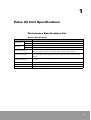
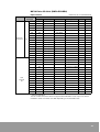
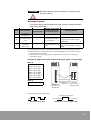
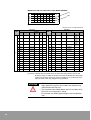
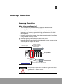
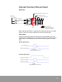
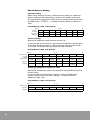
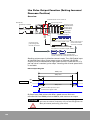
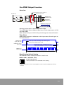
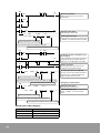
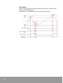
1
NX70/NX700 Series Pulse I/O Modules
(4CH) (NX70-PULSE4 and NX-PULSE4 )
User Manual
Important User
Information
Solid state equipment has operational characteristics differing from
those of electromechanical equipment. Because of these differences,
and also because of the wide variety of uses for solid state equipment,
all persons responsible for applying this equipment must satisfy
themselves that each intended application of this equipment is
acceptable.
In no event will Rockwell Samsung Automation be responsible or
liable for indirect or consequential damages resulting from the use or
application of this equipment.
The examples and diagrams in this manual are included solely for
illustrative purposes. Because of the many variables and requirements
associated with any particular installation, Rockwell Samsung
Automation cannot assume responsibility or liability for actual use
based on the examples and diagrams.
No patent liability is assumed by Rockwell Samsung Automation. with
respect to use of information, circuits, equipment, or software
described in this manual.
Reproduction of the contents of this manual, in whole or in part,
without written permission of Rockwell Samsung Automation. is
prohibited.
Throughout this manual we use notes to make you aware of safety
considerations.
WARNING
IMPORTANT
ATTENTION
Identifies information about practices or
circumstances which may lead to serious personal
injury or death, property damage, or economic loss.
Identifies information that is critical for successful
application and understanding of the product.
Identifies information about practices or
circumstances that can lead to minor personal injury,
property damage, economic loss, or product
malfunction. However, depending on circumstances,
failure to follow the directions accompanying this
symbol may also lead to serious consequences.
Contents
1. Pulse I/O Unit Specifications..................................... 9
Performance Specifications List .................................................................. 9
I/O Contact Points ....................................................................................... 13
Shared Memory Areas ............................................................................... 17
2. Pulse I/O Unit Functions .......................................... 27
Unit Features and Functions ...................................................................... 27
Functions of Unit ........................................................................................ 28
Configuration and Limit for Pulse I/O Unit ............................................... 33
Restrictions Due to Combination of Pulse Output Function ................... 34
Parts and Functions .................................................................................... 35
I/O Specifications and Connector Pin Diagram ........................................ 39
3. Configuration and Design Verification of the Unit .. 41
Slot No. and I/O Number Allocation Verification ..................................... 41
Embedded Counter..................................................................................... 51
4. General I/O Function................................................ 55
General I/O Function................................................................................... 55
5. Input Time Constant Function................................. 57
Input Time Constant Function ................................................................... 57
Use Input Time Constant Function............................................................ 59
6. High-Speed Counter Function ................................. 61
High-Speed Counter Function ................................................................... 61
Count Function Available as Direction Control Mode ............................. 66
Count Function Available as Individual Input .......................................... 68
Count Function Available as Phase Input Mode ...................................... 70
7.
Comparison Output Function .................................. 73
Comparison Output Function .................................................................... 73
Comparison Output Function with Counter ............................................. 76
3
8.
Interrupt Function ................................................... 79
Interrupt Function ....................................................................................... 79
Interrupt Functions (External Input) .......................................................... 83
Interrupt Functions (Comparison Coincidence Signal)............................ 86
9.
Pulse Output Function............................................. 91
Pulse Output Function ................................................................................ 91
Use Pulse Output Function ........................................................................ 95
Use Pulse Output Function (Frequency Change) ..................................... 98
Use Pulse Output Function (Constant Pulse Output)............................. 101
Use Pulse Output Function (Setting Increase/Decrease Position) ........ 106
10. PWM Output Function ........................................... 113
PWM Output Function .............................................................................. 113
Use PWM Output Function ...................................................................... 117
11. Sample Program .................................................... 121
Speed Measuring...................................................................................... 121
Fixed Length Processing .......................................................................... 124
Location Control by Absolute Value........................................................ 129
Location Control by Data Table ............................................................... 135
4
Safety Instructions
Please read this manual and the related documentation thoroughly
and familiarize yourself with product information, safety instructions
and other directions before installing, operating, performing
inspection and preventive maintenance. Make sure to follow the
directions correctly to ensure normal operation of the product and
your safety.
WARNING
ATTENTION
• If this product is used in a situation that may cause
personal injury and/or significant product damage,
implement safety measures such as use of fault-safe
equipment.
• Do not use this product under any conditions
exposed to explosive gases. It may cause an
explosion.
• Please fasten cables with terminal bolts.
• Do not use the product under conditions that do not
meet correct environmental standards.
• Make sure you connect grounding cables.
• Do not touch terminals when electric current is
flowing.
5
NX 700 Pulse I/O Unit Installation Environment
ATTENTION
Do not install your unit if any of the following
conditions are present:
• Ambient temperature outside the range of 0 to 55 ° C
(32 to 131 ° F).
• Direct sunlight.
• Humidity outside the range of 30% to 85%
(non-condensing).
• Chemicals that may affect electronic parts.
• Excessive or conductive dust, or salinity.
• High voltage, strong magnetic fields, or strong
electromagnetic influences.
• Direct impact and excessive vibration.
ATTENTION
Precautions for Electrostatic
• Excessive static electricity can be generated in dry
conditions, so please make sure to discharge
electrostatic with other materials like grounded
metal bars before contacting unit
ATTENTION
Cleaning Unit
• Do not use thinners, which can damage or degrade
PCB circuit board.
6
Compatibility of Pulse I/O unit to previous High-speed counter unit
(1CH or 2H)
N
Not compatible in terms of either hardware or software.
N
Ladder program is also not compatible.
Comparison between previous High-speed counter unit (1CH or 2CH)
and Pulse I/O unit
High-speed counter unit
Comparison item
Number of
channels
Highest
counting speed
High-speed
Counting range
counter
NX700 (NX-HSC1)
N700 (CPL7620A)
NX70 (NX70-HSC1)
1CH
2CH
NX700 (NX-PULSE4)
NX70 (NX70-PULSE4)
4CH
Max. 100 KHz
Max. 200 KHz
24bit signed (Binary format)
(-16,777,216 to +16,777,215)
32bit signed (Binary format)
(-2,147,483,648 to +2,147,483,647)
5us
2.5us
Min. input
pulse width
Comparison
output
NX700 (NX-HSC2)
N700 (CPL7621)
NX70 (NX70-HSC2)
Pulse I/O unit
2 points, (C=P, C>P)
Input time constant
4 points, (C=P, C>P) x 2
None
8 points, random designation for
8 target values
4 µs, 8 µs, 16 µs, 32 µs
(Setting for 2 input units)
Max. 8 points per 1 unit. Interrupt
program enabled in any of the
following situations
Interrupt function
None
Pulse output function
None
4CH, 100 KHz
PWM function
None
4CH, 30 KHz
• Coincidence with high-speed
counter target value
• External input
NOTE Pluse output unit can be used for only the following CPU modules (models).
NX700 CPU Module: NX-CPU750A, NX-CPU750B, NX-CPU750C, NX-CPU750D
NX70 CPU Module: NX70-CPU750
Reference Manuals
NX70 System Manual
Included in the package box of NX70 CPU module (NX70-CPU750).
NX700 System Manual
Included in the package box of NX700 CPU module (NX-CPU750A,
CPU750B, CPU750C, and CPU750D).
Programming Manual II (For N700a, N700H, NX700 PLC)
Included in the package box of NX70 CPU module (NX70-CPU750),
N700H PLC and NX700 CPU module (NX-CPU750A, CPU750B,
CPU750C, CPU750D).
WinFPST Software User Manual
For WinFPST S/W user manual, refer to HELP section of WinFPST S/W
screen, or contact your local distributor.
7
8
1
Pulse I/O Unit Specifications
Performance Specifications List
General Specifications
Item
Temperature
Humidity
Specifications
Operating
0 ° C to +55 ° C (32 ° F to 131 ° F)
Storage
-25 ° C to +70 ° C (-13 ° F to 158 ° F)
Operating
30 to 85% RH (Non-condensing)
Storage
30 to 85% RH (Non-condensing)
Withstand voltage
500V ac for 1 minute, between each pin<-> groundings of external connectors
(Except F and E terminals) (F and E terminals: connector shield cables)
Insulation resistance
100 MΩ or more at 500 mega V dc between each pin <-> groundings of external
connectors (But except F and E terminals) (F and E terminals: connector shield
cables)
Vibration immunity
10 to 55 Hz, 1 cycle/minute: double amplitude of 0.75mm, 10 minutes on 3 axis
(X, Y, Z)
Shock immunity
Peak acceleration and duration 98 m/s2 or more, 4 times for each X, Y, Z direction
Noise immunity
1500Vp-p with 50ns to 1 µs pulse width (generated by noise simulator)
Ambience
No corrosive gas, no excessive dust
9
I/O Specifications
Common Specifications
Item
Pulse I/O unit (NX-PULSE4, NX70-PULSE4)
Occupied I/O points
Input 32 points, output 32 points (32SX, 32SY)
Internal Current Consumption
500 mA or less (DC 5V)
Operation Indicator
32-point LED (Lit when ON)
External connection method
Connector (One MIL standard 40P connector)
Weight
Approx. 130g
Input Specifications
Item
Input
Pulse I/O unit (NX-PULSE4, NX70-PULSE4)
Isolation method
Photocoupler
Rated input voltage
24V DC
Rated input current
Approx. 7.5 mA (at 24V DC)
Input impedance:
Approx. 3.2 KΩ
Use voltage range
20.4V DC to 26.4V DC
Min. ON voltage/current
19.2V DC/6 mA
Max. OFF voltage/current
5.0V DC/1.5 mA
Response
time * 1
Counter
Interrupt
OFF →ON
1 µs or less
ON →OFF
2 µs or less
Input time constant
setting
N/A, 4 µs, 8 µs, 16 µs, 32 µs (2 input unit setting)
Common method
16 points/Common (+Common)
Number of counter
channels
4 CH
Counting range
32-bit signed (-2,147,483,648 to +2,147,483,647)
Max. counting speed *1
200 kHz
Input mode
3 modes (Direction control, individual input, phase input)
Min. input pulse width *1
2.5 µs
Others
Comparison output 8 points, multiplication (1, 2, 4)
Interrupt points *2
N/A, 1 point/unit, 8 points/unit
Interrupt delay
160 µs or less (NX-CPU750A, CPU750B, NX70-CPU750)
50 µs or less (NX-CPU750C, CPU750D)
*1. This value applies when input time constant (filter) is set to N/A.
*2. When using interrupts with a 1 point/unit setting, one of the interrupt programs (INT16
to INT 23) from the external input terminal (NX700: B1(X8), NX70: Interrupt program
from [ I ] B1(X8) or from comparison 0 (one among INT16 to INT23) is booted.
10
Output Specifications
Item
Pulse I/O unit (NX-PULSE4, NX70-PULSE4)
Isolation method
Photocoupler
Rated load voltage
5 to 24V DC
Rated load voltage range
4.75V DC to 26.4V DC
Max. load current
Output
1 µA or less
Max. ON state voltage
drop
0.5V or less
OFF →ON
1 µs or less
ON →OFF
1 µs or less
Surge absorber
Zener diode
Common method
16 points/COMMON
External
power
supply
Voltage
20.4V DC to 26.4V DC
Current
90 mA (for 24V DC)
Compare output
NX70: 8 points ([ II ] A1 to A8 terminal)
NX70: 4CH ([ II ]B1 to B8 terminal)
Min. output frequency *1
100 kHz
Output mode
2 modes (direction control, individual output)
Number of output points
PWM
Output
NX700: 8 points (A11 to A18 terminal)
NX700: 4CH (B11 to B18 terminal)
Channel
Pulse
Output
NX70: 0.1A ([ II ]A1 to A8, [ II ]B1 to B4 terminal),
0.8A ([ II ]B5 to B8 terminal)
OFF state leakage current
Response
time *1
Counter
NX700: 0.1A (A11 to A18, B11 to B14 terminals),
0.8A (B15 to B18 terminals)
NX700: 4CH (B15 to B18 terminal)
NX70: 4CH ([ II ]B5 to B8 terminal)
Max. load current
0.8A
Cycle *1
1 Hz to 30 kHz
Duty *1
0 to 100% (1% unit)
*1 Max. load current, resistance load, and output waveform can be distorted depending on
load current or type of load.
11
Function Specifications
Functions
Input, Output
Item
Pulse I/O unit (NX-PULSE4, NX70-PULSE4)
Occupied I/O points
32 In/32 Out
External point
16 In/16 Out
Point
Interrupt
N/A, 1 point/unit, 8 points/unit
1) No-interrupt unit
Mode
2) High-performance unit generating interrupts
Number of channels
4CH
3) Interrupt unit (configured by mode setting switch)
Counter
Comparison
output
Input time
constant
Pulse output
PWM output
Counting range
32-bit signed (-2,147,483,648 to +2,147,483,647)
Counting speed
200 kHz
Input mode
Direction control, individual input, phase input
Special functions
Multiplication (1, 2, 4)
Point
Max. 8 points
Point
16 points (2-point unit)
Constant
4, 8, 16, 32 µs
Number of channels
4CH *2
Cycle
1 Hz to 100 kHz (Set unit 1 Hz)
Output mode
Direction control, individual output
Number of channels
4CH *2
Output current
Max. 0.8A/1CH
Duty
0 to 100% (Set unit 1%)
Cycle
1 Hz - 30 kHz (Set unit 1 Hz)
*1
*1 This value applies when input time constant (filter) is set to N/A.
*2 Pulse output and PWM output share a common CH.
When using combined functions, refer to the table below to select functions per
each CH.
Combination
12
Using CH
CH0
CH1
CH2
CH3
1
PWM
PWM
PWM
PWM
2
PLS
PWM
PWM
PWM
3
PLS
PLS
PWM
PWM
4
PLS
PLS
PLS
PWM
5
PLS
PLS
PLS
PLS
I/O Contact Points
NX700 Pulse I/O unit (NX-PULSE4)
Input Contacts
NX700 Pulse I/O unit (NX-PULSE4)
Functions
External
Terminal
Input
Interrupt
Counter
Comparison
Pulse
PWM
A1
X0
-
CH0 IN-A
-
-
-
A2
X1
-
CH0 IN-B
-
-
-
A3
X2
-
CH0 Clear
-
-
-
A4
X3
-
CH0 Mask
-
-
-
A5
X4
-
CH1 IN-A
-
-
-
A6
X5
-
CH1 IN-B
-
-
-
A7
X6
-
CH1 Clear
-
-
-
External
A8
X7
-
CH1 Mask
-
-
-
Terminal
B1
X8
Interrupt INT0
CH2 IN-A
-
-
-
B2
X9
Interrupt INT1
CH2 IN-B
-
-
-
B3
XA
Interrupt INT2
CH2 Clear
-
-
-
B4
XB
Interrupt INT3
CH2 Mask
-
-
-
B5
XC
Interrupt INT4
CH3 IN-A
-
-
-
B6
XD
Interrupt INT5
CH3 IN-B
-
-
-
B7
XE
Interrupt INT6
CH3 Clear
-
-
-
B8
XF
Interrupt INT7
CH3 Mask
-
-
-
-
X10
-
-
Comparison CMP0
-
-
-
X11
-
-
Comparison CMP1
-
-
-
X12
-
-
Comparison CMP2
-
-
-
X13
-
-
Comparison CMP3
-
-
-
X14
-
-
Comparison CMP4
-
-
-
X15
-
-
Comparison CMP5
-
-
-
X16
-
-
Comparison CMP6
-
-
-
X17
-
-
Comparison CMP7
-
-
-
X18
-
-
-
PLS0 A
-
Unit
Internal
I/O
-
X19
-
-
-
PLS0 B
-
-
X1A
-
-
-
PLS1 A
-
-
X1B
-
-
-
PLS1 B
-
-
X1C
-
-
-
PLS2 A
PWM0
-
X1D
-
-
-
PLS2 B
PWM1
-
X1E
-
-
-
PLS3 A
PWM2
-
X1F
-
-
-
PLS3 B
PWM3
- : No input allocation.
The I/O number allocations above are applied when NX700 PLC Pulse I/O unit (4CH) is
installed in slot 0.
I/O number can differ depending on the installation slot.
13
Output contact
External
Terminal
External
Terminal
Unit
Internal
I/O
NX700 Pulse I/O unit (NX-PULSE4)
Functions
Output Interrupt
Counter
Comparison
Pulse
PWM
A11
Y20
-
-
[ Comparison CMP0 ]
PLS0 direction
-
A12
Y21
-
-
[ Comparison CMP1 ]
PLS1 direction
-
A13
Y22
-
-
[ Comparison CMP2 ]
PLS2 direction
-
A14
Y23
-
-
[ Comparison CMP3 ]
PLS3 direction
-
A15
Y24
-
-
[ Comparison CMP4 ]
-
-
A16
Y25
-
-
[ Comparison CMP5 ]
-
-
A17
Y26
-
-
[ Comparison CMP6 ]
-
-
A18
Y27
-
-
[ Comparison CMP7 ]
-
-
B11
Y28
-
-
-
[ PLS0 A ]
-
B12
Y29
-
-
-
[ PLS0 B ]
-
B13
Y2A
-
-
-
[ PLS1 A ]
-
B14
Y2B
-
-
-
[ PLS1 B ]
-
B15
Y2C
-
-
-
[ PLS2 A ]
[ PWM0 ]
B16
Y2D
-
-
-
[ PLS2 B ]
[ PWM1 ]
B17
Y2E
-
-
-
[ PLS3 A ]
[ PWM2 ]
B18
Y2F
-
-
-
[ PLS3 B ]
[ PWM3 ]
-
Y30
-
CH0 Soft Clear
-
-
-
-
Y31
-
CH0 Soft Mask
-
-
-
-
Y32
-
CH1 Soft Clear
-
-
-
-
Y33
-
CH1 Soft Mask
-
-
-
-
Y34
-
CH2 Soft Clear
-
-
-
-
Y35
-
CH2 Soft Mask
-
-
-
-
Y36
-
CH3 Soft Clear
-
-
-
-
Y37
-
CH3 Soft Mask
-
-
-
-
Y38
-
-
-
PLS0 enabled
-
Y39
-
-
-
PLS1 enabled
-
Y3A
-
-
-
PLS2 enabled
-
Y3B
-
-
-
PLS3 enabled
-
Y3C
-
-
-
PLS0 start
-
Y3D
-
-
-
PLS1 start
-
Y3E
-
-
-
PLS2 start
-
Y3F
-
-
-
PLS3 start
PWM0
enabled
PWM1
enabled
PWM2
enabled
PWM3
enabled
PWM0
start
PWM1
start
PWM2
start
PWM3
start
- : No output allocation
[ ] : Indicate the connector pins to which the comparison results are directly output in order
to send to an external device. But the signal states are saved in the input contacts, X10
to X 17, so that you can monitor them with the programming software.
ATTENTION
14
The I/O number allocations above are applied when NX700
PLC Pulse output unit (4CH) is installed in slot 0. I/O number
can differ depending on the installation slot.
NX70 Pulse I/O Unit (NX70-PULSE4)
Input contact
External
Terminal
External
Terminal
Unit
Internal
I/O
[I]
NX70 Pulse I/O unit (NX70-PULSE4)
Functions
Input
Interrupt
Counter
Comparison
Pulse
PWM
A1
X0
-
CH0 IN-A
-
-
-
A2
X1
-
CH0 IN-B
-
-
-
A3
X2
-
CH0 Clear
-
-
-
A4
X3
-
CH0 Mask
-
-
-
A5
X4
-
CH1 IN-A
-
-
-
A6
X5
-
CH1 IN-B
-
-
-
A7
X6
-
CH1 Clear
-
-
-
A8
X7
-
CH1 Mask
-
-
-
B1
X8
Interrupt INT0
CH2 IN-A
-
-
-
B2
X9
Interrupt INT1
CH2 IN-B
-
-
-
B3
XA
Interrupt INT2
CH2 Clear
-
-
-
B4
XB
Interrupt INT3
CH2 Mask
-
-
-
B5
XC
Interrupt INT4
CH3 IN-A
-
-
-
B6
XD
Interrupt INT5
CH3 IN-B
-
-
-
B7
XE
Interrupt INT6
CH3 Clear
-
-
-
B8
XF
Interrupt INT7
CH3 Mask
-
-
-
-
X10
-
-
Comparison CMP0
-
-
-
X11
-
-
Comparison CMP1
-
-
-
X12
-
-
Comparison CMP2
-
-
-
X13
-
-
Comparison CMP3
-
-
-
X14
-
-
Comparison CMP4
-
-
-
X15
-
-
Comparison CMP5
-
-
-
X16
-
-
Comparison CMP6
-
-
-
X17
-
-
Comparison CMP7
-
-
-
X18
-
-
-
PLS0 A
-
-
X19
-
-
-
PLS0 B
-
-
X1A
-
-
-
PLS1 A
-
-
X1B
-
-
-
PLS1 B
-
-
X1C
-
-
-
PLS2 A
PWM0
-
X1D
-
-
-
PLS2 B
PWM1
-
X1E
-
-
-
PLS3 A
PWM2
-
X1F
-
-
-
PLS3 B
PWM3
- : No input allocation.
The I/O number allocations above are applied when NX70 PLC Pulse output unit (4CH) is
installed in slot 0. I/O number can differ depending on the installation slot.
15
Output contact
Functions
External
Terminal
External
Terminal
[ II ]
Unit
Internal
I/O
NX70 Pulse I/O unit (NX70-PULSE4)
Output Interrupt
Counter
Comparison
A1
Y20
-
-
[ Comparison CMP0 ]
A2
Y21
-
-
[ Comparison CMP1 ]
A3
Y22
-
-
[ Comparison CMP2 ]
A4
Y23
-
-
[ Comparison CMP3 ]
Pulse
PWM
PLS0
direction
PLS1
direction
PLS2
direction
PLS3
direction
-
A5
Y24
-
-
[ Comparison CMP4 ]
-
-
A6
Y25
-
-
[ Comparison CMP5 ]
-
-
A7
Y26
-
-
[ Comparison CMP6 ]
-
-
A8
Y27
-
-
[ Comparison CMP7 ]
-
-
B1
Y28
-
-
-
B2
Y29
-
-
B3
Y2A
-
-
B4
Y2B
-
-
-
[ PLS1 B ]
-
B5
Y2C
-
-
-
[ PLS2 A ]
[ PWM0 ]
B6
Y2D
-
-
-
[ PLS2 B ]
[ PWM1 ]
B7
Y2E
-
-
-
[ PLS3 A ]
[ PWM2 ]
B8
Y2F
-
-
-
[ PLS3 B ]
[ PWM3 ]
-
Y30
-
CH0 Soft Clear
-
-
-
-
Y31
-
CH0 Soft Mask
-
-
-
-
Y32
-
CH1 Soft Clear
-
-
-
-
Y33
-
CH1 Soft Mask
-
-
-
-
Y34
-
CH2 Soft Clear
-
-
-
-
Y35
-
CH2 Soft Mask
-
-
-
-
Y36
-
CH3 Soft Clear
-
-
-
-
Y37
-
CH3 Soft Mask
-
-
-
-
Y38
-
-
Y39
-
-
-
-
Y3A
-
-
-
-
Y3B
-
-
-
-
Y3C
-
-
-
Y3D
-
-
-
Y3E
-
-
-
PLS2 start
PWM2 start
-
Y3F
-
-
-
PLS3 start
PWM3 start
-
[ PLS0 A ]
-
-
[ PLS0 B ]
-
-
[ PLS1 A ]
-
PLS0
enabled
PLS1
enabled
PLS2
enabled
PLS3
enabled
PWM0
enabled
PWM1
enabled
PWM2
enabled
PWM3
enabled
-
PLS0 start
PWM0 start
-
PLS1 start
PWM1 start
-
marks: No output allocation
[ ] marks: Indicate the connector pins to which the comparison results are directly output in
order to send to an external device. But the signal states are saved in the input contacts,
X10 to X 17, so that you can monitor them with the programming software.
ATTENTION
16
The I/O number allocations above are applied when NX70
PLC Pulse I/O unit (4CH) is installed in slot 0. I/O number can
differ depending on the installation slot.
Shared Memory Areas
NX700, NX70 PLC Pulse I/O unit (4CH) shared memory map.
Shared Memory Map
Address
Access
unit [word]
Functions
R/W
R/W
Event
100h, 101h
2W
Counter setting
102h, 103h
2W
Reserved
Counter functions setting
104h, 105h
2W
Comparison output setting
106h, 107h
2W
Reserved
108h, 109h
2W
Counter <CH0> Current value
R/W
CH0 Counter Current value (signed 32-bit)
10Ah, 10Bh
2W
Counter <CH1> Current value
R/W
CH1 Counter Current value (signed 32-bit)
Comparison output setting
10Ch, 10Dh
2W
Counter <CH2> Current value
R/W
CH2 Counter Current value (signed 32-bit)
10Eh, 10Fh
2W
Counter <CH3> Current value
R/W
CH2 Counter Current value (signed 32-bit)
110h to 11Fh
2W
Reserved
120h, 121h
2W
Comparison output Set value
MEM0
R/W
Comparison with counter current value
(signed 32-bit)
122h, 123h
2W
Comparison output Set value
MEM1
R/W
Comparison with counter current value
(signed 32-bit)
124h, 125h
2W
Comparison output Set value
MEM2
R/W
Comparison with counter current value
(signed 32-bit)
126h, 127h
2W
Comparison output Set value
MEM3
R/W
Comparison with counter current value
(signed 32-bit)
128h, 129h
2W
Comparison output Set value
MEM4
R/W
Comparison with counter current value
(signed 32-bit)
12Ah, 12Bh
2W
Comparison output Set value
MEM5
R/W
Comparison with counter current value
(signed 32-bit)
12Ch, 12Dh
2W
Comparison output Set value
MEM6
R/W
Comparison with counter current value
(signed 32-bit)
12Eh, 12Fh
2W
Comparison output Set value
MEM7
R/W
Comparison with counter current value
(signed 32-bit)
130h to 137h
2W
Reserved
138h, 139h
2W
Interrupt Setting
R/W
Interrupt Input Point Setting
13Ah, 13Bh
2W
Reserved
13Ch, 13Dh
2W
Input time constant setting
R/W
Input time constant setting for input
X0 to XF
13Eh, 13Fh
2W
Reserved
140h to 141h
2W
PLS/PWM Setting
R/W
Pulse output form setting
R
Pulse output form monitor
142h, 143h
2W
PLS/PWM flag
144h to 147h
2W
Reserved
148h, 149h
2W
PLS0/PWM0 frequency setting
R/W
Output frequency setting
14Ah, 14Bh
2W
PLS0/PWM1 frequency setting
R/W
Output frequency setting
14Ch, 14Dh
2W
PLS0/PWM2 frequency setting
R/W
Output frequency setting
14Eh, 14Fh
2W
PLS0/PWM3 frequency setting
R/W
Output frequency setting
150h to 157h
2W
Reserved
158h, 159h
2W
PWM0 Duty Setting
R/W
PWM Duty Setting
15Ah, 15Bh
2W
PWM1 Duty setting
R/W
PWM Duty Setting
15Ch, 15Dh
2W
PWM2 Duty setting
R/W
PWM Duty Setting
15Eh, 15Fh
2W
PWM3 Duty setting
R/W
PWM Duty Setting
NOTE R/W: Read and write. R: Read only.
17
Shared Memory Area Description
Below is a description of NX700, NX70 PLC Pulse I/O (4CH) unit shared
memory.
100h, 101h
Counter functions setting
Address: 100h 101h
Setting the operation b31~
mode for each
b28
counter CH with
shared memory
settings. Set the
counter functions
mode as shown in
the table below.
b27~
b24
b23~
b20
b19~
b16
b15~
b12
b11~
b8
b7~
b4
b3~
b0
Counter setting
Counter CH0 setting (used/unused)
Counter CH0 setting (input mode)
Counter CH1 setting (used/unused)
Counter CH1 setting (input mode)
Counter CH2 setting (used/unused)
Counter CH2 setting (input mode)
Counter CH3 setting (used/unused)
Counter CH3 setting (input mode)
Setting (Input Mode) Effective only for terminal input
Functions
Set value
(HEX)
Terminal input mode
0
Direction control *3
1
Individual input
Multiplication
Set value
(HEX)
Functions
0
Used
(Terminal input)
N/A
2
3
Setting (Function)
Phase input
4
1
1 multiplication
2
2 multiplications
3
4 multiplications
4
5
5
6
6
7
7
8
8
9
Counter
Used
(Internal connection) *1
Invalid *2
9
Invalid *2
A
A
B
B
C
C
D
D
E
E
F
F
Unused *3
*1: Used when counting the number of output pulses, with internal connection of pulse
output and PWM output.
*2: Do not use this setting.
*3: Initial values on power input are set as direction control for input mode and unused for
function setting.
Shared Memory Area Setting Example
Setting
item
Shared memory
address
Setting example
Setting range
For each channel (CH0 to CH3), 8 bits are
allocated.
100h to 101h
F
F
CH3
18
H20 : Phase input (1 multiplication)
H0 : Direction control
16 15
32
F
F
CH2
F
H00 : Direction control
H10 : Individual input
H0 : Used
Counter
Setting range for each channel
0
F
CH1
0
0
CH0
H30 : Phase input (2 multiplications)
H40 : Phase input (4 multiplications)
HFF : Unused
102h, 103h
Reserved
104h, 105h
Comparison output point setting
Address: 104h, 105h
Select the counter
b31~
CH and output logic b28
to be compared with
comparison output
set value.
b27~
b24
b23~
b20
b19~
b16
b15~
b12
b11~
b8
b7~
b4
b3~
b0
Comparison output point setting
Comparison output point CMP0 setting
Comparison output point CMP1 setting
Comparison output point CMP2 setting
Comparison output point CMP3 setting
Comparison output point CMP4 setting
Comparison output point CMP5 setting
Comparison output point CMP6 setting
Comparison output point CMP7 setting
Comparison Output Setting
Set value
(HEX)
Functions
Comparison
output functions
Counter CH to
be compared
Output logic
0
CH0
1
ON when current value < set value
2
3
CH2
CH3
Used
4
CH1
CH0
5
ON when current value ≥ set value
6
7
CH1
CH2
CH3
8
9
A
B
Invalid *1
Invalid *1
Unused *2
-
C
D
E
F
*1: Do not use this setting.
*2: Initial value on power input is set to unused.
Shared Memory Area Setting Example
Setting
item
Shared memory
address
Setting example
Setting range
For comparison output 8 points (CMP0 to
CMP7), 4 bits are allocated for each.
H0: Negative logic output counter CH0
Comparis
on output
setting
104h to 105h
32
16 15
F
F
F
F
0
F
F
F
0
CMP7 CMP6 CMP5 CMP4 CMP3 CMP2 CMP1 CMP0
Setting range for each channel
ON when current value < set value
1) H0 : CH0
2) H1 : CH1
3) H2 : CH2
4) H3 : CH3
ON when current value ≥ set value
1) H4 : CH0
2) H5 : CH1
3) H6 : CH2
4) H7 : CH3
5) HF : Unused
19
106h, 107h
108h to 10Fh
Reserved
Counter <CHx> Current value
N
Current value of each counter is stored in shared memory as
described below.
N
Use F150 and P150 instructions (reading data from highperformance units) to read the current value by 2 word units.
Address: 108h 109h
Counter CH0 Current value
K-2,147,483,648 to K+2,147,483,647
Address: 10Ah 10Bh
Counter CH1 Current value
K-2,147,483,648 to K+2,147,483,647
Address: 10Ch 10Dh
Counter CH2 Current value
K-2,147,483,648 to K+2,147,483,647
Address: 10Eh 10Fh
Counter CH3 Current value
N
K-2,147,483,648 to K+2,147,483,647
110h to 11Fh
Reserved
120h to 12Fh
Comparison output set value
Set the comparison output set value to be compared with counter
current value.
Address: 120h 121h
Comparison output Set value
(for CMP0)
20
MEM0
K-2,147,483,648 to K+2,147,483,647
Address: 122h 123h
Comparison output Set value
(for CMP1)
MEM1
Comparison output Set value
(for CMP2)
MEM2
Comparison output Set value
(for CMP3)
MEM3
Comparison output Set value
(for CMP4)
MEM4
Comparison output Set value
(for CMP5)
MEM5
Comparison output Set value
(for CMP6)
MEM6
Comparison output Set value
(for CMP7)
MEM7
K-2,147,483,648 to K+2,147,483,647
Address: 124h 125h
K-2,147,483,648 to K+2,147,483,647
Address: 126h 127h
K-2,147,483,648 to K+2,147,483,647
Address: 128h 129h
K-2,147,483,648 to K+2,147,483,647
Address: 12Ah 12Bh
K-2,147,483,648 to K+2,147,483,647
Address: 12Ch 12Dh
K-2,147,483,648 to K+2,147,483,647
Address: 12Eh 12Fh
K-2,147,483,648 to K+2,147,483,647
130h to 137h
138h, 139h
N
Reserved
Interrupt Setting
Set interrupt function mode in reference to the table below.
Address: 138h, 139h
b31~
b28
Interrupt setting
b27~
b24
b23~
b20
b19~
b16
b15~
b12
b11~
b8
b7~
b4
b3~
b0
INT0 Interrupt setting
INT1 Interrupt setting
INT2 Interrupt setting
INT3 Interrupt setting
INT4 Interrupt setting
INT5 Interrupt setting
INT6 Interrupt setting
INT7 Interrupt setting
Functions
Set
value
(HEX)
Interrupt
Function
0
1
Connection point
Interrupt condition
Comparison output function *1
(CMP0 to CMP7)
Coincidence output
Used
2
Input terminal (X8 to XF)
3
off →on
on →off *2
4
5
6
7
8
Invalid *3
Invalid *3
Invalid *3
Unused *4
-
-
9
A
B
C
D
E
F
*1: Each of INT0 to INT7 corresponds to each of CMP0 to CMP7.
<Ex> When Set Value 1 is selected for INT0 interrupt setting, interrupt generates on
coincidence output (EQ0) at CMP0.
*2: When you select this setting, make sure you run interrupt clear after setting.
*3: Do not use this setting.
*4: Initial value on power input is set to unused.
Shared Memory Area Setting Example
Setting
item
Shared memory
address
Setting example
Setting range
For interrupt programs (INT0 to INT7),
4 bits are allocated for each program.
H1 : High-speed counter coincidence output
Interrupt
138h to 139h
32
16 15
F
INT7
F
F
F
INT6 INT5 INT4
0
F
F
F
1
INT3
INT2 INT1 INT0
Interrupt setting range
H1 : High-speed counter coincidence
output
H2 : External input off →on
H3 : External input on →off
HF : Unused
21
13Ah, 13Bh
Reserved
13Ch, 13Dh
Input time constant setting
N
Set the input time constant for 8 external input terminal groups with
shared memory settings.
N
Input time constant is set for external input terminal, so function
allocations for each of input X0 to XF settings are also valid.
(Counter input, interrupt input)
Address: 13Ch, 13Dh
Input time
b31~ b27~ b23~
constant setting b28
b24
b20
b19~
b16
b15~
b12
b11~
b8
b7~
b4
b3~
b0
Input time constant settings for X0 and X1
Input time constant settings for X2 and X3
Input time constant settings for X4 and X5
Input time constant settings for X6 and X7
Input time constant settings for X8 and X9
Input time constant settings for XA and XB
Input time constant settings for XC and XD
Input time constant settings for XE and XF
Input Time Constant Setting
Functions
Set value
(HEX)
Input time constant
Effective pulse width
4 µs
0
1
8 µs
Used
2
16 µs
32 µs
3
4
5
6
7
8
9
Invalid *1
Invalid *1
Unused *2
-
A
B
C
D
E
F
*1: Do not use this setting.
*2: Initial value on power input is set to unused.
Shared Memory Area Setting Example
Setting
item
Shared memory
address
Setting example
Setting range
For inputs (X0, X1 to XE, XF), 4 bits are
allocated for each input.
Input
time
constant
22
H2 : 16 µs
13Ch to 13Dh
32
16 15
0
F
F
F
F
F
F
F
2
XF
XE
XD
XC
XB
XA
X9
X8
X7
X6
X5
X4
X3
X2
X1
X0
Input time constant setting range
H0 : 4 µs
H1 : 8 µs
H2 : 16 µs
H2 : 32 µs
HF : Unused
13Eh, 13Fh
Reserved
140h, 141h
PLS/PWM Setting
Set PWM output form by shared memory PLS/PWM settings.
Address: 138h, 139h
PLS/PWM Setting
b31~
b28
b27~
b24
b23~
b20
b19~
b16
b15~
b12
b11~
b8
b7~
b4
b3~
b0
PLS 0/PWM 0 setting
PLS 1/PWM 1 setting
PLS 2/PWM 2 setting
PLS 3/PWM 3 setting
Unused
Unused
Unused
Unused
Pulse output setting (PWM, PLS)
Set
value
(HEX)
Functions
Pulse
function
0
1
Data change timing
Refresh on edge rise of PLSx start signal
PWM
Edge rise of PLSx start signal, or comparison
output
2
Edge rise of PLSx start signal, or data refresh
3
Reserved
4
Refresh on edge rise of PLSx start signal
5
6
7
Output mode
PLS
8
Edge rise of PLSx start signal, or comparison
output
Edge rise of PLSx start signal, or data refresh
9
-
Direction control
Individual output
Direction control
Individual output
Direction control
Individual output
A
B
C
Invalid *1
Invalid *1
Invalid *1
D
E
F
Unused *2
-
-
*1: Do not use this setting.
*2: Initial value on power input is set to unused.
23
Shared Memory Area Setting Example
Setting
item
Shared
memory
address
Setting example
Setting range
For each output (PLS0, PWM0 to PLS3,
PWM3) 4 bits are allocated.
H4: Pulse output (direction control mode)
Data refresh with rising edge of start signal
32
16 15
F
PLS/
PWM
setting
F
F
F
0
F
F
0
0
PLS3 PLS2 PLS1 PLS0
PWM3 PWM2 PWM1 PWM0
140h to 141h
PLS/PWM Setting range
PWM output
H00: Data change on rising edge of start
H1: Data change on rising edge of start,
or comparison output
H2: Data change on rising edge of start,
or data refresh
Pulse output (direction control mode)
H4: Data change on rising edge of start
H6: Data change on rising edge of start,
or comparison output
H8: Data change on rising edge of start,
or data refresh
Pulse output (individual output mode)
H5: Data change on rising edge of start
H7: Data change on rising edge of start,
or comparison output
H9: Data change on rising edge of start,
or data refresh
HF: Unused
24
142h, 143h
PLS/PWM flag
Pulse output status can be monitored by reading the bit of this
address.
Address:
142h, 143h
CH3 flag
CH2 flag
CH1 flag
CH0 flag
b31 to b24
b23 to b16
b15 to b18
b17 to b1
bit7
bit6
bit5
bit4
bit3
bit2
bit1
bit0
Unused
Duty set value error flag
Duty 0% flag
Frequency set value error flag
Frequency 0Hz flag
PWM output flag
Pulse output flag
BUSY flag
Flag specifications
bit 7 ..................... BUSY flag
This flag indicates pulse or PWM output.
1: Output 0: Output OFF
bit 6 ..................... Flag for pulse output setting
Output when pulse output setting is configured.
1: Configured 0: Not configured
bit 5 ..................... Flag for PWM output setting
Output when PWM output function is configured.
1: Configured 0: Not configured
bit 4 ..................... Flag for frequency 0Hz
Output when frequency is set to 0Hz.
1: 0Hz Configured 0: Setting other than 0Hz
bit 3 ..................... Error flag for frequency settings
Output when frequency setting is out of permitted range.
PLS output
1: Setting 131.072 kHz *1
0: Setting less than 131.072kHz
PWM output
1: Setting more than 32.768 kHz *1
0: Setting less than
32.768 kHz
*1: Upper limit for error detection is 1048.575 kHz. (1048.575
kHz = FFFFFh)
When setting exceeds the limit, the value based on the
lower 20bit is applied.
bit 2 ..................... Flag for duty 0% setting.
Output when duty is set to 0%.
1 : Setting 0%
0: Setting other than 0%
bit 1 ..................... Error flag for duty setting
Output when duty setting exceeds 101%.
1: More than 101%
0: Less than 101%
25
Flag example
Set value
Item
BIN
On power input
Pulse
output
PWM
output
HEX
bit7
bit6
bit5
bit4
bit3
bit2
bit1
bit0
0
0
0
1
0
1
0
0
I4
Average
1
1
0
0
0
1
0
0
C4
0 Hz setting
1
1
0
1
0
1
0
0
D5
Error in frequency
setting
1
1
0
0
1
1
0
0
DC
Average
1
0
1
0
0
0
0
0
A0
0 Hz setting
1
0
1
1
0
0
0
0
B0
Error in frequency
setting
1
0
1
0
1
0
0
0
A8
Duty 0% setting
1
0
1
0
0
1
0
0
A4
Error in Duty
setting
1
0
1
0
0
0
1
0
A2
144h to 147h
Reserved
148h to 14Fh
PLSx/PWMx frequency setting
Address: 148h 149h
PLS0/PWM0 frequency setting
For PWM: K1 to K30000
Address: 14Ah 14Bh
PLS1/PWM1 frequency setting
For PM: K1 to K30000
Address: 14Ch 14Dh
PLS2/PWM2 frequency setting
For PWM: K1 to K30000
Address: 14Eh 14Fh
PLS3/PWM3 frequency setting
For PWM: K1 to K30000
150h to 157h
Reserved
158h to 15Fh
PWMx Duty setting
Address: 158h 159h
PWM0 Duty Setting
K0 to K100
Address: 15Ah 15Bh
PWM1 Duty Setting
K0 to K100
Address: 15Ch 15Dh
PWM2 Duty Setting
K0 to K100
Address: 15Eh 15Fh
PWM3 Duty Setting
26
K0 to K100
2
Pulse I/O Unit Functions
Unit Features and Functions
Unit Features
NX700 NX70 PLC Pulse I/O unit is a special unit that provides easy
implementation of pulse output and high-speed counter functions.
The main features of pulse I/O unit include the following.
Pulse I/O unit provides high-speed counter functions with various other
functions as follows:
PULSE
PULSE
NX-PULSE4
NX70-PULSE4
It operates as mixed I/O unit.
General I/O Function
(See "Chapter 4")
Input Time Constant
A
Set the effective pulse width of input
Function
signal.
(See "Chapter 5")
B
A B
1
20
B
A
Count pulse number.
Counter Function
(See "Chapter 6")
Compare pulse number and set
value and output the results.
Comparison Output
Function
(See "Chapter 7")
Generate interrupt signal.
Interrupt Function
(See "Chapter 8")
Pulse output.
Pulse Output Function
(See "Chapter 9")
PWM output.
PWM Output Function.
(See "Chapter 10")
1
20
NX700 PLC
Pulse output unit
(NX-PULSE4)
1
10
10
1
•
•±
NX70 PLC
Pulse output unit
(NX70-PULSE4)
Pulse output and PWM output are only available to pulse I/O unit.
Be careful because this function is NOT available for High-performance
High-speed counter unit (4CH).
System Configuration Without Losses
Unit I/O terminals that are not allocated to any function can be used for
general I/O terminal, which enables a single high-speed counter unit to be
used both for counter function and sensor input, providing system
configuration without system resource loss.
Interrupt Function
Interrupt control for general external input, and support for interrupt control
by counter and set value coincidence.
Easy location control with a single pulse I/O unit.
Pulse I/O unit provides pulse output function. Output pulse is feedback to unit,
providing easy location control with a single unit.
Four 0.8A Outputs
27
Functions of Unit
N
N
Each function can be operated by shared memory settings.
But, interrupt mode setting is selected with mode setting switch on
the bottom of the unit.
The factory default is set to OFF (no interrupt functions) for
switches, and the unit runs as a usual I/O unit on power input.
General I/O Functions
N Pulse I/O unit can be used as 32In/32Out mixed I/O unit with its
default setting without mode setting switch or shared memory
configuration.
But, I/O is initially allocated for 16 points for each, actually it will be
used as 16In/16Out mixed I/O unit.
N I/O allocation changes depending on unit installation slot.
(EX) When unit is installed in slot 0, occupied I/O will be WX0 to
WX1, WY2 to WY3, and the actual allocation for terminal will be
WX0 and WY2.
N Function I/O will set as priority when using functions, but for areas
without function allocation, they will be used for general I/O.
Input Time Constant Functions
N Effective pulse width for input signals from I/O connector can be set
by this function.
Input signal whose pulse width is smaller than the effective pulse
width is considered noise.
N Effective pulse width can be set by four constants, in two point units
for I/O connector, as described below.
Effective Pulse Max. count
Width (Wµs)
speed
Setting
Unit
External input terminal
NX700 Pulse output unit
NX70 Pulse output unit
No setting
200 kHz
Group 1 A1, A2 (Input allocation X0, X1) [ I ] A1, A2 (Input allocation X0, X1)
4
125 kHz
Group 2 A3, A4 (Input allocation X2, X3) [ I ] A3, A4 (Input allocation X2, X3)
8
62.5 kHz
Group 3 A5, A6 (Input allocation X4, X5) [ I ] A5, A6 (Input allocation X4, X5)
16
31.2 kHz
Group 4 A7, A8 (Input allocation X6, X7) [ I ] A7, A8 (Input allocation X6, X7)
32
15.6 kHz
Group 5 B1, B2 (Input allocation X8, X9) [ I ] B1, B2 (Input allocation X8, X9)
Group 6 B3, B4 (Input allocation XA, XB) [ I ] B3, B4 (Input allocation XA, XB)
W or more W or more
Group 7 B5, B6 (Input allocation XC, XD) [ I ] B5, B6 (Input allocation XC, XD)
Group 8 B7, B8 (Input allocation XE, XF) [ I ] B7, B8 (Input allocation XE, XF)
N
Input time constant function prevents input errors caused by noise
by setting the effective pulse width of input signals. See "Chapter 5"
for detailed settings for input time constant.
X0 (Terminal block input)
X0 (Signal after time
constant setting)
28
Input signal whose pulse width is smaller
than the effective pulse width is considered
an input error (noise).
Be careful because that the default is set to no time
constant setting.
ATTENTION
Interrupt Function
The mode setting switch determines the function mode described
below on power input.
N
Number of interrupt
Available
programs that can be
interrupt points
set by the program
Mode
Unit operation
Interrupt input *3
A
No interrupt
function unit
0
-
B
Interrupt function
unit
8
Corresponding to INT0
to 7 or INT8 to 15
*1
C
Interrupt
generation
Special unit
1
Corresponding to INT16
to 23
*1
I/O connector (X8 to XF)
Comparison coincidence signal
(EQ0 to EQ7)
*2
I/O Connector (X8)
Comparison coincidence signal
(EQ0)
*2
*1: Corresponding interrupt number differs depending on the unit installation location.
*2: Internal signal for comparison function. Generated when counter current value and
comparison value coincide.
*3: Input signal for interrupt generation is selectable. (I/O connector or comparison
coincidence signal)
Example of ladder instruction and interrupt input signal corresponding
INT0 ←X8, or EQ0
INT1 ←X9, or EQ1
INT2 ←XA, or EQ2
INT3 ←XB, or EQ3
INT4 ←XC, or EQ4
INT5 ←X8, or EQ5
INT6 ←XD, or EQ6
INT7 ←XE, or EQ7
A
PULSE
NX-PULSE4
PULSE
Mode B
NX70-PULSE4
B
A B A B
1
1
1
10
INT16 ←X8, or EQ0
1
•±
External terminal
•
input while using
NX70 PLC
interrupt function
Pulse output unit
(X8 to XF)
NX700 PLC
(NX70-PULSE4)
Pulse output unit
(NX-PULSE4)
20
Mode C
10
20
Interrupt generates on edge input.
Comparison coincidence
off
on
on
off
External terminal input
No coincidence
No coincidence
Comparison coincidence signal input
29
High-speed Counter Function
Pulse I/O unit has four high-speed counter channels. There are three
input modes for counting. Input mode can be set for each CH.
Direction control
Counter value changes with pulse string and direction signals.
ta
tb
tc
td
on
IN.A off
IN.B
n
Count number
n+1
n+2
n+1
n
n-1
ta, tb, tc, td ≥ 2.5 µs *1
Individual input
Count value changes with each input signal at CW and CCW.
ta
tb
tc
on
IN.A off
IN.B
n
Count number
n+1
n+2
n+1
n
n-1
ta, tb, tc ≥ 2.5 µs *1
Phase differential
Count value changes with the phase differential input on encoder and
others.
ta tb tc td
on
IN.A off
IN.B
Count number
n
n+1
n+2
n+1
*1: Value for when input time constant (filter) is set to None.
30
n
ta, tb, tc, td ≥ 2.5 µs *1
IMPORTANT
About multiplication
There are three types of multiplication for phase differential
input mode as following.
IN.A
1 multiplication
IN.B
n+1
n+2
A
IN.A
2 multiplications
IN.B
n
Count number
n+1
n+2
n+3
n+4
CH1 IN.A
IN.B
Clear
Mask
IN.A
4 multiplications
IN.B
Count number
CH0 IN.A
IN.B
Clear
Mask
CH2 IN.A
IN.B
Clear
Mask
B
1
1
20
CH3 IN.A
IN.B
Clear
Mask
20
NX70-PULSE4
PULSE
PULSE
NX-PULSE4
n
Count number
A B A B
1
10
10
1
•
n n+1 n+2 n+3 n+4 n+5 n+6 n+7 n+8 n+9
•±
NX70 PLC
Pulse output unit
(NX70-PULSE4)
NX700 PLC
Pulse output unit
(NX-PULSE4)
Comparison Output Function
N
Pulse I/O unit has 8 points of comparison output.
(CMP0 to CMP7)
N
Counter current value and comparison set value are compared, and
the comparison results are output.
Comparison output set value is set by shared memory.
(MEM0 to MEM7)
(Counter current value) < (Comparison output set value) →
Comparison output: OFF
(Counter current value) ≥ (Comparison output set value) →
Comparison output: ON
Comparison output
set value (MEMx)
Comparison
Output
(CMP0 to 7)
B
Coincidence
1
PULSE
A
PULSE
NX-PULSE4
NX70-PULSE4
1
A B A B
Counter current
value
1
10
10
1
Pulse I/O
Comparison
output (CMPx)
Coincidence
signal (EQx)
OFF
ON
No coincidence
Coincidence
Comparison output ON/OFF can also be set as reverse operation.
EQx is an internal processing signal that is not sent outside.
20
20
•
NX700 PLC
Pulse output unit
(NX-PULSE4)
•±
NX70 PLC
Pulse output unit
(NX70-PULSE4)
31
Pulse Output Function
N
Pulse I/O unit has 4CH for pulse output.
N
Max. 100 kHz output and 2 modes of output form as shown below
are available for pulse output function.
Output frequency can be set by 1 Hz unit.
N
Pulse output unit can be input to high-speed counter via internal
connection, providing high-speed processing.
Direction control
OFF
Negative direction(-)
ON
A
PLSx B
NX70-PULSE4
PULSE
PLSx A
PULSE
NX-PULSE4
Forward direction(+)
B
ON
OFF
1
1
A B A B
CW-CCW
PLS0 A, PLS0 B
Forward direction(+) Negative direction(-)
1
10
10
1
PLS1 A, PLS1 B
PLSx A
PLSx B
OFF
ON
PLS2 A, PLS2 B
20
ON
OFF
20
PLS3 A, PLS3 B
•±
•
NX70 PLC
Pulse output unit
(NX70-PULSE4)
NX700 PLC
Pulse output unit
(NX-PULSE4)
PWM Output Function
N
Pulse I/O unit has 4CH for PWM output.
N
Max. 30 kHz is available for PWM output, and Duty can be set by
1% unit.
PWM setting example
PWM 30%
PWM 60%
30%
60%
on
off
A
1
60%
40%
on
off
PULSE
PULSE
NX-PULSE4
Max. 30 kHz
NX70-PULSE4
B
1
A B A B
PWM0
PWM1
PWM2
20
20
1
10
10
1
ATTENTION
32
PWM1
PWM0
PWM3
•
NX700 PLC
Pulse output unit
(NX-PULSE4)
PWM3
PWM2
•±
NX70 PLC
Pulse output unit
(NX70-PULSE4)
Pulse output and PWM output functions are only
available on pulse I/O unit.
Configuration and Limit for Pulse I/O Unit
Configuration Limit with Current Consumption
Internal current consumption for Pulse I/O unit is shown below (at 5V).
Be careful when configuring system, not to exceed the total capacity
limit, considering the consumption of other units.
PLC Model
Name
Catalog
number
Current consumption
(5V power)
NX700 PLC
Pulse I/O unit (4CH)
NX-PULSE4
500 mA
NX70 PLC
Pulse I/O unit (4CH)
NX70-PULSE4
450 mA
Remarks
Mounting of Pulse I/O Unit
N
For NX700 PLC
Pulse I/O unit can be mounted at any location on CPU backplane or
expansion backplane.
But it cannot be mounted on power supply unit or CPU unit slots.
There is no limit to the number of Pulse I/O unit mounting for
NX700 PLC.
N
For NX70 PLC
Pulse I/O unit can be mounted at any location on the basic
backplane.
But it cannot be mounted on power supply unit or CPU unit slots.
There is no limit to the number of Pulse I/O mounting for NX70 PLC.
(Example of NX700 PLC)
Basic backplane
Mountable at any location
Pulse I/O unit
Expansion backplane
NOTE
Pulse I/O unit can be used for only the following CPU modules (models).
NX700 CPU Module: NX-CPU750A, NX-CPU750B, NX-CPU750C, NX-CPU750D
NX70 CPU Module: NX70-CPU750
33
Interrupt Points
When used as interrupt unit, a maximum of 2 units can provide eight
points each. Other units can use only one point (C mode) for interrupt.
N
Interrupt Functions Available and Interrupt Generation
Special Unit
Interrupt Function Available
Pulse I/O unit set to mode B is used as interrupt unit and provides
8 interrupts per each unit.
Be careful because only two mode B units can be used for one CPU
unit.
Interrupt Generation Special Unit
Pulse I/O unit set to mode C is used as interrupt generation special
unit, and provides one interrupt per one unit.
Be careful because only 8 interrupt generation special units can be
used per one CPU unit.
N
Interrupt function with multiple Pulse I/O units
Mode B INT0 to INT7
Mode B INT8 to INT15
Max. 2 B-mode units, can be used per
one CPU unit.
Mode C INT16
Max. 8 C-mode units, can be used per
one CPU unit.
Mode C INT17
Mode C INT18
NX-PULSE4
NX-PULSE4
NX-PULSE4
NX-PULSE4
NX-PULSE4
POWER
NX 700
COM
RS232C
NOTE
TOOL
RS232C
SAMSUNG
Slot No. →
0
1
2
3
4
There can be any combination of Pulse I/O unit
modes, but when B mode and C mode are used
together, be careful because the interrupt points are
available up to INT23.
Restrictions Due to Combination of Pulse
Output Function
Pulse I/O unit sends out pulse and PWM outputs from the same CH.
Up to 4CH are available.
When using combination of pulse and PWM outputs, allocate pulse
ahead of PWM as shown in the following table.
Combination
34
Using CH
CH0
CH1
CH2
CH3
1
PWM
PWM
PWM
PWM
2
PLS
PWM
PWM
PWM
3
PLS
PLS
PWM
PWM
4
PLS
PLS
PLS
PWM
5
PLS
PLS
PLS
PLS
Parts and Functions
Parts and Functions
®ÿ
7
F
27
2F
A
1
®ÿ
PULSE
0
8
20
28
PULSE
NX-PULSE4
B
NX70-PULSE4
0
8
20
28
7
F
27
2F
1
®Ë
A B
20
B
A
®È
1
10
10
1
•ı
®Î
®Í
2
1
20
ON
•
•±
Bottom of Unit
NX70 PLC Pulse
output unit
(NX70-PULSE4)
NX700 PLC Pulse
output unit
(NX-PULSE4)
Parts and Functions
Status LED
Turns on I/O status light at the terminal blocks.
See "Status LED" on page 37 for details.
I/O Connector (NX700 PLC)
Relays output signals to Pulse I/O unit.
See "Terminal Diagram" on page 39 for details.
Input Connector (NX70 PLC), [ I ]
Relays input signals from an external device to the Pulse I/O unit.
See "Terminal Diagram" on page 39.
Output Connector (NX70 PLC), [ II ]
Relays output signals from the Pulse I/O unit to an external device.
See "Terminal Diagram" on page 39.
Mode Setting Switch
Set the interrupt mode of the unit. Available modes are as follows:
N No Interrupt Function
N Interrupt Function (8 Interrupt Points)
N Interrupt Generation Special Unit (1 Interrupt Point)
See "Interrupt Function" in Chapter 8 for details.
ATTENTION
Operation mode setting switch turns effective only on
power input.
35
Mode Setting Switch Setting
Interrupt function setting with mode setting switch on the bottom of
the unit.
Mode Setting
Switch
Mode
2
1
Event
1
2
OFF
OFF
B
ON
OFF
Interrupt function (INT0 to INT7)
C
OFF
ON
Interrupt generation special unit (INT0)
D
ON
ON
Unused (Reserved)
A
ON
Switch No
No interrupt function
Mode A (SW1 →OFF, SW2 →OFF)
No interrupt function
2
1
Interrupt function is not available at this setting.
ON
Mode B (SW1 →ON, SW2 →OFF)
Interrupt function (8 interrupt points)
2
1
N
Max. 8 interrupt points are available per one unit.
(INT0 to INT7)
N
In this mode, 8 interrupt points (INT0 to INT7) are automatically
set regardless of ON/OFF setting of interrupt function
ON
Mode C (SW1 →OFF, SW2 →ON)
Interrupt generation special unit (1 interrupt point)
2
1
ON
N
Only one valid interrupt per one unit. (INT0 *1)
N
INT1 to INT7 are invalid regardless of interrupt setting.
*1: INT0 indicates the interrupt location on the unit.
Interrupt program numbers INT 16 to 23 are available for
sequence program setting.
Mode D (SW1 →ON, SW2 →ON)
Reserved
2
1
Do not use this setting.
ON
IMPORTANT
36
See "Interrupt Points" on page 34
Status LED
Unit LED indicates the I/O status at the terminals. Refer to the table
below.
NX700 Pulse I/O unit allocation table (NX-PULSE4)
0
A1
A2
A3
A4
A5
A6
A7
A8
7
8
B1
B2
B3
B4
B5
B6
B7
B8
F
20 A11 A12 A13 A14 A15 A16 A17 A18 27
28 B11 B12 B13 B14 B15 B16 B17 B18 2F
[Unit LED Indicator Window]
NX700 Pulse I/O unit (NX-PULSE4)
Functions
Functions
LED
LED
Input Interrupt
Counter
Comparison Pulse PWM
Output Interrupt Counter Comparison
Pulse
PWM
A1
X0
-
CH0 IN-A
-
-
-
A11
Y20
-
-
[CMP0]
PLS0
direction
-
A2
X1
-
CH0 IN-B
-
-
-
A12
Y21
-
-
[CMP1]
PLS1
direction
-
A3
X2
-
CH0 Clear
-
-
-
A13
Y22
-
-
[CMP2]
PLS2
direction
-
A4
X3
-
CH0 Mask
-
-
-
A14
Y23
-
-
[CMP3]
PLS3
direction
-
A5
X4
-
CH1 IN-A
-
-
-
A15
Y24
-
-
[CMP4]
-
-
A6
X5
-
CH1 IN-B
-
-
-
A16
Y25
-
-
[CMP5]
-
-
A7
X6
-
CH1 Clear
-
-
-
A17
Y26
-
-
[CMP6]
-
-
A8
X7
-
CH1 Mask
-
-
-
A18
Y27
-
-
[CMP7]
-
-
B1
X8
INT0
CH2 IN-A
-
-
-
B11
Y28
-
-
-
[PLS0 A]
-
B2
X9
INT1
CH2 IN-B
-
-
-
B12
Y29
-
-
-
[PLS0 B]
-
B3
XA
INT2
CH2 Clear
-
-
-
B13
Y2A
-
-
-
[PLS1 A]
-
B4
XB
INT3
CH2 Mask
-
-
-
B14
Y2B
-
-
-
[PLS1 B]
B5
XC
INT4
CH3 IN-A
-
-
-
B15
Y2C
-
-
-
[PLS2 A] [PWM0]
B6
XD
INT5
CH3 IN-B
-
-
-
B16
Y2D
-
-
-
[PLS2 B] [PWM1]
B7
XE
INT6
CH3 Clear
-
-
-
B17
Y2E
-
-
-
[PLS3 A] [PWM2]
B8
XF
INT7
CH3 Mask
-
-
-
B18
Y2F
-
-
-
[PLS3 B] [PWM3]
- marks: No output allocation
[ ] marks: Indicate the connector pins on which the comparison results are directly
output in order to send to an external device. But the signal states are saved in the
input contacts, X10 to X 17, so that you can monitor them with the programming
software.
ATTENTION
• LED indicators may show vibrations when there are highspeed I/O signals, but it does not indicate any
malfunctions on the unit.
• The numbers described above are I/O numbers with Pulse
I/O unit mounted in slot 0.
I/O number can differ depending on the installation slot.
37
NX70 Pulse I/O unit allocation table (NX70-PULSE4)
[I]
0
A1
A2
A3
A4
A5
A6
A7
A8
7
8
B1
B2
B3
B4
B5
B6
B7
B8
F
20
A1
A2
A3
A4
A5
A6
A7
A8
27
28
B1
B2
B3
B4
B5
B6
B7
B8
2F
[ II ]
[Unit LED Indicator Window]
NX70 Pulse I/O unit (NX70-PULSE4)
Functions
LED
Functions
Compari
Input Interrupt Counter
Pulse PWM
son
LED
Output Interrupt Counter Comparison
Pulse
PWM
A1
X0
-
CH0 IN-A
-
-
-
A1
Y20
-
-
[CMP0]
PLS0
direction
-
A2
X1
-
CH0 IN-B
-
-
-
A2
Y21
-
-
[CMP1]
PLS1
direction
-
A3
X2
-
CH0 Clear
-
-
-
A3
Y22
-
-
[CMP2]
PLS2
direction
-
A4
X3
-
CH0 Mask
-
-
-
A4
Y23
-
-
[CMP3]
PLS3
direction
-
A5
X4
-
CH1 IN-A
-
-
-
A5
Y24
-
-
[CMP4]
-
-
A6
X5
-
CH1 IN-B
-
-
-
A6
Y25
-
-
[CMP5]
-
-
A7
X6
-
CH1 Clear
-
-
-
A7
Y26
-
-
[CMP6]
-
-
A8
X7
-
CH1 Mask
-
-
-
A8
Y27
-
-
[CMP7]
-
-
B1
X8
INT0
CH2 IN-A
-
-
-
B1
Y28
-
-
-
[PLS0 A]
-
B2
X9
INT1
CH2 IN-B
-
-
-
B2
Y29
-
-
-
[PLS0 B]
-
B3
XA
INT2
CH2 Clear
-
-
-
B3
Y2A
-
-
-
[PLS1 A]
-
B4
XB
INT3
CH2 Mask
-
-
-
B4
Y2B
-
-
-
[PLS1 B]
-
B5
XC
INT4
CH3 IN-A
-
-
-
B5
Y2C
-
-
-
[PLS2 A] [PWM0]
B6
XD
INT5
CH3 IN-B
-
-
-
B6
Y2D
-
-
-
[PLS2 B] [PWM1]
B7
XE
INT6
CH3 Clear
-
-
-
B7
Y2E
-
-
-
[PLS3 A] [PWM2]
B8
XF
INT7
CH3 Mask
-
-
-
B8
Y2F
-
-
-
[PLS3 B] [PWM3]
[I]
[ II ]
- marks: No output allocation
[ ] marks: Indicate the connector pins to which the comparison results are
directly output in order to send to an external device. But the signal
states are saved in the input contacts, X10 to X 17, so that you can
monitor them with the programming software.
ATTENTION
38
• LED indicators may show vibrations when there are
high-speed I/O signals, but it does not indicate any
malfunctions on the unit.
• The numbers described above are I/O numbers with
Pulse I/O unit mounted in slot 0.
I/O number can differ depending on the installation
slot.
I/O Specifications and Connector Pin Diagram
Terminal Diagram
Terminal arrangement is common to Pulse I/O unit (4CH) and
High-performance High-speed counter unit (4CH).
1
2
3
4
5
6
7
8
9
10
L
L
L
L
L
L
L
L
11
12
13
14
15
16
17
18
19
20
A
B
0
8
1
9
2
A
3
B
4
C
5
D
6
E
7
1
2
3
4
5
1
F
2
+COM
+COM
22
23
24
25
B
0
8
1
9
2
A
3
B
4
C
5
D
6
E
7
F
+COM
+COM
+COM
+COM
B
A
0V
0V
+
+
2F
27
1
10
8
+COM
21
A
7
+COM
20
Input part
6
28
29
2A
2B
2C
2D
26
2E
27
2F
+
OV
OV
9
9
3
3
L
10
4
11
12
13
14
15
16
17
18
L
5
6
L
7
L
8
L
Output part
L
9
10
L
[I]
Input part
20
2D
5
2C
7
4
2B
8
3
2A
26
25
24
23
22
10
9
8
7
6
5
4
3
L
L
L
L
L
L
9
L
2
29
10
L
L
2E
6
6
L
L
7
5
L
L
8
4
L
L
19
+
2
1
28
2
L
1
L
21
20
[ II ]
Output part
[ NX70 Pulse I/O unit (NX70-PULSE4) ]
[ NX700 Pulse I/O unit (NX-PULSE4) ]
NOTE
4 (+ COM) points, 2 (+) points, and 2 (0V) points are internally connected,
respectively.
39
Internal Circuit Diagram
Input Part
Input indicator
LED
Input terminal
Internal Circuit
24V DC
COM terminal
Output Part
Output
indicator
LED
Terminal
Internal Circuit
Output terminal
~
Terminal
40
3
Configuration and Design Verification
of the Unit
Slot No. and I/O Number Allocation
Verification
Occupied I/O Area
As with other I/O units, NX70, NX700 Pulse I/O units also use the
allocation for input (X)/output (Y).
NX70, NX700 Pulse I/O units occupy 32 input (X0 to X1F) and 32 output
(Y20 to Y3F) points. Occupied I/O area configuration is as follows:
EX) When Pulse I/O unit is installed in slot 0
PULSE
NX-PULSE4
PULSE
A
1
NX70-PULSE4
B
64 occupied points
32 points input
32 points output
1
A B
20
B
A
1
10
10
1
From them, 16 points are
allocated for input
connector and 16 points
for output connector.
20
•
NX700 PLC
Pulse I/O Unit
(NX-PULSE4)
•±
Input: X0 to X1F (WX0 to WX1),
Output: Y20 to Y3F (WY2 to WY3)
NX70 PLC
Pulse I/O Unit
(NX70-PULSE4)
41
Pulse I/O Unit I/O Allocation Table
Input Allocation, NX700 Pulse I/O Unit (NX-PULSE4)
External
Terminal
External
Terminal
Unit
Internal
I/O
Functions
Input
Interrupt
Counter
Comparison
Pulse
PWM
A1
X0
-
CH0 IN-A
-
-
-
A2
X1
-
CH0 IN-B
-
-
-
A3
X2
-
CH0 Clear
-
-
-
A4
X3
-
CH0 Mask
-
-
-
A5
X4
-
CH1 IN-A
-
-
-
A6
X5
-
CH1 IN-B
-
-
-
A7
X6
-
CH1 Clear
-
-
-
A8
X7
-
CH1 Mask
-
-
-
B1
X8
Interrupt INT0
CH2 IN-A
-
-
-
B2
X9
Interrupt INT1
CH2 IN-B
-
-
-
B3
XA
Interrupt INT2
CH2 Clear
-
-
-
B4
XB
Interrupt INT3
CH2 Mask
-
-
-
B5
XC
Interrupt INT4
CH3 IN-A
-
-
-
B6
XD
Interrupt INT5
CH3 IN-B
-
-
-
B7
XE
Interrupt INT6
CH3 Clear
-
-
-
B8
XF
Interrupt INT7
CH3 Mask
-
-
-
-
X10
-
-
Comparison CMP0
-
-
-
X11
-
-
Comparison CMP1
-
-
-
X12
-
-
Comparison CMP2
-
-
-
X13
-
-
Comparison CMP3
-
-
-
X14
-
-
Comparison CMP4
-
-
-
X15
-
-
Comparison CMP5
-
-
-
X16
-
-
Comparison CMP6
-
-
-
X17
-
-
Comparison CMP7
-
-
-
X18
-
-
-
PLS0 A
-
-
X19
-
-
-
PLS0 B
-
-
X1A
-
-
-
PLS1 A
-
-
X1B
-
-
-
PLS1 B
-
-
X1C
-
-
-
PLS2 A
PWM0
-
X1D
-
-
-
PLS2 B
PWM1
-
X1E
-
-
-
PLS3 A
PWM2
-
X1F
-
-
-
PLS3 B
PWM3
- : No input allocation.
The I/O number allocations above are applied when NX700 PLC Pulse I/O unit (4CH) is
installed in slot 0.
I/O number can differ depending on the installation slot.
42
Input Allocation, NX70 Pulse I/O Unit (NX70-PULSE4)
External
Terminal
External
Terminal
[I]
Unit Internal I/
O
Functions
Input
Interrupt
Counter
Comparison
Pulse
PWM
A1
X0
-
CH0 IN-A
-
-
-
A2
X1
-
CH0 IN-B
-
-
-
A3
X2
-
CH0 Clear
-
-
-
A4
X3
-
CH0 Mask
-
-
-
A5
X4
-
CH1 IN-A
-
-
-
A6
X5
-
CH1 IN-B
-
-
-
A7
X6
-
CH1 Clear
-
-
-
A8
X7
-
CH1 Mask
-
-
-
B1
X8
Interrupt INT0
CH2 IN-A
-
-
-
B2
X9
Interrupt INT1
CH2 IN-B
-
-
-
B3
XA
Interrupt INT2
CH2 Clear
-
-
-
B4
XB
Interrupt INT3
CH2 Mask
-
-
-
B5
XC
Interrupt INT4
CH3 IN-A
-
-
-
B6
XD
Interrupt INT5
CH3 IN-B
-
-
-
B7
XE
Interrupt INT6
CH3 Clear
-
-
-
B8
XF
Interrupt INT7
CH3 Mask
-
-
-
-
X10
-
-
Comparison CMP0
-
-
-
X11
-
-
Comparison CMP1
-
-
-
X12
-
-
Comparison CMP2
-
-
-
X13
-
-
Comparison CMP3
-
-
-
X14
-
-
Comparison CMP4
-
-
-
X15
-
-
Comparison CMP5
-
-
-
X16
-
-
Comparison CMP6
-
-
-
X17
-
-
Comparison CMP7
-
-
-
X18
-
-
-
PLS0 A
-
-
X19
-
-
-
PLS0 B
-
-
X1A
-
-
-
PLS1 A
-
-
X1B
-
-
-
PLS1 B
-
-
X1C
-
-
-
PLS2 A
PWM0
-
X1D
-
-
-
PLS2 B
PWM1
-
X1E
-
-
-
PLS3 A
PWM2
-
X1F
-
-
-
PLS3 B
PWM3
- : No input allocation.
The I/O number allocations above are applied when NX70 PLC Pulse I/O unit (4CH) is
installed in slot 0.
I/O number can differ depending on the installation slot.
43
Detailed Descriptions on Occupied I/O points
External Input
X0 to XF .............................. Input
Operated as input.
It can be monitored as input even though
interrupt and counter functions are in use.
INT0 to INT7 ........................Interrupt Function
Input interrupt signal.
Generates interrupt signal from the input at I/O
connector, and runs the interrupt program of the
ladder program. This is available only when the
connection point is set to input terminal in shared
memory interrupt setting.
CHx IN-A, CHx IN-B ............Counter Function
Input count signal of counting operation.
Count signal input is IN-A, IN-B.
There are three input modes: 1) Direction control
2) Individual input and 3) Phase input.
CHx Clear ............................Counter Function
Input when counter current value is to be cleared.
Count current value is cleared to zero (0) with this
input.
CHx Mask ............................Counter Function
Pause counter.
When this input turns on, counter is paused.
Internal input
X10 to X1F ...........................Input
This monitors signals from each function, such as
comparison output.
CMP0 to CMP7 ....................Comparison Output Function
The comparison result of comparison output set
value in shared memory and counter current
value can be monitored by X10 to X17.
(Counter current value) < (Comparison output set
value) →Comparison output: OFF
(Counter current value) ≥ (Comparison output set
value) →Comparison output: ON
Comparison output ON/OFF can also be set as
reverse operation.
PLSx A, PLSx B .................Pulse Output Function
Pulse signals from pulse output function can
be monitored with X18 to 1F.
This input reflects pulse signals output to I/O
connector as internal input.
PWMx ..................................PWM output function
PWM signals from PWM output function can
be monitored with X1C to X1F.
This input reflects PWM signals output to I/O
connector as internal input.
44
Output Allocation, NX700 Pulse I/O unit (NX-PULSE4)
External
Terminal Output Interrupt
A11
Y20
-
Functions
Counter
-
Comparison
Pulse
[Comparison CMP0] PLS0 direction
PWM
-
A12
Y21
-
-
[Comparison CMP1] PLS1 direction
-
A13
Y22
-
-
[Comparison CMP2] PLS2 direction
-
A14
Y23
-
-
[Comparison CMP3] PLS3 direction
-
A15
Y24
-
-
[Comparison CMP4]
-
-
A16
Y25
-
-
[Comparison CMP5]
-
-
A17
Y26
-
-
[Comparison CMP6]
-
-
External
A18
Y27
-
-
[Comparison CMP7]
-
-
Terminal
B11
Y28
-
-
-
[ PLS0 A ]
-
B12
Y29
-
-
-
[ PLS0 B ]
-
B13
Y2A
-
-
-
[ PLS1 A ]
-
B14
Y2B
-
-
-
[ PLS1 B ]
-
B15
Y2C
-
-
-
[ PLS2 A ]
[PWM0]
B16
Y2D
-
-
-
[ PLS2 B ]
[PWM1]
B17
Y2E
-
-
-
[ PLS3 A ]
[PWM2]
B18
Y2F
-
-
-
[ PLS3 B ]
[PWM3]
-
Y30
-
CH0 Soft Clear
-
-
-
-
Y31
-
CH0 Soft Mask
-
-
-
-
Y32
-
CH1 Soft Clear
-
-
-
-
Y33
-
CH1 Soft Mask
-
-
-
-
Y34
-
CH2 Soft Clear
-
-
-
-
Y35
-
CH2 Soft Mask
-
-
-
-
Y36
-
CH3 Soft Clear
-
-
-
-
Y37
-
CH3 Soft Mask
-
-
-
-
Y38
-
-
-
PLS0 enabled
PWM0 enabled
-
Y39
-
-
-
PLS1 enabled
PWM1 enabled
-
Y3A
-
-
-
PLS2 enabled
PWM2 enabled
-
Y3B
-
-
-
PLS3 enabled
PWM3 enabled
-
Y3C
-
-
-
PLS0 start
PWM0 start
-
Y3D
-
-
-
PLS1 start
PWM1 start
-
Y3E
-
-
-
PLS2 start
PWM2 start
-
Y3F
-
-
-
PLS3 start
PWM3 start
Unit
Internal
I/O
- : No output allocation
[ ] : Indicate the connector pins on which the comparison results are directly output in
order to send to an external device. But the signal states are saved in the input
contacts, X10 to X 17, so that you can monitor them with the programming software.
ATTENTION
The I/O number allocations above are applied when NX700
PLC Pulse I/O unit (4CH) is installed in slot 0. I/O number can
differ depending on the installation slot.
45
Output Allocation, NX70 Pulse I/O unit (NX70-PULSE4)
External
Terminal
External
Terminal
[ II ]
Unit Internal
I/O
Functions
Output Interrupt
Counter
Comparison
Pulse
PWM
A1
Y20
-
-
[Comparison CMP0] PLS0 direction
-
A2
Y21
-
-
[Comparison CMP1] PLS1 direction
-
A3
Y22
-
-
[Comparison CMP2] PLS2 direction
-
A4
Y23
-
-
[Comparison CMP3] PLS3 direction
-
A5
Y24
-
-
[Comparison CMP4]
-
-
A6
Y25
-
-
[Comparison CMP5]
-
-
A7
Y26
-
-
[Comparison CMP6]
-
-
A8
Y27
-
-
[Comparison CMP7]
-
-
B1
Y28
-
-
-
[PLS0 A]
-
B2
Y29
-
-
-
[PLS0 B]
-
B3
Y2A
-
-
-
[PLS1 A]
-
B4
Y2B
-
-
-
[PLS1 B]
-
B5
Y2C
-
-
-
[PLS2 A]
[PWM0]
B6
Y2D
-
-
-
[PLS2 B]
[PWM1]
B7
Y2E
-
-
-
[PLS3 A]
[PWM2]
B8
Y2F
-
-
-
[PLS3 B]
[PWM3]
-
Y30
-
CH0 Soft Clear
-
-
-
-
Y31
-
CH0 Soft Mask
-
-
-
-
Y32
-
CH1 Soft Clear
-
-
-
-
Y33
-
CH1 Soft Mask
-
-
-
-
Y34
-
CH2 Soft Clear
-
-
-
-
Y35
-
CH2 Soft Mask
-
-
-
-
Y36
-
CH3 Soft Clear
-
-
-
-
Y37
-
CH3 Soft Mask
-
-
-
-
Y38
-
-
-
PLS0 enabled PWM0 enabled
-
Y39
-
-
-
PLS1 enabled PWM1 enabled
-
Y3A
-
-
-
PLS2 enabled PWM2 enabled
-
Y3B
-
-
-
PLS3 enabled PWM3 enabled
-
Y3C
-
-
-
PLS0 start
PWM0 start
-
Y3D
-
-
-
PLS1 start
PWM1 start
-
Y3E
-
-
-
PLS2 start
PWM2 start
-
Y3F
-
-
-
PLS3 start
PWM3 start
- : No output allocation
[ ] : Indicate the connector pins on which the comparison results are directly output in
order to send to an external device. But the signal states are saved in the input
contacts, X10 to X 17, so that you can monitor them with the programming software.
ATTENTION
46
The I/O number allocations above are applied when NX700
PLC Pulse I/O unit (4CH) is installed in slot 0. I/O number can
differ depending on the installation slot.
Detailed Descriptions on Occupied I/O Points
External Output
Y20 to Y2F ..........................Output
Operated as output.
But, if there is high-performance output allocation,
high-performance output is sent to I/O connector.
It can be used as internal relay when not being
used for external output.
PLSx direction ...................Pulse Output Function
Pulse output is directed to Y20 to Y23.
This output can be used together with comparison
result output CMPx. In that case, comparison
result is sent to I/O connect and pulse can be
directed with this Y output.
CMP0 to CMP7 ...................Comparison Output Function
Comparison result output that has been calculated
by comparison output functions.
This output is directly allocated to external output
terminal (NX700: A11 to A18,
NX70: [ II ] A1 to A8), and its output (Y) (Y20 to
Y27) can be used for PLS direction or internal
relay. Comparison output can be monitored by
internal input (X) with same name.
PLSx A, PLSx B .................Pulse output function
Pulse generated by pulse output functions is sent
out.
There are A and B types of signal outputs. This
output is directly allocated to external output
terminal (NX700: B11 to B18,
NX70: [ II ] B1 to B8), and output (Y) (Y28 to Y2F)
can be used as internal relay. Comparison output
can be monitored by internal input with the same
name (X).
PWMx ...............................PWM Output Functions
PWM signals generated by PWM output functions
are sent out.
This output is directly allocated to external output
terminal (NX700: B15 to B18,
NX70: [ II ] B5 to B8), and output (Y) (Y2C to Y2F)
can be used as internal relay. Comparison output
can be monitored with input with the same name
(X).
47
Internal Output
Y30 to Y3F ..........................Output
This output is a controlling signal for each function
such as counter function.
It can be used as internal relay when not allocated
to any function.
CHx Soft Clear ....................Counter Function
Output when counter current value is to be
cleared.
Counter current value is cleared to zero (0) by this
output (Y30, Y32, Y34, Y36).
CHx Soft Mask ....................Counter Function
Output for counter pause.
When this output (Y31, Y33, Y35, Y37) turns on,
counter is paused.
PLSx Enable ......................Pulse output function
This signal enables pulse output.
Pulse output is available while this input (Y38
to Y3B) is ON.
PLSx start ..........................Pulse output function
This signal starts pulse output (Y3C to Y3F).
Valid only when set to Enable.
PWMx Enable ...................PWM Output Function
This signal enables PWM output.
PWM output is available while this inputs
(Y38 to Y3B) are ON.
PWMx start .......................PWM Output Function
This signal starts PWM output (Y3C to Y3F).
Valid only when set to Enable.
48
Verification of Allocated I/O Number and Slot No.
N
I/O number and slot number are necessary for programming.
N
I/O number changes with backplane installation location. Make sure
it is the same as design.
N
For I/O allocation, See "I/O Number Allocation" in Chapter 3 of each
PLC system manual.
I/O Number Allocation Verification
Check the occupied I/O areas of the entire unit where Pulse I/O units
are installed.
EX] When Pulse I/O unit is installed next to CPU backplane I/O unit x 2.
For NX700 PLC
Pulse I/O unit
Slot No.
0
1
2
3
4
CPU backplane
X0
to
X3F
X40 X60
to
to
X7F
X5F Y80
Y100 Y110
to
to
Y10F Y11F
to
Y9F
EX] When Pulse I/O unit is installed next to CPU backplane I/O unit x 4.
For NX70 PLC
Pulse I/O unit
Slot No.
0
1
2
X0 X20 Y40
to
to
to
X1F X3F Y5F
3
4
Y60 X80
to
to
X9F
Y7F
Y100
to
Y11F
49
Verification of Slot No.
When mounted on CPU backplane
The first slot on the right of CPU is 0, and the others are numbered as
their location order.
Pulse I/O unit
0
Slot No.
1
2
3
4
CPU backplane
When mounted on expansion backplane
Set the slot on the right of power supply unit on expansion backplane
as No. 16.
Pulse I/O unit
Slot No.
CPU backplane
50
0
1
2
3
4
Slot No.
16
17
Expansion backplane
18
19
20
21
Embedded Counter
Embedded Counter Functions
Embedded Counter Functions
N Input pulse counting functions are embedded in the Pulse I/O unit.
N Counted values are stored in the shared memory areas of each
channel.
N Stored values can be read by a program, so current value can be
checked.
N With comparison functions, external output can be set according to
count value.
High-Speed
Shared
Counter
Memory
The values can be read with ladder programs.
Current
Value
Interrupt signal is generated when counter
current value coincides with set value.
NX-PULSE4
A B
1
1
20
20
Pulse string input
Embedded Counter Operation
N
N
N
Count value is set to zero (0) on power off.
Count value (current value) stored in shared memory can be read
with user program instructions (F150/P150).
Count value (current value) can be modified with user program
instructions (F151/P151).
Count Range of the Counter
-2,147,483,648 to +2,147,483,647
(signed 32-bit)
When current value exceeds max.
(min.), it returns to min. (max.)
without error. In this case no error
occurs.
Max. Value=
Min. Value=
Shared Memory Address for Storing Counter Value
Share Memory Address (heximal)
CH0
108h, 109h
CH1
10Ah, 10Bh
CH2
10Ch, 10Dh
CH3
10Eh, 10Fh
Event
Current value
count
Signed 32-bit
-2,147,483,648 to +2,147,483,647
51
Read Current Value
Use advanced instructions (F150/P150) to read the count value (current
value) from the shared memory of Pulse I/O unit.
About F150 (READ) . P150 (PREAD) Instructions
Data reading instructions from shared memory of special unit.
R0
[ F150
READ,
K0,
H108,
K2
DT100 ]------------- Reading Shared Memory
Assign Pulse I/O unit in slot No.0
Read 2 words of counter value data 108h to 109h of CH0
Store into data register DT100 to DT101
Description
Read 2 words of counter current value data of CH0, stored in shared
memory of Pulse I/O unit mounted in slot 0, and store the data in
DT100 to DT101 of CPU unit.
About Assigned Address
Data (current value) is stored as 32-bit data.
Share Memory Address (heximal)
CH0
108h, 109h
CH1
10Ah, 10Bh
CH2
10Ch, 10Dh
CH3
10Eh, 10Fh
Event
Current value
count
Signed 32-bit
-2,147,483,648 to +2,147,483,647
Program Example
When reading the counter current value to a certain data register
(DT200)
R0
[ F150
52
READ, K0, H108, K2, DT200 ]
Current Value Input
Use advanced instructions (F151/P151) to enter the count value
(current value) into the shared memory of Pulse I/O unit.
About F151 (WRT) . P151 (PWRT) Instructions
Data input instructions into shared memory of special unit.
R0
[ F151
WRT,
K0,
DT100,
K2,
H108-------------- Shared Memory Input
Assign Pulse I/O unit in slot No.0
Input 2 words of data from register DT100 to DT01
into Pulse I/O shared memory 108h to 109h.
Description
Store 2 words of data from CPU unit DT100 to DT101 into counter
current value data stored in Pulse I/O unit shared memory.
About Assigned Address
Data (current value) is stored as 32-bit data.
Share Memory Address (heximal)
CH0
108h, 109h
CH1
10Ah, 10Bh
CH2
10Ch, 10Dh
CH3
10Eh, 10Fh
Event
Current value
count
Signed 32-bit
-2,147,483,648 to +2,147,483,647
Program example
When entering zero (0) into counter current value
R0
[ F1 DMV,
K0,
[ F151 WRT,
K0,
DT100 ]
DT100,
K2, H108 ]
53
54
4
General I/O Function
General I/O Function
What is General I/O Function?
N
General I/O function means the general I/O, represented by input
and output units.
Pulse I/O unit has high-performance functions like counter function,
but I/O without allocations for high-performance functions is used
for general I/O functions.
N
When used along with input time constant functions, it can be used
as I/O with input time constant functions, which provides highperformance I/O with stronger noise immunity.
External Input External Output
X0 to XF
Y20 to Y2F
NX-PULSE4
A B
N
1
1
20
20
The I/O number allocations above are applied when Pulse I/O unit is
installed in slot 0.
How to use General I/O Function?
All I/O of Pulse I/O unit can be used for general I/O function. But when
high-performance functions are allocated, such as high-speed counter
function, the allocated functions have higher priority.
Using Method
N
Special settings such as mode setting switch or shared memory
settings are not needed for general I/O unit usage.
Use with initial setting.
N
When Pulse I/O unit is installed in slot 0, input X0 to XF and output
Y20 to Y2F can be used for external I/O contacts.
IMPORTANT
Terminals not allocated for functions can be used for general
I/O, which provides system configuration without losses,
including counter functions and sensor input only with a
single Pulse I/O unit.
55
56
5
Input Time Constant Function
Input Time Constant Function
What is Input Time Constant Function?
N
Setting the effective pulse width for the input signals from external
input terminal. Input signal whose pulse width is smaller than the
effective pulse width is considered noise.
N
Time constant can be selected from the following, and width signals
over the set value are recognized as signals.
1) 4 µs
2) 8 µs
3) 16 µs
4) 32 µs
N
Time constant can be set individually for each of 8 external input
terminal groups.
1)
External input
terminal
A1, A2
Input
allocation
X0, X1
1)
External input
terminal [ I ]
A1, A2
Input
allocation
X0, X1
2)
A3, A4
X2, X3
2)
A3, A4
X2, X3
3)
A5, A6
4)
A7, A8
X4, X5
3)
A5, A6
X4, X5
X6, X7
4)
A7, A8
X6, X7
5)
B1, B2
X8, X9
5)
B1, B2
X8, X9
6)
B3, B4
XA, XB
6)
B3, B4
XA, XB
7)
B5, B6
XC, XD
7)
B5, B6
XC, XD
8)
B7, B8
XE, XF
8)
B7, B8
XE, XF
(NX700 Pulse I/O unit NX-PULSE4)
(NX70 Pulse I/O unit NX70-PULSE4)
NX-PULSE4
It is considered an error (noise) because its pulse
width is smaller than the effective pulse width.
A B
1
1
20
20
Terminal input signal
Signals after time
constant setting
Set time constant
(Signal output delays as time constant)
57
Input constant functions can be used along with interrupt
and counter functions.
IMPORTANT
Input Time Constant Functions
N
To use input time constant functions, shared memory setting is
needed.
Using Method
Input time
b31~
constant setting b28
N
Set input constant for 8 external input terminal groups by setting
shared memory.
N
Input time constant is set for external output terminal, so function
allocations for each of input X0 to XF settings are also valid.
(Counter input, interrupt input)
b27~
b24
b23~
b20
b19~
b16
b15~
b12
b11~
b8
b7~
b4
b3~
b0
Input time constant settings for X0 and X1
Input time constant settings for X2 and X3
Input time constant settings for X4 and X5
Input time constant settings for X6 and X7
Input time constant settings for X8 and X9
Input time constant settings for XA and XB
Input time constant settings for XC and XD
Input time constant settings for XE and XF
Input Time Constant Setting
Set value
(HEX)
Functions
Input time constant
Effective pulse width
0
1
2
4 µs
Used
3
8 µs
16 µs
32 µs
4
5
6
7
8
9
Invalid *1
Invalid *1
A
B
C
D
E
F
Unused *2
*1: Do not use this setting.
*2: Initial value on power input is set to unused.
58
-
ATTENTION
Make sure to access shared memory by 2 word units.
Use Input Time Constant Function
Overview
Ignored as noise
Install Pulse I/O
unit in slot No. 0
Terminal input
signal
NX-PULSE4
After time constant
processing
A B
X0
1
1
20
20
Ignored as noise
X1
Terminal input
signal
After time constant
processing
Set time constant for X0, X1 input, and ignore signals outside the
width as noise.
Mode Setting Switch Setting
Set mode A when interrupt is unused.
Mode A (SW1 →OFF, SW2 →OFF)
No interrupt function
2
1
Interrupt function is not available at this setting.
ON
Count function can be used regardless of the use status (ON/OFF) of
interrupt function.
Shared Memory Setting
Time constant setting
Set input time constant.
In the example, time constant of 16 µs is set for X0 and X1 input.
Therefore, enter 「FFFFFFF2」 into shared memory address 13Ch and
13Dh.
Shared memory 13Ch, 13Dh settings
(bit) 32
External input
XF, XE
16 15
XD, XC
XB, XA
X9, X8
0
X7, X6
X5, X4
X3, X2
X1, X0
Set value
F
F
F
F
F
F
F
2
Settings
Unused
Unused
Unused
Unused
Unused
Unused
Unused
16 µs
NOTE See "Shared Memory Areas" in Chapter 1 for shared memory addresses.
59
Sample Program
Enter 「FFFFFFF2」 into the time constant setting area of shared
memory (13Ch, 13Dh), and set 16 µs time constant for X0 and X1 input.
R9013
[ F1 DMV,
[ F151
HFFFFFFF2,
WRT,
K0,
DT100 ] ---------------------------- Preparing data input
Data setting in DT100 to DT101
DT100,
K2,
Assign Pulse I/O unit in slot No.0
H13C ] ------------- Shared memory input
Enter 「FFFFFFF2」into addresses 13Ch
to set 16 µs sec time constant for X0 and
X1 input.
Input 2 words of data from register DT100 to DT101
into Pulse I/O shared memory 13Ch to 13Dh.
60
6
High-Speed Counter Function
High-Speed Counter Function
What is Counter Function?
N
Counter function counts the input pulse number and reflects it into
the current value. Also, it sets the offset value by recording data into
the current value.
N
Pulse I/O unit has 4 channels of 2 phase input counter. There are
three types of 2 phase input mode as follows.
1) Direction Control Mode
2) Individual Input Mode
3) Phase Input Mode
N
Particular to Pulse I/O unit, the connection point (condition) of pulse
signals to be counted can be selected.
Counting inputs from I/O connector.
② Pulses generated from pulse output or PWM output function are
counted via internal connection.
①
Input pulse
Shared
memory
The count value of pulse number is stored
in the shared memory as current value.
Counter
Current
value
Internal counting of
®Ë pulses output from unit
NX-PULSE4
A B
1
1
20
20
®Á Count input pulses
61
Setting Counter Function
N
To use counter function, shared memory setting is needed.
N
Besides shared memory setting, counter can be masked or cleared
with counter control signal.
Step
. Shared Memory Setting
Set the operation mode for each counter CH in the shared memory
settings. Set the counter functions mode as shown in the table below.
Address: 100h 101h
Counter
setting
b31~
b28
b27~
b24
b23~
b20
b19~
b16
b15~
b12
b11~
b8
b7~
b4
b3~
b0
Counter CH0 setting (used/unused)
Counter CH0 setting (input mode)
Counter CH1 setting (used/unused)
Counter CH1 setting (input mode)
Counter CH2 setting (used/unused)
Counter CH2 setting (input mode)
Counter CH3 setting (used/unused)
Counter CH3 setting (input mode)
Setting (Input Mode)...Effective only for
terminal input
Functions
Set value
(HEX)
Terminal input mode
0
Direction control *3
1
Individual input
Multiplication
N/A
2
3
Phase input
4
Setting (Function)
Set value
(HEX)
Functions
0
Used
(Terminal input)
1
1 multiplication
2
2 multiplications
3
4 multiplications
4
5
5
6
6
7
7
8
8
9
9
A
Invalid *2
A
B
B
C
C
D
D
E
E
F
F
Counter
Used (Internal
connection) *1
Invalid *2
Unused *3
*1: Used when counting the number of output pulses via internal connection to pulse or
PWM output.
*2: Do not use this setting.
*3: Initial values on power input are set as direction control for input mode and unused for
function setting.
62
ATTENTION
• Make sure to access shared memory by 2 word units.
• Internal connection between the counter and pulse/PWM
output is fixed on the CHs for counter and pulse/PWM
output.
• When pulse/PWM output are internally connected to
counter, the input mode of counter is automatically
configured to the input mode. Be careful that previously
configured counter input mode is ignored.
Step
. Counter Control Signal
N
Counter functions can set mask or clear with counter control signal.
N
There are two types of counter control signals as follows: Control
by external input terminal and Control by programming. Both
allow counter control.
Control by external input terminal
Control Signals (External input terminal)
External terminal
NX700
NX70
Input
allocation
A3
A3
X2
A4
A4
X3
A7
A7
X6
A8
A8
X7
B3
XA
B4
XB
B7
B7
XE
B8
B8
XF
B3
[I]
B4
Function
Subject
counter
CH0
CH1
CH2
CH3
Control
events
Remarks
Clear
Count current value is cleared to 0 with input ON.
Mask
Count is paused with input ON.
Clear
Count current value is cleared to 0 with input ON.
Mask
Count is paused with input ON.
Clear
Count current value is cleared to 0 with input ON.
Mask
Count is paused with input ON.
Clear
Count current value is cleared to 0 with input ON.
Mask
Count is paused with input ON.
Control by programming
Control Signals (Internal output terminal)
Output
allocation
Y30
Y31
Y32
Y33
Y34
Y35
Y36
Y37
Function
Subject counter
CH0
CH1
CH2
CH3
ATTENTION
Control events
Remarks
Clear
Count current value is cleared to 0 with output ON.
Mask
Count is paused with output ON.
Clear
Count current value is cleared to 0 with output ON.
Mask
Count is paused with output ON.
Clear
Count current value is cleared to 0 with output ON.
Mask
Count is paused with output ON.
Clear
Count current value is cleared to 0 with output ON.
Mask
Count is paused with output ON.
Be careful that when counter output is internally connected,
the control input (by external terminal) from I/O connector is
ignored.
63
Read Counter Current Value
N
Current value of each counter is stored in shared memory as
described below.
N
Use F150 and P150 instructions (reading data from highperformance units) to read the current value by 2 word units.
Address: 108h 109h
Counter CH0 Current value
K-2,147,483,648 to K+2,147,483,647
Address: 10Ah 10Bh
Counter CH1 Current value
K-2,147,483,648 to K+2,147,483,647
Address: 10Ch 10Dh
Counter CH2 Current value
K-2,147,483,648 to K+2,147,483,647
Address: 10Eh 10Fh
Counter CH3 Current value
K-2,147,483,648 to K+2,147,483,647
Ex
N
Following is an example of storing the current value from counter
CH0 to DT0, using F150 instruction.
R0
[ F150
READ,
K0,
H108,
K2,
DT0 ] ---------- Reading shared memory
Assign Pulse I/O unit in slot No.0
Read 2 words of current value data at CH0 108h to 109h
to data register DT0 to DT1.
64
Current Value Input
N
Current value of each counter is stored in shared memory as
described below.
N
Enter current value by 2 word units, using F151, P151 instructions
(data writing at high-performance unit).
Address: 108h 109h
Counter CH0 Current value
K-2,147,483,648 to K+2,147,483,647
Address: 10Ah 10Bh
Counter CH1 Current value
K-2,147,483,648 to K+2,147,483,647
Address: 10Ch 10Dh
Counter CH2 Current value
K-2,147,483,648 to K+2,147,483,647
Address: 10Eh 10Fh
Counter CH3 Current value
IMPORTANT
K-2,147,483,648 to K+2,147,483,647
Counter offset value can be set by counter current value
input.
Ex
Following is an example of entering the stored input data at DT20 as
counter CH0 current value, using F151 instruction.
R0
[ F1
[ F151
DMV,
WRT,
K6400,
K0,
DT20 ]------------------------------ Data setting
DT20,
K2,
H108 ]--------------- Shared Memory Input
Assign Pulse I/O unit in slot No.0
Input 2 words of data from register DT20 to DT21
into Pulse I/O shared memory 108h to 109h.
65
Count Function Available as Direction
Control Mode
Overview
Install Pulse I/O unit in slot No. 0
Pulse string input
NX-PULSE4
A B
(CH0 IN-A)
X0
1
1
20
20
Direction control signal input
(CH0 IN-B)
X1
Occupied I/O areas WX0
0V (24V DC)
WX1
WY2
WY3
Clear instruction
Mask instruction
(CH0 clear)
X2
(CH0 Mask)
X3
Input pulse string in X0 and direction control signal in X1 and measure
the count number.
Counter current value is cleared with X2 clear instruction, and count
operation is paused with X3 mask instruction.
Time Chart
Count value changes according to the input status of each signal as
illustrated below. Count value changes at the pulse input edge rise
time.
CH0 IN-A (X0)
CH0 IN-B (X1)
CH0 Clear (X2)
CH0 Mask (X3)
Count value
Count stops while
mask signal is ON.
Count increases with X0
pulse edge rising and
direction control OFF.
Reset count value with
clear signal ON.
66
Count decreases
with direction
control ON.
Count increases with
direction control OFF.
Mode Setting Switch Setting
Set to Mode A when counter function is in use without interrupt
function.
Mode A (SW1 →OFF, SW2 →OFF)
No interrupt function
2
1
Interrupt function is not available at this setting.
ON
Count function can be used regardless of the use status (ON/OFF) of
interrupt function.
Shared Memory Setting
Counter setting
Setting the operation mode for each counter CH.
In the example, pulse string is input to X0 and direction control signal
to X1, and counter function is used in direction control mode. Enter
「FFFFFF00」 to shared memory addresses 100h and 101h.
Shared memory 100h, 101h settings
16 15
(bit) 32
External input
Counter
number
XD
XC
X9
Input
mode
Functions
setting
X5
Input
mode
Functions
setting
F
F
F
F
CH3
Setting item
Set value
Settings
Unused
0
X8
X4
X1
Input
mode
Functions
setting
Input
mode
F
F
0
0
Unused
Direction
control
Terminal
Input
CH2
Unused
Unused
CH1
Unused
Unused
X0
CH0
Functions
setting
Sample Program
Enter 「FFFFFF00」 in shared memory address counter setting area
(100h, 101h), and enter pulse string in X0, direction control in X1,
and therefore set the counter function to direction control mode.
R9013
[ F1 DMV,
[ F151 WRT,
HFFFFFF00,
K0,
DT100 ]-----------------------
DT100,
Preparing data input
Data setting for DT100 to DT101
K2,
H100 ]------------ Shared memory input
Enter pulse string to X0 and direction
control signal in X1 and enter
Assign Pulse I/O unit in slot No.0
「FFFFFF00」 in addresses 100h and 101h
to use counter function in direction
control mode.
Input 2 words of data from register DT100 to DT101
into Pulse I/O shared memory 100h to 101h.
67
Count Function Available as Individual Input
Overview
Install Pulse I/O unit in slot No. 0
Increase pulse input
NX-PULSE4
A B
(CH0 IN-A)
X0
1
1
20
20
Decrease pulse input
(CH0 IN-B)
X1
Occupied I/O areas WX0
WX1
WY2
WY3
0V (24V DC)
Clear instruction
Mask instruction
(CH0 clear)
X2
(CH0 Mask)
X3
Input increase pulse in X0 and decrease pulse signal in X1 and
measure the count number.
Counter current value is cleared with X2 clear instruction, and count
operation is paused with X3 mask instruction.
Time Chart
Count value changes according to the input status of each signal as
illustrated below. Count value changes at the pulse input edge rise
time.
CH0 IN-A (X0)
CH0 IN-B (X1)
CH0 Clear (X2)
CH0 Mask (X3)
Count value
Count stops while
mask signal is ON.
Count increases with X0
pulse edge rising and
direction control OFF.
Reset count value with
clear signal ON.
68
Count decreases
with X1 input
Count increases with X0
input
Mode Setting Switch Setting
Set to Mode A when counter function is in use without interrupt
function.
Mode A (SW1 →OFF, SW2 →OFF)
No interrupt function
2
1
Interrupt function is not available at this setting.
ON
Count function can be used regardless of the use status (ON/OFF) of
interrupt function.
Shared Memory Setting
Counter setting
Setting the operation mode for each counter CH.
In the example, increase pulse string is input to X0 and decrease pulse
setting to X1, and counter function is used in direction control mode.
Enter 「FFFFFF10」 to shared memory addresses 100h and 101h.
Shared memory 100h, 101h settings
16 15
(bit) 32
External input
Counter
number
XD
XC
X9
Input
mode
Functions
setting
X5
Input
mode
Functions
setting
F
F
F
F
CH3
Setting item
Set value
Settings
Unused
0
X8
X4
X1
Input
mode
Functions
setting
Input
mode
F
F
0
0
Unused
Direction
control
Terminal
Input
CH2
Unused
Unused
CH1
Unused
Unused
X0
CH0
Functions
setting
Sample Program
Enter 「FFFFFF10」 in shared memory address counter setting area
(100h, 101h), and enter pulse string in X0, direction control in X1,
and therefore set the counter function to direction control mode.
R9013
[ F1 DMV,
[ F151 WRT,
HFFFFFF00,
K0,
DT100 ]-----------------------
DT100,
Preparing data input
Data setting for DT100 to DT101
K2,
H100 ]------------ Shared memory input
Enter increase pulse string to X0 and
decrease pulse stting in X1 and enter
Assign Pulse I/O unit in slot No.0
「FFFFFF10」 in addresses 100h and 101h
to use counter function in direction
control mode.
Input 2 words of data from register DT100 to DT101
into Pulse unit shared memory 100h to 101h.
69
Count Function Available as Phase Input
Mode
Overview
Install Pulse I/O unit in slot No. 0
Phase signal pulse input (on A)
NX-PULSE4
A B
(CH0 IN-A)
X0
1
1
20
20
Phase signal pulse input (on B)
(CH0 IN-B)
X1
Occupied I/O areas WX0
WX1
WY2
WY3
0V (24V DC)
Clear instruction
(CH0 clear)
X2
(CH0 Mask)
X3
Mask instruction
Phase signal from encoder is input to X0 and X1 and measures the
count number.
Counter current value is cleared with X2 clear instruction, and count
operation is paused with X3 mask instruction.
Time Chart
Count value changes according to the input status of each signal as
illustrated below.
Count value increases with IN-A OFF and IN-B edge falling with 1
multiplication, and decreases with IN-A OFF and IN-B edge rising.
CH0 IN-A (X0)
CH0 IN-B (X1)
CH0 Clear (X2)
CH0 Mask (X3)
Count value
Count stops while
mask signal is ON.
Count increases with up Count decreases
Count increases with up
with down count
count input (IN-A OFF
count input
input (IN-A OFF and
and edge falling on B)
edge rising on B)
Reset count value with
clear signal ON
70
Mode Setting Switch Setting
Set to Mode A when counter function is in use without interrupt
function.
Mode A (SW1 →OFF, SW2 →OFF)
No interrupt function
2
1
Interrupt function is not available at this setting.
ON
Count function can be used regardless of the use status (ON/OFF) of
interrupt function.
Shared Memory Setting
Counter setting
Setting the operation mode for each counter CH.
In the example, the phase signal from encoder is input to X0 and X1,
and counter function is used in 1 multiplication phase input mode,
therefore, enter 「FFFFFF20」 to shared memory addresses 100h and
101h.
Shared memory 100h, 101h settings
(bit) 32
External input
XD
16 15
XC
X9
Input
mode
Functions
setting
F
F
Counter
number
X5
Input
mode
Functions
setting
F
F
CH3
Setting item
Set value
Settings
Unused
0
X8
X4
X1
Input
mode
Functions
setting
Input
mode
F
F
2
0
Unused
Phase
Input
Terminal
Input
CH2
Unused
Unused
CH1
Unused
Unused
X0
CH0
Functions
setting
Sample Program
Enter 「FFFFFF20」 in shared memory address counter setting area
(100h, 101h), and enter increase pulse string in X0, decrease pulse
string in X1; therefore, set the counter function to individual input
mode.
R9013
[ F1 DMV,
HFFFFFF20,
[ F151 WRT,
K0,
DT100 ]------------------------ Preparing data input
Data setting for DT100 to DT101
DT100,
Assign Pulse I/O unit in slot No.0
K2,
H100 ]------------ Shared memory input
Enter phase signal from encoder in X0, X1
and enter「FFFFFF20」 in addresses 100h
to use counter function in 1 multiplication
phase input mode.
Input 2 words of data from register DT100 to DT101
into Pulse I/O shared memory 100h to 101h.
IMPORTANT
In phase differential input mode, the input pulse
magnification can be changed with multiplication function.
See "High-speed Counter Function" in Chapter 2 for details.
71
72
7
Comparison Output Function
Comparison Output Function
What is Comparison Output Function?
N
Compare the comparison output set value and counter current
value, and the comparison result is output.
Comparison result output [CMPx]:
Comparison output set value ≤Counter current value
N
Comparison result output can be selected from either ON when
current value < set value or current value ≥ set value.
N
For Pulse I/O unit, 8 types of comparison output set values can be
set, and the comparison counter channels can also be freely
selected. Therefore, if all comparison output set values are set to a
single counter, a maximum of 8 level comparisons are available.
Comparison
output set
value (MEMx)
Coincidence
Counter
current value
Pulse I/O
Comparison
OFF
output
ON
(CMPx)
Coincidence No coincidence
signal
Coincidence
(EQx)
NX-PULSE4
A B
1
1
20
20
Counter current value is compared with pre-set
comparison output set value, and the result is
output.
EQx is an internal processing signal that is not
sent outside.
Count input pulses
73
Setting Comparison Output Function
To use comparison output function, Step
Comparison Output Set Value and Step
Comparison Output Point are needed.
Step
. Shared Memory Setting for
. Shared Memory Setting for
. Shared Memory Setting for Comparison Output Set Value
Set the comparison output set value to be compared with counter
current value.
Address: 120h 121h
Comparison output set
value (for CMP0)
MEM0
Comparison output set
value (for CMP1)
MEM1
Comparison output set
value (for CMP2)
MEM2
Comparison output set
value (for CMP3)
MEM3
Comparison output set
value (for CMP4)
MEM4
Comparison output set
value (for CMP5)
MEM5
Comparison output set
value (for CMP6)
MEM6
Comparison output set
value (for CMP7)
MEM7
K-2,147,483,648 to K+2,147,483,647
Address: 122h 123h
K-2,147,483,648 to K+2,147,483,647
Address: 124h 125h
K-2,147,483,648 to K+2,147,483,647
Address: 126h 127h
K-2,147,483,648 to K+2,147,483,647
Address: 128h 129h
K-2,147,483,648 to K+2,147,483,647
Address: 12Ah 12Bh
K-2,147,483,648 to K+2,147,483,647
Address: 12Ch 12Dh
K-2,147,483,648 to K+2,147,483,647
Address: 12Eh 12Fh
ATTENTION
K-2,147,483,648 to K+2,147,483,647
Make sure to access shared memory by 2 word unit.
NOTE See "Shared Memory Areas" in Chapter 1 for shared memory addresses.
74
Step
. Shared Memory Setting for Comparison Output Point
Select the counter channel number and output logic for each
comparison output point.
Address: 104h, 105h
Comparison
output setting
b31~
b28
b27~
b24
b23~
b20
b19~
b16
b15~
b12
b11~
b8
b7~
b4
b3~
b0
Comparison output CMP0 setting
Comparison output CMP1 setting
Comparison output CMP2 setting
Comparison output CMP3 setting
Comparison output CMP4 setting
Comparison output CMP5 setting
Comparison output CMP6 setting
Comparison output CMP7 setting
Comparison Output Setting
Set
value
(HEX)
Functions
Comparison
output
function
Counter CH to be
compared
Output logic
0
CH0
1
ON when current value < set value
2
3
5
CH0
ON when current value ≥ set value
6
CH2
CH3
Used
4
CH1
7
CH1
CH2
CH3
8
9
A
B
Invalid *1
Invalid *1
Unused *2
-
C
D
E
F
*1: Do not use this setting.
*2: Initial values on power input are set as unused.
ATTENTION
• Make sure to access shared memory by 2 word unit.
• When using this setting regardless of counter function use
setting (ON/OFF), be careful that comparison output set
value and counter current value are compared.
• When setting the comparison output function, make sure
to first set shared memory for Comparison Output Set
Value. Otherwise, coincidence output is generated at the
time of data setting if the comparison output condition is
met, as in the case that counter initial value and
comparison output set value are both 0.
NOTE See "Shared Memory Areas" in Chapter 1 for shared memory addresses.
75
Comparison Output Function with Counter
Overview
Install Pulse I/O unit in slot No. 0
NX-PULSE4
Pulse string input
A B
(CH0 IN-A)
X0
Direction control signal input
(CH0 IN-B)
X1
1
1
20
20
Occupied I/O areas WX0
Y20
WX1
WY2
WY3
0V (24V DC)
Clear instruction
Mask instruction
(CH0 clear)
(CH0 Mask)
X2
X3
Comparison
coincidence signal
Set
Current =
value
value
Comparison
coincidence
output (CMP0)
CM P0
When counter current value coincides with
set value, and the comparison result is
output on CMP0.
Counter current value is compared with pre-set comparison output set
value, and the comparison result is output. This function is available in
all counter operation modes, but in this example the counter is used in
direction control mode.
Time Chart
Count value changes according to the input status of each signal as
illustrated below.
Count increases with X0
pulse edge rising and
direction control OFF.
Count decreases with
direction control ON.
Count increases with
direction control OFF.
CH0 IN-A (X0)
CH0 IN-B (X1)
CH0 Clear (X2)
CH0 Mask (X3)
Comparison
output set value
Count stops on
mask signal ON
Count value
Reset count value
with clear signal ON.
Comparison output
point CMP0 (Y20)
Coincidence EQ0
(Internal signal)
76
CMP signal ON
when coincidence
or excess.
EQ signal ON
only on
coincidence
Mode Setting Switch Setting
Set to Mode A when counter function is in use without interrupt
function.
Mode A (SW1 →OFF, SW2 →OFF)
No interrupt function
Interrupt function is not available at this setting.
* Count function can be used regardless of the use status (ON/OFF) of interrupt function.
Shared Memory Setting
Counter Setting
Setting the operation mode for each counter CH.
In the example, pulse string is input to X0 and direction control signal
to X1, and counter function is used in direction control mode. Enter
「FFFFFF00」 to shared memory addresses 100h and 101h.
Shared Memory 100h, 101h Settings
(bit) 32
External input
Counter
number
Setting item
XC
X9
Input
mode
Functions
setting
F
F
Unused
0
X8
X5
Input
mode
Functions
setting
F
F
CH3
Set value
Settings
16 15
XD
X4
X1
Input
mode
Functions
setting
Input
mode
F
F
0
0
Unused
Direction
Control
Terminal
Input
CH2
Unused
Unused
CH1
Unused
Unused
X0
CH0
Functions
setting
Setting the Comparison Output Set Value
Setting the comparison output set value to be compared with Counter
current value. In the example, the comparison result is output on
CMP0 when counter current value is 6. Enter 「K6(H6)」 in shared
memory addresses 120h, 121h.
Shared Memory 120h, 121h Settings
(bit) 32
Setting item
Set value
Settings
16 15
0
Comparison output set value (CMP0)
0
0
0
0
0
0
0
6
K6
77
Setting the Comparison Output Point
Select the counter channel number and output logic for each
comparison output point.
In the example, counter current value at CH0 is compared with
comparison output set value and the comparison result is output on
CMP0. Therefore, enter 「FFFFFFF4」 in shared memory addresses
104h and 105h.
Shared Memory 104h, 105h Settings
(bit) 32
Comparison input
CMP7
16 15
CMP6
CMP5
CMP4
0
CMP3
CMP2
CMP1
CMP0
Set value
F
F
F
F
F
F
F
4
Settings
Unused
Unused
Unused
Unused
Unused
Unused
Unused
CH0 Comparison *
* CMP0 is ON when current value ≥ set value
.
When setting the comparison output function, make sure to
first set shared memory for Comparison Output Set Value.
Otherwise, coincidence output is generated at the time of
data setting if the comparison output condition is met, as in
the case that counter initial value and comparison output set
value are both 0.
ATTENTION
Sample Program
Setting counter mode setting, comparison output functions in shared
memory.
R9013
[ F1 DMV,
Preparing data input
DT100 ]----------------------------- Data setting for DT100 to DT101
HFFFFFF00,
H100 ]----------------- Shared Memory Input
Enter pulse string to X0 and direction control
signal in X1 and enter 「FFFFFF00」in
Assign Pulse I/O unit in slot No.0
addresses 100h to use counter function in
direction control mode.
Input 2 words of data from register DT100 to DT101
[ F151 WRT,
K0,
DT100,
K2,
into Pulse I/O shared memory 100h to 101h.
R9013
[ F1 DMV,
[ F151 WRT,
Preparing data input
DT102 ]------------------------------ Data setting for DT102 to DT103
K6,
K0,
DT102,
K2,
Assign Pulse I/O unit in slot No.0
H120 ]----------------- Shared Memory Input
Enter K6 in addresses 120h to set the output
as CMP0 when the counter current value
sets to 6.
Input 2 words of data from register DT102 to DT103
into Pulse I/O shared memory 120h to 121h.
R9013
[ F1 DMV,
[ F151 WRT,
HFFFFFFF4,
K0,
Preparing data input
DT104 ]------------------------------ Data setting for DT104 to DT105
DT104,
K2,
Assign Pulse I/O unit in slot No.0
Input 2 words of data from register DT104 to DT105
H104 ]----------------- Shared Memory Input
Enter 「FFFFFFF4」 in addresses 104h to set
the comparison results to output at CMP0
after comparing counter current value of
CH0 and comparison output set value.
into Pulse I/O unit shared memory 104h to 105h.
78
8
Interrupt Function
Interrupt Function
What is Interrupt Function?
N
This function runs pre-set interrupt program based on the
interrupt signals generated at pulse I/O unit.
N
Pulse I/O unit can be used either as interrupt unit with 8 point
interrupt or as interrupt generation high-performance unit with 1
point interrupt.
N
Pulse I/O unit enables user to select the connection point (condition)
that generates interrupt signal.
①
Interrupt signal generation by I/O connector input
②
Interrupt signal generation by coincidence of counter current value
and comparison output set value
®Á
External Input
Interrupt signal can
be generated by I/O
connector input
NX-PULSE4
Interrupt
Program Run
A B
1
1
20
20
High-speed counter
Current
value
Pulse string input
ATTENTION
=
®Ë
Set value
Interrupt signal can be generated
when counter current value and set
value coincide.
Interrupt output by counter coincidence is generated when
the current value and comparison output set value coincide,
regardless of up or down count.
79
Setting Interrupt Function
To use interrupt function, Step . Mode Setting Switch Setting and
Step Shared Memory Setting are needed. Mode setting switch
settings become effective on power input.
Step
Mode Setting Switch Setting
Mode setting switch is needed for interrupt function.
Select one of the following, according to the "Mode Setting Switch
Setting" in Chapter 2.
Mode B (SW1 →ON, SW2 →OFF)
Interrupt function (8 interrupt points)
•
Max. 8 interrupt points are available per one unit. (INT0 to INT7)
•
In this mode, the unit is automatically set to 8 interrupt points
(INT0 to INT7) regardless of interrupt functions use (ON/OFF).
Mode C (SW1 →OFF, SW2 →ON)
Interrupt generation special unit (1 interrupt point)
•
Only one valid interrupt per one unit. (INT0 *1)
•
INT1 to INT7 are invalid regardless of interrupt settings.
*1: INT0 indicates the interrupt location on the unit. Numbers of
interrupt programs that can be set by the program are INT16 to
IMPORTANT
Interrupt functions available and interrupt generation special unit
Interrupt functions available
N
Pulse I/O unit set to mode B is used as interrupt unit and provides 8 interrupts
per each unit.
N
Be careful because only two mode B units can be used for one CPU unit.
Interrupt generation special unit
N Pulse I/O unit set to mode C is used as interrupt generation special unit and
provides 1 interrupt per each unit.
N
Be careful because only 8 interrupt generation special units can be used per
one CPU unit.
Interrupt functions with multiple Pulse I/O units
Mode B INT0 to INT7
Mode B INT8 to INT15
Max. 2 B-mode units can
be used per one CPU unit.
Mode C INT16
Mode C INT17
Mode C INT18
NX-PULSE4
Slot No. →
80
0
NX-PULSE4
1
NX-PULSE4
NX-PULSE4
2
Max. 8 C-mode units can
be used per one CPU unit.
NX-PULSE4
3
4
ATTENTION
Combination of Pulse I/O unit modes can be set
freely, but be careful because if B mode and C
mode are mixed, interrupt points can only go up to
INT23.
Step
Shared Memory Setting
Shared memory setting is needed along with mode switch setting.
Set interrupt function mode according to the table below.
Address: 138h 139h
Interrupt b31~ b27~ b23~
Setting b28
b24
b20
b19~
b16
b15~
b12
b11~
b8
b7~
b4
b3~
b0
INT0 Interrupt Setting
INT1 Interrupt Setting
INT2 Interrupt Setting
INT3 Interrupt Setting
INT4 Interrupt Setting
INT5 Interrupt Setting
INT6 Interrupt Setting
INT7 Interrupt Setting
Functions
Set value
(HEX)
Interrupt
function
0
1
Connection point
Interrupt condition
Comparison output function *1
(CMP0 to CMP7)
Coincidence output
Used
2
Input terminal (X8 to XF)
3
off →on
on →off *2
4
5
6
7
8
9
Invalid *3
Invalid *3
Invalid *3
Unused *4
-
-
A
B
C
D
E
F
*1: Each of INT0 to INT7 corresponds to each of CMP0 to CMP7.
<Ex> When Set Value 1 is selected for INT0 interrupt setting, interrupt generates on
coincidence output (EQ0) at CMP0
*2: Make sure to run interrupt clear instruction after this setting.
*3: Do not set the set value of H4 to HE
*4: Initial value on power input is set to unused.
ATTENTION
Make sure to access shared memory by 2 word unit.
NOTE See "Shared Memory Areas" in Chapter 1 for shared memory addresses.
81
Relations Between Interrupt Input Number and Interrupt
Program
Pulse I/O unit interrupt and interrupt program of sequence program
run in connection with each other.
When interrupt is generated at unit INT0 as shown below, the interrupt
programs of INT0 to IRET of sequence program boot up.
Within Pulse I/O Unit
Within CPU Unit
INT0
INT0 Interrupt Generation
Interrupt Program
INT1 Interrupt Generation
IRET
INT2 Interrupt Generation
INT1
INT3 Interrupt Generation
Interrupt Program
INT4 Interrupt Generation
IRET
INT5 Interrupt Generation
Mode B
INT6 Interrupt Generation
INT2
INT7 Interrupt Generation
IRET
Interrupt Program
INT8 Interrupt Generation
INT3
INT9 Interrupt Generation
Interrupt Program
INT10 Interrupt Generation
IRET
INT11 Interrupt Generation
INT4
INT12 Interrupt Generation
Interrupt Program
IRET
INT13 Interrupt Generation
INT14 Interrupt Generation
INT5
INT15 Interrupt Generation
Interrupt Program
INT16 Interrupt Generation
IRET
INT17 Interrupt Generation
INT6
Interrupt Program
INT18 Interrupt Generation
Mode C
IRET
INT19 Interrupt Generation
INT20 Interrupt Generation
INT7
Interrupt Program
INT21 Interrupt Generation
IRET
INT22 Interrupt Generation
INT8
INT23 Interrupt Generation
Interrupt Program
IRET
.
.
.
.
.
INT9
Interrupt Program
IRET
.
.
.
.
.
.
.
INT23
Interrupt Program
IRET
When set to mode C, the assignable interrupt program numbers for
sequence program are INT 16 to 23.
NOTE See “Programming II manual” for detailed description of interrupt programs.
82
Interrupt Functions (External Input)
Overview
Install Pulse I/O unit in slot No. 0
32 points input unit
0V(24V DC)
32 points output unit
Interrupt
instruction Connect to
(Interrupt INT0) X8
NX-PULSE4
A B
1
1
20
20
Interlock input
X40
Occupied I/O areas WX0 WX4 WY6
WX1 WX5 WY7
WY2
WY3
Y60
External output
(High-speed output by
interrupt processing)
When X8 interrupt (INTO) is entered with interlock X40 input, the Y60
output is sent out at high-speed due to interrupt processing.
Time Chart
In general processing without interrupt, the time between input and
signal output is affected by scan time. But if interrupt is processed, the
input status is not affected by scan time but delays signal for a short
time.
General Processing
Input signal (X8)
Output signal (Y60)
Output delays by scan time
Interrupt Processing
Interlock input (X40)
Interrupt input (X8)
Output signal (Y60)
Signal delays for a short time
83
Mode Setting Switch Setting
In this example, set the switch to mode B where max. 8 interrupt
points of INT0 to INT7 are available. If only one point is needed per
unit, set to mode C. Be careful because in mode C, signal will set to
INT 16.
Mode B (SW1 →ON, SW2 →OFF)
Interrupt function (8 interrupt points)
•
Max. 8 interrupt points are available per one unit. (INT0 to INT7)
•
In this mode, the unit is automatically set to 8 interrupt points
unit regardless of interrupt function use settings (ON/OFF).
Mode C (SW1 →OFF, SW2 →ON)
Interrupt generation special unit (1 interrupt point)
•
Only one valid interrupt per one unit. (INT0 *1)
•
INT1 to INT7 are invalid regardless of interrupt settings.
*1: INT0 indicates the interrupt location on the unit. Numbers of
interrupt programs that can be set by the sequence program
are INT16 to INT23.
Shared Memory Setting
Interrupt Setting
When using interrupt function, shared memory setting is needed as
well the setting of mode setting switch on the bottom of the unit. In the
example, the external input at X8 generates interrupt signal on edge
rising (off →on), so enter 「FFFFFFF2」 in shared memory addresses
138h and 139h.
Shared Memory 138h, 139h Settings
16 15
(bit) 32
External input
Counter
number
Set value
Settings
84
0
XF
XE
XD
XC
XB
XA
X9
X8
INT7
INT6
INT5
INT4
INT3
INT2
INT1
INT0
F
F
F
F
F
F
F
2
Unused
Unused
Unused
Unused
Unused
Unused
Unused
off →on
Sample Program
Enter 「FFFFFFFF2」 into the area of interrupt setting (138h, 139h) in
shared memory addresses, and set the interrupt at external input
(off →on) of X8.
Describing programs to be run by interrupts following end instruction
and permissions to interrupts before end instruction.
This program is an example when the Pulse I/O unit is installed in
slot 0.
N
R9013
[ F1 DMV,
[ F151
DT100 ]-------------------------- Preparing data input
Data setting for DT100 to DT101
HFFFFFF2,
WRT,
K0,
DT100,
K2,
Assign Pulse I/O unit in slot No.0
H138 ]----------- Shared memory input
At the time of edge rising of external
input at X8 (off →on), enter 「FFFFFFF2」
in 138h to generate interrupt.
Input 2 words of data from register DT100 to DT101
to Pulse I/O shared memory 138h and 139h.
R9013
[ ICTL,
H0,
H1 ]--------------------------------------- INTO Interrupt generation permission
TMX
Y60
0,
K5
Y60
< R >------- Reset Y60
( ED )
( INT 0 )------------ Interrupt program No.0
R9010
[ F143
IORF,
K4,
K4
X40
]---------------------------- Partial I/O refresh
Y60
< S >------- Set Y60
R9010
[ F143
IORF,
K6,
K6
]----------------------------- Partial I/O refresh
( IRET )------- End interrupt program No.0
85
Interrupt Functions (Comparison Coincidence
Signal)
Overview
Install Pulse I/O unit in slot No. 0
32 points input unit
32 points output unit
Pulse string input
NX-PULSE4
(CH0 IN-A)
Direction control
signal input
(CH0 IN-B)
X0
A B
X1
1
1
20
20
0 V(24V DC)
Clear instruction
(CH0 Clear) X2
Mask instruction
(CH0 Mask) X3
Interlock input
X40
Occupied
I/O area
WX0 WX4 WY6
WX1 WX5 WY7
WY2
WY3
Comparison coincidence signal
Current
value
=
Set value INT0
Y60
External output
(over signal)
High-speed output
by interrupt
processing
Interrupt signal is generated when
counter current value coincides
with set value.
Input pulse string in X0 and direction control signal in X1 and measure
the count number. If the counted pulse number reaches (exceeds) the
pre-settled comparison output set value, interrupt is generated at INT0.
When INT0 is generated, allocated programs from sequence program
INT0 to IRET start, and Y60 output is sent out at a high speed.
NOTE For comparison functions, See "Comparison Output Function" in Chapter 7.
86
Time Chart
Count value and output change according to the input status of each
signal as illustrated below.
Count increases with X0
pulse edge rising and
direction control OFF.
Count decreases
with direction
control ON.
Count increases with
direction control OFF.
CH0 IN-A (X0)
CH0 IN-B (X1)
CH0 Clear (X2)
CH0 Mask (X3)
Comparison
output set value
Count stops on
mask signal ON
Count value
Reset count value
with clear signal ON.
Comparison output
point CMP0 (Y20)
CMP signal ON
when coincidence
or excess.
EQ signal ON only
on coincidence
Coincidence EQ0
(Internal signal)
Interlock
input (X40)
External
output (Y60)
NOTE For signals such as clear and mask, See "Setting Counter Function" in Chapter 6.
Mode Setting Switch Setting
In this example, set the switch to mode B where max. 8 interrupt
points of INT0 to INT7 are available. If only one point is needed per
unit set to mode C. But in mode C, signal will set to INT 16.
Mode B (SW1 →ON, SW2 →OFF)
Interrupt function (8 interrupt points)
2
1
ON
•
Max. 8 interrupt points are available per one unit. (INT0 to INT7)
•
In this mode, 8 interrupt points (INT0 to INT7) are automatically
set regardless of ON/OFF setting of interrupt function.
Mode C (SW1 →OFF, SW2 →ON)
Interrupt generation special unit (1 interrupt point)
2
1
ON
•
Only one valid interrupt per one unit. (INT0 *1)
•
INT1 to INT7 are invalid regardless of interrupt settings.
*1: INT0 indicates the interrupt location on the unit. Interrupt program numbers INT 16 to 23
are available for sequence program setting.
87
Shared Memory Setting
Interrupt setting
When using interrupt function, shared memory setting is needed as
well as setting of the mode setting switch on the bottom of the unit.
In this example, comparison output function generates INT0 interrupt
at CMP0. Enter 「FFFFFFF1」 in shared memory addresses 138h and
139h.
Shared Memory 138h, 139h Settings
(bit) 32
Counter
INT7
number
F
Set value
Settings
Unused
16 15
INT6
INT5
INT4
0
INT3
INT2
INT1
INT0
F
F
F
F
F
F
1
Unused
Unused
Unused
Unused
Unused
Unused
CMP0
Counter Setting
Setting the operation mode for each counter CH.
In the example, pulse string is input to X0 and direction control signal
to X1, and counter function is used in direction control mode. Enter
「FFFFFF00」 to shared memory addresses 100h and 101h.
Shared Memory 100h, 101h Settings
(bit) 32
External input
X7
X5
Input
mode
Functions
setting
F
F
Counter
number
Setting item
Unused
0
X4
X3
Input
mode
Functions
setting
F
F
CH3
Set value
Settings
16 15
X6
X2
X1
Input
mode
Functions
setting
Input
mode
Functions
setting
F
F
0
0
Unused
Direction
control
Used
CH2
Unused
Unused
CH1
Unused
Unused
X0
CH0
Setting the comparison output set value
Setting the comparison output set value to be compared with counter
current value.
In the example, the comparison result is output on CMP0 when
counter current value is 6. Enter 「K6(H6)」 in shared memory
addresses 120h, 121h.
Shared Memory 120h, 121h Settings
(bit) 32
Setting item
Set value
Settings
88
16 15
0
Comparison output set value (CMP0)
0
0
0
0
0
K6
0
0
6
Setting the Comparison Output Point
Select the counter channel number and output logic for each
comparison output point.
In the example, counter current value at CH0 is compared with
comparison output set value and the result is output. Therefore, enter
「FFFFFFF0」 in shared memory addresses 104h and 105h.
Shared Memory 104h, 105h Settings
(bit) 32
Comparison
CMP7
input
F
Set value
Settings
Unused
16 15
0
CMP6
CMP5
CMP4
CMP3
CMP2
CMP1
F
F
F
F
F
F
0
Unused
Direction
control
Comparision
CMPO *
Unused
Unused
Unused
Unused
CMP0
* CMPO is ON when current value ≥ set value
ATTENTION
When setting the comparison output function, make sure to
first set shared memory for Comparison Output Set Value.
Otherwise, coincidence output is generated at the time of
data setting if the comparison output condition is met, as in
the case when counter initial value and comparison output
set value are both 0.
89
Sample Program
Setting interrupt settings and counter mode settings and comparison
output functions in shared memory.
Describing programs to be run by interrupts following end instruction.
N
This program is an example when the Pulse I/O unit is installed in
slot 0.
R9013
[ F1 DMV,
Preparing data input
DT100 ]----------------------- Data setting in DT100 to DT101
HFFFFFFF0,
[ F151 WRT,
K0,
DT100,
K2,
H138 ]---------
Assign Pulse I/O unit in slot No.0
Shared memory input
Enter 「FFFFFFF1」in addresses 138h
and 139h to generate interrupt function of
INT0 at CMP0.
Input 2 words of data from register DT100 to DT101
R9013
into Pulse I/O shared memory 138h to 139h.
[ F1 DMV,
Preparing data input
DT102 ]----------------------- Data setting in DT102 to DT103
HFFFFFF00,
[ F151 WRT,
K0,
DT102,
K2,
Assign Pulse I/O unit in slot No.0
H100 ]---------- Shared memory input
Enter pulse string in X0 and direction
control signal in X1, and enter
「FFFFFF00」 in addresses 100h to use
counter functions in direction control
Input 2 words of data from register DT102 to DT103
R9013
into Pulse I/O shared memory 100h to 101h.
[ F1 DMV,
K6,
[ F151 WRT,
K0,
DT104 ]--------------------DT104,
K2,
Assign Pulse I/O unit in slot No.0
Preparing data input
Data setting in DT104 to DT105
H120 ]---------- Shared memory input
Comparison result is output on CMP0
when counter current value is 6. Enter
「K6」 in shared memory addresses 120h.
Input 2 words of data from register DT104 to DT105
R9013
into Pulse I/O shared memory 120h to 121h.
[ F1 DMV,
Preparing data input
DT106 ]------------------*--- Data setting in DT106 to DT107
HFFFFFF00,
[ F151 WRT,
K0,
DT106,
K2,
Assign Pulse I/O unit in slot No.0
H104 ]---------- Shared memory input
Enter 「FFFFFFF0」 in addresses 104h to
output comparison result between CH0
counter current value and comparison
output set value.
Input 2 words of data from register DT106 to DT107
R9013
into Pulse I/O shared memory 104h to 105h.
[ ICTL,
H0,
H1 ]--------------------------------------- INT0 Interrupt generation permission
( ED )
( INT 0 )------------ Interrupt program No.0
R9010
[ F143,
IORF
K4,
X60
X40
K4 ]-------------------------------- Partial I/O refresh
Y60
<R>
--- Reset Y60
Y60
<S>
--- Set Y60
R9010
[ F143,
IORF
K6,
K6]------------------------------- Partial I/O refresh
( IRET )
90
--- End interrupt program No.0
9
Pulse Output Function
Pulse Output Function
What is Pulse Output Function?
N
Pulse output function sends out waves at a frequency randomly
selected from 1 Hz to 100 kHz range.
Setting unit is 1 Hz.
N
There are two output modes as follows:
1) Direction control
2) Individual output
In addition, Pulse I/O unit provides up to 4CH for pulse output.
But user must choose between pulse output and PWM output, so if
PWM is selected, the number of channels for pulse output is
decreased.
N
Shared memory
Output
pulse
setting
Settings for pulse output, such as output
frequency, are configured in shared memory.
Current
value
NX-PULSE4
A B
Enter PLS
control signal
• Enable signal
1
1
20
20
After shared memory data is configured,
pulse output starts when PLS control signal
is turned on by I/O operation.
• Start signal
• Direction signal
ATTENTION
Pulse output (pulse, PWM) consists of 4CH as described
below.
• CH 0: PLS0 output or PWM0 output
• CH 1: PLS1 output or PWM1 output
• CH 2: PLS2 output or PWM2 output
• CH 3: PLS3 output or PWM3 output
91
Setting Pulse output Function
N
To use pulse output function, Step Shared memory PLS/PWM
setting and Step Shared memory PLS/PWM frequency setting are
needed.
N
Beside shared memory setting, Enable start and direction signals
are needed to be controlled with PLS control signal.
Step
. Shared memory setting (PLS/PWM setting)
Set PWM output form by shared memory PLS/PWM settings.
The Same settings apply when PWM output is selected by pulse
function.
Address: 140h 141h
PLS/PWM b31~
Setting
b28
b27~
b24
b23~
b20
b19~
b16
b15~
b12
b11~
b8
b7~
b4
b3~
b0
PLS 0/PWM 0 setting
PLS 1/PWM 1 setting
PLS 2/PWM 2 setting
PLS 3/PWM 3 setting
Unused
Unused
Unused
Unused
Pulse output setting (PWM, PLS)
Set value
(HEX)
Functions
Pulse
function
Data change timing
0
Refresh on edge rise of PLSx start signal
1
Edge rise of PLSx start signal, or
comparison output
PWM
2
Edge rise of PLSx start signal, or data
refresh
3
Reserved area
4
Refresh on edge rise of PLSx start signal
5
6
7
PLS
8
Edge rise of PLSx start signal, or
comparison output
Edge rise of PLSx start signal, or data
refresh
9
Output mode
-
Direction control
Individual output
Direction control
Individual output
Direction control
Individual output
A
B
C
Invalid * 1
Invalid * 1
Invalid * 1
Not used * 2
-
-
D
E
F
*1: Do not use this setting.
*2: Initial value on power input is set to unused.
92
ATTENTION
Make sure to access shared memory by 2 word unit.
NOTE See "Shared Memory Areas" in Chapter 1 for shared memory addresses.
Step
Shared memory setting (PLS/PWM frequency setting)
N
Configure frequency of output pulses after PLS/PWM setting of
shared memory.
N
Frequency is set within the range of 1 Hz to 100 kHz by 1 Hz unit.
Output turns OFF (pulse stop) when frequency setting exceeds
131.072 kHz.
N
When frequency is set to 0 Hz and data is refreshed, pulse output is
stopped.
Address: 148h 149h
PLS 0/PWM 0
frequency setting
PLS: K1 to K100000
Address: 14Ah, 14Bh
PLS 1/PWM 1
frequency setting
PLS 2/PWM 2
frequency setting
PLS: K1 to K100000
Address: 14Ch 14Dh
PLS: K1 to K100000
Address: 14Eh 14Fh
PLS 3/PWM 3
frequency setting
ATTENTION
PLS: K1 to K100000
• Make sure to access shared memory by 2 word unit.
• On shared memory, PLS/PWM frequency setting should
be located after PLS/PWM setting.
If not, it may not work properly.
• Do not set a value out of the permitted range. It may cause
errors.
• Error detection upper limit of the unit is 1048.575 kHz.
(1048.575 kHz = FFFFFh)
When setting exceeds the limit, the value based on
the lower 20-bit is applied.
NOTE •
•
PLS/PWM flag is prepared at shared memory addresses 142h and 143h. Pulse
output can be monitored by reading the flag in these addresses. See “PLS/PWM
Flag” in Chapter 1 for details.
See "Shared Memory Areas" in Chapter 1 for shared memory addresses.
93
Step
N
PLS control signal
Beside PLS/PWM setting, Enable, start and direction signals are
needed to be controlled by PLS control signal.
Enable signal
→Enable signal determines valid/stop of pulse output.
ON: Pulse output valid
OFF: Pulse output stop
Start signal
→Start signal starts up pulse output, or change output frequency.
Frequency can also be changed at the time of comparison
coincidence or data refresh, by Pulse output setting configuration.
Start signal is valid only when Enable signal is ON. If not, start signal
is invalid. When both Enable and Start signals are ON, pulse output
is permitted.
Direction signal
→Direction signal controls the direction of pulse output.
OFF: Forward
ON: Reverse
Direction signal
Direction control output
Individual output
OFF (Forward)
Pulse output from PLSx A
PLSx B OFF
Pulse output from PLSx A
PLSx B OFF
ON (Reverse)
Pulse output from PLSx A
PLSx B ON
Pulse output from PLSx B
PLSx A OFF
N
Output allocation for each control signal is shown in the table
below.
Control signal allocation table
Output
Functions
Allocation
Pulse output CH
Y20
PLS0
Y21
PLS1
Y22
PLS2
Y23
PLS3
Y38
PLS0
Y39
PLS1
Y3A
PLS2
Y3B
PLS3
Y3C
PLS0
Y3D
PLS1
Y3E
PLS2
Y3F
PLS3
Control events
Direction control
Enable control
Start control
ATTENTION
94
Remarks
OFF: Forward Direction control output: PLSx B OFF
Individual output: Pulse output from PLSx A
ON: Reverse Direction control output: PLSx B ON
Individual output: Pulse output from PLSx B
OFF: Pulse output stop
ON: Pulse output valid
First ON: Pulse output start
OFF →ON edge: Output pulse frequency changed
Direction signal can be changed even during pulse output,
but timing with pulse output cannot be specified.
Change the signal when pulse is stopped.
Use Pulse Output Function
Overview
Install Pulse I/O unit in slot No. 0
0V (24V DC)
32 points input unit
NX-PULSE4
Enable input (PLS0)
X40
Start input (PLS0)
X41
Direction input (PLS0)
Y20
A B
1
1
Y38
20
20
Y3C
Occupied I/O areas WX0 WX4
WX1
WY2
WY3
X42
Direction signal
(PLS0 direction)
Enable signal
(PLS0 Enable)
Start signal
(PLS0 start)
Pulse string output
WX5
Y28
Pulse output (PLS0 A)
Direction control signal output
Y29
Pulse output (PLS0 B)
Sending pulse output in direction control mode.
Turn ON Enable input at X40 and Start input. Pulse output starts at Y28
and Y29 (PLS0).
When direction input at X42 is ON, pulse changes to reverse direction.
Time Chart
Pulse output changes in reference to the input status of each signal as
illustrated below.
PLS0 Enable signal
(X40, Y38)
Pulse output starts when edge rise of Start signal is
detected while Enable signal is ON.
PLS0 Start signal
(X41, Y3C)
When direction changes, 1 pulse
is deleted.
PLS0 Direction
signal (X42, Y20)
PLS0 A Pulse output
(Y28)
PLS0 B Direction
control signal (Y29)
Output of forward pulse
Output of reverse pulse
Mode Setting Switch Setting
Set to Mode A when interrupt function is not in use.
Mode A (SW1 →OFF, SW2 →OFF)
No interrupt function
2
1
Interrupt function is not available at this setting.
ON
* Pulse output function can be used regardless of the use status (ON/OFF) of interrupt
function.
95
Shared Memory Setting
PLS/PWM setting
Setting the Pulse output mode for PLS/PWM setting.
In this example, enter 「FFFFFFF8」 into shared memory addresses
140h and 141h, because in data refreshing direction control mode,
pulse output starts from Y28 and Y29 (PLS0) when PLSx Start signal
edge rises or data is refreshing.
Shared memory 140h, 141h settings
(bit) 32
16 15
Output number
Unused
Unused
Unused
Unused
Setting item
Unused
Unused
Unused
Unused
F
F
F
F
Set value
Settings
Unused
Unused
Unused
Unused
0
PLS3
Form
setting
PLS2
Form
setting
PLS1
Form
setting
F
F
F
4
Unused
Data refresh with
Start signal
(Direction control)
Unused
Unused
PLS0
Form setting
PLS/PWM frequency setting
This setting determines the frequency of PLS/PWM pulses. In this
example, enter 「K10000 (H2710)」 into shared memory addresses
148h and 149h, because pulse is sent out from Y28 and Y29 (PLS0) at
10 kHz.
Shared memory 148h, 149h settings
(bit) 32
Setting item
Set value
Settings
96
16 15
0
PLS0/PWM0 frequency setting
0
0
0
0
2
K 10000
7
1
0
Sample Program
Configure shared memory for pulse output function, and send out
pulses with button operation.
R9013
[ F1 DMV,
[ F151 WRT,
HFFFFFF4,
K0,
Preparing data input
DT100 ]------------------------- Data setting for DT100 to DT101
DT100,
K2,
H140 ]------------
→
Assign Pulse I/O unit in slot No.0
Shared memory input
Enter 「FFFFFFF4」 into addresses 140h
and 141h to start pulse output from Y28
and Y29 (PLS0) in data refreshing
direction control mode by PLS_ST
Input 2 words of data from register DT100 to DT101
R9013
into Pulse I/O shared memory 140h to 141h.
[ F1 DMV,
[ F151 WRT,
K 10000,
K0,
DT102 ]--------------------------
DT102,
Assign Pulse I/O unit in slot No.0
K2,
Preparing data input
Data setting for DT102 to DT103
H148 ]------------ Shared memory input
Enter 「K10000」 into addresses 148h
and 149h to start pulse output from Y28
and Y29 (PLS0) at 10 kHz.
Input 2 words of data from register DT102 to DT103
into Pulse I/O shared memory 148h to 149h.
X40
X40
X40
Y38
[ ]
Y3C
[ ]
Y20
[ ]
PLS control signal
--- • Enable signal ON with switch operation
--- • Start signal ON with switch operation
--- • Direction signal ON with switch
operation
97
Use Pulse Output Function (Frequency
Change)
Overview
Install Pulse I/O unit in slot No. 0
0V (24V DC)
32 points input unit
NX-PULSE4
Enable input (PLS0)
Y20
X40
A B
1
1
Y38
20
20
Y3C
Start input (PLS0)
X41
Direction input (PLS0)
Occupied I/O areas WX0 WX4
WX1
WY2
WY3
X42
Speed change input
Direction signal
(PLS0 direction)
Enable signal
(PLS0 Enable)
Start signal
(PLS0 start)
Pulse string output
WX5
Y28
X43
Pulse output (PLS0 A)
Direction control signal output
Y29
Pulse output (PLS0 B)
Sending pulse output in direction control mode. Turn ON Enable input
at X40 and Start input. Pulse output starts at Y28 and Y29 (PLS0).
When direction input to X42 is ON, pulse changes to reverse. If speed
change input is ON at X43, output pulse frequency changes.
Time Chart
Pulse output changes in reference to the input status of each signal as
illustrated below.
PLS0 Enable signal
(X40, Y38)
Pulse output starts when edge rise of Start signal is
detected while Enable signal is ON.
PLS0 Start signal
(X41, Y3C)
PLS0 Direction
signal (X42, Y20)
Speed change input
(X43)
Speed changes
Speed changeas
PLS0 A Pulse output
(Y28)
When direction changes,
1 pulse is deleted.
PLS0 B Direction
control signal (Y29)
Output of forward pulse
98
Output of reverse pulse
Mode Setting Switch Setting
Set to Mode A when interrupt function is not in use.
Mode A (SW1 →OFF, SW2 →OFF)
No interrupt function
2
1
Interrupt function is not available at this setting.
ON
* Pulse output function can be used regardless of the use status (ON/OFF) of interrupt
function.
Shared Memory Setting
PLS/PWM setting
Pulse output form is determined by PLS/PWM setting.
In this example, enter 「FFFFFFF8」 into shared memory addresses
140h and 141h, because in data refreshing direction control mode,
pulse output starts from Y28 and Y29 (PLS0) when PLSx Start signal
edge rises or data is refreshing.
Shared memory 140h, 141h settings
(bit) 32
16 15
Output number
Unused
Unused
Unused
Unused
Setting item
Unused
Unused
Unused
Unused
F
F
F
F
Set value
Settings
Unused
Unused
Unused
Unused
0
PLS3
Form
setting
PLS2
Form
setting
PLS1
Form
setting
F
F
F
8
Unused
Refresh by Start
signal or data change
(Direction control)
Unused
Unused
PLS0
Form setting
PLS/PWM frequency setting
This setting determines the frequency of PLS/PWM pulses.
In this example, enter 「K10000」 (H2710) into shared memory
addresses 148h and 149h, because pulse output starts at Y28 and Y29
(PLS0) at 10 kHz.
At the moment when speed change input turns ON at X3, re-enter
「K20000 (H4E20)」.
Shared memory 148h, 149h settings
(bit) 32
Setting item
16 15
0
Set value
0
PLS0/PWM0 frequency setting
0
0
0
2
7
1
0
K 10000
Settings
Shared memory 148h, 149h settings (X3 ON)
(bit) 32
Setting item
Set value
Settings
16 15
0
PLS0/PWM0 frequency setting
0
0
0
0
4
E
2
0
K 20000
99
Sample Program
Configure shared memory for pulse output function, and send out
pulses with button operation.
R9013
[ F1 DMV, HFFFFFFF8,
DT100 ]-------------------------------
Preparing data input
Data setting for DT100 to DT101
[ F151 WRT, K0, DT100, K2, H140 ]------------------- Shared memory input
Enter 「FFFFFFF8」 into addresses 140h
and 141h, to start pulse output from Y28
Assign Pulse I/O unit in slot No.0
and Y29 (PLS0) in frequency (speed)
changing direction control mode, when
Input 2 words of data from register DT100 to DT101
PLSx Start signal edge rises or data is
refreshing.
into Pulse I/O shared memory 140h to 141h.
R9013
Preparing data input
[ F1 DMV, K 10000, DT102 ]----------------------------------- Data setting for DT102 to DT103
[ F151 WRT, K0, DT102, K2, H148 ]------------------- Shared memory input
Enter 「K10000」 into addresses 148h
and 149h to start pulse output from Y28
Assign Pulse I/O unit in slot No.0
and Y29 (PLS0) at 10 kHz.
Input 2 words of data from register DT102 to DT103
into Pulse I/O shared memory 148h to 149h.
X40
Y38
X41
Y3C
PLS control signal control
------ • Enable signal ON with switch operation
------ • Start signal ON with switch operation
X42
Y20
------ • Direction signal ON with switch
operation
X43
(
DF
)
1
[ F1 DMV, K 20000, DT104 ]---------------------------------
1
Data input on X43 edge rising
Data setting for DT104 to DT105
[ F151 WRT, K0, DT104, K2, H148 ]------------------ Shared memory input
Enter 「K20000」 into addresses 148h
and 149h to start pulse output from Y28
Assign Pulse I/O unit in slot No.0
and Y29 (PLS0) at 10 kHz.
Input 2 words of data from register DT104 to DT105
into Pulse I/O shared memory 148h to 149h.
X43
(
1
DF/
)
1
Data input on X43 edge falling
[ F1 DMV, K 10000, DT106 ]----------------------------------- Data setting for DT106 and DT107
[ F151 WRT, K0, DT106, K2, H148 ]------------------- Shared memory input
Enter 「K10000」 into addresses 148h
and 149h to start pulse output from Y28
Assign Pulse I/O unit in slot No.0
and Y29 (PLS0) at 10 kHz.
Input 2 words of data from register DT106 to DT107
into Pulse I/O shared memory 148h to 149h.
100
Use Pulse Output Function (Constant Pulse
Output)
Overview
Install Pulse I/O unit in slot No. 0
32 points input unit
0V (24V DC)
1
1
Y38
Direction signal
(PLS0 direction)
Enable signal
(PLS0 Enable)
20
20
Y3C
Start signal
(PLS0 start)
NX-PULSE4
Enable input (PLS0)
Y20
X40
A B
Start input (PLS0)
X41
Occupied I/O areas WX0 WX4
WX1
WY2
WY3
Pulse string output
WX5
Y28
Pulse output (PLS0 A)
Direction control signal output
Counting output
pulse strings with
internal connection
Y29
Pulse output (PLS0 B)
Stop pulse output at
the moment when
set value is reached.
Comparison coincidence signal (CMP0)
current
value
=
set
value
Frequency (speed) setting changes to 0 when
counter current value coincides with set value.
Sending pulse output in direction control mode. Turn ON Enable input
at X40 and Start input. Pulse output starts at Y28 and Y29 (PLS0).
Output pulses are feedback to high-speed counter inside the unit. If a
pre-set value is reached, pulse stops.
Pulse output diagram
PLS0 Start input
(X41)
Pulse
frequency
Certain number of pulses is sent out when Start
signal is ON.
1000
0
10000 pulse
10000 pulses at 1 kHz are sent out by Start input.
ATTENTION
• When the number of output pulses is extremely small,
pulse may not stop at the pre-set value due to internal
processing (scan time) delay.
• When pulse output is internally connected to counter, the
input mode of counter is automatically configured to the
pulse output. Be careful because previously configured
counter input mode is ignored.
• Within the internal connection, counter and pulse output
are fixed at the corresponding CH.
101
Time Chart
Pulse output changes in reference to the input status of each signal as
illustrated below.
PLS0 Enable signal
(X40, Y38)
Pulse output starts when edge rise of Start signal is
detected while Enable signal is ON.
PLS0 Start signal
(X41, Y3C)
PLS0 Direction
signal (X42, Y20)
· · ·
PLS0 A Pulse output
(Y28)
· · ·
PLS0 B Direction
control signal (Y29)
Output of forward pulse
Output of reverse pulse
Mode Setting Switch Setting
Set to Mode A when interrupt function is not in use.
Mode A (SW1 →OFF, SW2 →OFF)
No interrupt function
2
1
Interrupt function is not available at this setting.
ON
* Pulse output function can be used regardless of the use status (ON/OFF) of interrupt
function.
Shared Memory Setting
Counter setting
Setting the operation mode for each counter CH.
In this example, counter functions is used in direction control mode,
output pulses are counted via internal connection, and 「FFFFFF02」 is
recorded in shared memory address 100h and 101h.
Shared memory 100h, 101h settings
(bit) 32
External input
Counter
number
Setting item
Set value
Settings
102
16 15
X7
X6
X5
Input
mode
Functions
etting
F
F
X3
Input
mode
Functions
etting
F
F
CH3
Unused
0
X4
X2
X1
Input
mode
Functions
setting
Input
mode
F
F
0
2
Unused
Direction
control
Internal
connection
CH2
Unused
Unused
CH1
Unused
Unused
X0
CH0
Functions
setting
Configuration of comparison output set value
Setting the "Comparison output set value" to be compared with
"Counter current value".
In the example, CMP0 is gained as output when counter current value
reaches 10000. Enter 「K10000 (H2710)」 into shared memory
addresses 120h and 121h.
Shared memory 120h, 121h settings
(bit) 32
Setting item
16 15
0
Set value
0
Comparison output set value (CMP0)
0
0
0
2
7
1
0
K 1000
Settings
Setting the comparison output point
Select the counter CH number and output logic to be used for
comparison output function.
In this example, enter 「FFFFFFF0」 into shared memory addresses
104h and 105h. Results of comparison between counter current value
and comparison output set value are gained as output to CMP0.
Shared memory 104h, 105h settings
(bit) 32
Setting item
CMP7
16 15
CMP6
CMP5
CMP4
0
CMP3
CMP2
CMP1
CMP0
Set value
F
F
F
F
F
F
F
0
Settings
Unused
Unused
Unused
Unused
Unused
Unused
Unused
CH0 Comparison *
* CMP0 is ON when current value ≥ set value
PLS/PWM frequency setting
Pulse output form is determined by PLS/PWM setting.
In this example, enter 「FFFFFFF6」 into shared memory addresses
140h and 141h. Pulse output starts at Y28 and Y29 (PLS0) in direction
control mode, when PLSx Start signal edge rises, or in comparison
output mode.
Shared memory 140h, 141h settings
(bit) 32
16 15
Output number
Unused
Unused
Unused
Unused
Setting item
Unused
Unused
Unused
Unused
F
F
F
F
Set value
Settings
Unused
Unused
Unused
Unused
0
PWM3
Form
setting
PWM2
Form
setting
PWM1
Form
setting
F
F
F
6
Unused
Data refresh with
Start signal or
comparison output
Unused
Unused
PWM0
Form setting
103
PLS/PWM frequency setting
This setting determines the frequency of PLS/PWM pulses.
In this example, enter 「K1000 (H3E8)」 into shared memory addresses
148h and 149h, because pulse output starts at Y28 and Y29 (PLS0) at
10kHz. After pulse output starts by Start signal, enter 「K0 (H0)」 to
prepare for stopping pulse.
Shared memory 148h, 149h settings (before pulse starts)
(bit) 32
Setting item
16 15
0
Set value
0
PLS0/PWM0 frequency setting
0
0
0
0
3
E
8
K 10000
Settings
Shared memory 148h, 149h settings (after pulse starts)
(bit) 32
Setting item
16 15
0
Set value
0
PLS0/PWM0 frequency setting
0
0
0
0
0
0
K0
Settings
ATTENTION
When pulse frequency (speed) is changed when counter
current value coincides with set value via internal connection
of pulse output and counter, CMP output for PLSx, PWMx
should be set to same CH.
Sample Program
In this example, pulse output, counter and comparison function
settings in shared memory are configured, and button operation
program is started.
R9013
[ F1 DMV, HFFFFFF02,
Preparing data input
DT100 ]------------------------------- Data setting for DT100 and DT101
[ F151 WRT, K0, DT100, K2, H100 ]-------------------- Shared memory input
Enter 「FFFFFF02」 into address 100h to
use
counter function with internal
Assign Pulse I/O unit in slot No.0
Input 2 words of data from register DT100 to DT101
R9013
into Pulse I/O shared memory 100h to 101h.
[ F1 DMV,
K10000,
Preparing data input
DT102 ]----------------------------- Data setting for DT102 and DT103
[ F151 WRT, K0, DT102, K2, H120 ]-------------------- Shared memory input
Enter「K10000」 into address 120h to set
CMP0 as output when counter current
Assign Pulse I/O unit in slot No.0
value reaches 10000.
Input 2 words of data from register DT102 to DT103
into Pulse I/O shared memory 120h to 121h.
104
0
R9013
[ F1 DMV, HFFFFFFF0,
Preparing data input
DT104 ]------------------------------- Data setting for DT104 to DT105
[ F151 WRT, K0, DT104, K2, H104 ]-------------------- Shared memory input
Enter 「FFFFFFF0」 into address 104h, to
configure CMP0 as comparison output of
Assign Pulse I/O unit in slot No.0
counter current value and comparison
output set value at CH0.
Input 2 words of data from register DT104 to DT105
into Pulse I/O shared memory 104h to 105h.
R9013
[ F1 DMV, HFFFFFFF6,
DT106 ]-------------------------------
[ F151 WRT, K0, DT106, K2, H140 ]-------------------Assign Pulse I/O unit in slot No.0
Input 2 words of data from register DT106 to DT07
into Pulse I/O shared memory 140h to 141h.
X40
Y38
DF
)
Speed setting by Start signal timing
1
[ F1 DMV, K 1000, DT108 ]
1
Shared memory input
Enter 「FFFFFFF6」 into shared memory
addresses 140h and 141h, because in
frequency (speed) changing direction
control mode, pulse output starts from
Y28 and Y29 (PLS0) when PLSx Start
signal edge rises or in comparison output
mode.
PLS control signal
-------------------- Enable signal ON by switch operation
X41
(
Preparing data input
Data setting for DT106 to DT107
Preparing data input
------------------------------- Data setting for DT108 and DT109
[ F151 WRT, K0, DT108, K2, H148 ]-------------------- Shared memory input
Enter 「K10000」 into addresses 148h
and 149h to start pulse output from Y28
Assign Pulse I/O unit in slot No.0
and Y29 (PLS0) at 1 kHz.
Input 2 words of data from register DT108 to DT109
into Pulse I/O shared memory 148h to 149h.
[ F1 DMV,
K 0,
Preparing data input
DT110 ] ------------------------------- Data setting for DT110 and DT111
[ F151 WRT, K0, DT110, K2, H108 ]-------------------- Shared memory input
Enter 0 into addresses 108h and 109h to
clear counter current value.
Assign Pulse I/O unit in slot No.0
Input 2 words of data from register DT110 to DT111
into Pulse I/O shared memory 108h to 109h.
X41
Y3C
-------------------
X41
(
1
DF
)
(
DF/
[ F1 DMV,
)
1
K 0,
PLS control signal
Start signal ON by switch operation
Setting stop (speed 0) 1 scan later than
Start signal
Preparing data input
DT112 ] ------------------------------- Data setting for DT112 and DT113
[ F151 WRT, K0, DT112, K2, H148 ]-------------------- Shared memory input
Enter K0 into addresses 148h and 149h to
stop (0 kHz) pulse output at Y28 and Y29.
Assign Pulse I/O unit in slot No.0
Input 2 words of data from register DT112 to DT113
into Pulse I/O shared memory 148h to 149h.
105
Use Pulse Output Function (Setting Increase/
Decrease Position)
Overview
Install Pulse I/O unit in slot No. 0
32 points input unit
0V (24V DC)
NX-PULSE4
Enable input (PLS0)
Y20
X40
A B
1
1
20
20
Y38
Start input (PLS0)
X41
Y3C
Occupied I/O areas WX0 WX4
WX1
WY2
WY3
Direction signal
(PLS0 direction)
Enable signal
(PLS0 Enable)
Start signal
(PLS0 start)
Pulse string output
WX5
Y28
Pulse output (PLS0 A)
Direction control signal output
Counting output
pulse strings with
internal connection
Y29
Pulse output (PLS0 B)
Stop pulse output at
the moment when
set value is reached.
Comparison coincidence signal (CMP0)
current
value
=
set
value
Frequency (speed) setting changes when
counter current value coincides with set value.
Sending pulse output in direction control mode. Turn ON Enable input
at X40 and Start input. Pulse output starts at Y28 and Y29 (PLS0).
Output pulses are feedback to high-speed counter inside the unit. If a
pre-set value is reached, pulse stops. Locating with 2-level speed shift
is available.
Pulse output diagram
10000 pulses
9500 pulses
500 pulses
1000
Pulse frequency
300
0
500 pulses
9000 pulses
500 pulses
Certain number of pulses is sent
out when Start signal is ON.
By Start input, 500 pulses with Max. speed around 1kHz are
transformed into 10000 pulses at 300 Hz, and sent out as output.
ATTENTION
106
When the number of pulses at frequency changing point
gets near to extreme, frequency may not be changed due to
delay of internal processing (scan time).
Time Chart
Pulse output changes in reference to the input status of each signal as
illustrated below.
PLS0 Enable signal
(X40, Y38)
Pulse output starts when edge rise of Start signal is ON.
PLS0 Start signal
(X41, Y3C)
PLS0 Direction
signal (X42, Y20)
Low speed pulse
output
High speed pulse output
Low speed pulse
output
PLS0 A Pulse output
(Y28)
PLS0 B Direction
control signal (Y29)
ATTENTION
• When pulse output is internally connected to counter, the
input mode of counter is automatically configured to the
pulse output. Be careful because previously configured
counter input mode is ignored.
• Within the internal connection, counter and pulse output
are fixed at the corresponding CH.
Mode Setting Switch Setting
Set to Mode A when interrupt function is not in use.
Mode A (SW1 →OFF, SW2 →OFF)
No interrupt function
2
1
Interrupt function is not available at this setting.
ON
* Pulse output function can be used regardless of the use status (ON/OFF) of interrupt
function.
107
Shared Memory Setting
Counter setting
Setting the operation mode for each counter CH.
In this example, counter functions is used in direction control mode,
output pulses are counted via internal connection, and 「FFFFFF02」
is recorded in shared memory address 100h and 101h.
Shared memory 100h, 101h settings
16 15
(bit) 32
External input
Counter
number
X7
X5
Input
mode
Functions
setting
Set value
F
F
Unused
0
X4
X3
Input
mode
Functions
setting
F
F
CH3
Setting item
Settings
X6
X2
X1
Input
mode
Functions
setting
Input
mode
F
F
0
2
Unused
Direction
control
Internal
connection
CH2
Unused
Unused
CH1
Unused
Unused
X0
CH0
Functions
setting
Setting the comparison output point
Select the counter CH number and output logic to be used for
comparison output function.
In this example, enter 「FFFFFFF0」 into shared memory addresses
104h and 105h. Results of comparison between counter current value
and comparison output set value are gained as output to CMP0.
Shared memory 104h, 105h settings
(bit) 32
Comparison Input
CMP7
16 15
CMP6
CMP5
CMP4
0
CMP3
CMP2
CMP1
CMP0
Set value
F
F
F
F
F
F
F
0
Settings
Unused
Unused
Unused
Unused
Unused
Unused
Unused
CH0 Comparison *
* CMP0 is ON when current value ≥ set value
Setting the comparison output set value
Setting the "Comparison output set value" to be compared with
"Counter current value".
In the example, CMP0 is gained as output when counter current value
reaches 500. Enter 「K500 (H1F4)」 into shared memory addresses
120h and 121h. Two values 「K9500 (H251C)」 and 「K10000 (H2710)」
are entered in turn every time comparison coincidence (CMP0) is ON.
Shared memory 120h, 121h settings (Increase/decrease end pointer)
(bit) 32
Setting item
16 15
0
Set value
0
Comparison output set value (CMP0)
0
0
0
0
1
F
4
K 500
Settings
Shared memory 120h, 121h settings (Max. speed end pointer)
(bit) 32
Setting item
Set value
Settings
108
16 15
0
Comparison output set value (CMP0)
0
0
0
0
2
K 9500
5
1
C
Shared memory 120h, 121h settings (Stop pointer)
(bit) 32
Setting item
16 15
0
Set value
0
Comparison output set value (CMP0)
0
0
0
2
7
1
0
K 10000
Settings
PLS/PWM Setting
Pulse output form is determined by PLS/PWM setting.
In this example, enter 「FFFFFFF6」 into shared memory addresses
140h and 141h, because in frequency (speed) changing direction
control mode, pulse output starts from Y28 and Y29 (PLS0) when PLSx
Start signal edge rises, or in comparison output mode.
Shared memory 140h, 141h settings
(bit) 32
16 15
Output number
Unused
Unused
Unused
Unused
Setting item
Unused
Unused
Unused
Unused
F
F
F
F
Set value
Settings
Unused
Unused
Unused
Unused
0
PLS3
Form
setting
PLS2
Form
setting
PLS1
Form
setting
F
F
F
6
Unused
Data refresh with
Start signal or
comparison output
Unused
Unused
PLS0
Form setting
PLS/PWM frequency setting
This setting determines the frequency of PLS/PWM pulses.
In this example, enter 「K300 (H12C)」 into shared memory addresses
148h and 149h, because pulse output starts at Y28 and Y29 (PLS0) at
10 kHz The entered value is replaced with 「K1000 (H3E8)」 before
comparison coincidence (CMP0) turns ON, to prepare for pulse
frequency (speed) change in comparison output mode. It changes
again to 「K300 (H12C)」 before deceleration, and 「K0 (H0)」 before
stop.
Shared memory 148h, 149h settings (Acceleration, deceleration)
(bit) 32
Setting item
16 15
PLS0/PWM0 frequency setting
0
Set value
0
0
0
0
0
1
2
C
K 300
Settings
Shared memory 148h, 149h settings (At Max. speed)
(bit) 32
Setting item
16 15
0
Set value
0
PLS0/PWM0 frequency setting
0
0
0
0
3
E
8
K 1000
Settings
Shared memory 148h, 149h settings (Stopped)
(bit) 32
Setting item
Set value
Settings
16 15
0
PLS0/PWM0 frequency setting
0
0
0
0
0
0
0
0
K0
109
Sample Program
In this example, pulse output, counter and comparison function
settings in shared memory are configured, and button operation
program is started.
R9013
[ F1 DMV, HFFFFFF02,
Preparing data input
Data setting for DT100 to DT101
------------------------------DT100 ]
[ F151 WRT, K0, DT100, K2, H100 ]-------------------- Shared memory input
Enter 「FFFFFF02」 into address 100h to
use counter function with internal
Assign Pulse I/O unit in slot No.0
connection.
Input 2 words of data from register DT100 to DT101
into Pulse I/O shared memory 100h to 101h.
R9013
[ F1 DMV,
K500,
Preparing data input
DT102 ]-------------------------------- Data setting for DT102 and DT103
[ F151 WRT, K0, DT102, K2, H120 ]-------------------- Shared memory input
Enter 「K500」 into address 120h to set
CMP0 as output when counter current
Assign Pulse I/O unit in slot No.0
value reaches 500.
Input 2 words of data from register DT102 to DT103
into Pulse I/O shared memory 120h to 121h.
R9013
[ F1 DMV, HFFFFFFF0,
Preparing data input
Data setting for DT104 to DT105
------------------------------DT104 ]
[ F151 WRT, K0, DT104, K2, H104 ]-------------------- Shared memory input
Enter 「FFFFFFF0」 into address 104h, to
configure CMP0 as comparison output of
Assign Pulse I/O unit in slot No.0
counter current value and comparison
output set value at CH0.
Input 2 words of data from register DT104 to DT105
into Pulse I/O shared memory 104h to 105h.
R9013
[ F1 DMV, HFFFFFFF6,
DT106 ]-------------------------------
Preparing data input
Data setting for DT106 to DT107
Shared memory input
[ F151 WRT, K0, DT106, K2, H140 ]------------------- Enter 「FFFFFFF6」 into shared memory
addresses 140h and 141h, because in
Assign Pulse I/O unit in slot No.0
frequency (speed) changing direction
control mode, pulse output starts from
Input 2 words of data from register DT106 to DT107
Y28 and Y29 (PLS0) when PLSx Start
signal edge rises or in comparison output
mode.
into Pulse I/O shared memory 140h to 141h.
X40
Y38
------------------X41
(
1
DF
)
[ F1 DMV,
1
K 500,
PLS control signal
Enable signal ON by switch operation
Speed setting by Start signal timing
Preparing data input
DT102 ]---------------------------------- Data setting for DT102 and DT103
[ F151 WRT, K0, DT102, K2, H120 ]-------------------- Shared memory input
Enter 「K500」 into address 120h to set
CMP0 as output when counter current
Assign Pulse I/O unit in slot No.0
value reaches 500.
Input 2 words of data from register DT102 to DT103
into Pulse I/O shared memory 120h to 121h.
110
[ F1 DMV,
K 300,
Preparing data input
DT108 ]---------------------------------- Data setting for DT108 and DT109
[ F151 WRT, K0, DT108, K2, H148 ]-------------------- Shared memory input
Enter 「K300」 into addresses 148h and
149h to start pulse output from Y28 and
Assign Pulse I/O unit in slot No.0
Y29 (PLS0) at 300 Hz.
Input 2 words of data from register DT108 to DT109
into Pulse I/O shared memory 148h to 149h.
[ F1 DMV,
K 0,
Preparing data input
DT110 ] ---------------------------------- Data setting for DT110 and DT111
[ F151 WRT, K0, DT110, K2, H108 ]-------------------- Shared memory input
Enter 「0」 into addresses 108h and 109h
to clear counter current value.
Assign Pulse I/O unit in slot No.0
Input 2 words of data from register DT110 to DT111
into Pulse I/O shared memory 108h to 109h.
X41
Y3C
PLS control signal
----------------- Start signal ON by switch operation
X41
(
DF
)
(
DF/
[ F1 DMV,
1
)
K 1000,
1
Setting speed 1 scan later than Start signal
Preparing data input
DT112 ]------------------------------- Data setting for DT112 to DT113
[ F151 WRT, K0, DT112, K2, H148 ] -------------------- Shared memory input
Enter 「K10000」 into addresses 148h
and 149h to start pulse output from Y28
Assign Pulse I/O unit in slot No.0
and Y29 (PLS0) at 1 kHz.
Input 2 words of data from register DT112 to DT113
into Pulse I/O shared memory 148h to 149h.
R0
(
1
DF
)
[ F1 DMV,
1
K 9500,
Data setting by R0 edge rising
Preparing data input
DT114 ]---------------------------------- Data setting for DT114 and DT115
[ F151 WRT, K0, DT114, K2, H120 ]-------------------- Shared memory input
Enter 「K9500」 into address 120h to set
CMP0 as output when counter current
Assign Pulse I/O unit in slot No.0
value reaches 9500.
Input 2 words of data from register DT114 to DT115
into Pulse I/O shared memory 120h to 121h.
[ F1 DMV,
K 300,
Preparing data input
DT116 ]---------------------------------- Data setting for DT116 to DT117
[ F151 WRT, K0, DT116, K2, H148 ]-------------------- Shared memory input
Enter 「K300」 into addresses 148h and
149h to start pulse output from Y28 and
Assign Pulse I/O unit in slot No.0
Y29 (PLS0) at 300 kHz.
Input 2 words of data from register DT116 to DT117
into Pulse I/O shared memory 148h to 149h.
111
R1
(
1
DF
)
Data setting by R1 edge rising
1
[ F1 DMV, K 10000,
Preparing data input
DT118 ]---------------------------------- Data setting for DT118 to DT119
[ F151 WRT, K0, DT118, K2, H120 ]-------------------- Shared memory input
Enter「K10000」 into address 120h to set
CMP0 as output when counter current
Assign Pulse I/O unit in slot No.0
value reaches 1000.
Input 2 words of data from register DT118 to DT119
into Pulse I/O shared memory 120h to 121h.
[ F1 DMV,
K 0,
Preparing data input
DT120 ]---------------------------------- Data setting for DT120 and DT121
[ F151 WRT, K0, DT120, K2, H148 ]-------------------- Shared memory input
Enter 「K0」 into addresses 148h and
149h to stop (0 kHz) pulse output at Y28
Assign Pulse I/O unit in slot No.0
and Y29 (PLS0).
Input 2 words of data from register DT120 to DT121
into Pulse I/O shared memory 148h to 149h.
X10
R0
( D F/ )
X41
R1
Coincidence output recorded
-------------- 2nd coincidence output (X10) recorded
R0
Coincidence output recorded
-------------- 1st coincidence output (X10) recorded
R1
X10
X41
( D F/)
R0
112
10
PWM Output Function
PWM Output Function
What is PWM Output Function?
N
PWM output function enables change of output Duty at any
frequency by 1% unit within the range of 0 to 100%.
Available frequency range is 1Hz to 30kHz, and setting unit is 1Hz.
N
Pulse I/O unit provides up to 4CH PWM output.
But user must choose between PWM and pulse output, so if pulse
output is selected, the number of CH for PWM output is decreased.
Shared memory
Output
pulse
setting
Current
value
Settings for PWM output, such as output
frequency, are configured in shared memory.
NX-PULSE4
A B
Enter PLS
control signal
• Enable signal
1
1
20
20
After shared memory data is configured,
pulse output starts when PWM control
signal is turned on by I/O operation.
• Start signal
ATTENTION
Pulse output (pulse, PWM) consists of 4CH as described
below.
• CH 0: PLS0 output or PWM0 output
• CH 1: PLS1 output or PWM1 output
• CH 2: PLS2 output or PWM2 output
• CH 3: PLS3 output or PWM3 output
113
PWM Output Function Configuration
N
To use PWM output function, Step . PLS/PWM setting of shared
memory, Step . PLS/PWM frequency setting of shared memory,
and Step . PWM Duty setting of shared memory are needed.
N
Beside shared memory setting, Enable and Start signals are needed
to be controlled with PWM control signal.
Step
. Shared Memory Setting (PLS/PWM setting)
Set PWM output form by shared memory PLS/PWM settings.
Address: 140h 141h
PLS/PWM b31~
Setting
b28
b27~
b24
b23~
b20
b19~
b16
b15~
b12
b11~
b8
b7~
b4
b3~
b0
PLS 0/PWM 1 setting
PLS 1/PWM 1 setting
PLS 2/PWM 2 setting
PLS 3/PWM 3 setting
Unused
Unused
Unused
Unused
Pulse output setting (PWM, PLS)
Set value
(HEX)
Functions
Pulse
function
Data change timing
0
Refresh on edge rise of PLSx start signal
1
Edge rise of PLSx start signal, or
comparison output
PWM
2
Edge rise of PLSx start signal, or data
refresh
3
Reserved area
4
Refresh on edge rise of PLSx start signal
5
6
7
PLS
8
9
Output mode
-
Direction control
Individual output
Direction control
Edge rise of PLSx start signal, or
comparison output
Individual output
Edge rise of PLSx start signal, or data
refresh
Individual output
Direction control
A
B
C
Invalid * 1
Invalid * 1
Invalid * 1
Not used * 2
-
-
D
E
F
*1: Do not use this setting.
*2: Initial value on power input is set to unused.
114
ATTENTION
Make sure to access shared memory by 2 word unit
NOTE See "Shared Memory Areas" in Chapter 1 for shared memory addresses.
Step
Shared memory setting (PLS/PWM frequency setting)
N
Configure frequency of output pulses after PLS/PWM setting of
shared memory.
N
Frequency is set within the range of 1 Hz to 30 kHz by 1 Hz unit.
Output turns OFF (pulse stop) when frequency setting exceeds
32.768 kHz.
N
When frequency is set to 0 Hz and data is refreshed, pulse output is
stopped.
Address: 148h 149h
PLS 0/PWM 0
frequency setting
PLS: K1 to K30000
Address: 14Ah, 14Bh
PLS 1/PWM 1
frequency setting
PLS 2/PWM 2
frequency setting
PLS: K1 to K30000
Address: 14Ch 14Dh
PLS: K1 to K30000
Address: 14Eh 14Fh
PLS 3/PWM 3
frequency setting
Step
PLS: K1 to K30000
Shared memory setting (PWM duty setting)
N
Configure Duty of output pulses after PLS/PWM setting of shared
memory.
N
Within range of 0% to 100%, by 1% unit. The value indicates the
proportion of ON.
N
0% means output OFF, and 100% means output ON.
Output OFF when value exceeds 101%.
Address: 158h 159h
PWM 0 Duty setting
K0 to K100
Address: 15Ah 15Bh
PWM1 Duty setting
K0 to K100
Address: 15Ch 15Dh
PWM2 Duty setting
K0 to K100
Address: 15Eh 15Fh
PWM3 Duty setting
ATTENTION
K0 to K100
• Make sure to access shared memory by 2 word unit.
•
Do not set a value out of the permitted range. It may
cause errors.
• Error detection upper limit of the unit is 1048.575 kHz.
(1048.575 kHz = FFFFFh)
When setting exceeds the limit, the value based on the
lower 20-bit is applied.
115
STEP
N
PWM control signal
After shared memory setting, Enable and Start signals are needed
to be controlled with PWM control signal.
Enable signal
→Enable signal determines valid/stop of PWM output.
ON: PWM output valid
OFF: PWM output stop
Start signal
→Start signal starts PWM output, and changes pulse frequency and
Duty.
Frequency can also be changed at the time of comparison
coincidence or data refresh, by Pulse output setting.
This signal is valid only when Enable signal is ON. It is invalid when
Enable signal is OFF.
When both Enable and Start signals are ON, pulse output is
permitted.
First ON of Start signal: PWM output start
Later OFF →ON edge: Change of output pulse frequency and Duty
N
Output allocation for each control signal is shown in the table
below.
Control signal allocation table
Output
Functions
Allocation
Pulse output CH
Y38
PWM0
Y39
PWM1
Y3A
PWM2
Y3B
PWM3
Y3C
PWM0
Y3D
PWM1
Y3E
PWM2
Y3F
PWM3
Control events
Enable control
Start control
ATTENTION
Remarks
OFF: PWM output stop
ON: PWM output valid
First ON: PWM output start
OFF →ON edge: Output pulse frequency, Duty changed
• Same function is allocated to same location for pulse and
PWM control signal.
• On shared memory, PLS/PWM setting, PLS/PWM
frequency setting, and PWM Duty setting should be
arranged in the above order.
• If not, it may not work properly.
• When frequency or Duty is changed during PWM output,
new setting applies from the next waveform.
NOTE PLS/PWM flag is prepared at shared memory addresses 142h and 143h. Pulse
output can be monitored by reading the flag in these addresses. See "PLS/PWM
Flag" in Chapter 1 for details.
116
Use PWM Output Function
Overview
Install Pulse I/O unit in slot No. 0
32 points input unit
0V (24V DC)
NX-PULSE4
Enable input (PLS0)
X40
A B
1
1
20
20
Start input (PLS0)
X41
Y38
Enable signal
(PWM0 Enable)
Y3C
Start signal
(PWM0 start)
Occupied I/O areas WX0 WY4
WX1
WY2
WY3
WX5
PWM Pulse string output
Y2C
Pulse string output (PWM0)
Sending pulse output in direction control mode.
Turn ON Enable input at X40 and Start input. Pulse output starts at Y28
and Y29 (PLS0).
When direction input at X42 is ON, pulse changes to reverse direction.
Time Chart
PWM output changes in reference to the input status of each signal as
illustrated below.
PWM0 Enable
signal (X40, Y38)
Pulse output starts when edge rise of Start signal is
detected while Enable signal is ON.
PWM0 Start signal
(X41, Y3C)
When Enable signal goes OFF during pulse
output, pulse waveform is sent out normally.
PWM0 Pulse
output (Y2C)
Duty 50% pulse output
Mode Setting Switch Setting
Set to Mode A when interrupt function is not in use.
Mode A (SW1 →OFF, SW2 →OFF)
No interrupt function
2
1
Interrupt function is not available at this setting.
ON
* PWM output function can be used regardless of the use status (ON/OFF) of interrupt
function.
117
Shared Memory Setting
PLS/PWM Setting
Pulse output form is determined by PLS/PWM setting.
In this example, enter 「FFFFFFF0」 into shared memory addresses
140h and 141h. In data refreshing direction control mode, PWM output
starts from Y2C (PWM0) when PLSx Start signal edge rises.
Shared memory 140h, 141h settings
(bit) 32
16 15
Output number
Unused
Unused
Unused
Unused
Setting item
Unused
Unused
Unused
Unused
F
F
F
F
Set value
Settings
Unused
Unused
Unused
Unused
0
PWM3
Form
setting
PWM2
Form
setting
PWM1
Form
setting
F
F
F
0
Unused
Data refresh by
Start signal
Unused
Unused
PWM0
Form setting
PLS/PWM frequency setting
This setting determines the frequency of PWM output.
In this example, enter 「K10000(H2710)」 into shared memory
addresses 148h and 149h. PWM output starts from Y2C (PWM0) at
10 kHz.
Shared memory 148h, 149h settings
(bit) 32
Setting item
16 15
0
Set value
0
PLS0/PWM0 frequency setting
0
0
0
2
7
1
0
K 10000
Settings
PWM Duty Setting
This setting determines Duty of PWM output.
In this example, enter K50 (H32) into shared memory addresses 158h
and 159h. PWM output starts from Y2C (PWM0) at 50% Duty.
Shared Memory 158h, 159h Settings
(bit) 32
Setting item
Set value
Settings
118
16 15
0
PWM0/PWM0 Duty setting
0
0
0
0
0
K 50
0
3
2
Sample Program
Configure shared memory for PWM output function, and send out
PWM with button operation.
R9013
[ F1 DMV, HFFFFFFF0,
DT100 ]-------------------------------
Preparing data input
Data setting for DT100 and DT101
→
[ F151 WRT, K0, DT100, K2, H140 ]------------------- Shared memory input
Enter 「FFFFFFF0」 into addresses 140h
and 141h. In data refreshing mode with
Assign Pulse I/O unit in slot No.0
PLS_ST PWM output starts from Y2C
(PWM0).
Input 2 words of data from register DT100 to DT101
into Pulse I/O shared memory 140h to 141h.
R9013
[ F1 DMV, K 10000, DT102 ]
-------------------------------
Preparing data input
Data setting for DT102 and DT103
Shared memory input
[ F151 WRT, K0, DT102, K2, H148 ]------------------Enter 「K10000」 into addresses 148h
and 149h to start PWM output from Y28
Assign Pulse I/O unit in slot No.0
and Y29 (PLS0) at 10 kHz.
Input 2 words of data from register DT102 to DT103
R9013
into Pulse I/O shared memory 148h to 149h.
[ F1 DMV,
K 50,
DT104 ]-------------------------------
Preparing data input
Data setting for DT104 and DT105
[ F151 WRT, K0, DT104, K2, H158 ]------------------- Shared memory input
Enter 「K50」 into addresses 158h and
159h to start pulse output from YC
Assign Pulse I/O unit in slot No.0
(PWM0) with 50% Duty.
Input 2 words of data from register DT104 to DT105
into Pulse I/O shared memory 158h to 159h.
X40
Y38
X41
Y3C
PWM control signal
------------------- • Enable signal ON with switch operation
------------------- • Start signal ON with switch operation
119
120
11
Sample Program
Speed Measuring
Overview
Install Pulse I/O
unit in slot No. 0
NX-PULSE4
A B
1
1
20
20
X0
X1
Occupied I/O areas WX0
Count phase input from the encoder, and
calculate rotation per minute based on the
counts.
WX1
WY2
WY3
Formula for calculation of rotation per minute
Rotation per minute = Pulse per second 60 = Pulse per second = Pulse per second 3
Pulse per rotation
1000
50
Enter phase signal in X0 and X1, and measure every second.
In this example, the resolution of encoder is 1000 pulses/rotation.
Rotation per minute is stored in DT 6 and DT7 for later checking with
monitor functions of programming tools such as WinFPST S/W.
Flow Chart
Power ON
Set values that are not likely to coincide (K-16777216)
as the target value (DT0, DT1).
1 second standby
Read current value (DT2, DT3)
Set initial value to 0 (DT4, DT5)
Convert to rotation (RPM) (DT6, DT7)
121
IMPORTANT
In phase differential input mode, the input pulse
magnification can change with multiplication function.
See "Chapter 2" for detail.
Mode Setting Switch Setting
Set to Mode A when interrupt function is not in use.
Mode A (SW1 →OFF, SW2 →OFF)
No interrupt function
2
1
Interrupt function is not available at this setting.
ON
* Count function can be used regardless of the use status (ON/OFF) of interrupt function.
Shared Memory Setting
Counter Setting
Setting the operation mode for each counter CH.
In the example, the phase signal from encoder is input to X0 and X1,
and counter function is used in 1 multiplication phase input mode;
therefore, enter 「FFFFFF20」 to shared memory addresses 100h and
101h.
Shared Memory 100h, 101h Settings
(bit) 32
External input
XD
X9
Input
mode
Functions
setting
F
F
Counter
number
Setting item
Unused
0
X8
X5
Input
mode
Functions
setting
F
F
CH3
Set value
Settings
16 15
XC
X4
X1
Input
mode
Functions
setting
Input
mode
F
F
2
0
Unused
Phase
input
Terminal
input
CH2
Unused
Unused
CH1
Unused
Unused
X0
CH0
Functions
setting
Counter Current Value Setting
Enter a value that does not coincide with counter current value at CH0.
In this example, enter 「K-16777216(H FF000000)」 in shared memory
addresses 108h and 109h where the current value has been stored.
Shared Memory 108h, 109h Settings
(bit) 32
Setting item
Set value
Settings
122
16 15
0
Comparison output set value (CMP0)
0
0
0
0
0
K-16777216
0
0
0
Sample Program
Enter 「FFFFFF20」 in counter setting areas (100h, 101h) of shared
memory address, and the enter phase signal from encoder in X0 and
X1, and calculate rotation per minute based on the values.
R9013
[ F1 DMV,
Preparing data input
DT0 ]-------------------------- Data setting in DT0 to DT1
HFFFFFF20,
[ F151 WRT,
K0,
DT0,
K2,
H100 ]----------- Shared memory input
Enter phase signals from encoder in X0
and X1, and enter 「FFFFFF20」in
addresses 100h and 101h to use the
counter in 1 multiplication phase input
Assign Pulse I/O unit in slot No.0
Input 2 words of data from register DT0 to DT1
into Pulse I/O unit shared memory 100h to 101h.
R9013
[ F1 DMV,
[ F151
Preparing data input
DT0 ]------------------- Data setting in DT0 to DT1
K-16777216,
WRT,
K0,
DT0,
K2,
H108 ]----------- Shared memory input
Enter 「K-16777216」in addresses 108h
and 109h to use a value that does not
coincide with counter current value.
Assign Pulse I/O unit in slot No.0
Input 2 words of data from register DT0 to DT1
into Pulse I/O unit shared memory 108h and 109h.
TO
TMX 0, K
10
0.1s Timer
---------- Set K10 to use as 1s timer.
TO
[ F150 READ,
K0,
H108,
K2,
Assign Pulse I/O unit slot No.0
DT2 ]------------ Reading shared memory
Read counter current value from shared
memory 108h and 109h and store them in
into DT2 and DT3 in CPU
Input 2 words of data from current value h108 to h109 at CHO.
into data register DT2 to DT3 in CPU.
[ F1 DMV,
K0,
[ F151 WRT,
K0,
DT4
DT4,
Preparing data input
]------------------------- Data setting in DT4 to DT5
K2,
H108 ]---------- Shared memory input
Enter K0 in addresses 108h and 109h to
reset counter current value.
Assign Pulse I/O unit in slot No.0
Input 2 words of data from register DT4 to DT5
into Pulse I/O unit shared memory addresses 108h to 109h.
[ F31 D*,
[ F33 D%,
DT2
DT6,
K3,
DT6 ]--------------------------
K50,
Multiply by 32bit
Multiply 「K3」by the read counter
current value and store the value in CPU
module DT6.
Divide by 32bit
DT6 ]--------------------------- Divide DT6 value by「 K50」 and store
the value in CPU module DT6.
Stored value in data register
Address
Event
DT0, DT1
Target value
DT2, DT3
Current value
DT4, DT5
Initial value (0)
DT6, DT7
Rotation (RPM)
123
Fixed Length Processing
Overview
Install Pulse I/O unit slot No.0
16 points input unit
16 points output unit
0 V(24V DC)
X40
Start input
NX-PULSE4
A B
X42
Emergency stop
(CH0 IN-A)
Roller
Motor
1
20
20
X0
Count phase signals
from encoder.
(CH0 IN-B)
1
X1
Occupied
I/O area
Encoder
WX0 WX4 WY5
WX1
WY2
WY3
ƒÕ
(CMP0) Y20
Cutter
Inverter (CMP1) Y21
START/STOP
High/Low Speed
Cutter operation signal
Y51
Lead cable
In the example, a transfer roller with diameter of 10cm and 10cm
movement of lead cable by one rotation is used.
With this roller, slow the rotation when lead cable moves 95cm, and
stop rotation at 100cm(10 rotations).
In this example, the resolution of encoder is 500 pulses/rotation. Also,
pulse output is not used, and inverter start/stop are controlled by
CMP0 signal, and high/low speed are controlled by CMP1 signal.
Time Chart
Count value and output change according to the input status of each
signal as illustrated below.
Initial value 5000
Initial value 5000
Target value 250
0
Start X40
Emergency stop(X42)
START/STOP(Y20)
(CMP0)
High/low Speed (Y21)
(CMP1)
Cutter operation (Y51)
0.5s 0.2s
124
Flow Chart
Power ON
Target value setting (K250) DT0, DT1
Start (X40)?
Record initial value (K5000) DT2, DT3
Output prevention
(No output at current value=0)
Cutter start (Y51 ON)
0.5 second standby
Cutter stop (Y51 OFF)
0.2 second standby
Mode Setting Switch Setting
Set to Mode A when interrupt function is not in use.
Mode A (SW1 →OFF, SW2 →OFF)
No Interrupt function
2
1
•
Interrupt function is not available at this setting.
ON
* Count function can be used regardless of the use status (ON/OFF) of interrupt function.
IMPORTANT
In phase differential input mode, the input pulse
magnification can change with multiplication function.
See "Parts and Functions" in Chapter 2.
125
Shared Memory Setting
Counter setting
Setting the operation mode for each counter CH.
In the example, the phase signal from encoder is input to X0 and X1,
and counter function is used in 1 multiplication phase input mode, and
therefore enter 「FFFFFF20」 to shared memory addresses 100h and
101h.
Shared Memory 100h, 101h Settings
(bit) 32
External input
XD
X9
Input
mode
Functions
setting
F
F
Counter
number
Setting item
Unused
0
X8
X5
Input
mode
Functions
setting
F
F
CH3
Set value
Settings
16 15
XC
X4
X1
Input
mode
Functions
setting
Input
mode
F
F
2
0
Unused
Phase
input
Terminal
input
CH2
Unused
Unused
CH1
Unused
Unused
X0
CH0
Functions
setting
Counter Current Value Setting
Enter 「K5000 (H1388)」 as count initial value in the shared memory
addresses 108h and 109h where the counter current value of CH0 is
stored.
Shared Memory 108h, 109h Settings
(bit) 32
Setting item
16 15
F
Set value
0
Comparison output set value (for CMP0)
F
0
0
1
3
8
8
K 5000
Settings
Setting the Comparison Output Set Value
Setting the Comparison output set value to be compared with Counter
current value.
In the example, enter 「K0 (H0)」 in shared memory addresses 120h,
121h and 「K250 (H FA)」 in 122h, 123h, to output CMP0 when counter
current value is 0 and CMP1 when 250.
Shared memory 120h, 121h settings
(bit) 32
Setting item
16 15
0
Set value
0
Comparison output set value (for CMP0)
0
0
0
0
0
0
0
K0
Settings
Shared Memory 122h, 123h Settings
(bit) 32
Setting item
Set value
Settings
126
16 15
0
Comparison output set value (for CMP2)
0
0
0
0
0
K250
0
F
A
Setting the Comparison Output Set Value
Select the counter channel number and output logic for each
comparison output point.
In the example, counter current value at CH0 is compared with
comparison output set value and the result is output as CMP0 and
CMP1. Therefore, enter 「FFFFFF44」 or 「FFFFFF00」 in shared memory
addresses 104h and 105h.
Shared memory 104h, 105h settings
(bit) 32
Comparison Input
16 15
CMP6
CMP5
CMP4
CMP3
CMP2
CMP1
F
F
F
F
F
F
4
Set value
Settings
0
CMP7
CH0 *
Unused Unused Unused Unused Unused Unused
Comparison
CMP0
4
CH0 *
Comparison
* CMPO is ON when current value ≥ set value
Sample Program
In this example, counter and comparison function settings in shared
memory will be made, and button operation program will be started.
R9013
[ F1 DMV,
[ F151
Preparing data input
DT0 ] --------------------------------- Data setting in DT0 to DT1
HFFFFFF2,
WRT,
K0,
DT0,
K2,
Assign Pulse I/O unit in slot No.0
Input 2 words of data from register DT0 to DT1
H100 ] ---------------- Shared memory input
The phase signals from encoder is input
to X0, X1 and enter 「FFFFFF20」to
addresses 100h, 101h and therefore
counter function is used in 1
multiplication phase input mode.
into Pulse I/O unit shared memory 100h to 101h.
R9013
[ F1
DMV,
[ F1
DMV,
Preparing data input
DT2 ] ----------------------------- Data setting in DT2 to DT3
K 0,
K 250,
[F151 WRT,
K0,
DT2,
DT4 ] ------------------------------ Data setting in DT4 to DT5
K4,
H120 ] --------------------
Assign Pulse I/O unit in slot No.0
Shared memory input
To output CMP0 when counter current
value reaches 0, and CMP1 when 250,
Enter 「K0」in addresses 120h and enter
「K250」in addresses 122h and 123h
Input 4 words of data from register DT2 to DT5
into Pulse I/O unit shared memory 120h to 123h.
R9013
[ F1 DMV,
[ F151
HFFFFFF44,
WRT,
K0,
DT6,
Preparing data input
DT6 ] ------------------------------- Data setting in DT6 to DT7
K2,
Assign Pulse I/O unit in slot No.0
Input 2 words of data from register DT6 to DT7
H104 ] ---------------- Shared memory input
To compare the counter current value and
comparison output set value at CH0, and
output the comparison result as CMP0
and CMP1, enter 「FFFFFF44」in
addresses 104h and 105h.
into Pulse I/O unit shared memory 104h to 105h.
127
X40
R1
X42
R0
[ ]
(DF )
T1
---- Release permission
ON from start signal to comparison
coincidence.
(DF / )
R0
R0
(DF )
1
[ F1
1
DMV,
[F151 WRT,
K 5000
DT8 ] -----------------------------
DT8,
K0,
Preparing data input
K2,
Data setting in DT8 to DT9
H108 ] -------------------- Shared memory input
As the initial counter current value, enter
「K5000」into addresses 108h and 109h.
Assign Pulse I/O unit in slot No.0
Input 2 words of data from register DT8 to DT9
into Pulse I/O unit shared memory 108h to 109h.
X10
T1
X42
(DF )
1
R1
R1
1
TMX 0, K5
R1
[ ]
TMX 1, K2
T0
Y51
[ ]
R9010
[F150
READ,
K0,
H108,
Comparison value coincidence oneshort signal
T0 turns ON 0.5 second after comparison
coincidence signal, and then after 0.2
---second T1 turns ON and R1 turns OFF.
Cutter operation
---- Cutter operates for 0.5 second since
comparison coincidence signal.
DT10 ]------------- Reading shared memory (Read)
Counter current value always read from
shared memory addresses 108h and
109h, and then store in DT10.
K2,
Assign Pulse I/O unit in slot No.0
Read 2 words of data from current value 108h to 109h at CH0
store into data register DT10 to DT11.
X42
[ F1
DMV,
[ F151
WRT,
Preparing data input
DT10 ]-------------------------------- Data setting in DT10 to DT11.
K-1000,
K0,
DT10,
K2,
H108 ]--------------- Shared memory input
Enter 「K-1000」as counter current
value.
Assign Pulse I/O unit in slot No.0
Input 2 words of data from register DT10 to DT11
into Pulse I/O unit shared memory 108h to 109h.
Stored Value in Data Register
128
Emergency circuit breaker
Address
Event
DT2 to DT4
Target value
DT8 to DT9
Initial value
DT10 to DT11
Current value
Location Control by Absolute Value
Overview
Install Pulse I/O unit in slot No. 0
0 V(24V DC)
Start input (Move to +1000)
X40
Start input (Move to -1500)
X41
Emergency stop
X42
Count phase signals
from encoder.
Motor
Encoder
Start/Stop
High/Low
Speed
NX-PULSE4
A B
1
1
20
20
(CH0 IN-A) X0
(CH0 IN-B) X1
(CMP0) Y20
Inverter
16 points input unit
16 points output unit
Occupied
I/O area
WX0 WX4 WY5
WX1
WY2
WY3
(CMP1) Y21
Reverse instruction
Y50
Location is controlled by absolute value. In this example, location
changes to +1000 at X40 input and -1500 at X41 input, and then speed
decreases before 300 pulses at the stop point, and finally everything
stops. Also, pulse output is not used, and inverter start/stop are
controlled by CMP0 signal, and high/low speed are controlled by CMP1
signal.
129
Time Chart
Count value and output change according to the input status of each
signal as illustrated below.
X40 ON Target value K1000
(Current value < Target value)
X40 ON Target value K1000
(Current value > Target value)
1000
700
1300
1000
Start (X40)
Start (X40)
CMP0 operation (Y20)
CMP0 operation (Y20)
Direction (Y50)
Direction (Y50)
CMP1 Highspeed (Y21)
CMP1 Highspeed (Y21)
X41 ON Target value K-1500
(Current value < Target value)
X41 ON Target value K-1500
(Current value > Target value)
-1500
-1800
-1200
-1500
Start (X40)
Start (X40)
CMP0 operation (Y20)
CMP0 operation (Y20)
Direction (Y50)
Direction (Y50)
CMP1 Highspeed (Y21)
130
CMP1 Highspeed (Y21)
Flow Chart
Power ON
Always read current value to DT0
and DT1.
NO
X40 ON?
YES
NO
X41 ON?
R0 ON
YES
Record target value (K1000)
DT2, DT3
R1 ON
Record target value (K-1500)
DT2, DT3
Current value < Target value
NO
YES
Record deceleration point (K300)
DT2, DT3
Record deceleration point (K-300)
DT2, DT3
Reverse signal (Y50) ON
Operation signal (Y20) ON
Current value >
Deceleration point
High-speed signal (Y21) ON
NO
Operation signal (Y20) OFF
High-speed signal (Y21) ON
Current value <
Deceleration point
YES
NO
YES
High-speed signal (Y21)
OFF
Comparison coincidence
NO
YES
Operation signal (Y20) OFF
Reverse signal (Y50) OFF
IMPORTANT
In phase differential input mode, the input pulse
magnification can change with multiplication function.
See "Chapter 2" for details.
131
Mode Setting Switch Setting
Set to Mode A when interrupt function is not in use.
Mode A (SW1 →OFF, SW2 →OFF)
No interrupt function
Interrupt function is not available at this setting.
* Count function can be used regardless of the use status (OM/OFF) of interrupt function.
Shared Memory Setting
Counter Setting
Setting the operation mode for each counter CH.
In the example, the phase signal from encoder is input to X0 and X1,
and counter function is used in 1 multiplication phase input mode;
therefore, enter 「FFFFFF20」 to shared memory addresses 100h and
101h.
Shared Memory 100h, 101h Settings
(bit) 32
External input
Counter
number
Setting item
XD
XC
X9
CH3
X8
0
X5
CH2
X4
X1
CH1
X0
CH0
Input
mode
Functions
setting
Input
mode
Functions
setting
Input
mode
Functions
setting
F
F
F
F
F
F
2
0
Unused
Phase
input
Terminal
Input
Set value
Settings
16 15
Unused
Unused
Unused
Unused
Unused
Input
mode
Functions
setting
Setting the Comparison Output Set Value
Setting the Comparison output set value to be compared with Counter
current value.
In this example, enter 「K1000 (H 3E8)」 into shared memory
addresses 120h and 121h when X40 turns ON, and
「K-1500 (H FFFFFA24)」 into 120h and 121h when X41 ON.
Shared Memory 120h, 121h Settings (X40 ON)
(bit) 32
Setting item
16 15
0
Set value
0
Comparison output set value (for CMP0)
0
0
0
0
3
E
8
K 1000
Settings
Shared Memory 120h, 121h Settings (X41 ON)
(bit) 32
Setting item
Set value
Settings
132
16 15
0
Comparison output set value (for CMP0)
F
F
F
F
F
K-1500
A
2
4
Setting the Comparison Output Point
Select the counter channel number and output logic for each
comparison output point.
In the example, counter current value at CH0 is compared with
comparison output set value, and the result is output at CMP0 and
CMP1. Therefore, enter 「FFFFFF44」 or 「FFFFFF00」 in shared
memory addresses 104h and 105h.
Shared Memory 104h, 105h Settings
16 15
(bit) 32
Comparison
CMP7
input
Set value
F
Settings
Unused
0
CMP6
CMP5
CMP4
CMP3
CMP2
CMP1
F
F
F
F
F
4
4
Unused
CH0 *
Comparison
CH0 *
Comparison
Unused
Unused
Unused
Unused
CMP0
* CMPO is ON when current value ≥ set value
Sample Program
In this example, counter and comparison function settings in shared
memory will be made, and button operation program will be started.
R9010
[ F150
READ,
K0,
H108,
K2,
Assign Pulse I/O unit in slot No.0
DT0 ]--------------- Reading shared memory (READ)
Always read counter current value from
shared memory addresses 108h and
store it into DT0 and DT1.
Read 2 words of CH0 current value data from 108h and 109h
and store into data registers DT0 to DT1 (READ)
X40
X38
X42
R0
X40 ON detection
[ ] --------- Set 「K1000 」 as target value
(DF )
R0
[ F1 DMV,
X38
X41
Preparing data input
DT2 ]--------------------------------------- Data setting in DT2 to DT3
K 1000,
X42
X41 ON detection
R1
[ ] --------- Set 「K-1500 」as target value
(DF )
R1
[ F1 DMV,
Preparing data input
DT2 ]--------------------------------------- Data setting in DT2 to DT3
K-1500,
R0
R2
Start switch ON detection
[ ] --------- With X40, X41 ON, turn R2 ON by only
one scan.
R1
R2
[ F151 WRT,
K0,
DT2,
K2,
Assign Pulse I/O unit in slot No.0
H120 ]------------------- Shared memory input
To output CMP0 when counter value
reaches the values at DT2 and DT3, enter
values into addresses 120h and 121h.
Input 2 words of data from register DT2 to DT3
into Pulse I/O unit shared memory 120h to 121h.
[ F61
R2
R900A
R2
R900C
DCMP,
DT 0,
32-bit data comparison
DT2 ] ------------------------------------ Compare Current value and target value
current value.
R3
[ ] --------- If target value is larger
R4
[ ] --------- If target value is smaller
133
R3
( DF )
1
32-bit added
Add K300 to target value and store the
DT4 ]---------------------------- value into DT4 and DT5.
( DF/ )
[ F23 D+,
1
DT2,
[ F151 WRT,
K 300,
K0,
DT4,
K2,
H122 ]------------- Shared memory input
To set CMP0 as output when counter
current value reaches K300 less than
Assign Pulse I/O unit in slot No.0
target value, enter DT4 and DT5 values
into addresses 122h and 123h.
Input 2 words of data from register DT4 to DT5
into Pulse I/O unit shared memory 122h to 123h.
[ F1 DMV,
Preparing data input
Data
setting for DT6 to DT7.
DT6 ]----------------------------
HFFFFFF44,
[ F151 WRT,
K0,
H104 ]---------------- Shared memory input
To compare the counter current value and
comparison output set value at CH0, and
Assign Pulse I/O unit in slot No.0
output the comparison result as CMP0
and CMP1, enter 「FFFFFF44」 in
Input 2 words of data from register DT6 to DT7
addresses 104h and 105h.
R4
DT6,
K2,
into Pulse I/O unit shared memory 104h to 105h.
( DF )
[ F23 D-,
DT2,
[ F151 WRT,
32-bit subtracted
Subtract K300 to target value and store
DT8 ]---------------------------- the value into DT8 and DT9.
1
( DF/ )
K 300,
K0,
DT8,
K2,
H122
Assign Pulse I/O unit in slot No.0
Input 2 words of data from register DT8 to DT9
]------------- Shared memory input
To set CMP0 as output when counter
current value reaches K300 more than
target value, enter DT8 and DT9 values
into addresses 122h and 123h.
into Pulse I/O unit shared memory 122h to 123h.
[ F1 DMV,
HFFFFFF00,
DT10
H104 ]------------- Shared memory input
To compare the counter current value and
comparison output set value at CH0, and
Assign Pulse I/O unit in slot No.0
output the comparison result as CMP0
and CMP1, enter 「FFFFFF00」 in
addresses 104h and 105h.
Input 2 words of data from register DT10 to DT11
[ F151 WRT,
K0,
DT10,
Preparing data input
]------------------------ Data setting in DT10 to DT11
K2,
into Pulse I/O unit shared memory 104h to 105h.
X10
R5
[ ]
( DF/ )
R3
R5
X42
Y50
[ ] ---- Reverse signal
Turn on the reverse signal at inverter.
( DF )
Y50
X42
[ F1
DMV,
[ F151 WRT,
HFFFFFFFF,
K0,
Emergency circuit breaker
Preparing data input
DT96 ]--------------------------- Data setting for DT96 to DT97.
DT96,
K2,
H104 ]---------- Shared memory input
Enter 「FFFFFFFF」 into addresses 104h
and 105h.
Assign Pulse I/O unit in slot No.0
Input 2 words of data from register DT96 to DT97
into Pulse I/O unit shared memory 104h to 105h.
134
Comparison coincidence
---- Comparison coincidence signal detection
on rising edge.
Stored value in data register
Address
Event
DT0, DT1
Current value
DT2, DT3
Target value
DT4, DT5
Deceleration point
DT8, DT9
Deceleration point
Location Control by Data Table
Overview
Install Pulse I/O unit in slot No. 0
0 V(24V DC)
Start input
16 points input unit
16 points output unit
X40
NX-PULSE4
Emergency stop
A B
X42
1
20
20
(CH0 IN-A) X0
Count phase signals
from encoder.
Motor
1
(CH0 IN-B) X1
Encoder
(CMP0) Y20
InverterStart/Stop
High/Low
Speed
Occupied
I/O area
WX0 WX4 WY5
WX1
WY2
WY3
(CMP1) Y21
Y50
Reverse instruction
In the example, location is controlled as absolute values according to
the set values in data table.
Speed decreases before 300 pulses at the stop point, and finally all
stop. Data table is organized as follows, and deceleration point value
(relative pulse value) is also registered.
Address
Set value
Event
DT10, DT11
K 300
Speed turning point
DT12, DT13
K 2000
Target value 1
DT14, DT15
K -1500
Target value 2
DT16, DT17
K -2000
Target value 3
DT18, DT19
K 3000
Target value 4
DT20, DT21
K0
Target value 5
Also, pulse output is not used, and inverter start/stop are controlled by
CMP0 signal, and high/low speed are controlled by CMP1 signal.
135
Time Chart
Count value and output change according to the input status of each
signal as illustrated below.
Deceleration starts K300 pulses prior to each target value.
2s
3000
2000
2s
0
2s
2s
-1500
-2000
Start (X40)
CMP0 operation
(Y20)
Direction (Y50)
CMP1 Highspeed (Y21)
136
Flow Chart
Power ON
Organizing operation
pattern table
Always read current values from
DT0 and DT1, and set IXDT12
value into data register target
value area.
Start?
X40 ON
NO
YES
Initialize index as 0
Enter IXDT12 value as target
value.
Current value < Target value?
NO
Enter deceleration point (K300)
DT4, DT5
YES
Enter deceleration point
(K-300)DT4,DT5
Operation sign (Y20) ON
Operation signal (Y20) ON
Reverse signal (Y50) ON
High-speed signal (Y21) ON
Current value >
Deceleration point?
NO
YES
High-speed signal (Y21) ON
Current value <
Deceleration point?
NO
YES
High-speed signal
(Y21) OFF
Comparison
coincidence (EQ0) ON?
NO
YES
Operation signal (Y20) OFF
Reverse signal (Y50) OFF
2 seconds standby
IX + 2 => IX
IX > K9
YES
NO
137
Mode Setting Switch Setting
Set to Mode A when interrupt function is not in use.
Mode A (SW1 →OFF, SW2 →OFF)
No interrupt function
Interrupt function is not available at this setting.
* Count function can be used regardless of the use status (ON/OFF) of interrupt function.
Shared Memory Setting
Counter Setting
Setting the operation mode for each counter CH.
In the example, the phase signal from encoder is input to X0 and X1,
and counter function is used in 1 multiplication phase input mode;
therefore, enter 「FFFFFF20」 to shared memory addresses 100h and
101h.
Shared Memory 100h, 101h Settings
(bit) 32
External input
XD
X9
Input
mode
Functions
setting
F
F
Counter
number
Setting item
Unused
0
X8
X5
Input
mode
Functions
setting
F
F
CH3
Set value
Settings
16 15
XC
X4
X1
Input
mode
Functions
setting
Input
mode
F
F
2
0
Unused
Phase
input
Terminal
input
CH2
Unused
Unused
CH1
Unused
Unused
X0
CH0
Functions
setting
Setting the Comparison Output Set Value
Setting the operation mode for each counter CH.
In the example, 「K2000(H 7D0)」 , 「K-1500(H FFFFFA24)」 , 「K-2000(H
FFFFF830)」 , 「K3000(H BB8)」 , 「K0(H 0)」 are input to shared
memory addresses 120h and 121h in sequential order.
Shared Memory 120h, 121h Settings (Target Value 1)
(bit) 32
Setting item
16 15
0
Set value
0
Comparison output set value (for CMP0)
0
0
0
0
2
D
0
K 2000
Settings
Shared Memory 120h, 121h Settings (Target Value 2)
(bit) 32
Setting item
Set value
Settings
138
16 15
0
Comparison output set value (for CMP1)
F
F
F
F
F
K-1500
A
2
4
Shared Memory 120h, 121h Settings (Target Value 3)
(bit) 32
Setting item
16 15
F
Set value
0
Comparison output set value (for CMP0)
F
F
F
F
8
3
0
K -2000
Settings
Shared Memory 120h, 121h Settings (Target Value 4)
(bit) 32
Setting item
16 15
0
Set value
0
Comparison output set value (for CMP0)
0
0
0
0
B
B
8
K 3000
Settings
Shared Memory 120h, 121h Settings (Target Value 5)
(bit) 32
Setting item
16 15
0
Set value
0
Comparison output set value (for CMP0)
0
0
0
0
0
0
0
K0
Settings
Setting the Comparison Output Point
Select the counter channel number and output logic for each
comparison output point.
In the example, counter current value at CH0 is compared with
comparison output set value, and the result is output at CMP0 and
CMP1. Therefore, enter 「FFFFFF44」 or 「FFFFFF00」 in shared
memory addresses 104h and 105h.
Shared Memory 104h, 105h Settings
16 15
(bit) 32
Comparison input
Set value
Settings
0
CMP7
CMP6
CMP5
CMP4
CMP3
CMP2
CMP1
CMP0
F
F
F
F
F
F
4
4
Unused
Unused
Unused
Unused
Unused
Unused
CH0 *
CH0 *
Comparison Comparison
* CMPO is ON when current value ≥ set value
139
Sample Program
In this example, counter and comparison function settings in shared
memory will be made, and button operation program will be started.
R9010
[ F1 DMV,
K300,
[ F1 DMV,
K2000,
[ F1 DMV,
K-2000,
[ F1 DMV,
K3000,
DT10 ]------------------------------- Preparing data input
Set the number of pulses before target
DT12 ]
value into DT10 to DT11 where
DT14 ]
deceleration starts
DT16 ]
Set 5 points as location decision target
value into DT12 to DT21.
DT18 ]
[ F1 DMV,
K-1500,
[ F1 DMV,
K0,
DT20 ]
R9010
[ F150 READ,
K0,
H108,
K2,
Assign Pulse I/O unit in slot No.0
DT0 ]------------- Read shared memory (READ)
Always read counter current value from
shared memory address 108h, and store
the value into DT0 and DT1.
Read 2 words of data from current value 108h to 109h CH0
store into data register DT0 to DT1.
[ F1
DMV,
I0DT12,
DT2 ]
X42
( MC 0)
X40
X38
R0
[ ]
( DF )
----- Emergency stop when OFF
----- X40 ON detection
Initialize index as 0
R0
[ F1
DMV,
K0,
I0 ]
R0
R2
[ ]
----- Start switch ON detection
With X40 ON, only 1 scan turns ON.
R1
R2
[ F151 WRT,
K0,
I0DT12,
Assign Pulse I/O unit in slot No.0
K2,
H120 ]---------- Shared memory input
To output CMP0 when counter value
reaches the values at DT12 and DT13,
enter the values into address 120h.
Input 2 words of data from register I0DT12 to I0DT13
into Pulse I/O unit shared memory 120h to 121h.
[ F61
140
R2
R900A
R2
R900C
DCMP,
DT0,
I0DT12 ]---------------------------- 32-bit data comparison
Compare current and target value
R3
----- If target value is larger
[ ]
R4
[ ]
----- If target value is smaller
R3
( DF )
1
32-bit added
Add K300 to target value and store the
DT4 ]-------------------------- value into DT4 and DT5.
( DF/ )
1
[ F23 D+, I0DR12, DT10,
[ F151 WRT,
K0,
DT4,
K2,
Assign Pulse I/O unit in slot No.0
H122 ]-------------- Shared memory input
To set CMP1 as output when counter
current value reaches K300 less than
target value, enter DT4 and DT5 values
into addresses 122h and 123h.
Input 2 words of data from register DT4 to DT5
into Pulse I/O unit shared memory 122h to 123h.
[ F1 DMV,
Preparing data input
DT0 ]---------------------------- Data setting at DT0 to DT1
HFFFFFF44,
[ F151 WRT,
K0,
DT0,
K2,
H104 ]-----------
Assign Pulse I/O unit in slot No.0
Input 2 words of data from data register DT0 to DT1
Shared memory input
To compare the counter current value and
comparison output set value at CH0, and
output the comparison result as CMP0
and CMP1, enter 「FFFFFF44」 in
addresses 104h and 105h.
into Pulse I/O unit shared memory 104h to 105h.
R4
( DF )
[ F23 D-, DT2, K300,
1
[ F151 WRT,
32-bit subtracted
Subtract K300 to target value and store
DT4 ]------------------------------- the value into DT4 and DT5.
1
( DF/ )
K0,
DT4,
K2,
H122 ]----------------
Assign Pulse I/O unit in slot No.0
Shared memory input
To set CMP0 as output when counter
current value reaches K300 more than
target value, enter DT4 and DT5 values
into addresses 122h and 123h.
Input 2 words of data from register DT4 to DT5
into Pulse I/O unit shared memory 122h to 123h.
[ F1 DMV,
[ F151 WRT,
HFFFFFF00,
K0,
DT0,
Preparing data input
DT0 ]---------------------------- Data setting at DT0 to DT1
K2,
H104 ]---------------- Shared memory input
To compare the counter current value and
comparison output set value at CH0, and
Assign Pulse I/O unit in slot No.0
output the comparison result as CMP0
and CMP1, enter 「FFFFFF00」 in
addresses 104h and 105h.
Input 2 words of data from register DT0 to DT1
into Pulse I/O unit shared memory 104h to 105h.
X10
R5
[ ]
( DF/ )
R3
R5
( DF )
X42
Comparison coincidence
---- Comparison coincidence signal detection
on rising edge.
Y50
[ ] ---- Reverse signal
Turn on the reverse signal at inverter.
Y50
141
R9010
[ F61 DCMP,
R3
DT0,
]------------------------------- 32-bit data comparison
Compare current value and deceleration
point
R6
[ ]
DT4
TO
Y50
TMX0, K20
T0
[ F22
T0
[ F60
R900C
+,
I0,
CMP,
K2,
I0,
I0
0.1s Timer
----- Set K20 and use it as 2s timer
16-bit added
] ------------------------ Add K2 to 10 and change target value.
]------------------------- 16-bit data comparison
Compare values in 10 and K9
R1
[ ] ----- Decide if values in 10 < K9
K9
(MCE 0)
Emergency circuit breaker
X42
[ F1 DMV,
[ F151 WRT,
DT96 ]--------------------------- Preparing data input
Data setting in DT96 to DT97
HFFFFFFFF,
K0,
DT96,
K2,
H104 ]-------------- Shared memory input
Enter 「FFFFFFFF」 into addresses 104h
and 105h.
Assign Pulse I/O unit in slot No.0
Input 2 words of data from register DT96 to DT97
into Pulse I/O unit shared memory 104h to 105h.
Stored value in data register
Address
142
Event
DT0, DT1
Current value
DT2, DT3
Current target value
DT4, DT5
Deceleration point (Absolute value)
DT10, DT11
Deceleration point (Absolute value)
DT12, DT13
Target value 1
DT14, DT15
Target value 2
DT16, DT17
Target value 3
DT18, DT19
Target value 4
DT20, DT21
Target value 5
NX70/NX700 Series Pulse I/O Modules (4CH)
(NX70-PULSE4 and NX-PULSE4 ) User Manual
www.samsungautomation.co.kr
Rockwell Samsung Automation
Technical Support
447-6, Gongse-Ri, Giheung-Eup, Youngin-City,
Gyeonggi-Do, South Korea, 449-902
Tel: 82-31-280-4700 Fax: 82-31-280-4900
Export Sales Team
Tel: 82-31-280-4768 Fax: 82-31-280-4900
Trademarks not belonging to Rockwell Samsung
Automation are property of their respective companies.
Publication RSA-NX700-UM014A-EN-P - March 2005 9
Copyright © 2005 Rockwell Samsung Automation. All rights reserved. Printed in Korea.