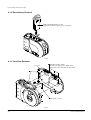
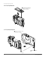
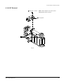
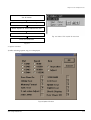
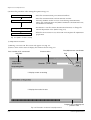
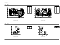
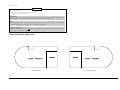
1
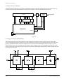
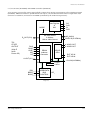
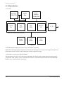
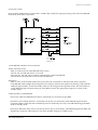
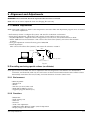
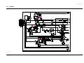
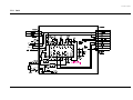
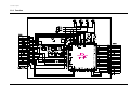
DIGITAL STILL CAMERA
SDC-30
SDC-33
SERVICE
DIGITAL STILL CAMERA
Manual
CONTENTS
1. Precautions
2. Reference Information
3. Product Specifications
4. Disassembly and Reassembly
MODE
TIMER
DELETE
5. Alignment and Adjustment
POWER
6. Troubleshooting
7. Exploded View and Parts List
8. Electrical Parts List
9. Block Diagram
10. PCB Diagrams
11. Schematic Diagrams
© Samsung Electronics Co., Ltd. JUN. 1997
AD68-20286A / AD68-20289A
1. Precautions
1. Be sure that all of the built-in protective devices are
replaced. Restore any missing protective shields.
2. When reinstalling the chassis and its assemblies, be
sure to restore all pretective devices, including :
control knobs and compartment covers.
3. Make sure that there are no cabinet openings
through which people--particularly children
--might insert fingers and contact dangerous
voltages. Such openings include the spacing
between the picture tube and the cabinet mask,
excessively wide cabinet ventilation slots, and
improperly fitted back covers.
(Reading should
not be above
0.5mA)
Device
Under
Test
Leakage
Currant
Tester
Test all
exposed metal
surfaces
2-Wire Cord
Also test with
plug reversed
(using AC adapter
plug as required)
Earth
Ground
Fig. 1 AC Leakage Test
If the measured resistance is less than 1.0 megohm
or greater than 5.2 megohms, an abnormality exists
that must be corrected before the unit is returned
to the customer.
4. Leakage Current Hot Check (See Fig. 1) :
Warning : Do not use an isolation transformer
during this test. Use a leakage current tester or a
metering system that complies with American
National Standards Institute (ANSI C101.1,
Leakage Current for Appliances), and Underwriters
Laboratories (UL Publication UL1410, 59.7).
5. With the unit completely reassembled, plug the AC
line cord directly the power outlet. With the unit’s
AC switch first in the ON position and then OFF,
measure the current between a known erath
ground (metal water pipe, conduit, etc.) and all
exposed metal parts, including : antennas, handle
brackets, metal cabinets, screwheads and control
shafts. The current measured should not exceed
0.5 milliamp. Reverse the power-plug prongs in the
AC outlet and repeat the test.
6. X-ray Limits :
The picture tube is designed to prohibit X-ray
emissions. To ensure continued X-ray protection,
replace the picture tube only with one that is the
same type as the original.
Samsung Electronics
7. Antenna Cold Check :
With the unit’s AC plug disconnected from the
AC source, connect an electrical jumper across the
two AC prongs. Connect one lead of the ohmmeter
to an AC prong.
Connect the other lead to the coaxial connector.
8. High Voltage Limit :
High voltage must be measured each time
servicing is done on the B+, horizontal deflection
or high voltage circuits.
Heed the high voltage limits. These include the
X-ray protection Specifications Label, and the
Product Safety and X-ray Warning Note on the
service data schematic.
9. Some semiconductor (“solid state”) devices are
easily damaged by static electricity.
Such components are called Electrostatically
Sensitive Devices (ESDs); examples include
integrated circuits and some field-effect transistors.
The following techniques will reduce the
occurrence of component damage caused by static
electricity.
10. Immediately before handling sny semiconductor
components or assemblies, drain the electrostatic
charge from your body by touching a known
earth ground. Alternatively, wear a discharging
Wrist-strap device. (Be sure to remove it prior to
applying power--this is an electric shock
precaution.)
1-1
Precautions
11. High voltage is maintained within specified limits
by close-tolerance, safety-related components and
adjustments. If the high voltage exceeds the
specified limits, check each of the special
components.
12. Design Alteration Warning :
Never alter or add to the mechanical or electrical
design of this unit. Example : Do not add
auxiliary audio or video connectors. Such
alterations might create a safety hazard. Also, any
design changes or additions will void the
manufacturer’s warranty.
13. Hot Chassis Warning :
Some TV receiver chassis are electrically
connected directly to one conductor of the AC
power cord. If an isolation transformer is not
used, these units may be safely serviced only if
the AC power plug is inserted so that the chassis
is connected to the ground side of the AC source.
To confirm that the AC power plug is inserted
correctly, do the following : Using an AC
voltmeter, measure the voltage between the
chassis and a known earth ground. If the reading
is greater than 1.0V, remove the AC power plug,
reverse its polarity and reinsert. Re-measure the
voltage between the chassis and ground.
14. Some TV chassis are designed to operate with 85
volts AC between chassis and ground, regardless
of the AC plug polarity. These units can be safely
serviced only if an isolation transformer inserted
between the receiver and the power source.
18. Picture Tube Implosion Warning :
The picture tube in this receiver employs
“integral implosion” protection. To ensure
continued implosion protection, make sure that
the replacement picture tube is the same as the
original.
19. Do not remove, install or handle the picture tube
without first putting on shatterproof goggles
equipped with side shields. Never handle the
picture tube by its neck. Some “in-line” picture
tubes are equipped with a permanently attached
deflection yoke; do not try to remove such
“permanently attached” yokes from the picture
tube.
20. Product Safety Notice :
Some electrical and mechanical parts have special
safety-related characteristics which might not be
obvious from visual inspection. These safety
features and the protection they give might be
lost if the replacement component differs from the
original--even if the replacement is rated for
higher voltage, wattage, etc.
Components that are critical for safety are
indicated in the circuit diagram by shading,
(
or
).
Use replacement components that have the same
ratings, especially for flame resistance and
dielectric strength specifications. A replacement
part that does not have the same safety
characteristics as the original might create shock,
fire or other hazards.
15. Never defeat any of the B+ voltage interlocks.
Do not apply AC power to the unit (or any of its
assemblies) unless all solid-state heat sinks are
correctly installed.
16. Always connect a test instrument’s ground lead to
the instrument chassis ground before connecting
the positive lead; always remove the instrument’s
ground lead last.
17. Observe the original lead dress, especially near
the following areas : Antenna wiring, sharp
edges, and especially the AC and high voltage
power supplies. Always inspect for pinched, outof-place, or frayed wiring. Do not change the
spacing between components and the printed
circuit board. Check the AC power cord for
damage. Make sure that leads and components
do not touch thermally hot parts.
1-2
Samsung Electronics
2. Reference Information
2-1 Circuit description
2-1-1 DSC
Digital camera(SDC-30/33), is an image-input device that connects to a PC. It’s small and light welght, supplies
high quality images and has a large capacity (4MB/2MB). The digital camera consists of 3 sections: Camera,
signal processing and storage.
1. Camera
The camera is similar to a camcorder but adapts a scanning method of 525/30 (which can read an entire image of
in one frame, whereas the camcorder’s scanning method is 525/60.
Photo-exposure is controlled by the electronic shutter through timing generator and CCD driver IC (where as a
camcorder controls the exposure using an IRIS).
Main function of this part is to control the photo-exposure in accordance with the brightness, and to store the
image in DRAM.
2. Digital Signal Processing
Image information of 1 frame is temporarily stored in DRAM. Image information stored in DRAM is the
digitalized CCD signal from the camera. It needs additional image signal processing by the 32-bit microprocessor.
The image signal processing done by the microprocessor includes white balance, shape adjustment and Y/C
signal conversion.
3. Storage
After image signal processing, an image signal compression technique allows more image to be stored in the
limited memory. In the case of SDC-30/33, 10:1 compression is normally executed for standard JPEG specification.
After compression, the image information is stored in the nonvolatile flash memory : Max. 45/22 frame for
VGA(640*480), and max 180/90 frame for QVGA(320*240).
The image can be stored, edited, and printed by the PC image editing program that is supplied with the camera.
2-1-2 Power
LCD MICOM generates the control signal that turns on the system (5V). When the power is on, the signal turns
on IC140 PWM IC which outputs 5V through T141.
When shot key is pressed, the signal for output is generated from MICOM, which turns on IC120 PWM IC and
outputs 5V, -7V, and 15V through T121. After the shot, the camera control signal turns off the power supply within. 5sec (through T121).
2-1-3 DC/DC block operation description
2-1-3(A) DC/DC BLOCK CONSISTS OF THREE COMPONENTS AS BELOW.
1. EVER5V
EVER5V consists of S8420 (IC100) IC and the assocciat battery circuitry (CN101 Pin2) is input to
IC100 (S8420). Pin 8 and 5V voltage are generated internally and are output to pins 1 and 7. EVER5V power
(Pin 1) is input to the function board for LCD MICOM (IC601) drive, POWER S/W (LED01) driving power, and
PULL-UPvoltage. RESET output of IC100 Pin 5, which changes from low to high at the power input, is connected
to LCD MICOM RESET PIN (and resets LCD MICOM).
Samsung Electronics
2-1
Reference Information
2. Camera power
Camera power block consists of IC120 (PWM IC MB3800), Q121 (INVERTER TR DTC144EU), Q122 (SWITCHING TR KSD1621), and rectifier circuit.
When CAM5V control pin of LCD MICOM 10PIN is high, it is converted at Q121 and IC 120. Pin 4 becomes low;
then IC120 Pin 7 starts oscillating and the PWM output from IC120 Pin 5 switches Q122. Pin 6 generates the 15V
output by a switching pulse and this output is rectified by D121, L123, C127, and C128 to generate 15V power for
the drive of CCD (IC201) and V DRIVE IC (MN3112SA).
The pulse for -7V (which is generated at T121 pin 10), is rectified by D121, C129, L124, C130 and becomes -7V
power for the drive of CCD and V DRIVE IC.
The pulse for 5V power, which is output from T121 pin 7, becomes CAMERA 5V power by D122, C133, L127, and
C134. The 5V power is divided by D5V for the drive of IC204(MN5246) and IC202(MN3112SA) and A5V for the
drive of IC203, IC205, and IC206 through L125.
3. SYS 5V
Using the same technique as with camera 5V (L141, IC140, Q142, and T141), the SYS 5V power drives IC301,
IC302, IC303, IC304 and IC307, and is generated by SYS 5V CONT from the LCD micom.
EVER5V power is always output when battery and adapter are connected; SYS 5V power is output only when
power is turned on. CAM power is output for 0.5 second (only during shot operation).
2-1-4 Camera
CDS out
1/3" 35
CCD
LENS
Vout
R
V1~V4 H1
VSUB H2
V-Drive
AGC IN
CDS
AGC
Vout
A/D
(8bit)
D7~D0
Data 8
D15~D0
8-16 CONV. Data 16
DRAM CTRL
16
SMD
SHP
Timing
Gen
DRAM
4Mb
Address
A9~A1
D Data, DCLK
HD, VD
Camera
Ctrl
S/W
DSCP
RISC Chip
1. Camera operation
Fig. 2-1
The image from the lens is converted to an electrical signal by the photoelectric conversion component, CCD
(MN3776PE). Each pulse used to extract CCD signal is generated by the timing geneartor IC(MN5246),
converted to actual driving voltage by V Drive IC(MN3112SA), and supplied to CCD. After noise elimination
(CDS) and amplification (AGC) at analog process IC(NN2038FAQ), CCD output signal is converted to a digital
signal by A/D converter. The 8-bit digital data is changed to 16-bit by DRAM control IC(SMA9606), and stored in
the DRAM.
2-2
Samsung Electronics
Reference Information
2. Lens
SDC-30/33 lens uses a fixed focus method, and can take a photograph clearly at over 1 meter distance (optimal
quality is between 1.5 and 3 meters).
3. Color Filter
Color filter, which remove, the color information on CCD, adapts RGB method
for best color characteristics and Bayer method for best.
4. CCD(MN3776PE) and V Driver(MN3112SA)
R
G
R
G
–
–
G
B
G
B
–
–
R
G
R
G
–
–
G
B
G
B
–
–
CCD converts the optical image to an electrical signal and is similar to an
–
–
–
–
–
–
existing camcorder (except for the scanning method). The camcorder method
uses interlace scanning, which outputs a field image every 1/60 second. (First
–
–
–
–
–
–
field consists of odd lines, the second field consists of even line, and a complete
picture consists of two fields. However, SDC-30/33 uses a the progressive
scanning method, which outputs a frame every 1/30 second (and has excellent vertical resolution).
The image is output at Pin 1 of CCD, and is input to Pin39 of analog signal process IC (IC203) through TR (Q201).
V Driver IC (MN3112SA) mixes each CCD driving pulse from Timing Generator IC, and converts it to
the required voltage.
Effective Pixel
325,546=659(H)X494(V)
ØV1~ØV4: Vertical Shift Clock
<BLOCK>
ØH1~ØH2:
Ø
Ø
Ø
Ø
Horizontal Shift Clock
V
V
V
V
V01: Video output
1
3
2
4
15
PW
13
14
12
V
e
r
t
i
c
a
l
16
S
h
i
f
t
VO1
(Bias) L G
R
e
g
i
s
t
e
r
1
2
VO25
OD
9
SUB
11
PT
4
Horizontal Shift Register 1
Horizontal Shift Register 2
3
Ø R
6
O G
8
7
Ø H 1
Ø H 2
10
SG
Fig. 2-2
Samsung Electronics
2-3
Reference Information
5. Timing Generator (MN5246)
A timing generator generates each clock, synchronized signal, and CCD driving pulse for the system. Also, it
receives the shutter speed information for the photo-exposure control (from the microprocessor).
VDO,HDO
CLK
CSYNC
DS1,DS2
SG
CH1
Image signal
ØSG
ØSUB
ØV4
ØV3
V3
V4
SUB
V2
V1
R
H2
bias
H1
Signal
process
CDS
ØV2
ØV1
CCD
MN5246
VDLIDE
2fck=24.5Mhz
Fig. 2-3
6. Analog processing IC (MN2038FAQ)
After eliminating the noise (CDS) from the CCD output signal (which is input to Pin39, to DS1/DS2 signal
of TG), Analog processing IC outputs it to Pin 46, and then it is input to pin 2 through C232 (for Row Clip and
primary amplificationAGC). Then it is output to Pin 35 and Pin 37 of EVR (IC206), which is input to pin 36,
which controls AGC. Pin 35 output signal is input to Pin 26 through C218, and is amplified second time at the
main amplifier. The offset adjust (pin 16 input) is activated by EVR output signal (Pin 4) and the output (Pin 21)
is sent to A/D converter.
Fig. 2-4
2-4
Samsung Electronics
Reference Information
7. A/D converter (KAD0228) and DRAM Controller (SMA9606)
A/D converter converts the analog signal which is output from Analog processing IC to the 8-bit digital signal
(24.54Mhz). DRAM Controller is synchronized with Vsync, converts the 8-bit data which is output from A/D
converter to 16-bit data, and stores it in DRAM (controlled by the 32-bit microprocessor).
MODE
AE Data Detect.
2 & Knee,
8bit to 16bit Convert
D_OUT(15:0)
–
TRI
STATE
OUTPUT
(High Z
when
Power Off)
RAS–
CASU–
CASL–
WR–
OE–
Data Register
&
SIO
AD_IN(9:0)
–
ADCK IN(12.27MHz)
WND1 OUT
WND2 OUT
DRAM
Address
Generator
VD/HD
GEN
A–OUT(9:1)
EXT VD IN
EXT HD IN
CLK IN(24.54MHz)
H ADJ
V ADJ
EOC –
R/B–
BREQ–
BACK–
SO
SCK
SI
SCS
ADDR/DATA
BUS
CONTROL
OE –
Fig. 2-5
Samsung Electronics
2-5
Reference Information
2-1-5 Digital Section
1. Overview
8-6 CONV
DRAM CTRL
Camera
Ctrl
Flash
Memory
16Mb/32Mb
DRAM
4Mb
S/W
DSCP
S/W
JPEG
Memory
Ctrl
LCD
Micom
LCD
Pannel
PC I/F
32bit RISC MICROPROCESSOR
Power
Control
Fig. 2-6
2. DRAM (KM416C256BLT) and flash memory (TC5832FT/TC5816FT)
DRAM stores the image signal temporarily and enables the microprocessor to process the signal. Flash memory
(nonvolatile) records various system information and the compressed image.
3. 32-bit RISC microprocessor (HD6477043F28)
This microprocessor is the core of the system and handles the camera control, image signal processing, image
compression, flash memory control, communication with PC, and communication with LCD control MICOM.
(Refer to 2-1-6 “System Control” for details.)
2-6
Samsung Electronics
Reference Information
2-1-6 Sytem control
Dual controller (MICOM) is located in DSC : A RISC chip controls the signal processing, and is the 4-bit MICOM
controls the LCD, timer, and switch.
Fig. 2-7
1. 4-bit MICOM; Functions and connections
1) PIN connection status
- RISC is connected to the 4-bit MICOM (total 7 lines).
- Pins 98, 130, and 108 and SCI No. 1 are used.
- Pins 132, 133, 134, and 136 are used for communication with 4-bit MICOM.
- Synchronized communication is used with 4-bit MICOM.
2) Function
- RISC is usally in the standby mode (low-power) because it consumes so much current when it operates.
- 4-bit MICOM acknowledges the starting time (for example, when the user pushes the shot key) and sends the
NMI pin signal to RISC, so that the standby mode can be changed to the operation mode. The information is
sent to RISC through communication port. After RISC executes the appropriate program, it returns to the
standby mode.
2. Main function of 4-bit MICOM
- Power ON/OFF: 4-bit MICOM turns the PC (main body) on, and turns on the RISC.
- Execution of shot: When the shot is executed by the PC key (or main body), 4-bit MICOM signals the shot
execution to RISC. When the shot is finished (system 5V and head power 5V), 4-bit MICOM changes the RISC
mode to standby mode.
- Delay shot: When the delay shot is executed by the PC key (or main body), 4-bit MICOM signals the RISC and
supplies the system 5V and head power 5V. Then, the RISC changes to standby mode.
Samsung Electronics
2-7
Reference Information
- Mode change: When the mode is input by the PC key (or main body), 4-bit MICOM signals the RISC. When
the mode is changed, 4-bit MICOM displays it on LCD, and changes the RISC to standby mode.
- Delete execution: When the delete instruction is input by the PC key (or main body), 4-bit MICOM signal the
RISC and changes the RISC to standby mode.
- LCD display: DSC status is displayed.
- Error handling: When an error occurs, (or RISC) the error message is displayed on LCD. If the RISC cannot
operate, the power is automatically off.
- Battery operation: The capacity of battery is classified as "Full", "Half", "Low", or "Battery replacement". For the
"Battery replacement" status, only the power on/off function is available, and other functions cannot operate.
- Auto power OFF: When any operation has not been executed (three minutes for main body operation, or
10 minutes for PC operation) the power automatically turns off.
3. Main functions of RISC processor
- Communication with 4-bit MICOM: RISC operation is completely controlled by the 4-bit MICOM.
A synchronization method is adapted for communication between 4-bit MICOM and RISC (with 8-bit*11 byte
communication).
- DRAM control: RISC processor includes internal BSC. BSC helps RISC to control the DRAM. RISC uses DRAM
as though it were internal RAM (with the help of BSC). BSC generates all DRAM control signals by itself. RISC
uses DRAM for the image buffer, temp memory for the calculation, and an area that manages the flash
memory and FAT(File Allocation Table).
- Camera Head control: RISC handles the control of the camera head during the shot. RISC controls the timing
generator, ASIC, etc. so that the image data from CCD can be transferred.
- Signal processing: RISC executes the signaling processing internally with CCD image data stored in DRAM.
After RISC separates CCD data into RGB, and processes detail and gamma, it creates a YUV signal, and
executes JPEG compression. The compressed JPEG data will be stored in DRAM again.
- Flash memory control: The compressed data (in DRAM) is stored in the flash memory. The file management
program is recorded in RISC, and manages the files in the flash memory (file location, file size, etc).
- PC communication: RISC processor receives the signal from PC (4-bit MICOM) and activates up RISC.
Then, RISC processor sets the flag for the request input from PC, and transfers the flag to RISC. The RISC
communicates with PC through the serial port. (PC always requests the PC communication to DSC, but RISC
does not request it from the PC.)
- Battery level checking: Battery indicator, which is displayed in LCD of 4-bit MICOM, accepts the data from
RISC. Battery level checking is executed when the camera head and main board are on. When new battery is
inserted, it outputs 6.2V; but the actual voltage drops below 6V after supplying power to the camera head and
main board.
2-8
Samsung Electronics
Reference Information
2-2 IC Blocks
2-2-1 IC301 (SMA9606)
Samsung Electronics
2-9
Reference Information
2-2-2 IC302 (KM416C256BLT)
2-10
Samsung Electronics
Reference Information
2-2-3 IC304 (HD6477043)
Samsung Electronics
2-11
Reference Information
2-2-4 IC307 (TC5832FT)
2-12
Samsung Electronics
Reference Information
2-2-5 IC601 (UPD75P3116GC)
2-2-6 IC501 (MAX232C)
Samsung Electronics
2-13
Reference Information
2-2-7 IC203 (NN2038FAQ)
2-14
Samsung Electronics
Reference Information
2-2-8 IC204 (NN5248)
Samsung Electronics
2-15
Reference Information
MEMO
2-16
Samsung Electronics
3. Product Specifications
Design and specifications are subject to change without notice.
Descriptions
Operation
SDC-30
Image sensor
Color depth
Memory
Image capacity
Compression
Lens
Range
Viewfinder
Shutter
Exposure system
Color balance
Sensitivity
Picture formats
Supported OS
PC
requirements
PC lnterface
Image transfer
time (speed)
Power
Power
consumption
Battery life
Dimensions
Net weight
Samsung Electronics
350,000 pixel CCD
(STD) :640 X 480 pixels (ECO)20 X 240 pixels
24 bit true color (16million colors)
2MB internal flash memory
Standard (STD) : 22 images
Economical (ECO) : 88 images
Standard JPEG
Fixed focusing
100 cm (3.3 feet) - infinity
Separate optical
Auto electronic (1/4 ~ 1/8000 seccond)
Auto exposure
Automatic White Balance (AWB)
ISO 100
BMP, JPG, PCX, PNG
PSD, TGA, TIF, TPL
Windows 3.1 or higher (Including Windows 95)
RAM : 8MB or more
HDD : 30MB or more (free space)
CPU : 486DX or higher (IBM PC based)
CD- ROM drive (recommended)
Standard RS-232C (9600 -115200bps)
(STD) Standard images : 7~8 sec. (at 115Kbps)
(ECO) Economy images : Under 2 sec. (at 115Kbps)
4AA TYPE alkaline batteries
6V DC in using AC adaptor (not supplied)
At power on : below 500mA
At power off : below 500uA
More than 200 images using new alkaline batteries
115(W) X 75(H) X 38(D)mm
140g (without batteries)
SDC-33
350,000 pixel CCD
(STD) :640 X 480 pixels (ECO) : 320 X 240 pixels
24 bit true color (16million colors)
4MB internal flash memory
Standard (STD) : 45 images
Economical (ECO) : 180 images
Standard JPEG
Fixed focusing
100 cm (3.3 feet) - infinity
Sparate optical
Auto electronic (1/4 ~ 1/8000 seccond)
Auto exposure
Automatic White Balance (AWB)
ISO 100
BMP, JPG, PCX, PNG
PSD, TGA, TIF, TPL
Windows 3.1 or higher (Including Windows 95)
RAM : 8MB or more
HDD : 30MB or more (free space)
CPU : 486DX or higher (IBM PC based)
CD- ROM drive (recommended)
Standard RS -232C (9600 -115200bps)
(STD) Standard images : 7~8 sec. (at 115Kbps)
(ECO) Economy images : Under 2 sec. (at 115Kbps)
4AA TYPE allaline batteries
6V DC in using AC adaptor (not supplied)
At power on : below 500mA
At power off : below 500uA
More than 200 images using new alkaline batteries
115(W) X 75(H) X 38(D)mm
140g (without batteries)
3-1
Product Specifications
MEMO
3-2
Samsung Electronics
4. Disassembly and Reassembly
4-1 Cabinet and PCB
Disassemble in the order shown.
(Reassemble in reverse order.)
4-1-1 Case-Side Removal
3 Disconnect 2 tabs while lifting
up the case-side to the arrow direction.
Bottom Side
1 Remove 2 screws.
Precision screw Driver
2 Lift up the case-side using the precision screw driver.
<BOTTOM SIDE>
Fig. 1
Samsung Electronics
4-1
Disassembly and Reassembly
4-1-2 Door-Battery Removal
Open the Door-Battery (in the
direction of arrow), and twist it to remove.
Fig. 2
4-1-3 Case-Rear Removal
2 Remove 3 tabs while
CASE-REAR
pushing "A" area down. Detach the
case-rear in the direction of the arrow.
A
1 Remove 1 screw.
Fig. 3
4-2
Samsung Electronics
Disassembly and Reassembly
4-1-4 Main-PCB Removal
1 Remove 2 screws.
2 Disassemble MAIN PCB while
disconnecting CN301 from FUNCTION-PCB.
3 Disconnect the lead connector
CN502 from JACK-PCB.
Fig. 4
4-1-5 Jack-PCB Removal
3 Disconnect the lead
connector from CN501.
1 Remove 1 screw.
2 Disconnect 1 tabs.
Fig. 5
Samsung Electronics
4-3
Disassembly and Reassembly
4-1-6 Case-Top Removal
1 Disconnect one tab and
detach Case-Top in the
direction of arrow.
Fig. 6
4-1-7 Case-Front Removal
2 Detach Case-Front in the
direction of arrow.
1 Remove 1 screw.
Fig. 7
4-4
Samsung Electronics
Disassembly and Reassembly
4-1-8 OVF Removal
1 Remove 1 screw.
Note : Take extreme care not to ieave
fingerprints on the surface.
2 Lift up OVF.
Fig. 8
Samsung Electronics
4-5
Disassembly and Reassembly
MEMO
4-6
Samsung Electronics
5. Alignment and Adjustments
WARNING: The main board should be replaced if the back focus is twisted.
Note : Ther is no need to adjust the focus for changing the CCD only
5-1 Camera Adjustment
Note : DNP 3100°K light box, 5100°K color temperature conversion filter and adjustment program. A PC is needed
for camera adjustment
- Flash memory format : Configure the system, and store the “bad block” information
- V-Sub voltage adjustment : Adjust the V-Sub voltage of CCD. (Refer to table on page 5-4)
* AE_BTM adjustment : Adjust the offset of image from A/D converter, and set the reference to black
* 3100°K AWB reference measurement : Take a shot of the white chart (3100°K), and extract the reference
at 3100°K.
* AGC gain adjustment : Extract the AGC gain of 0dB, 6dB
* 5100°K adjustment:
Take a shot of the white chart (5100°K), and extract the reference at 5100°K.
15Cm
RS-232C
PC
< 3100 K DNP Light BOX >
5100 K
< KenKo C14 49mm >
Fig. 5-1
5-2 Installing and using special softwre (on diskette)
Note: Special software handles the camera adjustment and fault diagnostics. This diskette isn't distributed to
consumers, and should be used only if a fault occurs. It allows internal disconnection state without camera
disassembly. It simulates the read, modify, and write functions of camera control value.
5-2-1 Environment
* IBM compatible
* Windows 95
* Mouse
* 256 color (or more) video card
* Hard disk (5 MByte or more)
* Supplied program diskette (3.5")
5-2-2 Functions
* DRAM test
* Flash memory test
* ASIC test
* LCD test
* Vsub value adjustment
* AWB(Auto White Balance) 3100°K ,5100°K adjustment
* Display image on PC after shot
Samsung Electronics
5-1
Alignment and Adjustments
5-2-3 Program installation
* Perform setup.exe.
* Perform SVC.exe (use directory made by setup.exe).
5-2-4 Program initial execution and adjustment
1. Initial execution
Turn on PC and execute Windows
Turn off camera
Connect PC with camera
Turn on camera
Execute SVC.exe in Windows
Fig.5-2
2. Initial screen of program
Fig. 5-3 Initial screen at execution of SVC.exe
1) The window (Fig. 5-3) appears at execution of SVC.exe.
2) It should be tested or adjusted in the following sequence.
5-2
Samsung Electronics
Alignment and Adjustments
Select 'SDC-33/30' of Winows menu bar in
use of mouse.
Two items appear as shown in Fig. 5-5.
Select 'Option' to set the adjustment item
Select 'Start' for execution
Fig. 5-5 Select 'SDC-33/30' of menu bar
Finish the execution
Fig. 5-4
3. 'Option' window
1) When selecting 'Option', Fig. 5-6 is displayed.
Fig.5-6 Option Window
Samsung Electronics
5-3
Alignment and Adjustments
2) Follow this procedure when setting the options in Fig. 5-6.
: Select the communication port connected with PC
Communication port setting
: Select the communication rate between DSC and PC.
Generally 56000 is used If an error occurs during communication,
reduce the communication rate (9600 is minimum communication rate,
and 115200 is maximum).
Communication rate setting
: Test decision : Use the camera disconnection function, or change the
internal adjustment value. (Refer to Fig. 5-9)
Adjustment setting
: When the above items are set, select 'OK' and complete the adjustment
preparation.
OK button
Fig. 5-7 Option window setting
3). Adjustment execution
1) SEE Fig. 5-6. Press O.K. The screen will appear as in Fig. 5-3.
2) Select 'Start' of SVC menu to display the window shown in Fig. 5-8.
Port number of PC connected
with DSC
Pictures taken
Test/Adjustment start button
Exit
* Display screen on testing
* Display the results for test
Progress bar to display the
process state
Fig. 5-8 Execution window of test/adjustment
5-4
Samsung Electronics
Alignment and Adjustments
4) Execute the program in accordance with the sequence of Fig. 5-6.
Power supply
DRAM test
Memory format
ASIC test
VSUB value adjustment
3100°K level AWB
5100°K level AWB
LCD test
Mode test
Timer test
Shot & Display
Power interrupt
Fig. 5-9 Process and procedure of adjustment
Samsung Electronics
5-5
Alignment and Adjustments
4, Adjistment item
Power supply
DRAM test
Memory format
Fig. 5-10
Format is broken
: Supply power to the entire camera
: Check connections between DRAM and RISC
: Check the flash memory state. The various information and image
management data are stored as usual in the flash memory.
* Normal memory : Go to the next step with ‘Formatted’ message.
* Abnormal memory : Display the window to ask for compulsory
format with ‘Format is broken’ message as shown in Fig. 5-11.
Press ‘Enter’ of PC keyboard to retry memory format. Press ‘+’ to
enter the next step without formatting. ( If formatted, all image
data are deleted.)
* Key : Stop Enter key : Continue
Fig. 5-11
* Replace with new memory : When replacing with memory (due to
memory error), go to the next step after automatic formatting.
: Check for disconnection state between ASIC, RISC and DRAM and
ASIC function.
ASIC test
: Input V-SUB value. (Always refer to the table in oppend it before
inputting, because picture quality is affected). (Fig.5-14)
VSUB value adjustment
3100°K level AWB
: Adjust AWB 3100°K level. This process should be done with 3100°K
level chart active throughout the screen. (Be certain to use it,
because picture quality is affected.)
: Adjust AWB 5100°K level. This process should be done with 5100°K
level chart active throughout the screen, and color temperature con
version filter should be attached to the camera. (Be certain to use it,
because picture quality is affected.)
5100°K level AWB
Fig. 5-12
5-6
Samsung Electronics
Alignment and Adjustments
LCD test
: Check each segment of camera LCD screen. Press 'Enter' key
to stop and enter the next step.
Mode test
: Test the a into shot mode. The camera has two types
of shot functions: VGA(640*480) and QVGA(320*240). Test both of these
mode conversions.
Timer test
: Check the delay shot On/Off of camera. Display the result by means of self
On/Off without special operation.
Shot and Display
Power interrupt
: Display the thumbnail after the shot to determine normal or abnormal
operation.
: Shut off the camera’s power supply after completion of all tests.
Proceed to the adjustment step.
Fig. 5-13
Fig. 5-14 V-Sub voltage
Samsung Electronics
5-7
Alignment and Adjustments
5. Process for adjustment failure
* Communication port XX cannot be used. Select another port.
-> Cannot use com port XX. Select another com port.
* RISC Processor isn't active.
-> RISC Processor does not respond.
* Can't receive the specified data data count from camera.
-> Camera Communication Error.
* There is a fatal error in <NG> DRAM circuit.
-> DRAM Test error occured.
* A fatal error occurs during <NG> ASIC test.
-> ASIC Test error occured.
* A fatal error occurs during <NG> Vsub adjustment.
-> V-sub adjust error occured. (Fig.5-14)
* Memory has been previously formatted.
-> Memory was already formatted.
* An error occurs in flash memory.
-> Flash Memory has defective area.
-> Flash Memory clearing error occured.
-> Flash Memory system block error occured.
* New flash memory.
-> Flash memory is rare.
* B value is larger than R value in <NG> 3100°K level test.
-> 3100°K AWB adjust error (B > R). RG xx / BG yy);
* R value exceeds the range in <NG> 3100°K level test.
-> 3100°K AWB adjust error (R value is out of bound). RG xx
* B value exceeds the range in <NG> 3100°K level test.
-> 3100°K AWB adjust error (B value is out of bound). BG yy
* R value is larger than B value in <NG> 5100°K level test.
-> 5100°K AWB adjust error (B > R) . RG xx / BG yy
* R value exceeds the range in <NG> 5100°K level test.
-> 5100°K AWB adjust error (R value is out of bound) . RG xx
* B value exceeds the range in <NG> 5100°K level test.
-> 5100°K AWB adjust error (B value is out of bound) . BG yy
5-8
Samsung Electronics
Alignment and Adjustments
5-2-5 Using the software
1. Edit S/W installation and use (iPhoto express of Ulead company based)
1) Insert CD-ROM (in Windows 95 environment).
2) Complete the installation according to the instructions on screen.
Note: Select 'iPhoto Express Tour' in Help menu to see the detailed instructions for Edit S/W. All functions of
Edit S/W are explained with figure.
Fig.5-15
2. Twain driver installation
1) Execute setup.exe in TWAIN intallation diskette under Windows 95 environments.
2) Complete the installation according to the instructions on screen.
Samsung Electronics
5-9
Alignment and Adjustments
3. Twain driver preparation
Fig.5-16
1) Execute TWAIN compatible edit program
(Photo Impect, Video Studio, iPhoto Express, Photo Shop Pro. etc
2) Select Acquire->Select Soruce->Samsung Digital Camera TWAIN in file menu of edit program
3) Connect the digital camera with PC in use of RS-232C cable and power on.
4) Select Acquire->Image->Acquire in file menu operate TWAIN driver and display the thumbnail image in the
camera.
5) Transmit the original image to PC by clicking the desired screen on TWAIN driver (or pressing the select all
button and Download button).
6) The basic operation is finished by storing a particular file name.
5-10
Samsung Electronics
Alignment and Adjustments
4. TWAIN driver use
Fig.5-17
Brief descriptions for other functions (except image transmission function on TWAIN driver ) :
- Option : Select communication rate
- Update : Execute Update when camera state changes
- Delete : Delete unnecessary screen.
- Shot : Shot
- Timer : Self timer function
- Mode : Switch the size (VGA/QVGA) of screen
- Download : Transmit the selected screen to PC
- Exit : Exit TWAIN driver
- Select All : Select entire screen
- PgUp/PgDn : Display the previous and next screen (by page 5)
- RowUp/RowDn : Display the previous and next screen (by row)
Samsung Electronics
5-11
Alignment and Adjustments
MEMO
5-12
Samsung Electronics
6. Troubleshooting
Samsung Electronics
6-1
Troubleshooting
6-2
Samsung Electronics
Troubleshooting
Samsung Electronics
6-3
Troubleshooting
6-4
Samsung Electronics
Troubleshooting
Samsung Electronics
6-5
Troubleshooting
6-1 Test and repair of digital section
* Perform the operation test and check for fault in digital section during adjustment and diagnostic program.
(Refer to Chapter 5 for Environments, function, program installation and initial execution)
Select 'SDC33/30' of Winows menu bar in
use of mouse.
Two items appear as shown in Fig.6-2.
Select 'Option' to set the test item
Select 'Start' for execution
Finish
Fig.6-2 Select 'SDC-30/33' of menu bar
Fig.6-1
6-2 Option window
Option window is set as follows.
6-6
Communication port setting
: The current DSC sets the communication port connected with PC
Communication rate setting
: Select the communication rate between DSC and PC (usuallg 56000).
If an error occurs, reduce the communication rate ( 9600 minimum and
115200 maximum ).
Test setting
: TEST DECISION : Disconnection or function (or change the internal
adjustment value). Refer to <Fig. 6-3> for details.
OK button
: When the above items are set, select 'OK' and complete the test.
Fig.6-3 Option window setting
Note : select ‘start” of SVC menu to display the window shown in
Fig. 5-14.
Samsung Electronics
Troubleshooting
6-3 Test procedure
Power supply
DRAM test
Memory format
ASIC test
LCD test
Mode test
Timer test
Shot & Display
Power interrupt
Fig.6-4 Test procedure
Samsung Electronics
6-7
Troubleshooting
6-4. Test items
: Supply power to the entire camera
Power supply
: Check connections between DRAM and RISC
DRAM test
Memory format
: Check the flash memory. The various information and image management
data required by the camera are stored in the flash memory.
* Normal memory : Go to the next step with 'Formatted' message.
Fig.6-5
* Abnormal memory : Display the window to ask for compulsory format
with 'Format is broken' message as shown in Fig 6-6. Press 'Enter' ( PC
keyboard) to retry memory format. Press '+' to enter the next step without formatting. (If formatted, all image data are deleted.)
*Key : Stop Enter key : Continue
Fig.6-6
*Replace with new memory : when replacing with new memory ( due to
memory error ), go to the next step after automatic formatting.
ASIC test
: Check for any disconnections between ASIC, RISC and DRAM and
ASIC.
LCD test
: Check each segment of camera LCD screen. Press 'Enter' key to stop
and enter the next step.
Mode test
: Test by converting the camera into shot mode. The camera has two
types of shot functions VGA(640*480) and QVGA(320*240).
Test these mode conversions.
Timer test
: Check the delay shot On/Off. Display the result by means of self
On/Off without special operation.
Shot & Display
: Display the thumbnail after shot, to confirm normal or abnormal
operation.
Power interrupt
: After completion of all tests and adjustments disconnect the power
supply.
Fig.6-7
6-8
Samsung Electronics
Troubleshooting
6-5. Follow up Actions After inspection
* Communication port XX can't be used. Select another port.
-> Cannot use com port XX. Select another com port.
* RISC Processor isn't active.
-> RISC Processor does not respond.
* Can't receive the specified count of data from camera.
-> Camera Communication Error.
* There is a Fatal error in <NG> DRAM circuit.
-> DRAM Test error.
* A fatal error occurs during <NG> ASIC test.
-> ASIC Test error.
* A fatal error occurs during <NG> Vsub adjustmentt.
-> V-sub adjust error.
* Memory has been previously formatted.
-> Memory was already formatted.
* An error occurs in flash memory.
-> Flash Memory has defective area.
-> Flash Memory clearing error.
-> Flash Memory system block error.
* New flash memory.
-> Flash memory is rare.
* There are Many bad blocks in <NG> flash memory.
-> Flash Memory system block error.
* XX data bus has a problem.
-> Data line XX error detected.
* Address bus has a problem.
-> Address line error detected.
Samsung Electronics
6-9
Troubleshooting
MEMO
6-10
Samsung Electronics
7. Exploded View and Parts List
Page
7-1
Cabinet Assembly - - - - - - - - - - - - - - - - - - - - - - -
7-2
7-2
Accessory - - - - - - - - - - - - - - - - - - - - - - - - - - - - -
7-4
Samsung Electronics
7-1
Exploded View and Parts List
30
2
1
31
14
12
13
10
31
11
9
22
21
15
30
20
19
18
17
16
7
32
8
30
5
30
4
3
7-1 Cabinet Assembly
7-2
Samsung Electronics
Exploded View and Parts List
Loc. No New Part No
Description and Specification
1
2
UNIT-CASE FRONT
PANEL-FRONT;-,A5056P,T0.8,-,-,DSC33
PANEL-FRONT;-,A5056P,T0.8,-,-,DSC30
UNIT-CASE REAR;SDC33
UNIT-CASE REAR;SDC30
KNOB-POWER;-,PC+ABS,-,BLK,-,
HOLDER-POWER;-,PC+ABS,-,BLK,
UNIT-CASE SIDE;
COVER-JACK;-,PE,HB,-,-,D-GRAY,-,UNIT-DOOR BATTERY
UNIT-CASE TOP
UNIT-OVF LENS
SPRING-BATTERY A
SPRING-BATTERY B
ASSY-FUNC BOARD;
ASSY-JACK BOARD;
ASSY-MAIN BOARD;SDC30
ASSY-MAIN BOARD;SDC33
BRACKET-CCD;-,AL,-,T1.2,-,-,DSC
CCD;COLOR,DIP,16,400MIL,325K,7.4X7
SPACER-CCD;-,SILICON,BLK,-,-,DSC
FILTER-OPTICALL;DP,SV-4C10MM,LP,-,T
HOLDER-LENS;-,PBT94,HB,-,-,BLK
LENS-FIXED FOCAL;-,0.16,GLASS,T5.18,15X15.6,6.0
SCREW-TAPPING;BH,+,-,M2,X6,FZB
SCREW-TAPPING;BH,+,-,M2,X4,FZB
SCREW-MACHINE;BH,+,M2,X3,FZW,FE,-,-,-
3
4
5
7
8
9
10
11
12
13
14
15
16
17
18
19
20
21
22
30
31
32
AD59-10417A
AD64-20621A
AD64-20621B
AD59-10418A
AD59-10418B
AD64-10825A
AD61-21053A
AD59-10422A
AD63-30548A
AD59-10420A
AD59-10419A
AD59-10445A
AD61-62003A
AD61-62004A
AD90-10813H
AD90-10813Q
AD90-10812V
AD90-10819W
AD61-11017A
0605-001010
AD63-60088A
AD29-90200J
AD61-21047A
AD67-10169A
AC60-10054A
AC60-10055A
AC60-10024A
Samsung Electronics
Remark
OPTION
OPTION
OPTION
OPTION
OPTION
OPTION
7-3
Exploded View and Parts List
7-2 Accessory
AD91-10001A
ASSY-ACCESSORY; SDC-30,NTSC
ŒAD39-42001C
´AD63-10212A
ˇAD69-32001A
¨AD46-30001C
¨AD46-30001E
ˆAD46-20007A
Ø4301-001017
CABLE-RS232C; 9P, 1000MM, PLUG 3.5. 20M
STRAP-SHOULDER;-,-,-,-,BLK,-,
BAG-SOFT CASE; SDC50, LEATHER,-,-,-,BLK,-,DISC-FLOPPY; 3.5 INCH, 1.44MB
DISC-FLOPPY WIN3.1;3.5INCH,1.44MB,SDC-33
DISC-IPHOTO EXPRESS ; 120MM
BATTREY-ALKALINE ; 1.5V, -, AA,14 X 49.5MM,PLATE
1
3
1.5V
1.5V
2
6
V
1.5
1.5V
5
4
Us
er
Ma
nua
l
DO NOT ORDER
7-4
Samsung Electronics
8. Electrical Parts List
Loc. No New Part No
Description and Specification
16
AD90-10819W
AD90-10812V
ASSY-MAIN BOARD;SDC-33
ASSY-MAIN BOARD;SDC-30
C201
C202
C203
C204
C205
C208
C209
C210
C211
C212
C213
C214
C215
C216
C217
C218
C219
C220
C221
C222
C223
C224
C225
C226
C227
C228
C229
C230
C231
C232
C233
C234
C238
C239
C240
C241
C242
C243
C244
C245
C246
C247
C248
C249
C250
C251
C277
C280
2203-000477
2203-000477
2203-001556
2203-000491
2404-000159
2203-000477
2203-001556
2203-001556
2203-000477
2203-000477
2203-001556
2404-000198
2203-001556
2203-001556
2203-001556
2203-001556
2203-001556
2404-000139
2203-001556
2203-001556
2203-001556
2203-001556
2404-000139
2404-000139
2404-000139
2404-000139
2203-001556
2203-002220
2203-000477
2203-001567
2203-001636
2203-001567
2203-001556
2404-000139
2203-001556
2404-000198
2203-001556
2404-000198
2203-001556
2404-000198
2203-001556
2404-000238
2404-000120
2203-001556
2404-000198
2203-001556
2404-000120
2203-000477
C-CERAMIC,CHIP;1UF,+80-20%,16V,Y5V,TP,2012,C-CERAMIC,CHIP;1UF,+80-20%,16V,Y5V,TP,2012,C-CERAMIC,CHIP;100NF,+80-20%,25V,Y5V,TP,1608,
C-CERAMIC,CHIP;2.2NF,10%,50V,X7R,TP,1608,C-TA,CHIP;1UF,20%,35V,-,TP,3528,C-CERAMIC,CHIP;1UF,+80-20%,16V,Y5V,TP,2012,C-CERAMIC,CHIP;100NF,+80-20%,25V,Y5V,TP,1608,
C-CERAMIC,CHIP;100NF,+80-20%,25V,Y5V,TP,1608,
C-CERAMIC,CHIP;1UF,+80-20%,16V,Y5V,TP,2012,C-CERAMIC,CHIP;1UF,+80-20%,16V,Y5V,TP,2012,C-CERAMIC,CHIP;100NF,+80-20%,25V,Y5V,TP,1608,
C-TA,CHIP;22UF,20%,6.3V,-,TP,3528,C-CERAMIC,CHIP;100NF,+80-20%,25V,Y5V,TP,1608,
C-CERAMIC,CHIP;100NF,+80-20%,25V,Y5V,TP,1608,
C-CERAMIC,CHIP;100NF,+80-20%,25V,Y5V,TP,1608,
C-CERAMIC,CHIP;100NF,+80-20%,25V,Y5V,TP,1608,
C-CERAMIC,CHIP;100NF,+80-20%,25V,Y5V,TP,1608,
C-TA,CHIP;10UF,20%,6.3V,-,TP,3216,C-CERAMIC,CHIP;100NF,+80-20%,25V,Y5V,TP,1608,
C-CERAMIC,CHIP;100NF,+80-20%,25V,Y5V,TP,1608,
C-CERAMIC,CHIP;100NF,+80-20%,25V,Y5V,TP,1608,
C-CERAMIC,CHIP;100NF,+80-20%,25V,Y5V,TP,1608,
C-TA,CHIP;10UF,20%,6.3V,-,TP,3216,C-TA,CHIP;10UF,20%,6.3V,-,TP,3216,C-TA,CHIP;10UF,20%,6.3V,-,TP,3216,C-TA,CHIP;10UF,20%,6.3V,-,TP,3216,C-CERAMIC,CHIP;100NF,+80-20%,25V,Y5V,TP,1608,
C-CERAMIC,CHIP;56PF,5%,50V,CH,TP,1608,C-CERAMIC,CHIP;1UF,+80-20%,16V,Y5V,TP,2012,C-CERAMIC,CHIP;10PF,0.5PF,50V,CH,TP,1608,1.6M
C-CERAMIC,CHIP;33PF,5%,50V,NPO,TP,1608,1.6MM
C-CERAMIC,CHIP;10PF,0.5PF,50V,CH,TP,1608,1.6M
C-CERAMIC,CHIP;100NF,+80-20%,25V,Y5V,TP,1608,
C-TA,CHIP;10UF,20%,6.3V,-,TP,3216,C-CERAMIC,CHIP;100NF,+80-20%,25V,Y5V,TP,1608,
C-TA,CHIP;22UF,20%,6.3V,-,TP,3528,C-CERAMIC,CHIP;100NF,+80-20%,25V,Y5V,TP,1608,
C-TA,CHIP;22UF,20%,6.3V,-,TP,3528,C-CERAMIC,CHIP;100NF,+80-20%,25V,Y5V,TP,1608,
C-TA,CHIP;22UF,20%,6.3V,-,TP,3528,C-CERAMIC,CHIP;100NF,+80-20%,25V,Y5V,TP,1608,
C-TA,CHIP;4.7UF,20%,20V,-,TP,3528,C-TA,CHIP;10UF,20%,10V,-,TP,3528,C-CERAMIC,CHIP;100NF,+80-20%,25V,Y5V,TP,1608,
C-TA,CHIP;22UF,20%,6.3V,-,TP,3528,C-CERAMIC,CHIP;100NF,+80-20%,25V,Y5V,TP,1608,
C-TA,CHIP;10UF,20%,10V,-,TP,3528,C-CERAMIC,CHIP;1UF,+80-20%,16V,Y5V,TP,2012,-
Samsung Electronics
Remark
8-1
Electrical Parts List
Loc. No New Part No
Description and Specification
C281
C282
C283
C285
C286
C287
C301
C302
C303
C304
C305
C306
C307
C308
C309
C310
C311
C312
C313
C314
C315
C316
C317
C318
C319
C320
C321
C330
C331
C332
C333
C391
C398
C399
CN206
CN301
D201
D202
D203
D204
D205
D207
D301
IC201
IC202
IC203
IC204
IC205
IC206
IC207
IC301
IC302
IC304
IC305
IC307
C-CERAMIC,CHIP;100NF,+80-20%,25V,Y5V,TP,1608,
C-CERAMIC,CHIP;22PF,5%,50V,NPO,TP,1608,C-CERAMIC,CHIP;22PF,5%,50V,NPO,TP,1608,C-CERAMIC,CHIP;100NF,+80-20%,25V,Y5V,TP,1608,
C-CERAMIC,CHIP;100NF,+80-20%,25V,Y5V,TP,1608,
C-CERAMIC,CHIP;100NF,+80-20%,25V,Y5V,TP,1608,
C-CERAMIC,CHIP;100NF,+80-20%,25V,Y5V,TP,1608,
C-CERAMIC,CHIP;100NF,+80-20%,25V,Y5V,TP,1608,
C-CERAMIC,CHIP;2.2UF,+80-20%,16V,Y5V,TP,2012,
C-CERAMIC,CHIP;100NF,+80-20%,25V,Y5V,TP,1608,
C-TA,CHIP;22UF,20%,6.3V,-,TP,3528,C-CERAMIC,CHIP;100NF,+80-20%,25V,Y5V,TP,1608,
C-CERAMIC,CHIP;100NF,+80-20%,25V,Y5V,TP,1608,
C-CERAMIC,CHIP;100NF,+80-20%,25V,Y5V,TP,1608,
C-CERAMIC,CHIP;100NF,+80-20%,25V,Y5V,TP,1608,
C-CERAMIC,CHIP;20PF,5%,50V,CH,TP,1608,1.6MM
C-CERAMIC,CHIP;20PF,5%,50V,CH,TP,1608,1.6MM
C-CERAMIC,CHIP;100NF,+80-20%,25V,Y5V,TP,1608,
C-CERAMIC,CHIP;470PF,5%,50V,CH,TP,1608,1.6MM
C-CERAMIC,CHIP;100NF,+80-20%,25V,Y5V,TP,1608,
C-CERAMIC,CHIP;100NF,+80-20%,25V,Y5V,TP,1608,
C-CERAMIC,CHIP;100NF,+80-20%,25V,Y5V,TP,1608,
C-CERAMIC,CHIP;100NF,+80-20%,25V,Y5V,TP,1608,
C-TA,CHIP;22UF,20%,6.3V,-,TP,3528,C-TA,CHIP;22UF,20%,6.3V,-,TP,3528,C-CERAMIC,CHIP;100NF,+80-20%,25V,Y5V,TP,1608,
C-CERAMIC,CHIP;100NF,+80-20%,25V,Y5V,TP,1608,
C-TA,CHIP;10UF,20%,6.3V,-,TP,3216,C-CERAMIC,CHIP;100NF,+80-20%,25V,Y5V,TP,1608,
C-CERAMIC,CHIP;100NF,+80-20%,25V,Y5V,TP,1608,
C-CERAMIC,CHIP;100NF,+80-20%,25V,Y5V,TP,1608,
C-CERAMIC,CHIP;100NF,+80-20%,25V,Y5V,TP,1608,
C-CERAMIC,CHIP;100NF,+80-20%,25V,Y5V,TP,1608,
C-TA,CHIP;22UF,20%,6.3V,-,TP,3528,CONNECTOR-SOCKET;18P,2R,0.8MM,SMD-S,AU
CONNECTOR-SOCKET;20P,2R,1MM,SMD-S,SN
DIODE-ARRAY;MA151WA,40V,100MA,CK2-3,SOT-23
DIODE-SWITCHING;MA110,40V,100MA,-,3NS,SM2
DIODE-SWITCHING;MA110,40V,100MA,-,3NS,SM2
DIODE-SWITCHING;MA110,40V,100MA,-,3NS,SM2
DIODE-SWITCHING;MA110,40V,100MA,-,3NS,SM2
DIODE-SWITCHING;MA110,40V,100MA,-,3NS,SM2
DIODE-SWITCHING;MA110,40V,100MA,-,3NS,SM2
CCD;COLOR,DIP,16,400MIL,325K,7.4X7
IC-CLOCK DRIVER;MN3112SA,SOP,20P,255MIL,SINGLE
IC-VIDEO PROCESS;NN2038FAQ,QFP,48P,472MIL,PLAST
IC-GENERATOR;MN5246,QFP,64P,-,PLASTIC,7.0V,
IC-LINEAR;KAD0228,SOP,IC;MB88346B,VSOP,IC-CMOS LOGIC;7W04,INVERTER,SOP,8P,150MIL,TR
IC-ASIC;-,SMA9606,QFP,80P,CNTR&INTERFA
IC-DRAM;416C256,256KX16BIT,SOP,40P,400
IC-MCU(OTP);HD6477043F28,144P,DIP,RISC MC,
IC-CMOS LOGIC;7W04,INVERTER,SOP,8P,150MIL,TR
IC-FLASH MEMORY;5832,4MX8BIT,SOP,44P,400MIL,10
8-2
2203-001556
2203-000626
2203-000626
2203-001556
2203-001556
2203-001556
2203-001556
2203-001556
2203-001598
2203-001556
2404-000198
2203-001556
2203-001556
2203-001556
2203-001556
2203-001600
2203-001600
2203-001556
2203-001656
2203-001556
2203-001556
2203-001556
2203-001556
2404-000198
2404-000198
2203-001556
2203-001556
2404-000139
2203-001556
2203-001556
2203-001556
2203-001556
2203-001556
2404-000198
3710-001110
3710-001172
0407-000149
0401-000170
0401-000170
0401-000170
0401-000170
0401-000170
0401-000170
0605-001010
1003-001099
1204-001257
1205-001165
AC14-12006V
AC14-12009X
0801-000301
AD13-10030C
1105-001083
AD09-10450N
0801-000301
1107-001054
Remark
Samsung Electronics
Electrical Parts List
Loc. No New Part No
Description and Specification
L201
L202
L203
L204
L205
L206
L207
L208
L209
L301
L302
L303
L311
L321
LED01
Q201
Q202
Q203
Q204
Q208
Q289
Q298
Q301
Q303
R201
R202
R203
R204
R205
R206
R207
R208
R209
R210
R211
R212
R213
R214
R215
R215
R216
R217
R218
R219
R220
R221
R222
R224
R232
R233
R234
R235
R236
R237
R239
INDUCTOR-SMD;22UH,10%,3.2X2.5X2.2MM
INDUCTOR-SMD;10UH,5%,2.5X2X1.8MM
INDUCTOR-SMD;22UH,10%,3.2X2.5X2.2MM
INDUCTOR-SMD;22UH,10%,3.2X2.5X2.2MM
INDUCTOR-SMD;22UH,10%,3.2X2.5X2.2MM
INDUCTOR-SMD;22UH,10%,3.2X2.5X2.2MM
INDUCTOR-SMD;22UH,10%,3.2X2.5X2.2MM
INDUCTOR-SMD;22UH,10%,3.2X2.5X2.2MM
INDUCTOR-SMD;22UH,10%,3.2X2.5X2.2MM
INDUCTOR-SMD;22UH,10%,3.2X2.5X2.2MM
INDUCTOR-SMD;22UH,10%,3.2X2.5X2.2MM
INDUCTOR-SMD;22UH,10%,3.2X2.5X2.2MM
INDUCTOR-SMD;22UH,10%,3.2X2.5X2.2MM
INDUCTOR-SMD;22UH,10%,3.2X2.5X2.2MM
LED;CHIP,RED,1.5X2MM,660NM
FET-SILICON;2SK1070,N,-,50MA,-,150MW,SOT-2
TR-SMALL SIGNAL;2SC4081,NPN,200MW,SC-70,TP,180
TR-ARRAY;UMX1N,NPN/PNP,1,50V,40V,100MA,
TR-SMALL SIGNAL;2SC4081,NPN,200MW,SC-70,TP,180
TR-DIGITAL;DTC144EUA,NPN,200MW,47K-47K,SC
TR-SMALL SIGNAL;2SB1121,PNP,500MW,PCP,TP,100-5
TR-DIGITAL;DTC144EUA,NPN,200MW,47K-47K,SC
TR-DIGITAL;DTC144EUA,NPN,200MW,47K-47K,SC
TR-DIGITAL;DTC144EUA,NPN,200MW,47K-47K,SC
R-CHIP;10OHM,5%,1/16W,DA,TP,1608
R-CHIP;1MOHM,5%,1/16W,DA,TP,1608
R-CHIP;100KOHM,5%,1/16W,DA,TP,1608
R-CHIP;100OHM,5%,1/16W,DA,TP,1608
R-CHIP;3.9KOHM,5%,1/16W,DA,TP,1608
R-CHIP;27KOHM,1%,1/16W,DA,TP,1608
R-CHIP;RH 1/16 CS 123-F C1608
R-CHIP;15KOHM,5%,1/16W,DA,TP,1608
R-CHIP;270KOHM,5%,1/16W,DA,TP,1608
R-CHIP;47KOHM,5%,1/16W,DA,TP,1608
R-CHIP;47KOHM,5%,1/16W,DA,TP,1608
R-CHIP;100OHM,5%,1/16W,DA,TP,1608
R-CHIP;100OHM,5%,1/16W,DA,TP,1608
R-CHIP;0OHM,5%,1/16W,DA,TP,1608
R-CHIP;0OHM,5%,1/16W,DA,TP,1608
R-CHIP;0OHM,5%,1/16W,DA,TP,1608
R-CHIP;100OHM,5%,1/16W,DA,TP,1608
R-CHIP;100OHM,5%,1/16W,DA,TP,1608
R-CHIP;10OHM,5%,1/16W,DA,TP,1608
R-CHIP;10OHM,5%,1/16W,DA,TP,1608
R-CHIP;470OHM,5%,1/16W,DA,TP,1608
R-CHIP;10OHM,5%,1/16W,DA,TP,1608
R-CHIP;560OHM,5%,1/16W,DA,TP,1608
R-CHIP;100OHM,5%,1/16W,DA,TP,1608
R-CHIP;100KOHM,5%,1/16W,DA,TP,1608
R-CHIP;100KOHM,5%,1/16W,DA,TP,1608
R-CHIP;1KOHM,5%,1/16W,DA,TP,1608
R-CHIP;3.9KOHM,5%,1/16W,DA,TP,1608
R-CHIP;100OHM,5%,1/16W,DA,TP,1608
R-CHIP;100OHM,5%,1/16W,DA,TP,1608
R-CHIP;15KOHM,5%,1/16W,DA,TP,1608
2703-000403
2703-000363
2703-000403
2703-000403
2703-000403
2703-000403
2703-000403
2703-000403
2703-000403
2703-000403
2703-000403
2703-000403
2703-000403
2703-000403
0601-000208
0505-000180
0501-000218
0506-000149
0501-000218
0504-000113
0501-000172
0504-000113
0504-000113
0504-000113
2007-001442
2007-000109
2007-000102
2007-000074
2007-000125
2007-000651
A1020-0598
2007-000092
2007-000637
2007-000097
2007-000097
2007-000074
2007-000074
2007-000070
2007-000070
2007-000070
2007-000074
2007-000074
2007-001442
2007-001442
2007-000077
2007-001442
2007-000119
2007-000074
2007-000102
2007-000102
2007-000078
2007-000125
2007-000074
2007-000074
2007-000092
Samsung Electronics
Remark
8-3
Electrical Parts List
Loc. No New Part No
Description and Specification
R240
R242
R244
R246
R257
R258
R259
R266
R287
R288
R289
R301
R302
R303
R304
R305
R306
R308
R309
R310
R333
R349
R350
R351
R352
R353
R354
R355
R356
R357
R358
R359
R360
R362
R363
R364
R370
R371
R372
R373
R374
R380
R383
R392
S301
X201
X301
2007-000078
2007-000093
2007-000124
2007-000070
B1018-0099
B1018-0099
2007-000070
2007-000070
2007-000090
2007-000572
2007-000572
2007-000102
2007-000090
2007-000076
2007-000539
2007-000083
2007-000070
2007-000102
2007-000077
2007-000102
2007-000102
B1018-0099
2007-000074
B1018-0099
B1018-0099
2007-000074
2007-000074
B1018-0099
B1018-0099
2007-000074
2007-000074
B1018-0099
B1018-0099
2007-000102
B1018-0099
2007-000084
B1018-0099
2007-000102
2007-000102
2007-000102
2007-000102
B1018-0099
2007-000102
2007-000102
3408-000300
2801-003378
2801-003392
R-CHIP;1KOHM,5%,1/16W,DA,TP,1608
R-CHIP;20KOHM,5%,1/16W,DA,TP,1608
R-CHIP;2.2KOHM,5%,1/16W,DA,TP,1608
R-CHIP;0OHM,5%,1/16W,DA,TP,1608
R-NETWORK;RN 1/16 FV 8P 101-J T MNR14-J-101 CS96
R-NETWORK;RN 1/16 FV 8P 101-J T MNR14-J-101 CS96
R-CHIP;0OHM,5%,1/16W,DA,TP,1608
R-CHIP;0OHM,5%,1/16W,DA,TP,1608
R-CHIP;10KOHM,5%,1/16W,DA,TP,1608
R-CHIP;220OHM,5%,1/10W,DA,TP,2012
R-CHIP;220OHM,5%,1/10W,DA,TP,2012
R-CHIP;100KOHM,5%,1/16W,DA,TP,1608
R-CHIP;10KOHM,5%,1/16W,DA,TP,1608
R-CHIP;330OHM,5%,1/16W,DA,TP,1608
R-CHIP;200OHM,5%,1/16W,DA,TP,1608
R-CHIP;3KOHM,5%,1/16W,DA,TP,1608
R-CHIP;0OHM,5%,1/16W,DA,TP,1608
R-CHIP;100KOHM,5%,1/16W,DA,TP,1608
R-CHIP;470OHM,5%,1/16W,DA,TP,1608
R-CHIP;100KOHM,5%,1/16W,DA,TP,1608
R-CHIP;100KOHM,5%,1/16W,DA,TP,1608
R-NETWORK;RN 1/16 FV 8P 101-J T MNR14-J-101 CS96
R-CHIP;100OHM,5%,1/16W,DA,TP,1608
R-NETWORK;RN 1/16 FV 8P 101-J T MNR14-J-101 CS96
R-NETWORK;RN 1/16 FV 8P 101-J T MNR14-J-101 CS96
R-CHIP;100OHM,5%,1/16W,DA,TP,1608
R-CHIP;100OHM,5%,1/16W,DA,TP,1608
R-NETWORK;RN 1/16 FV 8P 101-J T MNR14-J-101 CS96
R-NETWORK;RN 1/16 FV 8P 101-J T MNR14-J-101 CS96
R-CHIP;100OHM,5%,1/16W,DA,TP,1608
R-CHIP;100OHM,5%,1/16W,DA,TP,1608
R-NETWORK;RN 1/16 FV 8P 101-J T MNR14-J-101 CS96
R-NETWORK;RN 1/16 FV 8P 101-J T MNR14-J-101 CS96
R-CHIP;100KOHM,5%,1/16W,DA,TP,1608
R-NETWORK;RN 1/16 FV 8P 101-J T MNR14-J-101 CS96
R-CHIP;4.7KOHM,5%,1/16W,DA,TP,1608
R-NETWORK;RN 1/16 FV 8P 101-J T MNR14-J-101 CS96
R-CHIP;100KOHM,5%,1/16W,DA,TP,1608
R-CHIP;100KOHM,5%,1/16W,DA,TP,1608
R-CHIP;100KOHM,5%,1/16W,DA,TP,1608
R-CHIP;100KOHM,5%,1/16W,DA,TP,1608
R-NETWORK;RN 1/16 FV 8P 101-J T MNR14-J-101 CS96
R-CHIP;100KOHM,5%,1/16W,DA,TP,1608
R-CHIP;100KOHM,5%,1/16W,DA,TP,1608
SWITCH-SLIDE;5V,200MA,-,CRYSTAL-SMD;24.54545MHZ,30PPM,28-ABL,11.1P
CRYSTAL-SMD;7.15909MHZ,30PPM,28-ABN,16.5PF
C101
C102
C103
C104
C105
C121
DC/DC PARTS
2404-000139
2203-001556
2203-001556
2203-000477
2404-000120
2404-000120
C-TA,CHIP;10UF,20%,6.3V,-,TP,3216,C-CERAMIC,CHIP;100NF,+80-20%,25V,Y5V,TP,1608,
C-CERAMIC,CHIP;100NF,+80-20%,25V,Y5V,TP,1608,
C-CERAMIC,CHIP;1UF,+80-20%,16V,Y5V,TP,2012,C-TA,CHIP;10UF,20%,10V,-,TP,3528,C-TA,CHIP;10UF,20%,10V,-,TP,3528,-
8-4
Remark
Samsung Electronics
Electrical Parts List
Loc. No New Part No
Description and Specification
C122
C123
C124
C125
C127
C128
C129
C130
C131
C132
C133
C134
C135
C136
C141
C142
C143
C144
C145
C146
C147
C197
CN101
D101
D121
D122
D141
IC100
IC120
IC140
L101
L102
L121
L122
L123
L124
L125
L126
L127
L141
L142
L143
L144
P101
Q101
Q121
Q122
Q141
Q142
Q198
Q199
R101
R102
R103
R104
C-CERAMIC,CHIP;100NF,+80-20%,25V,Y5V,TP,1608,
C-CERAMIC,CHIP;CK 73 Y5V 16V T 685-Z C3225
C-CERAMIC,CHIP;100NF,+80-20%,25V,Y5V,TP,1608,
C-CERAMIC,CHIP;330PF,5%,50V,CH,TP,1608,1.6MM
C-TA,CHIP;10UF,20%,20V,-,TP,6032,C-TA,CHIP;10UF,20%,20V,-,TP,6032,C-TA,CHIP;10UF,20%,10V,-,TP,3528,C-TA,CHIP;10UF,20%,10V,-,TP,3528,C-TA,CHIP;22UF,20%,6.3V,-,TP,3528,C-CERAMIC,CHIP;100NF,+80-20%,25V,Y5V,TP,1608,
C-TA,CHIP;22UF,20%,6.3V,-,TP,3528,C-TA,CHIP;22UF,20%,6.3V,-,TP,3528,C-CERAMIC,CHIP;100NF,+80-20%,25V,Y5V,TP,1608,
C-TA,CHIP;22UF,20%,6.3V,-,TP,3528,C-TA,CHIP;10UF,20%,10V,-,TP,3528,C-CERAMIC,CHIP;100NF,+80-20%,25V,Y5V,TP,1608,
C-CERAMIC,CHIP;CK 73 Y5V 16V T 685-Z C3225
C-CERAMIC,CHIP;100NF,+80-20%,25V,Y5V,TP,1608,
C-CERAMIC,CHIP;330PF,5%,50V,CH,TP,1608,1.6MM
C-TA,CHIP;22UF,20%,6.3V,-,TP,3528,C-TA,CHIP;22UF,20%,6.3V,-,TP,3528,C-CERAMIC,CHIP;1UF,+80-20%,16V,Y5V,TP,2012,CONNECTOR-HEADER;BOX,10P,1R,1.25MM,SMD-A,SN
DIODE-SWITCHING;MA110,40V,100MA,-,3NS,SM2
DIODE-ARRAY;MA160A,80V,100MA,CX2,SOT-143,T
DIODE-SCH0TTKY;EC10QS04,40V,1A,SMD,TP
DIODE-SCH0TTKY;EC10QS04,40V,1A,SMD,TP
IC;S-8420BF-T1,SOP,IC-PWM CONTROLLER;3800,SOP,8P,250MIL,PLASTIC,1.0
IC-PWM CONTROLLER;3800,SOP,8P,250MIL,PLASTIC,1.0
INDUCTOR-SMD;22UH,10%,3.2X2.5X2.2MM
INDUCTOR-SMD;10UH,10%,3.2X2.5X2.2MM
INDUCTOR-SMD;22UH,10%,3.2X2.5X2.2MM
INDUCTOR-SMD;10UH,20%,7.3X7.3X4.75MM
INDUCTOR-SMD;22UH,10%,3.2X2.5X2.2MM
INDUCTOR-SMD;22UH,10%,3.2X2.5X2.2MM
INDUCTOR-SMD;10UH,10%,3.2X2.5X2.2MM
INDUCTOR-SMD;10UH,10%,3.2X2.5X2.2MM
INDUCTOR-SMD;10UH,20%,7.3X7.3X4.75MM
INDUCTOR-SMD;22UH,10%,3.2X2.5X2.2MM
INDUCTOR-SMD;10UH,20%,7.3X7.3X4.75MM
INDUCTOR-SMD;3.3UH,20%,3.2X2.5X2.2MM
INDUCTOR-SMD;3.3UH,20%,3.2X2.5X2.2MM
FUSE-SMD;125V,1.5A,VERY FAST ACT,CERAMI
TR-DIGITAL;DTC144EUA,NPN,200MW,47K-47K,SC
TR-DIGITAL;DTC144EUA,NPN,200MW,47K-47K,SC
TR-POWER;KSD1621,NPN,500MW,SOT-89,TP,14
TR-DIGITAL;DTC144EUA,NPN,200MW,47K-47K,SC
TR-POWER;KSD1621,NPN,500MW,SOT-89,TP,14
TR-DIGITAL;DTC144EUA,NPN,200MW,47K-47K,SC
TR-SMALL SIGNAL;2SB1121,PNP,500MW,PCP,TP,100-5
R-CHIP;0OHM,5%,1/16W,DA,TP,1608
R-CHIP;200OHM,5%,1/16W,DA,TP,1608
R-CHIP;470KOHM,5%,1/16W,DA,TP,1608
R-CHIP;560OHM,5%,1/16W,DA,TP,1608
2203-001556
B1100-0674
2203-001556
2203-001632
2404-000130
2404-000130
2404-000120
2404-000120
2404-000198
2203-001556
2404-000198
2404-000198
2203-001556
2404-000198
2404-000120
2203-001556
B1100-0674
2203-001556
2203-001632
2404-000198
2404-000198
2203-000477
3711-002050
0401-000170
0407-001013
0404-000150
0404-000150
AC14-12012F
1203-001199
1203-001199
2703-000403
2703-000398
2703-000403
2703-000350
2703-000403
2703-000403
2703-000398
2703-000398
2703-000350
2703-000403
2703-000350
2703-000408
2703-000408
3601-000365
0504-000113
0504-000113
0502-001054
0504-000113
0502-001054
0504-000113
0501-000172
2007-000070
2007-000539
2007-000107
2007-000119
Samsung Electronics
Remark
8-5
Electrical Parts List
Loc. No New Part No
Description and Specification
R105
R106
R107
R109
R121
R122
R123
R124
R125
R126
R127
R128
R140
R141
R142
R143
R144
R145
R146
R189
R198
R199
T121
T141
2007-000060
2007-000060
2007-000102
2007-000102
2007-000118
2007-000516
2007-000097
2007-000097
2007-000067
2007-001199
2007-000043
2007-000869
2007-000118
2007-000516
2007-000077
2007-000067
2007-001199
2007-000869
2007-000043
2007-000033
2007-000572
2007-000572
AD26-20120G
AD26-20120H
R-CHIP;100KOHM,1%,1/16W,DA,TP,1608
R-CHIP;100KOHM,1%,1/16W,DA,TP,1608
R-CHIP;100KOHM,5%,1/16W,DA,TP,1608
R-CHIP;100KOHM,5%,1/16W,DA,TP,1608
R-CHIP;390OHM,5%,1/16W,DA,TP,1608
R-CHIP;2.7KOHM,1%,1/16W,DA,TP,1608
R-CHIP;47KOHM,5%,1/16W,DA,TP,1608
R-CHIP;47KOHM,5%,1/16W,DA,TP,1608
R-CHIP;15KOHM,1%,1/16W,DA,TP,1608
R-CHIP;820OHM,1%,1/16W,DA,TP,1608
R-CHIP;1KOHM,1%,1/16W,DA,TP,1608
R-CHIP;4.7KOHM,1%,1/16W,DA,TP,1608
R-CHIP;390OHM,5%,1/16W,DA,TP,1608
R-CHIP;2.7KOHM,1%,1/16W,DA,TP,1608
R-CHIP;470OHM,5%,1/16W,DA,TP,1608
R-CHIP;15KOHM,1%,1/16W,DA,TP,1608
R-CHIP;820OHM,1%,1/16W,DA,TP,1608
R-CHIP;4.7KOHM,1%,1/16W,DA,TP,1608
R-CHIP;1KOHM,1%,1/16W,DA,TP,1608
R-CHIP;0OHM,5%,1/8W,DA,TP,3216
R-CHIP;220OHM,5%,1/10W,DA,TP,2012
R-CHIP;220OHM,5%,1/10W,DA,TP,2012
TRANS-CONVERTOR;DP,395UH,CLS-10(395UH)
TRANS-CONVERTOR;DP,12.5UH,CLS-10(12.5UH)
15
AD90-10813Q
ASSY-JACK BOARD
B501
B502
C501
C502
C503
C504
C505
C506
C507
CN501
CN502
CNE01
CNE02
D501
D502
D503
D504
D507
D508
D509
IC501
J501
J502
L501
LED501
SW510
AC29-32001B
AC29-32001B
2409-001013
2203-001556
2404-000198
2203-000477
2203-000477
2203-000477
2203-000477
3711-000541
3711-002050
AD39-20825M
AD39-20816A
0403-001126
0403-001126
0403-001126
0403-001126
0403-001126
0403-001126
0404-000150
AC14-12013Y
3722-000465
AD37-20001A
2703-000403
0601-000208
3408-000141
FILTER-EMI BEAD;CB321611-TA SB 0.2OH,-,-,FILTER-EMI BEAD;CB321611-TA SB 0.2OH,-,-,C-EDL;0.1F,5.0V,-,100UA,TP,10.5X5.5,
C-CERAMIC,CHIP;100NF,+80-20%,25V,Y5V,TP,1608,
C-TA,CHIP;22UF,20%,6.3V,-,TP,3528,C-CERAMIC,CHIP;1UF,+80-20%,16V,Y5V,TP,2012,C-CERAMIC,CHIP;1UF,+80-20%,16V,Y5V,TP,2012,C-CERAMIC,CHIP;1UF,+80-20%,16V,Y5V,TP,2012,C-CERAMIC,CHIP;1UF,+80-20%,16V,Y5V,TP,2012,CONNECTOR-HEADDER;4WALL,2P,1R,1.25MM,SMD,SN
CONNECTOR-HEADER;BOX,10P,1R,1.25MM,SMD-A,SN
LEAD CONNECTOR-ASSY;-,51021-0210,51021-0210,2P,1
LEAD CONNECTOR-ASSY;-,51021-51021-10P,-,10P,70MM
DIODE-ZENER;UDZ18D,10%,200MW,UMD2,TP
DIODE-ZENER;UDZ18D,10%,200MW,UMD2,TP
DIODE-ZENER;UDZ18D,10%,200MW,UMD2,TP
DIODE-ZENER;UDZ18D,10%,200MW,UMD2,TP
DIODE-ZENER;UDZ18D,10%,200MW,UMD2,TP
DIODE-ZENER;UDZ18D,10%,200MW,UMD2,TP
DIODE-SCH0TTKY;EC10QS04,40V,1A,SMD,TP
IC-LINEAR;MAX232CWE,SOP BULK,RS232-DRIVE
JACK-DC POWER;1P/1C,PI4.4,AG,BLK,JACK-PHONE;HSJ1456-012220,AU
INDUCTOR-SMD;22UH,10%,3.2X2.5X2.2MM
LED;CHIP,RED,1.5X2MM,660NM
SWITCH-SLIDE;15V,100MA,-,-
8-6
Remark
Samsung Electronics
Electrical Parts List
Loc. No New Part No
Description and Specification
14
AD90-10813H
ASSY-FUNC BOARD
C601
C602
C603
C604
C605
C606
C607
CN601
IC601
L601
LCD01
R601
R602
R603
R604
R605
R606
R607
R608
R609
R610
R612
R613
R615
R616
R617
R619
SW602
SW603
SW604
SW605
X601
X602
2404-000198
2203-001556
2203-001600
2203-001600
2203-000426
2203-000426
2203-000477
3711-003540
AD11-10020B
2703-000403
AD07-10032L
2007-000090
2007-000090
2007-000090
2007-000124
2007-000076
2007-000130
2007-000097
2007-000097
2007-000097
2007-000097
2007-000074
2007-000074
2007-000084
2007-000084
2007-000102
2007-000097
3404-000276
3404-000276
3404-000276
3404-000276
2801-001449
2801-001437
C-TA,CHIP;22UF,20%,6.3V,-,TP,3528,C-CERAMIC,CHIP;100NF,+80-20%,25V,Y5V,TP,1608,
C-CERAMIC,CHIP;20PF,5%,50V,CH,TP,1608,1.6MM
C-CERAMIC,CHIP;20PF,5%,50V,CH,TP,1608,1.6MM
C-CERAMIC,CHIP;18PF,5%,50V,NPO,TP,1608,C-CERAMIC,CHIP;18PF,5%,50V,NPO,TP,1608,C-CERAMIC,CHIP;1UF,+80-20%,16V,Y5V,TP,2012,CONNECTOR-HEADER;BOX,20P,2R,1MM,SMD-A,SN
MASK-ROM;UPD75P3116,64P,QFP,SV-D100,8BI
INDUCTOR-SMD;22UH,10%,3.2X2.5X2.2MM
LCD-PANNEL;DP,LS-0690A,SDC-30,R-CHIP;10KOHM,5%,1/16W,DA,TP,1608
R-CHIP;10KOHM,5%,1/16W,DA,TP,1608
R-CHIP;10KOHM,5%,1/16W,DA,TP,1608
R-CHIP;2.2KOHM,5%,1/16W,DA,TP,1608
R-CHIP;330OHM,5%,1/16W,DA,TP,1608
R-CHIP;39KOHM,5%,1/16W,DA,TP,1608
R-CHIP;47KOHM,5%,1/16W,DA,TP,1608
R-CHIP;47KOHM,5%,1/16W,DA,TP,1608
R-CHIP;47KOHM,5%,1/16W,DA,TP,1608
R-CHIP;47KOHM,5%,1/16W,DA,TP,1608
R-CHIP;100OHM,5%,1/16W,DA,TP,1608
R-CHIP;100OHM,5%,1/16W,DA,TP,1608
R-CHIP;4.7KOHM,5%,1/16W,DA,TP,1608
R-CHIP;4.7KOHM,5%,1/16W,DA,TP,1608
R-CHIP;100KOHM,5%,1/16W,DA,TP,1608
R-CHIP;47KOHM,5%,1/16W,DA,TP,1608
SWITCH-TACT;15VDC,20MA,100GF,4.9X4.9X1.5MM
SWITCH-TACT;15VDC,20MA,100GF,4.9X4.9X1.5MM
SWITCH-TACT;15VDC,20MA,100GF,4.9X4.9X1.5MM
SWITCH-TACT;15VDC,20MA,100GF,4.9X4.9X1.5MM
CRYSTAL-SMD;32.768KHZ,20PPM,28-AAW,12.5PF,
CRYSTAL-SMD;4.433619MHZ,20PPM,28-AAE,16PF,
ACCE
AD91-10001A
ASSY-ACCESSORY
4301-001017
68114-619-210
68654-604-820
AD39-42001C
AD46-20007A
AD46-30001C
AD46-30001E
AD63-10212A
AD69-32001A
BATTERY-ALKALINE;1.5V,-,AA,14X49.5MM,PLATE STEE
I/D STICKER;ART PAPER 120G DOUBLE FACE PAPER
PE-BAG ACCESSORY;PE T0.05X170X190 PAL
CABLE-RS232C;9P,F,1000MM,PLUG 3.5•’,20M•ÿ,2
DISC-IPHOTO EXPRESS;120MM,IPHOTO EXPRESS,CD,SDCDISC-FLOPPY;3.5INCH,1.44MB,SDC-33
DISC-FLOPPY WIN3.1;3.5INCH,1.44MB,SDC-33
STRAP-SHOULDER;-,-,-,-,BLK,-,SDC-50
BAG-SOFT CASE;SDC-50,LEATHER,-,-,-,BLK,-,-
Samsung Electronics
Remark
8-7
Electrical Parts List
MEMO
8-8
Samsung Electronics
9. Block Diagram
Samsung Electronics
9-1
10. PCB Diagrams
Page
10-1
Main - - - - - - - - - - - - - - - - - - - - - - - - - - - - - - - - 10-2
10-2
Jack - - - - - - - - - - - - - - - - - - - - - - - - - - - - - - - -
10-3
Function - - - - - - - - - - - - - - - - - - - - - - - - - - - - - 10-3
Samsung Electronics
10-2
10-1
PCB Diagrams
10-1
Main
LOCATION COORDINATES
Q101
4-A
Q122
3-B
Q204
4-F
IC100
4-A
IC120
2-B
IC307
3-C
IC206
3-C
IC302
2-C
IC301
2-D
IC205
2-E
IC202
4-F
IC203
4-F
4
3
4
3
2
2
1
1
A
B
C
D
E
LOCATION COORDINATES
IC140
2-F
IC204
4-A
IC207
3-B
IC303
3-D
IC305
1-D
Q201
3-B
Q303
4-C
Q198
4-E
Q121
4-F
Q141
4-F
Q199
4-F
Q142
2-F
A
F
B
C
(Component Side)
10-2
E
F
(Conductor Side)
Jack
LOCATION COORDINATES
J502
3-B
J501
2-B
IC501
1-A
3
2
1
1
B
(Component Side)
LOCATION COORDINATES
CN501
3-A
CN502
1-B
3
2
A
10-2
D
A
B
(Conductor Side)
Samsung Electronics
PCB Diagrams
10-3
Function
LOCATION COORDINATES
CN601
4-F
4
4
3
3
2
2
1
1
A
B
C
D
E
F
(Component Side)
Samsung Electronics
LOCATION COORDINATES
IC601
3-F
CN602
4-F
G
H
A
B
C
D
E
F
G
H
(Conductor Side)
10-3
11. Schematic Diagrams
Page
3 Block Identification of Main PCB - - - - - - - - - - - - - - - 11-2
11-1
DC/DC - - - - - - - - - - - - - - - - - - - - - - - - - - - - - - 11-3
11-2
Main - - - - - - - - - - - - - - - - - - - - - - - - - - - - - - -
11-3
Jack - - - - - - - - - - - - - - - - - - - - - - - - - - - - - - - 11-5
11-4
Function - - - - - - - - - - - - - - - - - - - - - - - - - - - - 11-6
Samsung Electronics
11-4
11-1
Schematic Diagrams
Note
For schematic Diagram
- Resistors are in ohms, 1/8W unless otherwise noted.
- Circled numbers refer to waveforms.
Special note :
Most semiconductor devices are electrostatically sensitive and therefore require the special handling techniques
described under the “electrostatically sensitive (ES) devices” section of this service manual.
Note :
Do not use the part number shown on this drawing for ordering. The correct part number is shown in the parts
list (may be slightly different or amended since this drawing was prepared).
Important safety notices :
Components identified with the mark ! have the special characteristics for safety. When replacing any of these
components. Use only the same type.
3 Block Identification of Main PCB
( Component Side )
11-2
( Conductor Side )
Samsung Electronics
Schematic Diagrams
11-1. DC/DC
Samsung Electronics
11-3
Schematic Diagrams
DIGITAL SIGNAL
JPEG SIGNAL
ANALOG SIGNAL
11-2. Main
CN206
15
DC/DC
14
16
1
2
8
7
6
5
3
4
CN301
10 9
13
12
11
1
2
3
4
5
6
7
8
9
10
11
12
13
14
15
16
11-4
Samsung Electronics
Schematic Diagrams
11-3. Jack
Samsung Electronics
11-5
Schematic Diagrams
11-4. Function
11-6
Samsung Electronics