1
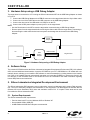
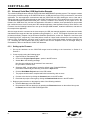
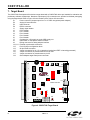
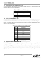
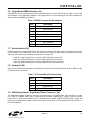
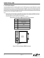
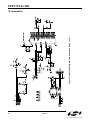
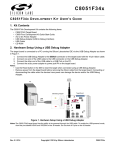
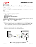
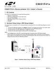
C8051F34x-DK
C8051F34 X D E V E L O P M E N T K I T U S E R ’ S G U I D E
1. Kit Contents
The C8051F34x Development Kit contains the following items:
•
•
•
•
C8051F340 Target Board
C8051Fxxx Development Kit Quick-start Guide
C8051F34x Development Kit User’s Guide (this document)
Silicon Laboratories IDE and Product Information CD-ROM. CD content includes:
• Silicon Laboratories Integrated Development Environment (IDE)
• Keil 8051 Development Tools (macro assembler, linker, evaluation ‘C’ compiler)
• Source code examples and register definition files
• Documentation
• AC to DC Power Adapter
• 6’ USB Cable
• Debug Adapter. Items include:
• USB Debug Adapter (USB to Debug Interface)
• USB Cable
2. Hardware Setup using an EC2 Serial Adapter
Connect the target board to a PC running the Silicon Laboratories IDE via the Serial Adapter as shown in Figure 1.
1.
2.
3.
4.
Connect one end of the RS232 serial cable to a serial (COM) port on the PC.
Connect the other end of the RS232 serial cable to the DB-9 connector on the Serial Adapter.
Connect the Serial Adapter to the DEBUG connector on the target board using the 10-pin ribbon cable.
Connect the AC/DC power adapter to power jack P1 on the target board.
Notes:
• Use the Reset button in the IDE to reset the target when connected using an EC2 Serial Adapter.
• Remove power from the target board and the EC2 before removing the ribbon cable from the target board.
Connecting or disconnecting the cable when the devices have power can damage the device and/or the EC2.
AC/DC
Adapter
PC
Serial
Cable
Serial
Adpater
Ribbon Cable
Target Board
Serial Port
Figure 1. Hardware Setup using an EC2 Serial Adapter
Rev. 0.1 12/05
Copyright © 2005 by Silicon Laboratories
C8051F34x-DK
C8051F34x-DK
3. Hardware Setup using a USB Debug Adapter
The target board is connected to a PC running the Silicon Laboratories IDE via the USB Debug Adapter as shown
in Figure 2.
1.
2.
3.
4.
Connect the USB Debug Adapter to the DEBUG connector on the target board with the 10-pin ribbon cable.
Connect one end of the USB cable to the USB connector on the USB Debug Adapter.
Connect the other end of the USB cable to a USB Port on the PC.
Connect the AC/DC power adapter to power jack P1 on the target board.
Notes:
• Use the Reset button in the IDE to reset the target when connected using a USB Debug Adapter.
• Remove power from the target board before removing the ribbon cable from the target board. Connecting or
disconnecting the cable when the devices have power can damage the device and/or the USB Debug
Adapter.
AC/DC
Adapter
PC
USB
Cable
USB Port
USB
Debug
Adapter
Ribbon Cable
Target Board
Figure 2. Hardware Setup using a USB Debug Adapter
4. Software Setup
The included CD-ROM contains the Silicon Laboratories Integrated Development Environment (IDE), Keil software
8051 tools and additional documentation. Insert the CD-ROM into your PC’s CD-ROM drive. An installer will automatically launch, allowing you to install the IDE software or read documentation by clicking buttons on the Installation Panel. If the installer does not automatically start when you insert the CD-ROM, run autorun.exe found in the
root directory of the CD-ROM. Refer to the readme.txt file on the CD-ROM for the latest information regarding
known IDE problems and restrictions.
5. Silicon Laboratories Integrated Development Environment
The Silicon Laboratories IDE integrates a source-code editor, source-level debugger and in-system Flash programmer. The use of third-party compilers and assemblers is also supported. This development kit includes the Keil
Software A51 macro assembler, BL51 linker and evaluation version C51 ‘C’ compiler. These tools can be used
from within the Silicon Laboratories IDE.
5.1. System Requirements
The Silicon Laboratories IDE requirements:
• Pentium-class host PC running Windows 2000 or Windows XP.
• One available COM or USB port.
• 64 MB RAM and 40 MB free HD space recommended.
2
Rev. 0.1
C8051F34x-DK
5.2. Assembler and Linker
A full-version Keil A51 macro assembler and BL51 banking linker are included with the development kit and are
installed during IDE installation. The complete assembler and linker reference manual can be found under the Help
menu in the IDE or in the “SiLabs\MCU\hlp” directory (A51.pdf).
5.3. Evaluation C51 ‘C’ Compiler
An evaluation version of the Keil C51 ‘C’ compiler is included with the development kit and is installed during IDE
installation. The evaluation version of the C51 compiler is the same as the full professional version except code
size is limited to 4 kB and the floating point library is not included. The C51 compiler reference manual can be
found under the Help menu in the IDE or in the “SiLabs\MCU\hlp” directory (C51.pdf).
5.4. Using the Keil Software 8051 Tools with the Silicon Laboratories IDE
To perform source-level debugging with the IDE, you must configure the Keil 8051 tools to generate an absolute
object file in the OMF-51 format with object extensions and debug records enabled. You may build the OMF-51
absolute object file by calling the Keil 8051 tools at the command line (e.g. batch file or make file) or by using the
project manager built into the IDE. The default configuration when using the Silicon Laboratories IDE project
manager enables object extension and debug record generation. Refer to Applications Note AN104 - Integrating
Keil 8051 Tools Into the Silicon Labs IDE in the “SiLabs\MCU\Documentation\Appnotes” directory on the CDROM for additional information on using the Keil 8051 tools with the Silicon Laboratories IDE.
To build an absolute object file using the Silicon Laboratories IDE project manager, you must first create a project. A
project consists of a set of files, IDE configuration, debug views, and a target build configuration (list of files and tool
configurations used as input to the assembler, compiler, and linker when building an output object file).
The following sections illustrate the steps necessary to manually create a project with one or more source files, build
a program and download the program to the target in preparation for debugging. (The IDE will automatically create a
single-file project using the currently open and active source file if you select Build/Make Project before a project is
defined.)
5.4.1. Creating a New Project
1. Select Project->New Project to open a new project and reset all configuration settings to default.
2. Select File->New File to open an editor window. Create your source file(s) and save the file(s) with a recognized extension, such as .c, .h, or .asm, to enable color syntax highlighting.
3. Right-click on “New Project” in the Project Window. Select Add files to project. Select files in the file
browser and click Open. Continue adding files until all project files have been added.
4. For each of the files in the Project Window that you want assembled, compiled and linked into the target
build, right-click on the file name and select Add file to build. Each file will be assembled or compiled as
appropriate (based on file extension) and linked into the build of the absolute object file.
Note: If a project contains a large number of files, the “Group” feature of the IDE can be used to organize.
Right-click on “New Project” in the Project Window. Select Add Groups to project. Add pre-defined
groups or add customized groups. Right-click on the group name and choose Add file to group. Select files
to be added. Continue adding files until all project files have been added.
Rev. 0.1
3
C8051F34x-DK
5.4.2. Building and Downloading the Program for Debugging
1. Once all source files have been added to the target build, build the project by clicking on the Build/Make
Project button in the toolbar or selecting Project->Build/Make Project from the menu.
Note: After the project has been built the first time, the Build/Make Project command will only build the
files that have been changed since the previous build. To rebuild all files and project dependencies, click
on the Rebuild All button in the toolbar or select Project->Rebuild All from the menu.
2. Before connecting to the target device, several connection options may need to be set. Open the
Connection Options window by selecting Options->Connection Options... in the IDE menu. First, select
the adapter that was included with the kit in the “Serial Adapter” section. Next, the correct “Debug Interface”
must be selected. C8051F34x family devices use the Silicon Labs 2-wire (C2) debug interface. Once all the
selections are made, click the OK button to close the window.
3. Click the Connect button in the toolbar or select Debug->Connect from the menu to connect to the device.
4. Download the project to the target by clicking the Download Code button in the toolbar.
Note: To enable automatic downloading if the program build is successful select Enable automatic connect/download after build in the Project->Target Build Configuration dialog. If errors occur during the
build process, the IDE will not attempt the download.
5. Save the project when finished with the debug session to preserve the current target build configuration,
editor settings and the location of all open debug views. To save the project, select Project->Save Project
As... from the menu. Create a new name for the project and click on Save.
4
Rev. 0.1
C8051F34x-DK
6. Example Source Code
Example source code and register definition files are provided in the “SiLabs\MCU\Examples\C8051F34x” directory
during IDE installation. These files may be used as a template for code development. Example applications include
a blinking LED example which configures the green LED on the target board to blink at a fixed rate. A Universal
Serial Bus (USB) application example is also included with the C8051F34x development kit.
6.1. Register Definition Files
Register definition files C8051F340.inc and C8051F340.h define all SFR registers and bit-addressable control/
status bits. They are installed into the “SiLabs\MCU\Examples\C8051F34x” directory during IDE installation. The
register and bit names are identical to those used in the C8051F34x datasheet. Both register definition files are
also installed in the default search path used by the Keil Software 8051 tools. Therefore, when using the Keil 8051
tools included with the development kit (A51, C51), it is not necessary to copy a register definition file to each
project’s file directory.
6.2. Blinking LED Example
The example source files blink.asm and blinky.c show examples of several basic C8051F34x functions. These
include; disabling the watchdog timer (WDT), configuring the Port I/O crossbar, configuring a timer for an interrupt
routine, initializing the system clock, and configuring a GPIO port. When compiled/assembled and linked this program flashes the green LED on the C8051F340 target board about five times a second using the interrupt handler
with a timer.
Rev. 0.1
5
C8051F34x-DK
6.3. Universal Serial Bus (USB) Application Example
The included USB application example requires Windows 98SE/2000/XP operating system. This example consists
of three parts: firmware running on the C8051F340 device, a USB device driver running on the host PC, and a host
application. The host application communicates with the C8051F340 via USB, allowing the user to view and to
change the state of several I/O peripherals on the C8051F340 target board. The example files can be found in the
“SiLabs\MCU\Examples\C8051F34x\C\USB_INT” directory. Located in this directory is the project file for the
firmware, the USB driver files, and the host application executable. In addition, three subdirectories are provided
that contain the source code for each part of the example application; Host Application Source, Driver Source, and
Firmware. Use the following instructions to set up the example USB firmware, install the USB driver, and then run
the example host application.
After the target board is connected to the host computer via USB, the example application enumerates and sends
data between the target and the host application using Endpoint 0, 1, and 2. The Endpoint 0 packets are control
packets as defined in Chapter 9 of the Universal Serial Bus Specification, version 2.0. Endpoints 1 and 2 are used
for data IN and OUT, respectively. These data packets consist of 8 bytes used to denote the current status of the
buttons, LEDs, Potentiometer, and logic levels of various port pins on the target board. Accessing the USB core
(i.e., accessing the USB registers and moving data to and from the Endpoint FIFOs on the target board) is
documented in Silicon Laboratories’ C8051F34x datasheet.
6.3.1. Setting-up the Firmware
1. Set up the hardware on the C8051F340 target board according to the instructions in Section 2 or
Section 3.
2. Create a project using the following steps.
a. Open the Silicon Laboratories IDE.
b. Click on the Project->Open Project... option in the IDE menus.
c.
Answer No to the following message:
Not all project windows can be restored if not connected.
Do you want to connect now?
d. Select the USB__Int.wsp project, located by default in the SiLabs\MCU\Examples\C8051F34x\C\USB_INT directory, and click the Open button.
e. Click the Build/Make Project button in the IDE toolbar.
f.
The project should now be compiled and linked successfully, with no errors.
g. Connect to the device by clicking the Connect button on the IDE toolbar.
h. Download the project to the target by clicking the Download Code button in the IDE toolbar.
3. Begin program execution on the target by either of the following methods:
a. Click the Go button in the IDE toolbar.
b. Disconnect the IDE from the device by pressing the Disconnect button on the toolbar. Next, press
the Reset button on the C8051F340 target board.
6
Rev. 0.1
C8051F34x-DK
6.3.2. Installing the USB Driver
1. Connect the USB cable between the host computer and the C8051F340 target board, as shown in
Figure 3. See Figure 4 on page 8 for the location of the USB connector.
2. At this point, Windows should notify you it has found new hardware and prompt you with a Found New
Hardware wizard. Press the Next button.
3. Select Search for a suitable driver for my device (recommended) and press the Next button.
4. Select Specify a location under “Optional search locations:” and press the Next button.
5. Press the Browse button to locate the SiLabsInt.inf driver installation file, located by default in the
“SiLabs\MCU\Examples\C8051F34x\C\USB_INT” directory. Once this file is selected press the OK button.
6. Verify that the correct path and filename are shown and press the Next button.
7. Press the Finish button.
6.3.3. Running the Host Application
1. Once firmware has been downloaded to the target board and the driver has been installed successfully, run
the USBTest.exe example application located by default in the “SiLabs\MCU\Examples\C8051F34x\C\USB_INT” directory.
2. The USBTest application will display the status of the potentiometer, the temperature sensor, the two
switches, and the lower four bits of Port 0.
3. The application also includes check boxes for turning on the two LEDs and changing the logic levels on the
lower four bits of Port 1.
4. If any of the application functions do not operate correctly, verify shorting blocks are installed at the following positions: J3[1-2] (P2.0 Switch), J3[3-4] (P2.1 Switch), J3[5-6] (P2.2 LED), J3[7-8] (P2.3 LED), and J16
and J17 (P2.5 Potentiometer).
5. See Figure 4 on page 8 for the location of headers, LEDs, switches, and potentiometer.
Note: The C8051F340 target board has the ability to be powered through the USB cable. To enable the USB powered mode,
short the pins labeled VBUS and VREGIN on the J8 header. Do not short all 3 pins on the J8 header.
AC/DC
Adapter
Serial or USB
Cable
Debug
Adapter
Serial or USB Port
RS232
PC
Debug
Ribbon
Cable
USB Port
USB
Connector
C8051F34x
Target
Board
Figure 3. USB Application Hardware Setup
Rev. 0.1
7
C8051F34x-DK
7. Target Board
The C8051F34x Development Kit includes a target board with a C8051F340 device pre-installed for evaluation and
preliminary software development. Numerous input/output (I/O) connections are provided to facilitate prototyping
using the target board. Refer to Figure 4 for the locations of the various I/O connectors.
Power connector (accepts input from 7 to 15 VDC unregulated power adapter)
Analog I/O terminal block
USB connector
RS232 connector
Supply signal header
Port 0 header
Port 1 header
Port 2 header
Port 3 header
Port 4 header
Connects the +3V supply net to the VDD supply net
USB Power or VDD power selection header
Debug connector for debug adapter interface
External crystal enable connectors
Port I/O jumper configuration block
96-pin female connector
Jumper connection for pin 1.5 to capacitors (used when VREF is internally generated)
Jumper connection for potentiometer source to VDD
Jumper connection for potentiometer to pin 2.5
Serial Adapter target board power connector
R10
J6
P2.1
P2.0 RESET
SW3
SW2
J16
J13
J17
P1
P2
P3
P4
J1
J2
J3
J4
J5
J6
J7
J8
J9
J10, J11
J12
J13
J15
J16
J17
J19
SW1
P4
RS232
D4
J1
D3
SILICON LABORATORIES
J5
J8
J12
P3
C8051F340-TB
340
J15
J11
J3
J7 J10
J19
J2
D2
P2
PWR
Figure 4. C8051F340 Target Board
Rev. 0.1
DEBUG
U1
J4
8
USB
J9
P1
C8051F34x-DK
7.1. System Clock Sources
The C8051F340 device installed on the target board features a calibrated programmable internal oscillator which is
enabled as the system clock source on reset. After reset, the internal oscillator operates at a frequency of 1.5 MHz
(±1.5%) by default but may be configured by software to operate at other frequencies. Therefore, in many applications an external oscillator is not required. However, if you wish to operate the C8051F340 device at a frequency not
available with the internal oscillator, an external crystal may be used. Refer to the C8051F34x datasheet for more
information on configuring the system clock source.
The target board is designed to facilitate the installation of an external crystal. Remove shorting blocks at headers
J10 and J11 and install the crystal at the pads marked Y1. Install a 10 MΩ resistor at R1 and install capacitors at C6
and C7 using values appropriate for the crystal you select. Refer to the C8051F34x datasheet for more information
on the use of external oscillators.
7.2. Switches and LEDs
Three switches are provided on the target board. Switch RESET is connected to the RESET pin of the C8051F340.
Pressing RESET puts the device into its hardware-reset state. Switches P2.0 and P2.1 are connected to the
C8051F340’s general purpose I/O (GPIO) pins through headers. Pressing P2.0 or P2.1 generates a logic low signal on the port pin. Remove the shorting blocks from the J12 header to disconnect Switch P2.0 and Switch P2.1
from the port pins. The port pin signals are also routed to pins on the J1 I/O connector. See Table 1 for the port pins
and headers corresponding to each switch.
Three LEDs are also provided on the target board. The red LED labeled PWR LED is used to indicate a power connection to the target board. The green surface-mount LEDs labeled with port pin names areconnected to the
C8051F340’s GPIO pins through headers. Remove the shorting blocks from the header to disconnect the LEDs
from the port pin. The port pin signals are also routed to pins on the J1 I/O connector. See Table 1 for the port pins
and headers corresponding to each LED.
Also included on the C8051F340 target board is a 10 KΩ Thumb-wheel Rotary Potentiometer, part number R10. The
Potentiometer is connected to the C8051F340’s P2.5 pin through the J17 header. Remove the shorting block from
the header to disconnect the Potentiometer from the port pin. The port pin signal is also routed to a pin on the J1 I/O
connector. See Table 1 for the port pin and header corresponding to the Potentiometer.
Table 1. Target Board I/O Descriptions
Description
I/O
Header
SW1
Reset
none
SW2
P2.0
J12[1-2]
SW3
P2.1
J12[3-4]
Green LED
P2.2
J12[5-6]
Green LED
P2.3
J12[7-8]
Red LED
PWR
none
Potentiometer
P2.5
J17
Rev. 0.1
9
C8051F34x-DK
7.3. Universal Serial Bus (USB) Interface (J14)
A Universal Serial Bus (USB) connector (P3) is provided to facilitate connections to the USB interface on the
C8051F340. Table 2 shows the J14 pin definitions.
Table 2. USB Connector Pin Descriptions
Pin #
Description
1
VBUS
2
D-
3
D+
4
GND (Ground)
7.4. PORT I/O Connectors (J2 - J6)
In addition to all port I/O signals being routed to the 96-pin expansion connector, each of the five parallel ports of
the C8051F340 has its own 10-pin header connector. Each connector provides a pin for the corresponding port
pins 0-7, +3.3 VDC and digital ground. Table 3 defines the pins for the port connectors. The same pin-out order is
used for all of the port connectors.
Table 3. J12–J19 Port Connector Pin Descriptions
Pin #
Description
1
Pn.0
2
Pn.1
3
Pn.2
4
Pn.3
5
Pn.4
6
Pn.5
7
Pn.6
8
Pn.7
9
+3 VD (+3.3 VDC)
10
GND (Ground)
7.5. USB Self-powered Configuration (J8)
The C8051F340 target board can be configured as a self-powered USB device to take power from the USB cable
instead of the AC/DC adapter connected at P1. To configure the target boards as a self-powered USB device, short
the VREGIN and VBUS pins on the J8 header
Note: When the C8051F340 target board is self-powered from the USB, the Serial Adapter is not powered from the
target board. The Serial Adapter must be powered directly by connecting the AC/DC adapter to the Serial Adapters’ DC power jack. Also, the RS232 Serial Interface (P4) cannot be used when powering the target board from the
USB.
10
Rev. 0.1
C8051F34x-DK
7.6. Target Board DEBUG Interface (J9)
The DEBUG connector (J9) provides access to the DEBUG (C2) pins of the C8051F340. It is used to connect the
Serial Adapter or the USB Debug Adapter to the target board for in-circuit debugging and Flash programming.
Table 4 shows the DEBUG pin definitions.
Table 4. DEBUG Connector Pin Descriptions
Pin #
Description
1
+3 VD (+3.3 VDC)
2, 3, 9
GND (Ground)
4
C2D
5
/RST (Reset)
6
P3.0
7
C2CK
8
Not Connected
10
USB Power
7.7. Serial Interface (P4)
A RS232 transceiver circuit and DB-9 (P4) connector are provided on the target board to facilitate serial connections to UART0 of the C8051F340. The TX, RX, RTS and CTS signals of UART0 may be connected to the DB-9
connector and transceiver by installing shorting blocks on header J12.
J12[9-10] - Install shorting block to connect UART0 TX (P0.4) to transceiver.
J12[11-12]- Install shorting block to connect UART0 RX (P0.5) to transceiver.
J12[13-14]- Install shorting block to connect UART0 RTS (P2.6) to transceiver.
J12[15-16]- Install shorting block to connect UART0 CTS (P2.7) to transceiver.
7.8. Analog I/O (P2)
Several of the C8051F340 target device’s port pins are connected to the P2 terminal block. Refer to Table 5 for the
P2 terminal block connections.
Table 5. J6 Terminal Block Pin Descriptions
Pin #
Description
1
P1.1 / AIN1.1
2
P1.2 / AIN1.2
3
GND (Ground)
4
P1.5 / VREF (Voltage Reference)
7.9. USB Debug Adapter Target Board Power Connector (J19)
The USB Debug Adapter includes a connection to provide power to the target board. This connection is routed
from J9[10] to J19[SER_PWR]. Place a shorting block at header J19[REG_IN-P1_PWR] to power the board
directly from an AC/DC power adapter. Place a shorting block at header J19[REG_IN-SER_PWR] to power the
board from the USB Debug Adapter. Please note that the second option is not supported with either the EC1 or
EC2 Serial Adapters.
Rev. 0.1
11
C8051F34x-DK
8. EC2 Serial Adapter
The Serial Adapter provides the interface between the PC’s RS232 serial port and the C8051F34x’s in-system
debug/programming circuitry. The Serial Adapter connects to the C8051F340 C2 debug interface on the target
board using the 10-pin connector on the Serial Adapter labeled “DEBUG”, see Figure 5. (The Serial Adapter supports both Silicon Laboratories JTAG and C2 debug interfaces.). All Serial Adapters may be powered from the target board, but the EC1 and EC2 Serial Adapter units cannot provide power to the target board. Table 6 shows the
pin definitions for the Serial Adapter’s DEBUG connector.
Notes:
• When powering the Serial Adapter via the DEBUG connector, the input voltage to the DEBUG connector’s
power pin must be 3.0 to 3.6 VDC. Otherwise, the Serial Adapter must be powered directly by connecting
the AC/DC adapter to the Serial Adapter’s DC power jack.
• The Serial Adapter requires a target system clock of 32 KHz or greater.
Table 6. EC2 Serial Adapter DEBUG Connector Pin Descriptions
Description
1
3.0 to 3.6 VDC Input
2,3,9
GND (Ground)
4
TCK (C2D)
5
TMS
6
TDO
7
TDI (C2CK)
8,10
Not Connected
DEBUG
Serial
Adapter
RS232
Pwr
Run/
Stop
Pin #
Pin 1
Pin 2
Figure 5. EC2 Serial Adapter DEBUG Connector
12
Rev. 0.1
C8051F34x-DK
9. USB Debug Adapter
The USB Debug Adapter provides the interface between the PC’s USB port and the C8051F34x’s in-system
debug/programming circuitry. The attached 10-pin DEBUG ribbon cable connects the adapter to the target board
and the target device’s debug interface signals. (The USB Debug Adapter supports both Silicon Laboratories JTAG
and C2 debug interfaces.) Power is provided to the adapter from the USB connection to the PC. The USB Debug
Adapter is capable of providing power to a circuit board via pin 10 of the DEBUG connector. See Section 7.9. for
instructions on powering the C8051F340 target board from this source. Table 7 shows the pin definitions for the
DEBUG ribbon cable connector.
Notes:
• The USB Debug Adapter requires a target system clock of 32 KHz or greater.
• With the default settings, the USB Debug Adapter can supply up to 100 mA to a target system.
Table 7. USB Debug Adapter DEBUG Connector Pin Descriptions
Pin #
Description
1,8
Not Connected
2,3,9
GND (Ground)
4
TCK (C2D)
5
TMS
6
TDO
7
TDI (C2CK)
10
USB Power
Figure 6. USB Debug Adapter
Rev. 0.1
13
Figure 7. C8051F340 Target Board Schematic (Page 1 of 2)
C8051F34x-DK
10. Schematics
14
Rev. 0.1
Figure 8. C8051F340 Target Board Schematic (Page 2 of 2)
C8051F34x-DK
Rev. 0.1
15
C8051F34x-DK
CONTACT INFORMATION
Silicon Laboratories Inc.
4635 Boston Lane
Austin, TX 78735
Tel: 1+(512) 416-8500
Fax: 1+(512) 416-9669
Toll Free: 1+(877) 444-3032
Email: [email protected]
Internet: www.silabs.com
The information in this document is believed to be accurate in all respects at the time of publication but is subject to change without notice.
Silicon Laboratories assumes no responsibility for errors and omissions, and disclaims responsibility for any consequences resulting from
the use of information included herein. Additionally, Silicon Laboratories assumes no responsibility for the functioning of undescribed features
or parameters. Silicon Laboratories reserves the right to make changes without further notice. Silicon Laboratories makes no warranty, representation or guarantee regarding the suitability of its products for any particular purpose, nor does Silicon Laboratories assume any liability
arising out of the application or use of any product or circuit, and specifically disclaims any and all liability, including without limitation consequential or incidental damages. Silicon Laboratories products are not designed, intended, or authorized for use in applications intended to
support or sustain life, or for any other application in which the failure of the Silicon Laboratories product could create a situation where personal injury or death may occur. Should Buyer purchase or use Silicon Laboratories products for any such unintended or unauthorized application, Buyer shall indemnify and hold Silicon Laboratories harmless against all claims and damages.
Silicon Laboratories and Silicon Labs are trademarks of Silicon Laboratories Inc.
Other products or brandnames mentioned herein are trademarks or registered trademarks of their respective holders.
16
Rev. 0.1