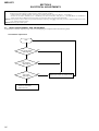
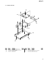
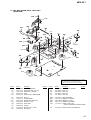
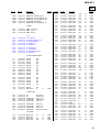
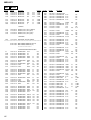
1
MDS-NT1
SERVICE MANUAL
AEP Model
UK Model
E Model
Ver 1.0 2002.02
US and foreign patents licensed from Dolby
Laboratories Licensing Corporation.
• OpenMG, “MagicGate”, “MagicGate Memory
Stick”, “Memory Stick”, VAIO, MusicClip, Net MD,
and their logos are trademarks of Sony Corporation.
• “WALKMAN ” is a trademark of Sony Corporation.
• Microsoft, Windows, Windows NT and Windows Media are trademarks or registered trademarks of
Microsoft Corporation in the United States and/or
other countries.
• IBM and PC/AT are registered trademarks of International Business Machines Corporation.
• Macintosh is a trademark of Apple Computer,Inc.in
the United States and/or other countries.
• MMX and Pentium are trademarks or registered trademarks of Intel Corporation.
• All other trademarks are trademarks of their respective owners.TM and ® marks are omitted in this manual.
Model Name Using Similar Mechanism
NEW
MD Mechanism Type
MDM-7S2B
Optical Pick-up Name
KMS-262E
SPECIFICATIONS
System
Disc
Laser
Revolutions (CLV)
Error correction
Sampling frequency
Coding
Modulation system
Number of channels
Frequency response
Signal-to-noise ratio
Wow and flutter
MiniDisc digital audio system
MiniDisc
Semiconductor laser (λ = 780 nm)
Emission duration: continuous
800 rpm to 1800 rpm
Advanced Cross Interleave Reed
Solomon Code (ACIRC)
44.1 kHz
Adaptive Transform Acoustic
Coding (ATRAC)/ATRAC 3
EFM (Eight-to-Fourteen
Modulation)
2 stereo channels
5 to 20,000 Hz ±0.8 dB
Over 96 dB during playback
Below measurable limit
Outputs
LINE (ANALOG) OUT
PHONES
Jack type: stereo-mini
Rated output: 1 Vrms (at
50 kilohms)
Load impedance: Over 10 kilohms
Jack type: stereo-mini
Rated output: 5 mW
Load impedance: 32 ohms
Supplied accessories
• AC power adaptor (1)
• USB cable (1)
• Audio connecting cord
(stereo mini-plug ×1 y stereo mini-plug ×1)
(1)
• OpenMG Jukebox CD-ROM (1)
• Operating instructions for OpenMG Jukebox
(1)
• Do not connect the supplied AC power adaptor to a
switched AC outlet (e.g., on an amplifier).
• Use only the supplied AC power adaptor. Do not
use any other AC power adaptor.
Polarity of the plug
General
USB port
series B, self powerd, full speed
Where purchased
Power requirements*
Design and specifications are subject to change
without notice.
Europe and other countries 220 – 230 V AC, 50/60 Hz
* Using an AC power adaptor (supplied)
Power consumption
Dimensions (approx.)
Mass (approx.)
6W
152 × 52 × 249 mm (w/h/d) incl.
projecting parts and controls
1.0 kg
MINIDISC DECK
9-873-614-01
Sony Corporation
2002B0500-1
C 2002.02
Home Audio Company
Published by Sony Engineering Corporation
MDS-NT1
SELF-DIAGNOSIS FUNCTION
The self-diagnosis function consists of error codes for customers which are displayed automatically when errors occur, and error codes
which show the error history in the test mode during servicing. For details on how to view error codes for the customer, refer to the
following box in the instruction manual. For details on how to check error codes during servicing, refer to the following “Procedure for
using the Self-Diagnosis Function (Error History Display Mode)”.
The deck’s self-diagnosis function automatically checks the condition of the MD deck when an error
occurs, then indicates the nature of the error through the two indicators. If the indicators light up or flash,
find them in the following table and perform the indicated countermeasure. Should the problem persist,
consult your nearest Sony dealer.
Playback
Indicator
(green)
Recording
Indicator
(red)
Cause/Remedy
Flashes
The recording was not made properly. (C13/Rec Error)
, Set the deck in a stable surface, and repeat the recording procedure.
Flashes
The inserted MD is dirty (with smudges, fingerprints, etc.), scratched, or
substandard in quality. (C13/Rec Error)
, Replace the disc and repeat the recording procedure.
Flashes
The deck could not read the TOC on the MD properly. (C13/Read Error)
, Take out the MD and insert it again.
Lights up
The deck could not read the TOC on the MD properly. (C14/Toc Error)
, Insert another disc.
, If possible, erase all the tracks on the MD.
Lights up
Lights up
There is an error in the internal data that the deck needs in order to operate.
(E0001/MEMORY NG)
, Consult your nearest Sony dealer.
Flashes
Flashes
There is a problem with the optical pickup. (E0101/LASER NG)
, Consult your nearest Sony dealer.
Both indicators flash alternately
An MD loading problem has occurred. (E0201/LOADING NG)
, Consult your nearest Sony dealer.
PROCEDURE FOR USING THE SELF-DIAGNOSIS FUNCTION (ERROR HISTORY DISPLAY MODE)
Note 1:The test mode and recording of this set are controlled by a personal computer, thus requiring the set to be connected to the PC.
Prepare the personal computer in which necessary software is already installed.
• Attached software “OpenMG Jukebox” (necessary for recording (check in, check out)) (Part No. : 4-237-880-01)
• Software for test mode “TestMode_S.exe” (“TestMode_S.exe” and essential files “data_files.csv”, “Net MDUSB.dil” are distributed together with the Service Manual. For the test mode, copy these three files in the same folder beforehand)
Note 2:In the operation in the test mode, the operational description requiring “click [xxx]” means that you have to click the button on the screen.
(“xxx” indicates the button name)
Note 3:Perform the self-diagnosis function in the “error history display mode” in the test mode. The following describes the least required procedure.
Be careful not to enter other modes by mistake. If you set other modes accidentally, click the [MENU/NO] to exit the mode.
1. Press the [B/> ] button and [x/Z] button until the NetMD indicator turns off (for more than 3 seconds). (During this step, the USB
cable must be disconnected)
2. Connect the set to the PC with the attached USB cable.
3. Start up the software for test mode.
4. Click the [TEST MODE].
5. Click the [JOG UP] or [JOG DOWN] and when “[Service]” is displayed, click the [ENTER/YES].
6. Click the [JOG UP] or [JOG DOWN] to display “Err Display”.
7. Click the [ENTER/YES] to sets the error history mode and displays “op rec tm”.
8. Select the contents to be displayed or executed using the [JOG UP] or [JOG DOWN].
9. Click the [PUSH] to display or execute the contents selected.
10. Click the [PUSH] another time returns to step 8.
11. Click the [MENU/NO] to display “Err Display” and release the error history mode.
12. To release the test mode, quit the software for test mode after the [REPEAT] clicked.
Note: When retrying this operation, start from step1.
2
MDS-NT1
ITEMS OF ERROR HISTORY MODE ITEMS AND CONTENTS
Selecting the Test Mode
Display
Details of History
op rec tm
Cumulative recording time is displayed.
When cumulative recording time is over 1 minute, the hour and minute are displayed as they are.
When it is under 1 minute, “Under 1 min” is displayed.
The displayed time shows how long the laser is in high power state.
It is about one fourth the actual recording time.
op play tm
Cumulative playing time is displayed.
When cumulative playing time is over 1 minute, the hour and minute are displayed as they are.
When it is under 1 minute, “Under 1 min” is displayed.
spdl rp tm
Cumulative spindle motor running time is displayed.
When cumulative spindle motor run time is over 1 minute, the hour and minute are displayed as they are.
When it is under 1 minute, “Under 1 min” is displayed.
retry err
Displays the total number of retries during recording and number of retry errors during play.
Displayed as “rss pss”.
“r” indicates the retries during recording while “p” indicates the retry errors during play.
The number of retries and retry errors are displayed in hexadecimal digits from 00 to FF.
total err
Displays the total number of errors.
Displayed as “total ss”.
The number of errors is displayed in hexadecimal digits from 00 to FF.
err history
Displays the 10 latest errors.
Displayed as “0s ErrCd@@”.
s indicates the history number. The smaller the number, the more recent is the error. (00 is the latest).
@@ indicates the error code.
Refer to the following table for the details. The error history can be switched by clicking the [JOG UP] or
[JOG DOWN].
retry adrs
Displays the past five retry addresses.
Displays “ss ADRS ssss”, ss is the history number, ssss is the cluster with the retry error.
Select the error history number using the [JOG UP] or [JOG DOWN].
er refresh
Mode to clear the error history and retry address history.
[Operating method]
1) Click the [JOG UP] or [JOG DOWN] when “er refresh” is displayed.
2) The display will change to “er refresh?”, and then click the [ENTER/YES].
The operation is over if “Complete!” is displayed.
After this mode was executed, check the following:
• The data have been cleared.
• Perform the recording and playing to check that the mechanism operates normally.
tm refresh
Mode to clear the “op rec tm” and “op play tm” histories.
These histories serve as approximate indications of when to replace the optical pick-up. If the optical pick-up
has been replaced, perform this operation and clear the history.
[Operating method]
1) Click the [JOG UP] or [JOG DOWN] when “tm refresh” is displayed.
2) The display will change to “tm refresh?”, and then click the [ENTER/YES].
The operation is over if “Complete!” is displayed.
After this mode was executed, check the following:
• The data have been cleared.
• Perform the recording and playing to check that the mechanism operates normally.
op change
Mode to clear cumulative time of “op rec tm” and “op play tm”.
These historical data are used to determine the timing when the optical pick-up is to be replaced. When the
optical pick-up was replaced, perform this operation to clear historical data.
[Operating method]
1) Click the [JOG UP] or [JOG DOWN] when “op change” is displayed.
2) The display will change to “op chang?”, and then click the [ENTER/YES].
The operation is over if “Complete!” is displayed.
spdl change
Mode to clear cumulative time of “spdl rp tm”.
This historical data is used to determine the timing when the spindle motor is to be replaced. When the spindle
motor was replaced, perform this operation to clear historical data.
[Operating method]
1) Click the [JOG UP] or [JOG DOWN] when “spdl change” is displayed.
2) The display will change to “spdl chang?”, and then click the [ENTER/YES].
The operation is over if “Complete!” is displayed.
3
MDS-NT1
Table of Error Codes
Error Code
4
Details of Error
10
Loading failed
12
Loading switch combination is illegal
20
Head of PTOC could not be read within the
specified time
21
Head of PTOC could be read but its content is
erroneous
22
Access to UTOC could not be made within the
specified time
23
UTOC could be not read within the specified
3time
24
Content of UTOC is erroneous
30
Playing could not start
31
Content of sector is erroneous
40
Cause of retry occurred during normal recording
41
D-RAM overflowed and retry was executed
42
Retry was executed during the writing to TOC
43
S.F editing was interrupted by retry
50
Address could not be read except in access
processing
51
Focusing failed and it is out of control
60
Unlock retry
MDS-NT1
TABLE OF CONTENTS
SELF-DIAGNOSIS FUNCTION ........................... 2
1.
SERVICING NOTES ............................................... 7
2.
GENERAL ................................................................... 12
3.
DISASSEMBLY
3-1.
3-2.
3-3.
3-4.
3-5.
3-6.
3-7.
3-8.
3-9.
3-10.
3-11.
Disassembly Flow ...........................................................
Case (Upper) ...................................................................
Main Board ......................................................................
MD Mechanism Deck (MDM-7S2B) .............................
Front Panel Section .........................................................
BD Board, Over Write Head (HR901) ...........................
Holder Assy .....................................................................
Loading Motor Assy (M103) ..........................................
Sled Motor Assy (M102) ................................................
Optical Pick-Up (KMS-262E) ........................................
Spindle Motor Assy (M101) ...........................................
4.
TEST MODE .............................................................. 20
5.
ELECTRICAL ADJUSTMENTS ........................ 24
6.
DIAGRAMS
6-1. Block Diagram – SERVO Section – ...............................
6-2. Block Diagram – MAIN Section – .................................
6-3. Note for Printed Wiring Boards and
Schematic Diagrams .......................................................
6-4. Printed Wiring Board – BD Board – ..............................
6-5. Schematic Diagram – BD Board (1/2) – ........................
6-6. Schematic Diagram – BD Board (2/2) – ........................
6-7. Printed Wiring Board
– MAIN Board (Component Side) – ..............................
6-8. Printed Wiring Board
– MAIN Board (Conductor Side) – ................................
6-9. Schematic Diagram – MAIN Board (1/2) – ...................
6-10. Schematic Diagram – MAIN Board (2/2) – ...................
6-11. Printed Wiring Board – Panel Board – ...........................
6-12. Schematic Diagram – Panel Board – ..............................
6-13. IC Pin Function Description ...........................................
13
14
15
15
16
16
17
17
18
18
19
36
37
38
39
40
41
42
43
44
45
46
47
51
7.
EXPLODED VIEWS
7-1.
7-2.
7-3.
7-4.
7-5.
Case Section ....................................................................
Front Panel Section .........................................................
Case (B) Section ..............................................................
MD Mechanism Deck Section-1 (MDX-7S2B) .............
MD Mechanism Deck Section-2 (MDX-7S2B) .............
8.
ELECTRICAL PARTS LIST ............................... 64
59
60
61
62
63
5
MDS-NT1
The laser component in this product
is capable of emitting radiation
exceeding the limit for Class 1.
This appliance is classified as a CLASS 1
LASER product. The CLASS 1 LASER
PRODUCT MARKING is located on the
bottom exterior.
CAUTION
Use of controls or adjustments or performance of procedures
other than those specified herein may result in hazardous radiation exposure.
Notes on chip component replacement
• Never reuse a disconnected chip component.
• Notice that the minus side of a tantalum capacitor may be damaged by heat.
Flexible Circuit Board Repairing
• Keep the temperature of the soldering iron around 270 ˚C during repairing.
• Do not touch the soldering iron on the same conductor of the
circuit board (within 3 times).
• Be careful not to apply force on the conductor when soldering
or unsoldering.
SAFETY-RELATED COMPONENT WARNING!!
COMPONENTS IDENTIFIED BY MARK 0 OR DOTTED LINE
WITH MARK 0 ON THE SCHEMATIC DIAGRAMS AND IN
THE PARTS LIST ARE CRITICAL TO SAFE OPERATION.
REPLACE THESE COMPONENTS WITH SONY PARTS WHOSE
PART NUMBERS APPEAR AS SHOWN IN THIS MANUAL
OR IN SUPPLEMENTS PUBLISHED BY SONY.
6
MDS-NT1
SECTION 1
SERVICING NOTES
NOTES ON HANDLING THE OPTICAL PICK-UP
BLOCK OR BASE UNIT
The laser diode in the optical pick-up block may suffer electrostatic break-down because of the potential difference generated
by the charged electrostatic load, etc. on clothing and the human
body.
During repair, pay attention to electrostatic break-down and also
use the procedure in the printed matter which is included in the
repair parts.
The flexible board is easily damaged and should be handled with
care.
NOTES ON LASER DIODE EMISSION CHECK
Never look into the laser diode emission from right above when
checking it for adjustment. It is feared that you will lose your sight.
CLEANING OBJECTIVE LENS OF OPTICAL PICK-UP
• In cleaning the objective lens of optical pick-up, be sure the
following below.
NOTES ON REPLACING BD BOARD OR MD MECHANISM
DECK
In replacing the BD board or MD mechanism deck, perform the
work through the steps provided below:
1. Remove the IC195 from the BD board to be replaced.
2. Remove the IC195 from new BD board.
3. Mount the IC195 on new BD board, which was removed from
the BD board to be replaced.
4. Install new BD board in the set.
Note: The IC195 cannot be replaced with a new part. If IC195 is faulty,
replace the entire BD board.
– BD BOARD (Conductor Side) –
IC195
1. In cleaning the lens, do not apply an excessive force.
As the optical pick-up is vulnerable, application of excessive
force could damage the lens holder.
2. In cleaning, do not use a cleaner other than exclusive cleaning
liquid (KK-91 or isopropyl alcohol).
3. Wipe the objective lens spirally from center toward outside.
(See Figure A)
(Figure A)
OPERATION CHECK IN NORMAL MODE
The set alone is capable of performing the play function only. In
checking the recording and other functions, connect the set to the
PC with a USB cable and perform the operation on the application
software “OpenMG Jukebox” attached.
4. Eject the disc, if loaded.
5. Disconnect the power cord from the socket to shut off the power
supply.
7
MDS-NT1
JIG FOR CHECKING BD BOARD WAVEFORM
The special jig (J-2501-149-A) is useful for checking the waveform of the BD board. The names of terminals and the checking items to be
performed are shown as follows.
GND
I+3V
Iop
TE
VC
RF
FE
: Ground
: For measuring Iop (Check the deterioration of the optical pick-up laser)
: For measuring Iop (Check the deterioration of the optical pick-up laser)
: Tracking error signal (Traverse adjustment)
: Reference level for checking the signal
: RF signal (Check jitter)
: Focus error signal
CN105
Iop
TE
I+3V
GND
FE
VC
RF
1
I+3V
Iop
GND
TE
FE
VC
RF
I+3V
Iop
GND
TE
FE
VC
RF
7
8
for
MDM-7S2B
MDS-NT1
Note 1:The test mode and recording of this set are controlled by a personal computer, thus requiring the set to be connected to the PC.
Prepare the personal computer in which necessary software is already installed.
• Attached software “OpenMG Jukebox” (necessary for recording (check in, check out)) (Part No. : 4-237-880-01)
• Software for test mode “TestMode_S.exe” (“TestMode_S.exe” and essential files “data_files.csv”, “Net MDUSB.dil” are distributed together with the Service Manual. For the test mode, copy these three files in the same folder beforehand)
Note 2:In the operation in the test mode, the operational description requiring “click [xxx]” means that you have to click the button on the screen.
(“xxx” indicates the button name)
Iop DATA RECORDING AND DISPLAY WHEN OPTICAL PICK-UP AND NON-VOLATILE MEMORY (IC195 OF
BD BOARD) ARE REPLACED
The Iop value labeled on the optical pick-up can be recorded in the non-volatile memory. By recording the value, it will eliminate the need
to look at the value on the optical pick-up label. When replacing the optical pick-up or non-volatile memory (IC195 of BD board), record
the Iop value on the optical pick-up according to the following procedure.
Record Procedure:
1. Press the [ B/> ] button and [x/Z] button until the NetMD indicator turns off (for more than 3 seconds). (During this step, the USB
cable must be disconnected)
2. Connect the set to the PC with the attached USB cable.
3. Start up the software for test mode.
4. Click the [TEST MODE].
5. Click the [JOG UP] or [JOG DOWN] to display “[Service]”, and click the [ENTER/YES].
6. Click the [JOG UP] or [JOG DOWN] to display “Iop Write” (C05), and click the [ENTER/YES].
7. The display becomes “Ref=@@@.@” (@ is an arbitrary number) and the numbers which can be changed will blink.
8. Input the Iop value written on the optical pick-up label.
To select the number : Click the [JOG UP] or [JOG DOWN].
To select the digit : Click the [PUSH].
9. When the [ENTER/YES] is clicked, the display becomes “Measu=@@@.@” (@ is an arbitrary number).
10. As the adjustment results are recorded for the 6 value. Leave it as it is and click the [PUSH].
11. “Complete!” will be displayed momentarily. The value will be recorded in the non-volatile memory and the display will become “Iop
Write (C05)”.
12. Quit the software for test mode after the [REPEAT] clicked.
Note: When retrying this operation start from step1.
Display Procedure:
1. Press the [B/> ] button and [x/Z] button until the NetMD indicator turns off (for more than 3 seconds). (During this step, the USB
cable must be disconnected)
2. Connect the set to the PC with the attached USB cable.
3. Start up the software for test mode.
4. Click the [TEST MODE].
5. Click the [JOG UP] or [JOG DOWN] to display “[Service]”, and click the [ENTER/YES].
6. Click the [JOG UP] or [JOG DOWN] to display “Iop Read” (C26), and click the [ENTER/YES].
7. “@@.@/##.#” is displayed and the recorded contents are displayed.
@@.@ : indicates the Iop value on the optical pick-up label.
##.# : indicates the Iop value after adjustment
8. To end, click the [PUSH] and [MENU/NO] to display “Iop Read” (C26).
9. Quit the software for test mode after the [REPEAT] clicked.
Note: When retrying this operation start from step1.
9
MDS-NT1
CHECKS PRIOR TO PARTS REPLACEMENT AND ADJUSTMENTS IN MD
Before performing repairs, perform the following checks to determine the faulty locations up to a certain extent.
Details of the procedures are described in “5. Electrical Adjustments”.
Note: This set uses optical pick-up KMS-262E in the production, but for the repair, only the KMS-262A is supplied. As a result, two types of optical
pick-ups are used for this set, and the specified values for the check and adjustment of the laser power vary depending on the type.Details of the
identify of KMS-262A/KMS-262E are described in “5-4. How to Identify Optical Pick-up KMS-262A/KMS-262E”. (See Page 26)
Criteria for Determination
(Unsatisfactory if specified value is not satisfied)
Laser power check
(5-7-2 : See page 28)
Measure if unsatisfactory:
• 0.90 mW power
Specified value : 0.84 to 0.92 mW (KMS-262A)
0.90 to 0.96 mW (KMS-262E)
• 8.40 mW power
Specified value : 8.1 to 8.7 mW (KMS-262A)
8.4 to 8.9 mW (KMS-262E)
• Clean the optical pick-up
• Adjust again
• Replace the optical pick-up
• Iop (at 8.4mW)
Labeled on the optical pick-up
Iop value ± 10mA
• Replace the optical pick-up
Auto check
(5-7-4 : See page 29)
• Unsatisfactory if displayed as “NG: XXXX”
NG
(XXXX is arbitrary number)
• Replace the optical pick-up
Temperature
compensation
offset check
(5-7-1 : See page 28)
• Unsatisfactory if displayed as “T=@@ (##) [NG”
NG
(@@, ## are both arbitrary numbers)
• Check for disconnection of the circuits around
D101 (BD board)
• Check the signals around IC101, IC201, CN102,
CN103 (BD board)
Note:
The criteria for determination above is intended merely to determine if satisfactory or not, and does not serve as the specified value for adjustments.
When performing adjustments, use the specified values for adjustments.
10
MDS-NT1
SERVICE MODE
Microcomputer Version Display
Procedure:
1. Press the [B/> ] button and [x/Z] button until the NetMD indicator turns off (for more than 3 seconds). (During this step, the USB
cable must be disconnected)
2. Connect the set to the PC with the attached USB cable.
3. Start up the software for test mode.
4. Click the [TEST MODE].
5. Enter the test mode, then click the [JOG UP] or [JOG DOWN] to display “<INFORMATION> ”, and click the [ENTER/YES].
6. “NT1-V**.****” is displayed. In the event of different display, click the [ENTER/YES] until it is displayed.
“**.****” indicates the microcomputer version.
Software Reset
Procedure:
1. Press the [ B/> ] button and [x/Z] button until the NetMD indicator turns off (for more than 3 seconds). (During this step, the USB
cable must be disconnected)
2. Connect the set to the PC with the attached USB cable.
3. Start up the software for test mode.
4. Click the [TEST MODE].
5. Quit the software for test mode after the [REPEAT] clicked.
Note: When retrying this operation, start from step 1.
System Requirements
• IBM PC/AT or Compatible (The software does not run on Macintosh.)
– CPU: MMX˛ Pentium® 233 MHz or higher (Pentium® II 400 MHz or higher is recommended)
– Hard disk drive space: 60 MB or more (The amount of necessary space depends on the version of the Windows OS or the size of
your audio files.)
– RAM: 64 MB or more
– CD-ROM drive (capable of software installation and playback of an audio CD)
– Sound Board
– USB port (supports USB 2.0 Full Speed. (previously USB 1.1))
• Operating System: Windows® 98/Windows® 98 Second Edition/Windows® 2000 Professional/Windows® Me/Windows® XP Home
Edition/Windows® XP Professional (manufacturer installed)
The following environments are not supported.
– Windows® 95, Windows® NT, or other versions of Windows® NT (such as Server)
– An environment that is an upgrade of the original manufacturer-installed operating system, as in the following examples:
Windows® 3.1/Windows® 95 t Windows® 98 (or Windows® 98 Second Edition/Windows® Me)
Windows® Me/Windows® 2000 Professional t Windows® XP
– Multi-boot environment with Windows® 2000 (or Windows® XP) and Windows® 98 (or Windows® 98 Second Edition/Windows® Me)
• Display: High (16 bit) Color or more (800 × 480 dot or more)
• Internet access: for Web registration and EMD services
• Windows Media Player (Version 6.4 or higher) installed for playing MP3 files.
• Windows Media Player (Version 7.0 or higher) installed for playing WMA files.
• We do not assure the operation of MusicClip on the computer other than VAIO series computer.
Notes
• We do not assure trouble-free operation for all computers satisfying the system requirements.
• Trouble-free operation is not guaranteed following the self-conducted upgrade of home-built PCs oroperating systems.
11
MDS-NT1
SECTION 2
GENERAL
This section is extracted from
instruction manual.
• LOCATION OF CONTROLS
– Rear View –
– Front View –
This chapter tells you about the location and function of the various buttons, controls on the MD deck.
1
2
3
1
6
4
5
1 N/> button
2 MD insertion slot
Insert the MD as illustrated below.
With the labeled
side up
Indicates the USB connection status between the
unit and the computer.
Lights dimly when the unit is connected only to a
wall outlet with the supplied AC adaptor.
Lights brightly when the unit is connected to a
computer with its operating system running.
6 Playback indicator
Lights during playback.
Flashes while the MD's TOC is being loaded by
the MD deck.
Notes
With the arrow pointing
towards the deck
3 x/Z button
Press while the unit is playing to stop playback.
Press while the unit is stopped to eject the MD.
4 Recording indicator
Lights up in the following cases:
While an audio file is being transferred from the
connected computer to the MD deck (check-out).
While an audio file is being transferred from the
MD deck to the connected computer (check-in).
When TOC information (such as track
information) has not been recorded to the MD.
Flashes when overwriting of the MD’s TOC by
the MD deck is started by pressing x/Z .
12
4
5 Net MD lamp
Press while the unit is stopped to start playback.
Press while the unit is playing to locate the
beginning of the next track.
• Except for operation of the x/Z button for ejecting
the MD, all other operations on the MD deck are
disabled while the Net MD is connected through the
supplied USB cable to a computer with its operating
system running.
Under these conditions, the Net MD lamp flashes
(the other indicators remain off) whenever you
attempt to do an operation that is disabled.
• The flashing of the Net MD lamp and flashing or
lighting up of the other indicators are indications
that the MD deck’s self-diagnosis function is active.
For details, see page 12.
3
1 DC IN 9V jack
Connect this jack to a wall outlet via the supplied
AC power adaptor to power the MD deck.
2 USB port
Connect this port to a USB port on your
computer with the supplied USB cable.
3 Headphones jack and PHONE LEVEL
control
Connect a headphones plug to this jack.
Turn the PHONE LEVEL control to adjust the
volume of the connected headphones.
4 ANALOG OUT jack
Connect active speakers, etc. to this jack with the
supplied audio connecting cord (stereo mini-plug
×1 y stereo mini-plug ×1) or optional audio
connecting cord (stereo mini-plug ×1 y phono
plug ×2).
or
2
MDS-NT1
SECTION 3
DISASSEMBLY
• This set can be disassembled in the order shown below.
3-1.
DISASSEMBLY FLOW
Note: The process described in
can be performed in any order.
Note: Without completing the process described in
, the next process can not be performed.
SET
3-2. CASE (UPPER)
(Page 14)
3-4. MD MECHANISM DECK
(MDM-7S2B)
(Page 15)
3-3. MAIN BOARD
(Page 15)
3-6. BD (MD) BOARD
(Page 16)
3-6. BD (MD) BOARD
(Page 16)
3-6. OVER WRITE HEAD
(HR901)
(Page 16)
3-7. HOLDER ASSY
(Page 17)
3-5. FRONT PANEL SECTION
(Page 16)
3-7. HOLDER ASSY
(Page 17)
3-8. LOADING MOTOR ASSY
(M103)
(Page 17)
3-9. SLED MOTOR ASSY
(M102)
(Page 18)
3-10. OPTICAL PICK-UP
(KMS-262E)
(Page 18)
3-11. SPINDLE MOTOR ASSY
(M101)
(Page 19)
13
MDS-NT1
Note: Follow the disassembly procedure in the numerical order given.
3-2.
CASE (UPPER)
Note 1: Fold down the flat type wire (7 core) in the direction of the
arrow at the first setout, then install the upper case.
wire (flat type) (7 core)
2 case (upper)
wire (flat type) (7core)
1 three screws
(BVTP3 × 10)
lead wire
Note 2: Check that the lead wire is connected vertically to the chassis
before installing the upper case.
If the lead wire is not connected vertically, it may be caught
between the upper case.
chassis
chassis
lead wire
OK
14
lead wire
NG
1 three screws
(BVTP3 × 10)
MDS-NT1
3-3.
MAIN BOARD
1 wire (flat type) (23 core)
(CN102)
1 wire (flat type) (7 core)
(CN104)
3 screw
(BVTP3 × 8)
1 wire (flat type) (27 core)
(CN101)
3 screw
(BVTP3 × 8)
4 MAIN board
2 screw
(BVTT3 × 8)
3-4.
MD MECHANISM DECK
(MDM-7S2B)
1 wire (flat type) (23 core)
(CN102)
2 four screws
(BVTTWH M3)
1 wire (flat type) (27 core)
(CN101)
3 MD mechanism deck
(MDM-7S2B)
15
MDS-NT1
3-5.
FRONT PANEL SECTION
1 wire (flat type) (7 core)
(CN104)
4 two screws
(BVTT3 × 5)
5 front panel section
wire (flat type) (7 core)
Note: Set the wire (flat type) as illustrated,
then install the front panel section.
3-6.
2 lead wire
3 two screws
(K3 × 8)
BD BOARD, OVER WRITE HEAD (HR901)
Note: By means of removing 1 connector (CN104),
BD board can be removed without removing
the over write head (HR901).
2 screw (P1.7 × 6)
3 over write head (HR901)
Note: The over write head (HR901) should be
handled with care as it is damaged easily.
4 Remove four solders.
8 BD board
BD board
(side B)
6
1 connector
(CN104)
4 Remove five solders.
7 flexible board (CN101)
5 two screws (PWH1.7 × 3.5)
16
MDS-NT1
3-7.
HOLDER ASSY
2 claw
3
6 holder assy
5
4 boss
1 tension spring (holder)
3-8.
4 boss
LOADING MOTOR ASSY (M103)
1 belt (loading)
2 two screws
(PWH1.7 × 2.5)
3 loading motor assy
(M103)
17
MDS-NT1
3-9.
SLED MOTOR ASSY (M102)
3
5 With holding the claw,
slide the slider fully in the
direction of arrow A.
4 slider (EJ)
A
8 lever (head)
6 slider
2 guide (L)
1 two screws
(B2 × 6)
9 two screws
(PWH1.7 × 2.5)
7 lever (CHG)
0 sled motor assy
(M102)
3-10. OPTICAL PICK-UP (KMS-262E)
qa optical pick-up (KMS-262E)
7 Pull out the main shaft.
1 flexible board
0 SL base
9 screw
(P1.7 × 6)
8
6 two screws
(KTP2 × 6)
4 screw (B2 × 6)
5 base (BU-A)
3 gear (SD)
2 screw (M1.7)
18
MDS-NT1
3-11. SPINDLE MOTOR ASSY (M101)
2 spindle motor assy
(M101)
1 three screws (M1.7)
19
MDS-NT1
SECTION 4
TEST MODE
Note 1:The test mode and recording of this set are controlled by a personal computer, thus requiring the set to be connected to the PC.
Prepare the personal computer in which necessary software is already installed.
• Attached software “OpenMG Jukebox” (necessary for recording (check in, check out)) (Part No. : 4-237-880-01)
• Software for test mode “TestMode_S.exe” (“TestMode_S.exe” and essential files “data_files.csv”, “Net MDUSB.dil” are distributed together with the Service Manual. For the test mode, copy these three files in the same folder beforehand)
Note 2:In the operation in the test mode, the operational description requiring “click [xxx]” means that you have to click the button on the screen.
(“xxx” indicates the button name)
Note 3:MD always plays double speed.
4-1.
PRECAUTIONS FOR USE OF TEST MODE
• The software for test mode is used.
Be sure to start the software for test mode after quitting the application software.
• As loading related operations will be performed regardless of the test mode operations being performed, be sure to check that the disc
is stopped before setting and removing it.
Even if the [EJECT] is clicked while the disc is rotating during continuous playback, continuous recording, etc., the disc will not stop
rotating.
Therefore, it will be ejected while rotating.
Be sure to click the [EJECT] button after clicking the [MENU/NO] and the rotation of disc is stopped.
4-1-1. Recording laser emission mode
• Continuous recording mode (CREC MODE)
• Laser power check mode (LDPWR CHECK)
• Laser power adjustment mode (LDPWR ADJUST)
• Iop check (Iop compare)
• Iop value non-volatile writing (Iop NV save)
• Traverse (MO) check (EF MO CHECK)
• Traverse (MO) adjustment (EF MO ADJUST)
4-2.
SETTING THE TEST MODE
1. Press the [ B/> ] button and [x/Z] button until the NetMD indicator turns off (for more than 3 seconds). (During this step, the USB
cable must be disconnected)
2. Connect the set to the PC with the attached USB cable.
3. Start up the software for test mode.
4. Click the [TEST MODE].
5. When the test mode is set, “[Check]” will be displayed. Click the [JOG UP] or [JOG UP] switches between the following three
groups; ···Tt [Check] Tt [Service] Tt [Develop] Tt ···.
Note: Do not use the test mode in the [Develop] group.
If used, the unit may not operate normally.
If the [Develop] group is set accidentally, click the [MENU/NO] immediately to exit the [Develop] group.
4-3.
RELEASING THE TEST MODE
Quit the software for test mode after [REPEAT] is clicked.
Note: When retrying test mode setting, perform the setting method from the start once again.
4-4.
BASIC OPERATIONS OF THE TEST MODE
All operations are performed clicking the [JOG UP], [JOG DOWN], [PUSH], [ENTER/YES], and [MENU/NO].
The functions of these buttons are as follows.
Function name
Function
[JOG UP], [JOG DOWN]
Select
[PUSH]
Set Sub menu
[ENTER/YES]
Proceeds onto the next step. Finalizes input
[MENU/NO]
Returns to previous step. Stops operations
20
MDS-NT1
4-5.
SELECTING THE TEST MODE
There are 26 types of test modes as shown below. The groups can be switched by clicking the [JOG UP] or [JOG DOWN]. After selecting
the group to be used, click the [ENTER/YES]. After setting a certain group, click the [JOG UP] or [JOG DOWN] switches between these
modes.
Refer to “Group” in the table for details can be selected.
All items used for servicing can be treated using group [Service]. So be carefully not to enter other groups by mistake.
Note: Do not use the test mode in the [Develop] group.
If used, the unit may not operate normally.
If the [Develop] group is set accidentally, click the [MENU/NO] immediately to exit the [Develop] group.
Group
Display
No.
Details
AUTO CHECK
C01
Automatic self-diagnosis
Err Display
C02
Error history display, clear
TEMP ADJUST
C03
Temperature compensation offset adjustment
LDPWR ADJUST
C04
Laser power adjustment
Iop Write
C05
Iop data writing
Iop NV Save
C06
Writes current Iop value in read nonvolatile memory using microprocessor
EF MO ADJUST
C07
Traverse (MO) adjustment
EF CD ADJUST
C08
Traverse (CD) adjustment
FBIAS ADJUST
C09
Focus bias adjustment
AG Set (MO)
C10
Auto gain output level adjustment (MO)
AG Set (CD)
C11
Auto gain output level adjustment (CD)
TEMP CHECK
C12
Temperature compensation offset check
LDPWR CHECK
C13
Laser power check
EF MO CHECK
C14
Traverse (MO) check
EF CD CHECK
C15
Traverse (CD) check
FBIAS CHECK
C16
Focus bias check
ScurveCHECK
C17
S-curve check
VERIFYMODE
C18
Nonvolatile memory check
DETRK CHECK
C19
Detrack check
0920 CHECK
C25
Most circumference check
Iop Read
C26
Iop data display
Iop Compare
C27
Comparison with initial Iop value written in nonvolatile memory
ADJ CLEAR
C28
Initialization of nonvolatile memory for adjustment values
INFORMATION
C31
Display of microprocessor version, etc.
CPLAY2MODE
C36
Continuous playback mode
CREC 2MODE
C37
Continuous recording mode
Mark
Check
Service
• For details of each adjustment mode, refer to “SECTION 5. Electrical Adjustments”.
For details of “Err Display”, refer to “Self-Diagnosis Function” on page 2.
• If a different mode has been selected by mistake, click the [MENU/NO] to release that mode.
• Modes with (×) in the Mark column are not used for servicing and therefore are not described in detail. If these modes are set accidentally, click the [MENU/NO] to release the mode immediately.
21
MDS-NT1
4-5-1. Operating the Continuous Playback Mode
1. Entering the continuous playback mode
(1) Set the disc in the unit. (Whichever recordable discs or discs for playback only are available)
(2) Click the [JOG UP] or [JOG DOWN] and display “CPLAY2MODE” (C36).
(3) Click the [ENTER/YES] to change the display to “CPLAY2MID”.
(4) When access completes, the display changes to “C =
AD = ”.
Note: The numbers “ ” displayed show you error rates and ADER.
2. Changing the parts to be played back
(1) Click the [ENTER/YES] during continuous playback to change the display as below.
“CREC 2MID” t “CREC 2OUT” t “CREC 2IN”
(2)
When clicked another time, the parts to be played back can be moved.
When access completes, the display changes to “C =
AD = ”.
Note: The numbers “ ” displayed show you error rates and ADER.
3. Ending the continuous playback mode
(1) Click the [MENU/NO]. The display will change to “CPLAY2MODE” (C36).
(2) Click the [EJECT] and take out the disc.
Note: The playback start addresses for IN, MID, and OUT are as follows.
IN 40h cluster
MID 300h cluster
OUT 700h cluster
4-5-2. Operating the Continuous Recording Mode (Use only when performing self-recording/palyback check)
1. Entering the continuous recording mode
(1) Set a recordable disc in the unit.
(2) Click the [JOG UP] or [JOG DOWN] and display “CREC 2MODE” (C37).
(3) Click the [ENTER/YES] to change the display to “CREC 2MID”.
”.
(4) When access completes, the display changes to “CREC 2 (
Note: The numbers “ ” displayed shows you the recording position addresses.
2. Changing the parts to be recorded
(1) When the [ENTER/YES] is clicked during continuous recording, the display changes as below.
“CREC 2MID” t “CREC 2OUT” t “CREC 2IN”
(2)
When clicked another time, the parts to be recorded can be changed.
”.
When access completes, the display changes to “CREC 2 (
Note: The numbers “ ” displayed shows you the recording position addresses.
3. Ending the continuous recording mode
(1) Click the [MENU/NO]. The display changes to “CREC 2MODE” (C37).
(2) Click the [EJECT] and take out the disc.
Note 1: The recording start addresses for IN, MID, and OUT are as follows.
IN 40h cluster
MID 300h cluster
OUT 700h cluster
Note 2: The [MENU/NO] can be used to stop recording anytime.
Note 3: Do not perform continuous recording for long periods of time above 5 minutes.
Note 4: During continuous recording, be careful not to apply vibration.
22
MDS-NT1
4-6.
AUTOMATIC SELF-DIAGNOSIS FUNCTION
This test mode performs CREC and CPLAY automatically for mainly checking the characteristics of the optical pick-up.
To perform this test mode, the laser power must first be checked.
Perform AUTO CHECK after the laser power check and Iop check.
Procedure:
1. Click the [ENTER/YES]. If “LDPWR
” is displayed, it means that the laser power check has not been performed. In this case,
perform the laser power check and Iop compare, and then repeat from step 1.
2. If a disc is in the mechanical deck, it will be ejected forcibly.
“DISC IN” will be displayed in this case. Load a test disc (MDW-74/GA-1) which can be recorded.
3. If a disk is loaded at step 2, the check will start automatically.
4. When “XX CHECK” is displayed, the item corresponding to XX will be performed.
When “06 CHECK” completes, the disc loaded at step 2 will be ejected. “DISC IN” will be displayed. Load the check disc (MD) TDYS-1.
5. When the disc is loaded in step 4, the check will automatically be resumed from “07 CHECK”.
6. After completing to test item 12, check OK or NG will be displayed. If all items are OK, “CHECK ALL OK” will be displayed. If any item
is NG, it will be displayed as “NG:xxxx”.
When “CHECK ALL OK” is displayed, it means that the optical pick-up is normal. Check the operations of the other spindle motor, thread
motor, etc.
When displayed as “NG:xxxx”, it means that the optical pick-up is faulty. In this case, replace the optical pick-up.
4-7.
INFORMATION
Display the software version.
Procedure:
1. If displayed as “INFORMATION”, click the [ENTER/YES].
2. The software version will be displayed.
3. Click the [MENU/NO] to end this mode.
23
MDS-NT1
SECTION 5
ELECTRICAL ADJUSTMENTS
Note 1:The test mode and recording of this set are controlled by a personal computer, thus requiring the set to be connected to the PC.
Prepare the personal computer in which necessary software is already installed.
• Attached software “OpenMG Jukebox” (necessary for recording (check in, check out)) (Part No. : 4-237-880-01)
• Software for test mode “TestMode_S.exe” (“TestMode_S.exe” and essential files “data_files.csv”, “Net MDUSB.dil” are distributed together with the Service Manual. For the test mode, copy these three files in the same folder beforehand)
Note 2:In the operation in the test mode, the operational description requiring “click [xxx]” means that you have to click the button on the screen.
(“xxx” indicates the button name)
Note 3:MD always plays double speed.
5-1.
PARTS REPLACEMENT AND ADJUSTMENT
If malfunctions caused by Optical pick-up such as sound skipping are suspected, follow the following check.
Check before replacement
Start
5-7-2.
Laser Power Check
(See page 28)
NG
OK
5-7-3.
Iop Compare
(See page 28)
NG
OK
5-7-4.
Auto Check
(See page 29)
OK
Other faults are suspected.
Check the mechanism
(sled motor, etc).
24
NG
Replace optical pick-up or MDM-7S2B
MDS-NT1
Adjustment flow
• Abbreviation
OP: optical pick-up
Start
Replace OP or IC195*
YES
5-8. INITIAL SETTING OF ADJUSTMENT VALUE
(See page 31)
YES
5-10. TEMPERATURE COMPENSATION OFFSET
ADJUSTMENT (See page 31)
NO
Replace IC101, IC195*, or D101
NO
Replace OP, IC933, or IC195*
YES
5-11. LASER POWER ADJUSTMENT (See page 31)
NO
Replace OP, IC701, IC933,
or IC195*
YES
5-12. Iop NV SAVE (See page 32)
NO
Replace OP, IC101, IC201,
or IC195*
YES
5-13. TRAVERSE ADJUSTMENT (See page 32)
5-14. FOCUS BIAS ADJUSTMENT (See page 33)
5-17. AUTO GAIN CONTROL OUTPUT LEVEL
ADJUSTMENT (See page 34)
NO
Replace OP
YES
OP change in Err Display mode
Iop write
NO
Replace the spindle motor
YES
Spindle change in Err Display mode
NO
5-7-4. Auto Check
(See page 29)
End adjustments
* The IC195 cannot be replaced with a new part.
For derail refer to “Notes on Replacing BD Board
or MD Mechanism Deck” (See page 7).
25
MDS-NT1
5-2. PRECAUTIONS FOR CHECKING LASER DIODE
EMISSION
5-4. HOW TO IDENTIFY OPTICAL PICK-UP KMS262A/KMS-262E
To check the emission of the laser diode during adjustments, never
view directly from the top as this may lose your eye-sight.
This set uses optical pick-up KMS-262E in the production, but for
the repair, only the KMS-262A is supplied. As a result, two types
of optical pick-ups are used for this set, and the specified values
for the check and adjustment of the laser power vary depending
on the type. Therefore, in performing the check and adjustment of
the laser power, first make sure the type of optical pick-up. The
type of optical pick-up can be identified as follows.
5-3. PRECAUTIONS FOR USE OF OPTICAL PICKUP (KMS-262A/262E)
As the laser diode in the optical pick-up is easily damaged by static
electricity, solder the laser tap of the flexible board when using it.
Before disconnecting the connector, desolder first. Before connecting the connector, be careful not to remove the solder. Also
take adequate measures to prevent damage by static electricity.
Handle the flexible board with care as it breaks easily.
pick-up
– KMS-262A –
– KMS-262E –
[Top view]
[Top view]
[Side view]
[Side view]
flexible board
laser tap
Optical pick-up flexible board
TYPE2 VR (small)
26
TYPE3 VR (large)
MDS-NT1
5-5. PRECAUTIONS FOR ADJUSTMENTS
1. When replacing the following parts, perform the adjustments
and checks with in the order shown in the following table.
2. Set the test mode when performing adjustments.
After completing the adjustments, exit the test mode.
Perform the adjustments and checks in “group Service” of the
test mode.
3. Perform the adjustments to be needed in the order shown.
4. Use the following tools and measuring devices.
• Check Disc (MD) TDYS-1 (Part No. : 4-963-646-01)
• Test Disk (MDW-74/GA-1) (Part No. : 4-229-747-01)
• Laser power meter LPM-8001 (Part No. : J-2501-046-A)
or
MD Laser power meter 8010S (Part No. : J-2501-145-A)*1
• Oscilloscope (Measure after performing CAL of prove)
• Digital voltmeter
• Thermometer
• Jig for checking BD board waveform
(Part No. : J-2501-149-A)
• Attached software “OpenMG Jukebox”
(Part No. : 4-237-880-01)
• Software for test mode
(Distributed together with the Service Manual)
• Attached USB cable (Part No. : 1-757-471-11)
• Personal computer (Refer to Servicing Notes)
5. When observing several signals on the oscilloscope, etc.,
make sure that VC and ground do not connect inside the oscilloscope.
(VC and ground will become short-circuited)
6. Using the above jig enables the waveform to be checked without the need to solder.
(Refer to Servicing Note on page 8)
7. As the disc used will affect the adjustment results, make sure
that no dusts nor fingerprints are attached to it.
8. In normal operation check after the completion of adjustment,
be sure to perform the recording check (check in, check out)
using the software “OpenMG Jukebox” attached.
*1 Laser power meter
When performing laser power checks and adjustment (electrical
adjustment), use of the new MD laser power meter 8010S (Part
No. : J-2501-145-A) instead of the conventional laser power meter is convenient.
It sharply reduces the time and trouble to set the laser power
meter sensor onto the objective lens of optical pick-up.
Parts to be replaced
Adjustment
Optical
Pick-up
IC101
IC701
IC201
IC933
IC195*
D101
7. Initial setting of adjustment value
8. Recording of Iop information
9.
Temperature compensation
offset adjustment
10. Laser power adjustment
11. Iop NV Save
12. Traverse adjustment
13. Focus bias adjustment
16. Auto gain adjustment
6-4. AUTO CHECK
* The IC195 cannot be replaced with a new part.
For detail refer to “Notes on Replacing BD Board or MD Mechanism Deck” (See page 7).
27
MDS-NT1
5-6. USING THE CONTINUOUSLY RECORDED DISC
* This disc is used in focus bias adjustment and error rate check.
The following describes how to create a continuous recording
disc.
1. Insert a disc (blank disc) commercially available.
2. Check the [JOG UP] or [JOG DOWN] and display
“CREC 2MODE” (C37).
3. Click the [ENTER/YES] again to display “CREC 2MID”.
Display “CREC 2 (0300)” and start to recording.
4. Complete recording within 5 minutes.
5. Click the [MENU/NO] and stop recording .
6. Click the [EJECT] and remove the disc.
The above has been how to create a continuous recorded data for
the focus bias adjustment and error rate check.
Note: Be careful not to apply vibration during continuous recording.
5-7. CHECKS PRIOR TO REPAIRS
These checks are performed before replacing parts according to
“approximate specifications” to determine the faulty locations. For
details, refer to “Checks Prior to Parts Replacement and Adjustments” (see page 10).
5-7-1. Temperature Compensation Offset Check
When performing adjustments, set the internal temperature and
room temperature to 22 to 28ºC.
Checking Procedure:
1. Set the laser power meter on the objective lens of the optical
pick-up.
Connect the digital volt meter to CN105 pin 1 (I+3V) and
CN105 pin 2 (Iop).
2. Then, click the [JOG UP] or [JOG DOWN] and display
“LDPWR CHECK” (C13).
3. Click the [ENTER/YES] once and display “L 0.90 mW $ ”.
Check that the reading of the laser power meter become specified value.
Specified Value:
Laser power meter reading : 0.84 to 0.92 mW (KMS-262A)
0.90 to 0.96 mW (KMS-262E)
4. Click the [ENTER/YES] once more and display “L 8.40 mW $
” (KMS-262A) or “L 8.65 mW $ ” (KMS-262E). Check
that the reading the laser power meter and digital volt meter satisfy the specified value.
Specified Value:
Laser power meter reading : 8.4 ± 0.3 mW (KMS-262A)
8.65 ± 0.25 mW (KMS-262E)
Digital voltmeter reading : Optical pick-up displayed value ± 10%
(Optical pick-up label)
KMS
Checking Procedure:
1. Click the [JOG UP] or [JOG DOWN] to display “TEMP
CHECK” (C12).
2. Click the [ENTER/YES].
3. “T=@@(##) [OK” should be displayed. If “T=@@ (##) [NG”
is displayed, it means that the results are bad.
(@@ indicates the current value set, and ## indicates the value
written in the non-volatile memory)
5-7-2. Laser Power Check
Before checking, check the Iop value of the optical pick-up.
(Refer to 5-9. Recording and Displaying the Iop Information (see
page 31)
262A
20101
B0825
(For details of the method for
checking this value, refer to “6-9.
Recording and Displaying the Iop
Information”)
Iop = 82.5 mA in this case
Iop (mA) = Digital voltmeter reading (mV)/1 (Ω)
5. Click the [MENU/NO] and display “LDPWR CHECK” (C13)
and stop the laser emission.
(The [MENU/NO] is effective at all times to stop the laser emission)
Note: After step 4, each time the [ENTER/YES] is clicked, the display
will be switched between “L 0.70 mW $ ” and “L 7.50 mW $
”, Nothing needs to be performed here.
Connection:
laser
power meter
5-7-3. Iop Compare
The current Iop value at laser power 8.4 mW output and reference
Iop value (set at shipment) written in the nonvolatile memory are
compared, and the rate of increase/decrease will be displayed in
percentage.
Optical pick-up
objective lens
digital voltmeter
BD board
CN105 pin 1 (I +3 V)
CN105 pin 2 (Iop)
28
Checking Location: BD board (see page 35)
+
–
Note: Perform this function with the optical pick-up set at room
temperature.
Procedure:
1. Click the [JOG UP] or [JOGDOWN] to display “Iop Compare”
(C27).
2. Click the [ENTER/YES] and start measurements.
3. When measurements complete, the display changes to
“±xx%yy”.
xx is the percentage of increase/decrease, and OK or NG is
displayed at yy to indicate whether the percentage of increase/
decrease is within the allowable range.
4. Click the [MENU/NO] to end this mode.
MDS-NT1
5-7-4. Auto Check
This test mode performs CREC and CPLAY automatically for
mainly checking the characteristics of the optical pick-up. To
perform this test mode, the laser power must first be checked.
Perform Auto Check after the laser power check and Iop compare.
Procedure:
1. Click the [ENTER/YES]. If “LDPWR
” is displayed,
it means that the laser power check has not been performed. In
this case, perform the laser power check and Iop compare, and
then repeat from step 1.
2. If a disc is in the mechanical deck, it will be ejected forcibly.
“DISC IN” will be displayed in this case. Load a test disc (MDW74/GA-1) which can be recorded.
3. If a disk is loaded at step 2, the check will start automatically.
4. When “XX CHECK” is displayed, the item corresponding to
XX will be performed.
When “06 CHECK” completes, the disc loaded at step 2 will be
ejected. “DISC IN” will be displayed. Load the check disc (MD)
TDYS-1.
5. When the disc is loaded, the check will automatically be resumed
from “07 CHECK”.
6. After completing to test item “12 check”, check OK or NG will
be displayed. If all items are OK, “CHECK ALL OK” will be
displayed. If any item is NG, it will be displayed as “NG:xxxx”.
When “CHECK ALL OK” is displayed, it means that the optical
pick-up is normal. Check the operations of the other spindle motor,
sled motor, etc.
When displayed as “NG:xxxx”, it means that the optical pick-up
is faulty. In this case, replace the optical pick-up.
5-7-5. Other Checks
All the following checks are performed by the Auto Check mode.
They therefore need not be performed in normal operation.
5-7-6. Traverse Check
5-7-7. Focus Bias Check
5-7-8. C PLAY Check
5-7-9. Self-Recording/Playback Check
5-7-6. Traverse Check
Note 1: Data will be erased during MO reading if a recorded disc is
used in this adjustment.
Note 2: If the traverse waveform is not clear, connect the oscilloscope
as shown in the following figure so that it can be seen more
clearly.
oscilloscope
(DC range)
BD board
330 k Ω
CN105 pin 4 (TE)
CN105 pin 6 (VC)
+
–
10 pF
Connection:
oscilloscope
(DC range)
BD board
CN105 pin 4 (TE)
CN105 pin 6 (VC)
+
–
V: 0.1 V/div
H: 10 ms/div
Checking Procedure:
1. Connect an oscilloscope to CN105 pin 4 (TE) and CN105
pin 6 (VC) on the BD (MD) board.
2. Load a disc (any available on the market). (Refer to Note 1)
3. Click the [FF] to move the optical pick-up outside the pit and
click the [STOP] to stop.
4. Click the [JOG UP] or [JOG DOWN] to display “EF MO
CHECK”(C14).
5. Click the [ENTER/YES] to display “EFB =
MO-R”.
(Laser power READ power/Focus servo ON/tracking servo
OFF/spindle (S) servo ON)
6. Observe the waveform of the oscilloscope, and check that the
specified value is satisfied. Do not click the [JOG UP] or
[JOG DOWN].
(Read power traverse checking)
Traverse Waveform
A
VC
B
Specified value : Below 10% offset value
Offset value (%) = I A – B I X 100
2 (A + B)
7. Click the [ENTER/YES] to display “EFB =
MO-W”.
8. Observe the waveform of the oscilloscope, and check that the
specified value is satisfied. Do not click the [JOG UP] or
[JOG DOWN].
(Write power traverse checking)
Traverse Waveform
A
VC
B
Specified value : Below 10% offset value
Offset value (%) = I A – B I X 100
2 (A + B)
29
MDS-NT1
9. Click the [ENTER/YES] to display “EFB =
MO-P”.
Then, the optical pick-up moves to the pit area automatically
and servo is imposed.
10. Observe the waveform of the oscilloscope, and check that the
specified value is satisfied. Do not click the [JOG UP] or
[JOG DOWN].
Traverse Waveform
A
VC
B
Specified value : Below 10% offset value
Offset value (%) = I A – B I X 100
2 (A + B)
11. Click the [ENTER/YES] to display “EF MO CHECK (C14)”.
The disc stops rotating automatically.
12. Click the [EJECT] button and take out the disc.
13. Load the check disc (MD) TDYS-1.
14. Click the [JOG UP] or [JOG DOWN] and display “EF CD
CHECK” (C15).
15. Click the [ENTER/YES] to display “EFB =
CD”. Servo is
imposed automatically.
16. Observe the waveform of the oscilloscope, and check that the
specified value is satisfied. Do not click the [JOG UP] or
[JOG DOWN].
Traverse Waveform
A
VC
B
Specified value : Below 10% offset value
Offset value (%) = I A – B I X 100
2 (A + B)
17. Click the [ENTER/YES] to display “EF CD CHECK” (C15).
18. Click the [EJECT] and take out the check disc (MD) TDYS-1.
Check Location: BD board (see page 35)
5-7-7. Focus Bias Check
Change the focus bias and check the focus tolerance amount.
Checking Procedure:
1. Load the test disk (MDW-74/GA-1).
2. Click the [JOG UP] or [JOG DOWN] to display “CPLAY2
MODE” (C36).
3. Click the [ENTER/YES] to display “CPLAY2MID”.
4. Click the [MENU/NO] when “C =
AD = ” is displayed.
5. Click the [JOG UP] or [JOG DOWN] to display “FBIAS
CHECK” (C16).
/ c = ”.
6. Click the [ENTER/YES] to display “
The first four digits indicate the C1 error rate, the two digits
after [/] indicate ADER, and the 2 digits after [c =] indicate
the focus bias value.
Check that the C1 error is below 20 and ADER is below 2.
7. Click the [ENTER/YES] to display “
/ b = ”.
Check that the C1 error is about 100 and ADER is below 2.
8. Click the [ENTER/YES] to display “
/ a = ”.
Check that the C1 error is about 100 and ADER is below 2.
9. Click the [MENU/NO], then click the [EJECT] and take out the
test disc.
5-7-8. C PLAY Check
MO Error Rate Check
Checking Procedure:
1. Load the test disk (MDW-74/GA-1).
2. Click the [JOG UP] or [JOG DOWN] to display “CPLAY2
MODE” (C36).
3. Click the [ENTER/YES] to display “CPLAY2MID”.
4. The display changes to “C =
AD = ”.
5. If the C1 error rate is below 20, check that ADER is 00.
6. Click the [MENU/NO] to stop playback, then Click the
[EJECT] and take out the test disc.
CD Error Rate Check
Checking Procedure:
1. Load the check disc (MD) TDYS-1.
2. Click the [JOG UP] or [JOG DOWN] to display “CPLAY2
MODE” (C36).
3. Click the [ENTER/YES] to display “CPLAY2MID”.
AD = ”.
4. The display changes to “C =
5. Check that the C1 error rate is below 20.
6. Click the [MENU/NO] to stop playback, then click the
[EJECT] and take out the check disc.
5-7-9. Self-Recording/playback Check
Prepare a continuous recording disc using the unit to be repaired
and check the error rate.
Checking Procedure:
1. Load a recordable disc (blank disc).
2. Click the [JOG UP] or [JOG DOWN] to display
“CREC 2MODE” (C37).
3. Click the [ENTER/YES] to display “CREC 2MID”.
4. When recording starts and display “CREC 2 @@@@” (@@@@
is the address).
5. About 1 minute later, click the [MENU/NO] to stop continuous recording.
6. Click the [JOG UP] or [JOG DOWN] to display “CPLAY2
MODE” (C36).
7. Click the [ENTER/YES] to display “CPLAY2MID”.
8. “C =
AD = ” will be displayed.
9. Check that the C1 error becomes below 20 and the AD error
below 2.
10. Click the [MENU/NO] to stop playback, then click the
[EJECT] and take out the disc.
30
MDS-NT1
5-8. INITIAL SETTING OF ADJUSTMENT VALUE
5-10.TEMPERATURE COMPENSATION OFFSET
ADJUSTMENT
Note:
Mode which sets the adjustment results recorded in the non-volatile
memory to the initial setting value. However the results of the temperature compensation offset adjustment will not change to the initial setting
value.
If initial setting is performed, perform all adjustments again excluding the
temperature compensation offset adjustment.
For details of the initial setting, refer to “5-5. Precautions for Adjustments”
and execute the initial setting before the adjustment as required.
Save the temperature data at that time in the non-volatile memory
as 25 ˚C reference data.
Setting Procedure:
1. Click the [JOG UP] or [JOG DOWN] to display “ADJ
CLEAR” (C28).
2. Click the [ENTER/YES]. “Complete!” will be displayed momentarily and initial setting will be executed, after which “ADJ
CLEAR” (C28) will be displayed.
5-9. RECORDING AND DISPLAYING THE Iop
INFORMATION
The Iop data can be recorded in the non-volatile memory. The Iop
value on the optical pick-up label and the Iop value after the adjustment will be recorded. Recording these data eliminates the need
to read the label on the optical pick-up.
Recording Procedure:
1. Click the [JOG UP] or [JOG DOWN] to display “Iop Write”
(C05), and click the [ENTER/YES].
2. The display becomes “Ref=@@@.@” (@ is an arbitrary number) and the numbers which can be changed will blink.
3. Input the Iop value on the optical pick-up label.
To select the number : Click the [JOG UP] or [JOG DOWN].
To select the digit : Click the [PUSH].
4. When the [ENTER/YES] is clicked, the display becomes
“Measu=@@@.@” (@ is an arbitrary number).
5. As the adjustment results are recorded for the 4 value. Leave it
as it is and click the [ENTER/YES].
6. “Complete!!” will be displayed momentarily. The value will
be recorded in the non-volatile memory and the display will
become “Iop Write” (C05).
Display Procedure:
1. Click the [JOG UP] or [JOG DOWN] to display “Iop Read”
(C26), and click the [ENTER/YES].
2. “@@.@/##.#” is displayed and the recorded contents are displayed.
@@.@ indicates the Iop value on the optical pick-up label.
##.# indicates the Iop value after adjustment
3. To end, click the [PUSH] or [MENU/NO] to display “Iop Read”
(C26).
Note:
1. Usually, do not perform this adjustment.
2. Perform this adjustment in an ambient temperature of 22 ˚C to 28 ˚C.
Perform it immediately after the power is turned on when the internal
temperature of the unit is the same as the ambient temperature of 22 ˚C
to 28 ˚C.
3. When D101 has been replaced, perform this adjustment after the temperature of this part has become the ambient temperature.
Adjusting Procedure:
1. Click the [JOG UP] or [JOG DOWN] to display “TEMP ADJUST” (C03).
2. Click the [ENTER/YES] to select the “TEMP ADJUST” mode.
3. “TEMP =
[OK” and the current temperature data will be
displayed.
4. To save the data, click the [ENTER/YES].
When not saving the data, click the [MENU/NO].
5. When the [ENTER/YES] is clicked, “TEMP = SAVE” will
be displayed and turned back to “TEMP ADJUST” (C03) display then. When the [MENU/NO] is clicked, “TEMP ADJUST”
(C03) will be displayed immediately.
Specified Value:
The “TEMP =
” should be within “E0 - EF”, “F0 - FF”, “00 0F”, “10 - 1F” and “20 - 2F”.
5-11. LASER POWER ADJUSTMENT
Check the Iop value of the optical pick-up before adjustments.
(Refer to 5-9. Recording and Displaying Iop Information)
Connection:
laser
power meter
Optical pick-up
objective lens
digital voltmeter
BD board
CN105 pin 1 (I +3 V)
CN105 pin 2 (Iop)
+
–
Adjusting Procedure:
1. Set the laser power meter on the objective lens of the optical
pick-up. (When it cannot be set properly, click the [FF] or
[FR] to move the optical pick-up)
Connect the digital voltmeter to CN105 pin 1 (I+3V) and
CN105 pin 2 (Iop) on the BD (MD) board.
2. Click the [JOG UP] or [JOG DOWN] to display “LDPWR
ADJUST” (C04).
(Laser power : For adjustment)
3. Click the [ENTER/YES] once to display “L 0.90 mW $ ”.
4. Click the [JOG UP] or [JOG DOWN] so that the reading of
the laser power meter becomes specified value. Click the
[ENTER/YES] after setting the range knob of the laser power
meter, and save the adjustment results. (“LD SAVE $ ” will
be displayed for a moment)
Specified Value:
Laser power meter reading: 0.85 to 0.91 mW (KMS-262A)
0.90 to 0.95 mW (KMS-262E)
5. Then “L 8.40 mW $ ” (KMS-262A) or “L 8.65 mW $
(KMS-262E) will be displayed.
”
31
MDS-NT1
6. Click the [JOG UP] or [JOG DOWN] so that the reading of
the laser power meter becomes specified value, click the
[ENTER/YES] to save it.
Specified Value:
Laser power meter reading: 8.2 to 8.6 mW (KMS-262A)
8.5 to 8.8 mW (KMS-262E)
Note: Do not perform the emission with 8.4 mW more than 15 seconds
continuously.
7. Then, click the [JOG UP] or [JOG DOWN] to display
“LDPWR CHECK” (C13).
8. Click the [ENTER/YES] once to display “L 0.90 mW $ ”.
Check that the reading of the laser power meter become specified value.
Specified Value:
Laser power meter reading: 0.84 to 0.92 mW (KMS-262A)
0.90 to 0.96 mW (KMS-262E)
9. Click the [ENTER/YES] button once more to display “L 8.40
mW $ ” (KMS-262A) or “L 8.65 mW $ ” (KMS-262E).
Check that the reading the laser power meter and digital voltmeter satisfy the specified value.
Note down the digital voltmeter reading value.
Specified Value:
Laser power meter reading : 8.4 ± 0.3 mW (KMS-262A)
8.65 ± 0.25 mW (KMS-262E)
Digital voltmeter reading : Value on the optical pick-up label
±10%
(Optical pick-up label)
KMS
262A
20101
B0825
(For details of the method for
checking this value, refer to “8.
Recording and Displaying the Iop
Information”.)
Iop = 82.5 mA in this case
Iop (mA) = Digital voltmeter reading (mV)/1 (Ω)
10. Click the [MENU/NO] to display “LDPWR CHECK” (C13)
and stop the laser emission.
(The [MENU/NO] is effective at all times to stop the laser
emission.)
11. Click the [JOG UP] or [JOG DOWN] to display “Iop Write”
(C05).
12. Click the [ENTER/YES] . When the display becomes
Ref=@@@.@ (@ is an arbitrary number), click the [ENTER/YES]
to display “Measu=@@@.@” (@ is an arbitrary number).
13. The numbers which can be changed will blink. Input the Iop
value noted down at step 9.
To select the number : Click the [JOG UP] or [JOG DOWN].
To select the digit : Click the [PUSH].
14. When the [ENTER/YES] is clicked, “Complete!” will be displayed momentarily. The value will be recorded in the nonvolatile memory and the display will become “Iop Write”
(C05).
Note: After step 4, each time the [ENTER/YES] is clicked, the display
” and “LD 7.50 mW $
”.
will be switched “L 0.70 mW $
Nothing needs to be performed here.
Adjustment Location: BD board (see page 35)
5-12. Iop NV SAVE
Write the reference values in the nonvolatile memory to perform
“Iop compare”. As this involves rewriting the reference values, do
not perform this procedure except when adjusting the laser power
during replacement of the optical pick-up and when replacing the
IC102. Otherwise the optical pick-up check may deteriorate.
Note: Perform this function with the optical pick-up set at room temperature.
Procedure:
1. Click the [JOG UP] or [JOG DOWN] to display “Iop NV Save”
(C06).
2. Click the [ENTER/YES] and display “Iop [stop]”.
3. After the display changes to “Iop =xxsave?”, click the [ENTER/YES].
4. After “Complete!” is displayed momentarily, the display changes
to “Iop 8.4 mW”.
5. After the display changes to “Iop=yysave?”, click the [ENTER/YES].
6. When “Complete!” is displayed, it means that Iop NV saving
has been completed.
5-13. TRAVERSE ADJUSTMENT
Note 1:Data will be erased during MO reading if a recorded disc is
used in this adjustment.
Note 2:If the traverse waveform is not clear, connect the oscilloscope
as shown in the following figure so that it can be seen more
clearly.
oscilloscope
(DC range)
BD board
330 k Ω
CN105 pin 4 (TE)
CN105 pin 6 (VC)
+
–
10 pF
Connection:
oscilloscope
(DC range)
BD board
CN105 pin 4 (TE)
CN105 pin 6 (VC)
+
–
V: 0.1 V/div
H: 10 ms/div
Adjusting Procedure:
1. Connect an oscilloscope to CN105 pin 4 (TE) and CN105
pin 6 (VC) on the BD board.
2. Load a disc (any available on the market). (Refer to Note 1)
3. Click the [STOP] after the [FF] clicked to move the optical
pick-up outside the pit.
4. Click the [JOG UP] or [JOG DOWN] to display “EF MO
ADJUST” (C07).
5. Click the [ENTER/YES] to display “EFB = MO-R”.
(Laser power READ power/Focus servo ON/tracking servo
OFF/spindle (S) servo ON)
6. Click the [JOG UP] or [JOG DOWN] so that the waveform
of the oscilloscope becomes the specified value.
(When the [JOG UP] or [JOG DOWN] is clicked, the
of
“EFB= ” changes and the waveform changes.) In this adjustment, waveform varies at intervals of approx. 2%. Adjust
the waveform so that the specified value is satisfied as much
as possible.
(Read power traverse adjustment)
Traverse Waveform
A
VC
B
Specification A = B
32
MDS-NT1
7. Click the [ENTER/YES] and save the result of adjustment to
the non-volatile memory (“EFB = SAVE” will be displayed
for a moment. Then “EFB =
MO-W” will be displayed).
8. Click the [JOG UP] or [JOG DOWN] so that the waveform
of the oscilloscope becomes the specified value.
(When the [JOG UP] or [JOG DOWN] is clicked, the
of
“EFB= ” changes and the waveform changes.) In this adjustment, waveform varies at intervals of approx. 2%. Adjust
the waveform so that the specified value is satisfied as much
as possible.
(Write power traverse adjustment)
Traverse Waveform
A
VC
B
Specification A = B
9. Click the [ENTER/YES], and save the adjustment results in
the non-volatile memory. (“EFB = SAVE” will be displayed
for a moment)
10. “EFB =
MO-P” will be displayed.
The optical pick-up moves to the pit area automatically and
servo is imposed.
11. Click the [JOG UP] or [JOG DOWN] until the waveform of
the oscilloscope moves closer to the specified value.
In this adjustment, waveform varies at intervals of approx. 2%.
Adjust the waveform so that the specified value is satisfied as
much as possible.
Traverse Waveform
A
VC
B
Specification A = B
12. Click the [ENTER/YES], and save the adjustment results in
the non-volatile memory. (“EFB = SAVE” will be displayed
for a moment.)
Next “EF MO ADJUST” (C07) is displayed. The disc stops
rotating automatically.
13. Click the [EJECT] and take out the disc.
14. Load the check disc (MD) TDYS-1.
15. Click the [JOG UP] or [JOG DOWN] to display “EF CD
ADJUST” (C08).
16. Click the [ENTER/YES] to display “EFB = CD”. Servo is
imposed automatically.
17. Click the [JOG UP] or [JOG DOWN] so that the waveform
of the oscilloscope moves closer to the specified value.
In this adjustment, waveform varies at intervals of approx. 2%.
Adjust the waveform so that the specified value is satisfied as
much as possible.
18. Click the [ENTER/YES], display “EFB = SAVE” for a moment and save the adjustment results in the non-volatile
memory.
Next “EF CD ADJUST” (C08) will be displayed.
19. Click the [EJECT] button and take out the disc (MD) TDYS1.
Adjustment Location: BD board (see page 35)
5-14. FOCUS BIAS ADJUSTMENT
Adjusting Procedure:
1. Load the continuously-recorded disc. (Refer to “5. USING
THE CONTINUOUSLY RECORDED DISC”)
2. Click the [JOG UP] or [JOG DOWN] to display “CPLAY2
MODE” (C36).
3. Click the [ENTER/YES] to display “CPLAY2MID”.
4. Click the [MENU/NO] when “C =
AD = ” is displayed.
5. Click the [JOG UP] or [JOG DOWN] to display “FBIAS
ADJUST” (C09).
6. Click the [ENTER/YES] to display “
/ a = ”.
The first four digits indicate the C1 error rate, the two digits
after “/ ” indicate ADER, and the 2 digits after “a =” indicate
the focus bias value.
7. Click the [JOG UP] and find the focus bias value at which the
C1 error rate becomes about 200 (refer to Note 2).
8. Click the [ENTER/YES] to display “
/ b = ”.
9. Click the [JOG DOWN] and find the focus bias value at which
the C1 error rate becomes about 200.
/ c = ”.
10. Click the [ENTER/YES] to display “
11. Check that the C1 error rate is below 20 and ADER is 00.
Then click the [ENTER/YES].
( )” is above 20, click the
12. If the “( )” in “ [ENTER/YES] button.
If below 20, click the [MENU/NO] and repeat the adjustment
from step 2.
13. Click the [EJECT] button and take out the disc.
Note 1: The relation between the C1 error and focus bias is as shown in
the following figure. Find points A and B in the following figure
using the above adjustment. The focal point position C is automatically calculated from points A and B.
Note 2: As the C1 error rate changes, perform the adjustment using the
average vale.
C1 error
about
200
Focus bias value
B
C
A
Traverse Waveform
A
VC
B
Specification A = B
33
MDS-NT1
5-15. ERROR RATE CHECK
5-17. AUTO GAIN CONTROL OUTPUT LEVEL
ADJUSTMENT
5-15-1. CD Error Rate Check
Checking Procedure:
1. Load the check disc (MD) TDYS-1.
2. Click the [JOG UP] or [JOG DOWN] to display “CPLAY2
MODE” (C36).
3. Click the [ENTER/YES] twice and display “CPLAY2MID”.
4. The display changes to “C =
AD = ”.
5. Check that the C1 error rate is below 20.
6. Click the [MENU/NO] to stop playback, then click the [EJECT]
and take out the check disc.
Be sure to perform this adjustment when the optical pick-up is
replaced.
If the adjustment results becomes “Adjust NG!”, the optical pickup may be faulty or the servo system circuits may be abnormal.
5-15-2. MO Error Rate Check
Checking Procedure:
1. Load the continuously-recorded disc. (Refer to “5-6. USING
THE CONTINUOUSLY RECORDED DISC”)
2. Click the [JOG UP] or [JOG DOWN] to display “CPLAY2
MODE” (C36).
3. Click the [ENTER/YES] to display “CPLAY2MID”.
4. The display changes to “C =
AD = ”.
5. If the C1 error rate is below 20, check that ADER is 00.
6. Click the [MENU/NO] to stop playback, then click the
[EJECT] and take out the test disc.
5-16. FOCUS BIAS CHECK
Change the focus bias and check the focus tolerance amount.
Checking Procedure:
1. Load the continuously-recorded disc. (Refer to “5-6. USING
THE CONTINUOUSLY RECORDED DISC”)
2. Click the [JOG UP] or [JOG DOWN] to display “CPLAY2
MODE” (C36).
3. Click the [ENTER/YES] twice to display “CPLAY2MID”.
4. Click the [MENU/NO] when “C =
AD = ” is displayed.
5. Click the [JOG UP] or [JOG DOWN] to display “FBIAS
CHECK” (C16).
6. Click the [ENTER/YES] to display “
/ c = ”.
The first four digits indicate the C1 error rate, the two digits
after “/ ” indicate ADER, and the 2 digits after “c =” indicate
the focus bias value.
Check that the C1 error is below 20 and ADER is below 2.
7. Click the [ENTER/YES] and display “
/ b = ”.
Check that the C1 error is about 100 and ADER is below 2.
8. Click the [ENTER/YES] and display “
/ a = ”.
Check that the C1 error is about 100 and ADER is below 2
9. Click the [MENU/NO], then click the [EJECT] and take out
the disc.
Note:
34
If the C1 error and ADER are above other than the specified
value at points a (step 8. in the above) or b (step 7. in the above),
the focus bias adjustment may not have been carried out properly. Adjust perform the beginning again.
5-17-1. CD Auto Gain Control Output Level Adjustment
Adjusting Procedure:
1. Load the check disc (MD) TDYS-1.
2. Click the [JOG UP] or [JOG DOWN] to display “AG Set (CD)”
(C11).
3. When the [ENTER/YES] is clicked, the adjustment will be
performed automatically.
“Complete!!” will then be displayed momentarily when the
value is recorded in the non-volatile memory, after which the
display changes to “AG Set (CD)” (C11).
4. Click the [EJECT] and take out the check disc.
5-17-2. MO Auto Gain Control Output Level Adjustment
Adjusting Procedure:
1. Load the test disc (MDW-74/GA-1).
2. Click the [JOG UP] or [JOG DOWN] to display “AG Set
(MO)” (C10).
3. When the [ENTER/YES] is clicked, the adjustment will be
performed automatically.
“Complete!!” will then be displayed momentarily when the
value is recorded in the non-volatile memory, after which the
display changes to “AG Set (MO)” (C10).
4. Click the [EJECT] and take out the test disc.
MDS-NT1
Adjustment and Checking Loacation:
– BD BOARD (Component Side) –
D101
CN101
– BD BOARD (Conductor Side) –
IC101
IC201
CN105
1
1. I+3V
2. Iop
7
3. GND
4. TE
5. FE
6. VC
7. RF
IC933
Note: It is useful to use the jig for checking the waveform. (Refer to Servicing Notes on page 8)
35
35
MDS-NT1
SECTION 6
DIAGRAMS
BLOCK DIAGRAM – SERVO Section –
FILTER
72
75
74
3T
AUX
PEAK
TEMP
PEAK &
BOTTOM
B
70
BOTM
33
37
C
D
E
ADFG
ABCD
ABCD
AMP
I-V
AMP
FE
FOCUS
ERROR AMP
32
91
9
I-V
AMP
F
TRACKING
ERROR AMP
COMMAND
ILCC
LD
AUTOMATIC
POWER CONTROL
Q202, 203
11
LASER ON
SWITCH
Q201
10
APC
LD/PD
AMP
SERIAL/PARALLEL
CONVERTER,
DECODER
SE
SUBCODE
PROCESSOR
ADIP
DEMODULATOR/
DECODER
CPU
INTERFACE
34
F0CN
SPINDLE
SERVO
26
28
110 109
V-I
CONVERTER
F0CNT
MONITOR
CONTROL
14 13
16
12 11 10 6 7 8
20
49 30 29 31 51
SENSE
SRDT
SWDT
87 IOP
43 LDON
16
2-AXIS
DEVICE
(FOCUS)
FCS+
HF MODULE
FCS–
TRK+
TRK–
25 OUT2R
12 OUT3F
10 OUT3R
IN2F 29
IN2R 30
IN3F 14
IN3R 15
108
107
SFDR
FFDR
104
FRDR
105
IN1F 19
IN1R 18
TFDR
103
TRDR
102
LOADING
MOTOR DRIVE
IC440
ANALOG MUX
SRDR
DIGITAL SERVO
SIGNAL PROCESSOR
IC201 (2/2)
3
6
55 54
: PLAY
: REC
IN2
+5V
VZ 5
A/D CONVERTER
DIGITAL SERVO
SIGNAL
PROCESS
FROM CPU
INTERFACE
AUTO
SEQUENCER
21 OUT1F
23 OUT1R
SWDT, SCLK
80 78 79 86 85 76 77
IN1
15
AUX1
ABCD
FE
TE
SE
PEAK
BOTM
4
100
SPRD
OUT2
27 OUT2F
IN4F
OE
WE
RAS
CAS
65 64
SPFD
RPWR
OUT4R
3
APCR
8
IN4R
OUT1
M
OUT4F
PWM GENERATOR
M102
(SLED)
6
22
4
5
23
SYSTEM CONTROLLER
IC301 (1/2)
LOAD-OUT
LOAD-IN
42 MOD
PSB
M
XOE
38
XWE
37
XRAS
47
XCAS
46
• SIGNAL PATH
48 D. RESET
46 WRPWR
FOCUS/TRACKING COIL DRIVE,
SPINDLE/SLED MOTOR DRIVE
IC401
M101
(SPINDLE)
C
(Page 37)
D-RAM
IC152
SHOCK
XBUSY
23
SCLK
XLATCH
16 18
XINT
COMPARATOR
IC701
SQSY
16 17 18
DQSY
12
20
SWDT
SCLK
SWDT
SCLK
XLAT
APCREF
PD
X801
90.3168MHz
1 2 3 4
LASER DIODE
PD
(Page 37)
35
SHOCK
XBUSY
8
TE
E
ADFG
19
42 – 45
ADIN
94
F
PD
30
SWDT
SCLK
XLAT
DETECTOR
29
XRST
SENS
SRDT
E
A
B
C
D
ADFM
XINT
4
5
6
7
B.P.F.
SQSY
A
AT
AMP
DQSY
J
SPRD
A
INTERNAL BUS
SPFD
B
OSCO
36
EQ
3T
WBL
C
D
DADT, BCK,
LRCK, FS256
DADT
BCK
LRCK
FS256
OSCI
CLOCK
GENERATOR
WBL
I
B
DIN1
26
DADT
33
XBCK
35
LRCK
34
FS256
36
COMPARATOR
RFI
25
DOUT
EQ
WBL
B.P.F.
F
38
ASYI
(Page 37)
24
DIN1
2, 3, 24, 25
40
RF
DIN0
DIGITAL
AUDIO
INTERFACE
DQ1 – DQ4
46
RF AGC
& EQ
ASYO
A
LRCKI
A0 – A10
RF AMP
J
AGCI
FILO
28
XBCKI
8 – 12, 15 – 19, 21
2
RFO
29
DADTI, XBCKI,
LRCKI, DIN1
DADTI
D0 – D3
J
68
I
XBCKI
LRCKI
PLL
CLTV
27
A00 – A10
1
67
PCO
32
48 – 56, 59, 60
I
RF AMP,
FOCUS/TRACKING ERROR AMP
IC101
FILI
DATAI
MNT0 (FOK)
MNT1 (SHCK)
MNT2 (XBUSY)
MNT3 (SLOC)
MORFO
OPTICAL PICK-UP BLOCK
(KMS-262E)
47
MORFI
48
ADDT
SAMPLING
RATE
CONVERTER
SHOCK PROOF
MEMORY CONTROLLER
73
SCTX
EFMO
EFM/ACIRC
ENCODER/DECODER
115
HR901
OVER WRITE HEAD
17
TX
IC201 (1/2)
ATRAC/ATRACK3
ENCODER/DECODER
DIGITAL SIGNAL PROCESSOR,
EFM/ACIRC ENCODER/DECODER,
SHOCK PROOF MEMORY CONTROLLER,
ATRAC ENCODER/DECODER
IC201 (1/2)
OVER WRITE
HEAD DRIVE
IC181, Q181, 182
(TRACKING)
6-1.
7
2
REFERENCE
VOLTAGE SWITCH
Q401, 440
63 LOAD-LO
M
XLRF
XLAT
97
CLRF
SCLK
98
DTRF
SWDT
99
M103
(LOADING)
EEPROM
IC195
HF MODULE
SWITCH
Q701 – 704
SDA 5
SCL 6
WP 7
57 SDA
52 SCL
56 EEP-WP
LIMIT-IN 45
S101
(LIMIT IN)
REC-SW 47
S105
(REC)
OUT-SW 53
S103
(OUT)
PLAY-SW 50
S104
(PLAY)
REFLECT 58
PROTECT 59
–1
–2
S102
MOD
36
36
S102-1
(REFELECT RATE DETECT)
S102-2
(PROTECT DETECT)
MDS-NT1
6-2.
BLOCK DIAGRAM – MAIN Section –
CN4
USB
DSPIF3
DSPIF2
DSPIF2
DSPIF0
5 DSPCLK
SWDT, SCLK
46
SWDT
SCLK
8 CDTI
7 CCLK
6 CSN
AOUTL+ 12
AOUTL– 11
MIX AMP
IC501 (1/2)
AOUTR+ 10
AOUTR– 9
MIX AMP
IC501 (2/2)
CN200
RV301
PHONE
LEVEL
HEADPHONE AMP
IC503
MUTING
Q170, 270
5 LIN
D732
Net MD
93
95
4 3 5 74 73 76 75
77
36
17
P. DOWN
84 82 81
: PLAY
: REC
MUTE
KEY0
11 XOUT
• SIGNAL PATH
D301
NETMD_VBUS
ADA_RESET
USI
USO
UCLK
UCS
UNIT
UPLLSW
URESET
ADA_LATCH
SYSTEM CONTROLLER
IC301 (2/2)
ROUT 1
HEADPHONE
MUTING
Q451
NETMD_SI
NETMD_SO
NETMD_CLK
NETMD_CS
NETMD_INT
NETMD_PLLSW
NETMD_RESET
37
PHONES
2
MUTING
CONTROL SWITCH
Q100
38
J180
LOUT 7
3 RIN
13 XIN
+5V
10
SYS+3.3V
LED DRIVE
Q732
D422
D421
+3.3V
REGULATOR
IC402
BAK+3.3V
D751
(PLAY)
D731
(REC)
VBUS
ANALOG OUT
5
X301
10MHz
1
X550
12MHz
MUTE
3 SDTI
2 BICK
4 LRCK
C
47
D901
USBEN 35
1 MCLK
DADT
BCK
LRCK
(Page 36)
USB+
USB–
USBSW 42
52 53 51 56 57 3 58
USI
USO
UCLK
UCS
UINT
UPLLSW
URESET
BUFFER
IC550
KEY1
B
FS256
2
3
DP 39
DM 40
PDN
(Page 36)
D/A CONVERTER
IC505
LED1
LED2
LED3
DADT, BCK,
LRCK, FS256
NET MD SECURITY,
DIGITAL SIGNAL PROCESSOR,
USB INTERFACE
IC901
EXTAL
11
10
8
7
XTAL
DADTI
XBCKI
LRCKI
DIN1
A
S. RESET
(Page 36)
CPUSO
CPUSI
CPUCK
CPUXCS
CPUINT
PLLSW
RESET
DADTI, XBCKI,
LRCKI, DIN1
LED DRIVE
Q751
LED DRIVE
Q731
S726
S702
B/>
x/Z
+9V
BT420
LITHIUM
BATTERY
RESET
SIGNAL
GENERATOR
IC420
BD+3.3V
+3.3V
REGULATOR
IC933
D+2.6V
+2.6V
REGULATOR
IC926
A–5V
37
37
VOLTAGE
DETECT
IC401
SWITCHING
Q400
SWITCHING
REGULATOR
IC400
A+5V
–5V
REGULATOR
IC451
+5V
REGULATOR
IC450
J400
THP400
+
–
DC IN 9V
MDS-NT1
6-3.
• Waveforms
– BD Board –
NOTE FOR PRINTED WIRING BOARDS AND SCHEMATIC DIAGRAMS
Note on Schematic Diagram:
• All capacitors are in µF unless otherwise noted. pF: µµF
50 WV or less are not indicated except for electrolytics
and tantalums.
• All resistors are in Ω and 1/4 W or less unless otherwise
specified.
f
: internal component.
•
• C : panel designation.
Note: The components identified by mark 0 or dotted line
with mark 0 are critical for safety.
Replace only with part number specified.
Note on Printed Wiring Boards:
• X : parts extracted from the component side.
• Y : parts extracted from the conductor side.
f
•
: internal component.
•
: Pattern from the side which enables seeing.
(The other layers' patterns are not indicated.)
Caution:
Pattern face side:
(Conductor Side)
Parts face side:
(Component Side)
1 IC101 ek (RF) (PLAY mode)
5 IC201 ef (LRCK) (PLAY mode)
4.5 Vp-p
1.4 Vp-p
Parts on the pattern face side seen from
the pattern face are indicated.
Parts on the parts face side seen from
the parts face are indicated.
• A : B+ Line.
• B : B– Line.
• Power voltage is dc 9V and fed with regulated dc power
supply from external power voltage jack.
• Voltages and waveforms are dc with respect to ground
under no-signal conditions.
no mark : PLAYBACK
(
) : STOP
: Impossible to measure
∗
• Voltages are taken with a VOM (Input impedance 10 MΩ).
Voltage variations may be noted due to normal production tolerances.
• Waveforms are taken with a oscilloscope.
Voltage variations may be noted due to normal production tolerances.
• Circled numbers refer to waveforms.
• Signal path.
E : PLAY
l : REC
qd IC505 4 (LRCK) (PLAY mode)
22.7 ns
22.7 ns
2 IC101 ef (FE) (PLAY mode)
6 IC201 eg (XBCK) (PLAY mode)
approx
460 mVp-p
4 Vp-p
qf IC505 2 (BICK) (PLAY mode)
4.6 Vp-p
354 ns
3.6 Vp-p
354 ns
– MAIN Board –
qa IC301 qa (XOUT)
3 IC101 wh (TE) (PLAY mode)
approx
620 mVp-p
qg IC505 1 (MCLK)
3 Vp-p
88 ns
100 ns
4 IC201 w; (OSCO)
38
38
qh IC400 7 (EXT)
qs IC901 5 (DSPCLK)
4.2 Vp-p
2.6 Vp-p
11 ns
4.2 Vp-p
88 ns
9.1 Vp-p
15.8 µs
MDS-NT1
6-4.
PRINTED WIRING BOARD – BD Board –
1
A
2
3
4
5
6
7
8
9
10
11
HR901
OVER WRITE
HEAD
BD BOARD (COMPONENT SIDE)
12
A
BD BOARD (CONDUCTOR SIDE)
13
14
MAIN BOARD
CN101
15
MAIN BOARD
CN102
B
(Page 42)
(Page 42)
(SLED)
+
B
–
M
7
1
IC195
IC181
S
8
D
14
G
C
8
S
5
D
3
4
2
1
3
1
G
1
4
30
1
1
D
1
31
26
2
120
26
IC201
IC152
(LIMIT IN)
IC933
3
1
(REC)
13
E
60
14
61
13
IC926
91
90
2
C
F
2C
1C
2B
B
E
E 1B
C
C
E
B
E
B
E
B
C
B
E
C
TEST PIN
(FOR ADJUSTMENT)
(PLAY)
3 21
I+3V 7
IOP
GND
TE
FE
VC
RF 1
4
E C
5
IC701
1
M101
(SPINDLE)
B
M
32
IC401
C
G
16
48
(OUT)
36
IC101
12
13
H
17
37
1
25
(LOADING)
24
–
+
M
-1
S102
-2
12
1-683-807-
I
12
(12)
1-683-807-
FLEXIBLE BOARD
OPTICAL PICK-UP
BLOCK
(KMS-262E)
• Semiconductor Location
Ref. No.
Location
D101
D501
D502
I-6
C-9
C-9
IC101
IC152
IC181
IC195
IC201
IC401
IC701
IC926
H-10
D-9
B-10
C-12
D-11
G-13
F-10
E-13
Ref. No.
Location
IC933
C-14
Q181
Q182
Q201
Q202
Q203
Q701
Q702
Q703
Q704
C-9
C-9
F-7
G-9
E-10
E-7
F-6
F-7
F-6
S102-1
REFLECT
RATE
DETECT
S102-2
PROTECT
DETECT
39
39
(12)
MDS-NT1
SCHEMATIC DIAGRAM – BD Board (1/2) –
• See page 38 for Waveforms.
(1/2)
• See page 48 for IC Block Diagrams.
A1
R707
4.7k
A2
C704 0.047
TP701
R712 100
A3
A4
Q704
2SA1576A-T
L701
R703
1k
R705
10k
IC701
TLV2361CDBV
R710
47k
-1
C702
4.7
-2
Q701-704
R701
1k
C701
0.1
TP616
COMPARATOR
A6
R709
2.2k
Q702
FMW1-T-148
CN101
21P
A5
R713
10k
R706
2.2k
R704
47k
R702
1k
HF MODULE
C703
0.1
R708
4.7k
R711
10k
C299
0.1
L202
SWITCH
VEE
A7
TP609
A
TP608
B
TP607
J
C105
10
6.3V
C112
0.022
TP215
TFDR
I
C114
2200p
C111
0.01
TRDR
TP611
VC
TP207
AA3
I
C109
0.047
AA4
F
SFDR
F
TP205
C
SRDR
C
TP612
D
Q703
UN5214-TX
BB2
TP613
Q701
UN5214-TX
BB1
D
TP213
E
TP614
TP209
TP615
E
A
L401
B
A8
TP606
C410
100
6.3V
C490
0.1
J
C101 4.7
VCC
L402
B
COIL DRIVE,
SPINDLE/SLED
MOTOR DRIVE
C120 0.068
CSLED
PD
IC401
BH6519FS
BB8
C107 0.022
A11
VM2
IN2F
DD1
WBLADJ
VCC
3TADJ
EQADJ
VREF
FOCNT
XLAT
SCLK
SWDT
TP203
TEMPI
APCREF
R110
470k
XSTBY
TE
TEMPR
APC
OUT2F
PGND4
PGND2
OUT4R
OUT2R
VM34
VM12
OUT3R
OUT1R
PGND3
PGND1
OUT3F
OUT1F
VM3
VM1
IN3F
IN1F
IN3R
IN1R
PSB
VDD
TP204
BB7
OUT4F
TP216
SE
VM4
F
FOCUS/TRACKING
C118
0.0047
ADFM
IC101
CXA2523AR
IN2R
ADIN
ERROR AMP
E
F
IN4F
FOCUS/TRACKING
D
E
CAPA-
D
ADAGC
CAPA+
AA4
C119 1
RF AMP,
C
IN4R
TP601
ADFG
C
C106
10
6.3V
BB9
TP217
B
FCS-
VG
AA3
A10
BB6
AUX
GND
AA2
TP602
C406
0.01
BB5
TP218
A
TP603
BB4
FE
A
AA1
FCS+
TRK+
BB3
TP219
C407
0.1
ABCD
VC
TP604
TP163
DD2
PEAK
RF
AGCI
RFAGC
COMPO
OPO
OPN
J
L201
K
TRK-
BOTM
J
PD
BOARD
COMPP
I
R103
4.7k
TP605
ADDC
I
VR
RFO
L603
MOD
MORFI
MORFO
L602
ILCC
FLEXIBLE
C411
4.7
A9
L601
LD-GND
GND
R120
33k
R105
3.3M
R119
22k
R104
470k
C110
0.001
XLRF
CKRF
TP212
C117
0.01
C103
0.01
R112
100k
C113
0.0068
R114
4.7k
R116
3.3k
R113
10k
R115
10k
C115
0.1
R102
1
R106
100k
C104
0.1
R107
680
IOP
GND
TEST PIN
FRDR
A13
C121
0.01
C108
0.1
A14
Q203
UN5113
-TX
R101
2.2
BB8
TE
FFDR
C122
0.033
R118
2.2k
(FOR ADJUSTMENT)
AA1
R117
100k
R111
D101
10k 1SS355TE-1
I+3V
(Page 41)
A12
LASER ON
SWITCH
AA2
TP11
DD4
R405
0
L203
DD3
C409
0.1
TP214
C116
4.7
Q201
UN5113
-TX
SPRD
C405
0.1
SPFD
R108
2.2k
DTRF
TP143
BB5
FE
VC
BB1
R109
4.7k
Q202
2SB798
-T1D
A15
Q202,203
RF
AUTOMATIC
CN105
7P
POWER CONTROL
OVER WRITE
HEAD DRIVE
TP404
IC181
MC74ACT08D
TR2
DD1
M102
A16
DD2
Q181,182
HEAD DRIVE
TP402
DD3
M101
(SPINDLE)
DD4
TP401
Q181
2SJ518ATZR
OVER WRITE
TP403
TP504 TP503
TP502
D501
F1J6TP
TP501
BG1
R501
0
C550
22
10V
D502
F1J6TP
C503 0.1
(SLED)
R553 47k
6-5.
R551
47k
CN104
2P
HR901
OVER WRITE
C505
100
6.3V
Q182
2SK2788VYTR
C501
470p
630V
R552
47k
C504
10
C502
0.1
L550
HEAD
A17
L502
L501
A18
A19
40
40
MDS-NT1
6-6.
SCHEMATIC DIAGRAM – BD Board (2/2) –
• See page 38 for Waveforms.
(2/2)
S105
(REC)
A1
TP935
CC2
TP931
CC3
TP927
CC4
A2
A3
S104
(PLAY)
TP1002
A4
C206
100
6.3V
L122
C240
0.1
C215 0.033
TP1001
R212
330k
R207 150
C219
100p
R214 100k
BB1
TP146
C242
0.1
S102
CC5
CC6
S101
(LIMIT IN)
TP920
TP919
S102-1
-1
REFLECT RATE
-2
DETECT
S102-2
CC1
PROTECT
R217 10k
BB2
BB3
R208 1k
C205 0.0022
R210 33k
TP10
C216 R211
2.2
1M
R209 330
TP164
TP113
A7
TP145
BB4
TP101
R203
100
R201 330
C241
0.1
BB6
TP125
R202
680
TP156
BB8
A6
BB5
BB7
C221 0.01
C220
0.47
A5
S103
(OUT)
DETECT
CN102
27P
TP942
MOD
TP941
IOP
TP940
DRVSS1
A9
DRVDD1
TEST1
TEST0
AVD1
TEST2
ASYI
ASYO
BIAS
RFI
AVS1
FILI
PCO
FILO
CLTV
PEAK
BOTM
ABCD
FE
VC
ADIO
AUX1
ADRT
ADRB
TE
SE
AVS2
AVD2
DCHG
APC
LDON
A8
CC1
TP939
XINT
TP938
LIMIT-IN
TP937
DQSY
TP936
XINT
WRPWR
DQSY
CC2
BB9
A03
C235 0.1
A03
VDIO1
A04
VSIO1
VSC2
F0CN
VDC2
REC-SW
SQSY
A04
C230 0.1
R122 10k
ADFG
SQSY
C253
0.1
TP933
DIG-RST
SENS
CC3
A02
C251 0.1
VDC3
VSC3
A05
XLRF
A01
CLRF
A06
DTRF
A00
APCR
A07
SRDT
TP930
XLAT
TP929
SCLK
TP928
A06
TP161
DTRF
IC152
MSM51V17400F50TS-K
A01
TP144
PLAY-SW
D-RAM
A02
A05
CKRF
TP932
SENS
TP162
A10
XLRF
TP934
D3
R121
TRDR 2.2k
LDDR
D2
D0
A07
TP165
A11
A08
TFDR
A09
XWE
A08
XRAS
TP926
MNT2
TP925
MNT1
TP924
MNT2(XBUSY)
XOE
MNT1(SHCK)
A09
A09
FFDR
EEP-WP
TP922
XRAS
XRAS
DIGITAL SERVO SIGNAL PROCESSOR,
FRDR
FRDR
EFM/ACIRC ENCODER/DECODER,
FS4
TP158
SRDR
SPRD
A00
A07
A01
A06
PROTECT SW
A02
A05
D-GND
A03
A04
REFRECT SW
CC6
D0
D0
D3
C909
22
10V
LD-OUT
D3
SPFD
SPFD
(Page 40)
SCL
D1
D2
D2
IC201
CXD2664R
SPRD
SDA
CC5
ATRAC ENCODER/DECODER
SFDR
A08
D1
SHOCK PROOF MEMORY CONTROLLER,
SRDR
SFDR
A10
XCAS
TP921
XCAS
DIGITAL SIGNAL PROCESSOR,
(Page 44)
SWDT
XCAS
TP923
TFDR
FFDR
SCLK
OUT-SW
SWDT
D1
A10
A10
TRDR
XLATCH
CC4
A00
TP160
SRDT
FGIN
DRVSS0
TST1
DRVDD0
TST2
XOE
LD-IN
C233
0.1
A11
C194
0.1
C175
0.1
M103
(LOADING)
XOE
A12
XWE
TP110
TST3
XWE
EFMO
FS256
CN103
23P
R227 100
C231 0.1
C234
0.1
A13
C250
0.1
VDIO2
XBCK
VSIO2
LRCK
VDC4
DADT
VSC4
ADDT
MDDT1
VSC1
ADDT
R226 100
XBCK
R225 100
LRCK
IC195
BR24C16F-E2
R224 100
DADT
(NOT SUPPLIED)
R228 100
TP917
ADDT
TP916
DADT
TP986
LRCK
ADDT
A0
LRCK
DADT
R303 R302 R301
10k 10k 10k
TP911
GND
XBCK
VCC
TP914
WP
A2
SCL
GND
SDA
XBCKI
VDC1
LRCKI
C301
0.1
TP912
A15
C254
0.01
C255
0.1
XBCKI
TP987
LRCKI
TP899
XBCKI
GND
DADTI
O
I
TP910
G
IC933
BA033FP-E2
C1102
0.1
R219 100
R216 0
R281 1k
R218 0
O
C908
10
TP907
A17
A18
A19
41
41
DIN1
MGND
I
M+5V
+3.3V REGULATOR
TP169
GND
C999
0.1
C907
0.01
R206
10k
MGND
M+5V
C903
100
6.3V
C209
100p
C211 C212 R205
100p 100p 10k
TP908
HGND
G
C902
0.1
XBCKI
LRCKI
DADTI
DOUT
DIN1
DIN0
XINT
DQSY
SQSY
SENS
SRDT
C214
0.01
DOUT
H+5V
DIN0
R298 0
L801
XLAT
3
SCLK
2
SWDT
X801
1 90MHz4
MNT2
C807
0.1
+5V
DIN0
R299
0
MNT1
C809
4.7
C998
0.1
+2.6V REGULATOR
L8
TP8
R808
0
C901
100
6.3V
TP909
DIN1
TP12
C905
100
6.3V
C904 0.1
TP149
L899
0
TP999
DADTI
L10
DOUT
A16
MCLK
LRCKI
IC926
NJM2391DL1-26
TP148
MCKGND
GND
C302
0.1
EEPROM
C252 0.1
TP913
R178
0
D-GND
DATA1
DOUT
DIN1
DIN0
XTSL
VSIO0
OSCO
OSCN
OSCI
VDIO0
XT
XINT
RPWR
DQSY
SQSY
XRST
SENS
SRDT
VSC0
XLAT
SCLK
SWDT
MNT3(SLOC)
VDC0
A14
MNT2(XBUSY)
MNT0(FOK)
TP190
MNT1(SHCK)
BCK
A1
(Page 44)
MDS-NT1
6-7.
PRINTED WIRING BOARD – MAIN Board (Component Side) –
1
2
3
4
5
6
7
8
9
10
11
12
A
MAIN BOARD (COMPONENT SIDE)
B
IC400
1
C
2
B
3
C
E
C
IC402
E
B
3
IC401
E
2
IC503
IC501
1
D
1
2
IC420
IC505
NC
F
13
• Semiconductor
Location
Ref. No.
14
IC301
Location
D301
D400
D402
D421
D422
D470
D901
D-3
C-2
C-7
D-6
D-6
D-3
F-5
IC301
IC400
IC401
IC402
IC420
IC451
IC501
IC503
IC505
IC550
IC901
F-7
B-5
D-3
C-7
E-6
I-9
E-10
D-9
F-10
G-10
G-4
Q100
Q170
Q270
Q400
Q401
Q440
Q451
D-3
C-11
C-10
B-6
H-5
H-5
E-9
IC550
1
2
G
1
8
4
5
C
PANEL
BOARD
CN704
6
IC901
7
(Page 46)
H
2
8
1
7
NC
IC451
1
6
3
4
I
12
1-682-708-
B
A
BD BOARD
CN103
(Page 39)
42
42
BD BOARD
CN102
(Page 39)
(12)
MDS-NT1
6-8.
PRINTED WIRING BOARD – MAIN Board (Conductor Side) –
1
A
2
3
4
5
6
7
8
MAIN BOARD (CONDUCTOR SIDE)
10
11
CN4
(FRONT VIEW)
CN200
ANALOG
OUT
9
PHONES
J400
–
SHORT
SOCKET
J180
+
DC IN 9V
RV301
PHONE
LEVEL
B
CN4
USB
–1
–2
2
4
3
1
C
2
1
D
E
F
8
G
IC440
3
H
2
1
IC450
1
• Semiconductor
Location
I
12
1-682-708-
(12)
Ref. No.
IC440
IC450
(CHASSIS)
43
43
Location
G-7
H-4
MDS-NT1
• See page 38 for Waveforms.
OUT1
GND
IN1
VCC1
OUT2
IC440
M54641L
• See page 48 for IC Block Diagrams.
VCC2
(1/2)
IN2
SCHEMATIC DIAGRAM – MAIN Board (1/2) –
VZ
6-9.
LOADING
MOTOR DRIVER
LOAD-OUT
TP1
R10
0
LOAD-IN
FB1
0
CN4
4P
USB
TP2
CN105
8P
R441
22k
GND
LF1
AA2
R442
15k
AA1
REFERENCE
RESET
RESET
TP3
VOLTAGE SWITCH
CNVSS
C441
0.1
CNVSS
RXD1
Q401
2SA1576-T106-QR
Q440
UN5211-TX
R443
47k
C442
0.1
FB2
0
Q401,440
LOAD-LOW
C1
0.1
FB3
0
TP4
RXD1
AA3
CLK1
NC
CLK1
FB4 0
+3.5V
A1
RTS1
RTS1
A2
TXD1
TXD1
A3
C304
100p
A4
WRPWR
TXD1
SWDT
SWDT
RTS1
RXD1
SRDT
CLK1
SCLK
A6
A7
A8
R350
10k
DQSY
DQSY
UVBUS3.3
TP351
R907
1.5k
R906
27
C916
0.1
C915
0.1
A9
AA3
R303
0
C920
0
AA2
R304
0
TP350
AA1
C306 220p
AA1
R314
10k
WRPWR
SCLK
LATCH
XINIT
XINT
ADA.RESET
MOD
DIG-RST
LDON
LIMIT-IN
LIMIT-IN
R302 0
LDON
LIMIT-IN
RB300
10k
X4
LDON
WRPWR
IOP
IOP
REC-P
MOD
DIG-RST
PLAY-P
MOD
SENS
A5
CN101
27P
R904
22k
R905
27
(Page 45)
D901
1SS355TE-17
REC-P
REC-SW
RB301
10k
X4
SQSY
SQSY
C918 C917
22p 0.1
C307
220p
C922
0.1
C913
0.1
R913
10k
R903
47k
R552
220
DIG-RST
DIG-RST
R351
10k
SENS
SCLK
NC
I2C_CLK
SRDT
SWDT
RTS1
SCLK
NC
NC
NC
MUTE
NC
NC
EPM
OUT-SW
NC
XINIT
XINT
NC
SHOCK
NC
EEP-WP
NC
R308
10k
SDA
EEP-WP
SDA
SDA
REFLECT
SCL
PROTECT
NC
SQSY
SDA
REFLECT
PROTECT
EEPNET-WP
NMI
DIN1
MGND
VSS
VCC
DIN0
X301
10MHz
LOAD-LOW
LD-OUT
LOAD-LO
XIN
C316
0.1
SYSTEM CONTROLLER
LOAD-OUT
LD-IN
LOAD-OUT
LOAD-IN
TP300
DIGITAL SIGNAL PROCESSOR,
TEST0
URESET
TP301
TEST1
TP302
TEST2
TP303
TEST3
LED1
NC
LED2
LED3
NC
KEY1
NC
LED3
C321
NC
NETMD_VBUS
NETMD_PLLSW
PANEL.GND
R332 10k
R307
10k
NETMD_SO
NETMD_CS
RMC
NETMD_RESET
FLCK
FLDT
NC
AVCC
VREF
KEY0
AVSS
KEY1
KEY2
NC
NC
SEL0
SEL1
IOP
JOG1
JOG0
LED1
FLCS
LED2
LED3
MCKGND
BCK
BCK
R301
100k
NC
NC
MCLK
C906
0.1
RMC
LED4
XBCKI
R915
10k
USO
NETMD_INT
REG GND
DADT
DADT
LRCK
RESET SIGNAL
UPLLSW
LRCK
GENERATOR
DISP.GND
ADDT
JOG1
JOG1
JOG0
RESET
JOG0
DIG-RST
DIG-RST
IC420
M62016FP-E1
RESET
C320 0.1
C319 0.1
C313 1000p
C315 1000p
GND
VCC
NC
NC
NC
R951
0
R908
10k
R324 10k
R323 10k
R329 10k
R325 10k
44
44
L452
0
DIN1
L451
0
R952
0
R950
0
LRCKI
FLCK
FLDT
KEY0
KEY1
KEY2
IOP
JOG1
R321 10k
LED1
JOG0
C301
10
16V
C421
0.1
R320 10k
LED2
FLCS
LED3
LED4
CD
C420
0.33
INT
C453
0.1
LED4
FLCK
UPLLSW
KEY0
FLCK
UVBUS3.3
FLDT
C314 1000p
FLDT
R330 10k
KEY1
KEY1
C310 1000p
C311 1000p
FLCS
FLCS
C312 1000p
KEY2
KEY2
DADTI
RMC
KEY0
C907
0.1
TP1642
RMC
XBCKI
5V
LED
REG GND
XBCKI
D-GND
USI
NETMD_SI
URESET
NC
C905
0.1
NETMD_CLK
UCS
SYS+3.3V
REG GND
LRCKI
UCLK
UINT
KEY0
REG +5V
DADTI
LRCKI
CNVSS
CNVSS
BYTE
DOUT
DADTI
IC901
CXD1873R
R902
0
NC
SYS+3.3V
LED2
USB INTERFACE
S.RESET
C309 0.1
LED1
H+5V
NET MD SECURITY,
UINT
XOUT
RESET
CN104
7P
HGND
R901
UCS 0
VSS
IC301
M30835FJGP-01
LOAD-IN
NC
MGND
DQSY
USO
C318
0.1
D-GND
CN103
14P
M+5V
DIN1
USI
DQSY
VCC
KEY0
M+5V
P.DOWN
REFLECT
REFRECT SW
KEY1
C904
0.1
C308
1000p
SQSY
UCLK
SCL
(Page 47)
CN102
23P
C903
0.1
C912 0.1
EEP-WP
R911 10k
XBUSY
EEP-WP
SHCK
PROTECT
A11
A12
SHCK
XBUSY
XBUSY
PROTECT SW
A10
XBUSY
SWDT
SHCK
L552
X550
12MHz
NC
OUT-SW
SWDT
C900
22p
C911 0.1
(Page 41)
CE
SCL
OUT-SW
OUT-SW
I2C_DATA
XLATCH
SCL
SCLK
ADA_RESET
XLATCH
MOD
R306
0
ADA_LATCH
XLATCH
LDON
XLATCH
LIMIT-IN
SRDT
SRDT
WRPWR
PLAY-SW
REC-SW
PLAY-SW
SENSE
PLAY-P
D.RESET
SENS
C910
0.1
(Page 41)
MDS-NT1
6-10. SCHEMATIC DIAGRAM – MAIN Board (2/2) –
• See page 38 for Waveforms.
• See page 48 for IC Block Diagrams.
(2/2)
EP550
R162
10k
R164
10k
C166
100p
C856
0.1
(CHASSIS)
C161
220p
R166
10k
IC501(2/2)
NJM2115V(TE2)
R140
0
6
7
R142
0
R176
680
C176
22
25V
L178
R178 C177
330 220p
CN200
5
C854
0
D/A CONVERTER
A1
A3
MCLK
R501 220
BCK
BICK
A4
DADT
R503 220
LRCK
R500 220
C451
0.1
C851
0
MIX AMP
SDTI
LRCK
C265
100p
VDD
PDN
C519
1000p
A8
1
R261
10k
AOUTL+
2
R263
10k
AOUTL-
R456
4.7k
R270
10k
C261
220p
AOUTR+
RV301
20k/20k
Q270
2SD1938(F)
-T(TX)
PHONE
LEVEL
R266
10k
R504 100
SWDT
R551
(CHASSIS)
MUTING
3
R505 100
CCLK
(Page 44)
Q170,270
IC501(1/2)
NJM2115V(TE2)
4
CSN
SCLK
A9
R265
10k
VSS
R506 100
LATCH
Q170
2SD1938(F)
-T(TX)
C452
0.1
DZFR
ADA.RESET
A7
R170
10k
C456
220
10V
OUT
C277
220p
L278
L503
A5
A6
R165
10k
C507
0.1
C524
0.1
DZFL
8
R163
10k
C165
100p
C523
100
10V
IC505
CXD9627
C554
0
A2
R161
10k
C852
0
ANALOG
R278
330
-1
CDTI AOUTRC517
100p
R581
220
C516
100p
R262
10k
C515
100p
R264
10k
C266
100p
R240
0
-2
R242
0
C556
0.1
R276
680
R455
10k
A10
C276
22
25V
C280
1
50V
A11
C551
0.1
C281
220 10V
L504
0
R450
100k
L280
R280
2.2
C459
1
C550
100
10V
C101
1
MUTE
LOUT
ROUT
VCC
RIN
VIN
VEE
IC451
XC6351A120MR
LIN
IC450
BA05T
I
-5V REGULATOR
BIAS
+5V REGULATOR
C1+ VOUT
C282
220p
R281
1k
IC503
BH3541F-E2
Q100
UN5111-TX
L550
C181
220
10V
MUTING
CONTROL
Q451
UN5211-TX
SWITCH
C432
0.1
C462
0.1
C461
0.1
R181
1k
C182
220p
G
R420
0
J180
PHONES
HEADPHONE AMP
O
L180
R180
2.2
HEADPHONE
C450
220
10V
C100
1
MUTING
C460
47
10V
C180
1 50V
C458
220
10V
D301
DAP202UT106
THP400
T400
R403
4.7k
J400
C401
0.1
D400
SFPB-52V
R471
2.2k
DC
IN
VOLTAGE
R470
2.2k
DETECT
C402
0.1
IC401
XC61FN3012MR
D470
MA8033-L-TX
VOUT VIN
(CHASSIS)
VSS
C404
0.1
+3.3V REGULATOR
IC402
BA033FP-E2
O
IC400
MAX1626ESA
L400
L22µH
I
Q400
HAT1020R-E
G
SWITCHING
D422
RB495D-T146
D421
1SS355TE-17
BUFFER
VCC
IC550
TC7WHU04FU
C555
0.1
CE
R550
1M
GND
L551
0.1
G N D C1-
A12
+V
REF
CS
SHDN
C408
0.1
(CHASSIS)
C409
0.1
CN420
2P
SHORT
EXT
GND
3 5
OUT
SOCKET
C410
15
16V
S
R421
220
C416
220
10V
R401
0.047
C415
0.1
C414
0.1
C413
1000
10V
C412
47
6.3V
45
D402
SFPB-52V
45
SWITCHING
REGULATOR
C407
6800
16V
R404
10k
C406
0.1
BT420
LITHIUM
BATTERY
9V
MDS-NT1
6-11. PRINTED WIRING BOARD – PANEL Board –
1
2
3
4
5
6
PANEL BOARD (COMPONENT SIDE)
A
C
MAIN BOARD
CN104
D731, 751
(Page 42)
A
K
K
K
A
A
(REC)
(PLAY)
B
12
1-682-709-
(12)
PANEL BOARD (CONDUCTOR SIDE)
C
Net MD
N/>
x/Z
12
D
1-682-709-
• Semiconductor
Location
Ref. No.
(CHASSIS)
Location
D731
D732
D751
A-6
C-4
A-1
Q731
Q732
Q751
B-5
B-3
B-1
46
46
(12)
MDS-NT1
6-12. SCHEMATIC DIAGRAM – PANEL Board –
R732
150
R751
150
D732
SEL5820A-TP15
CN704
7P
D751
SML-010MT-T87
Net MD
SYS+3.5V
(PLAY)
PANEL.GND
LED1
LED2
R726
4.7k
LED3
KEY1
TP701
(CHASSIS)
Q732
UN5211-TX
Q751
UN5211-TX
LED DRIVE
LED DRIVE
C748
0.1
KEY0
S726
(Page 44)
R731
150
D731
SML-010VT-T87
(REC)
R702
2.2k
S702
Q731
UN5211-TX
LED DRIVE
47
MDS-NT1
• IC Block Diagrams
– BD Board –
–
+
RF AGC
RF
PEAK
44
43 42
41
40
39
38
37
USROP
RF AGC
+
–
EQ
USRC
EQ
DET
+
–
RFA1
AGCI
45
COMPO
46
COMPP
OPN
47
ADDC
RFO
48
OPO
MORFI
CXA2523AR
MORFO
IC101
BPF3T
RFA2
I
J
1
–1
–
–2
–
2
RFA3
HLPT
–1
CVB
IVR
BOTTOM
–1
PBSW
GRVA
TEMP
36 BOTM
PBH
WBL
35 ABCD
34 FE
–
–
–
–
AA
WBL
PEAK
–2
GRV
+
–
4
3T
PTGR
–
1
–
–2
–
+
A
3
P-P
–2
OFST
VC
AUX
SW
PEAK3T
3T
33 AUX
BPFC
ABCDA
32 ADFG
B
+
–
5
IVR
C
31 ADAGC
BB
+
–
6
IVR
+
+
–
–
30 ADIN
FEA
CC
DET
BPF22
D
–
–
+
+
+
–
7
IVR
ADIP
AGC
WBL
ATA
DD
WBL
E
+
–
8
IVR
29 ADFM
+
–
EE
EE'
–1
PTGR
–
+
–
+
–2
–1
TESW
EBAL
–2
ESW
+
–
9
IVR
FF
IV
+
–
AUXSW
–
3T
25 WBLADJ
VI CONV
BGR
COMMAND
+ –
VREF
SCRI - PARA
DECODE
APC 11
14
15
16
17
18
19
20
21
22 23
24
TEMPI
TEMPR
SWDT
SCLK
XLAT
XSTBY
F0CNT
VREF
EQADJ
VCC
3TADJ
13
GND
APCREF 12
48
26 TE
TEA
EQ
PD 10
+
TG
WBL
FF'
FBAL
GSW
28 SE
SEA
27 CSLED
EFB
F
TG
MDS-NT1
CAPA+
IN2R
IN2F
VM2
OUT2F
PGND2
OUT2R
VM12
OUT1R
PGND1
OUT1F
VM1
IN1F
IN1R
VDD
BH6519FS-E2
CAPA–
IC401
32
31
30
29
28
27
26
25
24
23
22
21
20
19
18
17
INTERFACE
PREDRIVE
PREDRIVE
PREDRIVE
4
5
6
7
8
9
10
11
12
VM4
OUT4F
PGND4
OUT4R
VM34
OUT3R
PGND3
OUT3F
PSB
13
14
15
16
PSB
3
INTERFACE
IN3R
2
IN4F
AMP
IN4R
AMP
VDD
IN3F
AMP
AMP
VG
GND
AMP
PREDRIVE
INTERFACE
1
AMP
VM3
CHARGE
PUMP.
OSC
AMP
AMP
INTERFACE
– MAIN Board –
IC400
MAX1626ESA-TE2
8 GND
7 EXT
1.5V
MINIMUM ON-TIME
ONE-SHOT
ERROR
COMPARATOR
–
+
R2
OUT 1
TRIG
Q
TRIG
MINIMUM OFF-TIME
ONE-SHOT
R1
R3
Q
3/5 2
+
SHDN 3
REF
Q
R
S
REF 4
+
–
5 V+
NC
NC
NC
M62016FP-E1
VCC
IC420
6 CS
+ –
CURRENT-SENSE
COMPARATOR
3
4
5
6
R1
+
–
COM
R2
INTERRUPT
SIGNAL
GENERATOR
8 INT
RESET
SIGNAL
GENERATOR
1 RESET
R3
7
2
CD
COM
GND
R4
+
–
49
MDS-NT1
IC440
M54641L
INPUT
AMP
POWER
AMP
CONTROL
INPUT
AMP
POWER
AMP
IC451
6
7
8
IN2
VCC
5
OUT1
4
REFERENCE
3
GND
2
IN1
VCC
1
OUT2
REG.
XC6351A120MR
P1
GND 1
N2
6 C1–
CHIP
ENABLE
CCE/ 2
5 VIN
N3
N4
C1+ 3
OSCILLATOR
BUFFER
LOUT
BIAS
LIN
BH3541F-E2
VCC
IC503
4 VOUT
8
7
6
5
BIAS
180k
0dB
0dB
+
180k
+
MUTE
IC505
CDTI 8
CLK 7
CSN 6
3
4
VEE
2
RIN
1
ROUT
MUTE
CXD9627A-E2
µP
INTERFACE
DE-EMPHASIS
CONTROL
CLOCK
DIVIDER
8X
INTERPOLATOR
∆∑
MODULATOR
SCF
9 AOUTR–
10 AOUTR+
8X
INTERPOLATOR
∆∑
MODULATOR
SCF
11 AOUTL–
12 AOUTL+
PDN 5
LRCK 4
SDTI 3
BICK 2
MCLK 1
50
AUDIO
DATA
INTERFACE
13
14
15
16
VSS
VDD
DZFR
DZFL
MDS-NT1
6-13.
IC PIN FUNCTION DESCRIPTION
• BD BOARD IC101 CXA2523AR (RF AMP, FOCUS/TRACKING ERROR AMP)
Pin No.
Pin Name
I/O
Description
1
I
I
I-V converted RF signal I input from the optical pick-up block detector
2
J
I
I-V converted RF signal J input from the optical pick-up block detector
3
VC
O
Middle point voltage (+1.65V) generation output terminal
4 to 9
A to F
I
Signal input from the optical pick-up detector
10
PD
I
Light amount monitor input from the optical pick-up block laser diode
11
APC
O
Laser amplifier output to the automatic power control circuit
12
APCREF
I
Reference voltage input for setting laser power
13
GND
—
14
TEMPI
I
Connected to the temperature sensor
15
TEMPR
O
Output terminal for a temperature sensor reference voltage
16
SWDT
I
Writing serial data input from the CXD2664R
17
SCLK
I
Serial data transfer clock signal input from the CXD2664R
18
XLAT
I
Serial data latch pulse signal input from the CXD2664R
19
XSTBY
I
Standby signal input terminal “L”: standby (fixed at “H” in this set)
20
F0CNT
I
Center frequency control voltage input terminal of internal circuit (BPF22, BPF3T, EQ) input
terminal
21
VREF
O
Reference voltage output terminal Not used
22
EQADJ
I
Center frequency setting terminal for the internal circuit (EQ)
23
3TADJ
I
Center frequency setting terminal for the internal circuit (BPF3T)
24
VCC
—
25
WBLADJ
I
Center frequency setting terminal for the internal circuit (BPF22)
26
TE
O
Tracking error signal output terminal
27
CSLED
I
Connected to the external capacitor for low-pass filter of the sled error signal
28
SE
O
Sled error signal output terminal
29
ADFM
O
FM signal output terminal of the ADIP
30
ADIN
I
Receives a ADIP FM signal in AC coupling
31
ADAGC
I
Connected to the external capacitor for ADIP AGC
32
ADFG
O
ADIP duplex signal (22.05 kHz ± 1 kHz) output to the CXD2664R
33
AUX
O
Auxiliary signal (I3 signal/temperature signal) output to the CXD2664R
34
FE
O
Focus error signal output terminal
35
ABCD
O
Light amount signal (ABCD) output terminal
36
BOTM
O
Light amount signal (RF/ABCD) bottom hold output terminal
37
PEAK
O
Light amount signal (RF/ABCD) peak hold output terminal
38
RF
O
Playback EFM RF signal output terminal
39
RFAGC
I
Connected to the external capacitor for RF auto gain control circuit
40
AGCI
I
Receives a RF signal in AC coupling
41
COMPO
O
User comparator output terminal Not used
42
COMPP
I
User comparator input terminal Not used
43
ADDC
I
Connected to the external capacitor for cutting the low band of the ADIP amplifier
44
OPO
O
User operational amplifier output terminal Not used
45
OPN
I
User operational amplifier inversion input terminal Not used
46
RFO
O
RF signal output terminal
47
MORFI
I
Receives a MO RF signal in AC coupling
48
MORFO
O
MO RF signal output terminal
Ground terminal
Power supply terminal (+3.3V)
51
MDS-NT1
• BD BOARD IC201 CXD2664R
(DIGITAL SIGNAL PROCESSOR, DIGITAL SERVO SIGNAL PROCESSOR, EFM/ACIRC ENCODER/DECODER,
SHOCK PROOF MEMORY CONTROLLER, ATRAC ENCODER/DECODER)
Pin No.
Pin Name
I/O
Description
1
MNT0 (FOK)
O
Focus OK signal output terminal “H” is output when focus is on (“L”: NG)
2
MNT1 (SHCK)
O
Track jump detection signal output to the system controller
3
MNT2 (XBUSY)
O
Busy monitor signal output to the system controller
4
MNT3 (SLOC)
O
Spindle servo lock status monitor signal output terminal Not used
5
VDC0
—
Power supply terminal (+2.5V) (for core)
6
SWDT
I
Writing serial data signal input from the system controller
7
SCLK
I
Serial data transfer clock signal input from the system controller
8
XLAT
I
Serial data latch pulse signal input from the system controller
Not used
9
VSC0
—
Ground terminal (for core)
10
SRDT
O
Reading serial data signal output to the system controller
11
SENS
O
Internal status (SENSE) output to the system controller
12
XRST
I
Reset signal input from the system controller “L”: reset
13
SQSY
O
Subcode Q sync (SCOR) output to the system controller
“L” is output every 13.3 msec Almost all, “H” is output
14
DQSY
O
Digital In U-bit CD format subcode Q sync (SCOR) output to the system controller
“L” is output every 13.3 msec Almost all, “H” is output
15
RPWR
I
Laser power selection signal input from the system controller
“L”: playback mode, “H”: recording mode
16
XINT
O
Interrupt status output to the system controller
17
TX
O
Magnetic head on/off signal output to the over write head drive
18
VDIO0
—
Power supply terminal (+3.3V) (for I/O)
19
OSCI
I
System clock signal input terminal
20
OSCO
I
System clock signal (2048Fs=90.3168 MHz) input terminal
21
OSCN
I
Control terminal for inverter and feedback resistor of internal oscillator circuit
“L”: OSCO (pin w;) is output terminal, “H”: OSCO (pin w;) is input terminal
(fixed at “H” in this set)
22
VSIO0
—
23
XTSL
I
Input terminal for the system clock frequency setting
“L”: 180.6336 MHz, “H”: 90.3168 MHz (fixed at “H” in this set)
24
DIN0
I
Digital audio signal input terminal when recording mode
Not used
Ground terminal (for I/O)
Not used
25
DIN1
I
Digital audio signal input terminal when recording mode
26
DOUT
O
Digital audio signal output terminal when playback mode
27
DATAI
I
Recording data input from the USB interface
28
LRCKI
I
L/R sampling clock signal (44.1 kHz) input from the USB interface
29
XBCKI
I
30
VDC1
—
Power supply terminal (+2.5V) (for core)
31
VSC1
—
Ground terminal (for core)
32
ADDT
I
33
DADT
O
Playback data output to the D/A converter
34
LRCK
O
L/R sampling clock signal (44.1 kHz) output to the D/A converter
35
XBCK
O
Bit clock signal (2.8224 MHz) output to the D/A converter
36
FS256
O
Clock signal (11.2896 MHz) output to the D/A converter
37
XWE
O
Write enable signal output to the D-RAM “L” active
38
XOE
O
Output enable signal output to the D-RAM “L” active
39
DRVDD0
—
Power supply terminal (+3.3V) (for D-RAM interface)
40
DRVSS0
—
Ground terminal (for D-RAM interface)
52
Not used
Bit clock signal (2.8224 MHz) input from the USB interface
Recording data input terminal
Not used
MDS-NT1
Pin No.
Pin Name
I/O
Description
41
A11
O
Address signal output to the external D-RAM
42 to 45
D0 to D3
I/O
Two-way data bus with the D-RAM
46
XCAS
O
Column address strobe signal output to the D-RAM “L” active
47
XRAS
O
Row address strobe signal output to the D-RAM “L” active
48 to 56
A00 to A02,
A05 to A10
O
Address signal output to the D-RAM
57
VDC2
—
Power supply terminal (+2.5V) (for core)
Not used
58
VSC2
—
Ground terminal (for core)
59, 60
A03, A04
O
Address signal output to the D-RAM
61
DRVDD1
—
Power supply terminal (+3.3V) (for D-RAM interface)
—
Ground terminal (for D-RAM interface)
62
DRVSS1
63, 64
TEST0, TEST1
I
Not used
65
TEST2
O
Not used
66
AVD1
—
Power supply terminal (+3.3V) (analog system)
67
ASYO
O
Playback EFM full-swing output
68
ASYI
I
Playback EFM comparator slice voltage input
69
BIAS
I
Playback EFM comparator bias current input
70
RFI
I
Playback EFM RF signal input from the RF amplifier
71
AVS1
—
Ground terminal (analog system)
72
PCO
O
Phase comparison output for master clock of the recording/playback EFM master PLL
73
FILI
I
Filter input for master clock of the recording/playback EFM master PLL
74
FILO
O
Filter output for master clock of the recording/playback EFM master PLL
75
CLTV
I
Internal VCO control voltage input of the recording/playback EFM master PLL
76
PEAK
I
Light amount signal (RF/ABCD) peak hold input from the RF amplifier
77
BOTM
I
Light amount signal (RF/ABCD) bottom hold input from the RF amplifier
78
ABCD
I
Light amount signal (ABCD) input from the RF amplifier
79
FE
I
Focus error signal input from the RF amplifier
80
AUX1
I
Auxiliary signal (I3 signal/temperature signal) input from the RF amplifier
81
VC
I
Middle point voltage (+1.65V) input from the RF amplifier
82
ADIO
O
Output terminal for the test
83
ADRT
I
A/D converter operational range upper limit voltage input terminal (fixed at “H” in this set)
84
ADRB
I
A/D converter operational range lower limit voltage input terminal (fixed at “L” in this set)
85
SE
I
Sled error signal input from the RF amplifier
86
TE
I
Tracking error signal input from the RF amplifier
87
AVD2
—
Power supply terminal (+3.3V) (analog system)
88
AVS2
—
Ground terminal (analog system)
89
DCHG
I
Connected to the +3.3V power supply
90
APC
I
Error signal input terminal for laser digital automatic power control
91
ADFG
I
ADIP duplex FM signal (22.05 kHz ± 1 kHz) input from the RF amplifier
92
VDIO1
—
Power supply terminal (+3.3V) (for I/O)
93
VSIO1
—
Ground terminal (for I/O)
94
F0CN
O
Filter f0 control signal output to the RF amplifier
95
VDC3
—
Power supply terminal (+2.5V) (for core)
96
VSC3
—
Ground terminal (for core)
97
XLRF
O
Serial data latch pulse signal output to the RF amplifier
98
CKRF
O
Serial data transfer clock signal output to the RF amplifier
99
DTRF
O
Writing serial data output to the RF amplifier
Not used
53
MDS-NT1
Pin No.
Pin Name
I/O
100
APC
O
Reference PWM signal output to the RF amplifier for the laser automatic power control
101
LDDR
O
PWM signal output terminal for laser digital automatic power control Not used
102
TRDR
O
Tracking servo drive PWM signal (–) output
103
TFDR
O
Tracking servo drive PWM signal (+) output
104
FFDR
O
Focus servo drive PWM signal (+) output
105
FRDR
O
Focus servo drive PWM signal (–) output
106
FS4
O
Clock signal (176.4 kHz) output terminal (X’tal system) Not used
107
SRDR
O
Sled servo drive PWM signal (–) output
108
SFDR
O
Sled servo drive PWM signal (+) output
109
SPRD
O
Spindle servo drive PWM signal (–) output
110
SPFD
O
Spindle servo drive PWM signal (+) output
111
FGIN
I
FG input terminal for spindle servo Not used
I
Input terminal for the test
112 to 114 TST1 to TST3
Description
115
EFMO
O
EFM signal output terminal when recording mode “L” is output when playback mode
116
VDIO1
—
Power supply terminal (+3.3V) (for I/O)
117
VSIO1
—
Ground terminal (for I/O)
118
VDC4
—
Power supply terminal (+2.5V) (for core)
119
VSC4
—
Ground terminal (for core)
120
MDDT1
I
54
MD data mode selection signal input terminal
“L”: normal mode, “H”: MD data mode (fixed at “L” in this set)
MDS-NT1
• MAIN BOARD IC301 M30835FJGP-01 (SYSTEM CONTROLLER)
Pin No.
Pin Name
I/O
1
NC
—
Description
Not used
2
RMC
I
Remote control signal input terminal Not used
3
NETMD_SO
O
Serial data output to the USB interface IC
4
NETMD_SI
I
Serial data input from the USB interface IC
5
NETMD_CLK
O
Serial data transfer clock output to the USB interface IC
External data bus line byte selection signal input “L”: 16 bit, “H”: 8 bit (fixed at “L”)
6
BYTE
I
7
CNVSS
—
Not used
8, 9
NC
—
Not used
10
S.RESET
I
System reset signal input terminal “L”: reset
For several hundreds msec. after the power supply rises, “L” is input, then it change to “H”
11
XOUT
I
System clock input terminal (10 MHz)
12
VSS
—
Ground terminal
13
XIN
O
System clock output terminal (10 MHz)
14
VCC
—
Power supply terminal (+3.3V)
15
NMI
I
Non-maskable interrupt input terminal Not used
16
DQSY
I
Digital In U-bit CD format subcode Q sync (SCOR) input terminal
“L” is input every 13.3 msec Almost all, “H” is input
17
P.DOWN
I
Power down detection signal input terminal
20
SQSY
I
Subcode Q sync (SCOR) input terminal
“L” is input every 13.3 msec Almost all, “H” is input
19 to 22
NC
—
Not used
23
XINT
I
24 to 26
NC
—
Not used
27
I2C_CLK
I/O
Communication data reading clock signal output terminal Not used
28
Interrupt status input from the mechanism deck section
I2C_DATA
I/O
Communication data bus input/output terminal Not used
29
SWDT
O
Writing data output to the mechanism deck section and the D/A converter
30
SRDT
I
Reading data input from the mechanism deck section
31
SCLK
O
Serial data transfer clock signal output to the mechanism deck section and the D/A converter
32
RTSI
—
Not used
33 to 35
NC
—
Not used
36
MUTE
O
Audio line muting control signal output terminal “L”: line muting on
37
ADA_RESET
O
Reset signal output to the D/A converter “L”: reset
38
ADA_LATCH
O
Serial data latch signal output to the D/A converter “L”: reset
39
EPM
—
Not used
40, 41
NC
—
Not used
42
MOD
O
Laser modulation select signal output terminal Stop: “L” Playback power: “H”
Recoding power: “H” pulse is inputted in a cycle of 2 seconds
43
LDON
O
Laser diode on/off control signal output to the automatic power control circuit
“H”: laser diode on
44
CE
I
Command chip enable signal output to the D-RAM
45
LIMIT-IN
I
Detection input from the sled limit-in detect switch (S101)
The optical pick-up is inner position when “L”
46
WRPWR
O
Laser power select signal output terminal “L”: playback mode, “H”: recording mode
47
REC-SW
I
Detection input from the recording position detect switch “L”: active
48
ADA_RESET
O
Reset signal output to the mechanism deck section “L”: reset
49
SENSE
I
Internal status (SENSE) signal input to the mechanism deck section
55
MDS-NT1
Pin No.
Pin Name
I/O
Description
50
PLAY-SW
I
Detection input from the playback position detect switch “L”: active
51
XLATCH
O
Serial data latch pulse signal output to the mechanism deck section
52
SCL
O
Serial clock signal output to the EEPROM
53
OUT-SW
I
Detection signal input from the loading-out detect switch (S103)
“L” at a load-out position, others: “H”
54
XBUSY
I
Busy monitor signal input from the mechanism deck section
55
SHOCK
I
Track jump detection signal input from the mechanism deck section
56
EEP-WP
O
Writing protect signal output to the EEPROM
57
SDA
I/O
Two-way data bus with the EEPROM
58
REFLECT
I
Detection input from the disc reflection rate detect switch
“L”: high reflection rate disc, “H”: low reflection rate disc
59
PROTECT SW
I
REC-proof claw detection signal input from the protect detect switch
“H”: write protect
60
VCC
—
Power supply terminal (+3.3V)
61
EEPNET-WP
—
Not used
62
VSS
—
Ground terminal
63
LD-LOW
O
Loading motor drive voltage control signal output terminal “H” active
64
LOAD OUT
O
Loading motor control signal (load-in direction) output terminal “H” at a load-in
65
LOAD OUT
O
Loading motor control signal (eject direction) output terminal “H” at a eject
66 to 69
TEST
I
Test input terminal Not used
70 to 72
NC
—
Not used
73
NETMD_INT
I
Interrupt status input from the USB interface IC
74
NETMD_XCS
O
Chip select signal output to the USB interface IC
75
NETMD_RESET
O
Reset signal output to the USB interface IC “L”: reset
76
NETMD_PLLSW
O
PLL function on/off control signal output to the USB interface IC “L”: PLL on
USB connect detection signal input terminal “H”: USB on
77
NETMD_VBUS
I
78, 79
NC
—
Not used
80
LED4
O
LED drive signal output terminal Not used
81, 82
LED3, 2
O
LED drive signal output terminal
83
FLCS
—
Not used
84
LED1
O
LED drive signal output terminal
85
JOG0
I
Jog dial pulse input terminal Not used
86
JOG1
I
Jog dial pulse input terminal Not used
87
IOP
—
88
SEL1
I
Destination setting terminal
89
SEL0
I
Model setting terminal
90, 91
NC
—
92
KEY2
I
key input terminal Not used
93
KEY1
I
B/> key input terminal
94
AVSS
—
95
KEY0
I
96
VREF
I
97
AVCC
—
Power supply terminal (+3.3V)
98
NC
—
Not used
99
FLDT
—
Not used
100
FLCK
—
Not used
56
Not used
Not used
Ground terminal
x/Z key input terminal
Reference voltage (+3.3V) input terminal
MDS-NT1
• MAIN BOARD IC301 CXD1873R (NET MD SECURITY, DIGITAL SIGNAL PROCESSOR, USB INTERFACE)
Pin No.
Pin Name
I/O
Description
1
VDEA0
—
Power supply terminal (+3.3V) (for DSP)
2
VSEA0
—
Ground terminal (for DSP)
3
PLLSW
I
PLL function on/off control signal input from the system controller “L”: PLL on
4
TEST0
I
Test input terminal Normally fixed at “L”
5
DSPCLK
I
DSP transfer clock signal input terminal (256Fs: 11.2896MHz)
6
VDC0
—
Power supply terminal (+3.3V)
7
DSPIF0
O
Digital audio signal output terminal when recording mode
8
DSPIF1
O
L/R sampling clock signal (44.1 kHz) output terminal
9
VDEA1
—
Power supply terminal (+3.3V) (for DSP)
10
DSPIF2
O
Bit clock signal (2.8224 MHz) output terminal
11
DSPIF3
O
Recording data output terminal
12
VDC1
—
Power supply terminal (+3.3V)
13
VSC0
—
Ground terminal
14
EXTIF0
I/O
Not used
15
EXTIF1
I/O
Not used
16
VDEA2
—
Power supply terminal (+3.3V) (for DSP)
17
VSEA1
—
Ground terminal (for DSP)
18
EXTIF0
I/O
Not used
19
EXTIF1
I/O
Not used
20
VDC2
—
Power supply terminal (+3.3V)
21
VSC1
—
Ground terminal
22
DNKCK
O
Serial ROM clock signal output terminal Not used
23
DNKCS
O
Serial ROM chip select signal output terminal Not used
24
VDEA3
—
Power supply terminal (+3.3V) (for DSP)
25
VSEA2
—
Ground terminal (for DSP)
26
DNKSO
O
Serial ROM data output terminal Not used
27
DNKSI
I
Serial ROM data input terminal Not used
28
DNKST
I
Serial ROM status input terminal Not used
29
VDC3
—
Power supply terminal (+3.3V)
30
VSC2
—
Ground terminal
31
DNKRS
I
Serial ROM reset signal input terminal Not used
32
TEST1
I
Test input terminal Normally fixed at “L”
33
VDEA4
—
34
PLLTHRU
I
Not used
35
USBEN
I
USB enable signal input terminal
36
VDC4
—
Power supply terminal (+3.3V)
37
VSC3
—
Ground terminal
38
USBVSS
—
Ground terminal (for USB)
39
DP
I/O
USB communication input/output
40
DM
I/O
USB communication input/output
41
USBVDD
—
Power supply terminal (+3.3V) (for USB)
Power supply terminal (+3.3V) (for DSP)
42
USBSW
O
USB communication on/off control signal output “H”: USB communication on
43
PLLVDD
—
Power supply terminal (+3.3V) (for USB)
44
PLLVSS
—
Ground terminal (for USB)
45
OSCVDD
—
Power supply terminal (+3.3V) (for OSC)
57
MDS-NT1
Pin No.
Pin Name
I/O
46
EXTAL
I
System clock input terminal (12 MHz)
47
XTAL
O
System clock output terminal (12 MHz)
48
PLLVSS
—
Ground terminal (for OSC)
49
VDEC0
—
Power supply terminal (+3.3V) (for CPU)
50
VSEC0
—
Ground terminal (for CPU)
51
CPUCK
I
Serial data transfer clock input from the system controller
52
CPUSO
O
Serial data output to the system controller
53
CPUSI
I
Serial data input from the system controller
54
VDEC1
—
Power supply terminal (+3.3V) (for CPU)
55
VSEC1
—
Ground terminal (for CPU)
56
CPUXCS
I
Chip select signal input from the system controller
57
CPUINT
O
Interrupt status output to the system controller
Reset signal input from the system controller “L”: reset
58
Description
58
RESET
I
59
VDEC2
—
Power supply terminal (+3.3V) (for CPU)
60
VSEC2
—
Ground terminal (for CPU)
61
VDC5
—
Power supply terminal (+3.3V)
62
VSC4
—
Ground terminal
63
TEST2
O
Test input terminal Not used
64
TEST3
I
Test input terminal Normally fixed at “L”
MDS-NT1
SECTION 7
EXPLODED VIEWS
• Abbreviation
NOTE:
• -XX and -X mean standardized parts, so they
may have some difference from the original
one.
• Color Indication of Appearance Parts
Example:
KNOB, BALANCE (WHITE) . . . (RED)
↑
↑
Parts Color Cabinet's Color
SP
• Items marked “*” are not stocked since they
are seldom required for routine service. Some
delay should be anticipated when ordering
these items.
• The mechanical parts with no reference number in the exploded views are not supplied.
• Hardware (# mark) list and accessories and
packing materials are given in the last of the
electrical parts list.
: Singapore model
7-1. CASE SECTION
3
4
5
MDM-7S2B
4
5
not supplied
5
7
5
6
8
2
#1
case (B) section
#2
not supplied
#3
#2
front panel section
Ref. No.
2
3
4
5
6
Part No.
Description
4-951-620-01
4-237-133-02
4-228-643-21
4-228-689-01
1-823-648-11
SCREW (2.6X8), +BVTP
CASE (UPPER)
SCREW (+BVTTWH M3), STEP
INSULATOR
WIRE (FLAT TYPE) (7 CORE)
Remark
Ref. No.
7
8
#1
#2
#3
Part No.
Description
1-792-811-21
1-792-812-21
7-685-870-01
7-685-647-79
7-682-248-04
WIRE (FLAT TYPE) (23 CORE)
WIRE (FLAT TYPE) (27 CORE)
SCREW +BVTT 3X5 (S)
SCREW +BVTP 3X10 TYPE2 IT-3
SCREW +K 3X8
Remark
59
MDS-NT1
7-2. FRONT PANEL SECTION
not supplied
56
54
56
52
53
55
51
Ref. No.
51
52
53
54
60
Part No.
Description
X-4954-600-3
4-236-730-01
4-228-630-01
4-230-848-21
PANEL ASSY, FRONT
BUTTON (A)
SPRING (LID), TENSION COIL
LID (MD)
Remark
Ref. No.
55
55
56
Part No.
Description
A-4727-709-A PANEL BOARD, COMPLETE (SP)
A-4727-707-A PANEL BOARD, COMPLETE (AEP, UK)
4-951-620-01 SCREW (2.6X8), +BVTP
Remark
MDS-NT1
7-3. CASE (B) SECTION
102
#4
101
#5
#4
#4
#4
103
not supplied
104
105
105
Ref. No.
Part No.
Description
101
101
* 102
103
A-4727-708-A
A-4727-706-A
1-569-972-21
4-236-736-11
MAIN BOARD, COMPLETE (SP)
MAIN BOARD, COMPLETE (AEP, UK)
SOCKET, SHORT 2P
PANEL, BACK
Remark
Ref. No.
104
105
#4
#5
Part No.
Description
4-230-473-11
4-977-358-01
7-685-646-79
7-685-872-09
CASE (B)
CUSHION
SCREW +BVTP 3X8 TYPE2 IT-3
SCREW +BVTT 3X8 (S)
Remark
61
MDS-NT1
7-4. MD MECHANISM DECK SECTION-1
(MDM-7S2B)
305
not supplied
311
313
310
314
319
315
316
not supplied
304
317
308
303
318
not supplied
302
306
307
320
302
301
MD mechanism deck section-2
Ref. No.
Part No.
Description
* 301
302
303
304
305
4-996-267-01
4-231-319-01
4-227-007-01
4-227-025-01
A-4680-638-B
BASE (BU-D)
SCREW (2X6) CZN, +B (P) TRI
GEAR (SB)
BELT (LOADING)
RETAINER COMPLETE ASSY
306
307
308
310
4-227-002-01
4-226-999-01
X-4952-665-1
4-229-533-02
GEAR, PULLEY
LEVER (HEAD)
SPRING (SHT) ASSY, LEAF
SPRING (STOPPER), TORSION
62
Remark
Ref. No.
Part No.
Description
311
313
314
315
316
4-227-012-01
4-227-013-01
4-226-995-01
4-226-996-01
4-226-997-04
SPRING (HOLDER), TENSION
SPRING (EJ), TENSION
SLIDER (EJ)
LIMITTER (EJ)
SLIDER
317
318
319
320
4-226-998-01
4-227-006-01
A-4735-075-B
4-226-994-01
LEVER (CHG)
GEAR (SA)
HOLDER ASSY
GUIDE (L)
Remark
MDS-NT1
7-5. MD MECHANISM DECK SECTION-2
(MDM-7S2B)
359
HR901
A
358
357
360
367
#11
356
#11
364
362
A
355
368
362
354
359
not
supplied
352
353
S102
352
M101
365
366
M102
363
361
353
353
not supplied
M103
351
353
The components identified by mark 0 or dotted
line with mark 0 are critical for safety.
Replace only with part number specified.
Ref. No.
Part No.
Description
351
352
353
354
355
A-4727-982-A
4-231-319-01
3-372-761-01
4-226-993-01
4-227-014-01
BD BOARD, COMPLETE
SCREW (2X6) CZN, +B (P) TRI
SCREW (M1.7), TAPPING
RACK
SPRING (RACK), COMPRESSION
356
357
0 358
359
360
4-226-992-01
1-678-514-11
A-4672-976-A
4-988-560-01
4-996-265-01
BASE, SL
FLEXIBLE BOARD
OPTICAL PICK-UP KMS-262
SCREW (+P 1.7X6)
SHAFT, MAIN
361
362
363
4-226-989-01 CHASSIS
4-211-036-01 SCREW (1.7X2.5), +PWH
4-226-990-04 BASE (BU-A)
Remark
Ref. No.
Part No.
Description
Remark
364
365
366
367
368
4-230-716-01
4-227-004-01
4-227-005-01
4-227-008-01
4-227-009-01
SPRING (SPDL), TORSION
GEAR (LC)
GEAR (LD)
GEAR (SC)
GEAR (SD)
HR901
M101
M102
M103
S102
1-500-670-22
A-4735-757-A
A-4672-900-A
A-4672-975-A
1-771-957-11
HEAD, OVER WRITE
MOTOR ASSY, SPINDLE
MOTOR ASSY, SLED
MOTOR ASSY, LOADING
SWITCH, PUSH (2 KEY)
(REFLECT RATE DETECT, PROTECT DETECT)
#11
7-685-204-19 SCREW +KTP 2X6 TYPE2 NON-SLIT
63
MDS-NT1
SECTION 8
ELECTRICAL PARTS LIST
BD
NOTE:
• Due to standardization, replacements in the
parts list may be different from the parts specified in the diagrams or the components used
on the set.
• -XX and -X mean standardized parts, so they
may have some difference from the original
one.
• RESISTORS
All resistors are in ohms.
METAL: Metal-film resistor.
METAL OXIDE: Metal oxide-film resistor.
F: nonflammable
• Abbreviation
SP: Singapore
Ref. No.
Part No.
• Items marked “*” are not stocked since they
are seldom required for routine service.
Some delay should be anticipated when ordering these items.
• SEMICONDUCTORS
In each case, u: µ, for example:
uA. . : µA. .
uPA. . : µPA. .
uPB. . : µPB. .
uPC. . : µPC. .
uPD. . : µPD. .
• CAPACITORS
uF: µF
• COILS
uH: µH
Description
Remark
A-4727-982-A BD BOARD, COMPLETE
*******************
< CAPACITOR >
C101
C103
C104
C105
C106
1-117-720-11
1-162-970-11
1-164-156-11
1-135-259-11
1-135-259-11
CERAMIC CHIP
CERAMIC CHIP
CERAMIC CHIP
TANTALUM CHIP
TANTALUM CHIP
4.7uF
0.01uF
0.1uF
10uF
10uF
C107
C108
C109
C110
C111
1-164-227-11
1-164-156-11
1-165-176-11
1-115-416-11
1-162-970-11
CERAMIC CHIP
CERAMIC CHIP
CERAMIC CHIP
CERAMIC CHIP
CERAMIC CHIP
0.022uF
0.1uF
0.047uF
0.001uF
0.01uF
10%
5%
10%
25V
25V
16V
25V
25V
C112
C113
C114
C115
C116
1-164-227-11
1-162-969-11
1-162-966-11
1-164-156-11
1-117-720-11
CERAMIC CHIP
CERAMIC CHIP
CERAMIC CHIP
CERAMIC CHIP
CERAMIC CHIP
0.022uF 10%
0.0068uF 10%
0.0022uF 10%
0.1uF
4.7uF
25V
25V
50V
25V
10V
C117
C118
C119
C120
C121
1-162-970-11
1-162-968-11
1-125-837-11
1-110-563-11
1-162-970-11
CERAMIC CHIP
CERAMIC CHIP
CERAMIC CHIP
CERAMIC CHIP
CERAMIC CHIP
0.01uF
0.0047uF
1uF
0.068uF
0.01uF
10%
10%
10%
10%
10%
25V
50V
6.3V
16V
25V
C122
C175
C194
C205
C206
1-164-677-11
1-164-156-11
1-164-156-11
1-162-966-11
1-126-206-11
CERAMIC CHIP
CERAMIC CHIP
CERAMIC CHIP
CERAMIC CHIP
ELECT CHIP
0.033uF 10%
0.1uF
0.1uF
0.0022uF 10%
100uF
20%
16V
25V
25V
50V
6.3V
C209
C211
C212
C214
C215
1-162-927-11
1-162-927-11
1-162-927-11
1-162-970-11
1-164-677-11
CERAMIC CHIP
CERAMIC CHIP
CERAMIC CHIP
CERAMIC CHIP
CERAMIC CHIP
100PF
100PF
100PF
0.01uF
0.033uF
5%
5%
5%
10%
10%
50V
50V
50V
25V
16V
C216
C219
C220
C221
C230
1-125-889-11
1-162-927-11
1-125-891-11
1-162-970-11
1-164-156-11
CERAMIC CHIP
CERAMIC CHIP
CERAMIC CHIP
CERAMIC CHIP
CERAMIC CHIP
2.2uF
100PF
0.47uF
0.01uF
0.1uF
10%
5%
10%
10%
10V
50V
10V
25V
25V
C231
C233
C234
C235
C240
1-164-156-11
1-164-156-11
1-164-156-11
1-164-156-11
1-164-156-11
CERAMIC CHIP
CERAMIC CHIP
CERAMIC CHIP
CERAMIC CHIP
CERAMIC CHIP
0.1uF
0.1uF
0.1uF
0.1uF
0.1uF
64
10%
20%
20%
10%
10V
25V
25V
6.3V
6.3V
25V
25V
25V
25V
25V
Ref. No.
The components identified by
mark 0 or dotted line with mark
0 are critical for safety.
Replace only with part number
specified.
When indicating parts by reference
number, please include the board.
Part No.
Description
Remark
C241
C242
C250
C251
C252
1-164-156-11
1-164-156-11
1-164-156-11
1-164-156-11
1-164-156-11
CERAMIC CHIP
CERAMIC CHIP
CERAMIC CHIP
CERAMIC CHIP
CERAMIC CHIP
0.1uF
0.1uF
0.1uF
0.1uF
0.1uF
C253
C254
C255
C299
C301
1-164-156-11
1-162-970-11
1-164-156-11
1-164-156-11
1-164-156-11
CERAMIC CHIP
CERAMIC CHIP
CERAMIC CHIP
CERAMIC CHIP
CERAMIC CHIP
0.1uF
0.01uF
0.1uF
0.1uF
0.1uF
C302
C405
C406
C407
C409
1-164-156-11
1-164-156-11
1-162-970-11
1-164-156-11
1-164-156-11
CERAMIC CHIP
CERAMIC CHIP
CERAMIC CHIP
CERAMIC CHIP
CERAMIC CHIP
0.1uF
0.1uF
0.01uF
0.1uF
0.1uF
C410
C411
C490
C501
C502
1-126-206-11
1-117-720-11
1-164-156-11
1-128-795-91
1-164-156-11
ELECT CHIP
CERAMIC CHIP
CERAMIC CHIP
ELECT CHIP
CERAMIC CHIP
100uF
4.7uF
0.1uF
470PF
0.1uF
C503
C504
C505
C550
C701
1-164-156-11
1-117-370-11
1-126-206-11
1-117-970-11
1-164-156-11
CERAMIC CHIP
CERAMIC CHIP
ELECT CHIP
ELECT CHIP
CERAMIC CHIP
0.1uF
10uF
100uF
22uF
0.1uF
C702
C703
C704
C807
C809
1-117-720-11
1-164-156-11
1-165-176-11
1-164-156-11
1-117-720-11
CERAMIC CHIP
CERAMIC CHIP
CERAMIC CHIP
CERAMIC CHIP
CERAMIC CHIP
4.7uF
0.1uF
0.047uF
0.1uF
4.7uF
C901
C902
C903
C904
C905
1-126-206-11
1-164-156-11
1-126-206-11
1-164-156-11
1-126-206-11
ELECT CHIP
CERAMIC CHIP
ELECT CHIP
CERAMIC CHIP
ELECT CHIP
100uF
0.1uF
100uF
0.1uF
100uF
20%
C907
C908
C909
C909
C998
1-162-970-11
1-117-370-11
1-104-852-11
1-117-370-11
1-164-156-11
CERAMIC CHIP
CERAMIC CHIP
TANTALUM CHIP
CERAMIC CHIP
CERAMIC CHIP
0.01uF
10uF
22uF
10uF
0.1uF
10%
C999
C1102
1-164-156-11 CERAMIC CHIP
1-164-156-11 CERAMIC CHIP
0.1uF
0.1uF
25V
25V
25V
25V
25V
10%
10%
20%
10%
20%
20%
10%
20%
20%
20%
25V
25V
25V
25V
25V
25V
25V
25V
25V
25V
6.3V
10V
25V
630V
25V
25V
10V
6.3V
10V
25V
10V
25V
16V
25V
10V
6.3V
25V
6.3V
25V
6.3V
25V
10V
10V
10V
25V
25V
25V
MDS-NT1
BD
Ref. No.
CN101
CN102
CN103
* CN104
CN105
D101
D501
D502
Part No.
1-766-833-21
1-784-835-21
1-784-834-21
1-580-055-21
1-784-859-21
Description
Remark
Description
Remark
1-216-863-11 RES-CHIP
3.3M
5%
1/10W
CONNECTOR, FFC/FPC (ZIF) 21P
CONNECTOR, FFC (LIF (NON-ZIF)) 27P
CONNECTOR, FFC (LIF (NON-ZIF)) 23P
PIN, CONNECTOR (SMD) 2P
CONNECTOR, FFC (LIF (NON-ZIF)) 7P
R106
R107
R108
R109
R110
1-216-845-11
1-216-819-11
1-216-825-11
1-216-829-11
1-216-853-11
METAL CHIP
METAL CHIP
METAL CHIP
METAL CHIP
METAL CHIP
100K
680
2.2K
4.7K
470K
5%
5%
5%
5%
5%
1/10W
1/10W
1/10W
1/10W
1/10W
< DIODE >
R111
R112
R113
R114
R115
1-216-833-11
1-216-845-11
1-216-833-11
1-216-829-11
1-216-833-11
METAL CHIP
METAL CHIP
METAL CHIP
METAL CHIP
METAL CHIP
10K
100K
10K
4.7K
10K
5%
5%
5%
5%
5%
1/10W
1/10W
1/10W
1/10W
1/10W
R116
R117
R118
R119
R120
1-216-827-11
1-216-845-11
1-216-825-11
1-216-837-11
1-216-839-11
METAL CHIP
METAL CHIP
METAL CHIP
METAL CHIP
METAL CHIP
3.3K
100K
2.2K
22K
33K
5%
5%
5%
5%
5%
1/10W
1/10W
1/10W
1/10W
1/10W
R121
R122
R178
R201
R202
1-216-825-11
1-216-833-11
1-216-864-11
1-216-815-11
1-216-819-11
METAL CHIP
METAL CHIP
METAL CHIP
METAL CHIP
METAL CHIP
2.2K
10K
0
330
680
5%
5%
5%
5%
5%
1/10W
1/10W
1/10W
1/10W
1/10W
R203
R205
R206
R207
R208
1-216-809-11
1-216-833-11
1-216-833-11
1-216-811-11
1-216-821-11
METAL CHIP
METAL CHIP
METAL CHIP
METAL CHIP
METAL CHIP
100
10K
10K
150
1K
5%
5%
5%
5%
5%
1/10W
1/10W
1/10W
1/10W
1/10W
R209
R210
R211
R212
R214
1-216-815-11
1-216-839-11
1-216-857-11
1-216-851-11
1-216-845-11
METAL CHIP
METAL CHIP
METAL CHIP
METAL CHIP
METAL CHIP
330
33K
1M
330K
100K
5%
5%
5%
5%
5%
1/10W
1/10W
1/10W
1/10W
1/10W
R216
R217
R218
R219
R224
1-216-864-11
1-216-833-11
1-216-864-11
1-216-809-11
1-216-809-11
METAL CHIP
METAL CHIP
METAL CHIP
METAL CHIP
METAL CHIP
0
10K
0
100
100
5%
5%
5%
5%
5%
1/10W
1/10W
1/10W
1/10W
1/10W
R225
R226
R227
R228
R281
1-216-809-11
1-216-809-11
1-216-809-11
1-216-809-11
1-216-821-11
METAL CHIP
METAL CHIP
METAL CHIP
METAL CHIP
METAL CHIP
100
100
100
100
1K
5%
5%
5%
5%
5%
1/10W
1/10W
1/10W
1/10W
1/10W
R298
R299
R301
R302
R303
1-216-864-11
1-216-864-11
1-216-833-11
1-216-833-11
1-216-833-11
METAL CHIP
METAL CHIP
METAL CHIP
METAL CHIP
METAL CHIP
0
0
10K
10K
10K
5%
5%
5%
5%
5%
1/10W
1/10W
1/10W
1/10W
1/10W
R405
R501
R551
R552
R553
1-216-864-11
1-216-295-00
1-216-841-11
1-216-841-11
1-216-841-11
METAL CHIP
SHORT
METAL CHIP
METAL CHIP
METAL CHIP
0
0
47K
47K
47K
5%
1/10W
5%
5%
5%
1/10W
1/10W
1/10W
R701
R702
R703
R704
R705
1-216-821-11
1-216-821-11
1-216-821-11
1-216-841-11
1-216-833-11
METAL CHIP
METAL CHIP
METAL CHIP
METAL CHIP
METAL CHIP
1K
1K
1K
47K
10K
5%
5%
5%
5%
5%
1/10W
1/10W
1/10W
1/10W
1/10W
R706
1-218-855-11 METAL CHIP
2.2K
0.5%
1/10W
8-719-988-61 DIODE 1SS355TE-17
8-719-046-86 DIODE F1J6TP
8-719-046-86 DIODE F1J6TP
IC101
IC152
IC181
IC195
IC201
8-752-080-95
6-700-052-01
8-759-481-17
(not supplied)
8-752-414-89
IC
IC
IC
IC
IC
CXA2523AR
MSM51V17400F-50TS-K
MC74ACT08DTR2
BR24C16F-E2
CXD2664R
IC401
IC701
IC926
IC933
8-759-836-79
8-759-473-51
8-759-835-63
8-759-460-72
IC
IC
IC
IC
BH6519FS-E2
TLV2361CDBV
NJM2391DL1-26 (TE1)
BA033FP-E2
< FERRITE BEAD/RESISTOR >
L8
L10
L122
L201
L202
1-414-760-21
1-469-981-21
1-414-760-21
1-414-760-21
1-469-981-21
FERRITE
FERRITE
FERRITE
FERRITE
FERRITE
0uH
0uH
0uH
0uH
0uH
L203
L401
L402
L501
L502
1-414-760-21
1-400-050-11
1-400-050-11
1-400-050-11
1-400-050-11
FERRITE
FERRITE
FERRITE
FERRITE
FERRITE
0uH
0uH
0uH
0uH
0uH
L550
L601
L602
L603
L701
1-414-760-21
1-469-981-21
1-469-981-21
1-414-760-21
1-414-760-21
FERRITE
FERRITE
FERRITE
FERRITE
FERRITE
0uH
0uH
0uH
0uH
0uH
L801
L899
1-414-760-21 FERRITE
1-216-864-11 METAL CHIP
0uH
0
5%
1/10W
< TRANSISTOR >
Q181
Q182
Q201
Q202
Q203
8-729-048-87
8-729-048-88
8-729-403-35
8-729-101-07
8-729-403-35
FET
FET
TRANSISTOR
TRANSISTOR
TRANSISTOR
2SJ518AZTR
2SK2788VYTR
UN5113-TX
2SB798-T1DK
UN5113-TX
Q701
Q702
Q703
Q704
8-729-402-93
8-729-903-10
8-729-402-93
8-729-026-53
TRANSISTOR
TRANSISTOR
TRANSISTOR
TRANSISTOR
UN5214-TX
FMW1-T-148
UN5214-TX
2SA1576A-T106-QR
< RESISTOR >
1-216-298-00
1-219-724-11
1-216-829-11
1-216-853-11
Part No.
R105
< IC >
R101
R102
R103
R104
Ref. No.
< CONNECTOR >
METAL CHIP
METAL CHIP
METAL CHIP
METAL CHIP
2.2
1
4.7K
470K
5%
1%
5%
5%
1/10W
1/4W
1/10W
1/10W
65
MDS-NT1
BD
Ref. No.
MAIN
Part No.
Description
R707
R708
R709
R710
1-218-863-11
1-218-863-11
1-218-855-11
1-218-887-11
METAL CHIP
METAL CHIP
METAL CHIP
METAL CHIP
4.7K
4.7K
2.2K
47K
0.5%
0.5%
0.5%
0.5%
Remark
1/10W
1/10W
1/10W
1/10W
R711
R712
R713
R808
1-216-833-11
1-216-809-11
1-216-833-11
1-216-864-11
METAL CHIP
METAL CHIP
METAL CHIP
METAL CHIP
10K
100
10K
0
5%
5%
5%
5%
1/10W
1/10W
1/10W
1/10W
< SWITCH >
S101
S103
S104
S105
1-762-596-21
1-771-956-21
1-771-955-21
1-771-955-21
SWITCH, PUSH (1 KEY) (LIMIT IN)
SWITCH, PUSH (1 KEY) (OUT)
SWITCH, PUSH (1 KEY) (PLAY)
SWITCH, PUSH (1 KEY) (REC)
< VIBRATOR >
X801
1-781-569-21 OSCILLATOR, CRYSTAL (90MHz)
************************************************************
A-4727-706-A MAIN BOARD, COMPLETE (AEP, UK)
A-4727-708-A MAIN BOARD, COMPLETE (SP)
**********************
< CAPACITOR/VARISTOR/RESISTOR >
C1
C100
C101
C161
C165
1-164-156-11
1-115-156-11
1-115-156-11
1-164-230-11
1-162-927-11
CERAMIC CHIP
CERAMIC CHIP
CERAMIC CHIP
CERAMIC CHIP
CERAMIC CHIP
0.1uF
1uF
1uF
220PF
100PF
5%
5%
25V
10V
10V
50V
50V
C166
C176
C177
C180
C181
1-162-927-11
1-128-551-11
1-164-230-11
1-126-960-11
1-126-934-11
CERAMIC CHIP
ELECT
CERAMIC CHIP
ELECT
ELECT
100PF
22uF
220PF
1uF
220uF
5%
20%
5%
20%
20%
50V
25V
50V
50V
10V
C182
C261
C265
C266
C276
1-164-230-11
1-164-230-11
1-162-927-11
1-162-927-11
1-128-551-11
CERAMIC CHIP
CERAMIC CHIP
CERAMIC CHIP
CERAMIC CHIP
ELECT
220PF
220PF
100PF
100PF
22uF
5%
5%
5%
5%
20%
50V
50V
50V
50V
25V
C277
C280
C281
C282
C301
1-164-230-11
1-126-960-11
1-126-934-11
1-164-230-11
1-126-791-11
CERAMIC CHIP
ELECT
ELECT
CERAMIC CHIP
ELECT
220PF
1uF
220uF
220PF
10uF
5%
20%
20%
5%
20%
50V
50V
10V
50V
16V
C304
C306
C307
C308
C309
1-162-927-11
1-164-230-11
1-164-230-11
1-162-964-11
1-164-156-11
CERAMIC CHIP
CERAMIC CHIP
CERAMIC CHIP
CERAMIC CHIP
CERAMIC CHIP
100PF
220PF
220PF
0.001uF
0.1uF
5%
5%
5%
10%
50V
50V
50V
50V
25V
C310
C311
C312
C313
C314
1-162-964-11
1-162-964-11
1-162-964-11
1-162-964-11
1-162-964-11
CERAMIC CHIP
CERAMIC CHIP
CERAMIC CHIP
CERAMIC CHIP
CERAMIC CHIP
0.001uF
0.001uF
0.001uF
0.001uF
0.001uF
10%
10%
10%
10%
10%
50V
50V
50V
50V
50V
C315
C316
C318
C319
C320
1-162-964-11
1-164-156-11
1-164-156-11
1-164-156-11
1-164-156-11
CERAMIC CHIP
CERAMIC CHIP
CERAMIC CHIP
CERAMIC CHIP
CERAMIC CHIP
0.001uF
0.1uF
0.1uF
0.1uF
0.1uF
10%
50V
25V
25V
25V
25V
66
Ref. No.
Part No.
Description
Remark
C321
C401
C402
C404
C406
1-801-862-11
1-164-156-11
1-164-156-11
1-164-156-11
1-164-156-11
VARISTOR, CHIP
CERAMIC CHIP
CERAMIC CHIP
CERAMIC CHIP
CERAMIC CHIP
0.1uF
0.1uF
0.1uF
0.1uF
C407
C408
C409
C410
C412
1-128-547-11
1-164-156-11
1-164-156-11
1-119-879-11
1-119-765-11
ELECT
CERAMIC CHIP
CERAMIC CHIP
ELECT
ELECT
6800uF
0.1uF
0.1uF
15uF
47uF
20%
C413
C414
C415
C416
C420
1-126-926-11
1-164-156-11
1-164-156-11
1-126-934-11
1-165-112-11
ELECT
CERAMIC CHIP
CERAMIC CHIP
ELECT
CERAMIC CHIP
1000uF
0.1uF
0.1uF
220uF
0.33uF
20%
C421
C432
C441
C442
C450
1-164-156-11
1-164-156-11
1-164-156-11
1-164-156-11
1-126-934-11
CERAMIC CHIP
CERAMIC CHIP
CERAMIC CHIP
CERAMIC CHIP
ELECT
0.1uF
0.1uF
0.1uF
0.1uF
220uF
C451
C452
C453
C456
C458
1-164-156-11
1-164-156-11
1-164-156-11
1-126-934-11
1-126-934-11
CERAMIC CHIP
CERAMIC CHIP
CERAMIC CHIP
ELECT
ELECT
0.1uF
0.1uF
0.1uF
220uF
220uF
C459
C460
C461
C462
C507
1-115-156-11
1-126-947-11
1-164-156-11
1-164-156-11
1-164-156-11
CERAMIC CHIP
ELECT
CERAMIC CHIP
CERAMIC CHIP
CERAMIC CHIP
1uF
47uF
0.1uF
0.1uF
0.1uF
C515
C516
C517
C519
C523
1-162-927-11
1-162-927-11
1-162-927-11
1-162-964-11
1-104-665-11
CERAMIC CHIP
CERAMIC CHIP
CERAMIC CHIP
CERAMIC CHIP
ELECT
100PF
100PF
100PF
0.001uF
100uF
C524
C550
C551
C554
C555
1-164-156-11
1-104-665-11
1-164-156-11
1-216-864-11
1-164-156-11
CERAMIC CHIP
ELECT
CERAMIC CHIP
METAL CHIP
CERAMIC CHIP
0.1uF
100uF
0.1uF
0
0.1uF
C556
C851
C852
C854
C856
1-164-156-11
1-216-864-11
1-216-864-11
1-216-864-11
1-164-156-11
CERAMIC CHIP
METAL CHIP
METAL CHIP
METAL CHIP
CERAMIC CHIP
0.1uF
0
0
0
0.1uF
C900
C903
C904
C905
C906
1-162-919-11
1-164-156-11
1-164-156-11
1-164-156-11
1-164-156-11
CERAMIC CHIP
CERAMIC CHIP
CERAMIC CHIP
CERAMIC CHIP
CERAMIC CHIP
22PF
0.1uF
0.1uF
0.1uF
0.1uF
C907
C910
C911
C912
C913
1-164-156-11
1-164-156-11
1-164-156-11
1-164-156-11
1-164-156-11
CERAMIC CHIP
CERAMIC CHIP
CERAMIC CHIP
CERAMIC CHIP
CERAMIC CHIP
0.1uF
0.1uF
0.1uF
0.1uF
0.1uF
25V
25V
25V
25V
25V
C915
C916
1-164-156-11 CERAMIC CHIP
1-164-156-11 CERAMIC CHIP
0.1uF
0.1uF
25V
25V
25V
25V
25V
25V
20%
20%
16V
25V
25V
16V
6.3V
10V
25V
25V
10V
16V
20%
25V
25V
25V
25V
10V
20%
20%
25V
25V
25V
10V
10V
20%
5%
5%
5%
10%
20%
20%
5%
5%
5%
5%
5%
10V
10V
25V
25V
25V
50V
50V
50V
50V
10V
25V
10V
25V
1/10W
25V
25V
1/10W
1/10W
1/10W
25V
50V
25V
25V
25V
25V
MDS-NT1
MAIN
Ref. No.
Part No.
Description
Remark
C917
C918
C920
1-164-156-11 CERAMIC CHIP
1-162-919-11 CERAMIC CHIP
1-216-864-11 METAL CHIP
0.1uF
22PF
0
C922
1-164-156-11 CERAMIC CHIP
0.1uF
5%
5%
25V
50V
1/10W
25V
< CONNECTOR/JACK >
CN4
CN101
CN102
CN103
CN104
CN105
CN200
* CN420
1-815-194-11
1-784-384-11
1-793-991-11
1-784-373-21
1-784-366-21
CONNECTOR, USB (B) (USB)
CONNECTOR, FFC/FPC 27P
CONNECTOR, FFC/FPC 23P
CONNECTOR, FFC/FPC 14P
CONNECTOR, FFC/FPC 7P
< DIODE >
8-719-941-09
8-719-313-73
8-719-313-73
8-719-988-61
8-719-074-34
DIODE
DIODE
DIODE
DIODE
DIODE
D470
D901
8-719-421-18 DIODE MA8033-L-TX
8-719-988-61 DIODE 1SS355TE-17
DAP202UT106
SFPB-52V
SFPB-52V
1SS355TE-17
RB495D-T146
1-537-771-21 TERMINAL BOARD, GROUND
< RESISTOR >
FB1
FB2
FB3
FB4
1-216-864-11
1-216-864-11
1-216-864-11
1-216-864-11
METAL CHIP
METAL CHIP
METAL CHIP
METAL CHIP
0
0
0
0
Description
Remark
1-414-760-21 FERRITE
1-424-674-11 INDUCTOR
0uH
22uH
L451
L452
L503
L504
L550
1-216-864-11
1-216-864-11
1-414-760-21
1-216-864-11
1-414-760-21
0
0
0uH
0
0uH
L551
L552
1-164-156-11 CERAMIC CHIP
1-414-760-21 FERRITE
METAL CHIP
METAL CHIP
FERRITE
METAL CHIP
FERRITE
5%
5%
1/10W
1/10W
5%
1/10W
0.1uF
0uH
25V
LF1
1-419-100-21 INDUCTOR
0uH
< TRANSISTOR >
Q100
Q170
Q270
Q400
Q401
8-729-015-74
8-729-046-97
8-729-046-97
8-729-036-99
8-729-026-53
TRANSISTOR
TRANSISTOR
TRANSISTOR
TRANSISTOR
TRANSISTOR
Q440
Q451
8-729-015-76 TRANSISTOR
8-729-015-76 TRANSISTOR
UN5111-TX
2SD1938 (F) -T (TX).SO
2SD1938 (F) -T (TX).SO
HAT1020R-EL
2SA1576A-T106-QR
UN5211-TX
UN5211-TX
< RESISTOR/FERRITE BEAD >
< GROUND TERMINAL >
EP550
Part No.
L280
L400
< COIL >
1-784-367-11 CONNECTOR, FFC/FPC 8P
1-573-798-11 JACK, MINIATURE (DIA. 3.5) (ANALOG OUT)
1-565-513-11 PIN, CONNECTOR 2P
D301
D400
D402
D421
D422
Ref. No.
5%
5%
5%
5%
1/10W
1/10W
1/10W
1/10W
R10
R140
R142
R161
R162
1-216-864-11
1-216-864-11
1-216-864-11
1-216-833-11
1-216-833-11
METAL CHIP
METAL CHIP
METAL CHIP
METAL CHIP
METAL CHIP
0
0
0
10K
10K
5%
5%
5%
5%
5%
1/10W
1/10W
1/10W
1/10W
1/10W
R163
R164
R165
R166
R170
1-216-833-11
1-216-833-11
1-218-716-11
1-218-716-11
1-216-833-11
METAL CHIP
METAL CHIP
METAL CHIP
METAL CHIP
METAL CHIP
10K
10K
10K
10K
10K
5%
5%
0.5%
0.5%
5%
1/10W
1/10W
1/10W
1/10W
1/10W
R176
R178
R180
R181
R240
1-216-819-11
1-216-815-11
1-216-789-11
1-216-821-11
1-216-864-11
METAL CHIP
METAL CHIP
METAL CHIP
METAL CHIP
METAL CHIP
680
330
2.2
1K
0
5%
5%
5%
5%
5%
1/10W
1/10W
1/10W
1/10W
1/10W
R242
R261
R262
R263
R264
1-216-864-11
1-216-833-11
1-216-833-11
1-216-833-11
1-216-833-11
METAL CHIP
METAL CHIP
METAL CHIP
METAL CHIP
METAL CHIP
0
10K
10K
10K
10K
5%
5%
5%
5%
5%
1/10W
1/10W
1/10W
1/10W
1/10W
R265
R266
R270
R276
R278
1-218-716-11
1-218-716-11
1-216-833-11
1-216-819-11
1-216-815-11
METAL CHIP
METAL CHIP
METAL CHIP
METAL CHIP
METAL CHIP
10K
10K
10K
680
330
0.5%
0.5%
5%
5%
5%
1/10W
1/10W
1/10W
1/10W
1/10W
R280
R281
R301
R302
R303
1-216-789-11
1-216-821-11
1-216-845-11
1-216-864-11
1-216-864-11
METAL CHIP
METAL CHIP
METAL CHIP
METAL CHIP
METAL CHIP
2.2
1K
100K
0
0
5%
5%
5%
5%
5%
1/10W
1/10W
1/10W
1/10W
1/10W
R304
R306
R307
R308
1-216-864-11
1-216-864-11
1-216-833-11
1-216-833-11
METAL CHIP
METAL CHIP
METAL CHIP
METAL CHIP
0
0
10K
10K
5%
5%
5%
5%
1/10W
1/10W
1/10W
1/10W
< IC >
IC301
IC400
IC401
IC402
IC420
6-801-147-01
8-759-485-63
8-759-712-90
8-759-460-72
8-759-565-74
IC
IC
IC
IC
IC
M30833FJGP-01
MAX1626ESA-TE2
XC61FN3012MR
BA033FP-E2
M62016FP-E1
IC440
IC450
IC451
IC501
IC503
8-759-633-65
8-759-450-47
8-759-712-91
8-759-358-47
8-759-713-72
IC
IC
IC
IC
IC
M54641L
BA05T
XC6351A120MR
NJM2115V (TE2)
BH3541F-E2
IC505
IC550
IC901
6-701-565-01 IC CXD9627A-E2
8-759-591-61 IC TC7WHU04FU (TE12R)
8-752-415-60 IC CXD1873R
< JACK >
J180
J400
1-507-678-51 JACK (PHONES)
1-691-452-11 JACK, DC (POLARITY UNIFIET TYPE)
(DC IN 9V)
< COIL/RESISTOR/CAPACITOR >
L178
L180
L278
1-414-760-21 FERRITE
1-414-760-21 FERRITE
1-414-760-21 FERRITE
0uH
0uH
0uH
67
MDS-NT1
MAIN
Ref. No.
PANEL
Part No.
Description
Remark
Ref. No.
Part No.
Description
Remark
< FILTER >
R314
1-216-833-11 METAL CHIP
10K
5%
1/10W
R320
R321
R323
R324
R325
1-216-833-11
1-216-833-11
1-216-833-11
1-216-833-11
1-216-833-11
METAL CHIP
METAL CHIP
METAL CHIP
METAL CHIP
METAL CHIP
10K
10K
10K
10K
10K
5%
5%
5%
5%
5%
1/10W
1/10W
1/10W
1/10W
1/10W
R329
R330
R332
R350
R351
1-216-833-11
1-216-833-11
1-216-833-11
1-216-833-11
1-216-833-11
METAL CHIP
METAL CHIP
METAL CHIP
METAL CHIP
METAL CHIP
10K
10K
10K
10K
10K
5%
5%
5%
5%
5%
1/10W
1/10W
1/10W
1/10W
1/10W
R401
R403
R404
R420
R421
1-240-037-11
1-218-708-11
1-218-716-11
1-216-864-11
1-216-813-11
METAL
METAL CHIP
METAL CHIP
METAL CHIP
METAL CHIP
0.05
4.7K
10K
0
220
1%
0.5%
0.5%
5%
5%
1/4W
1/10W
1/10W
1/10W
1/10W
R441
R442
R443
R450
R455
1-216-837-11
1-216-835-11
1-216-841-11
1-216-845-11
1-216-833-11
METAL CHIP
METAL CHIP
METAL CHIP
METAL CHIP
METAL CHIP
22K
15K
47K
100K
10K
5%
5%
5%
5%
5%
1/10W
1/10W
1/10W
1/10W
1/10W
R456
R470
R471
R500
R501
1-216-829-11
1-216-825-11
1-216-825-11
1-216-813-11
1-216-813-11
METAL CHIP
METAL CHIP
METAL CHIP
METAL CHIP
METAL CHIP
4.7K
2.2K
2.2K
220
220
5%
5%
5%
5%
5%
1/10W
1/10W
1/10W
1/10W
1/10W
R503
R504
R505
R506
R550
1-216-813-11
1-216-809-11
1-216-809-11
1-216-809-11
1-216-857-11
METAL CHIP
METAL CHIP
METAL CHIP
METAL CHIP
METAL CHIP
220
100
100
100
1M
5%
5%
5%
5%
5%
1/10W
1/10W
1/10W
1/10W
1/10W
R551
R552
R581
R901
R902
1-414-760-21
1-216-813-11
1-216-813-11
1-216-864-11
1-216-864-11
FERRITE
METAL CHIP
METAL CHIP
METAL CHIP
METAL CHIP
0uH
220
220
0
0
5%
5%
5%
5%
1/10W
1/10W
1/10W
1/10W
R903
R904
R905
R906
R907
1-216-841-11
1-216-837-11
1-216-802-11
1-216-802-11
1-216-823-11
METAL CHIP
METAL CHIP
RES-CHIP
RES-CHIP
METAL CHIP
47K
22K
27
27
1.5K
5%
5%
5%
5%
5%
1/10W
1/10W
1/10W
1/10W
1/10W
R908
R911
R913
R915
R950
1-216-833-11
1-216-833-11
1-216-833-11
1-216-833-11
1-216-864-11
METAL CHIP
METAL CHIP
METAL CHIP
METAL CHIP
METAL CHIP
10K
10K
10K
10K
0
5%
5%
5%
5%
5%
1/10W
1/10W
1/10W
1/10W
1/10W
TP701 1-690-880-11 LEAD (WITH CONNECTOR)
************************************************************
R951
R952
1-216-864-11 METAL CHIP
1-216-864-11 METAL CHIP
0
0
5%
5%
1/10W
1/10W
MISCELLANEOUS
**************
1-411-312-11 FILTER, COMMON MODE
< THERMISTOR (POSITIVE) >
THP400 1-771-075-21 THERMISTOR, POSITIVE
< VIBRATOR >
X301
1-795-004-21 VIBRATOR, CERAMIC (10MHz)
X550
1-567-865-21 VIBRATOR, CRYSTAL (12MHz)
**************************************************************
A-4727-707-A PANEL BOARD, COMPLETE (AEP, UK)
A-4727-709-A PANEL BOARD, COMPLETE (SP)
**********************
< CAPACITOR >
C748
1-164-156-11 CERAMIC CHIP
0.1uF
25V
< CONNECTOR >
CN704
1-784-859-21 CONNECTOR, FFC (LIF (NON-ZIF)) 7P
< LED >
D731
D732
D751
8-719-051-89 LED SML-010VT-T87 (REC)
8-719-032-98 LED SEL5820A-TP15 (NetMD)
8-719-984-33 LED SML-010MT-T87 (PLAY)
< TRANSISTOR >
Q731
Q732
Q751
8-729-015-76 TRANSISTOR
8-729-015-76 TRANSISTOR
8-729-015-76 TRANSISTOR
UN5211-TX
UN5211-TX
UN5211-TX
< RESISTOR >
< COMPOSITION CIRCUIT BLOCK >
RB300
RB301
T400
1-236-908-11 NETWORK RESISTOR (CHIP) 10K
1-236-908-11 NETWORK RESISTOR (CHIP) 10K
R702
R726
R731
R732
R751
1-216-825-11
1-216-829-11
1-216-811-11
1-216-811-11
1-216-811-11
METAL CHIP
METAL CHIP
METAL CHIP
METAL CHIP
METAL CHIP
2.2K
4.7K
150
150
150
5%
5%
5%
5%
5%
1/10W
1/10W
1/10W
1/10W
1/10W
< SWITCH >
S702
S726
1-762-875-21 SWITCH, KEYBOARD (x/Z)
1-762-875-21 SWITCH, KEYBOARD (N/>)
< LEAD >
6
7
8
* 102
357
1-823-648-11
1-792-811-21
1-792-812-21
1-569-972-21
1-678-514-11
WIRE (FLAT TYPE) (7 CORE)
WIRE (FLAT TYPE) (23 CORE)
WIRE (FLAT TYPE) (27 CORE)
SOCKET, SHORT 2P
FLEXIBLE BOARD
0 358
HR901
M101
M102
A-4672-976-A
1-500-670-22
A-4735-757-A
A-4672-900-A
OPTICAL PICK-UP KMS-262
HEAD, OVER WRITE
MOTOR ASSY, SPINDLE
MOTOR ASSY, SLED
< VARIABLE RESISTOR >
RV301
68
1-227-450-11 RES, VAR 10K/10K (PHONE LEVEL)
The components identified by mark 0 or dotted
line with mark 0 are critical for safety.
Replace only with part number specified.
MDS-NT1
Ref. No.
M103
Part No.
Description
Remark
Ref. No.
Part No.
Description
Remark
A-4672-975-A MOTOR ASSY, LOADING
S102
1-771-957-11 SWITCH, PUSH (2 KEY)
(REFLECT RATE DETECT, PROTECT DETECT)
************************************************************
ACCESSORIES
************
0
0
1-469-089-11 FILTER, CLAMP (FERRITE CORE)
(for USB CABLE)
1-476-352-12 ADAPTOR, AC (AC-96NP) (AEP, SP)
1-476-353-12 ADAPTOR, AC (AC-96NP) (UK)
1-543-793-11 FILTER, CLAMP (FERRITE CORE)
(for AC ADAPTOR)
1-757-409-11 CORD, CONNECTION
(AUDIO CONNECTING CORD)
1-757-471-11 CABLE, CONNECTION (USB)
4-237-878-11 MANUAL, INSTRUCTION
(ENGLISH, FRENCH) (UK)
4-237-878-21 MANUAL, INSTRUCTION
(ENGLISH, FRENCH, GERMAN, SPANISH,
DUTCH, ITALIAN, SWEDISH, POLISH,
TRADITIONAL CHINESE) (AEP, SP)
4-237-878-31 MANUAL, INSTRUCTION (DANISH, FINNISH)
(AEP)
4-237-880-11 CD-ROM (Open MG Jukebox)
4-237-881-11 MANUAL, INSTRUCTION (ENGLISH) (AEP)
4-237-881-21 MANUAL, INSTRUCTION
(CZECK, HUNGALIAN) (AEP)
4-237-881-31 MANUAL, INSTRUCTION (TRUKISH) (AEP)
4-237-881-41 MANUAL, INSTRUCTION (SLOVAKIAN) (AEP)
The components identified by mark 0 or dotted
line with mark 0 are critical for safety.
Replace only with part number specified.
69
MDS-NT1
REVISION HISTORY
Clicking the version allows you to jump to the revised page.
Also, clicking the version at the upper right on the revised page allows you to jump to the next revised
page.
Ver.
1.0
Date
2002.02
Description of Revision
New