1
SERVICE MANUAL
(
Video Monitor
TD Series
5-017-1015
Aug. 31, 1979
Rev. C
Electronic
Display
Division
BALL ELECTRONIC DISPLAY DIVISION
P.O. BOX 43376 • ST. PAUL, MINNESOTA 55164 • TELEPHONE: {6121 786-8900 • TWX: 910-563-3552
IM1015
TABLE OF CONTENTS
SECTION
PAGE
I
QENERAL INFORMATION
1.1 General Description
1.2 Electrical Specifications
1.3 Mechanical Specification
1.4 Human Factors Specification
1.4.1 X Radiation
1.4.2 Power Requirements
1.4.3 UL Requirements
1-1
1-1
1-1
1-2
1-2
1-2
1-3
1-3
INSTALLATION INSTRUCTIONS
2.1 General
2.2 Space
2.3 Power
2.4 Location
2.5 Cable Termination
2.6 Initial Turn-on Procedure
2-1
2-1
2-1
2-1
2-1
2-1
2-2
CIRCUIT THEORY
'Z
1
"}-.L
3.1
3.2
3.3
3.4
3.5
3.6
3.7
3-1
3-1
3-2
3-2
3-3
3-5
3-5
II
III
IV
V
VI
General Information
Video Amplifier
Sync Processing
Vertical Deflection
Horizontal Deflection
Automatic Frequency Control
Low Voltage Power Supply
ADJUSTMENT AND MAINTENANCE
4.1 General
4.2 HV Shutdown Resistor Replacement
4.3 Vertical Circuit Adjustment
4.4 Horizontal Circuit Adjustment
4.5 Chassis Removal
4~5.1
TD23 Model
4.5.2 TD12 and TD15 Models
4.6 CRT Replacement
4.6.1 TD23 Model
4.6.2 TD12 and TD15 Models
4-1
4-1
4-1
4-3
4-3
4-3
4-3
4-3
4-3
4-3
4-4
WAVEFORMS
5.1 General
5-1
5-1
TD PARTS LIST
6.1 General
6.2 Ordering Parts
6.3 Returning Parts
6.4 Component Replacement Parts Affecting Product
Safety.
6.5 PWA Identification
6.6 Monitor Parts List
6-1
6-1
6-1
6-1
6-2
6-2
6-2
i
IM1015
ILLUSTRATIONS
FIGURE
2-1
2-2
2-3
4-1
5-1
6-1
ii
Loop Through Videq Connection between Monitors
Front and rear view of TD23 Monitor
Front and rear view of TD12 and TD15
Test Equipment lead placement for selecting R212
Circuit board component location and intercabling diagram
Schematic. TD series
PAGE
2-1
2-3
2-4
4-2
5-4
6-11
IMl015
Section 1
GENERAL INFORMATION
1.1
GENERAL DESCRIPTION
The TD monitor is a solid state unit for use in industrial, commercial and data display fields, where reliability and high quality
video reproduction are desired. Applications such as remote monitor for computer terminals and airline flight arrival/departure
displays are ideally suited to this unit.
1he TD monitor has a single plug-in circuit board with silicon
transistors. The unit is equipped with differential input for
composite video signal to minimize hum and other extraneous pickup on long video feed cables. The 23 inch cabinet is available
with or without studs for versatile mounting configuration.
1.2
ELECTRICAL SPECIFICATIONS
VIDEO AMPLIFIER
Input impedance
10 K~ Hi-Z; 75~ Low Z, Rear panel switch
for Hi-Z or 75~ termination.
Input connector:
UHF-looping
Input level:
.30 to 2.0 V p-p composite
Low Frequency tilt:
5% or less with window input signal
DC restorer:
Keyed backporch clamp
Gray scale:
Linear response to stairstep signal
Bandwidth:
17 . 5 MHZ @ - 3db
Rise and Fall time:
Less than 20 nanoseconds
SYNCHRONIZATION
Internal:
Vertical retrace
Blanking:
Line rate/Field rate:
yes
525/60 Hz or 625/50 Hz (with 50 Hz AC)
RETRACE TIME
Horizontal:
Vertical:
8 llseconds
600 llseconds
DISPLAY
Picture tube:
Center resolution:
Geometric Distortion:
Composite video only
23 or 12 inch rectangular
800 TV lines minimum (P4 at 30 FT-L no
panel)
Less than 2% of active raster height.
1-1
IMI015
POWER SUPPLY
Input voltage:
100 to 240 AC, 50/60 Hz
Input Power:
46W Nominal
Output voltage
+57 VDC short circuit protected
+18 KV nominal
ENVIRONMENTAL
Temperature:
Operating range: 5 0 C to 55 0 C ambient
Storage range:
-40oC to 65 0 C ambient
Humidity:
5 to 80% (non-condensing)
Altitude:
Operating: up to 10,000 ft.
S tor age : up to 14, 00 C ft.
1.3
MECHANICAL SPECIFICATION
Front panel controls:
Off/On, brightness and contrast controls
Remaining controls:
Internal
DIMENSIONS (NOMINAL)
MODEL
HEIGHT
TD23M
18"
WIDTH
DEPTH
23-1/16"
18-1/2"
65
12-1/2"
15
TD12C
9-1/16"
11-7/16"
TD12M
10-5/16"
12"
1.4
1.4.1
WEIGHT (lbs)
12-13/16" 25
HUMAN FACTORS SPECIFICATION
X Radiation
This monitor complies with the Federal Regulation for Radiation as required by
the Radiation for Health and Safety Act of 1968 and as implemented by title 21,
subchapter J of The Code of Federal Regulations.
These regulations place certain requirements on manufacturers, dealers, and
distributors of products which can emit X-rays under some conditions of operation
or failure. Critical components (shaded on the schematic) must be replaced with
EDD approved components.
Title 21 of the code of Federal Requlations, part 1002 specifies that dealers
and distributors must keep sales records for all electronic products which are
subject to the Federal Radiation Safety Performance Standards to permit tracing
of specific television recievers to ;;pecific purchasers. (RefJ. HEW publication
(FDA) 78-8044, Federal Record Keeping Requirements).
1-2
IM1015
Certification of compiiance with radiation regulations is shown by a label
attached to each monitor. The user is responsible for labeling his product in
a similar fashion or in making the DHEW label easisly visible from the outside
of the enclosure. The regulations state that "This (certification) information
shall be provided in the form of a tag or label permanently affixed or inscribed
on such product so as to be legible and readily accessible to view when the
product is fully assembled for use .. -:" Each monitor is supplied with an extra
label attached to the CRT. The user will remove this label and use it as
stated above.
1.4.2
Power Requirements
The TD monitor is designed to operate and meet radiation requirements when
operated within the respective AC input power specifications. Radiation
testing is performed at the maximum specified input voltage for AC powered monitors.
1.4.3
UL Requirements
The TD monitor is designed to meet:
UL standard 796, Printed Wiring Board
UL standard 478, Standard for Electronic Data Processing Units.
UL standard 114, Standard for Office Appliances.
1-3
IMl015
Section 2
INSTALLATION INSTRUCTIONS
2.1
GENERAL
This section describes the installation procedures of the TD series
monitor. It also contains information on the space, power and
cable termination requirements of the monitor.
2.2
SPACE
The TD-23 monitor occupies an area of 18 inches high, 23-1/16 inches
wide and 18-1/2 inches deep.
2.3
POWER
The external power requirements of the unit is 105-130 VAC, 50-60Hz,
46 watts nominal. The power cable supplied with the unit is the
standard 3-wire grounding type.
2.4
LOCATION
The monitor shall not be located in an area that restricts air flow
around the unit. Nor shall it be placed near any heat generating
sources; such as heating vents and heat radiating equipm~nt since
this may cause the monitor to overheat.
2.5
CABLE TERMINATION
The two video input connectors J1 and J2 on the rear panel are wired
in parallel. The video cable is connected to the video input
connector and is terminated by positioning the video termination
switch Sl to the 75Q position. If the video signal is looped through
the monitor to other monitors, the video termination switch is set
to the Hi-Z position, except on the last monitor, where it is set
to the 7SQ posiiion, see figure 2-1.
II
MONiTOR
NO. I
MONiTOR
NO.2
MONiTOR
NO.3
II
VIDEO TERMINATION SWrTCH ON MONITORS NO. I
AND NO.2 SET AT HI-Z POSITION; ON MONITOR
NO.3, SWITCH IS SET TO 75.(1 POSITION.
Figure 2-1 Loop through video connection between monitors.
INPUT
VIDEO
SIGNAL
2-1
IM1015
If a ground loop hum is apparent in the picture, placing the
differential input switch S2 in the ON position will remove
any hum induced in the cable between the monitor and the equipment which is causing it. If a ground loop hum is not apparent
in the picture, leave the differential input switch in the OFF
position.
2.6
INITIAL TURN-ON PROCEDURE
The TD monitor was tested and aligned before shipment, and should
not require further adjustment after installation. The following
procedure is recommended for turning on the monitor for the first
time:
(1)
Connect the monitor to a 120 VAC, 60Hz power source.
(2)
Connect a video cable to video input connector at rear
of chassis.
(3)
Set the video termination and differential input switches
to the desired position.
(4) Place power switch in ON position.
Adjust Brightness and
Contrast controls for desired effect.
2-2
IMlOlS
On-Off
Brightness
Control
Contrast
Control
1/
.. ·1111 11-:: 111111
I""I
""II
T(J.~EL£C.TM:$'iJOCK,OOl!lOf~etW£1t.
11)
Usu-s£lMC£AlU
II'AA'T! 1MsmE
I!IEHrtSlltY~T6~jit)iElMC[P£ItSUIf(L.
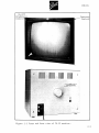
Figure 2-2 Front and Rear view of TD-23 monitor.
2-3
I~1015
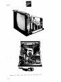
Figure 2-3 Front and rear view of TD12 and TD15
2-4
IMlOls
SECTION 3
CIRCUIT THEORY
3.1
GENERAL INFORMATION
This section describes the circuit theory of the TD series monitor. This
section is to be used with the waveforms and schematics found in section 5
and 6 of this manual.
3.2
VIDEO AMPLIFIER
The video amplifier consist of transistors QlOl through Ql03, integrated circuit UlOl and transistor Q10S through Qlll.
A composite video signal is applied to the PWA through Jl02-3 and is ac
coupled to the differential amplifier. The differential amplifier consists
of QlOl and Ql03 with Ql02 as the constant current source for the pair. The
video gain of this stage is essentially unity. Hum is rejected when S2 is
in the ON position because of the inherent common mode rejection of the differential pair. This stage presents an input impedance of 10K to the incoming
video signal.
The composite video is ac coupled to the electronic attenuator UlOl and direct
coupled to sync amplifier Ql12. Ul0l is an integrated circuit and its gain
is controlled by the contrast control R3. Its advantage over the conventional
method is that the video signal is not routed through the contrast control
and the stray capacity associated with these long leads does not cause a rolloff in high frequency response.
The video signal is ac coupled to the base of QlOs. QlOs with Ql06 forms a
compound series feedback stage. This configuration provides a high input
impedance and a low output impedance to drive emitter follower Ql08. It also
has a voltage gain of 9. The output signal from Q106 is coupled to the base
of Ql08, and its base is biased by the keyed clamp transistor Ql07.
The function of the keyed clamp stage is to clamp the blanking level of the
composite video signal to a fixed reference voltage which is constant regardless of scene content. It functions as a DC restorer and forces the input
voltage during blanking at Ql08 to be 1.5 volts. The base of Ql07 is driven
by composite negative sync and caused Ql07 to saturate at the trailing edge;
thus clamping occurs during the back porch of the composite video.
Ql08 is another emitter follower which isolates the keyed clamp from the output stages Ql09, QllO and Qlll. Transistor QllO and its components compris p
the video output driver with a gain of IS to 18. The bias voltage for QllO
is supplied by DC coupling from Ql08 which in turn is biased by the keyed clamp.
QllO operates essentially as a class B amplifier and is referenced to blanking level and allows a greater video swing in the output stage. R13s adds
series feedback which stabilizes the voltage gain and operating point against
transistor and temperature variation. Clls and C13s increase the gain of the
3-1
IMl015
driver at the high frequencies to compensate for the capacitance in QllO and
at the cathode of the CRT.
The signal at the collector of QllO is direct coupled to the base of the emitter
follower Qlll, which provides a low source impedance for driving the cathode
of the CRT.
Vertical retrace blanking is applied to the base of Ql09, which conducts
harder during this time to increase the voltage at Qlll emitter and drives
the cathode of the CRT to cutoff.
R227 and C159 forms a protection circuit for the output stages in the event
of a CRT arc. If a transient voltage of 230 volts or greater appears at the
CRT cathode, ionization will take place within the arc gap, providing a low
impedance path to ground.
3.3
SYNC PROCESSING
The sync processing circuit consist of Ql12, Ql14, Ql15 and QllS. The function of this circuit is to provide negative vertical sync pulses to drive
the vertical oscillator and positive horizontal pulses for the AFC circuitry.
A positive going composite video signal at the collector of Ql03 is applied
directly to the base of the sync amplifier Ql12. This amplifier has a voltage gain of S and it applies an amplified composite video signal to the base
of Ql14, the sync stripper. CllS is used to remove the 3.5SmHz color burst
signal from the back porch of the horizontal pulse. Ql14 is turned on when
triggered by the leading edge of the sync pulse and is turned off by the
trailing edge of the sync pulse. This on/off action of Ql14 results in a
negative going composite sync signal of approximately l3.5V p-p at its collector.
The composite sync signal is sent through a vertical integrator (R14S and C122)
to the base of Ql15, the vertical sync separator. The vertical sync signal
at the collector of Ql15 is used to trigger the vertical oscillator Ql16. The
zener diode in the collector circuit of Ql15 is used to limit the peak to peak
amplitude of the vertical sync pulse to 6.2V.
The vertical portion of the composite sync signal is removed by the differentiator circuit C129 and R167. The horizontal pulse is applied to QllS, inverted and used to drive the AFC stage Ql19.
3.4
VERTICAL DEFLECTION
The vertical deflection circuit consist of a vertical oscillator, an emitter
follower, a vertical output amplifier and the vertical deflection coil of
the yoke.
The vertical oscillator Ql16 is synchronized by the vertical sync pulse from
Ql15 and it produces a sawtooth waveform signal. This signal is fed through
an emitter follower to the input of the vertical output amplifier Ql. This
amplifier provides a sawtooth current waveform for the vertical deflection
coil of the yoke.
3-2
IMIOIS
The vertical oscillator Ql16 is a thyristor functioning as a programmaole
unijunction and operates as a relaxation oscillator. The free running frequency is set by the DC voltage at it's gate and anode. This voltage is
determined by the resistive voltage divider network of RIS3, RlS4 and RISS.
This voltage can be varied by the vertical hold control RIS4. The oscillator
is synchronized by a negative vertical sync pulse applied to the gate of Ql16
from QllS through C123.
The sawtooth forming network consists of C126, Cl27 and RlS7. These capacitors
charge exponentially at the vertical rate during the vertical scan time.
The vertical height control adjusts the amplitude of the sawtooth waveform by
controlling the charging rate of C126 and C127. To maintain a linear charging
rate, the output of Ql17 is fed back through R160 and R161 to the junction of
C126 and C12Z. The charging path is from ground through C126 and C127, past the
anode of Ql16' and through the vertical height control CRlS8) to B+. The vertical oscillator is at cutoff during the time that these capacitors are charging.
When the anode voltage exceeds Ql16 gate voltage, it turns on and rapidly discharges C126 and C127 through LI02. The tuned circuit consisting of LI02, C126
and C127 provide a stable control of the dropout time to maintain interlace.
The sawtooth signal at Ql16 anode is direct coupled to. the base of Qll7. This
transistor is a darlington pair emitter follower driver for the vertical output
amplifier. It presents a high imput impedance in shunt with RIS7 to prevent
loading of the wave shaping network across which the sawtooth waveform is
shaped. It also provides a low output impedance and high current gain to drive
the base of the vertical amplifier Ql.
The positive going sawtooth waveform at Ql17 emitter is fed back through the
resistive voltage divider of R160 and R161. This divider along with C127 integrates the sawtooth waveform and introduces a parabolic component to control
linearity. The amount of feed back is controlled by the vertical linearity
control R160.
Height control RlS8 varies the amplitude of the sawtooth voltage developed
by controlling the effective B+ applied to RIS7 and therefore controls the
vertical raster size on the CRT.
The vertical output stage Ql uses a NPN power type transistor operating as a
class AB amplifier. The output is transformer coupled to provide a proper
impedance match with the yoke. CRI08, R164 and C128 form a clamp circuit
which limits the collector voltage at Ql to safe levels during retrace. R139
prevents oscillations by providing damping across the vertical yoke coils.
3.S HORIZONTAL DEFLECTION
Transistors Q120 and Q121 and their components form an astable multivibrator
operating at the horizontal rate. Zener diode VRI03 and R177 provide a stable
6.2 volts source to this circuit from the 18 volt supply. The network consisting of R189, R190 and thermistor RTIOI is used to stabilize the frequency of
the multivibrator with temperature variation. The frequency of the multivibrator normally would increase with temperature due to base-emitter voltage
3-3
IMl015
of Q120 and Q12l varying inversely with temperature. As the temperature increases, the thermistor resistance decreases; thereby lowering the effective
source voltage applied to the main timing network consisting of R187, R185
and C140. This action slows down the charging current into C140 and holds the
off time of Q12l constant. The other timing network for Q120 and Q12l consists
of R18l and C138. The time constants chosen are such that the output square
wave at Q12l is positive for 38 ~seconds and grounded for 25 ~seconds. This
establishes the proper duty cycle for the output stages. The output at Q12l
is DC coupled to pre-driver inverter Q122 which produces sharp rise and fall
times for coupling to the driver transistor Q129.
Q129 is driven alternately into saturation and cutoff by the square wave ac
coupled from Q122. Its output is transformer coupled to the horizontal output stage Q3. Phasing of TlOl is chosen such that Q3 turns off when Q129 turns
on. This allows Q3 to turn off quickly, thus minimizing power dissipation.
During conduction of the driver transistor, energy is stored in the coupling
transformer. The voltage at the secondary is then negative and keeps Q3 cut
off. As soon as the primary current of TlOl is interrupted due to the base
signal driving Q129 into cut off, the secondary voltage changes polarity. Q3
~tarts conducting, and base current flows.
This gradually decreases at a rate
determined by the transformer inductance and circuit resistance.
The horizontal output stage has three main functions: to supply the yoke with
the correct horizontal scanning currents; develop 18 kV for the CRT anode and
DC voltage for the CRT bias, focus and accelerating grids.
Q3 acts as a switch which is turned on or off by the rectangular waveform on
the base. When Q3 is turned on, the supply voltage plus the charge on C158
causes yoke current to increase in a linear manner and moves the beam from near
the center of the screen to the right side. At this time, the transistor is
turned off by a negative voltage in its base which causes the output circuit
to oscillate. A high reactive voltage in the form of a half cycle positive
voltage pulse is developed by the yoke's inductance and the primary of T3. The
peak magnetic energy which was stored in the yoke during scan time is then
transferred to C156 and the yoke'S distributed capacity. During this cycle,
the beam is returned to the center of the screen.
The charged capacitances now discharge into the yoke and induce a current in
a direction opposite to the current of the previous part of the cycle. The
magnetic field thus created around the yoke moves the scanning beam to the
left of the screen.
After slightly more than half a cycle, the voltage across C156 biases the
damper diode CR12l into conduction and prevents the flyback pulse from further
oscillating. The magnetic energy that was stored in the yoke from the discharge
of the distributed capacity is released to provide sweep for the left half of
scan and to charge C158 through the rectifying action of the damper diode. The
beam js the:l at the center of the screen. The cycle will repeat as soon as the
bias voltag~ of Q3 becomes positive.
3-4
IM1015
C158 serves to block DC currents through the yoke and to provide usn shaping
of the current waveform. "S" shaping compensates for stretcnlng at the left
and right sides of the picture tube because the curvature of the CRT face and
the deflected beam do not describe the same arc.
L103 is an adjustable width control placed in series with the horizontal deflection coils. The variable inductive reactance allows a greater or lesser
amount of the deflection current to flow through the horizontal yoke and varies
the width of the horizontal scan.
The positive flyback pulse developed during horizontal retrace time is rectified by CRl16 and filtered by C148. This produces approximately 600 VDC which
is coupled through the focus control R219 to G4 of the CRT. The resistive
divider R221 and R225 provides approximately 400 VDC for the G2 of the CRT.
This same pulse is transformer coupled to the secondary windings of T3. It
is rectified by CRl and R5 to provide 18kV for the CRT anode. It is also
rectified by CR120 to provide a -80 V source for the brightness control R4.
In the event the -55 V supply voltage rises excessively due to a failure in the
regulator circuit, Q128 will conduct and shunt the +18Vsupply for Ql18 through
Q122 to ground. This will shut dO~T! the high voltage supply of the monitor and
prevent X radiation. R212 is a selected resistor (for replacement of R212,
see section 4.2) that enables Q128 to conduct when the +55 volt supply exceeds
59 V ±lV.
3.6
AUTOMATIC FREQUENCY CONTROL
The function of this circuit is to compare the phase (frequency) of the horizontal oscillator with the incoming sync signal and generate a DC control voltage which holds the oscillator in phase lock with the input sync signal.
The automatic frequency control circuit consists of stages Ql18, Ql19 and Q123.
The composite sync coupled from Ql14 is differentiated at Ql18 and fed to
phase splitter Ql19. The positive and negative balanced sync outputs of Ql19
and applied to the diode phase detector CRill and CRl12. Also applied to the
diodes is a sawtooth voltage derived from the horizontal flyback pulse by the
way of Q123 and integrator R173 and C134. The phase compared output appears
as a DC correction voltage after filtering by R179, C135 and C136. This
correction voltage is then applied to the base of Q121 to effect frequency
control.
3.7
LOW VOLTAGE POWER SUPPLY
The low voltage supply module is capable of operating from AC line voltage of
100V, 120V, 220V or 140V, SOi60Hz.
The power supply input voltage is determined by the setting of the two slide
switches located at the rear of the supply. These switches are stamped to
indicate the appropriate line voltage setting.
3-5
IMIOl5
To set the supply for a particular line voltage, the numbers on the two switches
are added together. This allows the supply to be set for four different input
line voltages. The position of the switches and the resultant input voltages
is shown in the schematic.
NOTE
When changing the AC input voltage from 100/120
to 220/240~ the fuse (F1) must also be changed
INPUT VOLTAGE
100/120
220/240
FUSE SIZE
3/4A 125V SE
3/BA 250V SE
The low voltage supply uses a series-pass regulator designed to maintain a
constant DC output for changes in input voltage, load impedance and temperature.
Also included is a current limiting circuit designed to protect transistors
connected to the 55V output of the regulated supply from accidental output short
circuits and load malfunctions.
The low voltage regulator consists of Q2, Q124, Q125, Q126, Ql27 and their
components. R206 and its circuitry control the current limiting feature.
The primary voltage is stepped down at the secondary of TI where it is rectified by a full wave bridge rectifier AI. Capacitor C2 is used as a filter
capacitor to smooth the rectified output of AI. Transistor Q2 is used as a
series pass stage to drop the rectified voltage to +57 VDC and to provide a
low output impedance. Approximately 7 volts is applied to the base of Q127
through a divider network of R209 and 211. A reference voltage from
zener diode VRl04 is applied to the emitter of Q127.
If the output voltage changes, an error current is generated through Q127. This
error current modulates the base current of Q125. Since Q2 is driven by Ql26
(in a darlington configuration), output drive is regulated in this manner to
bring the output voltage back to its proper level.
The short circuit protection or current limiting action can be explained as
follows. Assume the 55 volt bus becomes shorted to ground. This reduced output voltage is sensed by the base of Q127, turning that transistor off because
of the reverse bias across its emitter base junction. Simultaneously, the increased current through R206 increases the forward voltage drop across the base
emitter junction of Q126 and turns it on. The increased collector current
through Ql26 shunts away the base current of Q125. Since Q2 is driven directly
from Q125, its output current becomes limited. This closed loop oPeration
continues until a stable point is reached at which the current available during
a short circuit condition is maintained at approximately 100 rnA. This "foldback"
action limits dissipation in the monitor to safe levels during fault conditions
and prevents needless device failures due to accidental short circuits.
3-6
IM1015
SECTION IV
ADJUSTMENT AND MAINTENANCE
4.1
GENERAL
This section is for the adjustment procedures and maintenance procedures for
the TD series monitor.
CAUTION
NO WORK SHOULD BE ATTEMPTED
ON ANY EXPOSED MONITOR CHASSIS
BY ANYONE NOT FAMILIAR WITH
SERVICE PROCEDURES AND PRECAUTIONS
4.2
HV SHUTDOWN RESISTOR REPLACEMENT (R212)
Refer to figure 4-1 for component location on PWA and test equipment termination.
1.
Connect a DC voltmeter + lead to R216 and the - lead to chassis ground.
This meter is for monitoring the B+ voltage.
2.
Connect one end of a clip lead to R211 and the other end to chassis ground.
This will disable the voltage regulator circuit.
3.
Connect a lOOK range resistor decade box across the male molex pins for
R212 and set the decade box for 300n resistance.
4.
Plug the monitor AC plug (P1) in to a 0-140 V variac and set the variac
voltage control for 0 volts.
5.
You are going to determine what value of R212 that causes HV shutdown (loss
of raster) when the B+ voltage is 59V ±lV.
a.
Turn on the monitor and place the brightness and contrast controls in
the center of their rotation.
b.
Turn on the variac and slowly increase the AC input voltage to the monitor
while watching the B+ voltage. Note the B+ voltage reading prior to HV
shutdown (loss of raster).
6.
If HV shutdown occurs prior to 59V ±lV, increase the value of R212 and repeat
step 5b.
7.
When the HV shutdown occur-s at 59V ±1 V, note the decade box resistance value
and use this resistance for R212.
8.
Install R212 and repeat step 5b to varify that the ,shutdown voltage will
occur at 59V ±lV.
4-1
DC VOLTAGE
METER
.J::>.
I
100K RESISTOR
DECADE BOX
N
VARIAC
0-140V
AC LINE CORD FROM
TO MONITOR
REVISION LEVEL IDENTIFIER
clse
01
(0
....
rQ"i2'9>
R 21
'\::!:..!.!J
C 160
~
RI
II::-:-<!IID-
=U
QI21
CI17
0
I~' ~6 ~~:
= -::~:;->- I+ I ~A133
---fBIi&-
r"'\
I
I
~.II,\I
II:
II:
......fC'i'4Ol-
RIIS
'-;--~-1~,,---i.1'3
CI34
RI3S
Rla7
'i;:;:ia \ ~
Qlle
N
~
0
RISO
,--,
Figure 4-1 Test Equipment Lead Placement for Selecting R212
IM1015
4.3
1.
2.
3.
4.
VERTICAL CIRCUIT ADJUSTMENT
Apply a crosshatch video signal to the unit via J1 or J2.
Adjust vertical hold control R154 to the center of its range.
Adjust vertical height control R158 for a full raster from top to bottom.
Adjust vertical linearity control R160 and vertical height control R158 for
equal spacing between the horizontal lines of the crosshatch signal.
4.4
1.
2.
3.
4.
HORIZONTAL CIRCUIT ADJUSTMENT
Apply a crosshatch video signal to the monitor through J1 or,J2.
Adjust the horizontal hold control R187 to lock in the picture horizontally.
Adjust width coil L103 for a full raster from left to right.
Adjust linearity sleeve on the CRT neck for equal spacing between the
vertical lines of the crosshatch signal.
4.5
4.5.1
CHASSIS REMOVAL
TD23 Model
Remove input signal cable from J1 or J2. Remove screws holding cabinet back
and remove back from set. Discharge CRT HV anode to chassis ground and disconnect it from CRT. Disconnect CRT socket deflection coil plugs, brightness
and contrast control plugs. Remove screws holding chassis to cabinet bottom.
Remove chassis from cabinet.
4.5.2
TD12 and TD15 Models
Remove input signal cable from input panel. Remove screws holding cabinet back
and remove it from set. Remove screws holding chassis to cabinet bottom and
lift out chassis from cabinet.
4.6
CRT REPLACEMENT
HARNING
Extreme care shall be taken when
hnndlina the CRT. Safetu alasses
~~d--gZ;~e~ -mu~t be w;~ ~h~nhandling
the CRT. Care must be taken to
prevent scratching or nicking the
Crt or subject it to undue pressure
when removing or inserting the CRT
into the monitor.
DO NOT LIFT CRT BY THE ll/Eel{
4.6.1
TD23 Model
Remove signal input cables from input panel. Remove screws holding cabinet
back and remove back from cabinet. Discharge CRT HV anode to ground. Disconnect
HV anode, deflection coil plugs, brightness and contrast controls plugs.
4-3
IMI015
To protect CRT, insert a thin piece of cardboard between mask and CRT in the
upper right corner. Insert a thin wide blade screwdriver between the mask and
cardboard insert and pry the mask outward by twisting the screwdriver against
the CRT face.
Remove screws holding the CRT and remove CRT from cabinet.
the neck.
Do Not lift CRT by
Reverse removal procedure to install CRT.
4.6.2
TD12 and TD15 models
Follow chassis removal procedures in section 4.5.2.
Discharge CRT HV anode directly to ground and remove anode lead from CRT.
connect CRT socket and deflection coil plugs.
Dis-
On TD12 models - remove screws holding mask to frame and tilt mask upward.
Remove CRT mounting screws and lift CRT out of frame. Do Not lift CRT by the
neck.
On TD15 models - pull mask outward from frame and tilt upward to provide access
to CRT mounting screws. Remove CRT mounting screws and lift out CRT from frame.
Do Not lift CRT by the neck.
4-4
IM1015
SECTION V
WAVEFORMS
5.1
GENERAL
The waveforms shown on the following pages were taken using a crosshatch video
input signal applied to J1. The video termination switch 51 is in the 75Q
position and the differential input switch 52 is set to the OFF position.
5-1
H1l015
J1 VIDEO INPUT
500mV/cm 2ms/cm
IV P-P
QI06 EMITTER
ElOl COLLECTOR
100mV/cm 2ms/cm
lSOmV P-P
.5V /cm 2ms/cm
,SV p-p
Ql13 EMITTER
2V/cm 200ps/cm
6VP-P
5-2
Ql05 BASE
lV/cm 2ms/cm
.2SV P-P
Ql14 COLLECTOR
5V/cm 100ps/cm
13.5V P-P
Q116 ANODE
Ql19 EMITTER
2V fcm 2ms/cm
SV p-p
5V/cm 10ps/cm
8V P-P
1:>11015
Ql19 COLLECTOR
5V/em lOf.1.s/em
9VP-P
JJUNCTION R173 & C133
2V/em lOlls/em
7.6V P-P
Q122 COLLECTOR
Q129 COLLECTOR
2V/em lOlls/em
5.4V P-P
50V/em lOlls/em
150V P-P
Q1 EMITTER
Q3 BASE
2V / em 2ms/ em
8VP-P
5V/em lOps/em
14V p-p
Q3 COLLECTOR
100V/em laps/em
520V p-p
J105-1
TOP WAVEFORM 20V/em (DC) -78V DC
BOTTOM WAVEFORM IV/em (AC) 1AV ripple
5-3
IM1015
REVISION LEVEL IDENTIFIER
Figure 5-1 Circuit Board Component Location
and Intercab1ing Diagram.
5- 4
IMI015
SECTION 6
TD PARTS LIST
6. 1
GENERA.L
This section contains the replaceable electrical parts list and schematic for
the TD monitor.
The parts list and schematic in this manual is for our standard TD series
monitor and will not accurately represent a specific customer designed monitor
for a specific application.
6.2
ORDERING PARTS
Most parts contained in the monitor are available commercially from electronic
parts outlets. When it is necessary to order spare or replacement parts from
Ball Electronic Display Division (Ball E.D.D.), include the part description,
part number, model and serial number data of the Data Monitor as listed on the
serial number plate and, if applicable, the schematic reference number listed in
the parts list. Orders for these parts should be sent to:
Ball Electronic Display Division
P.O. Box 43376
St. Paul, Minnesota 55164
For rapid service:
6.3
Telephone area (612) 786-8900
or
TWX area (910) 563-3552
RETURNING PARTS
When the monitor requires service or repair in accordance with the enclosed
warranty, return the unit or~part to:
Ball Electronic Display Division
4501 Ball Road N.E.
Circle Pines, Minnesota 55014
ATTN: Customer Service
Telephone Area (612) 786-8900
TWX area (910) 563-3552
Unnecessary delays may be avoided when parts are returned to Ball Electronic
Display Division using the following procedures:
(1)
Package the unit or part in accordance with the method of
shipment. Enclose a list of the material being returned and
the reason for returning it.
6-1
IM1015
(2)
Send the unit or part, transportaion prepaid, to the address
~tipulated fQr returning parts.
All equipment and parts described in the warranty will be replaced, provided
our examination discloses that the defects are within the limits of the warranty.
If damages or defects are not within the limits of the warranty, the customer
will be notified of theex.tent of repairs required and the cost. The unit will
be repaired and returned upon agreement.
6.4
COMPONENT REPLACEMENT PARTS AFFECTING PRODUCT SAFETY
Product safety must be considered whenever a component is replaced
unit. The critical components that affect x-~adiation are denoted
shaded areas on the schematic and indicated on the parts list with
preceding the reference symbol designator. These components are to
only with Ball Electronic Display Divlsion approved parts.
in
by
an
be
this
the
asterick
replaced
The use of substitute components which do not have the same characteristics as
the original components may cause excessive x-radiation.
6.5
PWA IDENTIFICATION
The PWA (Printed Wiring Assembly) part number has a 6-002-XXXX prefix. The
last four digits of the assembly number is stamped on the component side of the
board and its location is indicated in figure 5-1.
Do not confuse the PWA number with the numbers etched on the conductor side of
the Printed Wiring Board. The PWA number is always located on the component
side of the PWA.
6.6
MONITOR PARTS LIST
The asterick (*) preceding the reference symbol (REF SYM) indicated that this
part is a critical component that affects product safety O~efe.r to paragraph
6.4 for details).
NOTE
This parts list is for our Standard TV
Series Monitor using one of the following
PWA numbers: 6-002-0858; 0859; and 0860.
REF
SYM
DESCRIPTION
PART NUMBER
Al
Bridge Rectifier, VS148
1-021-0413
C1
6-2
BEDD
~apacitor,
fixed: }iF unless otherwise stated
.OOl±10%;
1000V, ceramic disc
1-012-2274
IM101s
BEDD
PART NUMBER
REF
SYM
DESCRIPTION
CAPACITOR Fixed:
C2
C101
C102
C103
C104
C10S
C106
C107
C108
C109
ClIO
C111
Cl12
Cl13
Cl14
ellS
Cl16
Cl17
C11S
Cl19
C120
r.121
C122
C123
C124
C12S
C126
C127
C128
C129
C130
C131
"1",,,...
l.l. .)L
C133
C134
C135
C136
C137
C138
C139
C140
C141
C142
C143
C144
C145
~F
unless otherwise stated
1500; 100V, electrolytic
100; 2SV, electrolytic
100; lOY, electrolytic
100; 10V, electrolytic
.02 ± 20%; sOOV, ceramic disc
47; 2SV, electrolytic
Not used
22; 2SV, electrolytic
1; sOV,electrolytic
Not used
100; 2SV, electrolytic
.1 ± 10%; 200V, mylar
100; 10V, electrolytic
.1 ± 10%; 200V, mylar
.01 ± 20%; 1OOV, ceramic disc
68pF ± sg6; sOOV, dipped mica
.1 ± 20%; 1OOV, ceramic disc
Not used
7spF ± 5%; 1000V, ceramic disc
1; SOY, electrolytic
270pF ± 5%; sOOV, dipped mica
1; SOY, electrolytic
.022 ± 10%; 400V, mylar
.001 ± 20%; 1000V, ceramic disc
470pF ± 5%; sOOV, dipped mica
47; SOY, electrolytic
.22 ± 10%; 200V, mylar
.22 ± 10%; 200V, mylar
.1 ±10%; 400V, mylar
200pF ± 5%; SOOV, dipped mica
100pF ± 5%; SOOV, dipped mica
.002 ± 20%; 1000V, ceramic disc
_
... _ _ _ ....
•
• VVL :::r:: LV1>; lUUUV, ceramlC OlSC
.1 ±10%; 200V, mylar
.01 ±2Q%; 100V, ceramic disc
.ls±10%; 200V, mylar
.001 ±20%; 1000V, ceramic disc
.02 ± 20%; sOOV, ceramic disc
680pF ± 5%; 300V, dipped mica
.0022 ± 10%; ZOOV J mylar
.001 ± 10%; 200V, mylar
.1 ± 20%; 1OOV, ceramic disc
27pF ± 5%; sOOV, dipped mica
4.7; 160V, electrolytic
47; 2SV, electrolytic
.022 ± 10%; 200V, mylar
r\.n .....
I
,..,.n.O~
1.
1-012-2186
1-012-2200
1-012-2160
1-012-2160
1-012-0780
1-012-2165
1-012-2212
1-012-2189
1-012-2200
1-012-0870
1-012-2160
1-012-0870
10-12-7109
10-57-5680
10-12-7104
1-012-0280
1-012-2189
1-012-0396
1-012-2189
1-012-2265
1-012-0540
1-012-0460
1-012-2157
1-012-0930
1-012-0930
1-012-2239
10-57-5201
1-012-0300
1-012-2219
1-012-2219
1-012-0870
10-12-7109
1-012-0925
1-012-0540
1-012-0780
10-57-5681
10-47-7222
10-47-7102
10-12-7104
1-012-2161
1-012-2195
1-012-2165
10-47-7223
6-3
IM1015
REF
SYM
CAPACITOR Fixed;
C146
C147
C148
C149
C150
C151
C152
C153
C154
C155
*C156
or
C157
*C158
or
C159
C160
C161
C162
BEDD
PART NUMBER
DESCRIPTION
~F
unless' otherwise stated
4.7; 160V, electrolytic
22; 25V, electrolytic
.01 ±20%; 1000V, ceramic disc
Not used
Not used
Not used
4.7; 160V, electrolytic
.01; 1000V, ceramic arc gap
.01; 1000V, ceramic arc gap
.01; 1000V, ceramic arc gap
.0056 ±10%; 2000V, mylar (PWA 0859 &0858)
.0068 ±10%; 1600V, mylar (PWA 0860)
4.7; 160V, electrolytic
1 ±10%; 200V, polycarbonate (PWA 0858 & 0860)
1.2 ±10%; 100V, polycarbonate (PWA 0859)
2pF; 230V, arc gap
.001 ±20%; 1000V, ceramic disc
Not used
20pF ±5%; SOOV, dipped mica
1-012-2195
1-012-2212
1-012-2214
1-012-2195
1-012-0112
1-012-0112
1-012-0112
10-35-7562
1-012-2210
1-012-2195
1-012-2220
1-012-2223
1-012-0111
1-012-0540
10-57-5200
DIODE
CR1
CR101
CR102
CR103
CR104
CR10s
CR106
CR107
CR108
CR109
CR110
CRIll
CRl12
CRl13
CRl14
CRl15
CR116
CRl17
CRl18
CRl19
CR120
CR121
CR122
6-4
D0438
D0410
D0410
D0467
Not used
D0410
Not used
Not used
D0403
D0410
D0410
D0410
D0410
Not used
IN4001
D0410
D0447
D0403
Not used
Not used
D0403
D0436
D0410
1-021-0438
1-021-0410
1-021-0410
1-021-0467
1-021-0410
1-021-0403
1-021-0410
1-021-0410
1-021-0410
1-021-0410
78-62-4001
1-021-0410
1-021-0447
1-021-0403
1-021-0403
1-021-0436
1-021-0410
,.
•
REF
DESCRIPTION
SYM
IMI015
tu:nn
ULUU
PART NUMBER
FUSE
3/4A-125V, slo-blo
Fl
1-028-0242
CONNECTOR
Receptacle, female, 1 contact UHF
Receptacle, female, 1 contact UHF
J1
J2
1-039-0113
1-039-0113
COIL
*L1
or
or
L2
L101
L102
*LI03
Deflection coil assembly (TD 23)
Deflection coil assembly (TD 12)
Deflection coil assembly (TD 15)
Fixed; 10lJH
Not used
Fixed, 330lr1H
Adj; width
6-004-0342
6-004-0363
6-004-0329
15-13-1100
15-13-7331
1-016-0309
TRANSISTOR
Q1
Q2
Q3
Q101
Q102
Q103
Q104
Q105
Q106
Q107
Q108
Q109
n11f'1
'{ .......... '-'
Q111
Ql12
Ql13
Ql14
Ql15
Ql16
2SD199
DTS410
DTS402
2N4124
2N4124
2N4124
Not used
2N4124
2N3906
2N4124
2N4124
2N4124
MPS-6565
MPS-6565
2N3906
Not used
1-015-1176
78-85-0410
78-85-0402
1-015-1139
1-015-1139
1-015-1139
~fPS-A16
1-015-1193
1-015-1139
1-015-1157
1-015-1186
1-015-1139
1-015-1145
1-015-1139
1-015-1139
1-015-1139
1-015-1139
1-015-1175
2N4124
2N6027
~ii/
1""\11--1
MPS-A65
Ql18
Ql19
Q120
Q121
Q122
Q123
Q124
2N4124
2N3906
2N4124
2N4124
2N4124
2N4124
MPS-L51
1-015-1139
1-015-1145
1-015-1139
1-015-1139
1-015-1139
1-015-1185
1-015-1185
1-015-1145
6-5
IM1015
REF
SYM
DESCRIPTION
BEDD
PART NUMBER
TRANSISTOR
Q125
Q126
*Q127
*Q128
Q129
MPS-U03
2N5830
B1218
MPS-A14
MPS-U04
1-015-1153
1-015-1172
1-015-1218
1-015-1158
1-015-1167
RESISTOR, fixed;±5%; 1/4W, carbon film, unless otherwise stated
R1
R2
R3
R4
*R5
R101
R102
R103
R104
R105
R106
R107
R108
R109
R110
R111
Rl12
Rl13
Rl14
Rl15
Rl16
Rl17
Rl18
Rl19
R120
R121
R122
R123
R124
R125
Rl26
R127
R128
R129
R130
R131
R132
6-6
40Dn±10%; lOW, wirewound
75n, 1/2W
Var; 10K±30%; 1/2W, composition, contrast
Var; 100K±30%; 1/2W, composition, brightness
500M±15%; 6W, deposited carbon
Not used
Not used
33K
22K
3000
3000
330n
510n
33K
22K
12K
3K
Not used
56n; 1/2W
1.3K
5.1K
15K
2K
2K
150n
51n
1.2K
3.3K
3.3K
1.5K
lOOn
Not used
470n
15K
3.9K
47K
10n
1-011-2442
1-011-2243
6-004-0660
6-004-0659
1-011-2456
70-16-0333
70-16-0223
70-16-0301
70-16-0301
70-16-0331
70-16-0511
70-16-0333
70-16-0223
70-16-0123
70-16-0302
1-011~2240
70-16-0132
70-16-0512
70-16-0153
70-16-0202
70-16-0202
70-16-01B1
70-16-0510
70-16-0122
70-16-0332
70-16-0332
70-16-0152
70-16-0101
70-16-0471
70-16-0153
70-16-0392
70-16-0473
70-16-0100
IM1015
REF
SYM
DESCRIPTION
BEDD
PART NUMBER
RESISTOR, Fixed:±5%; 1/4W, carbon film, unless otherwise stated
R133
R134
R135
R136
R137
R138
R139
R140
R141
R142
R143
R144
R145
R146
R147
R148
R~49
R150
R151
R152
R153
R154
R155
R156
R157
R158
R159
R160
R161
R162
R163
R164
R166
R167
R168
R169
R170
R171
R172
R173
R174
R175
R176
R177
R178
R179
2.2K; 1W, composition
1000
1200
15Q
1000
1.8K; 1W, composition
1.5K; 1/2W
Not used
Not used
1.2K
lOOn
Not used
Not used
620K
3.3K
2.7K
lOOK
12K
470Q
1K
470Q
Var; 10K±20%; 1/8W, composition vert hold adj
6.8K
lOOK
180K
Var; 50K±20%; 1/8W, composition vert height adj
33K
Var; 10K±20%; 1/8W, composition vert linearity
10K
15Q
3.3K; 1W, composition
15K
70-16-0624
70-16-0332
70-16-0272
70-16-0104
70-16-0123
70-16-0471
70-16-0102
70-16-0471
1-011-5312
70-16-0682
70-16-0104
70-16-0184
1-011-5373
70-16-0333
1-011-5312
70-16-0103
70-16-0150
1-011-2425
70-16-0153
33d'"2; lW , composition
1
1"\11
1"\11r
i-Vii-Vii~
47K
1K
2.7K
33K
10K
1K
1.2K
8.2K
lOOK
47K
47K
750Q; 1/2W
10M
4.7K
70-16-0473
70-16-0102
70-16-0272
70-16-0333
70-16-0103
70-16-0102
70-16-0122
70-16-0822
70-16-0104
70-16-0473
70-16-0473
70-17-0751
70-16-0106
70-16-0472
1-011-2445
70-16-0101
70-16-0121
70-16-0150
70-16-0101
1-011-2424
1-011-2274
70-16-0122
70-16-0101
6-7
IM1015
REF
SYM
DESCRIPTION
BEDD
PART NUMBER
RESISTOR, Fixed:±5%; 1/4W carbon film unless otherwise stated
R180
R181
R182
R183
R184
R18S
R186
R187
R188
R189
R190
R191
R192
R193
R194
R19S
R196
R197
R198
R199
R200
R201
R202
R203
R204
R20S
R206
R207
R208
* R209
R210
*R211
*R212
*R213
R214
R215
R216
R217
R218
R219
R220
R221
R222
R223
R224
R225
R226
6-8
2.7K
62K
68K
47K
15K
47K
2.7K
Var; 25K±20%; 1/8W, composition, horizontal hold
12K
120rG
4.7K
2.2K
10K
Not used
620rG
470rG
1K
lOOK; 1/2W
1K
lOOK
680rG
43K
330rG
1.6M
1K
30K
1rG±10%; 3W, wirewound
10rG
6.2K; 1/2W
23.7K±1%; 1/2W, metal film
Not used
3.57K±1%; 1/2W, metal film
Selected (minimum resistance 300rG)
12K
2.4K
360K
22rG; 1/2W
6.8K
2.2rG; 2W, wirewound
Var; 2.5M±20%; 1/8W, composition focus adj
33K
1.2M; 1/2W
47K; 1/2W
1.2rG; 2W, wirewound
47K; 1/2W
2.2M; 1/2W
l.8K
70-16-0272
70-16-0623
70-16-0683
70-16-0473
70-16-0153
70-16-0473
70-16-0272
1-011-5325
70-16-0123
70-16-0121
70-16-0472
70-16-0222
70-16-0103
70-16-0621
70-16-0471
70-16-0102
1-011-2318
70-16-0102
70-16-0104
70-16-0681
70-16-0433
70-16-0331
1-011-2550
70-16-0102
70-16-0303
1-011-1742
70-16-0100
1-011-2289
1-011-2549
1-011-2517
1-011-2517
70-16-0123
70-16-0242
70-16-0364
1-011-2230
70-16-0682
1-011-0120
1-011-5566
70-16-0333
1-011-2344
1-011-2310
1-011-1395
1-011-2310
1-011-2350
70-16-0182
IM1015
BEDD
PART NUMBER
REF
DESCRIPTION
SYM
RESISTOR, fixed:
±5%; 1/4W, carbon film unless otherwise stated
270n; 1/2W
330n
3.3K
Not used
620n
150n
R227
R228
R229
R230
R231
R232
1-011-2256
70-16-0331
70-16-0332
70-16-0621
70-16-0151
THERMISTOR
ID101; 10K @ 25 0 C
RT101
1-011-7000
SWITCH
Slide, DPDT
Slide, DPDT
Rotary, Off-On (part of R4)
Slide, SPDT
Slide, 3PD3
S1
S2
S3
S4
S5
85-73-0278
85-73-0278
6 . . 004-0659
1-018-0255
1-018-0256
TRANSFORMER
T1
T2
*T3
or
T101
Power
Vertical output
High Voltage, TD23 &TD15
High Voltage, TD-12
Horizontal driver
6-003-0655
6-003-0341
6-003-0404
6-003-0406
1-017-5380
INTEGRATED CIRCUIT
U101
MC3340
1-025-0123
ZENER DIODE
V1
VR101
VR102
VR103
*VR104
*VR105
Refer to 1-014-XXXX number on CRT
IN4408, 15V
Z0475, 6.2V
Z0475, 6.2V
Z0493, 6.8V
Z0443, 56V
1-021-0405
1-021-0475
1-021-0475
1-021-0493
1-021-0420
MISCELLANEOUS
Assembly,
Assembly,
Assembly,
Assembly;
PWA, TD-12
PWA, TD-23
PWA, TD-15
power supply TD-23
6-002-0860
6-002-0858
6-002-0859
6-003-0422
6-9
IMI015
REF
SYM
DESCRIPTION
BEDD
PART NUMBER
MISCELLANEOUS
Assembly,
Assembly,
Assembly,
Assembly,
Assembly,
Assembly,
Assembly,
Assembly,
Assembly,
6-10
power supply TD12 &15
heats ink TD-23
heatsink TD12 &15
cabinet TD-23M
cabinet TD-23MV
cabinet TD-12MV
cabinet TD-12M
cabinet TD-15M
cabinet TD-15MV
6-003-0433
6-003-0361
6-003-0379
6-001-0198
6-001-0197
6-001-0103
6-001-0104
6-001-0111
6-001-0109
3
2
6
5
7
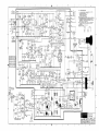
:'lOTES:
T'2.
1.
2•
11
RIH
:1
RI~9
JI
1.5K
IIzW
D
-2: I
-3
d2.
JIOS
-'i.1
S2.
RI2..0
~ ~~~~~~~~~~~I=i~~EU~~~~I~~~~~~~;' ':~I!;~~~~2~!FETY
GRN
(fJ
7.
ffi]
@)
yEt
ORN
UNLESS OTHERWISE SPECIFIED
ALL FIXED RESISTORE ARE !,;rI I 5% AND RESISTANCE VALUES IN OfM;.
ALL CAPACITANCE VALUES ARE IN MICROFARADS.
0 DENOTES PWA EDGE CCN-lECTOR.
-3>>- DENOTES JACK AND PLUG CCN-lECTOR.
--0- DENOTES SOLDERED CCN-lECTIONS.
R227 AND C159 IS PAAT OF CRT SOCKET.
..
I
CO-A
AND X-RADIATION. FOR CONTINUED PROTECTION USE CNLY TeE EXACT
REPLACEf"ENT PARTS. DO NOT SUBSTITUTE PARTS OR t'ODIFY THE CIRCUIT.
REFER TO SECTION 6.4 OF SERVICE MANLlA.L.
FOR SELECTlCN E'ROCEDURE, REFER TO SECTlCN 4.2 OF SERVICE MANUAL.
THIS SCHEMATIC IS CNLY FOR THE STANDARD TD12, TD15, AND TD23
DATA t'ONITORS.
FUSE SIZE: 120 VAC-. 75A; 220 VAC-.375A.
VARIABLE PART VALUES:
~.
~
e158
6-002C156
0858
0359
0850
,
-I/)~
I-:-
150
[lJ
YEl
1)
6
.0056
.0056
.0068
D
1.0
1.2
1.0
VERT Oe.FL
COIL
Cllb
.1
EIO/
YEL
[ ] R2.27
ill
FROM{ f.i-~~C/59 T J
270
Vz.W
2_0fF
Z30V
RISO
11K
c
C
LINE
ss
54
3K
VOlTAC£ F'oS'TIOW POS I TIOtI
t-2..0V
100
0
100
R2.2.1
120
'2.0
100
e20
1.2. M
'/2. W
0
2.2.0
240
2.0
2.Z,O
C/2.9
200,f
B
3
8
4
a?O.VAC
240 'lAC.
A
I
A
00
54l '
1-3
IOOVAC
laOYAC
2
3
4
5
6
7
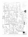
:I"-"'"-~..,·v '....~-.,p==.-=-~, ~----".i: DC., !':;'
'J ~
t
I
~------>! ~ ~ -
*'
--.-~~
.r-,
-.~'
I
!
;, 2-:-1'
-"
--
~48"
,
~
II
1
I
I
C.!b..L
I
R3.IOK
ICONTRASTI
II
c
i
1
I
I,
illiNl i 5!:>
54
VOLTAGE P05\il~ POSITION
\00
I ',20
i
c20
. ,-..
~II -,.v
~
C
I
'J
100
2.0
lOa
i
!
I
Ie
I
I
"'-18 KV
:
t:~;' 1
~
MP5AI(P
1"2..1-(
ci271
.2.2.
2.2.0
0
,..,
I
A
C
I
~
~
'-u
'I
~I'",
47K
I
RI'S
CRIIO
2..71(
00410
'403
33 K
I
'1""LO V
;;,2.2.1
CRI
I.::'/r'
1,2. VI
r\I~~
I
~'L'2.5
~,
2..2'"
'/;.W
II<;
RI"~
II
I
1
I
.33"
CRI09
I
!
D9410
I
R5,1
8
I8
SOOM:,
row '
~
n~~~~;~~
lii
'Zx-I-
~
12.0 VAC
a::.J'r
~QJ3
S5
IIh
; (j 0
VA c'
220
v:c:
240 'lAC
T!
WHT
2.CV~
----11'---+-R_E_D_I..:.B~L-K..-<'"".
I
'OOY
j
jI
3LK.p Ii
III,
(EL
6
12.0\1 _
t
100 VAC.
,
I
12.0 VI'-,c.
I~~
1,~
~.
r
~ i~19KI'
0,-,
OFF/ON ( PART OJ:" ~4)
I,"
BLUNt ..........; 1'1'
100V 5:::
-=1c
CZ
1,~:O\lO
::
'-___....__
~--=~-+--
0
\~RN/YEL
t :ii;;·9p,RN
I
I~
BLu.-:11
X=··
4
TO
.:::r;,.
I;
.~
I
:;:
I
I
~~~-:.3_,
I
~.
Ii
t
-:
~~ L
4
I
C,14J
~. ~
"";"
.::.. 4 i
22
c:5
Vi
I
,A,
INSTALLATION AND OPERATING MANUAL
MALFUNCTION
REPORT
Dear Customer:
We are trying to manufacture the most reliable. product possible. You would do us a great courtesy
by completing this form should you experienee any failures.
1.
Type Unit _ _ _ _ _ _ _ _ _ _ _ _ _ _ _ _ _ Serial No. _ _ _ _ _ _ _ __
Module (if applicable} _ _ _ _ _ _ _ _ _ _ _ _ _ _ _ _ _ _ _ _ _ __
3.
Cause of failure (if readily available} _ _ _ _ _ _ _ _ _ _ _ _ _ _ _ _ _ _ _ __
4.
Approximate hours/days of operation to failure _ _ _ _ _ _ _ _ _ _ _ _ _ _ _ __
5.
Failure occurred during:
Final Inspection
6.
Customer Installation
Field Use
Personal Comment:
Customer _ _ _ _ _ _ _ _ _ _ _ _ _ _ __
Address _ _ _ _ _ _ _ _ _ _ _ _ _ _ __
Signed _ _ _ _ _ _ _ _ _ _ _ _ _ _ _ ___
Date _ _ _ _ _ _ _ _ _ _ _ _ _ _ _ ____
Ball Electronic Display Division
P.O. Box 43376
St. Paul, Minnesota 55164
Telephone 612-786-8900 TWX 910-563-3552
LOST OR DAMAGED EQUIPMENT
The goods descrioed on your Packing Slip have been received by the Transportation Company complete and in good condition. If any of the goods called for on this Packing Slip are short or damaged,
you must file a claim WITH THE TRANSPORTATION COMPANY FOR THE AMOUNT OF THE
DAMAGE AND/OR LOSS.
IF LOSS OR DAMAGE IS EVIDENT AT TIME OF DELIVERY:
If any of the good called for on this Packing Slip are short or damaged at the time of
del ivery, ACCEPT TH EM, but only if the Freight Agent makes a damaged or short
notation on your Freight Bill or Express Receipt and signs it.
IF DAMAGE OR LOSS IS CONCEALED AND DISCOVERED AT A LATER DATE:
If any concealed loss or damage is discovered, notify your local Freight Agent or Express Agent AT ONCE and request him to make an inspection. This is absolutely
necessary. Unless you do this, the Transportation Company will not consider any
claim for loss or damage valid. If the agent refuses to make an inspection, you
should draw up an affidavit to the effect that you notified him on a certain date and
that he failed to make the necessary inspection.
After you have ascertained the extent of the loss or damage, ORDER THE REPLACEMENT
PARTS OF COMPLETE NEW UNITS FROM THE FACTORY. We will ship to you and bill you for
the cost. This new invoice will then be a part of your claim for reimbursement from the Transportation Company. This, together with other papers, will properly support your claim.
Remember, it is extremely important that you do not give the Transportation Company a clear receipt if damage or shortages are evident upon delivery. It is equally important that you call for an
inspection if the loss or damage is discovered later. DO NOT, UNDER ANY CI RCUMSTANCES,
ORDER THE TRANSPORTATION COMPANY TO RETURN SHIPMENT TO OUR FACTORY
OR REFUSE SHIPMENT UNTIL WE HAVE AUTHORIZED SUCH RETURN.
IMPORTANT
EQUIPMENT RETURN TO BALL ELECTRONIC DISPLAY DIVISION
1.
Receive return authorization from the plant unless the unit was sent to you upon evaluation
or rental.
2.
Return prepaid.
3.
Be sure a declared value equal to the price of the unit is shown on the bill of lading, express
receipt, or air freight bill, whichever is applicable. This would cover claim for shipping damage on return.