1
MQ162-02
Application
Manual
Real Time Clock Module
RTC-72421/72423
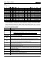
Model
Product Number
RTC-72421 A
Q42724210000100
RTC-72421 B
Q42724210000200
RTC-72423 A
Q42724230000600
RTC-72423
Q42724230000700
In pursuit of "Saving" Technology ,Epson electronic device.
Our Lineup of semiconductors, Liquid crystal displays and quartz devices
assists in creating the products of our customers' dreams.
Epson IS energy savings.
NOTICE
• No part of this material may be reproduced or duplicated in any form or any means without the written
permission of Seiko Epson.
• Seiko Epson reserves the right to make changes to this material without notice.
• Seiko Epson does not assume any liability of any kind arising out of any inaccuracies contained in this
material or due to its application or use in any product or circuit and, further, there is no representation
that this material is applicable to products requiring high level reliability, such as, medical products.
• Moreover, no license to any intellectual property rights is granted by implication or otherwise, and there
is no representation or warranty that anything made in accordance with this material will be free from
any patent or copyright infringement of a third party.
• This material of portions thereof may contain technology or the subject relating to strategic products
under the control of the Foreign Exchange and Foreign Trade Law of Japan and may require an export
license from the Ministry of international Trade and industry or other approval from another government
agency.
RTC - 72421 / 72423
CONTENTS
Overview ............................................................................................. 1
Block diagram ..................................................................................... 1
Terminal connections .......................................................................... 2
Terminal functions............................................................................... 3
Characteristics .................................................................................... 4
1. Absolute maximum ratings........................................................................................ 4
2. Recommended operating conditions......................................................................... 4
3. Frequency characteristics and current consumption characteristics.......................... 4
4. Electrical characteristics ( DC characteristics ) ......................................................... 4
Switching characteristics (AC characteristics) ........................................... 5
1. When ALE is used .................................................................................................... 5
2. When ALE is fixed at VDD ......................................................................................... 6
Registers............................................................................................. 7
1. Register table............................................................................................................ 7
2. Notes ........................................................................................................................ 7
3. Functions of register bits (overview).......................................................................... 7
4. Setting the fixed-period pulse output mode and fixed-period interrupt mode............. 8
5. Resetting the fixed-period pulse output mode and fixed-period interrupt mode......... 8
Register description ............................................................................ 9
1. Timing registers ........................................................................................................ 9
2. CD register (control register D) ............................................................................... 10
3. CE register (control register E)................................................................................ 11
4. CF register (control register F) ................................................................................ 13
Using the RTC-72421/RTC-72423 .....................................................14
1. Power-on procedure (initialization) .......................................................................... 14
2. Read/write of S1 to W registers .............................................................................. 16
3. Write to 30-second ADJ bit ..................................................................................... 16
4. Using the CS1 pin ................................................................................................... 17
Power supply circuit example.............................................................17
Examples of connection to general-purpose microprocessor .............18
External dimensions...........................................................................19
Marking layout....................................................................................19
Reference data ..................................................................................20
Application notes................................................................................21
1. Notes on handling ................................................................................................... 21
2. Notes on packaging ................................................................................................ 21
RTC - 72421 / 72423
4-BIT PARALLEL INTERFACE REAL TIME CLOCK MODULE
RTC - 72421 / 72423
• Built-in crystal unit removes need for adjustment and reduces installation costs
• Microprocessor bus compatible ( tWW, tRD = 120 ns )
• Use of C-MOS IC enables low current consumption ( 5 µA Max., at VDD = 2.0 V )
• Compatibility with Intel CPU bus
• Address latch enable (ALE) pin compatible with multiplex bus CPUs
• Time (hours, minutes, seconds) and calendar (year, month, day) counter
• 24-hour/12-hour switchover and automatic leap-year correction functions
• Fixed-period interrupt function
• 30-seconds correction (adjustment) function
• Stop, start, and reset functions
• Battery back-up function
• Same mounting conditions as general-purpose SMD ICs possible (RTC-72423)
∗ Pins and functions compatible with the SMC-5242 series
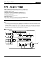
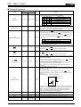
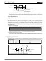
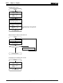
Overview
The RTC-72421/RTC-72423 module is a real time clock that can be connected directly to a microprocessor's bus. Its built-in crystal
unit enables highly accurate time-keeping with no physical access required for adjustment and, since there is no need to connect
external components, mounting and other costs can be reduced.
In addition to its time and calendar functions, the RTC-72421/RTC-72423 enables the use of 30-seconds correction and fixedperiod interrupt functions.
The RTC-72421/RTC-72423 module is ideally suited for applications requiring timing management, such as personal computers,
dedicated word-processors, fax machines, multi-function telephones, and sequencers.
Block diagram
RTC-72421/72423
OSC
D3
D2
D1
D0
Gate
WR
RD
Gate
A3
A2
A1
A0
CS0
Latch
Counter
RESET
bit
30sec ADJ
bit
S1 to CF
Decoder
STOP
bit
HOLD
bit
BUSY
bit
24/12
bit
S1
S10
MI1
MI10
H1
H10
D1
D10
MO1
MO10
Y1
Y10
W
Output Selector
ALE
CS1
CD
CE
Page - 1
CF
64 Hz
1 Second carry
1 Minute carry
1 Hour carry
STD.P
MQ - 162 - 02
RTC - 72421 / 72423
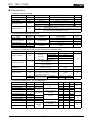
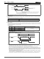
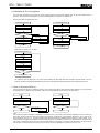
Terminal connections
RTC-72421
STD.P 1
CS0
ALE
A0
2
3
4
RTC-72423
18
VDD
17 ( VDD )
16 ( VDD )
15
CS1
A1
5
14
D0
A2
6
13
D1
A3
7
12
D2
RD
8
11
D3
GND
9
10
WR
STD.P
1
CS 0
2
24
N.C.
3
VDD
23 ( VDD )
22 ( VDD )
ALE
4
21
N.C.
A0
5
20
CS1
N.C.
6
19
D0
A1
7
18
N.C.
N.C.
8
17
N.C.
A2
9
16
D1
A3
10
15
D2
RD
11
14
D3
GND
12
13
WR
The (VDD) pins are at the same electrical level as VDD. Do not connect these pins externally. The N.C. pins are not connected
internally. Ground them in order to prevent noise.
Page - 2
MQ - 162 - 02
RTC - 72421 / 72423
Terminal functions
Signal
Input/ou
Pin No.
tput
RTC-72421 RTC-72423
Function
Connect these pines to a bi-directional data bus or CPU data bus. Use this bus
to read to and write from the internal counter and registers.
CS1 CS0 RD WR
D0-D3
(Data bus)
11−14
14−16, 19
Bidirection
L
L
H
Output mode (read mode)
H
L
H
L
Input mode (write mode)
H
L
L
L
L
H
A0-A3
(Address bus)
4−7
5, 7, 9, 10
Mode of D0 to D3
H
Do not use
H or L
H
High impedance (back-up mode)
H or L
High impedance (RTC not selected)
Address input pins used for connection to CPU address, etc. Used to select the
RTC’s internal counter and registers (address selection).
When the RTC is connected to a multiplexed-bus type of CPU, these pines can
also be used in combination with the ALE described below
Input
Reads in address data and
CS0
state for internal latching.
When the ALE is high, the address data and
CS0
state is read into the RTC.
When the (through-mode) ALE falls, the address data and
ALE
(Address Latch Enable)
point are held. The held address data and
3
4
Input
CS0
state at that
CS0
status are maintained while
the ALE is low.
Address data and CS0 status
ALE
H Read into the RTC to set address data
Held in the RTC (latched at the trailing edge of the ALE)
L
If the RTC is connected to a CPU that does not have an ALE pin and thus there
is no need to use this ALE pin, fix it to VDD.
Writes the data on D0 to D3 into the register of the address specified by A0 to
WR
10
13
A3, at the leading edge of
Input
(WRite)
Make sure that
RD
WR .
and
WR
are never low at the same time.
Output data to D0 to D3 from the register at the address specified by A0 to A3,
RD
8
11
while
Input
(ReaD)
RD
is
Make sure that
low.
RD
and
When CS1 is high and
CS0
WR
are never low at the same time.
is low, the RTC’s chip-select function is valid and
read and write are enabled.
CS1,
When the RTC is connected to a multiplexed-bus type of CPU,
CS0
15,2
20,2
Input
CS0
requires
the operation of the ALE (see the description of the ALE).
Use CS1 connected to a power voltage detection circuit. When CS1 is high, the
RTC is enabled; when it is low, the RTC is on standby.
When CS1 goes low, the HOLD and RESET bits in the RTC registers are
cleared to 0.
This is an N-channel open drain output pin.
Depending on the setting of the CE register, a fixed-period interrupt signal and a
pulse signal are output.
(Chip Select)
The output from this pin cannot be inhibited by the CS1 and
CS0
signals.
Use a load voltage that is less than or equal to VDD. If not using this pin, keep it
open-circuit.
An example of STD.P connection is shown below.
+5 V or VDD
STD.P
(STanDard Pulse)
RTC
1
1
At least 2.2 kΩ
Output
STD.P
If the STD.P output is not be used during standby operation, connecting the pullup resister to +5 V provides a reduction in current consumption. If the STD.P
output is to be used even during standby, connect the pull-up resistor to the
RTC’s VDD. In this case, the current consumption will be increased by the
amount of current flowing through the pull-up resistor.
VDD
18
24
GND
(VDD)
9
16, 17
12
22,23
−
3, 6, 8,
17, 18, 21
N.C.
Connect this pin to power source. Supply to 5 V ± 10 % to this pin during normal
operation; at least 2 V during battery back-up operation.
Connect this pin to ground.
These pins are connected internally to VDD. Leave them open circuit.
These pins are not connected internally. Ground them.
Page - 3
MQ - 162 - 02
RTC - 72421 / 72423
Characteristics
1. Absolute maximum ratings
Item
Symbol
Supply voltage
Input voltage
Output voltage
VDD
VI
VO
Storage temperature
TSTG
Soldering condition
TSOL
Condition
Specification
Unit
V
−0.3 to 7.0
Ta=+25 °C
V
Ta=+25 °C
GND−0.3 to VDD+0.3
V
Ta=+25 °C
GND−0.3 to VDD+0.3
RTC-72421
−55 to +85
°C
RTC-72423
−55 to +125
°C
RTC-72421 ; Under 10 seconds below a temperature of +260 °C on leads
( Package Max. +150 °C )
RTC-72423 ; Max. 2 times under 10 seconds below a temperature of +260 °C or
for 3 minutes below a temperature of +230 °C
2. Recommended operating conditions
Item
Symbol
Condition
Specification
Unit
V
°C
°C
V
µs
Supply voltage
VDD
Operating temperature
TOPR
No condensation
Data hold voltage
CS1 data hold time
Operation recovery time
VDH
tCDR
tr
4.5 to 5.5
RTC-72421 ; −10 to +70
RTC-72423 ; −40 to +85
2.0 to 5.5
See the section on data
hold timing
2.0 Min.
3. Frequency characteristics and current consumption characteristics
Item
Symbol
Condition
Specification
Frequency tolerance
∆f/f0
Operation temperature
Frequency voltage
characteristics
Aging
fa
Shock resistance
S.R.
Current consumption
IDD1
IDD2
RTC-72421A
RTC-72421B
RTC-72423A
RTC-72423
RTC-72421 : −10 °C to +70 °C
(+25 °C reference)
RTC-72423 : −40 °C to +85 °C
(+25 °C reference)
Ta=+25 °C
VDD=2.0 V to 5.5 V
VDD=5.0 V, Ta=+25 °C
Drop test 3 times on a hard board from
2
0.75 m height, or 29400 m/s × 0.2 ms ×
1/2 sin wave × 3 directions
VDD=5.0 V
Ta=+25 °C, CS1=0 V
I/O currents excluded
VDD=2.0 V
High input voltage 1
Low input voltage 1
High input voltage 2
Low input voltage 2
VIH1
VIL1
VIH2
VIL2
Input leakage current 1
ILK1
Input leakage current 2
Low output voltage 1
High output voltage
Low output voltage 2
Off-state leakage current
ILK2
VOL1
VOH
VOL2
Input capacitance
Input-output capacitance
IOFFLK
CI
CI/O
± 10
± 50
± 20
± 50
Ta=+25 °C
VDD=5.0 V
4. Electrical characteristics ( DC characteristics )
Item
Symbol
Condition
Applicable pins
All input pins except for
CS1
VDD=2.0 V to
5.5 V
VI=VDD/0 V
IOL=2.5 mA
IOH=-400 µA
IOL=2.5 mA
VI = VDD / 0 V
Input
frequency
1 MHz
CS1
Unit
-6
× 10
+10 / −120
+10 / −220
-6
± 5 Max.
× 10 / V
± 5 Max.
× 10 / year
-6
-6
± 10 Max.
1.0 Typ.
0.9 Typ.
Min.
× 10
10 Max.
5 Max.
Typ.
µA
Max.
2.2
V
0.8
4/5VDD
1/5VDD
Input pins except for
D0 to D3
V
µA
1/-1
10/-10
0.4
D0 to D3
V
2.4
0.4
10/-10
STD.P
Input pins except for
D0 to D3
10
D0 to D3 and STD.P
20
Page - 4
Unit
µA
pF
MQ - 162 - 02
RTC - 72421 / 72423
Switching characteristics (AC characteristics)
1. When ALE is used
( VDD=5 V ± 0.5 V, RTC-72421;Ta=−10 °C to +70 °C, RTC-72423;Ta=−40 °C to +85 °C )
Symbol
Condition
Min.
Max.
Unit
tSU(CS1)
1000
tSU(A-ALE)
50
th(ALE-A)
50
tw(ALE)
80
tSU(ALE-W)
0
tw(W)
120
ns
tSU(W-ALE)
50
tSU(D-W)
80
th(W-D)
10
th(CS1)
1000
trec(W)
200
Write mode
Item
CS1 set-up time
Address set-up time before ALE
Address hold time after ALE
ALE pulse width
ALE set-up time before write
Write pulse width
ALE set-up time after write
Data input set-up time before write
Data input hold time after write
CS1 hold time
Write recovery time
( VDD=5 V ± 0.5 V,
Symbol
CS1 set-up time
tSU(CS1)
Address set-up time before ALE
tSU(A-ALE)
Address hold time after ALE
th(ALE-A)
ALE pulse width
tw(ALE)
ALE set-up time before read
tSU(ALE-R)
ALE set-up time after read
tSU(R-ALE)
Data output transfer time after read
tPZV(R-Q)
Data output floating transfer time after read
tPVZ(R-Q)
CS1 hold time
th(CS1)
Read recovery time
trec(W)
RTC-72421;Ta=−10 °C to +70 °C, RTC-72423;Ta=−40 °C to +85 °C )
Condition
Min.
Max.
Unit
1000
50
50
80
0
ns
50
CL=150 pF
120
0
70
1000
200
Read mode
Item
(1) Write mode
VIH2
VIH2
CS1
tsu(CS1)
tsu(A-ALE)
A0 to A3
CS0
th(CS1)
th(ALE-A)
VIH1
VIH1
VIL1
VIL1
tw(ALE)
VIH1
VIH1
ALE
VIL1
VIL1
tsu(ALE-W)
tw(W)
tsu(W-ALE)
VIH1
WR
VIH1
VIL1
VIL1
th(W-D)
tsu(D-W)
D0 to D3
(Input)
VIH1
VIH1
VIL1
VIL1
(2) Read mode
VIH2
VIH2
CS1
tsu(CS1)
tsu(A-ALE)
A0 to A3
CS0
th(CS1)
th(ALE-A)
VIH1
VIH1
VIL1
VIL1
tw(ALE)
VIH1
VIH1
ALE
VIL1
VIL1
tsu(ALE-R)
tsu(R-ALE)
VIH1
RD
VIH1
VIL1
VIL1
tpvz(R-Q)
tpzv(R-Q)
)
D0 to D3
(Input)
VIH1
VIH1
VIL1
VIL1
Page - 5
MQ - 162 - 02
RTC - 72421 / 72423
2. When ALE is fixed at VDD
( VDD=5 V ± 0.5 V,
Symbol
tSU(CS1)
th(CS1)
tSU(A-W)
th(W-A)
tw(W)
tSU(D-W)
th(W-D)
trec(W)
RTC-72421;Ta=−10 °C to +70 °C, RTC-72423;Ta=−40 °C to +85 °C )
Condition
Min.
Max.
Unit
1000
1000
50
10
ns
120
80
10
200
( VDD=5 V ± 0.5 V,
Symbol
CS1 set-up time
tSU(CS1)
CS1 hold time
th(CS1)
Address set-up time before read
tSU(A-R)
Address hold time after read
th(R-A)
Data output transfer time after read
tpzv(R-Q)
Data output floating transfer time after read
tpvz(R-Q)
Read recovery time
trec(R)
RTC-72421;Ta=−10 °C to +70 °C, RTC-72423;Ta=−40 °C to +85 °C )
Condition
Min.
Max.
Unit
1000
1000
50
10
ns
CL=150 pF
120
0
70
200
Write mode
Item
CS1 set-up time
CS1 hold time
Address set-up time before write
Address hold time after write
Write pulse width
Data input set-up time before write
Data input hold time after write
Write recovery time
Read mode
Item
(1) Write mode
VIH2
VIH2
CS1
tsu(CS1)
th(CS1)
VIH1
A0 to A3
CS0
VIH1
VIL1
VIL1
tw(W)
tsu(A-W)
th(W-A)
VIH1
WR
VIH1
VIL1
VIL1
th(W-D)
tsu(D-W)
VIH1
VIH1
VIL1
VIL1
D0 to D3
(Input)
(2) Read mode
VIH2
VIH2
CS1
tsu(CS1)
th(CS1)
VIH1
A0 to A3
CS0
VIH1
VIL1
VIL1
th(R-A)
tsu(A-R)
VIH1
RD
VIH1
VIL1
VIL1
tpvz(R-Q)
tpzv(R-Q)
D0 to D3
(Output)
VOH
VOH
VOL
VOL
(3) Read/write recovery mode
trec(R/W)
VIH1
VIH1
RD,WR
Page - 6
MQ - 162 - 02
RTC - 72421 / 72423
Registers
1. Register table
Address
(Hex)
A3
A2
A1
A0
Register
name
D3
D2
D1
D0
Count
(BCD)
Remarks
0
1
0
0
0
0
0
0
0
1
S1
S10
s8
*
s4
s40
s2
s20
s1
s10
0 to 9
0 to 5
1-second digit register
10-seconds digit register
2
0
0
1
0
MI1
mi8
mi4
mi2
mi1
0 to 9
1-minute digit register
3
0
0
1
1
MI10
*
mi40
mi20
mi10
0 to 5
10-minute digit register
4
0
1
0
0
H1
h8
h4
h2
h1
0 to 9
1-hour digit register
5
0
1
0
1
H10
*
PM/AM
h20
h10
0 to1 or 2
10-hours digit register
6
0
1
1
0
D1
d8
d4
d2
d1
0 to 9
1-day digit register
7
0
1
1
1
D10
*
*
d20
d10
0 to 3
10-days digit register
8
1
0
0
0
MO1
mo8
mo4
mo2
mo1
0 to 9
1-month digit register
9
1
0
0
1
MO10
*
*
*
mo10
0 to 1
10-months digit register
A
1
0
1
0
Y1
y8
y4
y2
y1
0 to 9
1-year digit register
B
1
0
1
1
Y10
y80
y40
y20
y10
0 to 9
10-years digit register
C
1
1
0
0
W
*
w4
w2
w1
0 to 6
Day-of-the-week register
D
1
1
0
1
CD
30s ADJ
IRQ FLAG
BUSY
HOLD
Control register D
ITRPT/
STND
STOP
MASK
Control register E
RESET
Control register F
Data
E
1
1
1
0
CE
t1
t0
F
1
1
1
1
CF
TEST
24/12
2. Notes
The counts at addresses 0 to C are all positive logic. Therefore, a register bit that is 1 appears as a high-level signal on the data bus.
Data representation is BCD.
Do not set an impossible date or time in the RTC. If such a value is set, the effect is unpredictable.
When the power is turned on (before the RTC is initialized), the state of all bits is undefined. Therefore, write to all registers after
power-on, to set initial values. For details of the initialization procedure, see "Using the RTC-72421/RTC-72423".
The TEST bit of control register F is used by EPSON for testing. Operation cannot be guaranteed if 1 is written to this bit, so make
sure that it is set to 0 during power-on initialization.
3. Functions of register bits (overview)
Bit name
* mark
Function
Not used. Writing to this bit has no effect; reading it always returns 0.
Seconds to year digit
All written BCD code.
Day-of-the-week digit
This is special (base 7) counter that increments each time the day digits are incremented. It counts from 0 to 6. Since the value in the
counter bears no relationship to the day of the week, the user can choose the coding that relates the counter value to the day of the
week. The following is just one example of this relationship.
Count
Day
PM/AM
30-seconds ADJ
0
Sunday
1
Monday
2
Tuesday
3
Wednesday
4
Thursday
5
Friday
6
Saturday
The PM/AM bit is 1 for p.m. times; 0 for a.m. times. This bit is valid only for 12-hour-clock mode (when the 24/12 bit is 0); in 24-hourclock mode (when the 24/12 bit is 1), this bit is always 0.
Writing 1 to this bit executes a 30-seconds correction.
IRQ FLAG
The IRQ FLAG bit is set to 1 when an interrupt request is generated in fixed-period interrupt mode. Writing 0 to this bit clears it. Note
that it is possible to write 1 to this bit, but this will have no effect.
In fixed-period pulse output mode, this bit is at 1 while the pulse output is active(While the STD.P pin output is low), and is
automatically cleared when pulse output ends. Writing 0 to this bit while pulse output is active forcibly cancels the pulse output.
BUSY
Use the BUSY bit when accessing data in the S1 to W registers. This bit is set to 1 during the incrementation cycle of the S1 to W
registers, and is set to 0 otherwise. When the BUSY bit is 1, access to the S1 to W registers is inhibited.
Note that the HOLD bit must also be used when accessing the S1 to W registers. The BUSY bit is always 1 when the HOLD bit is 0.
There is no need to check the BUSY bit when accessing the control registers (CD, CE and CF).
HOLD
When 1 has been written to the HOLD bit, the status of the BUSY bit can be checked. While the HOLD bit is 1, any incrementation of
the digits is held just once. (The incrementation is held only once, even if the HOLD bit remains at 1 for two or more seconds.)
Clear the HOLD bit to 0 by forcing the CS1 pin low.
t1,t0
ITRPT/STND
These bits set the timing for fixed-period pulse output and interrupts (1/64 seconds, 1 second, 1minute or 1 hour).
The ITRPT/STND bit sets fixed-period pulse output mode and fixed-period interrupt mode. Write 1 to this bit to set interrupt(INRPT)
mode; when write 0 to it to set pulse output(STND) mode.
MASK
The MASK bit disables fixed-period pulse output and fixed-period interrupts. Write 1 to this bit to mask and inhibit these modes; write
0 to it to enable these modes.
TEST
The TEST bit is used by EPSON for test purposes. Operation cannot be guaranteed if 1 is written to this bit, so make sure that it is
set to 0 during power-on initialization.
24/12
The 24/12 bit switches between 24-hour clock and 12-hour clock. Write 1 to this bit to set 24-hour mode; write 0 to it to set 12-hour
mode. When the 24/12 bit is set, both the timer registers and the timer mode must be reset to match. Note that the h20 bit of the H10
register is always in 12-hour-clock mode.
STOP
The STOP bit sets an inhibition on clock operation in 8192 Hz steps which are divisions of the 1 second signal from the RTC’s
internal 32768 Hz oscillation source. The clock is inhibited when the STOP bit is 1, and released again when it becomes 0. The
internal oscillation circuit continues to operate even when the STOP bit is 1.
RESET
The RESET bit resets the part of the counter that is below one second. Write 1 to this bit to reset; 0 to release the reset.
The RESET bit set to 0 when the CS1 pin goes low.
Page - 7
MQ - 162 - 02
RTC - 72421 / 72423
4. Setting the fixed-period pulse output mode and fixed-period interrupt mode
Mode
Setting of fixed-period output timing
ITRPT/STND
STD.P pin
Set low when
active
t1 bit
0
0
1
1
1
Set to 1 when
active
t0 bit
0
1
0
1
0 or 1
"0"
Open-circuit
Output period
1/64 s
1s
1 min.
1 hour
MASK ITRPT/STND
Fixed-period pulse output mode
0
0
Fixed-period interrupt mode
0
Fixed-period pulse output
inhibited
1
5. Resetting the fixed-period pulse output mode and fixed-period interrupt mode
Mode
Fixed-period pulse output mode
MASK=0
ITRPT/STND=0
Fixed-period interrupt mode
MASK=0
ITRPT/STND=1
IRQ FLAG
STD.P pin
Reset immediately after the write
Reset immediately after the write
("1" → "0")
("L" → "OPEN")
IRQ FLAG
write 0
No write
write 0
No write
Automatically returned by the set period Automatically returned by the set period
("1" → "0")
("L" → "OPEN")
Reset immediately after write
Reset immediately after the write
("1" → "0")
("L" → "OPEN")
The interrupt request continues, with no reset. Subsequent interrupt are ignored.
Page - 8
MQ - 162 - 02
RTC - 72421 / 72423
Register description
1. Timing registers
(1) S1 to Y10 registers
These registers are 4-bit, positive logic registers in which the digits of the year, month, day, hour, minute, and second are
continuously written in BCD code.
For example, when(1, 0, 0, 1) has been written to the bits of the S1 register, the current value in the S1 register is 9. As
described previously, data is handled by 4-bit BCD codes. Therefore, the S1 to Y10 registers consist of units registers and
tens registers.
When seconds are read, for example, the values in the S1 and S10 registers are both read out to give the total number of
seconds.
(2) W register
The W register is a counter that increments each time the day digits are incremented. It counts from 0 to 6. Since the value in
the counter bears no relationship to the day of the week, the user can choose the coding that relates the counter value to the
day of the week. The following is just one example of this relationship;
Count
0
1
2
3
4
5
6
Day
Sunday
Monday
Tuesday
Wednesday Thursday
Friday
Saturday
(3) H10 register (PM/AM, h20, h10)
The H10 register contains a combination of the 10-hours digit bits and the PM/AM bit. Therefore, the contents of this register
will depend on whether the 12-hour clock or 24-hour clock is selected. If the 12-hour clock is selected, the user must bear in
mind that this register will contain two types of data: 10-hour data in the h10 bit and a.m./p.m. data in the PM/AM bit. The
PM/AM bit is 0 for a.m. and 1 for p.m.
For example, if a value of 48 is obtained from the H10 and H1 registers when the H10, H1, M10, and M1 registers are read,
remember that the inclusion of a set PM/AM bit (PM/AM=1) will make the tens digit appear to be 4. Since this bit is 1, the time
is p.m. If the value read from the M10 and M1 registers is 00, the actual time should be read as 8:00 p.m.
Similarly, if the value read from the H10 and H1 registers is 11, the PM/AM bit is 0, and so this time is therefore a.m. If the
value read from the M10 and M1 registers is 30, this time should be read as 11:30 a.m.
When the 12-hour clock is used, the h20 bit should never be 1, but it is nonetheless physically possible to write a 1 in this bit.
The user should be careful to write a 0, to avoid unpredictable consequences. Note that, if a mistake in the PM/AM value is
made while in 12-hour-clock mode, the date digits will be half a day out. Correct setting is needed.
If the 24-hour clock is selected, the PM/AM bit will always be 0.
For details of how to set 12-hour or 24-hour clock, see the section on the 24/12 bit.
Setting
Possible times
12-hour clock
12:00 to 11:59, a.m. and p.m.
24-hour clock
00:00 to 23:59
(4) Y1 and Y10 registers
The Y1 and Y10 registers can handle the last two digits of the year in the Gregorian calendar.
Leap years are automatically identified, and this affects the handling of the month and day digits
for February 29.
Actual leap years and ordinary years
Year
Leap year
Ordinary
year
[ Leap years ]
In general, a year contains 365 days. However, the Earth takes slightly longer than exactly 365
days to rotate around the sun, so we need to set leap years in compensation. A leap year occurs
once every four years, in years in the Gregorian calendar that are divisible by four. However, a
further small correction is necessary in that years that are divisible by 100 are ordinary years, but
years that are further divisible by 400 are leap years.
The main leap and ordinary years since 1900 and into the future are listed on the right.
1900
[ Leap years in the RTC-72421/72423 ]
To identify leap years, the RTC-72421/RTC-72423 checks whether or not the year digits are
divisible by four. As implied above, 2000 will be a leap year, and so no further correction will be
necessary in that case.
This process identifies the following years as leap years:
96, (20)00, (20)04, (20)08, (20)12...
The turn-of-the-century years for which the RTC-72421/RTC-72423 will require a correction are
shown shaded in the table on the right.
If Japanese-era years are set, accurate leap-year identification will only be possible if the era
years that are divisible by four are actually leap years. As it happens, years in the current era,
Heisei, that are divisible by four are leap years, which means that Heisei years can be set in these
registers.
1999
Ο
:
1993
Ο
1994
Ο
Ο
1995
1996
Ο
1997
Ο
1998
Ο
2000
Ο
Ο
2001
Ο
2002
Ο
Ο
2003
2004
Ο
Ο
2005
:
2100
Ο
2200
Ο
Ο
2300
2400
Ο
(5) Out-of-range data
If an impossible date or time is set, this may cause errors. If such a date is set, the behavior of the device is in general
unpredictable, so make sure that impossible data is not set.
Page - 9
MQ - 162 - 02
RTC - 72421 / 72423
2. CD register (control register D)
(1) HOLD bit (D0)
Use the HOLD bit when accessing the S1 and W registers. For details, see "Read/write of S1 to W registers".
HOLD bit
Function HOLD bit
0
The BUSY bit is always 1 (the BUSY status cannot be checked).
1
The BUSY status can be checked. When the HOLD bits is 1 and the BUSY bit is 0, read and write are enabled.
When the HOLD bit is 1, any incrementation in the count is held within the RTC. The held incrementation is automatically
compensated for when the HOLD bit becomes 0. (Second and subsequent incrementations are ignored.) Therefore, if the
HOLD bit is at 1 for two or more seconds in succession, the time will be slightly slow (delay). Make sure that any access to
the S1 to W registers is completed within one second, then clear the HOLD bit to 0.
The status of the BUSY bit remains as set while the HOLD bit is at 1. If the HOLD bit is not cleared temporarily to 0, the
BUSY bit will not indicate any change within the RTC of the BUSY status. Therefore, when checking the status of the BUSY
bit, write 0 to the HOLD bit each time the BUSY bit is read, to update the status of the BUSY bit.
If the CS1 pin goes low while the HOLD bit is 1, the HOLD bit is automatically cleared to 0.
There is no need to use the HOLD bit when accessing the control registers (CD, CE, and CF).
(2) BUSY bit (D1)
The BUSY bit indicates whether or not the digits from the seconds digit onward are being incremented, and is used when
accessing the S1 to W registers. For details, see "Read/write of S1 to W registers".
There is no need to check the BUSY bit when accessing the control registers (CD, CE, and CF).
BUSY bit
Significance of the BUSY bit
Condition
Remarks
0
Access enable
HOLD=1
The RTC is not counting
1
Access disabled
1
BUSY is always 1
The count has been incremented in the RTC (190 µs Max.)
HOLD=0
The count cannot be checked
The status of the BUSY bit remains as set while the HOLD bit is at 1. If the HOLD bit is not cleared temporarily to 0, the
BUSY bit will not indicate any change within the RTC of the BUSY status. Therefore, when checking the status of the BUSY
bit, write 0 to the HOLD bit each time the BUSY bit is read, to update the status of the BUSY bit.
The BUSY bit is a read-only bit, so any attempt to write 1 or 0 to it is ignored.
(3) IRQ FLAG bit (D2)
The IRQ FLAG bit is an internal status bit that corresponds to the status of the STD.P pin output, to indicate whether or not an
interrupt request has been issued to the CPU. When the STD.P pin output is low, the IRQ FLAG bit is 1; when the STD.P pin
output is open-circuit, the IRQ FLAG bit is 0.
When writing data to the CD register, keep the IRQ FLAG bit at 1, except when deliberately writing 0 to it. Writing 0 to the IRQ
FLAG bit cancels its status if it had become 1 at that instant or just before.
i. Interrupt processing (interrupt status monitor function)
Since the IRQ FLAG bit indicates that an interrupt request has been generated to the CPU, it is in synchronization with
the status of the STD.P pin output. In other words, the status of the STD.P pin output can be monitored by monitoring the
IRQ FLAG bit.
In fixed-period pulse output mode, the relationship between the IRQ FLAG bit and the STD.P pin output is as follows:
STD.P pin output
IRQ FLAG bit
Low
1
Open(for open-drain output)
0
The timing of the IRQ FLAG bit and the STD.P pin output in fixed-period pulse output mode is as follows:
*STD.P pin output
IRQ FLAG bit
0
1
0
Approx.
1.95 ms
7.8125 ms
The output levels of the STD.P pin are low (down) and open circuit (up).
ii. STD.P pin output reset function
The STD.P pin output can be reset after an interrupt is generated by writing 0 to the IRQ FLAG bit.
The relationships of this operation are shown below. Note that writing 1 to this bit is possible, but it has no effect.
IRQ FLAG bit
STD.P pin output
1
Low
0
Open(for open-drain output)
Page - 10
MQ - 162 - 02
RTC - 72421 / 72423
*STD.P pin output
IRQ FLAG bit
0
1
0
1
Interrupt generation (in synchronization
with count incrementation)
Writing of 0 IRQ FLAG bit.
The output levels of the STD.P pin are low (down) and open circuit (up).
Note: If the STD.P pin output remains low as set, subsequently generated interrupts are ignored. In order to prevent
interrupts from being overlooked, write 0 to the IRQ FLAG bit before the next interrupt is generated, to return the STD.P
pin to high.
iii. Initial setting of IRQ FLAG bit
If the fixed-period interrupt mode is not used, set the IRQ FLAG bit to 1. If the fixed-period interrupt mode is used, set the
IRQ FLAG bit to 0.
(4) 30-second ADJ bit (D3)
The 30-seconds ADJ bit provides a 30-seconds correction (by which term is meant a rounding to the nearest whole minute)
when 1 is written to it. The 30-seconds correction takes a maximum of 76.3 µs to perform, and after the correction the 30seconds ADJ bit is automatically returned to 0. This operation also clears the sub-second bits of the internal counter down to
the 1/256-seconds counter. During the 30-seconds correction, access to the counter registers at addresses 0 to C is inhibited,
so monitor the 30-seconds ADJ bit to check that this bit has returned to 0, before starting subsequent processing. If no
access is made to the RTC for 76.3 µs or more after 1 is written to the 30-seconds ADJ bit, there is no need to check the 30seconds ADJ bit again.
i. Operation of 30-seconds ADJ bit
Writing 1 to the 30-seconds ADJ bit performs a 30-second correction. This 30-seconds correction changes the seconds
and minutes digits as shown below. If the minutes digits have been incremented, an upward carry is propagated.
Status of seconds digits before correction
Status of seconds digits after correction
Up to 29 seconds
00 seconds. No carry to the minutes digits.
30 to 59 seconds
0 seconds. Carry to the minutes digits.
Example: The correction caused by the 30-seconds ADJ bit sets the time within the RTC to 00:00:00 if it was within the
range of 00:00:00 to 00:00:29, or to 00:01:00 if it was within the range of 00:00:30 to 00:00:59.
ii. Access inhibited after 30-seconds correction
For 76.3 µs after 1 is written to the 30-seconds ADJ bit, the RTC is engaged in internal processing, so read to and write
from the S1 to W registers is inhibited. The 30-seconds ADJ bit is automatically cleared to 0 at the end of the 76.3 µs.
3. CE register (control register E)
(1) MASK bit (D0)
The MASK bit controls the STD.P pin output. The relationships between the MASK bit, ITRPT/STND bit, and STD.P pin
output are as follows:
MASK
ITRPT/STND
STD.P pin output
0
0
1
0
1
0 or 1
Fixed-period pulse output mode
Fixed-period interrupt mode
Open
The timings of the MASK bit, ITRPT/STND bit, and STD.P pin output are as follows:
1.Fixed-period pulse output mode (ITRPT/STND=0)
0
MASK bit
IRQ FLAG bit
0
1
1
0
1
0
1
0
0
Nothing is output because
the MASK bit is at 1
*STD.P pin
Output timing
Automatic return
The output levels of the STD.P pin are low (down) and open circuit(up).
Page - 11
MQ - 162 - 02
RTC - 72421 / 72423
2.Fixed-period interrupt mode (ITRPT/STND=1)
MASK bit
0
IRQ FLAG bit
0
1
0
1
1
0
Nothing is output because
the MASK bit is at 1
*STD. P pin
Interrupt timing
Reset at the point at which 0 is written to the IRF FLAG bit
No interrupts are generated while the MASK bit is at 1
The output levels of the STD.P pin are low(down) and open circuit(up).
(2) ITRPT/STND bit (D1)
The ITRPT/STND bit specifies fixed-period pulse output mode or fixed-period interrupt mode for the fixed-period operating
mode.
The mode selected by each setting of this bit is as follows:
ITRPT/STND
Operating mode
0
Fixed-period pulse output mode
1
Fixed-period interrupt mode
For details of the timing of fixed-period operation, see the section on the t0 and t1 bits below.
(3) t0 (D2), t1 (D3) bits
These bits select the timing of fixed-period operation in fixed-period pulse output mode or fixed-period interrupt mode. There
is no special counter within the RTC for fixed-period operation; the fixed-period operation is performed at the incrementation
of the time (period) specified by the t0 and t1 bits.
i. Setting t0 and t1
Setting these bits specifies the generation timing for fixed-period pulse output or fixed-period interrupts.
t1
t0
Period(frequency)
Remarks
0
0
1/64 seconds (64 Hz)
In fixed-period pulse output mode, the STD.P pin output is low
for 7.8125 ms
(not that half the 1/64 second period is 7.8125 ms)
0
1
1 second (1 Hz)
1
0
1 minute (1/60 Hz)
1
1
1 hour (1/3600 Hz)
ii. STD.P pin output control
The timing of STD.P pin output is at the incrementation of the period specified by the t0 and t1 bits.
Example : STD.P pin output when 1 hour is set
(Conditions: t0=1, t1=1, MASK=0)
PM 1:00
Fixed-period pulse output mode
PM 2:00
STD.P pin output
(ITRPT/STND=0)
Automatic reset after 7.8125 ms
Fixed-period interrupt output mode
(ITRPT/STND=1)
STD.P pin output
Reset by writing 0 to IRQ FLAG bit
iii. Frequency of STD.P pin output in fixed-period pulse output mode
In fixed-period pulse output mode, the timing of output is determined by the frequency of the internal crystal unit. This
means that the output can be used to measure any error in the frequency of the crystal unit.
Note: The 30-seconds correction could generate a carry. If such a carry occurs when the t0 and t1 bits are set to
(0, 1) or (1, 1), the STD.P pin output could end up low. If the ITRPT/STND bit is 0, this low-level STD.P pin output will be
held from the time that the part of the counter that is below one second is cleared by the 30-seconds correction until the
incrementation of the 1/64-second digit of the internal counter restarts. Note that this may be different from the normal
case in which the STD.P pin output is low for 7.8125 ms.
The time of the low-level output of the first STD.P pin output after a RESET or STOP operation, or after 1 has been
written to the IRQ FLAG bit, may not be 7.8125 ms.
If any one of the t0, t1, or ITRPT/STND bits is overwritten, the IRQ FLAG bit may become 1. Therefore, after writing to
any of these bits, it is necessary to first write 0 to the IRQ FLAG bit then wait until the IRQ FLAG bit changes back to 1.
Page - 12
MQ - 162 - 02
RTC - 72421 / 72423
4. CF register (control register F)
(1) RESET bit (D0)
Writing 1 to the RESET bit clears the sub-second bits of the internal counter down to the 1/256-seconds counter. The reset
continues for as long as the RESET bit is 1. End the reset by writing 0 to the RESET bit. If the level of the CS1 pin goes low,
the RESET bit is automatically cleared to 0.
(2) STOP bit (D1)
Writing 1 to the STOP bit stops the clock of the internal counter from the 1/8192 second bit onward. Writing 0 to the STOP bit
restarts the clock.
This function can be used to create a cumulative timer.
(3) 24/12 bit (D2)
Set the 24/12 bit to select either 12-hour clock or 24-hour clock as the timer mode. In 12-hour clock mode, the PM/AM bit is
used.
i. Switching between 12-hour clock and 24-hour clock
Writing 1 to the 24/12 bit selects 24-hour clock mode. In 24-hour clock mode, the PM/AM bit is inoperative and is always
0. Writing 0 to the 24/12 bit selects 12-hour clock mode. In 12-hour clock mode, the PM/AM bit becomes valid. It is 0 for
a.m. times and 1 for p.m. times.
ii. Overwriting the 24/12 bit
Overwriting the contents of the 24/12 bit could destroy the contents of the registers from the H1 register upward (from the
1-hour digit upward). Therefore, before overwriting the 24/12 bit, it is necessary to save the contents of the hour (H1,
H10), day (D1, D10), month (MO1, MO10), year (Y1, Y10), and day-of-the-week (W) registers, then re-write the data back
into the registers to suit the new timer mode, after overwriting the 24/12 bit.
(4) TEST bit (D3)
The TEST bit is used by EPSON for test purposes. Operation cannot be
that it is set to 0 during power-on initialization.
Page - 13
guaranteed if 1 is written to this bit, so make sure
MQ - 162 - 02
RTC - 72421 / 72423
Using the RTC-72421/RTC-72423
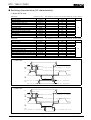
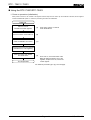
1. Power-on procedure (initialization)
When power is turned on, the contents of all registers and the output from the STD.P pin are undefined. Therefore, all the registers
must be initialized after power on. Follow the procedure given below for initialization.
Power On
Start the counter
Initialize the control registers
(A)
Check the status of the BUSY bit
(B)
STOP and RESET the counter
(C)
At ths point, there is no need to
check the BUSY bit.
Set the current time in the registers
(initialize the S1 to W registers)
Start the counter and release
the HOLD status
To next process
(A)
From here on, check the status of the
BUSY bit before accessing any of the
registers, except for the CD, CE and CF
control register.
For details of processes (A) to (C), see next page.
Page - 14
MQ - 162 - 02
RTC - 72421 / 72423
(A)Starting the count
START
Set the CF register
Reg.F ← 0*00B
TEST ← 0
24/12 ← 0 or 1
STOP ← 0
RESET ← 0
Set the CE register
This setting is not necessary when
the STD.P pin is not used
Set the CD register
← 0*00B
30 s ADJ ← 0
IRQ FLAG ← 0 or 1
← 0
HOLD
Reg.D
Set the IRQ FLAG bit to 0 when fixed-period
interrupt mode is used, or to 1when it is not
used.
To next process
(B)Checking the status of the BUSY bit
START
HOLD bit ← 1
Read the BUSY bit
BUSY bit=0?
YES
NO
HOLD bit ← 0
To next process
(C)Stopping and resetting the counter
START
Set the CF register
Reg.F ← 0*11B
TEST
24/12
STOP
RESET
←
←
←
←
0
0 or 1
1
1
To next process
Page - 15
MQ - 162 - 02
RTC - 72421 / 72423
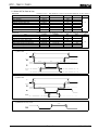
2. Read/write of S1 to W registers
Use one of the procedures shown below to access registers other than the control registers (CD, CE, and CF) while the RTC is
operating. Note that the control registers can be accessed regardless of the status of the BUSY bit.
Read or write when the HOLD bit is used
From previous process
From previous process
HOLD bit ← 1
HOLD bit ← 1
Read the BUSY bit
Read the BUSY bit
NO
BUSY bit = 0?
YES
or
HOLD bit ← 0
Read required digit data or
set the time
BUSY bit = 0?
NO
YES
HOLD bit ← 0
Read requierd digit data or
set the time
Wait 190 µs
HOLD bit ← 0
HOLD bit ← 0
To next process
To next process
Read when the HOLD bit is not used
From previous process
Read the required digit data
(1st time)
Store the read data (A←data)
Read the required digit data
(2nd time)
Store the read data (B←data)
NO
A=B?
YES
To next process
The operation when the HOLD bit is not used involves reading the same digit twice and comparing the read values. This is to
avoid the problem of reading unstable data that would occur if the data was read while the RTC was incrementing the count.
3. Write to 30-second ADJ bit
The 30-seconds ADJ function is enabled by writing 1 to the 30-seconds ADJ bit. Note that the counter registers (S1 to W) cannot be
accessed for 76.3 µs after this write. Therefore, follow one of the procedures shown below to use this function.
START
START
30 s ADJ bit ← 1
30 s ADJ bit ← 1
or
Read the 30 s ADJ bit
Read the 30 s ADJ bit
30 s ADJ bit=0?
YES
NO
30 s ADJ bit=0?
Wait
NO
YES
76.3 µs
END
END
Note
The crystal unit could be damaged if subjected to excessive shock. If the crystal unit should stop operating for such a reason, the
timer within the RTC will stop. While the crystal unit is operating, the BUSY bit is automatically reset every 190 µs and the 30seconds ADJ bit, every 76.3 µs , but this automatic reset cannot be done if the oscillation stops. Therefore, in such a status, it is no
longer possible to escape from the BUSY bit status check loop shown in subsection 2 above or the 30-seconds ADJ bit status check
loop shown in subsection 3 above, and you should consider backing up the system. To design a fail-safe system, provide an escape
from the loop to a procedure that can process such an error if the loop is repeated for more than 0.5 ms to 1.0 ms.
Page - 16
MQ - 162 - 02
RTC - 72421 / 72423
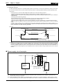
4. Using the CS1 pin
The RTC-72421/RTC-72423 has 2 chip-select signal systems: CS0 and CS1. Use CS0 as chip-select for ordinary bus access.
CS1 is not only used for CPU bus control, it also has the main function of switching between standby mode and operating mode.
(1) Functions
Providing the CS1 pin with the rated voltage levels enables CS1 to have the following functions:
• Enabling interface with microprocessor during operation within the operating voltage range (5.0 V ±0.5 V)
• Reducing current consumption during standby (to prevent through currents caused by unstable inputs, which is inherent to
C-MOS devices)
• Protecting internal data during standby
To ensure these functions, make sure that operation of the CS1 pins observes that following conditions:
• Make sure that the voltage input to the CS1 pin during operation is at least 4/5 VDD.
• Make sure that the voltage input to the CS1 pin during standby is as close as possible to 0 V, to prevent through currents.
• Make sure that the operation conforms to the timing chart below during a shift to standby mode or a return to operating
mode.
* Standby mode is a state in which a voltage lower than the RTC's rated range of operating supply voltage is applied (4.5 V
to 2.0 V). Under this condition, the timer continues to operate under battery back-up power, but the interface between the
interior and exterior of the RTC cannot be guaranteed.
(2) Timing
Shift to standby mode
Return to operation mode
Data hold mode
4V
4V
Must be at least 2.0 V
tCDR
tR
2 µs Min.
VIL2
(1/5 VDD)
2 µs Min.
VIH2
(4/5 VDD)
Must be at no more than 1/5VDD
Do not access the RTC while the voltage at CS1 is changing.
(3) Note
If the RTC is operated with timing conditions different from those shown above, data within the RTC could be overwritten
during a shift to standby mode or a return to operating mode. For example, if a write signal (WR) is generated during either of
the timing conditions (tCDR, tR) shown in the timing chart above, the data will be input before the RTC has stabilized. To
ensure that data is held throughout the entire standby process, make sure that the timing conditions shown in the chart are
followed.
Power supply circuit example
Note1
Note2
+5 V
+
VDD
Voltage
detection
circuit
RTC
CS1
Ceramic capacitor of
0.01 µF to 0.1 µF
GND
Note 1:This capacitor must be of a high capacity because a transient reverse current flows from the collector to the emitter of the
transistor when the power is turned off.
Note 2:Use a chargeable or lithium battery. If a chargeable battery is used, there is no need for the diode. If a lithium battery is used,
the diode is necessary. For specific details of the resistance of the resistor, contact the manufacturer of the battery that is used.
Page - 17
MQ - 162 - 02
RTC - 72421 / 72423
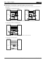
Examples of connection to general-purpose microprocessor
When connecting the RTC-72421/RTC-72423 to a microprocessor, carefully check the AC timings of both the RTC and the
microprocessor.
1. Connection to multiplexed bus type
8085/MCS48,51
RTC-72421/3
AD3
AD2
AD1
AD0
Upper address bus
Decoder
8085/MCS48,51
A3
A2
A1
A0
D3
D2
D1
D0
RTC-72421/3
AD3
AD2
AD1
AD0
Latch
Upper address bus
Decoder
A3
A2
A1
A0
D3
D2
D1
D0
IO/M
CS0
IO/M
CS0
ALE
ALE
ALE
ALE
RD
WR
RD
WR
RD
WR
RD
WR
The resistors on the RD and WR lines are not necessary if the CPU does not have a HALT or HOLD state.
2. Connection to Z80 or compatible CPU
Z80, SMC84C00AC
RTC-72421/3
A3
A2
A1
A0
D3
D2
D1
D0
A3
A2
A1
A0
D3
D2
D1
D0
Upper address bus
IORQ or
MEMRQ
Decoder
CS0
ALE
RD
RD
WR
WR
*Select IORQ or MEMRQ depending on whether the RTC maps I/O or memory of the CPU.
3. Connection to 68-series MPU
68 series MPU
RTC-72421/3
A3
A2
A1
A0
D3
D2
D1
D0
Upper address bus
A3
A2
A1
A0
D3
D2
D1
D0
Decoder
CS0
ALE
R/W
RD
E
WR
Page - 18
MQ - 162 - 02
RTC - 72421 / 72423
External dimensions
1.
RTC-72421
23.1 Max.
6.3
7.62
0.2 4.2
Min. Max.
1.52
0.46
0.25
2.54
Min.
2.54
0 - 15
2.
RTC-72423
16.3 Max.
7.9
12.0
0.1
Min.
0.35
2.8
Max.
0.2
1.0
0 - 10
1.27
Unless otherwise stated, all units are [mm]
Marking layout
Type
Frequency tlerance
RTC72421 A
EPSON 6053C
Logo mark
Indications of frequency tolerance
Type
RTC-72421
Indication
Tolerances
A
±10 x10
B
±50 x10
-6
±20 x10
A
RTC-72423
No indications
-6
-6
±50 x10
-6
Manufacturing lot no.
Note: The illustration is a general representation of the content and location of information on the
label, and is not a detailed specification of the typeface, size or positioning of printing used on the
label.
Page - 19
MQ - 162 - 02
RTC - 72421 / 72423
Reference data
1. Example of frequency and temperature characteristics
θT = +25 °C Typ.
α = -0.035 × 10⁻⁶ Typ.
× 10-6
1. Frequency and temperature characteristics can be approximated
using the following equations.
∆fT = α ( θT - θX )2
: Frequency deviation in any
∆fT
temperature
2
α
( 1 / °C ) : Coefficient of secondary temperature
-6
2
( −0.035±0.005 ) × 10 / °C
: Ultimate temperature (+25±5 °C)
θT ( °C )
: Any temperature
θX ( °C )
Frequency ∆fT
0
-50
-100
-150
-50
0
[Finding the frequency stability]
+50
+100
Temperature [°C]
2. To determine overall clock accuracy, add the frequency precision
and voltage characteristics.
∆f/f = ∆f/fo + ∆fT + ∆fV
: Clock accuracy (stable frequency) in
∆f/f
any temperature and voltage.
: Frequency precision
: Frequency deviation in any
temperature.
: Frequency deviation in any voltage.
∆f/fo
∆fT
∆fV
3. How to find the date difference
Date Difference = ∆f/f × 86400(s)
-6
* For example: ∆f/f = 11.574 × 10 is an error of
approximately 1 second/day.
2. Frequency voltage characteristics ( Typ. )
3. Current consumption voltage characteristics ( Typ. )
-6
Frequency[x10 ]
Current consumption[µA]
Condtions
Conditions
5 V reference,Ta=+25 °C
CS1=0 V, No load, Ta=+25 °C
+4
5
+2
4
2
3
4
5
6
3
0
-2
Supply Voltage(VDD) [V]
2
1
-4
2
Note:
3
4
5
Supply voltage(VDD)
6
This data shows average values for a sample lot.
For rated values, see the specifications.
Page - 20
MQ - 162 - 02
RTC - 72421 / 72423
Application notes
1. Notes on handling
This module uses a C-MOS IC to realize low power consumption.
handling.
(1) Static electricity
Carefully note the following cautions when
While this module has built-in circuitry designed to protect it against electrostatic discharge, the chip could still be
damaged by a large discharge of static electricity. Containers used for packing and transport should be
constructed of conductive materials. In addition, only soldering irons, measurement circuits, and other such
devices which do not leak high voltage should be used with this module, which should also be grounded when
such devices are being used.
(2) Noise
If a signal with excessive external noise is applied to the power supply or input pins, the device may malfunction or
"latch up." In order to ensure stable operation, connect a filter capacitor (preferably ceramic) of greater that 0.1 µF
as close as possible to the power supply pins ( between VDD and GND ). Also, avoid placing any device that
generates high level of electronic noise near this module.
∗ Do not connect signal lines to the shaded area in the figure shown in Fig.1 and, if possible, embed this area in a
GND land.
(3) Voltage levels of input pins
Apply signal levels that are as close as possible to VDD and ground, to all pins except the CS1 pin. Mid-level
potentials will cause increased current consumption and a reduced noise margin, and can impair the functioning of
the device.
Since it is likely that power consumption will increase excessively and operation cannot be guaranteed, the setting
of the voltage range of VIH2 and VIL2 at the CS1 pin should be such that the system is designed so that it is not
affected by ripple or other noise.
Note that the CS1 pin cannot handle a TTL interface.
(4) Handling of unused pins
Since the input impedance of the signal pins is extremely high, operating the device with these pins open circuit
can lead to malfunctions due to noise. Pull-up or pull-down resistors should be provided for all unused signal pins.
The N.C. pins should be connected to either VDD or GND, to prevent noise. If not using the ALE pin, connect it
directly to VDD.
2. Notes on packaging
(1) Soldering temperature conditions
If the temperature within the package exceeds +260 °C, the characteristics of the crystal oscillator will be degraded
and it may be damaged. Therefore, always check the mounting temperature before mounting this device. Also,
check again if the mounting conditions are later changed.
∗ See Fig.2 for the soldering conditions of SMD products.
(2) Mounting equipment
While this module can be used with general-purpose mounting equipment, the internal crystal oscillator may be
damaged in some circumstances, depending on the equipment and conditions. Therefore, be sure to check this. In
addition, if the mounting conditions are later changed, the same check should be performed again.
(3) Ultrasonic cleaning
Depending on the usage conditions, there is a possibility that the crystal oscillator will be damaged by resonance
during ultrasonic cleaning. Since the conditions under which ultrasonic cleaning is carried out (the type of cleaner,
power level, time, state of the inside of the cleaning vessel, etc.) vary widely, this device is not warranted against
damage during ultrasonic cleaning.
(4) Mounting orientation
This device can be damaged if it is mounted in the wrong orientation. Always confirm the orientation of the device
before mounting.
(5) Leakage between pins
Leakage between pins may occur if the power is turned on while the device has condensation or dirt on it. Make
sure the device is dry and clean before supplying power to it.
Fig. 1: Example GND Pattern
Fig. 2: Soldering Conditions of SMD Products
Air Reflow Profile
Temperature[ °C ]
RTC-72421
+240 °C Max.
10 s ± 1 s
+235 °C ± 5 °C
+200 °C
RTC-72423
+150 °C ± 10 °C
90 s ± 30 s
30 s ± 10 s
Time[ s ]
Page - 21
MQ - 162 - 02
Application Manual
Distributor
AMERICA
EPSON ELECTRONICS AMERICA, INC.
HEADQUARTER
Atlanta Office
Boston Office
Chicago Office
El Segundo Office
150 River Oaks Parkway, San Jose, CA 95134, U.S.A.
Phone: (1)800-228-3964 (Toll free) : (1)408-922-0200 Fax: (1)408-922-0238
3010 Royal Blvd. South, Ste. 170,Alpharetta,GA 30005
Phone: (1)877-332-0200 (Toll free) : (1)770-777-2078 Fax: (1)770-777-2637
301Edgewater Place, Ste. 120, Wakefield, MA 01880
Phone: (1)800-922-7667 (Toll free) : (1)781-246-3600 Fax: (1)781-246-5443
101 Virginia St., Ste. 290, Crystal Lake, IL 60014
Phone: (1)800-853-3588 (Toll free) : (1)815-455-7630 Fax: (1)815-455-7633
1960 E. Grand Ave., Ste. 200, El Segundo, CA 90245
Phone: (1)800-249-7730 (Toll free) : (1)310-955-5300 Fax: (1)310-955-5400
EUROPE
EPSON EUROPE ELECTRONICS GmbH
HEADQUARTER
- GERMANY Leverkusen Office
- UNITED KINGDOM UK BRANCH OFFICE
- FRANCE FRENCH BRANCH OFFICE
Riesstrasse 15, 80992 Munich Germany
Phone: (49)-(0)89-14005-0 Fax: (49)-(0)89-14005-110
Altstadtstrasse 176, 51379 Leverkusen Germany
Phone: (49)-(0)2171-5045-0 Fax: (49)-(0)2171-5045-10
Unit 2.4, Doncastle House Doncastle Road Bracknell Berkshire RG12 8PE England
Phone: (44)-(0)1344-381700 Fax: (44)-(0)1344-381701
1 Avenue de l' Atlantique LP 915 Les Conquerants Z.A. de Courtaboeuf 2 F-91976
Les Ulis Cedex France
Phone: (33)-(0)1-64862350 Fax: (33)-(0)1-64862355
ASIA
- CHINA -
EPSON (CHINA) CO., LTD.
SHANGHAI BRANCH
28F, Beijing Silver Tower 2# North RD DongSangHuan ChaoYang District, Beijing, China
Phone: (86) 10-6410-6655 Fax: (86) 10-6410-7319
4F, Bldg.,27, No.69, Guijing Road, Caoheijing, Shanghai, China
Phone: (86) 21-6485-0835 Fax: (86) 21-6485-0775
- HONG KONG CHINA -
EPSON HONG KONG LTD.
20/F., Harbour Centre, 25 Harbour Road, Wanchai, Hong kong
Phone: (852) 2585-4600 Fax: (852) 2827-2152
EPSON ELECTRONIC TECHNOLOGY DEVELOPMENT (SHENZHEN )CO., LTD.
Flat 16A, 16/F, New Times Plaza, No.1 Taizi Road, Shenzhen, China
Phone: (86) 755-6811118 Fax: (86) 755-6677786
- TAIWAN -
EPSON TAIWAN TECHNOLOGY & TRADING LTD.
10F, No.287, Nanking East Road, Sec.3, Taipei, Taiwan
Phone: (886) 2-2717-7360 Fax: (886)2-2718-9366
- SINGAPORE -
EPSON SINGAPORE PTE. LTD.
No.1, Temasek Avenue #36-00, Millenia Tower, Singapore 039192
Phone: (65) 337-7911 Fax: (65) 334-2716
- KOREA -
SEIKO EPSON CORPORATION KOREA Office
50F, KLI 63 Building,60 Yoido-dong, Youngdeungpo-Ku, Seoul, 150-763, Korea
Phone: (82) 2-784-6027 Fax: (82) 2-767-3677
ELECTRONIC DEVICE MARKETING DEPARTMENT
Electronic devices information on WWW server