1
Intel® Server Board S5000PAL /
S5000XAL
Technical Product Specification
Intel order number: D31979-010
Revision 1.7
February 2008
Enterprise Platforms and Services Division – Marketing
ii
Revision 1.7
Intel order number: D31979-010
Intel® Server Board S5000PAL / S5000XAL TPS
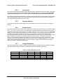
Revision History
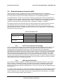
Revision History
Date
April 2006
Revision
Number
1.0
Modifications
June 2006
1.1
Updated theoretical memory bandwidth performance numbers.
Added Platform Control sections.
August 2006
1.2
Memory RAS is now available.
Updated Snoop Filter Section.
Updated Figures #16 and #25.
January 2007
1.3
Updated Table 44 BMC sensor.
Updated CMOS clear and password reset usage procedures.
Updated regulatory tables.
May 2007
1.4
Removed platform control information that can be found in the Intel S5000
Server Board Family Datasheet.
August 2007
1.5
Updated processor support section.
First external release.
®
October 2007
1.6
Updated Table 44 BMC sensor.
February 2008
1.7
Updated Processor support section
iii
Revision 1.7
Intel order number: D31979-010
Disclaimers
Intel® Server Board S5000PAL / S5000XAL TPS
Disclaimers
Information in this document is provided in connection with Intel® products. No license, express or implied,
by estoppel or otherwise, to any intellectual property rights is granted by this document. Except as
provided in Intel's Terms and Conditions of Sale for such products, Intel assumes no liability whatsoever,
and Intel disclaims any express or implied warranty, relating to sale and/or use of Intel products including
liability or warranties relating to fitness for a particular purpose, merchantability, or infringement of any
patent, copyright or other intellectual property right. Intel products are not intended for use in medical, life
saving, or life sustaining applications. Intel may make changes to specifications and product descriptions
at any time, without notice.
Designers must not rely on the absence or characteristics of any features or instructions marked
"reserved" or "undefined." Intel reserves these for future definition and shall have no responsibility
whatsoever for conflicts or incompatibilities arising from future changes to them.
The Intel® Server Board S5000PAL and the Intel® Server Board S5000XAL may contain design defects
or errors known as errata which may cause the product to deviate from published specifications. Current
characterized errata are available on request.
Intel Corporation server baseboards support peripheral components and contain a number of highdensity VLSI and power delivery components that need adequate airflow to cool. Intel’s own chassis are
designed and tested to meet the intended thermal requirements of these components when the fully
integrated system is used together. It is the responsibility of the system integrator that chooses not to use
Intel developed server building blocks to consult vendor datasheets and operating parameters to
determine the amount of air flow required for their specific application and environmental conditions. Intel
Corporation can not be held responsible if components fail or the server board does not operate correctly
when used outside any of their published operating or non-operating limits.
Intel, Pentium, Itanium, and Xeon are trademarks or registered trademarks of Intel Corporation.
*Other brands and names may be claimed as the property of others.
Copyright © Intel Corporation 2008.
iv
Revision 1.7
Intel order number: D31979-010
Intel® Server Board S5000PAL / S5000XAL TPS
Table of Contents
Table of Contents
1.
2.
3.
Introduction ........................................................................................................................ 12
1.1
Chapter Outline...................................................................................................... 12
1.2
Server Board Use Disclaimer ................................................................................ 12
Product Overview............................................................................................................... 13
2.1
Intel® Server Board S5000PAL / S5000XAL Feature Set ..................................... 13
2.2
Server Board Layout.............................................................................................. 14
2.2.1
Connector and Component Locations ................................................................... 15
2.2.2
Light Guided Diagnostic LED Locations ................................................................ 17
2.2.3
External I/O Connector Locations.......................................................................... 18
2.2.4
Server Board Mechanical Drawings ...................................................................... 19
Functional Architecture ..................................................................................................... 24
3.1
Intel® 5000P and 5000X Memory Controller Hubs (MCH) ..................................... 25
3.1.1
System Bus Interface............................................................................................. 25
3.1.2
Processor Support ................................................................................................. 25
3.1.3
Memory Sub-system .............................................................................................. 26
3.1.4
Snoop Filter (5000X MCH only) ............................................................................. 32
3.2
ESB-2 IO Controller ............................................................................................... 32
3.2.1
PCI Sub-system..................................................................................................... 33
3.2.2
Serial ATA Support ................................................................................................ 35
3.2.3
Parallel ATA (PATA) Support ................................................................................ 36
3.2.4
USB 2.0 Support.................................................................................................... 36
3.3
Video Support ........................................................................................................ 36
3.4
Network Interface Controller (NIC) ........................................................................ 38
3.4.1
Intel® I/O Acceleration Technology ........................................................................ 38
3.4.2
MAC Address Definition......................................................................................... 38
3.5
Super I/O ............................................................................................................... 39
4.
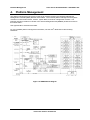
Platform Management........................................................................................................ 42
5.
Connector / Header Locations and Pin-outs.................................................................... 43
5.1
Board Connector Information................................................................................. 43
5.2
Power Connectors ................................................................................................. 44
5.3
System Management Headers .............................................................................. 45
5.3.1
Intel® Remote Management Module (RMM) Connector ........................................ 45
5.3.2
Intel® RMM NIC Connector .................................................................................... 46
5.3.3
LCP/AUX IPMB Header ......................................................................................... 47
5.3.4
IPMB Header ......................................................................................................... 47
Revision 1.7
v
Intel order number: D31979-010
Table of Contents
5.4
Riser Card Slots..................................................................................................... 47
5.5
SSI Control Panel Connector................................................................................. 52
5.6
Bridge Board Connector ........................................................................................ 52
5.7
I/O Connector Pin-out Definition ............................................................................ 54
5.7.1
VGA Connector...................................................................................................... 54
5.7.2
NIC Connectors ..................................................................................................... 54
5.7.3
IDE Connector ....................................................................................................... 55
5.7.4
Intel® I/O Expansion Module Connector ................................................................ 55
5.7.5
SATA Connectors .................................................................................................. 56
5.7.6
Serial Port Connectors........................................................................................... 57
5.7.7
Keyboard and Mouse Connector ........................................................................... 57
5.7.8
USB 2.0 Connectors .............................................................................................. 58
5.8
6.
vi
Recovery Jumper Blocks ....................................................................................... 60
6.1.1
CMOS Clear and Password Reset Usage Procedure ........................................... 61
6.1.2
BMC Force Update Procedure .............................................................................. 61
6.2
BIOS Select Jumper .............................................................................................. 62
6.3
External RJ45 Serial Port Jumper Block................................................................ 63
Light Guided Diagnostics.................................................................................................. 64
7.1
5-Volt Standby LED ............................................................................................... 64
7.2
System ID LED and System Status LED ............................................................... 65
7.2.1
8.
Fan Headers .......................................................................................................... 59
Jumper Block Settings ...................................................................................................... 60
6.1
7.
Intel® Server Board S5000PAL / S5000XAL TPS
System Status LED – BMC Initialization ................................................................ 66
7.3
DIMM Fault LEDs .................................................................................................. 67
7.4
Processor Fault LED.............................................................................................. 67
7.5
Post Code Diagnostic LEDs .................................................................................. 68
Power and Environmental Specifications ........................................................................ 69
8.1
Intel® Server Board S5000PAL / S5000XAL Design Specifications ..................... 69
8.2
Server Board Power Requirements ....................................................................... 70
8.2.1
Processor Power Support...................................................................................... 70
8.2.2
Power Supply Output Requirements ..................................................................... 71
8.2.3
Turn On No Load Operation .................................................................................. 71
8.2.4
Grounding .............................................................................................................. 72
8.2.5
Standby Outputs .................................................................................................... 72
8.2.6
Remote Sense ....................................................................................................... 72
8.2.7
Voltage Regulation ................................................................................................ 72
8.2.8
Dynamic Loading ................................................................................................... 73
8.2.9
Capacitive Loading ................................................................................................ 73
Revision 1.7
Intel order number: D31979-010
Intel® Server Board S5000PAL / S5000XAL TPS
9.
Table of Contents
8.2.10
Closed-Loop Stability............................................................................................. 73
8.2.11
Common Mode Noise ............................................................................................ 73
8.2.12
Ripple / Noise ........................................................................................................ 74
8.2.13
Soft Starting ........................................................................................................... 74
8.2.14
Timing Requirements............................................................................................. 74
8.2.15
Residual Voltage Immunity in Standby Mode ........................................................ 77
Regulatory and Certification Information......................................................................... 78
9.1
9.1.1
9.2
Product Regulatory Compliance ............................................................................ 78
Product Safety & Electromagnetic (EMC) Compliance.......................................... 78
Electromagnetic Compatibility Notices .................................................................. 79
9.2.1
FCC Verification Statement (USA) ........................................................................ 79
9.2.2
ICES-003 (Canada) ............................................................................................... 79
9.2.3
Europe (CE Declaration of Conformity) ................................................................. 79
9.2.4
BSMI (Taiwan) ....................................................................................................... 80
9.2.5
RRL (Korea)........................................................................................................... 80
9.3
Product Ecology Compliance................................................................................. 81
9.4
Other Markings ...................................................................................................... 82
Appendix A: Integration and Usage Tips................................................................................ 83
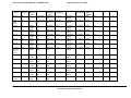
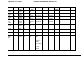
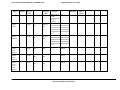
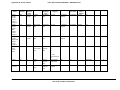
Appendix B: BMC Sensor Tables ............................................................................................ 84
Appendix C: POST Code Diagnostic LED Decoder ............................................................. 100
Appendix D: POST Error Messages and Handling .............................................................. 104
Appendix E: Supported Intel® Server Chassis ..................................................................... 107
Glossary................................................................................................................................... 110
Reference Documents ............................................................................................................ 113
Revision 1.7
vii
Intel order number: D31979-010
List of Figures
Intel® Server Board S5000PAL / S5000XAL TPS
List of Figures
Figure 1. Components & Connector Location Diagram .............................................................. 16
Figure 2. Light Guided Diagnostic LED Location Diagram ......................................................... 17
Figure 3. Intel® Server Board S5000PAL / S5000XAL ATX I/O Layout ..................................... 18
Figure 4. Intel® Server Board S5000PAL / S5000XAL – Hole and Component Positions (1 of 2)19
Figure 5. Intel® Server Board S5000PAL / S5000XAL – Hole and Component Positions (2 of 2)20
Figure 6. Intel® Server Board S5000PAL / S5000XAL – Restricted Areas on Side 1 ................ 21
Figure 7. Intel® Server Board S5000PAL / S5000XAL – Restricted Areas on Side 2 ................ 22
Figure 8. Intel® Server Board S5000PAL / S5000XAL - Primary Side Duct and VR Restrictions23
Figure 9. Server Board Functional Block Diagram...................................................................... 24
Figure 10. CEK Processor Mounting .......................................................................................... 26
Figure 11. Memory Layout .......................................................................................................... 27
Figure 12. Recommended Minimum Two DIMM Memory Configuration .................................... 29
Figure 13. Recommended Four DIMM Configuration ................................................................. 30
Figure 14. Single Branch Mode Sparing DIMM Configuration .................................................... 31
Figure 15. Serial Port Configuration Jumper Location ................................................................ 40
Figure 16. SMBUS Block Diagram.............................................................................................. 42
Figure 17. Recovery Jumper Blocks (J1D1, J1D2, J1D3) ......................................................... 60
Figure 18. BIOS Select Jumper (J3H1) ...................................................................................... 62
Figure 19. External RJ45 Serial Port Configuration Jumper ....................................................... 63
Figure 20. 5V Standby Status LED Location .............................................................................. 64
Figure 21. System ID LED and System Status LED Locations................................................... 65
Figure 22. DIMM Fault LED Locations........................................................................................ 67
Figure 23. Processor Fault LED Location ................................................................................... 67
Figure 24. POST Code Diagnostic LED Location ....................................................................... 68
Figure 25. Power Distribution Block Diagram ............................................................................. 70
Figure 26. Output Voltage Timing ............................................................................................... 75
Figure 27. Turn On/Off Timing (Power Supply Signals).............................................................. 76
Figure 28. Diagnostic LED Placement Diagram ....................................................................... 100
Figure 29. 1U – Intel® Server Chassis SR1500 Overview ........................................................ 107
Figure 30. 1U – Intel® Server Chassis SR1550 Overview ........................................................ 108
Figure 31. 2U – Intel® Server Chassis SR2500 Overview ........................................................ 109
viii
Revision 1.7
Intel order number: D31979-010
Intel® Server Board S5000PAL / S5000XAL TPS
List of Tables
List of Tables
Table 1. I2C Addresses for Memory Module SMB ..................................................................... 27
Table 2. Maximum 8 DIMM System Memory Configuration – x8 Single Rank ........................... 28
Table 3. Maximum 8 DIMM System Memory Configuration – x4 Dual Rank .............................. 28
Table 4. PCI Bus Segment Characteristics................................................................................. 33
Table 5. Video Modes ................................................................................................................. 37
Table 6. NIC2 Status LED........................................................................................................... 38
Table 7. Serial A Header Pin-out ................................................................................................ 39
Table 8. Rear Serial B Port Adapter Pin-out ............................................................................... 40
Table 9. Board Connector Matrix ................................................................................................ 43
Table 10. Power Connector Pin-out (J3K3) ................................................................................ 44
Table 11. 12V Power Connector Pin-out (J3K4)......................................................................... 44
Table 12. Power Supply Signal Connector Pin-out (J1K1) ......................................................... 44
Table 13. Intel® RMM Connector Pin-out (J1C5) ........................................................................ 45
Table 14. 30-pin Intel® RMM NIC Module Connector Pin-out (J1B2) ......................................... 46
Table 15. LPC/AUX IPMB Header Pin-out (J1C2) ...................................................................... 47
Table 16. IPMB Header Pin-out (J1C3) ...................................................................................... 47
Table 17. Low-profile Riser Slot Pin-out (J5B1).......................................................................... 47
Table 18. Full-height Riser Slot Pin-out (J4F1)........................................................................... 48
Table 19. Front Panel SSI Standard 24-pin Connector Pin-out (J3H2) ...................................... 52
Table 20. 120-pin Bridgeboard Connector Pin-out (J4G1) ......................................................... 52
Table 21. VGA Connector Pin-out (J6A1)................................................................................... 54
Table 22. RJ-45 10/100/1000 NIC Connector Pin-out (JA8A1, JA8A2)...................................... 54
Table 23. 44-pin IDE Connector Pin-out (J3G1) ......................................................................... 55
Table 24. 50-pin Intel® I/O Expansion Module Connector Pin-out (J3B1)................................... 56
Table 25. SATA Connector Pin-out (J1H1, J1G2, J1G1, J1F2, J1E3) ....................................... 56
Table 26. External RJ-45 Serial ‘B’ Port Pin-out (J9A2) ............................................................. 57
Table 27. Internal 9-pin Serial ‘A’ Header Pin-out (J1B1) ........................................................... 57
Table 28. Stacked PS/2 Keyboard and Mouse Port Pin-out (J9A1) ........................................... 57
Table 29. External USB Connector Pin-out (J5A1, J6A2)........................................................... 58
Table 30. Internal USB Connector Pin-out (J1J1)....................................................................... 58
Table 31. SSI Fan Connector Pin-out (J9K1,J5K1,J3K1,J3K2,J7A2,J7A1) ............................... 59
Table 32. Recovery Jumpers (J1D1, J1D2, J1D3) ..................................................................... 60
Table 33: Server Board Design Specifications ........................................................................... 69
Table 34. Dual-Core Intel® Xeon® Processor 5000 Sequence TDP Guidelines per processor .. 70
Table 35. 600W Load Ratings .................................................................................................... 71
Revision 1.7
ix
Intel order number: D31979-010
List of Tables
Intel® Server Board S5000PAL / S5000XAL TPS
Table 36: No load operating range ........................................................................................... 71
Table 37. Voltage Regulation Limits ........................................................................................... 72
Table 38. Transient Load Requirements..................................................................................... 73
Table 39. Capacitive Loading Conditions ................................................................................... 73
Table 40. Ripple and Noise......................................................................................................... 74
Table 41. Output Voltage Timing ................................................................................................ 75
Table 42. Turn On/Off Timing ..................................................................................................... 76
Table 43. BMC Sensors.............................................................................................................. 86
Table 44: POST Progress Code LED Example ........................................................................ 100
Table 45. Diagnostic LED POST Code Decoder ...................................................................... 101
Table 46. POST Error Messages and Handling........................................................................ 104
Table 47. POST Error Beep Codes .......................................................................................... 106
Table 48. BMC Beep Codes ..................................................................................................... 106
x
Revision 1.7
Intel order number: D31979-010
Intel® Server Board S5000PAL / S5000XAL TPS
List of Tables
< This page intentionally left blank. >
Revision 1.7
xi
Intel order number: D31979-010
Intel® Server Board S5000PAL / S5000XAL TPS
Introduction
1.
Introduction
This Technical Product Specification (TPS) provides board specific information detailing the features,
functionality, and high level architecture of the Intel® Server Board S5000PAL and Intel® Server Board
S5000XAL. The Intel® S5000 Series Chipsets Server Board Family Datasheet should also be referenced
for more in depth detail of various board sub-systems including chipset, BIOS, System Management, and
System Management software.
In addition, design level information for specific sub-systems can be obtained by ordering the External
Product Specifications (EPS) or External Design Specifications (EDS) for a given sub-system. EPS and
EDS documents are not publicly available. They are only made available under NDA with Intel and must
be ordered through your local Intel representative.
The Intel® Server Board S5000PAL/XAL may contain design defects or errors known as errata which
may cause the product to deviate from published specifications. Refer to the Intel® Server Board
S5000PAL/XAL Specification Update for published errata.
1.1
Chapter Outline
This document is divided into the following chapters
•
Chapter 1 – Introduction
•
Chapter 2 – Server Board Overview
•
Chapter 3 – Functional Architecture
•
Chapter 4 – Platform Management
•
Chapter 5 – Connector & Header Location and Pin-out
•
Chapter 6 – Configuration Jumpers
•
Chapter 7 – Light Guided Diagnostics
•
Chapter 8 – Power and Environmental Specifications
•
Chapter 9 – Regulatory and Certification Information
•
Appendix A – Integration and Usage Tips
•
Appendix B – BMC Sensor Tables
•
Appendix C – POST Code Diagnostic LED Decoder
•
Appendix D – Post Code Errors
•
Appendix E – Supported Intel® Server Chassis
1.2
Server Board Use Disclaimer
Intel Corporation server boards support add-in peripherals and contain a number of high-density VLSI
and power delivery components that need adequate airflow to cool. Intel ensures through its own chassis
development and testing that when Intel server building blocks are used together, the fully integrated
system will meet the intended thermal requirements of these components. It is the responsibility of the
system integrator who chooses not to use Intel developed server building blocks to consult vendor
datasheets and operating parameters to determine the amount of air flow required for their specific
application and environmental conditions. Intel Corporation cannot be held responsible if components fail
or the server board does not operate correctly when used outside any of their published operating or nonoperating limits.
12
Revision 1.7
Intel order number: D31979-010
Intel® Server Board S5000PAL / S5000XAL TPS
2.
Product Overview
Product Overview
The Intel® Server Board S5000PAL and Intel® Server Board S5000XAL are monolithic printed circuit
boards with features that were designed to support the high-density 1U and 2U server markets.
2.1
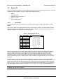
Intel® Server Board S5000PAL / S5000XAL Feature Set
Feature
Description
Processors
771-pin LGA sockets supporting 1 or 2 Dual-Core Intel® Xeon® processors 5000 sequence,
with system bus speeds of 667 MHz, 1066 MHz, or 1333 MHz
Memory
8 Keyed DIMM slots supporting fully buffered DIMM technology (FBDIMM) memory. 240-pin
DDR2-533 and DDR2-677 FBDIMMs must be used.
Chipset
Intel® 5000 Chipset Family which includes the following components:
Intel® 5000P Memory Controller Hub or Intel® 5000X Memory Controller Hub
Intel® 6321ESB I/O Controller Hub1
Note: Intel will only make available an OEM SKU of this server board using the Intel® 5000X
Memory Controller Hub.
On-board
Connectors/Headers
External connections:
Stacked PS/2* ports for keyboard and mouse
RJ45 Serial B port
Two RJ45 NIC connectors for 10/100/1000 Mb connections
Two USB 2.0 ports
Video Connector
Internal connectors/headers:
One USB port header, capable of providing two USB 2.0 ports
One DH10 Serial A header
Six SATA ports via the ESB-2 and integrated SW RAID 0/1/10 support
One 44pin (power + I/O) ATA/100 connector for optical drive support
One Intel® Remote Management Module (Intel® RMM) connector (Intel® RMM use is
optional)
One Intel® I/O Expansion Module Connector supporting:
Dual GB NIC Intel® I/O Expansion Module (Optional)
External SAS Intel® I/O Expansion Module (Optional)
Infiniband* I/O Expansion Module (Optional)
SSI-compliant 24-pin control panel header
SSI-compliant 24-pin main power connector, supporting the ATX-12V standard on the first
20 pins
8-Pin +12V Processor Power Connector
Add-in PCI, PCI-X*, PCI
Express* Cards
On-board Video
ATI* ES1000 video controller with 16MB DDR SDRAM
On-board Hard Drive
Controller
Six ESB-2 SATA ports.
Intel® Embedded Server RAID Technology II with SW RAID levels 0/1/10.
Optional support for SW RAID 5 with activation key.2
LAN
One low profile riser slot supporting 1U or 2U PCIe* riser cards
One full height riser slot supporting 1U or 2U PCI-X* and PCIe* riser cards
Two 10/100/1000 Intel® 82563EB PHYs supporting Intel® I/O Acceleration Technology
System Fans
Six 4-pin Fan Headers supporting two processor fans, and four system fans
System Management
Support for Intel® System Management Software
1 For the remainder of this document, the Intel® 6321ESB I/O Controller Hub will be refferred to as ESB-2.
2 Onboard SATA SW RAID 5 support provided as a post-launch product feature.
Revision 1.7
13
Intel order number: D31979-010
Intel® Server Board S5000PAL / S5000XAL TPS
Product Overview
2.2
14
Server Board Layout
Revision 1.7
Intel order number: D31979-010
Intel® Server Board S5000PAL / S5000XAL TPS
2.2.1
Product Overview
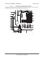
Connector and Component Locations
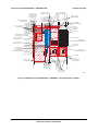
The following figure shows the board layout of the server board. Each connector and major component is
identified by a number or letter, and a description is given below the figure.
A
B C
D E F
G H I
QQ
J
PP
K
L
OO
NN
MM
LL
KK
JJ
II
M
N
HH
GG
FF
EE
O
DD
CC
BB
AA
P
Q
Z
Y
X
W V U TS
R
TP02071
Revision 1.7
15
Intel order number: D31979-010
Intel® Server Board S5000PAL / S5000XAL TPS
Product Overview
A
Description
BIOS Bank Select Jumper
B
Intel ESB-2 IO Controller Hub
W
CPU Power Connector
C
IO Module Option Connector
X
Main Power Connector
D
POST Code Diagnostic LEDs
Y
Battery
E
Intel Adaptive Slot – Full Height
Z
Power Supply Management Connector
F
PCI Express* Riser Slot – Low Profile
AA
Dual Port USB 2.0 Header
G
System Identification LED - Blue
BB
System Fan #1 Header
H
External IO Connectors
CC
SSI 24-pin Control Panel Header
I
Status LED – Green / Amber
DD
SATA 0
J
Serial ‘B’ Port Configuration Jumper
EE
SATA 1
K
System Fan #4 Header
FF
SATA 2
V
®
®
Description
System Fan #2 Header
L
System Fan #3 Header
GG
SATA 3
M
FBDIMM Slots
HH
SATA 4
N
Intel 5000P Memory Controller Hub (MCH) or
®
Intel 5000X Memory Controller Hub (MCH)
II
SATA 5
O
CPU #1 Connector
JJ
SATA SW RAID 5 Activation Key Connector
P
CPU #2 Connector
KK
Intel Remote Management Module (RMM)
Connector
Q
CPU #1 Fan Header
LL
System Recovery Jumper Block
R
Voltage Regulator Heat Sink
MM
Chassis Intrusion Switch Header
S
CPU #2 Fan Header
NN
3-pin IPMB Header
T
Bridge Board Connector
OO
Intel Local Control Panel Header
U
ATA-100 Optical Drive Connector (Power+IO)
PP
Serial ‘A’ Header
QQ
Intel RMM NIC Connector
®
®
®
®
Figure 1. Components & Connector Location Diagram
16
Revision 1.7
Intel order number: D31979-010
Intel® Server Board S5000PAL / S5000XAL TPS
2.2.2
Product Overview
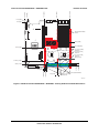
Light Guided Diagnostic LED Locations
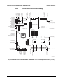
B
C
A
I J K L DM N O P
GS
QE
RF
TP02317
A
Description
Post Code Diagnostic LEDs
B
System Identification LED – Blue
F
CPU Fault LED
C
System Status LED – Green / Amber
G
5-Volt Stand-by Present
LED
D
DIMM Fault LEDs
E
Description
CPU Fault LED
Figure 2. Light Guided Diagnostic LED Location Diagram
Revision 1.7
17
Intel order number: D31979-010
Intel® Server Board S5000PAL / S5000XAL TPS
Product Overview
2.2.3
External I/O Connector Locations
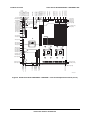
The drawing below shows the layout of the rear I/O components for the server board.
A
B
C
D
E
F
G
H
TP02296
A
PS/2 Mouse
E
NIC port 2 (1 Gb)
B
PS/2 Keyboard
F
Video
C
Serial Port B
G
USB port 1
D
NIC port 1 (1 Gb)
H
USB port 2
Figure 3. Intel® Server Board S5000PAL / S5000XAL ATX I/O Layout
18
Revision 1.7
Intel order number: D31979-010
Intel® Server Board S5000PAL / S5000XAL TPS
288.29 [11.350]
Molex 43202-8927
6026A0027801
196.85 [7.750]
118.11 [4.650]
2 x 124.46 [4.900]
2 x 86.89 [3.421]
82.80 [3.260]
44.89 [1.767]
33.91 [1.335]
Server Board Mechanical Drawings
2 x 0.00 [0.000]
11.02 [0.434]
11.91 [0.469]
16.76 [0.660]
16.51 [0.650]
2.2.4
Product Overview
10.16 [0.400]
2 x 0.00 [0.000]
0.91 [0.036]
15.24 [0.600]
21.59 [0.850]
Lotes B2515BB2M
6012A0019603
45.59 [1.795]
2 x 49.35 [1.943]
62.66 [2.467]
67.31 [2.650]
Molex 22-44-7031
6012A0099701-HDR4P
0.16 [0.006]
22.86 [0.900]
7 x Ø 3.96 [0.156]
Molex 877715-3205
6012A0100101
Molex 22-44-7031
6012A0099701
9 x Ø 0.125 [3.18] Typ.
152.40 [6.000]
FCI 10027747-114101
6012A0105001
2 x 101.60 [4.000]
2 x 3.28
[0.129]
124.26 [4.892]
127.43 [5.017]
5 x Ø 8.00 [0.315]
Silkscreen on secondary
side for spacer
AMP 177983-5
6012A0103201
6 x Betterment
BTM-PP02.2F1611.007X
6012B0018302
81.28
[3.200] Typ.
55.35
[2.179]
4 x 187.93 [7.399]
Lotes AAA-PCI-033-K02
6012B0051002
227.33 [8.950]
228.60 [9.000]
Lotes B2515BB2M
6012A0019603
Lotes B4L60BB2L
6012A0105401
8 x Ø 10.16 [0.400]
2 x 281.94 [11.100]
2 x 223.80 [8.811]
38.10
[1.500] Typ.
2 x 141.25 [5.561]
124.46 [4.900]
2 x 59.69 [2.350]
Molex 3930-0080
6012A0022801
AMP 794108-1
6012A0022801
9.65 [0.380]
5.08 [0.200]
3 x 312.42 [12.300]
320.04 [12.600]
TP02316
Figure 4. Intel® Server Board S5000PAL / S5000XAL – Hole and Component Positions (1 of 2)
Revision 1.7
19
Intel order number: D31979-010
278.38 [10.960]
280.71 [11.052]
263.14 [10.360]
244.27 [9.617]
224.21 [8.827]
200.13 [7.879]
205.97 [8.109]
175.03 [6.891]
141.78 [5.582]
87.88 [3.460]
94.23 [3.710]
100.58 [3.960]
104.39 [4.110]
106.93 [4.210]
127.20 [5.008]
80.14 [3.155]
56.84 [2.238]
0.00 [0.000]
5.21 [0.205]
9.32 [0.367]
16.51 [0.650]
3 x 13.59 [0.535]
2 x 12.33 [0.485]
12.27 [0.483]
9.07 [0.357]
158.80 [6.252]
Intel® Server Board S5000PAL / S5000XAL TPS
Product Overview
10.16 [0.400]
5 x 6.99 [0.275]
6.27 [0.247]
2.67 [0.105]
3.35 [0.132]
8.64 [0.340]
35.28 [1.389]
0.00 [0.000]
3.45 [0.136]
2 x 1.83 [0.072]
11.96 [0.471]
19.76 [0.778]
30.91 [1.217]
35.05 [1.380]
49.68 [1.956]
62.99 [2.480]
67.39 [2.653]
76.45 [3.010]
86.11 [3.390]
1st Pin
1st Pin
1st Pin
8 x 40.39 [1.590]
7 x 10.67 [0.420]
119.16 [4.692]
119.59 [4.708]
143.00 [5.630]
160.77 [6.330]
174.17 [6.857]
178.56 [7.030]
196.33 [7.730]
211.02 [8.308]
214.12 [8.430]
214.63 [8.450]
230.38 [9.070]
231.89 [9.130]
243.83 [9.600]
265.41 [10.449]
297.84 [11.726]
298.51 [11.752]
308.74 [12.155]
309.042 [12.167]
280.21 [11.032]
96.25 [3.789]
104.39 [4.110]
74.78 [2.944]
76.96 [3.030]
83.31 [3.280]
52.98 [2.086]
6 x 12.83 [0.505]
12.66 [0.498]
2 x 11.93 [0.470]
R1.52 [0.060]
TP02292
Figure 5. Intel® Server Board S5000PAL / S5000XAL – Hole and Component Positions (2 of 2)
20
Revision 1.7
Intel order number: D31979-010
H < 3.5 mm [0.138"]
for Three Boards
288.29 [11.350]
267.51 [10.532]
198.02 [7.796]
207.98 [8.188]
H < 11.65 mm [0.459"]
Under Rear Panel Tab
96.98 [3.818]
98.88 [3.893]
101.90 [4.012]
109.40 [4.307]
120.85 [4.758]
125.27 [4.932]
129.69 [5.106]
134.62 [5.300]
137.72 [5.422]
0.00 [0.000]
57.89 [2.279]
No Components Allowed
for Retention Pins
Product Overview
H < 30 mm [1.181"]
PCI BKT Drop Down
0.76 [0.030]
16.51 [0.650]
13.18 [0.519]
9.27 [0.365]
3.28 [0.129]
Intel® Server Board S5000PAL / S5000XAL TPS
H < 5 mm [0.196"]
PCI BKT Drop Down
H < 12.7 mm [0.499"]
Under LP PCI Option Card
3.81 [0.150]
2 x 5.08 [0.200]
10.16 [0.400]
3 x 5.08 [0.200]
0.00 [0.000]
2 x 3.07 [0.121]
21.23 [0.836]
28.17 [1.109]
41.96 [1.652]
53.34 [2.100]
60.15 [2.368]
0.18 [0.007]
10.80 [0.425]
18.97 [0.747]
46.76 [1.841]
9 x No Components 5.0 dia. on Top
No Components 3.5 dia. on Bottom
102.77 [4.046]
H < 12.4 mm [0.488"]
Under Riser PCIe Conn.
130.00 [5.118]
H < 26 mm [1.023"]
Under Riser PCI-X Conn.
H < 11.8 mm [0.465"]
Under Riser Card
H < 15.2 mm [0.600"]
Under FH PCI Option Card
H < 10mm [0.394"]
PCI BKT DROP DOWN
169.98 [6.692]
177.47 [6.987]
180.92 [7.123]
188.72 [7.430]
170.64 [6.718]
184.12 [7.249]
H < 3mm [0.118"]
PCI BKT DROP DOWN
234.75 [9.242]
264.97 [10.432]
273.02 [10.749]
REF ONLY
H < 7 mm [0.275"]
Under Heat Sink
316.00 [12.441]
320.04 [12.600]
REF ONLY
H < 11 mm [0.433"]
Under Heat Sink
282.22 [11.111]
89.36 [3.518]
94.41 [3.717]
96.57 [3.802]
111.84 [4.403]
120.93 [4.761]
9.70 [0.382]
199.67 [7.861]
203.48 [8.011]
4 x 7.62 [0.300]
H < 9.5 mm [0.374"]
Under Bridge Board
TP02293
Figure 6. Intel® Server Board S5000PAL / S5000XAL – Restricted Areas on Side 1
Revision 1.7
21
Intel order number: D31979-010
0.00 [0.000]
16.51 [0.650]
3 Ground Pad
on Side 2
H < 1.47 mm [0.058"] Typ.
No Components or
Surface Layer Traces
in this Zone.
2 X 5.00 [0.197]
3 X 3.99 [0.157]
10.16 [0.400]
288.29 [11.350]
Intel® Server Board S5000PAL / S5000XAL TPS
Product Overview
3.00 [0.118]
0.00 [0.000]
10.13 [0.399]
Ø 29.46 [1.160] Typ.
H < 2 mm
[0.078]
15.24 [0.600] Typ.
Backside Spring Area.
No Motherboard Component
Placement Allowed.
Ø 2.000 [50.8 mm] Typ.
180.34 [7.100]
200.03 [7.875]
0.200" [5.08 mm Max] Keep IN
for 2U and above Platforms.
0.100" [2.54 mm Max] Keep IN
for 1U Platforms on Side 2.
5.08 [0.200] Typ.
257.73 [10.147]
4 x 4.45 [0.175]
276.86 [10.900]
Limited Height 1.27 mm [0.05"]
on Side 2, Dia. 29.5 mm [1.160"]
20.32 [0.800] Typ.
Limited Height 1.27 mm
[0.05"] on Side 2
266.95 [10.510]
279.68 [11.011]
218.72 [8.611]
197.10 [7.760]
205.99 [8.110]
184.40 [7.260]
123.47 [4.861]
136.14 [5.360]
7.52 [0.296]
320.04 [12.600]
TP02294
Figure 7. Intel® Server Board S5000PAL / S5000XAL – Restricted Areas on Side 2
22
Revision 1.7
Intel order number: D31979-010
285.75 [11.250]
199.21 [7.843]
Product Overview
113.13 [4.454]
0.00 [0.000]
16.51 [0.650]
Intel® Server Board S5000PAL / S5000XAL TPS
10.16 [0.400]
0.00 [0.000]
NO Components Allowed
for Duct
143.51 [5.650]
2 x 173.99 [6.850]
182.83 [7.198]
H < 10.0 mm [0.394"]
Under Duct
H < 0.8 mm [0.310"]
Under VR
H < 1.5 mm [0.059"]
Under VR
256.54 [10.100]
3 x 274.32 [10.800]
2 x 77.22 [3.040]
6.35 [0.250]
125.78 [4.952]
109.86 [4.325]
5.52 [0.217]
4.83 [0.190]
11.69 [0.460]
298.51 [11.753]
NO Components Allowed
5.08 [0.200]
H < 27 mm [1.063"]
Under Duct
TP02295
Figure 8. Intel® Server Board S5000PAL / S5000XAL - Primary Side Duct and VR Restrictions
Revision 1.7
23
Intel order number: D31979-010
Intel® Server Board S5000PAL / S5000XAL TPS
Functional Architecture
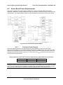
3.
Functional Architecture
The architecture and design of the Intel® Server Board S5000PAL / S5000XAL is based on the Intel®
5000 Chipset Family. The chipset is designed for systems based on the Dual-Core Intel® Xeon®
processor 5000 sequence with system bus speeds of 667 MHz, 1066 MHz, and 1333 MHz. The chipset
is made up of two main components: the Memory Controller Hub (MCH) for the host bridge and the ESB2 I/O controller hub for the I/O subsystem. This chapter provides a high-level description of the
functionality associated with each chipset component and the architectural blocks that make up this
server board. For more in depth detail of the functionality for each of the chipset components and each of
the functional architecture blocks, see the Intel® S5000 Server Board Family Datasheet.
Figure 9. Server Board Functional Block Diagram
Note: The diagram above uses the Intel® 5000P MCH as a general reference designator for both MCH
components supported on this server board.
24
Revision 1.7
Intel order number: D31979-010
Intel® Server Board S5000PAL / S5000XAL TPS
3.1
Functional Architecture
Intel® 5000P and 5000X Memory Controller Hubs (MCH)
This section will describe the general functionality of the memory controller hub as it is implemented on
this server board. Depending on the version of the server board in use, it may support either the Intel®
5000P MCH or the Intel® 5000X MCH. Features that are unique to a particular MCH will be so referenced.
The Memory Controller Hub (MCH) is a single 1432 pin FCBGA package which includes the following
core platform functions:
•
System Bus Interface for the processor sub-system
•
Memory Controller
•
PCI Express* Ports including the Enterprise South Bridge Interface (ESI)
•
FBD Thermal Management
•
SMBUS Interface
Additional information about MCH functionality can be obtained from the Intel® S5000 Series Chipsets
Server Board Family Datasheet, the Intel® 5000P Memory Controller Hub External Design Specification
(Yellow Cover), or the Intel® 5000X Memory Controller Hub External Design Specification (Yellow Cover).
Note: Yellow Cover documents can only be obtained under NDA with Intel and ordered through an Intel
representative.
3.1.1
System Bus Interface
The MCH is configured for symmetric multi-processing across two independent front side bus interfaces
that connect to the Dual-Core Intel® Xeon® processors 5000 sequence. Each front side bus on the MCH
uses a 64-bit wide 1066 or 1333 MHz data bus. The 1333 MHz data bus is capable of transferring data at
up to 10.66 GB/s. The MCH supports a 36-bit wide address bus, capable of addressing up to 64 GB of
memory. The MCH is the priority agent for both front side bus interfaces, and is optimized for one
processor on each bus.
3.1.2
Processor Support
The server board supports the following processors:
•
One or two Dual-Core Intel® Xeon® processors 5000 or 5100 sequence with a 677-, 1066-, or
1333-MHz front side bus.
•
Up to two Quad-Core Intel® Xeon® processors 5300 sequence with a 1066- or 1333-MHz front
side bus.
•
Up to two 45nm 2P Dual-Core Intel® Xeon® processors. Systems based on S5000PALR or
S5000XALR only.
•
Up to two 45nm next generation Quad-Core Intel® Xeon® processors. Systems based on
S5000PALR or S5000XALR only.
Previous generations of the Intel® Xeon® processor are not supported on the server board. See
http://support.intel.com/support/motherboards/server/s5000pal/ for a complete updated list of supported
processors. ( http://support.intel.com/support/motherboards/server/sb/CS-022346.htm/ is sub-directory of
above S5000PAL URL that reflects supported processor list)
Note: Only Dual-Core Intel® Xeon® processors 5000 sequence, that support system bus speeds of 667
MHz, 1066 MHz, and1333 MHz are supported on this server board.
Revision 1.7
25
Intel order number: D31979-010
Intel® Server Board S5000PAL / S5000XAL TPS
Functional Architecture
3.1.2.1
Processor Population Rules
When two processors are installed, both must be of identical revision, core voltage, and bus/core speed.
Mixed processor steppings is supported. However, the stepping of one processor cannot be greater than
one stepping back of the other. When only one processor is installed, it must be in the socket labeled
CPU1. The other socket must be empty.
The board is designed to provide up to 130A of current per processor. Processors with higher current
requirements are not supported.
No terminator is required in the second processor socket when using a single processor configuration.
3.1.2.2
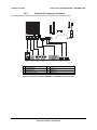
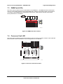
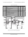
Common Enabling Kit (CEK) Design Support
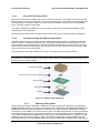
The server board complies with Intel’s Common Enabling Kit (CEK) processor mounting and heat sink
retention solution. The server board ships with a CEK spring snapped onto the underside of the server
board, beneath each processor socket. The heat sink attaches to the CEK, over the top of the processor
and the thermal interface material (TIM). See the figure below for the stacking order of the chassis, CEK
spring, server board, TIM, and heat sink.
The CEK spring is removable, allowing for the use of non-Intel heat sink retention solutions.
Note: The processor heat sink and CEK spring shown in the following diagram are for reference
purposes only. The actual processor heat sink and CEK solutions compatible with this generation server
board may be of a different design.
Heatsink assembly
Thermal interface material (TIM)
Server board
CEK spring
Chassis
Figure 10. CEK Processor Mounting
3.1.3
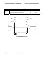
Memory Sub-system
On the Intel® Server Board S5000PAL / S5000XAL, the MCH provides four channels of Fully Buffered
DIMM (FB-DIMM) memory. Each channel can support up to 2 Dual Ranked FB-DIMM DDR2 DIMMs. FBDIMM memory channels are organized in to two branches for support of RAID 1 (mirroring). The MCH
can support up to 8 DIMMs or a maximum memory size of 32 GB physical memory in non-mirrored mode
and 16 GB physical memory in a mirrored configuration. The read bandwidth for each FB-DIMM channel
is 4.25 GB/s for DDR2 533 FB-DIMM memory which gives a total read bandwidth of 17 GB/s for four FBDIMM channels. Thus, this provides 8.5 GB/s of write memory bandwidth for four FB-DIMM channels.
The read bandwidth for each FB-DIMM channel is 5.3GB/s for DDR2 667 FB-DIMM memory which gives
26
Revision 1.7
Intel order number: D31979-010
Intel® Server Board S5000PAL / S5000XAL TPS
Functional Architecture
a total read bandwidth of 21GB/s for four FB-DIMM channels. Thus, this provides 10.7 GB/s of write
memory bandwidth for four FB-DIMM channels. The total bandwidth is based on read bandwidth thus the
total bandwidth is 17 GB/s for 533 and 21.0 GB/s for 667.
On the Intel® Server Board S5000PAL / S5000XAL, a pair of channels becomes a branch where Branch
0 consists of channels A and B, and Branch 1 consists of channels C and D. FBD memory channels are
organized into two branches for support of RAID 1(mirroring).
Channel B
Channel C
Channel A
Channel D
H
MC
1
MA
DIM M A2 1
DIM M B 2
DIM M B 1
DIM M C 2
DIM M C 1
DIM M D 2
DIM M D
DIM
Branch 0
Branch 1
TP02299
Figure 11. Memory Layout
To boot the system, the system BIOS on the server board uses a dedicated I2C bus to retrieve DIMM
information needed to program the MCH memory registers. The following table provides the I2C
addresses for each DIMM slot.
Table 1. I2C Addresses for Memory Module SMB
3.1.3.1
Device
DIMM A1
Address
0xA0
DIMM A2
0xA2
DIMM B1
0xA0
DIMM B2
0xA2
DIMM C1
0xA0
DIMM C2
0xA2
DIMM D1
0xA0
DIMM D2
0xA2
Memory RASUM Featuresi
The MCH supports several memory RASUM (Reliability, Availability, Serviceability, Usability, and
Manageability) features. These features include the Intel® x4 Single Device Data Correction (Intel® x4
SDDC) for memory error detection and correction, Memory Scrubbing, Retry on Correctable Errors,
Memory Built In Self Test, DIMM Sparing, and Memory Mirroring. See the Intel® S5000 Series Chipsets
Server Board Family Datasheet for more information describing these features.
3.1.3.2
Supported Memory
The server board supports up to eight DDR2-533 or DDR2-667 Fully Buffered DIMMs (FBD memory).
The following tables show the maximum memory configurations supported using the specified memory
technology.
Revision 1.7
27
Intel order number: D31979-010
Intel® Server Board S5000PAL / S5000XAL TPS
Functional Architecture
Table 2. Maximum 8 DIMM System Memory Configuration – x8 Single Rank
DRAM Technology x8
Single Rank
256 Mb
512 Mb
1024 Mb
2048 Mb
Maximum Capacity
Mirrored Mode
1 GB
2 GB
4 GB
8 GB
Maximum Capacity
Non-Mirrored Mode
2 GB
4 GB
8 GB
16 GB
Table 3. Maximum 8 DIMM System Memory Configuration – x4 Dual Rank
DRAM Technology x4
Dual Rank
256 Mb
512 Mb
1024 Mb
2048 Mb
Maximum Capacity
Mirrored Mode
4 GB
8 GB
16 GB
16 GB
Maximum Capacity
Non-Mirrored Mode
8 GB
16 GB
32 GB
32 GB
Note: DDR2 DIMMs that are not fully buffered are NOT supported on this server board. See the Intel®
Server Board S5000PAL / S5000XAL Tested Memory List for a complete list of supported memory for
this server board.
3.1.3.3
DIMM Population Rules and Supported DIMM Configurations
DIMM population rules depend on the operating mode of the memory controller, which is determined by
the number of DIMMs installed. DIMMs must be populated in pairs. DIMM pairs are populated in the
following DIMM slot order: A1 & B1, C1 & D1, A2 & B2, C2 & D2. DIMMs within a given pair must be
identical with respect to size, speed, and organization. However, DIMM capacities can be different
between different DIMM pairs.
For example, a valid mixed DIMM configuration may have 512MB DIMMs installed in DIMM Slots A1 &
B1, and 1GB DIMMs installed in DIMM slots C1 & D1.
Intel supported DIMM configurations for this server board are shown in the following table.
Supported and Validated configuration : Slot is populated
Supported but not validated configuration : Slot is
populated
Slot is not populated
Mirroring:
Sparing:
Y = Yes. Indicates that configuration supports Memory Mirroring.
Y(x) = Yes. Indicates that configuration supports Memory Sparing.
Where x = 0 : Sparing supported on Branch0 only
1 : Sparing supported on Branch1 only
0,1 : Sparing supported on both branches
Branch 0
Channel A
DIMM_A1
28
DIMM_A2
Branch 1
Channel B
DIMM_B1
Channel C
DIMM B2
DIMM C1
DIMM C2
Channel D
DIMM D1
Revision 1.7
Intel order number: D31979-010
DIMM D2
Mirroring
Possible
Sparing
Possible
Intel® Server Board S5000PAL / S5000XAL TPS
Functional Architecture
Y (0)
Y
Y (0)
Y
Y (0, 1)
Notes:
- Single channel mode is only tested and supported with a 512MB x8 FBDIMM installed in DIMM
Slot A1.
- The supported memory configurations must meet population rules defined above.
- For best performance, the number of DIMMs installed should be balanced across both
memory branches. For Example: a four DIMM configuration will perform better than a two
DIMM configuration and should be installed in DIMM Slots A1, B1, C1, and D1. An eight
DIMM configuration will perform better then a six DIMM configuration.
- Although mixed DIMM capacities between channels is supported, Intel does not validate DIMMs
in mixed DIMM configurations.
3.1.3.3.1
Minimum Non-Mirrored Mode Configuration
The server board is capable of supporting a minimum of one DIMM installed. However, for system
performance reasons, Intel’s recommendation is that at least 2 DIMMs be installed.
The following diagram shows the recommended minimum DIMM memory configuration. Populated DIMM
slots are shown in Grey.
Channel B
Channel C
Channel A
Channel D
H
MC
1
M A A2
M
I
D
M
DIM M B1 2
DIM M B 1
DIM M C 2
DIM M C 1
DIM M D 2
DIM M D
DIM
Branch 0
Branch 1
TP02300
Figure 12. Recommended Minimum Two DIMM Memory Configuration
Note: The server board supports single DIMM mode operation. Intel will only validate and support this
configuration with a single 512MB x8 FBDIMM installed in DIMM slot A1.
Revision 1.7
29
Intel order number: D31979-010
Intel® Server Board S5000PAL / S5000XAL TPS
Functional Architecture
3.1.3.4
Non-mirrored mode memory upgrades
The minimum memory upgrade increment is two DIMMs per branch. The DIMMs must cover the same
slot position on both channels. DIMMs pairs must be identical with respect to size, speed, and
organization. DIMMs that cover adjacent slot positions do not need to be identical.
When adding two DIMMs to the configuration shown in Figure 12, the DIMMs should be populated in
DIMM slots C1 and D1 as shown in the following diagram. Populated DIMM slots are shown in Grey.
Channel B
Channel C
Channel A
Channel D
H
MC
1
M A A2
M
I
D
M
DIM M B1 2
DIM M B 1
DIM M C 2
DIM M C 1
DIM M D 2
DIM M D
DIM
Branch 0
Branch 1
TP02301
Figure 13. Recommended Four DIMM Configuration
Functionally, DIMM slots A2 and B2 could also have been populated instead of DIMM slots C1 and D1.
However, your system will not achieve equivalent performance. Figure 13 shows the supported DIMM
configuration that is recommended because it allows both memory branches from the MCH to operate
independently and simultaneously. FBD bandwidth is doubled when both branches operate in parallel.
3.1.3.4.1
Mirrored Mode Memory Configuration
When operating in mirrored mode, both branches operate in lock step. In mirrored mode, branch 1
contains a replicate copy of the data in branch 0. The minimum DIMM configuration to support memory
mirroring is four DIMMs, populated as shown in Figure 13 above. All four DIMMs must be identical with
respect to size, speed, and organization.
To upgrade a four DIMM mirrored memory configuration, four additional DIMMs must be added to the
system. All four DIMMs in the second set must be identical to the first with the exception of speed. The
MCH will adjust to the lowest speed DIMM.
30
Revision 1.7
Intel order number: D31979-010
Intel® Server Board S5000PAL / S5000XAL TPS
3.1.3.4.2
Functional Architecture
DIMM Sparing Mode Memory Configuration
The MCH provides DIMM sparing capabilities. Sparing is a RAS feature that involves configuring a DIMM
to be placed in reserve so it can be use to replace a DIMM that fails. DIMM sparing occurs within a given
bank of memory and is not supported across branches.
There are two supported Memory Sparing configurations.
3.1.3.4.2.1
Single Branch Mode Sparing
Slot 2
DIMM_A2
DIMM_B2
DIMM_C2
DIMM_D2
Slot 1
DIMM_A1
DIMM_B1
DIMM_C1
DIMM_D1
Channel B
Channel C
Channel D
Channel A
Branch 0
Branch 1
Intel® 5000P/5000X Memory Controller Hub
Figure 14. Single Branch Mode Sparing DIMM Configuration
•
DIMM_A1 and DIMM_B1 must be identical in organization, size and speed.
•
DIMM_A2 and DIMM_B2 must be identical in organization, size and speed.
•
DIMM_A1 and DIMM_A2 need not be identical in organization, size and speed.
•
DIMM_B1 and DIMM_B2 need not be identical in organization, size and speed.
•
Sparing should be enabled in BIOS setup.
•
BIOS will configure Rank Sparing Mode.
•
The larger of the pairs {DIMM_A1, DIMM_B1} and {DIMM_A2, DIMM_B2} will be selected as the
spare pair unit.
Revision 1.7
31
Intel order number: D31979-010
Intel® Server Board S5000PAL / S5000XAL TPS
Functional Architecture
3.1.3.4.2.2
Dual Branch Mode Sparing
Dual branch mode sparing requires that all eight DIMM slots be populated and must comply with the
following population rules.
•
DIMM_A1 and DIMM_B1 must be identical in organization, size and speed.
•
DIMM_A2 and DIMM_B2 must be identical in organization, size and speed.
•
DIMM_C1 and DIMM_D1 must be identical in organization, size and speed.
•
DIMM_C2 and DIMM_D2 must be identical in organization, size and speed.
•
DIMM_A1 and DIMM_A2 need not be identical in organization, size and speed.
•
DIMM_B1 and DIMM_B2 need not be identical in organization, size and speed.
•
DIMM_C1 and DIMM_C2 need not be identical in organization, size and speed.
•
DIMM_D1 and DIMM_D2 need not be identical in organization, size and speed.
•
Sparing should be enabled in BIOS setup.
•
BIOS will configure Rank Sparing Mode.
•
The larger of the pairs {DIMM_A1, DIMM_B1} and {DIMM_A2, DIMM_B2} and {DIMM_C1,
DIMM_D1} and {DIMM_C2, DIMM_D2} will be selected as the spare pair units.
3.1.4
Snoop Filter (5000X MCH only)
The 5000X version of the MCH includes a snoop filter. Depending on the application of the server, this
feature can be used to enhance the performance of the server by eliminating unnecessary traffic on the
system bus. By removing the excess traffic from the snooped bus, the full bandwidth is available for
other operations.
3.2
ESB-2 IO Controller
The ESB-2 is a multi-function device that provides four distinct functions: an IO Controller, a PCI-X*
Bridge, a Gigabit Ethernet Controller, and a Baseboard Management Controller (BMC). Each function
within the ESB-2 has its own set of configuration registers. Once configured, each appears to the system
as a distinct hardware controller.
A primary role of the ESB-2 is to provide the gateway to all PC-compatible I/O devices and features. The
server board uses the following ESB-2 features:
32
•
PCI-X* bus interface
•
Six Channel SATA interface w/SATA Busy LED Control
•
Dual GbE MAC
•
Baseboard Management Controller (BMC)
•
Single ATA interface, with Ultra DMA 100 capability
•
Universal Serial Bus 2.0 (USB) interface
•
Removable Media Drives
•
LPC bus interface
•
PC-compatible timer/counter and DMA controllers
•
APIC and 8259 interrupt controller
•
Power management
•
System RTC
•
General purpose I/O
Revision 1.7
Intel order number: D31979-010
Intel® Server Board S5000PAL / S5000XAL TPS
Functional Architecture
This section describes the function of most of the listed features as they pertain to this server board. For
more detail information, see the Intel® S5000 Series Chipsets Server Board Family Datasheet or the
Intel® Enterprise South Bridge-2 External Design Specification (Yellow Cover)
3.2.1
PCI Sub-system
The primary I/O buses for the server board are PCI, PCI Express*, and PCI-X*, with six independent PCI
bus segments. The PCI buses comply with the PCI Local Bus Specification, Revision 2.3. The table
below lists the characteristics of the PCI bus segments. Details about each bus segment follow the table.
Table 4. PCI Bus Segment Characteristics
PCI Bus Segment
PCI32
ESB-2
Voltage
Width
Speed
Type
On-board Device Support
3.3V
32 bit
33MHz
PCI
Used internally for video controller
PXA
ESB-2
3.3V/5.0V
64 bit
133MHz
PCI-X*
Full height riser slot, up to three slots on riser
card
PE1
ESB-2 PCIe* Port2
3.3V
x4
10Gb/S
PCIe*
Used for Intel chassis for mid-plane IOP
PE2
ESB-2 PCIe Port3
3.3V
x4
10Gb/S
PCIe
Mezzanine connector for Intel I/O Expansion
Module
PE4, PE5
BNB PCIe Ports
4,5
3.3V
x8
20Gb/S
PCIe
Low profile riser slot, up to two x4 slots on 2U
riser, or one x8 slot on 1U riser.
PE6, PE7
BNB PCIe Ports
6,7
3.3V
x8
20Gb/S
PCIe
Full height riser slot, up to two x4 slots on
riser or one x8
3.2.1.1
®
PCI32: 32-bit, 33-MHz PCI Bus Segment
All 32-bit, 33-MHz PCI I/O is directed through the ESB-2 ICH6. The 32-bit, 33-MHz PCI segment created
by the ESB-2-ICH6 is known as the PCI32 segment. The PCI32 segment supports the following
embedded devices:
•
2D Graphics Accelerator: ATI* ES1000 Video Controller
3.2.1.2
PXA: 64-bit, 133MHz PCI-X* Bus Segment
One 64-bit PCI-X* bus segment is directed through the ESB-2 ICH6. This PCI-X segment, PXA, can
support up to three add-in cards on a riser card plugged into the full height riser card slot (J4F1).
3.2.1.3
PE1: One x4 PCI Express* Bus Segment
One x4 PCI Express* bus segment is directed through the ESB-2. This PCI Express segment, PE1,
supports the optional Active SAS Midplane IOP as used in supported Intel chassis for this server board.
3.2.1.4
PE2: One x4 PCI Express* Bus Segment
One x4 PCI Express* bus segment is directed through the ESB-2. This PCI Express segment, PE2,
supports one x4 PCI Express segment to the proprietary Intel® I/O Expansion Module mezzanine
connector (J3B1).
Revision 1.7
33
Intel order number: D31979-010
Intel® Server Board S5000PAL / S5000XAL TPS
Functional Architecture
3.2.1.5
PE4, PE5: Two x4 PCI Express* Bus Segments
Two x4 PCI Express* bus segments are directed through the MCH. These PCI Express segments, PE4
and PE5, support one x8 or two x4 PCI Express segments to the low profile riser slot (J5B1).
3.2.1.6
PE6, PE7: Two x4 PCI Express* Bus Segments
Two x4 PCI Express* bus segments are directed through the MCH. These PCI Express segments, PE6
and PE7, support one x8 or two x4 PCI Express segments to the full height riser slot (J4F1).
3.2.1.7
PCI Riser Slots
The server board has two riser slots capable of supporting riser cards for both 1U and 2U system
configurations. Because of board placement resulting in different pin orientations, and expanded
technology support associated with the full-height riser, the riser slots are not the same and require
different riser cards.
The low profile riser slot (J5B1) utilizes a 98-pin connector. It is capable of supporting one x8 (1U) or two
x4 (2U) low profile PCI Express* add-in cards. The x8 PCI Express* bus can support bus speeds of up to
20 Gb/S. The following table provides the supported bus throughput for the given riser card used and the
number of add-in cards installed.
Low Profile Riser
1U – 1 add-in card slot
2U – 2 add-in card slots
1 add-in card populated
x8 or x4
x4
2 add-in cards populated
NA
x4
Note: There are no population rules for installing a single low profile add-in card in the 2U LP riser card; a
single add in card can be installed in either PCI Express* slot. While each slot can accommodate a x8
card, each slot will only support x4 bus speeds.
The full height riser slot (J4F1) implements Intel® Adaptive Slot Technology. This 280-pin connector is
capable of supporting riser cards that meet either the PCI-X* or PCI Express* technology specifications.
The following tables show the maximum bus speed supported with different add-in card populations for
each supported riser card.
Full Height PCI-X*
(Passive) Riser
1U – 1 add-in card slot
2U – 3 add-in card slots
1 add-in card populated
Up to 133MHz
Up to 100MHz in top PCI
slot
2 add-in cards populated
3 add-in cards populated
NA
Up to 100MHz using top
and middle slots
NA
66MHz
Note: For the 2U PCI-X* (passive) riser card, add-in cards should be installed starting with the top slot
first, followed by the middle, and then the bottom. Any add-in card populated in the bottom PCI slot will
cause the bus to operate at 66MHz.
Full Height PCI-X*
(Active) Riser
2U – 3 add-in card slots
1 add-in card populated
Up to 133MHz
2 add-in cards populated
3 add-in cards populated
Up to 133MHz
Up to 133MHz
Note: Each PCI slot on the 2U PCI-X* (active) riser card operates on an independent PCI bus. Therefore,
using an add-in card that operates below 133MHz will not affect the bus speed of the other PCI slots.
34
Revision 1.7
Intel order number: D31979-010
Intel® Server Board S5000PAL / S5000XAL TPS
Functional Architecture
Full Height PCI Express*
Riser
1 add-in card populated
2 add-in cards populated
1U – 1 add-in card slot
2U – 3 add-in card slots
x4 or x8
Single PCIe* x4 in either
slot or x8 in middle slot
Or
PCI-X* – Up to 133MHz in
bottom slot
NA
Single PCIe* – x4 in either
slot or x8 in middle slot and
PCI-X* – Up to 133MHz
Or
Dual PCIe – x4
3.2.2
3 add-in cards populated
NA
Dual PCIe* – x4
And
PCI-X* – Up to 133MHz
Serial ATA Support
The ESB-2 has an integrated Serial ATA (SATA) controller that supports independent DMA operation on
six ports and supports data transfer rates of up to 3.0 Gb/s. The six SATA ports on the server board are
numbered SATA-0 thru SATA-5. The SATA ports can be enabled/disabled and/or configured by
accessing the BIOS Setup Utility during POST.
Intel® Embedded Server RAID Technology II Support
3.2.2.1
The onboard storage capability of this server board includes support for Intel® Embedded Server RAID
Technology which provides three standard software RAID levels: data stripping (RAID Level 0), data
mirroring (RAID Level 1), and data stripping with mirroring (RAID Level 10). For higher performance,
data stripping can be used to alleviate disk bottlenecks by taking advantage of the dual independent DMA
engines that each SATA port offers. Data mirroring is used for data security. Should a disk fail, a mirrored
copy of the failed disk is brought on-line. There is no loss of either PCI resources (request/grant pair) or
add-in card slots.
With the addition of an optional Intel RAID Activation Key, Intel® Embedded Server RAID Technology is
also capable of providing fault tolerant data stripping (software RAID Level 5), such that if a SATA hard
drive should fail, the lost data can be restored on a replacement drive from the other drives that make up
the RAID 5 pack.
See Figure 1. Components & Connector Location Diagram for the location of Intel RAID Activation Key
connector location.
Note: Availability of the Intel RAID Activation Key to support software RAID 5 will be deferred until after
product launch of this server board.
Intel® Embedded Server RAID Technology functionality requires the following items:
•
Intel® ESB-2 IO Controller Hub
•
Intel® Embedded Server RAID Technology Option ROM
•
Intel® Application Accelerator RAID Edition drivers, most recent revision
•
At least two SATA hard disk drives
Intel® Embedded Server RAID Technology is not available in the following configurations:
•
The SATA controller in compatible mode
•
Intel® Embedded Server RAID Technology has been disabled
Revision 1.7
35
Intel order number: D31979-010
Intel® Server Board S5000PAL / S5000XAL TPS
Functional Architecture
3.2.2.2
Intel® Embedded Server RAID Technology Option ROM
The Intel® Embedded Server RAID Technology for SATA Option ROM provides a pre-OS user interface
for the Intel® Embedded Server RAID Technology implementation and provides the ability for an Intel®
Embedded Server RAID Technology volume to be used as a boot disk as well as to detect any faults in
the Intel® Embedded Server RAID Technology volume(s) attached to the Intel® RAID controller.
3.2.3
Parallel ATA (PATA) Support
The integrated IDE controller of the ESB-2 ICH6 provides one IDE channel. It redefines signals on the
IDE cable to allow both host and target throttling of data and transfer rates of up to 100MB/s. For this
server board, the IDE channel was designed to provide Slim-line Optical Drive support to the platform.
The BIOS initializes and supports ATAPI devices such as CDROM, CD-RW and DVD. The IDE channel
is accessed through a single high density 44-pin connector ((J3G1) which provides both power and IO
signals. The ATA channel can be configured and enabled or disabled by accessing the BIOS Setup Utility
during POST.
Note: The IDE connector on this server board is NOT a standard 40 IDE connector. Instead, this
connector has an additional 4 power pins over and above the standard 40 I/O pins. The design intent of
this connector is to provide support for a slim-line optical drive only.
3.2.4
USB 2.0 Support
The USB controller functionality integrated into ESB-2 provides the server board with the interface for up
to eight USB 2.0 ports. Two external connectors are located on the back edge of the server board. One
internal 2x5 header is provided, capable of supporting two optional USB 2.0 ports. Three USB ports are
routed through the bridge board connector providing optional USB support for a system Control Panel or
other USB requirements. An additional USB port is dedicated to the Intel® Remote Management Module
(Intel® RMM) connector.
3.3
Video Support
The server board provides an ATI* ES1000 PCI graphics accelerator, along with 16MB of video DDR
SDRAM and support circuitry for an embedded SVGA video sub-system. The ATI ES1000 chip contains
an SVGA video controller, clock generator, 2D engine, and RAMDAC in a 359-pin BGA. One 4Mx16x4
bank DDR SDRAM chip provides 16MB of video memory.
The SVGA sub-system supports a variety of modes, up to 1024 x 768 resolution in 8 / 16 / 32bpp modes
under 2D. It also supports both CRT and LCD monitors up to a 100 Hz vertical refresh rate.
Video is accessed using a standard 15-pin VGA connector found on the back edge of the server board.
Video signals are also made available through the 120-pin bridgeboard connector which provides signals
for an optional video connector to be present on the platform’s control panel. Video is routed to both the
rear video connector and a control panel video connector. Video is present at both connectors
simultaneously and cannot be disabled at either connector individually. Hot plugging the video while the
system is still running is supported.
On-board video can be disabled using the BIOS Setup Utility or when an add-in video card is installed.
System BIOS also provides the option for dual video operation when an add-in video card is configured in
the system.
36
Revision 1.7
Intel order number: D31979-010
Intel® Server Board S5000PAL / S5000XAL TPS
3.3.1.1
Functional Architecture
Video Modes
The ATI ES1000 chip supports all standard IBM* VGA modes. The following table shows the 2D modes
supported for both CRT and LCD.
Table 5. Video Modes
2D Mode
Refresh Rate (Hz)
8 bpp
Supported
2D Video Mode Support
16 bpp
32 bpp
Supported
Supported
640x480
60, 72, 75, 85, 90,
100, 120, 160, 200
800x600
60, 70, 72, 75, 85,
90, 100, 120,160
Supported
Supported
Supported
1024x768
60, 70, 72,
75,85,90,100
Supported
Supported
Supported
1152x864
43,47,60,70,75,80,85
Supported
Supported
Supported
1280x1024
60,70,74,75
Supported
Supported
Supported
1600x1200
52
Supported
Supported
Supported
3.3.1.2
Video Memory Interface
The memory controller sub-system of the ES1000 arbitrates requests from the direct memory interface,
the VGA graphics controller, the drawing co-processor, the display controller, the video scalar, and the
hardware cursor. Requests are serviced in a manner that ensures display integrity and maximum
CPU/co-processor drawing performance.
The server board supports a 16MB (4Meg x 16-bit x 4 banks) DDR SDRAM device for video memory.
3.3.1.3
Dual Video
The BIOS supports single and dual video modes. The dual video mode is enabled by default.
•
In single mode (Dual Monitor Video = Disabled), the on-board video controller is disabled when
an add-in video card is detected.
•
In dual mode (On-board Video = Enabled, Dual Monitor Video = Enabled), the on-board video
controller is enabled and will be the primary video device. The external video card will be
allocated resources and is considered the secondary video device. BIOS Setup provides user
options to configure the feature as follows.
On-board Video
Enabled
Disabled
Dual Monitor Video
Enabled
Disabled
Shaded if on-board video is set to "Disabled"
Revision 1.7
37
Intel order number: D31979-010
Intel® Server Board S5000PAL / S5000XAL TPS
Functional Architecture
3.4
Network Interface Controller (NIC)
Network interface support is provided from the built in Dual GbE MAC features of the ESB-2 in
conjunction with the Intel® 82563EB compact Physical Layer Transceiver (PHY). Together, they provide
the server board with support for dual LAN ports designed for 10/100/1000 Mbps operation.
The 82563EB device is based upon proven PHY technology integrated into the Intel® Gigabit Ethernet
Controllers. The physical layer circuitry provides a standard IEEE 802.3 Ethernet interface for 1000BASET, 100BASE-TX, and 10BASE-T applications (802.3, 802.3u, and 802.3ab). The 82563EB device is
capable of transmitting and receiving data at rates of 1000 Mbps, 100 Mbps, or 10 Mbps
Each Network Interface Controller (NIC) drives two LEDs located on each network interface connector.
The link/activity LED (to the right of the connector) indicates network connection when on, and
Transmit/Receive activity when blinking. The speed LED (to the left of the connector) indicates 1000Mbps operation when amber, 100-Mbps operation when green, and 10-Mbps when off. The table below
provides an overview of the LEDs.
Table 6. NIC2 Status LED
LED Color
Green/Amber (Left)
Green (Right)
®
LED State
NIC State
Off
10 Mbps
Green
100 Mbps
Amber
1000 Mbps
On
Active Connection
Blinking
Transmit / Receive activity
3.4.1
Intel® I/O Acceleration Technology
3.4.2
MAC Address Definition
Intel I/O Acceleration Technology moves network data more efficiently through Dual-Core Intel® Xeon®
processor 5000 sequence-based servers for improved application responsiveness across diverse
operating systems and virtualized environments. Intel® I/OAT improves network application
responsiveness by unleashing the power of Dual-Core Intel® Xeon® processors 5000 sequence through
more efficient network data movement and reduced system overhead. Intel multi-port network adapters
with Intel® I/OAT provide high-performance I/O for server consolidation and virtualization via stateless
network acceleration that seamlessly scales across multiple ports and virtual machines. Intel® I/OAT
provides safe and flexible network acceleration through tight integration into popular operating systems &
virtual machine monitors, avoiding the support risks of 3rd-party network stacks and preserving existing
network requirements such as teaming and failover.
Each Intel® Server Board S5000PAL / S5000XAL has four MAC addresses assigned to it at the Intel
factory. During the manufacturing process, each server board will have a white MAC address sticker
placed on the board. The sticker will display the MAC address in both bar code and alpha numeric
formats. The printed MAC address is assigned to NIC 1 on the server board. NIC 2 is assigned the NIC 1
MAC address + 1.
Two additional MAC addresses are assigned to the Baseboard Management Controller (BMC) embedded
in the ESB-2. These MAC addresses are used by the BMC’s embedded network stack to enable IPMI
remote management over LAN. BMC LAN Channel 1 is assigned the NIC1 MAC address + 2, and BMC
LAN Channel 2 is assigned the NIC1 MAC address + 3.
38
Revision 1.7
Intel order number: D31979-010
Intel® Server Board S5000PAL / S5000XAL TPS
3.5
Functional Architecture
Super I/O
Legacy I/O support is provided by using a National Semiconductor* PC87427 Super I/O device. This chip
contains all of the necessary circuitry to support the following functions:
•
GPIOs
•
Two serial ports
•
Keyboard and mouse support
•
Wake up control
•
System health support
3.5.1.1
Serial Ports
The server board provides two serial ports: an external RJ45 serial port, and an internal DH10 serial
header.
Serial A is an optional port accessed through a 9-pin internal DH-10 header. A standard DH10 to DB9
cable can be used to direct the Serial A port to the rear of a chassis. The Serial A interface follows the
standard RS232 pin-out as defined in the following table.
Table 7. Serial A Header Pin-out
Pin
1
Signal Name
DCD
2
DSR
3
RX
4
RTS
5
TX
6
CTS
7
DTR
8
RI
9
GND
Serial Port A Header Pin-out
The rear RJ45 Serial B port is a fully functional serial port that can support any standard serial device.
Using an RJ45 connector for a serial port allows direct support for serial port concentrators, which
typically use RJ45 connectors and are widely used in the high-density server market. For server
applications that use a serial concentrator to access the system management features of the server
board, a standard 8-pin CAT-5 cable from the serial concentrator is plugged directly into the rear RJ45
serial port.
To allow support for either of two serial port configuration standards, a jumper block located directly
behind the rear RJ45 serial port must be configured appropriately according to the desired standard. For
serial concentrators that require a DCD signal, the jumper block must be configured with the serial port
jumper over pins 1 and 2. For serial concentrators that require a DSR signal (Default), the jumper block
must be configured with the serial port jumper over pins 3 and 4. Pin 1 on the jumper is identified by “*”.
Note: By default, the rear RJ45 serial port is configured to support a DSR signal. This configuration is
compatible with the Cisco* standard.
Revision 1.7
39
Intel order number: D31979-010
Intel® Server Board S5000PAL / S5000XAL TPS
Functional Architecture
J8A3
2
3
4
1-2: DCD to DTR
3-4: DSR to DTR
(factory default)
TP02303
Figure 15. Serial Port Configuration Jumper Location
Pins
1-2
What happens at system reset…
Serial port is configured for DCD to DTR
3-4
Serial port is configured for DSR to DTR (default)
For server applications that require a DB9 serial connector, an 8-pin RJ45-to-DB9 adapter must be used.
The following table provides the pin-out required for the adapter to provide RS232 support. A standard
DH10-to-DB9 cable and 8-pin RJ45 to DB9 DCD and DSR adapters are available from Intel in the Serial
Port Accessory Kit, product code: AXXRJ45DB92.
Table 8. Rear Serial B Port Adapter Pin-out
RJ45
1
Signal
Request to Send
Abbreviation
RTS
7
2
Data Terminal Ready
DTR
4
3
Transmitted Data
TD
3
4
Signal Ground
SGND
5
DB9
5
Ring Indicator
RI
9
6
Received Data
RD
2
7
DCD or DSR
DCD/DSR
1 or 6 (see note)
8
Clear To Send
CTS
8
Note: The RJ45-to-DB9 adapter should match the configuration of the serial device used. One of two pinout configurations is used, depending on whether the serial device requires a DSR or DCD signal. The
final adapter configuration should also match the desired pin-out of the RJ45 connector, as it can also be
configured to support either DSR or DCD.
3.5.1.2
Floppy Disk Controller
The server board does not support a floppy disk controller (FDC) interface. However, the system BIOS
does recognize USB floppy devices.
3.5.1.3
Keyboard and Mouse Support
Dual stacked PS/2 ports, located on the back edge of the server board, are provided for keyboard and
mouse support. Either port can support a mouse or keyboard. Neither port supports hot plugging.
40
Revision 1.7
Intel order number: D31979-010
Intel® Server Board S5000PAL / S5000XAL TPS
3.5.1.4
Functional Architecture
Wake-up Control
The super I/O contains functionality that allows various events to power-on and power-off the system.
3.5.1.5
System Health Support
The super I/O provides an interface via GPIOs for BIOS and Server Management Firmware to activate
the Diagnostic LEDs, the FRU fault indicator LEDs for processors, DIMMs, fans and the system status
LED. Refer to Figure 2. Light Guided Diagnostic LED Location Diagram for the location of the LEDs on
the baseboard.
The super I/O also provides PMW fan control to the system fans, monitors tach and presence signals for
the system fans and monitors baseboard and control panel temperature.
Revision 1.7
41
Intel order number: D31979-010
Intel® Server Board S5000PAL / S5000XAL TPS
Platform Management
4.
Platform Management
The platform management sub-system on the server board is based on the integrated Baseboard
Management Controller (BMC) features of the ESB-2. The on board platform management subsystem
consists of communication buses, sensors, system BIOS, and server management firmware. The
following diagram provides an overview of the Server Management Bus (SMBUS) architecture used on
this server board.
See Appendix B for onboard sensor data.
For more detailed platform management information, see the Intel® S5000 Server Board Family
Datasheet.
Figure 16. SMBUS Block Diagram
42
Revision 1.7
Intel order number: D31979-010
Intel® Server Board S5000PAL / S5000XAL TPS
Connector / Header Locations and Pin-outs
5.
Connector / Header Locations and Pin-outs
5.1
Board Connector Information
The following section provides detailed information regarding all connectors, headers and jumpers on the
server board. Table 9 lists all connector types available on the board and the corresponding reference
designators printed on the silkscreen.
Table 9. Board Connector Matrix
Connector
Quantity
Reference Designators
Connector Type
CPU Power
Main Power
P/S Aux
Pin
Count
8
24
5
Power supply
3
J3K4
J3K3
J1K1
CPU
2
J8G1, J5G1
CPU Sockets
771
Main Memory
8
J7B1,J7B2,J8B1,J8B2,J8B3,J9B1,J9B2,
J9B3
DIMM Sockets
240
Full Height Riser
1
J4F1
Card Edge
280
Low Profile Riser
1
J5B1
Card Edge
98
Bridge Board
Connector
1
J4G1
Card Edge
120
RMM
1
J1C5
Mezzanine
120
RMM NIC
1
J1B2
Mezzanine
30
®
Intel I/O
Expansion Module
1
J3B1
Mezzanine
50
SATA RAID Key
1
J1E4
Key Holder
3
IDE (I/O + Power)
1
J3G1
Shrouded
Header
44
Front System Fans
#1 & #2
2
J3K1, J3K2
Header
4
Rear System Fans
#3 & #4
2
J7A2, J7A1
Header
4
CPU Fans
2
J5K1, J9K1
Header
4
Battery
1
BT1J1
Battery Holder
3
Keyboard/Mouse
1
J9A1
PS2, stacked
12
Rear USB
2
J5A1, J6A2
External
4
Serial Port A
1
J1B1
Header
9
Serial Port B
1
J9A2
External, RJ45
10
Video connector
1
J6A1
External, D-Sub
15
LAN connector
10/100/1000
2
JA8A1, JA8A2
External LAN
connector with
built-in magnetic
14
SSI Control Panel
1
J3H2
Header
24
Internal USB
1
J1J1
Header
10
Intrusion detect
2
J1C4
Header
2
Serial ATA
6
J1H1,J1G2,J1G1,J1F2,J1F1,J1E3
Header
7
LCP / AUX IPMB
1
J1C2
Header
4
IPMB
1
J1C3
Header
3
Revision 1.7
43
Intel order number: D31979-010
Intel® Server Board S5000PAL / S5000XAL TPS
Connector / Header Locations and Pin-outs
Connector
Quantity
System Recovery
Setting Jumpers
5.2
Reference Designators
4
Connector Type
J1D1, J1D2, J1D3, J3H1
Jumper
Pin
Count
3
Power Connectors
The main power supply connection is obtained using an SSI compliant 2x12 pin connector (J3K3). In
addition, there are two additional power related connectors; one SSI compliant 2x4 pin power connector
(J3K4) providing support for additional 12V, and one SSI compliant 1x5 pin connector (J1K1) providing
I2C monitoring of the power supply. The following tables define the connector pin-outs.
Table 10. Power Connector Pin-out (J3K3)
1
Pin
Signal
+3.3Vdc
Color
Orange
Pin
13
Signal
+3.3Vdc
Color
Orange
2
+3.3Vdc
Orange
14
-12Vdc
Blue
3
GND
Black
15
GND
Black
4
+5Vdc
Red
16
PS_ON#
Green
5
GND
Black
17
GND
Black
6
+5Vdc
Red
18
GND
Black
7
GND
Black
19
GND
Black
8
PWR_OK
Gray
20
RSVD_(-5V)
White
9
5VSB
Purple
21
+5Vdc
Red
10
+12Vdc
Yellow
22
+5Vdc
Red
11
+12Vdc
Yellow
23
+5Vdc
Red
12
+3.3Vdc
Orange
24
GND
Black
Table 11. 12V Power Connector Pin-out (J3K4)
1
Pin
GND
Signal
Color
Black
2
GND
Black
3
GND
Black
4
GND
Black
5
+12Vdc
Yellow/Black
6
+12Vdc
Yellow/Black
7
+12Vdc
Yellow/Black
8
+12Vdc
Yellow/Black
Table 12. Power Supply Signal Connector Pin-out (J1K1)
44
Pin
Signal
1
SMB_CLK_ESB_FP_PWR_R
Color
Orange
2
SMB_DAT_ESB_FP_PWR_R
Black
3
SMB_ALRT_3_ESB_R
Red
4
3.3V SENSE-
Yellow
5
3.3V SENSE+
Green
Revision 1.7
Intel order number: D31979-010
Intel® Server Board S5000PAL / S5000XAL TPS
5.3
Connector / Header Locations and Pin-outs
System Management Headers
5.3.1
Intel® Remote Management Module (RMM) Connector
A 120-pin Intel® RMM Connector (J1C5) is included on the server board for sole support of the optional
Intel® Remote Management Module. There is no support for third party ASMI cards on this server board.
Note: This connector is NOT compatible for use with Intel® Server Management Module Professional
Edition (Product Code AXXIMMPRO) or the Intel® Server Management Module Advanced Edition
(Product Code AXXIMMADV).
Table 13. Intel® RMM Connector Pin-out (J1C5)
Pin
1
Signal Name
Reserved - NC
Pin
2
Signal Name
GND
3
ESB_PLT_RST_G1_N
4
Reserved - NC
5
GND
6
Reserved - NC
7
Reserved - NC
8
GND
9
Reserved - NC
10
GND
11
GND
12
Reserved - NC
13
GND
14
IRQ_SERIAL_R
15
USB_ESB_P7P
16
GND
17
USB_ESB_P7N
18
GND
19
GND
20
Reserved - NC
21
P3V3
22
Reserved - NC
23
LPC_LAD<0>
24
GND
25
LPC_LAD<1>
26
LPC_FRAME_N
27
P3V3
28
LPC_LAD<2>
29
LPC_LCLK
30
LPC_LAD<3>
31
P3V3
32
P3V3
33
SMB_1_3V3SB_MS_DAT
34
SMB_IPMB_3V3SB_DAT
35
SMB_1_3V3SB_SL_DAT
36
SMB_IPMB_3V3SB_CLK
37
SMB_1_3V3SB_MS_CLK
38
SMB_0_3V3SB_MS_CLK
39
SMB_1_3V3SB_INT
40
SMB_0_3V3SB_INT
41
P3V3_AUX
42
SMB_0_3V3SB_MS_DAT
43
SPB_IMM_DSR_N
44
SMB_0_3V3SB_SL_DAT
45
SPB_IMM_RTS_N
46
P3V3_AUX
47
SPB_IMM_CTS_N
48
FM_IMM_PRESENT_N
49
SPB_IMM_DCD_N
50
SPB_IMM_DTR_N
51
SPB_RI_N
52
SPB_IMM_SIN
53
SPB_IMM_SOUT
54
P3V3_AUX
55
P3V3_AUX
56
V_LCDDATA7
57
V_LCDCNTL3
56
V_LCDDATA6
59
P3V3_AUX
60
V_LCDDATA5
61
Reserved - NC
62
V_LCDDATA4
63
Reserved - NC
64
V_LCDDATA3
65
GND
66
V_LCDCNTL1
67
V_LCDCNTL0
68
GND
69
Reserved - NC
70
V_LCDDATA15
71
GND
72
V_LCDDATA714
Revision 1.7
45
Intel order number: D31979-010
Intel® Server Board S5000PAL / S5000XAL TPS
Connector / Header Locations and Pin-outs
Pin
73
Signal Name
V_LCDDATA23
Pin
74
Signal Name
V_LCDDATA13
75
V_LCDDATA22
76
V_LCDDATA12
77
V_LCDDATA21
78
V_LCDDATA11
79
V_LCDDATA20
80
GND
81
V_LCDDATA19
82
V_LCDCNTL2
83
GND
84
V_DVO_DDC_SDA
85
FM_MAN_LAN_TYPE1
86
V_DVO_DDC_SCL
87
FM_MAN_LAN_TYPE1
88
RST_PS_PWRGD
89
Reserved - NC
90
Reserved - NC
91
Reserved - NC
92
Reserved - NC
93
MII_MDC_RMII_SPARE
94
Reserved - NC
95
MII_COL_RMIIB_RXER
96
GND
97
GND
98
MII_CRS_RMIIB_CRS
99
MII_TXER_RMIIB_TXEN
100
MII_TXCLK_RMIIB_RXCLK
101
MII_MDIO_RMIIB_PRESENT
102
GND
103
GND
104
MII_TXD3_RMIIB_TXD1
105
MII_RXD3_RMIIB_RXD1
106
MII_TXD2_RMIIB_TXD0
107
MII_RXD2_RMIIB_RXD0
108
GND
109
GND
110
MII_TXD1_RMIIA_TXD1
111
MII_RXD1_RMIIA_RXD1
112
MII_TXD0_RMIIA_TXD0
113
MII_RXD0_RMIIA_RXD0
114
GND
115
GND
116
MII_TXEN_RMIIA_TXEN
117
MII_RXCLK
118
MII_RXER_RMIIA_TXER
119
MII_RXDV_RMIIA_CRS
120
GND
5.3.2
Intel® RMM NIC Connector
The server board provides an internal 30-pin mezzanine style connector (J1B2) to accommodate a
proprietary form factor RMM NIC module. The following table details the pin-out of the RMM NIC module
connector.
Table 14. 30-pin Intel® RMM NIC Module Connector Pin-out (J1B2)
Pin
1
46
Signal Name
FM_MAN_LAN_TYPE2
Pin
2
Signal Name
MII_MDC_RMII_SPARE
3
FM_MAN_LAN_TYPE1
4
MII_COL_RMIIB_RXER
5
GND
6
GND
7
MII_TXCLK_RMIIB_RXCLK
8
MII_TXER_RMIIB_TXEN
9
MII_CRS_RMIIB_CRS
10
MII_MDIO_RMIIB_PRESENT
11
GND
12
GND
13
MII_TXD2_RMIIB_TXD0
14
MII_RXD3_RMIIB_RXD1
15
MII_TXD1_RMIIA_TXD1
16
MII_RXD3_RMIIB_RXD0
17
GND
18
GND
19
MII_TXD3_RMIIB_TXD1
20
MII_RXD1_RMIIA_RXD1
21
MII_TXD0_RMIIA_TXD0
22
MII_RXD0_RMIIA_RXD0
23
GND
24
GND
25
MII_TXEN_RMIIA_TXEN
26
MII_RXCLK
27
P3V3_AUX
28
P3V3_AUX
29
MII_RXER_RMIIA_RXER
30
MII_RXDV_RMIIA_CRS
Revision 1.7
Intel order number: D31979-010
Intel® Server Board S5000PAL / S5000XAL TPS
5.3.3
Connector / Header Locations and Pin-outs
LCP/AUX IPMB Header
Table 15. LPC/AUX IPMB Header Pin-out (J1C2)
1
Pin
Signal Name
SMB_IPMB_5VSB_DAT
Description
BMC IMB 5V Standby Data Line
2
GND
Ground
3
SMB_IPMB_5VSB_CLK
BMC IMB 5V Standby Clock Line
4
P5V_STBY
+5V Standby Power
5.3.4
IPMB Header
Table 16. IPMB Header Pin-out (J1C3)
Pin
5.4
1
Signal Name
SMB_IPMB_5VSB_DAT
2
GND
3
SMB_IPMB_5VSB_CLK
Description
BMC IMB 5V Standby Data Line
BMC IMB 5V Standby Clock Line
Riser Card Slots
The server board has two riser card slots. The full height riser slot (J4F1) utilizes Intel® Adaptive Slot
Technology. It is capable of supporting riser cards that support either the PCI-X* or PCI Express* full
height / full length add-in cards. The low profile riser slot (J5B1) supports riser cards that support low
profile PCI Express* add-in cards. The following tables show the pin-out for these riser slots.
Table 17. Low-profile Riser Slot Pin-out (J5B1)
Pin Side B
1
PCI Spec Signal
P12V
Pin Side A
1
PCI Spec Signal
2
P12V
2
P12V
3
P12V
3
P12V
4
GND
4
GND
5
SMB_PCI3V3SB_CLK
5
PD_LP_TCK
6
SMB_PCI3V3SB_DAT
6
PU_LP_TDI
7
GND
7
FP_CHASSIS_INTRU
8
P3V3
8
PU_LP_TMS
9
PD_LPTRST_N
9
P3V3
10
P3V3_AUX
10
P3V3
11
PE_WAKE_N
11
PE_RST_LP_N
12
P3V3
12
GND
13
13
CLK_100M_LP_PCIE_SLOT1_P
14
PE4_MCH_TXP_C <3..0>
0
14
CLK_100M_LP_PCIE_SLOT1_N
15
PE4_MCH_TXN_C <3..0>
0
15
16
GND
16
PE4_MCH_RXP <3..0>
0
17
PE4_MCH_RXN <3..0>
0
GND
18
GND
19
P3V3
17
18
19
GND
GND
PE4_MCH_TXP_C <3..0>
1
Revision 1.7
47
Intel order number: D31979-010
Intel® Server Board S5000PAL / S5000XAL TPS
Connector / Header Locations and Pin-outs
Pin Side B
PCI Spec Signal
20
PE4_MCH_TXN_C <3..0>
21
1
Pin Side A
20
GND
22
GND
21
PE4_MCH_RXP <3..0>
1
22
PE4_MCH_RXN <3..0>
1
23
PE4_MCH_TXP_C <3..0>
2
23
24
PE4_MCH_TXN_C <3..0>
2
24
25
GND
26
GND
2
26
PE4_MCH_RXN <3..0>
2
3
27
28
PE4_MCH_TXN_C <3..0>
3
28
30
P3V3
31
32
GND
GND
PE4_MCH_RXP <3..0>
PE4_MCH_TXP_C <3..0>
GND
GND
25
27
29
PCI Spec Signal
GND
GND
GND
29
PE4_MCH_RXP <3..0>
3
30
PE4_MCH_RXN <3..0>
3
31
GND
32
CLK_100M_LP_PCIE_SLOT2_P
33
PE5_MCH_TXP_C <3..0>
0
33
CLK_100M_LP_PCIE_SLOT2_N
34
PE5_MCH_TXN_C <3..0>
0
34
GND
35
GND
35
PE5_MCH_RXP <3..0>
0
36
GND
36
PE5_MCH_RXN <3..0>
0
37
PE5_MCH_TXP_C <3..0>
1
37
GND
38
PE5_MCH_TXN_C <3..0>
1
38
GND
39
GND
39
PE5_MCH_RXP <3..0>
1
40
GND
40
PE5_MCH_RXN <3..0>
1
41
PE5_MCH_TXP_C <3..0>
2
41
GND
42
PE5_MCH_TXN_C <3..0>
2
42
GND
43
GND
43
PE5_MCH_RXP <3..0>
2
44
GND
44
PE5_MCH_RXN <3..0>
2
45
PE5_MCH_TXP_C <3..0>
3
45
GND
46
PE5_MCH_TXN_C <3..0>
3
46
GND
47
GND
47
PE5_MCH_RXP <3..0>
3
48
FM_LP_RISER_TYPE1
48
PE5_MCH_RXN <3..0>
3
49
FM_LP_RISER_TYPE0
49
GND
Table 18. Full-height Riser Slot Pin-out (J4F1)
Pin-Side B PCI Spec Signal Pin-Side A PCI Spec Signal
48
140
12V
140
12V
139
12V
139
12V
138
Ground
138
GND
137
-12V
137
3.3VAux
136
12V
136
Wake#
135
GND
135
12V
134
REFCLK2+
134
3.3V
133
REFCLK2+
133
PERST_N
132
GND
132
GND
131
GND
131
REFCLK1+
130
HSOp(0)
130
REFCLK1+
129
HSOn(0)
129
GND
Revision 1.7
Intel order number: D31979-010
Intel® Server Board S5000PAL / S5000XAL TPS
Connector / Header Locations and Pin-outs
Pin-Side B PCI Spec Signal Pin-Side A PCI Spec Signal
128
GND
128
HSIp(0)
127
GND
127
HSIn(0)
126
HSOp(1)
126
GND
125
HSOn(1)
125
GND
124
GND
124
HSIp(1)
123
GND
123
HSIn(1)
122
HSOp(2)
122
GND
121
HSOn(2)
121
GND
120
GND
120
HSIp(2)
119
GND
119
HSIn(2)
118
HSOp(3)
118
GND
117
HSOn(3)
117
GND
116
GND
116
HSIp(3)
115
GND
115
HSIn(3)
114
HSOp(4)
114
GND
113
HSOn(4)
113
GND
112
GND
112
HSIp(4)
111
GND
111
HSIn(4)
110
HSOp(5)
110
GND
109
HSOn(6)
109
GND
108
GND
108
HSIp(5)
107
GND
107
HSIn(5)
106
HSOp(6)
106
GND
105
HSOn(6)
105
GND
104
GND
104
HSIp(6)
103
GND
103
HSIn(6)
102
HSOp(7)
102
GND
101
HSOn(7)
101
GND
100
GND
100
HSIp(7)
99
+5V
99
HSIn(7)
98
INTB#
98
GND
97
INTD#
97
ZCR_PRSNT_L
96
+5V
96
+5V
95
Reserved
95
+5V
94
+5V
94
ZCR_MSKID_L
93
IOP INTA
93
+5V
92
IOP INTB
92
INTA#
91
GND
91
INTC#
90
CLK3
90
GND
89
GND
89
REQ3#
88
CLK2
88
GND
87
GND
87
GNT3#
86
REQ2#
86
GND
85
GND
85
RST#
84
Reserved
84
GND
83
GND
83
Reserved
KEY
KEY
Revision 1.7
49
Intel order number: D31979-010
Connector / Header Locations and Pin-outs
Intel® Server Board S5000PAL / S5000XAL TPS
Pin-Side B PCI Spec Signal Pin-Side A PCI Spec Signal
KEY
82
50
Reserved
KEY
82
+5V
81
GND
81
Reserved
80
CLK1
80
GND
79
Ground
79
GNT2#
78
REQ1#
78
+3.3V
77
+3.3V
77
GNT1#
76
PME2#
76
Ground
75
AD[31]
75
PME1#
74
AD[29]
74
PME3#
73
Ground
73
AD[30]
72
AD[27]
72
+3.3V
71
AD[25]
71
AD[28]
70
+3.3V
70
AD[26]
69
C/BE[3]#
69
Ground
68
AD[23]
68
AD[24]
67
Ground
67
RSVRD
66
AD[21]
66
+3.3V
65
AD[19]
65
AD[22]
64
+3.3V
64
AD[20]
63
AD[17]
63
Ground
62
C/BE[2]#
62
AD[18]
61
Ground
61
AD[16]
60
IRDY#
60
+3.3V
59
+3.3V
59
FRAME#
58
DEVSEL#
58
Ground
57
PCI-XCAP
57
TRDY#
56
LOCK#
56
Ground
55
PERR#
55
STOP#
54
+3.3V
54
+3.3V
53
SERR#
53
SMBD
52
+3.3V
52
SMBCLK
51
C/BE[1]#
51
Ground
50
AD[14]
50
PAR
49
Ground
49
AD[15]
48
AD[12]
48
+3.3V
47
AD[10]
47
AD[13]
46
M66EN
46
AD[11]
45
Ground
45
Ground
44
Ground
44
AD[09]
43
AD[08]
43
C/BE[0]#
42
AD[07]
42
+3.3V
41
+3.3V
41
AD[06]
40
AD[05]
40
AD[04]
39
AD[03]
39
Ground
38
Ground
38
AD[02]
37
AD[01]
37
AD[00]
Revision 1.7
Intel order number: D31979-010
Intel® Server Board S5000PAL / S5000XAL TPS
Connector / Header Locations and Pin-outs
Pin-Side B PCI Spec Signal Pin-Side A PCI Spec Signal
36
+3.3V
36
+3.3V
35
ACK64#
35
REQ64#
34
+5V
34
+5V
33
+5V
33
+5V
32
Reserved
32
+5V
31
Ground
31
C/BE[7]#
30
C/BE[6]#
30
C/BE[5]#
29
C/BE[4]#
29
Ground
28
Ground
28
PAR64
27
AD[63]
27
AD[62]
26
AD[61]
26
3.3V
25
3.3V
25
AD[60]
24
AD[59]
24
AD[58]
23
AD[57]
23
Ground
22
Ground
22
AD[56]
21
AD[55]
21
AD[54]
20
AD[53]
20
3.3V
19
Ground
19
AD[52]
18
AD[51]
18
AD[50]
17
AD[49]
17
Ground
16
3.3V
16
AD[48]
15
AD[47]
15
AD[46]
14
AD[45]
14
Ground
13
Ground
13
AD[44]
12
AD[43]
12
AD[42]
KEY
KEY
KEY
KEY
11
AD[41]
11
3.3V
10
Ground
10
AD[40]
9
AD[39]
9
AD[38]
8
AD[37]
8
Ground
7
3.3V
7
AD[36]
6
AD[35]
6
AD[34]
5
AD[33]
5
Ground
4
Ground
4
AD[32]
3
Type1
3
PXH_RST_N
2
Type0
2
Ground
1
Size
1
PXH_PWROK
Revision 1.7
51
Intel order number: D31979-010
Intel® Server Board S5000PAL / S5000XAL TPS
Connector / Header Locations and Pin-outs
5.5
SSI Control Panel Connector
The server board provides a 24-pin SSI control panel connector (J3H2) for use with non-Intel chassis.
The following table provides the pin-out for this connector.
Table 19. Front Panel SSI Standard 24-pin Connector Pin-out (J3H2)
Pin
5.6
1
Signal Name
P3V3_STBY
2
Pin
Signal Name
P3V3_STBY
3
Key
4
P5V_STBY
5
FP_PWR_LED_L
6
FP_ID_LED_L
7
P3V3
8
FP_STATUS_LED1_R
9
HDD_LED_ACT_R
10
FP_STATUS_LED2_R
11
FP_PWR_BTN_L
12
LAN_ACT_A_L
13
GND
14
LAN_LINKA_L
15
Reset Button
16
PS_I2C_3VSB_SDA
17
GND
18
PS_I2C_3VSB_SCL
19
FP_ID_BTN_L
20
FP_CHASSIS_INTRU
21
TEMP_SENSOR
22
LAN_ACT_B_L
23
FP_NMI_BTN_L
24
LAN_LINKB_L
Bridge Board Connector
For use in supported Intel® Server Chassis, the server board provides a 120-pin high-density bridge
board connector (J4G1) to route control panel, mid-plane, and backplane signals from the server board to
the specified system board. The following table provides the pin-outs for this connector.
Table 20. 120-pin Bridgeboard Connector Pin-out (J4G1)
52
Pin
A1
Signal Name
SMB_HOST_3V3_CLK
Pin
B1
GND
Signal Name
A2
SMB_HOST_3V3_DAT
B2
PE1_ESB_TXN_C<3>
A3
FM_BRIDGE_PRESENT_N
B3
PE1_ESB_TXP_C<3>
A4
GND
B4
GND
A5
PE1_ESB_RXN_C<3>
B5
PE_WAKE_N
A6
PE1_ESB_RXP_C<3>
B6
GND
A7
GND
B7
PE1_ESB_TXN_C<2>
A8
FM_FAN_D_PRSNT6
B8
PE1_ESB_TXP_C<2>
A9
GND
B9
GND
A10
PE1_ESB_RXN_C<2>
B10
FM_FAN_D_PRSNT5
A11
PE1_ESB_RXP_C<2>
B11
GND
A12
GND
B12
PE1_ESB_TXN_C<1>
A13
FM_FAN_D_PRSNT4
B13
PE1_ESB_TXP_C<1>
A14
GND
B14
GND
A15
PE1_ESB_RXN_C<1>
B15
RST_MP_PWRGD
A16
PE1_ESB_RXP_C<1>
B16
GND
A17
GND
B17
PE1_ESB_TXN_C<0>
A18
FM_RAID_PRESENT
B18
PE1_ESB_TXP_C<0>
Revision 1.7
Intel order number: D31979-010
Intel® Server Board S5000PAL / S5000XAL TPS
Signal Name
Connector / Header Locations and Pin-outs
Pin
A19
GND
Pin
B19
GND
Signal Name
A20
PE1_ESB_RXN_C<0>
B20
FM_RAID_MODE
A21
PE1_ESB_RXP_C<0>
B21
GND
A22
GND
B22
CLK_100M_SRLAKE_N
A23
FM_FAN_D_PRSNT1
B23
CLK_100M_SRLAKE_P
A24
FM_FAN_D_PRSNT3
B24
GND
A25
FM_FAN_D_PRSNT2
B25
SGPIO_DATAOUT1_R
A26
GND
B26
SGPIO_DATAOUT0_R
A27
USB_ESB_P4P
B27
SGPIO_LOAD_R
A28
USB_ESB_P4N
B28
SGPIO_CLOCK_N
A29
GND
B29
GND
A30
USB_ESB_OC_N<4>
B30
USB_ESB_P2P
A31
USB_ESB_OC_N<3>
B31
USB_ESB_P2N
A32
GND
B32
GND
A33
USB_ESB_P3P
B33
USB_ESB_OC_N<2>
A34
USB_ESB_P3N
B34
NIC1_LINK_LED_N
A35
GND
B35
NIC1_ACT_LED_N
A36
FP_NMI_BTN_N
B36
LED_STATUS_GREEN_R1
KEY
KEY
A37
BMC_RST_BTN_N
B37
NIC2_LINK_LED_N
A38
FP_PWR_BTN_N
B38
NIC2_ACT_LED_N
A39
FP_ID_BTN
B39
LED_STATUS_AMBER_R1
A40
GND
B40
GND
A41
SMB_IPMB_ 5VSB_SDA
B41
SMB_SN_3V3SB_DAT_BUF
A42
SMB_IPMB_ 5VSB_CLK
B42
SMB_SN_3V3SB_CLK_BUF
A43
GND
B43
GND
A44
LED_ HDD_ACTIVITY_N
B44
V_IO_HSYNC2_BUF_FP
A45
P3V3
B45
V_IO_VSYNC2_BUF_FP
A46
FP_PWR_LED_N_R
B46
GND
A47
P3V3_STBY
B47
V_IO_BLUE_CONN_FP
A48
FP_ID_LED_R1_N
B48
V_IO_GREEN_CONN_FP
A49
FM_SIO_TEMP_SENSOR
B49
V_IO_RED_CONN_FP
A50
LED_FAN3_FAULT
B50
GND
A51
LED_FAN2_FAULT
B51
LED_FAN10_FAULT
A52
LED_FAN1_FAULT
B52
LED_FAN5_FAULT
A53
FAN_PWM_CPU1
B53
LED_FAN4_FAULT
A54
GND
B54
FAN_IO_PWM
A55
FAN_PWM_CPU2
B55
GND
A56
PCI_FAN_TACH9
B56
PCI_FAN_TACH10
A57
FAN_TACH7
B57
FAN_TACH8
A58
FAN_TACH5
B58
FAN_TACH6
A59
FAN_TACH3_H7
B59
FAN_TACH4_H7
A60
FAN_TACH1_H7
B60
FAN_TACH2_H7
Revision 1.7
53
Intel order number: D31979-010
Intel® Server Board S5000PAL / S5000XAL TPS
Connector / Header Locations and Pin-outs
5.7
I/O Connector Pin-out Definition
5.7.1
VGA Connector
The following table details the pin-out definition of the VGA connector (J6A1).
Table 21. VGA Connector Pin-out (J6A1)
1
Pin
Signal Name
V_IO_R_CONN
Description
Red (analog color signal R)
2
V_IO_G_CONN
Green (analog color signal G)
3
V_IO_B_CONN
Blue (analog color signal B)
4
TP_VID_CONN_B4
No connection
5
GND
Ground
6
GND
Ground
7
GND
Ground
8
GND
Ground
9
TP_VID_CONN_B9
No Connection
10
GND
Ground
11
TP_VID_CONN_B11
No connection
12
V_IO_DDCDAT
DDCDAT
13
V_IO_HSYNC_CONN
HSYNC (horizontal sync)
14
V_IO_VSYNC_CONN
VSYNC (vertical sync)
15
V_IO_DDCCLK
DDCCLK
5.7.2
NIC Connectors
The server board provides two RJ45 NIC connectors oriented side by side on the back edge of the board
(JA8A1, JA8A2). The pin-out for each connector is identical and is defined in the following table.
Table 22. RJ-45 10/100/1000 NIC Connector Pin-out (JA8A1, JA8A2)
Pin
54
Signal Name
1
GND
2
P1V8_NIC
3
NIC_A_MDI3P
4
NIC_A_MDI3N
5
NIC_A_MDI2P
6
NIC_A_MDI2N
7
NIC_A_MDI1P
8
NIC_A_MDI1N
9
NIC_A_MDI0P
10
NIC_A_MDI0N
11 (D1)
NIC_LINKA_1000_N (LED
12 (D2)
NIC_LINKA_100_N (LED)
13 (D3)
NIC_ACT_LED_N
14
NIC_LINK_LED_N
15
GND
16
GND
Revision 1.7
Intel order number: D31979-010
Intel® Server Board S5000PAL / S5000XAL TPS
5.7.3
Connector / Header Locations and Pin-outs
IDE Connector
The server board includes an IDE connector to access the single IDE channel from the ESB-2 IO
controller hub. The design intent for this connector is to provide IDE support for a single slim-line optical
drive, such as CDROM or DVD. The connector is not a standard 40-pin IDE connector, instead it has 44
pins providing support for both power and IO signals. The pin-out for this connector is defined in the
following table.
Table 23. 44-pin IDE Connector Pin-out (J3G1)
1
Pin
Signal Name
ESB_PLT_RST_IDE_N
2
Pin
GND
Signal Name
3
RIDE_DD_7
4
RIDE_DD_8
5
RIDE_DD_6
6
RIDE_DD_9
7
RIDE_DD_5
8
RIDE_DD_10
9
RIDE_DD_4
10
RIDE_DD_11
11
RIDE_DD_3
12
RIDE_DD_12
13
RIDE_DD_2
14
RIDE_DD_13
15
RIDE_DD_1
16
RIDE_DD_14
17
RIDE_DD_0
18
RIDE_DD_15
19
GND
20
KEY
21
RIDE_DDREQ
22
GND
23
RIDE_DIOW_N
24
GND
25
RIDE_DIOR_N
26
GND
27
RIDE_PIORDY
28
GND
29
RIDE_DDACK_N
30
GND
31
IRQ_IDE
32
TP_PIDE_32
33
RIDE_DA1
34
IDE_PRI_CBLSNS
35
RIDE_DA0
36
RIDE_DA2
37
RIDE_DCS1_N
38
RIDE_DCS3_N
39
LED_IDE_N
40
GND
41
P5V
42
P5V
43
GND
44
GND
5.7.4
Intel® I/O Expansion Module Connector
The server board provides an internal 50-pin mezzanine style connector (J3B1) to accommodate
proprietary form factor Intel® I/O Expansion Modules, which expand the IO capabilities of the server board
without sacrificing an add-in slot from the riser cards. There are three planned IO modules for use on this
server board: external 4 port SAS, dual Gb NIC, and Infiniband*. For more detail on the supported IO
modules, please refer to the Intel® Server Board S5000PAL / S5000XAL IO Module Hardware
Specification. The following table details the pin-out of the Intel® I/O Expansion Module connector.
Revision 1.7
55
Intel order number: D31979-010
Intel® Server Board S5000PAL / S5000XAL TPS
Connector / Header Locations and Pin-outs
Table 24. 50-pin Intel® I/O Expansion Module Connector Pin-out (J3B1)
1
Pin
Signal Name
P3V3_AUX
2
Pin
Signal Name
P3V3_AUX
3
PE_RST_G2_PM_N
4
GND
5
GND
6
PE2_ESB_RXP_C<0>
7
GND
8
PE2_ESB_RXN_C<0>
9
PE2_ESB_TXP_C<0>
10
GND
11
PE2_ESB_TXN_C<0>
12
GND
13
GND
14
PE2_ESB_RXP_C<1>
15
GND
16
PE2_ESB_RXN_C<1>
17
PE2_ESB_TXP_C<2>
18
GND
19
PE2_ESB_TXN_C<2>
20
GND
21
GND
22
PE2_ESB_RXP_C<2>
22
GND
24
PE2_ESB_RXN_C<2>
25
PE2_ESB_TXP_C<1>
26
GND
27
PE2_ESB_TXN_C<1>
28
GND
29
GND
30
PE2_ESB_RXP_C<3>
31
GND
32
PE2_ESB_RXN_C<3>
33
PE2_ESB_TXP_C<0>
34
GND
35
PE2_ESB_TXN_C<0>
36
GND
37
GND
38
CLK_100M_LP_PCIE_SLOT3_P
39
GND
40
CLK_100M_LP_PCIE_SLOT3_N
41
PE_WAKE_N
42
GND
43
P3V3
44
P3V3
45
P3V3
46
P3V3
47
P3V3
48
P3V3
49
P3V3
50
P3V3
5.7.5
SATA Connectors
The server board provides six SATA (Serial ATA) connectors: SATA-0 (J1H1), SATA-1 (J1G2), SATA-2
(J1G1), SATA-3 (J1F2), SATA-4 (J1F1), and SATA-5 (J1E3), for use with an internal SATA backplane.
The pin configuration for each connector is identical and is defined in the following table.
Table 25. SATA Connector Pin-out (J1H1, J1G2, J1G1, J1F2, J1E3)
Pin
Signal Name
GND
GND1
2
SATA#_TX_P_C
Positive side of transmit differential pair
3
SATA#_TX_N_C
Negative side of transmit differential pair
4
GND
GND2
5
SATA#_RX_N_C
Negative side of Receive differential pair
6
SATA#_RX_P_C
Positive side of Receive differential pair
7
GND
GND3
1
56
Description
Revision 1.7
Intel order number: D31979-010
Intel® Server Board S5000PAL / S5000XAL TPS
5.7.6
Connector / Header Locations and Pin-outs
Serial Port Connectors
The server board provides one external RJ45 Serial ‘B’ port (J9A2) and one internal 9-pin Serial ‘A’ port
header (J1B1). The following tables define the pin-outs for each.
Table 26. External RJ-45 Serial ‘B’ Port Pin-out (J9A2)
1
Pin
Signal Name
SPB_RTS
Description
RTS (request to send)
2
SPB_DTR
DTR (Data terminal ready)
3
SPB_OUT_N
TXD (Transmit data)
4
GND
Ground
5
SPB_RI
RI (Ring Indicate)
6
SPB_SIN_N
RXD (receive data)
7
SPB_DSR _DCD
Data Set Ready / Data Carrier Detect 1
8
SPB_CTS
CTS (clear to send)
Note:
1
A jumper block on the server board will determine whether DSR or DCD is routed to pin 7. The
board will have the jumper block configured with DSR enabled at production.
Table 27. Internal 9-pin Serial ‘A’ Header Pin-out (J1B1)
1
Pin
Signal Name
SPA_DCD
Description
DCD (carrier detect)
2
SPA_DSR
DSR (data set ready)
3
SPA_SIN_L
RXD (receive data)
4
SPA_RTS
RTS (request to send)
5
SPA_SOUT_N
TXD (Transmit data)
6
SPA_CTS
CTS (clear to send)
7
SPA_DTR
DTR (Data terminal ready)
8
SPA_RI
RI (Ring Indicate)
9
GND
Ground
5.7.7
Keyboard and Mouse Connector
Two stacked PS/2 ports (J9A1) are provided to support both a keyboard and a mouse. Either PS/2 port
can support a mouse or keyboard. The following table details the pin-out of the PS/2 connector.
Table 28. Stacked PS/2 Keyboard and Mouse Port Pin-out (J9A1)
Pin
1
Signal Name
KB_DATA_F
Description
Keyboard Data
2
TP_PS2_2
Test point – keyboard
3
GND
Ground
4
P5V_KB_F
Keyboard / mouse power
5
KB_CLK_F
Keyboard Clock
6
TP_PS2_6
Test point – keyboard / mouse
7
MS_DAT_F
Mouse Data
8
TP_PS2_8
Test point – keyboard / mouse
9
GND
Ground
Revision 1.7
57
Intel order number: D31979-010
Connector / Header Locations and Pin-outs
Intel® Server Board S5000PAL / S5000XAL TPS
Pin
10
Signal Name
P5V_KB_F
Description
Keyboard / mouse power
11
MS_CLK_F
Mouse Clock
12
TP_PS2_12
Test point – keyboard / mouse
13
GND
Ground
14
GND
Ground
15
GND
Ground
16
GND
Ground
17
GND
Ground
5.7.8
USB 2.0 Connectors
The following table details the pin-out of the external USB connectors (J5A1, J6A2) found on the back
edge of the server board.
Table 29. External USB Connector Pin-out (J5A1, J6A2)
Pin
Signal Name
1
USB_OC#_FB_1
Description
USB_PWR
2
USB_P#N_FB_2
DATAL0 (Differential data line paired with DATAH0)
3
USB_P#N_FB_2
DATAH0 (Differential data line paired with DATAL0)
4
GND
Ground
One 2x5 header on the server board (J1J1) provides an option to support an additional two USB 2.0 ports.
The pin-out of the connector is detailed in the following table.
Table 30. Internal USB Connector Pin-out (J1J1)
Pin
Signal Name
P5V_USB2_VBUS0
Description
USB Power (Ports 0,1)
2
P5V_USB2_VBUS1
USB Power (Ports 0,1)
3
USB_ESB_P0N_CONN USB Port 0 Negative Signal
4
USB_ESB_P1N_CONN USB Port 0 Positive Signal
5
USB_ESB_P0P_CONN
USB Port 1 Negative Signal
6
USB_ESB_P1P_CONN
USB Port 1 Positive Signal
7
Ground
8
Ground
1
9
10
58
-TP_USB_ESB_NC
No Pin
TEST POINT
Revision 1.7
Intel order number: D31979-010
Intel® Server Board S5000PAL / S5000XAL TPS
5.8
Connector / Header Locations and Pin-outs
Fan Headers
The server board incorporates three system fan circuits which support a total of six SSI compliant 4-pin
fan connectors. Two fan connectors are designated as processor cooling fans, CPU1 Fan (J9K1) and
CPU2 Fan (J5K1). These connectors can support CPU fans that draw a maximum of 1.2 Amps each.
Two system fan connectors can be found towards the front edge of the server board, System Fan 1
(J3K1), System Fan 2 (J3K2). These connectors are capable of supporting a maximum fan load of 3.5
Amps each. Two additional system fan connectors can be found near the back edge of the server board,
System Fan 3(J7A1) and System Fan 4 (J7A2). These two connectors are capable of supporting a
maximum fan load of 2.5 Amps per connector. With the proper Sensor Data Record (SDR) installed,
Server Management software can monitor all system fans in use.
The pin configuration for each fan connector is identical and is defined in the following table.
Table 31. SSI Fan Connector Pin-out (J9K1,J5K1,J3K1,J3K2,J7A2,J7A1)
1
Pin
Signal Name
Ground
Type
GND
Description
GROUND is the power supply ground
2
12V
Power
Power supply 12V
3
Fan Tach
Out
FAN_TACH signal is connected to the BMC to monitor the fan speed
4
Fan PWM
In
FAN_PWM signal to control fan speed
Note: Intel Corporation server baseboards support peripheral components and contain a number of highdensity VLSI and power delivery components that need adequate airflow to cool. Intel’s own chassis are
designed and tested to meet the intended thermal requirements of these components when the fully
integrated system is used together. It is the responsibility of the system integrator that chooses not to use
Intel developed server building blocks to consult vendor datasheets and operating parameters to
determine the amount of air flow required for their specific application and environmental conditions. Intel
Corporation can not be held responsible if components fail or the server board does not operate correctly
when used outside any of their published operating or non-operating limits
Revision 1.7
59
Intel order number: D31979-010
Intel® Server Board S5000PAL / S5000XAL TPS
Jumper Block Settings
6.
Jumper Block Settings
The server board has several 2-pin and 3-pin jumper blocks that can be used to configure, protect, or
recover specific features of the server board. Pin 1 on each jumper block is denoted by an “*” or “▼”.
6.1
Recovery Jumper Blocks
Table 32. Recovery Jumpers (J1D1, J1D2, J1D3)
Jumper Name
J1D1: BMC Force
Update
J1D2: Password
Clear
J1D3: CMOS
Clear
Pins
What happens at system reset…
BMC Firmware Force Update Mode – Disabled (Default)
1-2
2-3
BMC Firmware Force Update Mode – Enabled
1-2
These pins should have a jumper in place for normal system operation. (Default)
2-3
If these pins are jumpered, administrator and user passwords will be cleared
immediately. These pins should not be jumpered for normal operation.
1-2
These pins should have a jumper in place for normal system operation. (Default)
2-3
If these pins are jumpered, the CMOS settings will be cleared immediately. These pins
should not be jumpered for normal operation
BMC Force
Update Mode
Disable
2
Password
Reset
3
J1D2
2
Enable
3
J1D1
2
3
Clear
CMOS
J1D3
TP02080
Figure 17. Recovery Jumper Blocks (J1D1, J1D2, J1D3)
60
Revision 1.7
Intel order number: D31979-010
Intel® Server Board S5000PAL / S5000XAL TPS
6.1.1
Jumper Block Settings
CMOS Clear and Password Reset Usage Procedure
The CMOS Clear (J1D3) and Password Reset (J1D2) recovery features are designed so that the desired
operation can be achieved with minimal system down time. The usage procedure for these two features
has changed from previous generation Intel® Server Boards. The following procedure outlines the new
usage model.
CMOS Clear Procedure:
1. Power down the server; do not remove AC power.
2. Open the server and move the jumper from the default operating position (pins1-2) to the “clear”
position (pins 2-3).
3. Wait 5 seconds.
4. Move the jumper back to the default position (pins 1-2).
5. Close the server system and power up the server.
6. CMOS is now cleared and can be reset by going into the BIOS setup.
Password Reset Procedure:
1. Power down the server; do not remove AC power.
2. Open the server and move the jumper from the default operating position (pins1-2) to the “reset”
position (pins 2-3).
3. Power up the server.
4. The password is now cleared.
5. Power down the server; do not remove AC power.
6. Move the jumper back to the default position (pins 1-2) and close the server system.
7. The password can be reset by going into the BIOS setup.
Note: Removing AC power before performing the CMOS clear operation will cause the system to
automatically power up and immediately power down, after the procedure is followed and AC power is reapplied. Should this occur, remove the AC power cord again, wait 30 seconds, and re-install the AC
power cord. Power up system and proceed to the <F2> BIOS Setup Utility to reset desired settings.
6.1.2
BMC Force Update Procedure
When performing a standard BMC firmware update procedure, the update utility places the BMC into an
update mode, allowing the firmware to load safely onto the flash device. In the unlikely event that the
BMC firmware update process fails due to the BMC not being in the proper update state, the server board
provides a BMC Force Update jumper (J1D1) which will force the BMC into the proper update state. The
following procedure should be following in the event the standard BMC firmware update process fails.
•
Power down the server and remove AC power.
•
Open the server and move the jumper from the default operating position (pins1-2) to the
“enabled” position (pins 2-3).
•
Close the server system and reconnect AC power and power up the server.
•
Perform the standard BMC firmware update procedure as documented in README.TXT file that
is included in the given BMC Firmware Update package.
•
After successful completion of the firmware update process, the firmware update utility may
generate an error stating that the BMC is still in update mode.
•
Power down and remove AC power.
•
Open the server and move the jumper from the “enabled” position (pins 2-3) to the “disabled”
position (pins 1-2).
•
Close the server system and reconnect AC power and power up the server.
Revision 1.7
61
Intel order number: D31979-010
Intel® Server Board S5000PAL / S5000XAL TPS
Jumper Block Settings
Note: Normal BMC functionality is disabled with the force BMC update jumper set to the “enabled”
position. The server should never be run with the BMC force update jumper set in this position and should
only be used when the standard firmware update process fails. This jumper should remain in the default –
disabled position when the server is running normally.
6.2
BIOS Select Jumper
The jumper block at J3H1, located just to the left of the SSI control panel header, is used to select which
BIOS image the system will boot to. Pin 1 on the jumper is identified with a ‘▼’. This jumper should only
be moved if you wish to force the BIOS to boot to the secondary bank which may hold a different version
of BIOS.
The rolling BIOS feature of the baseboard will automatically alternate the Boot BIOS to the secondary
bank in the event the BIOS image in the primary bank is corrupted and cannot boot for any reason.
3
2
3
1-2: Force BIOS
to bank 0
J3H1
2
2-3: System is
configured for
normal operation
(factory default)
TP02305
Figure 18. BIOS Select Jumper (J3H1)
Pins
1-2
Force BIOS to bank 0
What happens at system reset…
2-3
System is configured for normal operation (Default)
Note: When performing a BIOS update procedure, the BIOS select jumper must be set to its default
position (pins 2-3).
62
Revision 1.7
Intel order number: D31979-010
Intel® Server Board S5000PAL / S5000XAL TPS
6.3
Jumper Block Settings
External RJ45 Serial Port Jumper Block
The jumper block J8A3, located directly behind the external RJ45 serial port, is used to configure either a
DSR or a DCD signal to the connector.
J8A3
2
3
4
1-2: DCD to DTR
3-4: DSR to DTR
(factory default)
TP02303
Figure 19. External RJ45 Serial Port Configuration Jumper
Revision 1.7
63
Intel order number: D31979-010
Intel® Server Board S5000PAL / S5000XAL TPS
Light Guided Diagnostics
7.
Light Guided Diagnostics
The server board has several on-board diagnostic LEDs to assist in troubleshooting board level issues.
This section shows where each LED is located and provides a high level usage description. For a more
detailed description of what drives the diagnostic LED operation, refer to the Intel® S5000 Series Chipsets
Server Board Family Datasheet.
7.1
5-Volt Standby LED
Several server management features of this server board require that a 5 volt stand-by voltage be
supplied from the power supply. Some of the features and components that require this voltage be
present when the system is “Off” include the BMC within the ESB-2, onboard NICs, and optional Intel®
RMM.
The LED located just below the system recovery jumper block labeled “5V STBY” is illuminated when AC
power is applied to the platform and 5 Volt standby voltage is supplied to the server board by the power
supply.
TP02307
Figure 20. 5V Standby Status LED Location
64
Revision 1.7
Intel order number: D31979-010
Intel® Server Board S5000PAL / S5000XAL TPS
7.2
Light Guided Diagnostics
System ID LED and System Status LED
The server board provides LEDs for both System ID and System Status.
ID LED
Status LED
TP02309
Figure 21. System ID LED and System Status LED Locations.
The blue “System ID” LED can be illuminated using either of two mechanisms.
•
By pressing the System ID Button on the system control panel the ID LED will display a solid blue
color, until the button is pressed again.
•
By issuing the appropriate hex IPMI “Chassis Identify” value, the ID LED will either blink blue for
15 seconds and turn off or will blink indefinitely until the appropriate hex IPMI Chassis Identify
value is issued to turn it off.
Revision 1.7
65
Intel order number: D31979-010
Intel® Server Board S5000PAL / S5000XAL TPS
Light Guided Diagnostics
The bi-color System Status LED will operate as follows:
Color
Off
Green /
Amber
State
N/A
Alternating
Blink
Criticality
Not ready
Not ready
Green
Green
Solid on
Blink
System OK
Degraded
Amber
Blink
Non-critical
Amber
Solid on
7.2.1
Critical, nonrecoverable
Description
AC power off
Pre DC Power On – 15-20 second BMC Initialization when AC is
applied to the server. Control Panel buttons are disabled until BMC
initialization is complete.
System booted and ready.
System degraded
•
Unable to use all of the installed memory (more than one
DIMM installed).
•
Correctable errors over a threshold of 10 and migrating to a
spare DIMM (memory sparing). This indicates that the user
no longer has spared DIMMs indicating a redundancy lost
condition. Corresponding DIMM LED should light up.
•
In mirrored configuration, when memory mirroring takes
place and system loses memory redundancy. This is not
covered by (2).
•
Redundancy loss such as power-supply or fan. This does
not apply to non-redundant sub-systems.
•
PCI-e link errors
•
CPU failure / disabled – if there are two processors and one
of them fails
•
Fan alarm – Fan failure. Number of operational fans should
be more than minimum number needed to cool the system
•
Non-critical threshold crossed – Temperature and voltage
•
Chassis Intrusion events, including lost LAN connection
Non-fatal alarm – system is likely to fail
•
Critical voltage threshold crossed
•
VRD hot asserted
•
Minimum number of fans to cool the system not present or
failed
•
In non-sparing and non-mirroring mode if the threshold of
ten correctable errors is crossed within the window
Fatal alarm – system has failed or shutdown
•
DIMM failure when there is one DIMM present, no good
memory present
•
Run-time memory uncorrectable error in non-redundant
mode
•
IERR signal asserted
•
Processor 1 missing
•
Temperature (CPU ThermTrip, memory TempHi, critical
threshold crossed)
•
No power good – power fault
•
Processor configuration error (for instance, processor
stepping mismatch)
System Status LED – BMC Initialization
When the AC power is first applied to the system and 5V-STBY is present, the BMC controller on the
server board requires 15-20 seconds to initialize. During this time, the system status LED will blink,
alternating between amber and green, and the power button functionality of the control panel is disabled
preventing the server from powering up. Once BMC initialization has completed, the status LED will stop
blinking and the power button functionality is restored and can be used to turn on the server.
66
Revision 1.7
Intel order number: D31979-010
Intel® Server Board S5000PAL / S5000XAL TPS
7.3
Light Guided Diagnostics
DIMM Fault LEDs
The server board provides a memory fault LED for each DIMM slot. The DIMM fault LED is illuminated
when the system BIOS disables the specified DIMM after it reaches a specified number of given failures
or if specific critical DIMM failures are detected. See the Intel® S5000 Series Chipsets Server Board
Family Datasheet for more details.
TP02310
Figure 22. DIMM Fault LED Locations
7.4
Processor Fault LED
The server board provides a Processor Fault LED for each of the two processor sockets. These LEDs will
illuminate when a CPU is disabled or a CPU configuration error is detected.
CPU 2
CPU 1
TP02311
Figure 23. Processor Fault LED Location
Revision 1.7
67
Intel order number: D31979-010
Intel® Server Board S5000PAL / S5000XAL TPS
Light Guided Diagnostics
7.5
Post Code Diagnostic LEDs
During the system boot process, BIOS executes a number of platform configuration processes, each of
which is assigned a specific hex POST code number. As each configuration routine is started, BIOS will
display the given POST code to the POST code diagnostic LEDs found on the back edge of the server
board. To assist in troubleshooting a system hang during the POST process, the diagnostic LEDs can be
used to identify the last POST process to be executed. See Appendix C for a complete description of
how these LEDs are read, and for a list of all supported POST codes.
TP02312
Figure 24. POST Code Diagnostic LED Location
68
Revision 1.7
Intel order number: D31979-010
Intel® Server Board S5000PAL / S5000XAL TPS
Power and Environmental Specifications
8.
Power and Environmental Specifications
8.1
Intel® Server Board S5000PAL / S5000XAL Design
Specifications
Operation of the server board at conditions beyond those shown in the following table may cause
permanent damage to the system. Exposure to absolute maximum rating conditions for extended periods
may affect system reliability.
Table 33: Server Board Design Specifications
1
Operating Temperature
0º C to 55º C (32º F to 131º F)
Non-Operating Temperature
-40º C to 70º C (-40º F to 158º F)
DC Voltage
± 5% of all nominal voltages
Shock (Unpackaged)
Trapezoidal, 50 g, 170 inches/sec
Shock (Packaged)
< 20 lbs
≥ 20 to < 40
≥ 40 to < 80
≥ 80 to < 100
≥100 to < 120
≥120
Vibration (Unpackaged)
36 inches
30 inches
24 inches
18 inches
12 inches
9 inches
5 Hz to 500 Hz 3.13 g RMS random
Note:
1
®
®
Chassis design must provide proper airflow to avoid exceeding the Dual-Core Intel Xeon
processor 5000 sequence maximum case temperature.
Disclaimer Note: Intel Corporation server boards support add-in peripherals and contain a number of
high-density VLSI and power delivery components that need adequate airflow to cool. Intel ensures
through its own chassis development and testing that when Intel server building blocks are used together,
the fully integrated system will meet the intended thermal requirements of these components. It is the
responsibility of the system integrator who chooses not to use Intel developed server building blocks to
consult vendor datasheets and operating parameters to determine the amount of air flow required for their
specific application and environmental conditions. Intel Corporation cannot be held responsible, if
components fail or the server board does not operate correctly when used outside any of their published
operating or non-operating limits.
Revision 1.7
69
Intel order number: D31979-010
Power and Environmental Specifications
8.2
Intel® Server Board S5000PAL / S5000XAL TPS
Server Board Power Requirements
This section provides power supply design guidelines for a system using the Intel® Server Board
S5000PAL / S5000XAL, including voltage and current specifications, and power supply on/off sequencing
characteristics. The following diagram shows the power distribution implemented on this server board.
Figure 25. Power Distribution Block Diagram
8.2.1
Processor Power Support
The server board supports the Thermal Design Point (TDP) guideline for Dual-Core Intel® Xeon®
processors 5000 sequence. The Flexible Motherboard Guidelines (FMB) has also been followed to help
determine the suggested thermal and current design values for anticipating future processor needs. The
following table provides maximum values for Icc, TDP power and TCASE for the Dual-Core Intel® Xeon®
processor 5000 sequence family.
Table 34. Dual-Core Intel® Xeon® Processor 5000 Sequence TDP Guidelines per processor
TDP Power
130 W
Max TCASE
70º C
Icc MAX
150 A
Note: These values are for reference only. The Dual-Core Intel® Xeon® processor 5000 sequence
Datasheet contains the actual specifications for the processor. If the values found in the Dual-Core Intel®
Xeon® processor 5000 sequence Datasheet are different than those published here, the Dual-Core Intel®
Xeon® processor 5000 sequence Datasheet values will supersede these, and should be used.
70
Revision 1.7
Intel order number: D31979-010
Intel® Server Board S5000PAL / S5000XAL TPS
8.2.2
Power and Environmental Specifications
Power Supply Output Requirements
This section is for reference purposes only. Its intent is to provide guidance to system designers for
determining a proper power supply for use with this server board. The contents of this section specify the
power supply requirements Intel used to develop a power supply for its 1U server platform.
The combined power of all outputs shall not exceed the rated output power of the power supply. The
power supply must meet both static and dynamic voltage regulation requirements for the minimum
loading conditions.
Table 35. 600W Load Ratings
Voltage
+3.3 V
+5 V
+12 V1
+12 V2
+12 V3
+12 V4
-12 V
+5 VSB
1.
2.
3.
4.
5.
6.
Minimum
Continuous
1.5 A
1.0 A
0.5 A
0.5 A
0.5 A
0.5 A
0A
0.1 A
Maximum
Continuous
10 A
20 A
16 A
16 A
16 A
16 A
0.5 A
3.0 A
Peak
18 A
18 A
3.5 A
Maximum continuous total DC output power should not exceed 600W.
Peak load on the combined 12 V output shall not exceed 49A.
Maximum continuous load on the combined 12 V output shall not exceed 44A.
Peak total DC output power should not exceed 650W.
Peak power and current loading shall be supported for a minimum of 12 seconds.
Combined 3.3V and 5V power shall not exceed 100W.
8.2.3 Turn On No Load Operation
At power on the system shall present a no load condition to the power supply. In this no load state the
voltage regulation limits for the 3.3V and 5V are relaxed to +/-10% and the +12V rails relaxed to +10/-8%.
When operating loads are applied the voltages must regulated to there normal limits.
Table 36: No load operating range
Voltage
+3.3 V
+5 V
+12 V1
+12 V2
+12 V3
+12 V4
-12 V
+5 VSB
Minimum
Continuous
0A
0A
0A
0A
0A
0A
0A
0.1 A
Maximum
Continuous
7A
5A
5A
5A
6A
5A
0.5 A
3.0 A
Revision 1.7
Peak
7A
7A
3.5 A
71
Intel order number: D31979-010
Intel® Server Board S5000PAL / S5000XAL TPS
Power and Environmental Specifications
8.2.4
Grounding
The grounds of the pins of the power supply output connector provide the power return path. The output
connector ground pins shall be connected to safety ground (power supply enclosure). This grounding
should be well designed to ensure passing the maximum allowed Common Mode Noise levels.
The power supply shall be provided with a reliable protective earth ground. All secondary circuits shall be
connected to protective earth ground. Resistance of the ground returns to chassis shall not exceed 1.0
mΩ. This path may be used to carry DC current.
8.2.5
Standby Outputs
The 5VSB output shall be present when an AC input greater than the power supply turn on voltage is
applied.
8.2.6
Remote Sense
The power supply has remote sense return (ReturnS) to regulate out ground drops for all output voltages:
+3.3V, +5V, +12V1, +12V2, +12V3, -12V, and 5VSB. The power supply uses remote sense (3.3VS) to
regulate out drops in the system for the +3.3V output. The +5V, +12V1, +12V2, +12V3, –12V and 5VSB
outputs only use remote sense referenced to the ReturnS signal. The remote sense input impedance to
the power supply must be greater than 200 Ω on 3.3VS and 5VS; this is the value of the resistor
connecting the remote sense to the output voltage internal to the power supply. Remote sense must be
able to regulate out a minimum of a 200 mV drop on the +3.3V output. The remote sense return
(ReturnS) must be able to regulate out a minimum of a 200 mV drop in the power ground return. The
current in any remote sense line shall be less than 5 mA to prevent voltage sensing errors. The power
supply must operate within specification over the full range of voltage drops from the power supply’s
output connector to the remote sense points.
8.2.7
Voltage Regulation
The power supply output voltages must stay within the following voltage limits when operating at steady
state and dynamic loading conditions. These limits include the peak-peak ripple/noise.
Table 37. Voltage Regulation Limits
PARAMETER
+ 3.3V
+ 5V
+ 12V1,2,3,4
- 12V
+ 5VSB
72
TOLERANCE
- 5% / +5%
- 5% / +5%
- 5% / +5%
- 5% / +9%
- 5% / +5%
MIN
+3.14
+4.75
+11.40
-10.80
+4.75
NOM
+3.30
+5.00
+12.00
-12.00
+5.00
Revision 1.7
Intel order number: D31979-010
MAX
+3.46
+5.25
+12.60
-13.20
+5.25
UNITS
Vrms
Vrms
Vrms
Vrms
Vrms
Intel® Server Board S5000PAL / S5000XAL TPS
8.2.8
Power and Environmental Specifications
Dynamic Loading
The output voltages shall remain within limits for the step loading and capacitive loading specified in the
table below. The load transient repetition rate shall be tested between 50 Hz and 5 kHz at duty cycles
ranging from 10%-90%. The load transient repetition rate is only a test specification. The Δ step load
may occur anywhere within the MIN load to the MAX load conditions.
Table 38. Transient Load Requirements
Output
+3.3V
+5V
12V1+12V2+12V3+12
V4
+5VSB
Δ Step Load Size
(See note 2)
5.0A
6.0A
28.0A
0.25 A/μsec
0.25 A/μsec
0.25 A/μsec
250 μF
400 μF
1,2
2200 μF
0.5A
0.25 A/μsec
20 μF
Load Slew Rate
Test capacitive Load
Notes:
1) Step loads on each 12V output may happen simultaneously.
2) The +12V should be tested with 2200μF evenly split between the four +12V rails.
8.2.9
Capacitive Loading
The power supply shall be stable and meet all requirements with the following capacitive loading ranges.
Table 39. Capacitive Loading Conditions
Output
+3.3V
+5V
+12V1,2,3,4
MIN
250
400
500 each
MAX
6,800
4,700
11,000
Units
μF
μF
μF
-12V
+5VSB
1
20
350
350
μF
μF
8.2.10
Closed-Loop Stability
The power supply shall be unconditionally stable under all line/load/transient load conditions including
capacitive load ranges. A minimum of: 45 degrees phase margin and -10dB-gain margin is required.
Closed-loop stability must be ensured at the maximum and minimum loads as applicable.
8.2.11
Common Mode Noise
The common mode noise on any output shall not exceed 350 mV pk-pk over the frequency band of 10Hz
to 30MHz.
1. The measurement shall be made across a 100 Ω resistor between each of the DC outputs,
including ground, at the DC power connector and chassis ground (power subsystem enclosure).
2. The test set-up shall use an FET probe such as Tektronix* model P6046 or equivalent.
Revision 1.7
73
Intel order number: D31979-010
Intel® Server Board S5000PAL / S5000XAL TPS
Power and Environmental Specifications
8.2.12
Ripple / Noise
The maximum allowed ripple/noise output of the power supply is defined in the following table. This is
measured over a bandwidth of 0Hz to 20MHz at the power supply output connectors. A 10 μF tantalum
capacitor in parallel with a 0.1 μF ceramic capacitor are placed at the point of measurement.
Table 40. Ripple and Noise
+3.3V
50mVp-p
8.2.13
+5V
50mVp-p
+12V1/2/3/4
120mVp-p
-12V
120mVp-p
+5VSB
50mVp-p
Soft Starting
The power supply shall contain a control circuit which provides a monotonic soft start for its outputs
without overstress of the AC line or any power supply components at any specified AC line or load
conditions. There is no requirement for rise time on the 5 V standby, but the turn on/off shall be
monotonic.
8.2.14
Timing Requirements
These are the timing requirements for the power supply operation. The output voltages must rise from
10% to within regulation limits (Tvout_rise) within 5 to 70 ms, except for 5VSB; it is allowed to rise from 1.0 to
25 ms. All outputs must rise monotonically. Each output voltage shall reach regulation within 50 ms
(Tvout_on) of each other during turn on of the power supply. Each output voltage shall fall out of regulation
within 400 msec (Tvout_off) of each other during turn off. The following diagrams show the timing
requirements for the power supply being turned on and off via the AC input with PSON held low, and the
PSON signal with the AC input applied.
74
Revision 1.7
Intel order number: D31979-010
Intel® Server Board S5000PAL / S5000XAL TPS
Power and Environmental Specifications
Table 41. Output Voltage Timing
Item
Tvout_rise
Tvout_on
Description
MIN
Output voltage rise time from each main output.
5.0 *
All main outputs must be within regulation of each
other within this time.
Tvout_off
All main outputs must leave regulation within this
time.
1
The 5VSB output voltage rise time shall be from 1.0ms to 25.0ms
MAX
70
50
1
400
UNITS
msec
msec
msec
V out
10% V out
V1
V2
V3
V4
Tvout_rise
Tvout_off
Tvout_on
TP02313
Figure 26. Output Voltage Timing
Revision 1.7
75
Intel order number: D31979-010
Intel® Server Board S5000PAL / S5000XAL TPS
Power and Environmental Specifications
Table 42. Turn On/Off Timing
Item
Tsb_on_delay
Tac_on_delay
Tvout_holdup
Tpwok_holdup
Tpson_on_delay
Tpson_pwok
Tpwok_on
Tpwok_off
Tpwok_low
Tsb_vout
T5VSB_holdup
Description
Delay from AC being applied to 5VSB being within regulation.
Delay from AC being applied to all output voltages being within
regulation.
Time all output voltages stay within regulation after loss of AC.
Measured at 60% of maximum load.
Delay from loss of AC to de-assertion of PWOK. Measured at
60% of maximum load.
#
Delay from PSON active to output voltages within regulation
limits.
#
Delay from PSON de-active to PWOK being de-asserted.
Delay from output voltages within regulation limits to PWOK
asserted at turn on.
Delay from PWOK de-asserted to output voltages (3.3V, 5V,
12V, -12V) dropping out of regulation limits.
Duration of PWOK being in the de-asserted state during an
off/on cycle using AC or the PSON signal.
Delay from 5VSB being in regulation to O/Ps being in
regulation at AC turn on.
Time the 5VSB output voltage stays within regulation after loss
of AC.
MIN
MAX
1500
2500
UNITS
msec
msec
msec
21
msec
20
5
400
50
100
500
msec
msec
msec
msec
1
msec
100
50
1000
msec
msec
70
AC Input
Tvout_holdup
V out
Tpwok_low
TAC_on_delay
Tsb_on_delay
5 VSB
Tpwok_off
Tpwok_on
PWOK
Tsb_on_delay
Tpwok_on
Tpwok_holdup
Tsb_vout
Tpwok_off
Tpson_pwok
T5VSB_holdup
Tpson_on_delay
PSON
AC turn on/off cycle
PSON turn on/off cycle
TP02314
Figure 27. Turn On/Off Timing (Power Supply Signals)
76
Revision 1.7
Intel order number: D31979-010
Intel® Server Board S5000PAL / S5000XAL TPS
8.2.15
Power and Environmental Specifications
Residual Voltage Immunity in Standby Mode
The power supply shall be immune to any residual voltage placed on its outputs (typically a leakage
voltage through the system from standby output) up to 500 mV. There shall be no additional heat
generated, nor stress of any internal components with this voltage applied to any individual output, and all
outputs simultaneously. It also should not trip the power supply protection circuits during turn on.
Residual voltage at the power supply outputs for a no load condition shall not exceed 100 mV when AC
voltage is applied and the PSON# signal is de-asserted.
Revision 1.7
77
Intel order number: D31979-010
Regulatory and Certification Information
9.
Intel® Server Board S5000PAL / S5000XAL TPS
Regulatory and Certification Information
9.1 Product Regulatory Compliance
Intended Application – This product was evaluated as Information Technology Equipment (ITE), which
may be installed in offices, schools, computer rooms, and similar commercial type locations. The
suitability of this product for other product categories and environments (such as: medical, industrial,
telecommunications, NEBS, residential, alarm systems, test equipment, etc.), other than an ITE
application, may require further evaluation. This is an FCC Class A device. Integration of it into a Class B
chassis does not result in a Class B device.
The following table references Server Board Compliance and markings that may appear on the
product. Markings below are typical markings however, may vary or be different based on how
certification is obtained.
Note: Certifications Emissions requirements are to Class A
9.1.1
Product Safety & Electromagnetic (EMC) Compliance
Compliance Regional
Compliance
Description
Reference
Australia / New Zealand AS/NZS 3548 (Emissions)
Compliance Reference Marking
Example
N232
Canada / USA
CSA 60950 – UL 60950
(Safety)
Industry Canada ICES-003
(Emissions)
CENELEC Europe
International
Korea
Taiwan
Low Voltage Directive 93/68/EEC;
EMC Directive 89/336/EEC
EN55022 (Emissions)
EN55024 (Immunity)
CE Declaration of Conformity
CB Certification – IEC60950
CISPR 22 / CISPR 24
RRL Certification
MIC Notice No. 1997-41 (EMC)
& 1997-42 (EMI)
CANADA ICES-003 CLASS A
CANADA NMB-003 CLASSE A
None Required
인증번호: CPU-Model Name (A)
BSMI CNS13438
D33025
78
Revision 1.7
Intel order number: D31979-010
Intel® Server Board S5000PAL / S5000XAL TPS
9.2
Regulatory and Certification Information
Electromagnetic Compatibility Notices
9.2.1
FCC Verification Statement (USA)
This device complies with Part 15 of the FCC Rules. Operation is subject to the following two conditions:
(1) This device may not cause harmful interference, and (2) this device must accept any interference
received, including interference that may cause undesired operation.
Intel Corporation
5200 N.E. Elam Young Parkway
Hillsboro, OR 97124-6497
Phone: 1-800-628-8686
This equipment has been tested and found to comply with the limits for a Class B digital device, pursuant
to Part 15 of the FCC Rules. These limits are designed to provide reasonable protection against harmful
interference in a residential installation. This equipment generates, uses, and can radiate radio frequency
energy and, if not installed and used in accordance with the instructions, may cause harmful interference
to radio communications. However, there is no guarantee that interference will not occur in a particular
installation. If this equipment does cause harmful interference to radio or television reception, which can
be determined by turning the equipment off and on, the user is encouraged to try to correct the
interference by one or more of the following measures:
•
•
•
•
Reorient or relocate the receiving antenna.
Increase the separation between the equipment and the receiver.
Connect the equipment into an outlet on a circuit different from that to which the receiver is
connected.
Consult the dealer or an experienced radio/TV technician for help.
Any changes or modifications not expressly approved by the grantee of this device could void the user’s
authority to operate the equipment. The customer is responsible for ensuring compliance of the modified
product.
All cables used to connect to peripherals must be shielded and grounded. Operation with cables,
connected to peripherals that are not shielded and grounded may result in interference to radio and TV
reception.
9.2.2
ICES-003 (Canada)
Cet appareil numérique respecte les limites bruits radioélectriques applicables aux
appareils numériques de Classe B prescrites dans la norme sur le matériel brouilleur:
“Appareils Numériques”, NMB-003 édictée par le Ministre Canadian des Communications.
English translation of the notice above:
This digital apparatus does not exceed the Class B limits for radio noise emissions from digital apparatus
set out in the interference-causing equipment standard entitled “Digital Apparatus,” ICES-003 of the
Canadian Department of Communications.
9.2.3
Europe (CE Declaration of Conformity)
This product has been tested in accordance too, and complies with the Low Voltage Directive
(73/23/EEC) and EMC Directive (89/336/EEC). The product has been marked with the CE Mark to
illustrate its compliance.
Revision 1.7
79
Intel order number: D31979-010
Regulatory and Certification Information
9.2.4
Intel® Server Board S5000PAL / S5000XAL TPS
BSMI (Taiwan)
The BSMI Certification Marking and EMC warning is located on the outside rear area of the product.
9.2.5
RRL (Korea)
Following is the RRL certification information for Korea.
English translation of the notice above:
1.
2.
3.
4.
5.
80
Type of Equipment (Model Name): On License and Product
Certification No.: On RRL certificate. Obtain certificate from local Intel representative
Name of Certification Recipient: Intel Corporation
Date of Manufacturer: Refer to date code on product
Manufacturer/Nation: Intel Corporation/Refer to country of origin marked on product
Revision 1.7
Intel order number: D31979-010
Intel® Server Board S5000PAL / S5000XAL TPS
9.3
Regulatory and Certification Information
Product Ecology Compliance
Intel has a system in place to restrict the use of banned substances in accordance with world wide
product ecology regulatory requirements. The following is Intel’s product ecology compliance criteria.
Compliance Regional
Description
California
Compliance Reference
California Code of Regulations, Title 22, Division 4.5;
Chapter 33: Best Management Practices for
Perchlorate Materials.
Compliance Reference
Marking Example
Special handling may
apply. See
www.dtsc.ca.gov/hazar
douswaste/perchlorate
This notice is required by
California Code of
Regulations, Title 22,
Division 4.5; Chapter 33:
Best Management
Practices for Perchlorate
Materials. This product /
part include a battery
which contains
Perchlorate material.
China
China RoHS
Administrative Measures on the Control of Pollution
Caused by Electronic Information Products” (EIP) #39.
Referred to as China RoHS.
Mark requires to be applied to retail products only.
Mark used is the Environmental Friendly Use Period
(EFUP). Number represents years.
China Recycling (GB18455-2001)
Mark requires to be applied to be retail product only.
Marking applied to bulk packaging and single
packages. Not applied to internal packaging such as
plastics, foams, etc.
Intel Internal
Specification
All materials, parts and subassemblies must not
contain restricted materials as defined in Intel’s
Environmental Product Content Specification of
Suppliers and Outsourced Manufacturers –
None Required
http://supplier.intel.com/ehs/environmental.htm
Europe
Germany
European Directive 2002/95/EC Restriction of Hazardous Substances (RoHS)
Threshold limits and banned substances are
noted below.
Quantity limit of 0.1% by mass (1000 PPM) for:
Lead, Mercury, Hexavalent Chromium,
Polybrominated Biphenyls Diphenyl Ethers
(PBB/PBDE)
Quantity limit of 0.01% by mass (100 PPM) for:
Cadmium
None Required
German Green Dot
Applied to Retail Packaging Only for Boxed Boards
Revision 1.7
81
Intel order number: D31979-010
Regulatory and Certification Information
Compliance Regional
Description
Intel Internal
Specification
Intel® Server Board S5000PAL / S5000XAL TPS
Compliance Reference
All materials, parts and subassemblies must not
contain restricted materials as defined in Intel’s
Environmental Product Content Specification of
Suppliers and Outsourced Manufacturers –
Compliance Reference
Marking Example
None Required
http://supplier.intel.com/ehs/environmental.htm
International
ISO11469 - Plastic parts weighing >25gm are
intended to be marked with per ISO11469.
>PC/ABS<
Recycling Markings – Fiberboard (FB) and Cardboard
(CB) are marked with international recycling marks.
Applied to outer bulk packaging and single package.
Japan
9.4
Japan Recycling
Applied to Retail Packaging Only for Boxed Boards
Other Markings
Compliance
Description
Country of Origin
82
Compliance Reference
Logistic Requirements
Applied to products to indicate where product was
made.
Revision 1.7
Intel order number: D31979-010
Compliance Reference
Marking Example
Made in XXXX
Intel® Server Board S5000PAL / S5000XAL TPS
Appendix A: Integration and Usage Tips
Appendix A: Integration and Usage Tips
When adding or removing components or peripherals from the server board, AC power must be
removed. With AC power plugged into the server board, 5-volt standby is still present even
though the server board is powered off.
When two processors are installed, both must be of identical revision, core voltage, and bus/core
speed. Mixed processor steppings is supported. However, the stepping of one processor can not
greater then one stepping back of the other.
Processors must be installed in order. CPU 1 is located near the edge of the server board and
must be populated to operate the board.
On the back edge of the server board are four diagnostic LEDs which display a sequence of red,
green, or amber POST codes during the boot process. If the server board hangs during POST,
the LEDs will display the last POST event run before the hang.
Only Fully Buffered DIMMs (FBD) are supported on this server board. For a list of supported
memory for this server board, see the Intel® Server Board S5000PAL / S5000XAL Tested
Memory List.
For a list of Intel supported operating systems, add-in cards, and peripherals for this server board,
see the Intel® Server Board S5000PAL / S5000XAL Tested Hardware and OS List.
Only Dual-Core Intel® Xeon® processors 5000 sequence, with system bus speeds of
667/1066/1333 MHz are supported on this server board. Previous generation Intel® Xeon®
processors are not supported.
For best performance, the number of DIMMs installed should be balanced across both memory
branches. For example: a four DIMM configuration will perform better than a two DIMM
configuration and should be installed in DIMM Slots A1, B1, C1, and D1. An eight DIMM
configuration will perform better then a six DIMM configuration.
There are no population rules for installing a single low profile add-in card in the 2U LP riser card;
a single add in card can be installed in either PCI Express* slot. While each slot can
accommodate a x8 card, each slot will only support x4 bus speeds.
For the 2U PCI-X* (passive) riser card, add-in cards should be installed starting with the top slot
first, followed by the middle, and then the bottom. Any add-in card populated in the bottom PCI
slot will cause the bus to operate at 66MHz.
Each PCI slot on the 2U PCI-X* (active) riser card operates on an independent PCI bus.
Therefore, using an add-in card that operates below 133MHz will not affect the bus speed of the
other PCI slots.
The IDE connector on this server board is NOT a standard 40-pin IDE connector. Instead, this
connector has an additional 4 power pins over and above the standard 40 I/O pins. The design
intent of this connector is to provide support for a slim-line optical drive only.
Removing AC Power before performing the CMOS clear operation will cause the system to
automatically power up and immediately power down after the procedure is followed and AC
power is re-applied. Should this occur, remove the AC power cord again, wait 30 seconds, and
re-install the AC power cord. Power up system and proceed to the <F2> BIOS setup utility to
reset desired settings.
Normal BMC functionality is disabled with the force BMC update jumper set to the “enabled”
position (pins 2-3). The server should never be run with the BMC force update jumper set in this
position and should only be used when the standard firmware update process fails. This jumper
should remain in the default (disabled) position (pins 1-2) when the server is running normally.
When performing a BIOS update procedure, the BIOS select jumper must be set to its default
position (pins 2-3).
When AC power is applied to the server, a 25-30 second delay is necessary to initialize the BMC.
During this initialization period, the Power Button functionality is disabled.
Revision 1.7
83
Intel order number: D31979-010
Appendix B: Sensor Tables
Intel® Server Board S5000PAL / S5000XAL TPS
Appendix B: BMC Sensor Tables
This appendix lists the sensor identification numbers and information regarding the sensor type, name,
supported thresholds, assertion and de-assertion information, and a brief description of the sensor
purpose. See the Intelligent Platform Management Interface Specification, Version 1.5, for sensor and
event/reading-type table information.
Sensor Type
The Sensor Type references the values enumerated in the Sensor Type Codes table in the IPMI
specification. It provides the context in which to interpret the sensor, e.g., the physical entity or
characteristic that is represented by this sensor.
Event / Reading Type
The Event/Reading Type references values from the Event/Reading Type Code Ranges and
Generic Event/Reading Type Codes tables in the IPMI specification. Note that digital sensors are
a specific type of discrete sensors, which have only two states.
Event Offset/Triggers
Event Thresholds are ‘supported event generating thresholds’ for threshold types of sensors.
o
o
[u,l][nr,c,nc]: upper non-recoverable, upper critical, upper non-critical, lower non-recoverable,
lower critical, lower non-critical
uc, lc: upper critical, lower critical
Event Triggers are ‘supported event generating offsets’ for discrete type sensors. The offsets can
be found in the Generic Event/Reading Type Codes or Sensor Type Codes tables in the IPMI
specification, depending on whether the sensor event/reading type is generic or a sensor specific
response.
Assertion / De-assertion Enables
Assertion and de-assertion indicators reveal the type of events the sensor can generate:
o As: Assertions
o De: De-assertion
Readable Value / Offsets
o Readable Value indicates the type of value returned for threshold and other non-discrete type
sensors.
o
84
Readable Offsets indicate the offsets for discrete sensors that are readable via the Get
Sensor Reading command. Unless otherwise indicated, all event triggers are readable, i.e.,
Readable Offsets consists of the reading type offsets that do not generate events.
Event Data
This is the data that is included in an event message generated by the associated sensor. For
threshold-based sensors, the following abbreviations are used:
o R: Reading value
o T: Threshold value
Revision 1.7
Intel order number: D31979-010
Intel® Server Board S5000PAL / S5000XAL TPS
Appendix B: Sensor Tables
Rearm Sensors
- The rearm is a request for the event status for a sensor to be rechecked and updated upon a
transition between good and bad states. Rearming the sensors can be done manually or
automatically. This column indicates the type supported by the sensor. The following
abbreviations are used in the comment column to describe a sensor:
A: Auto-rearm
M: Manual rearm
Default Hysteresis
- Hysteresis setting applies to all thresholds of the sensor. This column provides the count of
hysteresis for the sensor, which can be 1 or 2 (positive or negative Hysteresis).
Criticality
- Criticality is a classification of the severity and nature of the condition. It also controls the
behavior of the Control Panel Status LED.
Standby
- Some sensors operate on standby power. These sensors may be accessed and / or
generate events when the main (system) power is off, but AC power is present.
Revision 1.7
85
Intel order number: D31979-010
Intel® Server Board S5000PAL / S5000XAL TPS
Appendix B: Sensor Tables
Table 43. BMC Sensors
Sensor
Name
Sensor
Number
Power Unit 01h
Status
System
Applicability
All
Sensor Type
Power Unit
09h
Event /
Reading
Type
Sensor
Specific
6Fh
Event Offset
Triggers
Power down
Criticality
OK
Assert /
De-assert
Event Data
Rearm
As
Readable
Value /
Offsets
–
Standby
Trig Offset
A
X
As
–
Trig Offset
A
X
Power cycle
A/C lost
Soft power
control failure
Critical
Power unit
failure
Power Unit 02h
Redundancy
Chassisspecific
Power Unit
Generic
09h
0Bh
Predictive
failure
Non-Critical
Redundancy
regained
OK
Non-red: suff
res from redund
Redundancy
lost
Degraded
Redundancy
degraded
Non-red: suff
from insuff
OK
Non-red:
insufficient
Critical
Redun degrade
from full
OK
Redun degrade
from nonredundant
86
Revision 1.7
Intel order number: D31979-010
Intel® Server Board S5000PAL / S5000XAL TPS
Sensor
Name
Watchdog
Sensor
Number
03h
System
Applicability
All
Sensor Type
Watchdog 2
23h
Appendix B: Sensor Tables
Event /
Reading
Type
Sensor
Specific
Event Offset
Triggers
Timer expired,
status only
6Fh
Hard reset
Criticality
Assert /
De-assert
OK
As
Readable
Value /
Offsets
–
Event Data
Rearm
Standby
Trig Offset
A
X
OK
As
–
Trig Offset
A
X
OK
As and De
–
Trig Offset
A
X
As
–
Trig Offset
A
–
Power down
Power cycle
Timer interrupt
Platform
Security
Violation
04h
All
Platform
Security
Violation
Attempt
Sensor
Specific
6Fh
Out-of-band
access
password
violation
06h
Physical
Security
FP Diag
Interrupt
(NMI)
05h
07h
Secure mode
violation
attempt
Physical
Chassis
Security
Intrusion
is chassis- 05h
specific
Sensor
Specific
Chassis
intrusion
6Fh
LAN leash lost
1
All
Critical
Interrupt
Sensor
Specific
13h
6Fh
Front panel NMI OK
/ diagnostic
interrupt
Bus
uncorrectable
error
System
Event Log
09h
All
Event
Logging
Disabled
Sensor
Specific
Log area reset /
cleared
OK
As
–
Trig Offset
A
X
00h – Session
activation
OK
As
–
As defined
by IPMI
A
X
6Fh
10h
Session
Audit
0Ah
All
Session Audit Sensor
Specific
2Ah
6Fh
01h – Session
deactivation
Revision 1.7
87
Intel order number: D31979-010
Intel® Server Board S5000PAL / S5000XAL TPS
Appendix B: Sensor Tables
Sensor
Name
Sensor
Number
System
Event
('System
Event')
0Bh
BB +1.2V
Vtt
10h
BB+1.9V
NIC Core
11h
BB +1.5V
AUX
12h
BB +1.5V
13h
BB +1.8V
BB +3.3V
14h
15h
BB +3.3V
STB
16h
BB +1.5V
ESB
17h
BB +5V
18h
BB +1.2V
NIC
19h
BB +12V
AUX
1Ah
BB 0.9V
1Bh
BB Vbat
1Eh
System
Applicability
All
All
All
All
All
All
All
All
All
All
All
All
All
All
Sensor Type
Event /
Reading
Type
System Event Sensor
Specific
12h
00 – System
reconfigured
Criticality
Assert /
De-assert
OK
As
Event Data
Rearm
Standby
Trig Offset
A
X
04 – PEF action
[u,l] [c,nc]
Threshold
defined
As and De
Analog
R, T
A
–
[u,l] [c,nc]
Threshold
defined
As and De
Analog
R, T
A
X
[u,l] [c,nc]
Threshold
defined
As and De
Analog
R, T
A
–
[u,l] [c,nc]
Threshold
defined
As and De
Analog
R, T
A
–
[u,l] [c,nc]
Threshold
defined
As and De
Analog
R, T
A
–
[u,l] [c,nc]
Threshold
defined
As and De
Analog
R, T
A
–
[u,l] [c,nc]
Threshold
defined
As and De
Analog
R, T
A
X
[u,l] [c,nc]
Threshold
defined
As and De
Analog
R, T
A
X
[u,l] [c,nc]
Threshold
defined
As and De
Analog
R, T
A
–
[u,l] [c,nc]
Threshold
defined
As and De
Analog
R, T
A
–
[u,l] [c,nc]
Threshold
defined
As and De
Analog
R, T
A
–
[u,l] [c,nc]
Threshold
defined
As and De
Analog
R, T
A
–
01h – Limit
exceeded
Critical
As and De
–
R, T
A
X
Voltage
Threshold
01h
Voltage
Threshold
02h
01h
Voltage
Threshold
02h
01h
Voltage
Threshold
02h
01h
Voltage
Threshold
02h
01h
Voltage
Threshold
02h
01h
Voltage
Threshold
02h
01h
Voltage
Threshold
02h
01h
Voltage
Threshold
02h
01h
Voltage
Threshold
02h
01h
Voltage
Threshold
02h
01h
Voltage
Threshold
02h
01h
Voltage
Digital
Discrete
05h
88
Readable
Value /
Offsets
–
6Fh
02h
02h
Event Offset
Triggers
Revision 1.7
Intel order number: D31979-010
Intel® Server Board S5000PAL / S5000XAL TPS
Sensor
Name
Sensor
Number
BB Temp
30h
System
Applicability
All
Front
Panel
Temp
32h
All
Fan 1A
50h
Fan 2A
Sensor Type
Temperature
Event /
Reading
Type
Threshold
01h
01h
Temperature
Threshold
01h
01h
Chassisspecific
Fan
Threshold
04h
01h
51h
Chassisspecific
Fan
Threshold
04h
01h
Fan 3A
52h
Chassisspecific
Fan
Threshold
04h
01h
Fan 4A
53h
Chassisspecific
Fan
Threshold
04h
01h
Fan 5A
54h
Chassisspecific
Fan
Threshold
04h
01h
Tach Fan
(not used
on this
server)
55h
Chassisspecific
Fan
Threshold
04h
01h
Fan 1B
56h
Chassisspecific
Fan
Threshold
04h
01h
Chassisspecific
Fan
Threshold
04h
01h
Chassisspecific
Fan
Threshold
04h
01h
Chassisspecific
Fan
Threshold
04h
01h
Chassisspecific
Fan
Threshold
04h
01h
Chassisspecific
Fan
Generic
04h
08h
Fan 2B
Fan 3B
Fan 4B
Fan 5B
Fan 1
Present
57h
58h
59h
5Ah
60h
Appendix B: Sensor Tables
Event Offset
Triggers
Criticality
Assert /
De-assert
[u,l] [c,nc]
Threshold
defined
As and De
Readable
Value /
Offsets
Analog
[u,l] [c,nc]
Threshold
defined
As and De
Analog
R, T
A
X
[l] [c,nc]
Threshold
defined
As and De
Analog
R, T
M
–
[l] [c,nc]
Threshold
defined
As and De
Analog
R, T
M
–
[l] [c,nc]
Threshold
defined
As and De
Analog
R, T
M
–
[l] [c,nc]
Threshold
defined
As and De
Analog
R, T
M
–
[l] [c,nc]
Threshold
defined
As and De
Analog
R, T
M
–
[l] [c,nc]
Threshold
defined
As and De
Analog
R, T
M
–
[l] [c,nc]
Threshold
defined
As and De
Analog
R, T
M
–
[l] [c,nc]
Threshold
defined
As and De
Analog
R, T
M
–
[l] [c,nc]
Threshold
defined
As and De
Analog
R, T
M
–
[l] [c,nc]
Threshold
defined
As and De
Analog
R, T
M
–
[l] [c,nc]
Threshold
defined
As and De
Analog
R, T
M
–
Device present
OK
As and De
–
T
A
–
Revision 1.7
Event Data
Rearm
Standby
R, T
A
X
89
Intel order number: D31979-010
Intel® Server Board S5000PAL / S5000XAL TPS
Appendix B: Sensor Tables
Sensor
Name
Sensor
Number
System
Applicability
Chassisspecific
Fan 2
Present
61h
Fan 3
Present
62h
Chassisspecific
Fan 4
Present
63h
Chassisspecific
Fan 5
Present
64h
Chassisspecific
Fan 6
Present
65h
Chassisspecific
Fan 7
Present
66h
Chassisspecific
Fan 8
Present
67h
Chassisspecific
Fan 9
Present
68h
Chassisspecific
Fan 10
Present
69h
Chassisspecific
Fan
Redundancy
6Fh
Chassisspecific
Sensor Type
Fan
Event /
Reading
Type
Generic
04h
08h
Fan
Generic
04h
08h
Fan
Generic
04h
08h
Fan
Generic
04h
08h
Fan
Generic
04h
08h
Fan
Generic
04h
08h
Fan
Generic
04h
08h
Fan
Generic
04h
08h
Fan
Generic
04h
08h
Fan
Generic
04h
0Bh
Event Offset
Triggers
Criticality
Assert /
De-assert
Device present
OK
As and De
Readable
Value /
Offsets
–
Device present
OK
As and De
–
T
A
–
Device present
OK
As and De
–
T
A
–
Device present
OK
As and De
–
T
A
–
Device present
OK
As and De
–
T
A
–
Device present
OK
As and De
–
T
A
–
Device present
OK
As and De
–
T
A
–
Device present
OK
As and De
–
T
A
–
Device present
OK
As and De
–
T
A
–
Redundancy
regained
OK
As
–
Trig Offset
A
X
Redundancy
lost
Degraded
Redundancy
degraded
Non-red: suff
OK
res from redund
Non-red: suff
from insuff
Non-red:
insufficient
90
Critical
Revision 1.7
Intel order number: D31979-010
Event Data
Rearm
Standby
T
A
–
Intel® Server Board S5000PAL / S5000XAL TPS
Sensor
Name
Sensor
Number
System
Applicability
Sensor Type
Event /
Reading
Type
Appendix B: Sensor Tables
Event Offset
Triggers
Redun degrade
from full
Criticality
Assert /
De-assert
Readable
Value /
Offsets
Event Data
Rearm
As and De
Standby
–
Trig Offset
A
X
As and De
–
Trig Offset
A
X
OK
Redun degrade
from nonredundant
Power
Supply
Status 1
Power
Supply
Status 2
Power
Nozzle
70h
Chassisspecific
Power Supply Sensor
Specific
08h
6Fh
71h
Chassisspecific
Power Supply Sensor
Specific
08h
6Fh
78h
Chassisspecific
Current
Threshold
03h
01h
Chassisspecific
Current
Threshold
03h
01h
Chassisspecific
Current
Threshold
03h
01h
Presence
OK
Failure
Critical
Predictive fail
Non-Critical
A/C lost
Critical
Configuration
error
Non-Critical
Presence
OK
Failure
Critical
Predictive fail
Non-Critical
A/C lost
Critical
Configuration
error
Non-Critical
[u] [c,nc]
Threshold
defined
As and De
Analog
R, T
A
–
[u] [c,nc]
Threshold
defined
As and De
Analog
R, T
A
–
[u] [c,nc]
Threshold
defined
As and De
Analog
R, T
A
–
Power
Supply 1
Power
Nozzle
79h
Power
Supply 2
Power
Gauge
V1 rail
(+12v)
7Ah
Power
Supply 1
Revision 1.7
91
Intel order number: D31979-010
Intel® Server Board S5000PAL / S5000XAL TPS
Appendix B: Sensor Tables
Sensor
Name
Power
Gauge
V1 rail
(+12v)
Sensor
Number
7Bh
System
Applicability
Chassisspecific
Sensor Type
Current
Event /
Reading
Type
Threshold
03h
01h
Chassisspecific
Other Units
Threshold
0Bh
01h
Chassisspecific
Other Units
Threshold
0Bh
01h
All
System ACPI
Power State
22h
Event Offset
Triggers
Criticality
Assert /
De-assert
[u] [c,nc]
Threshold
defined
As and De
Readable
Value /
Offsets
Analog
Event Data
Rearm
Standby
R, T
A
–
[u] [c,nc]
Threshold
defined
As and De
Analog
R, T
A
–
[u] [c,nc]
Threshold
defined
As and De
Analog
R, T
A
–
Sensor
Specific
S0 / G0
OK
As
–
Trig Offset
A
X
6Fh
S3
OK
As
–
Trig Offset
A
X
Critical
As and De
–
Trig Offset
A
–
Power
Supply 2
Power
Gauge
(aggregate
power)
7Ch
Power
Supply 1
7Dh
Power
Gauge
(aggregate
power)
Power
Supply 2
System
ACPI
Power
State
82h
S1
S4
S5 / G2
G3 mechanical
off
Button
84h
All
Button
14h
Sensor
Specific
Power button
Reset button
6Fh
SMI
Timeout
85h
All
SMI Timeout
F3h
Digital
Discrete
01h – State
asserted
03h
92
Revision 1.7
Intel order number: D31979-010
Intel® Server Board S5000PAL / S5000XAL TPS
Sensor
Name
Sensor
Failure
Sensor
Number
86h
System
Applicability
All
Sensor Type
Sensor
Failure
F6h
Event /
Reading
Type
OEM
Sensor
Specific
73h
Appendix B: Sensor Tables
Event Offset
Triggers
I2C device not
found
Criticality
OK
Assert /
De-assert
As
Readable
Value /
Offsets
–
Event Data
Rearm
Trig Offset
A
Standby
X
2
I C device error
detected
2
I C bus timeout
NMI Signal 87h
State
All
OEM
C0h
Digital
Discrete
01h – State
asserted
OK
–
01h
–
–
–
01h – State
asserted
OK
–
01h
–
–
–
IERR
Critical
Thermal trip
Non-rec
03h
SMI Signal 88h
State
All
Proc 1
Status
All
OEM
C0h
Digital
Discrete
03h
90h
Processor
07h
Sensor
Specific
6Fh
Proc 2
Status
91h
All
Processor
07h
Sensor
Specific
6Fh
Proc 1
Temp
98h
Proc 2
Temp
9Ah
PCIe Link0 A0h
All
All
Temperature
Threshold
01h
01h
Temperature
Threshold
01h
01h
Critical
Interrupt
Sensor
Specific
PCIe
Link0
13F
6Fh
Config error
Critical
Presence
OK
Disabled
Degraded
IERR
Critical
Thermal trip
Non-rec
Config error
Critical
As and De
–
Trig Offset
M
X
As and De
–
Trig Offset
M
X
Presence
OK
Disabled
Degraded
[u,l] [c,nc]
Threshold
defined
As and De
Analog
R, T
A
–
[u,l] [c,nc]
Threshold
defined
As and De
Analog
R, T
A
–
Bus correctable
error
OK
As
See the
BIOS EPS
A
–
Bus
uncorrectable
error
Degraded
Revision 1.7
–
93
Intel order number: D31979-010
Intel® Server Board S5000PAL / S5000XAL TPS
Appendix B: Sensor Tables
Sensor
Name
Sensor
Number
PCIe Link1 A1h
PCIe Link2 A2h
PCIe Link3 A3h
PCIe Link4 A4h
PCIe Link5 A5h
PCIe Link6 A6h
PCIe Link7 A7h
94
System
Applicability
Critical
Interrupt
Sensor Type
Sensor
Specific
13F
6Fh
Critical
Interrupt
Sensor
Specific
13F
6Fh
Critical
Interrupt
Sensor
Specific
13F
6Fh
Critical
Interrupt
Sensor
Specific
13F
6Fh
Critical
Interrupt
Sensor
Specific
13F
6Fh
Critical
Interrupt
Sensor
Specific
13F
6Fh
Critical
Interrupt
Sensor
Specific
Event /
Reading
Type
PCIe
Link1
PCIe
Link2
PCIe
Link3
PCIe
Link4
PCIe
Link5
PCIe
Link6
PCIe
Link7
Event Offset
Triggers
Criticality
Bus correctable
error
OK
Bus
uncorrectable
error
Degraded
Bus correctable
error
OK
Bus
uncorrectable
error
Degraded
Bus correctable
error
OK
Bus
uncorrectable
error
Degraded
Bus correctable
error
OK
Bus
uncorrectable
error
Degraded
Bus correctable
error
OK
Bus
uncorrectable
error
Degraded
Bus correctable
error
OK
Bus
uncorrectable
error
Degraded
Bus correctable
error
OK
Assert /
De-assert
As
Readable
Value /
Offsets
–
As
–
See the
BIOS EPS
A
–
As
–
See the
BIOS EPS
A
–
As
–
See the
BIOS EPS
A
–
As
–
See the
BIOS EPS
A
–
As
–
See the
BIOS EPS
A
–
As
–
See the
BIOS EPS
A
–
Revision 1.7
Intel order number: D31979-010
Event Data
Rearm
Standby
See the
BIOS EPS
A
–
Intel® Server Board S5000PAL / S5000XAL TPS
Sensor
Name
Sensor
Number
PCIe Link8 A8h
PCIe Link9 A9h
PCIe
Link10
PCIe
Link11
PCIe
Link12
PCIe
Link13
AAh
ABh
ACh
ADh
System
Applicability
13F
Sensor Type
6Fh
Critical
Interrupt
Sensor
Specific
13F
6Fh
Critical
Interrupt
Sensor
Specific
13F
6Fh
Critical
Interrupt
Sensor
Specific
13F
6Fh
Critical
Interrupt
Sensor
Specific
13F
6Fh
Critical
Interrupt
Sensor
Specific
13F
6Fh
Critical
Interrupt
Sensor
Specific
13F
6Fh
Event /
Reading
Type
PCIe
Link8
PCIe
Link9
PCIe
Link10
PCIe
Link11
PCIe
Link12
PCIe
Link13
Appendix B: Sensor Tables
Event Offset
Triggers
Criticality
Bus
uncorrectable
error
Degraded
Bus correctable
error
OK
Bus
uncorrectable
error
Degraded
Bus correctable
error
OK
Bus
uncorrectable
error
Degraded
Bus correctable
error
OK
Bus
uncorrectable
error
Degraded
Bus correctable
error
OK
Bus
uncorrectable
error
Degraded
Bus correctable
error
OK
Bus
uncorrectable
error
Degraded
Bus correctable
error
OK
Bus
uncorrectable
error
Degraded
Assert /
De-assert
Readable
Value /
Offsets
Event Data
Rearm
Standby
As
–
See the
BIOS EPS
A
–
As
–
See the
BIOS EPS
A
–
As
–
See the
BIOS EPS
A
–
As
–
See the
BIOS EPS
A
–
As
–
See the
BIOS EPS
A
–
As
–
See the
BIOS EPS
A
–
Revision 1.7
95
Intel order number: D31979-010
Intel® Server Board S5000PAL / S5000XAL TPS
Appendix B: Sensor Tables
Sensor
Name
Sensor
Number
Proc 1
Thermal
Control
C0h
Proc 2
Thermal
Control
C1h
Proc 1
VRD Over
Temp
C8h
Proc 2
VRD Over
Temp
C9h
System
Applicability
All
All
All
01h
01h
Temperature
Threshold
01h
01h
Temperature
Digital
Discrete
Event Offset
Triggers
Criticality
Assert /
De-assert
[u] [c,nc]
Threshold
defined
As and De
Readable
Value /
Offsets
Analog
Event Data
Rearm
Standby
Trig Offset
M
–
[u] [c,nc]
Threshold
defined
As and De
Analog
Trig Offset
M
–
01h – Limit
exceeded
Non-Critical
As and De
–
Trig Offset
M
–
01h – Limit
exceeded
Non-Critical
As and De
–
Trig Offset
M
–
[u,l] [c,nc]
Threshold
defined
As and De
Analog
R, T
A
–
[u,l] [c,nc]
Threshold
defined
As and De
Analog
R, T
A
–
01h – Limit
exceeded
Non-Critical
As and De
Discrete
R, T
A
–
01h – Limit
exceeded
Non-Critical
As and De
Discrete
R, T
A
–
05h
All
Temperature
01h
Digital
Discrete
05h
Proc 2 Vcc D1h
All
All
Proc 1 Vcc D2h
Out-ofRange
All
Proc 2
All
D3h
Voltage
Threshold
02h
01h
Voltage
Threshold
02h
01h
Voltage
Digital
Discrete
02h
05h
Voltage
02h
Vcc Outof-Range
Digital
Discrete
05h
CPU
Population
Error
D8h
DIMM A1
E0h
96
Temperature
Event /
Reading
Type
Threshold
01h
Proc 1 Vcc D0h
DIMM A2
Sensor Type
E1h
All
All
All
Processor
Generic
As and De
–
R, T
A
–
03h
01h –- State
asserted
Critical
07h
Slot
Connector
Sensor
Specific
Fault status
asserted
Degraded
As
–
Trig Offset
A
–
21h
6Fh
Device installed
OK
Disabled
Degraded
Sparing
OK
Fault status
asserted
Degraded
As
–
Trig Offset
A
–
Slot
Connector
Sensor
Specific
Revision 1.7
Intel order number: D31979-010
Intel® Server Board S5000PAL / S5000XAL TPS
Sensor
Name
Sensor
Number
System
Applicability
Sensor Type
21h
DIMM B1
DIMM B2
DIMM C1
DIMM C2
DIMM D1
DIMM D2
E2h
E3h
E4h
E5h
E6h
E7h
All
All
All
All
All
All
Event /
Reading
Type
6Fh
Appendix B: Sensor Tables
Event Offset
Triggers
Criticality
Device installed
OK
Disabled
Degraded
Sparing
OK
Slot
Connector
Sensor
Specific
Fault status
asserted
Degraded
21h
6Fh
Device installed
OK
Disabled
Degraded
Sparing
OK
Slot
Connector
Sensor
Specific
Fault status
asserted
Degraded
21h
6Fh
Device installed
OK
Disabled
Degraded
Sparing
OK
Slot
Connector
Sensor
Specific
Fault status
asserted
Degraded
21h
6Fh
Device installed
OK
Disabled
Degraded
Sparing
OK
Slot
Connector
Sensor
Specific
Fault status
asserted
Degraded
21h
6Fh
Device installed
OK
Disabled
Degraded
Sparing
OK
Slot
Connector
Sensor
Specific
Fault status
asserted
Degraded
21h
6Fh
Device installed
OK
Disabled
Degraded
Sparing
OK
Fault status
asserted
Degraded
Slot
Connector
Sensor
Specific
Assert /
De-assert
Readable
Value /
Offsets
Event Data
Rearm
Standby
As
–
Trig Offset
A
–
As
–
Trig Offset
A
–
As
–
Trig Offset
A
–
As
–
Trig Offset
A
–
As
–
Trig Offset
A
–
As
–
Trig Offset
A
–
Revision 1.7
97
Intel order number: D31979-010
Intel® Server Board S5000PAL / S5000XAL TPS
Appendix B: Sensor Tables
Sensor
Name
Sensor
Number
System
Applicability
Sensor Type
21h
Memory A
Error
Memory B
Error
Memory C
Error
Memory D
Error
ECh
All
EEh
EFh
Systemspecific
Systemspecific
Systemspecific
B0 DIMM
Sparing
Enabled
F0h
All
B0 DIMM
Sparing
Redundancy
F1h
All
B1 DIMM
Sparing
Enabled
98
Event Offset
Triggers
Criticality
Device installed
OK
Disabled
Degraded
Assert /
De-assert
Readable
Value /
Offsets
Event Data
Rearm
Standby
Sparing
OK
Sensor
Specific
Correctable
ECC
OK
As
–
Trig Offset
A
–
6Fh
Uncorrectable
ECC
Sensor
Specific
Correctable
ECC
OK
As
–
Trig Offset
A
–
6Fh
Uncorrectable
ECC
Sensor
Specific
Correctable
ECC
OK
As
–
Trig Offset
A
–
6Fh
Uncorrectable
ECC
Sensor
Specific
Correctable
ECC
OK
As
–
Trig Offset
A
–
6Fh
Uncorrectable
ECC
Entity
Presence
Sensor
Specific
Entity present
OK
As
–
Trig Offset
A
–
25h
6Fh
Memory
Discrete
0Bh
Fully redundant
OK
As
–
Trig Offset
A
–
As
–
Trig Offset
A
–
Memory
0Ch
EDh
Event /
Reading
Type
6Fh
Memory
0Ch
Memory
0Ch
Memory
0Ch
0Ch
Degraded
Non-red: suff
res from redund
Non-red: suff
res from insuff
res
F2h
All
Entity
Presence
Sensor
Specific
25h
6Fh
Non-red: Insuff
res
Critical
Entity present
OK
Revision 1.7
Intel order number: D31979-010
Intel® Server Board S5000PAL / S5000XAL TPS
Sensor
Name
B1 DIMM
Sparing
Redundancy
Sensor
Number
F3h
System
Applicability
All
Sensor Type
Memory
0Ch
Event /
Reading
Type
Discrete
0Bh
Appendix B: Sensor Tables
Event Offset
Triggers
Fully redundant
Criticality
OK
Assert /
De-assert
Event Data
Rearm
As
Readable
Value /
Offsets
–
Standby
Trig Offset
A
–
Non-red: suff
Degraded
res from redund
Non-red: suff
res from insuff
res
B01 DIMM
Mirroring
Enabled
F4h
All
B01 DIMM
Mirroring
Redundancy
F5h
All
Entity
Presence
Sensor
Specific
25h
6Fh
Memory
Discrete
0Bh
0Ch
Non-red: insuff
res
Critical
Entity present
OK
As
–
Trig Offset
A
–
Fully redundant
OK
As
–
Trig Offset
A
–
Non-red:suff res Degraded
from redund
Non-red:suff res
from insuff res
Non-red: insuff
res
Critical
Note 1: Not supported except for ESB-2 embedded NICs
Revision 1.7
99
Intel order number: D31979-010
Intel® Server Board S5000PAL / S5000XAL TPS
Appendix C: POST Code Diagnostic LEDs
Appendix C: POST Code Diagnostic LED Decoder
During the system boot process, BIOS executes a number of platform configuration processes, each of
which is assigned a specific hex POST code number. As each configuration routine is started, BIOS will
display the given POST code to the POST Code Diagnostic LEDs found on the back edge of the server
board. To assist in troubleshooting a system hang during the POST process, the Diagnostic LEDs can
be used to identify the last POST process to be executed.
Each POST code will be represented by a combination of colors from the four LEDs. The LEDs are
capable of displaying three colors: green, red, and amber. The POST codes are divided into two nibbles,
an upper nibble and a lower nibble. Each bit in the upper nibble is represented by a red LED and each bit
in the lower nibble is represented by a green LED. If both bits are set in the upper and lower nibbles then
both red and green LEDs are lit, resulting in an amber color. If both bits are clear, then the LED is off.
In the below example, BIOS sends a value of ACh to the diagnostic LED decoder. The LEDs are decoded
as follows:
•
red bits = 1010b = Ah
green bits = 1100b = Ch
Since the red bits correspond to the upper nibble and the green bits correspond to the lower nibble, the
two are concatenated to be ACh.
Table 44: POST Progress Code LED Example
8h
LEDs
ACh
1
Result
Amber
4h
Red
Green
1
2h
Red
Green
0
1
Green
1h
Red
1
Green
0
Red
MSB
USB Port
0
Green
0
Off
LSB
Diagnostic LEDs
USB Port
Back edge of baseboard
MSB
LSB
Figure 28. Diagnostic LED Placement Diagram
100
Red
Revision 1.7
Intel order number: D31979-010
Intel® Server Board S5000PAL / S5000XAL TPS
Appendix C: POST Code Diagnostic LEDs
Table 45. Diagnostic LED POST Code Decoder
Diagnostic LED Decoder
G=Green, R=Red, A=Amber
MSB
LSB
Host Processor
Description
Checkpoint
0x10h
OFF
OFF
OFF
R
Power-on initialization of the host processor (bootstrap processor)
0x11h
OFF
OFF
OFF
A
Host processor cache initialization (including AP)
0x12h
OFF
OFF
G
R
Starting application processor initialization
0x13h
OFF
OFF
G
A
SMM initialization
OFF
OFF
R
G
Initializing a chipset component
OFF
OFF
A
OFF
0x23h
OFF
OFF
A
G
0x24h
OFF
G
R
OFF
Programming timing parameters in the memory controller
0x25h
OFF
G
R
G
Configuring memory parameters in the memory controller
Chipset
0x21h
Memory
0x22h
Reading configuration data from memory (SPD on DIMM)
Detecting presence of memory
0x26h
OFF
G
A
OFF
Optimizing memory controller settings
0x27h
OFF
G
A
G
Initializing memory, such as ECC init
0x28h
G
OFF
R
OFF
0x50h
OFF
R
OFF
R
Enumerating PCI busses
0x51h
OFF
R
OFF
A
Allocating resources to PCI busses
0x52h
OFF
R
G
R
Hot Plug PCI controller initialization
0x53h
OFF
R
G
A
Reserved for PCI bus
0x54h
OFF
A
OFF
R
Reserved for PCI bus
0x55h
OFF
A
OFF
A
Reserved for PCI bus
0x56h
OFF
A
G
R
Reserved for PCI bus
0x57h
OFF
A
G
A
Reserved for PCI bus
0x58h
G
R
OFF
R
Resetting USB bus
0x59h
G
R
OFF
A
Reserved for USB devices
Testing memory
PCI Bus
USB
ATA / ATAPI / SATA
0x5Ah
G
R
G
R
Resetting PATA / SATA bus and all devices
0x5Bh
G
R
G
A
Reserved for ATA
0x5Ch
G
A
OFF
R
Resetting SMBUS
0x5Dh
G
A
OFF
A
Reserved for SMBUS
0x70h
OFF
R
R
R
Resetting the video controller (VGA)
0x71h
OFF
R
R
A
Disabling the video controller (VGA)
0x72h
OFF
R
A
R
Enabling the video controller (VGA)
R
R
R
Resetting the console controller
SMBUS
Local Console
Remote Console
0x78h
G
0x79h
G
R
R
A
Disabling the console controller
0x7Ah
G
R
A
R
Enabling the console controller
Keyboard (PS2 or USB)
0x90h
R
OFF
OFF
R
Resetting the keyboard
0x91h
R
OFF
OFF
A
Disabling the keyboard
Revision 1.7
101
Intel order number: D31979-010
Appendix C: POST Code Diagnostic LEDs
Checkpoint
0x92h
Diagnostic LED Decoder
G=Green, R=Red, A=Amber
MSB
LSB
R
OFF
G
R
Intel® Server Board S5000PAL / S5000XAL TPS
Description
Detecting the presence of the keyboard
0x93h
R
OFF
G
A
Enabling the keyboard
0x94h
R
G
OFF
R
Clearing keyboard input buffer
0x95h
R
G
OFF
A
Instructing keyboard controller to run Self Test (PS2 only)
Mouse (PS2 or USB)
0x98h
A
OFF
OFF
R
Resetting the mouse
0x99h
A
OFF
OFF
A
Detecting the mouse
0x9Ah
A
OFF
G
R
Detecting the presence of mouse
0x9Bh
A
OFF
G
A
Enabling the mouse
0xB0h
R
OFF
R
R
Resetting fixed media device
0xB1h
R
OFF
R
A
Disabling fixed media device
R
OFF
A
R
Detecting presence of a fixed media device (IDE hard drive detection,
etc.)
R
OFF
A
A
Enabling / configuring a fixed media device
Resetting removable media device
Fixed Media
0xB2h
0xB3h
Removable Media
0xB8h
A
OFF
R
R
0xB9h
A
OFF
R
A
Disabling removable media device
0xBAh
0xBCh
A
OFF
A
R
Detecting presence of a removable media device (IDE CDROM
detection, etc.)
A
G
R
R
Enabling / configuring a removable media device
Boot Device Selection
0xD0
R
R
OFF
R
Trying boot device selection
0xD1
R
R
OFF
A
Trying boot device selection
0xD2
R
R
G
R
Trying boot device selection
0xD3
R
R
G
A
Trying boot device selection
0xD4
R
A
OFF
R
Trying boot device selection
0xD5
R
A
OFF
A
Trying boot device selection
0xD6
R
A
G
R
Trying boot device selection
0xD7
R
A
G
A
Trying boot device selection
0xD8
A
R
OFF
R
Trying boot device selection
0xD9
A
R
OFF
A
Trying boot device selection
0XDA
A
R
G
R
Trying boot device selection
0xDB
A
R
G
A
Trying boot device selection
0xDC
A
A
OFF
R
Trying boot device selection
0xDE
A
A
G
R
Trying boot device selection
0xDF
A
A
G
A
Trying boot device selection
R
OFF
Pre-EFI Initialization (PEI) Core
0xE0h
R
R
Started dispatching early initialization modules (PEIM)
0xE2h
R
R
A
OFF
0xE1h
R
R
R
G
Reserved for initialization module use (PEIM)
Initial memory found, configured, and installed correctly
0xE3h
R
R
A
G
Reserved for initialization module use (PEIM)
Driver Execution Environment (DXE) Core
0xE4h
R
A
R
OFF
0xE5h
R
A
R
G
Entered EFI driver execution phase (DXE)
Started dispatching drivers
0xE6h
R
A
A
OFF
Started connecting drivers
DXE Drivers
102
Revision 1.7
Intel order number: D31979-010
Intel® Server Board S5000PAL / S5000XAL TPS
Checkpoint
0xE7h
Diagnostic LED Decoder
G=Green, R=Red, A=Amber
MSB
LSB
R
A
A
G
Appendix C: POST Code Diagnostic LEDs
Description
Waiting for user input
0xE8h
A
R
R
OFF
Checking password
0xE9h
A
R
R
G
Entering BIOS setup
0xEAh
A
R
A
OFF
Flash Update
0xEEh
A
A
A
OFF
Calling Int 19. One beep unless silent boot is enabled.
0xEFh
A
A
A
G
Unrecoverable boot failure / S3 resume failure
Runtime Phase / EFI Operating System Boot
0xF4h
R
A
R
R
Entering Sleep state
0xF5h
R
A
R
A
Exiting Sleep state
A
R
R
R
Operating system has requested EFI to close boot services
(ExitBootServices ( ) has been called)
A
R
R
A
Operating system has switched to virtual address mode
(SetVirtualAddressMap ( ) has been called)
A
R
A
R
Operating system has requested the system to reset (ResetSystem ()
has been called)
0xF8h
0xF9h
0xFAh
Pre-EFI Initialization Module (PEIM) / Recovery
0x30h
OFF
OFF
0x31h
OFF
OFF
0x34h
OFF
G
0x35h
OFF
G
0x3Fh
G
G
R
R
Crisis recovery has been initiated because of a user request
R
A
Crisis recovery has been initiated by software (corrupt flash)
R
R
Loading crisis recovery capsule
R
A
Handing off control to the crisis recovery capsule
A
A
Unable to complete crisis recovery.
Revision 1.7
103
Intel order number: D31979-010
Appendix D: POST Error Messages and Handling
Intel® Server Board S5000PAL / S5000XAL TPS
Appendix D: POST Error Messages and Handling
Whenever possible, the BIOS will output the current boot progress codes on the video screen. Progress
codes are 32-bit quantities plus optional data. The 32-bit numbers include class, subclass, and operation
information. The class and subclass fields point to the type of hardware that is being initialized. The
operation field represents the specific initialization activity. Based on the data bit availability to display
progress codes, a progress code can be customized to fit the data width. The higher the data bit, the
higher the granularity of information that can be sent on the progress port. The progress codes may be
reported by the system BIOS or option ROMs.
The Response section in the following table is divided into two types:
Pause: The message is displayed in the Error Manager screen, an error is logged to the
SEL, and user input is required to continue. The user can take immediate corrective
action or choose to continue booting.
Halt: The message is displayed in the Error Manager screen, an error is logged to the SEL,
and the system cannot boot unless the error is resolved. The user needs to replace the
faulty part and restart the system.
Table 46. POST Error Messages and Handling
Error Code
004C
Error Message
Keyboard / interface error
Response
Pause
0012
CMOS date / time not set
Pause
5220
Configuration cleared by jumper
Pause
5221
Passwords cleared by jumper
Pause
5223
Configuration default loaded
Pause
0048
Password check failed
Halt
0141
PCI resource conflict
Pause
0146
Insufficient memory to shadow PCI ROM
Pause
8110
Processor 01 internal error (IERR) on last boot
Pause
8111
Processor 02 internal error (IERR) on last boot
Pause
8120
Processor 01 thermal trip error on last boot
Pause
8121
Processor 02 thermal trip error on last boot
Pause
8130
Processor 01 disabled
Pause
8131
Processor 02 disabled
Pause
8160
Processor 01 unable to apply BIOS update
Pause
8161
Processor 02 unable to apply BIOS update
Pause
8190
Watchdog timer failed on last boot
Pause
8198
Operating system boot watchdog timer expired on last boot
Pause
0192
L3 cache size mismatch
Halt
0194
CPUID, processor family are different
Halt
0195
Front side bus mismatch
Pause
0197
Processor speeds mismatched
Pause
8300
Baseboard management controller failed self-test
Pause
8306
Front panel controller locked
Pause
8305
Hot swap controller failed
Pause
84F2
Baseboard management controller failed to respond
Pause
84F3
Baseboard management controller in update mode
Pause
84F4
Sensor data record empty
Pause
104
Revision 1.7
Intel order number: D31979-010
Intel® Server Board S5000PAL / S5000XAL TPS
Appendix D: POST Error Messages and Handling
Error Code
84FF
System event log full
Error Message
Response
Pause
8500
Memory Component could not be configured in the selected RAS mode.
Pause
8520
DIMM_A1 failed Self Test (BIST).
Pause
8521
DIMM_A2 failed Self Test (BIST).
Pause
8522
DIMM_A3 failed Self Test (BIST).
Pause
8523
DIMM_A4 failed Self Test (BIST).
Pause
8524
DIMM_B1 failed Self Test (BIST).
Pause
8525
DIMM_B2 failed Self Test (BIST).
Pause
8526
DIMM_B3 failed Self Test (BIST).
Pause
8527
DIMM_B4 failed Self Test (BIST).
Pause
8528
DIMM_C1 failed Self Test (BIST).
Pause
8529
DIMM_C2 failed Self Test (BIST).
Pause
852A
DIMM_C3 failed Self Test (BIST).
Pause
852B
DIMM_C4 failed Self Test (BIST).
Pause
852C
DIMM_D1 failed Self Test (BIST).
Pause
852D
DIMM_D2 failed Self Test (BIST).
Pause
852E
DIMM_D3 failed Self Test (BIST).
Pause
852F
DIMM_D4 failed Self Test (BIST).
Pause
8540
Memory Component lost redundancy during the last boot.
Pause
8580
DIMM_A1 Correctable ECC error encountered.
Pause
8581
DIMM_A2 Correctable ECC error encountered.
Pause
8582
DIMM_A3 Correctable ECC error encountered.
Pause
8583
DIMM_A4 Correctable ECC error encountered.
Pause
8584
DIMM_B1 Correctable ECC error encountered.
Pause
8585
DIMM_B2 Correctable ECC error encountered.
Pause
8586
DIMM_B3 Correctable ECC error encountered.
Pause
8587
DIMM_B4 Correctable ECC error encountered.
Pause
8588
DIMM_C1 Correctable ECC error encountered.
Pause
8589
DIMM_C2 Correctable ECC error encountered.
Pause
858A
DIMM_C3 Correctable ECC error encountered.
Pause
858B
DIMM_C4 Correctable ECC error encountered.
Pause
858C
DIMM_D1 Correctable ECC error encountered.
Pause
858D
DIMM_D2 Correctable ECC error encountered.
Pause
858E
DIMM_D3 Correctable ECC error encountered.
Pause
858F
DIMM_D4 Correctable ECC error encountered.
Pause
8600
Primary and secondary BIOS IDs do not match.
Pause
8601
Override jumper is set to force boot from lower alternate BIOS bank of flash
ROM
Pause
8602
WatchDog timer expired (secondary BIOS may be bad!)
Pause
8603
Secondary BIOS checksum fail
Pause
Revision 1.7
105
Intel order number: D31979-010
Appendix D: POST Error Messages and Handling
Intel® Server Board S5000PAL / S5000XAL TPS
POST Error Beep Codes
The following table lists POST error beep codes. Prior to system Video initialization, BIOS uses these
beep codes to inform users on error conditions. The beep code is followed by a user visible code on
POST Progress LEDs.
Table 47. POST Error Beep Codes
Beeps
3
Error Message
Memory error
6
BIOS rolling back
error
POST Progress Code
Description
System halted because a fatal error related to the memory
was detected.
The system has detected a corrupted BIOS in the flash
part, and is rolling back to the last good BIOS.
The BMC may generate beep codes upon detection of failure conditions. Beep codes are sounded each
time the problem is discovered, such as on each power-up attempt, but are not sounded continuously.
Codes that are common across all Intel® Server Boards and systems that use the Intel® S5000 chipset
are listed in Table 48. Each digit in the code is represented by a sequence of beeps whose count is equal
to the digit.
Table 48. BMC Beep Codes
106
Code
1-5-2-1
Reason for Beep
CPU: Empty slot / population error – Processor
slot 1 is not populated.
Associated Sensors
CPU Population Error
1-5-2-2
CPU: No processors (terminators only)
N/A
No
1-5-2-3
CPU: Configuration error (e.g., VID mismatch)
N/A
No
1-5-2-4
CPU: Configuration error (e.g., BSEL mismatch)
N/A
No
1-5-4-2
Power fault: DC power unexpectedly lost (power
good dropout)
Power Unit – power unit
failure offset
Yes
1-5-4-3
Chipset control failure
N/A
No
1-5-4-4
Power control fault
Power Unit – soft power
control failure offset
Yes
Revision 1.7
Intel order number: D31979-010
Supported?
Yes
Intel® Server Board S5000PAL / S5000XAL TPS
Appendix E: Supported Intel® Server Chassis
Appendix E: Supported Intel® Server Chassis
The Intel® Server Board S5000PAL / S5000XAL is supported in the following Intel high density rack
mount server chassis:
•
•
•
Intel® Server Chassis SR1500
Intel® Server Chassis SR1550
Intel® Server Chassis SR2500
This section provides a high level descriptive overview of each chassis. For more detail, please
reference the appropriate Technical Product Specification (TPS) available for each.
F
G
E
D
H
I
C
B
A
P
J
O
K
L
N
A
M
TP02154
A
Rack handles
I
PCI card bracket (low profile) – PCIe*
B
Backplane – Passive SAS/SATA or Active
SAS/SAS RAID
J
Processor air duct
C
Air baffle
K
Fan module
D
Power supply fans
L
Bridge board
E
600 Watt Power supply
M
Control panel (standard control panel shown)
F
Intel® Server Board S5000PAL / S5000XAL
N
Hard drive bays (drives not included)
G
PCI card bracket (full height) – PCI-X* or PCIe*
O
Slimline drive bay (drive not included)
H
PCI add-in riser assembly
P
Front bezel (optional)
Figure 29. 1U – Intel® Server Chassis SR1500 Overview
Revision 1.7
107
Intel order number: D31979-010
Appendix E: Supported Intel® Server Chassis
Intel® Server Board S5000PAL / S5000XAL TPS
A
Rack Handles
L
Riser Card Assembly
B
SAS/SATA Backplane
SAS RAID Battery Pack
(Optional)
Power Supply Air Duct
M
System Memory
N
Processor and Heat Sink
O
Processor Air Duct
Power Distribution Board
1+1 650 Watt Power Supply
Modules
Intel® Server Board S5000PAL /
S5000XAL
P
H
Bridge Board
S
I
Intel RMM Module (Optional)
J
K
C
D
E
F
G
®
T
Intel RMM NIC(Optional)
®
U
System Fan Bank
Mid-plane Board
(Active - SAS/SAS RAID shown)
Front Bezel (Optional; Standard Control Panel
shown)
®
Standard Control Panel or Intel Local Control
Panel (Optional)
Mini Control Panel Bay – required option to
support eight hard drives
Slimline Optical Drive Bay
IO Module (Optional)
V
Up to Eight 2.5” Hard Drive Bays
Q
R
Figure 30. 1U – Intel® Server Chassis SR1550 Overview
108
Revision 1.7
Intel order number: D31979-010
Intel® Server Board S5000PAL / S5000XAL TPS
Appendix E: Supported Intel® Server Chassis
E
F
D
C
B
A
G
N
H
M
I
L
K
A
J
TP02094
A.
Rack Handles
H.
CPU Air Duct
B.
SAS/SATA Backplane
I.
System Fan Assembly
C.
Air Baffles
J.
Standard Control Panel
D.
Power Distribution Module
1+1 750 Watt Power Supply
Modules
Riser Card Assembly
K.
Flex Bay – 6 HDD or Tape (Optional)
L.
Five SATA/SAS Hard Drive Bays
M.
Slim-Line Optical Drive Bay
N.
Front Bezel (Optional)
E.
F.
G.
System Memory
Mid-pane – Passive SAS/SATA
or Active SAS/SAS RAID
(Not shown)
th
Figure 31. 2U – Intel® Server Chassis SR2500 Overview
Revision 1.7
109
Intel order number: D31979-010
Intel® Server Board S5000PAL / S5000XAL TPS
Glossary
Glossary
This appendix contains important terms used in the preceding chapters. For ease of use, numeric entries
are listed first (e.g., “82460GX”) with alpha entries following (e.g., “AGP 4x”). Acronyms are then entered
in their respective place, with non-acronyms following.
Term
ACPI
Advanced Configuration and Power Interface
Definition
AP
Application Processor
APIC
Advanced Programmable Interrupt Control
ASIC
Application Specific Integrated Circuit
ASMI
Advanced Server Management Interface
BIOS
Basic Input/Output System
BIST
Built-In Self Test
BMC
Baseboard Management Controller
Bridge
Circuitry connecting one computer bus to another, allowing an agent on one to access the other
BSP
Bootstrap Processor
byte
8-bit quantity.
CBC
Chassis Bridge Controller (A microcontroller connected to one or more other CBCs, together they
bridge the IPMB buses of multiple chassis.
CEK
Common Enabling Kit
CHAP
Challenge Handshake Authentication Protocol
CMOS
In terms of this specification, this describes the PC-AT compatible region of battery-backed 128 bytes
of memory, which normally resides on the server board.
DPC
Direct Platform Control
EEPROM
Electrically Erasable Programmable Read-Only Memory
EHCI
Enhanced Host Controller Interface
EMP
Emergency Management Port
EPS
External Product Specification
ESB-2
Enterprise South Bridge 2
FBD
Fully Buffered DIMM
FMB
Flexible Mother Board
FRB
Fault Resilient Booting
FRU
Field Replaceable Unit
FSB
Front Side Bus
GB
1024MB
GPIO
General Purpose I/O
GTL
Gunning Transceiver Logic
HSC
Hot-Swap Controller
Hz
Hertz (1 cycle/second)
I2C
Inter-Integrated Circuit Bus
IA
Intel Architecture
IBF
Input Buffer
®
ICH
I/O Controller Hub
ICMB
Intelligent Chassis Management Bus
IERR
Internal Error
IFB
I/O and Firmware Bridge
INTR
Interrupt
IP
Internet Protocol
IPMB
Intelligent Platform Management Bus
110
Revision 1.7
Intel order number: D31979-010
Intel® Server Board S5000PAL / S5000XAL TPS
Term
IPMI
Intelligent Platform Management Interface
IR
Infrared
ITP
In-Target Probe
KB
1024 bytes
Glossary
Definition
KCS
Keyboard Controller Style
LAN
Local Area Network
LCD
Liquid Crystal Display
LED
Light Emitting Diode
LPC
Low Pin Count
LUN
Logical Unit Number
MAC
Media Access Control
MB
1024KB
MCH
Memory Controller Hub
MD2
Message Digest 2 – Hashing Algorithm
MD5
Message Digest 5 – Hashing Algorithm – Higher Security
ms
milliseconds
MTTR
Memory Type Range Register
Mux
Multiplexor
NIC
Network Interface Controller
NMI
Nonmaskable Interrupt
OBF
Output Buffer
OEM
Original Equipment Manufacturer
Ohm
Unit of electrical resistance
PEF
Platform Event Filtering
PEP
Platform Event Paging
PIA
Platform Information Area (This feature configures the firmware for the platform hardware)
PLD
Programmable Logic Device
PMI
Platform Management Interrupt
POST
Power-On Self Test
PSMI
Power Supply Management Interface
PWM
Pulse-Width Modulation
RAM
Random Access Memory
RASUM
Reliability, Availability, Serviceability, Usability, and Manageability
RISC
Reduced Instruction Set Computing
ROM
Read Only Memory
RTC
Real-Time Clock (Component of ICH peripheral chip on the server board)
SDR
Sensor Data Record
SECC
Single Edge Connector Cartridge
SEEPROM
Serial Electrically Erasable Programmable Read-Only Memory
SEL
System Event Log
SIO
Server Input/Output
SMI
Server Management Interrupt (SMI is the highest priority nonmaskable interrupt)
SMM
Server Management Mode
SMS
Server Management Software
SNMP
Simple Network Management Protocol
TBD
To Be Determined
TIM
Thermal Interface Material
UART
Universal Asynchronous Receiver/Transmitter
Revision 1.7
111
Intel order number: D31979-010
Intel® Server Board S5000PAL / S5000XAL TPS
Glossary
Term
UDP
User Datagram Protocol
Definition
UHCI
Universal Host Controller Interface
UTC
Universal time coordinate
VID
Voltage Identification
VRD
Voltage Regulator Down
Word
16-bit quantity
ZIF
Zero Insertion Force
112
Revision 1.7
Intel order number: D31979-010
Intel® Server Board S5000PAL / S5000XAL TPS
Reference Documents
Reference Documents
See the following documents for additional information:
Intel® S5000 Series Chipsets Server Board Family Datasheet
Intel® S5000 Server Board Family BIOS Core External Product Specification (Yellow Cover)
Intel® S5000 Server Board Family BMC Core External Product Specification (Yellow Cover)
Intel® 5000P Memory Controller Hub External Design Specification (Yellow Cover)
Intel® Enterprise South Bridge-2 (ESB-2) External Design Specification (Yellow Cover)
TEB 2.11 – Thin Electronics Bay (1U/2U Rack Optimized)
EPS 1U Rev. 2.93 – Entry Level Power Supply – 1U non-redundant – Intel® S5000 Server Board
Family
ERP 2U – Rev. 2.31 – Entry Redundant Power Supply 2U form factor – Intel® S5000 Server
Board Family
Note: Yellow Cover documents can only be obtained under NDA with Intel and ordered through an Intel
representative.
Revision 1.7
113
Intel order number: D31979-010