1
LOW BANDER
Low Frequency SWL
Converter
Ramsey Electronics Model No.
VLF1
Tune in on all that low frequency action your rig has been
missing! Get down below 400KHz with an effective and easy-tobuild design.
•
Converts 400KHz shortwave up to 4MHz.
•
Less than 10dB loss from 10KHz to 600KHz!
•
Powered by any 9 - 12 VDC source.
•
Uses analog and digital circuitry in a simple, robust design.
•
E - Z hookup with built in “feed thru” antenna connections - no
need to disconnect when not in use!
•
Uses stable crystal oscillator for drift-free operation!
•
Can use 4MHz-10MHz crystal, 4MHz included.
•
Complete and informative instructions guide you to a kit that works
the first time, every time.
•
Gain valuable experience by winding a three-coil transformer.
VLF1 • 1
PARTIAL LIST OF AVAILABLE KITS:
RAMSEY TRANSMITTER KITS
• FM10A, FM25B FM Stereo Transmitters
• AM1, AM25 Transmitter
RAMSEY RECEIVER KITS
• FR1 FM Broadcast Receiver
• AR1 Aircraft Band Receiver
• SR2 Shortwave Receiver
• AA7 Active Antenna
• SC1 Shortwave Converter
RAMSEY HOBBY KITS
• SG7 Personal Speed Radar
• SS70A Speech Scrambler/Descrambler
• TT1 Telephone Recorder
• SP1 Speakerphone
• MD3 Microwave Motion Detector
• PH14 Peak hold Meter
• TFM3 Tri-Field Meter
RAMSEY AMATEUR RADIO KITS
• HR Series HF All Mode Receivers
• QRP Series HF CW Transmitters
• CW7 CW Keyer
• DDF1 Doppler Direction Finder
• QRP Power Amplifiers
RAMSEY MINI-KITS
Many other kits are available for hobby, school, scouts and just plain FUN. New
kits are always under development. Write or call for our free Ramsey catalog.
VLF1 LOW FREQUENCY SWL CONVERTER INSTRUCTION MANUAL
Ramsey Electronics publication No. MVLF1 Rev. 1.1
November 2002
COPYRIGHT 2002 by Ramsey Electronics, Inc. 590 Fishers Station Drive, Victor, New York
14564. All rights reserved. No portion of this publication may be copied or duplicated without the
written permission of Ramsey Electronics, Inc. Printed in the United States of America.
VLF1 • 2
Ramsey Publication No. VLF1
Manual Price Only $5.00
KIT ASSEMBLY
AND INSTRUCTION MANUAL FOR
Low Bander,
Low Frequency SWL
Converter Kit
TABLE OF CONTENTS
Introduction to the VLF1 ........................ 4
VLF1 Circuit Description ........................ 4
Kit Building Tips ......................................5
Parts List................................................ 7
Parts Layout Diagram ............................ 9
Assembly Instructions...........................10
Setup and Testing ...............................16
Troubleshooting Guide .........................16
Schematic Diagram ..............................17
Ramsey Kit Warranty............................18
RAMSEY ELECTRONICS, INC.
590 Fishers Station Drive
Victor, New York 14564
Phone (585) 924-4560
Fax (585) 924-4555
www.ramseykits.com
VLF1 • 3
INTRODUCTION
You have a great setup, tuning in just about everything in the spectrum. You
go up and down, down, down, until...DOH! Your receiver bottoms out. Ever
wonder what was down there just under your rig’s lower limit? You need a
very easy to build and easy to set up frequency converter, so you can delve
in to all the wonders that reside in The Low Frequencies. Well, there’s some
cool stuff down there and that’s what the VLF1 is all about: a kit that Ramsey
Electronics is only too happy to provide for you.
You’ll notice that the PC board included with your kit is single sided. It is easy
to assemble and a quick look at the parts list reveals 2 ICs and a handful of
resistors and caps. This kit uses both digital and analog circuitry to step up a
low frequency RF signal to a 4MHz minimum.
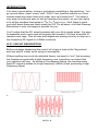
VLF1 CIRCUIT DESCRIPTION
Before we begin dissecting the circuit, let’s have a look at the “big picture”
and see what it is that we’re trying to accomplish.
Without getting too much into detailed theory, we need to “mix” the incoming
low frequency signal with a high frequency one to produce an output that
your receiver can use. As shown in the diagram below: the low frequency
input RF signal is added to a high frequency (4MHz) clock producing a high
frequency signal.
+
=
VLF1 • 4
Take a quick look at the schematic. The low frequency signal from your
antenna is fed into J1. It passes through a low-pass filter made up of L1, L2,
L3,C1,C2,C3, and C4. The signal then passes through transformer T1 which
produces 2 identical copies of the original signal, with one being inverted.
Next is the magic step that creates the high frequency signal for your
receiver. The 4053 analog switch alternately switches between the input
signal and its inverted version at a frequency of 4MHz. This 4MHz comes
from the crystal oscillator made up of the 7404 and its support components.
The result of this switching is to produce a 4MHz version of your input signal!
That’s it, after being amplified by Q1; this signal comes out of J2 and on to
your receiver.
RAMSEY Learn-As-You-Build KIT ASSEMBLY
There are numerous solder connections on the VLF1 printed circuit board.
Therefore, PLEASE take us seriously when we say that good soldering is
essential to the proper operation of your transmitter!
•
•
•
•
Use a 25-watt soldering pencil with a clean, sharp tip.
Use only rosin-core solder intended for electronics use.
Use bright lighting, a magnifying lamp or bench-style magnifier may
be helpful.
Do your work in stages, taking breaks to check your work. Carefully
brush away wire cuttings so they don't lodge between solder
connections.
We have a two-fold "strategy" for the order of the following kit assembly
steps. First, we install parts in physical relationship to each other, so there's
minimal chance of inserting wires into wrong holes. Second, whenever
possible, we install in an order that fits our "Learn-As-You Build" Kit building
philosophy. This entails describing the circuit that you are building instead of
just blindly installing components. We hope that this will not only make
assembly of our kits easier, but help you to understand the circuit you’re
constructing.
For each part, our word "Install" always means these steps:
1. Pick the correct part value to start with.
2. Insert it into the correct PC board location.
3. Orient it correctly, follow the PC board drawing and the written
directions for all parts - especially when there's a right way
and a wrong way to solder it in. (Diode bands, electrolytic
VLF1 • 5
capacitor polarity, transistor shapes, dotted or notched ends
of IC's, and so forth.)
4. Solder all connections unless directed otherwise. Use enough
heat and solder flow for clean, shiny, completed connections.
SINGLE SIDED COMPONENT SOLDERING INSTRUCTIONS:
You’ll notice that the circuit board contains plating on only one side of the
board. This makes soldering relatively easy for even the inexperienced kit
builder. Just take your time and be sure to apply enough heat to the
connections. Don’t be too afraid of overheating a component, most are fairly
hardy and a weak connection will prevent your kit from working properly.
In all RF kits it is a good idea to keep the components as close to the board
as you can and trim off the excess lengths of the component legs. However,
in this kit the highest frequency on the board is around 4MHz, so this isn’t as
critical as it would be in a higher frequency circuit.
VLF1 • 6
VLF1 PARTS LIST
Sort and “check off” the components in the boxes provided. We do our best
to pack all our kits correctly but it is possible that a boo-boo has occurred
and we missed a part. Please note that physical descriptions of parts are for
those currently being shipped. Sometimes the parts in your kit may have a
different appearance but still have the same values.
3
2
2
1
1
1
10K ohm resistor [brown-black-orange] (R1,R2,R3)
1K ohm resistor [brown-black-red] (R6,R10)
270 ohm resistor [red-violet-brown] (R5,R9)
18 ohm resistor [brown-gray-black] (R8)
1M ohm resistor [brown-black-green] (R4)
3.3K ohm resistor [orange-orange-red] (R7)
CAPACITORS
5 .1 uF ceramic disc capacitors [little green, marked 104] (C6, C7,
C11, C12, C14)
2 .015 .uF polyester film [brown, marked 153] (C2, C3)
2 .0082 uF Mylar or ceramic disk capacitors [steely blue rectangles, or
marked 822] (C1, C4)
1 40 pf adjustable cap [little cube with phillips indent on top] (C10)
2 22 pf ceramic disc [marked 22] (C8, C9)
2 10 uF electrolytic (C5, C16)
1 1 uF electrolytic (C13)
1 1000 uF electrolytic [big whopper cap] (C15)
INDUCTORS
Note: Inductor color codes can be hard to read. If you don’t have an LCR
meter, get a bright light and a magnifying glass. You can also check with an
ohmmeter to make sure that what you think is an inductor is not a resistor in
disguise. The inductors in this kit have almost zero resistance.
2
1
1
22 uH [look like turquoise or tan resistors, red-red-black] (L1, L3)
100 uH [brown-black-brown] (L4)
27 uH [red-purple-black] (L2)
SEMICONDUCTORS
Note: Chips may have different numbers and letters on them; the important
thing is that the numbers listed in brackets are there
1
1
1
1
MC74HC04AN [7404] Hex Inverter (U2)
CD74HC4053E [4053] CMOS analog Multiplexer/Demultiplexer (U1)
2N3904 NPN bipolar transistor (Q1)
7805 5 volt regulator (VR1)
VLF1 • 7
1 Red LED (D2)
1 4004 silicon diode (D1)
Miscellaneous
1
3
1
1
1
1
1
Pushbutton Switch (S1)
RCA Jacks (J1, J2, J3)
Power Jack (J4)
4MHz quartz crystal (X1)
36 AWG wire for T1
Plastic tuning screwdriver
Ferrite core for T1
Now, let's get building!
Since you may appreciate some “warm-up” soldering practice as well as a
chance to put some “landmarks” on the PC board we’ll first install some
“hardware” components. This will also help us to get acquainted with the updown, left-right orientation of the circuit board.
VLF1 • 8
VLF1 PARTS LAYOUT DIAGRAM
VLF1 • 9
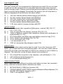
ASSEMBLY INSTRUCTIONS
Once you’ve begun to install some of the longer leaded parts, save a couple
of clipped off leads to use as jumpers in construction of your VLF1 kit.
1. Install jacks J1, J2, and J3, the antenna input and RF output Jacks.
They are RCA PC mount type. These connectors will “snap” into place
before soldering. Don’t be afraid to completely solder all three ground
connections as these will also limit the “stress” on the input and antenna
connections. Solder all four “tabs” on the bottom. Be sure to use enough
heat to properly “flow” the connection.
2. In the same manner, install power jack J4.
3. Install pushbutton switch S1. Orient the switch so that the end of the
switch extends over the edge of the PC board. Be sure to push the
switch flush to the circuit board. Solder all six pins.
That wasn’t so bad, now was it! Recheck your connections for a shiny,
smooth solder fillet connecting the component to the PC trace. Touch up any
poor looking connections. We’ll continue now by building the low-pass filter.
The next few parts will make up the low-pass filter at the antenna input of the
VLF1.
5. Install C1, .0082µF capacitor (marked 822), by the RCA jacks.
6. Install L1, 22uH inductor (red-red-black. One of the smaller blue green
or light tan parts that looks like a resistor). You can check with an
ohmmeter to make sure it isn’t a resistor. The inductors have nearly zero
resistance.
7. Install C2 .015uF capacitor (little brown chicklet marked 153), next to
L1.
8. Install C3, the other .015uF capacitor kitty corner to C2.
9. Install L2, 27uH inductor (red-purple-black).
10. Install L3, the other 22uh inductor, kitty corner to L3.
11. Install C4, the other .0082uF capacitor.
You have now completed the low-pass filter!
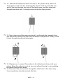
It is now time to wire up T1, the three winding transformer. Don’t be alarmed,
it isn’t that hard. Don’t be afraid to be a bit sloppy with the wire. The ferrite
core is almost an ideal material for wire stripping and if you tug on the wire
and it scrapes against the core, the insulation will come off. This will cause a
short and you will have to rewind the transformer. The wire must be
delicately threaded through the holes in the core.
VLF1 • 10
12. Take the 36 AWG wire and cut it into 3, 20” pieces. Now, take 2 of
these pieces and twist the ends together about a half an inch. Slip one
end of the wire through one hole of the ferrite core, and the other end
through the other hole. It should now look like the figure below.
13. Next, take one of the wires and wind it up through the opposite hole
and then down through the first hole as shown in the picture. Finally, route
it back through the second hole again.
14. Repeat this 12 times. Remember to be delicate and loose with your
wiring. Snug the coils as much as you can without having to use anything
but gentle force on the wires.
15. Now wind the second wire through the other hole in the same way.
Your transformer should now look like this:
VLF1 • 11
16. The twisted part is the center tap of the secondary and the other two
ends make up the end points of the secondary. You now need to wind the
primary. This will go much faster than the secondary winding. Take the
third piece of wire you cut and feed it down through the left hole leaving
about 1/2” sticking out.
17. Now run this wire through the right hole, down through the left, and
back up through the right again. This is just like you did for the secondary.
18. Wind the wire 12 more times. Your COMPLETED transformer should
now look like the next picture. Of course, yours will not be all sloppy, and it
will have more than the few wires shown. If you end up with 11 turns, it’s
okay. One turn won’t make any noticeable difference
VLF1 • 12
19. Lastly, solder in your transformer, aligning the primary and secondary
leads as they appear in the board outline. You have to tin the leads with
your soldering iron before you insert them. Get a little solder on your iron
and “paint” it on the leads as you heat them. The insulation will melt off
and the solder should stick. You will be able to see that the leads are
shiny and the red insulation is melted off. Now solder a wire or long piece
of component lead over the top of the core and into the two holes on
either side of the board.
Now take a break! That was the hardest part of this kit. After you solder in the
rest of the parts, you will be good to go.
20. Install R2, 10K ohm resistor (brown-black-orange) next to C4.
21. Install JMP3, a little piece of cutoff component lead bent into a staple
shaped piece.
22. Install C6, .1uF capacitor (marked 104).
23. Install C5, 10uF electrolytic capacitor next to C6. Be sure to observer
polarity. The “+” mark on the board outline has to line up with the “+” side
of the cap. Caps are usually marked with a “-” band. The plus side is the
other one, also normally the longer lead.
24. Install R1 and R3, 10K ohm resistors (brown-black-orange) next to
C5.
25. Install C11, .1uF ceramic disk capacitor. This feeds the mixed signal
to the 2N3904 which amplifies it.
26. Install JMP1, a little piece of cutoff component lead next to C11.
27. Install R6, 1K ohm resistor (brown-black-red) next to C11.
28. Install R5, 270 ohm resistor (red-violet-brown).
29. Install C7, .1uF ceramic disk capacitor (marked 104) next to R5.
30. Install C13 1uF electrolytic capacitor next R6. Be sure to observe
polarity.
VLF1 • 13
31. Install Q1 the 2N3904 NPN transistor next to C13. This provides
amplification for the mixed signal fed to the output jack. Be sure to align
the part with the outline on the board. The flat side should face the RCA
jacks at the bottom of the board.
32. Install R9, 270 ohm resistor (red-violet-brown) next to C3.
33. Install R8, 18 ohm resistor (brown-gray-black) next to Q1.
Now take a break from this part of the board and mosey over to the left side
and you can install the heart of the VLF1, the integrated circuits.
34. Solder in U2, the MC74HC04AN Hex Inverter. Be sure to observe the
direction when placing it. ICs soldered in the wrong way tend not to work.
Its outline on the board has a notch at one end. Line this up with the notch
on the top of the IC. The 7404 is part of the crystal oscillator that
generates the 4MHZ Clock.
35. Take a previously saved piece of clipped off lead and bend it into the
form of a staple that will fit in the holes marked “JMP2”. Place it into the
holes as though it’s a resistor or capacitor and solder it in place.
35. Install X1, the 4MHz crystal at the end of U2. It doesn’t matter which
way it goes in.
36. Install C8 and C9, 22pF capacitors (marked 22). These parts, along
with R4 and C10, set the oscillating frequency.
37. Install R4, 1M ohm resistor (brown-black-green).
38. Install C10, 40pf variable capacitor
39. Install U1, the CD74HC4053E analog multiplexer/demultiplexer, next
to U2. Again, be sure that the part is correctly oriented using the part
outline on the board. It Is lined up backwards from U2. U1 does the
switching that mixes the low frequency input with the 4MHz clock.
You’re in the home stretch!
40. Install C14, .1uF ceramic disk capacitor (marked 104), next to R8.
41. Install R7, 3.3K ohm resistor, next to C14.
42. Install C12, .1uF ceramic disk capacitor (marked 104).
43. Install D1, 4002 silicon diode.
44. Install L4, 100uH inductor (marked brown-black-brown).
45. Install C16, 10uF electrolytic capacitor, next to L4. Be sure to observe
polarity.
46. Install C15, 1000uF electrolytic capacitor, next to C16. Be sure to
observe polarity.
VLF1 • 14
47. Install the 7805 voltage regulator, bending the pins back and letting it
lay flat on the board as shown in the picture.
48. Install R10, 1K ohm resistor (brown-black-red).
49. Install D2, the red LED, next to the 7805. Observe which way it goes
in. The flat side of the LED should match the flat side on the board outline.
Leave the leads on the LED long; aproximately 1/2 inch of lead length
from the top of the PC board will give you enough space to bend it over
and fit it through the case.
You have now finished soldering all the components! At this point you should
look over your work and make sure all the solder joints look good and there
aren’t any solder bridges or “splash-ohs” on the circuit board causing
undesirable connections. Also very important is that transformer T1 is
soldered in correctly. Look at the transformer outline drawing on the board. If
you have an ohmmeter, Check across the outermost wires (the transformer
primary) and ensure that you get a low resistance reading. Also check the
inner wires (the transformer secondary) and ensure that they are low
resistance as well.
If you don’t get a low resistance reading in these tests, the wires are not wired
to the correct holes. Fix them, and test again with your meter until they are
correct.
VLF1 • 15
SETUP AND TESTING
With all this done, it is now time to set up your VLF1 and apply power!
The first thing to do is plug in the power adapter and see that nothing
burns out or gets hot. If nothing does, congratulations! At least you haven’t
made any catastrophic mistakes.
The next step is to tune the quartz oscillator to exactly 4MHz. To do this,
connect your receiver’s input jack to the VLF1’s output jack J2. Tune your
receiver to 4MHz and set it to sideband mode. Now turn variable capacitor
C10 with the red plastic screwdriver until you can’t hear anything coming
out of your receiver. This is called “zero beating”, and is useful for tuning
circuits like this without the need for a scope. Now that the Quartz
oscillator is tuned, your kit needs an input! At this point you can plug in an
audio generator or an antenna to input jack J1. That’s right, an audio
generator! The VLF1 will give you a mixed output with less than 10dB loss
at 10KHz input! Note that the VLF1 has been tested using from 4MHz to
10MHz crystals, and this tuning method works for all.
Your receiver has to be tuned to a frequency that is the sum of whatever
frequency you are interested in listening to plus 4MHz. If you want to see
if there is something going on at 300KHz, you tune your receiver to:
300KHz + 4MHz = 4.3MHz. If you are using an audio generator to test out
your kit at 10KHz, set its output level to something like –20dBm and set
your receiver to 4.01MHz. You should then hear your audio signal coming
out. If you can’t immediately hear something with your antenna, be
patient. In different areas you will have different stations available to you.
TROUBLESHOOTING GUIDE
If your kit doesn’t work it’s most likely a problem with the transformer T1.
Be really sure that the primary and secondary windings are wired onto the
board correctly. Also, check to make sure that none of your coils are
shorted to the ferrite core. You can check this with an ohmmeter. Measure
across each of the wires and the core. If you get anything other than
infinity, there is a short. You will have to rewind the transformer. Don’t feel
bad, it’s hard to do. We’ve given you enough wire to mess it up pretty
good a couple of times and still end up with a working transformer.
The next most likely boo-boo is that one or both ICs are in wrong.
The third likeliest possibility is that one or more polarized components are
backwards. These would be the electrolytic caps, the diode, and
transistor.
VLF1 • 16
VLF1 • 17
VLF1 • 18
The Ramsey Kit Warranty
Please read carefully BEFORE calling or writing in about your kit. Most
problems can be solved without contacting the factory.
Notice that this is not a "fine print" warranty. We want you to understand your rights and ours too! All
Ramsey kits will work if assembled properly. The very fact that your kit includes this new manual is your
assurance that a team of knowledgeable people have field-tested several "copies" of this kit straight
from the Ramsey Inventory. If you need help, please read through your manual carefully, all information
required to properly build and test your kit is contained within the pages! However, customer
satisfaction is our goal, so in the event that you do have a problem, take note of the following.
1. DEFECTIVE PARTS: It's always easy to blame a part for a problem in your kit, Before you conclude
that a part may be bad, thoroughly check your work. Today's semiconductors and passive components
have reached incredibly high reliability levels, and its sad to say that our human construction skills have
not! But on rare occasions a sour component can slip through. All our kit parts carry the Ramsey
Electronics Warranty that they are free from defects for a full ninety (90) days from the date of
purchase. Defective parts will be replaced promptly at our expense. If you suspect any part to be
defective, please mail it to our factory for testing and replacement. Please send only the defective part
(s), not the entire kit. The part(s) MUST be returned to us in suitable condition for testing. Please be
aware that testing can usually determine if the part was truly defective or damaged by assembly or
usage. Don't be afraid of telling us that you 'blew-it', we're all human and in most cases, replacement
parts are very reasonably priced.
2. MISSING PARTS: Before assuming a part value is incorrect, check the parts listing carefully to see if
it is a critical value such as a specific coil or IC, or whether a RANGE of values is suitable (such as
"100 to 500 uF"). Often times, common sense will solve a mysterious missing part problem. If you're
missing five 10K ohm resistors and received five extra 1K resistors, you can pretty much be assured
that the '1K ohm' resistors are actually the 'missing' 10 K parts ("Hum-m-m, I guess the 'red' band really
does look orange!") Ramsey Electronics project kits are packed with pride in the USA. If you believe
we packed an incorrect part or omitted a part clearly indicated in your assembly manual as supplied
with the basic kit by Ramsey, please write or call us with information on the part you need and proof of
kit purchase.
3. FACTORY REPAIR OF ASSEMBLED KITS:
To qualify for Ramsey Electronics factory repair, kits MUST:
1. NOT be assembled with acid core solder or flux.
2. NOT be modified in any manner.
3. BE returned in fully-assembled form, not partially assembled.
4. BE accompanied by the proper repair fee. No repair will be undertaken until we have received the
MINIMUM repair fee (1/2 hour labor) of $25.00, or authorization to charge it to your credit card account.
5. INCLUDE a description of the problem and legible return address. DO NOT send a separate letter;
include all correspondence with the unit. Please do not include your own hardware such as
nonRamsey cabinets, knobs, cables, external battery packs and the like. Ramsey Electronics, Inc.,
reserves the right to refuse repair on ANY item in which we find excessive problems or damage due to
construction methods. To assist customers in such situations, Ramsey Electronics, Inc., reserves the
right to solve their needs on a case-by-case basis.
The repair is $50.00 per hour, regardless of the cost of the kit. Please understand that our technicians
are not volunteers and that set-up, testing, diagnosis, repair and repacking and paperwork can take
nearly an hour of paid employee time on even a simple kit. Of course, if we find that a part was
defective in manufacture, there will be no charge to repair your kit (But please realize that our
technicians know the difference between a defective part and parts burned out or damaged through
improper use or assembly).
4. REFUNDS: You are given ten (10) days to examine our products. If you are not satisfied, you may
return your unassembled kit with all the parts and instructions and proof of purchase to the factory for a
full refund. The return package should be packed securely. Insurance is recommended. Please do not
cause needless delays, read all information carefully.
VLF1 • 19
VLF1 LOW FREQUENCY SWL CONVERTER
Quick Reference Page Guide
Introduction to the VLF1 ........................ 4
VLF1 Circuit Description ........................ 4
Parts List................................................ 7
Parts Layout Diagram ............................ 9
Assembly Instructions...........................10
Schematic Diagram ..............................17
Ramsey Kit Warranty............................18
REQUIRED TOOLS
• Soldering Iron Ramsey WLC100
• Thin Rosin Core Solder Ramsey RTS12
• Needle Nose Pliers Ramsey MPP4 or
RTS05
• Small Diagonal Cutters Ramsey RTS04
<OR> Technician’s Tool Kit TK405
ADDITIONAL SUGGESTED ITEMS
Holder for PC Board/Parts Ramsey HH3
Desoldering Braid Ramsey RTS08
Digital Multimeter Ramsey M133
•
•
•
Manual Price Only: $5.00
Ramsey Publication No. MVLF1
Assembly and Instruction manual for:
RAMSEY MODEL NO. VLF1 Low Bander Low
Frequency SWL Converter
RAMSEY ELECTRONICS, INC.
590 Fishers Station Drive
Victor, New York 14564
VLF1 • 20
Phone
(585) 924-4560
Fax
(585) 924-4555
www.ramseykits.com
TOTAL SOLDER POINTS
128
ESTIMATED ASSEMBLY
TIME
Beginner .............. 4 hrs
Intermediate ........ 2 hrs
Advanced ............. 1.5 hrs