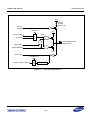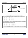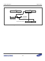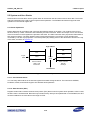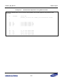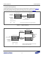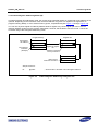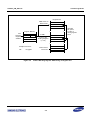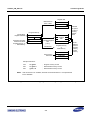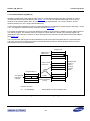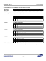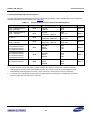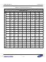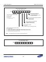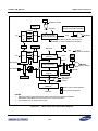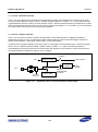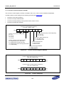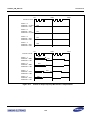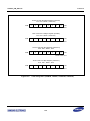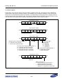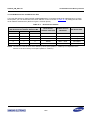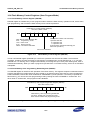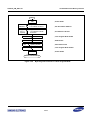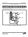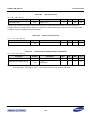
1
S3F80P5 8-Bit CMOS Microcontrollers Revision 1.30 November 2011 User's Manual 2011 Samsung Electronics Co., Ltd. All rights reserved. Important Notice Samsung Electronics Co. Ltd. (―Samsung‖) reserves the right to make changes to the information in this publication at any time without prior notice. All information provided is for reference purpose only. Samsung assumes no responsibility for possible errors or omissions, or for any consequences resulting from the use of the information contained herein. This publication on its own does not convey any license, either express or implied, relating to any Samsung and/or third-party products, under the intellectual property rights of Samsung and/or any third parties. any information provided in this publication. Customer shall indemnify and hold Samsung and its officers, employees, subsidiaries, affiliates, and distributors harmless against all claims, costs, damages, expenses, and reasonable attorney fees arising out of, either directly or indirectly, any claim (including but not limited to personal injury or death) that may be associated with such unintended, unauthorized and/or illegal use. Customers are responsible for their own products and applications. "Typical" parameters can and do vary in different applications. All operating parameters, including "Typicals" must be validated for each customer application by the customer's technical experts. WARNING No part of this publication may be reproduced, stored in a retrieval system, or transmitted in any form or by any means, electric or mechanical, by photocopying, recording, or otherwise, without the prior written consent of Samsung. This publication is intended for use by designated recipients only. This publication contains confidential information (including trade secrets) of Samsung protected by Competition Law, Trade Secrets Protection Act and other related laws, and therefore may not be, in part or in whole, directly or indirectly publicized, distributed, photocopied or used (including in a posting on the Internet where unspecified access is possible) by any unauthorized third party. Samsung reserves its right to take any and all measures both in equity and law available to it and claim full damages against any party that misappropriates Samsung‘s trade secrets and/or confidential information. Samsung products are not designed, intended, or authorized for use in applications intended to support or sustain life, or for any other application in which the failure of the Samsung product could reasonably be expected to create a situation where personal injury or death may occur. Customers acknowledge and agree that they are solely responsible to meet all other legal and regulatory requirements regarding their applications using Samsung products notwithstanding 警 告 本文件仅向经韩国三星电子株式会社授权的人员提供, 其内容含有商业秘密保护相关法规规定并受其保护的三星电 子株式会社商业秘密,任何直接或间接非法向第三人披露、 传播、复制或允许第三人使用该文件全部或部分内容的行为 (包括在互联网等公开媒介刊登该商业秘密而可能导致不特 定第三人获取相关信息的行为)皆为法律严格禁止。此等违 法行为一经发现,三星电子株式会社有权根据相关法规对其 采取法律措施,包括但不限于提出损害赔偿请求。 Samsung makes no warranty, representation, or guarantee regarding the suitability of its products for any particular purpose, nor does Samsung assume any liability arising out of the application or use of any product or circuit and specifically disclaims any and all liability, including without limitation any consequential or incidental damages. Copyright 2011 Samsung Electronics Co., Ltd. Samsung Electronics Co., Ltd. San #24 Nongseo-Dong, Giheung-Gu Yongin-City, Gyeonggi-Do, Korea 446-711 Contact Us: [email protected] TEL: (86)-(571)-86726288-8127 FAX: (86)-(571)-86726285 Home Page: http://www.samsungsemi.com Trademarks All brand names, trademarks and registered trademarks belong to their respective owners. Exynos, Exynos4210, FlexOneNAND, and OneNAND are trademarks of Samsung Electronics. ARM, Jazelle, TrustZone, and Thumb are registered trademarks of ARM Limited. Cortex, ETM, ETB, Coresight, ISA, and Neon are trademarks of ARM Limited. Java is a trademark of Sun Microsystems, Inc. SD is a registered trademark of Toshiba Corporation. MMC and eMMC are trademarks of MultiMediaCard Association. JTAG is a registered trademark of JTAG Technologies, Inc. Synopsys is a registered trademark of Synopsys, Inc. I2S is a trademark of Phillips Electronics. I2C is a trademark of Phillips Semiconductor Corp. MIPI and Slimbus are registered trademarks of the Mobile Industry Processor Interface (MIPI) Alliance. All other trademarks used in this publication are the property of their respective owners. Chip Handling Guide Precaution against Electrostatic Discharge When handling semiconductor devices, be sure that the environment is protected against static electricity. 1. Operators should wear anti-static clothing and use earth band. 2. All objects that come in direct contact with devices should be made of materials that do not produce static electricity that would cause damage. 3. Equipment and work table must be earthed. 4. Ionizer is recommended to remove electron charge. Contamination Be sure to use semiconductor products in the environment that may not be exposed to dust or dirt adhesion. Temperature/Humidity Semiconductor devices are sensitive to environment temperature and humidity. High temperature or humidity may deteriorate semiconductor device‘s characteristics. Therefore avoid storage or use in such conditions. Mechanical Shock Care should be exercised not to apply excessive mechanical shock or force on semiconductor device. Chemical Do not expose semiconductor device to chemical because reaction to chemical may cause deterioration of device characteristics. Light Protection In case of non-EMC (Epoxy Molding Compound) package, do not expose semiconductor IC to strong light. It may cause device‘s malfunction. (But, some special products which utilize the light or have security function are excepted from this guide) Radioactive, Cosmic and X-ray Semiconductor devices can be influenced by radioactive, cosmic ray or X-ray. Radioactive, cosmic and X-ray may cause soft error during device operation. Therefore semiconductor devices must be shielded under environment that may be exposed to radioactive, cosmic ray or X-ray. EMS (Electromagnetic Susceptibility) Note that semiconductor device‘s characteristics may be affected by strong electromagnetic wave or magnetic field during operation under insufficient PCB circuit design for EMS. Revision History Revision No. Date Description Author(s) 0.00 Oct, 2008 Preliminary Spec for internal release only. Minseok Jeong 0.10 Mar, 2009 Preliminary Spec for internal release only. Fan Zhang 1.00 Nov, 2009 Final version Fan Zhang – Temperature and Stop current changed – TB80PB jumper setting changed 1.10 Dec, 2009 VPOR and VDDDR changed Fan Zhang 1.20 May, 2010 Added TEST pin and nRESET pin descriptions Fan Zhang LVD enable time is added Electrical timing diagrams are changed 1.21 June, 2011 Add 24-ELP package type. Fan Zhang 1.22 July, 2011 Revise 24-ELP package mechanical data. (Figure 17-3) Fan Zhang 1.30 Oct, 2011 LVD flag levels are changed. Fan Zhang Revision Descriptions for Revision 1.30 Chapter Name 1. Overview 1-3 4. Control Registers 4-17 15. Low Voltage Detector 15-1, 15-2, 15-4. 16. Electrical Data Major Changes Comparing with Last Version Page 16-5 REV 1.22 LVDSEL Bit REV 1.30 REV1.22 REV1.30 0 0 LVD_FLAG Level = 1.88 V LVD_FLAG Level = 1.90 V 0 1 LVD_FLAG Level = 1.98 V LVD_FLAG Level = 2.00 V 1 0 LVD_FLAG Level = 2.53 V LVD_FLAG Level = 2.10 V 1 1 LVD_FLAG Level = 2.73 V LVD_FLAG Level = 2.20 V Revision Descriptions for Revision 1.20 Chapter Name Page Major Changes Comparing with Last Version REV 0.10 REV 1.00 TEST pin and nRESET pin description should be added. Table 1-1, 1-2 nRESET pin description It is recommended that add a 0.1uF capacitor between nRESET pin and VSS for better noise immunity. TEST pin description 1. Overview Table 1-1, 1-2 If on board programming is needed, It is recommended that add a 0.1uF capacitor between TEST pin and VSS for better noise immunity; otherwise, connect TEST pin to VSS directly. ESD Characteristics Table 16-12 Chapter Name Page 16-5 NOTE: If on board programming is needed, it is recommended that add a 0.1uF capacitor between TEST pin and VSS for better noise immunity; otherwise, connect TEST pin to VSS directly. It is recommended also that add a 0.1uF capacitor between nRESET pin and VSS for better noise immunity. Major Changes Comparing with Last Version tLVD spec is added. LVD Enable Time (Table 16-4) Parameter 16. Electrical Data LVD enable time Table 16-4 Symbol Conditions Min. Typ. Max. Unit tLVD VDD = 1.4 V – – 50 us In stop mode, LVD turns off. When external interrupt occurs, LVD needs tLVD during max.50us to wake up. If VDD is below VLVD after external interrupt, chip goes into back-up. Because tLVD time is not enough to start oscillation, chip is not operated to abnormal state. In 16-7, stop mode to normal mode timing diagrams are changed. Revision Descriptions for Revision 1.10 Chapter Name Major Changes Comparing with Last Version S3F80PB REV 0.10 REV 1.00 VPOR and VDDDR should be changed. 16. Electrical Data VPOR VDDDR Min. Typ. Max. Min. Typ. Max. 1.0 V 1.2 V 1.4 V 0.8 V 1.1 V 1.4 V Min. Typ. Max. Min. Typ. Max. 1.0 V – 3.6 V 0.8 V – 3.6 V Revision Descriptions for Revision 1.00 Chapter Name S3F80PB Major Changes Comparing with Last Version REV 0.10 REV 1.00 Operating temperature and stop mode current should be changed. 16. Electrical Data Operating temperature TA = 0 C to + 70 C TA = 25 C to + 85 C Stop mode current Typ. 1 uA Max. 5 uA Typ. 0.7 uA Max. 5 uA Chapter Name Page Major Changes Comparing with Last Version 19. Development Tools 19-4 Table 19-1 is deleted 19-5 Table 19-2 is changed Revision Descriptions for Revision 0.10 Chapter Name Major Changes Comparing with Last Version Page – – All – – REV 0.00 REV 0.10 Executable RAM: 256 byte Executable RAM: 1 Kbyte Operating Voltage Range: Operating Voltage Range: – 25 C to + 85 C 0 C to + 70 C IRQ – IRQ0–IRQ7 (IRQ5 is reserved for S3F80P5) Flash Memory: 16 KByte Flash Memory: 18 KByte Back-up mode features 1. Overview 4. Control Registers 5. Interrupt Structure 1-2 13. Timer 2 15. Low Voltage Detector 16. Electrical Data enters Back-up mode to block oscillation and reduce the current consumption." 1-5 Added: VSS pin (Table 1-1) 4-2 Deleted: P2CONH 4-13 Revised: IMR register 4-15 Revised: IPR register 4-16 Revised: IRQ register 4-28 Revised: P2INT register 4-30 Revised: P2PND register 4-39 Revised: SYM register 5-11 Deleted: IPR.5 controls the … 8-4 8. Reset – Deleted: "When reset pin is lower than Input Low Voltage (VIL), the chip 8-7 Deleted: "when the reset pin is set to low level", "the reset pin is at a high state and" Revised (Table 8-1) 8-15 Added: register P1, P1CONH, P1CONL (Table 8-2) 8-19 Added: register P1 (Table 8-5) – Added Deleted: When the reset pin is at a high state and the LVD circuit detects 15-1 rising edge of VDD on the point VLVD, the reset pulse generator makes a reset pulse, and system reset occurs. 16-1 Deleted: "Input Timing for External reset" 16-6 Deleted (Figure 15-2) Added: Programming socket adapter for S3F80P5 should be connected 18. Flash MCU 18-3 18-3 R (330 ) and C (0.1 uF) for delay time. And nRST pin should be connected to GND. Added (Figure 17-2) Table of Contents 1 PRODUCT OVERVIEW .................................................................................1-1 1.1 S3C8/S3F8-Series Microcontrollers......................................................................................................... 1-1 1.2 S3F80P5 Microcontroller ......................................................................................................................... 1-1 1.3 Features ................................................................................................................................................... 1-2 1.4 Block Diagram .......................................................................................................................................... 1-4 1.4.1 24-Pin Package ................................................................................................................................ 1-4 1.5 Pin Assignments ...................................................................................................................................... 1-5 1.6 Pin Circuits ............................................................................................................................................... 1-7 2 ADDRESS SPACE ........................................................................................2-1 2.1 Overview .................................................................................................................................................. 2-1 2.2 Program Memory ..................................................................................................................................... 2-2 2.2.1 Smart Option ..................................................................................................................................... 2-3 2.3 Register Architecture ............................................................................................................................... 2-5 2.3.1 Register Page Pointer (PP) .............................................................................................................. 2-7 2.3.2 Register Set 1 ................................................................................................................................... 2-8 2.3.3 Register Set 2 ................................................................................................................................... 2-8 2.3.4 Prime Register Space ....................................................................................................................... 2-9 2.3.5 Working Registers .......................................................................................................................... 2-10 2.3.6 Using the Register Pointers ............................................................................................................ 2-11 2.4 Register Addressing ............................................................................................................................... 2-13 2.4.1 Common Working Register Area (C0H–CFH) ................................................................................ 2-15 2.4.2 4-Bit Working Register Addressing ................................................................................................. 2-16 2.4.3 8-Bit Working Register Addressing ................................................................................................. 2-18 2.5 System and User Stacks ........................................................................................................................ 2-20 2.5.1 Stack Operations ............................................................................................................................ 2-20 3 ADDRESSING MODES .................................................................................3-1 3.1 Overview .................................................................................................................................................. 3-1 3.1.1 Register Addressing Mode (R) ......................................................................................................... 3-2 3.1.2 Indirect Register Addressing Mode (IR) ........................................................................................... 3-3 3.1.3 Indexed Addressing Mode (X) .......................................................................................................... 3-7 3.1.4 Direct Address Mode (DA) .............................................................................................................. 3-10 3.1.5 Indirect Address Mode (IA) ............................................................................................................. 3-12 3.1.6 Relative Address Mode (RA) .......................................................................................................... 3-13 3.1.7 Immediate Mode (IM)...................................................................................................................... 3-14 4 CONTROL REGISTERS ................................................................................4-1 4.1 Overview .................................................................................................................................................. 4-1 4.2 Register Map Summary ........................................................................................................................... 4-2 4.2.1 BTCON: Basic Timer Control Register (D3H, Set1, Bank0) ............................................................ 4-6 4.2.2 CACON: Counter A Control Register (F3H, Set1, Bank0) ............................................................... 4-7 4.2.3 CLKCON: System Clock Control Register (D4H, Set1, Bank0) ....................................................... 4-8 ( 4.2.4 EMT: External Memory Timing Register (NOTE) FEH, Set1, Bank0) ............................................. 4-9 4.2.5 FLAGS: System Flags Register (D5H, Set1, Bank0) ..................................................................... 4-10 4.2.6 FMCON: Flash Memory Control Register (EFH, Set1, Bank1) ...................................................... 4-11 4.2.7 FMSECH: Flash Memory Sector Address Register (High Byte) (ECH, Set1, Bank1) ................... 4-12 4.2.8 FMSECL: Flash Memory Sector Address Register (Low Byte) (EDH, Set1, Bank1) ..................... 4-12 4.2.9 FMUSR: Flash Memory User Programming Enable Register (EEH, Set1, Bank1) ....................... 4-12 4.2.10 IMR: Interrupt Mask Register (DDH, Set1, Bank0) ....................................................................... 4-13 4.2.11 IPH: Instruction Pointer (High Byte) (DAH, Set1, Bank0) ............................................................. 4-14 4.2.12 IPL: Instruction Pointer (Low Byte) (DBH, Set1, Bank0) .............................................................. 4-14 4.2.13 IPR: Interrupt Priority Register (FFH, Set1, Bank0) ..................................................................... 4-15 4.2.14 IRQ: Interrupt Request Register (DCH, Set1, Bank0) .................................................................. 4-16 4.2.15 LVDCON: LVD Control Register (E0H, Set1, Bank1) .................................................................. 4-17 4.2.16 LVDSEL: LVD Flag Level Selection Register (F1H, Set1, Bank1 ................................................ 4-17 4.2.17 P0CONH: Port 0 Control Register (High Byte) (E8H, Set1, Bank0) ............................................. 4-18 4.2.18 P0CONL: Port 0 Control Register (Low Byte) (E9H, Set1, Bank0) .............................................. 4-19 4.2.19 P0INT: Port 0 External Interrupt Enable Register (F1H, Set1, Bank0) ........................................ 4-20 4.2.20 P0PND: Port 0 External Interrupt Pending Register (F2H, Set1, Bank0)..................................... 4-21 4.2.21 P0PUR: Port 0 Pull-up Resistor Enable Register (E7H, Set1, Bank0) ......................................... 4-23 4.2.22 P1CONH: Port 1 Control Register (High Byte) (EAH, Set1, Bank0) ............................................ 4-24 4.2.23 P1CONL: Port 1 Control Register (Low Byte) (EBH, Set1, Bank0) .............................................. 4-25 4.2.24 P1OUTPU: Port 1 Output Pull-up Resistor Enable Register (F2H, Set1, Bank1) ........................ 4-26 4.2.25 P2CONL: Port 2 Control Register (Low Byte) (EDH, Set1, Bank0) ............................................. 4-27 4.2.26 P2INT: Port 2 External Interrupt Enable Register (E5H, Set1, Bank0) ........................................ 4-27 4.2.27 P2OUTMD: Port 2 Output Mode Selection Register (F3H, Set1, Bank1) .................................... 4-27 4.2.28 P2PND: Port 2 External Interrupt Pending Register (E6H, Set1, Bank0) .................................... 4-28 4.2.29 P2PUR: Port 2 Pull-up Resistor Enable Register (EEH, Set1, Bank0) ........................................ 4-28 4.2.30 P3CON: Port 3 Control Register (EFH, Set1, Bank0) .................................................................. 4-29 4.2.31 P3OUTPU: Port 3 Output Pull-up Resistor Enable Register (F4H, Set1, Bank1) ........................ 4-31 4.2.32 PP: Register Page Pointer (DFH, Set1, Bank0) ........................................................................... 4-32 4.2.33 RESETID: Reset Source Indicating Register (F0H, Set1, Bank1) ............................................... 4-33 4.2.34 RP0: Register Pointer 0 (D6H, Set1, Bank0) ............................................................................... 4-34 4.2.35 RP1: Register Pointer 1 (D7H, Set1, Bank0) ............................................................................... 4-34 4.2.36 SPL: Stack Pointer (Low Byte) (D9H, Set1, Bank0) ..................................................................... 4-35 4.2.37 STOPCON: Stop Control Register (FBH, Set1, Bank0) ............................................................... 4-35 4.2.38 SYM: System Mode Register (DEH, Set1, Bank0) ....................................................................... 4-36 4.2.39 T0CON: Timer 0 Control Register (D2H, Set 1, Bank0) ............................................................... 4-37 4.2.40 T1CON: Timer 1 Control Register (FAH, Set1, Bank0) ................................................................ 4-38 4.2.41 T2CON: Timer 2 Control Register (E8H, Set1, Bank1) ................................................................ 4-39 5 INTERRUPT STRUCTURE ............................................................................5-1 5.1 Overview .................................................................................................................................................. 5-1 5.1.1 Levels ............................................................................................................................................... 5-1 5.1.2 Vectors .............................................................................................................................................. 5-1 5.1.3 Sources ............................................................................................................................................. 5-1 5.1.4 Interrupt Types .................................................................................................................................. 5-2 5.1.5 Interrupt Vector Addresses ............................................................................................................... 5-4 5.1.6 Enable/Disable Interrupt Instructions (EI, DI) ................................................................................... 5-6 5.1.7 Interrupt Processing Control Points .................................................................................................. 5-7 5.1.8 Peripheral Interrupt Control Registers .............................................................................................. 5-8 5.1.9 System Mode Register (SYM) .......................................................................................................... 5-9 5.1.10 Interrupt Mask Register (IMR) ...................................................................................................... 5-10 5.1.11 Interrupt Priority Register (IPR) .................................................................................................... 5-11 5.1.12 Interrupt Request Register (IRQ) .................................................................................................. 5-13 5.1.13 Interrupt Pending Function Types ................................................................................................ 5-14 5.1.14 Interrupt Source Polling Sequence ............................................................................................... 5-15 5.1.15 Interrupt Service Routines ............................................................................................................ 5-15 5.1.16 Generating interrupt Vector Addresses ........................................................................................ 5-16 5.1.17 Nesting of Vectored Interrupts ...................................................................................................... 5-16 5.1.18 Instruction Pointer (IP) .................................................................................................................. 5-16 5.1.19 Fast Interrupt Processing ............................................................................................................. 5-17 6 INSTRUCTION SET .......................................................................................6-1 6.1 Overview .................................................................................................................................................. 6-1 6.1.1 Data Types ....................................................................................................................................... 6-1 6.1.2 Register Addressing ......................................................................................................................... 6-1 6.1.3 Addressing Modes ............................................................................................................................ 6-1 6.2 Flags Register (FLAGS) ........................................................................................................................... 6-5 6.2.1 Flag Descriptions .............................................................................................................................. 6-6 6.2.2 Instruction Set Notation .................................................................................................................... 6-7 6.2.3 Condition Codes ............................................................................................................................. 6-11 6.3 Instruction Descriptions .......................................................................................................................... 6-12 6.3.1 ADC-Add with Carry ....................................................................................................................... 6-13 6.3.2 ADD-Add ......................................................................................................................................... 6-14 6.3.3 AND-Logical AND ........................................................................................................................... 6-15 6.3.4 BAND-Bit AND ................................................................................................................................ 6-16 6.3.5 BCP-Bit Compare ........................................................................................................................... 6-17 6.3.6 BITC-Bit Complement ..................................................................................................................... 6-18 6.3.7 BITR-Bit Reset ................................................................................................................................ 6-19 6.3.8 BITS-Bit Set .................................................................................................................................... 6-20 6.3.9 BOR-Bit OR .................................................................................................................................... 6-21 6.3.10 BTJRF-Bit Test, Jump Relative on False ..................................................................................... 6-22 6.3.11 BTJRT-Bit Test, Jump Relative on True ....................................................................................... 6-23 6.3.12 BXOR-Bit XOR ............................................................................................................................. 6-24 6.3.13 CALL-Call Procedure .................................................................................................................... 6-25 6.3.14 CCF-Complement Carry Flag ....................................................................................................... 6-26 6.3.15 CLR-Clear ..................................................................................................................................... 6-27 6.3.16 COM-Complement ........................................................................................................................ 6-28 6.3.17 CP-Compare ................................................................................................................................. 6-29 6.3.18 CPIJE-Compare, Increment, and Jump on Equal ........................................................................ 6-30 6.3.19 CPIJNE-Compare, Increment, and Jump on Non-Equal .............................................................. 6-31 6.3.20 DA-Decimal Adjust........................................................................................................................ 6-32 6.3.21 DEC-Decrement ........................................................................................................................... 6-34 6.3.22 DECW-Decrement Word .............................................................................................................. 6-35 6.3.23 DI-Disable Interrupts ..................................................................................................................... 6-36 6.3.24 DIV-Divide (Unsigned) .................................................................................................................. 6-37 6.3.25 DJNZ-Decrement and Jump if Non-Zero ...................................................................................... 6-38 6.3.26 EI-Enable Interrupts ...................................................................................................................... 6-39 6.3.27 ENTER-Enter ................................................................................................................................ 6-40 6.3.28 EXIT-Exit ....................................................................................................................................... 6-41 6.3.29 IDLE-Idle Operation ...................................................................................................................... 6-42 6.3.30 INC-Increment .............................................................................................................................. 6-43 6.3.31 INCW-Increment Word ................................................................................................................. 6-44 6.3.32 IRET-Interrupt Return ................................................................................................................... 6-45 6.3.33 JP-Jump........................................................................................................................................ 6-46 6.3.34 JR-Jump Relative ......................................................................................................................... 6-47 6.3.35 LD-Load ........................................................................................................................................ 6-48 6.3.36 LDB-Load Bit ................................................................................................................................ 6-50 6.3.37 LDC/LDE-Load Memory ............................................................................................................... 6-51 6.3.38 LDCD/LDED-Load Memory and Decrement ................................................................................ 6-53 6.3.39 LDCI/LDEI-Load Memory and Increment ..................................................................................... 6-54 6.3.40 LDCPD/LDEPD-Load Memory with Pre-Decrement .................................................................... 6-55 6.3.41 LDCPI/LDEPI-Load Memory with Pre-Increment ......................................................................... 6-56 6.3.42 LDW-Load Word ........................................................................................................................... 6-57 6.3.43 MULT-Multiply (Unsigned) ............................................................................................................ 6-58 6.3.44 NEXT-Next.................................................................................................................................... 6-59 6.3.45 NOP-No Operation ....................................................................................................................... 6-60 6.3.46 OR-Logical OR ............................................................................................................................. 6-61 6.3.47 POP-Pop from Stack .................................................................................................................... 6-62 6.3.48 POPUD-Pop User Stack (Decrementing) ..................................................................................... 6-63 6.3.49 POPUI-Pop User Stack (Incrementing) ........................................................................................ 6-64 6.3.50 PUSH-Push to Stack .................................................................................................................... 6-65 6.3.51 PUSHUD-Push User Stack (Decrementing) ................................................................................ 6-66 6.3.52 PUSHUI-Push User Stack (Incrementing) .................................................................................... 6-67 6.3.53 RCF-Reset Carry Flag .................................................................................................................. 6-68 6.3.54 RET-Return................................................................................................................................... 6-69 6.3.55 RL-Rotate Left .............................................................................................................................. 6-70 6.3.56 RLC-Rotate Left Through Carry ................................................................................................... 6-71 6.3.57 RR-Rotate Right ........................................................................................................................... 6-72 6.3.58 RRC-Rotate Right through Carry.................................................................................................. 6-73 6.3.59 SB0-Select Bank 0........................................................................................................................ 6-74 6.3.60 SB1-Select Bank 1........................................................................................................................ 6-75 6.3.61 SBC-Subtract with Carry .............................................................................................................. 6-76 6.3.62 SCF-Set Carry Flag ...................................................................................................................... 6-77 6.3.63 SRA-Shift Right Arithmetic ........................................................................................................... 6-78 6.3.64 SRP/SRP0/SRP1-Set Register Pointer ........................................................................................ 6-79 6.3.65 STOP-Stop Operation .................................................................................................................. 6-80 6.3.66 SUB-Subtract ................................................................................................................................ 6-81 6.3.67 SWAP-Swap Nibbles .................................................................................................................... 6-82 6.3.68 TCM-Test Complement under Mask ............................................................................................ 6-83 6.3.69 TM-Test under Mask .................................................................................................................... 6-84 6.3.70 WFI-Wait for Interrupt ................................................................................................................... 6-85 6.3.71 XOR-Logical Exclusive OR ........................................................................................................... 6-86 7 CLOCK AND POWER CIRCUITS .................................................................7-1 7.1 Overview .................................................................................................................................................. 7-1 7.1.1 System Clock Circuit......................................................................................................................... 7-1 7.1.2 Clock Status during Power-Down Modes ......................................................................................... 7-3 7.1.3 System Clock Control Register (CLKCON) ...................................................................................... 7-4 8 RESET ...........................................................................................................8-1 8.1 Overview .................................................................................................................................................. 8-1 8.1.1 Reset Sources .................................................................................................................................. 8-1 8.1.2 Reset Mechanism ............................................................................................................................. 8-4 8.1.3 Watch Dog Timer Reset ................................................................................................................... 8-4 8.1.4 LVD Reset ........................................................................................................................................ 8-4 8.1.5 Internal Power-On Reset .................................................................................................................. 8-5 8.1.6 External Interrupt Reset .................................................................................................................... 8-6 8.1.7 STOP Error Detection & Recovery ................................................................................................... 8-6 8.1.8 Power-Down Modes ......................................................................................................................... 8-7 8.1.9 Back-Up Mode .................................................................................................................................. 8-8 8.1.10 STOP Mode .................................................................................................................................. 8-10 8.1.11 System Reset Operation .............................................................................................................. 8-13 8.1.12 Hardware Reset Values ................................................................................................................ 8-14 8.1.13 Recommendation for Unusued Pins ............................................................................................. 8-18 8.1.14 Summary Table of Back-Up Mode, Stop Mode, and Reset Status .............................................. 8-19 9 I/O PORTS .....................................................................................................9-1 9.1 Overview .................................................................................................................................................. 9-1 9.1.1 Port Data Registers .......................................................................................................................... 9-3 9.1.2 Pull-Up Resistor Enable Registers ................................................................................................... 9-4 10 BASIC TIMER AND TIMER 0 ....................................................................10-1 10.1 Overview .............................................................................................................................................. 10-1 10.1.1 Basic Timer (BT) ........................................................................................................................... 10-1 10.1.2 Basic Timer Control Register (BTCON) ....................................................................................... 10-2 10.1.3 Basic Timer Function Description ................................................................................................. 10-3 10.1.4 Timer 0 Control Register (T0CON) ............................................................................................... 10-4 10.1.5 Timer 0 Function Description ........................................................................................................ 10-6 11 TIMER 1 .....................................................................................................11-1 11.1 Overview .............................................................................................................................................. 11-1 11.1.1 Timer 1 Overflow Interrupt ............................................................................................................ 11-2 11.1.2 Timer 1 Capture Interrupt ............................................................................................................. 11-2 11.1.3 Timer 1 Match Interrupt ................................................................................................................ 11-3 11.1.4 Timer 1 Control Register (T1CON) ............................................................................................... 11-5 12 COUNTER A ..............................................................................................12-1 12.1 Overview .............................................................................................................................................. 12-1 12.1.1 Counter A Control Register (CACON) .......................................................................................... 12-3 12.1.2 Counter A Pulse Width Calculations............................................................................................. 12-4 13 TIMER 2 .....................................................................................................13-1 13.1 Overview .............................................................................................................................................. 13-1 13.1.1 Timer 2 Overflow Interrupt ............................................................................................................ 13-2 13.1.2 Timer 2 Capture Interrupt ............................................................................................................. 13-2 13.1.3 Timer 2 Match interrupt ................................................................................................................ 13-3 13.1.4 Timer 2 Control Register (T2CON) ............................................................................................... 13-5 14 EMBEDDED FLASH MEMORY INTERFACE ............................................14-1 14.1 Overview .............................................................................................................................................. 14-1 14.2 Flash ROM Configuration .................................................................................................................... 14-1 14.3 User Program Mode ............................................................................................................................. 14-2 TM 14.3.1 ISP (On-Board Programming) SECTOR ................................................................................... 14-2 14.3.2 Smart Option................................................................................................................................. 14-3 14.3.3 ISP Reset Vector and ISP Sector Size ......................................................................................... 14-5 14.4 Flash Memory Control Registers (User Program Mode) ..................................................................... 14-6 14.4.1 Flash Memory Control Register (FMCON) ................................................................................... 14-6 14.4.2 Flash Memory User Programming Enable Register (FMUSR) .................................................... 14-6 14.4.3 Flash Memory sector Address Registers ..................................................................................... 14-7 14.4.4 Sector Erase ................................................................................................................................. 14-8 14.4.5 Programming .............................................................................................................................. 14-12 14.4.6 Reading ...................................................................................................................................... 14-18 14.4.7 Hard Lock Protection .................................................................................................................. 14-19 15 LOW VOLTAGE DETECTOR ....................................................................15-1 15.1 Overview .............................................................................................................................................. 15-1 15.1.1 LVD ............................................................................................................................................... 15-1 15.1.2 LVD FLAG .................................................................................................................................... 15-1 15.1.3 Low Voltage Detector Control Register (LVDCON)...................................................................... 15-4 15.1.4 Low Voltage Detector Flag Selection Register (LVDSEL) ........................................................... 15-4 16 ELECTRICAL DATA..................................................................................16-1 16.1 Overview .............................................................................................................................................. 16-1 16.2 Absolute Maximum Ratings ................................................................................................................. 16-2 16.3 D.C. Electrical Characteristics ............................................................................................................. 16-3 16.4 A.C. Electrical Characteristics .............................................................................................................. 16-8 16.5 Oscillation Characteristics .................................................................................................................... 16-9 17 MECHANICAL DATA ................................................................................17-1 17.1 Overview .............................................................................................................................................. 17-1 18 S3F80P5 FLASH MCU ..............................................................................18-1 18.1 Overview .............................................................................................................................................. 18-1 18.2 Pin Assignment .................................................................................................................................... 18-2 18.2.1 Operating Mode Characteristics ................................................................................................... 18-4 19 DEVELOPMENT TOOLS ...........................................................................19-1 19.1 Overview .............................................................................................................................................. 19-1 19.1.1 Target Boards ............................................................................................................................... 19-1 19.1.2 Programming Socket Adapter ...................................................................................................... 19-1 19.1.3 Development System Configuration ............................................................................................. 19-2 19.1.4 Third Parties for Development Tools ............................................................................................ 19-6 List of Figures Figure Number Title Page Number Figure 1-1 Figure 1-2 Figure 1-3 Figure 1-4 Figure 1-5 Figure 1-6 Figure 1-7 Figure 1-8 Block Diagram (24-Pin) ..................................................................................................................... 1-4 Pin Assignment Diagram (24-Pin SOP/SDIP Package) ................................................................... 1-5 Pin Assignment Diagram (24-Pin ELP Package) ............................................................................. 1-5 Pin Circuit Type 1 (Port 0) ................................................................................................................ 1-7 Pin Circuit Type 2 (Port 1) ................................................................................................................ 1-8 Pin Circuit Type 2 (Port 2) ................................................................................................................ 1-9 Pin Circuit Type 4 (P3.0) ................................................................................................................. 1-10 Pin Circuit Type 5 (P3.1) ................................................................................................................. 1-11 Figure 2-1 Figure 2-2 Figure 2-3 Figure 2-4 Figure 2-5 Figure 2-6 Figure 2-7 Figure 2-8 Figure 2-9 Figure 2-10 Figure 2-11 Figure 2-12 Figure 2-13 Figure 2-14 Figure 2-15 Figure 2-16 Program Memory Address Space..................................................................................................... 2-2 Smart Option ..................................................................................................................................... 2-3 Internal Register File Organization ................................................................................................... 2-6 Register Page Pointer (PP) .............................................................................................................. 2-7 Set 1, Set 2, and Prime Area Register Map ..................................................................................... 2-9 8 Byte Working Register Areas (Slices) ......................................................................................... 2-10 Contiguous 16 Byte Working Register Block .................................................................................. 2-11 Non-Contiguous 16 Byte Working Register Block .......................................................................... 2-12 16-Bit Register Pair ......................................................................................................................... 2-13 Register File Addressing ............................................................................................................... 2-14 Common Working Register Area .................................................................................................. 2-15 4-Bit Working Register Addressing ............................................................................................... 2-17 4-Bit Working Register Addressing Example................................................................................ 2-17 8-Bit Working Register Addressing ............................................................................................... 2-18 8-Bit Working Register Addressing Example................................................................................ 2-19 Stack Operations .......................................................................................................................... 2-20 Figure 3-1 Figure 3-2 Figure 3-3 Figure 3-4 Figure 3-5 Figure 3-6 Figure 3-7 Figure 3-8 Figure 3-9 Figure 3-10 Figure 3-11 Figure 3-12 Figure 3-13 Figure 3-14 Register Addressing ......................................................................................................................... 3-2 Working Register Addressing ........................................................................................................... 3-2 Indirect Register Addressing to Register File ................................................................................... 3-3 Indirect Register Addressing to Program Memory............................................................................ 3-4 Indirect Working Register Addressing to Register File ..................................................................... 3-5 Indirect Working Register Addressing to Program or Data Memory ................................................ 3-6 Indexed Addressing to Register File ................................................................................................. 3-7 Indexed Addressing to Program or Data Memory with Short Offset ................................................ 3-8 Indexed Addressing to Program or Data Memory ............................................................................ 3-9 Direct Addressing for Load Instructions ........................................................................................ 3-10 Direct Addressing for Call and Jump Instructions ......................................................................... 3-11 Indirect Addressing ....................................................................................................................... 3-12 Relative Addressing ...................................................................................................................... 3-13 Immediate Addressing .................................................................................................................. 3-14 Figure 4-1 Register Description Format ............................................................................................................. 4-5 Figure 5-1 Figure 5-2 Figure 5-3 S3C8/S3F8-Series Interrupt Types................................................................................................... 5-2 S3F80P5 Interrupt Structure ............................................................................................................. 5-3 ROM Vector Address Area ............................................................................................................... 5-4 Figure 5-4 Figure 5-5 Figure 5-6 Figure 5-7 Figure 5-8 Figure 5-9 Interrupt Function Diagram ............................................................................................................... 5-7 System Mode Register (SYM) .......................................................................................................... 5-9 Interrupt Mask Register (IMR) ........................................................................................................ 5-10 Interrupt Request Priority Groups ................................................................................................... 5-11 Interrupt Priority Register (IPR) ...................................................................................................... 5-12 Interrupt Request Register (IRQ) .................................................................................................... 5-13 Figure 6-1 System Flags Register (FLAGS) ...................................................................................................... 6-5 Figure 7-1 Figure 7-2 Figure 7-3 Figure 7-4 Figure 7-5 Figure 7-6 Main Oscillator Circuit (External Crystal or Ceramic Resonator) ..................................................... 7-2 External Clock Circuit ....................................................................................................................... 7-2 System Clock Circuit Diagram .......................................................................................................... 7-3 System Clock Control Register (CLKCON) ...................................................................................... 7-4 Power Circuit (VDD) ......................................................................................................................... 7-5 Guide Line of Chip Operating Voltage .............................................................................................. 7-5 Figure 8-1 Figure 8-2 Figure 8-3 Figure 8-4 Figure 8-5 Figure 8-6 Figure 8-7 Figure 8-8 RESET Sources of the S3F80P5...................................................................................................... 8-2 RESET Block Diagram of the S3F80P5 ........................................................................................... 8-3 RESET Block Diagram by LVD for the S3F80P5 in STOP Mode .................................................... 8-4 Timing Diagram for Internal Power-On Reset Circuit ....................................................................... 8-5 Reset Timing Diagram for the S3F80P5 in STOP Mode by IPOR ................................................... 8-5 Block Diagram for Back-Up Mode .................................................................................................... 8-8 Timing Diagram for Back-Up Mode Input and Released by LVD ..................................................... 8-8 Timing Diagram for Back-Up Mode Input in STOP Mode ................................................................ 8-9 Figure 9-1 Figure 9-2 S3F80P5 I/O Port Data Register Format .......................................................................................... 9-3 Pull-up Resistor Enable Registers (Port 0 and Port 2) ..................................................................... 9-4 Figure 10-1 Figure 10-2 Figure 10-3 Figure 10-4 Figure 10-5 Figure 10-6 Figure 10-7 Basic Timer Control Register (BTCON) ........................................................................................ 10-2 Timer 0 Control Register (T0CON) ............................................................................................... 10-5 Timer 0 DATA Register (T0DATA) ............................................................................................... 10-5 Simplified Timer 0 Function Diagram: Interval Timer Mode ......................................................... 10-6 Simplified Timer 0 Function Diagram: PWM Mode....................................................................... 10-7 Simplified Timer 0 Function Diagram: Capture Mode................................................................... 10-8 Basic Timer and Timer 0 Block Diagram ...................................................................................... 10-9 Figure 11-1 Figure 11-2 Figure 11-3 Figure 11-4 Figure 11-5 Simplified Timer 1 Function Diagram: Capture Mode................................................................... 11-2 Simplified Timer 1 Function Diagram: Interval Timer Mode ......................................................... 11-3 Timer 1 Block Diagram ................................................................................................................. 11-4 Timer 1 Control Register (T1CON) ............................................................................................... 11-5 Timer 1 Registers (T1CNTH, T1CNTL, T1DATAH, T1DATAL) .................................................... 11-6 Figure 12-1 Figure 12-2 Figure 12-3 Figure 12-4 Counter A Block Diagram ............................................................................................................. 12-2 Counter A Control Register (CACON) .......................................................................................... 12-3 Counter A Registers ..................................................................................................................... 12-3 Counter A Output Flip-Flop Waveforms in Repeat Mode ............................................................. 12-5 Figure 13-1 Figure 13-2 Figure 13-3 Figure 13-4 Figure 13-5 Simplified Timer 2 Function Diagram: Capture Mode................................................................... 13-2 Simplified Timer 2 Function Diagram: Interval Timer Mode ......................................................... 13-3 Timer 2 Block Diagram ................................................................................................................. 13-4 Timer 2 Control Register (T2CON) ............................................................................................... 13-5 Timer 2 Registers (T2CNTH, T2CNTL, T2DATAH, T2DATAL) .................................................... 13-6 Figure 14-1 Figure 14-2 Figure 14-3 Figure 14-4 Figure 14-5 Figure 14-6 Figure 14-7 Figure 14-8 Figure 14-9 Figure 14-10 Program Memory Address Space ................................................................................................ 14-2 Smart Option ................................................................................................................................. 14-3 Flash Memory Control Register (FMCON) ................................................................................... 14-6 Flash Memory User Programming Enable Register (FMUSR) ..................................................... 14-6 Flash Memory Sector Address Register (FMSECH) .................................................................... 14-7 Flash Memory Sector Address Register (FMSECL) ..................................................................... 14-7 Sector Configurations in User Program Mode .............................................................................. 14-8 Sector Erase Flowchart in User Program Mode ........................................................................... 14-9 Byte Program Flowchart in a User Program Mode ..................................................................... 14-13 Program Flowchart in a User Program Mode ........................................................................... 14-14 Figure 15-1 Figure 15-2 Figure 15-3 Low Voltage Detect (LVD) Block Diagram .................................................................................... 15-3 Low Voltage Detect Control Register (LVDCON) ......................................................................... 15-4 Low Voltage Detect Flag Selection Register (LVDSEL) ............................................................... 15-4 Figure 16-1 Figure 16-2 Figure 16-3 Figure 16-4 Stop Mode to Normal Mode Timing Diagram (1) .......................................................................... 16-7 Stop Mode to Normal Mode Timing Diagram (2) .......................................................................... 16-7 Input Timing for External Interrupts (Port 0 and Port 2) ............................................................... 16-8 Operating Voltage Range of S3F80P5 ....................................................................................... 16-10 Figure 17-1 Figure 17-2 Figure 17-3 24-Pin SOP Package Mechanical Data ........................................................................................ 17-1 24-Pin SDIP Package Mechanical Data ....................................................................................... 17-2 24-Pin ELP Package Mechanical Data ......................................................................................... 17-3 Figure 18-1 Figure 18-2 Pin Assignment Diagram (24-Pin SOP/SDIP Package) ............................................................... 18-2 Pin Assignment Diagram (24-Pin ELP Package) ......................................................................... 18-2 Figure 19-1 Figure 19-2 Figure 19-3 Figure 19-4 Development System Configuration ............................................................................................. 19-2 TB80PB Target Board Configuration ............................................................................................ 19-3 50-Pin Connector Pin Assignment for User System ..................................................................... 19-5 TB80PB Probe Adapter Cable ...................................................................................................... 19-5 List of Tables Table Number Title Page Number Table 1-1 Pin Descriptions of 24-SOP/SDIP (24-ELP) ...................................................................................... 1-6 Table 2-1 The Summary of S3F80P5 Register Type ......................................................................................... 2-5 Table 4-1 Table 4-2 Table 4-3 Mapped Registers (Bank 0, Set 1) ..................................................................................................... 4-2 Mapped Registers (Bank 1, Set 1) ..................................................................................................... 4-4 Each Function Description and Pin Assignment of P3CON in 24-Pin Package .............................. 4-30 Table 5-1 Table 5-2 Table 5-3 S3F80P5 Interrupt Vectors ................................................................................................................ 5-5 Interrupt Control Register Overview................................................................................................... 5-6 Vectored Interrupt Source Control and Data Registers ..................................................................... 5-8 Table 6-1 Table 6-2 Table 6-3 Table 6-4 Table 6-5 Table 6-6 Table 6-7 Instruction Group Summary ............................................................................................................... 6-2 Flag Notation Conventions ................................................................................................................. 6-7 Instruction Set Symbols ..................................................................................................................... 6-7 Instruction Notation Conventions ....................................................................................................... 6-8 Opcode Quick Reference (0 – 7) ....................................................................................................... 6-9 Opcode Quick Reference (8 – F) ..................................................................................................... 6-10 Condition Codes............................................................................................................................... 6-11 Table 7-1 Falling and Rising Time of Operating Voltage ................................................................................... 7-5 Table 8-1 Table 8-2 Table 8-3 Table 8-4 Table 8-5 Table 8-6 Reset Condition in STOP Mode ......................................................................................................... 8-6 Set 1, Bank 0 Register Values after Reset ...................................................................................... 8-14 Set 1, Bank 1 Register Values after Reset ...................................................................................... 8-16 Reset Generation According to the Condition of Smart Option ....................................................... 8-17 Guideline for Unused Pins to Reduced Power Consumption .......................................................... 8-18 Summary of Each Mode .................................................................................................................. 8-19 Table 9-1 Table 9-2 Port Configuration Overview (24-SOP/SDIP/ELP) ............................................................................ 9-2 Port Data Register Summary ............................................................................................................. 9-3 Table 14-1 Table 14-2 ISP Sector Size .............................................................................................................................. 14-4 Reset Vector Address .................................................................................................................... 14-5 Table 15-1 LVD Enable Time ........................................................................................................................... 15-3 Table 16-1 Table 16-2 Table 16-3 Table 16-4 Table 16-5 Table 16-6 Table 16-7 Table 16-8 Table 16-9 Absolute Maximum Ratings ........................................................................................................... 16-2 D.C. Electrical Characteristics ....................................................................................................... 16-3 Characteristics of Low Voltage Detect Circuit ................................................................................ 16-5 LVD Enable Time ........................................................................................................................... 16-6 Power On Reset Circuit ................................................................................................................. 16-6 Data Retention Supply Voltage in Stop Mode ............................................................................... 16-6 A.C. Electrical Characteristics ........................................................................................................ 16-8 Oscillation Characteristics .............................................................................................................. 16-9 Input/Output Capacitance .............................................................................................................. 16-9 Table 16-10 Table 16-11 Table 16-12 Oscillation Stabilization Time ..................................................................................................... 16-10 AC Electrical Characteristics for Internal Flash ROM ................................................................ 16-11 ESD Characteristics ................................................................................................................... 16-11 Table 18-1 Table 18-2 Descriptions of Pins Used to Read/Write the Flash ROM ............................................................. 18-3 Operating Mode Selection Criteria ................................................................................................. 18-4 Table 19-1 Setting of the Jumper in TB80PB .................................................................................................. 19-4 List of Examples Example Number Title Page Number Example 2-1 Example 2-2 Example 2-3 Example 2-4 Setting the Register Pointers ...................................................................................................... 2-11 Using the RPs to Calculate the Sum of a Series of Registers .................................................... 2-12 Addressing the Common Working Register Area ....................................................................... 2-16 Standard Stack Operations Using PUSH and POP .................................................................... 2-21 Example 8-1 To Enter STOP Mode ................................................................................................................. 8-10 Example 10-1 Example 10-2 Configuring the Basic Timer.................................................................................................... 10-10 Programming Timer 0 ............................................................................................................. 10-11 Example 12-1 Example 12-2 To Generate 38 kHz, 1/3 Duty Signal Through P3.1 ................................................................ 12-6 To Generate a One-Pulse Signal Through P3.1 ....................................................................... 12-7 Example 14-1 Example 14-2 Example 14-3 Example 14-4 Sector Erase ........................................................................................................................... 14-10 Programming .......................................................................................................................... 14-15 Reading ................................................................................................................................... 14-18 Hard Lock Protection .............................................................................................................. 14-19 List of Conventions Register RW Access Type Conventions Type Definition Description R Read Only The application has permission to read the Register field. Writes to read-only fields have no effect. W Write Only The application has permission to write in the Register field. RW Read & Write The application has permission to read and writes in the Register field. The application sets this field by writing 1‘b1 and clears it by writing 1‘b0. Register Value Conventions Expression Description x Undefined bit X Undefined multiple bits ? Undefined, but depends on the device or pin status Device dependent Pin value The value depends on the device The value depends on the pin status Reset Value Conventions Expression Warning: Description 0 Clears the register field 1 Sets the register field x Don't care condition Some bits of control registers are driven by hardware or write operation only. As a result the indicated reset value and the read value after reset might be different. S3F80P5_UM_REV1.30 1 1 Product Overview Product Overview 1.1 S3C8/S3F8-Series Microcontrollers Samsung's S3C8/S3F8-series of 8-bit single-chip CMOS microcontrollers offers a fast and efficient CPU, a wide range of integrated peripherals, and various flash memory ROM sizes. Important CPU features include: Efficient register-oriented architecture Selectable CPU clock sources Idle and Stop power-down mode release by interrupts Built-in basic timer with watchdog function A sophisticated interrupt structure recognizes up to eight interrupt levels. Each level can have one or more interrupt sources and vectors. Fast interrupt processing (within a minimum four CPU clocks) can be assigned to specific interrupt levels. 1.2 S3F80P5 Microcontroller The S3F80P5 single-chip CMOS microcontroller is fabricated using a highly advanced CMOS process and is based on Samsung's newest CPU architecture. The S3F80P5 is the microcontroller which has 18 Kbyte Flash Memory ROM. Using a proven modular design approach, Samsung engineers developed S3F80P5 by integrating the following peripheral modules with the powerful SAM8 RC core: Internal LVD circuit and 9 bit-programmable pins for external interrupts. One 8-bit basic timer for oscillation stabilization and watchdog function (system reset). One 8-bit Timer/counter with three operating modes. Two 16-bit timer/counters with selectable operating modes. One 8-bit counter with auto-reload function and one-shot or repeat control. The S3F80P5 is a versatile general-purpose microcontroller, which is especially suitable for use as remote transmitter controller. It is currently available in a 24-pin SOP/SDIP/ELP package. 1-1 S3F80P5_UM_REV1.30 1 Product Overview 1.3 Features CPU SAM8 RC CPU core Memory Program memory: 18 Kbyte Internal Flash Memory 10 years data retention Endurance: 10,000 Erase/Program cycles Byte Programmable User programmable by "LDC" instruction Executable memory: 1 Kbyte RAM Data memory: 272 byte general purpose RAM Instruction Set 78 instructions IDLE and STOP instructions added for power-down modes Instruction Execution Time 500 ns at 8 MHz fOSC (Minimum) Interrupts 17 interrupt sources with 14 vectors and 7 levels I/O Ports Two 8-bit I/O ports (P0, P1), one 1-bit (P2) and 2-bit (P3) for a total of 19-bit programmable pins (24-SOP, 24SDIP, 24-ELP) Carrier Frequency Generator One 8-bit counter with auto-reload function and one-shot or repeat control (Counter A) Basic Timer and Timer/Counters One programmable 8-bit basic timer (BT) for oscillation stabilization control or watchdog timer (software reset) function. One 8-bit timer/counter (Timer 0) with three operating modes: Interval mode, Capture and PWM mode. One 16-bit timer/counter (Timer 1) with two operating modes: Interval and Capture mode. One 16-bit timer/counter (Timer 2) with two operating modes: Interval and Capture mode. 1-2 S3F80P5_UM_REV1.30 1 Product Overview Back-up Mode When VDD is lower than VLVD, LVD is "ON" and the chip enters Back-up mode to block oscillation. Low Voltage Detect Circuit Low voltage detect to get into Back-up mode and Reset. 1.65 V (Typ.) 50 mV Low voltage detect to control LVD_Flag bit. 1.90, 2.00, 2.10, 2.20 V (Typ.) 100 mV (selectable) LVD-Reset is enabled in the operating mode: When the voltage at VDD is falling down and passing VLVD, the chip goes into back-up mode. The voltage at VDD is rising up, the reset pulse is generated at "VDD> VLVD". LVD is disabled in the stop mode: If the voltage at VDD is not falling down to VPOR, the reset pulse is not generated. Operating Temperature Range – 25 C to + 85 C Operating Voltage Range 1.60 V to 3.6 V at 1 to 8 MHz Package Types 24-pin SOP 24-pin SDIP 24-pin ELP 1-3 S3F80P5_UM_REV1.30 1 Product Overview 1.4 Block Diagram 1.4.1 24-Pin Package P0.0 (INT0) / SDAT P0.1 (INT1) / SCLK P0.2-0.3 (INT2-INT3) P0.4-P0.7(INT4) P1.0-1.7 Port0 VDD TEST nRESET Port1 LVD IPOR(note) X IN XOUT Main OSC 8-Bit Basic Timer 8-Bit Timer0 /Counter 16-Bit Timer1 /Counter I/O Port and Interrupt Control Port2 P2.0 (INT5) SAM8RC CPU FLASH 18KB & Executable RAM 1K-Byte Memory 16-Bit Timer2 /Counter Port3 272-byte Register File Carrier Generator (Counter A) Figure 1-1 Block Diagram (24-Pin) 1-4 P3.0/T0PWM/T0CAP/ T1CAP/T2CAP P3.1/REM/T0CK S3F80P5_UM_REV1.30 1 Product Overview 1.5 Pin Assignments 1 2 3 4 5 6 7 8 9 10 11 12 S3C80P5 24-SOP/SDIP (TOP VIEW) Figure 1-3 P1.6 P1.5 P1.4 P1.3 P1.2 17 16 15 14 13 20 S3F80P5 21 Top View 22 4 5 6 nRESET/P0.2/INT2 P0.3/INT3 24 SCLK/P0.1/INT1 Xin 3 23 SDAT/P0.0/INT0 Vss (24-ELP) 2 VDD 19 TEST P2.0/INT5 P1.7 P3.0/T0PWM/T0CAP /T1CAP/T2CAP P3.1/REM/T0CK 18 Pin Assignment Diagram (24-Pin SOP/SDIP Package) 1 Figure 1-2 VDD P2.0/INT 5 P3.1/ REM /T 0CK P3.0/T 0 PWM /T0 CAP /T1 CAP /T2 CAP P1.7 P1.6 P1.5 P1.4 P1.3 P1.2 P1.1 P1.0 24 23 22 21 20 19 18 17 16 15 14 13 Xout Vss Xin Xout TEST SDAT /P0.0/INT 0 SCLK /P0.1/INT 1 nRESET /P0.2/INT 2 P0.3/INT 3 P0.4/INT 4 P0.5/INT 4 P0.6/INT 4 P0.7/INT 4 12 P1.1 11 P1.0 10 P0.7/INT4 9 P0.6/INT4 8 P0.5/INT4 7 P0.4/INT4 Pin Assignment Diagram (24-Pin ELP Package) 1-5 S3F80P5_UM_REV1.30 1 Product Overview Table 1-1 Pin Names Pin Descriptions of 24-SOP/SDIP (24-ELP) Pin Type Pin Description P0.0–P0.7 I/O I/O port with bit-programmable pins. Configurable to input or push-pull output mode. Pull-up resistors are assignable by software. Pins can be assigned individually as external interrupt inputs with noise filters, interrupt enable/disable, and interrupt pending control. SED & R circuit built in P0 for STOP releasing. In the tool mode, P0.0 and P0.1 are assigned as serial MTP interface pins; SDAT and SCLK P1.0–P1.7 I/O Pin No. Shared Functions 1 5–12 (3–10) Ext. INT (INT0–INT3) (INT4) (SDAT) (SCLK) I/O port with bit-programmable pins. Configurable to input mode or output mode. Pin circuits are either push-pull or n-channel open-drain type. 2 13–20 (11–18) – I/O I/O port with bit-programmable pin. Configurable to input mode, push-pull output mode, or nchannel open-drain output mode. Pull-up resistor can be assigned by software. Pin can be assigned as external interrupt input with noise filter, interrupt enable/disable, and interrupt pending control. 3 23 (21) Ext. INT (INT5) I/O I/O port with bit-programmable pin. Configurable to input mode, push-pull output mode, or nchannel open-drain output mode. Input mode with a pull-up resistor can be assigned by software. This port 3 pin has high current drive capability. Also P3.0 can be assigned individually as an output pin for T0PWM or input pin for T0CAP/T1CAP/T2CAP. 4 26 (19) T0PWM/T0CAP /T1CAP/T2CAP I/O I/O port with bit-programmable pin. Configurable to input mode, push-pull output mode, or nchannel open-drain output mode. Input mode with a pull-up resistor can be assigned by software. This port 3 pin has high current drive capability. Also P3.1 can be assigned individually as an output pin for REM or input pin for T0CK. 5 27 (20) REM/T0CK – System clock input and output pins – 2,3 (24,1) – TEST I Test signal input pin If on board programming is needed, It is recommended that add a 0.1uF capacitor between TEST pin and VSS for better noise immunity; otherwise, connect TEST pin to VSS directly. – 4 (2) – VDD – Power supply input pin – 28(22) – VSS – Ground pin – 1(23) – P2.0 P3.0 P3.1 XIN, XOUT 1-6 Circuit Type S3F80P5_UM_REV1.30 1 Product Overview 1.6 Pin Circuits VDD Pull-Up Resistor (67k- typ) Pull-up Enable VDD Data INPUT/OUTPUT Output Disable VSS External Interrupt Noise Filter Stop Release Stop Figure 1-4 Pin Circuit Type 1 (Port 0) 1-7 S3F80P5_UM_REV1.30 1 Product Overview VDD Pull-up Resistor (67k-Typ) Pull-up Enable VDD Data INPUT/OUTPUT Open-Drain Output Disable VSS Normal Input Noise Filter Figure 1-5 Pin Circuit Type 2 (Port 1) 1-8 S3F80P5_UM_REV1.30 1 Product Overview V DD Pull-Up Resistor (67k- typ) Pull-up Enable V DD Data INPUT/ OUTPUT Open-Drain Output Disable V SS External Interrupt Noise Filter Figure 1-6 Pin Circuit Type 2 (Port 2) 1-9 S3F80P5_UM_REV1.30 1 Product Overview VDD Pull-up Resistor (67k-Typ) Pull-up Enable P3CON.2 VDD Port 3.0 Data T0_PWM M U X Data P3.0/T0PWM/T0CAP/ T1CAP/T2CAP Open-Drain Output Disable VSS P3.0 Input P3CON.2,6,7 T0CAP/T1CAP/T2CAP M U X Noise filter Figure 1-7 Pin Circuit Type 4 (P3.0) 1-10 S3F80P5_UM_REV1.30 1 Product Overview V DD Pull-up Resistor (67k-Typ) Pull-up Enable P3CON.5 V DD M U X Port 3.1 Data Carrier On/Off (P3DAT.7) CACON.2 Data P3.1/REM/T0CK Open-Drain Output Disable V SS P3.1 Input P3CON.5,6,7 T0CK M U X Figure 1-8 Noise filter Pin Circuit Type 5 (P3.1) 1-11 S3F80P5_UM_REV1.30 2 2 Address Space Address Space 2.1 Overview The S3F80P5 microcontroller has two types of address space: Internal program memory (Flash memory) Internal register file A 16-bit address bus supports program memory operations. A separate 8-bit register bus carries addresses and data between the CPU and the register file. The S3F80P5 has a programmable internal 18 Kbytes Flash ROM. An external memory interface is not implemented. There are 333 mapped registers in the internal register file. Of these, 272 byte are for general-purpose use. (This number includes a 16 byte working register common area that is used as a "scratch area" for data operations, a 192 byte prime register area, and a 64 byte area (Set 2) that is also used for stack operations). Twenty-two 8-bit registers are used for CPU and system control and 39 registers are mapped peripheral control and data registers. 2-1 S3F80P5_UM_REV1.30 2 Address Space 2.2 Program Memory Program memory stores program code or table data. The S3F80P5 has 18 Kbyte of internal programmable Flash memory. The program memory address range is therefore 0000H–47FFH of Flash memory (See Figure 2-1). The first 256 bytes of the program memory (0H–0FFH) are reserved for interrupt vector addresses. Unused locations (0000H–00FFH except 03CH, 03DH, 03EH and 03FH) in this address range can be used as normal program memory. The location 03CH, 03DH, 03EH and 03FH is used as smart option ROM cell. If you use the vector address area to store program code, be careful to avoid overwriting vector addresses stored in these locations. The program memory address at which program execution starts after reset is 0100H (default). If you use ISPTM TM sectors as the ISP software storage, the reset vector address can be changed by setting the Smart Option (See Figure 2-2). (Decimal) (HEX) 65,536 FFFFH 1 Kbyte Internal RAM FC00H 16,383 47FFH Internal Program S3F80P5(18Kbyte) Memory (Flash) Note 1 01FFH, 02FFH, 04FFH or 08FFH ISP Sector 255 0FFH Interrupt Vector Area Smart Option Rom Cell 0 03FH 03CH 00H Figure 2-1 Program Memory Address Space NOTE: TM 1. The size of ISP sector can be varied by Smart Option. (See Figure 2-2). According to the smart option setting related to the ISP, ISP reset vector address can be changed one of addresses to be select (200H, 300H, 500H or 900H). 2. ISP TM sector can store On Board Program Software (Refer to Chapter 14 Embedded Flash Memory Interface). 2-2 S3F80P5_UM_REV1.30 2 Address Space 2.2.1 Smart Option Smart option is the program memory option for starting condition of the chip. The program memory addresses used by smart option are from 003CH to 003FH. The S3F80P5 only use 003EH and 003FH. User can write any value in the not used addresses (003CH and 003DH). The default value of smart option bits in program memory is 0FFH (Normal reset vector address 100H, ISP protection disable). Before execution the program memory code, user can set the smart option bits according to the hardware option for user to want to select. ROM Address: 003CH MSB .7 .6 .5 .4 .3 .2 .1 .0 LSB .1 .0 LSB .1 .0 LSB Not used ROM Address: 003DH MSB .7 .6 .5 .4 .3 .2 Not used ROM Address: 003EH MSB .7 ISP Reset Vector Change Selection Bit: 0 = OBP Reset vector address 1 = Normal vector (address 100H) .6 .5 (1) .4 .3 .2 ISP Protection Size Selection Bits: (4) 00 = 256 bytes 01 = 512 bytes 10 = 1024 bytes 11 = 2048 bytes Not used ISP Reset Vector Address Selection Bits: 00 = 200H (ISP Area size: 256 bytes) 01 = 300H (ISP Area size: 512 bytes) 10 = 500H (ISP Area size: 1024 bytes) 11 = 900H (ISP Area size: 2048 bytes) (2) ISP Protection Enable/Disable Bit: 0 = Enable (Not erasable) 1 = Disable (Erasable) ROM Address: 003FH MSB .7 .6 .5 .4 .3 .2 .1 .0 LSB Not used RESET Control Bit (5) 0 = External interrupts by P0 and P2 or SED&R generate the reset signal 1 = External interrupts by P0 and P2 or SED&R do not generate the reset signal Figure 2-2 2-3 Smart Option (3) S3F80P5_UM_REV1.30 2 Address Space NOTE: 1. By setting ISP Reset Vector Change Selection Bit (3EH.7) to "0", user can have the available ISP area. If ISP Reset Vector Change Selection Bit (3EH.7) is "1", 3EH.6 and 3EH.5 are meaningless. 2. If ISP Reset Vector Change Selection Bit (3EH.7) is "0", user must change ISP reset vector address from 0100H to some address which user want to set reset address (0200H, 0300H, 0500H or 0900H). If the reset vector address is 0200H, the ISP area can be assigned from 0100H to 01FFH (256 bytes). If 0300H, the ISP area can be assigned from 0100H to 02FFH (512 bytes). If 0500H, the ISP area can be assigned from 0100H to 04FFH (1024 bytes). If 0900H, the ISP area can be assigned from 0100H to 08FFH (2048 bytes). 3. If ISP Protection Enable/Disable Bit is "0", user can‘t erase or program the ISP area selected by 3EH.1 and 3EH.0 in flash memory. 4. User can select suitable ISP protection size by 3EH.1 and 3EH.0. If ISP Protection Enable/Disable Bit (3EH.2) is "1", 3EH.1 and 3EH.0 are meaningless. 5. External interrupts can be used to release stop mode. When RESET Control Bit (3FH.0) is "0" and external interrupts is enabled, external interrupts wake MCU from stop mode and generate reset signal. Any falling edge input signals of P0 can wake MCU from stop mode and generate reset signal. When RESET Control Bit (3FH.0) is "1", S3F80P5 is only released stop mode and is not generated reset signal. 2-4 S3F80P5_UM_REV1.30 2 Address Space 2.3 Register Architecture In the S3F80P5 implementation, the upper 64 byte area of register files is expanded two 64 byte areas, called set 1 and set 2. The upper 32 byte area of set 1 is further expanded two 32 byte register banks (bank 0 and bank 1), and the lower 32 byte area is a single 32 byte common area. In case of S3F80P5 the total number of addressable 8-bit registers is 333. Of these 333 registers, 22 bytes are for CPU and system control registers, 39 bytes are for peripheral control and data registers, 16 bytes are used as shared working registers, and 272 registers are for general-purpose use. The extension of register space into separately addressable areas (sets, banks) is supported by various addressing mode restrictions: the select bank instructions, SB0 and SB1. Specific register types and the area occupied in the S3F80P5 internal register space are summarized in Table 2-1. Table 2-1 The Summary of S3F80P5 Register Type Register Type Number of Bytes General-purpose registers (including the 16 byte common working register area, the 64 byte set 2 area and 192 byte prime register area of page 0) 272 CPU and system control registers 22 Mapped clock, peripheral, and I/O control and data registers (bank 0: 27 registers, bank 1: 12 registers) 39 Total Addressable Bytes 333 2-5 S3F80P5_UM_REV1.30 2 Address Space Set 1 Set 2 Bank1 FFH 64 By tes Bank 0 Sy stem and Peripheral Control Register (Register Addressing Mode) E0H DFH D0H CFH Sy stem Register (Register Addressing Mode) 32 By tes Page 0 E0H General Purpose Data Register 32 By tes (Indirect Register or Indexed Addressing Modes or Stack Operations) FFH 256 By tes Working Register (Working Register Addressing only ) C0H C0H BFH Page 0 192 By tes Prime Data Register (All Addressing Mode) 00H Figure 2-3 Internal Register File Organization 2-6 S3F80P5_UM_REV1.30 2 Address Space 2.3.1 Register Page Pointer (PP) The S3C8/S3F8-series architecture supports the logical expansion of the physical 333 byte internal register files (using an 8-bit data bus) into as many as 16 separately addressable register pages. Page addressing is controlled by the register page pointer PP (DFH, Set 1, and Bank 0). In the S3F80P5 microcontroller, a paged register file expansion is not implemented and the register page pointer settings therefore always point to "page 0". Following a reset, the page pointer's source value (lower nibble) and destination value (upper nibble) are always "0000" automatically. Therefore, S3F80P5 is always selected page 0 as the source and destination page for register addressing. These page pointer (PP) register settings, as shown in Figure 2-4, should not be modified during normal operation. Register Page Pointer (PP) DFH ,Set 1, Bank0, R/W MSB .7 .6 .5 .4 .3 Destination Register Page Seleciton Bits: 0 0 0 0 NOTE: .2 .1 .0 LSB Source Register Page Selection Bits: Destination: page 0 0 0 0 0 Source: page 0 A hardware reset operation writes the 4-bit destination and source values shown above to the register page pointer. These values should not be modified to address other pages. Figure 2-4 Register Page Pointer (PP) 2-7 S3F80P5_UM_REV1.30 2 Address Space 2.3.2 Register Set 1 The term set 1 refers to the upper 64 bytes of the register file, locations C0H–FFH. The upper 32 byte area of this 64 byte space (E0H–FFH) is divided into two 32 byte register banks, bank 0 and bank 1. The set register bank instructions SB0 or SB1 are used to address one bank or the other. In the S3F80P5 microcontroller, bank 1 is implemented. The set register bank instructions, SB0 or SB1, are used to address one bank or the other. A hardware reset operation always selects bank 0 addressing. The upper two 32 byte area of set 1, bank 0, (E0H–FFH) contains 31 mapped systems and peripheral control registers. Also, the upper 32 byte area of set1, bank1 (E0H–FFH) contains 16 mapped peripheral control register. The lower 32 byte area contains 15 system registers (D0H–DFH) and a 16 byte common working register area (C0H–CFH). You can use the common working register area as a "scratch" area for data operations being performed in other areas of the register file. Registers in set 1 location are directly accessible at all times using the Register addressing mode. The 16 byte working register area can only be accessed using working register addressing. (For more information about working register addressing, please refer to Chapter 3 Addressing Modes) 2.3.3 Register Set 2 The same 64 byte physical space that is used for set 1 location C0H–FFH is logically duplicated to add another 64 bytes of register space. This expanded area of the register file is called set 2. The set 2 locations (C0H–FFH) is accessible on page 0 in the S3F80P5 register space. The logical division of set 1 and set 2 is maintained by means of addressing mode restrictions: You can use only Register addressing mode to access set 1 locations; to access registers in set 2, you must use Register Indirect addressing mode or Indexed addressing mode. The set 2 register area is commonly used for stack operations. 2-8 S3F80P5_UM_REV1.30 2 Address Space 2.3.4 Prime Register Space The lower 192 bytes of the 256 byte physical internal register file (00H–BFH) are called the prime register space or, more simply, the prime area. You can access registers in this address using any addressing mode. (In other words, there is no addressing mode restriction for these registers, as is the case for set 1 and set 2 registers.). The prime register area on page 0 is immediately addressable following a reset. Set 1 Bank 0 Bank 1 FFH FFH FCH Page 0 Set 2 E0H D0H C0H C0H BFH CPU and system control Page 0 Prime Register Area General-purpose Peripheral and IO 00H Figure 2-5 Set 1, Set 2, and Prime Area Register Map 2-9 S3F80P5_UM_REV1.30 2 Address Space 2.3.5 Working Registers Instructions can access specific 8-bit registers or 16-bit register pairs using either 4-bit or 8-bit address fields. When 4-bit working register addressing is used, the 256 byte register file can be seen by the programmer as consisting of 32 8 byte register groups or "slices". Each slice consists of eight 8-bit registers. Using the two 8-bit register pointers, RP1 and RP0, two working register slices can be selected at any one time to form a 16-byte working register block. Using the register pointers, you can move this 16 byte register block anywhere in the addressable register file, except for the set 2 area. The terms slice and block are used in this manual to help you visualize the size and relative locations of selected working register spaces: One working register slice is 8 bytes (eight 8-bit working registers; R0–R7 or R8–R15) One working register block is 16 bytes (sixteen 8-bit working registers; R0–R15) All of the registers in an 8 byte working register slice have the same binary value for their five most significant address bits. This makes it possible for each register pointer to point to one of the 24 slices in the register file. The base addresses for the two selected 8 byte register slices are contained in register pointers RP0 and RP1. After a reset, RP0 and RP1 always point to the 16 byte common area in set 1 (C0H–CFH). Slice 32 FFH F8H F7H F0H 1 1 1 1 1 X X X Set 1 Only RP1 (Registers R8-R15) Each register pointer points to one 8-byte slice of the register space, selecting a total 16-byte working register block. CFH C0H ~ ~ 0 0 0 0 0 X X X RP0 (Registers R0-R7) Slice 1 Figure 2-6 10H 0FH 08H 07H 00H 8 Byte Working Register Areas (Slices) 2-10 S3F80P5_UM_REV1.30 2 Address Space 2.3.6 Using the Register Pointers Register pointers RP0 and RP1, mapped to addresses D6H and D7H in set 1, are used to select two movable 8-byte working register slices in the register file. After a reset, they point to the working register common area: RP0 points to addresses C0H–C7H, and RP1 points to addresses C8H–CFH. To change a register pointer value, you load a new value to RP0 and/or RP1 using an SRP or LD instruction (See Figure 2-6 and Figure 2-7). With working register addressing, you can only access those two 8-bit slices of the register file that are currently pointed to by RP0 and RP1. You cannot, however, use the register pointers to select a working register space in set 2, C0H–FFH, because these locations can be accessed only using the Indirect Register or Indexed addressing modes. The selected 16 byte working register block usually consists of two contiguous 8 byte slices. As a general programming guideline, we recommend that RP0 point to the "lower" slice and RP1 point to the "upper" slice (See Figure 2-6). In some cases, it may be necessary to define working register areas in different (non-contiguous) areas of the register file. In Figure 2-7, RP0 points to the "upper" slice and RP1 to the "lower" slice. Because a register pointer can point to the either of the two 8 byte slices in the working register block, you can define the working register area very flexibly to support program requirements. Example 2-1 ;RP0 ;RP0 ;RP0 Setting the Register Pointers SRP #70H ;RP0 70H, RP1 SRP1 #48H ;RP0 no change, RP1 SRP0 #0A0H CLR RP0 LD RP1,#0F8H A0H, RP1 00H, RP1 no change, RP1 78H 48H, no change no change 0F8H Register File Contains 32 8-Byte Slices 0 0 0 0 1 X X X 0FH (R15) RP1 8-Byte Slice 0 0 0 0 0 X X X 8-Byte Slice 08H 07H 00H (R0) RP0 Figure 2-7 16-byte contiguous working register block Contiguous 16 Byte Working Register Block 2-11 S3F80P5_UM_REV1.30 2 Address Space F7H (R7) 8-Byte Slice F0H (R0) Register File Contains 32 8-Byte Slices 1 1 1 1 0 X X X 16-byte non-contiguous working register block RP0 07H (R15) 0 0 0 0 0 X X X 8-Byte Slice 00H (R0) RP1 Figure 2-8 Example 2-2 Non-Contiguous 16 Byte Working Register Block Using the RPs to Calculate the Sum of a Series of Registers Calculate the sum of registers 80H–85H using the register pointer. The register addresses 80H through 85H contains the values 10H, 11H, 12H, 13H, 14H, and 15 H, respectively: SRP0 #80H ;RP0 ADD R0,R1 ;R0 ADC R0,R2 ;R0 ADC R0,R3 ;R0 ADC R0,R4 ;R0 ADC R0,R5 ;R0 80H R0 + R1 R0 + R2 + C R0 + R3 + C R0 + R4 + C R0 + R5 + C The sum of these six registers, 6FH, is located in the register R0 (80H). The instruction string used in this example takes 12 bytes of instruction code and its execution time is 36 cycles. If the register pointer is not used to calculate the sum of these registers, the following instruction sequence would have to be used: ADD 80H,81H ;80H ADC 80H,82H ;80H ADC 80H,83H ;80H ADC 80H,84H ;80H ADC 80H,85H ;80H (80H) + (81H) (80H) + (82H) + C (80H) + (83H) + C (80H) + (84H) + C (80H) + (85H) + C Now, the sum of the six registers is also located in register 80H. However, this instruction string takes 15 bytes of instruction code instead of 12 bytes, and its execution time is 50 cycles instead of 36 cycles. 2-12 S3F80P5_UM_REV1.30 2 Address Space 2.4 Register Addressing The S3C8-series register architecture provides an efficient method of working register addressing that takes full advantage of shorter instruction formats to reduce execution time. With Register (R) addressing mode, in which the operand value is the content of a specific register or register pair, you can access all locations in the register file except for set 2. With working register addressing, you use a register pointer to specify an 8 byte working register space in the register file and an 8-bit register within that space. Registers are addressed either as a single 8-bit register or as a paired 16-bit register space. In a 16-bit register pair, the address of the first 8-bit register is always an even number and the address of the next register is always an odd number. The most significant byte of the 16-bit data is always stored in the even-numbered register; the least significant byte is always stored in the next (+ 1) odd-numbered register. Working register addressing differs from Register addressing because it uses a register pointer to identify a specific 8 byte working register space in the internal register file and a specific 8-bit register within that space. MSB LSB Rn Rn+1 Figure 2-9 n = Even address 16-Bit Register Pair 2-13 S3F80P5_UM_REV1.30 2 Address Space Special-Purpose Registers Bank 1 General-Purpose Registers Bank 0 FFH FFH Control Registers E0H Set 2 System Registers D0H CFH C0H BFH C0H RP1 Register Pointers RP0 Each register pointer (RP) can independently point to one of the 24 8-byte "slices" of the register file (other than set 2). After a reset, RP0 points to locations C0H-C7H and RP1 to locations C8H-CFH (that is, to the common working register area). NOTE: Prime Registers In the S3F80P5 microcontroller,only page0 is implemented.Page0 containsall of the addressable registers in the internal register file. 00H Register Addressing Only Page 0 Page 0 All Addressing Modes Indirect Register, Indexed Addressing Modes Can be Pointed by Register Pointer Figure 2-10 Register File Addressing 2-14 S3F80P5_UM_REV1.30 2 Address Space 2.4.1 Common Working Register Area (C0H–CFH) After a reset, register pointers RP0 and RP1 automatically select two 8 byte register slices in set 1, locations C0H–CFH, as the active 16 byte working register block: RP0 C0H–C7H RP1 C8H–CFH This 16 byte address range is called common area. That is, locations in this area can be used as working registers by operations that address any location on any page in the register file. Typically, these working registers serve as temporary buffers for data operations. FFH Set 1 FFH Page 0 F0H E0H Set 2 D0H C0H BFH C0H Page 0 Following a hareware reset, register pointers RP0 and RP1 point to the common working register area, locations C0H-CFH. RP0 = 1 1 0 0 0 0 0 0 RP1 = 1 1 0 0 1 0 0 0 Figure 2-11 ~ Prime Area ~ 00H Common Working Register Area 2-15 S3F80P5_UM_REV1.30 2 Address Space Example 2-3 Addressing the Common Working Register Area As the following examples show, you should access working registers in the common area, locations C0H–CFH, using working register addressing mode only. Example 1: LD 0C2H, 40H ; Invalid addressing mode! Use working register addressing instead: SRP #0C0H LD R2,40H ; R2 (C2H) 0C3H,#45H ; Invalid addressing mode! the value in location 40H Example 2: ADD Use working register addressing instead: SRP #0C0H ADD R3,#45H ; R3 (C3H) R3 + 45H 2.4.2 4-Bit Working Register Addressing Each register pointer defines a movable 8 byte slice of working register space. The address information stored in a register pointer serves as an addressing "window" that makes it possible for instructions to access working registers very efficiently using short 4-bit addresses. When an instruction addresses a location in the selected working register area, the address bits are concatenated in the following way to form a complete 8-bit address: The high-order bit of the 4-bit address selects one of the register pointers ("0" selects RP0; "1" selects RP1); The five high-order bits in the register pointer select an 8-byte slice of the register space; The three low-order bits of the 4-bit address select one of the eight registers in the slice. As shown in Figure 2-12, the result of this operation is that the five high-order bits from the register pointer are concatenated with the three low-order bits from the instruction address to form the complete address. As long as the address stored in the register pointer remains unchanged, the three bits from the address will always point to an address in the same 8 byte register slice. Figure 2-13 shows a typical example of 4-bit working register addressing. The high-order bit of the instruction "INC R6" is "0", which selects RP0. The five high-order bits stored in RP0 (01110B) are concatenated with the three low-order bits of the instruction's 4-bit address (110B) to produce the register address 76H (01110110B). 2-16 S3F80P5_UM_REV1.30 2 Address Space RP0 RP1 Selects RP0 or RP1 Address OPCODE 4-bit address procides three low-order bits Register pointer provides five high-order bits Together they create an 8-bit register address Figure 2-12 4-Bit Working Register Addressing RP1 RP0 0 1 1 1 0 0 0 0 0 1 1 1 1 0 0 0 Selects RP0 0 1 1 1 0 1 1 0 Figure 2-13 Register address (76H) R6 OPCODE 0 1 1 0 1 1 1 0 4-Bit Working Register Addressing Example 2-17 Instruction: 'INC R6' S3F80P5_UM_REV1.30 2 Address Space 2.4.3 8-Bit Working Register Addressing You can also use 8-bit working register addressing to access registers in a selected working register area. To initiate 8-bit working register addressing, the upper four bits of the instruction address must contain the value 1100B. This 4-bit value (1100B) indicates that the remaining four bits have the same effect as 4-bit working register addressing. As shown in Figure 2-13, the lower nibble of the 8-bit address is concatenated in much the same way as for 4-bit addressing: Bit 3 selects either RP0 or RP1, which then supplies the five high-order bits of the final address. The three low-order bits of the complete address are provided by the original instruction. Figure 2-14 shows an example of 8-bit working register addressing. The four high-order bits of the instruction address (1100B) specify 8-bit working register addressing. Bit 4 ("1") selects RP1 and the five high-order bits in RP1 (10101B) become the five high-order bits of the register address. The three low-order bits of the register address (011) are provided by the three low-order bits of the 8-bit instruction address. The five-address bits from RP1 and the three address bits from the instruction are concatenated to form the complete register address, 0ABH (10101011B). RP0 RP1 Selects RP0 or RP1 Address These address bits indicate 8-bit working register addressing 1 1 0 0 8-bit logical address Three loworder bits Register pointer provides five high-order bits 8-bit physical address Figure 2-14 8-Bit Working Register Addressing 2-18 S3F80P5_UM_REV1.30 2 Address Space RP1 RP0 0 1 1 1 0 0 0 0 1 0 1 0 1 0 0 0 Selects RP1 R11 1 1 0 0 1 0 1 1 8-bit address from instruction 'LD R11, R2' Specifies working register addressing Register address (0ABH) Figure 2-15 1 0 1 0 1 0 1 1 8-Bit Working Register Addressing Example 2-19 S3F80P5_UM_REV1.30 2 Address Space 2.5 System and User Stacks S3C8-series microcontrollers use the system stack for subroutine calls and returns and to store data. The PUSH and POP instructions are used to control system stack operations. The S3F80P5 architecture supports stack operations in the internal register file. 2.5.1 Stack Operations Return addresses for procedure calls, interrupts and data are stored on the stack. The contents of the PC are saved to stack by a CALL instruction and restored by the RET instruction. When an interrupt occurs, the contents of the PC and the FLAGS registers are pushed to the stack. The IRET instruction then pops these values back to their original locations. The stack address value is always decreased by one before a push operation and increased by one after a pop operation. The stack pointer (SP) always points to the stack frame stored on the top of the stack, as shown in Figure 2-16. High Address PCL PCL PCH Top of stack PCH Top of stack Stack contents after a call instruction Flags Stack contents after an interrupt Low Address Figure 2-16 Stack Operations 2.5.1.1 User-Defined Stacks You can freely define stacks in the internal register file as data storage locations. The instructions PUSHUI, PUSHUD, POPUI, and POPUD support user-defined stack operations. 2.5.1.2 Stack Pointers (SPL) Register location D9H contains the 8-bit stack pointer (SPL) that is used for system stack operations. After a reset, the SPL value is undetermined. Because only internal memory 256 byte is implemented in The S3F80P5, the SPL must be initialized to an 8-bit value in the range 00–FFH. 2-20 S3F80P5_UM_REV1.30 2 Address Space Example 2-4 Standard Stack Operations Using PUSH and POP The following example shows you how to perform stack operations in the internal register file using PUSH and POP instructions: LD SPL,#0FFH ; SPL FFH ;(Normally, the SPL is set to 0FFH by the initialization routine) • • • PUSH PP ; Stack address 0FEH RP0 ; Stack address 0FDH RP0 PUSH RP1 PUSH R3 ; Stack address 0FCH ; Stack address 0FBH PP PUSH POP R3 ; R3 Stack address 0FBH POP RP1 ; RP1 Stack address 0FCH POP RP0 POP PP RP1 R3 • • • ; RP0 ; PP Stack address 0FDH Stack address 0FEH 2-21 S3F80P5_UM_REV1.30 3 3 Addressing Modes Addressing Modes 3.1 Overview The program counter is used to fetch instructions that are stored in program memory for execution. Instructions indicate the operation to be performed and the data to be operated on. Addressing mode is the method used to determine the location of the data operand. The operands specified in instructions may be condition codes, immediate data, or a location in the register file, program memory, or data memory. The S3C8/S3F8-series instruction set supports seven explicit addressing modes. Not all of these addressing modes are available for each instruction: Register (R) Indirect Register (IR) Indexed (X) Direct Address (DA) Indirect Address (IA) Relative Address (RA) Immediate (IM) 3-1 S3F80P5_UM_REV1.30 3 Addressing Modes 3.1.1 Register Addressing Mode (R) In Register addressing mode, the operand is the content of a specified register or register pair (See Figure 3-1). Working register addressing differs from Register addressing because it uses a register pointer to specify an 8 byte working register space in the register file and an 8-bit register within that space (See Figure 3-2). Program Memory 8-bit register file address Register File dst OPCODE OPERAND Points to one register in register file One-Operand Instruction (Example) Value used in instruction execution Sample Instruction: DEC CNTR ; Where CNTR is the label of an 8-bit register address Figure 3-1 Register Addressing Register File MSB Points to RP0 ot RP1 RP0 or RP1 Selected RP points to start of working register block Program Memory 4-bit Working Register dst src OPCODE Two-Operand Instruction (Example) 3 LSBs Points to the woking register (1 of 8) OPERAND Sample Instruction: ADD R1, R2 Figure 3-2 ; Where R1 and R2 are registers in the curruntly selected working register area. Working Register Addressing 3-2 S3F80P5_UM_REV1.30 3 Addressing Modes 3.1.2 Indirect Register Addressing Mode (IR) In Indirect Register (IR) addressing mode, the content of the specified register or register pair is the address of the operand. Depending on the instruction used, the actual address may point to a register in the register file, to program memory (ROM), or to an external memory space, if implemented (See Figure 3-3 through Figure 3-6). You can use any 8-bit register to indirectly address another register. Any 16-bit register pair can be used to indirectly address another memory location. Remember, however, that locations C0H–FFH in set 1 cannot be accessed using Indirect Register addressing mode. Program Memory 8-bit register file address Register File dst OPCODE ADDRESS Points to one register in register file One-Operand Instruction (Example) Address of operand used by instruction Value used in instruction execution OPERAND Sample Instruction: RL @SHIFT Figure 3-3 ; Where SHIFT is the label of an 8-bit register address. Indirect Register Addressing to Register File 3-3 S3F80P5_UM_REV1.30 3 Addressing Modes Register File Program Memory Example Instruction References Program Memory dst OPCODE Register Pair Points to Register Pair Program Memory Sample Instructions: CALL JP @RR2 @RR2 Figure 3-4 Value used in instruction 16-Bit Address Points to Program Memory OPERAND Indirect Register Addressing to Program Memory 3-4 S3F80P5_UM_REV1.30 3 Addressing Modes Register File MSB Points to RP0 or RP1 ~ Program Memory 4-bit Working Register Address dst src OPCODE RP0 or RP1 ~ 3 LSBs Point to the Woking Register (1 of 8) ADDRESS ~ Sample Instruction: OR R3, @R6 Figure 3-5 Value used in instruction Selected RP points to start of woking register block ~ OPERAND Indirect Working Register Addressing to Register File 3-5 S3F80P5_UM_REV1.30 3 Addressing Modes Register File MSB Points to RP0 or RP1 RP0 or RP1 Selected RP points to start of working register block Program Memory 4-bit Working Register Address Example Instruction References either Program Memory or Data Memory dst src OPCODE Next 2-bit Point to Working Register Pair (1 of 4) LSB Selects Value used in Instruction Register Pair Program Memory or Data Memory 16-Bit address points to program memory or data memory OPERAND Sample Instructions: LCD LDE LDE R5,@RR6 R3,@RR14 @RR4, R8 ; Program memory access ; External data memory access ; External data memory access NOTE: LDE command is not available, because an external interface is not implemented for the S3F80P5. Figure 3-6 Indirect Working Register Addressing to Program or Data Memory 3-6 S3F80P5_UM_REV1.30 3 Addressing Modes 3.1.3 Indexed Addressing Mode (X) Indexed (X) addressing mode adds an offset value to a base address during instruction execution in order to calculate the effective operand address (See Figure 3-7). You can use Indexed addressing mode to access locations in the internal register file or in external memory (if implemented). You cannot, however, access locations C0H–FFH in set 1 using indexed addressing. In short offset Indexed addressing mode, the 8-bit displacement is treated as a signed integer in the range –128 to +127. This applies to external memory accesses only (See Figure 3-8). For register file addressing, an 8-bit base address provided by the instruction is added to an 8-bit offset contained in a working register. For external memory accesses, the base address is stored in the working register pair designated in the instruction. The 8-bit or 16-bit offset given in the instruction is then added to the base address (See Figure 3-9). The only instruction that supports indexed addressing mode for the internal register file is the Load instruction (LD). The LDC and LDE instructions support indexed addressing mode for internal program memory and for external data memory (if implemented). Register File MSB Points to RP0 or RP1 RP0 or RP1 ~ ~ Selected RP points to start of working register block Value used in Instruction OPERAND + Program Memory Two-Operand Instruction Example Base Address dst/src x OPCODE 3 LSBs ~ ~ INDEX Points to one of the Woking Registers (1 of 8) Sample Instruction: LD R0, #BASE[R1] Figure 3-7 ; Where BASE is an 8-bit immediate value. Indexed Addressing to Register File 3-7 S3F80P5_UM_REV1.30 3 Addressing Modes Register File MSB Points to RP0 or RP1 RP0 or RP1 ~ ~ Program Memory 4-bit Working Register Address OFFSET dst/src x OPCODE Selected RP points to start of working register block NEXT 2 BITS Point to Working Register Pair (1 of 4) LSB Selects + 8-Bit Register Pair Program Memory or Data Memory 16-Bit address added to offset 16-Bit 16-Bit OPERAND Value used in Instruction Sample Instructions: LDC R4, #04H[RR2] LDE R4,#04H[RR2] NOTE: LDE command is not available, because an external interface is not implemented for the S3F80P5. Figure 3-8 ; The values in the program address (RR2 + 04H) are loaded into register R4. ; Identical operation to LDC example, except that external data memory is accessed. Indexed Addressing to Program or Data Memory with Short Offset 3-8 S3F80P5_UM_REV1.30 3 Addressing Modes Register File MSB Points to RP0 or RP1 Program Memory OFFSET OFFSET dst/src x 4-bit Working Register Address ~ Selected RP points to start of working register block ~ NEXT 2 BITS Point to Working Register Pair OPCODE RP0 or RP1 LSB Selects + 16-Bit Register Pair 16-Bit address added to offset Program Memory or Data Memory 16-Bit 16-Bit OPERAND Value used in Instruction Sample Instructions: LDC R4, #1000H[RR2] LDE R4,#1000H[RR2] NOTE: ; The values in the program address (RR2 + 1000H) are loaded into register R4. ; Identical operation to LDC example, except that external data memory is accessed. LDE command is not available, because an external interface is not implemented for the S3F80P5. Figure 3-9 Indexed Addressing to Program or Data Memory 3-9 S3F80P5_UM_REV1.30 3 Addressing Modes 3.1.4 Direct Address Mode (DA) In Direct Address (DA) mode, the instruction provides the operand's 16-bit memory address. Jump (JP) and Call (CALL) instructions use this addressing mode to specify the 16-bit destination address that is loaded into the PC whenever a JP or CALL instruction is executed. The LDC and LDE instructions can use Direct Address mode to specify the source or destination address for Load operations to program memory (LDC) or to external data memory (LDE), if implemented. Program or Data Memory Program Memory Upper Address Byte Lower Address Byte dst/src "0" or "1" OPCODE Memory Address Used LSB Selects Program Memory or Data Memory: "0" = Program Memory "1" = Data Memory Sample Instructions: LDC R5,1234H ; LDE R5,1234H ; The values in the program address (1234H) are loaded into register R5. Identical operation to LDC example, except that external data memory is accessed. NOTE: LDE command is not available, because an external interface is not implemented for the S3F80P5. Figure 3-10 Direct Addressing for Load Instructions 3-10 S3F80P5_UM_REV1.30 3 Addressing Modes Program Memory Next OPCODE Program Memory Address Used Lower Address Byte Upper Address Byte OPCODE Sample Instructions: JP CALL C,JOB1 DISPLAY Figure 3-11 ; ; Where JOB1 is a 16-bit immediate address Where DISPLAY is a 16-bit immediate address Direct Addressing for Call and Jump Instructions 3-11 S3F80P5_UM_REV1.30 3 Addressing Modes 3.1.5 Indirect Address Mode (IA) In Indirect Address (IA) mode, the instruction specifies an address located in the lowest 256 bytes of the program memory. The selected pair of memory locations contains the actual address of the next instruction to be executed. Only the CALL instruction can use the Indirect Address mode. Because the Indirect Address mode assumes that the operand is located in the lowest 256 bytes of program memory, only an 8-bit address is supplied in the instruction; the upper bytes of the destination address are assumed to be all zeros. Program Memory Next Instruction LSB Must be Zero Current Instruction dst OPCODE Lower Address Byte Upper Address Byte Program Memory Locations 0-255 Sample Instruction: CALL #40H ; The 16-bit value in program memory addresses 40H and 41H is the subroutine start address. Figure 3-12 Indirect Addressing 3-12 S3F80P5_UM_REV1.30 3 Addressing Modes 3.1.6 Relative Address Mode (RA) In Relative Address (RA) mode, a two's-complement signed displacement between – 128 and + 127 is specified in the instruction. The displacement value is then added to the current PC value. The result is the address of the next instruction to be executed. Before this addition occurs, the PC contains the address of the instruction immediately following the current instruction. Several program control instructions use the Relative Address mode to perform conditional jumps. The instructions that support RA addressing are BTJRF, BTJRT, DJNZ, CPIJE, CPIJNE, and JR. Program Memory Next OPCODE Program Memory Address Used Current PC Value Displacement Current Instruction OPCODE + Signed Displacement Value Sample Instructions: JR ULT,$+OFFSET ; Where OFFSET is a value in the range +127 to -128 Figure 3-13 Relative Addressing 3-13 S3F80P5_UM_REV1.30 3 Addressing Modes 3.1.7 Immediate Mode (IM) In Immediate (IM) mode, the operand value used in the instruction is the value supplied in the operand field itself. The operand may be one byte or one word in length, depending on the instruction used. Immediate addressing mode is useful for loading constant values into registers. Program Memory OPERAND OPCODE (The operand value is in the instruction) Sample Instruction: LD Figure 3-14 R0,#0AAH Immediate Addressing 3-14 S3F80P5_UM_REV1.30 4 4 Control Registers Control Registers 4.1 Overview In this section, detailed descriptions of the S3F80P5 control registers are presented in an easy-to-read format. You can use this section as a quick-reference source when writing application programs. Figure 4-1 illustrates the important features of the standard register description format. Control register descriptions are arranged in alphabetical order (A to Z) according to the register mnemonic. More detailed information about control registers is presented in the context of the specific peripheral hardware descriptions in Part II of this manual. Data and counter registers are not described in detail in this reference section. More information about all of the registers used by a specific peripheral is presented in the corresponding peripheral descriptions in Part II of this manual. 4-1 S3F80P5_UM_REV1.30 4 Control Registers 4.2 Register Map Summary Table 4-1 Register Name Mapped Registers (Bank 0, Set 1) Mnemonic Decimal Hex R/W T0CNT 208 D0H R (NOTE) Timer 0 Data Register T0DATA 209 D1H R/W Timer 0 Control Register T0CON 210 D2H R/W Basic Timer Control Register BTCON 211 D3H R/W Clock Control Register CLKCON 212 D4H R/W System Flags Register FLAGS 213 D5H R/W Register Pointer 0 RP0 214 D6H R/W Register Pointer 1 RP1 215 D7H R/W Timer 0 Counter Location D8H is not mapped Stack Pointer (Low Byte) SPL 217 D9H R/W Instruction Pointer (High Byte) IPH 218 DAH R/W Instruction Pointer (Low Byte) IPL 219 DBH R/W Interrupt Request Register IRQ 220 DCH R (NOTE) Interrupt Mask Register IMR 221 DDH R/W System Mode Register SYM 222 DEH R/W Register Page Pointer PP 223 DFH R/W Port 0 Data Register P0 224 E0H R/W Port 1 Data Register P1 225 E1H R/W Port 2 Data Register P2 226 E2H R/W Port 3 Data Register P3 227 E3H R/W Reserved E4H Port 2 Interrupt Enable Register P2INT 229 E5H R/W Port 2 Interrupt Pending Register P2PND 230 E6H R/W Port 0 Pull-up Resistor Enable Register P0PUR 231 E7H R/W Port 0 Control Register (High Byte) P0CONH 232 E8H R/W Port 0 Control Register (Low Byte) P0CONL 233 E9H R/W Port 1 Control Register (High Byte) P1CONH 234 EAH R/W Port 1 Control Register (Low Byte) P1CONL 235 EBH R/W P2CONL 237 EDH R/W Port 2 Pull-up Enable Register P2PUR 238 EEH R/W Port 3 Control Register P3CON 239 EFH R/W 241 F1H R/W Reserved ECH Port 2 Control Register (Low Byte) Reserved F0H Port 0 Interrupt Enable Register P0INT 4-2 S3F80P5_UM_REV1.30 Register Name 4 Control Registers Mnemonic Decimal Hex R/W Port 0 Interrupt Pending Register P0PND 242 F2H R/W Counter A Control Register CACON 243 F3H R/W Counter A Data Register (High Byte) CADATAH 244 F4H R/W Counter A Data Register (Low Byte) CADATAL 245 F5H R/W Timer 1 Counter Register (High Byte) T1CNTH 246 F6H R (NOTE) Timer 1 Counter Register (Low Byte) T1CNTL 247 F7H R (NOTE) Timer 1 Data Register (High Byte) T1DATAH 248 F8H R/W Timer 1 Data Register (Low Byte) T1DATAL 249 F9H R/W T1CON 250 FAH R/W STOPCON 251 FBH W BTCNT 253 FDH R (NOTE) External Memory Timing Register EMT 254 FEH R/W Interrupt Priority Register IPR 255 FFH R/W Timer 1 Control Register STOP Control Register Location FCH is not mapped Basic Timer Counter NOTE: You cannot use a read-only register as a destination for the instructions OR, AND, LD, or LDB. 4-3 S3F80P5_UM_REV1.30 4 Control Registers Table 4-2 Mapped Registers (Bank 1, Set 1) Register Name LVD Control Register Mnemonic Decimal Hex R/W LVDCON 224 E0 R/W Reserved E1H Reserved E2H Reserved E3H Timer 2 Counter Register (High Byte) T2CNTH 228 E4 R (NOTE) Timer 2 Counter Register (Low Byte) T2CNTL 229 E5 R (NOTE) Timer 2 Data Register (High Byte) T2DATAH 230 E6 R/W Timer 2 Data Register (Low Byte) T2DATAL 231 E7 R/W T2CON 232 E8 R/W Timer 2 Control Register Location E9H is not mapped Location EAH is not mapped Location EBH is not mapped Flash Memory Sector Address Register (High Byte) FMSECH 236 EC R/W Flash Memory Sector Address Register (Low Byte) FMSECL 237 ED R/W Flash Memory User Programming Enable Register FMUSR 238 EE R/W Flash Memory Control Register FMCON 239 EF R/W Reset Indicating Register RESETID 240 F0 R/W LVD Flag Selection Register LVDSEL 243 F1 R/W PORT1 Output Mode Pull-up Enable Register P1OUTPU 244 F2 R/W PORT2 Output Mode Selection Register P2OUTMD 245 F3 R/W PORT3 Output Mode Pull-up Enable Register P3OUTPU 246 F4 R/W Not mapped in address F5H to 0FFH NOTE: You cannot use a read-only register as a destination for the instructions OR, AND, LD, or LDB. 4-4 S3F80P5_UM_REV1.30 4 Control Registers Bit number(s) that is/are appended to the register name for bit addressing Register mnemonic Full register name Name of individual bit or bit function Register address (Hexadecimal) D5H FLAGS - System Flags Register Bit Identifier Reset Value Read/Write .7 Register address (Set ) Register address (Bank ) Set1 Bank0 .7 .6 .5 .4 .3 .2 .1 .0 x R/W x R/W x R/W x R/W x R/W x R/W 0 R/W 0 R/W Carry Flag Bit (C) .6 0 Operation dose not generate a carry or borrow condition 1 Operation generates carry-out or borrow into high-order bit7 Zero Flag Bit (Z) .5 0 Operation result is a non-zero value 1 Operation result is zero Sign Flag Bit (S) 0 Operation generates positive number (MSB = "0") 1 Operation generates negative number (MSB = "1") R = Read-only W = Write-only R/W = Read/write ' - ' = Not used Description of the effect of specific bit settings Addressing mode or modes you can use to modify register values Figure 4-1 RESET value notation: '-' = Not used 'x' = Undetermind value '0' = Logic zero '1' = Logic one Register Description Format 4-5 Bit number: MSB = Bit 7 LSB = Bit 0 S3F80P5_UM_REV1.30 4 Control Registers 4.2.1 BTCON: Basic Timer Control Register (D3H, Set1, Bank0) Bit Identifier .7 .6 .5 .4 .3 .2 .1 .0 Reset Value 0 0 0 0 0 0 0 0 Read/Write R/W R/W R/W R/W R/W R/W R/W R/W Addressing Mode Register addressing mode only .7–.4 Watchdog Timer Function Enable Bits (for System Reset) 1 0 1 0 Any other value .3 and .2 Disable watchdog timer function Enable watchdog timer function Basic Timer Input Clock Selection Bits 0 0 fOSC/4096 0 1 fOSC/1024 1 0 fOSC/128 1 1 fOSC/16384 Basic Timer Counter Clear Bit (1) .1 0 No effect 1 Clear the basic timer counter value Clock Frequency Divider Clear Bit for Basic Timer and Timer 0 (2) .0 0 No effect 1 Clear both block frequency dividers NOTE: 1. When you write a "1" to BTCON.1, the basic timer counter value is cleared to "00H". Immediately following the write operation, the BTCON.1 value is automatically cleared to "0". 2. When you write a "1" to BTCON.0, the corresponding frequency divider is cleared to "00H". Immediately following the write operation, the BTCON.0 value is automatically cleared to "0". 4-6 S3F80P5_UM_REV1.30 4 Control Registers 4.2.2 CACON: Counter A Control Register (F3H, Set1, Bank0) Bit Identifier .7 .6 .5 .4 .3 .2 .1 .0 Reset Value 0 0 0 0 0 0 0 0 Read/Write R/W R/W R/W R/W R/W R/W R/W R/W Addressing Mode Register addressing mode only .7 and .6 Counter A Input Clock Selection Bits .5 and .4 .3 .2 .1 .0 0 0 fOSC 0 1 fOSC/2 1 0 fOSC/4 1 1 fOSC/8 Counter A Interrupt Timing Selection Bits 0 0 Elapsed time for Low data value 0 1 Elapsed time for High data value 1 0 Elapsed time for combined Low and High data values 1 1 Not used for S3F80P5 Counter A Interrupt Enable Bit 0 Disable interrupt 1 Enable interrupt Counter A Start Bit 0 Stop counter A 1 Start counter A Counter A Mode Selection Bit 0 One-shot mode 1 Repeating mode Counter A Output Flip-Flop Control Bit 0 Flip-Flop Low level (T-FF = Low) 1 Flip-flop High level (T-FF = High) 4-7 S3F80P5_UM_REV1.30 4 Control Registers 4.2.3 CLKCON: System Clock Control Register (D4H, Set1, Bank0) Bit Identifier .7 .6 .5 .4 .3 .2 .1 .0 Reset Value 0 0 0 0 0 0 0 0 Read/Write R/W R/W R/W R/W R/W R/W R/W R/W Addressing Mode Register addressing mode only .7– .5 Not used for S3F80P5 .4 and .3 CPU Clock (System Clock) Selection Bits (1) .2– .0 0 0 fOSC/16 0 1 fOSC/8 1 0 fOSC/2 1 1 fOSC (non-divided) Subsystem Clock Selection Bits (2) 1 0 1 Other value Not used for S3F80P5 Select main system clock (MCLK) NOTE: 1. After a reset, the slowest clock (divided by 16) is selected as the system clock. To select faster clock speeds, load the appropriate values to CLKCON.3 and CLKCON.4. 2. These selection bits CLKCON.0, .1, .2 are required only for systems that have a main clock and a subsystem clock. The S3F80P5 uses only the main oscillator clock circuit. For this reason, the setting "101B" is invalid. 4-8 S3F80P5_UM_REV1.30 4 Control Registers ( 4.2.4 EMT: External Memory Timing Register (NOTE) FEH, Set1, Bank0) Bit Identifier .7 .6 .5 .4 .3 .2 .1 .0 Reset Value 0 1 1 1 1 1 0 – Read/Write R/W R/W R/W R/W R/W R/W R/W – Addressing Mode Register addressing mode only .7 External WAIT Input Function Enable Bit .6 .3 and .2 .0 Disable WAIT input function for external device 1 Enable WAIT input function for external device Slow Memory Timing Enable Bit .5 and .4 .1 0 0 Disable slow memory timing 1 Enable slow memory timing Program Memory Automatic Wait Control Bits 0 0 No wait 0 1 Wait one cycle 1 0 Wait two cycles 1 1 Wait three cycles Data Memory Automatic Wait Control Bits 0 0 No wait 0 1 Wait one cycle 1 0 Wait two cycles 1 1 Wait three cycles Stack Area Selection Bit 0 Select internal register file area 1 Select external data memory area Not used for S3F80P5 NOTE: The EMT register is not used for S3F80P5, because an external peripheral interface is not implemented in the S3F80P5. The program initialization routine should clear the EMT register to "00H" following a reset. Modification of EMT values during normal operation may cause a system malfunction. 4-9 S3F80P5_UM_REV1.30 4 Control Registers 4.2.5 FLAGS: System Flags Register (D5H, Set1, Bank0) Bit Identifier .7 .6 .5 .4 .3 .2 .1 .0 Reset Value x x x x x x 0 0 Read/Write R/W R/W R/W R/W R/W R/W R R/W Addressing Mode Register addressing mode only .7 Carry Flag Bit (C) .6 .5 .4 .3 .2 .1 .0 0 Operation does not generate a carry or borrow condition 1 Operation generates a carry-out or borrow into high-order bit 7 Zero Flag Bit (Z) 0 Operation result is a non-zero value 1 Operation result is zero Sign Flag Bit (S) 0 Operation generates a positive number (MSB = "0") 1 Operation generates a negative number (MSB = "1") Overflow Flag Bit (V) 0 Operation result is + 127 or – 128 1 Operation result is > + 127 or < – 128 Decimal Adjust Flag Bit (D) 0 Add operation completed 1 Subtraction operation completed Half-Carry Flag Bit (H) 0 No carry-out of bit 3 or no borrow into bit 3 by addition or subtraction 1 Addition generated carry-out of bit 3 or subtraction generated borrow into bit 3 Fast Interrupt Status Flag Bit (FIS) 0 Interrupt return (IRET) in progress (when read) 1 Fast interrupt service routine in progress (when read) Bank Address Selection Flag Bit (BA) 0 Bank 0 is selected 1 Bank 1 is selected 4-10 S3F80P5_UM_REV1.30 4 Control Registers 4.2.6 FMCON: Flash Memory Control Register (EFH, Set1, Bank1) Bit Identifier .7 .6 .5 .4 .3 .2 .1 .0 Reset Value 0 0 0 0 – – – 0 Read/Write R/W R/W R/W R/W – – – R/W Addressing Mode Register addressing mode only .7– .4 Flash Memory Mode Selection Bits 0 1 0 1 Programming mode 1 0 1 0 Erase mode 0 1 1 0 Hard Lock mode (NOTE) Others Not used for S3F80P5 .3– .1 Not used for S3F80P5 .0 Flash operation Start Bit (available for Erase and Hard Lock mode only) 0 Operation stop 1 Operation start (auto clear bit) NOTE: Hard Lock mode is one of the flash protection modes. Refer to page 14-17. 4-11 S3F80P5_UM_REV1.30 4 Control Registers 4.2.7 FMSECH: Flash Memory Sector Address Register (High Byte) (ECH, Set1, Bank1) Bit Identifier .7 .6 .5 .4 .3 .2 .1 .0 Reset Value 0 0 0 0 0 0 0 0 Read/Write R/W R/W R/W R/W R/W R/W R/W R/W Addressing Mode Register addressing mode only .7– .0 Flash Memory Sector Address (High Byte) NOTE: The high-byte flash memory sector address pointer value is the higher eight bits of the 16-bit pointer address. 4.2.8 FMSECL: Flash Memory Sector Address Register (Low Byte) (EDH, Set1, Bank1) Bit Identifier .7 .6 .5 .4 .3 .2 .1 .0 Reset Value 0 0 0 0 0 0 0 0 Read/Write R/W R/W R/W R/W R/W R/W R/W R/W Addressing Mode Register addressing mode only .7– .0 Flash Memory Sector Address (Low Byte) NOTE: The low-byte flash memory sector address pointer value is the lower eight bits of the 16-bit pointer address. 4.2.9 FMUSR: Flash Memory User Programming Enable Register (EEH, Set1, Bank1) Bit Identifier .7 .6 .5 .4 .3 .2 .1 .0 Reset Value 0 0 0 0 0 0 0 0 Read/Write R/W R/W R/W R/W R/W R/W R/W R/W Addressing Mode Register addressing mode only .7– .0 Flash Memory User Programming Enable Bits 1 0 1 0 0 1 0 1 Other values Enable user programming mode Disable user programming mode NOTE: 1. To enable flash memory user programming, write 10100101B to FMUSR. 2. To disable flash memory operation, write other value except 10100101B into FMUSR. 4-12 S3F80P5_UM_REV1.30 4 Control Registers 4.2.10 IMR: Interrupt Mask Register (DDH, Set1, Bank0) Bit Identifier .7 .6 .5 .4 .3 .2 .1 .0 Reset Value x x x x x x x x Read/Write R/W R/W R/W R/W R/W R/W R/W R/W Addressing Mode Register addressing mode only .7 Interrupt Level 7 (IRQ7) Enable Bit; External Interrupts P0.7–P0.4 .6 0 Disable (mask) 1 Enable (un-mask) Interrupt Level 6 (IRQ6) Enable Bit; External Interrupts P0.3–P0.0 0 Disable (mask) 1 Enable (un-mask) .5 Not used for S3F80P5 .4 Interrupt Level 4 (IRQ4) Enable Bit; External Interrupts P2.0 .3 .2 .1 .0 0 Disable (mask) 1 Enable (un-mask) Interrupt Level 3 (IRQ3) Enable Bit; Timer 2 Match or Overflow 0 Disable (mask) 1 Enable (un-mask) Interrupt Level 2 (IRQ2) Enable Bit; Counter A Interrupt 0 Disable (mask) 1 Enable (un-mask) Interrupt Level 1 (IRQ1) Enable Bit; Timer 1 Match or Overflow 0 Disable (mask) 1 Enable (un-mask) Interrupt Level 0 (IRQ0) Enable Bit; Timer 0 Match or Overflow 0 Disable (mask) 1 Enable (un-mask) 4-13 S3F80P5_UM_REV1.30 4 Control Registers 4.2.11 IPH: Instruction Pointer (High Byte) (DAH, Set1, Bank0) Bit Identifier .7 .6 .5 .4 .3 .2 .1 .0 Reset Value x x x x x x x x Read/Write R/W R/W R/W R/W R/W R/W R/W R/W Addressing Mode Register addressing mode only .7– .1 Instruction Pointer Address (High Byte) The high-byte instruction pointer value is the upper eight bits of the 16-bit instruction pointer address (IP15–IP8). The lower byte of the IP address is located in the IPL register (DBH). 4.2.12 IPL: Instruction Pointer (Low Byte) (DBH, Set1, Bank0) Bit Identifier .7 .6 .5 .4 .3 .2 .1 .0 Reset Value x x x x x x x x Read/Write R/W R/W R/W R/W R/W R/W R/W R/W Addressing Mode Register addressing mode only .7– .0 Instruction Pointer Address (Low Byte) The low-byte instruction pointer value is the lower eight bits of the 16-bit instruction pointer address (IP7–IP0). The upper byte of the IP address is located in the IPH register (DAH). 4-14 S3F80P5_UM_REV1.30 4 Control Registers 4.2.13 IPR: Interrupt Priority Register (FFH, Set1, Bank0) Bit Identifier .7 .6 .5 .4 .3 .2 .1 .0 Reset Value x x x x x x x x Read/Write R/W R/W R/W R/W R/W R/W R/W R/W Addressing Mode Register addressing mode only .7, .4, and .1 Priority Control Bits for Interrupt Groups A, B, and C .6 0 0 0 Group priority undefined 0 0 1 B>C>A 0 1 0 A>B>C 0 1 1 B>A>C 1 0 0 C>A>B 1 0 1 C>B>A 1 1 0 A>C>B 1 1 1 Group priority undefined Interrupt Subgroup C Priority Control Bit 0 IRQ6 > IRQ7 1 IRQ7 > IRQ6 .5 Not used for S3F80P5 .3 Interrupt Subgroup B Priority Control Bit (NOTE) .2 .0 0 IRQ3 > IRQ4 1 IRQ4 > IRQ3 Interrupt Group B Priority Control Bit (NOTE) 0 IRQ2 > (IRQ3, IRQ4) 1 (IRQ3, IRQ4) > IRQ2 Interrupt Group A Priority Control Bit 0 IRQ0 > IRQ1 1 IRQ1 > IRQ0 NOTE: The S3F80P5 interrupt structure uses seven levels: IRQ0–IRQ7 (IRQ5 is reserved for S3F80P5). 4-15 S3F80P5_UM_REV1.30 4 Control Registers 4.2.14 IRQ: Interrupt Request Register (DCH, Set1, Bank0) Bit Identifier .7 .6 .5 .4 .3 .2 .1 .0 Reset Value 0 0 0 0 0 0 0 0 Read/Write R R R R R R R R Addressing Mode Register addressing mode only .7 Level 7 (IRQ7) Request Pending Bit; External Interrupts P0.7–P0.4 .6 0 Not pending 1 Pending Level 6 (IRQ6) Request Pending Bit; External Interrupts P0.3–P0.0 0 Not pending 1 Pending .5 Not used for S3F80P5 .4 Level 4 (IRQ4) Request Pending Bit; External Interrupts P2.0 .3 .2 .1 .0 0 Not pending 1 Pending Level 3 (IRQ3) Request Pending Bit; Timer 2 Match/Capture or Overflow 0 Not pending 1 Pending Level 2 (IRQ2) Request Pending Bit; Counter A Interrupt 0 Not pending 1 Pending Level 1 (IRQ1) Request Pending Bit; Timer 1 Match/Capture or Overflow 0 Not pending 1 Pending Level 0 (IRQ0) Request Pending Bit; Timer 0 Match/Capture or Overflow 0 Not pending 1 Pending 4-16 S3F80P5_UM_REV1.30 4 Control Registers 4.2.15 LVDCON: LVD Control Register (E0H, Set1, Bank1) Bit Identifier .7 .6 .5 .4 .3 .2 .1 .0 Reset Value – – – – – – – 0 Read/Write – – – – – – – R/W Addressing Mode Register addressing mode only .7–.1 Not used for S3F80P5 .0 LVD Flag Indicator Bit 0 VDD LVD_FLAG Level 1 VDD < FLAG Level NOTE: When LVD detects LVD_FLAG level, LVDCON.0 flag bit is set automatically. When VDD is upper LVD_FLAG level, LVDCON.0 flag bit is cleared automatically. 4.2.16 LVDSEL: LVD Flag Level Selection Register (F1H, Set1, Bank1 Bit Identifier .7 .6 .5 .4 .3 .2 .1 .0 Reset Value 0 0 – – – – – – Read/Write R/W R/W – – – – – – Addressing Mode Register addressing mode only .7 and .6 LVD Flag Level Selection Bits .5–.0 0 0 LVD_FLAG Level = 1.90 V 0 1 LVD_FLAG Level = 2.00 V 1 0 LVD_FLAG Level = 2.10 V 1 1 LVD_FLAG Level = 2.20 V Not used for S3F80P5 4-17 S3F80P5_UM_REV1.30 4 Control Registers 4.2.17 P0CONH: Port 0 Control Register (High Byte) (E8H, Set1, Bank0) Bit Identifier .7 .6 .5 .4 .3 .2 .1 .0 Reset Value 0 0 0 0 0 0 0 0 Read/Write R/W R/W R/W R/W R/W R/W R/W R/W Addressing Mode Register addressing mode only .7 and .6 P0.7/INT4 Mode Selection Bits .5 and .4 .3 and .2 .1 and .0 0 0 C-MOS input mode; interrupt on falling edges 0 1 C-MOS input mode; interrupt on rising and falling edges 1 0 Push-pull output mode 1 1 C-MOS input mode; interrupt on rising edges P0.6/INT4 Mode Selection Bits 0 0 C-MOS input mode; interrupt on falling edges 0 1 C-MOS input mode; interrupt on rising and falling edges 1 0 Push-pull output mode 1 1 C-MOS input mode; interrupt on rising edges P0.5/INT4 Mode Selection Bits 0 0 C-MOS input mode; interrupt on falling edges 0 1 C-MOS input mode; interrupt on rising and falling edges 1 0 Push-pull output mode 1 1 C-MOS input mode; interrupt on rising edges P0.4/INT4 Mode Selection Bits 0 0 C-MOS input mode; interrupt on falling edges 0 1 C-MOS input mode; interrupt on rising and falling edges 1 0 Push-pull output mode 1 1 C-MOS input mode; interrupt on rising edges NOTE: 1. The INT4 external interrupts at the P0.7–P0.4 pins share the same interrupt level (IRQ7) and interrupt vector address (E8H). 2. You can assign pull-up resistors to individual port 0 pins by making the appropriate settings to the P0PUR register. (P0PUR.7–P0PUR.4) 4-18 S3F80P5_UM_REV1.30 4 Control Registers 4.2.18 P0CONL: Port 0 Control Register (Low Byte) (E9H, Set1, Bank0) Bit Identifier .7 .6 .5 .4 .3 .2 .1 .0 Reset Value 0 0 0 0 0 0 0 0 Read/Write R/W R/W R/W R/W R/W R/W R/W R/W Addressing Mode Register addressing mode only .7 and .6 P0.3/INT3 Mode Selection Bits .5 and .4 .3 and .2 .1 and .0 0 0 C-MOS input mode; interrupt on falling edges 0 1 C-MOS input mode; interrupt on rising and falling edges 1 0 Push-pull output mode 1 1 C-MOS input mode; interrupt on rising edges P0.2/INT2 Mode Selection Bits 0 0 C-MOS input mode; interrupt on falling edges 0 1 C-MOS input mode; interrupt on rising and falling edges 1 0 Push-pull output mode 1 1 C-MOS input mode; interrupt on rising edges P0.1/INT1 Mode Selection Bits 0 0 C-MOS input mode; interrupt on falling edges 0 1 C-MOS input mode; interrupt on rising and falling edges 1 0 Push-pull output mode 1 1 C-MOS input mode; interrupt on rising edges P0.0/INT0 Mode Selection Bits 0 0 C-MOS input mode; interrupt on falling edges 0 1 C-MOS input mode; interrupt on rising and falling edges 1 0 Push-pull output mode 1 1 C-MOS input mode; interrupt on rising edges NOTE: 1. The INT3–INT0 external interrupts at P0.3–P0.0 are interrupt level IRQ6. Each interrupt has a separate vector address. 2. You can assign pull-up resistors to individual port 0 pins by making the appropriate settings to the P0PUR register. (P0PUR.3–P0PUR.0) 4-19 S3F80P5_UM_REV1.30 4 Control Registers 4.2.19 P0INT: Port 0 External Interrupt Enable Register (F1H, Set1, Bank0) Bit Identifier .7 .6 .5 .4 .3 .2 .1 .0 Reset Value 0 0 0 0 0 0 0 0 Read/Write R/W R/W R/W R/W R/W R/W R/W R/W Addressing Mode Register addressing mode only .7 P0.7 External Interrupt (INT4) Enable Bit .6 .5 .4 .3 .2 .1 .0 0 Disable interrupt 1 Enable interrupt P0.6 External Interrupt (INT4) Enable Bit 0 Disable interrupt 1 Enable interrupt P0.5 External Interrupt (INT4) Enable Bit 0 Disable interrupt 1 Enable interrupt P0.4 External Interrupt (INT4) Enable Bit 0 Disable interrupt 1 Enable interrupt P0.3 External Interrupt (INT3) Enable Bit 0 Disable interrupt 1 Enable interrupt P0.2 External Interrupt (INT2) Enable Bit 0 Disable interrupt 1 Enable interrupt P0.1 External Interrupt (INT1) Enable Bit 0 Disable interrupt 1 Enable interrupt P0.0 External Interrupt (INT0) Enable Bit 0 Disable interrupt 1 Enable interrupt 4-20 S3F80P5_UM_REV1.30 4 Control Registers 4.2.20 P0PND: Port 0 External Interrupt Pending Register (F2H, Set1, Bank0) Bit Identifier .7 .6 .5 .4 .3 .2 .1 .0 Reset Value 0 0 0 0 0 0 0 0 Read/Write R/W R/W R/W R/W R/W R/W R/W R/W Addressing Mode Register addressing mode only .7 P0.7 External Interrupt (INT4) Pending Flag Bit (see Note) .6 .5 .4 .3 .2 .1 .0 0 No P0.7 external interrupt pending (when read) 1 P0.7 external interrupt is pending (when read) P0.6 External Interrupt (INT4) Pending Flag Bit 0 No P0.6 external interrupt pending (when read) 1 P0.6 external interrupt is pending (when read) P0.5 External Interrupt (INT4) Pending Flag Bit 0 No P0.5 external interrupt pending (when read) 1 P0.5 external interrupt is pending (when read) P0.4 External Interrupt (INT4) Pending Flag Bit 0 No P0.4 external interrupt pending (when read) 1 P0.4 external interrupt is pending (when read) P0.3 External Interrupt (INT3) Pending Flag Bit 0 No P0.3 external interrupt pending (when read) 1 P0.3 external interrupt is pending (when read) P0.2 External Interrupt (INT2) Pending Flag Bit 0 No P0.2 external interrupt pending (when read) 1 P0.2 external interrupt is pending (when read) P0.1 External Interrupt (INT1) Pending Flag Bit 0 No P0.1 external interrupt pending (when read) 1 P0.1 external interrupt is pending (when read) P0.0 External Interrupt (INT0) Pending Flag Bit 0 No P0.0 external interrupt pending (when read) 1 P0.0 external interrupt is pending (when read) 4-21 S3F80P5_UM_REV1.30 4 Control Registers NOTE: To clear an interrupt pending condition, write a "0" to the appropriate pending flag bit. Writing a "1" to an interrupt pending flag (P0PND.7–0) has no effect. 4-22 S3F80P5_UM_REV1.30 4 Control Registers 4.2.21 P0PUR: Port 0 Pull-up Resistor Enable Register (E7H, Set1, Bank0) Bit Identifier .7 .6 .5 .4 .3 .2 .1 .0 Reset Value 0 0 0 0 0 0 0 0 Read/Write R/W R/W R/W R/W R/W R/W R/W R/W Addressing Mode Register addressing mode only .7 P0.7 Pull-up Resistor Enable Bit .6 .5 .4 .3 .2 .1 .0 0 Disable pull-up resistor 1 Enable pull-up resistor P0.6 Pull-up Resistor Enable Bit 0 Disable pull-up resistor 1 Enable pull-up resistor P0.5 Pull-up Resistor Enable Bit 0 Disable pull-up resistor 1 Enable pull-up resistor P0.4 Pull-up Resistor Enable Bit 0 Disable pull-up resistor 1 Enable pull-up resistor P0.3 Pull-up Resistor Enable Bit 0 Disable pull-up resistor 1 Enable pull-up resistor P0.2 Pull-up Resistor Enable Bit 0 Disable pull-up resistor 1 Enable pull-up resistor P0.1 Pull-up Resistor Enable Bit 0 Disable pull-up resistor 1 Enable pull-up resistor P0.0 Pull-up Resistor Enable Bit 0 Disable pull-up resistor 1 Enable pull-up resistor 4-23 S3F80P5_UM_REV1.30 4 Control Registers 4.2.22 P1CONH: Port 1 Control Register (High Byte) (EAH, Set1, Bank0) Bit Identifier .7 .6 .5 .4 .3 .2 .1 .0 Reset Value 1 1 1 1 1 1 1 1 Read/Write R/W R/W R/W R/W R/W R/W R/W R/W Addressing Mode Register addressing mode only .7 and .6 P1.7 Mode Selection Bits .5 and .4 .3 and .2 .1 and .0 0 0 C-MOS input mode 0 1 Open-drain output mode 1 0 Push-pull output mode 1 1 C-MOS input with pull up mode P1.6 Mode Selection Bits 0 0 C-MOS input mode 0 1 Open-drain output mode 1 0 Push-pull output mode 1 1 C-MOS input with pull up mode P1.5 Mode Selection Bits 0 0 C-MOS input mode 0 1 Open-drain output mode 1 0 Push-pull output mode 1 1 C-MOS input with pull up mode P1.4 Mode Selection Bits 0 0 C-MOS input mode 0 1 Open-drain output mode 1 0 Push-pull output mode 1 1 C-MOS input with pull up mode NOTE: P1CONH is available in case of S3F80P5's 32-pin, not in 28-pin. P1CONH's reset value is 0FFH. After reset, initial values of port1.4–.7 become CMOS input with pull-up mode. 4-24 S3F80P5_UM_REV1.30 4 Control Registers 4.2.23 P1CONL: Port 1 Control Register (Low Byte) (EBH, Set1, Bank0) Bit Identifier .7 .6 .5 .4 .3 .2 .1 .0 Reset Value 0 0 0 0 0 0 0 0 Read/Write R/W R/W R/W R/W R/W R/W R/W R/W Addressing Mode Register addressing mode only .7 and .6 P1.3 Mode Selection Bits .5 and .4 .3 and .2 .1 and .0 0 0 C-MOS input mode 0 1 Open-drain output mode 1 0 Push-pull output mode 1 1 C-MOS input with pull up mode P1.2 Mode Selection Bits 0 0 C-MOS input mode 0 1 Open-drain output mode 1 0 Push-pull output mode 1 1 C-MOS input with pull up mode P1.1 Mode Selection Bits 0 0 C-MOS input mode 0 1 Open-drain output mode 1 0 Push-pull output mode 1 1 C-MOS input with pull up mode P1.0 Mode Selection Bits 0 0 C-MOS input mode 0 1 Open-drain output mode 1 0 Push-pull output mode 1 1 C-MOS input with pull up mode 4-25 S3F80P5_UM_REV1.30 4 Control Registers 4.2.24 P1OUTPU: Port 1 Output Pull-up Resistor Enable Register (F2H, Set1, Bank1) Bit Identifier .7 .6 .5 .4 .3 .2 .1 .0 Reset Value 0 0 0 0 0 0 0 0 Read/Write R/W R/W R/W R/W R/W R/W R/W R/W Addressing Mode Register addressing mode only .7 P1.7 Output Mode Pull-up Resistor Enable Bit .6 .5 .4 .3 .2 .1 .0 0 Disable pull-up resistor 1 Enable pull-up resistor P1.6 Output Mode Pull-up Resistor Enable Bit 0 Disable pull-up resistor 1 Enable pull-up resistor P1.5 Output Mode Pull-up Resistor Enable Bit 0 Disable pull-up resistor 1 Enable pull-up resistor P1.4 Output Mode Pull-up Resistor Enable Bit 0 Disable pull-up resistor 1 Enable pull-up resistor P1.3 Output Mode Pull-up Resistor Enable Bit 0 Disable pull-up resistor 1 Enable pull-up resistor P1.2 Output Mode Pull-up Resistor Enable Bit 0 Disable pull-up resistor 1 Enable pull-up resistor P1.1 Output Mode Pull-up Resistor Enable Bit 0 Disable pull-up resistor 1 Enable pull-up resistor P1.0 Output Mode Pull-up Resistor Enable Bit 0 Disable pull-up resistor 1 Enable pull-up resistor 4-26 S3F80P5_UM_REV1.30 4 Control Registers 4.2.25 P2CONL: Port 2 Control Register (Low Byte) (EDH, Set1, Bank0) Bit Identifier .7 .6 .5 .4 .3 .2 .1 .0 Reset Value 0 0 0 0 0 0 0 0 Read/Write R/W R/W R/W R/W R/W R/W R/W R/W Addressing Mode Register addressing mode only .1 and .0 P2.0/INT5 Mode Selection Bits 0 0 C-MOS input mode; interrupt on falling edges 0 1 C-MOS input mode; interrupt on rising edges and falling edges 1 0 Output mode; push-pull or open-drain output (refer to P2OUTMD) 1 1 C-MOS input mode; interrupt on rising edges NOTE: Pull-up resistors can be assigned to individual port 2 pins by making the appropriate settings to the P2PUR control register, location EEH, set 1, bank0. 4.2.26 P2INT: Port 2 External Interrupt Enable Register (E5H, Set1, Bank0) Bit Identifier .7 .6 .5 .4 .3 .2 .1 .0 Reset Value 0 0 0 0 0 0 0 0 Read/Write R/W R/W R/W R/W R/W R/W R/W R/W Addressing Mode Register addressing mode only .0 P2.0 External Interrupt (INT4) Enable Bit 0 Disable interrupt 1 Enable interrupt 4.2.27 P2OUTMD: Port 2 Output Mode Selection Register (F3H, Set1, Bank1) Bit Identifier .7 .6 .5 .4 .3 .2 .1 .0 Reset Value 0 0 0 0 0 0 0 0 Read/Write R/W R/W R/W R/W R/W R/W R/W R/W Addressing Mode Register addressing mode only .0 P2.0 Output Mode Selection Bit 0 Push-pull output mode 1 Open-drain output mode 4-27 S3F80P5_UM_REV1.30 4 Control Registers 4.2.28 P2PND: Port 2 External Interrupt Pending Register (E6H, Set1, Bank0) Bit Identifier .7 .6 .5 .4 .3 .2 .1 .0 Reset Value 0 0 0 0 0 0 0 0 Read/Write R/W R/W R/W R/W R/W R/W R/W R/W Addressing Mode Register addressing mode only .0 P2.0 External Interrupt (INT4) Pending Flag Bit 0 No P2.0 external interrupt pending (when read) 1 P2.0 external interrupt is pending (when read) NOTE: To clear an interrupt pending condition, write a "0" to the appropriate pending flag bit. Writing a "1" to an interrupt rending flag (P2PND.0–7) has no effect. 4.2.29 P2PUR: Port 2 Pull-up Resistor Enable Register (EEH, Set1, Bank0) Bit Identifier .7 .6 .5 .4 .3 .2 .1 .0 Reset Value 0 0 0 0 0 0 0 0 Read/Write R/W R/W R/W R/W R/W R/W R/W R/W Addressing Mode Register addressing mode only .0 P2.0 Pull-up Resistor Enable Bit 0 Disable pull-up resistor 1 Enable pull-up resistor 4-28 S3F80P5_UM_REV1.30 4 Control Registers 4.2.30 P3CON: Port 3 Control Register (EFH, Set1, Bank0) Bit Identifier .7 .6 .5 .4 .3 .2 .1 .0 Reset Value 0 0 0 0 0 0 0 0 Read/Write R/W R/W R/W R/W R/W R/W R/W R/W Addressing Mode Register addressing mode only .7 and .6 Package selection and Alternative function select Bits 0 0 Others .5 24 pin package P3.0: T0PWM/T0CAP/T1CAP, P3.1: REM/T0CK Not used for S3F80P5 P3.1 Function Selection Bit .4 and .3 .2 0 Normal I/O selection 1 Alternative function enable (REM/T0CK) P3.1 Mode Selection Bits 0 0 Schmitt trigger input mode 0 1 Open-drain output mode 1 0 Push pull output mode 1 1 Schmitt trigger input with pull up resistor Function Selection Bit for P3.0 .1 and .0 0 Normal I/O selection 1 Alternative function enable (P3.0: T0PWM/T0CAP/T1CAP) P3.0 Mode Selection bits 0 0 Schmitt trigger input mode 0 1 Open-drain output mode 1 0 Push pull output mode 1 1 Schmitt trigger input with pull up resistor NOTE: 1. The port 3 data register, P3, at location E3H, set1, bank0, contains seven bit values which correspond to the following Port 3 pin functions (bit 6 is not used for the S3F80P5) a. Port 3, bit 7: carrier signal on ("1") or off ("0"). b. Port 3, bit 1, 0: P3.1/REM/T0CK pin, bit 0: P3.0/T0PWM/T0CAP/T1CAP pin. 2. The alternative function enable/disable are enabled in accordance with function selection bit (bit 5 and bit 2). 3. Following Table is the specific example about the alternative function and pin assignment according to the each bit control of P3CON in 24-pin package. 4-29 S3F80P5_UM_REV1.30 Table 4-3 4 Control Registers Each Function Description and Pin Assignment of P3CON in 24-Pin Package P3CON Each Function Description and Assignment to P3.0–P3.3 B5 B4 B3 B2 B1 B0 P3.0 P3.1 0 x x 0 x x Normal I/O Normal I/O 0 x x 1 0 0 T0_CAP/T1_CAP Normal I/O 0 x x 1 1 1 T0_CAP/T1_CAP Normal I/O 0 x x 1 0 1 T0PWM Normal I/O 0 x x 1 1 0 T0PWM Normal I/O 1 0 0 0 x x Normal I/O T0CK 1 1 1 0 x x Normal I/O T0CK 1 0 1 0 x x Normal I/O REM 1 1 0 0 x x Normal I/O REM 1 0 0 1 0 0 T0_CAP/T1_CAP T0CK 1 1 1 1 1 1 T0_CAP/T1_CAP T0CK 1 0 1 1 0 1 T0PWM REM 1 1 0 1 1 0 T0PWM REM 1 0 0 1 0 1 T0PWM Normal Input 1 1 1 1 1 0 T0PWM Normal Input 1 0 1 1 0 0 T0_CAP/T1_CAP REM 1 1 0 1 1 1 T0_CAP/T1_CAP REM 4-30 S3F80P5_UM_REV1.30 4 Control Registers 4.2.31 P3OUTPU: Port 3 Output Pull-up Resistor Enable Register (F4H, Set1, Bank1) Bit Identifier .7 .6 .5 .4 .3 .2 .1 .0 Reset Value – – – – – – 0 0 Read/Write – – – – – – R/W R/W Addressing Mode Register addressing mode only .7– .2 Not used for S3F80P5 .1 P3.1 Output Mode Pull-up Resistor Enable Bit .0 0 Disable pull-up resistor 1 Enable pull-up resistor P3.0 Output Mode Pull-up Resistor Enable Bit 0 Disable pull-up resistor 1 Enable pull-up resistor 4-31 S3F80P5_UM_REV1.30 4 Control Registers 4.2.32 PP: Register Page Pointer (DFH, Set1, Bank0) Bit Identifier .7 .6 .5 .4 .3 .2 .1 .0 Reset Value 0 0 0 0 0 0 0 0 Read/Write R/W R/W R/W R/W R/W R/W R/W R/W Addressing Mode Register addressing mode only .7– .4 Destination Register Page Selection Bits 0 .3– .0 0 0 0 Destination: page 0 (NOTE) Source Register Page Selection Bits 0 0 0 0 Source: page 0 (NOTE) NOTE: In the S3F80P5 microcontroller, a paged expansion of the internal register file is not implemented. For this reason, only page 0 settings are valid. Register page pointer values for the source and destination register page are automatically set to "0000B" following a hardware reset. These values should not be changed curing normal operation. 4-32 S3F80P5_UM_REV1.30 4 Control Registers 4.2.33 RESETID: Reset Source Indicating Register (F0H, Set1, Bank1) Bit Identifier .7 .6 .5 .4 .3 .2 .1 .0 Read/Write – – – R/W R/W R/W R/W R/W Addressing Mode Register addressing mode only .7– .4 Not used for S3F80P5 .3 Key-in Reset Indicating Bit .2 0 Reset is not generated by P0, P2 external INT 1 Reset is generated by P0, P2 external INT WDT Reset Indicating Bit .1 0 Reset is not generated by WDT (when read) 1 Reset is generated by WDT (when read) LVD Reset Indicating Bit .0 0 Reset is not generated by LVD (when read) 1 Reset is generated by LVD (when read) POR Reset Indicating Bit 0 Reset is not generated by POR (when read) 1 Reset is generated by POR (when read) State of RESETID Depends on Reset Source .7 .6 .5 .4 .3 .2 .1 .0 POR – – – 0 0 0 1 1 LVD – – – 0 0 0 1 (2) WDT, Key-in – – – – (3) (2) NOTE: 1. To clear an indicating register, write a "0" to indicating flag bit. Writing a "1" to a reset indicating flag (RESETID.0–.3) has no effect. 2. Not affected by any other reset. 3. Bits corresponding to sources that are active at the time of reset will be set. 4-33 S3F80P5_UM_REV1.30 4 Control Registers 4.2.34 RP0: Register Pointer 0 (D6H, Set1, Bank0) Bit Identifier .7 .6 .5 .4 .3 .2 .1 .0 Reset Value 1 1 0 0 0 – – – Read/Write R/W R/W R/W R/W R/W – – – Addressing Mode Register addressing mode only .7– .3 Register Pointer 0 Address Value Register pointer 0 can independently point to one of the 248-byte working register areas in the register file. Using the register pointers RP0 and RP1, you can select two 8-byte register slices at one time as active working register space. After a reset, RP0 points to address C0H in register set 1, bank0, selecting the 8-byte working register slice C0H–C7H. .2– .0 Not used for S3F80P5 4.2.35 RP1: Register Pointer 1 (D7H, Set1, Bank0) Bit Identifier .7 .6 .5 .4 .3 .2 .1 .0 Reset Value 1 1 0 0 1 – – – Read/Write R/W R/W R/W R/W R/W – – – Addressing Mode Register addressing mode only .7– .3 Register Pointer 1 Address Value Register pointer 1 can independently point to one of the 248-byte working register areas in the register file. Using the register pointers RP0 and RP1, you can select two 8-byte register slices at one time as active working register space. After a reset, RP1 points to address C8H in register set 1, bank0, selecting the 8-byte working register slice C8H–CFH. .2– .0 Not used for S3F80P5 4-34 S3F80P5_UM_REV1.30 4 Control Registers 4.2.36 SPL: Stack Pointer (Low Byte) (D9H, Set1, Bank0) Bit Identifier .7 .6 .5 .4 .3 .2 .1 .0 Reset Value x x x x x x x x Read/Write R/W R/W R/W R/W R/W R/W R/W R/W Addressing Mode Register addressing mode only .7– .0 Stack Pointer Address (Low Byte) The SP value is undefined following a reset 4.2.37 STOPCON: Stop Control Register (FBH, Set1, Bank0) Bit Identifier .7 .6 .5 .4 .3 .2 .1 .0 Reset Value 0 0 0 0 0 0 0 0 Read/Write W W W W W W W W Addressing Mode Register addressing mode only .7– .0 Stop Control Register enable bits 1 0 1 0 0 1 Other value 0 1 Enable STOP Mode Disable STOP Mode NOTE: 1. To get into STOP mode, stop control register must be enabled just before STOP instruction. 2. When STOP mode is released, stop control register (STOPCON) value is cleared automatically. 3. It is prohibited to write another value into STOPCON. 4-35 S3F80P5_UM_REV1.30 4 Control Registers 4.2.38 SYM: System Mode Register (DEH, Set1, Bank0) Bit Identifier .7 .6 .5 .4 .3 .2 .1 .0 Reset Value 0 – – x x x 0 0 Read/Write R/W – – R/W R/W R/W R/W R/W Addressing Mode Register addressing mode only .7 Tri-State External Interface Control Bit (1) 0 Normal operation (disable tri-state operation) 1 Set external interface lines to high impedance (enable tri-state operation) .6 and .5 Not used for S3F80P5 (2) .4– .2 Fast Interrupt Level Selection Bits (3) 0 0 0 IRQ0 0 0 1 IRQ1 0 1 0 IRQ2 0 1 1 IRQ3 1 0 0 IRQ4 1 0 1 Not used for S3F80P5 1 1 0 IRQ6 1 1 1 IRQ7 Fast Interrupt Enable Bit (4) .1 0 Disable fast interrupt processing 1 Enable fast interrupt processing Global Interrupt Enable Bit (5) .0 0 Disable global interrupt processing 1 Enable global interrupt processing NOTE: 1. Because an external interface is not implemented for the S3F80P5, SYM.7 must always be "0". 2. Although the SYM register is not used, SYM.5 should always be "0". If you accidentally write a "1" to this bit during normal operation, a system malfunction may occur. 3. You can select only one interrupt level at a time for fast interrupt processing. 4. Setting SYM.1 to "1" enables fast interrupt processing for the interrupt level currently selected by SYM.2–SYM.4. 5. Following a reset, you must enable global interrupt processing by executing an EI instruction (not by writing a "1" to SYM.0) 4-36 S3F80P5_UM_REV1.30 4 Control Registers 4.2.39 T0CON: Timer 0 Control Register (D2H, Set 1, Bank0) Bit Identifier .7 .6 .5 .4 .3 .2 .1 .0 Reset Value 0 0 0 0 0 0 0 0 Read/Write R/W R/W R/W R/W R/W R/W R/W R/W Addressing Mode Register addressing mode only .7 and .6 Timer 0 Input Clock Selection Bits .5 and .4 .3 .2 .1 .0 0 0 fOSC/4096 0 1 fOSC/256 1 0 fOSC/8 1 1 External clock input (at the T0CK pin, P3.1 or P3.2) Timer 0 Operating Mode Selection Bits 0 0 Interval timer mode (counter cleared by match signal) 0 1 Capture mode (rising edges, counter running, OVF interrupt can occur) 1 0 Capture mode (falling edges, counter running, OVF interrupt can occur) 1 1 PWM mode (Match and OVF interrupt can occur) Timer 0 Counter Clear Bit 0 No effect (when write) 1 Clear T0 counter, T0CNT (when write) Timer 0 Overflow Interrupt Enable Bit (NOTE) 0 Disable T0 overflow interrupt 1 Enable T0 overflow interrupt Timer 0 Match/Capture Interrupt Enable Bit 0 Disable T0 match/capture interrupt 1 Enable T0 match/capture interrupt Timer 0 Match/Capture Interrupt Pending Flag Bit 0 No T0 match/capture interrupt pending (when read) 0 Clear T0 match/capture interrupt pending condition (when write) 1 T0 match/capture interrupt is pending (when read) 1 No effect (when write) NOTE: A timer 0 overflow interrupt pending condition is automatically cleared by hardware. However, the timer 0 match/capture interrupt, IRQ0, vector FCH, must be cleared by the interrupt service routine (S/W). 4-37 S3F80P5_UM_REV1.30 4 Control Registers 4.2.40 T1CON: Timer 1 Control Register (FAH, Set1, Bank0) Bit Identifier .7 .6 .5 .4 .3 .2 .1 .0 Reset Value 0 0 0 0 0 0 0 0 Read/Write R/W R/W R/W R/W R/W R/W R/W R/W Addressing Mode Register addressing mode only .7 and .6 Timer 1 Input Clock Selection Bits .5 and .4 .3 .2 .1 .0 0 0 fOSC/4 0 1 fOSC/8 1 0 fOSC/16 1 1 Internal clock (counter A flip-flop, T-FF) Timer 1 Operating Mode Selection Bits 0 0 Interval timer mode (counter cleared by match signal) 0 1 Capture mode (rising edges, counter running, OVF can occur) 1 0 Capture mode (falling edges, counter running, OVF can occur) 1 1 Capture mode (rising and falling edges, counter running, OVF can occur) Timer 1 Counter Clear Bit 0 No effect (when write) 1 Clear T1 counter, T1CNT (when write) Timer 1 Overflow Interrupt Enable Bit (NOTE) 0 Disable T1 overflow interrupt 1 Enable T1 overflow interrupt Timer 1 Match/Capture Interrupt Enable Bit 0 Disable T1 match/capture interrupt 1 Enable T1 match/capture interrupt Timer 1 Match/Capture Interrupt Pending Flag Bit 0 No T1 match/capture interrupt pending (when read) 0 Clear T1 match/capture interrupt pending condition (when write) 1 T1 match/capture interrupt is pending (when read) 1 No effect (when write) NOTE: A timer 1 overflow interrupt pending condition is automatically cleared by hardware. However, the timer 1 match/capture interrupt, IRQ1, vector F6H, must be cleared by the interrupt service routine (S/W). 4-38 S3F80P5_UM_REV1.30 4 Control Registers 4.2.41 T2CON: Timer 2 Control Register (E8H, Set1, Bank1) Bit Identifier .7 .6 .5 .4 .3 .2 .1 .0 Reset Value 0 0 0 0 0 0 0 0 Read/Write R/W R/W R/W R/W R/W R/W R/W R/W Addressing Mode Register addressing mode only .7 and .6 Timer 2 Input Clock Selection Bits .5 and .4 .3 .2 .1 .0 0 0 fOSC/4 0 1 fOSC/8 1 0 fOSC/16 1 1 Internal clock (counter A flip-flop, T-FF) Timer 2 Operating Mode Selection Bits 0 0 Interval timer mode (counter cleared by match signal) 0 1 Capture mode (rising edges, counter running, OVF can occur) 1 0 Capture mode (falling edges, counter running, OVF can occur) 1 1 Capture mode (rising and falling edges, counter running, OVF can occur) Timer 2 Counter Clear Bit 0 No effect (when write) 1 Clear T2 counter, T2CNT (when write) Timer 2 Overflow Interrupt Enable Bit (NOTE) 0 Disable T2 overflow interrupt 1 Enable T2 overflow interrupt Timer 2 Match/Capture Interrupt Enable Bit 0 Disable T2 match/capture interrupt 1 Enable T2 match/capture interrupt Timer 2 Match/Capture Interrupt Pending Flag Bit 0 No T2 match/capture interrupt pending (when read) 0 Clear T2 match/capture interrupt pending condition (when write) 1 T2 match/capture interrupt is pending (when read) 1 No effect (when write) NOTE: A timer 2 overflow interrupt pending condition is automatically cleared by hardware. However, the timer 2 match/capture interrupt, IRQ3, vector F2H, must be cleared by the interrupt service routine (S/W). 4-39 S3F80P5_UM_REV1.30 5 5 Interrupt Structure Interrupt Structure 5.1 Overview The S3C8/S3F8-series interrupt structure has three basic components: levels, vectors, and sources. The SAM8RC CPU recognizes up to eight interrupt levels and supports up to 128 interrupt vectors. When a specific interrupt level has more than one vector address, the vector priorities are established in hardware. A vector address can be assigned to one or more sources. 5.1.1 Levels Interrupt levels are the main unit for interrupt priority assignment and recognition. All peripherals and I/O blocks can issue interrupt requests. In other words, peripheral and I/O operations are interrupt-driven. There are seven possible interrupt levels: IRQ0–IRQ7 (IRQ5 is reserved for S3F80P5), also called level 0 – level 7 (level 5 is reserved for S3F80P5). Each interrupt level directly corresponds to an interrupt request number (IRQn). The total number of interrupt levels used in the interrupt structure varies from device to device. The S3F80P5 interrupt structure recognizes seven interrupt levels. The interrupt level numbers 0 through 7 (5 is reserved for S3F80P5) do not necessarily indicate the relative priority of the levels. They are simply identifiers for the interrupt levels that are recognized by the CPU. The relative priority of different interrupt levels is determined by settings in the interrupt priority register, IPR. Interrupt group and subgroup logic controlled by IPR register settings lets you define more complex priority relationships between different levels. 5.1.2 Vectors Each interrupt level can have one or more interrupt vectors, or it may have no vector address assigned at all. The maximum number of vectors that can be supported for a given level is 128. (The actual number of vectors used for S3C8/S3F8-series devices is always much smaller.) If an interrupt level has more than one vector address, the vector priorities are set in hardware. The S3F80P5 uses fourteen vectors. One vector addresses are shared by four interrupt sources. 5.1.3 Sources A source is any peripheral that generates an interrupt. A source can be an external pin or a counter overflow, for example. Each vector can have several interrupt sources. In the S3F80P5 interrupt structure, there are 17 possible interrupt sources. When a service routine starts, the respective pending bit is either cleared automatically by hardware or is must be cleared "manually" by program software. The characteristics of the source's pending mechanism determine which method is used to clear its respective pending bit. 5-1 S3F80P5_UM_REV1.30 5 Interrupt Structure 5.1.4 Interrupt Types The three components of the S3C8/S3F8-series interrupt structure described above — levels, vectors, and sources — are combined to determine the interrupt structure of an individual device and to make full use of its available interrupt logic. There are three possible combinations of interrupt structure components, called interrupt types 1, 2, and 3. The types differ in the number of vectors and interrupt sources assigned to each level (See Figure 5-1): Type 1: One level (IRQn) + one vector (V1) + one source (S1) Type 2: One level (IRQn) + one vector (V1) + multiple sources (S1 – Sn) Type 3: One level (IRQn) + multiple vectors (V1 – Vn) + multiple sources (S1 – Sn, Sn+1 – Sn+m) In the S3F80P5 microcontroller, all three interrupt types are implemented. Levels Vectors Sources IRQn V1 S1 Type 1: S1 Type 2: IRQn V1 S2 S3 Sn Type 3: IRQn V1 S1 V2 S2 V3 S3 Vn Sn Sn + 1 Sn + 2 Sn + m NOTE: The number of Sn and Vn value is expandable. Figure 5-1 S3C8/S3F8-Series Interrupt Types 5-2 S3F80P5_UM_REV1.30 5 Interrupt Structure The S3F80P5 microcontroller supports seventeen interrupt sources. Thirteen of the interrupt sources have a corresponding interrupt vector address; the remaining four interrupt sources share by one vector address. Seven interrupt levels are recognized by the CPU in this device-specific interrupt structure, as shown in Figure 5-2. When multiple interrupt levels are active, the interrupt priority register (IPR) determines the order in which contending interrupts are to be serviced. If multiple interrupts occur within the same interrupt level, the interrupt with the lowest vector address is usually processed first (The relative priorities of multiple interrupts within a single level are fixed in hardware). When the CPU grants an interrupt request, interrupt processing starts: All other interrupts are disabled and the program counter value and status flags are pushed to stack. The starting address of the service routine is fetched from the appropriate vector address (plus the next 8-bit value to concatenate the full 16-bit address) and the service routine is executed. Levels(7) RESET Vectors(14) Sources(17) 100H 1 FCH IRQ0 0 FAH F6H IRQ1 F4H IRQ2 IRQ3 F0H IRQ4 E4H IRQ6 E2H E0H IRQ7 0 H/W Timer 0 match/capture S/W Timer 0 overflow H/W Timer 1 match/capture S/W Timer 1 overflow H/W Counter A H/W Timer 2 match/capture S/W Timer 2 overflow H/W P2.0 external interrupt S/W P0.3 external interrupt S/W P0.2 external interrupt S/W P0.1 external interrupt S/W P0.0 external interrupt S/W P0.7 external interrupt P0.6 external interrupt S/W P0.5 external interrupt S/W S/W 1 0 D0H E6H Basic timer overflow 1 ECH F2H 3 2 1 0 E8H P0.4 external interrupt Figure 5-2 Reset/Clear S3F80P5 Interrupt Structure NOTE: Reset interrupt vector address (Basic timer overflow) can be varied by smart option. 5-3 S/W S3F80P5_UM_REV1.30 5 Interrupt Structure 5.1.5 Interrupt Vector Addresses All interrupt vector addresses for the S3F80P5 interrupt structure are stored in the vector address area of the internal program memory ROM, 00H–FFH (See Figure 5-3). You can allocate unused locations in the vector address area as normal program memory. If you do so, please be careful not to overwrite any of the stored vector addresses (See Table 5-1 lists all vector addresses). The program reset address in the ROM is 0100H. Reset address can be changed by smart option (Refer to Figure 14-2 or Figure 2-2). (Decimal) (HEX) 65,536 FFFFH 1 Kbyte Internal RAM FC00H 16,383 Internal 47FFH Program S3F80P5(18Kbyte) Memory (Flash) Note 1 01FFH, 02FFH, 04FFH or 08FFH ISP Sector 255 0FFH Interrupt Vector Area Smart Option Rom Cell 0 03FH 03CH 00H Figure 5-3 ROM Vector Address Area NOTE: The size of ISPTM sector can be varied by Smart Option (Refer to Figure 2-2 and Figure 14-2). According to the smart option setting related to the ISP, ISP reset vector address can be changed one of addresses to be selected (200H, 300H, 500H, or 900H). 5-4 S3F80P5_UM_REV1.30 5 Interrupt Structure Table 5-1 Vector Address S3F80P5 Interrupt Vectors Interrupt Source Decimal Value Hex Value 256 100H Basic timer overflow/POR 252 FCH Timer 0 match/capture 250 FAH Timer 0 overflow 246 F6H Timer 1 match/capture 244 F4H Timer 1 overflow 236 ECH Counter A 242 F2H Timer 2 match/capture 240 F0H Timer 2 overflow 232 E8H P0.7 external interrupt 232 E8H 232 Request Reset/Clear Interrupt Level Priority in Level H/W RESET – IRQ0 1 0 IRQ1 1 0 IRQ2 – IRQ3 1 0 S/W – P0.6 external interrupt – E8H P0.5 external interrupt – 232 E8H P0.4 external interrupt – 230 E6H P0.3 external interrupt 3 228 E4H P0.2 external interrupt 2 226 E2H P0.1 external interrupt 1 224 E0H P0.0 external interrupt 0 208 D0H P2.0 external interrupt – IRQ7 IRQ6 IRQ4 NOTE: 1. Interrupt priorities are identified in inverse order: "0" is highest priority, "1" is the next highest, and so on. 2. If two or more interrupts within the same level content, the interrupt with the lowest vector address usually has priority over one with a higher vector address. The priorities within a given level are fixed in hardware. 3. Reset (Basic timer overflow or POR) interrupt vector address can be changed by smart option (Refer to Figure 2-2). 5-5 S3F80P5_UM_REV1.30 5 Interrupt Structure 5.1.6 Enable/Disable Interrupt Instructions (EI, DI) Executing the Enable Interrupts (EI) instruction globally enables the interrupt structure. All interrupts are then serviced as they occur, and according to the established priorities. NOTE: The system initialization routine that is executed following a reset must always contain an EI instruction to globally enable the interrupt structure. During normal operation, you can execute the DI (Disable Interrupt) instruction at any time to globally disable interrupt processing. The EI and DI instructions change the value of bit 0 in the SYM register. Although you can manipulate SYM.0 directly to enable or disable interrupts, we recommend that you use the EI and DI instructions instead. 5.1.6.1 System-Level Interrupt Control Registers In addition to the control registers for specific interrupt sources, four system-level registers control interrupt processing: The interrupt mask register, IMR, enables (un-masks) or disables (masks) interrupt levels. The interrupt priority register, IPR, controls the relative priorities of interrupt levels. The interrupt request register, IRQ, contains interrupt pending flags for each interrupt level (as opposed to each interrupt source). The system mode register, SYM, enables or disables global interrupt processing (SYM settings also enable fast interrupts and control the activity of external interface, if implemented). Table 5-2 Control Register Interrupt Mask Register Interrupt Control Register Overview ID R/W Function Description IMR R/W Bit settings in the IMR register enable or disable interrupt processing for each of the seven interrupt levels: IRQ0–IRQ7 (IRQ5 is reserved for S3F80P5). Interrupt Priority Register IPR R/W Controls the relative processing priorities of the interrupt levels. The seven levels of the S3F80P5 are organized into three groups: A, B, and C. Group A is IRQ0 and IRQ1, group B is IRQ2, IRQ3 and IRQ4, and group C is IRQ6, IRQ7. Interrupt Request Register IRQ R This register contains a request pending bit for each interrupt level. R/W A dynamic global interrupt processing enables/disables, fast interrupt processing, and external interface control (an external memory interface is not implemented in the S3F80P5 microcontroller). System Mode Register SYM 5-6 S3F80P5_UM_REV1.30 5 Interrupt Structure 5.1.7 Interrupt Processing Control Points Interrupt processing can therefore be controlled in two ways: globally or by a specific interrupt level and source. The system-level control points in the interrupt structure are, therefore: Global interrupt enable and disable (by EI and DI instructions or by a direct manipulation of SYM.0) Interrupt level enable/disable settings (IMR register) Interrupt level priority settings (IPR register) Interrupt source enable/disable settings in the corresponding peripheral control registers NOTE: When writing the part of your application program that handles the interrupt processing, be sure to include the necessary register file address (register pointer) information. EI S nRESET R Interrupt Request Register (Read-only) Q Polling Cycle IRQ0-IRQ7 Interrupts Vector Interrupt Cycle Interrupt Priority Register Interrupt Mask Register Global Interrupt Control (EI, DI or SYM.0 manipulation) Figure 5-4 Interrupt Function Diagram 5-7 S3F80P5_UM_REV1.30 5 Interrupt Structure 5.1.8 Peripheral Interrupt Control Registers For each interrupt source there is one or more corresponding peripheral control registers that let you control the interrupt generated by that peripheral (See Table 5-3). Table 5-3 Interrupt Source Vectored Interrupt Source Control and Data Registers Interrupt Level Register(s) Location(s) in Set 1 Bank Timer 0 match/capture or Timer 0 overflow IRQ0 T0CON (NOTE) T0DATA D2H D1H Bank 0 Timer 1 match/capture or Timer 1 overflow IRQ1 T1CON (NOTE) T1DATAH, T1DATAL FAH F8H, F9H Bank 0 Counter A IRQ2 CACON CADATAH, CADATAL F3H F4H, F5H Bank 0 Timer 2 match/capture or Timer 2 overflow IRQ3 T2CON (NOTE) T2DATAH, T2DATAL E8H E6H, E7H Bank 1 P0.7 external interrupt P0.6 external interrupt P0.5 external interrupt P0.4 external interrupt IRQ7 P0CONH P0INT P0PND E8H F1H F2H Bank 0 P0.3 external interrupt P0.2 external interrupt P0.1 external interrupt P0.0 external interrupt IRQ6 P0CONL P0INT P0PND E9H F1H F2H Bank 0 P2.0 external interrupt IRQ4 P2CONL P2INT P2PND EDH E5H E6H Bank 0 NOTE: 1. Because the timer 0, timer1 and timer 2 overflow interrupts are cleared by hardware, the T0CON, T1CON and T2CON registers control only the enable/disable functions. The T0CON, T1CON and T2CON registers contain enable/disable and pending bits for the timer 0, timer 1 and timer 2 match/capture interrupts, respectively. 2. If a interrupt is un-mask (Enable interrupt level) in the IMR register, the pending bit and enable bit of the interrupt should be written after a DI instruction is executed. 5-8 S3F80P5_UM_REV1.30 5 Interrupt Structure 5.1.9 System Mode Register (SYM) The system mode register, SYM (DEH, Set 1, Bank 0), is used to globally enable and disable interrupt processing and to control fast interrupt processing (See Figure 5-5). A reset clears SYM.7, SYM.1, and SYM.0 to "0". The 3-bit value, SYM.4–SYM.2, is for fast interrupt level selection and undetermined values after reset. SYM.6 and SYM5 are not used. The instructions EI and DI enable and disable global interrupt processing, respectively, by modifying the bit 0 value of the SYM register. An Enable Interrupt (EI) instruction must be included in the initialization routine, which follows a reset operation, in order to enable interrupt processing. Although you can manipulate SYM.0 directly to enable and disable interrupts during normal operation, we recommend using the EI and DI instructions for this purpose. System Mode Register (SYM) DEH, Set 1, Bank 0, R/W MSB .7 - - External Interface Tri-state Enable Bit: 0 = Normal operation Not used (Tri-state disabled) 1 = High impedance (Tri-state enabled) NOTE: .4 .3 .2 .1 Fast Interrupt Level Selection Bits: 0 0 0 0 1 1 1 1 0 0 1 1 0 0 1 1 0 1 0 1 0 1 0 1 IRQ0 IRQ1 IRQ2 IRQ3 IRQ4 IRQ6 IRQ7 .0 Global Interrupt Enable Bit: 0 = Disable all 1 = Enable all Fast Interrupt Enable Bit: 0 = Disable fast 1 = Enable fast An external memory interface is not implemented. Figure 5-5 System Mode Register (SYM) 5-9 LSB S3F80P5_UM_REV1.30 5 Interrupt Structure 5.1.10 Interrupt Mask Register (IMR) The interrupt mask register, IMR (DDH, Set 1, and Bank 0) is used to enable or disable interrupt processing for individual interrupt levels. After a reset, all IMR bit values are undetermined and must therefore be written to their required settings by the initialization routine. Each IMR bit corresponds to a specific interrupt level: bit 1 to IRQ1, bit 2 to IRQ2, and so on. When the IMR bit of an interrupt level is cleared to "0", interrupt processing for that level is disabled (masked). When you set a level's IMR bit to "1", interrupt processing for the level is enabled (not masked). The IMR register is mapped to register location DDH in set 1 and Bank 0. Bit values can be read and written by instructions using the register addressing mode. Interrupt Mask Register (IMR) DDH, Set 1, Bank 0, R/W MS B .7 IRQ 7 NOTE: .6 IRQ 6 .5 Not used .4 IRQ 4 .3 IRQ 3 .2 IRQ 2 .1 IRQ 1 .0 LSB IRQ 0 Interrupt Level Enable Bits (7-0): 0 = Disable (mask) interrupt 1 = Enable (un-mask) interrupt Before IMR register is changed to any value, all interrupts must be disable. Using DI instruction is recommended. Figure 5-6 Interrupt Mask Register (IMR) 5-10 S3F80P5_UM_REV1.30 5 Interrupt Structure 5.1.11 Interrupt Priority Register (IPR) The interrupt priority register, IPR (FFH, Set 1, Bank 0), is used to set the relative priorities of the interrupt levels used in the microcontroller‘s interrupt structure. After a reset, all IPR bit values are undetermined and must therefore be written to their required settings by the initialization routine. When more than one interrupt source is active, the source with the highest priority level is serviced first. If both sources belong to the same interrupt level, the source with the lowest vector address usually has priority (This priority is fixed in hardware). To support programming of the relative interrupt level priorities, they are organized into groups and subgroups by the interrupt logic. Please note that these groups (and subgroups) are used only by IPR logic for the IPR register priority definitions (See Figure 5-7): Group A IRQ0, IRQ1 Group B IRQ2, IRQ3, IRQ4 Group C IRQ6, IRQ7 IPR Group A A1 IPR Group B A2 IPR Group C B1 B21 IRQ0 IRQ1 IRQ2 Figure 5-7 C1 B2 IRQ3 B22 IRQ4 IRQ6 Interrupt Request Priority Groups 5-11 C2 IRQ7 S3F80P5_UM_REV1.30 5 Interrupt Structure As you can see in Figure 5-8, IPR.7, IPR.4, and IPR.1 control the relative priority of interrupt groups A, B, and C. For example, the setting "001B" for these bits would select the group relationship B > C > A; the setting "101B" would select the relationship C > B > A. The functions of the other IPR bit settings are as follows: Interrupt group B has a subgroup to provide an additional priority relationship between for interrupt levels 2, 3, and 4. IPR.3 defines the possible subgroup B relationships. IPR.2 controls interrupt group B. IPR.0 controls the relative priority setting of IRQ0 and IRQ1 interrupts. Interrupt Priority Register(IPR) FEH, Set 1, Bank 0 , R/W MSB .7 .6 .5 .4 .3 .2 .1 .0 LSB Group Priority: Group A 0 = IRQ0 > IRQ1 1 = IRQ0 < IRQ1 D7 D4 D1 0 0 0 0 1 1 1 1 0 0 1 1 0 0 1 1 0 1 0 1 0 1 0 1 Group B 0 = IRQ2 > (IRQ3, IRQ4) 1 = IRQ2 < (IRQ3, IRQ4) = Undefined =B >C> A =A >B>C =B >A>C =C>A> B =C>B> A =A >C> B = Undefined Subgroup B (see note) 0 = IRQ3 > IRQ4 1 = IRQ3 < IRQ4 Not used Group C 0 = IRQ6 > IRQ7 1 = IRQ7 > IRQ6 Figure 5-8 Interrupt Priority Register (IPR) 5-12 S3F80P5_UM_REV1.30 5 Interrupt Structure 5.1.12 Interrupt Request Register (IRQ) You can poll bit values in the interrupt request register, IRQ (DCH, Set 1, Bank 0), to monitor interrupt request status for all levels in the microcontroller's interrupt structure. Each bit corresponds to the interrupt level of the same number: bit 0 to IRQ0, bit 1 to IRQ1, and so on. A "0" indicates that no interrupt request is currently being issued for that level; a "1" indicates that an interrupt request has been generated for that level. IRQ bit values are read-only addressable using Register addressing mode. You can read (test) the contents of the IRQ register at any time using bit or byte addressing to determine the current interrupt request status of specific interrupt levels. After a reset, all IRQ status bits are cleared to "0" You can poll IRQ register values even if a DI instruction has been executed (that is, if global interrupt processing is disabled). If an interrupt occurs while the interrupt structure is disabled, the CPU will not service it. You can, however, still detect the interrupt request by polling the IRQ register. In this way, you can determine which events occurred while the interrupt structure was globally disabled. Interrupt Request Register (IRQ) DCH, Set 1, Bank 0 , Read-only MSB .7 IRQ7 .6 IRQ6 .5 .4 Not used .3 IRQ4 IRQ3 .2 IRQ2 .1 IRQ1 .0 IRQ0 Interrupt Level Request Enable Bits: 0 = Interrupt level is not pending 1 = Interrupt level is pending Figure 5-9 Interrupt Request Register (IRQ) 5-13 LSB S3F80P5_UM_REV1.30 5 Interrupt Structure 5.1.13 Interrupt Pending Function Types 5.1.13.1 Overview There are two types of interrupt pending bits: One type is automatically cleared by hardware after the interrupt service routine is acknowledged and executed; the other type must be cleared by the interrupt service routine. 5.1.13.2 Pending Bits Cleared Automatically by Hardware For interrupt pending bits that are cleared automatically by hardware, interrupt logic sets the corresponding pending bit to "1" when a request occurs. It then issues an IRQ pulse to inform the CPU that an interrupt is waiting to be serviced. The CPU acknowledges the interrupt source by sending an IACK, executes the service routine, and clears the pending bit to "0". This type of pending bit is not mapped and cannot, therefore, be read or written by application software. In the S3F80P5 interrupt structure, the timer 0 overflow interrupt (IRQ0), the timer 1 overflow interrupt (IRQ1) and the counter A interrupt (IRQ2) belong to this category of interrupts whose pending condition is cleared automatically by hardware. 5.1.13.3 Pending Bits Cleared by the Service Routine The second type of pending bit must be cleared by program software. The service routine must clear the appropriate pending bit before a return-from-interrupt subroutine (IRET) occurs. To do this, a "0" must be written to the corresponding pending bit location in the source‘s mode or control register. In the S3F80P5 interrupt structure, pending conditions for all interrupt sources except the timer 0 overflow interrupt, the timer 1 overflow interrupt and the counter A borrow interrupt, must be cleared by the interrupt service routine. 5-14 S3F80P5_UM_REV1.30 5 Interrupt Structure 5.1.14 Interrupt Source Polling Sequence The interrupt request polling and servicing sequence is as follows: 1. A source generates an interrupt request by setting the interrupt request bit to "1". 2. The CPU polling procedure identifies a pending condition for that source. 3. The CPU checks the interrupt level of source. 4. The CPU generates an interrupt acknowledge signal. 5. Interrupt logic determines the interrupt's vector address. 6. The service routine starts and the source's pending bit is cleared to "0" (by hardware or by software). 7. The CPU continues polling for interrupt requests. 5.1.15 Interrupt Service Routines Before an interrupt request can be serviced, the following conditions must be met: Interrupt processing must be globally enabled (EI, SYM.0 = "1") The interrupt level must be enabled (IMR register-unmask) The interrupt level must have the highest priority if more than one level is currently requesting service The interrupt must be enabled at the interrupt's source (peripheral control register) If all of the above conditions are met, the interrupt request is acknowledged at the end of the instruction cycle. The CPU then initiates an interrupt machine cycle that completes the following processing sequence: 1. Reset (clear to "0") the interrupt enable bit in the SYM register (SYM.0) to disable all subsequent interrupts. 2. Save the program counter (PC) and status flags to the system stack. 3. Branch to the interrupt vector to fetch the address of the service routine. 4. Pass control to the interrupt service routine. When the interrupt service routine is completed, the CPU issues an Interrupt Return (IRET). The IRET restores the PC and status flags and sets SYM.0 to "1", allowing the CPU to process the next interrupt request. 5-15 S3F80P5_UM_REV1.30 5 Interrupt Structure 5.1.16 Generating interrupt Vector Addresses The interrupt vector area in the ROM (except smart option ROM Cell- 003CH, 003DH, 003EH and 003FH) contains the addresses of interrupt service routines that correspond to each level in the interrupt structure. Vectored interrupt processing follows this sequence: 1. Push the program counter's low-byte value to the stack. 2. Push the program counter's high-byte value to the stack. 3. Push the FLAG register values to the stack. 4. Fetch the service routine's high-byte address from the vector location. 5. Fetch the service routine's low-byte address from the vector location. 6. Branch to the service routine specified by the concatenated 16-bit vector address. NOTE: A 16-bit vector address always begins at an even-numbered ROM address within the range 00H–FFH. 5.1.17 Nesting of Vectored Interrupts It is possible to nest a higher-priority interrupt request while a lower-priority request is being serviced. To do this, you must follow these steps: 1. Push the current 8-bit interrupt mask register (IMR) value to the stack (PUSH IMR). 2. Load the IMR register with a new mask value that enables only the higher priority interrupt. 3. Execute an EI instruction to enable interrupt processing (a higher priority interrupt will be processed if it occurs). 4. When the lower-priority interrupt service routine ends, restore the IMR to its original value by returning the previous mask value from the stack (POP IMR). 5. Execute an IRET. Depending on the application, you may be able to simplify the above procedure to some extent. 5.1.18 Instruction Pointer (IP) The instruction pointer (IP) is used by all S3C8/S3F8-series microcontrollers to control the optional high-speed interrupt processing feature called fast interrupts. The IP consists of register pair IPH (DAH Set 1 Bank 0) and IPL (DBH Set 1 Bank 0). The IP register names are IPH (high byte, IP15–IP8) and IPL (low byte, IP7–IP0). 5-16 S3F80P5_UM_REV1.30 5 Interrupt Structure 5.1.19 Fast Interrupt Processing The feature called fast interrupt processing lets you specify that an interrupt within a given level be completed in approximately six clock cycles instead of the usual 22 clock cycles. To select a specific interrupt level for fast interrupt processing, you write the appropriate 3-bit value to SYM.4–SYM.2. Then, to enable fast interrupt processing for the selected level, you set SYM.1 to "1" Two other system registers support fast interrupt processing: The instruction pointer (IP) contains the starting address of the service routine (and is later used to swap the program counter values), and When a fast interrupt occurs, the contents of the FLAGS register are stored in an unmapped, dedicated register called FLAGS' ("FLAGS prime"). NOTE: For the S3F80P5 microcontroller, the service routine for any one of the seven interrupt levels: IRQ0–IRQ7 (IRQ5 is reserved for S3F80P5), can be selected for fast interrupt processing. 5.1.19.1 Procedure for Initiating Fast Interrupt To initiate fast interrupt processing, follow these steps: 1. Load the start address of the service routine into the instruction pointer (IP). 2. Load the interrupt level number (IRQn) into the fast interrupt selection field (SYM.4–SYM.2) 3. Write a "1" to the fast interrupt enable bit in the SYM register. 5.1.19.2 Fast Interrupt Service Routine When an interrupt occurs in the level selected for fast interrupt processing, the following events occur: 1. The contents of the instruction pointer and the PC are swapped. 2. The FLAG register values are written to the FLAGS' ("FLAGS prime") register. 3. The fast interrupt status bit in the FLAGS register is set. 4. The interrupt is serviced. 5. Assuming that the fast interrupt status bit is set, when the fast interrupt service routine ends, the instruction pointer and PC values are swapped back. 6. The content of FLAGS' ("FLAGS prime") is copied automatically back to the FLAGS register. 7. The fast interrupt status bit in FLAGS is cleared automatically. 5-17 S3F80P5_UM_REV1.30 5 Interrupt Structure 5.1.19.3 Programming Guidelines Remember that the only way to enable/disable a fast interrupt is to set/clear the fast interrupt enable bit in the SYM register, SYM.1. Executing an EI or DI instruction globally enables or disables all interrupt processing, including fast interrupts. If you use fast interrupts, remember to load the IP with a new start address when the fast interrupt service routine ends. 5-18 S3F80P5_UM_REV1.30 6 6 Instruction Set Instruction Set 6.1 Overview The SAM8 instruction set is specifically designed to support the large register files that are typical of most SAM8 microcontrollers. There are 78 instructions. The powerful data manipulation capabilities and features of the instruction set include: A full complement of 8-bit arithmetic and logic operations, including multiply and divide No special I/O instructions (I/O control/data registers are mapped directly into the register file) Decimal adjustment included in binary-coded decimal (BCD) operations 16-bit (word) data can be incremented and decremented Flexible instructions for bit addressing, rotate, and shift operations 6.1.1 Data Types The SAM8 CPU performs operations on bits, bytes, BCD digits, and two-byte words. Bits in the register file can be set, cleared, complemented and tested. Bits within a byte are numbered from 7 to 0, where bit 0 is the least significant (right-most) bit. 6.1.2 Register Addressing To access an individual register, an 8-bit address in the range 0 – 255 or the 4-bit address of a working register is specified. Paired registers can be used to construct 16-bit data or 16-bit program memory or data memory addresses. For detailed information about register addressing, please refer to Chapter 2 "Address Spaces." 6.1.3 Addressing Modes There are seven explicit addressing modes: Register (R), Indirect Register (IR), Indexed (X), Direct (DA), Relative (RA), Immediate (IM) and Indirect (IA). For detailed descriptions of these addressing modes, please refer to Chapter 3 "Addressing Modes." 6-1 S3F80P5_UM_REV1.30 6 Instruction Set Table 6-1 Mnemonic Instruction Group Summary Operands Instruction Load Instructions CLR dst Clear LD dst, src Load LDB dst, src Load bit LDE dst, src Load external data memory LDC dst, src Load program memory LDED dst, src Load external data memory and decrement LDCD dst, src Load program memory and decrement LDEI dst, src Load external data memory and increment LDCI dst, src Load program memory and increment LDEPD dst, src Load external data memory with pre-decrement LDCPD dst, src Load program memory with pre-decrement LDEPI dst, src Load external data memory with pre-increment LDCPI dst, src Load program memory with pre-increment LDW dst, src Load word POP dst Pop from stack POPUD dst, src Pop user stack (decrementing) POPUI dst, src Pop user stack (incrementing) PUSH Src Push to stack PUSHUD dst, src Push user stack (decrementing) PUSHUI dst, src Push user stack (incrementing) ADC dst,src Add with carry ADD dst,src Add CP dst,src Compare DA dst Decimal adjust DEC dst Decrement DECW dst Decrement word Arithmetic Instructions DIV dst,src Divide INC dst Increment INCW dst Increment word MULT dst,src Multiply SBC dst,src Subtract with carry SUB dst,src Subtract dst,src Logical AND Logic Instructions AND 6-2 S3F80P5_UM_REV1.30 Mnemonic 6 Instruction Set Operands COM dst Instruction Complement OR dst,src Logical OR XOR dst,src Logical exclusive OR BTJRF dst,src Bit test and jump relative on false BTJRT dst,src Bit test and jump relative on true Program Control Instructions CALL dst CPIJE dst,src Compare, increment and jump on equal CPIJNE dst,src Compare, increment and jump on non-equal DJNZ r,dst Call procedure Decrement register and jump on non-zero ENTER – Enter EXIT – Exit IRET – Interrupt return JP cc,dst JP dst JR cc,dst Jump on condition code Jump unconditional Jump relative on condition code NEXT – Next RET – Return WFI – Wait for interrupt Bit Manipulation Instructions BAND dst,src Bit AND BCP dst,src Bit compare BITC dst Bit complement BITR dst Bit reset BITS dst Bit set BOR dst,src Bit OR BXOR dst,src Bit XOR TCM dst,src Test complement under mask TM dst,src Test under mask Rotate and Shift Instructions RL dst Rotate left RLC dst Rotate left through carry RR dst Rotate right RRC dst Rotate right through carry SRA dst Shift right arithmetic SWAP dst Swap nibbles CPU Control Instructions 6-3 S3F80P5_UM_REV1.30 Mnemonic 6 Instruction Set Operands Instruction CCF – Complement carry flag DI – Disable interrupts EI – Enable interrupts IDLE – Enter Idle mode NOP – No operation RCF – Reset carry flag SB0 – Set bank 0 SB1 – Set bank 1 SCF – Set carry flag SRP src Set register pointers SRP0 src Set register pointer 0 SRP1 src Set register pointer 1 STOP – Enter Stop mode 6-4 S3F80P5_UM_REV1.30 6 Instruction Set 6.2 Flags Register (FLAGS) The flags register FLAGS contains eight bits that describe the current status of CPU operations. Four of these bits, FLAGS.7–FLAGS.4, can be tested and used with conditional jump instructions; two others FLAGS.3 and FLAGS.2 are used for BCD arithmetic. The FLAGS register also contains a bit to indicate the status of fast interrupt processing (FLAGS.1) and a bank address status bit (FLAGS.0) to indicate whether bank 0 or bank 1 is currently being addressed. FLAGS register can be set or reset by instructions as long as its outcome does not affect the flags, such as, Load instruction. Logical and Arithmetic instructions such as, AND, OR, XOR, ADD, and SUB can affect the Flags register. For example, the AND instruction updates the Zero, Sign and Overflow flags based on the outcome of the AND instruction. If the AND instruction uses the Flags register as the destination, then simultaneously, two write will occur to the Flags register producing an unpredictable result. System Flags Register (FLAGS) D5H, Set 1, Bank0 , R/W MSB .7 .6 .5 .4 .3 .2 .1 .0 LSB Bank address status flag (BA) Carry flag (C) First interrupt status flag (FIS) Zero flag (Z) Sign flag (S) Half-carry flag (H) Overflow (V) Figure 6-1 Decimal adjust flag (D) System Flags Register (FLAGS) 6-5 S3F80P5_UM_REV1.30 6 Instruction Set 6.2.1 Flag Descriptions C Carry Flag (FLAGS.7) The C flag is set to "1" if the result from an arithmetic operation generates a carry-out from or a borrow to the bit 7 position (MSB). After rotate and shift operations, it contains the last value shifted out of the specified register. Program instructions can set, clear, or complement the carry flag. Z Zero Flag (FLAGS.6) For arithmetic and logic operations, the Z flag is set to "1" if the result of the operation is zero. For operations that test register bits, and for shift and rotate operations, the Z flag is set to "1" if the result is logic zero. S Sign Flag (FLAGS.5) Following arithmetic, logic, rotate, or shift operations, the sign bit identifies the state of the MSB of the result. A logic zero indicates a positive number and a logic one indicates a negative number. V Overflow Flag (FLAGS.4) The V flag is set to "1" when the result of a two's-complement operation is greater than + 127 or less than – 128. It is also cleared to "0" following logic operations. D Decimal Adjust Flag (FLAGS.3) The DA bit is used to specify what type of instruction was executed last during BCD operations, so that a subsequent decimal adjust operation can execute correctly. The DA bit is not usually accessed by programmers, and cannot be used as a test condition. H Half-Carry Flag (FLAGS.2) The H bit is set to "1" whenever an addition generates a carry-out of bit 3, or when a subtraction borrows out of bit 4. It is used by the Decimal Adjust (DA) instruction to convert the binary result of a previous addition or subtraction into the correct decimal (BCD) result. The H flag is seldom accessed directly by a program. FIS Fast Interrupt Status Flag (FLAGS.1) The FIS bit is set during a fast interrupt cycle and reset during the IRET following interrupt servicing. When set, it inhibits all interrupts and causes the fast interrupt return to be executed when the IRET instruction is executed. BA Bank Address Flag (FLAGS.0) The BA flag indicates which register bank in the set 1 area of the internal register file is currently selected, bank 0 or bank 1. The BA flag is cleared to "0" (select bank 0) when you execute the SB0 instruction and is set to "1" (select bank 1) when you execute the SB1 instruction. 6-6 S3F80P5_UM_REV1.30 6 Instruction Set 6.2.2 Instruction Set Notation Table 6-2 Flag Notation Conventions Flag Description C Carry flag Z Zero flag S Sign flag V Overflow flag D Decimal-adjust flag H Half-carry flag 0 Cleared to logic zero 1 Set to logic one * Set or cleared according to operation – Value is unaffected x Value is undefined Table 6-3 Instruction Set Symbols Symbol Description dst Destination operand src Source operand @ Indirect register address prefix PC Program counter IP Instruction pointer FLAGS RP Flags register (D5H) Register pointer # Immediate operand or register address prefix H Hexadecimal number suffix D Decimal number suffix B Binary number suffix opc Opcode 6-7 S3F80P5_UM_REV1.30 6 Instruction Set Table 6-4 Notation Instruction Notation Conventions Description Actual Operand Range Condition code See list of condition codes in Table 6-7. r Working register only Rn (n = 0 – 15) rb Bit (b) of working register Rn.b (n = 0 – 15, b = 0 – 7) r0 Bit 0 (LSB) of working register Rn (n = 0 – 15) rr Working register pair RRp (p = 0, 2, 4, ..., 14) R Register or working register reg or Rn (reg = 0 – 255, n = 0 – 15) Rb Bit 'b' of register or working register reg.b (reg = 0 – 255, b = 0 – 7) RR Register pair or working register pair reg or RRp (reg = 0 – 254, even number only, where p = 0, 2, ..., 14) IA Indirect addressing mode addr (addr = 0 – 254, even number only) Ir Indirect working register only @Rn (n = 0 – 15) IR Indirect register or indirect working register @Rn or @reg (reg = 0 – 255, n = 0 – 15) Irr Indirect working register pair only @RRp (p = 0, 2, ..., 14) Indirect register pair or indirect working register pair @RRp or @reg (reg = 0 – 254, even only, where p = 0, 2, ..., 14) Indexed addressing mode #reg [Rn] (reg = 0 – 255, n = 0 – 15) XS Indexed (short offset) addressing mode #addr[RRp] (addr = range –128 to +127, where p = 0, 2, ..., 14) xl Indexed (long offset) addressing mode #addr[RRp] (addr = range 0–65535, where p = 0, 2, ..., 14) da Direct addressing mode addr (addr = range 0 – 65535) ra Relative addressing mode addr (addr = number in the range +127 to – 128 that is an offset relative to the address of the next instruction) im Immediate addressing mode #data (data = 0 – 255) iml Immediate (long) addressing mode #data (data = range 0 – 65535) cc IRR X 6-8 S3F80P5_UM_REV1.30 6 Instruction Set Table 6-5 Opcode Quick Reference (0 – 7) OPCODE MAP LOWER NIBBLE (HEX) – 0 1 2 3 4 5 6 7 U 0 DEC R1 DEC IR1 ADD r1,r2 ADD r1,Ir2 ADD R2,R1 ADD IR2,R1 ADD R1,IM BOR r0–Rb P 1 RLC R1 RLC IR1 ADC r1,r2 ADC r1,Ir2 ADC R2,R1 ADC IR2,R1 ADC R1,IM BCP r1.b, R2 P 2 INC R1 INC IR1 SUB r1,r2 SUB r1,Ir2 SUB R2,R1 SUB IR2,R1 SUB R1,IM BXOR r0–Rb E 3 JP IRR1 SRP/0/1 IM SBC r1,r2 SBC r1,Ir2 SBC R2,R1 SBC IR2,R1 SBC R1,IM BTJR r2.b, RA R 4 DA R1 DA IR1 OR r1,r2 OR r1,Ir2 OR R2,R1 OR IR2,R1 OR R1,IM LDB r0–Rb 5 POP R1 POP IR1 AND r1,r2 AND r1,Ir2 AND R2,R1 AND IR2,R1 AND R1,IM BITC r1.b N 6 COM R1 COM IR1 TCM r1,r2 TCM r1,Ir2 TCM R2,R1 TCM IR2,R1 TCM R1,IM BAND r0–Rb I 7 PUSH R2 PUSH IR2 TM r1,r2 TM r1,Ir2 TM R2,R1 TM IR2,R1 TM R1,IM BIT r1.b B 8 DECW RR1 DECW IR1 PUSHUD IR1,R2 PUSHUI IR1,R2 MULT R2,RR1 MULT IR2,RR1 MULT IM,RR1 LD r1, x, r2 B 9 RL R1 RL IR1 POPUD IR2,R1 POPUI IR2,R1 DIV R2,RR1 DIV IR2,RR1 DIV IM,RR1 LD r2, x, r1 L A INCW RR1 INCW IR1 CP r1,r2 CP r1,Ir2 CP R2,R1 CP IR2,R1 CP R1,IM LDC r1, Irr2, xL E B CLR R1 CLR IR1 XOR r1,r2 XOR r1,Ir2 XOR R2,R1 XOR IR2,R1 XOR R1,IM LDC r2, Irr2, xL C RRC R1 RRC IR1 CPIJE Ir,r2,RA LDC r1,Irr2 LDW RR2,RR1 LDW IR2,RR1 LDW RR1,IML LD r1, Ir2 H D SRA R1 SRA IR1 CPIJNE Irr,r2,RA LDC r2,Irr1 CALL IA1 LD IR1,IM LD Ir1, r2 E E RR R1 RR IR1 LDCD r1,Irr2 LDCI r1,Irr2 LD R2,R1 LD R2,IR1 LD R1,IM LDC r1, Irr2, xs X F SWAP R1 SWAP IR1 LDCPD r2,Irr1 LDCPI r2,Irr1 CALL IRR1 LD IR2,R1 CALL DA1 LDC r2, Irr1, xs 6-9 S3F80P5_UM_REV1.30 6 Instruction Set Table 6-6 Opcode Quick Reference (8 – F) OPCODE MAP LOWER NIBBLE (HEX) – 8 9 A B C D E F U 0 LD r1,R2 LD r2,R1 DJNZ r1,RA JR cc,RA LD r1,IM JP cc,DA INC r1 NEXT P 1 ENTER P 2 EXIT E 3 WFI R 4 SB0 5 SB1 N 6 IDLE I 7 B 8 DI B 9 EI L A RET E B IRET C RCF H D E E X F STOP SCF CCF LD r1,R2 LD r2,R1 DJNZ r1,RA JR cc,RA 6-10 LD r1,IM JP cc,DA INC r1 NOP S3F80P5_UM_REV1.30 6 Instruction Set 6.2.3 Condition Codes The op-code of a conditional jump always contains a 4-bit field called the condition code (cc). This specifies under which conditions it is to execute the jump. For example, a conditional jump with the condition code for "equal" after a compare operation only jumps if the two operands are equal. Condition codes are listed in Table 6-7. The carry (C), zero (Z), sign (S), and overflow (V) flags are used to control the operation of conditional jump instructions. Table 6-7 Condition Codes Mnemonic Binary F 0000 Always false – T 1000 Always true – C 0111 (NOTE) Carry C=1 NC 1111 (NOTE) No carry C=0 Zero Z=1 Not zero Z=0 Z 0110 (NOTE) Description Flags Set NZ 1110 (NOTE) PL 1101 Plus S=0 MI 0101 Minus S=1 OV 0100 Overflow V=1 NOV 1100 No overflow V=0 EQ 0110 (NOTE) Equal Z=1 NE (NOTE) Not equal Z=0 1110 GE 1001 Greater than or equal (S XOR V) = 0 LT 0001 Less than (S XOR V) = 1 GT 1010 Greater than (Z OR (S XOR V)) = 0 LE 0010 Less than or equal (Z OR (S XOR V)) = 1 Unsigned greater than or equal C=0 Unsigned less than C=1 (NOTE) UGE 1111 ULT 0111 (NOTE) UGT 1011 Unsigned greater than (C = 0 AND Z = 0) = 1 ULE 0011 Unsigned less than or equal (C OR Z) = 1 NOTE: 1. It indicates condition codes that are related to two different mnemonics but which test the same flag. For example, Z and EQ are both true if the zero flag (Z) is set, but after an ADD instruction, Z would probably be used; after a CP instruction, however, EQ would probably be used. 2. For operations involving unsigned numbers, the special condition codes UGE, ULT, UGT, and ULE must be used. 6-11 S3F80P5_UM_REV1.30 6 Instruction Set 6.3 Instruction Descriptions This section contains detailed information and programming examples for each instruction in the SAM8 instruction set. Information is arranged in a consistent format for improved readability and for fast referencing. The following information is included in each instruction description: Instruction name (mnemonic) Full instruction name Source/destination format of the instruction operand Shorthand notation of the instruction's operation Textual description of the instruction's effect Specific flag settings affected by the instruction Detailed description of the instruction's format, execution time, and addressing mode(s) Programming example(s) explaining how to use the instruction 6-12 S3F80P5_UM_REV1.30 6 Instruction Set 6.3.1 ADC-Add with Carry ADC dst, src Operation: dst dst + src + c The source operand, along with the setting of the carry flag, is added to the destination operand and the sum is stored in the destination. The contents of the source are unaffected. Two'scomplement addition is performed. In multiple precision arithmetic, this instruction permits the carry from the addition of low-order operands to be carried into the addition of high-order operands. Flags: C: Set if there is a carry from the most significant bit of the result; cleared otherwise. Z: Set if the result is "0"; cleared otherwise. S: Set if the result is negative; cleared otherwise. V: Set if arithmetic overflow occurs, that is, if both operands are of the same sign and the result is of the opposite sign; cleared otherwise. D: Always cleared to "0". H: Set if there is a carry from the most significant bit of the low-order four bits of the result; cleared otherwise. Format: opc opc opc Examples: dst | src src dst dst Bytes Cycles Opcode (Hex) 2 4 12 r r 6 13 r lr 6 14 R R 6 15 R IR 6 16 R IM 3 src 3 Addr Mode dst src Given: R1 = 10H, R2 = 03H, C flag = "1", register 01H = 20H, register 02H = 03H, and register 03H = 0AH: ADC ADC ADC ADC ADC R1, R2 R1, @R2 01H, 02H 01H, @02H 01H, #11H R1 = 14H, R2 R1 = 1BH, R2 Register 01H Register 01H Register 01H = = = = = 03H 03H 24H, register 02H = 03H 2BH, register 02H = 03H 32H In the first example, destination register R1 contains the value 10H, the carry flag is set to "1", and the source working register R2 contains the value 03H. The statement "ADC R1, R2" adds 03H and the carry flag value ("1") to the destination value 10H, leaving 14H in register R1. 6-13 S3F80P5_UM_REV1.30 6 Instruction Set 6.3.2 ADD-Add ADD dst, src Operation: dst dst + src The source operand is added to the destination operand and the sum is stored in the destination. The contents of the source are unaffected. Two's-complement addition is performed. Flags: C: Set if there is a carry from the most significant bit of the result; cleared otherwise. Z: Set if the result is "0"; cleared otherwise. S: Set if the result is negative; cleared otherwise. V: Set if arithmetic overflow occurred, that is, if both operands are of the same sign and the result is of the opposite sign; cleared otherwise. D: Always cleared to "0". H: Set if a carry from the low-order nibble occurred. Format: opc opc opc Examples: dst | src src dst dst Bytes Cycles Opcode (Hex) 2 4 02 r r 6 03 r lr 6 04 R R 6 05 R IR 6 06 R IM 3 src 3 Addr Mode dst src Given: R1 = 12H, R2 = 03H, register 01H = 21H, register 02H = 03H, register 03H = 0AH: ADD ADD ADD ADD ADD R1, R2 R1, @R2 01H, 02H 01H, @02H 01H, #25H R1 = 15H, R2 R1 = 1CH, R2 Register 01H Register 01H Register 01H = = = = = 03H 03H 24H, register 02H = 03H 2BH, register 02H = 03H 46H In the first example, destination working register R1 contains 12H and the source working register R2 contains 03H. The statement "ADD R1, R2" adds 03H to 12H, leaving the value 15H in register R1. 6-14 S3F80P5_UM_REV1.30 6 Instruction Set 6.3.3 AND-Logical AND AND dst, src Operation: dst dst AND src The source operand is logically ANDed with the destination operand. The result is stored in the destination. The AND operation results in a "1" bit being stored whenever the corresponding bits in the two operands are both logic ones; otherwise a "0" bit value is stored. The contents of the source are unaffected. Flags: C: Unaffected. Z: Set if the result is "0"; cleared otherwise. S: Set if the result bit 7 is set; cleared otherwise. V: Always cleared to "0". D: Unaffected. H: Unaffected. Format: opc opc opc Examples: dst | src src dst dst Bytes Cycles Opcode (Hex) 2 4 52 r r 6 53 r lr 6 54 R R 6 55 R IR 6 56 R IM 3 src 3 Addr Mode dst src Given: R1 = 12H, R2 = 03H, register 01H = 21H, register 02H = 03H, register 03H = 0AH: AND AND AND AND AND R1, R2 R1, @R2 01H, 02H 01H, @02H 01H, #25H R1 = 02H, R2 R1 = 02H, R2 Register 01H Register 01H Register 01H = = = = = 03H 03H 01H, register 02H = 03H 00H, register 02H = 03H 21H In the first example, destination working register R1 contains the value 12H and the source working register R2 contains 03H. The statement "AND R1, R2" logically ANDs the source operand 03H with the destination operand value 12H, leaving the value 02H in register R1. 6-15 S3F80P5_UM_REV1.30 6 Instruction Set 6.3.4 BAND-Bit AND BAND dst, src.b BAND dst.b, src Operation: dst(0) dst(0) AND src(b) or dst(b) dst(b) AND src(0) The specified bit of the source (or the destination) is logically ANDed with the zero bit (LSB) of the destination (or source). The resultant bit is stored in the specified bit of the destination. No other bits of the destination are affected. The source is unaffected. Flags: C: Unaffected. Z: Set if the result is "0"; cleared otherwise. S: Cleared to "0". V: Undefined. D: Unaffected. H: Unaffected. Format: Bytes Cycles Opcode (Hex) Addr Mode dst src opc dst | b | 0 src 3 6 67 r0 Rb opc src | b | 1 dst 3 6 67 Rb r0 NOTE: In the second byte of the 3 byte instruction formats, the destination (or source) address is four bits, the bit address "b" is three bits, and the LSB address value is one bit in length. Examples: Given: R1 = 07H and register 01H = 05H: BAND BAND R1, 01H.1 01H.1, R1 R1 = 06H, register 01H = 05H Register 01H = 05H, R1 = 07H In the first example, source register 01H contains the value 05H (00000101B) and destination working register R1 contains 07H (00000111B). The statement "BAND R1, 01H.1" ANDs the bit 1 value of the source register ("0") with the bit 0 value of register R1 (destination), leaving the value 06H (00000110B) in register R1. 6-16 S3F80P5_UM_REV1.30 6 Instruction Set 6.3.5 BCP-Bit Compare BCP dst, src.b Operation: dst(0) – src(b) The specified bit of the source is compared to (subtracted from) bit zero (LSB) of the destination. The zero flag is set if the bits are the same; otherwise it is cleared. The contents of both operands are unaffected by the comparison. Flags: C: Unaffected. Z: Set if the two bits are the same; cleared otherwise. S: Cleared to "0". V: Undefined. D: Unaffected. H: Unaffected. Format: opc dst | b | 0 src Bytes Cycles Opcode (Hex) 3 6 17 Addr Mode dst src r0 Rb NOTE: In the second byte of the instruction format, the destination address is four bits, the bit address "b" is three bits, and the LSB address value is one bit in length. Example: Given: R1 = 07H and register 01H = 01H: BCP R1, 01H.1 R1 = 07H, register 01H = 01H If destination working register R1 contains the value 07H (00000111B) and the source register 01H contains the value 01H (00000001B), the statement "BCP R1, 01H.1" compares bit one of the source register (01H) and bit zero of the destination register (R1). Because the bit values are not identical, the zero flag bit (Z) is cleared in the FLAGS register (0D5H). 6-17 S3F80P5_UM_REV1.30 6 Instruction Set 6.3.6 BITC-Bit Complement BITC dst.b Operation: dst(b) NOT dst(b) This instruction complements the specified bit within the destination without affecting any other bits in the destination. Flags: C: Unaffected. Z: Set if the result is "0"; cleared otherwise. S: Cleared to "0". V: Undefined. D: Unaffected. H: Unaffected. Format: opc dst | b | 0 Bytes Cycles Opcode (Hex) Addr Mode dst 2 4 57 rb NOTE: In the second byte of the instruction format, the destination address is four bits, the bit address "b" is three bits, and the LSB address value is one bit in length. Example: Given: R1 = 07H BITC R1.1 R1 = 05H If working register R1 contains the value 07H (00000111B), the statement "BITC R1.1" complements bit one of the destination and leaves the value 05H (00000101B) in register R1. Because the result of the complement is not "0", the zero flag (Z) in the FLAGS register (0D5H) is cleared. 6-18 S3F80P5_UM_REV1.30 6 Instruction Set 6.3.7 BITR-Bit Reset BITR dst.b Operation: dst(b) 0 The BITR instruction clears the specified bit within the destination without affecting any other bits in the destination. Flags: No flags are affected. Format: opc dst | b | 0 Bytes Cycles Opcode (Hex) Addr Mode dst 2 4 77 rb NOTE: In the second byte of the instruction format, the destination address is four bits, the bit address "b" is three bits, and the LSB address value is one bit in length. Example: Given: R1 = 07H: BITR R1.1 R1 = 05H If the value of working register R1 is 07H (00000111B), the statement "BITR R1.1" clears bit one of the destination register R1, leaving the value 05H (00000101B). 6-19 S3F80P5_UM_REV1.30 6 Instruction Set 6.3.8 BITS-Bit Set BITS dst.b Operation: dst(b) 1 The BITS instruction sets the specified bit within the destination without affecting any other bits in the destination. Flags: No flags are affected. Format: opc dst | b | 1 Bytes Cycles Opcode (Hex) Addr Mode dst 2 4 77 rb NOTE: In the second byte of the instruction format, the destination address is four bits, the bit address "b" is three bits, and the LSB address value is one bit in length. Example: Given: R1 = 07H: BITS R1.3 R1 = 0FH If working register R1 contains the value 07H (00000111B), the statement "BITS R1.3" sets bit three of the destination register R1 to "1", leaving the value 0FH (00001111B). 6-20 S3F80P5_UM_REV1.30 6 Instruction Set 6.3.9 BOR-Bit OR BOR dst, src.b BOR dst.b,src Operation: dst(0) dst(0) OR src(b) or dst(b) dst(b) OR src(0) The specified bit of the source (or the destination) is logically ORed with bit zero (LSB) of the destination (or the source). The resulting bit value is stored in the specified bit of the destination. No other bits of the destination are affected. The source is unaffected. Flags: C: Unaffected. Z: Set if the result is "0"; cleared otherwise. S: Cleared to "0". V: Undefined. D: Unaffected. H: Unaffected. Format: Bytes Cycles Opcode (Hex) Addr Mode dst src opc dst | b | 0 src 3 6 07 r0 Rb opc src | b | 1 dst 3 6 07 Rb r0 NOTE: In the second byte of the 3 byte instruction formats, the destination (or source) address is four bits, the bit address "b" is three bits, and the LSB address value is one bit. Examples: Given: R1 = 07H and register 01H = 03H: BOR BOR R1, 01H.1 01H.2, R1 R1 = 07H, register 01H = 03H Register 01H = 07H, R1 = 07H In the first example, destination working register R1 contains the value 07H (00000111B) and source register 01H the value 03H (00000011B). The statement "BOR R1, 01H.1" logically ORs bit one of register 01H (source) with bit zero of R1 (destination). This leaves the same value (07H) in working register R1. In the second example, destination register 01H contains the value 03H (00000011B) and the source working register R1 the value 07H (00000111B). The statement "BOR 01H.2, R1" logically ORs bit two of register 01H (destination) with bit zero of R1 (source). This leaves the value 07H in register 01H. 6-21 S3F80P5_UM_REV1.30 6 Instruction Set 6.3.10 BTJRF-Bit Test, Jump Relative on False BTJRF dst, src.b Operation: If src(b) is a "0", then PC PC + dst The specified bit within the source operand is tested. If it is a "0", the relative address is added to the program counter and control passes to the statement whose address is now in the PC; otherwise, the instruction following the BTJRF instruction is executed. Flags: No flags are affected. Format: Bytes Cycles Opcode (Hex) 3 10 37 (NOTE) opc src | b | 0 dst Addr Mode dst src RA rb NOTE: In the second byte of the instruction format, the source address is four bits, the bit address "b" is three bits, and the LSB address value is one bit in length. Example: Given: R1 = 07H: BTJRF SKIP, R1.3 PC jumps to SKIP location If working register R1 contains the value 07H (00000111B), the statement "BTJRF SKIP, R1.3" tests bit 3. Because it is "0", the relative address is added to the PC and the PC jumps to the memory location pointed to by the SKIP. (Remember that the memory location must be within the allowed range of + 127 to – 128). 6-22 S3F80P5_UM_REV1.30 6 Instruction Set 6.3.11 BTJRT-Bit Test, Jump Relative on True BTJRT dst, src.b Operation: If src (b) is a "1", then PC PC + dst The specified bit within the source operand is tested. If it is a "1", the relative address is added to the program counter and control passes to the statement whose address is now in the PC; otherwise, the instruction following the BTJRT instruction is executed. Flags: No flags are affected. Format: Bytes Cycles Opcode (Hex) 3 10 37 (NOTE) opc src | b | 1 dst Addr Mode dst src RA rb NOTE: In the second byte of the instruction format, the source address is four bits, the bit address "b" is three bits, and the LSB address value is one bit in length. Example: Given: R1 = 07H: BTJRT SKIP, R1.1 If working register R1 contains the value 07H (00000111B), the statement "BTJRT SKIP, R1.1" tests bit one in the source register (R1). Because it is a "1", the relative address is added to the PC and the PC jumps to the memory location pointed to by the SKIP. (Remember that the memory location must be within the allowed range of + 127 to – 128). 6-23 S3F80P5_UM_REV1.30 6 Instruction Set 6.3.12 BXOR-Bit XOR BXOR dst, src.b BXOR dst.b, src Operation: dst(0) dst(0) XOR src(b) or dst(b) dst(b) XOR src(0) The specified bit of the source (or the destination) is logically exclusive-ORed with bit zero (LSB) of the destination (or source). The result bit is stored in the specified bit of the destination. No other bits of the destination are affected. The source is unaffected. Flags: C: Unaffected. Z: Set if the result is "0"; cleared otherwise. S: Cleared to "0". V: Undefined. D: Unaffected. H: Unaffected. Format: Bytes Cycles Opcode (Hex) Addr Mode dst src opc dst | b | 0 src 3 6 27 r0 Rb opc src | b | 1 dst 3 6 27 Rb r0 NOTE: In the second byte of the 3 byte instruction formats, the destination (or source) address is four bits, the bit address "b" is three bits, and the LSB address value is one bit in length. Examples: Given: R1 = 07H (00000111B) and register 01H = 03H (00000011B): BXOR BXOR R1, 01H.1 01H.2, R1 R1 = 06H, register 01H = 03H Register 01H = 07H, R1 = 07H In the first example, destination working register R1 has the value 07H (00000111B) and source register 01H has the value 03H (00000011B). The statement "BXOR R1, 01H.1" exclusive-ORs bit one of register 01H (source) with bit zero of R1 (destination). The result bit value is stored in bit zero of R1, changing its value from 07H to 06H. The value of source register 01H is unaffected. 6-24 S3F80P5_UM_REV1.30 6 Instruction Set 6.3.13 CALL-Call Procedure CALL dst Operation: SP @SP SP @SP PC SP – 1 PCL SP –1 PCH dst The current contents of the program counter are pushed onto the top of the stack. The program counter value used is the address of the first instruction following the CALL instruction. The specified destination address is then loaded into the program counter and points to the first instruction of a procedure. At the end of the procedure the return instruction (RET) can be used to return to the original program flow. RET pops the top of the stack back into the program counter. Flags: No flags are affected. Format: opc Examples: dst Bytes Cycles Opcode (Hex) Addr Mode dst 3 14 F6 DA opc dst 2 12 F4 IRR opc dst 2 14 D4 IA Given: R0 = 35H, R1 = 21H, PC = 1A47H, and SP = 0002H: CALL 3521H SP = 0000H (Memory locations 0000H = 1AH, 0001H = 4AH, where 4AH is the address that follows the instruction.) CALL CALL @RR0 #40H SP = 0000H (0000H = 1AH, 0001H = 49H) SP = 0000H (0000H = 1AH, 0001H = 49H) In the first example, if the program counter value is 1A47H and the stack pointer contains the value 0002H, the statement "CALL 3521H" pushes the current PC value onto the top of the stack. The stack pointer now points to memory location 0000H. The PC is then loaded with the value 3521H, the address of the first instruction in the program sequence to be executed. If the contents of the program counter and stack pointer are the same as in the first example, the statement "CALL @RR0" produces the same result except that the 49H is stored in stack location 0001H (because the two-byte instruction format was used). The PC is then loaded with the value 3521H, the address of the first instruction in the program sequence to be executed. Assuming that the contents of the program counter and stack pointer are the same as in the first example, if program address 0040H contains 35H and program address 0041H contains 21H, the statement "CALL #40H" produces the same result as in the second example. 6-25 S3F80P5_UM_REV1.30 6 Instruction Set 6.3.14 CCF-Complement Carry Flag CCF Operation: C NOT C The carry flag (C) is complemented. If C = "1", the value of the carry flag is changed to logic zero; if C = "0", the value of the carry flag is changed to logic one. Flags: C: Complemented. No other flags are affected. Format: opc Example: Bytes Cycles Opcode (Hex) 1 4 EF Given: The carry flag = "0": CCF If the carry flag = "0", the CCF instruction complements it in the FLAGS register (0D5H), changing its value from logic zero to logic one. 6-26 S3F80P5_UM_REV1.30 6 Instruction Set 6.3.15 CLR-Clear CLR dst Operation: dst "0" The destination location is cleared to "0". Flags: No flags are affected. Format: opc Examples: dst Bytes Cycles Opcode (Hex) Addr Mode dst 2 4 B0 R 4 B1 IR Given: Register 00H = 4FH, register 01H = 02H, and register 02H = 5EH: CLR CLR 00H @01H Register 00H = 00H Register 01H = 02H, register 02H = 00H In Register (R) addressing mode, the statement "CLR 00H" clears the destination register 00H value to 00H. In the second example, the statement "CLR @01H" uses Indirect Register (IR) addressing mode to clear the 02H register value to 00H. 6-27 S3F80P5_UM_REV1.30 6 Instruction Set 6.3.16 COM-Complement COM dst Operation: dst NOT dst The contents of the destination location are complemented (one's complement); all "1s" are changed to "0s", and vice-versa. Flags: C: Unaffected. Z: Set if the result is "0"; cleared otherwise. S: Set if the result bit 7 is set; cleared otherwise. V: Always reset to "0". D: Unaffected. H: Unaffected. Format: opc Examples: dst Bytes Cycles Opcode (Hex) Addr Mode dst 2 4 60 R 4 61 IR Given: R1 = 07H and register 07H = 0F1H: COM COM R1 @R1 R1 = 0F8H R1 = 07H, register 07H = 0EH In the first example, destination working register R1 contains the value 07H (00000111B). The statement "COM R1" complements all the bits in R1: all logic ones are changed to logic zeros, and vice-versa, leaving the value 0F8H (11111000B). In the second example, Indirect Register (IR) addressing mode is used to complement the value of destination register 07H (11110001B), leaving the new value 0EH (00001110B). 6-28 S3F80P5_UM_REV1.30 6 Instruction Set 6.3.17 CP-Compare CP dst, src Operation: dst – src The source operand is compared to (subtracted from) the destination operand, and the appropriate flags are set accordingly. The contents of both operands are unaffected by the comparison. Flags: C: Set if a "borrow" occurred (src > dst); cleared otherwise. Z: Set if the result is "0"; cleared otherwise. S: Set if the result is negative; cleared otherwise. V: Set if arithmetic overflow occurred; cleared otherwise. D: Unaffected. H: Unaffected. Format: opc opc opc Examples: dst | src src dst dst Bytes Cycles Opcode (Hex) 2 4 A2 r r 6 A3 r lr 6 A4 R R 6 A5 R IR 6 A6 R IM 3 src 3 Addr Mode dst src 1. Given: R1 = 02H and R2 = 03H: CP R1, R2 Set the C and S flags Destination working register R1 contains the value 02H and source register R2 contains the value 03H. The statement "CP R1, R2" subtracts the R2 value (source/subtrahend) from the R1 value (destination/minuend). Because a "borrow" occurs and the difference is negative, C and S are "1". 2. Given: R1 = 05H and R2 = 0AH: CP JP INC SKIP R1, R2 UGE, SKIP R1 LD R3, R1 In this example, destination working register R1 contains the value 05H which is less than the contents of the source working register R2 (0AH). The statement "CP R1, R2" generates C = "1" and the JP instruction does not jump to the SKIP location. After the statement "LD R3, R1" executes, the value 06H remains in working register R3. 6-29 S3F80P5_UM_REV1.30 6 Instruction Set 6.3.18 CPIJE-Compare, Increment, and Jump on Equal CPIJE dst, src, RA Operation: If dst – src = "0", PC PC + RA Ir Ir + 1 The source operand is compared to (subtracted from) the destination operand. If the result is "0", the relative address is added to the program counter and control passes to the statement whose address is now in the program counter. Otherwise, the instruction immediately following the CPIJE instruction is executed. In either case, the source pointer is incremented by one before the next instruction is executed. Flags: No flags are affected. Format: opc src dst RA Bytes Cycles Opcode (Hex) 3 12 C2 Addr Mode dst src r Ir NOTE: Execution time is 18 cycles if the jump is taken or 16 cycles if it is not taken. Example: Given: R1 = 02H, R2 = 03H, and register 03H = 02H: CPIJE R1, @R2, SKIP R2 = 04H, PC jumps to SKIP location In this example, working register R1 contains the value 02H, working register R2 the value 03H, and register 03 contains 02H. The statement "CPIJE R1, @R2, SKIP" compares the @R2 value 02H (00000010B) to 02H (00000010B). Because the result of the comparison is equal, the relative address is added to the PC and the PC then jumps to the memory location pointed to by SKIP. The source register (R2) is incremented by one, leaving a value of 04H. (Remember that the memory location must be within the allowed range of + 127 to – 128.) 6-30 S3F80P5_UM_REV1.30 6 Instruction Set 6.3.19 CPIJNE-Compare, Increment, and Jump on Non-Equal CPIJNE dst, src, RA Operation: If dst – src "0", PC PC + RA Ir Ir + 1 ` Flags: The source operand is compared to (subtracted from) the destination operand. If the result is not "0", the relative address is added to the program counter and control passes to the statement whose address is now in the program counter; otherwise the instruction following the CPIJNE instruction is executed. In either case the source pointer is incremented by one before the next instruction. No flags are affected. Format: opc src dst RA Bytes Cycles Opcode (Hex) 3 12 D2 Addr Mode dst src r Ir NOTE: Execution time is 18 cycles if the jump is taken or 16 cycles if it is not taken. Example: Given: R1 = 02H, R2 = 03H, and register 03H = 04H: CPIJNE R1, @R2, SKIP R2 = 04H, PC jumps to SKIP location Working register R1 contains the value 02H, working register R2 (the source pointer) the value 03H, and general register 03 the value 04H. The statement "CPIJNE R1, @R2, SKIP" subtracts 04H (00000100B) from 02H (00000010B). Because the result of the comparison is non-equal, the relative address is added to the PC and the PC then jumps to the memory location pointed to by SKIP. The source pointer register (R2) is also incremented by one, leaving a value of 04H. (Remember that the memory location must be within the allowed range of + 127 to – 128.) 6-31 S3F80P5_UM_REV1.30 6 Instruction Set 6.3.20 DA-Decimal Adjust DA dst Operation: dst DA dst The destination operand is adjusted to form two 4-bit BCD digits following an addition or subtraction operation. For addition (ADD, ADC) or subtraction (SUB, SBC), the following table indicates the operation performed. (The operation is undefined if the destination operand was not the result of a valid addition or subtraction of BCD digits): Instruction Carry Before DA Bits 4–7 Value (Hex) H Flag Before DA Bits 0–3 Value (Hex) Number Added to Byte Carry After DA 0 0–9 0 0–9 00 0 0 0–8 0 A–F 06 0 0 0–9 1 0–3 06 0 ADD 0 A–F 0 0–9 60 1 ADC 0 9–F 0 A–F 66 1 0 A–F 1 0–3 66 1 1 0–2 0 0–9 60 1 1 0–2 0 A–F 66 1 1 0–3 1 0–3 66 1 0 0–9 0 0–9 00 = – 00 0 SUB 0 0–8 1 6–F FA = – 06 0 SBC 1 7–F 0 0–9 A0 = – 60 1 1 6–F 1 6–F 9A = – 66 1 Flags: C: Set if there was a carry from the most significant bit; cleared otherwise (see table). Z: Set if result is "0"; cleared otherwise. S: Set if result bit 7 is set; cleared otherwise. V: Undefined. D: Unaffected. H: Unaffected. Format: opc dst 6-32 Bytes Cycles Opcode (Hex) Addr Mode dst 2 4 40 R 4 41 IR S3F80P5_UM_REV1.30 6 Instruction Set DA (Continued) Example: Given: Working register R0 contains the value 15 (BCD), working register R1 contains 27 (BCD), and address 27H contains 46 (BCD): ADD DA ; C "0", H "0", Bits 4–7 = 3, bits 0–3 = C, R1 3CH ; R1 3CH + 06 R1, R0 R1 If addition is performed using the BCD values 15 and 27, the result should be 42. The sum is incorrect, however, when the binary representations are added in the destination location using standard binary arithmetic: + 0001 0010 0011 0101 0111 1100 = 15 27 3CH The DA instruction adjusts this result so that the correct BCD representation is obtained: + 0011 0000 0100 1100 0110 0010 = 42 Assuming the same values given above, the statements SUB DA 27H, R0 @R1 ; C "0", H "0", Bits 4–7 = 3, bits 0–3 = 1 ; @R1 31–0 Leave the value 31 (BCD) in address 27H (@R1). 6-33 S3F80P5_UM_REV1.30 6 Instruction Set 6.3.21 DEC-Decrement DEC dst Operation: dst dst – 1 The contents of the destination operand are decremented by one. Flags: C: Unaffected. Z: Set if the result is "0"; cleared otherwise. S: Set if result is negative; cleared otherwise. V: Set if arithmetic overflow occurred; cleared otherwise. D: Unaffected. H: Unaffected. Format: opc Examples: dst Bytes Cycles Opcode (Hex) Addr Mode dst 2 4 00 R 4 01 IR Given: R1 = 03H and register 03H = 10H: DEC DEC R1 @R1 R1 = 02H Register 03H = 0FH In the first example, if working register R1 contains the value 03H, the statement "DEC R1" decrements the hexadecimal value by one, leaving the value 02H. In the second example, the statement "DEC @R1" decrements the value 10H contained in the destination register 03H by one, leaving the value 0FH. 6-34 S3F80P5_UM_REV1.30 6 Instruction Set 6.3.22 DECW-Decrement Word DECW dst Operation: dst dst – 1 The contents of the destination location (which must be an even address) and the operand following that location are treated as a single 16-bit value that is decremented by one. Flags: C: Unaffected. Z: Set if the result is "0"; cleared otherwise. S: Set if the result is negative; cleared otherwise. V: Set if arithmetic overflow occurred; cleared otherwise. D: Unaffected. H: Unaffected. Format: opc Examples: dst Bytes Cycles Opcode (Hex) Addr Mode dst 2 8 80 RR 8 81 IR Given: R0 = 12H, R1 = 34H, R2 = 30H, register 30H = 0FH, and register 31H = 21H: DECW DECW RR0 @R2 R0 = 12H, R1 = 33H Register 30H = 0FH, register 31H = 20H In the first example, destination register R0 contains the value 12H and register R1 the value 34H. The statement "DECW RR0" addresses R0 and the following operand R1 as a 16-bit word and decrements the value of R1 by one, leaving the value 33H. NOTE: A system malfunction may occur if you use a Zero flag (FLAGS.6) result together with a DECW instruction. To avoid this problem, we recommend that you use DECW as shown in the following example: LOOP: DECW LD OR JR RR0 R2, R1 R2, R0 NZ, LOOP 6-35 S3F80P5_UM_REV1.30 6 Instruction Set 6.3.23 DI-Disable Interrupts DI Operation: SYM (0) 0 Bit zero of the system mode control register, SYM.0, is cleared to "0", globally disabling all interrupt processing. Interrupt requests will continue to set their respective interrupt pending bits, but the CPU will not service them while interrupt processing is disabled. Flags: No flags are affected. Format: opc Example: Bytes Cycles Opcode (Hex) 1 4 8F Given: SYM = 01H: DI If the value of the SYM register is 01H, the statement "DI" leaves the new value 00H in the register and clears SYM.0 to "0", disabling interrupt processing. Before changing IMR, interrupt pending and interrupt source control register, be sure DI state. 6-36 S3F80P5_UM_REV1.30 6 Instruction Set 6.3.24 DIV-Divide (Unsigned) DIV dst, src Operation: dst src dst (UPPER) REMAINDER dst (LOWER) QUOTIENT The destination operand (16 bits) is divided by the source operand (8 bits). The quotient (8 bits) is stored in the lower half of the destination. The remainder (8 bits) is stored in the upper half of the destination. When the quotient is 28, the numbers stored in the upper and lower halves of the destination for quotient and remainder are incorrect. Both operands are treated as unsigned integers. Flags: 8 9 C: Set if the V flag is set and quotient is between 2 and 2 –1; cleared otherwise. Z: Set if divisor or quotient = "0"; cleared otherwise. S: Set if MSB of quotient = "1"; cleared otherwise. V: Set if quotient is 2 or if divisor = "0"; cleared otherwise. D: Unaffected. H: Unaffected. 8 Format: opc src dst Bytes Cycles Opcode (Hex) Addr Mode dst src 3 26/10 94 RR R 26/10 95 RR IR 26/10 96 RR IM NOTE: Execution takes 10 cycles if the divide-by-zero is attempted; otherwise it takes 26 cycles. Examples: Given: R0 = 10H, R1 = 03H, R2 = 40H, register 40H = 80H: DIV DIV DIV RR0, R2 RR0, @R2 RR0, #20H R0 = 03H, R1 = 40H R0 = 03H, R1 = 20H R0 = 03H, R1 = 80H In the first example, destination working register pair RR0 contains the values 10H (R0) and 03H (R1), and register R2 contains the value 40H. The statement "DIV RR0, R2" divides the 16-bit RR0 value by the 8-bit value of the R2 (source) register. After the DIV instruction, R0 contains the value 03H and R1 contains 40H. The 8-bit remainder is stored in the upper half of the destination register RR0 (R0) and the quotient in the lower half (R1). 6-37 S3F80P5_UM_REV1.30 6 Instruction Set 6.3.25 DJNZ-Decrement and Jump if Non-Zero DJNZ r, dst Operation: rr–1 If r 0, PC PC + dst The working register being used as a counter is decremented. If the contents of the register are not logic zero after decrementing, the relative address is added to the program counter and control passes to the statement whose address is now in the PC. The range of the relative address is +127 to – 128, and the original value of the PC is taken to be the address of the instruction byte following the DJNZ statement. NOTE: In case of using DJNZ instruction, the working register being used as a counter should be set at the one of location 0C0H to 0CFH with SRP, SRP0, or SRP1 instruction. Flags: No flags are affected. Format: r Example: | opc dst Bytes Cycles Opcode (Hex) Addr Mode dst 2 8 (jump taken) rA RA 8 (no jump) r = 0 to F Given: R1 = 02H and LOOP is the label of a relative address: SRP DJNZ #0C0H R1, LOOP DJNZ is typically used to control a "loop" of instructions. In many cases, a label is used as the destination operand instead of a numeric relative address value. In the example, working register R1 contains the value 02H, and LOOP is the label for a relative address. The statement "DJNZ R1, LOOP" decrements register R1 by one, leaving the value 01H. Because the contents of R1 after the decrement are non-zero, the jump is taken to the relative address specified by the LOOP label. 6-38 S3F80P5_UM_REV1.30 6 Instruction Set 6.3.26 EI-Enable Interrupts EI Operation: SYM (0) 1 An EI instruction sets bit zero of the system mode register, SYM.0 to "1". This allows interrupts to be serviced as they occur (assuming they have highest priority). If an interrupt's pending bit was set while interrupt processing was disabled (by executing a DI instruction), it will be serviced when you execute the EI instruction. Flags: No flags are affected. Format: opc Example: Bytes Cycles Opcode (Hex) 1 4 9F Given: SYM = 00H: EI If the SYM register contains the value 00H, that is, if interrupts are currently disabled, the statement "EI" sets the SYM register to 01H, enabling all interrupts. (SYM.0 is the enable bit for global interrupt processing.) 6-39 S3F80P5_UM_REV1.30 6 Instruction Set 6.3.27 ENTER-Enter ENTER Operation: SP @SP IP PC IP SP – 2 IP PC @IP IP + 2 This instruction is useful when implementing threaded-code languages. The contents of the instruction pointer are pushed to the stack. The program counter (PC) value is then written to the instruction pointer. The program memory word that is pointed to by the instruction pointer is loaded into the PC, and the instruction pointer is incremented by two. Flags: No flags are affected. Format: opc Example: Bytes Cycles Opcode (Hex) 1 14 1F The diagram below shows one example of how to use an ENTER statement. Bef ore Address Af ter Data IP 0050 PC 0040 SP 0022 Address Address 22 Data 40 41 42 43 Data IP 0043 PC 0110 SP 0020 20 21 22 IPH IPL Data Data Enter Address H Address L Address H Address 1F 01 10 Memory Stack Stack 6-40 40 41 42 43 00 50 110 Data Enter Address H Address L Address H Routine Memory 1F 01 10 S3F80P5_UM_REV1.30 6 Instruction Set 6.3.28 EXIT-Exit EXIT Operation: IP SP PC IP @SP SP + 2 @IP IP + 2 This instruction is useful when implementing threaded-code languages. The stack value is popped and loaded into the instruction pointer. The program memory word that is pointed to by the instruction pointer is then loaded into the program counter, and the instruction pointer is incremented by two. Flags: No flags are affected. Format: opc Bytes Cycles Opcode (Hex) 1 14 (internal stack) 2F 16 (internal stack) Example: The diagram below shows one example of how to use an EXIT statement. Bef ore Address Af ter Data IP 0050 PC 0040 Address Address 50 51 SP 0022 20 21 22 IPH IPL Data 140 00 50 Data IP 0052 PC 0060 Data PCL old PCH Exit Address 60 00 60 SP 0022 22 Data Data Main 2F Memory Stack Stack 6-41 Memory S3F80P5_UM_REV1.30 6 Instruction Set 6.3.29 IDLE-Idle Operation IDLE Operation: The IDLE instruction stops the CPU clock while allowing system clock oscillation to continue. Idle mode can be released by an interrupt request (IRQ) or an external reset operation. Flags: No flags are affected. Format: opc Example: The instruction IDLE Stops the CPU clock but not the system clock. 6-42 Bytes Cycles Opcode (Hex) 1 4 6F Addr Mode dst src – – S3F80P5_UM_REV1.30 6 Instruction Set 6.3.30 INC-Increment INC dst Operation: dst dst + 1 The contents of the destination operand are incremented by one. Flags: C: Unaffected. Z: Set if the result is "0"; cleared otherwise. S: Set if the result is negative; cleared otherwise. V: Set if arithmetic overflow occurred; cleared otherwise. D: Unaffected. H: Unaffected. Format: dst | opc Bytes Cycles Opcode (Hex) Addr Mode dst 1 4 rE r r = 0 to F opc Examples: dst 2 4 20 R 4 21 IR Given: R0 = 1BH, register 00H = 0CH, and register 1BH = 0FH: INC INC INC R0 00H @R0 R0 = 1CH Register 00H = 0DH R0 = 1BH, register 01H = 10H In the first example, if destination working register R0 contains the value 1BH, the statement "INC R0" leaves the value 1CH in that same register. The next example shows the effect an INC instruction has on register 00H, assuming that it contains the value 0CH. In the third example, INC is used in Indirect Register (IR) addressing mode to increment the value of register 1BH from 0FH to 10H. 6-43 S3F80P5_UM_REV1.30 6 Instruction Set 6.3.31 INCW-Increment Word INCW dst Operation: dst dst + 1 The contents of the destination (which must be an even address) and the byte following that location are treated as a single 16-bit value that is incremented by one. Flags: C: Unaffected. Z: Set if the result is "0"; cleared otherwise. S: Set if the result is negative; cleared otherwise. V: Set if arithmetic overflow occurred; cleared otherwise. D: Unaffected. H: Unaffected. Format: opc Examples: dst Bytes Cycles Opcode (Hex) Addr Mode dst 2 8 A0 RR 8 A1 IR Given: R0 = 1AH, R1 = 02H, register 02H = 0FH, and register 03H = 0FFH: INCW INCW RR0 @R1 R0 = 1AH, R1 = 03H Register 02H = 10H, register 03H = 00H In the first example, the working register pair RR0 contains the value 1AH in register R0 and 02H in register R1. The statement "INCW RR0" increments the 16-bit destination by one, leaving the value 03H in register R1. In the second example, the statement "INCW @R1" uses Indirect Register (IR) addressing mode to increment the contents of general register 03H from 0FFH to 00H and register 02H from 0FH to 10H. NOTE: A system malfunction may occur if you use a Zero (Z) flag (FLAGS.6) result together with an INCW instruction. To avoid this problem, we recommend that you use INCW as shown in the following example: LOOP: INCW LD OR JR RR0 R2, R1 R2, R0 NZ, LOOP 6-44 S3F80P5_UM_REV1.30 6 Instruction Set 6.3.32 IRET-Interrupt Return IRET IRET (Normal) IRET (Fast) Operation: FLAGS @SP SP SP + 1 PC @SP SP SP + 2 SYM(0) 1 PC IP FLAGS FLAGS' FIS 0 This instruction is used at the end of an interrupt service routine. It restores the flag register and the program counter. It also re-enables global interrupts. A "normal IRET" is executed only if the fast interrupt status bit (FIS, bit one of the FLAGS register, 0D5H) is cleared (= "0"). If a fast interrupt occurred, IRET clears the FIS bit that was set at the beginning of the service routine. Flags: All flags are restored to their original settings (that is, the settings before the interrupt occurred). Format: IRET (Normal) Bytes Cycles Opcode (Hex) opc 1 10 (internal stack) BF 12 (internal stack) Example: IRET (Fast) Bytes Cycles Opcode (Hex) opc 1 6 BF In the figure below, the instruction pointer is initially loaded with 100H in the main program before interrupts are enabled. When an interrupt occurs, the program counter and instruction pointer are swapped. This causes the PC to jump to address 100H and the IP to keep the return address. The last instruction in the service routine normally is a jump to IRET at address FFH. This causes the instruction pointer to be loaded with 100H "again" and the program counter to jump back to the main program. Now, the next interrupt can occur and the IP is still correct at 100H. 0H FFH 100H IRET Interrupt Serv ice Routine JP to FFH FFFFH NOTE: In the fast interrupt example above, if the last instruction is not a jump to IRET, you must pay attention to the order of the last two instructions. The IRET cannot be immediately proceeded by a clearing of the interrupt status (as with a reset of the IPR register). 6-45 S3F80P5_UM_REV1.30 6 Instruction Set 6.3.33 JP-Jump JP cc,dst (Conditional) JP dst (Unconditional) Operation: If cc is true, PC dst The conditional JUMP instruction transfers program control to the destination address if the condition specified by the condition code (cc) is true; otherwise, the instruction following the JP instruction is executed. The unconditional JP simply replaces the contents of the PC with the contents of the specified register pair. Control then passes to the statement addressed by the PC. Flags: No flags are affected. Format: (1) Bytes Cycles Opcode (Hex) Addr Mode dst 3 8 ccD DA (2) cc | opc dst cc = 0 to F opc dst 2 8 30 IRR NOTE: 1. The 3 byte format is used for a conditional jump and the 2 byte format for an unconditional jump. 2. In the first byte of the three-byte instruction format (conditional jump), the condition code and the opcode are both four bits. Examples: Given: The carry flag (C) = "1", register 00 = 01H, and register 01 = 20H: JP JP C, LABEL_W @00H LABEL_W = 1000H, PC = 1000H PC = 0120H The first example shows a conditional JP. Assuming that the carry flag is set to "1", the statement "JP C, LABEL_W" replaces the contents of the PC with the value 1000H and transfers control to that location. Had the carry flag not been set, control would then have passed to the statement immediately following the JP instruction. The second example shows an unconditional JP. The statement "JP @00" replaces the contents of the PC with the contents of the register pair 00H and 01H, leaving the value 0120H. 6-46 S3F80P5_UM_REV1.30 6 Instruction Set 6.3.34 JR-Jump Relative JR cc, dst Operation: If cc is true, PC PC + dst If the condition specified by the condition code (cc) is true, the relative address is added to the program counter and control passes to the statement whose address is now in the program counter; otherwise, the instruction following the JR instruction is executed. (See list of condition codes). The range of the relative address is +127, –128, and the original value of the program counter is taken to be the address of the first instruction byte following the JR statement. Flags: No flags are affected. Format: Bytes Cycles Opcode (Hex) Addr Mode dst 2 6 ccB RA (NOTE) cc | opc dst cc = 0 to F NOTE: In the first byte of the two-byte instruction format, the condition code and the opcode are each four bits. Example: Given: The carry flag = "1" and LABEL_X = 1FF7H: JR C, LABEL_X PC = 1FF7H If the carry flag is set (that is, if the condition code is true), the statement "JR C, LABEL_X" will pass control to the statement whose address is now in the PC. Otherwise, the program instruction following the JR would be executed. 6-47 S3F80P5_UM_REV1.30 6 Instruction Set 6.3.35 LD-Load LD dst, src Operation: dst src The contents of the source are loaded into the destination. The source's contents are unaffected. Flags: No flags are affected. Format: dst src | opc src | opc dst Bytes Cycles Opcode (Hex) 2 4 rC r IM 4 r8 r R 4 r9 R r 2 Addr Mode dst src r = 0 to F opc dst opc | src src opc dst opc src 2 dst 3 src 3 4 C7 r lr 4 D7 Ir r 6 E4 R R 6 E5 R IR 6 E6 R IM 6 D6 IR IM dst 3 6 F5 IR R opc dst | src x 3 6 87 r x [r] opc src | dst x 3 6 97 x [r] r 6-48 S3F80P5_UM_REV1.30 6 Instruction Set LD (Continued) Examples: Given: R0 = 01H, R1 = 0AH, register 00H = 01H, register 01H = 20H, register 02H = 02H, LOOP = 30H, and register 3AH = 0FFH: LD LD LD LD LD LD LD LD LD LD LD LD R0, #10H R0, 01H 01H, R0 R1, @R0 @R0, R1 00H, 01H 02H, @00H 00H, #0AH @00H, #10H @00H, 02H R0, #LOOP[R1] #LOOP[R0], R1 R0 = 10H R0 = 20H, register 01H = 20H Register 01H = 01H, R0 = 01H R1 = 20H, R0 = 01H R0 = 01H, R1 = 0AH, register 01H Register 00H = 20H, register 01H Register 02H = 20H, register 00H Register 00H = 0AH Register 00H = 01H, register 01H Register 00H = 01H, register 01H R0 = 0FFH, R1 = 0AH Register 31H = 0AH, R0 = 01H, R1 6-49 = 0AH = 20H = 01H = 10H = 02, register 02H = 02H = 0AH S3F80P5_UM_REV1.30 6 Instruction Set 6.3.36 LDB-Load Bit LDB dst, src.b LDB dst.b,src Operation: dst(0) src(b) or dst(b) src(0) The specified bit of the source is loaded into bit zero (LSB) of the destination, or bit zero of the source is loaded into the specified bit of the destination. No other bits of the destination are affected. The source is unaffected. Flags: No flags are affected. Format: Bytes Cycles Opcode (Hex) Addr Mode dst src opc dst | b | 0 src 3 6 47 r0 Rb opc src | b | 1 dst 3 6 47 Rb r0 NOTE: In the second byte of the instruction formats, the destination (or source) address is four bits, the bit address "b" is three bits, and the LSB address value is one bit in length. Examples: Given: R0 = 06H and general register 00H = 05H: LDB LDB R0, 00H.2 00H.0, R0 R0 = 07H, register 00H = 05H R0 = 06H, register 00H = 04H In the first example, destination working register R0 contains the value 06H and the source general register 00H the value 05H. The statement "LD R0,00H.2" loads the bit two value of the 00H register into bit zero of the R0 register, leaving the value 07H in register R0. In the second example, 00H is the destination register. The statement "LD 00H.0, R0" loads bit zero of register R0 to the specified bit (bit zero) of the destination register, leaving 04H in general register 00H. 6-50 S3F80P5_UM_REV1.30 6 Instruction Set 6.3.37 LDC/LDE-Load Memory LDC/LDE dst, src Operation: dst src This instruction loads a byte from program or data memory into a working register or vice-versa. The source values are unaffected. LDC refers to program memory and LDE to data memory. The assembler makes "Irr" or "rr" values an even number for program memory and odd an odd number for data memory. Flags: No flags are affected. Format: Bytes Cycles Opcode (Hex) Addr Mode dst src 1. opc dst | src 2 10 C3 r Irr 2. opc src | dst 2 10 D3 Irr r 3. opc dst | src XS 3 12 E7 r XS [rr] 4. opc src | dst XS 3 12 F7 XS [rr] r 5. opc dst | src XLL XLH 4 14 A7 r XL [rr] 6. opc src | dst XLL XLH 4 14 B7 XL [rr] r 7. opc dst | 0000 DAL DAH 4 14 A7 r DA 8. opc src | 0000 DAL DAH 4 14 B7 DA r 9. opc dst | 0001 DAL DAH 4 14 A7 r DA 10. opc src | 0001 DAL DAH 4 14 B7 DA r NOTE: 1. The source (src) or working register pair [rr] for formats 5 and 6 cannot use register pair 0–1. 2. For formats 3 and 4, the destination address "XS [rr]" and the source address "XS [rr]" are each one byte. 3. For formats 5 and 6, the destination address "XL [rr]" and the source address "XL [rr]" are each two bytes. 4. The DA and r source values for formats 7 and 8 are used to address program memory; the second set of values, used in formats 9 and 10, are used to address data memory. 6-51 S3F80P5_UM_REV1.30 6 Instruction Set LDC/LDE (Continued) Examples: Given: R0 = 11H, R1 = 34H, R2 = 01H, R3 = 04H; Program memory locations 0103H = 4FH, 0104H = 1A, 0105H = 6DH, and 1104H = 88H. External data memory locations 0103H = 5FH, 0104H = 2AH, 0105H = 7DH, and 1104H = 98H: LDC R0, @RR2 LDE R0, @RR2 LDC (NOTE)@RR2, R0 LDE @RR2, R0 LDC R0, #01H[RR2] LDE R0, #01H[RR2] LDC (NOTE)#01H[RR2], R0 LDE #01H[RR2], R0 LDC R0, #1000H[RR2] LDE R0, #1000H[RR2] LDC LDE R0, 1104H R0, 1104H LDC (NOTE)1105H, R0 LDE 1105H, R0 contents of program memory location 0104H = 1AH, R2 = 01H, R3 = 04H contents of external data memory location 0104H = 2AH, R2 = 01H, R3 = 04H ; ; ; ; R0 R0 R0 R0 ; ; ; ; ; ; ; ; ; ; ; 11H (contents of R0) is loaded into program memory location 0104H (RR2), working registers R0, R2, R3 no change 11H (contents of R0) is loaded into external data memory location 0104H (RR2), working registers R0, R2, R3 no change R0 contents of program memory location 0105H (01H + RR2), R0 = 6DH, R2 = 01H, R3 = 04H R0 contents of external data memory location 0105H (01H + RR2), R0 = 7DH, R2 = 01H, R3 = 04H ; 11H (contents of R0) is loaded into program memory ; ; ; ; ; ; ; ; ; ; location 0105H (01H + 0104H) 11H (contents of R0) is loaded into external data memory location 0105H (01H + 0104H) R0 contents of program memory location 1104H (1000H + 0104H), R0 = 88H, R2 = 01H, R3 = 04H R0 contents of external data memory location 1104H (1000H + 0104H), R0 = 98H, R2 = 01H, R3 = 04H R0 contents of program memory location 1104H, R0 = 88H R0 contents of external data memory location 1104H, R0 = 98H ; 11H (contents of R0) is loaded into program memory location ; 1105H, (1105H) 11H ; 11H (contents of R0) is loaded into external data memory ; location 1105H, (1105H) 11H NOTE: These instructions are not supported by masked ROM type devices. 6-52 S3F80P5_UM_REV1.30 6 Instruction Set 6.3.38 LDCD/LDED-Load Memory and Decrement LDCD/LDED dst, src Operation: dst src rr rr – 1 These instructions are used for user stacks or block transfers of data from program or data memory to the register file. The address of the memory location is specified by a working register pair. The contents of the source location are loaded into the destination location. The memory address is then decremented. The contents of the source are unaffected. LDCD references program memory and LDED references external data memory. The assembler makes "Irr" an even number for program memory and an odd number for data memory. Flags: No flags are affected. Format: opc Examples: dst | src Bytes Cycles Opcode (Hex) 2 10 E2 Addr Mode dst src r Given: R6 = 10H, R7 = 33H, R8 = 12H, program memory location 1033H = 0CDH, and external data memory location 1033H = 0DDH: LDCD R8, @RR6 ; 0CDH (contents of program memory location 1033H) is loaded ; into R8 and RR6 is decremented by one ; R8 = 0CDH, R6 = 10H, R7 = 32H (RR6 RR6 – 1) LDED R8, @RR6 ; 0DDH (contents of data memory location 1033H) is loaded ; into R8 and RR6 is decremented by one (RR6 RR6 – 1) ; R8 = 0DDH, R6 = 10H, R7 = 32H 6-53 Irr S3F80P5_UM_REV1.30 6 Instruction Set 6.3.39 LDCI/LDEI-Load Memory and Increment LDCI/LDEI dst, src Operation: dst src rr rr + 1 These instructions are used for user stacks or block transfers of data from program or data memory to the register file. The address of the memory location is specified by a working register pair. The contents of the source location are loaded into the destination location. The memory address is then incremented automatically. The contents of the source are unaffected. LDCI refers to program memory and LDEI refers to external data memory. The assembler makes "Irr" even for program memory and odd for data memory. Flags: No flags are affected. Format: opc Examples: dst | src Bytes Cycles Opcode (Hex) 2 10 E3 Addr Mode dst src r Given: R6 = 10H, R7 = 33H, R8 = 12H, program memory locations 1033H = 0CDH and 1034H = 0C5H; external data memory locations 1033H = 0DDH and 1034H = 0D5H: LDCI R8, @RR6 ; 0CDH (contents of program memory location 1033H) is loaded ; into R8 and RR6 is incremented by one (RR6 RR6 + 1) ; R8 = 0CDH, R6 = 10H, R7 = 34H LDEI R8, @RR6 ; 0DDH (contents of data memory location 1033H) is loaded ; into R8 and RR6 is incremented by one (RR6 RR6 + 1) ; R8 = 0DDH, R6 = 10H, R7 = 34H 6-54 Irr S3F80P5_UM_REV1.30 6 Instruction Set 6.3.40 LDCPD/LDEPD-Load Memory with Pre-Decrement LDCPD/ LDEPD Operation: dst, src rr rr – 1 dst src These instructions are used for block transfers of data from program or data memory from the register file. The address of the memory location is specified by a working register pair and is first decremented. The contents of the source location are then loaded into the destination location. The contents of the source are unaffected. LDCPD refers to program memory and LDEPD refers to external data memory. The assembler makes "Irr" an even number for program memory and an odd number for external data memory. Flags: No flags are affected. Format: opc Examples: src | dst Bytes Cycles Opcode (Hex) 2 14 F2 Addr Mode dst src Irr Given: R0 = 77H, R6 = 30H, and R7 = 00H: LDCPD @RR6, R0 ; ; ; ; (RR6 RR6 – 1) 77H (contents of R0) is loaded into program memory location 2FFFH (3000H – 1H) R0 = 77H, R6 = 2FH, R7 = 0FFH LDEPD @RR6, R0 ; ; ; ; (RR6 RR6 – 1) 77H (contents of R0) is loaded into external data memory location 2FFFH (3000H – 1H) R0 = 77H, R6 = 2FH, R7 = 0FFH 6-55 r S3F80P5_UM_REV1.30 6 Instruction Set 6.3.41 LDCPI/LDEPI-Load Memory with Pre-Increment LDCPI/ LDEPI Operation: dst, src rr rr + 1 dst src These instructions are used for block transfers of data from program or data memory from the register file. The address of the memory location is specified by a working register pair and is first incremented. The contents of the source location are loaded into the destination location. The contents of the source are unaffected. LDCPI refers to program memory and LDEPI refers to external data memory. The assembler makes "Irr" an even number for program memory and an odd number for data memory. Flags: No flags are affected. Format: opc Examples: src | dst Bytes Cycles Opcode (Hex) 2 14 F3 Addr Mode dst src Irr Given: R0 = 7FH, R6 = 21H, and R7 = 0FFH: LDCPI @RR6, R0 ; ; ; ; (RR6 RR6 + 1) 7FH (contents of R0) is loaded into program memory location 2200H (21FFH + 1H) R0 = 7FH, R6 = 22H, R7 = 00H LDEPI @RR6, R0 ; ; ; ; (RR6 RR6 + 1) 7FH (contents of R0) is loaded into external data memory location 2200H (21FFH + 1H) R0 = 7FH, R6 = 22H, R7 = 00H 6-56 r S3F80P5_UM_REV1.30 6 Instruction Set 6.3.42 LDW-Load Word LDW dst, src Operation: dst src The contents of the source (a word) are loaded into the destination. The contents of the source are unaffected. Flags: No flags are affected. Format: opc src opc Examples: dst dst src Bytes Cycles Opcode (Hex) 3 8 C4 RR RR 8 C5 RR IR 8 C6 RR IML 4 Addr Mode dst src Given: R4 = 06H, R5 = 1CH, R6 = 05H, R7 = 02H, register 00H = 1AH, register 01H = 02H, register 02H = 03H, and register 03H = 0FH: LDW LDW RR6, RR4 00H, 02H LDW LDW LDW LDW RR2, 04H, RR6, 02H, @R7 @01H #1234H #0FEDH R6 = 06H, R7 Register 00H register 02H R2 = 03H, R3 Register 04H R6 = 12H, R7 Register 02H = = = = = = = 1CH, 03H, 03H, 0FH, 03H, 34H 0FH, R4 = 06H, R5 = 1CH register 01H = 0FH, register 03H = 0FH register 05H = 0FH register 03H = 0EDH In the second example, please note that the statement "LDW 00H,02H" loads the contents of the source word 02H, 03H into the destination word 00H, 01H. This leaves the value 03H in general register 00H and the value 0FH in register 01H. The other examples show how to use the LDW instruction with various addressing modes and formats. 6-57 S3F80P5_UM_REV1.30 6 Instruction Set 6.3.43 MULT-Multiply (Unsigned) MULT dst, src Operation: dst dst src The 8-bit destination operand (even register of the register pair) is multiplied by the source operand (8 bits) and the product (16 bits) is stored in the register pair specified by the destination address. Both operands are treated as unsigned integers. Flags: C: Set if result is 255; cleared otherwise. Z: Set if the result is "0"; cleared otherwise. S: Set if MSB of the result is a "1"; cleared otherwise. V: Cleared. D: Unaffected. H: Unaffected. Format: opc Examples: src dst Bytes Cycles Opcode (Hex) Addr Mode dst src 3 22 84 RR R 22 85 RR IR 22 86 RR IM Given: Register 00H = 20H, register 01H = 03H, register 02H = 09H, register 03H = 06H: MULT MULT MULT 00H, 02H 00H, @01H 00H, #30H Register 00H = 01H, register 01H = 20H, register 02H = 09H Register 00H = 00H, register 01H = 0C0H Register 00H = 06H, register 01H = 00H In the first example, the statement "MULT 00H, 02H" multiplies the 8-bit destination operand (in the register 00H of the register pair 00H, 01H) by the source register 02H operand (09H). The 16-bit product, 0120H, is stored in the register pair 00H, 01H. 6-58 S3F80P5_UM_REV1.30 6 Instruction Set 6.3.44 NEXT-Next NEXT PC @ IP IP IP + 2 Operation: The NEXT instruction is useful when implementing threaded-code languages. The program memory word that is pointed to by the instruction pointer is loaded into the program counter. The instruction pointer is then incremented by two. Flags: No flags are affected. Format: opc Example: Bytes Cycles Opcode (Hex) 1 10 0F The following diagram shows one example of how to use the NEXT instruction. Bef ore Address IP Af ter Data Address 0043 IP Address PC 0120 43 44 45 120 Data 0045 Data Address H Address L Address H Address 01 10 PC Next 0130 43 44 45 130 Memory Data Address H Address L Address H Routine Memory 6-59 S3F80P5_UM_REV1.30 6 Instruction Set 6.3.45 NOP-No Operation NOP Operation: No action is performed when the CPU executes this instruction. Typically, one or more NOPs are executed in sequence in order to effect a timing delay of variable duration. Flags: No flags are affected. Format: opc Example: Bytes Cycles Opcode (Hex) 1 4 FF When the instruction NOP Is encountered in a program, no operation occurs. Instead, there is a delay in instruction execution time. 6-60 S3F80P5_UM_REV1.30 6 Instruction Set 6.3.46 OR-Logical OR OR dst, src Operation: dst dst OR src The source operand is logically ORed with the destination operand and the result is stored in the destination. The contents of the source are unaffected. The OR operation results in a "1" being stored whenever either of the corresponding bits in the two operands is a "1"; otherwise a "0" is stored. Flags: C: Unaffected. Z: Set if the result is "0"; cleared otherwise. S: Set if the result bit 7 is set; cleared otherwise. V: Always cleared to "0". D: Unaffected. H: Unaffected. Format: opc opc opc Examples: dst | src src dst dst Bytes Cycles Opcode (Hex) 2 4 42 r r 6 43 r lr 6 44 R R 6 45 R IR 6 46 R IM 3 src 3 Addr Mode dst src Given: R0 = 15H, R1 = 2AH, R2 = 01H, register 00H = 08H, register 01H = 37H, and register 08H = 8AH: OR OR OR OR OR R0, R1 R0, @R2 00H, 01H 01H, @00H 00H, #02H R0 = 3FH, R1 R0 = 37H, R2 Register 00H Register 00H Register 00H = = = = = 2AH 01H, register 01H = 37H 3FH, register 01H = 37H 08H, register 01H = 0BFH 0AH In the first example, if working register R0 contains the value 15H and register R1 the value 2AH, the statement "OR R0,R1" logical-ORs the R0 and R1 register contents and stores the result (3FH) in destination register R0. The other examples show the use of the logical OR instruction with the various addressing modes and formats. 6-61 S3F80P5_UM_REV1.30 6 Instruction Set 6.3.47 POP-Pop from Stack POP dst Operation: dst @SP SP SP + 1 The contents of the location addressed by the stack pointer are loaded into the destination. The stack pointer is then incremented by one. Flags: No flags affected. Format: opc Examples: dst Bytes Cycles Opcode (Hex) Addr Mode dst 2 8 50 R 8 51 IR Given: Register 00H = 01H, register 01H = 1BH, SPH (0D8H) = 00H, SPL (0D9H) = 0FBH, and stack register 0FBH = 55H: POP POP 00H @00H Register 00H = 55H, SP = 00FCH Register 00H = 01H, register 01H = 55H, SP = 00FCH In the first example, general register 00H contains the value 01H. The statement "POP 00H" loads the contents of location 00FBH (55H) into destination register 00H and then increments the stack pointer by one. Register 00H then contains the value 55H and the SP points to location 00FCH. 6-62 S3F80P5_UM_REV1.30 6 Instruction Set 6.3.48 POPUD-Pop User Stack (Decrementing) POPUD dst, src Operation: dst src IR IR – 1 This instruction is used for user-defined stacks in the register file. The contents of the register file location addressed by the user stack pointer are loaded into the destination. The user stack pointer is then decremented. Flags: No flags are affected. Format: opc Example: src dst Bytes Cycles Opcode (Hex) 3 8 92 Addr Mode dst src R IR Given: Register 00H = 42H (user stack pointer register), register 42H = 6FH, and register 02H = 70H: POPUD 02H, @00H Register 00H = 41H, register 02H = 6FH, register 42H = 6FH If general register 00H contains the value 42H and register 42H the value 6FH, the statement "POPUD 02H,@00H" loads the contents of register 42H into the destination register 02H. The user stack pointer is then decremented by one, leaving the value 41H. 6-63 S3F80P5_UM_REV1.30 6 Instruction Set 6.3.49 POPUI-Pop User Stack (Incrementing) POPUI dst, src Operation: dst src IR IR + 1 The POPUI instruction is used for user-defined stacks in the register file. The contents of the register file location addressed by the user stack pointer are loaded into the destination. The user stack pointer is then incremented. Flags: No flags are affected. Format: opc Example: src dst Bytes Cycles Opcode (Hex) 3 8 93 Addr Mode dst src R IR Given: Register 00H = 01H and register 01H = 70H: POPUI 02H, @00H Register 00H = 02H, register 01H = 70H, register 02H = 70H If general register 00H contains the value 01H and register 01H the value 70H, the statement "POPUI 02H,@00H" loads the value 70H into the destination general register 02H. The user stack pointer (register 00H) is then incremented by one, changing its value from 01H to 02H. 6-64 S3F80P5_UM_REV1.30 6 Instruction Set 6.3.50 PUSH-Push to Stack PUSH src Operation: SP SP – 1 @SP src A PUSH instruction decrements the stack pointer value and loads the contents of the source (src) into the location addressed by the decremented stack pointer. The operation then adds the new value to the top of the stack. Flags: No flags are affected. Format: opc src Bytes Cycles Opcode (Hex) Addr Mode dst 2 8 (internal clock) 70 R 71 IR 8 (external clock) 8 (internal clock) 8 (external clock) Examples: Given: Register 40H = 4FH, register 4FH = 0AAH, SPH = 00H, and SPL = 00H: PUSH 40H PUSH @40H Register 40H = 4FH, stack register 0FFH = 4FH, SPH = 0FFH, SPL = 0FFH Register 40H = 4FH, register 4FH = 0AAH, stack register 0FFH = 0AAH, SPH = 0FFH, SPL = 0FFH In the first example, if the stack pointer contains the value 0000H, and general register 40H the value 4FH, the statement "PUSH 40H" decrements the stack pointer from 0000 to 0FFFFH. It then loads the contents of register 40H into location 0FFFFH and adds this new value to the top of the stack. 6-65 S3F80P5_UM_REV1.30 6 Instruction Set 6.3.51 PUSHUD-Push User Stack (Decrementing) PUSHUD dst, src Operation: IR IR – 1 dst src This instruction is used to address user-defined stacks in the register file. PUSHUD decrements the user stack pointer and loads the contents of the source into the register addressed by the decremented stack pointer. Flags: No flags are affected. Format: opc Example: dst src Bytes Cycles Opcode (Hex) 3 8 82 Addr Mode dst src IR R Given: Register 00H = 03H, register 01H = 05H, and register 02H = 1AH: PUSHUD @00H, 01H Register 00H = 02H, register 01H = 05H, register 02H = 05H If the user stack pointer (register 00H, for example) contains the value 03H, the statement "PUSHUD@00H, 01H" decrements the user stack pointer by one, leaving the value 02H. The 01H register value, 05H, is then loaded into the register addressed by the decremented user stack pointer. 6-66 S3F80P5_UM_REV1.30 6 Instruction Set 6.3.52 PUSHUI-Push User Stack (Incrementing) PUSHUI dst, src Operation: IR IR + 1 dst src This instruction is used for user-defined stacks in the register file. PUSHUI increments the user stack pointer and then loads the contents of the source into the register location addressed by the incremented user stack pointer. Flags: No flags are affected. Format: opc Example: dst src Bytes Cycles Opcode (Hex) 3 8 83 Addr Mode dst src IR R Given: Register 00H = 03H, register 01H = 05H, and register 04H = 2AH: PUSHUI @00H, 01H Register 00H = 04H, register 01H = 05H, register 04H = 05H If the user stack pointer (register 00H, for example) contains the value 03H, the statement "PUSHUI @00H, 01H" increments the user stack pointer by one, leaving the value 04H. The 01H register value, 05H, is then loaded into the location addressed by the incremented user stack pointer. 6-67 S3F80P5_UM_REV1.30 6 Instruction Set 6.3.53 RCF-Reset Carry Flag RCF RCF Operation: C0 The carry flag is cleared to logic zero, regardless of its previous value. Flags: C: Cleared to "0". No other flags are affected. Format: opc Example: Bytes Cycles Opcode (Hex) 1 4 CF Given: C = "1" or "0": The instruction RCF clears the carry flag (C) to logic zero. 6-68 S3F80P5_UM_REV1.30 6 Instruction Set 6.3.54 RET-Return RET Operation: PC @SP SP SP + 2 The RET instruction is normally used to return to the previously executing procedure at the end of a procedure entered by a CALL instruction. The contents of the location addressed by the stack pointer are popped into the program counter. The next statement that is executed is the one that is addressed by the new program counter value. Flags: No flags are affected. Format: opc Bytes Cycles Opcode (Hex) 1 8 (internal stack) AF 10 (internal stack) Example: Given: SP = 00FCH, (SP) = 101AH, and PC = 1234: RET PC = 101AH, SP = 00FEH The statement "RET" pops the contents of stack pointer location 00FCH (10H) into the high byte of the program counter. The stack pointer then pops the value in location 00FEH (1AH) into the PC's low byte and the instruction at location 101AH is executed. The stack pointer now points to memory location 00FEH. 6-69 S3F80P5_UM_REV1.30 6 Instruction Set 6.3.55 RL-Rotate Left RL dst Operation: C dst (7) dst (0) dst (7) dst (n + 1) dst (n), n = 0–6 The contents of the destination operand are rotated left one bit position. The initial value of bit 7 is moved to the bit zero (LSB) position and also replaces the carry flag. 7 0 C Flags: C: Set if the bit rotated from the most significant bit position (bit 7) was "1". Z: Set if the result is "0"; cleared otherwise. S: Set if the result bit 7 is set; cleared otherwise. V: Set if arithmetic overflow occurred; cleared otherwise. D: Unaffected. H: Unaffected. Format: opc Examples: dst Bytes Cycles Opcode (Hex) Addr Mode dst 2 4 90 R 4 91 IR Given: Register 00H = 0AAH, register 01H = 02H and register 02H = 17H: RL RL 00H @01H Register 00H = 55H, C = "1" Register 01H = 02H, register 02H = 2EH, C = "0" In the first example, if general register 00H contains the value 0AAH (10101010B), the statement "RL 00H" rotates the 0AAH value left one bit position, leaving the new value 55H (01010101B) and setting the carry and overflow flags. 6-70 S3F80P5_UM_REV1.30 6 Instruction Set 6.3.56 RLC-Rotate Left Through Carry RLC dst Operation: dst (0) C C dst (7) dst (n + 1) dst (n), n = 0 – 6 The contents of the destination operand with the carry flag are rotated left one bit position. The initial value of bit 7 replaces the carry flag (C); the initial value of the carry flag replaces bit zero. 7 0 C Flags: C: Set if the bit rotated from the most significant bit position (bit 7) was "1". Z: Set if the result is "0"; cleared otherwise. S: Set if the result bit 7 is set; cleared otherwise. V: Set if arithmetic overflow occurred, that is, if the sign of the destination changed during rotation; cleared otherwise. D: Unaffected. H: Unaffected. Format: opc Examples: dst Bytes Cycles Opcode (Hex) Addr Mode dst 2 4 10 R 4 11 IR Given: Register 00H = 0AAH, register 01H = 02H, and register 02H = 17H, C = "0": RLC RLC 00H @01H Register 00H = 54H, C = "1" Register 01H = 02H, register 02H = 2EH, C = "0" In the first example, if general register 00H has the value 0AAH (10101010B), the statement "RLC 00H" rotates 0AAH one bit position to the left. The initial value of bit 7 sets the carry flag and the initial value of the C flag replaces bit zero of register 00H, leaving the value 55H (01010101B). The MSB of register 00H resets the carry flag to "1" and sets the overflow flag. 6-71 S3F80P5_UM_REV1.30 6 Instruction Set 6.3.57 RR-Rotate Right RR dst Operation: C dst (0) dst (7) dst (0) dst (n) dst (n + 1), n = 0 – 6 The contents of the destination operand are rotated right one bit position. The initial value of bit zero (LSB) is moved to bit 7 (MSB) and also replaces the carry flag (C). 7 0 C Flags: C: Set if the bit rotated from the least significant bit position (bit zero) was "1". Z: Set if the result is "0"; cleared otherwise. S: Set if the result bit 7 is set; cleared otherwise. V: Set if arithmetic overflow occurred, that is, if the sign of the destination changed during rotation; cleared otherwise. D: Unaffected. H: Unaffected. Format: opc Examples: dst Bytes Cycles Opcode (Hex) Addr Mode dst 2 4 E0 R 4 E1 IR Given: Register 00H = 31H, register 01H = 02H, and register 02H = 17H: RR RR 00H @01H Register 00H = 98H, C = "1" Register 01H = 02H, register 02H = 8BH, C = "1" In the first example, if general register 00H contains the value 31H (00110001B), the statement "RR 00H" rotates this value one bit position to the right. The initial value of bit zero is moved to bit 7, leaving the new value 98H (10011000B) in the destination register. The initial bit zero also resets the C flag to "1" and the sign flag and overflow flag are also set to "1". 6-72 S3F80P5_UM_REV1.30 6 Instruction Set 6.3.58 RRC-Rotate Right through Carry RRC dst Operation: dst (7) C C dst (0) dst (n) dst (n + 1), n = 0 – 6 The contents of the destination operand and the carry flag are rotated right one bit position. The initial value of bit zero (LSB) replaces the carry flag; the initial value of the carry flag replaces bit 7 (MSB). 7 0 C Flags: C: Set if the bit rotated from the least significant bit position (bit zero) was "1". Z: Set if the result is "0" cleared otherwise. S: Set if the result bit 7 is set; cleared otherwise. V: Set if arithmetic overflow occurred, that is, if the sign of the destination changed during rotation; cleared otherwise. D: Unaffected. H: Unaffected. Format: opc Examples: dst Bytes Cycles Opcode (Hex) Addr Mode dst 2 4 C0 R 4 C1 IR Given: Register 00H = 55H, register 01H = 02H, register 02H = 17H, and C = "0": RRC RRC 00H @01H Register 00H = 2AH, C = "1" Register 01H = 02H, register 02H = 0BH, C = "1" In the first example, if general register 00H contains the value 55H (01010101B), the statement "RRC 00H" rotates this value one bit position to the right. The initial value of bit zero ("1") replaces the carry flag and the initial value of the C flag ("1") replaces bit 7. This leaves the new value 2AH (00101010B) in destination register 00H. The sign flag and overflow flag are both cleared to "0". 6-73 S3F80P5_UM_REV1.30 6 Instruction Set 6.3.59 SB0-Select Bank 0 SB0 Operation: BANK 0 The SB0 instruction clears the bank address flag in the FLAGS register (FLAGS.0) to logic zero, selecting bank 0 register addressing in the set 1 area of the register file. Flags: No flags are affected. Format: opc Example: Bytes Cycles Opcode (Hex) 1 4 4F The statement SB0 Clears FLAGS.0 to "0", selecting bank 0 register addressing. 6-74 S3F80P5_UM_REV1.30 6 Instruction Set 6.3.60 SB1-Select Bank 1 SB1 Operation: BANK 1 The SB1 instruction sets the bank address flag in the FLAGS register (FLAGS.0) to logic one, selecting bank 1 register addressing in the set 1 area of the register file. (Bank 1 is not implemented in some S3F8-series microcontrollers.) Flags: No flags are affected. Format: opc Example: Bytes Cycles Opcode (Hex) 1 4 5F The statement SB1 Sets FLAGS.0 to "1", selecting bank 1 register addressing, if implemented. 6-75 S3F80P5_UM_REV1.30 6 Instruction Set 6.3.61 SBC-Subtract with Carry SBC dst, src Operation: dst dst – src – c The source operand, along with the current value of the carry flag, is subtracted from the destination operand and the result is stored in the destination. The contents of the source are unaffected. Subtraction is performed by adding the two's-complement of the source operand to the destination operand. In multiple precision arithmetic, this instruction permits the carry ("borrow") from the subtraction of the low-order operands to be subtracted from the subtraction of high-order operands. Flags: C: Set if a borrow occurred (src dst); cleared otherwise. Z: Set if the result is "0"; cleared otherwise. S: Set if the result is negative; cleared otherwise. V: Set if arithmetic overflow occurred, that is, if the operands were of opposite sign and the sign of the result is the same as the sign of the source; cleared otherwise. D: Always set to "1". H: Cleared if there is a carry from the most significant bit of the low-order four bits of the result; set otherwise, indicating a "borrow". Format: opc opc opc Examples: dst | src src dst dst Bytes Cycles Opcode (Hex) 2 4 32 r r 6 33 r lr 6 34 R R 6 35 R IR 6 36 R IM 3 src 3 Addr Mode dst src Given: R1 = 10H, R2 = 03H, C = "1", register 01H = 20H, register 02H = 03H, and register 03H = 0AH: SBC SBC SBC SBC SBC R1, R2 R1, @R2 01H, 02H 01H, @02H 01H, #8AH R1 = 0CH, R2 R1 = 05H, R2 Register 01H Register 01H Register 01H = = = = = 03H 03H, register 03H = 0AH 1CH, register 02H = 03H 15H,register 02H = 03H, register 03H = 0AH 95H; C, S, and V = "1" In the first example, if working register R1 contains the value 10H and register R2 the value 03H, the statement "SBC R1, R2" subtracts the source value (03H) and the C flag value ("1") from the destination (10H) and then stores the result (0CH) in register R1. 6-76 S3F80P5_UM_REV1.30 6 Instruction Set 6.3.62 SCF-Set Carry Flag SCF Operation: C1 The carry flag (C) is set to logic one, regardless of its previous value. Flags: C: Set to "1". No other flags are affected. Format: opc Example: The statement SCF Sets the carry flag to logic one. 6-77 Bytes Cycles Opcode (Hex) 1 4 DF S3F80P5_UM_REV1.30 6 Instruction Set 6.3.63 SRA-Shift Right Arithmetic SRA dst Operation: dst (7) dst (7) C dst (0) dst (n) dst (n + 1), n = 0 – 6 An arithmetic shift-right of one bit position is performed on the destination operand. Bit zero (the LSB) replaces the carry flag. The value of bit 7 (the sign bit) is unchanged and is shifted into bit position 6. 7 6 0 C Flags: C: Set if the bit shifted from the LSB position (bit zero) was "1". Z: Set if the result is "0"; cleared otherwise. S: Set if the result is negative; cleared otherwise. V: Always cleared to "0". D: Unaffected. H: Unaffected. Format: opc Examples: dst Bytes Cycles Opcode (Hex) Addr Mode dst 2 4 D0 R 4 D1 IR Given: Register 00H = 9AH, register 02H = 03H, register 03H = 0BCH, and C = "1": SRA SRA 00H @02H Register 00H = 0CD, C = "0" Register 02H = 03H, register 03H = 0DEH, C = "0" In the first example, if general register 00H contains the value 9AH (10011010B), the statement "SRA 00H" shifts the bit values in register 00H right one bit position. Bit zero ("0") clears the C flag and bit 7 ("1") is then shifted into the bit 6 position (bit 7 remains unchanged). This leaves the value 0CDH (11001101B) in destination register 00H. 6-78 S3F80P5_UM_REV1.30 6 Instruction Set 6.3.64 SRP/SRP0/SRP1-Set Register Pointer SRP src SRP0 src SRP1 src Operation: If src (1) = 1 and src (0) = 0 then: If src (1) = 0 and src (0) = 1 then: If src (1) = 0 and src (0) = 0 then: RP0 (3 – 7) RP1 (3 – 7) RP0 (4 – 7) RP0 (3) RP1 (4–7) src (3 – 7) src (3 – 7) src (4 – 7), 0 src (4 – 7), 1 The source data bits one and zero (LSB) determine whether to write one or both of the register pointers, RP0 and RP1. Bits 3–7 of the selected register pointer are written unless both register pointers are selected. RP0.3 is then cleared to logic zero and RP1.3 is set to logic one. Flags: No flags are affected. Format: opc Examples: src Bytes Cycles Opcode (Hex) Addr Mode src 2 4 31 IM The statement SRP #40H Sets register pointer 0 (RP0) at location 0D6H to 40H and register pointer 1 (RP1) at location 0D7H to 48H. The statement "SRP0 #50H" sets RP0 to 50H, and the statement "SRP1 #68H" sets RP1 to 68H. 6-79 S3F80P5_UM_REV1.30 6 Instruction Set 6.3.65 STOP-Stop Operation STOP Operation: The STOP instruction stops the both the CPU clock and system clock and causes the microcontroller to enter Stop mode. During Stop mode, the contents of on-chip CPU registers, peripheral registers, and I/O port control and data registers are retained. Stop mode can be released by an external reset operation or by external interrupts. For the reset operation, the RESET pin must be held to Low level until the required oscillation stabilization interval has elapsed. Flags: No flags are affected. Format: opc Example: The statement STOP Halts all microcontroller operations. 6-80 Bytes Cycles Opcode (Hex) 1 4 7F Addr Mode dst src – – S3F80P5_UM_REV1.30 6 Instruction Set 6.3.66 SUB-Subtract SUB dst, src Operation: dst dst – src The source operand is subtracted from the destination operand and the result is stored in the destination. The contents of the source are unaffected. Subtraction is performed by adding the two's complement of the source operand to the destination operand. Flags: C: Set if a "borrow" occurred; cleared otherwise. Z: Set if the result is "0"; cleared otherwise. S: Set if the result is negative; cleared otherwise. V: Set if arithmetic overflow occurred, that is, if the operands were of opposite signs and the sign of the result is of the same as the sign of the source operand; cleared otherwise. D: Always set to "1". H: Cleared if there is a carry from the most significant bit of the low-order four bits of the result; set otherwise indicating a "borrow". Format: opc opc opc Examples: dst | src src dst dst Bytes Cycles Opcode (Hex) 2 4 22 r r 6 23 r lr 6 24 R R 6 25 R IR 6 26 R IM 3 src 3 Addr Mode dst src Given: R1 = 12H, R2 = 03H, register 01H = 21H, register 02H = 03H, register 03H = 0AH: SUB SUB SUB SUB SUB SUB R1, R2 R1, @R2 01H, 02H 01H, @02H 01H, #90H 01H, #65H R1 = 0FH, R2 R1 = 08H, R2 Register 01H Register 01H Register 01H Register 01H = = = = = = 03H 03H 1EH, register 02H = 03H 17H, register 02H = 03H 91H; C, S, and V = "1" 0BCH; C and S = "1", V = "0" In the first example, if working register R1 contains the value 12H and if register R2 contains the value 03H, the statement "SUB R1, R2" subtracts the source value (03H) from the destination value (12H) and stores the result (0FH) in destination register R1. 6-81 S3F80P5_UM_REV1.30 6 Instruction Set 6.3.67 SWAP-Swap Nibbles SWAP dst Operation: dst (0 – 3) dst (4 – 7) The contents of the lower four bits and upper four bits of the destination operand are swapped. 7 Flags: 4 3 0 C: Undefined. Z: Set if the result is "0"; cleared otherwise. S: Set if the result bit 7 is set; cleared otherwise. V: Undefined. D: Unaffected. H: Unaffected. Format: opc Examples: dst Bytes Cycles Opcode (Hex) Addr Mode dst 2 4 F0 R 4 F1 IR Given: Register 00H = 3EH, register 02H = 03H, and register 03H = 0A4H: SWAP SWAP 00H @02H Register 00H = 0E3H Register 02H = 03H, register 03H = 4AH In the first example, if general register 00H contains the value 3EH (00111110B), the statement "SWAP 00H" swaps the lower and upper four bits (nibbles) in the 00H register, leaving the value 0E3H (11100011B). 6-82 S3F80P5_UM_REV1.30 6 Instruction Set 6.3.68 TCM-Test Complement under Mask TCM dst, src Operation: (NOT dst) AND src This instruction tests selected bits in the destination operand for a logic one value. The bits to be tested are specified by setting a "1" bit in the corresponding position of the source operand (mask). The TCM statement complements the destination operand, which is then ANDed with the source mask. The zero (Z) flag can then be checked to determine the result. The destination and source operands are unaffected. Flags: C: Unaffected. Z: Set if the result is "0"; cleared otherwise. S: Set if the result bit 7 is set; cleared otherwise. V: Always cleared to "0". D: Unaffected. H: Unaffected. Format: opc opc opc Examples: dst | src src dst dst Bytes Cycles Opcode (Hex) 2 4 62 r r 6 63 r lr 6 64 R R 6 65 R IR 6 66 R IM 3 src 3 Addr Mode dst src Given: R0 = 0C7H, R1 = 02H, R2 = 12H, register 00H = 2BH, register 01H = 02H, and register 02H = 23H: TCM TCM TCM TCM R0, R1 R0, @R1 00H, 01H 00H, TCM 00H, #34 R0 = 0C7H, R1 = 02H, Z = "1" R0 = 0C7H, R1 = 02H, register 02H = 23H, Z = "0" Register 00H = 2BH, register 01H = 02H, Z = "1" Register 00H = 2BH, register 01H = 02H, register 02H = 23H, Z = "1" Register 00H = 2BH, Z = "0" In the first example, if working register R0 contains the value 0C7H (11000111B) and register R1 the value 02H (00000010B), the statement "TCM R0, R1" tests bit one in the destination register for a "1" value. Because the mask value corresponds to the test bit, the Z flag is set to logic one and can be tested to determine the result of the TCM operation. 6-83 S3F80P5_UM_REV1.30 6 Instruction Set 6.3.69 TM-Test under Mask TM dst, src Operation: dst AND src This instruction tests selected bits in the destination operand for a logic zero value. The bits to be tested are specified by setting a "1" bit in the corresponding position of the source operand (mask), which is ANDed with the destination operand. The zero (Z) flag can then be checked to determine the result. The destination and source operands are unaffected. Flags: C: Unaffected. Z: Set if the result is "0"; cleared otherwise. S: Set if the result bit 7 is set; cleared otherwise. V: Always reset to "0". D: Unaffected. H: Unaffected. Format: opc opc opc Examples: dst | src src dst dst Bytes Cycles Opcode (Hex) 2 4 72 r r 6 73 r lr 6 74 R R 6 75 R IR 6 76 R IM 3 src 3 Addr Mode dst src Given: R0 = 0C7H, R1 = 02H, R2 = 18H, register 00H = 2BH, register 01H = 02H, and register 02H = 23H: TM TM TM TM R0, R1 R0, @R1 00H, 01H 00H, @01H TM 00H, #54H R0 = 0C7H, R1 R0 = 0C7H, R1 Register 00H = Register 00H = register 02H = Register 00H = = 02H, Z = "0" = 02H, register 02H = 23H, Z 2BH, register 01H = 02H, Z = 2BH, register 01H = 02H, 23H, Z = "0" 2BH, Z = "1" = "0" "0" In the first example, if working register R0 contains the value 0C7H (11000111B) and register R1 the value 02H (00000010B), the statement "TM R0, R1" tests bit one in the destination register for a "0" value. Because the mask value does not match the test bit, the Z flag is cleared to logic zero and can be tested to determine the result of the TM operation. 6-84 S3F80P5_UM_REV1.30 6 Instruction Set 6.3.70 WFI-Wait for Interrupt WFI Operation: The CPU is effectively halted until an interrupt occurs, except that DMA transfers can still take place during this wait state. The WFI status can be released by an internal interrupt, including a fast interrupt. Flags: No flags are affected. Format: Bytes opc 1 Cycles 4n (NOTE) Opcode (Hex) 3F NOTE: n = 1, 2, 3, … Example: The following sample program structure shows the sequence of operations that follow a "WFI" statement: Main program . . . EI WFI (Next instruction) (Enable global interrupt) (Wait f or interrupt) . . . Interrupt occurs Interrupt serv ice routine . . . Clear interrupt f lag IRET Serv ice routine completed 6-85 S3F80P5_UM_REV1.30 6 Instruction Set 6.3.71 XOR-Logical Exclusive OR XOR dst, src Operation: dst dst XOR src The source operand is logically exclusive-ORed with the destination operand and the result is stored in the destination. The exclusive-OR operation results in a "1" bit being stored whenever the corresponding bits in the operands are different; otherwise, a "0" bit is stored. Flags: C: Unaffected. Z: Set if the result is "0"; cleared otherwise. S: Set if the result bit 7 is set; cleared otherwise. V: Always reset to "0". D: Unaffected. H: Unaffected. Format: opc opc opc Examples: dst | src src dst dst Bytes Cycles Opcode (Hex) 2 4 B2 r r 6 B3 r lr 6 B4 R R 6 B5 R IR 6 B6 R IM 3 src 3 Addr Mode dst src Given: R0 = 0C7H, R1 = 02H, R2 = 18H, register 00H = 2BH, register 01H = 02H, and register 02H = 23H: XOR XOR XOR XOR XOR R0, R1 R0, @R1 00H, 01H 00H, @01H 00H, #54H R0 = 0C5H, R1 = 02H R0 = 0E4H, R1 = 02H, register 02H = 23H Register 00H = 29H, register 01H = 02H Register 00H = 08H, register 01H = 02H, register 02H = 23H Register 00H = 7FH In the first example, if working register R0 contains the value 0C7H and if register R1 contains the value 02H, the statement "XOR R0, R1" logically exclusive-ORs the R1 value with the R0 value and stores the result (0C5H) in the destination register R0. 6-86 S3F80P5_UM_REV1.30 7 7 Clock and Power Circuits Clock and Power Circuits 7.1 Overview The clock frequency for the S3F80P5 can be generated by an external crystal or supplied by an external clock source. The clock frequency for the S3F80P5 can range from 1 MHz to 8 MHz. The maximum CPU clock frequency, as determined by CLKCON register, is 8 MHz. The XIN and XOUT pins connect the external oscillator or clock source to the on-chip clock circuit. Typically, application systems have a resister and two separate capacitors across the power pins in order to suppress high frequency noise and provide bulk charge storage for the overall system. 7.1.1 System Clock Circuit The system clock circuit has the following components: External crystal or ceramic resonator oscillation source (or an external clock) Oscillator stop and wake-up functions Programmable frequency divider for the CPU clock (f OSC divided by 1, 2, 8, or 16) Clock circuit control register, CLKCON 7-1 S3F80P5_UM_REV1.30 Figure 7-1 7 Clock and Power Circuits C1 XIN C2 XOUT Main Oscillator Circuit (External Crystal or Ceramic Resonator) XIN External Clock Open Pin XOUT Figure 7-2 External Clock Circuit 7-2 S3F80P5_UM_REV1.30 7 Clock and Power Circuits 7.1.2 Clock Status during Power-Down Modes The two power-down modes, Stop mode and Idle mode, affect the system clock as follows: In Stop mode, the main oscillator is halted. When stop mode is released, the oscillator starts by a reset operation or by an external interrupt. To enter the stop mode, STOPCON (STOP Control Register) has to be loaded with value, #0A5H before STOP instruction execution. After recovering from the stop mode by a reset or an external interrupt, STOPCON register is automatically cleared. In Idle mode, the internal clock signal is gated away from the CPU, but continues to be supplied to the interrupt structure, timer 0, timer 1, counter A and so on. Idle mode is released by a reset or by an interrupt (external or internally generated). STOPCON STOP Instruction CLKCON.3, .4 Oscillator Stop 1/2 Main OSC 1/8 Oscillator Wake-up M U X CPU CLOCK 1/16 Noise Filter INT Pin (1) NOTES: 1. An external interrupt with an RC-delay noise filter (for the S3F80P5 INT0-5) is fixed to release stop mode and "wake up" the main oscillator. 2. Because the S3F80P5 has no subsystem clock, the 3-bit CLKCON signature code (CLKCON.2-CLKCON.0) is no meaning. Figure 7-3 System Clock Circuit Diagram 7-3 S3F80P5_UM_REV1.30 7 Clock and Power Circuits 7.1.3 System Clock Control Register (CLKCON) The system clock control register, CLKCON, is located in address D4H, Set 1, Bank 0. It is read/write addressable and has the following functions: Oscillator frequency divide-by value The CLKCON.7–.5 and CLKCON.2–.0 Bit are not used in S3F80P5. After a reset, the main oscillator is activated, and the fOSC/16 (the slowest clock speed) is selected as the CPU clock. If necessary, you can then increase the CPU clock speed to fOSC, fOSC/2, fOSC/8 or fOSC/16. System Clock Control Register (CLKCON) D4H, Set 1, Bank 0, R/W MSB .7 .6 .5 .4 .3 .2 .1 .0 LSB Not used Not used Figure 7-4 Divide-by selection bits for CPU clock frequency 00 = fosc/16 01 = fosc/8 10 = fosc/2 11 = fosc (non-divided) System Clock Control Register (CLKCON) 7-4 S3F80P5_UM_REV1.30 7 Clock and Power Circuits VDD R1 VDD C1 Figure 7-5 C2 Power Circuit (VDD) Typically, application systems have a resister and two separate capacitors across the power pins. R1 and C1 located as near to the MCU power pins as practical to suppress high-frequency noise. C2 should be a bulk electrolytic capacitor to provide bulk charge storage for the overall system. We recommend that R1 = 10 , C1 = 0.1 uF and C2 = 100 uF. VDD VF VBAT (3.6V) (Note 2) VBAT (1.55V) VR (Note1) VF: VDD falling time should be at least 100us for stabilized IVC VDD. VR: VDD rising time should be at least 500us for stabilized IVC VDD. Figure 7-6 Table 7-1 Guide Line of Chip Operating Voltage Falling and Rising Time of Operating Voltage VDD Slope Min. Typ. Max. VF 100 – – VR 500 – – NOTE: 1. In order to reduce overshoot, VR is longer than VF. 2. Since VDD = 3.6 V is the worst case, IVC VDD will be stabilized when VF >= 100 us, VR >= 500 us. 7-5 Unit us S3F80P5_UM_REV1.30 8 8 RESET RESET 8.1 Overview Resetting the MCU is the function to start processing by generating reset signal using several reset schemes. During reset, most control and status are forced to initial values and the program counter is loaded from the reset vector. In case of S3F80P5, reset vector can be changed by smart option. (Refer to page 2-3 or page 14-3). 8.1.1 Reset Sources The S3F80P5 has five-different system reset sources as following. Watch Dog Timer (WTD): When watchdog timer enables in normal operating, a reset is generated whenever the basic timer overflow occurs. Low Voltage Detect (LVD): When VDD is changed in condition for LVD operation in the normal operating mode, reset occurs. Internal Power-ON Reset (IPOR): When VDD is changed in condition for IPOR operation, a reset is generated. External Interrupt (INT0-INT5): When RESET Control Bit is set to "0" (smart option @ 03FH) and chip is in stop mode, if external interrupt is enabled, external interrupts by P0 and P2.0 generate the reset signal. STOP Error Detection & Recovery (SED&R): When RESET Control Bit is set to "0" (smart option bit [7] @ 03FH) and MCU is in stop or abnormal state, the falling edge input of P0 generates the reset signal regardless of external interrupt enable or disable. 8-1 S3F80P5_UM_REV1.30 8 RESET STOP LVD IPOR Watchdog Timer 1 2 3 RESET 4 5 P0&P2.0 (INT0-INT5) (EI)external interrupt enable RESET Contorl Bit '1' STOP P0 RESET Contorl Bit '1' *RESET Control Bit : smart option bit[0]@03FH STOP Figure 8-1 RESET Sources of the S3F80P5 1. The rising edge detection of LVD circuit while rising of VDD passes the level of VLVD. 2. When POR circuit detects VDD below VPOR, reset is generated by internal power-on reset. 3. Basic Timer over-flow for watchdog timer. Refer to Chapter 10 Basic Timer and Timer 0 for more understanding. 4. When RESET Control Bit (smart option @ 03FH) is set to "0" and chip is in stop mode, external interrupt input by P0 and P2.0 generates the reset signal. 5. When RESET Control Bit (smart option @ 03FH) are set to "0" and chip is in stop mode or abnormal state, the falling edge input of P0 generates the reset signal regardless of external interrupt enable/disable. 8-2 S3F80P5_UM_REV1.30 8 RESET Enable/ Disable STOP STOPCON Falling Edge Detector LVD Back-up Mode Rising Edge Detector IPOR BT (WDT) fosc RESET RESET Contorl Bit'1' STOP STOPCON P0& P2.0 P0&P2.0 (INT0~INT5) External Interrupt Control Block Enabled INT0~INT5 Noise Filter P0 SED&R Circuit Falling Edge STOPCON STOP *RESET Control Bit: smart option bit[0] @03FH RESET Contorl Bit'1' Figure 8-2 RESET Block Diagram of the S3F80P5 8-3 S3F80P5_UM_REV1.30 8 RESET 8.1.2 Reset Mechanism The interlocking work of reset pin and LVD circuit supplies two operating modes: back-up mode input, and system reset input. Back-up mode input automatically creates a chip stop state when the voltage at VDD is lower than VLVD. When the LVD circuit detects rising edge of VDD on the point VLVD, the reset pulse generator makes a reset pulse, and system reset occurs. When the operating mode is in STOP mode, the LVD circuit is disabled to reduce the current consumption under 5 uA (at VDD = 3.6 V). Therefore, although the voltage at VDD is lower than VLVD, the chip doesn‘t go into back-up mode when the operating state is in stop mode. 8.1.3 Watch Dog Timer Reset The watchdog timer that can recover to normal operation from abnormal function is built in S3F80P5. Watchdog timer generates a system reset signal, if Basic Timer Counter (BTCNT) isn‘t cleared within a specific time by program. For more understanding of the watchdog timer function, please see the chapter 10, Basic Timer and Timer 0. 8.1.4 LVD Reset The Low Voltage Detect Circuit (LVD) is built on the S3F80P5 product to generate a system reset. LVD is disabled in stop mode. When the voltage at VDD is falling down and passing VLVD, the chip goes into back-up mode at the moment "VDD = VLVD". As the voltage at VDD is rising up, the reset pulse is occurred at the moment "VDD VLVD". STOPCON (note 2) (note 3) LVD STOP Instruction Figure 8-3 Reset RESET Block Diagram by LVD for the S3F80P5 in STOP Mode NOTE: 1. LVD is disabled in stop mode. LVD always operates in any other operation modes. 2. CPU can enter stop mode by setting STOPCON (Stop Control Register) into 0A5H before execution STOP instruction. 3. This signal is output relating to STOP mode. If STOPCON has 0A5H, and STOP instruction is executed, that output signal makes S3F80P5 enter STOP mode. So that is one of two statuses; one is STOP mode, the other is not STOP mode. 8-4 S3F80P5_UM_REV1.30 8 RESET 8.1.5 Internal Power-On Reset The power-on reset circuit is built on the S3F80P5 product. When power is initially applied to the MCU, or when VDD drops below the VPOR, the POR circuit holds the MCU in reset until VDD has risen above the VLVD level. tWAIT Normal Operating Mode VDD VLVD VPOR Reset Pulse Internal RESET Release Figure 8-4 Timing Diagram for Internal Power-On Reset Circuit If "Vreset > VIH", the operating status is in STOP mode, LVD circuit is disabled in the S3F80P5X. Stop Mode (LVD off) Reset Low t WAIT (4096x16x1/fosc) Normal Operating Mode (LVD on) VDD VLVD VPOR Reset pulse generated, Oscillation starts POR detected POR Reset Release LVD Reset Release Internal Reset Release Figure 8-5 Reset Timing Diagram for the S3F80P5 in STOP Mode by IPOR 8-5 S3F80P5_UM_REV1.30 8 RESET 8.1.6 External Interrupt Reset When RESET Control Bit (smart option @ 03FH) is set to "0" and chip is in stop mode, if external interrupt is occurred by among the enabled external interrupt sources, from INT0 to INT5, reset signal is generated. 8.1.7 STOP Error Detection & Recovery When RESET Control Bit (smart option bit [0] @ 03FH) is set to "0" and chip is in stop or abnormal state, the falling edge input of P0 generates the reset signal. Refer to following table and figure for more information. Table 8-1 Reset Condition in STOP Mode Condition Slope of VDD Reset Source VDD Rising up from VPOR < VDD < VLVD VDD VLVD – Rising up from VDD < VPOR VDD VLVD Internal POR 8-6 System Reset No system reset System reset occurs S3F80P5_UM_REV1.30 8 RESET 8.1.8 Power-Down Modes The power down mode of S3F80P5 are described following that: IDLE mode Back- up mode STOP mode 8.1.8.1 Idle Mode Idle mode is invoked by the instruction IDLE (op-code 6FH). In Idle mode, CPU operations are halted while some peripherals remain active. During Idle mode, the internal clock signal is gated away from the CPU and from all but the following peripherals, which remain active: Interrupt logic Basic Timer Timer 0 Timer 1 Timer2 Counter A I/O port pins retain the state (input or output) they had at the time IDLE mode was entered. 8.1.8.1.1 IDLE Mode Release You can release IDLE mode in one of two ways: 1. Execute a reset. All system and peripheral control registers are reset to their default values and the contents of all data registers are retained. The reset automatically selects the slowest clock (1/16) because of the hardware reset value for the CLKCON register. If all interrupts are masked in the IMR register, a reset is the only way you can release IDLE mode. 2. Activate any enabled interrupt; internal or external. When you use an interrupt to release IDLE mode, the 2-bit CLKCON.4/CLKCON.3 value remains unchanged, and the currently selected clock value is used. The interrupt is then serviced. When the return-from-interrupt condition (IRET) occurs, the instruction immediately following the one which initiated IDLE mode is executed. NOTE: Only external interrupts built in to the pin circuit can be used to release stop mode. To release IDLE mode, you can use either an external interrupt or an internally-generated interrupt. 8-7 S3F80P5_UM_REV1.30 8 RESET 8.1.9 Back-Up Mode For reducing current consumption, S3F80P5 goes into Back-up mode. If a falling level of VDD is detected by LVD circuit on the point of VLVD, chip goes into the back-up mode. CPU and peripheral operation are stopped, but LVD is enabled. Because of oscillation stop, the supply current is reduced. In back-up mode, chip cannot be released from stop state by any interrupt. The only way to release back-up mode is the system-reset operation by interactive work of LVD circuit. The system reset of watchdog timer is not occurred in back up mode. LVD Rising Edge Detector VDD<=VLVD Falling Edge Detector Figure 8-6 Back-Up Mode Block Diagram for Back-Up Mode Voltage [V] Slope of nRESET & V DD Pin V DD Rising edge detected (V DD >= V LVD ) V LVD Low level detect voltage Reset Pulse generated, oscillation starts Falling edge detected, oscillation stop. (V DD < V LVD ) Normal Operation Back up Mode Normal Operation NOTES: 1, When the rising edge is detected by LVD circuit, Back-up mode is relesased. (V 2. When the falling edge is detected by LVD circuit, Back-up mode is activated (V Figure 8-7 LVD LVD = V DD ) > V DD ) Timing Diagram for Back-Up Mode Input and Released by LVD 8-8 S3F80P5_UM_REV1.30 8 RESET tWAIT Stop Mode (LVD off) Normal Operating Mode VDD VLVD Key-in VPOR LVD ON Stop Mode (LVD off) Back-up Mode Normal Operating Mode tWAIT VDD VLVD Reset pulse generated, oscillation start VPOR Key-in LVD ON Figure 8-8 Timing Diagram for Back-Up Mode Input in STOP Mode 8-9 S3F80P5_UM_REV1.30 8 RESET 8.1.10 STOP Mode STOP mode is invoked by executing the instruction "STOP", after setting the stop control register (STOPCON). In STOP mode, the operation of the CPU and all peripherals is halted. That is, the on-chip main oscillator stops and the current consumption can be reduced. All system functions stop when the clock "freezes", but data stored in the internal register file is retained. STOP mode can be released in one of two ways: by a system reset or by an external interrupt. After releasing from STOP mode, the value of stop control register (STOPCON) is cleared automatically. Example 8-1 To Enter STOP Mode This example shows how to enter the Stop mode. ORG 0000H • • • JP T,START LD STOPCON,#0A5H ; Reset address ENTER_STOP: STOP NOP NOP NOP RET ORG 0100H-3 JP T,START ORG 0100H ; Reset address LD BTCON,#03 ; Clear basic timer counter. ENTER_STOP ; Enter the STOP mode LD BTCON,#02H ; Clear basic timer counter. JP T,MAIN START: • • • MAIN: NOP • • • CALL • • • • • • 8-10 S3F80P5_UM_REV1.30 8 RESET 8.1.10.1 Sources to Release STOP Mode STOP mode is released when following sources go active: System Reset by Internal Power-On Reset (IPOR) External Interrupt (INT0–INT5) SED & R circuit 8.1.10.2 Using IPOR to Release STOP Mode STOP mode is released when the system reset signal goes active by internal power-on reset (IPOR). All system and peripheral control registers are reset to their default hardware values and contents of all data registers are unknown states. When the oscillation stabilization interval has elapsed, the CPU starts the system initialization routine by fetching the program instruction stored in reset address. 8.1.10.3 Using an External Interrupt to Release STOP Mode External interrupts can be used to release Stop mode. When RESET Control Bit is set to "0" (smart option @ 03FH) and external interrupt is enabled, S3F80P5 is released from Stop mode and generates reset signal. On the other hand, when RESET Control Bit are set to "1" (smart option @ 03FH), S3F80P5 is only released from stop mode and does not generate reset signal. To wake-up from stop mode by external interrupt from INT0 to INT5, external interrupt should be enabled by setting corresponding control registers or instructions. Please note the following conditions for Stop mode release: If you release STOP mode using an external interrupt, the current values in system and peripheral control registers are unchanged. If you use an external interrupt for STOP mode release, you can also program the duration of the oscillation stabilization interval. To do this, you must make the appropriate control and clock settings before entering STOP mode. If you use an interrupt to release STOP mode, the bit-pair setting for CLKCON.4/CLKCON.3 remains unchanged and the currently selected clock value is used. 8-11 S3F80P5_UM_REV1.30 8 RESET 8.1.10.4 SED & R (STOP Error Detect and Recovery) The stop Error Detect & Recovery circuit is used to release STOP mode and prevent abnormal – STOP Mode that can be occurred by battery bouncing. It executes two functions in related to the internal logic of P0. One is releasing from stop status by switching the level of input port (P0) and the other is keeping the chip from entering stop mode when the chip is in abnormal status. Releasing from STOP mode When RESET Control Bit is set to "0" (smart option @ 03FH), if falling edge input signal enters in through Port0, S3F80P5 is released from stop mode and generates reset signal. On the other hand, when RESET Control Bit is set to "1" (smart option @ 03FH), S3F80P5 is only released stop mode, reset doesn‘t occur. When the falling edge of a pin on Port0 is entered, the chip is released from stop mode even though external interrupt is disabled. Keeping the chip from entering abnormal – STOP Mode This circuit detects the abnormal status by checking the port (P0) status. If the chip is in abnormal status it keeps from entering Stop mode. NOTE: In case of P2.0, SED & R circuit isn‘t implemented. So although 1pins, P2.0, have the falling edge input signal in stop mode, if external interrupt is disabled, the stop state of S3F80P5 is unchanged. Do not use stop mode if you are using an external clock source because Xin input must be cleared internally to VSS to reduce current leakage. 8-12 S3F80P5_UM_REV1.30 8 RESET 8.1.11 System Reset Operation System reset starts the oscillation circuit, synchronize chip operation with CPU clock, and initialize the internal CPU and peripheral modules. This procedure brings the S3F80P5 into a known operating status. To allow time for internal CPU clock oscillation to stabilize, the reset pulse generator must be held to active level for a minimum time interval after the power supply comes within tolerance. The minimum required reset operation for an oscillation stabilization time is 16 oscillation clocks. All system and peripheral control registers are then reset to their default hardware values (See Table 8-2). In summary, the following sequence of events occurs during a reset operation: All interrupts are disabled. The watch-dog function (Basic Timer) is enabled. Port 0, 2 and 3 are set to input mode and all pull-up resistors are disabled for the I/O port pin circuits. Peripheral control and data register settings are disabled and reset to their default hardware values. (See Table 8-2) The program counter (PC) is loaded with the program reset address in the ROM, 0100H. When the programmed oscillation stabilization time interval has elapsed, the instruction stored in reset address is fetched and executed. NOTE: To program the duration of the oscillation stabilization interval, you make the appropriate settings to the basic timer control register, BTCON, before entering Stop mode. Also, if you do not want to use the basic timer watchdog function (which causes a system reset if a basic timer counter overflow occurs), you can disable it by writing "1010B" to the upper nibble of BTCON. But we recommend you should use it to prevent the chip malfunction. 8-13 S3F80P5_UM_REV1.30 8 RESET 8.1.12 Hardware Reset Values Table 8-2 list the reset values for CPU and system registers, peripheral control registers, and peripheral data registers following a reset operation. The following notation is used to represent reset values: A "1" or a "0" shows the reset bit value as logic one or logic zero, respectively. An "x" means that the bit value is undefined after a reset. A dash ("–") means that the bit is either not used or not mapped (but a 0 is read from the bit position) Table 8-2 Register Name Set 1, Bank 0 Register Values after Reset Mnemonic Address Bit Values after Reset Dec Hex 7 6 5 4 3 2 1 0 T0CNT 208 D0H 0 0 0 0 0 0 0 0 Timer 0 data register T0DATA 209 D1H 1 1 1 1 1 1 1 1 Timer 0 control register T0CON 210 D2H 0 0 0 0 0 0 0 0 Basic timer control register BTCON 211 D3H 0 0 0 0 0 0 0 0 Clock control register CLKCON 212 D4H 0 0 0 0 0 0 0 0 System flags register FLAGS 213 D5H x x x x x x 0 0 Register pointer 0 RP0 214 D6H 1 1 0 0 0 Register pointer 1 RP1 215 D7H 1 1 0 0 1 Timer 0 counter register Location D8H (SPH) is not mapped. Stack pointer (low byte) SPL 217 D9H x x x x x x x x Instruction pointer (high byte) IPH 218 DAH x x x x x x x x Instruction pointer (low byte) IPL 219 DBH x x x x x x x x Interrupt request register (read-only) IRQ 220 DCH 0 0 0 0 0 0 0 0 Interrupt mask register IMR 221 DDH x x x x x x x x System mode register SYM 222 DEH 0 – – x x x 0 0 Register page pointer PP 223 DFH 0 0 0 0 0 0 0 0 Port 0 data register P0 224 E0H 0 0 0 0 0 0 0 0 Port 1 data register P1 225 E1H 0 0 0 0 0 0 0 0 Port 2 data register P2 226 E2H 0 0 0 0 0 0 0 0 Port 3 data register P3 227 E3H 0 – 0 0 1 1 0 0 Reserved Port 2 interrupt enable register P2INT 229 E5H 0 0 0 0 0 0 0 0 Port 2 interrupt pending register P2PND 230 E6H 0 0 0 0 0 0 0 0 Port 0 pull-up enable register P0PUR 231 E7H 0 0 0 0 0 0 0 0 Port 0 control register (high byte) P0CONH 232 E8H 0 0 0 0 0 0 0 0 Port 0 control register (low byte) P0CONL 233 E9H 0 0 0 0 0 0 0 0 8-14 S3F80P5_UM_REV1.30 8 RESET Address Register Name Bit Values after Reset Mnemonic Dec Hex 7 6 5 4 3 2 1 0 Port 1 control register (high byte) P1CONH 234 EAH 1 1 1 1 1 1 1 1 Port 1 control register (low byte) P1CONL 235 EBH 0 0 0 0 0 0 0 0 Reserved Port 2 control register (low byte) P2CONL 237 EDH 0 0 0 0 0 0 0 0 Port 2 pull-up enable register P2PUR 238 EEH 0 0 0 0 0 0 0 0 Port 3 control register P3CON 239 EFH 0 0 0 0 0 0 0 0 Reserved Port 0 interrupt enable register P0INT 241 F1H 0 0 0 0 0 0 0 0 Port 0 interrupt pending register P0PND 242 F2H 0 0 0 0 0 0 0 0 Counter A control register CACON 243 F3H 0 0 0 0 0 0 0 0 Counter A data register (high byte) CADATAH 244 F4H 1 1 1 1 1 1 1 1 Counter A data register (low byte) CADATAL 245 F5H 1 1 1 1 1 1 1 1 Timer 1 counter register (high byte) T1CNTH 246 F6H 0 0 0 0 0 0 0 0 Timer 1 counter register (low byte) T1CNTL 247 F7H 0 0 0 0 0 0 0 0 Timer 1 data register (high byte) T1DATAH 248 F8H 1 1 1 1 1 1 1 1 Timer 1 data register (low byte) T1DATAL 249 F9H 1 1 1 1 1 1 1 1 T1CON 250 FAH 0 0 0 0 0 0 0 0 STOPCON 251 FBH 0 0 0 0 0 0 0 0 Timer 1 control register STOP control register Locations FCH is not mapped. (for factory test) Basic timer counter BTCNT 253 FDH 0 0 0 0 0 0 0 0 External memory timing register EMT 254 FEH 0 1 1 1 1 1 0 – Interrupt priority register IPR 255 FFH x x x x x x x x NOTE: 1. Although the SYM register is not used, SYM.5 should always be "0". If you accidentally write a 1 to this bit during normal operation, a system malfunction may occur. 2. Except for T0CNTH, T0CNTL, IRQ, T1CNTH, T1CNTL, and BTCNT, which are read-only, all registers in set 1 are read/write addressable. 3. You cannot use a read-only register as a destination field for the instructions OR, AND, LD, and LDB. 8-15 S3F80P5_UM_REV1.30 8 RESET Table 8-3 Set 1, Bank 1 Register Values after Reset Address Register Name LVD control register Bit Values after Reset Mnemonic LVDCON Dec Hex 7 6 5 4 3 2 1 0 224 E0H – – – – – – – 0 Reserved Reserved Reserved Timer 2 counter register (high byte) T2CNTH 228 E4H 0 0 0 0 0 0 0 0 Timer 2 counter register (low byte) T2CNTL 229 E5H 0 0 0 0 0 0 0 0 Timer 2 data register (high byte) T2DATAH 230 E6H 1 1 1 1 1 1 1 1 Timer 2 data register (low byte) T2DATAL 231 E7H 1 1 1 1 1 1 1 1 T2CON 232 E8H 0 0 0 0 0 0 0 0 Timer 2 control register Not mapped in address E9H to EB Flash memory sector address register (high byte) FMSECH 236 ECH 0 0 0 0 0 0 0 0 Flash memory sector address register (low byte) FMSECL 237 EDH 0 0 0 0 0 0 0 0 Flash memory user programming enable register FMUSR 238 EEH 0 0 0 0 0 0 0 0 Flash memory control register FMCON 239 EFH 0 0 0 0 – – – 0 Reset indicating register RESETID 240 F0H LVD flag level selection register LVDSEL 243 F1H 0 0 – – – – – – Port 1 output mode pull-up enable register P1OUTPU 244 F2H 0 0 0 0 0 0 0 0 Port 2 output mode selection register P2OUTMD 245 F3H 0 0 0 0 0 0 0 0 Port 3 output mode pull-up enable register P3OUTPU 246 F4H – – 0 0 – – 0 0 8-16 Refer to Chapter 4 Control Registers S3F80P5_UM_REV1.30 8 RESET Table 8-4 Reset Generation According to the Condition of Smart Option st Mode Normal Operating Stop Mode Smart option 1 bit @3FH Reset Source 1 0 Watch Dog Timer Enable O Reset O Reset IPOR O Reset O Reset LVD O Reset O Reset External Interrupt (EI) P0 and P2 X External ISR X External ISR External Interrupt (DI) P0 and P2 X Continue X Continue Watch Dog Timer Enable X STOP X STOP IPOR O STOP Release and Reset O STOP Release and Reset LVD X STOP X STOP External Interrupt (EI-Enable) P0 and P2 X STOP Release and External ISR O STOP Release and Reset P0 X STOP Release and Continue O STOP Release and Reset P2.0 X STOP X STOP SED&R NOTE: 1. "X" means that a corresponding reset source don‘t generate reset signal. "O" means that a corresponding reset source generates reset signal. 2. "Reset" means that reset signal is generated and chip reset occurs, 3. "Continue" means that it executes the next instruction continuously without ISR execution. 4. "External ISR" means that chip executes the interrupt service routine of generated external interrupt source. 5. "STOP" means that the chip is in stop state. 6. "STOP Release and External ISR" means that chip executes the external interrupt service routine of generated external interrupt source after STOP released. 7. "STOP Release and Continue" means that executes the next instruction continuously after STOP released. 8-17 S3F80P5_UM_REV1.30 8 RESET 8.1.13 Recommendation for Unusued Pins To reduce overall power consumption, please configure unused pins according to the guideline description Table 8-5. Table 8-5 Pin Name Recommend Port 0 Port 1 Port 2.0 Guideline for Unused Pins to Reduced Power Consumption Example P0CONH # 00H or 0FFH P0CONL # 00H or 0FFH P0PUR # 0FFH Set Input mode Enable Pull-up Resister No Connection for Pins Set Open-Drain Output mode Set P1 Data Register to #00H. Disable Pull-up Resister No Connection for Pins Set Push-pull Output mode Set P2 Data Register to #00H. Disable Pull-up resister No Connection for Pins P3.0–3.1 Set Push-pull Output mode Set P3 Data Register to #00H. No Connection for Pins TEST Connect to VSS. P1CONH # 55H P1CONL # 55H P1 # 00H P2CONL P2 P2PUR P3CON P3 # 0AAH # 00H # 00H # 11010010B # 00H – 8-18 S3F80P5_UM_REV1.30 8 RESET 8.1.14 Summary Table of Back-Up Mode, Stop Mode, and Reset Status For more understanding, please see the below description Table 8-6. Table 8-6 Item/Mode Back-Up Summary of Each Mode Reset Status The rising edge at VDD is Approach condition VDD is lower than VLVD detected by LVD circuit. (When VDD VLVD) Watch-dog timer overflow signal is activated. All I/O port is floating Port status status All the ports become input mode but is blocked. Disable all pull-up resister All control register and Control register Releasing condition Others system register are initialized as list of Table 8-2. The rising edge of LVD circuit is generated. There is no current consumption in chip. Stop STOPCON #A5H STOP (LD STOPCON,#0A5H) (STOP) All the ports keep the All I/O port is floating status Disable all pull-up resisters previous status. Output port data is not changed. All control register and system register are initialized as list of Table 8-2. After passing an oscillation warm-up time There can be input leakage current in chip. 8-19 – External interrupt or reset SED & R Circuit. It depends on control program S3F80P5_UM_REV1.30 9 9 I/O Ports I/O Ports 9.1 Overview The S3F80P5 microcontroller has four bit-programmable I/O ports, P0, P1, P2, P3. Two ports, P0 and P1, are 8bit ports and P2 is a 1-bit port and P3 is a 2-bit port. This gives a total of 19 I/O pins. Each port is bit-programmable and can be flexibly configured to meet application design requirements. The CPU accesses ports by directly writing or reading port registers. No special I/O instructions are required. For IR applications, port 0, port 1 are usually configured to the keyboard matrix, port 2 is normal I/O pin and port 3 is used to IR drive pins. Table 9-1, Table 9-2 give you a general overview of S3F80P5 I/O port functions. 9-1 S3F80P5_UM_REV1.30 9 I/O Ports Table 9-1 Port Port Configuration Overview (24-SOP/SDIP/ELP) Configuration Options Port 0 8-bit general-purpose I/O port; Input or push-pull output; external interrupt input on falling edges, rising edges, or both edges; all P0 pin circuits have noise filters and interrupt enable/disable register (P0INT) and pending control register (P0PND); Pull-up resistors can be assigned to individual P0 pins using P0PUR register settings. This port is dedicated for key input in IR controller application. Port 1 8-bit general-purpose I/O port; Input without or with pull-up, open-drain output, or push-pull output. This port is dedicated for key output in IR controller application. Port 2 1-bit general-purpose I/O port; Input, push-pull output, or open-drain output. The P2.0 can be used as external interrupt inputs and have noise filters. The P2INT register is used to enable/disable interrupts and P2PND bits can be polled by software for interrupt pending control. Pull-up resistors can be assigned to individual P2 pins using P2PUR register settings. P3.0–P3.1 2-bit I/O port; P3.0 and P3.1 are configured input functions (Input mode, with or without pull-up, for T0CK, T0CAP or T1CAP) or output functions (push-pull or open-drain output mode, or for REM and T0PWM). P3.1 is dedicated for IR drive pin and P3.0 can be used for indicator LED drive. 9-2 S3F80P5_UM_REV1.30 9 I/O Ports 9.1.1 Port Data Registers Table 9-2 gives you an overview of the register locations of all four S3F80P5 I/O port data registers. Data registers for ports 0, 1 have the general format shown in Figure 9-1 . NOTE: The data register for port 3, P3, contains 2 bits for P3.0–P3.1, and an additional status bit (P3.7) for carrier signal on/off. Table 9-2 Register Name Port Data Register Summary Mnemonic Decimal Hex Location R/W Port 0 data register P0 224 E0H Set 1, Bank 0 R/W Port 1 data register P1 225 E1H Set 1, Bank 0 R/W Port 2 data register P2 226 E2H Set 1, Bank 0 R/W Port 3 data register P3 227 E3H Set 1, Bank 0 R/W Because port 3 is a 2-bit I/O port, the port 3 data register only contains values for P3.0–P3.1. The P3 register also contains a special carrier on/off bit (P3.7). See the port 3 description for details. All other I/O ports except P2 are 8-bit. MSB .7 Pn.7 NOTE: .6 Pn.6 .5 Pn.5 .4 .3 Pn.4 Pn.3 .2 Pn.2 .1 Pn.1 .0 LSB Pn.0 Because port 3 is a 2-bit I/O port, the port 3 data register only contains values for P3.0-P3.1. The P3 register also contains a special carrier on/off bit (P3.7). See the port 3 description for details. Figure 9-1 S3F80P5 I/O Port Data Register Format 9-3 S3F80P5_UM_REV1.30 9 I/O Ports 9.1.2 Pull-Up Resistor Enable Registers You can assign pull-up resistors to the pin circuits of individual pins in port0 and port1. To do this, you make the appropriate settings to the corresponding pull-up resistor enable registers; P0PUR. These registers are located in set 1, bank 0 at locations E7H, respectively, and are read/write accessible using Register addressing mode. You can assign a pull-up resistor to the port 3 pins, P3.0–P3.1 in the input mode using basic port configuration setting in the P3CON registers. Pull-up Register Enable Registers (PnPUR, where n = 0) Set 1 , E7H, Bank0 , R/W MSB .7 Pn.7 .6 Pn.6 .5 Pn.5 .4 Pn.4 .3 Pn.3 .2 Pn.2 .1 Pn.1 .0 LSB Pn.0 Pull-up Resistor Enable Bit: 0 = Disable pull-up resistor 1 = Enable pull-up resistor NOTE: Pull-up resistors can be assigned to the port 3 pins, P3.0 - P3.1 by making the appropriate setting the port 3 control register P3CON. Figure 9-2 Pull-up Resistor Enable Registers (Port 0 and Port 2) 9-4 S3F80P5_UM_REV1.30 10 10 Basic Timer and Timer 0 Basic Timer and Timer 0 10.1 Overview The S3F80P5 has two default timers: the 8-bit basic timer and the 8-bit general-purpose timer/counter. The 8-bit timer/counter is called timer 0. 10.1.1 Basic Timer (BT) You can use the basic timer (BT) in two different ways: As a watch-dog timer to provide an automatic reset mechanism in the event of a system malfunction To signal the end of the required oscillation stabilization interval after a reset or a Stop mode release. The functional components of the basic timer block are: Clock frequency divider (fOSC divided by 16384, 4096, 1024 or 128) with multiplexer 8-bit basic timer counter, BTCNT (FDH, Set 1, Bank 0, Read-only) Basic timer control register, BTCON (D3H, Set 1, Bank 0, R/W) 10.1.1.1 Timer 0 Timer 0 has three operating modes, one of which you select using the appropriate T0CON setting: Interval timer mode Capture input mode with a rising or falling edge trigger at the P3.0 pin PWM mode Timer 0 has the following functional components: Clock frequency divider (fOSC divided by 4096, 256 or 8) with multiplexer External clock input pin (T0CK) 8-bit timer 0 counter (T0CNT), 8-bit comparator, and 8-bit reference data register (T0DATA) I/O pins for capture input (T0CAP) or match output Timer 0 overflow interrupt (IRQ0, vector FAH) and match/capture interrupt (IRQ0, vector FCH) generation Timer 0 control register, T0CON (D2H, Set 1, Bank 0, R/W) NOTE: The CPU clock should be faster than basic timer clock and timer 0 clock. 10-1 S3F80P5_UM_REV1.30 10 Basic Timer and Timer 0 10.1.2 Basic Timer Control Register (BTCON) The basic timer control register, BTCON, is used to select the input clock frequency, to clear the basic timer counter and frequency dividers, and to enable or disable the watch-dog timer function. It is located in Set 1 and Bank0, addresses D3H, and is read/write addressable using register addressing mode. A reset clears BTCON to "00H". This enables the watch-dog function and selects a basic timer clock frequency of fOSC/4096. To disable the watch-dog function, you must write the signature code "1010B" to the basic timer register control bits BTCON.7–BTCON.4. For improved reliability, using the watch-dog timer function is recommended in remote controllers and hand-held product applications. Basic Timer Control Register (BTCON) D3H, Set 1, Bank 0 , R/W MSB .7 .6 .5 .4 .3 .2 Watch-dog Timer Enable Bits: 1010B = Disable watch-dog function Others = Enable watch-dog function .1 .0 LSB Divider Clear Bit for BT and T0: 0 = No effect 1 = Clear both dividers Basic Timer Counter Clear Bits: 0 = No effect 1 = Clear BTCNT Basic Timer Input Clock Selection Bits: 00 = fOSC/4096 01 = fOSC/1024 10 = fOSC/128 11 = fOSC/16384 Figure 10-1 Basic Timer Control Register (BTCON) 10-2 S3F80P5_UM_REV1.30 10 Basic Timer and Timer 0 10.1.3 Basic Timer Function Description 10.1.3.1 Watch-dog Timer Function You can program the basic timer overflow signal (BTOVF) to generate a reset by setting BTCON.7–BTCON.4 to any value other than "1010B". (The "1010B" value disables the watch-dog function.) A reset clears BTCON to '00H', automatically enabling the watch-dog timer function. A reset also selects the CPU clock (as determined by the current CLKCON register setting), divided by 4096, as the BT clock. A reset is generated whenever the basic timer overflow occurs. During normal operation, the application program must prevent the overflow, and the accompanying reset operation, from occurring. To do this, the BTCNT value must be cleared (by writing a "1" to BTCON.1) at regular intervals. If a system malfunction occurs due to circuit noise or some other error condition, the BT counter clear operation will not be executed and a basic timer overflow will occur, initiating a reset. In other words, during normal operation, the basic timer overflow loop (a bit 7 overflow of the 8-bit basic timer counter, BTCNT) is always broken by a BTCNT clear instruction. If a malfunction does occur, a reset is triggered automatically. 10.1.3.2 Oscillation Stabilization Interval Timer Function You can also use the basic timer to program a specific oscillation stabilization interval following a reset or when Stop mode has been released by an external interrupt. In Stop mode, whenever a reset or an external interrupt occurs, the oscillator starts. The BTCNT value then starts increasing at the rate of fOSC/4096 (for reset), or at the rate of the preset clock source (for an external interrupt). When BTCNT.3 overflows, a signal is generated to indicate that the stabilization interval has elapsed and to gate the clock signal off to the CPU so that it can resume normal operation. In summary, the following events occur when Stop mode is released: 1. During Stop mode, a power-on reset or an external interrupt occurs to trigger the Stop mode release and oscillation starts. 2. If a power-on reset occurred, the basic timer counter will increase at the rate of fOSC/4096. If an external interrupt is used to release Stop mode, the BTCNT value increases at the rate of the preset clock source. 3. Clock oscillation stabilization interval begins and continues until bit 3 of the basic timer counter overflows. 4. When a BTCNT.3 overflow occurs, normal CPU operation resumes. 10-3 S3F80P5_UM_REV1.30 10 Basic Timer and Timer 0 10.1.4 Timer 0 Control Register (T0CON) You use the timer 0 control register, T0CON, to Select the timer 0 operating mode (interval timer, capture mode, or PWM mode) Select the timer 0 input clock frequency Clear the timer 0 counter, T0CNT Enable the timer 0 overflow interrupt or timer 0 match/capture interrupt Clear timer0 match/capture interrupt pending conditions T0CON is located in Set 1, Bank0, at address D2H, and is read/write addressable using register addressing mode. A reset clears T0CON to "00H'. This sets timer 0 to normal interval timer mode, selects an input clock frequency of fOSC/4096, and disables all timer 0 interrupts. You can clear the timer 0 counter at any time during normal operation by writing a "1" to T0CON.3. The timer 0 overflow interrupt (T0OVF) is interrupt level IRQ0 and has the vector address FAH. When a timer0 overflow interrupt occurs and is serviced by the CPU, the pending condition is cleared automatically by hardware. To enable the timer 0 mach/capture interrupt (IRQ0, vector FCH), you must write T0CON.1 to "1". To detect a match/capture interrupt pending condition, the application program polls T0CON.0. When a "1" is detected, a timer0 match or capture interrupt is pending. When the interrupt request has been serviced, the pending condition must be cleared by software by writing a "0" to the timer0 interrupt pending bit, T0CON.0. 10-4 S3F80P5_UM_REV1.30 10 Basic Timer and Timer 0 Timer 0 Control Register (T0CON) D2H, Set 1, Bank0 , R/W MS B .7 .6 .5 .4 .3 .2 .1 .0 LSB Timer 0 Interrupt Pending Bit: 0 = No interrupt pending 0 = Clear pending bit (when write) 1 = Interrupt is pending Timer 0 Input Clock Selection Bits: 00 = fOSC /4096 01 = fOSC /256 10 = fOSC /8 11 = External clock (NOTE) Timer 0 Interrupt Match/capture Enable Bit: 0 = Disable interrupt 1 = Enable interrupt Timer 0 Overflow Interrupt Enable Bit: 0 = Disable overflow interrupt 1 = Enable overflow interrupt Timer 0 Counter Clear Bit: 0 = No effect 1 = Clear the timer 0 counter (when write) Timer 0 Operating Mode Selection Bits: 00 = Interval mode 01 = Capture mode (capture on rising edge, counter running, OVF can occur) 10 = Capture mode (capture on falling edge, counter running, OVF can occur) 11 = PWM mode (OVF interrupt can occur) NOTE: The external clock source of timer 0 is P3.1/T0CK (Pin 22). Figure 10-2 Timer 0 Control Register (T0CON) Timer 0 Data Register (T0DATA) D1H, Set1, Bank 0 , R/W MSB .7 .6 .5 .4 .3 .2 .1 .0 LSB Reset Value: FFH Figure 10-3 Timer 0 DATA Register (T0DATA) 10-5 S3F80P5_UM_REV1.30 10 Basic Timer and Timer 0 10.1.5 Timer 0 Function Description 10.1.5.1 Timer 0 Interrupts (IRQ0, Vectors FAH and FCH) The timer 0 module can generate two interrupts: the timer 0 overflow interrupt (T0OVF), and the timer 0 match/ capture interrupt (T0INT). T0OVF is interrupt with level IRQ0 and vector FAH. T0INT also belongs to interrupt level IRQ0, but is assigned the separate vector address, FCH. A timer 0 overflow interrupt (T0OVF) pending condition is automatically cleared by hardware when it has been serviced. The T0INT pending condition must, however, be cleared by the application‘s interrupt service routine by writing a "1" to the T0CON.0 interrupt pending bit. 10.1.5.2 Interval Timer Mode In interval timer mode, a match signal is generated when the counter value is identical to the value written to the T0 reference data register, T0DATA. The match signal generates a timer 0 match interrupt (T0INT, vector FCH) and clears the counter. If, for example, you write the value "10H" to T0DATA, ‗0BH‘ to T0CON, the counter will increment until it reaches "10H". At this point, the T0 interrupt request is generated. And after the counter value is reset, counting resumes. With each match, the level of the signal at the timer 0 output pin is inverted (See Figure 10-4). IRQ0(T0INT) Pending (T0CON.0) Interrupt Enable/Disable (T0CON.1) CLK 8-Bit Counter (T0CNT) 8-Bit Comparator T0CON.3 R (Clear) Match CTL P3.0/T0CAP T0CON.5 T0CON.4 Buffer Register Match Signal T0CON.3 Timer0 Data Register (T0DATA) Figure 10-4 Simplified Timer 0 Function Diagram: Interval Timer Mode 10-6 S3F80P5_UM_REV1.30 10 Basic Timer and Timer 0 10.1.5.3 Pulse Width Modulation Mode Pulse width modulation (PWM) mode lets you program the width (duration) of the pulse that is output at the T0PWM pin. As in interval timer mode, a match signal is generated when the counter value is identical to the value written to the timer 0 data register. In PWM mode, however, the match signal does not clear the counter. Instead, it runs continuously, overflowing at "FFH", and then continues incrementing from "00H". Although you can use the match signal to generate a timer 0 overflow interrupt, interrupts are not typically used in PWM-type applications. Instead, the pulse at the T0PWM pin is held to low level as long as the reference data value is less than or equal to ( ) the counter value and then the pulse is held to high level for as long as the data value is greater than ( > ) the counter value. One pulse width is equal to t CLK 256 (See Figure 10-5). IRQ0 (T0INT) (T0PNT.0) Pending Interrupt Enable/Disable Interrupt Enable/Disable (T0CON.2) (T0CON.1) overflow CLK 8-bit Counter (T0CNT) 8-bit Comparator Pending clear IRQ0 (T0OVF) (T0PNT.0) Match CTL P3.0/T0PWM High level when data > counter Low level when data < counter T0CON.5 T0CON.4 Buffer Register Match Signal T0CON.3 T0OVF Timer0 Data Register (T0DATA) Figure 10-5 Simplified Timer 0 Function Diagram: PWM Mode 10-7 S3F80P5_UM_REV1.30 10 Basic Timer and Timer 0 10.1.5.4 Capture Mode In capture mode, a signal edge that is detected at the T0CAP pin opens a gate and loads the current counter value into the T0 data register. You can select rising or falling edges to trigger this operation. Timer 0 also gives you capture input source: the signal edge at the T0CAP pin. You select the capture input by setting the value of the timer 0 capture input selection bit in the port 3 control register, P3CON.2, (set 1, bank 0, EFH). When P3CON.2 is "1", the T0CAP input is selected. When P3CON.2 is set to "0", normal I/O port (P3.0) is selected. Both kinds of timer 0 interrupts can be used in capture mode: the timer 0 overflow interrupt is generated whenever a counter overflow occurs; the timer 0 match/capture interrupt is generated whenever the counter value is loaded into the T0 data register. By reading the captured data value in T0DATA, and assuming a specific value for the timer 0 clock frequency, you can calculate the pulse width (duration) of the signal that is being input at the T0CAP pin (See Figure 10-6). Interrupt Enable/Disable (T0CON.2) 8-bit Counter (T0CNT) CLK P3.0/T0CAP T0CON.5 T0CON.4 Figure 10-6 Timer 0 Data Register (T0DATA) Pending IRQ0 (T0OVF) Pending IRQ0 (T0INT) Interrupt Enable/Disable (T0CON.1) Simplified Timer 0 Function Diagram: Capture Mode 10-8 S3F80P5_UM_REV1.30 10 Basic Timer and Timer 0 Bit 1 RESET or STOP Bits 3, 2 Data Bus Clear 1/16384 1/4096 XIN DIV R MUX 1/1024 Basic Timer Control Register (Write'1010xxxxB' to disable.) 8-Bit Up Counter (BTCNT, Read-Only) 1/128 RESET OVF When BTCNT.4 is set after releasing from RESET or STOP mode , CPU clock starts . Bit 0 Bits 7, 6 Bit 2 Data Bus R OVF 1/4096 IRQ0 (Timer 0 Overflow) 1/256 XIN DIV 1/8 MUX 8-Bit Up-Counter R (T0CNT) Clear Match (2) Bit 3 Bit 1 P3.1/T0CK GND 8-Bit Compatator Bit 0 P3.0/T0CAP IRQ0 (Timer0 Match) T0PWM Timer0 Buffer Register Bits 5, 4 Bits 5, 4 Match Signal T0CON.3 T0OVF Timer 0 Data Register (T0DATA) Basic Timer Control Register Data Bus Timer0 Control Register NOTES: 1. During a power-on reset operation , the CPU is idle during the required oscillation stabilization interval(until bit4 of the basic timer counter overflows 2. It is available only in using internal mode . Figure 10-7 Basic Timer and Timer 0 Block Diagram 10-9 S3F80P5_UM_REV1.30 10 Basic Timer and Timer 0 Example 10-1 Configuring the Basic Timer This example shows how to configure the basic timer to sample specifications: ORG RESET 0100H DI ; Disable all interrupts LD BTCON,#0AAH ; Disable the watchdog timer LD CLKCON,#18H ; Non-divided clock CLR SYM ; Disable global and fast interrupts CLR SPL ; Stack pointer low byte "0" ; Stack area starts at 0FFH • • • SRP #0C0H EI ; Set register pointer 0C0H ; Enable interrupts • • • MAIN LD BTCON,#52H ; Enable the watchdog timer ; Basic timer clock: fOSC/4096 ; Clear basic timer counter NOP NOP • • • JP T,MAIN • • • 10-10 S3F80P5_UM_REV1.30 10 Basic Timer and Timer 0 Example 10-2 Programming Timer 0 This sample program sets timer 0 to interval timer mode, sets the frequency of the oscillator clock, and determines the execution sequence which follows a timer 0 interrupt. The program parameters are as follows: Timer 0 is used in interval mode; the timer interval is set to 4 milliseconds Oscillation frequency is 6 MHz General register 60H (page 0) 60H + 61H + 62H + 63H + 64H (page 0) is executed after a timer 0 interrupt VECTOR 00FAH,T0OVER VECTOR 00FCH,T0INT ORG 0100H LD BTCON,#0AAH ; Disable the watchdog timer LD CLKCON,#18H ; Select non-divided clock CLR SYM ; Disable global and fast interrupts CLR SPL ; Stack pointer low byte RESET: DI ; Timer 0 overflow interrupt ; Timer 0 match/capture interrupt ; Disable all interrupts "0" ; Stack area starts at 0FFH • • • LD T0CON,#4BH ; Write „00100101B‟ ; Input clock is fOSC/256 ; Interval timer mode ; Enable the timer 0 interrupt ; Disable the timer 0 overflow interrupt LD T0DATA,#5DH ; Set timer interval to 4 milliseconds ; (6 MHz/256) SRP #0C0H EI (93 + 1)= 0.25 kHz (4 ms) ; Set register pointer 0C0H ; Enable interrupts • • • T0INT: PUSH RP0 ; Save RP0 to stack SRP0 #60H ; RP0 INC R0 ; R0 ADD R2,R0 ; R2 ADC R3,R2 ; R3 ADC R4,R0 ; R4 CP R0,#32H ; 50 JR ULT,NO_200MS_SET BITS R1.2 60H R0 + R2 + R3 + R4 + 4 = 200 1 R0 R2 + Carry R0 + Carry ms ; Bit setting (61.2H) NO_200MS_SET: 10-11 S3F80P5_UM_REV1.30 T0OVER IRET 10 Basic Timer and Timer 0 LD T0CON,#42H ; Clear pending bit POP RP0 ; Restore register pointer 0 value ; Return from interrupt service routine 10-12 S3F80P5_UM_REV1.30 11 11 Timer 1 Timer 1 11.1 Overview The S3F80P5 microcontroller has a 16-bit timer/counter called Timer 1 (T1). For universal remote controller applications, Timer 1 can be used to generate the envelope pattern for the remote controller signal. Timer 1 has the following components: One control register, T1CON (FAH, set 1, Bank0, R/W) Two 8-bit counter registers, T1CNTH and T1CNTL (F6H and F7H, set 1, Bank0, read-only) Two 8-bit reference data registers, T1DATAH and T1DATAL (F8H and F9H, set 1, Bank0, R/W) One 16-bit comparator You can select one of the following clock sources as the Timer 1 clock: Oscillator frequency (fOSC) divided by 4, 8, or 16 Internal clock input from the counter A module (counter A flip/flop output) You can use Timer 1 in three ways: As a normal free run counter, generating a Timer 1 overflow interrupt (IRQ1, vector F4H) at programmed time intervals. To generate a Timer 1 match interrupt (IRQ1, vector F6H) when the 16-bit Timer 1 count value matches the 16-bit value written to the reference data registers. To generate a Timer 1 capture interrupt (IRQ1, vector F6H) when a triggering condition exists at the P3.0 (You can select a rising edge, a falling edge, or both edges as the trigger). In the S3F80P5 interrupt structure, the Timer 1 overflow interrupt has higher priority than the Timer 1 match or capture interrupt. NOTE: The CPU clock should be faster than timer 1 clock. 11-1 S3F80P5_UM_REV1.30 11 Timer 1 11.1.1 Timer 1 Overflow Interrupt Timer 1 can be programmed to generate an overflow interrupt (IRQ1, F4H) whenever an overflow occurs in the 16-bit up counter. When you set the Timer 1 overflow interrupt enable bit, T1CON.2, to "1", the overflow interrupt is generated each time the 16-bit up counter reaches ‗FFFFH‘. After the interrupt request is generated, the counter value is automatically cleared to "00H" and up counting resumes. By writing a "1" to T1CON.3, you can clear/reset the 16-bit counter value at any time during program operation. 11.1.2 Timer 1 Capture Interrupt Timer 1 can be used to generate a capture interrupt (IRQ1, vector F6H) whenever a triggering condition is detected at the P3.0 pin. The T1CON.5 and T1CON.4 bit-pair setting is used to select the trigger condition for capture mode operation: rising edges, falling edges, or both signal edges. In capture mode, program software can poll the Timer 1 match/capture interrupt pending bit, T1CON.0, to detect when a Timer 1 capture interrupt pending condition exists (T1CON.0 = "1"). When the interrupt request is acknowledged by the CPU and the service routine starts, the interrupt service routine for vector F6H must clear the interrupt pending condition by writing a "0" to T1CON.0. T1CON.2 16-Bit Up Counter CLK IRQ1 (T1OVF) Pending (T1CON.0) P3.0 T1CON.5 T1CON.4 Figure 11-1 Timer 1 Data IRQ1 (T1INT) Interrupt Enable/Disable (T1CON.1) Simplified Timer 1 Function Diagram: Capture Mode 11-2 S3F80P5_UM_REV1.30 11 Timer 1 11.1.3 Timer 1 Match Interrupt Timer 1 can also be used to generate a match interrupt (IRQ1, vector F6H) whenever the 16-bit counter value matches the value that is written to the Timer 1 reference data registers, T1DATAH and T1DATAL. When a match condition is detected by the 16-bit comparator, the match interrupt is generated, the counter value is cleared, and up counting resumes from "00H". In match mode, program software can poll the Timer 1 match/capture interrupt pending bit, T1CON.0, to detect when a Timer 1 match interrupt pending condition exists (T1CON.0 = "1"). When the interrupt request is acknowledged by the CPU and the service routine starts, the interrupt service routine for vector F6H must clear the interrupt pending condition by writing a "0" to T1CON.0. IRQ1 (T1INT) Pending (T1CON.0) Interrupt Enable/Disable (T1CON.1) CLK 16-Bit Up Counter 16-Bit Comparator R (Clear) Match Timer 1 High/Low Buffer Register CTL P3.0 T1CON.5 T1CON.4 Match Signal T1CON.3 Timer 1 Data High/Low Buffer Register Figure 11-2 Simplified Timer 1 Function Diagram: Interval Timer Mode 11-3 S3F80P5_UM_REV1.30 11 Timer 1 T1CON.2 T1CON. 7-.6 IRQ1 OVF CAOF (T-F/F) fOSC/4 fOSC/8 MUX 16-Bit Up-Counter R (Read-Only) fOSC/16 Clear Match (note) 16-Bit Compatator MUX Timer 1 High/Low Buffer Register T1CON.5-.4 T1CON.3 T1CON.1 T1CON.3 Match Signal T1OVF Timer 1 Data High/Low Register Data Bus NOTE: Match signal is occurrd only in interval mode. Figure 11-3 Timer 1 Block Diagram 11-4 T1CON.0 IRQ1 S3F80P5_UM_REV1.30 11 Timer 1 11.1.4 Timer 1 Control Register (T1CON) The Timer 1 control register, T1CON, is located in set 1, FAH, Bank0 and is read/write addressable. T1CON contains control settings for the following T1 functions: Timer 1 input clock selection Timer 1 operating mode selection Timer 1 16-bit down counter clear Timer 1 overflow interrupt enable/disable Timer 1 match or capture interrupt enable/disable Timer 1 interrupt pending control (read for status, write to clear) A reset operation clears T1CON to "00H", selecting fosc divided by 4 as the T1 clock, configuring Timer 1 as a normal interval Timer, and disabling the Timer 1 interrupts. Timer 1 Control Register (T1CON) FAH, Set 1, Bank 0 , R/W MSB .7 .6 .5 .4 .3 .2 Timer 1 Input Clock Selection Bits: 00 = fOSC/4 01 = fOSC/8 10 = fOSC/16 11 = Internal clock (T-F/F) .1 .0 LSB Timer 1 Interrupt Pending Bit: 0 = No interrupt pending 0 = Clear pending bit (when write) 1 = Interrupt is pending Timer 1 Interrupt Match/capture Enable Bit: 0 = Disable interrupt 1 = Enable interrupt Timer 1 Operating Mode Selection Bits: 00 = Interval mode 01 = Capture mode (capture on rising edge, counter running, OVF can occur) 10 = Capture mode (capture on falling edge, counter running, OVF can occur) 11 = Capture mode (capture on rising and falling edge, counter running, OVF can occur) Timer 1 Overflow Interrupt Enable Bit: 0 = Disable overflow interrupt 1 = Enable overflow interrupt Timer 1 Counter Clear Bit: 0 = No effect 1 = Clear the timer 0 counter (when write) Figure 11-4 Timer 1 Control Register (T1CON) 11-5 S3F80P5_UM_REV1.30 11 Timer 1 Timer1 Counter High-byte Register (T1CNTH) F6H, Set 1, Bank 0, R MSB .7 .6 .5 .4 .3 .2 .1 .0 LSB Reset Value: 00H Timer 1 Counter Low-byte Register (T1CNTL) F7H, Set 1, Bank 0, R MSB .7 .6 .5 .4 .3 .2 .1 .0 LSB Reset Value: 00H Timer 1 Data High-byte Register (T1DATAH) F8H, Set 1, Bank 0, R/W MSB .7 .6 .5 .4 .3 .2 .1 .0 LSB Reset Value: FFH Timer 1 Data Low-byte Register (T1DATAL) F9H, Set 1, Bank 0, R/W MSB .7 .6 .5 .4 .3 .2 .1 .0 LSB Reset Value: FFH Figure 11-5 Timer 1 Registers (T1CNTH, T1CNTL, T1DATAH, T1DATAL) 11-6 S3F80P5_UM_REV1.30 12 12 Counter A Counter A 12.1 Overview The S3F80P5 microcontroller has one 8-bit counter called counter A. Counter A, which can be used to generate the carrier frequency, has the following components (See Figure 12-1): Counter A control register, CACON 8-bit down counter with auto-reload function Two 8-bit reference data registers, CADATAH and CADATAL Counter A has two functions: As a normal interval timer, generating a counter A interrupt (IRQ2, vector ECH) at programmed time intervals. To supply a clock source to the 16-bit timer/counter module, Timer 1, for generating the Timer 1 overflow interrupt. NOTE: The CPU clock should be faster than count A clock. 12-1 S3F80P5_UM_REV1.30 12 Counter A CACON.6-.7 DIV 1 DIV 2 CLK MUX 8-Bit Down Counter CACON.0 (CAOF) MUX CACON.3 DIV 4 To Other Block (P3.1/REM) DIV 8 Repeat Control Interrupt Control INT. GEN. Counter A Data Low Byte Register CACON.2 fOSC CACON.4-.5 Counter A Data High Byte Register Data Bus NOTE: The value of the CADATAL register is loaded into the 8-bit counter when the operation of the counter A stars. If a borrow occurs, the value of the CADATAH register is loaded into the 8-bit counter. However, if the next borrow occurs, the value of the CADATAL register is loaded into the 8-bit counter. Figure 12-1 Counter A Block Diagram 12-2 IRQ2 (CAINT) S3F80P5_UM_REV1.30 12 Counter A 12.1.1 Counter A Control Register (CACON) The counter A control register, CACON, is located in F3H, set 1, bank 0, and is read/write addressable. CACON contains control settings for the following functions (See Figure 12-2): Counter A clock source selection Counter A interrupt enable/disable Counter A interrupt pending control (read for status, write to clear) Counter A interrupt time selection Counter A Control Register (CACON) F3H, Set 1, Bank 0, R/W MSB .7 .6 .5 .4 .3 .2 .1 .0 LSB Counter A Output Flip-Flop Control Bit(CAOF): 0 = T-F/F is low 1 = T-F/F is high Counter A Input Clock Selection Bits: 00 = fOSC 01 = fOSC/2 10 = fOSC/4 11 = fOSC/8 Counter A Mode Selection Bit: 0 = One shot mode 1 = Repeating mode Counter A Interrupt Time Selection Bits: 00 = Elapsed time for low data value 01 = Elapsed time for high data value 10 = Elapsed time for low and high data values 11 = Invalid setting Counter A Start/Stop Bit: 0 = Stop counter A 1 = Start counter A Counter A Interrupt Enable Bit: 0 = Disable interrupt 1 = Enable interrupt Figure 12-2 Counter A Control Register (CACON) Counter A Data High-Byte Register (CADATAH) F4H, Set 1, Bank 0, R/W MSB .7 .6 .5 .4 .3 .2 .1 .0 LSB Reset Value: FFH Counter A Data Low-Byte Register (CADATAL) F5H, Set 1, Bank 0, R/W MSB .7 .6 .5 .4 .3 .2 .1 .0 LSB Reset Value: FFH Figure 12-3 Counter A Registers 12-3 S3F80P5_UM_REV1.30 12 Counter A 12.1.2 Counter A Pulse Width Calculations tLOW tHIGH tLOW To generate the above repeated waveform consisted of low period time, tLOW , and high period time, tHIGH. When CAOF = 0, tLOW = (CADATAL + 2) 1/Fx. 0H < CADATAL < 100H, where Fx = the selected clock. tHIGH = (CADATAH + 2) 1/Fx. 0H < CADATAH < 100H, where Fx = the selected clock. When CAOF = 1, tLOW = (CADATAH + 2) 1/Fx. 0H < CADATAH < 100H, where Fx = the selected clock. tHIGH = (CADATAL + 2) 1/Fx. 0H < CADATAL < 100H, where Fx = the selected clock. To make tLOW = 24 us and tHIGH = 15 us. fOSC = 4 MHz, FX = 4 MHz/4 = 1 MHz [Method 1] When CAOF = 0, tLOW = 24 us = (CADATAL + 2) / FX = (CADATAL + 2) x 1us, CADATAL = 22. tHIGH = 15 us = (CADATAH + 2) / FX = (CADATAH + 2) x 1us, CADATAH = 13. [Method 2] When CAOF = 1, tHIGH = 15 us = (CADATAL + 2) / FX = (CADATAL + 2) x 1us, CADATAL = 13. tLOW = 24 us = (CADATAH + 2) / FX = (CADATAH + 2) x 1us, CADATAH = 22. 12-4 S3F80P5_UM_REV1.30 12 Counter A 0H 100H 200H 100H 200H Counter A Clock CAOF = '0' CADATAL = 01-FFH CADATAH = 00H High CAOF = '0' CADATAL = 00H CADATAH = 01-FFH Low CAOF = '0' CADATAL = 00H CADATAH = 00H Low CAOF = '1' CADATAL = 00H CADATAH = 00H High 0H Counter A Clock CAOF = '1' CADATAL = DEH CADATAH = 1EH CAOF = '0' CADATAL = DEH CADATAH = 1EH CAOF = '1' CADATAL = 7EH CADATAH = 7EH CAOF = '0' CADATAL = 7EH CADATAH = 7EH Figure 12-4 E0H 20H E0H 20H 80H 80H 80H 80H Counter A Output Flip-Flop Waveforms in Repeat Mode 12-5 S3F80P5_UM_REV1.30 12 Counter A Example 12-1 To Generate 38 kHz, 1/3 Duty Signal Through P3.1 This example sets Counter A to the repeat mode, sets the oscillation frequency as the Counter A clock source, and CADATAH and CADATAL to make a 38 kHz, 1/3 Duty carrier frequency. The program parameters are: 8.795 us 17.59 us 37.9 kHz 1/3 duty Counter A is used in repeat mode Oscillation frequency is 4 MHz (0.25 s) CADATAH = 8.795 s/0.25 s = 35.18 CADATAL = 17.59 s/0.25 s = 70.36 Set P3.1 C-MOS push-pull output and CAOF mode. ORG START: 0100H ; Reset address LD CADATAL,#(70-2) ; Set 17.5 ms LD CADATAH,#(35-2) ; Set 8.75 ms LD P3CON,#11110010B ; Set P3 to C-MOS push-pull output. DI • • • ; Set P3.1 to REM output LD CACON,#00000110B ; Clock Source Fosc ; Disable Counter A interrupt. ; Select repeat mode for Counter A. ; Start Counter A operation. ; Set Counter A Output Flip-flop(CAOF) high. LD P3,#80H ; Set P3.7(Carrier On/Off) to high. ; This command generates 38 kHz, 1/3 duty pulse signal through P3.1 • • • 12-6 S3F80P5_UM_REV1.30 12 Counter A Example 12-2 To Generate a One-Pulse Signal Through P3.1 This example sets Counter A to the one shot mode, sets the oscillation frequency as the Counter A clock source, and CADATAH and CADATAL to make a 40 s width pulse. The program parameters are: 40 us Counter A is used in one-shot mode Oscillation frequency is 4 MHz (1 clock = 0.25 s) CADATAH = 40 s/0.25 s = 160 CADATAL = 1 Set P3.1 C-MOS push-pull output and CAOF mode. ORG START: 0100H ; Reset address LD CADATAH,#(160-2) ; Set 40 ms LD CADATAL,#1 ; Set any value except 00H LD P3CON,#11110010B ; Set P3 to C-MOS push-pull output. DI • • ; Set P3.1 to REM output LD CACON,#00000001B ; Clock Source Fosc ; Disable Counter A interrupt. ; Select one shot mode for Counter A. ; Stop Counter A operation. ; Set Counter A Output Flip-Flop (CAOF) high LD P3,#80H ; Set P3.7(Carrier On/Off) to high. CACON,#00000101B ; Start Counter A operation • • • Pulse_out: LD ; to make the pulse at this point. ; After the instruction is executed, 0.75 ms is required ; before the falling edge of the pulse starts. • • • 12-7 S3F80P5_UM_REV1.30 13 13 Timer 2 Timer 2 13.1 Overview The S3F80P5 microcontroller has a 16-bit timer/counter called Timer 2 (T2). For universal remote controller applications, timer 2 can be used to generate the envelope pattern for the remote controller signal. Timer 2 has the following components: One control register, T2CON (E8H, set 1, Bank1, R/W) Two 8-bit counter registers, T2CNTH and T2CNTL (E4H and E5H, Set1, Bank1, Read only) Two 8-bit reference data registers, T2DATAH and T2DATAL (E6H and E7H, set 1, Bank1, R/W) One 16-bit comparator You can select one of the following clock sources as the timer 2 clock: Oscillator frequency (fOSC) divided by 4, 8, or 16 Internal clock input from the counter A module (counter A flip/flop output) You can use Timer 2 in three ways: As a normal free run counter, generating a timer 2 overflow interrupt (IRQ3, vector F0H) at programmed time intervals. To generate a timer 2 match interrupt (IRQ3, vector F2H) when the 16-bit timer 2 count value matches the 16bit value written to the reference data registers. To generate a timer 2 capture interrupt (IRQ3, vector F2H) when a triggering condition exists at the P3.0 (You can select a rising edge, a falling edge, or both edges as the trigger). In the S3F80P5 interrupt structure, the timer 2 overflow interrupt has higher priority than the timer 2 match or capture interrupt. NOTE: The CPU clock should be faster than timer 2 clock. 13-1 S3F80P5_UM_REV1.30 13 Timer 2 13.1.1 Timer 2 Overflow Interrupt Timer 2 can be programmed to generate an overflow interrupt (IRQ3, F0H) whenever an overflow occurs in the 16-bit up counter. When you set the timer 2 overflow interrupt enable bit, T2CON.2, to "1", the overflow interrupt is generated each time the 16-bit up counter reaches "FFFFH". After the interrupt request is generated, the counter value is automatically cleared to "00H" and up counting resumes. By writing a "1" to T2CON.3, you can clear/reset the 16-bit counter value at any time during program operation. 13.1.2 Timer 2 Capture Interrupt Timer 2 can be used to generate a capture interrupt (IRQ3, vector F2H) whenever a triggering condition is detected at the P3.0 pin for 32 pin package and P3.3 pin for 44 pin package. The T2CON.5 and T2CON.4 bit-pair setting is used to select the trigger condition for capture mode operation: rising edges, falling edges, or both signal edges. In capture mode, program software can poll the timer 2 match/capture interrupt pending bit, T2CON.0, to detect when a timer 2 capture interrupt pending condition exists (T2CON.0 = "1"). When the interrupt request is acknowledged by the CPU and the service routine starts, the interrupt service routine for vector F2H must clear the interrupt pending condition by writing a "0" to T2CON.0. T2CON.2 16-Bit Up Counter CLK IRQ3 (T2OVF) Pending (T2CON.0) P3.0 T2CON.5 T2CON.4 Figure 13-1 Timer 2 Data IRQ3 (T2INT) Interrupt Enable/Disable (T2CON.1) Simplified Timer 2 Function Diagram: Capture Mode 13-2 S3F80P5_UM_REV1.30 13 Timer 2 13.1.3 Timer 2 Match interrupt Timer 2 can also be used to generate a match interrupt (IRQ3, vector F2H) whenever the 16-bit counter value matches the value that is written to the timer 2 reference data registers, T2DATAH and T2DATAL. When a match condition is detected by the 16-bit comparator, the match interrupt is generated, the counter value is cleared, and up counting resumes from "00H". In match mode, program software can poll the timer 2 match/capture interrupt pending bit, T2CON.0, to detect when a timer 2 match interrupt pending condition exists (T2CON.0 = "1"). When the interrupt request is acknowledged by the CPU and the service routine starts, the interrupt service routine for vector F2H must clear the interrupt pending condition by writing a "0" to T2CON.0. IRQ3 (T2INT) Pending (T2CON.0) Interrupt Enable/Disable (T2CON.1) CLK 16-Bit Up Counter 16-Bit Comparator R (Clear) Match CTL Timer 2 High/Low Buffer Register P3.0 T2CON.5 T2CON.4 Match Signal T2CON.3 Timer 2 Data High/Low Buffer Register Figure 13-2 Simplified Timer 2 Function Diagram: Interval Timer Mode 13-3 S3F80P5_UM_REV1.30 13 Timer 2 T2CON.2 T2CON. 7-.6 IRQ3 OVF CAOF (T-F/F) fOSC/4 fOSC/8 MUX 16-Bit Up-Counter R (Read-Only) fOSC/16 Clear Match (note) 16-Bit Compatator MUX Timer 2 High/Low Buffer Register T2CON.5-.4 T2CON.3 T2CON.1 T1CON.3 Match Signal T2OVF Timer 2 Data High/Low Register Data Bus NOTE: Match signal is occurrd only in interval mode. Figure 13-3 Timer 2 Block Diagram 13-4 T1CON.0 IRQ3 S3F80P5_UM_REV1.30 13 Timer 2 13.1.4 Timer 2 Control Register (T2CON) The timer 2 control register, T2CON, is located in address E8H, bank1, set 1 and is read/write addressable. T2CON contains control settings for the following T2 functions: Timer 2 input clock selection Timer 2 operating mode selection Timer 2 16-bit down counter clear Timer 2 overflow interrupt enable/disable Timer 2 match or capture interrupt enable/disable Timer 2 interrupt pending control (read for status, write to clear) A reset operation clears T2CON to 00H, selecting f OSC divided by 4 as the T2 clock, configuring timer 2 as a normal interval timer, and disabling the timer 2 interrupts. Timer 2 Control Register (T2CON) E8H, Set 1, Bank 1, R/W MSB .7 .6 .5 .4 .3 .2 .0 LSB Timer 2 Interrupt Pending Bit: 0 = No interrupt pending 0 = Clear pending bit (when write) 1 = Interrupt is pending Timer 2 Input Clock Selection Bits: 00 = fOSC/4 01 = fOSC/8 10 = fOSC/16 11 = Internal clock (T-F/F) Timer 2 Operating Mode Selection Bits: 00 = Interval mode 01 = Capture mode (capture on rising edge, counter running, OVF can occur) 10 = Capture mode (capture on falling edge, counter running, OVF can occur) 11 = Capture mode (capture on rising and falling edge, counter running, OVF can occur) Figure 13-4 .1 Timer 2 Interrupt Match/capture Enable Bit: 0 = Disable interrupt 1 = Enable interrupt Timer 2 Overflow Interrupt Enable Bit: 0 = Disable overflow interrupt 1 = Enable overflow interrupt Timer 2 Counter Clear Bit: 0 = No effect 1 = Clear the timer 0 counter (when write) Timer 2 Control Register (T2CON) 13-5 S3F80P5_UM_REV1.30 13 Timer 2 Timer2 Counter High-Byte Register (T2CNTH) E4H , Set 1, Bank 1, Read-only MSB .7 .6 .5 .4 .3 .2 .1 .0 LSB Reset Value: 00H Timer 2 Counter Low-Byte Register (T2CNTL) E5H , Set 1, Bank 1, Read-only MSB .7 .6 .5 .4 .3 .2 .1 .0 LSB Reset Value: 00H Timer 2 Data High-Byte Register (T2DATAH) E6H , Set 1, Bank 1, R/W MSB .7 .6 .5 .4 .3 .2 .1 .0 LSB Reset Value: FFH Timer 2 Data Low-Byte Register (T2DATAL) E7H , Set 1, Bank 1, R/W MSB .7 .6 .5 .4 .3 .2 .1 .0 LSB Reset Value: FFH Figure 13-5 Timer 2 Registers (T2CNTH, T2CNTL, T2DATAH, T2DATAL) 13-6 S3F80P5_UM_REV1.30 14 14 Embedded Flash Memory Interface Embedded Flash Memory Interface 14.1 Overview The S3F80P5 has an on-chip flash memory internally instead of masked ROM. The flash memory is accessed by instruction "LDC". This is a sector erasable and a byte programmable flash. User can program the data in a flash memory area any time you want. The S3F80P5's embedded 18 Kbyte memory has two operating features as below: User Program Mode Tool Program Mode: Refer to Chapter 18 Flash MCU. 14.2 Flash ROM Configuration The S3F80P5 flash memory consists of 144 sectors. Each sector consists of 128 Bytes. So, the total size of flash memory is 128 144 Bytes (18 KB). User can erase the flash memory by a sector unit at a time and write the data into the flash memory by a byte unit at a time. 18 Kbyte Internal flash memory Sector size: 128 Bytes 10 years data retention Fast programming Time: Sector Erase: 4 ms (min) Byte Program: 20 us (min) Byte programmable User programmable by "LDC" instruction Sector (128 Bytes) erase available External serial programming support Endurance: 10,000 Erase/Program cycles (min) Expandable OBPTM (On Board Program) 14-1 S3F80P5_UM_REV1.30 14 Embedded Flash Memory Interface 14.3 User Program Mode This mode supports sector erase, byte programming, byte read and one protection mode (Hard Lock Protection). The S3F80P5 has the internal pumping circuit to generate high voltage. Therefore, 12.5 V into Vpp (test) pin is not needed. To program a flash memory in this mode several control registers will be used. There are four kind functions in user program mode – programming, reading, sector erase, and one protection mode (hard lock protection). 14.3.1 ISP TM (On-Board Programming) SECTOR TM ISP sectors located in program memory area can store On Board Program Software (boot program code for TM upgrading application code by interfacing with I/O port pin). The ISP sectors can‘t be erased or programmed by "LDC" instruction for the safety of On Board Program Software. The ISP sectors are available only when the ISP enable/disable bit is set 0, that is, enable ISP at the Smart Option. If you don‘t like to use ISP sector, this area can be used as a normal program memory (can be erased or programmed by "LDC" instruction) by setting ISP disable bit ("1") at the Smart Option. Even if ISP sector is selected, ISP sector can be erased or programmed in the tool program mode by serial programming tools. The size of ISP sector can be varied by settings of smart option (refer to Figure 2-2 and Figure 14-2). You can choose appropriate ISP sector size according to the size of On Board Program Software. (Decimal) (HEX) 65,536 FFFFH 1 Kbyte Internal RAM FC00H 16,383 47FFH Internal Program S3F80P5(18Kbyte) Memory (Flash) Note 1 01FFH, 02FFH, 04FFH or 08FFH ISP Sector 255 0FFH Interrupt Vector Area Smart Option Rom Cell 0 03FH 03CH 00H Figure 14-1 Program Memory Address Space 14-2 S3F80P5_UM_REV1.30 14 Embedded Flash Memory Interface 14.3.2 Smart Option Smart option is the program memory option for starting condition of the chip. The program memory addresses used by smart option are from 003CH to 003FH. The S3F80P5 only use 003EH and 003FH. User can write any value in the not used addresses (003CH and 003DH). The default value of smart option bits in program memory is 0FFH (Normal reset vector address 100H, ISP protection disable). Before execution the program memory code, user can set the smart option bits according to the hardware option for user to want to select. ROM Address: 003CH MSB .7 .6 .5 .4 .3 .2 .1 .0 LSB .1 .0 LSB .1 .0 LSB Not used ROM Address: 003DH MSB .7 .6 .5 .4 .3 .2 Not used ROM Address: 003EH MSB .7 ISP Reset Vector Change Selection Bit: 0 = OBP Reset vector address 1 = Normal vector (address 100H) .6 .5 .4 (1) .3 .2 ISP Protection Size Selection Bits: (4) 00 = 256 bytes 01 = 512 bytes 10 = 1024 bytes 11 = 2048 bytes Not used ISP Reset Vector Address Selection Bits: 00 = 200H (ISP Area size: 256 bytes) 01 = 300H (ISP Area size: 512 bytes) 10 = 500H (ISP Area size: 1024 bytes) 11 = 900H (ISP Area size: 2048 bytes) (2) ISP Protection Enable/Disable Bit: 0 = Enable (Not erasable) 1 = Disable (Erasable) (3) ROM Address: 003FH MSB .7 .6 .5 .4 .3 .2 .1 .0 LSB Not used RESET Control Bit (5) 0 = External interrupts by P0 and P2 or SED&R generate the reset signal 1 = External interrupts by P0 and P2 or SED&R do not generate the reset signal Figure 14-2 14-3 Smart Option S3F80P5_UM_REV1.30 14 Embedded Flash Memory Interface NOTE: 1. By setting ISP Reset Vector Change Selection Bit (3EH.7) to "0", user can have the available ISP area. If ISP Reset Vector Change Selection Bit (3EH.7) is "1", 3EH.6 and 3EH.5 are meaningless. 2. If ISP Reset Vector Change Selection Bit (3EH.7) is ‗0‘, user must change ISP reset vector address from 0100H to some address which user want to set reset address (0200H, 0300H, 0500H or 0900H). If the reset vector address is 0200H, the ISP area can be assigned from 0100H to 01FFH (256 bytes). If 0300H, the ISP area can be assigned from 0100H to 02FFH (512 bytes). If 0500H, the ISP area can be from 0100H to 04FFH (1024 bytes). If 0900H, the ISP area can be from 0100H to 08FFH (2048 bytes). 3. If ISP Protection Enable/Disable Bit is "0", user can't erase or program the ISP area selected by 3EH.1 and 3EH.0 in flash memory. 4. User can select suitable ISP protection size by 3EH.1 and 3EH.0. If ISP Protection Enable/Disable Bit (3EH.2) is "1", 3EH.1 and 3EH.0 are meaningless. Table 14-1 Smart Option (003EH) ISP Size Selection Bit ISP Sector Size Area of ISP Sector ISP Sector Size x 0 0 0 0 100H – 1FFH (256 Bytes) 256 Bytes 0 0 1 100H – 2FFH (512 Bytes) 512 Bytes 0 1 0 100H – 4FFH (1024 Bytes) 1024 Bytes 0 1 1 100H – 8FFH (2048 Bytes) 2048 Bytes Bit 2 Bit 1 Bit 0 1 x 0 NOTE: The area of the ISP sector selected by smart option bit (3EH.2 – 3EH.0) can‘t be erased and programmed by "LDC" instruction in user program mode. 14-4 S3F80P5_UM_REV1.30 14 Embedded Flash Memory Interface 14.3.3 ISP Reset Vector and ISP Sector Size If you use ISP sectors by setting the ISP enable/disable bit to "0" and the reset vector selection bit to "0" at the smart option, you can choose the reset vector address of CPU as shown in Table 14-2 by setting the ISP reset vector address selection bits. (Refer to Figure 2-2 Smart Option). Table 14-2 Smart Option (003EH) ISP Reset Vector Address Selection Bit Reset Vector Address Reset Vector Address after POR Usable Area for ISP Sector ISP Sector Size Bit 7 Bit 6 Bit 5 1 x x 0100H 0 0 0 0 0 0200H 100H – 1FFH 256 Bytes 0 0 1 0300H 100H – 2FFH 512 Bytes 0 1 0 0500H 100H – 4FFH 1024 Bytes 0 1 1 0900H 100H – 8FFH 2048 Bytes NOTE: The selection of the ISP reset vector address by Smart Option (003EH.7 – 003EH.5) is not dependent of the selection of ISP sector size by Smart Option (003EH.2 – 003EH.0). 14-5 S3F80P5_UM_REV1.30 14 Embedded Flash Memory Interface 14.4 Flash Memory Control Registers (User Program Mode) 14.4.1 Flash Memory Control Register (FMCON) FMCON register is available only in user program mode to select the flash memory operation mode; sector erase, byte programming, and to make the flash memory into a hard lock protection. Flash Memory Control Register (FMCON) EFH, Set 1, Bank 1, R/W MSB .7 .6 .5 .4 .3 .2 .1 .0 LSB Flash (Erase or Hard Lock Protection) Operation Start Bit 0 = Operation stop 1 = Operation start (This bit will be cleared automatically just after erase operation.) Flash Memory Mode Selection Bits 0101 : Programming mode 1010 : Erase mode 0110 : Hard lock mode Others : Not used for S3F80P5 Not used for S3F80P5 Figure 14-3 Flash Memory Control Register (FMCON) The bit 0 of FMCON register (FMCON.0) is a bit for the operation start of Erase and Hard Lock Protection. Therefore, operation of Erase and Hard Lock Protection is activated when you set FMCON.0 to "1". If you write FMCON.0 to 1 for erasing, CPU is stopped automatically for erasing time (min.10ms). After erasing time, CPU is restarted automatically. When you read or program a byte data from or into flash memory, this bit is not needed to manipulate. 14.4.2 Flash Memory User Programming Enable Register (FMUSR) The FMUSR register is used for a safe operation of the flash memory. This register will protect undesired erase or program operation from malfunctioning of CPU caused by an electrical noise. After reset, the user-programming mode is disabled, because the value of FMUSR is "00000000B" by reset operation. If necessary to operate the flash memory, you can use the user programming mode by setting the value of FMUSR to "10100101B". The other value of "10100101B", user program mode is disabled. Flash Memory User Programming Enable Register (FMUSR) EEH, Set1, Bank 1, R/W MSB .7 .6 .5 .4 .3 .2 .1 .0 LSB Flash Memory User Programming Enable Bits 10100101: Enable user programming mode Other values: Disable user programming mode Figure 14-4 Flash Memory User Programming Enable Register (FMUSR) 14-6 S3F80P5_UM_REV1.30 14 Embedded Flash Memory Interface 14.4.3 Flash Memory sector Address Registers There are two sector address registers for the erase or programming flash memory. The FMSECL (Flash Memory Sector Address Register Low Byte) indicates the low byte of sector address and FMSECH (Flash Memory Address Sector Register High Byte) indicates the high byte of sector address. One sector consists of 128-bytes. Each sector‘s address starts XX00H or XX80H, that is, a base address of sector is XX00H or XX80H. So bit .6– .0 of FMSECL don‘t mean whether the value is "1" or "0". We recommend that it is the simplest way to load the sector base address into FMSECH and FMSECL register. When programming the flash memory, user should program after loading a sector base address, which is located in the destination address to write data into FMSECH and FMSECL register. If the next operation is also to write one byte data, user should check whether next destination address is located in the same sector or not. In case of other sectors, user should load sector address to FMSECH and FMSECL Register according to the sector. (Refer to Example 14-2 Programming) Flash Memory Sector Address Register (FMSECH) ECH, Set1, Bank 1, R/W MSB .7 .6 .5 .4 .3 .2 .1 .0 LSB Flash Memory Sector Address(High Byte) NOTE: The High- Byte flash memory sector address pointer value is the higher eight bits of the 16-bit pointer address. Figure 14-5 Flash Memory Sector Address Register (FMSECH) Flash Memory Sector Address Register (FMSECL) EDH, Set1, Bank 1, R/W MSB .7 .6 .5 .4 .3 .2 .1 .0 LSB Don't Care Flash Memory Sector Address(Low Byte) NOTE: The Low- Byte flash memory sector address pointer value is the lower eight bits of the 16-bit pointer address. Figure 14-6 Flash Memory Sector Address Register (FMSECL) 14-7 S3F80P5_UM_REV1.30 14 Embedded Flash Memory Interface 14.4.4 Sector Erase User can erase a flash memory partially by using sector erase function only in user program mode. The only unit of flash memory to be erased in the user program mode is a sector. The program memory of S3F80P5, 18 Kbytes flash memory, is divided into 144 sectors. Every sector has all 128 byte sizes. So the sector to be located destination address should be erased first to program a new data (one byte) into flash memory. Minimum 10 ms delay time for the erase is required after setting sector address and triggering erase start bit (FMCON.0). Sector erase is not supported in tool program modes (MDS mode tool or programming tool). Sector 143 (128 byte) Sector 142 (128 byte) Sector 11 (128 byte) Sector 10 (128 byte) Sector 0-9 (128 byte x 10) Figure 14-7 47FFH 477FH 3EFFH 05FFH 057FH 0500H 04FFH 0000H Sector Configurations in User Program Mode 14-8 S3F80P5_UM_REV1.30 14 Embedded Flash Memory Interface The Sector Erase Procedure in User Program Mode 1. Set Flash Memory User Programming Enable Register (FMUSR) to "10100101B". 2. Set Flash Memory Sector Address Register (FMSECH and FMSECL). 3. Set Flash Memory Control Register (FMCON) to "10100001B". 4. Set Flash Memory User Programming Enable Register (FMUSR) to "00000000B". Start SB1 FMUSR FMSECH FMSECL #0A5H ; User Programimg Mode Enable High Address of Sector Low Address of Sector ; Set Sector Base Address #10100001B ; Mode Select & Start Erase FMCON FMUSR ; Select Bank1 #00H ; User Prgramming Mode Disable SB0 ; Select Bank0 Finish One Sector Erase Figure 14-8 Sector Erase Flowchart in User Program Mode NOTE: 1. If user erases a sector selected by Flash Memory Sector Address Register FMSECH and FMSECL, FMUSR should be enabled just before starting sector erase operation. And to erase a sector, Flash Operation Start Bit of FMCON register is written from operation stop "0" to operation start "1". That bit will be cleared automatically just after the corresponding operation completed. In other words, when S3F80P5 is in the condition that flash memory user programming enable bits is enabled and executes start operation of sector erase, it will get the result of erasing selected sector as user‘s a purpose and Flash Operation Start Bit of FMCON register is also clear automatically. 2. If user executes sector erase operation with FMUSR disabled, FMCON.0 bit, Flash Operation Start Bit, remains "high", which means start operation, and is not cleared even though next instruction is executed. So user should be careful to set FMUSR when executing sector erase, for no effect on other flash sectors. 14-9 S3F80P5_UM_REV1.30 14 Embedded Flash Memory Interface Example 14-1 Sector Erase Case1. Erase one sector ERASE_ONESECTOR: SB1 LD LD LD LD ERASE_STOP: FMUSR,#0A5H FMSECH,# FMSECL,#00H FMCON,#10100001B LD ; ; ; ; FMUSR,#00H User program mode enable Set sector address 4000H,sector 128, among sector 0~511 Select erase mode enable & Start sector erase ; User program mode disable SB0 Case2.Erase flash memory space from sector (n) to sector (n + m) ;;Pre-define the number of sector to erase LD LD LD LD LD LD ERASE_LOOP: CALL LD LD DECW LD OR CP JP SecNumH,#00H SecNumL,#128 R6,#01H R7,#7DH R2,SecNumH R3,SecNumL ; ; ; ; Set sector number Selection the sector128 (base address 4000H) Set the sector range (m) to erase into High-byte(R6) and Low-byte(R7) SECTOR_ERASE XOR P4,#11111111B INCW RR2 SecNumH,R2 SecNumL,R3 RR6 R8,R6 R8,R7 R8,#00H NZ,ERASE_LOOP ; Display ERASE_LOOP cycle SECTOR_ERASE: LD MULT MULT ADD R12,SecNumH LD R14,SecNumL RR12,#80H RR14,#80H R13,R14 ; Calculation the base address of a target sector ; The size of one sector is 128 bytes ; BTJRF FLAGS.7,NOCARRY ; INC R12 NOCARRY: LD R10,R13 LD R11,R15 14-10 S3F80P5_UM_REV1.30 14 Embedded Flash Memory Interface ERASE_START: SB1 LD LD LD LD FMUSR,#0A5H FMSECH,R10 FMSECL,R11 FMCON,#10100001B ; User program mode enable ; Set sector address FMUSR,#00H ; User program mode disable ; Select erase mode enable & Start sector erase ERASE_STOP: LD SB0 RET 14-11 S3F80P5_UM_REV1.30 14 Embedded Flash Memory Interface 14.4.5 Programming A flash memory is programmed in one-byte unit after sector erase. The write operation of programming starts by "LDC" instruction. The Program Procedure in User Program Mode Must erase target sectors before programming. Set Flash Memory User Programming Enable Register (FMUSR) to "10100101B". Set Flash Memory Control Register (FMCON) to "0101000XB". Set Flash Memory Sector Address Register (FMSECH and FMSECL) to the sector base address of destination address to write data. Load a transmission data into a working register. Load a flash memory upper address into upper register of pair working register. Load a flash memory lower address into lower register of pair working register. Load transmission data to flash memory location area on "LDC" instruction by indirectly addressing mode Set Flash Memory User Programming Enable Register (FMUSR) to "00000000B". NOTE: In programming mode, it doesn‘t care whether FMCON.0‘s value is "0" or "1". 14-12 S3F80P5_UM_REV1.30 14 Embedded Flash Memory Interface Start SB1 ; Select Bank1 FMSECH FMSECL High Address of Sector Low Address of Sector R(n) R(n+1) R(data) High Address to Write Low Address to Write 8-bit Data FMUSR ; Set Address and Data #0A5H FMCON LDC ; Set Secotr Base Address ; User Program Mode Enable #01010000B ; Mode Select @RR(n),R(data) FMUSR ; Write data at flash #00H ; User Program Mode Disable SB0 ; Select Bank0 Finish 1-BYTE Writing Figure 14-9 Byte Program Flowchart in a User Program Mode 14-13 S3F80P5_UM_REV1.30 14 Embedded Flash Memory Interface Start SB1 FMSECH FMSECL ; Select Bank1 High Address of Sector Low Address of Sector R(n) R(n+1) R(data) High Address to Write Low Address to Write 8-bit Data FMUSR #0A5H FMCON #01010000B ; Set Secotr Base Address ; Set Address and Data ; User Program Mode Enable ; Mode Select ; Write data at flash LDC @RR(n),R(data) ; User Program Mode Disable YES Write again? NO NO Same Sector? FMUSR #00H ; User Program Mode Disable ;; Check Sector YES NO SB0 ; Select Bank0 Continuous address? ;; Check Address Finish Writing YES INC ;; Increse Address R(n+1) Different Data? YES R(data) New 8-bit Data ;; Update Data to Write NO Figure 14-10 Program Flowchart in a User Program Mode 14-14 S3F80P5_UM_REV1.30 14 Embedded Flash Memory Interface Example 14-2 Programming Case1. 1 byte programming WR_BYTE: ; Write data “AAH” to destination address 4010H SB1 LD FMUSR,#0A5H ; User program mode enable LD FMCON,#01010000B ; Selection programming mode LD FMSECH,#40H ; Set the base address of sector (4000H) LD FMSECL,#00H LD R9,#0AAH ; Load data “AA” to write LD R10,#40H ; Load flash memory upper address into upper register of pair working register LD R11,#10H ; Load flash memory lower address into lower register of pair working register LDC @RR10,R9 ; Write data "AAH" at flash memory location (4010H) LD FMUSR,#00H ; User program mode disable SB0 Case2. Programming in the same sector WR_INSECTOR: ; RR10-->Address copy (R10 –high address,R11-low address) LD R0,#40H SB1 LD FMUSR,#0A5H ; User program mode enable LD FMCON,#01010000B ; Selection programming mode and Start programming LD FMSECH,#40H ; Set the base address of sector located in target address to write data LD FMSECL,#00H ; The sector 128‟s base address is 4000H. LD R9,#33H ; Load data “33H” to write LD R10,#40H ; Load flash memory upper address into upper register of pair working register LD R11,#40H ; Load flash memory lower address into lower register of pair working register LDC @RR10,R9 ; Write data '33H' at flash memory location INC R11 ; Reset address in the same sector by INC instruction DJNZ R0,WR_BYTE ; Check whether the end address for programming reach 407FH or not. LD FMUSR,#00H ; User Program mode disable WR_BYTE: SB0 14-15 S3F80P5_UM_REV1.30 14 Embedded Flash Memory Interface Case3. Programming to the flash memory space located in other sectors WR_INSECTOR2: LD R0,#40H LD R1,#40H SB1 LD FMUSR,#0A5H ; User program mode enable LD FMCON,#01010000B ; Selection programming mode and Start programming LD FMSECH,#01H ; Set the base address of sector located in target address to write data LD FMSECL,#00H ; The sector 2‟s base address is 100H LD R9,#0CCH ; Load data “CCH” to write LD R10,#01H ; Load flash memory upper address into upper register of pair working register LD R11,#40H ; Load flash memory lower address into lower register of pair working register CALL WR_BYTE LD R0,#40H WR_INSECTOR50: LD FMSECH,#19H ; Set the base address of sector located in target address to write data LD FMSECL,#00H ; The sector 50‟s base address is 1900H LD R9,# 55H ; Load data “55H” to write LD R10,#19H ; Load flash memory upper address into upper register of pair working register LD R11,#40H ; Load flash memory lower address into lower register of pair working register CALL WR_BYTE WR_INSECTOR128: LD FMSECH,#40H ; Set the base address of sector located in target address to write data LD FMSECL,#00H ; The sector 128‟s base address is 4000H LD R9,#0A3H LD R10,#40H ; Load flash memory upper address into upper register of pair working register LD R11,#40H ; Load flash memory lower address into lower register of pair working register LDC @RR10,R9 ; Write data 'A3H' at flash memory location INC R11 DJNZ R1,WR_BYTE1 LD FMUSR,#00H ; Load data “A3H” to write WR_BYTE1: ; User Program mode disable 14-16 S3F80P5_UM_REV1.30 14 Embedded Flash Memory Interface SB0 WR_BYTE: LDC @RR10,R9 INC R11 DJNZ R0,WR_BYTE ; Write data written by R9 RET 14-17 at flash memory location S3F80P5_UM_REV1.30 14 Embedded Flash Memory Interface 14.4.6 Reading The read operation starts by "LDC" instruction. The Program Procedure in User Program Mode 1. Load a flash memory upper address into upper register of pair working register. 2. Load a flash memory lower address into lower register of pair working register. 3. Load receive data from flash memory location area on ‗LDC‘ instruction by indirectly addressing mode Example 14-3 Reading LOOP: LD R2,#03H ; Load flash memory‟s upper address to upper register of pair working register LD R3,#00H ; Load flash memory‟s lower address to lower register of pair working register LDC R0,@RR2 ; Read data from flash memory location (Between 300H and 3FFH) INC R3 CP R3,#0FFH JP NZ,LOOP 14-18 S3F80P5_UM_REV 1.30 14 Embedded Flash Memory Interface 14.4.7 Hard Lock Protection User can set Hard Lock Protection by writing "0110B" in FMCON7–4. This function prevents the changes of data in a flash memory area. If this function is enabled, the user cannot write or erase the data in a flash memory area. This protection can be released by the chip erase execution in the tool program mode. In terms of user program mode, the procedure of setting Hard Lock Protection is following that. In tool mode, the manufacturer of serial tool writer could support Hardware Protection. Please refer to the manual of serial program writer tool provided by the manufacturer. The Program Procedure in User Program Mode 1. Set Flash Memory User Programming Enable Register (FMUSR) to "10100101B". 2. Set Flash Memory Control Register (FMCON) to "01100001B". 3. Set Flash Memory User Programming Enable Register (FMUSR) to "00000000B". Example 14-4 Hard Lock Protection SB1 LD FMUSR,#0A5H ; User program mode enable LD FMCON,#01100001B ; Select Hard Lock Mode and Start protection LD FMUSR,#00H ; User program mode disable SB0 14-19 S3F80P5_UM_REV1.30 15 15 Low Voltage Detector Low Voltage Detector 15.1 Overview The S3F80P5 micro-controller has a built-in Low Voltage Detector (LVD) circuit, which allows LVD and LVD_FLAG detection of power voltage. The S3F80P5 has two options in LVD and LVD_FLAG voltage level according to the operating frequency to be set by smart option (Refer to page 2-3 and page 14-3). Operating Frequency 8 MHz: Low voltage detect level for Backup Mode and Reset (LVD): 1.65 V (Typ.) 50 mV Low voltage detect level for Flash Flag Bit (LVD_FLAG): 1.90, 2.00, 2.10, 2.20 V (Typ.) 100 mV After power-on, LVD block is always enabled. LVD block is only disable when executed STOP instruction. The LVD block of S3F80P5 consists of two comparators and a resistor string. One of comparators is for LVD detection, and the other is for LVD_FLAG detection. 15.1.1 LVD LVD circuit supplies two operating modes by one comparator: back-up mode input and system reset input. The S3F80P5 can enter the back-up mode and generate the reset signal by the LVD level (note1) detection using LVD circuit. When LVD circuit detects the LVD level in falling power, S3F80P5 enters the Back-up mode. Back-up mode input automatically creates a chip stop state. When LVD circuit detects the LVD level in rising power, the system reset occurs. This reset by LVD circuit is one of the S3F80P5 reset sources. (Refer to page 8-3 for more.) 15.1.2 LVD FLAG The other comparator‘s output makes LVD indicator flag bit "1" or "0". That is used to indicate low voltage level. When the power voltage is below the LVD_FLAG level, the bit 0 of LVDCON register is set "1". When the power voltage is above the LVD_FLAG level, the bit 0 of LVDCON register is set "0" automatically. LVDCON.0 can be used flag bit to indicate low battery in IR application or others. 15-1 S3F80P5_UM_REV1.30 15 Low Voltage Detector NOTE: 1. A term of LVD is a symbol of parameter that means "Low Level Detect Voltage for Back-Up Mode". 2. A term of LVD_FLAG is a symbol of parameter that means "Low Level Detect Voltage for Flag Indicator". 3. The voltage gaps (LVD_GAPn (n = 1 to 4)) between LVD and LVD FLAGn (n = 1 to 4) have ± 80 mV distribution. LVD and LVD FLAGn (n = 1 to 4) are not overlapped Symbol Min. Typ. Max. Unit LVD_GAP1 170 250 330 mV LVD_GAP2 270 350 430 mV LVD_GAP3 370 450 530 mV LVD_GAP4 470 550 630 mV Symbol Min. Typ. Max. Unit GAP Between LVD_Flag1 and LVD_Flag2 50 100 150 mV GAP Between LVD_Flag2 and LVD_Flag3 50 100 150 mV GAP Between LVD_Flag3 and LVD_Flag4 50 100 150 mV 15-2 S3F80P5_UM_REV1.30 15 Low Voltage Detector Table 15-1 LVD Enable Time (TA = 25 C to + 85 C) Parameter LVD enable time Symbol Conditions Min. Typ. Max. Unit tLVD VDD = 1.4 V – – 50 us In stop mode, LVD turns off. When external interrupt occurs, LVD needs tLVD during max.50us to wake up. If VDD is below VLVD after external interrupt, chip goes into back-up. Because tLVD time is not enough to start oscillation, chip is not operated to abnormal state. Resistor String STOP Comparator LVD (BackupMode /Reset) Bias VDIV VDIV_Flag1~4 MUX VIN Comparator LVDCON.0 (LVD Flag Bit) VREF LVDSEL.7-.6 Bias BANDGAP Figure 15-1 Low Voltage Detect (LVD) Block Diagram 15-3 S3F80P5_UM_REV1.30 15 Low Voltage Detector 15.1.3 Low Voltage Detector Control Register (LVDCON) LVDCON.0 is used flag bit to indicate low battery in IR application or others. When LVD circuit detects LVD_FLAG, LVDCON.0 flag bit is set automatically. The reset value of LVDCON is #00H. Low Voltage Detect Control Register ( LVDCON ) E 0 H , Set 1 , Bank 1 , R /W MSB .7 .6 .5 .4 .3 .2 .1 .0 LSB Not used for S3F80P5 LVD Indicator Flag Bit : 0 = V DD > LVD _ Flag Voltage 1 = V DD < LVD _ Flag Voltage Figure 15-2 Low Voltage Detect Control Register (LVDCON) 15.1.4 Low Voltage Detector Flag Selection Register (LVDSEL) LVDSEL is used to select LVD flag level. The reset value of LVDSEL is #00H. Low Voltage Detect Flag Selection Register ( LVDSEL) F1H, Set1, Bank 1, R/W MSB .7 .6 .5 .4 .3 .2 .1 .0 LSB Not used for S3F80P5 LVD Flag Level Selection Bit : 00 = LVD Flag level is 1. 9 V( Typ.) 01 = LVD Flag level is 2. 0 V(Typ.) 10 = LVD Flag level is 2. 1 V(Typ.) 11 = LVD Flag level is 2. 2 V(Typ.) Figure 15-3 Low Voltage Detect Flag Selection Register (LVDSEL) 15-4 S3F80P5_UM_REV1.30 16 16 Electrical Data Electrical Data 16.1 Overview In this section, S3F80P5 electrical characteristics are presented in tables and graphs. The information is arranged in the following order: Absolute maximum ratings D.C. electrical characteristics Characteristics of low voltage detect circuit Data retention supply voltage in stop mode Typical Low-Side Driver (Sink) characteristics Typical High-Side Driver (Source) characteristics Stop mode release timing when initiated by an external interrupt Stop mode release timing when initiated by a RESET Stop mode release timing when initiated by a LVD Input/Output capacitance A.C. electrical characteristics Input timing for external interrupts Oscillation characteristics Oscillation stabilization time Operating voltage range A.C. electrical characteristics for internal flash ROM 16-1 S3F80P5_UM_REV1.30 16 Electrical Data 16.2 Absolute Maximum Ratings Table 16-1 Absolute Maximum Ratings (TA = 25 C) Parameter Symbol Conditions Supply voltage VDD – Input voltage VIN – Output voltage VO Output current high IOH Output current low IOL Operating temperature TA – – 25 to + 85 C TSTG – – 65 to + 150 C Storage temperature Rating *TBD – 0.3 to + 3.8 – 0.3 to VDD + 0.3 – 0.3 to VDD + 0.3 All output pins One I/O pin active – 18 All I/O pins active – 60 One I/O pin active + 30 All I/O pins active + 150 16-2 Unit V V V mA mA S3F80P5_UM_REV1.30 16 Electrical Data 16.3 D.C. Electrical Characteristics Table 16-2 D.C. Electrical Characteristics (TA = – 25 C to + 85 C, VDD = 1.60 V to 3.6 V) Parameter Operating voltage Symbol Conditions Min. Typ. Max. Unit 1.60 – 3.6 V VDD FOSC = 4 MHz, 8 MHz VIH1 All input pins except VIH2 and VIH3 VIH3 XIN VIL1 All input pins except VIL3 VIL3 XIN VOH1 VDD = 1.70 V, IOH = – 6mA Port 3.1 only VDD – 0.7 VOH2 VDD = 1.70 V, IOH = – 2.2mA P3.0 and P2.0 VDD – 0.7 VOH3 VDD = 1.70 V, IOH = – 1mA Port0, Port 1 VDD – 1.0 VOL1 VDD = 1.70 V, IOL = 8 mA Port 3.1 only – 0.4 0.5 VOL2 VDD = 1.70 V, IOL = 5 mA P3.0 and P2.0 – 0.4 0.5 VOL3 VDD = 1.70 V, IOL = 2 mA Port 0, Port 1 – 0.4 1.0 ILIH1 VIN = VDD All input pins except ILIH2 and XOUT – – ILIH2 VIN = VDD, XIN ILIL1 VIN = 0 V All input pins except ILIL2 and XOUT ILIL2 VIN = 0 V, XIN Output high leakage current ILOH VOUT = VDD All output pins – – 1 uA Output low leakage current ILOL VOUT = 0 V All output pins – – –1 uA Pull-up resistors RL1 VIN = 0 V, VDD = 2.35 V TA = 25 C, Ports 0–3 44 67 95 k Feedback resistor Rfd VIN = VDD, VDD = 2.35 V TA = 25 C, XIN 300 700 1500 k IDD1 Operating Mode (2) VDD = 3.6 V 8 MHz crystal – 3 6 IDD2 Idle Mode VDD = 3.6 V 8 MHz crystal – Input high voltage Input low voltage Output high voltage Output low voltage Input high leakage current Input low leakage current Supply current (1) 0.8 VDD VDD – 0.3 0 – – – VDD VDD 0.2 VDD 0.3 – 1 V V V V uA 20 – – –1 uA – 20 16-3 mA 1 2 S3F80P5_UM_REV1.30 Parameter 16 Electrical Data Symbol Conditions Min. Typ. Max. Unit uA IDD3 Stop Mode LVD OFF, VDD = 3.6 V – 0.7 5 IDD12 Operating Mode VDD = 3.6 V 4 MHz crystal – 1.5 3 IDD22 Idle Mode VDD = 3.6 V 4 MHz crystal – mA 0.5 1 NOTE: 1. Supply current does not include current drawn through internal pull-up resistors or external output current loads. 2. IDD1 includes flash operating current (flash erase/write/read operation). 3. The adder by LVD on current in back-up mode is 18 uA. Back-up mode voltage is VDD between LVD and POR. Conditions LVD on current in back-up mode VDD = 1.60 V Min. Typ. Max. Unit – 18 35 uA 16-4 S3F80P5_UM_REV1.30 16 Electrical Data Table 16-3 Characteristics of Low Voltage Detect Circuit (TA = – 25 C to + 85 C) Parameter Symbol Hysteresis voltage of LVD (Slew Rate of LVD) V Low level detect voltage for back-up mode LVD Low level detect voltage for flag indicator Conditions – – Min. Typ. Max. Unit – 100 200 mV 1.60 1.65 1.70 V LVD_FLAG1 – 1.80 1.90 2.00 V LVD_FLAG2 – 1.90 2.00 2.10 V LVD_FLAG3 – 2.00 2.10 2.20 V LVD_FLAG4 – 2.10 2.20 2.30 V NOTE: The voltage gaps (LVD_GAPn (n = 1 to 4)) between LVD and LVD FLAGn (n = 1 to 4) have ± 80 mV distribution. LVD and LVD FLAGn (n = 1 to 4) are not overlapped. The variation of LVD FLAGn (n = 1 to 4) and LVD always is shifted in same direction. That is, if one chip has positive tolerance (e.g. + 50 mV) in LVD FLAG, LVD has positive tolerance. Symbol Min. Typ. Max. Unit LVD_GAP1 170 250 330 mV LVD_GAP2 270 350 430 mV LVD_GAP3 370 450 530 mV LVD_GAP4 470 550 630 mV Symbol Min. Typ. Max. Unit GAP Between LVD_Flag1 and LVD_Flag2 50 100 150 mV GAP Between LVD_Flag2 and LVD_Flag3 50 100 150 mV GAP Between LVD_Flag3 and LVD_Flag4 50 100 150 mV 16-5 S3F80P5_UM_REV1.30 16 Electrical Data Table 16-4 LVD Enable Time (TA = 25 C to + 85 C) Parameter Symbol LVD enable time tLVD Conditions VDD = 1.4 V Min. Typ. Max. Unit – – 50 us In stop mode, LVD turns off. When external interrupt occurs, LVD needs tLVD during max.50us to wake up. If VDD is below VLVD after external interrupt, chip goes into back-up. Because tLVD time is not enough to start oscillation, chip is not operated to abnormal state. Table 16-5 Power On Reset Circuit (TA = – 25 C to + 85 C) Parameter Symbol Power on reset (POR) voltage VPOR Table 16-6 Conditions – Min. Typ. Max. Unit 0.8 1.1 1.4 V Min. Typ. Max. Unit 0.8 – 3.6 V – – 1 A Data Retention Supply Voltage in Stop Mode (TA = – 25 C to + 85 C) Parameter Symbol Data retention supply voltage VDDDR Data retention supply current IDDDR Conditions – VDDDR = 1.0 V Stop Mode NOTE: Data Retention Supply Current means that the minimum supplied current for data retention. When the battery voltage is not sufficient (i,e, the supply current is < 1 uA), the data retention could be not be guaranteed. 16-6 S3F80P5_UM_REV1.30 16 Electrical Data tWAIT Normal Mode (oscillation stabilization time) Stop Mode ~ ~ tLVD Available Data Retention ~ ~ ~ ~ VDD Execution of STOP instruction VLVD VPOR (Data retention min.voltage) LVD ON Key-in EXT INT Falling edge detect Figure 16-1 Stop Mode to Normal Mode Timing Diagram (1) tWAIT tLVD Back-up mode (oscillation stabilization time) Normal Mode Stop Mode ~ ~ Available Data Retention ~ ~ ~ ~ VDD Execution of STOP instruction VLVD VPOR (Data retention min.voltage) LVD ON Key-in EXT INT Falling edge detect Figure 16-2 Stop Mode to Normal Mode Timing Diagram (2) 16-7 S3F80P5_UM_REV1.30 16 Electrical Data 16.4 A.C. Electrical Characteristics Table 16-7 A.C. Electrical Characteristics (TA = – 25 C to + 85 C) Parameter Symbol Interrupt input High, Low width tINTH, tINTL Conditions P0.0–P0.7, P2.0 VDD = 3.6 V tINTL NOTE: Typ. Max. Unit 200 300 – ns tINTH 0.8 VDD 0.2 VDD Min. 0.8 VDD 0.2 VDD The unit tCPU means one CPU clock period. Figure 16-3 Input Timing for External Interrupts (Port 0 and Port 2) 16-8 S3F80P5_UM_REV1.30 16 Electrical Data 16.5 Oscillation Characteristics Table 16-8 Oscillation Characteristics (TA = – 25 C to + 85 C) Oscillator Clock Circuit Conditions XIN C1 Crystal Min. Typ. Max. Unit CPU clock oscillation frequency 1 – 8 MHz CPU clock oscillation frequency 1 – 8 MHz XIN input frequency 1 – 8 MHz Min. Typ. Max. Unit – – 10 – – – – – – XOUT C2 XIN C1 Ceramic XOUT C2 External Clock External Clock Open Pin XIN XOUT Table 16-9 Input/Output Capacitance (TA = – 25 C to + 85 C) Parameter Symbol Input capacitance CIN Output capacitance COUT I/O capacitance Conditions f = 1 MHz VDD = 0 V, unmeasured pins are connected to VSS CIO 16-9 pF S3F80P5_UM_REV1.30 16 Electrical Data Table 16-10 Oscillation Stabilization Time (TA = – 25 C to + 85 C, VDD = 3.6 V) Oscillator Test Condition Min. Typ. Max. Unit Main crystal fOSC > 1 MHz – – 20 ms Main ceramic Oscillation stabilization occurs when VDD is equal to the minimum oscillator voltage range. – – 10 ms External clock (main system) XIN input High and Low width (tXH, tXL) 25 – 500 ns tWAIT when released by a reset (1) – 2 /fOSC – ms tWAIT when released by an interrupt (2) – – – ms Oscillator stabilization wait time 16 NOTE: 1. 2. fOSC is the oscillator frequency. The duration of the oscillation stabilization time (tWAIT) when it is released by an interrupt is determined by the setting in the basic timer control register, BTCON. fOSC (Main Oscillator Frequency) Minimun Instruction Clock A 2 MHz 8 MHz 1.5MHz 6 MHz 1MHz 4 MHz 500 kHz 2 MHz 250 kHz 1 MHz 400 kHz 1kHz 1 2 3 4 5 6 7 Supply Voltage (V) Minimun Instruction Clock = 1/4n x oscillator frequency (n = 1, 2, 8, or 16) A: 1.65 V, 8 MHz Figure 16-4 Operating Voltage Range of S3F80P5 16-10 S3F80P5_UM_REV1.30 Table 16-11 16 Electrical Data AC Electrical Characteristics for Internal Flash ROM (TA = – 25 C to + 85 C) Parameter Symbol Flash erase/write/read voltage Fewrv Programming time (1) Ftp Sector erasing time (2) Ftp1 Chip erasing time (3) Data access time Number of writing/erasing Data retention Conditions VDD – Ftp2 FtRS VDD = 2.0 V Min. Typ. Max. Unit 1.60 3.3 3.6 V 20 – 30 S 4 – 12 mS 32 – 70 mS – 250 – nS FNwe – 10,000 – – Times Ftdr – 10 – – Years Min. Typ. Max. Unit HBM 2000 – – V MM 200 – – V CDM 500 – – V NOTE: 1. 2. 3. The programming time is the time during which one byte (8-bit) is programmed. The Sector erasing time is the time during which all 128 bytes of one sector block is erased. In the case of S3F80P5, the chip erasing is available in Tool Program Mode only. Table 16-12 Parameter Electrostatic discharge Symbol VESD ESD Characteristics Conditions NOTE: If on board programming is needed, it is recommended that add a 0.1 uF capacitor between TEST pin and VSS for better noise immunity; otherwise, connect TEST pin to VSS directly. 16-11 S3F80P5_UM_REV1.30 17 17 Mechanical Data Mechanical Data 17.1 Overview The S3F80P5 micro-controller is currently available in a 24-pin SOP, SDIP and ELP package. 0-8 #13 0.15 15.74 MAX 15.34 0.20 + 0.10 - 0.05 0.85 0.20 #12 2.30 0.10 #1 2.50 MAX 24-SOP-375 9.53 7.50 0.20 10.30 0.30 #24 1.27 (0.69) 0.38 NOTE: + 0.10 - 0.05 0.05 MIN 0.10 MAX Dimensions are in millimeters. Figure 17-1 24-Pin SOP Package Mechanical Data 17-1 S3F80P5_UM_REV1.30 17 Mechanical Data #13 0-15 0.2 5 24-SDIP-300 +0 - 0 .1 0 .05 7.62 6.40 0.20 #24 0.46 0.10 (1.70) NOTE: 1.778 0.89 0.10 5.08 MAX 22.95 0.20 3.30 0.30 23.35 MAX 3.25 0.20 #12 0.51 MIN #1 Dimensions are in millimeters. Figure 17-2 24-Pin SDIP Package Mechanical Data 17-2 S3F80P5_UM_REV1.30 B 17 Mechanical Data Exposed Pad 24 18 1 24 DAP SIZE 2.8x2.8 1 18 INDEX AREA (S) C0.35 6 6 R 2.50 12 f 0.10 C 12 24X DETAIL A -0.05 (S) j 0.10 m C A B 24X NOTE : Terminal Thickness d 0.08 C 1. ALL DIMENSION ARE IN mm. ANGLES IN DEGREES. C 2. COPLANARITY APPLIES TO THE EXPOSED PAD AS WELL AS THE TERMINALS. DETAIL A COPLANARITY SHALL NOT EXCEED 0.08 mm. 3. WARPAGE SHALL NOT EXCEED 0.10 mm. 4. PACKAGE LENGTH / PACKAGE WIDTH ARE CONSIDERED AS SPECIAL CHARACTERISTIC. (S) 5. EXPOSED PAD IS FOR HEAT DISSIPATION. IT SHOULD BE KEPT FLOATING. DO NOT CONNECT IT TO GND. Figure 17-3 24-Pin ELP Package Mechanical Data 17-3 S3F80P5_UM_REV1.30 18 18 S3F80P5 Flash MCU S3F80P5 Flash MCU 18.1 Overview The S3F80P5 single-chip CMOS microcontroller is the Flash MCU. It has an on-chip Flash MCU ROM. The Flash ROM is accessed by serial data format. NOTE: This chapter is about the Tool Program Mode of Flash MCU. If you want to know the User Program Mode, refer to Chapter 14 Embedded Flash Memory Interface. 18-1 S3F80P5_UM_REV1.30 18 S3F80P5 Flash MCU 18.2 Pin Assignment 1 2 3 4 5 6 7 8 9 10 11 12 S3C80P5 24-SOP/SDIP (TOP VIEW) Figure 18-2 P1.6 P1.5 P1.4 P1.3 P1.2 17 16 15 14 13 20 S3F80P5 21 Top View 22 4 5 6 nRESET/P0.2/INT2 P0.3/INT3 24 SCLK/P0.1/INT1 Xin 3 23 SDAT/P0.0/INT0 Vss (24-ELP) 2 VDD 19 TEST P2.0/INT5 P1.7 P3.0/T0PWM/T0CAP /T1CAP/T2CAP P3.1/REM/T0CK 18 Pin Assignment Diagram (24-Pin SOP/SDIP Package) 1 Figure 18-1 VDD P2.0/INT 5 P3.1/ REM /T 0CK P3.0/T 0 PWM /T0 CAP /T1 CAP /T2 CAP P1.7 P1.6 P1.5 P1.4 P1.3 P1.2 P1.1 P1.0 24 23 22 21 20 19 18 17 16 15 14 13 Xout Vss Xin Xout TEST SDAT /P0.0/INT 0 SCLK /P0.1/INT 1 nRESET /P0.2/INT 2 P0.3/INT 3 P0.4/INT 4 P0.5/INT 4 P0.6/INT 4 P0.7/INT 4 12 P1.1 11 P1.0 10 P0.7/INT4 9 P0.6/INT4 8 P0.5/INT4 7 P0.4/INT4 Pin Assignment Diagram (24-Pin ELP Package) 18-2 S3F80P5_UM_REV1.30 Table 18-1 18 S3F80P5 Flash MCU Descriptions of Pins Used to Read/Write the Flash ROM Main Chip During Programming Pin Name Pin Name Pin No. I/O Function P0.0 SDAT 5(3) I/O P0.1 SCLK 6(4) I Serial clock pin. Input only pin. Serial data pin. Output port when reading and input port when writing. Can be assigned as a Input/push-pull output port. TEST TEST 4(2) I Tool mode selection when TEST pin sets Logic value "1". If user uses the flash writer tool mode (ex.spw2+ etc.), user should connect TEST pin to VDD. (S3F80P5 supplies high voltage 12.5 V by internal high voltage generation circuit.) nRESET nRESET 7(5) I Chip Initialization VDD, VSS VDD, VSS 24(22), 1(23) – Power supply pin for logic circuit. VDD should be tied to + 3.3 V during programming. Test Pin Voltage The TEST pin on socket board for OTP/MTP writer must be connected to VDD (3.3 V). The TEST pin on socket board must not be connected VPP (12.5 V) which is generated from OTP/MTP Writer. So the specific socket board for S3F80P5 must be used, when writing or erasing using OTP/MTP writer. 18-3 S3F80P5_UM_REV1.30 18 S3F80P5 Flash MCU 18.2.1 Operating Mode Characteristics When 3.3 V is supplied to the TEST pin of the S3F80P5, the Flash ROM programming mode is entered. The operating mode (read, write, or read protection) is selected according to the input signals to the pins listed in Table 18-2 below. Table 18-2 VDD 3.3 V Operating Mode Selection Criteria TEST REG/nMEM Address (A15–A0) R/W 3.3 V 0 0000H 1 Flash ROM read 3.3 V 0 0000H 0 Flash ROM program 3.3 V 1 0E3FH 0 Flash ROM read protection NOTE: 0: Means Low level 1: Means High level 18-4 Mode S3F80P5_UM_REV1.30 19 19 Development Tools Development Tools 19.1 Overview Samsung provides a powerful and easy-to-use development support system on a turnkey basis. The development support system is composed of a host system, debugging tools, and supporting software. For a host system, any standard computer that employs Win95/98/2000/XP as its operating system can be used. A sophisticated debugging tool is provided both in hardware and software: the powerful in-circuit emulator, OPENice-i500 and SK1200, for the S3C7-, S3C9-, and S3C8- microcontroller families. Samsung also offers supporting software that includes, debugger, an assembler, and a program for setting options. 19.1.1 Target Boards Target boards are available for all the S3C8/S3F8-series microcontrollers. All the required target system cables and adapters are included on the device-specific target board. TB80PB is a specific target board for the development of application systems using S3F80P5. 19.1.2 Programming Socket Adapter When you program S3F80P5‘s flash memory by using an emulator or OTP/MTP writer, you need a specific programming socket adapter for S3F80P5. 19-1 S3F80P5_UM_REV1.30 19 Development Tools 19.1.3 Development System Configuration IBM-PC AT or Compatible RS-232C / USB Emulator [ SK-1200(RS-232,USB) or OPENIce I-500(RS-232) ] Target Application System OTP/MTP Writer Block RAM Break/Display Block Bus Probe Adapter Trace/Timer Block SAM8 Base Block POD Power Supply Block Figure 19-1 Development System Configuration 19-2 TB80PB Target Board EVA Chip S3F80P5_UM_REV1.30 19 Development Tools 19.1.3.1 TB80PB Target Board The TB80PB target board can be used for development of S3F80P5. TB80PB Rev1 To User _Vcc In-Circuit Emulator (SK-1200,OPENIce I -500) nRESET IDLE STOP U2 74HC11 + + GND On S1 + RESET JP6 JP10 Y1 VDDMCU JP8 VDD_3.3 JP5 BOARD_CLK VDD_REG JP1 J1A SMDS 2+ nRESET SCLK S DAT VDD VSS SW3 3FH 1 SW2 3EH 25 26 O N SMDS2 J3 U1 JP 3 50 1 EVA_MODE 144 QFP S3E80 PBX EVA Chip TEST_MODE 1 J2 MAIN_MODE JP2 USER_MODE Figure 19-2 JP11 1 1 00-Pin Connecto r 100-P in Conn ector 4 MDS_CLK O N 2 5 5 0-Pin Co nnector Off VCC The TB80PB target board is operated as target CPU with Emulator (SK-1200, OPENIce I-500) TB80PB Target Board Configuration NOTE: 1. TB80PB should be supplied 3.3 V normally. So the power supply from Emulator should be set 3.3 V for the target board operation. If the power supply from Emulator is set to 5 V, you should activate 3.3 V regulator on the TB80PB by setting the related jumpers (See Figure 19-2). 2. The symbol " " marks start point of jumper signals. 19-3 S3F80P5_UM_REV1.30 19 Development Tools Table 19-1 JP# Description Setting of the Jumper in TB80PB 1-2 Connection 2-3 Connection Default Setting S1 Target board power source Use JP7 (VCC) NOT connected Join 1-2 JP1 Target board mode selection H: Main-Mode L: EVA-Mode Join 2-3 JP2 Operation Mode H: User-Mode L: Test-Mode Join 1-2 JP3 MDS version SMDS2 SMDS2+, SK-1200, OPENIce I-500 Join 2-3 Target system is supplied VDD Target system is supplied VDD from user system. Target system is not supplied VDD from user system. JP5 Board peripheral power connection Board peripheral power connection JP6 When supplied 5 V in target board, generation of 3.3 V using regulator. In case of selection 3.3 V of Emulator (Not use 3.3 V regulator) POWER connector JP7: VCC JP9: GND 80PB VDD power connection 80PB VDD power connection Connect JP10 Clock source selection When using the internal clock source which is generated from Emulator, join connector 2-3 and 4-5 pin. If user wants to use the external clock source like a crystal, user should change the jumper setting from 1-2 to 5-6 and connect Y1 to an external clock source. Emulator 2-3 4-5 JP11, 12 NOT used for TB80PB – SW1 Generation low active reset signal to S3F80PB EVA-chip Push switch SW2 Smart option at address 3EH Dip switch for smart option. This 1byte is mapped address 3EH for special function. Refer to page 2-3 and page 14-3. SW3 Smart option at address 3FH Dip switch for smart option. This 1byte is mapped address 3FH for special function. Refer to page 2-3 and page 14-3. Y1 External clock source Connecting points for external clock source J3 Header for flash serial programming signals To program an internal flash, connect the signals with flash writer tool. Target System is supplied VDD Target Board is not supplied VDD from user System. JP4 to User_Vcc JP7, JP9 JP8 To User_Vcc ON setting Connect In case of selection 5 V of Emulator (Use 3.3 V Regulator) Join 2-3 – NOT connected – nRESET LED This LED is OFF when the Reset switch is ON. IDLE LED This is LED is ON when the evaluation chip (S3E80PB) is in idle mode. STOP LED This LED is ON when the evaluation chip (S3E80PB) is in stop mode. 19-4 Target Board is supplied VDD from user System. J3 Join 2-3 S3F80P5_UM_REV1.30 19 Development Tools J2 NOTE: Figure 19-3 1 2 3 4 5 6 7 8 9 10 11 12 13 14 15 16 17 18 19 20 21 22 50-Pin DIP Connector P2.3/INT8 P2.4/INT9/CIN0 P3.0/T0PWM/T0CAP P3.1/REM VDD VSS XOUT XIN TEST P2.5/INT9/CIN1 P2.6/INT9/CIN2 RESET P3.4 P3.5 P2.7/INT9/CIN3 P1.0 P3.2/T0CK P3.3/T1CAP/T2CAP P4.7 P1.1 P1.2 P1.3 N.C N.C N.C 44 43 42 41 40 39 38 37 36 35 34 33 32 31 30 29 28 27 26 25 24 23 P2.2/INT7 P2.1/INT6 P2.0/INT5 P4.0 P4.1 P4.2 P4.3 P0.7/INT4 P0.6/INT4 P0.5/INT4 P0.4/INT4 P0.3/INT3 P0.2/INT2 P0.1/INT1/SCLK P0.0/INT0/SDAT P4.4 P4.5 P4.6 P1.7 P1.6 P1.5 P1.4 N.C N.C N.C N.C means No Connection. 50-Pin Connector Pin Assignment for User System Target Board User System J2 50 1 50 25 26 Target Cable for 50-Pin Connector 25 26 Figure 19-4 TB80PB Probe Adapter Cable 19-5 50-Pin DIP Connector 50-Pin DIP Connector 1 S3F80P5_UM_REV1.30 19 Development Tools 19.1.4 Third Parties for Development Tools SAMSUNG provides a complete line of development tools for SAMSUNG's microcontroller. With long experience in developing MCU systems, our third parties are leading companies in the tool's technology. SAMSUNG In-circuit emulator solution covers a wide range of capabilities and prices, from a low cost ICE to a complete system with an OTP/MTP programmer. 19.1.4.1 In-Circuit Emulator for SAM8 family OPENice-i500 SmartKit SK-1200 19.1.4.2 OTP/MTP Programmer SPW-uni AS-pro US-pro GW-PRO2 (8-gang programmer) 19.1.4.3 Development Tools Suppliers rd Please contact our local sales offices or the 3 party tool suppliers directly as shown below for getting development tools. 19.1.4.4 8-bit In-Circuit Emulator OPENice - i500 AIJI System TEL: 82-31-223-6611 FAX: 82-31-223-6613 E-mail: [email protected] URL: http://www.aijisystem.com SK-1200 Seminix TEL: 82-2-539-7891 FAX: 82-2-539-7819 E-mail: [email protected] URL: http://www.seminix.com 19-6 S3F80P5_UM_REV1.30 19 Development Tools 19.1.4.5 OTP/MTP Programmer (Writer) SPW-uni Single OTP/ MTP/FLASH Programmer Download/Upload and data edit function PC-based operation with USB port Full function regarding OTP/MTP/FLASH MCU programmer (Read, Program, Verify, Blank, Protection..) Fast programming speed (4 Kbyte/sec) Support all of SAMSUNG OTP/MTP/FLASH MCU devices Low-cost NOR Flash memory (SST, Samsung…) NAND Flash memory (SLC) New devices will be supported just by adding device files or upgrading the software. AS-pro On-board programmer for Samsung Flash MCU Portable & Stand alone Samsung OTP/MTP/FLASH Programmer for After Service Small size and Light for the portable use Support all of SAMSUNG OTP/MTP/FLASH devices HEX file download via USB port from PC Very fast program and verify time (OTP: 2 Kbytes per second, MTP: 10 Kbytes per second) Internal large buffer memory (118M Bytes) Driver software run under various O/S (Windows 95/98/2000/XP) Full function regarding OTP/MTP programmer (Read, Program, Verify, Blank, Protection..) Two kind of Power Supplies (User system power or USB power adapter) Support Firmware upgrade 19-7 SEMINIX TEL: 82-2-539-7891 FAX: 82-2-539-7819 E-mail: [email protected] URL: http://www.seminix.com SEMINIX TEL: 82-2-539-7891 FAX: 82-2-539-7819 E-mail: [email protected] URL: http://www.seminix.com S3F80P5_UM_REV1.30 19 Development Tools US-pro Portable Samsung OTP/MTP/FLASH Programmer Portable Samsung OTP/MTP/FLASH Programmer Small size and Light for the portable use Support all of SAMSUNG OTP/MTP/FLASH devices Convenient USB connection to any IBM compatible PC or Laptop computers. Operated by USB power of PC PC-based menu-drive software for simple operation Very fast program and verify time (OTP: 2 Kbytes per second, MTP: 10 Kbytes per second) Support Samsung standard Hex or Intel Hex format Driver software run under various O/S (Windows 95/98/2000/XP) Full function regarding OTP/MTP programmer (Read, Program, Verify, Blank, Protection..) Support Firmware upgrade GW-PRO2 Gang Programmer for OTP/MTP/FLASH MCU 8 devices programming at one time Fast programming speed (1.2 Kbyte/sec) PC-based control operation mode or Stand-alone Full Function regarding OTP/MTP programmer (Read, Program, Verify, Protection, Blank..) Data back-up even at power break after setup in Design Lab, it can be moved to the factory site. Key Lock protecting operator's mistake Good/Fail quantity displayed and memorized Buzzer sounds after programming User friendly single-menu operation (PC) Operation status displayed in LCD panel 19-8 SEMINIX TEL: 82-2-539-7891 FAX: 82-2-539-7819 E-mail: [email protected] URL: http://www.seminix.com SEMINIX TEL: 82-2-539-7891 FAX: 82-2-539-7819 E-mail: [email protected] URL: http://www.seminix.com