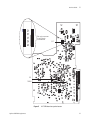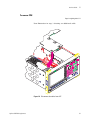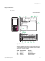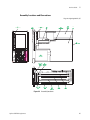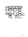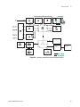
1
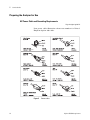
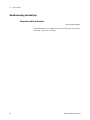
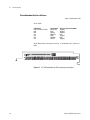
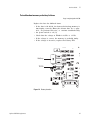
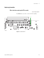
Agilent 35670A
Dynamic Signal Analyzer
Supplement to Installation,
Service and Operator’s Guide
Agilent Technologies
Notices
© Agilent Technologies, Inc. 2002, 2003, 2006
Warranty
No part of this manual may be reproduced in any
form or by any means (including electronic storage and retrieval or translation into a foreign language) without prior agreement and written
consent from Agilent Technologies, Inc. as governed by United States and international copyright laws.
Microsoft® and Windows® are U.S. registered
trademarks of Microsoft Corporation.
The material contained in this document
is provided “as is,” and is subject to being
changed, without notice, in future editions. Further, to the maximum extent permitted by applicable law, Agilent
disclaims all warranties, either express
or implied, with regard to this manual and
any information contained herein, including but not limited to the implied warranties of merchantability and fitness for a
particular purpose. Agilent shall not be
liable for errors or for incidental or consequential damages in connection with the
furnishing, use, or performance of this
document or of any information contained
herein. Should Agilent and the user have a
separate written agreement with warranty terms covering the material in this
document that conflict with these terms,
the warranty terms in the separate agreement shall control.
Software Revision
Technology Licenses
This guide is valid for the firmware that was
installed in the instrument at the time of manufacture.
The hardware and/or software described in this
document are furnished under a license and may
be used or copied only in accordance with the
terms of such license.
Manual Part Number
35670-90067
Edition
Third Edition. August 2006
Printed in Malaysia
Agilent Technologies, Inc.
3501 Stevens Creek Blvd.
Santa Clara, CA 95052 USA
Safety Notices
CAU TI O N
A CAUTION notice denotes a hazard. It
calls attention to an operating procedure, practice, or the like that, if not
correctly performed or adhered to,
could result in damage to the product
or loss of important data. Do not proceed beyond a CAUTION notice until
the indicated conditions are fully
understood and met.
WA RN ING
A WARNING notice denotes a hazard.
It calls attention to an operating procedure, practice, or the like that, if not
correctly performed or adhered to,
could result in personal injury or
death. Do not proceed beyond a
WARNING notice until the indicated
conditions are fully understood and
met.
Restricted Rights Legend
U.S. Government Restricted Rights. Software
and technical data rights granted to the federal
government include only those rights customarily provided to end user customers. Agilent provides this customary commercial license in
Software and technical data pursuant to FAR
12.211 (Technical Data) and 12.212 (Computer
Software) and, for the Department of Defense,
DFARS 252.227-7015 (Technical Data - Commercial Items) and DFARS 227.7202-3 (Rights in
Commercial Computer Software or Computer
Software Documentation).
2
Agilent 35670A Supplement
In This Supplement
Purpose
The purpose of this supplement is to describe changes to the
display of the Agilent 35670A. These changes apply only to
instruments with a serial number higher than MY42506200 made
after December 2002.
Most users of the Agilent 35670A will see few or no changes in the
operation of the instrument. The changes apply to specific sections
of the Agilent 35670A Operator’s Guide, the Agilent 35670A
Installation and Verification Guide, and the Agilent 35670A
Service Guide.
How to Use This Supplement
You may use these supplement pages to mark up your other guides
or you may place supplement pages in the appropriate locations in
those guides. Each segment of this document indicates which
section of the original guide is affected by the changes. Only
content which has changed is presented here in order to avoid
confusion.
Agilent 35670A Supplement
3
4
Agilent 35670A Supplement
Contents
1
Overview
Summary of Changes 8
Display 8
Rear panel 8
Board revisions 8
2
Installation and Verification Guide
Preparing the Analyzer for Use 10
To connect the analyzer to an external monitor
3
10
Operator’s Guide
Formatting the Display 12
To control the screen 12
4
Service Guide
Preparing the Analyzer for Use 14
AC Power Cable and Grounding Requirements
To connect the analyzer to an external monitor
Troubleshooting the Analyzer 16
To perform initial verification 16
To troubleshoot the power supply 19
To troubleshoot power-up failures 20
To troubleshoot CPU, memory and buses failures
To troubleshoot display failures 22
To troubleshoot IIC bus failures 24
To troubleshoot fast bus failures 26
To troubleshoot memory or battery failures 27
Adjusting the Analyzer 28
Adjusting the analyzer 28
To adjust the frequency reference
To adjust the display voltage 28
Replacing Assemblies
Agilent 35670A Supplement
14
15
21
28
29
5
What to do before replacing the CPU assembly
What to do after replacing an assembly 30
To remove CPU 31
To remove NVRAM 32
To remove memory 32
To remove motherboard 32
Replaceable Parts 33
Assemblies 33
Cables 34
Instrument Covers and Handles
Front Panel Parts 35
Rear Panel Parts 36
Chassis Parts 36
Miscellaneous Parts 36
Circuit Descriptions 37
Overall Block Diagram
A7 CPU 39
A8 Memory 43
A9 NVRAM 43
A102 DC-DC Converter
29
34
37
43
Voltages and Signals 44
Voltages and Signals 44
Assembly Locations and Connections 45
Power Supply Voltage Distribution 48
A8 Memory 48
A9 NVRAM 49
A99 Motherboard 49
A101 Display 50
A102 DC-DC Converter 51
6
Agilent 35670A Supplement
Agilent 35670A Dynamic Signal Analyzer
Supplement to Installation, Service and Operator’s Guide
1
Overview
The changes to the Agilent 35670A Dynamic Signal Analyzer
will not be noticeable to most users. The changes covered in the
supplement include:
• new display
• new CPU board that also incorporates the memory and
NVRAM boards
• memory options are now standard
• new external monitor interface which supports XGA
resolution.
• DC- DC converter has been replaced by a power inverter
Agilent Technologies
7
1
Overview
Summary of Changes
Display
Changes in the display will be imperceptible to most users. The
changes are mainly at the assembly level and are addressed in
the Service Guide.
Rear panel
The illustration below shows the new rear panel. The only
change is in the location of the external monitor connection.
This is the only place in this supplement that shows the new
rear panel unless a detailed illustration is required.
Figure 1
Rear panel
Board revisions
Throughout this supplement please note that the following is
true for all instances of the following board numbers:
• A7 (CPU) is now A17
• A8 (memory) in now incorporated into A17
• A9 (NVRAM) in now incorporated into A17 and is no longer
an option
These are global changes and will not be noted in each instance
to avoid a large number of insignificant changes.
8
Agilent 35670A Supplement
Agilent 35670A Dynamic Signal Analyzer
Supplement to Installation, Service and Operator’s Guide
2
Installation and Verification Guide
The Agilent 35670A has incorporated a standard VGA
monitor output and is now compatible with most monitors.
Agilent Technologies
9
2
Installation and Verification Guide
Preparing the Analyzer for Use
Page in original guide 2-13
To connect the analyzer to an external monitor
The External Monitor is a standard 15- pin miniature connector
that can interface with an external monitor. The monitor must
be compatible with the 49.74 kHz line rate, 61.6 Hz frame rate,
analog RGB signals, and TTL sync signals provided by the
Agilent 35670A.
1 Set the analyzer’s power switch to on (|).
2 Set the monitor’s power switch to on.
3 Connect the external monitor’s input cable to the analyzer’s
rear panel EXT MONITOR connector.
4 Press the following keys to enable external display mode:
[Disp Format]
[MORE]
[MORE]
[EXT MON ON OFF]
Pin 5
Pin 10
Pin 15
Figure 2
Pin
Signal Name
Number
1
red analog output
2
green analog output
3
blue analog output
4
not connected
5
Ground
10
Pin 1
Pin6
Pin 11
Rear panel showing external monitor connector
Pin
Signal Name
Number
6
Ground
7
Ground
8
Ground
9
Not connected
10
Ground
Pin
Signal Name
Number
11
Not connected
12
Not connected
13
TTL Horizontal Sync
14
TTL Vertical Sync
15
Not connected
Agilent 35670A Supplement
Agilent 35670A Dynamic Signal Analyzer
Supplement to Installation, Service and Operator’s Guide
3
Operator’s Guide
Changes in this guide include display attributes (resolution,
size, brightness) and external monitor connections.
Agilent Technologies
11
3
Operator’s Guide
Formatting the Display
To control the screen
Page in original guide 2-4
Disregard item 2. Display brightness is no longer adjustable.
12
Agilent 35670A Supplement
Agilent 35670A Dynamic Signal Analyzer
Supplement to Installation, Service and Operator’s Guide
4
Service Guide
The CPU board has a new number (A17) and is a consolidation
of the original CPU assembly (A7), memory assembly (A8) and
the Non- Volatile RAM option board (A9). Memory options are
now standard.
There is a new higher resolution display, and a power inverter
to replace the dc- dc converter. The external monitor port is now
a standard VGA interface with XGA output resolution.
Agilent Technologies
13
4
Service Guide
Preparing the Analyzer for Use
AC Power Cable and Grounding Requirements
Page in original guide 2-4
New power cable illustration shows new number for United
Kingdom Option 900 cable.
8709
Figure 3
14
Power cables
Agilent 35670A Supplement
4
Service Guide
To connect the analyzer to an external monitor
Page in original guide 2-13
The External Monitor is a standard 15- pin miniature connector
that can interface with an external monitor. The monitor must
be compatible with the 49.74 kHz line rate, 61.6 Hz frame rate,
analog RGB signals, and TTL sync signals provided by the
Agilent 35670A.
1 Set the analyzer’s power switch to on (|).
2 Set the monitor’s power switch to on.
3 Connect the external monitor’s input cable to the analyzer’s
rear panel EXT MONITOR connector.
4 Press the following keys to enable external display mode:
[Disp Format]
[MORE]
[MORE]
[EXT MON ON OFF]
Pin 5
Pin 10
Pin 15
Figure 4
Pin
Signal Name
Number
1
red analog output
2
green analog output
3
blue analog output
4
not connected
5
Ground
Agilent 35670A Supplement
Pin 1
Pin6
Pin 11
Rear panel showing external monitor connector
Pin
Signal Name
Number
6
Ground
7
Ground
8
Ground
9
Not connected
10
Ground
Pin
Signal Name
Number
11
Not connected
12
Not connected
13
TTL Horizontal Sync
14
TTL Vertical Sync
15
Not connected
15
4
Service Guide
Troubleshooting the Analyzer
To perform initial verification
Page in original guide 4-5
New illustrations for component locators show new test points
and new connector locations:
16
Agilent 35670A Supplement
Service Guide
4
Pin-out common
to all 36-pin
connectors
P17
P11
TP202
Figure 5
Agilent 35670A Supplement
A17 CPU board test point locator
17
4
Service Guide
Replace Step 7: Check signals required for power up.
• Using a logic probe, check the following signals.
Signal Name
PVALID
RSTn
ASn
+5V
+3.3V
C20MHz
PASn
DSACK1n
DSACK0n
PRW
PDSn
Test Location
TP202-1
P11-32
P17-27
A17 TP212
A17 TP 216
A17 TP1
TP205
TP207
TP206
TP210
TP209
TTL State
High
High
Toggling
High
High
Toggling
Toggling
Toggling
Toggling
Toggling
Toggling
Probable Faulty Assembly
A98 Power Supply
A17 CPU
A17 CPU
A98 Power Supply
A17
A17
A17
A17
A17
A17
A17
• Using a logic probe, check that A17 P10 pin B20 (SCL) and
A17 P10 pin C11 (SDA) toggle TTL states at least twice just
after power up.
• If the signals are correct, go to page 4- 15, “To troubleshoot
power- up failures.”
18
Agilent 35670A Supplement
Service Guide
4
To troubleshoot the power supply
Page in original guide 4-13
Step 5: Replace the bullet concerning reconnecting assemblies:
• Reconnect one assembly at a time in the following order:
1 A17 CPU (A17 P10 to A99 J7)
2 A102 Power Inverter (cable to A17 P13)
3 A11 Keyboard Controller (Cable to A17 P1)
4 A100 Disk Drive (cable to A17 P3)
The illustration for component locator shows new connector
locations.
Inverter power
connector
P13
Motherboard connector
P10
Keyboard
connector
P1
P3
Disk drive
connector
P3
Figure 6
Agilent 35670A Supplement
A17 CPU board connector locator, component side
19
4
Service Guide
To troubleshoot power-up failures
Page in original guide 4-15
Replace the first five rows of the table:
Failing Power-up Message
LEDs
MC68030 Processor
MC68882 Coprocessor
Bootrom
Display
Main RAM
ProgramROM
DSP
Fast bus
MFP
20
Probable Faulty Assembly or Next Test
A17 CPU
A17 CPU
A17 CPU
A17 CPU
A17 CPU
Agilent 35670A Supplement
Service Guide
4
To troubleshoot CPU, memory and buses failures
Page in original guide 4-19
Step 1: Disregard references to Memory Assembly and
incorporate the related information into A17 CPU.
Step2: Illustration for component locator shows new connector
locations
Inverter power
connector
P13
Motherboard connector
P10
Keyboard
connector
P1
Disk drive
connector
P3
Figure 7
Agilent 35670A Supplement
A17 CPU board connector locator, component side
21
4
Service Guide
To troubleshoot display failures
Page in original guide 4-23
Replace entire section
Use this test to isolate display failures to the A101 Display
assembly, A102 assembly, or the A17 CPU assembly
✔ Step 1. Check the power inverter assembly.
• Set the power switch to off (O).
• Remove the cable connected to P13 on the A17 assembly.
• Set the power switch to on (|)
• Measure voltage at P13 pin 1 on A17 assembly.
• If voltage is not +5Vdc the A17 board may be faulty.
• Set the power switch to off (O).
• Reconnect the cable to P13.
• Set the power switch to on (|).
• Measure voltage at A17 P13 pin 1.
• If voltage is not +5Vdc the power inverter assembly may be
faulty.
• If display backlight lamps do not light up, one or both of the
lamps may be faulty.
• If lamps are replaced and still do not light up, the power
inverter may be faulty.
✔ Step 2. Check the CPU signals on the Display assembly.
• Set the power switch to on (|).
• Using a logic probe check that the following TTL signals are
toggling:
Test Location
P14-31
P14-33
P14-24
Signal Name
VSYNCLCD
HSYNCLCD
CLK_LCD
In/Out
A17 Out
A17 Out
A17 Out
• If the signals are incorrect the A17 board may be faulty.
22
Agilent 35670A Supplement
Service Guide
4
Pin-out for
P13 connector
Pin-Out
for P14
Figure 8
A17 CPU board connector locator, circuit side
✔ Step 3. Determine the probable faulty assembly by comparing
the analyzer’s symptoms to the following table.
Symptom
Probable Faulty Assembly
CPU
Vertical and horizontal scanning is occurring
Part of information is missing, for example only half letters
Blocks of information are missing
Information on the screen is scrambled or mixed up
Vertical or horizontal stripes appear across the screen
Screen is blank
Display, Power inverter,
Display backlights, cables
Screen is tilted, compressed, or distorted
Display, A17
Line across the screen
Agilent 35670A Supplement
23
4
Service Guide
To troubleshoot IIC bus failures
Page in original guide 4-26,27
A new illustration above step 2 shows new connector pin- outs:
A1 2 34
A50
B50
C50
B1
C1
Figure 9
A17 CPU motherboard (P10) connector pin locations
✔ Step 2. Check the serial clock (SCL).
• Attach a logic probe to A17 P1- 15 (SCL) or P10 pin B10.
• Set the power switch to on (|).
• Press S5 (reset switch) while monitoring A17 P10 pin B10
(SCL), the power- on LEDs, and the display.
NO TE
S5 (reset switch) is a normally open momentary switch. A press of the
switch, S5, can be simulated by temporarily shorting TP214(RESET
INn) to TP215 (DCOM).
The TTL logic level of the SCL signal should toggle continuously
while Booting System is displayed. The following failure message
should be displayed after Booting System and the display grid
should appear about two minutes after power up.
Front Panel failure information:
keyboard IIC chip fails:
IIC: No Device Acknowledge
Key stuck: 32
A power-on test has failed. Refer
servicing to qualified personnel.
Press Start key to attempt to continue
Power-up.
• If the SCL signal does not toggle after S5 is pressed, the A17
CPU assembly is probably faulty
24
Agilent 35670A Supplement
Service Guide
4
• If no error messages are displayed after Booting System or A17
DS101 (green run LED) is off, go to page 4- 29, “To
troubleshoot fast bus failures.”
DS
5 4 3 2 6
MSB
A17 CPU
7 8 9 10 1
Green
Yellow
S5
Figure 10 Power-on LEDs and reset switch
✔ Step 3. Check the serial data line (SDA).
• Attach the logic probe to A17 P10 pin C11 (SDA).
• Press S5 while monitoring A17 P10 pin C11 (SDA), the power
on LEDs and the display.
The TTL logic level of the SCL signal should toggle continuously
while Booting System is displayed. The following failure message
should be displayed after Booting System and the display grid
should appear about two minutes after power up.
Front Panel failure information:
keyboard IIC chip fails:
IIC: No Device Acknowledge
Key stuck: 32
A power-on test has failed. Refer
servicing to qualified personnel.
Press Start key to attempt to continue
Power-up.
• If the SCL signal does not toggle after S5 is pressed or the
failure message is not displayed, the A17 CPU assembly is
probably faulty.
Agilent 35670A Supplement
25
4
Service Guide
To troubleshoot fast bus failures
Page in original guide 4-30
New table:
A17 P10 Pin
B14, C14, B15, C15, B16
B22
B24
C12
C19
C23
C24
Signal Name
FA1 to FA5
ECLK
FSELAn
BRESETn
FRW
FIFOENn
FSELSn
TTL Logic State in Test Mode
Toggling
Toggling
Toggling
Low
Toggling
High
Toggling
New illustration showing location of motherboard connector
pins.
A1 2 34
A50
B50
C50
B1
C1
Figure 11 A17 CPU motherboard (P10) connector pin locations
26
Agilent 35670A Supplement
Service Guide
4
To troubleshoot memory or battery failures
Page in original guide 4-67,68
Replace the last five bulleted items:
• If the date is 01- 01- 01, the battery- backed- up memory is
functioning correctly. Enter the current date. Go to page
4- 13, “To perform self tests,” to continue troubleshooting.
• Set power switch to off (O)
• Check that the voltage at TP200 is 2.6Vdc to 3.1Vdc.
• If the voltage is correct, the memory is probably faulty.
• If the voltage is incorrect, replace the battery BT1.
Battery
TP200
Figure 12 Battery location
Agilent 35670A Supplement
27
4
Service Guide
Adjusting the Analyzer
Adjusting the analyzer
Page in original guide 5-2
Delete the first row of the table referring to frequency reference.
The frequency is no longer adjustable.
To adjust the frequency reference
Page in original guide 5-5
Disregard this section. The frequency reference is not
adjustable.
To adjust the display voltage
Page in original guide 5-21,22
Disregard this section. The display voltage is not adjustable.
28
Agilent 35670A Supplement
Service Guide
4
Replacing Assemblies
What to do before replacing the CPU assembly
Page in original guide 6-3
The EEPROM is now U111 on the A17 CPU assembly.
U111
Figure 13 Location of U111
Agilent 35670A Supplement
29
4
Service Guide
What to do after replacing an assembly
Page in original guide 6-5
The rows referring to A7 CPU, A8 Memory, and A9 NVRAM are
replaced with:
Assembly Replaced
A17 CPU
Required Adjustment
No
Required Performance Test
No
Note that the frequency adjustment is no longer needed.
Disregard the last two rows of the table referring to adjustments
of the Display and the DC- DC Converter (now a Power Inverter).
There are no adjustments for these items.
30
Agilent 35670A Supplement
Service Guide
4
To remove CPU
Page in original guide 6-11
New illustration in step 3 showing an additional cable:
Figure 14 Disconnect the cables from A17
Agilent 35670A Supplement
31
4
Service Guide
To remove NVRAM
Page in original guide 6-12
Disregard this section. The NVRAM is now on the CPU board.
To remove memory
Page in original guide 6-13
Disregard this section. The memory in now on the CPU board.
To remove motherboard
Page in original guide 6-17
Disregard step 5.
32
Agilent 35670A Supplement
Service Guide
4
Replaceable Parts
Assemblies
Page in original guide 7-4
A17
Power Inverter
Bezel Assembly
Figure 15 Assemblies
Reference designator A17 replaces A7, A8 and A9. There is also
a replacement motherboard, bezel assembly, display assembly
and DC- DC converter assembly.
Ref Des
A17
A99
A14
A101
A102
Agilent 35670A Supplement
Agilent Part Number
35670-66517
35670-66598
35670-64320
2090-0881
35670-66525
Description
CPU ASSEMBY
MOTHERBOARD
BEZEL ASSEMBLY
VGA DISPLAY ASSEMBLY
INVERTER ASSEMBLY
33
4
Service Guide
Cables
Page in original guide 7-6
Disregard Memory and NVRAM sections of block diagram.
Four new cables have been added:
Agilent Part Number
35670-61626
35670-61627
3670-61628
3670-61624
Description
EXTERNAL MONITOR CABLE
INVERTER CABLE
EXTENDER CABLE FOR CCFL TUBES
DISPLAY CABLE
Instrument Covers and Handles
Page in original guide 7-7
Two parts have been replaced:
Ref Des Agilent Part Number
MP1
35670-64101
MP4
5063-5523
34
Description
SHTF ASSY-COVER ALV
MOLD BUMPER SET 4PC FF CORNRS
Agilent 35670A Supplement
Service Guide
4
Front Panel Parts
Page in original guide 7-9
MP211
Figure 16 Front panel parts
Three parts have been replaced and a new one added:
Ref Des
MP201
MP210
MP212
MP211
Agilent 35670A Supplement
Agilent Part Number
35670-22021
35670-29321
35670-44723
8160-1502
Description
CSTG-FRT FRAME MACH&PAINTED
LNZ-FLTR RFI/OPTICAL
DISPLAY GASKET
4 RFI ELASTOMER STRIPS
35
4
Service Guide
Rear Panel Parts
Page in original guide 7-10
One part has been replaced:
Ref Des Agilent Part Number
MP300 35670-00221
Description
SHTF REAR PANEL W/SILKSCREEN
Chassis Parts
Page in original guide 7-11
Two parts have been replaced:
Ref Des Agilent Part Number
MP400 35670-00122
MP401 35670-00123
Description
SHTF-CHASSIS ASSY
SHTF WALL ASSY FRONT
Miscellaneous Parts
Page in original guide 7-12
One part has been replaced and a new part has been added:
Ref Des Qty
A17BT1 1
2
36
Agilent Part NumberDescription
Mfr CodeMfr Part Number
1420-0338
BATTERY - 3V LITIUM 08709 BR2/3EAE2P
2090-0896
Backlight (CCFL) lamps NEC
63LHS01
Agilent 35670A Supplement
Service Guide
4
Circuit Descriptions
Overall Block Diagram
Page in original guide 8-4,5
The Memory and NVRAM assemblies are now incorporated into
the CPU assembly. The additional NVRAM option assembly is
now standard and consolidated onto the CPU assembly.
The DC- DC Converter has been replaced with a Power Inverter
which generates the display backlight voltage.
Figure 17 Two channel overall block diagram
Agilent 35670A Supplement
37
4
Service Guide
Figure 18 Four channel overall block diagram
38
Agilent 35670A Supplement
Service Guide
4
A7 CPU
Page in original guide 8-26 through 29
This is now the A17 CPU. Delete all references to A8 memory
and A9 NVRAM as separate assemblies since they are now
incorporated on the CPU board.
The A17 board now includes Non- Volatile Memory Storage
operations among its tasks.
The Math Co- processor is 20 MHz rather than 40 MHz (error in
previous documentation).
The 40 MHz oscillator is now a precision clock oscillator and is
no longer adjustable.
Clock Circuits Provide the clocks for the CPU assembly and all
other assemblies.
New block diagrams:
Agilent 35670A Supplement
39
40
I/O DEVICES
S5
Reset Logic
and Voltage
Supervisor
68030
Battery Backed SRAM
A
B
AND
Battery
backed
SRAM
3
(PD0-31)
(PA2-23)
Memory
Controller
Firmware
ROM
DRAM
3.3 Volt Circuits
4
Service Guide
MUXADDR (11:0)
Buffer Buffer
Figure 19 A17 CPU Block Diagram
Agilent 35670A Supplement
Service Guide
4
Real Time Clock
Frame Buffer1
Frame Buffer2
Display
Controller
Video
Gate
Array
Video
DAC
Buffer TTL
RGB Data Bus
HSYNC
VSYNC
R
G
B
VSYNC
HSYNC
LVD Data
External
Display
Connector
LCD
Serializer
Inverter control
Inverter
CCFL
backlights
Figure 20 CPU Block Diagram: Interface
Agilent 35670A Supplement
41
4
Service Guide
+5V
RUN
(GREEN)
RESET
RSTn
RESET
RESETn
Buffer
+5V
RESETINn
test point
To Disk I/F
TO IIC Controller
To A11 Keyboard Controller
To Disk I/F
To Display I/F
To HP-IB Interface
To MFP
To MC56001
To DMA Controller
To A6 Digital
To A5 Analog
P8(S)
Reset
+5V
S5
RSTn
PVALID
DCOM (from power supply)
Reset
Generator
MPU
HALTn
To battery-backed SRAM control circuit
Figure 21 Reset logic
Reset logic all references to S2 are changed to S5 and there is a
new block diagram.
IIC (Inter_IC) controller
replaced:
the bullet referring to A8 memory is
• A17 CPU (Real time clock, EEPROM)
Disk Controller Disregard the final sentence referring to
reversed operation.
Frame Memory
42
Consists of four SRAM chips.
Agilent 35670A Supplement
Service Guide
4
A8 Memory
Page in original guide 8-30,31
The memory has been incorporated into the CPU board.
Therefore, the information in the sections on Memory
Controller and FLASH ROM, DRAM, and SRAM is now added to
the section on the A17 CPU. Disregard the rest of this section
A9 NVRAM
Page in original guide 8-32
The NVRAM has been incorporated into the CPU board.
Disregard this section.
A102 DC-DC Converter
Page in original guide 8-39
This is now a power inverter assembly which supplies the
voltage for the LCD display backlights (CCFL).
Agilent 35670A Supplement
43
4
Service Guide
Voltages and Signals
Voltages and Signals
Page in original guide 9-2
The references in the table to A8 Memory and A9 NVRAM are
deleted since the circuits are now consolidated onto the A17
CPU board.
44
Agilent 35670A Supplement
Service Guide
4
Assembly Locations and Connections
Page in original guide 9-3,4,5
Bezel Assembly
Power Inverter
A17
Figure 22 Assembly locations
Agilent 35670A Supplement
45
4
Service Guide
LCD
A17
CPU
and memory
Power
Inverter
Backlights
CCFL
Figure 23 Assembly connections for two-channel analyzer
46
Agilent 35670A Supplement
Service Guide
4
LCD
A17
CPU
and memory
Power
Inverter
Backlights
CCFL
Figure 24 Assembly connections for four-channel analyzer
Agilent 35670A Supplement
47
4
Service Guide
Power Supply Voltage Distribution
Page in original guide 9-6
In the table the references to paths to the A8 and A9 boards is
deleted since the circuits are now on the A17 CPU board.
A8 Memory
Page in original guide 9-8 through 9-11
The memory is in now incorporated into the A17 CPU board
and the following information should be transferred to the A17
signal descriptions:
BD16-31
DSACK0n—
DSACK1n
PA0—PA26
PASn
PD0—15
PRW
SCL
SDA
Buffered Data Bus–This is the buffered processor data bus from the A17 CPU assembly. This
bus is further buffered on the A17 CPU assembly to create the Device Data bus.
Data Strobe Acknowledge–During a write cycle, DSACK signals are set low when the device
being addressed is ready to end the memory access cycle. When DSACK0n goes low and
DSACK1n is low, 32 bits of data are valid. When DSACK0n goes low and DSACK1n is high, 8
bits of data are valid.
Processor Address Bus–This is the processor address bus from the CPU. PA0 and PA1 also
operate with SIZE0 and SIZE1 to specify the alignment of the operand.
Processor Address Strobe–A low on this line starts a memory access cycle. This line pulses
low when a valid address is on the processor address bus.
Processor Data Bus–This is the processor data bus.
Processor Read/Write–This line is high when the current memory cycle is a read, and low
when the current memory cycle is a write.
Serial Clock–This is the serial clock for the IIC bus. The IIC controller on the CPU assembly
generates this clock to synchronize the transfer of data on the IIC bus.
Serial Data–This is the IIC bus bidirectional data line.
Everything else in the section should be disregarded.
48
Agilent 35670A Supplement
Service Guide
4
A9 NVRAM
Page in original guide 9-12, 13
The NVRAM is in now incorporated into the A17 CPU board and
the following information should be transferred to the A17
signal descriptions:
PROTCTn
VBATT
Protect–A low on this line disables the battery-backed static RAM. This line is low during
power-up and power-down, when the CPU assembly’s microprocessor is externally reset, and
when +5 volts is too low.
Battery Voltage–This line provides the power to the battery-backed static RAM and real time
clock. When the analyzer is on, the +5 volts provides the power for this line. When the
analyzer is off, the battery on the A17 board provides the power for this line. Since power is
applied to the static RAM even when the analyzer is off, the static RAM is non-volatile.
Everything else in the section should be disregarded.
A99 Motherboard
Page in original guide 9-31,33
Disregard the sections on HSYNC, VDATA, and VSYNC
Agilent 35670A Supplement
49
4
Service Guide
A101 Display
Page in original guide 9-36
The following table lists signals routed between the A17 board
and the LCD display assembly. All signals are generated on the
A17 board and are used by the display assembly. A description
of each signal follows the table. All data lines are LVDS.
CLK +
CLK –
Pixel Data
Pixel Data
Pixel Data
Pixel Data
Pixel Data
Pixel Data
VCC
Gnd
2
2
1
1
0
0
+
–
+
–
+
–
6
7
9
10
12
13
15
16
19,20
1,2,3,4,5,8,11,14,17,18
CLK: LVDS pair carrying the 66.660MHz clock signal used by the
LCD screen
Pixel Data 2: LVDS pair carrying blue pixel bits 4 to 7, Hsync,
Vsync, and Data enable signals
Pixel Data 1: LVDS pair carrying green pixel bits 3 to 7, and blue
pixels bits 2 to 3
Pixel Data 0: LVDS pair carrying red pixel bits 2 to 7, and green
pixels bit 2.
VCC: 3.3 Volts.
50
Agilent 35670A Supplement
Service Guide
4
A102 DC-DC Converter
Page in original guide 9-37
This assembly is now a Power Inverter.
The following table lists signals routed between the A17 board
and the A102 Power Inverter. A description of each signal
follows the table:
VCC
Gnd
BLight_ON
1,2
3,4,7,8
5
VCC: 5 Volts
BLight_ON: Generated by U135 to turn on and off the display
backlights for power saver mode.
Agilent 35670A Supplement
51
4
52
Service Guide
Agilent 35670A Supplement