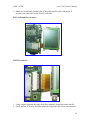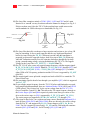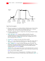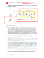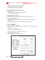
1
Level 1 and 2 Service Manual
Model A008 /
A6188+
GSM Dual Band
Technology
A008 / A6188+
Level 1 & 2 Service Manual
Table of Contents
Introduction ........................................................................................................... V
Product Identification ............................................................................................................... V
Product Names ......................................................................................................................... V
Product Changes ....................................................................................................................... V
Regulatory Agency Compliance ................................................................................................ V
Computer Software Copyrights ................................................................................................ VI
About This Service Manual ...................................................................................................... VI
Warranty Service Policy .........................................................................................................VII
Specifications ....................................................................................................... 1
Product Overview ................................................................................................... 2
Features ..................................................................................................................................... 2
Controls and Indicators .............................................................................................................. 8
User Interface Flowcharts .......................................................................................................... 9
Tools and Test Equipment ................................................................................... 14
Disassembly .......................................................................................................... 14
Removing the Battery Door ..................................................................................................... 14
Removing the Battery .............................................................................................................. 15
Removing the housing screws .................................................................................................. 15
Separate front and rear housing ................................................................................................ 16
PCB Screw removal ................................................................................................................. 16
Speaker connector removal ...................................................................................................... 17
LCD & PCB removal ............................................................................................................... 17
LCD & PCB Overview ............................................................................................................ 18
LCD Flex removal ................................................................................................................... 18
Subscriber Identity Module (SIM) Cards and Security ...................................... 19
Inserting the SIM Card ............................................................................................................ 19
Manual Test Mode ................................................................................................................... 19
Personality Transfer ................................................................................................................. 21
GSM Test Commands............................................................................................................... 21
Set up of User Profiles........................................................................................... 22
Identity and Security............................................................................................. 24
MSN......................................................................................................................................... 24
IMEI......................................................................................................................................... 24
Package Number....................................................................................................................... 24
Picasso Labeling....................................................................................................................... 25
Sales Model Numbers ........................................................................................... 26
Exploded View ...................................................................................................... 27
Exploded View Parts List ........................................................................................................ 28
Accessories ............................................................................................................ 29
III
A008 / A6188+
Level 1 & 2 Service Manual
Introduction
Motorola ® Inc. maintains a worldwide organisation that is dedicated to
provide responsive, full-service customer support. An international network of
company-operated product care centres as well as authorised independent
service firms service Motorola products.
Available on a contract basis, Motorola Inc. offers comprehensive
maintenance and installation programs which enable customers to meet
requirements for reliable, continuous communications.
Product Identification
IV
A008 / A6188+
Level 1 & 2 Service Manual
The model number on the housing identifies Motorola products. Use the entire
model number when inquiring about the product. Numbers are also assigned
to chassis and kits. Use these numbers when requesting information or
ordering replacement parts.
Product Names
Product names included in this manual are listed on the front cover. Product
names are subject to change without notice. Some product names, as well as
some frequency bands, are available only in certain markets.
Product Changes
When electrical, mechanical or production changes are incorporated into
Motorola products, a revision letter is assigned to the chassis or kit affected,
for example; -A, -B, or -C, and so on.
The chassis or kit number, complete with revision number is imprinted during
production. The revision letter is an integral part of the chassis or kit number
and is also listed on schematic diagrams and printed circuit board layouts.
Regulatory Agency Compliance
This device complies with Part 15 of the FCC Rules. Operation is subject to
the following conditions:
This device may not cause any harmful interference, and
This device must accept interference received, including interference that may
cause undesired operation.
This class B device also complies with all requirements of the Canadian
Interference-Causing Equipment Regulations (ICES-003).
Cet appareil numérique de la classe B respecte toutes les exigences du
Règlement sur le matériel brouilleur du Canada.
Computer Software Copyrights
The Motorola products described in this manual might include copyrighted
Motorola computer software stored in semiconductor memories and other
media. Laws in the United States and other countries preserve for Motorola,
Inc. certain exclusive rights for copyrighted computer programs, including the
exclusive right to copy or reproduce in any form the copyrighted computer
software.
Accordingly, any copyrighted Motorola computer software contained in the
Motorola products described in this manual cannot be copied or reproduced in
any manner without the express written permission of Motorola, Inc.
V
A008 / A6188+
Level 1 & 2 Service Manual
Furthermore, neither the purchase of Motorola products nor your receipt of
this manual (whether in connection with a purchase or otherwise) grants,
either directly or by implication, estoppel, or otherwise, any license under the
copyrights, patents or patent applications of Motorola, Inc., except for the
normal, nonexclusive, royalty-free license to use that arises by operation of
law in the sale of a product.
Additionally, use of the information in this manual other than in connection
with an associated product purchased from Motorola Inc. requires express
written permission of Motorola, Inc. In this regard, you may not use the
information in this manual to create a software application for separate sale or
license to others not in connection with the associated product purchased from
Motorola, Inc.
About This Service Manual
Using this service manual and the many suggestions contained in it assures
proper installation, operation, and maintenance of the A008. Refer any
questions about this manual to the nearest Customer Service Manager.
Audience
This document provides assistance to service personnel in testing and
repairing the A008. Service personnel should be familiar with electronic
assembly, testing, and troubleshooting methods, and with the operation and
use of associated test equipment.
Use of this document assures proper installation, operation, and maintenance
of Motorola products and equipment. It contains all service information
required for the equipment described and is current as of the printing date.
Scope
The scope of this document is to provide the reader with basic information
relating to the A008, and also to provide procedures and processes for
repairing the units at Level 1 and 2 service centres including:
Unit swap out
Repairing of mechanical faults
Basic modular troubleshooting
Testing and verification of unit functionality
Initiate warranty claims and send any faulty modules to Level 3 or 4 repair
centres.
Finding Information
The first three digits of the serial number identify a product family, unless
covered by an extended warranty. Extended warranty products have two
alphabetic characters in place of the first two digits of the family code. The
VI
A008 / A6188+
Level 1 & 2 Service Manual
first digit following the alphabetic code indicates the number of years the
warranty period is in effect.
This Service Manual consists of the following sections:
Overview - Describes the features, specifications, and options.
Operation - Provides a theory of operation, describes message handling, and
how to program the communicator, and a functional overview.
Disassembly - Procedures for removing and replacing assemblies and a troubleshooting chart.
Part Numbers - Provides diagrams and associated parts lists.
Conventions
Special characters and typefaces, listed and described below, are used in this
publication to emphasise certain types of information.
ç
Note: Emphasises additional information pertinent to the subject manner
Caution: Emphasises information about actions that may result in equipment
damage.
Warning: Emphasises information about actions that may result in personal
injury.
Enter
Keys to be pressed are represented graphically. For example, instead of “Press
the Enter Key”, you will see “Press
Bold
Information from a screen is shown in text as similar as possible to what
appears in the display. For example
Information that you need to type is printed in boldface type.
Revisions
Any changes that occur after manuals are printed are described in publication
revision bulletins (PMRs). These bulletins provide change information that
can include new parts listing data, schematic diagrams, and printed board
layouts.
Warranty Service Policy
VII
A008 / A6188+
Level 1 & 2 Service Manual
The product will be sold with the standard 12 months warranty terms and
conditions. Accidental damage, misuse, and extended warranties offered by
retailers are not supported under warranty. Non warranty repairs are available
at agreed fixed repair prices.
Out of Box Failure Policy
The standard out of box failure criteria applies. Customer units that fail very
early on after the date of sale are to be returned to Manufacturing for root
cause analysis, to guard against epidemic criteria. Manufacturing to bear the
costs of early life failure.
Product Support
Customer’s original units will be repaired but not refurbished as standard.
Appointed Motorola Service Hubs will perform warranty and non-warranty
field service for level 2 (assemblies) and level 3 (limited PCB component).
The Motorola HTC centres will perform level 4 (full component) repairs.
Customer Support
Customer support is available through dedicated Call Centres and in-country
help desks. Product Service training should be arranged through the local
Motorola Support Centre.
Ordering Replacement Parts
Only centres authorised to carry out repairs can purchase spare parts. Orders
for spare parts from hubs and Hi-Tech Centres should be placed with the
regional Motorola Parts Distribution Centre.
VIII
A008 / A6188+
Level 1 & 2 Service Manual
Specifications
General Function
Frequency Range GSM
Frequency Range DCS
Frequency Range PCS
Channel Spacing
Channels
Modulation
Transmitter Phase Accuracy
Duplex Spacing
Frequency Stability
Operating Voltage
Transmit Current
Stand-by Current
Dimensions
Size (Volume)
Weight
Temperature Range
Transmitter
Function
RF Power Output
Output Impedance
Spurious Emissions
Receiver
Function
RF Level
RX bit error rate (100 k bits)
Channel Hop Time
Time to Camp
Speech Coding
Function
Speech Coding Type
Bit Rate
Frame Duration
Block Length
Classes
Bit Rate with FEC Encoding
Specification
880-915 MHz TX (with EGSM)
925-960 MHz RX
1710-1785 MHz TX
1805-1880 MHz Rx
1850.2 – 1909.8 MHz TX
1930.2 – 1989.8 MHz Rx
200 kHz
174 GSM/374 DCS carriers with 8 channels per carrier
GMSK at BT = 0.3
5 Degrees RMS, 20 Degrees peak
45 MHz GSM 95MHz DCS 80MHz PCS
+ 0.10 PPM of the Downlink frequency (Rx)
Full Rate PSU = 4.4V +/- 5%
(During Charging = VBatt +/-5% 6.63V
Mid Rate Charger = 5.9V +/- 0.3V
CLA Supply = 4.4V
Battery Operating Voltage = 2.85V(Radio Shut Down voltage)
To 4.2V Max
Typically 250 ma avg., 1.0A peak
Typically 7.0 ma (DRX2)
130mm x 46mm x 24.5mm
105cc with Batt
106g with Batt
-10C to +55C
Specification
33 dBm + 2dB GSM/ 30 dBm + 2 dB DCS
50 ohms (nominal)
-36 dBm from 0.1 to 1 Ghz
-30 dBm from 1 to 4 Ghz
Specification
-102 dBm
< 2%
500 microseconds
Approximately 5-10 seconds
Specification
Regular Pulse Excitation / Linear Predictive Coding with Long
Term Prediction. (RPE LPC with LTP).
13.0 k bps
20 ms
260 bits
Class 1 bits = 182 bits. Class 2 bits = 78 bits
22.8 k bps
1
A008 / A6188+
Level 1 & 2 Service Manual
Product Overview
Features
The A008 (E MEA) A6188+ (Asia) is a GSM dual band (900/1800 MHz) GPRS
product, and is an enhanced version of A6188. From this point onwards we will
refer to this product as the A008. The A008 is mechanically very similar to the
existing A6188 form factor with slight modifications made to the flip and front
Housing to ensure a different look.
The display will be 320 x 240 pixels, 4 level gray scale ¼ VGA display. The
display shall be 24 x 24 bitmap for Chinese Characters and 15 x 16 bitmap for
English Characters. The line spacing has been modified for easier reading.
There will be 2 new Colours, Mica Grey, Summer Sky Blue/TT silver
In additional to the existing A6188 User Interface features the following features /
applications will be available
GPRS – General Packet Radio service
GPRS (General Packet Radio Service) is a combination of HSCSD (High Speed
Circuit Switched Data) and SMS (Short Message Service). It has a theoretical
speed of 171.2kbps compared with 9.6kbps as today. A single user using all 8
uplink timeslots and all 8 Downlink timeslots could theoretically achieve this.
The main purpose for GPRS is to give ‘immediacy’ to the customer i.e. to allow
the customer access to data transfer as and when they need it.
Information will be carried across as IP from Internet sites etc…
For GPRS the Traffic Channel (TCH) now becomes the Packet Data Channel
(PDCH)
Downlink
PDCH
PDCH
PDCH
PDCH
PDCH
PDCH
PDCH
Uplink
PDCH
PDCH
PDCH
PDCH
PDCH
PDCH
PDCH
2
A008 / A6188+
Level 1 & 2 Service Manual
BCH
As can be seen from the above drawing, up to 8 different users can occupy 1
single timeslot at any given time. The more Bandwidth that is required, the more
channels are allocated by the network.
This extra timeslot allocation is only given when the network is not busy, and
therefore dynamically maximises idle network resources. Also because much of
the SMS messaging will now be carried over the GPRS system this will relive
much of the SMS Centre loading.
Also the Uplink and Downlink are now completely separate channels in that we
can now have an uplink only and downlink only channel allocated by the network.
GPRS is high bandwidth data split at source into separate but related data
‘packets’. The information packets that a GPRS enabled phone is to receive, is
addressed specifically for that phone using a TFI - Temporary Flag Indicator.
And although the phone will ‘listen’ to each timeslot of data but will only decode
the information that is highlighted by a matching TFI.
By setting a USF – Uplink Status Flag
on a Downlink timeslot, the mobile
phone is instructed it can transmit on the next available uplink timeslot.
GPRS will support GSM 900 / 1800 / 1900 as well as TDMA technologies
For GPRS to operate the following must be available:
• Mobile phone must be of GPRS technology
• Network provider must support GPRS which includes a modified
Infrastructure (Core Network)
GPRS can be set up manually through the UI or using the PC Tools programming
equipment. The A008 will be a 1 up 2 down GPRS technology i.e. it supports 2
timeslots of Downlink information per Frame and 1 uplink slot.
E – Mail
•5 mailboxes
• POP3, IMAP4, SMTP, MIME
• Text, Inkpad, V-Card attachment
3
A008 / A6188+
Level 1 & 2 Service Manual
K-Java
K-Java is basically a protocol used to download applications to a device; there are
3 methods of achieving this.
1) Web to PC Synchronisation –
• Download application package to PC using standard Internet protocols
• Installation from PC to devices through cable or local wireless
2) WAP / HTTP •Browse applications using WAP browser
•Download application package using http protocol
3) HTTP (end to End) •Browse applications with special-purpose Java service browser using http
•Download application package using http protocol
3
OTA Sync
1
2
MyAccompli.com
Supports:
Address Book
Calendar Events
To Do
SMS
IrDA or RS232
Over The Air
4
A008 / A6188+
•
•
•
Level 1 & 2 Service Manual
SyncML based OTA TrueSync
Enables A008 users to synchronize data to the Internet
Enables associates to update your schedule over the air
Improved Hand writing recognition
Compared to the original A6188. There are now 2 handwriting screens allowing
successive letters to be entered whilst the system processes the previous action.
• European HWR based from Lexicus
• Initially supports Phase 1 EMEA languages
• Virtual Keypads available.
Virtual Keypad
Symbol Keypad
WAP 1.1 (Wireless Application Protocol)
Simplified WAP
Architecture
‘The Internet’
Content Servers
Wireless
connection
(GSM Data call
is preferred)
WAP
Gateway
ISP
account
5
A008 / A6188+
Level 1 & 2 Service Manual
WAP Format is derived as follows
1. The request for information is made in WML (Wireless Mark-Up Language)
derived from HTML.
2. Request is passed to WAP Gateway, which retrieves the information from the
server in standard HTML (which is then filtered to WML) or if available
WML format.
3. The information is then passed the cellular user, via the cellular network
provider.
All settable parameters can be entered manually or programmed using PC Tools
For image download, the bitmap image will be downloaded as text and if the
image is larger than the screen then only part of the image will be displayed
During browser mode, if incoming call is received then the browser will be
paused with the user having the option to resume after the call.
Other Options covered within the Menu Chapter are:
• Address Book
• Recent calls
• Call Divert
• STK Option
Communicate
• E-Mail
Menu Option
• Messages
• Turbo Dial
• Integration
• Instant messaging
•
•
•
•
•
•
Text Notes
Ink Notes
Voice Notes
Melody Composer
To Do List
Date Book
•
•
•
•
Calculator
Conversion Calculator
Currency Calculator
World Time
Annotate
Menu Option
Extras Menu
Option
6
A008 / A6188+
•
•
•
•
•
•
Alarm Clock
Dictionary
Truesync
Games
Receive IR
Soft Modem
Level 1 & 2 Service Manual
Tools Menu
Option
7
A008 / A6188+
Level 1 & 2 Service Manual
Controls and Indicators
IrDA
Headset
Speaker
Rocker
Switch
Voice Notes
320 X
240
Pixels
Stylus
Power Key
Page Up / Down
Menu &
Back light
Shows user current signal strength
Takes user to messages structure
When Pressed brings up phone Keypad menu
12:20
b
Present Time
Shows user present battery meter reading 1/3 – 2/3 or Full
STK access & User Information
Takes user to Call Divert Sub Menu
Informs user they are within ‘Communicate’ Menu
When pressed brings up ‘Annotate’ Menu
When pressed brings up ‘Extras’ Menu
When pressed brings up ‘Tools’ Menu
8
A008 / A6188+
Level 1 & 2 Service Manual
User Interface
The Menu Structure is broken down in to 4 Main Heading, each with Sub-Headings
within.
Communicate
Annotate
12:26
12:26
b
eMail
GSM Carrier
b
GSM Carrier
Tools
Extras
12:26
12:26
GSM Carrier
b
GSM Carrier
b
9
A008 / A6188+
Level 1 & 2 Service Manual
Communicate
messages
• print message via IrDA
• concatenated messages
• folder routing
• voice mail access
• cell broadcast access
• multiple recipients
turbo dial
address book
• tap and dial
• transfer records via IrDA
• print contacts via IrDA
• groups
• Vcard
12:26
12:26
MyMail.com
Inbox
[23]92
Family
[16]31
Friends
[ 0] 9
Proj Gold [ 1] 7
Ski Pals
eMail
recent calls
• last 20 missed
(page down)
• last 20 called
(rocker in)
• last 20 answered
(page up)
• call divert icon
2
eMail
• 5 mailboxes
• POP3, IMAP4, SMTP,
MIME
• text, ink, Vcard attachment
Exit
GSM Carrier
WAP browser
• 4.1.16f Phone.com browser
• increased lines/screen
[ 0] 0
Drafts
b
• STK access
• owner info access
Compose
Instant
Messaging
10
A008 / A6188+
Level 1 & 2 Service Manual
Annotate
12:26
12:26
1 Mon, May 26
1 May 1999
S M T W T F S
Lunar
1
2
text notes
• send viaeMail
• send via SMS
• send via IR
• send fax
3
4
5
6
7
10M 30D
Mail
8
00:00
9 10 11 12 13 14 15
01:00meeting
16 17 18 19 20 21 22
12:26
23 24 25 26 27 28 29
02:00Call
30 31
03:00
Exit
Exit
Day View
MthView
date book
12:26
To
Do List
1234567890123456
ink notes
• send viaeMail
• send fax
• send to A6188+
prepare for
to do list
meeting
pick up dog
pay rent
give blood
donate food
Exit
New
12:26
Voice Note
Title:
voice notes
Time: 12:35
GSM Carrier
b
Date: 1999/05/06
Duration: 00:43
12:26
Cancel
OK
Edit Melody
Melody Composer
• send/receive via IR
• send/receive via SMS
1/32 1/16 1/8
1/4
1/2
1
H
M
C D E F G A B
Cancel
OK
11
L
A008 / A6188+
Level 1 & 2 Service Manual
Extras
calculator
• basic
• scientific
dictionary
• Chinese-to-English
• English-to-Chinese
12:26
conversion calculator
• mass
• length
• temperature
• area
• volume
alarm clock
• 2 alarms
• variable snooze duration
12:26
12:26
Alarm Clock
Mass Conversion
|
Alarm A:10:00am
kilograms
pounds
1
4
7
Exit
2
5
8
3
6
9
GSM Carrier
.
Status:on
Alarm B:10:15am
Status:off
Alert 1
Snooze:
0
Convert
b
world time
5 min
Exit
currency calculator
• 27 currencies
• conversion log
12
A008 / A6188+
Level 1 & 2 Service Manual
Tools
12:26
12:26
Receive IrDA
Sokoban Level 99
Best:000
Push:000
Exit
Undo
Games
• Blackjack
• Memory
• Sokoban
•Hua Rong Dao
•Connect five
Soft Modem
GSM Carrier
12:26
b
Black Jack
Bet:
90
10
Bet:
90
10
Jack Black
Place Bet
Exit
Hold
Truesync
• address book
• date book
• to do list
• text and ink notes
• backup all user data
13
A008 / A6188+
Level 1 & 2 Service Manual
Tools and Test Equipment
RSX4043-A
Torque Driver 1 Used to remove and replace screws
Torque Driver Bit T-6 Plus, Apex 440-6IP Torx Plus or equivalent 1
Used with torque driver
Disassembly tool, plastic with flat and pointed ends 1 Used during
assembly / disassembly of device
Delrin Tweezers 1 Used during assembly/disassembly
Digital Multi-meter 2 Used to troubleshoot device
6680388B67
6680388B01
HP34401A
Disassembly
The Procedure in this section provides instructions for the disassembly of
the A008.
Removing the Battery Door
1. Remove the Battery door by pushing down on battery retaining catch and sliding
battery door down and away from Antenna end of unit.
14
A008 / A6188+
Level 1 & 2 Service Manual
Removing the Battery
1. Press down on the top of the battery to compress the battery contacts
2. Pull up and away from rear Housing.
Remove Housing Screws
1. Remove the 4 retaining screws from the top and bottom of the rear housing. Use a T6
Torx driver.
15
A008 / A6188+
Level 1 & 2 Service Manual
Separate Front and Rear Housing
1. Slide a finger nail or a plastic tool between the front and back housing on either side
of the phone
2. This will push back the retaining catches; the front housing can then be lifted up over
the catches and the rear housing removed.
PCB Screw Removal
16
A008 / A6188+
Level 1 & 2 Service Manual
1. Remove the two PCB screws from the bottom of the housing using a T6 Torx driver.
Speaker Connector Removal
1. Very Carefully extract the 2 Pin speaker connector, using a pair of long nosed pliers.
2. These connecting wires are very susceptible to damage take extra care.
PCB / LCD Removal
17
A008 / A6188+
Level 1 & 2 Service Manual
1. Rotate the front hosing, and allow the PCB to drop into the palm of the hand. If
necessary use plastic tool to free PCB if at all stuck.
PCB / LCD and Flex Overview
LCD Flex removal
1. Using a plastic tool push the edges of the flex connector forward to release the flex.
2. Gently pull the LCD away from the connector keeping the flex in line with connector.
18
A008 / A6188+
Level 1 & 2 Service Manual
Subscriber Identity Module (SIM) Cards and Security
Removing the SIM Card
1. Remove the Battery Door and Battery as described in the Disassembly Procedure
2. Holding unit with antenna upwards push black SIM carrier to the right and pull
upwards
Cut Corner
Inserting the SIM card
1. Locate the 1 cut corner of the SIM Card; slide the SIM fully into the carrier, gold
contacts facing down towards the unit.
2. Push the carrier down and slide to the right
Manual Test Mode
The Aoo8 is equipped with a manual test mode capability. This allows service personnel
to manually control electronic functions that would usually be initiated by the product’s
operating software. This is achieved by the user entering specific test mode commands.
To enter there test commands a GSM / DCS Test SIM card (Part Number 8102430Z04)
must be used. See above for SIM Card entry procedure
19
A008 / A6188+
Level 1 & 2 Service Manual
To enter into test mode the unit should be powered up. Touch the
bring up the phone keypad screen.
Icon. This will
1. Touch and hold the virtual
key, for 3 – 4 seconds. This will initiate test
#
mode.
2. To enter a test mode command, the following sequence must be followed:
A Soft Reset for Example
571
#
Send
20
A008 / A6188+
Level 1 & 2 Service Manual
GSM Test Commands
Key Sequence
#(hold down for 2 seconds)
01#
07x#
08#
09#
10#
15x#
16#
19#
*19
20#
36#
37#
38#
39#
43x#
47x#
51#
52#
57#
58#
58xxxxxx#
59#
59xxx#
60#
99#
Test Function/Name
Enter manual test mode
Exit manual test mode
Mute RX audio path
Unmute RX audio path
Mute TX audio path
Unmute TX audio path
Generate tone
Mute tone generator
Display S/W version number of Call Processor
Display S/W version number of Dragonball
Display S/W version number of Modem
Initiate acoustic loopback
Stop test
Activate Mini SIM
Deactivate Mini SIM
Change audio path
Set audio volume
Enable sidetone
Disable sidetone
Initialise non-volatile memory
Display security code
Modify security code
Display lock code
Modify lock code
Display IMEI
Display all display pixels
15XX#
90#
91#
Vibrator
Ringer
0 or Omitted
1
2
36XX#
Full Rate
Enhanced Full rate
Half Rate
98#
20#
21#
23#
GSM 1800
GSM 900
Dual Band 900 / 1800
Personality Transfer
Personality transfer will be achieved using the Truesync application software.
21
A008 / A6188+
Level 1 & 2 Service Manual
Set up of User Profiles
PC Tools is an end user software program, which allows user friendly set up of the A008
WAP, E-Mail and GPRS functions.
Set up of PC Tools is as follows:
1. Open pcc (PC Configuration) document:
From main menu or tool bar, click New to create a new document or Open to open an
exist pcc document. The opened document looks like a property sheet.
2. Edit pcc document:
Once you have a document opened, click Connection, WAP Browser, or eMail tab to go
to the setup you desired. Enter data into each field.
22
A008 / A6188+
Level 1 & 2 Service Manual
4. Save pcc document:
From main menu select Save or Save As to save the document.
5. Setup hardware environment:
Connect phone with PC using serial port cable. Also the phone must connected to a
power source.
6. Download data to phone:
At the bottom of opened document, select the COM port which you are using to connect
PC and phone; if the phone is able to power on, check Phone Power On check box; click
Download button to start downloading.
7. Switch phone off and then power the unit back on again.
23
A008 / A6188+
Level 1 & 2 Service Manual
Identity and Security
Each Motorola GSM Cellular Cassette will be labelled with various
number configurations. The following information describes what these
configurations mean.
MSN
The mechanical Serial Number (MSN) is an individual unit identity
number and will remain with the unit throughout the life of the unit.
The MSN can be used to log and track a unit on Motorola’s EPPRS
system.
The MSN is divided into 4 sections.
MSN 10
3 digits
APC
Account Product Code
I.e. Startac 130
1 digit
2 digits
DC
4 digits
DC
Distribution Centre
I.e. Easter Inch
SNR
Date Code: Year and
Month of Shipment
Units individual serial
number
Figure MSN label breakdown
IMEI
The International Mobile station Equipment Identity (IMEI) number is an
individual number unique to the PCB and is stored within the unit’s
memory. The following figure gives a description of the make up of this
number.
IMEI 16
Type Approval code
6 digits
2 digits
6 digits
2 digits
TAC
FAC
SNR
IU
Distribution Centre
factory code
Individual PCB Serial
Number
Internal use – spare
digits
Figure IMEI label breakdown
Some other label number configurations that will be present will be: XCVR NUMBER: Identifies type of product. i.e. L7389i (Usually SWF
number)
24
A008 / A6188+
Level 1 & 2 Service Manual
Package Number: Determines type of equipment, mode in which it was
shipped and language with which it was shipped.
Picasso Labelling
Model
Number
Factory
Picasso
Factory label for Leap
Picasso is the new factory tracking system. It is being implemented globally in all Motorola and out-sourcing
manufacturing sites throughout 2000. For all field failures, Service currently records the MSN to validate the
warranty period and record which site shipped the phone. By recording the Picasso number in addition to the
MSN, we can perform the normal validations but also attribute all field failures back to original site, shift and
line of manufacture.
25
A008 / A6188+
Level 1 & 2 Service Manual
Sales Model Numbers
SA0037A
SA0034A
SA0039A
SA0043A
A6188+, SCCD, Grey Mica, Full Package, PRC
A6188+, SCCD, Grey Mica, Full Package, HK Cellstar
A6188+, TCCD, Grey Mica, Simple Package, HK
A6188+, TCCD, Grey Mica, Simple Package, TW
* Initial release to Greater China only
26
A008 / A6188+
Level 1 & 2 Service Manual
Exploded View Diagram
13
3
6
4
2
14
1
11
7
10
9
12
5
8
27
A008 / A6188+
Level 1 & 2 Service Manual
Exploded View Parts List
CHYN4209A
0164617E05
CHHN4213A
7564435E01
3264662E01
0164481E01
0364579E01
0164027E01
5009135L07
0564533E01
5464580E01
5964466E01
1364832E03
CHYN4207A
1
2
3
4
5
6
7
8
9
10
11
12
13
14
Flip & Front Assembly, Grey Mica
Rear Housing, Grey Mica
LCD Module
Rubber Foot x2
Battery Pad
Antenna Assembly
Screw x6
Stylus Assembly
Microphone
Mic Grommet
LCD Protector
Motor Assembly
Logo A6188+, Grey Mica
Battery Door, Grey Mica
28
A008 / A6188+
Level 1 & 2 Service Manual
Accessories
Battery
· Lithium Ion Battery (Slim) ~800mAh (1 hour rapid charge)
· Label must meet all countries specific requirements
· Reuse A6188 battery
Battery Door
· Reuse A6188 Battery door but with A008 specific colours
– Mica Grey, TT Silver
Data Cable (Serial cable)
· Lever shifter for RS232 communication
· No PC card required. Cable hooks directly to RS232 port of PC
· Reuse A6188 Data cable
Travel Charger
· A Travel Charger similar to the existing SPN4604 but its plug should
meet the PRC
National Standard, Hong Kong Safety requirements and respective
regulatory and
Countries standard in EMEA and Brazil.
· Kramer charger reuse (SPN 4654A)
· Labels must meet all countries specific requirements.
Charger Base & Docking station (Cradle)
The Charger base & Docking Station should be able to
· Fast charge the battery inside the phone
· It should be able to charge a spare battery in the rear pocket
· Display the charging status of the battery inside the phone, a standalone
battery,
and indicate data transfer
· The Transformer should be able to connect to the charger base Hirose
socket
· Have True-Sync SW data transfer capability
· The front slot of the charger base should be able to hold the phone in
upright
Position (docked) and if the serial cable is connected (between the
Transformer
Hirose plug and the PC), it should be able to do all the communication
with PC
29
A008 / A6188+
Level 1 & 2 Service Manual
· Labels must meet all the countries specific requirements
· Reuse A6188 Cradle. ID modification will not affect Cradle design
Vehicle Power Adapter
· Powers the phone and rapid charges the battery from vehicle’ s cigarette
lighter
Socket
· Reuse A6188 VPA
Silver Headset
· Hand free operation, walk and Talk.
· Reuse P7689 headset
Leather Holster
· Stylish leather holster. Prefer local source to reduce cost.
· Will not create problem to remove the stylus B, making and answer a
call, and
operate with headset
Starfish True Sync CDROM Kit
· Able to support Win95/98/2K/NT and Palm (English)
· Recorded in a CDROM and bundle sales with Cradle
· Package comes in kit with proper packaging d Quick Start Up guides in
English and
localised language support by the software.
· New CDROM kit since new features were added and with EMEA
languages.
Plug
· Per the standard plug specified by each supported country.
Car Kit
· DSP easy install car kit.
Stylus
· Stylus A – Retractable and able to fit well in the fitting slot of A008 rear
housing.
· Stylus B – Pen type that can fit in the Stylus pocket of the leather case.
30
A008 / A6188+
SPN4830A
SKN6133A
SPN4654A
SPN4659A
SYN7455A
SPN4604A
SNN5713A
SNN5712A
CHYN4201A
AAYN4264A
1364832E03
CHYN4207A
CHVN4103B
CHJN4219A
SJN9785A
SJJN4107A
5564831E01
5564831E02
5664504E01
5689407K01
AAYN4290A
SYN9070A
Level 1 & 2 Service Manual
Cradle(Chinese)
Sync Cable
Travel Charger
Travel Charger (UK Plug)
UK Plug
Travel Charger (US Plug)
Battery (Chinese)
Battery (English with CE) X2
Leather Case
Headsets
Logo A6188+, Grey Mica
Battery Door, Grey Mica
Truesync Kit
Manual, SC Version
Manual, TC Version
Manual, English Version
Unit Box, PRC
Unit Box, TW
Pulp Tray, PRC+TW
Pulp Tray, HK
Sling with Stylus Pen
DGT Label
31
GSM_LNA275
RX
LOCAL
OSCILLATOR
DCS_LNA275
4
7
Osc.
discrete
circuty
FL460
FL470
CR259
5
Q1254
MIX_275
Q1254
1
2
B
FL450
C
A7 STEP
ATT.
PHASE
DETECTOR
C
400 MHz
SW_VCC
C7
F2
C
RF_V2
B
Q242
E
E
Q240
B+
RF_V1
DCS_LNA
C
H1
H2
3
10-15
4
10-15
MIX_275
RF_V2
PAC_275
1
2
GSM_PINDIODE
CR306,307
U400
GSM
PA
2
C
A1
Q300
C
Q400
Q455
B
SHIFT LEVEL CIRCUIT
PAC_275
DM_CS
SWITCH
26MHz
Y230
C4
F9
( CE ) MQSPI_CS1
SPI
G5
INTER
H4
FACE
J3
LOGIC
( SPI_CLK ) MOSPI_CLK1
( SPI_DATA ) DX1
from WhiteCap
U250
TX VCO
12
NPA_MUTE
10
6
TX LOOP
FILTER
4
( SDTX ) BDX
6
DET_SW
D_TX_VCO
PA_B+
U341
G_TX_VCO
4, 14
PAC_275
SAT.
TVCO_250
Q343
TX
J2
SPI
G7
TX_EN
( TX_CLK ) BCLKX
( GSM / DCS SELECT )
RVCO_250
( RX VCO, GSM/DCS SELECT )
AOC_DRIVE
SAT_DETECT
DETECT_SW
A5
AOC_DRIVE
B6
SAT_DETECT
TX_KEY_OUT
GSM / DCS SELECT CIRCUIT
MODULATION
Q344
PAC_275
11
from WhiteCap
TX_EN
V1_FILT
SF_OUT
NPA_MUTE
TVCO_250
PAC_275
DCS_VCO
MIX_275
GSM_LNA275
DCS_LNA275
G_TX_VCO
D_TX_VCO
GSM_PINDIODE
REFERENCE
OSCILLATOR
CONTROL
2
8
to WhiteCap
CLK_SELCT
Startup
Reference
E1
J8
DCS_SEL
D_TX_VCO
7
1, 3
12
1 /2
G_TX_VCO
DET
10
Prog.
Divider
PHASE
DET
J6
G6
V1
EGSM: 880-915Mhz
DCS: 1710-1785MHz
2, 8
MUX
MAGIC_13MHz
C257
Inductive layer
B
J9
PLL
Q253
Q255
Q262
C
CR301
7
B1
A3
CR251
CR250
B
1, 7
C1
DCS_VCO
CR300
U340 PAC
2
RVCO_250
RX VCO
U300
DCS
PA
-5V_SW
RF_IN
EGSM: 1325-1360MHz
DCS: 1405-1480MHz
PA_B+
SF_OUT
VRef
J7
CR230
SUPER
FILTER
Q330
5
5
FL300
DM_CS
to WhiteCap
( SDRX ) BDR
13MHz
H7, C8; J1
4
( SDFS ) BFSR
GP04
1-3
( SCLK_OUT ) BCLKR
G1
PHASE
DET
PLL
B
B+
EGSM: 880-915Mhz
DCS: 1710-1785MHz
G9
SPI
F1
FL1000
PAC_275
MIX_275
Q104 -5V
Q105 Switch
Q106 Control
Circuit
RX
A/D
G8
E
FL465
C
C
Q490
DCS_LNA275
-5V_SW
TAI CHI + ORGANISER
Q451
Q101 / Q102
U401
SWITCH
CONTROL
CIRCUIT
-5V
B
1805-1880MHz
1805-1880MHz
9
F7
B
FL457
U101
3
C
E
6
EXT ANT
SW_RF
from J600
U913
MAGIC
C8
RF_V1
925-960MHz
B
10
PLL
MIX_275
Q461
B
800MHz E9
Q1255
C
925-960MHz
A9
SWITCH
GSM_LNA275
GSM LNA
REG.
A1
TX_KEY_OUT
GLOBAL GSM SERVICE SUPPORT
15.01.01
LEVEL 3 RF Block Diagram
Rev. 1.1
TAI CHI PLUS ORGANISER
Ralf Lorenzen, Michael Hansen, Ray Collins
Page1
B4
H8
LOGIC
PA
CONTROL
J4
CONTROL H5
RX_ACQ
DM_CS
TX_KEY
from WhiteCap
C5
RX SIGNAL PATH
REFERENCE CLOCK
TX SIGNAL PATH
Orderable Part
MAIN VCO SIGNAL PATH
Non - Orderable Part
TUNING VOLTAGES
V2
C6
D5 A6
ON / OFF
(From Switch)
9
1
GND
3
10
GND
15
GND
MAN_TEST_AD
5
CR920
DOWNLINK
11
12
CE0
-5V_EN
LS_V1
D2
GCAP_DOWNLINK
C3
From PDA
DOWNLINK_AD
MIC
J910
HEAD_INT
HEADSET
J504
REAL TIME
CLOCK
SELECT
SENSE
CNTL
KBR0
VA
BATT FDBK
Q932
CR932
4
2
6
Q805
3
Q805
4
5
J900
SIM
Con.
1
2
VSIM1
RX SIGNAL PATH
PWR_SW
STDBY
G9
C1
V3
REG.
B5
V2
REG.
J5
V1
REG.
A6
VSIM
REG.
C6
A10, C10
TX SIGNAL PATH
VREF 2.775V,for MAGIC
MAIN VCO SIGNAL PATH
V3 1,8V, for WhiteCap
TUNING VOLTAGES
V2 2.775V, for WhiteCap logic outputs, RAM, FLASH, EEPROM
LS_V1
5.0V, for DSC Bus, Negative Voltage Regulator
Q920
V1
VSIM1 3.0 or 5.0V, for SIM Card Circuit
REFERENCE CLOCK
Orderable Part
VBOOST1
REG.
K5
5
LED_RED
( WhiteCap )
LED_GRN
LS2_IN
LS1_IN
LS3_TX (SIM_TX)
LS3_RX (SIM_RX)
G4
E1
J2
KBR2
1
6
SIM_I/O
SHIFT J8
H9
Jog Switch
( GCAP2 ) V2
RST
J7
CW
Q634
Q942
CR940
CLK
F6
VREF
REG.
SPKR
J9833
ALRT_VCC
TO PDA
V1
POWER ON / OFF
B+
Non - Orderable Part
B10
Q902
LX
BOOM_PWR
PAGE DOWN
PWR_SW
CHRG_EN
BATT +
CHRGC
BATT+
B+
F7
E10
LEVEL
Logic Control
H6 H7
PAGE UP
CCW
BATT +
I SENSE
D9
E8
K7
G6
K10
H8
SPR-
U980
DEEP SLEEP
CIRCUIT
V2 & VREF Grounded
R932
B7 D6
C2
H2
LS_V1
-5V
RTC BATT
J9844
G_CAP2
Interface
Audio
Codec
HOME
KBR0
SR_CS
C4
H3
KBC0
KBC1
DSC_RXD
SR_VCC
1
Q901
Q9819
C8
To PDA
STDBY
EXT B+
LS_V1
RESET
2
U901
D7 K5 G14
U900
B2 SENSE
A2
B3 CNTL.
D9
D7
KBR1
( Ext Accessory Sense)
A1
U701
EPROM
EEPROM
F8
A9
N6
J811
B4
CE1
C7 A7
DSC_EN_AD
DOWNLINK_AD
BATT_THERM
ISENSE
LS_V1
GCAP UPLINK
RESET
SR_VCC
E1 & D6
J810
4
U801
TIMER
SPI
INTERFACE
G5
DSC_TXD
UPLINK
G6
1
5
A4, A6, F6
D9
F5
VS944
A1
R_W
V2
U702
SRAM
Q9808
CR901
Q938
L901
B+
B+
V_BOOST1 Internal GCap use only (VSIM1, LS_V1)
BKLT_EN
GND
CE3
D11
5
8
On/Off
D6, E1
B2
CE2
C9
E9
MAGIC_13MHz
SW_RF
B+
CHARGE
UTXD URXD
To / From PDA
EXT_B+
( WhiteCap ) VIB_EN
V2
32.768 KHz
BATT FDBK
EXT_B+
6
7
4
14
2
J612
GND
R627
( Flip Con. ) R_W
Y900
PC_TXD
J610 THERM
J611
J614
BATT +
N/C
J613
BATT_SER_DATA
BATT_THERM
A/D
SPI
INTERFACE
U950
ADDRESS BUS
CTM F3
GCLK
PC_RXD
Baseband
to Digital
DSP Speech
Q628
STBY
PRESENCE DETECT
DATA BUS
I
N
T
E
R
F
A
C
E
CPU
BATT_+
( MAGIC SPI )
( SPI_DATA ) DX1
M
E
M
O
R
Y
UART
INTERF.
DSC_EN_AD
From PDA
( for RS232 )
To PDA
( CE ) MQSPI_CS1
( SPI_CLK ) MOSPI_CLK1
BATT CONNECTOR
V2
DSC
K2
V1
L8
M8
SPI
INTERFACE M7
PA_DRV
Q803
Q911
Q912
SERIAL
INTER
FACE
A3
B4
C4
( SDRX ) BDR
13
15 PIN EXT CONN.
TAI CHI + ORGANISEER
DSC_EN
A2
( SCLK_OUT ) BCLKR
( SDFS ) BFSR
J 600
V2
U700
WHITE_CAP
AUDIO SPI
from / to MAGIC
V3
E8
SIM
D6
INTER
E1
FACE
E6
A1
C3
D2
C1
F5
E2
CTM
E1
E4
E2
E3 MODULE
E3
E4
M4
P2
L2
( TX_CLK ) BCLKX
BKLT_EN
B5, B9, B10, G12, K14, L11, N8
GCAP SPI
LS1_IN
LS2_IN
LS3_TX
LS3_RX
CLK_SELCT
TX_EN
DM_CS
TX_KEY
RX_EN
RX_ACQ
RESET
PB2
( SDTX ) BDX
V2
GCAP_CLK 13 MHz
VIB_EN
LED_RED
LED_GRN
A4 C14, D4, E12, H4, J10, K6, N12
SPR+
DSC_RXD DSC_TXD
G1 F4
N3
H2, H3, H1
K1, J4, J3, J2
K2
E10 KEYPAD
P4
DISPLAY
K4
INTERFACE
M3
M2
HEAD_INT
KBR0, KBR1, KBR2
( Keyboard )
KBC0, KBC1, KBC2, KBC3
HS_INT
DP_EN
Q938
GLOBAL GSM SERVICE SUPPORT
15.01.01
LEVEL 3 AL Block Diagram
Rev. 1.1
TAI CHI PLUS ORGANISER
Ralf Lorenzen, Michael Hansen, Ray Collins
BKLT+ ( Flip Con. )
Page 2
DATA BUS (0:15)
DATA BUS (0:15)
ADDRESS BUS (0:19)
ADDRESS BUS (0:19)
REVISIONS
GSM SERVICE SUPPORT GROUP
07.01.01
Level 3 PDA Block Diagram
Rev. 1.1
Dualband TaiChi+ (GPRS)
CSA1*ROM
SDCSO
CSAO*ROM
SDWE
SDCE
SDRAS
SDCAS SDA10
SDA10
DQML
DQMH TOUCH_CS*
8464737E01_
Rev. O
Michael Hansen, Ralf Lorenzen-Scheil, Ray Collins
SDCLK
J12
Page 3
L12
J11
M12
L11
K11
D10
SYSTEM
INTERGRATION
MODULE
M10
PDA_VCC
PDA_OE*
PORT B
CSAO*_ROM
PDA_RW
TP918
DRAM-CONTROLLER
CHIP-SELECT
DB_RESET
PDA_VCC
A4, F5, E1, A5
PDA_OE*
F8
TP919
CSA1*_ROM
D7
A4, F5, E1, A5
SDCE
F8
SDWE
DQMH
B3
DB_RESET
38
37
16
D7
SDCS0
PDA_RW
B4
DQML
PDA_VCC
B3
SDRAS
B4
SDCAS
19
18
17
8 / 16 BIT
68000 BUS
INTERFACE
PDA_RW*
PDA_OE*
68EC000 HCMOS
STATIC CORE
B9
B10
CLOCK
SYNTHESISER
AND
POWER
CONTROL
DB*_RESET
From AL Block
BACKLIGHT
PEN_IRQ*
PB5
WD_INT*
KBC2
DW_INT*
RESET*_PDA
PB11
To AL Block
D1
DRAGONBALL
U9801
U9816
U9810
EPROM
EPROM
SDRAM
REALTIME
CLOCK
M2
L3
INTERRUPT
CONTROLLER
L5
U2000
16-BIT
TIMER
UART
WITH
INFRA-RED
SUPPORT
SERIAL
LCD
CONTROLLER
PERIPHERAL
PORTS C & F
PORT E
PWM
INTERFACE
A11
PROCESSOR
CONTROL
J9805
PORT E
PORT B
RIGHT
SD_IrDA
J8
CTS2*
E4
BOTTOM
CTS URTS_PA5
To / From W/CAP
IrDA_TXD
LCD (0:3)
5
6
7
IrDA Device
LCD (0:3)
BACKLIGHT
PDA_VCC
LACD
RTS2*
4, 5, 6
13
DFCOM
LFRM
14
FRAME
15
VD1
16
17
VS12
19
10
VDD
20
U9824
VCC
21
VSS
22
CTS2*
EL+
U2601
U2601
SPM_CLK
TOUCH_CS*
UPLINK_GCAP
U2601
12
DFSEG
18
EL+
Q9800
1
LOADCO
VD2
SECOND_VCC
2
3
11
VM
PDA_VCC
To AL Block
DOWNLINK
10
LOADSE
LLP
3, 8
U9812
PDA_VCC
From AL Block
UPLINK
9
SD_IrDA PDA_VCC
DOWNLINK_GCAP
U2601
SPM_TXD
16
2
15
5
14
4
RIGHT
24
25
TOP
26
LEFT
V2
SPM_RXD
A
U9822
12
U9808
A/D
3
BOTTOM
PB2
PEN_IRQ*
11
9 & 10
23
PDA_VCC
CP
LCLK
TAI CHI PLUS ORGANISER
IrDA_RXD
FROM AL BLOCK
ALRT_VCC
5
7
Q9801
PDA_VCC
4
8
PC_RXD
U9821
3
U_RTS U_CTS
LCD (0:3)
V1
2
6
PC_TXD
A
1
RTS1* CTS1*
DISP
URXD UTXD
To / From W/CAP
Q9809
H2
LEFT
PWM_OUT
From AL Block
SPEAK_TP915
PWM_OUT
H3
E3
RXD2
G2
TXD2
G1
TXD1
L10
RXD1
SPM_TXD
F2 F4
SPM_CLK
SDCLK
LLP
E2
RTS2*
L7 K8 F3 D11 E1
LACD
L8
LFRM
LCLK
CONTRAST
LCDOFF*
RESET_*PDA
M6
SPM_RXD
TOP
M3 M7
DualBand TaiChi+ (GPRS)_8464737E01_Rev.O
Note :
This drawing refers only to the first PCB-Version of the product !
REVISIONS
GSM SERVICE SUPPORT GROUP
Level 3 Layout
Dualband TaiChi+ (GPRS)
Michael Hansen, Ralf Lorenzen-Scheil, Ray Collins
02.01.2001
Rev. 1.0
8464737E01_
Rev. O
Page 2 of 2
DualBand TaiChi+ (GPRS)_8464737E01_Rev.O
Note :
This drawing refers only to the first PCB-Version of the product !
REVISIONS
GSM SERVICE SUPPORT GROUP
Level 3 Layout
Dualband TaiChi+ (GPRS)
Michael Hansen, Ralf Lorenzen-Scheil, Ray Collins
02.01.2001
Rev. 1.0
8464737E01_
Rev. O
Page 1 of 2
A008 / A6188 +
Level 3
Circuit Description
03 / 03 / 01
V1.1
A008 / A6188+ – Circuit Description
A6188 Level 3 Product Guide
RF: Receive
1) The RF Signal from the base station is received through the Antenna A1 and is fed to
RF Switch U101, This connects RF to the Aux RF port or the antenna, and isolates
TX from RX. The switch is controlled primarily by the following signals SW_RF:
This is a 50Ω load signal from Pin 2 of the Accessory Socket J600, when an external
device is attached. RX / TX isolation is achieved using the negatively biased signals
from Q101 and Q102. These devices use the signals MIX_275 (RX_EN + RF_V2
through Q340) and PAC_275 (TX_EN + RF_V2 through Q321 and Q320) to
produce the Transmit and Receive switching signals. The negative bias is produced
using -5V through Q104, Q105, these 2 transistors are used to provide the RF Switch
with the correct switching voltages (for RX Mode 0 – 2.7V, for TX Mode –5V to
2.7V) and Q106 is used to change the output path between Antenna and Buttplug.
The control signals from Q101 and Q102 are then fed to Pins 2 and 9 of the RF
switch. These 3 signals, supported by the voltages GSM_LNA275 (MIX_275 +
GSM_SEL) and DCS_LNAS275 (DCS_SEL and MIX_275) both through Q342
select whether the signal is Transmitted or Received.
2) Provided MIX_275 is high, then the received signal will be passed to the band pass
filter FL460, for GSM 900 and to FL450 for GSM 1800. The filters will then pass the
frequency range (GSM 1800 or GSM900), and remove any existing harmonics or
other unwanted frequencies.
3) The signal will be fed into the appropriate Low noise Amplifier Circuit, Q461 for
GSM 900 and Q451 for DCS. This part of the circuit is critical in the achievement of
a very low signal to noise ratio, therefore as can be seen around the actual amplifiers,
a large amount of external frequency matching and noise reduction circuitry is
involved. The LNA’s are supported by MIX_275 and are biased on or off by
GSM_LNA275 for Q461and DCS_LNAS275 for Q451.
4) The appropriate signal is then fed onto FL470 (For GSM 900 or FL465 (For GSM
1800) where any harmonics created during amplification are removed.
5) The amplified signal is now injected to the base of the dual transistor mixer Q1254.
Both mixers are supported by MIX_275 (Q340).The tuned emitter biasing voltage is
provided by GSM_LNA275 (Q342) and DCS_LNA275 (Q342)
6) The RX VCO Varactor CR250. Is the active component used within the RX VCO,
basically a Varactor diode works in the following way:
When a reverse voltage is applid to a PN junction , the holes in the p-region are
attracted to the anode terminal and electrons in the n-region are attracted to the
cathode terminal creating a region where there is little current.This region ,the
depletion region, is essentially devoid of carriers and behaves as the dielectric of a
capacitor.
The depletion region increases as reverse voltage across it increases; and since
capacitance varies inversely as dielectic thickness, the junction capacitance will
Motorola Internal Use
2
A008 / A6188+ – Circuit Description
decrease as the voltage across the PN junction increases. So by varying the reverse
voltage across a PN junction the junction capacitance can be varied .This is shown in
the typical varactor voltage-capacitance curve below. Fig 6.1. This variable
N
P
Fig 6.1
+
capacitence can then be used along with the inductive strip (PCB Tracks lying very
close) to provide a LC tuning resonant circuit.
The tuning voltage for the varactor is provided by CP_RX (MAGIC U913 Pin A1).
The VCO amplification is made up of 3 transistor stages Q253, Q255 and Q262, these
are supported by the voltage RVCO_250 (SF_OUT through Q344). The collector
output from Q255 provides the Phase locked loop feedback to the MAGIC IC Pin A3,
to ensure the RX VCO frequency changes in line with the Received signal to give the
correct IF.
7) Within the mixer, the received frequency and the RX VCO frequencies are mixed
sum and difference signals are created, it will be the difference signal of 400Mhz that
will be created.
8) The – IF, is now fed to the SAW FL457 filter (Surface Acoustic Wave), this filter is
the same as was used in previous 400MHz products. The purpose of the SAW filter is
to provide comprehensive removal of harmonics created during the mixing process.
The reason the IF was changed from 215Mhz to 400Mhz was for the following
reason:
Description
IF
Channel
EGSM L Channel
DCS H Channel
EGSM L Channel
DCS L Channel
400Mhz
400Mhz
215Mhz
215Mhz
975
885
975
810
Received
Frequency
925.2Mhz
1879.8Mhz
925.2Mhz
1879.8Mhz
RX VCO
Frequency
1325.2Mhz
1479.8Mhz
1140.2Mhz
1664.8Mhz
Difference
154.6Mhz
524.6Mhz
The above table demonstrates that if 215Mhz were used instead of 400Mhz, the RX
VCO would be required to operate over an extra 370Mhz. With this need eliminated,
the part count and therefore the cost are reduced.
9) The 400Mhz IF signal is then passed to the Isolation Amplifier Q490
The purpose of an Isolation Amp is to couple an analogue signal to adjoining parts of
a circuit with 2 different grounds. Also to protect the base band signals produced in
MAGIC from any stray RF. The Isolation Amp is supported by SW_VCC (MAGIC
U200 Pin C7)
Isolation
Amp
Motorola Internal Use
MAGIC
IC
U200
3
Base-band
Signal
101001010100
A008 / A6188+ – Circuit Description
Different Earthing Points
10) The signal is then passed to the MAGIC IC U200 PRE IN Pin A7
11) The signal is demodulated internally using an external Varactor diode RX Local
Oscillator set up CR259, which is driven by LO2 CP Pin A9 of MAGIC U200.
12) Where in earlier products, we used to have RX RXQ, and I these signals are now
only used in digital form within the MAGIC and cannot be measured without
technical set up. The demodulated signal is now converted internally to digital form
to be passed along an RX SPI bus to the Whitecap.
13) The RX SPI signal is made up of BDR (Base band Data Receive), BFSR (Base band
Frame Synch Receive) and BCLKR (Base band Clock Receive, fed from MAGIC
Pins G8, G9 and F7 respectively.
14) The Whitecap U800 receives these signals on Pins A3, D4 and B4, within the
Whitecap the signal is digitally processed. Baud rate reduced, Error correction bits
removed, etc…
15) The digital signal is now being fed down the DIG_AUD SPI bus to the GCAP II
U900, internally to the GCAP, the digital signal is converted to analogue and
distributed to the correct outputs
16) For Earpiece, from GCAP II Pins H6 and H7 to Speaker Pads J9833 Pins 1 and 2
17) The Alert is generated within the Dragon ball IC U2000, and not GCAP II given the
appropriate data from the incoming signal, SMS, call etc… an interrupt from the alert
is fed back to the GCAP, via the signal SPEAK_TP915. This signal is supported by
the signal PDA_VCC (ALRT_VCC (Q938 on AL) to SECOND_VCC (PDA) and
then to PDA_VCC through Q9800.
18) For the headset only the SPKR- signal is used GCAP II Pin H6 and feeds the
Headset Connector J650, Pin 3.
RF: Transmit
1) There are 2 Mic inputs, firstly from the Xcvr mic J910 Pin 2, where the analogue
input is fed to the GCAP II U900 Pin J2
2) Secondly the analogue voice can be fed from the Aux Mic attached to the headset and
will be routed from connection 1 of the Headset Jack J504, through to GCAP II, Pin
H3. The Aux mic input is amplified through U980 which is supported by
BOOM_PWR (BOOM_EN-Whitecap +V2)
3) Within the GCAP II the analogue audio will be converted to digital and clocked out
onto the DIG_AUD SPI bus to the Whitecap U800.
4) It is within the Whitecap that all information about the transmission burst is
formulated i.e. The timing of the burst / The channel to transmit on / The error
correction protocol / In which frame the information will be carried to the base
station, etc, etc…
5) All this information is then added to the digitised audio and is transferred to the
MAGIC U200 along the TX SPI bus. The bus is made up of BCLKX (Base band
Clock Transmit) Pin B3 and BDX (Base band Data Transmit) Pin B6. The timing for
Motorola Internal Use
4
A008 / A6188+ – Circuit Description
this data is already decided for the transmission burst, and therefore a frame synch is
not required.
6) The SPI bus signals enters into the MAGIC at Pin G7 (BCLKX) and Pin J2 (BDX)
7) The operation of the MAGIC is very complex and with respect to the transmit path,
integrates the functions of the Modem and its function of GMSK (Gaussian Minimum
Shift Keying) and also the functions of the TIC (Translational Integrated Circuit).
8) A very basic block view of how the transmit path works within the MAGIC is
demonstrated in: Fig 8.1
Internal MAGIC Operation Fig 8.1
BDX
AFC
Look
Up
ROM
CLK
Σ
Channel
Info
Digital
representation
of TX VCO
F/B
Digital
representation
of RX VCO
TX_CP
CLK
9) The data is transmitted from Whitecap to MAGIC on TX SPI bus BDX, within the
MAGIC each bit of data is clocked into a register. The clocked bit and the 3
preceding bits on the register are then clocked into the look up ROM, which looks at
the digital word and from that information downloads the appropriate GSMK digital
representation. Channel information and AFC information from MAGIC SPI is then
added to this new digital word, this word is then representative of the TX IF
frequency of GIFSYN products. As in the case of the TIC, the TX frequency
feedback and the RX VCO frequency are mixed to give a difference signal, this is
digitally phase compared with the ‘modulation’ from the look up ROM. The
difference creates a DC error voltage TX_CP that forms part of the TX Phase locked
loop.
10) The error correction voltage CP_TX is then fed from Pin B1 of MAGIC to Pin 8 of
the TX VCO IC U250, adjoining this line is the loop filter (See Loop Filter document
on the GSM Service Support Website).
Motorola Internal Use
5
A008 / A6188+ – Circuit Description
11) The Loop filter comprises mainly of U200 / Q201 / Q202 and C205 and it’s main
function is to ‘smooth’ out any overshoots when the channel is changed, see Fig 11.1.
If this overshoot were fed to the TX VCO the resulting burst would not meet the
world standards for GSM with respect to bandwidth, see Fig 11.2.
Overshoot
Channel 56
Fig 11.2
Channel 24
Fig 11.1
Acceptable
3dB
Bandwidth
Unacceptable
3dB
Bandwidth
12) The Loop filter basically acts then as a huge capacitor and resistor to give a long CR
time for smoothing. It uses a small capacitor and the very high input impedance
buffer Op-Amp. During the TX_EN (Whitecap) period when the transmitter is
preparing to operate the capacitor charges, then on receipt of DM_CS (Whitecap)
when the Transmitter actually fires; the capacitor discharges through the Op-Amp
giving a smooth tuning voltage, carrying modulation to the TX VCO. The support
voltage for the Loop filter is V1_FILT (V1 + MAGIC Pin C2).
13) The TX VCO IC now creates our required output frequency with the support signals
D_TX_VCO (DCS_SEL (MAGIC Pin C4) +TVCO_250 (Q343) through Q333) and
G_TX_VCO (GSM_SEL (U201) +TVCO_250 (Q343) through Q333), to enable
either GSM or DCS frequency production and the IC Power is supported by SF_OUT
(MAGIC).
14) The output signal is now split with a sample sent back to MAGIC to control the TX
Phase locked loop
15) The remaining signal is then fed out through a pre amplifier Q455, which is supported
via PAC_275
16) To prevent the output frequency from the TX VCO before stabilisation has occurred,
being amplified and transmitted, there are Isolation Diodes CR300 (DCS) and CR301
(GSM) placed. This is biased ‘on’ by the exciter voltage from the PAC IC U350
(Power Amplifier Control IC); Pin 7 this allows the TX output frequency through to
the Exciter stages Q300 and Q400 respectively and at same time gives more or less
drive to the exciter stage via Q301 (supported by G_TX_VCO and D_TX_VCO)
The exciter stages are supported by PA B+ (B+ and PAC_275 through Q330.
17) The signal is then fed to a two separate uni-stage, narrow bandwidth Integrated PA’s
made up from Q300 (DCS) and Q400 (GSM), these are driven by the exciter voltage
from the PAC IC, and supported by PA_B+. Name changes to DCS_PA_B+ for
U400. The PA is negatively biased using –5V_SW and for GSM using the transistor
network Q303, Q304 and Q301, for DCS using Q302, Q303 and Q301.
Motorola Internal Use
6
A008 / A6188+ – Circuit Description
18) PA matching is achieved using the MCIC Filter FL300 and the signal
GSM_PINDIODE (-5V and DCS_SEL through Q322). The signal switches in or out
tuning stubs within the MCIC to provide correct matching. The MCIC filter also
samples off part of the transmitted power to feed back to the PAC IC U340
19) The signal now goes through FL1000, FL1000 is a low pass filter, filtering 2nd and 3rd
harmonics of GSM and DCS frequencies.
20) The amplified signal is then fed through to the RF switch U101, which again is
controlled as was discussed in Receive, then passed to the Antenna A1/ Accessory
Socket Switch J600
RF: Power Control Operation
1) The PAC IC U350 (Power Amplifier Control Integrated Circuit) controls the power
control of the transmitter. Below is a list of the main signals associated with the PAC
IC and their purposes.
2) The RF detector (RF_IN Pin 2) provides a DC level proportional to the peak RF
voltage out of the power amplifier, this is taken via an inductive strip from the output
of the PA Q370.
3) DET_SW Pin 11. This pin controls the variable gain stage connected between the RF
detector and the integrator. The gain of the variable stage will be unity when
DET_SW is low and will be 3 when DET_SW is high (floating).
4) TX_KEY Pin 10. This signal is used to ‘pre-charge’ the Exciter and P.A. and occurs
20µS before the start of the transmit pulse.
5) EXC Pin 7.This output drives the power control port of the exciter. An increase of
this voltage will cause the exciter to increase its output power.
6) SAT_DET Pin 12. If the feedback signal from the RF detector lags too far behind the
AOC signal then this output will go low, indicating that the loop in at or near
saturation. This signals the DSP to reduce the AOC_DRIVE signal until SAT_DET
rises. See Fig 6.1
7) AOC_DRIVE Pin 8. The voltage on this pin will determine the output power of the
transmitter. Under normal conditions the control loop will adjust the voltage on EXC
so that the power level presented to the RF detector results in equality of the voltage
present at INT and AOC. The input level will be between 0 and 2.5V.
8) ACT Pin 9. This pin will hold a high voltage when no RF is present. Once the RF
level increases enough to cause the detector to rise a few millivolts then this output
will go low. In the GSM radio a resistor is routed between this point and the AOC
input to cause the radio to ramp up the power until the detector goes active.
Motorola Internal Use
7
A008 / A6188+ – Circuit Description
Fig 6.1
DMCS
goes high
TX starts
TX_KEY
goes high
SAT_DET
goes low
Linear ramp
down begins
SAT_DET
goes high
Ramp down
ceases
TX_KEY
Goes low
DMCS
goes low
Logic: Power Up sequence
1) The power up sequence is very similar to Kramer with the 2 sources of power being
the battery which is a slim version of the Zap battery (SNN5713A), or using an
External B+ source. The unit will not operate without the battery.
2) The battery component consists of 4 output leads: serial data, ground, power supply
(+) and temperature sensor.
•
BATT_SER_DATA: J613. It connects to Whitecap Pin H5 to be used to
communicate both ways with the internal EEprom on the battery. This is used to
determine if the battery is authentic and what the battery charging profile is to be
used. (Sometimes known as OWDAT)
•
Ground: J612. It connects to be used as the reference ground
•
BATT +: J611. It provides the main PCB with source voltage. The voltage range of
A008 battery is from 1.4 VDC (after discharging) to 5.1 VDC (after charging).
•
BATT_THERM: J610. Is used to determine the temperature of the battery. The
temperature of the battery determines the end of the battery charging cycle. In order
to protect the charging circuit, this line will be measured constantly during the
charging period by GCAP II (U900 Pin B3)
THERM: This is used to ensure that a battery is present when the phone is powered
up, therefore ensuring the SIM card cannot be removed whilst the unit is powered up.
(Q628 is used to reduce standby current)
The A008 will use two types of charging batteries– Ni-MH battery and Li-ION
battery. The unit derives its power from the battery in the following way, BATT + is
Motorola Internal Use
8
A008 / A6188+ – Circuit Description
controlled through Battery FET Q942 by GCAP II Output Pin F10 and is output as
B+
2) Once B+ is available the unit carries out the following checks:
• The battery temperature is monitored to establish whether rapid charge is required,
(J610 BATT_THERM_AD to GCAP II Pin B3)
-40 deg C – 2.75V
25 deg C – 1.39V
40 deg C – 0.96V
• Charger sensed (J600 Pin 5 MANTEST_AD to GCAP II Pin A1) This is achieved
using different sense resistors within the accessory.
For DHFA Charger - 2.75V
For Fast Charger – 2.13V
• Senses battery voltage (GCAP II Pin F7 – BATT+)
• Senses input B+ level GCAP II Pin E10 – B+)
If EXT B+ is available the current will be passed through protection diode CR940
and output as B+ to provide power to the PCB.
3) The GCAP II is programmed to Boost mode (5.6V) by PGM0 Pin G7 and PGM1
Pin G8 both being tied to Ground. Once B+ is applied to GCAP II Pin K5, all the
appropriate voltages to supply the circuit are provided. These are:
• V1 – Programmed to 5.0V. V1 is at 2.775V at immediate power on, but is ‘boosted’
to 5.0V through the switch mode power supply L901 / CR901 and C934. See Fig 6.1
for basic operation.
•
V1 supplies the DSC bus drivers, negative voltage regulators and MAGIC. V1 is
created from GCAP II Pin A6 and can be measured on C906.
B+
LX
Output
Fig 6.1
The basic circuit operation for the Boost circuit is as follows the LX signal (GCAP II
Pin B10) allows a path for B+ to charge the capacitor, when the switch is on, the
capacitor then discharges through the inductor (switch off), setting up an electric
field. The field then collapses setting up a back EMF to charge the capacitor, and so
on and so on. The back EMF created by the inductor is greater than B+ with the +ve
half of the cycle passing through the diode to charge a capacitor from where the
V_BOOST voltage is taken. The frequency of the switching signal LX decides the
duty cycle of the output wave and therefore the resultant voltage. V_BOOST is fed
back into the GCAP.
On initial power up the LX signal is not always immediately correct in frequency,
therefore the duty cycle of the B+ signal is incorrect which can lead to the switch
mode power supply creating huge current problems. To prevent this Q9808 is placed
with Q902 as a protection circuit.
Motorola Internal Use
9
A008 / A6188+ – Circuit Description
As excess current is drawn through B+ towards L901 through Q9808 source, Pin 4.
Q902 base will go low forcing its collector high. This high on Pin 3 Gate of Q9808
will switch off Q9808, therefore preventing B+ to the power supply, until LX is
stable.
• V2 – Programmed to 2.775V, available whenever the radio is on and supplies most of
the logic side of the board. V2 is supplied out of GCAP II Pin J2 and can be
measured on either C923 or C924.
• V3 – Programmed to 2.003V to support the Whitecap, but does support the normal
2.75V logic output from the Whitecap, it originates from GCAP II Pin B5 and can be
measured on C926 or C927.
• VSIM1 – Used to support either 3V or 5V SIM cards. Will dynamically be set to 3V
upon power up, but if the card cannot be read then the SIM card is powered down and
an attempt to read the card at 5V is tried. VSIM1 can be measured on C928 and is
distributed from GCAP II Pin C6 (For further information, see SIM Card Operation).
• VREF – Programmed as V2 i.e. 2.775 and provides a reference voltage for the
MAGIC IC, distributed from GCAP II Pin G9 and can be measured on C939.
• -5V – Used to drive TX Biasing, produced from LS_V1 and –5V_EN through U901
• SR_VCC – Power Cut Circuit - Used to buffer the SRAM U702 voltage with a built
in soft reset within the unit’s software. The reason for this is to protect the user from
any accidental loss of power up to 0.5 seconds i.e. If the unit is knocked, causing a
slight battery contact bounce, the SR_VCC will, to the user, keep the unit running
normally, whilst internally the unit resets itself. During this loss of power the unit
takes it’s power from a the RTC BATT. SR_VCC is created from a buffered V2
using R9922
• V1_SW – See Deep Sleep Mode
4) Once the power source has been selected to power the phone on the PWR_SW must
be toggled low. This can be done by pressing the Power Key to create PWR_SW,
which is supported by ON+ (GCAP II Pin C8), or inserting an external power source
into the Accessory Connector J600. Either way will drive Pin G5 ON2+ low
Motorola Internal Use
10
A008 / A6188+ – Circuit Description
5) The unit will then follow on as in the sequence below:
0
50
100
150
200
250
300
350
400
450
500
RESET
EPROM CE
SRAM VB&LB
SPI_CE
GCAP
R/W
SPI_CE MAGIC
CLK SELECT
VCLK
BFSR 1.7 after RESET, BCKLR at 1.6s
DSC_EN
DOWNLINK
V1
UPLINK
6) 13 MHz clock. On Power Up there are 2 different reference clocks produced.
Initially, as soon as power is applied to the MAGIC IC the crystal, Y200, supported
by the CRYSTAL_BASE (MAGIC Pin E1) will emit a 26MHz signal to the
MAGIC IC, which will internally be divided by 2 to give our external 13MHz clock.
This is then fed out of the MAGIC on Pin J6 (CLK_OUT) and distributed to
Whitecap Pin H10 (CLKIN), then from Whitecap to GCAP II Pin F5 as
GCAP_CLK. At the same time the 13MHz Varactor Diode CR248 is producing an
output. This output is controlled in the following way: The 26MHz from Y230 is
divided down to 200 kHz and fed to a phase comparator within the MAGIC. The
13MHz from CR230 is also divided down and fed in to the phase comparator, the
difference in phase produces an error voltage that is fed onto the cathode of the
Varactor CR230. Which regulates the output to a stable 13MHz clock. Once the
software is running and the logic side of the board has successfully powered up, the
CLK_SELECT signal from Whitecap Pin 1 is fed to MAGIC Pin G6. This in turn
Motorola Internal Use
11
A008 / A6188+ – Circuit Description
then switches the Multiplexer from the output of Y200 to the CR230 output. A high
will switch to 13MHz.
Phase 1
Phase 2
PLL
Error Voltage
200kHz
Y230
26MHz
F
F
F
130
Phase
Detector
F
CR230
F
65
13MHz
F
2
Multiplexer
13MHz Output
to Whitecap
MAGIC IC
U913
Logic: SIM Card Interface
1) Once powered up, the SIM card is interrogated. The SIM interface is part of the
Whitecap U800 and it supports both ‘synchronous’ (Prepay card) and asynchronous,
serial data transmission, though the A008 is programmed only for asynchronous.
VSIM1 (SIM_VCC) is originally programmed to 3V but if the card is 5V then the
SIM card will be powered down and VSIM1 will be reprogrammed to 5V The
Whitecap interprets that the card is 5V if after programming with 3V, it cannot read
any data from the card. The signal levels for in and out of the SIM are now required
to be level shifted within GCAP II U900 to 3V these signals are:
• Reset (Whitecap Pin E9 – RST0) in to GCAP II Pin E9 – LS1_IN_TG1A. This
signal is then level shifted to the required voltage and fed out to SIM Contacts J900
Pin 4 from Pin J7 - LS1_OUT_TG1A.
• Clock: This is a 3.25MHz signal from Whitecap – CLK0 Pin E7 to GCAP II Pin G6
– LS2_IN. This signal is then level shifted to the required voltage and fed out to SIM
Contacts J900 Pin 6 from Pin F6 – LS2_OUT.
• SIM I/O – Data transmission to and from SIM card; for TX, from SIM card contact
SIM I/O Pin 5 through to GCAP II Pin J8 SIM I/O. Through level shifter to desired
voltage and out through Pin K10 (LS3_TX_PA_B+) to Whitecap Pin F3 DAT0_TX.
For RX data from Whitecap Pin B5 DATA0_RX to GCAP II, Pin H8 – LS3_RX
where the signal is level shifted to desired voltage and outputted on Pin J8 SIM I/O
to SIM contacts Pin 5 SIM I/O.
• SIM_PD – This signal is provided by the signal THERM (Batt Contact J610), or by
BATT+. If there are no batteries present then the unit will display ‘Insert Battery’. If
batteries are present but the SIM card is either not inserted or faulty ‘! NO SIM
CARD ‘ will be displayed. The reason behind this is to prevent the extra cost of a
Motorola Internal Use
12
A008 / A6188+ – Circuit Description
mechanical SIM presence detect switch and to prevent the SIM card being removed
whilst connected to Aux Power.
NB With no SIM card, Antenna Off can be selected and the unit can be used
directly as an organiser without the use of the transceiver.
Logic: Charger Circuit
1) The charging operation is as follows:
2) After a charger has been detected MAN_TEST_AD, the Whitecap U700 will
communicate with the device via DSC_EN.
3) EXT B+ is fed in from Accessory Connector J600 Pin 14 to the source of Q901,
controlled by U9819,(these components are placed purely for high voltage
protection), this voltage will then be passed back to the source of Q932, where the
line MOBPORTB detects the presence of EXT B+. The current is sensed through
R932 Current Sense Resistor, the voltage drop over it is sent to GCAP II Pin D9
I_SENSE, this is used to evaluate the charging current.
4) The charging current is then passed through CR932 to charge BATT +. The charge
current is restricted by the signal CHRGC – GCAP II Pin E8, this opens the gate of
Q635. CHRGC is programmed during charger phasing.
5) CHRG_EN Whitecap Pin 1, biases Q634 On or Off
Logic: Deep Sleep Mode
1) Deep sleep mode is there to provide a facility to save battery life by intermittently
shutting off part of the PCB. This is achieved in the following way. The signal
STDBY is generated from Whitecap Pin F1, and from here the signal is then passed
onto Q960 and Q921. This has the effect respectively of:
2) Grounding VREF which makes MAGIC inoperable
3) Grounding V2 This switches off MAGIC, and inhibits the Transmit path through
RF_V2
4) Also the signal is passed through a standby delay using the logic gate U9820 and
diode CR701 these provide a short delay between the de-activation of V2 and VREF
and the activation of LS_V1. Which will support the Down-link lines during sleep
mode.
5) The shutdown is only for a fraction of a second and during that time the GCAP Clock
supports the logic side of the unit. The GCAP clock is generated by Y900, which
generates a 32.768MHz clock. This clock is output from Whitecap Pin C7 and fed
directly to Whitecap Pin P4. The clock is always monitored by Whitecap and should
it fail, the unit will no longer go into deep sleep mode.
Motorola Internal Use
13
A008 / A6188+ – Circuit Description
Logic: Keypad Operation
1) The keypad works as a matrix supported by V2. The signals inform the Whitecap
upon a key press by dropping the signal ‘low’. There are only 6 ‘hard’ keys, these are:
PAGE UP – KBR0
PAGE DOWN – KBR1
HOME – KBC0
POWER – PWR_SW
VA – KBC3
JOG DIAL – KBR2 / KBR3 for clockwise operation
KBC1 / GND for counter clockwise operation
KBR3 / KBR2 for push.
The jog dial can be used for most scrolling operations within the touch screen menu
HS_INT is used to detect the Flip being opened
PDA
Next to being a telephone the A6188 is a touch screen personal organiser. It incorporates
many functions these being:
•
•
•
•
•
•
•
•
•
Address book
Recent call Log
WAP Browser
Voice recorder
Calculator
Currency Converter
Measurement converter
Instant Messaging
Transfer Application
•
•
•
•
•
•
•
•
Messaging Center
Diary
Memo pad
Chinese / English Dictionary
Games are available
KJAVA
Full Email functions
Truesync PC
A6188 Data
Dragon Ball IC U2000
1) Dragon Ball is the processor that operates the running system of the display. The
MC68EZ328 features a more flexible LCD controller with streamlined list of
peripherals placed in a smaller package. This processor mainly targeted for portable
consumer products, which require less peripheral and a more flexible LCD controller.
By providing 3V, fully static operation in an efficient 100 TQFP package.
2) Static 68EC000 Core Processor
• 32-Bit internal address bus
• 24-Bit external address bus capable of addressing maximum 4 x 16MB blocks with
chip selects 16-Bit on-chip data bus for MC68000 bus operations
• Static design allows processor clock to be stopped to provide power savings
• External M68000 Bus interface with selectable bus sizing for 8-bit and 16-bit data
ports
Motorola Internal Use
14
A008 / A6188+ – Circuit Description
3) System Integration Module (SIM28-EZ )
Related to External Array Logic, such as:
• System configuration, programmable address mapping
• Interface to SRAM, EPROM, FLASH memory
• 8 programmable chip selects with wait state generation logic
• 4 programmable interrupt I/O and with keyboard interrupt capability
• 5 general purpose, programmable edge/level/polarity interrupt IRQ
• Other programmable I/O, multiplexed with peripheral functions up to 47 parallel I/O
• Low-Power mode control
4)
•
•
•
•
DRAM Controller
Support 8 bit / 16 bit port DRAM
Programmable refresh rate
Support up to 2 banks of DRAM/EDO DRAM
Programmable column address size
5) UART
• Support IrDA physical layer protocol up to 115.2kbps
• 8 Bytes FIFO on TX and 12 Bytes FIFO on RX
6) Serial Peripheral Interface Port
• 16 bit programmable SPI to support external peripherals
• Master mode support
7)
•
•
•
16-Bit General Purpose Counter / Timer
Automatic interrupt generation
60-ns resolution at 16.58-MHz system clock
Timer input/output pin
8)
•
•
•
•
Real Time Clock / Sampling Timer
Separate power supply for the RTC
One programmable alarm
Capable to count up to 512 days
Sampling Timer with selectable frequency (4Hz, 8Hz, 16Hz, 32Hz, 64Hz, 256Hz,
512Hz, 1kHz). Generate interrupt for digitizer sampling, or keyboard debouncing.
9) LCD Controller
• Software programmable screen size ( up to 640*512 ) to support single (Non-Split)
monochrome/ colour STN panels
• Capable of direct driving popular LCD drivers/modules from Motorola, Sharp,
Hitachi, Toshiba etc.
Motorola Internal Use
15
A008 / A6188+ – Circuit Description
•
•
•
Support up to 4 grey levels out of 16 palettes.
Utilise system memory as display memory
LCD contrast control using 8-bit PWM
10) Pulse Width Modulation (PWM) Module
• 8 bit resolution
• 5 Byte FIFO provide more flexibility on performance
• Sound and melody generation
11) Build-in Emulation Function
• Dedicated memory space for Emulator Debug Monitor with Chip Select
12) Boot Strap Mode Function
• Allow User to initialise system and download program/data to system memory
through UART
• Accept execution command to run program stored in system memory
13) Power Management
• Fully static HCMOS technology
• Programmable clock synthesiser using 32.768 kHz/38.4 kHz crystal for full frequency
control
• Low power stop capabilities
• Modules can be individually shut-down
•
•
•
Operation from DC To 16.58 MHz (processor clock)
Operating Voltage of 2.7V-3.3V
144 Pin Ball Grid Array (PBGA) packages
Dragon Ball Block Diagram
Motorola Internal Use
16
A008 / A6188+ – Circuit Description
The touch screen is controlled in the following way See Fig 1.
Touch screen control lines
EL control lines
- EL (GND), EL (+)
Data lines
- D0, D1, D2, D3
Control lines
- Disp, Loadse, Loadco, Dfseg, Dfcom,
Frame, CP
Power lines
Column driver IC (320 outputs)
- Right, Top, Left, Bottom
Touch screen
1/4 VGA
resolution LCD
EL panel
VD1, VD2, VM, VS12, Vdd, Vcc, Vss
Row driver IC
(120 outputs)
Row driver IC
(120 outputs)
Fig.1 LCD module electrical block diagram
Each row and column, is in effect a long imaginary resistor with a +ve voltage at one end
and a –ve or Grounded voltage level at the other. We can imagine that if these resistors
could be overlapped then we can create a comprehensive resistor matrix. It is this matrix
that provides us with the information of where the pen is placed on the touch screen. See
Fig 2 (Example values only)
+5V
Resultant Data
1V (X)
3V (Y)
+5V
Resistor values =1K
Fig 2
1) The row drivers / Control Lines LOADCO and LOADCE are originated from
Dragon Ball LLP Pin K8 (latches line of data J9805 where the signal becomes
LOAD_IN before splitting to produce the 2 signals going to J9805 Pins 11 and 12
DFSEG is originated from Dragon Ball LACD PIN L7 (used to toggle the crystal
polarisation) to J9805 where the signal becomes DF_IN changing again to DFSEG
on J9805 Pin 13
LCDOFF* From Dragon Ball Pin M2 (switches LCD On or Off – NOT USED)
FRAME – Used to indicate start of new frame
CP is originated from Dragon Ball LCLK PIN M7 (synchronises display data) to
J9805 Pin 10, where the signal becomes CP
Motorola Internal Use
18
A008 / A6188+ – Circuit Description
2) Power Lines these consist of the following: These are all created in the LCD Module
VD1 – 3.3V to supply logic circuit of LCD Driver
VD2 – 3.0V to segment driver
VM – 1.5V to for comparator of segment driver
Vdd - +ve LCD Drive Voltage
Vcc – Internal Logic voltage of Com Driver IC
Vss – -ve LCD Driver Voltage
3) Contrast control is again controlled from within the LCD module using a resistive
potential divider with the average room temperature contrast voltage being 12.5V.
4) The Data bus is a 4-line bus that is used to transfer pixel information to the LCD.
They are D0– D3. These lines connect between Dragon Ball U2000 Pins J10, M9, L9
& K9 and J9805 Pins 6,7,8,9 respectively.
5) The EL panel within the LCD requires a LCD AC voltage to correctly orientate the
liquid crystal. This is provide using a DC- AC Converter U9824. The DC to AC
converter samples the DC input before separating it into small elements that will
make up a sinusoidal waveform, this waveform is then stepped up to the appropriate
voltage using a transformer (L9800). The input is controlled by the signal backlight
and supported by PDA_VCC the resultant output will be a 100V amplitude sine
wave, EL+ see Fig 3
EL+(V)
100
2.8
-100
Figure
Fig
3 5. EL+ Driving Signal
6) This signal EL+ is then fed to J9805 Pin 23
Motorola Internal Use
19
t(ms)
A008 / A6188+ – Circuit Description
7) When the screen is touched as was discussed earlier the voltage matrix will be
converted to a 12-bit word (Interrupt Request).
PENIRQ
+Vcc
X+
A
D
C
XYY+
Touch
Screen
8) The analogue signal is fed from the LCD PCB as RIGHT / TOP / LEFT /
BOTTOM on J9805 Pins 1,2, 3 & 4 respectively and is fed to the ADC converter on
Pins 2, 3,4& 5. This data is then relayed to and from Dragon Ball on SPM_TXD and
SPM_RXD. The ADC is supported by PDA_VCC.
Logic: Communication
1) There are several ways by which the A008 can transmit and receive data; these are as
follows.
• Communication between the Whitecap and the Dragon ball, is carried on 6 lines,
these are U_CTS / U_RTX / URXD / UTXD / WD_INT* & DW_INT*.
• When W/CAP need to send data to Dragon ball, it will send an interrupt signal to
Dragon ball through WD_INT*. Dragon ball will response by clear U_CTS, then
data will be send to Dragon ball over the UART port. If Dragon ball need to send
data to W/CAP, it will send an interrupt to W/CAP through DW_INT*. The
communication is the same.
2) Communication between Whitecap and GCAP uses the following lines of
communication – DR2 / DX2 / MQSPI_CLK2 / MQSPI – CS0
• Where DR2 is data transfer from GCAP to Whitecap
• Where DX2 is data transfer from Whitecap to GCAP
• MQSPI_CLK2 is the data transfer clock
• MQSPI_CS0 is the select line for DR2 / DX2
3) For programming i.e. flashing the phone, we use the flow matrix consisting of U9821
/ U9822 and U2601. Basic function being.
• U9822 and U9821 are inverter and non inverting devices respectively
• PB2 (Whitecap Pin L2) is sent to the input of U9822 and also output as A to
U9821is used to decide whether information is sent from External Connector to
Whitecap or to Dragon Ball
• The signals CTS2* and RTS2* (Dragon Ball Pins F4 and F3) control data flow
and data can either be sent from either processor to External connector on the
Motorola Internal Use
20
A008 / A6188+ – Circuit Description
UPLINK / GCAP UPLINK lines or for example Flash Information can be
programmed into either Processor using DOWNLINK / GCAP_DOWNLINK.
4) IrDA – The IrDA transceiver module is U9812. The IrDA data takes the form of an
SIP (Serial Infrared Pulse) with SD_IrDA being an active high signal that turns the
LED on. The received signal IrDA RXD is always a pulsed, active low 2.4µs pulse,
and a low will light the LED. The data for TX is sent to IRDA_TXD U9812 Pin 7
from Dragon Ball as TXD2 Pin E4. For IRDA_RXD, information received is passed
from U9812 to Dragon Ball as RXD2 Pin E3
Motorola Internal Use
21