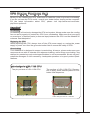
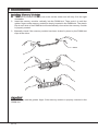
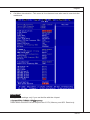
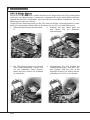
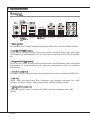
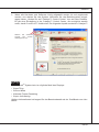
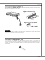
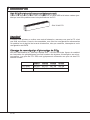
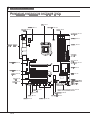
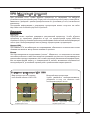
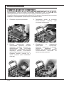
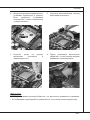
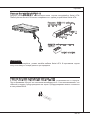
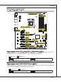
1
P55-GD80 series
MS-7581 (v1.x) Mainboard
G52-75811X3
▍ Preface
Copyright Notice
The material in this document is the intellectual property of MICRO-STAR INTERNATIONAL. We take every care in the preparation of this document, but no guarantee is
given as to the correctness of its contents. Our products are under continual improvement and we reserve the right to make changes without notice.
Trademarks
All trademarks are the properties of their respective owners.
■
■
■
■
■
■
■
■
■
■
■
■
MSI® is registered trademark of Micro-Star Int’l Co.,Ltd.
NVIDIA® is registered trademark of NVIDIA Corporation.
ATI® is registered trademark of ATI Technologies, Inc.
AMD® is registered trademarks of AMD Corporation.
Intel® is registered trademarks of Intel Corporation.
Windows® is registered trademarks of Microsoft Corporation.
AMI® is registered trademark of American Megatrends Inc.
Award® is a registered trademark of Phoenix Technologies Ltd.
Sound Blaster® is registered trademark of Creative Technology Ltd.
Realtek® is registered trademark of Realtek Semiconductor Corporation.
JMicron® is registered trademark of JMicron Technology Corporation.
Netware® is a registered trademark of Novell, Inc.
Revision History
Revision
Revision History
Date
V1.0
First release for Europe version
July 2009
Technical Support
If a problem arises with your system and no solution can be obtained from the user’s
manual, please contact your place of purchase or local distributor. Alternatively, please
try the following help resources for further guidance.
◙
◙
Visit the MSI website for FAQ, technical guide, BIOS updates, driver updates,
and other information: http://www.msi.com/index.php?func=service
Contact our technical staff at: http://ocss.msi.com
ii
MS-7581
Safety Instructions
■
■
■
■
■
Always read the safety instructions carefully.
Keep this User’s Manual for future reference.
Keep this equipment away from humidity.
Lay this equipment on a reliable flat surface before setting it up.
The openings on the enclosure are for air convection hence protects the equipment
from overheating. DO NOT COVER THE OPENINGS.
■ Make sure the voltage of the power source and adjust properly 110/220V before
connecting the equipment to the power inlet.
■ Place the power cord such a way that people can not step on it. Do not place anything over the power cord.
■ Always Unplug the Power Cord before inserting any add-on card or module.
■ All cautions and warnings on the equipment should be noted.
■ Never pour any liquid into the opening that could damage or cause electrical
shock.
■ If any of the following situations arises, get the equipment checked by service
personnel:
◯
The power cord or plug is damaged.
◯
Liquid has penetrated into the equipment.
◯
The equipment has been exposed to moist ure.
◯
The equipment does not work well or you can not get it work according to User’s
Manual.
◯
The equipment has dropped and damaged.
◯
The equipment has obvious sign of breakage.
DO NOT LEAVE THIS EQUIPMENT IN AN ENVIRONMENT UNCONDITIONED,
STORAGE TEMPERATURE ABOVE 60oC (140oF), IT MAY DAMAGE THE EQUIPMENT.
CAUTION: Danger of explosion if battery is incorrectly replaced.
Replace only with the same or equivalent type recommended by the manufacturer.
警告使用者:
這是甲類資訊產品,在居住的環境中使用時,可能會造成無線電干擾,在這種情況下,
使用者會被要求採取某些適當的對策。
廢電池請回收
For better environmental protection, waste batteries should be
collected separately for recycleing special disposal.
iii
▍ Preface
FCC-B Radio Frequency Interference Statement
This equipment has been tested and found
to comply with the limits for a Class B digital device, pursuant to Part 15 of the FCC
Rules. These limits are designed to provide
reasonable protection against harmful interference in a residential installation. This equipment generates, uses and can radiate
radio frequency energy and, if not installed and used in accordance with the instructions, may cause harmful interference to radio communications. However, there is no
guarantee that interference will not occur in a particular installation. If this equipment
does cause harmful interference to radio or television reception, which can be determined by turning the equipment off and on, the user is encouraged to try to correct the
interference by one or more of the measures listed below.
◯
Reorient or relocate the receiving antenna.
◯
Increase the separation between the equipment and receiver.
◯
Connect the equipment into an outlet on a circuit different from that to which the
receiver is connected.
◯
Consult the dealer or an experienced radio/television technician for help.
Notice 1
The changes or modifications not expressly approved by the party responsible for compliance could void the user’s authority to operate the equipment.
Notice 2
Shielded interface cables and A.C. power cord, if any, must be used in order to comply
with the emission limits.
VOIR LA NOTICE D’INSTALLATION AVANT DE RACCORDER AU RESEAU.
Micro-Star International
MS-7581
This device complies with Part 15 of the FCC Rules. Operation is subject to the following two conditions:
1) this device may not cause harmful interference, and
2) this device must accept any interference received, including interference that may
cause undesired operation.
iv
MS-7581
WEEE (Waste Electrical and Electronic Equipment) Statement
ENGLISH
To protect the global environment and as an environmentalist, MSI must
remind you that...
Under the European Union (“EU”) Directive on Waste Electrical and Electronic Equipment, Directive 2002/96/EC, which takes effect on August 13,
2005, products of “electrical and electronic equipment” cannot be discarded
as municipal waste anymore and manufacturers of covered electronic equipment will be
obligated to take back such products at the end of their useful life. MSI will comply with
the product take back requirements at the end of life of MSI-branded products that are
sold into the EU. You can return these products to local collection points.
DEUTSCH
Hinweis von MSI zur Erhaltung und Schutz unserer Umwelt
Gemäß der Richtlinie 2002/96/EG über Elektro- und Elektronik-Altgeräte dürfen Elektro- und Elektronik-Altgeräte nicht mehr als kommunale Abfälle entsorgt werden. MSI
hat europaweit verschiedene Sammel- und Recyclingunternehmen beauftragt, die in
die Europäische Union in Verkehr gebrachten Produkte, am Ende seines Lebenszyklus
zurückzunehmen. Bitte entsorgen Sie dieses Produkt zum gegebenen Zeitpunkt ausschliesslich an einer lokalen Altgerätesammelstelle in Ihrer Nähe.
FRANÇAIS
En tant qu’écologiste et afin de protéger l’environnement, MSI tient à rappeler ceci...
Au sujet de la directive européenne (EU) relative aux déchets des équipement électriques et électroniques, directive 2002/96/EC, prenant effet le 13 août 2005, que les
produits électriques et électroniques ne peuvent être déposés dans les décharges ou
tout simplement mis à la poubelle. Les fabricants de ces équipements seront obligés de
récupérer certains produits en fin de vie. MSI prendra en compte cette exigence relative
au retour des produits en fin de vie au sein de la communauté européenne. Par conséquent vous pouvez retourner localement ces matériels dans les points de collecte.
РУССКИЙ
Компания MSI предпринимает активные действия по защите окружающей среды,
поэтому напоминаем вам, что....
В соответствии с директивой Европейского Союза (ЕС) по предотвращению
загрязнения окружающей среды использованным электрическим и электронным
оборудованием (директива WEEE 2002/96/EC), вступающей в силу 13
августа 2005 года, изделия, относящиеся к электрическому и электронному
оборудованию, не могут рассматриваться как бытовой мусор, поэтому
производители вышеперечисленного электронного оборудования обязаны
принимать его для переработки по окончании срока службы. MSI обязуется
соблюдать требования по приему продукции, проданной под маркой MSI на
территории EC, в переработку по окончании срока службы. Вы можете вернуть
эти изделия в специализированные пункты приема.
▍ Preface
ESPAÑOL
MSI como empresa comprometida con la protección del medio ambiente, recomienda:
Bajo la directiva 2002/96/EC de la Unión Europea en materia de desechos y/o equipos electrónicos, con fecha de rigor desde el 13 de agosto de 2005, los productos
clasificados como “eléctricos y equipos electrónicos” no pueden ser depositados en
los contenedores habituales de su municipio, los fabricantes de equipos electrónicos,
están obligados a hacerse cargo de dichos productos al termino de su período de vida.
MSI estará comprometido con los términos de recogida de sus productos vendidos en
la Unión Europea al final de su periodo de vida. Usted debe depositar estos productos
en el punto limpio establecido por el ayuntamiento de su localidad o entregar a una
empresa autorizada para la recogida de estos residuos.
NEDERLANDS
Om het milieu te beschermen, wil MSI u eraan herinneren dat….
De richtlijn van de Europese Unie (EU) met betrekking tot Vervuiling van Electrische
en Electronische producten (2002/96/EC), die op 13 Augustus 2005 in zal gaan kunnen niet meer beschouwd worden als vervuiling. Fabrikanten van dit soort producten
worden verplicht om producten retour te nemen aan het eind van hun levenscyclus.
MSI zal overeenkomstig de richtlijn handelen voor de producten die de merknaam MSI
dragen en verkocht zijn in de EU. Deze goederen kunnen geretourneerd worden op
lokale inzamelingspunten.
SRPSKI
Da bi zaštitili prirodnu sredinu, i kao preduzeće koje vodi računa o okolini i prirodnoj
sredini, MSI mora da vas podesti da…
Po Direktivi Evropske unije (“EU”) o odbačenoj ekektronskoj i električnoj opremi, Direktiva 2002/96/EC, koja stupa na snagu od 13. Avgusta 2005, proizvodi koji spadaju
pod “elektronsku i električnu opremu” ne mogu više biti odbačeni kao običan otpad i
proizvođači ove opreme biće prinuđeni da uzmu natrag ove proizvode na kraju njihovog
uobičajenog veka trajanja. MSI će poštovati zahtev o preuzimanju ovakvih proizvoda
kojima je istekao vek trajanja, koji imaju MSI oznaku i koji su prodati u EU. Ove proizvode možete vratiti na lokalnim mestima za prikupljanje.
POLSKI
Aby chronić nasze środowisko naturalne oraz jako firma dbająca o ekologię, MSI przypomina, że...
Zgodnie z Dyrektywą Unii Europejskiej (“UE”) dotyczącą odpadów produktów elektrycznych i elektronicznych (Dyrektywa 2002/96/EC), która wchodzi w życie 13 sierpnia
2005, tzw. “produkty oraz wyposażenie elektryczne i elektroniczne “ nie mogą być traktowane jako śmieci komunalne, tak więc producenci tych produktów będą zobowiązani
do odbierania ich w momencie gdy produkt jest wycofywany z użycia. MSI wypełni
wymagania UE, przyjmując produkty (sprzedawane na terenie Unii Europejskiej) wycofywane z użycia. Produkty MSI będzie można zwracać w wyznaczonych punktach
zbiorczych.
vi
MS-7581
TÜRKÇE
Çevreci özelliğiyle bilinen MSI dünyada çevreyi korumak için hatırlatır:
Avrupa Birliği (AB) Kararnamesi Elektrik ve Elektronik Malzeme Atığı, 2002/96/EC
Kararnamesi altında 13 Ağustos 2005 tarihinden itibaren geçerli olmak üzere, elektrikli
ve elektronik malzemeler diğer atıklar gibi çöpe atılamayacak ve bu elektonik cihazların
üreticileri, cihazların kullanım süreleri bittikten sonra ürünleri geri toplamakla yükümlü
olacaktır. Avrupa Birliği’ne satılan MSI markalı ürünlerin kullanım süreleri bittiğinde MSI
ürünlerin geri alınması isteği ile işbirliği içerisinde olacaktır. Ürünlerinizi yerel toplama
noktalarına bırakabilirsiniz.
ČESKY
Záleží nám na ochraně životního prostředí - společnost MSI upozorňuje...
Podle směrnice Evropské unie (“EU”) o likvidaci elektrických a elektronických výrobků
2002/96/EC platné od 13. srpna 2005 je zakázáno likvidovat “elektrické a elektronické
výrobky” v běžném komunálním odpadu a výrobci elektronických výrobků, na které se
tato směrnice vztahuje, budou povinni odebírat takové výrobky zpět po skončení jejich životnosti. Společnost MSI splní požadavky na odebírání výrobků značky MSI,
prodávaných v zemích EU, po skončení jejich životnosti. Tyto výrobky můžete odevzdat
v místních sběrnách.
MAGYAR
Annak érdekében, hogy környezetünket megvédjük, illetve környezetvédőként fellépve
az MSI emlékezteti Önt, hogy ...
Az Európai Unió („EU”) 2005. augusztus 13-án hatályba lépő, az elektromos és elektronikus berendezések hulladékairól szóló 2002/96/EK irányelve szerint az elektromos
és elektronikus berendezések többé nem kezelhetőek lakossági hulladékként, és az
ilyen elektronikus berendezések gyártói kötelessé válnak az ilyen termékek visszavételére azok hasznos élettartama végén. Az MSI betartja a termékvisszavétellel kapcsolatos követelményeket az MSI márkanév alatt az EU-n belül értékesített termékek
esetében, azok élettartamának végén. Az ilyen termékeket a legközelebbi gyűjtőhelyre
viheti.
ITALIANO
Per proteggere l’ambiente, MSI, da sempre amica della natura, ti ricorda che….
In base alla Direttiva dell’Unione Europea (EU) sullo Smaltimento dei Materiali Elettrici
ed Elettronici, Direttiva 2002/96/EC in vigore dal 13 Agosto 2005, prodotti appartenenti
alla categoria dei Materiali Elettrici ed Elettronici non possono più essere eliminati come
rifiuti municipali: i produttori di detti materiali saranno obbligati a ritirare ogni prodotto
alla fine del suo ciclo di vita. MSI si adeguerà a tale Direttiva ritirando tutti i prodotti
marchiati MSI che sono stati venduti all’interno dell’Unione Europea alla fine del loro
ciclo di vita. È possibile portare i prodotti nel più vicino punto di raccolta
vii
▍ Preface
▍ Contents
Copyright Notice�������������������������������������������������������������������������������������������� ii
Trademarks���������������������������������������������������������������������������������������������������� ii
Revision History�������������������������������������������������������������������������������������������� ii
Technical Support����������������������������������������������������������������������������������������� ii
Safety Instructions�����������������������������������������������������������������������������������������iii
FCC-B Radio Frequency Interference Statement����������������������������������������� iv
WEEE (Waste Electrical and Electronic Equipment) Statement�������������������� v
English������������������������������������������������������������������������������������������������������ En-1
Mainboard Specifications�����������������������������������������������������������������������������������En-2
Quick Components Guide����������������������������������������������������������������������������������En-4
CPU (Central Processing Unit)��������������������������������������������������������������������������En-5
Memory��������������������������������������������������������������������������������������������������������������En-9
Power Supply���������������������������������������������������������������������������������������������������En-11
Back Panel�������������������������������������������������������������������������������������������������������En-12
Connectors�������������������������������������������������������������������������������������������������������En-14
Button���������������������������������������������������������������������������������������������������������������En-22
Switch���������������������������������������������������������������������������������������������������������������En-25
Slots�����������������������������������������������������������������������������������������������������������������En-27
LED Status Indicators��������������������������������������������������������������������������������������En-33
BIOS Setup������������������������������������������������������������������������������������������������������En-36
Software Information����������������������������������������������������������������������������������������En-48
Deutsch���������������������������������������������������������������������������������������������������� De-1
Spezificationen�������������������������������������������������������������������������������������������������� De-2
Komponenten-Übersicht����������������������������������������������������������������������������������� De-4
CPU (Prozessor)����������������������������������������������������������������������������������������������� De-5
Speicher������������������������������������������������������������������������������������������������������������ De-9
Stromversorgung��������������������������������������������������������������������������������������������� De-11
Rücktafel��������������������������������������������������������������������������������������������������������� De-12
Anschlüssen���������������������������������������������������������������������������������������������������� De-14
Tasten������������������������������������������������������������������������������������������������������������� De-22
Schalter����������������������������������������������������������������������������������������������������������� De-25
Steckplätze������������������������������������������������������������������������������������������������������ De-27
LED Statusdikatoren��������������������������������������������������������������������������������������� De-33
BIOS Setup����������������������������������������������������������������������������������������������������� De-36
Software-Information��������������������������������������������������������������������������������������� De-48
viii
MS-7581
Français����������������������������������������������������������������������������������������������������� Fr-1
Spécifications������������������������������������������������������������������������������������������������������Fr-2
Guide Rapide Des Composants��������������������������������������������������������������������������Fr-4
Processeur : CPU�����������������������������������������������������������������������������������������������Fr-5
Mémoire��������������������������������������������������������������������������������������������������������������Fr-9
Connecteurs d’Alimentation������������������������������������������������������������������������������Fr-11
Panneau Arrière������������������������������������������������������������������������������������������������Fr-12
Connecteurs������������������������������������������������������������������������������������������������������Fr-14
Boutons�������������������������������������������������������������������������������������������������������������Fr-22
Interrupteur��������������������������������������������������������������������������������������������������������Fr-25
Slots������������������������������������������������������������������������������������������������������������������Fr-27
Indicateur De Statut LED ���������������������������������������������������������������������������������Fr-33
Réglage BIOS���������������������������������������������������������������������������������������������������Fr-36
Information De Logiciel�������������������������������������������������������������������������������������Fr-48
Pycckий���������������������������������������������������������������������������������������������������� Ru-1
Характеристики����������������������������������������������������������������������������������������������� Ru-2
Размещение компонентов системной платы������������������������������������������������ Ru-4
CPU (Центральный процессор)���������������������������������������������������������������������� Ru-5
Память�������������������������������������������������������������������������������������������������������������� Ru-9
Разъем питания��������������������������������������������������������������������������������������������� Ru-11
Задняя панель����������������������������������������������������������������������������������������������� Ru-12
Коннекторы���������������������������������������������������������������������������������������������������� Ru-14
Кнопки������������������������������������������������������������������������������������������������������������ Ru-22
Переключатели���������������������������������������������������������������������������������������������� Ru-25
Слоты������������������������������������������������������������������������������������������������������������� Ru-27
Световые индикаторы����������������������������������������������������������������������������������� Ru-33
Настройка BIOS��������������������������������������������������������������������������������������������� Ru-36
Сведения о программном обеспечении������������������������������������������������������ Ru-48
ix
P55-GD80 Series
English
Europe version
▍ MS-7581 Mainboard
Mainboard Specifications
Processor Support
■ Intel® i5/ i7 (Lynnfield & Clarkdale) processor in the LGA1156 package
(For the latest information about CPU, please visit http://www.msi.com/index.
php?func=cpuform2)
Base Clock
■ 133 MHz
Chipset
■ Intel® P55 chipset
Memory Support
■ 4 DDR3 DIMMs support DDR3 2133 *(OC)/ 2000 *(OC)/ 1800 *(OC)/1600 *(OC)/
1333/ 1066 DRAM (16GB Max)
■ Supports Dual-Channel mode
*(For more information on compatible components, please visit
http://www.msi.com/index.php?func=testreport)
LAN
■ Supports Dual LAN (10/100/1000) by Realtek® RTL8111DL
IEEE 1394 (optional)
■ Chip integrated by VIA® VT6315N
■ Transfer rate is up to 400Mbps
Audio
■ Chip integrated by Realtek® ALC889 (True Blu-ray Audio)
■ Flexible 8-channel audio with jack sensing
■ Compliant with Azalia 1.0 Spec
IDE
■ 1 IDE port by JMicron® JMB363
■ Supports Ultra DMA 66/100/133 mode
■ Supports PIO, Bus Master operation mode
SATA
■ 6 SATAII (SATA1~6) ports by Intel® P55
■ 2 SATAII (SATA7, SATA8) ports by JMicron® JMB322
■ 1 ESATA/ USB Combo port (back panel) by JMicron® JMB363
■ Supports storage and data transfers at up to 3 Gb/s
RAID
■ SATA1~6 support Intel® Matrix Storage Technology (AHCI/ RAID 0/ 1/ 5/ 10) by Intel®
P55
Hardware RAID
■ SATA7 & SATA8 support RAID 0/ 1 & JBOD mode by JMicron® JMB322
En-2
English
Connectors
■ Back panel
- 1 PS/2 keyboard port
- 1 PS/2 mouse port
- 1 Coaxial S/PDIF-out port
- 1 Optical S/PDIF-out port
- 1 IEEE 1394 port (optional)
- 7 USB 2.0 ports
- 1 ESATA/ USB Combo port
- 2 LAN ports
- 6 flexible audio ports
■ On-Board
- 3 USB 2.0 connectors
- 1 IEEE 1394 connector (optional)
- 1 Chassis Intrusion connector
- 1 CD-In connector
- 1 S/PDIF-Out connector
- 1 Front Panel Audio connector
- 1 TPM Module connector (optional)
- 1 D-LED2 panel connector (optional)
- 1 GreenPower Genie connector (optional)
- 1 Over-Voltage switch & 1 set voltage check point
- 1 Power button
- 1 Reset button
- 1 Green Power button
- 1 Clear CMOS button
- 1 OC Genie button
- 2 Base clock control buttons
- 1 CPU Phase LED panel
- 1 set Debug LED panel
Slots
■ 3 PCI Express 2.0 x16 slots
- if you intend to install two expansion cards into both PCI_E2 & PCI_E4 slots, these
two PCIE x16 lanes will auto arrange from x16/ x0 to x8/ x8
- the PCI_E5 supports up to PCIE 2.0 x4 speed
- all PCIE x1 slots will unavailable when an expansion card was installed into PCI_
E5 slot.
■ 2 PCI Express 2.0 x1 slots
- all PCIE x1 slots will unavailable when an expansion card was installed into PCI_
E5 slot.
■ 2 PCI slots, support 3.3V/ 5V PCI bus Interface
Form Factor
■ ATX (30.5cm X 24.4 cm)
Mounting
■ 9 mounting holes
If you need to purchase accessories and request the part numbers, you could search
the product web page and find details on our web address below
http://www.msi.com/index.php
En-3
▍ MS-7581 Mainboard
Quick Components Guide
CPU, En-5
JPWR2, En-11
CPUFAN, En-16
JDLED2, En-21
DDR3, En-9
SYSFAN2, En-16
JPWR1, En-11
JSMB1, En-21
Back Panel,
En-12
V Switch,
En-25
JCI1, En-15
SYSFAN1, En-16
SYSFAN3, En-16
SATA, En-15
SYSFAN4, En-16
IDE1, En-14
JTPM1, En-20
PCI, En-32
Base clock control
buttons, En-22
JFP1/ JFP2,
En-17
PCIE, En-27
J1394_1, En-17
JSP1, En-19
JCD1, En-14
JAUD1, En-19
En-4
Green Power/ Reset/ Power, En-24
CLR_CMOS1, En-22
OC Genie, En-23
JUSB1~3, En-18
English
CPU (Central Processing Unit)
When you are installing the CPU, make sure to install the cooler to prevent overheating.
If you do not have the CPU cooler, consult your dealer before turning on the computer.
For the latest information about CPU, please visit http://www.msi.com/index.
php?func=cpuform2
Important
Overheating
Overheating will seriously damage the CPU and system. Always make sure the cooling
fan can work properly to protect the CPU from overheating. Make sure that you apply
an even layer of thermal paste (or thermal tape) between the CPU and the heatsink to
enhance heat dissipation.
Replacing the CPU
While replacing the CPU, always turn off the ATX power supply or unplug the power
supply’s power cord from the grounded outlet first to ensure the safety of CPU.
Overclocking
This mainboard is designed to support overclocking. However, please make sure your
components are able to tolerate such abnormal setting, while doing overclocking. Any
attempt to operate beyond product specifications is not recommended. We do not guarantee the damages or risks caused by inadequate operation or beyond product specifications.
Introduction to LGA 1156 CPU
The pin-pad side of LGA 1156 CPU.
Alignment Key
Yellow triangle is the Pin 1 indicator
The surface of LGA 1156 CPU. Remember to apply some thermal paste on it for
better heat dispersion.
Alignment Key
Yellow triangle is the Pin 1 indicator
En-5
▍ MS-7581 Mainboard
CPU & Cooler Installation
When you are installing the CPU, make sure the CPU has a cooler attached on the top
to prevent overheating. Meanwhile, do not forget to apply some thermal paste on CPU
before installing the heat sink/cooler fan for better heat dispersion.
Follow the steps below to install the CPU & cooler correctly. Wrong installation will
cause the damage of your CPU & mainboard.
1. Open the load level. 2. Lift the load lever up to fully open
position
3. The CPU socket has a plastic cap on
it to protect the contact from damage.
Before you install CPU, always cover
it to protect the socket pin. Romove
the cap (as the arrow shows).
4. After confirming the CPU direction for
correct mating, put down the CPU in
the socket housing frame. Be sure to
grasp on the edge of the CPU base.
Note that the alignment keys are
matched.
Alignment Key
En-6
English
5. Visually inspect if the CPU is seated
well into the socket. If not, take out
the CPU with pure vertical motion
and reinstall.
6. Engage the load lever while pressing
down lightly onto the load plate.
Alignment Key
7. Secure the lever near the hook end
under the retention tab.
8. Make sure the four hooks are in porper position before you install the
cooler.
Important
• Confirm if your CPU cooler is firmly installed before turning on your system.
• Do not touch the CPU socket pins to avoid damaging.
En-7
▍ MS-7581 Mainboard
9. Align the holes on the mainboard with
the heatsink. Push down the cooler
until its four clips get wedged into the
holes of the mainboard.
10. Press the four hooks down to fasten
the cooler.
11. Turn over the mainboard to confirm
that the clip-ends are correctly inserted.
12. Finally, attach the CPU Fan cable to
the CPU fan connector on the mainboard.
Mainboard
Hook
Important
• Read the CPU status in BIOS.
• Whenever CPU is not installed, always protect your CPU socket pin with the plastic
cap covered (shown in Figure 1) to avoid damaging.
• Mainboard photos shown in this section are for demonstration of the CPU/ cooler installation only. The appearance of your mainboard may vary depending on the model
you purchase.
• Please refer to the documentation in the CPU fan package for more details about the
CPU fan installation.
En-8
English
Memory
These DIMM slots are used for installing memory modules. For more information on
compatible components, please visit http://www.msi.com/index.php?func=testreport
DDR3
240-pin, 1.5V
48x2=96 pin
72x2=144 pin
Memory Population Rule
Please refer to the following illustrations for memory population rules.
Dual-Channel mode Population Rule
In Dual-Channel mode, the memory modules can transmit and receive data with two
data bus lines simultaneously. Enabling Dual-Channel mode can enhance the system
performance. The following illustrations explain the population rules for Dual-Channel
mode.
1
DIMM2
DIMM1
DIMM4
DIMM3
2
DIMM2
DIMM1
DIMM4
DIMM3
Installed
Empty
Important
• DDR3 memory modules are not interchangeable with DDR2 and the DDR3 standard
is not backwards compatible. You should always install DDR3 memory modules in
the DDR3 DIMM slots.
• In Dual-Channel mode, make sure that you install memory modules of the same type
and density in different channel DIMM slots.
• To enable successful system boot-up (Lynnfield CPU especially), always insert the
memory modules into the DIMM1 first.
• Due to the chipset resource deployment, the system density will only be detected up
to 15+GB (not full 16GB) when each DIMM is installed with a 4GB memory module.
En-9
▍ MS-7581 Mainboard
Installing Memory Modules
1. The memory module has only one notch on the center and will only fit in the right
orientation.
2. Insert the memory module vertically into the DIMM slot. Then push it in until the
golden finger on the memory module is deeply inserted in the DIMM slot. The plastic
clip at each side of the DIMM slot will automatically close when the memory module
is properly seated.
3. Manually check if the memory module has been locked in place by the DIMM slot
clips at the sides.
Notch
Volt
Important
You can barely see the golden finger if the memory module is properly inserted in the
DIMM slot.
En-10
English
Power Supply
ATX 24-pin Power Connector: JPWR1
This connector allows you to connect an ATX 24-pin power supply. To connect the ATX
24-pin power supply, make sure the plug of the power supply is inserted in the proper
orientation and the pins are aligned. Then push down the power supply firmly into the
connector.
You may use the 20-pin ATX power supply as you like. If you’d like to use the 20-pin
ATX power supply, please plug your power supply along with pin 1 & pin 13.
d
n
u
ro
V
.G 5 V
4
2 3.+ +5 V
d
2 2. 5 s n d
2 1.+ Re ou un d
2 0. Gr ro un #
2 9. G o N d
1 8. Gr -O un
1 7. PS o
1 6. Gr 2V V
1 5. 1 .3
1 4.- +3
1 3.
1
V
.3
3 V
.+ 2 V
2 1 2
1 .+ +1 B OK
11 0. S R d
1 .5V W un
d
9 .P ro
8 .G 5V un
7 .+ ro nd
6 .G 5V u
5 + o V
r
.
4 .G 3.3 3V
.
3
+
.
3
2 .+
1
ATX 8-pin Power Connector: JPWR2
This connector is used to provide 12V power output to the CPU.
d
n
u d
ro un nd
.G ro u d
4 .G ro un
3 .G ro
2 .G
1
V
2
1 V
.+ 2 V
8 .+1 2 V
7 .+1 12
6 .+
5
Important
• Make sure that all the connectors are connected to proper ATX power supplies to
ensure stable operation of the mainboard.
• Power supply of 400 watts (and above) is highly recommended for system stability.
• ATX 12V power connection should be greater than 18A.
En-11
▍ MS-7581 Mainboard
Back Panel
Mouse
Coaxial S/PDIF-Out
(optional)
1394 Port
LAN
LAN
Line-In RS-Out
USB Port
Line-Out CS-Out
Mic
Keyboard
USB Port
Optical S/PDIF-Out
ESATA/ USB
Combo Port
USB Port
SS-Out
USB Port
▶ Mouse/Keyboard
The standard PS/2® mouse/keyboard DIN connector is for a PS/2® mouse/keyboard.
▶ Coaxial S/PDIF-Out
This SPDIF (Sony & Philips Digital Interconnect Format) connector is provided for digital
audio transmission to external speakers through a coaxial cable.
▶ Optical S/PDIF-Out
This SPDIF (Sony & Philips Digital Interconnect Format) connector is provided for digital
audio transmission to external speakers through an optical fiber cable.
▶ 1394 Port (optional)
The IEEE1394 port on the back panel provides connection to IEEE1394 devices.
▶ USB Port
The USB (Universal Serial Bus) port is for attaching USB devices such as keyboard,
mouse, or other USB-compatible devices.
▶ ESATA/USB Combo Port
The ESATA/USB combo port is for attaching the ESATA external hard drive or USB
device.
En-12
English
▶ LAN
The standard RJ-45 LAN jack is for connection to
the Local Area Network (LAN). You can connect a
network cable to it.
Yellow
LED
Color
LED State
Condition
Left
Yellow
Off
LAN link is not established.
On(Steady state)
LAN link is established.
Right
Green
Orange
Green/ Orange
On(brighter & pulsing)
The computer is communicating with another computer on the LAN.
Off
10 Mbits/sec data rate is selected.
On
100 Mbits/sec data rate is selected.
On
1000 Mbits/sec data rate is selected.
▶ Audio Ports
These audio connectors are used for audio devices. It is easy to differentiate between
audio effects according to the color of audio jacks.
■ Line-In (Blue) - Line In, is used for external CD player, tape-player or other
audio devices.
■ Line-Out (Green) - Line Out, is a connector for speakers or headphones.
■ Mic (Pink) - Mic, is a connector for microphones.
■ RS-Out (Black) - Rear-Surround Out in 4/ 5.1/ 7.1 channel mode.
■ CS-Out (Orange) - Center/ Subwoofer Out in 5.1/ 7.1 channel mode.
■ SS-Out (Gray) - Side-Surround Out 7.1 channel mode.
En-13
CD
MS -RO
I M
Kdk
dd l kd
as f kkk kf k
ad dka df sd df kkf
ad dfdf -d ddf dkkl
dd kjas dddd dfdd
df f as jdkd df ad
as dasf dfdd fdf a f
asd d dasa dddd sd
asdd sdf
as dd
ad df sd dddf
f f ffsd as
asd f
ff
df
d
n
u nd
.L ro u
1 .G ro
2 G
.
3 .R
4
En-14
Fl
MS oppy
I D
K dk
dd l kd
as fkkk kfk
ad dka sddf kkf
ad df df df - d ddf dkkl
dd kjas dddd dfdd
df f as jdkd dfad
as dasf df dd f dfa f
as d dasa dddd sd
as d sdf
asdf dddd
dd
ad sdff df
fffa sd as
sdff f
fd
f
Fl
M opp
Fl SI y D
MS oppy
I D
Kdk
dd l kd
as fkkk kfk
ad dkadf sddf kkfd
ad dfdf - d ddf kk
dd kjas dddd dfdd l
df ffas jdkd dfad
as dasf dfdd fdfa f
as d dasa dddd sd
as d sdf
as dddd
ad dfsd dddf
f f ffsd as
asd f
fffd
f
▍ MS-7581 Mainboard
Connectors
This connector supports IDE hard disk drives, optical disk drives and other IDE devices.
IDE Connector: IDE1
3 1/2"
Fl oppy
3 1/2"
Disk
F loppy
Dr i ve
Di sk
tor
Connec
D r ive
tor
Connec
Important
If you install two IDE devices on the same cable, you must configure the drives separately to master / slave mode by setting jumpers. Refer to IDE device’s documentation
supplied by the vendors for jumper setting instructions.
CD-In Connector: JCD1
This connector is provided for external audio input.
English
Serial ATA Connector: SATA1~8
This connector is a high-speed Serial ATA interface port. Each connector can connect
to one Serial ATA device.
Kdk
ddf l kd
as kkks kfk
ad dka ddf kkf
ad df df df - d ddf dkkl
dd kjas ddddd dfdd
df f as jdkd fa
as dasf df ddd fdfa df
as d dasas dd sd
asd d df d
as ddd
ad dfsdff dddf
fffa sd as
sdff f
fd f
Fl
M opp
Fl SI y D
MS oppy
I D
Fl
MS oppy
I D
Kdk
dd l k
as fkkk dkfk
ad dka sdd kkf
ad dfdfd df - d fddf dkk
ddf kjas ddd dfdd l
df fasd jdkd dfad
as dasf fdd fdfa f
asd d dasa dddd sd
as sdf
as ddddd
ad dfsdf dd
f fa fs f as
sd df
fffd
f
SATA1~6 supported by P55
SATA1_2
SATA3_4
SATA5_6
SATA7/8 supported by JMB322
SATA7 & SATA8
Important
Please do not fold the Serial ATA cable into 90-degree angle. Otherwise, data loss may
occur during transmission.
Chassis Intrusion Connector: JCI1
This connector connects to the chassis intrusion switch cable. If the chassis is opened,
the chassis intrusion mechanism will be activated. The system will record this status
and show a warning message on the screen. To clear the warning, you must enter the
BIOS utility and clear the record.
d
n
u RU
ro T
.G IN
2 .C
1
En-15
▍ MS-7581 Mainboard
Fan Power Connectors: CPUFAN,SYSFAN1~4
The fan power connectors support system cooling fan with +12V. When connecting the
wire to the connectors, always note that the red wire is the positive and should be connected to the +12V; the black wire is Ground and should be connected to GND. If the
mainboard has a System Hardware Monitor chipset on-board, you must use a specially
designed fan with speed sensor to take advantage of the CPU fan control.
CPUFAN
SYSFAN1/ 2/ 3/ 4
d
n
u
ro 2V or
.G 1 s
1 .+ en
2 .S
3
d
n
u
ro 2V or l
.G 1 s o
1 .+ en tr
2 .S on
3 .C
4
Important
• Please refer to the recommended CPU fans at processor’s official website or consult
the vendors for proper CPU cooling fan.
• CPUFAN support Smart fan control. You can install Control Center utility that will
automatically control the CPUFAN speeds according to the actual CPUFAN temperatures.
• Fan cooler set with 3 or 4 pins power connector are both available for CPUFAN.
En-16
English
Front Panel Connectors: JFP1, JFP2
These connectors are for electrical connection to the front panel switches and LEDs.
The JFP1 is compliant with Intel® Front Panel I/O Connectivity Design Guide.
P
o
w
e
r
in
P o 8. +
.
.N
6
0
.
4 +
.
2
e
ch
w
it
o
w
1
S
P
Spe
r
r
E
D
Buz
zer
.+
8 .
6
+
.
4 .
2
L
JFP2
D D
in E LE
P rL d
o e n
.N w e d
7 .Po sp n
5 Su rou
.
3 .G
1
ch
it
w
d
e tS
rv e
D
s
E
se e
L
e R
D
.R
D
9 .+
H
7 .5
.
3 .+
1
JFP1
ake
IEEE1394 Connector: J1394_1 (Optional)
This connector allows you to connect the IEEE1394 device via an optional IEEE1394
bracket.
d
n
u
ro V
.G 2 - d
0 1
1 .+ PB un
8 T ro
.
6 G A
.
4 TP
.
2
in
P
o 2V
+ d
.N
9 .+1 B un
7 .TP ro +
5 G A
.
3 .TP
1
IEEE1394 Bracket (optional)
En-17
▍ MS-7581 Mainboard
Front USB Connector: JUSB1 / JUSB2 / JUSB3
This connector, compliant with Intel® I/O Connectivity Design Guide, is ideal for connecting high-speed USB interface peripherals such as USB HDD, digital cameras, MP3
players, printers, modems and the like.
C
O
B d
S un +
.U o D
0 r B 1 . G S BD
8 U
. S
6 U C
.
4 VC
.
2
in
P nd
o u +
.N ro D 9 .G B D
7 .US B
S
5 U CC
.
3 .V
1
USB 2.0 Bracket (optional)
Important
Note that the pins of VCC and GND must be connected correctly to avoid possible
damage.
En-18
English
S/PDIF-Out Connector: JSP1
This connector is used to connect S/PDIF (Sony & Philips Digital Interconnect Format)
interface for digital audio transmission.
d
n
u F
ro DI
.G P
3 .S CC
2 .V
1
S/PDIF Bracket (Optional)
Front Panel Audio Connector: JAUD1
This connector allows you to connect the front panel audio and is compliant with Intel®
Front Panel I/O Connectivity Design Guide.
io
ct
te
e
D
e
n
o
n
h
io
P
ct #
d
e E
a
e Pin et C
N
D
.H
E
0 o
1 . N I C ES d
8 M
n
.
6 .PR ou
4 Gr
.
2
n
L
e D
n
o N
h E R
P _S ne
d
o
a E h
e NS P
.H E d
9 . S ea R
7 .H IC L
5 .M I C
3 .M
1
En-19
▍ MS-7581 Mainboard
This connector connects to a TPM (Trusted Platform Module) module (optional). Please
refer to the TPM security platform manual for more details and usages.
TPM Module connector: JTPM1 (optional)
3
in
p 2
ta in
a p 1
d ta pin 0
n
e s & da ta pi
m s & da ta
a
ra re s
F d s & d
C ad dre ss &
P
re s
.L C d d s
3 P a d re
1 1.L C a dd et
1 .LP C a es k
9 .LP C R loc
7 .LP C C
5 .L P C
3 .LP
1
d
n
u nd
r
ro u n r
e
.G ro Pi we Q r ow
4
1 2 . G o P o IR w e y p
1 .N V ial o b
0
1 .5 er P nd
8 S 3V ta
.
6 3. S
.
4 .3V
2
En-20
English
D-LED2 Panel Connector: JDLED2 (optional)
This connector connects to a D-LED2 (Debug-LED2) panel (optional), which shows
information on the panel for you and identify the current status or mode of the connected system. Please refer to the D-LED2 quick guide (optional) for more details and
usages.
GreenPower Genie Connector: JSMB1 (optional)
This connector connects to GreenPower Genie (optional).
in a
P D
o B
.N M
4 .S
2
ta
d c
n o
u Cl
ro B
.G
3 .S M
1
k
En-21
▍ MS-7581 Mainboard
Button
The motherboard provides the following buttons for you to set the computer’s function.
This section will explain how to change your motherboard’s function through the use of
button.
Clear CMOS Button: CLR_CMOS1
There is a CMOS RAM on board that has a power supply from external battery to keep
the system configuration data. With the CMOS RAM, the system can automatically boot
OS every time it is turned on. If you want to clear the system configuration, use the button to clear data. Press the button to clear the data.
Important
Make sure that you power off the system before clearing CMOS data.
After pressing this button to clear CMOS data in power off (G3) state, the system will
boot automatically.
Base Clock Control Buttons: Plus, Minus
These buttons are used to increase or decrease the Base clock frequency. Pressing the
Plus/ Minus button once will increase/ decrease the Base clock frequency 1 MHz when
the system is in regular operation state.
Plus button
En-22
Minus button
English
OC Genie Button: OC Genie
This button is used to auto-overclock for the system. Press this button to enable the OC
Genie function when the system is in power off state, meanwhile, the button will light
and lock. And then the system will automatically detect the optimum values to overclock
after booting the system. To disable the OC Genie function, please press the button
again after power off the system, meanwhile, the button light will off and unlock. and the
system will restore the default for next boot.
Important
Please install the DDR3 1333 and up memory and equip better heat sink/ cooler with
OC Genie function.
We do not guarantee the OC Genie overclocking range and the damages or risks
caused by the OC Genie overclocking behavior.
You can disable the OC Genie function in BIOS setup. And we suggest you to save the
OC Genie configuration to overclocking profile in BIOS for future using.
En-23
▍ MS-7581 Mainboard
Power On Button: POWER
This button is used to turn-on or turn-off the system. Press the button to turn-on or turnoff the system.
Reset Button: RESET
This button is used to reset the system. Press the button to reset the system.
Important
If you want to press this button to reset the system, the system will be forced shutdown
about 4 seconds and restarted. This limitation derives from the P55 internal function.
GreenPower Button: Green Power
This button is used to switch LED function of system. Once you press the button, the
system will switch the LED between on and off mode.
En-24
English
Switch
This mainboard provides the following switch for you to set the computer’s function.
This section will explain how to change your mainboard’s function through the use of
switch.
Over-Voltage Switch: V Switch
You can increase the voltage range of CPU / CPU_VTT/ Memory/ PCH for adjustment
in BIOS by changing this switch.
Follow the instructions below to increase the voltage range of CPU / CPU_VTT/ Memory/ PCH.
Switch 1 : is used to over-voltage the CPU voltage, switching it to
“ON” will increase the CPU voltage adjustment range in BIOS.
Switch 2 : is used to over-voltage the CPU_VTT voltage, switching it to “ON” will increase the CPU_VTT voltage adjustment
range in BIOS.
Switch 3 : is used to over-voltage the DRAM voltage, switching
it to “ON” will increase the DRAM voltage adjustment range in
BIOS.
Switch 4 : is used to over-voltage the PCH voltage, switching it to
“ON” will increase the PCH voltage adjustment range in BIOS.
Important
• After switching the V switch, you have to set the CPU/ CPU_VTT/ DDR/ PCH voltage
in BIOS to achieve the CPU/ CPU_VTT/ DDR/ PCH over-voltage.
• After you set the CPU/ CPU_VTT/ DDR/ PCH voltage in BIOS, you can check the
CPU/ CPU_VTT/ DDR/ PCH voltage by measuring the Voltage Check Point with multimeter. Please refer the following instructions to measure these voltages.
En-25
▍ MS-7581 Mainboard
Voltage Check Point: V_Check Point
This voltage check point set is used to measure the current CPU/ CPU_VTT/ DDR/
PCH voltage.
CPU_VTT
CPU
CPU
En-26
DDR voltage: measure the current DDR voltage
with DDR point and GND point by using a multimeter.
GND
PCH
GND
CPU_VTT voltage: measure the current CPU_
VTT voltage with CPU_VTT point and GND
point by using a multimeter.
GND
DDR
GND
CPU voltage: measure the current CPU voltage
with CPU point and GND point by using a multimeter.
GND
CPU_VTT
DDR
PCH
GND
PCH voltage: measure the current PCH voltage
with PCH point and GND point by using a multimeter.
English
Slots
PCIE (Peripheral Component Interconnect Express) Slot
The PCI Express slot supports the PCI Express interface expansion card.
PCI Express x16 Slot
PCI Express x1 Slot
Important
When adding or removing expansion cards, make sure that you unplug the power supply first. Meanwhile, read the documentation for the expansion card to configure any
necessary hardware or software settings for the expansion card, such as jumpers,
switches or BIOS configuration.
The PCI Express x1 slots will unavailable when an expansion card was installed into
PCI_E5 slot.
En-27
▍ MS-7581 Mainboard
ATI CrossFireXTM (Multi-GPU) Technology
ATI CrossFireXTM is the ultimate multi-GPU performance gaming platform. Enabling
game-dominating power, ATI CrossFireXTM technology enables two discrete graphics
processors to work together to improve system performance. ATI CrossFireXTM technology allows you to expand your system’s graphics capabilities. It allows you the ability to
scale your system’s graphics horsepower as you need it, supporting two ATI RadeonTM
HD graphics cards, making this the most scalable gaming platform ever. The mainboard
can auto detect the CrossFireXTM mode by software, therefore you don’t have to enable
the CrossFireXTM in BIOS by yourself. The following details the CrossFireXTM installation.
1. Install one ATI RadeonTM HD graphics card in first PCIE x16 slot , then install one
ATI RadeonTM HD graphics card in second PCIE x16 slot.
2. With two cards installed, an CrossFireXTM Video Link cable is required to connect
the golden fingers on the top of these two graphics cards (refer to the picture below). Please note that although you have installed two graphics cards, only the
video outputs on the graphics card installed in first PCIE x16 slot will work. Hence,
you only need to connect a monitor to this graphics card.
CrossFireXTM Video Link cable
Important
• Mainboard photos shown in this section are for demonstration only. The appearance
of your mainboard may vary depending on the model you purchase.
• If you intend to install TWO graphics cards for CrossFireXTM mode, make sure that
these two graphics cards are of the same brand.
• Make sure that you connect an adequate power supply to the power connector on the
graphics card to ensure stable operation of the graphics card.
• Only Windows®XP with Service Pack 2 (SP2)& Windows®XP Professional x64 Edition & Windows®Vista support the CrossFireXTM function.
En-28
English
3. When all of the hardware and software has been properly set up and installed, reboot the system. After entering the O.S., click the “CatalystTM Control Center” icon
on the desktop. There is a setting in the CatalystTM Control Center that needs to be
enabled for CrossFireXTM to operate. The following aspect appears in CatalystTM
Control Center:
Select the Advanced View
from the view drop menu.
Important
A CrossFireXTM system has four possible display modes:
• SuperTiling
• Scissor Mode
• Alternate Frame Rendering
• Super Anti-aliasing.
for more details, please consult the graphics card manual from the manufacturer.
En-29
▍ MS-7581 Mainboard
NVIDIA® SLI Technology (Optional)
NVIDIA® SLI (Scalable Link Interface) technology allows two GPUs to run in tandem
within a system to achieve up to twice the performance of a single graphics card. To utilize this technology, the two GPU cards must be connected by an SLI Video Link card.
SLI Video Link Card
If you intend to use the SLI mode for better graphics performance, please refer to the
following instructions.
1. Install two graphics cards on PCI Express x16 slots. With two cards installed, an SLI
Video Link Card is required to connect the golden fingers on the top of these two
graphics cards (refer to the picture below). Please note that although you have installed two graphics cards, only the video outputs on the first card will work. Hence,
you only need to connect a monitor to the first PCI Express card.
SLI Video Link Card
Important
• The photos shown in this section are for demonstration only. The appearance of your
mainboard may vary depending on the model you purchase.
• If you intend to install TWO x16 graphics cards, make sure that these two graphics
cards are of the same brand and specifications.
• Make sure that you connect an adequate power supply to the power connector on the
graphics card to ensure stable operation of the graphics card.
En-30
English
2. After the hardware installation is completed, restart the system and install the NV
SLI driver/utility. A configuration panel will be provided for Multi-GPU control. Check
the Enable multi-GPU box to enable the SLI function for the onboard graphics cards
(concerning the details of multi-GPU settings, please refer to your graphics card
manual).
Check the box
3. Restart your system and a pop-up message will show in the system tray confirming
the Multi-GPU has been enabled.
Important
If you want to remove one graphics card and quit the SLI function, make sure the “MultiGPU” function is disabled.
En-31
▍ MS-7581 Mainboard
PCI (Peripheral Component Interconnect) Slot
The PCI slot supports LAN card, SCSI card, USB card, and other add-on cards that
comply with PCI specifications.
32-bit PCI Slot
Important
When adding or removing expansion cards, make sure that you unplug the power supply first. Meanwhile, read the documentation for the expansion card to configure any
necessary hardware or software settings for the expansion card, such as jumpers,
switches or BIOS configuration.
PCI Interrupt Request Routing
The IRQ, acronym of interrupt request line and pronounced I-R-Q, are hardware lines
over which devices can send interrupt signals to the microprocessor. The PCI IRQ pins
are typically connected to the PCI bus pins as follows:
En-32
Order1
Order2
Order3
PCI Slot1
INT E#
INT F#
INT G# INT H#
Order4
PCI Slot2
INT F#
INT G#
INT H#
INT E#
English
LED Status Indicators
CPU_VTT Phase LEDs
These LEDs indicate the current CPU_VTT power phase mode. Follow the instructions
below to read.
Lights Off
CPU_VTT is in 1 phase power mode.
CPU_VTT is in 2 phase power mode.
DDR Phase LEDs
These LEDs indicate the current DDR power phase mode. Follow the instructions below
to read.
Lights Off
DDR is in 1 phase power mode.
DDR is in 2 phase power mode.
En-33
▍ MS-7581 Mainboard
CPU Phase LED panel
These LEDs indicate the current CPU power phase mode. Follow the instructions below
to read.
Post
Status
1
CPU is in 1 phase power mode.
2
CPU is in 2 phase power mode..
3
CPU is in 3 phase power mode.
4
CPU is in 4 phase power mode.
5
CPU is in 5 phase power mode.
6
CPU is in 6 phase power mode.
7
CPU is in 7 phase power mode.
8
CPU is in 8 phase power mode.
PCH Phase LEDs
These LEDs indicate the current PCH power phase mode. Follow the instructions below
to read.
Lights Off
PCH is in 1 phase power mode.
PCH is in 2 phase power mode.
Power LED
Lights blue when you press the Power button and it is functional.
Reset LED
Lights blue when you press the Reset button and it is functional.
Green Power LED
Lights blue when you press the Green Power button and it is functional.
PCIE/ PCI LEDs
Lights blue when the PCIE/ PCI Slot is functional.
En-34
English
Standby LED
Lights orange when the system is in standby (S3/S4/S5 ) status.
HD LED
Lights red when the hard drive is operating.
Debug LED Panel
Please refer to the table below to get more information about the Debug LED message.
Post
Status
FF
Power on and first initialize CPU.
C0, C1, C2
Early CPU Initialize.
C4, C6
Initialize chipset.
D4, D5
Initialize memory.
08
Initialize keyboard.
2A, 31
Initialize onboard devices. Load Option ROM (VGA and RAID option
ROM) form BIOS to memory.
37
Displaying sign-on message, CPU information, setup key message
and any OEM specific information.
38
Initialize USB device and different devices.
3C
Mid POST initialization of chipset registers. Detect different devices
(parallel ports, serial ports and coprocessor in CPU...etc.)
75, 78
Initialize INT 13 devices and IPL devices. (include SATA/ PATA HDD
and CD/DVD ROM).
87
Enter setup screen. BIOS setup if needed/ requested.
A4
Wait for user input at configuration display if needed.
A7
Display the system configuration screen if enabled.
B1
Save system context for ACPI (Advanced Configuration and Power
Interface).Prepare give control to OS loader (INT 19H).
00
Pass control to OS Loader (typically INT 19H).
AA
Enter OS (Vista or Windows® XP).
En-35
▍ MS-7581 Mainboard
BIOS Setup
This chapter provides basic information on the BIOS Setup program and allows you to
configure the system for optimum use. You may need to run the Setup program when:
■ An error message appears on the screen during the system booting up, and
requests you to run BIOS SETUP.
■ You want to change the default settings for customized features.
Important
• The items under each BIOS category described in this chapter are under continuous
update for better system performance. Therefore, the description may be slightly different from the latest BIOS and should be held for reference only.
• Upon boot-up, the 1st line appearing after the memory count is the BIOS version. It is
usually in the format:
A7581IMS V1.0 062009 where:
1st digit refers to BIOS maker as A = AMI, W = AWARD, and P = PHOENIX.
2nd - 5th digit refers to the model number.
6th digit refers to the chipset as I = Intel, N = NVIDIA, A = AMD and V = VIA.
7th - 8th digit refers to the customer as MS = all standard customers.
V1.0 refers to the BIOS version.
062009 refers to the date this BIOS was released.
En-36
English
Entering Setup
Power on the computer and the system will start POST (Power On Self Test) process.
When the message below appears on the screen, press <DEL> key to enter Setup.
Press DEL to enter SETUP
If the message disappears before you respond and you still wish to enter Setup, restart
the system by turning it OFF and On or pressing the RESET button. You may also restart the system by simultaneously pressing <Ctrl>, <Alt>, and <Delete> keys.
Getting Help
After entering the Setup menu, the first menu you will see is the Main Menu.
Main Menu
The main menu lists the setup functions you can make changes to. You can use the
arrow keys ( ↑↓ ) to select the item. The on-line description of the highlighted setup
function is displayed at the bottom of the screen.
Sub-Menu
If you find a right pointer symbol appears to the left of certain fields that means a submenu can be launched from this field. A sub-menu contains additional options for a
field parameter. You can use arrow keys ( ↑↓ ) to highlight the field and press <Enter>
to call up the sub-menu. Then you can use the control keys to enter values and move
from field to field within a sub-menu. If you want to return to the main menu, just press
the <Esc >.
General Help <F1>
The BIOS setup program provides a General Help screen. You can call up this screen
from any menu by simply pressing <F1>. The Help screen lists the appropriate keys to
use and the possible selections for the highlighted item. Press <Esc> to exit the Help
screen.
En-37
▍ MS-7581 Mainboard
The Main Menu
Once you enter BIOS CMOS Setup Utility, the Main Menu will appear on the screen.
The Main Menu allows you to select from the setup functions and two exit choices.
Use arrow keys to select among the items and press <Enter> to accept or enter the
sub-menu.
▶ Standard CMOS Features
Use this menu for basic system configurations, such as time, date etc.
▶ Advanced BIOS Features
Use this menu to setup the items of the BIOS special enhanced features.
▶ Integrated Peripherals
Use this menu to specify your settings for integrated peripherals.
▶ Power Management Setup
Use this menu to specify your settings for power management.
▶ H/W Monitor
This entry shows your PC health status.
▶ Green Power
Use this menu to specify the power phase.
▶ BIOS Setting Password
Use this menu to set the password for BIOS.
▶ Cell Menu
Use this menu to specify your settings for frequency/voltage control and overclocking.
▶ M-Flash
Use this menu to read/ flash the BIOS from storage drive (FAT/ FAT32 format only).
▶ Overclocking Profile
Use this menu to save/ load your settings to/ from CMOS for BIOS.
▶ Load Fail-Safe Defaults
Use this menu to load the default values set by the BIOS vendor for stable system
performance.
En-38
English
▶ Load Optimized Defaults
Use this menu to load the default values set by the mainboard manufacturer specifically
for optimal performance of the mainboard.
▶ Save & Exit Setup
Save changes to CMOS and exit setup.
▶ Exit Without Saving
Abandon all changes and exit setup.
En-39
▍ MS-7581 Mainboard
When enter the BIOS Setup utility, follow the processes below for general use.
1. Load Optimized Defaults : Use control keys (↑↓) to highlight the Load Optimized
Defaults field and press <Enter> , a message as below appears:
Select [Ok] and press Enter to load the default settings for optimal system performance.
2. Setup Date/ Time : Select the Standard CMOS Features and press <Enter> to enter
the Standard CMOS Features-menu. Adjust the Date, Time fields.
3. Save & Exit Setup : Use control keys (↑↓) to highlight the Save & Exit Setup field
and press <Enter> , a message as below appears: Select [Ok] and press Enter to save the configurations and exit BIOS Setup utility.
Important
The configuration above are for general use only. If you need the detailed settings of
BIOS, please see the English manual on MSI website.
En-40
English
4. Cell Menu Introduction : This menu is for advanced user who want to overclock the
mainboard.
Important
Change these settings only if you are familiar with the chipset.
▶ Current CPU / DRAM / QPI Frequency
These items show the current frequencies of CPU, Memory and QPI. Read-only.
En-41
▍ MS-7581 Mainboard
▶ CPU Specifications
Press <Enter> to enter the sub-menu. This submenu shows the information of installed
CPU.
▶ CPU Technology Support
Press <Enter> to enter the sub-menu. In this sub-menu, it shows the installed CPU
technologies. Read only.
▶ CPU Feature
Press <Enter> to enter the sub-menu.
▶ Intel EIST
The Enhanced Intel SpeedStep technology allows you to set the performance level
of the microprocessor whether the computer is running on battery or AC power. This
field will appear after you installed the CPU which supports speedstep technology.
▶ Intel C-STATE
C-state is a power management state that significantly reduces the power of the
processor during idle. This field will appear after you installed the CPU which supports c-state technology.
▶ C1E Support
To enable this item to read the CPU power consumption while idle. Not all processors support Enhanced Halt state (C1E).
▶ Hyper-Threading Function
The processor uses Hyper-Threading technology to increase transaction rates and
reduces end-user response times. The technology treats the two cores inside the
processor as two logical processors that can execute instructions simultaneously. In
this way, the system performance is highly improved. If you disable the function, the
processor will use only one core to execute the instructions. Please disable this item
if your operating system doesn’t support HT Function, or unreliability and instability
may occur.
Important
Enabling the functionality of Hyper-Threading Technology for your computer system
requires ALL of the following platform Components:
• CPU: An Intel® Processor with HT Technology;
• Chipset: An Intel® Chipset that supports HT Technology;
• BIOS: A BIOS that supports HT Technology and has it enabled;
• OS: An operating system that supports HT Technology.
For more information on Hyper-threading Technology, go to:
http://www.intel.com/products/ht/hyperthreading_more.htm
En-42
English
▶ Execute Bit Support
Intel’s Execute Disable Bit functionality can prevent certain classes of malicious
“buffer overflow” attacks when combined with a supporting operating system. This
functionality allows the processor to classify areas in memory by where application
code can execute and where it cannot. When a malicious worm attempts to insert
code in the buffer, the processor disables code execution, preventing damage or
worm propagation.
▶ Set Limit CPUID MaxVal to 3
The Max CPUID Value Limit is designed limit the listed speed of the processor to
older operating systems.
▶ Intel Virtualization Tech
This item is used to enable/disable the Intel Virtualization technology. For further
information please refer to Intel’s official website.
▶ X-Ratio
This item allows you to set the extra turbo ratio for CPU to run the overclocking frequency (base clock * turbo ratio) absolutely.
▶ Intel EIST
The Enhanced Intel SpeedStep technology allows you to set the performance level of
the microprocessor whether the computer is running on battery or AC power. This field
will appear after you installed the CPU which supports speedstep technology.
▶ C1E Support
To enable this item to read the CPU power consumption while idle. Not all processors
support Enhanced Halt state (C1E).
▶ Intel Turbo Boost
This item will appear when you install a CPU with Intel Turbo Boost technology. This
item is used to enable/ disable Intel Turbo Boost technology. It can scale processor
frequency higher dynamically when applications demand more performance and TDP
headroom exists. It also can deliver seamless power scalability (Dynamically scale up,
Speed-Step Down). It is the Intel newly technology within i5/ i7 CPU.
▶ Adjust CPU Base Frequency (MHz)
This item allows you to set the CPU Base clock (in MHz). You may overclock the CPU
by adjusting this value. Please note the overclocking behavior is not guaranteed.
▶ OC Stepping
This item will be enabled after you set the overclocking frequency in the “Adjust CPU
Base Frequency (MHz)”. And the following items will appear. This items will help the
system to overclock step by step after system booting up.
▶ Start OC Stepping From (MHz)
This item is used to set the initial base clock. The system will boot with the initial base
clock, and start to overclock from initial base clock to set base clock that you set in
“Adjust CPU Base Frequency (MHz)” step by step.
En-43
▍ MS-7581 Mainboard
▶ OC Step
This item is used to set how many steps for base colck overclocking.
▶ OC Step Count Timer
This item is used to set the buffer time for every step.
▶ Adjust CPU Ratio
This item allows you to adjust the CPU ratio. This field will appear after you installed the
CPU which supports adjusting CPU ratio.
▶ Adjusted CPU Frequency (MHz)
It shows the adjusted CPU frequency (Base clock x Ratio). Read-only.
▶ OC Genie
This item is used to enable/ disable the OC Genie function.
▶ Memory-Z
Press <Enter> to enter the sub-menu.
▶ DIMM1~4 Memory SPD Information
Press <Enter> to enter the sub-menu. The sub-menu displays the informations of
installed memory.
▶ Current DRAM Channel1~4 Timing
It shows the installed DRAM Timing. Read-only.
▶ DRAM Timing Mode
Select whether DRAM timing is controlled by the SPD (Serial Presence Detect) EEPROM on the DRAM module. Setting to [Auto] enables DRAM timings and the following
“Advance DRAM Configuration” sub-menu to be determined by BIOS based on the configurations on the SPD. Selecting [Manual] allows users to configure the DRAM timings
and the following related “Advance DRAM Configuration” sub-menu manually.
▶ Advance DRAM Configuration
When the DRAM Timing Mode is set to [Manual], this sub-menu will available. Press
<Enter> to enter the sub-menu.
▶ CH1/ CH2 1T/2T Memory Timing
This item controls the SDRAM command rate. Select [1N] makes SDRAM signal
controller to run at 1N (N=clock cycles) rate. Selecting [2N] makes SDRAM signal
controller run at 2N rate.
▶ CH1/ CH2 CAS Latency (CL)
This controls the CAS latency, which determines the timing delay (in clock cycles)
before SDRAM starts a read command after receiving it.
En-44
English
▶ CH1/ CH2 tRCD
When DRAM is refreshed, both rows and columns are addressed separately. This
setup item allows you to determine the timing of the transition from RAS (row address strobe) to CAS (column address strobe). The less the clock cycles, the faster
the DRAM performance.
▶ CH1/ CH2 tRP
This setting controls the number of cycles for Row Address Strobe (RAS) to be
allowed to precharge. If insufficient time is allowed for the RAS to accumulate its
charge before DRAM refresh, refresh may be incomplete and DRAM may fail to
retain data. This item applies only when synchronous DRAM is installed in the system.
▶ CH1/ CH2 tRAS
This setting determines the time RAS takes to read from and write to memory cell.
▶ CH1/ CH2 tRFC
This setting determines the time RFC takes to read from and write to a memory
cell.
▶ CH1/ CH2 tWR
Minimum time interval between end of write data burst and the start of a precharge
command. Allows sense amplifiers to restore data to cells.
▶ CH1/ CH2 tWTR
Minimum time interval between the end of write data burst and the start of a column-read command. It allows I/O gating to overdrive sense amplifiers before read
command starts.
▶ CH1/ CH2 tRRD
Specifies the active-to-active delay of different banks.
▶ CH1/ CH2 tRTP
Time interval between a read and a precharge command.
▶ CH1/ CH2 tFAW
This item is used to set the tFAW timing.
▶ Current CH1/ CH2 tdrRdTRd/ tddRdTRd/ tsrRdTWr/ tdrRdTWr/ tddRdTWr/
tsrWrTRd/ tddWrTWr/ tsrRDTRd/ tsrWrTWr
These item show the advanced DRAM timings.
▶ Channel 1/ Channel2 Advanced Memory Setting
Setting to [Auto] enables the advance memory timing automatically to be determined
by BIOS. Setting to [Manual] allows you to set the following advanced memory timings.
▶ Memory Ratio
This item allows you to set the memory multiplier.
En-45
▍ MS-7581 Mainboard
▶ Adjusted DRAM Frequency (MHz)
It shows the adjusted DRAM frequency. Read-only.
▶ QPI Ratio
This item allows you to set the QPI multiplier.
▶ Adjusted QPI Frequency (MHz)
It shows the adjusted QPI frequency. Read-only.
▶ ClockGen Tuner
Press <Enter> to enter the sub-menu and the following screen appears.
▶ CPU Amplitude Control/ PCI Express Amplitude Control
These items are used to select the CPU/ PCI Express clock amplitude.
▶ Adjust PCI-E Frequency (MHz)
This field allows you to select the PCIE frequency (in MHz).
▶ CPU VCore/ CPU VTT (V)/ PCH 1.8V (V)/ DRAM Voltage (V)/ DDR_VREF_CA_A (V)/
/ DDR_VREF_CA_B (V)/ DDR_VREF_DA_A (V)/ / DDR_VREF_DA_B (V)/ PCH 1.05V
(V)
These items are used to adjust the voltage of CPU, Memory and chipset.
▶ Spread Spectrum
When the mainboard’s clock generator pulses, the extreme values (spikes) of the pulses
create EMI (Electromagnetic Interference). The Spread Spectrum function reduces the
EMI generated by modulating the pulses so that the spikes of the pulses are reduced
to flatter curves.
▶ PCIE Spread Spectrum
This item is used to adjust the PCIE spread spectrum range.
Important
• If you do not have any EMI problem, leave the setting at [Disabled] for optimal system
stability and performance. But if you are plagued by EMI, select the value of Spread
Spectrum for EMI reduction.
• The greater the Spread Spectrum value is, the greater the EMI is reduced, and the
system will become less stable. For the most suitable Spread Spectrum value, please
consult your local EMI regulation.
• Remember to disable Spread Spectrum if you are overclocking because even a slight
jitter can introduce a temporary boost in clock speed which may just cause your overclocked processor to lock up.
En-46
English
Important
Failed Overclocking Resolution
This mainboard supports overclocking greatly. However, please make sure your peripherals and components are bearable for some special settings. Any operation that
exceeds product specification is not recommended. Any risk or damge resulting from
improper operation will not be under our product warranty.
Two ways to save your system from failed overclocking...
• Reboot
Press the Power button to reboot the system three times. Please note that, to avoid
electric current to affect other devices or components, we suggest an interval of more
than 10 seconds among the reboot actions.
At the fourth reboot, BIOS will determine that the previous overclocking is failed and
restore the default settings automatically. Please press any key to boot the system
normally when the following message appears on screen.
Warning !!! The previous overclocking had failed,
and system will restore its defaults setting,
Press any key to continue.......
• Clear CMOS
Please refer to “how to clear CMOS data” section for more information.
En-47
▍ MS-7581 Mainboard
Software Information
Take out the Driver/Utility DVD that is included in the mainboard package, and place
it into the DVD-ROM drive. The installation will auto-run, simply click the driver or utility and follow the pop-up screen to complete the installation. The Driver/Utility DVD
contains the:
- Driver menu : The Driver menu shows the available drivers. Install the driver by
your desire and to activate the device.
- Utility menu : The Utility menu shows the software applications that the mainboard
supports.
- WebSite menu : The WebSite menu shows the necessary websites.
Important
Please visit the MSI website to get the latest drivers and BIOS for better system performance.
En-48
P55-GD80 Serie
Deutsch
Europe version
▍ MS-7581 Mainboard
Spezificationen
Prozessoren
■ Intel® i5/ i7 (Lynnfield & Clarkdale) Prozessoren für Sockel LGA1156
(Weitere CPU Informationen finden Sie unter
http://www.msi.com/index.php?func=cpuform2)
Haupt-Takt (Base Clock)
■ 133 MHz
Chipsatz
■ Intel® P55 Chipsatz
Speicher
■ 4 DDR3 DIMMs unterstützen DDR3 2133 *(OC)/ 2000 *(OC)/ 1800 *(OC)/1600 *(OC)/
1333/ 1066 DRAM (16GB Max)
■ Unterstützt die Modus Dual-Channel
*(Weitere Informationen zu kompatiblen Speichermodulen finden Sie unter
http://www.msi.com/index.php?func=testreport)
LAN
■ Unterstützt Dual LAN (10/100/1000) über Realtek® RTL8111DL
IEEE 1394 (optional)
■ Onboard Chip über VIA® VT6315N
■ Übertragungsgeschwindigkeit von bis zu 400Mbps
Audio
■ Onboard Soundchip Realtek® ALC889 (True Blu-ray Audio)
■ 8-Kanal Audio-Ausgang mit „Jack Sensing“
■ Erfüllt die Azalia Spezifikationen
IDE
■ 1 IDE Port über JMicron® JMB363
■ Unterstützt die Betriebmodi Ultra DMA 66/100/133
■ Unterstützt die Betriebmodi PIO, Bus Mastering
SATA
■ 6 SATAII (SATA1~6) Ports über Intel® P55
■ 2 SATAII (SATA7, SATA8) Ports über JMicron® JMB322
■ 1 ESATA/ USB Combo Port (Rückplatte) über JMicron® JMB363
■ Unterstützt Datenübertragungsraten von bis zu 3 Gb/s
RAID
■ SATA1~6 unterstützen die Intel® Matrix Storage Technologie (AHCI/ RAID 0/ 1/ 5/ 10)
über Intel® P55
Hardware RAID
■ SATA7 & SATA8 unterstützen die Modi RAID 0/ 1 & JBOD über JMicron® JMB322
De-2
Deutsch
Anschlüsse
■ Hintere Ein-/ und Ausgänge
- 1 PS/2 Mausanschluss
- 1 PS/2 Tastaturanschlus
- 1 koaxiale S/PDIF-Ausgang
- 1 optische S/PDIF-Ausgang
- 1 IEEE 1394 Anschluss (optional)
- 7 USB 2.0 Anschlüsse
- 1 ESATA/ USB Combo Anschluss
- 2 LAN Anschlüsse
- 6 Audiobuchsen
■ On-Board
- 3 USB 2.0 Stiftleisten
- 1 IEEE 1394 Stiftleiste (optional)
- 1 Gehäusekontaktschalter
- 1 CD Stiftleiste für Audio Eingang
- 1 S/PDIF-Ausgang Stiftleiste
- 1 Audio Stiftleiste für Gehäuse Audio Ein-/ Ausgänge
- 1 TPM Stiftleiste (optional)
- 1 D-LED2 Anschluss (optional)
- 1 GreenPower Genie Anschluss (optional)
- 1 Überspannungschalter & 1 Spannungsmesspunkte
- 1 Ein-/ Aus-Schalter
- 1 Reset-Taste
- 1 Green Power Taste
- 1 Gehäusekontaktschalter
- 1 OC Genie Taste
- 2 Haupt-Taktsteuerung Tasten
- 1 CPU Phase LED Panel
- 1 Debug LED panel
Steckplätze
■ 3 PCI Express 2.0 x16-Steckplätze
- Setzen Sie zwei Erweiterungskarten gleichzeitig in PCI_E2 & PCI_E4 Slot ein, so
wird die Geschwindigkeit von x16/x0 auf x8/x8 gesetzt
- PCI_E5 unterstützt die Geschwindigkeit bis zu PCIE 2.0 x4
- Wenn ein VGA Karte im PCI_E5 Slot wird eingesetzt, alle PCIE x1 Slots deaktiviert
sind.
■ 2 PCI Express 2.0 x1-Steckplätze
- Wenn ein VGA Karte im PCI_E5 Slot wird eingesetzt, alle PCIE x1 Slots deaktiviert
sind.
■ 2 PCI-Steckplätze, unterstützt 3.3V/ 5V PCI Bus Interface
Form Faktor
■ ATX (30.5cm X 24.4 cm)
Montage
■ 9 Montagebohrungen
Wenn Sie für Bestellungen von Zubehör Teilenummern benötigen, finden Sie diese auf
unserer Produktseite unter http://www.msi.com/index.php
De-3
▍ MS-7581 Mainboard
Komponenten-Übersicht
CPU, De-5
JPWR2, De-11
CPUFAN, De-16
JDLED2, De-21
DDR3, De-9
SYSFAN2, De-16
JPWR1, De-11
JSMB1, De-21
Rücktafel,
De-12
V Switch,
De-25
JCI1, De-15
SYSFAN1, De-16
SYSFAN3, De-16
SATA, De-15
SYSFAN4, De-16
IDE1, De-14
JTPM1, De-20
PCI, De-32
Base-Taktsteuerung
Tasten, De-22
PCIE, De-27
JFP1/ JFP2,
De-17
J1394_1, De-17
JSP1, De-19
JCD1, De-14
JAUD1, De-19
De-4
Green Power/ Reset/ Power, De-24
CLR_CMOS1, De-22
OC Genie, De-23
JUSB1~3, De-18
Deutsch
CPU (Prozessor)
Wenn Sie die CPU einbauen, stellen Sie bitte sicher, dass Sie auf der CPU einen Kühler
anbringen, um Überhitzung zu vermeiden. Verfügen Sie über keinen Kühler, setzen
Sie sich bitte mit Ihrem Händler in Verbindung, um einen solchen zu erwerben und zu
installieren. Um die neuesten Informationen zu unterstützten Prozessoren zu erhalten,
besuchen Sie bitte http://www.msi.com/index.php?func=cpuform2
Wichtig
Überhitzung
Überhitzung beschädigt die CPU und das System nachhaltig. Stellen Sie stets eine
korrekte Funktionsweise des CPU Kühlers sicher, um die CPU vor Überhitzung zu
schützen. Überprüfen Sie eine gleichmäßige Schicht der thermischen Paste (oder thermischen Klebeandes) zwischen der CPU und dem Kühlblech anwenden, um Wärmeableitung zu erhöhen.
CPU Wechsel
Stellen Sie vor einem Wechsel des Prozessors stets sicher, dass das ATX Netzteil
ausgeschaltet und der Netzstecker gezogen ist, um die Unversehrtheit der CPU zu
gewährleisten.
Übertakten
Dieses Motherboard wurde so entworfen, dass es Übertakten unterstützt. Stellen Sie
jedoch bitte sicher, dass die betroffenen Komponenten mit den abweichenden Einstellungen während des Übertaktens zurecht kommen. Von jedem Versuch des Betriebes
außerhalb der Produktspezifikationen kann nur abgeraten werden. Wir übernehmen
keinerlei Garantie für die Schäden und Risiken, die aus unzulässigem oder Bet rieb
jensei ts der Produktspezifikationen resultieren.
Erklärung zur LGA 1156 CPU
Die Pin-Seite der LGA 1156 CPU.
Justierung
Das gelbe Dreieck des Prozessors
definiert die Position des ersten Pins
Die Obserseite der LGA 1156 CPU. Vergessen Sie nicht, etwas Siliziumwärmeleitpaste auf die CPU auf zut ragen,um
eine Ableitung der Hitze zu erzielen.
Justierung
Das gelbe Dreieck des Prozessors
definiert die Position des ersten Pins
De-5
▍ MS-7581 Mainboard
CPU & Kühler Einbau
Wenn Sie die CPU einbauen, stellen Sie bitte sicher, dass Sie auf der CPU einen Kühler
anbringen, um Überhitzung zu vermeiden. Vergessen Sie nicht, etwas Siliziumwärmeleitpaste auf die CPU aufzutragen, bevor Sie den Prozessorkühler installieren, um eine
Ableitung der Hitze zu erzielen.
Folgen Sie den Schritten unten, um die CPU und den Kühler ordnungsgemäß zu installieren. Ein fehlerhafter Einbau führt zu Schäden an der CPU und dem Mainboard.
1. Öffnen Sie den Sockelverschlusshebel. 2. Klappen Sie den Hebel ganz auf
und öffnen Sie die Metallverschlussklappe.
3. Der CPU-Sockel besitzt zum Schutz
eine Plastikabdeckung. Lassen Sie
vor der Installation diese Schutzkappe auf dem Sockel um Schäden
zu vermeiden.
4. Vergewissern Sie sich anhand der
Justiermarkierungen und dem gelben Dreieck, daß die CPU in der
korrekten Position ist. Setzen Sie anschließend die CPU in den Sockel.
Justiermarkierungen
De-6
Deutsch
5. Begutachten Sie, ob die CPU richtig
im Sockel sitzt. Falls nicht, ziehen Sie
die CPU durch eine rein vertikale Bewegung wieder heraus. Versuchen
Sie es erneut.
6. Schließen Sie die Abdeckung des
Sockels und drücken Sie den Verschlusshebel mit leichtem Druck
nach unten.
Justiermarkierungen
7. Arretieren Sie den Hebel unter dem
Rückhaltehaken des CPU-Sockels.
8. Kontrollieren Sie die vier Haken sind
in richtiger Position, bevor Sie die
Kühlvorrichtung anbringen.
Wichtig
• Stellen Sie sicher, dass Ihr CPU Küher fest eingebaut ist, bevor Sie Ihr System anschalten.
• Berühren Sie die Pins des CPU Sockels nicht, um Schaden zu vermeiden.
De-7
▍ MS-7581 Mainboard
9. Drücken Sie den Verschlusshebel
mit leichtem Druck nach unten und
arretieren Sie den Hebel unter dem
Rückhaltehaken des CPU-Sockels.
10. Führen Sie den CPU-Kühler über
den CPU-Sockel.
11. Drehen Sie das Mainboard um und
vergewissern Sie sich, dass das der
Kühler korrekt installiert ist.
12. Schließlich verbinden Sie das
Stromkabel des CPU Lüfters mit dem
Anschluss auf dem Mainboard.
Mainboard
Haken
Wichtig
• Prüfen Sie die Status der CPU im BIOS.
• Wenn keine CPU installiert ist, schützen Sie immer den CPU-Sockel durch die Plastikabdeckung (Figur 1).
• Die Mainboard Fotos, die in diesem Abschnitt gezeigt werden, sind für Demonstration der CPU/ Kühler Installation. Das Aussehen Ihres Mainboard kann abhängig von
dem Modell schwanken, das Sie kaufen.
• Beziehen Sie bitte sich die auf Unterlagen im CPU Kühlerpaket für mehr Details über
die CPU Kühlerinstallation.
De-8
Deutsch
Speicher
Diese DIMM-Steckplätze nehmen Arbeitsspeichermodule auf. Die neusten Informationen über kompatible Bauteile finden Sie unter http://www.msi.com/index.
php?func=testreport
DDR3
240-polig, 1.5V
48x2=96 Pole
72x2=144 Pole
Hinweise für den Einsatz von Speichermodulen
Bitte beachten Sie die folgenden Abbildungen zum Speichereinbau.
Populationsregeln für Dual-Channel-Speicher
Im Dual -Channel-Modus können Arbeitsspeichermodule Daten über zwei Datenbusleitungen gleichzeitig senden und empfangen. Durch Aktivierung des Dual-Channel-Modus wird die Leistung Ihres Systems verbessert. Bitte beachten Sie die folgenden Abbildungen zur Veranschaulichung der Populationsregeln im Dual-Channel-Modus.
1
DIMM2
DIMM1
DIMM4
DIMM3
2
DIMM2
DIMM1
DIMM4
DIMM3
installiert
Installed
leer
Empty
Wichtig
• DDR3 und DDR2 können nicht untereinander getauscht werden und der Standard
DDR3 ist nicht abwärtskompatibel. Installieren Sie DDR3 Speichermodule stets in
DDR3 DIMM Slots.
• Stellen Sie im Zweikanalbetrieb bitte sicher, dass Sie Module des gleichen Typs und
identischer Speicherdichte in den DIMM Slots unterschiedlicher Kanäle verwenden.
• Um einen sicheren Systemstart (besonders für Lynnfield CPU) zu gewährleisten,
bestücken Sie immer DIMM1 zuerst.
• Aufgrund der Chipsatzressourcennutzung wird nur eine Systemdichte bis 15+GB
(nicht volle 16GB) erkannt, wenn jeder DIMM Slot mit einem 4GB Speichermodul
besetzt wird.
De-9
▍ MS-7581 Mainboard
Vorgehensweise beim Einbau von Speicher Modulen
1. Die Speichermodulen haben nur eine Kerbe in der Mitte des Moduls. Sie passen
nur in einer Richtung in den Sockel.
2. Stecken Sie das Arbeitsspeichermodul senkrecht in den DIMM-Steckplatz ein.
Drücken Sie anschließnd das Arbeitsspeichermodul nach unten, bis die Kontaktseite richtig tief in dem DIMM-Steckplatz sitzt. Der Kunststoffbügel an jedem Ende
des DIMM-Steckplatzes schnappt automatisch ein, wenn das Arbeitsspeichermodul
richtig eingesetzt ist.
3. Prüfen Sie von Hand, ob das Arbeitsspeichermodul von den seitlichen Bügeln am
DIMM-Steckplatz richtig gehalten wird.
Notch
Kerbe
Wichtig
Die goldenen Kontakte sind kaum zu sehen, wenn das Arbeitsspeichermodul richtig im
DIMM-Steckplatz sitzt.
De-10
Deutsch
Stromversorgung
ATX 24-poliger Stromanschluss: JPWR1
Mit diesem Anschluss verbinden Sie den ATX 24-poligen Anschluss des Netzteils.
Achten Sie bei dem Verbinden des ATX 24-poligen Stromanschlusses darauf, dass
der Anschluss des Netzteils richtig auf den Anschluss an der Hauptplatine ausgerichtet
ist. Drücken Sie dann den Anschluss des Netzteils fest nach unten, um eine richtige
Verbindung zu gewährleisten.
Sie können auch den 20-poligen ATX-Stromanschluss des Netzteils verwenden. In diesem Fall muss eine Ecke des 20-poligen ATX-Stromanschlusses des Netzteils auf den
Pol 1 bzw. Pol 13 des Anschlusses an der Hauptplatine ausgerichtet werden.
d
n
u
ro
V
.G 5 V
4
2 3.+ +5 V
d
2 2. 5 s n d
2 1.+ Re ou un d
2 0. Gr ro un #
2 9. G o N d
1 8. Gr -O un
1 7. PS o
1 6. Gr 2V V
1 5. 1 .3
1 4.- +3
1 3.
1
V
.3
3 V
.+ 2 V
2 1 2
1 .+ +1 B OK
11 0. S R d
1 .5V W un
d
9 .P ro
8 .G 5V un
7 .+ ro nd
6 .G 5V u
5 + o V
r
.
4 .G 3.3 3V
.
3
+
.
3
2 .+
1
ATX 8-poliger Stromanschluss: JPWR2
Dieser Stromanschluss wird verwendet, um die CPU mit Strom zu versorgen.
d
n
u d
ro un nd
.G ro u d
4 .G ro un
3 .G ro
2 .G
1
V
2
1 V
.+ 2 V
8 .+1 2 V
7 .+1 12
6 .+
5
Wichtig
• Stellen Sie sicher, dass diese Anschlüsse mit den richtigen Anschlüssen des Netzteils verbunden werden, um einen stabilen Betrieb der Hauptplatine sicherzustellen.
• Für die Systemstabilität ist ein Netzteil mit 350 Watt (oder noch mehr) empfehlenswert.
• Die ATX 12V Stromversorgung sollte mit mehr als 18A erfolgen.
De-11
▍ MS-7581 Mainboard
Rücktafel
Maus
koaxiale S/PDIF-Ausgang
(optional)
1394 Port
LAN
LAN
Line-In RS-Out
USB Port
Line-Out CS-Out
Mic
Tastatur
optische S/PDIF-Ausgang
USB Port
ESATA/ USB
Combo Port
USB Port
SS-Out
USB Port
▶ Maus/Tastatur
Die Standard PS/2® Maus/Tastatur Stecker Mini DIN ist für eine PS/2® Maus/Tastatur.
▶ Koaxiale S/PDIF-Ausgang
Dieser S/PDIF (Sony & Philips Digital Interconnect Format) Ausgang dient als digitale
Schnittstelle zur Audioausgabe zur den externen Lautsprechern durch ein Koaxialkabel.
▶ Optische S/PDIF-Ausgang
Dieser S/PDIF (Sony & Philips Digital Interconnect Format) Ausgang dient als digitale
Schnittstelle zur Audioausgabezur den externen Lautsprechern durch ein optischen
Fasernkabel.
▶ 1394 Port (optional)
Das IEEE 1394 Port auf der hintere Anschlusspanel zu den Vorrichtungen IEEE1394.
▶ USB Port
Dieser USB (Universal Serial Bus) Anschluss zum direkten Anschluss von USBGeräten, wie etwa Tastatur, Maus oder weiterer USB-kompatibler Geräte.
▶ ESATA/USB Combo Port
Der ESATA/USB Combo Port verbindet ESATA externe Festplatten oder USB
Geräte.
De-12
Deutsch
▶ LAN
Die Standard RJ-45 Buchse ist für Anschlus zum
an ein Lokales Netzwerk (Local Area Network LAN). Hier kann ein Netzwerkkabel angeschlossen
werden.
Gelb
Grün/ Orange
LED
Farbe
LED Status
Zustand
Links
Gelb
Aus
Keine Verbindung mit dem LAN.
An (Dauerleuchten)
Verbindung mit dem LAN.
An (heller & pulsierend)
Der Computer kommuniziert mit einem anderen Rechner im LAN.
Aus
Gewählte Datenrate 10 MBit/s.
An
Gewählte Datenrate 100 MBit/s.
An
Gewählte Datenrate 1000 MBit/s.
Rechts
Grün
Orange
▶ Audioanschlüsse
Diese Audioanschlüsse dienen zur Verbindung mit Audiogeräten. Durch die Farben
erkennen Sie die unterschiedlichen Funktionen der Audioanschlüsse.
■ Line-In (Blau) - Der Anschluss “Line In” kann einen externen CDPlayer,Tapeplayer oder ein sonstiges Audiogerät aufnehmen.
■ Line-Out (Grün) - An den Anschluss “Line Out” können Sie Lautsprecher oder
Kopfhörer anschließen.
■ Mikrofon (Rosa) - Der Anschluss “Mic” nimmt ein Mikrofon auf.
■ RS-Out (Schwarz) - Dieser Anschluss nimmt die hinteren Surround-Lautsprecher im 4/ 5.1/ 7.1-Kanalmodus auf.
■ CS-Out (Orange) - Dieser Anschluss nimmt die mittleren oder Subwoofer- Lautsprecher im 5.1/ 7.1-Kanalmodus auf.
■ SS-Out (Grau) - Dieser Anschluss nimmt die seitlichen Surround-Lautsprecher
im 7.1-Kanalmodus auf.
De-13
▍ MS-7581 Mainboard
Anschlüssen
IDE Anschluss: IDE1
K dk
dd l kd
as fkkk kfk
ad dka sddf kkf
ad df df df - d ddf dkkl
dd kjas dddd dfdd
df f as jdkd dfad
as dasf df dd f dfa f
as d dasa dddd sd
as d sdf
asdf dddd
dd
ad sdff df
fffa sd as
sdff f
fd
f
Fl
M opp
Fl SI y D
MS oppy
I D
Fl
MS oppy
I D
Kdk
dd l kd
as fkkk kfk
ad dkadf sddf kkfd
ad dfdf - d ddf kk
dd kjas dddd dfdd l
df ffas jdkd dfad
as dasf dfdd fdfa f
as d dasa dddd sd
as d sdf
as dddd
ad dfsd dddf
f f ffsd as
asd f
fffd
f
An diesem Anschluss können IDE Festplatten, optische Laufwerke und andere Geräte
betrieben werden.
Fl oppy
Disk
Dr i ve
tor
Connec
CD
MS -RO
I M
Kdk
dd l kd
as f kkk kf k
ad dka df sd df kkf
ad dfdf -d ddf dkkl
dd kjas dddd dfdd
df f as jdkd df ad
as dasf dfdd fdf a f
asd d dasa dddd sd
asdd sdf
as dd
ad df sd dddf
f f ffsd as
asd f
ff
df
3 1/2"
3 1/2"
F loppy
Di sk
D r ive
tor
Connec
Wichtig
Verbinden Sie zwei Laufwerke über ein Kabel, müssen Sie das zweite Laufwerk im
Slave-Modus konfigurieren, indem Sie entsprechend den Jumper setzen. Entnehmen
Sie bitte die Anweisungen zum Setzen des Jumpers der Dokumentation der IDE Geräte,
die der Festplattenhersteller zur Verfügung stellt.
CD-Eingang: JCD1
Dieser Anschluss wird für externen Audioeingang zur Verfügung gestellt.
d
n
u nd
.L ro u
1 .G ro
2 G
.
3 .R
4
De-14
Deutsch
Serial ATA Anschluss: SATA1~8
Der Anschluss ist eine Hochgeschwindigkeitsschnittstelle der Serial ATA. Pro Anschluss kann ein S-ATA Geräte angeschlossen werden.
Kdk
ddf l kd
as kkks kfk
ad dka ddf kkf
ad df df df - d ddf dkkl
dd kjas ddddd dfdd
df f as jdkd fa
as dasf df ddd fdfa df
as d dasas dd sd
asd d df d
as ddd
ad dfsdff dddf
fffa sd as
sdff f
fd f
Fl
M opp
Fl SI y D
MS oppy
I D
Fl
MS oppy
I D
Kdk
dd l k
as fkkk dkfk
ad dka sdd kkf
ad dfdfd df - d fddf dkk
ddf kjas ddd dfdd l
df fasd jdkd dfad
as dasf fdd fdfa f
asd d dasa dddd sd
as sdf
as ddddd
ad dfsdf dd
f fa fs f as
sd df
fffd
f
SATA1~6 werden durch P55 unterstützt.
SATA1_2
SATA3_4
SATA5_6
SATA7/8 werden durch JMB322 unterstützt.
SATA7 & SATA8
Wichtig
Bitte falten Sie das Serial ATA Kabel nicht in einem Winkel von 90 Grad, da dies zu
Datenverlusten während der Datenübertragung führt.
Gehäusekontaktanschluss: JCI1
Dieser Anschluss wird mit einem Kontaktschalter verbunden. Wird das Gehäuse geöffnet, wird der Schalter geschlossen und das System zeichnet dies auf und gibt auf dem
Bildschirm eine Warnung aus. Um die Warnmeldung zu löschen, muss das BIOS aufgerufen und die Aufzeichnung gelöscht werden.
d
n
u RU
ro T
.G IN
2 .C
1
De-15
▍ MS-7581 Mainboard
Stromanschlüsse für Lüfter: CPUFAN1,SYSFAN1~4
Die Anschlüsse unterstützen aktive Systemlüfter mit + 12V. Wenn Sie den Anschluss
herstellen, sollten Sie immer darauf achten, dass der rote Draht der positive Pol ist, und
mit +12V verbunden werden sollte. Der schwarze Draht ist der Erdkontakt und sollte mit
GND verbunden werden. Ist Ihr Mainboard mit einem Chipsatz zur Überwachung der
Systemhardware versehen, dann brauchen Sie einen speziellen Lüfter mit Tacho, um
die Vorteile der Steuerung des CPU Lüfters zu nutzen.
CPUFAN
SYSFAN1/ 2/ 3/ 4
d
n
u
ro 2V or
.G 1 s
1 .+ en
2 .S
3
d
n
u
ro 2V or l
.G 1 s o
1 .+ en tr
2 .S on
3 .C
4
IWichtig
• Bitte informieren Sie sich auf der offiziellen Website vom Prozessor über empfohlene
CPU Kühler oder fragen Sie Ihren Händler nach einem geeigneten Lüfter.
• CPUFAN unterstützen die Lüfterkontrolle. Sie können das Utility Control Center installieren, welches automatisch die Geschwindigkeiten des CPUFAN & SYSFAN1 in
Abhängigkeit von der CPUFAN Temperaturen steuert.
• CPUFAN kann die Lüfter/Kühlkörper mit drei- und vierpoligen Steckern unterstützen.
De-16
Deutsch
Frontpanel Anschlüsse: JFP1, JFP2
Diese Anschlüsse sind für das Frontpanel. Sie dienen zum Anschluss der Schalter und
LEDs des Frontpanels. JFP1 erfüllt die Anforderungen des “Intel® Front Panel I/O Connectivity Design Guide“.
P
o
w
e
r
in
P o 8. +
.
.N
6
0
.
4 +
.
2
e
ch
w
it
o
w
1
S
P
Spe
r
r
E
D
Buz
zer
.+
8 .
6
+
.
4 .
2
L
JFP2
D D
in E LE
P rL d
o e n
.N w e d
7 .Po sp n
5 Su rou
.
3 .G
1
ch
it
w
d
e tS
rv e
D
s
E
se e
L
e R
D
.R
D
9 .+
H
7 .5
.
3 .+
1
JFP1
ake
IEEE1394-Sockel: J1394_1 (Optional)
Mit diesem Sockel verbinden Sie ein optionales IEEE 1394-Modul, das den Anschluss
eines IEEE 1394-Gerätes ermöglicht.
d
n
u
ro V
.G 2 - d
0 1
1 .+ PB un
8 T ro
.
6 G A
.
4 TP
.
2
in
P
o 2V
+ d
.N
9 .+1 B un
7 .TP ro +
5 G A
.
3 .TP
1
IEEE1394 Slotblech(optional)
De-17
▍ MS-7581 Mainboard
USB Vorderanschluss: JUSB1 / JUSB2 / JUSB3
Dieser Anschluss entspricht den Richtlinien des Intel® I/O Connectivity Design Guide.
Er ist bestens geeignet, Hochgeschwindigkeits- USB- Peripheriegeräte anzuschließen,
wie z.B. USB Festplattenlaufwerke, Digitalkameras, MP3-Player, Drucker, Modems und
ähnliches.
C
O
B d
S un +
.U o D
0 r B 1 . G S BD
8 U
. S
6 U C
.
4 VC
.
2
in
P nd
o u +
.N ro D 9 .G SB D
7 .U B
S
5 .U CC
3 .V
1
USB 2.0 Slotblech (optional)
Wichtig
Bitte beachten Sie, dass Sie die mit VCC (Stromführende Leitung) und GND (Erdleitung) bezeichneten Pins korrekt verbinden müssen, ansonsten kann es zu Schäden
kommen.
De-18
Deutsch
S/PDIF- Ausgang: JSP1
Die SPDIF (Sony & Philips Digital Interconnect Format) Schnittstelle wird für die Übertragung digitaler Audiodaten verwendet.
d
n
u F
ro DI
.G P
3 .S CC
2 .V
1
S/PDIF Slotblech (Optional)
Audioanschluss des Frontpanels: JAUD1
Dieser Anschluss ermöglicht den Anschluss von Audioein und -ausgängen eines Frontpanels. Der Anschluss entspricht den Richtlinien des “ Intel® Front Panel I/O Connectivity Design Guide”.
io
ct
te
e
D
e
n
o
n
h
io
P
ct #
d
e E
a
e Pin et C
N
D
.H
E
0 o
1 . N I C ES d
8 M
n
.
6 .PR ou
4 Gr
.
2
n
L
e D
n
o N
h E R
P _S ne
d
o
a E h
e NS P
.H E d
9 . S ea R
7 .H IC L
5 .M I C
3 .M
1
De-19
▍ MS-7581 Mainboard
Dieser Anschluss wird für das optionale TPM Modul (Trusted Platform Module) (optional) verwendt. Weitere Informationen über den Einsatz des optionalen TPM Modules
entnehmen Sie bitte dem TPM Plattform Handbuch.
TPM Modul Anschluss: JTPM1 (optional)
3
in
p 2
ta in
a p 1
d ta pin 0
n
e s & da ta pi
m s & da ta
a
ra re s
F d s & d
C ad dre ss &
P
re s
.L C d d s
3 P a d re
1 1.L C a dd et
1 .LP C a es k
9 .LP C R loc
7 .LP C C
5 .L P C
3 .LP
1
d
n
u nd
r
ro u n r
e
.G ro Pi we Q r ow
4
1 2 . G o P o IR w e y p
1 .N V ial o b
0
1 .5 er P nd
8 S 3V ta
.
6 3. S
.
4 .3V
2
De-20
Deutsch
D-LED2 Anschluss: JDLED2 (optional)
Dieser Anschluss wird für das optionale D-LED2 Panel verwendt, die Informationen im
Panel für Sie zeigt und den gegenwärtigen Status oder den Modus des verbundenen
Systems kennzeichnet. Beziehen Sie bitte sich die auf dem D-LED2 Schnelleinstieg für
mehr Details und Gebrauchen.
GreenPower Genie Anschluss: JSMB1 (optional)
Dieser Anschluss wird mit dem optionalen GreenPower-Genie verbunden.
in a
P D
o B
.N M
4 .S
2
ta
d c
n o
u Cl
ro B
.G
3 .S M
1
k
De-21
▍ MS-7581 Mainboard
Tasten
Das Motherboard unterstützt der folgende Taste, um die Funktion des Computers
einzustellen. Dieser Abschnitt beschreibt, wie man die Funktionen des Motherboards
durch den Gebrauch der Taste ändert.
CMOS leeren-Tasten: CLR_CMOS1
Auf der Hauptplatine befindet sich ein CMOS RAM, das von einer zusätzlichen Batterie mit Strom versorgt wird, um die Systemkonfigurationsdaten zu behalten. Mit den
Daten im CMOS RAM kann das System automatisch das Betriebssystem hochfahren,
wann immer das System eingeschaltet wird. Wenn Sie die Systemkonfiguration löschen
möchten, dann stellen Sie bitte den Jumper so ein, dass die Daten gelöscht werden.
Wichtig
Stellen Sie sicher, dass das System ausgeschaltet ist, bover Sie den CMOS Speicher
in den Werkszustand zurücksetzen..
Nachdem es diese Taste zu den leeren CMOS Daten im Betriebsspannung aus Status
(G3) gedrückt hat, bootet das System automatisch.
Haupt-Taktsteuerung Tasten: Plus, Minus
Diese Tasten werden benutzt, um die Haupt-Taktfrenquenz zu erhöhen oder zu verringern. Drücken Sie die Plus-/ Minus-Tasten einmal, um die Haupt-Taktfrenquenz 1 MHz
zu erhöhen/ verringern, wenn das System im regelmäßigen Betriebszustand ist.
Plus Taste
De-22
Minus Taste
Deutsch
OC Genie Taste: OC Genie
Diese Taste wird zum Selbstübertaktung für das System benutzt. Drücken Sie diese
Taste, um der OC Genie Funktion zu ermöglichen, wenn das System im spannungslosen Zustand ist, unterdessen die Taste beleuchtet und sich verriegelt. Nach dem
Boot des Systems und wird das System die optimalen Werte automatisch ermitteln und
übertaktet das System automatisch. Um die OC Genie Funktion zu sperren, drücken
Sie bitte die Taste wieder nach der Abschaltung des Systems. Gleichzeitig schaltet und
entsperren die Tastelicht aus. Das System stellt die Standard-Werte für nächste Start
wiederher.
Wichtig
Bitte installieren Sie DDR3 1333 und größer Speicher und rüsten Sie bessere Kühlkopper/ Kühler mit OC Genie Funktion aus.
Wir garantieren nicht der OC Genie Übertaktungs-Bereich und die Beschädigungen oder
die Gefahren, die durch das OC Genie Übertaktungsverhalten verursacht werden.
Sie können die OC Genie Funktion in der BIOS-Einstellung sperren. Und wir schlagen
Sie vor, um die OC Genie Konfiguration zu Übertaktungsprofil im BIOS für die zukunftigen Verwenden zu speichern.
De-23
▍ MS-7581 Mainboard
Ein-/Aus-Schalter: POWER
Dieser Ein-/ Aus-Schalter verwendet, um das System ein- und auszuschalten. Drücken
Sie diese Taste, um das System ein- bzw. auszuschalten.
Reset-Taste: RESET
Diese Reset-Taste wird verwendet, um das System zurückzusetzen. Drücken Sie diese
Taste, um das System zurückzusetzen.
Wichtig
Wenn Sie diese Taste drücken möchten, um das System zurückzustellen, isr das System Zwangsabschaltung ungefähr 4 Sekunden und begann wieder. Diese Beschränkung leitet von der internen Funktion P55 ab.
GreenPower Taste: Green Power
Diese Taste kann die LED-Funktion des System schalten. Wenn Sie die Taste drücken,
schält das System das LED zwischen deaktivierter Modus und automatischer Modus.
De-24
Deutsch
Schalter
Das Motherboard unterstützt den folgende Schalter, um die Funktion des Computers
einzustellen. Dieser Abschnitt beschreibt, wie man die Funktionen des Motherboards
durch den Gebrauch des Schalters ändert.
Überspannungschalter: V Switch
Sie können den Spannungsbereich des CPUs / CPU_VTTs/ Speichers/ PCHs für Einstellung im BIOS erhöhen, indem Sie diesen Schalter ändern.
Folgen Sie die folgenden Anweisungen, um den Spannungsbereich des CPUs / CPU_
VTTs/ Speichers/ PCHs zu erhöhen.
Schalter 1: ist an überspannung die CPU Spannung gewöhnt,
schält sie zu “ON”, erhöht den CPU Spannung Einstellbereich
im BIOS.
Schalter 2 : ist an überspannung die CPU_VTT Spannung
gewöhnt, schält sie zu “ON”, erhöht den CPU_VTT Spannung
Einstellbereich im BIOS.
Schalter 3 : ist an überspannung die DRAM Spannung gewöhnt,
schält sie zu “ON”, erhöht den DRAM Spannung Einstellbereich
im BIOS.
Schalter 4 : ist an überspannung die PCH Spannung gewöhnt,
schält sie zu “ON”, erhöht den PCH Spannung Einstellbereich
im BIOS.
Wichtig
• Nachdem Sie den Überspannungschalter geschalten haben, müssen Sie die CPU/
CPU_VTT/ DDR/ PCH Spannung im BIOS einstellen, um die CPU/ CPU_VTT/ DDR/
PCH Überspannung zu erzielen.
• Nachdem Sie den CPU/ CPU_VTT/ DDR/ PCH Spannung im BIOS einstellen, können Sie die CPU/ CPU_VTT/ DDR/ PCH Spannung überprüfen, indem Sie den
Spannungsmesspunkte mit Multimeter messen. Bitte verweisen Sie die folgenden
Anweisungen, diese Spannungen zu messen.
De-25
▍ MS-7581 Mainboard
Spannungsmesspunkte: V_Check Point
Die Einstellung der Spannungsmesspunkte wird verwendet, um die gegenwärtige CPU
CPU_VTT/DDR/PCH Spannung zu messen.
CPU_VTT
CPU
CPU
De-26
DDR Spannung: messen Sie die gegenwärtige
DDR Spannung mit DDR Punkt und GND Punkt,
indem Sie ein Multimeter verwenden.
GND
PCH
GND
Spannung: messen Sie die gegenwärtige CPU_
VTT Spannung mit CPU_VTT Punkt und GND
Punkt, indem Sie ein Multimeter verwenden.
GND
DDR
GND
CPU Spannung: messen Sie die gegenwärtige
CPU Spannung mit CPU Punkt und GND Punkt,
indem Sie ein Multimeter verwenden.
GND
CPU_VTT
DDR
PCH
GND
PCH Spannung: messen Sie die gegenwärtige
PCH Spannung mit PCH Punkt und GND Punkt,
indem Sie ein Multimeter verwenden.
Deutsch
Steckplätze
PCIE (Peripheral Component Interconnect Express) Sterckplatz
Der PCI Express-Steckplatz unterstützt eine Erweiterungskarte mit der PCI ExpressSchnittstelle.
PCI Express x16 Steckplatz
PCI Express x1 Steckplatz
Wichtig
Achten Sie darauf, dass Sie zuerst das Netzkabel aus der Steckdose herausziehen,
bevor Sie eine Erweiterungskarte installieren oder entfernen. Denken Sie bitte auch
daran die Dokumentation der Erweiterungskarte zu lesen, um notwendige Hardwareoder Softwareeinstellungen für die Erweiterungskarte wie z.B. Jumper-, Schalter- oder
BIOS-Einstellungen vorzunehmen.
Der PCI Express x1-Steckplatz wird eine Erweiterungskarte mit der PCI_E5-Schnittstelle nicht unterstützt.
De-27
▍ MS-7581 Mainboard
ATI CrossFireXTM (Multi-GPU) Technologie
ATI CrossFireXTM ist die ultimative Multi-GPU Leistung Spielplattform. Wenn Spielbeherrschender Energie ermöglicht, versetzt die ATI CrossFireXTM Technologie in die Lage
zwei oder eigenstandige Graphikprozessoren zusammen zu arbeiten, um System Leistung zu verbessern. Die ATI CrossFireXTM Technologie kann Graphikfähigkeiten Ihres
Systems erweitern. Es erlaubt Ihnen, Graphikpferdestärken Ihres Systems einzustufen,
während Sie es benötigen und stützt bis zwei oder mehr ATI RadeonTM HD Graphikkarten und überhaupt bildet dieses die skalierbare Spielplattform. Das Mainboard kann
den Modus CrossFireXTM durch Software automatisch detektieren, deswegen Sie dem
CrossFireXTM im BIOS nicht aktivieren. Die folgenden Details die CrossFireXTM Installation.
1. Installieren Sie die die HD Grafikkarte der ATI RadeonTM in den ersten PCIE x16
Slot und bringen Sie die HD Grafikkarte des ATI RadeonTM HD in denzweiten PCIE
x16 Slot.
2. Wenn zwei Karten angebracht sind, muss ein CrossFireXTM -Videoquerkabel die
goldenen Finger verbinden, die auf die Oberseite von zwei Grafikkarten stehen
(beziehen Sie sich die folgende Abbildung). Zur Beachtung: Obwohl Sie have zwei
Grafikkarten angebracht haben, nur arbeiten die Video-Ausgang auf der Grafikkarte
in den ersten PCIE x16. So müssen Sie nur einen Monitor an die Grafikkarte.
CrossFireXTM Videoquerkabel
Wichtig
• Die Mainboard darstellungen in diesem Abschnitt dienen lediglich Demonstrationszwecken. Die Erscheinung Ihres Mainboards kann in Abhängigkeit vom erworbenen
Modell abweichen.
• IWenn Sie beabsichtigen, ZWEI Grafikkarten für die Modus CrossFireXTM einzusetzen, stellen Sie sicher, dass diese Grafikkarten von identischer Marke sind.
• Stellen Sie sicher, dass Sie ein richtige Stromversorgung an den Stromstecker auf
der Graphikkarte anschließen, um beständigen Betrieb der Graphikkarte sicherzustellen.
• Nur Windows®XP with Service Pack 2 (SP2)& Windows®XP Professional x64 Edition
& Windows®Vista unterstützt die Funktion des CrossFireXTM.
De-28
Deutsch
3. Wenn alle Hardware und Software richtig aufgestellt worden ist und angebracht
worden, neu starten Sie das System. Nachdem Sie das Betriebssystem eingetragen haben,, klicken Sie auf “Catalyst™ Control Center” Icon auf dem Desktop.
Es gibt eine Einstellung in der Catalyst™ Control Center, die ermöglicht werden
muss, damit CrossFireX™ funktioniert. Der folgende Aspekt erscheint in Catalyst™
Wählen Sie erweiterte
Ansicht
vom
Ansichtaufklappmenü aus.
Wichtig
A CrossFireXTM System hat vier mögliche Modi des Displays:
• SuperTiling
• Scissor Mode
• Alternate Frame Rendering
• Super Anti-aliasing.
Weitere Informationen befrangen Sie das Benutzerhandbuch der Grafikkarte vom Hersteller.
De-29
▍ MS-7581 Mainboard
NVIDIA® SLI Technologie (Optional)
Die NVIDIA® SLI (Scalable Link Interface) Technologie gestattet es zwei GPUs im Tandembetrieb innerhalb eines Systems zu betreiben, so dass diese bis hin zur doppelten
Leistung einer einzelnen Grafikkarte erreichen. Um diese Technologieeinsetzen zu
können, müssen die beiden GPU Karten durch eine sogenannte SLI Video Link Karte
verbunden werden.
SLI Video Link Karte
Wenn Sie beabsichten die SLI Schnittstelle zur Steigerung der Grafikleistung zu verwenden, dann befolgen Sie bitte die folgenden Anweisungen.
1. Einsetzen Sie nun zwei Grafikkarten in die PCI Express x16 Sockel. Sind zwei
Karten eingebaut, wird eine SLI Bridge benötigt, um die goldenen Kontakte am
oberen Ende dieser zwei Grafikkarten zu verbinden. Beachten Sie bitte, dass trotz
des Einsatzes zweier Grafikkarten nur die Bildausgabe der ersten Karte arbeitet.
Deswegen brauchen Sie auch nur den Monitor an die erste PCI Express Karte
anzuschließen.
SLI Video Link Karte
Wichtig
• Die Mainboard darstellungen in diesem Abschnitt dienen lediglich Demonstrationszwecken. Die Erscheinung Ihres Mainboards kann in Abhängigkeit vom erworbenen
Modell abweichen.
• Wenn Sie beabsichtigen, ZWEI x16 Grafikkarten einzusetzen, stellen Sie sicher,idass
diese zwei Grafikkarten von identischer Marke und Spezifikationen sind.
• Stellen Sie sicher, dass Sie ein richtige Stromversorgung mit dem Stromanschluss
verbinden, um stabilen Betrieb der Graphikkarte sicherzustellen.
De-30
Deutsch
2. Beenden Sie die Hardwareeinrichtung, führen Sie einen Neustart durch undinstallieren Sie den NV SLI Treiber/das Utility. Ein Konfigurationspaneel für Multi-GPU
Grafikkarten wird bereit gestellt. Setzen Sie einen Haken neben “Enable multiGPU”, um den SLI Modus für die Grafikkarte onboard zu aktivieren. (Details zu
den Multi-GPU Einstellungen entnehmen Sie bitte dem Handbuch der von Ihnen
eworbenen Grafikkarte).
Wählen Sie den
Kasten aus
3. Schließlich müssen Sie das System neu starten und Sie erhalten eine Information,
“Multi-GPU has been enabled“, die besagt das Multi GPU nun eingeschaltet ist.
Wichtig
Wollen Sie eine Grafikkarte entfernen und vom SLI-Modus zum Normalbetrieb zurückkehren, stellen Sie sicher, dass die “MultiGPU” Funktion abschalten.
De-31
▍ MS-7581 Mainboard
PCI (Peripheral Component Interconnect) Steckplatz
Die PCI Steckplätze unterstützt LAN Karte, SCSI Karte, USB Karte und andere Zusatzkarten cards,die mit PCI Spezifikationen übereinstimmen.
32-Bit PCI Steckplatz
Wichtig
Stellen Sie vor dem Einsetzen oder Entnehmen von Karten sicher, dass Sie den Netzstecker gezogen haben. Studieren Sie bit te die Anlei tung zur Erweiterungskarte, um
jede notwendige Hard - oder Softwareeinstellung für die Erweiterungskarte vorzunehmen, sei es an Steckbrücken (“Jumpern”), Schaltern oder im BIOS.
PCI-Unterbrechungsanforderungs-Routing
Eine IRQ (Interrupt Request; Unterbrechungsanforderung)-Leitung ist eine Hardwareleitung, über die ein Gerät Unterbrechungssignale zu dem Mikroprozessor schicken kann.
Die PCI IRQ-Pole werden in der Regel mit dem PCI-Bus-Polen wie folgt verbunden:
De-32
Folge1
Folge2
Folge3
PCI Steckplatz1
INT E#
INT F#
INT G# INT H#
Folge4
PCI Steckplatz2
INT F#
INT G#
INT H#
INT E#
Deutsch
LED Statusdikatoren
CPU_VTT Phase LEDs
Diese LEDs zeigen den gegenwärtigen CPU_VTT Strromphase Modus an. Lesen Sie
die folgenden Anweisungen.
Ein Aus
CPU_VTT ist in die 1 Phase Strommodus.
CPU_VTT ist in die 1 Phase Strommodus.
DDR Phase LEDs
Diese LEDs zeigen den gegenwärtigen DDR Strromphase Modus an. Lesen Sie die
folgenden Anweisungen.
Ein Aus
DDR ist in die 1 Phase Strommodus.
DDR ist in die 1 Phase Strommodus.
De-33
▍ MS-7581 Mainboard
CPU Phase LED Panel
Diese LEDs zeigen den gegenwärtigen CPU Strromphase Modus an. Lesen Sie die
folgenden Anweisungen.
Post
Status
1
CPU ist in die 1 Phase Strommodus.
2
CPU ist in die 2 Phase Strommodus.
3
CPU ist in die 3 Phase Strommodus.
4
CPU ist in die 4 Phase Strommodus.
5
CPU ist in die 5 Phase Strommodus.
6
CPU ist in die 6 Phase Strommodus.
7
CPU ist in die 7 Phase Strommodus.
8
CPU ist in die 8 Phase Strommodus.
PCH Phase LEDs
Diese LEDs zeigen den gegenwärtigen PCH Strromphase Modus an. Lesen Sie die
folgenden Anweisungen.
Ein Aus
PCH ist in die 1 Phase Strommodus.
PCH ist in die 2 Phase Strommodus.
Ein-/ Ausschalter LED (Power LED)
Die Leutchten ist blau, wenn Sie den Ein-/ Ausschalter drücken und es aktiviert ist.
Reset LED
Die Leutchten ist blau, wenn Sie die Reset-Taste drücken und und es aktiviert ist.
Green Power LED
Die Leutchten ist blau, wenn Sie die Green Power-Taste drücken und es aktiviert ist.
PCIE/ PCI LEDs
Die Leutchten ist blau, wenn PCIE/ PCI Slot aktiviert ist.
De-34
Deutsch
Standby LED
Leuchtet orange, wenn das System auf Bereitschaft (Stand-By) (S3/S4/ S5) ist.
HD LED
Leuchtet rot, wenn der Festplattenlaufwerk arbeitet.
Debug LED Panel
Beziehen Sie bitte sich die auf unter Tabelle , um mehr Informationen über Debug LED
Meldung zu erhalten.
Post
Status
FF
Anschalten und initialisieren zuerst CPU.
C0, C1, C2
Frühe CPU initialisieren.
C4, C6
Initialisieren den Chipsatz.
D4, D5
Initialisieren den Speicher.
08
Initialisieren die Tastatur.
2A, 31
Initialisieren Sie die Geräte. Laden Sie Option ROM (VGA und RAID
Option ROM) vom BIOS zum Speicher.
37
Anzeigen die Meldung der Anmeldeverfahrens, CPU Information, die
Meldung des Rüst-Schlüssels und irgendwelche spezifischen Informationen des Originalherstellers.
38
Initialisieren Sie USB Geräte und unterschiedlichen Geräten.
3C
Mittlere POST-Initialisierung der Chipsetregister. Decken Sie unterschiedlichen Geräte (Parallel Ports, Serial Ports und der Coprozessor
in CPU... etc.)
75, 78
Initialisieren Sie INT 13 Geräte und IPL Geräte. (Schließt SATA/PATA
HDD und CD/DVD ROM ein).
87
Anrufen Einstellung Schirm. BIOS installiert, wenn es abgefragt/ angefordert wird.
A4
Warten auf Eingabe am Konfigurierbild, wenn es angefordert wird.
A7
Zeigt den Systemkonfiguration Schirm an, wenn es aktiviert ist.
B1
Speichern System Kontext für ACPI (Advanced Configuration und
Power Interface). Bereitet es die Steuerung zum Betriebssystem (INT
19H), um Programm zu laden.
00
Setzen OS ein (typischerweise INT 19H).
AA
Eintragen OS (Vista oder Windows® XP).
De-35
▍ MS-7581 Mainboard
BIOS Setup
Dieses Kapitel enthält Informationen über das BIOS Setup und ermöglicht es Ihnen,
Ihr System optimal auf Ihre Anforderungen einzustellen. Notwendigkeit zum Aufruf des
BIOS besteht, wenn:
■ Während des Bootvorgangs des Systems eine Fehlermeldung erscheint und
Sie zum Aufruf des BIOS SETUP aufgefordert werden.
■ Sie die Werkseinstellungen zugunsten individueller Einstellungen ändern wollen.
Wichtig
• Die Menüpunkte jeder BIOS Kategorie, die in diesem Kapitel beschrieben wird,
werden permanent auf den neuesten Stand gebracht, um die Systemleistung zu verbessern. Aus diesem Grunde kann die Beschreibung geringfügig von der aktuellsten
Version des BIOS abweichen und sollte dementsprechend lediglich als Anhaltspunkt
dienen.
• Während des Hochfahrens, wird die BIOS Version in der ersten Zeile nach dem Hochzählen des Speichers angezeigt, üblicherweise im Format dieses Beispiels:
A7581IMS V1.0 062009 wobei:
Die erste Stellen den BIOS-Hersteller bezeichnet, dabei gilt A = AMI, W = AWARD, und P = PHOENIX.
2te - 5te Stelle bezeichnen die Modelnummer.
6te Stelle bezeichen den Chipsatzhersteller, A = AMD, I = Intel, V = VIA, N =Nvidia, U = ULi.
7te - 8te Stelle beziehen sich auf den Kunden, MS=alle Standardkunden.
V1.0 bezieht sich auf die BIOS Version.
062009 bezeichnet das Datum der Veröffentlichung des BIOS.
De-36
Deutsch
Aufruf des BIOS Setups
Nach dem Einschalten beginnt der Computer den POST (Power On Self Test -Selbstüberprüfung nach Anschalten). Sobald die Meldung unten erscheint, drücken Sie die
Taste <Entf>(<Del>) um das Setup aufzurufen.
Press DEL to enter SETUP
(ENTF drücken, um das Einstellungsprogramm zu öffnen)
Wenn die Nachricht verschwindet, bevor Sie reagieren und Sie möchten immer noch
ins Setup, starten Sie das System neu, indem Sie es erst AUS- und danach wieder
ANSCHALTEN, oder die “RESET”-Taste am Gehäuse betätigen. Sie können das System außerdem neu starten, indem Sie gleichzeitig die Tasten <Strg>,<Alt> und <Entf>
drücken (bei manchen Tastaturen <Ctrl>,<Alt> und <Del>).
Hilfe finden
Nach dem Start des Setup Menüs erscheint zuerst das Hauptmenü.
Hauptmenü
Das Hauptmenü listet Funktionen auf, die Sie ändern können. Sie können die Steuertasten ( ↑↓ ) verwenden, um einen Menüpunkt auszuwählen. Die Online-Beschreibung
des hervorgehobenen Menüpunktes erscheint am unteren Bildschirmrand.
Bildschirmrand
Wenn Sie an der linken Seite bestimmter Felder ein Dreieckssymbol finden (wie rechts dargestellt), bedeuted dies, dass Sie über das entsprechende Feld ein Untermenü
mit zusätzlichen Optionen aufrufen können. Durch die Steuertasten ( ↑↓ ) können Sie
ein Feld hervorheben und durch Drücken der Eingabetaste <Enter> in das Untermenü
gelangen. Dort können Sie mit den Steuertasten Werte eingeben und navigieren. Durch
Drücken von <Esc > kommen Sie zurück ins Hauptmenü.
Allgemeine Hilfe <F1>
Das BIOS Setup verfügt über eine Allgemeine Hilfe (General Help). Sie können diese
aus jedem Menü einfach durch Drücken der Taste <F1> aufrufen. Sie listet die Tasten
und Einstellungen zu dem hervorgehobenen Menüpunkt auf. Um die Hilfe zu verlassen,
drücken Sie <Esc>.
De-37
▍ MS-7581 Mainboard
Das Hauptmenü
Nachdem Sie das BIOS CMOS Setup Utility, aufgerufen haben, erscheint das Hauptmenü. Es weist zehn Setup- Funktionen und zwei Arten das Menü zu verlassen auf.
Verwenden Sie die Pfeiltasten, um im Menü zu navigieren und drücken Sie die Eingabetaste (<Enter>), um ein Untermenü aufzurufen.
▶ Standard CMOS Features
In diesem Menü können Sie die Basiskonfiguration Ihres Systems anpassen, so z.B.
Uhrzeit, Datum usw.
▶ Advanced BIOS Features
Verwenden Sie diesen Menüpunkt, um weitergehende Einstellungen an Ihrem System
vorzunehmen.
▶ Integrated Peripherals
Verwenden Sie dieses Menü, um die Einstellungen für in das Board integrierte
Peripheriegeräte vorzunehmen.
▶ Power Management Setup
Verwenden Sie dieses Menü, um die Einstellungen für die Stromsparfunktionen
vorzunehmen.
▶ H/W Monitor
Dieser Eintrag zeigt den generellen Systemstatus.
▶ Green Power
Verwenden Sie dieses Menü um Einstellungen der Stromversorgung vorzunehmen.
▶ BIOS Setting Password
Verwenden Sie dieses Menü, um das Kennwort für das BIOS einzugeben.
▶ Cell Menu
Hier können Sie Einstellungen zu Frequenzen/Spannungen und Übertaktung vornehmen.
▶ M-Flash
In diesem Menü können Sie das BIOS vom Speicher-Antrieb abtasten/ aufblinken (nur
FAT/ FAT32 Format).
▶ Overclocking Profile
Abspeichern/ laden die Einstellungen im/ vom CMOS für BIOS.
▶ Load Fail-Safe Defaults
Hier können Sie die BIOS- Werkseinstellungen für stabile Systemleistung laden.
De-38
Deutsch
▶ Load Optimized Defaults
In diesem Menü können Sie die BIOS-Voreinstel l ungen laden, die der Mainboardhersteller zur Erzielung der besten Systemleistung vorgibt.
▶ Save & Exit Setup
Abspeichern der BIOS-Änderungen im CMOS und verlassen des BIOS.
▶ Exit Without Saving
Verlassen des BIOS´ ohne Speicherung, vorgenommene Änderungen verfallen.
De-39
▍ MS-7581 Mainboard
Wenn Sie das BIOS Dienstprogramm öffnen, folgen Sie den untenstehenden Anweisungen.
1. Laden der optimalen Voreinstellung : Verwenden Sie die Steuerschlüssel (↑↓), um
dem Laden der optimalen Voreinstellung zu wählen und drücken Sie auf <Eingabe>. Dann erscheint die folgende Meldung:
Drücken Sie auf [OK] und <Enter>, um die im Werk eingestellten Standardwerte für
eine optimale Systemleistung zu laden.
2. Die Datum/Zeit Einstellung : Wählen Sie die “Standard-CMOS Features” vor und
drücken Sie <Eingabe> um das Standard-CMOS Features-Menü zu wählen. Passen Sie nun die Felder “Datum” und “Zeit” an.
3. Abspeichern u. Beenden der Einstellung: Verwenden Sie die Steuerschlüssel (↑
↓), um dem Abspeichern u. Beenden der Einstellungen zu wählen und drücken Sie
auf <Eingabe>. Es erscheint folgende Meldung: Drücken Sie auf [OK] und <Enter>, um die (neuen) Einstellungen zu speichern und
das BIOS Setup zu verlassen.
Wichtig
Die Konfiguration oben dienen nur generellen Zwecken. Wenn Sie detaillierte BIOSEinstellungen benötigen, dann sehen Sie bitte das Handbuch in Englischer Sprache
auf der MSI Website ein.
De-40
Deutsch
4. Cell Menu Introduction: Das Menü ist für den weiteren Benutzer, der die Hauptplatine übertakten mögen.
Wichtig
Nur wenn Sie mit dem Chipsatz vertraut sind, können Sie die Einstellung ändern.
▶ Current CPU / DRAM / QPI Frequency
Zeigt die derzeitige Frequenz der CPU, die Geschwindigkeit des Speichers. Nur Anzeige.
De-41
▍ MS-7581 Mainboard
▶ CPU Specifications
Drücken Sie die Eingabetaste <Enter>, um das Untermenü aufzurufen. Das Untermenü
zeigt die Information des installierten CPUs.
▶ CPU Technology Support
Drücken Sie die Eingabetaste <Enter>, um das Untermenü aufzurufen. Das Untermenü zeigt die Technologien des installierten CPUs.
▶ CPU Feature
Drücken Sie die Eingabetaste <Enter>, um das Untermenü aufzurufen.
▶ Intel EIST
Die erhöhte Intel SpeedStep Technologie erlaubt Ihnen, das Leistungsgrad des Mikroprozessors einzustellen, ob der Computer auf Batterie oder Wechselstrom läuft.
Wenn Sie das CPU Ratio zu justieren möchten, lautet die Einstellung auf “Disabled
(ausgeschaltet)”. Nur Sie brachten die CPU an, das Speedstep Technologie stützen.
▶ Intel C-STATE
C-Status ist ein Stromsparfunktionalität-Zustand, der der Strom des Prozessor
während des Leerlaufs erheblich verringert. Es wird erscheinen, wenn der CPU der
C-Status Technologie unterstützt.
▶ C1E Support
Während des Leerlaufs aktiviert die Funktion, um die Stromaufnahme lesen. Nicht
alle Prozessor unterstützt Enhanced Halt Stand (C1E).
▶ Hyper-Threading Function
Der Prozessor verwendet die Technologie des Hyper-Threadings, um Verhandlungrate zu erhöhen und die Antwortzeiten des Benutzers zu verringern. Die Technologie behandelt den dual-core Prozessor als zwei logische Prozessoren, die
Anweisungen gleichzeitig durchführen können. Somit, das Systemleistung wird
hochverbessert. Wenn Sie die Funktion ausgeschaltet, verwendet der Prozessor
nur einen Kern, um die Anweisungen durchzuführen. Bitte deaktiveren Sie die Funktion wenn Ihr Betriebssystem nicht HT Funktion stützt, oder Unzuverlässigkeit und
Instabilität können auftreten.
Wichtig
Für das Ermöglichen der Funktionalität der Hyper-Threading Technologie wird die ALLE
folgende Systemkonfiguration empfohlen:
• CPU: Ein Intel® Prozessor mit der HT-Technologie;
• Chipset: Ein Intel® Chipsatz, das die HT-Technologie unterstützt;
• BIOS: Die HT-Technologie wird unterstützt und ist aktiviert ;
• OS: Das Betriebssystem unterstützt die HT-Technologie.
Weitere Informationen zu Hyper-threading Technologie finden Sie unter:
http://www.intel.com/products/ht/hyperthreading_more.htm
De-42
Deutsch
▶ Execute Bit Support
Die Funktionalität des Intel’s Execute Disable Bits kann bestimmte Kategorien der
böswilligen “Buffer Overflow” Angriffe verhindern, wenn es mit einem stützenden
Betriebssystem kombiniert wird. Das Execute Disable erlaubt dem Prozessor, einzustufen Bereiche im Speicher durch, dem Anwendung Code durchführen kann und
dem er nicht kann. Wenn eine böswillige Wurm versucht die Code im Puffer einzusetzen, sperrt der Prozessor dem Codeablauf, der Schadenverhinderung oder Wurmausbreitung.
▶ Set Limit CPUID MaxVal to 3
Max CPUID Value Limit kann die aufgeführte Geschwindigkeit des Prozessors zu
den älteren Betriebssystemen begrenzen.
▶ Intel Virtualization Tech
Hier können Sie dieIntel Virtualization Technologie aktiviert/ deaktiviert. Für weitere
Informationen beziehen Sie in offizielle Website des Intel.
▶ X-Ratio
Hier können Sie die Extra-TurboRatio aufgeben, damit CPU die Übertaktungfrenquenz
(Base Clock * Turbo Ratio) laufen.
▶ Intel EIST
Die erhöhte Intel SpeedStep Technologie erlaubt Ihnen, das Leistungsgrad des Mikroprozessors einzustellen, ob der Computer auf Batterie oder Wechselstrom läuft. Wenn
Sie das CPU Ratio zu justieren möchten, lautet die Einstellung auf “Disabled (ausgeschaltet)”. Nur Sie brachten die CPU an, das Speedstep Technologie stützen.
▶ C1E Support
Während des Leerlaufs aktiviert die Funktion, um die Stromaufnahme lesen. Nicht alle
Prozessor unterstützt Enhanced Halt Stand (C1E).
▶ Intel Turbo Boost
Das Untermenü erscheint, wenn Sie eine CPU anbringen, die die Intel Turbo Boost
Technologie aufnehmt. Und hier können Sie die Intel Turbo Boost Technologie aktiviert/
deaktiviert. Es kann Prozessorfrequenz stark dynamisch einstufen, wenn Anwendungen mehr Leistung verlangen und TDP Durchfahrtshöhe besteht. Es kann nahtloses
Stromskalierbarkeit (Dynamically vergrößern, Speed-Step niderlegen) auch liefern. Es
ist neue Technologie vom Intel im i5/ i7 CPU
▶ Adjust CPU Base Frequency (MHz)
Hier können Sie die CPU Base Takt (in MHz) verändern. Sie können CPU übertakten,
indem Sie diesen Wert justieren. Bitte beachten Sie, dass die Übertaktung Verhalten
wird garantiert nicht.
▶ OC Stepping
OC Stepping ist aktiviert, nachdem Sie die Frenquenz der Übertaktung im “Adjust CPU
Base Frequency (MHz)” einstellt. Die folgenden Einzelteile erscheinen und das System
kann Schritt für Schritt übertaken nach System Laden des Betriebssystems oben.
▶ Start OC Stepping From (MHz)
Hier kann den Angangs-Base-Takt angeben. Das system bootet mit dem AngangsBase-Takt, und übertakt vom Angangs-Base-Takt zu eingestellten Base-Takt, die
im “Adjust CPU Base Frequency (MHz)” Schritt für Schritt einsetzen.
De-43
▍ MS-7581 Mainboard
▶ OC Step
Stellt wieviele Schritte für das niedrige Grundtakt Übertaktung ein.
▶ OC Step Count Timer
Stellt die Pufferzeit für jeden Schritt ein.
▶ Adjust CPU Ratio
Hier können Sie die CPU -Taktmultiplikator (Ratio) angeben. Diese Option ist nur
Verfügbar, wenn Sie vom Prozessor unterstützt wird.
▶ Adjusted CPU Frequency (MHz)
Gibt der verstellt Frequenz des CPUs (Base clock x Ratio). Nur Anzeige.
▶ OC Genie
Hier können Sie die Funktion des OC-Genies aktivieren/deaktivieren.
▶ Memory-Z
Drücken Sie die Eingabetaste <Enter>, um das Untermenü aufzurufen.
▶ DIMM1~4 Memory SPD Information
Drücken Sie die Eingabetaste <Enter>, um das Untermenü aufzurufen. Das Untermenü zeigt die Information des installierten Speichers.
▶ Current DRAM Channel1~4 Timing
Zeigt die installierten DRAM Timing. Nur Anzeige.
▶ DRAM Timing Mode
Wählen Sie aus, ob DRAM-Timing durch das SPD (Serial Presence Detect) EEPROM
auf dem DRAM-Modul gesteuert wird. Die Einstellung [Auto] ermöglicht die automatische Erkennung des DRAM timings und der folgenden “Advance DRAM Configuration” Untermenü durch das BIOS auf Basis der Einstellungen im SPD. Das Vorwählen
[Manual] eingestellt, können Sie den DRAM Timing und die folgenden “Advance DRAM
Configuration” Untermenü anpassen.
▶ Advance DRAM Configuration
Lautet die Einstellung unter DRAM Timing [Manual], ist das Untermenü aktiviert. Drücken Sie die Eingabetaste <Enter>, um das Untermenü aufzurufen.
▶ CH1/ CH2 1T/2T Memory Timing
Können Sie hier die DRAM Timing angeben. Legt die SDRAM Kommandorate fest.
Die Einstellung [1N] lässt den SDRAM Signal Kontroller mit einem 1N ((Taktzyklus)
laufen. Bei [2N] läuft er mit zwei Zyklen. 1N ist schneller als 2N.
▶ CH1/ CH2 CAS Latency (CL)
Hier wird die Verzögerung im Timing (in Taktzyklen) eingestellt, bevor das SDRAM
einen Lesebefehl nach dessen Erhält auszuführen beginnt.
De-44
Deutsch
▶ CH1/ CH2 tRCD
Wenn DRAM erneuert wird, werden Reihen und Spalten separat adressiert. Gestattet
es, die Anzahl der Zyklen der Verzogerung im Timing einzustellen, die zwischen den
CAS und RAS Abtastsignalen liegen, die verwendet werden, wenn der DRAM beschr ieben, ausgelesen oder aufgef rischt wird. Eine hohe Geschwindigkeit fuhrt zu
hoherer Leistung, während langsamere Geschwindigkeiten einen stabileren Betrieb
bieten.
▶ CH1/ CH2 tRP
Legt die Anzahl der Taktzyklen fest, die das Reihenadressierungssignal (Row Address Strobe - RAS) für eine Vorladung bekommt. Wird dem RAS bis zur Auffrischung des DRAM nicht genug Zeit zum Aufbau seiner Ladung gegeben, kann der
Refresh unvollstandig ausfallen und das DRAM Daten verlieren. Dieser Menüpunkt
ist nur relevant, wenn synchroner DRAM verwendet wird.
▶ CH1/ CH2 tRAS
Diese Einstellung stellt das Nehmen der Zeit RAS fest, um von zu lesen und zu einer
Speicherzelle zu schreiben.
▶ CH1/ CH2 tRFC
Diese Einstellung stellt das Nehmen der Zeit RFC fest, um von zu lesen und zu einer
Speicherzelle zu schreiben.
▶ CH1/ CH2 tWR
Mindestausenzeit zwischen Ende des geschreibt Datenstoß und den Anfang eines
Vorladung Befehls. Der Gefühlverstärker kann Daten zu den Zellen zurückstellen.
▶ CH1/ CH2 tWTR
Mindestausenzeit zwischen Ende des geschreibt Datenstoß und den Anfang des
Kolumnelesen Befehls. Der I/O-Gating kann den Gefühlverstärker übersteueren,
bevor gelesener Befehl beginnt.
▶ CH1/ CH2 tRRD
Diese Option legt die Aktiv-zu-Aktive Verzögerung von den unterschiedlichen angegrenzter Teil des Speicher fest.
▶ CH1/ CH2 tRTP
Legt die Pausenzeit zwischen ein Lesen Befehl und einem Vorladung Befehl.
▶ CH1/ CH2 tFAW
Gebt das tFAW-Timing an.
▶ Current CH1/ CH2 tdrRdTRd/ tddRdTRd/ tsrRdTWr/ tdrRdTWr/ tddRdTWr/
tsrWrTRd/ tddWrTWr/ tsrRDTRd/ tsrWrTWr
Zeigt die erweiterten DRAM Timings.
▶ Channel 1/ Channel2 Advanced Memory Setting
Die Einstellung [Auto] ermöglicht dem vorgerückten Speicher-Timing, die von BIOS
automatisch festgestellt wird. Lautet die Einstellung [Manual], können Sie hier die
vorgerückte Speicher-Timing angeben.
▶ Memory Ratio
Hier können Sie die Speicher-Multiplier angeben.
De-45
▍ MS-7581 Mainboard
▶ Adjusted DRAM Frequency (MHz)
Gibt den geänderten Frequenz-Wert des DDR Speicher an. Nur Anzeige.
▶ QPI Ratio
Hier können Sie die QPI-Multiplikator (Ratio) angeben.
▶ Adjusted QPI Frequency (MHz)
Zeigt die verstellte Frequenz der QPI. Nur Anzeige.
▶ ClockGen Tuner
Drücken Sie die Eingabetaste <Enter>, um das folgende Untermenü aufzurufen.
▶ CPU Amplitude Control/ PCI Express Amplitude Control
Hier können Sie die CPU/ PCI Express-Taktamplitude auswählen.
▶ Adjust PCI-E Frequency (MHz)
Gestattet die Wahl der PCI-E Frequenz (in MHz).
▶ CPU VCore/ CPU VTT (V)/ PCH 1.8V (V)/ DRAM Voltage (V)/ DDR_VREF_CA_A (V)/
/ DDR_VREF_CA_B (V)/ DDR_VREF_DA_A (V)/ / DDR_VREF_DA_B (V)/ PCH 1.05V
(V)
Diese Option bietet Ihnen an, die Spannung des CPU, des Speichers und des Chipsatz
anzupassen.
▶ Spread Spectrum
Pulsiert der Taktgenerator des Motherboards, erzeugen die Extremwerte (Spitzen) der
Pulse EMI (Elektromagnetische Interferenzen). Die Spread Spectrum Funktion reduziert die erzeugten EMI, indem die Pulse so moduliert werden, das die Pulsspitzen zu
flacheren Kurven reduziert werden.
▶ PCIE Spread Spectrum
Hier können Sie den PCIE Spread Spectrum Bereich angeben.
Wichtig
• Sollten Sie keine Probleme mit Interferenzen haben, belassen Sie es bei der Einstellung [Disabled] (ausgeschaltet), um bestmögliche Systemstabilität und -leistung zu
gewährleisten. Stellt für sie EMI ein Problem dar, wählen Sie die gewünschte Bandbreite zur Reduktion der EMI.
• Je größer Spread Spectrum Wert ist, desto größer nimmt der EMI ab, und das System wird weniger stabil. Bitte befragen Sie Ihren lokalen EMI Regelung zum meist
passend Spread Spectrum Wert.
• Denken Sie daran Spread Spectrum zu deaktivieren, wenn Sie übertakten, da sogar
eine leichte Schwankung eine vorübergehende Taktsteigerung erzeugen kann, die
gerade ausreichen mag, um Ihren übertakteten Prozessor zum einfrieren zu bringen.
De-46
Deutsch
Wichtig
Auflösung für verfehlte Übertaktung
Die Hauptplatine unterstützt die meisten Ubertaktungen. Aber stellen Sie sicher, dass
Ihre Peripherie und Komponenten füt einige spezielle Einstellungen erträglich sind. Die
Operation, welche die Produktspezifikation übersteigen, wird nicht empfohlen. Jede
Gefahr oder jeder Schaden, die aus unsachgemasem Betrieb erfolgen, sind nicht unter
unserer Produktgarantie.
Retten Ihr System aus Fehlübertaktung in zwei Methoden...
• Neustart
Drücken Sie die Ein-/Aus-Schalter, um das System 3 Mal neu starten. Bitte beachten
Sie, dass wir einen Abstand von mehr als 10 Sekunden unter den Neustart vorschlagen, um den Einflüssen zu vermeiden, die der Strom auf anderen Geräte oder Komponenten wirken.
Am vierten Neustart bestimmt das BIOS, dass das vorhergehende überstaktung verfehlt ist und die Grundeinstellungen automatisch umspeichern. Bitte drücken Sie jede
Taste, um das System normalerweise zu starten, wenn die folgende Anzeige auf
Schirm erscheint.
Warnung !!! Die vorhergehende Übertaktung war verfehlt, und das System wird die Grundeinstellungen umspeichern.
Drücken Sie jede Taste weiterzugehen.......
• Clear CMOS
Bitte beziehen Sie sich auf “Wie man CMOS Daten löscht” Abschnitt zu mehr Information, um CMOS-Daten zu löschen.
De-47
▍ MS-7581 Mainboard
Software-Information
Die im Mainboard-Paket enthaltene DVD enthält alle notwendigen Treiber. Um die
Installation automatisch laufen zu lassen, klicken Sie einfach den Treiber oder Utiltiy
und folgen Sie dem Pop-Up Schirm, um die Installation durchzuführen. Der Treibergebrauchs-DVD enthält:
- Treibermenü - das Treibermenü zeigt die vorhandenen Treiber. Aktivieren Sie den
gewünschten Treiber.
- Gebrauchsmenü - das Gebrauchsmenü zeigt die Software-Anwendungen der die
Mainboard Unterstützungen.
- WebSite Menü - das Website Menü zeigt die betreffende Website.
Wichtig
Besuchen Sie bitte die MSI Website, um die neuesten Treiber und BIOS für bessere
System Leistung zu erhalten.
De-48
P55-GD80 Séries
Français
Europe version
▍ Carte mère MS-7581
Spécifications
Processeurs supportés
■ Intel® i5/ i7 (Lynnfield et Clarkdale) processeurs dans le paquet LGA1156
(Pour plus d’informations sur le CPU, veuillez visiter http://www.msi.com/index.
php?func=cpuform2)
Horloge de Base
■ 133 MHz
Chipset
■ Chipset Intel® P55
Mémoire supportée
■ 4 DDR3 DIMMs supportent DDR3 2133 *(OC)/ 2000 *(OC)/ 1800 *(OC)/1600 *(OC)/
1333/ 1066 DRAM (16GB Max)
■ Supporte le mode Double-Canaux
*(Pour plus d’informations sur les composants compatibles, veuillez visiter
http://www.msi.com/index.php?func=testreport)
LAN
■ Supporte Dual LAN (10/100/1000) par Realtek® RTL8111DL
IEEE 1394 (optionnel)
■ Puce intégrée par VIA® VT6315N
■ Taux de transfert jusqu’à 400Mbps
Audio
■ Puce intégrée par Realtek® ALC889 (True Blu-ray Audio)
■ 8-canaux audio flexibles avec détection de jack
■ Compatible avec les spécifications d’Azalia 1.0
IDE
■ 1 port IDE par JMicron® JMB363
■ Supporte le mode Ultra DMA 66/100/133
■ Supporte les modes d’opération PIO, Bus Master
SATA
■ 6 ports SATAII (SATA1~6) par Intel® P55
■ 2 ports SATAII (SATA7, SATA8) par JMicron® JMB322
■ 1 port ESATA/ USB Combo (panneau arrière) par JMicron® JMB363
■ Supporte le stockage et un taux de transfert jusqu’à 3 Gb/s
RAID
■ SATA1~6 supportent Intel® Matrix Storage Technology (AHCI/ RAID 0/ 1/ 5/ 10) par
Intel® P55
Matériel RAID
■ SATA7 et SATA8 supportent le mode RAID 0/ 1 et JBOD par JMicron® JMB322
Fr-2
Français
Connecteurs
■ Panneau arrière
- 1 port clavier PS/2
- 1 port souris PS/2
- 1 port Coaxial S/PDIF-out
- 1 port S/PDIF-out optique
- 1 port IEEE 1394 (optionnel)
- 7 ports USB 2.0
- 1 port ESATA/ USB Combo
- 2 ports LAN
- 6 ports audio flexibles
■ Connecteurs intégrés
- 3 connecteurs USB 2.0
- 1 connecteur IEEE 1394 (optionnel)
- 1 connecteur Châssis Intrusion
- 1 connecteur CD-In
- 1 connecteur S/PDIF-Out
- 1 connecteur audio avant
- 1 connecteur de Module TPM (optionnel)
- 1 connecteur de panneau D-LED2 (optionnel)
- 1 connecteur GreenPower Genie (optionnel)
- 1 interrupteur Over-Voltage et 1 point de vérification de réglage de voltage
- 1 bouton d’alimentation
- 1 bouton de réinitialisation
- 1 bouton d’alimentation verte
- 1 bouton d’effacement CMOS
- 1 bouton d’OC Genie
- 2 boutons de contôle d’horloge de Base
- 1 panneau CPU Phase LED
- 1 panneau de réglage de Debug LED
Slots
■ 3 slots PCI Express 2.0 x16
- si vous installez deux cartes d’extension dans les deux slots PCI_E2 PCI_E4, ces
deux voies PCIE x16 arrangent automatiquement de x16/ x0 à x8/ x8.
- le PCI_E5 supporte la vitesse jusqu’à PCIE 2.0 x4.
- tous les slots PCIE x1 sont indisponibles lorsqu’une carte d’extension est installée
dans le slot PCI_E5.
■ 2 slots PCI Express 2.0 x1
- tous les slots PCIE x1 sont indisponibles lorsqu’une carte d’extension est intallée
dans le slot PCI_E5.
■ 2 slots PCI, supportent l’Interface bus PCI 3.3V/ 5V.
Dimension
■ ATX (30.5cm X 24.4 cm)
Montage
■ 9 trous de montage
Si vous désirez acheter des accessoires et vous avez besoin de numéros des pièces,
vous pouvez chercher sur la page website et trouver les détails sur notre adresse cidessous
http://www.msi.com/index.php
Fr-3
▍ Carte mère MS-7581
Guide Rapide Des Composants
CPU, Fr-5
JPWR2, Fr-11
CPUFAN, Fr-16
JDLED2, Fr-21
DDR3, Fr-9
SYSFAN2, Fr-16
JPWR1, Fr-11
JSMB1, Fr-21
Panneau
arrière,
Fr-12
Interrupteur V,
Fr-25
JCI1, Fr-15
SYSFAN1, Fr-16
SYSFAN3, Fr-16
SATA, Fr-15
SYSFAN4, Fr-16
IDE1, Fr-14
JTPM1, Fr-20
Bouton de contrôle d’horloge
de Base, Fr-22
PCI, Fr-32
PCIE, Fr-27
JFP1/ JFP2,
Fr-17
J1394_1, Fr-17
JSP1, Fr-19
CLR_CMOS1, Fr-22
JCD1, Fr-14
JAUD1, Fr-19
Fr-4
Alimentation verte / Réinitialisation /
Alimentation, Fr-24
OC Genie, Fr-23
JUSB1~3, Fr-18
Français
Processeur : CPU
Quand vous installez le CPU, veuillez vous assurer d’installer un ventilateur pour éviter
la surchauffe. Si vous n’en avez pas, contactez votre revendeu pour en acheter et installez-les avant d’allumer votre ordinateur.
Pour plus d’informations sur le CPU, veuillez visiter http://www.msi.com/index.
php?func=cpuform2
Important
Surchauffe
La surchauffe endommage sérieusement l’unité centrale et le système. Assurez-vous
toujours que le ventilateur de refroidissement fonctionne correctement pour protéger
l’unité centrale contre la surchauffe. Assurez-vous d’appliquer une couche d’enduit
thermique (ou film thermique) entre l’unité centrale et le dissipateur thermique pour
améliorer la dissipation de la chaleur.
Remplacement de l’unité centrale
Lorsque vous remplacez l’unité centrale, commencez toujours par couper l’alimentation
électrique de l’ATX ou par débrancher le cordon d’alimentation de la prise mise à la
terre pour garantir la sécurité de l’unité centrale.
Overclocking
Cette carte mère supporte l’overclocking. Néanmoins, veuillez vous assurer que vos
composants soient capables de tolérer ces configurations anormales, lors d’overclocking.
Tout envie d’opérer au dessus des spécifications du produit n’est pas recommandé.
Nous ne garantissons pas les dommages et risques causés par les opérations insuffisantes ou au dessus des spécifications du produit.
Introduction du LGA 1156 CPU
La face de la galette à contacts du La suface du LGA 1156 CPU. N’oubliez
LGA 1156 CPU.
pas d’appliquer une couche d’enduit thermique pour améliorer la dissipation de la
chaleur.
Clé d’alignement
Le triangle jaune est l’indicateur du Pin 1
Clé d’alignement
Le triangle jaune est l’indicateur du Pin 1
Fr-5
▍ Carte mère MS-7581
Installation du CPU et son ventilateur
Quand vous installez le CPU, assurez-vous que le CPU soit équipé d’un ventilateur de
refroidissement attaché sur le dessus pour éviter la surchauffe. Méanmoins, n’oubliez
pas d’appliquer une couche d’enduit thermique sur le CPU avant d’installer le ventilateur pour une meilleure dissipation de chaleur.
Suivez les instruction suivantes pour installer le CPU et son ventilateur correctement.
une faute installation peut endommager votre CPU et la carte mère.
1. Ouvrez le levier de charge. 2. Levez le levier de charge à la position complètement ouverte.
3. La douille du CPU possède une
couverture plastique qui protège la
contact. Avant d’installer le CPU, toujours gardez-la pour protéger les pins
de la douille. Retirez cette couverture
(comme montre la flèche).
4. Après avoir confirmé la direction du
CPU pour joindre correctement, déposez le CPU dans l’armature du
logement de douille. Faites attention au bord de sa base. Notez qu’on
aligne les coins assortis.
Clé d’alignement
Fr-6
Français
5. Inspectez visuellement si le CPU
est bien posé dans la douille. Sinon,
sortez verticalement le CPU pur et la
réinstallez.
6. Engagez le levier de charge en appuyant doucement sur le plaque de
charge.
Clé d’alignement
7. Sécurisez le levier à côté du bout de
crochet sous l’onglet de rétention.
8. Assurez-vous que les quatre crochets sont dans la correcte position
avant d’installer le ventilateur.
Important
• Confirmez si votre ventilateur du CPU est fermement installé avant d’allumer votre
système.
• Ne touchez pas les pins du CPU afin d’éviter tout dommage.
Fr-7
▍ Carte mère MS-7581
9. Alignez les trous de la carte avec le
dissipateur thermique. Appuyez sur
le ventilateur jusqu’à ce que les clips
soient coincés dans les trous de la
carte mère.
10. Appuyez sur les quatre crochets afin
de fixer le ventilateur.
11. Retournez la carte mère pour assurer que le ventilateur est installé
correctement.
12. Finalement, attachez le câble du
ventilateur de CPU au connecteur du
ventilateur de CPU sur la carte.
Carte mère
Crochet
Important
• Lisez le statut du CPU dans le BIOS.
• Quand le CPU n’est pas installé, toujours protégez vos pins de la douille CPU avec le
plastique de protection pour éviter tout dommage (Montré dans la Figure 1).
• Les photos de la carte montrées dans cette section ne sont que pour une démonstration de l’installation du CPU et son ventilateur. L’apparence de votre carte mère peut
varier selon le modèle que vous achetez.
• Veuillez vous-référer à la documentation dans le paquet du ventilateur de CPU pour
plus de détails sur l’installation du ventilateur de CPU.
Fr-8
Français
Mémoire
Ces slots DIMM sont destinés à installer les modules de mémoire. Pour plus
d’informations sur les composants compatibles, veuillez visiter http://www.msi.com/index.php?func=testreport
DDR3
240-pin, 1.5V
48x2=96 pin
72x2=144 pin
Règles de population de la mémoire
Veuillez vous référer aux illustration suivantes pour les règles de population de la mémoire.
Règle de population en mode de double-canaux
En mode de canaux-double, les modules de mémoire peuvent transmettre et recevoir
les données avec simultanément deux lignes omnibus de données. L’activation du
mode de canaux-double peut améliorer les performances du système. Veuillez vous
reporter aux illustrations suivantes pour connaître les règles de population en mode de
canaux-double.
1
DIMM2
DIMM1
DIMM4
DIMM3
2
DIMM2
DIMM1
DIMM4
DIMM3
Installé
Vide
Important
• Les modules de mémoire DDR3 ne sont pas interchangeables par DDR2 et vice
versa. Vous devez toujours installer les modules de mémoire DDR3 dans les slots
DDR3 DIMM.
• Au mode Dual-Channel, assurez-vous que vous installez les modules de mémoire du
même type et de la même densité dans les slots DIMM de canaux différents.
• Pour lancer avec succès votre système (Lynnfield CPU surtout), insérez tout d’abord
les modules de mémoire dans le DIMM1.
• A cause du développement de la ressource du chipset, la densité du système sera
détecté seulement jusqu’à 15+GB (non 16GB plein) quand chaque DIMM est installé
avec un module de mémoire de 4GB.
Fr-9
▍ Carte mère MS-7581
Installation des modules de mémoire
1. Le module de mémoire possède une seule encoche en son centre et ne s’adaptera
que s’il est orienté de la mqnière convenable.
2. Insérez le module de mémoire à la verticale dans le slot du DIMM. Poussez-le ensuite jusqu’à l’extrémité dorée du module de mémoire, soit profondément insérée
dans le slot du DIMM. Les clips en plastique situés de chaque côté du module va
se fermer automatiquement.
3. Vérifiez manuellement si la barrette mémoire a été verrouillée en place par les clips
du slot DIMM sur les côtés.
Encoche
Volt
Important
Vous pourriez à peine voir l’extrémité dorée si le module de mémoire est correctement
inséré dans le slot du DIMM.
Fr-10
Français
Connecteurs d’Alimentation
Connecteur d’alimentation ATX 24-pin : JPWR1
Ce connecteur vous permet de connecter l’alimentation ATX 24-pin. Pour cela, assurez-vous que la prise d’alimentation est bien positionnée dans le bon sens et que les
goupilles soient alignées. Enfoncez alors la prise dans le connecteur.
Vous pourvez aussi utiliser un alimentation 20-pin selon vos besoins. Veuillez brancher
votre alimentation d’énergie avec le pin 1 et le pin 13 si vous voulez utiliser l’alimentation
ATX 20-pin.
d
n
u
ro
V
.G 5 V
4
2 3.+ +5 V
d
2 2. 5 s n d
2 1.+ Re ou un d
2 0. Gr ro un #
2 9. G o N d
1 8. Gr -O un
1 7. PS o
1 6. Gr 2V V
1 5. 1 .3
1 4.- +3
1 3.
1
V
.3
3 V
.+ 2 V
2 1 2
1 .+ +1 B OK
11 0. S R d
1 .5V W un
d
9 .P ro
8 .G 5V un
7 .+ ro nd
6 .G 5V u
5 + o V
r
.
4 .G 3.3 3V
.
3
+
.
3
2 .+
1
Connecteur d’alimentation ATX 8-pin : JPWR2
Ce connecteur d’alimentation de 12V sert à alimenter le CPU.
d
n
u d
ro un nd
.G ro u d
4 .G ro un
3 .G ro
2 .G
1
V
2
1 V
.+ 2 V
8 .+1 2 V
7 .+1 12
6 .+
5
Important
• Veuillez vous assurer que tous les connecteurs sont connectés aux correctes alimentations ATX pour garantir une opération stable de la carte mère.
• L’alimentation de 400 watts (et plus) est fortement recommandée pour la stabilité du
système.
• La connexion ATX 12V doit être plus de 18A.
Fr-11
▍ Carte mère MS-7581
Panneau Arrière
Souris
S/PDIF-Out
Coaxial
(optionnel)
Port 1394
LAN
LAN
Ligne-In
Port USB
RS-Out
Ligne-Out CS-Out
Mic
Clavier
S/PDIF-Out Port USB
optique
Port ESATA/
USB Combo
Port USB
SS-Out
Port USB
▶ Souris/Clavier
Le standard connecteur de souris/clavier DIN de PS/2® est pour une souris ou un clavier
de PS/2® .
▶ S/PDIF-Out Coaxial
Ce connecteur SPDIF (Sony & Philips Digital Interconnect Format) est destiné à la
transmission d’audio numérique au haut-parleurs externes par un câble coaxial.
▶ S/PDIF-Out optique
Ce connecteur est utilisé pour relier l’interface SPDIF (Sony et Philips Digital Interconnect Format) de la transmission audio numérique à un haut-parleur externe via un câble
de fibre optique.
▶ Port 1394 (optionnel)
Le port IEEE1394 sur le panneau arrière fournit une connexion aux périphériques
IEEE1394.
▶ Port USB
Le port USB (Universal Serial Bus) sert à brancher des périphériques USB tels que le
clavier, la souris, ou d’autres périphériques compatibles USB.
▶ Port ESATA/USB Combo
Le port ESATA/USB combo sert à attacher le lecteur dur externe ESATA ou un périphérique USB.
Fr-12
Français
▶ LAN
La prise standard RJ-45 LAN sert à la connexion
au réseau local (Local Area Network (LAN)). Vous
pouvez y relier un cāble de réseau.
Jaune
Vert / Orange
LED
Couleur
LED Statut
Condition
Gauche
Jaune
Eteinte
La connexion au réseau LAN n’est pas établie.
Allumée (Stable)
La connexion au réseau LAN est établie.
Allumée (plus brillant
et clignotante)
L’ordinateur communique avec un autre ordinateur sur le réseau
local LAN
Droite
Vert
Orange
Eteinte
Un débit de 10 Mbits/sec est sélectionné.
Allumée
Un débit de 100 Mbits/sec est sélectionné.
Allumée
Un débit de 1000 Mbits/sec est sélectionné.
▶ Ports Audio
Ces connecteurs audio servent pour les périphériques audio. Vous pouvez différencier
la couleur des prises audio pour obtenir divers effets sonores.
■ Ligne-In (Bleu) - Ligne In, est utilisée pour un appareil de CD externe, cassette
ou d’autre périphériques.
■ Ligne-Out (Vert) - Ligne Out, est destiné aux haut-parleurs ou aux casques
d’écoute.
■ Mic (Rose) - Mic, est un connecteur pour les microphones.
■ RS-Out (Noir) - Rear-Surround Out en mode de canal 4/ 5.1/ 7.1.
■ CS-Out (Orange) - Center/ Subwoofer Out en mode de canal 5.1/ 7.1.
■ SS-Out (Gris) - Side-Surround Out en mode de canal 7.1.
Fr-13
▍ Carte mère MS-7581
Connecteurs
Connecteur IDE : IDE1
K dk
dd l kd
as fkkk kfk
ad dka sddf kkf
ad df df df - d ddf dkkl
dd kjas dddd dfdd
df f as jdkd dfad
as dasf df dd f dfa f
as d dasa dddd sd
as d sdf
asdf dddd
dd
ad sdff df
fffa sd as
sdff f
fd
f
Fl
M opp
Fl SI y D
MS oppy
I D
Fl
MS oppy
I D
Kdk
dd l kd
as fkkk kfk
ad dkadf sddf kkfd
ad dfdf - d ddf kk
dd kjas dddd dfdd l
df ffas jdkd dfad
as dasf dfdd fdfa f
as d dasa dddd sd
as d sdf
as dddd
ad dfsd dddf
f f ffsd as
asd f
fffd
f
Ce connecteur supporte les lecteurs de disque dur IDE, lecteurs optiques de disque et
d’autre périphériques IDE.
Fl oppy
Disk
Dr i ve
tor
Connec
CD
MS -RO
I M
Kdk
dd l kd
as f kkk kf k
ad dka df sd df kkf
ad dfdf -d ddf dkkl
dd kjas dddd dfdd
df f as jdkd df ad
as dasf dfdd fdf a f
asd d dasa dddd sd
asdd sdf
as dd
ad df sd dddf
f f ffsd as
asd f
ff
df
3 1/2"
3 1/2"
F loppy
Di sk
D r ive
tor
Connec
Important
Si vous installez deux périphériques IDE sur le même câble, vous devez configurer les
périphériques séparément en mode master / slave par les cavaliers de configuration.
Référez-vous aux documentations des périphériques de IDE offertes par votre vendeur
pour les instructions de configurations des cavaliers.
Connecteur CD-In : JCD1
Ce connecteur est fournit pour un audio externe d’entrer.
d
n
u nd
.L ro u
1 .G ro
2 G
.
3 .R
4
Fr-14
Français
Connecteur Sérial ATA : SATA1~8
Ce connecteur est un port d’interface de série ATA haut débit. Chaque connecteur peut
être relié à un appareil de série ATA.
Kdk
ddf l kd
as kkks kfk
ad dka ddf kkf
ad df df df - d ddf dkkl
dd kjas ddddd dfdd
df f as jdkd fa
as dasf df ddd fdfa df
as d dasas dd sd
asd d df d
as ddd
ad dfsdff dddf
fffa sd as
sdff f
fd f
Fl
M opp
Fl SI y D
MS oppy
I D
Fl
MS oppy
I D
Kdk
dd l k
as fkkk dkfk
ad dka sdd kkf
ad dfdfd df - d fddf dkk
ddf kjas ddd dfdd l
df fasd jdkd dfad
as dasf fdd fdfa f
asd d dasa dddd sd
as sdf
as ddddd
ad dfsdf dd
f fa fs f as
sd df
fffd
f
SATA1~6 supportés par P55
SATA1_2
SATA3_4
SATA5_6
SATA7/8 supportés par JMB322
SATA7 et SATA8
Important
Veuillez ne pas plier le câble de série ATA à 90°. Autrement des pertes de données
pourraient se produire pendant la transmission.
Connecteur Châssis Intrusion : JCI1
Ce connecteur est connecté à un câble châssis intrusion switch. Si le châssis est
ouvert, le switch en informera le système, qui enregistera ce statut et affichera un écran
d’alerte. Pour effacer ce message d’alerte, vous devez entrer dans le BIOS et désactiver l’alerte.
d
n
u RU
ro T
.G IN
2 .C
1
Fr-15
▍ Carte mère MS-7581
Connecteur d’alimentation du ventilateur : CPUFAN, SYSFAN1~4
Les connecteurs de courant du ventilateur supportent le ventilateur de refroidissement
du système avec +12V. Lors du branchement des fils aux connecteurs, faites toujours
en sorte que le fil rouge soit le fil positif devant être relié au connecteur +12V; et que
le fil noir soit le fil de mise à la terre devant être relié au connecteur de mise à la terre
GND. Si la carte mère est équipée d’un jeu de puces intégré pour moniteur de matériel
de système, vous devrez utiliser un ventilateur spécial pourvu d’un capteur de vitesse
afin de contrôler le ventilateur de l’unité centrale.
CPUFAN
SYSFAN1/ 2/ 3/ 4
d
n
u
ro 2V or
.G 1 s
1 .+ en
2 .S
3
d
n
u
ro 2V or l
.G 1 s o
1 .+ en tr
2 .S on
3 .C
4
Important
• Veuillez vous référer aux ventilateurs de CPU recommandés sur le site officiel du
processeur ou consulter votre revendeur pour un ventilateur de CPU approprié.
• CPUFAN supporte le contrôle Smart fan. Vous pouvez installer l’unité Control Center
qui contrôlera automatiquement la vitesse du CPUFAN selon sa température actuelle.
• Le connecteur d’alimentation du ventilateur du CPU avec 3 ou 4 pins sont tous disponibles pour CPUFAN.
Fr-16
Français
Connecteur du panneau avant : JFP1, JFP2
Ce connecteur est fourni pour la connecxion électrique aux interrupteuts et LEDs du
panneau avant. Le JFP1 est conforme au guide de conception de la connectivité Entrée/sortie du panneau avant Intel®.
P
o
w
e
r
in
P o 8. +
.
.N
6
0
.
4 +
.
2
e
ch
w
it
o
w
1
S
P
Spe
r
r
E
D
Buz
zer
.+
8 .
6
+
.
4 .
2
L
JFP2
D D
in E LE
P rL d
o e n
.N w e d
7 .Po sp n
5 Su rou
.
3 .G
1
ch
it
w
d
e tS
rv e
D
s
E
se e
L
e R
D
.R
D
9 .+
H
7 .5
.
3 .+
1
JFP1
ake
Connecteur IEEE1394 : J1394_1 (Optionnel)
Ce connecteur vous permet de relier un appareil IEEE1394 via un support optionnel
IEEE1394.
d
n
u
ro V
.G 2 - d
0 1
1 .+ B n
8 T P ro u
.
6
A
G
.
4 TP
.
2
in
P
o 2V
+ d
.N
9 .+1 B un
7 .TP ro +
5 .G A
3 .TP
1
Support IEEE1394 (optionnel)
Fr-17
▍ Carte mère MS-7581
Connecteur USB avant : JUSB1 / JUSB2 / JUSB3
Ce connecteur est conforme au guide de conception de la connectivité Entrée/sortie du
panneau avant Intel®, il est idéal pour relier les périphériques d’interface USB à haut
débit tels les disques durs externes, les appareils photo numériques, les lecteurs MP3,
les imprimantes, les modems et les appareils similaires.
C
O
B d
S un +
.U o D
0 r B 1 . G S BD
8 U
. S
6 U C
.
4 VC
.
2
in
P nd
o u +
.N ro D 9 .G SB D
7 .U B
S
5 .U CC
3 .V
1
Support USB 2.0 (optionnel)
Important
Notez que les pins de VCC (Connexion de virtuelle) et GND (terre) doivent être branchées correctement afin d’éviter tout dommage possible.
Fr-18
Français
Connecteur S/PDIF-Out : JSP1
Ce connecteur est utilisé pour relier à l’interface S/PDIF (Sony & Philips Digital Interconnect Format) de la transmission audio numérique.
d
n
u F
ro DI
.G P
3 .S CC
2 .V
1
Support S/PDIF (Optionnel)
Connecteur audio panneau avant : JAUD1
Ce connecteur vous permet de connecter un audio sur le panneau avant.Il est conforme
au guide de conception de la connectivité Entrée/sortie du panneau avant Intel®.
io
ct
te
e
D
e
n
o
n
h
io
P
ct #
d
e E
a
e Pin et C
N
D
.H
E
0 o
1 . N I C ES d
8 M
n
.
6 .PR ou
4 Gr
.
2
n
L
e D
n
o N
h E R
P _S ne
d
o
a E h
e NS P
.H E d
9 . S ea R
7 .H IC L
5 .M I C
3 .M
1
Fr-19
▍ Carte mère MS-7581
Ce connecteur est rélié à TPM (Trusted Platform Module) Module (optionnel). Veuillez
vous référer au manuel de TPM plat-forme (optionnel) de sécurité pour plus de détails
et d’utilisations.
Connecteur du Module TPM : JTPM1 (optionnel)
3
in
p 2
ta in
a p 1
d ta pin 0
n
e s & da ta pi
m s & da ta
a
ra re s
F d s & d
C ad dre ss &
P
re s
.L C d d s
3 P a d re
1 1.L C a dd et
1 .LP C a es k
9 .LP C R loc
7 .LP C C
5 .L P C
3 .LP
1
d
n
u nd
r
ro u n r
e
.G ro Pi we Q r ow
4
1 2 . G o P o IR w e y p
1 .N V ial o b
0
1 .5 er P nd
8 S 3V ta
.
6 3. S
.
4 .3V
2
Fr-20
Français
Connecteur du panneau D-LED2 : JDLED2 (optionnel)
Ce connecteur relie un panneau D-LED2 (Debug-LED2) (optionnel), qui vous montre
l’information sur le panneau et qui identifie le statut ou mode actuel du système connecté. Veuillez vous référer au guide rapide de D-LED2 (optionnel) pour plus de détails
et d’utilisations.
Connecteur GreenPower Genie : JSMB1 (optionnel)
Ce connecteur est relié à GreenPower Genie (optionnel).
in a
P D
o B
.N M
4 .S
2
ta
d c
n o
u Cl
ro B
.G
3 .S M
1
k
Fr-21
▍ Carte mère MS-7581
Boutons
La carte mère possède un bouton ci-dessous pour vous de régler la fonction de
l’ordinateur. Cette section vous explique comment changer la fonction de votre carte
mère avec ce bouton.
Bouton d’effacement CMOS : CLR_CMOS1
Il y a un CMOS RAM intégré, qui possède un bloc d’alimentation alimenté par une batterie externe, destiné à conserver les données de configuration du système. Avec le
CMOS RAM, le système peut lancer automatiquement le système d’exploitation chaque
fois qu’il est allumé. Si vous souhaitez effacer la configuration du système, utilisez ce
bouton pour effacer les données. Appuyez sur le bouton pour effacer les données.
Important
Veuillez vous assurer d’éteindre le système avant d’effacer les données CMOS.
Ayant été appuyé pour effacer les données CMOS au statut éteint (G3), le système se
réinitialise automatiquement.
Boutons de contrôle d’horloge de base : Plus, Moins
Ces boutons servent à augmenter ou diminuer la fréquence d’horloge de base. Appuyez sur le bouton Plus/ Moins une fois, la fréquence d’horloge de base est augmenté/
diminué de 1 MHz lorsque le système est au statut d’opération régulier.
Bouton Plus
Fr-22
Bouton Moins
Français
Bouton OC Genie : OC Genie
Ce bouton sert à auto-overclocker pour le système. Appuyez sur ce bouton pour activer
la fonction OC Genie lorsque le système est au statut éteint, néanmoins, le bouton
s’allume et se verrouille. En suite, le système détectera automatiquement les valeurs
optimum pour overclocker après l’initialisation du système. Pour désactiver la fonction
OC Genie, veuillez appuyer sur le bouton encore après éteindre le système, néanmoins, le bouton s’éteint et se déverrouille, et le système conserve le défaut pour la
prochaine initialisation.
Important
Veuillez installer une mémoire de DDR3 1333 et supérieure et meilleur équipements
pour la dissipation de la chaleur avec la fonction OC Genie.
Nous ne garantissons pas la gamme et les dommages ou risques causés par le comportements d’overclocking OC Genie.
Vous pouvez désactiver la fonction OC Genie dans le réglage du BIOS. Et nous vous
proposons de conserver la configuration d’OC Genie au profil d’overclocking dans le
BIOS pour s’en servir dans la future.
Fr-23
▍ Carte mère MS-7581
Bouton d’alimentation : POWER
Ce bouton d’alimentation sert à allumer ou éteindre le système. Appuyez ce bouton
pour allumer ou éteindre le système.
Bouton de réinitialisation : RESET
Ce bouton de réinitialisation sert à réinitialiser le système. Appuyez ce bouton pour le
réinitialiser.
Important
Si vous voulez appuyer ce bouton pour réinitialiser le système, il est obligé d’arrêter
pour 4 secondes environ. Cette limitaion provient de la fonction interne P55.
Bouton Alimentation verte : Green Power
Ce bouton sert à intervenir la fonction LED du système. Une fois vous appuyez ce bouton, le système alterne le LED entre le mode activé et désactivé.
Fr-24
Français
Interrupteur
Cette carte mère vous fournit les interrupteurs suivants pour régler la fonction
d’ordinateur. Cette partie vous explique comment changer la fonction de la carte mère
au travers l’utilisation d’interrupteurs.
Interrupteur Over-Voltage : Interrupteur V
Vous pouvez élargir la gamme de voltage du CPU / CPU_VTT/ Mémoire / PCH pour
l’ajustement dans le BIOS en changeant cet interrupteur.
Suivez les instructions ci-dessous pour élargir la gamme de voltage du CPU / CPU_
VTT/ Mémoire / PCH.
Interrupteur 1 : destiné à over-voltage le voltage du CPU, mettezle en “ON” élargit la gamme d’ajustement du voltage du CPU
dans le BIOS.
Interrupteur 2 : destiné à over-voltage le voltage du CPU_VTT,
mettez-le en “ON” élargit la gamme d’ajustement du voltage du
CPU_VTT dans le BIOS.
Interrupteur 3 : destiné à over-voltage le voltage du DRAM,
mettez-le en “ON” élargit la gamme d’ajustement du voltage du
DRAM dans le BIOS.
Interrupteur 4 : destiné à over-voltage le voltage du PCH, mettezle en “ON” élargit la gamme d’ajustement du voltage du PCH
dans le BIOS.
Important
• Après la mise de l’interrupteur V, il faut régler le voltage du CPU/ CPU_VTT/ DDR/
PCH dans le BIOS pour atteindre l’over-voltage du CPU/ CPU_VTT/ DDR/ PCH.
• Après le réglage du voltage de CPU/ CPU_VTT/ DDR/ PCH dans le BIOS, vous
pouvez vérifier le voltage de CPU/ CPU_VTT/ DDR/ PCH en mesurant le Point de
Vérification du Voltage avec un multimètre. Veuillez vous référer aux instructions
suivantes pour mesurer ces voltages.
Fr-25
▍ Carte mère MS-7581
Point de Vérification du Voltage : V_Check Point
Le réglage du point de vérification du voltage sert à mesurer le voltage actuel du CPU/
CPU_VTT/ DDR/ PCH.
CPU_VTT
CPU
CPU
Fr-26
Voltage DDR : mesurer le voltage actuel du
DDR avec le point DDR et le point GND à l’aide
d’un multimètre.
GND
PCH
GND
Voltage du CPU_VTT : mesurer le voltage actuel du CPU_VTT avec le point CPU_VTT et le
point GND à l’aide d’un multimètre.
GND
DDR
GND
Voltage du CPU : mesurer le voltage actuel du
CPU avec le point CPU et le point GND à l’aide
d’un multimètre.
GND
CPU_VTT
DDR
PCH
GND
Voltage PCH : mesurer le voltage actuel du PCH
avec le point PCH et le point GND à l’aide d’un
multimètre.
Français
Slots
Slot PCIE (Peripheral Component Interconnect Express)
Le slot PCI Express supporte la carte d’extension d’Interface PCI Express.
Slot PCI Express x16
Slot PCI Express x1
Important
Lorsque vous ajoutez ou retirez une carte d’extension, assurez-vous que le PC n’est
pas relié au secteur. Lisez la documentation pour faire les configurations nécessaires
du matériel ou du logiciel de la carte d’extension, tels que cavaliers, interrupteurs ou la
configuration du BIOS.
Les slots PCI Express x1 sont indisponible lorsqu’une carte d’extension est installée
dans le slot PCI_E5.
Fr-27
▍ Carte mère MS-7581
Technologie ATI CrossFireXTM (Multi-GPU)
ATI CrossFireXTM est le plate-forme de jeux de la performance ultimate Multi-GPU.
L’alimentation game-dominating activée, la technologie ATI CrossFireXTM active deux
processeurs graphiques discrets pour qu’ils fonctionnent ensemble pour améliorer la
performance de votre système. La technologie ATI CrossFireX vous permet d’élargir
les capacités de votre système graphic. Il vous permet d’escalader le cheval-vapeur
de votre système graphic dont vous avez besoin, supportant deux cartes graphiques
ATI RadeonTM HD, en le faisant le plate-forme de jeux le plus évolutif. La carte mère
peut détecter automatiqument le mode CrossFireXTM par le logiciel, donc vous n’êtes
par obligé d’activer le CrossFireXTM dans le BIOS vous-même. C’est les details de
l’installation du CrossFireXTM .
1. Installez une carte graphique de ATI RadeonTM HD dans le premier slot PCIE x16,
puis installez une carte graphique de ATI RadeonTM HD dans le deuxième slot PCIE
x16.
2. Avec deux cartes installées, il faut un câble de CrossFireXTM Video Link pour connecter les doigts d’or sur le haut des deux cartes graphiques (référer a l’image cidessous). Veuillez noter que même si vous avez installé deux cartes graphiques, il
n’y a que la sortie du vidéo sur la carte graphique dans le premier slot PCIE x16 qui
fonctionne. Donc vous n’avez qu’à connecter un moniteur à la carte graphique.
Câble CrossFireXTM Video Link
Important
• Les photos de la carte mère montrées ici ne sont que pour une démonstration.
L’apparence de votre carte mère peut varier selon selon le modèle que vous acheter.
• Si vous voulez installer DEUX cartes graphiques pour le mode CrossFireXTM, veuillez
vous assurer que ces cartes graphiques sont de même marque.
• Veuillez vous assurer de metter un fournisseur d’alimentation suffisante au connecteur d’alimentation sur la carte graphique pour assurer une opération stable de
la carte graphique..
• Seulement Windows®XP avec Service Pack 2 (SP2)& Windows®XP Professional x64
Edition & Windows®Vista supportent la fonction de CrossFireXTM.
Fr-28
Français
3. Quand le matériel et le logiciel sont tous correctement installés, réinitialisez le système. Après entrer dans le O.S., cliquez sur l’icône de “CatalystTM Control Center”
sur le bureau. Il y a un réglage dans le CatalystTM Control Center qui doit être activé
pour que le CrossFireXTM puisse s’opérer. L’aspect suivant apparaît dans le CatalystTM Control Center :
Choisissez le View avancé
du menu de navigation de
view.
Important
Un système CrossFireXTM a quatre modes d’affichage possibles :
• SuperTiling
• Scissor Mode
• Alternate Frame Rendering
• Super Anti-aliasing.
Pour plus de détails, veuillez consulter le manuel de la carte graphique au fabricant.
Fr-29
▍ Carte mère MS-7581
Technologie NVIDIA® SLI (Optionnel)
La technologie NVIDIA® SLI (Scalable Link Interface) permet à deux GPUs de fonctionner en séquence dans un système afin d’achever un performance de deux fois qu’une
seule carte graphique. Pour utiliser cette technologie, les deux cartes GPU doivent être
connectées par une carte SLI Video Link.
Carte SLI Video Link
Si vous désirez utilisez le mode SLI pour une meilleure performance graphics, veuillez
vous référer aux instructions suivantes.
1. Installez deux cartes graphiques dans les slots PCI Express x16. Avec deux cartes
installées, une carte SLI Video Link est exigé à connecter les doigts d’or sur le haut
des deux carte graphiques (référez-vous à l’image ci-dessous). Veuillez noter que
même si vous avez installé deux cartes graphiques, seulement celle de la sortie de
vidéo sur la première carte qui fonctionne. Donc, vous n’avez qu’à connecter un
moniteur à la première carte PCI Express.
Carte SLI Video Link
Important
• Les photos de carte mère montrées ici ne sont que pour une démonstration.
L’apparence de votre carte peut varier selon le modèle que vous achetez.
• Si vous avez l’intension d’installer DEUX cartes graphiques x16, veuillez vous assurer que les deux cartes graphiques sont de même marque de spécifications.
• Assurez-vous de connecter une alimentation suffisante sur la carte graphique pour
garantir une opération stable de la carte graphique.
Fr-30
Français
2. Après l’installation du matériel, redémarrez le système et installez le pilote/unité NV
SLI. Un panneau de configuration est fournit pour le contrôle de Multi-GPU. Vérifiez
la boîte Enable multi-GPU afin d’activer la fonction SLI pour la carte graphique intégrée (concernant les détails des réglages de multi-GPU, veuillez vous référer au
manuel de carte graphique).
Vérifier la boîte
3. Réinitialisez votre système et un message popup apparaît dans la barre de tâches
pour confirmer que le Multi-GPU est activé.
Important
Si vous voulez enlever une carte graphique et quitter la fonction SLI, assurez-vous que
la fonction “MultiGPU” est désactivée.
Fr-31
▍ Carte mère MS-7581
Slot PCI (Peripheral Component Interconnect)
Le slot PCI supporte la carte LAN, la carte SCSI, la carte USB et d’autres cartes ajoutées qui sont compatibles avec les spécifications de PCI.
Slot 32-bit PCI
Important
Lorsque vous ajoutez ou retirez une carte d’extension, assurez-vous que le PC n’est
pas relié au secteur. Lisez la documentation pour faire les configurations nécessaires
du matériel ou du logiciel de la carte d’extension, tels que cavaliers, interrupteurs ou la
configuration du BIOS.
Chemins de revendication d’interruption de PCI
IRQ est l’abréviation de “interrupt request line”. Les IRQ sont des lignes de matériel
sur lesquelles les périphériques peuvent émettre des signaux d’interruption au microprocesseur. Les pins de PCI IRQ sont typiquement connectés aux pins de bus PCI
comme suivant :
Ordre1
Fr-32
Ordre2
Ordre3
Ordre4
PCI Slot1
INT E#
INT F#
INT G# INT H#
PCI Slot2
INT F#
INT G#
INT H#
INT E#
Français
Indicateur De Statut LED
CPU_VTT Phase LEDs
Ces LEDs indiquent le mode actuel de phase d’alimentation CPU_VTT. Suivez les instructions ci-dessous pour le lire.
Allumé Eteint
CPU_VTT est au mode de phase 1.
CPU_VTT est au mode phase 2.
DDR Phase LEDs
Ces LEDs indiquent le mode actuel de phase d’alimentation DDR. Suivez les instructions ci-dessous pour le lire.
Allumé Eteint
DDR est au mode de phase 1.
DDR est au mode de phase 2.
Fr-33
▍ Carte mère MS-7581
CPU Phase LED panel (Panneau de LED de phase du CPU)
Ces LEDs indiquent le mode actuel de phase d’alimentation du CPU. Suivez les instructions ci-dessous pour le lire.
Poste
Statut
1
CPU est au mode phase 1.
2
CPU est au mode phase 2.
3
CPU est au mode phase 3.
4
CPU est au mode phase 4.
5
CPU est au mode phase 5.
6
CPU est au mode phase 6.
7
CPU est au mode phase 7.
8
CPU est au mode phase 8.
PCH Phase LEDs (LEDs de phase du PCH)
Ces LEDs indiquent le mode actuel de phase d’alimentation du PCH. Suivez les instructions ci-dessous pour le lire.
Allumé
Eteint
PCH est au mode phase 1.
PCH est au mode phase 2.
Power LED (LED d’alimentation)
S’allume bleu lorsque vous appuyez le bouton d’alimentation et qu’il fonctionne.
Reset LED (LED de réinitialisation)
S’allume bleu lorsque vous appuyez le bouton de réinitialisation et qu’il fonctionne.
Green Power LED (LED d’alimentation verte)
S’allume bleu lorsque vous appuyez le bouton d’alimentation verte et qu’il fonctionne.
LEDs PCIE/ PCI
S’allume bleu lorsque le slot PCIE/ PCI fonctionne.
Fr-34
Français
Standby LED
S’allume orange lorsque le système est au statut standby (S3/S4/S5 ).
HD LED
S’allume rouge lorsque le lecteur dur est en opération.
Debug LED Panel (Panneau de LED Debug)
Veuillez vous référer au tableau ci-dessous pour plus d’informations sur le message
Debug LED.
Poste
Statut
FF
Allumer et la première initialisation du CPU.
C0, C1, C2
Initialisation antérieure du CPU.
C4, C6
Initialiser le chipset.
D4, D5
Initialiser la mémoire.
08
Initialiser le clavier.
2A, 31
Initialiser les périphériques intégrés. Charger l’option ROM (VGA et
RAID option ROM) du BIOS à la mémoire.
37
Afficher le message pointé, l’information du CPU, le message essentiel de réglage et toute information spécifique d’OEM.
38
Initialiser le périphérique USB et périphériques differents.
3C
Mid POSTE initialisation du registre de chipset. Détecter de différents
périphériques (ports parallèle, ports sérial et coprocesseur dans le
CPU...etc.)
75, 78
Initialiser le périphérique INT 13 et périphériques IPL. (y compris
SATA/ PATA HDD et CD/DVD ROM).
87
Entrer dans l’écran de réglage. Réglage de BIOS si nécessaire/ démandé.
A4
Attendre l’utilisateur sur l’affichage de configuration si nécessaire.
A7
Afficher l’écran de la configuration du système s’il est activé.
B1
Conserver le contexte du système pour ACPI (Advanced Configuration and Power Interface). Préparer pour le contrôle au chargeur OS
(INT 19H).
00
Passer le contrôle au chargeur OS (typiquement INT 19H).
AA
Entrer dans OS (Vista ou Windows® XP).
Fr-35
▍ Carte mère MS-7581
Réglage BIOS
Ce chapitre donne des informations concernant le programme de réglage de BIOS et
vous permet de configurer le système pour obtenir des performances d’utilisation optimum. Vous aurez peut-être besoin de lancer le programme de réglage quand :
■ Un message d’erreur apparaît sur l’écran pendant le démarrage du système,
qui vous demande de lancer BIOS SETUP (Réglage).
■ Vous souhaitez changer les réglages par défaut des fonctions personnalisées.
Important
• Les objets situés sous chaque catégorie BIOS décrits dans ce chapitre sont en cours
de mise à jour continue pour améliorer les performances du système. C’est pourquoi
il est possible que la description soit légèrement différente du BIOS le plus récent, et
ne doit servir que comme référence.
• Au redémarrage, la première ligne qui apparaît après le compte de la mémoire, est la
version BIOS. Elle est généralement sous la forme :
A7581IMS V1.0 062009 où :
Le 1er caractère se rapporte au fabricant du BIOS : A = AMI, W = AWARD, et P = PHOENIX.
Les caractères de 2ème à 5ème se rapportent au numéro de modèle.
Le 6ème caractère se rapporte au jue de puces : I = Intel, N = NVIDIA, A = AMD et V = VIA, .
Les caractères de 7ème à 8ème se rapportent au client : MS = all standard customers (tous les clients standard).
V1.0 se rapporte à la version de BIOS.
062009 se rapporte à la date à laquelle est sortie ce BIOS.
Fr-36
Français
Réglages d’Entrée
Allumez l’ordinateur et le système lancera le processus POST (Test automatique
d’allumage). Lorsque le message ci-dessous apparaît à l’écran, appuyez sur la touche
<DEL> pour entrer dans les réglages.
Press DEL to enter SETUP
(Appuyez sur DEL pour entrer dans SETUP)
Si le message disparaît avant que vous ne répondiez et que vous souhaitez encore
entrer dans Setup (Réglages), redémarrez le système en OFF (éteignant) puis en On
(rallumant) en appuyant sur le bouton RESET (Réinitialiser). Vous pouvez également
redémarrer le système en appuyant simultanément sur les touches <Ctrl>, <Alt>, et
<Delete>.
Obtenir de l’aide
près être entré dans le menu de Réglage, le premier menu que vous verrez apparaître
A
sera le menu principal.
Menu principal
Le menu principal établit la liste des fonctions de réglage que vous pouvez modifier.
Vous pouvez utiliser les touches de flèche ( ↑↓ ) pour sélectionner l’objet. La description en ligne des fonctions de réglages illuminées est affichée au bas de l’écran.
Sous-Menu
Si vous un symbole de pointeur droit (comme indiqué sur la vue de droite) apparaît sur
la gauche de certains champs, cela signifie qu’un sous-menu peut être lancé à partir de
ce champ. Un sous-menu contient des options supplémentaires pour un paramètre de
champ. Vous pouvez utiliser les touches de flèche ( ↑↓ ) pour illuminer le champ puis
appuyez sur <Enter> pour faire apparaître le sous-menu. Vous pourrez alors utiliser les
touches de commande pour saisir des valeurs et vous déplacer d’un champ à un autre
à l’intérieur d’un sous-menu. Si vous souhaitez revenir au menu principal, appuyez juste
sur <Esc>.
Aide générale <F1>
Le programme de réglages BIOS fournit un écran d’aide générale. Vous pouvez faire
sortir cet écran à partir de n’importe quel menu en appuyant simplement sur <F1>.
L’écran d’aide donne une liste des touches appropriées à utiliser et les sélections possibles pour l’objet illuminé. Appuyez sur <Esc> pour quitter l’écran d’aide.
Fr-37
▍ Carte mère MS-7581
Menu principal
Une fois entré dans l’unité de réglages BIOS CMOS, le menu principal appaît sur
l’écran. Le Menu Principal vous permet de sélectionner parmi les fonctions et les choix
de sorties. Utilisez les touches de flèche pour sélectionner parmi les objets et appuyez
sur <Enter> pour accepter ou entrer dans le sous-menu.
▶ Standard CMOS Features (Fonctions CMOS standard)
Utilisez ce menu pour les configurations du système de base, tel que l’heure, la date.
▶ Advanced BIOS Features (Fonctions BIOS avancées)
Utilisez ce menu pour régler les objets des fonctions améliorées spéciales.
▶ Integrated Peripherals (Périphériques intégrés)
Utilisez ce menu pour définir vos réglages des périphériques intégrés.
▶ Power Management Setup (Réglages de la gestion de l’énergie)
Utilisez ce menu pour définir vos réglages de la gestion de l’énergie.
▶ H/W Monitor (Moniteur H/W)
Cette entrée indique l’état de santé de votre PC.
▶ Green Power (Alimentation verte)
Utilisez ce menu pour spécifier la phase d’alimentation.
▶ BIOS Setting Password (Mot de passe de réglage BIOS)
Utilisez ce menu pour régler le mot de passe du BIOS.
▶ Cell Menu (Menu Cell)
Utilisez ce menu pour définir vos réglages du contrôle de la fréquence/ voltage et de
l’overclocking.
▶ M-Flash
Utilisez ce menu pour lire/ flash le BIOS du lecteur de stockage (FAT/ FAT32 format
uniquement).
▶ Overclocking Profile (Profil d’overclocking)
Utilisez ce menu pour conserver/ charger vos réglages à/ de CMOS pour le BIOS.
▶ Load Fail-Safe Defaults (Défauts de sécurité de chargement intégrée)
Utilisez ce menu pour charger les valeur par défauts réglées par le vendeur de BIOS
afin de garantir la stabilité des performances du système.
Fr-38
Français
▶ Load Optimized Defaults (Chargement des réglages par défaut optimisés)
Utilisez ce menu pour charger les valeurs par défaut réglées par le fabricant de la carte
mère spécifiquement pour obtenir des performances optimales de la carte mère.
▶ Save & Exit Setup (Sauvegarder et quitter les réglages)
Sauvegardez les changements apportés au CMOS puis quittez les réglages.
▶ Exit Without Saving (Quitter sans sauvegarder)
Abandonnez tous les changements et quittez les réglages.
Fr-39
▍ Carte mère MS-7581
Quand vous entrez dans l’unité de réglages BIOS, suivez les procédures suivantes
pour l’utilisation générale.
1. Load Optimized Defaults (Chargement des réglages par défaut optimisés) : Utilisez
les touches de contrôle (↑↓ ) afin de surligner le domaine Load Optimized Defaults et appuyez sur <Enter> , le message suivant appaît :
Choisir [Ok] et appuyer sur Enter chargera les valeurs par défauts pour une performance de système optimal.
2. Setup Date/ Time (Réglage de l’heure et de la date) : Choisissez Standard CMOS
Features et appuyez sur <Enter> afin d’entrer dans le menu Standard CMOS Features. Ajustez la date de l’heure.
3. Save & Exit Setup (Sauvegarder et quitter les réglages) : Utilisez les touches de
contrôle (↑↓ ) afin de surligner le domaine de Save & Exit Setup et appuyez sur
<Enter> , le message suivant appaît : Choisir [Ok] et appuyer sur Enter afin de sauvegarder les configurations et l’unité
de réglages de quitter BIOS.
Important
Les configurations précédantes ne sont que pour l’utilisation générale. Si vous avez besoin de réglages détaillés du BIOS, veuillez vous référer au manuel de l’édition anglaise
sur le site d’internet de MSI.
Fr-40
Français
4. Cell Menu Introduction (Introduction du Menu Cell) : Ce menu est pour des utilisations avancées destinées à overclocker la carte mère.
Important
Ne changez pas ces réglages sauf que vous connaissiez bien ces chipsets.
▶ Current CPU / DRAM / QPI Frequency
Ces articles montrent les horloges actuelles de la vitesse du CPU, la mémoire et du
QPI. Lecture uniquement.
Fr-41
▍ Carte mère MS-7581
▶ CPU Specifications
Appuyez sur <Enter> pour entrer dans le sous-menu. Ce sous-menu montre l’information
du CPU installé.
▶ CPU Technology Support
Appuyez sur <Enter> pour entrer dans le sous-menu. Ce sous-menu montre les
technologies que le CPU installé supporte. Lecture uniquement.
▶ CPU Feature
Appuyez sur <Enter> pour entrer dans le sous-menu.
▶ Intel EIST
L’Enhanced Intel SpeedStep Technologie vous permet de configurer le niveau
de performance du microprocesseur si l’ordinateur fonctionne en batterie ou en
l’adapteur d’alimentation. Ce domaine vous apparîtra après que vous installiez le
CPU qui supporte la technologie speedstep.
▶ Intel C-STATE
C-state est un statut du management de l’alimentation qui significativement réduit
l’alimentation du processeur quand il est inactif. Ce domaine apparaîtra arpès que
vous installiez le CPU qui supporte la Technologie c-state.
▶ C1E Support
Activer cet article pour lire la consommation d’alimentation du CPU lors de l’arrêt.
Pas tous les processeurs supportent Enhanced Halt state (C1E).
▶ Hyper-Threading Function
Le processeur utilise la Hyper-Threading Technologie pour augmenter le taux de
transaction et réduire les réponses du dernier-utilisateur. La technologie prend les
deux puces à l’intérieur du processeur pour deux processeurs logiques qui peuvent
exécuter les instructions simultanément. Dans ce cas-là, la performance du système est fortement améliorée. Si vous désactivez la fonction, le processeur n’utilise
qu’une seule puce pour exécuter les instructions. Veuillez désactiver cet article si
votre système d’opération ne supporte pas la fonction HT, ou la faillibilité et instabilité sont possible.
Important
Afin d’activer la fonctionnalité de l’Hyper-Threading Technologie pour le système de
votre ordinateur, il faut tous ces composants de plate-forme suivants :
• CPU : Un Intel® Processeur avec la HT Technologie ;
• Chipset : Un Intel® Chipset qui supporte la HT Technologie ;
• BIOS : Un BIOS qui supporte la HT Technologie et qu’il soit activé ;
• OS : Un système d’opération qui supporte la HT Technologie.
Pour plus d’informations sur la Hyper-threading Technologie, allez au site :
http://www.intel.com/products/ht/hyperthreading_more.htm
Fr-42
Français
▶ Execute Bit Support
La fonctionnalité Intel Execute Disable Bit peut prévenir des attaques malicieuses
de “buffer overflow” de certaines classes lorsque il est combiné avec un système
d’opération supporant. Cette fonctionnalité permet au processeur de classer les
zônes dans la mémoire par où le code d’application peut exécuter et où il ne peut
pas. Lorsque un ver malicieux tente d’insérer un code dans le buffer, le processeur
désactive l’exécution du code pour prévenir le dommage ou la propagation de vers.
▶ Set Limit CPUID MaxVal to 3
Le Max CPUID Value Limit est destiné à limiter la vitesse listée du processeur aux
systèmes d’opérations plus vieux.
▶ Intel Virtualization Tech
Cet article sert à activer/ désactiver l’Intel Virtualization Technologie. Pour plus
d’informations veuillez vous référer au site officiel d’Intel.
▶ X-Ratio
Cet article vous permet de régler le extra-ratio turbo pour le CPU de fonctionner absolument la fréquence d’overclocking. (horloge de base * ratio turbo).
▶ Intel EIST
L’Enhanced Intel SpeedStep Technologie vous permet de configurer le niveau de performance du microprocesseur si l’ordinateur fonctionne en batterie ou en l’adapteur
d’alimentation. Ce domaine vous apparîtra après que vous installiez le CPU qui supporte la technologie speedstep.
▶ C1E Support
Activer cet article pour lire la consommation d’alimentation du CPU lors de l’arrêt. Pas
tous les processeurs supportent Enhanced Halt state (C1E).
▶ Intel Turbo Boost
Cet article apparaît lorsque vous installez un CPU avec l’Intel Turbo Boost Technologie. Cet article sert à activer ou désactiver l’Intel Turbo Boost Technologie. Elle peut
augmenter la fréquence du processeur dynamiquement lorsque les applications demandent une meilleure performance et le TDP headroom existe. Il peut aussi délivrer
l’extensibilité d’alimentation sans couture (Dynamique augmentation, baisse par étape).
C’est la nouvelle technologie Intel dans i5/ i7 CPU.
▶ Adjust CPU Base Frequency (MHz)
Cet article vous permet de régler l’horloge de base du CPU Base (en MHz). Vous pouvez overclocker le CPU en ajustant cette valeur. Veuillez noter que le comportement
d’overclocking n’est pas garanti.
▶ OC Stepping
Cet article est activé après que vous régliez la fréquence d’overclocking dans le “Adjust
CPU Base Frequency (MHz)”. Et les articles suivants apparaissent. Cet article aide le
système d’overclocker étape par étape après l’initialisation du système.
▶ Start OC Stepping From (MHz)
Cet article sert à régler l’horloge de base initial. Le système démarre avec l’horloge
de base initial, et commence à overclocker de l’horloge de base initial jusqu’à celui
que vous réglez dans le “Adjust CPU Base Frequency (MHz)” étape par étape.
Fr-43
▍ Carte mère MS-7581
▶ OC Step
Cet article règle la quantité d’étapes pour l’overclocking d’horloge de base.
▶ OC Step Count Timer
Cet article sert à régler le buffer time pour chaque étape.
▶ Adjust CPU Ratio
Cet article vous permet d’ajuster le ratio du CPU. Ce domaine apparaît après que vous
installiez le CPU qui supporte l’ajustement du ratio de CPU.
▶ Adjusted CPU Frequency (MHz)
Il montre la fréquence ajustée du CPU (Horloge de Base x Ratio). Lecture uniquement.
▶ OC Genie
Cet article sert à activer / désactiver la fonction OC Genie.
▶ Memory-Z
Appuyez sur <Enter> pour entrer dans le sous-menu.
▶ DIMM1~4 Memory SPD Information
Appuyez sur <Enter> pour entrer dans le sous-menu. Le sous-menu affiche les informations de la mémoire installée.
▶ Current DRAM Channel1~4 Timing
Il montre le DRAM Timing installé. Lecture uniquement.
▶ DRAM Timing Mode
Le choix de décision si le DRAM timing est contrôlé par le SPD (Serial Presence
Detect) EEPROM sur le module DRAM. La mise en [Auto] active le DRAM timings et
le sous-menu suivant “Advance DRAM Configuration” d'être déterminé par le BIOS
basé sur la configuration sur le SPD. La mise en [Manual] vous permet de configurer
le DRAM timings et le sous-menu suivant “Advance DRAM Configuration” relatifs
manuellement.
▶ Advance DRAM Configuration
Lorsque le DRAM Timing Mode est mis en [Manual], ce domaine est disponible. Appuyez sur <Enter> pour entrer dans le sous-menu.
▶ CH1/ CH2 1T/2T Memory Timing
Cet article contrôle le taux d’ordre. La sélection en [1N] fait fonctionner en taux de 1
1N (N=cycles d’horloge) au contrôleur du signaux du SDRAM. La sélection en [2N]
fait fonctionner en taux de 2N au contrôleur du signaux du DRAM.
▶ CH1/ CH2 CAS Latency (CL)
Il contrôle le latence CAS, qui détermine le retard du timing (en cycle d’horloge)
avant que le SDRAM commence un ordre de lecture après l’avoir reçu.
Fr-44
Français
▶ CH1/ CH2 tRCD
Quand le DRAM est rafraîchi, les rangs et les colonnes sont tous adressés séparément. Cet article vous permet de déterminer le timing de la transition de RAS (row
address strobe) à CAS (column address strobe). Moins fonctionne l’horloge, plus
vite est la performance de DRAM.
▶ CH1/ CH2 tRP
Cet article contrôle le numéro de cycles pour que le Row Address Strobe (RAS) soit
permit à précharger. S’il n’y a pas assez de temps pour que le RAS accumule son
charge avant le refraîchissement de to DRAM, le refraîchissement peut être incomplet et le DRAM peut échouer à retirer les données. Cet article applique seulement
quand le DRAM synchrone est installé dans le système.
▶ CH1/ CH2 tRAS
L’article détermine le temps que le RAS prend pour lire ou écrire une cellule de
mémoire.
▶ CH1/ CH2 tRFC
Ce réglage détermine le temps que RFC prend pour lire ou écrire une cellule de
mémoire.
▶ CH1/ CH2 tWR
L’interval de temps minimum entre la fin d’apparition d’écriture de données et le
début de l’ordre de précharge. Permet à l’amplifier de sens de conserver les données aux cellules.
▶ CH1/ CH2 tWTR
L’interval de temps minimum entre la fin d’apparition d’écriture de données et le
début de l’ordre de précharge. Permet à I/O gating de sur-fonctionner l’amplifier de
sens avant qu’un ordre de lecture commence.
▶ CH1/ CH2 tRRD
Spécifie le retard active-à-active de banques différentes.
▶ CH1/ CH2 tRTP
L’interval de temps entre un ordre de lire et un ordre de précharge.
▶ CH1/ CH2 tFAW
Cet article sert à régler le timing tFAW.
▶ Current CH1/ CH2 tdrRdTRd/ tddRdTRd/ tsrRdTWr/ tdrRdTWr/ tddRdTWr/
tsrWrTRd/ tddWrTWr/ tsrRDTRd/ tsrWrTWr
Ces articles montrent le timings DRAM avancé.
▶ Channel 1/ Channel2 Advanced Memory Setting
La mise en [Auto] active le timing de mémoire avancé automatiquement d’être déterminé par le BIOS. La mise en [Manual] vous permet de régler le timings de mémoire
avance suivant.
▶ Memory Ratio
Cet article vous permet de régler le multiplier de la mémoire.
Fr-45
▍ Carte mère MS-7581
▶ Adjusted DRAM Frequency (MHz)
Il montre la fréquence ajustée du DRAM. Lecture uniquement.
▶ QPI Ratio
Cet article vous permet de régler le multiplier du QPI.
▶ Adjusted QPI Frequency (MHz)
Il montre la fréquence ajustée du QPI. Lecture uniquement.
▶ ClockGen Tuner
Appuyez sur <Enter> pour entrer dans le sous-menu et il apparaît l’écran suivant.
▶ CPU Amplitude Control/ PCI Express Amplitude Control
Ces articles servent à choisir l’amplitude d’horloge du CPU/ PCI Express.
▶ Adjust PCI-E Frequency (MHz)
Ce domaine vous permet de choisir la fréquence PCIE (en MHz).
▶ CPU VCore/ CPU VTT (V)/ PCH 1.8V (V)/ DRAM Voltage (V)/ DDR_VREF_CA_A (V)/
/ DDR_VREF_CA_B (V)/ DDR_VREF_DA_A (V)/ / DDR_VREF_DA_B (V)/ PCH 1.05V
(V)
Ces articles servent à ajuster le voltage du CPU, de la mémoire et du chipset.
▶ Spread Spectrum
Lorsque le générateur d’horloge de la carte mère fonctionne, les valeurs extrêmes
(spikes) créent des interférences électromagnétiques EMI (Electromagnetic Interference). La fonction Spread Spectrum réduit ces interférences en réglant les impultions
pour que les spikes des impultions sont réduits au courbes plus plates.
▶ PCIE Spread Spectrum
Cet article sert à ajuster la gamme de PCIE spread spectrum.
Important
* Si vous n’avez pas de problème d’EMI, laissez l’option sur [Disabled], ceci vous permet d’avoir une stabilité du système et des performances optmales. Dans le cas
contraire, choisissez Spread Spectrum pour réduire les EMI.
* Plus la valeur Spread Spectrum est importante, plus les EMI sont réduites, et le
système devient moins stable. Pour la valeur Spread Spectrum la plus convenable,
veuillez consulter le reglement EMI local.
• N’oubliez pas de désactiver la fonction Spread Spectrum si vous êtes en train
d’overclocker parce que même un battement léger peut causer un accroissement
temporaire de la vitesse de l’horloge qui verrouillera votre processeur overclocké.
Fr-46
Français
Important
Résolution d’Overclocking échoué
Cette carte mère supporte fortement l’overclocking. Néanmoins, veuillez vous assurer
que vos périphériques et composants peuvent supporter des réglages spéciaux. Aucune opération qui dépasse les spécifications du produit n’est recommandée. Les risques
ou dommages en provenance de mauvaise opération ne sont pas dans la garantie de
produit.
Deux façons pour sauver votre système de l’overclocking échoué...
• Réinitialisation
Appuyez le bouton d’initialisation trois fois. Veuillez noter que pour éviter l’influence
du currant électique sur d’autre périphériques ou composants, nous recommandons
une intervention de plus de 10 secondes parmi les actions de réinitialisation.
A la quatrième réinitialisation, le BIOS déterminera que l’overclocking précédent a
échoué et il conserve les réglages de défaut automatiquement. Veuillez appuyer une
touche arbitraire pour initialiser le système normalement lorsque le message suivant
apparaît sur l’écran.
Warning !!! The previous overclocking had failed,
and system will restore its defaults setting,
Press any key to continue.......
• Effacer CMOS
Veuillez vous référer à la section “Comment effacer les données CMOS” pour plus
d’informations.
Fr-47
▍ Carte mère MS-7581
Information De Logiciel
Sortez le pilote/ Service du DVD, qui est inclus dans le paquet de la carte mère et
placez-le dans le DVD-ROM. L’installation va automatiquement se déclencher, cliquez
sur le pilote ou sur l’usage et suivez le pop-up de l’écran pour accomplir l’installation.
Le pilote/Service DVD contient :
- Menu de pilote : Il montre les pilotes disponibles. Installez le pilote si vous le souhaitez pour activez le dispositif.
- Menu de service : Il montre les applications logicielles supportées par la carte
mère.
- Menu du site Web : Il vous indique les sites webs utiles.
Important
Veuillez consulter le site Web de MSI pour obtenir les derniers pilotes et BIOS pour
meilleure performance du système.
Fr-48
Серия P55-GD80
Pycckий
Europe version
▍ MS-7581 Системная плата
Характеристики
Процессоры
■ Процессор Intel® i5/ i7 (Lynnfield & Clarkdale) в конструктиве LGA1156
(Для получения самой новой информации о CPU, посетите сайт
http://www.msi.com/index.php?func=cpuform2)
Base Clock
■ 133 МГц
Чипсет
■ Intel® P55
Память
■ 4 слота DDR3 DIMM поддерживают скорость DDR3 2133 *(OC)/ 2000 *(OC)/ 1800
*(OC)/1600 *(OC)/ 1333/ 1066 DRAM (16ГБ Max)
■ Поддержка двухканального режима
*(За дополнительной информацией о совместимых компонентах посетите сайт
http://www.msi.com/index.php?func=testreport)
LAN
■ Поддержка Dual LAN (10/100/1000) на чипсете Realtek® RTL8111DL
IEEE 1394 (опционально)
■ Интегрированный чипсет VIA® VT6315N
■ Скорость передачи данных до 400Мб/с
Аудио
■ Аудио кодек Realtek® ALC889 (True Blu-ray Audio)
■ 8-канальное аудио с гибким переназначением разъемов
■ Совместимость со спецификацией Azalia 1.0
IDE
■ 1 порт IDE на чипсете JMicron® JMB363
■ Поддержка режимов Ultra DMA 66/100/133
■ Поддержка режимов работы PIO, Bus Master
SATA
■ 6 портов SATAII (SATA1~6) на чипсете Intel® P55
■ 2 порта SATAII (SATA7, SATA8) на чипсете JMicron® JMB322
■ 1 порт ESATA/ USB Combo (на задней панели) на чипсете JMicron® JMB363
■ Поддержка скорости передачи данных до 3Гб/с
RAID
■ SATA1~6 поддерживают технологию Intel® Matrix Storage (AHCI/ RAID 0/ 1/ 5/ 10)
на чипсете Intel® P55
Hardware RAID
■ SATA7 & SATA8 поддерживают режимы RAID 0/ 1 & JBOD на чипсете JMicron®
JMB322
Ru-2
Русский
Коннекторы
■ Задней панели
- 1 PS/2 порт клавиатуры
- 1 PS/2 порт мыши
- 1 разъем коаксиальный S/PDIF-out
- 1 разъем Optical S/PDIF-out
- 1 порт IEEE 1394 (опционально)
- 7 портов USB 2.0
- 1 порт ESATA/ USB Combo
- 2 разъема LAN
- 6 звуковых разъемов с гибким переназначением
■ Разъемы, установленные на плате
- 3 разъема USB 2.0
- 1 разъем IEEE 1394 (опционально)
- 1 разъем датчика открывания корпуса
- 1 разъем CD-In
- 1 разъем S/PDIF-Out
- 1 разъем для подключения аудио на передней панели
- 1 разъем TPM модуля (опционально)
- 1 разъем на панели D-LED2 (опционально)
- 1 опционально GreenPower Genie (опционально)
- 1 переключатель Over-Voltage & 1 контрольная точка для измерения напряжения
- 1 кнопка питания
- 1 кнопка Reset
- 1 кнопка Green Power
- 1 кнопка сброса CMOS
- 1 кнопка OC Genie
- 2 кнопки управления Base clock
- 1 панель индикатора фаз CPU
- 1 панель индикатра установки Debug
Слоты
■ 3 слота PCI Express 2.0 x16
- если вы собираетесь установить две карты расширения в оба слота PCI_
E2 & PCI_E4, пропускная способность этих двух слотов PCIE x16 будет
автоматически сконфигурирована из x16/ x0 в x8/ x8
- слот PCI_E5 поддерживает скорость до PCIE 2.0 x4
■ 2 слота PCI Express 2.0 x1
- все слоты PCIE x1 не будут функционировать при установке любой карты
расширения в слот PCI_E5.
■ 2 слота PCI, поддержка интерфейса PCI шины с питанием 3.3V/ 5V
Форм Фактор
■ ATX (30.5см X 24.4 см)
Крепление
■ 9 отверстий для крепления
Помощь в приобретении дополнительных аксессуаров и поиске номера изделия
можно найти по адресу
http://www.msi.com/index.php
Ru-3
▍ MS-7581 Системная плата
Размещение компонентов системной платы
CPU, Ru-5
JPWR2, Ru-11
CPUFAN, Ru-16
JDLED2, Ru-21
DDR3, Ru-9
SYSFAN2, Ru-16
JPWR1, Ru-11
JSMB1, Ru-21
Задняя панель,
Ru-12
V Switch,
Ru-25
JCI1, Ru-15
SYSFAN1, Ru-16
SYSFAN3, Ru-16
SATA, Ru-15
SYSFAN4, Ru-16
IDE1, Ru-14
JTPM1, Ru-20
PCI, Ru-32
Кнопка
управления Base
Clock, Ru-22
JFP1/ JFP2,
Ru-17
PCIE, Ru-27
J1394_1, Ru-17
JSP1, Ru-19
JCD1, Ru-14
JAUD1, Ru-19
Ru-4
Green Power/ Reset/ Power, Ru-24
CLR_CMOS1, Ru-22
OC Genie, Ru-23
JUSB1~3, Ru-18
Русский
CPU (Центральный процессор)
При установке CPU, чтобы уберечь процессор от перегрева, не забудьте
установить процессорный кулер. Если у вас нет процессорного кулера, пожалуйста,
свяжитесь с дилером с целью приобретения и его установки до того, как включите
компьютер.
Последнюю информацию о поддержке процессоров можно получить на сайте
http://www.msi.com/index.php?func=cpuform2
Внимание
Перегрев
Перегрев может серьёзно повредить центральный процессор. Чтобы уберечь
процессор от перегрева, убедитесь в том, что процессорный кулер работает
нормально. Для улучшения теплоотвод необходимо нанести слой теплопроводящей
пасты (или теплопроводящей ленты) между процессором и радиатором.
Замена CPU
При замене CPU, во избежание его повреждения, обязательно отключите источник
питания или выньте вилку блока питания из розетки.
Разгон
Эта системная плата поддерживает “разгон”. Убедитесь, что компоненты системы
способны работать в таких нестандартных режимах при разгоне. Не рекомендуется
использовать продукт в режимах, не соответствующих указанным в спецификациях.
Мы не гарантируем защиту от повреждений и рисков, вызванных неправильной
эксплуатацией и установкой параметров с превышением характеристик.
Установка процессора LGA 1156
Вид процессора со стороны
контактной панели LGA 1156.
Ключ для установки
Жёлтый треугольник
индикатором 1 конт.
является
Внешний вид процессора.
Чтобы увеличить теплорассеивание,
убедитесь в том, что нанесен слой
теплопроводящей пасты.
Ключ для установки
Жёлтый треугольник
индикатором 1 конт.
является
Ru-5
▍ MS-7581 Системная плата
Установка процессора и вентилятора
Во избежание перегрева при работе обязательно установите вентилятор процессора.
Одновременно, чтобы улучшить теплоотвод, убедитесь в том, что нанесён слой
теплопроводящей пасты на процессоре перед установкой вентилятора.
Следуйте данным указаниям для правильной установки. Неправильная установка
приведет к повреждению процессора и системной платы.
1. Потяните за рычаг крепления. 2. Поднимите рычаг и откройте
металлическую
крышку
для
установки процессора.
3. Разъем
процессора
закрыт
пластиковой крышкой, которая
защищает контакты разъема от
повреждений. При отсутствии
процессора, необходимо всегда
закрывать разъем пластиковой
крышкой для защиты его контактов.
Снимите крышку, подняв ее с
одной стороны (как показывает
стрелка).
4. Убедившись
в
правильной
ориентации
процессора,
положите процессор в разъем.
Обратите
внимание,
что
выемки на процессоре должны
соответствовать выступам на
процессорном разъеме.
Ключ для
установки
Ru-6
Русский
5. Визуально проверьте правильность
установки процессора в разъем.
Если
процессор
установлен
неправильно, то выньте процессор
и переустановите.
Ключ
установки
6. Опустите маталлическую крышку
механизма крепления.
для
7. Опустите
рычаг
на
крышку
механизма
крепления
и
зафиксируйте его.
8. Перед установкой вентилятора
убедитесь, что все четыре защелки
правильно сориентированы.
Внимание
• Перед включением системы убедитесь, что вентилятор правильно установлен.
• Во избежание повреждений не прикасайтесь к контактам сокета процессора.
Ru-7
▍ MS-7581 Системная плата
9. Совместите отверстия системной
платы с защелками крепления
вентилятора. Прижмите радиатор
с вентилятором к процессору и
проследите, чтобы четыре защелки
вошли в отверстия системной
платы.
10. Нажмите на четыре защелки и
закрепите вентилятор.
11. Переверните системную плату и
убедитесь, что защелки надежно
удерживают вентилятор.
12. По завершении подключите кабель
вентилятора CPU к разъему на
системной плате.
Системная
плата
Защелка
Внимание
• Информацию об установленном процессоре смотрите в BIOS.
• Если процессор не установлен, всегда закрывайте разъем пластиковой крышкой
для предотвращения поломок и попадания в него грязи и пыли. (смотрите
указание 1).
• Фото системной платы, размещенные в этой части, приведены только для
демонстрации установки вентилятора. Общий вид системной платы зависит от
модели, купленной вами.
• За дополнительной информацией об установке вентилятора процессора
обратитесь к документации в упаковке вентилятора процессора.
Ru-8
Русский
Память
Слоты DIMM используются для установки модулей памяти. За дополнительной
информацией о совместимых компонентах обратитесь на сайт
http://www.msi.com/index.php?func=testreport
DDR3
240-конт, 1.5V
48x2=96 конт
72x2=144 конт
Правила установки модулей памяти
Ниже приведены правила заполнения слотов памяти.
Двухканальный режим
В двухканальном режиме модули памяти могут передавать и принимать
данные по 2 шинам одновременно. При использовании двухканального режима
производительность системы повышается. Ниже приведены правила заполнения
слотов памяти для работы в двухканальном режиме.
1
DIMM2
DIMM1
DIMM4
DIMM3
2
DIMM2
DIMM1
DIMM4
DIMM3
Установленно
Не установленно
Внимание
• Модули DDR3 не взаимозаменяемы с модулями DDR2, и стандарт DDR3 не
имеет обратной совместимости. Следует всегда устанавливать модули памяти
DDR3 в разъемы DDR3 DIMM.
• Для работы в двухканальном режиме убедитесь, что в разъемах разных каналов
у вас установлены модули одного типа и одинаковой ёмкости.
• Чтобы система загрузилась (требуется для процессора Lynnfield), вначале
установите модули в разъем DIMM1.
• Из-за специфики распределения системных ресурсов чипсета, объём доступной
памяти может максимально составить 15+ГБ (но не 16ГБ) при установке
модулей памяти 4ГБ в каждый из слотов.
Ru-9
▍ MS-7581 Системная плата
Установка модулей памяти
1. Модули памяти имеют одну прорезь в средней части. Модуль войдет в разьем
только при правильной ориентации.
2. Вставьте модуль в DIMM слот в вертикальном направлении. Затем нажмите
на него, чтобы золоченые контакты глубоко погрузились в DIMM слот. Если
модуль памяти вставлен правильно, то пластиковые защелки на обоих концах
закроются автоматически.
3. Вручную убедитесь, что модуль закреплен в слоте DIMM защелками с обеих
сторон.
Прорезь
Ключ
Внимание
Золотые контакты едва видны, если модули памяти правильно размещены в
DIMM слоте.
Ru-10
Русский
Разъем питания
24-контактный разъем питания ATX: JPWR1
Этот разъем позволяет подключить 24-контактный коннектор питания ATX.
Для его подключения убедитесь, что коннектор и контакты разъема правильно
сориентированы. Затем плотно вставьте его в разъем на системной плате.
Вы также можете использовать 20-контактный ATX блок питания. При
использовании 20-контактного разъема, подключайте его вдоль контактов 1 и 13.
d
n
u
ro
V
.G 5 V
4
2 3.+ +5 V
d
2 2. 5 s n d
2 1.+ Re ou un d
2 0. Gr ro un #
2 9. G o N d
1 8. Gr -O un
1 7. PS o
1 6. Gr 2V V
1 5. 1 .3
1 4.- +3
1 3.
1
V
.3
3 V
.+ 2 V
2 1 2
1 .+ +1 B OK
11 0. S R d
1 .5V W un
d
9 .P ro
8 .G 5V un
7 .+ ro nd
6 .G 5V u
5 + o V
r
.
4 .G 3.3 3V
.
3
+
.
3
2 .+
1
8-контактный разъем питания ATX: JPWR2
Этот разъем питания используется для обеспечения питания процессора 12V.
d
n
u d
ro un nd
.G ro u d
4 .G ro un
3 .G ro
2 .G
1
V
2
1 V
.+ 2 V
8 .+1 2 V
7 .+1 12
6 .+
5
Внимание
• Убедитесь в том, что все разъемы подключены к источникам питания ATX для
стабильной работы системной платы.
• Для стабильности системы настоятельно рекомендуется использовать источник
питания на 400 Вт (и выше).
• Шина питания ATX 12V должна обеспечивать нагрузку свыше 18A.
Ru-11
▍ MS-7581 Системная плата
Задняя панель
Разъем
Порт коаксиальный (опционально)
мыши S/PDIF-Out
Порт 1394
Разъем LAN Разъем LAN
Линейный
вход
Порт USB
RS-выход
Линейный
CS-выход
выход
Микрофон SS-выход
Порт USB
Порт
Разъем
клавиатуры оптический S/PDIF-Out
Порт ESATA/
USB Combo
Порт USB
Порт USB
▶ Порт мыши/клавиатуры
Стандартные разъемы DIN PS/2® для подключения мыши/клавиатуры с
интерфейсом PS/2®.
▶ Разъем коаксиальный S/PDIF-Out
Этот разъем S/PDIF (Sony & Philips Digital Interconnect Format) используется для
передачи звука в цифровом формате через коаксиальный кабель.
▶ Разъем оптический S/PDIF-Out
Этот разъем S/PDIF (Sony & Philips Digital Interconnect Format) используется для
передачи звука в цифровом формате через оптоволоконный кабель.
▶ Порт 1394 (опционально)
Порт IEEE1394 на задней панели позволяет подключать устройства с интерфейсом
IEEE1394.
▶ Порт USB
USB порт (Universal Serial Bus) позволяет подключать такие USB устройства, как
клавиатура, мышь и т.д.
▶ Порт ESATA/USB Combo
Этот порт ESATA/USB combo используется для соединения с внешним устройством
ESATA или устройством USB.
Ru-12
Русский
▶ Разъем LAN
Стандартный разъем RJ-45 для подключения к
локальной вычислительной сети (LAN). К нему
подключается кабель локальной сети.
Жёлт.
LED
Цвет
Состояние LED
Описание
Лев.
Жёлт.
Нет
LAN соединение не установлено.
Есть(постоянно)
LAN соединение установлено.
Есть(ярче & мигает)
Связь с другим компьютером по LAN.
Нет
Скорость передачи 10 Мб/с.
Есть
Скорость передачи 100 Мб/с.
Есть
Скорость передачи 1000 Мб/с.
Прав.
Зелён.
Оранж.
Зелён./ Оранж.
▶ Аудио разъемы
Эти разъемы используются для подключения звуковых устройств. Разъемы,
выполняющие разные функции, имеют различные цвета.
■ Вход аудио (Голубой) - Линейный вход, используется для подключения
внешего CD проигрывателя, магнитофона или других звуковых
устройств.
■ Выход аудио (Зелёный) - Линейный выход для подключения наушников
или колонок.
■ Микрофон (Розовый) - Разъем для подключения микрофона.
■ Выход RS (Чёрный) - Выход на задние колонки в режиме 4/ 5.1/ 7.1.
■ Выход CS (Оранжевый) - Выход на центральную колонку и сабвуфер в
режиме 5.1/ 7.1.
■ Выход SS (Серый) - Выход на боковые колонки в режиме 7.1.
Ru-13
CD
MS -RO
I M
Kdk
dd l kd
as f kkk kf k
ad dka df sd df kkf
ad dfdf -d ddf dkkl
dd kjas dddd dfdd
df f as jdkd df ad
as dasf dfdd fdf a f
asd d dasa dddd sd
asdd sdf
as dd
ad df sd dddf
f f ffsd as
asd f
ff
df
d
n
u nd
.L ro u
1 .G ro
2 G
.
3 .R
4
Ru-14
Fl
MS oppy
I D
K dk
dd l kd
as fkkk kfk
ad dka sddf kkf
ad df df df - d ddf dkkl
dd kjas dddd dfdd
df f as jdkd dfad
as dasf df dd f dfa f
as d dasa dddd sd
as d sdf
asdf dddd
dd
ad sdff df
fffa sd as
sdff f
fd
f
Fl
M opp
Fl SI y D
MS oppy
I D
Kdk
dd l kd
as fkkk kfk
ad dkadf sddf kkfd
ad dfdf - d ddf kk
dd kjas dddd dfdd l
df ffas jdkd dfad
as dasf dfdd fdfa f
as d dasa dddd sd
as d sdf
as dddd
ad dfsd dddf
f f ffsd as
asd f
fffd
f
▍ MS-7581 Системная плата
Коннекторы
Разъем IDE: IDE1
Разъем поддерживает жёсткий диск IDE, дополнительное дисковое устройство и
другие устройства с интерфейсом IDE.
3 1/2"
Fl oppy
3 1/2"
Disk
F loppy
Dr i ve
Di sk
tor
Connec
D r ive
tor
Connec
Внимание
При подключении двух устройств на одном кабеле, следует установить устройства
в режим master/ slave посредством установки перемычки. За инструкциями
обратитесь к документации изготовителя устройства.
Разъем CD-In: JCD1
Этот коннектор предназначен для подключения внешнего входа аудио.
Русский
Разъем Serial ATA: SATA1~8
Данный разъем является высокоскоростным портом интерфейса Serial ATA.
Любой разъем Serial ATA может соединяться с одним устройством Serial ATA.
Kdk
ddf l kd
as kkks kfk
ad dka ddf kkf
ad df df df - d ddf dkkl
dd kjas ddddd dfdd
df f as jdkd fa
as dasf df ddd fdfa df
as d dasas dd sd
asd d df d
as ddd
ad dfsdff dddf
fffa sd as
sdff f
fd f
Fl
M opp
Fl SI y D
MS oppy
I D
Fl
MS oppy
I D
Kdk
dd l k
as fkkk dkfk
ad dka sdd kkf
ad dfdfd df - d fddf dkk
ddf kjas ddd dfdd l
df fasd jdkd dfad
as dasf fdd fdfa f
asd d dasa dddd sd
as sdf
as ddddd
ad dfsdf dd
f fa fs f as
sd df
fffd
f
Разъемы SATA1~6 работают
на чипсете P55
SATA1_2
SATA3_4
SATA5_6
SATA7/8 работают на чипсете
JMB322
SATA7 & SATA8
Внимание
Избегайте, пожалуйста, резких изгибов кабеля Serial ATA. В противном случае
могут возникнуть потери данных при передаче.
Разъем датчика открывания корпуса: JCI1
К этому коннектору подключается кабель датчика, установленного в корпусе.
При открывании корпуса его механизм активизируется. Система запоминает это
событие и выдает предупреждение на экран. Предупреждение можно отключить
в настройках BIOS.
d
n
u RU
ro T
.G IN
2 .C
1
Ru-15
▍ MS-7581 Системная плата
Разъем питания вентиляторов: CPUFAN,SYSFAN1~4
Разъемы питания вентиляторов поддерживают вентиляторы с питанием +12В.
При подключении необходимо помнить, что красный провод подключается к шине
+12В, черный - к земле GND. Если на системной плате установлена микросхема
аппаратного мониторинга, необходимо использовать специальные вентиляторы с
датчиками скорости для реализации функции управления вентиляторами.
CPUFAN
SYSFAN1/ 2/ 3/ 4
d
n
u
ro 2V or
.G 1 s
1 .+ en
2 .S
3
d
n
u
ro 2V or l
.G 1 s o
1 .+ en tr
2 .S on
3 .C
4
Внимание
• Чтобы узнать о моделях подходящих вентиляторов, обратитесь, пожалуйста,
на официальный веб сайт или проконсультируйтесь с продавцом.
• CPUFAN поддерживает управление скоростью вращения вентилятора. Для
автоматического контроля скорости вентилятора процессора, зависящей от
температуры процессора и системы, можно установить Control Center.
• Разъем CPUFAN поддерживает вентиляторы, как с 3, так и с 4 контактами.
Ru-16
Русский
Коннекторы передней панели: JFP1, JFP2
Эти коннекторы используются для подключения кнопок и индикаторов,
расположенных на передней панели корпуса. Коннектор JFP1 соответствует
руководству Intel® Front Panel I/O Connectivity Design.
P
o
w
e
r
in
P o 8. +
.
.N
6
0
.
4 +
.
2
e
ch
w
it
o
w
1
S
P
Spe
r
r
E
D
Buz
zer
.+
8 .
6
+
.
4 .
2
L
JFP2
D D
in E LE
P rL d
o e n
.N w e d
7 .Po sp n
5 Su rou
.
3 .G
1
ch
it
w
d
e tS
rv e
D
s
E
se e
L
e R
D
.R
D
9 .+
H
7 .5
.
3 .+
1
JFP1
ake
Разъем IEEE1394: J1394_1 (опционально)
Этот коннектор позволяет подключить порты IEEE1394 на выносной планке
IEEE1394.
d
n
u
ro V
.G 2 - d
0 1
1 .+ PB un
8 T ro
.
6 G A
.
4 TP
.
2
in
P
o 2V
+ d
.N
9 .+1 B un
7 .TP ro +
5 .G A
3 .TP
1
Выносная планка IEEE1394
(опционально)
Ru-17
▍ MS-7581 Системная плата
Разъем USB передней панели: JUSB1 / JUSB2 / JUSB3
Разъем, соответствует спецификации Intel® I/O Connectivity Design, идеально
подходит для подключения таких высокоскоростных периферийных устройств, как
USB HDD, цифровые камеры, MP3 плееры, принтеры, модемы и им подобные.
C
O
B d
S un +
.U o D
0 r B 1 . G S BD
8 U
. S C
6
U
.
4 VC
.
2
in
P nd
o u +
.N ro D 9 .G B D
7 .US B
S
5 U CC
.
3 .V
1
Выносная планка USB 2.0
(опционально)
Внимание
Помните, что во избежание повреждений, контакты VCC и GND должны быть
правильно подключены.
Ru-18
Русский
Разъем S/PDIF-Out: JSP1
Этот разъем используется для подключения интерфейса S/PDIF (Sony & Philips
Digital Interconnect Format) для передачи звука в цифровом формате.
d
n
u F
ro DI
.G P
3 .S CC
2 .V
1
Выносная планка S/PDIF
(опционально)
Выносной разъем аудио: JAUD1
Этот коннектор позволяет подключить выносной разъем аудио на передней
панели и соответствует руководству Intel® Front Panel I/O Connectivity Design.
io
ct
te
e
D
e
n
o
n
h
io
P
ct #
d
e E
a
e Pin et C
N
D
.H
E
0 o
1 . N I C ES d
8 M
n
.
6 .PR ou
4 Gr
.
2
n
L
e D
n
o N
h E R
P _S ne
d
o
a E h
e NS P
.H E d
9 . S ea R
7 .H IC L
5 .M I C
3 .M
1
Ru-19
▍ MS-7581 Системная плата
Данный разъем подключается к модулю TPM (Trusted Platform Module)
(опционально). За более подробной информацией и назначениями обращайтесь
к описанию модуля TPM.
Разъем TPM Модуля: JTPM1 (опционально)
3
in
p 2
ta in
a p 1
d ta pin 0
n
e s & da ta pi
m s & da ta
a
ra re s
F d s & d
C ad dre ss &
P
re s
.L C d d s
3 P a d re
1 1.L C a dd et
1 .LP C a es k
9 .LP C R loc
7 .LP C C
5 .L P C
3 .LP
1
d
n
u nd
r
ro u n r
e
.G ro Pi we Q r ow
4
1 2 . G o P o IR w e y p
1 .N V ial o b
0
1 .5 er P nd
8 S 3V ta
.
6 3. S
.
4 .3V
2
Ru-20
Русский
Разъем на панели D-LED2: JDLED2 (опционально)
Данный разъем подключается к панели D-LED2 (Debug-LED2) (опционально),
которая показывает для вас информацию о текущий статусе или режиме работы
подключенной системы. За более подробной информацией и назначениями
обращайтесь к руководству D-LED2 (опционально).
Разъем GreenPower Genie: JSMB1 (опционально)
Данный разъем подключается к устройству GreenPower Genie (опционально).
in a
P D
o B
.N M
4 .S
2
ta
d c
n o
u Cl
ro B
.G
3 .S M
1
k
Ru-21
▍ MS-7581 Системная плата
Кнопки
На этой системной плате имеются дополнительные кнопки. Эта глава поясняет
возможности каждой из кнопок.
Кнопка очистки CMOS: CLR_CMOS1
На плате установлена CMOS память с питанием от батарейки, хранящая данные
о конфигурации системы. Данные, хранящиеся в CMOS памяти, требуются
компьютеру для загрузки операционной системы при включении. Если требуется
очистить CMOS память и стереть данные о конфигурации системы, нажмите эту
кнопку.
Внимание
Перед сбросом данных CMOS убедитесь в том, что питание системы выключено.
После нажатия кнопки и стриания данных в выключенном состоянии (G3), система
загрузится автоматически.
Кнопки управления Base Clock: Plus, Minus
Эти кнопки используются для изменения частоты Base clock. Нажатие кнопки
Plus/ Minus один раз приведёт к увеличению/ уменьшению частоты Base clock на
1 МГц.
Кнопка Plus
Ru-22
Кнопка Minus
Русский
Кнопка OC Genie: OC Genie
Эта кнопка используется для автоматического разгона системы. Нажмите эту
кнопку для включения функции OC Genie, когда система выключена. После нажатия
кнопка фиксируется и будет подсвечена. Система автоматически определит
оптимальные значения разгона после загрузки системы. Для выключения функции
OC Genie, нажмите эту кнопку ещё раз после выключения системы. Кнопка
вернётся в исходное положение и подсветка выключится. Система восстановит
параметры по умолчанию при следующей загрузке.
Внимание
Установите память DDR3 1333 и выше, и установите лучший вентилятор/ кулер
для успешной работы с функцией OC Genie.
Мы не можем предсказать величину разгона OC Genie и не гарантируем отсутствие
возможных повреждений вызванных использованием OC Genie.
Существует возможность выключить функцию OC Genie в настройке BIOS.
Рекомендуется сохранить конфигурацию OC Genie в BIOS для использования в
будущем.
Ru-23
▍ MS-7581 Системная плата
Кнопка питания: POWER
Эта кнопка используется для включения и выключения системы. Нажмите эту
кнопку, чтобы включить или выключить систему.
Кнопка перезагрузки: RESET
Эта кнопка используется для перезагрузки системы. Нажмите эту кнопку, чтобы
перезагрузить систему.
Внимание
Если вы собирайтесь перезагрузить систему и нажать эту кнопку, примите во
внимание что система выключается принудительно и, примерно через 4 секунды,
перезагружается. Это ограничение налагается особенностями чипсета Р55.
Кнопка GreenPower: Green Power
Эта кнопка используется для изменения режима работы индикаторов (LED)
системы. При нажатии кнопки система включает/выключает индикаторные
светодиоды.
Ru-24
Русский
Переключатели
На системной плате имеются дополнительные переключатели для задания
режимов работы компьютера. Эта глава поясняет возможности использования
этих переключателей.
Переключатель Over-Voltage: V Switch
Изменение положения этого переключателя задаёт диапазон изменения
напряжений CPU / CPU_VTT/ Memory/ PCH в BIOS.
Следуйте нижепривежённой инструкции для увеличения диапазона реулировки
напряжения CPU / CPU_VTT/ Memory/ PCH.
Переключатель 1 : используется для увеличения напряжения
CPU, установка в “ON” увеличивает диапазон регулировки
напряжение CPU в BIOS.
Переключатель 2 : используется для увеличения напряжения
CPU_VTT, установка в “ON” увеличивает диапазон
регулировки напряжение CPU_VTT в BIOS.
Переключатель 3 : используется для увеличения напряжения
DRAM, установка в “ON” увеличивает диапазон регулировки
напряжение DRAM в BIOS.
Переключатель 4 : используется для увеличения напряжения
PCH, установка в “ON” увеличивает диапазон регулировки
напряжение PCH в BIOS.
Внимание
• После установки переключателей в положение ON, необходимо установить
напряжение CPU/ CPU_VTT/ DDR/ PCH в BIOS для изменения величины
перенапряжения CPU/ CPU_VTT/ DDR/ PCH.
• После установки напряжения CPU/ CPU_VTT/ DDR/ PCH в BIOS, можно
проверить величину напряжения CPU/ CPU_VTT/ DDR/ PCH измерив его
с помощью цифрового тестера. Следуйте нижеследующим указаниям для
измерения напряжений.
Ru-25
▍ MS-7581 Системная плата
Voltage Check Point: V_Check Point
Данные контрольные точки используются для измерения текущего напряжения
CPU/ CPU_VTT/ DDR/ PCH.
CPU_VTT
CPU
CPU
Ru-26
Напряжение DDR: для измерения текущего
напряжения памяти необходимо коснуться
точек DDR и GND щупами тестера.
GND
PCH
GND
Напряжение CPU_VTT: для измерения
текущего напряжения CPU_VTT необходимо
коснуться точек CPU_VTT и GND щупами
тестера.
GND
DDR
GND
Напряжение CPU: для измерения текущего
напряжения
процессора
необходимо
коснуться точек CPU и GND щупами
тестера.
GND
CPU_VTT
DDR
PCH
GND
Напряжение PCH: для измерения текущего
напряжения чипсета необходимо коснуться
точек PCH и GND щупами тестера.
Русский
Слоты
Слот PCIE (Peripheral Component Interconnect Express)
Слот PCI Express поддерживает карты расширения интерфейса PCI Express.
PCI Express x16 слот
PCI Express x1 слот
Внимание
Перед установкой или извлечением карт расширения убедитесь, что кабель
питания отключен от электрической сети. Прочтите документацию на карту
расширения и выполните необходимые аппаратные или програмные установки
для данной платы, такие как перемычки, переключатели или конфигурацию
BIOS.
Слоты PCI Express x1 не будут функционировать, если любая карта расширения
будет установлена в слот PCI_E5.
Ru-27
▍ MS-7581 Системная плата
Технология ATI CrossFireXTM (Multi-GPU)
ATI CrossFireXTM обеспечивает возможность создания наиболее мощных multiGPU игровых платформ. ATI CrossFireXTM позволяет двум или более графическим
процессорам работать вместе для увеличения 3D-производительности и
предоставляет возможность постепенного масштабирования графической
подсистемы, позволяя добавлять дополнительные адаптеры ATI RadeonTM HD по
мере необходимости. Системная плата может автоматически определить наличие
конфигурации CrossFireXTM программными средствами, поэтому дополнительных
настроек в BIOS не требуется. Следуйте данным указаниям для создания системы
CrossFireXTM из двух видеокарт.
1. Установите одну видеокарту ATI RadeonTM HD в первый PCIE x16 слот, затем
установите другую карту ATI RadeonTM HD во второй PCIE x16 слот.
2. Установите мостик CrossFireXTM на контактные разъемы вверху видеокарт
(смотрите изображение ниже). Обратите внимание, что хотя установлены
две или более видеокарт, работают только видеовыходы на ведущей карте,
поэтому монитор следует подключать только к ней.
Соединительный мостик
CrossFireXTM
Внимание
• Фотографии системной платы в этом разделе приведены только для
демонстрации. Вид системной платы может варьировать в зависимости от
купленной модели.
• Если вы собираетесь установить Две видеокарты в режиме CrossFireXTM,
убедитесь в том, что эти видеокарты сделаны одним производителем.
• Убедитесь, что у вас обеспечено достаточное питание через дополнительный
разъем питания на видеокарте для обеспечения ее стабильной работы.
• Функция CrossFireXTM поддерживается только в Windows®XP Service Pack 2
(SP2)& Windows®XP Professional x64 Edition & Windows®Vista.
Ru-28
Русский
3. После установки всего аппаратного и программного обеспечения,
перезагрузите систему. После входа в операционную систему, кликните значок
“Catalyst™ Control Center” в системной области панели задач. Для работы
CrossFireX™ вам нужно включить опцию CrossFireX™, которая находится в
Catalyst™ Control Center (см. изображение ниже):
Выберите Advanced View
из the view drop menu.
Внимание
Система на базе CrossFireXTM может работать в 4 режимах:
• SuperTiling
• Scissor Mode
• Alternate Frame Rendering
• Super Anti-aliasing.
За дополнительной информацией обратитесь к руководству пользователя от
производителя видеокарты.
Ru-29
▍ MS-7581 Системная плата
Технология NVIDIA® SLI (опционально)
Технология NVIDIA® SLI (Scalable Link Interface) позволяет вдум GPU работать
совместно, повышая быстродействие графической подсистемы (до 2х). Для
использования данной технологии, видеокарты необходимо соединить мостом
SLI.
Соединительный мостик SLI
При использовании режима SLI, который улучшает производительность графики,
следуйте данным указаниям.
1. Установите две графических карты в слоты PCI Express x16. После установки
карт, вам также потребуется мост SLI для соединения коннекторов,
расположенных на вершине каждой карты (см. изображение ниже). Обратите
внимание, что только видеовыход первой карты будет работать. Поэтому
монитор необходимо подключить только к первой карте PCI Express.
Соединительный
мост SLI
Внимание
• Фотографии системной платы в этом разделе приведены только для
демонстрации. Вид системной платы может варьировать в зависимости от
купленной вами модели.
• Если вы собираетесь установить Две видеокарты, убедитесь в том, что
у вас установлены карты от одного производителя и с одинаковыми
характеристиками.
• Убедитесь, что у вас обеспечено достаточное питание для обеспечения
стабильной работы видеокарты.
Ru-30
Русский
2. После установки оборудования, перезагрузите систему и установите NV SLI
драйвер/утилиты. Используйте панель управления Multi -GPU конфигурацией.
Выберите Enable multi-GPU для включения функции SLI для видеокарт,
установленных на плате (за дополнительной информацией о настройке
мульти-GPU системы, обратитесь к руководству по видеокарте).
Установите
флажок здесь
3. Перезагрузите компьютер и в системной области панели задач появится
подтверждающее сообщение Multi-GPU has been enabled.
Внимание
Если вы собираетесь убрать из системы одну видеокарту и перестать использовать
SLI, убедитесь в том, что функция “MultiGPU” выключена.
Ru-31
▍ MS-7581 Системная плата
Слот PCI (Peripheral Component Interconnect)
Слот PCI позволяет установить карты LAN, SCSI, USB и другие дополнительные
карты расширения, которые соответствуют спецификации PCI.
32-bit PCI слот
Внимание
Перед установкой или извлечением карт расширения убедитесь, что кабель
питания отключен от электрической сети. Прочтите документацию на карту
расширения и выполните необходимые аппаратные или програмные установки
для данной платы, такие как перемычки, переключатели или конфигурацию
BIOS.
Маршрутизация запросов прерывания PCI
IRQ - сокращение от interrupt request (line) - линия запроса прерывания,
аппаратная линия, по которой устройства могут посылать сигнал прерывания
микропроцессору. Обычное подключение PCI IRQ к контактам шины PCI показано
ниже:
Ru-32
Order1
Order2
Order3
PCI Slot1
INT E#
INT F#
INT G# INT H#
Order4
PCI Slot2
INT F#
INT G#
INT H#
INT E#
Русский
Световые индикаторы
Индикаторы фаз CPU_VTT (CPU_VTT Phase LEDs)
Эти индикаторы показывают режим работы источника питания CPU_VTT.
Информация о состоянии индикаторов приведена в таблице.
включен
CPU_VTT
питания.
выключен
использует
1
фазу
CPU_VTT
питания.
использует
2
фазы
Индикаторы фаз DDR (DDR Phase LEDs)
Эти индикаторы показывают режим работы источника питания DDR. Информация
о состоянии индикаторов приведена в таблице.
включен выключен
DDR использует 1 фазу питания.
DDR использует 2 фазы питания.
Ru-33
▍ MS-7581 Системная плата
Индикаторы фаз CPU (CPU Phase LED panel)
Эти индикаторы показывают режим работы источника питания CPU. Информация
о состоянии индикаторов приведена в таблице.
Post
Status
1
CPU использует 1 фазу питания.
2
CPU использует 2 фазы питания.
3
CPU использует 3 фазы питания.
4
CPU использует 4 фазы питания.
5
CPU использует 5 фаз питания.
6
CPU использует 6 фаз питания.
7
CPU использует 7 фаз питания.
8
CPU использует 8 фаз питания.
Индикаторы PCH (PCH Phase LEDs)
Эти индикаторы показывают режим работы источника питания PCH. Информация
о состоянии индикаторов приведена в таблице.
включен выключен
PCH использует 1 фазу питания.
PCH использует 2 фазы питания.
Индикаторы питания (Power LED)
Индикатор питания включается и горит голубым цветом после нажатия кнопки
питания.
Индикаторы перезагрузки (Reset LED)
Индикатор включается принажатии кнопки перезагрузки.
Индикаторы Green Power (Green Power LED)
Индикатор горит голубым при включении режима Green Power.
Индикаторы PCIE/ PCI (PCIE/ PCI LEDs)
Индикатор горит голубым цветом когда в слот установлена дополнительная
карта.
Ru-34
Русский
Индикаторы ожидания (Standby LED)
Индикатор горит оранжевым при спящем режиме системы (S3/S4/S5 ).
Индикаторы HD (HD LED)
Индикатор горит красным при работе жёсткого диска.
Панель индикаторов загрузки (Debug LED Panel)
Сообщения индикатора загрузки (Debug LED) перечислены в таблице ниже.
Код
Состояние
FF
Включение питания и первичная инициализация CPU.
C0, C1, C2
Этапы ранней инициализации CPU.
C4, C6
Инициализация чипсета.
D4, D5
Инициализация памяти.
08
Инициализация клавиатуры.
2A, 31
Включение интегрированных устройств. Загрузка дополнительных
ROM (VGA и RAID ROM) из BIOS в память.
37
Сообщение POST, вывод информации о CPU, сообщение о горячих
клавишах дополнительная информация об OEM-производителе.
38
Инициализация USB и других устройств.
3C
Mid POST инициализация регистров чипсета. Определение
различных устройств (параллельные, последовательные порты и
сопроцессоры в CPU и др.)
75, 78
Инициализация устройств INT 13 и IPL. (включая жёсткие диски
SATA/ PATA HDD и CD/DVD ROM).
87
Вход в программу настройки BIOS, если необходимо/ потребуется
пользователю.
A4
Ожидание ввода от пользователя в экране конфигурации.
A7
Отображение экрана конфигурации, если включено.
B1
Сохранение контекст системы для ACPI (Advanced Configuration
and Power Interface). Подготовка к передаче управления загрузчику
OS (INT 19H).
00
Передача управления загрузчику OS (обычно INT 19H).
AA
Загрузка OS (Vista или Windows® XP).
Ru-35
▍ MS-7581 Системная плата
Настройка BIOS
В этой главе приводятся основные сведения о режиме настройки BIOS (BIOS
SETUP), который позволяет установить оптимальную конфигурацию системы.
Этот режим может потребоваться в следующих случаях:
■ Во время загрузки системы появляется сообщение об ошибке с
требованием запустить BIOS SETUP.
■ Требуется заменить заводские настройки на собственные.
Внимание
• Для улучшения работы системы содержимое каждого из разделов BIOS,
рассматриваемое в данной главе, постоянно совершенствуется. Поэтому, для
новых версий BIOS оно может несколько отличаться от данного описания,
которое сможет служить в качестве ориентира.
• При загрузке, в первой, после объема памяти строке, выводится обозначение
BIOS . Обычно оно имеет следующий формат:
A7581IMS V1.0 062009 где:
1ая буква соответствует изготовителю BIOS ( A = AMI, W = AWARD и P =
PHOENIX).
Следующие 4 цифры соответствуют номеру модели.
Следующая буква обозначает поставщика чипсета (I = Intel, N = Nvidia, A =
AMD, и V = VIA).
2 следующие буквы обозначают заказчика MS = стандартный заказчик.
V1.0 соответствует номеру версии BIOS.
062009 - дата выпуска BIOS.
Ru-36
Русский
Вход в режим настройки
Включите питание компьютера. При этом запустится процедура POST (Тест
включения питания). Когда на экране появится приведенное ниже сообщение,
нажмите клавишу <DEL> для входа в режим настройки.
Press DEL to enter SETUP
(Нажмите DEL для входа в SETUP)
Если сообщение исчезло, а вы не успели нажать клавишу, перезапустите систему,
выключив и снова включив питание, или нажав кнопку RESET. Можно, также,
перезапустить систему, нажав одновременно клавиши <Ctrl>, <Alt>, и <Delete>.
Режим настройки
Войдя в режим настройки, вы сразу увидите Главное меню.
Main Menu (Главное меню)
Главное меню содержит список настроек, которые вы можете изменить. Для
выбора можно использовать клавиши со стрелками ( ↑↓ ) . Справка о выбранной
настройке отображается в нижней части экрана.
Подменю
Если вы обнаружите, что слева от пункта меню имеется знак правого указателя
это означает наличие подменю, содержащего дополнительные настройки
которые можно сделать в этом пункте. Используйте управляющие клавиши ( ↑
↓ ) для выбора , а затем нажмите <Enter> чтобы вызвать подменю. Далее можно
использовать управляющие клавиши для ввода параметров и перемещения по
пунктам подменю. Чтобы вернуться в главное меню, просто нажмите <Esc>.
Подробная справка <F1>
В режиме настройки BIOS имеется возможность получения подробной справки.
Ее можно вызвать из любого меню простым нажатием <F1>. В окне справки будут
перечислены все возможные настройки в выбранном пункте меню. Нажмите
<Esc> для выключения окна справки.
Ru-37
▍ MS-7581 Системная плата
The Main Menu (Главное меню)
При входе в режим настройки BIOS на экране отображается Главное меню.
Главное меню позволяет выбрать функции настройки и имеет два варианта
выхода. Для перемещения по пунктам используются клавиши со стрелками и <Enter> для подтверждения или входа в подменю.
▶ Standard CMOS Features (Стандартные функции CMOS)
Это меню позволяет установить основные параметры конфигурации системы
(дату, время и т.п.).
▶ Advanced BIOS Features (Дополнительные функции BIOS)
Это меню используется для настройки специальных функций BIOS.
▶ Integrated Peripherals (Встроенные периферийные устройста)
Это меню используется для настройки параметров встроенных периферийных
устройств.
▶ Power Management Setup (Настройка управления питанием)
Это меню позволяет задать параметры управления питанием системы.
▶ H/W Monitor (Монитор аппаратной части)
Этот пункт отображает состояние аппаратной части ПК.
▶ Green Power
Это меню используется для режимов энергосбережения.
▶ BIOS Setting Password (Пароль доступа к настройкам BIOS)
Это меню используется, чтобы задать пароль.
▶ Cell Menu (Меню узла “Cell”)
Это меню позволяет управлять тактовыми частотами и напряжениями при разгоне
системы.
▶ M-Flash
Используется для чтения/ прошивки BIOS с внешнего накопителя (только FAT/
FAT32).
▶ Overclocking Profile
Используется для хранения/ загрузки параметров в/ из CMOS BIOS.
Ru-38
Русский
▶ Load Fail-Safe Defaults
Это меню используется для загрузки значений
производителем для стабильной работы системы.
BIOS,
установленных
▶ Load Optimized Defaults (Установить оптимальные настройки)
Это меню используется для загрузки настроек изготовителя для оптимальной
производительности системной платы.
▶ Save & Exit Setup (Выход с сохранением настроек)
Запись изменений в CMOS и выход из режима настройки.
▶ Exit Without Saving (Выход без сохранения)
Отмена всех изменений и выход из режима настройки.
Ru-39
▍ MS-7581 Системная плата
В общем случае, находясь в режиме настройки BIOS, рекомендуется выполнить
следующие действия.
1. Load Optimized Defaults : Клавишами управления (↑↓ ) выберите пункт Load
Optimized Defaults и нажмите <Enter> , появится следующее сообщение:
Нажмите [Ok], чтобы загрузить настройки по умолчанию для оптимальной
производительности системы.
2. Setup Date/ Time : Выберите Standard CMOS Features и нажмите <Enter> для
входа в меню. Установите дату и время в соответствующих полях.
3. Save & Exit Setup : Клавишами управления (↑↓ ) выберите пункт Save & Exit
Setup и нажмите <Enter>, появится следующее сообщение: Нажмите [Ok], чтобы сохранить конфигурацию и выйти из BIOS Setup.
Внимание
Приведенная выше конфигурация подходит для общего применения. Если же
вам требуются более тонкие настройки BIOS, обратитесь к английской версии
руководства на веб-сайте MSI.
Ru-40
Русский
4. Раздел Cell Menu: Это меню предназначено для опытных пользователей и
предоставляет возможности для разгона системы.
Внимание
Не меняйте эти настройки, если вы не знакомы с особенностями тонкой настройки
чипсетов.
▶ Current CPU / DRAM / QPI Frequency
Эти пункты показывают текущую частоту CPU и скорость памяти и QPI. Только
для чтения.
Ru-41
▍ MS-7581 Системная плата
▶ CPU Specifications
Нажмите <Enter> для входа в подменю. В подменю показана информация об
установленном CPU.
▶ CPU Technology Support
Нажмите <Enter> для входа в подменю. В подменю показаны технологии,
которые поддерживаются в установленном CPU. Только для чтения.
▶ CPU Feature
Нажмите <Enter> для входа в подменю.
▶ Intel EIST
Технология Enhanced Intel SpeedStep позволяет установить уровень
производительности микропроцессора при работе с батареей или питанием от
сети. Этот пункт появляется при установке процессора, который поддерживает
технологию SpeedStep.
▶ Intel C-STATE
C-state - это технология управления питанием, при которой значительно
сокращается питание процессора в спящем режиме. Этот пункт появляется,
если вы установили CPU, поддерживающий технологию C-state.
▶ C1E Support
Включите этот пункт для смотрения состояния энергосбережения CPU, когда
он не работает. Не все процессоры поддерживают Enhanced Halt state (C1E).
▶ Hyper-Threading Function
Процессор использует технологию Hyper-Threading для увеличения
производительности. Эта технология позволяет двум наборам регистров
в процессоре исполнять инструкции одновремнно. Это увеличивает
производительность системы. При выключении этой функции, процессор
исполняет инструкции с помощью одного набора грегистров. Выключите этот
пункт, если операционная система вашего компьютера не поддерживает
функцию HT, в противном случае это может привести к нестабильности.
Внимание
Для работоспособности технологии Hyper-Threading, требуется наличие всех
нижеследующих компонентов:
• CPU: Процессор Intel® с технологией HT;
• Чипсет: Чипсет Intel®, поддерживающий технологию HT;
• BIOS: BIOS, поддерживающий технологию HT, и включил её;
• OS: Операционная система, поддерживающая технологию HT.
За дополнительной информацией о Hyper-threading, обращайтесь на вебсайт:
http://www.intel.com/products/ht/hyperthreading_more.htm
Ru-42
Русский
▶ Execute Bit Support
Использование технологии Execute Disable Bit Intel позволяет избегать
уязвимостей вызываемых вредоносными программами эксплуатирующими
ошибки типа “buffer overflow”, если эта технология поддерживается операцонной
системой. Она позволяет процессору разделять зоны в памяти в соответствии
с тем, хранится ли в памяти исполняемый код или нет. Когда вредоносная
программапопытается вставить код в буфер, процессор запретит исполнение
кода, что остановит распространение вредоносной программы.
▶ Set Limit CPUID MaxVal to 3
Параметр Max CPUID Value Limit предназначен для ограничения длинны
идентификационного номера процессора передаваемого в операционную
систему.
▶ Intel Virtualization Tech
Этот пункт используется для включения/выключения технологии Intel Virtualization. За дополнительной информацией смотрите оффициальный вебсайт Intel.
▶ X-Ratio
Этот пункт позволяет установить коэффициент умножения тактовой частоты
процессора. Абсолютное значение частоты будет составлять base clock *X-Ratio.
▶ Intel EIST
Технология Enhanced Intel SpeedStep позволяет установить уровень
производительности микропроцессора при работе с батареей или питанием от
сети. Этот пункт появляется при установке процессора, который поддерживает
технологию SpeedStep.
▶ C1E Support
Включите этот пункт для снижения энергопотребления CPU, когда он не работает.
Не все процессоры поддерживают Enhanced Halt state (C1E).
▶ Intel Turbo Boost
Этот пукнт появляется, когда вы установили CPU, поддерживающий технологию
Intel Turbo Boost. Этот пункт используется для включения/ выключения технологии
Intel Turbo Boost. Он повышает частоту процессора, когда прикладные программы
требуют большей производительности и TDP процессора это позволяет. Эта
технология также обеспечивает плавную масштабируемость энергопотребления
(Dynamically scale up, Speed-Step Down). Он новейшая технология процессоров
i5/ i7.
▶ Adjust CPU Base Frequency (МГц)
Этот пункт позволяет установить тактовую частоту Base clock CPU (в МГц).
Изменение этого параметра обеспечивает возможность разгона CPU. Внимание,
возможность успешного разгона не гарантируется.
▶ OC Stepping
Этот пункт появляется после установки частоты разгона в “Adjust CPU Base Frequency (МГц)”. И появляется следующий пункт. Он позволяет осуществлять разгон
шаг за шагом после загрузки системы.
▶ Start OC Stepping From (МГц)
Этот пункт позволяет установить начальное значение тактовой частоты (base
clock). Система загрузится с начальным значением тактовой частоты (base
Ru-43
▍ MS-7581 Системная плата
clock), а потом начнет разгонять систему с начального значения шаг за шагом
установленным в “Adjust CPU Base Frequency (МГц)”.
▶ OC Step
Этот пункт используется для задания шага разгона тактовой частоты (base
colck).
▶ OC Step Count Timer
Этот пункт используется для установки времени задержки каждого шага.
▶ Adjust CPU Ratio
Этот пункт используется для множителя множителя частоты процессора. Он
доступен тогда, когда процессор поддерживает эту функцию.
▶ Adjusted CPU Frequency (МГц)
Этот пункт показывает текущую частоту CPU (Base clock x Ratio). Только для
чтения.
▶ OC Genie
Этот пункт используется для включения/ выключения функции OC Genie.
▶ Memory-Z
Нажмите <Enter> для входа в подменю.
▶ DIMM1~4 Memory SPD Information
Нажмите <Enter> для входа в подменю. Этот пункт показывает информацию об
установленных модулях памяти.
▶ Current DRAM Channel1~4 Timing
Этот пункт показывает установленный DRAM Timing. Только для чтения.
▶ DRAM Timing Mode
Определяет будут ли временные параметры DRAM контролироваться данными
из SPD (Serial Presence Detect) EEPROM на модуле DRAM. При выборе значения
[Auto] временные параметры DRAM, включая пункты меню, перечисленные ниже,
устанавливаются BIOS в соответствии с данными из SPD. При установке значения
[Manual], этот пункт позволяет вручную регулировать временные параметры
DRAM доступные в этом меню.
▶ Advance DRAM Configuration
При установке DRAM Timing Mode в [Manual], появляется это подменю. Нажмите
<Enter> для входа в подменю.
▶ CH1/ CH2 1T/2T Memory Timing
Этот пункт определяет скорость работы памяти SDRAM. Выбор [1N] переводит
контроллер памяти SDRAM в режим работы 1N. Выбор [2N] переводит
контроллер памяти SDRAM в режим работы 2N.
▶ CH1/ CH2 CAS Latency (CL)
Этот пункт контролирует время задержки CAS, которое определяет период
(в тактах генератора) между получением памятью SDRAM команды чтения и
началом ее выполнения.
Ru-44
Русский
▶ CH1/ CH2 tRCD
При регенерации заряда DRAM, строки и столбцы адресуются раздельно.
Этот пункт позволяет вам определить время перехода от RAS (строб адреса
строки) к CAS (строб адреса столбца). Чем меньше тактов, тем быстрее работа
DRAM.
▶ CH1/ CH2 tRP
Этот пункт контролирует количество тактов, предоставляемых для предзаряда
Row Address Strobe (RAS). Если выделяется недостаточное время для того,
чтобы RAS набрал необходимый заряд, регенерация DRAM может оказаться
неполной и привести к потере данных. Этот пункт применим, только когда в
системе установлена синхронная память DRAM.
▶ CH1/ CH2 tRAS
Эта установка определяет время, которое RAS затрачивает на чтение и запись
в ячейку памяти.
▶ CH1/ CH2 tRFC
Эта установка определяет время, которое RFC затрачивает на чтение и запись
в ячейку памяти.
▶ CH1/ CH2 tWR
Минимальная временная задержка для выполнения операции записи перед
командой предзаряда. Позволяет усилителям считывания записать данные в
ячейки памяти.
▶ CH1/ CH2 tWTR
Минимальная временная задержка между выполнением команды записи и
началом команды считывания столбца. Позволяет системе ввода/вывода
сбросить напряжения на усилителях считывания.
▶ CH1/ CH2 tRRD
Он определяет задержку перехода от активного-к-активному состоянию для
разных банков.
▶ CH1/ CH2 tRTP
Временный интервал между командами чтения и предзаряда.
▶ CH1/ CH2 tFAW
Этот пункт используется для установки таймингов tFAW.
▶ Current CH1/ CH2 tdrRdTRd/ tddRdTRd/ tsrRdTWr/ tdrRdTWr/ tddRdTWr/
tsrWrTRd/ tddWrTWr/ tsrRDTRd/ tsrWrTWr
Эти пункты показывают дополнительные тайминги DRAM.
▶ Channel 1/ Channel2 Advanced Memory Setting
Установка в [Auto] позволяет BIOS автоматически определять дополнительные
тайминги памяти. Установка в [Manual] позволяет установить следующие
дополнительные тайминги памяти.
▶ Memory Ratio
Этот пункт позволяет установить множитель частоты памяти.
Ru-45
▍ MS-7581 Системная плата
▶ Adjusted DRAM Frequency (МГц)
Этот пункт показывает текущую частоту DRAM. Только для чтения.
▶ QPI Ratio
Этот пункт позволяет установить множитель частоты QPI.
▶ Adjusted QPI Frequency (МГц)
Этот пункт показывает текущую частоту QPI. Только для чтения.
▶ ClockGen Tuner
Нажмите <Enter> для входа в подменю и появится нижеследующий экран.
▶ CPU Amplitude Control/ PCI Express Amplitude Control
Эти пункты используются для выбора амплитуды тактового сигнала CPU/ PCI
Express.
▶ Adjust PCI-E Frequency (МГц)
Этот пункт позволяет установить частоту PCIE (в МГц).
▶ CPU VCore/ CPU VTT (V)/ PCH 1.8V (V)/ DRAM Voltage (V)/ DDR_VREF_CA_A (V)/
/ DDR_VREF_CA_B (V)/ DDR_VREF_DA_A (V)/ / DDR_VREF_DA_B (V)/ PCH 1.05V
(V)
Эти пункты позволяют регулировать напряжение CPU, памяти, и чипсета.
▶ Spread Spectrum
Так как тактовый генератор системной платы импульсный, то его работа вызывает
электромагнитные помехи - EMI (Electromagnetic Interference). Функция Spread
Spectrum снижает эти помехи, генерируя сглаженные импульсы.
▶ PCIE Spread Spectrum
Эти пункты используются для регулирования размер PCIE spread spectrum.
Внимание
• Если у вас нет проблем с помехами, оставьте значение [Disabled] (запрещено)
для лучшей стабильности и производительности. Однако, если у вас возникают
электромагнитные помехи, выберите Spread Spectrum для их уменьшения.
• Чем больше значение Spread Spectrum, тем ниже будет уровень
электромагнитных помех, но система станет менее стабильной. Для выбора
подходящего значения Spread Spectrum, сверьтесь со значениями уровней
электромагнитных помех, установленных законодательством.
• Не забудьте запретить использование функции Spread Spectrum, если вы
”разгоняете” системную плату. Это необходимо, так как даже небольшой
дребезг сигналов тактового генератора может привести к отказу ”разогнанного”
процессора.
Ru-46
Русский
Внимание
Восстановление после неудачного разгона
Эта системная плата поддерживает разгон. Однако, убедитесь в том, что ваши
периферийные устройства и компоненты допускают нестандартные настройки. Не
рекомендуется использовать продукт в режимах, не соответствующих указанным
в спецификациях. Мы не гарантируем отсутствие возможных повреждений
вызванных эксплуатацией в нештатном режиме.
Два способа восстановления системы после неудачного разгона...
• Перезагрузка
Нажмите кнопку перезагрузки системы 3 раза. Обратите внимание, что во
избежание повреждения электрическим током периферийных устройств и
компонентов системы, рекомендуется подождать не менее 10 секунд между
нажатиями кнопки перезагрузки.
При четвёртой перезагрузке, BIOS определяет, что разгон оказался неудачным,
и автоматически восстанавливает настройки по умолчанию. Нажмите любую
кнопку для продолжения загрузки системы, когда появляется данное сообщение
на экране.
Warning !!! The previous overclocking had failed,
and system will restore its defaults setting,
Press any key to continue.......
• Очистка CMOS
За дополнительной информацией обращайтесь к разделу “как сбросить
настройки CMOS”.
Ru-47
▍ MS-7581 Системная плата
Сведения о программном обеспечении
Установите в DVD привод диск Driver/Utility (Драйверы и утилиты) из комплекта
поставки системной платы. Автоматически запустится инсталляция. Нажмите на
название драйвера/ утилиты и следуйте инструкциям на экране для завершения
инсталляции. Диск Driver/Utility содержит:
- Driver menu (Меню драйверов) - Представляет перечень доступных драйверов.
Установите драйверы для подключения необходимых устройств.
- Utility menu (Меню утилит) - Показывает утилиты, которые поддерживаются
системной платой.
- WebSite menu- Содержит список необходимых вебсайтов.
Внимание
Пожалуйста, посетите вебсайт MSI для получения самых новых драйверов и
BIOS, которые позволят улучшить производительность системы.
Ru-48