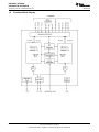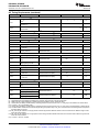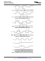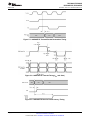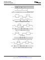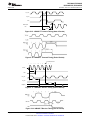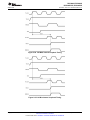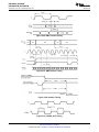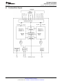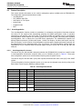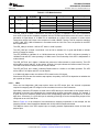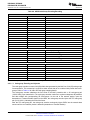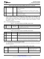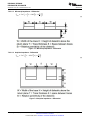
1
Product
Folder
Sample &
Buy
Tools &
Software
Technical
Documents
Support &
Community
DP83848C, DP83848I
DP83848VYB, DP83848YB
SNLS266E – MAY 2007 – REVISED MARCH 2015
DP83848C/I/VYB/YB PHYTER™ QFP Single Port 10/100 Mb/s Ethernet
Physical Layer Transceiver
1 Introduction
1.1
Features
1
•
•
•
•
•
•
•
•
•
•
•
•
Multiple Temperature Range from –40°C to 105°C
Low-Power 3.3-V, 0.18-µm CMOS Technology
Low-Power Consumption < 270 mW Typical
3.3-V MAC Interface
Auto-MDIX for 10/100 Mb/s
Energy Detection Mode
25-MHz Clock Output
SNI Interface (Configurable)
RMII Rev. 1.2 Interface (Configurable)
MII Serial Management Interface (MDC and MDIO)
IEEE 802.3 MII
IEEE 802.3 Auto-Negotiation and Parallel
Detection
1.2
•
•
Applications
Automotive/Transportation
Industrial Controls and Factory Automation
1.3
• IEEE 802.3 ENDEC, 10BASE-T Transceivers and
Filters
• IEEE 802.3 PCS, 100BASE-TX Transceivers and
Filters
• IEEE 1149.1 JTAG
• Integrated ANSI X3.263 Compliant TP-PMD
Physical Sub-Layer with Adaptive Equalization and
Baseline Wander Compensation
• Error-Free Operation up to 150 Meters
• Programmable LED Support for Link, 10/100 Mb/s
Mode, Activity, Duplex and Collision Detect
• Single Register Access for Complete PHY Status
• 10/100 Mb/s Packet BIST (Built in Self Test)
•
General Embedded Applications
Description
The number of applications requiring Ethernet connectivity continues to increase, driving Ethernet enabled
devices into harsher environments.
The DP83848C/I/VYB/YB was designed to meet the challenge of these new applications with an extended
temperature performance that goes beyond the typical Industrial temperature range. The
DP83848C/I/VYB/YB is a highly reliable, feature rich, robust device which meets IEEE 802.3 standards
over multiple temperature ranges from commercial to extreme temperatures. This device is ideally suited
for harsh environments such as wireless remote base stations, automotive/transportation, and industrial
control applications.
It offers enhanced ESD protection and the choice of an MII or RMII interface for maximum flexibility in
MPU selection; all in a 48 pin package.
The DP83848VYB extends the leadership position of the PHYTER™ family of devices with a wide
operating temperature range. The TI line of PHYTER transceivers builds on decades of Ethernet expertise
to offer the high performance and flexibility that allows the end user an easy implementation tailored to
meet these application needs.
Device Information (1)
PART NUMBER
DP83848VYB/YB
DP83848I/C
(1)
PACKAGE
HLQFP (48)
LQFP (48)
BODY SIZE (NOM)
7.00 mm × 7.00 mm
For more information, see Section 9, Mechanical, Packaging, and Orderable Information.
1
An IMPORTANT NOTICE at the end of this data sheet addresses availability, warranty, changes, use in safety-critical applications,
intellectual property matters and other important disclaimers. PRODUCTION DATA.
DP83848C, DP83848I
DP83848VYB, DP83848YB
SNLS266E – MAY 2007 – REVISED MARCH 2015
1.4
Functional Block Diagram
2
Introduction
www.ti.com
Copyright © 2007–2015, Texas Instruments Incorporated
Submit Documentation Feedback
Product Folder Links: DP83848C DP83848I DP83848VYB DP83848YB
DP83848C, DP83848I
DP83848VYB, DP83848YB
www.ti.com
SNLS266E – MAY 2007 – REVISED MARCH 2015
Table of Contents
1
2
3
4
5
Introduction ............................................... 1
5.3
Recommended Operating Conditions ............... 11
1.1
Features .............................................. 1
5.4
Thermal Information ................................. 11
1.2
Applications ........................................... 1
5.5
DC Specifications ................................... 12
1.3
Description ............................................ 1
5.6
AC Timing Requirements
1.4
Functional Block Diagram ............................ 2
6
Revision History ......................................... 3
Device Comparison ..................................... 4
Pin Configuration and Functions ..................... 4
4.1
Pin Layout ............................................ 5
4.2
Package Pin Assignments............................ 6
4.3
Serial Management Interface ......................... 6
4.4
Mac Data Interface ................................... 6
4.5
Clock Interface
4.6
LED Interface ......................................... 8
4.7
JTAG Interface for DP83848I/VYB/YB ............... 8
4.8
Reset and Power Down .............................. 8
4.9
Strap Options ......................................... 8
.......................................
7
............... 9
................................ 10
4.12 Power Supply Pins .................................. 10
Specifications ........................................... 11
5.1
Absolute Maximum Ratings ........................ 11
5.2
ESD Ratings ........................................ 11
4.10
10 Mb/s and 100 Mb/s PMD Interface
4.11
Special Connections
7
8
9
...........................
13
Detailed Description ................................... 26
............................................
6.1
Overview
6.2
Functional Block Diagram ........................... 27
.................................
...........................
6.5
Programming ........................................
6.6
Memory ..............................................
Application, Implementation, and Layout .........
7.1
Application Information ..............................
7.2
Typical Application ..................................
7.3
Layout ...............................................
7.4
Power Supply Recommendations ...................
Device and Documentation Support ...............
8.1
Documentation Support .............................
8.2
Related Links ........................................
8.3
Trademarks..........................................
8.4
Electrostatic Discharge Caution .....................
8.5
Glossary .............................................
26
6.3
Feature Description
28
6.4
Device Functional Modes
33
39
48
68
68
68
76
78
79
79
79
79
79
79
Mechanical, Packaging, and Orderable
Information .............................................. 79
2 Revision History
NOTE: Page numbers for previous revisions may differ from page numbers in the current version.
Changes from Revision D (April 2013) to Revision E
•
Page
Added ESD Ratings table, Feature Description section, Device Functional Modes, Application and
Implementation section, Power Supply Recommendations section, Layout section, Device and Documentation
Support section, and Mechanical, Packaging, and Orderable Information section .......................................... 1
Changes from Revision C (April 2013) to Revision D
•
Page
Changed layout of National Data Sheet to TI format ........................................................................... 67
Copyright © 2007–2015, Texas Instruments Incorporated
Submit Documentation Feedback
Product Folder Links: DP83848C DP83848I DP83848VYB DP83848YB
Revision History
3
DP83848C, DP83848I
DP83848VYB, DP83848YB
SNLS266E – MAY 2007 – REVISED MARCH 2015
www.ti.com
3 Device Comparison
Table 3-1. Device Features Comparison
DEVICE
TEMPERATURE RANGE
TEMPERATURE GRADE
DP83848C
0°C
70°C
Commercial
DP83848I
-40°C
85°C
Industrial
DP83848VYB
-40°C
105°C
Extended
DP83848YB
-40°C
125°C
Extreme
4 Pin Configuration and Functions
The DP83848VYB pins are classified into the following interface categories (each interface is described in
the sections that follow):
• Serial Management Interface
• MAC Data Interface
• Clock Interface
• LED Interface
• JTAG Interface
• Reset and Power Down
• Strap Options
• 10/100 Mb/s PMD Interface
• Special Connect Pins
• Power and Ground pins
NOTE
Strapping pin option. See Section 4.9 for strap definitions.
All DP83848VYB signal pins are I/O cells regardless of the particular use. The definitions below define the
functionality of the I/O cells for each pin.
Type: I
Input
Type: O
Output
Type: I/O
Input/Output
Type: OD
Open Drain
Type: PD,PU Internal Pulldown/Pullup
Type: S
4
Strapping Pin (All strap pins have weak internal pullups or pulldowns. If the default strap
value is to be changed then an external 2.2 kΩ resistor should be used. See Section 4.9 for
details.)
Pin Configuration and Functions
Copyright © 2007–2015, Texas Instruments Incorporated
Submit Documentation Feedback
Product Folder Links: DP83848C DP83848I DP83848VYB DP83848YB
DP83848C, DP83848I
DP83848VYB, DP83848YB
www.ti.com
4.1
SNLS266E – MAY 2007 – REVISED MARCH 2015
Pin Layout
PTB Package
48-Pin HLQFP
Top View
Pin Configuration and Functions
Submit Documentation Feedback
Product Folder Links: DP83848C DP83848I DP83848VYB DP83848YB
Copyright © 2007–2015, Texas Instruments Incorporated
5
DP83848C, DP83848I
DP83848VYB, DP83848YB
SNLS266E – MAY 2007 – REVISED MARCH 2015
4.2
www.ti.com
Package Pin Assignments
VBH48A PIN #
PIN NAME
VBH48A PIN #
PIN NAME
1
TX_CLK
26
LED_ACT/COL/AN_EN
2
TX_EN
27
LED_SPEED/AN1
3
TXD_0
28
LED_LINK/AN0
4
TXD_1
29
RESET_N
5
TXD_2
30
MDIO
6
TXD_3/SNI_MODE
31
MDC
7
PWR_DOWN/INT
32
IOVDD33
8
TCK
33
X2
9
TDO
34
X1
10
TMS
35
IOGND
11
TRST#
36
DGND
12
TDI
37
PFBIN2
13
RD -
38
RX_CLK
14
RD +
39
RX_DV/MII_MODE
15
AGND
40
CRS/CRS_DV/LED_CFG
16
TD -
41
RX_ER/MDIX_EN
17
TD +
42
COL/PHYAD0
18
PFBIN1
43
RXD_0/PHYAD1
19
AGND
44
RXD_1/PHYAD2
20
RESERVED
45
RXD_2/PHYAD3
21
RESERVED
46
RXD_3/PHYAD4
22
AVDD33
47
IOGND
23
PFBOUT
48
IOVDD33
24
RBIAS
49
GNDPAD
25
CLK_OUT
4.3
Serial Management Interface
SIGNAL
NAME
TYPE
PIN #
MDC
I
31
MANAGEMENT DATA CLOCK: Synchronous clock to the MDIO management data input/output
serial interface which may be asynchronous to transmit and receive clocks. The maximum clock
rate is 25 MHz with no minimum clock rate.
MDIO
I/O
30
MANAGEMENT DATA I/O: Bi-directional management instruction/data signal that may be
sourced by the station management entity or the PHY. This pin requires a 1.5 kΩ pullup resistor.
4.4
DESCRIPTION
Mac Data Interface
SIGNAL
NAME
TYPE
PIN #
TX_CLK
O
1
MII TRANSMIT CLOCK: 25 MHz Transmit clock output in 100 Mb/s mode or 2.5 MHz in 10 Mb/s
mode derived from the 25 MHz reference clock.
Unused in RMII mode. The device uses the X1 reference clock input as the 50 MHz reference for
both transmit and receive.
SNI TRANSMIT CLOCK: 10 MHz Transmit clock output in 10 Mb SNI mode. The MAC should
source TX_EN and TXD_0 using this clock.
TX_EN
I, PD
2
MII TRANSMIT ENABLE: Active high input indicates the presence of valid data inputs on
TXD[3:0].
RMII TRANSMIT ENABLE: Active high input indicates the presence of valid data on TXD[1:0].
SNI TRANSMIT ENABLE: Active high input indicates the presence of valid data on TXD_0.
6
Pin Configuration and Functions
DESCRIPTION
Copyright © 2007–2015, Texas Instruments Incorporated
Submit Documentation Feedback
Product Folder Links: DP83848C DP83848I DP83848VYB DP83848YB
DP83848C, DP83848I
DP83848VYB, DP83848YB
www.ti.com
SIGNAL
NAME
SNLS266E – MAY 2007 – REVISED MARCH 2015
TYPE
PIN #
DESCRIPTION
I
S, I, PD
3
4
5
6
MII TRANSMIT DATA: Transmit data MII input pins, TXD[3:0], that accept data synchronous to
the TX_CLK (2.5 MHz in 10 Mb/s mode or 25 MHz in 100 Mb/s mode).
RMII TRANSMIT DATA: Transmit data RMII input pins, TXD[1:0], that accept data synchronous to
the 50 MHz reference clock.
SNI TRANSMIT DATA: Transmit data SNI input pin, TXD_0, that accept data synchronous to the
TX_CLK (10 MHz in 10 Mb/s SNI mode).
RX_CLK
O
38
MII RECEIVE CLOCK: Provides the 25 MHz recovered receive clocks for 100 Mb/s mode and 2.5
MHz for 10 Mb/s mode.
Unused in RMII mode. The device uses the X1 reference clock input as the 50 MHz reference for
both transmit and receive.
SNI RECEIVE CLOCK: Provides the 10 MHz recovered receive clocks for 10 Mb/s SNI mode.
RX_DV
S, O, PD
39
MII RECEIVE DATA VALID: Asserted high to indicate that valid data is present on the
corresponding RXD[3:0]. Mll mode by default with internal pulldown.
RMII Synchronous RECEIVE DATA VALID:This signal provide the RMII Receive Data Valid
indication independent of Carrier Sense.
This pin is not used in SNI mode.
RX_ER
S, O, PU
41
MII RECEIVE ERROR: Asserted high synchronously to RX_CLK to indicate that an invalid symbol
has been detected within a received packet in 100 Mb/s mode.
RMII RECEIVE ERROR: Asserted high synchronously to X1 whenever an invalid symbol is
detected, and CRS_DV is asserted in 100 Mb/s mode.
This pin is not required to be used by a MAC in either MII or RMII mode, since the Phy is required
to corrupt data on a receive error.
This pin is not used in SNI mode.
RXD_0
RXD_1
RXD_2
RXD_3
S, O, PD
43
44
45
46
MII RECEIVE DATA: Nibble wide receive data signals driven synchronously to the RX_CLK, 25
MHz for 100 Mb/s mode, 2.5 MHz for 10 Mb/s mode). RXD[3:0] signals contain valid data when
RX_DV is asserted.
RMII RECEIVE DATA: 2-bits receive data signals, RXD[1:0], driven synchronously to the X1 clock,
50 MHz.
SNI RECEIVE DATA: Receive data signal, RXD_0, driven synchronously to the RX_CLK. RXD_0
contains valid data when CRS is asserted. RXD[3:1] are not used in this mode.
CRS/CRS_D
V
S, O, PU
40
MII CARRIER SENSE: Asserted high to indicate the receive medium is non-idle.
RMII CARRIER SENSE/RECEIVE DATA VALID: This signal combines the RMII Carrier and
Receive Data Valid indications. For a detailed description of this signal, see the RMII Specification.
SNI CARRIER SENSE: Asserted high to indicate the receive medium is non-idle. It is used to
frame valid receive data on the RXD_0 signal.
COL
S, O, PU
42
MII COLLISION DETECT: Asserted high to indicate detection of a collision condition
(simultaneous transmit and receive activity) in 10 Mb/s and 100 Mb/s Half Duplex Modes.
While in 10BASE-T Half Duplex mode with heartbeat enabled this pin is also asserted for a
duration of approximately 1µs at the end of transmission to indicate heartbeat (SQE test).
In Full Duplex Mode, for 10 Mb/s or 100 Mb/s operation, this signal is always logic 0. There is no
heartbeat function during 10 Mb/s full duplex operation.
RMII COLLISION DETECT: Per the RMII Specification, no COL signal is required. The MAC will
recover CRS from the CRS_DV signal and use that along with its TX_EN signal to determine
collision.
SNI COLLISION DETECT: Asserted high to indicate detection of a collision condition
(simultaneous transmit and receive activity) in 10 Mb/s SNI mode.
TXD_0
TXD_1
TXD_2
TXD_3
4.5
Clock Interface
SIGNAL
NAME
TYPE
PIN #
DESCRIPTION
X1
I
34
CRYSTAL/OSCILLATOR INPUT: This pin is the primary clock reference input for the
DP83848C/I/VYB/YB and must be connected to a 25 MHz 0.005% (±50 ppm) clock source.
The DP83848C/I/VYB/YB supports either an external crystal resonator connected across pins
X1 and X2, or an external CMOS-level oscillator source connected to pin X1 only.
RMII REFERENCE CLOCK: This pin is the primary clock reference input for the RMII mode
and must be connected to a 50 MHz 0.005% (±50 ppm) CMOS-level oscillator source.
X2
O
33
CRYSTAL OUTPUT: This pin is the primary clock reference output to connect to an external
25 MHz crystal resonator device. This pin must be left unconnected if an external CMOS
oscillator clock source is used.
CLK_OUT
O
25
25 MHz CLOCK OUTPUT:
In MII mode, this pin provides a 25 MHz clock output to the system.
In RMII mode, this pin provides a 50 MHz clock output to the system.
This allows other devices to use the reference clock from the DP83848VYB without requiring
additional clock sources.
Pin Configuration and Functions
Submit Documentation Feedback
Product Folder Links: DP83848C DP83848I DP83848VYB DP83848YB
Copyright © 2007–2015, Texas Instruments Incorporated
7
DP83848C, DP83848I
DP83848VYB, DP83848YB
SNLS266E – MAY 2007 – REVISED MARCH 2015
4.6
www.ti.com
LED Interface
See Table 6-2 for LED Mode Selection.
SIGNAL NAME
TYPE
PIN #
DESCRIPTION
LED_LINK
S, O, PU
28
LINK LED: In Mode 1, this pin indicates the status of the LINK. The LED will be
ON
when
Link
is
good.
LINK/ACT LED: In Mode 2 and Mode 3, this pin indicates transmit and receive
activity in addition to the status of the Link. The LED will be ON when Link is
good. It will blink when the transmitter or receiver is active.
LED_SPEED
S, O, PU
27
SPEED LED: The LED is ON when device is in 100 Mb/s and OFF when in 10
Mb/s. Functionality of this LED is independent of mode selected.
LED_ACT/COL
S, O, PU
26
ACTIVITY LED: In Mode 1, this pin is the Activity LED which is ON when activity
is
present
on
either
Transmit
or
Receive.
COLLISION/DUPLEX LED: In Mode 2, this pin by default indicates Collision
detection. For Mode 3, this LED output may be programmed to indicate Fullduplex status instead of Collision.
4.7
JTAG Interface for DP83848I/VYB/YB
SIGNAL NAME
TCK
TYPE
PIN # (1)
I, PU
8
DESCRIPTION
TEST CLOCK
This pin has a weak internal pullup.
TDI
I, PU
12
TEST DATA INPUT
TDO
O
9
TEST OUTPUT
TMS
I, PU
10
TEST MODE SELECT
TRST#
I, PU
11
This pin has a weak internal pullup.
This pin has a weak internal pullup.
TEST RESET: Active low asynchronous test reset.
This pin has a weak internal pullup.
(1)
4.8
DP83848C does not support JTAG. Pins 8-12 should be left unconnected.
Reset and Power Down
SIGNAL NAME
TYPE
PIN #
DESCRIPTION
RESET_N
I, PU
29
RESET: Active Low input that initializes or re-initializes the DP83848VYB. Asserting
this pin low for at least 1 µs will force a reset process to occur. All internal registers
will re-initialize to their default states as specified for each bit in the Section 6.6
section. All strap options are re-initialized as well.
PWR_DOWN/INT
I, PU
7
See Section 7.2.1.3.1 for detailed description.
The default function of this pin is POWER DOWN.
POWER DOWN: The pin is an active low input in this mode and should be
asserted low to put the device in a Power Down mode.
INTERRUPT: The pin is an open drain output in this mode and will be asserted low
when an interrupt condition occurs. Although the pin has a weak internal pullup,
some applications may require an external pullup resister. Register access is
required for the pin to be used as an interrupt mechanism. See Section 7.2.1.3.1.2
for more details on the interrupt mechanisms.
4.9
Strap Options
The DP83848VYB uses many of the functional pins as strap options. The values of these pins are
sampled during reset and used to strap the device into specific modes of operation. The strap option pin
assignments are defined below. The functional pin name is indicated in parentheses.
A 2.2 kΩ resistor should be used for pulldown or pullup to change the default strap option. If the default
option is required, then there is no need for external pullup or pulldown resistors. Since these pins may
have alternate functions after reset is deasserted, they should not be connected directly to VCC or GND.
8
Pin Configuration and Functions
Copyright © 2007–2015, Texas Instruments Incorporated
Submit Documentation Feedback
Product Folder Links: DP83848C DP83848I DP83848VYB DP83848YB
DP83848C, DP83848I
DP83848VYB, DP83848YB
www.ti.com
SIGNAL NAME
SNLS266E – MAY 2007 – REVISED MARCH 2015
TYPE
PIN #
PHYAD0 (COL)
PHYAD1 (RXD1_0)
PHYAD2 (RXD0_1)
PHYAD3 (RXD1_2)
PHYAD4 (RXD1_3)
S, O, PU
S, O, PD
42
43
44
45
46
PHY ADDRESS [4:0]: The DP83848VYB provides five PHY address pins, the state of
which are latched into the PHYCTRL register at system Hardware-Reset.
The DP83848VYB supports PHY Address strapping values 0 (<00000>) through 31
(<11111>).A PHY Adress of 0 puts the part into the Mll isolate Mode. The Mll isolate
mode must be selected by strapping Phy Address 0; changing to Address 0 by register
write will not put the Phy in the Mll isolate mode. Please refer to Section 6.4.5 for
additional information.
PHYAD0 pin has weak internal pullup resistor.
PHYAD[4:1] pins have weak internal pulldown resistors.
AN_EN(LED_ACT/COL)
AN_1 (LED_SPEED)
AN_0 (LED_LINK)
S, O, PU
26
27
28
Auto-Negotiation Enable: When high, this enables Auto-Negotiation with the capability
set by AN0 and AN1 pins. When low, this puts the part into Forced Mode with the
capability set by AN0 and AN1 pins.
AN0 / AN1: These input pins control the forced or advertised operating mode of the
DP83848VYB according to the following table. The value on these pins is set by
connecting the input pins to GND (0) or VCC (1) through 2.2 kΩ resistors. These pins
should NEVER be connected directly to GND or VCC.
The value set at this input is latched into the DP83848VYB at Hardware-Reset.
The float/pulldown status of these pins are latched into the Basic Mode Control Register
and the Auto_Negotiation Advertisement Register during Hardware-Reset.
The default is 111 since the these pin have internal pullups.
MII_MODE (RX_DV)
SNI_MODE (TXD_3)
S, O, PD
39
6
DESCRIPTION
AN_EN
AN1
AN0
0
0
0
10BASE-T, Half-Duplex
Forced Mode
0
0
1
10BASE-T, Full-Duplex
0
1
0
100BASE-TX, Half-Duplex
100BASE-TX, Full-Duplex
0
1
1
AN_EN
AN1
AN0
1
0
0
10BASE-T, Half/Full-Duplex
1
0
1
100BASE-TX, Half/Full-Duplex
1
1
0
10BASE-T, Half-Duplex,
100BASE-TX, Half-Duplex
1
1
1
10BASE-T, Half/Full-Duplex,
100BASE-TX, Half/Full-Duplex
Advertised Mode
MII MODE SELECT: This strapping option pair determines the operating mode of the
MAC Data Interface. Default operation (No pullups) will enable normal MII Mode of
operation. Strapping MII_MODE high will cause the device to be in RMII or SNI modes of
operation, determined by the status of the SNI_MODE strap. Since the pins include
internal pulldowns, the default values are 0.
The following table details the configurations:
MII_MODE
SNI_MODE
0
X
MAC Interface Mode
MII Mode
1
0
RMII Mode
1
1
10 Mb SNI Mode
LED_CFG (CRS)
S, O, PU
40
LED CONFIGURATION: This strapping option determines the mode of operation of the
LED pins. Default is Mode 1. Mode 1 and Mode 2 can be controlled through the strap
option. All modes are configurable through register access.
See Table 6-2 for LED Mode Selection.
MDIX_EN (RX_ER)
S, O, PU
41
MDIX ENABLE: Default is to enable MDIX. This strapping option disables Auto-MDIX. An
external pulldown will disable Auto-MDIX mode.
4.10 10 Mb/s and 100 Mb/s PMD Interface
SIGNAL NAME
TD-, TD+
TYPE
PIN #
I/O
16
17
DESCRIPTION
Differential common driver transmit output (PMD Output Pair). These differential outputs
are automatically configured to either 10BASE-T or 100BASE-TX signaling.
IIn Auto-MDIX mode of operation, this pair can be used as the Receive Input pair.
These pins require 3.3-V bias for operation.
Pin Configuration and Functions
Submit Documentation Feedback
Product Folder Links: DP83848C DP83848I DP83848VYB DP83848YB
Copyright © 2007–2015, Texas Instruments Incorporated
9
DP83848C, DP83848I
DP83848VYB, DP83848YB
SNLS266E – MAY 2007 – REVISED MARCH 2015
SIGNAL NAME
RD-, RD+
www.ti.com
TYPE
PIN #
I/O
13
14
DESCRIPTION
Differential receive input (PMD Input Pair). These differential inputs are automatically
configured to accept either 100BASE-TX or 10BASE-T signaling.
In Auto-MDIX mode of operation, this pair can be used as the Transmit Output pair.
These pins require 3.3-V bias for operation.
4.11 Special Connections
TYPE
PIN #
RBIAS
SIGNAL NAME
I
24
Bias Resistor Connection: A 4.87 kΩ 1% resistor should be connected from RBIAS to
GND.
PFBOUT
O
23
Power Feedback Output: Parallel caps, 10 µF (Tantalum preferred) and 0.1 µF, should be
placed close to the PFBOUT. Connect this pin to PFBIN1 (pin 18) and PFBIN2 (pin 37). See
Section 7.2.1.3 for proper placement pin.
PFBIN1
PFBIN2
I
18
37
Power Feedback Input: These pins are fed with power from PFBOUT pin. A small capacitor
of 0.1 µF should be connected close to each pin. (1)
I/O
20, 21
RESERVED
(1)
DESCRIPTION
RESERVED: These pins must be pulled-up through 2.2 kΩ resistors to AVDD33 supply.
Note: Do not supply power to these pins other than from PFBOUT.
4.12 Power Supply Pins
SIGNAL NAME
PIN #
DESCRIPTION
IOVDD33
32, 38
I/O 3.3-V Supply
IOGND
35, 47
I/O Ground
DGND
36
Digital Ground
AVDD33
22
Analog 3.3-V Supply
AGND
15, 19
GNDPAD
10
49
Pin Configuration and Functions
Analog Ground
Ground PAD
Copyright © 2007–2015, Texas Instruments Incorporated
Submit Documentation Feedback
Product Folder Links: DP83848C DP83848I DP83848VYB DP83848YB
DP83848C, DP83848I
DP83848VYB, DP83848YB
www.ti.com
SNLS266E – MAY 2007 – REVISED MARCH 2015
5 Specifications
5.1
Absolute Maximum Ratings
(1) (2)
MIN
MAX
UNIT
Supply Voltage (VCC)
–0.5
4.2
V
DC Input Voltage (VIN)
–0.5
VCC + 0.5
V
DC Output Voltage (VOUT)
–0.5
VCC + 0.5
V
121.5
°C
260
°C
150
°C
Maximum Die Temperature
Lead Temperature (TL) (Soldering, 10 sec.)
Storage Temperature, Tstg
(1)
(2)
–65
Stresses beyond those listed under Absolute Maximum Ratings may cause permanent damage to the device. These are stress ratings
only, which do not imply functional operation of the device at these or any other conditions beyond those indicated under Recommended
Operating Conditions. Exposure to absolute-maximum-rated conditions for extended periods may affect device reliability.
If Military/Aerospace specified devices are required, please contact the TI Sales Office/ Distributors for availability and specifications.
5.2
ESD Ratings
VALUE
V(ESD)
(1)
(2)
Electrostatic discharge
Human body model (HBM), per ANSI/ESDA/JEDEC JS-001, all pins (1)
±4000
Charged device model (CDM), per JEDEC specification JESD22-C101, all
pins (2)
±1000
UNIT
V
JEDEC document JEP155 states that 500-V HBM allows safe manufacturing with a standard ESD control process.
JEDEC document JEP157 states that 250-V CDM allows safe manufacturing with a standard ESD control process.
5.3
Recommended Operating Conditions
MIN
Supply voltage (VCC)
MAX
Commercial
0
–40
85
Extended
–40
105
Extreme
–40
125
Power Dissipation (PD)
°C
267
mW
Thermal Information
THERMAL METRIC
(1)
DP83848C/I
DP83848VYB/YB
PT [HLQFP]
PTB [LQFP]
48 PINS
48 PINS
RθJA
Junction-to-ambient thermal resistance
73.9
40.1
RθJC(top)
Junction-to-case (top) thermal resistance
30.9
25.5
RθJB
Junction-to-board thermal resistance
37.2
21
ψJT
Junction-to-top characterization parameter
2.8
2.7
ψJB
Junction-to-board characterization parameter
37
20.9
RθJC(bot)
Junction-to-case (bottom) thermal resistance
N/A
3.6
(1)
V
70
Industrial
5.4
UNIT
3.3 V ± 0.3
UNIT
°C/W
For more information about traditional and new thermal metrics, see the IC Package Thermal Metrics application report, SPRA953.
Copyright © 2007–2015, Texas Instruments Incorporated
Submit Documentation Feedback
Product Folder Links: DP83848C DP83848I DP83848VYB DP83848YB
Specifications
11
DP83848C, DP83848I
DP83848VYB, DP83848YB
SNLS266E – MAY 2007 – REVISED MARCH 2015
5.5
www.ti.com
DC Specifications
PARAMETER
TEST CONDITIONS
VIH
Input High Voltage
Nominal VCC
VIL
Input Low Voltage
IIH
Input High Current
VIN = VCC
IIL
Input Low Current
VIN = GND
IOL = 4 mA
Output High
IOH = –4 mA
Voltage
IOZ
I,
I/O
O,
I/O
O,
TRI-STATE
VOUT = VCC
I/O,
Leakage
VOUT = GND
O
100M Transmit Voltage
PMD
Output Pair
VTPTDsym
100M Transmit Voltage
Symmetry
PMD
Output Pair
VTPTD_10
10M Transmit Voltage
PMD
Output Pair
COUT1
SDTHon
SDTHoff
VTH1
Idd100
Idd10
Idd
12
CMOS Input
Capacitance
CMOS Output
Capacitance
100BASE-TX
100BASE-TX
100BASE-TX
(Full Duplex)
100BASE-TX
(Full Duplex)
Power Down Mode
Specifications
1
CLK2MAC disabled
µA
10
µA
0.4
V
±10
µA
1.05
V
±2%
2.2
2.5
2.8
V
5
pF
O
5
pF
1000
mV diff
pk-pk
mV diff
pk-pk
200
PMD Input
Pair
10BASE-T Receive Threshold
10
I
PMD Input
Pair
Signal detect turnoff threshold
V
V
PMD Input
Pair
Signal detect turnon threshold
0.8
VCC - 0.5
0.95
UNIT
V
I/O
I/O
MAX
2.0
I,
VTPTD_100
CIN1
TYP
I,
Voltage
VOH
I,
I/O
MIN
I/O
Output Low
VOL
PIN
TYPES
585
mV
Supply
81
mA
Supply
92
mA
Supply
14
mA
Copyright © 2007–2015, Texas Instruments Incorporated
Submit Documentation Feedback
Product Folder Links: DP83848C DP83848I DP83848VYB DP83848YB
DP83848C, DP83848I
DP83848VYB, DP83848YB
www.ti.com
5.6
SNLS266E – MAY 2007 – REVISED MARCH 2015
AC Timing Requirements
PARAMETER
DESCRIPTION
NOTES
MIN
TYP
MAX
UNIT
POWER-UP TIMING
T2.1.1
Post Power-Up Stabilization
time prior to MDC preamble for
register accesses (1)
T2.1.2
Hardware Configuration Latchin Time from power up (1)
T2.1.3
Hardware Configuration pins
transition to output drivers
MDIO is pulled high for 32-bit serial
management initialization
X1 Clock must be stable for a min.
of 167 ms at power up.
Hardware Configuration Pins are
described in the Section 4 section.
X1 Clock must be stable for a min.
of 167 ms at power up.
167
ms
167
ms
50
ns
RESET TIMING
T2.2.1
Post RESET Stabilization time
prior to MDC preamble for
register accesses (2)
MDIO is pulled high for 32-bit serial
management initialization
3
µs
T2.2.2
Hardware Configuration Latchin Time from the Deassertion of
RESET (either soft or hard) (2)
Hardware Configuration Pins are
described in the Section 4 section
3
µs
T2.2.3
Hardware Configuration pins
transition to output drivers
50
ns
T2.2.4
RESET pulse width
X1 Clock must be stable for at min.
of 1us during RESET pulse low
time.
1
µs
MII SERIAL MANAGEMENT TIMING
T2.3.1
MDC to MDIO (Output) Delay
Time
T2.3.2
MDIO (Input) to MDC Setup
Time
10
ns
T2.3.3
MDIO (Input) to MDC Hold
Time
10
ns
T2.3.4
MDC Frequency
0
30
ns
2.5
25
MHz
20
24
ns
100 Mb/s MII TRANSMIT TIMING
T2.4.1
TX_CLK High/Low Time
100 Mb/s Normal mode
16
T2.4.2
TXD[3:0], TX_EN Data Setup to
100 Mb/s Normal mode
TX_CLK
10
ns
T2.4.3
TXD[3:0], TX_EN Data Hold
from TX_CLK
100 Mb/s Normal mode
0
ns
100 Mb/s MII RECEIVE TIMING
T2.5.1
RX_CLK High/Low Time (3)
100 Mb/s Normal mode
16
T2.5.2
RX_CLK to RXD[3:0], RX_DV,
RX_ER Delay
100 Mb/s Normal mode
10
20
24
ns
30
ns
100BASE-TX MII TRANSMIT PACKET LATENCY TIMING
T2.6.1
TX_CLK to PMD Output Pair
Latency (4)
100BASE-TX mode
6
bits
5
bits
100BASE-TX TRANSMIT PACKET DEASSERTION TIMING
T2.7.1
(1)
(2)
(3)
(4)
(5)
TX_CLK to PMD Output Pair
Deassertion (5)
100BASE-TX mode
In RMII Mode, the minimum Post Power-up Stabilization and Hardware Configuration Latch-in times are 84ms.
It is important to choose pullup and/or pulldown resistors for each of the hardware configuration pins that provide fast RC time constants
in order to latch-in the proper value prior to the pin transitioning to an output driver.
RX_CLK may be held low or high for a longer period of time during transition between reference and recovered clocks. Minimum high
and low times will not be violated.
For Normal mode, latency is determined by measuring the time from the first rising edge of TX_CLK occurring after the assertion of
TX_EN to the first bit of the “J” code group as output from the PMD Output Pair. 1 bit time = 10 ns in 100 Mb/s mode.
Deassertion is determined by measuring the time from the first rising edge of TX_CLK occurring after the deassertion of TX_EN to the
first bit of the “T” code group as output from the PMD Output Pair. 1 bit time = 10 ns in 100 Mb/s mode.
Copyright © 2007–2015, Texas Instruments Incorporated
Submit Documentation Feedback
Product Folder Links: DP83848C DP83848I DP83848VYB DP83848YB
Specifications
13
DP83848C, DP83848I
DP83848VYB, DP83848YB
SNLS266E – MAY 2007 – REVISED MARCH 2015
www.ti.com
AC Timing Requirements (continued)
PARAMETER
DESCRIPTION
NOTES
MIN
TYP
MAX
UNIT
3
4
5
ns
100 Mb/s tR and tF
Mismatch (7) (6)
500
ps
100 Mb/s PMD Output Pair
Transmit Jitter
1.4
ns
100BASE-TX TRANSMIT TIMING (tR/F and Jitter)
100 Mb/s PMD Output Pair tR
and tF (6)
T2.8.1
T2.8.2
100BASE-TX RECEIVE PACKET LATENCY TIMING (8)
T2.9.1
Carrier Sense ON Delay (9)
100 Mb/s Normal mode (10)
20
bits
T2.9.2
Receive Data Latency
100 Mb/s Normal mode (10)
24
bits
24
bits
100BASE-TX RECEIVE PACKET DEASSERTION TIMING
T2.10.1
Carrier Sense OFF Delay (11)
10 Mb/s MII TRANSMIT TIMING
100 Mb/s Normal mode (10)
(12)
T2.11.1
TX_CLK High/Low Time
10 Mb/s MII mode
190
T2.11.2
TXD[3:0], TX_EN Data Setup to
10 Mb/s MII mode
TX_CLK fall
25
ns
T2.11.3
TXD[3:0], TX_EN Data Hold
from TX_CLK rise
0
ns
10 Mb/s MII mode
200
210
ns
10 Mb/s MII RECEIVE TIMING
T2.12.1
RX_CLK High/Low Time (13)
T2.12.2
RX_CLK TO RXD[3:0}, RX_DV
Delay
10 Mb/s MII mode
100
ns
T2.12.3
RX_CLK rising edge delay from
RXD[3:0], RX_DV Valid
10 Mb/s MII mode
100
ns
160
200
240
ns
10 Mb/s SERIAL MODE (SNI) TRANSMIT TIMING
T2.13.1
TX_CLK High Time
10 Mb/s Serial mode (SNI)
20
25
30
ns
T2.13.2
TX_CLK Low Time
10 Mb/s Serial mode (SNI)
70
75
80
ns
T2.13.3
TXD_0, TX_EN Data Setup to
TX_CLK rise
10 Mb/s Serial mode (SNI)
25
ns
T2.13.4
TXD_0, TX_EN Data Hold from
TX_CLK rise
10 Mb/s Serial mode (SNI)
0
ns
10 Mb/s SERIAL MODE (SNI) RECEIVE TIMING
T2.14.1
RX_CLK High/Low Time (14)
T2.14.2
RX_CLK fall to RXD_0, RX_DV
Delay
35
10 Mb/s Serial mode (SNI)
50
–10
65
ns
10
ns
10BASE-T TRANSMIT TIMING (START OF PACKET)
T2.15.1
T2.15.2
Transmit Output Delay from the
Falling Edge of TX_CLK
Transmit Output Delay from the
Rising Edge of TX_CLK
10 Mb/s MII mode (15)
3.5
bits
10 Mb/s Serial mode (SNI) (15)
3.5
bits
(6)
(7)
(8)
(9)
(10)
(11)
(12)
Rise and fall times taken at 10% and 90% of the +1 or -1 amplitude
Normal Mismatch is the difference between the maximum and minimum of all rise and fall times
PMD Input Pair voltage amplitude is greater than the Signal Detect Turnon Threshold Value.
Carrier Sense On Delay is determined by measuring the time from the first bit of the “J” code group to the assertion of Carrier Sense.
1 bit time = 10 ns in 100 Mb/s mode.
Carrier Sense Off Delay is determined by measuring the time from the first bit of the “T” code group to the deassertion of Carrier Sense.
An attached Mac should drive the transmit signals using the positive edge of TX_CLK. As shown above, the MII signals are sampled on
the falling edge of TX_CLK.
(13) RX_CLK may be held low for a longer period of time during transition between reference and recovered clocks. Minimum high and low
times will not be violated.
(14) RX_CLK may be held high for a longer period of time during transition between reference and recovered clocks. Minimum high and low
times will not be violated.
(15) 1 bit time = 100 ns in 10 Mb/s.
14
Specifications
Copyright © 2007–2015, Texas Instruments Incorporated
Submit Documentation Feedback
Product Folder Links: DP83848C DP83848I DP83848VYB DP83848YB
DP83848C, DP83848I
DP83848VYB, DP83848YB
www.ti.com
SNLS266E – MAY 2007 – REVISED MARCH 2015
AC Timing Requirements (continued)
PARAMETER
DESCRIPTION
NOTES
MIN
TYP
MAX
UNIT
250
300
ns
250
300
ns
10BASE-T TRANSMIT TIMING (END OF PACKET)
T2.16.1
T2.16.2
End of Packet High Time
(with '0' ending bit)
End of Packet High Time
(with '1' ending bit)
10BASE-T RECEIVE TIMING (START OF PACKET) (16)
T2.17.1
Carrier Sense Turnon Delay
(PMD Input Pair to CRS)
T2.17.2
RX_DV Latency (17)
T2.17.3
Receive Data Latency
630
Measurement shown from SFD
1000
ns
10
bits
8
bits
10BASE-T RECEIVE TIMING (END OF PACKET)
T2.18.1
Carrier Sense Turn Off Delay
1
µs
10 Mb/s HEARTBEAT TIMING
T2.19.1
CD Heartbeat Delay
10 Mb/s half-duplex mode
1200
ns
T2.19.2
CD Heartbeat Duration
10 Mb/s half-duplex mode
1000
ns
85
ms
500
ms
10 Mb/s JABBER TIMING
T2.20.1
Jabber Activation Time
T2.20.2
Jabber Deactivation Time
10BASE-T NORMAL LINK PULSE TIMING
(18)
T2.21.1
Pulse Width
100
ns
T2.21.2
Pulse Period
16
ms
100
ns
125
µs
62
µs
2
ms
16
ms
AUTO-NEGOTIATION FAST LINK PULSE (FLP) TIMING (18)
T2.22.1
T2.22.2
T2.22.3
Clock, Data Pulse Width
Clock Pulse to Clock Pulse
Period
Clock Pulse to Data Pulse
Period
T2.22.4
Burst Width
T2.22.5
FLP Burst to FLP Burst Period
Data = 1
100BASE-TX SIGNAL DETECT TIMING (19)
T2.23.1
SD Internal Turnon Time
1
ms
T2.23.2
SD Internal Turnoff Time
350
µs
240
ns
2
µs
100 Mb/s INTERNAL LOOPBACK TIMING
T2.24.1
TX_EN to RX_DV Loopback (20)
100 Mb/s internal loopback mode (21)
10 Mb/s INTERNAL LOOPBACK TIMING
T2.25.1
TX_EN to RX_DV Loopback (20)
10 Mb/s internal loopback mode
RMII TRANSMIT TIMING
T2.26.1
X1 Clock Period
T2.26.2
TXD[1:0], TX_EN, Data Setup
to X1 rising
4
ns
T2.26.3
TXD[1:0], TX_EN, Data Hold
from X1 rising
2
ns
(16)
(17)
(18)
(19)
(20)
(21)
50 MHz Reference Clock
20
ns
1 bit time = 100 ns in 10 Mb/s mode.
10BASE-T RX_DV Latency is measured from first bit of preamble on the wire to the assertion of RX_DV
These specifications represent transmit timings.
The signal amplitude on PMD Input Pair must be TP-PMD compliant.
Measurement is made from the first rising edge of TX_CLK after assertion of TX_EN.
Due to the nature of the descrambler function, all 100BASE-TX Loopback modes will cause an initial “dead-time” of up to 550 µs during
which time no data will be present at the receive MII outputs. The 100BASE-TX timing specified is based on device delays after the
initial 550µs “dead-time”.
Copyright © 2007–2015, Texas Instruments Incorporated
Submit Documentation Feedback
Product Folder Links: DP83848C DP83848I DP83848VYB DP83848YB
Specifications
15
DP83848C, DP83848I
DP83848VYB, DP83848YB
SNLS266E – MAY 2007 – REVISED MARCH 2015
www.ti.com
AC Timing Requirements (continued)
PARAMETER
T2.26.4
DESCRIPTION
X1 Clock to PMD Output Pair
Latency
NOTES
MIN
TYP
MAX
UNIT
From X1 Rising edge to first bit of
symbol
17
bits
50 MHz Reference Clock
20
ns
RMII RECEIVE TIMING
T2.27.1
X1 Clock Period
T2.27.2
RXD[1:0], CRS_DV, RX_DV
and RX_ER output delay from
X1 rising (22) (23) (24)
T2.27.3
CRS ON delay (100Mb)
From JK symbol on PMD Receive
Pair to initial assertion of CRS_DV
18.5
bits
T2.27.4
CRS OFF delay (100Mb)
From TR symbol on PMD Receive
Pair to initial deassertion of
CRS_DV
27
bits
T2.27.5
RXD[1:0] and RX_ER latency
(100Mb)
From symbol on Receive Pair.
Elasticity buffer set to default value
(01)
38
bits
2
14
ns
ISOLATION TIMING
T2.28.1
From software clear of bit 10 in
the BMCR register to the
transition from Isolate to Normal
mode
100
µs
T2.28.2
From Deassertion of S/W or
H/W Reset to transition from
Isolate to Normal mode
500
µs
25 MHz_OUT TIMING
T2.29.1
25 MHz_OUT High/Low
Time (25)
T2.29.2
25 MHz_OUT propagation
delay (25)
MII mode
20
ns
RMII mode
10
ns
Relative to X1
8
ns
5
ns
100 Mb/s X1 TO TX_CLK TIMING
T2.30.1
X1 to TX_CLK delay (26)
100 Mb/s Normal mode
0
(22) Per the RMII Specification, output delays assume a 25pF load.
(23) CRS_DV is asserted asynchronously in order to minimize latency of control signals through the Phy. CRS_DV may toggle
synchronously at the end of the packet to indicate CRS deassertion.
(24) RX_DV is synchronous to X1. While not part of the RMII specification, this signal is provided to simplify recovery of receive data.
(25) 25 MHz_OUT characteristics are dependent upon the X1 input characteristics.
(26) X1 to TX_CLK timing is provided to support devices that use X1 instead of TX_CLK as the reference for transmit Mll data.
16
Specifications
Copyright © 2007–2015, Texas Instruments Incorporated
Submit Documentation Feedback
Product Folder Links: DP83848C DP83848I DP83848VYB DP83848YB
DP83848C, DP83848I
DP83848VYB, DP83848YB
www.ti.com
SNLS266E – MAY 2007 – REVISED MARCH 2015
Figure 5-1. Power-Up Timing
Figure 5-2. Reset Timing
Copyright © 2007–2015, Texas Instruments Incorporated
Submit Documentation Feedback
Product Folder Links: DP83848C DP83848I DP83848VYB DP83848YB
Specifications
17
DP83848C, DP83848I
DP83848VYB, DP83848YB
SNLS266E – MAY 2007 – REVISED MARCH 2015
www.ti.com
Figure 5-3. MII Serial Management Timing
Figure 5-4. 100 Mb/s MII Transmit Timing
Figure 5-5. 100 Mb/s MII Receive Timing
Figure 5-6. 100BASE-TX MII Transmit Packet Latency Timing
18
Specifications
Copyright © 2007–2015, Texas Instruments Incorporated
Submit Documentation Feedback
Product Folder Links: DP83848C DP83848I DP83848VYB DP83848YB
DP83848C, DP83848I
DP83848VYB, DP83848YB
www.ti.com
SNLS266E – MAY 2007 – REVISED MARCH 2015
Figure 5-7. 100BASE-TX Transmit Packet Deassertion Timing
Figure 5-8. 100BASE-TX Transmit Timing (tR/F and Jitter)
Figure 5-9. 100BASE-TX Receive Packet Latency Timing
Copyright © 2007–2015, Texas Instruments Incorporated
Submit Documentation Feedback
Product Folder Links: DP83848C DP83848I DP83848VYB DP83848YB
Specifications
19
DP83848C, DP83848I
DP83848VYB, DP83848YB
SNLS266E – MAY 2007 – REVISED MARCH 2015
www.ti.com
Figure 5-10. 100BASE-TX Receive Packet Deassertion Timing
Figure 5-11. 10 Mb/s MII Transmit Timing
Figure 5-12. 10 Mb/s MII Receive Timing
Figure 5-13. 10 Mb/s Serial Mode (SNI) Transmit Timing
Figure 5-14. 10 Mb/s Serial Mode (SNI) Receive Timing
20
Specifications
Copyright © 2007–2015, Texas Instruments Incorporated
Submit Documentation Feedback
Product Folder Links: DP83848C DP83848I DP83848VYB DP83848YB
DP83848C, DP83848I
DP83848VYB, DP83848YB
www.ti.com
SNLS266E – MAY 2007 – REVISED MARCH 2015
TX_CLK
TX_EN
TXD
T2.15.2
PMD Output
Pair
T2.15.1
Figure 5-15. 10BASE-T Transmit Timing (Start of Packet)
Figure 5-16. 10BASE-T Transmit Timing (End of Packet)
1st SFD Bit Decoded
1
0
1
0
1
0
1
0
1
0
1
1
TPRDr
T2.17.1
CRS
RX_CLK
T2.17.2
RX_DV
T2.17.3
RXD[3:0]
0000
Preamble
SFD
Data
Figure 5-17. 10BASE-T Receive Timing (Start of Packet)
Figure 5-18. 10BASE-T Receive Timing (End of Packet)
Copyright © 2007–2015, Texas Instruments Incorporated
Submit Documentation Feedback
Product Folder Links: DP83848C DP83848I DP83848VYB DP83848YB
Specifications
21
DP83848C, DP83848I
DP83848VYB, DP83848YB
SNLS266E – MAY 2007 – REVISED MARCH 2015
www.ti.com
Figure 5-19. 10 Mb/s Heartbeat Timing
Figure 5-20. 10 Mb/s Jabber Timing
Figure 5-21. 10BASE-T Normal Link Pulse Timing
Figure 5-22. Auto-Negotiation Fast Link Pulse (FLP) Timing
Figure 5-23. 100BASE-TX Signal Detect Timing
22
Specifications
Copyright © 2007–2015, Texas Instruments Incorporated
Submit Documentation Feedback
Product Folder Links: DP83848C DP83848I DP83848VYB DP83848YB
DP83848C, DP83848I
DP83848VYB, DP83848YB
www.ti.com
SNLS266E – MAY 2007 – REVISED MARCH 2015
Figure 5-24. 100 Mb/s Internal Loopback Timing
Figure 5-25. 10 Mb/s Internal Loopback Timing
Copyright © 2007–2015, Texas Instruments Incorporated
Submit Documentation Feedback
Product Folder Links: DP83848C DP83848I DP83848VYB DP83848YB
Specifications
23
DP83848C, DP83848I
DP83848VYB, DP83848YB
SNLS266E – MAY 2007 – REVISED MARCH 2015
www.ti.com
Figure 5-26. RMII Transmit Timing
Figure 5-27. RMII Receive Timing
Figure 5-28. Isolation Timing
Figure 5-29. 25 MHz_OUT Timing
24
Specifications
Copyright © 2007–2015, Texas Instruments Incorporated
Submit Documentation Feedback
Product Folder Links: DP83848C DP83848I DP83848VYB DP83848YB
DP83848C, DP83848I
DP83848VYB, DP83848YB
www.ti.com
SNLS266E – MAY 2007 – REVISED MARCH 2015
Figure 5-30. 100 Mb/s X1 to TX_CLK Timing
Copyright © 2007–2015, Texas Instruments Incorporated
Submit Documentation Feedback
Product Folder Links: DP83848C DP83848I DP83848VYB DP83848YB
Specifications
25
DP83848C, DP83848I
DP83848VYB, DP83848YB
SNLS266E – MAY 2007 – REVISED MARCH 2015
www.ti.com
6 Detailed Description
6.1
Overview
The device is 10/100 Mbps Ethernet transceiver with an extended temperature range of -40°C to 105°C.
The ability to perform over extreme temperatures makes this device ideal for demanding environments like
Automotive, Transportation and Industrial Applications.
The device is AEC-Q100 Grade 2 certified. Its 3.3-V operating voltage and less than 270-mW typical
power consumption makes this device suitable for low power applications.
The device has Auto MDIX capability to select MDI or MDIX automatically. It supports Auto-Negotiation for
selecting the highest performance mode of operation. This functionality can be turned off if a particular
mode is to be forced.
The device supports both MII and RMII interface thus being more flexible and increasing the number of
compatible MPU. MII and RMII options can be selected using strap options or register control. The device
operates with 25-MHz clock when in MII mode and requires a 50-MHz clock when in RMII mode.
26
Detailed Description
Copyright © 2007–2015, Texas Instruments Incorporated
Submit Documentation Feedback
Product Folder Links: DP83848C DP83848I DP83848VYB DP83848YB
DP83848C, DP83848I
DP83848VYB, DP83848YB
www.ti.com
6.2
SNLS266E – MAY 2007 – REVISED MARCH 2015
Functional Block Diagram
Copyright © 2007–2015, Texas Instruments Incorporated
Submit Documentation Feedback
Product Folder Links: DP83848C DP83848I DP83848VYB DP83848YB
Detailed Description
27
DP83848C, DP83848I
DP83848VYB, DP83848YB
SNLS266E – MAY 2007 – REVISED MARCH 2015
6.3
www.ti.com
Feature Description
This section includes information on the various configuration options available with the DP83848VYB.
The configuration options described below include:
• Auto-Negotiation
• PHY Address and LEDs
• Half Duplex vs. Full Duplex
• Isolate mode
• Loopback mode
• BIST
6.3.1
Auto-Negotiation
The Auto-Negotiation function provides a mechanism for exchanging configuration information between
two ends of a link segment and automatically selecting the highest performance mode of operation
supported by both devices. Fast Link Pulse (FLP) Bursts provide the signalling used to communicate
Auto-Negotiation abilities between two devices at each end of a link segment. For further detail regarding
Auto-Negotiation, refer to Clause 28 of the IEEE 802.3 specification. The DP83848VYB supports four
different Ethernet protocols (10 Mb/s Half Duplex, 10 Mb/s Full Duplex, 100 Mb/s Half Duplex, and 100
Mb/s Full Duplex), so the inclusion of Auto-Negotiation ensures that the highest performance protocol will
be selected based on the advertised ability of the Link Partner. The Auto-Negotiation function within the
DP83848VYB can be controlled either by internal register access or by the use of the AN_EN, AN1 and
AN0 pins.
6.3.1.1
Auto-Negotiation Pin Control
The state of AN_EN, AN0 and AN1 determines whether the DP83848VYB is forced into a specific mode
or Auto-Negotiation will advertise a specific ability (or set of abilities) as given in Table 6-1. These pins
allow configuration options to be selected without requiring internal register access.
The state of AN_EN, AN0 and AN1, upon power up/reset, determines the state of bits [8:5] of the ANAR
register.
The Auto-Negotiation function selected at power up or reset can be changed at any time by writing to the
Basic Mode Control Register (BMCR) at address 0x00h.
Table 6-1. Auto-Negotiation Modes
28
AN_EN
AN1
AN0
0
0
0
10BASE-T, Half-Duplex
Forced Mode
0
0
1
10BASE-T, Full-Duplex
0
1
0
100BASE-TX, Half-Duplex
100BASE-TX, Full-Duplex
0
1
1
AN_EN
AN1
AN0
1
0
0
10BASE-T, Half/Full-Duplex
1
0
1
100BASE-TX, Half/Full-Duplex
1
1
0
1
1
1
Detailed Description
Advertised Mode
10BASE-T Half-Duplex
100BASE-TX, Half-Duplex
10BASE-T, Half/Full-Duplex
100BASE-TX, Half/Full-Duplex
Copyright © 2007–2015, Texas Instruments Incorporated
Submit Documentation Feedback
Product Folder Links: DP83848C DP83848I DP83848VYB DP83848YB
DP83848C, DP83848I
DP83848VYB, DP83848YB
www.ti.com
6.3.1.2
SNLS266E – MAY 2007 – REVISED MARCH 2015
Auto-Negotiation Register Control
When Auto-Negotiation is enabled, the DP83848VYB transmits the abilities programmed into the AutoNegotiation Advertisement register (ANAR) at address 04h through FLP Bursts. Any combination of 10
Mb/s, 100 Mb/s, Half-Duplex, and Full Duplex modes may be selected.
Auto-Negotiation Priority Resolution:
1. 100BASE-TX Full Duplex (Highest Priority)
2. 100BASE-TX Half Duplex
3. 10BASE-T Full Duplex
4. 10BASE-T Half Duplex (Lowest Priority)
The Basic Mode Control Register (BMCR) at address 00h provides control for enabling, disabling, and
restarting the Auto-Negotiation process. When Auto-Negotiation is disabled, the Speed Selection bit in the
BMCR controls switching between 10 Mb/s or 100 Mb/s operation, and the Duplex Mode bit controls
switching between full duplex operation and half duplex operation. The Speed Selection and Duplex Mode
bits have no effect on the mode of operation when the Auto-Negotiation Enable bit is set.
The Link Speed can be examined through the PHY Status Register (PHYSTS) at address 10h after a Link
is achieved.
The Basic Mode Status Register (BMSR) indicates the set of available abilities for technology types, AutoNegotiation ability, and Extended Register Capability. These bits are permanently set to indicate the full
functionality of the DP83848VYB (only the 100BASE-T4 bit is not set since the DP83848VYB does not
support that function).
The BMSR also provides status on:
• Whether or not Auto-Negotiation is complete
• Whether or not the Link Partner is advertising that a remote fault has occurred
• Whether or not valid link has been established
• Support for Management Frame Preamble suppression
The Auto-Negotiation Advertisement Register (ANAR) indicates the Auto-Negotiation abilities to be
advertised by the DP83848VYB. All available abilities are transmitted by default, but any ability can be
suppressed by writing to the ANAR. Updating the ANAR to suppress an ability is one way for a
management agent to change (restrict) the technology that is used.
The Auto-Negotiation Link Partner Ability Register (ANLPAR) at address 0x05h is used to receive the
base link code word as well as all next page code words during the negotiation. Furthermore, the ANLPAR
will be updated to either 0081h or 0021h for parallel detection to either 100 Mb/s or 10 Mb/s respectively.
The Auto-Negotiation Expansion Register (ANER) indicates additional Auto-Negotiation status. The ANER
provides status on:
• Whether or not a Parallel Detect Fault has occurred
• Whether or not the Link Partner supports the Next Page function
• Whether or not the DP83848VYB supports the Next Page function
• Whether or not the current page being exchanged by Auto-Negotiation has been received
• Whether or not the Link Partner supports Auto-Negotiation
6.3.1.3
Auto-Negotiation Parallel Detection
The DP83848VYB supports the Parallel Detection function as defined in the IEEE 802.3 specification.
Parallel Detection requires both the 10 Mb/s and 100 Mb/s receivers to monitor the receive signal and
report link status to the Auto-Negotiation function. Auto-Negotiation uses this information to configure the
correct technology in the event that the Link Partner does not support Auto-Negotiation but is transmitting
link signals that the 100BASE-TX or 10BASE-T PMAs recognize as valid link signals.
Copyright © 2007–2015, Texas Instruments Incorporated
Submit Documentation Feedback
Product Folder Links: DP83848C DP83848I DP83848VYB DP83848YB
Detailed Description
29
DP83848C, DP83848I
DP83848VYB, DP83848YB
SNLS266E – MAY 2007 – REVISED MARCH 2015
www.ti.com
If the DP83848VYB completes Auto-Negotiation as a result of Parallel Detection, bits 5 and 7 within the
ANLPAR register will be set to reflect the mode of operation present in the Link Partner. Note that bits 4:0
of the ANLPAR will also be set to 00001 based on a successful parallel detection to indicate a valid 802.3
selector field. Software may determine that negotiation completed through Parallel Detection by reading a
zero in the Link Partner Auto-Negotiation Able bit once the Auto-Negotiation Complete bit is set. If
configured for parallel detect mode and any condition other than a single good link occurs then the parallel
detect fault bit will be set.
6.3.1.4
Auto-Negotiation Restart
Once Auto-Negotiation has completed, it may be restarted at any time by setting bit 9 (Restart AutoNegotiation) of the BMCR to one. If the mode configured by a successful Auto-Negotiation loses a valid
link, then the Auto-Negotiation process will resume and attempt to determine the configuration for the link.
This function ensures that a valid configuration is maintained if the cable becomes disconnected.
A renegotiation request from any entity, such as a management agent, will cause the DP83848VYB to halt
any transmit data and link pulse activity until the break_link_timer expires (~1500 ms). Consequently, the
Link Partner will go into link fail and normal Auto-Negotiation resumes. The DP83848VYB will resume
Auto-Negotiation after the break_link_timer has expired by issuing FLP (Fast Link Pulse) bursts.
6.3.1.5
Enabling Auto-Negotiation Through Software
It is important to note that if the DP83848VYB has been initialized upon power up as a non-autonegotiating device (forced technology), and it is then required that Auto-Negotiation or re-Auto-Negotiation
be initiated through software, bit 12 (Auto-Negotiation Enable) of the Basic Mode Control Register (BMCR)
must first be cleared and then set for any Auto-Negotiation function to take effect.
6.3.1.6
Auto-Negotiation Complete Time
Parallel detection and Auto-Negotiation take approximately 2-3 seconds to complete. In addition, AutoNegotiation with next page should take approximately 2-3 seconds to complete, depending on the number
of next pages sent.
Refer to Clause 28 of the IEEE 802.3 standard for a full description of the individual timers related to AutoNegotiation.
6.3.2
Auto-MDIX
When enabled, this function uses Auto-Negotiation to determine the proper configuration for transmission
and reception of data and subsequently selects the appropriate MDI pair for MDI/MDIX operation. The
function uses a random seed to control switching of the crossover circuitry. This implementation complies
with the corresponding IEEE 802.3 Auto-Negotiation and Crossover Specifications.
Auto-MDIX is enabled by default and can be configured through strap or through PHYCR (19h) register,
bits [15:14].
Neither Auto-Negotiation nor Auto-MDIX is required to be enabled in forcing crossover of the MDI pairs.
Forced crossover can be achieved through the FORCE_MDIX bit, bit 14 of PHYCR (19h) register.
NOTE
Auto-MDIX will not work in a forced mode of operation.
6.3.3
LED Interface
The DP83848VYB supports three configurable Light Emitting Diode (LED) pins. The device supports three
LED configurations: Link, Speed, Activity and Collision. Function are multiplexed among the LEDs. The
PHY Control Register (PHYCR) for the LEDs can also be selected through address 19h, bits [6:5].
See Table 6-2 for LED Mode selection.
30
Detailed Description
Copyright © 2007–2015, Texas Instruments Incorporated
Submit Documentation Feedback
Product Folder Links: DP83848C DP83848I DP83848VYB DP83848YB
DP83848C, DP83848I
DP83848VYB, DP83848YB
www.ti.com
SNLS266E – MAY 2007 – REVISED MARCH 2015
Table 6-2. LED Mode Selection
Mode
LED_CFG[1] (bit
6)
LED_CFG[0] (bit 5)
or (pin 40)
1
don't care
1
2
0
0
3
1
0
LED_LINK
LED_SPEED
LED_ACT/LED_COL
ON for Good Link
ON in 100 Mb/s
ON for Activity
OFF for No Link
OFF in 10 Mb/s
OFF for No Activity
ON for Good Link
ON in 100 Mb/s
ON for Collision
BLINK for Activity
OFF in 10 Mb/s
OFF for No Collision
ON for Good Link
ON in 100 Mb/s
ON for Full Duplex
BLINK for Activity
OFF in 10 Mb/s
OFF for Half Duplex
The LED_LINK pin in Mode 1 indicates the link status of the port. In 100BASE-T mode, link is established
as a result of input receive amplitude compliant with the TP-PMD specifications which will result in internal
generation of signal detect. A 10 Mb/s Link is established as a result of the reception of at least seven
consecutive normal Link Pulses or the reception of a valid 10BASE-T packet. This will cause the assertion
of LED_LINK. LED_LINK will deassert in accordance with the Link Loss Timer as specified in the IEEE
802.3 specification.
The LED_LINK pin in Mode 1 will be OFF when no LINK is present.
The LED_LINK pin in Mode 2 and Mode 3 will be ON to indicate Link is good and BLINK to indicate
activity is present on activity.
The LED_SPEED pin indicates 10 or 100 Mb/s data rate of the port. The LED is ON when operating in
100Mb/s mode and OFF when operating in 10 Mb/s mode. The functionality of this LED is independent of
mode selected.
The LED_ACT/COL pin in Mode 1 indicates the presence of either transmit or receive activity. The LED
will be ON for Activity and OFF for No Activity. In Mode 2, this pin indicates the Collision status of the port.
The LED will be ON for Collision and OFF for No Collision.
The LED_ACT/COL pin in Mode 3 indicates Duplex status for 10 Mb/s or 100 Mb/s operation. The LED
will be ON for Full Duplex and OFF for Half Duplex.
In 10 Mb/s half duplex mode, the collision LED is based on the COL signal.
Since these LED pins are also used as strap options, the polarity of the LED is dependent on whether the
pin is pulled up or down.
6.3.3.1
LEDs
Since the Auto-Negotiation (AN) strap options share the LED output pins, the external components
required for strapping and LED usage must be considered in order to avoid contention.
Specifically, when the LED outputs are used to drive LEDs directly, the active state of each output driver is
dependent on the logic level sampled by the corresponding AN input upon power up/reset. For example, if
a given AN input is resistively pulled low then the corresponding output will be configured as an active
high driver. Conversely, if a given AN input is resistively pulled high, then the corresponding output will be
configured as an active low driver.
Refer to Figure 6-1 for an example of AN connections to external components. In this example, the AN
strapping results in Auto-Negotiation disabled with 10/100 Half/Full-Duplex advertised .
The adaptive nature of the LED outputs helps to simplify potential implementation issues of these dual
purpose pins.
Copyright © 2007–2015, Texas Instruments Incorporated
Submit Documentation Feedback
Product Folder Links: DP83848C DP83848I DP83848VYB DP83848YB
Detailed Description
31
DP83848C, DP83848I
DP83848VYB, DP83848YB
SNLS266E – MAY 2007 – REVISED MARCH 2015
www.ti.com
Figure 6-1. AN Strapping and LED Loading Example
6.3.3.2
LED Direct Control
The DP83848VYB provides another option to directly control any or all LED outputs through the LED
Direct Control Register (LEDCR), address 18h. The register does not provide read access to LEDs.
6.3.4
Internal Loopback
The DP83848VYB includes a Loopback Test mode for facilitating system diagnostics. The Loopback
mode is selected through bit 14 (Loopback) of the Basic Mode Control Register (BMCR). Writing 1 to this
bit enables MII transmit data to be routed to the MII receive outputs. Loopback status may be checked in
bit 3 of the PHY Status Register (PHYSTS). While in Loopback mode the data will not be transmitted onto
the media. To ensure that the desired operating mode is maintained, Auto-Negotiation should be disabled
before selecting the Loopback mode.
6.3.5
BIST
The DP83848VYB incorporates an internal Built-in Self Test (BIST) circuit to accommodate in-circuit
testing or diagnostics. The BIST circuit can be used to test the integrity of the transmit and receive data
paths. BIST testing can be performed with the part in the internal loopback mode or externally looped back
using a loopback cable fixture.
The BIST is implemented with independent transmit and receive paths, with the transmit block generating
a continuous stream of a pseudo random sequence. The user can select a 9 bit or 15 bit pseudo random
sequence from the PSR_15 bit in the PHY Control Register (PHYCR). The received data is compared to
the generated pseudo-random data by the BIST Linear Feedback Shift Register (LFSR) to determine the
BIST pass/fail status.
The pass/fail status of the BIST is stored in the BIST status bit in the PHYCR register. The status bit
defaults to 0 (BIST fail) and will transition on a successful comparison. If an error (mis-compare) occurs,
the status bit is latched and is cleared upon a subsequent write to the Start/Stop bit.
For transmit VOD testing, the Packet BIST Continuous Mode can be used to allow continuous data
transmission, setting BIST_CONT_MODE, bit 5, of CDCTRL1 (0x1Bh).
The number of BIST errors can be monitored through the BIST Error Count in the CDCTRL1 (0x1Bh), bits
[15:8].
32
Detailed Description
Copyright © 2007–2015, Texas Instruments Incorporated
Submit Documentation Feedback
Product Folder Links: DP83848C DP83848I DP83848VYB DP83848YB
DP83848C, DP83848I
DP83848VYB, DP83848YB
www.ti.com
6.3.6
SNLS266E – MAY 2007 – REVISED MARCH 2015
Energy Detect Mode
When Energy Detect is enabled and there is no activity on the cable, the DP83848C/I/VYB/YB will remain
in a low power mode while monitoring the transmission line. Activity on the line will cause the device to go
through a normal power-up sequence. Regardless of cable activity, the device will occasionally wake up
the transmitter to put ED pulses on the line, but will otherwise draw as little power as possible. Energy
detect functionality is controlled through register Energy Detect Control (EDCR), address 0x1Dh.
6.4
Device Functional Modes
The DP83848C/I/VYB/YB supports several modes of operation using the MII interface pins. The options
are defined in the following sections and include:
• MII Mode
• RMII Mode
The modes of operation can be selected by strap options or register control. For RMII mode, it is required
to use the strap option, since it requires a 50-MHz clock instead of the normal 25 MHz.
In each of these modes, the IEEE 802.3 serial management interface is operational for device
configuration and status. The serial management interface of the MII allows for the configuration and
control of multiple PHY devices, gathering of status, error information, and the determination of the type
and capabilities of the attached PHY(s).
6.4.1
MII Interface
The DP83848VYB incorporates the Media Independent Interface (MII) as specified in Clause 22 of the
IEEE 802.3 standard. This interface may be used to connect PHY devices to a MAC in 10/100 Mb/s
systems. This section describes the nibble wide MII data interface.
The nibble wide MII data interface consists of a receive bus and a transmit bus each with control signals
to facilitate data transfer between the PHY and the upper layer (MAC).
6.4.1.1
Nibble-wide MII Data Interface
Clause 22 of the IEEE 802.3 specification defines the Media Independent Interface. This interface includes
a dedicated receive bus and a dedicated transmit bus. These two data buses, along with various control
and status signals, allow for the simultaneous exchange of data between the DP83848VYB and the upper
layer agent (MAC).
The receive interface consists of a nibble wide data bus RXD[3:0], a receive error signal RX_ER, a receive
data valid flag RX_DV, and a receive clock RX_CLK for synchronous transfer of the data. The receive
clock operates at either 2.5 MHz to support 10 Mb/s operation modes or at 25 MHz to support 100 Mb/s
operational modes.
The transmit interface consists of a nibble wide data bus TXD[3:0], a transmit enable control signal
TX_EN, and a transmit clock TX_CLK which runs at either 2.5 MHz or 25 MHz.
Additionally, the MII includes the carrier sense signal CRS, as well as a collision detect signal COL. The
CRS signal asserts to indicate the reception of data from the network or as a function of transmit data in
Half Duplex mode. The COL signal asserts as an indication of a collision which can occur during halfduplex operation when both a transmit and receive operation occur simultaneously.
6.4.1.2
Collision Detect
For Half Duplex, a 10BASE-T or 100BASE-TX collision is detected when the receive and transmit
channels are active simultaneously. Collisions are reported by the COL signal on the MII.
If the DP83848VYB is transmitting in 10 Mb/s mode when a collision is detected, the collision is not
reported until seven bits have been received while in the collision state. This prevents a collision being
reported incorrectly due to noise on the network. The COL signal remains set for the duration of the
collision.
Copyright © 2007–2015, Texas Instruments Incorporated
Submit Documentation Feedback
Product Folder Links: DP83848C DP83848I DP83848VYB DP83848YB
Detailed Description
33
DP83848C, DP83848I
DP83848VYB, DP83848YB
SNLS266E – MAY 2007 – REVISED MARCH 2015
www.ti.com
If a collision occurs during a receive operation, it is immediately reported by the COL signal.
When heartbeat is enabled (only applicable to 10 Mb/s operation), approximately 1 µs after the
transmission of each packet, a Signal Quality Error (SQE) signal of approximately 10 bit times is
generated (internally) to indicate successful transmission. SQE is reported as a pulse on the COL signal of
the MII.
6.4.1.3
Carrier Sense
Carrier Sense (CRS) is asserted due to receive activity, once valid data is detected through the squelch
function during 10 Mb/s operation. During 100 Mb/s operation CRS is asserted when a valid link (SD) and
two non-contiguous zeros are detected on the line.
For 10 or 100 Mb/s Half Duplex operation, CRS is asserted during either packet transmission or reception.
For 10 or 100 Mb/s Full Duplex operation, CRS is asserted only due to receive activity.
CRS is deasserted following an end of packet.
6.4.2
Reduced MII Interface
The DP83848VYB incorporates the Reduced Media Independent Interface (RMII) as specified in the RMII
specification (rev1.2) from the RMII Consortium. This interface may be used to connect PHY devices to a
MAC in 10/100 Mb/s systems using a reduced number of pins. In this mode, data is transferred 2-bits at a
time using the 50-MHz RMII_REF clock for both transmit and receive. The following pins are used in RMII
mode:
• TX_EN
• TXD[1:0]
• RX_ER (optional for MAC)
• CRS_DV
• RXD[1:0]
• X1 (RMII Reference clock is 50 MHz)
In addition, the RMII mode supplies an RX_DV signal which allows for a simpler method of recovering
receive data without having to separate RX_DV from the CRS_DV indication. This is especially useful for
diagnostic testing where it may be desirable to externally loop Receive MII data directly to the transmitter.
Since the reference clock operates at 10 times the data rate for 10 Mb/s operation, transmit data is
sampled every 10 clocks. Likewise, receive data will be generated every 10th clock so that an attached
device can sample the data every 10 clocks.
RMII mode requires a 50-MHz oscillator be connected to the device X1 pin. A 50 MHz crystal is not
supported.
To tolerate potential frequency differences between the 50-MHz reference clock and the recovered receive
clock, the receive RMII function includes a programmable elasticity buffer. The elasticity buffer is
programmable to minimize propagation delay based on expected packet size and clock accuracy. This
allows for supporting a range of packet sizes including jumbo frames.
The elasticity buffer will force Frame Check Sequence errors for packets which overrun or underrun the
FIFO. Underrun and Overrun conditions can be reported in the RMII and Bypass Register (RBR). The
following table indicates how to program the elasticity buffer fifo (in 4-bit increments) based on expected
max packet size and clock accuracy. It assumes both clocks (RMII Reference clock and far-end
Transmitter clock) have the same accuracy.
34
Detailed Description
Copyright © 2007–2015, Texas Instruments Incorporated
Submit Documentation Feedback
Product Folder Links: DP83848C DP83848I DP83848VYB DP83848YB
DP83848C, DP83848I
DP83848VYB, DP83848YB
www.ti.com
SNLS266E – MAY 2007 – REVISED MARCH 2015
Table 6-3. Supported Packet Sizes at ±50ppm ±100ppm For Each Clock
Start Threshold RBR[1:0]
Latency Tolerance
Recommended Packet Size
at ±50ppm
Recommended Packet Size
at ±100ppm
1 (4-bits)
2 bits
2,400 bytes
1,200 bytes
2 (8-bits)
6 bits
7,200 bytes
3,600 bytes
3 (12-bits)
10 bits
12,000 bytes
6,000 bytes
0 (16-bits)
14 bits
16,800 bytes
8,400 bytes
6.4.3
802.3 MII Serial Management Interface
6.4.3.1
Serial Management Register Access
The serial management MII specification defines a set of thirty-two 16-bit status and control registers that
are accessible through the management interface pins MDC and MDIO. The DP83848VYB implements all
the required MII registers as well as several optional registers. These registers are fully described in
Section 6.6.1. A description of the serial management access protocol follows.
6.4.3.2
Serial Management Access Protocol
The serial control interface consists of two pins, Management Data Clock (MDC) and Management Data
Input/Output (MDIO). MDC has a maximum clock rate of 25 MHz and no minimum rate. The MDIO line is
bi-directional and may be shared by up to 32 devices. The MDIO frame format is shown below in
Table 6-4.
Table 6-4. Typical MDIO Frame Format
MII Management Serial Protocol
<idle><start><op code><device addr><reg addr><turnaround><data><idle>
Read Operation
<idle><01><10><AAAAA><RRRRR><Z0><xxxx xxxx xxxx xxxx><idle>
Write Operation
<idle><01><01><AAAAA><RRRRR><10><xxxx xxxx xxxx xxxx><idle>
The MDIO pin requires a pullup resistor (1.5 kΩ) which, during IDLE and turnaround, will pull MDIO high.
In order to initialize the MDIO interface, the station management entity sends a sequence of 32 contiguous
logic ones on MDIO to provide the DP83848VYB with a sequence that can be used to establish
synchronization. This preamble may be generated either by driving MDIO high for 32 consecutive MDC
clock cycles, or by simply allowing the MDIO pullup resistor to pull the MDIO pin high during which time 32
MDC clock cycles are provided. In addition 32 MDC clock cycles should be used to re-sync the device if
an invalid start, opcode, or turnaround bit is detected.
The DP83848VYB waits until it has received this preamble sequence before responding to any other
transaction. Once the DP83848VYB serial management port has been initialized no further preamble
sequencing is required until after a power-on/reset, invalid Start, invalid Opcode, or invalid turnaround bit
has occurred.
The Start code is indicated by a <01> pattern. This assures the MDIO line transitions from the default idle
line state.
Turnaround is defined as an idle bit time inserted between the Register Address field and the Data field.
To avoid contention during a read transaction, no device shall actively drive the MDIO signal during the
first bit of Turnaround. The addressed DP83848VYB drives the MDIO with a zero for the second bit of
turnaround and follows this with the required data. Figure 6-2 shows the timing relationship between MDC
and the MDIO as driven/received by the Station (STA) and the DP83848VYB (PHY) for a typical register
read access.
For write transactions, the station management entity writes data to the addressed DP83848VYB thus
eliminating the requirement for MDIO Turnaround. The Turnaround time is filled by the management entity
by inserting <10>. Figure 6-3 shows the timing relationship for a typical MII register write access.
Copyright © 2007–2015, Texas Instruments Incorporated
Submit Documentation Feedback
Product Folder Links: DP83848C DP83848I DP83848VYB DP83848YB
Detailed Description
35
DP83848C, DP83848I
DP83848VYB, DP83848YB
SNLS266E – MAY 2007 – REVISED MARCH 2015
www.ti.com
Figure 6-2. Typical MDC/MDIO Read Operation
Figure 6-3. Typical MDC/MDIO Write Operation
6.4.3.3
Serial Management Preamble Suppression
The DP83848VYB supports a Preamble Suppression mode as indicated by a one in bit 6 of the Basic
Mode Status Register (BMSR, address 01h.) If the station management entity (for example, MAC or other
management controller) determines that all PHYs in the system support Preamble Suppression by
returning a one in this bit, then the station management entity need not generate preamble for each
management transaction.
The DP83848VYB requires a single initialization sequence of 32 bits of preamble following
hardware/software reset. This requirement is generally met by the mandatory pullup resistor on MDIO in
conjunction with a continuous MDC, or the management access made to determine whether Preamble
Suppression is supported.
While the DP83848VYB requires an initial preamble sequence of 32 bits for management initialization, it
does not require a full 32-bit sequence between each subsequent transaction. A minimum of one idle bit
between management transactions is required as specified in the IEEE 802.3 specification.
6.4.4
10 Mb Serial Network Interface (SNI)
The DP83848VYB incorporates a 10-Mb Serial Network Interface (SNI) which allows a simple serial data
interface for 10-Mb only devices. This is also referred to as a 7-wire interface. While there is no defined
standard for this interface, it is based on early 10-Mb physical layer devices. Data is clocked serially at 10
MHz using separate transmit and receive paths. The following pins are used in SNI mode:
• TX_CLK
• TX_EN
• TXD[0]
• RX_CLK
• RXD[0]
• CRS
• COL
6.4.5
PHY Address
The 5 PHY address inputs pins are shared with the RXD[3:0] pins and COL pin are shown in Table 6-5.
36
Detailed Description
Copyright © 2007–2015, Texas Instruments Incorporated
Submit Documentation Feedback
Product Folder Links: DP83848C DP83848I DP83848VYB DP83848YB
DP83848C, DP83848I
DP83848VYB, DP83848YB
www.ti.com
SNLS266E – MAY 2007 – REVISED MARCH 2015
Table 6-5. PHY Address Mapping
Pin #
PHYAD Function
42
PHYAD0
RXD Function
COL
43
PHYAD1
RXD_0
44
PHYAD2
RXD_1
45
PHYAD3
RXD_2
46
PHYAD4
RXD_3
The DP83848VYB can be set to respond to any of 32 possible PHY addresses through strap pins. The
information is latched into the PHYCR register (address 19h, bits [4:0]) at device power up and hardware
reset. The PHY Address pins are shared with the RXD and COL pins. Each DP83848VYB or port sharing
an MDIO bus in a system must have a unique physical address.
The DP83848VYB supports PHY Address strapping values 0 (<00000>) through 31 (<11111>). Strapping
PHY Address 0 puts the part into Isolate Mode. It should also be noted that selecting PHY Address 0
through an MDIO write to PHYCR will not put the device in Isolate Mode. See Section 6.4.5.1 for more
information.
For further detail relating to the latch-in timing requirements of the PHY Address pins, as well as the other
hardware configuration pins, refer to the Reset summary in Section 6.4.7.
Since the PHYAD[0] pin has weak internal pullup resistor and PHYAD[4:1] pins have weak internal
pulldown resistors, the default setting for the PHY address is 00001 (0x01h).
Refer to Figure 6-4 for an example of a PHYAD connection to external components. In this example, the
PHYAD strapping results in address 000101 (0x03h).
Figure 6-4. PHYAD Strapping Example
6.4.5.1
MII Isolate Mode
The DP83848VYB can be put into MII Isolate mode by writing to bit 10 of the BMCR register or by
strapping in Physical Address 0. It should be noted that selecting Physical Address 0 through an MDIO
write to PHYCR will not put the device in the MII isolate mode.
When in the MII isolate mode, the DP83848VYB does not respond to packet data present at TXD[3:0],
TX_EN inputs and presents a high impedance on the TX_CLK, RX_CLK, RX_DV, RX_ER, RXD[3:0],
COL, and CRS outputs. When in Isolate mode, the DP83848VYB will continue to respond to all
management transactions.
While in Isolate mode, the PMD output pair will not transmit packet data but will continue to source
100BASE-TX scrambled idles or 10BASE-T normal link pulses.
The DP83848VYB can Auto-Negotiate or parallel detect to a specific technology depending on the receive
signal at the PMD input pair. A valid link can be established for the receiver even when the DP83848VYB
is in Isolate mode.
Copyright © 2007–2015, Texas Instruments Incorporated
Submit Documentation Feedback
Product Folder Links: DP83848C DP83848I DP83848VYB DP83848YB
Detailed Description
37
DP83848C, DP83848I
DP83848VYB, DP83848YB
SNLS266E – MAY 2007 – REVISED MARCH 2015
6.4.6
www.ti.com
Half Duplex vs. Full Duplex
The DP83848VYB supports both half and full duplex operation at both 10 Mb/s and 100 Mb/s speeds.
Half-duplex relies on the CSMA/CD protocol to handle collisions and network access. In Half-Duplex
mode, CRS responds to both transmit and receive activity in order to maintain compliance with the IEEE
802.3 specification.
Since the DP83848VYB is designed to support simultaneous transmit and receive activity it is capable of
supporting full-duplex switched applications with a throughput of up to 200 Mb/s per port when operating
in 100BASE-TX. Because the CSMA/CD protocol does not apply to full-duplex operation, the
DP83848VYB disables its own internal collision sensing and reporting functions and modifies the behavior
of Carrier Sense (CRS) such that it indicates only receive activity. This allows a full-duplex capable MAC
to operate properly.
All modes of operation (100BASE-TX, and 10BASE-T) can run either half-duplex or full-duplex.
Additionally, other than CRS and Collision reporting, all remaining MII signaling remains the same
regardless of the selected duplex mode.
It is important to understand that while Auto-Negotiation with the use of Fast Link Pulse code words can
interpret and configure to full-duplex operation, parallel detection can not recognize the difference between
full and half-duplex from a fixed 10 Mb/s or 100 Mb/s link partner over twisted pair. As specified in the
802.3 specification, if a far-end link partner is configured to a forced full duplex 100BASE-TX ability, the
parallel detection state machine in the partner would be unable to detect the full duplex capability of the
far-end link partner. This link segment would negotiate to a half duplex 100BASE-TX configuration (same
scenario for 10 Mb/s).
6.4.7
Reset Operation
The DP83848VYB includes an internal power-on reset (POR) function and does not need to be explicitly
reset for normal operation after power up. If required during normal operation, the device can be reset by
a hardware or software reset.
6.4.7.1
Hardware Reset
A hardware reset is accomplished by applying a low pulse (TTL level), with a duration of at least 1 µs, to
the RESET_N pin. This will reset the device such that all registers will be reinitialized to default values and
the hardware configuration values will be re-latched into the device (similar to the power up/reset
operation).
6.4.7.2
Software Reset
A software reset is accomplished by setting the reset bit (bit 15) of the Basic Mode Control Register
(BMCR). The period from the point in time when the reset bit is set to the point in time when software
reset has concluded is approximately 1 µs.
A software reset will reset the device such that all registers will be reinitialized to default values and the
hardware configuration values will be re-latched into the device. Software driver code must wait 3 µs
following a software reset before allowing further serial MII operations with the DP83848VYB.
38
Detailed Description
Copyright © 2007–2015, Texas Instruments Incorporated
Submit Documentation Feedback
Product Folder Links: DP83848C DP83848I DP83848VYB DP83848YB
DP83848C, DP83848I
DP83848VYB, DP83848YB
www.ti.com
6.5
SNLS266E – MAY 2007 – REVISED MARCH 2015
Programming
6.5.1
Architecture
This section describes the operations within each transceiver module, 100BASE-TX and 10BASE-T. Each
operation consists of several functional blocks and described in the following:
• 100BASE-TX Transmitter
• 100BASE-TX Receiver
• 10BASE-T Transceiver Module
6.5.1.1
100BASE-TX Transmitter
The 100BASE-TX transmitter consists of several functional blocks which convert synchronous 4-bit nibble
data, as provided by the MII, to a scrambled MLT-3 125 Mb/s serial data stream. Because the 100BASETX TP-PMD is integrated, the differential output pins, PMD Output Pair, can be directly routed to the
magnetics.
The block diagram in Figure 6-5. provides an overview of each functional block within the 100BASE-TX
transmit section.
The Transmitter section consists of the following functional blocks:
• Code-group Encoder and Injection block
• Scrambler block (bypass option)
• NRZ to NRZI encoder block
• Binary to MLT-3 converter / Common Driver
The bypass option for the functional blocks within the 100BASE-TX transmitter provides flexibility for
applications where data conversion is not always required. The DP83848VYB implements the 100BASETX transmit state machine diagram as specified in the IEEE 802.3 Standard, Clause 24.
Figure 6-5. 100BASE-TX Transmit Block Diagram
Copyright © 2007–2015, Texas Instruments Incorporated
Submit Documentation Feedback
Product Folder Links: DP83848C DP83848I DP83848VYB DP83848YB
Detailed Description
39
DP83848C, DP83848I
DP83848VYB, DP83848YB
SNLS266E – MAY 2007 – REVISED MARCH 2015
www.ti.com
Table 6-6. 4B5B Code-Group Encoding/Decoding
DATA CODES
0
11110
0000
1
01001
0001
2
10100
0010
3
10101
0011
4
01010
0100
5
01011
0101
6
01110
0110
7
01111
0111
8
10010
1000
9
10011
1001
A
10110
1010
B
10111
1011
C
11010
1100
D
11011
1101
E
11100
1110
F
11101
1111
IDLE AND CONTROL CODES
H
00100
HALT code-group - Error code
I
11111
Inter-Packet IDLE - 0000 (1)
J
11000
First Start of Packet - 0101 (1)
K
10001
Second Start of Packet - 0101 (1)
T
01101
First End of Packet - 0000 (1)
R
00111
Second End of Packet - 0000 (1)
INVALID CODES
(1)
V
00000
V
00001
V
00010
V
00011
V
00101
V
00110
V
01000
V
01100
Control code-groups I, J, K, T and R in data fields will be mapped as invalid codes, together with RX_ER asserted.
6.5.1.1.1 Code-group Encoding and Injection
The code-group encoder converts 4-bit (4B) nibble data generated by the MAC into 5-bit (5B) code-groups
for transmission. This conversion is required to allow control data to be combined with packet data codegroups. Refer to Table 6-6 for 4B to 5B code-group mapping details.
The code-group encoder substitutes the first 8-bits of the MAC preamble with a J/K code-group pair
(11000 10001) upon transmission. The code-group encoder continues to replace subsequent 4B preamble
and data nibbles with corresponding 5B code-groups. At the end of the transmit packet, upon the
deassertion of Transmit Enable signal from the MAC, the code-group encoder injects the T/R code-group
pair (01101 00111) indicating the end of the frame.
After the T/R code-group pair, the code-group encoder continuously injects IDLEs into the transmit data
stream until the next transmit packet is detected (reassertion of Transmit Enable).
40
Detailed Description
Copyright © 2007–2015, Texas Instruments Incorporated
Submit Documentation Feedback
Product Folder Links: DP83848C DP83848I DP83848VYB DP83848YB
DP83848C, DP83848I
DP83848VYB, DP83848YB
www.ti.com
6.5.1.1.2
SNLS266E – MAY 2007 – REVISED MARCH 2015
Scrambler
The scrambler is required to control the radiated emissions at the media connector and on the twisted pair
cable (for 100BASE-TX applications). By scrambling the data, the total energy launched onto the cable is
randomly distributed over a wide frequency range. Without the scrambler, energy levels at the PMD and
on the cable could peak beyond FCC limitations at frequencies related to repeating 5B sequences (for
example, continuous transmission of IDLEs).
The scrambler is configured as a closed loop linear feedback shift register (LFSR) with an 11-bit
polynomial. The output of the closed loop LFSR is X-ORd with the serial NRZ data from the code-group
encoder. The result is a scrambled data stream with sufficient randomization to decrease radiated
emissions at certain frequencies by as much as 20 dB. The DP83848VYB uses the PHY_ID (pins PHYAD
[4:1]) to set a unique seed value.
6.5.1.1.3 NRZ to NRZI Encoder
After the transmit data stream has been serialized and scrambled, the data must be NRZI encoded in
order to comply with the TP-PMD standard for 100BASE-TX transmission over Category-5 Unshielded
twisted pair cable.
6.5.1.1.4 Binary to MLT-3 Convertor
The Binary to MLT-3 conversion is accomplished by converting the serial binary data stream output from
the NRZI encoder into two binary data streams with alternately phased logic one events. These two binary
streams are then fed to the twisted pair output driver which converts the voltage to current and alternately
drives either side of the transmit transformer primary winding, resulting in a MLT-3 signal.
The 100BASE-TX MLT-3 signal sourced by the PMD Output Pair common driver is slew rate controlled.
This should be considered when selecting AC coupling magnetics to ensure TP-PMD Standard compliant
transition times (3 ns < Tr < 5 ns).
The 100BASE-TX transmit TP-PMD function within the DP83848VYB is capable of sourcing only MLT-3
encoded data. Binary output from the PMD Output Pair is not possible in 100 Mb/s mode.
6.5.1.2
100BASE-TX Receiver
The 100BASE-TX receiver consists of several functional blocks which convert the scrambled MLT-3 125
Mb/s serial data stream to synchronous 4-bit nibble data that is provided to the MII. Because the
100BASE-TX TP-PMD is integrated, the differential input pins, RD±, can be directly routed from the AC
coupling magnetics.
See Figure 6-6 for a block diagram of the 100BASE-TX receive function. This provides an overview of
each functional block within the 100BASE-TX receive section.
The Receive section consists of the following functional blocks:
• Analog Front End
• Digital Signal Processor
• Signal Detect
• MLT-3 to Binary Decoder
• NRZI to NRZ Decoder
• Serial to Parallel
• Descrambler
• Code Group Alignment
• 4B/5B Decoder
• Link Integrity Monitor
• Bad SSD Detection
Copyright © 2007–2015, Texas Instruments Incorporated
Submit Documentation Feedback
Product Folder Links: DP83848C DP83848I DP83848VYB DP83848YB
Detailed Description
41
DP83848C, DP83848I
DP83848VYB, DP83848YB
SNLS266E – MAY 2007 – REVISED MARCH 2015
www.ti.com
6.5.1.2.1 Analog Front End
In addition to the Digital Equalization and Gain Control, the DP83848VYB includes Analog Equalization
and Gain Control in the Analog Front End. The Analog Equalization reduces the amount of Digital
Equalization required in the DSP.
6.5.1.2.2 Digital Signal Processor
The Digital Signal Processor includes Adaptive Equalization with Gain Control and Base Line Wander
Compensation.
Figure 6-6. 100BASE-TX Receive Block Diagram
6.5.1.2.2.1 Digital Adaptive Equalization and Gain Control
When transmitting data at high speeds over copper twisted pair cable, frequency dependent attenuation
becomes a concern. In high-speed twisted pair signalling, the frequency content of the transmitted signal
can vary greatly during normal operation based primarily on the randomness of the scrambled data
stream. This variation in signal attenuation caused by frequency variations must be compensated to
ensure the integrity of the transmission.
42
Detailed Description
Copyright © 2007–2015, Texas Instruments Incorporated
Submit Documentation Feedback
Product Folder Links: DP83848C DP83848I DP83848VYB DP83848YB
DP83848C, DP83848I
DP83848VYB, DP83848YB
www.ti.com
SNLS266E – MAY 2007 – REVISED MARCH 2015
In order to ensure quality transmission when employing MLT-3 encoding, the compensation must be able
to adapt to various cable lengths and cable types depending on the installed environment. The selection of
long cable lengths for a given implementation, requires significant compensation which will overcompensate for shorter, less attenuating lengths. Conversely, the selection of short or intermediate cable
lengths requiring less compensation will cause serious under-compensation for longer length cables. The
compensation or equalization must be adaptive to ensure proper conditioning of the received signal
independent of the cable length.
The DP83848VYB uses an extremely robust equalization scheme referred as ‘Digital Adaptive
Equalization.’
The Digital Equalizer removes ISI (inter symbol interference) from the receive data stream by continuously
adapting to provide a filter with the inverse frequency response of the channel. Equalization is combined
with an adaptive gain control stage. This enables the receive 'eye pattern' to be opened sufficiently to
allow very reliable data recovery.
The curves given in Figure 6-8 illustrate attenuation at certain frequencies for given cable lengths. This is
derived from the worst case frequency vs. attenuation figures as specified in the EIA/TIA Bulletin TSB-36.
These curves indicate the significant variations in signal attenuation that must be compensated for by the
receive adaptive equalization circuit.
Figure 6-7. EIA/TIA Attenuation vs. Frequency for 0, 50, 100, 130 and 150 Meters of CAT 5 Cable
6.5.1.2.2.2 Base Line Wander Compensation
Figure 6-8. 100BASE-TX BLW Event
Copyright © 2007–2015, Texas Instruments Incorporated
Submit Documentation Feedback
Product Folder Links: DP83848C DP83848I DP83848VYB DP83848YB
Detailed Description
43
DP83848C, DP83848I
DP83848VYB, DP83848YB
SNLS266E – MAY 2007 – REVISED MARCH 2015
www.ti.com
The DP83848VYB is completely ANSI TP-PMD compliant and includes Base Line Wander (BLW)
compensation. The BLW compensation block can successfully recover the TP-PMD defined “killer”
pattern.
BLW can generally be defined as the change in the average DC content, relatively short period over time,
of an AC coupled digital transmission over a given transmission medium. (for example,, copper wire).
BLW results from the interaction between the low frequency components of a transmitted bit stream and
the frequency response of the AC coupling component(s) within the transmission system. If the low
frequency content of the digital bit stream goes below the low frequency pole of the AC coupling
transformers then the droop characteristics of the transformers will dominate resulting in potentially
serious BLW.
The digital oscilloscope plot provided in Figure 6-9 illustrates the severity of the BLW event that can
theoretically be generated during 100BASE-TX packet transmission. This event consists of approximately
800 mV of DC offset for a period of 120 ms. Left uncompensated, events such as this can cause packet
loss.
6.5.1.2.3 Signal Detect
The signal detect function of the DP83848VYB is incorporated to meet the specifications mandated by the
ANSI FDDI TP-PMD Standard as well as the IEEE 802.3 100BASE-TX Standard for both voltage
thresholds and timing parameters.
Note that the reception of normal 10BASE-T link pulses and fast link pulses per IEEE 802.3 AutoNegotiation by the 100BASE-TX receiver do not cause the DP83848VYB to assert signal detect.
6.5.1.2.4 MLT-3 to NRZI Decoder
The DP83848VYB decodes the MLT-3 information from the Digital Adaptive Equalizer block to binary
NRZI data.
6.5.1.2.5
NRZI to NRZ
In a typical application, the NRZI to NRZ decoder is required in order to present NRZ formatted data to the
descrambler.
6.5.1.2.6 Serial to Parallel
The 100BASE-TX receiver includes a Serial to Parallel converter which supplies 5-bit wide data symbols
to the PCS Rx state machine.
6.5.1.2.7 Descrambler
A serial descrambler is used to de-scramble the received NRZ data. The descrambler has to generate an
identical data scrambling sequence (N) in order to recover the original unscrambled data (UD) from the
scrambled data (SD) as represented in the equations:
SD = (UD ⊕ N)
UD = (SD ⊕ N)
(1)
(2)
Synchronization of the descrambler to the original scrambling sequence (N) is achieved based on the
knowledge that the incoming scrambled data stream consists of scrambled IDLE data. After the
descrambler has recognized 12 consecutive IDLE code-groups, where an unscrambled IDLE code-group
in 5B NRZ is equal to five consecutive ones (11111), it will synchronize to the receive data stream and
generate unscrambled data in the form of unaligned 5B code-groups.
44
Detailed Description
Copyright © 2007–2015, Texas Instruments Incorporated
Submit Documentation Feedback
Product Folder Links: DP83848C DP83848I DP83848VYB DP83848YB
DP83848C, DP83848I
DP83848VYB, DP83848YB
www.ti.com
SNLS266E – MAY 2007 – REVISED MARCH 2015
In order to maintain synchronization, the descrambler must continuously monitor the validity of the
unscrambled data that it generates. To ensure this, a line state monitor and a hold timer are used to
constantly monitor the synchronization status. Upon synchronization of the descrambler the hold timer
starts a 722-µs countdown. Upon detection of sufficient IDLE code-groups (58 bit times) within the 722-µs
period, the hold timer will reset and begin a new countdown. This monitoring operation will continue
indefinitely given a properly operating network connection with good signal integrity. If the line state
monitor does not recognize sufficient unscrambled IDLE code-groups within the 722-µs period, the entire
descrambler will be forced out of the current state of synchronization and reset in order to re-acquire
synchronization.
6.5.1.2.8 Code-group Alignment
The code-group alignment module operates on unaligned 5-bit data from the descrambler (or, if the
descrambler is bypassed, directly from the NRZI/NRZ decoder) and converts it into 5B code-group data (5
bits). Code-group alignment occurs after the J/K code-group pair is detected. Once the J/K code-group
pair (11000 10001) is detected, subsequent data is aligned on a fixed boundary.
6.5.1.2.9 4B/5B Decoder
The code-group decoder functions as a look up table that translates incoming 5B code-groups into 4B
nibbles. The code-group decoder first detects the J/K code-group pair preceded by IDLE code-groups and
replaces the J/K with MAC preamble. Specifically, the J/K 10-bit code-group pair is replaced by the nibble
pair (0101 0101). All subsequent 5B code-groups are converted to the corresponding 4B nibbles for the
duration of the entire packet. This conversion ceases upon the detection of the T/R code-group pair
denoting the End of Stream Delimiter (ESD) or with the reception of a minimum of two IDLE code-groups.
6.5.1.2.10 100BASE-TX Link Integrity Monitor
The 100 Base TX Link monitor ensures that a valid and stable link is established before enabling both the
Transmit and Receive PCS layer.
Signal detect must be valid for 395 µs to allow the link monitor to enter the 'Link Up' state, and enable the
transmit and receive functions.
6.5.1.2.11 Bad SSD Detection
A Bad Start of Stream Delimiter (Bad SSD) is any transition from consecutive idle code-groups to non-idle
code-groups which is not prefixed by the code-group pair /J/K.
If this condition is detected, the DP83848VYB will assert RX_ER and present RXD[3:0] = 1110 to the MII
for the cycles that correspond to received 5B code-groups until at least two IDLE code groups are
detected. In addition, the False Carrier Sense Counter register (FCSCR) will be incremented by one.
Once at least two IDLE code groups are detected, RX_ER and CRS become deasserted.
6.5.1.3
10BASE-T Transceiver Module
The 10BASE-T Transceiver Module is IEEE 802.3 compliant. It includes the receiver, transmitter, collision,
heartbeat, loopback, jabber, and link integrity functions, as defined in the standard. An external filter is not
required on the 10BASE-T interface since this is integrated inside the DP83848VYB. This section focuses
on the general 10BASE-T system level operation.
6.5.1.3.1 Operational Modes
The DP83848VYB has two basic 10BASE-T operational modes:
• Half Duplex mode
• Full Duplex mode
Copyright © 2007–2015, Texas Instruments Incorporated
Submit Documentation Feedback
Product Folder Links: DP83848C DP83848I DP83848VYB DP83848YB
Detailed Description
45
DP83848C, DP83848I
DP83848VYB, DP83848YB
SNLS266E – MAY 2007 – REVISED MARCH 2015
www.ti.com
6.5.1.3.1.1 Half Duplex Mode
In Half Duplex mode the DP83848VYB functions as a standard IEEE 802.3 10BASE-T transceiver
supporting the CSMA/CD protocol.
6.5.1.3.1.2 Full Duplex Mode
In Full Duplex mode the DP83848VYB is capable of simultaneously transmitting and receiving without
asserting the collision signal. The DP83848VYB's 10 Mb/s ENDEC is designed to encode and decode
simultaneously.
6.5.1.3.2 Smart Squelch
The smart squelch is responsible for determining when valid data is present on the differential receive
inputs. The DP83848VYB implements an intelligent receive squelch to ensure that impulse noise on the
receive inputs will not be mistaken for a valid signal. Smart squelch operation is independent of the
10BASE-T operational mode.
The squelch circuitry employs a combination of amplitude and timing measurements (as specified in the
IEEE 802.3 10BSE-T standard) to determine the validity of data on the twisted pair inputs (refer to
Figure 6-9).
The signal at the start of a packet is checked by the smart squelch and any pulses not exceeding the
squelch level (either positive or negative, depending upon polarity) will be rejected. Once this first squelch
level is overcome correctly, the opposite squelch level must then be exceeded within 150 ns. Finally the
signal must again exceed the original squelch level within 150 ns to ensure that the input waveform will
not be rejected. This checking procedure results in the loss of typically three preamble bits at the
beginning of each packet.
Only after all these conditions have been satisfied will a control signal be generated to indicate to the
remainder of the circuitry that valid data is present. At this time, the smart squelch circuitry is reset.
Valid data is considered to be present until the squelch level has not been generated for a time longer
than 150 ns, indicating the End of Packet. Once good data has been detected, the squelch levels are
reduced to minimize the effect of noise causing premature End of Packet detection.
Figure 6-9. 10BASE-T Twisted Pair Smart Squelch Operation
6.5.1.3.3 Collision Detection and SQE
When in Half Duplex, a 10BASE-T collision is detected when the receive and transmit channels are active
simultaneously. Collisions are reported by the COL signal on the MII. Collisions are also reported when a
jabber condition is detected.
The COL signal remains set for the duration of the collision. If the PHY is receiving when a collision is
detected it is reported immediately (through the COL pin).
46
Detailed Description
Copyright © 2007–2015, Texas Instruments Incorporated
Submit Documentation Feedback
Product Folder Links: DP83848C DP83848I DP83848VYB DP83848YB
DP83848C, DP83848I
DP83848VYB, DP83848YB
www.ti.com
SNLS266E – MAY 2007 – REVISED MARCH 2015
When heartbeat is enabled, approximately 1 µs after the transmission of each packet, a Signal Quality
Error (SQE) signal of approximately 10-bit times is generated to indicate successful transmission. SQE is
reported as a pulse on the COL signal of the MII.
The SQE test is inhibited when the PHY is set in full duplex mode. SQE can also be inhibited by setting
the HEARTBEAT_DIS bit in the 10BTSCR register.
6.5.1.3.4 Carrier Sense
Carrier Sense (CRS) may be asserted due to receive activity once valid data is detected through the
squelch function.
For 10 Mb/s Half Duplex operation, CRS is asserted during either packet transmission or reception.
For 10 Mb/s Full Duplex operation, CRS is asserted only during receive activity.
CRS is deasserted following an end of packet.
6.5.1.3.5 Normal Link Pulse Detection/Generation
The link pulse generator produces pulses as defined in the IEEE 802.3 10BASE-T standard. Each link
pulse is nominally 100 ns in duration and transmitted every 16 ms in the absence of transmit data.
Link pulses are used to check the integrity of the connection with the remote end. If valid link pulses are
not received, the link detector disables the 10BASE-T twisted pair transmitter, receiver and collision
detection functions.
When the link integrity function is disabled (FORCE_LINK_10 of the 10BTSCR register), a good link is
forced and the 10BASE-T transceiver will operate regardless of the presence of link pulses.
6.5.1.3.6 Jabber Function
The jabber function monitors the DP83848VYB's output and disables the transmitter if it attempts to
transmit a packet of longer than legal size. A jabber timer monitors the transmitter and disables the
transmission if the transmitter is active for approximately 85 ms.
Once disabled by the Jabber function, the transmitter stays disabled for the entire time that the ENDEC
module's internal transmit enable is asserted. This signal has to be deasserted for approximately 500 ms
(the “unjab” time) before the Jabber function re-enables the transmit outputs.
The Jabber function is only relevant in 10BASE-T mode.
6.5.1.3.7 Automatic Link Polarity Detection and Correction
The DP83848VYB's 10BASE-T transceiver module incorporates an automatic link polarity detection circuit.
When three consecutive inverted link pulses are received, bad polarity is reported.
A polarity reversal can be caused by a wiring error at either end of the cable, usually at the Main
Distribution Frame (MDF) or patch panel in the wiring closet.
The bad polarity condition is latched in the 10BTSCR register. The DP83848VYB's 10BASE-T transceiver
module corrects for this error internally and will continue to decode received data correctly. This eliminates
the need to correct the wiring error immediately.
6.5.1.3.8 Transmit and Receive Filtering
External 10BASE-T filters are not required when using the DP83848VYB, as the required signal
conditioning is integrated into the device.
Only isolation transformers and impedance matching resistors are required for the 10BASE-T transmit and
receive interface. The internal transmit filtering ensures that all the harmonics in the transmit signal are
attenuated by at least 30 dB.
Copyright © 2007–2015, Texas Instruments Incorporated
Submit Documentation Feedback
Product Folder Links: DP83848C DP83848I DP83848VYB DP83848YB
Detailed Description
47
DP83848C, DP83848I
DP83848VYB, DP83848YB
SNLS266E – MAY 2007 – REVISED MARCH 2015
www.ti.com
6.5.1.3.9 Transmitter
The encoder begins operation when the Transmit Enable input (TX_EN) goes high and converts NRZ data
to pre-emphasized Manchester data for the transceiver. For the duration of TX_EN, the serialized
Transmit Data (TXD) is encoded for the transmit-driver pair (PMD Output Pair). TXD must be valid on the
rising edge of Transmit Clock (TX_CLK). Transmission ends when TX_EN deasserts. The last transition is
always positive; it occurs at the center of the bit cell if the last bit is a one, or at the end of the bit cell if the
last bit is a zero.
6.5.1.3.10 Receiver
The decoder detects the end of a frame when no additional mid-bit transitions are detected. Within one
and a half bit times after the last bit, carrier sense is deasserted. Receive clock stays active for five more
bit times after CRS goes low, to specify the receive timings of the controller.
6.6
Memory
6.6.1
Register Block
Table 6-7. Register Map
Offset
Access
Tag
Description
Hex
Decimal
00h
0
RW
BMCR
Basic Mode Control Register
01h
1
RO
BMSR
Basic Mode Status Register
02h
2
RO
PHYIDR1
PHY Identifier Register #1
03h
3
RO
PHYIDR2
PHY Identifier Register #2
04h
4
RW
ANAR
Auto-Negotiation Advertisement Register
05h
5
RW
ANLPAR
Auto-Negotiation Link Partner Ability Register (Base Page)
05h
5
RW
ANLPARNP
Auto-Negotiation Link Partner Ability Register (Next Page)
06h
6
RW
ANER
Auto-Negotiation Expansion Register
07h
7
RW
ANNPTR
Auto-Negotiation Next Page TX
08h-Fh
8-15
RESERVED
RESERVED
10h
16
RO
PHYSTS
PHY Status Register
11h
17
RW
MICR
MII Interrupt Control Register
12h
18
RW
MISR
MII Interrupt Status Register
13h
19
RW
RESERVED
RESERVED
14h
20
RO
FCSCR
False Carrier Sense Counter Register
15h
21
RO
RECR
Receive Error Counter Register
16h
22
RW
PCSR
PCS Sub-Layer Configuration and Status Register
17h
23
RW
RBR
RMII and Bypass Register
18h
24
RW
LEDCR
LED Direct Control Register
Extended Registers
48
19h
25
RW
PHYCR
PHY Control Register
1Ah
26
RW
10BTSCR
10Base-T Status/Control Register
1Bh
27
RW
CDCTRL1
CD Test Control Register and BIST Extensions Register
1Ch
28
RW
RESERVED
RESERVED
1Dh
29
RW
EDCR
Energy Detect Control Register
1Eh-1Fh
30-31
RW
RESERVED
RESERVED
Detailed Description
Copyright © 2007–2015, Texas Instruments Incorporated
Submit Documentation Feedback
Product Folder Links: DP83848C DP83848I DP83848VYB DP83848YB
DP83848C, DP83848I
DP83848VYB, DP83848YB
www.ti.com
SNLS266E – MAY 2007 – REVISED MARCH 2015
Table 6-8. Register Table
Register Name
Addr
Tag
Bit 15
Bit 14
Bit 13
Bit 12
Bit 11
Bit 10
Bit 9
Bit 8
Bit 7
Bit 6
Bit 5
Bit 4
Bit 3
Bit 2
Bit 1
Bit 0
Basic Mode
Control Register
00h
BMCR
Reset
Loopback
Speed
Selection
Auto-Neg
Enable
Power
Down
Isolate
Restart
Auto-Neg
Duplex
Mode
Collision
Test
Reserved
Reserved
Reserved
Reserved
Reserved
Reserved
Reserved
Basic Mode Status 01h
Register
BMSR
100BaseT4
100BaseTX FDX
100BaseTX HDX
10Base-T
10Base-T
Reserved
Reserved
Reserved
Reserved
Link
Complete
Remote
Fault
Auto-Neg
HDX
MF
Preamble
Suppress
Auto-Neg
FDX
Ability
Status
PHY Identifier
Register 1
02h
PHYIDR1
OUI MSB
PHY Identifier
Register 2
03h
PHYIDR2
OUI LSB
Auto-Negotiation
Advertisement
Register
04h
OUI MSB
OUI LSB
OUI MSB
OUI LSB
OUI MSB
OUI LSB
OUI MSB
OUI LSB
Jabber Detect Extended
Capability
OUI MSB
OUI MSB
OUI MSB
OUI MSB
OUI MSB
OUI MSB
OUI MSB
OUI MSB
OUI MSB
OUI MSB
OUI MSB
OUI LSB
VNDR_
VNDR_
VNDR_
VNDR_
VNDR_
VNDR_
MDL_
MDL_
MDL_
MDL_
MDL
MDL
MDL
MDL
MDL
MDL
REV
REV
REV
REV
ANAR
Next Page
Ind
Reserved
Remote
Fault
Reserved
ASM_DIR
PAUSE
T4
TX_FD
TX
10_FD
10
Protocol
Selection
Protocol
Selection
Protocol
Selection
Protocol
Selection
Protocol
Selection
Auto-Negotiation
05h
Link Partner Ability
Register (Base
Page)
ANLPAR
Next Page
Ind
ACK
Remote
Fault
Reserved
ASM_DIR
PAUSE
T4
TX_FD
TX
10_FD
10
Protocol
Selection
Protocol
Selection
Protocol
Selection
Protocol
Selection
Protocol
Selection
Auto-Negotiation
05h
Link Partner Ability
Register (Next
Page)
ANLPARN Next Page
P
Ind
ACK
Message
Page
ACK2
Toggle
Code
Code
Code
Code
Code
Code
Code
Code
Code
Code
Code
Auto-Negotiation
Expansion
Register
06h
ANER
Reserved
Reserved
Reserved
Reserved
Reserved
Reserved
Reserved
Reserved
Reserved
Reserved
PDF
LP_NP_
NP_
PAGE_
LP_AN_
ABLE
ABLE
RX
ABLE
Auto-Negotiation
Next Page TX
Register
07h
ANNPTR
Next Page
Ind
Reserved
Message
Page
ACK2
TOG_TX
CODE
CODE
CODE
CODE
CODE
CODE
CODE
CODE
CODE
CODE
CODE
RESERVED
08-0fh
Reserved
Reserved
Reserved
Reserved
Reserved
Reserved
Reserved
Reserved
Reserved
Reserved
Reserved
Reserved
Reserved
Reserved
Reserved
Reserved
Reserved
MII
Interrupt
Remote
Fault
Jabber Detect Auto-Neg
Loopback
Status
Duplex
Status
Speed Status
Reserved
TINT
INTEN
Reserved
EXTENDED REGISTERS
PHY Status
Register
10h
Rx Err
Latch
Polarity
Status
False
Carrier
Sense
Signal
Detect
Descrambl
er Lock
MII Interrupt
Control Register
11h
MICR
Reserved
Reserved
Reserved
Reserved
Reserved
Reserved
Reserved
Reserved
Reserved
Reserved
MII Interrupt Status 12h
and Misc. Control
Register
MISR
Reserved
ED_INT
LINK_INT
SPD_INT
DUP_INT
ANC_INT
FHF_INT
RHF_INT
Reserved
ED_INT_E LINK_INT_EN SPED_INT DUP_INT_EN ANC_INT_ FHF_INT_EN RHF_INT_
N
_EN
EN
EN
RESERVED
13h
False Carrier
Sense Counter
Register
14h
Reserved
Reserved
Reserved
Reserved
Reserved
Reserved
Reserved
Reserved
Reserved
Reserved
Reserved
Reserved
Reserved
Reserved
Reserved
Reserved
Reserved
FCSCR
Reserved
Reserved
Reserved
Reserved
Reserved
Reserved
Reserved
Reserved
FCSCNT
FCSCNT
FCSCNT
FCSCNT
FCSCNT
FCSCNT
FCSCNT
FCSCNT
Receive Error
Counter Register
15h
RECR
Reserved
Reserved
Reserved
Reserved
Reserved
Reserved
Reserved
Reserved
RXERCNT RXERCNT
RXERCNT
RXERCNT
RXERCNT
RXERCNT
RXERCNT
RXERCNT
PCS Sub-Layer
Configuration and
Status Register
16h
PCSR
Reserved
Reserved
Reserved
Reserved FREE_CLK
TQ_EN
SD_FORC
E_PMA
SD_
DESC_TIM Reserved
E
FORCE_
Reserved
Reserved
RMII and Bypass
Register
17h
LED Direct Control 18h
Register
PHYSTS
Reserved
MDIX
mode
RBR
SIM_WRIT Reserved
E
LEDCR
Reserved
Reserved
DIS_TX_O
PT
Reserved
Page
Receive
OPTION
RX_PORT RX_PORT TX_SOUR TX_SOUR PMD_LOO SCMII_RX SCMII_TX
CE
CE
P
Reserved
Reserved
Reserved
Complete
Reserved
Reserved
Link
Status
INT_OE
NRZI_
SCRAM_
DE
100_OK
BYPASS
BYPASS
SCRAM_B
YPASS
RMII_MODE
RMII_REV RX_OVF_ST RX_UNF_S ELAST_BUF ELAST_BU
1_0
S
TS
F
Reserved LEDACT_R BLINK_FR BLINK_FR DRV_SPDLE DRV_LNKL DRV_ACTLE
X
EQ
EQ
D
ED
D
SPDLED
LNKLED
Detailed Description
Copyright © 2007–2015, Texas Instruments Incorporated
Submit Documentation Feedback
Product Folder Links: DP83848C DP83848I DP83848VYB DP83848YB
ACTLED
49
DP83848C, DP83848I
DP83848VYB, DP83848YB
SNLS266E – MAY 2007 – REVISED MARCH 2015
www.ti.com
Table 6-8. Register Table (continued)
Register Name
Addr
Tag
Bit 15
PHY Control
Register
19h
PHYCR
MDIX_EN
10Base-T
Status/Control
Register
1Ah
CD Test Control
and BIST
Extensions
Register
1Bh
CDCTRL1
BIST_ERR BIST_ERR BIST_ERR BIST_ERR BIST_ERR BIST_ERR BIST_ERR BIST_ERR Reserved
OR_COUN OR_COUN OR_COUN OR_COUN OR_COUN OR_COUN OR_COUN OR_COUN
T
T
T
T
T
T
T
T
RESERVED
1Ch
Reserved
Reserved
Reserved
Reserved
Reserved
Reserved
Reserved
Reserved
Energy Detect
Control Register
1Dh
EDCR
ED_EN
ED_AUTO ED_AUTO
_UP
_DOWN
ED_MAN
ED_BURS ED_PWR_
T_DIS
STATE
ED_ERR_ ED_DATA_ ED_ERR_
MET
MET
COUNT
ED_ERR_
COUNT
RESERVED
1Eh-1Fh
Reserved
Reserved
Reserved
Reserved
Reserved
Reserved
50
10BT_SER Reserved
IAL
Bit 14
Bit 13
Bit 12
FORCE_M PAUSE_R PAUSE_TX
DIX
X
Reserved
Reserved
Reserved
Reserved
Bit 11
Bit 10
Bit 9
BIST_FE
PSR_15
BIST_
STATUS
SQUELCH SQUELCH
Reserved
Reserved
Bit 8
SQUELCH LOOPBAC
K_10_DIS
Reserved
Bit 7
BIST_STA BP_STRET
RT
CH
Reserved
Reserved
LP_DIS
Bit 6
Bit 5
Bit 4
Bit 3
Bit 2
Bit 1
LED_
LED_
PHY
PHY
PHY
PHY
PHY
CNFG[1]
CNFG[0]
ADDR
ADDR
ADDR
ADDR
ADDR
FORCE_
Reserved
POLARITY
Reserved
Reserved
BIST_CONT_ CDPattEN_
MODE
10
Reserved
10Meg_Pat
t_Gap
CDPattSel
CDPattSel
Reserved
Reserved
Reserved
Reserved
LINK_10
Reserved
Reserved
Reserved
Reserved
Reserved
Bit 0
HEARTBEAT JABBER_D
_DIS
IS
ED_ERR_CO ED_ERR_ ED_DATA_C ED_DATA_ ED_DATA_C ED_DATA_
UNT
COUNT
OUNT
COUNT
OUNT
COUNT
Reserved
Detailed Description
Reserved
Reserved
Reserved
Reserved
Reserved
Copyright © 2007–2015, Texas Instruments Incorporated
Submit Documentation Feedback
Product Folder Links: DP83848C DP83848I DP83848VYB DP83848YB
DP83848C, DP83848I
DP83848VYB, DP83848YB
www.ti.com
6.6.1.1
SNLS266E – MAY 2007 – REVISED MARCH 2015
Register Definition
In
•
•
•
•
•
•
•
•
•
the register definitions under the ‘Default’ heading, the following definitions hold true:
RW = Read Write access
SC = Register sets on event occurrence and Self-Clears when event ends
RW/SC = ReadWrite access/Self Clearing bit
RO = Read Only access
COR = Clear On Read
RO/COR = Read Only, Clear On Read
RO/P = Read Only, Permanently set to a default value
LL = Latched Low and held until read, based upon the occurrence of the corresponding event
LH = Latched High and held until read, based upon the occurrence of the corresponding event
6.6.1.1.1 Basic Mode Control Register (BMCR)
Table 6-9. Basic Mode Control Register (BMCR), address 0x00h
Bit
Bit Name
Default
15
RESET
0, RW/SC
Description
Reset:
1 = Initiate software Reset / Reset in Process.
0 = Normal operation.
This bit, which is self-clearing, returns a value of one until the reset process is complete.
The configuration is re-strapped.
14
LOOPBACK
0, RW
Loopback:
1 = Loopback enabled.
0 = Normal operation.
The loopback function enables MII transmit data to be routed to the MII receive data path.
Setting this bit may cause the descrambler to lose synchronization and produce a 500 µs
“dead time” before any valid data will appear at the MII receive outputs.
13
SPEED SELECTION
Strap, RW
Speed Select:
When auto-negotiation is disabled writing to this bit allows the port speed to be selected.
1 = 100 Mb/s.
0 = 10 Mb/s.
12
AUTO-NEGOTIATION
ENABLE
Strap, RW
Auto-Negotiation Enable:
Strap controls initial value at reset.
1 = Auto-Negotiation Enabled - bits 8 and 13 of this register are ignored when this bit is
set.
0 = Auto-Negotiation Disabled - bits 8 and 13 determine the port speed and duplex mode.
11
POWER DOWN
0, RW
Power Down:
1 = Power down.
0 = Normal operation.
Setting this bit powers down the PHY. Only the register block is enabled during a powerdown condition. This bit is ORd with the input from the PWRDOWN_INT pin. When the
active low PWRDOWN_INT pin is asserted, this bit will be set.
10
ISOLATE
0, RW
Isolate:
1 = Isolates the Port from the MII with the exception of the serial management.
0 = Normal operation.
9
RESTART
AUTO-NEGOTIATION
0, RW/SC
Restart Auto-Negotiation:
1 = Restart Auto-Negotiation. Re-initiates the Auto-Negotiation process. If AutoNegotiation is disabled (bit 12 = 0), this bit is ignored. This bit is self-clearing and will
return a value of 1 until Auto-Negotiation is initiated, whereupon it will self-clear. Operation
of the Auto-Negotiation process is not affected by the management entity clearing this bit.
0 = Normal operation.
Copyright © 2007–2015, Texas Instruments Incorporated
Submit Documentation Feedback
Product Folder Links: DP83848C DP83848I DP83848VYB DP83848YB
Detailed Description
51
DP83848C, DP83848I
DP83848VYB, DP83848YB
SNLS266E – MAY 2007 – REVISED MARCH 2015
www.ti.com
Table 6-9. Basic Mode Control Register (BMCR), address 0x00h (continued)
Bit
Bit Name
Default
8
DUPLEX MODE
Strap, RW
Description
Duplex Mode:
When auto-negotiation is disabled writing to this bit allows the port Duplex capability to be
selected.
1 = Full Duplex operation.
0 = Half Duplex operation.
7
COLLISION TEST
0, RW
Collision Test:
1 = Collision test enabled.
0 = Normal operation.
When set, this bit will cause the COL signal to be asserted in response to the assertion of
TX_EN within 512-bit times. The COL signal will be deasserted within 4-bit times in
response to the deassertion of TX_EN.
6:0
RESERVED
6.6.1.1.2
0, RO
RESERVED: Write ignored, read as 0.
Basic Mode Status Register (BMSR)
Table 6-10. Basic Mode Status Register (BMSR), address 0x01h
Bit
Bit Name
Default
15
100BASE-T4
0, RO/P
14
100BASE-TX
1, RO/P
Description
100BASE-T4 Capable:
0 = Device not able to perform 100BASE-T4 mode.
FULL DUPLEX
13
100BASE-TX
1 = Device able to perform 100BASE-TX in full duplex mode.
1, RO/P
HALF DUPLEX
12
10BASE-T
10BASE-T
6
10BASE-T Full Duplex Capable:
1 = Device able to perform 10BASE-T in full duplex mode.
1, RO/P
HALF DUPLEX
10:7
100BASE-TX Half Duplex Capable:
1 = Device able to perform 100BASE-TX in half duplex mode.
1, RO/P
FULL DUPLEX
11
100BASE-TX Full Duplex Capable:
10BASE-T Half Duplex Capable:
1 = Device able to perform 10BASE-T in half duplex mode.
RESERVED
0, RO
RESERVED: Write as 0, read as 0.
MF PREAMBLE
1, RO/P
Preamble suppression Capable:
SUPPRESSION
1 = Device able to perform management transaction with preamble suppressed, 32-bits of
preamble needed only once after reset, invalid opcode or invalid turnaround.
0 = Normal management operation.
5
AUTO-NEGOTIATION
COMPLETE
0, RO
Auto-Negotiation Complete:
1 = Auto-Negotiation process complete.
0 = Auto-Negotiation process not complete.
4
REMOTE FAULT
0, RO/LH
Remote Fault:
1 = Remote Fault condition detected (cleared on read or by reset). Fault criteria:
NOTIFICATION from Link Partner of Remote Fault.
0 = No remote fault condition detected.
3
AUTO-NEGOTIATION
ABILITY
1, RO/P
Auto Negotiation Ability:
1 = Device is able to perform Auto-Negotiation.
0 = Device is not able to perform Auto-Negotiation.
2
LINK STATUS
0, RO/LL
Link Status:
1 = Valid link established (for either 10 or 100 Mb/s operation).
0 = Link not established.
The criteria for link validity is implementation specific. The occurrence of a link failure
condition will causes the Link Status bit to clear. Once cleared, this bit may only be set by
establishing a good link condition and a read through the management interface.
52
Detailed Description
Copyright © 2007–2015, Texas Instruments Incorporated
Submit Documentation Feedback
Product Folder Links: DP83848C DP83848I DP83848VYB DP83848YB
DP83848C, DP83848I
DP83848VYB, DP83848YB
www.ti.com
SNLS266E – MAY 2007 – REVISED MARCH 2015
Table 6-10. Basic Mode Status Register (BMSR), address 0x01h (continued)
Bit
Bit Name
Default
1
JABBER DETECT
0, RO/LH
Description
Jabber Detect: This bit only has meaning in 10 Mb/s mode.
1 = Jabber condition detected.
0 = No Jabber.
This bit is implemented with a latching function, such that the occurrence of a jabber
condition causes it to set until it is cleared by a read to this register by the management
interface or by a reset.
0
EXTENDED
CAPABILITY
1, RO/P
Extended Capability:
1 = Extended register capabilities.
0 = Basic register set capabilities only.
The PHY Identifier Registers #1 and #2 together form a unique identifier for the DP83848VYB. The
Identifier consists of a concatenation of the Organizationally Unique Identifier (OUI), the vendor's model
number and the model revision number. A PHY may return a value of zero in each of the 32 bits of the
PHY Identifier if desired. The PHY Identifier is intended to support network management. TI's IEEE
assigned OUI is 080017h.
6.6.1.1.3 PHY Identifier Register #1 (PHYIDR1)
Table 6-11. PHY Identifier Register #1 (PHYIDR1), address 0x02h
Bit
Bit Name
Default
15:0
OUI_MSB
<0010 0000 0000
0000>, RO/P
Description
OUI Most Significant Bits: Bits 3 to 18 of the OUI (080017h) are stored in bits 15
to 0 of this register. The most significant two bits of the OUI are ignored (the IEEE
standard refers to these as bits 1 and 2).
6.6.1.1.4 PHY Identifier Register #2 (PHYIDR2)
Table 6-12. PHY Identifier Register #2 (PHYIDR2), address 0x03h
Bit
Bit Name
Default
15:10
OUI_LSB
<0101 11>, RO/P
Description
OUI Least Significant Bits:
Bits 19 to 24 of the OUI (080017h) are mapped from bits 15 to 10 of this register
respectively.
9:4
VNDR_MDL
<00 1010>, RO/P
Vendor Model Number:
The six bits of vendor model number are mapped from bits 9 to 4 (most significant bit to
bit 9).
3:0
MDL_REV
<0010>, RO/P
Model Revision Number:
Four bits of the vendor model revision number are mapped from bits 3 to 0 (most
significant bit to bit 3). This field will be incremented for all major device changes.
6.6.1.1.5
Auto-Negotiation Advertisement Register (ANAR)
This register contains the advertised abilities of this device as they will be transmitted to its link partner
during Auto-Negotiation.
Table 6-13. Negotiation Advertisement Register (ANAR), address 0x04h
Bit
Bit Name
Default
15
NP
0, RW
Description
Next Page Indication:
0 = Next Page Transfer not desired.
1 = Next Page Transfer desired.
14
RESERVED
0, RO/P
RESERVED by IEEE: Writes ignored, Read
as 0.
Copyright © 2007–2015, Texas Instruments Incorporated
Submit Documentation Feedback
Product Folder Links: DP83848C DP83848I DP83848VYB DP83848YB
Detailed Description
53
DP83848C, DP83848I
DP83848VYB, DP83848YB
SNLS266E – MAY 2007 – REVISED MARCH 2015
www.ti.com
Table 6-13. Negotiation Advertisement Register (ANAR), address 0x04h (continued)
Bit
Bit Name
Default
13
RF
0, RW
Description
Remote Fault:
1 = Advertises that this device has detected
a Remote Fault.
0 = No Remote Fault detected.
12
RESERVED
0, RW
RESERVED for Future IEEE use: Write as
0, Read as 0
11
ASM_DIR
0, RW
Asymmetric PAUSE Support for Full
Duplex Links:
The ASM_DIR bit indicates that asymmetric
PAUSE is supported.
Encoding and resolution of PAUSE bits is
defined in IEEE 802.3 Annex 28B, Tables
28B-2 and 28B-3, respectively. Pause
resolution status is reported in
PHYCR[13:12].
1 = Advertise that the DTE (MAC) has
implemented both the optional MAC control
sublayer and the pause function as specified
in clause 31 and annex 31B of 802.3.
0= No MAC based full duplex flow control.
10
PAUSE
0, RW
PAUSE Support for Full Duplex Links:
The PAUSE bit indicates that the device is
capable of providing the symmetric PAUSE
functions as defined in Annex 31B.
Encoding and resolution of PAUSE bits is
defined in IEEE 802.3 Annex 28B, Tables
28B-2 and 28B-3, respectively. Pause
resolution status is reported in
PHYCR[13:12].
1 = Advertise that the DTE (MAC) has
implemented both the optional MAC control
sublayer and the pause function as specified
in clause 31 and annex 31B of 802.3.
0= No MAC based full duplex flow control.
9
T4
0, RO/P
100BASE-T4 Support:
1= 100BASE-T4 is supported by the local
device.
0 = 100BASE-T4 not supported.
8
TX_FD
Strap, RW
100BASE-TX Full Duplex Support:
1 = 100BASE-TX Full Duplex is supported
by the local device.
0 = 100BASE-TX Full Duplex not supported.
7
TX
Strap, RW
100BASE-TX Support:
1 = 100BASE-TX is supported by the local
device.
0 = 100BASE-TX not supported.
6
10_FD
Strap, RW
10BASE-T Full Duplex Support:
1 = 10BASE-T Full Duplex is supported by
the local device.
0 = 10BASE-T Full Duplex not supported.
5
10
Strap, RW
10BASE-T Support:
1 = 10BASE-T is supported by the local
device.
0 = 10BASE-T not supported.
54
Detailed Description
Copyright © 2007–2015, Texas Instruments Incorporated
Submit Documentation Feedback
Product Folder Links: DP83848C DP83848I DP83848VYB DP83848YB
DP83848C, DP83848I
DP83848VYB, DP83848YB
www.ti.com
SNLS266E – MAY 2007 – REVISED MARCH 2015
Table 6-13. Negotiation Advertisement Register (ANAR), address 0x04h (continued)
Bit
Bit Name
Default
4:0
SELECTOR
<00001>, RW
Description
Protocol Selection Bits:
These bits contain the binary encoded
protocol selector supported by this port.
<00001> indicates that this device supports
IEEE 802.3.
6.6.1.1.6 Auto-Negotiation Link Partner Ability Register (ANLPAR) (BASE Page)
This register contains the advertised abilities of the Link Partner as received during Auto-Negotiation. The
content changes after the successful auto-negotiation if Next-pages are supported.
Table 6-14. Auto-Negotiation Link Partner Ability Register (ANLPAR) (BASE Page), address 0x05h
Bit
Bit Name
Default
15
NP
0, RO
Description
Next Page Indication:
0 = Link Partner does not desire Next Page Transfer.
1 = Link Partner desires Next Page Transfer.
14
ACK
0, RO
Acknowledge:
1 = Link Partner acknowledges reception of the ability data word.
0 = Not acknowledged.
The Auto-Negotiation state machine will automatically control the this bit based on the
incoming FLP bursts.
13
RF
0, RO
Remote Fault:
1 = Remote Fault indicated by Link Partner.
0 = No Remote Fault indicated by Link Partner.
12
RESERVED
0, RO
RESERVED for Future IEEE use:
Write as 0, read as 0.
11
ASM_DIR
0, RO
ASYMMETRIC PAUSE:
1 = Asymmetric pause is supported by the Link Partner.
0 = Asymmetric pause is not supported by the Link Partner.
10
PAUSE
0, RO
PAUSE:
1 = Pause function is supported by the Link Partner.
0 = Pause function is not supported by the Link Partner.
9
T4
0, RO
100BASE-T4 Support:
1 = 100BASE-T4 is supported by the Link Partner.
0 = 100BASE-T4 not supported by the Link Partner.
8
TX_FD
0, RO
100BASE-TX Full Duplex Support:
1 = 100BASE-TX Full Duplex is supported by the Link Partner.
0 = 100BASE-TX Full Duplex not supported by the Link Partner.
7
TX
0, RO
100BASE-TX Support:
1 = 100BASE-TX is supported by the Link Partner.
0 = 100BASE-TX not supported by the Link Partner.
6
10_FD
0, RO
10BASE-T Full Duplex Support:
1 = 10BASE-T Full Duplex is supported by the Link Partner.
0 = 10BASE-T Full Duplex not supported by the Link Partner.
5
10
0, RO
10BASE-T Support:
1 = 10BASE-T is supported by the Link Partner.
0 = 10BASE-T not supported by the Link Partner.
4:0
SELECTOR
<0 0000>, RO
Protocol Selection Bits:
Link Partners binary encoded protocol selector.
Copyright © 2007–2015, Texas Instruments Incorporated
Submit Documentation Feedback
Product Folder Links: DP83848C DP83848I DP83848VYB DP83848YB
Detailed Description
55
DP83848C, DP83848I
DP83848VYB, DP83848YB
SNLS266E – MAY 2007 – REVISED MARCH 2015
www.ti.com
6.6.1.1.7 Auto-Negotiation Link Partner Ability Register (ANLPAR) (Next Page)
Table 6-15. Auto-Negotiation Link Partner Ability Register (ANLPAR) (Next Page), address 0x05h
Bit
Bit Name
Default
15
NP
0, RO
Description
Next Page Indication:
1 = Link Partner desires Next Page Transfer.
0 = Link Partner does not desire Next Page Transfer.
14
ACK
0, RO
Acknowledge:
1 = Link Partner acknowledges reception of the ability data word.
0 = Not acknowledged.
The Auto-Negotiation state machine will automatically control the this bit based on the
incoming FLP bursts. Software should not attempt to write to this bit.
13
MP
0, RO
Message Page:
1 = Message Page.
0 = Unformatted Page.
12
ACK2
0, RO
Acknowledge 2:
1 = Link Partner does have the ability to comply to next page message.
0 = Link Partner does not have the ability to comply to next page message.
11
TOGGLE
0, RO
Toggle:
1 = Previous value of the transmitted Link Code word equaled 0.
0 = Previous value of the transmitted Link Code word equaled 1.
10:0
56
CODE
Detailed Description
<000 0000 0000>,
RO
Code:
This field represents the code field of the next page transmission. If the MP bit is set
(bit 13 of this register), then the code shall be interpreted as a Message Page, as
defined in annex 28C of Clause 28. Otherwise, the code shall be interpreted as an
Unformatted Page, and the interpretation is application specific.
Copyright © 2007–2015, Texas Instruments Incorporated
Submit Documentation Feedback
Product Folder Links: DP83848C DP83848I DP83848VYB DP83848YB
DP83848C, DP83848I
DP83848VYB, DP83848YB
www.ti.com
SNLS266E – MAY 2007 – REVISED MARCH 2015
6.6.1.1.8 Auto-Negotiate Expansion Register (ANER)
This register contains additional Local Device and Link Partner status information.
Table 6-16. Auto-Negotiate Expansion Register (ANER), address 0x06h
Bit
Bit Name
Default
15:5
RESERVED
0, RO
RESERVED: Writes ignored, Read as 0.
Description
4
PDF
0, RO
Parallel Detection Fault:
1 = A fault has been detected through the Parallel Detection function.
0 = A fault has not been detected.
3
LP_NP_ABLE
0, RO
Link Partner Next Page Able:
1 = Link Partner does support Next Page.
0 = Link Partner does not support Next Page.
2
NP_ABLE
1, RO/P
Next Page Able:
1 = Indicates local device is able to send additional Next Pages.
1
PAGE_RX
0, RO/COR
Link Code Word Page Received:
1 = Link Code Word has been received, cleared on a read.
0 = Link Code Word has not been received.
0
LP_AN_ABLE
0, RO
Link Partner Auto-Negotiation Able:
1 = indicates that the Link Partner supports Auto-Negotiation.
0 = indicates that the Link Partner does not support Auto-Negotiation.
6.6.1.1.9 Auto-Negotiation Next Page Transmit Register (ANNPTR)
This register contains the next page information sent by this device to its Link Partner during AutoNegotiation.
Table 6-17. Auto-Negotiation Next Page Transmit Register (ANNPTR), address 0x07h
Bit
Bit Name
Default
15
NP
0, RW
Description
Next Page Indication:
0 = No other Next Page Transfer desired.
1 = Another Next Page desired.
14
RESERVED
0, RO
RESERVED: Writes ignored, read as 0.
13
MP
1, RW
Message Page:
1 = Message Page.
0 = Unformatted Page.
12
ACK2
0, RW
Acknowledge2:
1 = Will comply with message.
0 = Cannot comply with message.
Acknowledge2 is used by the next page function to indicate that Local Device has
the ability to comply with the message received.
11
TOG_TX
0, RO
Toggle:
1 = Value of toggle bit in previously transmitted Link Code Word was 0.
0 = Value of toggle bit in previously transmitted Link Code Word was 1.
Toggle is used by the Arbitration function within Auto-Negotiation to ensure
synchronization with the Link Partner during Next Page exchange. This bit shall
always take the opposite value of the Toggle bit in the previously exchanged Link
Code Word.
Copyright © 2007–2015, Texas Instruments Incorporated
Submit Documentation Feedback
Product Folder Links: DP83848C DP83848I DP83848VYB DP83848YB
Detailed Description
57
DP83848C, DP83848I
DP83848VYB, DP83848YB
SNLS266E – MAY 2007 – REVISED MARCH 2015
www.ti.com
Table 6-17. Auto-Negotiation Next Page Transmit Register (ANNPTR), address 0x07h (continued)
Bit
Bit Name
10:0
CODE
Default
Description
<000 0000 0001>, RW Code:
This field represents the code field of the next page transmission. If the MP bit is
set (bit 13 of this register), then the code shall be interpreted as a "Message
Page”, as defined in annex 28C of IEEE 802.3. Otherwise, the code shall be
interpreted as an "Unformatted Page”, and the interpretation is application
specific.
The default value of the CODE represents a Null Page as defined in Annex 28C
of IEEE 802.3.
6.6.1.2
Extended Registers
6.6.1.2.1 PHY Status Register (PHYSTS)
This register provides a single location within the register set for quick access to commonly accessed
information.
Table 6-18. PHY Status Register (PHYSTS), address 10h
Bit
Bit Name
Default
15
RESERVED
0, RO
RESERVED: Write ignored, read as 0.
Description
14
MDIX MODE
0, RO
MDIX mode as reported by the Auto-Negotiation logic:
This bit will be affected by the settings of the MDIX_EN and FORCE_MDIX bits
in the PHYCR register. When MDIX is enabled, but not forced, this bit will
update dynamically as the Auto-MDIX algorithm swaps between MDI and MDIX
configurations.
1 = MDI pairs swapped
(Receive on TPTD pair, Transmit on TPRD pair)
0 = MDI pairs normal
(Receive on TRD pair, Transmit on TPTD pair)
13
RECEIVE ERROR
LATCH
0, RO/LH
Receive Error Latch:
This bit will be cleared upon a read of the RECR register.
1 = Receive error event has occurred since last read of RXERCNT (address
15h, Page 0).
0 = No receive error event has occurred.
12
POLARITY STATUS
0, RO
Polarity Status:
This bit is a duplication of bit 4 in the 10BTSCR register. This bit will be cleared
upon a read of the 10BTSCR register, but not upon a read of the PHYSTS
register.
1 = Inverted Polarity detected.
0 = Correct Polarity detected.
11
FALSE CARRIER SENSE
LATCH
0, RO/LH
False Carrier Sense Latch:
This bit will be cleared upon a read of the FCSR register.
1 = False Carrier event has occurred since last read of FCSCR (address 14h).
0 = No False Carrier event has occurred.
10
SIGNAL DETECT
0, RO/LL
100Base-TX qualified Signal Detect from PMA:
This is the SD that goes into the link monitor. It is the AND of raw SD and
descrambler lock, when address 16h, bit 8 (page 0) is set. When this bit is
cleared, it will be equivalent to the raw SD from the PMD.
9
58
DESCRAMBLER LOCK
Detailed Description
0, RO/LL
100Base-TX Descrambler Lock from PMD.
Copyright © 2007–2015, Texas Instruments Incorporated
Submit Documentation Feedback
Product Folder Links: DP83848C DP83848I DP83848VYB DP83848YB
DP83848C, DP83848I
DP83848VYB, DP83848YB
www.ti.com
SNLS266E – MAY 2007 – REVISED MARCH 2015
Table 6-18. PHY Status Register (PHYSTS), address 10h (continued)
Bit
Bit Name
Default
8
PAGE RECEIVED
0, RO
Description
Link Code Word Page Received:
This is a duplicate of the Page Received bit in the ANER register, but this bit
will not be cleared upon a read of the PHYSTS register.
1 = A new Link Code Word Page has been received. Cleared on read of the
ANER (address 06h, bit 1).
0 = Link Code Word Page has not been received.
7
MII INTERRUPT
0, RO
MII Interrupt Pending:
1 = Indicates that an internal interrupt is pending. Interrupt source can be
determined by reading the MISR Register (12h). Reading the MISR will clear
the Interrupt.
0 = No interrupt pending.
6
REMOTE FAULT
0, RO
Remote Fault:
1 = Remote Fault condition detected (cleared on read of BMSR (address 01h)
register or by reset). Fault criteria: notification from Link Partner of Remote
Fault through Auto-Negotiation.
0 = No remote fault condition detected.
5
JABBER DETECT
0, RO
Jabber Detect: This bit only has meaning in 10 Mb/s mode.
This bit is a duplicate of the Jabber Detect bit in the BMSR register, except that
it is not cleared upon a read of the PHYSTS register.
1 = Jabber condition detected.
0 = No Jabber.
4
AUTO-NEG COMPLETE
0, RO
Auto-Negotiation Complete:
1 = Auto-Negotiation complete.
0 = Auto-Negotiation not complete.
3
LOOPBACK STATUS
0, RO
Loopback:
1 = Loopback enabled.
0 = Normal operation.
2
DUPLEX STATUS
0, RO
Duplex:
This bit indicates duplex status and is determined from Auto-Negotiation or
Forced Modes.
1 = Full duplex mode.
0 = Half duplex mode. (1)
1
SPEED STATUS
0, RO
Speed10:
This bit indicates the status of the speed and is determined from AutoNegotiation or Forced Modes.
1 = 10 Mb/s mode.
0 = 100 Mb/s mode. (1)
0
LINK STATUS
0, RO
Link Status:
This bit is a duplicate of the Link Status bit in the BMSR register, except that it
will not be cleared upon a read of the PHYSTS register.
1 = Valid link established (for either 10 or 100 Mb/s operation).
0 = Link not established.
(1)
Note: This bit is only valid if Auto-Negotiation is enabled and complete and there is a valid link or if Auto-Negotiation is disabled and
there is a valid link.
Copyright © 2007–2015, Texas Instruments Incorporated
Submit Documentation Feedback
Product Folder Links: DP83848C DP83848I DP83848VYB DP83848YB
Detailed Description
59
DP83848C, DP83848I
DP83848VYB, DP83848YB
SNLS266E – MAY 2007 – REVISED MARCH 2015
www.ti.com
6.6.1.2.2 MII Interrupt Control Register (MICR)
This register implements the MII Interrupt PHY Specific Control register. Sources for interrupt generation
include: Energy Detect State Change, Link State Change, Speed Status Change, Duplex Status Change,
Auto-Negotiation Complete or any of the counters becoming half-full. The individual interrupt events must
be enabled by setting bits in the MII Interrupt Status and Event Control Register (MISR).
Table 6-19. MII Interrupt Control Register (MICR), address 0x11h
Bit
Bit Name
Default
15:3
RESERVED
0, RO
RESERVED: Writes ignored, read as 0.
Description
2
TINT
0, RW
Test Interrupt:
Forces the PHY to generate an interrupt to facilitate interrupt testing. Interrupts will
continue to be generated as long as this bit remains set.
1 = Generate an interrupt.
0 = Do not generate interrupt.
1
INTEN
0, RW
Interrupt Enable:
Enable interrupt dependent on the event enables in the MISR register.
1 = Enable event based interrupts.
0 = Disable event based interrupts.
0
INT_OE
0, RW
Interrupt Output Enable:
Enable interrupt events to signal through the PWRDOWN_INT pin by configuring
the PWRDOWN_INT pin as an output.
1 = PWRDOWN_INT is an Interrupt Output.
0 = PWRDOWN_INT is a Power Down Input.
6.6.1.2.3
MII Interrupt Status and Misc. Control Register (MISR)
This register contains event status and enables for the interrupt function. If an event has occurred since
the last read of this register, the corresponding status bit will be set. If the corresponding enable bit in the
register is set, an interrupt will be generated if the event occurs. The MICR register controls must also be
set to allow interrupts. The status indications in this register will be set even if the interrupt is not enabled.
Table 6-20. MII Interrupt Status and Misc. Control Register (MISR), address 0x12h
Bit
Bit Name
Default
15
Reserved
0, RO/COR
Description
Link Quality interrupt:
1 = Link Quality interrupt is pending and is cleared by the current read.
0 = No Link Quality interrupt pending.
14
ED_INT
0, RO/COR
Energy Detect interrupt:
1 = Energy detect interrupt is pending and is cleared by the current read.
0 = No energy detect interrupt pending.
13
LINK_INT
0, RO/COR
Change of Link Status interrupt:
1 = Change of link status interrupt is pending and is cleared by the current read.
0 = No change of link status interrupt pending.
12
SPD_INT
0, RO/COR
Change of speed status interrupt:
1 = Speed status change interrupt is pending and is cleared by the current read.
0 = No speed status change interrupt pending.
11
DUP_INT
0, RO/COR
Change of duplex status interrupt:
1 = Duplex status change interrupt is pending and is cleared by the current read.
0 = No duplex status change interrupt pending.
60
Detailed Description
Copyright © 2007–2015, Texas Instruments Incorporated
Submit Documentation Feedback
Product Folder Links: DP83848C DP83848I DP83848VYB DP83848YB
DP83848C, DP83848I
DP83848VYB, DP83848YB
www.ti.com
SNLS266E – MAY 2007 – REVISED MARCH 2015
Table 6-20. MII Interrupt Status and Misc. Control Register (MISR), address 0x12h (continued)
Bit
Bit Name
Default
10
ANC_INT
0, RO/COR
Description
Auto-Negotiation Complete interrupt:
1 = Auto-negotiation complete interrupt is pending and is cleared by the current
read.
0 = No Auto-negotiation complete interrupt pending.
9
FHF_INT
0, RO/COR
False Carrier Counter half-full interrupt:
1 = False carrier counter half-full interrupt is pending and is cleared by the current
read.
0 = No false carrier counter half-full interrupt pending.
8
RHF_INT
0, RO/COR
Receive Error Counter half-full interrupt:
1 = Receive error counter half-full interrupt is pending and is cleared by the current
read.
0 = No receive error carrier counter half-full interrupt pending.
7
Reserved
0, RW
Enable Interrupt on Link Quality Monitor event.
6
ED_INT_EN
0, RW
Enable Interrupt on energy detect event.
5
LINK_INT_EN
0, RW
Enable Interrupt on change of link status.
4
SPD_INT_EN
0, RW
Enable Interrupt on change of speed status.
3
DUP_INT_EN
0, RW
Enable Interrupt on change of duplex status.
2
ANC_INT_EN
0, RW
Enable Interrupt on Auto-negotiation complete event.
1
FHF_INT_EN
0, RW
Enable Interrupt on False Carrier Counter Register half-full event.
0
RHF_INT_EN
0, RW
Enable Interrupt on Receive Error Counter Register half-full event.
6.6.1.2.4 False Carrier Sense Counter Register (FCSCR)
This counter provides information required to implement the “False Carriers” attribute within the MAU
managed object class of Clause 30 of the IEEE 802.3 specification.
Table 6-21. False Carrier Sense Counter Register (FCSCR), address 0x14h
Bit
Bit Name
Default
15:8
RESERVED
0, RO
7:0
FCSCNT[7:0]
0, RO/COR
Description
RESERVED: Writes ignored, read as 0
False Carrier Event Counter:
This 8-bit counter increments on every false carrier event. This counter sticks when
it reaches its max count (FFh).
6.6.1.2.5 Receiver Error Counter Register (RECR)
This counter provides information required to implement the “Symbol Error During Carrier” attribute within
the PHY managed object class of Clause 30 of the IEEE 802.3 specification.
Table 6-22. Receiver Error Counter Register (RECR), address 0x15h
Bit
Bit Name
Default
15:8
RESERVED
0, RO
7:0
RXERCNT[7:0]
0, RO/COR
Description
RESERVED: Writes ignored, read as 0.
RX_ER Counter:
When a valid carrier is present and there is at least one occurrence of an invalid
data symbol, this 8-bit counter increments for each receive error detected. This
event can increment only once per valid carrier event. If a collision is present, the
attribute will not increment. The counter sticks when it reaches its max count.
Copyright © 2007–2015, Texas Instruments Incorporated
Submit Documentation Feedback
Product Folder Links: DP83848C DP83848I DP83848VYB DP83848YB
Detailed Description
61
DP83848C, DP83848I
DP83848VYB, DP83848YB
SNLS266E – MAY 2007 – REVISED MARCH 2015
www.ti.com
6.6.1.2.6 100 Mb/s PCS Configuration and Status Register (PCSR)
This register contains control and status information for the 100BASE Physical Coding Sublayer.
Table 6-23. 100 Mb/s PCS Configuration and Status Register (PCSR), address 0x16h
Bit
Bit Name
Default
15:13
RESERVED
<00>, RO
Description
12
RESERVED
0
11
FREE_CLK
0, RW
Receive Clock:
10
TQ_EN
0, RW
100Mbs True Quiet Mode Enable:
RESERVED: Writes ignored, read as 0.
RESERVED:Must be zero.
1 = Transmit True Quiet Mode.
0 = Normal Transmit Mode.
9
SD FORCE PMA
0, RW
Signal Detect Force PMA:
1 = Forces Signal Detection in PMA.
0 = Normal SD operation.
8
SD_OPTION
1, RW
Signal Detect Option:
1 = Default operation. Link will be asserted following detection of valid signal level
and Descrambler Lock. Link will be maintained as long as signal level is valid. A loss
of Descrambler Lock will not cause Link Status to drop.
0 = Modified signal detect algorithm. Link will be asserted following detection of valid
signal level and Descrambler Lock. Link will be maintained as long as signal level is
valid and Descrambler remains locked.
7
DESC_TIME
0, RW
Descrambler Timeout:
Increase the descrambler timeout. When set this should allow the device to receive
larger packets (>9k bytes) without loss of synchronization.
1 = 2ms.
0 = 722us (per ANSI X3.263: 1995 (TP-PMD) 7.2.3.3e).
6
RESERVED
0
5
FORCE_100_OK
0, RW
RESERVED: Must be zero.
Force 100 Mb/s Good Link:
1 = Forces 100 Mb/s Good Link.
0 = Normal 100 Mb/s operation.
4
RESERVED
0
RESERVED:Must be zero.
3
RESERVED
0
RESERVED:Must be zero.
2
NRZI_BYPASS
0, RW
NRZI Bypass Enable:
1 = NRZI Bypass Enabled.
0 = NRZI Bypass Disabled.
62
1
RESERVED
0
RESERVED:Must be zero.
0
RESERVED
0
RESERVED:Must be zero.
Detailed Description
Copyright © 2007–2015, Texas Instruments Incorporated
Submit Documentation Feedback
Product Folder Links: DP83848C DP83848I DP83848VYB DP83848YB
DP83848C, DP83848I
DP83848VYB, DP83848YB
www.ti.com
SNLS266E – MAY 2007 – REVISED MARCH 2015
6.6.1.2.7 RMII and Bypass Register (RBR)
This register configures the RMII Mode of operation. When RMII mode is disabled, the RMII functionality is
bypassed.
Table 6-24. RMII and Bypass Register (RBR), addresses 0x17h
Bit
Bit Name
Default
15:6
RESERVED
0, RO
5
RMII_MODE
Strap, RW
Description
RESERVED: Writes ignored, read as 0.
Reduced MII Mode:
0 = Standard MII Mode.
1 = Reduced MII Mode.
4
RMII_REV1_0
0, RW
Reduced MII Revision 1.0:
0 = (RMII revision 1.2) CRS_DV will toggle at the end of a packet to indicate
deassertion of CRS.
1 = (RMII revision 1.0) CRS_DV will remain asserted until final data is transferred.
CRS_DV will not toggle at the end of a packet.
3
RX_OVF_STS
0, RO
RX FIFO Over Flow Status:
0 = Normal.
1 = Overflow detected.
2
RX_UNF_STS
0, RO
RX FIFO Under Flow Status:
0 = Normal.
1 = Underflow detected.
1:0
ELAST_BUF[1:0]
01, RW
Receive Elasticity Buffer:
This field controls the Receive Elasticity Buffer which allows for frequency variation
tolerance between the 50 MHz RMII clock and the recovered data. The following
values indicate the tolerance in bits for a single packet. The minimum setting
allows for standard Ethernet frame sizes at ±50ppm accuracy for both RMII and
Receive clocks. For greater frequency tolerance the packet lengths may be scaled
(for example, for ±100ppm, the packet lenths need to be divided by 2).
00 = 14 bit tolerance (up to 16800 byte packets)
01 = 2bit tolerance (up to 2400 byte packets)
10 = 6bit tolerance (up to 7200 byte packets)
11 = 10 bit tolerance (up to 12000 byte packets)
6.6.1.2.8 LED Direct Control Register (LEDCR)
This register provides the ability to directly control any or all LED outputs. It does not provide read access
to LEDs.
Table 6-25. LED Direct Control Register (LEDCR), address 0x18h
Bit
Bit Name
Default
15:6
RESERVED
0, RO
RESERVED: Writes ignored, read as 0.
Description
5
DRV_SPDLED
0, RW
1 = Drive value of SPDLED bit onto LED_SPEED output.
4
DRV_LNKLED
0, RW
0 = Normal operation.
1 = Drive value of LNKLED bit onto LED_LINK output.
0 = Normal operation.
3
DRV_ACTLED
0, RW
1 = Drive value of ACTLED bit onto LED_ACT/LED_COL output.
2
SPDLED
0, RW
Value to force on LED_SPEED output.
1
LNKLED
0, RW
Value to force on LED_LINK output.
0
ACTLED
0, RW
Value to force on LED_ACT/LED_COL output.
0 = Normal operation.
Copyright © 2007–2015, Texas Instruments Incorporated
Submit Documentation Feedback
Product Folder Links: DP83848C DP83848I DP83848VYB DP83848YB
Detailed Description
63
DP83848C, DP83848I
DP83848VYB, DP83848YB
SNLS266E – MAY 2007 – REVISED MARCH 2015
www.ti.com
6.6.1.2.9 PHY Control Register (PHYCR)
This register provides control for Phy functions such as MDIX, BIST, LED configuration, and Phy address.
It also provides Pause Negotiation status.
Table 6-26. PHY Control Register (PHYCR), address 0x19h
Bit
Bit Name
Default
15
MDIX_EN
Strap, RW
Description
Auto-MDIX Enable:
1 = Enable Auto-neg Auto-MDIX capability.
0 = Disable Auto-neg Auto-MDIX capability.
The Auto-MDIX algorithm requires that the Auto-Negotiation Enable bit in the BMCR
register to be set. If Auto-Negotiation is not enabled, Auto-MDIX should be disabled
as well.
14
FORCE_MDIX
0, RW
Force MDIX:
1 = Force MDI pairs to cross.
(Receive on TPTD pair, Transmit on TPRD pair)
0 = Normal operation.
13
PAUSE_RX
0, RO
Pause Receive Negotiated:
Indicates that pause receive should be enabled in the MAC. Based on ANAR[11:10]
and ANLPAR[11:10] settings.
This function shall be enabled according to IEEE 802.3 Annex 28B Table 28B-3,
“Pause Resolution”, only if the Auto-Negotiated Highest Common Denominator is a
full duplex technology.
12
PAUSE_TX
0, RO
Pause Transmit Negotiated:
Indicates that pause transmit should be enabled in the MAC. Based on ANAR[11:10]
and ANLPAR[11:10] settings.
This function shall be enabled according to IEEE 802.3 Annex 28B Table 28B-3,
Pause Resolution, only if the Auto-Negotiated Highest Common Denominator is a
full duplex technology.
11
BIST_FE
0, RW/SC
BIST Force Error:
1 = Force BIST Error.
0 = Normal operation.
This bit forces a single error, and is self clearing.
10
PSR_15
0, RW
BIST Sequence select:
1 = PSR15 selected.
0 = PSR9 selected.
9
BIST_STATUS
0, LL/RO
BIST Test Status:
1 = BIST pass.
0 = BIST fail. Latched, cleared when BIST is stopped.
For a count number of BIST errors, see the BIST Error Count in the
Section 6.6.1.2.11.
8
BIST_START
0, RW
BIST Start:
1 = BIST start.
0 = BIST stop.
7
BP_STRETCH
0, RW
Bypass LED Stretching:
This will bypass the LED stretching and the LEDs will reflect the internal value.
1 = Bypass LED stretching.
0 = Normal operation.
64
Detailed Description
Copyright © 2007–2015, Texas Instruments Incorporated
Submit Documentation Feedback
Product Folder Links: DP83848C DP83848I DP83848VYB DP83848YB
DP83848C, DP83848I
DP83848VYB, DP83848YB
www.ti.com
SNLS266E – MAY 2007 – REVISED MARCH 2015
Table 6-26. PHY Control Register (PHYCR), address 0x19h (continued)
Bit
Bit Name
Default
6
5
LED_CNFG[1]
LED_CNFG[0]
0, RW
Strap, RW
Description
LED Configuration
LED_CNFG[1]
LED_CNFG[0]
Mode Description
Don't care
1
Mode 1
0
0
Mode 2
1
0
Mode 3
In Mode 1, LEDs are configured as follows:
LED_LINK = ON for Good Link, OFF for No Link
LED_SPEED = ON in 100 Mb/s, OFF in 10 Mb/s
LED_ACT/LED_COL = ON for Activity, OFF for No Activity
In Mode 2, LEDs are configured as follows:
LED_LINK = ON for good Link, BLINK for Activity
LED_SPEED = ON in 100 Mb/s, OFF in 10 Mb/s
LED_ACT/LED_COL = ON for Collision, OFF for No Collision
Full Duplex, OFF for Half Duplex
In Mode 3, LEDs are configured as follows:
LED_LINK = ON for Good Link, BLINK for Activity
LED_SPEED = ON in 100 Mb/s, OFF in 10 Mb/s
LED_ACT/LED_COL = ON for Full Duplex, OFF for Half Duplex
4:0
PHYADDR[4:0]
Strap, RW
PHY Address: PHY address for port.
6.6.1.2.10 10 Base-T Status/Control Register (10BTSCR)
This register is used for control and status for 10BASE-T device operation.
Table 6-27. 10Base-T Status/Control Register (10BTSCR), address 1Ah
Bit
Bit Name
Default
15
10BT_SERIAL
Strap, RW
Description
10Base-T Serial Mode (SNI)
1 = Enables 10Base-T Serial Mode.
0 = Normal Operation.
Places 10 Mb/s transmit and receive functions in Serial Network Interface (SNI)
Mode of operation. Has no effect on 100 Mb/s operation.
14:1
2
RESERVED
0, RW
11:9
SQUELCH
100, RW
8
LOOPBACK_10_DIS
0, RW
RESERVED: Must be zero.
Squelch Configuration:
Used to set the Squelch ON threshold for the receiver.
Default Squelch ON is 330mV peak.
10Base-T Loopback Disable:
In half-duplex mode, default 10BASE-T operation loops Transmit data to the
Receive data in addition to transmitting the data on the physical medium. This is
for consistency with earlier 10BASE2 and 10BASE5 implementations which used
a shared medium. Setting this bit disables the loopback function.
This bit does not affect loopback due to setting BMCR[14].
7
LP_DIS
0, RW
Normal Link Pulse Disable:
1 = Transmission of NLPs is disabled.
0 = Transmission of NLPs is enabled.
6
FORCE_LINK_10
0, RW
Force 10Mb Good Link:
1 = Forced Good 10Mb Link.
0 = Normal Link Status.
5
RESERVED
0, RW
RESERVED: Must be zero.
4
POLARITY
RO/LH
10Mb Polarity Status:
This bit is a duplication of bit 12 in the PHYSTS register. Both bits will be cleared
upon a read of 10BTSCR register, but not upon a read of the PHYSTS register.
1 = Inverted Polarity detected.
0 = Correct Polarity detected.
Copyright © 2007–2015, Texas Instruments Incorporated
Submit Documentation Feedback
Product Folder Links: DP83848C DP83848I DP83848VYB DP83848YB
Detailed Description
65
DP83848C, DP83848I
DP83848VYB, DP83848YB
SNLS266E – MAY 2007 – REVISED MARCH 2015
www.ti.com
Table 6-27. 10Base-T Status/Control Register (10BTSCR), address 1Ah (continued)
Bit
Bit Name
Default
3
RESERVED
0, RW
RESERVED: Must be zero.
Description
2
RESERVED
1, RW
RESERVED: Must be set to one.
1
HEARTBEAT_DIS
0, RW
Heartbeat Disable: This bit only has influence in half-duplex 10Mb mode.
1 = Heartbeat function disabled.
0 = Heartbeat function enabled.
When the device is operating at 100Mb or configured for full duplex
operation, this bit will be ignored - the heartbeat function is disabled.
0
JABBER_DIS
0, RW
Jabber Disable:
Applicable only in 10BASE-T.
1 = Jabber function disabled.
0 = Jabber function enabled.
6.6.1.2.11
CD Test and BIST Extensions Register (CDCTRL1)
This register controls test modes for the 10BASE-T Common Driver. In addition it contains extended
control and status for the packet BIST function.
Table 6-28. CD Test and BIST Extensions Register (CDCTRL1), address 0x1Bh
Bit
Bit Name
Default
15:8
BIST_ERROR_COUNT
0, RO
Description
BIST ERROR Counter:
Counts number of errored data nibbles during Packet BIST. This value
will reset when Packet BIST is restarted. The counter sticks when it
reaches its max count.
7:6
RESERVED
0, RW
RESERVED: Must be zero.
5
BIST_CONT_MODE
0, RW
Packet BIST Continuous Mode:
Allows continuous pseudo random data transmission without any break
in transmission. This can be used for transmit VOD testing. This is used
in conjunction with the BIST controls in the PHYCR Register (19h). For
10Mb operation, jabber function must be disabled, bit 0 of the 10BTSCR
(1Ah), JABBER_DIS = 1.
4
CDPATTEN_10
0, RW
CD Pattern Enable for 10Mb:
1 = Enabled.
0 = Disabled.
3
RESERVED
0, RW
RESERVED: Must be zero.
2
10MEG_PATT_GAP
0, RW
Defines gap between data or NLP test sequences:
1 = 15 µs.
0 = 10 µs.
1:0
CDPATTSEL[1:0]
00, RW
CD Pattern Select[1:0]:
If CDPATTEN_10 = 1:
00 = Data, EOP0 sequence.
01 = Data, EOP1 sequence.
10 = NLPs.
11 = Constant Manchester 1s (10 MHz sine wave) for harmonic distortion
testing.
66
Detailed Description
Copyright © 2007–2015, Texas Instruments Incorporated
Submit Documentation Feedback
Product Folder Links: DP83848C DP83848I DP83848VYB DP83848YB
DP83848C, DP83848I
DP83848VYB, DP83848YB
www.ti.com
SNLS266E – MAY 2007 – REVISED MARCH 2015
6.6.1.2.12 Energy Detect Control (EDCR)
This register provides control and status for the Energy Detect function.
Table 6-29. Energy Detect Control (EDCR), address 0x1Dh
Bit
Bit Name
Default
15
ED_EN
0, RW
Description
Energy Detect Enable:
Allow Energy Detect Mode.
When Energy Detect is enabled and Auto-Negotiation is disabled through
the BMCR register, Auto-MDIX should be disabled through the PHYCR
register.
14
ED_AUTO_UP
1, RW
Energy Detect Automatic Power Up:
Automatically begin power-up sequence when Energy Detect Data
Threshold value (EDCR[3:0]) is reached. Alternatively, device could be
powered up manually using the ED_MAN bit (ECDR[12]).
13
ED_AUTO_DOWN
1, RW
Energy Detect Automatic Power Down:
Automatically begin power-down sequence when no energy is detected.
Alternatively, device could be powered down using the ED_MAN bit
(EDCR[12]).
12
ED_MAN
0, RW/SC
Energy Detect Manual Power Up/Down:
Begin power-up/down sequence when this bit is asserted. When set, the
Energy Detect algorithm will initiate a change of Energy Detect state
regardless of threshold (error or data) and timer values. In managed
applications, this bit can be set after clearing the Energy Detect interrupt
to control the timing of changing the power state.
11
ED_BURST_DIS
0, RW
Energy Detect Burst Disable:
Disable bursting of energy detect data pulses. By default, Energy Detect
(ED) transmits a burst of 4 ED data pulses each time the CD is powered
up. When bursting is disabled, only a single ED data pulse will be send
each time the CD is powered up.
10
ED_PWR_STATE
0, RO
Energy Detect Power State:
Indicates current Energy Detect Power state. When set, Energy Detect is
in the powered up state. When cleared, Energy Detect is in the powered
down state. This bit is invalid when Energy Detect is not enabled.
9
ED_ERR_MET
0, RO/COR
Energy Detect Error Threshold Met:
No action is automatically taken upon receipt of error events. This bit is
informational only and would be cleared on a read.
8
ED_DATA_MET
0, RO/COR
Energy Detect Data Threshold Met:
The number of data events that occurred met or surpassed the Energy
Detect Data Threshold. This bit is cleared on a read.
7:4
ED_ERR_COUNT
0001, RW
Energy Detect Error Threshold:
Threshold to determine the number of energy detect error events that
should cause the device to take action. Intended to allow averaging of
noise that may be on the line. Counter will reset after approximately 2
seconds without any energy detect data events.
3:0
ED_DATA_COUNT
0001, RW
Energy Detect Data Threshold:
Threshold to determine the number of energy detect events that should
cause the device to take actions. Intended to allow averaging of noise
that may be on the line. Counter will reset after approximately 2 seconds
without any energy detect data events.
Copyright © 2007–2015, Texas Instruments Incorporated
Submit Documentation Feedback
Product Folder Links: DP83848C DP83848I DP83848VYB DP83848YB
Detailed Description
67
DP83848C, DP83848I
DP83848VYB, DP83848YB
SNLS266E – MAY 2007 – REVISED MARCH 2015
www.ti.com
7 Application, Implementation, and Layout
NOTE
Information in the following applications sections is not part of the TI component
specification, and TI does not warrant its accuracy or completeness. TI’s customers are
responsible for determining suitability of components for their purposes. Customers should
validate and test their design implementation to confirm system functionality.
7.1
Application Information
The device is a physical layer Ethernet transceiver. Typical operating voltage is 3.3 V with power
consumption less than 270 mW. When using the device for Ethernet application, it is necessary to meet
certain requirements for normal operation of device. Following typical application and design requirements
can be used for selecting appropriate component values for DP83848.
7.2
Typical Application
Figure 7-1. Typical Application Schematic
7.2.1
Design Requirements
The design requirements for DP83848 are:
• Vin = 3.3 V
• Vout = Vcc – 0.5 V
• Clock Input = 25 MHz for MII and 50 MHz for RMII
7.2.1.1
TPI Network Circuit
Figure 7-2 shows the recommended circuit for a 10/100 Mb/s twisted pair interface. To the right is a partial
list of recommended transformers. It is important that the user realize that variations with PCB and
component characteristics requires that the application be tested to ensure that the circuit meets the
requirements of the intended application.
• Pulse H1102
• Pulse H2019
• Pulse J0011D21
• Pulse J0011D21B
68
Application, Implementation, and Layout
Copyright © 2007–2015, Texas Instruments Incorporated
Submit Documentation Feedback
Product Folder Links: DP83848C DP83848I DP83848VYB DP83848YB
DP83848C, DP83848I
DP83848VYB, DP83848YB
www.ti.com
SNLS266E – MAY 2007 – REVISED MARCH 2015
Vdd
TPRDM
Vdd
COMMON MODE CHOKES
MAY BE REQUIRED
49.9 :
0.1 PF
49.9 :
1:1
TDRDP
RD0.1 PF*
RD+
TDTD+
TPTDM
0.1 PF*
Vdd
49.9 :
1:1
0.1 PF
49.9 :
T1
RJ45
NOTE: CENTER TAP IS PULLED TO VDD
*PLACE CAPACITORS CLOSE TO THE
TRANSFORMER CENTER TAPS
TPTDP
All values are typical and are +/- 1%
PLACE RESISTORS AND
CAPACITORS CLOSE TO
THE DEVICE
Figure 7-2. 10/100 Mb/s Twisted Pair Interface
7.2.1.2
Clock IN (X1) Requirements
The DP83848VYB supports an external CMOS level oscillator source or a crystal resonator device.
7.2.1.2.1 Oscillator
If an external clock source is used, X1 should be tied to the clock source and X2 should be left floating.
Specifications for CMOS oscillators: 25 MHz in MII Mode and 50 MHz in RMII Mode are listed in Table 7-1
and Table 7-2.
7.2.1.2.2 Crystal
A 25-MHz, parallel, 20-pF load crystal resonator should be used if a crystal source is desired. Figure 7-4
shows a typical connection for a crystal resonator circuit. The load capacitor values will vary with the
crystal vendors; check with the vendor for the recommended loads.
The oscillator circuit is designed to drive a parallel resonance AT cut crystal with a minimum drive level of
100 mW and a maximum of 500 µW. If a crystal is specified for a lower drive level, a current limiting
resistor should be placed in series between X2 and the crystal.
As a starting point for evaluating an oscillator circuit, if the requirements for the crystal are not known, CL1
and CL2 should be set at 33 pF, and R1 should be set at 0 Ω.
Specification for 25-MHz crystal are listed in Table 7-3.
Application, Implementation, and Layout
Submit Documentation Feedback
Product Folder Links: DP83848C DP83848I DP83848VYB DP83848YB
Copyright © 2007–2015, Texas Instruments Incorporated
69
DP83848C, DP83848I
DP83848VYB, DP83848YB
SNLS266E – MAY 2007 – REVISED MARCH 2015
www.ti.com
Figure 7-3. Crystal Oscillator Circuit
Table 7-1. 25-MHz Oscillator Specification
PARAMETER
CONDITION
MIN
TYP
Frequency
(1)
MAX
25
UNIT
MHz
Frequency Tolerance
Operational Temperature
±50
Frequency Stability
1 year aging
±50
ppm
Rise / Fall Time
20% - 80%
6
nsec
Jitter
Short term
800 (1)
psec
Jitter
Long term
800 (1)
psec
Symmetry
Duty Cycle
40%
ppm
60%
This limit is provided as a guideline for component selection and not specified by production testing. Refer to AN-1548 (SNLA091),
PHYTER 100 Base-TX Reference Clock Jitter Tolerance, for details on jitter performance.
Table 7-2. 50-MHz Oscillator Specification
PARAMETER
CONDITION
MIN
TYP
Frequency
(1)
MAX
50
UNIT
MHz
Frequency Tolerance
Operational Temperature
±50
Frequency Stability
Operational Temperature
±50
ppm
Rise / Fall Time
20% - 80%
6
nsec
Jitter
Short term
800 (1)
psec
Jitter
Long term
800 (1)
psec
Symmetry
Duty Cycle
40%
ppm
60%
This limit is provided as a guideline for component selection and not specified by production testing. Refer to AN-1548 (SNLA091),
PHYTER 100 Base-TX Reference Clock Jitter Tolerance for details on jitter performance.
Table 7-3. 25-MHz Crystal Specification
PARAMETER
CONDITION
MIN
TYP
Frequency
MAX
25
UNIT
MHz
Frequency Tolerance
Operational Temperature
±50
ppm
Frequency Stability
1 year aging
±50
ppm
40
pF
Load Capacitance
7.2.1.3
25
Power Feedback Circuit
To ensure correct operation for the DP83848VYB, parallel caps with values of 10 µF and 0.1 µF should be
placed close to pin 23 (PFBOUT) of the device.
Pin 18 (PFBIN1), pin 37 (PFBIN2), pin 23 (PFBIN3) and pin 54 (PFBIN4) must be connected to pin 31
(PFBOUT), each pin requires a small capacitor (.1 µF). See Figure 7-4 below for proper connections.
70
Application, Implementation, and Layout
Copyright © 2007–2015, Texas Instruments Incorporated
Submit Documentation Feedback
Product Folder Links: DP83848C DP83848I DP83848VYB DP83848YB
DP83848C, DP83848I
DP83848VYB, DP83848YB
www.ti.com
SNLS266E – MAY 2007 – REVISED MARCH 2015
Figure 7-4. Power Feedback Connection
7.2.1.3.1 Power Down and Interrupt
The Power Down and Interrupt functions are multiplexed on pin 7 of the device. By default, this pin
functions as a power-down input and the interrupt function is disabled. Setting bit 0 (INT_OE) of MICR
(0x11h) will configure the pin as an active low interrupt output.
7.2.1.3.1.1 Power Down Control Mode
The PWRDOWN_INT pins can be asserted low to put the device in a Power Down mode. This is
equivalent to setting bit 11 (Power Down) in the Basic Mode Control Register, BMCR (0x00h). An external
control signal can be used to drive the pin low, overcoming the weak internal pullup resistor. Alternatively,
the device can be configured to initialize into a Power Down state by use of an external pulldown resistor
on the PWRDOWN_INT pin. Since the device will still respond to management register accesses, setting
the INT_OE bit in the MICR register will disable the PWRDOWN_INT input, allowing the device to exit the
Power Down state.
7.2.1.3.1.2 Interrupt Mechanisms
The interrupt function is controlled through register access. All interrupt sources are disabled by default.
Setting bit 1 (INTEN) of MICR (0x11h) will enable interrupts to be output, dependent on the interrupt mask
set in the lower byte of the MISR (0x12h). The PWRDOWN_INT pin is asynchronously asserted low when
an interrupt condition occurs. The source of the interrupt can be determined by reading the upper byte of
the MISR. One or more bits in the MISR will be set, denoting all currently pending interrupts. Reading of
the MISR clears ALL pending interrupts.
Example: To generate an interrupt on a change of link status or on a change of energy detect power state,
the steps would be:
• Write 0003h to MICR to set INTEN and INT_OE
• Write 0060h to MISR to set ED_INT_EN and LINK_INT_EN
• Monitor PWRDOWN_INT pin
When PWRDOWN_INT pin asserts low, the user would read the MISR register to see if the ED_INT or
LINK_INT bits are set, for example, which source caused the interrupt. After reading the MISR, the
interrupt bits should clear and the PWRDOWN_INT pin will deassert.
7.2.1.4
Magnetics
The magnetics have a large impact on the PHY performance as well. While several components are listed
below, others may be compatible following the requirements listed in Table 6-4. It is recommended that
the magnetics include both an isolation transformer and an integrated common mode choke to reduce
EMI. When doing the layout, do not run signals under the magnetics. This could cause unwanted noise
crosstalk. Likewise void the planes under discrete magnetics, this will help prevent common mode noise
coupling. To save board space and reduce component count, an RJ-45 with integrated magnetics may be
used.
Application, Implementation, and Layout
Submit Documentation Feedback
Product Folder Links: DP83848C DP83848I DP83848VYB DP83848YB
Copyright © 2007–2015, Texas Instruments Incorporated
71
DP83848C, DP83848I
DP83848VYB, DP83848YB
SNLS266E – MAY 2007 – REVISED MARCH 2015
www.ti.com
Table 7-4. Magnetics Requirements
PARAMETER
TYP
UNITS
Turn Ratio
1:1
—
±2%
Insertion Loss
-1
dB
1-100 MHz
-16
dB
1-30 MHz
-12
dB
30-60 MHz
10
dB
60-80 MHz
-30
dB
1-50MHz
-20
dB
50-150 MHz
-35
dB
30 MHz
-30
dB
60 MHz
1,500
Vrms
HPOT
Return Loss
Differential to Common Rejection Ratio
Crosstalk
Isolation
7.2.1.5
CONDITION
ESD Protection
Typically, ESD precautions are predominantly in effect when handling the devices or board before being
installed in a system. In those cases, strict handling procedures need be implemented during the
manufacturing process to greatly reduce the occurrences of catastrophic ESD events. After the system is
assembled, internal components are less sensitive from ESD events.
See Section 5.2 for ESD rating.
7.2.2
Detailed Design Procedure
7.2.2.1
MAC Interface (MII/RMII)
The Media Independent Interface (MII) connects the PHYTER component to the Media Access Controller
(MAC). The MAC may in fact be a discrete device, integrated into a microprocessor, CPU or FPGA. On
the MII signals, the IEEE specification states the bus should be 68-Ω impedance. For space critical
designs, the PHYTER family of products also support Reduced MII (RMII). For additional information on
this mode of operation, refer to the AN-1405 DP83848 Single 10/100 Mb/s Ethernet Transceiver Reduced
Media Independent Interface (RMII) Mode Application Report (SNLA076).
7.2.2.1.1 Termination Requirement
To reduce digital signal energy, 50-Ω series termination resistors are recommended for all MII output
signals (including RXCLK, TXCLK, and RX Data signals.)
7.2.2.1.2 Recommended Maximum Trace Length
Although RMII and MII are synchronous bus architectures, there are a number of factors limiting signal
trace lengths. With a longer trace, the signal becomes more attenuated at the destination and thus more
susceptible to noise interference. Longer traces also act as antennas, and if run on the surface layer, can
increase EMI radiation. If a long trace is running near and adjacent to a noisy signal, the unwanted signals
could be coupled in as cross talk. It is recommended to keep the signal trace lengths as short as possible.
Ideally, keep the traces under 6 inches. Trace length matching, to within 2.0 inches on the MII or RMII bus
is also recommended. Significant differences in the trace lengths can cause data timing issues. As with
any high speed data signal, good design practices dictate that impedance should be maintained and stubs
should be avoided throughout the entire data path.
7.2.2.2
Calculating Impedance
The following equations can be used to calculate the differential impedance of the board. For microstrip
traces, a solid ground plane is needed under the signal traces. The ground plane helps keep the EMI
localized and the trace impedance continuous. Since stripline traces are typically sandwiched between the
ground/supply planes, they have the advantage of lower EMI radiation and less noise coupling. The trade
off of using strip line is lower propagation speed.
72
Application, Implementation, and Layout
Copyright © 2007–2015, Texas Instruments Incorporated
Submit Documentation Feedback
Product Folder Links: DP83848C DP83848I DP83848VYB DP83848YB
DP83848C, DP83848I
DP83848VYB, DP83848YB
www.ti.com
SNLS266E – MAY 2007 – REVISED MARCH 2015
7.2.2.2.1 Microstrip Impedance - Single-Ended
87
H
p
Zo = F
G ln l5.98
0.8 W + T
¥Er + (1.41)
(3)
Figure 7-5. Microstrip Impedance - Single-Ended
7.2.2.2.2 Stripline Impedance – Single Ended
60
2 ×H+T
pG
Zo = F
G ln F1.98 × l
0.8 × W + T
¥Er
(4)
Figure 7-6. Stripline Impedance – Single Ended
Application, Implementation, and Layout
Submit Documentation Feedback
Product Folder Links: DP83848C DP83848I DP83848VYB DP83848YB
Copyright © 2007–2015, Texas Instruments Incorporated
73
DP83848C, DP83848I
DP83848VYB, DP83848YB
SNLS266E – MAY 2007 – REVISED MARCH 2015
www.ti.com
7.2.2.2.3 Microstrip Impedance - Differential
S
@F0.96 A
H pG
Zdiff = 2 × Zo × F1 F 0.48 le
(5)
Figure 7-7. Microstrip Impedance - Differential
7.2.2.2.4 Stripline Impedance - Differential
Zdiff = 2 × Zo F1 F 0.347 le
S
@F2.9 A
H pG
(6)
Figure 7-8. Stripline Impedance - Differential
74
Application, Implementation, and Layout
Copyright © 2007–2015, Texas Instruments Incorporated
Submit Documentation Feedback
Product Folder Links: DP83848C DP83848I DP83848VYB DP83848YB
DP83848C, DP83848I
DP83848VYB, DP83848YB
www.ti.com
7.2.3
SNLS266E – MAY 2007 – REVISED MARCH 2015
Application Curves
Figure 7-9. Sample 100 Mb/s Waveform (MLT-3)
Figure 7-10. Sample 10 Mb/s Waveform
Application, Implementation, and Layout
Submit Documentation Feedback
Product Folder Links: DP83848C DP83848I DP83848VYB DP83848YB
Copyright © 2007–2015, Texas Instruments Incorporated
75
DP83848C, DP83848I
DP83848VYB, DP83848YB
SNLS266E – MAY 2007 – REVISED MARCH 2015
7.3
www.ti.com
Layout
7.3.1
Layout Guidelines
7.3.1.1
PCB Layout Considerations
Place the 49.9-Ω,1% resistors and 0.1-μF decoupling capacitor near the PHYTER TD± and RD± pins and
via directly to the Vdd plane.
Stubs should be avoided on all signal traces, especially the differential signal pairs. See Figure 7-11.
Within the pairs (for example, TD+ and TD-) the trace lengths should be run parallel to each other and
matched in length. Matched lengths minimize delay differences, avoiding an increase in common mode
noise and increased EMI. See Figure 7-11.
Figure 7-11. Differential Signal Pair – Stubs
Ideally, there should be no crossover or via on the signal paths. Vias present impedance discontinuities
and should be minimized. Route an entire trace pair on a single layer if possible.
PCB trace lengths should be kept as short as possible.
Signal traces should not be run such that they cross a plane split. See Figure 7-12. A signal crossing a
plane split may cause unpredictable return path currents and would likely impact signal quality as well,
potentially creating EMI problems.
Figure 7-12. Differential Signal Pair-Plane Crossing
MDI signal traces should have 50 Ω to ground or 100 Ω differential controlled impedance. Many tools are
available online to calculate this.
76
Application, Implementation, and Layout
Copyright © 2007–2015, Texas Instruments Incorporated
Submit Documentation Feedback
Product Folder Links: DP83848C DP83848I DP83848VYB DP83848YB
DP83848C, DP83848I
DP83848VYB, DP83848YB
www.ti.com
7.3.1.2
SNLS266E – MAY 2007 – REVISED MARCH 2015
PCB Layer Stacking
To meet signal integrity and performance requirements, at minimum a four layer PCB is recommended for
implementing PHYTER components in end user systems. The following layer stack-ups are recommended
for four, six, and eight-layer boards, although other options are possible.
Figure 7-13. PCB Stripline Layer Stacking
Within a PCB it may be desirable to run traces using different methods, microstrip vs. stripline, depending
on the location of the signal on the PCB. For example, it may be desirable to change layer stacking where
an isolated chassis ground plane is used. Figure 7-14 illustrates alternative PCB stacking options.
Figure 7-14. Alternative PCB Stripline Layer Stacking
Application, Implementation, and Layout
Submit Documentation Feedback
Product Folder Links: DP83848C DP83848I DP83848VYB DP83848YB
Copyright © 2007–2015, Texas Instruments Incorporated
77
DP83848C, DP83848I
DP83848VYB, DP83848YB
SNLS266E – MAY 2007 – REVISED MARCH 2015
7.3.2
www.ti.com
Layout Example
Plane Coupling
Component
Transformer
(if not
Integrated in
RJ45)
PHY
Component
Termination
Components
RJ45
Connector
Plane Coupling
Component
Note:Power/
Ground Planes
Voided under
Transformer
System Power/Ground
Planes
Chassis Ground
Plane
Figure 7-15. Layout Example
7.4
Power Supply Recommendations
The device Vdd supply pins should be bypassed with low impedance 0.1-μF surface mount capacitors. To
reduce EMI, the capacitors should be places as close as possible to the component Vdd supply pins,
preferably between the supply pins and the vias connecting to the power plane. In some systems it may
be desirable to add 0-Ω resistors in series with supply pins, as the resistor pads provide flexibility if adding
EMI beads becomes necessary to meet system level certification testing requirements. (See Figure 6.8) It
is recommended the PCB have at least one solid ground plane and one solid Vdd plane to provide a low
impedance power source to the component. This also provides a low impedance return path for nondifferential digital MII and clock signals. A 10.0-μF capacitor should also be placed near the PHY
component for local bulk bypassing between the Vdd and ground planes.
PHY
Component
Vdd
PCB
Via
Vdd
Pin
Optional 0 :
or Bead
0.1 PF
Ground Pin
PCB Via
Figure 7-16. Vdd Bypass Layout
78
Application, Implementation, and Layout
Copyright © 2007–2015, Texas Instruments Incorporated
Submit Documentation Feedback
Product Folder Links: DP83848C DP83848I DP83848VYB DP83848YB
DP83848C, DP83848I
DP83848VYB, DP83848YB
www.ti.com
SNLS266E – MAY 2007 – REVISED MARCH 2015
8 Device and Documentation Support
8.1
Documentation Support
8.1.1
Related Documentation
•
•
8.2
AN-1548 PHYTER 100 Base-TX Reference Clock Jitter Tolerance, (SNLA091)
AN-1405 DP83848 Single 10/100 Mb/s Ethernet Transceiver Reduced Media Independent Interface
(RMII) Mode Application Report, (SNLA076)
Related Links
The table below lists quick access links. Categories include technical documents, support and community
resources, tools and software, and quick access to sample or buy.
Table 8-1. Related Links
8.3
PARTS
PRODUCT FOLDER
SAMPLE & BUY
TECHNICAL
DOCUMENTS
TOOLS &
SOFTWARE
SUPPORT &
COMMUNITY
DP83848C
Click here
Click here
Click here
Click here
Click here
DP83848I
Click here
Click here
Click here
Click here
Click here
DP83848VYB
Click here
Click here
Click here
Click here
Click here
DP83848YB
Click here
Click here
Click here
Click here
Click here
Trademarks
PHYTER is a trademark of Texas Instruments.
All other trademarks are the property of their respective owners.
8.4
Electrostatic Discharge Caution
These devices have limited built-in ESD protection. The leads should be shorted together or the device placed in conductive foam
during storage or handling to prevent electrostatic damage to the MOS gates.
8.5
Glossary
SLYZ022 — TI Glossary.
This glossary lists and explains terms, acronyms, and definitions.
9 Mechanical, Packaging, and Orderable Information
The following pages include mechanical, packaging, and orderable information. This information is the
most current data available for the designated devices. This data is subject to change without notice and
revision of this document. For browser-based versions of this data sheet, refer to the left-hand navigation.
Mechanical, Packaging, and Orderable Information
Submit Documentation Feedback
Product Folder Links: DP83848C DP83848I DP83848VYB DP83848YB
Copyright © 2007–2015, Texas Instruments Incorporated
79
PACKAGE OPTION ADDENDUM
www.ti.com
10-Sep-2014
PACKAGING INFORMATION
Orderable Device
Status
(1)
DP83848VYB/NOPB
ACTIVE
Package Type Package Pins Package
Drawing
Qty
HLQFP
PTB
48
250
Eco Plan
Lead/Ball Finish
MSL Peak Temp
(2)
(6)
(3)
Green (RoHS
& no Sb/Br)
CU SN
Level-3-260C-168 HR
Op Temp (°C)
Device Marking
(4/5)
-40 to 105
DP83848
VYB
(1)
The marketing status values are defined as follows:
ACTIVE: Product device recommended for new designs.
LIFEBUY: TI has announced that the device will be discontinued, and a lifetime-buy period is in effect.
NRND: Not recommended for new designs. Device is in production to support existing customers, but TI does not recommend using this part in a new design.
PREVIEW: Device has been announced but is not in production. Samples may or may not be available.
OBSOLETE: TI has discontinued the production of the device.
(2)
Eco Plan - The planned eco-friendly classification: Pb-Free (RoHS), Pb-Free (RoHS Exempt), or Green (RoHS & no Sb/Br) - please check http://www.ti.com/productcontent for the latest availability
information and additional product content details.
TBD: The Pb-Free/Green conversion plan has not been defined.
Pb-Free (RoHS): TI's terms "Lead-Free" or "Pb-Free" mean semiconductor products that are compatible with the current RoHS requirements for all 6 substances, including the requirement that
lead not exceed 0.1% by weight in homogeneous materials. Where designed to be soldered at high temperatures, TI Pb-Free products are suitable for use in specified lead-free processes.
Pb-Free (RoHS Exempt): This component has a RoHS exemption for either 1) lead-based flip-chip solder bumps used between the die and package, or 2) lead-based die adhesive used between
the die and leadframe. The component is otherwise considered Pb-Free (RoHS compatible) as defined above.
Green (RoHS & no Sb/Br): TI defines "Green" to mean Pb-Free (RoHS compatible), and free of Bromine (Br) and Antimony (Sb) based flame retardants (Br or Sb do not exceed 0.1% by weight
in homogeneous material)
(3)
MSL, Peak Temp. - The Moisture Sensitivity Level rating according to the JEDEC industry standard classifications, and peak solder temperature.
(4)
There may be additional marking, which relates to the logo, the lot trace code information, or the environmental category on the device.
(5)
Multiple Device Markings will be inside parentheses. Only one Device Marking contained in parentheses and separated by a "~" will appear on a device. If a line is indented then it is a continuation
of the previous line and the two combined represent the entire Device Marking for that device.
(6)
Lead/Ball Finish - Orderable Devices may have multiple material finish options. Finish options are separated by a vertical ruled line. Lead/Ball Finish values may wrap to two lines if the finish
value exceeds the maximum column width.
Important Information and Disclaimer:The information provided on this page represents TI's knowledge and belief as of the date that it is provided. TI bases its knowledge and belief on information
provided by third parties, and makes no representation or warranty as to the accuracy of such information. Efforts are underway to better integrate information from third parties. TI has taken and
continues to take reasonable steps to provide representative and accurate information but may not have conducted destructive testing or chemical analysis on incoming materials and chemicals.
TI and TI suppliers consider certain information to be proprietary, and thus CAS numbers and other limited information may not be available for release.
In no event shall TI's liability arising out of such information exceed the total purchase price of the TI part(s) at issue in this document sold by TI to Customer on an annual basis.
Addendum-Page 1
Samples
PACKAGE OPTION ADDENDUM
www.ti.com
10-Sep-2014
Addendum-Page 2
IMPORTANT NOTICE
Texas Instruments Incorporated and its subsidiaries (TI) reserve the right to make corrections, enhancements, improvements and other
changes to its semiconductor products and services per JESD46, latest issue, and to discontinue any product or service per JESD48, latest
issue. Buyers should obtain the latest relevant information before placing orders and should verify that such information is current and
complete. All semiconductor products (also referred to herein as “components”) are sold subject to TI’s terms and conditions of sale
supplied at the time of order acknowledgment.
TI warrants performance of its components to the specifications applicable at the time of sale, in accordance with the warranty in TI’s terms
and conditions of sale of semiconductor products. Testing and other quality control techniques are used to the extent TI deems necessary
to support this warranty. Except where mandated by applicable law, testing of all parameters of each component is not necessarily
performed.
TI assumes no liability for applications assistance or the design of Buyers’ products. Buyers are responsible for their products and
applications using TI components. To minimize the risks associated with Buyers’ products and applications, Buyers should provide
adequate design and operating safeguards.
TI does not warrant or represent that any license, either express or implied, is granted under any patent right, copyright, mask work right, or
other intellectual property right relating to any combination, machine, or process in which TI components or services are used. Information
published by TI regarding third-party products or services does not constitute a license to use such products or services or a warranty or
endorsement thereof. Use of such information may require a license from a third party under the patents or other intellectual property of the
third party, or a license from TI under the patents or other intellectual property of TI.
Reproduction of significant portions of TI information in TI data books or data sheets is permissible only if reproduction is without alteration
and is accompanied by all associated warranties, conditions, limitations, and notices. TI is not responsible or liable for such altered
documentation. Information of third parties may be subject to additional restrictions.
Resale of TI components or services with statements different from or beyond the parameters stated by TI for that component or service
voids all express and any implied warranties for the associated TI component or service and is an unfair and deceptive business practice.
TI is not responsible or liable for any such statements.
Buyer acknowledges and agrees that it is solely responsible for compliance with all legal, regulatory and safety-related requirements
concerning its products, and any use of TI components in its applications, notwithstanding any applications-related information or support
that may be provided by TI. Buyer represents and agrees that it has all the necessary expertise to create and implement safeguards which
anticipate dangerous consequences of failures, monitor failures and their consequences, lessen the likelihood of failures that might cause
harm and take appropriate remedial actions. Buyer will fully indemnify TI and its representatives against any damages arising out of the use
of any TI components in safety-critical applications.
In some cases, TI components may be promoted specifically to facilitate safety-related applications. With such components, TI’s goal is to
help enable customers to design and create their own end-product solutions that meet applicable functional safety standards and
requirements. Nonetheless, such components are subject to these terms.
No TI components are authorized for use in FDA Class III (or similar life-critical medical equipment) unless authorized officers of the parties
have executed a special agreement specifically governing such use.
Only those TI components which TI has specifically designated as military grade or “enhanced plastic” are designed and intended for use in
military/aerospace applications or environments. Buyer acknowledges and agrees that any military or aerospace use of TI components
which have not been so designated is solely at the Buyer's risk, and that Buyer is solely responsible for compliance with all legal and
regulatory requirements in connection with such use.
TI has specifically designated certain components as meeting ISO/TS16949 requirements, mainly for automotive use. In any case of use of
non-designated products, TI will not be responsible for any failure to meet ISO/TS16949.
Products
Applications
Audio
www.ti.com/audio
Automotive and Transportation
www.ti.com/automotive
Amplifiers
amplifier.ti.com
Communications and Telecom
www.ti.com/communications
Data Converters
dataconverter.ti.com
Computers and Peripherals
www.ti.com/computers
DLP® Products
www.dlp.com
Consumer Electronics
www.ti.com/consumer-apps
DSP
dsp.ti.com
Energy and Lighting
www.ti.com/energy
Clocks and Timers
www.ti.com/clocks
Industrial
www.ti.com/industrial
Interface
interface.ti.com
Medical
www.ti.com/medical
Logic
logic.ti.com
Security
www.ti.com/security
Power Mgmt
power.ti.com
Space, Avionics and Defense
www.ti.com/space-avionics-defense
Microcontrollers
microcontroller.ti.com
Video and Imaging
www.ti.com/video
RFID
www.ti-rfid.com
OMAP Applications Processors
www.ti.com/omap
TI E2E Community
e2e.ti.com
Wireless Connectivity
www.ti.com/wirelessconnectivity
Mailing Address: Texas Instruments, Post Office Box 655303, Dallas, Texas 75265
Copyright © 2015, Texas Instruments Incorporated