1
ORDER NO.CHM0501001C2
DVD Player
DVD-S29EG
DVD-S29E
DVD-S29EB
DL4.1 Mechanism Series
Colour
(S).......................Silver Type
(K).......................Black Type (S29EG/E Only)
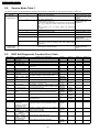
Specifications
Power supply:
AC230 V, 50 Hz
(DVD-S29EG/E)
Power consumption:
WMA:
(9)
between 48 kbps and 320 kbps
JPEG
AC230-240 V, 50 Hz
●Exif Ver 2.1 JPEG Baseline files
(DVD-S29EB only)
●The total combined maximum number of recognizable
audio and picture contents and groups:
9W
4000 audio and picture
contents and 400 groups.
Power consumption in standby mode:
approx. 1 W
Dimensions:
430 (W)×248 (D)×43 (H) mm
Mass:
2.14 kg
Signal system:
PAL625/50, PAL525/60, NTSC
Operating temperature range:
+5 to +35°C
Operating humidity range:
5 to 90 % RH (no
condensation)
Region number:
Region No.2
between 320×240 and
6144×4096 pixels
(Sub sampling is 4:2:2 or 4:2:0)
(10) HighMAT Level 2 (Audio and Image)
Video output:
Output level:
1 Vp-p (75 Ω)
Output terminal:
Pin jack (1 system)/AV
S video output:
Discs played [8 cm or 12 cm]:
(1)
DVD-RAM (DVD-VR compatible, JPEG formatted discs)
(2)
DVD-Audio
(3)
DVD-R (DVD-Video compatible)
(4)
CD-Audio (CD-DA)
Y output level:
1 Vp-p (75 Ω)
C output level:
NTSC; 0.286 Vp-p (75 Ω)
PAL; 0.300 Vp-p (75 Ω)
Output terminal:
Component video output:
(5)
Video CD
(6)
SVCD (Conforming to IEC62107)
(7)
CD-R/CD-RW (CD-DA, Video CD, SVCD, MP3, WMA,
JPEG formatted discs)
(8)
●Picture resolution:
AV
[NTSC: 525(480)p / 525(480)i,
PAL: 625(576)p / 625(576)i]
Y output level:
1 Vp-p (75 Ω)
PB output level:
0.7 Vp-p (75 Ω)
MP3/WMA
PR output level:
0.7 Vp-p (75 Ω)
●The total combined maximum number of recognizable
audio and picture contents and groups:
Output terminal:
4000 audio and picture
contents and 400 groups.
●Compatible compression rate:
MP3:
Pin jack (Y: green, PB: bule,
PR: red)
Number of terminals:
1 system
RGB video output:
R output level:
0.7 Vp-p (75 Ω)
between 32 kbps and 320 kbps
© 2005 Matsushita Electric Industrial CO., Ltd. All
rights reserved. Unauthorized copying and
distribution is a violation of law.
DVD-S29EG / DVD-S29E / DVD-S29EB
G output level:
0.7 Vp-p (75 Ω)
B output level:
0.7 Vp-p (75 Ω)
Output terminal:
AV
Note:
Audio output:
Specifications are subject to change without notice.
Output level:
2 Vrms (1 kHz, 0 dB)
Output terminal:
Pin jack/AV
Mass and dimensions are approximate.
Solder:
Number of terminals:
2 channel:
This model uses lead free solder (PbF).
1 system
Audio performance:
(1)
Frequency response:
●DVD (linear audio):
4 Hz-22 kHz (48 kHz sampling)
4 Hz-44 kHz (96 kHz sampling)
●CD audio:
(2)
S/N ratio:
●CD audio:
(3)
(4)
4 Hz-20 kHz
115 dB
Dynamic range:
●DVD (linear audio):
100 dB
●CD audio:
98 dB
Total harmonic distortion:
●CD audio:
0.0025 %
Digital audio output:
Coaxial digital output:
Pin jack
Pickup
Wave length:
662 nm/785 nm
Laser power:
CLASS 2/CLASS 3A
CONTENTS
Page
1 SAFETY PRECAUTIONS
1.1. GENERAL GUIDELINES
Page
4
7 ASSEMBLING AND DISASSEMBLING THE MECHANISM UNIT
4
11
7.1. Disassembly Procedure
11
4
7.2. Traverse Unit
11
3 Precaution of Laser Diode
5
7.3. Tray
12
4 About lead free solder (PbF)
5
7.4. Loading section
13
5 PREVENTION OF STATIC ELECTRICITY DISCHARGE
6
7.5. Loading motor P.C.B.
14
5.1. Grounding for electrostatic breakdown prevention
6
7.6. Optical Pickup Unit
15
5.2. Handling Precautions for Traverse Unit (Optical Pickup)
6
7.7. Traverse Motor
17
2 PREVENTION OF ELECTRO STATIC DISCHARGE (ESD) TO
ELECTROSTATICALLY SENSITIVE (ES) DEVICES
6 DISASSEMBLING THE CASING AND CHECKING P.C.B.S
7
8 Self-Diagnosis Function and Service Modes
19
6.1. Disassembly Procedure
7
8.1. Optical Pickup Breakdown Diagnosis
19
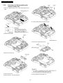
6.2. Casing Parts and P.C.B. Positions
7
8.2. Service Mode Table 1
20
6.3. Top Panel
8
8.3. DVD Self Diagnostic Function-Error Code
20
6.4. Front Panel
8
8.4. Last Error Code saved during NO PLAY
21
6.5. Module P.C.B.
8
8.5. Service mode table 2
22
6.6. Mechanism Unit
8
8.6. Sales demonstration lock function
24
6.7. Rear panel
9
8.7. Handling After Completing Repairs
24
6.8. Mother P.C.B. and Power SW P.C.B.
6.9. Service Position
9
9 Service Precautions
10
2
25
9.1. Recovery after the dvd player is repaired
25
9.2. Firmware version-up of the DVD player
25
DVD-S29EG / DVD-S29E / DVD-S29EB
10 ADJUSTMENT PROCEDURES
26
10.1. Service Tools and Equipment
26
10.2. Important points in adjustment
26
10.3. Storing and Handling Test Discs
26
10.4. Optical adjustment
27
11 Abbreviations
29
12 VOLTAGE CHART
31
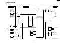
15 SCHEMATIC DIAGRAM
15.1. POWER SUPPLY SECTION (MOTHER P.C.B. (1/2))
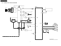
SCHEMATIC DIAGRAM
SCHEMATIC DIAGRAM
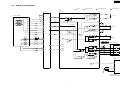
15.3. MODULE SCHEMATIC DIAGRAM
16 PRINT CIRCUIT BOARD
31
16.1. MOTHER P.C.B.
12.2. MODULE P.C.B.
32
16.2. MOTHER P.C.B. & MODULE P.C.B. ADDRESS
35
13.1. OVERALL BLOCK DIAGRAM
35
13.2. POWER SUPPLY BLOCK DIAGRAM
36
13.3. SERVO BLOCK DIAGRAM
37
13.4. VIDEO BLOCK DIAGRAM
38
13.5. AUDIO BLOCK DIAGRAM
40
INFORMATION
14.2. SCHEMATIC DIAGRAM NOTES
42
49
49
50
16.4. MODULE P.C.B. (2/2) (FOIL SIDE)
52
53
17.1. CASING PARTS & MECHANISM SECTION EXPLODED
VIEW
53
54
17.3. PACKING & ACCESSORIES SECTION EXPLODED
41
41
46
51
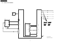
17.2. MECHANISM SECTION EXPLODED VIEW
14.1. INTERCONNECTION SCHEMATIC DIAGRAM
44
16.3. MODULE P.C.B. (1/2) (COMPONENT SIDE)
17 EXPLODED VIEWS
14 INTERCONNECTION SCHEMATIC DIAGRAM & SCHEMATIC
DIAGRAM NOTES
43
15.2. FRONT & AV OUT SECTION (MOTHER P.C.B. (2/2))
12.1. MOTHER P.C.B.
13 BLOCK DIAGRAM
43
VIEW
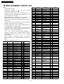
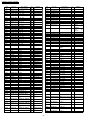
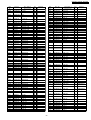
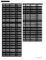
18 REPLACEMENT PARTS LIST
3
55
56
DVD-S29EG / DVD-S29E / DVD-S29EB
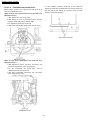
1 SAFETY PRECAUTIONS
1.1.
GENERAL GUIDELINES
1. When servicing, observe the original lead dress. If a short circuit is found, replace all parts which have been overheated or
damaged by the short circuit.
2. After servicing, see to it that all the protective devices such as insulation barriers, insulation papers shields are properly
installed.
3. After servicing, make the following leakage current checks to prevent the customer from being exposed to shock hazards.
1.1.1.
LEAKAGE CURRENT COLD
CHECK
1.1.2.
LEAKAGE CURRENT HOT CHECK
(See Figure 1 .)
1. Unplug the AC cord and connect a jumper between the two
prongs on the plug.
1. Plug the AC cord directly into the AC outlet. Do not use an
isolation transformer for this check.
2. Measure the resistance value, with an ohmmeter, between
the jumpered AC plug and each exposed metallic cabinet
part on the equipment such as screwheads, connectors,
control shafts, etc. When the exposed metallic part has a
return path to the chassis, the reading should be between
1MΩ and 5.2MΩ.
When the exposed metal does not have a return path to
the chassis, the reading must be .
2. Connect a 1.5kΩ, 10 watts resistor, in parallel with a 0.15µF
capacitors, between each exposed metallic part on the set
and a good earth ground such as a water pipe, as shown in
Figure 1.
3. Use an AC voltmeter, with 1000 ohms/volt or more
sensitivity, to measure the potential across the resistor.
4. Check each exposed metallic part, and measure the
voltage at each point.
5. Reverse the AC plug in the AC outlet and repeat each of the
above measurements.
6. The potential at any point should not exceed 0.75 volts
RMS. A leakage current tester (Simpson Model 229 or
equivalent) may be used to make the hot checks, leakage
current mu3st not exceed 1/2 milliamp. In case a
measurement is outside of the limits specified, there is a
possibility of a shock hazard, and the equipment should be
repaired and rechecked before it is returned to the
customer.
Figure 1
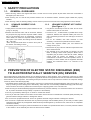
2 PREVENTION OF ELECTRO STATIC DISCHARGE (ESD)
TO ELECTROSTATICALLY SENSITIVE (ES) DEVICES
Some semiconductor (solid state) devices can be damaged easily by static electricity. Such components commonly are called
Electrostatically Sensitive (ES) Devices. Examples of typical ES devices are integrated circuits and some field-effect transistors and
semiconductor "chip" components. The following techniques should be used to help reduce the incidence of component damage
caused by electro static discharge (ESD).
1. Immediately before handling any semiconductor component or semiconductor-equipped assembly, drain off any ESD on your
body by touching a known earth ground. Alternatively, obtain and wear a commercially available discharging ESD wrist strap,
which should be removed for potential shock reasons prior to applying power to the unit under test.
2. After removing an electrical assembly equipped with ES devices, place the assembly on a conductive surface such as alminum
foil, to prevent electrostatic charge buildup or exposure of the assembly.
3. Use only a grounded-tip soldering iron to solder or unsolder ES devices.
4. Use only an anti-static solder removal device. Some solder removal devices not classified as "anti-static (ESD protected)" can
generate electrical charge sufficient to damage ES devices.
5. Do not use freon-propelled chemicals. These can generate electrical charges sufficient to damage ES devices.
6. Do not remove a replacement ES device from its protective package until immediately before you are ready to install it. (Most
replacement ES devices are packaged with leads electrically shorted together by conductive foam, alminum foil or comparable
conductive material).
7. Immediately before removing the protective material from the leads of a replacement ES device, touch the protective material
to the chassis or circuit assembly into which the device will be installed.
4
DVD-S29EG / DVD-S29E / DVD-S29EB
Caution
Be sure no power is applied to the chassis or circuit, and observe all other safety precautions.
8. Minimize bodily motions when handling unpackaged replacement ES devices. (Otherwise hamless motion such as the brushing
together of your clothes fabric or the lifting of your foot from a carpeted floor can generate static electricity (ESD) sufficient to
damage an ES device).
3 Precaution of Laser Diode
4 About lead free solder (PbF)
Distinction of PbF PCB:
PCBs (manufactured) using lead free solder will have a PbF stamp on the PCB.
Caution:
· Pb free solder has a higher melting point than standard solder; Typically thmelting point is 50 - 70°F (30 - 40°C) higher.
Please use a high temperature soldering iron. In case of the soldering iron with temperature control, please set it to 700 ±
20°F (370 ± 10°C).
· Pb free solder will tend to splash when heated too high (about 1100°F/ 600°C).
When soldering or unsoldering, please completely remove all of the solder on the pins or solder area, and be sure to heat the
soldering points with the Pb free solder until it melts enough.
5
DVD-S29EG / DVD-S29E / DVD-S29EB
5 PREVENTION OF STATIC ELECTRICITY DISCHARGE
The laser diode in the traverse unit (optical pickup) may brake down due to static electricity of clothes or human body. Use due
caution to electrostatic breakdown when servicing and handling the laser diode.
5.1.
Grounding for electrostatic breakdown prevention
Some devices such as the DVD player use the optical pickup (laser diode) and the optical pickup will be damaged by static
electricity in the working environment. Proceed servicing works under the working environment where grounding works is
completed.
5.1.1.
Worktable grounding
1. Put a conductive material (sheet) or iron sheet on the area where the optical pickup is placed, and ground the sheet.
5.1.2.
Human body grounding
1. Use the anti-static wrist strap to discharge the static electricity form your body.
5.1.3.
Handling of optical pickup
1. To keep the good quality of the optical pickup maintenance parts during transportation and before installation, the both ends of
the laser diode are short-circuited. After replacing the parts with new ones, remove the short circuit according to the correct
procedure. (See this Technical Guide.)
2. Do not use a tester to check the laser diode for the optical pickup. Failure to do so will damage the laser diode due to the power
supply in the tester.
5.2.
Handling Precautions for Traverse Unit (Optical Pickup)
1. Do not give a considerable shock to the traverse unit (optical pickup) as it has an extremely high-precise structure.
2. When replacing the optical pickup, install the flexible cable and cut its short land with a nipper. See the optical pickup
replacement procedure in this Technical Guide. Before replacing the traverse unit, remove the short pin for preventing static
electricity and install a new unit. Connect the connector as short times as possible.
3. The flexible cable may be cut off if an excessive force is applied to it. Use caution when handling the cable.
4. The half-fixed resistor for laser power adjustment cannot be adjusted. Do not turn the resistor.
6
DVD-S29EG / DVD-S29E / DVD-S29EB
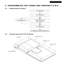
6 DISASSEMBLING THE CASING AND CHECKING P.C.B.S
6.1.
Disassembly Procedure
6.2.
Casing Parts and P.C.B. Positions
7
DVD-S29EG / DVD-S29E / DVD-S29EB
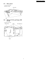
6.3.
Top Panel
1. Unscrew the screws.
6.5.
Module P.C.B.
1. Unscrew the screws.
2. Remove the connectors.
3. Press each tab with the nipper to module PCB vertically.
6.4.
Front Panel
1. Release the tabs.
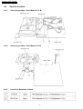
6.6.
Mechanism Unit
1. Unscrew the screws.
2. Remove the connectors.
2. Release the tabs.
8
DVD-S29EG / DVD-S29E / DVD-S29EB
6.7.
Rear panel
1. Unscrew the screws
2. Release the tabs.
6.8.
Mother P.C.B. and Power SW
P.C.B.
1. Unscrew the screws.
9
DVD-S29EG / DVD-S29E / DVD-S29EB
6.9.
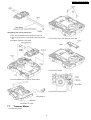
Service Position
6.9.1.
Servicing position of the Module P.C.B.
6.9.2.
Servicing position of the Mother P.C.B.
6.9.3.
List of the Extension Cables
10
DVD-S29EG / DVD-S29E / DVD-S29EB
7 ASSEMBLING AND
DISASSEMBLING THE
MECHANISM UNIT
7.1.
Disassembly Procedure
4. Remove the traverse unit
7.2.
Traverse Unit
1. Slide the lever (A) in the arrow direction (to the opposite
side) till it stops.
2. Slide the lever (A) further by bending the tab at the right
side of the lever A in the right direction. (The right groove
opens and the boss becomes seen.)
3. Open the lever (B) to left. (The 2 grooves at the left side
open.)
11
DVD-S29EG / DVD-S29E / DVD-S29EB
7.3.
Tray
1. Slide the guide tray unit while pressing the stopper in the
arrow direction, and remove the guide tray unit.
5. Remove the drive arm concave phase from the tray slider
and tray.
2. Raise the loading unit.
<Assembling the tray unit>
3. Slide the lever in the arrow direction till it stops and pull the
tray out.
1. Insert a part of the tray into the unit sliding over the
groove on the mechanical chassis unit.
2. Insert the tray to the point before the tab of the
mechanical chassis unit.
4. Spread the tabs at the both sides and pull the tray out. (The
tray slides a little forward and stops.)
3. Hook the drive arm concave phase over the tray and the
tray slider.
4. Press in the tray.
5. Make sure that the tray and the drive arm move
smoothly.
12
DVD-S29EG / DVD-S29E / DVD-S29EB
4. Remove the belt.
7.4.
Loading section
5. Unlock the tab and remove the pulley.
6. Remove the relay gear.
1. Spread the tabs at the both sides and push out the drive
arm shaft.
7. Turn the change lever in the arrow direction till it stops.
8. Hook the change lever spring on the change lever project
part temporarily.
2. Hook the lock lever spring on the lock lever projection part
temporarily.
3. Unlock the tab and remove the lock lever.
13
DVD-S29EG / DVD-S29E / DVD-S29EB
9. Pull the lever (B) in the bottom side to your side and remove
the change lever.
10. Remove the drive rack, the sub rack and the drive gear.
7.5.
Loading motor P.C.B.
1. Unscrew the screws
14
DVD-S29EG / DVD-S29E / DVD-S29EB
7.6.
7.6.1.
Optical Pickup Unit
Cautions to Be Taken in Handling the Optical Pickup Unit
The laser diode in the optical pickup unit may be damaged due to electrostatic discharge generating from clothes or human body.
Use due caution to electrostatic discharge damage when servicing the laser diode.
1. Do not give a considerable shock to the optical pickup unit as it has an extremely high-precise structure.
2. To prevent the laser diode from the electrostatic discharge damage, the Intermediate FFC of the optical pickup unit removed
from the PCB should be short-circuited with a short pin or a clip.
3. The Intermediate FFC may be cut off if an excessive force is applied to it. Use caution when handling the Intermediate FFC.
4. The antistatic FPC is connected to the new optical pickup unit. After replacing the optical pickup unit and connecting the
fIntermediate FFC, cut off the antistatic FPC.
15
DVD-S29EG / DVD-S29E / DVD-S29EB
7.6.2.
Procedure for Disassembling the
Optical Pickup Unit
1. Move the optical pickup unit in the arrow direction till it
stops.
6. Lift the optical pickup unit with the shaft.
2. Unscrew the screws.
7. Remove the optical pickup unit.
3. Remove the drive rack.
4. Unscrew the screw
8. Pull the shaft and the rubber out.
5. Slide the shaft in the arrow direction.
16
DVD-S29EG / DVD-S29E / DVD-S29EB
<Assembling the optical pickup unit>
1. Pass the intermediate FPC through the frame hole.
2. Align the guide section of the optical pickup unit with the
rail.
2. Remove the cover while lifting the inner gear.
3. Install the shaft top to the holder.
3. Remove the solders.
4. The intermediate FFC is fixed as shown below.
4. Remove the traverse motor.
7.7.
Traverse Motor
1. Unscrew the screws.
17
DVD-S29EG / DVD-S29E / DVD-S29EB
18
DVD-S29EG / DVD-S29E / DVD-S29EB
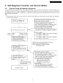
8 Self-Diagnosis Function and Service Modes
8.1.
Optical Pickup Breakdown Diagnosis
The optical pickup self-diagnosis function and tilt adjustment check function have been included in this unit. When repairing, use
the following procedure for effective Self-diagnosis and tilt adjustment.Be sure to use the self-diagnosis function before replacing
the optical pickup when "NO DISC" is displayed. As a guideline, you should replace the optical pickup when the value of the laser
drive current is more than 55.
Note:
Press the power button to turn on the power, and check the value within three minutes before the unit warms up. (Otherwise,
the result will be incorrect.)
19
DVD-S29EG / DVD-S29E / DVD-S29EB
8.2.
Service Mode Table 1
The service modes can be activated by pressing various button combination on the player and remote control unit.
Player buttons
PAUSE
+
OPEN/CLOSE
Remote control unit buttons
0
5
6
7
9
FUNCTION
PAUSE
PAUSE
QUICK OSD
OPEN/CLOSE
8.3.
Application
Displaying the UHF display F_ _ _
Note
Refer to section 8.3. SelfDiagnosis Function (UHF
Display).
Jitter check, tilt adjustment
Refer to section 10.4.
*Display shows J_xxx/yyy_zz
Optical Pickup Tilt
"yyy" and "zz" shown to the right have nothing to do with the jitter Adjustment
value. "yyy" is the error counter, while "zz" is the focus drive
value.
Refer to section 10.4. for Optical Pickup Tilt Adjustment
Procedure.
Checking the region numbers and broadcast system
Checking the program version
Check the IC8651 FLASH
ROM program.
Lighting Confirmation Function of Display Tube
Checking the laser drive current
Refer to section 7
Optical Pickup
Replacement Procedure.
Writing the laser drive current value after replacing the optical
pickup (do not use for anything other than optical pickup
replacement)
Initializing the DVD player
Refer to section 8.5.
(restoring factory preset settings)
Initializing the DVD
player.
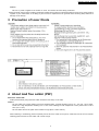
DVD Self Diagnostic Function-Error Code
Error Code
U11
U15
H01
H02
Error Content
U, H error
Focus error
Unfinalized DVD-R
Tray loading error
Spindle servo error
H03
H04
H05
H06
Traverse servo error
Tracking servo error
Seek error
Power error
H07
F500
Spindle motor
error
DSC related
DSC error
F501
DSC not Ready
F502
DSC Time out error
F503
F505
DSC
communication Communication error (result error occured
Failure
although communication command was sent)
DSC Attention error
Similar disposal as F500
F506
Invalid media
F600
F601
F602
F603
F610
Additional error explanation
Defect 1
Defect 2
Defect 3
DV2
(IC8001)
servo drive
DV2
(IC8001)
EEPROM
(IC8611)
DV2
(IC8001)
DV2
(IC8001)
servo drive
(Spindle servo, DV2 (IC8001) SP motor, CLV
servo error)
Cannot switch off the power because of the panel
and system computer communication error
drive
ODC related
Access
failure
to
management
information caused by
demodulation error
Indeterminate sector ID
requested
Access failure to LEADIN
caused
by
demodulation error
Access
failure
to
KEYDET caused by
demodulation error
ODC abnormality
Spindle
motor ass’y
DV2 (IC8001) stops in the occurence of servo
error (starup, focus error, etc)
DSC-system computer communication error
(Communication failure caused by idling of DSC)
Similar disposal as F500
unreadable,
Optical
pickup
DV2
(IC8001)
Optical
pickup
DV2
(IC8001)
Optical
pickup
DISC
Operation stopped because navigation data is not
accessible caused by the demodulation defect
DV2
(IC8001)
Operation stopped caused by the request to
access abnormal ID data
LEAD IN data unreadable
DV2
(IC8001)
Disc is flipped
incompatible disc
over,
TOC
Access failure to CSS data of disc
No permission for command execution
20
DV2
(IC8001)
servo drive
Defect 4
DVD-S29EG / DVD-S29E / DVD-S29EB
Error Code
F611
F612
F630
F631
F632
F103
Error Content
6626 QCODE don’t
read Error
No CRC OK for a
specific time
No reply to KEY DET
enquiry
CPPM KEY DET is not
available till the FILE
terminal
CPPM KEY DET is not
available
Disc code
Illegal highlight Position
Additional error explanation
Access failure to seek address in CD series
Defect 1
DV2
(IC8001)
DV2
(IC8001)
Defect 2
(CPPM file system is unreadable caused by
scratches)
DISC
CPPM
(*1)
Been revoked or falsified
DISC
EEPROM
(IC8611)
Big possibility of disc specification violation during
highlight display
DISC
Access failure to ID data in DVD series
F893
F894
EEPROM abnormality
F895
Language
area Firm version agreement check for factory preset
abnormality
setting failure prevention
No existence model
Firm version agreement check for factory preset
setting failure prevention
Initialize
is
not Initialize completion check for factory preset
completed
setting failure prevention
Disagreement
of Unsuitable combination of AV DECORDER,
hardware and software SDRAM and FLASH ROM (firmware)
Message command is Begin sending message to AV task
not appropriate
F700
F701
F702
F880
F890
F891
F896
F897
F898
F8A0
Defect 4
(for internal use only)
HIC Error
Force initialize failure
(time out)
Micro computer error
MBX overflow
Message
command
does not end
Message
command
changes
Task number is not
appropriate
Sending message when
message is being sent
to AV task
Message couldn’t be
sent to AV task
FROM falsification
F4FF
Defect 3
EEPROM
(IC8611)
DV2
(IC8001)
FROM
(IC8651)
EEPROM
(IC8611)
DV2
(IC8001)
Serial
communicat
ion on lone
CPPM
(*1)
When replying message to disc manager
Next message is sent before replying to disc
manager
Message is changed before it is sent as a reply to
disc manager
Message coming from a non-existing task
Sending message to AV task
Begin sending message to AV task
FROM
(IC8651)
Note:
An error code will be canceled if a power supply is turned OFF.
*1: CPPM is the copy guard function beforehand written in the disk for protection of copyrights.
8.4.
Last Error Code saved during NO PLAY
Error code
Error Content
F0BF
6)
Cannot
playback
because
physical layer is not recoginizable
F0C0
8) DVD: Cannot playback because it
is not DVD Video/Adio/VR
F0C1
9) DVD: Prohibited by the restricted
region code
F0C2
A) DVD: PAL restricted playback
F0C3
B) DVD: Parental lock setting
prohibits the playback of the entire
title
F0C4
C) VCD: Prohibited because it is in
PHOTO CD fromat
F0C5
VCD/CD: Prohibited because it is
CDROM without CD-DA
System computer
Setting task
PCND_NOPLAY
PHYSICAL DriveManager
0x50
PCND_NOPLAY VIDEO 0x70
DiscManager
System computer internal error code
0xDOBF
0xDOC0
PCND_NOPLAY RCD 0x80
DiscManager
0xDOC1
PCND_NOPLAY PAL 0x90
PCND_NOPLAY PTL 0xA0
DiscManager
DiscManager
0xDOC2
0xDOC3
PCND_NOPLAY PHOTO CD DiscManager
0xB0
PCND_NOPLAY CDROM 0xC0 DiscManager
0xDOC4
21
0xDOC5
DVD-S29EG / DVD-S29E / DVD-S29EB
8.5.
Service mode table 2
Pressing various button combinations on the player and remote control unit can activate the service modes.
22
DVD-S29EG / DVD-S29E / DVD-S29EB
23
DVD-S29EG / DVD-S29E / DVD-S29EB
8.6.
Sales demonstration lock function
This function prevents discs from being lost when the unit is used for sales demonstrations by disabling the disc eject function.
"LOC" is displayed on the unit, and ordinary operation is disabled.
8.6.1.
Setting
The sales demonstration lock is set by simultaneously pressing STOP button on the player and POWER button on the remote
control unit for 1 second or longer.
8.6.2.
Cancellation
The lock can be cancelled by the same procedure as used in setting. ("UNLOC" is displayed on cancellation. Disconnecting the
power cable from power outlet does not cancel the lock.)
8.7.
Handling After Completing Repairs
Use the following procedure after completing repairs.
8.7.1.
Method
Confirm that the power is turned on:
1. Press the "OPEN/CLOSE" button to close the tray.
2. Press the "POWER" button to turn off the power.
3. Disconnect the power plug from the outlet.
8.7.2.
Precautions
Do not disconnect the power plug from the outlet with the tray still open, then close the tray manually.
24
DVD-S29EG / DVD-S29E / DVD-S29EB
9 Service Precautions
9.1.
Recovery after the dvd player is repaired
· When FROM or module P.C.B. is replaced, carry out the recovery processing to optimize the drive.
Playback the recovery disk to process the recovery automatically.
· Recovery disc [Product number: RFKZD03R005] (RFKZD03R004 can not be recovered as a partial item.
So use the new recovery disc, RFKZD03R005.)
· Performing recovery
1. Load the recovery disc RFKZD03R005 on to the player and run it.
2. Recovery is performed automatically. When it is finished, a message appears on the screen.
3. Remove the recovery disc.
4. Turn off the power.
Note:
This unit requires no initialization process carried out after the traditional DVD players were repaired.
When the recovery measures are taken, the customer setting will return to the factory setting as same as the procedure
described in item of "Initialization" in 8.5. is carried out. Write down the contents of the setting before recovery processing, and
reset the player.
9.2.
Firmware version-up of the DVD player
· The firmware of the DVD player may be renewed to improve the quality including operationability and playerbility to the
substandard discs.processing to optimize the drive.
The recovery disc has also firmware version-up.
· After version-up, recovery processing is executed automatically.
· Part number of the recovery disc for version-up will be noticed when it is supplied.
· Updating firmware
1. Load the recovery disc that is supplied to the player and run it.
2. Firmware version of the player is automatically checked. Appropriate message appears whenever necessary.
3. Using remote controller´s cursor key, select whether version updating is to be done or not. (Selection of Yes/No)
4. a. If Yes is selected, version updating is performed.
b. If No is selected, only recovery is performed.
5. a. When updating is finished, remove the disc according to the message appearing on the screen.
b. Remove the disc according to the message appearing on the screen.
6. Turn off the power.
Note:
If the AC power supply is shut out during version-up due to a power failure, the version-up is improperly carried out.
In such a case, replace the FROM and carry out the version-up again.
25
DVD-S29EG / DVD-S29E / DVD-S29EB
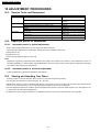
10 ADJUSTMENT PROCEDURES
10.1. Service Tools and Equipment
Application
Tilt adjustment
Name
Number
DVDT-S15 or DVDT-S01
DVD test disc
TORX screw driver (T6)
Inspection
Others
Confirmation
Extension cable (module P.C.B. to mother P.C.B.)
Extension cable (module P.C.B. to mother P.C.B.)
Hanarl
Grease
Drysurf
CD test disc
VCD test disc
Recovery disc
Available on sales route. (T6) or
RFKZ0185
VUC8026
RFKZ0106
VFK1784
RFKXPG641
RFKXGUD24
PVCD-K06 or any other commercially
available disc
PVCD-K06 or any other commercially
available disc
RFKZD03R005
10.2. Important points in adjustment
10.2.1.
Important points in optical adjustment
· Before starting optical adjustment, be sure to take anti-static measures.
· Optical pickup tilt adjustment is needed after replacement of the following components.
1. Optical pickup unit
2. Spindle motor unit
3. Optical pickup peripheral parts (such as rail)
Notes
Adjustment is generally unnecessary after replacing other parts of the traverse unit. However, make adjustment if there is a
noticeable degradation in picture quality. Optical adjustments cannot be made inside the optical pickup. Adjustment is generally
unnecessary after replacing the traverse unit.
10.2.2.
Important points in electrical adjustment
· Follow the adjustment procedures described in this Manual.
10.3. Storing and Handling Test Discs
· Surface precision is vital for DVD test discs. Be sure to store and handle them carefully.
1. Do not place discs directly onto the workbench, etc., after use.
2. Handle discs carefully in order to maintain their flatness. Place them into their case after use and store them vertically. Store
discs in a cool place where they are not exposed to direct sunlight or air from air conditioners.
3. Accurate adjustment will not be possible if the disc is warped when placed on a surface made of glass, etc. If this happens, use
a new test disc to make optical adjustments.
4. If adjustment is done using a warped disc, the adjustment will be incorrect and some discs will not be playable.
26
DVD-S29EG / DVD-S29E / DVD-S29EB
10.4. Optical adjustment
10.4.1.
Optical pickup tilt adjustment
Measurement point
Adjustment point
Tangential adjustment screw
Tilt adjustment screw
Measuring equipment
None (Main unit display for servicing is used.)
Mode
Disc
T01 (inner periphery) play
DVDR-S15 or DVDT-S01
T30 (central periphery) play
T43 (outer periphery) play
Adjustment value
Adjust to the minimum jitter value.
Note:
10.4.1.1. Adjustment procedure
When FFC has covered the adjustment screw, please insert
a screwdriver, evading FFC(s).
1. While pressing PAUSE and OPEN/CLOSE buttons on the
main unit, press "5" on the remote control unit.
2. Confirm that "J_xxx/yyy_zz" is shown on the front display.
For your information:
"yyy" and "zz" shown to the right have nothing to do with
the jitter value. "yyy" is the error counter, while "zz" is
the focus drive value.
Note:
Jitter value appears on the front display.
3. Play test disc T30 (central periphery).
4. Adjust tangential adjustment screw so that the jitter value is
minimized.
5. Play test disc T30 (central periphery).
6. Adjust tilt adjustment screw 1 so that the jitter value is
minimized.
7. Play test disc T30 (central periphery).
8. Adjust tilt adjustment screw 2 so that the jitter value is
minimized.
10.4.1.3. Check after adjustment
9. Repeat adjusting tilt adjustment screws 1 and 2 alternately
until the jitter value is minimized.
Play test disc or any other disc to make sure there is no picture
degradation in the inner, middle and outer peripheries, and no
audio skipping. After adjustment is finished, lock each
adjustment screw in position using screw lock.
10. Finally please reproduce T01 (inner periphery) and T43
(outer periphery) and check the jitter value. (Please
readjust, when the jitter value is extremely different.)
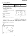
10.4.1.2. Important points
1. Make tangential adjustment first, and then make tilt
adjustment.
2. Repeat adjusting two or three times to find the optimum
point.
3. Finish the procedure with tilt adjustment.
Jitter value depends on the model:
1. If the jitter value changes like B, the optimum point is easy to
find.
2. If the jitter value changes like A, set the optimum point near the
middle.
27
DVD-S29EG / DVD-S29E / DVD-S29EB
It is also possible to perform screw lock on the head of an
adjustment screw after an adjustment end using an injector etc.
from the hole at the bottom of a product (hole of bottom
chassis), without decomposing.
10.4.1.4. Procedure for screw lock
Please perform a screw lock in which by the side of the tip or
head of an adjustment screw.
<When a screw lock is performed to the tip part side of an
adjustment screw>
1. After adjustment, remove top panel.
2. After pulling out a tray to the position which does not
become obstructive,remove clamper plate.
3. Fix adjustment screw with screw lock.
4. After fixing, reassemble clamper plate and top panel.
<When a screw lock is performed to the head side of an
adjustment screw>
1. After adjustment, remove top panel, front panel, rear
panel and mechanism unit in this sequence.
2. Lay the mechanism unit upside
adjustment scwer with screw lock.
down,
and fix
3. After fixing, reassemble mechanism unit, rear panel,
front panel and top panel.
28
DVD-S29EG / DVD-S29E / DVD-S29EB
11 Abbreviations
INITIAL/LOGO
A
A0~UP
ACLK
AD0~UP
ADATA
ALE
AMUTE
AREQ
ARF
ASI
ASO
ASYNC
B
BCK
BCKIN
BDO
BLKCK
BOTTOM
BYP
BYTCK
C
CAV
CBDO
CD
CDSCK
CDSRDATA
CDRF
CDV
CHNDATA
CKSL
CLV
COFTR
CPA
CPCS
CPDT
CPUADR
CPUADT
CPUIRQ
CPRD
CPWR
CS
CSYNCIN
CSYNCOUT
D
DACCK
DEEMP
DEMPH
DIG0~UP
DIN
DMSRCK
DMUTE
DO
DOUT0~UP
DRF
DRPOUT
DREQ
DRESP
DSC
DSLF
DVD
ABBREVIATIONS
ADDRESS
AUDIO CLOCK
ADDRESS BUS
AUDIO PES PACKET DATA
ADDRESS LATCH ENABLE
AUDIO MUTE
AUDIO PES PACKET REQUEST
AUDIO RF
SERVO AMP INVERTED INPUT
SERVO AMP OUTPUT
AUDIO WORD DISTINCTION SYNC
BIT CLOCK (PCM)
BIT CLOCK INPUT
BLACK DROP OUT
SUB CODE BLOCK CLOCK
CAP. FOR BOTTOM HOLD
BYPATH
BYTE CLOCK
CONSTANT ANGULAR VELOCITY
CAP. BLACK DROP OUT
COMPACT DISC
CD SERIAL DATA CLOCK
CD SERIAL DATA
CD RF (EFM) SIGNAL
COMPACT DISC-VIDEO
CHANNEL DATA
SYSTEM CLOCK SELECT
CONSTANT LINEAR VELOCITY
CAP. OFF TRACK
CPU ADDRESS
CPU CHIP SELECT
CPU DATA
CPU ADDRESS LATCH
CPU ADDRESS DATA BUS
CPU INTERRUPT REQUEST
CPU READ ENABLE
CPU WRITE ENABLE
CHIP SELECT
COMPOSITE SYNC IN
COMPOSITE SYNC OUT
D/A CONVERTER CLOCK
DEEMPHASIS BIT ON/OFF
DEEMPHASIS SWITCHING
FL DIGIT OUTPUT
DATA INPUT
DM SERIAL DATA READ CLOCK
DIGITAL MUTE CONTROL
DROP OUT
DATA OUTPUT
DATA SLICE RF (BIAS)
DROP OUT SIGNAL
DATA REQUEST
DATA RESPONSE
DIGITAL SERVO CONTROLLER
DATA SLICE LOOP FILTER
DIGITAL VIDEO DISC
INITIAL/LOGO
E
EC
ECR
F
G
H
I
L
M
O
P
29
ENCSEL
ETMCLK
ETSCLK
FBAL
FCLK
FE
FFI
FEO
FG
FSC
FSCK
GND
HA0~UP
HD0~UP
HINT
HRXW
IECOUT
IPFRAG
IREF
ISEL
LDON
LPC
LRCK
MA0~UP
MCK
MCKI
MCLK
MDATA
MDQ0~UP
MDQM
MLD
MPEG
ODC
OFTR
OSCI
OSCO
OSD
P1~UP
PCD
PCK
PDVD
PEAK
PLLCLK
PLLOK
PWMCTL
PWMDA
PWMOA, B
ABBREVIATIONS
ERROR TORQUE CONTROL
ERROR
TORQUE
CONTROL
REFERENCE
ENCODER SELECT
EXTERNAL M CLOCK (81MHz/40.5MHz)
EXTERNAL S CLOCK (54MHz)
FOCUS BALANCE
FRAME CLOCK
FOCUS ERROR
FOCUS ERROR AMP INVERTED INPUT
FOCUS ERROR AMP OUTPUT
FREQUENCY GENERATOR
FREQUENCY SUB CARRIER
FS (384 OVER SAMPLING) CLOCK
COMMON GROUNDING (EARTH)
HOST ADDRESS
HOST DATA
HOST INTERRUPT
HOST READ/WRITE
IEC958 FORMAT DATA OUTPUT
INTERPOLATION FLAG
I (CURRENT) REFERENCE
INTERFACE MODE SELECT
LASER DIODE CONTROL
LASER POWER CONTROL
L CH/R CH DISTINCTION CLOCK
MEMORY ADDRESS
MEMORY CLOCK
MEMORY CLOCK INPUT
MEMORY SERIAL COMMAND CLOCK
MEMORY SERIAL COMMAND DATA
MEMORY DATA INPUT/OUTPUT
MEMORY DATA I/O MASK
MEMORY SERIAL COMMAND LOAD
MOVING PICTURE EXPERTS GROUP
OPTICAL DISC CONTROLLER
OFF TRACKING
OSCILLATOR INPUT
OSCILLATOR OUTPUT
ON SCREEN DISPLAY
PORT
CD TRACKING PHASE DIFFERENCE
PLL CLOCK
DVD TRACKING PHASE DIFFERENCE
CAP. FOR PEAK HOLD
CHANNEL PLL CLOCK
PLL LOCK
PWM OUTPUT CONTROL
PULSE WAVE MOTOR DRIVE A
PULSE WAVE MOTOR OUT A, B
DVD-S29EG / DVD-S29E / DVD-S29EB
INITIAL/LOGO
R
RE
RFENV
RFO
RS
RSEL
RST
RSV
S
SBI0, 1
SBO0
SBT0, 1
SCK
SCKR
SCL
SCLK
SDA
SEG0~UP
SELCLK
SEN
SIN1, 2
SOUT1, 2
SPDI
SPDO
SPEN
SPRCLK
SPWCLK
SQCK
SQCX
SRDATA
SRMADR
SRMDT0~7
SS
STAT
STCLK
STD0~UP
STENABLE
STSEL
STVALID
SUBC
SBCK
SUBQ
SYSCLK
T
TE
TIBAL
TID
TIN
TIP
TIS
TPSN
TPSO
TPSP
TRCRS
TRON
TRSON
ABBREVIATIONS
READ ENABLE
RF ENVELOPE
RF PHASE DIFFERENCE OUTPUT
(CD-ROM) REGISTER SELECT
RF POLARITY SELECT
RESET
RESERVE
SERIAL DATA INPUT
SERIAL DATA OUTPUT
SERIAL CLOCK
SERIAL DATA CLOCK
AUDIO SERIAL CLOCK RECEIVER
SERIAL CLOCK
SERIAL CLOCK
SERIAL DATA
FL SEGMENT OUTPUT
SELECT CLOCK
SERIAL PORT ENABLE
SERIAL DATA IN
SERIAL DATA OUT
SERIAL PORT DATA INPUT
SERIAL PORT DATA OUTPUT
SERIAL PORT R/W ENABLE
SERIAL PORT READ CLOCK
SERIAL PORT WRITE CLOCK
SUB CODE Q CLOCK
SUB CODE Q DATA READ CLOCK
SERIAL DATA
SRAM ADDRESS BUS
SRAM DATA BUS 0~7
START/STOP
STATUS
STREAM DATA CLOCK
STREAM DATA
STREAM DATA INPUT ENABLE
STREAM DATA POLARITY SELECT
STREAM DATA VALIDITY
SUB CODE SERIAL
SUB CODE CLOCK
SUB CODE Q DATA
SYSTEM CLOCK
TRACKING ERROR
BALANCE CONTROL
BALANCE OUTPUT 1
BALANCE INPUT
BALANCE INPUT
BALANCE OUTPUT 2
OP AMP INPUT
OP AMP OUTPUT
OP AMP INVERTED INPUT
TRACK CROSS SIGNAL
TRACKING ON
TRAVERSE SERVO ON
INITIAL/LOGO
V
VBLANK
VCC
VCDCONT
W
X
30
VDD
VFB
VREF
VSS
WAIT
WDCK
WEH
WSR
X
XALE
XAREQ
XCDROM
XCS
XCSYNC
XDS
XHSYNCO
XHINT
XI
XINT
XMW
XO
XRE
XSRMCE
XSRMOE
XSRMWE
XVCS
XVDS
XVSYNCO
ABBREVIATIONS
V BLANKING
COLLECTOR POWER SUPPLY
VOLTAGE
VIDEO CD CONTROL (TRACKING
BALANCE)
DRAIN POWER SUPPLY VOLTAGE
VIDEO FEED BACK
VOLTAGE REFERENCE
SOURCE POWER SUPPLY VOLTAGE
BUS CYCLE WAIT
WORD CLOCK
WRITE ENABLE HIGH
WORD SELECT RECEIVER
X´ TAL
X ADDRESS LATCH ENABLE
X AUDIO DATA REQUEST
X CD ROM CHIP SELECT
X CHIP SELECT
X COMPOSITE SYNC
X DATA STROBE
X HORIZONTAL SYNC OUTPUT
XH INTERRUPT REQUEST
X´ TAL OSCILLATOR INPUT
X INTERRUPT
X MEMORY WRITE ENABLE
X´ TAL OSCILLATOR OUTPUT
X READ ENABLE
X SRAM CHIP ENABLE
X SRAM OUTPUT ENABLE
X SRAM WRITE ENABLE
X V-DEC CHIP SELECT
X V-DEC CONTROL BUS STROBE
X VERTICAL SYNC OUTPUT
DVD-S29EG / DVD-S29E / DVD-S29EB
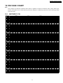
12 VOLTAGE CHART
Note:
· Circuit voltage and waveform described herein shall be regarded as reference information when probing defect point,
because it may differ from an actual measuring value due to difference of Measuring instrument and its measuringcondition
and product itself.
12.1. MOTHER P.C.B.
Ref No.
MODE
PLAY
STOP
Ref No.
MODE
PLAY
STOP
Ref No.
MODE
PLAY
STOP
Ref No.
MODE
PLAY
STOP
Ref No.
MODE
PLAY
STOP
Ref No.
MODE
PLAY
STOP
Ref No.
MODE
PLAY
STOP
Ref No.
MODE
PLAY
STOP
Ref No.
MODE
PLAY
STOP
Ref No.
MODE
PLAY
STOP
Ref No.
MODE
PLAY
STOP
Ref No.
MODE
PLAY
STOP
Ref No.
MODE
PLAY
STOP
Ref No.
MODE
PLAY
STOP
Ref No.
MODE
PLAY
STOP
Ref No.
MODE
PLAY
STOP
Ref No.
MODE
PLAY
STOP
Ref No.
MODE
PLAY
STOP
Ref No.
MODE
PLAY
STOP
IC1021
3
0
0
IC1195
3
4.4
4.4
1
2.0
1.9
2
1.7
1.7
1
5.2
5.2
2
0
0
1
5.0
5.0
2
2.4
2.4
1
0
0
2
1.6
1.4
1
0
0
2
2.6
2.6
1
5.0
5.0
2
0
0
3
0
0
21
3.7
2.9
22
0
0
23
3.7
2.9
1
2.5
2.5
2
2.5
2.5
3
2.5
2.5
1
0
0
2
0
0
3
0.4
0.4
4
3.3
3.3
21
3.1
3.2
22
0
0
23
3.3
3.3
41
-7.4
-9.2
42
-7.4
-9.2
61
3.3
0
62
0
3.2
Q1045
C
23.6
23.4
E
15.1
15.1
1
5.1
5.1
E
1.1
1.1
1
5.0
5.0
E
0
0
E
0
0
E
0
0
2
5.1
5.1
Q3501
C
0
0
2
5.0
5.0
Q4422
C
0
0
QR1115
C
0
0
QR3822
C
0.1
0.1
4
15.0
15.0
5
-790
-815
1
2.9
2.9
4
3.3
3.3
5
3.3
3.3
3
4
2.5
1.9
2.5
1.7
IC3502
3
4
5.0
2.4
5.0
2.2
IC3802
3
4
5.0
2.5
5.0
2.6
5
5.0
5.0
6
1.9
1.7
5
0
0
6
2.4
2.2
5
0
0
6
2.5
2.5
5
5.0
5.0
24
25
3.7
0
3.0
0
IC4301
4
5
-11.6
2.5
-11.4
2.5
IC1101
2
2.5
2.5
3
0
0
7
0
0
IC3501
8
9
2.3
2.3
2.3
2.3
6
0
0.3
7
0
0
8
1.9
1.5
9
2.2
2.2
26
1.6
1.3
27
1.6
1.3
28
0
0
29
1.6
1.4
6
2.5
2.5
7
2.5
2.5
8
11.8
12.7
5
3.3
3.3
6
3.3
3.3
7
3.3
3.3
8
3.3
3.3
9
1.7
1.7
24
3.3
3.3
25
0
0
26
0
0
27
0
0
28
3.3
3.3
29
3.3
3.3
43
-11.4
-9.2
44
-7.4
-9.2
45
-7.4
-9.2
46
-7.4
-9.2
47
-11.4
-9.2
48
-11.5
-9.2
49
-7.7
-9.2
63
3.3
0
64
0
0
1
5.2
5.2
Q1051
2
3
4.2
0
4.2
0
4
2.2
2.2
B
15.7
15.7
Q1115
3
4
0.1
5.2
0.1
5.2
B
0.4
0.4
Q3821
3
4
5.0
0
5.0
0
B
-4.7
0.7
B
3.3
3.3
B
5.0
5.0
5
5.1
5.1
E
1.1
1.1
6
5.1
5.1
Q3502
C
0
0
6
0
0
Q4423
E
C
0
0
0
0
QR3501
E
C
0
0
0
0
QR3823
E
C
10.8
10.8
11.7
11.7
E
2.4
2.4
Q1125
C
1.3
1.3
E
0
0
E
10.9
11.7
Q3851
C
0
0
E
1.9
1.9
B
3.3
3.3
E
0
0
B
0.1
0.1
E
0.1
2.6
IC1151
3
9.0
9.0
4
-
5
0
0
11
2.3
2.3
12
2.3
2.3
13
1.9
1.6
14
1.9
1.6
15
1.9
1.6
16
2.3
2.4
12
0
0
13
0.1
0.1
14
0
0
15
0.2
0.1
16
5.0
5.0
17
3.0
2.9
18
3.0
2.9
19
0
0
20
3.7
2.9
12
0
0
13
0.1
0
14
0
0.1
15
3.3
3.3
16
2.8
0.2
17
1.6
0.2
18
3.3
0
19
0
0
20
3.3
3.3
32
0
3.3
33
0
3.3
34
-4.4
0
35
-4.4
0
36
3.2
-8.7
37
-8.0
-9.2
38
-8.0
-9.2
39
-7.9
-9.2
40
-8.0
-9.2
52
-11.2
-9.2
53
-11.3
-9.2
54
-11.2
-9.2
55
-7.5
-9.2
56
-11.4
-9.2
57
-11.5
-9.3
58
3.2
0
59
2.7
0
60
2.8
0
Q1082
C
0
0
B
0.7
0.7
1
1.3
1.3
2
0.7
0.7
4
1.3
1.3
5
1.3
1.3
E
0
0
E
1.2
1.0
Q3852
C
0
0
E
0
0
Q1126
3
1.8
1.7
Q3811
C
0
0
Q4302
C
4.1
0
B
0
0
E
0
0
QR3821
C
11.4
12.3
IC6001
10
11
1.5
0
1.5
0
IC6001
30
31
3.3
3.3
3.3
3.3
IC6001
50
51
-3.0
0
-9.2
-9.2
IC6001
E
0
0
B
-4.7
0.7
2
3.3
3.3
IC3811
10
11
5.0
0
5.0
0
IC3811
30
31
1.8
0.1
1.4
0.1
4
1.7
1.7
B
0.4
0.4
5
0
0
10
0
0
1
11.0
12.0
B
1.8
1.7
Q3801
C
11.8
12.7
B
-4.7
0.7
Q4751
C
5.1
5.1
QR3502
C
2.3
2.3
QR4302
C
-4.7
2.5
31
Q1081
C
0.7
0.7
32
2.3
2.3
B
0
0
B
11.5
12.3
B
2.5
2.5
E
-6.5
-6.6
B
0
0
E
0
0
B
0
0
E
0
0
B
-4.7
0.7
Q6085
C
-6.4
-6.5
QR3503
C
2.3
2.3
QR4306
C
0.1
2.6
B
0.5
0.4
E
0
0
B
-5.8
-5.8
B
0
0
B
4.1
0
B
0
0
DVD-S29EG / DVD-S29E / DVD-S29EB
12.2. MODULE P.C.B.
Ref No.
MODE
PLAY
STOP
Ref No.
MODE
PLAY
STOP
Ref No.
MODE
PLAY
STOP
Ref No.
MODE
PLAY
STOP
Ref No.
MODE
PLAY
STOP
Ref No.
MODE
PLAY
STOP
Ref No.
MODE
PLAY
STOP
Ref No.
MODE
PLAY
STOP
Ref No.
MODE
PLAY
STOP
Ref No.
MODE
PLAY
STOP
Ref No.
MODE
PLAY
STOP
Ref No.
MODE
PLAY
STOP
Ref No.
MODE
PLAY
STOP
Ref No.
MODE
PLAY
STOP
Ref No.
MODE
PLAY
STOP
Ref No.
MODE
PLAY
STOP
Ref No.
MODE
PLAY
STOP
Ref No.
MODE
PLAY
STOP
Ref No.
MODE
PLAY
STOP
Ref No.
MODE
PLAY
STOP
Ref No.
MODE
PLAY
STOP
1
3.2
3.2
2
3.3
3.1
3
0
0
4
3.3
3.1
5
3.3
3.3
6
3.3
3.3
7
3.3
3.1
8
3.3
3.1
9
0
0
21
0
0
22
3.3
3.3
23
2.3
3.3
24
1.8
0
25
1.1
3.3
26
1.2
1.2
27
2.0
0
28
3.3
3.3
29
0
0
41
3.3
2.8
42
3.3
0.6
43
0
2.5
44
1.2
1.2
45
0
2.1
46
0
1.0
47
3.3
0.6
48
3.3
3.3
49
0
0
61
0
0
62
3.3
3.3
63
0
0
64
0
0
65
0
0
66
0.1
0
67
2.9
0
68
2.8
2.8
69
2.7
2.8
81
2.8
3.2
82
3.3
0
83
3.3
0
84
3.3
3.3
85
0
0
86
0
0
87
0
0
88
0
0
89
0
1.2
101
2.3
2.3
102
2.1
2.1
103
1.8
1.8
104
1.3
0
105
0
0
106
1.7
1.8
107
3.3
3.2
108
2.1
2.1
109
2.1
2.0
121
1.4
1.4
122
0
0
123
0.4
0
124
1.0
0.1
125
0.1
0.1
126
0.1
0.6
127
2.2
2.2
128
1.6
1.6
129
2.6
2.2
141
3.3
3.3
142
1.2
1.2
143
1.9
2.0
144
2.1
2.1
145
0
0
146
1.6
1.6
147
1.6
1.6
148
1.6
1.6
149
0.6
0.4
161
3.3
3.3
162
0
0
163
1.6
1.6
164
0
0
165
1.5
166
1.5
1.5
167
3.3
3.3
168
0.1
0.1
169
1.7
1.7
181
0
0
182
3.3
3.3
183
0
0
184
0
0
185
0
0
186
0
0
187
0
0
188
0
0
189
0
0
201
0
0
202
3.3
3.3
203
1.0
0
204
1.5
0.8
205
0
0.9
206
1.7
0
207
0.5
0
208
3.1
1.8
209
3.3
3.3
221
2.3
0
222
0
0
223
0
1.6
224
0
0
225
3.3
3.3
226
1.6
1.6
227
0
0
228
0
1.5
229
0
1.5
241
3.0
1.6
242
0
0
243
1.6
1.6
244
3.3
3.2
245
3.2
3.2
246
3.3
3.3
247
0
0
248
3.2
0
249
2.3
3.3
1
3.3
3.3
2
3.2
3.0
3
3.3
3.3
4
3.2
3.2
5
3.2
3.1
6
0
0
7
3.2
3.3
8
3.2
3.3
9
3.3
3.3
21
1.5
1.7
22
0
0
23
0
0.1
24
0
0.1
25
0
0.2
26
3.1
1.6
27
3.3
3.3
28
0
0
29
2.3
1.6
41
0
0
42
3.2
3.2
43
3.3
3.3
46
0
0
47
3.1
3.0
48
3.2
3.2
49
3.3
3.3
1
3.3
3.3
2
-
3
0
0
44
45
3.2
3.2
3.2
3.1
IC8111
4
5
2.0
4.7
2.3
4.7
6
-
7
-
8
5.1
5.1
1
3.3
3.3
2
1.6
1.6
3
3.3
0
4
3.3
0
5
1.8
1.6
6
1.6
1.6
7
1.6
1.6
8
9.0
9.0
21
5.1
5.1
22
1.6
1.6
23
1.6
1.6
24
0
0
25
1.8
1.7
26
1.8
1.8
27
1.8
1.6
1
1.6
1.6
2
1.6
1.6
IC8601
2
3.2
3.2
3
1.3
0
4
1.7
1.7
5
1.7
3.2
6
3.3
3.3
7
3.3
3.3
28
1.6
1.6
IC8421
8
9
3.3
0
3.3
0
1
0
0
IC8001
10
11
3.3
3.3
3.2
3.1
IC8001
30
31
0.9
0.9
0.7
0.5
IC8001
50
51
3.3
0
1.9
2.8
IC8001
70
71
3.0
0
0
0
IC8001
90
91
1.2
0
0
0
IC8001
110
111
1.8
1.8
1.8
1.8
IC8001
130
131
2.6
2.6
2.2
2.2
IC8001
150
151
3.3
0.4
3.3
0.5
IC8001
170
171
1.6
1.3
1.6
0
IC8001
190
191
3.3
0
3.3
0
IC8001
210
211
3.3
0.6
3.3
2.2
IC8001
230
231
0
3.3
0
3.3
IC8001
250
251
0
2.4
0
3.3
IC8051
10
11
3.2
3.2
3.1
3.0
IC8051
30
31
1.6
1.5
1.6
1.6
IC8051
50
51
3.1
3.2
2.9
2.9
9
4.3
4.2
3
3.3
3.3
32
12
3.3
3.3
13
3.3
3.0
14
3.3
3.2
15
3.3
2.9
16
0
0
17
3.3
3.2
18
3.3
3.1
19
3.3
3.3
20
0
0
32
0.7
0.3
33
0
0.8
34
3.3
3.3
35
0
0
36
0
1.1
37
0
2.3
38
3.3
2.5
39
0
1.4
40
0
1.4
52
2.0
2.6
53
3.3
3.3
54
0
0
55
0
3.3
56
3.3
3.3
57
3.3
3.3
58
3.3
3.3
59
3.3
3.3
60
3.3
3.3
72
0
0
73
3.2
0
74
0
0
75
1.6
1.6
76
2.0
1.6
77
1.7
1.7
78
0.1
3.3
79
3.3
0
80
0
3.3
92
0
0
93
0
0
94
0
0
95
0
0
96
0
0
97
0
0
98
3.3
3.3
99
0.7
0.8
100
0
0
112
1.3
1.0
113
1.3
1.6
114
1.6
1.6
115
1.6
1.6
116
1.6
1.6
117
1.6
3.3
118
3.3
3.3
119
1.9
1.8
120
1.5
1.5
132
2.6
2.2
133
2.6
2.2
134
2.6
2.2
135
2.4
2.2
136
2.4
2.2
137
2.4
2.2
138
2.4
2.2
139
1.6
1.6
140
1.8
1.6
152
0.4
0.4
153
1.0
1.0
154
1.0
1.0
155
2.2
2.2
156
0.7
0.4
157
0
0
158
0.9
0.9
159
3.3
3.3
160
0
0
172
1.2
1.2
173
0
0
174
0
0
175
0
0
176
1.1
0
177
3.3
1.6
178
3.3
3.3
179
0
0
180
3.3
3.3
192
1.0
0.8
193
1.6
1.6
194
1.0
1.0
195
1.0
0.9
196
3.3
3.3
197
3.3
3.3
198
0.8
0.8
199
0.8
0.9
200
0.7
0.9
212
0.6
2.2
213
0
0
214
0
0
215
3.1
0
216
3.3
3.0
217
3.3
3.3
218
0
0
219
1.2
1.2
220
1.2
1.6
232
1.6
3.3
233
0
0.5
234
3.0
0.8
235
0
0
236
1.2
1.2
237
0
0
238
0
0
239
3.3
3.3
240
3.0
3.1
252
3.1
3.3
253
0
0
254
3.2
0
255
3.3
3.3
256
3.2
3.0
12
0
0
13
3.3
2.9
14
3.1
3.3
15
3.3
2.8
16
3.3
3.3
17
3.3
3.2
18
3.2
3.2
19
3.0
3.2
20
1.5
2.7
32
1.5
1.5
33
0
0.1
34
0
0
35
0
0
36
0
0
37
3.3
3.3
38
3.3
1.6
39
2.4
2.8
40
-
52
0
0
53
3.3
3.1
54
0
0
IC8251
10
11
4.3
4.3
4.2
4.2
IC8251
12
4.2
4.2
13
3.1
3.8
14
5.5
3.8
15
2.5
2.6
16
2.6
2.6
17
2.6
2.6
18
2.6
2.6
19
0
0
20
9.0
9.0
10
2.5
2.5
12
2.5
2.5
13
0
0
14
5.0
5.0
15
5.0
0
16
4.9
0
11
2.5
2.5
DVD-S29EG / DVD-S29E / DVD-S29EB
Ref No.
MODE
PLAY
STOP
Ref No.
MODE
PLAY
STOP
Ref No.
MODE
PLAY
STOP
Ref No.
MODE
PLAY
STOP
Ref No.
MODE
PLAY
STOP
Ref No.
MODE
PLAY
STOP
Ref No.
MODE
PLAY
STOP
IC8611
4
5
0
3.3
0
3.3
1
0
0
2
0
0
3
0
0
1
1.0
2
0.3
3
0.6
4
2.4
21
0
22
0
23
0
41
0.6
43
0.6
E
5.0
5.0
42
0.6
Q8550
C
5.0
5.1
Q8562
C
0.1
0.1
1
0
0
2
0
0
E
5.0
5.1
6
3.3
3.3
7
0
0
8
3.3
3.3
5
0
6
0
7
3.3
8
3.3
9
0
24
0
25
3.3
26
3.3
27
0
28
3.3
29
0.6
44
0.6
45
0.6
47
3.3
48
0
E
0.4
0
46
0
Q8551
C
4.0
5.0
5
0
0
6
4.7
4.7
B
4.3
4.4
B
5.0
5.0
QR8111
3
4
1.2
0
1.2
0
B
1.0
0.1
E
0
0
IC8651
10
11
0
3.3
IC8651
30
31
0.6
0.6
IC8651
E
4.6
5.0
Q8552
C
2.2
1.3
QR8431
C
4.2
0
B
0
3.3
33
12
3.2
13
3.3
14
3.3
15
3.3
16
3.3
17
3.3
18
3.3
19
0
20
0
32
0.6
33
0.6
34
0.6
35
0.6
36
0.6
37
3.3
38
0.6
39
0.6
40
0.6
E
0
0
Q8560
C
0.1
0.1
B
0.7
0.7
E
0
0
Q8561
C
5.0
5.0
B
0.1
0.1
QR8571
C
3.2
0
B
0.1
3.3
B
3.9
5.0
E
3.3
3.3
DVD-S29EG / DVD-S29E / DVD-S29EB
34
DVD-S29EG / DVD-S29E / DVD-S29EB
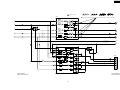
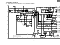
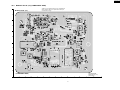
13 BLOCK DIAGRAM
Note:
Circuit voltage and waveform described herein shall be regarded as reference information when probing defect point, because it may differ from an actual measuring value due to difference of Measuring instrument and its measuringcondition and product itself.
13.1. OVERALL BLOCK DIAGRAM
MECHANISM UNIT
MODULE P.C.B.
MOTHER P.C.B.
IC8001
OPTICAL
PICK UP
UNIT
IC8421
MIXL
AUDIO
D/A
CONVERTER
MIXR
IC8251
L OUT
SPINDLE
MOTOR
TRAVERSE
MOTOR
AV21PIN
R OUT
MOTOR
DRIVE
IC8651
DV2
FRONT-END PROCESSOR/
OPTICAL DISC CONTROLLER/
DIGITAL SERVO CONTROLLER/
AV DECODER
LOADING
MOTOR
DIGITAL
AUDIO OUT
(COAXIAL)
16Mbit
FLASH
ROM
IC6001
TRAY
IC3501
FL
VIDEO
DRIVER
OPERATION
CPU
VIDEO OUT(LINE)
Y
PB
PR
IC8611
16Kbit
EEP ROM
KEY
IC3811
VIDEO OUT
(AV21PIN)
IC8051
VIDEO
DRIVER
64Mbit
SDRAM
R
G
B
AV21PIN
REMOTE CTL
MOTHER P.C.B.
DVD-S29EG/E/EB
OVERALL BLOCK DIAGRAM
35
DVD-S29EG / DVD-S29E / DVD-S29EB
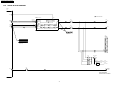
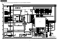
13.2. POWER SUPPLY BLOCK DIAGRAM
PRIMARY CIRCUIT
SECONDARY CIRCUIT
IC6001
L1001
D1011,C1011
(OPERATION CPU)
T1021
FL
AC SOCKET
P1001
VA1002
SURGE
KILLER
10
LINE
FILTER
RECTIFIER
F1001
NSW+9V
NSW-12V
VCC
VEE
AUDIO
OP AMPS
DGT8 40
DGT11 37
POWER
TRANSFORMER
Q1125
11
REG.
D+1.2V
SEG0 41
Q1126
SEG15 56
SWITCH
A+5V
Q1115
12
D+5V
REG.
QR1115
N.POWER OFF L
SWITCH
63 N.P.OFF L
IC1151
IC1021
CONSTANT
VOLTAGE
CONTROL
(REG.M+9V)
2
ON/OFF
1 IN
OUT 3
15
16
M+9V
IC1195
IR6131
NSW+3.3V
REG.
REMOTE CTL 21
1 IR
RECEIVER
OPEN/CLOSE
15 RESET
S6151
POWER
STANBY D6101
32 STANBY LED
Q1051
PHOTO
COUPLER
S6152
AN2 4
PLAY
SHUNT IC1101
REG.
S6161
AN1 5
QUICK OSD
PAUSE
IP1171
PROTECTOR
FLH-
S6171
AN0 6
S6162
STOP
S6172
9 OSC2
X6001
10 OSC1
DVD-S29EG/E/EB
POWER SUPPLY BLOCK DIAGRAM
36
DVD-S29EG / DVD-S29E / DVD-S29EB
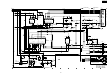
13.3. SERVO BLOCK DIAGRAM
RF SIGNAL
MOTOR DRIVE SIGNAL
TRACKING ERROR SIGNAL
FOCUS ERROR SIGNAL
IC8251
IC8001
(DV2)
(MOTOR DRIVE)
VO2+
VIN9
OPTICAL PICK UP UNIT
VIN10
VIN5
PHOTO DETECTOR
VIN6
B1
B2
A1
A4
B4
A2
A3
B3
VIN7
HEAD
AMP
VIN8
VIN1
VIN2
VIN3
VIN4
LASER DIODE(DVD)
129
75
TRSDRV
6
VIN2
LEVEL
SHIFT
134
133
147
TRDRV
22
11
+
+
BIAS1
TRAVERS MOTOR
VO2-
VIN4
OPIN+
25
132
VO1+
131
148
FODRV
23
VIN5
138
137
LEVEL
SHIFT
76
SPDRV
5
AD1
27
13
+
OPIN-
+
140
SPINDLE MOTOR
VO1-
VIN1
136
135
14
+
+
-
OPOUT
VO3+
26
10
+
LPC01
LPC1
124
FROM
IC6001-16,17PIN
123
7
LEVEL
SHIFT
VIN3
LPC02
LPC2
126
VO3-
RFINP
9
BIAS2
IC8251-15,16,17,18
4Vp-p(0.5msec./div.)
125
79
RFINN
M2601
LOADING MOTOR
+
+
Q8561, Q8562
LD DRIVE
12
+
Q8551, Q8552
LD DRIVE
LASER DIODE(CD)
130
MUTE1
3
OPTICAL PICK UP UNIT
ACTUATOR
CH1
MUTE
+
VO4+
TRACKING
COIL
ACT T+
17
110
83
111
MUTE2
4
LEVEL
SHIFT
CH2,4,5
MUTE
VO4-
+
+
+
VO5+
VO5-
ACT T-
18
FOCUS
COIL
ACT F+
15
ACT F-
16
LEVEL
SHIFT
+
+
IC6001
(OPERATION CPU)
CH3
MUTE
MUTE3
TRAY MUTE
1
18
CLOSE SW
TRAY CLOSE
25
S2601
OPEN SW
TRAY OPEN
24
S2602
DVD-S29EG/E/EB
SERVO BLOCK DIAGRAM
37
DVD-S29EG / DVD-S29E / DVD-S29EB
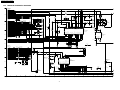
13.4. VIDEO BLOCK DIAGRAM
IC8001
(DV2)
DAC5OUT 158
DAC4OUT 156
OPTICAL
PICK-UP
UNIT
DAC2OUT 151
DAC3OUT 152
(16M FLASH ROM)
29 DQ0
31
33
35
38
40
42
44
30
32
34
36
39
41
43
45 DQ15
A0 25
A8 8
A15 1
DATA
XCE
26
ADDRESS
XWE
11
A16
A17
A18
A19
A20
48
17
16
9
10
Y
B
Y/PY/G
C
CB/PB/B
D
CR/PR/R
E
23 A0
39
37
51
24
40
36
50 A7
ADDRESS
A7 18
ADDRESS
A
110 RFINN
111 RFINP
DAC1OUT 149
IC8651
C
25 A8
41
33
47
27
42
32
46 A15
30
43
31
45
21
A16
A17
A18
A19
A20
IC8051
(64M SDRAM)
IC8001-152
0.49Vp-p(20usec./div.)
ADDRESS
MEMORY
ADDRESS
12bit
XOE
28
52 NEXOE
22 NEXWE
38 NEXCE
212 EXADT0
210
207
204
200
198
195
193
192
194
197
199
203
206
208
211 EXADT15
MEMORY
DATA
16bit
DATA
A0
A1
A2
A3
A4
A5
A6
A7
A8
A9
A10
A11
23
24
25
26
29
30
31
32
33
34
22
35
227
224
221
217
220
223
226
228
233
238
230
237
MA0
MA1
MA2
MA3
MA4
MA5
MA6
MA7
MA8
MA9
MA10
MA11
DQ0 2
DQ1 4
DQ2 5
DQ3 7
DQ4 8
DQ5 10
DQ6 11
DQ7 13
DQ8 42
DQ9 44
DQ10 45
DQ11 47
DQ12 48
DQ13 50
DQ14 51
DQ15 53
17 MDQ0
14 MDQ1
11 MDQ2
8 MDQ3
5 MDQ4
2 MDQ5
256 MDQ6
252 MDQ7
254 MDQ8
1 MDQ9
4 MDQ10
7 MDQ11
10 MDQ12
13 MDQ13
15 MDQ14
18 MDQ15
CS
NRAS
CAS
WE
CLK
240 NCSM
244 NRAS
245 NCAS
248 NWE
243 MCK
19
18
17
16
38
MEMORY
ADDRESS
12bit
IC8001-149
0.92Vp-p(20usec./div.)
IC8001-151
0.49Vp-p(20usec./div.)
IC8001-158
0.6Vp-p(20usec./div.)
IC8001-156
0.92Vp-p(20usec./div.)
MEMORY
DATA
16bit
NRST 73
FROM
IC8601-2PIN
DVD-S29EG/E/EB
VIDEO BLOCK DIAGRAM
38
DVD-S29EG / DVD-S29E / DVD-S29EB
VIDEO MAIN SIGNAL
IC3501-11
1.2Vp-p(20usec./div.)
IC3501-12
1.2Vp-p(20usec./div.)
IC3501-15
2.0Vp-p(20usec./div.)
IC3501-13
2.0Vp-p(20usec./div.)
IC3501
(VIDEO DRIVE)
BIAS
2
A
CIN
LPF
4dB
2dB
75
DRIVER
8dB
75
DRIVER
2dB
75
DRIVER
COUT
6.75MHz
-6dB +
CVBS
OUT
16
JK4401
VIDEO OUT
15
CLAMP
4
B
YIN
LPF
4dB
YOUT
14
6.75MHz
IC3502
MUTE
BIAS
4
1.4V
2
MUTE
6
C
JK4401
CLAMP
1
6
CYIN
LPF
4dB
2dB
75
DRIVER
2dB
75
DRIVER
2dB
75
DRIVER
CYOUT
13
Y
12
PB
11
PR
13.5MHz
Q3501
AMP
D
BIAS
8
CBIN
LPF
4dB
CBOUT
6.75MHz
Q3502
AMP
E
BIAS
9
CRIN
LPF
4dB
CROUT
6.75MHz
D-WIDE1/RGB-H/MIC MUTE
FROM
IC6001-26PIN
D-WIDE2/YC-H/MIC DET
FROM
IC6001-27PIN
IC3811
(VIDEO DRIVE)
IC3802
2
3
4
S1
6MHz
LPF
S2
S-DCOUT
S1/S2
CIN
BIAS
6
7
8
6
31
CLAMP
6dB
L
6MHz
LPF
75
CVOUT
CVOUT
SAG
CLAMP
30
H
6MHz
LPF
6dB
75
YOUT
27
AMP
11
PY/G
IN
13
PB/B IN
H
6dB
CLAMP
BIAS
21
V-OUT
YOUT
SAG
BIAS
JK3871
AV 21-PIN
TERMINAL
29
SEL
Q3811
4
1
SEL
YIN
32
2
S-DCOUT
6dB
+
CVIN
75
COUT
12MHz
LPF
75
PY/G
OUT
20
19
18
26
17
RED I/O
24
16
15
14
L
13
PY/G
OUT
SAG
6dB
12MHz
LPF
75
PB/B
OUT
GREEN I/O
23
12
11
10
9
21
BLUE I/O
8
7
6
PB/B
OUT
SAG
15
PR/R IN
BIAS
6dB
12MHz
LPF
75
PR/R
OUT
PR/R
OUT
SAG
DVD-S29EG/E/EB
VIDEO BLOCK DIAGRAM
5
4
20
3
2
1
18
17
DVD-S29EG/E/EB
VIDEO BLOCK DIAGRAM
39
DVD-S29EG / DVD-S29E / DVD-S29EB
13.5. AUDIO BLOCK DIAGRAM
IC8001
(DV2)
DACCK 163
AUDIO MAIN SIGNAL
IC8421
MCLK
1
(AUDIO D/A CONVERTER)
SMUTE/CSM
ACKS/C CLK
DIF0/CDTI
STBDAC 53
SBT3 56
STO3 57
LRCK
LRCK 169
BICK
SRCK 170
SDTI
ADOUT3 171
6
7
8
4
2
3
DE-EMPHASIS
CONTROL
µP
INTERFACE
CLOCK
DIVIDER
ATT
8X
INTERPOLATOR
∆Σ
MODULATOR
SCF
LPF
ATT
8X
INTERPOLATOR
∆Σ
MODULATOR
SCF
LPF
AUDIO
DATA
INTERFACE
JK4401
IC4301
11
AOUTL
2
AOUTR
6
AMP
1
MIX L
IC4301
10
AMP
7
MIX R
IC8421-10,11
0.44Vp-p(0.5msec./div.)
JK3871
AV 21-PIN
TERMINAL
21
20
19
18
17
16
15
14
IC8001-171
5Vp-p(10usec./div.)
13
12
11
10
9
8
7
6
5
Q4422
MUTE
LOUT
4
ROUT
2
3
1
QR4302,QR4306
MUTE
Q4423
MUTE
Q3852
MUTE
Q3851
MUTE
Q4751
IECOUT 177
Q4302
SWITCHING
NP-MUTE
FROM
IC6001-62PIN
A-MUTE
FROM
IC8001-55PIN
QR8431
SWITCHING
JK4401 DIGITAL
AUDIO OUT
(COAXIAL)
AMP
DVD-S29EG/E/EB
AUDIO BLOCK DIAGRAM
40
DVD-S29EG / DVD-S29E / DVD-S29EB
14 INTERCONNECTION SCHEMATIC DIAGRAM & SCHEMATIC DIAGRAM NOTES
14.1. INTERCONNECTION SCHEMATIC DIAGRAM
OPTICAL PICK UP UNIT
E
FP8501
1
2
3
4
5
6
7
8
9
10
11
12
13
14
15
16
17
18
19
20
21
22
23
24
25
26
T+
F+
FTHFM
TA(DVD)
TB(DVD)
TD(DVD)
TC(DVD)
FE2(DVD/CD)
FE1(DVD/CD)
GND
RF
VREF2(RF-)
PIN(DVD)
LDCD
LDGND
LDDVD
GND(OEIC)
VREF1
VCC
SUB2
SUB1
PIN(CD)
SUBSEL
GND(VRCD)
FP8201
6
5
4
3
2
1
TRV INNER SW
DGND
TRVM+
TRVMSPM+
SPM-
DGND
D+5V
DGND
A+5V
AGND
D+1.2V
DGND
M+9V
MGND
TRAY DRV
TRAY MUT
DOP CPU CLK
DOP CPU CMD
DOP CPU STAT
MOTHER P.C.B.
FP8101
MIX-L
1
ADGND
2
MIX-R
3
4
ADGND
5
A-REF
6
ZFLAG & AMUTE
7
ADGND
8
AUDIODIGITAL
ADAC5V
9
LD10
LD+
11
12
CR/PR/R
13
VGND
14
CB/PB/B
VGND
15
16
Y/PY/G
VGND
17
18
Y
VGND
19
20
C
FP3502
MIX-L
1
ADGND
2
3
MIX-R
4
ADGND
5
A-REF
6
ZFLAG & AMUTE
7
ADGND
8
AUDIODIGITAL
ADAC5V
9
10
LD11
LD+
CR/PR/R
12
13
VGND
CB/PB/B
14
15
VGND
16
Y/PY/G
VGND
17
18
Y
19
VGND
20
C
FP2001
1
LDLD2
3
LD+
4
LD+
5
CLOSE-SW
6
GND(SW)
OPEN-SW
7
C
6
5
4
3
2
1
FP3501
1
DGND
2
D+5V
3
DGND
4
A+5V
5
AGND
6
D+1.2V
7
DGND
8
M+9V
9
MGND
10
TRAY DRV
TRAY MUT
11
12
DOP CPU CLK
13
DOP CPU CMD
14
DOP CPU STAT
MODULE P.C.B.
D
TRV INNER SW
DGND
TRVM+
TRVMSPM+
SPM-
FP8102
1
2
3
4
5
6
7
8
9
10
11
12
13
14
PJ6101
KEY-SCAN1
1
2
DGND
STBYLED
3
F
KEY-SCAN1
DGND
STBYLED
LDLDLD+
LD+
CLOSE-SW
GND(SW)
OPEN-SW
B
PJ6101
1
2
3
FP2601
1
2
3
4
5
6
7
MECHANISM UNIT
LOADING MOTOR P.C.B.
A
POWER SW P.C.B.
DVD-S29EG/E/EB
INTERCONNECTION
SCHEMATIC DIAGRAM
1
2
3
4
5
41
6
7
8
9
DVD-S29EG / DVD-S29E / DVD-S29EB
14.2. SCHEMATIC DIAGRAM NOTES
This schematic diagram may be modified at any time with the development of new technology.
Important safety notice:
Components identified by
mark have special characteristics important for safety.
Furthermore, special parts which have purpose of fire-retardant (resistors), high-quality sound (capacitors), low-noise
(resistors), etc. are used. When replacing any of components, be sure to use only manufacture´s specified parts shown in
theparts list.
Important safety notice:
There are special components used in this equipment which are important for safety.
in the schematic diagrams. It is essential that these critical parts should be replaced with
These parts are marked by
manufacturer’s specified parts to prevent shock, fire, or other hazards. Do not modify the original design without permission of
manufacturer.
Caution!
IC and LSI are sensitive to static electricity.
Secondary trouble can be prevented by taking care during repair.
Cover the parts boxes made of plastics with aluminum foil.
Ground the soldering iron.
Put a conductive mat on the work table.
Do not touch the legs of IC or LSI with the fingers directly.
42
DVD-S29EG / DVD-S29E / DVD-S29EB
15 SCHEMATIC DIAGRAM
15.1. POWER SUPPLY SECTION (MOTHER P.C.B. (1/2)) SCHEMATIC DIAGRAM
Q1125
2SB14170JA
D1121
B0JAMG000013
K1121
C1003
ECKMNA471MBV
C1122
6V2200
C1121
6V1000
Q1126
XN0150100L
-
T1021
G4D2A0000223
(POWER TRANSFORMER)
2
TL1007
+
1
D1031
B0HADV000001
TL1005
17
3
16
4
15
5
14
6
13
7
12
8
11
9
10
R1126
3600
R1125
270
3
5
R1041
68
D1041
B0HAGM000006
C1041
50V56
Q1045
2SC3311ASA
C1051
820P
D1111
B0JAMG000013
4
R1072
1K
MGND
F AV
A+5V
F AV
D+5V
F AV
M+9V
F AV
NSW+9V
F AV
FLH+
F AV
FLH-
F AV
NSW-12V
F AV
NPOFF L
F AV
TP1105
3
5
2
6
C1116
10V220
1
C1117
6V1000
IC1151
C0DBZHG00047
(REG.M+9V)
D1071
MZ41000MF
QR1115
B1GBCFNN0036
(SWITCHING)
R1062 12K
D1152
B0JAML000009
D1153
B0EAKM000122
L1151
G0A220GA0026
C1061
120P
R1085
100K
1
2
3
4
5
TP1107
R1061
22K
D1084
MAZ41600LF
TP1108
L1117
G0C100JA0048
C1111
10V1000
C1071
0.068
D
F AV
L1111
G0A100HA0023
R1116
1K
R1071
1500
R1051
20K
AGND
C1004 ECKMNA102MEV
D1072
MA2C16500E
D1051
MAZ40680MF
TP1106
(REG.5V)
R1045
27K
E
F AV
GND
1
DGND
Q1115
B1DHDD000029
CONSTANT
VOLTAGE CTL.
DRAIN
F/B
VCC
C1045
25V47
GND
4
Z/C
2
2
D1045 MAZ42000LF
R1046
10
(SW IC)
TP1104
2
NC
IC1021
C0DACZH00007
R1128
120
C1115 0.1
C1021
F1A3D470A010
F AV
3
OUT
4
VGND
4
ON/OFF
C1002
F0CAF104A024
F AV
IN
2
D1125
MA2J11100L
C1125
0.1
R1115 100K
1
R1031
68K
R1001
470K
R1127
1300
18
C1031
F1B3A332A009
C1012
450V10
VA1002
ERZVA5Z471
C1001
F0CAF104A024
3
3
C1112 10V1000
F
4
TL1006
F1001
FUSE
K5D162BLA013
TL1004
R1002
470K
ADGND
TP1112
5
C1011
450V10
K1006
ZA1002
EYF52BC
ZA1001
EYF52BC
P1001
K2AA2B000004
TL1002
L1001
ELF15N003A
F AV
C1127
6V1000
1
D1011
B0EDKT000002
K1005
A
D+1.2V
C1126
1000P
(REG.D+1.2V)
G
TL1001
TP1101
(REG.D+1.2V)
D1081
MA2C18500E
D1151
B0JAML000009
R1081
27K
C1083
50V47
K1154
K1155
C1153
25V330
C1155
0.1
C1154
16V220
TP1111
L1131
G0C330KA0004
C1151
25V330
TP1116
R1082
10K
Q1082
2SC3311ASA
CONSTANT
VOLTAGE CTL.
D1171
B0JAME000037
K1172
R1083
5.6K
D1083
MAZ41000HF
Q1081
2SC3311ASA
CONSTANT
VOLTAGE CTL.
C1082
0.1
R1084
22K
D1082
MA2C16500E
C1171
10V100
IP1171
B1ZAZ0000030
C1081
1000P
2
TP1115
1
C
TP1113
L1141
G0C330KA0004
D1141
B0JAML000009
C1141
25V100
ZA1111
RMCC0001
TP1109
ZA1112
K4CZ01000027
B
IC1101
C0DAEMB00003
Q1051
B3PBA0000104
(FEED BACK)
A
C
R1052
4
1
1
3
5
VB
R
A :PO(POWER SUPPLY SECTION)
B :F/AV(FRONT & AV OUT SECTION)
1
2
3
HOT
4
5
43
AV
(REG.NSW+3.3V)
VDD
1
COLD
6
RESET
IC1195
C0DBFGC00008
2
R1104
1K
A
AV
4
RST
2
R1105
1K
3
NSW+3.3V
R1191
100K
C1197
1
(SHUNT REG.)
7
C1102
0.1
R1107
10K
C1101
0.68
R1106
1.2K
8
R1102
12
GND
2
CD
3
C1110 1000P
R1101
75
R1103
12
C1196
0.01
C1195
1
9
10
DVD-S29EG/E/EB
POWER SUPPLY SECTION
(MOTHER P.C.B.(1/2))
SCHEMATIC DIAGRAM
11
DVD-S29EG / DVD-S29E / DVD-S29EB
15.2. FRONT & AV OUT SECTION (MOTHER P.C.B. (2/2)) SCHEMATIC DIAGRAM
A
B
PO
PO
B
C
A+5V
D+5V
M+9V
D+1.2V
ADGND
AGND
MGND
E
A :PO(POWER SUPPLY SECTION)
B :F/AV(FRONT & AV OUT SECTION)
FLH+
FLH-
F
P15
4G
P14
P13
4G
3G
P12
P11
P10
3G
P9
2G
P8
P7
P6
2G
P5
1G
P4
P3
1G
P2
P1
1G
F-
F-
1
2
4
5
6
7
8
9
10
11
12
13
14
15
16
17
18
19
20
21
22
23
24
25
26
27
28
29
31
32
CL6022
Q6085
B1ABGC000011
D6081
MAZ40910LF
G
DP6081
A2BA00000217
P16
K3514
4G
K3513
K3512
F+
K3511
F+
H
PO
PO
PO
PO
PO
PO
PO
TO FP8102
MODULE P.C.B.
FP3501
OP CPU-STAT
OP CPU-CMD
OP CPU-CLK
TRAT MUT
TRAY DRV
MGND
M+9V
DGND
D+1.2V
AGND
A+5V
DGND
D+5V
DGND
R4304
2200
14
13
12
11
10
9
8
7
6
5
4
3
2
1
CL6001
R6086
100K
(FL DRIVE)
CL6011
CL6010
CL6009
CL6008
CL6007
CL6006
CL6005
CL6004
CL6003
CL6002
R4320
2200
R6081 270
R6085
8200
A1
A2
CL6012
CL6013
CL6014
CL6015
CL6016
CL6017
CL6018
CL6019
CL6020
CL6021
K6009
B3
B10
A21
L4291
G0C391JA0064
B4
B7
B21
B6
B12
B8
B9
B20
B21
B11
B4
B6
B3
B5
B8
B7
B11
B9
B13
B12
B15
B14
B17
B16
B19
B18
E
PO
B19
B18
C6081
0.01
CL6023
C4337 50V82
20
19
18
17
16
15
14
13
12
11
10
9
8
7
6
5
4
3
2
1
A24
45
44
43
42
41
40
39
38
37
36
35
34
33
SEG0/DGT7
DGT8
DGT9
DGT10
DGT11
DGT12
DGT13
DGT14
DGT15
IC4301
C0ABBB000118
R4355 15K
46
SEG1/DGT6
A23
47
SEG2/DGT5
+
A5
48
SEG3/DGT4
5
SEG4/DGT3
6
SEG5/DGT2
7
SEG6/DGT1
8
VCC
A4
SEG7/DGT0
A3
49 SEG8
DGT16 32
50 SEG9
DGT17 31
51 SEG10
VDD3 30
A10
52 SEG11
VDD2 29
A11
53 SEG12
LED2 28
A27
R4332 8.2K
54 SEG13
LED1 27
A28
R4331 8.2K
55 SEG14
LED0 26
A29
IRQ4 25
A30
57 VPP
IRQ3 24
A31
A13
58 TXD,SBO0
IRQ2 23
A14
59 RXD/SBI0
A15
60 SBT0
A6
+
-
C4336 50V82
A7
A8
A9
1
(AMP)
2
3
VEE
4
NSW-12V
L6001
G0C101JA0019
D
B17
B15
A22
IC6001
MN101C87AAA1
56 SEG15
PO
B16
B14
B10
R4356 15K
TO FP8101
MODULE P.C.B.
FP3502
C
VGND
Y
VGND
Y/PY/G
VGND
CB/PB/B
VGND
CR/PR/R
LD+
LDADAC5V
AUDIO DIGITAL
ADGND
ZFLAG & MUTE
A-REF
ADGND
MIX-R
ADGND
MIX-L
B20
B13
B1
B2
C3519 6V1000
B5
B2
B1
RESET
A12
C4314 0.1
C4315 0.1
C4324
25V220
TL4902
C6006
0.01
C6005
50V10
R6004 0
C4323
25V220
IRQ1/ACZ 22
IRQ0 21
61 SBO2/SDA
TM7IO 20
A25
62 SBI2/AN7
TM3IO 19
A18
63 SBT2/SCL
TM2IO 18
PO
NSW+9V
PO
NPOFF L
PO
NSW+3.3V
AN0
VREF+
VDD
OSC2
OSC1
VSS
XI
XO
MMOD
XRST
RMOUT/TM0IO
4
5
6
7
8
9
10
11
12
13
14
15
16
A2
A12
R6071
30K
CL6025
R6011 1K
X6001
H2D800400009
1
R6072
47K
R6009 10K
AN1
3
R6008 0
AN2
2
A1
TM1IO 17
K6007
AN3
K4904
VGND
DGND
1
64 BUZZER/AN6
C
PO
PO
AN4
A13
A14
A15
AN5
CL6024
K4905
K4902
3
K4901
A19
2
R6000
0
TL4901
A36
1
2
A21
3
4
A25
A11
5
6
7
44
8
R6060 10K
R6050 10K
R6040 10K
R6025 10K
(MUTE)
C6060 0.01
CL6027
R4329
0
C6050 0.01
R4302
10K
C6040 0.01
TL4303
R6022
R6101
D6101
150
B3AAA0000721
(RED)
QR4306
B1GBCFJA0026
(SWITCHING)
A19
1
2
3
C4313
0.1
Q4302
B1ABCF000138
K6008
PJ6101
R6021 10K
CL6026
KEY-SCAN1
GND
STBY LED
R6006
10K
S6171
EVQ11G07K
EVQ11407KJ
PAUSE
S6161
EVQ11G07K
EVQ11407KJ
PLAY
L6131
C6132
0.1
TL4301
A24
S6152
EVQ11G07K
EVQ11407KJ
A
QR4302
B1GDCFJJ0046
(MUTE)
POWER SW
R6026
POWER SW P.C.B.
R6023 10K
R4303
2200
C6001 6V100
C6002
0.1
R4309 22K
C6003
0.01
9
R6171
1200
R6161
1200
R6151
1200
S6172
EVQ11G07K
EVQ11407KJ
STOP
3 2 1
VCC
GND
ROUT
R4301 3300
R6024
B
A18
S6162
EVQ11G07K
EVQ11407KJ
QUICK OSD
S6151
EVQ11G07K
EVQ11407KJ
OPEN/CLOSE
10
IR6131
B3RAD0000090
(REMOTE CTL.RECEIVER)
DVD-S29EG/E/EB
FRONT & AV OUT SECTION
(MOTHER P.C.B.(2/2))
SCHEMATIC DIAGRAM
11
12
F
DVD-S29EG / DVD-S29E / DVD-S29EB
VIDEO MAIN SIGNAL
A
L3801
G0C680JA0019
B
JK4401
K2YZ07000003
LB3535 J0JBC0000117
R3535 75
C3513 6V1000
B
C
AUDIO MAIN SIGNAL
17
PB
16
PR
15
VGND
14
Y
13
V
12
VGND
4
METAL
GND
11
CK
10
CK GND
7
Y(S)
C3512 6V1000
E
LB3536 J0JBC0000117
R3536 75
C3514 6V1000
A4
R3804
1800
C3810
0.01
LB3534 J0JBC0000186
R3534 75
C3516 6V1000
C3825
6V1000
LB3533 J0JBC0000117
R3533 75
A5
C3504
1
C3503
1
R3803
1800
C3511 1
A35
12
11
10
9
YOUT
CBOUT
CROUT
GND2
CNIN
VOUT
13
CYOUT
COUT
14
R3505
1800
R3502
1K
R3506
68
C4432 0.1
K3873
5
K3872
(VIDEO DRIVE)
(SWITCHING)
CBIN
(SWITCHING)
GND1
QR3503
B1GBCFLL0035
CYIN
IC3501
C9ZB00000466
MUTE
IC3502
C1AB00001486
YIN
3
15
BIAS
2
16
VCC
IN2
1
(AMP)
CIN
IN1
VCC
4
OUT
5
SW
6
GND
Q3811
B1ADCE000011
1
2
3
4
5
6
7
8
C4431 0.1
C4591 0.1
9
A7
6
Q3502
B1ADCE000011
C4414
25V47
(AMP)
C3510 1
A6
R4428 680
A36
C3506 0.01
A3
R3507
47K
C3508 1
C3507 6V22
R3503
1800
C3502
0.01
L3501
G0C220JA0019
C3505
0.1
R3504
68
C(S)
3
MIX-L
2
R4452 820
(MUTE)
MIX-R
1
A-GND
R4451 820
Q4423
B1ABCF000138
R4422
47K
QR3502
B1GBCFLL0035
C3518
6V47
C4427
1000P
Q4422
B1ABCF000138
C3509 1
R3501
1K
8
R4459 220
A23
(SWITCHING)
R4460
220
(MUTE)
C4415
25V47
R4429 680
A22
Q3501
B1ADCE000011
A29
C4423
1000P
(AMP)
K3804
K3803
R4423 47K
C3805
0.01
PBOUT SAG
GND
PROUT
P/ROUTSAG
IN2
PBOUT
1
2
3
4
5
6
7
8
9
10
11
12
13
14
15
16
1
2
3
(VIDEO DRIVE)
R3851 680
Q3851
B1ABCF000138
IC3802
C1AB00001731
K3801
IC3811
C9ZB00000461
K3813
VCC
GND
PYGOUT
IN1
YOUT
YOUT SAG
GND
GND
OUT
CVOUT SAG
4
SW
CVOUT
5
VCC2
COUT
6
PRIN
17
MUTE2
18
PB/B1
19
GND
20
GND
21
PY/Y1
22
PUGOUT
SEL
SAG
(BLASACLAMP)
23
BIAS
24
YIN
25
SEL
26
CVIN
27
MUTE1
28
CIN
29
S2
30
S1
31
VCC1
32
S-DCOUT
C3806
6V47
R3852 820
(MUTE)
R3853 820
Q3852
B1ABCF000138
(SWITCHING)
C3851
0.001
JK3871
K1FB121B0004
R3875 220
R3876 220
K3805
C3819 1
C3818 1
C3817 1
C3815 1
C3816 6V22
C3814 1
C3813 0.01
2
3
4
C3852 0.001
C3872
100P
5
R3871 75
6
LB3871 J0JBC0000117
7
8
K3811
K3812
9
R3872 75
K3816
C3811 6V47
C3812 0.1
C3871
100P
1
(MUTE)
R3854 680
10
LB3872 J0JBC0000117
11
12
13
L3502
G0C220JA0019
R3874 75
14
LB3874 J0JBC0000117
R3877
75
15
16
17
A28
R3873 75
C3804
0.01
18
LB3873 J0JBC0000117
20
21
K3871 0
(SWITCHING)
QR3822
B1GBCFLL0035
R3827
22K
1
2
C4703
0.1
2
C4050
0.1
C4781
6V47
A8
ZA4751
K4CZ01000027
QR3501
B1GBCFLL0035
(SWITCHING)
(SWITCHING)
A27
6
5
4
A30
A31
R4752
1K
R4751
1K
Q3821
XN0460100L
QR3821
B1GBCFLL0035
A9
R3828
470
3
R3825
4700
C4751
25V47
R4753
1K
(INV.)
FP2001
LDLDLD+
LD+
CLOSE-SW
GND(SW)
OPEN-SW
1
2
3
4
5
6
7
Q4751
B1ABCF000138
(AMP)
R4755
75
R4754
220
1
2
3
4
5
6
7
13
14
15
16
17
MT2601
MDN3BL3CVF
FP2601
LDLDLD+
LD+
CLOSE-SW
GND(SW)
OPEN-SW
S2601
K0L1BA000078
3
1
4
2
3
1
4
2
TL2602
LOADING MOTOR P.C.B.
S2602
K0L1BA000078
C4752
25V47
DVD-S29EG/E/EB
FRONT & AV OUT SECTION
(MOTHER P.C.B.(2/2))
SCHEMATIC DIAGRAM
R4756
10K
DVD-S29EG/E/EB FRONT & AV OUT SECTION (MOTHER P.C.B.(2/2)) SCHEMATIC DIAGRAM
F
LD-MOTOR
TL2601
R3824
22K
1
A10
3
(INV.)
R3823
4700
R3521
22K
A35
(SWITCHING)
R3822 22K
R3826
18K
QR3823
UNR211H00L
R3821
22K
D3821
MA3X152A0L
Q3801
B1ABCF000138
R3878
75
19
18
19
45
20
21
22
23
24
DVD-S29EG / DVD-S29E / DVD-S29EB
15.3. MODULE SCHEMATIC DIAGRAM
A
A15
B
ERJ2GE0R00X
ERJ2GE0R00X
ERJ2GEJ101X
ERJ2GEJ101X
ERJ2GEJ101X
A1
A2
A3
K8102
0
CL8234
17
16
15
VO5-
18
VO5+
19
VO4-
20
VO4+
21
PGND
30
PVCC12
22
PVCC45
23
VIN4
OPIN-
24
GND
25
VIN5
26
OPIN+
27
1
29
11
12
13
14
5
NC
10
6
CONT
9
7
NC
8
8
VIN
7
VO1+
6
VO1-
5
VO2+
4
VO2-
3
VO3+
2
VO3-
1
PVCC3
(MOTOR DRIVE)
IC8111
C0CBCBD00018
E17
E18
(REG.D+3.3V)
GND
CN
C8505
220P
NC
C8504
0.1
VO
C8503
0.1
3
C8111
0.1
C8257
0.1
R8505 2200
R8501 0
2
IC8251
C0GBG0000054
VIN3
E15
E16
3
1
28
BIAS2
E13
E14
1
2
3
4
C8113
470P
TL8111
E5
C8241 0.1
TL8201
CL8242
C8242 0.1
D
C
CL8244
C8112
1
R8254 0
E21
E19
E23
E22
B5
14
13
12
11
10
9
AOUTR
P/S
QR8571
B1GDCFEC0001
IC8421
C0FBBK000047
DIFO/CDTI
R8560
1K
15
ACKS/CCLK
A14
16
AOUTL
(SWITCHING)
VSS
Q8550
B1ADHG000003
A13
SMUTE/CSN
R8326 10
A12
VCOM
J0JCC0000371
C8421
6V100
PDN
J0JCC0000371
LB8302
C8422
0.1
VDD
LB8301
R8550
7500
A11
LRCK
J0JCC0000371
SDTI
LB8303
R8431
2200
A9
A10
DZFL
J0JCC0000371
K8421 0
B4
B5
DZFR
LB8304
A8
BICK
ERJ2GE0R00X
ERJ3GEY0R00V
ERJ3GEY0R00V
J0JCC0000371
B2
B1
C8425
6V33
B3
MCLK
LB8491
LB8006
LB8005
LB8305
B3
B2
R8341 82
ERJ2GE0R00X
ERJ2GE0R00X
R8331 180
LB8423
LB8424
B1
R8335 82
ERJ2GE0R00X
R8321 160
LB8422
R8332 10
1
2
3
4
5
6
7
8
9
10
11
12
13
14
15
16
17
18
19
20
ERJ2GE0R00X
K8105 0
B
E20
B4
LB8421
R8325 160
TO FP3502
MOTHER P.C.B.
(F/AV SECTION)
FP8101
MIX-L
ADGND
MIX-R
ADGND
A-REF
ZFLAG & AMUTE
ADGND
AUDIODIGITAL
ADAC5V
LDLD+
CR/PR/R
VGND
CB/PB/B
VGND
Y/PY/G
VGND
Y
VGND
C
R8322 10
C
(SWITCHING)
C8237
1000P
A19
1
3
4
2
E4
QR8111
XP0621400L
R8255
0
C8550
6V33
RX8503
56X2
E3
C8238
820P
VIN2
J0JCC0000371
ERJ2GE0R00X
J0JHC0000097
R8262
4700
VIN1
LB8504
LB8503
LB8502
4
A18
R8264
4700
MUTE2
100P
R8265
0
MUTE1
C8506
E1
E2
J0JCC0000371
5
R8236
8200
OPOUT
LB8505
CL8231
6
E11
E12
1
3
2
4
1500
C8251
6V220
1 3
CL8236
RX8504
56X2
RX8501
56X2
R8506
RX8111
22KX2
C8235
1000P
A17
E7
E8
E9
E10
2
4
6
8
2
4
C8254
0.1
C8255 0.1
BIAS1
1
2
3
4
5
6
A4
A5
A6
A7
C8236
1000P
C8252 16V47
C8256 0.1
TO MECHANISM UNIT
FP8201
SPMSPM+
TRVMTRVM+
DGND
TRV INNER SW
ERJ3GEY0R00V
ERJ3GEY0R00V
ERJ3GEY0R00V
ERJ3GEY0R00V
J0JCC0000371
1
3
5
7
K8104
0
E6
RX8502
56X4
LB8514
LB8513
LB8512
LB8511
LB8507
2 4
A16
R8263 82K
LB8003
LB8004
LB8691
LB8693
LB8692
MUTE3
E
A5
CL8235
R8261 82K
F
A4
R8235
8200
C8502 0.1
26
25
24
23
22
21
20
19
18
17
16
15
14
13
12
11
10
9
8
7
6
5
4
3
2
1
A6
K8101 0
C8501 10
TO OPTICAL
PICKUP UNIT
FP8501
T+
F+
FTHFM
TA(DVD)
TB(DVD)
TD(DVD)
TC(DVD)
FE2(DVD/CD)
FE1(DVD/CD)
GND
RF
VREF2(RF-)
PIN(DVD)
LDCD
LDGND
LDDVD
GND(OEIC)
VREF1
VCC
SUB2
SUB1
PIN(CD)
SUBSEL
GND(VRCD)
A7
K8103 0
1
2
3
4
5
6
7
8
9
10
11
12
13
14
L8550
G1C100KA0055
G
TO FP3501
MOTHER P.C.B.
(F/AV SECTION)
FP8102
DGND
D+5V
DGND
A+5V
AGND
D+1.2V
DGND
M+9V
MGND
TRAY DRV
TRAY MUT
DOP CPU-CLK
DOP CPU-CMD
DOP CPU-STAT
1
2
3
4
5
6
7
8
(SWITCHING)
(AUDIO A/D CONVERTER)
Q8560
B1ABDF000018
(SWITCHING)
CL8571
C8423 0.1
QR8431
B1GBCFJJ0047
A
D8571
MA2J72800L
C8426
0.1
R8420 330
CL8423
CL8422
CL8421
D
R8569
12K
R8570
100K
(SWITCHING)
D8550
MA2J11100L
R8421
47
E25
E24
E27
E26
E28
E30
E29
E6
E34
E
F
DVD-S29EG/E/EB MODULE SCHEMATIC DIAGRAM
1
2
3
4
5
6
46
7
8
9
10
11
G
DVD-S29EG / DVD-S29E / DVD-S29EB
A
A
A20
LB8001
LB8002
B
B
C
D
E
F
J0JHC0000097
J0JHC0000097
C8002
4V330
C8001
6V100
C8027
0.1
C8028
1
A21
A23
A24
A25
C8026
1
C8025
0.1
C8024
2200P
C8023
1
C8022
0.1
C8021
0.1
C8020
0.1
C8019
1
C8018
0.1
A26
A22
H
I
FDT 8
FDT 7
FDT 9
FDT 6
FDT 5
FDT 10
FDT 4
FDT 11
FDT 3
FDT 12
FDT 2
FDT 13
FDT 14
C13
FDT 1
C14
FDT 0
C11
2 4
192
191
190
189
188
187
186
185
184
183
182
181
180
179
178
177
176
175
174
173
172
171
170
169
168
167
166
165
164
163
162
161
160
159
158
157
156
155
154
153
152
151
150
149
148
147
146
145
144
143
142
141
140
139
138
137
136
135
134
133
132
131
130
129
R8041
TRCST
TRCDATA3
TRCDATA2
TRCDATA1
TRCDATA0
TRCCLK
33
CL8040
SDATA
EXTRGO
SCLOCK
C8014 0.1
R8404
100
R8402
100
A8
E26
E44
E45
C8015 1
R8622 390
R8621
1M
R8401 47K
LB8401 ERJ2GEJ151X
C8302 6V33
0
C8312
R8313
1
24K
X8621
H0J270500080
E24
1
C8308 15P
R8314
C8622 22P
C8621 15P
C8304
L8302
J0JCC0000079
A13
R8315
6.8
R8311 2400
A12
L8301
G1C100KA0055
A9
A10
A11
A16
A18
A19
C8234
0.1
C8232
0.1
C8311 0.1
C8303 0.1
R8312 1K
C8301 6V220
L8202
J0JCC0000079
E7
E8
E9
E10
E16
E15
E11
E12
D8231
MA2J11100L
A17
R8231 10K
A15
C8206 1
CL8206
C8202 6V100
RX8401
100X2
VHALF
VREFH
LPCO2
LPC2
LPCO1
LPC1
AVSSB
C8017
0.1
RX8031
4.7KX2
MDQ24
VSS
VDD33
TRCST
TRCDATA3
TRCDATA2
TRCDATA1
TRCDATA0
TRCCLK
EXTRG1
SDATA
EXTRG0
SCLOCK
VSS
VDD33
IECOUT
ADOUT0
ADOUT1
ADOUT2
VSS
VDD12
ADOUT3
SRCK
LRCK
EXTCK
VDD33
OSCO
OSCI
VSS
DACCK
AVSSG
AVDDG
AVSSE
AVDDE
DAC5OUT
AVSSF
DAC4OUT
COMP
IREF1
VREF
DAC3OUT
DAC2OUT
AVDDF
DAC1OUT
PWM0
PWM1
VCOF/AD4
AVSSH
VREFH10
AD0
VREFL10
AVDDH
AD1
AD2
VIN1
VIN2
VIN3
VIN4
VIN5
VIN6
VIN7
VIN8
VIN9
VIN10
VREFL5
VREFM5
VREFH5
AVDDB
VIN1RF
VIN2RF
VIN3RF
VIN4RF
VIN5RF
VIN6RF
RFINP
RFINN
ANAMONI2
ANAMONI1
AVDDC
CDATA
AVSSC
CCAPA
VREFL7
VREFM7
VREFH7
AVSSD
PLFIL1
AVDDD
MONI0
MONI1
MONI2
MONI3
VSS
MONI4
MONI5
C8016
1
1 3
MDQ23
MDQ25
VDD33
MDQ22
MDQ26
MDQ21
MDQ27
VSS
MDQ20
VDD33
MDQ28
VSS
MDQ19
MDQ29
MDQ18
MDQ30
VDD33
MDQ17
MDQ31
VSS
MDQ16
DQM3
DQM2
VDD33
VSS
MA3
MA4
VDD12
VSS
MA2
MA5
MA1
MA6
VDD33
MA0
VSS
MA7
MA10
BA1
VDD33
BA0
MA8
VSS
VDD12
MA9
MA11
NCSM
VDD33
VSS
MCKI
MCK
NRAS
NCAS
VSS
VDD33
NWE
VSS
DQM0
DQM1
VSS
MDQ7
MDQ8
MDQ6
P6
CL8611
MONI6
CL8612
VDD12
CL8027
MONI7
CL8026
VSS
CL8022
A14
E29
E30
P17
E28
P16
0.1
VDD33
C8010
DRV8
0.1
EXADT 7
EXADT 3
NEXOE
CL8021
CL8023
CL8025
C8
C12
(When IC8001 is exchanged. Please use IC8001(RFKVDS29BKIT) when IC8051(SDRAM) is parts made of Elpida.)
DRV7
C8009
EXADR 19
EXADT 15
EXADT 11
R8021
10K
C10
(DV2)
DRV6
C8008 0.1
DRV5
C
CL8024
C9
IC8001
MN2DS03VP1H
DRV4
0.1
EXADR 16
EXADR 18
EXADT 14
EXADT 10
EXADT 6
EXADT 2
NEXCE
EXADT 1
EXADT 5
EXADT 9
EXADT 13
EXADR 17
C7
C4
DRV3
0.1
C8007
DRV2
C8006
EXADT 12
DRV1
C8005 0.1
EXADR 20
NEXWE
EXADT 0
EXADT 4
EXADT 8
DRV0
RX8011
82X4
VSS
7
5
3
1
NRST
8
8
4
2
RX8012
82X4
FG
1
3
5
7
P0
2
4
6
8
MDQ9
MDQ5
VSS
MDQ10
MDQ4
VDD33
MDQ11
MDQ3
VSS
MDQ12
MDQ2
VDD33
MDQ13
MDQ1
MDQ14
VSS
MDQ0
MDQ15
VDD33
VSS
EXADR20
NEXWE
EXADT0
EXADT4
EXADT8
VDD12
EXADT12
VDD33
VSS
EXADR16
EXADR18
EXADT14
EXADT10
VDD33
VSS
EXADT6
EXADT2
NEXCE
EXADT1
EXADT5
EXADT9
EXADT13
EXADR17
VDD12
EXADR19
EXADT15
EXADT11
VDD33
VSS
EXADT7
EXADT3
NEXOE
P15(STBDAC)
P14
P13(AMUT)
P12(SBT3)
P11(SBO3)
P10
P9(SCL)
P8(SDA)
P7
VDD33
MMOD
VSS
P1(OP CPU CMD)
2
4
E25
E27
1
3
E44
E45
C8031
0.1
E36
CL8033
CL8032
CL8031
E37
E22
E38
E23
C8012
0.1
R8023 47K
D
R8242
7500
R8241
22K
CL8243
E35
0.1
0.1
0.1
0.1
0.1
0.1
C8223
C8224
C8225
C8226
C8227
0.018
C8216
C8222
5600P
C8215
0.1
0.1
C8214
C8221
0.1
C8213
TL8212
0.1
C8212
TL8211
0.033
TL8213
TL8214
C8229 1
C8228 1
L8201
G1C100K00020
R8201
2200
CL8241
A1
A3
A2
C8211
4 2
TL8215
TL8216
TL8217
TL8218
TL8219
TL8220
CL8003
CL8002
CL8035
CL8030
R8022
10K
RX8021
10KX2
CL8029
3 1
CL8028
C8011
1
CL8036
65 66 67 68 69 70 71 72 73 74 75 76 77 78 79 80 81 82 83 84 85 86 87 88 89 90 91 92 93 94 95 96 97 98 99 100 101 102 103 104 105 106 107 108 109 110 111 112 113 114 115 116 117 118 119 120 121 122 123 124 125 126 127 128
R8243 10K
MDQ 1
MDQ 14
MDQ 0
MDQ 15
1
3
5
7
1
2
3
4
5
6
7
8
9
10
11
12
13
14
15
16
17
18
19
20
21
22
23
24
25
26
27
28
29
30
31
32
33
34
35
36
37
38
39
40
41
42
43
44
45
46
47
48
49
50
51
52
53
54
55
56
57
58
59
60
61
62
63
64
RX8013
82X4
P2(OP CPU STAT)
MDQ 3
MDQ 12
MDQ 2
MDQ 13
2
4
6
8
C6
256 255 254 253 252 251 250 249 248 247 246 245 244 243 242 241 240 239 238 237 236 235 234 233 232 231 230 229 228 227 226 225 224 223 222 221 220 219 218 217 216 215 214 213 212 211 210 209 208 207 206 205 204 203 202 201 200 199 198 197 196 195 194 193
P3(OP CPU CLK)
MDQ 5
MDQ 10
MDQ 4
MDQ 11
C5
R8011
22
C8003
2200P
P4
8
6
4
2
VDD33
7
5
3
1
C2
RX8014
82X4
P5
MDQ 7
MDQ 8
MDQ 6
MDQ 9
C3
FDT 15
C1
C8004
0.1
C8207 0.1
C8203
0.1
C8217
C8218
C8204
0.1
1
1
C8201
6V100
C8205
0.1
C8233
4700P
CL8233
C8307 0.1
CL8201
C8208 0.1
E20
E34
C8013
0.1
CL8202
E18
E5
E21
E14
E9
E10
E13
E7
E39
E8
E1
E40
E17
R8233
15K
E19
E4
E41
E
F
J
K
DVD-S29EG/E/EB MODULE SCHEMATIC DIAGRAM
G
12
13
DVD-S29EG/E/EB MODULE SCHEMATIC DIAGRAM
14
15
16
17
47
18
19
20
21
22
L
DVD-S29EG / DVD-S29E / DVD-S29EB
A20
A
VIDEO MAIN SIGNAL
B
C
D
E
F
AUDIO MAIN SIGNAL
C8601
0.1
R8601
1K
C8611
0.1
RF SIGNAL
2 4
RX8611
4.7KX2
1 3
5
WP
SCL
SDA
IC8611
C3EBGC000055
C3EBGC000044
C3EBGC000056
(EEP ROM)
R8611
100
1
2
3
4
E36
E35
MDQ 8
MDQ 9
MDQ 10
MDQ 11
MDQ 12
MDQ 13
MDQ 14
6
GND
1
MA 11
MA 1
MA 6
MA 0
MA 7
1 3 5 7
A21
MDQ 15
7
GND
1 3 5 7
8
(RESET)
RX8018
82X4
MA 4
1 3 5 7
MA 10
MA 8
MA 11
MA 9
1 3
RX8017
82X4
MA 5
RX8016
82X4
MA 6
RX8015
22X2
IC8601
C0EBE0000384
2 RESET
A2
2 4 6 8
VCC
2 4 6 8
2 4 6 8
TRCDATA0
TRCDATA1
TRCDATA2
TRCDATA3
TRCST
3
VDD
A0
C14 C12
C13 C11
A1
C10 C8
C9 C7
MA 7
2 4
C3
MA 8
C4
C5
MA 9
C6
C1
MA 3
MA 4
MA 2
MA 5
C2
I
(FOR DEBUG)
FP8041
TRCCLK
1
GND
2
TRCD(0)
3
TRCD(1)
4
TRCD(2)
5
TRCD(3)
6
TRCST
7
GND
8
TRCCLK
H
CL8034
C8057
2200P
C8056
0.1
RX8032
4.7KX2
E37
1
3
(FOR FLASH WRITING)
FP8031
DGND
1
SDATA
2
3
KMODE
4
EXTRGO
5
DGND
SCLOCK
6
DGND
7
NRESET
8
VDD
9
VDD
10
SDATA
2
4
EXTRGO
43
42
41
40
39
VSS
VSSQ
DQ14
DQ13
VDDQ
DQ12
DQ11
VSSQ
DQ10
DQ9
VDDQ
DQ8
VSS
NC
UDQM
38
37
36
35
34
33
32
31
30
29
28
VSS
44
A4
45
A5
46
A6
47
A7
48
A8
49
A9
50
NC
51
A11
52
CLK
53
CKE
54
DQ15
SCLOCK
IC8051
C3ABPG000133
LDQM
/WE
/CAS
/RAS
/CS
BA0
BA1
A10/AP
A0
A1
A2
A3
VDD
7
VDD
6
DQ7
DQ3
5
VSSQ
VSSQ
4
DQ6
DQ2
3
DQ5
DQ1
2
DQ4
VDDQ
1
VDDQ
VDD
DQ0
(SD RAM)
8
9
10
11
12
13
14
15
16
17
18
19
20
21
22
23
24
25
26
27
CL8561
MA 3
MA 2
MA 1
MA 10
MA 0
C8055
1
C8054 1
MDQ 7
MDQ 6
MDQ 5
MDQ 4
MDQ 3
MDQ 2
MDQ 1
MDQ 0
C8052
0.1
C8053 220P
E2
C8051
1
R8564
22
Q8561
B1ABDF000018
E40
R8561
0
Q8562
2SB09700RL
(LD DRIVE)
(LD DRIVE)
R8568
47K
R8565
2.2
R8562
1K
A25
C8563
6V47
R8566
56
R8567
51
E3
26
E39
R8551
0
NC
WP/ACC
RDY/XBSY
A18
A17
A7
A6
A5
A4
A3
A2
A1
13
14
15
16
17
18
19
20
21
22
23
24
EXADT 14
EXADT 13
EXADT 12
EXADT 11
EXADT 10
EXADT 9
EXADT 8
EXADR 19
NEXWE
R8558
47K
TL8512
C8554
1
C8552
16V10
R8553
1K
C8553
6V47
R8556
56
R8559
15K
R8557
51
E38
DVD-S29EG/E/EB
MODULE
SCHEMATIC DIAGRAM
DVD-S29EG/E/EB MODULE SCHEMATIC DIAGRAM
23
24
25
C8551 0.1
C8561 0.1
J
K
L
TL8513
EXADT 1
XRESET
12
EXADT 2
XWE
11
EXADT 3
A20
10
EXADT 4
A8
A19
9
EXADT 5
A9
8
EXADT 6
A10
7
EXADT 7
A11
6
EXADR 17
A12
5
EXADR 18
A13
4
EXADR 20
A15
A14
3
(LD DRIVE)
R8552
1K
(16M FLASH ROM)
2
Q8552
2SB09700RL
(LD DRIVE)
R8555
2.2
IC8651
RFKFSS82B160
1
R8554
68
Q8551
B1ABDF000018
25
A0
27
XCE
28
VSS
29
XOE
30
DQ0
31
DQ8
32
DQ1
33
DQ9
34
DQ2
35
DQ3
36
DQ10
37
DQ11
38
VDD
39
DQ4
40
DQ12
41
DQ5
42
DQ13
43
DQ6
44
DQ14
45
DQ7
46
VSS
47
EXADT 15
EXADR 16
A16
48
R8563
1K
EXADT 0
NEXCE
FDT 0
FDT 8
FDT 1
FDT 9
FDT 2
FDT 10
FDT 3
FDT 11
FDT 4
FDT 12
FDT 5
FDT 13
FDT 6
FDT 14
FDT 7
A26
C8562
16V10
CL8551
DQ15/A-1
C8652
0.1
XBYTE
C8651
0.1
A24
K8651
ERJ2GE0R00X
FDT 15
A22
E41
TL8522
C8564
1
NEXOE
A23
26
27
28
48
29
30
31
32
33
DVD-S29EG / DVD-S29E / DVD-S29EB
16 PRINT CIRCUIT BOARD
16.1. MOTHER P.C.B.
MOTHER P.C.B.
LOADING MOTOR P.C.B.
F
E
D
C
POWER SW P.C.B.
B
A
DVD-S29EG/E/EB
MOTHER P.C.B.(VEP76107A)
POWER SW P.C.B.(VEP76108A)
LOADING MOTOR P.C.B.(VEP70114A)
1
2
3
4
5
49
6
7
8
DVD-S29EG / DVD-S29E / DVD-S29EB
16.2. MOTHER P.C.B. & MODULE P.C.B. ADDRESS INFORMATION
MOTHER P.C.B.
Transistors
Test Point
Q1045
D-1
CL3501
F-6
Q1051
C-2
CL3502
F-6
Q1081
D-3
CL3503
F-6
Q1082
D-2
CL3504
F-6
Q1115
B-3
CL3505
F-6
Q1125
B-3
CL3506
F-6
Q1126
B-3
CL3507
F-6
Q3501
D-4
CL6001
A-6
Q3502
E-4
CL6002
A-6
Q3801
F-5
CL6003
A-6
Q3811
D-5
CL6004
A-6
Q3821
F-4
CL6005
A-6
Q3851
F-5
CL6006
A-6
Q3852
F-5
CL6007
A-6
Q4302
E-2
CL6008
A-6
Q4422
F-2
CL6009
A-6
Q4423
F-2
CL6010
A-6
Q4751
F-2
CL6011
A-6
Q6085
A-5
CL6012
A-5
Transistor-resistor
CL6013
A-5
QR1115
B-2
CL6014
A-5
QR3501
F-3
CL6015
A-5
QR3502
E-4
CL6016
A-5
QR3503
E-4
CL6017
A-5
QR3821
F-5
CL6018
A-5
QR3822
F-4
CL6019
A-5
QR3823
F-4
CL6020
A-5
QR4302
E-2
CL6021
A-5
QR4306
E-2
CL6022
A-5
Inntegrated Circuit
CL6023
A-5
IC1021
D-2
CL6024
B-5
IC1101
C-3
CL6025
B-5
IC1151
A-2
CL6026
B-6
IC1195
C-3
CL6027
B-6
IC3501
E-4
CL6028
B-5
IC3502
D-3
TL1001
E-1
IC3802
F-4
TL1002
E-1
IC3811
E-5
TL1003
E-1
IC4301
E-3
TL1004
F-2
IC6001
B-5
TL1005
E-2
ADDRESS INFORMATION
TL1006
TL1007
TL4301
TL4303
TL4901
TL4902
TP1101
TP1104
TP1105
TP1106
TP1107
TP1108
TP1109
TP1111
TP1112
TP1113
TP1115
TP1116
Connector
FP2001
FP3501
FP3502
JK3871
JK4401
P1001
Transformer
T1021
MODULE P.C.B.
Transistor
CL8027
B-3
C
Q8550
E-4
C
CL8028
B-3
C
Q8551
E-3
C
CL8029
B-3
C
Q8552
E-2
C
CL8030
B-3
C
Q8560
E-4
C
CL8031
B-3
C
Q8561
E-3
C
CL8032
B-3
C
Q8562
F-2
C
CL8033
B-3
C
Transistor-resistor
CL8034
D-5
C
QR8111
C-6
C
CL8035
B-3
C
QR8431
F-5
C
CL8036
B-3
C
QR8571
F-3
C
CL8040
D-4
C
Inntegrated Circuit
CL8201
C-3
C
IC8001
C-4
F
CL8202
C-3
C
IC8051
B-5
C
CL8206
D-2
C
IC8111
C-6
C
CL8231
D-3
C
IC8251
C-2
C
CL8233
D-3
C
IC8421
E-5
C
CL8234
D-3
C
IC8601
B-2
C
CL8235
D-3
C
IC8611
B-3
C
CL8236
D-3
C
IC8651
B-4
C
CL8241
B-3
C
Test Point
CL8242
B-2
C
CL8002
B-3
C
CL8243
B-3
C
CL8003
B-3
C
CL8244
B-2
C
CL8021
A-3
C
CL8421
E-4
C
CL8022
A-3
C
CL8422
E-5
C
CL8023
A-3
C
CL8423
E-5
C
CL8024
B-3
C
CL8551
E-3
C
CL8025
A-3
C
CL8561
E-3
C
CL8026
A-3
C
CL8571
F-3
C
ADDRESS INFORMATION
C……COMPONENT SIDE
F……FOIL SIDE
E-1
E-1
E-2
E-3
C-4
C-3
B-3
B-3
B-3
B-4
A-2
B-4
A-3
C-3
B-3
C-3
B-1
B-1
E-6
C-4
D-4
F-4
F-3
F-1
C-2
50
CL8611
CL8612
TL8111
TL8201
TL8211
TL8212
TL8213
TL8214
TL8215
TL8216
TL8217
TL8218
TL8219
TL8220
TL8512
TL8513
TL8522
Connector
FP8031
FP8041
FP8101
FP8102
FP8201
FP8501
B-3
B-3
D-6
D-2
C-3
C-3
C-3
C-3
C-3
C-3
C-3
C-3
B-3
B-3
E-2
E-3
E-2
C
C
C
C
C
C
C
C
C
C
C
C
C
C
C
C
C
D-5
D-5
E-2
B-2
A-2
F-2
C
C
F
F
C
C
DVD-S29EG / DVD-S29E / DVD-S29EB
16.3. MODULE P.C.B. (1/2) (COMPONENT SIDE)
*IC8611 is not supplied in the form of an individual part.
When replacing, be sure to replace the module p.c.b.
and not IC8611 singly.
MODULE P.C.B. (1/2)
F
E
D
C
B
A
(COMPONENT SIDE)
1
DVD-S29EG/E/EB
MODULE P.C.B. (1/2)
(VEP73122A)
2
3
4
5
51
6
7
DVD-S29EG / DVD-S29E / DVD-S29EB
16.4. MODULE P.C.B. (2/2) (FOIL SIDE)
MODULE P.C.B. (2/2)
F
E
D
C
B
A
(FOIL SIDE)
1
DVD-S29EG/E/EB
MODULE P.C.B. (2/2)
(VEP73122A)
2
3
4
5
52
6
7
DVD-S29EG / DVD-S29E / DVD-S29EB
17 EXPLODED VIEWS
17.1. CASING PARTS & MECHANISM SECTION EXPLODED VIEW
53
DVD-S29EG / DVD-S29E / DVD-S29EB
17.2. MECHANISM SECTION EXPLODED VIEW
54
DVD-S29EG / DVD-S29E / DVD-S29EB
17.3. PACKING & ACCESSORIES SECTION EXPLODED VIEW
55
DVD-S29EG / DVD-S29E / DVD-S29EB
18 REPLACEMENT PARTS LIST
Notes:
*Important safety notice:
mark
Components identified by
characteristics important for safety.
have
special
Furthermore, special parts which have purposes of fireretardant (resistors), high-quality sound (capacitors), lownoise (resistors), etc. are used.
When replacing any of components, be sure to use only
manufacture’s specified parts shown in the parts list.
*Warning: This product uses a laser diode. Refer to caution
statements.
*Capacity values are in microfarads (µF) unless specified
otherwise, P=Pico-farads (pF), F=Farads (F).
*Resistance values are in ohms, unless specified otherwise,
1K=1,000 (OHM), 1M=1,000k (OHM).
*The marking (RTL) indicates the retention time is limited
for this item. After the discontinuation of this assembly in
production, it will no longer be available.
*“<IA> - <ID>”, marks in Remarks indicate languages of
instruction manuals. [<IA>: German/ Italian/ French/
Netherlands/ Swedish/ Danish <IB>: Polish <IC>: English
<ID>: Spanish.]
*When IC8001 is exchanged. Please use IC8001
(RFKVDS29BKIT) when IC8051 (SDRAM) is parts made of
Elpida.
*All parts are supplied by S.P.C..
Ref.
No.
Part No.
1
2
3
4
5
6
7
7
8
9
10
11
12
13
14
15
16
17
17
17-1
17-2
18
18
19
19
101
VEP73122A
VEP76108A
VEP76107A
REZ1685
RGKC0053
RGQC0022
RGRC0019B-A
RGRC0019B-B
RHD30101
RHD30111
RHDC0023
RMAC0019
RMNC0016
RMNC0017
RMNC0019
RKA0130-K
VHD0690
RYPC0064-S
RYPC0064-K
RHD26046
RGLC0021
RHD30007-1SJ
RHD30007-K1
RKMC0010-S
RKMC0010-K
RXQ1327
102
103
105
107
108
110
111
112
RDG0557
RDG0558
RMB0713-1
RMG0617-H
RMQ1112
RMS0788
RMS0798
RMX0233
Part Name &
Description
MODULE P.C.B.
SW P.C.B.
MOTHER P.C.B.
FFC(7P)
TRAY TOP
INSULATION SHEET
REAR PANEL
REAR PANEL
SCREW
SCREW
SCREW
FRONT ANGLE
PCB SUPPORT(A)
PCB SUPPORT(B)
PCB SUPPORT
FOOT RUBBER
SCREW
FRONT PANEL ASS’Y
FRONT PANEL ASS’Y
SCREW
LIGHTING PIECE
SCREW
SCREW
TOP PANEL
TOP PANEL
SPINDLE MOTOR
ASS’Y
PINION SHAFT
BEVEL GEAR
THRUST SPRING
CUSHION RUBBER(A)
MOTOR COVER
GUIDE SHAFT
GEAR SHAFT
THRUST WASHER
Pcs
1
1
1
1
1
2
1
1
2
6
2
1
1
1
1
4
10
1
1
7
1
2
2
1
1
1
Remarks
(RTL)
(RTL)
(E,EG)
(EB-S)
(S)
(K)
(S)
(K)
(S)
(K)
1
1
1
1
1
1
1
1
56
Ref.
No.
113
114
115
Part No.
RMX0247
RWJ6702042
RXQ0946
116
117
118
119
121
122
127
128
129
130
131
RAF3113A-C
REZ1686
RHD14112-J
RHD17046
RMM0261
VHD1224
RDG0597
RDG0548
RDG0549
RDV0070
REM0126
132
133
134
135
VEP70114A
RMC0387
RME0351
RMEC0350
136
RMK0616
137
138
139
140
141
144
RML0680
RML0628
RML0629
RMM0283
RMM0284
RQLCA0141
145
146
147
148
150
151
152
153
154
155
156
JSMC0048
RMR1685-X
RMA1890
RMR1686-K
RGQ0417-K
RME0353-1
RML0631
XQN17+C25FJ
XTB26+6GFJ
XTN2+6GFJ
RMQ1280
A1
EUR7631110
A1-1
A2
A2
A3
A4
A5
UR76EC3103
RJA0019-2X
RJA0053-3X
K2KA6BA00004
RPHC0096
RPFC0031-B
A6
RQT7768-M
A6
RQT7771-E
A6
RQT7770-D
A6
RQT7772-B
C1001,0
2
C1003
C1004
C1011,1
2
C1021
C1031
C1041
C1045
C1051
C1061
C1071
Part Name &
Pcs
Remarks
Description
WASHER
1
MOTOR CABLE
1
TRAVERSE MOTOR
1
ASS’Y
OPTICAL PICK-UP
1
FFC
1
SCREW
1
SCREW
1
OPU DRIVE RACK
1
SCREW
4
PULLEY GEAR
1
RELAY GEAR
1
DRIVE GEAR
1
BELT
1
LOADING MOTOR
1
ASS’Y
MOTOR P.C.B.
1 (RTL)
SUPPORT SPRING
1
LOCK LEVER SPRING
1
CHANGE LEVER
1
SPRING
MECHA CHASSIS
1
ASS’Y
DRIVE ARM
1
CHANGE LEVER
1
LOCK LEVER
1
DRIVE RACK
1
SUB RACK
1
LASER CAUTION
1
LABEL
MAGNET
1
CLAMPER
1
MAGNET HOLDER
1
CLAMP PLATE
1
TRAY
1
TRAY SLIDER SPRING
1
TRAY SLIDER
1
SCREW
1
SCREW
1
SCREW
1
FFC HOLDER PIECE
1
REMOTE CONTROL
ASS’Y
BATTERY COVER
AC CORD
AC CORD
AV CORD
PAD
POLYETHYLENE
BAG(F.B.)
OPERATING
INSTRUCTIONS
OPERATING
INSTRUCTIONS
OPERATING
INSTRUCTIONS
OPERATING
INSTRUCTIONS
1
F0CAF104A024
0.1U
2
ECKMNA471MBV
ECKMNA102MEV
ECA2WHG100
470P
0.01U
450V 10U
1
1
2
F1A3D470A010
F1B3A332A009
F2A1H5600009
ECA1EHG470
ECQB1H821JF
ECQB1H121KF
ECQB1H683JF4
2000V 47P
1000V 3300P
50V 56U
25V 47U
50V 820P
50V 0.12U
50V 0.068U
1
1
1
1
1
1
1
1
1
1
1
1
1
(E,EG)
(EB-S)
1
<IA>(EG)
1
<IB>(E)
1
<IC>(EG)
1
<ID>(E,EB-S)
DVD-S29EG / DVD-S29E / DVD-S29EB
Ref.
No.
C1081
C1082
C1083
C1101
C1102
C1110
C1111
C1112
C1115
C1116
C1117
C1121
C1122
C1125
C1126
C1127
C1141
C1151
C1153
C1154
C1155
C1171
C1195
C1196
C1197
C3502
C3503,0
4
C3505
C3506
C3507
C350811
C351214
C3516
C3518
C3519
C3804,0
5
C3806
C3810
C3811
C3812
C3813
C3814,1
5
C3816
C381719
C3825
C3851,5
2
C3871,7
2
C4050
C431315
C4323,2
4
C4336,3
7
C4414,1
5
C4423
C4427
C4431
C4432
C4591
C4703
C4751,5
2
C4781
C6001
C6002
C6003
Part No.
ECQB1H102JF
ECQB1H104JF4
VCEA1HJC470
ECQV1H684JL
ECQB1H104JF4
ECJ1VB1H102K
F2A1A1020054
F2A1A102A206
F1H1C104A111
ECA1AM221
F2A0J102A247
F2A0J1020045
F2A0J222A247
F1H1C104A111
ECJ1VB1H102K
F2A0J102A247
EEUFC1E101S
EEUFC1E331
ECA1EM331
ECA1CM221
ECJ1VB1E104K
F2A1A1010072
ECJ1VB1A105K
ECJ1VB1H103K
ECJ1VB1A105K
ECJ1VB1H103K
ECJ1VB1C105K
Part Name &
Description
50V 1000P
50V 0.1U
50V 47U
50V 0.68U
50V 0.1U
50V 1000P
10V 1000U
10V 1000U
16V 0.1U
10V 220U
6.3V 1000U
6.3V 1000U
6.3V 2200U
16V 0.1U
50V 1000P
6.3V 1000U
25V 100U
25V 330U
25V 330U
16V 220U
25V 0.1U
10V 100U
10V 1U
50V 0.01U
10V 1U
50V 0.01U
16V 1U
Pcs
ECJ1XB1C104K
ECJ1VB1H103K
ECEA0JKS220
ECJ1VB1C105K
16V 0.1U
50V 0.01U
6.3V 22U
16V 1U
1
1
1
4
F2A0J102A247
6.3V 1000U
3
F2A0J102A247
ECEA0JKA470
F2A0J102A247
ECJ1VB1H103K
6.3V 1000U
6.3V 47U
6.3V 1000U
50V 0.01U
1
1
1
2
ECEA0JKA470
ECJ1VB1H103K
ECEA0JKA470
ECJ1XB1C104K
ECJ1VB1H103K
ECJ1VB1C105K
6.3V 47U
50V 0.01U
6.3V 47U
16V 0.1U
50V 0.01U
16V 1U
1
1
1
1
1
2
ECEA0JKS220
ECJ1VB1C105K
6.3V 22U
16V 1U
1
3
F2A0J102A247
ECJ1XC1H102J
6.3V 1000U
50V 1000P
1
2
F1H1H101A799
50V 100P
2
F1H1C104A111
F1H1C104A111
16V 0.1U
16V 0.1U
1
3
F2A1E221A205
25V 220U
2
ECJ1VC1H820G
50V 82P
2
F2A1E470A205
25V 47U
2
ECJ1XC1H102J
ECJ1XC1H102J
F1H1C104A111
ECJ1XB1C104K
F1H1C104A111
ECJ1XB1C104K
F2A1E470A205
50V
50V
16V
16V
16V
16V
25V
1000P
1000P
0.1U
0.1U
0.1U
0.1U
47U
1
1
1
1
1
1
2
F2A0J470A179
F2A0J101A245
ECJ2VB1E104K
ECJ1VB1H103K
6.3V 47U
6.3V 100U
25V 0.1U
50V 0.01U
1
1
1
1
Remarks
Ref.
No.
C6005
C6006
C6040
C6050
C6060
C6081
C6132
C8001
C8002
C8003
C800410
C8011
C801214
C8015,1
6
C8017,1
8
C8019
C802022
C8023
C8024
C8025
C8026
C8027
C8028
C8031
C8051
C8052
C8053
C8054,5
5
C8056
C8057
C8111
C8112
C8113
C8201
C8202
C820305
C8206
C8207,0
8
C8211
C821214
C8215
C8216
C8217,1
8
C822124
C822527
C8228,2
9
C8232
C8233
C8234
C823537
C8238
C8241,4
2
C8251
C8252
C825457
C8301
C8302
C8303
C8304
C8307
1
1
1
1
1
1
1
1
1
1
1
1
1
1
1
1
1
1
1
1
1
1
1
1
1
1
2
57
Part No.
F2A1H100A236
ECJ1VB1H103K
ECJ1VF1H103Z
ECJ1VF1H103Z
ECJ1VF1H103Z
ECJ1VB1H103K
ECJ1XB1C104K
F2G0J101A066
F2G0G331A012
ECJ0EB1H222K
ECJ0EF1C104Z
Part Name &
Description
50V 10U
50V 0.01U
50V 0.01U
50V 0.01U
50V 0.01U
50V 0.01U
16V 0.1U
6.3V 100U
4V 330U
50V 2200P
16V 0.1U
ECJ1VB0J105K
ECJ0EF1C104Z
6.3V 1U
16V 0.1U
1
3
ECJ1VB0J105K
6.3V 1U
2
ECJ0EF1C104Z
16V 0.1U
2
ECJ1VB0J105K
ECJ0EF1C104Z
6.3V 1U
16V 0.1U
1
3
ECJ1VB0J105K
ECJ0EB1H222K
ECJ0EF1C104Z
ECJ1VB0J105K
ECJ0EF1C104Z
ECJ1VB0J105K
ECJ0EF1C104Z
ECJ1VB0J105K
ECJ0EF1C104Z
ECJ0EC1H221J
ECJ1VB0J105K
6.3V 1U
50V 2200P
16V 0.1U
6.3V 1U
16V 0.1U
6.3V 1U
16V 0.1U
6.3V 1U
16V 0.1U
50V 220P
6.3V 1U
1
1
1
1
1
1
1
1
1
1
2
ECJ0EF1C104Z
ECJ0EB1H222K
ECJ0EB1A104K
ECJ1VB0J105K
ECUX1E471KBQ
F2G0J101A031
F2G0J101A066
ECJ0EF1C104Z
16V 0.1U
50V 2200P
10V 0.1U
6.3V 1U
25V 470P
6.3V 100U
6.3V 100U
16V 0.1U
1
1
1
1
1
1
1
3
ECJ1VB0J105K
ECJ0EF1C104Z
6.3V 1U
16V 0.1U
1
2
ECJ0EB1A333K
ECJ0EF1C104Z
10V 0.033U
16V 0.1U
1
3
ECJ0EB1C562K
ECJ0EB1C183K
ECJ1VB0J105K
16V 5600P
16V 0.018U
6.3V 1U
1
1
2
ECJ0EB1A104K
10V 0.1U
4
ECJ0EF1C104Z
16V 0.1U
3
ECJ1VB0J105K
6.3V 1U
2
ECJ0EF1C104Z
ECJ0EB1E472K
ECJ0EF1C104Z
ECJ0EB1H102K
16V
25V
16V
50V
1
1
1
3
ECUE1E821KBQ
ECJ0EB1A104K
25V 820P
10V 0.1U
1
2
F2G0J221A065
F2G1C470A076
ECJ0EF1C104Z
6.3V 220U
16V 47U
16V 0.1U
1
1
4
F2G0J221A031
F2G0J330A031
ECJ0EF1C104Z
ECJ1VB0J105K
ECJ0EF1C104Z
6.3V 220U
6.3V 33U
16V 0.1U
6.3V 1U
16V 0.1U
1
1
1
1
1
0.1U
4700P
0.1U
1000P
Pcs
Remarks
1
1
1
1
1
1
1
1
1
1
7
ECJ0EB1E471K
F1G1E821A056
DVD-S29EG / DVD-S29E / DVD-S29EB
Ref.
No.
C8308
C8311
C8312
C8421
C8422,2
3
C8425
C8426
C8501
C850204
C8505
C8506
C8550
C8551
C8552
C8553
C8554
C8561
C8562
C8563
C8564
C8601
C8611
C8621
C8622
C8651,5
2
Part No.
ECJ0EC1H150J
ECJ0EF1C104Z
ECJ1VB0J105K
F2G0J101A083
ECJ0EF1C104Z
Part Name &
Description
50V 15P
16V 0.1U
6.3V 1U
6.3V 100U
16V 0.1U
Pcs
F2G0J330A015
ECJ0EF1C104Z
ECJ3YB1A106K
ECJ0EF1C104Z
6.3V 33U
16V 0.1U
10V 10U
16V 0.1U
1
1
1
3
ECJ0EC1H221J
ECJ0EC1H101J
F2G0J330A031
ECJ0EF1C104Z
F2G1C100A072
F2G0J470A031
ECJ1VB0J105K
ECJ0EF1C104Z
F2G1C100A072
F2G0J470A031
ECJ1VB0J105K
ECJ0EF1C104Z
ECJ0EF1C104Z
ECJ0EC1H150J
ECJ0EC1H220J
ECJ0EF1C104Z
50V 220P
50V 100P
6.3V 33U
16V 0.1U
16V 10U
6.3V 47U
6.3V 1U
16V 0.1U
16V 10U
6.3V 47U
6.3V 1U
16V 0.1U
16V 0.1U
50V 15P
50V 22P
16V 0.1U
1
1
1
1
1
1
1
1
1
1
1
1
1
1
1
2
1
1
1
1
2
D1011
D1031
D1041
D1045
D1051
D1071
D1072
D1081
D1082
D1083
D1084
D1111
D1121
D1125
D1141
D1151,5
2
D1153
D1171
D3821
D6081
D6101
D8231
D8550
D8571
B0EDKT000002
AP01C
B0HAGM000006
MA4200L
MA4068M
MA4100M
MA2C16500E
MA2C18500E
MA2C16500E
MA4100H
MA4160-L
21DQ06FC4
21DQ06FC4
MA2J11100L
B0JAML000009
B0JAML000009
DIODE
DIODE
DIODE
DIODE
DIODE
DIODE
DIODE
DIODE
DIODE
DIODE
DIODE
DIODE
DIODE
DIODE
DIODE
DIODE
1
1
1
1
1
1
1
1
1
1
1
1
1
1
1
2
B0EAKM000122
B0JAME000037
MA3X152A0L
MA4091L
B3AAA0000721
MA2J11100L
MA2J11100L
MA2J72800L
DIODE
DIODE
DIODE
DIODE
DIODE
DIODE
DIODE
DIODE
1
1
1
1
1
1
1
1
DP6081
A2BA00000217
DISPLAY TUBE
1
F1001
K5D162BLA013
FUSE
1
FP2001
FP2601
FP3501
K1MN07A00005
K1MN07B00082
K1KA14A00135
1
1
1
FP3502
K1KA20A00215
FP8031
K1MN10A00030
FP8041
FP8101
K1MN08A00023
K1KB20A00101
FP8102
VJS4222C014B
FP8201
RJS2A5106T
FP8501
K1MN26A00061
CONNECTOR(7P)
CONNECTOR(7P)
CONNECTOR(MALE)
14P
CONNECTOR(MALE)
20P
CONNECTOR(FEMALE)1
0P
CONNECTOR(10P)
CONNECTOR(FEMALE)
20P
CONNECTOR(FEMALE)
14P
CONNECTOR(FEMALE)
6P
CONNECTOR(26P)
Remarks
Ref.
No.
F2G0J101A015
B0HADV000010
MAZ42000LF
MAZ40680M
MAZ41000MF
MAZ41000H
MAZ41600L
B0JAMG000013
B0JAMG000013
MAZ40910L
1
1
1
1
1
K1KB14A00037
1
K1MN06A00022
1
58
Part No.
Part Name &
Description
Pcs
IC1021
IC1101
IC1151
IC1195
IC3501
IC3502
IC3802
IC3811
IC4301
IC6001
IC8001
C0DACZH00007
C0DAEMB00003
C0DBZHG00047
C0DBFGC00008
C9ZB00000466
C1AB00001486
C1AB00001731
C9ZB00000461
C0ABBB000118
MN101C87AAA1
MN2DS03VP1H
IC
IC
IC
IC
IC
IC
IC
IC
IC
IC
IC
1
1
1
1
1
1
1
1
1
1
1
IC8001
RFKVDS29BKIT
IC
1
IC8051
IC8111
IC8251
IC8421
IC8601
IC8611
IC8651
C3ABPG000133
C0CBCBD00018
C0GBG0000054
C0FBBK000047
C0EBE0000384
VEP73122A
RFKFSS82B160
IC
IC
IC
IC
IC
MODULE P.C.B.
IC
1
1
1
1
1
1
1
IP1171
B1ZAZ0000030
IC PROTECTOR
1
IR6131
B3RAD0000090
REMOTE CONTROL
SENSOR
1
JK3871
JK4401
K1FB121B0004
K2YZ07000003
JACK,AV
JACK
1
1
K3871
K810103
K8104
K8105
K8421
K8651
ERJ3GEY0R00
ERJ3GEY0R00
1/10W 0
1/10W 0
1
3
ERJ6GEY0R00V
ERJ3GEY0R00
ERJ3GEY0R00
ERJ2GE0R00X
1/8W 0
1/10W 0
1/10W 0
1/16W 0
1
1
1
1
L1001
L1111
L1117
L1131
L1141
L1151
L3501,0
2
L3801
L4291
L6001
L8201
L8202
L8301
L8302
L8550
ELF15N003A
G0A100HA0023
G0C100JA0048
VLQEL05S330K
VLQEL05S330K
G0A220GA0026
G0C220JA0019
NOISE FILTER
COIL 10UH
COIL 10UH
COIL 33UH
COIL 33UH
COIL 22UH
COIL 22UH
1
1
1
1
1
1
2
VLQ0599J680
G0C391JA0064
G0C101JA0019
G1C100K00020
J0JCC0000079
G1C100KA0055
J0JCC0000079
G1C100KA0055
COIL
COIL
COIL
COIL
COIL
COIL
COIL
COIL
1
1
1
1
1
1
1
1
LB3533
LB3534
LB3535,
36
LB387174
LB8001,
02
LB8003,
04
LB8005,
06
LB830105
LB8401
LB842124
LB8491
J0JBC0000117
J0JCC0000186
J0JBC0000117
COIL
COIL
COIL
1
1
2
J0JBC0000117
COIL
4
J0JHC0000097
COIL
2
ERJ2GE0R00X
1/16W 0
2
ERJ3GEY0R00
1/10W 0
2
J0JCC0000371
COIL
5
ERJ2GEJ151
ERJ2GE0R00X
1/16W 150
1/16W 0
1
4
ERJ2GE0R00X
1/16W 0
1
68UH
390UH
100UH
10UH
9UH
10UH
9UH
10UH
Remarks
IC8051
made
SAMSUNG.
IC8051
made
ELPIDA.
is
by
is
by
G0C330KA0004
G0C330KA0004
G0C680JA0026
DVD-S29EG / DVD-S29E / DVD-S29EB
Ref.
No.
LB8502
LB8503
LB8504,
05
LB8507
LB851114
LB869193
Part No.
J0JHC0000097
ERJ2GE0R00X
J0JCC0000371
Part Name &
Description
COIL
1/16W 0
COIL
Pcs
J0JCC0000371
ERJ3GEY0R00
COIL
1/10W 0
1
4
ERJ2GEJ101
1/16W 100
3
Remarks
Ref.
No.
R1084
R1085
R1101
R1102,0
3
R1104
R1105
R1106
R1107
R1115
R1116
R1125
R1126
R1127
R1128
R1191
R3501,0
2
R3503
R3504
R3505
R3506
R3507
R3521
R3533,3
4
R3535,3
6
R3803,0
4
R3821,2
2
R3823
R3824
R3825
R3826
R3827
R3828
R3851
R3852,5
3
R3854
R387174
R3875,7
6
R3877
R3878
R4301
R4302
R4303,0
4
R4309
R4320
R4329
R4331,3
2
R4355,5
6
R4422,2
3
R4428,2
9
R4451,5
2
R4459,6
0
R475153
R4754
R4755
R4756
R6000
R6004
R6006
R6008
1
1
2
P1001
K2AA2B000004
AC INLET
1
PC1
PC1
PC1
PC1
PC1
PC2
PC3
PC4
RPGC0317
RPGC0318
RPGC0319
RPGC0315
RPGC0316
RPNC0085A
RPNC0085B
RPFC0026-B
PACKING CASE
PACKING CASE
PACKING CASE
PACKING CASE
PACKING CASE
CUSHION(L)
CUSHION(R)
POLYETHYLENE BAG
1
1
1
1
1
1
1
1
PJ6101
REZ1682
CABLE
1
Q1045
Q1051
Q1081,8
2
Q1115
Q1125
Q1126
Q3501,0
2
Q3801
Q3811
Q3821
Q3851,5
2
Q4302
Q4422,2
3
Q4751
Q6085
Q8550
Q8551
Q8552
Q8560,6
1
Q8562
2SC3311AS
B3PBA0000104
2SC3311AS
TRANSISTOR
PHOTO COUPLER
TRANSISTOR
1
1
2
B1DHDD000029
2SB14170JA
XN1501
B1ADCE000011
TRANSISTOR
TRANSISTOR
TRANSISTOR
TRANSISTOR
1
1
1
2
B1ABCF000138
B1ADCE000011
XN4601TX
B1ABCF000138
TRANSISTOR
TRANSISTOR
TRANSISTOR
TRANSISTOR
1
1
1
2
B1ABCF000138
B1ABCF000138
TRANSISTOR
TRANSISTOR
1
2
B1ABCF000138
B1ABGC000011
B1ADHG000003
B1ABDF000018
2SB970-R
B1ABDF000018
TRANSISTOR
TRANSISTOR
TRANSISTOR
TRANSISTOR
TRANSISTOR
TRANSISTOR
1
1
1
1
1
2
2SB970-R
TRANSISTOR
1
QR1115
QR350103
QR3821,
22
QR3823
QR4302
QR4306
QR8111
QR8431
QR8571
B1GBCFNN0036
B1GBCFLL0035
TRANSISTOR
TRANSISTOR
1
3
B1GBCFLL0035
TRANSISTOR
2
UNR211H00L
B1GDCFJJ0046
B1GBCFJA0026
XP6214
B1GBCFJJ0047
B1GDCFEC0001
TRANSISTOR
TRANSISTOR
TRANSISTOR
TRANSISTOR
TRANSISTOR
TRANSISTOR
1
1
1
1
1
1
R1001,0
2
R1031
R1041
R1045
R1046
R1051
R1061
R1062
R1071
R1072
R1081
R1082
R1083
ERDS2FJ474
1/4W 470K
2
ERG2SJ683
ERG1SJ680
ERDS2FJ273
ERDS2FJ100
ER0S2CKF2002
ERDS2FJ223
ERDS2FJ123
ER0S2CHF1501
ER0S2CHF1001
ER0S2CKF2702
ER0S2CHF1002
ER0S2CHF5601
2W 68K
1W 68
1/4W 27K
1/4W 10
1/4W 20K
1/4W 22K
1/4W 12K
1/4W 1.5K
1/4W 1K
1/4W 27K
1/4W 1K
1/4W 5.6K
1
1
1
1
1
1
1
1
1
1
1
1
(S)
(K)
(EB-S)
(EG-S)
(EG-K)
XN01501
XN0460100L
2SB09700R
2SB09700R
XP06214
EROS2CKF2002
EROS2CKF2702
59
Part No.
ERDS2FJ223
ERDS2FJ104
ERDS2FJ750
ER0S2CKF1201
Part Name &
Description
1/4W 22K
1/4W 100K
1/4W 75
1/4W 1.2K
ERJ6GEYJ102V
ERJ3GEYJ102V
ERJ3GEYJ122
ERJ3GEYJ103V
ERJ3GEYJ104
ERJ3GEYJ102V
ERJ3GEYJ271
ERJ3RBD362
ERJ3RBD132
ERJ3GEYJ121
ERJ3GEYJ104
ERJ3GEYJ102V
1/8W 1K
1/10W 1K
1/10W 1.2K
1/10W 10K
1/10W 100K
1/10W 1K
1/10W 270
1/16W 3.6K
1/16W 1.3K
1/10W 120
1/10W 100K
1/10W 1K
1
1
1
1
1
1
1
1
1
1
1
2
ERJ3RBD182
ERJ3RED680
ERJ3RBD182
ERJ3RED680
ERDS2FJ473
ERJ3GEYJ223
ERJ3GEYF750
1/16W 1.8K
1/16W 68
1/16W 1.8K
1/16W 68
1/4W 47K
1/10W 22K
1/10W 75
1
1
1
1
1
1
2
ERJ3EKF75R0
1/10W 75
2
ERJ3RBD182
1/16W 1.8K
2
ERJ3GEYJ223
1/10W 22K
2
ERJ3GEYJ472
ERJ3GEYJ223
ERJ3GEYJ472
ERJ3GEYJ183V
ERJ3GEYJ223
ERJ3GEYJ471
ERJ3GEYJ681
ERJ3GEYJ821
1/10W
1/10W
1/10W
1/10W
1/10W
1/10W
1/10W
1/10W
1
1
1
1
1
1
1
2
ERJ3GEYJ681
ERJ3GEYF750
1/10W 680
1/10W 75
1
4
ERJ3GEYJ221
1/10W 220
2
ERJ3GEYF750
ERJ3EKF75R0
ERJ3GEYJ332
ERJ3GEYJ103V
ERJ3GEYJ222
1/10W
1/10W
1/10W
1/10W
1/10W
75
75
3.3K
10K
2.2K
1
1
1
1
2
ERJ3GEYJ223
ERJ3GEYJ222
ERJ3GEY0R00
JAR0816P822D
1/10W
1/10W
1/10W
1/16W
22K
2.2K
0
8200
1
1
1
2
D0HB153ZA002
1/10W 15K
2
ERJ3GEYJ473V
1/10W 47K
2
ERJ3GEYJ681
1/10W 680
2
ERJ3GEYJ821
1/10W 820
2
ERJ3GEYJ221
1/10W 220
2
ERJ3GEYJ102V
1/10W 1K
3
ERJ3GEYJ221
ERJ3EKF75R0
ERJ3GEYJ103V
ERJ3GEY0R00
ERJ3GEY0R00
ERJ3GEYJ103V
ERJ3GEY0R00
1/10W
1/10W
1/10W
1/10W
1/10W
1/10W
1/10W
1
1
1
1
1
1
1
4.7K
22K
4.7K
18K
22K
470
680
820
220
75
10K
0
0
10K
0
Pcs
1
1
1
2
Remarks
EROS2CKF1201
D0GB103JA002
ERJ3RED680V
ERJ3RED680V
D0GB183JA002
D0GB103JA002
D0HB822ZA002
D0GB473JA002
D0GB103JA002
D0GB103JA002
DVD-S29EG / DVD-S29E / DVD-S29EB
Ref.
No.
R6009
R6011
R6021
R6022
R6023
R6024
R6025
R6026
R6040
R6050
R6060
R6071
R6072
R6081
R6085
R6086
R6101
R6151
R6161
R6171
R8011
R8021,2
2
R8023
R8041
R8201
R8231
R8233
R8235,3
6
R8241
R8242
R8243
R8254
R8255
R8261
R8262
R8263
R8264
R8265
R8311
R8312
R8313
R8314
R8315
R8321
R8322
R8325
R8326
R8331
R8332
R8335
R8341
R8401
R8402
R8404
R8420
R8421
R8431
R8501
R8505
R8506
R8550
R8551
R8552,5
3
R8554
R8555
R8556
R8557
R8558
R8559
R8560
R8561
Part No.
ERJ3GEYJ103V
ERJ3GEYJ102V
ERJ3GEYJ103V
ERJ3GEY0R00
ERJ3GEYJ103V
ERJ3GEY0R00
ERJ3GEYJ103V
ERJ3GEYJ122
ERJ3GEYJ103V
ERJ3GEYJ103V
ERJ3GEYJ103V
ERJ3GEYJ303
ERJ3GEYJ473V
ERQ14AJW271E
ERJ3GEYJ822
ERJ3GEYJ104
ERJ3GEYJ151V
ERJ3GEYJ122
ERJ3GEYJ122
ERJ3GEYJ122
ERJ2GEJ220
ERJ2GEJ103
Part Name &
Description
1/10W 10K
1/10W 1K
1/10W 10K
1/10W 0
1/10W 10K
1/10W 0
1/10W 10K
1/10W 1.2K
1/10W 10K
1/10W 10K
1/10W 10K
1/10W 30K
1/10W 47K
1/4W 270
1/10W 8.2K
1/10W 100K
1/10W 150
1/10W 1.2K
1/10W 1.2K
1/10W 1.2K
1/16W 22
1/16W 10K
Pcs
ERJ2GEJ473
ERJ2GEJ330
ERJ2GEJ222
ERJ2GEJ103
ERJ2GEJ153
ERJ2GEJ822
1/16W
1/16W
1/16W
1/16W
1/16W
1/16W
47K
33
2.2K
10K
15K
8.2K
1
1
1
1
1
2
ERJ2GEJ223
ERJ2GEJ752X
ERJ2GEJ103
ERJ3GEY0R00
ERJ2GE0R00X
ERJ2GEJ823
ERJ2GEJ472
ERJ2GEJ823
ERJ2GEJ472
ERJ2GE0R00X
ERJ2RHD242
ERJ2RHD102
ERJ2RHD243
ERJ2GE0R00X
ERJ2GEJ6R8X
ERJ3RBD161
ERJ2RKD100
ERJ3RBD161
ERJ2RKD100
ERJ3RBD161
ERJ2RKD100
ERJ3RED820V
ERJ3RED820V
ERJ2GEJ473
ERJ2GEJ101
ERJ2GEJ101
ERJ2GEJ331
ERJ2GEJ470
ERJ2GEJ222
ERJ2GE0R00X
ERJ2GEJ222
ERJ2GEJ152
ERJ2GEJ752X
ERJ2GE0R00X
ERJ2GEJ102X
1/16W
1/16W
1/16W
1/10W
1/16W
1/16W
1/16W
1/16W
1/16W
1/16W
1/16W
1/16W
1/16W
1/16W
1/16W
1/16W
1/16W
1/16W
1/16W
1/16W
1/16W
1/16W
1/16W
1/16W
1/16W
1/16W
1/16W
1/16W
1/16W
1/16W
1/16W
1/16W
1/16W
1/16W
1/16W
22K
7.5K
10K
0
0
82K
4.7K
82K
4.7K
0
2.4K
1K
24K
0
6.8
160
10
160
10
160
10
82
82
47K
100
100
330
47
2.2K
0
2.2K
1.5K
7.5K
0
1K
1
1
1
1
1
1
1
1
1
1
1
1
1
1
1
1
1
1
1
1
1
1
1
1
1
1
1
1
1
1
1
1
1
1
2
ERJ2GEJ680
ERJ2GEJ2R2X
ERJ3GEYJ560
ERJ3GEYJ510
ERJ2GEJ473
ERJ2GEJ153
ERJ2GEJ102X
ERJ2GE0R00X
1/16W
1/16W
1/10W
1/10W
1/16W
1/16W
1/16W
1/16W
68
2.2
56
51
47K
15K
1K
0
1
1
1
1
1
1
1
1
1
1
1
1
1
1
1
1
1
1
1
1
1
1
1
1
1
1
1
1
1
2
Remarks
Ref.
No.
R8562,6
3
R8564
R8565
R8566
R8567
R8568
R8569
R8570
R8601
R8611
R8621
R8622
D0GB103JA002
D0GB103JA002
D0GB103JA002
D0GB103JA002
D0GB103JA002
D0GB103JA002
D0GB103JA002
D0GB473JA002
ERJ2RMJ752X
Part No.
ERJ2GEJ102X
Part Name &
Description
1/16W 1K
ERJ2GEJ220
ERJ2GEJ2R2X
ERJ3GEYJ560
ERJ3GEYJ510
ERJ2GEJ473
ERJ2GEJ123
ERJ2GEJ104
ERJ2GEJ102X
ERJ2GEJ101
ERJ2GEJ105
ERJ2RHD391
1/16W
1/16W
1/10W
1/10W
1/16W
1/16W
1/16W
1/16W
1/16W
1/16W
1/16W
RX801114
RX8015
RX801618
RX8021
RX8031,
32
RX8111
RX8401
RX8501
RX8502
RX8503,
04
RX8611
D1H88204A024
RESISTOR-RESISTOR
4
D1H422020001
D1H88204A024
RESISTOR-RESISTOR
RESISTOR-RESISTOR
1
3
D1H410320002
D1H447220001
RESISTOR-RESISTOR
RESISTOR-RESISTOR
1
2
D1H422320002
D1H410120001
D1H456020001
D1H85604A024
D1H456020001
RESISTOR-RESISTOR
RESISTOR-RESISTOR
RESISTOR-RESISTOR
RESISTOR-RESISTOR
RESISTOR-RESISTOR
1
1
1
1
2
D1H447220001
RESISTOR-RESISTOR
1
S2601,0
2
S6151
S6152
S6161
S6162
S6171
S6172
K0L1BA000078
SWITCH
2
EVQ11G07K
EVQ11G07K
EVQ11G07K
EVQ11G07K
EVQ11G07K
EVQ11G07K
SWITCH,OPEN/CLOSE
SWITCH,POWER
SWITCH,PLAY
SWITCH,QUICK OSD
SWITCH,PAUSE
SWITCH,STOP
1
1
1
1
1
1
T1021
G4D2A0000223
TRANSFORMER
1
VA1002
ERZVA5Z471
DIODE
1
W301,02 ERJ3GEY0R00
1/10W 0
2
X6001
X8621
CERAMIC OSCILLATOR
CRYSTAL OSCILLATOR
1
1
FUSE HOLDER
2
TERMINAL
TERMINAL
1
1
H2D800400009
H0J270500080
ZA1001, EYF52BC
02
ZA1112
K4CZ01000027
ZA4751
K4CZ01000027
22
2.2
56
51
47K
12K
100K
1K
100
1M
390
Pcs
2
1
1
1
1
1
1
1
1
1
1
1
Remarks
ERJ2RMJ102X
ERJ2RMJ2R2X
ERJ2RMJ102X
ERJ2RMJ752X
ERJ2RMJ102X
ERJ2RMJ680X
ERJ2RMJ2R2X
ERJ2RMJ102X
60
H050100000HP