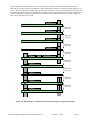
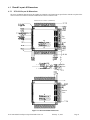
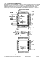
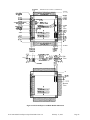
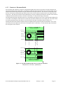
1
™
PCI/104-Express
&
™
PCIe/104
Specification
Including OneBank™ and Adoption on
104™, EPIC™, and EBX™ Form Factors
Version 3.0
February 17, 2015
Please Note:
This specification is subject to change without notice. While every effort has been made to ensure the
accuracy of the material contained within this document, the PC/104 Consortium shall under no
circumstances be liable for incidental or consequential damages or related expenses resulting from the use
of this specification. If errors are found, please notify the PC/104 Consortium.
The PC/104 logo, PC/104, PC/104-Plus, PCI-104, PCIe/104, PCI/104-Express, 104, OneBank, EPIC
and EBX are trademarks of the PC/104 Consortium. All other marks are the property of their respective
companies.
Copyright 2007 - 2015, PC/104 Consortium
IMPORTANT INFORMATION AND DISCLAIMERS
The PC/104 Consortium (“Consortium”) makes no warranties with regard to this PCI/104-Express and
PCIe/104 Specifications (“Specifications”) and, in particular, neither warrant nor represent that these
Specifications or any products made in conformance with them will work in the intended manner. Nor does
the Consortium assume responsibility for any errors that the Specifications may contain or have any
liabilities or obligations for damages including, but not limited to, special, incidental, indirect, punitive, or
consequential damages whether arising from or in connection with the use of these Specifications in any
way. This specification is subject to change without notice. While every effort has been made to ensure
the accuracy of the material contained within this document, the publishers shall under no circumstances be
liable for incidental or consequential damages or related expenses resulting from the use of this
specification. If errors are found, please notify the publishers.
No representations or warranties are made that any product based in whole or part on these Specifications
will be free from defects or safe for use for its intended purposes. Any person making, using, or selling
such product does so at his or her own risk. The user of these Specifications hereby expressly
acknowledges that the Specifications are provided as is, and that the Consortium make no representations,
or extends any warranties of any kind, either express or implied, oral, or written, including any warranty of
merchantability or fitness for a particular purpose, or warranty or representation that the Specifications or
any product or technology utilizing the Specifications or any subset of the Specifications will be free from
any claims of infringement of any intellectual property, including patents, copyright and trade secrets nor
does the Consortium assume any responsibilities whatsoever with respect to the Specifications or such
products.
TRADEMARKS AND COPYRIGHTS
The PC/104 logo, PC/104, PC/104-Plus, PCI-104, PCI/104-Express, PCIe/104, 104, EPIC, and EBX are
trademarks of the PC/104 Consortium. PCI, PCI Express, and PCIe are trademarks of PCI-SIG. PS/2,
PC/XT, PC/AT and IBM are trademarks of International Business Machines Inc. Information regarding the
traditional stackable PCI bus found on in the PC/104-Plus and PCI-104 specifications is the property of the
PC/104 Consortium. All other trademarks are the property of their respective companies.
PCIe/104 and PCI/104-Express Specification Revision 3.0
February 17, 2015
Page 1
REVISION HISTORY
March 21, 2008
•
Version 1.0
Initial release
March 27, 2009
•
•
•
•
•
Version 1.1
Add USB and over current signal to pin out, inserted description in 1.4.4, modified shift example
to include USB
Section 2.4 corrected that even numbered pins are located towards the inside of the board and odd
numbered pins are located towards the edge of the board
PEx16_ENA changed to PEG_ENA# in section 2.4.1.2 and 2.4.3
Figure 2.3 Moved Host to bottom in this figure and added USB
Figure 6-14 Top two boards are PCI/104-Express
February 10, 2011
•
•
•
•
Version 2.0
Added Type 2 connector version
Added 22mm connector option
Removed Figure 6 4: Mating of Top Half and Bottom Half of Connector A because this nondimensioned sketch provided no useful information
Editorial changes:
o Changed signal names PWRGD to PWRGOOD, CPU_DIR to DIR, and 5V_Always to
+5V_SB for consistency
o Corrected USB0 and USB1 in Automatic Link Shifting Examples for Host and Various
Devices
o Corrected text in Appendix B and C related to PCI/104-Express Expansion Zone
o Redrew Example breakout routing of connector bank 1 PCI Express x1 links with
shifting
o Changed PCIe to PCI Express when discussing the PCI Express specification.
o Cleaned up drawings in Figure 1-1
o Swapped order of section 1.3 and 1.4 and edited text
o Fixed missing references.
o Added signal switches suggestions for SATA and USB 3.0
March 21, 2011
•
Provided SATA definitions that were omitted in previous version.
February 18, 2013
•
•
•
•
•
•
Version 2.01
Version 2.10
Corrected Consortium name in all references
Expanded introduction to PCI Express to include Gen 1, 2, and 3.
Added PCI Express Gen 2 recommendations.
o Added devices and updated signal switch table.
o Updated layout recommendations section to include PCIe Gen 2 & 3.
o Added Gen 2 & 3 to via and trace length table.
o Removed microstrip and stripline examples.
Added PCI Express x4, x8, and x16 layout examples.
Added SATA and USB 3.0 capacitor info and layout examples.
Changed SDVO to Alternate Function
PCIe/104 and PCI/104-Express Specification Revision 3.0
February 17, 2015
Page 2
December 16, 2014
•
•
•
•
Version 3.0
Added OneBank™ connector variation
Updated connector mechanical performance specifications
Cleaned up Link Shifting wording
Added stitching capacitors to first bank of PCIe/104 connector
PCIe/104 and PCI/104-Express Specification Revision 3.0
February 17, 2015
Page 3
TABLE OF CONTENTS
1. INTRODUCTION ................................................................................................................................................... 1 1.1. Purpose ...................................................................................................................................................... 1 1.2. Standard Identification ............................................................................................................................... 1 1.3. Description ................................................................................................................................................. 1 1.4. PCIe/104 Type 1 and Type 2 ..................................................................................................................... 2 1.4.1 PCI/104-Express Version 1.0 and 1.1 Host Board Compatibility ............................................ 2 1.4.2 PCI/104-Express Version 1.0 and 1.1 Peripheral Board Compatibility ................................... 3 1.5. PCIe/104 Feature Set ................................................................................................................................. 3 1.5.1 Connector A : PCI Express Bus .............................................................................................. 3 1.6. PCI/104-Express Feature Set ..................................................................................................................... 3 1.6.1 Connector A : Same as 1.5.1 above ......................................................................................... 3 1.6.2 Connector B: PCI Bus:............................................................................................................ 3 1.7. General Stacking Rules .............................................................................................................................. 3 1.8. Stack Up, Stack Down, and Both............................................................................................................... 4 1.9. Bus and Signal Group Descriptions ........................................................................................................... 4 1.9.1 PCI Express Expansion Bus ..................................................................................................... 4 1.9.2 SATA Links ............................................................................................................................. 5 1.9.3 LPC Bus ................................................................................................................................... 5 1.9.4 Universal Serial Bus (USB) ..................................................................................................... 5 1.9.5 System Management Bus ......................................................................................................... 6 1.9.6 ATX and Power Management.................................................................................................. 6 1.9.7 RTC Battery ............................................................................................................................. 7 1.9.8 PCI Expansion Bus .................................................................................................................. 7 1.10. References.................................................................................................................................................. 7 2. EXPANSION CONNECTOR A ............................................................................................................................. 8 2.1. Functions.................................................................................................................................................... 8 2.1.1 PCIe/104 Type 1 and Type 2 Common Features ..................................................................... 8 2.1.2 PCIe/104 Type 1 Only Additional Features ............................................................................. 8 2.1.3 PCIe/104 Type 2 Only Additional Features ............................................................................. 8 2.2. Signal Descriptions .................................................................................................................................... 9 2.2.1 PCIe/104 Type 1 ...................................................................................................................... 9 2.2.2 PCIe/104 Type 2 .................................................................................................................... 10 2.3. Signal Naming Convention ...................................................................................................................... 10 2.4. Pin Assignment ........................................................................................................................................ 11 2.4.1 Type 1 x16 PCI Express Link ................................................................................................ 14 PCIe/104 and PCI/104-Express Specification Revision 3.0
February 17, 2015
Page 4
2.4.2 PEG_ENA# Signal................................................................................................................. 15 2.4.3 DIR Signal ............................................................................................................................. 15 2.4.4 Stack-UP or Stack-DOWN Link Shifting .............................................................................. 17 2.4.5 Link Shifting PCB Examples ................................................................................................. 18 2.4.6 Link Shifting Stack Examples................................................................................................ 19 2.5. Switching ................................................................................................................................................. 21 2.5.1 Signal Switch ......................................................................................................................... 21 2.6. System Clocking ...................................................................................................................................... 21 2.7. Layout Recommendations ....................................................................................................................... 22 2.7.1 Stitching Capacitors ............................................................................................................... 22 2.7.2 Number of PCI Express Boards in the Stack ......................................................................... 22 2.8. Routing Topology .................................................................................................................................... 23 2.8.1 PCI Express and USB 3.0 ...................................................................................................... 23 2.8.2 SATA ..................................................................................................................................... 24 2.9. Device Connector Break-out Examples ................................................................................................... 25 2.9.1 Universal PCI Express x1 Device Layout Example ............................................................... 25 2.9.2 Universal PCI Express x4 Device Layout Example ............................................................... 25 2.9.3 Type 1 PCI Express x8 Device Layout Example ................................................................... 26 2.9.4 Type 1 PCI Express x16 Device Layout Example ................................................................. 26 2.9.5 Type 2 USB 3.0 Device Layout Example .............................................................................. 27 2.9.6 Type 2 SATA Device Layout Example ................................................................................. 27 3. EXPANSION CONNECTOR B ............................................................................................................................ 28 3.1. Description ............................................................................................................................................... 28 3.2. Functions.................................................................................................................................................. 28 3.3. Signal Descriptions .................................................................................................................................. 29 3.4. Pin Assignment ........................................................................................................................................ 30 3.5. +5V_SB, PSON#, and PME# .................................................................................................................. 30 3.6. PCI Signaling Voltage (VI/O) Requirements .......................................................................................... 31 3.6.1 PCI Host Module ................................................................................................................... 31 3.6.2 Add-In Modules ..................................................................................................................... 31 4. PCIe/104 Type 1 and Type 2 Stacking .................................................................................................................. 32 4.1. System Stacking Rules............................................................................................................................. 32 4.2. Host Configuration Rules ........................................................................................................................ 32 4.3. Peripheral Configuration Rules................................................................................................................ 33 4.4. Stack Configuration Examples ................................................................................................................ 34 PCIe/104 and PCI/104-Express Specification Revision 3.0
February 17, 2015
Page 5
5. ELECTRICAL SPECIFICATION......................................................................................................................... 40 5.1. Power and Ground ................................................................................................................................... 40 5.1.1 Connector A, PCIe/104, Power Capabilities .......................................................................... 40 5.1.2 Connector B, PCI-104, Power Capabilities............................................................................ 40 5.1.3 Total PCIe/104 Power Capabilities Connector A Only (OneBank Option) ........................... 41 5.1.4 Total PCI/104-Express Power Capabilities Connector A and B (OneBank Option) ............. 41 5.2. AC/DC Signal Specifications .................................................................................................................. 41 5.2.2 Stackable PCI Expansion Bus ................................................................................................ 41 6. MECHANICAL SPECIFICATIONS .................................................................................................................... 42 6.1. Connector A ............................................................................................................................................. 42 6.1.1 Part Number ........................................................................................................................... 42 6.1.2 Connector A Specifications ................................................................................................... 44 6.1.3 Standard 0.600” (15.24mm) Top Connector A Mechanical Drawings .................................. 45 6.1.4 Optional 0.866” (22.00mm) Top Connector A Mechanical Drawings .................................. 46 6.1.5 Optional OneBank Top Connector A Mechanical Drawings ................................................. 47 6.1.6 Standard ASP-129646-03 or equivalent (Bottom Connector) Mechanical Drawings............ 49 6.1.7 Optional ASP-129646-22 (OneBank Bottom Connector) Mechanical Drawings .................. 50 6.2. Connector B ............................................................................................................................................. 50 6.3. Board Layout & Dimensions ................................................................................................................... 51 6.3.1 PCIe/104 Layout & Dimensions ............................................................................................ 51 6.3.2 PCI/104-Express Layout & Dimensions ................................................................................ 53 6.3.3 Connector A Placement Details ............................................................................................. 55 6.4. Standoff ................................................................................................................................................... 56 APPENDIX A: PC/104 BRIDGE CARD ........................................................................................................... 57 A.1 Bridge Module Configurations ................................................................................................................ 58 A.2 Stack Configuration Examples ................................................................................................................ 58 APPENDIX B: EPIC FORM FACTOR – PCI/104-Express Placement ............................................................ 61 APPENDIX C: EBX FORM FACTOR – PCI/104-Express Placement ............................................................. 62 PCIe/104 and PCI/104-Express Specification Revision 3.0
February 17, 2015
Page 6
TABLE OF FIGURES
Figure 1-1: PCI/104-Express and PCIe/104 Board Layouts on 104 Form Factor .......................................... 1 Figure 1-2: OneBank Connector PCI/104-Express and PCIe/104 Board Layouts on 104 Form Factor......... 2 Figure 1-3 RTC Battery Example ................................................................................................................... 7 Figure 2-1 Required Circuitry for a Host Module Configuration for Automatic Link Shifting ................... 16 Figure 2-2 Required Device Circuitry for Automatic Link Shifting ............................................................ 16 Figure 2-3: Automatic Link Shifting Examples for Host and Various Devices ........................................... 18 Figure 2-4: Automatic Link Shifting Stack-Up Example Consisting of Two x1 Link Device, One x4 Link
Device, and One Device with One x1 Link and One x4 Link ............................................................. 19 Figure 2-5: Automatic Link Shifting Stack-Down Example Consisting of Two x1 Link Device, One x4
Link Device, and One Device with One x1 Link and One x4 Link .................................................... 20 Figure 2-6 PCI Express and USB 3.0 Capacitor Placement ......................................................................... 23 Figure 2-7 SATA Capacitor Placement ........................................................................................................ 24 Figure 2-8 Example breakout routing of a Universal PCI Express x1 link with shifting. ............................ 25 Figure 2-9 Example breakout routing a Universal PCI Express x4 link with lane shifting. ......................... 25 Figure 2-10 Example breakout routing a PCI Express x8 device stacking down with lane shifting ............ 26 Figure 2-11 Example breakout routing a PCI Express x16 device stacking down ....................................... 26 Figure 2-12 Example breakout routing an USB 3.0 device with lane shifting ............................................. 27 Figure 2-13 Example breakout routing a SATA device with lane shifting................................................... 27 Figure 4-1: Type 1 or 2 Stack-DOWN Configuration Example ................................................................... 34 Figure 4-2: Type 1 or 2 Stack-UP Configuration Example with EPIC Host Baseboard .............................. 35 Figure 4-3 PCIe/104 with a PCI Express to PCI Bridge............................................................................... 36 Figure 4-4: PCI/104-Express Combined Stack-UP and Stack-DOWN Configuration Example .................. 37 Figure 4-5: PCIe/104 Type 1 Stack-down and Type 2 Stack-up Configuration Example ............................ 38 Figure 4-6: PCIe/104 Type 2 Stack-down, Type 2 Stack-up Busses Not Connected Configuration Example
............................................................................................................................................................ 39 Figure 6-1 Standard Top Connector 0.600” (15.24mm) ASP-129637-03 or equivalent .............................. 42 Figure 6-2 Optional Top Connector 0.866” (22.00mm) ASP-142781-03 or equivalent .............................. 42 Figure 6-3 OneBank Top Connector ASP-129637-13 or equivalent Shown with Pick-and-Place Adapter . 42 Figure 6-4: Bottom Connector ASP-129646-03 or equivalent ..................................................................... 43 Figure 6-5: OneBank Bottom Connector ASP-129646-22 or equivalent Shown with Pick-and-Place
Adapter ............................................................................................................................................... 43 Figure 6-6: Top Half and Bottom Half of Connector A Shown with Pick-and-Place Adapters ................... 43 Figure 6-7: Standard 0.600” (15.24mm) Connector ASP-129637-03 or equivalent Mechanical Drawings 45 Figure 6-8 Optional 0.866” (22.00mm) Connector ASP-142781-03 or equivalent Mechanical Drawings .. 46 Figure 6-9 Optional OneBank 0.600” (15.24mm) Connector ASP-129637-13 or equivalent Mechanical
Drawings ............................................................................................................................................. 47 PCIe/104 and PCI/104-Express Specification Revision 3.0
February 17, 2015
Page 7
Figure 6-10 Optional OneBank 0.866” (22mm) Connector ASP-142781-07 or equivalent Mechanical
Drawings ............................................................................................................................................. 48 Figure 6-11: Standard ASP-129646-03 or equivalent Mechanical Drawings .............................................. 49 Figure 6-12 Optional OneBank ASP-129646-22 or equivalent Mechanical Drawings ................................ 50 Figure 6-13 PCIe/104 Module Dimensions .................................................................................................. 51 Figure 6-14 PCIe/104 OneBank Module Dimensions .................................................................................. 52 Figure 6-15 PCI/104-Express Module Dimensions ...................................................................................... 53 Figure 6-16 PCI/104-Express OneBank Module Dimensions ...................................................................... 54 Figure 6-17: Top Side and Bottom Side Views of Connector Placements ................................................... 55 Figure 6-18: Standoff Mechanical Dimensions ............................................................................................ 56 Figure 6-19: Basic Configuration of the PCI-to-ISA Bridge Module .......................................................... 58 Figure 6-20: Stack-DOWN Configuration of the PCI-to-ISA Bridge Module ............................................. 58 Figure 6-21: Stack-UP Configuration of the PCI-to-ISA Bridge Module .................................................... 58 Figure 6-22: Stack-DOWN Configuration Example .................................................................................... 59 Figure 6-23: Combined Stack-UP Configuration Example .......................................................................... 60 Figure 6-24: EPIC with PCI/104-Express .................................................................................................... 61 Figure 6-25: EBX with PCI/104-Express ..................................................................................................... 62 PCIe/104 and PCI/104-Express Specification Revision 3.0
February 17, 2015
Page 8
TABLE OF TABLES
Table 1-1 Feature Summary ........................................................................................................................... 2 Table 1-2 Type 1 & Type 2 Combinations ..................................................................................................... 4 Table 2-1 Connector A Type 1 Signals .......................................................................................................... 9 Table 2-2 Connector A Type 2 Signals ........................................................................................................ 10 Table 2-3 Connector A, Type 1 Pin Assignments ........................................................................................ 12 Table 2-4 Connector A, Type 2 Pin Assignments ........................................................................................ 13 Table 2-5 Connector A, OneBank Pin Assignments .................................................................................... 14 Table 2-6: x16 Link as Two x8 or Two x4 Links Top Connector ................................................................ 14 Table 2-7: x16 Link as Two x8 or Two x4 Links Bottom Connector .......................................................... 15 Table 2-8: Signal Switches or equivalent ..................................................................................................... 21 Table 2-9: Via and Trace Length Budget ..................................................................................................... 22 Table 2-10 PCI Express and USB 3.0 Routing Specification ....................................................................... 23 Table 2-11 SATA Routing Specification ..................................................................................................... 24 Table 3-1 Connector B Signals ..................................................................................................................... 29 Table 3-2 Connector Signal Assignment ...................................................................................................... 30 Table 4-1 Required Host State When Peripherals Are Placed on Type 1 and Type 2 Hosts ........................ 32 Table 4-2 Peripheral Effect on Type 1 Host CPU Signals............................................................................ 32 Table 4-3 Peripheral Effect on Type 2 Host CPU Signals............................................................................ 32 Table 4-4 Host CPU Stacking Rules ............................................................................................................ 33 Table 4-5 Required Host Connector A Pin Configuration............................................................................ 33 Table 4-6 Peripheral Stacking Rules ............................................................................................................ 33 Table 5-1 Connector A Power Delivery (OneBank Option) ........................................................................ 40 Table 5-2 Connector B Power Delivery ....................................................................................................... 40 Table 5-3 Connector A Power Delivery ....................................................................................................... 41 Table 5-4 Combined Connector A and B Power Delivery ........................................................................... 41 PCIe/104 and PCI/104-Express Specification Revision 3.0
February 17, 2015
Page 9
Glossary of Terms
Terms
Definitions
ATX
Advanced Technology Extended
A specification for PC motherboards, power supplies, and system chassis. One of its most
notable features is support for “Standby” and “Soft-Off” power savings modes.
Device
A logical device attached to a PCI Express Link. Generally an add-in card.
DMA
Direct Memory Access
A method for peripherals to efficiently access system memory without CPU intervention.
EBX
Form factor for SBC’s
Host
The central connection of a PCI Express system, typically a CPU module. This is called the
“Root Complex” by the PCI Express specification.
ISA Bus
Industry Standard Architecture
A legacy bus used on earlier PCs. It has been phased out of desktop PCs, but is still common in
embedded systems.
Lane
Fundamental unit of a PCI Express connection. A set of differential signal pairs, one pair for
transmission, and one pair for reception. Multiple lanes may be combined to increase
bandwidth (up to x16). A “by-N Link” is comprised of N Lanes.
Link
The collection of one or more PCI Express Lanes, plus an additional differential pair for a
clock, which make up a standard PCI Express interconnect. According to PCI Express
Specification 1.1 a Link can be comprised of 1, 4, 8, or 16 Lanes.
Packet Switch
A device used to attach multiple PCI Express devices to a single link on the HOST. The PCI
Express Specification refers to this simply as a “Switch.” In this document, the term “Packet
Switch” is used to differentiate from a “Signal Switch.”
PCIe
PCI Express
PEG
PCI Express Graphics
SBC
Single Board Computer
SDVO
Serial Digital Video Output used from Intel 915/945/965 chipsets
Signal Switch
An analog switch used to select between multiple PCI Express devices to attach to a single PCI
Express link, or multiple links to attach to a single device. Also called a “Channel Switch.”
SMBus
System Management Bus
USB
Universal Serial Bus
LPC
Low pin count bus, a bus specification for legacy devices
SATA
Serial ATA Bus
PCIe/104 and PCI/104-Express Specification Revision 3.0
February 17, 2015
Page 10
1. INTRODUCTION
1.1. Purpose
This document defines the addition of PCI Express, the next generation serial interconnect bus, to the stackable 104,
EPIC, and EBX form factors. PCI Express was chosen because of its performance, scalability, wide market acceptance,
and growing silicon availability worldwide. The PCI Express architecture uses familiar software and configuration
interfaces of the conventional PCI bus architecture, but provides a new high-performance physical interface while
retaining software compatibility with the existing conventional PCI infrastructure.
PCI Express is a high performance I/O architecture used in both desktop and mobile applications. This hierarchical, pointto-point interconnect works well with on-board and slot oriented architectures. The purpose of this Specification is to
adapt PCI Express to the stacked architecture employed with 104, EPIC and EBX form factors.
1.2. Standard Identification
A PCI-104 board with the addition of PCI Express becomes PCI/104-Express. A board with only the PCI Express
connector is called PCIe/104. Each of these configurations can be applied to EPIC and EBX as shown in Appendix B and
C. This allows full interchangeability with add-in devices across all PC/104 form factors.
1.3. Description
As computer technology continues to develop, the PC/104 community must expand to the new, widely accepted and
sustained technologies of the day. The PCI/104-Express Specification provides this next generation PC/104 platform with
a connector architecture that provides high-speed interfaces, maintains the ability to develop low-cost modules, and is
sustainable for the foreseeable future.
Key to its development was obtaining a high speed, 3-bank, stackable PCI Express connector for both up and down
stacking, while retaining the stackable PCI connector for backward compatibility to PCI-104, PC/104-Plus, and PC/104
peripheral modules. Figure 1-2 shows a basic view of the PCI/104-Express and PCIe/104 layouts.
D1
C1
B1
A1
PCI Bus: 32 bit/33MHz
PCI/104-Express Module
3-Bank Connector
3.775 inches
(95.89 mm)
3.775 inches
(95.89 mm)
Connector B
PCI – 120 Pin Connector
Connector A
PCI Express – 156 pin Connector
Connector A
PCI Express – 156 pin Connector
Bank 1
Bank 2
PCIe/104 Module
3-Bank Connector
Bank 3
Bank 1
3.550 inches
(90.17 mm)
Bank 2
Bank 3
3.550 inches
(90.17 mm)
Figure 1-1: PCI/104-Express and PCIe/104 Board Layouts on 104 Form Factor
PCIe/104 and PCI/104-Express Specification Revision 3.0
February 17, 2015
Page 1
A reduced feature set OneBank version does not implement the Bank 2 or Bank 3 connectors. Figure 1-2 shows the same
basic views with the OneBank connector.
D1
C1
B1
A1
PCI Bus: 32 bit/33MHz
3.775 inches
(95.89 mm)
3.775 inches
(95.89 mm)
Connector B
PCI – 120 Pin Connector
PCI/104-Express Module
1-Bank Connector
PCIe/104 Module
1-Bank Connector
Connector A
PCI Express – 52 pin Connector
Connector A
PCI Express – 52 pin Connector
Bank 1
Bank 1
3.550 inches
(90.17 mm)
3.550 inches
(90.17 mm)
Figure 1-2: OneBank Connector PCI/104-Express and PCIe/104 Board Layouts on 104 Form Factor
ISA bus backward compatibility can naturally and easily be achieved with the use of a PCI-to-ISA bridge peripheral
module (see Appendix A).
1.4. PCIe/104 Type 1 and Type 2
PCIe/104 is implemented by a pair of high-speed surface mount connectors. If the host CPU has top and bottom
connectors electrically connected together then the system can be built either stack-up or stack-down, but not both at the
same time. However, there is no requirement for the connector on the top of the host to be electrically connected to the
connector on the bottom of the host. This means that a PCIe/104 bus stacking up can be completely separate from
PCIe/104 bus going down. The specification does require all peripheral boards to be universal, so all peripheral boards
will work either above or below the CPU.
This specification defines two versions of the PCIe/104 connector pin out, Type 1 and Type 2. Type 1 is the same
versions 1.0 and 1.1 of the PCI/104-Express and PCIe/104 specification. Type 2 replaces the PCI Express x16 link with
two PCI Express x4 links, two USB 3.0, two SATA, LPC, and an RTC battery. The OneBank implementation is
compatible with the common Type 1 and Type 2 features. See Table 1-1 below for a comparison.
Table 1-1 Feature Summary
Feature
Type 1
Type 2
OneBank
USB 2.0
SMB
PCIe x1
Power
ATX Control
PCIe x4
PCIe x16*
USB 3.0
SATA
LPC
RTC Battery
2
1
4
+3.3V, +5V, +12V
Yes
2
1
4
+3.3V, +5V, +12V
Yes
2
2
1
4
+3.3V, +5V
Yes
1
2
2
1
1
* x16 Link can be used as x8 or x4, see Section 2.4.1.1.
1.4.1
PCI/104-Express Version 1.0 and 1.1 Host Board Compatibility
All host boards built to PCI/104-Express version1.0 and 1.1 are considered Type 1.
PCIe/104 and PCI/104-Express Specification Revision 3.0
February 17, 2015
Page 2
1.4.2
PCI/104-Express Version 1.0 and 1.1 Peripheral Board Compatibility
All PCI Express x1, USB 2.0, and SMBus boards build to version 1.0 or 1.1 are considered Universal boards and will
work unchanged on either Type 1 or Type 2 host CPUs. PCI Express x16 peripherals work only on Type 1 hosts. USB
3.0, SATA, and LPC peripherals will work only on Type 2 hosts.
The pin assignments on Bank 1 of the connector is exactly the same in Type 1 and Type 2, therefore all the PCI Express
x1, USB 2.0, SMBus, and all the control signals are the same. Likewise all power and grounds are the same throughout
the connector.
1.5. PCIe/104 Feature Set
1.5.1
Connector A : PCI Express Bus
PCIe/104 Type 1, Type 2 and the OneBank implementation have this common feature set and pin assignments:
Four x1 PCI Express Links
Two USB 2.0
ATX power and control signals: +5V Standby, Power supply on, Power OK
Power: +3.3V, +5V, +12V (A OneBank implementation does not include +12V)
SMBus
Type 1 has the common feature set plus:
One x16 PCI Express Link, or optionally two x8 Links, or two x4 PCI Express Links
Type 2 has the common feature set plus:
Two x4 PCI Express Links
Two USB 3.0
Two SATA
LPC Bus
RTC Battery
1.6. PCI/104-Express Feature Set
1.6.1
Connector A : Same as 1.5.1 above
1.6.2
Connector B: PCI Bus:
PCI Bus: 32 bit, 33 MHz, Four Bus Master capable (same as on PC/104-Plus and & PCI-104)
+5V Standby, Power supply on, and power management event signals for ATX power supply
Power: +3.3V, +5V, +12V, -12V
Same location and pin out as PCI-104 and PC/104-Plus specifications
1.7. General Stacking Rules
This specification defines Type 1 and Type 2 host and peripheral modules. There are four stacking rules.
Peripheral modules connecting with PCI Express x1 or x4 links, USB 2.0 links, or SMB are universal and can
plug into either a Type 1 or a Type 2 host.
Peripheral modules connecting with PCI Express x16 or x8 links must plug into a Type 1 host.
Peripheral modules connecting with SATA, USB 3.0, or LPC links must plug into a Type 2 host.
Any peripheral module plugged in the wrong bus holds the system in reset and causes no damage.
Guidelines for stacking PCI Express Gen 1, 2, 3, USB 3.0, and SATA.
•
Build a stack by putting higher clock rate peripherals closer to the host. Follow the priority below:
1. Gen 3 PCI Express at 8.0 Gigabits/second closest to the host
2. SATA 3 at 6.0 Gigabits/second next closest
3. Gen 2 PCI Express and USB 3.0 at 5.0 Gigabits/second
4. SATA 2 at 3.0 Gigabits/second
5. Gen 1 PCI Express at 2.5 Gigabits/second
PCIe/104 and PCI/104-Express Specification Revision 3.0
February 17, 2015
Page 3
•
6. SATA 1 at 1.5 Gigabits/second
7. USB 2.0 at 480 Mbits/second
Follow the guidelines for up and down stacking in Table 1-2 Type 1 & Type 2 Combinations below.
For example, if you have a host with a Type 1 stacking down and a Type 2 stacking up with one SATA 2, one USB 3.0,
one PCI Express x1 Gen 2, two PCI Express x1 Gen 1, and one PCI Express x16 Gen 2 peripherals your stack could be
configured as:
•
•
•
•
•
•
•
SATA peripheral
USB 3.0 peripheral
Host (Type 1 going down and Type 2 going up)
PCI Express x16 Gen 2 peripheral
PCI Express x1 Gen 2 peripheral
PCI Express x1 Gen 1 peripheral
PCI Express x1 Gen 1 peripheral
For details on host and peripheral configuration see section 4, PCIe/104 Type 1 and Type 2 Stacking.
1.8. Stack Up, Stack Down, and Both
If the host CPU has the same type connector on top and bottom of the board and the signals are connected together,
boards can be stacked either up or down using the direction signal DIR to indicate to the peripheral board where the host
is located. In this case, care must be taken not to stack boards in both directions because signal stubs will be created
which may adversely affect the bus signals.
Surface mounted connectors permit the top and bottom connectors to be separate busses. If the host CPU is built with
separate busses on top and bottom there will not be stubs when stacking cards both up and down at the same time. This
specification supports connected or separate bus options as long as board configuration rules are followed. Table 1-2
shows the maximum number of links for all the possible combinations.
Table 1-2 Type 1 & Type 2 Combinations
PCIe/104
Type 1
Top and Bottom Connectors
Peripheral Board Stacking
Connected
Type 2
Separate
Connected
Type 1 & 2 Combo
Separate
Connected
Either up or down Both up and down Either up or down Both up and down
Separate
Both up and down
x1 PCIe Links
4
8
4
8
8
USB 2.0
2
4
2
4
4
SMB
x4 PCIe Links
1
2
1
4
1
2
1
4
1
4
x8 PCIe Links
2
4
None
None
x16 PCIe Links
1
2
None
None
1
SATA
None
None
2
4
2
USB 3.0
None
None
2
4
2
LPC
None
None
1
1
1
Not Allowed
2
1.9. Bus and Signal Group Descriptions
1.9.1
PCI Express Expansion Bus
PCI Express is a high performance, general purpose I/O interconnect defined for a wide variety of future computing and
communication platforms. Key PCI attributes, such as its usage model, load-store architecture, and software interfaces,
are maintained, whereas its parallel bus implementation is replaced by a highly scalable, fully serial interface. PCI
Express takes advantage of recent advances in point-to-point interconnects, Switch-based technology, and packet-protocol
to deliver new levels of performance and features. Power Management, Quality of Service (QoS), Hot-Plug/Hot-Swap
support, Data Integrity, and Error Handling are among some of the advanced features supported by PCI Express. PCI
Express has three signaling rates.
•
•
•
Generation 1, Gen 1, is 2.5 Gigabits/second/Lane/direction of raw bandwidth
Generation 2, Gen 2, is 5.0 Gigabits/second/Lane/direction of raw bandwidth
Generation 3, Gen 3, is 8.0 Gigabits/second/Lane/direction of raw bandwidth
PCIe/104 and PCI/104-Express Specification Revision 3.0
February 17, 2015
Page 4
PCI/104-Express and PCIe/104 incorporate four x1 PCI Express Links and options for either a single x16 Link, or two x8
Links, or two x4 PCI Express Links to allow connections to standard PCI Express device chips. The x16 Link option
allows maximum flexibility, configurability, and expandability for current and future designs. Some examples of x16
Link application are next generation graphics chips, 1/10 gigabit Ethernet chips, or use with a PCI Express Switch which
can then branch the high throughput out into any number of various size Links including multiple x16 Link graphics
engines. The only limitation is the bandwidth requirement for each of the branched links.
1.9.1.1
PCI Express x16 or PEG Link
PCI Express x16, sometimes called PEG (PCI Express for Graphics), is an interface with 16 PCI Express differential
lanes to connect a high performance video controller or other high bandwidth devices. In chipsets with internal graphics,
the PEG bus is used as an alternative to connect an external video controller. The internal chip controller is disabled in
this case. The PEG-Bus configuration must be enabled from the Device by connecting the PEG-ENA# signal to ground.
1.9.1.2
Non-PCI Express functions of the CPU/Chipset x16 Link
Some processors/chipsets allow alternate functions on the x16 link pins. There is no standard which all manufacturers
follow, so this specification will not define one. Using these alternate functions is allowed, but it is up to the host board
manufacturer to define the alternate uses and what peripheral boards are compatible. Use of the PEG-ENA# shall remain
open on these peripheral boards.
One example of this is Serial Digital Video Output (SDVO). This bus is provided as an alternative to the PEG-Bus on
some CPU chipsets. SDVO-Links needs up to 7 differential signal pairs per interface.
1.9.2
SATA Links
Serial ATA (SATA or Serial Advanced Technology Attachment) is a computer bus interface for connecting host bus
adapters to mass storage devices such as hard disk drives and optical drives. Serial ATA was designed to replace the older
ATA (AT Attachment) standard (also known as EIDE). It is able to use the same low level commands, but serial ATA
host-adapters and devices communicate via a high-speed serial cable over two pairs of conductors. Support for device
detection and power enable for hot-pluggable applications.
1.9.3
LPC Bus
The Low Pin Count bus, or LPC bus, is used on IBM-compatible personal computers to connect low-bandwidth devices
to the CPU, such as the boot ROM and the “legacy” I/O devices. The “legacy” I/O devices usually include serial and
parallel ports, keyboard, mouse, and floppy disk controller.
The LPC bus was introduced by Intel in 1998 as a substitute for the Industry Standard Architecture (ISA) bus. It
resembles ISA to software, although physically it is quite different, replacing the 16-bit-wide, 8.33 MHz ISA bus with a
4-bit-wide bus operating at 4 times the clock speed (33.3 MHz). LPC’s main advantage is that it requires only seven
signals.
1.9.4
Universal Serial Bus (USB)
The USB is specified to be an industry-standard extension to the PC architecture with a focus on PC peripherals that
enable consumer and business applications. The following criteria were applied in defining the architecture for the USB:
•
•
•
•
•
•
•
•
•
•
Ease-of-use for PC peripheral expansion.
USB 2.0 is a low-cost solution that supports transfer rates up to 480Mb/s.
USB 3.0 is a high-speed solution with speeds up to 4800Mb/s
Full support for real-time data of voice, audio, and video.
Protocol flexibility for mixed-mode isochronous data transfers and asynchronous messaging.
Integration in commodity device technology.
Comprehension of various PC configurations and form factors.
Provision of a standard interface capable of quick diffusion into a product.
Enabling new classes of devices that augment the PC’s capability.
Full backward compatibility of USB 2.0 for devices built to previous versions of the specification.
The over-current protection is made on each PCI/104-Express peripheral board, if needed. Any channel can pull the OC#Signal low to indicate the CPU host that an over-current situation has occurred.
PCIe/104 and PCI/104-Express Specification Revision 3.0
February 17, 2015
Page 5
1.9.5
System Management Bus
The optional System Management Bus (SMBus) is a two-wire interface through which various system component chips
can communicate with each other and with the rest of the system. It is based on the principles of operation of I2C. SMBus
provides a control bus for system- and power-management related tasks. A system may use SMBus to pass messages to
and from devices instead of tripping individual control lines. Removing the individual control lines reduces pin count.
Accepting messages ensures future expandability. With SMBus, a device can provide manufacturer information, tell the
system what its model/part number is, save its state for a suspended event, report different types of errors, accept control
parameters, and return its status. SMBus is described in System Management Bus (SMBus) Specification, Version 2.0.
Refer to this specification for DC characteristics and all AC timings. If the system board or add-in card supports SMBus,
it must adhere to additional requirements that may be found in Chapter 8 of the PCI Local Bus Specification, Revision.
3.0.
An address resolution protocol (ARP) is defined in the SMBus 2.0 Specification that is used to assign slave addresses to
SMBus devices. Although optional in the SMBus 2.0 Specification, it is required that systems that connect the SMBus to
PCI slots implement ARP for assignment of SMBus slave addresses to SMBus interface devices on PCI add-in cards. The
system must execute ARP on a logical SMBus whenever any PCI bus segment associated with the logical SMBus exits
the B3 state or a device in an individual slot associated with the logical SMBus exits the D3cold state. Prior to executing
ARP, the system must insure that all ARP-capable SMBus interface devices are returned to their default address state.
The system board provides pull-ups to the +3.3Vaux rail per the above specification and the components attached to these
signals need to have a 3.3V signaling tolerance (5V signaling must not be used). Also, the SMBus is used during all
power states, so all components attached to the SMBus must remain powered during standby, or ensure that the bus is not
pulled down when not powered.
The SMBus interface is based upon the System Management Bus Specification (SMBus 2.0 Specification). This two-wire
serial interface has low power and low software overhead characteristics that make it well suited for low-bandwidth
system management functions.
The capabilities enabled by the SMBus interface include, but are not limited to, the following:
Support for client management technologies.
Support for server management technologies.
Support for thermal sensors and other instrumentation devices on add-in cards.
Add-in card identification when the bus is in the B3 state or when the PCI device is in the D3hot or D3cold
states as defined in the PCI Power Management Interface Specification.
1.9.6
ATX and Power Management
PCI/104-Express and PCIe/104 incorporate all of the necessary control and signal lines for ATX and power management
functionalities. These signals include PWRGOOD, PSON#, +5V_SB, and PME#. The inclusion of these signals allows
maximum power savings.
PWRGOOD is a “power good” signal. It should be asserted high by the power supply to indicate that the +12 VDC, +5
VDC, and +3.3 VDC outputs are above the under-voltage thresholds and that sufficient main energy is stored by the
converter to guarantee continuous power operation within specifications. Conversely, PWRGOOD should be de-asserted
to a low state when any of the +12 VDC, +5 VDC, or +3.3 VDC output voltages falls below its under-voltage threshold,
or when main-power has been removed for a sufficiently long enough time that the power supply operation cannot be
guaranteed beyond the power-down warning time.
PSON# is an active-low, TTL-compatible signal that allows a motherboard to remotely control the power supply in
conjunction with features such as soft on/off, wake-on-LAN, or wake-on-modem. When PSON# is pulled to TTL low, the
power supply should turn on the five main DC output rails: +12 VDC, +5 VDC, +3.3 VDC, -5 VDC, and -12 VDC. When
PSON# is pulled to TTL high or open-circuited, the DC output rails should not deliver current and should be held at zero
potential with respect to ground. PSON# has no effect on the +5V_SB output, which is always enabled whenever AC
power is present. PSON# shall be pulled to +5V_SB with a 10K ohm resistor on the power supply.
+5V_SB is a standby supply output that is active whenever AC power is present. It provides a power source for circuits
that must remain operational when the five main DC output rails are in a disabled state. Example uses include soft power
control, wake-on-LAN, wake-on-modem, intrusion detection, or suspend state activities.
PCIe/104 and PCI/104-Express Specification Revision 3.0
February 17, 2015
Page 6
1.9.7
RTC Battery
Any board in a system can provide a 3.0 to 3.6 volt battery on pin 154 of the Type 2 connector. This battery shall be
current limited with a 1KΩ resistor, reverse current protected with a schottky diode, and filtered with a 10uF capacitor.
Any board in the system may use the battery. Battery life will depend on the specific battery used and the load.
Figure 1-3 RTC Battery Example
1.9.8
PCI Expansion Bus
The PCI Expansion Bus is the same 32 bit, 33 MHz PCI bus found on the PC/104-Plus and PCI-104 Specifications with
the addition of +5V_SB, PSON#, and PME#.
1.10. References
The following documents should be used as reference for a detailed understanding of the overall system requirements.
For latest revisions of the above specifications contact the respective organizations.
PC/104 Specification
PC/104-Plus Specification
PCI-104 Specification
PCI Local Bus Specification Revision 2.2
PCI Express Base Specification Revision 1.1
ATX Specification Version 2.2
System Management Bus (SMBus)
Specification Version 2.0
INTEL description of PEG and SDVO in the
915/945/965 chipsets
USB Specification Revision 2.0
USB Specification Revision 3.0
PC/104 Consortium
PC/104 Consortium
PC/104 Consortium
PCI Special Interest Group
PCI Special Interest Group
Intel Corporation
SBS Implementers Forum
www.pc104.org
Intel
www.intel.com
USB Implementers Forum
www.usb.org
www.pc104.org
www.pc104.org
www.pcisig.com
www.pcisig.com
www.intel.com
www.sbs-forum.org
If errors are found in this document, please send a written copy of the suggested corrections to the publishers listed on the
title page.
PCIe/104 and PCI/104-Express Specification Revision 3.0
February 17, 2015
Page 7
2. EXPANSION CONNECTOR A
2.1. Functions
Not all processors and chipsets support all features on the PCIe/104 connectors, and in some cases the design of the Host
may consume some or all of these features, rendering them unavailable. It is up to the Host designer to determine the
type and number of features included on the expansion connector. For cases where the host provides less than the
maximum number of features supported by the connector, see Section 2.4.4.
2.1.1
PCIe/104 Type 1 and Type 2 Common Features
PCIe/104 Type 1, Type 2 and the OneBank implementation have this common feature set
•
•
•
•
•
2.1.2
Four x1 PCI Express Links
Two USB 2.0
ATX power and control signals: +5V Standby, Power supply on, Power OK
Power: +3.3V, +5V, +12V (A OneBank implementation does not include +12V)
SMBus
PCIe/104 Type 1 Only Additional Features
One x16 PCI Express Link, or optionally two x8 Links, or two x4 PCI Express Links
2.1.3
PCIe/104 Type 2 Only Additional Features
Two PCI Express x4 Links
Two USB 3.0
Two SATA
LPC Bus
RTC Battery
PCIe/104 and PCI/104-Express Specification Revision 3.0
February 17, 2015
Page 8
2.2. Signal Descriptions
2.2.1
PCIe/104 Type 1
Table 2-1 Connector A Type 1 Signals
Group
PCIe x1
PCIe x4
Pins
Signal Name
Host Direction
4
4
4
4
4
4
PEx1_[0:3]Tp
PEx1_[0:3]Tn
PEx1_[0:3]Rp
PEx1_[0:3]Rn
PEx1_[0:3]CLKp
PEx1_[0:3]CLKn
Output
Output
Input
Input
Output
Output
8
PEx4_[0:1]T(#)p
Output
8
PEx4_[0:1]T(#)n
Output
8
PEx4_[0:1]R(#)p
Input
8
PEx4_[0:1]R(#)n
Input
1
1
PEx16_x8_x4_CLKp Output
PEx16_x8_x4_CLKn Output
PEx16_0T(#)p
PEx8_[0:1]T(#)p
Output
16
16
16
16
16
16
16
16
1
1
1
1
1
2
2
1
PEx16_0T(#)n
PEx8_[0:1]T(#)n
PEx16_0R(#)p
PEx8_[0:1]R(#)p
PEx16_0R(#)n
PEx8_[0:1]R(#)n
PEx16_x8_x4_CLKp
PEx16_x8_x4_CLKn
STK0/WAKE#
STK1/SDVO_DAT
STK1/PEG_ENA#
USB_[1:0]p
USB_[1:0]n
USB_OC
Misc.
1
DIR
Output
PCIe
1
PERST#
Output
1
PSON#
Output
1
PWRGOOD
Input
2
+5V_SB
Power
2
2
1
46
1
1
1
+5V
+3.3V
+12V
GND
SMB_Clk
SMB_Data
SMB_Alert#
Power
Power
Power
Power
Output
Bidirectional
Input
PCIe x16 or
PCIe x8
Stacking
Control
USB 2.0
ATX
Power
Supply
SMB
Output
Input
Input
Output
Output
Input
In/Out
Input
Bidirectional
Input
Description
Transmit Differential Upper Line for x1 Links 0, 1, 2, 3. Shifted when used.
Transmit Differential Lower Line for x1 Links 0, 1, 2, 3. Shifted when used.
Receive Differential Upper Line for x1 Links 0, 1, 2, 3. Shifted when used.
Receive Differential Lower Line for x1 Links 0, 1, 2, 3. Shifted when used.
Clock Differential Upper Line for x1 Links 0, 1, 2, 3. Shifted when used.
Clock Differential Lower Line for x1 Links 0, 1, 2, 3. Shifted when used.
Transmit Differential Upper Lines for the x4 Links. The x4 Links should be shifted
when used.
Transmit Differential Lower Lines for x4 Links. The x4 Links should be shifted when
used.
Receive Differential Upper Lines for the x4 Links. The x4 Links should be shifted
when used.
Receive Differential Lower Lines for the x4 Links. The x4 Links should be shifted
when used.
Clock Differential Upper Line for x16 or first x8 or x4 Link. Re-driven when used
Clock Differential Lower Line for x16 or first x8 or x4 Link. Re-driven when used
Transmit Differential Upper Lines for the x16, x8 or the x4 Links. The x8 Links should
be shifted when used.
Transmit Differential Lower Lines for x16, x8 or the x4 Links. The x8 Links should be
shifted when used.
Receive Differential Upper Lines for the x16, x8, or the x4 Links. The x 8 Links should
be shifted when used.
Receive Differential Lower Lines for the x16, x8, or the x4 Links. The x8 Links should
be shifted when used.
Clock Differential Upper Line for x16 or first x8 or x4 Link. Re-driven when used
Clock Differential Lower Line for x16 or first x8 or x4 Link. Re-driven when used
Stacking bit 0/Wake on LAN
Stacking bit 1/SDVO Data
Stacking bit 2/x16 Link or Alternate Function Enable
Differential Upper Lines for USB 2.0 Links 0, 1. Shifted when used.
Differential Lower Lines for USB 2.0 Links 0, 1. Shifted when used.
Over-current detect for USB. Pulled low by device.
Direction indicates to the Device if it is installed above or below the Host. Bypass with
a 0.01uF capacitor to ground as close as possible to the pin.
Reset for PCI Express Bus
Power Supply On brings the ATX power supply out of sleep mode. Bypass with a
0.01uF capacitor to ground as close as possible to the pin.
Power Good from the power supply indicates power is good Bypass with a 0.01uF
capacitor to ground as close as possible to the pin.
Standby Power for advanced power saving modes. Always on Bypass with a 0.01uF
capacitor to ground as close as possible to the pin.
+5V central power planes
+3.3V power
+12V central power plane
GND pins
Clock for SMBus
Data for SMBus
Alert for SMBus
# indicates the lane within a link
[0:3] indicates link 0, 1, 2, or 3
[0:1] indicates link 0 or 1
Table 2-1 shows only the required pins, arranged in functional groups, for the various buses housed in Connector A Type 1.
This version of the stackable PCI Express is as defined in the PCIe Base Specification Revision 1.1 with the exception that
Hot plug present detect, Hot plug detect, and JTAG are not supported.
PCIe/104 and PCI/104-Express Specification Revision 3.0
February 17, 2015
Page 9
2.2.2
PCIe/104 Type 2
Table 2-2 Connector A Type 2 Signals
Group
PCIe x1
PCIe x4
SATA
Stacking
Control
USB 2.0
USB 3.0
Misc.
PCIe
ATX
Power
Supply
SMB
Reserved
Pins
Signal Name
Host Direction
4
4
4
4
4
4
PEx1_[0:3]Tp
PEx1_[0:3]Tn
PEx1_[0:3]Rp
PEx1_[0:3]Rn
PEx1_[0:3]CLKp
PEx1_[0:3]CLKn
Output
Output
Input
Input
Output
Output
8
PEx4_[0:1]T(#)p
Output
8
PEx4_[0:1]T(#)n
Output
8
PEx4_[0:1]R(#)p
Input
8
PEx4_[0:1]R(#)n
Input
1
1
4
4
4
4
PEx16_x8_x4_CLKp
PEx16_x8_x4_CLKn
SATA_T[0:1]p
SATA_T[0:1]n
SATA_R[0:1]p
SATA_R[0:1]n
Output
Output
Output
Output
Input
Input
2
SATA_DET#[0:1]
Input
2
SATA_PWREN#[0:1] Output
1 STK0/WAKE#
Input
1 STK1/SDVO_DAT
In/Out
1 STK1/PEG_ENA#
Input
2 USB_[1:0]p
Bidirectional
2 USB_[1:0]n
1 USB_OC
Input
2 SSTX_[0:1]p
Output
2 SSTX _[0:1]n
Output
2 SSRX _[0:1]p
Input
2 SSRX _[0:1]n
Input
1 DIR
Output
1 PERST#
Output
1 PSON#
Output
1 PWRGOOD
Input
2 +5V_SB
Power
2 +5V
Power
2 +3.3V
Power
1 +12V
Power
1 RTC_Battery
Power
46 GND
Power
1 SMB_Clk
Output
1 SMB_Data
Bidirectional
1 SMB_Alert#
Input
4 Reserved
# indicates the lane within a link
[0:3] indicates link 0, 1, 2, or 3
[0:1] indicates link 0 or 1
Description
Transmit Differential Upper Line for x1 Links 0, 1, 2, 3. Shifted when used.
Transmit Differential Lower Line for x1 Links 0, 1, 2, 3. Shifted when used.
Receive Differential Upper Line for x1 Links 0, 1, 2, 3. Shifted when used.
Receive Differential Lower Line for x1 Links 0, 1, 2, 3. Shifted when used.
Clock Differential Upper Line for x1 Links 0, 1, 2, 3. Shifted when used.
Clock Differential Lower Line for x1 Links 0, 1, 2, 3. Shifted when used.
Transmit Differential Upper Lines for the x4 Links. The x4 Links should be shifted
when used.
Transmit Differential Lower Lines for x4 Links. The x4 Links should be shifted when
used.
Receive Differential Upper Lines for the x4 Links. The x4 Links should be shifted
when used.
Receive Differential Lower Lines for the x4 Links. The x4 Links should be shifted
when used.
Clock Differential Upper Line for x16 or first x8 or x4 Link. Re-driven when used
Clock Differential Lower Line for x16 or first x8 or x4 Link. Re-driven when used
Transmit Differential Upper Line for SATA Links 0 and 1. Shifted when used.
Transmit Differential Lower Line for SATA Links 0 and 1. Shifted when used.
Receive Differential Upper Line for SATA Links 0 and 1. Shifted when used.
Receive Differential Lower Line for SATA Links 0 and 1. Shifted when used.
Active low input to the host to indicate that a drive is attached. Only used in hotpluggable applications. Pull up to +3.3V at the host. Ground at the device when it is
attached. High impedance at the device when it is not attached, or when the drive is
going to be removed. Shifted along with the other SATA signals. Optional.
Active low output from the host to enable power to the device. Only used in hotpluggable applications. Pull up to +3.3V at the device. Assert low at the host when the
device is to be powered (i.e. in response to SATA_DET# being asserted). Shifted along
with the other SATA signals. Optional.
Stacking bit 0/Wake on LAN
Stacking bit 1/SDVO Data
Stacking bit 2/x16 Link or Alternate Function Enable
Differential Upper Lines for USB 2.0 Links 0, 1. Shifted when used.
Differential Lower Lines for USB 2.0 Links 0, 1. Shifted when used.
Over-current detect for USB. Pulled low by device.
Transmit Differential Upper Line for USB 3.0 Links 0, 1. Shifted when used.
Transmit Differential Lower Line for USB 3.0 Links 0, 1. Shifted when used.
Receive Differential Upper Line for USB 3.0 Links 0, 1. Shifted when used.
Receive Differential Lower Line for USB 3.0 Links 0, 1. Shifted when used.
Direction indicates to the Device if it is installed above or below the Host
Reset for PCI Express Bus
Power Supply On brings the ATX power supply out of sleep mode.
Power Good from the power supply indicates power is good
Standby Power for advanced power saving modes. Always on
+5V central power planes
+3.3V power
+12V central power plane
Battery for real time clock (with diode, series resistor, and capacitor)
GND pins
Clock for SMBus
Data for SMBus
Alert for SMBus
Reserved – Do not make any connection to these pins
Table 2-2 Connector A Type 2 Signals shows only the required pins, arranged in functional groups, for the various buses
housed in Connector A Type 2. This version of the stackable PCI Express is as defined in the PCIe Base Specification
Revision 1.1 with the exception that Hot plug present detect, Hot plug detect, and JTAG are not supported.
2.3. Signal Naming Convention
The PCI Express signals on Connector A are named so that signal groupings are obvious. The fields in a signal name go
from general to specific. The PCI Express signals start with the characters “PE,” followed by the width of the Link (“x1”,
“x4”, “x8”, or “x16”), followed by an underscore “_”. Next is the Link number if there is more than one Link of that
width. Then is either “T”, “R”, or “Clk” for Transmit, Receive, or Clock respectively. Next is the lane number in the link
PCIe/104 and PCI/104-Express Specification Revision 3.0
February 17, 2015
Page 10
in parenthesis, for the links that have more than one lane. Last is “p” or “n” for the positive and negative signal in the
differential pair.
For example, Pex4_0T(2)p is the positive signal in lane number 2 of the first x4 Link.
A signal on the connector is designated “transmit” or “receive” in a Host-centric manner. The “transmit” pin on the Host
connects to the “T” (transmit) pin of the connector. From there, the signal connects to “receive” pin of the Device.
In a PCI Express system the transmit pins of the chip are always connected to the receive pins of the other chip in the link,
and vice-versa. For example, for a specific link, transmit on the Host chip is connected to receive on the Device chip, and
receive on the Host is connected to transmit on the Device.
Other non-PCI Express signals follow a similar convention.
2.4. Pin Assignment
On both of these connectors, the odd-numbered pins are located towards the edge of the board, and the even numbered
pins are located towards the inside of the board. Signals were assigned to pins to simplify breakout and reduce trace
lengths of the PCI Express signals around Connector A. See Table 2-3 for Type 1 and Table 2-4 for Type 2 pin
assignments.
PCIe/104 and PCI/104-Express Specification Revision 3.0
February 17, 2015
Page 11
Table 2-3 Connector A, Type 1 Pin Assignments
Bottom View Signal Assignment
1
USB_OC#
PE_RST#
2
2
PE_RST#
USB_OC#
3
3.3V
3.3V
4
4
3.3V
3.3V
3
5
USB_1p
USB_0p
6
6
USB_0p
USB_1p
5
7
USB_1n
USB_0n
8
8
USB_0n
USB_1n
7
PCIe x16
9
GND
GND
10
10
GND
GND
9
2 USB 2.0
11
PEx1_1Tp
PEx1_0Tp
12
12
PEx1_0Tp
PEx1_1Tp
11
13
PEx1_1Tn
PEx1_0Tn
14
14
PEx1_0Tn
PEx1_1Tn
13
xxx Misc.
1
xxx
16
GND
GND
15
18
18
PEx1_3Tp
PEx1_2Tp
17
19
PEx1_2Tn
PEx1_3Tn
20
20
PEx1_3Tn
PEx1_2Tn
19
21
GND
GND
22
22
GND
GND
21
23
PEx1_1Rp
PEx1_0Rp
24
24
PEx1_0Rp
PEx1_1Rp
23
25
PEx1_1Rn
PEx1_0Rn
26
26
PEx1_0Rn
PEx1_1Rn
25
27
GND
GND
28
28
GND
29
PEx1_2Rp
PEx1_3Rp
30
30
PEx1_3Rp
31
PEx1_2Rn
PEx1_3Rn
32
32
33
GND
GND
34
34
35
PEx1_1Clkp
PEx1_0Clkp
36
37
PEx1_1Clkn
PEx1_0Clkn
39
+5V_SB
+5V_SB
41
PEx1_2Clkp
43
45
47
31
GND
33
36
PEx1_0Clkp
PEx1_1Clkp
35
38
38
PEx1_0Clkn
PEx1_1Clkn
37
40
40
+5V_SB
+5V_SB
39
PEx1_3Clkp
42
42
PEx1_3Clkp
PEx1_2Clkp
41
PEx1_2Clkn
PEx1_3Clkn
44
44
PEx1_3Clkn
PEx1_2Clkn
43
DIR
PWRGOOD
46
46
PWRGOOD
DIR
45
SMB_DAT
PEx16_Clkp
48
48
PEx16_Clkp
SMB_DAT
47
49
SMB_CLK
PEx16_Clkn
50
50
PEx16_Clkn
SMB_CLK
49
51
SMB_ALERT
PSON#
52
52
PSON#
SMB_ALERT
51
53
STK0 / WAKE#
STK1 / PEG_ENA#
54
54
STK1 / PEG_ENA#
STK0 / WAKE#
53
55
GND
GND
56
56
GND
GND
55
57
PEx16_0T(8)p
PEx16_0T(0)p
58
58
PEx16_0T(0)p
PEx16_0T(8)p
57
59
PEx16_0T(8)n
PEx16_0T(0)n
60
60
PEx16_0T(0)n
PEx16_0T(8)n
59
61
GND
GND
62
62
GND
GND
61
63
PEx16_0T(9)p
PEx16_0T(1)p
64
64
PEx16_0T(1)p
PEx16_0T(9)p
63
65
PEx16_0T(9)n
PEx16_0T(1)n
66
66
PEx16_0T(1)n
PEx16_0T(9)n
65
67
GND
GND
68
68
GND
GND
67
69
PEx16_0T(10)p
PEx16_0T(2)p
70
70
PEx16_0T(2)p
PEx16_0T(10)p
69
71
PEx16_0T(10)n
PEx16_0T(2)n
72
72
PEx16_0T(2)n
PEx16_0T(10)n
71
73
GND
GND
74
74
GND
GND
73
75
PEx16_0T(11)p
PEx16_0T(3)p
76
76
PEx16_0T(3)p
PEx16_0T(11)p
75
77
PEx16_0T(11)n
PEx16_0T(3)n
78
78
PEx16_0T(3)n
PEx16_0T(11)n
77
79
GND
81
PEx16_0T(12)p
GND
80
PEx16_0T(4)p
82
83
PEx16_0T(12)n
PEx16_0T(4)n
84
85
GND
GND
86
87
PEx16_0T(13)p
PEx16_0T(5)p
88
89
PEx16_0T(13)n
PEx16_0T(5)n
91
GND
93
80
GND
82
PEx16_0T(4)p
84
+5 Volts
PEx1_2Rn
GND
Toward center of board
PEx1_3Rn
Bank 2
29
Toward center of board
27
PEx1_2Rp
+5 Volts
GND
GND
79
PEx16_0T(12)p
81
PEx16_0T(4)n
PEx16_0T(12)n
83
86
GND
GND
85
88
PEx16_0T(5)p
PEx16_0T(13)p
87
90
90
PEx16_0T(5)n
PEx16_0T(13)n
89
GND
92
92
GND
GND
91
PEx16_0T(14)p
PEx16_0T(6)p
94
94
PEx16_0T(6)p
PEx16_0T(14)p
93
95
PEx16_0T(14)n
PEx16_0T(6)n
96
96
PEx16_0T(6)n
PEx16_0T(14)n
95
97
GND
GND
98
98
GND
GND
97
99
PEx16_0T(15)p
PEx16_0T(7)p
100
100
PEx16_0T(7)p
PEx16_0T(15)p
99
101
PEx16_0T(15)n
PEx16_0T(7)n
102
102
PEx16_0T(7)n
PEx16_0T(15)n
101
103
GND
GND
104
104
GND
GND
103
105
STK2 / SDVO_DAT
SDVO_CLK
106
106
SDVO_CLK
STK2 / SDVO_DAT
105
107
GND
GND
108
108
GND
GND
107
109
109
PEx16_0R(8)p
PEx16_0R(0)p
110
110
PEx16_0R(0)p
PEx16_0R(8)p
111
PEx16_0R(8)n
PEx16_0R(0)n
112
112
PEx16_0R(0)n
PEx16_0R(8)n
111
113
GND
GND
114
114
GND
GND
113
115
PEx16_0R(1)p
116
116
PEx16_0R(1)p
PEx16_0R(9)p
PEx16_0R(9)n
PEx16_0R(1)n
118
118
PEx16_0R(1)n
PEx16_0R(9)n
117
119
GND
GND
120
120
GND
GND
119
121
PEx16_0R(10)p
PEx16_0R(2)p
122
122
PEx16_0R(2)p
PEx16_0R(10)p
121
123
PEx16_0R(10)n
PEx16_0R(2)n
124
124
PEx16_0R(2)n
PEx16_0R(10)n
123
125
GND
GND
126
126
GND
GND
125
127
PEx16_0R(11)p
PEx16_0R(3)p
128
128
PEx16_0R(3)p
PEx16_0R(11)p
127
129
PEx16_0R(11)n
PEx16_0R(3)n
130
130
PEx16_0R(3)n
PEx16_0R(11)n
129
131
GND
GND
132
132
GND
GND
131
133
PEx16_0R(12)p
PEx16_0R(4)p
134
134
PEx16_0R(4)p
PEx16_0R(12)p
133
135
PEx16_0R(12)n
PEx16_0R(4)n
136
136
PEx16_0R(4)n
PEx16_0R(12)n
135
137
GND
GND
138
138
GND
GND
137
139
PEx16_0R(13)p
PEx16_0R(5)p
140
140
PEx16_0R(5)p
PEx16_0R(13)p
139
141
PEx16_0R(13)n
PEx16_0R(5)n
142
142
PEx16_0R(5)n
PEx16_0R(13)n
141
143
GND
GND
144
144
GND
GND
143
145
PEx16_0R(14)p
PEx16_0R(6)p
146
146
PEx16_0R(6)p
PEx16_0R(14)p
145
147
PEx16_0R(14)n
PEx16_0R(6)n
148
148
PEx16_0R(6)n
PEx16_0R(14)n
147
149
GND
GND
150
150
GND
GND
149
151
PEx16_0R(15)p
PEx16_0R(7)p
152
152
PEx16_0R(7)p
PEx16_0R(15)p
151
153
PEx16_0R(15)n
PEx16_0R(7)n
154
154
PEx16_0R(7)n
PEx16_0R(15)n
153
155
GND
GND
156
156
GND
GND
155
PCIe/104 and PCI/104-Express Specification Revision 3.0
+12 Volts
PEx16_0R(9)p
Bank 3
115
117
February 17, 2015
4 PCIe x1
1 SMB
Pw r/Gnd
Toward edge of board
16
PEx1_3Tp
+5 Volts
GND
PEx1_2Tp
Bank 1
GND
17
+5 Volts
15
+12 Volts
Toward edge of board
Top View Signal Assignment
Page 12
Table 2-4 Connector A, Type 2 Pin Assignments
Top View Signal Assignment
USB_OC#
PE_RST#
2
2
PE_RST#
USB_OC#
3
3.3V
3.3V
4
4
3.3V
3.3V
3
5
USB_1p
USB_0p
6
6
USB_0p
USB_1p
5
7
USB_1n
USB_0n
8
8
USB_0n
USB_1n
7
2 PCIe x4
9
GND
GND
10
10
GND
GND
9
2 USB 2.0
11
PEx1_1Tp
PEx1_0Tp
12
12
PEx1_0Tp
PEx1_1Tp
11
2 USB 3.0
13
PEx1_1Tn
PEx1_0Tn
14
14
PEx1_0Tn
PEx1_1Tn
13
2 SATA
15
GND
GND
16
16
GND
GND
15
1 LPC
17
PEx1_2Tp
PEx1_3Tp
18
18
PEx1_3Tp
PEx1_2Tp
17
19
PEx1_2Tn
PEx1_3Tn
20
20
PEx1_3Tn
PEx1_2Tn
19
xxx Misc.
1
xxx
22
22
GND
GND
21
24
24
PEx1_0Rp
PEx1_1Rp
23
25
PEx1_1Rn
PEx1_0Rn
26
26
PEx1_0Rn
PEx1_1Rn
25
27
GND
GND
28
28
GND
29
PEx1_2Rp
PEx1_3Rp
30
30
PEx1_3Rp
31
PEx1_2Rn
PEx1_3Rn
32
32
33
GND
GND
34
34
35
PEx1_1Clkp
PEx1_0Clkp
36
37
PEx1_1Clkn
PEx1_0Clkn
39
+5V_SB
+5V_SB
41
PEx1_2Clkp
43
45
GND
27
PEx1_2Rp
29
PEx1_3Rn
PEx1_2Rn
31
GND
GND
33
36
PEx1_0Clkp
PEx1_1Clkp
35
38
38
PEx1_0Clkn
PEx1_1Clkn
37
40
40
+5V_SB
+5V_SB
39
PEx1_3Clkp
42
42
PEx1_3Clkp
PEx1_2Clkp
41
PEx1_2Clkn
PEx1_3Clkn
44
44
PEx1_3Clkn
PEx1_2Clkn
43
DIR
PWRGOOD
46
46
PWRGOOD
DIR
45
47
SMB_DAT
PEx_x4_Clkp
48
48
PEx_x4_Clkp
SMB_DAT
47
49
SMB_CLK
PEx_x4_Clkn
50
50
PEx_x4_Clkn
SMB_CLK
49
51
SMB_ALERT
PSON#
52
52
PSON#
SMB_ALERT
51
53
STK0 / WAKE#
STK1 / PEG_ENA#
54
54
STK1 / PEG_ENA#
STK0 / WAKE#
53
55
GND
GND
56
56
GND
GND
55
57
PEx4_1T(0)p
PEx4_0T(0)p
58
58
PEx4_0T(0)p
PEx4_1T(0)p
57
59
PEx4_1T(0)n
PEx4_0T(0)n
60
60
PEx4_0T(0)n
PEx4_1T(0)n
59
GND
62
62
GND
61
63
PEx4_1T(1)p
PEx4_0T(1)p
64
64
PEx4_0T(1)p
PEx4_1T(1)p
63
65
PEx4_1T(1)n
GND
PEx4_0T(1)n
66
PEx4_0T(1)n
PEx4_1T(1)n
66
GND
GND
67
PEx4_1T(2)p
69
71
PEx4_1T(2)n
PEx4_0T(2)n
72
72
PEx4_0T(2)n
PEx4_1T(2)n
71
73
GND
GND
74
74
GND
GND
73
PEx4_1T(3)p
PEx4_1T(3)n
79
GND
81
SATA_T1p
PEx4_0T(3)p
76
PEx4_0T(3)n
78
GND
80
SATA_T0p
82
83
SATA_T1n
SATA_T0n
84
85
GND
GND
86
87
SSTX1p
SSTX0p
88
89
SSTX1n
SSTX0n
90
91
GND
GND
93
Reserved
95
Reserved
97
GND
76
PEx4_0T(3)p
78
PEx4_0T(3)n
80
GND
82
SATA_T0p
+5 Volts
GND
PEx4_0T(2)p
Toward center of board
68
70
Bank 2
68
70
Toward center of board
GND
PEx4_0T(2)p
+5 Volts
GND
PEx4_1T(2)p
75
PEx4_1T(3)p
75
PEx4_1T(3)n
77
GND
79
SATA_T1p
81
84
SATA_T0n
SATA_T1n
83
86
GND
GND
85
88
SSTX0p
SSTX1p
87
90
SSTX0n
SSTX1n
89
92
92
GND
GND
91
Reserved
94
94
Reserved
Reserved
93
Reserved
96
96
Reserved
Reserved
95
GND
98
98
GND
GND
97
99
SATA_DET#1
SATA_DET#0
100
100
SATA_DET#0
SATA_DET#1
99
101
SATA_PWREN#1
SATA_PWREN#0
102
102
SATA_PWREN#0
SATA_PWREN#1
101
103
GND
GND
104
104
GND
GND
103
105
STK2 / SDVO_DAT
LPC_CLK
106
106
LPC_CLK
STK2 / SDVO_DAT
105
107
GND
GND
108
108
GND
GND
107
109
PEx4_1R(0)p
PEx4_0R(0)p
110
110
PEx4_0R(0)p
PEx4_1R(0)p
109
111
PEx4_1R(0)n
PEx4_0R(0)n
112
112
PEx4_0R(0)n
PEx4_1R(0)n
111
113
GND
GND
114
114
GND
GND
113
115
PEx4_1R(1)p
PEx4_0R(1)p
116
116
PEx4_0R(1)p
PEx4_1R(1)p
115
117
PEx4_1R(1)n
PEx4_0R(1)n
118
118
PEx4_0R(1)n
PEx4_1R(1)n
117
119
GND
GND
120
120
GND
GND
119
121
PEx4_1R(2)p
PEx4_0R(2)p
122
122
PEx4_0R(2)p
PEx4_1R(2)p
121
123
124
124
PEx4_0R(2)n
PEx4_1R(2)n
GND
126
126
GND
GND
125
127
PEx4_1R(3)p
PEx4_0R(3)p
128
128
PEx4_0R(3)p
PEx4_1R(3)p
127
PEx4_1R(3)n
129
GND
131
129
PEx4_1R(3)n
GND
133
SATA_R1p
135
SATA_R1n
PEx4_0R(3)n
130
GND
132
130
PEx4_0R(3)n
132
GND
SATA_R0p
134
134
SATA_R0p
SATA_R0n
136
136
SATA_R0n
+12 Volts
PEx4_0R(2)n
GND
Bank 3
PEx4_1R(2)n
+12 Volts
123
125
131
SATA_R1p
133
SATA_R1n
135
137
GND
GND
138
138
GND
GND
137
139
SSRX1p
SSRX0p
140
140
SSRX0p
SSRX1p
139
141
SSRX1n
SSRX0n
142
142
SSRX0n
SSRX1n
141
143
GND
GND
144
144
GND
GND
143
145
LPC_AD0
LPC_DRQ#
146
146
LPC_DRQ#
LPC_AD0
145
147
LPC_AD1
LPC_SERIRQ#
148
148
LPC_SERIRQ#
LPC_AD1
147
149
GND
GND
150
150
GND
GND
149
151
LPC_AD2
LPC_FRAME#
152
152
LPC_FRAME#
LPC_AD2
151
153
LPC_AD3
RTC_Battery
154
154
RTC_Battery
LPC_AD3
153
155
GND
GND
156
156
GND
GND
155
PCIe/104 and PCI/104-Express Specification Revision 3.0
February 17, 2015
1 SMB
Pw r/Gnd
65
67
69
77
4 PCIe x1
Toward edge of board
+5 Volts
GND
PEx1_0Rp
Bank 1
GND
PEx1_1Rp
+5 Volts
21
23
61
Toward edge of board
Bottom View Signal Assignment
1
Page 13
Table 2-5 Connector A, OneBank Pin Assignments
Top View Signal Assignment
2.4.1
Bottom View Signal Assignment
1
USB_OC#
PE_RST#
2
2
PE_RST#
USB_OC#
3
3.3V
3.3V
4
4
3.3V
3.3V
1
3
5
USB_1p
USB_0p
6
6
USB_0p
USB_1p
5
7
USB_1n
USB_0n
8
8
USB_0n
USB_1n
7
4 PCIe x1
9
GND
GND
10
10
GND
GND
9
2 USB 2.0
11
PEx1_1Tp
PEx1_0Tp
12
12
PEx1_0Tp
PEx1_1Tp
11
13
PEx1_1Tn
PEx1_0Tn
14
14
PEx1_0Tn
PEx1_1Tn
13
xxx Misc.
xxx
GND
15
PEx1_3Tp
PEx1_2Tp
17
19
PEx1_2Tn
PEx1_3Tn
20
20
PEx1_3Tn
PEx1_2Tn
19
21
GND
GND
22
22
GND
GND
21
23
PEx1_1Rp
PEx1_0Rp
24
24
PEx1_0Rp
PEx1_1Rp
23
25
PEx1_1Rn
PEx1_0Rn
26
26
PEx1_0Rn
PEx1_1Rn
25
27
GND
GND
28
28
GND
29
PEx1_2Rp
PEx1_3Rp
30
30
PEx1_3Rp
31
PEx1_2Rn
PEx1_3Rn
32
32
33
GND
GND
34
34
35
PEx1_1Clkp
PEx1_0Clkp
36
37
PEx1_1Clkn
PEx1_0Clkn
39
+5V_SB
+5V_SB
41
PEx1_2Clkp
43
45
47
GND
27
PEx1_2Rp
29
PEx1_3Rn
PEx1_2Rn
31
GND
GND
33
36
PEx1_0Clkp
PEx1_1Clkp
35
38
38
PEx1_0Clkn
PEx1_1Clkn
37
40
40
+5V_SB
+5V_SB
39
PEx1_3Clkp
42
42
PEx1_3Clkp
PEx1_2Clkp
41
PEx1_2Clkn
PEx1_3Clkn
44
44
PEx1_3Clkn
PEx1_2Clkn
43
DIR
PWRGOOD
46
46
PWRGOOD
DIR
45
SMB_DAT
Reserved
48
48
Reserved
SMB_DAT
47
49
SMB_CLK
Reserved
50
50
Reserved
SMB_CLK
49
51
SMB_ALERT
PSON#
52
52
PSON#
SMB_ALERT
51
Pw r/Gnd
Toward edge of board
GND
18
+5 Volts
16
18
Toward center of board
16
PEx1_3Tp
Bank 1
GND
PEx1_2Tp
Toward center of board
GND
17
+5 Volts
15
1 SMB
Type 1 x16 PCI Express Link
Type 1 connector banks 2 and 3 provide an x16 PCI Express link. The x16 Link allows maximum flexibility,
configurability, and expandability for current and future designs. Some examples of x16 Link application are next
generation graphics chips, 1/10 gigabit Ethernet chips, or use with a PCI Express Switch which can then branch the high
throughput out into any number of various size Links including multiple x16 Link graphics engines. The only limitation
is the bandwidth requirement for each of the branched links.
The specification allows the x16 Link on a Type 1 PCIe/104 to be configured for alternate PCI Express configurations.
These include two x8 Links, two x4 Links, or an Alternate Function defined by the CPU/chipset. These alternate
configurations are Host and Device dependent. A Host that supports an x16 Link is not required to support an Alternate
Function, two x8, or two x4 Links. Also, a device that supports operation at x16 is not required to support operation at x8
or x4.
2.4.1.1
Two x8 or x4 Links
Two x8 or two x4 PCI Express links can be provided on the x16 Link connectors pins. When a Device uses one of the
Links, the other Link is shifted according to the same rules as the x1 Links. With host support, each x8 Link may also be
used as an x4 Link.
Because there is only one clock provided for the x16 Link and potentially two devices when operating as x8 or x4, any
Device that operates at x8 or x4 must re-drive the clock. The clock must not incur more than 10ns of phase delay when it
is re-driven.
The pin assignments for the x8 and x4 Links are shown in Table 2-6 below.
Table 2-6: x16 Link as Two x8 or Two x4 Links Top Connector
Host Transmit Signals
x16 Signal
x8 Signal
x4 Signal
PEx16_0T(0) PEx8_0T(0) PEx4_0T(0)
PEx16_0T(1) PEx8_0T(1) PEx4_0T(1)
PEx16_0T(2) PEx8_0T(2) PEx4_0T(2)
PEx16_0T(3) PEx8_0T(3) PEx4_0T(3)
PEx16_0T(4) PEx8_0T(4)
PCIe/104 and PCI/104-Express Specification Revision 3.0
Host Receive Signals
x16 Signal
x8 Signal
x4 Signal
PEx16_0R(0) PEx8_0R(0) PEx4_0R(0)
PEx16_0R(1) PEx8_0R(1) PEx4_0R(1)
PEx16_0R(2) PEx8_0R(2) PEx4_0R(2)
PEx16_0R(3) PEx8_0R(3) PEx4_0R(3)
PEx16_0R(4) PEx8_0R(4)
February 17, 2015
Page 14
Table 2-6: x16 Link as Two x8 or Two x4 Links Top Connector
Host Transmit Signals
x16 Signal
x8 Signal
x4 Signal
PEx16_0T(5) PEx8_0T(5)
PEx16_0T(6) PEx8_0T(6)
PEx16_0T(7) PEx8_0T(7)
PEx16_0T(8) PEx8_1T(0) PEx4_1T(0)
PEx16_0T(9) PEx8_1T(1) PEx4_1T(1)
PEx16_0T(10) PEx8_1T(2) PEx4_1T(2)
PEx16_0T(11) PEx8_1T(3) PEx4_1T(3)
PEx16_0T(12) PEx8_1T(4)
PEx16_0T(13) PEx8_1T(5)
PEx16_0T(14) PEx8_1T(6)
PEx16_0T(15) PEx8_1T(7)
Host Receive Signals
x16 Signal
x8 Signal
x4 Signal
PEx16_0R(5) PEx8_0R(5)
PEx16_0R(6) PEx8_0R(6)
PEx16_0R(7) PEx8_0R(7)
PEx16_0R(8) PEx8_1R(0) PEx4_1R(0)
PEx16_0R(9) PEx8_1R(1) PEx4_1R(1)
PEx16_0R(10) PEx8_1R(2) PEx4_1R(2)
PEx16_0R(11) PEx8_1R(3) PEx4_1R(3)
PEx16_0R(12) PEx8_1R(4)
PEx16_0R(13) PEx8_1R(5)
PEx16_0R(14) PEx8_1R(6)
PEx16_0R(15) PEx8_1R(7)
Table 2-7: x16 Link as Two x8 or Two x4 Links Bottom Connector
Host Transmit Signals
x16 Signal
x8 Signal
x4 Signal
PEx16_0T(0) PEx8_1T(0) PEx4_1T(0)
PEx16_0T(1) PEx8_1T(1) PEx4_1T(1)
PEx16_0T(2) PEx8_1T(2) PEx4_1T(2)
PEx16_0T(3) PEx8_1T(3) PEx4_1T(3)
PEx16_0T(4) PEx8_1T(4)
PEx16_0T(5) PEx8_1T(5)
PEx16_0T(6) PEx8_1T(6)
PEx16_0T(7) PEx8_1T(7)
PEx16_0T(8) PEx8_0T(0) PEx4_0T(0)
PEx16_0T(9) PEx8_0T(1) PEx4_0T(1)
PEx16_0T(10) PEx8_0T(2) PEx4_0T(2)
PEx16_0T(11) PEx8_0T(3) PEx4_0T(3)
PEx16_0T(12) PEx8_0T(4)
PEx16_0T(13) PEx8_0T(5)
PEx16_0T(14) PEx8_0T(6)
PEx16_0T(15) PEx8_0T(7)
2.4.2
Host Receive Signals
x16 Signal
x8 Signal
x4 Signal
PEx16_0R(0) PEx8_1R(0) PEx4_1R(0)
PEx16_0R(1) PEx8_1R(1) PEx4_1R(1)
PEx16_0R(2) PEx8_1R(2) PEx4_1R(2)
PEx16_0R(3) PEx8_1R(3) PEx4_1R(3)
PEx16_0R(4) PEx8_1R(4)
PEx16_0R(5) PEx8_1R(5)
PEx16_0R(6) PEx8_1R(6)
PEx16_0R(7) PEx8_1R(7)
PEx16_0R(8) PEx8_0R(0) PEx4_0R(0)
PEx16_0R(9) PEx8_0R(1) PEx4_0R(1)
PEx16_0R(10) PEx8_0R(2) PEx4_0R(2)
PEx16_0R(11) PEx8_0R(3) PEx4_0R(3)
PEx16_0R(12) PEx8_0R(4)
PEx16_0R(13) PEx8_0R(5)
PEx16_0R(14) PEx8_0R(6)
PEx16_0R(15) PEx8_0R(7)
PEG_ENA# Signal
The PEG_ENA# signal is used to indicate the presence of a device on the x16 Link. This signal is pulled up at the Host.
Any Device that uses the x16 Link (or the x16 as an x8 or x4) attaches this signal to ground. When the Host sees this
signal high, indicating that an x16 Device is not present, it may disable the x16 Link, or convert it to alternate uses, such
as Alternate Functions as defined by the CPU/chipset.
2.4.3
DIR Signal
The DIR line provides a means for the Devices to select the correct PCI Express, SATA, or USB Link depending if it is
above or below the Host in the stack.
PCIe/104 and PCI/104-Express Specification Revision 3.0
February 17, 2015
Page 15
2.4.3.1
DIR Line on Host
DIR
Link 0
Link 1
Link 2
Link 3
The state of the DIR line is always determined by the Host so that the Devices can be designed without regards to the
design of other Devices. On the top side connector this line must be tied to ground on the Host. On the bottom side
connector the DIR line must be tied to +5 volt power during all implemented power saving modes except power
completely off. A Host that supports suspend modes may want to use +5V_Aux diode Ored with +5V in case the power
supply does not provide +5V_Aux. Shown in Figure 2-1 is the required PCB connection for the DIR line on the Host.
GND
PCI Express Host Chipset
Host CPU Module
DIR
Link 0
Link 1
Link 2
Link 3
+5V
Figure 2-1 Required Circuitry for a Host Module Configuration for Automatic Link Shifting
2.4.3.2
DIR Line on Device
DIR
Link 0
Link 1
Link 2
Link 3
On the Device the DIR line is an input to the resident auto-switching multiplexers. A resistor divider is required on the
DIR line on each Device to adjust the SELECT line voltage for the switches. Each Device must sink or source less than
300uA of current. Therefore, the divider resistors R1 and R2 shown in Figure 2-2 must total 15K or greater.
R2
PCI Express
Device
PCI Express
Bi-directional Switches
Add-On Module
DIR
Link 0
Link 1
Link 2
Link 3
R1
Select
Figure 2-2 Required Device Circuitry for Automatic Link Shifting
If the Device is positioned above the Host, then the DIR signal would be grounded and the SELECT line of the
multiplexers would allow Link 0 to connect to the PCI device. Links 1, 2, and 3 are then allowed to shift and pass over so
that Link 1 is in the Link 0 position, Link 2 is in the Link 1 position, and Link 3 is in the Link 2 position. A left-most
Link is now available for the next Device card to be stacked above the first Device.
PCIe/104 and PCI/104-Express Specification Revision 3.0
February 17, 2015
Page 16
If the Device is stacked below the module, then the DIR line would be set to +5V and the SELECT line of the
multiplexers would allow Link 3 to connect to the PCI device. Links 0, 1, and 2 are then allowed to shift and pass over so
that Link 2 is in the Link 3 position, Link 1 is in the Link 2 position, and Link 0 is in the Link 1 position. A right-most
link is now available for the next Device card to be stacked below the first Device.
All Devices can be built using the same methodology as a single configuration. The Links used will always be the left
most links or the rights most links depending if the Device gets stacked above or below the Host. Stack-UP or StackDOWN Link Shifting
2.4.4
Stack-UP or Stack-DOWN Link Shifting
Within the different connector types and configurations, Connector A contains differential Link Groups. These include
x1/x4/x8 PCI Express, USB 2.0, USB 3.0, and SATA. Within each group are individual point-to-point links which must
be automatically shifted if one or more links out of that group are used on a Device. The x16 PCI Express, LPC, SMB,
power, and control signals do not require Link shifting.
Link shifting is utilized so that Devices can be built uniformly and consistently while using dedicated point-to-point
connections. Without link shifting, Devices would have to be made with a specific link identified. This would then
require each Device to have multiple configurations, one for each link position. Link shifting at the PCB level allows
each Device to have only one universal configuration.
In cases where less than the maximum number of features is provided by the Host (for example 2 PCIe x1 links instead of
4), the designer must place them in the positions that enable them to be used by add-on modules. If the host provides for
top side expansion, the features should be positioned on the connector starting with the lowest numbered feature. If the
host provides for bottom side expansion, the features should be positioned starting with the highest numbered feature.
Note: If the host has the same expansion bus links connected to both the top and bottom connectors, devices using these
links should not be stacked both above and below the Host at the same time, in order to avoid signal integrity degradation
due to signal path stubs.
PCIe/104 and PCI/104-Express Specification Revision 3.0
February 17, 2015
Page 17
2.4.5
Link Shifting PCB Examples
As a demonstration of link shifting in the presence of multiple link groups, the x1 PCI Express, x4 PCI Express, USB 2.0,
USB 3.0, and SATA link groups are used in Figure 2-3: Automatic Link Shifting Examples for Host and Various
Devices. Any Device may use one or more Links from any group. If multiple Links are used then the necessary link
shifting must be implemented on the Device PCB for each Link and Link Group. For example, in the case where two x1
Link devices are resident on the Device, it is required that the remaining two unused Links be shifted two locations in
order that other Devices be able to use the remaining Links. It is not enough to shift only one link space as in the case of
a one x1 Link Device.
0x1
1x1
2x1
3x1
0x4(0:3) 1x4(0:3)
USB0
USB1
SATA0
SATA1
0x1
1x1
2x1
3x1
0x4(0:3) 1x4(0:3)
USB0
USB1
SATA0
SATA1
0x1
1x1
2x1
3x1
0x4(0:3) 1x4(0:3)
USB0
USB1
SATA0
SATA1
0x1
1x1
2x1
3x1
0x4(0:3) 1x4(0:3)
USB0
USB1
SATA0
SATA1
0x1
1x1
2x1
3x1
0x4(0:3) 1x4(0:3)
USB0
USB1
SATA0
SATA1
0x1
1x1
2x1
3x1
0x4(0:3) 1x4(0:3)
USB0
USB1
SATA0
SATA1
0x1
1x1
2x1
3x1
0x4(0:3) 1x4(0:3)
USB0
USB1
SATA0
SATA1
0x1
1x1
2x1
3x1
0x4(0:3) 1x4(0:3)
USB0
USB1
SATA0
SATA1
0x1
1x1
2x1
3x1
0x4(0:3) 1x4(0:3)
USB0
USB1
SATA0
SATA1
0x1
1x1
2x1
3x1
0x4(0:3) 1x4(0:3)
USB0
USB1
SATA0
SATA1
0x1
1x1
2x1
3x1
0x4(0:3) 1x4(0:3)
USB0
USB1
SATA0
SATA1
0x1
1x1
2x1
3x1
0x4(0:3) 1x4(0:3)
USB0
USB1
SATA0
SATA1
0x1
1x1
2x1
3x1
0x4(0:3) 1x4(0:3)
USB0
USB1
SATA0
SATA1
0x1
1x1
2x1
3x1
0x4(0:3) 1x4(0:3)
USB0
USB1
SATA0
SATA1
USB Device
Device
x1 Link Device
Device
Two x1 Link Devices
Device
x4 Link Device
Device
Combination x1 and
x4 Link Devices
Device
SATA Device
Host Module
Figure 2-3: Automatic Link Shifting Examples for Host and Various Devices
PCIe/104 and PCI/104-Express Specification Revision 3.0
February 17, 2015
Page 18
2.4.6
Link Shifting Stack Examples
x4 Link Device
x1 Link Device
Combination
x1 and x4 Link Devices
Peripheral Module
x4 Link Device
x4 Link Device
Peripheral Module
x1 Link Device
x1 Link Device
Peripheral Module
x1 Link Device
x1 Link Device
Peripheral Module
1x1
2x1
3x1
4x1
Four x 1 Links
0x4
0x4
0x4 0x4
1x4
1x4
Two x4 Links
1x4 1x4
CPU
Figure 2-4: Automatic Link Shifting Stack-Up Example Consisting of Two x1 Link Device, One x4 Link Device, and
One Device with One x1 Link and One x4 Link
PCIe/104 and PCI/104-Express Specification Revision 3.0
February 17, 2015
Page 19
CPU
Four x 1 Links
1x1
2x1
3x1
Two x4 Links
4x1
0x4
0x4
0x4 0x4
1x4
1x4
1x4 1x4
x1 Link Device
x4 Link Device
X4 Link
Peripheral Module
Automatic Shift
x4 Link Device
X4 Link
Peripheral Module
Automatic Shift
x1 Link Device
x1 Link
Peripheral Module
Automatic Shift
x1 Link Device
x1 Link
Peripheral Module
Automatic Shift
Figure 2-5: Automatic Link Shifting Stack-Down Example Consisting of Two x1 Link Device, One x4 Link Device,
and One Device with One x1 Link and One x4 Link
PCIe/104 and PCI/104-Express Specification Revision 3.0
February 17, 2015
Page 20
2.5. Switching
To ensure that all Device modules can be stacked up or down without manual configuration a signal switch is required on
the Device. The switch is only required on interface being used. For example a SATA Device will have a switch on the
SATA link, but will not have switches on USB 3.0 or PCI Express links.
2.5.1
Signal Switch
A signal switch is an analog multiplexer that can be used to select between the link on top connector or the bottom
connector. This switch must be able to perform well at the high data rates found in the PCI Express, SATA, or USB 3.0
signaling environment.
Several initial candidates for signal switches have been identified and listed in Table 2-8. These switches have advertised
specifications that meet the requirements of the application but have not been independently verified. Equivalent
substitutes are permitted.
Table 2-8: Signal Switches or equivalent
Manufacturer
Texas Instruments
Pericom
Texas Instruments
NXP
Pericom
Maxim
Pericom
Pericom
Pericom
NXP
Part Number
TS2PCIE2212
PI2PCIE2442
DS25MB100
CBTU0808EE/G
PI2PCIE2442
MAX4889A
PI3PCIE3412
PI2USB3212
PI2DBS212
CBTU04083
Application
PCIe 1
PCIe 1
PCIe 1
PCIe 1
PCIe 2
PCIe 2
PCIe 3
USB 3.0
SATA 3
PCIe 3, SATA 6 or USB 3.0
2.6. System Clocking
The PCI Express architecture is based on a 100 MHz reference clock that is distributed from the Host to the Devices.
The Host may employ spread spectrum clocking as defined in the PCI Express Base Specification to reduce EMI. For
this reason it is recommended that Devices always use the distributed clock as its reference clock. Using an on-board
oscillator as a reference is not allowed.
PCIe/104 does not provide for any termination on unused clock lines, therefore the Host is required to disable any unused
clocks.
Because there is only one clock provided for the Type 1 PCI Express x16 Link or the Type 2 PCI Express x4 links and
potentially two devices, any Device that operates at x8 or x4 must re-drive the clock. The clock must not incur more than
10ns of phase delay when it is re-driven.
PCIe/104 and PCI/104-Express Specification Revision 3.0
February 17, 2015
Page 21
2.7. Layout Recommendations
The Data rate for PCI Express Generation 1 is 2.5 Gbps, Generation 2 is 5.0 Gbps, and Generation 3 is 8.0 Gbps. This
means that significant frequency content exists up to 1.25 GHz for Generation 1, 2.50 GHz for Generation 2, and 4.0GHz
for Generation 3. At these speeds, PCB layout becomes very critical. Therefore, the following recommendations should
be followed to avoid signal integrity problems:
•
Route all PCI Express signal lines (Transmit and Receive) as controlled impedance using microstrip, stripline,
or similar techniques.
o
68 – 105Ω differential pairs, 85Ω recommended.
•
Spacing from a link to its neighbor must be at least 20 mils (0.51 mm) in the main routing region, 15 mils (0.38
mm) for stripline breakout, and 12 mils (0.30 mm) for microstrip breakout.
•
Symmetrical routing must be used between the two signals of a differential pair.
•
Signals in a differential pair must be matched to within 5 mils (0.13 mm).
•
AC coupling capacitors must be provided on the TX lines. Values should be between 75nF and 200nF. A
surface mount capacitor must be used.
•
All PCI Express signals should be routed in an adjacent layer to a ground plane.
•
There shall be no stubs except the short stub caused by the unused end of the Host connector. SI testing has
shown this very short stub to be insignificant in a system with a Host and 6 add-in cards. No stubs are
recommended on the Host at Gen 2.
•
Do not use 90 degree bends. Use 45 degree bends or curves.
Table 2-9: Via and Trace Length Budget
Location
Host TX lines Gen 1 & 2
Host TX lines Gen 3
Host RX lines Gen 1 & 2
Host RX lines Gen 3
Device TX Lines
Device RX lines
Pass-through (lane shifting)
2.7.1
Max. Vias
4
4
2
2
4
4
2
Max. Trace Length mil (mm)
6000 (152.40)
4000 (101.60)
6000 (152.40)
4000 (101.60)
4000 (101.60)
4000 (101.60)
1000 (25.40)
Notes
Both sides of AC capacitor
Both sides of AC capacitor
Both sides of signal switch.
Both sides of signal switch.
Includes stack height
Stitching Capacitors
Bypass these pins with a 0.01uF capacitor to ground as close as possible to the pin. This will ensure a good return
path to ground for all clock signals.
•
•
•
•
•
2.7.2
Pin 39, 5V_SB
Pin 40, 5V_SB
Pin 45, DIR
Pin 46, PWRGOOD
Pin 52, PSON#
Number of PCI Express Boards in the Stack
The last PCI Express Generation 1, SATA 1 or SATA 2 peripheral in a stack shall have no more than 10 boards between
it and the host. The last PCI Express Generation 2 or USB 3.0 peripheral in a stack shall have no more than 9 boards
between it and the host. The last PCI Express Generation 3 or SATA 3 peripheral in a stack shall have no more than 5
boards between it and the host.
PCIe/104 and PCI/104-Express Specification Revision 3.0
February 17, 2015
Page 22
2.8. Routing Topology
2.8.1
PCI Express and USB 3.0
Figure 2-6 below shows the positioning of the DC blocking capacitor and PCIe/104 connector in relation to the Host and
Device. The DC blocking capacitor is placed on the transmit signals. This will be the signals the Host drives onto the Tx
bus connector’s pins and the signals the Device drives onto the Rx signals of the connector. The actual position is not
critical; however the position must be closely matched between the signals of a differential pair.
Figure 2-6 PCI Express and USB 3.0 Capacitor Placement
Table 2-10 below list the general guide lines for PCI Express routing.
Table 2-10 PCI Express and USB 3.0 Routing Specification
Interface
PCIe Gen 1, 2 & 3 Capable
PCIe Gen 1 only
PCIe Pass Through
USB 3.0
Differential
Impedance
(Ohm)
85 ±15%
100 ±20%
85 ±15%
96 ±15%
PCIe/104 and PCI/104-Express Specification Revision 3.0
Matching
in a pair
mil (mm)
5 (0.13)
5 (0.13)
5 (0.13)
N/A
Matching
pair to pair
mil (mm)
Not required
Not required
Not required
N/A
February 17, 2015
Page 23
2.8.2
SATA
Figure 2-7 below shows the positioning of the DC blocking capacitor and PCIe/104 connector in relation to the Host and
Device. The DC blocking capacitor is placed on the transmit and receive signals. The actual position is not critical;
however the position must be closely matched between the signals of a differential pair. Note that a SATA device
typically has internal capacitors, if so capacitors on the PCB are not required.
Figure 2-7 SATA Capacitor Placement
Table 2-11 below lists the general guide lines for SATA routing.
Table 2-11 SATA Routing Specification
Interface
SATA
Differential
Impedance
(Ohm)
100 ±15%
PCIe/104 and PCI/104-Express Specification Revision 3.0
Matching
in a pair
mil (mm)
N/A
Matching pair
to pair
mil (mm)
N/A
February 17, 2015
Page 24
2.9. Device Connector Break-out Examples
These drawings are not to scale and do not show controlled impedance lines. They are intended to show the general
connections and lane shifting on a device for various PCIe/104 devices that can be stacked above or below the CPU.
All power, ground, and unused signals have the top and bottom connectors connected together. The examples show
the device on the top of the board; however that is not a requirement.
2.9.1
Universal PCI Express x1 Device Layout Example
Figure 2-8 below shows an example of routing a Universal x1 PCI Express link from the PCIe/104 connector to a
Signal Switch. This device can be stacked either above or below the CPU and implements lane shifting.
Figure 2-8 Example breakout routing of a Universal PCI Express x1 link with shifting.
2.9.2
Universal PCI Express x4 Device Layout Example
Figure 2-9 below shows an example of routing a Universal x4 PCI Express link from the PCIe/104 connector to a
Signal Switch. This device can be stacked either above or below the CPU and implements lane shifting.
Figure 2-9 Example breakout routing a Universal PCI Express x4 link with lane shifting.
PCIe/104 and PCI/104-Express Specification Revision 3.0
February 17, 2015
Page 25
2.9.3
Type 1 PCI Express x8 Device Layout Example
Figure 2-10 below shows an example of routing a Type 1 x8 PCI Express link from the PCIe/104 connector directly
to a PCI Express x8 device. This device is shown as a stack down version and implements lane shifting.
Figure 2-10 Example breakout routing a PCI Express x8 device stacking down with lane shifting
2.9.4
Type 1 PCI Express x16 Device Layout Example
Figure 2-11 below shows an example of the routing from the Device connector directly to a PCI Express x16 device.
This example is stack down and does not use lane shifting since the x16 device uses all of the lanes on the link.
Figure 2-11 Example breakout routing a PCI Express x16 device stacking down
PCIe/104 and PCI/104-Express Specification Revision 3.0
February 17, 2015
Page 26
2.9.5
Type 2 USB 3.0 Device Layout Example
Figure 2-12 below shows an example of routing an USB 3.0 link from the PCIe/104 connector to a Signal Switch.
This device can be stacked either above or below the CPU and implements lane shifting. USB 3.0 requires that each
USB 3.0 port to be associated with a USB 2.0 port as shown in this example.
Figure 2-12 Example breakout routing an USB 3.0 device with lane shifting
2.9.6
Type 2 SATA Device Layout Example
Figure 2-13 below shows an example of routing a SATA link from the PCIe/104 connector to a Signal Switch. This
device can be stacked either above or below the CPU and implements lane shifting.
Figure 2-13 Example breakout routing a SATA device with lane shifting
PCIe/104 and PCI/104-Express Specification Revision 3.0
February 17, 2015
Page 27
3. EXPANSION CONNECTOR B
3.1. Description
Expansion Connector B is the stackable PCI Expansion connector of the PC/104-Plus and PCI-104 specifications. For
full details and connector location see the PC/104-Plus or PCI-104 Specifications published by the PC/104 Consortium
3.2. Functions
•
•
•
Four 32 bit, 33 MHz PCI Bus Links each capable of Bus Mastering
+5V_SB, PSON#, PME# for ATX power management
Power: +3.3V, +5V, +12V, -12V
PCIe/104 and PCI/104-Express Specification Revision 3.0
February 17, 2015
Page 28
3.3. Signal Descriptions
Table 3-1 Connector B Signals
# Pins
Signal Name
32
AD[31:00]
4
C/BE[0,3]#
1
PAR
1
FRAME#
1
TRDY#
1
IRDY#
1
STOP#
1
DEVSEL#
4
IDSEL[0,3]
1
LOCK#
1
1
4
4
PERR#
SERR#
REQ#[0,3]
GNT#[0,3]
4
CLK[0,3]
1
RST#
1
M66EN
1
1
1
1
INTA#
INTB#
INTC#
INTD#
1
PME#
1
+5V_SB
1
5
10
8
1
1
25
PSON#
VI/O
+3.3V
+5V
+12V
-12V
GND
Group
PCI Bus
ATX
Power
Supply
Power
Description
Address and Data are multiplexed on the same PCI pins. A bus transaction
consists of an address phase followed by one or more data phases.
Bus Command/Byte Enables are multiplexed. During the address phase of
a transaction, they define the bus command. During the data phase, they are
used as byte enables.
Parity is even parity across AD [31:00] and C/BE [3:0]#. Parity generation
is required by all PCI signals.
Cycle Frame is driven by the current master to indicate the beginning of an
access and will remain active until the final data cycle.
Target Ready indicates the selected device’s ability to complete the current
data phase of the transaction. Both IRDY# and TRDY# must be asserted to
terminate a data cycle.
Initiator Ready indicates the bus master's ability to complete the current
data phase of the transaction.
Stop indicates the current selected device is requesting the master to stop the
current transaction.
Device Select, when actively driven, indicates the driving device has
decoded its address as the target of the current access.
Initialization Device Select is used as a chip-select during configuration
read and write transactions.
Lock indicates an atomic operation to a bridge that may require multiple
transactions to complete.
Parity Error is for reporting data parity errors.
System Error is for reporting address parity errors.
Request indicates to the arbitrator that this device desires use of the bus.
Grant indicates to the requesting device that access has been granted.
Clock provides timing for all transactions on the PCI bus and is an input to
every PCI device.
Reset is used to bring PCI-specific registers, sequencers, and signals to a
consistent state.
66 MHz Enable indicates to a device whether the bus segment is operating
at 33 MHz or 66 MHz. The PCI bus has been simulated at 33MHz. For the
purpose of this specification, 66MHz is not supported.
Interrupt A is used to request Interrupts.
Interrupt B is used to request Interrupts.
Interrupt C is used to request Interrupts.
Interrupt D is used to request Interrupts.
Power Management Event such as wake-on-LAN
Standby Power for advanced power saving modes. Always on
Power Supply On brings the ATX power supply out of sleep mode.
+3.3V power lines
+5V power lines
+12V power line
-12V power line
Ground lines
Table 3-1 shows only the required pins, arranged in functional groups, which are required for the stackable PCI
Expansion bus. This version of the PCI bus is intended as a 32-bit bus running at 33MHz as defined in the PCI Local
Bus Specification Revision 2.2, and therefore, 64-bit extension and 66MHz1 are not supported at this time. Also not
supported are the boundary scan features (JTAG), Present (PRSNT [1:2]#), and Clock running (CLKRUN#). The
direction indication on the pins assumes a combination master/target device.
1
The PCI bus has been simulated at 33MHz. For the purpose of this specification, 66MHz is not supported. To support
future enhancements, the M66EN signal should be grounded on any module that cannot support 66MHz and left open for
modules that can support a 66MHz clock.
PCIe/104 and PCI/104-Express Specification Revision 3.0
February 17, 2015
Page 29
3.4. Pin Assignment
Signals are assigned in the same relative order as in the PCI Local Bus Specification Revision 2.2, but transformed to the
corresponding header connector pins. Because of the stack-through nature of the bus, slot-specific signals are duplicated
for each plug-in module. The system has been designed to accommodate 4 modules, which are PC/104-Plus, PCI-104, or
a combination of the two, so multiple sets of the signals have been duplicated to accommodate one signal for each
module. These four signal groups include: IDSEL[3:0], CLK[3:0], REQ#[3:0], GNT#[3:0]. Signal assignments for the
J3/P3 connector are given in Table 3-2.
Table 3-2 Connector Signal Assignment
1
2
3
4
5
6
7
8
9
10
11
12
13
14
15
16
17
18
19
20
21
22
23
24
25
26
27
28
29
30
A
GND
VI/O
AD05
C/BE0#
GND
AD11
AD14
+3.3V
SERR#
GND
STOP#
+3.3V
FRAME#
GND
AD18
AD21
+3.3V
IDSEL0
AD24
GND
AD29
+5V
REQ0#
GND
GNT1#
+5V
CLK2
GND
+12V
-12V
B
+5V_SB
AD02
GND
AD07
AD09
VI/O
AD13
C/BE1#
GND
PERR#
+3.3V
TRDY#
GND
AD16
+3.3V
AD20
AD23
GND
C/BE3#
AD26
+5V
AD30
GND
REQ2#
VI/O
CLK0
+5V
INTD#
INTA#
REQ3#
C
+5V
AD01
AD04
GND
AD08
AD10
GND
AD15
PSON#
+3.3V
LOCK#
GND
IRDY#
+3.3V
AD17
GND
AD22
IDSEL1
VI/O
AD25
AD28
GND
REQ1#
+5V
GNT2#
GND
CLK3
+5V
INTB#
GNT3#
D
AD00
+5V
AD03
AD06
GND
M66EN
AD12
+3.3V
PAR
PME#
GND
DEVSEL#
+3.3V
C/BE2#
GND
AD19
+3.3V
IDSEL2
IDSEL3
GND
AD27
AD31
VI/O
GNT0#
GND
CLK1
GND
RST#
INTC#
GND
3.5. +5V_SB, PSON#, and PME#
To support ATX power supplies and power down features three signals have been added to the PCI bus. They are
+5V_SB which is a power source that is always present when main power is supplied to the system, PSON# which is a
power supple control signal that can turn the power supple on or off, and PME# which can be used to bring the CPU out
of power down states such as wake-on-LAN.
These signals have been implemented on the reserved pins of the PCI expansion bus of the PC/104-Plus and PCI-104
Specifications at pins B1, C9, and D10. Not all manufacturers will implement these signals; therefore to maintain
compatibility with existing products it is important for designs that implement these functions to protect against undriven
inputs.
PCIe/104 and PCI/104-Express Specification Revision 3.0
February 17, 2015
Page 30
3.6. PCI Signaling Voltage (VI/O) Requirements
3.6.1
PCI Host Module
The PCI Host board will always determine the PCI signaling level on the bus by setting all VI/O pins to either +3.3V or
+5V. If VI/O is set to 3.3V, then the system will use +3.3V I/O signaling and, likewise, if VI/O is set to +5V, then the
system will use +5V I/O signaling. Some PCI host modules may only allow one of the options, while others may provide
a jumper to allow the user to select the signaling level. Once the signaling level is selected, the remaining boards in the
system must use that signaling level.
3.6.2
Add-In Modules
Add-in cards can be 3.3V, 5V, or universal.
3.6.2.1
3.3V Add-In Modules
3.3V add-in modules operate in environments where VI/O has been set to +3.3V by the host module. Using 5V add-in
modules on a 3.3V stack will result in the 3.3V modules being damaged.
3.6.2.2
5V Add-In Modules
5V add-in modules operate in environments where VI/O has been set to +5V by the host module. Using 3.3V add-in
modules on a 5V stack will result in the 3.3V modules being damaged.
3.6.2.3
Universal Add-In Modules
Universal add-in boards can be used on either 3V or 5V I/O signaling buses. Universal boards either use the VI/O signal
to determine its signaling level or are 3V signaling boards that have 5V-tolerant I/O. Many PCI interface chips have a
"VI/O" pin that is the power for the I/O buffers that can be directly connected to VI/O. Universal boards will work on
either 3V or 5V I/O signaling buses.
PCIe/104 and PCI/104-Express Specification Revision 3.0
February 17, 2015
Page 31
4. PCIe/104 Type 1 and Type 2 Stacking
4.1. System Stacking Rules
These rules will insure that the systems are not damaged when different type peripheral boards and host modules are
stacked together. A 1-bank implementation is limited to the PCI Express x1and USB 2.0 features noted below; the STKx
signals are not present.
Table 4-1 Required Host State When Peripherals Are Placed on Type 1 and Type 2 Hosts
Peripheral Card
Bus Used
Type
Alternate Function
PCI Express x16
PCI Express x8
PCI Express x4
PCI Express x1
USB 2.0
USB 3.0
SATA
LPC
1
1
1
Universal
Universal
Universal
2
2
2
Type 1 Host Configuration
Alternate
x16
x8
x4
Function
Reset
Good
Good
Reset
Good
Reset
Good
Reset
Good
Good
Reset
Reset
Reset
Type 2 Host
Reset
Reset
Reset
Good
Good
Good
Good
Good
Good
Table 4-2 Peripheral Effect on Type 1 Host CPU Signals
Bus
Type 1
Type 1
Type 2
Universal
Universal
Peripheral
PCIe x16 or x8
Alternate Function
SATA, USB 3.0, LPC
PCIe x4
PCIe x1, USB 2.0
53 STK0/WAKE#
No Change
No Change
0 = Bus Stacking Error
No Change
No Change
54 STK1/PEG_ENA#
0 = Enable PCIe x16
No Change
No Change
0 = Enable PCIe x16
No Change
105 STK2/SDVO_DAT
No Change
1 = Enable GFX
No Change
No Change
No Change
Table 4-3 Peripheral Effect on Type 2 Host CPU Signals
Bus
Type 1
Type 1
Type 2
Universal
Universal
•
•
•
•
•
Peripheral
PCIe x16 or x8
Alternate Function
SATA, USB 3.0, LPC
PCIe x4
PCIe x1, USB 2.0
53 STK0/WAKE#
No Change
No Change
0 = Normal Operation
No Change
No Change
54 STK1/PEG_ENA#
0 = Bus Stacking Error
No Change
No Change
1 = Normal Operation
No Change
105 STK2/SDVO_DAT
No Change
1 = Bus Stacking Error
No Change
No Change
No Change
The PCI Express signals may always be driven, but it is recommended that they are Hi-Z during reset.
The system should provide some indication to the user when a bus stacking error has occurred, i.e. a blinking
LED.
A PCI Express Link may only traverse up to six stacked PCI Express connector heights and all PCI Express
modules should be on the same side of the host if the top and bottom PCI Express connectors are electrically
connected together.
A PCI Express Link may only be attached to a single connector on the Host.
A PCI bus may only traverse up to four stacked PCI connectors, and they must all be on the same side of the
Host. Because of the requirements of trace length matching, all PCI Devices must be stacked together and must
be next to the Host
4.2. Host Configuration Rules
There are a set of rules to ensure that improper stacking does not damage either the host or peripheral boards. In addition
to connecting the pins as specified in Table 4-5, if a bus stacking error is detected the host shall hold the system in reset.
The host can optionally indicate to the user a stacking error.
PCIe/104 and PCI/104-Express Specification Revision 3.0
February 17, 2015
Page 32
The signals that need special consideration are: SATA_T[0:3]n, SATA_T[0:3]p, SATA_R[0:3]n, SATA_R[0:3]p,
SATA_DET#[0:3], SATA_PWREN#[0:3], LPC_CLK, LPC_AD[0:3], LPC_FRAME#, LPC_SERIRQ#, LPC_DRQ#.
•
•
•
The CPU SHALL NOT DRIVE these signals until it determines that there is not a Bus Stacking Error.
If the system detects a bus stacking error, it must remain in reset and not drive these signals.
The CPU must tolerate PCI Express signal levels on these signals during reset.
The rules for all host CPUs are detailed below and affect the operation of pins 52, 54, and 105 on PCIe/104 Connector A.
Table 4-4 Host CPU Stacking Rules
Host
Type 1
Type 2
53 STK0/WAKE#
During Reset:
0 = Bus Stacking Error
1 = Normal Operation
0 = Normal Operation
1 = Normal Operation
54 STK1/PEG_ENA#
105 STK2/SDVO_DAT
0 = Enable PCIe x16
1 = Enable GFX(optional)
0 = Enable PCIe x16
1 = Enable GFX(optional)
0 = Bus Stacking Error
1 = Normal Operation
0 = Normal Operation
1 = Bus Stacking Error
Table 4-5 Required Host Connector A Pin Configuration
•
Host Type
53 STK0/WAKE#
54 STK1/PEG_ENA#
105 STK2/SDVO_DAT
Type 1
Input (100K Pull-up)
Input (100K Pull-up)
Input (100K Pull-down)
Type 2
Input (100K Pull-up)
Input (1K Pull-up):
Input (100K Pull-down):
All pull-ups described above must be to 3.3V that is derived from the +5V_Always supply. If a board does not
have the appropriate supply, a Thevenin equivalent resistor divider may be used. All pull-downs are to ground.
4.3. Peripheral Configuration Rules
The signals that need special consideration are: SATA_T[0:3]n, SATA_T[0:3]p, SATA_R[0:3]n, SATA_R[0:3]p,
SATA_DET#[0:3], SATA_PWREN#[0:3], LPC_CLK, LPC_AD[0:3], LPC_FRAME#, LPC_SERIRQ#, LPC_DRQ#.
•
•
Peripheral cards MUST NOT DRIVE these signals while PE_RST# is asserted.
The peripheral cards must tolerate PCI Express signal levels on these signals during reset.
Rules guiding peripheral boards are listed in Table 4-6.
Table 4-6 Peripheral Stacking Rules
Bus
Type 1
Type 1
Type 2
Universal
Universal
•
•
•
•
Peripheral Interface
PCIe x16 or x8
Alternate Function
SATA, USB 3.0, LPC
PCIe x4
PCIe x1 or USB 2.0
53 - STK0/WAKE#
Hi-Z During Reset
Open
Short to GND
Hi-Z During Reset
Hi-Z During Reset
54 – STK1/PEG_ENA#
Short to GND
Open
Open
10K Pull-down
Open
105 – STK2/SDVO_DAT
Open
1K to 10K Pull-up
Open
Open
Open
All pull-ups described above must be to 3.3V that is derived from the +5V_Always supply. If a board does not
have the appropriate supply, a Thevenin equivalent resistor divider may be used.
A peripheral device must be able to be stacked above or below the Host. Therefore, the peripheral must be
capable of selecting the TX, RX, and clock lines from the top connector or the bottom connector.
If any link(s) from a Link group (PCI Express x1, PCI Express x4, PCI Express x8, USB 2.0, USB 3.0, or
SATA) is used on the module, the other links in that group must be shifted to the appropriate positions.
Any unused signals must be passed between top and bottom using no more than two vias and as short of a trace
as possible.
PCIe/104 and PCI/104-Express Specification Revision 3.0
February 17, 2015
Page 33
4.4. Stack Configuration Examples
Figure 4-1 illustrates a stack down configuration using PCI/104-Express and PCI-104 peripheral modules. In this
configuration the Connector A, PCIe/104, could be either Type 1 or Type 2.
PCI
Memory
Chipset
PCI/104-Express CPU Module
Processor Chip
PCI
PCI
PCIe
0.600 inches
(15.24 mm)
PCIe Device
PCI/104-Express Peripheral Module
PCI
PCIe
0.600 inches
(15.24 mm)
PCIe Device
PCI/104-Express Peripheral Module
PCI
PCIe
0.600 inches
(15.24 mm)
PCI Device
PCI-104 Peripheral Module
PCI
PCI
0.600 inches
(15.24 mm)
PCI Device
PCI-104 Peripheral Module
PCI
PCI
Figure 4-1: Type 1 or 2 Stack-DOWN Configuration Example
PCIe/104 and PCI/104-Express Specification Revision 3.0
February 17, 2015
Page 34
Figure 4-2 illustrates putting PCIe/104 and PCI/104-Express peripheral modules on an EPIC Host board. In this
configuration Connector A, PCIe/104, could be either Type 1 or Type 2.
PCIe Device
PCIe/104 Peripheral Module
PCIe
0.600 inches
(15.24 mm)
PCIe Device
PCIe/104 Peripheral Module
PCIe
0.600 inches
(15.24 mm)
PCIe Device
PCIe/104 Peripheral Module
PCIe
0.600 inches
(15.24 mm)
PCI
PCI Device
PCI/104-Express Peripheral Module
PCI
PCI
PCIe
Memory
Chipset
0.600 inches
(15.24 mm)
Processor
Larger Form Factor PCIe/104-Express CPU Module
PCI
PCI
PCIe
Figure 4-2: Type 1 or 2 Stack-UP Configuration Example with EPIC Host Baseboard
PCIe/104 and PCI/104-Express Specification Revision 3.0
February 17, 2015
Page 35
Figure 4-3 illustrates a stack with PCIe/104, PCI/104-Express and PCI-104 peripheral boards. In this configuration
Connector A, PCIe/104, could be either Type 1 or Type 2.
Memory
PCIe/104 CPU Module
Chipset
Processor Chip
PCIe
0.600 inches
(15.24 mm)
PCIe Device
PCIe/104 Peripheral Module
PCIe
0.600 inches
(15.24 mm)
PCIe Device
PCIe/104 to PCI-104 Bridge Module
PCI
PCIe
0.600 inches
(15.24 mm)
PCI Device
PCI-104 Peripheral Module
PCI
PCI
0.600 inches
(15.24 mm)
PCI Device
PCI-104 Peripheral Module
PCI
PCI
Figure 4-3 PCIe/104 with a PCI Express to PCI Bridge
PCIe/104 and PCI/104-Express Specification Revision 3.0
February 17, 2015
Page 36
Figure 4-4 illustrates a stack that has PCI/104-Express Host with the PCIe/104 bus connected top and bottom with
PCIe/104, PC/104-Plus, and PCI-104 peripherals. In this configuration Connector A, PCIe/104, could be either Type 1 or
Type 2. Because of the requirement that each type of bus must completely reside on one side of the Host in order to avoid
bus splits and signal stubs, only PCI-104 and PCIe/104 modules can be used in this configuration. In this example all of
the PCI-104 boards are on the bottom side of the Host and all of the PCIe/104 modules are on the top side of the Host.
The reverse configuration is also valid.
PCIe Device
PCIe/104 Peripheral Module
PCIe
0.600 inches
(15.24 mm)
PCIe Device
PCIe/104 Peripheral Module
PCIe
0.600 inches
(15.24 mm)
PCIe Device
PCIe/104 Peripheral Module
PCIe
0.600 inches
(15.24 mm)
PCIe Device
PCIe/104 Peripheral Module
PCIe
0.600 inches
(15.24 mm)
Memory
Chipset
PCI/104-Express CPU Module
Processor Chip
PCI
PCI
PCIe
0.600 inches
(15.24 mm)
PCI Device
PCI-104 Peripheral Module
PCI
0.600 inches
(15.24 mm)
PCI Device
PCI-104 Peripheral Module
PCI
0.600 inches
(15.24 mm)
PCI Device
PC/104-Plus Peripheral Module with PCI to ISA Bridge
PCI
PCI
0.600 inches
(15.24 mm)
PCI Device
PC/104-Plus Peripheral Module
PCI
PCI
Figure 4-4: PCI/104-Express Combined Stack-UP and Stack-DOWN Configuration Example
PCIe/104 and PCI/104-Express Specification Revision 3.0
February 17, 2015
Page 37
Figure 4-5 illustrates a Host with a PCIe/104 Type 1 connector going down and a PCIe/104 Type 2 connector going up.
The Host does not have the top and bottom busses connected. Type 1 and Universal Devices are stacked below the Host.
Type 2 and Universal Devices are stacked above the Host.
PCIe x1 Device
Type
2
PCIe/104 Universal PCIe x1 Peripheral Module
Type
2
0.600 inches
(15.24 mm)
SATA Drive
PCIe/104 Type 2 SATA Peripheral Module
Type
2
0.600 inches
(15.24 mm)
Memory
Chipset
Processor
PCIe/104 CPU Module Type 2 Up, Type 1 Down
Type
1
0.600 inches
(15.24 mm)
PCIe x16 Device
PCIe/104 Type 1PCIe x16 Peripheral Module
Type
1
0.600 inches
(15.24 mm)
PCIe x1 Device
PCIe/104 Universal PCIe x1 Peripheral Module
Type
1
Figure 4-5: PCIe/104 Type 1 Stack-down and Type 2 Stack-up Configuration Example
PCIe/104 and PCI/104-Express Specification Revision 3.0
February 17, 2015
Page 38
Figure 4-6 illustrates a Host with a PCIe/104 Type 2 connector going down and a PCIe/104 Type 2 connector going up.
The Host does not have the top and bottom busses connected so, as in this example, it can support up to 4 SATA Devices.
In this example Type 2 and Universal Devices are stacked either above or below the Host or both at the same time.
Type
2
PCIe x1 Device
PCIe/104 Type 2 SATA Peripheral Module
Type
2
0.600 inches
(15.24 mm)
SATA Drive
PCIe/104 Type 2 SATA Peripheral Module
Type
2
0.600 inches
(15.24 mm)
Memory
Chipset
Processor
PCIe/104 CPU Module Type 2 Up, Type 2 Down Not Connected
Type
2
0.600 inches
(15.24 mm)
PCIe x16 Device
PCIe/104 Type 2 SATA Peripheral Module
Type
2
0.600 inches
(15.24 mm)
PCIe x1 Device
PCIe/104 Type 2 SATA Peripheral Module
Type
2
Figure 4-6: PCIe/104 Type 2 Stack-down, Type 2 Stack-up Busses Not Connected Configuration Example
PCIe/104 and PCI/104-Express Specification Revision 3.0
February 17, 2015
Page 39
5. ELECTRICAL SPECIFICATION
5.1. Power and Ground
5.1.1
Connector A, PCIe/104, Power Capabilities
The power rails on Connector A are +5V_SB, +3.3V, +5V, and +12V. The +5V and +12V are carried on central
conductor planes which are dispersed among the three banks of Connector A. The +5V_SB is carried on individual pins.
The current carrying capacities of the central panes and pins are shown in Table 5-1 below. Current values include a 20%
industry standard de-rating factor at 85 °C. Note that at lower temperatures the current carrying capacities increase.
There is a 2.9 to 1 ratio of current ground to current voltages which helps ensure good current paths.
Table 5-1 Connector A Power Delivery (OneBank Option)
Voltage
Minimum
Voltage (V)
Maximum
Voltage (V)
Number of Current per Pin
Total Current (A)
Pins
(A)
Total Power (W)
+3.3V
3.00
3.60
2 (2)
1.8
3.6 (3.6)
+5V
4.75
5.25
2 (1) planes
8.4
16.8 (8.4)
11.9 (11.9)
84.0 (42.0)
+12V
11.40
12.60
1 (0) plane
8.4
8.4 (0.0)
100.8 (0.0)
+5V_SB
4.75
5.25
2 (2)
1.8
3.6 (3.6)
18.0 (18.0)
GND
n/a
n/a
46 (10)
1.8
82.8 (18.0)
n/a
Standby power is supplied for wake capabilities. Because of the limited amount of power available during standby, it is
important for Device cards to be designed to minimize power consumption from the standby rail. Note that during full
power operation, the voltage on the Standby rail may exceed the voltage on the +5V rail. Therefore, if powering devices
from both the standby and the +5V rail, care must be taken not to exceed the current limits of the Standby rail during
normal operation. The +12V rail is intended to provide additional power for high power devices
5.1.2
Connector B, PCI-104, Power Capabilities
Table 5-2 Connector B Power Delivery
Voltage
Minimum
Voltage (V)
Maximum
Voltage (V)
Number of Current per Pin
Total Current (A)
Pins
(A)
Total Power (W)
+3.3V
3.00
3.60
10
1.0
10.0
+5V
4.75
5.25
8
1.0
8.0
40.0
+12V
11.4
12.6
1
1.0
1.0
12.0
-12V
-12.6
-11.4
1
1.0
1.0
12.0
GND
n/a
n/a
23
1.0
23.0
n/a
PCIe/104 and PCI/104-Express Specification Revision 3.0
February 17, 2015
33.0
Page 40
5.1.3
Total PCIe/104 Power Capabilities Connector A Only (OneBank Option)
Table 5-3 Connector A Power Delivery
Voltage
5.1.4
Minimum
Voltage (V)
Maximum
Voltage (V)
Total Current (A)
Total Power (W)
+3.3V
3.00
3.60
3.6 (3.6)
11.9 (11.9)
+5V
4.75
5.25
16.8 (8.4)
84.0 (42.0)
+12V
11.40
12.60
8.4 (0.0)
100.8 (0.0)
+5V_SB
4.75
5.25
3.6 (3.6)
18.0 (18.0)
GND
n/a
n/a
82.8 (18.0)
n/a
Total PCI/104-Express Power Capabilities Connector A and B (OneBank Option)
Table 5-4 Combined Connector A and B Power Delivery
Voltage
Minimum
Voltage (V)
Maximum
Voltage (V)
Total Current (A)
Total Power (W)
+3.3V
3.00
3.60
13.6 (13.6)
44.9 (44.9)
+5V
4.75
5.25
24.8 (16.4)
124.0 (82.0)
+12V
11.40
12.60
9.4 (1.0)
112.8 (12.0)
-12V
-12.6
-11.4
1.0 (1.0)
12.0 (12.0)
+5V_SB
4.75
5.25
3.6 (3.6)
18.0 (18.0)
GND
n/a
n/a
105.8
n/a
5.2. AC/DC Signal Specifications
5.2.1
Stackable PCI Express Expansion Bus
For full details on the electrical requirements for the PCI Express bus, reference the PCI Express Base Specification
referenced in Section 1.9.7.
5.2.1.1
Power and Ground Pins
Power and ground planes are shared among all of the interfaces on Connector A. See Section 2 for more details.
5.2.2
Stackable PCI Expansion Bus
For full details on the electrical requirements for the stackable PCI bus, reference the PC/104-Plus or PCI-104
Specifications referenced in Section 1.9.7.
5.2.2.1
Power and Ground Pins
Power and ground planes are shared among all of the interfaces on Connector A. See Section 2 for more details.
5.2.3
System Management Bus (SMBus)
For full details on the electrical requirements for the SMBus, reference the System Management Bus (SMBus) Specification
referenced in Section 1.9.7.
5.2.3.1
Power and Ground Pins
Power and ground planes are shared among all of the interfaces on Connector A. See Section 2 for more details.
PCIe/104 and PCI/104-Express Specification Revision 3.0
February 17, 2015
Page 41
6. MECHANICAL SPECIFICATIONS
6.1. Connector A
Samtec’s QMS/QFS High Speed Interface series connectors were optimized for a 0.600” (15.24mm) stacking height and
standoff tolerances. Additionally, an optional 22mm top connector was developed to allow additional height above the
board. In both height options the bottom connector remains the same. An equivalent connector can be used.
It is permissible to use a OneBank connector for applications that do not require the signals or power in banks 2 and 3.
This connector consists of bank 1 pins 1 – 52 and its +5 volt power blade. All bank 1 signals and power are the same in
Type 1 and Type 2, so there is no such distinction when using the OneBank connector. It is recommended that all 3-bank
boards in a system be placed closest to the host CPU and then any OneBank boards be placed on the top or bottom of the
stack.
Note: Exercise caution when unplugging boards, especially with the smaller OneBank connectors. The connectors must
be kept in alignment and pulled straight apart to prevent damage to the exposed connector post.
6.1.1
Part Number
Top Connector (standard):
Top Connector (optional):
Top Connector (OneBank variation):
Top Connector (OneBank variation optional):
Bottom Connector (standard):
Bottom Connector (OneBank variation):
ASP-129637-03 with 0.600 inch (15.24 mm) stack height
ASP-142781-03 with 0.866 inch (22.00 mm) stack height
ASP-129637-13 with 0.600 inch (15.24 mm) stack height
ASP-142781-07 with 0.866 inch (22.00 mm) stack height
ASP-129646-03 same for either stack height
ASP-129646-22 same for either stack height
Figure 6-1 Standard Top Connector 0.600” (15.24mm)
ASP-129637-03 or equivalent
Figure 6-2 Optional Top Connector 0.866” (22.00mm)
ASP-142781-03 or equivalent
Figure 6-3 OneBank Top Connector ASP-129637-13 or equivalent
Shown with Pick-and-Place Adapter
PCIe/104 and PCI/104-Express Specification Revision 3.0
February 17, 2015
Page 42
Figure 6-4: Bottom Connector ASP-129646-03 or equivalent
Figure 6-5: OneBank Bottom Connector ASP-129646-22 or equivalent
Shown with Pick-and-Place Adapter
Top Connector
Bottom Connector
Figure 6-6: Top Half and Bottom Half of Connector A Shown with Pick-and-Place Adapters
PCIe/104 and PCI/104-Express Specification Revision 3.0
February 17, 2015
Page 43
6.1.2
Connector A Specifications
MATERIALS
Housing:
Terminal & Ground Plane Material:
Terminal Plating:
Plane Plating:
Terminal and Plane Tails:
Liquid Crystal Polymer
Phosphor Bronze
Au over 50μ” (1.27μm) Ni
Au over 50μ” (1.27μm) Ni
Tin
CONTACT FINISH
Socket Interface:
Terminal Interface:
Underplate:
30μ” Au
30μ” Au
50μ” Ni
MECHANICAL PERFORMANCE
Insertion Force:
Insertion Force OneBank variation:
Withdrawal Force:
Withdrawal Force OneBank variation:
Normal Force @ nominal deflection:
Normal Force @ nominal deflection OneBank:
10.6 lbs initial & 12.9 lbs @ 100 cycles
2.9 lbs initial & 3.3 lbs @ 100 cycles
6.3 lbs initial & 9.3 lbs @ 100 cycles
1.9 lbs initial & 2.6 lbs @ 100 cycles
67 grams
67 grams
Minimum stacking size:
Nominal stacking size:
Maximum stacking size:
Standard
14.8mm
15.24mm
15.50mm
Contact wipe (at nom. Height):
Ground Plane wipe (at nom. Height):
Durability:
Operating Temp:
.044” [1.22mm]
.059” [1.50mm]
50 cycles
-55 °C to 125 °C
Optional
21.56mm
22.00mm
22.26mm
ELECTRICAL PERFORMANCE
Positions
Contact Resistance (initial):
Contact Resistance (@ 1,000 cycles):
Contact Current Capacity:
Ground Plane Resistance:
Ground Plane Current Capacity:
Dielectric Withstanding Voltage:
Working Voltage:
Insulation Resistance:
Three banks of 52 pins and 1 plane for 156 total pins and 3 planes
Optional one bank of 52 pins and 1 plane
30 mOhms
50 mOhms
1.8A at 85 °C and with 20% Industry Standard Derating Factor
0.5 mOhms
8.4A at 85 °C and with 20% Industry Standard Derating Factor
900 VAC
300 VAC
50,000 mega Ohms
SOLDERABILITY
Maximum Processing Temperature:
230 °C for 60 seconds or 260 °C for 20 seconds
HIGH FREQUENCY PERFORMANCE
Differential Pair Impedance
Single-Ended Impedance
Differential Return Loss (SDD11):
Differential Insertion Loss (SDD21):
Differential Near End Crosstalk (SDD31):
Differential Far End Crosstalk (SDD41):
100 Ohms nominal +/- 10%
50 Ohms nominal +/- 10%
-15dB @ 1.25 GHz; -8dB @ 5 GHz
-1dB @ 1.25 GHz; -3dB @ 5 GHz
-45dB @ 1.25 GHz; -35dB @ 5 GHz
-45dB @ 1.25 GHz; -25 dB @ 5 GHz
PCIe/104 and PCI/104-Express Specification Revision 3.0
February 17, 2015
Page 44
6.1.3
Standard 0.600” (15.24mm) Top Connector A Mechanical Drawings
Figure 6-7: Standard 0.600” (15.24mm) Connector ASP-129637-03 or equivalent Mechanical Drawings
PCIe/104 and PCI/104-Express Specification Revision 3.0
February 17, 2015
Page 45
6.1.4
Optional 0.866” (22.00mm) Top Connector A Mechanical Drawings
Figure 6-8 Optional 0.866” (22.00mm) Connector ASP-142781-03 or equivalent Mechanical Drawings
PCIe/104 and PCI/104-Express Specification Revision 3.0
February 17, 2015
Page 46
6.1.5
Optional OneBank Top Connector A Mechanical Drawings
Figure 6-9 Optional OneBank 0.600” (15.24mm) Connector ASP-129637-13 or equivalent Mechanical Drawings
PCIe/104 and PCI/104-Express Specification Revision 3.0
February 17, 2015
Page 47
Figure 6-10 Optional OneBank 0.866” (22mm) Connector ASP-142781-07 or equivalent Mechanical Drawings
PCIe/104 and PCI/104-Express Specification Revision 3.0
February 17, 2015
Page 48
6.1.6
Standard ASP-129646-03 or equivalent (Bottom Connector) Mechanical Drawings
Figure 6-11: Standard ASP-129646-03 or equivalent Mechanical Drawings
PCIe/104 and PCI/104-Express Specification Revision 3.0
February 17, 2015
Page 49
6.1.7
Optional ASP-129646-22 (OneBank Bottom Connector) Mechanical Drawings
Figure 6-12 Optional OneBank ASP-129646-22 or equivalent Mechanical Drawings
6.2. Connector B
Connector B is the standard PCI bus that is used on PC/104-Plus and PCI-104 modules. See the PC/104-Plus or PCI-104
Specification for mechanical specification details of the connector.
PCIe/104 and PCI/104-Express Specification Revision 3.0
February 17, 2015
Page 50
6.3. Board Layout & Dimensions
6.3.1
PCIe/104 Layout & Dimensions
The outer mechanical dimensions for this module are identical to PCI/104-Express Specification with the exception of the
removal of the PCI connector and some modifications to the I/O connector area.
Dimensions are in inches / (millimeters)
Top
View
Side
View
Bottom
View
Figure 6-13 PCIe/104 Module Dimensions
PCIe/104 and PCI/104-Express Specification Revision 3.0
February 17, 2015
Page 51
Dimensions are in inches / (millimeters)
Top
View
Side
View
Bottom
View
Figure 6-14 PCIe/104 OneBank Module Dimensions
PCIe/104 and PCI/104-Express Specification Revision 3.0
February 17, 2015
Page 52
6.3.2
PCI/104-Express Layout & Dimensions
The outer mechanical dimensions for this module are identical to PC/104-Plus Specification with the exception of the added
connector (J3), modifications to the I/O connector area, and changes to the component height restrictions. The component
height on the top has been reduced from 0.435" to 0.345" and the bottom has been increased from 0.100" to 0.190".
Exceptions are the three regions on the sides of the module (indicated by the dotted region in Figure 6-15 which have a
maximum height of 0.435” for the top and 0.100” for the bottom.
Top
View
Side
View
Bottom
View
Figure 6-15 PCI/104-Express Module Dimensions
PCIe/104 and PCI/104-Express Specification Revision 3.0
February 17, 2015
Page 53
Dimensions are in inches / (millimeters)
Top
View
Side
View
Bottom
View
Figure 6-16 PCI/104-Express OneBank Module Dimensions
PCIe/104 and PCI/104-Express Specification Revision 3.0
February 17, 2015
Page 54
6.3.3
Connector A Placement Details
Since the QFS (ASP-129646-03) connector is larger than the QMS (ASP-129637-03), the QFS was used to determine the
placement of both the QFS and the QMS. The maximum width of the QFS is determined by the recommend solder pad size
and placement which is larger than the outer plastic dimensions of the QFS connector. The connector was lined up so that
the base of the bottom solder pad lined up with the bottom of the AT ISA connector found on the PC/104 and PC/104-Plus
form factors. This allows the retention of the traditional keep out region. With this placement the centerline of the connector
(which placement should be based on) is located at 0.290 inches (7.37 mm) from the edge of the board.
The horizontal positioning of the QFS connector was calculated by positioning it in the center of the PCB and rounding off to
a reasonable even multiple of 0.025 inches (0.635 mm) since this is the distance between two solder pads. The result was the
first solder pad being located 0.625 inches (15.875 mm) from the left edge of the PCB as shown in Figure 6-17.
With the placement of the bottom side QFS connector, the QMS connector placement points are determined. The vertical
placement point for the QMS is the same as that for the QFS which is 0.290 inches (7.37 mm) from the edge of the PCB to
the center planes of the connector.
--
Connector A: ASP-129637-03
Top View of Module
0.450 (11.43)
0.365 (9.27)
2
0.290 (7.37)
1
0.200 (5.08)
0.130 (3.30)
0.000 (0.00)
0.625 (15.88)
0.570 (14.48)
0.5325 (13.53)
0.200 (5.08)
0.000 (0.00)
0.000 (0.00)
0.120 (3.05)
0.200 (5.08)
0.210 (5.33)
1
0.290 (7.37)
2
0.460 (11.68)
Connector A: ASP-129646-03
Bottom View of Module
Figure 6-17: Top Side and Bottom Side Views of Connector Placements
Dimensions are in inches / [millimeters]
PCIe/104 and PCI/104-Express Specification Revision 3.0
February 17, 2015
Page 55
6.4. Standoff
Standoffs are used to ensure stacked boards retain their connectivity. The standoffs are preferably made from stainlesssteel to provide for maximum strength and height tolerance. Pads must be provided for the standoffs, with the same
plating as the pads for the PCI Express connectors.
All critical dimensions are listed. It is up to the user to define the thread type. The height of the standoff shall be 0.600
inches ±0.005 inches (15.24mm ±0.127mm).
Optionally, 22mm standoffs are to be used with the optional 22mm connector and they shall be 0.866 inches ±0.005
inches (22.00mm ±0.127mm) all other dimensions remain the same.
The width of the standoff must be able to fit on the Standoff pad called out on the Board Layout & Dimensions Section.
The width of the threaded section must be able to fit into the standoff pad hole called out in the Board Layout &
Dimensions Section.
0.600 ± 0.005 inches
(15.24 ± 0.127 mm)
< 0.250 inches
(< 6.350 mm)
< 0.125 inches
(< 3.175 mm)
Figure 6-18: Standoff Mechanical Dimensions
PCIe/104 and PCI/104-Express Specification Revision 3.0
February 17, 2015
Page 56
APPENDIX A: PC/104 BRIDGE CARD
While advancing the PC/104 family of specifications, maintaining the stackable PCI bus was chosen over the stackable
ISA bus for two reasons. First, many current and most future modern chipsets support both PCI and PCI Express. None
support ISA. Second, backward compatibility to PC/104, PC/104-Plus, and PCI-104 is mechanically easier to achieve if
the stackable PCI bus is retained over the stackable ISA bus.
To realize the stackable ISA bus, one merely needs to create a single board PCI-to-ISA bridge module using off-the-shelf
PCI-to-ISA bridge chips or FPGA cores. This will get a basic ISA bus without DMA or IRQs. With the addition of three
signals (SDMA_REQ, SDMA_GNT, and SIRQ) which are present on many chipsets and can be cabled to a bridge board,
a full ISA bus can be realized for complete backward compatibility to all PC/104 specifications without any mechanical
or electrical interference or deficiency issues.
And since the ISA bus is created using a PCI-to-ISA bridge chip, it is a natural electrical and mechanical extension to
create the ISA bus off of the PCI expansion bus to support the number of ISA legacy cards already on the market. If the
ISA bus was retained then creating a PCI bus off of the PCI Express bus would be easy electrically, but mechanically you
have problems because the both the PCI expansion bus and the PCI Express expansion bus would reside in the same
location. This would then require a two board solution to support the number of PC/104-Plus and PCI-104 cards already
on the market.
PCIe/104 and PCI/104-Express Specification Revision 3.0
February 17, 2015
Page 57
A.1 Bridge Module Configurations
The PCI-to-ISA Bridge module has three possible configurations: Basic, Stack-UP only, and Stack-DOWN Only.
Because of the heights of the Q2 (PCI/104-Express and PCIe/104) connectors and the ISA Bus (PC/104-Plus) connector
and because they reside in the same general location, interference can occur if a PCI-to-ISA Bridge module is placed next
to PCI/104-Express or PCIe/104 module.. In this case a Stack-UP Only or a Stack-DOWN Only version must be used. If
there is a PCI-104 module between the PCI-to-ISA Bridge module and a PCI/104-Express or PCIe/104 module then a
Basic configuration can be used.
PCI
ISA
PCI Device
PC/104-Plus Bridge Module
PCI
Figure 6-19: Basic Configuration of the PCI-to-ISA Bridge Module
PCI
PCI Device
PC/104-Plus Bridge Module
PCI
ISA
Figure 6-20: Stack-DOWN Configuration of the PCI-to-ISA Bridge Module
PCI
PCI Device
ISA
PC/104-Plus Bridge Module
PCI
Figure 6-21: Stack-UP Configuration of the PCI-to-ISA Bridge Module
A.2 Stack Configuration Examples
PCIe/104 and PCI/104-Express Specification Revision 3.0
February 17, 2015
Page 58
PCI
Memory
Chipset
P rocessor Chip
PCI/104-Express CPU Module
PCI
PCI
PCIe
0.600 inches
15.2 4 mm)
PCIe Device
PCI/104-Express Peripheral Module
PCI
PCIe
0.600 inches
(15.24 mm)
PCI Device
PCI-104 Peripheral Module
PCI
PCI
ISA
0.600 inches
(15.24 mm)
ISA
0.600 inches
(15.24 mm)
ISA
0.600 inches
(15.24 mm)
PCI-to-ISA Bridge Device
PC/104-Plus Bridge Module
PCI
PCI
ISA Device
PC/104 Periphe ral Module
ISA Device
PC/104 Periphe ral Module
Figure 6-22: Stack-DOWN Configuration Example
PCIe/104 and PCI/104-Express Specification Revision 3.0
February 17, 2015
Page 59
ISA
ISA Device
PC/104 Peripheral Module
ISA
0.600 inches
(15.24 mm)
ISA
0.600 inches
(15.24 mm)
ISA Device
PC/104 Peripheral Module
PCI
PCI-to-ISA Bridge Device
PC/104-Plus Bridge Module
PCI
PCI
0.600 inches
(15.24 mm)
PCIe Device
PCI/104-Express Peripheral Module
PCIe
PCI
0.600 inches
(15.24 mm)
Memory
Chipset
PCI/104-Express CPU Module
Processor Chip
PCI
PCI
PCIe
Figure 6-23: Combined Stack-UP Configuration Example
PCIe/104 and PCI/104-Express Specification Revision 3.0
February 17, 2015
Page 60
APPENDIX B: EPIC FORM FACTOR – PCI/104-Express Placement
6.096
(159.92) 6.296
(154.84)
(147.22) 5.796
(139.60) 5.496
(137.06) 5.394
(73.56) 2.896
(67.21) 2.646
(65.94) 2.596
(57.05) 2.246
(44.35) 1.746
(40.64) 1.600
(3.18) 0.125
(0.00) 0.000
(-5.08) -0.200
4.328 (109.93)
(109.93) 4.328
I/O Zone 3
(104.86) 4.128
(101.68) 4.003
4.128 (104.85)
4.003 (101.68)
(97.23) 3.828
0.250 (6.35) DIA. PAD
0.125 (3.18) DIA. HOLE
8 PLCS
PC/104 PCI Connector
I/O Zone 2
Stackable PCIe Connector
(22.30) 0.878
(19.13) 0.753
(14.05) 0.553
(12.70) 0.500
I/O Zone 1A
Connector Overhang Zone
& I/O Zone 2
PC/104 Expamsion Zone
Connector Zone
ConnectorZone
Zone
Connector
Connector Overhang Zone
Tall CPU & Power Zone
0.978 (24.84)
0.753 (19.13)
0.553 (14.06)
0.500 (12.70)
Connector Overhang Zone
(0.00) 0.000
0.125 (3.18)
0.000 (0.00)
I/O Zone 1B
-0.200 (-5.08)
(-5.08) -0.200
6.296 (159.92)
6.096 (154.84)
5.971 (151.66)
5.796 (147.22)
5.596 (142.14)
5.471 (138.96)
2.571 (65.30)
2446 (62.13)
2.246 (57.05)
1.746 (44.35)
1.600 (40.64)
0.125 (3.18)
0.000 (0.00)
-0.200 (-5.08)
Figure 6-24: EPIC with PCI/104-Express
PCIe/104 and PCI/104-Express Specification Revision 3.0
February 17, 2015
Page 61
APPENDIX C: EBX FORM FACTOR – PCI/104-Express Placement
8.300 (210.82)
7.800 (198.12)
7.600 (193.04)
7.000 (177.80)
6.000 (152.40)
5.700 (144.78)
3.100 (78.74)
2.800 (71.12)
1.000 (25.40)
0.125 (3.18)
0.000 (0.00)
-0.200 (-5.08)
-0.200 (-5.08)
-0.200 (-5.08)
0.000 (0.00)
SIMM/DIMM
Memory Zone
0.000 (0.00)
0.150 (3.81)
A
Power
Connector
Zone
0.650 (16.51)
Tall CPU
Region
(option)
General
Purpose
I/O Zone
D
1.875 (47.63)
2.000 (50.80)
B
E
1.675 (42.55)
1.675 (42.55)
2.000 (50.80)
C
PC/104 PCI Connector
General
Purpose
I/O Zone
2.000 (50.80)
Tall CPU
Region
(option)
G
G
PCI/104-Plus
Expansion Zone
H
J
5.125 (130.18)
Stackable PCIe Connector
5.250 (133.35)
5.350 (135.89)
5.550 (140.97)
5.250 (133.35)
5.350 (135.89)
5.550 (140.97)
G
7.800 (198.12)
7.600 (193.04)
6.500 (165.10)
6.000 (152.40)
5.800 (147.96)
5.700 (144.78)
2.775 (67.31)
2.650 (67.31)
2.450 (62.23)
1.950 (49.53)
0.000 (0.00)
-0.200 (-5.08)
Figure 6-25: EBX with PCI/104-Express
PCIe/104 and PCI/104-Express Specification Revision 3.0
February 17, 2015
Page 62