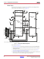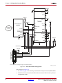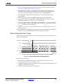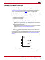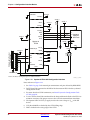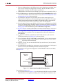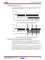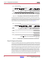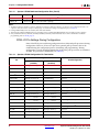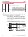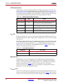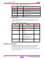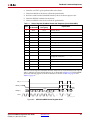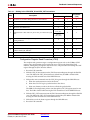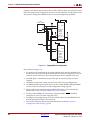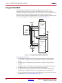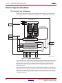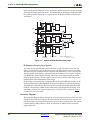
1
Spartan-6 FPGA
Configuration
User Guide
UG380 (v2.7) October 29, 2014
Notice of Disclaimer
The information disclosed to you hereunder (the “Materials”) is provided solely for the selection and use of Xilinx products. To the maximum
extent permitted by applicable law: (1) Materials are made available "AS IS" and with all faults, Xilinx hereby DISCLAIMS ALL
WARRANTIES AND CONDITIONS, EXPRESS, IMPLIED, OR STATUTORY, INCLUDING BUT NOT LIMITED TO WARRANTIES OF
MERCHANTABILITY, NON-INFRINGEMENT, OR FITNESS FOR ANY PARTICULAR PURPOSE; and (2) Xilinx shall not be liable (whether
in contract or tort, including negligence, or under any other theory of liability) for any loss or damage of any kind or nature related to, arising
under, or in connection with, the Materials (including your use of the Materials), including for any direct, indirect, special, incidental, or
consequential loss or damage (including loss of data, profits, goodwill, or any type of loss or damage suffered as a result of any action
brought by a third party) even if such damage or loss was reasonably foreseeable or Xilinx had been advised of the possibility of the same.
Xilinx assumes no obligation to correct any errors contained in the Materials or to notify you of updates to the Materials or to product
specifications. You may not reproduce, modify, distribute, or publicly display the Materials without prior written consent. Certain products are
subject to the terms and conditions of Xilinx’s limited warranty, please refer to Xilinx’s Terms of Sale which can be viewed at
www.xilinx.com/legal.htm#tos; IP cores may be subject to warranty and support terms contained in a license issued to you by Xilinx. Xilinx
products are not designed or intended to be fail-safe or for use in any application requiring fail-safe performance; you assume sole risk and
liability for use of Xilinx products in such critical applications, please refer to Xilinx’s Terms of Sale which can be viewed at
www.xilinx.com/legal.htm#tos.
© Copyright 2009–2014 Xilinx, Inc. Xilinx, the Xilinx logo, Artix, ISE, Kintex, Spartan, Virtex, Zynq, and other designated brands included
herein are trademarks of Xilinx in the United States and other countries. PCI, PCI Express, PCIe, and PCI-X are trademarks of PCI-SIG. All
other trademarks are the property of their respective owners.
Spartan-6 FPGA Configuration User Guide
www.xilinx.com
UG380 (v2.7) October 29, 2014
Revision History
The following table shows the revision history for this document.
Date
Version
Revision
06/24/2009
1.0
Initial Xilinx release.
02/17/2010
2.0
Changed REBOOT command to IPROG command throughout the document.
Chapter 1: In The High-Speed Priority Option, changed the configuration data size to 3.6 Mb (XC6SLX16). In FPGA
Density Migration on page 21, changed the required configuration memory size to 2.6 Mb (XC6SLX9) and 3.6 Mb
(XC6SLX16). In Protecting the FPGA Bitstream against Unauthorized Duplication, clarified which Spartan-6
devices have AES decryption logic.
Chapter 2: Removed the caution statement following Table 2-1. In Figure 2-2, Figure 2-3, Figure 2-6, Figure 2-7,
Figure 2-12, and Figure 2-20, changed VCCO_2 resistor to 2.4 kΩ.; added VFS and VBATT ports, added the
SUSPEND pin, and added four notes to the end of the Notes section following each figure. In Figure 2-2 and
Figure 2-6, removed “either 2.5V or 3.3V” from note about Spartan-6 FPGA VCCO_2 and the Platform Flash PROM
VCCO supply inputs. In Note 12 under Figure 2-12 and Note 10 under Figure 2-20, included PLL lock wait. In
Figure 2-2, changed PROGRAM_B pull-up power to VCCO_2. Removed Slave DIN from Figure 2-4. Added
sentence about SelectMAP unavailability to the first paragraph of SelectMAP Configuration Interface. Added
sentence about toggling to the BUSY description in Table 2-3. In Figure 2-6, added a 4.7 kΩ pull-up to
PROGRAM_B. Added BUSY to Note 14 under Figure 2-6. Added “configuration and” to Note 2 under Figure 2-7.
Moved placement of Table 2-6 and Table 2-7. Removed mention of Winbond’s SPI flash from Table 2-6. Changed
the first paragraph of CSI_B. Revised the RDWR_B section. In Note 1 under Figure 2-9, indicated that CSI_B cannot
be deasserted during the sync word. In Figure 2-12, changed 3.3V to VCCO_2. In Master BPI Configuration
Interface, updated the devices and packages that do not support the BPI interface; indicated A22 and A23 are not
in the CSG225 package; and added “top boot” to parallel NOR flash. In Table 2-7, removed the reference to the
BYTE# port in the HDC and LDC descriptions. In Figure 2-20, connected VCCO_1 and BYTE# to VCCO_1 and
added pull-up resistors to FCS_B, FOE_B, and FWE_B. Added Note 5 and 6 after Figure 2-20. Removed note about
CCLK being free from reflections to avoid double clocking in Board Layout for Configuration Clock (CCLK).
Chapter 4: Changed the last sentence in the first paragraph of ICAP_SPARTAN6. In the first paragraph of
STARTUP_SPARTAN6, changed EOS to configuration.
Chapter 5: Throughout this chapter, included waiting for PLLs to lock along with DCMs. In Table 5-1, added rows
for VFS, VBATT, and RFUSE; added Note 4; and changed pin name CMP_CS_B to CMPCS_B and updated its
description. Transferred FPGA I/O Pin Settings During Configuration from Chapter 1 and Reserving
Dual-Purpose Configuration Pins (Persist) from Chapter 2. In FPGA I/O Pin Settings During Configuration,
indicated that all user I/Os have optional pull-ups. Added Note 3 to Table 5-2. In Table 5-3, added Note 1 and
revised Note 2. In Table 5-5, changed the values in the “Total Number of Configuration Bits” column. In Device
Power-Up (Step 1), changed the second and third paragraphs and added -4 to the fourth paragraph. In Table 5-11,
added VFS and VCCO_5; changed VFS and VBATT descriptions; deleted “Value” and “Units” columns; added Notes
1, 4, and 5; and updated Note 2 to add VFS. Changed the second paragraph following Figure 5-4. Changed the last
paragraph in Check Device ID (Step 5). Added clocking specifics for the sequential state machine in the first
paragraph of Startup (Step 8). In Table 5-17, revised the DCM_LOCK description and moved Note 3 text to Startup
(Step 8). Added new paragraph after Table 5-17. In Loading the Encryption Key, clarified the type of programming
cable and rephrased the last sentence in the last paragraph. Changed the fourth and fifth paragraphs of Loading
Encrypted Bitstreams. Added the eFUSE section. In Table 5-22, changed the values under the “Total Bits” column.
Revised the GENERAL2 and GENERAL4 descriptions in Table 5-30. In Boot History Status Register (BOOTSTS),
changed the description of how this register is reset. In Table 5-48, changed bits 2 and 8 to “Reserved.” In
Figure 5-16, added a buffer between DOUT and DIN. Added sentence prior to Figure 5-16 about the new buffer.
Added the Bitstream Compression section.
Chapter 6: Changed the first paragraph. In Table 6-1, changed the “Configuration Data [15:0]” values for Steps 6
and 12. Changed the step numbers in the first sentence under Table 6-1. Added a sentence on SelectMAP data
ordering to the paragraph preceding Figure 6-2. In Figure 6-2, changed the timing diagram.
Chapter 7: In MultiBoot Overview, changed the last paragraph and removed the caution statement. Made
numerous changes to Fallback Behavior. In Reboot Using ICAP_SPARTAN6, changed “next bitstream” to
“MultiBoot bitstream” in the first paragraph and changed step 2 in the sequence of commands. In Table 7-1,
swapped the values of the Sync words, made changes in the “Explanation” column, and added Note 1 and Note
2. In Watchdog Timer, changed the first sentence in the first three paragraphs.
Chapter 8: On page 138, changed slice to frame in the first bullet, revised the fourth bullet, and removed the bullet
about transceiver DRPs not being masked.
Chapter 9: Changed Table 9-1.
UG380 (v2.7) October 29, 2014
www.xilinx.com
Spartan-6 FPGA Configuration User Guide
Date
Version
Revision
02/22/2010
2.1
Changed the supported encryption data widths to x1 and x8 in the Bitstream Encryption section.
In the third paragraph of Loading Encrypted Bitstreams, clarified that the configuration
bitstream can be delivered in an x1 or x8 data width configuration mode, and indicated that SPI
x2 and x4, BPI x16, and SelectMAP x16 bus widths are not supported for encrypted bitstreams.
07/30/2010
2.2
Changed the value of pull-up resistors connected between DONE and VCCO_2 from 2.4 kΩ to
330Ω in Figure 2-2, Figure 2-3, Figure 2-6, Figure 2-7, Figure 2-12, and Figure 2-20. Changed the
value of the pull-up the resistor connected between INIT_B and VCCO_2 from 2.4 kΩ to 4.7 kΩ
in Figure 2-3 and Figure 2-6. Added ports RDWR_B and CSI_B to FPGA (tied to ground) in
Figure 2-6. Added second and third paragraphs about configuration clock frequency to Master
Modes. Added introductory sentence and two bullets about SelectMAP considerations to
SelectMAP Configuration Interface section. Added sentence about VREF to description of
RDWR_B in Table 2-3. Added sentence to first paragraph of CSI_B section indicating that CSI_B
should not be deasserted in the middle of a sync word. Reformatted the first paragraph in Master
BPI Configuration Interface into one paragraph followed by bullets, and added the bullet
indicating the removal of the BPI configuration interface from the XC6SLX25/T devices.
Changed “VCCO_0” to “VCCO_2” in Figure 2-22, Figure 2-23, and Figure 2-24. Changed second
paragraph in Providing Power section. Added “if Suspend feature is not used” and Note 4 to
Table 5-2. Changed table reference from Table 5-4 to Table 5-3 in first paragraph of Configuration
Pins section. Added “Dual-Purpose” to Table 5-3 title. Changed “LVCMOS25 8 mA SLOW” to
“LVCMOS 8 mA SLOW” in second paragraph of Device Power-Up (Step 1). Changed CCLK
Output Delay symbol in Table 5-12 from “TICCK” to “TBPIICCK or TSPIICCK” and added Note 2.
Changed “VPOR” to “the recommended operating voltage” in the paragraph following
Figure 5-4. Added fourth paragraph about startup waiting for DCMs and PLLs by assigning
the LCK_CYCLE option to Startup (Step 8). Removed “DSP” from title in Figure 5-13. Added
third bullet to Bitstream Compression section under overall benefits on page 113. Changed
“warm boot” to “MultiBoot” in first paragraph of Fallback Behavior section. Added sentence
indicating how to generate the bitstream automatically to fourth paragraph of Fallback Behavior
section. Added last sentence to Note 2 in Table 7-1. Changed “DCM_WAIT” to “LCK_Cycle” in
Additional Memory Space Required for LCK_Cycle section title and text. Removed “66” from
the possible values listed in the description for the POST_CRC_FREQ constraint. Removed NCF
syntax examples from the Syntax Examples section. Changed “BPI UP” to “BPI” in Figure 9-4.
Changed “BPI UP, or BPI Down” to “or BPI“ in Note 7 (Notes relevant to Figure 9-4).
07/06/2011
2.3
Updated description of INIT_B in Table 2-2 and Table 2-3. Added VCCO_2 of 3.3V to Note 16 on
page 27, Note 9 on page 29, Note 18 on page 33, and Note 12 on page 35. Added a sentence about
deasserting the CSI_B signal to Non-Continuous SelectMAP Data Loading. Updated After
Configuration entries for CSO_B and INIT_B in Table 2-6. Updated Notes 11 and 16 on page 43.
Updated description of INIT_B in Table 2-7. Updated Note 2 on page 50, and Notes 11 and 18 on
page 51. Updated External Configuration Clock for Master Modes. Updated guideline about
configuration in master mode in Board Layout for Configuration Clock (CCLK).
Updated Note 2 after Table 5-3. In Table 5-5, updated Total Number of Configuration Bits
column and added Note 2. Removed -4 speed grade from paragraph before Table 5-11. Added
paragraph about external master clock pin after Table 5-17. Updated first paragraph of Bitstream
Encryption. Updated RFUSE Pin. Changed bitstream length from 32 to 16 and added list of three
types of configuration frames to Configuration Memory Frames. Removed Total Bits column
from Table 5-22. Updated Type 2 Packet. Changed direction of RDBK_SIGN in Table 5-30 from
R/W to W. Updated description of CRC_EXTSTAT_DISABLE in Table 5-34. Replaced type3
(PCFG) with type2 (IOB) in Frame Length Register. Added new paragraph before Table 5-41.
Updated Boot History Status Register (BOOTSTS) and Bitstream Compression.
Added readback limitations to Preparing a Design for Readback. Updated steps 7 and 8 in
Table 6-2. Removed AES encryption from MultiBoot Overview. Added Note 3 to Table 7-4.
Updated first sentence in second paragraph of page 137. Updated first paragraph of
POST_CRC_INIT_FLAG.
Updated Startup Sequencing (GTS).
Spartan-6 FPGA Configuration User Guide
www.xilinx.com
UG380 (v2.7) October 29, 2014
Date
Version
Revision
06/27/2012
2.4
Updated bullet about VBATT being tied to VCCAUX or ground in notes 8, 17, 11, 15, and 17 after
Figure 2-3, Figure 2-6, Figure 2-7, Figure 2-12, and Figure 2-20 respectively. Updated notes after
Figure 2-13. Updated references in SPI Configuration Interface. Updated Master SPI Dual (x2)
and Quad (x4) Read Commands. In Master BPI Configuration Interface, updated support of
Spartan-6 FPGAs for parallel NOR flash from 512 Mb to 1 Gb and for iMPACT software to
program bottom boot parallel NOR flash. Updated note 2 after Figure 2-20. Replaced LVCMOS25
with LVCMOS in External Configuration Clock for Master Modes. Updated Board Layout for
Configuration Clock (CCLK).
Updated last paragraph of Providing Power.
Updated note 1 after Table 5-1. Updated descriptions of VBATT and VFS in Table 5-11. Added note
2 to Figure 5-4. Removed sentence about ID error from Check Device ID (Step 5). Updated
description of GTS startup setting after Table 5-16. Added note 3 to Table 5-17. Added SPI x1 to
Loading Encrypted Bitstreams. Updated first row of Table 5-21. Updated FAR_MAJ Register and
Boot History Status Register (BOOTSTS).
Updated first paragraph of Configuration Memory Read Procedure (SelectMAP).
Updated first paragraph of Status Register for Fallback and IPROG Reconfiguration.
Added CRC Masking. Added POST_CRC_SOURCE to Post_CRC Constraints.
Added paragraph about using SPI in a serial daisy-chain configuration to Serial Daisy-Chains.
Updated SelectMAP Reconfiguration.
01/23/2013
2.5
Updated first bullet in sixth paragraph in Overview. Added Vccaux Level. Removed “XC” from
some device references throughout the user guide. Updated Figure 2-2, Figure 2-6, Figure 2-21,
Figure 5-15, Figure 8-2, Figure 9-1, Figure 9-2, Figure 9-4, and Figure 9-5. Updated second
paragraph in SelectMAP Configuration Interface. Updated second paragraph in
Non-Continuous SelectMAP Data Loading. Updated sixth paragraph in Master BPI
Configuration Interface. Updated Table 2-7, Table 4-3, Table 5-2, Table 5-19, Table 5-50, Table 6-2,
Table 6-5, Table 6-6, and Table 10-4. Added Determining the Maximum Configuration Clock
Frequency. Updated first paragraph after Table 2-8. Updated third paragraph in Board Layout
for Configuration Clock (CCLK). Updated first paragraph in FPGA I/O Pin Settings During
Configuration. Updated pin GCLK0 in Table 5-3. Updated second paragraph in Device
Power-Up (Step 1). Updated first paragraph in Cyclic Redundancy Check (Step 7). Updated first
paragraph in Startup (Step 8). Updated first and second paragraphs and Table 5-22 in
Configuration Memory Frames. Updated third paragraph in Frame Length Register. Updated
first paragraph in Identifier Memory Specifications. Updated Steps 3 and 6 in Configuration
Register Read Procedure (SelectMAP). Updated Step 13 in Configuration Memory Read
Procedure (SelectMAP). Updated first and sixth paragraphs following Figure 7-1. Updated first
paragraph and Table 7-4 in Status Register for Fallback and IPROG Reconfiguration. Added
Caution after first paragraph in Chapter 8, Readback CRC. Updated first and third bullet and
note in CRC Masking. Changed “dynamic” to “distributed” in CLB with LUT Configured as
Distributed RAM or Shift Register and in CLBs Near Top or Bottom IOI DRP with LUTs
Configured as Distributed RAM. Added second paragraph to Bit Sequence Boundary-Scan
Register.
06/20/2014
2.6
Updated first paragraph of CSI_B. Updated Figure 2-20. Updated explanation of O[15:0] in
Table 4-2. Updated SUSPEND pin in Table 5-2. Added Caution statement for Bit 16 in Table 5-19.
Added paragraph to the end of FPGA I/O Pin Settings During Configuration. Updated first
paragraph of Bitstream Overview. Updated Device Power-Up (Step 1). Updated second
paragraph of Bitstream Encryption. Updated second paragraph of Loading the Encryption Key.
Updated numbered procedure in Configuration Memory Read Procedure (SelectMAP). Added
explanation on how to carry out testing when the IOB is configured with an invertor in TAP
Controller and Architecture.
10/29/2014
2.7
Updated Steps 5 and 12 in Configuration Memory Read Procedure (SelectMAP). Updated Step
12 in Table 6-2. Minor update to Figure 10-3.
UG380 (v2.7) October 29, 2014
www.xilinx.com
Spartan-6 FPGA Configuration User Guide
Spartan-6 FPGA Configuration User Guide
www.xilinx.com
UG380 (v2.7) October 29, 2014
Table of Contents
Revision History . . . . . . . . . . . . . . . . . . . . . . . . . . . . . . . . . . . . . . . . . . . . . . . . . . . . . . . . . . . . . 3
Preface: About This Guide
Guide Contents . . . . . . . . . . . . . . . . . . . . . . . . . . . . . . . . . . . . . . . . . . . . . . . . . . . . . . . . . . . . . 13
Additional Documentation . . . . . . . . . . . . . . . . . . . . . . . . . . . . . . . . . . . . . . . . . . . . . . . . . . 13
Additional Resources . . . . . . . . . . . . . . . . . . . . . . . . . . . . . . . . . . . . . . . . . . . . . . . . . . . . . . . 14
Chapter 1: Configuration Overview
Overview . . . . . . . . . . . . . . . . . . . . . . . . . . . . . . . . . . . . . . . . . . . . . . . . . . . . . . . . . . . . . . . . . . . 15
Design Considerations . . . . . . . . . . . . . . . . . . . . . . . . . . . . . . . . . . . . . . . . . . . . . . . . . . . . . . 16
FPGA Configuration Data Source . . . . . . . . . . . . . . . . . . . . . . . . . . . . . . . . . . . . . . . . . . .
Master Modes . . . . . . . . . . . . . . . . . . . . . . . . . . . . . . . . . . . . . . . . . . . . . . . . . . . . . . . . . . . .
Slave Modes . . . . . . . . . . . . . . . . . . . . . . . . . . . . . . . . . . . . . . . . . . . . . . . . . . . . . . . . . . . . .
JTAG Connection . . . . . . . . . . . . . . . . . . . . . . . . . . . . . . . . . . . . . . . . . . . . . . . . . . . . . . . . .
The Basic Configuration Solution . . . . . . . . . . . . . . . . . . . . . . . . . . . . . . . . . . . . . . . . . . .
The Low-Cost Priority Solution . . . . . . . . . . . . . . . . . . . . . . . . . . . . . . . . . . . . . . . . . . . . .
The High-Speed Priority Option . . . . . . . . . . . . . . . . . . . . . . . . . . . . . . . . . . . . . . . . . . . .
Conforming to PCI Link Activation Requirements . . . . . . . . . . . . . . . . . . . . . . . . . . . .
Single and Multiple Configuration Images . . . . . . . . . . . . . . . . . . . . . . . . . . . . . . . . . . .
MultiBoot /Safe Update . . . . . . . . . . . . . . . . . . . . . . . . . . . . . . . . . . . . . . . . . . . . . . . . . . .
Required I/O Voltages . . . . . . . . . . . . . . . . . . . . . . . . . . . . . . . . . . . . . . . . . . . . . . . . . . . .
Vccaux Level . . . . . . . . . . . . . . . . . . . . . . . . . . . . . . . . . . . . . . . . . . . . . . . . . . . . . . . . . .
Nonvolatile Data Storage . . . . . . . . . . . . . . . . . . . . . . . . . . . . . . . . . . . . . . . . . . . . . . . . . .
FPGA Density Migration . . . . . . . . . . . . . . . . . . . . . . . . . . . . . . . . . . . . . . . . . . . . . . . . . .
Production Lifetime . . . . . . . . . . . . . . . . . . . . . . . . . . . . . . . . . . . . . . . . . . . . . . . . . . . . . . .
Protecting the FPGA Bitstream against Unauthorized Duplication. . . . . . . . . . . . . . .
Loading Multiple FPGAs with the Same Configuration Bitstream . . . . . . . . . . . . . . .
16
16
17
18
18
19
19
19
20
20
20
20
20
21
21
21
22
Configuration Factors . . . . . . . . . . . . . . . . . . . . . . . . . . . . . . . . . . . . . . . . . . . . . . . . . . . . . . . 22
Chapter 2: Configuration Interface Basics
JTAG Interface . . . . . . . . . . . . . . . . . . . . . . . . . . . . . . . . . . . . . . . . . . . . . . . . . . . . . . . . . . . . . . 23
Serial Configuration Interface . . . . . . . . . . . . . . . . . . . . . . . . . . . . . . . . . . . . . . . . . . . . . . . 24
Master Serial . . . . . . . . . . . . . . . . . . . . . . . . . . . . . . . . . . . . . . . . . . . . . . . . . . . . . . . . . . . . . 26
Slave Serial Configuration . . . . . . . . . . . . . . . . . . . . . . . . . . . . . . . . . . . . . . . . . . . . . . . . . 27
Serial Configuration Data Timing . . . . . . . . . . . . . . . . . . . . . . . . . . . . . . . . . . . . . . . . . . . 29
SelectMAP Configuration Interface. . . . . . . . . . . . . . . . . . . . . . . . . . . . . . . . . . . . . . . . . . 30
Single Device SelectMAP Configuration . . . . . . . . . . . . . . . . . . . . . . . . . . . . . . . . . . . . .
Platform Flash PROM SelectMAP Configuration . . . . . . . . . . . . . . . . . . . . . . . . . . . . . .
Microprocessor-Driven SelectMAP Configuration . . . . . . . . . . . . . . . . . . . . . . . . . . . . .
SelectMAP Data Loading . . . . . . . . . . . . . . . . . . . . . . . . . . . . . . . . . . . . . . . . . . . . . . . . . .
CSI_B . . . . . . . . . . . . . . . . . . . . . . . . . . . . . . . . . . . . . . . . . . . . . . . . . . . . . . . . . . . . . . .
RDWR_B . . . . . . . . . . . . . . . . . . . . . . . . . . . . . . . . . . . . . . . . . . . . . . . . . . . . . . . . . . . . .
CCLK . . . . . . . . . . . . . . . . . . . . . . . . . . . . . . . . . . . . . . . . . . . . . . . . . . . . . . . . . . . . . . .
Continuous SelectMAP Data Loading . . . . . . . . . . . . . . . . . . . . . . . . . . . . . . . . . . . . . .
Non-Continuous SelectMAP Data Loading . . . . . . . . . . . . . . . . . . . . . . . . . . . . . . . . . .
Spartan-6 FPGA Configuration User Guide
UG380 (v2.7) October 29, 2014
www.xilinx.com
31
32
34
35
35
36
36
36
37
7
SelectMAP Data Ordering . . . . . . . . . . . . . . . . . . . . . . . . . . . . . . . . . . . . . . . . . . . . . . . . . 39
SPI Configuration Interface . . . . . . . . . . . . . . . . . . . . . . . . . . . . . . . . . . . . . . . . . . . . . . . . . 40
Master SPI Vendor Auto-Detection and Error Handling . . . . . . . . . . . . . . . . . . . . . . . .
Master SPI Timing Waveform . . . . . . . . . . . . . . . . . . . . . . . . . . . . . . . . . . . . . . . . . . . . . .
Master SPI Dual (x2) and Quad (x4) Read Commands . . . . . . . . . . . . . . . . . . . . . . . . .
Power-On Sequence Precautions . . . . . . . . . . . . . . . . . . . . . . . . . . . . . . . . . . . . . . . . . . . .
SPI Serial Daisy-Chain . . . . . . . . . . . . . . . . . . . . . . . . . . . . . . . . . . . . . . . . . . . . . . . . . . . . .
44
45
45
46
47
Master BPI Configuration Interface . . . . . . . . . . . . . . . . . . . . . . . . . . . . . . . . . . . . . . . . . . 47
Determining the Maximum Configuration Clock Frequency . . . . . . . . . . . . . . . . . . . . 53
Power-On Sequence Precautions . . . . . . . . . . . . . . . . . . . . . . . . . . . . . . . . . . . . . . . . . . . . 53
External Configuration Clock for Master Modes . . . . . . . . . . . . . . . . . . . . . . . . . . . . . 54
Board Layout for Configuration Clock (CCLK) . . . . . . . . . . . . . . . . . . . . . . . . . . . . . . . 54
Chapter 3: Boundary-Scan and JTAG Configuration
Introduction . . . . . . . . . . . . . . . . . . . . . . . . . . . . . . . . . . . . . . . . . . . . . . . . . . . . . . . . . . . . . . . . 59
Boundary-Scan for Spartan-6 Devices Using IEEE Std 1149.1 . . . . . . . . . . . . . . . . . 59
Test Access Port (TAP) . . . . . . . . . . . . . . . . . . . . . . . . . . . . . . . . . . . . . . . . . . . . . . . . . . . . 59
Boundary-Scan Timing Parameters . . . . . . . . . . . . . . . . . . . . . . . . . . . . . . . . . . . . . . . . . . 60
Using Boundary-Scan in Spartan-6 Devices . . . . . . . . . . . . . . . . . . . . . . . . . . . . . . . . . . 61
Design Considerations . . . . . . . . . . . . . . . . . . . . . . . . . . . . . . . . . . . . . . . . . . . . . . . . . . . . . . 62
JTAG Signal Routing . . . . . . . . . . . . . . . . . . . . . . . . . . . . . . . . . . . . . . . . . . . . . . . . . . . . . . 62
Providing Power . . . . . . . . . . . . . . . . . . . . . . . . . . . . . . . . . . . . . . . . . . . . . . . . . . . . . . . . . 62
Configuring through Boundary-Scan . . . . . . . . . . . . . . . . . . . . . . . . . . . . . . . . . . . . . . . . 63
Chapter 4: User Primitives
BSCAN_SPARTAN6 . . . . . . . . . . . . . . . . . . . . . . . . . . . . . . . . . . . . . . . . . . . . . . . . . . . . . . . .
ICAP_SPARTAN6 . . . . . . . . . . . . . . . . . . . . . . . . . . . . . . . . . . . . . . . . . . . . . . . . . . . . . . . . . .
STARTUP_SPARTAN6 . . . . . . . . . . . . . . . . . . . . . . . . . . . . . . . . . . . . . . . . . . . . . . . . . . . . .
DNA_PORT . . . . . . . . . . . . . . . . . . . . . . . . . . . . . . . . . . . . . . . . . . . . . . . . . . . . . . . . . . . . . . . .
SUSPEND_SYNC . . . . . . . . . . . . . . . . . . . . . . . . . . . . . . . . . . . . . . . . . . . . . . . . . . . . . . . . . . .
POST_CRC_INTERNAL . . . . . . . . . . . . . . . . . . . . . . . . . . . . . . . . . . . . . . . . . . . . . . . . . . . .
65
66
67
67
68
69
Chapter 5: Configuration Details
Configuration Pins . . . . . . . . . . . . . . . . . . . . . . . . . . . . . . . . . . . . . . . . . . . . . . . . . . . . . . . . . . 71
FPGA I/O Pin Settings During Configuration . . . . . . . . . . . . . . . . . . . . . . . . . . . . . . . . 72
Reserving Dual-Purpose Configuration Pins (Persist) . . . . . . . . . . . . . . . . . . . . . . . . . . 73
Configuration Data File Formats. . . . . . . . . . . . . . . . . . . . . . . . . . . . . . . . . . . . . . . . . . . . . 75
Bitstream Overview . . . . . . . . . . . . . . . . . . . . . . . . . . . . . . . . . . . . . . . . . . . . . . . . . . . . . . . . . 75
Sync Word/Bus Width Auto Detection . . . . . . . . . . . . . . . . . . . . . . . . . . . . . . . . . . . . . . 76
Generating PROM Files . . . . . . . . . . . . . . . . . . . . . . . . . . . . . . . . . . . . . . . . . . . . . . . . . . . . . 77
PROM Files for Serial Daisy-Chains . . . . . . . . . . . . . . . . . . . . . . . . . . . . . . . . . . . . . . . . .
PROM Files for SelectMAP Configuration . . . . . . . . . . . . . . . . . . . . . . . . . . . . . . . . . . . .
PROM Files for SPI/BPI Configuration . . . . . . . . . . . . . . . . . . . . . . . . . . . . . . . . . . . . . .
Bit Swapping . . . . . . . . . . . . . . . . . . . . . . . . . . . . . . . . . . . . . . . . . . . . . . . . . . . . . . . . . . . . .
Parallel Bus Bit Order . . . . . . . . . . . . . . . . . . . . . . . . . . . . . . . . . . . . . . . . . . . . . . . . . . . . .
Delaying Configuration . . . . . . . . . . . . . . . . . . . . . . . . . . . . . . . . . . . . . . . . . . . . . . . . .
77
77
77
78
79
80
Configuration Sequence . . . . . . . . . . . . . . . . . . . . . . . . . . . . . . . . . . . . . . . . . . . . . . . . . . . . . 80
8
www.xilinx.com
Spartan-6 FPGA Configuration User Guide
UG380 (v2.7) October 29, 2014
Setup (Steps 1-3) . . . . . . . . . . . . . . . . . . . . . . . . . . . . . . . . . . . . . . . . . . . . . . . . . . . . . . . . . .
Device Power-Up (Step 1) . . . . . . . . . . . . . . . . . . . . . . . . . . . . . . . . . . . . . . . . . . . . . . . .
Clear Configuration Memory (Step 2, Initialization) . . . . . . . . . . . . . . . . . . . . . . . . . . .
Sample Mode Pins (Step 3) . . . . . . . . . . . . . . . . . . . . . . . . . . . . . . . . . . . . . . . . . . . . . . .
Bitstream Loading (Steps 4-7) . . . . . . . . . . . . . . . . . . . . . . . . . . . . . . . . . . . . . . . . . . . . . .
Synchronization (Step 4) . . . . . . . . . . . . . . . . . . . . . . . . . . . . . . . . . . . . . . . . . . . . . . . . .
Check Device ID (Step 5) . . . . . . . . . . . . . . . . . . . . . . . . . . . . . . . . . . . . . . . . . . . . . . . .
Load Configuration Data Frames (Step 6). . . . . . . . . . . . . . . . . . . . . . . . . . . . . . . . . . . .
Cyclic Redundancy Check (Step 7) . . . . . . . . . . . . . . . . . . . . . . . . . . . . . . . . . . . . . . . . .
Startup (Step 8) . . . . . . . . . . . . . . . . . . . . . . . . . . . . . . . . . . . . . . . . . . . . . . . . . . . . . . . .
81
81
83
83
84
84
84
86
86
86
Bitstream Encryption . . . . . . . . . . . . . . . . . . . . . . . . . . . . . . . . . . . . . . . . . . . . . . . . . . . . . . . . 89
Advanced Encryption Standard Overview . . . . . . . . . . . . . . . . . . . . . . . . . . . . . . . . . . .
Creating an Encrypted Bitstream . . . . . . . . . . . . . . . . . . . . . . . . . . . . . . . . . . . . . . . . . . .
Loading the Encryption Key . . . . . . . . . . . . . . . . . . . . . . . . . . . . . . . . . . . . . . . . . . . . . . .
Loading Encrypted Bitstreams . . . . . . . . . . . . . . . . . . . . . . . . . . . . . . . . . . . . . . . . . . . . . .
Bitstream Encryption and Internal Configuration Access Port (ICAP) . . . . . . . . . . . .
VBATT . . . . . . . . . . . . . . . . . . . . . . . . . . . . . . . . . . . . . . . . . . . . . . . . . . . . . . . . . . . . . . . . . . .
89
89
90
90
91
91
eFUSE . . . . . . . . . . . . . . . . . . . . . . . . . . . . . . . . . . . . . . . . . . . . . . . . . . . . . . . . . . . . . . . . . . . . . . 91
eFUSE Registers . . . . . . . . . . . . . . . . . . . . . . . . . . . . . . . . . . . . . . . . . . . . . . . . . . . . . . . . . .
eFUSE Control Register (FUSE_CNTL). . . . . . . . . . . . . . . . . . . . . . . . . . . . . . . . . . . . . .
JTAG Instructions . . . . . . . . . . . . . . . . . . . . . . . . . . . . . . . . . . . . . . . . . . . . . . . . . . . . . . . .
VFS Pin . . . . . . . . . . . . . . . . . . . . . . . . . . . . . . . . . . . . . . . . . . . . . . . . . . . . . . . . . . . . . . . . .
RFUSE Pin . . . . . . . . . . . . . . . . . . . . . . . . . . . . . . . . . . . . . . . . . . . . . . . . . . . . . . . . . . . . . . .
VCCAUX Pin . . . . . . . . . . . . . . . . . . . . . . . . . . . . . . . . . . . . . . . . . . . . . . . . . . . . . . . . . . . .
92
92
94
94
94
94
Configuration Memory Frames . . . . . . . . . . . . . . . . . . . . . . . . . . . . . . . . . . . . . . . . . . . . . . 95
Configuration Packets . . . . . . . . . . . . . . . . . . . . . . . . . . . . . . . . . . . . . . . . . . . . . . . . . . . . . . . 96
Packet Types . . . . . . . . . . . . . . . . . . . . . . . . . . . . . . . . . . . . . . . . . . . . . . . . . . . . . . . . . . . . . 96
Type 1 Packet . . . . . . . . . . . . . . . . . . . . . . . . . . . . . . . . . . . . . . . . . . . . . . . . . . . . . . . . . 96
Type 2 Packet . . . . . . . . . . . . . . . . . . . . . . . . . . . . . . . . . . . . . . . . . . . . . . . . . . . . . . . . . 96
Configuration Registers . . . . . . . . . . . . . . . . . . . . . . . . . . . . . . . . . . . . . . . . . . . . . . . . . . . 97
CRC Register . . . . . . . . . . . . . . . . . . . . . . . . . . . . . . . . . . . . . . . . . . . . . . . . . . . . . . . . . . 98
FAR_MAJ Register . . . . . . . . . . . . . . . . . . . . . . . . . . . . . . . . . . . . . . . . . . . . . . . . . . . . . 99
FAR_MIN Register . . . . . . . . . . . . . . . . . . . . . . . . . . . . . . . . . . . . . . . . . . . . . . . . . . . . . 99
FDRI Register . . . . . . . . . . . . . . . . . . . . . . . . . . . . . . . . . . . . . . . . . . . . . . . . . . . . . . . . . 99
FDRO Register . . . . . . . . . . . . . . . . . . . . . . . . . . . . . . . . . . . . . . . . . . . . . . . . . . . . . . . . 99
MASK Register . . . . . . . . . . . . . . . . . . . . . . . . . . . . . . . . . . . . . . . . . . . . . . . . . . . . . . . . 99
EYE_MASK Register . . . . . . . . . . . . . . . . . . . . . . . . . . . . . . . . . . . . . . . . . . . . . . . . . . . . 99
LOUT Register . . . . . . . . . . . . . . . . . . . . . . . . . . . . . . . . . . . . . . . . . . . . . . . . . . . . . . . . 99
CBC_REG Register . . . . . . . . . . . . . . . . . . . . . . . . . . . . . . . . . . . . . . . . . . . . . . . . . . . . 100
IDCODE Register . . . . . . . . . . . . . . . . . . . . . . . . . . . . . . . . . . . . . . . . . . . . . . . . . . . . . 100
CSBO Register . . . . . . . . . . . . . . . . . . . . . . . . . . . . . . . . . . . . . . . . . . . . . . . . . . . . . . . . 100
Command Register (CMD) . . . . . . . . . . . . . . . . . . . . . . . . . . . . . . . . . . . . . . . . . . . . . . 100
Control Register 0 (CTL) . . . . . . . . . . . . . . . . . . . . . . . . . . . . . . . . . . . . . . . . . . . . . . . . 101
Status Register (STAT) . . . . . . . . . . . . . . . . . . . . . . . . . . . . . . . . . . . . . . . . . . . . . . . . . 102
Configuration Options Register (COR1 and COR2) . . . . . . . . . . . . . . . . . . . . . . . . . . . 103
Suspend Register (PWRDN_REG) . . . . . . . . . . . . . . . . . . . . . . . . . . . . . . . . . . . . . . . . 104
Frame Length Register . . . . . . . . . . . . . . . . . . . . . . . . . . . . . . . . . . . . . . . . . . . . . . . . . 104
Multi-Frame Write Register . . . . . . . . . . . . . . . . . . . . . . . . . . . . . . . . . . . . . . . . . . . . . 104
Configuration Watchdog Timer Register . . . . . . . . . . . . . . . . . . . . . . . . . . . . . . . . . . . 105
HC_OPT_REG Register . . . . . . . . . . . . . . . . . . . . . . . . . . . . . . . . . . . . . . . . . . . . . . . . 105
GENERAL Registers 1, 2, 3, 4, and 5 . . . . . . . . . . . . . . . . . . . . . . . . . . . . . . . . . . . . . . . 105
MODE Register . . . . . . . . . . . . . . . . . . . . . . . . . . . . . . . . . . . . . . . . . . . . . . . . . . . . . . . 106
CCLK_FREQ Register . . . . . . . . . . . . . . . . . . . . . . . . . . . . . . . . . . . . . . . . . . . . . . . . . . 107
Spartan-6 FPGA Configuration User Guide
UG380 (v2.7) October 29, 2014
www.xilinx.com
9
PU_GWE Register . . . . . . . . . . . . . . . . . . . . . . . . . . . . . . . . . . . . . . . . . . . . . . . . . . . . .
PU_GTS Register. . . . . . . . . . . . . . . . . . . . . . . . . . . . . . . . . . . . . . . . . . . . . . . . . . . . . .
Boot History Status Register (BOOTSTS) . . . . . . . . . . . . . . . . . . . . . . . . . . . . . . . . . . .
SEU_OPT Register . . . . . . . . . . . . . . . . . . . . . . . . . . . . . . . . . . . . . . . . . . . . . . . . . . . .
107
107
107
108
Bitstream Composition . . . . . . . . . . . . . . . . . . . . . . . . . . . . . . . . . . . . . . . . . . . . . . . . . . . . . 108
Default Initial Configuration Process . . . . . . . . . . . . . . . . . . . . . . . . . . . . . . . . . . . . . . . 109
Spartan-6 FPGA Unique Device Identifier (Device DNA) . . . . . . . . . . . . . . . . . . . 109
Identifier Value . . . . . . . . . . . . . . . . . . . . . . . . . . . . . . . . . . . . . . . . . . . . . . . . . . . . . . . . . .
Operation. . . . . . . . . . . . . . . . . . . . . . . . . . . . . . . . . . . . . . . . . . . . . . . . . . . . . . . . . . . . . . .
Identifier Memory Specifications. . . . . . . . . . . . . . . . . . . . . . . . . . . . . . . . . . . . . . . . . . .
Extending Identifier Length . . . . . . . . . . . . . . . . . . . . . . . . . . . . . . . . . . . . . . . . . . . . . . .
JTAG Access to Device Identifier. . . . . . . . . . . . . . . . . . . . . . . . . . . . . . . . . . . . . . . . . . .
iMPACT Access to Device Identifier . . . . . . . . . . . . . . . . . . . . . . . . . . . . . . . . . . . . . . . .
110
110
111
111
112
112
Bitstream Compression . . . . . . . . . . . . . . . . . . . . . . . . . . . . . . . . . . . . . . . . . . . . . . . . . . . . . 112
Chapter 6: Readback and Configuration Verification
Preparing a Design for Readback . . . . . . . . . . . . . . . . . . . . . . . . . . . . . . . . . . . . . . . . . . . 115
Readback Command Sequences . . . . . . . . . . . . . . . . . . . . . . . . . . . . . . . . . . . . . . . . . . . . 116
Accessing Configuration Registers through the SelectMAP Interface . . . . . . . . . . . .
Configuration Register Read Procedure (SelectMAP) . . . . . . . . . . . . . . . . . . . . . . . . .
Configuration Memory Read Procedure (SelectMAP) . . . . . . . . . . . . . . . . . . . . . . . . .
Accessing Configuration Registers through the JTAG Interface . . . . . . . . . . . . . . . .
Configuration Register Read Procedure (JTAG) . . . . . . . . . . . . . . . . . . . . . . . . . . . . . .
Configuration Memory Read Procedure (IEEE Std 1149.1 JTAG) . . . . . . . . . . . . . . . . .
116
116
118
120
121
123
Verifying Readback Data. . . . . . . . . . . . . . . . . . . . . . . . . . . . . . . . . . . . . . . . . . . . . . . . . . . 127
Chapter 7: Reconfiguration and MultiBoot
MultiBoot Overview . . . . . . . . . . . . . . . . . . . . . . . . . . . . . . . . . . . . . . . . . . . . . . . . . . . . . . . 131
Fallback MultiBoot . . . . . . . . . . . . . . . . . . . . . . . . . . . . . . . . . . . . . . . . . . . . . . . . . . . . . . . . . 132
Fallback Behavior . . . . . . . . . . . . . . . . . . . . . . . . . . . . . . . . . . . . . . . . . . . . . . . . . . . . . . . . 132
IPROG Reconfiguration . . . . . . . . . . . . . . . . . . . . . . . . . . . . . . . . . . . . . . . . . . . . . . . . . . . . 134
Reboot Using ICAP_SPARTAN6 . . . . . . . . . . . . . . . . . . . . . . . . . . . . . . . . . . . . . . . . . . . 134
Status Register for Fallback and IPROG Reconfiguration . . . . . . . . . . . . . . . . . . . 135
Watchdog Timer . . . . . . . . . . . . . . . . . . . . . . . . . . . . . . . . . . . . . . . . . . . . . . . . . . . . . . . . . . . 135
Required Data Spacing between MultiBoot Images . . . . . . . . . . . . . . . . . . . . . . . . . 136
Flash Sector, Block, or Page Boundaries . . . . . . . . . . . . . . . . . . . . . . . . . . . . . . . . . . . . . 136
Additional Memory Space Required for LCK_Cycle . . . . . . . . . . . . . . . . . . . . . . . . . . 136
Chapter 8: Readback CRC
CRC Masking . . . . . . . . . . . . . . . . . . . . . . . . . . . . . . . . . . . . . . . . . . . . . . . . . . . . . . . . . . . . . . 138
CLB with LUT Configured as Distributed RAM or Shift Register . . . . . . . . . . . . . . . 138
CLBs Near Top or Bottom IOI Using DRP . . . . . . . . . . . . . . . . . . . . . . . . . . . . . . . . . . . 140
CLBs Near Top or Bottom IOI DRP with LUTs Configured as Distributed RAM . . 141
Post_CRC Constraints . . . . . . . . . . . . . . . . . . . . . . . . . . . . . . . . . . . . . . . . . . . . . . . . . . . . . . 142
POST_CRC . . . . . . . . . . . . . . . . . . . . . . . . . . . . . . . . . . . . . . . . . . . . . . . . . . . . . . . . . . . . .
POST_CRC_INIT_FLAG . . . . . . . . . . . . . . . . . . . . . . . . . . . . . . . . . . . . . . . . . . . . . . . . . .
POST_CRC_SOURCE . . . . . . . . . . . . . . . . . . . . . . . . . . . . . . . . . . . . . . . . . . . . . . . . . . . .
POST_CRC_ACTION . . . . . . . . . . . . . . . . . . . . . . . . . . . . . . . . . . . . . . . . . . . . . . . . . . . .
10
www.xilinx.com
142
142
142
143
Spartan-6 FPGA Configuration User Guide
UG380 (v2.7) October 29, 2014
POST_CRC_FREQ . . . . . . . . . . . . . . . . . . . . . . . . . . . . . . . . . . . . . . . . . . . . . . . . . . . . . . .
Syntax Examples . . . . . . . . . . . . . . . . . . . . . . . . . . . . . . . . . . . . . . . . . . . . . . . . . . . . . . . .
POST_CRC . . . . . . . . . . . . . . . . . . . . . . . . . . . . . . . . . . . . . . . . . . . . . . . . . . . . . . . . . .
POST_CRC_INIT_FLAG . . . . . . . . . . . . . . . . . . . . . . . . . . . . . . . . . . . . . . . . . . . . . . . .
POST_CRC_SOURCE . . . . . . . . . . . . . . . . . . . . . . . . . . . . . . . . . . . . . . . . . . . . . . . . . .
POST_CRC_ACTION . . . . . . . . . . . . . . . . . . . . . . . . . . . . . . . . . . . . . . . . . . . . . . . . . .
POST_CRC_FREQ . . . . . . . . . . . . . . . . . . . . . . . . . . . . . . . . . . . . . . . . . . . . . . . . . . . .
143
143
143
143
143
144
144
Chapter 9: Advanced Configuration Interfaces
Serial Daisy-Chains . . . . . . . . . . . . . . . . . . . . . . . . . . . . . . . . . . . . . . . . . . . . . . . . . . . . . . . . 145
Mixed Serial Daisy-Chains . . . . . . . . . . . . . . . . . . . . . . . . . . . . . . . . . . . . . . . . . . . . . . . . . 146
Guidelines and Design Considerations for Serial Daisy-Chains . . . . . . . . . . . . . . . .
Startup Sequencing (GTS) . . . . . . . . . . . . . . . . . . . . . . . . . . . . . . . . . . . . . . . . . . . . . . .
Active DONE Driver . . . . . . . . . . . . . . . . . . . . . . . . . . . . . . . . . . . . . . . . . . . . . . . . . . .
Connect All DONE Pins . . . . . . . . . . . . . . . . . . . . . . . . . . . . . . . . . . . . . . . . . . . . . . . .
DONE Pin Rise Time . . . . . . . . . . . . . . . . . . . . . . . . . . . . . . . . . . . . . . . . . . . . . . . . . .
Bitstream Formatting . . . . . . . . . . . . . . . . . . . . . . . . . . . . . . . . . . . . . . . . . . . . . . . . . .
147
147
147
147
147
147
Ganged Serial Configuration . . . . . . . . . . . . . . . . . . . . . . . . . . . . . . . . . . . . . . . . . . . . . . .
Multiple Device SelectMAP Configuration . . . . . . . . . . . . . . . . . . . . . . . . . . . . . . . . .
Parallel Daisy-Chain . . . . . . . . . . . . . . . . . . . . . . . . . . . . . . . . . . . . . . . . . . . . . . . . . . . . . . .
Ganged SelectMAP . . . . . . . . . . . . . . . . . . . . . . . . . . . . . . . . . . . . . . . . . . . . . . . . . . . . . . . .
SelectMAP ABORT . . . . . . . . . . . . . . . . . . . . . . . . . . . . . . . . . . . . . . . . . . . . . . . . . . . . . . . .
147
Configuration Abort Sequence Description . . . . . . . . . . . . . . . . . . . . . . . . . . . . . . . . . .
Readback Abort Sequence Description . . . . . . . . . . . . . . . . . . . . . . . . . . . . . . . . . . . . . .
ABORT Status Word . . . . . . . . . . . . . . . . . . . . . . . . . . . . . . . . . . . . . . . . . . . . . . . . . . . . .
Resuming Configuration or Readback After an Abort . . . . . . . . . . . . . . . . . . . . . . . . .
149
151
152
153
153
154
154
155
SelectMAP Reconfiguration . . . . . . . . . . . . . . . . . . . . . . . . . . . . . . . . . . . . . . . . . . . . . . . . 155
Chapter 10: Advanced JTAG Configurations
Introduction . . . . . . . . . . . . . . . . . . . . . . . . . . . . . . . . . . . . . . . . . . . . . . . . . . . . . . . . . . . . . . . 157
JTAG Configuration/Readback . . . . . . . . . . . . . . . . . . . . . . . . . . . . . . . . . . . . . . . . . . . . . 158
TAP Controller and Architecture . . . . . . . . . . . . . . . . . . . . . . . . . . . . . . . . . . . . . . . . . .
Boundary-Scan Architecture . . . . . . . . . . . . . . . . . . . . . . . . . . . . . . . . . . . . . . . . . . . . . .
Boundary-Scan Register . . . . . . . . . . . . . . . . . . . . . . . . . . . . . . . . . . . . . . . . . . . . . . . .
Instruction Register . . . . . . . . . . . . . . . . . . . . . . . . . . . . . . . . . . . . . . . . . . . . . . . . . . . .
BYPASS Register . . . . . . . . . . . . . . . . . . . . . . . . . . . . . . . . . . . . . . . . . . . . . . . . . . . . . .
Identification (IDCODE) Register . . . . . . . . . . . . . . . . . . . . . . . . . . . . . . . . . . . . . . . . .
JTAG Configuration Register . . . . . . . . . . . . . . . . . . . . . . . . . . . . . . . . . . . . . . . . . . . .
USERCODE Register. . . . . . . . . . . . . . . . . . . . . . . . . . . . . . . . . . . . . . . . . . . . . . . . . . .
USER1, USER2, USER3, and USER4 Registers . . . . . . . . . . . . . . . . . . . . . . . . . . . . . . .
Using Boundary-Scan in Spartan-6 Devices . . . . . . . . . . . . . . . . . . . . . . . . . . . . . . . . .
Configuring through Boundary-Scan . . . . . . . . . . . . . . . . . . . . . . . . . . . . . . . . . . . . . .
Clocking Startup and Shutdown Sequences (JTAG) . . . . . . . . . . . . . . . . . . . . . . . . . .
Spartan-6 FPGA Configuration User Guide
UG380 (v2.7) October 29, 2014
www.xilinx.com
158
161
161
162
164
164
164
164
164
165
165
168
11
12
www.xilinx.com
Spartan-6 FPGA Configuration User Guide
UG380 (v2.7) October 29, 2014
Preface
About This Guide
This document describes Spartan®-6 FPGA configuration. Complete and up-to-date
documentation of the Spartan-6 family of FPGAs is available on the Xilinx website at
http://www.xilinx.com/support/documentation/spartan-6.htm.
Guide Contents
This manual contains the following chapters:
•
Chapter 1, Configuration Overview
•
Chapter 2, Configuration Interface Basics
•
Chapter 3, Boundary-Scan and JTAG Configuration
•
Chapter 4, User Primitives
•
Chapter 5, Configuration Details
•
Chapter 6, Readback and Configuration Verification
•
Chapter 7, Reconfiguration and MultiBoot
•
Chapter 8, Readback CRC
•
Chapter 9, Advanced Configuration Interfaces
•
Chapter 10, Advanced JTAG Configurations
Additional Documentation
The following documents are also available for download at:
http://www.xilinx.com/support/documentation/spartan-6.htm.
•
Spartan-6 Family Overview
This overview outlines the features and product selection of the Spartan-6 family.
•
Spartan-6 FPGA Data Sheet: DC and Switching Characteristics
This data sheet contains the DC and Switching Characteristic specifications for the
Spartan-6 family.
•
Spartan-6 FPGA Packaging and Pinout Specifications
This specification includes the tables for device/package combinations and maximum
I/Os, pin definitions, pinout tables, pinout diagrams, mechanical drawings, and
thermal specifications.
•
Spartan-6 FPGA SelectIO Resources User Guide
This guide describes the SelectIO™ resources available in all Spartan-6 devices.
Spartan-6 FPGA Configuration User Guide
UG380 (v2.7) October 29, 2014
www.xilinx.com
13
Preface: About This Guide
•
Spartan-6 FPGA Clocking Resources User Guide
This guide describes the clocking resources available in all Spartan-6 devices,
including the DCMs and the PLLs.
•
Spartan-6 FPGA Block RAM Resources User Guide
This guide describes the Spartan-6 device block RAM capabilities.
•
Spartan-6 FPGA Configurable Logic Blocks User Guide
This guide describes the capabilities of the configurable logic blocks (CLBs) available
in all Spartan-6 devices.
•
Spartan-6 FPGA Memory Controller User Guide
This guide describes the Spartan-6 FPGA memory controller block, a dedicated,
embedded multi-port memory controller that greatly simplifies interfacing Spartan-6
FPGAs to the most popular memory standards.
•
Spartan-6 FPGA GTP Transceivers User Guide
This guide describes the GTP transceivers available in Spartan-6 LXT FPGAs.
•
Spartan-6 FPGA DSP48A1 Slice User Guide
This guide describes the architecture of the DSP48A1 slice in Spartan-6 FPGAs and
provides configuration examples.
•
Spartan-6 FPGA PCB and Pin Planning Design Guide
This guide provides information on PCB design for Spartan-6 devices, with a focus on
strategies for making design decisions at the PCB and interface level.
•
Spartan-6 FPGA Power Management User Guide
This guide provides information on the various hardware methods of power
management in Spartan-6 devices, primarily focusing on the suspend mode.
Additional Resources
To find additional documentation, see the Xilinx website at:
http://www.xilinx.com/support/documentation/index.htm.
To search the Answer Database of silicon, software, and IP questions and answers, or to
create a technical support WebCase, see the Xilinx website at:
http://www.xilinx.com/support.
14
www.xilinx.com
Spartan-6 FPGA Configuration User Guide
UG380 (v2.7) October 29, 2014
Chapter 1
Configuration Overview
Overview
Spartan®-6 FPGAs are configured by loading application-specific configuration data—a
bitstream—into internal memory. Spartan-6 FPGAs can load themselves from an external
nonvolatile memory device or they can be configured by an external smart source, such as
a microprocessor, DSP processor, microcontroller, PC, or board tester. In any case, there are
two general configuration datapaths. The first is the serial datapath that is used to
minimize the device pin requirements. The second datapath is the 8- or 16-bit datapath
used for higher performance or access (or link) to industry-standard interfaces, ideal for
external data sources like processors, or x8- or x16-parallel flash memory.
Like processors and processor peripherals, Xilinx® FPGAs can be reprogrammed, in
system, on demand, an unlimited number of times.
Because Xilinx FPGA configuration data is stored in CMOS configuration latches (CCLs), it
must be reconfigured after it is powered down. The bitstream is loaded each time into the
device through special configuration pins. These configuration pins serve as the interface
for a number of different configuration modes:
•
JTAG configuration mode
•
Master Serial/SPI configuration mode (x1, x2, and x4)
•
Slave Serial configuration mode
•
Master SelectMAP/BPI configuration mode (x8 and x16)
•
Slave SelectMAP configuration mode (x8 and x16)
The configuration modes are explained in detail in Chapter 2, Configuration Interface
Basics.
The specific configuration mode is selected by setting the appropriate level on the mode
input pins M[1:0]. The M1 and M0 mode pins should be set at a constant DC voltage level,
either through pull-up or pull-down resistors (2.4 kΩ), or tied directly to ground or
VCCO_2. The mode pins should not be toggled during or before configuration but can be
toggled after. See Chapter 2, Configuration Interface Basics, for the mode pin setting
options.
The terms Master and Slave refer to the direction of the configuration clock (CCLK):
•
In Master configuration modes, the Spartan-6 device drives CCLK from an internal
oscillator by default or optional external master clock source GCLK0/USERCCLK. To
select the desired frequency, the BitGen -g ConfigRate option is used for the
internal oscillator. The default is 2 MHz. The CCLK output frequency varies with
process, voltage, and temperature. The data sheet FMCCKTOL specification defines the
frequency tolerance. A frequency tolerance of ± 50% means that a ConfigRate setting
of 10 could generate a CCLK rate of between 5 MHz and 15 MHz.The BitGen section
Spartan-6 FPGA Configuration User Guide
UG380 (v2.7) October 29, 2014
www.xilinx.com
15
Chapter 1: Configuration Overview
of UG628, Command Line Tools User Guide provides more information. After
configuration, the oscillator is turned OFF unless one of these conditions is met:
•
SEU detection is used.
•
CFGMCLK in STARTUP primitive is connected.
•
The internal clock source is selected in SUSPEND mode (the oscillator is on only
during the WAKEUP sequence).
•
Encryption is enabled.
CCLK is a dual-purpose pin. Before configuration, there is no on-chip pull-up. After
configuration, it is a user pin unless PERSIST is used.
•
In Slave configuration modes, CCLK is an input.
The JTAG/boundary-scan configuration interface is always available, regardless of the
mode pin settings.
Design Considerations
To make an efficient system, it is important to consider which FPGA configuration mode
best matches the system’s requirements. Each configuration mode dedicates certain FPGA
pins and can temporarily use other pins during configuration only. These non-dedicated
pins are then released for general use when configuration is completed. See Chapter 5,
Configuration Details.
Similarly, the configuration mode can place voltage restrictions on some FPGA I/O banks.
Several different configuration options are available, and while the options are flexible,
there is often an optimal solution for each system. Several topics must be considered when
choosing the best configuration option: overall setup, speed, cost, and complexity.
FPGA Configuration Data Source
Spartan-6 FPGAs are designed for maximum flexibility. The FPGA either automatically
loads itself with configuration data from a PROM, or another external intelligent device
like a processor or microcontroller can download the configuration data to the FPGA.
Master Modes
The self-loading FPGA configuration modes, generically called Master modes, as shown in
Figure 1-1. The Master modes leverage various types of nonvolatile memories to store the
FPGA configuration information. In Master mode, the FPGA configuration bitstream
typically resides in nonvolatile memory on the same board, generally external to the
FPGA. The FPGA provides a configuration clock signal called CCLK (the source is from
either an internal oscillator or an optional external master clock source
GCLK0/USERCCLK), and the FPGA controls the configuration process.
The configuration clock frequency is user controllable in Master modes, using the BitGen
-g ConfigRate option. The default is 2 MHz.
Regardless of what option the user selects, the configuration clock in Master mode initially
starts at 1 MHz. As the FPGA clocks in the bitstream, it reads in the configuration rate
setting and then changes accordingly.
16
www.xilinx.com
Spartan-6 FPGA Configuration User Guide
UG380 (v2.7) October 29, 2014
Design Considerations
X-Ref Target - Figure 1-1
Serial
Byte-Wide
Xilinx
Platform Flash
Spartan-6 FPGA
DIN
CCLK
D0 XCFxxS
XCFxxP
CLK
(a) Master Serial/SPI Mode
MOSI
DIN
CSO_B
CCLK
FCS_B
CE#
FOE_B
OE#
FWE_B
WE#
LDC
BYTE#
8/16
D[7:0]
D[15:8]
SPI Serial
Spartan-6 FPGA
Parallel NOR
Flash
Spartan-6 FPGA
PROM
Flash
A[n:0]
DATA_IN
DATA[7:0]
DATA[15:8]
ADDR[n:0]
n+1
DATA_OUT
(c) Master SelectMAP/BPI Mode
with Parallel NOR Flash
SELECT
CLOCK
(b) Master Serial/SPI Mode with SPI Flash
Xilinx XCFxxP
Platform Flash
PROM
Spartan-6 FPGA(1)
D[7:0]
8
D[7:0]
XCFxxP
CCLK
CLK
(d) Master SelectMAP/BPI Mode
Note: The remaining Spartan-6 FPGAs support XCFxxP Platform Flash PROMs via Master SelectMAP mode.
The master serial and the master SPI configuration modes are combined and use the same mode selection.
The master SelectMAP and the master BPI configuration modes are combined and use the same mode selection.
UG380_c1_01_060109
Figure 1-1: Master Configuration Modes
Slave Modes
The externally controlled loading FPGA configuration modes, generically called Slave
modes, are also available with either a serial or byte-wide datapath. In Slave mode, an
external “intelligent agent” such as a processor, microcontroller, DSP processor, or tester
downloads the configuration image into the FPGA, as shown in Figure 1-2. The advantage
of the Slave configuration modes is that the FPGA bitstream can reside almost anywhere in
the overall system. The bitstream can reside in flash, onboard, along with the host
processor's code. It can reside on a hard disk. It can originate somewhere over a network
connection or another type of bridge connection.
Spartan-6 FPGA Configuration User Guide
UG380 (v2.7) October 29, 2014
www.xilinx.com
17
Chapter 1: Configuration Overview
X-Ref Target - Figure 1-2
Serial
Processor,
Microcontroller
SelectMAP
Spartan-6 FPGA
SERIAL_DATA
DATA[15:8]
DATA[7:0]
DIN
CLOCK
CCLK
Spartan-6
FPGA
Processor,
Microcontroller
8,16
SELECT
READ/WRITE
(a) Slave Serial Mode
JTAG Tester,
Processor,
Microcontroller
CLOCK
Spartan-6 FPGA
DATA_OUT
D[15:8]
D[7:0]
CSI_B
RDWR_B
CCLK
(c) Slave SelectMAP Mode
TDI
MODE_SELECT
TMS
CLOCK
TCK
DATA_IN
TDO
(b) JTAG
UG380_c1_02_051109
Figure 1-2:
Slave Configuration Modes
The Slave SelectMAP mode is a simple x8- or x16-bit-wide processor peripheral interface,
including a chip-select input and a read/write control input. The Slave Serial mode is
extremely simple, consisting only of a clock and serial data input.
JTAG Connection
The four-wire JTAG interface is common on board testers and debugging hardware. In fact,
the Xilinx programming cables for Spartan-6 FPGAs, listed here, use the JTAG interface for
prototype download and debugging. Regardless of the configuration mode ultimately
used in the application, it is best to also include a JTAG configuration path for easy design
development. Also see Chapter 3, Boundary-Scan and JTAG Configuration.
•
Platform Cable USB II
http://www.xilinx.com/products/devkits/HW-USB-II-G.htm
•
Parallel Cable IV
http://www.xilinx.com/products/devkits/HW-PC4.htm
The Basic Configuration Solution
Basic options include either Master Serial mode using a Xilinx Platform Flash PROM or a
third-party SPI PROM. These solutions use the fewest FPGA pins, have flexible I/O
voltage support, and select SPI PROMs are supported by iMPACT, the Xilinx JTAG-based
programming software. See iMPACT Help under Software Help:
http://www.xilinx.com/support/documentation/sw_manuals/xilinx11/isehelp_start.htm.
18
www.xilinx.com
Spartan-6 FPGA Configuration User Guide
UG380 (v2.7) October 29, 2014
Design Considerations
The Low-Cost Priority Solution
The option with the lowest cost varies depending on the specific application.
•
If there is spare nonvolatile memory already available in the system, the bitstream
image can be stored in system memory. It can even be stored on a hard drive or
downloaded remotely over a network connection. If so, one of the downloaded
modes should be considered: Slave SelectMAP Mode, Slave Serial Mode, or JTAG.
•
If nonvolatile memory is already required for an application, it is possible to
consolidate the memory. For example, the FPGA configuration bitstream(s) can be
stored with any processor code for the board. If the processor is a MicroBlaze™
embedded processor in the FPGA, the FPGA configuration data and the MicroBlaze
processor code can share the same nonvolatile memory device.
•
Spartan-6 FPGAs optionally configure directly from commodity SPI serial flash and
parallel NOR flash memories. See Chapter 2, Configuration Interface Basics. Also see
XAPP973, Indirect Programming of BPI PROMs with Virtex-5 FPGAs, and XAPP974,
Indirect Programming of SPI Serial Flash PROMs with Spartan-3A FPGAs.
The High-Speed Priority Option
Some applications require the logic to be operational within a short time. Certain FPGA
configuration modes and methods are faster than others. The configuration time includes
the initialization time plus the configuration time. Configuration time depends on the size
of the device and speed of the configuration logic. For example, configuring at 33 MHz
with a 4-bit data bus, a Spartan-6 XC6SLX16 FPGA requires ~28 ms to receive its 3.6 Mb of
configuration data.
•
At the same clock frequency, parallel configuration modes are inherently faster than
the serial modes because they program multiple bits at a time.
•
Configuring a single FPGA is inherently faster than configuring multiple FPGAs in a
daisy-chain. In a multi-FPGA design where configuration speed is a concern, each
FPGA should be configured separately and in parallel.
•
In Master modes, the FPGA internally generates the CCLK configuration clock signal.
By default, the CCLK frequency starts out low but can be increased using the
ConfigRate bitstream option. The maximum supported CCLK frequency setting
depends on the read specifications for the attached nonvolatile memory. A faster
memory enables faster configuration. The FPGA's CCLK output frequency varies
with process, voltage, and temperature. The fastest guaranteed configuration rate
depends on the slowest guaranteed CCLK frequency, as shown in the Spartan-6 FPGA
data sheet. If an external clock is available on the board, it is also possible to configure
the FPGA in Slave mode while using Xilinx Platform Flash.
•
If an external clock is available on the board, the FPGA supports the ability to connect
and use an external clock source during Master mode configuration. It is also possible
to use an external clock source to configure the FPGA in a slave mode while using
Xilinx Platform Flash. The external clock source during configuration enables
predictable configuration times to be achieved in Master modes as well as Slave
modes.
Conforming to PCI Link Activation Requirements
The PCI™ Local Bus Specification, Revision 3.0 (“the PCI specification”) defines a number
of power and reset requirements. These requirements, when considered in an FPGA
implementation, create several challenges that must be addressed for long term reliability
Spartan-6 FPGA Configuration User Guide
UG380 (v2.7) October 29, 2014
www.xilinx.com
19
Chapter 1: Configuration Overview
and broad interoperability. It is important to consider the link activation time in the PCI
application and ensure the FPGA can complete configuration during the specified time.
Many third-party flash vendors do not meet these specific time constraints.
Single and Multiple Configuration Images
In most FPGA applications, the FPGA is loaded only when the system is powered on.
However, some applications reload the FPGA multiple times while the system is
operating, with different FPGA bitstreams for different functions. For example, the FPGA
can be loaded with one bitstream to implement a power-on self-test, followed by a second
bitstream with the final application. In many test equipment applications, the FPGA is
loaded with different bitstreams to execute hardware-assisted tests. In this way, one
smaller FPGA can implement the equivalent functionality of a larger ASIC or gate array
device.
See Chapter 7, Reconfiguration and MultiBoot, for more information.
MultiBoot /Safe Update
In advanced applications, multiple bitstream images can be stored. One of the images can
be upgraded by the user application, and real-time system upgrades can occur. The system
can also recover from any failure booting from the initial image.
Required I/O Voltages
The chosen FPGA configuration mode places some constraints on the FPGA application,
specifically the I/O voltage allowed on the FPGA's configuration banks.
For example, the SPI or BPI modes leverage third-party flash memory components that are
usually 3.3V-only devices (but tolerant to lower voltages). This requires that the I/O
voltage on the bank or banks attached to the memory must comply with the input voltage.
Vccaux Level
The Vccaux level is programmable as either 2.5V (default) or 3.3V. The user specifies the
value in the tools with the CONFIG VCCAUX=2.5 or CONFIG VCCAUX=3.3 constraint.
Nonvolatile Data Storage
Some FPGA applications store data in external nonvolatile memory. Spartan-6 FPGAs
provide useful enhancements for these applications.
20
•
Spartan-6 FPGAs can configure directly from external commodity serial (SPI) or
parallel Flash PROMs (BPI).
•
The Flash PROM address, data, and control pins are only borrowed by the FPGA
during configuration. After configuration, the FPGA has full read/write control over
these pins.
•
The FPGA configuration bitstreams and the application’s nonvolatile data can share
the same PROM, reducing overall system cost.
www.xilinx.com
Spartan-6 FPGA Configuration User Guide
UG380 (v2.7) October 29, 2014
Design Considerations
FPGA Density Migration
The package footprint and pinouts for Spartan-6 FPGAs are designed to allow migration
between different densities within a specific family.
Likewise, an FPGA application can store other nonvolatile data in the flash memory,
requiring a larger storage device.
To support design migration between device densities, sufficient configuration memory
must be allowed to cover the largest device in the targeted package. For example, if using
the Spartan-6 XC6SLX9 device, enough configuration memory to accommodate 2.6 Mb is
required. To allow for migration to the Spartan-6 XC6SLX16 device, 3.6 Mb of
configuration memory is required.
In downloaded applications, enough space in the memory must be reserved for the largest
anticipated, uncompressed FPGA bitstream.
In self-loaded applications, a PROM footprint and the associated FPGA configuration
mode should be used to facilitate easy migration. For example, Xilinx Platform Flash
provides excellent migration between 1 to 4 Mb using the XCFxxS serial family and
between 8 to 32 Mb using the XCFxxP parallel family. If an application spans between the
two, two separate footprints should be used, one for each Platform Flash subfamily. The
XCFxxP Flash family requires a 1.8V core supply voltage input while the XCFxxS requires
3.3V. Both families provide 3.3V I/O.
The SPI serial flash vendors offer a wider migration range but do require a multi-package
footprint. For example, the Atmel DataFlash SPI serial flash family spans the range of
1 to 64 Mb, using a single footprint that accommodates the JEDEC and EIAJ versions of the
8-pin SOIC package along with the 8-connector CASON package. The Numonyx SPI serial
flash has uses a different footprint that uses a combined 8-pin and 16-pin SOIC footprint
and is also compatible with devices from multiple SPI flash vendors.
Similarly, parallel flash supports a wide density range in a common, multi-vendor package
footprint. This overview is provided as an example; flash vendors should be consulted for
specific details.
Production Lifetime
An application’s production lifetime should be considered. Commodity memories
generally have a shorter production lifetime than the proprietary Xilinx Platform Flash
PROMs. For example, if an industrial application is built that will be manufactured for five
years or more, Xilinx Platform Flash PROMs provide better long-term availability.
Products with shorter production lifetimes can benefit from the multi-vendor pricing and
multi-sourcing of commodity memories.
Protecting the FPGA Bitstream against Unauthorized Duplication
Like processor code, the bitstream that defines the FPGA’s functionality loads into the
FPGA during power-on. Consequently, this means that an unscrupulous company can
capture the bitstream and create an unauthorized copy of the design.
Like processors, there are multiple techniques to protect the FPGA bitstream and any
intellectual property (IP) cores embedded in the FPGA. One of the most powerful
techniques is called authentication, which uses unique device “DNA,” and is described in
more detail in Chapter 5, Configuration Details. In addition, the 6SLX75/T, 6SLX100/T,
and 6SLX150/T devices also have on-chip Advanced Encryption Standard (AES)
decryption logic to provide a high degree of design security.
Spartan-6 FPGA Configuration User Guide
UG380 (v2.7) October 29, 2014
www.xilinx.com
21
Chapter 1: Configuration Overview
Loading Multiple FPGAs with the Same Configuration Bitstream
Generally, there is one configuration bitstream image per FPGA in a system. Multiple,
different FPGA bitstream images can share a single configuration PROM by leveraging a
configuration daisy-chain. However, if all the FPGAs in the application have the same part
number and use the same bitstream, only a single bitstream image is required. An
alternative solution, called a ganged configuration, loads multiple, identical FPGAs with
the same bitstream.
Configuration Factors
Many factors determine which configuration solution is optimal for a system and many
details need to be considered. Proper configuration mitigates problems later in the design
cycle.
Designers need to understand the difference between dedicated configuration pins and
reusable post configuration pins. Details can be found in the configuration details section.
Other issues that need to be considered are Data File formats and bitstream sizes. The size
of the bitstream is directly affected by the device size and there are several formats in
which the bitstream can be created.
The FPGA goes through certain sequences during the configuration process, from clearing
internal memory to activating the I/Os. This process is called the configuration sequence.
Designers should be aware of this sequence and its subsequences to understand the timing
from power-on to completed FPGA configuration and start-up.
The Spartan-6 LX75, LX75T, LX100, LX100T, LX150, and LX150T FPGAs also have
enhanced security features such as AES encryption. This feature is very useful in
protecting bitstream theft.
More details can be found in Chapter 5, Configuration Details.
22
www.xilinx.com
Spartan-6 FPGA Configuration User Guide
UG380 (v2.7) October 29, 2014
Chapter 2
Configuration Interface Basics
This chapter provides quick access to the most commonly used configuration solutions for
Spartan®-6 FPGA devices. It includes several different methods and gives the appropriate
connections, terminations, signal definitions, and basic timing descriptions. Additional
detail is included in Chapter 9, Advanced Configuration Interfaces, which covers more
advanced arrangements as well as more detail on error recovery and further explanation of
some of the ideas initially summarized here.
Spartan-6 devices support all the configuration modes supported by the Extended
Spartan-3A family. However, the difference is Spartan-6 devices only expose two mode
pins M[1:0], which define the configuration modes, instead of three mode pins M[2:0] used
by the Extended Spartan-3A family. The mode pins are described in Table 2-1. Detailed
interface timing information is located in DS162, Spartan-6 FPGA Data Sheet: DC and
Switching Characteristics.
Table 2-1:
Spartan-6 FPGA Configuration Modes
Configuration Mode
M[1:0]
Bus Width
CCLK Direction
Master Serial/SPI
01
1, 2, 4(1)
Output
Master SelectMAP/BPI(2)
00
8, 16
Output
JTAG(3)
xx
1
Input (TCK)
Slave SelectMAP(2)
10
8, 16
Input
Serial(4)
11
1
Input
Slave
Notes:
1. Utilizing dual and quad SPI modes.
2. Parallel configuration mode bus is auto-detected by the configuration logic.
3. Spartan-6 devices also have a dedicated four-wire JTAG (IEEE Std 1149.1) port that is always available
to the FPGA regardless of the mode pin settings.
4. Default setting due to internal pull-up termination on Mode pins.
JTAG Interface
While there is no specific mode for JTAG, the JTAG interface is available as a configuration
interface any time the device is powered. For more information, refer to Chapter 3,
Boundary-Scan and JTAG Configuration.
Spartan-6 FPGA Configuration User Guide
UG380 (v2.7) October 29, 2014
www.xilinx.com
23
Chapter 2: Configuration Interface Basics
Serial Configuration Interface
In serial configuration modes, the FPGA is configured by loading one configuration bit per
CCLK cycle:
•
In Master Serial mode, CCLK is an output.
•
In Slave Serial mode, CCLK is an input.
A simulation model for serial configuration is available. For more information, consult
UG626, Synthesis and Simulation Guide.
Figure 2-1 shows the basic Spartan-6 FPGA serial configuration interface.
There are four methods of configuring an FPGA in serial mode:
•
Master Serial configuration:
•
•
Slave Serial configuration
•
•
Typical setup includes a processor providing data and clock.
Serial daisy-chain configuration
•
•
Typical setup includes a PROM such as the Platform Flash XCFxxS.
Multiple FPGAs are configured in series with different images from a PROM or
processor (see Chapter 9, Advanced Configuration Interfaces).
Ganged Serial configuration
•
Multiple FPGAs are configured in parallel with the same image from a PROM or
processor (see Chapter 9, Advanced Configuration Interfaces).
Master and Slave Serial configuration are described in this chapter, daisy-chain and
ganged configuration methods are discussed in Chapter 9, Advanced Configuration
Interfaces.
X-Ref Target - Figure 2-1
M[1:0]
DOUT
DIN
INIT_B
PROGRAM_B
DONE
CCLK
UG380_c2_01_042909
Figure 2-1:
24
Spartan-6 FPGA Serial Configuration Interface
www.xilinx.com
Spartan-6 FPGA Configuration User Guide
UG380 (v2.7) October 29, 2014
Serial Configuration Interface
Table 2-2 describes the serial configuration interface.
Table 2-2:
Spartan-6 FPGA Serial Configuration Interface Pins
Pin Name
Dedicated
or DualPurpose
Type
Description
M[1:0]
Input
DualPurpose
Mode Pins – determine configuration mode (see
Table 2-1).
CCLK
Input or
Output
DualPurpose
Configuration clock source for all configuration
modes except JTAG (see Design Considerations,
page 62).
Input
DualPurpose
Serial configuration data input, synchronous to
rising CCLK edge.
DOUT
Output
DualPurpose
Serial data output for downstream daisy-chained
devices. Data provided on the falling edge of
CCLK.
DONE
Bidirectional,
Open-Drain,
or Active
Dedicated
DIN
Active-High signal indicating configuration is
complete:
0 = FPGA not configured
1 = FPGA configured
Refer to the BitGen section of UG628, Command
Line Tools User Guide for software settings.
INIT_B
Input or
Output,
Open-Drain
DualPurpose
Before the Mode pins are sampled, INIT_B is an
input that can be held Low to delay configuration.
After the Mode pins are sampled, INIT_B is an
open-drain active-Low output indicating whether
a CRC error occurred during configuration:
0 = CRC error
1 = No CRC error
When the SEU detection function is enabled,
INIT_B is reserved and cannot be used as user
I/O.
PROGRAM_B
Spartan-6 FPGA Configuration User Guide
UG380 (v2.7) October 29, 2014
Input
Dedicated
www.xilinx.com
Active-Low asynchronous full-chip reset.
25
Chapter 2: Configuration Interface Basics
Master Serial
The Master Serial configuration is designed so that the FPGA can be configured from a
Xilinx® Platform Flash PROM, as shown in Figure 2-2.
X-Ref Target - Figure 2-2
VCCO_0
VCCINT
VCCO_1
VCCO_0
HSWAPEN
VCCO_2
VCCO_1
VCCINT
DOUT
VCCO
VCCO_2
Platform Flash
XCFxxS
VCCO_2
M1
VCCO_2
VCCO_2
M0
CEO
330Ω
CE
DONE
PROGRAM_B
DIN
Spartan-6
FPGA CSO_B
VCCO_2
4.7 kΩ
D0
VCCO_2
VCCO_2
MOSI
4.7 kΩ
CLK
CCLK
INIT_B
VCCAUX
1
VCCJ
VCCAUX
VREF
Xilinx Cable Header
(JTAG Interface)
OE/RESET
VCCAUX
VFS
TMS
TMS
TCK
TCK
VFS
VBATT
TCK
VBATT
TDO
TDI
VCCAUX
TMS
TDO
TDI
TDI
TDO
N.C.
SUSPEND
N.C.
GND
GND
14
PROGRAM_B
Refer to the Notes following this figure for related information.
Figure 2-2:
UG380_c2_02_011513
Master Serial Mode Configuration
Notes relevant to Figure 2-2:
26
1.
See Table 5-2, page 72 for internal pin terminations and pins affected by HSWAPEN.
2.
DOUT should be connected to the DIN of the downstream FPGA for daisy-chained
configuration modes.
3.
The CCLK net requires Thevenin parallel termination. For details, refer to Board
Layout for Configuration Clock (CCLK), page 54.
4.
Master Serial and Master SPI are both enabled from the same mode pins. Therefore, the
SPI control pins, CSO_B and MOSI, toggle during configuration.
www.xilinx.com
Spartan-6 FPGA Configuration User Guide
UG380 (v2.7) October 29, 2014
Serial Configuration Interface
5.
The Spartan-6 FPGA VCCO_2 supply input and the Platform Flash PROM VCCO
supply input must be the same voltage.
6.
The DONE pin is by default an open-drain output with an internal pull-up. An
additional external pull-up is recommended. The DONE pin has a programmable
active driver that can be enabled via the BitGen option -g DriveDone.
7.
The INIT_B pin is a bidirectional, open-drain pin. An external pull-up resistor is
recommended.
8.
The BitGen startup clock setting must be set for CCLK for serial configuration, which
is done by default in the software. See UG628, Command Line Tools User Guide for
details.
9.
The PROM in this diagram represents one or more Xilinx PROMs. Multiple Xilinx
PROMs can be cascaded to increase the overall configuration storage capacity, further
described in UG161, Platform Flash PROM User Guide.
10. The BIT file must be reformatted into a PROM file before it can be stored on the Xilinx
PROM. Refer to the Generating PROM Files, page 77, which outlines how to use
iMPACT software to generate the required files.
11. On some Xilinx PROMs, the reset polarity is programmable. RESET should be
configured as active Low when using this setup.
12. Master Serial mode configuration is specific to the Platform Flash XCFS and XCFP
PROM only.
13. Unused configuration pins such as CSI_B and RDWR_B can be left floating or tied to
GND because they are not connected to any configuration logic in this mode. CSI_B
and RDWR_B are dual-purpose pins.
14. VFS is present in 6SLX75/T, 6SLX100/T, and 6SLX150/T devices, and is used for
eFUSE programming. See eFUSE, page 91 for more details.
15. VBATT is present in 6SLX75/T, 6SLX100/T, and 6SLX150/T devices, and is the power
source for AES key storage. If AES encryption is unused, VBATT can be tied to either
VCCAUX or ground, or can be left unconnected.
16. If VCCO_2 is 1.8V, VCCAUX must be 2.5V. If VCCO_2 is 2.5V or 3.3V, VCCAUX can be
either 2.5V or 3.3V.
17. The SUSPEND pin should be Low during power up and configuration. If the Suspend
feature is not used, the SUSPEND pin must be connected to ground.
Slave Serial Configuration
Slave Serial configuration is typically used for devices in a serial daisy-chain or when
configuring a single device from an external microprocessor or CPLD (see Figure 2-3).
Design considerations are similar to Master Serial configuration except for the direction of
CCLK. CCLK must be driven from an external clock source, which also provides data (see
Serial Configuration Data Timing, page 29).
Spartan-6 FPGA Configuration User Guide
UG380 (v2.7) October 29, 2014
www.xilinx.com
27
Chapter 2: Configuration Interface Basics
X-Ref Target - Figure 2-3
VCCO_0
VCCINT
VCCO_0
HSWAPEN
VCCO_1
VCCO_1
DOUT
VCCO_2
VCCO_2
VCC
VCCO_2
Spartan-6
FPGA
CSO_B
MOSI
M1
M0
4.7 kΩ
VCCO_2
Microprocessor
or CPLD
VCCO_2
PROGRAM_B
CLOCK
CCLK
SERIAL_OUT
DONE
DIN
PROGRAM_B
INIT_B
DONE
INIT_B
VCCAUX
VFS
TDI
GND
VCCAUX
VFS
TMS
VBATT
TCK
VBATT
VCCO_2
TDO
SUSPEND
330
GND
4.7 k
Configuration
Memory
Source
PROGRAM_B
VCCAUX
1
VREF
Xilinx Cable Header
(JTAG Interface)
TMS
TCK
TDO
TDI
N.C.
N.C.
14
Refer to the Notes following this figure for related information.
UG380_c2_03_071910
Figure 2-3:
Slave Serial Mode Configuration
Notes relevant to Figure 2-3:
28
1.
See Table 5-2, page 72 for internal pin terminations and pins affected by HSWAPEN.
2.
DOUT should be connected to the DIN of the downstream FPGA for daisy-chained
configuration modes.
www.xilinx.com
Spartan-6 FPGA Configuration User Guide
UG380 (v2.7) October 29, 2014
Serial Configuration Interface
3.
The CCLK net requires Thevenin parallel termination. For more details, see Board
Layout for Configuration Clock (CCLK), page 54.
4.
The DONE pin is by default an open-drain output with an internal pull-up. An
additional external pull-up is recommended. The DONE pin has a programmable
active driver that can be enabled via the BitGen option -g DriveDone.
5.
The INIT_B pin is a bidirectional, open-drain pin. An external pull-up resistor is
recommended.
6.
The SPI control pins, CSO_B and MOSI, toggle during serial configuration.
7.
VFS is present in 6SLX75/T, 6SLX100/T, and 6SLX150/T devices, and is used for
eFUSE programming. See eFUSE, page 91 for more details.
8.
VBATT is present in 6SLX75/T, 6SLX100/T, and 6SLX150/T devices, and is the power
source for AES key storage. If AES encryption is unused, VBATT can be tied to either
VCCAUX or ground, or left unconnected.
9.
If VCCO_2 is 1.8V, VCCAUX must be 2.5V. If VCCO_2 is 2.5V or 3.3V, VCCAUX can be
either 2.5V or 3.3V.
10. The SUSPEND pin should be Low during power up and configuration. If the Suspend
feature is not used, the SUSPEND pin must be connected to ground.
Serial Configuration Data Timing
Figure 2-4 shows how configuration data is clocked into Spartan-6 devices in Slave Serial
and Master Serial modes.
X-Ref Target - Figure 2-4
PROGRAM_B
INIT_B
Master CLK begins here
CCLK
Master DIN
BIT 0
BIT 1
BIT n
BIT n+1
Master DOUT
Data bits clocked out on falling edge of CCLK
DONE
UG380_c2_04_0121012
Figure 2-4:
Serial Configuration Clocking Sequence
Notes relevant to Figure 2-4:
1.
Bit 0 represents the MSB of the first byte. For example, if the first byte is 0xAA
(1010_1010), bit 0 = 1, bit 1 = 0, bit 2 = 1, etc.
2.
For Master configuration mode, CCLK does not transition until after the Mode pins are
sampled, as indicated by the arrow.
3.
CCLK can be free-running in Slave Serial mode.
Spartan-6 FPGA Configuration User Guide
UG380 (v2.7) October 29, 2014
www.xilinx.com
29
Chapter 2: Configuration Interface Basics
SelectMAP Configuration Interface
The SelectMAP configuration interface (Figure 2-5) provides an 8-bit or 16-bit bidirectional
data bus interface to the Spartan-6 device configuration logic that can be used for both
configuration and readback. (For details, refer to Chapter 6, Readback and Configuration
Verification.) The bus width of SelectMAP is automatically detected (see Sync Word/Bus
Width Auto Detection, page 76). A simulation model for SelectMAP configuration is
available. For more information, consult UG626, Synthesis and Simulation Guide.
CCLK is an output in Master SelectMAP mode, sourced by the internal oscillator or by the
GCLK0/USERCCLK pin. In Slave SelectMAP mode, CCLK is an input. One or more
Spartan-6 devices can be configured through the SelectMAP bus, in series or parallel.
There are multiple methods of configuring an FPGA in SelectMAP mode:
•
Single-device Master SelectMAP
•
Single-device Slave SelectMAP
•
•
Multiple-device daisy-chain SelectMAP bus
•
•
Typical setup includes a processor, providing data and clock.
Multiple FPGAs are configured in series with different images from a PROM or
processor (see Chapter 9, Advanced Configuration Interfaces).
Multiple-device ganged SelectMAP
•
Multiple FPGAs are configured in parallel with the same image from a PROM or
processor (see Chapter 9, Advanced Configuration Interfaces).
Some SelectMAP considerations are:
•
RDWR_B is a dual-function pin that can be a VREF pin in bank 2, but it cannot be
utilized as VREF when the SelectMAP configuration mode is used.
Master SelectMAP and Slave SelectMAP are described in this chapter; daisy-chain and
ganged configuration methods are described in Chapter 9, Advanced Configuration
Interfaces.
X-Ref Target - Figure 2-5
M[1:0]
D[15:0]
INIT_B
PROGRAM_B
CSO_B
RDWR_B
CSI_B
DONE
CCLK
UG380_c2_05_042909
Figure 2-5:
30
Spartan-6 FPGA SelectMAP Configuration Interface
www.xilinx.com
Spartan-6 FPGA Configuration User Guide
UG380 (v2.7) October 29, 2014
SelectMAP Configuration Interface
Table 2-3 describes the SelectMAP configuration interface.
Table 2-3:
Spartan-6 FPGA SelectMAP Configuration Interface Pins
Pin Name
Dedicated
or DualPurpose
Type
Description
M[1:0]
Input
DualPurpose
Mode pins - determine configuration mode.
See Table 2-1, page 23.
CCLK
Input and
Output
DualPurpose
Configuration clock source for all configuration
modes except JTAG. See Board Layout for
Configuration Clock (CCLK), page 54.
D[15:0]
3-State
Bidirectional
DualPurpose
Configuration and readback data bus, clocked on
the rising edge of CCLK. See Parallel Bus Bit Order,
page 79.
DONE
Bidirectional,
Open-Drain
or Active
Dedicated
INIT_B
Input or
Output,
Open-Drain
DualPurpose
PROGRAM_B
Input
Dedicated
CSI_B
Input
DualPurpose
Active-Low chip select to enable the SelectMAP
data bus (see SelectMAP Data Loading, page 35):
0 = SelectMAP data bus enabled
1 = SelectMAP data bus disabled
RDWR_B
Input
DualPurpose
Determines the direction of the D[x:0] data bus (see
SelectMAP Data Loading, page 35):
0 = inputs
1 = outputs
RDWR_B input can only be changed while CSI_B is
deasserted, otherwise an ABORT occurs (see
SelectMAP ABORT, page 153). RDWR_B can be
used as a VREF pin, but doing so prevents use of the
SelectMAP configuration mode.
CSO_B
Output
DualPurpose
Parallel daisy-chain active-Low chip select output.
Not used in single FPGA applications.
BUSY
Output
DualPurpose
This output pin is used during readback. This pin
can toggle during configuration.
Active-High signal indicating configuration is
complete:
0 = FPGA not configured
1 = FPGA configured
Before the Mode pins are sampled, INIT_B is an
input that can be held Low to delay configuration.
After the Mode pins are sampled, INIT_B is an
open-drain, active-Low output indicating whether
a CRC error occurred during configuration:
0 = CRC error
1 = No CRC error
When the SEU detection function is enabled,
INIT_B is reserved and cannot be used as user I/O.
Active-Low asynchronous full-chip reset.
Single Device SelectMAP Configuration
This section describes how to configure a single device in SelectMAP mode, where the
FPGA connects either to a Platform Flash PROM or to a microprocessor or CPLD.
Spartan-6 FPGA Configuration User Guide
UG380 (v2.7) October 29, 2014
www.xilinx.com
31
Chapter 2: Configuration Interface Basics
Platform Flash PROM SelectMAP Configuration
The simplest way to configure a single device in SelectMAP mode is to connect it directly
to a configuration PROM, as shown in Figure 2-6. In this arrangement, the device is set for
Master SelectMAP mode, and the RDWR_B and CSI_B pins are tied to ground for
continuous data loading (see SelectMAP Data Loading, page 35).
X-Ref Target - Figure 2-6
VCCINT
VCCINT
VCCO_0
VCCO_2
VCCO_1
VCCO_0
HSWAPEN
VCCO
VCCO_1
FCS_B
Spartan-6
FPGA
CEO
BUSY
FOE_B
FWE_B
Platform Flash
XCFxxP
LDC
A25
A24
REV_SEL1
A[23:0]
REV_SEL0
DOUT/BUSY
RDWR_B
CSI_B
M1
M0
VCCO_2
4.7 kΩ
VCCO_2
CF
D[7:0]
D[7:0]
VCCO_2
DONE
VCCO_2
330Ω
CE
CCLK
4.7 kΩ
CLK
VCCAUX
CLKOUT
VCCO_2
CSO_B
PROGRAM_B
1
EN_EXT_SEL
VCCO_2
4.7 kΩ
INIT_B
OE/RESET
VCCAUX
Xilinx Cable Header
(JTAG Interface)
VREF
VCCAUX
TMS
VFS
TMS
TCK
TCK
VCCAUX
TMS
VCCJ
TCK
VFS
TDO
VBATT
TDI
TDI
N.C.
SUSPEND
N.C.
TDO
VBATT
TDO
GND
TDI
GND
14
PROGRAM_B
Refer to the Notes following this figure for related information.
UG380_c2_06_011513
Figure 2-6:
Single-Device Master SelectMAP Configuration
Notes relevant to Figure 2-6:
1.
32
See Table 5-2, page 72 for internal pin terminations and pins affected by HSWAPEN.
www.xilinx.com
Spartan-6 FPGA Configuration User Guide
UG380 (v2.7) October 29, 2014
SelectMAP Configuration Interface
2.
The CCLK net requires Thevenin parallel termination. For more details, see Board
Layout for Configuration Clock (CCLK), page 54.
3.
The DONE pin is by default an open-drain output with an internal pull-up. An
additional external pull-up is recommended. The DONE pin has a programmable
active driver that can be enabled via the BitGen option -g DriveDone.
4.
A series resistor should be considered for the datapath from the flash to the FPGA to
minimize overshoot. The proper resistor value can be determined from simulation.
5.
The INIT_B pin is a bidirectional, open-drain pin. An external pull-up resistor is
recommended.
6.
The BitGen startup clock setting must be set for CCLK for SelectMAP configuration.
7.
The PROM in this diagram represents one or more Xilinx PROMs. Multiple PROMs
can be cascaded to increase the overall configuration storage capacity.
8.
The BIT file must be reformatted into a PROM file before it can be stored on the
PROM. Refer to the Generating PROM Files, page 77.
9.
On some Xilinx PROMs, the reset polarity is programmable. RESET should be
configured as active Low when using this setup.
10. The Xilinx PROM must be set for parallel mode. This mode is not available for all
devices.
11. When configuring a Spartan-6 device in SelectMAP mode from a Xilinx configuration
PROM, the RDWR_B and CSI_B signals can be tied Low (see SelectMAP Data Loading,
page 35).
12. The D bus can be x8 or x16 for Master SelectMAP configuration. The maximum data
width for XCFxxP is x8.
13. Platform Flash PROM SelectMAP configuration is specific to the Platform Flash XCFP
PROM only. The Platform Flash XCFS PROM only supports serial configuration
modes.
14. The address bus A[25:0] along with the BUSY, FOE_B, FCS_B, and FWE_B pins toggle
during configuration. The system should be able to handle activity on these dualpurpose pins during the configuration process.
15. The Spartan-6 FPGA VCCO_2 supply input and the Platform Flash PROM VCCO
supply input must be the same voltage.
16. VFS is present in 6SLX75/T, 6SLX100/T, and 6SLX150/T devices, and is used for
eFUSE programming. See eFUSE, page 91 for more details.
17. VBATT is present in 6SLX75/T, 6SLX100/T, and 6SLX150/T devices, and is the power
source for AES key storage. If AES encryption is unused, VBATT can be tied to either
VCCAUX or ground, or left unconnected.
18. If VCCO_2 is 1.8V, VCCAUX must be 2.5V. If VCCO_2 is 2.5V or 3.3V, VCCAUX can be
either 2.5V or 3.3V.
19. The SUSPEND pin should be Low during power up and configuration. If the Suspend
feature is not used, the SUSPEND pin must be connected to ground.
Spartan-6 FPGA Configuration User Guide
UG380 (v2.7) October 29, 2014
www.xilinx.com
33
Chapter 2: Configuration Interface Basics
Microprocessor-Driven SelectMAP Configuration
For custom applications where a microprocessor or CPLD is used to configure a single
Spartan-6 device, either Master SelectMAP mode (use CCLK from the FPGA) or Slave
SelectMAP mode can be used (Figure 2-7). Slave SelectMAP mode is preferred. See
XAPP502, Using a Microprocessor to Configure Xilinx FPGAs via Slave Serial or SelectMAP
Mode, for information on configuration from a microprocessor).
X-Ref Target - Figure 2-7
VCCINT
HSWAPEN
VCCO_2
VCCO_2
M1
VCCO_2
D[15:0]
SELECT
READ/WRITE
CLOCK
M0
Spartan-6
FPGA
VCCO_2
BUSY
D[15:0]
CSI_B
CSO_B
RDWR _B
INIT _ B
CCLK
PROGRAM_B
DONE
DONE
INIT_B
TMS
VFS
TCK
GND
VCCAUX
VCCAUX
VFS
VBATT
TDI
VBATT
SUSPEND
GND
PROGRAM_B
VCCO_2
TDO
4.7 kΩ
PROGRAM_B
.
Configuration
Memory
Source
VCCO _ 2
330Ω
Microprocessor
or CPLD
VCCO _0
4.7 kΩ
VCC
VCCO _ 0
VCCAUX
1
Xilin x Cable Header
(JTAG Interface)
VREF
TMS
TCK
TDO
TDI
N.C.
N.C.
14
Refer to the Notes following this figure for related information.
UG380_c2_07_062910
Figure 2-7:
Single-Device Slave SelectMAP Configuration from Microprocessor and CPLD
Notes relevant to Figure 2-7:
34
1.
See Table 5-2, page 72 for internal pin terminations and pins affected by HSWAPEN.
2.
DOUT/BUSY is an output that can drive during configuration and readback
operations.
www.xilinx.com
Spartan-6 FPGA Configuration User Guide
UG380 (v2.7) October 29, 2014
SelectMAP Configuration Interface
3.
For more details on CCLK termination, see Board Layout for Configuration Clock
(CCLK), page 54.
4.
This schematic is from XAPP502, Using a Microprocessor to Configure Xilinx FPGAs via
Slave Serial or SelectMAP Mode. It is one of many possible implementations.
5.
The DONE pin is by default an open-drain output with an internal pull-up. An
additional external pull-up is recommended. The DONE pin has a programmable
active driver that can be enabled via the BitGen option -g DriveDone.
6.
The INIT_B pin is a bidirectional, open-drain pin. An external pull-up resistor is
recommended.
7.
The BitGen startup clock setting must be set for CCLK for SelectMAP configuration.
8.
The CSI_B and RDWR_B signals can be tied to ground if only one FPGA is going to be
configured and readback is not needed.
9.
The D[0:n] bus can be x8 or x16 for Slave SelectMAP configuration.
10. VFS is present in 6SLX75/T, 6SLX100/T, and 6SLX150/T devices, and is used for
eFUSE programming. See eFUSE, page 91 for more details.
11. VBATT is present in 6SLX75/T, 6SLX100/T, and 6SLX150/T devices, and is the power
source for AES key storage. If AES encryption is unused, VBATT can be tied to either
VCCAUX or ground, or left unconnected.
12. If VCCO_2 is 1.8V, VCCAUX must be 2.5V. If VCCO_2 is 2.5V or 3.3V, VCCAUX can be
either 2.5V or 3.3V.
13. The SUSPEND pin should be Low during power up and configuration. If the Suspend
feature is not used, the SUSPEND pin must be connected to ground.
SelectMAP Data Loading
The SelectMAP interface allows for either continuous or non-continuous data loading.
Data loading is controlled by the CSI_B, RDWR_B, and CCLK signals.
CSI_B
The Chip Select input (CSI_B) enables the SelectMAP bus. CSI_B should not be deasserted
in the middle of a sync word. When CSI_B is High, the Spartan-6 device ignores the
SelectMAP interface, neither registering any inputs nor driving any outputs. D[0:n] is
placed in a High-Z state, and RDWR_B is ignored.
•
If CSI_B = 0, the device's SelectMAP interface is enabled.
•
If CSI_B = 1, the device's SelectMAP interface is disabled.
For a multiple device SelectMAP configuration, refer to Chapter 9, Advanced
Configuration Interfaces.
If only one device is being configured through the SelectMAP interface and readback is not
required, or if ganged SelectMAP configuration is used, the CSI_B signal can be tied to
ground, as illustrated in Chapter 9, Advanced Configuration Interfaces.
Spartan-6 FPGA Configuration User Guide
UG380 (v2.7) October 29, 2014
www.xilinx.com
35
Chapter 2: Configuration Interface Basics
RDWR_B
RDWR_B is an input to the Spartan-6 device that controls whether the data pins are inputs
or outputs:
•
If RDWR_B = 0, the data pins are inputs (writing to the FPGA).
•
If RDWR_B = 1, the data pins are outputs (reading from the FPGA).
For configuration, RDWR_B must be set for write control (RDWR_B = 0). For readback,
RDWR_B must be set for read control (RDWR_B = 1) while CSI_B is deasserted. (For
details, refer to Chapter 6, Readback and Configuration Verification.) If readback is not
needed, RDWR_B can be tied to ground or used for debugging with SelectMAP ABORT.
The RDWR_B signal is ignored while CSI_B is deasserted. Read/write control of the
3-stating of the data pins is asynchronous. The FPGA actively drives SelectMAP data
without regard to CCLK if RDWR_B is set for read control (RDWR_B = 1, Readback) while
CSI_B is asserted. If RDWR_B is changed while CSI_B is still asserted, the FPGA
asynchronously detects the violation and drives the BUSY signal, indicating an ABORT.
The status register is not updated until the next rising CCLK edge (see SelectMAP ABORT,
page 153).
CCLK
All activity on the SelectMAP data bus is synchronous to CCLK. When RDWR_B is set for
write control (RDWR_B = 0, Configuration), the FPGA samples the SelectMAP data pins
on rising CCLK edges. When RDWR_B is set for read control (RDWR_B = 1, Readback),
the FPGA updates the SelectMAP data pins on rising CCLK edges.
In Slave SelectMAP mode, configuration can be paused by stopping CCLK (see NonContinuous SelectMAP Data Loading, page 37).
Continuous SelectMAP Data Loading
Continuous data loading is used in applications where the configuration controller can
provide an uninterrupted stream of configuration data. After power-up, the configuration
controller sets the RDWR_B signal for write control (RDWR_B = 0) and asserts the CSI_B
signal (CSI_B = 0), causing the device to drive BUSY Low (this transition is asynchronous).
RDWR_B must be driven Low before CSI_B is asserted, otherwise an ABORT occurs, see
SelectMAP ABORT, page 153.
On the next rising CCLK edge, the device begins sampling the data pins. Pins D[0:15] are
sampled by Configuration until the bus width is determined. See Sync Word/Bus Width
Auto Detection, page 76 for details. After bus width is determined, the proper width of the
data bus is sampled for the synchronization word search. Configuration begins after the
synchronization word is clocked into the device.
After the configuration bitstream is loaded, the device enters the startup sequence. The
device asserts its DONE signal High in the phase of the startup sequence that is specified
by the bitstream (see Startup (Step 8) in Chapter 5). The configuration controller should
continue sending CCLK pulses until after the startup sequence has finished. (This can
require several CCLK pulses after DONE goes High. See Startup (Step 8) in Chapter 5 for
details).
After configuration, the CSI_B and RDWR_B signals can be deasserted, or they can remain
asserted. Because the SelectMAP port is inactive, toggling RDWR_B at this time does not
cause an abort. Figure 2-8 summarizes the timing of SelectMAP configuration with
continuous data loading.
36
www.xilinx.com
Spartan-6 FPGA Configuration User Guide
UG380 (v2.7) October 29, 2014
SelectMAP Configuration Interface
X-Ref Target - Figure 2-8
PROGRAM_B
(3)
INIT_B
CCLK
(11)
(5)
(1)
CSI_B
(2)
(12)
(4)
RDWR_B
(6)
D[0:n]
(7)
Byte 0
Byte 1
(8)
(9)
Byte n
(10)
DONE
UG380_c2_08_042909
Figure 2-8: Continuous x8 or x16 SelectMAP Data Loading
Notes relevant to Figure 2-8:
1.
CSI_B signal can be tied Low if there is only one device on the SelectMAP bus. If CSI_B
is not tied Low, it can be asserted at any time.
2.
RDWR_B can be tied Low if readback is not needed. RDWR_B should not be toggled
after CSI_B has been asserted because this triggers an ABORT. See SelectMAP ABORT,
page 153.
3.
The Mode pins are sampled when INIT_B goes High.
4.
RDWR_B should be asserted before CSI_B to avoid causing an abort.
5.
CSI_B is asserted, enabling the SelectMAP interface.
6.
The first byte is loaded on the first rising CCLK edge after CSI_B is asserted.
7.
The configuration bitstream is loaded one byte per rising CCLK edge.
8.
After the startup command is loaded, the device enters the startup sequence.
9.
The startup sequence lasts a minimum of eight CCLK cycles (see Startup (Step 8) in
Chapter 5).
10. The DONE pin goes High during the startup sequence. Additional CCLKs can be
required to complete the startup sequence. (See Startup (Step 8) in Chapter 5.)
11. After configuration has finished, the CSI_B signal can be deasserted.
12. After the CSI_B signal is deasserted, RDWR_B can be deasserted.
13. The data bus can be x8 or x16.
Non-Continuous SelectMAP Data Loading
Non-continuous data loading is used in applications where the configuration controller
cannot provide an uninterrupted stream of configuration data—for example, if the
controller pauses configuration while it fetches additional data.
Configuration can be paused in two ways: by deasserting the CSI_B signal (Free-Running
CCLK method, Figure 2-9) or by halting CCLK (Controlled CCLK method, Figure 2-10).
The only time that the CSI_B signal must NOT be deasserted is during the loading of the
sync word or within two CCLK cycles after the loading of the sync word.
Spartan-6 FPGA Configuration User Guide
UG380 (v2.7) October 29, 2014
www.xilinx.com
37
Chapter 2: Configuration Interface Basics
X-Ref Target - Figure 2-9
PROGRAM_B
(2)
INIT_B
(4)
(5)
(6)
(7)
(8)
(9)
(10)
(11)
(12)
(13)
CCLK
(3)
CSI_B
DATA[0:n]
(1)
RDWR_B
UG380_c2_09_042909
Figure 2-9: Non-Continuous SelectMAP Data Loading with Free-Running CCLK
Notes relevant to Figure 2-9:
1.
RDWR_B is driven Low by the user, setting the D[0:n] pins as inputs for configuration.
RDWR_B can be tied Low if readback is not needed. RDWR_B should not be toggled
after CSI_B has been asserted because this triggers an ABORT. See SelectMAP ABORT,
page 153. CSI_B cannot be deasserted during the sync word.
2.
The device is ready for configuration after INIT_B toggles High.
3.
The user asserts CSI_B Low, enabling the SelectMAP data bus. CSI_B signal can be tied
Low if there is only one device on the SelectMAP bus. If CSI_B is not tied Low, it can be
asserted at any time.
4.
A byte is loaded on the rising CCLK edge. The data bus can be x8 or x16 wide.
5.
A byte is loaded on the rising CCLK edge.
6.
The user deasserts CSI_B, and the byte is ignored.
7.
The user deasserts CSI_B, and the byte is ignored.
8.
A byte is loaded on the rising CCLK edge.
9.
A byte is loaded on the rising CCLK edge.
10. The user deasserts CSI_B, and the byte is ignored.
11. A byte is loaded on the rising CCLK edge.
12. A byte is loaded on the rising CCLK edge.
13. A byte is loaded on the rising CCLK edge.
X-Ref Target - Figure 2-10
(4)
(5)
(6)
CCLK
(3)
CSI_B
(2)
RDWR_B
(1)
DATA[0:n]
Byte 0
Byte 1
Byte n
UG380_c2_10_042909
Figure 2-10:
38
Non-Continuous SelectMAP Data Loading with Controlled CCLK
www.xilinx.com
Spartan-6 FPGA Configuration User Guide
UG380 (v2.7) October 29, 2014
SelectMAP Configuration Interface
Notes relevant to Figure 2-10:
1.
The Data pins are in the High-Z state while CSI_B is deasserted. The data bus can be x8
or x16.
2.
RDWR_B has no effect on the device while CSI_B is deasserted.
3.
CSI_B is asserted by the user. The device begins loading configuration data on rising
CCLK edges.
4.
A byte is loaded on the rising CCLK edge.
5.
A byte is loaded on the rising CCLK edge.
6.
A byte is loaded on the rising CCLK edge.
SelectMAP Data Ordering
In many cases, SelectMAP configuration is driven by a user application residing on a
microprocessor, CPLD, or in some cases another FPGA. In these applications, it is
important to understand how the data ordering in the configuration data file corresponds
to the data ordering expected by the FPGA.
In SelectMAP x8 mode, configuration data is loaded at one byte per CCLK, with the MSB
of each byte presented to the D0 pin. This convention (D0 = MSB, D7 = LSB) differs from
many other devices. For x16 modes, see Parallel Bus Bit Order, page 79. This convention
can be a source of confusion when designing custom configuration solutions. Table 2-4
shows how to load the hexadecimal value 0xABCD into the SelectMAP data bus.
Table 2-4:
Bit Ordering for SelectMAP 8-Bit Mode
CCLK Cycle
Hex Equivalent
D0
D1
D2
D3
D4
D5
D6
D7
1
0xAB
1
0
1
0
1
0
1
1
2
0xCD
1
1
0
0
1
1
0
1
Notes:
1. D[0:7] represent the SelectMAP DATA pins.
Some applications can accommodate the non-conventional data ordering without
difficulty. For other applications, it can be more convenient for the source configuration
data file to be bit swapped, meaning that the bits in each byte of the data stream are reversed.
For these applications, the Xilinx PROM file generation software can generate bit-swapped
PROM files (see Configuration Data File Formats, page 75).
Table 2-5 shows the bit ordering for x8 and x16 modes.
Table 2-5:
Spartan-6 FPGA Bit Ordering
Pins
Mode
15 14 13 12 11 10
x16
8
9
1
0
x8
Spartan-6 FPGA Configuration User Guide
UG380 (v2.7) October 29, 2014
1
1
1
2
1
3
9
8
7
6
5
4
3
2
1
0
1
4
1
5
0
1
2
3
4
5
6
7
0
1
2
3
4
5
6
7
www.xilinx.com
39
Chapter 2: Configuration Interface Basics
SPI Configuration Interface
The Master Serial Peripheral Interface (SPI) (Figure 2-11) allows a SPI serial flash to be used
to store configuration data. The Spartan-6 FPGA configures itself from a directly attached
industry-standard SPI serial flash PROM. Although SPI is a standard four-wire interface,
various available SPI flash memories use different read commands and protocol.
Figure 2-12 shows the connections for an SPI configuration with a data width of x1 or x2.
These connections are the same because the x2 flash devices use the D pin as a dual
purpose Data In/Out pin. Connections for the SPI x4 option are shown in Figure 2-13,
page 43; two additional data pins provide a 4-bit data interface. Daisy-chained
configuration mode is only available in SPI x1 mode. The FPGA pin connections to the SPI
flash PROM involved in the Master SPI mode are listed in Table 2-5.
The iMPACT programming software provides the ability to program an SPI serial flash
using an indirect programming method. This downloads a new FPGA design that
provides a connection from the iMPACT software through the Spartan-6 device to the SPI
flash. Previous FPGA memory contents are lost. For a list of supported SPI flash devices in
the latest version of software, see the software help documentation.
For more details see XAPP586: Using SPI Flash with 7 Series FPGAs.
X-Ref Target - Figure 2-11
M[1:0]
MOSI
DIN
CSO_B
INIT_B
DONE
PROGRAM_B
CCLK
UG380_c2_11_051909
Figure 2-11: Spartan-6 FPGA SPI Configuration Interface
Table 2-6 describes the SPI configuration interface pins.
Table 2-6:
Pin Name
HSWAPEN
Spartan-6 FPGA SPI Configuration Interface Pins
FPGA Direction
Input
Description
User I/O Pull-Up Control.
When Low during configuration, enables
pull-up resistors in all I/O pins to respective
I/O bank VCCO input.
During Configuration
After Configuration
Drive at valid level
throughout configuration.
User I/O
M[1:0] = 2'b01
Sampled when INIT_B goes
High.
User I/O
FPGA sends SPI flash
memory read commands
and starting address to the
PROM’s serial data input.
User I/O
0: Pull-ups during configuration
1: No pull-ups
M[1:0]
Input
Mode Select.
Selects the FPGA configuration mode.
MOSI/
MISO[0]/
CSI_B
40
Output/Input
Master FPGA Serial Data Output and
Master FPGA Serial Data Input.
Connect to the SPI Flash PROM’s Slave Data
Input pin.
www.xilinx.com
Spartan-6 FPGA Configuration User Guide
UG380 (v2.7) October 29, 2014
SPI Configuration Interface
Table 2-6:
Spartan-6 FPGA SPI Configuration Interface Pins (Cont’d)
Pin Name
DIN/D0/
MISO/
MISO[1]
CSO_B
CCLK
FPGA Direction
Input
Output
Output
Description
During Configuration
Master FPGA Serial Data Input and Slave
SPI flash output. Connect to the SPI flash
PROM’s Slave Data Output pin.
FPGA receives serial data
from PROM’s serial data
output.
User I/O
Master SPI Chip Select Output.
Active Low. Connect to the SPI flash
PROM’s Slave Select input.
If HSWAPEN_B = 1,
connect this signal to VCCO
through pull-up resistor
externally.
User I/O. Drive CSO_B High
after configuration to disable
the SPI flash and reclaim
MOSI, DIN, and CCLK pins.
Optionally reuse this pin,
MOSI, DIN, and CCLK to
continue communicating
with SPI flash.
Configuration Clock.
Drive PROM’s clock input.
User I/O. Drive High or Low
if not used.
Not used in single-FPGA
designs; DOUT is pulled up
and is not actively driving.
In a daisy-chain
configuration, this pin
connects to the DIN input of
the next FPGA in the chain.
User I/O
Active during
configuration. If SPI flash
PROM requires more than
2 ms to awake after
powering on, hold INIT_B
Low until PROM is ready.
User I/O if POST_CRC is not
enabled. Use a pull-up
resistor on INIT_B.
Generated by FPGA internal oscillator.
Connect to the SPI flash PROM’s Slave
Clock input.
DOUT
Output
Serial Data Output.
Used in multi-FPGA daisy-chain
configurations.
INIT_B
DONE
PROGRAM_B
Open-Drain
Bidirectional
I/O
Initialization indicator.
Open-Drain
Bidirectional
I/O
FPGA Configuration Done.
Input
Active Low. Goes Low at start of
configuration during initialization memory
clearing process. Released at the end of
memory clearing, where mode pins are
sampled.
Low during configuration. Goes High when
the FPGA successfully completes
configuration.
Program FPGA.
Active Low. When asserted Low for 500 ns
or longer, forces the FPGA to restart its
configuration process by clearing
configuration memory and resetting the
DONE and INIT_B pins after PROGRAM_B
returns High.
MISO[3:2]
Input
After Configuration
Master FPGA Serial Data Input and Slave
SPI data output.
Spartan-6 FPGA Configuration User Guide
UG380 (v2.7) October 29, 2014
www.xilinx.com
Low indicates that the
Dedicated. Pulled High via
FPGA is not yet configured. external pull-up. When
High, indicates that the
FPGA is successfully
configured.
Must be High to allow
configuration to start.
Drive PROGRAM_B Low
and release to reprogram
FPGA. Hold PROGRAM_B
to force the FPGA I/O pins
into High-Z, allowing direct
programming access to SPI
flash PROM pins.
Used only when using the
fast-read quad output
command.
User I/O
41
Chapter 2: Configuration Interface Basics
X-Ref Target - Figure 2-12
VCCINT
VCCO_0
HSWAPEN
VCCO_0
DOUT
VCCO_1
4.7 kΩ
VCCO_2
VCCO_2
2.4 kΩ
VCCO_1
VCCO_2
VCC
VCCO_2
MOSI
D
DIN
Q
CSO_B
S
CCLK
C
M1
VCCO_2
M0
Spartan-6
FPGA
VCCO_2
Numonyx
M25Pxx
SPI Flash
HOLD
W
GND
INIT_B
VCCO_2
PROGRAM_B
VCCAUX
Xilin x Cable Header
(JTAG Interface)
VCCAUX
TMS
TMS
TCK
VFS
4.7 kΩ
VCCAUX
VREF
330Ω
1
DONE
VFS
TCK
VBATT
TDO
VBATT
TDI
TDI
N.C.
N.C.
SUSPEND
TDO
GND
14
PROGRAM_B
Refer to the Notes following this figure for related information.
Figure 2-12:
UG380_c2_12_062510
Spartan-6 FPGA SPI Configuration Interface
Notes relevant to Figure 2-12:
42
1.
See Table 5-2, page 72 for internal pin terminations and pins affected by HSWAPEN.
2.
DOUT should be connected to the DIN of the downstream FPGA for daisy-chained
configuration modes.
3.
For more details on CCLK termination, see Board Layout for Configuration Clock
(CCLK), page 54.
4.
A series resistor should be considered for the datapath from the flash to the FPGA to
minimize overshoot. The proper resistor value can be determined from simulation.
5.
The Spartan-6 FPGA VCCO_2 supply must be the same voltage as VCC of the SPI
device.
6.
CSO_B and MOSI are clocked by the CCLK falling edge.
7.
DIN is clocked on the rising edge of the CCLK.
www.xilinx.com
Spartan-6 FPGA Configuration User Guide
UG380 (v2.7) October 29, 2014
SPI Configuration Interface
8.
There are additional pins on the SPI flash side, such as Write Protect and Hold. These
pins are not used in FPGA configuration (read only). But they should be tied off
appropriately according to the SPI vendor’s specification.
9.
If HSWAPEN is left unconnected or tied High, a pull-up resistor is required for CSO_B.
10. The CCLK frequency is adjusted by using the BitGen option ConfigRate if the source
is the internal oscillator. If an external source is used, see External Configuration Clock
for Master Modes, page 54 for more details.
11. The DONE pin is by default an open-drain output with an internal pull-up. An
additional external pull-up is recommended in general, but required when using the
indirect programming method using iMPACT. The DONE pin has a programmable
active driver that can be enabled via the BitGen option -g DriveDone.
12. When the digital clock manager (DCM) or PLL lock wait is enabled before the DONE
release cycle during startup, the FPGA continues to clock in data until the startup wait
condition is met and DONE is released. See Required Data Spacing between MultiBoot
Images, page 136 for considerations specific to MultiBoot Configuration.
13. Figure 2-12 shows a Numonyx SPI flash device. Refer to the ISE software overview at
http://www.xilinx.com/support/documentation/sw_manuals/xilinx11/isehelp_start.htm
and navigate to the iMPACT help documentation (“Introduction to Indirect
Programming”) to see which devices are supported for indirect SPI configuration
using iMPACT.
14. VFS is present in 6SLX75/T, 6SLX100/T, and 6SLX150/T devices, and is used for
eFUSE programming. See eFUSE, page 91 for more details.
15. VBATT is present in 6SLX75/T, 6SLX100/T, and 6SLX150/T devices, and is the power
source for AES key storage. If AES encryption is unused, VBATT can be tied to either
VCCAUX or ground, or left unconnected.
16. If VCCO_2 is 1.8V, VCCAUX must be 2.5V. If VCCO_2 is 2.5V or 3.3V, VCCAUX can be
either 2.5V or 3.3V.
17. The SUSPEND pin should be Low during power up and configuration. If the Suspend
feature is not used, the SUSPEND pin must be connected to ground.
Spartan-6 FPGAs also support x4 configuration with SPI PROMs in Master Serial Mode.
See Figure 2-13.
X-Ref Target - Figure 2-13
Spartan-6
Device
Winbond
W25Q SPI
CCLK
CSO_B
MOSI/MISO[0]
CLK
CS
DI (bit0)
DIN/D0/MISO/MISO[1]
DO (bit1)
MISO[2]
WP (bit2)
MISO[3]
HOLD (bit3)
UG380_c2_13_052009
Figure 2-13:
Master Serial Quad-Bit SPI Configuration
Notes relevant to Figure 2-13:
1.
The connection shown in Figure 2-13 uses the Winbond W25Q SPI series flash PROM.
Other SPI devices are supported, including devices from Spansion and Micron. For a
Spartan-6 FPGA Configuration User Guide
UG380 (v2.7) October 29, 2014
www.xilinx.com
43
Chapter 2: Configuration Interface Basics
complete list, see the URL for the ISE software overview at the beginning of SPI
Configuration Interface, page 40.
2.
Software support for x4 requires the x4 capability enabled in BitGen
(-g: spi_buswidth:4).
3.
The SPI device needs to be programmed with a specific register setting, which is done
in iMPACT software, to enable x4 output.
4.
Figure 2-12 is used as a basis for the connections for x4 data width mode. The only
differences are the MISO[2] and MISO[3] connections. These two pins also require
pull-ups to VCCO_2.
Master SPI Vendor Auto-Detection and Error Handling
The SPI read command is automatically selected, using a read-command looping
mechanism for the initial device configuration. This looping algorithm is outlined in
Figure 2-14. SPI x2 and x4 applications use this sequence for an initial data load. After the
first set of commands are issued to the FPGA, the read command changes in the Mode_Reg
and configuration changes to x2 or x4 mode using the IPROG command. To enable these
modes, the BitGen spi_buswidth option needs to have the SPI x2 or x4 command set.
MultiBoot applications require a manual setting of the read command to be used along
with other MultiBoot settings contained in the Mode_Reg, General 2, and General 4
registers.
X-Ref Target - Figure 2-14
Master Serial Mode
Set Error Count = 0
Initiate SPI with
OPCODE 0x03,
Address = 0
Sync Word in 512 Cycles?
No
Initiate SPI with
OPCODE 0xE8
Address = 0
Yes
Configure Device
Yes
Sync Word in 512 Cycles?
Yes
No
CRC Error?
Yes
Increment Error
Count
No
Error Count
< 3?
No
Config Passes,
Startup Sequence
Fail Configuration,
Init = 0
UG380_c2_14_011310
Figure 2-14:
44
Read-Command Looping Mechanism during Initial Configuration
www.xilinx.com
Spartan-6 FPGA Configuration User Guide
UG380 (v2.7) October 29, 2014
SPI Configuration Interface
Master SPI Timing Waveform
Figure 2-15 shows SPI Read (opcode = 03H), which is the first read command issued by the
device. If this read command fails to return a sync word, the next read command of E8h is
issued to the device (see Figure 2-16).
X-Ref Target - Figure 2-15
CSO_B
0 1 2
CCLK
7
12
30
29 31
39
47
OPCODE 03H Address Bits A23-A0
MOSI
Data Byte 1
DIN
Data Byte 2
Data Byte 3
UG380_c2_15_052009
Figure 2-15:
Master SPI Timing Diagram (opcode = 03h)
X-Ref Target - Figure 2-16
CSO_B
1 2
CCLK
7
OPCODE E8H
12
30
29 31
Address Bits A23-A0
63
71
32 Dummy Cycles
MOSI
Data Byte 1
DIN
Data Byte 2
UG380_c2_16_052009
Figure 2-16:
Master Serial SPI Timing Diagram (opcode = E8h)
Master SPI Dual (x2) and Quad (x4) Read Commands
The Master SPI configuration mode in Spartan-6 FPGAs supports the SPI flash memory
dual (x2) and quad bit (x4) memory fast output read commands. To enable this
configuration method in software, the BitGen spi_buswidth option is used to create a
.bit file for SPI x2 or x4. The FPGA still initially boots in x1 mode and then switches to x2
or x4 mode.
In x2 mode, the Fast-Read Dual Output (3Bh) instruction is issued and is similar to the
standard Fast Read (0Bh) instruction except that data is output on two pins, DO and DIO
(MOSI), instead of just DO. This allows data to be transferred from the dual output at twice
the rate of standard SPI devices. The timing diagram of the Master Serial SPI configuration
mode using an SPI flash with dual read-bit command (3Bh) is shown in Figure 2-17.
Spartan-6 FPGA Configuration User Guide
UG380 (v2.7) October 29, 2014
www.xilinx.com
45
Chapter 2: Configuration Interface Basics
X-Ref Target - Figure 2-17
CSO_B
CCLK
MOSI/
MISO[0]
Read Command
24-Bit Address
Dummy
Byte (8 Bits)
DIN/
MISO[1]
D6
D4
D2
D0
D7
D5
D3
D1
Data Byte 1
UG380_c2_17_052009
Figure 2-17:
Timing Diagram of Winbond SPI Dual-Read Bit Command (3Bh)
In x4 mode, the Fast-Read Quad Output (6Bh) instruction is issued and is similar to the
standard Fast Read (0Bh) instruction except that data is output on four data pins, instead
of just DO. This allows data to be transferred from the quad output at four times the rate of
standard SPI devices. The timing diagram of the Master Serial SPI configuration mode
using an SPI flash with quad read bit command (6Bh) is shown in Figure 2-18.
X-Ref Target - Figure 2-18
CSO_B
CCLK
MOSI/
MISO[0]
Read Command
Dummy
Byte (8 Bits)
D4
D0
D4
D0
DIN/
MISO[1]
D5
D1
D5
D1
MISO[2]
D6
D2
D6
D2
MISO[3]
D7
D3
D7
D3
D0–D7
Next D0–D7
24-Bit Address
Data Byte 1 This corresponds with the first two columns of data.
Data Byte 2 This corresponds with the last two columns of data.
UG380_c2_18_052009
Figure 2-18:
Timing Diagram of Winbond SPI Quad-Read Bit Command (6Bh)
Power-On Sequence Precautions
At power-on, the FPGA automatically starts its configuration procedure. When the FPGA
is in Master Serial SPI configuration mode, the FPGA asserts CSO_B Low to select the SPI
flash and drives a read command to the SPI flash. The SPI flash must be awake and ready
to receive commands before the FPGA drives CSO_B Low and sends the read command.
Because different power rails can supply the FPGA and SPI flash or because the FPGA and
SPI flash can respond at different times along the ramp of a shared power supply, special
attention to the FPGA and SPI Flash power-on sequence or power-on ramps is essential.
The power-on sequence or power supply ramps can cause the FPGA to awake, or start,
before the SPI flash or vice versa. In addition, some SPI flash devices specify a minimum
time period, which can be several milliseconds from power-on, during which the device
must not be selected. For many systems with near-simultaneous power supply ramps, the
FPGA power-on reset time (TPOR) can sufficiently delay the start of the FPGA
46
www.xilinx.com
Spartan-6 FPGA Configuration User Guide
UG380 (v2.7) October 29, 2014
Master BPI Configuration Interface
configuration procedure such that the SPI flash becomes ready before the start of the FPGA
configuration procedure. In general, the system design must consider the effect of the
power sequence, the power ramps, FPGA power-on reset timing, and SPI flash power-up
timing on the timing relationship between the start of FPGA configuration and the
readiness of the SPI flash. Check DS162, Spartan-6 FPGA Data Sheet: DC and Switching
Characteristics, for Spartan-6 FPGA power supply requirements and timing. Check the SPI
flash data sheet for the SPI flash power-up timing requirements.
One of the following system design approaches can ensure that the SPI flash is ready to
receive commands before the FPGA starts its configuration procedure:
•
Control the sequence of the power supplies such that the SPI flash is certain to be
powered and ready for asynchronous reads before the FPGA begins its configuration
procedure.
•
Hold the FPGA PROGRAM_B pin Low from power-up to delay the start of the FPGA
configuration procedure and release the PROGRAM_B pin to High after the SPI flash
is fully powered and is able to receive commands.
•
Hold the FPGA INIT_B pin Low from power-up to delay the start of the FPGA
configuration procedure and release the INIT_B pin to High after the SPI flash
becomes ready to receive commands.
For more information on how to configure FPGAs with SPI flash and how to use iMPACT
software perform in-system SPI programming, see XAPP951, Configuring Xilinx FPGAs
with SPI Serial Flash.
SPI Serial Daisy-Chain
In a serial daisy-chain application, the leading device can be in SPI mode and all
downstream devices in Slave Serial mode. In this case, all configuration bitstreams can be
stored inside one SPI device. The bitstream format for Master and Slave Serial daisy-chains
is exactly the same. See Serial Daisy-Chains, page 145 for details.
Master BPI Configuration Interface
In the Master Byte-wide Peripheral Interface (BPI) shown in Figure 2-19, the Spartan-6
FPGA can configure itself from an industry-standard parallel NOR flash, as illustrated in
Figure 2-20. Spartan-6 FPGAs support up to 1 Gb parallel NOR flash, which can be
accessed with up to 26 address signals. Refer to the specific Spartan-6 device and package
to determine the number of address signals that limit the maximum flash density for
configuration.
Some BPI considerations are:
•
The memory controller block in bank 1 (MCB-M1) cannot be used when the Master
BPI configuration interface is targeted. The design can either use the dual-purpose
pins for the MCB or for the BPI configuration interface but not both.
•
6SLX25/T devices do not support the BPI interface.
•
6SLX4 devices and Spartan-6 FPGAs in TQG144 and CPG196 packages do not
support the BPI interface.
•
In the CSG225 package, address configuration pins A22 and A23 are not available.
The iMPACT programming software provides the ability to program top or bottom boot
parallel NOR flash using an indirect programming method. A small piece of IP is required
to be added to the FPGA design that provides a connection from the iMPACT software
Spartan-6 FPGA Configuration User Guide
UG380 (v2.7) October 29, 2014
www.xilinx.com
47
Chapter 2: Configuration Interface Basics
through the Spartan-6 device to the flash device. For a list of supported BPI devices, refer
to the ISE software overview at
http://www.xilinx.com/support/documentation/sw_manuals/xilinx11/isehelp_start.htm and
navigate to the iMPACT help section “Introduction to Indirect Programming – SPI or BPI
Flash Memory.”
For more details see XAPP973, Indirect Programming of BPI PROMs with Virtex-5 FPGAs.
The FPGA drives up to 26 address lines to access the attached parallel flash. For
configuration, only async read mode is used, where the FPGA drives the address bus, and
the flash PROM drives back the bitstream data. Bus widths of x8 and x16 are supported. If
the parallel NOR flash supports both x8 and x16 data widths, it is necessary to tie the
BYTE# signal to the appropriate level for the desired width. Bus widths are auto detected,
as described in Sync Word/Bus Width Auto Detection, page 76.
In Master BPI mode when using a parallel NOR flash device, the CCLK output is not
connected to the parallel NOR flash device. However, flash data is still sampled on the
rising edge of CCLK. The address output is generated on the falling edge of CCLK. See
Board Layout for Configuration Clock (CCLK), page 54. The timing parameters related to
BPI use CCLK as a reference.
In Master BPI mode, the address starts at 0 and increments by 1 until the DONE pin is
asserted. If the address reaches the maximum value (26’h3FFFFFF) and configuration is
not done (DONE is not asserted), the counter wraps around and starts again from 0.
X-Ref Target - Figure 2-19
M[1:0]
A[25:0]
D[15:0]
CSO_B
CCLK
INIT_B
HSWAPEN
PROGRAM_B
FCS_B
FOE_B
FWE_B
DONE
UG380_c2_25_121109
Figure 2-19:
Spartan-6 FPGA BPI Configuration Interface
Table 2-7 defines the BPI configuration interface pins.
If the FPGA is subject to reprogramming during configuration from the parallel NOR flash,
then the INIT pin can be connected to the BPI reset to set the BPI into a known state.
Table 2-7:
Spartan-6 FPGA BPI Configuration Interface Pins
Pin Name
M[1:0]
Type
Input
Dedicated
or DualPurpose
DualPurpose
Description
The Mode pins are set to 00 for Master BPI mode when configuring
with parallel NOR flash:
00 = Master BPI mode
HSWAPEN
Input
DualPurpose
Controls I/O pull-up resistors during configuration. This pin has a
built-in weak pull-up resistor.
0 = Pull-up during configuration
1 = 3-state during configuration
48
www.xilinx.com
Spartan-6 FPGA Configuration User Guide
UG380 (v2.7) October 29, 2014
Master BPI Configuration Interface
Table 2-7:
Spartan-6 FPGA BPI Configuration Interface Pins (Cont’d)
Pin Name
DONE
INIT_B
Type
Dedicated
or DualPurpose
Bidirectional,
Open-Drain,
or Active
Dedicated
Input or
Output,
Open-Drain
DualPurpose
Description
Active-High signal indicating configuration is complete:
0 = FPGA not configured
1 = FPGA configured
Before the Mode pins are sampled, INIT_B is an input that can be held
Low to delay configuration. After the Mode pins are sampled, INIT_B
is an open-drain, active-Low output indicating whether a CRC error
occurred during configuration:
0 = CRC error
1 = No CRC error
When the SEU detection function is enabled, INIT_B is reserved and
cannot be used as user I/O.
PROGRAM_B
Input
Dedicated
CCLK
Output
DualPurpose
Configuration clock output. CCLK does not directly connect to parallel
NOR flash but is used internally to generate the address and sample
read data.
FCS_B
Output
DualPurpose
Active-Low flash chip select output. This output is actively driven Low
during configuration and 3-stated after configuration. It has a weak
pull-up resistor during configuration. By default, this signal has a weak
pull-down resistor after configuration.
FOE_B
Output
DualPurpose
Active-Low flash output enable. This output is actively driven Low
during configuration and 3-stated after configuration. It has a weak
pull-up resistor during configuration. By default, this signal has a weak
pull-down resistor after configuration.
FWE_B
Output
DualPurpose
Active-Low flash write enable. This output is actively driven High
during configuration and 3-stated after configuration. It has a weak
pull-up resistor during configuration. By default, this signal has a weak
pull-down resistor after configuration.
A[25:0]
Output
DualPurpose
Address output, generated on the falling edge of CCLK.
D[15:0]
Input
DualPurpose
Data input, sampled by the rising edge of the FPGA CCLK.
CSO_B
Output
DualPurpose
Parallel daisy-chain active-Low chip select output. Not used in single
FPGA applications.
HDC
Output
DualPurpose
High During Configuration (HDC) is High and can be connected to the
flash device to control byte-wide output versus 16-bit output.
LDC
Output
DualPurpose
Low During Configuration (LDC) is Low and can be connected to the
flash device to control byte-wide output versus 16-bit output.
Spartan-6 FPGA Configuration User Guide
UG380 (v2.7) October 29, 2014
Active-Low asynchronous full-chip reset
www.xilinx.com
49
Chapter 2: Configuration Interface Basics
X-Ref Target - Figure 2-20
4.7 kΩ
VCCO_1
VCCO
VCCO_1
FCS_B
CE#
FOE_B
OE#
x8/x16
Parallel NOR
WE#
Flash
A[n:0]
FWE_B
A[25:0]
VCCO_1
DOUT/BUSY
HDC
LDC
BYTE#
D [15:8]
VCCO_2
D[15:8]
VCCO_2
D[7:0]
M1
VCCO_2
D[7:0]
Spartan-6 FPGA
GND
M0
4.7 kΩ
VCCO_0
HSWAPEN
4.7 kΩ
VCCO_0
VCCINT
4.7 kΩ
VCCO_1
PROGRAM_B
DONE
VCCO_2
330Ω
CSO_B
VCCAUX
1
INIT_B
VREF
Xilinx Cable Header
(JTAG Interface)
TMS
VCCAUX
TMS
TCK
4.7 kΩ
CCLK
VCCAUX
TCK
TDO
VFS
VFS
TDI
VBATT
TDI
VBATT
N.C.
SUSPEND
N.C.
TDO
GND
14
PROGRAM_B
Refer to the Notes following this figure for related information.
Figure 2-20:
UG380_c2_20_052914
Spartan-6 FPGA Master BPI Configuration Interface
Notes relevant to Figure 2-20:
50
1.
See Table 5-2, page 72 for internal pin terminations and pins affected by HSWAPEN.
2.
The CCLK net is not used in this configuration mode and can be unconnected or
externally terminated.
3.
M[1:0] = 00 for Master BPI mode.
4.
Figure 2-20 shows the x16 BPI interface. For x8 BPI interfaces, only D[7:0] are used. See
Sync Word/Bus Width Auto Detection, page 76.
5.
VCCO_1 and VCCO_2 should be the same because they both communicate with the
flash device.
www.xilinx.com
Spartan-6 FPGA Configuration User Guide
UG380 (v2.7) October 29, 2014
Master BPI Configuration Interface
6.
A24 and A25 can be in I/O bank 5, depending on the device. Consult the pinout for
your selected device.
7.
Sending a bitstream to the data pin follows the same bit-swapping rule as in
SelectMAP mode. See Parallel Bus Bit Order, page 79.
8.
If flash programming is not required, FCS_B, FOE_B, and FWE_B can be tied off; that
is, DONE is connected to FCS_B, FOE_B is tied Low, and FWE_B is tied High.
9.
The CCLK outputs are not used to connect to flash but are used to sample flash read
data during configuration. All timings are referenced to CCLK. The CCLK pin must
not be driven or tied High or Low.
10. If HSWAPEN is left unconnected or tied High, a pull-up resistor is required for FCS_B.
11. The DONE pin is by default an open-drain output with an internal pull-up. An
additional external pull-up is recommended in general, but required when using the
indirect programming method using iMPACT. The DONE pin has a programmable
active driver that can be enabled via the BitGen option -g DriveDone.
12. Required Data Spacing between MultiBoot Images, page 136 provides information on
when the DCM or PLL lock wait is turned on.
13. For details on how to daisy-chain FPGAs in BPI mode, see Chapter 9, Advanced
Configuration Interfaces.
14. The parallel NOR flash vendor data sheet should be referred to for details on the
specific flash signal connectivity. To prevent address misalignment, close attention
should be paid to the flash family address LSB for the byte/word mode used. Not all
flash families use the A0 as the address LSB.
15. The CCLK frequency is adjusted by using the BitGen option ConfigRate if the source
is the internal oscillator. If an external clock source is used, see External Configuration
Clock for Master Modes, page 54.
16. VFS is present in 6SLX75/T, 6SLX100/T, and 6SLX150/T devices, and is used for
eFUSE programming. See eFUSE, page 91 for more details.
17. VBATT is present in 6SLX75/T, 6SLX100/T, and 6SLX150/T devices, and is the power
source for AES key storage. If AES encryption is unused, VBATT can be tied to either
VCCAUX or ground, or left unconnected.
18. If VCCO_2 is 1.8V, VCCAUX must be 2.5V. If VCCO_2 is 2.5V or 3.3V, VCCAUX can be
either 2.5V or 3.3V.
19. The SUSPEND pin should be Low during power up and configuration. If the Suspend
feature is not used, the SUSPEND pin must be connected to ground.
Spartan-6 FPGA Configuration User Guide
UG380 (v2.7) October 29, 2014
www.xilinx.com
51
Chapter 2: Configuration Interface Basics
Figure 2-21 shows the BPI configuration waveforms.
X-Ref Target - Figure 2-21
CCLK
INIT_B
FCS_B
FOE_B
FWE_B
0
A[n:0]
1
D[n:0]
D0
2
3
D1
D2
n
D3
Dn
DONE
UG380_c2_20_052109
Figure 2-21:
Spartan-6 FPGA BPI Configuration Waveforms
Notes related to Figure 2-21:
52
1.
CCLK is output in BPI modes. The parallel NOR flash does not require CCLK, but the
Spartan-6 FPGA uses the rising edge of CCLK to sample D[n:0] pins. The falling edge
of CCLK is used to generate the address outputs.
2.
The Spartan-6 FPGA stops loading the bitstream after the DONE pin goes High.
3.
Dual-purpose configuration I/O switches to User mode after the GTS_cycle. By
default, this is one cycle after DONE goes High.
4.
In D[n:0], n can be 7 or 15. For A[n:0], n can be a value up to 25.
5.
FCS_B, FOE_B, and FWE_B should have weak pull-ups after configuration through
either I/O constraints or external pull-up resistors.
6.
The first address 0 for Master BPI is extended for multiple cycles due to the initial
latency.
www.xilinx.com
Spartan-6 FPGA Configuration User Guide
UG380 (v2.7) October 29, 2014
Master BPI Configuration Interface
Determining the Maximum Configuration Clock Frequency
In Master BPI mode, the FPGA delivers the configuration clock. The master configuration
clock frequency of the FPGA is set through the BitGen -g ConfigRate option. The
BitGen -g ConfigRate option sets the nominal configuration clock frequency. The
default BitGen ConfigRate setting of 2 is recommended. This default value sets the
nominal master CCLK frequency to 2 MHz, which satisfies timing requirements for the
leading BPI flash families. If the timing requirements discussed in this section are satisfied,
the BitGen ConfigRate setting can be increased for a faster configuration time. When
determining a valid ConfigRate setting, these timing parameters must be considered:
•
FPGA nominal master CCLK frequency (BitGen ConfigRate)
•
FPGA Master CCLK frequency tolerance (FMCCKTOL)
•
A[25:0] outputs valid after CCLK falling edge (TBPICCO)
•
BPI flash address to output valid (access) time (TACC)
•
FPGA data setup time to CCLK rising edge (TBPIDCC)
The master configuration clock of the FPGA has a tolerance of FMCCKTOL. Due to the
master configuration clock tolerance (FMCCKTOL), the BitGen -g ConfigRate option
must be checked so that half the period for the worst-case (fastest) master CCLK frequency
is greater than the sum of the FPGA address valid time, BPI flash access time, and FPGA
set up time, as shown in Equation 2-1.
1
------------------------------------------------------------------------------------------------ ≥ TBPICCO + TACC + TBPIDCC Equation 2-1
2 × ConfigRate × FMCCKTOLMAX
Power-On Sequence Precautions
At power-on, the FPGA automatically starts its configuration procedure. When the FPGA
is in a Master-BPI configuration mode, the FPGA asserts FCS_B Low and drives a sequence
of addresses to read the bitstream from a parallel NOR flash. The parallel NOR flash must
be ready for asynchronous reads before the FPGA drives FCS_B Low and outputs the first
address to ensure the parallel NOR flash can output the stored bitstream.
Because different power rails can supply the FPGA and parallel NOR flash or because the
FPGA and parallel NOR flash can respond at different times along the ramp of a shared
power supply, special attention to the FPGA and parallel NOR flash power-on sequence or
power-on ramps is essential. The power-on sequence or power supply ramps can cause the
FPGA to awake before the parallel NOR flash or vice versa. For many systems with nearsimultaneous power supply ramps, the FPGA power-on reset time (TPOR) can sufficiently
delay the start of the FPGA configuration procedure such that the parallel NOR flash
becomes ready before the start of the FPGA configuration procedure. In general, the
system design must consider the effect of the power sequence, the power ramps, FPGA
power-on reset time, and parallel NOR flash power-on reset time on the timing relation
between the start of FPGA configuration and the readiness of the parallel NOR flash for
asynchronous reads. Check DS162, Spartan-6 FPGA Data Sheet: DC and Switching
Characteristics, for Spartan-6 FPGA power supply requirements and timing.
One of the following system design approaches can ensure that the parallel NOR flash is
ready for asynchronous reads before the FPGA starts its configuration procedure:
•
Control the sequence of the power supplies such that the parallel NOR flash is certain
to be powered and ready for asynchronous reads before the FPGA begins its
configuration procedure.
Spartan-6 FPGA Configuration User Guide
UG380 (v2.7) October 29, 2014
www.xilinx.com
53
Chapter 2: Configuration Interface Basics
•
Hold the FPGA PROGRAM_B pin Low from power-up to delay the start of the FPGA
configuration procedure and release the PROGRAM_B pin to High after the parallel
NOR flash is fully powered and is able to perform asynchronous reads.
•
Hold the FPGA INIT_B pin Low from power-up to delay the start of the FPGA
configuration procedure and release the INIT_B pin to High after the parallel NOR
flash becomes ready for asynchronous reads.
External Configuration Clock for Master Modes
By default, Spartan-6 FPGAs perform master mode configuration using an internally
generated clock source. However, Spartan-6 FPGAs support the ability to dynamically
switch to an external clock source during master mode configuration. The external clock
source is effective for an application where faster and stable configuration times are
needed.
Table 2-8:
Spartan-6 FPGA External Configuration Clock Interface Pin
Pin Name
USERCCLK
Type
Dedicated or
Dual-Purpose
Input
Dual-purpose
Description
External
configuration clock
source for all master
configuration modes
USERCCLK is a dual-purpose pin that can be used by the application as GCLK0 after the
configuration. To enable the external clock source during master mode configuration, the
ExtMasterCclk_en option in BitGen must be enabled. The USERCCLK frequency can be
divided down using the ExtMasterCclk_divide BitGen option. The allowable values
are 1 (default) and all even numbers between 2 and 1022. The I/O standard for the
USERCCLK is LVCMOS 8 mA slow slew rate. The configuration begins with the CCLK
generated by the FPGA internal oscillator. When the configuration clock register setting is
reached in the bitstream, the FPGA switches from the internal oscillator to the clock found
on USERCCLK (or divided down, as set by the BitGen option ExtMasterCclk_divide).
The clock multiplexer is designed to generate a glitchless output clock during the
transition. Care must be exercised when also using this clock output as an input to the
design. When the end of startup (EOS) completes, the I/O standard for this pin as specified
by the design is enabled. At this time, the input of this pin might glitch as the I/O changes
from the default I/O standard to the user-specified I/O standard.
Board Layout for Configuration Clock (CCLK)
The Spartan-6 FPGA configuration I/Os use the LVCMOS slow slew rate 8 mA I/O
standard. This requires more attention to PCB trace routing and termination for proper
signal integrity.
These basic guidelines must be followed:
54
•
Route the CCLK net as a 50Ω controlled impedance transmission line.
•
Always route the CCLK net without any branching; do not use a star topology
(Figure 2-25).
•
Stubs, if necessary, must be shorter than 8 mm (0.3 inches).
www.xilinx.com
Spartan-6 FPGA Configuration User Guide
UG380 (v2.7) October 29, 2014
Board Layout for Configuration Clock (CCLK)
•
Terminate the end of the CCLK transmission line with a parallel termination of 100Ω
to VCCO and 100Ω to GND (the Thevenin equivalent of VCCO/2, and assuming a trace
characteristic impedance of 50Ω).
•
After configuration in master mode, the CCLK pin is not driven unless it is used in the
user design. If unused in the design, it is recommended to drive this pin to a logic
level to prevent the pin from floating after configuration has completed.
Familiarity with the advantages and disadvantages of available termination techniques
helps the designer choose the best option for the target application. Refer to UG393,
Spartan-6 FPGA PCB Design and Pin Planning Guide, for detailed guidelines to determine
the appropriate topology for the intended application and detailed trade-offs. Figure 2-22
through Figure 2-24 show a few possible topologies for CCLK distribution. Because the
Master CCLK goes to high impedance at the end of the configuration sequence, the
examples using parallel termination can be less desirable than other termination options
because more power is dissipated. This trade-off must be weighed against other factors to
determine the optimal termination topography for an interface.
Figure 2-22 through Figure 2-25 show the recommended topologies for CCLK distribution.
Figure 2-22 shows the basic point-to-point topology for one CCLK driver (FPGA master)
and one CCLK receiver (PROM or FPGA slave).
X-Ref Target - Figure 2-22
CCLK
Input
CCLK
Output
Z0 (50Ω)
Z0 (50Ω)
VCCO_2
2 x Z0 (100Ω)
CCLK Output = Master FPGA
CCLK Input = PROM or Slave FPGA
2 x Z0 (100Ω)
UG380_c2_21_062510
Figure 2-22:
Spartan-6 FPGA Configuration User Guide
UG380 (v2.7) October 29, 2014
Point-to-Point: One CCLK Output, One CCLK Input
www.xilinx.com
55
Chapter 2: Configuration Interface Basics
Figure 2-23 shows the basic multi-drop flyby topology for one CCLK driver and two CCLK
receivers. The stub at CCLK input 1 has a length constraint.
X-Ref Target - Figure 2-23
CCLK
Input 2
CCLK
Output
Z0 (50Ω)
Z0 (50Ω)
Z0 (50Ω)
Length < 8 mm
Z0 (50Ω)
VCCO_2
2 x Z0 (100Ω)
CCLK
Input 1
2 x Z0 (100Ω)
UG380_c2_22_062510
Figure 2-23: Multi-Drop: One CCLK Output, Two CCLK Inputs
Figure 2-24 shows the multi-drop flyby topology for one CCLK driver and more than two
CCLK receivers (four in this example). All CCLK inputs except input 4 have length
constraints.
X-Ref Target - Figure 2-24
CCLK
Input 4
CCLK
Output
Z0 (50Ω)
Z0 (50Ω)
Z0 (50Ω)
Z0 (50Ω)
Z0 (50Ω)
Z0 (50Ω)
length < 8 mm
Z0 (50Ω)
length < 8 mm
Z0 (50Ω)
Length < 8 mm
VCCO_2
2 x Z0 (100Ω)
CCLK
Input 1
CCLK
Input 2
CCLK
Input 3
2 x Z0 (100Ω)
UG380_c2_23_062510
Figure 2-24:
56
Multi-Drop: One CCLK Output, More Than Two CCLK Inputs
www.xilinx.com
Spartan-6 FPGA Configuration User Guide
UG380 (v2.7) October 29, 2014
Board Layout for Configuration Clock (CCLK)
Figure 2-25 shows a star topology where the transmission line branches to the multiple
CCLK inputs. The branch point creates a significant impedance discontinuity. This
arrangement is Not Recommended.
X-Ref Target - Figure 2-25
CCLK
Input 1
Impedance
Discontinuity
Z0
CCLK
Output
Z0
CCLK
Input 2
Z0
UG380_c2_24_042909
Figure 2-25: Not Recommended
Star Topology: One CCLK Output, Two CCLK Input
Spartan-6 FPGA Configuration User Guide
UG380 (v2.7) October 29, 2014
www.xilinx.com
57
Chapter 2: Configuration Interface Basics
58
www.xilinx.com
Spartan-6 FPGA Configuration User Guide
UG380 (v2.7) October 29, 2014
Chapter 3
Boundary-Scan and JTAG Configuration
Introduction
Spartan®-6 devices support IEEE Std 1149.1, defining Test Access Port (TAP) and
boundary-scan architecture. These standards ensure the board-level integrity of individual
components and the interconnections between them. In addition to connectivity testing,
boundary-scan architecture offers flexibility for vendor-specific instructions, such as
configure and verify, which add the capability of loading configuration data directly to
FPGAs and compliant PROMs. TAP and boundary-scan architecture is commonly referred
to collectively as JTAG.
Boundary-Scan for Spartan-6 Devices Using IEEE Std 1149.1
The Spartan-6 family is fully compliant with the IEEE Std 1149.1 (TAP and boundary-scan
architecture). The architecture includes all mandatory elements defined in IEEE Std 1149.1.
These elements include the TAP, the TAP controller, the Instruction register, the instruction
decoder, the boundary-scan register, and the BYPASS register. The Spartan-6 family also
supports a 32-bit Identification register in full compliance with the standard. Outlined in
the following sections are the details of the JTAG architecture for Spartan-6 devices. More
details about the JTAG architecture for Spartan-6 devices can be found in Chapter 10,
Advanced JTAG Configurations.
Test Access Port (TAP)
The Spartan-6 FPGA TAP contains four mandatory dedicated pins as specified by the
protocol in Spartan-6 devices and in typical JTAG architecture (see Figure 10-1, page 158).
Three input pins and one output pin control the IEEE Std 1149.1 boundary-scan TAP
controller. Optional control pins, such as Test Reset (TRST), and enable pins might be
found on devices from other manufacturers. It is important to be aware of these optional
signals when interfacing Xilinx devices with parts from different vendors because they
might need to be driven.
The IEEE Std 1149.1 boundary-scan TAP controller is a state machine (16 states), shown in
Chapter 10, Advanced JTAG Configurations.
Spartan-6 FPGA Configuration User Guide
UG380 (v2.7) October 29, 2014
www.xilinx.com
59
Chapter 3: Boundary-Scan and JTAG Configuration
The four mandatory TAP pins are outlined in Table 3-1.
Table 3-1:
Pin
TDI
Spartan-6 FPGA TAP Controller Pins
Direction
Pre-Configuration
Internal Pull Resistor
IN
Pull-up(1)
Description
Test Data In. This pin is the serial input to all JTAG instruction and data
registers.
The state of the TAP controller and the current instruction determine the
register that is fed by the TDI pin for a specific operation. TDI has an
internal resistive pull-up to provide a logic High to the system if the pin
is not driven. TDI is applied into the JTAG registers on the rising edge of
TCK.
TDO
Pull-up(1)
Out
Test Data Out. This pin is the serial output for all JTAG instruction and
data registers.
The state of the TAP controller and the current instruction determine the
register (instruction or data) that feeds TDO for a specific operation. TDO
changes state on the falling edge of TCK and is only active during the
shifting of instructions or data through the device. TDO is an active
driver output.
TMS
Pull-up(1)
In
Test Mode Select. This pin determines the sequence of states through the
TAP controller on the rising edge of TCK.
TMS has an internal resistive pull-up to provide a logic High if the pin is
not driven.
TCK
Pull-up(1)
In
Test Clock. This pin is the JTAG Test Clock.
TCK sequences the TAP controller and the JTAG registers in the
Spartan-6 devices.
Notes:
1. All JTAG pins have internal pull-up resistors to VCCAUX before configuration. These internal pull-up resistors are active, regardless
of the mode selected. BitGen can be used to enable the pull-ups after configuration for all four mandatory pins. See UG628,
Command Line Tools User Guide for more information.
Boundary-Scan Timing Parameters
Characterization data for some of the most commonly requested timing parameters,
shown in Figure 3-1, are listed in the “Configuration Switching Characteristics” table of
DS162, Spartan-6 FPGA Data Sheet: DC and Switching Characteristics. For more information
on the configuration flow details, refer to Chapter 10, Advanced JTAG Configurations.
X-Ref Target - Figure 3-1
TMS
TDI
TTAPTCK TTCKTAP
TCK
TTCKTDO
TDO
Data Valid
UG380_c3_01_042909
Figure 3-1:
60
Spartan-6 FPGA Boundary-Scan Port Timing Waveforms
www.xilinx.com
Spartan-6 FPGA Configuration User Guide
UG380 (v2.7) October 29, 2014
Boundary-Scan for Spartan-6 Devices Using IEEE Std 1149.1
Using Boundary-Scan in Spartan-6 Devices
For single-device configuration, the TAP controller commands are issued automatically if
the part is being configured with Xilinx® iMPACT software. The download cable must be
attached to the appropriate four JTAG pins (TMS, TCK, TDI, and TDO) to deliver the
bitstream automatically from the computer port to the Spartan-6 FPGA. The iMPACT
software automatically checks for proper connections and drives the commands to deliver
and/or verify that the configuration bits are properly managed.
Figure 3-2 shows a typical JTAG setup with the simple connection required to attach a
single device to a JTAG signal header, which can be driven from a processor or a Xilinx
programming cable under control of iMPACT software. TCK is the clock used for
boundary-scan operations. The TDO-TDI connections create a serial datapath for shifting
data through the JTAG chain. TMS controls the transition between states in the TAP
controller; see Chapter 10, Advanced JTAG Configurations. Proper physical connections of
all of these signals are essential to JTAG functionality.
X-Ref Target - Figure 3-2
JTAG Header
Spartan-6
FPGA
TDO
TDO
TDI
TMS
TCK
TDI
TMS
TCK
Device
UG380_c3_02_042909
Figure 3-2:
Single-Device JTAG Programming Connections
Multiple Device Configuration
It is possible to configure multiple Spartan-6 devices in a chain. (See Figure 3-3.)
X-Ref Target - Figure 3-3
JTAG Header
TDO
Spartan-6
FPGA
Spartan-6
FPGA
Spartan-6
FPGA
TDI
TDI
TMS
TMS
TMS
TMS
TCK
TCK
TCK
TCK
PROGRAM_B
PROGRAM_B
PROGRAM_B
Device 0
Device 1
TDO
TDI
TDO
TDI
TDO
Device 2
UG380_c3_03_042909
Figure 3-3:
Boundary-Scan Chain of Devices
If JTAG is the only configuration mode, then PROGRAM_B, INIT_B, and DONE can be
tied High to a 330Ω resistor.
Spartan-6 FPGA Configuration User Guide
UG380 (v2.7) October 29, 2014
www.xilinx.com
61
Chapter 3: Boundary-Scan and JTAG Configuration
The devices in the JTAG chain are configured one at a time. The multiple device
configuration steps can be applied to any size chain as long as an excellent signal integrity
is maintained. The iMPACT software automatically discovers the devices in the chain,
starting from the one nearest to TDI coming from the JTAG header and the iMPACT
software.
JTAG inputs use the VCCAUX supply for JTAG operations.
Chapter 10, Advanced JTAG Configurations provides a detailed description of the various
TAP controller states, the JTAG instructions, and the architecture of the boundary-scan
chain.
For details on the boundary-scan instructions EXTEST, INTEST, and BYPASS, refer to the
IEEE Std 1149.1 and Chapter 10, Advanced JTAG Configurations.
For further information on the startup sequence, bitstream, and internal configuration
registers referenced here, refer to Chapter 5, Configuration Details and Chapter 10,
Advanced JTAG Configurations.
Design Considerations
JTAG Signal Routing
The TCK and TMS signals go to all devices in the chain; consequently, their signal quality
is important. For example, TCK should transition monotonically at all receivers to ensure
proper JTAG functionality and must be properly terminated. The quality of TCK can limit
the maximum frequency for reliable JTAG configuration.
Additionally, if the chain is large (three devices or more), TMS and TCK should be buffered
to ensure that they have sufficient drive strength at all receivers, and the voltage at logic
High must be compatible with all devices in the chain.
When interfacing to devices from other manufacturers, optional JTAG signals can be
present (such as TRST and enables) and might need to be driven.
Providing Power
To ensure proper power-on behavior, the guidelines in the Spartan-6 FPGA Data Sheet: DC
and Switching Characteristics must be followed. The power supplies should ramp
monotonically within the power supply ramp time range specified. All supply voltages
should be within the recommended operating ranges; any dips in VCCINT below VDRINT or
VCCAUX below VDRAUX can result in loss of configuration data.
VCCO_2 and sometimes VCCO_1 determine the I/O voltage for the configuration
interface (SPI, Serial, BPI, and SelectMAP). VCCAUX determines the I/O voltage for the
JTAG configuration pins. The voltage provided must be compatible with all configuration
interfaces that will be used
Unused serial transceivers have no effect on boundary-scan functionality and need not be
powered.
62
www.xilinx.com
Spartan-6 FPGA Configuration User Guide
UG380 (v2.7) October 29, 2014
Design Considerations
Configuring through Boundary-Scan
If the Spartan-6 device is configured via JTAG on power-up, any activity on the JTAG
signals will override the current configuration mode setting.
The configuration flow for Spartan-6 device configuration with JTAG is discussed in the
Chapter 10, Advanced JTAG Configurations. This chapter includes details about the
command sequences used for configuring a Spartan-6 device as a single device through
boundary-scan or as part of a multiple-device boundary-scan chain. A configured device
can be reconfigured by toggling the TAP and entering a CFG_IN instruction after pulsing
the PROGRAM_B pin or issuing the shut-down sequence. See Chapter 10, Advanced JTAG
Configurations.
Xilinx has proprietary programming cables (Parallel and USB) and boundary-scan
programming software (iMPACT) for prototyping purposes. These are not intended for
production environments but can be highly useful for verifying FPGA implementations
and JTAG chain integrity.
When trying to access other devices in the JTAG chain, it is important to know the size of
the instruction register length in order to shift in the correct number of leading 1s or 0s to
ensure each device receives the correct instructions. This information can be found in the
BSDL file for the device, provided in the ISE® software.
One of the most common boundary-scan vendor-specific instructions is the configure
instruction. If the Spartan-6 device is configured via JTAG, the configuration instructions
occur independent from the mode pins. Chapter 10, Advanced JTAG Configurations,
details device configuration through JTAG. The Spartan-6 FPGA JTAG configuration
algorithm uses the SVF-based flow, provided in XAPP058, Xilinx In-System Programming
Using an Embedded Microcontroller.
Spartan-6 FPGA Configuration User Guide
UG380 (v2.7) October 29, 2014
www.xilinx.com
63
Chapter 3: Boundary-Scan and JTAG Configuration
64
www.xilinx.com
Spartan-6 FPGA Configuration User Guide
UG380 (v2.7) October 29, 2014
Chapter 4
User Primitives
The configuration primitives described in this chapter are provided for users to access
FPGA configuration resources during or after FPGA configuration. For additional
information and instantiation templates, refer to UG615, Spartan-6 Libraries Guide for HDL
Designs.
BSCAN_SPARTAN6
JTAG is a standard four-pin interface: TCK, TMS, TDI, and TDO. Many applications are
built around this interface. The JTAG TAP controller is a dedicated state machine inside the
configuration logic. BSCAN_SPARTAN6 provides access between the JTAG TAP controller
and user logic in fabric. There are up to four instances of BSCAN_SPARTAN6 for each
device. Each instance of this design element can handle one JTAG USER instruction
(USER1 through USER4) as set with the JTAG_CHAIN attribute. To handle all four USER
instructions, four of these elements can be instantiated, and the JTAG_CHAIN attribute
must be set appropriately. Table 4-1 lists the BSCAN_SPARTAN6 port descriptions.
Table 4-1:
BSCAN_SPARTAN6 Port Descriptions
Signal Name
Type
Function
SEL
Output
Active-High interface selection output. SEL = 1 when the JTAG
instruction register holds the corresponding (USER1, USER2,
USER3, or USER4) instruction. Change in Update_IR state. SEL
changes on the falling edge of TCK in the UPDATE_IR state of
the TAP controller.
RESET
Output
Active-High reset output. RESET = 1 during the
TEST-LOGIC-RESET state, PROGRAM_B, or during
power-up. This signal is deasserted on the falling edge of TCK.
TDI
Output
Fed through directly from the FPGA TDI pin.
DRCK
Output
DRCK is the same as TCK in the Capture_DR and Shift_DR
states. If the interface is not selected by the instruction register,
DRCK remains High.
CAPTURE
Output
Active-High pulse indicating the Capture_DR state. This signal
is asserted on the falling edge of TCK.
UPDATE
Output
Active-High pulse indicating the Update_DR state. This signal
is asserted on the falling edge of TCK.
SHIFT
Output
Active-High pulse indicating the Shift_DR state. This signal is
asserted on the falling edge of TCK.
RUNTEST
Output
Indicates JTAG is in Run Test/Idle state.
Spartan-6 FPGA Configuration User Guide
UG380 (v2.7) October 29, 2014
www.xilinx.com
65
Chapter 4: User Primitives
Table 4-1:
BSCAN_SPARTAN6 Port Descriptions (Cont’d)
Signal Name
Type
Function
TCK
Output
The value of the TCK input pin to the FPGA.
TMS
Output
The value of the TMS input pin to the FPGA.
TDO
Input
TDO input driven from the user fabric logic. This signal is
internally sampled on the falling edge before being driven out
to the FPGA TDO pin.
ICAP_SPARTAN6
The ICAP_SPARTAN6 primitive works similarly to the SelectMAP configuration interface
except it is on the fabric side, and ICAP has a separate read/write bus, as opposed to the
bidirectional bus in SelectMAP. ICAP also only supports x16 data width. The general
SelectMAP timing diagrams and the SelectMAP bitstream ordering information, as
described in SelectMAP Configuration Interface, page 30, are also applicable to ICAP. It
allows the user to access configuration registers and readback configuration data after
configuration is done.
ICAP data width is 16 bits for both input and output.
Table 4-2:
Signal
ICAP_SPARTAN6 Port Descriptions
Type
Function
CLK
Input
ICAP interface clock.
CE
Input
Active-Low ICAP interface select. Equivalent to CSI_B in the
SelectMAP interface.
WRITE
Input
Read/Write control input. 0 = WRITE, 1 = READ. Equivalent to
the RDWR_B signal in the SelectMAP interface.
I[15:0]
Input
16-bit-wide ICAP write data bus. The bit ordering is identical to
the SelectMAP interface. See SelectMAP Data Ordering, page 39.
O[15:0]
Output
16-bit-wide ICAP read data bus. The bit ordering is identical to the
SelectMAP interface. See SelectMAP Data Ordering in SelectMAP
Data Ordering, page 39. The ICAP output should be captured in a
device register.
The packet buffer must be cleared for read data from a command
to be presented on the O[15:0] bus. See Configuration Register
Read Procedure (SelectMAP) and Configuration Memory Read
Procedure (SelectMAP) for the correct procedure.
BUSY
66
Output
Active-High busy status. Only used in read operations. BUSY
remains Low during writes.
www.xilinx.com
Spartan-6 FPGA Configuration User Guide
UG380 (v2.7) October 29, 2014
STARTUP_SPARTAN6
STARTUP_SPARTAN6
The STARTUP_SPARTAN6 primitive provides a fabric interface to allow users to control
some of global signals after configuration.
Table 4-3:
STARTUP_SPARTAN6 Port Description
Signal Name
Type
Function
EOS
Output
Active-High. Absolute end of startup.
CLK
Input
User startup clock.
GSR
Input
Active-High global set/reset signal. When this
input is asserted, all flip-flops are restored to their
initial value in the bitstream.
KEYCLEARB
Input
Clear the battery-backed RAM key when it is set.
This signal needs to stay Low for 200 ns (four clock
cycles) to enable KEYCLEAR function.
GTS
Input
Active-High global 3-state signal. When this input is
asserted, all user I/Os are 3-stated.
CFGMCLK
Output
Configuration internal oscillator clock output of
approximately 50 MHz that can be used as a generic
clock source instead of a ring oscillator in the FPGA
logic. If this port is not connected in the design, the
oscillator is disabled.
CFGCLK
Output
Configuration logic main clock output. This signal
outputs the clock associated with the current
configuration mode. If the FPGA is in a Slave
configuration mode, the clock source is CCLK. If the
FPGA is in a Master configuration mode, the clock
source is the internal oscillator frequency (as
defined by the BitGen option -g ConfigRate).
Use the BitGen Persist option to maintain this
signal after configuration.
DNA_PORT
The DNA_PORT provides access to a dedicated shift register, which can be loaded with the
Device DNA data bits (unique ID) for a given Spartan®-6 device. In addition to shifting
out the DNA data bits, this component allows for the inclusion of supplemental data bits
for additional user data or allow for the DNA data to rollover (repeat DNA data after
initial data has been shifted out). This component is primarily used in conjunction with
other circuitry to build anti-cloning protection for the FPGA bitstream from possible theft.
The DNA_PORT component must be instantiated to be used in a design. The instantiation
template is found within the ISE® software. Project Navigator HDL templates. The
instance declaration must be placed within the code. All inputs and outputs must be
connected to the design to ensure proper operation.
To access the Device DNA data, the shift register must first be loaded by setting the
active-High READ signal for one clock cycle. After the shift register is loaded, the data can
be synchronously shifted out by enabling the active-High SHIFT input and capturing the
data from the DOUT output port. If desired, additional data can be appended to the end of
the 57-bit shift register by connecting the appropriate logic to the DIN port. If DNA data
Spartan-6 FPGA Configuration User Guide
UG380 (v2.7) October 29, 2014
www.xilinx.com
67
Chapter 4: User Primitives
rollover is desired, the DOUT port can be connected directly to the DIN port to allow for
the same data to be shifted out after completing the 57-bit shift operation. If no additional
data is necessary, the DIN port can be tied to a logic zero. The attribute SIM_DNA_VALUE
can optionally be set to allow for simulation of a possible DNA data sequence. By default,
the Device DNA data bits are all zeros in the simulation model.
Table 4-4:
Table 4-5:
DNA_PORT Port Descriptions
Signal Name
Direction
Function
DOUT
Output
DIN
Input
User data input to the shift register.
READ
Input
Synchronous load of the shift register
with the Device DNA data. A READ
operation overrides a SHIFT
operation.
SHIFT
Input
Active-High shift enable input.
CLK
Input
Input clock to the shift register.
Serial-shifted output data.
DNA_PORT Attribute
Attribute
Type
Allowed Values
Default
SIM_DNA_VALUE
57-bit vector
57'b0, any 57-bit
value
All zeros
Description
Specifies a DNA value for
simulation purposes (the actual
value is specific to the particular
device used).
SUSPEND_SYNC
The SUSPEND primitive extends the capabilities of the user to synchronize the design for
applications using the suspend mode. It uses a three-pin interface to allow synchronization
of the trigger to start the suspend mode, even when there are several clock domains
requiring synchronization. The three signals are: SREQ, SACK, and CLK.
SREQ outputs a request to the fabric to begin a suspend mode. SACK acknowledges that
the fabric is ready to start the suspend mode. The SACK pin is synchronous to the CLK pin.
Table 4-6:
68
SUSPEND Port Description
Signal Name
Direction
Function
CLK
Input
User clock.
SACK
Input
SUSPEND Acknowledgement; synchronous to CLK.
SREQ
Output
Suspend request from SUSPEND pin.
www.xilinx.com
Spartan-6 FPGA Configuration User Guide
UG380 (v2.7) October 29, 2014
POST_CRC_INTERNAL
POST_CRC_INTERNAL
POST_CRC_INTERNAL provides fabric access to the post-CRC error.
Table 4-7:
POST_CRC_INTERNAL Port Description
Signal Name
Direction
CRCERROR
Output
Spartan-6 FPGA Configuration User Guide
UG380 (v2.7) October 29, 2014
Function
Post-configuration error. High when an error is
detected.
www.xilinx.com
69
Chapter 4: User Primitives
70
www.xilinx.com
Spartan-6 FPGA Configuration User Guide
UG380 (v2.7) October 29, 2014
Chapter 5
Configuration Details
Configuration Pins
Certain pins are dedicated to configuration (Table 5-1), while others are dual-purpose
(Table 5-3). Dual-purpose pins serve both as configuration pins and as user I/Os after
configuration. Dedicated configuration pins retain their function after configuration.
Configuration constraints can be selected when generating the Spartan®-6 device
bitstream. Certain configuration operations can be affected by these constraints. For a
description of the available constraints, see the software constraints guide.
Table 5-1:
Spartan-6 FPGA Dedicated Configuration Pins
Pin Name
DONE
Type (1)
Bidirectional,
Open-Drain,
or Active
Description
Active High signal with programmable pull-up indicating configuration is complete.
0 = FPGA not configured
1 = FPGA configured
Refer to the BitGen section of UG628, Command Line Tools User Guide, for software settings.
PROGRAM_B(2, 3)
Input
Active Low signal with programmable pull-up, asynchronous full-chip reset.
TDI
Input
Test Data In. This pin is the serial input to all JTAG instruction and data registers.
The state of the TAP controller and the current instruction determine the register that
is fed by the TDI pin for a specific operation. TDI has an internal resistive pull-up to
provide a logic High to the system if the pin is not driven. TDI is applied into the
JTAG registers on the rising edge of TCK.
TDO
Output
Test Data Out. This pin is the serial output for all JTAG instruction and data registers.
The state of the TAP controller and the current instruction determine the register
(instruction or data) that feeds TDO for a specific operation. TDO changes state on
the falling edge of TCK and is only active during the shifting of instructions or data
through the device. TDO is an active driver output.
TMS
Input
Test Mode Select. This pin determines the sequence of states through the JTAG TAP
controller on the rising edge of TCK. TMS has an internal resistive pull-up to provide
a logic High if the pin is not driven.
TCK
Input
Test Clock. This pin is the JTAG Test Clock. TCK sequences the TAP controller and
the JTAG registers.
SUSPEND(3)
Input
Suspend Mode. Used to put the FPGA into suspend mode.
The SUSPEND pin should be Low during power up and configuration. If the
Suspend feature is not used, the SUSPEND pin must be connected to ground.
VFS
Input
Voltage source for eFUSE programming.(4)
VBATT
Input
Battery supply voltage for AES encryption key storage in SRAM.(4)
Spartan-6 FPGA Configuration User Guide
UG380 (v2.7) October 29, 2014
www.xilinx.com
71
Chapter 5: Configuration Details
Table 5-1:
Spartan-6 FPGA Dedicated Configuration Pins (Cont’d)
Pin Name
RFUSE
Type (1)
Input
CMPCS_B
Reserved
Description
Pulldown for eFUSE
programming.(4)
Leave unconnected or pull up.
Notes:
1. The Bidirectional type describes a pin that is bidirectional under all conditions. If the pin is an input for some configuration modes or an
output for others, it is listed as an Input or Output type. For termination settings of configuration pins, see Table 5-2.
2. Pulsing PROGRAM_B does not reset the JTAG TAP state machine.
3. All JTAG pins and the SUSPEND pin are powered by VCCAUX; DONE and PROGRAM_B are powered by VCCO_2 supplies.
4. Only available in 6SLX75, 6SLX75T, 6SLX100, 6SLX100T, 6SLX150, and 6SLX150T devices. For more information on eFUSE
programming, refer to eFUSE, page 91.
FPGA I/O Pin Settings During Configuration
Some of the FPGA pins used during configuration have dedicated pull-up resistors during
configuration. However, all user I/O pins have optional pull-up resistors that can be
enabled during the configuration process (initializing and programming). During
configuration, a single control line determines whether the pull-up resistors are enabled or
disabled. The pin name is HSWAPEN (see Table 5-2).
Table 5-2:
Spartan-6 FPGA Configuration Pin Termination
Pre-Configuration
Pin
HSWAPEN = 0
(enabled)
Post-Configuration
HSWAPEN = 1
(disabled)
CCLK
Pull-up to VCCO_2
No termination
User I/O
D15-D0
Pull-up to VCCO_2
No termination
User I/O
CSO_B
Pull-up to VCCO_2
No termination
User I/O
A25-A0(1)
Pull-up to VCCO_1
No termination
User I/O
SCP7-SCP0
Pull-up to VCCO_0
No termination
User I/O
DOUT/BUSY
Pull-up to VCCO_1
No termination
User I/O
HSWAPEN
Pull-up to VCCO_0
Pull-up to VCCO_0
User I/O
PROGRAM_B
Pull-up to VCCO_2
Pull-up to VCCO_2
BitGen -g ProgPin(2)
DONE
Pull-up to VCCO_2
Pull-up to VCCO_2
BitGen -g DonePin(2) -g DriveDone
INIT_B
Pull-up to VCCO_2
Pull-up to VCCO_2
User I/O
TDI
Pull-up to VCCAUX
Pull-up to VCCAUX
BitGen -g TdiPin(2)
TMS
Pull-up to VCCAUX
Pull-up to VCCAUX
BitGen -g TmsPin(2)
TCK
Pull-up to VCCAUX
Pull-up to VCCAUX
BitGen -g TckPin(2)
TDO
Pull-up to VCCAUX
Pull-up to VCCAUX
BitGen -g TdoPin(2)
M1, M0
Pull-up to VCCO_2
Pull-up to VCCO_2
User I/O
FCS_B
Pull-up to VCCO_1
No termination
User I/O
FOE_B
Pull-up to VCCO_1
No termination
User I/O
72
www.xilinx.com
Spartan-6 FPGA Configuration User Guide
UG380 (v2.7) October 29, 2014
Configuration Pins
Table 5-2:
Spartan-6 FPGA Configuration Pin Termination (Cont’d)
Pre-Configuration
Pin
HSWAPEN = 0
(enabled)
Post-Configuration
HSWAPEN = 1
(disabled)
FWE_B
Pull-up to VCCO_1
No termination
User I/O
MOSI/CSI_B
Pull-up to VCCO_2
No termination
User I/O
RDWR_B
Pull-up to VCCO_2
No termination
User I/O
AWAKE
Pull-up to VCCO_1
No termination
User I/O if Suspend feature is not used(4)
SUSPEND
No termination
No termination
SUSPEND pin(3)(4)
HDC
Pull-up to VCCO_1
No termination
User I/O
LDC
Pull-up to VCCO_1
No termination
User I/O
USERCCLK
Pull-up to VCCO_2
No termination
User I/O
Other I/O
(not used during
configuration)
Pull-up to VCCO
No termination
User I/O
Notes:
1. A24/A25 are in bank 5 in the 6SLX75/T devices and larger densities and in FG676 and larger packages. Then the pull-up is to
VCCO_5.
2. Setting the BitGen options configures the termination on the respective pin. Not setting an option defaults to Pull-up. Refer to the
BitGen section of UG628, Command Line Tools User Guide, for software settings.
3. The SUSPEND pin must be Low during power-up. Connection of an external pull-down resistor ensures this condition.
4. For more details on the Suspend feature, refer to UG394, Spartan-6 FPGA Power Management User Guide.
Floating signal levels are problematic in CMOS logic systems. Other logic components in
the system can require a valid input level from the FPGA. The internal pull-up resistors
generate a logic High level on each pin. Generally, a device driving signals into the FPGA
can overcome the pull-up resistor. Similarly, an individual pin can be pulled down using
an appropriately sized external pull-down resistor.
In hot-swap or hot-insertion applications, the pull-up resistors provide a potential current
path to the I/O power rail. Turning off the pull-up resistors disables this potential path.
However, then external pull-up or pull-down resistors can be required on each individual
I/O pin.
During power-up or at reconfiguration following PROG_B assertion, the I/O pull-ups may
be enabled until the device begins configuration.
Reserving Dual-Purpose Configuration Pins (Persist)
Dual-purpose pins serve as configuration pins and user I/Os after configuration. The
BitGen option -g Persist is used to reserve these pins as configuration pins (see
Table 5-3 for the settings).
Table 5-3:
Dual-Purpose Configuration Pin Settings
Pin Name
Bank
SelectMAP
BPI
SPI/Serial
DIN/D0/MISO/MISO[1]
2
Persist
No
Persist
D1/MISO2
2
Persist
No
No
Spartan-6 FPGA Configuration User Guide
UG380 (v2.7) October 29, 2014
www.xilinx.com
73
Chapter 5: Configuration Details
Table 5-3:
Dual-Purpose Configuration Pin Settings (Cont’d)
Pin Name
Bank
SelectMAP
BPI
SPI/Serial
D2/MISO3
2
Persist
No
No
D[15:3]
2
Persist(1)
No
No
DOUT
1
Persist
No
Persist
INIT_B(2)
2
Persist(2)
No(2)
Persist(2)
RDWR_B
2
Persist
No
No
M0
2
No
No
No
M1
2
No
No
No
HSWAPEN
0
No
No
No
CCLK
2
Persist
No
Persist
GCLK0/USERCCLK
2
No
No
No
CSO_B
2
No
No
No
MOSI/MISO0/CSI_B
2
Persist
No
No
AWAKE(3)
1
No
No
No
A[25:0](4)
1
No
No
No
SCP[7:0](3)
0
No
No
No
FCS_B
1
No
No
No
FOE_B
1
No
No
No
FWE_B
1
No
No
No
HDC
1
No
No
No
LDC
1
No
No
No
Notes:
1.
2.
3.
4.
74
All 16 data pins are persisted regardless of whether the SelectMAP data width is x8 or x16.
INIT_B is persisted if readback CRC is enabled, regardless of the POST_CRC_INIT_FLAG setting.
AWAKE and SCP[7:0] are activated based on the suspend setting.
A24 and A25 are in bank 5 in larger devices with 6 or more I/O banks.
www.xilinx.com
Spartan-6 FPGA Configuration User Guide
UG380 (v2.7) October 29, 2014
Configuration Data File Formats
Configuration Data File Formats
Xilinx design tools can generate configuration data files in a number of different formats,
as described in Table 5-4. BitGen converts the post-PAR NCD file into a configuration file or
a bitstream. PROMGen, the PROM file generator, converts one or more bitstream files into
a PROM file. PROM files can be generated in a number of different file formats and does
not need to be used with a PROM. They can be stored anywhere and delivered by any
means.
Table 5-4:
Configuration File Formats
File
Bit Swapping (1)
Extension
Xilinx Software
Tool (2)
Description
BIT
Not
Bit Swapped
BitGen (generated by
default)
Binary configuration data file containing header information
that does not need to be downloaded to the FPGA. Used to
program devices from iMPACT software with a programming
cable.
RBT
Not
Bit Swapped
BitGen (generated if
-b option is set)
ASCII equivalent of the BIT file containing a text header and
ASCII 1s and 0s. (Eight bits per configuration bit.)
BIN
Not
Bit Swapped
BitGen (generated if
-g Binary:yes
option is set) or
PROMGen
Binary configuration data file with no header information.
Similar to BIT file. Can be used for custom configuration
solutions (for example, microprocessors), or in some cases to
program third-party PROMs.
MCS
EXO
Bit Swapped
PROMGen or
iMPACT software
ASCII PROM file formats containing address and checksum
information in addition to configuration data. Used mainly for
device programmers and iMPACT software.
HEX
Determined
by User
PROMGen or
iMPACT software
ASCII PROM file format containing only configuration data.
Used mainly in custom configuration solutions.
CFI
N/A
PROMGen or
iMPACT software
Data file used by iMPACT software to determine PROM
options to set such as x2 and x4 data width or version control.
Notes:
1. Bit swapping is discussed in the Bit Swapping section.
2. For complete BitGen and PROMGen syntax, refer to UG628, Command Line Tools User Guide.
Bitstream Overview
The Spartan-6 FPGA bitstream contains commands to the FPGA configuration logic as
well as configuration data. Table 5-5 gives a typical default bitstream length for each of the
Spartan-6 devices. Compression can provide a smaller bitstream.
Table 5-5:
Spartan-6 FPGA Bitstream Length
Device
Total Number of Configuration Bits(1)
6SLX4
2,731,488
6SLX9
2,742,528
6SLX16
3,731,264
6SLX25
6,440,432
6SLX25T
6,440,432
Spartan-6 FPGA Configuration User Guide
UG380 (v2.7) October 29, 2014
www.xilinx.com
75
Chapter 5: Configuration Details
Table 5-5:
Spartan-6 FPGA Bitstream Length (Cont’d)
Total Number of Configuration Bits(1)
Device
6SLX45
11,939,296
6SLX45T
11,939,296
6SLX75
19,719,712
6SLX75T
19,719,712
6SLX100
26,691,232
6SLX100T
26,691,232
6SLX150
33,909,664
6SLX150T
33,909,664
Notes:
1. The bitstream length represents the typical default cases. Certain BitGen options can vary the bitstream
length, such as Compress. The x2 and x4 SPI configuration modes require additional commands and
will increase the bitstream length.
2. Bitstream lengths might appear to increase after the ISE tools, version 13.2. This is due to a software
change that affects designs containing 9K block RAMs. For more information on this change, refer to
the Block RAM Initialization section of UG383, Spartan-6 FPGA Block RAM User Guide.
A Spartan-6 FPGA bitstream consists of two sections:
•
Sync Word/Bus Width Auto Detection
•
FPGA configuration
Sync Word/Bus Width Auto Detection
For parallel configuration modes, the bus width is auto-detected by the configuration
logic. A bus-width detection pattern uses the sync word. The configuration logic checks
the data received on the parallel bus. Depending on the byte sequence received, the
configuration logic can automatically switch to the appropriate external bus width.
Table 5-6 shows an example bitstream in x16 mode. When observing the pattern on the
FPGA data pin, the bits are bit swapped, as described in Parallel Bus Bit Order, page 79.
Table 5-6:
Bus-Width Detection Pattern for x16 Data
D[8:15]
D[0:7]
Comments
0xFF
0xFF
Pad word
0xFF
0xFF
Pad word
0xAA
0x99
Sync word
0x55
0x66
Sync word
…
…
…
Bus-width auto detection is transparent to most users.
For the x8 bus, the configuration bus-width detection logic first finds 0xAA on the D[0:7]
pins, followed by 0x99. The logic then finds 0x55, and if 0x66 is found the next cycle,
then the device will continue in x8 mode. For the x16 bus, the configuration bus-width
detection logic checks the first byte to find 0x99 on D[0:7], followed by 0x66 the next clock
cycle because the rest of the sync word is on the upper bits. The device then continues on
76
www.xilinx.com
Spartan-6 FPGA Configuration User Guide
UG380 (v2.7) October 29, 2014
Generating PROM Files
in x16 mode. The FPGA now knows on which bus width to receive the rest of the data. No
packet processed by the FPGA until the Sync word is found. See Table 5-7.
Table 5-7:
Sync Word
31:24
23:16
15:8
7:0
0xAA
0x99
0x55
0x66
Generating PROM Files
PROM files are generated from bitstream files with the PROMGen utility. Users can access
PROMGen directly from the command line or indirectly through the iMPACT File
Generation Mode. For PROMGen syntax, refer to UG628, Command Line Tools User Guide.
For information on iMPACT software, refer to the ISE® software documentation. PROM
files serve to reformat bitstream files for PROM programming and combine bitstream files
for serial daisy-chains (see PROM Files for Serial Daisy-Chains).
PROM Files for Serial Daisy-Chains
Configuration data for serial daisy-chains requires special formatting because separate
BIT files cannot simply be concatenated together to program the daisy-chain. The special
formatting is performed by PROMGen (or iMPACT software) when generating a PROM
file from multiple bitstreams. To generate the PROM file, specify multiple bitstreams using
the PROMGen -n, -u, and -d options or the iMPACT Software File Generation Wizard.
Refer to ISE software documentation for details.
PROMGen reformats the configuration bitstreams by nesting downstream configuration
data into configuration packets for upstream devices. Attempting to program the chain by
sending multiple bitstreams to the first device causes the first device to configure and then
ignore the subsequent data.
PROM Files for SelectMAP Configuration
The MCS file format is most commonly used to program Xilinx® configuration PROMs
that in turn program a single FPGA in SelectMAP mode. For custom configuration
solutions, the BIN and HEX files are the easiest PROM file formats to use due to their raw
data format. In some cases, additional formatting is required; refer to XAPP502, Using a
Microprocessor to Configure Xilinx FPGAs via Slave Serial or SelectMAP Mode for details.
If multiple configuration bitstreams for a SelectMAP configuration reside on a single
memory device, the bitstreams must not be combined into a serial daisy-chain PROM file.
Instead, the target memory device should be programmed with multiple BIN or HEX files.
If a single PROM file with multiple, separate data streams is needed, one can be generated
in iMPACT software by targeting a Parallel PROM, then selecting the appropriate number
of data streams. This can also be accomplished through the PROMGen command line.
Refer to PROMGen software documentation for details.
PROM Files for SPI/BPI Configuration
The -d, -u, -spi, -s, and -data_width options in PROMGen or the iMPACT Software
File Generation Wizard are used to create PROM files for third-party flash devices. The
output format supported by the third-party programmer is important. Some BPI devices
require endian-swapping to be enabled when programming the PROM file. Refer to the
flash vendor's documentation.
Spartan-6 FPGA Configuration User Guide
UG380 (v2.7) October 29, 2014
www.xilinx.com
77
Chapter 5: Configuration Details
Bit Swapping
Bit swapping is the swapping of the bits within a byte. The MCS, EXO, and TEK PROM file
formats are always bit swapped. The HEX file format can be bit swapped or not bit
swapped, depending on user options. The bitstream files (BIT, RBT, and BIN) are never bit
swapped.
The HEX file format contains only configuration data. The other PROM file formats
include address and checksum information that should not be sent to the FPGA. The
address and checksum information is used by some third-party device programmers, but
it is not programmed into the PROM.
Figure 5-1 shows how two bytes of data (0xABCD) are bit swapped.
X-Ref Target - Figure 5-1
A
Hex:
B
C
D
SelectMAP D0 D1 D2 D3 D4 D5 D6 D7 D0 D1 D2 D3 D4 D5 D6 D7
Data Pin:
Binary:
1
0
1
0
1
0
1
1
1
1
0
0
1
1
0
1
BitSwapped
Binary:
1
1
0
1
0
1
0
1
1
0
1
1
0
0
1
1
SelectMAP
D7 D6 D5 D4 D3 D2 D1 D0 D7 D6 D5 D4 D3 D2 D1 D0
Data Pin:
BitSwapped
Hex:
D
5
B
3
UG380_c5_01_042909
Figure 5-1:
Bit Swapping Example
The MSB of each byte goes to the D0 pin regardless of the orientation of the data:
•
In the bit-swapped version of the data, the bit that goes to D0 is the right-most bit.
•
In the non-bit-swapped data, the bit that goes to D0 is the left-most bit.
Whether or not data must be bit swapped is entirely application-dependent. Bit swapping
is applicable for Master Serial, Master SelectMAP, or BPI PROM files.
78
www.xilinx.com
Spartan-6 FPGA Configuration User Guide
UG380 (v2.7) October 29, 2014
Generating PROM Files
Parallel Bus Bit Order
Traditionally, in SelectMAP x8 mode, configuration data is loaded one byte per CCLK,
with the most-significant bit (MSB) of each byte presented to the D0 pin. Although this
convention (D0 = MSB, D7 = LSB) differs from many other devices, it is consistent across all
Xilinx FPGAs. The bit-swap rule also applies to Spartan-6 FPGA BPI x8 modes (see Bit
Swapping, page 78).
In Spartan-6 devices, the bit-swap rule is extended to x16 bus widths; the data is bit
swapped within each byte.
Table 5-8 and Table 5-9 show examples of a sync word inside a bitstream. These examples
illustrate what is expected at the FPGA data pins when using parallel configuration
modes, such as Slave SelectMAP and Master SelectMAP (BPI) modes.
Table 5-8:
Sync Word Bit Swap Example
[31:24](1)
[23:16]
[15:8]
[7:0]
Bitstream Format
0xAA
0x99
0x55
0x66
Bit Swapped
0x55
0x99
0xAA
0x66
Sync Word
Notes:
1. [31:24] changes from 0xAA to 0x55 after bit swapping.
Table 5-9:
Sync Word Data Sequence Example for x8 and x16 Modes
CCLK Cycle
D[7:0] pins for x8
D[15:0] pins for x16
Spartan-6 FPGA Configuration User Guide
UG380 (v2.7) October 29, 2014
1
2
3
4
0x55
0x99
0xAA
0x66
0x5599
0xAA66
www.xilinx.com
79
Chapter 5: Configuration Details
Delaying Configuration
There are two ways to delay configuration for Spartan-6 devices:
Table 5-10:
•
Hold the INIT_B pin Low during initialization. When INIT_B has gone High,
configuration cannot be delayed by subsequently pulling INIT_B Low.
•
Hold the PROGRAM_B pin Low. The signals relating to initialization and delaying
configuration are defined in Table 5-10.
Signals Relating to Initialization and Delaying Configuration
Signal Name
PROGRAM_B
INIT_B
Access (1)
Type
Description
Input
Externally accessible via the
PROGRAM_B pin.
Global asynchronous chip reset. Can be held Low to delay
configuration.
Input,
Output,
or Open
Drain
Externally accessible via the
INIT_B pin.
Before the Mode pins are sampled, INIT_B is an input that
can be held Low to delay configuration.
After the Mode pins are sampled, INIT_B is an opendrain, active-Low output that indicates whether a CRC
error occurred during configuration or a readback CRC
error occurred after configuration (when enabled):
0 = CRC error
1 = No CRC error (needs an external pull-up)
MODE_STATUS[1:0]
Status
Internal signals, accessible
through the Spartan-6 FPGA
status register.
Reflects the direct pin value of the Mode pins.
Notes:
1. Information on the Spartan-6 FPGA status register is available in Table 5-38, page 104. Information on accessing the device status
register via JTAG is available in Table 6-5, page 122. Information on accessing the device status register via SelectMAP is available in
Table 6-1.
2. The Status type is an internal status signal without a corresponding pin.
Configuration Sequence
While each of the configuration interfaces is different, the basic steps for configuring a
Spartan-6 device are the same for all modes. Figure 5-2 shows the Spartan-6 FPGA
configuration process. The following subsections describe each step in detail, where the
current step is highlighted in gray at the beginning of each subsection.
X-Ref Target - Figure 5-2
Steps
1
2
3
Device
Power-Up
Clear
Configuration
Memory
Sample Mode
Pins
4
5
6
Synchronization
Device ID
Check
Load
Configuration
Data
7
8
CRC Check
Startup
Sequence
Bitstream
Loading
Setup
Start
Finish
UG380_c5_02_042909
Figure 5-2:
Spartan-6 FPGA Configuration Process
The Spartan-6 device is initialized and the configuration mode is determined by sampling
the mode pins in three setup steps.
80
www.xilinx.com
Spartan-6 FPGA Configuration User Guide
UG380 (v2.7) October 29, 2014
Configuration Sequence
Setup (Steps 1-3)
The setup process is similar for all configuration modes (see Figure 5-3).
The setup steps are critical for proper device configuration. The steps include Device
Power-Up, Clear Configuration Memory, and Sample Mode Pins.
Device Power-Up (Step 1)
X-Ref Target - Figure 5-3
Steps
1
2
3
Device
Power-Up
Clear
Configuration
Memory
Sample Mode
Pins
4
5
6
Synchronization
Device ID
Check
Load
Configuration
Data
7
8
CRC Check
Startup
Sequence
Bitstream
Loading
Setup
Start
Finish
UG380_c5_03_042909
Figure 5-3:
Device Power-Up (Step 1)
For configuration, Spartan-6 devices require power on the VCCO_2, VCCAUX, and VCCINT
pins. There are no power-supply sequencing requirements. Power VCCO last after VCCINT
and VCCAUX to ensure that the outputs stay disabled until configuration begins.
All JTAG and serial configuration pins are located in VCCAUX and VCCO_2 supply banks.
The dual-purpose pins are located in Banks 0, 1, and 2 (one exception is A24 and A25 are in
bank 5 for larger devices with 6 I/O banks). The DONE and PROGRAM_B dedicated
inputs operate at the VCCO_2 LVCMOS level, and the JTAG input pins (TCK, TMS, and
TDI) and the SUSPEND pin operate at the VCCAUX LVCMOS level. The DONE pin
operates at the VCCO_2 voltage level with the output standard set to LVCMOS 8 mA
SLOW. TDO drives at the voltage level provided on VCCAUX at 8 mA SLOW.
For all modes that use dual-purpose I/O, the associated VCCO_X must be connected to the
appropriate voltage to match the I/O standard of the configuration device. The pins are
also LVCMOS18, LVCMOS25, or LVCMOS33 8 mA SLOW during configuration,
depending on the VCCO_X level.
For power-up, the VCCINT power pins must be supplied with 1.2V for -2/-3 speed grades
and 1.0V for -1L sources. VCCO_2 must be supplied. Table 5-11 shows the power supplies
required for configuration. Table 5-12 shows the timing for power-up.
Table 5-11:
Power Supplies Required for Configuration
Pin Name(1)
Description
VCCINT
Internal core voltage.
VBATT (2)
Encryption Key battery supply. If there is no encryption key
being stored in the volatile memory, VBATT should be
connected to VCCAUX or GND, or left unconnected.
VFS
Encryption Key eFUSE programming voltage. If eFUSE
programming is not needed, connect VFS to VCC or GND
(recommended).
VCCAUX(3)
Auxiliary power input for configuration logic and other FPGA
functions.
Spartan-6 FPGA Configuration User Guide
UG380 (v2.7) October 29, 2014
www.xilinx.com
81
Chapter 5: Configuration Details
Table 5-11:
Power Supplies Required for Configuration (Cont’d)
Pin Name(1)
Description
VCCO_0
VCCO_1
VCCO_2(4)
VCCO_5(5)
Dual-purpose configuration pin output supply voltage.
VCCO_2 cannot be 1.2V or 1.5V during configuration.
Notes:
1. For recommended operating values, refer to DS162, Spartan-6 FPGA Data Sheet: DC and Switching
Characteristics.
2. VBATT or VFS are required only when using bitstream encryption and are only supported in Spartan-6
LX75, LX75T, LX100, LX100T, LX150, and LX150T devices.
3. VCCAUX must be greater than or equal to VFS during eFUSE programming. This requirement is not
necessary for configuration.
4. If VCCO_2 is 1.8V, VCCAUX must be 2.5V. If VCCO_2 is 2.5V or 3.3V, VCCAUX can be either 2.5V or 3.3V.
5. VCCO_5 might be needed if BPI configuration mode is used and A24 and A25 are in I/O Bank 5.
Table 5-12:
Power-Up Timing
Description
Symbol
Program Latency
TPL
Power-on Reset (POR)
TPOR
CCLK Output Delay
TBPIICCK or TSPIICCK(2)
Program Pulse Width
TPROGRAM
Notes:
1. See Configuration Switching Characteristics in DS162, Spartan-6 FPGA Data Sheet: DC and Switching
Characteristics, for power-up timing characteristics.
2. Use TBPIICCK for the Master Select MAP and BPI configuration interfaces, and TSPIICCK for Master
Serial and SPI configuration interfaces.
Figure 5-4 shows the power-up waveforms.
X-Ref Target - Figure 5-4
TPOR
VCCINT, VCCO_2, VCCAUX
PROGRAM_B
TPL
INIT_B
(2)
TICCK
CCLK Output or Input
M0, M1(1)
(Required)
VALID
UG380_c5_04_050812
Figure 5-4:
Device Power-Up Timing
Notes relevant to Figure 5-4:
1.
82
M0, M1 can be either 0 or 1, but must not toggle during and after the INIT rising edge.
www.xilinx.com
Spartan-6 FPGA Configuration User Guide
UG380 (v2.7) October 29, 2014
Configuration Sequence
2.
TICCK is either TSPIICCK or TBPIICCK depending on whether the master SPI or BPI
configuration modes is used. In slave configuration modes, this is an input pin.
VCCINT, VCCO_2, and VCCAUX should rise monotonically within the specified ramp rate.
If this is not possible, configuration must be delayed by holding the INIT_B pin or the
PROGRAM_B pin Low (see Delaying Configuration, page 80) while the system power
reaches the recommended operating voltage.
VCCO_2, VCCAUX, and VCCINT are inputs to Power On Reset (POR). If either VCCAUX or
VCCINT dips below the operating minimum, POR might trigger again.
Clear Configuration Memory (Step 2, Initialization)
X-Ref Target - Figure 5-5
Steps
1
2
3
Device
Power-Up
Clear
Configuration
Memory
Sample Mode
Pins
4
5
6
Synchronization
Device ID
Check
Load
Configuration
Data
7
8
CRC Check
Startup
Sequence
Bitstream
Loading
Setup
Start
Finish
UG380_c5_05_042909
Figure 5-5:
Initialization (Step 2)
Configuration memory is cleared sequentially any time the device is powered up, after the
PROGRAM_B pin is pulsed Low, after the JTAG JPROGRAM instruction or the IPROG
command is used, or during a fallback retry configuration sequence. During this time,
I/Os are placed in a High-Z state except for the dedicated configuration and JTAG pins.
INIT_B is internally driven Low during initialization, then released after TPOR (Figure 5-4)
for the power-up case, and TPL for other cases. If the INIT_B pin is held Low externally, the
device waits at this point in the initialization process until the pin is released.
The minimum Low pulse time for PROGRAM_B is defined by the TPROGRAM timing
parameter. The PROGRAM_B pin can be held active (Low) for as long as necessary, and the
device clears the configuration memory twice after PROGRAM_B is released.
Sample Mode Pins (Step 3)
X-Ref Target - Figure 5-6
Steps
Start
1
2
3
Device
Power-Up
Clear
Configuration
Memory
Sample Mode
Pins
4
5
6
Synchronization
Device ID
Check
Load
Configuration
Data
Bitstream
Loading
Setup
7
CRC Check
8
Startup
Sequence
Finish
UG380_c5_06_042909
Figure 5-6: Sample Mode Pins (Step 3)
When the INIT_B pin transitions to High, the device samples the M[1:0] and begins driving
CCLK if in the Master modes. The device begins sampling the configuration data input
pins on the rising edge of the configuration clock.
Spartan-6 FPGA Configuration User Guide
UG380 (v2.7) October 29, 2014
www.xilinx.com
83
Chapter 5: Configuration Details
Bitstream Loading (Steps 4-7)
The bitstream loading process is similar for all configuration modes; the primary
difference between modes is the interface to the configuration logic. Details on the different
configuration interfaces are provided in Chapter 2, Configuration Interface Basics.
Synchronization (Step 4)
X-Ref Target - Figure 5-7
Steps
1
Device
Power-Up
2
Clear
Configuration
Memory
3
Sample Mode
Pins
4
5
Synchronization
Device ID
Check
6
Load
Configuration
Data
7
8
CRC Check
Startup
Sequence
Bitstream
Loading
Start
Finish
UG380_c5_07_042909
Figure 5-7:
Synchronization (Step 4)
The synchronization word alerts the device to upcoming configuration data and aligns the
configuration data with the internal configuration logic. Any data on the configuration
input pins prior to synchronization is ignored.
Synchronization is transparent to most users because all configuration bitstreams (BIT
files) generated by the BitGen software include both the bus width detection
pattern/synchronization word.
Check Device ID (Step 5)
X-Ref Target - Figure 5-8
Steps
1
2
3
Device
Power-Up
Clear
Configuration
Memory
Sample Mode
Pins
4
5
6
Synchronization
Device ID
Check
Load
Configuration
Data
Bitstream
Loading
Start
7
8
CRC Check
Startup
Sequence
Finish
UG380_c5_08_042909
Figure 5-8:
Check Device ID (Step 5)
After the device is synchronized, a device ID check must pass before the configuration data
frames can be loaded. This prevents a configuration with a bitstream that is formatted for
a different device. For example, the device ID check should prevent an XC6SLX4 from
being configured with an XC6SLX9 bitstream.
The device ID check is built into the bitstream, making this step transparent to most
designers. Table 5-14 shows the signals relating to the device ID check. The device ID check
is performed through commands in the bitstream to the configuration logic, not through
the JTAG IDCODE register in this case.
84
www.xilinx.com
Spartan-6 FPGA Configuration User Guide
UG380 (v2.7) October 29, 2014
Configuration Sequence
The Spartan-6 FPGA JTAG IDCODE register has the following format:
vvvv:fffffff:aaaaaaaaa:ccccccccccc1
where
v = revision
f = 7-bit family code
a = 9-bit array code (4-bit subfamily and 5-bit device identifier)
c = 11-bit company code
Table 5-13:
ID Codes
Device
ID Code (Hex)
6SLX4
0xX4000093
6SLX9
0xX4001093
6SLX16
0xX4002093
6SLX25
0xX4004093
6SLX25T
0xX4024093
6SLX45
0xX4008093
6SLX45T
0xX4028093
6SLX75
0xX400E093
6SLX75T
0xX402E093
6SLX100
0xX4011093
6SLX100T
0xX4031093
6SLX150
0xX401D093
6SLX150T
0xX403D093
Notes:
1. The X digit in the ID code corresponding to the four binary revision
bits are not used by the programming tools when performing
IDCODE verification.
Table 5-14:
Signals Relating to the Device ID Check
Signal Name
ID_Error
Type
Access (1)
Description
Status
Internal signal. Accessed only
through the Spartan-6 FPGA
status register.
Indicates a mismatch between the
device ID specified in the bitstream
and the actual device ID.
Notes:
1. Information on the Spartan-6 FPGA status register is available in Table 5-35. Information on accessing
the device status register via JTAG is available in Table 6-5. Information on accessing the device status
register via SelectMAP is available in Table 6-1.
Spartan-6 FPGA Configuration User Guide
UG380 (v2.7) October 29, 2014
www.xilinx.com
85
Chapter 5: Configuration Details
Load Configuration Data Frames (Step 6)
X-Ref Target - Figure 5-9
Steps
1
2
3
Device
Power-Up
Clear
Configuration
Memory
Sample Mode
Pins
4
5
6
Synchronization
Device ID
Check
Load
Configuration
Data
7
8
CRC Check
Startup
Sequence
Bitstream
Loading
Start
Finish
UG380_c5_09_042909
Figure 5-9:
Load Configuration Data Frames (Step 6)
After the synchronization word is loaded and the device ID has been checked, the
configuration data frames are loaded. This process is transparent to most users.
Cyclic Redundancy Check (Step 7)
X-Ref Target - Figure 5-10
Steps
1
2
3
Device
Power-Up
Clear
Configuration
Memory
Sample Mode
Pins
4
5
6
Synchronization
Device ID
Check
Load
Configuration
Data
7
8
CRC Check
Startup
Sequence
Bitstream
Loading
Start
Finish
UG380_c5_10_042909
Figure 5-10: Cyclic Redundancy Check (Step 7)
As the configuration data frames are loaded and after synchronization, the device
calculates a Cyclic Redundancy Check (CRC) value from the configuration data packets.
After the configuration data frames are loaded and before the DESYNC word, the
configuration bitstream can issue a Check CRC instruction to the device, followed by an
expected CRC value. If the CRC value calculated by the device does not match the
expected CRC value in the bitstream, the device pulls INIT_B Low and aborts
configuration. The CRC check is included in the configuration bitstream by default,
although the designer can disable it if desired. (Refer to the BitGen section of UG628,
Command Line Tools User Guide.) If the CRC check is disabled, there is a risk of loading
incorrect configuration data frames, causing incorrect design behavior or damage to the
device.
If a CRC error occurs during configuration from a mode where the FPGA is the
configuration master, the device can attempt to do a fallback reconfiguration (see Fallback
MultiBoot, page 132).
Startup (Step 8)
X-Ref Target - Figure 5-11
Steps
1
2
3
Device
Power-Up
Clear
Configuration
Memory
Sample Mode
Pins
4
5
6
Synchronization
Device ID
Check
Load
Configuration
Data
Bitstream
Loading
Start
7
8
CRC Check
Startup
Sequence
Finish
UG380_c5_11_042909
Figure 5-11:
86
Startup Sequence (Step 8)
www.xilinx.com
Spartan-6 FPGA Configuration User Guide
UG380 (v2.7) October 29, 2014
Configuration Sequence
After the configuration frames are loaded, the bitstream asserts the DESYNC command,
and then the START command instructs the device to enter the startup sequence. The
startup sequence is controlled by an eight-phase (phases 0–7) sequential state machine that
is clocked by the JTAG clock or any user clock defined by the BitGen -g StartupCLK
option. The startup sequencer performs the tasks outlined in Table 5-15.
Table 5-15:
User-Selectable Cycle of Startup Events
Phase
Event
1–6
Wait for DCMs and PLLs to lock (optional)
1–6
Assert Global Write Enable (GWE), allowing RAMs and flip-flops to change state
1– 6
Negate Global 3-State (GTS), activating I/O
1–6
Release DONE pin
7
Assert End Of Startup (EOS)
The specific order of startup events (except for EOS assertion) is user-programmable
through BitGen options (refer to UG628, Command Line Tools User Guide). Table 5-15 shows
the general sequence of events, although the specific phase for each of these startup events
is user-programmable (EOS is always asserted in the last phase). Refer to Chapter 2,
Configuration Interface Basics, for important startup option guidelines. By default, startup
events occur as shown in Table 5-16.
Table 5-16:
Default BitGen Sequence of Startup Events
Phase
Event
4
Release DONE pin
5
Negate GTS, activating I/O
6
Assert GWE, allowing RAMs and flip-flops to change state
7
Assert EOS
The startup sequence can be forced to wait for the DCMs and PLLs to lock with the
appropriate BitGen options. These options are typically set to prevent DONE and GWE
from being asserted (preventing device operation) before the DCMs and PLLs have locked.
Startup can wait for DCMs and PLLs by assigning the LCK_CYCLE option to a startup
phase. If this is not done, startup does not wait for any DCMs or PLLs. When the
LCK_CYCLE is set to a startup phase, the FPGA waits for all DCMs and PLLs to lock prior
to moving to the next phase of startup. To only wait for specific DCMs to lock, assign the
STARTUP_WAIT attribute to those instances. There is no corresponding attribute for PLLs.
When waiting for DCM and PLL lock, the GTS startup setting must be enabled on a phase
before LCK_CYCLE. Failing to do so results in the FPGA waiting for the clock components
indefinitely and never completing startup. For additional information on using the
LCK_CYCLE feature in master configuration modes, see Required Data Spacing between
MultiBoot Images, page 136.
The DONE signal is released by the startup sequencer on the cycle indicated by the user,
but the startup sequencer does not proceed until the DONE pin actually sees a logic High.
The DONE pin is an open-drain bidirectional signal with an internal pull-up by default. By
releasing the DONE pin, the device simply stops driving a logic Low and the pin is weakly
pulled High. Table 5-17 shows signals relating to the startup sequencer. Figure 5-12 shows
the waveforms relating to the startup sequencer.
Spartan-6 FPGA Configuration User Guide
UG380 (v2.7) October 29, 2014
www.xilinx.com
87
Chapter 5: Configuration Details
Table 5-17:
Signal Name
DONE
Signals Relating to the Startup Sequencer
Type
Access(1)
Bidirectional (2)
DONE pin or
Spartan-6 FPGA
Status Register
Description
GWE
Indicates configuration is complete. Can be held Low externally to
synchronize startup with other FPGAs.
Global Write Enable (GWE). When deasserted, GWE disables the CLB and
the IOB flip-flops as well as other synchronous elements on the FPGA.
GTS
Spartan-6 FPGA
Status Register
Status
DCM_LOCK
Global 3-State (GTS). When asserted, GTS disables all the I/O drivers
except for the configuration pins.
DCM_LOCK indicates when all DCMs and PLLs have locked. This signal
is asserted by default. It is active if the STARTUP_WAIT option is used on
a DCM and the LCK_CYCLE option is used when the bitstream is
generated.
Notes:
1. Information on the Spartan-6 FPGA status register is available in Table 5-35, page 102. Information on accessing the device status
register via JTAG is available in Table 6-5, page 122. Information on accessing the device status register via SelectMAP is available in
Table 6-1, page 117.
2. Open-drain output with internal pull-up by default; the optional driver is enabled using the BitGen DriveDone option.
3. GWE is asserted synchronously to the configuration clock (CCLK) and has a significant skew across the part. Therefore, sequential
elements might not be released synchronously to the system clock and timing violations can occur during startup. It is
recommended to reset the design after startup and/or apply some other synchronization technique.
In a Slave configuration mode, additional clocks are needed after DONE goes High to
complete the startup events. In Master configuration mode, the FPGA provides these
clocks. The number of clocks necessary varies depending on the settings selected for the
startup events. A general rule is to apply eight clocks (with DIN all 1’s) after DONE has
gone High. More clocks are necessary if the startup is configured to wait for the DCM and
PLLs to lock (LCK_CYCLE).
When using the external master clock (USERCCLK) pin, I/O standard becomes enabled at
the EOS phase. As I/O standard changes from the default pre-configuration value to the
user specified value, a glitch might appear. It is recommended to use clock enables or a
reset to prevent glitches from affecting the design.
X-Ref Target - Figure 5-12
POR
INIT_B
DONE
GWE
GTS
EOS
CCLK
Initialization
Configuration
End of Bitstream
Startup
UG380_c5_12_042909
Figure 5-12:
88
Configuration Signal Sequencing (Default Startup Settings)
www.xilinx.com
Spartan-6 FPGA Configuration User Guide
UG380 (v2.7) October 29, 2014
Bitstream Encryption
Bitstream Encryption
The Spartan-6 6SLX75/T, 6SLX100/T, and 6SLX150/T devices have on-chip AES
decryption logic to provide a high degree of design security. Without knowledge of the
encryption key, potential pirates cannot analyze an externally intercepted bitstream to
understand or clone the design. Encrypted Spartan-6 FPGA designs cannot be copied or
reverse-engineered. Encryption is permitted in configuration modes of x1 and x8 data
widths (including JTAG). Encryption cannot be used in conjunction with bitstream
compression.
The Spartan-6 FPGA AES system consists of software-based bitstream encryption and
on-chip bitstream decryption with dedicated memory for storing the encryption key.
Using the ISE software, the user generates the encryption key and the encrypted bitstream.
Spartan-6 devices store the encryption key internally in either dedicated RAM, backed up
by a small externally connected battery, or the eFUSE. The encryption key can only be
programmed onto the device through the JTAG interface; once programmed and secured
with the Key Security bits, it is not possible to read the encryption key out of the device
through JTAG or any other means.
During configuration, the Spartan-6 device performs the reverse operation, decrypting the
incoming bitstream. The Spartan-6 FPGA AES encryption logic uses a 256-bit encryption
key.
The on-chip AES decryption logic cannot be used for any purpose other than bitstream
decryption; i.e., the AES decryption logic is not available to the user design and cannot be
used to decrypt any data other than the configuration bitstream.
Advanced Encryption Standard Overview
The Spartan-6 FPGA encryption system uses the AES encryption algorithm. AES is an
official standard supported by the National Institute of Standards and Technology (NIST)
and the U.S. Department of Commerce
(http://csrc.nist.gov/publications/fips/fips197/fips-197.pdf).
The Spartan-6 FPGA AES encryption system uses a 256-bit encryption key (the alternate
key lengths of 128 and 192 bits described by NIST are not implemented) to encrypt or
decrypt blocks of 128 bits of data at a time. According to NIST, there are 1.1 x 1077 possible
key combinations for a 256-bit key.
Symmetric encryption algorithms such as AES use the same key for encryption and
decryption. The security of the data is therefore dependent on the secrecy of the key.
Creating an Encrypted Bitstream
BitGen, provided with the ISE software, can generate encrypted as well as non-encrypted
bitstreams. For AES bitstream encryption, the user specifies a 256-bit key as an input to
BitGen. BitGen in turn generates an encrypted bitstream file (BIT) and an encryption key
file (NKY).
For specific BitGen commands and syntax, refer to UG628, Command Line Tools User Guide.
Spartan-6 FPGA Configuration User Guide
UG380 (v2.7) October 29, 2014
www.xilinx.com
89
Chapter 5: Configuration Details
Loading the Encryption Key
The encryption key can only be loaded onto a Spartan-6 device through the JTAG interface.
The iMPACT tool, provided with ISE software, can accept the NKY file as an input and
program the device with the key through JTAG, using a Xilinx USB-II programming cable.
To program the key, the device enters a special key-access mode using the
ISC_PROGRAM_KEY instruction. In this instruction, all FPGA memory, including the
encryption key and configuration memory, is cleared. After the key is programmed and
the key-access mode is exited and the Key Security bits are programmed, the key cannot be
read out of the device by any means, and it cannot be reprogrammed without clearing the
entire device. After programming the key into the eFUSE, the key cannot be
reprogrammed later.
Loading Encrypted Bitstreams
Once the device has been programmed with the correct encryption key, the device can be
configured with an encrypted bitstream. After configuration with an encrypted bitstream,
it is not possible to read the configuration memory through JTAG or SelectMAP readback,
regardless of the BitGen security setting.
While the device holds an encryption key, a non-encrypted bitstream can be used to
configure the device; in this case the key is ignored. After configuring with a nonencrypted bitstream, readback is possible (if allowed by the BitGen security setting). The
encryption key still cannot be read out of the device, preventing the use of Trojan Horse
bitstreams to defeat the Spartan-6 FPGA encryption scheme.
The method of configuration is not affected by encryption. The configuration bitstream can
be delivered in any x1 or x8 data width configuration mode (Serial, SPI x1, JTAG, BPI,
SelectMAP). The SPI x2, SPI x4, BPI x16, and SelectMAP x16 bus widths are not supported
for encrypted bitstreams. Configuration timing and signaling are also unaffected by
encryption.
After configuration, the device cannot be reconfigured without toggling the PROGRAM_B
pin, cycling power, or issuing the JPROGRAM instruction. Fallback reconfiguration and
IPROG reconfiguration (see Fallback MultiBoot, page 132) are disabled after encryption is
turned on. Readback is available through the ICAP primitive (see Bitstream Encryption
and Internal Configuration Access Port (ICAP)). None of these events resets the key if
VBATT or VCCAUX is maintained.
A mismatch between the key used to generate the encrypted bitstream and the key stored
in the device causes configuration to fail with the INIT_B pin going Low and the DONE
pin remaining Low.
90
www.xilinx.com
Spartan-6 FPGA Configuration User Guide
UG380 (v2.7) October 29, 2014
eFUSE
Bitstream Encryption and Internal Configuration Access Port (ICAP)
The Internal Configuration Access Port (ICAP) primitive provides the user logic with
access to the Spartan-6 FPGA configuration interface. The ICAP interface is similar to the
SelectMAP interface, although the restrictions on readback for the SelectMAP interface do
not apply to the ICAP interface after configuration. Users can perform readback through
the ICAP interface even if bitstream encryption is used. Unless the designer wires the ICAP
interface to user I/O, this interface does not offer attackers a method for defeating the
Spartan-6 FPGA AES encryption scheme.
Users concerned about the security of their design should not:
•
Wire the ICAP interface to user I/O
-or•
Instantiate the ICAP primitive.
Like the other configuration interfaces, the ICAP interface does not provide access to the
key register.
VBATT
The encryption key memory cells are volatile and must receive continuous power to retain
their contents. During normal operation, these memory cells are powered by the auxiliary
voltage input (VCCAUX), although a separate VBATT power input is provided for retaining
the key when VCCAUX is removed. Because VBATT draws very little current (on the order of
nanoamperes), a small watch battery is suitable for this supply. (To estimate the battery life,
refer to VBATT DC Characteristics in the Spartan-6 FPGA Data Sheet: DC and Switching
Characteristics and the battery specifications.) At less than a 150 nA load, the endurance of
the battery should be limited only by its shelf life.
VBATT does not draw any current and can be removed while VCCAUX is applied. VBATT
cannot be used for any purpose other than retaining the encryption keys when VCCAUX is
removed.
eFUSE
The fuse link is programmed by flowing a large current for a specific amount of time. Fuse
programming current is provided by a fixed external voltage supply (VFS pin). The
maximum level is controlled by an internally generated supply. eFUSEs are one-time
programmable.
The resistance of a programmed fuse link is typically a few orders of magnitude higher
than that of a pristine one. A programmed fuse is assigned a logic value of 1 and a pristine
fuse 0.
Each logical bit of the FUSE_KEY and FUSE_CNTL registers consists of two eFUSE cells
(primary and redundant), a flip-flop, and common logic elements for data multiplexing.
Spartan-6 FPGA Configuration User Guide
UG380 (v2.7) October 29, 2014
www.xilinx.com
91
Chapter 5: Configuration Details
eFUSE Registers
A Spartan-6 FPGA has a total of three eFUSE registers. Table 5-18 lists the eFUSE registers
in Spartan-6 devices with their sizes and usage. The eFUSE bits are addressed so that the
LSB is shifted in/out first and MSB is last.
Table 5-18:
eFUSE Registers
Register Name
Size
(Bits)
Contents
Description
FUSE_KEY(1)
256
Bitstream encryption key
Stores key for use by AES bitstream decryptor. The eFUSE key
can be used instead of the key stored in battery-backed SRAM.
[0:255]
FUSE_ID
57
(bit 255 shifted first)
The AES key is used by the Spartan-6 FPGA decryption engine
to load encrypted bitstreams. Depending on the read/write
access bits in the CNTL register, the AES key can be
programmed and read through the JTAG port.
Device DNA
Stores device DNA, a read-only register that is accessed
through the JTAG port or the DNA_PORT primitive.
[0:56]
(bit 56 shifted first)
FUSE_CNTL(1)
32
Controls key use and read/write access to eFUSE registers.
This register can be programmed and read through the JTAG
port.
Control Bits
CNTL [31:0]
(bit 0 shifted first)
Notes:
1. FUSE_KEY and FUSE_CNTL are only available on 6SLX75/T, 6SLX100/T, and 6SLX150/T devices.
eFUSE Control Register (FUSE_CNTL)
This register contains six user programmable bits. These bits are used to select AES key
usage and set the read/write protection for eFUSE registers, as detailed in Table 5-19. Bit 0
is shifted in or out first.
The eFUSE bits are one-time programmable (OTP). Once programmed, they cannot be
unprogrammed. For example, if access to a register is disabled, it cannot be re-enabled.
Table 5-19:
Bit #
Name
0:7
-
8
92
eFUSE CNTL Register Bits
Description
Comments
-
Reserved
CNTL Security Disable read and write of
the CNTL registers.
Redundant with
CNTL[12].
9
-
10
Key Security
11
-
The user must program this bit after
programming and verifying AES and
CNTL registers to prevent any
manipulation or readback of these
registers.
-
Reserved
Disables read and write of
KEY register. Redundant
with CNTL[14].
The user must program this bit after
programming and verifying AES
registers to prevent manipulation or
readback of these registers.
-
Reserved
www.xilinx.com
Spartan-6 FPGA Configuration User Guide
UG380 (v2.7) October 29, 2014
eFUSE
Table 5-19:
Bit #
12
eFUSE CNTL Register Bits (Cont’d)
Name
Description
CNTL Security Disable read and write of
the CNTL registers.
Redundant with
CNTL[8].
13
-
14
Key Security
15
-
16
aes_exclusive
Comments
The user must program this bit after
programming and verifying AES and
CNTL registers to prevent
manipulation or readback of these
registers.
-
Reserved
Disables read and write of
KEY register. Redundant
with CNTL[10].
The user must program this bit after
programming and verifying AES
registers to prevent manipulation or
readback of these registers.
-
Reserved
Disables partial
reconfiguration.
This bit requires the FPGA contents to
be cleared prior to reconfiguration by
issuing a JPROG JTAG instruction,
pulsing the PROGRAM_B pin, or
cycling power to the FPGA.
Caution! If this bit is programmed,
Return Material Authorization
(RMA) device analysis and debug is
limited. An alternative that does not
limit RMA analysis is Security
Level3.
17
cfg_aes_only
The FPGA can only be
configured using the AES
key stored in the eFUSE
KEY register after this bit
is programmed.
The FPGA can only be configured by a
bitstream that was encrypted with the
AES key stored in the eFUSE AES
register.
Caution! If this bit is programmed,
the device cannot be used unless
the AES key is known. Return
Material Authorization (RMA)
returns cannot be accepted if this bit
is programmed.
18:31
-
-
Reserved
If CNTL[17] is NOT programmed:
•
Encryption can be enabled or disabled via the BitGen options.
•
The AES key stored in eFUSE or battery-backed SRAM can be selected via the BitGen
options.
Once CNTL[17] is programmed, only bitstreams encrypted with the eFUSE key can be
used to configure the FPGA.
Configuration memory is blocked after initial configuration if CNTL[16] is programmed.
The only way to reconfigure the device is to issue a JTAG JPROG instruction, cycle power,
or pulse the PROGRAM_B pin.
Spartan-6 FPGA Configuration User Guide
UG380 (v2.7) October 29, 2014
www.xilinx.com
93
Chapter 5: Configuration Details
JTAG Instructions
eFUSE registers can be read through JTAG ports. eFUSE programming can be done only
via JTAG. Table 5-20 lists eFUSE-related JTAG instructions. Refer to Chapter 10, Advanced
JTAG Configurations, for general JTAG communication protocol. These instructions are
not sufficient to program eFUSEs. A precise algorithm is used and not provided. The only
supported method of programming eFUSEs is by using the iMPACT software.
Table 5-20:
eFUSE-Related JTAG Instructions
JTAG Instruction
FUSE_KEY
FUSE_OPTION
ISC_FUSE_READ
FUSE_UPDATE
FUSE_CNTL
Code
Action
6'h3B
Selects the 256-bit FUSE_KEY register.
6'h3C
Selects the 16-bit FUSE_OPTION register for data
and commands for interfacing with eFUSE.
6'h30
Selects the DNA eFUSE registers. Must be preceded
by ISC_ENABLE and followed by ISC_DISABLE.
6'h3A
Updates the FPGA with the values from the AES
and CNTL eFUSEs.
6'h34
Selects the 32-bit FUSE_CNTL register.
VFS Pin
In Spartan-6 devices, the VFS pin is one of two pins dedicated to eFUSE operation. The VFS
pin should be treated as a power supply pin for testing purposes, such as power-up ramp
and ESD stress.
The voltage specification for the VFS pin during programming is 3.3V nominal. The supply
must be able to provide up to 40 mA of current during programming. For read mode, the
VFS pin only needs to be lower than the VCCAUX maximum operating condition. See
Table 5-21 for VFS bias conditions. For the full specification, see DS162, Spartan-6 FPGA
Data Sheet: DC and Switching Characteristics.
Table 5-21:
VFS Pin Bias Conditions
eFUSE Mode
VFS Pin Bias
Read or Unused
VCC or GND (recommended)
Program
3.3V
RFUSE Pin
The RFUSE pin is the second dedicated pin for eFUSE operation. If programming the
eFUSE is required, connect a 1,140Ω resistor to ground. If a 1,140Ω resistor is difficult to
acquire, it can be replaced with an 1,130Ω resistor in series with a 10Ω resistor. Resistor
tolerance can be found in DS162, Spartan-6 FPGA Data Sheet: DC and Switching
Characteristics. When not programming or using eFUSE, it is recommended to connect
RFUSE to VCCAUX or GND, or RFUSE can float.
VCCAUX Pin
The VCCAUX must be equal to or greater than VFS when programming the eFUSE. VCCAUX
can be any of the other recommended operating values allowed in DS162, Spartan-6 FPGA
Data Sheet: DC and Switching Characteristics, when reading or configuring from the eFUSE.
94
www.xilinx.com
Spartan-6 FPGA Configuration User Guide
UG380 (v2.7) October 29, 2014
Configuration Memory Frames
Configuration Memory Frames
Spartan-6 FPGA configuration memory is arranged in frames that are tiled about the
device. Because these frames are the smallest addressable segments of the Spartan-6 FPGA
configuration memory space, all operations must act upon whole configuration frames.
Most frames are 65 words of 16 bits. Spartan-6 FPGA frame counts are shown in Table 5-22.
Depending on BitGen options, additional overhead exists in the configuration bitstream.
The exact bitstream length is available in the rawbits file (.rbt) created by using the -b
option with BitGen or selecting Create ASCII Configuration File in the Generate
Programming File options popup in ISE software. Bitstream length (words) are roughly
equal to the configuration array size (words) plus configuration overhead (words).
Bitstream length (bits) are roughly equal to the bitstream length in words times 16.
There are three types of configuration frames. These frame types contain data for specific
segments of the FPGA:
Table 5-22:
•
Type 0: Core: CLB, DSP, input/output interconnect (IOI), clocking
•
Type 1: Block RAM
•
Type 2: IOB
Frame Counts
Number of Type 0
Frames for Core
Block RAM
Columns
Number of Type 1
Frames for Block RAM
Number of
I/Os(1)
Length of Type 2
Frames for IOB
6SLX4
2028
1
37,440
132
897
6SLX9
2028
2
37,440
200
897
6SLX16
2976
2
37,440
232
1,073
6SLX25
5065
3
70,200
266
1,153
6SLX25T
5065
3
70,200
266
1,153
6SLX45
9088
4
149,760
358
1,577
6SLX45T
9088
4
149,760
370
1,577
6SLX75
15384
4
224,640
426
1,801
6SLX75T
15384
4
224,640
426
1,801
6SLX100
20304
6
336,960
498
2,089
6SLX100T
20304
6
336,960
498
2,089
6SLX150
27240
6
336,960
576
2,401
6SLX150T
27240
6
336,960
576
2,401
Device
Notes:
1. I/O count can be greater than in available packages due to unbonded I/O.
Spartan-6 FPGA Configuration User Guide
UG380 (v2.7) October 29, 2014
www.xilinx.com
95
Chapter 5: Configuration Details
Configuration Packets
All Spartan-6 FPGA bitstream commands are executed by reading or writing to the
configuration registers. Configuration data is organized as 16-bit words. Some data can
occupy multiple words. There are three major commands that the configuration data can
contain: NOP, READ, and WRITE, shown in Table 5-23.
Table 5-23:
Opcode Format
OP
CODE
NOP
00
READ
01
WRITE
10
A configuration command is executed when the configuration command is read or written
to the appropriate command register.
Packet Types
All data (register writes and frame data) is encapsulated into two kinds of packets:
•
Type 1 packet: contains two sections: Header and Data.
•
Type 2 packet: contains three sections: Header, Word Count, and Data.
Type 1 Packet
A Type 1 packet is used for a register write with six address bits for a short block. The
Header section is always a 16-bit word. See Table 5-24.
Table 5-24:
Type 1 Header Packet
Header
Type
Operation
Register
Address
Word Count
Bits
[15:13]
[12:11]
[10:5]
[4:0]
Type 1
001
xx
xxxxxx
xxxxx
The Type 1 data section follows the Type 1 packet header and contains the number of 16-bit
words specified by the word count portion of the header. See Table 5-25.
Table 5-25:
Type 1 Data Section
Data
[15:0]
Word
xxxxxxxxxxxxxxxx
Type 2 Packet
The Type 2 packet, which must follow a Type 1 packet, is used to write long blocks. The
header section is always a 16-bit word.
Following the Type 2 packet header is the Type 2 data section, which contains the number
of 16-bit words specified by the word count portion of the header.
96
www.xilinx.com
Spartan-6 FPGA Configuration User Guide
UG380 (v2.7) October 29, 2014
Configuration Packets
Table 5-26:
Type 2 Packet Header
Header
Type
Operation
Register
Address
(Not Used)
Bits
[15:13]
[12:11]
[10:5]
[4:0]
Type 2
010
xx
xxxxxx
00000
The Type 2 word count follows the Type 2 packet header and contains two 16-bit words,
with MSB in the first word.
Table 5-27:
Type 2 Packet Word Count Data 2
WC1
[31:16]
Data
0000xxxxxxxxxxxx
Table 5-28:
Type 2 Packet Word Count Data 1
WC2
[15:0]
Data
xxxxxxxxxxxxxxxx
Following the Type 2 word count section is the Type 2 data section; it contains the number
of 16-bit words that the word count portion of the header specifies.
Table 5-29:
Type 2 Packet Data Section
Data
[15:0]
Word [1]
xxxxxxxxxxxxxxxx
…
xxxxxxxxxxxxxxxx
Word [wc]
xxxxxxxxxxxxxxxx
Word Count = (Total Number of Frames + 1 Dummy Frame) x Actual Frame Length
Configuration Registers
Table 5-30 summarizes the configuration registers. A detailed explanation of selected
registers follows.
Table 5-30:
Configuration Registers
Register Name
R/W
Address
CRC
W
6'h00
Cyclic Redundancy Check.
FAR_MAJ
W
6'h01
Frame Address Register Block and Major.
FAR_MIN
W
6'h02
Frame Address Register Minor.
FDRI
W
6'h03
Frame Data Input.
FDRO
R
6'h04
Frame Data Output.
CMD
R/W
6'h05
Command.
CTL
R/W
6'h06
Control.
MASK
R/W
6'h07
Control Mask.
STAT
R
6'h08
Status.
Spartan-6 FPGA Configuration User Guide
UG380 (v2.7) October 29, 2014
www.xilinx.com
Description
97
Chapter 5: Configuration Details
Table 5-30:
Configuration Registers (Cont’d)
Register Name
R/W
Address
LOUT
W
6'h09
Legacy output for serial daisy-chain.
COR1
R/W
6'h0a
Configuration Option 1.
COR2
R/W
6'h0b
Configuration Option 2.
PWRDN_REG
R/W
6'h0c
Power-down Option register.
W
6'h0d
Frame Length register.
IDCODE
R/W
6'h0e
Product IDCODE.
CWDT
R/W
6'h0f
Configuration Watchdog Timer.
HC_OPT_REG
R/W
6'h10
House Clean Option register.
W
6'h12
CSB output for parallel daisy-chaining.
R/W
6'h13
Power-up self test or loadable program
address.
GENERAL2
R/W
6'h14
Power-up self test or loadable program
address and new SPI opcode.
GENERAL3
R/W
6'h15
Golden bitstream address.
GENERAL4
R/W
6'h16
Golden bitstream address and new SPI
opcode.
GENERAL5
R/W
6'h17
User-defined register for fail-safe scheme.
MODE_REG
R/W
6'h18
Reboot mode.
PU_GWE
W
6'h19
GWE cycle during wake-up from suspend.
PU_GTS
W
6'h1a
GTS cycle during wake-up from suspend.
MFWR
W
6'h1b
Multi-frame write register.
CCLK_FREQ
W
6'h1c
CCLK frequency select for master mode.
R/W
6'h1d
SEU frequency, enable and status.
R/W
6'h1e
Expected readback signature for SEU
detection.
W
6'h1f
Readback signature for readback command
and SEU.
R
6'h20
Boot History Register.
R/W
6'h21
Mask pins for Multi-Pin Wake-Up.
W
6'h22
Initial CBC Value Register.
FLR
CSBO
GENERAL1
SEU_OPT
EXP_SIGN
RDBK_SIGN
BOOTSTS
EYE_MASK
CBC_REG
Description
CRC Register
The Cyclic Redundancy Check register utilizes a standard 32-bit CRC checksum algorithm
to verify bitstream integrity during configuration. If the value written matches the current
calculated CRC, the CRC_ERROR flag is cleared and startup is allowed.
98
www.xilinx.com
Spartan-6 FPGA Configuration User Guide
UG380 (v2.7) October 29, 2014
Configuration Packets
FAR_MAJ Register
Frame Address Register sets the starting block and column address for the next
configuration data input. See Table 5-31.
Table 5-31:
Frame Address Register (MAJOR)
Bits
BLK
ROW
MAJOR
[15:12]
[11:8]
[7:0]
0xxx
xxxx
xxxxxxxx
FAR_MIN Register
.
Table 5-32:
Frame Address Register (MINOR)
Bits
Block RAM
(Reserved)
MINOR
[15:14]
[13:10]
[9:0]
xx
0000
xxxxxxxxxx
There are three types of write to FAR:
•
Write one word to FAR_MAJ: only updates the FAR_MAJ.
•
Write one word to FAR_MIN: only updates the FAR_MIN.
•
Write two words to FAR_MAJ: updates both FAR_MAJ and FAR_MIN; the data for
FAR_MAJ will come first.
FDRI Register
Configuration data is written to the device by loading the command register with the
WCFG command and then loading the Frame Data Input Register.
FDRO Register
The FDRO is for reading configuration data or captured data from the device. Loading the
command register with the RCFG command, and then addressing the FDRO with a read
command perform a readback.
MASK Register
MASK register performs writes to the CTL register. A 1 in bit N of the mask allows that bit
position to be written in the CTL register. The default value of the mask is 0.
EYE_MASK Register
The EYE_MASK register stores the mask for the SCP pins for the Multi-Pin Wake-Up
feature. It is 16 bits, with the lower 8 representing the mask. The upper 8 bits are reserved.
The lower 8 bits are set from the -g wakeup_mask BitGen option.
LOUT Register
The Legacy Output Register (LOUT) is used for daisy-chaining the configuration bit
stream to other Xilinx devices. Data written to the LOUT is serialized and appears on the
DOUT pin.
Spartan-6 FPGA Configuration User Guide
UG380 (v2.7) October 29, 2014
www.xilinx.com
99
Chapter 5: Configuration Details
CBC_REG Register
This register is used by the bitstream compression option to hold the Initial Vector (IV) for
AES decryption.
IDCODE Register
Any writes to the FDRI register must be preceded by a write to this register. The provided
IDCODE must match the device’s IDCODE. See Configuration Sequence, page 80.
A read of this register returns the device IDCODE.
CSBO Register
The CSBO register is designed to assert the CSB_O signal and then ignore any incoming
data for a specified word count. It works much the same way as the LOUT register except
that it only outputs a Low on CSB_O and no data is passed through. Like the LOUT
register, multiple calls can be nested for different devices in support of daisy-chaining.
Command Register (CMD)
The Command Register is used to instruct the configuration control logic to strobe global
signals and perform other configuration functions. The command present in the CMD
register is executed each time the FAR is loaded with a new value. Table 5-33 lists the
Command Register commands and codes.
Table 5-33:
Command
100
Command Register Codes
Code
Description
NULL
00000
Null Command
WCFG
00001
Writes Configuration Data: Used prior to writing configuration
data to the FDRI.
MFW
00010
Multiple Frame Write: Used to perform a write of a single frame
data to multiple frame addresses.
LFRM
00011
Last Frame: Deasserts the GHIGH_B signal, activating all
interconnects. The GHIGH_B signal is asserted with the AGHIGH
command.
RCFG
00100
Reads Configuration Data: Used prior to reading configuration
data from the FDRO.
START
00101
Begins the Startup Sequence: Initiates the startup sequence. The
startup sequence begins after a successful CRC check and a
DESYNC command are performed.
RCRC
00111
Resets CRC: Resets the CRC register.
AGHIGH
01000
Asserts the GHIGH_B signal: Places all interconnect in a high-Z
state to prevent contention when writing new configuration data.
This command is only used in shutdown reconfiguration.
Interconnect is reactivated with the LFRM command.
GRESTORE
01010
Pulses the GRESTORE signal: Sets/resets (depending on user
configuration) IOB and CLB flip-flops.
www.xilinx.com
Spartan-6 FPGA Configuration User Guide
UG380 (v2.7) October 29, 2014
Configuration Packets
Table 5-33:
Command Register Codes (Cont’d)
Command
Code
Description
SHUTDOWN
01011
Begins the shutdown sequence: Initiates the shutdown sequence,
disabling the device when finished. Shutdown activates on the next
successful CRC check or RCRC instruction (typically, an RCRC
instruction).
DESYNC
01101
Resets the DALIGN Signal: Used at the end of configuration to
desynchronize the device. After desynchronization, all values on
the configuration data pins are ignored.
IPROG
01110
Generates reboot_rst to reconfigure from the address specified in
the general register.
Control Register 0 (CTL)
The CTL register is used to configure the Spartan-6 device. Writes to the CTL register are
masked by the value in the MASK register. The name of each bit position in the CTL0
register is given in Table 5-34.
Table 5-34:
Control Register 0 (CTL0) Description
Name
Bit Index
Description
BitGen Default
DEC
6
Decryption
0: No decryption
1: Decryption used (automatically set SBITS to Level1 or up
and mc_enc=1)
Once set to 1, the DEC cannot be altered except by hard
reboot (PROGRAM_B or JPROGRAM).
0
SBITS
5:4
Security level:
Level0: SBITS=00: R/W OK (default)
Level1: SBITS=01: Permits only ICAP readback
Level2: SBITS=10: All readback disabled;
(en_vrb_b =1 => Vrd=0)
Level3: SBITS=11: Readback disabled, Writing disabled
except CRC,CMD; (mc_vrd=1 => Vrd=0)
00
Once set to 1, the SBITS cannot be altered except by soft
reboot (PROGRAM_B, JPROGRAM, IPROG command,
error reboot, or fallback reboot).
PERSIST
3
Configuration interface remains after configuration
0
0: No (default)
1: Yes
USE_EFUSE_KEY
2
Spartan-6 FPGA Configuration User Guide
UG380 (v2.7) October 29, 2014
Use eFUSE key as decryption key
0: Use battery-backed RAM key (default)
1: Use eFUSE key
www.xilinx.com
0
101
Chapter 5: Configuration Details
Table 5-34:
Control Register 0 (CTL0) Description (Cont’d)
Name
Bit Index
Description
BitGen Default
CRC_EXTSTAT_DISABLE
1
External CRC status pin (INIT_B) pulled Low when using
POST CRC.
0
The first configuration always has the CRC indicator on
INIT_B.
0: CRC indicator enabled
1: CRC indicator disabled
RESERVED
0
Reserved.
1
Caution! PERSIST and ICAP cannot be set at the same time. PERSIST has higher priority.
Status Register (STAT)
The Status Register indicates the value of numerous global signals. The register can be read
through the SelectMAP or JTAG interfaces. Table 5-35 gives the name of each bit position in
the STAT register; a detailed explanation of each bit position is given in Table 5-35.
Table 5-35:
Status Register Description
Name
Bits
Description
15
Indicates error to configure for reasons of failure to find
the sync word within the Configuration WatchDog timer
(CWDT) count, invalid IDCODE, or CRC error. See the
BOOTSTS register for the specific cause of failure. INIT
is pulled Low and SWWD_strikeout goes High.
IN_PWRDN
14
SUSPEND status.
DONE
13
DONEIN input from DONE pin.
INIT_B
12
Value of INIT_B.
MODE
11:9
SWWD_strikeout
(SyncWordWatchDog)
102
Value of MODE pins (0, M1,M0).
HSWAPEN
8
HSWAPEN status.
PART_SECURED
7
0: Decryption security not set.
1: Decryption security set.
DEC_ERROR
6
FDRI write attempted before or after decryption
operation:
0: No DEC_ERROR.
1: DEC_ERROR.
GHIGH_B
5
Status of GHIGH.
GWE
4
Status of Global Write Enable.
GTS_CFG_B
3
Status of Global 3-State.
DCM_LOCK
2
DCMs and PLLs are locked.
ID_ERROR
1
IDCODE not validated while trying to write FDRI.
CRC_ERROR
0
CRC error.
www.xilinx.com
Spartan-6 FPGA Configuration User Guide
UG380 (v2.7) October 29, 2014
Configuration Packets
Configuration Options Register (COR1 and COR2)
The Configuration Options Register is used to set certain configuration options for the
device. The name of each bit position in COR1 and COR2 is given in Table 5-36.
Table 5-36:
Configuration Options (COR1 and COR2) Descriptions
Register
Field
COR1
DRIVE_AWAKE
COR2
Bit Index
15
Description
0: Does not drive the awake pin (open drain).
1: Actively drives the awake pin.
0
RESERVED
14:5
CRC_BYPASS
4
Does not check against the updated CRC value.
0
DONE_PIPE
3
0: No pipeline stage for DONEIN.
1: Add pipeline stage to DONEIN.
0
DRIVE_DONE
2
0: DONE pin is open drain.
1: DONE pin is actively driven High.
0
SSCLKSRC
1:0
Startup sequence clock.
00: CCLK.
01: UserClk.
1x: TCK.
00
Option to fallback when a crc_error occurs.
0: Disable reset on error.
1: Enable reset on error.
0
RESET_ON_ERROR
15
Reserved.
BitGen Default
0110111000
RESERVED
14:12
Reserved
000
DONE_CYCLE
11:9
Startup phase in which DONE pin is released.
(001,010,011,100,101,110)
100
LCK_CYCLE
8:6
Stall in this startup phase until DCM or PLL lock is
asserted. (001,010,011,100,101,110,111<No
wait>)
GTS_CYCLE
5:3
Startup phase in which I/Os switch from 3-state to user
design.
(000<Keep>, 001,010,011,100,101,110,
111<Done>)
101
GWE_CYCLE
2:0
Startup phase in which the global write enable is asserted.
(000<Keep>, 001,010,011,100,101,110,
111<Done>)
110
Spartan-6 FPGA Configuration User Guide
UG380 (v2.7) October 29, 2014
www.xilinx.com
111 (No wait)
103
Chapter 5: Configuration Details
Suspend Register (PWRDN_REG)
Table 5-37:
Power-Down Register Description
Field
Bit Index
Description
RESERVED
15
Reserved.
EN_EYES
14
Enable Multi-Pin Wake-Up.
0: Disable Multi-Pin Wake-Up.
1: Enable Multi-Pin Wake-Up.
RESERVED
13:6
FILTER_B
5
0: Suspend filter (300 ns) on.
1: Filter off.
0
EN_PGSR
4
0: No GSR pulse during return from Suspend.
1: Generate GSR pulse during return from
Suspend.
0
RESERVED
3
Reserved.
EN_PWRDN
2
0: Suspend is disabled.
1: Suspend is enabled.
0
KEEP_SCLK
0
0: Use MCCLK for startup sequence initiated
by power-up.
1: Use SSCLKSRC for startup sequence
initiated by power-up.
1
Reserved.
BitGen Default
0
0010_0010
Frame Length Register
Frame Length Register (FLR) is written with the length of a frame, as measured in 16-bit
words, near the beginning of the configuration bitstream. FLR must be written before any
FDR operation will work. It is not necessary to set the FLR more than once.
The actual value written to FLR = Actual Frame Length.
Based on the segmentation scheme in Spartan-6 devices, the frame length for type0 (CLB,
IOI, and special blocks) and type1 (block RAM) are fixed. The only block that needs a
specified frame length is IOB.
Table 5-38:
Frame Length Register
Bits
FLR
[15:0]
xxxxxxxxxxxxxxxx
Multi-Frame Write Register
The Spartan-6 FPGA supports Multi-Frame Write (MFWR) for first-time configuration but
does not support it during reconfiguration. The FPGA has to go through one power cycle
or use PROGRAM_B to reset the chip before MFWR can be used.
104
www.xilinx.com
Spartan-6 FPGA Configuration User Guide
UG380 (v2.7) October 29, 2014
Configuration Packets
Configuration Watchdog Timer Register
The configuration watchdog timer (CWDT) register stores the value of the number of clock
cycles that the FPGA will wait before the watchdog time-out (in which SYNCWORD is not
received). The default is 64k clock cycles. The minimum value is 16h'0201.
Table 5-39:
CWDT Register
Bits
Value
[15:0]
16h'ffff
HC_OPT_REG Register
The HC_OPT_REG register can only be reset to default by por_b.
Table 5-40:
HC_OPT_REG Description
Name
Bits
INIT_SKIP
6
RESERVED
5:0
Description
Default
0: Do not skip initialization.
1: Skip initialization.
Reserved.
0
011111
GENERAL Registers 1, 2, 3, 4, and 5
GENERAL1 and GENERAL2 registers are used to store loadable multiple configuration
addresses for SPI and BPI.
GENERAL3 and GENERAL4 registers have a similar function as GENERAL1 and
GENERAL2, except that GENERAL3 and GENERAL4 store the golden bitstream address
instead of the MultiBoot address.
The GENERAL5 register is a 16-bit register that allows users to store and access any extra
information desired for the fail-safe scheme. These register contents are untouched during
a soft reboot.
These registers are set by the bitstream. BitGen can be instructed not to write to these
registers using the -g next_config_register_write:Disable command. This allows the ability
to store user data in the FPGA between re-configuration attempts.
Table 5-41:
General Registers
Name
Bits
GENERAL1
[15:0]
GENERAL2
[15:0]
GENERAL3
[15:0]
GENERAL4
[15:0]
GENERAL5
[15:0]
Description
The lower half of the multiple boot address.
15:8 – SPI opcode.
7:0 – Higher half of the boot address.
The lower half of the golden bitstream address.
15:8 – SPI opcode.
7:0 – Higher half of the golden boot address.
The user-defined scratchpad register.
If the second configuration needs a previously unknown SPI vendor command, the new
vendor command has already been loaded in GENERAL2 from the bitstream by this point.
Spartan-6 FPGA Configuration User Guide
UG380 (v2.7) October 29, 2014
www.xilinx.com
105
Chapter 5: Configuration Details
If it is a known-vendor command, the SPI read command needs to be loaded to
GENERAL2.
In case of SPI, the general register contains an 8-bit command plus a 24-bit address. See
Table 5-42.
Table 5-42:
SPI General Register Example
gen2[15:0]
gen1[15:0]
rd_cmd[7:0], addr[23:16]
addr[15:0]
BPI has a 26-bit address (there are 6 don’t care bits). See Table 5-43.
Table 5-43:
BPI General Register Example
gen2[15:0]
gen1[15:0]
xxxxxx, address[25:16]
addr[15:0]
MODE Register
The MODE register contains the mode setting (two bits for bus width, three bits for mode,
and eight bits for vsel), which can be used for the reboot. The default is the original pin
setting.
This register is cleared in the same way as General registers, that is they can only be cleared
by bus_reset0 but NOT by reboot_rst (bus_reset = bus_reset || reboot_rst). See
Table 5-44.
Table 5-44:
MODE Registers Description
Name
Bits
Description
Default
RESERVED
15
Reserved.
0
RESERVED
14
Reserved.
0
NEW_MODE
13
0: Physical mode, ignore bit[10:0] (default).
1: Bitstream mode, use bit[10:0], required for
MultiBoot and Fallback.
0
BUSWIDTH
12:11
The buswidth setting to reboot.
SPI:
00: by 1
01: by 2
10: by 4
BOOTMODE
10:8
Mode setting required for MultiBoot and
Fallback. Enabled by NEW_MODE.
00 (SPI by1)
001
bit [10]: Reserved
bit [9]: BOOTMODE <1>
bit [8]: BOOTMODE <0>
BOOTVSEL
106
7:0
The vsel setting to reboot.
www.xilinx.com
Read only.
Spartan-6 FPGA Configuration User Guide
UG380 (v2.7) October 29, 2014
Configuration Packets
CCLK_FREQ Register
Table 5-45:
Master Mode CCLK Frequency Select Description
Name
Bits
Description
EXT_MCLK
14
Select external master clock.
0: Select internal master clock.
1: Select external master clock.
MCLK_FREQ
9:0
CCLK frequency select. This register is a shared use
register with the ExtMCCLK_Divide signal, which
divides the external clock.
Default
0
10x1BE
PU_GWE Register
This 10-bit register stores the wake-up GWE sequence from suspend. See Table 5-46.
Table 5-46:
Wake-Up 10-Bit Register Default
Bits
[9:0]
Default Value
10h'006
PU_GTS Register
This 10-bit register stores the wake-up GTS sequence from suspend. See Table 5-47.
Table 5-47:
10-Bit Wake-Up Register Default
Bits
[9:0]
Default Value
10h'005
Boot History Status Register (BOOTSTS)
This register is reset by POR or asserting PROGRAM_B. It is not reset by an IPROG
command, because the purpose of this register is to store the potential errors of a MultiBoot
operation. At EOS or an error condition, status (_0) is updated with the current status. If
fallback or MultiBoot occurs, status (_1) is updated at EOS or an error condition. BOOTSTS
is not updated after a successful IPROG command. The name of each bit position in the
BOOTSTS register is given in Table 5-48.
Table 5-48:
BOOTSTS Register Description
Name
Bits
STRIKE_CNT
15:12
CRC_ERROR_1
11
CRC error.
ID_ERROR_1
10
IDCODE not validated while trying to write FDRI.
WTO_ERROR_1
9
Watchdog time-out error.
RESERVED
8
Reserved.
FALLBACK_1
7
1: Fallback to 00 address.
0: Normal configuration.
VALID_1
6
Status Valid.
Spartan-6 FPGA Configuration User Guide
UG380 (v2.7) October 29, 2014
Description
Strike count.
www.xilinx.com
107
Chapter 5: Configuration Details
Table 5-48:
BOOTSTS Register Description (Cont’d)
Name
Bits
Description
CRC_ERROR_0
5
CRC error.
ID_ERROR_0
4
IDCODE not validated while trying to write FDRI.
WTO_ERROR_0
3
Watchdog time-out error.
RESERVED
2
Reserved
FALLBACK_0
1
1: Fallback to golden bit stream address.
0: Normal configuration.
VALID_0
0
Status Valid.
SEU_OPT Register
This register enables SEU detection and contains the status and frequency at which the
FPGA should run during SEU detection. Each bit position of the SEU_OPT register is
described in Table 5-49.
Table 5-49:
Soft Error Upset Option Register
Name
Bits
Description
RESERVED
15
Reserved.
1
RESERVED
14
Reserved.
0
SEU_FREQ
13:4
SEU_RUN_ON_ERR
3
If SEU_ERR is detected, keep
running?
0: Halt.
1: Keep running.
0
GLUT_MASK
1
Mask out LUTRAM/SRL readback.
0: Unmask.
1: Mask out LUTRAM/SRL.
Also controlled by the BitGen
option -g glutmask.
1
SEU_ENABLE
0
Enable SEU Detection.
0: Disable.
1: Enable.
0
Bus_clk frequency during SEU
detection.
Default
10x1be
Bitstream Composition
Configuration can begin after the device is powered and initialization has finished, as
indicated by the INIT_B pin being released. After initialization, the packet processor
ignores all data presented on the configuration interface until it receives the
synchronization word. After synchronization, the packet processor waits for a valid packet
header to begin the configuration process. A bitstream for regular configuration has the
structure as shown in Table 5-50.
108
www.xilinx.com
Spartan-6 FPGA Configuration User Guide
UG380 (v2.7) October 29, 2014
Default Initial Configuration Process
Table 5-50:
Spartan-6 FPGA Bitstream Structure
Section
Description
Example
DUMMYWORD
Sixteen dummy words for BPI address shift cycle.
0xFFFF
SYNC WORD
Two word (32-bit) pattern for synchronization.
0xAA99
0x5566
HEADER
Configuration register setup.
CFG BODY
Starting address
R/W command
FDRI/FDRO
Configuration memory contents
AUTO CRC word
HEADER2
Configuration register setup (for daisy-chain and
features available after configuration).
CTL
DESYNC WORD
One word (16-bit) pattern signifying the end of the
bitstream.
0x000D
Notes:
1. Configuration CRC calculation begins immediately after the SYNC WORD and the final check occurs
before the DESYNC WORD.
Default Initial Configuration Process
Initial configuration using a default bitstream (a bitstream generated using the default
BitGen settings) begins by pulsing the PROGRAM_B pin for SelectMAP and Serial
configuration modes or by issuing the JPROGRAM instruction for JTAG configuration
mode.
Spartan-6 FPGA Unique Device Identifier (Device DNA)
Spartan-6 FPGAs contain an embedded, unique device identifier (device DNA). The
identifier is nonvolatile, permanently programmed into the FPGA, and is unchangeable,
making it tamper resistant.
The FPGA application accesses the identifier value using the Device DNA Access Port
(DNA_PORT) design primitive, shown in Figure 5-13.
X-Ref Target - Figure 5-13
DNA_PORT
DIN
DOUT
READ
SHIFT
CLK
UG380_c5_13_052009
Figure 5-13:
Spartan-6 FPGA Configuration User Guide
UG380 (v2.7) October 29, 2014
Spartan-6 FPGA DNA_PORT Design Primitive
www.xilinx.com
109
Chapter 5: Configuration Details
Identifier Value
As shown in Figure 5-14, the device DNA value is 57 bits long. The two most-significant
bits are always 1 and 0. The remaining 55 bits are unique to a specific Spartan-6 FPGA.
Operation
Figure 5-14 shows the general functionality of the DNA_PORT design primitive. An FPGA
application must first instantiate the DNA_PORT primitive, shown in Figure 5-13, within a
design.
X-Ref Target - Figure 5-14
SHIFT=1
0
56
Read = 0
DIN
CLK
DOUT
57-Bit Bit Loadable Shift Register
READ = 1
0
54 55 56
55-Bit Unique Device Identifier (Device DNA)
Factory Programmed, Unchangeable
Figure 5-14:
0
1
UG380_c5_14_052009
DNA_PORT Operation
To read the device DNA, the FPGA application must first transfer the identifier value into
the DNA_PORT output shift register. The READ input must be asserted during a rising
edge of CLK, as shown in Table 5-51. This action parallel loads the output shift register
with all 57 bits of the identifier. Because bit 56 of the identifier is always 1, the DOUT
output is also 1. The READ operation overrides a SHIFT operation.
To continue reading the identifier values, SHIFT must be asserted, followed by a rising
edge of CLK, as shown in Table 5-51. This action causes the output shift register to shift its
contents toward the DOUT output. The value on the DIN input is shifted into the shift
register.
A Low-to-High transition on SHIFT should be avoided when CLK is High because this
causes a spurious initial clock edge. Ideally, SHIFT should only be asserted when CLK is
Low or on a falling edge of CLK.
If both READ and SHIFT are Low, the output shift register holds its value and DOUT
remains unchanged.
Table 5-51:
DNA_PORT Operations
Operation
DIN
READ
SHIFT
CLK
Shift Register
DOUT
HOLD
X
0
0
X
Hold previous value
Hold previous value
READ
X
1
X
↑
Parallel load with 57-bit ID
Bit 56 of identifier,
which is always 1
SHIFT
DIN
0
1
↑
Shift DIN into bit 0, shift contents of Shift
Register toward DOUT
Bit 56 of Shift Register
Notes:
X = Don’t care
↑ = Rising clock edge
110
www.xilinx.com
Spartan-6 FPGA Configuration User Guide
UG380 (v2.7) October 29, 2014
Spartan-6 FPGA Unique Device Identifier (Device DNA)
Identifier Memory Specifications
The unique FPGA identifier value is retained for a minimum of ten years of continuous
usage under worst-case recommended operating conditions. The identifier can be read,
using the READ operation defined in Table 5-51, a minimum of 30 million cycles, which
roughly correlates to one read operation every 11 seconds for the operating lifetime of the
Spartan-6 FPGA.
Extending Identifier Length
As shown in Figure 5-15, most applications that use the DNA_PORT primitive tie the DIN
data input to a static value.
X-Ref Target - Figure 5-15
DNA_PORT
DIN DOUT
READ
SHIFT
CLK
UG380_c5_15_121112
Figure 5-15:
Shift in Constant
As shown in Figure 5-16, the length of the identifier can be extended by feeding the DOUT
serial output port back into the DIN serial input port. This way, the identifier can be
extended to any possible length. However, there are still only 55 unique bits, with a 57-bit
repeating pattern. A buffer is included in Figure 5-16 to demonstrate a user inserting logic
for the user’s DNA logic extension or delay for the loopback to meet hold time
requirements.
X-Ref Target - Figure 5-16
DNA_PORT
DIN DOUT
READ
SHIFT
CLK
UG380_c5_16_021010
Figure 5-16:
Spartan-6 FPGA Configuration User Guide
UG380 (v2.7) October 29, 2014
www.xilinx.com
Circular Shift
111
Chapter 5: Configuration Details
It is also possible to add additional bits to the identifier using FPGA logic resources. As
shown in Figure 5-17, the FPGA application can insert additional bits via the DNA_PORT
DIN serial input. The additional bits provided by the logic resources could take the form of
an additional fixed value or a variable computed from the device DNA.
X-Ref Target - Figure 5-17
Application Code
DIN
READ
SHIFT
CLK
DOUT
DNA_PORT
DIN DOUT
READ
SHIFT
CLK
READ
SHIFT
CLK
UG380_c5_17_052009
Figure 5-17:
Bitstream Specific Code
JTAG Access to Device Identifier
The FPGA's internal device identifier, plus any values shifted in on the DIN input, can be
read via the JTAG port using the private ISC_DNA command. This requires the
ISC_ENABLE to be loaded before the ISC_DNA command is issued.
Bit 56 of the identifier, shown in Figure 5-14, appears on the TDO JTAG output following
the ISC_DNA command when the device enters the Shift-DR state. The remaining Device
DNA bits and any data on the input to the register are shifted out sequentially while the
JTAG controller is left in the Shift-DR state. When this operation is complete, the
ISC_DISABLE command should be issued.
iMPACT Access to Device Identifier
The iMPACT software in ISE 10.1 (and later) tools can also read the device DNA value.
readDna -p <position> is the batch command that reads the device DNA from the
FPGA.
Bitstream Compression
By default, FPGA bitstreams are uncompressed. However, Spartan-6 FPGAs support basic
bitstream compression. The compression is fairly simple, yet effective for some
applications. The ISE bitstream generator software examines the FPGA bitstream for any
duplicate configuration data frames. These duplicates occur often in these situations:
•
FPGA designs with unused block RAM or hardware multipliers.
•
FPGA designs with low logic utilization, such as when most of the FPGA array is
empty.
The ISE software can then generate a compressed FPGA bitstream. As the FPGA
configures, the internal configuration controller copies the redundant data frame to
multiple locations. Compression is not supported for encrypted bitstreams.
The amount of compression is non-deterministic. Changes to the source FPGA design can
cause the size of the compressed bitstream to grow. Sparse, mostly empty FPGA designs
112
www.xilinx.com
Spartan-6 FPGA Configuration User Guide
UG380 (v2.7) October 29, 2014
Bitstream Compression
have the greatest overall compression factor. Similarly, FPGA designs with an empty
column of block RAM have a high compression factor.
The overall benefits of a compressed bitstream are:
•
Smaller memory footprint.
•
Faster programming time for nonvolatile memory.
•
Faster configuration time.
Compression is enabled using the BitGen option -g compress.
Parallel Platform Flash PROMs offer their own compression mechanisms. For more details,
see the “XCFxxP Decompression and Clock Options” chapter in UG161, Platform Flash
PROM User Guide.
Spartan-6 FPGA Configuration User Guide
UG380 (v2.7) October 29, 2014
www.xilinx.com
113
Chapter 5: Configuration Details
114
www.xilinx.com
Spartan-6 FPGA Configuration User Guide
UG380 (v2.7) October 29, 2014
Chapter 6
Readback and Configuration
Verification
Spartan®-6 devices allow users to read configuration memory through the SelectMAP,
ICAP, and JTAG interfaces. During readback, the user reads all configuration memory
cells, including the current values on all user memory elements (LUT RAM, SRL16, and
block RAM).
To read configuration memory, users must send a sequence of commands to the device to
initiate the readback procedure. Once initiated, the device dumps the contents of its
configuration memory to the SelectMAP or JTAG interface. The Accessing Configuration
Registers through the SelectMAP Interface section and IEEE Std 1149.1 JTAG describe the
steps for reading configuration memory.
Users can send the readback command sequence from a custom microprocessor, CPLD, or
FPGA-based system, or use iMPACT to perform JTAG-based readback verify. iMPACT, the
device programming software provided with the ISE® software by Xilinx, can perform all
readback and comparison functions for Spartan-6 devices and report to the user whether
there were any configuration errors.
Once configuration memory is read from the device, the next step is to determine if there
are any errors by comparing the readback bitstream to the configuration bitstream. The
Verifying Readback Data section explains how this is done.
Preparing a Design for Readback
There are two mandatory bitstream settings for readback using JTAG or SelectMAP: the
BitGen security setting must not prohibit readback (-g Security:none), and bitstream
encryption must not be used. Additionally, if readback is to be performed through the
SelectMAP interface, the port must be set to retain its function after configuration by
setting the persist option in BitGen (-g Persist:Yes), otherwise the SelectMAP data pins
revert to user I/O, precluding further configuration operations. Beyond these security and
encryption requirements, no special considerations are necessary to enable readback
through the boundary-scan port. Also, these requirements are not necessary when using
readback via the ICAP. Limitations for readback are:
•
Performing a readback while the design is in operation (without providing a
shutdown command) results in reading back invalid block RAM data. The actual
contents of the block RAM are unaffected.
•
Performing a readback (with or without a shutdown command) corrupts the contents
of block RAMs configured in 9K mode.
Spartan-6 FPGA Configuration User Guide
UG380 (v2.7) October 29, 2014
www.xilinx.com
115
Chapter 6: Readback and Configuration Verification
Readback Command Sequences
Spartan-6 FPGA configuration memory is read from the FDRO (Frame Data Register Output) configuration register and can be accessed from the JTAG, SelectMAP, and ICAP
interfaces. For the JTAG and SelectMAP interfaces, readback is possible while the FPGA
design is active or in a shutdown state, although block RAMs cannot be accessed by the
user design while they are being accessed by the configuration logic.
Accessing Configuration Registers through the SelectMAP Interface
To read configuration memory through the SelectMAP interface, users must set the
interface for write control to send commands to the FPGA, and then switch the interface to
read control to read data from the device. Write and read control for the SelectMAP
interface is determined by the RDWR_B input: the SelectMAP data pins are inputs when
the interface is set for Write control (RDWR_B = 0); they are outputs when the interface is
set for Read control (RDWR_B = 1).
The CSI_B signal must be deasserted (CSI_B =1) before toggling the RDWR_B signal,
otherwise the user causes an abort (refer to SelectMAP ABORT, page 153 for details).
The procedure for changing the SelectMAP interface from Write to Read Control, or vice
versa, is:
1.
Deassert CSI_B.
2.
Toggle RDWR_B.
RDWR_B = 0: Write control
RDWR_B = 1: Read control
3.
Assert CSI_B.
4.
CSI_B is synchronous to CCLK.
5.
This procedure is illustrated in Figure 6-1.
X-Ref Target - Figure 6-1
CSI_B
RDWR_B
WRITE
DATA[0:7]
Byte 0
READ
Byte n
Byte 0
Byte n
CCLK
UG380_c6_01_042909
Figure 6-1:
Changing the SelectMAP Port from Write to Read Control
Configuration Register Read Procedure (SelectMAP)
The simplest read operation targets a configuration register such as the COR0 or STAT
register. Any configuration register with read access can be read through the SelectMAP
interface, although not all registers offer read access. The procedure for reading the STAT
register through the SelectMAP interface follows:
1.
116
Write a dummy word and a synchronization word to the device followed by at least
one no operation command (NOOP).
www.xilinx.com
Spartan-6 FPGA Configuration User Guide
UG380 (v2.7) October 29, 2014
Readback Command Sequences
2.
Write the read STAT register packet header to the device.
3.
Write four NOOPs to the device to flush the packet buffer.
4.
Read one word from the SelectMAP interface; this is the Status register value.
5.
Write the DESYNC command to the device.
6.
Write two NOOPs to the device to flush the packet buffer.
Table 6-1:
Status Register Readback Command Sequence (16-Bit SelectMAP)
Step
SelectMAP
Port Direction
Configuration
Data [15:0]
1
Write
FFFF
Dummy Word
2
Write
FFFF
Dummy Word
3
Write
AA99
Sync Word
4
Write
5566
Sync Word
5
Write
2000
NOOP
6
Write
2901
Write Type1 packet header to read STAT register
7
Write
2000
NOOP
8
Write
2000
NOOP
9
Write
2000
NOOP
10
Write
2000
NOOP
11
Read
SSSS
Read one word from the STAT register to the
configuration interface
12
Write
30A1
Type 1 Write 1 Word to CMD
13
Write
000D
DESYNC Command
14
Write
2000
NOOP
15
Write
2000
NOOP
Explanation
The user must change the SelectMAP interface from write to read control between steps 10
and 11, and back to write control after step 11, as illustrated in Figure 6-2. The SelectMAP
16-bit data ordering applies to the ICAP interface as shown in Table 2-4, page 39 and
Table 2-5, page 39.
X-Ref Target - Figure 6-2
CSI_B
RDWR_B
WRITE
DATA[0:7]
AA
99
55
66
28
READ
00
E0
0
0
XX
WRITE
XX
30
CCLK
UG380_c6_02_011110
Figure 6-2: 8-Bit SelectMAP Status Register Read
Spartan-6 FPGA Configuration User Guide
UG380 (v2.7) October 29, 2014
www.xilinx.com
117
Chapter 6: Readback and Configuration Verification
To read registers other than STAT, the address specified in the Type-1 packet header in
step 2 of Table 6-1 should be modified and the word count changed if necessary. Reading
from the FDRO register is a special case that is described in Configuration Memory Read
Procedure (SelectMAP).
Configuration Memory Read Procedure (SelectMAP)
The process for reading configuration memory from the FDRO register is similar to the
process for reading from other registers. Additional steps are needed to accommodate the
configuration logic. Configuration data coming from the FDRO register passes through the
frame buffer. The first frame of readback data should be discarded. After changing the FAR
or beginning to read a different frame type, it is necessary to send the DESYNC command
and a new synchronization word prior to starting another read operation.
1.
Write the dummy and synchronization words to the device.
2.
Write one NOOP command.
3.
Write the Shutdown command, and write NOOP commands.
4.
Write the RCRC command, and write one NOOP command.
5.
Write the AGHIGH command to disable the interconnect, and write one NOOP
command.
6.
Set the frame length register.
7.
Write the Starting Frame Address to the FAR (typically 0x00000000).
8.
Write the RCFG command to the CMD register.
9.
Write the read FDRO register packet header to the device. The FDRO read length is
given by:
FDRO Read Length = (words per frame) x (frames to read + 1) + 1
One extra frame is read to account for the frame buffer. Users should strobe readback
data while DOUT_BUSY is Low. The frame buffer produces one dummy frame at the
beginning of the read. Also, one extra word is read in SelectMap8 mode.
10. Write to the device to flush the packet buffer.
11. Read the FDRO register from the SelectMAP interface. The FDRO read length is the
same as in step 9 above.
12. Write the LFRM command to enable the interconnect, and write one NOOP command.
13. Write the START command, and write NOOP commands.
14. Write the RCRC command, and write one NOOP command.
15. Write the DESYNC command.
16. Write at least 64 bits of NOOP commands to flush the packet buffer. Continue sending
CCLK pulses until DONE goes High.
118
www.xilinx.com
Spartan-6 FPGA Configuration User Guide
UG380 (v2.7) October 29, 2014
Readback Command Sequences
Table 6-2 shows the readback command sequence.
Table 6-2:
Step
1
2
3
4
5
6
7
Shutdown Readback Command Sequence (SelectMAP)
SelectMAP Port Direction
Write
Write
Write
Write
Write
Write
Write
8
Write
9
Write
10
Write
11
12
Read
Write
Spartan-6 FPGA Configuration User Guide
UG380 (v2.7) October 29, 2014
Configuration Data
Explanation
FFFF
Dummy Word
FFFF
Dummy Word
FFFF
Dummy Word
FFFF
Dummy Word
AA99
Sync Word
5566
Sync Word
2000
Type 1 NOOP Word 0
30A1
Type 1 Write 1 Word to CMD
000B
SHUTDOWN Command
2000
Type 1 NOOP Word 0
REPEAT for 16 cycles.
30A1
Type 1 Write 1 Word to CMD
0007
RCRC Command
2000
Type 1 NOOP Word 0
30A1
Type 1 Write 1 Word to CMD
0008
AGHIGH Command
2000
Type 1 NOOP Word 0
31a1
Type 1 Write 1 Word to FLR
XXXX
Framelength
3022
Type 1 Write 2 Words to FAR
0000
FAR_MAJ = 0000
0000
FAR_MIN = 0000
30A1
Type 1 Write 1 Word to CMD
0004
RCFG Command
4880
Type 2 Read 0 Words from FDRO
XXXX
Type 2 Read XXXX Words from FDRO
2000
Type 1 NOOP Word 0
...
Type 1 65 More NOOPs Word 0
0000
Packet Data Read FDRO Word 0
...
0000
Packet Data Read FDRO Last Word
30A1
Type 1 Write 1 Word to CMD
0003
LFRM Command
2000
Type 1 NOOP Word 0
www.xilinx.com
119
Chapter 6: Readback and Configuration Verification
Table 6-2:
Step
13
14
Shutdown Readback Command Sequence (SelectMAP) (Cont’d)
SelectMAP Port Direction
Configuration Data
Write
Write
15
Write
16
Write
Explanation
30A1
Type 1 Write 1 Word to CMD
0005
START Command
2000
Type 1 NOOP Word 0
2000
Type 1 NOOP Word 0
2000
Type 1 NOOP Word 0
2000
Type 1 NOOP Word 0
30A1
Type 1 Write 1 Word to CMD
0007
RCRC Command
2000
Type 1 NOOP Word 0
30A1
Type 1 Write 1 Word to CMD
000D
DESYNC Command
2000
Type 1 NOOP Word 0
REPEAT for at least 16 cycles.
User logic should strobe readback data while DOUT_BUSY is Low after switching from a
write to a read (both CSI_B and RDWR_B are Low). DOUT_BUSY must be monitored to
determine when the readback data is valid.
When readback is initiated, and after BUSY is deasserted, a number of dummy words
depending on the SelectMAP bus width are read prior to valid data behind present.
Table 6-3 lists the dummy readback cycles for the two SelectMAP widths.
Table 6-3:
Readback Latency (SelectMAP)
CSI_B to Readback Latency
x8
x16
3 clocks
2 clocks
Notes:
1. These latencies assume CSI_B and RDWR_B are deasserted for one cycle between write and read. If
the deassertion lasts more than one cycle, then the latency is less. It is best to monitor the BUSY signal
for valid readback data.
Accessing Configuration Registers through the JTAG Interface
JTAG access to the Spartan-6 FPGA configuration logic is provided through the JTAG
CFG_IN and CFG_OUT registers. The CFG_IN and CFG_OUT registers are not
configuration registers, rather they are JTAG registers like BYPASS and
BOUNDARY_SCAN. Data shifted into the CFG_IN register goes to the configuration
packet processor, where it is processed in the same way commands from the SelectMAP
interface are processed.
Readback commands are written to the configuration logic by going through the CFG_IN
register; configuration memory is read through the CFG_OUT register. The JTAG state
transitions for accessing the CFG_IN and CFG_OUT registers are described in Table 6-4.
120
www.xilinx.com
Spartan-6 FPGA Configuration User Guide
UG380 (v2.7) October 29, 2014
Readback Command Sequences
Table 6-4:
Shifting in the JTAG CFG_IN and CFG_OUT Instructions
Step
Set and Hold
Description
TDI
TMS
# of Clocks
(TCK)
1
Clock five 1s on TMS to bring the device to the TLR state
X
1
5
2
Move into the RTI state
X
0
1
3
Move into the Select-IR state
X
1
2
4
Move into the Shift-IR state
X
0
2
0
5
5
Shift the first five bits of the CFG_IN or CFG_OUT instruction, LSB
first
000101
(CFG_IN)
000100
(CFG_OUT)
6
Shift the MSB of the CFG_IN or CFG_OUT instruction while
exiting SHIFT-IR
0
1
1
7
Move into the SELECT-DR state
X
1
2
8
Move into the SHIFT-DR state
X
0
2
9
Shift data into the CFG_IN register or out of the CFG_OUT register
while in SHIFT_DR, MSB first
X
0
X
10
Shift the LSB while exiting SHIFT-DR
X
1
1
11
Reset the TAP by clocking five 1s on TMS
X
1
5
Configuration Register Read Procedure (JTAG)
The simplest read operation targets a configuration register such as the COR0 or STAT
register. Any configuration register with read access can be read through the JTAG
interface, although not all registers offer read access. The procedure for reading the STAT
register through the JTAG interface follows:
1.
Reset the TAP controller.
2.
Shift the CFG_IN instruction into the JTAG Instruction Register through the Shift-IR
state. The LSB of the CFG_IN instruction is shifted first; the MSB is shifted while
moving the TAP controller out of the SHIFT-IR state.
3.
Shift packet write commands into the CFG_IN register through the Shift-DR state:
a.
Write the synchronization word to the device.
b.
Write the read STAT register packet header to the device.
c.
Write two dummy words to the device to flush the packet buffer.
The MSB of all configuration packets sent through the CFG_IN register must be sent
first. The LSB is shifted while moving the TAP controller out of the SHIFT-DR state.
4.
Shift the CFG_OUT instruction into the JTAG Instruction Register through the Shift-IR
state. The LSB of the CFG_OUT instruction is shifted first; the MSB is shifted while
moving the TAP controller out of the SHIFT-IR state.
5.
Shift 32 bits out of the Status register through the Shift-DR state.
6.
Reset the TAP controller.
Spartan-6 FPGA Configuration User Guide
UG380 (v2.7) October 29, 2014
www.xilinx.com
121
Chapter 6: Readback and Configuration Verification
Table 6-5:
Status Register Readback Command Sequence (JTAG)
Set and Hold
Step
1
TDI
TMS
# of
Clocks
(TCK)
Clock five 1s on TMS to bring the device to the TLR state.
X
1
5
Move into the RTI state.
X
0
1
Move into the Select-IR state.
X
1
2
Move into the Shift-IR state.
X
0
2
0
5
Description
Shift the first five bits of the CFG_IN instruction, LSB
first.
2
Shift the MSB of the CFG_IN instruction while exiting
SHIFT-IR.
0
1
1
Move into the SELECT-DR state.
X
1
2
Move into the SHIFT-DR state.
X
0
2
0
111
Shift configuration packets into the CFG_IN data
register, MSB first.
Shift the LSB of the last configuration packet while
exiting SHIFT-DR.
0
1
1
Move into the SELECT-IR state.
X
1
3
Move into the SHIFT-IR state.
X
0
2
0
5
Shift the first five bits of the CFG_OUT instruction, LSB
first.
6
00100
(CFG_OUT)
Shift the MSB of the CFG_OUT instruction while exiting
Shift-IR.
0
1
1
Move into the SELECT-DR state.
X
1
2
Move into the SHIFT-DR state.
X
0
2
0xSSSS
0
15
Shift the last bit of the STAT register out of the CFG_OUT
data register while exiting SHIFT-DR.
S
1
1
Move into the Select-IR state.
X
1
3
Move into the Shift-IR State.
X
0
2
Reset the TAP Controller.
X
1
5
Shift the contents of the STAT register out of the
CFG_OUT data register.
5
a: 0xAA99
a: 0x5566
b: 0x2901
c: 0x2000
c: 0x2000
d: 0x2000
d: 0x2000
3
4
00101
(CFG_IN)
The packets shifted in to the JTAG CFG_IN register are identical to the packets shifted in
through the SelectMAP interface when reading the STAT register through SelectMAP.
122
www.xilinx.com
Spartan-6 FPGA Configuration User Guide
UG380 (v2.7) October 29, 2014
Readback Command Sequences
Configuration Memory Read Procedure (IEEE Std 1149.1 JTAG)
The process for reading configuration memory from the FDRO register through the JTAG
interface is similar to the process for reading from other registers. However, additional
steps are needed to accommodate frame logic. Configuration data coming from the FDRO
register pass through the frame buffer, therefore the first frame of readback data is dummy
data and should be discarded (refer to the FDRI and FDRO register description). The
IEEE Std 1149.1 JTAG readback flow is recommended for most users.
1.
Reset the TAP controller.
2.
Shift the CFG_IN instruction into the JTAG Instruction Register. The LSB of the
CFG_IN instruction is shifted first; the MSB is shifted while moving the TAP controller
out of the SHIFT-IR state.
3.
Shift packet write commands into the CFG_IN register through the Shift-DR state:
a.
Write a dummy word to the device.
b.
Write the synchronization word to the device.
c.
Write 1 word to CMD register header.
d. Specify the length of the data frame to be read back.
e.
Write the starting frame address to the FAR registers.
4.
Shift the JSHUTDOWN instruction into the JTAG Instruction Register.
5.
Move into the RTI state; remain there for 24 TCK cycles to complete the Shutdown
sequence. The DONE pin goes Low during the Shutdown sequence.
6.
Shift the CFG_IN instruction into the JTAG Instruction Register.
7.
Move to the Shift-DR state and shift packet write commands into the CFG_IN register:
a.
Write a dummy word to the device.
b.
Write the synchronization word to the device.
c.
Write 1 word to CMD register header.
d. Specify the length of the data frame to be read back.
e.
Write the starting frame address to the FAR registers.
f.
Write the RCFG command to the device.
g.
Write the read FDRO register Type-1 packet header to the device.
h. Write two dummy words to the device to flush the packet buffer.
The MSB of all configuration packets sent through the CFG_IN register must be sent
first. The LSB is shifted while moving the TAP controller out of the SHIFT-DR state.
8.
Shift the CFG_OUT instruction into the JTAG Instruction Register through the
Shift-DR state. The LSB of the CFG_OUT instruction is shifted first; the MSB is shifted
while moving the TAP controller out of the SHIFT-IR state.
9.
Shift frame data from the FDRO register through the Shift-DR state.
10. Reset the TAP controller.
Spartan-6 FPGA Configuration User Guide
UG380 (v2.7) October 29, 2014
www.xilinx.com
123
Chapter 6: Readback and Configuration Verification
Table 6-6:
Step
1
Shutdown Readback Command Sequence (JTAG)
Set and Hold
TDI
TMS
# of Clocks
(TCK)
Clock five 1s on TMS to bring the device to the TLR
state.
X
1
5
Move into the RTI state.
X
0
1
Move into the Select-IR state.
X
1
2
Move into the Shift-IR state.
X
0
2
00101
0
5
Shift the MSB of the CFG_IN instruction while
exiting Shift-IR.
0
1
1
Move into the SELECT-DR state.
X
1
2
Move into the SHIFT-DR state.
X
0
2
a: 0xFFFF
b: 0xAA99
b: 0x5566
c: 0x30A1
d: 0x0007
e: 0x2000
f: 0x2000
0
111
Shift the LSB of the last configuration packet while
exiting SHIFT-DR.
0
1
1
Move into the SELECT-IR state.
X
1
3
Move into the SHIFT-IR state.
X
0
2
01101
0
5
Shift the MSB of the JSHUTDOWN instruction
while exiting SHIFT-IR.
0
1
1
Move into the RTI state; remain there for 24 TCK
cycles.
X
0
24
Move into the Select-IR state.
X
1
2
Move into the Shift-IR state.
X
0
2
00101
0
5
Shift the MSB of the CFG_IN instruction while
exiting SHIFT-IR.
0
1
1
Move into the SELECT-DR state.
X
1
2
Move into the SHIFT-DR state.
X
0
2
Description
Shift the first five bits of the CFG_IN instruction,
LSB first.
2
Shift configuration packets into the CFG_IN data
register, MSB first.
3
4
5
Shift the first five bits of the JSHUTDOWN
instruction, LSB first.
Shift the first five bits of the CFG_IN instruction,
LSB first.
6
124
www.xilinx.com
Spartan-6 FPGA Configuration User Guide
UG380 (v2.7) October 29, 2014
Readback Command Sequences
Table 6-6:
Shutdown Readback Command Sequence (JTAG) (Cont’d)
Step
Description
0
271
Shift the LSB of the last configuration packet while
exiting SHIFT-DR.
0
1
1
Move into the SELECT-IR state.
X
1
3
Move into the SHIFT-IR state.
X
0
2
0
5
7
Shift the first five bits of the CFG_OUT instruction,
LSB first.
9
10
TDI
# of Clocks
(TCK)
TMS
a: 0xFFFF
b: 0xAA99
b: 0x5566
c: 0x30A1
c: 0x0008
d: 0x31A1
d: 0xXXXX
e: 0x3022
e: 0x0000
e: 0x0000
f: 0x30A1
f: 0x0004
g: 0x4880
g: 0x0000
g: 0x0000
h: 0x2000
h: 0x2000
Shift configuration packets into the CFG_IN data
register, MSB first.
8
Set and Hold
00100
(CFG_OUT)
Shift the MSB of the CFG_OUT instruction while
exiting Shift-IR.
0
1
1
Move into the SELECT-DR state.
X
1
2
Move into the SHIFT-DR state.
X
0
2
Shift the contents of the FDRO register out of the
CFG_OUT data register.
…
0
number of
readback
bits – 1
Shift the last bit of the FDRO register out of the
CFG_OUT data register while exiting SHIFT-DR.
X
1
1
Move into the Select-IR state.
X
1
3
Move into the Shift-IR state.
X
0
2
End by placing the TAP controller in the TLR state.
X
1
3
Spartan-6 FPGA Configuration User Guide
UG380 (v2.7) October 29, 2014
www.xilinx.com
125
Chapter 6: Readback and Configuration Verification
Table 6-7 lists the readback files.
Table 6-7:
File
Extension
Readback Files
File
Type
BitGen
Setting
Description
An ASCII file that contains readback commands, rather than
-b and -g configuration commands, and expected readback data where
RBA
ASCII
RBB
Binary
-g
Binary version of the RBA file. This file must be used with the
Readback MSK file.
RBD
ASCII
An ASCII file that contains only expected readback data,
including the initial pad frame. No commands are included.
Readback
This file must be used with the MSD file.
MSK
MSD
LL
Binary
ASCII
ASCII
Readback the configuration data normally is. This file must be used with
the MSK file
-g
-m
-g
readback
-l
A binary file that contains the same configuration commands
as a BIT file, but replaces the contents of the FDRI write packet
with mask data that indicate whether the corresponding bits in
the BIT file should be compared. If a mask bit is 0, the
corresponding bits in the readback data stream should be
compared. If a mask bit is 1, the corresponding bit in the
readback data stream should be ignored.
An ASCII file that contains only mask bits. The first bit in the
MSD file corresponds to the first bit in the RBD file. Pad data in
the actual readback stream are accounted for in the MSD and
RBD files. If a mask bit is 0, that bit should be verified against
the bitstream data. If a mask bit is 1, that bit should not be
verified.
An ASCII file that contains information on each of the nodes in
the design that can be captured for readback. The file contains
the absolute bit position in the readback stream, frame address,
frame offset, logic resource used, and name of the component
in the design.
The design.rba and design.rbb files combine readback commands with expected
readback data and the RBD file contains only expected readback data. Systems that use an
RBD file for readback must store readback commands elsewhere. The actual readback data
must be masked against an MSK or MSD mask file, as certain bits in the expected readback
stream in the RBA, RBB, and RBD files should be ignored.
The readback command set files do not indicate when users must change the SelectMAP or
JTAG interface from write to read control; the user must handle this based on the Readback
Command Sequences described above.
126
www.xilinx.com
Spartan-6 FPGA Configuration User Guide
UG380 (v2.7) October 29, 2014
Verifying Readback Data
Verifying Readback Data
The readback data stream contains configuration frame data that are preceded by one
frame of pad data, as described in the Configuration Memory Read Procedure
(SelectMAP). The readback stream does not contain any of the commands or packet
information found in the configuration bitstream and no CRC calculation is performed
during readback. The readback data stream is shown in Figure 6-3.
X-Ref Target - Figure 6-3
Readback Data
Pad Frame
(65 16-Bit Words)
1 Frame
Type 0 CLB Frame Data
Total
Number of
Device
Frames
Pad Frame
(65 16-Bit Words)
Type 1 Block RAM
Frame Data
Pad Frame
(1 16-Bit Word)
Type 2 IOB Frame Data
UG380_c6_03_062911
Figure 6-3:
Readback Data Stream
The readback data stream is verified by comparing it to the original configuration frame
data that were programmed into the device. Certain bits within the readback data stream
must not be compared, because these can correspond to user memory or null memory
locations. The location of don't care bits in the readback data stream is given by the mask
files (MSK and MSD). These files have different formats although both convey essentially the
same information. Once readback data have been obtained from the device, either of the
following comparison procedures can be used:
1.
Compare readback data to the RBD golden readback file. Mask by using the MSD file (see
Figure 6-4).
The simplest way to verify the readback data stream is to compare it to the RBD golden
readback file, masking readback bits with the MSD file. This approach is simple because
there is a 1:1 correspondence between the start of the readback data stream and the
start of the RBD and MSD files, making the task of aligning readback, mask, and
expected data easier.
The RBD and MSD files contain an ASCII representation of the readback and mask data
along with a file header that lists the file name, etc. This header information should be
ignored or deleted. The ASCII 1s and 0s in the RBD and MSD files correspond to the
binary readback data from the device. Take care to interpret these files as text, not
binary sources. Users can convert the RBD and MSD files to a binary format using a
script or text editor, to simplify the verify procedure for some systems and to reduce
the size of the files by a factor of eight.
Spartan-6 FPGA Configuration User Guide
UG380 (v2.7) October 29, 2014
www.xilinx.com
127
Chapter 6: Readback and Configuration Verification
X-Ref Target - Figure 6-4
MSD
File
RBD
File
Readback
Data Stream
File Header
File Header
1 Frame
Pad Frame
Pad Frame
Pad Frame
Total
Number of
Device
Frames
Frame Data
Frame Data
Mask
Frame Data
UG380_c6_04_042909
Figure 6-4:
Comparing Readback Data Using the MSD and RBD Files
The drawback to this approach is that in addition to storing the initial configuration
bitstream and the MSD file, the golden RBD file must be stored somewhere, increasing
the overall storage requirement.
2.
Compare readback data to the configuration BIT file, mask using the MSK file (see
Figure 6-5).
Another approach for verifying readback data is to compare the readback data stream
to the frame data within the FDRI write in the original configuration bitstream,
masking readback bits with the MSK file.
After sending readback commands to the device, comparison begins by aligning the
beginning of the readback frame data to the beginning of the FDRI write in the BIT
and MSK files. The comparison ends when the end of the FDRI write is reached.
This approach requires the least in-system storage space, because only the BIT, MSK,
and readback commands must be stored.
128
www.xilinx.com
Spartan-6 FPGA Configuration User Guide
UG380 (v2.7) October 29, 2014
Verifying Readback Data
X-Ref Target - Figure 6-5
Readback
Data Stream
1 Frame
Total
Number of
Device
Frames
MSK
File
BIT
File
File Header
File Header
Commands
Commands
Frame Data
Mask
Frame Data
Pad Frame
Frame Data
Pad Frame
Pad Frame
Commands
Commands
UG380_c6_05_042909
Figure 6-5:
Comparing Readback Data Using the MSK and BIT Files
The RBA and RBB files contain expected readback data along with readback command
sets. They are intended for use with the MSK file, although they are better suited to
readback for Virtex® devices than for Spartan-6 devices (see XAPP138, Virtex FPGA
Series Configuration and Readback).
Spartan-6 FPGA Configuration User Guide
UG380 (v2.7) October 29, 2014
www.xilinx.com
129
Chapter 6: Readback and Configuration Verification
130
www.xilinx.com
Spartan-6 FPGA Configuration User Guide
UG380 (v2.7) October 29, 2014
Chapter 7
Reconfiguration and MultiBoot
MultiBoot Overview
Because Spartan®-6 FPGAs are reprogrammable in the system, some applications reload
the FPGA with one or more bitstream images during normal operation. In this way, a
single smaller FPGA, reprogrammed multiple times, replaces a much larger and more
expensive ASIC or FPGA programmed just once.
A variety of methods can be used to reprogram the FPGA during normal operation. The
downloaded configuration modes inherently provide this capability. Via an external
“intelligent agent,” such as a processor, microcontroller, computer, or tester, an FPGA can
be reprogrammed numerous times. The downloaded modes are available on all
Spartan-6 FPGA families.
Spartan-6 FPGAs include a capability called MultiBoot that allows the FPGA to selectively
reprogram and reload its bitstream from an attached external memory. The MultiBoot
feature allows the FPGA application to load two or more FPGA bitstreams under the
control of the FPGA application. The FPGA application triggers a MultiBoot operation,
causing the FPGA to reconfigure from a different configuration bitstream. After a
MultiBoot operation is triggered, the FPGA restarts its configuration process as usual. The
INIT_B pin pulses Low while the FPGA clears its configuration memory, and the DONE
output remains Low until the MultiBoot operation successfully completes.
MultiBoot is supported in SPI x1, x2, x4, and BPI configuration modes.
Spartan-6 FPGA Configuration User Guide
UG380 (v2.7) October 29, 2014
www.xilinx.com
131
Chapter 7: Reconfiguration and MultiBoot
Fallback MultiBoot
Fallback Behavior
Spartan-6 FPGAs have dedicated MultiBoot logic, which is used for both fallback and
MultiBoot (IPROG) reconfiguration. When fallback or IPROG happens, an internally
generated pulse resets the entire configuration logic, except for the dedicated MultiBoot
logic and the BOOTSTS, MODE, and GENERAL1.5 registers. See Figure 7-1. This reset
pulse pulls INIT_B and DONE Low, and restarts the configuration process by clearing
configuration memory.
X-Ref Target - Figure 7-1
0xFFFFFF
Strike 0..2
MultiBoot
Bitstream
Strike 3..5
2nd Image
3rd Image
Golden
Strike 6..8
Header
1st Image
0x000000
UG380_c7_01_051009
Figure 7-1:
MultiBoot Logic
During configuration, a CRC error or a watchdog timer time-out error can trigger fallback.
The watchdog timer is only active in master configuration modes. The time-out value is
user configurable using the BitGen -g TIMER_CFG switch. The switch is followed by a
16-bit value (greater than 16h'0201) indicating the number of configuration clocks
allowed before detection of the Sync word times out.
During fallback reconfiguration, the FPGA increments the strike count, stored in the
BOOTSTS register, and continues reconfiguration if the strike count is less than the limit
permitted for that image. If the limit is not reached, the FPGA checks the NEW_MODE bit
in the MODE register. If this value is 0, the device uses the configuration mode defined by
the mode pins. If the value is 1, the device uses the configuration mode defined in the
BOOTMODE bits in the MODE register. The NEW_MODE register is set by the BitGen
option -g Next_Config_New_Mode:Yes. The BOOTMODE bits are set by the BitGen
option -g Next_Config_Boot_Mode.
132
www.xilinx.com
Spartan-6 FPGA Configuration User Guide
UG380 (v2.7) October 29, 2014
Fallback MultiBoot
There are three images for MultiBoot configuration. The first image is the Header. This
small bitstream contains the sync word, sets the addresses for the next bitstream as well as
the fallback or golden bitstream, and ends with an IPROG command. To generate this
bitstream automatically, add the BitGen option -g next_config_addr when creating
the programming file for the golden bitstream.
The second image is the MultiBoot bitstream. This is the bitstream that the user plans to
configure first. The location of this bitstream is defined by the values of GENERAL1,2. The
upper eight bits of the GENERAL 2 register are reserved for the opcode for the non-volatile
device. See Chapter 5, Configuration Details, for more information.
The third image is the fallback or golden bitstream. This bitstream is known to be “safe”
should an error occur consistently during configuration. The location of this bitstream is
defined by the values of GENERAL3,4. As with GENERAL1,2, the upper eight bits of
GENERAL4 are reserved for the opcode of the non-volatile device.
If the configuration fallback occurs and the golden bitstream is reached, the only way to
boot back into the MultiBoot bitstream (located at GENERAL1,2) is to toggle the
PROGRAM_B pin, power cycle the device, or use IPROG reconfiguration (see IPROG
Reconfiguration, page 134)
For designs that use more than two bitstreams, the GENERAL1,2 values must be set to the
location of the next bitstream then an IPROG command needs to be issued. GENERAL3,4
values should be reserved for the fallback bitstream.
The header image must start at address 0. This image has three “strikes” allotted to it. If a
CRC error is detected, the strike count increments and configuration restarts if the register
setting RESET_ON_ERROR is 1 (located in the register COR2, and can be set from BitGen
setting -g Reset_on_err) and the strike count is less than 3. The same behavior occurs
if the watchdog timer times out, but it does not depend on RESET_ON_ERROR. The strike
counter is found in the BOOTSTS registers. If the count is 3, configuration halts with INIT
and DONE driven Low.
The MultiBoot image can reside at any address specified in GENERAL1,2. This image has
three “strikes” allotted to it. If an error is detected, the strike count increments and
configuration will restart at the address specified in GENERAL1,2 if the count is less than
3 and RESET_ON_ERROR is 1. If the count hits 3, configuration moves to the fallback
bitstream located at GENERAL3,4. There are two ways to clear the strike count: power
cycle the FPGA or pulse the PROGRAM_B pin.
The fallback (or golden) image can reside at any address specified in GENERAL3,4. This
image has 3 strikes allotted to it. If an error is detected, the strike count increments and
configuration will restart at the address specified in GENERAL3,4 if the count is less than
6. The value is 6 because it shares the strike counter with the MultiBoot image. If the count
reaches 6, configuration boots back to zero, where the header image is located. When this
occurs, configuration will attempt both the MultiBoot image and the fallback image three
more times before halting configuration. This results in a strike count of 9.
After successful fallback reconfiguration, the user design should readback the STATUS or
BOOTSTS registers to verify the fallback was successful. Successful fallback configuration
maintains the strike count register, and a subsequent soft reboot uses the address stored in
GENERAL3,4 (the golden image). There are two ways to clear the strike count: perform a
hard reboot (pulse the PROGRAM_B pin) or cycle power.
If fallback reconfiguration exhausts all three strikes out, configuration stops and both
INIT_B and DONE are held Low.
Fallback is disabled if AES is enabled and for Slave configuration mode.
Spartan-6 FPGA Configuration User Guide
UG380 (v2.7) October 29, 2014
www.xilinx.com
133
Chapter 7: Reconfiguration and MultiBoot
IPROG Reconfiguration
The IPROG (internal PROGRAM_B) command has similar effect as a pulsing
PROGRAM_B pin, except IPROG does not reset the dedicated reconfiguration logic. The
start address set in GENERAL1,2 is used during reconfiguration instead of the default
address (zero). The fallback (golden) bitstream address is set in GENERAL3,4. The IPROG
command can be sent through ICAP_SPARTAN6 or the bitstream.
Reboot Using ICAP_SPARTAN6
The IPROG command can also be sent using the ICAP_SPARTAN6 primitive. After a
successful configuration, the user design determines the start address of the MultiBoot
bitstream, and sets the GENERAL1,2 registers, and then issues an IPROG command using
ICAP.
The sequence of commands is:
1.
Send the Sync word.
2.
Program the GENERAL1,2 registers for the next bitstream start address and the nonvolatile device opcode for a read operation. Also program the GENERAL3,4 registers
for the fallback (golden) bitstream start address and the opcode for the non-volatile
device for a read operation.
3.
Send the IPROG command.
Table 7-1 shows an example bitstream for the IPROG command using ICAP.
Table 7-1:
Example Bitstream for IPROG through ICAP
Configuration
Data (hex)(1)
Explanation
FFFF
Dummy Word
AA99
Sync Word
5566
Sync Word
3261
Type 1 Write 1 Words to GENERAL_1
XXXX
MultiBoot Start Address [15:0]
3281
Type 1 Write 1 Word to GENERAL2(2)
XXXX
Opcode and MultiBoot Start Address [23:16]
32A1
Type 1 Write 1 Word to GENERAL3
XXXX
Fallback Start Address [15:0]
32C1
Type 1 Write 1 Word to GENERAL4(2)
XXXX
Opcode and Fallback Start Address [23:16]
30A1
Type 1 Write 1 Word to CMD
000E
IPROG Command
2000
Type 1 NO OP
Notes:
1. SelectMAP 16-bit data ordering applies to the ICAP data bus. See Table 2-5, page 39 for proper bit
ordering.
2. The eight most significant bits of GENERAL2 and GENERAL4 registers represent the opcode for the
read instruction for the non-volatile storage device. Consult the data sheet of the storage device for the
proper opcode. Common codes are 0x0B, 0x3B, and 0x6B for Fast Read, Dual Fast Read, and Quad
Fast Read, respectively.
134
www.xilinx.com
Spartan-6 FPGA Configuration User Guide
UG380 (v2.7) October 29, 2014
Status Register for Fallback and IPROG Reconfiguration
After the configuration logic receives the IPROG command, the FPGA resets everything
except the dedicated reconfiguration logic, and the INIT_B and DONE pins go Low. After
the FPGA clears all configuration memory, INIT_B goes High again. Then the value in
GENERAL1,2 is used for the bitstream starting address.
Status Register for Fallback and IPROG Reconfiguration
Spartan-6 devices contain a BOOTSTS that stores configuration history. At EOS or an error
condition, Status_0 is updated with the current status. If fallback or MultiBoot occurs,
Status_1 is updated at EOS or an error condition. The Valid_0 bit indicates if the rest of
Status_0 is valid or not. The BOOTSTS register is written either at an End Of Startup (EOS)
event or a fallback event. The EOS event happens after the first configuration attempt. A
successful MultiBoot operation via the IPROG command does not result in the BOOTSTS
register being updated. See Boot History Status Register (BOOTSTS), page 107.
Table 7-2 through Table 7-4 show the BOOTSTS values in some common situations.
Table 7-2:
Status after First Bitstream Configuration without Error
CRC_ERROR
ID_ERROR
WTO_ERROR
IPROG
FALLBACK
VALID
Status_1
0
0
0
0
0
0
Status_0
0
0
0
0
0
1
Table 7-3:
First Configuration followed by IPROG
CRC_ERROR
ID_ERROR
WTO_ERROR
IPROG
FALLBACK
VALID
Status_1
0
0
0
0
0
1
Status_0
0
0
0
1
0
1
Table 7-4: IPROG Embedded in First Bitstream, Second Bitstream CRC Error, and
Fallback Successfully
CRC_ERROR (1) ID_ERROR WTO_ERROR IPROG FALLBACK VALID
Status_1 (2)
0
0
0
1
1
1
Status_0 (3)
1
0
0
1
0
1
Notes:
1. CRC_Error only registers CRC errors detected during initial configuration. CRC_Error is not updated
if CRC errors are found from the Readback CRC (POST_CRC) function.
2. Status_1 shows a fallback bitstream was loaded successfully. The IPROG bit was also set in this case,
because the fallback bitstream contains an IPROG command. Although the IPROG command is
ignored during fallback, the status still records this occurrence.
3. Status_0 shows IPROG was attempted, and a CRC_ERROR was detected for that bitstream.
Watchdog Timer
The Spartan-6 FPGA watchdog timer is used to monitor detection of the sync word. When
the watchdog timer times out, the configuration logic increments the strike count and
attempts to reconfigure if the BitGen option -g Reset_On_Err is Yes and the maximum
strike limit has not been reached. The Fallback MultiBoot section provides more details.
The watchdog timer uses the same clock source as the configuration clock. The watchdog
counter limit is configurable by setting the Configuration WatchDog Timer (CWDT)
Spartan-6 FPGA Configuration User Guide
UG380 (v2.7) October 29, 2014
www.xilinx.com
135
Chapter 7: Reconfiguration and MultiBoot
register or setting the BitGen option TIMER_CFG. The default is 64k clock cycles, and the
minimum value is 16h'0201.
The watchdog timer cannot be disabled by the user. The watchdog timer is disabled during
and after fallback reconfiguration.
Required Data Spacing between MultiBoot Images
Spartan-6 FPGA MultiBoot addressing is flexible enough to allow a bitstream to begin at
any byte boundary. However, there are a few practical limitations, based on specific
application requirements.
Flash Sector, Block, or Page Boundaries
Spartan-6 FPGAs load MultiBoot configuration images from an external flash PROM. All
flash PROMs have an internal memory architecture that arranges the memory into sectors,
blocks, or pages. Nearly all PROMs have multiple sectors. Some architectures provide
additional granularity, splitting a sector into smaller blocks, or even smaller still, pages.
Ideally, a Spartan-6 FPGA MultiBoot configuration image should be aligned to a sector,
block, or page boundary. The specific requirement depends on the flash PROM
architecture. If the smallest erasable element in the flash PROM is a sector, then the FPGA
bitstream must be aligned to a sector boundary. This way, one FPGA bitstream can be
updated without affecting others in the PROM.
Additional Memory Space Required for LCK_Cycle
A Spartan-6 FPGA application can contain one or more digital clock managers (DCMs) or
phase-locked loops (PLLs). The LCK_Cycle BitGen setting determines if, during
configuration, the FPGA waits for all of the clock elements to acquire and lock to their
respective input clock frequency before allowing the FPGA to finish the configuration
process. The lock time, which is specified in DS162, Spartan-6 FPGA Data Sheet: DC and
Switching Characteristics, depends on the DCM or PLL mode, and the input clock frequency.
Even if the FPGA is waiting for one or more clock elements to lock before completing
configuration, the FPGA’s configuration controller continues searching for the next
synchronization word. If two adjacent MultiBoot images are placed with one immediately
following the other and the first FPGA bitstream contains a DCM or PLL with the
LCK_Cycle option set, then potential configuration problems can occur. If the controller
sees the synchronization word in the second FPGA bitstream before completing the
current configuration, it starts interpreting data from the second bitstream. However, the
FPGA’s configuration logic can complete the current configuration even though the FPGA
has read data from the second bitstream. If this condition applies to a design, sufficient
spacing must exist between bitstreams.
For more information on MultiBoot in Spartan-6 FPGAs, see the SP605 Evaluation Kit
design files.
136
www.xilinx.com
Spartan-6 FPGA Configuration User Guide
UG380 (v2.7) October 29, 2014
Chapter 8
Readback CRC
Spartan®-6 devices include a feature to perform continuous readback of configuration
data in the background of a user design. This feature is aimed at simplifying detection of
single event upsets (SEUs) that cause a configuration memory bit to flip. Detected failures
appear either on a device pin (INIT_B) and/or on an internally accessible component,
POST_CRC_INTERNAL. The clock source of the readback can be external or internally
generated.
Caution! Continuous readback of configuration data using the built-in post-configuration CRC
checking (POST_CRC) or configuration frame read operations using ICAP can increase jitter on
SelectIO or GTP I/O. Increased jitter lowers the link margin and can cause bit errors. This issue
is limited to Spartan-6 devices. The Soft Error Mitigation IP core includes a workaround for this
issue.
The expected “golden” CRC value is calculated by the software and written into the FPGA
for later comparison. The subsequent scans of Readback CRC value are compared against
the golden value. When a CRC mismatch is found, the CRCERROR pin of the
POST_CRC_INTERNAL primitive is driven High, the INIT_B pin is driven Low, and the
DONE pin remains High. The CONFIG user primitive attribute POST_CRC_INIT_FLAG
can be optionally set to DISABLE to disable INIT_B as a Readback CRC flag. The error flag
remains High until cleared.
Readback CRC is halted and the error flag cleared when:
•
SYNC or DESYNC word is detected.
•
JTAG TAP controller is reset.
•
Abort is triggered through Slave SelectMAP or ICAP access.
•
IPROG (internal program) command is received.
•
Suspend mode is enabled.
•
The device is in shutdown mode, such as readback shutdown, JSHUTDOWN, or
ISC_ENABLE.
The Readback CRC automatically stops without affecting the user configuration access,
and the error flag is cleared. When the user exits the condition that halted the readback, the
golden value CRC is recalculated and automatically resumes if POST_CRC is set to
ENABLE.
Readback CRC logic runs under these conditions:
•
The FPGA has started up successfully, as indicated by the DONE pin going High.
•
Any configuration operation must finish with a DESYNC command to release the
configuration logic. If a DESYNC command is not issued, the readback CRC logic
cannot access the configuration logic and cannot run.
Spartan-6 FPGA Configuration User Guide
UG380 (v2.7) October 29, 2014
www.xilinx.com
137
Chapter 8: Readback CRC
•
In addition, the JTAG instruction register (IR) must not contain any configuration
instructions (CFG_IN, CFG_OUT, or ISC_ENABLE). When these instructions are
present, at any time, the readback CRC logic can not access the configuration logic
and cannot run. Any configuration operation performed via the JTAG interface
should finish by loading the IR with a value other than these three configuration
instructions.
These dynamically changeable memory locations are masked during background
readback:
•
Look-up tables (LUTs) configured as distributed RAM or shift registers are not
checked. In Spartan-6 FPGAs, only SLICEMs can be configured as these memory
elements. Due to the granularity of the LUT masking, any LUTs in the same vertical
alignment as a LUTRAM or SRL16 in a given frame are not checked. To ensure
maximum coverage of the readback CRC, these LUTs used as memories must be kept
in separate frames from the LUTs used for logic.
•
Block RAM content is dynamic, so it is not expected to be the same as the initial
configuration; therefore, these elements are not checked.
•
Use of the PLL DRP is not masked; therefore, any change to the PLL results in a CRC
error.
•
The I/O interface DRP at the top and bottom can be masked; however, LUTs for CLBs
in the same frame are also masked. Similarly, masking LUTs in the top or bottom
frame will also mask the I/O interface.
CRC Masking
Configuration data is organized into frames. Each frame of data configures portions of
multiple configurable logic blocks (CLBs), and multiple frames are needed to configure a
single CLB. The granularity of masking for the Spartan-6 FPGA is at a single frame that
spans several CLBs. To understand the coverage of the CRC, it is necessary to understand
the masking details. Three masking scenarios are presented:
•
CLBs containing LUTs configured as distributed RAM
•
CLBs near top or bottom IOI DRP
•
CLBs near top or bottom IOI DRP with LUT configured as distributed RAM
Note: Distributed RAM is a LUT configured as a distributed RAM or a shift register.
CLB with LUT Configured as Distributed RAM or Shift Register
Only the SLICEM contains LUTs capable of being configured as distributed RAM. The
architecture of Spartan-6 FPGAs pairs a SLICEM with a SLICEX in a CLB alternating with
a CLB comprised of a SLICEL with a SLICEX. For more information on CLB composition,
see UG384, Spartan-6 FPGA Configurable Logic Block User Guide. A frame of data spans
16 CLBs, which includes 64 LUTs. For simplification, LUT6 (created using two LUT5
components) are shown in Figure 8-1 to demonstrate the frame data association with the
CLB.
138
www.xilinx.com
Spartan-6 FPGA Configuration User Guide
UG380 (v2.7) October 29, 2014
CRC Masking
X-Ref Target - Figure 8-1
LUT6
LUT6
LUT6
LUT6
LUT6
LUT6
Segments of four frames shown passing through
the LUTs of the two SLICEMs within a CLB
SLICEM Frames
LUT6
LUT6
16 CLBs
SLICEX Frames
SLICEM
SLICEL
SLICEX
CLB
CLB
UG380_c8_01_052412
Figure 8-1:
CLB Frame Masking with Distributed RAM
There are two types of CLBs, those containing SLICEM, which are able to configure as
distributed RAM, and those containing SLICEL, which cannot. SLICEM CLBs are the only
type that are masked in this scenario.
When a single LUT is configured as a distributed RAM, the 15 adjacent CLBs sharing the
same frame must be masked. Consequently, to maximize coverage of the CRC, it is
recommended to constrain LUTs configured as distributed RAM to frame boundaries. This
limits the amount of masking performed by BitGen and therefore increases the CRC
coverage.
Spartan-6 FPGA Configuration User Guide
UG380 (v2.7) October 29, 2014
www.xilinx.com
139
Chapter 8: Readback CRC
CLBs Near Top or Bottom IOI Using DRP
Using IOI with DRP requires additional masking because the IOI configuration data is
now reconfigurable during user operation. The organization of the IOI data in frames also
encompasses the 14 adjacent CLBs shown in Figure 8-2.
X-Ref Target - Figure 8-2
Top IOI
With
DRP
LUT6
Top IOI
With
DRP
SLICEM Frames
LUT6
LUT6
LUT6
LUT6
LUT6
Top IOI
With
DRP
LUT6
Top IOI
With
DRP
LUT6
SLICEM
SLICEL
SLICEX
SLICEX Frames
14 CLBs
Associated with
Top and Bottom IOI
14 CLBs
Associated with
Top and Bottom IOI
DRP Masking Impacts
Frames Containing:
SLICEM and SLICEX (shown left), or
SLICEL and SLICEX (shown right)
UG380_c8_02_121212
Figure 8-2:
140
CLB Masking with IOI DRP Enabled
www.xilinx.com
Spartan-6 FPGA Configuration User Guide
UG380 (v2.7) October 29, 2014
CRC Masking
CLBs Near Top or Bottom IOI DRP with LUTs Configured as
Distributed RAM
Using IOI with DRP in addition to LUTs configured as distributed RAM results in masking
that is a combination of the two scenarios above and results in five frames being masked,
as shown in Figure 8-3.
X-Ref Target - Figure 8-3
Top IOI
With
DRP
LUT6
LUT6
LUT6
LUT6
LUT6
LUT6
LUT6
LUT6
Top IOI
With
DRP
SLICEM Frames
14 CLBs
SLICEX Frames
SLICEM
SLICEL
SLICEX
CLB
CLB
UG380_c8_03_052412
Figure 8-3:
CLB Masking with Both Distributed RAM and IOI DRP Enabled
Readback CRC runs on different clock sources in different modes as indicated in Table 8-1.
Table 8-1:
Readback CRC Clock Sources
ICAP Primitive
Master Modes Slave Modes
JTAG Mode
Clock Source
Instantiated
x
x
x
Not Instantiated
Yes
No
No
Internal oscillator with frequency constrained by
configuration constraint POST_CRC_FREQ
Not Instantiated
No
Yes
No
CCLK pin input
Not Instantiated
No
No
Yes
Internal oscillator with frequency constrained by
configuration constraint POST_CRC_FREQ
Spartan-6 FPGA Configuration User Guide
UG380 (v2.7) October 29, 2014
www.xilinx.com
CLK input of the ICAP primitive
141
Chapter 8: Readback CRC
Because JTAG has the highest priority in the configuration mode, it takes over the
configuration bus whenever it needs to. The JTAG Instruction Register must not be parked
at the CFG_IN, CFG_OUT, or ISC_ENABLE instructions.
Post_CRC Constraints
There are several Spartan-6 FPGA constraints used for signaling SEU events. All
constraints have the same propagation rule. They are placed as an attribute on the
CONFIG block, then propagated to the physical design object.
POST_CRC
POST_CRC enables the readback CRC feature in the FPGA. It uses the
POST_CRC_INTERNAL primitive's CRCERROR pin for signaling SEU events. By default,
INIT is reserved as an SEU CRC error indicator but can be disabled by setting the
POST_CRC_INIT_FLAG constraint.
The POST_CRC constraint is the best way to convey this information. It attaches to the
CONFIG constraint. POST_CRC can be used by PAR and BitGen to reserve the INIT pin by
not programming the IOB to drive the INIT pin.
POST_CRC can take two values:
•
ENABLE
SEU detection is enabled.
•
DISABLE
SEU detection is disabled.
POST_CRC_INIT_FLAG
POST_CRC_INIT_FLAG determines whether the Spartan-6 FPGA INIT_B pin is a source
of the SEU error signal. Whether or not the INIT_B pin is used as the error signal, it cannot
be used as user I/O when POST_CRC is enabled.
During configuration, the INIT pin operates normally. After configuration, if SEU analysis
is enabled and INIT is reserved, the INIT pin (default) serves as an SEU status pin. An SEU
is detected when a comparison of the real-time computed CRC differs from the precomputed CRC, the CRCERROR pin is driven High, and the INIT pin is driven Low.
POST_CRC_INIT_FLAG is used to disable the INIT_B pin from acting as the readback
CRC error status output pin. The error condition is still available from the
POST_CRC_INTERNAL site.
POST_CRC_INIT_FLAG can take two values:
•
ENABLE
The INIT_B pin is used as an indicator of the SEU error signal (default).
•
DISABLE
INIT_B is not used as an indicator of the SEU error signal. The error condition is only
available via POST_CRC_INTERNAL primitive.
POST_CRC_SOURCE
POST_CRC_SOURCE determines the source of the golden CRC value.
POST_CRC_SOURCE can take two values:
142
www.xilinx.com
Spartan-6 FPGA Configuration User Guide
UG380 (v2.7) October 29, 2014
Post_CRC Constraints
•
PRE_COMPUTED
BitGen calculates the CRC value and stores it in the FPGA. All CRC checks are
compared against this value (default).
•
FIRST_READBACK
After successful configuration, the CRC logic runs in the FPGA and stores the first
calculated CRC value. All subsequent CRC checks are compared against this value.
POST_CRC_ACTION
POST_CRC_ACTION determines the behavior of the Readback CRC feature after a CRC
error is detected.
POST_CRC_ACTION can take two values:
•
HALT
Once a CRC error is detected, do not perform any further readback CRC testing. After
the error is cleared, the CRC testing resumes (default).
•
CONTINUE
Once a CRC error is detected, issue the error flag but continue to perform testing.
POST_CRC_FREQ
POST_CRC_FREQ determines the frequency of the internally generated clock to the
Readback CRC logic.
POST_CRC_FREQ can take these values: 2, 4, 6, 10, 12, 16, 22, 26, 33, 40, and 50.
These values do not directly represent a specific frequency. See the Spartan-6 FPGA Data
Sheet: DC and Switching Characteristics for the approximate frequency associated with each
of these values.
Syntax Examples
This section lists the supported syntax examples for each constraint.
POST_CRC
UCF Syntax Example
CONFIG POST_CRC = [ENABLE|DISABLE]
POST_CRC_INIT_FLAG
UCF Syntax Example
CONFIG POST_CRC_INIT_FLAG = [ENABLE|DISABLE]
POST_CRC_SOURCE
UCF Syntax Example
CONFIG POST_CRC_SOURCE = [PRE_COMPUTED|FIRST_READBACK]
Spartan-6 FPGA Configuration User Guide
UG380 (v2.7) October 29, 2014
www.xilinx.com
143
Chapter 8: Readback CRC
POST_CRC_ACTION
UCF Syntax Example
CONFIG POST_CRC_ACTION = [HALT|CONTINUE]
POST_CRC_FREQ
UCF Syntax Example
CONFIG POST_CRC_FREQ = [2|4|6|10|12|16|22|26|33|40|50]
144
www.xilinx.com
Spartan-6 FPGA Configuration User Guide
UG380 (v2.7) October 29, 2014
Chapter 9
Advanced Configuration Interfaces
Serial Daisy-Chains
Multiple Spartan®-6 devices can be configured from a single configuration source by
arranging the devices in a serial daisy-chain. In a serial daisy-chain, devices receive their
configuration data through their DIN pin, passing configuration data along to
downstream devices through their DOUT pin. The device closest to the configuration data
source is considered the most upstream device, while the device furthest from the
configuration data source is considered the most downstream device.
In a serial daisy-chain, the configuration clock is typically provided by the most upstream
device in Master Serial mode. All other devices are set for Slave Serial mode. Figure 9-1
illustrates this configuration.
Another alternative is to use SPI mode for the first device. The daisy-chain data is still sent
out through DOUT in SPI mode.
X-Ref Target - Figure 9-1
Xilinx
Platform Flash PROM
M0
D0
M1
DIN
CLK
CE
RESET/OE
M0
DOUT
DIN
DOUT
CCLK
CCLK
Spartan-6 FPGA
Master
Serial
Spartan-6 FPGA
Slave
Serial
4.7 kΩ
PROGRAM_B
DONE
PROGRAM
Figure 9-1:
M1
INIT_B
330Ω
PROGRAM_B
DONE
INIT_B
UG380_c9_01_011513
Master/Slave Serial Mode Daisy-Chain Configuration
Notes relevant to Figure 9-1:
1.
The DONE pin is by default an open-drain output requiring an external pull-up
resistor. For all devices except the first, the active driver on DONE must be disabled.
For the first device in the chain, the active driver on DONE can be enabled. See
Guidelines and Design Considerations for Serial Daisy-Chains.
2.
The INIT_B pin is a bidirectional, open-drain pin. An external pull-up resistor is
required.
Spartan-6 FPGA Configuration User Guide
UG380 (v2.7) October 29, 2014
www.xilinx.com
145
Chapter 9: Advanced Configuration Interfaces
3.
The BitGen startup clock setting must be set for CCLK for serial configuration.
4.
The PROM in this diagram represents one or more Xilinx® PROMs. Multiple Xilinx
PROMs can be cascaded to increase the overall configuration storage capacity.
5.
The BIT file must be reformatted into a PROM file before it can be stored on the Xilinx
PROM.
6.
The CCLK net requires Thevenin parallel termination. See Board Layout for
Configuration Clock (CCLK), page 54.
7.
Serial daisy-chains are specific to the Platform Flash (XCFxxS and XCFxxP) PROMs
and SPI serial flash only.
The first device in a serial daisy-chain is the last to be configured. CRC checks only include
the data for the current device, not for any others in the chain.
After the last device in the chain finishes configuration and passes its CRC check, it enters
the Startup sequence. At the Release DONE pin phase in the Startup sequence, the device
places its DONE pin in a High-Z state while the next to the last device in the chain is
configured. After all devices release their DONE pins, the common DONE signal is either
pulled High externally or driven High by the first device in the chain. On the next rising
CCLK edge, all devices move out of the Release DONE pin phase and complete their startup
sequences.
It is important that all DONE pins in a Slave Serial daisy-chain be connected. Only the first
device in the serial daisy-chain should have the DONE active pull-up driver enabled.
Enabling the DONE driver on downstream devices causes contention on the DONE signal.
If using SPI in a serial daisy-chain configuration, the slave FPGAs must be configured with
a design prior to attempting to indirectly program the SPI flash through the master FPGA.
Not doing so causes indirect programming to fail.
Mixed Serial Daisy-Chains
Spartan-6 devices can be daisy-chained with the Spartan-3, Virtex®-4, and Virtex-5
families. There are three important design considerations when designing a mixed serial
daisy-chain:
146
•
Many older FPGA devices cannot accept as fast a CCLK frequency as a
Spartan-6 device can generate. Select a configuration CCLK speed supported by all
devices in the chain.
•
Spartan-6 devices should always be at the beginning of the serial daisy-chain, with
older family devices located at the end of the chain.
•
These device families have similar BitGen options. The guidelines provided for
Spartan-6 FPGA BitGen options should be applied to all devices in a serial daisychain.
•
The number of configuration bits that a device can pass through its DOUT pin is
limited. This limit varies for different families (Table 9-1). The sum of the bitstream
lengths for all downstream devices must not exceed the number in Table 9-1 for each
family.
www.xilinx.com
Spartan-6 FPGA Configuration User Guide
UG380 (v2.7) October 29, 2014
Ganged Serial Configuration
Table 9-1:
Maximum Number of Configuration Bits, Various Device Families
Architecture
Spartan-6, Spartan-3, Virtex-6, Virtex-5, Virtex-4,
Virtex-II Pro, and Virtex-II Devices
Virtex, Virtex-E, Spartan-II, and Spartan-IIE Devices
Maximum DOUT Bits
32 x (227 – 1) = 4,294,967,264
32 x (220 – 1) = 33,554,216
Guidelines and Design Considerations for Serial Daisy-Chains
There are a number of important considerations for serial daisy-chains:
Startup Sequencing (GTS)
GTS should be released before DONE or during the same cycle as DONE to ensure the
Spartan-6 device is operational when all DONE pins have been released.
Active DONE Driver
All devices except the first should disable the driver on the DONE pin (refer to the BitGen
section of UG628, Command Line Tools User Guide for software settings). The first device in
a chain is programmed last:
•
DriveDone is disabled (all devices except the first)
•
DriveDone is enabled (first device)
Alternatively, the driver can be disabled for all DONE pins and an external pull-up resistor
can be added to pull the signal High after all devices have released it.
Connect All DONE Pins
It is important to connect the DONE pins for all devices in a serial daisy-chain. Failing to
connect the DONE pins can cause configuration to fail. For debugging purposes, it is often
helpful to have a way of disconnecting individual DONE pins from the common DONE
signal, so that devices can be individually configured through the serial or JTAG interface.
DONE Pin Rise Time
After all DONE pins are released, the DONE pin should rise from logic 0 to logic 1 in one
CCLK cycle. External pull-up resistors are required. If additional time is required for the
DONE signal to rise, the BitGen DonePipe option can be set for all devices in the serial
daisy-chain. (Refer to the BitGen section of UG628, Command Line Tools User Guide for
software settings.)
Bitstream Formatting
Bitstreams must be customized to inform the FPGAs that more than one bitstream is being
delivered and to cascade information to downstream devices. This must be done by using
PROMGen, a PROM file formatting tool located within the iMPACT programming tool.
Ganged Serial Configuration
More than one device can be configured simultaneously from the same bitstream using a
ganged serial configuration setup (Figure 9-2). In this arrangement, the serial configuration
pins are tied together such that each device sees the same signal transitions. One device is
Spartan-6 FPGA Configuration User Guide
UG380 (v2.7) October 29, 2014
www.xilinx.com
147
Chapter 9: Advanced Configuration Interfaces
typically set for Master Serial mode (to drive CCLK) while the others are set for Slave Serial
mode. For ganged serial configuration, all devices must be identical. Configuration can be
driven from a configuration PROM or from an external configuration controller.
X-Ref Target - Figure 9-2
Xilinx
Platform PROM
M0 M1
DIN
D0
CLK
DOUT
CCLK
CE
Spartan-6
FPGA
Master
Serial
RESET/OE
PROGRAM_B
DONE
PROGRAM
INIT_B
M0 M1
DIN
DOUT
CCLK
Spartan-6
FPGA
Slave
Serial
PROGRAM_B
DONE
INIT_B
UG380_c9_02_052009
Figure 9-2:
Ganged Serial Configuration
Notes relevant to Figure 9-2:
148
1.
For ganged serial configuration, the optional DONE driver must be disabled for all
devices if one device is set for Master mode because each device might not start up on
exactly the same CCLK cycle. An external pull-up resistor is required in this case.
2.
The INIT_B pin is a bidirectional, open-drain pin. An external pull-up resistor is
required.
3.
The BitGen startup clock setting must be set for CCLK for serial configuration.
4.
The PROM in this diagram represents one or more Xilinx PROMs. Multiple PROMs
can be cascaded to increase the overall configuration storage capacity.
5.
The BIT file must be reformatted into a PROM file before it can be stored on the
PROM. Refer to the Generating PROM Files, page 77 section.
6.
On some Xilinx PROMs, the reset polarity is programmable. RESET should be
configured as active Low when using this setup.
7.
For ganged serial configuration, all devices must be identical (same IDCODE) and
must be configured with the same bitstream.
8.
The CCLK net requires Thevenin parallel termination. See Board Layout for
Configuration Clock (CCLK), page 54.
www.xilinx.com
Spartan-6 FPGA Configuration User Guide
UG380 (v2.7) October 29, 2014
Multiple Device SelectMAP Configuration
9.
Ganged serial configuration is specific to the Platform Flash (XCFxxS and XCFxxP)
PROMs and SPI serial flash only.
10. Fallback MultiBoot is not supported in this configuration.
There are a number of important considerations for ganged serial configuration:
•
Startup sequencing (GTS)
GTS should be released before DONE or during the same cycle as DONE to ensure all
devices are operational when all DONE pins have been released.
•
Disable the active DONE driver for all devices
For ganged serial configuration, the active DONE driver must be disabled for all
devices if the DONE pins are tied together, because there can be variations in the
startup sequencing of each device. A pull-up resistor is therefore required on the
common DONE signal.
-g DriveDone:no (BitGen option, all devices)
•
Connect all DONE pins if using a Master device
It is important to connect the DONE pins for all devices in ganged serial configuration
if one FPGA is used as the Master device. Failing to connect the DONE pins can cause
configuration to fail for individual devices in this case. If all devices are set for Slave
Serial mode, the DONE pins can be disconnected (if the external CCLK source
continues toggling until all DONE pins go High).
For debugging purposes, it is often helpful to have a way of disconnecting individual
DONE pins from the common DONE signal.
•
DONE pin rise time
After all DONE pins are released, the DONE pin should rise from logic 0 to logic 1 in
one CCLK cycle. If additional time is required for the DONE signal to rise, the BitGen
-g DonePipe option can be set for all devices in the serial daisy-chain.
•
Configuration Clock (CCLK) as the clock signal for board layout
The CCLK signal is relatively slow, but the edge rates on the Spartan-6 FPGA input
buffers are very fast. Even minor signal integrity problems on the CCLK signal can
cause the configuration to fail. (Typical failure mode: DONE Low and INIT_B High.)
Therefore, design practices that focus on signal integrity, including signal integrity
simulation with IBIS, are recommended.
•
Signal fanout
Designers must focus on good signal integrity when using ganged serial
configuration. Signal integrity simulation is recommended.
•
PROM files for ganged serial configuration
PROM files for ganged serial configuration are identical to the PROM files used to
configure single devices. There are no special PROM file considerations.
Multiple Device SelectMAP Configuration
Multiple Spartan-6 devices in Slave SelectMAP mode can be connected on a common
SelectMAP bus (Figure 9-3). In a SelectMAP bus, the D, CCLK, RDWR_B, BUSY,
PROGRAM_B, DONE, and INIT_B pins share a common connection between all of the
devices. To allow each device to be accessed individually, the CSI_B (Chip Select) inputs
must not be tied together. External control of the CSI_B signal is required and is usually
provided by a microprocessor or CPLD.
Spartan-6 FPGA Configuration User Guide
UG380 (v2.7) October 29, 2014
www.xilinx.com
149
Chapter 9: Advanced Configuration Interfaces
If Readback is going to be performed on the device after configuration, the RDWR_B and
BUSY signals must be handled appropriately. (For details, refer to Chapter 6, Readback
and Configuration Verification.)
Otherwise, RDWR_B can be tied Low and BUSY can be ignored. The BUSY signal never
needs to be monitored when configuring Spartan-6 devices. Refer to Bitstream Loading
(Steps 4-7), page 83 and to Chapter 6, Readback and Configuration Verification.
X-Ref Target - Figure 9-3
DATA[7:0]
CCLK
WRITE
BUSY
M1
M0
M1
Spartan-6
FPGA
Slave
SelectMAP
D[7:0]
D[7:0]
CCLK
CCLK
RDWR_B
RDWR_B
BUSY
CS(0)
BUSY
CS(1)
CSI_B
PROGRAM_B
330Ω
4.7 kΩ
M0
Spartan-6
FPGA
Slave
SelectMAP
DONE
INIT_B
330Ω
CSI_B
PROGRAM_B
DONE
INIT_B
DONE
INIT
PROGRAM
UG380_c9_03_052009
Figure 9-3:
Multiple Slave Device Configuration on an 8-Bit SelectMAP Bus
Notes relevant to Figure 9-3:
150
1.
The DONE pin is by default an open-drain output requiring an external pull-up
resistor. In this arrangement, the active DONE driver must be disabled.
2.
The INIT_B pin is a bidirectional, open-drain pin. An external pull-up resistor is
required.
3.
The BitGen startup clock setting must be set for CCLK for SelectMAP configuration.
4.
The BUSY signals can be left unconnected if readback is not needed.
5.
An external controller such as a microprocessor or CPLD is needed to control
configuration.
6.
The CCLK net requires Thevenin parallel termination. See Board Layout for
Configuration Clock (CCLK), page 54.
7.
The data bus can be x8 or x16.
www.xilinx.com
Spartan-6 FPGA Configuration User Guide
UG380 (v2.7) October 29, 2014
Parallel Daisy-Chain
Parallel Daisy-Chain
Spartan-6 FPGA configuration supports parallel daisy-chains. Figure 9-4 shows an
example schematic of the leading device in Master BPI configuration mode. The leading
device can also be in Master or Slave SelectMAP modes. The D[15:0], CCLK, RDWR_B,
PROGRAM_B, DONE, and INIT_B pins share a common connection between all of the
devices. The CSI_B pins are daisy-chained, gating the configuration data to each device in
sequence.
A[25:0]
D[15:0]
Flash FCS_B
FOE_B
FWE_B
BUSY
CSO_B
INIT_B
DONE
Spartan-6
A[25:0]FPGA
D[15:0]
FCS_B
FOE_B
FWE_B CCLK
M1 M0
0
0
BPI
330Ω
330Ω
330Ω
4.7 kΩ
X-Ref Target - Figure 9-4
BUSY
CSO_B
INIT_B
DONE
Spartan-6
FPGA
D[15:0]
CSI_B
RDWR_B
CCLK
M1 M0
1
BUSY
No
CSO_B
INIT_B
Connect
DONE
Spartan-6
FPGA
D[15:0]
CSI_B
RDWR_B
CCLK
M1 M0
0
M[1:0]=Slave SelectMAP
1
0
M[1:0]=Slave SelectMAP
UG380_c9_04_071910
Figure 9-4:
Parallel Daisy-Chain
Notes relevant to Figure 9-4:
1.
The DONE pin is by default an open-drain output requiring an external pull-up
resistor. In this arrangement, the active DONE driver must be disabled.
2.
The INIT_B pin is a bidirectional, open-drain pin. An external pull-up is required.
3.
The BitGen startup clock setting must be set for CCLK for SelectMAP configuration.
4.
The BUSY signals can be left unconnected if readback is not needed.
5.
The CCLK net requires Thevenin parallel termination. See Board Layout for
Configuration Clock (CCLK).
6.
The FCS_B, FWE_B, FOE_B, CSO_B weak pull-up resistors should be enabled,
otherwise external pull-up resistors are required for each pin. By default, all dualmode I/Os have weak pull-downs after configuration.
7.
The first device in the chain can be Master SelectMAP, Slave SelectMAP, or BPI.
8.
Readback in the parallel daisy-chain scheme is not supported.
9.
AES decryption is not available in x16 mode, only in x8 mode.
10. Fallback MultiBoot is not supported in this configuration.
Spartan-6 FPGA Configuration User Guide
UG380 (v2.7) October 29, 2014
www.xilinx.com
151
Chapter 9: Advanced Configuration Interfaces
Ganged SelectMAP
It is also possible to configure simultaneously multiple devices with the same
configuration bitstream by using a ganged SelectMAP configuration. In a ganged
SelectMAP arrangement, the CSI_B pins of two or more devices are connected together (or
tied to ground), causing all devices to recognize data presented on the D pins.
All devices can be set for Slave SelectMAP mode if an external oscillator is available, or one
device can be designated as the Master device, as illustrated in Figure 9-5.
X-Ref Target - Figure 9-5
M1
M0
PROGRAM_B
D[0:7]
Spartan-6 FPGA
SelectMAP
Master
D[0:7]
CCLK
CCLK
PROGRAM_B
BUSY
CE
RESET/OE
INIT_B
Xilinx
Platform Flash
PROM
330Ω
DONE
M1
M0
Spartan-6 FPGA
SelectMAP
Slave
D[0:7]
CCLK
PROGRAM_B
BUSY
4.7 kΩ
INIT_B
DONE
UG380_c9_05_011513
Figure 9-5:
Ganged x8 SelectMAP Configuration
Notes relevant to Figure 9-5:
152
1.
The DONE pin is by default an open-drain output requiring an external pull-up
resistor. In this arrangement, the active DONE driver must be disabled for both
devices.
2.
The INIT_B pin is a bidirectional, open-drain pin. An external pull-up resistor is
required.
3.
The BitGen startup clock setting must be set for CCLK for SelectMAP configuration.
4.
The BUSY signal is not used for ganged SelectMAP configuration.
5.
The PROM in this diagram represents one or more Xilinx PROMs. Multiple Xilinx
PROMs can be cascaded to increase the overall configurations storage capacity.
6.
The BIT file must be reformatted into a PROM file before it can be stored on the Xilinx
PROM. Refer to the Generating PROM Files, page 77.
www.xilinx.com
Spartan-6 FPGA Configuration User Guide
UG380 (v2.7) October 29, 2014
SelectMAP ABORT
7.
The Xilinx PROM must be set for parallel mode. This mode is available on the XCFxxP
devices.
8.
When configuring a Spartan-6 device in SelectMAP mode from a Xilinx configuration
PROM, the RDWR_B and CSI_B signals can be tied Low (see SelectMAP Data Loading,
page 35).
9.
Ganged SelectMAP configuration is specific to the Platform Flash XCFxxP PROM.
10. The CCLK net requires Thevenin parallel termination. See Board Layout for
Configuration Clock (CCLK), page 54.
If one device is designated as the Master, the DONE pins of all devices must be connected
with the active DONE drivers disabled. An external pull-up resistor is required on the
common DONE signal. Designers must carefully focus on signal integrity due to the
increased fanout of the outputs from the PROM. Signal integrity simulation is
recommended.
Readback is not possible if the CSI_B signals are tied together, because all devices
simultaneously attempt to drive the D signals.
SelectMAP ABORT
An ABORT is an interruption in the SelectMAP configuration or readback sequence
occurring when the state of RDWR_B changes while CSI_B is asserted. During a
configuration ABORT, internal status is driven onto the D[7:4] pins over the next four
CCLK cycles. The other D pins are always High. After the ABORT sequence finishes, the
user can resynchronize the configuration logic and resume configuration. For applications
that must deassert RDWR_B between bytes, see Accessing Configuration Registers
through the SelectMAP Interface, page 116.
Configuration Abort Sequence Description
An ABORT is signaled during configuration as follows:
1.
The configuration sequence begins normally.
2.
The user pulls the RDWR_B pin High while the device is selected (CSI_B asserted
Low).
3.
BUSY goes High if CSI_B remains asserted (Low). The FPGA drives the status word
onto the data pins if RDWR_B remains set for read control (logic High).
4.
The ABORT lasts for four clock cycles, and Status is updated.
X-Ref Target - Figure 9-6
CCLK
CSI_B
RDWR_B
STATUS
D[0:7]
BUSY
ABORT
Figure 9-6:
UG380_c9_06_021710
Configuration Abort Sequence for SelectMAP Modes
Spartan-6 FPGA Configuration User Guide
UG380 (v2.7) October 29, 2014
www.xilinx.com
153
Chapter 9: Advanced Configuration Interfaces
Readback Abort Sequence Description
An ABORT is signaled during readback as follows:
1.
The readback sequence begins normally.
2.
The user pulls the RDWR_B pin Low while the device is selected (CSI_B asserted
Low).
3.
BUSY goes High if CSI_B remains asserted (Low).
4.
The ABORT ends when CSI_B is deasserted.
X-Ref Target - Figure 9-7
CCLK
CSI_B
RDWR_B
FPGA
D[0:7]
BUSY
ABORT
Figure 9-7:
UG380_c9_07_052009
Readback Abort Sequence
ABORTs during readback are not followed by a status word because the RDWR_B signal is
set for write control (FPGA D[x:0] pins are inputs).
ABORT Status Word
During the configuration ABORT sequence, the device drives a status word onto the D[7:0]
pins. The status bits do not bit swap. The other data pins are always High. The key for that
status word is given in Table 9-2.
Table 9-2:
ABORT Status Word
Bit Number
Status Bit Name
D7
CFGERR_B
D6
DALIGN
D5
RIP
Meaning
Configuration error (active Low)
0 = A configuration error has occurred.
1 = No configuration error.
Sync word received (active High)
0 = No sync word received.
1 = Sync word received by interface logic.
Readback in progress (active High)
154
www.xilinx.com
0 = No readback in progress.
1 = A readback is in progress.
Spartan-6 FPGA Configuration User Guide
UG380 (v2.7) October 29, 2014
SelectMAP Reconfiguration
Table 9-2:
ABORT Status Word (Cont’d)
Bit Number
Status Bit Name
D4
IN_ABORT_B
D3-D0
1111
Meaning
ABORT in progress (active Low)
0 = Abort is in progress.
1 = No abort in progress.
Fixed to ones.
The ABORT sequence lasts four CCLK cycles. During those cycles, the status word changes
to reflect data alignment and ABORT status. A typical sequence might be:
11011111
11001111
10001111
10011111
=>
=>
=>
=>
DALIGN
DALIGN
DALIGN
DALIGN
=
=
=
=
1,
1,
0,
0,
IN_ABORT_B
IN_ABORT_B
IN_ABORT_B
IN_ABORT_B
=
=
=
=
1
0
0
1
After the last cycle, the synchronization word can be reloaded to establish data alignment.
Resuming Configuration or Readback After an Abort
There are two ways to resume configuration or readback after an ABORT:
•
The device can be resynchronized after the ABORT completes.
•
The device can be reset by pulsing PROGRAM_B Low at any time.
To resynchronize the device, CSI_B must be deasserted then reasserted. Configuration or
readback can be resumed by sending the last configuration or readback packet that was in
progress when the ABORT occurred. Alternatively, configuration or readback can be
restarted from the beginning.
SelectMAP Reconfiguration
The term reconfiguration refers to reprogramming an FPGA after its DONE pin has gone
High. Reconfiguration can be initiated by pulsing the PROGRAM_B pin (this method is
identical to configuration) or by resynchronizing the device and sending configuration
data.
To reconfigure a device in SelectMAP mode without pulsing PROGRAM_B, the BitGen
-g Persist option must be set—otherwise, the DATA pins become user I/O after
configuration. Reconfiguration must be enabled in BitGen. See Table 5-3 for a list of pins
affected by Persist in the SelectMAP configuration mode.
Spartan-6 FPGA Configuration User Guide
UG380 (v2.7) October 29, 2014
www.xilinx.com
155
Chapter 9: Advanced Configuration Interfaces
156
www.xilinx.com
Spartan-6 FPGA Configuration User Guide
UG380 (v2.7) October 29, 2014
Chapter 10
Advanced JTAG Configurations
Introduction
Spartan®-6 devices support IEEE Std 1149.1. The Joint Test Action Group (JTAG) is the
technical subcommittee responsible for developing IEEE Std 1149.1. This standard ensures
the board-level integrity of individual components and the interconnections between
them. The IEEE Std 1149.1 TAP and boundary-scan architecture is commonly referred to as
JTAG. With multi-layer PC boards becoming increasingly dense and with more
sophisticated surface mounting techniques in use, boundary-scan testing is becoming
widely used as an important debugging tool.
Devices containing boundary-scan logic can send data out on I/O pins to test connections
between devices at the board level. The circuitry can also be used to send signals internally
to test the device-specific behavior. These tests are commonly used to detect opens and
shorts at both the board and device level.
In addition to testing, boundary-scan offers the flexibility for a device to have its own set of
user-defined instructions. The added, common, vendor-specific instructions, such as
configure and verify, have increased the popularity of boundary-scan testing and
functionality.
Spartan-6 FPGA Configuration User Guide
UG380 (v2.7) October 29, 2014
www.xilinx.com
157
Chapter 10: Advanced JTAG Configurations
JTAG Configuration/Readback
TAP Controller and Architecture
The Spartan-6 FPGA TAP contains four mandatory dedicated pins as specified by the
protocol given in Table 3-1 and illustrated in Figure 10-1, a typical JTAG architecture.
X-Ref Target - Figure 10-1
IEEE Standard 1149.1 Compliant Device
TAP State Machine
1
Test-Logic-Reset
0
TMS
Select Next State
0
Run-Test/Idle
1
Select-DR
1
Select-IR
0
1
0
1
Capture-DR
Capture-IR
0
0
0
Shift-DR
1
1
Exit1-DR
1
Exit1-IR
0
0
Pause-IR
0
1
1
Exit2-IR
0
1
TCK
1
TDI
Update-DR
0
1
0
Pause-DR
Exit2-DR
Shift-IR/Shift-DR
Shift-IR
0
0
1
1
Update-IR
0
Instruction Register
Select Data
Register
Instruction Decoder
TDO
Bypass[1] Register
IDCODE[32] Register
Boundary-Scan[N] Register
I/O
I/O
I/O
I/O
UG380_c10_01_042909
Figure 10-1:
Typical JTAG Architecture
Figure 10-1 diagrams a 16-state finite state machine. The four TAP pins control how data is
scanned into the various registers. The state of the TMS pin at the rising edge of TCK
determines the sequence of state transitions. There are two main sequences, one for
shifting data into the data register and the other for shifting an instruction into the
instruction register.
A transition between the states only occurs on the rising edge of TCK, and each state has a
different name. The two vertical columns with seven states each represent the Instruction
Path and the Datapath. The data registers operate in the states whose names end with
"DR," and the instruction register operates in the states whose names end in "IR." The states
are otherwise identical.
158
www.xilinx.com
Spartan-6 FPGA Configuration User Guide
UG380 (v2.7) October 29, 2014
JTAG Configuration/Readback
The operation of each state is described here:
Test-Logic-Reset:
All test logic is disabled in this controller state, enabling the normal operation of the IC.
The TAP controller state machine is designed so that regardless of the initial state of the
controller, the Test-Logic-Reset state can be entered by holding TMS High and pulsing
TCK five times. Consequently, the Test Reset (TRST) pin is optional and not found on
Xilinx® devices.
Run-Test-Idle:
In this controller state, the test logic in the IC is active only if certain instructions are
present. For example, if an instruction activates the self test, then it is executed when the
controller enters this state. The test logic in the IC is idle otherwise.
Select-DR-Scan:
This controller state controls whether to enter the Datapath or the Select-IR-Scan state.
Select-IR-Scan:
This controller state controls whether or not to enter the Instruction Path. The controller
can return to the Test-Logic-Reset state otherwise.
Capture-IR:
In this controller state, the shift register bank in the Instruction Register parallel loads a
pattern of fixed values on the rising edge of TCK. The last two significant bits must always
be 01.
Shift-IR:
In this controller state, the instruction register gets connected between TDI and TDO, and
the captured pattern gets shifted on each rising edge of TCK. The instruction available on
the TDI pin is also shifted in to the instruction register.
Exit1-IR:
This controller state controls whether to enter the Pause-IR state or Update-IR state.
Pause-IR:
This state allows the shifting of the instruction register to be temporarily halted.
Exit2-DR:
This controller state controls whether to enter either the Shift-IR state or Update-IR state.
Update-IR:
In this controller state, the instruction in the instruction register is latched to the latch bank
of the Instruction Register on every falling edge of TCK. This instruction becomes the
current instruction after it is latched.
Capture-DR:
In this controller state, the data is parallel-loaded into the data registers selected by the
current instruction on the rising edge of TCK.
Shift-Dr, Exit1-DR, Pause-DR, Exit2-DR, and Update-DR:
These controller states are similar to the Shift-IR, Exit1-IR, Pause-IR, Exit2-IR, and
Update-IR states in the Instruction path.
Spartan-6 FPGA Configuration User Guide
UG380 (v2.7) October 29, 2014
www.xilinx.com
159
Chapter 10: Advanced JTAG Configurations
X-Ref Target - Figure 10-2
1
TEST-LOGIC-RESET
0
0
RUN-TEST/IDLE
1
SELECT-DR-SCAN
1
1
0
SELECT-IR-SCAN
1
CAPTURE-DR
0
CAPTURE-IR
0
0
0
SHIFT-DR
1
EXIT1-DR
1
1
EXIT1-IR
0
0
PAUSE-DR
PAUSE-IR
0
0
1
1
EXIT2-DR
0
EXIT2-IR
1
1
UPDATE-DR
1
0
SHIFT-IR
1
0
1
0
UPDATE-IR
1
0
Note: The value shown adjacent to each state transition represents the signal
present at TMS at the time of a rising edge at TCK.
UG380_c11_02_051109
Figure 10-2:
Boundary-Scan TAP Controller
Spartan-6 devices support the mandatory IEEE Std 1149.1 commands as well as several
Xilinx vendor-specific commands. The EXTEST, INTEST, SAMPLE, BYPASS, IDCODE,
USERCODE, and HIGHZ instructions are all included. The TAP also supports internal
user-defined registers (USER1, USER2, USER3, and USER4) and configuration/readback
of the device.
The Spartan-6 FPGA boundary-scan operations are independent of mode selection. The
boundary-scan mode in Spartan-6 devices overrides other mode selections. For this
reason, boundary-scan instructions using the boundary-scan register
(SAMPLE/PRELOAD, INTEST, and EXTEST) must not be performed during
configuration. All instructions except the user-defined instructions are available before a
Spartan-6 device is configured. After configuration, all instructions are available.
When boundary-scan testing is carried out on a configured Spartan-6 device, and the IOB
is configured to include an inverter, incorrect values can be driven by EXTEST and read on
the SAMPLE instructions. When the IOB is configured to include an inverter, this inverter
is included on the path from the pad to the boundary-scan cell. This results in unexpected
values being driven and/or sampled by the cell. The SAMPLE, PRELOAD, EXTEST, and
INTEST JTAG instructions can all be affected.
There are a number of alternatives that can be employed.
160
1.
Prevent FPGA configuration. This can be achieved by holding the INIT_B pin Low, or
alternatively changing the Mode pin values if configuring from flash.
2.
Clear prior configuration using PROGRAM_B pin or a power cycle and prevent
reconfiguration.
www.xilinx.com
Spartan-6 FPGA Configuration User Guide
UG380 (v2.7) October 29, 2014
JTAG Configuration/Readback
3.
Overwrite the FPGA configuration with a design that does not use inversion at the
inputs.
4.
Modify the original design to avoid the IOB invert path.
JSTART and JSHUTDOWN are instructions specific to the Spartan-6 architecture and
configuration flow. In Spartan-6 devices, the TAP controller is not reset by the
PROGRAM_B pin and can only be reset by bringing the controller to the TLR state. The
TAP controller is reset on power up.
For details on the standard boundary-scan instructions EXTEST, INTEST, and BYPASS,
refer to IEEE Std 1149.1.
Boundary-Scan Architecture
Spartan-6 device registers include all registers required by IEEE Std 1149.1. In addition to
the standard registers, the family contains optional registers for simplified testing and
verification (Table 10-1).
Table 10-1:
Spartan-6 FPGA JTAG Registers
Register Name
Register Length
Description
3 bits per I/O
Controls and observes input, output,
and output enable
Instruction Register
6 bits
Holds current instruction opcode and
captures internal device status
BYPASS Register
1 bit
Bypasses the device
Boundary-Scan Register
Identification Register
32 bits
Captures the Device ID
JTAG Configuration Register
16 bits
Allows access to the configuration bus
when using the CFG_IN or CFG_OUT
instructions
USERCODE Register
32 bits
Captures the user-programmable code
User-Defined Registers (USER1,
USER2, USER3, and USER4)
Design specific
Design specific
Boundary-Scan Register
The test primary data register is the boundary-scan register. Boundary-scan operation is
independent of individual IOB configuration. Each IOB, bonded or unbonded, starts as
bidirectional with 3-state control. Later, it can be configured to be an input, output, or
3-state only. Therefore, three data register bits are provided per IOB (Figure 10-1).
When conducting a data register (DR) operation, the DR captures data in a parallel fashion
during the CAPTURE-DR state. The data is then shifted out and replaced by new data
during the SHIFT-DR state. For each bit of the DR, an update latch is used to hold the input
data stable during the next SHIFT-DR state. The data is then latched during the
UPDATE-DR state when TCK is Low.
The update latch is opened each time the TAP controller enters the UPDATE-DR state. Care
is necessary when exercising an INTEST or EXTEST to ensure that the proper data has been
latched before exercising the command. This is typically accomplished by using the
SAMPLE instruction.
Spartan-6 FPGA Configuration User Guide
UG380 (v2.7) October 29, 2014
www.xilinx.com
161
Chapter 10: Advanced JTAG Configurations
Internal pull-up and pull-down resistors should be considered when test vectors are being
developed for testing opens and shorts. The HSWAPEN pin determines whether the IOB
has a pull-up resistor. Figure 10-3 is a representation of Spartan-6 FPGA boundary-scan
architecture.
X-Ref Target - Figure 10-3
TDI
1x
01
00
D
Q
D
sd
Q
LE
INTEST
1
IOB.I
0
1x
01
00
D
Q
D
sd
Q
LE
1
0
IOB.O
IOB.T
0
1x
01
00
D
Q
D
sd
Q
1
LE
EXTEST
SHIFT
CLOCK DATA
REGISTER
Figure 10-3:
TDO
UPDATE
INTEST is OR'd with EXTEST
UG380_c10_03_102014
Spartan-6 FPGA Boundary-Scan Logic
Bit Sequence Boundary-Scan Register
The order of each non-TAP IOB is described in this section. The input is first, then the
output, and finally the 3-state IOB control. The 3-state IOB control is closest to the TDO.
The input-only pins contribute only the input bit to the boundary-scan I/O data register.
The bit sequence of the device is obtainable from the Boundary-Scan Description Language
Files (BSDL files) for the Spartan-6 family. (These files can be obtained from the Xilinx
software download area.) The bit sequence always has the same bit order and the same
number of bits and is independent of the design.
For boundary-scan testing with a configured FPGA, the Xilinx BSDLAnno utility can be
used to automatically modify the BSDL file for post-configuration interconnect testing.
The BSDLAnno utility obtains the necessary FPGA design information from the routed
NCD file, and generates a BSDL file that reflects the post-configuration boundary-scan
architecture of the device. For more information, see the BSDLAnno chapter in UG628,
Command Line Tools User Guide.
Instruction Register
The Instruction Register (IR) for the Spartan-6 device is connected between TDI and TDO
during an instruction scan sequence. In preparation for an instruction scan sequence, the
instruction register is parallel-loaded with a fixed instruction capture pattern. This pattern
is shifted out onto TDO (LSB first), while an instruction is shifted into the instruction
register from TDI.
162
www.xilinx.com
Spartan-6 FPGA Configuration User Guide
UG380 (v2.7) October 29, 2014
JTAG Configuration/Readback
To invoke an operation, the desired opcode must be loaded into the Instruction Register
(IR). The length of the instruction register varies by device type. However, the IR is
6 bits wide for all Spartan-6 FPGAs.
Table 10-2:
Spartan-6 FPGA Boundary-Scan Instructions
Boundary-Scan
Command
Instruction
EXTEST
001111
Enables boundary-scan EXTEST operation.
SAMPLE
000001
Enables boundary-scan SAMPLE operation.
USER1
000010
Access user-defined register 1.
USER2
000011
Access user-defined register 2.
USER3
011010
User code that allows fabric access to/from the TAP
controller from JTAG primitive instance 3.
USER4
011011
User code that allows fabric access to/from the TAP
controller from JTAG primitive instance 4.
CFG_OUT
000100
Access the configuration bus for readback.
CFG_IN
000101
Access the configuration bus for configuration.
INTEST
000111
Enables boundary-scan INTEST operation.
USERCODE
001000
Enables shifting out user code.
IDCODE
001001
Enables shifting out of ID code.
HIGHZ
001010
3-state output pins while enabling BYPASS Register.
JPROGRAM
001011
Equivalent to and has the same effect as PROGRAM.
JSTART
001100
Clocks the startup sequence when Startup clock source
is TCK (StartupClk:JtagClk).
JSHUTDOWN
001101
Clocks the shutdown sequence.
ISC_ENABLE
010000
Marks the beginning of ISC configuration. Full
shutdown is executed.
ISC_PROGRAM
010001
Enables in-system programming.
ISC_NOOP
010100
No operation.
ISC_READ
010101
Used to read back battery-backed RAM.
ISC_DISABLE
010110
Completes ISC configuration. Startup sequence is
executed.
ISC_DNA
(ISC_FUSE_READ)
110000
Read Device DNA.
BYPASS
111111
Enables BYPASS.
RESERVED
All other
codes
Xilinx reserved instructions.
Spartan-6 FPGA Configuration User Guide
UG380 (v2.7) October 29, 2014
Description
www.xilinx.com
163
Chapter 10: Advanced JTAG Configurations
Table 10-3 shows the instruction capture values loaded into the IR as part of an instruction
scan sequence.
Table 10-3:
TDI →
Instruction Capture Values
IR[5]
IR[4]
IR[3]
IR[2]
IR[1:0]
DONE
INIT(1)
ISC_ENABLED
ISC_DONE
01
→ TDO
BYPASS Register
The other standard data register is the single flip-flop BYPASS register. It passes data
serially from the TDI pin to the TDO pin during a bypass instruction. This register is
initialized to zero when the TAP controller is in the CAPTURE-DR state.
Identification (IDCODE) Register
Spartan-6 devices have a 32-bit identification register called the IDCODE register. The
IDCODE is based on IEEE Std 1149.1 and is a fixed, vendor-assigned value that is used to
identify electrically the manufacturer and the type of device that is being addressed. This
register allows easy identification of the part being tested or programmed by
boundary-scan, and it can be shifted out for examination by using the IDCODE
instruction.
The last bit of the IDCODE is always 1 (based on JTAG IEEE 1149.1). The last three hex
digits appear as 0x093. IDCODEs assigned to Spartan-6 FPGAs are shown in Table 5-13.
JTAG Configuration Register
The JTAG Configuration register is a 16-bit register. This register allows access to the
configuration bus and readback operations.
USERCODE Register
The USERCODE instruction is supported in the Spartan-6 family. This register allows a
user to specify a design-specific identification code. The USERCODE can be programmed
into the device and can be read back for verification later. The USERCODE is embedded
into the bitstream during bitstream generation (BitGen -g UserID option) and is valid
only after configuration. If the device is blank or the USERCODE was not programmed,
the USERCODE register contains 0xFFFFFFFF.
USER1, USER2, USER3, and USER4 Registers
The USER1, USER2, USER3, and USER4 registers are only available after configuration.
These four registers must be defined by the user within the design. These registers can be
accessed after they are defined by the TAP pins.
The BSCAN_Spartan6 library macro is required when creating these registers. This symbol
is only required for driving internal scan chains (USER1, USER2, USER3, and USER4).
A common input pin (TDI) and shared output pins represent the state of the TAP controller
(RESET, SHIFT, and UPDATE). Spartan-6 FPGA TAP pins are dedicated and do not require
the BSCAN_Spartan6 macro for normal boundary-scan instructions or operations. For
HDL, the BSCAN_Spartan6 macro must be instantiated in the design.
164
www.xilinx.com
Spartan-6 FPGA Configuration User Guide
UG380 (v2.7) October 29, 2014
JTAG Configuration/Readback
Using Boundary-Scan in Spartan-6 Devices
Characterization data for some of the most commonly requested timing parameters shown
in Figure 10-4 is listed in the Spartan-6 FPGA Data Sheet: DC and Switching Characteristics in
the Configuration Switching Characteristics table.
X-Ref Target - Figure 10-4
TMS
TDI
TTAPTCK TTCKTAP
TCK
TTCKTDO
TDO
Data Valid
Data to be captured
Data Valid
Data to be driven out
UG380_c10_04_042909
Figure 10-4:
Spartan-6 FPGA Boundary-Scan Port Timing Waveforms
For further information on the startup sequence, bitstream, and internal configuration
registers referenced here, refer to Configuration Sequence in Chapter 5.
Configuring through Boundary-Scan
One of the most common boundary-scan vendor-specific instructions is the configure
instruction.
The configuration flow for Spartan-6 device configuration with JTAG is shown in
Figure 10-5. The sections that follow describe how the Spartan-6 device can be configured
as a single device through the boundary-scan or as part of a multiple-device scan chain.
A configured device can be reconfigured by toggling the TAP and entering a CFG_IN
instruction after pulsing the PROGRAM_B pin or issuing the shut-down sequence. (See
Figure 10-5.)
Designers who wish to implement the Spartan-6 FPGA JTAG configuration algorithm are
encouraged to use the SVF-based flow provided in XAPP058, Xilinx In-System
Programming Using an Embedded Microcontroller and XAPP424, Embedded JTAG ACE Player.
Spartan-6 FPGA Configuration User Guide
UG380 (v2.7) October 29, 2014
www.xilinx.com
165
Chapter 10: Advanced JTAG Configurations
X-Ref Target - Figure 10-5
Power-Up
No
VCCINT > .75V
Yes
Keep Clearing
Configuration
Memory
Yes
PROGRAM_B
Low?
Clear Configuration
Memory Once More
INIT_B = High?
No
Yes
Sample
Mode Pins
JTAG Available
Load
JSHUTDOWN
Instruction
Shutdown
Sequence
Load CFG_IN
Instruction
Load
Bitstream
CRC
Correct?
No
Abort Startup
Yes
Load JSTART
Instruction
Startup
Sequence
Yes
Reconfigure?
Operational
No
Figure 10-5:
166
UG380_c10_05_042909
Device Configuration Flow Diagram
www.xilinx.com
Spartan-6 FPGA Configuration User Guide
UG380 (v2.7) October 29, 2014
JTAG Configuration/Readback
Single Device Configuration
Table 10-4 describes the TAP controller commands required to configure a Spartan-6
device. Refer to Figure 10-2 for TAP controller states. These TAP controller commands are
issued automatically if configuring the part with the iMPACT software.
Table 10-4:
Single Device Configuration Sequence
Set and Hold
# of Clocks
TAP Controller Step and Description
TDI
TMS
TCK
1.
On power-up, place a logic 1 on the TMS, and clock the TCK five
times. This ensures starting in the TLR (Test-Logic-Reset) state.
X
1
5
2.
Move into the RTI state.
X
0
1
3.
Move into the SELECT-IR state.
X
1
2
4.
Enter the SHIFT-IR state.
X
0
2
5.
Start loading the CFG_IN instruction, LSB first:
000101
0
5
6.
Load the MSB of CFG_IN instruction when exiting SHIFT-IR, as
defined in the IEEE standard.
0
1
1
7.
Enter the SELECT-DR state.
X
1
2
8.
Enter the SHIFT-DR state.
X
0
2
9.
Shift in the Spartan-6 FPGA bitstream. Bitn (MSB) is the first bit in
the bitstream (1).
bit1 ... bitn
0
(bits in bitstream)-1
10.
Shift in the last bit of the bitstream. Bit0 (LSB) shifts on the
transition to EXIT1-DR.
bit0
1
1
11.
Enter the UPDATE-DR state.
X
1
1
12.
Move into the RTI state.
X
0
1
13.
Enter the SELECT-IR state.
X
1
2
14.
Move to the SHIFT-IR state.
X
0
2
15.
Start loading the JSTART instruction. The JSTART instruction
initializes the startup sequence.
001100
0
5
16.
Load the last bit of the JSTART instruction.
0
1
1
17.
Move to the UPDATE-IR state.
X
1
1
18.
Move to the RTI state and clock the startup sequence by applying
a minimum of 16 clock cycles to the TCK.
X
0
16
19.
Move to the TLR state. The device is now functional.
X
1
3
Notes:
1. In the Configuration Register, data is shifted in from the right (TDI) to the left (TDO), MSB first. (Shifts into the Configuration
Register are different from shifts into the other registers in that they are MSB first.)
Spartan-6 FPGA Configuration User Guide
UG380 (v2.7) October 29, 2014
www.xilinx.com
167
Chapter 10: Advanced JTAG Configurations
Multiple Device Configuration
It is possible to configure multiple Spartan-6 devices in a chain. (See Figure 10-6.) The
devices in the JTAG chain are configured one at a time. The multiple device configuration
steps can be applied to any size chain.
Refer to the state diagram in Figure 10-1 for the following TAP controller steps:
1.
On power-up, place a logic 1 on the TMS and clock the TCK five times. This ensures
starting in the TLR (Test-Logic-Reset) state.
2.
Load the CFG_IN instruction into the target device (and BYPASS in all other devices).
Go through the RTI state (RUN-TEST/IDLE).
3.
Load in the configuration bitstream per step 7 through step 11 in Table 10-4.
4.
Repeat step 2 and step 3 for each device.
5.
Load the JSTART command into all devices.
6.
Go to the RTI state and clock TCK 16 times.
All devices are active at this point.
X-Ref Target - Figure 10-6
JTAG Header
TDO
Spartan-6
FPGA
TDI
TDI
TMS
TMS
TCK
TDO
Spartan-6
FPGA
TDI
TDO
TMS
Spartan-6
FPGA
TDI
TDO
TMS
TCK
TCK
TCK
PROGRAM_B
PROGRAM_B
PROGRAM_B
Device 0
Device 1
Device 2
UG380_c10_06_042909
Figure 10-6:
Boundary-Scan Chain of Devices
Clocking Startup and Shutdown Sequences (JTAG)
There are three clock sources for startup and shutdown sequence: CCLK, UserCLK, and
JTAGCLK. Clock selection is set by BitGen. The startup sequence is executed in the
ISC_Accessed state. When it is clocked by JTAGCLK, the startup sequence receives the
JTAGCLK in TAP Run/Test Idle state while ISC_DISABLE is the current JTAG instruction.
The number of clock cycles in Run/Test Idle state for successful completion of
ISC_DISABLE is determined by the number of clock cycles needed to complete the startup
sequence.
When UserCLK or CCLK is used to clock the startup sequence, the user should know how
many JTAGCLK cycles should be spent in Run/Test Idle to complete the startup sequence
successfully.
The shutdown sequence is executed when the device transitions from the Operational to
the ISC_Accessed state. Shutdown is done while executing the ISC_ENABLE instruction.
When the shutdown sequence is clocked using JTAGCLK, the clock is supplied in the
Run/Test Idle state of the ISC_ENABLE instruction. The number of clock cycles in
Run/Test Idle is determined by the number of clock cycles needed to complete the
shutdown sequence.
168
www.xilinx.com
Spartan-6 FPGA Configuration User Guide
UG380 (v2.7) October 29, 2014
JTAG Configuration/Readback
When the shutdown sequence is clocked by CCLK or UserCLK, the user is responsible for
knowing how many JTAGCLK cycles in Run/Test Idle are needed to complete the
shutdown sequence. The shutdown sequence is the startup sequence in reverse order.
Note: When configuring the device through JTAG, the startup and shutdown clock should come
from TCK, regardless of the selection in BitGen.
Spartan-6 FPGA Configuration User Guide
UG380 (v2.7) October 29, 2014
www.xilinx.com
169
Chapter 10: Advanced JTAG Configurations
170
www.xilinx.com
Spartan-6 FPGA Configuration User Guide
UG380 (v2.7) October 29, 2014