1
EZ-USB FX2
Technical Reference
Manual
Cypress Semiconductor
3901 North First Street
San Jose, CA 95134
Tel.: (800) 858-1810 (toll-free in the U.S.)
(408) 943-2600
www.cypress.com
Cypress Disclaimer Agreement
The information in this document is subject to
change without notice and should not be construed as a commitment by Cypress Semiconductor Corporation Incorporated. While
reasonable precautions have been taken,
Cypress Semiconductor Corporation assumes
no responsibility for any errors that may appear
in this document.
No part of this document may be copied or
reproduced in any form or by any means without the prior written consent of Cypress Semiconductor Corporation.
Cypress Semiconductor products are not
designed, intended, or authorized for use as
components in systems intended for surgical
implant into the body, or other applications
intended to support or sustain life, or for any
other application in which the failure of the
Cypress Semiconductor product could create a
situation where personal injury or death may
occur. Should Buyer purchase or use Cypress
Semiconductor products for any such unintended or unauthorized application, Buyer shall
indemnify and hold Cypress Semiconductor
and its officers, employees, subsidiaries, affiliates and distributors harmless against all
claims, costs, damages, expenses, and reasonable attorney fees arising out of, directly or
indirectly, any claim of personal injury or death
associated with such unintended or unauthorized use, even if such claim alleges that
Cypress Semiconductor was negligent regarding the design or manufacture of the product.
The acceptance of this document will be construed as an acceptance of the foregoing conditions.
EZ-USB FX2 Technical Reference Manual,
Version 2.1.
Copyright © 2000, 2001
Cypress Semiconductor Corporation.
All rights reserved.
List of Trademarks
Cypress, the Cypress Logo, EZ-USB, Making USB Universal, Xcelerator, and ReNumeration are
trademarks or registered trademarks of Cypress Semiconductor Corporation. Macintosh is a registered trademark of Apple Computer, Inc. Windows is a registered trademark of Microsoft Corporation. I²C is a registered trademark of Philips Electronics. All other product or company names used
in this manual may be trademarks, registered trademarks, or servicemarks of their respective owners.
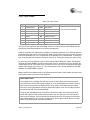
Table of Contents
Chapter 1. Introducing EZ-USB FX2
1.1
1.2
1.3
1.4
1.5
1.6
Introduction....................................................................................................................................1-1
An Introduction to USB..................................................................................................................1-1
The USB Specification ..................................................................................................................1-2
Host Is Master ...............................................................................................................................1-3
USB Direction................................................................................................................................1-3
Tokens and PIDs...........................................................................................................................1-3
1.6.1 Receiving Data from the Host..........................................................................................1-5
1.6.2 Sending Data to the Host.................................................................................................1-5
1.7 USB Frames..................................................................................................................................1-5
1.8 USB Transfer Types......................................................................................................................1-6
1.8.1 Bulk Transfers..................................................................................................................1-6
1.8.2 Interrupt Transfers ...........................................................................................................1-6
1.8.3 Isochronous Transfers .....................................................................................................1-7
1.8.4 Control Transfers............................................................................................................1-7
1.9 Enumeration ..................................................................................................................................1-8
1.9.1 Full-Speed / High-Speed Detection .................................................................................1-8
1.10 The Serial Interface Engine (SIE)................................................................................................1-9
1.11 ReNumeration™........................................................................................................................1-10
1.12 EZ-USB FX2 Architecture .........................................................................................................1-11
1.13 FX2 Feature Summary ..............................................................................................................1-13
1.14 FX2 Integrated Microprocessor .................................................................................................1-13
1.15 FX2 Block Diagram ...................................................................................................................1-15
1.16 Packages...................................................................................................................................1-16
1.16.1 56-Pin Package ...........................................................................................................1-16
1.16.2 100-Pin Package .........................................................................................................1-17
1.16.3 128-Pin Package .........................................................................................................1-17
1.16.4 Signals Available in the Three Packages ....................................................................1-17
1.17 Package Diagrams ....................................................................................................................1-20
1.18 FX2 Endpoint Buffers ................................................................................................................1-23
1.19 External FIFO Interface .............................................................................................................1-25
1.20 EZ-USB FX2 Product Family....................................................................................................1-28
Chapter 2. Endpoint Zero
2.1 Introduction....................................................................................................................................2-1
2.2 Control Endpoint EP0....................................................................................................................2-2
2.3 USB Requests...............................................................................................................................2-5
2.3.1 Get Status........................................................................................................................2-7
2.3.2 Set Feature ....................................................................................................................2-10
i
(Table of Contents)
2.3.3 Clear Feature .................................................................................................................2-11
2.3.4 Get Descriptor ...............................................................................................................2-12
2.3.4.1 Get Descriptor-Device........................................................................................2-14
2.3.4.2 Get Descriptor-Device Qualifier .........................................................................2-15
2.3.4.3 Get Descriptor-Configuration .............................................................................2-15
2.3.4.4 Get Descriptor-String .........................................................................................2-16
2.3.4.5 Get Descriptor-Other Speed Configuration........................................................2-16
2.3.5 Set Descriptor................................................................................................................2-17
2.3.5.1 Set Configuration ...............................................................................................2-20
2.3.6 Get Configuration ..........................................................................................................2-20
2.3.7 Set Interface ..................................................................................................................2-21
2.3.8 Get Interface..................................................................................................................2-22
2.3.9 Set Address ...................................................................................................................2-22
2.3.10 Sync Frame .................................................................................................................2-23
2.3.11 Firmware Load.............................................................................................................2-24
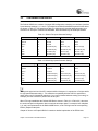
Chapter 3. Enumeration and ReNumeration™
3.1
3.2
3.3
3.4
Introduction ...................................................................................................................................3-1
FX2 Startup Modes .......................................................................................................................3-1
The Default USB Device ..............................................................................................................3-3
EEPROM Boot-load Data Formats ...............................................................................................3-4
3.4.1 No EEPROM or Invalid EEPROM...................................................................................3-4
3.4.2 Serial EEPROM Present, First Byte is 0xC0 ...................................................................3-5
3.4.3 Serial EEPROM Present, First Byte is 0xC2 ...................................................................3-6
3.5 EEPROM Configuration Byte ........................................................................................................3-8
3.6 The RENUM Bit.............................................................................................................................3-9
3.7 FX2 Response to Device Requests (RENUM=0)........................................................................3-10
3.8 FX2 Vendor Request for Firmware Load ....................................................................................3-11
3.9 How the Firmware ReNumerates ................................................................................................3-12
3.10 Multiple ReNumerations™ ........................................................................................................3-12
Chapter 4. Interrupts
4.1 Introduction ...................................................................................................................................4-1
4.2 SFRs .............................................................................................................................................4-2
4.2.1 803x/805x Compatibility ..................................................................................................4-5
4.3 Interrupt Processing ......................................................................................................................4-6
4.3.1 Interrupt Masking.............................................................................................................4-6
4.3.1.1 Interrupt Priorities.................................................................................................4-7
4.3.2 Interrupt Sampling ...........................................................................................................4-8
4.3.3 Interrupt Latency..............................................................................................................4-8
4.4 USB-Specific Interrupts.................................................................................................................4-8
4.4.1 Resume Interrupt.............................................................................................................4-8
4.4.2 USB Interrupts.................................................................................................................4-9
4.4.2.1 SUTOK, SUDAV Interrupts ................................................................................4-12
ii
Table of Contents
(Table of Contents)
4.5
4.6
4.7
4.8
4.4.2.2 SOF Interrupt .....................................................................................................4-13
4.4.2.3 Suspend Interrupt...............................................................................................4-13
4.4.2.4 USB RESET Interrupt ........................................................................................4-13
4.4.2.5 HISPEED Interrupt .............................................................................................4-13
4.4.2.6 EP0ACK Interrupt...............................................................................................4-13
4.4.2.7 Endpoint Interrupts.............................................................................................4-14
4.4.2.8 In-Bulk-NAK (IBN) Interrupt................................................................................4-14
4.4.2.9 EPxPING Interrupt .............................................................................................4-14
4.4.2.10 ERRLIMIT Interrupt ..........................................................................................4-15
4.4.2.11 EPxISOERR Interrupt ......................................................................................4-15
USB-Interrupt Autovectors ..........................................................................................................4-15
4.5.1 USB Autovector Coding .................................................................................................4-17
I²C-Compatible Bus Interrupt.......................................................................................................4-18
FIFO/GPIF Interrupt (INT4) .........................................................................................................4-19
FIFO/GPIF-Interrupt Autovectors ................................................................................................4-20
4.8.1 FIFO/GPIF Autovector Coding.......................................................................................4-21
Chapter 5. Memory
5.1 Introduction....................................................................................................................................5-1
5.2 Internal Data RAM .........................................................................................................................5-1
5.2.1 The Lower 128.................................................................................................................5-2
5.2.2 The Upper 128.................................................................................................................5-2
5.2.3 SFR (Special Function Register) Space ..........................................................................5-2
5.3 External Program Memory and External Data Memory.................................................................5-3
5.3.1 56- and 100-pin FX2 ........................................................................................................5-4
5.3.2 128-pin FX2 .....................................................................................................................5-4
5.4 FX2 Memory Maps ........................................................................................................................5-5
5.5 “Von-Neumannizing” Off-Chip Program and Data Memory...........................................................5-8
5.6 On-Chip Data Memory at 0xE000-0xFFFF ...................................................................................5-9
Chapter 6. Power Management
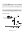
6.1 Introduction....................................................................................................................................6-1
6.2 USB Suspend................................................................................................................................6-3
6.2.1 SUSPEND Register .........................................................................................................6-4
6.3 Wakeup/Resume...........................................................................................................................6-4
6.3.1 Wakeup Interrupt .............................................................................................................6-5
6.4 USB Resume (Remote Wakeup) ..................................................................................................6-6
6.4.1 WU2 Pin...........................................................................................................................6-6
Chapter 7. Resets
7.1 Introduction....................................................................................................................................7-1
7.2 Power-On Reset (POR).................................................................................................................7-2
7.3 Releasing the CPU Reset .............................................................................................................7-3
7.3.1 RAM Download................................................................................................................7-3
Table of Contents
iii
(Table of Contents)
7.4
7.5
7.6
7.7
7.3.2 EEPROM Load ................................................................................................................7-3
7.3.3 External ROM ..................................................................................................................7-3
CPU Reset Effects ........................................................................................................................7-4
USB Bus Reset .............................................................................................................................7-4
FX2 Disconnect.............................................................................................................................7-5
Reset Summary ...........................................................................................................................7-5
Chapter 8. Access to Endpoint Buffers
8.1
8.2
8.3
8.4
8.5
8.6
Introduction ...................................................................................................................................8-1
FX2 Large and Small Endpoints ...................................................................................................8-1
High-Speed and Full-Speed Differences.......................................................................................8-2
How the CPU Configures the Endpoints .......................................................................................8-3
CPU Access to FX2 Endpoint Data...............................................................................................8-4
CPU Control of FX2 Endpoints .....................................................................................................8-5
8.6.1 Registers That Control EP0, EP1IN, and EP1OUT.........................................................8-5
8.6.1.1 EP0CS ................................................................................................................. 8-5
8.6.1.2 EP0BCH and EP0BCL.........................................................................................8-7
8.6.1.3 USBIE, USBIRQ ..................................................................................................8-7
8.6.1.4 EP01STAT ...........................................................................................................8-8
8.6.1.5 EP1OUTCS..........................................................................................................8-8
8.6.1.6 EP1OUTBC..........................................................................................................8-9
8.6.1.7 EP1INCS..............................................................................................................8-9
8.6.1.8 EP1INBC..............................................................................................................8-9
8.6.2 Registers That Control EP2, EP4, EP6, EP8................................................................8-10
8.6.2.1 EP2468STAT .....................................................................................................8-10
8.6.2.2 EP2ISOINPKTS, EP4ISOINPKTS, EP6ISOINPKTS, EP8ISOINPKTS .............8-10
8.6.2.3 EP2CS, EP4CS, EP6CS, EP8CS ......................................................................8-11
8.6.2.4 EP2BCH:L, EP4BCH:L, EP6BCH:L, EP8BCH:L................................................8-12
8.6.3 Registers That Control All Endpoints.............................................................................8-13
8.6.3.1 IBNIE, IBNIRQ, NAKIE, NAKIRQ.......................................................................8-14
8.6.3.2 EPIE, EPIRQ......................................................................................................8-15
8.6.3.3 USBERRIE, USBERRIRQ, ERRCNTLIM, CLRERRCNT..................................8-16
8.6.3.4 TOGCTL ............................................................................................................8-16
8.7 The Setup Data Pointer...............................................................................................................8-17
8.7.1 Transfer Length .............................................................................................................8-19
8.7.2 Accessible Memory Spaces ..........................................................................................8-19
8.8 Autopointers ................................................................................................................................8-19
Chapter 9. Slave FIFOs
9.1 Introduction ...................................................................................................................................9-1
9.2 Hardware.......................................................................................................................................9-2
9.2.1 Slave FIFO Pins ..............................................................................................................9-3
9.2.2 FIFO Data Bus (FD) ........................................................................................................9-4
9.2.3 Interface Clock (IFCLK) ...................................................................................................9-5
iv
Table of Contents
(Table of Contents)
9.2.4 FIFO Flag Pins (FLAGA, FLAGB, FLAGC, FLAGD)........................................................9-6
9.2.5 Control Pins (SLOE, SLRD, SLWR, PKTEND, FIFOADR[1:0]).......................................9-8
9.2.6 Slave FIFO Chip Select (SLCS) ....................................................................................9-10
9.2.7 Implementing Synchronous Slave FIFO Writes.............................................................9-10
9.2.8 Implementing Synchronous Slave FIFO Reads.............................................................9-13
9.2.9 Implementing Asynchronous Slave FIFO Writes ...........................................................9-15
9.2.10 Implementing Asynchronous Slave FIFO Reads .........................................................9-17
9.3 Firmware .....................................................................................................................................9-19
9.3.1 Firmware FIFO Access ..................................................................................................9-19
9.3.2 EPx Memories ...............................................................................................................9-20
9.3.3 Slave FIFO Programmable-Level Flag (PF) ..................................................................9-21
9.3.4 Auto-In / Auto-Out Modes ..............................................................................................9-22
9.3.5 CPU Access to OUT Packets, AUTOOUT = 1...............................................................9-23
9.3.6 CPU Access to OUT Packets, AUTOOUT = 0...............................................................9-24
9.3.7 CPU Access to IN Packets, AUTOIN = 1.......................................................................9-27
9.3.8 Access to IN Packets, AUTOIN=0 .................................................................................9-30
9.3.9 Auto-In / Auto-Out Initialization ......................................................................................9-31
9.3.10 Auto-Mode Example: Synchronous FIFO IN Data Transfers .......................................9-32
9.3.11 Auto-Mode Example: Asynchronous FIFO IN Data Transfers .....................................9-33
9.4 Switching Between Manual-Out and Auto-Out...........................................................................9-33
Chapter 10. General Programmable Interface (GPIF)
10.1 Introduction................................................................................................................................10-1
10.1.1 Typical GPIF Interface .................................................................................................10-3
10.2 Hardware ...................................................................................................................................10-5
10.2.1 The External GPIF Interface ........................................................................................10-5
10.2.2 Default GPIF Pins Configuration..................................................................................10-6
10.2.3 Six Control OUT Signals ..............................................................................................10-7
10.2.3.1 Control Output Modes ......................................................................................10-7
10.2.4 Six Ready IN signals....................................................................................................10-7
10.2.5 Nine GPIF Address OUT signals .................................................................................10-7
10.2.6 Three GSTATE OUT signals .......................................................................................10-8
10.2.7 8/16-Bit Data Path, WORDWIDE = 1 (default) and WORDWIDE = 0 .........................10-8
10.2.8 Byte Order for 16-bit GPIF Transactions .....................................................................10-8
10.2.9 Interface Clock (IFCLK) ...............................................................................................10-8
10.2.10 Connecting GPIF Signal Pins to Hardware..............................................................10-10
10.2.11 Example GPIF Hardware Interconnect....................................................................10-10
10.3 Programming the GPIF Waveforms ........................................................................................10-11
10.3.1 The GPIF Registers ...................................................................................................10-12
10.3.2 Programming GPIF Waveforms.................................................................................10-12
10.3.2.1 The GPIF IDLE State .....................................................................................10-12
10.3.2.1.1 GPIF Data Bus During IDLE .............................................................10-13
10.3.2.1.2 CTL Outputs During IDLE..................................................................10-13
10.3.2.2 Defining States ...............................................................................................10-14
Table of Contents
v
(Table of Contents)
10.3.2.2.1 Non-Decision Point (NDP) States......................................................10-14
10.3.2.2.2 Decision Point (DP) States ................................................................10-16
10.3.3 Re-Executing a Task Within a DP State ....................................................................10-18
10.3.4 State Instructions.......................................................................................................10-21
10.3.4.1 Structure of the Waveform Descriptors ..........................................................10-25
10.4 Firmware .................................................................................................................................10-26
10.4.1 Single-Read Transactions .........................................................................................10-33
10.4.2 Single-Write Transactions .........................................................................................10-38
10.4.3 FIFO-Read and FIFO-Write Transactions .................................................................10-41
10.4.3.1 Transaction Counter ......................................................................................10-41
10.4.3.2 Reading the Transaction-Count Status in a DP State....................................10-42
10.4.4 GPIF Flag Selection ..................................................................................................10-42
10.4.5 GPIF Flag Stop ..........................................................................................................10-42
10.4.5.1 Performing a FIFO-Read Transaction............................................................10-43
10.4.6 Firmware Access to IN packet(s), (AUTOIN=1).........................................................10-48
10.4.7 Firmware Access to IN Packet(s), (AUTOIN = 0) ......................................................10-49
10.4.7.1 Performing a FIFO-Write Transaction ............................................................10-52
10.4.8 Firmware access to OUT packets, (AUTOOUT=1) ...................................................10-56
10.4.9 Firmware access to OUT packets, (AUTOOUT = 0) .................................................10-57
10.4.10 Burst FIFO Transactions .........................................................................................10-59
10.5 UDMA Interface.......................................................................................................................10-63
Chapter 11. CPU Introduction
11.1
11.2
11.3
11.4
11.5
11.6
Introduction ...............................................................................................................................11-1
8051 Enhancements .................................................................................................................11-2
Performance Overview..............................................................................................................11-3
Software Compatibility ..............................................................................................................11-4
803x/805x Feature Comparison................................................................................................11-4
FX2/DS80C320 Differences ......................................................................................................11-5
11.6.1 Serial Ports ..................................................................................................................11-5
11.6.2 Timer 2 ........................................................................................................................11-5
11.6.3 Timed Access Protection.............................................................................................11-6
11.6.4 Watchdog Timer ..........................................................................................................11-6
11.6.5 Power Fail Detection ...................................................................................................11-6
11.6.6 Port I/O ........................................................................................................................11-6
11.6.7 Interrupts .....................................................................................................................11-6
11.7 EZ-USB FX2 Register Interface ................................................................................................11-7
11.8 EZ-USB FX2 Internal RAM .......................................................................................................11-7
11.9 I/O Ports ....................................................................................................................................11-8
11.10 Interrupts .................................................................................................................................11-9
11.11 Power Control .........................................................................................................................11-9
11.12 Special Function Registers (SFR) .........................................................................................11-10
11.13 External Address/Data Buses ...............................................................................................11-11
11.14 Reset .....................................................................................................................................11-11
vi
Table of Contents
(Table of Contents)
Chapter 12. Instruction Set
12.1 Introduction................................................................................................................................12-1
12.1.1 Instruction Timing ........................................................................................................12-5
12.1.2 Stretch Memory Cycles (Wait States) ..........................................................................12-5
12.1.3 Dual Data Pointers.......................................................................................................12-7
12.1.4 Special Function Registers ..........................................................................................12-7
Chapter 13. Input/Output
13.1 Introduction................................................................................................................................13-1
13.2 I/O Ports ....................................................................................................................................13-1
13.3 I/O Port Alternate Functions ......................................................................................................13-5
13.3.1 Port A Alternate Functions ...........................................................................................13-7
13.3.2 Port B and Port D Alternate Functions.........................................................................13-8
13.3.3 Port C Alternate Functions...........................................................................................13-9
13.3.4 Port E Alternate Functions .........................................................................................13-10
13.4 I²C-Compatible Bus Controller ................................................................................................13-12
13.4.1 Interfacing to I²C Peripherals .....................................................................................13-12
13.4.2 Registers....................................................................................................................13-13
13.4.2.1 Control Bits.....................................................................................................13-14
13.4.2.2 Status Bits ......................................................................................................13-15
13.4.3 Sending Data .............................................................................................................13-16
13.4.4 Receiving Data ..........................................................................................................13-16
13.5 EEPROM Boot Loader ............................................................................................................13-17
Chapter 14. Timers/Counters and Serial Interface
14.1 Introduction................................................................................................................................14-1
14.2 Timers/Counters........................................................................................................................14-1
14.2.1 803x/805x Compatibility...............................................................................................14-2
14.2.2 Timers 0 and 1.............................................................................................................14-2
14.2.2.1 Mode 0, 13-Bit Timer/Counter — Timer 0 and Timer 1 ....................................14-3
14.2.2.2 Mode 1, 16-Bit Timer/Counter — Timer 0 and Timer 1 ....................................14-3
14.2.2.3 Mode 2, 8-Bit Counter with Auto-Reload — Timer 0 and Timer 1....................14-5
14.2.2.4 Mode 3, Two 8-Bit Counters — Timer 0 Only ..................................................14-6
14.2.3 Timer Rate Control ......................................................................................................14-7
14.2.4 Timer 2.........................................................................................................................14-8
14.2.4.1 Timer 2 Mode Control ......................................................................................14-9
14.2.5 Timer 2 — 16-Bit Timer/Counter Mode......................................................................14-10
14.2.5.1 Timer 2 — 16-Bit Timer/Counter Mode with Capture .....................................14-10
14.2.6 Timer 2 — 16-Bit Timer/Counter Mode with Auto-Reload .........................................14-10
14.2.7 Timer 2 — Baud Rate Generator Mode .....................................................................14-11
14.3 Serial Interface ........................................................................................................................14-12
14.3.1 803x/805x Compatibility.............................................................................................14-13
14.3.2 High-Speed Baud Rate Generator.............................................................................14-14
Table of Contents
vii
(Table of Contents)
14.3.3 Mode 0.......................................................................................................................14-15
14.3.4 Mode 1.......................................................................................................................14-20
14.3.4.1 Mode 1 Baud Rate .........................................................................................14-20
14.3.4.2 Mode 1 Transmit ............................................................................................14-22
14.3.5 Mode 1 Receive.........................................................................................................14-22
14.3.6 Mode 2.......................................................................................................................14-24
14.3.6.1 Mode 2 Transmit ............................................................................................14-24
14.3.6.2 Mode 2 Receive .............................................................................................14-25
14.3.7 Mode 3.......................................................................................................................14-26
Chapter 15. Registers
15.1 Introduction ...............................................................................................................................15-1
15.1.1 Example Register Formats ..........................................................................................15-1
15.1.2 Other Conventions.......................................................................................................15-2
15.2 Special Function Registers (SFR) .............................................................................................15-3
15.3 About SFRS ..............................................................................................................................15-4
15.4 GPIF Waveform Memories......................................................................................................15-13
15.4.1 GPIF Waveform Descriptor Data...............................................................................15-13
15.5 General Configuration Registers .............................................................................................15-13
15.5.1 CPU Control and Status ............................................................................................15-13
15.5.2 Interface Configuration (Ports, GPIF, slave FIFOs)...................................................15-14
15.5.3 Slave FIFO FLAGA-FLAGD Pin Configuration ..........................................................15-18
15.5.4 FIFO Reset ................................................................................................................15-20
15.5.5 Breakpoint, Breakpoint Address High, Breakpoint Address Low...............................15-20
15.5.6 230 Kbaud Clock (T0, T1, T2) ...................................................................................15-22
15.5.7 Slave FIFO Interface Pins Polarity ............................................................................15-22
15.5.8 Chip Revision ID........................................................................................................15-23
15.5.9 Chip Revision Control................................................................................................15-24
15.5.10 GPIF Hold Time.......................................................................................................15-25
15.6 Endpoint Configuration............................................................................................................15-26
15.6.1 Endpoint 1-OUT/Endpoint 1-IN Configurations .........................................................15-26
15.6.2 Endpoint 2, 4, 6 and 8 Configuration.........................................................................15-27
15.6.3 Endpoint 2, 4, 6 and 8/Slave FIFO Configuration......................................................15-29
15.6.4 Endpoint 2, 4, 6, 8 AUTOIN Packet Length (High/Low) ............................................15-31
15.6.5 Endpoint 2, 4, 6, 8 /Slave FIFO Programmable-Level Flag (High/Low) ....................15-33
15.6.5.1 IN Endpoints ..................................................................................................15-39
15.6.5.2 OUT Endpoints ..............................................................................................15-40
15.6.6 Endpoint 2, 4, 6, 8 ISO IN Packets per Frame ..........................................................15-41
15.6.7 Force IN Packet End .................................................................................................15-41
15.6.8 Force OUT Packet End .............................................................................................15-42
15.7 Interrupts .................................................................................................................................15-43
15.7.1 Endpoint 2, 4, 6, 8 Slave FIFO Flag Interrupt Enable/Request .................................15-43
15.7.2 IN-BULK-NAK Interrupt Enable/Request...................................................................15-45
15.7.3 Endpoint Ping-NAK/IBN Interrupt Enable/Request....................................................15-46
viii
Table of Contents
(Table of Contents)
15.7.4 USB Interrupt Enable/Request ..................................................................................15-47
15.7.5 Endpoint Interrupt Enable/Request............................................................................15-49
15.7.6 GPIF Interrupt Enable/Request .................................................................................15-50
15.7.7 USB Error Interrupt Enable/Request .........................................................................15-51
15.7.8 USB Error Counter Limit ............................................................................................15-52
15.7.9 Clear Error Count.......................................................................................................15-52
15.7.10 INT 2 (USB) Autovector ...........................................................................................15-53
15.7.11 INT 4 (slave FIFOs & GPIF) Autovector ..................................................................15-53
15.7.12 INT 2 and INT 4 Setup.............................................................................................15-54
15.8 Input/Output Registers ............................................................................................................15-55
15.8.1 I/O PORTA Alternate Configuration...........................................................................15-55
15.8.2 I/O PORTC Alternate Configuration...........................................................................15-56
15.8.3 I/O PORTE Alternate Configuration...........................................................................15-56
15.8.4 I²C Compatible Bus Control and Status .....................................................................15-57
15.8.5 I²C-Compatible Bus Data...........................................................................................15-59
15.8.6 I²C-Compatible Bus Control.......................................................................................15-59
15.8.7 AUTOPOINTERs 1 and 2 MOVX access ..................................................................15-60
15.9 UDMA CRC Registers .............................................................................................................15-61
15.10 USB Control ..........................................................................................................................15-63
15.10.1 USB Control and Status...........................................................................................15-63
15.10.2 Enter Suspend State................................................................................................15-64
15.10.3 Wakeup Control & Status ........................................................................................15-64
15.10.4 Data Toggle Control.................................................................................................15-65
15.10.5 USB Frame Count High ...........................................................................................15-66
15.10.6 USB Frame Count Low............................................................................................15-67
15.10.7 USB Microframe Count............................................................................................15-67
15.10.8 USB Function Address ............................................................................................15-68
15.11 Endpoints ..............................................................................................................................15-68
15.11.1 Endpoint 0 (Byte Count High) ..................................................................................15-68
15.11.2 Endpoint 0 Control and Status (Byte Count Low) ....................................................15-69
15.11.3 Endpoint 1 OUT and IN Byte Count.........................................................................15-69
15.11.4 Endpoint 2 and 6 Byte Count High ..........................................................................15-70
15.11.5 Endpoint 4 and 8 Byte Count High ..........................................................................15-70
15.11.6 Endpoint 2, 4, 6, 8 Byte Count Low .........................................................................15-71
15.11.7 Endpoint 0 Control and Status.................................................................................15-71
15.11.8 Endpoint 1 OUT/IN Control and Status....................................................................15-72
15.11.9 Endpoint 2 Control and Status.................................................................................15-74
15.11.10 Endpoint 4 Control and Status...............................................................................15-74
15.11.11 Endpoint 6 Control and Status...............................................................................15-75
15.11.12 Endpoint 8 Control and Status...............................................................................15-76
15.11.13 Endpoint 2 and 4 Slave FIFO Flags.......................................................................15-77
15.11.14 Endpoint 6 and 8 Slave FIFO Flags.......................................................................15-77
15.11.15 Endpoint 2 Slave FIFO Byte Count High ...............................................................15-78
15.11.16 Endpoint 6 Slave FIFO Total Byte Count High ......................................................15-78
Table of Contents
ix
(Table of Contents)
15.11.17 Endpoint 4 and 8 Slave FIFO Byte Count High .....................................................15-79
15.11.18 Endpoint 2, 4, 6, 8 Slave FIFO Byte Count Low....................................................15-79
15.11.19 Setup Data Pointer High and Low Address ...........................................................15-80
15.11.20 Setup Data Pointer Auto........................................................................................15-81
15.11.21 Setup Data - 8 Bytes .............................................................................................15-82
15.12 General Programmable Interface (GPIF) ..............................................................................15-83
15.12.1 GPIF Waveform Selector.........................................................................................15-83
15.12.2 GPIF Done and Idle Drive Mode .............................................................................15-83
15.12.3 CTL Outputs ............................................................................................................15-84
15.12.4 GPIF Address High..................................................................................................15-86
15.12.5 GPIF Address Low ..................................................................................................15-87
15.12.6 GPIF Flowstate Registers........................................................................................15-87
15.12.7 GPIF Transaction Count Bytes................................................................................15-95
15.12.8 Endpoint 2, 4, 6, 8 GPIF Flag Select .......................................................................15-97
15.12.9 Endpoint 2, 4, 6, and 8 GPIF Stop Transaction .......................................................15-98
15.12.10 Endpoint 2, 4, 6, and 8 Slave FIFO GPIF Trigger .................................................15-98
15.12.11 GPIF Data High (16-Bit Mode) ..............................................................................15-99
15.12.12 Read/Write GPIF Data LOW & Trigger Transaction..............................................15-99
15.12.13 Read GPIF Data LOW, No Transaction Trigger ..................................................15-100
15.12.14 GPIF RDY Pin Configuration ...............................................................................15-100
15.12.15 GPIF RDY Pin Status ..........................................................................................15-101
15.12.16 Abort GPIF Cycles...............................................................................................15-101
15.13 Endpoint Buffers..................................................................................................................15-102
15.13.1 EP0 IN-OUT Buffer................................................................................................15-102
15.13.2 Endpoint 1-OUT Buffer ..........................................................................................15-102
15.13.3 Endpoint 1-IN Buffer ..............................................................................................15-103
15.13.4 Endpoint 2/Slave FIFO Buffer................................................................................15-103
15.13.5 512-byte Endpoint 4/Slave FIFO Buffer.................................................................15-104
15.13.6 512/1024-byte Endpoint 6/Slave FIFO Buffer........................................................15-104
15.13.7 512-byte Endpoint 8/Slave FIFO Buffer.................................................................15-105
15.14 Synchronization Delay ........................................................................................................15-105
Appendix A
Default Descriptors for Full Speed Mode ...............................................................................Appendix - 1
Appendix B
Default Descriptors for High Speed Mode............................................................................Appendix - 11
Appendix C
FX2 Register Summary......................................................................................................Appendix - 23
x
Table of Contents
List of Figures
Figure 1-1.
Figure 1-2.
Figure 1-3.
Figure 1-4.
Figure 1-5.
Figure 1-6.
Figure 1-7.
Figure 1-8.
Figure 1-9.
Figure 1-10.
Figure 1-11.
Figure 1-12.
Figure 1-13.
Figure 1-14.
Figure 1-15.
Figure 1-16.
Figure 1-17.
Figure 2-1.
Figure 2-2.
Figure 2-3.
Figure 2-4.
Figure 2-5.
Figure 3-1.
Figure 3-2.
Figure 4-1.
Figure 4-2.
Figure 4-3.
Figure 4-4.
Figure 4-5.
Figure 4-6.
Figure 4-7.
Figure 5-1.
Figure 5-2.
Figure 5-3.
Figure 5-4.
Figure 6-1.
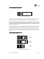
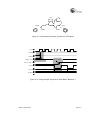
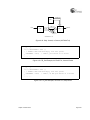
USB Packets ....................................................................................................................1-4
Two Bulk Transfers, IN and OUT .....................................................................................1-6
An Interrupt Transfer ........................................................................................................1-6
An Isochronous Transfer ..................................................................................................1-7
A Control Transfer ............................................................................................................1-7
What the SIE Does ...........................................................................................................1-9
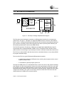
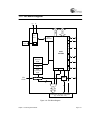
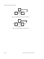
FX2 56-pin Package Simplified Block Diagram ..............................................................1-11
FX2 128-pin Package Simplified Block Diagram ............................................................1-12
FX2 Block Diagram ........................................................................................................1-15
56-pin, 100-pin, and 128-pin FX2 Packages ..................................................................1-16
Signals for the Three FX2 Package Types ....................................................................1-19
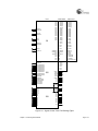
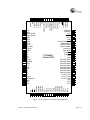
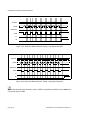
CY7C68013-128 TQFP Pin Assignment ........................................................................1-20
CY7C68013-100 TQFP Pin Assignment ........................................................................1-21
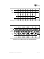
CY7C68013-56 SSOP Pin Assignment .........................................................................1-22
FX2 Endpoint Buffers .....................................................................................................1-23
FX2 FIFOs in “Slave FIFO” Mode ..................................................................................1-26
FX2 FIFOs in “GPIF Master” Mode ................................................................................1-27
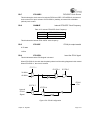
A USB Control Transfer (With Data Stage) ......................................................................2-2
Two Interrupts Associated with EP0 CONTROL Transfers ..............................................2-3
Registers Associated with EP0 Control Transfers ...........................................................2-4
Data Flow for a Get_Status Request ...............................................................................2-7
Using Setup Data Pointer (SUDPTR) for Get_Descriptor Requests ..............................2-13
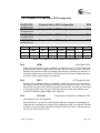
EEPROM Configuration Byte ...........................................................................................3-8
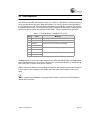
USB Control and Status Register ...................................................................................3-12
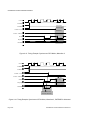
USB Interrupts ................................................................................................................4-10
The Order of Clearing Interrupt Requests is Important ..................................................4-12
SUTOK and SUDAV Interrupts ......................................................................................4-12
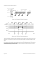
A Start Of Frame (SOF) Packet .....................................................................................4-13
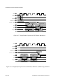
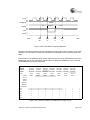
The USB Autovector Mechanism in Action ....................................................................4-17
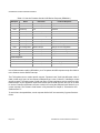
I²C-Compatible Bus Interrupt-Enable Bits and Registers ...............................................4-18
The FIFO/GPIF Autovector Mechanism in Action ..........................................................4-22
Internal Data RAM Organization ......................................................................................5-1
FX2 External Program/Data Memory Map, EA=0 ............................................................5-5
FX2 External Program/Data Memory Map, EA=1 ............................................................5-7
On-Chip Data Memory at 0xE000-0xFFFF ......................................................................5-9
Suspend-Resume Control ................................................................................................6-2
xiii
(List of Figures)
Figure 6-2.
Figure 6-3.
Figure 6-4.
Figure 7-1.
Figure 9-1.
Figure 9-2.
Figure 9-3.
Figure 9-4.
Figure 9-5.
Figure 9-6.
Figure 9-7.
Figure 9-8.
Figure 9-9.
Figure 9-10.
Figure 9-11.
Figure 9-12.
Figure 9-13.
Figure 9-14.
Figure 9-15.
Figure 9-16.
Figure 9-17.
Figure 9-18.
Figure 9-19.
Figure 9-20.
Figure 9-21.
Figure 9-22.
Figure 9-23.
Figure 9-24.
Figure 9-25.
Figure 9-26.
Figure 9-27.
Figure 9-28.
Figure 9-29.
Figure 9-30.
Figure 9-31.
Figure 9-32.
Figure 9-33.
Figure 9-34.
Figure 9-35.
Figure 9-36.
xiv
USB Suspend sequence ..................................................................................................6-3
FX2 Wakeup/Resume sequence .....................................................................................6-4
USB Control and Status register ......................................................................................6-6
EZ-USB FX2 Resets ........................................................................................................7-1
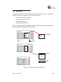
Slave FIFOs’ Role in the FX2 System .............................................................................9-2
FX2 Slave Mode Full-Featured Interface Pins .................................................................9-3
Asynchronous vs. Synchronous Timing Models ..............................................................9-3
8-bit Mode Slave FIFOs, WORDWIDE=0 ........................................................................9-4
16-bit Mode Slave FIFOs, WORDWIDE=1 ......................................................................9-5
IFCLK Configuration ........................................................................................................9-6
Satisfying Setup Timing by Inverting the IFCLK Output ...................................................9-6
FLAGx ..............................................................................................................................9-7
Slave FIFO Control Pins ..................................................................................................9-9
Interface Pins Example: Synchronous FIFO Writes .......................................................9-10
State Machine Example: Synchronous FIFO Writes ......................................................9-11
Timing Example: Synchronous FIFO Writes, Waveform 1 .............................................9-11
Timing Example: Synchronous FIFO Writes, Waveform 2 .............................................9-12
Timing Example: Synchronous FIFO Writes, Waveform 3, PKTEND Pin Illustrated .....9-12
Interface Pins Example: Synchronous FIFO Reads .......................................................9-13
State Machine Example: Synchronous FIFO Reads ......................................................9-13
Timing Example: Synchronous FIFO Reads, Waveform 1 ............................................9-14
Timing Example: Synchronous FIFO Reads, Waveform 2, EMPTY Flag Illustrated .....9-14
Interface Pins Example: Asynchronous FIFO Writes .....................................................9-15
State Machine Example: Asynchronous FIFO Writes ....................................................9-15
Timing Example: Asynchronous FIFO Writes ................................................................9-16
Interface Pins Example: Asynchronous FIFO Reads .....................................................9-17
State Machine Example: Asynchronous FIFO Reads ....................................................9-17
Timing Example: Asynchronous FIFO Reads ................................................................9-18
EPxFIFOBUF Registers .................................................................................................9-20
EPx Memories ................................................................................................................9-21
When AUTOOUT=1, OUT Packets are Automatically Committed .................................9-22
TD_Init Example: Configuring AUTOOUT = 1 ...............................................................9-22
TD_Init Example: Configuring AUTOIN = 1 ...................................................................9-23
TD_Poll Example: No Code Necessary for OUT Packets When AUTOOUT=1 ............9-23
TD_Init Example, Configuring AUTOOUT=0 .................................................................9-24
Skip, Commit, or Source (AUTOOUT=0) .......................................................................9-25
TD_Poll Example, AUTOOUT=0, Commit Packet .........................................................9-25
TD_Poll Example, AUTOOUT=0, Skip Packet ...............................................................9-25
TD_Poll Example, AUTOOUT=0, Source ......................................................................9-26
TD_Init Example, OUT Endpoint Initialization ................................................................9-27
List of Figures
(List of Figures)
Figure 9-37.
Figure 9-38.
Figure 9-39.
Figure 9-40.
Figure 9-41.
Figure 9-42.
Figure 9-43.
Figure 9-44.
Figure 9-45.
Figure 9-46.
Figure 10-1.
Figure 10-2.
Figure 10-3.
Figure 10-4.
Figure 10-5.
Figure 10-6.
Figure 10-7.
Figure 10-8.
Figure 10-9.
Figure 10-10.
Figure 10-11.
Figure 10-12.
Figure 10-13.
Figure 10-14.
Figure 10-15.
Figure 10-16.
Figure 10-17.
Figure 10-18.
Figure 10-19.
Figure 10-20.
Figure 10-21.
Figure 10-22.
Figure 10-23.
Figure 10-24.
Figure 10-25.
Figure 10-26.
Figure 10-27.
Figure 10-28.
Figure 10-29.
List of Figures
TD_Poll Example, AUTOIN = 1 ......................................................................................9-27
Master Writes Directly to Host, AUTOIN = 1 ..................................................................9-28
Firmware Intervention, AUTOIN = 0 or 1 ........................................................................9-28
TD_Poll Example: Sourcing an IN Packet ......................................................................9-29
TD_Poll Example, AUTOIN=0, Committing a Packet via INPKTEND ............................9-30
TD_Poll Example, AUTOIN=0, Skipping a Packet via INPKTEND ................................9-30
TD_Poll Example, AUTOIN=0, Editing a Packet via EPxBCH:L ....................................9-31
Code Example, Synchronous Slave FIFO IN Data Transfer ..........................................9-32
TD_Init Example, Asynchronous Slave FIFO IN Data Transfers ...................................9-33
TD_Poll Example, Asynchronous Slave FIFO IN Data Transfers ..................................9-33
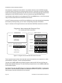
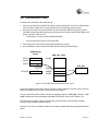
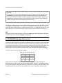
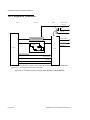
GPIF’s Place in the FX2 System ....................................................................................10-2
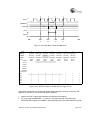
Example GPIF Waveform ..............................................................................................10-3
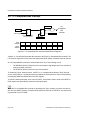
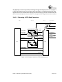
EZ-USB FX2 Interfacing to a Peripheral ........................................................................10-4
IFCLK Configuration .......................................................................................................10-9
Satisfying Setup Timing by Inverting the IFCLK Output .................................................10-9
GPIF State Machine Overview .....................................................................................10-11
Non-Decision Point (NDP) States ................................................................................10-15
One Decision Point: Wait States Inserted Until RDY0 Goes Low ................................10-17
One Decision Point: No Wait States Inserted:
RDY0 is Already Low at Decision Point I1 ................................................................10-17
Re-Executing a Task within a DP State .......................................................................10-19
GPIFTool Setup for the Waveform of Figure 10-10 .....................................................10-19
A DP State Which Does NOT Re-Execute the Task ....................................................10-20
GPIFTool Setup for the Waveform of Figure 10-12 .....................................................10-20
Firmware Launches a Single-Read Waveform, WORDWIDE=0 ..................................10-33
Single-Read Transaction Waveform ............................................................................10-34
GPIFTool Setup for the Waveform of Figure 10-15 .....................................................10-34
Single-Read Transaction Functions .............................................................................10-36
Initialization Code for Single-Read Transactions .........................................................10-37
Firmware Launches a Single-Write Waveform, WORDWIDE=0 ..................................10-38
Single-Write Transaction Waveform ............................................................................10-39
GPIFTool Setup for the Waveform of Figure 10-20 .....................................................10-39
Single-Write Transaction Functions .............................................................................10-40
Initialization Code for Single-Write Transactions .........................................................10-41
Firmware Launches a FIFO-Read Waveform ..............................................................10-43
Example FIFO-Read Transaction ................................................................................10-44
FIFO-Read Transaction Waveform ..............................................................................10-44
GPIFTool Setup for the Waveform of Figure 10-26 .....................................................10-45
FIFO-Read Transaction Functions ...............................................................................10-46
Initialization Code for FIFO-Read Transactions ...........................................................10-47
xv
(List of Figures)
Figure 10-30.
Figure 10-31.
Figure 10-32.
Figure 10-33.
Figure 10-34.
Figure 10-35.
Figure 10-36.
Figure 10-37.
Figure 10-38.
Figure 10-39.
Figure 10-40.
Figure 10-41.
Figure 10-42.
Figure 10-43.
Figure 10-44.
Figure 10-45.
Figure 10-46.
Figure 10-47.
Figure 10-48.
Figure 10-49.
Figure 10-50.
Figure 10-51.
Figure 10-52.
Figure 10-53.
Figure 10-54.
Figure 10-55.
Figure 10-56.
Figure 10-57.
Figure 11-1.
Figure 11-2.
Figure 11-1.
Figure 13-1.
Figure 13-2.
Figure 13-3.
Figure 13-4.
Figure 13-5.
Figure 13-6.
Figure 13-7.
Figure 13-8.
Figure 14-1.
xvi
FIFO-Read w/ AUTOIN = 0, Committing Packets via INPKTEND w/SKIP=0 ..............10-47
FIFO-Read w/ AUTOIN = 0, Committing Packets via EPxBCL ....................................10-48
AUTOIN=1, GPIF FIFO Read Transactions, AUTOIN = 1 ...........................................10-48
FIFO-Read Transaction Code, AUTOIN = 1 ................................................................10-49
Firmware intervention, AUTOIN = 0/1 ..........................................................................10-49
Committing a Packet by Writing INPKTEND with EPx Number (w/SKIP=0) ................10-50
Skipping a Packet by Writing to INPKTEND w/SKIP=1 ...............................................10-50
Sourcing an IN Packet by writing to EPxBCH:L ...........................................................10-51
Firmware Launches a FIFO-Write Waveform ..............................................................10-52
Example FIFO-Write Transaction .................................................................................10-52
FIFO-Write Transaction Waveform ..............................................................................10-53
GPIFTool Setup for the Waveform of Figure 10-40 .....................................................10-53
FIFO-Write Transaction Functions ...............................................................................10-54
Initialization Code for FIFO-Write Transactions ...........................................................10-55
FIFO-Write w/ AUTOOUT = 0, Committing Packets via EPxBCL ................................10-55
CPU not in data path, AUTOOUT=1 ............................................................................10-56
TD_Init Example: Configuring AUTOOUT = 1 .............................................................10-56
FIFO-Write Transaction Code, AUTOOUT = 1 ............................................................10-56
Firmware can Skip or Commit, AUTOOUT = 0 ............................................................10-57
Initialization Code for AUTOOUT = 0 ...........................................................................10-57
Committing an OUT Packet by Writing OUTPKTEND w/SKIP=0 ................................10-57
Skipping an OUT Packet by Writing OUTPKTEND w/SKIP=1 .....................................10-58
Sourcing an OUT Packet (AUTOOUT = 0) ..................................................................10-58
Ensuring that the FIFO is Clear after Power-On-Reset ................................................10-59
Burst FIFO-Read Transaction Functions .....................................................................10-60
Initialization for Burst FIFO-Read Transactions ...........................................................10-61
Burst FIFO-Read Transaction Example, Writing INPKTEND w/SKIP=0 to Commit ....10-62
Burst FIFO-Read Transaction Example, Writing EPxBCL to Commit ..........................10-63
FX2 CPU Features .........................................................................................................11-1
FX2 to Standard 8051 Timing Comparison ....................................................................11-4
FX2 Internal Data RAM ..................................................................................................11-7
FX2 I/O Pin ....................................................................................................................13-2
I/O Port Output-Enable Registers ..................................................................................13-3
I/O Port Data Registers ..................................................................................................13-4
I/O-Pin Logic when Alternate Function is an OUTPUT ..................................................13-5
I/O-Pin Logic when Alternate Function is an INPUT ......................................................13-6
General I²C Transfer ....................................................................................................13-12
Addressing an I²C Peripheral .......................................................................................13-13
I²C-Compatible Registers .............................................................................................13-14
Timer 0/1 - Modes 0 and 1 .............................................................................................14-3
List of Figures
(List of Figures)
Figure 14-2.
Figure 14-3.
Figure 14-4.
Figure 14-5.
Figure 14-6.
Figure 14-7.
Figure 14-8.
Figure 14-9.
Figure 14-10.
Figure 14-11.
Figure 14-12.
Figure 14-13.
Figure 14-14.
Figure 14-15.
Figure 14-16.
Figure 15-1.
Figure 15-2.
Figure 15-3.
Figure 15-4.
Figure 15-5.
Figure 15-6.
Figure 15-7.
Figure 15-8.
Figure 15-9.
Figure 15-10.
Figure 15-11.
Figure 15-12.
Figure 15-13.
Figure 15-14.
Figure 15-15.
Figure 15-16.
Figure 15-17.
Figure 15-18.
Figure 15-19.
Figure 15-20.
Figure 15-21.
Figure 15-22.
Figure 15-23.
Figure 15-24.
Figure 15-25.
List of Figures
Timer 0/1 - Mode 2 .........................................................................................................14-6
Timer 0 - Mode 3 ............................................................................................................14-7
Timer 2 - Timer/Counter with Capture ..........................................................................14-10
Timer 2 - Timer/Counter with Auto Reload ...................................................................14-11
Timer 2 - Baud Rate Generator Mode ..........................................................................14-12
Serial Port Mode 0 Receive Timing - Low Speed Operation ........................................14-18
Serial Port Mode 0 Receive Timing - High Speed Operation .......................................14-18
Serial Port Mode 0 Transmit Timing - Low Speed Operation .......................................14-19
Serial Port Mode 0 Transmit Timing - High Speed Operation ......................................14-19
Serial Port 0 Mode 1 Transmit Timing ..........................................................................14-23
Serial Port 0 Mode 1 Receive Timing ...........................................................................14-24
Serial Port 0 Mode 2 Transmit Timing ..........................................................................14-25
Serial Port 0 Mode 2 Receive Timing ...........................................................................14-26
Serial Port 0 Mode 3 Transmit Timing ..........................................................................14-27
Serial Port 0 Mode 3 Receive Timing ...........................................................................14-27
Register Description Format ..........................................................................................15-2
Single Instruction to Read Port B ...................................................................................15-4
Single Instruction to Write to Port C ...............................................................................15-4
Use Bit 2 to set PORTD - Single Instruction ..................................................................15-9
Use OR to Set Bit 3 ........................................................................................................15-9
GPIF Waveform Descriptor Data .................................................................................15-13
CPU Control and Status ...............................................................................................15-13
Interface Configuration (Ports, GPIF, slave FIFOs) .....................................................15-14
IFCLK Configuration .....................................................................................................15-15
Slave FIFO FLAGA-FLAGD Pin Configuration ............................................................15-18
Restore FIFOs to Reset State ......................................................................................15-20
Breakpoint Control .......................................................................................................15-20
Breakpoint Address High .............................................................................................15-21
Breakpoint Address Low ..............................................................................................15-21
230 Kbaud Internally Generated Reference Clock .......................................................15-22
Slave FIFO Interface Pins Polarity ...............................................................................15-22
Chip Revision ID ..........................................................................................................15-23
Chip Revision Control ..................................................................................................15-24
Endpoint 1-OUT/Endpoint 1-IN Configurations ............................................................15-26
Endpoint 2 Configuration ..............................................................................................15-27
Endpoint 4 Configuration ..............................................................................................15-27
Endpoint 6 Configuration ..............................................................................................15-27
Endpoint 8 Configuration ..............................................................................................15-27
Endpoint 2, 4, 6 and 8 /Slave FIFO Configuration .......................................................15-29
Endpoint 2 and 6 AUTOIN Packet Length High ...........................................................15-31
xvii
(List of Figures)
Figure 15-26.
Figure 15-27.
Figure 15-28.
Figure 15-29.
Figure 15-30.
Figure 15-31.
Figure 15-32.
Figure 15-33.
Figure 15-34.
Figure 15-35.
Figure 15-36.
Figure 15-37.
Figure 15-38.
Figure 15-39.
Figure 15-40.
Figure 15-41.
Figure 15-42.
Figure 15-43.
Figure 15-44.
Figure 15-45.
Figure 15-46.
Figure 15-47.
Figure 15-48.
Figure 15-49.
Figure 15-50.
Figure 15-51.
Figure 15-52.
Figure 15-53.
Figure 15-54.
Figure 15-55.
Figure 15-56.
Figure 15-57.
Figure 15-58.
Figure 15-59.
Figure 15-60.
Figure 15-61.
Figure 15-62.
Figure 15-63.
Figure 15-64.
Figure 15-65.
xviii
Endpoint 4 and 8 AUTOIN Packet Length High ...........................................................15-31
Endpoint 2, 4, 6, 8 AUTOIN Packet Length Low ..........................................................15-32
Endpoint 2/Slave FIFO Programmable Flag High ........................................................15-33
Endpoint 6/Slave FIFO Programmable Flag High ........................................................15-34
Endpoint 4/Slave FIFO Programmable Flag High ........................................................15-36
Endpoint 8/Slave FIFO Programmable Flag High ........................................................15-37
Endpoint 2, 4, 6, 8/Slave FIFO Programmable Flag Low .............................................15-38
Maximum FIFO Sizes ..................................................................................................15-40
Endpoint ISO IN Packets per Frame ............................................................................15-41
Force IN Packet End ....................................................................................................15-41
Force OUT Packet End ................................................................................................15-42
Endpoint 2, 4, 6, 8 Slave FIFO Flag Interrupt Enable ..................................................15-43
Endpoint 2, 4, 6, 8 Slave FIFO Flag Interrupt Request ................................................15-44
IN-BULK-NAK Interrupt Enable ....................................................................................15-45
IN-BULK-NAK Interrupt Request .................................................................................15-45
Endpoint Ping-NAK/IBN Interrupt Enable ....................................................................15-46
Endpoint Ping-NAK/IBN Interrupt Request ..................................................................15-46
USB Interrupt Enables .................................................................................................15-47
USB Interrupt Requests ...............................................................................................15-47
Endpoint Interrupt Enables ..........................................................................................15-49
Endpoint Interrupt Requests ........................................................................................15-49
GPIF Interrupt Enable ..................................................................................................15-50
GPIF Interrupt Request ................................................................................................15-50
USB Error Interrupt Enables ........................................................................................15-51
USB Error Interrupt Request ........................................................................................15-51
USB Error Counter and Limit .......................................................................................15-52
Clear Error Count EC3:0 ..............................................................................................15-52
INT 2 (USB) Autovector ...............................................................................................15-53
INT 4 (slave FIFOs & GPIF) Autovector .......................................................................15-53
INT 2 and INT 4 Setup .................................................................................................15-54
I/O PORTA Alternate Configuration .............................................................................15-55
I/O PORTC Alternate Configuration .............................................................................15-56
I/O PORTE Alternate Configuration .............................................................................15-56
I²C-Compatible Bus Control and Status .......................................................................15-57
I²C-Compatible Bus Data .............................................................................................15-59
I²C-Compatible Bus Control .........................................................................................15-59
AUTOPTR1 & AUTOPTR2 MOVX access (when APTREN=1) ...................................15-60
USB Control and Status ...............................................................................................15-63
Enter Suspend State ....................................................................................................15-64
Wakeup Control & Status .............................................................................................15-64
List of Figures
(List of Figures)
Figure 15-66.
Figure 15-67.
Figure 15-68.
Figure 15-69.
Figure 15-70.
Figure 15-71.
Figure 15-72.
Figure 15-73.
Figure 15-74.
Figure 15-75.
Figure 15-76.
Figure 15-77.
Figure 15-78.
Figure 15-79.
Figure 15-80.
Figure 15-81.
Figure 15-82.
Figure 15-83.
Figure 15-84.
Figure 15-85.
Figure 15-86.
Figure 15-87.
Figure 15-88.
Figure 15-89.
Figure 15-90.
Figure 15-91.
Figure 15-92.
Figure 15-93.
Figure 15-94.
Figure 15-95.
Figure 15-96.
Figure 15-97.
Figure 15-98.
Figure 15-99.
Figure 15-100.
Figure 15-101.
Figure 15-102.
Figure 15-103.
Figure 15-104.
Figure 15-105.
List of Figures
Data Toggle Control .....................................................................................................15-65
USB Frame Count HIGH ..............................................................................................15-66
USB Frame Count Low ................................................................................................15-67
USB Microframe Count ................................................................................................15-67
USB Function Address .................................................................................................15-68
Endpoint 0 (Byte Count High) ......................................................................................15-68
Endpoint 0 Control and Status (Byte Count Low) ........................................................15-69
Endpoint 1 OUT/IN Byte Count ....................................................................................15-69
Endpoint 2 and 6 Byte Count High ...............................................................................15-70
Endpoint 4 and 5 Byte Count High ...............................................................................15-70
Endpoint 2, 4, 6, 8 Byte Count Low ..............................................................................15-71
Endpoint 0 Control and Status .....................................................................................15-71
Endpoint 1 OUT/IN Control and Status ........................................................................15-72
Endpoint 2 Control and Status .....................................................................................15-74
Endpoint 4 Control and Status .....................................................................................15-74
Endpoint 6 Control and Status .....................................................................................15-75
Endpoint 8 Control and Status .....................................................................................15-76
Endpoint 2 and 4 Slave FIFO Flags .............................................................................15-77
Endpoint 6 and 8 Slave FIFO Flags .............................................................................15-77
Endpoint 2 Slave FIFO Total Byte Count High .............................................................15-78
Endpoint 6 Slave FIFO Total Byte Count High .............................................................15-78
Endpoint 4 and 8 Slave FIFO Byte Count High ............................................................15-79
Endpoint 2, 4, 6, 8 Slave FIFO Byte Count Low ..........................................................15-79
Setup Data Pointer High Address Byte ........................................................................15-80
Setup Data Pointer Low Address Byte .........................................................................15-80
Setup Data Pointer AUTO Mode ..................................................................................15-81
Setup Data - 8 Bytes ....................................................................................................15-82
GPIF Waveform Selector .............................................................................................15-83
GPIF Done and Idle Drive ............................................................................................15-83
CTL Output States in Idle .............................................................................................15-84
CTL Output Drive Type ................................................................................................15-84
GPIF Address High ......................................................................................................15-86
GPIF Address Low .......................................................................................................15-87
GPIF Transaction Count Byte3 ....................................................................................15-95
GPIF Transaction Count Byte2 ....................................................................................15-95
GPIF Transaction Count Byte1 ....................................................................................15-96
GPIF Transaction Count Byte0 ....................................................................................15-96
Endpoint 2, 4, 6, 8 GPIF Flag Select ............................................................................15-97
Endpoint 2, 4, 6, and 8 GPIF Stop Transaction ...........................................................15-98
Endpoint 2, 4, 6, and 8 Slave FIFO GPIF Trigger ........................................................15-98
xix
(List of Figures)
Figure 15-106.
Figure 15-107.
Figure 15-108.
Figure 15-109.
Figure 15-110.
Figure 15-111.
Figure 15-112.
Figure 15-113.
Figure 15-114.
Figure 15-115.
Figure 15-116.
Figure 15-117.
Figure 15-118.
xx
GPIF Data High (16-Bit Mode) .....................................................................................15-99
Read/Write GPIF Data LOW & Trigger Transaction ....................................................15-99
Read GPIF Data LOW, No Transaction Trigger .........................................................15-100
GPIF Ready Pins .......................................................................................................15-100
GPIF Ready Status Pins ............................................................................................15-101
Abort GPIF .................................................................................................................15-101
EP0 IN/OUT Buffer ....................................................................................................15-102
EP1-OUT Buffer .........................................................................................................15-102
EP1-IN Buffer .............................................................................................................15-103
512/1024-byte EP2/Slave FIFO Buffer ......................................................................15-103
512-byte EP4/Slave FIFO Buffer ...............................................................................15-104
512/1024-byte EP6/Slave FIFO Buffer ......................................................................15-104
512-byte EP8/Slave FIFO Buffer ...............................................................................15-105
List of Figures
List of Tables
Table 1-1.
Table 1-2.
Table 1-3.
Table 2-1.
Table 2-2.
Table 2-3.
Table 2-4.
Table 2-5.
Table 2-6.
Table 2-7.
Table 2-8.
Table 2-9.
Table 2-10.
Table 2-11.
Table 2-12.
Table 2-13.
Table 2-14.
Table 2-15.
Table 2-16.
Table 2-17.
Table 2-18.
Table 2-19.
Table 2-20.
Table 2-21.
Table 2-22.
Table 2-23.
Table 2-24.
Table 3-1.
Table 3-2.
Table 3-3.
Table 3-4.
Table 3-5.
Table 3-6.
Table 3-7.
Table 3-8.
Table 4-1.
USB PIDS . . . . . . . . . . . . . . . . . . . . . . . . . . . . . . . . . . . . . . . . . . . . . . . . . . . . . . . . . . . . 1-3
Endpoint 2, 4, 6, and 8 Configuration Choices . . . . . . . . . . . . . . . . . . . . . . . . . . . . . . . 1-24
EZ-USB FX2 Family . . . . . . . . . . . . . . . . . . . . . . . . . . . . . . . . . . . . . . . . . . . . . . . . . . . 1-28
The Eight Bytes in a USB SETUP Packet . . . . . . . . . . . . . . . . . . . . . . . . . . . . . . . . . . . . 2-5
How the Firmware Handles USB Device Requests (RENUM=1) . . . . . . . . . . . . . . . . . . 2-6
Get Status-Device (Remote Wakeup and Self-Powered Bits) . . . . . . . . . . . . . . . . . . . . 2-8
Get Status-Endpoint (Stall Bits) . . . . . . . . . . . . . . . . . . . . . . . . . . . . . . . . . . . . . . . . . . . 2-8
Get Status-Interface . . . . . . . . . . . . . . . . . . . . . . . . . . . . . . . . . . . . . . . . . . . . . . . . . . . . 2-9
Set Feature-Device (Set Remote Wakeup Bit) . . . . . . . . . . . . . . . . . . . . . . . . . . . . . . . 2-10
Set Feature-Endpoint (Stall) . . . . . . . . . . . . . . . . . . . . . . . . . . . . . . . . . . . . . . . . . . . . . 2-10
Clear Feature-Device (Clear Remote Wakeup Bit) . . . . . . . . . . . . . . . . . . . . . . . . . . . . 2-11
Clear Feature-Endpoint (Clear Stall) . . . . . . . . . . . . . . . . . . . . . . . . . . . . . . . . . . . . . . . 2-12
Get Descriptor-Device . . . . . . . . . . . . . . . . . . . . . . . . . . . . . . . . . . . . . . . . . . . . . . . . . . 2-14
Get Descriptor-Device Qualifier . . . . . . . . . . . . . . . . . . . . . . . . . . . . . . . . . . . . . . . . . . 2-15
Get Descriptor-Configuration . . . . . . . . . . . . . . . . . . . . . . . . . . . . . . . . . . . . . . . . . . . . 2-15
Get Descriptor-String . . . . . . . . . . . . . . . . . . . . . . . . . . . . . . . . . . . . . . . . . . . . . . . . . . 2-16
Get Descriptor-Other Speed Configuration . . . . . . . . . . . . . . . . . . . . . . . . . . . . . . . . . . 2-16
Set Descriptor-Device . . . . . . . . . . . . . . . . . . . . . . . . . . . . . . . . . . . . . . . . . . . . . . . . . . 2-17
Set Descriptor-Configuration . . . . . . . . . . . . . . . . . . . . . . . . . . . . . . . . . . . . . . . . . . . . . 2-17
Set Descriptor-String . . . . . . . . . . . . . . . . . . . . . . . . . . . . . . . . . . . . . . . . . . . . . . . . . . . 2-18
Set Configuration . . . . . . . . . . . . . . . . . . . . . . . . . . . . . . . . . . . . . . . . . . . . . . . . . . . . . 2-20
Get Configuration . . . . . . . . . . . . . . . . . . . . . . . . . . . . . . . . . . . . . . . . . . . . . . . . . . . . . 2-20
Set Interface (Actually, Set Alternate Setting #AS for Interface #IF) . . . . . . . . . . . . . . . 2-21
Get Interface (Actually, Get Alternate Setting #AS for interface #IF) . . . . . . . . . . . . . . 2-22
Sync Frame . . . . . . . . . . . . . . . . . . . . . . . . . . . . . . . . . . . . . . . . . . . . . . . . . . . . . . . . . . 2-23
Firmware Download . . . . . . . . . . . . . . . . . . . . . . . . . . . . . . . . . . . . . . . . . . . . . . . . . . . 2-24
Firmware Upload . . . . . . . . . . . . . . . . . . . . . . . . . . . . . . . . . . . . . . . . . . . . . . . . . . . . . . 2-24
Default Full-speed Alternate Settings . . . . . . . . . . . . . . . . . . . . . . . . . . . . . . . . . . . . . . . 3-3
Default High-speed Alternate Settings . . . . . . . . . . . . . . . . . . . . . . . . . . . . . . . . . . . . . . 3-3
FX2 Device Characteristics, No EEPROM / Invalid EEPROM . . . . . . . . . . . . . . . . . . . . 3-4
“C0 Load” Format . . . . . . . . . . . . . . . . . . . . . . . . . . . . . . . . . . . . . . . . . . . . . . . . . . . . . . 3-5
“C2 Load” Format . . . . . . . . . . . . . . . . . . . . . . . . . . . . . . . . . . . . . . . . . . . . . . . . . . . . . . 3-6
How the Default USB Device Handles EP0 Requests When RENUM=0 . . . . . . . . . . . 3-10
Firmware Download . . . . . . . . . . . . . . . . . . . . . . . . . . . . . . . . . . . . . . . . . . . . . . . . . . . 3-11
Firmware Upload . . . . . . . . . . . . . . . . . . . . . . . . . . . . . . . . . . . . . . . . . . . . . . . . . . . . . . 3-11
FX2 Interrupts . . . . . . . . . . . . . . . . . . . . . . . . . . . . . . . . . . . . . . . . . . . . . . . . . . . . . . . . . 4-1
xxiii
(List of Tables)
Table 4-2.
Table 4-3.
Table 4-4.
Table 4-5.
Table 4-6.
Table 4-7.
Table 4-8.
Table 4-9.
Table 4-10.
Table 4-11.
Table 4-12.
Table 4-13.
Table 4-14.
Table 4-15.
Table 4-16.
Table 7-1.
Table 8-1.
Table 8-2.
Table 8-3.
Table 8-4.
Table 8-5.
Table 8-6.
Table 8-7.
Table 8-8.
Table 8-9.
Table 9-1.
Table 9-2.
Table 9-3.
Table 10-1.
Table 10-2.
Table 10-3.
Table 10-4.
Table 10-5.
Table 10-6.
Table 10-7.
Table 10-8.
Table 11-1.
Table 11-2.
Table 11-3.
Table 11-4.
xxiv
IE Register — SFR 0xA8 . . . . . . . . . . . . . . . . . . . . . . . . . . . . . . . . . . . . . . . . . . . . . . . . . 4-2
IP Register — SFR 0xB8 . . . . . . . . . . . . . . . . . . . . . . . . . . . . . . . . . . . . . . . . . . . . . . . . . 4-3
EXIF Register — SFR 0x91 . . . . . . . . . . . . . . . . . . . . . . . . . . . . . . . . . . . . . . . . . . . . . . . 4-3
EICON Register — SFR 0xD8 . . . . . . . . . . . . . . . . . . . . . . . . . . . . . . . . . . . . . . . . . . . . . 4-4
EIE Register — SFR 0xE8 . . . . . . . . . . . . . . . . . . . . . . . . . . . . . . . . . . . . . . . . . . . . . . . . 4-4
EIP Register — SFR 0xF8 . . . . . . . . . . . . . . . . . . . . . . . . . . . . . . . . . . . . . . . . . . . . . . . . 4-5
Summary of Interrupt Compatibility . . . . . . . . . . . . . . . . . . . . . . . . . . . . . . . . . . . . . . . . . 4-5
Interrupt Flags, Enables, Priority Control, and Vectors . . . . . . . . . . . . . . . . . . . . . . . . . . 4-7
Individual USB Interrupt Sources . . . . . . . . . . . . . . . . . . . . . . . . . . . . . . . . . . . . . . . . . . . 4-9
Endpoint Interrupts . . . . . . . . . . . . . . . . . . . . . . . . . . . . . . . . . . . . . . . . . . . . . . . . . . . . .4-14
FX2 JUMP Instruction . . . . . . . . . . . . . . . . . . . . . . . . . . . . . . . . . . . . . . . . . . . . . . . . . . 4-15
A Typical USB-Interrupt Jump Table . . . . . . . . . . . . . . . . . . . . . . . . . . . . . . . . . . . . . . . 4-16
Individual FIFO/GPIF Interrupt Sources . . . . . . . . . . . . . . . . . . . . . . . . . . . . . . . . . . . . . 4-19
FX2 JUMP Instruction . . . . . . . . . . . . . . . . . . . . . . . . . . . . . . . . . . . . . . . . . . . . . . . . . . 4-20
A Typical FIFO/GPIF-Interrupt Jump Table . . . . . . . . . . . . . . . . . . . . . . . . . . . . . . . . . . 4-21
Effects of Various Resets on FX2 Resources (“—” means “no change”) . . . . . . . . . . . . . 7-5
Maximum Packet Sizes for USB 1.1 and 2.0 . . . . . . . . . . . . . . . . . . . . . . . . . . . . . . . . . . 8-2
Endpoint Configuration Registers . . . . . . . . . . . . . . . . . . . . . . . . . . . . . . . . . . . . . . . . . .8-3
Endpoint Buffers in RAM Space . . . . . . . . . . . . . . . . . . . . . . . . . . . . . . . . . . . . . . . . . . . 8-4
Registers that control EP0 and EP1 . . . . . . . . . . . . . . . . . . . . . . . . . . . . . . . . . . . . . . . . 8-5
Registers that control EP2,EP4,EP6 and EP8 . . . . . . . . . . . . . . . . . . . . . . . . . . . . . . . . 8-10
Isochronous IN Packets per Microframe, High-Speed Only . . . . . . . . . . . . . . . . . . . . . . 8-11
Registers that control all endpoints . . . . . . . . . . . . . . . . . . . . . . . . . . . . . . . . . . . . . . . . 8-13
Registers used to control the Setup Data Pointer . . . . . . . . . . . . . . . . . . . . . . . . . . . . . 8-18
Registers that control the Autopointers . . . . . . . . . . . . . . . . . . . . . . . . . . . . . . . . . . . . . 8-20
Registers Associated with Slave FIFO Hardware . . . . . . . . . . . . . . . . . . . . . . . . . . . . . . 9-2
FIFO Selection via FIFOADR[1:0] . . . . . . . . . . . . . . . . . . . . . . . . . . . . . . . . . . . . . . . . . .9-8
Registers Associated with Slave FIFO Firmware . . . . . . . . . . . . . . . . . . . . . . . . . . . . . . 9-19
Registers Associated with GPIF Hardware . . . . . . . . . . . . . . . . . . . . . . . . . . . . . . . . . . 10-5
GPIF Pin Descriptions . . . . . . . . . . . . . . . . . . . . . . . . . . . . . . . . . . . . . . . . . . . . . . . . . . 10-5
CTL[5:0] Output Modes . . . . . . . . . . . . . . . . . . . . . . . . . . . . . . . . . . . . . . . . . . . . . . . . . 10-7
Example GPIF Hardware Interconnect . . . . . . . . . . . . . . . . . . . . . . . . . . . . . . . . . . . . 10-10
Control Outputs (CTLn) During the IDLE State . . . . . . . . . . . . . . . . . . . . . . . . . . . . . . 10-14
Waveform Descriptor Addresses . . . . . . . . . . . . . . . . . . . . . . . . . . . . . . . . . . . . . . . . . 10-25
Waveform Descriptor 0 Structure . . . . . . . . . . . . . . . . . . . . . . . . . . . . . . . . . . . . . . . . . 10-25
Registers Associated with GPIF Firmware . . . . . . . . . . . . . . . . . . . . . . . . . . . . . . . . . .10-26
FX2 Speed Compared to Standard 8051 . . . . . . . . . . . . . . . . . . . . . . . . . . . . . . . . . . . . 11-3
Comparison Between FX2 and Other 803x/805x Devices . . . . . . . . . . . . . . . . . . . . . . .11-5
Differences between FX and DS80C320 Interrupts . . . . . . . . . . . . . . . . . . . . . . . . . . . . 11-6
EZ-USB FX2 Interrupts . . . . . . . . . . . . . . . . . . . . . . . . . . . . . . . . . . . . . . . . . . . . . . . . . 11-9
List of Tables
(List of Tables)
Table 11-5.
Table 12-1.
Table 12-2.
Table 12-3.
Table 12-4.
Table 13-1.
Table 13-2.
Table 13-3.
Table 13-4.
Table 13-5.
Table 13-6.
Table 13-7.
Table 13-8.
Table 13-9.
Table 13-10.
Table 13-11.
Table 13-12.
Table 14-1.
Table 14-2.
Table 14-3.
Table 14-4.
Table 14-5.
Table 14-6.
Table 14-7.
Table 14-8.
Table 14-9.
Table 14-10.
Table 14-11.
Table 14-12.
Table 14-13.
Table 14-14.
Table 14-15.
Table 14-16.
Table 15-1.
Table 15-2.
Table 15-3.
Table 15-4.
Table 15-5.
Table 15-6.
Table 15-7.
List of Tables
FX2 Special Function Registers (SFR) . . . . . . . . . . . . . . . . . . . . . . . . . . . . . . . . . . . . 11-10
Legend for Instruction Set Table . . . . . . . . . . . . . . . . . . . . . . . . . . . . . . . . . . . . . . . . . . 12-1
FX2 Instruction Set . . . . . . . . . . . . . . . . . . . . . . . . . . . . . . . . . . . . . . . . . . . . . . . . . . . . 12-2
Data Memory Stretch Values . . . . . . . . . . . . . . . . . . . . . . . . . . . . . . . . . . . . . . . . . . . . 12-6
PSW Register - SFR 0xD0 . . . . . . . . . . . . . . . . . . . . . . . . . . . . . . . . . . . . . . . . . . . . . . 12-8
Register Bits Which Select Port A Alternate Functions . . . . . . . . . . . . . . . . . . . . . . . . . 13-7
Port A Alternate-Function Configuration . . . . . . . . . . . . . . . . . . . . . . . . . . . . . . . . . . . . 13-7
Register Bits Which Select Port B and Port D Alternate Functions . . . . . . . . . . . . . . . . 13-8
Port B Alternate-Function Configuration . . . . . . . . . . . . . . . . . . . . . . . . . . . . . . . . . . . . 13-8
Port D Alternate-Function Configuration . . . . . . . . . . . . . . . . . . . . . . . . . . . . . . . . . . . . 13-8
Register Bits Which Select Port C Alternate Functions . . . . . . . . . . . . . . . . . . . . . . . . . 13-9
Port C Alternate-Function Configuration . . . . . . . . . . . . . . . . . . . . . . . . . . . . . . . . . . . . 13-9
Register Bits Which Select Port E Alternate Functions . . . . . . . . . . . . . . . . . . . . . . . . 13-10
Port E Alternate-Function Configuration . . . . . . . . . . . . . . . . . . . . . . . . . . . . . . . . . . . 13-10
IFCFG Selection of Port I/O Pin Functions . . . . . . . . . . . . . . . . . . . . . . . . . . . . . . . . . 13-11
Strap Boot EEPROM Address Lines to These Values . . . . . . . . . . . . . . . . . . . . . . . . 13-17
Results of Power-On-Reset EEPROM Test . . . . . . . . . . . . . . . . . . . . . . . . . . . . . . . . 13-18
Timer/Counter Implementation Comparison . . . . . . . . . . . . . . . . . . . . . . . . . . . . . . . . . 14-2
TMOD Register — SFR 0x89 . . . . . . . . . . . . . . . . . . . . . . . . . . . . . . . . . . . . . . . . . . . . 14-4
TCON Register — SRF 0x88 . . . . . . . . . . . . . . . . . . . . . . . . . . . . . . . . . . . . . . . . . . . . 14-5
CKCON (SFR 0x8E) Timer Rate Control Bits . . . . . . . . . . . . . . . . . . . . . . . . . . . . . . . . 14-7
T2CON Register — SFR 0xC8 . . . . . . . . . . . . . . . . . . . . . . . . . . . . . . . . . . . . . . . . . . . 14-9
Timer 2 Mode Control Summary . . . . . . . . . . . . . . . . . . . . . . . . . . . . . . . . . . . . . . . . . . 14-9
Serial Port Modes . . . . . . . . . . . . . . . . . . . . . . . . . . . . . . . . . . . . . . . . . . . . . . . . . . . . 14-13
Serial Interface Implementation Comparison . . . . . . . . . . . . . . . . . . . . . . . . . . . . . . . 14-13
UART230 Register — Address 0xE608 . . . . . . . . . . . . . . . . . . . . . . . . . . . . . . . . . . . 14-14
Allowable Baud-Clock Combinations for Modes 1 and 3 . . . . . . . . . . . . . . . . . . . . . . 14-14
SCON0 Register — SFR 98h . . . . . . . . . . . . . . . . . . . . . . . . . . . . . . . . . . . . . . . . . . . 14-16
EICON (SFR 0xD8) SMOD1 Bit . . . . . . . . . . . . . . . . . . . . . . . . . . . . . . . . . . . . . . . . . 14-16
PCON (SFR 0x87) SMOD0 Bit . . . . . . . . . . . . . . . . . . . . . . . . . . . . . . . . . . . . . . . . . . 14-16
SCON1 Register — SFR C0h . . . . . . . . . . . . . . . . . . . . . . . . . . . . . . . . . . . . . . . . . . . 14-17
Timer 1 Reload Values for Common Serial Port Mode 1 Baud Rates . . . . . . . . . . . . 14-21
Timer 2 Reload Values for Common Serial Port Mode 1 Baud Rates . . . . . . . . . . . . 14-22
FX2 Special Function Registers (SFR) . . . . . . . . . . . . . . . . . . . . . . . . . . . . . . . . . . . . . 15-3
SFR and FX2 Register File Correspondences . . . . . . . . . . . . . . . . . . . . . . . . . . . . . . . 15-7
SFR Registers and External Ram Equivalent . . . . . . . . . . . . . . . . . . . . . . . . . . . . . . . 15-12
CPU Clock Speeds . . . . . . . . . . . . . . . . . . . . . . . . . . . . . . . . . . . . . . . . . . . . . . . . . . . 15-14
Internal FIFO/GPIF Clock Frequency . . . . . . . . . . . . . . . . . . . . . . . . . . . . . . . . . . . . . 15-15
Port E Alternate Functions When GSTATE=1 . . . . . . . . . . . . . . . . . . . . . . . . . . . . . . 15-16
Ports, GPIF, Slave FIFO Select . . . . . . . . . . . . . . . . . . . . . . . . . . . . . . . . . . . . . . . . . 15-16
xxv
(List of Tables)
Table 15-8.
Table 15-9.
Table 15-10.
Table 15-11.
Table 15-12.
Table 15-13.
Table 15-14.
Table 15-15.
Table 15-16.
Table 15-17.
Table 15-18.
Table 15-19.
Table 15-20.
IFCFG Selection of Port I/O Pin Functions . . . . . . . . . . . . . . . . . . . . . . . . . . . . . . . . . 15-17
FIFO Flag Pin Functions . . . . . . . . . . . . . . . . . . . . . . . . . . . . . . . . . . . . . . . . . . . . . . . 15-19
FIFOADR1 FIFOADR0 Pin Correspondence . . . . . . . . . . . . . . . . . . . . . . . . . . . . . . . . 15-19
Endpoint Type Definitions . . . . . . . . . . . . . . . . . . . . . . . . . . . . . . . . . . . . . . . . . . . . . . 15-26
Endpoint Type Definitions . . . . . . . . . . . . . . . . . . . . . . . . . . . . . . . . . . . . . . . . . . . . . . 15-28
Endpoint Buffering Amounts . . . . . . . . . . . . . . . . . . . . . . . . . . . . . . . . . . . . . . . . . . . . 15-28
Interpretation of PF for IN Endpoints . . . . . . . . . . . . . . . . . . . . . . . . . . . . . . . . . . . . . . 15-39
IN Packets per Microframe . . . . . . . . . . . . . . . . . . . . . . . . . . . . . . . . . . . . . . . . . . . . . 15-41
CTL[5:0] Output Modes . . . . . . . . . . . . . . . . . . . . . . . . . . . . . . . . . . . . . . . . . . . . . . . .15-85
Control Outputs (CTLx) During the IDLE State . . . . . . . . . . . . . . . . . . . . . . . . . . . . . . 15-86
Control Outputs (CTLx) During the Flow State . . . . . . . . . . . . . . . . . . . . . . . . . . . . . . 15-91
Endpoint 2, 4, 6, 8 GPIF Flag Select Values . . . . . . . . . . . . . . . . . . . . . . . . . . . . . . . . 15-97
Registers Which Require a Synchronization Delay . . . . . . . . . . . . . . . . . . . . . . . . . . 15-105
Table A-1
Table A-2
Table A-3
Table A-4
Table A-5
Table A-6
Table A-7
Table A-8
Table A-9
Table A-10
Table A-11
Table A-12
Table A-13
Table A-14
Table A-15
Table A-16
Table A-17
Table A-18
Table A-19
Table A-20
Table A-21
Table A-22
Table A-23
Default USB Device Descriptor . . . . . . . . . . . . . . . . . . . . . . . . . . . . . . . . . . . . . .
Device Qualifier . . . . . . . . . . . . . . . . . . . . . . . . . . . . . . . . . . . . . . . . . . . . . . . . . .
USB Default Configuration Descriptor . . . . . . . . . . . . . . . . . . . . . . . . . . . . . . . . .
USB Default Interface 0, Alternate Setting 0 . . . . . . . . . . . . . . . . . . . . . . . . . . . .
USB Default Interface 0, Alternate Setting 1 . . . . . . . . . . . . . . . . . . . . . . . . . . . .
Endpoint Descriptor (EP1 out) . . . . . . . . . . . . . . . . . . . . . . . . . . . . . . . . . . . . . . .
Endpoint Descriptor (EP1 in) . . . . . . . . . . . . . . . . . . . . . . . . . . . . . . . . . . . . . . . .
Endpoint Descriptor (EP2) . . . . . . . . . . . . . . . . . . . . . . . . . . . . . . . . . . . . . . . . . .
Endpoint Descriptor (EP4) . . . . . . . . . . . . . . . . . . . . . . . . . . . . . . . . . . . . . . . . . .
Endpoint Descriptor (EP6) . . . . . . . . . . . . . . . . . . . . . . . . . . . . . . . . . . . . . . . . . .
Endpoint Descriptor (EP8) . . . . . . . . . . . . . . . . . . . . . . . . . . . . . . . . . . . . . . . . . .
Interface Descriptor (Alt. Setting 2) . . . . . . . . . . . . . . . . . . . . . . . . . . . . . . . . . . .
Endpoint Descriptor (EP1 out) . . . . . . . . . . . . . . . . . . . . . . . . . . . . . . . . . . . . . . .
Endpoint Descriptor (EP1 in) . . . . . . . . . . . . . . . . . . . . . . . . . . . . . . . . . . . . . . . .
Endpoint Descriptor (EP2. . . . . . . . . . . . . . . . . . . . . . . . . . . . . . . . . . . . . . . . . . .
Endpoint Descriptor (EP4) . . . . . . . . . . . . . . . . . . . . . . . . . . . . . . . . . . . . . . . . . .
Endpoint Descriptor (EP6) . . . . . . . . . . . . . . . . . . . . . . . . . . . . . . . . . . . . . . . . . .
Endpoint Descriptor (EP8) . . . . . . . . . . . . . . . . . . . . . . . . . . . . . . . . . . . . . . . . . .
Interface Descriptor (Alt. Setting 3) . . . . . . . . . . . . . . . . . . . . . . . . . . . . . . . . . . .
Endpoint Descriptor (EP1 out) . . . . . . . . . . . . . . . . . . . . . . . . . . . . . . . . . . . . . . .
Endpoint Descriptor (EP1 in) . . . . . . . . . . . . . . . . . . . . . . . . . . . . . . . . . . . . . . . .
Endpoint Descriptor (EP2) . . . . . . . . . . . . . . . . . . . . . . . . . . . . . . . . . . . . . . . . . .
Endpoint Descriptor (EP4) . . . . . . . . . . . . . . . . . . . . . . . . . . . . . . . . . . . . . . . . . .
xxvi
1
2
2
3
3
3
4
4
4
5
5
5
6
6
6
7
7
7
8
8
8
9
9
List of Tables
(List of Tables)
Table A-24
Table A-25
Endpoint Descriptor (EP6) . . . . . . . . . . . . . . . . . . . . . . . . . . . . . . . . . . . . . . . . . . 9
Endpoint Descriptor (EP8) . . . . . . . . . . . . . . . . . . . . . . . . . . . . . . . . . . . . . . . . . 10
Table B-1
Table B-2
Table B-3
Table B-4
Table B-5
Table B-6
Table B-7
Table B-8
Table B-9
Table B-10
Table B-11
Table B-12
Table B-13
Table B-14
Table B-15
Table B-16
Table B-17
Table B-18
Table B-19
Table B-20
Table B-21
Table B-22
Table B-23
Table B-24
Table B-25
Device Descriptor . . . . . . . . . . . . . . . . . . . . . . . . . . . . . . . . . . . . . . . . . . . . . . . .
Device Qualifier . . . . . . . . . . . . . . . . . . . . . . . . . . . . . . . . . . . . . . . . . . . . . . . . .
Configuration Descriptor . . . . . . . . . . . . . . . . . . . . . . . . . . . . . . . . . . . . . . . . . .
Interface Descriptor (Alt. Setting 0) . . . . . . . . . . . . . . . . . . . . . . . . . . . . . . . . . .
Interface Descriptor (Alt. Setting 1) . . . . . . . . . . . . . . . . . . . . . . . . . . . . . . . . . .
Endpoint Descriptor (EP1 out) . . . . . . . . . . . . . . . . . . . . . . . . . . . . . . . . . . . . . .
Endpoint Descriptor (EP1 in) . . . . . . . . . . . . . . . . . . . . . . . . . . . . . . . . . . . . . . .
Endpoint Descriptor (EP2) . . . . . . . . . . . . . . . . . . . . . . . . . . . . . . . . . . . . . . . . .
Endpoint Descriptor (EP4) . . . . . . . . . . . . . . . . . . . . . . . . . . . . . . . . . . . . . . . . .
Endpoint Descriptor (EP6) . . . . . . . . . . . . . . . . . . . . . . . . . . . . . . . . . . . . . . . . .
Endpoint Descriptor (EP8) . . . . . . . . . . . . . . . . . . . . . . . . . . . . . . . . . . . . . . . . .
Interface Descriptor (Alt. Setting 2) . . . . . . . . . . . . . . . . . . . . . . . . . . . . . . . . . .
Endpoint Descriptor (EP1 out) . . . . . . . . . . . . . . . . . . . . . . . . . . . . . . . . . . . . . .
Endpoint Descriptor (EP1 in) . . . . . . . . . . . . . . . . . . . . . . . . . . . . . . . . . . . . . . .
Endpoint Descriptor (EP2) . . . . . . . . . . . . . . . . . . . . . . . . . . . . . . . . . . . . . . . . .
Endpoint Descriptor (EP4) . . . . . . . . . . . . . . . . . . . . . . . . . . . . . . . . . . . . . . . . .
Endpoint Descriptor (EP6) . . . . . . . . . . . . . . . . . . . . . . . . . . . . . . . . . . . . . . . . .
Endpoint Descriptor (EP8) . . . . . . . . . . . . . . . . . . . . . . . . . . . . . . . . . . . . . . . . .
Interface Descriptor (Alt. Setting 3) . . . . . . . . . . . . . . . . . . . . . . . . . . . . . . . . . .
Endpoint Descriptor (EP1 out) . . . . . . . . . . . . . . . . . . . . . . . . . . . . . . . . . . . . . .
Endpoint Descriptor (EP1 in) . . . . . . . . . . . . . . . . . . . . . . . . . . . . . . . . . . . . . . .
Endpoint Descriptor (EP2) . . . . . . . . . . . . . . . . . . . . . . . . . . . . . . . . . . . . . . . . .
Endpoint Descriptor (EP4) . . . . . . . . . . . . . . . . . . . . . . . . . . . . . . . . . . . . . . . . .
Endpoint Descriptor (EP6) . . . . . . . . . . . . . . . . . . . . . . . . . . . . . . . . . . . . . . . . .
Endpoint Descriptor (EP8) . . . . . . . . . . . . . . . . . . . . . . . . . . . . . . . . . . . . . . . . .
List of Tables
11
12
12
13
13
13
14
14
14
15
15
15
16
16
16
17
17
17
18
18
18
19
19
19
20
xxvii
xxviii
List of Tables
Chapter 1
1.1
Introducing EZ-USB FX2
Introduction
The Universal Serial Bus (USB) has gained wide acceptance as the connection method of choice
for low and medium speed PC peripherals. Equally successful in the Windows and Macintosh
worlds, USB has delivered on its promises of easy attachment, an end to configuration hassles,
and true plug-and-play operation.
The second generation of the USB specification, “USB 2.0”, extends the original specification to
include:
•
480 Mbits/sec signaling rate, a 40× improvement over the USB 1.1 rate of 12 Mbits/sec.
•
Full backward and forward compatibility with USB 1.1 devices and cables.
•
A new hub architecture that can provide multiple 12 Mbits/sec downstream ports for USB
1.1 devices.
The Cypress Semiconductor EZ-USB FX2 (often abbreviated as “FX2” in this manual) is a singlechip USB 2.0 peripheral whose architecture is similar to that of the Cypress Semiconductor EZUSB FX family. Although much of the FX architecture is preserved, certain elements have been
redesigned to accommodate the higher data rates offered by USB 2.0.
This introductory chapter begins with a brief USB tutorial to put USB and FX2 terminology into context. The remainder of the chapter briefly outlines the FX2 architecture.
1.2
An Introduction to USB
Like a well-designed automobile or appliance, a USB peripheral’s outward simplicity hides internal
complexity. There’s a lot going on “under the hood” of a USB device.
•
A USB device can be plugged in anytime, even while the PC is turned on.
•
When the PC detects that a USB device has been plugged in, it automatically interrogates
the device to learn its capabilities and requirements. From this information, the PC auto-
Chapter 1. Introducing EZ-USB FX2
Page 1-1
EZ-USB FX2 Technical Reference Manual
matically loads the device’s driver into the operating system. When the device is
unplugged, the operating system automatically logs it off and unloads its driver.
•
USB devices do not use DIP switches, jumpers, or configuration programs. There is never
an IRQ, DMA, memory, or I/O conflict with a USB device.
•
USB expansion hubs make the bus simultaneously available to dozens of devices.
•
USB is fast enough for printers, hard disk drives, CD-quality audio, and scanners.
•
With the introduction of the USB 2.0 Specification, USB supports three speeds:
-
Low Speed (1.5 Mbits/sec), suitable for mice, keyboards and joysticks.
-
Full Speed (12 Mbits/sec), for devices like modems, speakers and scanners.
-
High Speed (480 Mbits/sec), for devices like hard disk drives, CD-ROMs, video cameras, and high-resolution scanners.
The Cypress Semiconductor EZ-USB FX2 augments the EZ-USB family by supporting the high
bandwidth offered by the USB 2.0 High Speed mode. The FX2 provides a highly-integrated solution for a USB peripheral device. Like all EZ-USB devices, the FX2 offers the following features:
•
An integrated, high-performance CPU based on the industry-standard 8051 processor.
•
A soft (RAM-based) architecture that allows unlimited configuration and upgrades.
•
Full USB throughput. USB devices that use EZ-USB chips are not limited by number of
endpoints, buffer sizes, or transfer speeds.
•
Automatic handling of most of the USB protocol, which simplifies code and accelerates
the USB learning curve.
1.3
The USB Specification
The Universal Serial Bus Specification Version 2.0 is available on the Internet from the USB Implementers Forum, Inc., at http://www.usb.org. Published in April, 2000, the USB Specification is
the work of a founding committee of seven industry heavyweights: Compaq, Hewlett-Packard,
Lucent, Philips, Intel, Microsoft, and NEC. This impressive list of developers secures USB’s position as the low- to high-speed PC connection method of the future.
A glance at the USB Specification makes it immediately apparent that USB is not nearly as simple
as the older serial or parallel ports. The USB Specification uses new terms like endpoint, isochronous, and enumeration, and finds new uses for old terms like configuration, interface, and interrupt. Woven into the USB fabric is a software abstraction model that deals with things such as
pipes. The USB Specification also contains information about such details as connector types and
wire colors.
Page 1-2
EZ-USB FX2 Technical Reference Manual v2.1
1.4
Host Is Master
This is a fundamental USB concept. There is exactly one master in a USB system: the host computer. USB devices respond to host requests. USB devices cannot send information among
themselves, as they could if USB were a peer-to-peer topology.
However, there is one case where a USB device can initiate signaling without prompting from the
host. After being put into a low-power “suspend” mode by the host, a device can signal a “remote
wakeup”. This is the only case in which the USB device is the initiator; in all other cases, the host
makes device requests and the device responds to them.
There’s an excellent reason for this host-centric model. The USB architects were keenly mindful of
cost, and the best way to make low-cost peripherals is to put most of the “smarts” into the host
side, the PC. If USB had been defined as peer-to-peer, every USB device would have required
more intelligence, raising cost.
1.5
USB Direction
Because the host is always the bus master, it’s easy to remember USB direction: OUT means from
the host to the device, and IN means from the device to the host. FX2 nomenclature uses this
naming convention. For example, an endpoint that sends data to the host is an IN endpoint. This
can be confusing at first, because the FX2 sends data to the host by loading an IN endpoint buffer.
Likewise, the FX2 receives host data from an OUT endpoint buffer.
1.6
Tokens and PIDs
In this manual, you’ll read statements such as: “When the host sends an IN token…,” or “The
device responds with an ACK”. What do these terms mean?
A USB transaction consists of data packets identified by special codes called Packet IDs or PIDs.
A PID signifies what kind of packet is being transmitted. There are four PID types, shown in
Table 1-1.
Table 1-1. USB PIDS
PID Type
Token
PID Name
IN, OUT, SOF, SETUP
Data
DATA0, DATA1, DATA2, MDATA
Handshake
ACK, NAK, STALL, NYET
Special
PRE, ERR, SPLIT, PING
Bold type indicates PIDs introduced with USB 2.0
Chapter 1. Introducing EZ-USB FX2
Page 1-3
EZ-USB FX2 Technical Reference Manual
O
U
T
A
D
D
R
E
N
D
P
C
R
C
5
D
A
T
A
1
Payload
D ata
Token P acket
D ata P acket
1
2
C
R
C
1
6
A
C
K
H /S P kt
3
O
U
T
A
D
D
R
E
N
D
P
C
R
C
5
Token P acket
4
D
A
T
A
0
Payload
D ata
D ata P acket
5
C
R
C
1
6
A
C
K
H /S P kt
6
Figure 1-1. USB Packets
Figure 1-1 illustrates a USB OUT transfer. Host traffic is shown in solid shading, while device traffic is shown crosshatched. Packet 1 is an OUT token, indicated by the OUT PID. The OUT token
signifies that data from the host is about to be transmitted over the bus. Packet 2 contains data, as
indicated by the DATA1 PID. Packet 3 is a handshake packet, sent by the device using the ACK
(acknowledge) PID to signify to the host that the device received the data error-free.
Continuing with Figure 1-1, a second transaction begins with another OUT token 4, followed by
more data 5, this time using the DATA0 PID. Finally, the device again indicates success by transmitting the ACK PID in a handshake packet 6.
When operating at full speed, every OUT transfer sends the OUT data, even when the device is
busy and can’t accept the data. When operating at high speed, this slightly wasteful use of USB
bandwidth is remedied by using the new “Ping” PID. The host first sends a short PING token to an
OUT endpoint, asking if there is room for OUT data in the peripheral device. Only when the PING
is answered by an ACK does the host send the OUT token and data.
There are two DATA PIDs (DATA0 and DATA1) in Figure1-1 because the USB architects took
error correction very seriously. As mentioned previously, the ACK handshake is an indication to
the host that the peripheral received data without error (the CRC portion of the packet is used to
detect errors). But what if the handshake packet itself is garbled in transmission? To detect this,
each side (host and device) maintains a data toggle bit, which is toggled between data packet
transfers. The state of this internal toggle bit is compared with the PID that arrives with the data,
either DATA0 or DATA1. When sending data, the host or device sends alternating DATA0-DATA1
PIDs. By comparing the received Data PID with the state of its own internal toggle bit, the receiver
can detect a corrupted handshake packet.
SETUP tokens are unique to CONTROL transfers. They preface eight bytes of data from which
the peripheral decodes host Device Requests.
At full speed, SOF (Start of Frame) tokens occur once per millisecond. At high speed, each frame
contains eight SOF tokens, each denoting a 125-microsecond microframe.
Four handshake PIDs indicate the status of a USB transfer:
•
ACK (“Acknowledge”) means success; the data was received error-free.
•
NAK (“Negative Acknowledge”) means “busy, try again.” It’s tempting to assume that NAK
means “error,” but it doesn’t; a USB device indicates an error by not responding.
Page 1-4
EZ-USB FX2 Technical Reference Manual v2.1
•
STALL means that something unforeseen went wrong (probably as a result of miscommunication or lack of cooperation between the host and device software). A device sends the
STALL handshake to indicate that it doesn’t understand a device request, that something
went wrong on the peripheral end, or that the host tried to access a resource that wasn’t
there. It’s like HALT, but better, because USB provides a way to recover from a stall.
•
NYET (“Not Yet”) has the same meaning as ACK — the data was received error-free —
but also indicates that the endpoint is not yet ready to receive another OUT transfer. NYET
PIDs occur only in high speed mode.
A PRE (Preamble) PID precedes a low-speed (1.5 Mbits/sec) USB transmission. The FX2 supports full-speed (12 Mbits/sec) and high-speed (480 Mbits/sec) USB transfers only.
1.6.1 Receiving Data from the Host
To send data to a USB peripheral, the host issues an OUT token followed by the data. If the peripheral has space for the data and accepts it without error, it returns an ACK to the host. If it is busy, it
sends a NAK. If it finds an error, it sends back nothing. For the latter two cases, the host re-sends
the data at a later time.
1.6.2 Sending Data to the Host
A USB device never spontaneously sends data to the host. Either FX2 firmware or external
logic can load data into an FX2 endpoint buffer and ‘arm’ it for transfer at any time. However, the
data is not transmitted to the host until the host issues an IN request to the FX2 endpoint. If the
host never sends the IN token, the data remains in the FX2 endpoint buffer indefinitely.
1.7
USB Frames
The USB host provides a time base to all USB devices by transmitting an SOF (“Start of Frame”)
packet every millisecond. SOF packets include an 11-bit number which increments once per
frame; the current frame number [0-2047] may be read from internal FX2 registers at any time.
At high speed (480 Mbits/sec), each one-millisecond frame is divided into eight 125-microsecond
microframes, each of which is preceded by an SOF packet. The frame number still increments only
once per millisecond, so each of those SOF packets contains the same frame number. To keep
track of the current microframe number [0-7], the FX2 provides a readable microframe counter.
The FX2 can generate an interrupt request whenever it receives an SOF (once every millisecond
at full speed, or once every 125 microseconds at high speed). This SOF interrupt can be used, for
example, to service isochronous endpoint data.
Chapter 1. Introducing EZ-USB FX2
Page 1-5
EZ-USB FX2 Technical Reference Manual
1.8
USB Transfer Types
USB defines four transfer types. These match the requirements of different data types delivered
over the bus.
1.8.1 Bulk Transfers
I
N
A
D
D
R
E
N
D
P
C
R
C
5
Token Packet
D
A
T
A
1
C
R
C
1
6
Payload
Data
Data Packet
A
O
D
U
D
T
R
A
C
K
E
N
D
P
D
A
T
A
0
C
R
C
5
Token Packet
H/S Pkt
Payload
Data
Data Packet
C
R
C
1
6
A
C
K
H/S Pkt
Figure 1-2. Two Bulk Transfers, IN and OUT
Bulk data is bursty, traveling in packets of 8, 16, 32 or 64 bytes at full speed or 512 bytes at high
speed. Bulk data has guaranteed accuracy, due to an automatic retry mechanism for erroneous
data. The host schedules bulk packets when there is available bus time. Bulk transfers are typically used for printer, scanner, or modem data. Bulk data has built-in flow control provided by
handshake packets.
1.8.2 Interrupt Transfers
I
N
A
D
D
R
E
N
D
P
C
R
C
5
Token Packet
D
A
T
A
1
Payload
Data
Data Packet
C
R
C
1
6
A
C
K
H/S Pkt
Figure 1-3. An Interrupt Transfer
Interrupt data is like bulk data; it can have packet sizes of 1 through 64 bytes at full speed or up to
1024 bytes at high speed. Interrupt endpoints have an associated polling interval that ensures
they will be polled (receive an IN token) by the host on a regular basis.
Page 1-6
EZ-USB FX2 Technical Reference Manual v2.1
1.8.3 Isochronous Transfers
A
D
D
R
I
N
E
N
D
P
D
A
T
A
0
C
R
C
5
C
R
C
1
6
Payload
Data
Token Packet
Data Packet
Figure 1-4. An Isochronous Transfer
Isochronous data is time-critical and used to stream data like audio and video. An isochronous
packet may contain up to 1023 bytes at full speed, or up to 1024 bytes at high speed.
Time of delivery is the most important requirement for isochronous data. In every USB frame, a
certain amount of USB bandwidth is allocated to isochronous transfers. To lighten the overhead,
isochronous transfers have no handshake (ACK/NAK/STALL/NYET), and no retries; error detection is limited to a 16-bit CRC.
Isochronous transfers do not use the data-toggle mechanism. Full-speed isochronous data uses
only the DATA0 PID; high-speed isochronous data uses DATA0, DATA1, DATA2 and MDATA.
In full-speed mode, only one isochronous packet can be transferred per endpoint, per frame. In
high-speed mode, up to three isochronous packets can be transferred per endpoint, per microframe.
1.8.4
Control Transfers
S
A E C
E
D N R
T
D D C
U
R P 5
P
Token Packet
I
N
A
D
D
R
E
N
D
P
C
R
C
5
D
A
T
A
0
Data Packet
D
A
T
A
1
E
N
D
P
Payload
Data
Data Packet
Token Packet
A
O
D
U
D
T
R
8 bytes
Setup
Data
C
R
C
5
Token Packet
D
A
T
A
1
Data
C
R
C
1
6
Pkt
A
C
K
C
R
C
1
6
A
C
K
SETUP
Stage
H/S Pkt
C
R
C
1
6
A
C
K
DATA
Stage
(optional)
H/S Pkt
STATUS
Stage
H/S Pkt
Figure 1-5. A Control Transfer
Chapter 1. Introducing EZ-USB FX2
Page 1-7
EZ-USB FX2 Technical Reference Manual
Control transfers configure and send commands to a device. Because they’re so important, they
employ the most extensive USB error checking. The host reserves a portion of each USB frame
for Control transfers.
Control transfers consist of two or three stages. The SETUP stage contains eight bytes of USB
CONTROL data. An optional DATA stage contains more data, if required. The STATUS (or “handshake”) stage allows the device to indicate successful completion of a CONTROL operation.
1.9
Enumeration
Your computer is ON. You plug in a USB device, and the Windows™ cursor switches to an hourglass and then back to a cursor. Magically, your device is connected and its Windows™ driver is
loaded! Anyone who has installed a sound card into a PC and has had to configure countless
jumpers, drivers, and IO/Interrupt/DMA settings knows that a USB connection is miraculous.
We’ve all heard about Plug and Play, but USB delivers the real thing.
How does all this happen automatically? Inside every USB device is a table of descriptors. This
table is the sum total of the device’s requirements and capabilities. When you plug into USB, the
host goes through a sign-on sequence:
1. The host sends a Get Descriptor-Device request to address zero (all USB devices must
respond to address zero when first attached).
2. The device responds to the request by sending ID data back to the host to identify itself.
3. The host sends a Set Address request, which assigns a unique address to the just-attached
device so it may be distinguished from the other devices connected to the bus.
4. The host sends more Get Descriptor requests, asking for additional device information. From
this, it learns everything else about the device: number of endpoints, power requirements,
required bus bandwidth, what driver to load, etc.
This sign-on process is called Enumeration.
1.9.1 Full-Speed / High-Speed Detection
The USB 2.0 Specification requires that high-speed (480 Mbit/sec) devices must also be capable
of enumerating at full-speed (12 Mbit/s). In fact, all high-speed devices begin the enumeration process in full-speed mode; devices switch to high-speed operation only after the host and device
have agreed to operate at high speed. The high-speed negotiation process occurs during USB
reset, via the “Chirp” protocol described in Chapter 7 of the USB 2.0 Specification.
When connected to a full-speed host, the FX2 will enumerate as a full-speed device. When connected to a high-speed host, the FX2 automatically switches to high-speed mode.
Page 1-8
EZ-USB FX2 Technical Reference Manual v2.1
1.10 The Serial Interface Engine (SIE)
O
U
T
A
D
D
R
E
N
D
P
C
R
C
5
Token Packet
D
A
T
A
1
Payload
Data
Data Packet
C
R
C
1
6
A
C
K
H/S Pkt
O
U
T
A
D
D
R
E
N
D
P
C
R
C
5
D
A
T
A
0
Token Packet
Payload
Data
Data Packet
C
R
C
1
6
A
C
K
H/S Pkt
Payload
Data
Serial
Interface
Engine
(SIE)
D+
D-
USB
Transceiver
Payload
Data
A
C
K
Figure 1-6. What the SIE Does
Every USB device has a Serial Interface Engine (SIE) which connects to the USB data lines (D+
and D-) and delivers data to and from the USB device. Figure 1-6 illustrates the SIE’s role: it
decodes the packet PIDs, performs error checking on the data using the transmitted CRC bits, and
delivers payload data to the USB device.
Bulk transfers are asynchronous, meaning that they include a flow control mechanism using ACK
and NAK handshake PIDs. The SIE indicates busy to the host by sending a NAK handshake
packet. When the USB device has successfully transferred the data, it commands the SIE to send
an ACK handshake packet, indicating success. If the SIE encounters an error in the data, it automatically indicates no response instead of supplying a handshake PID. This instructs the host to
retransmit the data at a later time.
To send data to the host, the SIE accepts bytes and control signals from the USB device, formats it
for USB transfer, and sends it over D+ and D-. Because USB uses a self-clocking data format
(NRZI), the SIE also inserts bits at appropriate places in the bit stream to guarantee a certain number of transitions in the serial data. This is called “bit stuffing,” and is handled automatically by the
FX2’s SIE.
One of the most important features of the FX2 (and the other EZ-USB chips) family is that its configuration is soft. Instead of requiring ROM or other fixed memory, it contains internal program/data
Chapter 1. Introducing EZ-USB FX2
Page 1-9
EZ-USB FX2 Technical Reference Manual
RAM which can be loaded over the USB. This makes modifications, specification revisions, and
updates a snap.
The FX2’s “smart” SIE performs much more than the basic functions shown in Figur e1-6; it can
perform a full enumeration by itself, which allows the FX2 to connect as a USB device and download code into its RAM while its CPU is held in reset. This added SIE functionality is also made
available to the FX2 programmer, to make development easier and save code and processing
time.
1.11 ReNumeration™
Because the FX2’s configuration is soft, one chip can take on the identities of multiple distinct USB
devices.
When first plugged into USB, the FX2 enumerates automatically and downloads firmware and
USB descriptor tables over the USB cable. Next, the FX2 enumerates again, this time as a device
defined by the downloaded information. This patented two-step process, called ReNumeration™,
happens instantly when the device is plugged in, with no hint that the initial download step has
occurred.
Alternately, FX2 can also load its firmware from an external EEPROM.
Chapter 3, "Enumeration and ReNumeration™" describes these processes in detail.
Page 1-10
EZ-USB FX2 Technical Reference Manual v2.1
1.12 EZ-USB FX2 Architecture
D+
D-
Serial
Interface
Engine
(SIE)
USB
Connector
OUT
data
IN
data
USB
Interface
USB
Transceiver
CPU
(Enhanced
8051)
Slave
FIFOs
I/O Ports
GPIF
16
EZ-USB FX2
Program &
Data
RAM
CTL
RDY
Figure 1-7. FX2 56-pin Package Simplified Block Diagram
The FX2 packs all the intelligence required by a USB peripheral interface into a compact integrated circuit. As Figure 1-7 illustrates, an integrated USB transceiver connects to the USB bus
pins D+ and D-. A Serial Interface Engine (SIE) decodes and encodes the serial data and performs
error correction, bit stuffing, and the other signaling-level tasks required by USB. Ultimately, the
SIE transfers parallel data to and from the USB interface.
The FX2 SIE operates at Full Speed (12 Mbits/sec) and High Speed (480 Mbits/sec) rates. To
accommodate the increased bandwidth of USB 2.0, the FX2 endpoint FIFOs and slave FIFOs
(which interface to external logic or processors) are unified to eliminate internal data transfer times.
The CPU is an enhanced 8051 with fast execution time and added features. It uses internal RAM
for program and data storage.
The role of the CPU in a typical FX2-based USB peripheral is twofold:
•
It implements the high-level USB protocol by servicing host requests over the control
endpoint (endpoint zero)
•
It is available for general-purpose system use
The high-level USB protocol is not bandwidth-critical, so the FX2’s CPU is well-suited for handling
host requests over the control endpoint. However, the data rates offered by USB 2.0 are too high
for the CPU to process the USB data directly. For this reason, the CPU is not usually in the highbandwidth data path between endpoint FIFOs and the external interface. Instead, the CPU simply
configures the interface, then “gets out of the way” while the unified FX2 FIFOs move the data
directly between the USB and the external interface.
Chapter 1. Introducing EZ-USB FX2
Page 1-11
EZ-USB FX2 Technical Reference Manual
The FIFOs can be controlled by an external master, which either supplies a clock and clockenable signals to operates synchronously, or strobe signals to operate asynchronously.
Alternately, the FIFOs can be controlled by an internal FX2 timing generator called the General
Programmable Interface (GPIF). The GPIF serves as an internal master, interfacing directly to the
FIFOs and generating user-programmed control signals for the interface to external logic. Additionally, the GPIF can be made to wait for external events by sampling external signals on its RDY
pins. The GPIF runs much faster than the FIFO data rate to give good programmable resolution
for the timing signals. It can be clocked from either the internal FX2 clock or an externally supplied
clock.
The FX2’s CPU is rich in features. Up to five I/O ports are available, as well as two USARTs, three
counter/timers, and an extensive interrupt system. It runs at a clock rate of up to 48 MHz and uses
four clocks per instruction cycle instead of the twelve required by a standard 8051.
The FX2 chip family uses an enhanced SIE/USB interface which simplifies FX2 code by implementing much of the USB protocol. In fact, the FX2 can function as a full USB device even without
firmware.
Like all EZ-USB family chips, FX2 operates at 3.3V. This simplifies the design of bus-powered
USB devices, since the 5V power available at the USB connector (which the USB Specification
allows to be as low as 4.4V) can drive a 3.3V regulator to deliver clean, isolated power to the FX2
chip.
D+
D-
Serial
Interface
Engine
(SIE)
USB
Connector
USB
Transceiver
IN
data
USB
Interface
Program &
Data
RAM
I/O Ports
CPU
(Enhanced
8051)
Slave
FIFOs
Address Bus
Data Bus
Off-Chip
Memory
GPIF
16
EZ-USB FX2
OUT
data
CTL
RDY
Figure 1-8. FX2 128-pin Package Simplified Block Diagram
FX2 is available in a 128-pin package which brings out the 8051 address bus, data bus, and control signals to allow connection of external memory and/or memory-mapped I/O. Figure 1-8 is a
block diagram for this package; Chapter 5, "Memory", gives full details of the external-memory
interface.
Page 1-12
EZ-USB FX2 Technical Reference Manual v2.1
1.13 FX2 Feature Summary
FX2 includes the following features:
•
On-chip 480 Mbits/sec transceiver, PLL and SIE—the entire USB 2.0 physical layer (PHY).
•
Double-, triple- and quad-buffered endpoint FIFOs accommodate the 480 MBits/sec USB
2.0 data rate.
•
Built-in, enhanced 8051 running at up to 48 MHz.
-
Fully featured: 256 bytes of register RAM, two USARTs, three timers, two data
pointers.
-
Fast: four clocks (83.3 nanoseconds at 48 MHz) per instruction cycle.
-
SFR access to control registers (including I/O ports) that require high speed.
-
USB-vectored interrupts for low ISR latency.
-
Used for USB housekeeping and control, not to move high speed data.
•
“Soft” operation—USB firmware can be downloaded over USB, eliminating the need for
hard-coded memory.
•
Four interface FIFOs that can be internally or externally clocked. The endpoint and interface FIFOs are unified to eliminate data transfer time between USB and external logic.
•
General Programmable Interface (GPIF), a microcoded state machine which serves as a
timing master for ‘glueless’ interface to the FX2 FIFOs.
FX2 is a single-chip USB 2.0 peripheral solution. Unlike designs that use an external PHY, the FX2
integrates everything on one chip, eliminating costly high pin-count packages and the need to
route high-speed signals between chips.
1.14 FX2 Integrated Microprocessor
The FX2’s CPU uses on-chip RAM as program and data memory. Chapter 5, "Memory", describes
the various internal/external memory options.
The CPU communicates with the SIE using a set of registers occupying on-chip RAM addresses
0xE600-0xE6FF. These registers are grouped and described by function in individual chapters of
this reference manual and summarized in register order in Chapter 15, "Registers".
The CPU has two duties. First, it participates in the protocol defined in the Universal Serial Bus
Specification Version 2.0, “Chapter 9, USB Device Framework.” Thanks to the FX2’s “smart” SIE,
Chapter 1. Introducing EZ-USB FX2
Page 1-13
EZ-USB FX2 Technical Reference Manual
the firmware associated with the USB protocol is simplified, leaving code space and bandwidth
available for the CPU’s primary duty—to help implement your device. On the device side, abundant input/output resources are available, including I/O ports, USARTs, and an I² C -compatible
bus master controller. These resources are described in Chapter 13, "Input/Output", and Chapter
14, "Timers/Counters and Serial Interface".
It’s important to recognize that the FX2 architecture is such that the CPU sets up and controls data
transfers, but it normally does not participate in high bandwidth transfers. It is not in the data path;
instead, the large data FIFOs that handle endpoint data connect directly to outside interfaces. To
make the interface versatile, a programmable timing generator (GPIF, General Programmable
Interface) can create user-programmed waveforms for high bandwidth transfers between the internal FIFOs and external logic.
FX2 adds eight interrupt sources to the standard 8051 interrupt system:
•
INT2: USB Interrupt
•
INT3: I² C -Compatible Bus Interrupt
•
INT4: FIFO/GPIF Interrupt
•
INT4: External Interrupt 4
•
INT5: External Interrupt 5
•
INT6: External Interrupt 6
•
USART1: USART1 Interrupt
•
WAKEUP: USB Resume Interrupt
The FX2 provides 27 individual USB-interrupt sources which share the INT2 interrupt, and 14 individual FIFO/GPIF-interrupt sources which share the INT4 interrupt. To save the code and processing time which normally would be required to identify an individual interrupt source, the FX2
provides a second level of interrupt vectoring called Autovectoring. Each INT2 and INT4 interrupt
source has its own autovector, so when an interrupt requires service, the proper ISR (interrupt service routine) is automatically invoked. Chapter 4, "Interrupts" describes the FX2 interrupt system.
Page 1-14
EZ-USB FX2 Technical Reference Manual v2.1
1.15 FX2 Block Diagram
D-
S IO
S IO
2
i2c com patible
2
port A
8
8
1
PLL
80 51
48 M H z
4 KB
Endpoint
R AM
U SB regs
0.5K D ata
R AM
port B
8 KB
Pgm /D ata
R AM
E xt
C lock
2
port E
24 M H z
crystal
PH Y
Interface
port C
U SB
2.0
PH Y
D ata(8)
Addr(16)
D+
port D
F IF O S
G P IF
14
7
16
16
4
G eneral P urpose Interface
(e.g. AT A, EPP , etc.)
Figure 1-9. FX2 Block Diagram
Chapter 1. Introducing EZ-USB FX2
Page 1-15
EZ-USB FX2 Technical Reference Manual
1.16 Packages
FX2 is available in three packages:
56
SSOP
8 x1 8 x2 .3
mm
128
TQFP
1 4 x2 0 x1.4
mm
100
TQFP
1 4 x2 0 x1.4
mm
Figure 1-10. 56-pin, 100-pin, and 128-pin FX2 Packages
1.16.1 56-Pin Package
Twenty-four general-purpose I/O pins (ports A, B, and D) are available. Sixteen of these I/O pins
can be configured as the 16-bit data interface to the FX2’s internal high-speed 16-bit FIFOs, which
can be used to implement low cost, high-performance interfaces such as ATAPI, UTOPIA, EPP,
etc. The 56-pin package has the following:
•
Three 8-bit I/O ports: PORTA, PORTB, and PORTD
•
I²C-compatible bus
•
An 8- or 16-bit General Programmable Interface (GPIF) multiplexed onto PORTB and
PORTD, with five non-multiplexed control signals
•
Four 8- or 16-bit Slave FIFOs, with five non-multiplexed control signals and four or five
control signals multiplexed with PORTA
Page 1-16
EZ-USB FX2 Technical Reference Manual v2.1
1.16.2 100-Pin Package
The 100-pin package adds functionality to the 56-pin package:
•
Two additional 8-bit I/O ports: PORTC and PORTE
•
Seven additional GPIF Control (CTL) and Ready (RDY) signals
•
Nine non-multiplexed peripheral signals (two USARTs, three timer inputs, INT4, and INT5)
•
Eight additional control signals multiplexed onto PORTE
•
Nine GPIF address lines, multiplexed onto PORTC (eight) and PORTE (one)
•
RD and WR signals which may be used as read and write strobes for PORTC
1.16.3 128-Pin Package
The 128-pin package adds the 8051 address and data buses and control signals. The RD, PSEN,
and WR strobes are standard 8051 control strobes, serving as read/write strobes for external
memory attached to the 8051 address and data buses. The FX2 encodes the CS and OE signals
to automatically exclude external access to memory spaces which exist on-chip, and optionally to
combine off-chip data- and code-memory read accesses. The 128-pin package adds the following:
•
16-bit 8051 address bus
•
8-bit 8051 data bus
•
Address/data bus control signals
1.16.4 Signals Available in the Three Packages
Three interface modes are available: Ports, GPIF Master, and Slave FIFO.
Figure 1-11 shows a logical diagram of the signals available in the three packages. The signals on
the left edge of the diagram are common to all interface modes, while the signals on the right are
specific to each mode. The interface mode is software-selectable via an internal mode register.
In “Ports” mode, all the I/O pins are general-purpose I/O ports.
“GPIF master” mode uses the PORTB and PORTD pins as a 16-bit data interface to the four FX2
endpoint FIFOs EP2, EP4, EP6 and EP8. In this “master” mode, the FX2 FIFOs are controlled by
the internal GPIF, a programmable waveform generator that responds to FIFO status flags, drives
timing signals using its CTL outputs, and waits for external conditions to be true on its RDY inputs.
Note that only a subset of the GPIF signals (CTL0-2, RDY0-1) is available in the 56-pin package,
while the full set (CTL0-5, RDY0-5) is available in the 100- and 128-pin packages.
Chapter 1. Introducing EZ-USB FX2
Page 1-17
EZ-USB FX2 Technical Reference Manual
In the “Slave FIFO” mode, external logic or an external processor interfaces directly to the FX2
endpoint FIFOs. In this mode, the GPIF is not active, since external logic has direct FIFO control.
Therefore, the basic FIFO signals (flags, selectors, strobes) are brought out on FX2 pins. The
external master can be asynchronous or synchronous, and it may supply its own independent
clock to the FX2 interface.
The 100-pin package includes all the functionality of the 56-pin package, and brings out the two
additional I/O ports PORTC and PORTE as well as all the USART, Timer, Interrupt, and GPIF signals. The RD and WR pins function as PORTC strobes in the 100-pin package, and as expansion
memory strobes in the 128-pin package.
The 128-pin package adds 28 pins to the 100-pin package to bring out the full 8051 expansion
memory bus. This allows for the connection of external memory for applications that run at poweron and before connection to USB. The 128-pin package also provides the foundation for the
Cypress FX2 Development Kit boards, in which code is developed using a debug monitor that
runs in external RAM.
Page 1-18
EZ-USB FX2 Technical Reference Manual v2.1
Ports
XTALIN
XTALOUT
DPLUS
DMINUS
SCL
SDA
56
GPIF Master
PD7
PD6
PD5
PD4
PD3
PD2
PD1
PD0
PB7
PB6
PB5
PB4
PB3
PB2
PB1
PB0
RESET#
WAKEUP
IFCLK
CLKOUT
INT0#/PA0
INT1#/PA1
PA2
WU2/PA3
PA4
PA5
PA6
PA7
100
PE7/GPIFADR8
PE6/T2EX
PE5/INT6
PE4/RxD1OUT
PE3/RxD0OUT
PE2/T2OUT
PE1/T1OUT
PE0/T0OUT
A15
A14
A13
A12
A11
A10
A9
A8
A7
A6
A5
A4
A3
A2
A1
A0
FD[15]
FD[14]
FD[13]
FD[12]
FD[11]
FD[10]
FD[9]
FD[8]
FD[7]
FD[6]
FD[5]
FD[4]
FD[3]
FD[2]
FD[1]
FD[0]
Slave FIFO
↔
↔
↔
↔
↔
↔
↔
↔
↔
↔
↔
↔
↔
↔
↔
↔
FD[15]
FD[14]
FD[13]
FD[12]
FD[11]
FD[10]
FD[9]
FD[8]
FD[7]
FD[6]
FD[5]
FD[4]
FD[3]
FD[2]
FD[1]
FD[0]
← RDY0
← RDY1
← SLRD
← SLWR
→ CTL0
→ CTL1
→ CTL2
→ FLAGA
→ FLAGB
→ FLAGC
INT0#/PA0
INT1#/PA1
PA2
WU2/PA3
PA4
PA5
PA6
PA7
INT0#/PA0
INT1#/PA1
← SLOE
WU2/PA3
← FIFOADR0
← FIFOADR1
← PKTEND
PA7/FLAGD/SLCS#
← RDY2
← RDY3
← RDY4
← RDY5
→ CTL3
→ CTL4
→ CTL5
BRKPNT
PC7/GPIFADR7
PC6/GPIFADR6
PC5/GPIFADR5
PC4/GPIFADR4
PC3/GPIFADR3
PC2/GPIFADR2
PC1/GPIFADR1
PC0/GPIFADR0
↔
↔
↔
↔
↔
↔
↔
↔
↔
↔
↔
↔
↔
↔
↔
↔
RXD0
TxD0
RxD1
TxD1
INT4
INT5#
T2
T1
T0
RD#
WR#
CS#
OE#
PSEN#
128
D7
D6
D5
D4
D3
D2
D1
D0
EA
Figure 1-11. Signals for the Three FX2 Package Types
Chapter 1. Introducing EZ-USB FX2
Page 1-19
EZ-USB FX2 Technical Reference Manual
1.17 Package Diagrams
128
127
126
125
124
123
122
121
120
119
118
117
116
115
114
113
112
111
110
109
108
107
106
105
104
103
A10
A9
A8
GND
PD7/FD15
PD6/FD14
PD5/FD13
PD4/FD12
A7
A6
A5
A4
GND
PE7/GPIFADR8
PE6/T2EX
PE5/INT6
PE4/RXD1OUT
PE3/RXD0OUT
PE2/T2OUT
PE1/T1OUT
PE0/T0OUT
VCC
INT5
PD3/FD11
PD2/FD10
PD1/FD9
PD0/FD8
102
*WAKEUP
101
VCC
100
RDY0/*SLRD
RESET
99
5
RDY1/*SLWR
CTL5
98
6
RDY2
A3
97
7
RDY3
A2
96
8
RDY4
A1
95
9
RDY5
A0
94
10
AVCC
GND
93
11
XTALOUT
PA7/*FLAGD/SLCS
92
12
XTALIN
PA6/*PKTEND
91
13
AGND
PA5/FIFOADR1
90
14
NC
PA4/FIFOADR0
89
15
NC
D7
88
16
NC
D6
87
17
VCC
D5
86
18
DPLUS
PA3/*WU2
85
19
DMINUS
PA2/*SLOE
84
20
GND
PA1/INT1
83
21
A11
PA0/INT0
82
22
A12
VCC
81
23
A13
GND
80
24
A14
PC7/GPIFADR7
79
25
A15
PC6/GPIFADR6
78
26
VCC
PC5/GPIFADR5
77
27
GND
PC4/GPIFADR4
76
28
INT4
PC3/GPIFADR3
75
29
T0
PC2/GPIFADR2
74
30
T1
PC1/GPIFADR1
73
31
T2
PC0/GPIFADR0
72
32
IFCLK
CTL2/*FLAGC
71
33
RESERVED
CTL1/*FLAGB
70
34
BKPT
CTL0/*FLAGA
69
35
EA
VCC
68
36
SCL
CTL4
67
37
SDA
CTL3
66
38
OE
GND
65
1
CLKOUT
2
VCC
3
GND
4
CY7C68013
128-pin TQFP
PSEN
RD
WR
CS
VCC
PB0/FD0
PB1/FD1
PB2/FD2
PB3/FD3
VCC
GND
TxD0
RxD0
TxD1
RxD1
PB4/FD4
PB5/FD5
PB6/FD6
PB7/FD7
GND
D0
D1
D2
D3
D4
VCC
39
40
41
42
43
44
45
46
47
48
49
50
51
52
53
54
55
56
57
58
59
60
61
62
63
64
Figure 1-12. CY7C68013-128 TQFP Pin Assignment
Page 1-20
EZ-USB FX2 Technical Reference Manual v2.1
21
22
23
24
25
26
27
28
29
30
81
20
82
19
83
18
84
17
85
16
86
15
87
14
88
13
89
12
90
11
91
10
92
9
93
8
94
7
95
6
96
5
97
4
98
3
PD1/FD9
PD2/FD10
PD3/FD11
INT5
VCC
PE0/T0OUT
PE1/T1OUT
PE2/T2OUT
PE3/RXD0OUT
PE4/RXD1OUT
PE5/INT6
PE6/T2EX
PE7/GPIFADR8
GND
PD4/FD12
PD5/FD13
PD6/FD14
PD7/FD15
GND
CLKOUT
2
99
100
1
VCC
GND
RDY0/*SLRD
RDY1/*SLWR
RDY2
RDY3
RDY4
RDY5
AVCC
XTALOUT
XTALIN
AGND
NC
NC
NC
VCC
DPLUS
DMINUS
GND
VCC
GND
INT4
T0
T1
T2
IFCLK
RESERVED
BKPT
SCL
SDA
PD0/FD8
*WAKEUP
VCC
RESET
CTL5
GND
PA7/*FLAGD/SLCS
PA6/*PKTEND
PA5/FIFOADR1
PA4/FIFOADR0
PA3/*WU2
PA2/*SLOE
PA1/INT1
PA0/INT0
VCC
GND
PC7/GPIFADR7
PC6/GPIFADR6
PC5/GPIFADR5
PC4/GPIFADR4
PC3/GPIFADR3
PC2/GPIFADR2
PC1/GPIFADR1
PC0/GPIFADR0
CTL2/*FLAGC
CTL1/*FLAGB
CTL0/*FLAGA
VCC
CTL4
CTL3
CY7C68013
100-pin TQFP
80
79
78
77
76
75
74
73
72
71
70
69
68
67
66
65
64
63
62
61
60
59
58
57
56
55
54
53
52
51
GND
VCC
GND
PB7/FD7
PB6/FD6
PB5/FD5
PB4/FD4
RxD1
TxD1
RxD0
TxD0
GND
VCC
PB3/FD3
PB2/FD2
PB1/FD1
PB0/FD0
VCC
WR
RD
50
49
48
47
46
45
44
43
42
41
40
39
38
37
36
35
34
33
32
31
Figure 1-13. CY7C68013-100 TQFP Pin Assignment
Chapter 1. Introducing EZ-USB FX2
Page 1-21
EZ-USB FX2 Technical Reference Manual
1
2
3
4
5
6
7
8
9
10
11
12
13
14
15
16
17
18
19
20
21
22
23
24
25
26
27
28
PD5/FD13
PD4/FD12
PD6/FD14
PD3/FD11
PD7/FD15
PD2/FD10
GND
PD1/FD9
CLKOUT
PD0/FD8
VCC
*WAKEUP
GND
VCC
RDY0/*SLRD
RESET
GND
RDY1/*SLWR
PA7/*FLAGD/SLCS
AVCC
XTALOUT
PA6/PKTEND
XTALIN
PA5/FIFOADR1
AGND
PA4/FIFOADR0
VCC
PA3/*WU2
DPLUS
PA2/*SLOE
DMINUS
PA1/INT1
GND
PA0/INT0
VCC
VCC
CTL2/*FLAGC
GND
CTL1/*FLAGB
IFCLK
CTL0/*FLAGA
RESERVED
GND
SCL
CY7C68013
SDA
56-pin SSOP VCC
GND
VCC
PB7/FD7
PB0/FD0
PB6/FD6
PB1/FD1
PB5/FD5
PB2/FD2
PB4/FD4
PB3/FD3
56
55
54
53
52
51
50
49
48
47
46
45
44
43
42
41
40
39
38
37
36
35
34
33
32
31
30
29
Figure 1-14. CY7C68013-56 SSOP Pin Assignment
Page 1-22
EZ-USB FX2 Technical Reference Manual v2.1
1.18 FX2 Endpoint Buffers
The USB Specification defines an endpoint as a source or sink of data. Since USB is a serial bus,
a device endpoint is actually a FIFO which sequentially empties or fills with USB data bytes. The
host selects a device endpoint by sending a 4-bit address and a direction bit. Therefore, USB can
uniquely address 32 endpoints, IN0 through IN15 and OUT0 through OUT15.
From the FX2’s point of view, an endpoint is a buffer full of bytes received or held for transmission
over the bus. The FX2 reads host data from an OUT endpoint buffer, and writes data for transmission to the host to an IN endpoint buffer.
FX2 contains three 64-byte endpoint buffers, plus 4 Kilobytes of buffer space that can be configured various ways, as indicated by Figure 1-15. The three 64-byte buffers are common to all configurations.
Figure 1-15. FX2 Endpoint Buffers
The three 64-byte buffers are designated EP0, EP1IN and EP1OUT. EP0 is the default CONTROL
endpoint, a bidirectional endpoint that uses a single 64-byte buffer for both IN and OUT data. FX2
firmware reads or fills the EP0 buffer when the (optional) data stage of a CONTROL transfer is
required.
Chapter 1. Introducing EZ-USB FX2
Page 1-23
EZ-USB FX2 Technical Reference Manual
The eight SETUP bytes in a CONTROL transfer do not appear in the 64-byte EP0 endpoint buffer.
Instead, to simplify programming, the FX2 automatically stores the eight SETUP bytes in a separate buffer (SETUPDAT, at 0xE6B8-0xE6BF).
EP1IN and EP1OUT use separate 64 byte buffers. FX2 firmware can configure these endpoints as
BULK, INTERRUPT or ISOCHRONOUS. These endpoints, as well as EP0, are accessible only by
FX2 firmware. This is in contrast to the large endpoint buffers EP2, EP4, EP6 and EP8, which are
designed to move high bandwidth data directly on and off chip without firmware intervention.
Endpoints 2, 4, 6 and 8 are the large, high bandwidth, data moving endpoints. They can be configured various ways to suit bandwidth requirements. The shaded boxes in Figure 1-15 enclose the
buffers to indicate double, triple, or quad buffering. Double buffering means that one packet of
data can be filling or emptying with USB data while another packet (from the same endpoint) is
being serviced by external interface logic. Triple buffering adds a third packet buffer to the pool,
which can be used by either side (USB or interface) as needed. Quad buffering adds a fourth
packet buffer. Multiple buffering can significantly improve USB bandwidth performance when the
data supplying and consuming rates are similar, but bursty; it smooths out the bursts, reducing or
eliminating the need for one side to wait for the other.
Endpoints 2, 4, 6 and 8 can be configured using the choices shown in Tab le1-2.
Table 1-2. Endpoint 2, 4, 6, and 8 Configuration Choices
Characteristic
Choices
Direction
IN, OUT
Type
Bulk, Interrupt, Isochronous
Buffering
Double, Triple, Quad
When the FX2 operates at full speed (12 Mbits/sec), some or all of the endpoint buffer bytes
shown in Figure 1-15 may be employed, depending on endpoint type. Regardless of the physical
buffer size, the endpoint buffer accommodates only one full-speed packet.
For example, if EP2 is used as a full-speed BULK endpoint, the maximum number of bytes (maxPacketSize) it can accommodate is 64, even though the physical buffer size is 512 or 1024 bytes
(it makes sense, therefore, to configure full-speed BULK endpoints as 512 bytes rather than 1024,
so that fewer unused bytes are wasted). An ISOCHRONOUS full speed endpoint, on the other
hand, could fully use either a 512- or 1024-byte buffer.
Page 1-24
EZ-USB FX2 Technical Reference Manual v2.1
1.19 External FIFO Interface
The large data FIFOs (endpoints 2, 4, 6 and 8) in the FX2 are designed to move high speed (480
Mbits/sec) USB data on and off chip without introducing any bandwidth bottlenecks. They accomplish this goal by implementing the following features:
1. Direct interface with outside logic, with the FX2’s CPU out of the data path.
2. “Quantum FIFO” architecture instantaneously moves (“commits”) packets between the USB
and the FIFOs.
3. Versatile interfaces: Slave FIFO (external master) or GPIF (internal master), synchronous or
asynchronous clocking, internal or external clocks, etc.
The firmware sets switches to configure the outside FIFO interface, and then generally does not
participate in moving the data into and out of the FIFOs.
To understand the “Quantum FIFO”, it is necessary to refer to two data domains, the USB domain
and the Interface domain. Each domain is independent, allowing different clocks and logic to handle its data.
The USB domain is serviced by the SIE, which receives and delivers FIFO data packets over the
two-wire USB bus. The USB domain is clocked using a reference derived from the 24 MHz crystal
attached to the FX2 chip.
The Interface domain loads and unloads the endpoint FIFOs. An external device such as a DSP or
ASIC can supply its own clock to the FIFO interface, or the FX2’s internal interface clock (IFCLK)
can be supplied to the interface.
The classic solution to the problem of reconciling two different and independent clocks is to use a
FIFO. The FX2’s FIFOs have an unusual property: They’re Quantum FIFOs, which means that
data is committed to the FIFOs in USB-size packets, rather than one byte at a time. This is invisible
to the outside interface, since it services the FIFOs just like any ordinary FIFO (i.e., by checking full
and empty flags). The only minor difference is that when an empty flag goes from 1 (empty) to 0
(not empty), the number of bytes in the FIFO jumps to a USB packet size, rather than just one
byte.
FX2 Quantum FIFOs may be moved between data domains almost instantaneously. The Quantum
nature of the FIFOs also simplifies error recovery. If endpoint data were continuously clocked into
an interface FIFO, some of the packet data might have already been clocked out by the time an
error is detected at the end of a USB packet. By switching FIFO data between the domains in
USB-packet-size blocks, each USB packet can be error-checked (and retried, if necessary) before
it’s committed to the other domain.
Figures 1-16 and 1-17 illustrate the two methods by which external logic interfaces to the endpoint
FIFOs EP2, EP4, EP6 and EP8.
Chapter 1. Introducing EZ-USB FX2
Page 1-25
EZ-USB FX2 Technical Reference Manual
EP8
EP6
EP4
EP2
FD [15:0]
D ata
PKT EN D
(IN FU LL)
(O U T EM PT Y)
FIFO
S LR D
S LW R
P K TE N D
Asynchronous
(PR G FLAG )
IFC LK
SLR D
IFC LK
SLW R
select
SLO E
S LR D
S LW R
P K TE N D
Synchronous
FIFO AD R 1
FIFO AD R 0
Figure 1-16. FX2 FIFOs in “Slave FIFO” Mode
Figure 1-16 illustrates the outside-world view of the FX2 data FIFOs configured as “Slave FIFOs”.
The outside logic supplies a clock, responds to the FIFO flags, and clocks FIFO data in and out
using the strobe signals. Optionally, the outside logic may use the internal FX2 Interface Clock
(IFCLK) as its reference clock.
Three FIFO flags are shown in parentheses in Figure1-16 because they actually are called
FLAGA-FLAGD in the pin diagram (there are four flag pins). Using configuration bits, various FIFO
flags can be assigned to these general-purpose flag pins. The names shown in parentheses illustrate typical uses for these configurable flags. The Programmable Level Flag (PRGFLAG) can be
set to any value to indicate degrees of FIFO “fullness”. The outside interface selects one of the
four FIFOs using the FIFOADR pins, and then clocks the 16-bit FIFO data using the SLRD (Slave
Read) and SLWR (Slave Write) signals. PKTEND is used to dispatch a non-full IN packet to USB.
Page 1-26
EZ-USB FX2 Technical Reference Manual v2.1
EP8
EP6
EP4
EP2
D ata
FD [15:0]
FLAG S
F IF O
SLR D
SLW R
SLO E
SLR D
6
select
6
G P IF
9
CTL
RDY
G PIFAD R
8051 R D Y
8051 IN T
IFC LK
30 M H z
48 M H z
IFC LK
Figure 1-17. FX2 FIFOs in “GPIF Master” Mode
External systems that connect to the FX2 FIFOs must provide control circuitry to select FIFOs,
check flags, clock data, etc. FX2 contains a sophisticated control unit (the General Programmable
Interface, or GPIF) which can replace this external logic. In the “GPIF Master” FIFO mode,
(Figure 1-17), the GPIF reads the FIFO flags, controls the FIFO strobes, and presents a user-customizable interface to the outside world. The GPIF runs at a very high speed (up to 48 MHz clock
rate) so that it can develop high-resolution control waveforms. It can be clocked from one of two
internal sources (30 or 48 MHz) or from an external clock.
Control (CTL) signals are programmable waveform outputs, and ready (RDY) signals are input
pins that can be tested for conditions that cause the GPIF to pause and resume operation, imple-
Chapter 1. Introducing EZ-USB FX2
Page 1-27
EZ-USB FX2 Technical Reference Manual
menting “wait states”. GPIFADR pins present a 9-bit address to the interface that may be incremented as data is transferred. The 8051 INT signal is a ‘hook’ that can signal the FX2’s CPU in the
middle of a transaction; GPIF operation resumes once the CPU asserts its own 8051 RDY signal.
This ‘hook’ permits great flexibility in the generation of GPIF waveforms.
1.20 EZ-USB FX2 Product Family
The EZ-USB FX2 family is available in various pinouts to serve different system requirements and
costs.
Table 1-3. EZ-USB FX2 Family
Ram
ISO
Support
CY7C68013-56PVC 56-pin SSOP
8 KBytes
Yes
24
8/16 Bits
No
CY7C68013-100AC
100-pin TQFP
8 KBytes
Yes
40
8/16 Bits
No
CY7C68013-128AC
128-pin TQFP
8 KBytes
Yes
40
8/16 Bits
8051 Address/Data Bus
Part Number
Page 1-28
Package
I/O Bus Width
Data/Address Bus
EZ-USB FX2 Technical Reference Manual v2.1
Chapter 2
2.1
Endpoint Zero
Introduction
Endpoint zero has special significance in a USB system. It is a CONTROL endpoint, and it is
required by every USB device. The USB host uses special SETUP tokens to signal transfers that
deal with device control; only CONTROL endpoints accept these special tokens.
The USB host sends a suite of standard device requests over endpoint zero. These standard
requests are fully defined in Chapter 9 of the USB Specification. This chapter describes how the
FX2 chip handles endpoint zero requests.
The FX2 provides extensive hardware support for handling endpoint-zero operations; this chapter
describes those operations and the FX2 resources that simplify the firmware which handles them.
Endpoint zero is the only CONTROL endpoint supported by the FX2. CONTROL endpoints are
bi-directional, so the FX2 provides a single 64-byte buffer, EP0BUF, which firmware handles
exactly like a bulk endpoint buffer for the data stages of a CONTROL transfer. A second 8-byte
buffer called SETUPDAT, which is unique to endpoint zero, holds data that arrives in the SETUP
stage of a CONTROL transfer. This relieves the FX2 firmware of the burden of tracking the three
CONTROL transfer phases (SETUP, DATA, and STATUS). The FX2 also generates separate interrupt requests for the various transfer phases, further simplifying code.
Endpoint zero is always enabled and accessible by the USB host.
Chapter 2. Endpoint Zero
Page 2-1
EZ-USB FX2 Technical Reference Manual
2.2
Control Endpoint EP0
SETUP Stage
S
A E C
E
D N R
T
D D C
U
R P 5
P
Token Packet
D
A
T
A
0
C
R
C
1
6
8 bytes
Setup
Data
Data Packet
A
C
K
H/S Pkt
SUTOK Interrupt
FX2 sets HSNAK=1
SUDAV Interrupt
DATA Stage
A E
I D N
N D D
R P
C
R
C
5
Token Packet
D
A
T
A
1
C
R
C
1
6
Payload
Data
Data Packet
A E
I D N
N D D
R P
A
C
K
C
R
C
5
Token Packet
H/S Pkt
EP0-IN Interrupt
D
A
T
A
0
Payload
Data
C
R
C
1
6
Data Packet
A
C
K
H/S Pkt
EP0-IN Interrupt
STATUS Stage
D C
S
N
A R
Y
A
T C
N
K
A 1
C
1 6
Token Packet Data Pkt H/S Pkt
A E
O
D N
U
D D
T
R P
C
R
C
5
....
D C
A R
A
T C
C
A 1
K
1 6
Token Packet Data Pkt H/S Pkt
A E
O
D N
U
D D
T
R P
C
R
C
5
8051 clears HSNAK bit (writes 1 to it)
or sets the STALL bit.
Figure 2-1. A USB Control Transfer (With Data Stage)
Endpoint zero accepts a special SETUP packet, which contains an 8-byte data structure that provides host information about the CONTROL transaction. CONTROL transfers include a final
STATUS phase, constructed from standard PIDs (IN/OUT, DATA1, and ACK/NAK).
Some CONTROL transactions include all required data in their 8-byte SETUP Data packet. Other
CONTROL transactions require more OUT data than will fit into the eight bytes, or require IN data
from the device. These transactions use standard bulk-like transfers to move the data. Note in
Figure 2-1 that the DATA Stage looks exactly like a bulk transfer. As with BULK endpoints, the
endpoint zero byte count registers must be loaded to ACK each data transfer stage of a
CONTROL transfer.
Page 2-2
EZ-USB FX2 Technical Reference Manual v2.1
The STATUS stage consists of an empty data packet with the opposite direction of the data stage,
or an IN if there was no data stage. This empty data packet gives the device a chance to ACK or
NAK the entire CONTROL transfer.
The HSNAK bit holds off the completion of a CONTROL transfer until the device has had time to
respond to a request. For example, if the host issues a Set_Interface Request, the FX2 firmware
performs various housekeeping chores such as adjusting internal modes and re-initializing endpoints. During this time, the host issues handshake (STATUS stage) packets to which the FX2
automatically responds with NAKs, indicating “busy.” When the firmware completes its housekeeping operations, it clears the HSNAK bit (by writing 1 to it), which instructs the FX2 to ACK the
STATUS stage, terminating the transfer. This handshake prevents the host from attempting to use
an interface before it’s fully configured.
To perform an endpoint stall for the DATA or STATUS stage of an endpoint zero transfer (the
SETUP stage can never stall), firmware must set both the STALL and HSNAK bits for endpoint
zero.
Some CONTROL transfers do not have a DATA stage. Therefore, the code that processes the
SETUP data should check the length field in the SETUP data (in the 8-byte buffer at SETUPDAT)
and arm endpoint zero for the DATA phase (by loading EP0BCH:L) only if the length field is nonzero.
Two interrupts provide notification that a SETUP packet has arrived, as shown in Figur e2-2.
SETUP Stage
S
A E C
E
D N R
T
D D C
U
R P 5
P
Token Packet
SUTOK
Interrupt
D
A
T
A
0
8 bytes
Setup
Data
Data Packet
C
R
C
1
6
A
C
K
SETUPDAT
8 RAM
bytes
H/S Pkt
SUDAV
Interrupt
Figure 2-2. Two Interrupts Associated with EP0 CONTROL Transfers
The FX2 asserts the SUTOK (Setup Token) interrupt request when it detects the SETUP token at
the beginning of a CONTROL transfer. This interrupt is normally used for debug only.
The FX2 asserts the SUDAV (Setup Data Available) interrupt request when the eight bytes of
SETUP data have been received error-free and transferred to the SETUPDAT buffer. The FX2
automatically takes care of any retries if it finds errors in the SETUP data. These two interrupt
request bits must be cleared by firmware.
Firmware responds to the SUDAV interrupt request by either directly inspecting the eight bytes at
SETUPDAT or by transferring them to a local buffer for further processing. Servicing the SETUP
data should be a high priority, since the USB Specification stipulates that CONTROL transfers
Chapter 2. Endpoint Zero
Page 2-3
EZ-USB FX2 Technical Reference Manual
must always be accepted and never NAK’d. It is possible, therefore, that a CONTROL transfer
could arrive while the firmware is still servicing a previous one. In this case, the earlier CONTROL
transfer service should be aborted and the new one serviced. The SUTOK interrupt gives advance
warning that a new CONTROL transfer is about to overwrite the eight SETUPDAT bytes.
If the firmware stalls endpoint zero (by setting the STALL and HSNAK bits to 1), the FX2 automatically clears the stall bit when the next SETUP token arrives.
Like all FX2 interrupt requests, the SUTOK and SUDAV bits can be directly tested and cleared by
the firmware (cleared by writing 1) even if their corresponding interrupts are disabled.
Figure 2-3 shows the FX2 registers that are associated with CONTROL transactions over EP0.
R egisters Associated with E ndpoint Zero
For handling SET U P transactions
In itia liza tio n
D a ta tra n s fe r
S E TU P D A T
U S B IE
T
A
8 B ytes of
S E TU P D ata
D
Interrupt E nable:
A =E P 0 A C K
T=S etup Token
D =S etup D ata
E P 0B C H
15
14
13
12
11
10
9
8
E P 0B C L
7
6
5
4
3
2
1
0
S U D P TR H
15
14
13
12
11
10
9
8
S U D P TR L
7
6
5
4
3
2
1
0
In te rru p t C o n tro l
U S B IR Q
T
A
Interrupt R equest:
D
A =E P 0 A C K
T=S etup Token
D =S etup D ata
S U D P TR C TL
A
A =S D P A uto
Figure 2-3. Registers Associated with EP0 Control Transfers
These registers augment those associated with normal bulk transfers over endpoint zero, which
are described in Chapter 8, "Access to Endpoint Buffers".
Two bits in the USBIE (USB Interrupt Enable) register enable the SETUP Token (SUTOK) and
SETUP Data Available interrupts. The actual interrupt-request bits are in the USBIRQ (USB Interrupt Requests) register.
The FX2 transfers the eight SETUP bytes into eight bytes of RAM at SETUPDAT. A 16-bit pointer,
SUDPTRH:L, provides hardware assistance for handling CONTROL IN transfers, in particular the
Get Descriptor requests described later in this chapter.
Page 2-4
EZ-USB FX2 Technical Reference Manual v2.1
2.3 USB Requests
The Universal Serial Bus Specification Version 2.0, Chapter 9, "USB Device Framework" defines a
set of Standard Device Requests. When the firmware is in control of endpoint zero (RENUM=1),
the FX2 handles only one of these requests (Set Address) automatically; it relies on the firmware
to support all of the others. The firmware acts on device requests by decoding the eight bytes contained in the SETUP packet and available at SETUPDAT. Table2-1 defines these eight bytes.
Table 2-1. The Eight Bytes in a USB SETUP Packet
Byte
Field
Meaning
0
bmRequestType Request Type, Direction, and Recipient.
1
bRequest
The actual request (see Tabl e2-2).
2
wValueL
16-bit value, varies according to bRequest.
3
wValueH
4
wIndexL
5
wIndexH
6
wLengthL
7
wLengthH
16-bit field, varies according to bRequest.
Number of bytes to transfer if there is a data phase.
The Byte column in the previous table shows the byte offset from SETUPDAT. The Field column
shows the different bytes in the request, where the “bm” prefix means bit-map, “b” means byte [8
bits, 0-255], and “w” means word [16 bits, 0-65535].
Table 2-2 shows the different values defined for bRequest, and how the firmware should respond
to each request. The remainder of this chapter describes each of the requests in Tabl e2-2 in
detail.
Table 2-2 applies when RENUM=1, signifying that the firmware, rather than the FX2 hardware,
handles device requests
Chapter 2. Endpoint Zero
Page 2-5
EZ-USB FX2 Technical Reference Manual
.
Table 2-2. How the Firmware Handles USB Device Requests (RENUM=1)
bRequest
0x00
Name
FX2 Action
Firmware Response
Get Status
SUDAV Interrupt
Supply RemWU, SelfPwr or Stall Bits
0x01
Clear Feature
SUDAV Interrupt
Clear RemWU, SelfPwr or Stall Bits
0x02
(reserved)
none
Stall EP0
0x03
Set Feature
SUDAV Interrupt
Set RemWU, SelfPwr or Stall Bits
0x04
(reserved)
none
Stall EP0
0x05
Set Address
Update FNADDR Register
none
0x06
Get Descriptor
SUDAV Interrupt
Supply table data over EP0-IN
0x07
Set Descriptor
SUDAV Interrupt
Application dependent
0x08
Get Configuration SUDAV Interrupt
Send current configuration number
0x09
Set Configuration SUDAV Interrupt
Change current configuration
0x0A
Get Interface
SUDAV Interrupt
Supply alternate setting No. from RAM
0x0B
Set Interface
SUDAV Interrupt
Change alternate setting No.
0x0C
Sync Frame
SUDAV Interrupt
Supply a frame number over EP0-IN
0xA0 (Firmware Load)
Upload / Download RAM
---
0xA1 - 0xAF
SUDAV Interrupt
Reserved by Cypress Semiconductor
All except 0xA0
SUDAV Interrupt
Depends on application
Vendor Requests
In the ReNumerated condition (RENUM=1), the FX2 passes all USB requests except Set Address
to the firmware via the SUDAV interrupt.
The FX2 implements one vendor-specific request: “Firmware Load,” 0xA0 (the bRequest value of
0xA0 is valid only if byte 0 of the request, bmRequestType, is also “x10xxxxx,” indicating a vendorspecific request.) The load request is valid at all times, so the load feature may be used even after
ReNumeration. If your application implements vendor-specific USB requests, and you do not wish
to use the Firmware Load feature, be sure to refrain from using the bRequest value 0xA0 for your
custom requests. The Firmware Load feature is fully described in Chapter 3, "Enumeration and
ReNumeration™".
To avoid future incompatibilities, vendor requests 0xA0-0xAF are reserved by Cypress Semiconductor.
Page 2-6
EZ-USB FX2 Technical Reference Manual v2.1
2.3.1 Get Status
The USB Specification defines three USB status requests. A fourth request, to an interface, is
declared in the spec as “reserved.” The four status requests are:
•
Remote Wakeup (Device request)
•
Self-Powered (Device request)
•
Stall (Endpoint request)
•
Interface request (reserved)
The FX2 automatically asserts the SUDAV interrupt to tell the firmware to decode the SETUP
packet and supply the appropriate status information.
SETUP Stage
S
A E C
E
D N R
T
D D C
U
R P 5
P
Token Packet
D
A
T
A
0
C
R
C
1
6
8 bytes
Setup
Data
Data Packet
A
C
K
SETUPDAT
8 RAM
bytes
H/S Pkt
SUTOK
Interrupt
SUDAV
Interrupt
DATA Stage
I
N
A
D
D
R
E
N
D
P
C
R
C
5
Token Packet
D
C
A
R
2
T
C
Bytes
A
1
1
6
Data Packet
A
C
K
H/S Pkt
IN0BUF
64-byte
Buffer
STATUS Stage
O
U
T
A
D
D
R
E
N
D
P
C
R
C
5
Token Packet
D
A
T
A
1
Data
C
R
C
1
6
Pkt
A
C
K
2
IN0BC
H/S Pkt
Figure 2-4. Data Flow for a Get_Status Request
Chapter 2. Endpoint Zero
Page 2-7
EZ-USB FX2 Technical Reference Manual
As Figure 2-4 illustrates, the firmware responds to the SUDAV interrupt by decoding the eight
bytes the FX2 has copied into RAM at SETUPDAT. The firmware answers a Get Status request
(bRequest=0) by loading two bytes into the EP0BUF buffer and loading the byte count register
EP0BCH:L with the value 0x0002. The FX2 then transmits these two bytes in response to an IN
token. Finally, the firmware clears the HSNAK bit (by writing 1 to it), which instructs the FX2 to
ACK the status stage of the transfer.
The following tables show the eight SETUP bytes for Get Status Requests.
Table 2-3. Get Status-Device (Remote Wakeup and Self-Powered Bits)
Byte
Field
Value
Meaning
0
bmRequestType
0x80
IN, Device
1
bRequest
0x00
“Get Status”
2
wValueL
0x00
3
wValueH
0x00
4
wIndexL
0x00
5
wIndexH
0x00
6
wLengthL
0x02
7
wLengthH
0x00
Firmware Response
Load two bytes into EP0BUF:
Byte 0 : bit 0 = Self-Powered
: bit 1 = Remote Wakeup
Byte 1 : zero
Two bytes requested
Get Status-Device queries the state of two bits, “Remote Wakeup” and “Self-Powered”. The
Remote Wakeup bit indicates whether or not the device is currently enabled to request remote
wakeup (remote wakeup is explained in Chapter 6, "Power Management"). The Self-Powered bit
indicates whether or not the device is self-powered (as opposed to USB bus-powered).
The firmware returns these two bits by loading two bytes into EP0BUF, then loading a byte count
of 0x0002 into EP0BCH:L.
Table 2-4. Get Status-Endpoint (Stall Bits)
Byte
Field
Value
Meaning
Firmware Response
0
bmRequestType
0x82
IN, Endpoint
Load two bytes into EP0BUF:
1
bRequest
0x00
“Get Status”
Byte 0 : bit 0 = Stall Bit for EP(n)
2
wValueL
0x00
3
wValueH
0x00
4
wIndexL
EP
5
wIndexH
0x00
0x80-0x88: IN0-IN8
6
wLengthL
0x02
Two bytes requested
7
wLengthH
0x00
Byte 1 : zero
0x00-0x08: OUT0-OUT8
Each endpoint has a STALL bit in its EPxCS register. If this bit is set, any request to the endpoint
returns a STALL handshake rather than ACK or NAK. The Get Status-Endpoint request returns
the STALL state for the endpoint indicated in byte 4 of the request. Note that bit 7 of the endpoint
number EP (byte 4) specifies direction (0 = OUT, 1 = IN).
Page 2-8
EZ-USB FX2 Technical Reference Manual v2.1
Endpoint zero is a CONTROL endpoint, which by USB definition is bi-directional. Therefore, it has
only one stall bit.
About STALL
The USB STALL handshake indicates that something unexpected has happened. For
instance, if the host requests an invalid alternate setting or attempts to send data to a nonexistent endpoint, the device responds with a STALL handshake over endpoint zero instead
of ACK or NAK.
Stalls are defined for all endpoint types except ISOCHRONOUS, which does not employ
handshakes. Every FX2 bulk endpoint has its own stall bit. The firmware sets the stall condition for an endpoint by setting the STALL bit in the endpoint’s EPxCS register. The host tells
the firmware to set or clear the stall condition for an endpoint using the Set Feature/Stall and
Clear Feature/Stall Requests.
The device might decide to set the stall condition on its own, too. In a routine that handles
endpoint zero device requests, for example, when an undefined or non-supported request is
decoded, the firmware should stall EP0.
Once the firmware stalls an endpoint, it should not remove the stall until the host issues a
Clear Feature/Stall Request. An exception to this rule is endpoint 0, which reports a stall condition only for the current transaction and then automatically clears the stall condition. This
prevents endpoint 0, the default CONTROL endpoint, from locking out device requests.
Table 2-5. Get Status-Interface
Byte
Field
Value
Meaning
Firmware Response
0
bmRequestType
0x81
IN, Endpoint
Load two bytes into EP0BUF:
1
bRequest
0x00
“Get Status”
Byte 0 : zero
2
wValueL
0x00
3
wValueH
0x00
4
wIndexL
0x00
5
wIndexH
0x00
6
wLengthL
0x02
7
wLengthH
0x00
Byte 1 : zero
Two bytes requested
Get Status/Interface is easy: the firmware returns two zero bytes through EP0BUF and clears the
HSNAK bit (by writing 1 to it). The requested bytes are shown as “Reserved (reset to zero)” in the
USB Specification.
Chapter 2. Endpoint Zero
Page 2-9
EZ-USB FX2 Technical Reference Manual
2.3.2 Set Feature
Set Feature is used to enable remote wakeup or stall an endpoint. No data stage is required.
Table 2-6. Set Feature-Device (Set Remote Wakeup Bit)
Byte
Field
Value
Meaning
0
bmRequestType
0x00
OUT, Device
1
bRequest
0x03
“Set Feature”
2
wValueL
0x01
Feature Selector:
3
wValueH
0x00
Remote Wakeup
4
wIndexL
0x00
5
wIndexH
0x00
6
wLengthL
0x00
7
wLengthH
0x00
Firmware Response
Set the Remote Wakeup Bit
The only Set Feature/Device request presently defined in the USB Specification is to set the
remote wakeup bit. This is the same bit reported back to the host as a result of a Get StatusDevice request (Table 2-3). The host uses this bit to enable or disable remote wakeup by the
device.
Table 2-7. Set Feature-Endpoint (Stall)
Byte
Field
Value
Meaning
Firmware Response
0
bmRequestType
0x02
OUT, Endpoint
Set the STALL bit for the
1
bRequest
0x03
“Set Feature”
indicated endpoint:.
2
wValueL
0x00
Feature Selector:
3
wValueH
0x00
STALL
4
wIndexL
EP
5
wIndexH
0x00
6
wLengthL
0x00
7
wLengthH
0x00
0x00-0x08: OUT0-OUT8
0x80-0x88: IN0-IN8
The only Set Feature/Endpoint request presently defined in the USB Specification is to stall an
endpoint. The firmware should respond to this request by setting the STALL bit in the EPxCS register for the indicated endpoint EP (byte 4 of the request). The firmware can either stall an endpoint on its own or in response to the device request. Endpoint stalls are cleared by the host Clear
Feature/Stall request.
The firmware should respond to the Set Feature/Stall request by performing the following tasks:
1. Set the STALL bit in the indicated endpoint’s EPxCS register.
2. Reset the data toggle for the indicated endpoint.
Page 2-10
EZ-USB FX2 Technical Reference Manual v2.1
3. Restore the stalled endpoint to its default condition, ready to send or accept data after the stall
condition is removed by the host (via a Clear Feature/Stall request). For EP1 IN, for example,
firmware should clear the BUSY bit in the EP1CS register; for EP1OUT, firmware should load
any value into the EP1 byte-count register.
4. Clear the HSNAK bit in the EP0CS register (by writing 1 to it) to terminate the Set Feature/Stall
CONTROL transfer.
Step 3 is also required whenever the host sends a Set Interface request.
Data Toggles
The FX2 automatically maintains the endpoint toggle bits to ensure data integrity for USB
transfers. Firmware should directly manipulate these bits only for a very limited set of circumstances:
•
Set Feature/Stall
•
Set Configuration
•
Set Interface
2.3.3 Clear Feature
Clear Feature is used to disable remote wakeup or to clear a stalled endpoint.
Table 2-8. Clear Feature-Device (Clear Remote Wakeup Bit)
Byte
Field
Value
Meaning
0
bmRequestType
0x00
OUT, Device
1
bRequest
0x01
“Clear Feature”
2
wValueL
0x01
Feature Selector:
3
wValueH
0x00
Remote Wakeup
4
wIndexL
0x00
5
wIndexH
0x00
6
wLengthL
0x00
7
wLengthH
0x00
Chapter 2. Endpoint Zero
Firmware Response
Clear the remote wakeup bit.
Page 2-11
EZ-USB FX2 Technical Reference Manual
Table 2-9. Clear Feature-Endpoint (Clear Stall)
Byte
Field
Value
Meaning
Firmware Response
0
bmRequestType
0x02
OUT, Endpoint
Clear the STALL bit for the
1
bRequest
0x01
“Clear Feature”
indicated endpoint.
2
wValueL
0x00
Feature Selector:
3
wValueH
0x00
STALL
4
wIndexL
EP
5
wIndexH
0x00
6
wLengthL
0x00
7
wLengthH
0x00
0x00-0x08: OUT0-OUT8
0x80-0x88: IN0-IN8
If the USB device supports remote wakeup (reported in its descriptor table when the device enumerates), the Clear Feature/Remote Wakeup request disables the wakeup capability.
The Clear Feature/Stall removes the stall condition from an endpoint. The firmware should
respond by clearing the STALL bit in the indicated endpoint’s EPxCS register.
2.3.4 Get Descriptor
During enumeration, the host queries a USB device to learn its capabilities and requirements
using Get Descriptor requests. Using tables of descriptors, the device sends back (over EP0-IN)
such information as what device driver to load, how many endpoints it has, its different configurations, alternate settings it may use, and informative text strings about the device.
The FX2 provides a special Setup Data Pointer to simplify firmware service for Get_Descriptor
requests. The firmware loads this 16-bit pointer with the starting address of the requested descriptor, clears the HSNAK bit (by writing 1 to it), and the FX2 transfers the entire descriptor.
Page 2-12
EZ-USB FX2 Technical Reference Manual v2.1
SETUP Stage
S
A E C
E
D N R
T
D D C
U
R P 5
P
Token Packet
D
A
T
A
0
8 bytes
Setup
Data
Data Packet
C
R
C
1
6
A
C
K
SETUPDAT
8 RAM
bytes
H/S Pkt
SUDAV Interrupt
DATA Stage
I
N
A
D
D
R
E
N
D
P
C
R
C
5
D
A
T
A
1
Payload
Data
Data Packet
Token Packet
C
R
C
1
6
A
C
K
H/S Pkt
I
N
A
D
D
R
E
N
D
P
C
R
C
5
Token Packet
D
A
T
A
0
Payload
Data
Data Packet
EP0IN
Interrupt
STATUS Stage
O
U
T
A
D
D
R
E
N
D
P
C
R
C
5
Token Packet
D
A
T
A
1
Data
C
R
C
1
6
Pkt
C
R
C
1
6
A
C
K
H/S Pkt
EP0IN
Interrupt
SUDPTRH/L
A
C
K
64 bytes
27 bytes
H/S Pkt
Figure 2-5. Using Setup Data Pointer (SUDPTR) for Get_Descriptor Requests
Figure 2-5 illustrates use of the Setup Data Pointer. This pointer is implemented as two registers,
SUDPTRH and SUDPTRL. Most Get Descriptor requests involve transferring more data than fits
into one packet. In the Figure 2-5 example, the descriptor data consists of 91 bytes.
The CONTROL transaction starts in the usual way, with theFX2 automatically transferring the eight
bytes from the SETUP packet into RAM at SETUPDAT, then asserting the SUDAV interrupt
request. The firmware decodes the Get Descriptor request, and responds by clearing the HSNAK
bit (by writing 1 to it), and then loading the SUDPTRH:L registers with the address of the requested
descriptor. Loading the SUDPTRL register causes the FX2 to automatically respond to two IN
transfers with 64 bytes and 27 bytes of data using SUDPTR as a base address, and then to
respond to the STATUS stage with an ACK.
The usual endpoint-zero interrupts SUDAV and EP0IN remain active during this automated transfer, so firmware will normally disables these interrupts because the transfer requires no firmware
intervention.
Three types of descriptors are defined: Device, Configuration, and String.
Chapter 2. Endpoint Zero
Page 2-13
EZ-USB FX2 Technical Reference Manual
2.3.4.1 Get Descriptor-Device
Table 2-10. Get Descriptor-Device
Byte
Field
Value
Meaning
Firmware Response
0
bmRequestType
0x80
IN, Device
Set SUDPTR H:L to start of
1
bRequest
0x06
“Get Descriptor”
Device Descriptor table in RAM.
2
wValueL
0x00
3
wValueH
0x01
4
wIndexL
0x00
5
wIndexH
0x00
6
wLengthL
LenL
7
wLengthH
LenH
Descriptor Type: Device
As illustrated in Figure 2-5, the firmware loads the 2-byte SUDPTR with the starting address of the
Device Descriptor table. When SUDPTRL is loaded, the FX2 automatically performs the following
operations:
1. Reads the requested number of bytes for the transfer from bytes 6 and 7 of the SETUP packet
(LenL and LenH in Table 2-10).
2. Reads the requested descriptor’s length field to determine the actual descriptor length.
3. Sends the smaller of (a) the requested number of bytes or (b) the actual number of bytes in
the descriptor, over EP0BUF using the Setup Data Pointer as a data table index. This constitutes the second phase of the three-phase CONTROL transfer. The FX2 packetizes the data
into multiple data transfers as necessary.
4. Automatically checks for errors and re-transmits data packets if necessary.
5. Responds to the third (handshake) phase of the CONTROL transfer to terminate the operation.
The Setup Data Pointer can be used for any Get Descriptor request (e.g., Get Descriptor-String).
It can also be used for vendor-specific requests. If bytes 6 and 7 of those requests contain the
number of bytes in the transfer (see Step 1, above), the Setup Data Pointer works automatically,
as it does for Get Descriptor requests; if bytes 6 and 7 don’t contain the length of the transfer, the
length can be loaded explicitly (see the SDPAUTO paragraphs of Section 8.7, "The Setup Data
Pointer").
It is possible for the firmware to do manual CONTROL transfers by directly loading the EP0BUF
buffer with the various packets and keeping track of which SETUP phase is in effect. This is a
good USB training exercise, but not necessary due to the hardware support built into the FX2 for
CONTROL transfers.
For DATA stage transfers of fewer than 64 bytes, moving the data into the EP0BUF buffer and
then loading the EP0BCH:L registers with the byte count would be equivalent to loading the Setup
Page 2-14
EZ-USB FX2 Technical Reference Manual v2.1
Data Pointer. However, this would waste bandwidth because it requires byte transfers into the
EP0BUF Buffer; using the Setup Data Pointer doesn’t.
2.3.4.2 Get Descriptor-Device Qualifier
Table 2-11. Get Descriptor-Device Qualifier
Byte
Field
Value
Meaning
Firmware Response
0
bmRequestType
0x80
IN, Device
Set SUDPTR H:L to start of
1
bRequest
0x06
“Get_Descriptor”
the appropriate Device Qualifier
2
wValueL
0x00
3
wValueH
0x06
4
wIndexL
0x00
5
wIndexH
0x00
6
wLengthL
LenL
7
wLengthH
LenH
Descriptor table in RAM.
Descriptor Type: Device Qualifier
The Device Qualifier descriptor is used only by devices capable of high-speed (480 Mbps) operation; it describes information about the device that would change if the device were operating at
the other speed (i.e., if the device is currently operating at high speed, the device qualifier returns
information about how it would operate at full speed and vice-versa).
Device Qualifier descriptors are handled just like Device descriptors; the firmware loads the appropriate descriptor address into SUDPTRH:L, then the FX2 does the rest.
2.3.4.3 Get Descriptor-Configuration
Table 2-12. Get Descriptor-Configuration
Byte
Field
Value
Meaning
Firmware Response
0
bmRequestType
0x80
IN, Device
Set SUDPTR H:L to start of
1
bRequest
0x06
“Get_Descriptor”
Configuration Descriptor table in
2
wValueL
CFG
Configuration Number
RAM
3
wValueH
0x02
Descriptor Type: Configuration
4
wIndexL
0x00
5
wIndexH
0x00
6
wLengthL
LenL
7
wLengthH
LenH
Chapter 2. Endpoint Zero
Page 2-15
EZ-USB FX2 Technical Reference Manual
2.3.4.4 Get Descriptor-String
Table 2-13. Get Descriptor-String
Byte
Field
Value
Meaning
Firmware Response
0
bmRequestType
0x80
IN, Device
Set SUDPTR H:L to start of
1
bRequest
0x06
“Get_Descriptor”
String Descriptor table in
2
wValueL
STR
String Number
RAM.
3
wValueH
0x03
Descriptor Type: String
4
wIndexL
0x00
(Language ID L)
5
wIndexH
0x00
(Language ID H)
6
wLengthL
LenL
7
wLengthH
LenH
Configuration and String descriptors are handled similarly to Device descriptors. The firmware
reads byte 2 of the SETUP data to determine which configuration or string is being requested,
then loads the corresponding descriptor address into SUDPTRH:L. The FX2 does the rest.
2.3.4.5 Get Descriptor-Other Speed Configuration
Table 2-14. Get Descriptor-Other Speed Configuration
Byte
Field
Value
Meaning
Firmware Response
IN, Device
Set SUDPTR H:L to start of
0x06
“Get_Descriptor”
Other Speed Configuration
CFG
Other Speed
Configuration Number
Descriptor table in RAM.
wValueH
0x07
Descriptor Type: Other
Speed Configuration
4
wIndexL
0x00
(Language ID L)
5
wIndexH
0x00
(Language ID H)
6
wLengthL
LenL
7
wLengthH
LenH
0
bmRequestType
0x80
1
bRequest
2
wValueL
3
The Other Speed Configuration descriptor is used only by devices capable of high-speed (480
Mbps) operation; it describes the configuration(s) of the device if it were operating at the other
speed (i.e., if the device is currently operating at high speed, the Other Speed Configuration
returns information about full-speed configuration and vice-versa).
Other Speed Configuration descriptors are handled just like Configuration descriptors; the firmware loads the appropriate descriptor address into SUDPTRH:L, then the FX2 does the rest.
Page 2-16
EZ-USB FX2 Technical Reference Manual v2.1
2.3.5 Set Descriptor
Table 2-15. Set Descriptor-Device
Byte
Field
Value
Meaning
Firmware Response
0
bmRequestType
0x00
OUT, Device
Read device descriptor data over
1
bRequest
0x07
“Set_Descriptor”
EP0BUF.
2
wValueL
0x00
3
wValueH
0x01
4
wIndexL
0x00
5
wIndexH
0x00
6
wLengthL
LenL
7
wLengthH
LenH
Descriptor Type: Device
Table 2-16. Set Descriptor-Configuration
Byte
Field
Value
Meaning
Firmware Response
0
bmRequestType
0x00
OUT, Device
Read configuration descriptor
1
bRequest
0x07
“Set_Descriptor”
data over EP0BUF.
2
wValueL
0x00
3
wValueH
0x02
4
wIndexL
0x00
5
wIndexH
0x00
6
wLengthL
LenL
7
wLengthH
LenH
Chapter 2. Endpoint Zero
Descriptor Type: Configuration
Page 2-17
EZ-USB FX2 Technical Reference Manual
Table 2-17. Set Descriptor-String
Byte
Field
Value
Meaning
Firmware Response
0
bmRequestType
0x00
IN, Device
Read string descriptor data over
1
bRequest
0x07
“Get_Descriptor”
EP0BUF.
2
wValueL
0x00
String Number
3
wValueH
0x03
Descriptor Type: String
4
wIndexL
0x00
(Language ID L)
5
wIndexH
0x00
(Language ID H)
6
wLengthL
LenL
7
wLengthH
LenH
The firmware handles Set Descriptor requests by clearing the HSNAK bit (by writing 1 to it), then
reading descriptor data directly from the EP0BUF buffer. The FX2 keeps track of the number of
byes transferred from the host into EP0BUF, and compares this number with the length field in
bytes 6 and 7. When the proper number of bytes has been transferred, the FX2 automatically
responds to the STATUS phase, which is the third and final stage of the CONTROL transfer.
The firmware controls the flow of data in the Data Stage of a Control Transfer. After the firmware
processes each OUT packet, it writes any value into the endpoint’s byte count register to re-arm
the endpoint.
Page 2-18
EZ-USB FX2 Technical Reference Manual v2.1
Configurations, Interfaces, and Alternate Settings
A USB device has one or more configurations. Only one configuration is active
at any time.
A configuration has one or more interfaces, all of which are concurrently
active. Multiple interfaces allow different
host-side device drivers to be associated
with different portions of a USB device.
Each interface has one or more alternate
settings. Each alternate setting has a
collection of one or more endpoints.
Device
Config 1
High Power
Interface 0
CDROM
control
Alt Setting
0
Interface 1
audio
Config 2
Low Power
Interface 3
data
storage
Interface 2
video
Alt Setting
1
Alt Setting
3
ep
ep
One at a time
Concur r ent
One at a time
ep
This structure is a software model; the FX2 takes no action when these settings change.
However, the firmware must re-initialize endpoints when the host changes configurations
or interfaces alternate settings.
As far as the firmware is concerned, a configuration is simply a byte variable that indicates
the current setting.
The host issues a Set Configuration request to select a configuration, and a Get Configuration request to determine the current configuration.
Chapter 2. Endpoint Zero
Page 2-19
EZ-USB FX2 Technical Reference Manual
2.3.5.1 Set Configuration
Table 2-18. Set Configuration
Byte
Field
Value
Meaning
Firmware Response
0
bmRequestType
0x00
OUT, Device
Read and store CFG, change
1
bRequest
0x09
“Set Configuration”
configurations in firmware.
2
wValueL
CFG
Configuration Number
3
wValueH
0x00
4
wIndexL
0x00
5
wIndexH
0x00
6
wLengthL
0x00
7
wLengthH
0x00
When the host issues the Set Configuration request, the firmware saves the configuration number
(byte 2, CFG, in Tabl e2-18), performs any internal operations necessary to support the configuration, and finally clears the HSNAK bit (by writing 1 to it) to terminate the Set Configuration
CONTROL transfer.
After setting a configuration, the host issues Set Interface commands to set up the various interfaces contained in the configuration.
2.3.6 Get Configuration
Table 2-19. Get Configuration
Byte
Field
Value
Meaning
Firmware Response
0
bmRequestType
0x80
IN, Device
Send CFG over EP0 after
1
bRequest
0x08
“Get Configuration”
re-configuring.
2
wValueL
0x00
3
wValueH
0x00
4
wIndexL
0x00
5
wIndexH
0x00
6
wLengthL
1
LenL
7
wLengthH
0
LenH
When the host issues the Get Configuration request, the firmware returns the current configuration
number. It loads the configuration number into EP0BUF, loads a byte count of one into EP0BCH:L,
and finally clears the HSHAK bit (by writing 1 to it) to terminate the Set Configuration CONTROL
transfer.
Page 2-20
EZ-USB FX2 Technical Reference Manual v2.1
2.3.7 Set Interface
This confusingly-named USB command actually sets alternate settings for a specified interface.
USB devices can have multiple concurrent interfaces. For example, a device may have an audio
system that supports different sample rates, and a graphic control panel that supports different languages. Each interface has a collection of endpoints. Except for endpoint 0, which each interface
uses for device control, endpoints may not be shared between interfaces.
Interfaces may report alternate settings in their descriptors. For example, the audio interface may
have setting 0, 1, and 2 for 8-KHz, 22-KHz, and 44-KHz sample rates. The panel interface may
have settings 0 and 1 for English and Spanish. The Set/Get Interface requests select among the
various alternate settings in an interface.
Table 2-20. Set Interface (Actually, Set Alternate Setting #AS for Interface #IF)
Byte
Field
Value
Meaning
Firmware Response
0
bmRequestType
0x00
OUT, Device
Read and store byte 2 (AS) for
1
bRequest
0x0B
“Set Interface”
Interface #IF, change setting for
2
wValueL
AS
3
wValueH
0x00
4
wIndexL
IF
5
wIndexH
0x00
6
wLengthL
0x00
7
wLengthH
0x00
Alternate Setting Number Interface #IF in firmware.
Interface Number
The firmware should respond to a Set Interface request by performing the following steps:
1. Perform the internal operation requested (such as adjusting a sampling rate).
2. Reset the data toggles for every endpoint in the interface.
3. Restore the endpoints to their default conditions, ready to send or accept data. For EP1 IN, for
example, firmware should clear the BUSY bit in the EP1CS register; for EP1OUT, firmware
should load any value into the EP1 byte-count register.
4. Clear the HSNAK bit (by writing 1 to it) to terminate the Set Interface CONTROL transfer.
Chapter 2. Endpoint Zero
Page 2-21
EZ-USB FX2 Technical Reference Manual
2.3.8 Get Interface
Table 2-21. Get Interface (Actually, Get Alternate Setting #AS for interface #IF)
Byte
Field
Value
Meaning
Firmware Response
0
bmRequestType
0x81
IN, Device
Send AS for Interface #IF over
1
bRequest
0x0A
“Get Interface”
EP0.
2
wValueL
0x00
3
wValueH
0x00
4
wIndexL
IF
5
wIndexH
0x00
6
wLengthL
1
LenL
7
wLengthH
0
LenH
Interface Number
When the host issues the Get Interface request, the firmware simply returns the alternate setting
for the requested interface IF and clears the HSNAK bit (by writing 1 to it).
2.3.9 Set Address
When a USB device is first plugged in, it responds to device address 0 until the host assigns it a
unique address using the Set Address request. The FX2 copies this device address into the
FNADDR (Function Address) register, then subsequently responds only to requests to this
address. This address is in effect until the USB device is unplugged, the host issues a USB Reset,
or the host powers down.
The FNADDR register is read-only. Whenever the FX2 ReNumerates (see Chapter 3, "Enumeration and ReNumeration™"), it automatically resets FNADDR to zero, allowing the device to come
back as new.
An FX2 program does not need to know the device address, because the FX2 automatically
responds only to the host-assigned FNADDR value. The device address is readable only for
debug/diagnostic purposes.
Page 2-22
EZ-USB FX2 Technical Reference Manual v2.1
2.3.10 Sync Frame
Table 2-22. Sync Frame
Byte
Field
Value
Meaning
Firmware Response
0
bmRequestType
0x82
IN, Endpoint
Send a frame number over EP0
1
bRequest
0x0C
“Sync Frame”
to synchronize endpoint #EP
2
wValueL
0x00
3
wValueH
0x00
4
wIndexL
EP
5
wIndexH
0x00
6
wLengthL
2
LenL
7
wLengthH
0
LenH
Endpoint number
The Sync Frame request is used to establish a marker in time so the host and USB device can
synchronize multi-frame transfers over isochronous endpoints.
Suppose an isochronous transmission consists of a repeating sequence of five 300-byte packets
transmitted from host to device over EP8-OUT. Both host and device maintain sequence counters
that count repeatedly from 1 to 5 to keep track of the packets inside a transmission. To start up in
sync, both host and device need to reset their counts to “0” at the same time (in the same frame).
To get in sync, the host issues the Sync Frame request with EP=EP8OUT (0x08). The firmware
responds by loading EP0BUF with a two-byte frame count for some future time; for example, the
current frame plus 20. This marks frame “current+20” as the sync frame, during which both sides
initialize their sequence counters to “0.” The current frame count is always available in the USBFRAMEL and USBFRAMEH registers.
Multiple isochronous endpoints can be synchronized in this manner; the firmware can keep a separate internal sequence count for each endpoint.
About USB Frames
In full-speed mode (12 Mbps), the USB host issues an SOF (Start Of Frame) packet once
every millisecond. Every SOF packet contains an 11-bit (mod-2048) frame number. The firmware services all isochronous transfers at SOF time, using a single SOF interrupt request
and vector. If the FX2 detects a missing or garbled SOF packet, it can use an internal counter
to generate the SOF interrupt automatically.
In high-speed (480 Mbps) mode, each frame is divided into eight 125-microsecond microframes. Although the frame counter still increments only once per frame, the host issues an
SOF every microframe. The host and device always synchronize on the zero-th microframe
of the frame specified in the device’s response to the Sync Frame request; there’s no mechanism for synchronizing on any other microframe.
Chapter 2. Endpoint Zero
Page 2-23
EZ-USB FX2 Technical Reference Manual
2.3.11 Firmware Load
The USB endpoint-zero protocol provides a mechanism for mixing vendor-specific requests with
standard device requests. Bits 6:5 of the bmRequestType field are set to 00 for a standard device
request and to 10 for a vendor request.
Table 2-23. Firmware Download
Byte
Field
Value
Meaning
0
bmRequestType
0x40
Vendor Request, OUT
1
bRequest
0xA0
“Firmware Load”
2
wValueL
AddrL
Starting address
3
wValueH
AddrH
4
wIndexL
0x00
5
wIndexH
0x00
6
wLengthL
LenL
7
wLengthH
LenH
Firmware Response
None required.
Number of bytes
Table 2-24. Firmware Upload
Byte
Field
Value
Meaning
0
bmRequestType
0xC0
Vendor Request, IN
1
bRequest
0xA0
“Firmware Load”
2
wValueL
AddrL
Starting address
3
wValueH
AddrH
4
wIndexL
0x00
5
wIndexH
0x00
6
wLengthL
LenL
7
wLengthH
LenH
Firmware Response
None Required.
Number of Bytes
The FX2 responds to two endpoint-zero vendor requests, RAM Download and RAM Upload.
These requests are active whether RENUM=0 or RENUM=1.
Because bit 7 of the first byte of the SETUP packet specifies direction, only one bRequest value
(0xA0) is required for the upload and download requests. These RAM load commands are available to any USB device that uses the FX2 chip.
A host loader program will typically write 0x01 to the CPUCS register to put the FX2’s CPU into
RESET, load all or part of the FX2’s internal RAM with code, then reload the CPUCS register with
0 to take the CPU out of RESET.
Page 2-24
EZ-USB FX2 Technical Reference Manual v2.1
Chapter 3
3.1
Enumeration and ReNumeration™
Introduction
The FX2’s configuration is soft: Code and data are stored in internal RAM, which can be loaded
from the host over the USB interface. FX2-based USB peripherals can operate without ROM,
EPROM, or FLASH memory, shortening production lead times and making firmware updates
extremely simple.
To support this soft configuration, the FX2 is capable of enumerating as a USB device without firmware. This automatically-enumerated USB device (the Default USB Device) contains a set of interfaces and endpoints and can accept firmware downloaded from the host.
Two separate Default USB Devices actually exist, one for enumeration as a full speed (12 Mbits/
sec) device, and the other for enumeration as a high speed (480 Mbits/sec) device. The FX2 automatically performs the speed-detect protocol and chooses the proper Default USB Device. The two
sets of Default USB Device descriptors are shown in Appendices A and B.
Once the Default USB Device enumerates, it downloads firmware and descriptor tables from the
host into the FX2’s on-chip RAM. The FX2 then begins executing the downloaded code, which
electrically simulates a physical disconnect/connect from the USB and causes the FX2 to enumerate again as a second device, this time taking on the USB personality defined by the downloaded
code and descriptors. This patented secondary enumeration process is called “ReNumeration™.”
An FX2 register bit called RENUM controls whether device requests over endpoint zero are handled by firmware or automatically by the Default USB Device. When RENUM=0, the Default USB
Device handles the requests automatically; when RENUM=1, they must be handled by firmware.
3.2 FX2 Startup Modes
When the FX2 comes out of reset, it can act in various ways to establish itself as a USB device.
FX2 power-on behavior depends on several factors:
Chapter 3. Enumeration and ReNumeration™
Page 3-1
EZ-USB FX2 Technical Reference Manual
1. If no off-chip memory (either on the I²C-compatible bus or on the address/data bus) is connected to the FX2, it enumerates as the Default USB Device, with descriptors and VID / PID /
DID supplied by hardwired internal logic (Table 3-3). RENUM is set to 0, indicating that the
Default USB Device automatically handles device requests.
2. If an EEPROM containing custom VID / PID / DID values is attached to the FX2’s SCL and
SDA pins, FX2 also enumerates as the Default USB Device as above, but it substitutes the
VID / PID / DID values from the EEPROM for its internal values. The EEPROM must contain
the value 0xC0 in its first byte to indicate this mode to FX2, so this mode is called a “C0 Load”.
As above, RENUM is automatically set to 0, indicating that the Default USB Device automatically handles device requests. A 16-byte EEPROM is sufficiently large for a C0 Load.
3. If an EEPROM containing FX2 firmware is attached to the SCL and SDA pins, the firmware is
automatically loaded from the EEPROM into the FX2’s on-chip RAM, and then the CPU is
taken out of reset to execute this boot-loaded code. In this case, the VID / PID / DID values
are encapsulated in the firmware; the RENUM bit is automatically set to 1 to indicate that the
firmware, not the Default USB Device, handles device requests. The EEPROM must contain
the value 0xC2 in its first byte to indicate this mode to FX2, so this mode is called a “C2 Load”.
Although the FX2 can perform C2 Loads from EEPROMs as large as 64KB, code can only be
downloaded to the 8K of on-chip RAM.
4. If a Flash, EPROM, or other memory is attached to the FX2’s address/data bus (128-pin package only) and a properly formatted EEPROM meeting the requirements above is not present,
and the EA pin is tied high (indicating that the FX2 starts code execution at 0x0000 from offchip memory), the FX2 begins executing firmware from the off-chip memory. In this case, the
VID / PID / DID values are encapsulated in the firmware; the RENUM bit is automatically set to
1 to indicate that the firmware, not internal FX2 logic, handles device requests.
Case (2) is the most frequently used mode when soft operation is desired, since the VID/PID values from EEPROM always bind the device to the appropriate host driver while allowing FX2 firmware to be easily updated. In this case, the host first uses the FX2 Default USB Device to
download firmware, then the host takes the CPU out of reset so that it can execute the downloaded code. Section 3.8, "FX2 Vendor Request for Firmware Load" describes the USB Vendor
Request that the FX2 supports for code download and upload.
The Default USB Device is fully characterized in Appendices A and B, which list the built-in FX2
descriptor tables for full-speed and high-speed enumeration, respectively. Studying these Appendices in conjunction with Tables 3-1 and 3-2 is an excellent way to learn the structure of USB
descriptors.
Page 3-2
EZ-USB FX2 Technical Reference Manual v2.1
3.3
The Default USB Device
The Default USB Device consists of a single USB configuration containing one interface (interface
0) and alternate settings 0, 1, 2 and 3. The endpoints and MaxPacketSizes reported for this device
are shown in Table 3-1 (full speed) and Table 3-2 (high speed). Note that alternate setting zero
consumes no interrupt or isochronous bandwidth, as recommended by the USB Specification.
Table 3-1. Default Full-speed Alternate Settings
Alternate Setting
0
1
2
3
ep0
64
64
64
64
ep1out
0
64 bulk
64 int
64 int
ep1in
0
64 bulk
64 int
64 int
ep2
0
64 bulk out (2x)
64 int out (2x)
64 iso out (2x)
ep4
0
64 bulk out (2x)
64 bulk out (2x)
64 bulk out (2x)
ep6
0
64 bulk in (2x)
64 int in (2x)
64 iso in (2x)
ep8
0
64 bulk in (2x)
64 bulk in (2x)
64 bulk in (2x)
Note: “0” means “not implemented”, “2x” means double buffered.
Table 3-2. Default High-speed Alternate Settings
Alternate Setting
0
1
2
3
ep0
64
64
64
64
ep1out
0
512 bulk
64 int
64 int
ep1in
0
512 bulk
64 int
64 int
ep2
0
512 bulk out (2x)
512 int out (2x)
512 iso out (2x)
ep4
0
512 bulk out (2x)
512 bulk out (2x)
512 bulk out (2x)
ep6
0
512 bulk in (2x)
512 int in (2x)
512 iso in (2x)
ep8
0
512 bulk in (2x)
512 bulk in (2x)
512 bulk in (2x)
Note: “0” means “not implemented”, “2x” means double buffered.
Although the physical size of the EP1 endpoint buffer is 64 bytes, it is reported as a 512-byte buffer
for high-speed alternate setting 1. This maintains compatibility with the USB 2.0 specification,
which allows only 512-byte bulk endpoints. If you use this default alternate setting (for testing, for
example), be sure to limit EP1 packet sizes to 64 bytes.
When FX2 logic establishes the Default USB Device shown in Table 3-1 or Tabl e3-2, it also sets
the various endpoint configuration bits to match the descriptor data. For example, bulk endpoints
2, 4, and 6 are implemented in the Default USB Device, so the FX2 logic sets the corresponding
EPVAL (Endpoint Valid) bits.
Chapter 8 "Access to Endpoint Buffers" contains a detailed explanation of the EPVAL bits.
Chapter 3. Enumeration and ReNumeration™
Page 3-3
EZ-USB FX2 Technical Reference Manual
3.4 EEPROM Boot-load Data Formats
This section describes three EEPROM boot-load scenarios and the EEPROM data formats that
support them. The three scenarios are:
•
No EEPROM, or EEPROM with invalid boot data
•
“C0” EEPROM (load custom VID / PID / DID only)
•
“C2” EEPROM (load firmware to on-chip RAM)
3.4.1 No EEPROM or Invalid EEPROM
In the simplest scenario, either no serial EEPROM is present on the I ² C-compatible bus or an
EEPROM is present, but its first byte is neither 0xC0 nor 0xC2. In this case, descriptor data is supplied by hardwired internal FX2 tables. The FX2 enumerates as the Default USB Device, with the
ID bytes shown in Table 3-3.
Pull-up resistors are required on the SCL/SDA pins even if no device is connected. The resistors
are required to allow FX2 logic to detect the “No EEPROM / Invalid EEPROM” condition.
Table 3-3. FX2 Device Characteristics, No EEPROM / Invalid EEPROM
Vendor ID
0x04B4 (Cypress Semiconductor/)
Product ID
0x8613 (EZ-USB FX2)
Device Release
0xXXYY (depends on revision)
The USB host queries the FX2 Default USB Device during enumeration, reads its device descriptor, and uses the IDs in Table 3-3 to determine which software driver to load into the operating system. This is a major USB feature — drivers are dynamically matched with devices and
automatically loaded when a device is plugged in.
The “No EEPROM / Invalid EEPROM” scenario is the simplest configuration, and also the most
limiting. This configuration must only be used for code development, utilizing Cypress software
tools matched to the ID values in Table 3-3; no USB peripheral based on the FX2 may use this
configuration.
Page 3-4
EZ-USB FX2 Technical Reference Manual v2.1
3.4.2 Serial EEPROM Present, First Byte is 0xC0
Table 3-4. “C0 Load” Format
EEPROM Address
Contents
0
0xC0
1
Vendor ID (VID) L
2
Vendor ID (VID) H
3
Product ID (PID) L
4
Product ID (PID) H
5
Device ID (DID) L
6
Device ID (DID) H
7
Configuration byte
If, at power-on reset, the FX2 detects an EEPROM connected to its I² C -compatible bus with the
value 0xC0 at address 0, the FX2 automatically copies the Vendor ID (VID), Product ID (PID), and
Device ID (DID) from the EEPROM (Table 3-4) into internal storage. The FX2 then supplies these
EEPROM bytes to the host as part of its response to the host’s Get_Descriptor-Device request
(these six bytes replace only the VID / PID / DID bytes in the Default USB Device descriptor). This
causes a host driver matched to the VID / PID / DID values in the EEPROM to be loaded by the
host OS.
After initial enumeration, that host driver downloads FX2 firmware and USB descriptor data into the
FX2’s RAM and starts the CPU. The FX2 then ReNumerates™ as a custom device. At that point,
the host may load a new driver, bound to the just-loaded VID / PID / DID.
The eighth EEPROM byte contains configuration bits that control the following:
•
I²C-compatible bus speed. Default is 100 KHz.
•
Disconnect polarity. Default is for FX2 to come out of reset connected to USB.
FX2 firmware can change the I²C-compatible bus speed using control-register bits, so an
EEPROM is not required in order to override the default setting. However, the firmware cannot
modify the disconnect polarity; if it’s desired for the FX2 to come out of reset disconnected from
USB, a “C0” or “C2” EEPROM must be connected.
Section 3.5 "EEPROM Configuration Byte" contains a full description of the configurations bits.
Chapter 3. Enumeration and ReNumeration™
Page 3-5
EZ-USB FX2 Technical Reference Manual
3.4.3 Serial EEPROM Present, First Byte is 0xC2
If, at power-on reset, the FX2 detects an EEPROM connected to its I² C -compatible with the value
0xC2 at address 0, the FX2 loads the EEPROM data into RAM. It also sets the RENUM bit to 1,
causing device requests to be handled by the firmware instead of the Default USB Device. The
“C2 Load” EEPROM data format is shown in Table3-5.
Table 3-5. “C2 Load” Format
EEPROM Address
Contents
0
0xC2
1
Vendor ID (VID) L
2
Vendor ID (VID) H
3
Product ID (PID) L
4
Product ID (PID) H
5
Device ID (DID) L
6
Device ID (DID) H
7
Configuration byte
8
Length H
9
Length L
10
Start Address H
11
Start Address L
---
Data Block
-----
Length H
---
Length L
---
Start Address H
---
Start Address L
---
Data Block
-----
0x80
---
0x01
---
0xE6
---
0x00
last
00000000
The first byte indicates a “C2 load”, which instructs the FX2 to copy the EEPROM data into RAM.
The FX2 reads the next six bytes (VID / PID / DID) even though they aren’t used by most C2-Load
applications. The eighth byte (byte 7) is the configuration byte described in the previous section.
Page 3-6
EZ-USB FX2 Technical Reference Manual v2.1
Bytes 1-6 of a C2 EEPROM can be loaded with VID / PID / DID bytes if it is desired at some point
to run the firmware with RENUM = 0 (i.e., FX2 logic handles device requests), using the EEPROM
VID / PID / DID rather than the development-only VID / PID / DID values shown in Table 3-3.
One or more data records follow, starting at EEPROM address 8. Each data record consists of a
10-bit Length field (0-1023) which indicates the number of bytes in the following data block, a 13bit Start Address (0-0x1FFF) for the data block, and the data block itself.
The last data record, which must always consist of a single-byte load of 0x00 to the CPUCS register at 0xE600, is marked with a “1” in the most-significant bit of the Length field. Only the least-significant bit (8051RES) of this byte is writable by the download; that bit is set to zero to bring the
CPU out of reset.
Serial EEPROM data can be loaded only into these three on-chip RAM spaces:
•
Program / Data RAM at 0x0000-0x1FFF
•
Data RAM at 0xE000-0xE1FF
•
The CPUCS register at 0xE600 (only bit 0, 8051RES, is EEPROM-loadable).
General-Purpose Use of the I² C -Compatible Bus
The FX2’s I² C -compatible controller serves two purposes. First, as described in this chapter,
it manages the serial EEPROM interface that operates automatically at power-on to determine the enumeration method. Second, once the CPU is up and running, firmware can
access the I ² C-compatible controller for general-purpose use. This makes a wide range of
standard I ² C peripherals available to an FX2-based system.
Other I² C devices can be attached to the SCL and SDA lines as long as there is no address
conflict with the serial EEPROM described in this chapter. Chapter 13, "Input/Output"
describes the general-purpose nature of the I ² C-compatible interface.
Chapter 3. Enumeration and ReNumeration™
Page 3-7
EZ-USB FX2 Technical Reference Manual
3.5
EEPROM Configuration Byte
The configuration byte is valid for both EEPROM load formats (C0 and C2) and has the following
format:
Configuration
b7
b6
b5
b4
b3
b2
b1
b0
0
DISCON
0
0
0
0
0
400KHz
Figure 3-1. EEPROM Configuration Byte
Bit 6:
DISCON
USB Disconnect
A USB hub or host detects attachment of a full-speed device by sensing a high level on the D+
wire. A USB device provides this high level using a 1500-ohm resistor between D+ and 3.3V (the
D+ line is normally low, pulled down by a 15 K-ohm resistor in the hub or host). The 1500-ohm
resistor is internal to the FX2.
The FX2 accomplishes ReNumeration by selectively driving or floating the 3.3V supply to its internal 1500-ohm resistor. When the supply is floated, the host no longer “sees” the FX2; it appears to
have been disconnected from the USB. When the supply is then driven, the FX2 appears to have
been newly-connected to the USB. From the host’s point of view, the FX2 can be disconnected
and re-connected to the USB, without ever physically disconnecting.
The “connect state” of FX2 is controlled by a register bit called DISCON (USBCS.3), which
defaults to 0, or “connected”. This default may be overridden by setting the DISCON bit in the
EEPROM configuration byte to 1. This bit is copied into the USBCS.3 bit before the CPU is taken
out of reset. Once the CPU is running, firmware can modify this bit.
Bit 0:
400KHz
I²C-compatible bus speed
0: 100 KHz
1: 400 KHz
If 400KHZ=0, the I² C -compatible bus operates at approximately 100 KHz. If 400KHZ=1, the
I² C-compatible bus operates at approximately 400 KHz. This bit is copied to I² CCTL.0, whose
default value is 0, or “100 KHz”. Once the CPU is running, firmware can modify this bit.
Page 3-8
EZ-USB FX2 Technical Reference Manual v2.1
3.6 The RENUM Bit
An FX2 control bit called “RENUM” (ReNumerated) determines whether USB device requests over
endpoint zero are handled by the Default USB Device or by FX2 firmware. At power-on reset, the
RENUM bit (USBCS.1) is zero, indicating that the Default USB Device will automatically handle
USB device requests. Once firmware has been downloaded to the FX2 and the CPU is running, it
can set RENUM=1 so that subsequent device requests will be handled by the downloaded firmware and descriptor tables. Chapter 2, "Endpoint Zero" describes how the firmware handles device
requests while RENUM=1.
If a 128-pin FX2 is using off-chip code memory at 0x0000 and there is no boot EEPROM to supply
a custom Vendor ID and Product ID, the FX2 automatically sets the RENUM bit to 1 so that device
requests are always handled by the firmware and descriptor tables in the off-chip memory. The
FX2 also sets RENUM=1 after a “C2 load” if the EA pin is low. In this case, firmware execution
begins in internal RAM using the code loaded from the EEPROM, with the firmware handling all
USB requests.
Another Use for the Default USB Device
The Default USB Device is established at power-on to set up a USB device capable of downloading firmware into the FX2’s RAM. Another useful feature of the Default USB Device is
that FX2 code can be written to support the already-configured generic USB device. Before
bringing the CPU out of reset, the FX2 automatically enables certain endpoints and reports
them to the host via descriptors. By utilizing the Default USB Device (i.e., by keeping
RENUM=0), the firmware can, with very little code, perform meaningful USB transfers that
use these pre-configured endpoints. This accelerates the USB learning curve.
Chapter 3. Enumeration and ReNumeration™
Page 3-9
EZ-USB FX2 Technical Reference Manual
3.7
FX2 Response to Device Requests (RENUM=0)
Table 3-6 shows how the Default USB Device responds to endpoint zero device requests when
RENUM=0.
Table 3-6. How the Default USB Device Handles EP0 Requests When RENUM=0
bRequest
0x00
Name
FX2 Response
Get Status-Device
Returns two zero bytes
0x00
Get Status-Endpoint
Supplies EP Stall bit for indicated EP
0x00
Get Status-Interface
Returns two zero bytes
0x01
Clear Feature-Device
None
0x01
Clear Feature-Endpoint
Clears Stall bit for indicated EP
0x02
(reserved)
None
0x03
Set Feature-Device
None
0x03
Set Feature-Endpoint
Sets Stall bit for indicated EP
0x04
(reserved)
None
0x05
Set Address
Updates FNADD register
0x06
Get Descriptor
Supplies internal table
0x07
Set Descriptor
None
0x08
Get Configuration
Returns internal value
0x09
Set Configuration
Sets internal value
0x0A
Get Interface
Returns internal value (0-3)
0x0B
Set Interface
Sets internal value (0-3)
0x0C
Sync Frame
None
Vendor Requests
0xA0
0xA1-0xAF
Firmware Load
Reserved
all other
Upload/Download RAM
Reserved by Cypress Semiconductor
None
A USB host enumerates by issuing Set_Address, Get_Descriptor, and Set_Configuration (to 1)
requests (the Set_Address and Get_Address requests are used only during enumeration). After
enumeration, the Default USB Device will respond to the following device requests from the host:
•
Set or clear an endpoint stall (Set/Clear Feature_Endpoint)
•
Read the stall status for an endpoint (Get_Status-Endpoint)
•
Set/Read an 8-bit configuration number (Set/Get_Configuration)
•
Set/Read a 2-bit interface alternate setting (Set/Get_Interface)
•
Download or upload FX2 RAM
Page 3-10
EZ-USB FX2 Technical Reference Manual v2.1
3.8
FX2 Vendor Request for Firmware Load
Prior to ReNumeration, the host downloads data into the FX2’s internal RAM. The host can access
two on-chip FX2 RAM spaces — Program / Data RAM at 0x0000-0x1FFF and Data RAM at
0xE000-0xE1FF — which it can download or upload whether the CPU is in reset or running: These
two RAM spaces may also be boot-loaded by a “C2” EEPROM connected to the I²C-compatible
bus. The host may also write to the CPUCS register to put the CPU in or out of reset.
Off-chip RAM (on the 128-pin FX2’s address/data bus) cannot be uploaded or downloaded by the
host via the “Firmware Load” vendor request.
The USB Specification provides for vendor-specific requests to be sent over endpoint zero. The
FX2 uses this feature to transfer data between the host and FX2 RAM. The FX2 automatically
responds to two “Firmware Load” requests, as shown in Tabl e3-7 and Table 3-8.
Table 3-7. Firmware Download
Byte
Field
Value
0
bmRequest
1
bRequest
2
wValueL
3
wValueH
0x40
0xA0
AddrL
AddrH
4
wIndexL
0x00
5
wIndexH
0x00
6
wLenghtL
7
wLengthH
LenL
LenH
Meaning
FX2
Response
Vendor Request, OUT
None required
“Firmware Load”
Starting Address
Number of Bytes
Table 3-8. Firmware Upload
Byte
Field
Value
Meaning
FX2
Response
None required
0
bmRequest
0xC0
Vendor Request, IN
1
bRequest
0xA0
“Firmware Load”
2
wValueL
AddrL
Starting Address
3
wValueH
AddrH
4
wIndexL
0x00
5
wIndexH
0x00
6
wLengthL
LenL
7
wLengthH
LenH
Chapter 3. Enumeration and ReNumeration™
Number of Bytes
Page 3-11
EZ-USB FX2 Technical Reference Manual
These upload and download requests are always handled by the FX2, regardless of the state of
the RENUM bit.
The bRequest value 0xA0 is reserved for this purpose. It should never be used for another vendor
request. Cypress Semiconductor also reserves bRequest values 0xA1 through 0xAF; devices
should not use these bRequest values.
A host loader program will typically write 0x01 to the CPUCS register to put the CPU into RESET,
load all or part of the FX2 RAM with firmware, then reload the CPUCS register with 0 to take the
CPU out of RESET. The CPUCS register (at 0xE600) is the only FX2 register that can be written
using the Firmware Download command.
3.9
How the Firmware ReNumerates
Two control bits in the USBCS (USB Control and Status) register control the ReNumeration™ process: DISCON and RENUM.
USBCS
USB Control and Status
E680
b7
b6
b5
b4
b3
b2
b1
b0
HSM
0
0
0
DISCON
NOSYNSOF RENUM
SIGRSUME
R/W
R
R
R
R/W
R/W
R/W
R/W
0
0
0
0
0
1
0
0
Figure 3-2. USB Control and Status Register
To simulate a USB disconnect, the firmware sets DISCON to 1. To reconnect, the firmware clears
DISCON to 0.
Before reconnecting, the firmware sets or clears the RENUM bit to indicate whether the firmware
or the Default USB Device will handle device requests over endpoint zero: if RENUM=0, the
Default USB Device will handle device requests; if RENUM=1, the firmware will.
3.10 Multiple ReNumerations™
FX2 firmware can ReNumerate™ anytime. One use for this capability might be to fine tune an isochronous endpoint’s bandwidth requests by trying various descriptor values and ReNumerating.
Page 3-12
EZ-USB FX2 Technical Reference Manual v2.1
Chapter 4
Interrupts
4.1 Introduction
The EZ-USB FX2’s interrupt architecture is an enhanced and expanded version of the standard
8051’s. The FX2 responds to the interrupts shown in Table 4-1; interrupt sources that are not
present in the standard 8051 are shown in bold type.
.
Table 4-1. FX2 Interrupts
Interrupt
Vector
Natural
Priority
INT0 Pin
0x0003
1
TF0
Timer 0 Overflow
0x000B
2
IE1
INT1 Pin
0x0013
3
TF1
Timer 1 Overflow
0x001B
4
RI_0 & TI_0
USART0 Rx & Tx
0x0023
5
TF2
Timer 2 Overflow
0x002B
6
Resume
WAKEUP / WU2 Pin or USB Resume
0x0033
0
RI_1 & TI_1
USART1 Rx & Tx
0x003B
7
USBINT
USB
0x0043
8
I²CINT
I²C-Compatible Bus
0x004B
9
IE4
GPIF / FIFOs / INT4 Pin
0x0053
10
IE5
INT5 Pin
0x005B
11
IE6
INT6 Pin
0x0063
12
FX2 Interrupt
IE0
Source
The Natural Priority column in Table 4-1 shows the FX2 interrupt priorities. As explained in Chapter 14, "Timers/Counters and Serial Interface", the FX2 can assign each interrupt to a high or low
priority group. The FX2 resolves priorities within the groups using the natural priorities.
Chapter 4. Interrupts
Page 4-1
EZ-USB FX2 Technical Reference Manual
4.2 SFRs
The following SFRs are associated with interrupt control:
•
IE - SFR 0xA8 (Table 4-2)
•
IP - SFR 0xB8 (Table 4-3)
•
EXIF - SFR 0x91 (Table 4-4)
•
EICON - SFR 0xD8 (Table 4-5)
•
EIE - SFR 0xE8 (Table 4-6)
•
EIP - SFR 0xF8 (Table 4-7)
The IE and IP SFRs provide interrupt enable and priority control for the standard interrupt unit, as
with the standard 8051. Additionally, these SFRs provide control bits for the Serial Port 1 interrupt.
The EXIF, EICON, EIE and EIP Registers provide flags, enable control, and priority control.
Table 4-2. IE Register — SFR 0xA8
Bit
Function
IE.7
EA - Global interrupt enable. Controls masking of all interrupts except USB wakeup
(resume). EA = 0 disables all interrupts except USB wakeup. When EA = 1, interrupts are
enabled or masked by their individual enable bits.
IE.6
ES1 - Enable Serial Port 1 interrupt. ES1 = 0 disables Serial port 1 interrupts (TI_1 and
RI_1). ES1 = 1 enables interrupts generated by the TI_1 or RI_1 flag.
IE.5
ET2 - Enable Timer 2 interrupt. ET2 = 0 disables Timer 2 interrupt (TF2). ET2=1 enables
interrupts generated by the TF2 or EXF2 flag.
IE.4
ES0 - Enable Serial Port 0 interrupt. ES0 = 0 disables Serial Port 0 interrupts (TI_0 and
RI_0). ES0=1 enables interrupts generated by the TI_0 or RI_0 flag.
IE.3
ET1 - Enable Timer 1 interrupt. ET1 = 0 disables Timer 1 interrupt (TF1). ET1=1 enables
interrupts generated by the TF1 flag.
IE.2
EX1 - Enable external interrupt 1. EX1 = 0 disables external interrupt 1 (INT1). EX1=1
enables interrupts generated by the INT1 pin.
IE.1
ET0 - Enable Timer 0 interrupt. ET0 = 0 disables Timer 0 interrupt (TF0). ET0=1 enables
interrupts generated by the TF0 flag.
IE.0
EX0 - Enable external interrupt 0. EX0 = 0 disables external interrupt 0 (INT0). EX0=1
enables interrupts generated by the INT0 pin.
Page 4-2
EZ-USB FX2 Technical Reference Manual v2.1
Table 4-3. IP Register — SFR 0xB8
Bit
Function
IP.7
Reserved. Read as 1.
IP.6
PS1 - Serial Port 1 interrupt priority control. PS1 = 0 sets Serial Port 1 interrupt
(TI_1 or RI_1) to low priority. PS1 = 1 sets Serial port 1 interrupt to high priority.
IP.5
PT2 - Timer 2 interrupt priority control. PT2 = 0 sets Timer 2 interrupt (TF2) to low
priority. PT2 = 1 sets Timer 2 interrupt to high priority.
IP.4
PS0 - Serial Port 0 interrupt priority control. PS0 = 0 sets Serial Port 0 interrupt
(TI_0 or RI_0) to low priority. PS0 = 1 sets Serial Port 0 interrupt to high priority.
IP.3
PT1 - Timer 1 interrupt priority control. PT1 = 0 sets Timer 1 interrupt (TF1) to low
priority. PT1 = 1 sets Timer 1 interrupt to high priority.
IP.2
PX1 - External interrupt 1 priority control. PX1 = 0 sets external interrupt 1 (INT1)
to low priority. PT1 = 1 sets external interrupt 1 to high priority.
IP.1
PT0 - Timer 0 interrupt priority control. PT0 = 0 sets Timer 0 interrupt (TF0) to low
priority. PT0 = 1 sets Timer 0 interrupt to high priority.
IP.0
PX0 - External interrupt 0 priority control. PX0 = 0 sets external interrupt 0 (INT0)
to low priority. PX0 = 1 sets external interrupt 0 to high priority.
Table 4-4. EXIF Register — SFR 0x91
Bit
Function
EXIF.7
IE5 - External Interrupt 5 flag. IE5 = 1 indicates a falling edge was detected at the
INT5 pin. IE5 must be cleared by software. Setting IE5 in software generates an
interrupt, if enabled.
EXIF.6
IE4 - GPIF/FIFO/External Interrupt 4 flag. The “INT4” interrupt is internally connected to the FIFO/GPIF interrupt by default; it can optionally function as External Interrupt 4 on the 100- and 128-pin FX2. When configured as External
Interrupt 4, IE4 indicates that a rising edge was detected at the INT4 pin. IE4
must be cleared by software. Setting IE4 in software generates an interrupt, if
enabled.
EXIF.5
I²CINT - I²C-Compatible Bus Interrupt flag. I²CINT = 1 indicates an I²C -Compatible Bus interrupt. I²CINT must be cleared by software. Setting I²CINT in software
generates an interrupt, if enabled.
EXIF.4
USBINT - USB Interrupt flag. USBINT = 1 indicates an USB interrupt. USBINT
must be cleared by software. Setting USBINT in software generates an interrupt,
if enabled.
EXIF.3
Reserved. Read as 1.
EXIF.2-0
Reserved. Read as 0.
Chapter 4. Interrupts
Page 4-3
EZ-USB FX2 Technical Reference Manual
Table 4-5. EICON Register — SFR 0xD8
Bit
Function
EICON.7
SMOD1 - Serial Port 1 baud rate doubler enable. When SMOD1 = 1, the
baud rate for Serial Port 1 is doubled.
EICON.6
Reserved. Read as 1.
EICON.5
ERESI - Enable Resume interrupt. ERESI = 0 disables the Resume interrupt. ERESI = 1 enables interrupts generated by the resume event.
EICON.4
RESI - Wakeup interrupt flag. RESI = 1 indicates a false-to-true transition
was detected at the WAKEUP or WU pin, or that USB activity has resumed
from the suspended state. RESI must be cleared by software before exiting
the interrupt service routine, otherwise the interrupt will immediately be
reasserted. Setting RESI = 1 in software generates a wakeup interrupt, if
enabled.
EICON.3
INT6 - External interrupt 6. When INT6 = 1, the INT6 pin has detected a low
to high transition. INT6 must be cleared by software. Setting this bit in software generates an INT6 interrupt, if enabled.
EICON.2-0
Reserved. Read as 0.
Table 4-6. EIE Register — SFR 0xE8
Bit
EIE.7-5
Page 4-4
Function
Reserved. Read as 1.
EIE.4
EX6 - Enable external interrupt 6. EX6 = 0 disables external interrupt 6
(INT6). EX6 = 1 enables interrupts generated by the INT6 pin.
EIE.3
EX5 - Enable external interrupt 5. EX5 = 0 disables external interrupt 5
(INT5). EX5 = 1 enables interrupts generated by the INT5 pin.
EIE.2
EX4 - Enable external interrupt 4. EX4 = 0 disables external interrupt 4
(INT4). EX4 = 1 enables interrupts generated by the INT4 pin or by the
FIFO/GPIF Interrupt.
EIE.1
EI²C - Enable I²C -Compatible Bus interrupt (I²CINT). EI²C = 0 disables the
I ²C -Compatible Bus interrupt. EI²C = 1 enables interrupts generated by the
I ²C -Compatible Bus controller.
EIE.0
EUSB - Enable USB interrupt (USBINT). EUSB = 0 disables USB interrupts.
EUSB = 1 enables interrupts generated by the USB Interface.
EZ-USB FX2 Technical Reference Manual v2.1
Table 4-7. EIP Register — SFR 0xF8
Bit
EIP.7-5
Function
Reserved. Read as 1.
EIP.4
PX6 - External interrupt 6 priority control. PX6 = 0 sets external interrupt 6 (INT6)
to low priority. PX6 = 1 sets external interrupt 6 to high priority.
EIP.3
PX5 - External interrupt 5 priority control. PX5 = 0 sets external interrupt 5 (INT5)
to low priority. PX5=1 sets external interrupt 5 to high priority.
EIP.2
PX4 - External interrupt 4 priority control. PX4 = 0 sets external interrupt 4
(INT4 / GPIF / FIFO) to low priority. PX4=1 sets external interrupt 4 to high priority.
EIP.1
PI²C - I²CINT priority control. PI²C = 0 sets I²C -Compatible Bus interrupt to low priority. PI²C=1 sets I ²C -Compatible Bus interrupt to high priority.
EIP.0
PUSB - USBINT priority control. PUSB = 0 sets USB interrupt to low priority.
PUSB=1 sets USB interrupt to high priority.
4.2.1 803x/805x Compatibility
The implementation of interrupts is similar to that of the Dallas Semiconductor DS80C320.
Table 4-8 summarizes the differences in interrupt implementation between the Intel 8051, the Dallas Semiconductor DS80C320, and the FX2.
Table 4-8. Summary of Interrupt Compatibility
Feature
Intel
8051
Dallas
DS80C320
Cypress
FX2
Power Fail Interrupt
Not implemented Internally generated Replaced with RESUME Interrupt
External Interrupt 0
Implemented
Implemented
Implemented
Timer 0 Interrupt
Implemented
Implemented
Implemented
External Interrupt 1
Implemented
Implemented
Implemented
Timer 1 Interrupt
Implemented
Implemented
Implemented
Serial Port 0 Interrupt
Implemented
Implemented
Implemented
Timer 2 Interrupt
Not implemented Implemented
Implemented
Serial Port 1 Interrupt
Not implemented Implemented
Implemented
External Interrupt 2
Not implemented Implemented
Replaced with autovectored USB
Interrupt
External Interrupt 3
Not implemented Implemented
Replaced with I²C-Compatible Bus Interrupt
External Interrupt 4
Not implemented Implemented
Replaced by autovectored FIFO/GPIF
Interrupt. Can be configured as External
Interrupt 4 on 100- and 128-pin FX2 only.
External Interrupt 5
Not implemented Implemented
Implemented
Watchdog Timer Interrupt Not implemented Internally generated Replaced with External Interrupt 6
Real-time Clock Interrupt Not implemented Implemented
Chapter 4. Interrupts
Not implemented
Page 4-5
EZ-USB FX2 Technical Reference Manual
4.3 Interrupt Processing
When an enabled interrupt occurs, the FX2 completes the instruction it’s currently executing, then
vectors to the address of the interrupt service routine (ISR) associated with that interrupt (see
Table 4-9). The FX2 executes the ISR to completion unless another interrupt of higher priority
occurs. Each ISR ends with a RETI (return from interrupt) instruction. After executing the RETI,
the FX2 continues executing firmware at the instruction following the one which was executing
when the interrupt occurred.
The FX2 always completes the instruction in progress before servicing an interrupt. If the instruction in progress is RETI, or a write access to any of the IP, IE, EIP, or EIE SFRs, the FX2 completes one additional instruction before servicing the interrupt.
4.3.1 Interrupt Masking
The EA Bit in the IE SFR (IE.7) is a global enable for all interrupts except the RESUME (USB
wakeup) interrupt, which is always enabled. When EA = 1, each interrupt is enabled or masked by
its individual enable bit. When EA = 0, all interrupts are masked except the USB wakeup interrupt.
Table 4-9 provides a summary of interrupt sources, flags, enables, and priorities.
Page 4-6
EZ-USB FX2 Technical Reference Manual v2.1
Table 4-9. Interrupt Flags, Enables, Priority Control, and Vectors
Interrupt
Description
Interrupt
Request Flag
Interrupt
Enable
Assigned
Natural Interrupt
Priority
Priority Vector
Control
RESUME
Resume interrupt
EICON.4
EICON.5 Always
Highest
INT0
External interrupt 0
TCON.1
IE.0
TF0
Timer 0 interrupt
TCON.5
IE.1
INT1
External interrupt 1
TCON.3
IE.2
TF1
Timer 1 interrupt
TCON.7
IE.3
TI_0 or RI_0 Serial port 0 transmit or
receive interrupt
SCON0.1 (TI.0)
SCON0.0 (RI_0)
0
(highest)
0x0033
1
0x0003
IP.1
2
0x000B
IP.2
3
0x0013
IP.3
4
0x001B
IE.4
IP.4
5
0x0023
TF2 or EXF2 Timer 2 interrupt
T2CON.7 (TF2) IE.5
T2CON.6 (EXF2)
IP.5
6
0x002B
TI_1 or RI_1 Serial port 1 transmit or
receive interrupt
SCON1.1 (TI_1)
SCON1.0 (RI_1)
IE.6
IP.6
7
0x003B
USBINT
Autovectored USB interrupt
EXIF.4
EIE.0
EIP.0
8
0x0043
I² CI NT
I ²C -Compatible Bus interrupt
EXIT.5
EIE.1
EIP.1
9
0x004B
INT4
Autovectored FIFO / GPIF or
External interrupt 4
EXIF.6
EIE.2
EIP.2
10
0x0053
INT5
External interrupt 5
EXIF.7
EIE.3
EIP.3
11
0x005B
INT6
External interrupt 6
EICON.3
EIE.4
EIP.4
12
0x0063
IP.0
4.3.1.1 Interrupt Priorities
There are two stages of interrupt priority: assigned interrupt level and natural priority. Assigned priority is set by FX2 firmware; natural priority is as shown in Table 4-9, and is fixed.
The assigned interrupt level (highest, high, or low) takes precedence over natural priority. The
RESUME (USB wakeup) interrupt always has highest assigned priority and is the only interrupt
that can have highest assigned priority. All other interrupts can be assigned either high or low priority.
In addition to an assigned priority level (high or low), each interrupt also has a natural priority, as
listed in Table 4-9. Simultaneous interrupts with the same assigned priority level (for example, both
high) are resolved according to their natural priority. For example, if INT0 and INT1 are both
assigned high priority and both occur simultaneously, INT0 takes precedence due to its higher natural priority.
Once an interrupt is being serviced, only an interrupt of higher assigned priority level can interrupt
the service routine. That is, an ISR for a low-assigned-level interrupt can only be interrupted by a
high-assigned-level interrupt. An ISR for a high-assigned-level interrupt can only be interrupted by
the RESUME interrupt.
Chapter 4. Interrupts
Page 4-7
EZ-USB FX2 Technical Reference Manual
4.3.2 Interrupt Sampling
The internal timers and serial ports generate interrupts by setting the interrupt flag bits shown in
Table 4-9. These interrupts are sampled once per instruction cycle (i.e., once every 4 CLKOUT
cycles).
INT0 and INT1 are both active low and can be programmed to be either edge-sensitive or levelsensitive, through the IT0 and IT1 bits in the TCON SFR. When ITx = 0, INTx is level-sensitive and
the FX2 sets the IEx flag when the INTx pin is sampled low. When ITx = 1, INTx is edge-sensitive
and the FX2 sets the IEx flag when the INTx pin is sampled high then low on consecutive samples.
The remaining five interrupts (INT 4-6, USB & I ² C-Compatible Bus interrupts) are edge-sensitive
only. INT6 and INT4 are active high and INT5 is active low.
To ensure that edge-sensitive interrupts are detected, the interrupt pins should be held in each
state for a minimum of one instruction cycle (4 CLKOUT cycles). Level-sensitive interrupts are not
latched; their pins must remain asserted until the interrupt is serviced.
4.3.3 Interrupt Latency
Interrupt response time depends on the current state of the FX2. The fastest response time is 5
instruction cycles: 1 to detect the interrupt, and 4 to perform the LCALL to the ISR.
The maximum latency is 13 instruction cycles. This 13-cycle latency occurs when the FX2 is currently executing a RETI instruction followed by a MUL or DIV instruction. The 13 instruction cycles
in this case are: 1 to detect the interrupt, 3 to complete the RETI, 5 to execute the DIV or MUL, and
4 to execute the LCALL to the ISR.
This13-instruction-cycle latency excludes autovector latency for the USB and FIFO/GPIF interrupts (see Sections 4.5 and 4.8). Autovectoring adds a fixed 4 instruction cycles, so the maximum
latency for an autovectored USB or FIFO/GPIF interrupt is 13 + 4 = 17 instruction cycles.
4.4 USB-Specific Interrupts
The FX2 provides 28 USB-specific interrupts. One, “Resume”, has its own dedicated interrupt; the
other 27 share the “USB” interrupt.
4.4.1 Resume Interrupt
After the FX2 has entered its idle state, it responds to an external signal on its WAKEUP/WU2 pins
or resumption of USB bus activity by restarting its oscillator and resuming firmware execution.
Chapter 6, "Power Management" describes suspend/resume signaling in detail, and presents an
example which uses the Wakeup Interrupt.
Page 4-8
EZ-USB FX2 Technical Reference Manual v2.1
4.4.2 USB Interrupts
Table 4-10 shows the 27 USB requests that share the USB Interrupt. Figur e4-1 shows the USB
Interrupt logic; the bottom IRQ, EP8ISOERR, is expanded in the diagram to show the logic which
is associated with each USB interrupt request.
Table 4-10. Individual USB Interrupt Sources
Priority
INT2VEC
Value
1
00
SUDAV
SETUP Data Available
2
04
SOF
Start of Frame (or microframe)
3
08
SUTOK
Setup Token Received
4
0C
SUSPEND
USB Suspend request
Source
Notes
5
10
USB RESET Bus reset
6
14
HISPEED
Entered high speed operation
7
18
EP0ACK
FX2 ACK’d the CONTROL Handshake
8
1C
reserved
9
20
EP0-IN
EP0-IN ready to be loaded with data
10
24
EP0-OUT
EP0-OUT has USB data
11
28
EP1-IN
EP1-IN ready to be loaded with data
12
2C
EP1-OUT
EP1-OUT has USB data
13
30
EP2
IN: buffer available. OUT: buffer has data
14
34
EP4
IN: buffer available. OUT: buffer has data
15
38
EP6
IN: buffer available. OUT: buffer has data
16
3C
EP8
IN: buffer available. OUT: buffer has data
17
40
IBN
IN-Bulk-NAK (any IN endpoint)
18
44
reserved
19
48
EP0PING
EP0 OUT was Pinged and it NAK’d
20
4C
EP1PING
EP1 OUT was Pinged and it NAK’d
21
50
EP2PING
EP2 OUT was Pinged and it NAK’d
22
54
EP4PING
EP4 OUT was Pinged and it NAK’d
23
58
EP6PING
EP6 OUT was Pinged and it NAK’d
24
5C
EP8PING
EP8 OUT was Pinged and it NAK’d
25
60
ERRLIMIT
Bus errors exceeded the programmed limit
26
64
reserved
27
68
reserved
28
6C
reserved
29
70
EP2ISOERR ISO EP2 OUT PID sequence error
30
74
EP4ISOERR ISO EP4 OUT PID sequence error
31
78
EP6ISOERR ISO EP6 OUT PID sequence error
32
7C
EP8ISOERR ISO EP8 OUT PID sequence error
Chapter 4. Interrupts
Page 4-9
EZ-USB FX2 Technical Reference Manual
USB Interrupt
00
SUDAV
01
SOF
02
SUTOK
EIE.0
FX2 "USB"
Interrupt
S
R
EXIF.4(rd)
EXIF.4(0)
29
EP4ISOERR
30
EP6ISOERR
USBERRIE.7
31
S
EP8ISOERR
USBERRIRQ.7 (1)
R
USBERRIRQ.7 (rd)
Interrupt Request Latch
INT2VEC
0
IV4
IV3
IV2
IV1
IV0
0
0
Figure 4-1. USB Interrupts
Referring to the logic inside the dotted lines, each USB interrupt source has an interrupt request
latch. IRQ bits are set automatically by the FX2; firmware clears an IRQ bit by writing a “1” to it.
The output of each latch is ANDed with an Interrupt Enable Bit and then ORed with all the other
USB Interrupt request sources.
The FX2 prioritizes the USB interrupts and constructs an Autovector, which appears in the
INT2VEC register. The interrupt vector values IV[4:0] are shown to the left of the interrupt sources
(shaded boxes); 0 is the highest priority, 31 is the lowest. If two USB interrupts occur simultaneously, the prioritization affects which one is first indicated in the INT2VEC register.
Page 4-10
EZ-USB FX2 Technical Reference Manual v2.1
If Autovectoring is enabled, the INT2VEC byte replaces the contents of address 0x0045 in the
FX2’s program memory. This causes the FX2 to automatically vector to a different address for
each USB interrupt source. This mechanism is explained in detail in Section 4.5. "USB-Interrupt
Autovectors."
Due to the OR gate in Figure 4-1, assertion of any of the individual USB interrupt sources sets the
FX2’s “main” USB Interrupt request bit (EXIF.4). This main USB interrupt is enabled by setting
EIE.0 to 1.
To clear the main USB interrupt request, firmware clears the EXIF.4 bit to 0.
After servicing a USB interrupt, FX2 firmware clears the individual USB source’s IRQ bit by setting
it to 1. If any other USB interrupts are pending, the act of clearing the IRQ bit causes the FX2 to
generate another pulse for the highest-priority pending interrupt. If more than one is pending, each
is serviced in the priority order shown in Figur e4-1, starting with SUDAV (priority 00) as the highest priority, and ending with EP8ISOERR (priority 31) as the lowest.
The main USB interrupt request is cleared by clearing the EXIF.4 bit to 0; each individual USB
interrupt is cleared by setting its IRQ bit to 1.
Important
It is important in any USB Interrupt Service Routine (ISR) to clear the main USB Interrupt
before clearing the individual USB interrupt request latch. This is because as soon as the
individual USB interrupt is cleared, any pending USB interrupt will immediately try to generate another main USB Interrupt. If the main USB IRQ bit has not been previously cleared, the
pending interrupt will be lost.
Chapter 4. Interrupts
Page 4-11
EZ-USB FX2 Technical Reference Manual
Figure 4-2 illustrates a typical USB ISR for endpoint 2-IN.
USB_ISR: push
push
push
push
push
push
;
mov
clr
mov
;
mov
mov
movx
;
; (service the
;
pop
pop
pop
pop
pop
pop
;
reti
dps
dpl
dph
dpl1
dph1
acc
a,EXIF
acc.4
EXIF,a
; FIRST clear the USB (INT2) interrupt request
; Note:
EXIF reg is not bit-addressable
dptr,#USBERRIRQ ; now clear the USB interrupt request
a,#10000000b
; use EP8ISOERR as example
@dptr,a
interrupt here)
acc
dph1
dpl1
dph
dpl
dps
Figure 4-2. The Order of Clearing Interrupt Requests is Important
The registers associated with the individual USB interrupt sources are described in Chapter 15,
"Registers" and Section 8.6, "CPU Control of FX2 Endpoints". Each interrupt source has an
enable (IE) and a request (IRQ) bit. Firmware sets the IE bit to 1 to enable the interrupt. The FX2
sets an IRQ bit to 1 to request an interrupt, and the firmware clears an IRQ bit by writing a “1” to it.
4.4.2.1 SUTOK, SUDAV Interrupts
SETUP Stage
S
A E C
E
D N R
T
D D C
U
R P 5
P
Token Packet
SUTOK
Interrupt
D
A
T
A
0
8 bytes
Setup
Data
C
R
C
1
6
A
C
K
H/S Pkt
Data Packet
SUDAV
Interrupt
Figure 4-3. SUTOK and SUDAV Interrupts
Page 4-12
EZ-USB FX2 Technical Reference Manual v2.1
SUTOK and SUDAV are supplied to the FX2 by CONTROL endpoint zero. The first portion of a
USB CONTROL transfer is the SETUP stage shown in Figure 4-3 (a full CONTROL transfer is
shown in Figure 2-1). When the FX2 decodes a SETUP packet, it asserts the SUTOK (SETUP
Token) Interrupt Request. After the FX2 has received the eight bytes error-free and copied them
into the eight internal registers at SETUPDAT, it asserts the SUDAV Interrupt Request.
Firmware responds to the SUDAV Interrupt by reading the eight SETUP data bytes in order to
decode the USB request (Chapter 2, "Endpoint Zero").
The SUTOK Interrupt is provided to give advance warning that the eight register bytes at
SETUPDAT are about to be overwritten. It is useful for debug and diagnostic purposes.
4.4.2.2 SOF Interrupt
F
S
R
O
N
F
O
C
R
C
5
Token Pkt
Figure 4-4. A Start Of Frame (SOF) Packet
A USB Start-of-Frame Interrupt Request is asserted when the host sends a Start of Frame (SOF)
packet. SOFs occur once per millisecond in full-speed (12 Mbits/sec) mode, and once every 125
microseconds in high-speed (480 Mbits/sec) mode.
When the FX2 receives an SOF packet, it copies the eleven-bit frame number (FRNO in Figu re44) into the USBFRAMEH:L registers and asserts the SOF Interrupt Request. All isochronous endpoint data is generally serviced via the SOF Interrupt.
4.4.2.3 Suspend Interrupt
If the FX2 detects a “suspend” condition from the host, it asserts the SUSP (Suspend) Interrupt
Request. A full description of Suspend-Resume signaling appears in Chapter 6, "Power Management".
4.4.2.4 USB RESET Interrupt
The USB host signals a bus reset by driving both D+ and D- low for at least 10 ms. When the FX2
detects the onset of USB bus reset, it asserts the URES Interrupt Request.
4.4.2.5 HISPEED Interrupt
This interrupt is asserted when the host grants high-speed (480 Mbps) access to the FX2.
4.4.2.6 EP0ACK Interrupt
This interrupt is asserted when the FX2 has acknowledged the STATUS stage of a CONTROL
transfer on endpoint 0.
Chapter 4. Interrupts
Page 4-13
EZ-USB FX2 Technical Reference Manual
4.4.2.7 Endpoint Interrupts
These interrupts are asserted when an endpoint requires service.
For an OUT endpoint, the interrupt request signifies that OUT data has been sent from the host,
validated by the FX2, and is in the endpoint buffer memory.
For an IN endpoint, the interrupt request signifies that the data previously loaded by the FX2 into
the IN endpoint buffer has been read and validated by the host, making the IN endpoint buffer
ready to accept new data.
Table 4-11. Endpoint Interrupts
EP0-IN
EP0-IN ready to be loaded with data (BUSY bit 1-to-0)
EP0-OUT
EP0-OUT has received USB data (BUSY bit 1-to-0)
EP1-IN
EP1-IN ready to be loaded with data (BUSY bit 1-to-0)
EP1-OUT
EP1-OUT has received USB data (BUSY bit 1-to-0)
EP2
IN: Buffer available (Empty Flag 1-to-0)
OUT: Buffer has received USB data (Empty Flag 0-to-1)
EP4
IN: Buffer available (Empty Flag 1-to-0)
OUT: Buffer has received USB data (Empty Flag 0-to-1)
EP6
IN: Buffer available (Empty Flag 1-to-0)
OUT: Buffer has received USB data (Empty Flag 0-to-1)
EP8
IN: Buffer available (Empty Flag 1-to-0)
OUT: Buffer has received USB data (Empty Flag 0-to-1)
4.4.2.8 In-Bulk-NAK (IBN) Interrupt
When the host sends an IN token to any IN endpoint which does not have data to send, the FX2
automatically NAKs the IN token and asserts this interrupt.
4.4.2.9 EPxPING Interrupt
These interrupts are active only during high speed (480 Mbits/sec) operation.
USB 2.0 improves the USB 1.1 bus bandwidth utilization by implementing a PING-NAK mechanism for OUT transfers. When the host wishes to send OUT data to an endpoint, it first sends a
PING token to see if the endpoint is ready (i.e. if it has an empty buffer). If a buffer is not available,
the FX2 returns a NAK handshake. PING-NAK transactions continue to occur until an OUT buffer
is available, at which time the FX2 answers a PING with an ACK handshake and the host sends
the OUT data to the endpoint.
The EPxPING interrupt is asserted when the host PINGs an endpoint and the FX2 responds with
a NAK because no endpoint buffer memory is available.
Page 4-14
EZ-USB FX2 Technical Reference Manual v2.1
4.4.2.10 ERRLIMIT Interrupt
This interrupt is asserted when the USB error-limit counter has exceeded the preset error limit
threshold. See Section 8.6.3.3 for full details.
4.4.2.11 EPxISOERR Interrupt
These interrupts are asserted when an ISO data PID is missing or arrives out of sequence, or
when an ISO packet is dropped because no buffer space is available (to receive an OUT packet)
or no data is available to be sent (from an IN buffer).
4.5 USB-Interrupt Autovectors
The main USB interrupt is shared by 27 interrupt sources. To save the code and processing time
which normally would be required to identify the individual USB interrupt source, the FX2 provides
a second level of interrupt vectoring, called Autovectoring. When a USB interrupt is asserted, the
FX2 pushes the program counter onto its stack then jumps to address 0x0043, where it expects to
find a “jump” instruction to the USB Interrupt service routine.
The FX2 jump instruction is encoded as follows:
Table 4-12. FX2 JUMP Instruction
Address Op-Code Hex Value
0x0043
LJMP
0x02
0x0044
AddrH
0xHH
0x0045
AddrL
0xLL
If Autovectoring is enabled (AV2EN=1 in the INTSETUP register), the FX2 substitutes its INT2VEC
byte (see Table 4-10) for the byte at address 0x0045. Therefore, if the high byte (“page”) of a jumptable address is preloaded at location 0x0044, the automatically-inserted INT2VEC byte at 0x0045
will direct the jump to the correct address out of the 27 addresses within the page.
As shown in Table 4-13, the jump table contains a series of jump instructions, one for each individual USB Interrupt source’s ISR.
Chapter 4. Interrupts
Page 4-15
EZ-USB FX2 Technical Reference Manual
Table 4-13. A Typical USB-Interrupt Jump Table
Table Offset
Page 4-16
Instruction
0x00
LJMP SUDAV_ISR
0x04
LJMP SOF_ISR
0x08
LJMP SUTOK_ISR
0x0C
LJMP SUSPEND_ISR
0x10
LJMP USBRESET_ISR
0x14
LJMP HISPEED_ISR
0x18
LJMP EP0ACK_ISR
0x1C
LJMP SPARE_ISR
0x20
LJMP EP0IN _ISR
0x24
LJMP EP0OUT_ISR
0x28
LJMP EP1IN _ISR
0x2C
LJMP EP1OUT_ISR
0x30
LJMP EP2_ISR
0x34
LJMP EP4_ISR
0x38
LJMP EP6_ISR
0x3C
LJMP EP8_ISR
0x40
LJMP IBN_ISR
0x44
LJMP SPARE_ISR
0x48
LJMP EP0PING_ISR
0x4C
LJMP EP1PING_ISR
0x50
LJMP EP2PING_ISR
0x54
LJMP EP4PING_ISR
0x58
LJMP EP6PING_ISR
0x5C
LJMP EP8PING_ISR
0x60
LJMP ERRLIMIT_ISR
0x64
LJMP SPARE_ISR
0x68
LJMP SPARE_ISR
0x6C
LJMP SPARE_ISR
0x70
LJMP EP2ISOERR_ISR
0x74
LJMP EP2ISOERR_ISR
0x78
LJMP EP2ISOERR_ISR
0x7C
LJMP EP2ISOERR_ISR
EZ-USB FX2 Technical Reference Manual v2.1
4.5.1 USB Autovector Coding
To employ autovectoring for the USB interrupt:
1. Insert a jump instruction at 0x0043 to a table of jump instructions to the various USB interrupt
service routines. Make sure the jump table starts on a 0x0100-byte page boundary.
2. Code the jump table with jump instructions to each individual USB interrupt service routine.
This table has two important requirements, arising from the format of the INT2VEC Byte (zerobased, with the 2 LSBs set to 0):
•
It must begin on a page boundary (address 0xnn00)
•
The jump instructions must be four bytes apart.
3. The interrupt service routines can be placed anywhere in memory.
4. Write initialization code to enable the USB interrupt (INT2) and Autovectoring.
USB Interrupt
Vector
USB_Jmp_Table:
0x0043
0x0044
0x0045
LJMP
2C
Automatically
copied by FX2
INT2VEC
0x0400
04
2C
EP2_ISR:
0x042C
0x042D
0x042E
LJMP EP2_ISR
01
0x0119
19
Figure 4-5. The USB Autovector Mechanism in Action
Figure 4-5 illustrates an ISR that services endpoint 2. When endpoint 2 requires service, the FX2
asserts the USB interrupt request, vectoring to location 0x0043.
The jump instruction at this location, which was originally coded as “LJMP 0400”, becomes “LJMP
042C” because the FX2 automatically inserts 2C, the INT2VEC value for EP2 (Table 4-13).
The FX2 jumps to 0x042C, where it executes the jump instruction to the EP2 ISR, arbitrarily
located for this example at address 0x0119.
Once the FX2 vectors to 0x0043, initiation of the endpoint-specific ISR takes only eight instruction
cycles.
Chapter 4. Interrupts
Page 4-17
EZ-USB FX2 Technical Reference Manual
4.6 I²C-Compatible Bus Interrupt
EIE.1
DONE
RD or WR
I2DAT register
S
S
R
R
EXIF.5(rd)
I2CCompatible
Bus
Interrupt
2
I C-Compatible Bus
Interrupt Request
EXIF.5(0)
I2CS
0xE678
START
STOP
LASTRD
ID1
ID0
BERR
ACK
DONE
I2DAT
0xE679
D7
D6
D5
D4
D3
D2
D1
D0
Figure 4-6. I²C-Compatible Bus Interrupt-Enable Bits and Registers
Chapter 13, "Input/Output" describes the interface to the FX2’s I²C-Compatible Bus controller. The
FX2 uses two registers, I2CS (Control and Status) and I2DAT (Data), to transfer data over the bus.
An I²C-Compatible Bus Interrupt is asserted whenever one of the following occurs:
•
•
The DONE Bit (I2CS.0) makes a zero-to-one transition, signalling that the bus controller is
ready for another command.
The STOP bit (I2CS.6) makes a one-to-zero transition.
To enable the “Done” interrupt source, set EIE.1 to 1; to additionally enable the “Stop” interrupt
source, set STOPIE to 1. If both interrupts are enabled, the interrupt source may be determined by
checking the DONE and STOP Bits in the I2CS register.
To reset the Interrupt Request, write a zero to EXIF.5. Any firmware read or write to the I2DAT or
I2CS register also automatically clears the Interrupt Request.
While the I²C-Compatible Bus controller is generating the “stop” condition, it ignores accesses to
the I2CS and I2DAT registers. Firmware should therefore check the STOP Bit for zero before writing new data to I2CS or I2DAT.
Page 4-18
EZ-USB FX2 Technical Reference Manual v2.1
4.7 FIFO/GPIF Interrupt (INT4)
Just as the USB Interrupt is shared among 27 individual USB-interrupt sources, the FIFO/GPIF
interrupt is shared among 14 individual FIFO/GPIF sources.
The FIFO/GPIF Interrupt, like the USB Interrupt, can employ autovectoring. Table 4-14 shows the
priority and INT4VEC values for the 14 FIFO/GPIF interrupt sources.
Table 4-14. Individual FIFO/GPIF Interrupt Sources
Priority
INT4VEC
Value
1
80
EP2PF
Endpoint 2 Programmable Flag
2
84
EP4PF
Endpoint 4 Programmable Flag
3
88
EP6PF
Endpoint 6 Programmable Flag
4
8C
EP8PF
Endpoint 8 Programmable Flag
5
90
EP2EF
Endpoint 2 Empty Flag
6
94
EP4EF
Endpoint 4 Empty Flag
7
98
EP6EF
Endpoint 6 Empty Flag
8
9C
EP8EF
Endpoint 8 Empty Flag
9
A0
EP2FF
Endpoint 2 Full Flag
10
A4
EP4FF
Endpoint 4 Full Flag
11
A8
EP6FF
Endpoint 6 Full Flag
12
AC
EP8FF
Endpoint 8 Full Flag
13
B0
GPIFDONE
GPIF Operation Complete
(See Chapter 10, "General Programmable
Interface (GPIF)")
14
B4
GPIFWF
GPIF Waveform
(See Chapter 10, "General Programmable
Interface (GPIF)")
Source
Notes
When FIFO/GPIF interrupt sources are asserted, the FX2 prioritizes them and constructs an
Autovector, which appears in the INT4VEC register; 0 is the highest priority, 14 is the lowest. If two
FIFO/GPIF interrupts occur simultaneously, the prioritization affects which one is first indicated in
the INT4VEC register. If Autovectoring is enabled, the INT4VEC byte replaces the contents of
address 0x0055 in the FX2’s program memory. This causes the FX2 to automatically vector to a
different address for each FIFO/GPIF interrupt source. This mechanism is explained in detail in
Section 4.8 "FIFO/GPIF-Interrupt Autovectors".
Chapter 4. Interrupts
Page 4-19
EZ-USB FX2 Technical Reference Manual
Important
It is important in any FIFO/GPIF Interrupt Service Routine (ISR) to clear the main INT4 Interrupt before clearing the individual FIFO/GPIF interrupt request latch. This is because as
soon as the individual FIFO/GPIF interrupt is cleared, any pending FIFO/GPIF interrupt will
immediately try to generate another main FIFO/GPIF Interrupt. If the main INT4 IRQ bit has
not been previously cleared, the pending interrupt will be lost.
The registers associated with the individual FIFO/GPIF interrupt sources are described in Chapter
15, "Registers" and Section 8.6, "CPU Control of FX2 Endpoints". Each interrupt source has an
enable (IE) and a request (IRQ) bit. Firmware sets the IE bit to 1 to enable the interrupt. The FX2
sets an IRQ bit to 1 to request an interrupt, and the firmware clears an IRQ bit by setting it to 1.
The main FIFO/GPIF interrupt request is cleared by clearing the EXIF.6 bit to 0; each individual
FIFO/GPIF interrupt is cleared by setting its IRQ bit to 1.
4.8 FIFO/GPIF-Interrupt Autovectors
The main FIFO/GPIF interrupt is shared by 14 interrupt sources. To save the code and processing
time which normally would be required to sort out the individual FIFO/GPIF interrupt source, the
FX2 provides a second level of interrupt vectoring, called Autovectoring. When a FIFO/GPIF interrupt is asserted, the FX2 pushes the program counter onto its stack then jumps to address
0x0053, where it expects to find a “jump” instruction to the FIFO/GPIF Interrupt service routine.
The FX2 jump instruction is encoded as follows:
Table 4-15. FX2 JUMP Instruction
Address Op-Code Hex Value
0x0053
LJMP
0x02
0x0054
AddrH
0xHH
0x0055
AddrL
0xLL
If Autovectoring is enabled (AV4EN=1 in the INTSETUP register), the FX2 substitutes its
INT4VEC byte (see Table 4-14) for the byte at address 0x0055. Therefore, if the high byte (“page”)
of a jump-table address is preloaded at location 0x0054, the automatically-inserted INT4VEC byte
at 0x0055 will direct the jump to the correct address out of the 14 addresses within the page.
Page 4-20
EZ-USB FX2 Technical Reference Manual v2.1
As shown in Table 4-16, the jump table contains a series of jump instructions, one for each individual FIFO/GPIF Interrupt source’s ISR.
Table 4-16. A Typical FIFO/GPIF-Interrupt Jump Table
Table Offset
Instruction
0x80
LJMP EP2PF_ISR
0x84
LJMP EP4PF_ISR
0x88
LJMP EP6PF_ISR
0x8C
LJMP EP8PF_ISR
0x90
LJMP EP2EF_ISR
0x94
LJMP EP4EF_ISR
0x98
LJMP EP6EF_ISR
0x9C
LJMP EP8EF_ISR
0xA0
LJMP EP2FF_ISR
0xA4
LJMP EP4FF_ISR
0xA8
LJMP EP6FF_ISR
0xAC
LJMP EP8FF_ISR
0xB0
LJMP GPIFDONE_ISR
0xB4
LJMP GPIFWF_ISR
4.8.1 FIFO/GPIF Autovector Coding
To employ autovectoring for the FIFO/GPIF interrupt, perform the following steps:
1. Insert a jump instruction at 0x0053 to a table of jump instructions to the various FIFO/GPIF
interrupt service routines. Make sure the jump table starts at a 0x0100-byte page boundary
plus 0x80.
2. Code the jump table with jump instructions to each individual FIFO/GPIF interrupt service routine. This table has two important requirements, arising from the format of the INT4VEC byte
(0x80-based, with the 2 LSBs set to 0); the two requirements are the following:
•
It must begin on a page boundary + 0x80 (address 0xnn80).
•
The jump instructions must be four bytes apart.
3. Place the interrupt service routines anywhere in memory.
4. Write initialization code to enable the FIFO/GPIF interrupt (INT4) and Autovectoring.
Chapter 4. Interrupts
Page 4-21
EZ-USB FX2 Technical Reference Manual
FIFO/GPIF
Interrupt
Vector
0x0053
LJMP
0x0054
04
0x0055
A4
INT4VEC
FIFO_GPIF_Jmp_Table:
0x0480
EP4FF_ISR
Automatically
copied by FX2
0x04A4
LJMP EP4FF_ISR
A4
0x04A5
01
0x04A6
19
0x0321
Figure 4-7. The FIFO/GPIF Autovector Mechanism in Action
Figure 4-7 illustrates an ISR that services EP4’s Full Flag. When EP4 goes full, the FX2 asserts
the FIFO/GPIF interrupt request, vectoring to location 0x0053.
The jump instruction at this location, which was originally coded as “LJMP 0480”, becomes “LJMP
04A4” because the FX2 automatically inserts A4, the INT4VEC value for EP4FF (Table 4-13).
The FX2 jumps to 0x04A4, where it executes the jump instruction to the EP4FF ISR, arbitrarily
located for this example at address 0x0321.
Once the FX2 vectors to 0x0053, initiation of the endpoint-specific ISR takes only eight instruction
cycles.
Page 4-22
EZ-USB FX2 Technical Reference Manual v2.1
Chapter 5
Memory
5.1 Introduction
Memory organization in the FX2 is similar, but not identical, to that of the standard 8051. There are
three distinct memory areas: Internal Data Memory, External Data Memory, and External Program
Memory. As will be explained below, “External” memory is not necessarily external to the FX2 chip.
5.2 Internal Data RAM
As shown in Figure 5-1, the FX2’s Internal Data RAM is divided into three distinct regions: the
“Lower 128”, the “Upper 128”, and “SFR Space”. The Lower 128 and Upper 128 are general-purpose RAM; the SFR Space contains FX2 control and status registers.
Lower 128
Indirect addressing only
0x7F
0xFF
GeneralPurpose
0x30
0x2F 78
Register
Bank Select
(PSW.4:3)
Upper 128
....
10
0
0
SFR Space
7
Bit-Addressable
RAM
....
11
0xFF
0x80
0x7F
0x80
Lower 128
0
0x20 0
0x1F R0-R7 (Bank 3)
0x18
0x17
R0-R7 (Bank 2)
0x10
0x0F R0-R7 (Bank 1)
0x08
0x07
R0-R7 (Bank 0)
0x00
Direct addressing
only
0x00
Direct or indirect addressing
Figure 5-1. Internal Data RAM Organization
Chapter 5. Memory
Page 5-1
EZ-USB FX2 Technical Reference Manual
5.2.1 The Lower 128
The Lower 128 occupies Internal Data RAM locations 0x00-0x7F. All of the Lower 128 may be
accessed as general-purpose RAM, using either direct or indirect addressing (for more information
on the FX2 addressing modes, see Chapter 12 "Instruction Set").
Two segments of the Lower 128 may additionally be accessed in other ways.
•
Locations 0x00-0x1F comprise four banks of 8 registers each, numbered R0 through R7.
The current bank is selected via the “register-select” bits (RS1:RS0) in the PSW specialfunction register; code which references registers R0-R7 will access them only in the currently-selected bank.
•
Locations 0x20-0x2F are bit-addressable. Each of the 128 bits in this segment may be
individually addressed, either by its bit address (0x00 to 0x7F) or by reference to the byte
which contains it (0x20.0 to 0x2F.7).
5.2.2 The Upper 128
The Upper 128 occupies Internal Data RAM locations 0x80-0xFF; all 128 bytes may be accessed
as general-purpose RAM, but only by using indirect addressing (for more information on the FX2
addressing modes, see Chapter 12 "Instruction Set").
Since the FX2’s stack is internally accessed using indirect addressing, it’s a good idea to put the
stack in the Upper 128; this frees the more-efficiently-accessed Lower 128 for General-Purpose
use.
5.2.3 SFR (Special Function Register) Space
The SFR Space, like the Upper 128, is accessed at Internal Data RAM locations 0x80-0xFF. The
FX2 keeps SFR Space separate from the Upper 128 by using different addressing modes to
access the two regions: SFRs may only be accessed using direct addressing, and the Upper 128
may only be accessed using indirect addressing.
The SFR Space contains FX2 control and status registers; an overview is in Section 11.12, "Special Function Registers (SFR)", and a full description of all the SFRs is in Chapter 15 "Registers".
The sixteen SFRs at locations 0x80, 0x88, ...., 0xF0, 0xF8 are bit-addressable. Each of the 128
bits in these registers may be individually addressed, either by its bit address (0x80 to 0xFF) or by
reference to the byte which contains it (e.g., 0x80.0, 0xC8.7, etc.).
Page 5-2
EZ-USB FX2 Technical Reference Manual v2.1
5.3 External Program Memory and External Data Memory
The standard 8051 employs a Harvard architecture for its External memory; the program and data
memories are physically separate. The FX2 uses a modified version of this memory model; offchip program and data memories are separate, but the on-chip program and data memories are
unified in a Von Neumann architecture. This allows the FX2’s on-chip RAM to be loaded from an
external source (USB or EEPROM, see Chapter 3 "Enumeration and ReNumeration™"), then
used as program memory.
Standard 8051
The standard 8051 has separate address spaces for program and data memory; it can address
64K of read-only program memory at addresses 0x0000-0xFFFF, and another 64K of read/write
data memory, also at addresses 0x0000-0xFFFF. The standard 8051 keeps the two memory
spaces separate by using different bus signals to access them; the read strobe for program memory is PSEN (Program Store Enable), and the read and write strobes for data memory are RD and
WR. The 8051 generates PSEN strobes for instruction fetches and for the MOVC (move code
memory into the accumulator) instruction; it generates RD and WR strobes for all data-memory
accesses. In a standard 8051 application, an external 64K ROM chip (enabled by the 8051’s
PSEN signal) might be used for program memory and an external 64K RAM chip (enabled by the
8051’s RD and WR signals) might be used for data memory.
In the standard 8051, all program memory is read-only.
FX2
The FX2 has 8K of on-chip RAM (the “Main RAM”) at addresses 0x0000-0x1FFF, and 512 bytes of
on-chip RAM (the “Scratch RAM”) at addresses 0xE000-0xE1FFF. Although this RAM is physically
located inside the chip, it’s addressed by FX2 firmware as External memory, just as though it were
in an external RAM chip.
Some systems use only this on-chip RAM, with no off-chip memory. In those systems, the RD and
PSEN strobes are automatically combined for accesses to addresses below 0x2000, so the Main
RAM is accessible as both data and program memory. The RD and PSEN strobes are not combined for the Scratch RAM; Scratch RAM is accessible as data memory only.
Although it’s technically accurate to say that the Main RAM data memory is writable while the Main
RAM program memory is not, it’s a distinction without a difference. The Main RAM is accessible
both as program memory and data memory, so writing to Main RAM data memory is equivalent to
writing to Main RAM program memory at the same address.
The Scratch RAM is never accessible as program memory.
The FX2 also reserves 7.5K (0xE200-0xFFFF) of the data-memory address space for control/status registers and endpoint buffers (see Section 5.6, "On-Chip Data Memory at 0xE000-0xFFFF").
Chapter 5. Memory
Page 5-3
EZ-USB FX2 Technical Reference Manual
Note that only the data-memory space is reserved; program memory in the 0xE000-0xFFFF range
is not reserved, so the 128-pin FX2 can access off-chip program memory in that range.
5.3.1 56- and 100-pin FX2
The 56- and 100-pin FX2 chips have no facility for adding off-chip program or data memory. Therefore, the Main RAM must serve as both program and data memory. To accomplish this, the FX2
reads the Main RAM using the logical OR of the PSEN and RD strobes. It is the responsibility of
the system designer to ensure that the program- and data-memory spaces do not overlap; with
most C compilers, this is done by using linker directives that place the code and data modules into
separate areas.
5.3.2 128-pin FX2
It is possible to add off-chip program and data memory to the 128-pin FX2; the organization of that
memory depends on the state of the EA (External Access) pin.
EA = 0
The Main RAM is accessible both as program and data memory, just as in the 56- and 100-pin
FX2.
To avoid conflict with the Main RAM, the pins which control access to off-chip memory (the RD,
WR, CS, OE, and PSEN pins) are inactive whenever the FX2 accesses addresses 0x00000x1FFF. This allows a 64K memory chip (data and/or program) to be added without requiring additional external logic to inhibit access to the lower 8K of that chip. Note that the PSEN and RD signals are available on separate pins, so the program and data spaces outside the FX2 are not
combined as they are inside the FX2.
When code in the range 0x0000-0x1FFF is fetched from the on-chip RAM, the PSEN pin is not
asserted; when code is fetched from program memory in the range 0x2000-0xFFFF, the PSEN pin
is asserted.
EA = 1
All program memory is off-chip; all on-chip RAM, including the Main RAM, is data memory only.
The FX2 reads all on-chip RAM using only the RD strobe; the combining of RD and PSEN is disabled, so the on-chip RAM becomes data memory only. All program memory is off-chip; accesses
to the lower 8K of off-chip program memory are not inhibited.
Any code fetch will assert the PSEN pin.
After a power-on-reset, the FX2 immediately begins executing code at address 0x0000 in the offchip program memory, rather than waiting for an EEPROM load or USB code download to complete (see Chapter 7 "Resets" for a full description of the FX2 resets).
Page 5-4
EZ-USB FX2 Technical Reference Manual v2.1
5.4
FX2 Memory Maps
In s id e F X 2
O u ts id e F X 2
d a ta m e m o ry
FFFF
E200
E000
7.5 K ilobytes
U S B regs and
4K E P buffers
D a ta (R D ,W R )
0.5 K bytes R A M
D a ta (R D ,W R )*
c o d e m e m o ry
(O K to p o p u la te
u n u s e d d a ta
m e m o ry h e r e-R D /W R s tro b e s
a re n o t a c tiv e )
48 KBytes
External
D ata
M em ory
(R D ,W R )
56 KBytes
External
C ode
M em ory
(PSEN )
1FFF
8 K ilobytes
RAM
C o d e & D a ta
(P S E N ,R D ,W R )*
(O K to p o p u la te
u n u s e d d a ta
m e m o ry h e r e-R D /W R s tro b e s
a re n o t a c tiv e )
(O K to p o p u la te
u n u s e d p ro g ra m
m e m o ry h e r e-P S E N s tro b e is
n o t a c tiv e )
0000
E A =0
* SU D PT R , U SB upload/download, EEPR O M boot access
Figure 5-2. FX2 External Program/Data Memory Map, EA=0
Figure 5-2 illustrates the memory map of the 128-pin FX2 with off-chip program and data memory.
The 56- and 100-pin FX2 chips cannot access off-chip memory; the entire memory map for those
chips is illustrated on the left side of Figur e5-2, in the “Inside FX2” column.
Chapter 5. Memory
Page 5-5
EZ-USB FX2 Technical Reference Manual
On-chip FX2 memory consists of three RAM regions:
•
0x0000-0x1FFF (Main RAM)
•
0xE000-0xE1FF (Scratch RAM)
•
0xE200-0xFFFF (Registers/Buffers)
The 8K “Main RAM” occupies code-memory (PSEN) and data-memory (RD/WR) addresses
0x0000-0x1FFF.
The 512-byte “Scratch RAM” occupies data-memory (RD/WR) addresses 0xE000-0xE1FF.
7.5K of control/status registers and endpoint buffers occupy data-memory (RD/WR) addresses
0xE200-0xFFFF.
When off-chip memory is connected to the FX2, it fills in the gaps not occupied by on-chip FX2
RAM. Since the lower 8K of memory is occupied by on-chip program/data memory and the upper
8K is occupied by on-chip data memory, the off-chip memory cannot be active in these regions.
Nevertheless, it’s still safe to populate those regions with off-chip memory, as the following paragraphs explain.
The middle column of Figure 5-2 indicates FX2 data memory (activated by the RD and WR
strobes) and the right-most column indicates FX2 code memory (activated by PSEN).
The “middle” 48K of the data-memory space may be filled with off-chip memory, since it does not
conflict with the upper and lower 8K of on-chip FX2 data memory. To allow a 64K RAM to be connected to the FX2, the FX2 gates its RD and WR strobes to exclude the top and bottom 8K for offchip accesses. Therefore, a 64K RAM can be connected to FX2, and the top and bottom 8K of it
are automatically disabled.
Likewise, when a 64K code memory (PSEN strobe) is attached to the FX2 (when EA = 0), the
lower 8K is automatically excluded for off-chip code fetches, avoiding conflict with the on-chip
code memory inside FX2.
The asterisks in Figures 5-2 and 5-3 indicate memory regions that may be accessed using three
special FX2 resources:
•
Setup Data Pointer (see Section 8.7)
•
Upload or download via USB (see Section 3.8)
•
Code boot from an I²C-compatible EEPROM (see Section 13.5 and Section 3.4)
Page 5-6
EZ-USB FX2 Technical Reference Manual v2.1
In s id e F X 2
O u ts id e F X 2
d a ta m e m o ry
FFFF
E200
E000
7.5 K ilobytes
U S B regs and
4K E P buffers
D a ta (R D ,W R )
0.5 K bytes R A M
D a ta (R D ,W R )*
c o d e m e m o ry
(O K to p o p u la te
u n u s e d d a ta
m e m o ry h e r e-R D /W R s tro b e s
a re n o t a c tiv e )
48 KBytes
External
D ata
M em ory
(R D ,W R )
64 KBytes
External
C ode
M em ory
(PSEN )
1FFF
8 K ilobytes
RAM
D a ta
(R D ,W R )*
(O K to p o p u la te
u n u s e d d a ta
m e m o ry h e r e-R D /W R s tro b e s
a re n o t a c tiv e )
0000
E A =1
* SU D PT R , U SB upload/download, EEPR O M boot access
Figure 5-3. FX2 External Program/Data Memory Map, EA=1
Figure 5-3 illustrates the 128-pin FX2 memory map when the EA pin is tied high. The only difference from Figure 5-2 is that the Main RAM is data memory only, instead of combined code/data
memory. This allows an off-chip code memory to contain all of the FX2 firmware. In this configuration, the FX2 can begin executing code from off-chip memory immediately after power-on-reset.
FX2 code execution begins at address 0x0000, where the reset vector is located.
Off-chip data memory is partially disabled just as in Figure 5-2, ensuring that off-chip data memory
does not conflict with on-chip data RAM.
Chapter 5. Memory
Page 5-7
EZ-USB FX2 Technical Reference Manual
Be careful to check the access time of external Flash or other code memory in this mode. The FX2
can stretch its RD and WR strobes to compensate for slow data memories, but it does not have
the capability to stretch its PSEN signal to allow for slow code memories. At 48 MHz, an external
code-memory chip must have an access time of approximately 44 ns or shorter (access-time
parameters are given in the CY7C68013 data sheet).
5.5
“Von-Neumannizing” Off-Chip Program and Data Memory
The 128-pin FX2 package provides a 16-bit address bus, an 8-bit data bus, and memory control
signals PSEN, RD, and WR. These signals are used to expand the FX2’s External Program and/or
External Data memory.
As described in the previous section, the FX2 gates the RD and WR signals to exclude selection
of off-chip data memory in the range occupied by the on-chip memory. The PSEN signal is also
available on a pin for connection to off-chip code memory.
In some systems, it may be desirable to combine off-chip program and data memory, just as the
FX2 combines its on-chip program/data Main RAM. These systems must logically OR the PSEN
and RD strobes to qualify the off-chip memory’s chip enable and output enable signals. To save
the external logic which would normally be needed, FX2 provides two additional control signals,
CS and OE. The equations for these active-low signals are:
CS = RD + WR + PSEN
OE = RD + PSEN
Because the RD, WR, and PSEN signals are already qualified by the addresses allocated to offchip memory, the added strobes CS and OE strobes are active only when the FX2 accesses offchip memory.
Page 5-8
EZ-USB FX2 Technical Reference Manual v2.1
5.6 On-Chip Data Memory at 0xE000-0xFFFF
FFFF
FC00
FBFF
F800
F7FF
F400
F3FF
F000
E P 8 B uffer (1024)
E P 6 B uffer (1024)
E P 4 B uffer (1024)
E P 2 B uffer (1024)
EFFF
R E S E R V E D (2048)
E800
E7FF
E7C0
E7BF
E780
E77F
E740
E73F
E700
E6FF
E600
E5FF
E480
E47F
E400
E P 1IN (64)
E P 1O U T (64)
E P 0 IN /O U T (64)
U N A V A ILA B LE (64)
R egisters (256)
R E S E R V E D (384)
G P IF waveform s (128)
E3FF
R E S E R V E D (512)
E200
E1FF
8051 data (512)
E000
Figure 5-4. On-Chip Data Memory at 0xE000-0xFFFF
Figure 5-4 shows the memory map for on-chip data RAM at 0xE000-0xFFFF.
512 bytes of Scratch RAM is available at 0xE000-0xE1FF. This is data RAM only; code cannot be
run from it. The 128 bytes at 0xE400-0xE47F hold the four waveform descriptors for the GPIF,
described in Chapter 10. The shaded area from 0xE600-0xE6FF contains FX2 control and status
registers.
Memory blocks 0xE200-0xE3FF, 0xE480-0xE5FF, 0xE700-0xE73F, and 0xE800-0xEFFF) are
reserved; they must not be used for data storage.
The remaining RAM contains the endpoint buffers. These buffers are accessible either as addressable data RAM (via the ‘MOVX’ instruction) or as a FIFO (via the Autopointer, described in Section 8.8).
Chapter 5. Memory
Page 5-9
EZ-USB FX2 Technical Reference Manual
Page 5-10
EZ-USB FX2 Technical Reference Manual v2.1
Chapter 6
6.1
Power Management
Introduction
The USB host can suspend a device to put it into a power-down mode. When the USB signals a
SUSPEND operation, the FX2 goes through a sequence of steps to allow the firmware first to turn
off external power-consuming subsystems, and then to enter a low-power mode by turning off the
FX2’s oscillator. Once suspended, the FX2 is awakened either by resumption of USB bus activity
or by assertion of one of its two WAKEUP pins (provided that they’re enabled). This chapter
describes the suspend-resume mechanism.
It is important to understand the distinction between ‘suspend’, ‘resume’, ‘idle’, and ‘wakeup’.
•
SUSPEND is a request—indicated by a 3-millisecond “J” state on the USB bus—from the
USB host/hub to the device. This request is usually sent by the host when it enters a lowpower “suspended” state. USB devices are required to enter a low power state in response
to this request.
The FX2 also provides a register called SUSPEND; writing any value to it will allow the
FX2 to enter the suspended state even when a SUSPEND condition doesn’t exist on the
bus.
•
RESUME is a signal from the device to the host, requesting that the host be taken out of its
low-power “suspended” mode. RESUME can be signaled only by a USB device that has
reported (via its Configuration Descriptor) that it supports this “remote wakeup” feature,
and only if the host has enabled remote wakeup from that device.
•
Idle is an FX2 low-power state. FX2 firmware initiates this mode by setting bit 0 of the
PCON (Power Control) register. To meet the stringent USB suspend current specification,
the FX2’s oscillator must be stopped; after the PCON.0 bit is set, the oscillator will stop if a)
a SUSPEND condition exists on the bus or the SUSPEND register has been written to,
and b) the two WAKEUP pins are either disabled or false. The FX2 exits the Idle state
when it receives a Wakeup Interrupt.
•
Wakeup is the mechanism which restarts the FX2 oscillator and asserts an interrupt to
force the FX2 to exit the Idle state and resume code execution. The FX2 recognizes three
wakeup sources: one from the USB itself (when bus activity resumes) and two from device
pins (WAKEUP and WU2).
Chapter 6. Power Management
Page 6-1
EZ-USB FX2 Technical Reference Manual
The FX2 enters and exits its Idle state independent of USB activity; in other words, the FX2 can
enter the Idle state at any time, even when not connected to USB. The Idle state is “hooked into”
the USB SUSPEND-RESUME mechanism using interrupts. An interrupt is automatically generated when the USB goes inactive for 3 milliseconds; FX2 firmware may respond to that interrupt
by entering the Idle state to reduce power. If the FX2 is in the Idle state, a Wakeup Interrupt is
generated when one of the three Wakeup sources is asserted; the FX2 responds to that interrupt
by exiting the Idle state and resuming code execution.
Once the FX2 is awake, its firmware may send a USB RESUME request by setting the SIGRSUME bit in the USBCS register (at 0xE680). Before sending the RESUME request, the device
must have: a) reported remote-wakeup capability in its Configuration Descriptor, and b) been
given permission (via a Set Feature-Remote Wakeup request from the host) to use that remotewakeup capability. To be compliant with the USB Specification, firmware should wait 5 milliseconds after the wakeup interrupt, set the SIGRSUME bit, wait 10-15 milliseconds, then clear it.
Figure 6-1 illustrates the FX2 logic that implements USB suspend and resume. These operations
are explained in the next sections.
24 M H z
DPEN
USB RESUM E
W UPOL
W AK E U P p in
W U2PO L
W UEN
S TA R T
S TO P
W U2EN
O scillator
W U 2 p in
P LL
R estart
D elay
divider
C LK O U T
P C O N .0
"R E S U M E " IN T
8051
S ignal
R esum e
(U S B C S .0)
Resum e
S uspend
N o U S B activity
for 3 m sec.
USB
"S U S P E N D "
Interrupt
W rite any value to
S U S P E N D register
(0xE 681)
Figure 6-1. Suspend-Resume Control
Page 6-2
EZ-USB FX2 Technical Reference Manual v2.1
6.2
USB Suspend
24 MHz
STOP
Oscillator
PLL
divider
CLKOUT
PCON.0
8051
No USB activity
for 3 msec.
Signal
Resume
(USBCS.0)
USB
"SUSPEND"
Interrupt
Write any value to
SUSPEND register
(0xE681)
Figure 6-2. USB Suspend sequence
A USB device recognizes a SUSPEND request as three milliseconds of the bus-idle (“J”) state.
When the FX2 detects this condition, it asserts the USB interrupt (INT2) and the SUSPEND interrupt autovector (vector #3).
If the CPU is in reset when a SUSPEND condition is detected on the bus, the FX2 will automatically turn off its oscillators (and keep the CPU in reset) until an enabled wakeup source is
asserted.
The bus-idle (“J”) state is not equivalent to the disconnected-from-USB state; the “J” state means
that the voltage on D+ is higher than that on D-.
Chapter 6. Power Management
Page 6-3
EZ-USB FX2 Technical Reference Manual
FX2 firmware responds to the SUSPEND interrupt by taking the following actions:
1. Perform any necessary housekeeping such as shutting off external power-consuming devices.
2. Set bit 0 of the PCON register.
These actions put the FX2 into a low power ‘suspend’ state, as required by the USB Specification.
6.2.1 SUSPEND Register
FX2 firmware can force the chip into its low-power mode at any time, even without detecting a
3-millisecond “J” state on the USB bus. This “unconditional suspend” functionality is useful in
applications which require the FX2 to enter its low-power mode even while disconnected from the
USB bus.
To force the FX2 unconditionally to enter its low-power mode, firmware simply writes any value to
the SUSPEND register (at 0xE681) before setting the PCON.0 bit.
6.3
Wakeup/Resume
24 M H z
DPEN
USB RESUM E
W UEN
W UPOL
W AK E U P p in
W U2POL
S T AR T
O scillato r
W U2EN
W U 2 p in
PLL
R estart
D elay
d ivid er
CLKOUT
"W AK E U P " IN T
8051
S ig n al
R esu m e
(U S B C S .0)
Figure 6-3. FX2 Wakeup/Resume sequence
Page 6-4
EZ-USB FX2 Technical Reference Manual v2.1
Once in the low-power mode, there are three ways to wake up the FX2:
•
USB activity on the FX2’s DPLUS pin
•
Assertion of the WAKEUP pin
•
Assertion of the WU2 (“Wakeup 2”) pin
These three wakeup sources may be individually enabled by setting the DPEN, WUEN, and
WU2EN bits in the Wakeup Control register.
WAKEUPCS
Wakeup Control & Status
E682
b7
b6
b5
b4
b3
b2
b1
b0
WU2
WU
WU2POL
WUPOL
0
DPEN
WU2EN
WUEN
R/W
R/W
R/W
R/W
R
R/W
R/W
R/W
0
0
0
0
0
1
0
1
The polarities of the wakeup pins are set using the WUPOL and WU2POL bits; 0 is active low and
1 is active high.
Three bits in the WAKEUP register enable the three wakeup sources. DPEN stands for “DPLUS
Enable” (DPLUS is one of the USB data lines; the other is DMINUS).
WUEN (Wakeup Enable) enables the WAKEUP pin, and WU2EN (Wakeup 2 Enable) enables the
WU2 pin.
When the FX2 chip detects activity on DPLUS while DPEN is true, or a false-to-true transition on
WAKEUP or WU2 while WUEN or WU2EN is true, it asserts the “wakeup” interrupt.
The status bits WU and WU2 indicate which of the wakeup pins caused the wakeup event. Asserting the wakeup pin (according to its programmed polarity) sets the corresponding bit. If the wakeup
was caused by resumption of USB DPLUS activity, neither of these bits is set, leading to the conclusion that the third source, a USB bus reset, caused the wakeup event. FX2 firmware clears the
WU and WU2 flags by writing “1” to them.
6.3.1 Wakeup Interrupt
When a wakeup event occurs, the FX2 restarts its oscillator and, after the PLL stabilizes, it generates an interrupt request. This applies whether or not the FX2 is connected to the USB. The
Wakeup Interrupt is a dedicated interrupt, and is not shared by USBINT like most of the other individual USB interrupts.
The Wakeup Interrupt vector is at 0x33, and has the highest interrupt priority. It is enabled by
EICON.5, and its IRQ flag is at EICON.4 (EICON is SFR 0xD8).
Chapter 6. Power Management
Page 6-5
EZ-USB FX2 Technical Reference Manual
The Wakeup Interrupt Service Routine clears the interrupt request flag (using the ‘bit clear’ instruction, i.e. ‘clr EICON.4’), and then executes a ‘reti’ (return from interrupt) instruction. This causes
the FX2 to continue program execution at the instruction following the one that set PCON.0 to initiate the power-down operation.
About the Wakeup Interrupt
The FX2 enters its idle state when it sets PCON.0 to 1. Although a standard 8051 exits the
idle state when any interrupt occurs, the FX2 supports only the Wakeup Interrupt to exit the
idle state.
If PCON.0 is set when no Suspend condition exists (i.e., the USB is not signaling “Suspend”, and
firmware hasn’t written to the SUSPEND register), the Wakeup Interrupt will fire immediately.
6.4
USB Resume (Remote Wakeup)
USBCS
USB Control and Status
7FD6
b7
b6
b5
b4
b3
b2
b1
b0
HSM
-
-
-
DISCON
NOSYNSOF
RENUM
SIGRSUME
Figure 6-4. USB Control and Status register
Firmware sets the SIGRSUME bit to send a remote-wakeup request to the host. To be compliant
with the USB Specification, the firmware should wait 5 milliseconds after the wakeup interrupt, set
the SIGRSUME bit, wait 10-15 milliseconds, then clear it.
Holding either WAKEUP pin in its active state (as determined by the programmed polarity) inhibits
the FX2 chip from turning off its oscillator in order to enter the ‘suspend’ state.
The Default USB Device does not support remote wakeup. This fact is reported at enumeration
time in byte 7 of the built-in Configuration Descriptor (see Appendices A and B).
6.4.1 WU2 Pin
The WU2 function shares the general-purpose I/O pin PA3. Unlike other multi-purpose I/O pins
that use configuration registers (PORTACFG, PORTBCFG and PORTCCFG) to select alternate
Page 6-6
EZ-USB FX2 Technical Reference Manual v2.1
functions, the PA3 and WU2 functions are simultaneously active. However, the WU2 function has
no effect unless enabled (by setting the WU2EN bit to 1). If WU2 is used as a wakeup pin, make
sure to set PA3 as an input (OEA.3=0, the default state) to prevent PA3 from also driving the pin.
The dual nature of the PA3/WU2 pin allows the FX2 to enter the low-power mode, then periodically
awaken itself. This is done by connecting an RC network to the PA3/WU2 pin; if the WU2 pin is set
to the default polarity (active-high), the resistor is connected to 3.3V and the capacitor is connected to ground.
The firmware then performs the following steps:
1. Set W2POL to 1 for active-high polarity on the WU2 pin.
2. Set WU2EN to 1 to enable Wakeup 2.
3. Enable the wakeup interrupt by setting EICON.5=1.
4. Set PA3 to 0, then set OEA.3 to 1. This enables the PA3 output and drives the PA3/WU2 pin to
ground, discharging the capacitor.
5. Set OEA.3 to 0. This floats the PA3/WU2 pin, allowing the resistor to begin charging the
capacitor.
6. Write any value to the SUSPEND register, so the FX2 will unconditionally stop the oscillator
when the firmware sets PCON.0.
7. Set PCON.0 to 1. This commands the FX2 to enter the Idle state.
After the capacitor charges to a logic high level, the wakeup interrupt triggers via the WU2 pin.
8. In the Wakeup interrupt service routine, clear EICON.4 (the wakeup interrupt request flag),
then execute a ‘reti’ instruction. This resumes program execution at the instruction following
the instruction in step 7.
9. At this point, the firmware can check for any tasks to perform; if none are required, it can then
re-enter the Idle state starting at step 4.
By selecting a long time constant for the RC network attached to the WU2 pin, the FX2 chip can
operate at extremely low average power, since the on/off (active/suspend) duty-cycle is very short.
Chapter 6. Power Management
Page 6-7
EZ-USB FX2 Technical Reference Manual
Page 6-8
EZ-USB FX2 Technical Reference Manual v2.1
Chapter 7
Resets
7.1 Introduction
The FX2 chip has two internal resets:
•
Power-On Reset (POR), controlled by the RESET pin, which puts the FX2 in a known
state.
•
CPU Reset, controlled by the FX2’s USB Core logic. The CPU Reset is always asserted
(i.e., the CPU is always held in reset) while the FX2’s RESET pin is asserted.
Additionally, the USB Specification defines a USB Bus Reset, which is a condition on the bus initiated by the USB host in order to put every device’s USB functions in a known state.
This chapter describes the effects of these three resets.
RES
CPU
Vcc
CPUCS.0
(1 at PWR ON)
RESET
RES
USB Core
12, 24,
or 48
MHz
USB Bus
Reset
48 MHz
XIN
24
MHz
Oscillator
PLL
÷1, ÷2,
or ÷4
XOUT
CLKOUT
Figure 7-1. EZ-USB FX2 Resets
Chapter 7. Resets
Page 7-1
EZ-USB FX2 Technical Reference Manual
7.2 Power-On Reset (POR)
An active-low input pin (RESET) resets the FX2 chip. Note that the term “Power-On Reset”
refers to a reset initiated either by application of power or by assertion of the RESET pin.
The RESET pin is normally connected to an external R-C network in order to ensure that, when
power is first applied, the FX2 is held in reset until the operating parameters (Vcc voltage, crystal
frequency, PLL frequency, etc.) stabilize. The recommended values for the R-C network are a 10K
resistor to Vcc and a 1 µF capacitor to GND (see Figure 7-1). External logic can force a POR at
any time by pulling the RESET pin low.
Whenever the RESET pin is asserted, the USB Core holds the CPU in reset.
The CLKOUT pin, crystal oscillator, and PLL are active as soon as power is applied. Once the
CPU is out of reset, firmware may clear a control bit (CLKOE, CPUCS.1) to inhibit the CLKOUT
output pin for EMI-sensitive applications that do not need this signal.
The CLKOUT signal is active while RESET is low. When RESET returns high, the activity on the
CLKOUT pin depends on whether or not the FX2 is in the low-power “suspend” state; if it is, CLKOUT stops. Resumption of USB bus activity or assertion of the WAKEUP or WU2 pin (if enabled)
restarts the CLKOUT signal.
The oscillator and PLL are unaffected by the state of the RESET pin.
Power-on default values for all FX2 register bits are shown in Chapter 15, "Registers". At poweron reset:
•
Endpoint data buffers and byte counts are uninitialized.
•
The CPU clock speed is set to 12 MHz, the CPU is held in reset, and the CLKOUT pin is
active.
•
All port pins are configured as general-purpose input pins.
•
USB interrupts are disabled and USB interrupt requests are cleared.
•
Bulk IN and OUT endpoints are unarmed, and their stall bits are cleared. The FX2 will
NAK IN and OUT tokens while the CPU is reset.
•
Endpoint toggle bits are cleared to 0.
•
The RENUM bit is cleared to 0. This means that the Default USB Device, not the firmware,
will respond to USB device requests.
•
The USB Function Address register is cleared to zero.
•
The endpoints are configured for the Default USB Device.
•
Interrupt autovectoring is turned off.
•
Configuration Zero, Alternate Setting Zero is in effect.
Page 7-2
EZ-USB FX2 Technical Reference Manual v2.1
7.3 Releasing the CPU Reset
Register bit CPUCS.0 resets the CPU. This bit is set to 1 at power-on, initially holding the CPU in
reset. There are three ways that the CPUCS.0 bit can be cleared to 0, releasing the CPU from
reset:
•
By the host, as the final step of a RAM download.
•
Automatically, at the end of an EEPROM load (assuming the EEPROM is correctly programmed).
•
Automatically, when external ROM is used (EA=1) and no “C0” or “C2” EEPROM is
present.
FX2 firmware cannot put the CPU into reset by setting CPUCS.0 to 1; to the firmware, that bit is
read-only.
7.3.1 RAM Download
Once enumerated, the host can download code into the FX2 RAM using the “Firmware Load” vendor request (Chapter 2, "Endpoint Zero"). The last packet loaded writes 0x00 to the CPUCS register, which releases the CPU from reset.
7.3.2 EEPROM Load
Chapter 3, "Enumeration and ReNumeration™" describes the EEPROM boot loads in detail. At
power-on, the FX2 checks for the presence of an EEPROM on its I ²C-compatible bus. If found, it
reads the first EEPROM byte. If it reads 0xC2 as the first byte, the FX2 downloads firmware from
the EEPROM into internal RAM. The last operation in a “C2” Load writes 0x00 to the CPUCS register, which releases the CPU from reset.
After a “C2” Load, the FX2 sets the RENUM bit to 1, so the firmware will be responsible for
responding to USB device requests.
7.3.3 External ROM
The 128-pin FX2 can use off-chip program memory containing FX2 code and USB device descriptors, which include the VID/DID/PID bytes. Because such a system does not require an I²C-compatible EEPROM to supply the VID/DID/PID, the FX2 automatically releases the CPU from reset
when:
•
The EA pin is pulled high (indicating off-chip code memory), and
Chapter 7. Resets
Page 7-3
EZ-USB FX2 Technical Reference Manual
•
No “C0/C2” EEPROM is detected on the I² C-compatible bus.
Under these conditions, the FX2 also sets the RENUM bit to 1, so the firmware will be responsible
for responding to USB device requests.
7.4 CPU Reset Effects
The USB host may reset the CPU at any time by downloading the value 0x01 to the CPUCS register. The host might do this, for example, in preparation for loading code overlays, effectively magnifying the size of the internal FX2 RAM. For such applications, it is important to know the state of
the FX2 chip during and after a CPU reset. In this section, this particular reset is called a “CPU
Reset,” and should not be confused with the POR described in Section 7.2, "Power-On Reset
(POR)." This discussion applies only to the condition in which the FX2 chip is powered, and the
CPU is reset by the host setting the CPUCS.0 bit to 1.
The basic USB device configuration remains intact through a CPU reset. Endpoints keep their
configuration, the USB Function Address remains the same, and the I/O ports retain their configurations and values. Stalled endpoints remain stalled, data toggles don’t change, and the RENUM
bit is unaffected. The only effects of a CPU reset are as follows:
•
USB (INT2) interrupts are disabled, but pending interrupt requests remain pending.
•
When the CPU comes out of reset, pending interrupts are kept pending, but disabled. This
gives the firmware writer the choice of acting on pre-reset USB events, or ignoring them
by clearing the pending interrupt(s) before enabling INT2.
•
The breakpoint condition (BREAKPT.3) is cleared.
•
While the CPU is in reset, the FX2 will enter the Suspend state automatically if a “suspend” condition is detected on the bus.
7.5 USB Bus Reset
The host signals a USB Bus Reset by driving an SE0 state (both D+ and D- data lines low) for a
minimum of 10 ms. The FX2 senses this condition, requests the USB Interrupt (INT2), and supplies the interrupt vector for a USB Reset. After a USB bus reset, the following occurs:
•
Toggle bits are cleared to 0.
•
The device address is reset to zero.
•
If the Default USB Device is active, the USB configuration and alternate settings are reset
to zero.
•
The FX2 will renegotiate with the host for high-speed (480 Mbps) mode.
Page 7-4
EZ-USB FX2 Technical Reference Manual v2.1
Note that the RENUM bit is unchanged after a USB bus reset. Therefore, if a device has ReNumerated™ and loaded a new personality, it retains the new personality through a USB bus reset.
7.6 FX2 Disconnect
Although not strictly a “reset,” the disconnect-reconnect sequence used for ReNumeration™
affects the FX2 in ways similar to the other resets. When the FX2 simulates a disconnect-reconnect, the following occurs:
•
Endpoint STALL bits are cleared.
•
Data toggles are reset to 0.
•
The Function Address is reset to zero.
•
If the Default USB Device is active, the USB configuration and alternate settings are reset
to zero.
7.7 Reset Summary
Table 7-1. Effects of Various Resets on FX2 Resources (“—” means “no change”)
RESET Pin CPU Reset USB Bus Reset Disconnect
CPU Reset
Reset
n/a
—
—
IN Endpoints
Unarm
—
—
—
OUT Endpoints
Unarm
—
—
—
0
0
—
—
Stall Bits
0
—
—
0
Interrupt Enables
0
0
—
—
Interrupt Requests
0
—
—
—
Active
—
—
—
Breakpoint
CLKOUT
CPU Clock Speed
12 MHz
—
—
—
Data Toggles
0
—
0
0
Function Address
0
—
0
0
Default USB Device
Configuration
0
—
0
0
Default USB Device
Alternate Setting
0
—
0
0
RENUM Bit
0
—
—
—
Chapter 7. Resets
Page 7-5
EZ-USB FX2 Technical Reference Manual
Page 7-6
EZ-USB FX2 Technical Reference Manual v2.1
Chapter 8
Access to Endpoint Buffers
8.1 Introduction
USB data enters and exits FX2 via endpoint buffers. In order to keep up with the high-speed 480
megabit/second transfer rates, external logic usually reads and writes this data by direct connection to the endpoint FIFOs without any participation by the FX2’s CPU.
Chapter 9, "Slave FIFOs" and Chapter 10, "General Programmable Interface (GPIF)" give details
about how external logic directly connects to the large endpoint FIFOs.
When an application requires the CPU to process the data as it flows between external logic and
the USB — or when there is no external logic — firmware can access the endpoint buffers either as
blocks of RAM or (using a special auto-incrementing pointer) as a FIFO.
Even when external logic or the built-in General Programmable Interface (GPIF) is handling highbandwidth data transfers through the four large endpoint FIFOs without any CPU intervention, the
firmware has certain responsibilities:
•
Configure the endpoints.
•
Respond to host requests on CONTROL endpoint zero.
•
Control and monitor GPIF activity.
•
Handle all application-specific tasks using its USARTs, counter-timers, interrupts, I/O pins,
etc.
8.2 FX2 Large and Small Endpoints
FX2 endpoint buffers are divided into “small” and “large” groups. EP0 and EP1 are small, 64-byte
endpoints which are accessible only by the CPU; they can’t be connected directly to external logic.
EP2, EP4, EP6 and EP8 are large, configurable endpoints designed to meet the high-bandwidth
requirements of USB 2.0. Although data normally flows through the large endpoint buffers under
Chapter 8. Access to Endpoint Buffers
Page 8-1
EZ-USB FX2 Technical Reference Manual
control of the FIFO interfaces described in Chapters 9 and 10, the CPU can access the large endpoints if necessary.
8.3 High-Speed and Full-Speed Differences
FX2 operates at both full speed (12 Mbps) and high speed (480 Mbps). The data-payload-size and
transfer-speed requirements differ between the two modes. FX2 architecture is optimized for high
speed transfers:
•
Instead of many small endpoint buffers, FX2 provides a reduced number of large buffers.
•
FX2 provides double, triple or quad buffering on its large endpoints (EP2, 4, 6, and 8).
•
The CPU need not participate in high-bandwidth transfers. Instead, dedicated FX2 logic
and unified endpoint/interface FIFOs move data on and off the chip at USB 2.0 rates without any CPU intervention.
FX2 endpoint buffers appear to have different sizes depending on whether the FX2 is operating at
full or high speed. This is due to the difference in maximum packet sizes allowed by the USB specification for the two modes, as illustrated by Table 8-1.
Table 8-1. Maximum Packet Sizes for USB 1.1 and 2.0
Transfer Type
Max Packet Size
USB 1.1
USB 2.0
CONTROL (EP0 only)
8,16,32,64
64
BULK
8,16,32,64
512
1-64
1-1024
1-1023
1-1024
INTERRUPT
ISOCHRONOUS
Although the EP2, EP4, EP6 and EP8 buffers are physically large, they appear as smaller buffers
when the FX2 is operating at full speed to account for the smaller maximum packet sizes.
When operating at high speed, firmware can configure the large endpoints’ size, type, and buffering; when operating at full speed, type and buffering are configurable but the maximum packet
size is always fixed at 64 bytes for the non-isochronous types.
Page 8-2
EZ-USB FX2 Technical Reference Manual v2.1
8.4 How the CPU Configures the Endpoints
Endpoints are configured via the six registers shown in Table 8-2.
Table 8-2. Endpoint Configuration Registers
Address
Name
0xE610
EP1OUTCFG
Configurable Parameters
valid, type (always OUT, 64 bytes, single-buffered)
0xE611
EP1INCFG
valid, type1 (always IN, 64 bytes, single-buffered)
0xE612
EP2CFG
valid, direction, type, size, buffering
0xE613
EP4CFG
valid, direction, type (always 512 double-buffered)
0xE614
EP6CFG
valid, direction, type, size, buffering
0xE615
EP8CFG
valid, direction, type (always 512 double-buffered)
1
Note 1: For EP1, “type” may be set to Interrupt or Bulk only.
Chapter 15 gives full bit-level details for all registers.
Endpoint 0 does not require a configuration register since it is fixed as valid, IN/OUT, CONTROL,
64 bytes, single-buffered. EP0 uses a single 64-byte buffer both for IN and OUT transfers. EP1
uses separate 64 byte buffers for IN and OUT transfers.
Endpoints 2, 4, 6 and 8 handle the high bandwidth USB 2.0 transfers. Endpoints EP2 and EP6 are
the most flexible endpoints, as they are configurable for size (512 or 1024 bytes) and depth of buffering (double, triple, or quad). Endpoints EP4 and EP8 are fixed at 512 bytes, double-buffered.
The bits in these registers control the following:
•
Valid. Set to 1 (default) to enable the endpoint. A non-valid endpoint does not respond to
host IN or OUT packets.
•
Type. Two bits, TYPE1:0 (bits 5 and 4) set the endpoint type:
–
00 = invalid
–
01 = ISOCHRONOUS (EP2,4,6,8 only)
–
10 = BULK (default)
–
11 = INTERRUPT
•
Direction. 1 = IN, 0 = OUT.
•
Buffering. EP2 and EP6 only. Two bits, BUF1:0 control the depth of buffering:
–
00 = quad
Chapter 8. Access to Endpoint Buffers
Page 8-3
EZ-USB FX2 Technical Reference Manual
–
01 = invalid
–
10 = double (default)
–
11 = triple
“Buffering” refers to the number of RAM blocks available to the endpoint. With double buffering,
for example, USB data can fill or empty an endpoint buffer at the same time that another packet
from the same endpoint fills or empties from the external logic. This technique maximizes performance by saving each side, USB and external-logic interface, from waiting for the other side. Multiple buffering is most effective when the providing and consuming rates are comparable but
bursty (as is the case with USB and many other interfaces, such as disk drives). Assigning more
RAM blocks (triple and quad buffering) provides more “smoothing” of the bursty data rates. A simple way to determine the appropriate buffering depth is to start with the minimum, then increase it
until no NAKs appear on the USB side and no wait states appear on the interface side.
8.5 CPU Access to FX2 Endpoint Data
Endpoint data is visible to the CPU at the addresses shown in Table 8-3. Whenever the application
calls for endpoint buffers smaller than the physical buffer sizes shown in Tabl e8-3, the CPU
accesses the endpoint data starting from the lowest address in the buffer. For example, if EP2 has
a reported MaxPacketSize of 512 bytes, the CPU accesses the data in the lower portion of the
EP2 buffer (i.e., from 0xF000 to 0xF1FF). Similarly, if the FX2 is operating in full speed mode
(which dictates a maximum Bulk packet size of only 64 bytes), only the lower 64 bytes of the endpoint (i.e., 0xF000-0xF03F for EP2) will be used for Bulk data.
Table 8-3. Endpoint Buffers in RAM Space
Name
Address
Size (bytes)
EPOBUF
0xE740-0xE77F
64
EP1OUTBUF
0xE780-0xE7BF
64
EP1INBUF
0xE7C0-0xE7FF
64
EP2FIFOBUF
0xF000-0xF3FF
1024
EP4FIFOBUF
0xF400-0xF5FF
512
EP6FIFOBUF
0xF800-0xFBFF
1024
EP8FIFOBUF
0xFC00-0xFDFF
512
EP0BUF is for the (optional) data stage of a CONTROL transfer. The eight bytes of data from the
CONTROL packet appear in a separate FX2 RAM buffer called SETUPDAT, at 0xE6B8-0xE6BF.
The CPU can only access the “active” buffer of a multiple-buffered endpoint. In other words, firmware must treat a quad-buffered 512-byte endpoint as being only 512 bytes wide, even though the
quad-buffered endpoint actually occupies 2048 bytes of RAM. Also, when EP2 and EP6 are configured such that EP4 and/or EP8 are unavailable, the firmware must never attempt to access the
buffers corresponding to those unavailable endpoints.
Page 8-4
EZ-USB FX2 Technical Reference Manual v2.1
For example, if EP2 is configured for triple-buffered 1024-byte operation, the firmware should
access EP2 only at 0xF000-0xF3FF. The firmware should not access the EP4 or EP6 buffers in
this configuration, since they don’t exist (the RAM space which they would normally occupy is used
to implement the EP2 triple-buffering).
8.6 CPU Control of FX2 Endpoints
From the CPU’s point of view, the “small” and “large” endpoints operate slightly differently, due to
the multiple-packet buffering scheme used by the large endpoints.
The CPU uses internal registers to control the flow of endpoint data. Since the small endpoints
EP0 and EP1 are programmed differently than the large endpoints EP2, EP4, EP6, and EP8,
these registers fall into three categories:
•
Registers that apply to the small endpoints (EP0, EP1IN, and EP1OUT)
•
Registers that apply to the large endpoints (EP2, EP4, EP6, and EP8)
•
Registers that apply to both sets of endpoints
8.6.1 Registers That Control EP0, EP1IN, and EP1OUT
Table 8-4. Registers that control EP0 and EP1
Address
Name
Function
0xE6A0
EP0CS
EP0 HSNAK, Busy, Stall
0xE68A
0xE68B
EP0BCH
EP0BCL
EP0 Byte Count (MSB)
EP0 Byte Count (LSB)
0xE65C
0xE65D
USBIE
USBIRQ
EP0 Interrupt Enables
EP0 Interrupt Requests
SFR 0xBA
EP01STAT
Endpoint 0 and 1 Status
0xE6A1
EP1OUTCS
EP1OUT Busy, Stall
0xE68D
EP1OUTBC
EP1OUT Byte Count
0xE6A2
EP1INCS
EP1IN Busy, Stall
0xE68F
EP1INBC
EP1IN Byte Count
8.6.1.1 EP0CS
Firmware uses this register to coordinate CONTROL transfers over endpoint 0. The EP0CS register contains three bits: HSNAK, BUSY and STALL.
Chapter 8. Access to Endpoint Buffers
Page 8-5
EZ-USB FX2 Technical Reference Manual
HSNAK
HSNAK is automatically set to 1 whenever the SETUP token of a CONTROL transfer arrives. The
FX2 logic automatically NAKs the STATUS (handshake) stage of the CONTROL transfer until the
firmware clears the HSNAK bit by writing “1” to it. This mechanism gives the firmware a chance to
hold off subsequent transfers until it completes the actions required by the CONTROL transfer.
Firmware must clear the HSNAK bit after servicing every CONTROL transfer.
BUSY
The read-only BUSY bit is relevant only for the data stage of a CONTROL transfer. BUSY=1 indicates that the endpoint is currently being serviced by USB, so firmware should not access the endpoint data.
BUSY is automatically cleared to 0 whenever the SETUP token of a CONTROL transfer arrives.
The BUSY bit is set to 1 under different conditions for IN and OUT transfers.
For IN transfers, FX2 logic will NAK all IN0 tokens until the firmware has “armed” EP0 for IN transfers by writing to the EP0BCH:L Byte Count register, which sets BUSY=1 to indicate that firmware
should not access the data. Once the endpoint data is sent and acknowledged, BUSY is automatically cleared to 0 and the EP0IN interrupt request bit is asserted. After BUSY is automatically
cleared to 0, the firmware may refill the EP0IN buffer.
For OUT transfers, FX2 logic will NAK all OUT0 tokens until the firmware has “armed” EP0 for
OUT transfers by writing any value to the EP0BCL register. BUSY is automatically set to 1 when
the firmware writes to EP0BCL, and BUSY is automatically cleared to 0 after the data has been
correctly received and ACK’d. When BUSY transitions to zero, the FX2 also generates an
EP0OUT interrupt request.
The FX2’s autovectored interrupt system automatically transfers control to the appropriate ISR
(Interrupt Service Routine) for the endpoint requiring service. Chapter 4, "Interrupts" describes this
mechanism.
STALL
Set STALL=1 to instruct the FX2 to return the STALL response to a CONTROL transfer. This is
generally done when the firmware does not recognize an incoming USB request. According to the
USB spec, endpoint zero must always accept transfers, so STALL is automatically cleared to 0
whenever a SETUP token arrives. If it’s desired to stall a transfer and also clear HSNAK to 0 (by
writing a 1 to it), the firmware should set STALL=1 first, in order to ensure that the STALL bit is set
before the “acknowledge” phase of the CONTROL transfer can complete.
Page 8-6
EZ-USB FX2 Technical Reference Manual v2.1
8.6.1.2 EP0BCH and EP0BCL
These are the byte count registers for bytes sent as the optional data stage of a CONTROL transfer. Although the EP0 buffer is only 64 bytes wide, the byte count registers are 16 bits wide to allow
using the Setup Data Pointer to send USB IN data records that consist of multiple packets.
To use the Setup Data Pointer in its most-general mode, firmware clears the SUDPTR AUTO bit
and writes the address of a data block into the Setup Data Pointer, then loads the EP0BCH:L registers with the total number of bytes to transfer. The FX2 automatically transfers the entire block,
partitioning the data into MaxPacketSIze packets as necessary.
The Setup Data Pointer is the subject of Section 8.7.
For IN transfers without using the Setup Data Pointer, firmware loads data into EP0BUF, then
writes the number of bytes to transfer into EP0BCH and EP0BCL. The packet is armed for IN
transfer when the firmware writes to EP0BCL, so EP0BCH should always be loaded first. These
transfers are always 64 bytes or less, so EP0BCH must be loaded with 0 (and EP0BCL must be in
the range [0-64]). EP0BCH will hold that zero value until firmware overwrites it.
For EP0 OUT transfers, the byte count registers indicate the number of bytes received in EP0BUF.
Byte counts for EP0 OUT transfers are always 64 or fewer, so EP0BCH is always zero after an
OUT transfer. To re-arm the EP0 buffer for a future OUT transfer, the firmware simply writes any
value to EP0BCL.
The EP0BCH register must be initialized on reset, since its power-on-reset state is undefined.
8.6.1.3 USBIE, USBIRQ
Three interrupts — SUTOK, SUDAV, and EP0ACK — are used to manage CONTROL transfers
over endpoint zero. The individual enables for these three interrupt sources are in the USBIE register, and the interrupt-request flags are in the USBIRQ register.
Each of the three interrupts signals the completion of a different stage of a CONTROL transfer.
•
SUTOK (“Setup Token”) asserts when FX2 receives the SETUP token.
•
SUDAV (“Setup Data Available”) asserts when FX2 logic has loaded the eight bytes from
the SETUP stage into the 8-byte buffer at SETUPDAT.
•
EP0ACK (“Endpoint Zero Acknowledge”) asserts when the handshake stage has completed.
The SUTOK interrupt is not normally used; it is provided for debug and diagnostic purposes. Firmware generally services the CONTROL transfer by responding to the SUDAV interrupt, since this
interrupt fires only after the 8 setup bytes are available for examination in the SETUPDAT buffer.
Chapter 8. Access to Endpoint Buffers
Page 8-7
EZ-USB FX2 Technical Reference Manual
8.6.1.4 EP01STAT
The BUSY bits in EP0CS, EP1OUTCS, and EP1INCS (described later in this chapter) are replicated in this SFR; they are provided here in order to allow faster access (via the MOV instruction
rather than MOVX) to those bits.
Three status bits are provided in the EP01STAT register; the status bits are the following:
•
EP1INBSY: 1 = EP1IN is busy
•
EP1OUTBSY: 1 = EP1OUT is busy
•
EP0BSY: 1 = EP0 is busy
8.6.1.5 EP1OUTCS
This register is used to coordinate BULK or INTERRUPT transfers over EP1OUT. The
EP1OUTCS register contains two bits, BUSY and STALL.
BUSY
This bit indicates when the firmware can read data from the Endpoint 1 OUT buffer. BUSY=1
means that the SIE “owns” the buffer, so firmware should not read (or write) the buffer. BUSY=0
means that the firmware may read from (or write to) the buffer. A 1-to-0 BUSY transition asserts
the EP1OUT interrupt request, signaling that new EP1OUT data is available.
BUSY is automatically cleared to 0 after the FX2 verifies the OUT data for accuracy and ACKs the
transfer. If a transmission error occurs, the FX2 automatically retries the transfer; error recovery is
transparent to the firmware.
Firmware arms the endpoint for OUT transfers by writing any value to the byte count register
EP1OUTBC, which automatically sets BUSY=1.
At power-on (or whenever a 0-to-1 transition occurs on the RESET pin), the BUSY bit is set to 0,
so the FX2 will NAK all EP1OUT transfers until the firmware arms EP1OUT by writing any value to
EP1OUTBC.
EZ-USB / EZ-USB FX Programmers:
The power-on state of all FX2 endpoint BUSY bits is zero, in contrast to EZ-USB and EZ-USB FX,
whose BUSY bits for OUT endpoints default to one. This means that FX2 firmware must arm OUT
endpoints prior to using them (EZ-USB and EZ-USB FX accept one OUT transfer before the OUT
endpoint must be armed).
Page 8-8
EZ-USB FX2 Technical Reference Manual v2.1
STALL
Firmware sets STALL=1 to instruct the FX2 to return the STALL PID (instead of ACK or NAK) in
response to an EP1OUT transfer. The FX2 will continue to respond to EP1OUT transfers with the
STALL PID until the firmware clears this bit.
8.6.1.6 EP1OUTBC
Firmware may read this 7-bit register to determine the number of bytes (0-64) in EP1OUTBUF.
Firmware writes any value to EP1OUTBC to arm an EP1OUT transfer.
8.6.1.7 EP1INCS
This register is used to coordinate BULK or INTERRUPT transfers over EP1IN. The EP1INCS register contains two bits, BUSY and STALL.
BUSY
This bit indicates when the firmware can load data into the Endpoint 1 IN buffer. BUSY=1 means
that the SIE “owns” the buffer, so firmware should not write (or read) the buffer. BUSY=0 means
that the firmware may write data into (or read from) the buffer. A 1-to-0 BUSY transition asserts the
EP1IN interrupt request, signaling that the EP1IN buffer is free and ready to be loaded with new
data.
The firmware schedules an IN transfer by loading up to 64 bytes of data into EP1INBUF, then writing the byte count register EP1INBC with the number of bytes loaded (0-64). Writing the byte count
register automatically sets BUSY=1, indicating that the transfer over USB is pending. After the FX2
subsequently receives an IN token, sends the data, and successfully receives an ACK from the
host, BUSY is automatically cleared to 0 to indicate that the buffer is ready to accept more data.
This generates the EP1IN interrupt request, which signals that the buffer is again available.
At power-on, or whenever a 0-to-1 transition occurs on the RESET pin, the BUSY bit is set to 0,
meaning that the FX2 will NAK all EP1IN transfers until the firmware arms the endpoint by writing
the number of bytes to transfer into the EP1INBC register.
STALL
Firmware sets STALL=1 to instruct the FX2 to return the STALL PID (instead of ACK or NAK) in
response to an EP1IN transfer. The FX2 will continue to respond to EP1IN transfers with the
STALL PID until the firmware clears this bit.
8.6.1.8 EP1INBC
Firmware arms an IN transfer by loading this 7-bit register with the number of bytes (0-64) it has
previously loaded into EP1INBUF.
Chapter 8. Access to Endpoint Buffers
Page 8-9
EZ-USB FX2 Technical Reference Manual
8.6.2 Registers That Control EP2, EP4, EP6, EP8
In order to achieve the high transfer bandwidths required by USB 2.0’s high-speed mode,
the FX2’s CPU should not participate in transfers to and from the “large” endpoints.
Instead, those endpoints are usually connected directly to external logic (see Chapter 9 and Chapter 10 for details).
Some applications, however, may require the firmware to have at least some small amount of control over the large endpoints. For those applications, the FX2 provides the registers shown in
Table 8-5.
Table 8-5. Registers that control EP2,EP4,EP6 and EP8
Address
SFR 0xAA
Name
Function
EP2468STAT
EP2, 4, 6, 8 empty/full
0xE648
INPKTEND
force end of IN packet
0xE640
EP2ISOINPKTS
ISO IN packets per frame or microframe
0xE6A3
EP2CS
npak, full, empty, stall
0xE690
EP2BCH
byte count (H)
0xE691
EP2BCL
byte count (L)
0xE641
EP4ISOINPKTS
ISO IN packets per frame or microframe
0xE6A4
EP4CS
npak, full, empty, stall
0xE694
EP4BCH
byte count (H)
0xE695
EP4BCL
byte count (L)
0xE642
EP6ISOINPKTS
ISO IN packets per frame/microframe
0xE6A5
EP6CS
npak, full, empty, stall
0xE698
EP6BCH
byte count (H)
0xE699
EP6BCL
byte count (L)
0xE643
EP8ISOINPKTS
ISO IN packets per frame/microframe
0xE6A6
EP8CS
npak, full, empty, stall
0xE69C
EP8BCH
byte count (H)
0xE69D
EP8BCL
byte count (L)
8.6.2.1 EP2468STAT
The Endpoint Full and Endpoint Empty status bits (described below, in Section 8.6.2.3) are replicated here in order to allow faster access by the firmware.
8.6.2.2 EP2ISOINPKTS, EP4ISOINPKTS, EP6ISOINPKTS, EP8ISOINPKTS
For high-speed (480 Mbps) ISOCHRONOUS IN endpoints only, the INPPF1 and INPPF0 bits in
each of these registers determine the number of packets per microframe.
Page 8-10
EZ-USB FX2 Technical Reference Manual v2.1
These registers do not affect full-speed (12 Mbps) operation; full-speed isochronous transfers are
always fixed at one packet per frame.
Table 8-6. Isochronous IN Packets per Microframe, High-Speed Only
INPPF1
INPPF0
Packets
0
0
Invalid
0
1
1
1
0
2
1
1
3
8.6.2.3 EP2CS, EP4CS, EP6CS, EP8CS
Because the four large FX2 endpoints offer double, triple or quad buffering, a single BUSY bit is
not sufficient to convey the state of these endpoint buffers. Therefore, these endpoints have multiple bits (NPAK, FULL, EMPTY) that can be inspected in order to determine the state of the endpoint buffers.
Multiple-buffered endpoint data must be read or written only at the buffer addresses given in
Table 8-3. The FX2 automatically switches the multiple buffers in and out of the single addressable
buffer space.
NPAK[2:0] (EP2, EP6) and NPAK[1:0] (EP4, EP8)
NPAK values have different interpretations for IN and OUT endpoints:
•
OUT Endpoints: NPAK indicates the number of packets received over USB and ready for
the firmware to read.
•
IN Endpoints: NPAK indicates the number of IN packets committed to USB (i.e., loaded
and armed for USB transfer), and thus unavailable to the firmware.
The NPAK fields differ in size to account for the depth of buffering available to the endpoints. Only
double buffering is available for EP4 and EP8 (two NPAK bits), and up to quad buffering is available for EP2 and EP6 (three NPAK bits).
FULL
While FULL and EMPTY apply to transfers in both directions, “FULL” is more useful for IN transfers. It has the same meaning as “BUSY”, but applies to multiple-buffered IN endpoints. FULL=1
means that all buffers are committed to USB, and none are available for firmware access.
For IN transfers, FULL=1 means that all buffers are committed to USB, so firmware should not
load the endpoint buffer with any more data. When FULL=1, NPAK will hold 2, 3 or 4, depending
on the buffering depth (double, triple or quad). This indicates that all buffers are in use by the USB
Chapter 8. Access to Endpoint Buffers
Page 8-11
EZ-USB FX2 Technical Reference Manual
transfer logic. As soon as one buffer becomes available, FULL will be cleared to 0 and NPAK will
decrement by one, indicating that all but one of the buffers are committed to USB (i.e., one is available for firmware access). As IN buffers are transferred over USB, NPAK decrements to indicate
the number still pending, until all are sent and NPAK=0.
EMPTY
While FULL and EMPTY apply to transfers in both directions, EMPTY is more useful for OUT
transfers. EMPTY=1 means that the buffers are empty; all received packets (2, 3, or 4, depending
on the buffering depth) have been serviced.
STALL
Firmware sets STALL=1 to instruct the FX2 to return the STALL PID (instead of ACK or NAK) in
response to an IN or OUT transfer. The FX2 will continue to respond to IN or OUT transfers with
the STALL PID until the firmware clears this bit.
8.6.2.4 EP2BCH:L, EP4BCH:L, EP6BCH:L, EP8BCH:L
Endpoints EP2 and EP6 have 11-bit byte count registers to account for their maximum buffer sizes
of 1024 bytes. Endpoints EP4 and EP8 have 10-bit byte count registers to account for their maximum buffer sizes of 512 bytes.
The byte count registers function similarly to the EP0 and EP1 byte count registers:
•
For an IN transfer, the firmware loads the byte count registers to arm the endpoint (if
EPxBCH must be loaded, it should be loaded first, since the endpoint is armed when
EPxBCL is loaded).
•
For an OUT transfer, the firmware reads the byte count registers to determine the number
of bytes in the buffer, then writes any value to the low byte count register to re-arm the
endpoint. See the “Skip” section, below, for further details.
SKIP
Normally, the CPU interface and outside-logic interface to the endpoint FIFOs are independent,
with separate sets of control bits for each interface. The AUTOOUT mode and the SKIP bit implement an “overlap” between these two domains. A brief introduction to the AUTOOUT mode is
given below; full details appear in Chapter 9, "Slave FIFOs."
When outside logic is connected to the interface FIFOs, the normal data flow is for the FX2 automatically to commit OUT data packets to the outside interface FIFO as they become available.
This ensures an uninterrupted flow of OUT data from the host to the outside world, and preserves
the high bandwidth required by high speed mode.
In some cases, it may be desirable to insert a “hook” into this data flow, so that -- rather than the
FX2 automatically committing the packets to the outside interface as they are received over USB,
firmware receives an interrupt for every received OUT packet, then has the option to either commit
Page 8-12
EZ-USB FX2 Technical Reference Manual v2.1
the packet to the outside interface (the “output FIFO”), or discard it. The firmware might, for example, inspect a packet header to make this skip/commit decision.
To enable this “hook”, the AUTOOUT bit is cleared to 0. If AUTOOUT = 0 and an OUT endpoint is
re-armed by writing to its low byte-count register, the actual value written to the register becomes
significant:
•
If the SKIP bit (bit 7 of each EPxBCL register) is cleared to 0, the packet will be committed
to the output FIFO and thereby made available to the FIFO’s master (either external logic
or the internal GPIF).
•
If the SKIP bit is set to 1, the just-received OUT packet will not be committed to the output
FIFO for transfer to the external logic; instead, the packet will be ignored, its buffer will
immediately be made available for the next OUT packet, and the output FIFO (and external logic) will never even “know” that it arrived.
The AUTOOUT bit appears in bit 4 of the Endpoint FIFO Configuration Registers EP2FIFOCFG,
EP4FIFOCFG, EP6FIFOCFG and EP8FIFOCFG.
8.6.3 Registers That Control All Endpoints
Table 8-7. Registers that control all endpoints
0xE658
IBNIE
IN-BULK-NAK individual interrupt enables
0xE659
IBNIRQ
IN-BULK-NAK individual interrupt requests
0xE65A
NAKIE
PING plus combined IBN-interrupt enable
0xE65B
NAKIRQ
PING plus combined IBN-interrupt request
0xE65C
USBIE
SUTOK, SUDAV, EP0-ACK, SOF interrupt enables
0xE65D
USBIRQ
SUTOK, SUDAV, EP0-ACK, and SOF interrupt requests
0xE65E
EPIE
Endpoint interrupt enables
0xE65F
EPIRQ
Endpoint interrupt requests
0xE662
USBERRIE
USB error interrupt enables
0xE663
USBERRIE
USB error interrupt requests
0xE664
ERRCNTLIM
USB error counter and limit
0xE665
CLRERRCNT
Clear error count
0xE683
TOGCTL
EP0/EP1 data toggle
Chapter 8. Access to Endpoint Buffers
Page 8-13
EZ-USB FX2 Technical Reference Manual
8.6.3.1 IBNIE, IBNIRQ, NAKIE, NAKIRQ
These registers contain the interrupt-enable and interrupt-request bits for two endpoint conditions,
IN-BULK-NAK and PING.
IN-BULK-NAK (IBN)
When the host requests an IN packet from an FX2 BULK endpoint, the endpoint NAKs (returns the
NAK PID) until the endpoint buffer is filled with data and armed for transfer, at which point the FX2
answers the IN request with data.
Until the endpoint is armed, a flood of IN-NAKs can tie up bus bandwidth. Therefore, if the IN endpoints aren’t always kept full and armed, it may be useful to know when the host is “knocking at
the door”, requesting IN data.
The IN-BULK-NAK (IBN) interrupt provides this notification. The IBN interrupt fires whenever a
BULK endpoint NAKs an IN request. The IBNIE/IBNIRQ registers contain individual enable and
request bits per endpoint, and the NAKIE/NAKIRQ registers each contain a single bit, IBN, that is
the OR’d combination of the individual bits in IBNIE/IBNIRQ, respectively.
Firmware enables an interrupt by setting the enable bit high, and clears an interrupt request bit by
writing a 1 to it.
The FX2 interrupt system is described in detail in Chapter 4, "Interrupts."
The IBNIE register contains an individual interrupt-enable bit for each endpoint: EP0, EP1, EP2,
EP4, EP6 and EP8. These bits are valid only if the endpoint is configured as a BULK or INTERRUPT endpoint. The IBNIRQ register similarly contains individual interrupt request bits for the 6
endpoints.
The IBN interrupt-service routine should take the following actions, in the order shown:
1. Clear the USB (INT2) interrupt request (by writing 0 to it).
2. Inspect the endpoint bits in IBNIRQ to determine which IN endpoint just NAK’d.
3. Take the required action (set a flag, arm the endpoint, etc.), then clear the individual IBN bit in
IBNIRQ for the serviced endpoint (by writing 1 to it).
4. Repeat steps (2) and (3) for any other endpoints that require IBN service, until all IRQ bits are
cleared.
5. Clear the IBN bit in the NAKIRQ register (by writing 1 to it).
Because the IBN bit represents the OR’d combination of the individual IBN interrupt requests, it
will not “fire” again until all individual IBN interrupt requests have been serviced and cleared.
Page 8-14
EZ-USB FX2 Technical Reference Manual v2.1
PING
PING is the “flip side” of IBN; it’s used for high speed (480 Mbits/sec) BULK OUT transfers.
When operating at full speed (USB 1.1 spec), every host OUT transfer consists of the OUT PID
and the endpoint data, even if the endpoint is NAKing (not ready). While the endpoint is not ready,
the host repeatedly sends all the OUT data; if it’s repeatedly NAK’d, bus bandwidth is wasted.
USB 2.0 introduced a new mechanism, called PING, that makes better use of bus bandwidth for
“unready” BULK OUT endpoints.
At high speed (USB 2.0 spec), the host can “ping” a BULK OUT endpoint to determine if it is ready
to accept data, holding off the OUT data transfer until it can actually be accepted. The host sends
a PING token, and the FX2 responds with:
•
An ACK to indicate that there is space in the OUT endpoint buffer
•
A NAK to indicate “not ready, try later”.
The PING interrupts indicate that an FX2 BULK OUT endpoint returned a NAK in response to a
PING.
PING only applies at high speed (480 Mbits/sec).
Unlike the IBN bits, which are combined into a single IBN interrupt for all endpoints, each BULK
OUT endpoint has a separate interrupt (EP0PING, EP1PING, EP2PING, ...., EP8PING). Interruptenables for the individual interrupts are in the NAKIE register; the interrupt-requests are in the
NAKIRQ register.
The interrupt service routine for the PING interrupts should perform the following steps, in the
order shown:
1. Clear the INT2 interrupt request.
2. Take the action for the requesting endpoint.
3. Clear the appropriate EPxPING bit for the endpoint.
8.6.3.2 EPIE, EPIRQ
These registers are used to manage interrupts from the FX2 endpoints. In general, an interrupt
request is asserted whenever the following occurs:
•
An IN endpoint buffer becomes available for the CPU to load.
•
An OUT endpoint has new data for the CPU to read.
Chapter 8. Access to Endpoint Buffers
Page 8-15
EZ-USB FX2 Technical Reference Manual
For the small endpoints (EP0 and EP1IN/OUT), these conditions are synonymous with the endpoint BUSY bit making a 1-to-0 transition (busy to not-busy). As with all FX2 interrupts, this one is
enabled by writing a “1” to its enable bit, and the interrupt flag by writing a “1” to it.
Do not attempt to clear an IRQ bit by reading the IRQ register, ORing its contents with a bit mask
(e.g. 00010000), then writing the contents back to the register. Since a “1” clears an IRQ bit, this
clears all the asserted IRQ bits rather than just the desired one. Instead, simply write a single “1”
(e.g., 00010000) to the register.
8.6.3.3 USBERRIE, USBERRIRQ, ERRCNTLIM, CLRERRCNT
These registers are used to monitor the “health” of the USB connection between the FX2 and the
host.
USBERRIE
This register contains the interrupt-enable bits for the “Isochronous Endpoint Error” interrupts and
the “USB Error Limit” interrupt.
An “Isochronous Endpoint Error” occurs when the FX2 detects a PID sequencing error for a highbandwidth, high-speed ISO endpoint.
USBERRIRQ
This register contains the interrupt flags for the “Isochronous Endpoint Error” interrupts and the
“USB Error Limit” interrupt.
ERRCNTLIM
FX2 firmware sets the USB error limit to any value from 1 to 15 by writing that value to the lower
nibble of this register; when that many USB errors (CRC errors, Invalid PIDs, garbled packets,
etc.) have occurred, the “USB Error Limit” interrupt flag will be set. At power-on-reset, the error
limit defaults to 4 (0100 binary).
The upper nibble of this register contains the current USB error count.
CLRERRCNT
Writing any value to this register clears the error count in the upper nibble of ERRCNTLIM. The
lower nibble of ERRCNTLIM is not affected.
8.6.3.4 TOGCTL
As described in Chapter 1, "Introducing EZ-USB FX2" the host and device maintain a data toggle
bit, which is toggled between data packet transfers. There are certain times when the firmware
must reset an endpoint’s data toggle bit to 0:
Page 8-16
EZ-USB FX2 Technical Reference Manual v2.1
•
After a configuration changes (i.e., after the host issues a Set Configuration request).
•
After an interface’s alternate setting changes (i.e., after the host issues a Set Interface
request).
•
After the host sends a Clear Feature - Endpoint Stall request to an endpoint.
For the first two, the firmware must clear the data toggle bits for all endpoints contained in the
affected interfaces. For the third, only one endpoint’s data toggle bit is cleared.
The TOGCTL register contains bits to set or clear an endpoint data toggle bit, as well as to read
the current state of a toggle bit.
At this writing, there is no known reason for firmware to set an endpoint toggle to “1”. Also, since
the FX2 handles all data toggle management, normally there is no reason to know the state of a
data toggle. These capabilities are included in the TOGCTL register for completeness and debug
purposes.
TOGCTL
Data Toggle Control
E683
b7
b6
b5
b4
b3
b2
b1
b0
Q
S
R
IO
EP3
EP2
EP1
EP0
R
R/W
R/W
R/W
R/W
R/W
R/W
R/W
x
x
x
x
x
x
x
x
A two-step process is employed to clear an endpoint data toggle bit to 0. First, writes the TOGCTL
register with an endpoint address (EP3:EP0) plus a direction bit (IO). Then, keeping the endpoint
and direction bits the same, write a “1” to the R (reset) bit. For example, to clear the data toggle for
EP6 configured as an “IN” endpoint, write the following values sequentially to TOGCTL:
•
00010110
•
00110110
8.7 The Setup Data Pointer
The USB host sends device requests using CONTROL transfers over endpoint 0. Some requests
require the FX2 to return data over EP0. During enumeration, for example, the host issues Get
Descriptor requests that ask for the device’s capabilities and requirements. The returned data can
span many packets, so it must be partitioned into packet-sized blocks, then the blocks must be
sent at the appropriate times (i.e., when the EP0 buffer becomes ready).
Chapter 8. Access to Endpoint Buffers
Page 8-17
EZ-USB FX2 Technical Reference Manual
The Setup Data Pointer automates this process of returning IN data over EP0, simplifying the firmware.
For the Setup Data Pointer to work properly, EP0’s MaxPacketSize must be set to 64.
Table 8-8 lists the registers which configure the Setup Data Pointer.
Table 8-8. Registers used to control the Setup Data Pointer
Address
0xE6B3
Register Name
SUDPTRH
Function
High address
0xE6B4
SUDPTRL
Low address
0xE6B5
SUDPTRCTL
SDPAUTO bit
To send a block of data, the block’s starting address is loaded into SUDPTRH:L. The block length
must previously have been set; the method for accomplishing this depends on the state of the
SDPAUTO bit:
•
SDPAUTO = 0 (Manual Mode): Used for general-purpose block transfers. Firmware
writes the block length to EP0BCH:L.
•
SDPAUTO = 1 (Auto Mode): Used for sending Device, Configuration, String, Device
Qualifier, and Other Speed Configuration descriptors only. The block length is automatically read from the “length” field of the descriptor itself; no explicit loading of EP0BCH:L is
necessary.
Writing to SUDPTRL starts the transfer; the FX2 automatically sends the entire block, packetizing
as necessary.
For example, to answer a Get Descriptor - Device request, firmware sets SDPAUTO = 1, then
loads the address of the device descriptor into SUDPTRH:L. The FX2 then automatically loads the
EP0 data buffer with the required number of packets and transfers them to the host.
To command the FX2 to ACK the status (handshake) packet, the firmware clears the HSNAK bit
(by writing 1 to it) before starting the Setup Data Pointer transfer.
If the firmware needs to know when the transaction is complete (i.e., sent and acknowledged), it
can enable the EP0ACK interrupt before starting the Setup Data Pointer transfer.
When SDPAUTO = 0, writing to EP0BCH:L only sets the block length; it does not arm the transfer
(the transfer is armed by writing to SUDPTRL). Therefore, before performing an EP0 transfer
which does not use the Setup Data Pointer (i.e., one which is meant to be armed by writing to
EP0BCL), SDPAUTO must be set to 1.
Page 8-18
EZ-USB FX2 Technical Reference Manual v2.1
8.7.1 Transfer Length
When the host makes any EP0IN request, the FX2 respects the following two length fields:
•
the requested number of bytes (from the last two bytes of the SETUP packet received
from the host)
•
the available number of bytes, supplied either as a length field in the actual descriptor
(SDPAUTO=1) or in EP0BCH:L (SDPAUTO=0)
In accordance with the USB Specification, the FX2 sends the smaller of these two length fields.
8.7.2 Accessible Memory Spaces
The Setup Data Pointer can access data in either of two RAM spaces:
•
On-chip Main RAM (8 KB at 0x0000-0x1FFF)
•
On-chip Scratch RAM (512 bytes at 0xE000-0xE1FF)
The Setup Data Pointer cannot be used to access off-chip memory at any address.
8.8
Autopointers
Endpoint data is available to the CPU in RAM buffers (see Table 8-3). In some cases, it is faster for
the firmware to access endpoint data as though it were in a FIFO register. The FX2 provides two
special data pointers, called “Autopointers”, that automatically increment after each byte transfer.
Using the Autopointers, firmware can access contiguous blocks of on- or off-chip data memory as
a FIFO.
Each Autopointer is controlled by a 16-bit address register (AUTOPTRnH:L), a data register (XAUTODATn), and a control bit (APTRnINC). An additional control bit, APTREN, enables both Autopointers.
A read from (or write to) an Autopointer data register actually accesses the address pointed to by
the corresponding Autopointer address register, which increments on every data-register access.
To read or write a contiguous block of memory (for example, an endpoint buffer) using an Autopointer, load the Autopointer’s address register with the starting address of the block, then repeatedly read or write the Autopointer’s data register.
The AUTOPTRnH:L registers may be written or read at any time to determine the current Autopointer address.
Chapter 8. Access to Endpoint Buffers
Page 8-19
EZ-USB FX2 Technical Reference Manual
Most of the Autopointer registers are in SFR Space for quick access; the data registers are available only in External Data space.
Table 8-9. Registers that control the Autopointers
Address
Register Name
Function
SFR 0xAF
AUTOPTRSETUP
Increment/freeze, off-chip access enable
SFR 0x9A
AUTOPTR1H
Address high
SFR 0x9B
AUTOPTR1L
Address low
0xE67B
XAUTODAT1
Data
SFR 0x9D
AUTOPTR2H
Address high
SFR 0x9E
AUTOPTR2L
Address low
0xE67C
XAUTODAT2
Data
The Autopointers are configured using three bits in the AUTOPTRSETUP register: one bit
(APTREN) enables both autopointers, and two bits (one for each Autopointer, called APTR1INC
and APTR2INC, respectively) control whether or not the address increments for every Autodata
access.
Enabling the Autopointers has one side-effect: Any code access (an instruction fetch, for instance)
from addresses 0xE67B and 0xE67C will return the AUTODATA values, rather than the codememory values at these two addresses. This introduces a two-byte “hole” in the code memory.
There is no two-byte hole in the data memory at 0xE67B:E67C; the hole only appears in the program memory.
Page 8-20
EZ-USB FX2 Technical Reference Manual v2.1
Chapter 9
Slave FIFOs
9.1 Introduction
Although some FX2-based devices may use the FX2’s CPU to process USB data directly (see
Chapter 8 "Access to Endpoint Buffers"), most will use the FX2 simply as a conduit between the
USB and external data-processing logic (e.g., an ASIC or DSP, or the IDE controller on a hard disk
drive).
In devices with external data-processing logic, USB data flows between the host and that external
logic — usually without any participation by the FX2’s CPU — through the FX2’s internal endpoint
FIFOs. To the external logic, these endpoint FIFOs look like most others; they provide the usual
timing signals, handshake lines (full, empty, programmable-level), read and write strobes, output
enable, etc.
These FIFO signals must, of course, be controlled by a FIFO “master”. The FX2’s General Programmable Interface (GPIF) can act as an internal master when the FX2 is connected to external
logic which doesn’t include a standard FIFO interface, or the FIFOs can be controlled by an external master. While its FIFOs are controlled by an external master, the FX2 is said to be in “Slave
FIFO” mode.
Chapter 10, "General Programmable Interface (GPIF)," discusses the internal-master GPIF. This
chapter provides details on the interface — both hardware and software — between the FX2’s
slave FIFOs and an external master.
Chapter 9. Slave FIFOs
Page 9-1
EZ-USB FX2 Technical Reference Manual
9.2 Hardware
Figure 9-1 illustrates the four slave FIFOs. The figure shows the FIFOs operating in 16-bit mode,
although they can also be configured for 8-bit operation.
CP U
Device Pins
Slave FIFO s
FD [15:0]
30/48M Hz
IFCLK 5 - 48M Hz
where: x =
2, 4, 6, or 8
FLAG A
FLAG B
FLAG C
Slave FIFO s
W O R LDW IDE = 1
FLAG D / S LCS#
EPxFIFO BUF
EP2
EPx - EF, FF, P F
CP U
EPxBCH :L
SLO E
SLR D
SLW R
EP4
EP6
EP8
FIFO ADR [1:0]
INPKT END
PKT END
PO RT I / O
Figure 9-1. Slave FIFOs’ Role in the FX2 System
Table 9-1 lists the registers associated with the slave-FIFO hardware. The registers are fully
described in Chapter 15, "Registers."
Table 9-1. Registers Associated with Slave FIFO Hardware
Page 9-2
IFCONFIG
EPxFIFOPFH/L
PINFLAGAB
PORTACFG
PINFLAGCD
INPKTEND
FIFORESET
EPxFLAGIE
FIFOPINPOLAR
EPxFLAGIRQ
EPxCFG
EPxFIFOBCH:L
EPxFIFOCFG
EPxFLAGS
EPxAUTOINLENH:L
EPxBUF
EZ-USB FX2 Technical Reference Manual v2.1
9.2.1 Slave FIFO Pins
The FX2 comes out of reset with its I/O pins configured in “Ports” mode, not “Slave FIFO” mode. To
configure the pins for Slave FIFO mode, the IFCFG1:0 bits in the IFCONFIG register must be set
to 11 (see Table 13-10, “IFCFG Selection of Port I/O Pin Functions" for details). When
IFCFG1:0 = 11, the Slave FIFO interface pins are presented to the external master, as shown in
Figure 9-2.
IF CLK
F LA G A
F LA G B
F LA G C
FX2
S lave
M ode
F LA G D / S LC S #
S LO E
E XT.
M aster
S LR D
S LR W R
PKTEND
F D [15:0]
F IF O A DR [1:0]
Figure 9-2. FX2 Slave Mode Full-Featured Interface Pins
External logic accesses the FIFOs through an 8- or 16-bit-wide data bus, FD. The data bus is bidirectional, with its output drivers controlled by the SLOE pin.
The FIFOADR[1:0] pins select which of the four FIFOs is connected to the FD bus.
In asynchronous mode (IFCONFIG.3 = 1), SLRD and SLWR are read and write strobes; in synchronous mode (IFCONFIG.3 = 0), SLRD and SLWR are enables for the IFCLK clock pin.
IFCLK
SLRD
SLWR
SLRD
SLWR
Asynchronous
Synchronous
Figure 9-3. Asynchronous vs. Synchronous Timing Models
Chapter 9. Slave FIFOs
Page 9-3
EZ-USB FX2 Technical Reference Manual
9.2.2 FIFO Data Bus (FD)
The FIFO data bus, FD[x:0], can be either 8 or 16 bits wide. The width is selected via each FIFO’s
WORDWIDE bit, (EPxFIFOCFG.0):
•
WORDWIDE=0: 8-bit mode. FD[7:0] replaces Port B. See Figure 9-4.
•
WORDWIDE=1: 16-bit mode. FD[15:8] replaces Port D and FD[7:0] replaces Port B. See
Figure 9-5.
At power-on reset, the FIFO data bus defaults to 16-bit mode (WORDWIDE = 1) for all FIFOs.
In either mode, the FIFOADR[1:0] pins select which of the four FIFOs is internally connected to the
FD pins.
If all of the FIFOs are configured for 8-bit mode, Port D remains available for use as general-purpose I/O. If any FIFO is configured for 16-bit mode, Port D is unavailable for use as general-purpose I/O regardless of which FIFO is currently selected via the FIFOADR[1:0] pins.
FX2 R egisters
S lave FIFO s
D evice P ins
30/48M H z
IFC LK
5 - 48M H z
FIFO A D R [1:0]
E P 2FIFO B U F
E P 4FIFO B U F
E P 6FIFO B U F
E P 8FIFO B U F
EP2
EP4
EP6
EP8
FLA G A
FLA G B
FLA G C
FLA G D /S LC S #
S LO E
S LR D
S LW R
P K TE N D
FD [7:0]
Figure 9-4. 8-bit Mode Slave FIFOs, WORDWIDE=0
Page 9-4
EZ-USB FX2 Technical Reference Manual v2.1
FX2 R egisters
S lave FIFO s
D evice P ins
30/48M H z
IFC LK
5 - 48M H z
FIFO A D R [1:0]
E P 2FIFO B U F
E P 4FIFO B U F
E P 6FIFO B U F
E P 8FIFO B U F
EP2
EP4
EP6
EP8
FLA G A
FLA G B
FLA G C
FLA G D /S LC S #
S LO E
S LR D
S LW R
P K TE N D
FD [15:0]
Figure 9-5. 16-bit Mode Slave FIFOs, WORDWIDE=1
9.2.3 Interface Clock (IFCLK)
The slave FIFO interface can be clocked from either an internal or an external source. The FX2’s
internal clock source can be configured to run at either 30 or 48 MHz, and it can optionally be output on the IFCLK pin. If the FX2 is configured to use an external clock source, the IFCLK pin can
be driven at any frequency between 5 MHz and 48 MHz. On power-on reset, the FX2 defaults to
the internal source at 48 MHz, normal polarity, with the IFCLK output disabled. See Figur e9-6.
IFCONFIG.7 selects between internal and external sources: 0 = external, 1 = internal.
IFCONFIG.6 selects between the 30- and 48-MHz internal clock: 0 = 30 MHz, 1 = 48 MHz. This bit
has no effect when IFCONFIG.7 = 0.
IFCONFIG.5 is the output enable for the internal clock source: 0 = disable, 1 = enable. This bit has
no effect when IFCONFIG.7 = 0.
IFCONFIG.4 inverts the polarity of the interface clock (whether it’s internal or external): 0 = normal,
1 = inverted. IFCLK inversion can make it easier to interface the FX2 with certain external circuitry;
Figure 9-7, for example, demonstrates the use of IFCLK inversion in order to ensure a longenough setup time for reading the FX2’s FIFO flags.
When IFCLK is configured as an input, the minimum frequency that can be applied to it is 5 MHz.
Chapter 9. Slave FIFOs
Page 9-5
EZ-USB FX2 Technical Reference Manual
IFC FG .6
30 M H z
48 M H z
IFC FG .4
0
1
IFC FG .5
0
1
IFC LK
P in
IFC FG .7
IFC FG .4
Internal
IFC LK
S ignal
1
0
0
1
Figure 9-6. IFCLK Configuration
Internal IFCLK Signal
Inverted IFCLK Output
FIFO Flag
FX2
Asserts
Flag
ts
Master
Samples
Flag
Figure 9-7. Satisfying Setup Timing by Inverting the IFCLK Output
9.2.4 FIFO Flag Pins (FLAGA, FLAGB, FLAGC, FLAGD)
Four pins — FLAGA, FLAGB, FLAGC, and FLAGD — report the status of the FX2’s FIFOs; in
addition to the usual “FIFO full” and “FIFO empty” signals, there is also a signal which indicates
that a FIFO has filled to a user-programmable level. The external master typically monitors the
“empty” flag of OUT endpoints and the “full” flag of IN endpoints; the “programmable-level” flag is
Page 9-6
EZ-USB FX2 Technical Reference Manual v2.1
equally useful for either type of endpoint (it can, for instance, give advance warning that an OUT
endpoint is almost empty or that an IN endpoint is almost full).
The FLAGA, FLAGB, and FLAGC pins can operate in either of two modes: Indexed or Fixed, as
selected via the PINFLAGSAB and PINFLAGSCD registers. The FLAGD pin operates in Fixed
mode only. Each pin is configured independently; some pins can be in Fixed mode while others are
in Indexed mode. See Chapter 15, "Registers," for complete details.
Flag pins configured for Indexed mode report the status of the FIFO currently selected by the
FIFOADR[1:0] pins. When configured for Indexed mode, FLAGA reports the “programmable-level”
status, FLAGB reports the “full” status, and FLAGC reports the “empty” status.
Flag pins configured for Fixed mode report one of the three conditions for a specific FIFO, regardless of the state of the FIFOADR[1:0] pins. The condition and FIFO are user-selectable. For example, FLAGA could be configured to report FIFO2’s “empty” status, FLAGB to report FIFO4’s
“empty” status, FLAGC to report FIFO4’s “programmable level” status, and FLAGD to report
FIFO6’s “full” status.
The polarity of the “empty” and “full” flag pins defaults to active-low but may be inverted via the
FIFOPINPOLAR register.
At power-on reset, the FIFO flags are configured for Indexed operation.
FX2 Registers
Slave FIFOs
Device Pins
30/48MHz
IFCLK
5 - 48MHz
FIFOADR[1:0]
EP2FIFOBUF
EP4FIFOBUF
EP6FIFOBUF
EP8FIFOBUF
EP2
EP4
EP6
EP8
FLAGA
FLAGB
FLAGC
FLAGD/SLCS#
SLOE
SLRD
SLWR
PKTEND
FD[15:0]
Figure 9-8. FLAGx
Chapter 9. Slave FIFOs
Page 9-7
EZ-USB FX2 Technical Reference Manual
9.2.5 Control Pins (SLOE, SLRD, SLWR, PKTEND, FIFOADR[1:0])
The Slave FIFO “control” pins are SLOE (Output Enable), SLRD (Read), SLWR (Write), PKTEND
(Packet End), and FIFOADR[1:0] (FIFO Select). “Read” and “Write” are from the external master’s
point of view; the external master reads from OUT endpoints and writes to IN endpoints. See
Figure 9-9.
Read — SLOE and SLRD:
In synchronous mode (IFCONFIG.3 = 0), the FIFO pointer is incremented on each rising edge of
IFCLK while SLRD is asserted. In asynchronous mode (IFCONFIG.3 = 1), the FIFO pointer is
incremented on each asserted-to-deasserted transition of SLRD.
The SLOE pin enables the FD outputs.
By default, SLOE and SLRD are active-low; their polarities can be changed via the
FIFOPINPOLAR register.
Write — SLWR:
In synchronous mode (IFCONFIG.3 = 0), data on the FD bus is written to the FIFO (and the FIFO
pointer is incremented) on each rising edge of IFCLK while SLWR is asserted. In asynchronous
mode (IFCONFIG.3 = 1), data on the FD bus is written to the FIFO (and the FIFO pointer is incremented) on each asserted-to-deasserted transition of SLWR.
By default, SLWR is active-low; its polarity can be changed via the FIFOPINPOLAR register.
FIFOADR[1:0]:
The FIFOADR[1:0] pins select which of the four FIFOs is connected to the FD bus (and, if the
FIFO flags are operating in Indexed mode, they select which FIFO’s flags are presented on the
FLAGx pins):
Table 9-2. FIFO Selection via FIFOADR[1:0]
Page 9-8
FIFOADR[1:0]
Selected
FIFO
00
EP2
01
EP4
10
EP6
11
EP8
EZ-USB FX2 Technical Reference Manual v2.1
PKTEND:
An external master asserts the PKTEND pin to commit an IN packet to USB regardless of the
packet’s length. PKTEND is usually used when the master wishes to send a “short” packet (i.e., a
packet smaller than the size specified in the EPxAUTOINLENH:L registers).
For example: Assume that EP4AUTOINLENH:L is set to the default of 512 bytes. If AUTOIN = 1,
the external master can stream data to FIFO4 continuously, and (absent any bottlenecks in the
data path) the FX2 will automatically commit a packet to USB whenever the FIFO fills with 512
bytes. If the master wants to send a stream of data whose length is not a multiple of 512, the last
packet will not be automatically committed to USB because it’s smaller than 512 bytes. To commit
that last packet, the master can do one of two things: It can pad the packet with dummy data in
order to make it exactly 512 bytes long, or it can write the short packet to the FIFO then assert the
PKTEND pin.
If the FIFO is configured to allow zero-length packets (EPxFIFOCFG.2 = 1), asserting the
PKTEND pin when the FIFO is empty will commit a zero-length packet.
By default, PKTEND is active-low; its polarity can be changed via the FIFOPINPOLAR register.
The PKTEND pin must not be asserted unless a buffer is available, even if only a zero-length
packet is being committed. The “full” flag may be used to determine whether a buffer is available.
FX2 Registers
Slave FIFOs
Device Pins
30/48MHz
IFCLK
5 - 48MHz
FIFOADR[1:0]
EP2FIFOBUF
EP4FIFOBUF
EP6FIFOBUF
EP8FIFOBUF
EP2
EP4
EP6
EP8
FLAGA
FLAGB
FLAGC
FLAGD/SLCS#
SLOE
SLRD
SLWR
PKTEND
FD[15:0]
Figure 9-9. Slave FIFO Control Pins
Chapter 9. Slave FIFOs
Page 9-9
EZ-USB FX2 Technical Reference Manual
9.2.6 Slave FIFO Chip Select (SLCS)
The “Slave FIFO Chip Select” pin (SLCS) is an alternate function of pin PA7; it’s enabled via the
PORTACFG.6 bit (see Section 13.3.1, "Port A Alternate Functions").
The SLCS pin allows external logic to effectively remove the FX2 from the FIFO Data bus, in order
to, for example, share that bus among multiple slave devices.
While the SLCS pin is pulled high by external logic, the FX2 floats its FD[x:0] pins and ignores the
SLOE, SLRD, SLWR, and PKTEND pins.
9.2.7 Implementing Synchronous Slave FIFO Writes
IFCLK
5-48MHz
FIFOADR[1:0]
FLAGB
FULL
FLAGC
EMPTY
FX2
Slave
Mode
SLWR
EXT.
Master
FD[15:0]
PKTEND
Figure 9-10. Interface Pins Example: Synchronous FIFO Writes
Typically, the sequence of events for the external master is:
IDLE: When write event occurs, transition to State 1.
STATE 1: Point to IN FIFO, assert FIFOADR[1:0], transition to State 2.
STATE 2: If FIFO-Full flag is false (FIFO not full), transition to State 3 else remain in State 2.
STATE 3: Drive data on the bus, assert SLWR for one IFCLK, transition to State 4.
STATE 4: If more data to write, transition to State 2 else transition to IDLE.
Page 9-10
EZ-USB FX2 Technical Reference Manual v2.1
Full
State 3
Launch
Done
State 2
State 1
State 4
Figure 9-11. State Machine Example: Synchronous FIFO Writes
IFC LK
FA D D R 0
FA D D R 1
FLA G B - FU LL
M aster S elects E P 8
E P 8 N ot E m pty
FLA G C - E M P TY
S LW R
FD [15:0]
Z
N
N +1
P K TE N D
Figure 9-12. Timing Example: Synchronous FIFO Writes, Waveform 1
Chapter 9. Slave FIFOs
Page 9-11
EZ-USB FX2 Technical Reference Manual
IFC LK
FA D D R 0
C ore A uto
FA D D R 1
C om m its P kt
FLA G B - FU LL
A U TO IN =1
FLA G C - E M P TY
S LW R
FD [15:0]
510
511
512
P K TE N D
Figure 9-13. Timing Example: Synchronous FIFO Writes, Waveform 2
IFC LK
FA D D R 0
FA D D R 1
FLA G B - FU LL
FLA G C - E M P TY
D ata N ot
W ritten
S LW R
FD [15:0]
815
816
N
P K TE N D
M aster M anually
C om m its S hort Pkt
Figure 9-14. Timing Example: Synchronous FIFO Writes, Waveform 3, PKTEND Pin Illustrated
Page 9-12
EZ-USB FX2 Technical Reference Manual v2.1
9.2.8 Implementing Synchronous Slave FIFO Reads
IFC LK
5-48M H z
FIFO A D R [1:0]
FLA G B
FU LL
FLA G C
E M P TY
S LO E
FX 2
Slave
M ode
EX T .
M aster
S LR D
FD [15:0]
Figure 9-15. Interface Pins Example: Synchronous FIFO Reads
Typically, the sequence of events for the external master is:
IDLE: When read event occurs, transition to State 1.
STATE 1: Point to OUT FIFO, assert FIFOADR[1:0], transition to State 2.
STATE 2: Assert SLOE. If FIFO-Empty flag is false (FIFO not empty), transition to State 3 else
remain in State 2.
STATE 3: Sample data on the bus, increment pointer by asserting SLRD for one IFCLK, de-assert
SLOE, transition to State 4.
STATE 4: If more data to read, transition to State 2 else transition to IDLE.
Empty
State 3
Launch
Done
State 2
State 1
State 4
Figure 9-16. State Machine Example: Synchronous FIFO Reads
Chapter 9. Slave FIFOs
Page 9-13
EZ-USB FX2 Technical Reference Manual
IFC LK
FA D D R 0
FA D D R 1
FLA G B - FU LL
S elects E P 2
A sse rts S LO E then
R eads First B yte
in FIFO
FLA G C - E M P TY
Increm ents to N ext
B yte in FIFO
S LO E
S LR D
Z
FD [15:0]
N
N +1
Figure 9-17. Timing Example: Synchronous FIFO Reads, Waveform 1
IFC LK
FA D D R 0
FA D D R 1
FLA G B - FU LL
E P 2 E m pty
FLA G C - E M P TY
R eads 1023 B yte
in FIFO
S LO E
R eads Last B yte in
FIFO
S LR D
FD [15:0]
1023
1024
Z
Figure 9-18. Timing Example: Synchronous FIFO Reads, Waveform 2, EMPTY Flag Illustrated
Page 9-14
EZ-USB FX2 Technical Reference Manual v2.1
9.2.9 Implementing Asynchronous Slave FIFO Writes
FIFO A D R [1:0]
FLA G B
FU LL
FLA G C
E M P TY
S LW R
FX 2
Slave
M ode
FD [15:0]
EX T .
M aster
P K TE N D
Figure 9-19. Interface Pins Example: Asynchronous FIFO Writes
Typically, the sequence of events for the external master is:
IDLE: When write event occurs, transition to State 1.
STATE 1: Point to IN FIFO, assert FIFOADR[1:0], transition to State 2.
STATE 2: If FIFO-Full flag is false (FIFO not full), transition to State 3 else remain in State 2.
STATE 3: Drive data on the bus, increment pointer by asserting then de-asserting SLWR, transition
to State 4.
STATE 4: If more data to write, transition to State 2 else transition to IDLE.
Full
State 3
Launch
Done
State 2
State 1
State 4
Figure 9-20. State Machine Example: Asynchronous FIFO Writes
Chapter 9. Slave FIFOs
Page 9-15
EZ-USB FX2 Technical Reference Manual
IFC LK
FA D D R 0
FA D D R 1
FLA G B - FU LL
FLA G C - E M P TY
S LW R
FD [15:0]
Z
N
N +1
P K TE N D
Figure 9-21. Timing Example: Asynchronous FIFO Writes
Page 9-16
EZ-USB FX2 Technical Reference Manual v2.1
9.2.10 Implementing Asynchronous Slave FIFO Reads
FIFO A D R [1:0]
FLA G B
FU LL
FLA G C
E M P TY
S LO E
FX 2
Slave
M ode
S LR D
EX T .
M aster
FD [15:0]
Figure 9-22. Interface Pins Example: Asynchronous FIFO Reads
Typically, the sequence of events for the external master is:
IDLE: When read event occurs, transition to State 1.
STATE 1: Point to OUT FIFO, assert FIFOADR[1:0], transition to State 2.
STATE 2: If Empty flag is false (FIFO not empty), transition to State 3 else remain in State 2.
STATE 3: Assert SLOE, assert SLRD, sample data on the bus, de-assert SLRD (increment
pointer), de-assert SLOE, transition to State 4.
STATE 4: If more data to read, transition to State 2 else transition to IDLE.
.
Empty
State 3
Launch
Done
State 2
State 1
State 4
Figure 9-23. State Machine Example: Asynchronous FIFO Reads
Chapter 9. Slave FIFOs
Page 9-17
EZ-USB FX2 Technical Reference Manual
IFC LK
FA D D R 0
FA D D R 1
FLA G B - FU LL
FLA G C - E M P TY
S LO E
S LR D
FD [15:0]
Z
N
N +1
Figure 9-24. Timing Example: Asynchronous FIFO Reads
Page 9-18
EZ-USB FX2 Technical Reference Manual v2.1
9.3 Firmware
This section describes the interface between FX2 firmware and the FIFOs. More information is
available in Chapter 8, "Access to Endpoint Buffers."
Table 9-3. Registers Associated with Slave FIFO Firmware
EPxCFG
INPKTEND
EPxFIFOCFG
EPxFIFOIE
EPxAUTOINLENH/L
EPxFIFOIRQ
EPxFIFOPFH:L
INT2IVEC
EP2468STAT
INT4IVEC
EP24FIFOFLGS
INTSETUP
EP68FIFOFLGS
IE
EPxCS
IP
EPxFIFOFLGS
INT2CLR
EPxBCH:L
INT4CLR
EPxFIFOBCH:L
EIE
EPxFIFOBUF
EXIF
REVCTL (bits 0 and 1 must be initialized to 1 for operation as described in this chapter)
9.3.1 Firmware FIFO Access
FX2 firmware can access the slave FIFOs using four registers in XDATA memory: EP2FIFOBUF,
EP4FIFOBUF, EP6FIFOBUF, and EP8FIFOBUF. These registers can be read and written directly
(using the MOVX instruction), or they can serve as sources and destinations for the dual Autopointer mechanism built into the EZ-USB FX2 (see Section 8.8. "Autopointers").
Additionally, there are a number of FIFO control and status registers: Byte Count registers indicate
the number of bytes in each FIFO; flag bits indicate FIFO fullness, mode bits control the various
FIFO modes, etc.
This chapter focuses on the registers and bits which are specific to slave-FIFO operation; for a
fuller description of all the FIFO registers, see Chapter 8 "Access to Endpoint Buffers" and Chapter
15, "Registers."
For proper operation as described in this chapter, FX2 firmware must set the DYN_OUT and
ENH_PKT bits (REVCTL.0 and REVCTL.1) to 1.
Chapter 9. Slave FIFOs
Page 9-19
EZ-USB FX2 Technical Reference Manual
FX2 Registers
Slave FIFOs
Device Pins
30/48MHz
IFCLK
5 - 48MHz
FIFOADR[1:0]
EP2FIFOBUF
EP4FIFOBUF
EP6FIFOBUF
EP8FIFOBUF
EP2
EP4
EP6
EP8
FLAGA
FLAGB
FLAGC
FLAGD/SLCS#
SLOE
SLRD
SLWR
PKTEND
FD[15:0]
Figure 9-25. EPxFIFOBUF Registers
9.3.2 EPx Memories
The slave FIFOs connect external logic to the FX2’s four endpoint memories (EP2, EP4, EP6, and
EP8). These endpoint memories have the following programmable features:
1. Type can be either BULK, INTERRUPT, or ISOCHRONOUS.
2. Direction can be either IN or OUT.
3. For EP2 and EP6, size can be either 512 or 1024 bytes. EP4 and EP8 are fixed at 512 bytes.
4. Buffering can be 2x, 3x, or 4x for EP2 and EP6. EP4 and EP8 are fixed at 2x.
5. FX2 automatically commits endpoint data to and from the slave FIFO interface (AUTOIN=1,
AUTOOUT=1).
At power-on-reset, these endpoint memories are configured as follows:
1. EP2 - Bulk OUT, 512 bytes/packet, 2x buffered.
2. EP4 - Bulk OUT, 512 bytes/packet, 2x buffered.
3. EP6 - Bulk IN, 512 bytes/packet, 2x buffered.
4. EP8 - Bulk IN, 512 bytes/packet, 2x buffered.
Page 9-20
EZ-USB FX2 Technical Reference Manual v2.1
8051 Registers
Slave FIFOs
Device Pins
30/48MHz
IFCLK
5 - 48MHz
FIFOADR[1:0]
EP2FIFOBUF
EP4FIFOBUF
EP6FIFOBUF
EP8FIFOBUF
EP2
EP4
EP6
EP8
FLAGA
FLAGB
FLAGC
FLAGD/SLCS#
SLOE
SLRD
SLWR
PKTEND
FD[15:0]
Figure 9-26. EPx Memories
9.3.3 Slave FIFO Programmable-Level Flag (PF)
Each FIFO’s programmable-level flag (PF) asserts when the FIFO reaches a user-defined fullness
threshold. That threshold is configured as follows:
1. For OUT packets: The threshold is stored in PFC12:0. The PF is asserted when the number of
bytes in the entire FIFO is less than/equal to (DECIS=0) or greater than/equal to (DECIS=1)
the threshold.
2. For IN packets, with PKTSTAT = 1: The threshold is stored in PFC9:0. The PF is asserted
when the number of bytes written into the current packet in the FIFO is less than/equal to
(DECIS=0) or greater than/equal to (DECIS=1) the threshold.
3. For IN packets, with PKTSTAT = 0: The threshold is stored in two parts: PKTS2:0 holds the
number of committed packets, and PFC9:0 holds the number of bytes in the current packet.
The PF is asserted when the FIFO is at or less full than (DECIS=0), or at or more full than
(DECIS=1), the threshold.
By default, FLAGA is the Programmable-Level Flag (PF) for the endpoint currently pointed to by
the FIFOADR[1:0] pins. For EP2 and EP4, the default endpoint configuration is BULK, OUT, 512,
2x, and the PF pin asserts when the entire FIFO has greater than/equal to 512 bytes. For EP6 and
EP8, the default endpoint configuration is BULK, IN, 512, 2x, and the PF pin asserts when the
entire FIFO has less than/equal to 512 bytes.
In other words, the default-configuration PFs for EP2 and EP4 assert when the FIFOs are half-full,
and the default-configuration PFs for EP6 and EP8 assert when those FIFOs are half-empty.
See Chapter 15, "Registers," for full details.
Chapter 9. Slave FIFOs
Page 9-21
EZ-USB FX2 Technical Reference Manual
9.3.4 Auto-In / Auto-Out Modes
The FX2 FIFOs can be configured to commit packets to/from USB automatically. For IN endpoints,
Auto-In Mode allows the external logic to stream data into a FIFO continuously, with no need for it
or the FX2 firmware to packetize the data or explicitly signal the FX2 to send it to the host. For
OUT endpoints, Auto-Out Mode allows the host to continuously fill a FIFO, with no need for the
external logic or FX2 firmware to handshake each incoming packet, arm the endpoint buffers, etc.
See Figure 9-27.
CPU
Host
USB
D a ta P a th
S lave
M a s te r
A U TO O U T=1
Figure 9-27. When AUTOOUT=1, OUT Packets are Automatically Committed
To configure an IN endpoint FIFO for Auto Mode, set the AUTOIN bit in the appropriate
EPxFIFOCFG register to 1. To configure an OUT endpoint FIFO for Auto Mode, set the AUTOOUT
bit in the appropriate EPxFIFOCFG register to 1. See Figures 9-28 and 9-29.
At power-on reset, all FIFOs default to Manual Mode (i.e., AUTOIN = 0 and AUTOOUT = 0).
TD_Init():
… … … … …
REVCTL = 0x03;
SYNCDELAY;
EP2CFG = 0xA2;
SYNCDELAY;
FIFORESET = 0x80;
SYNCDELAY;
FIFORESET = 0x02;
SYNCDELAY;
FIFORESET = 0x00;
SYNCDELAY;
EP2FIFOCFG = 0x10;
SYNCDELAY;
OUTPKTEND = 0x82;
SYNCDELAY;
OUTPKTEND = 0x82;
… … … … …
// MUST set REVCTL.0 and REVCTL.1 to 1
// EP2 is DIR=OUT, TYPE=BULK, SIZE=512, BUF=2x
// Reset the FIFO
// EP2 is AUTOOUT=1, AUTOIN=0, ZEROLEN=0, WORDWIDE=0
// Arm both EP2 buffers to “prime the pump”
Figure 9-28. TD_Init Example: Configuring AUTOOUT = 1
Page 9-22
EZ-USB FX2 Technical Reference Manual v2.1
TD_Init():
… … … … …
REVCTL = 0x03;
// MUST set REVCTL.0 and REVCTL.1 to 1
SYNCDELAY;
SYNCDELAY;
EP8CFG = 0xE0;
// EP8 is DIR=IN, TYPE=BULK
SYNCDELAY;
FIFORESET = 0x80;
// Reset the FIFO
SYNCDELAY;
FIFORESET = 0x08;
SYNCDELAY;
FIFORESET = 0x00;
SYNCDELAY;
EP8FIFOCFG = 0x0C;
// EP8 is AUTOOUT=0, AUTOIN=1, ZEROLEN=1, WORDWIDE=0
SYNCDELAY;
EP8AUTOINLENH = 0x02; // Auto-commit 512-byte packets
SYNCDELAY;
EP8AUTOINLENL = 0x00;
… … … … …
Figure 9-29. TD_Init Example: Configuring AUTOIN = 1
9.3.5 CPU Access to OUT Packets, AUTOOUT = 1
The FX2’s CPU is not in the host-to-master data path when AUTOOUT = 1. To achieve the maximum USB 2.0 bandwidth, the host and master are directly connected, bypassing the CPU.
Figure 9-30 shows that, in Auto-Out mode, data from the host is automatically committed to the
FIFOs with no firmware intervention.
TD_Poll():
… … … … …
// no code necessary to xfr data from host to master!
// AUTOOUT=1 and SIZE=0 auto-commits packets
// in 512 byte chunks.
… … … … …
Figure 9-30. TD_Poll Example: No Code Necessary for OUT Packets When AUTOOUT=1
Chapter 9. Slave FIFOs
Page 9-23
EZ-USB FX2 Technical Reference Manual
9.3.6 CPU Access to OUT Packets, AUTOOUT = 0
In some systems, it may be desirable to allow the FX2’s CPU to participate in the transfer of data
between the host and the slave FIFOs. To configure a FIFO for this “Manual-Out” mode, the
AUTOOUT bit in the appropriate EPxFIFOCFG register must be cleared to 0 (see Figure 9-31).
TD_Init():
… … … … …
REVCTL = 0x03;
SYNCDELAY;
EP2CFG = 0xA2;
SYNCDELAY;
FIFORESET = 0x80;
SYNCDELAY;
FIFORESET = 0x02;
SYNCDELAY;
FIFORESET = 0x00;
SYNCDELAY;
EP2FIFOCFG = 0x00;
SYNCDELAY;
OUTPKTEND = 0x82;
SYNCDELAY;
OUTPKTEND = 0x82;
… … … … …
// MUST set REVCTL.0 and REVCTL.1 to 1
// EP2 is DIR=OUT, TYPE=BULK, SIZE=512, BUF=2x
// Reset the FIFO
// EP2 is AUTOOUT=0, AUTOIN=0, ZEROLEN=0, WORDWIDE=0
// Arm both EP2 buffers to “prime the pump”
Figure 9-31. TD_Init Example, Configuring AUTOOUT=0
As Illustrated in Figure 9-32, FX2 firmware can do one of three things when the FX2 is in ManualOut mode and a packet is received from the host:
1. It can commit (pass to the FIFOs) the packet by writing OUTPKTEND with SKIP=0 (Figur e933).
2. It can skip (discard) the packet by writing OUTPKTEND with SKIP=1 (Figur e9-34).
3. It can edit the packet (or source an entire OUT packet) by writing to the FIFO buffer directly,
then writing the length of the packet to EPxBCH:L. The write to EPxBCL commits the edited
packet, so EPxBCL should be written after writing EPxBCH (Figure9-35).
In all cases, the OUT buffer automatically re-arms so it can receive the next packet.
See Section 8.6.2.4 for a detailed description of the SKIP bit.
Page 9-24
EZ-USB FX2 Technical Reference Manual v2.1
E PxB C H :L
C PU
skip = 0
H ost
U SB
D ata
S lave
M aster
skip = 1
AUTOOUT = 0
Figure 9-32. Skip, Commit, or Source (AUTOOUT=0)
TD_Poll():
… … … … …
if( !( EP2468STAT & 0x01 ) )
{ // EP2EF=0 when FIFO NOT empty, host sent packet
OUTPKTEND = 0x02; // SKIP=0, pass buffer on to master
}
… … … … …
Figure 9-33. TD_Poll Example, AUTOOUT=0, Commit Packet
TD_Poll():
… … … … …
if( !( EP2468STAT & 0x01 ) )
{ // EP2EF=0 when FIFO NOT empty, host sent packet
OUTPKTEND = 0x82; // SKIP=1, do NOT pass buffer on to master
}
… … … … …
Figure 9-34. TD_Poll Example, AUTOOUT=0, Skip Packet
Chapter 9. Slave FIFOs
Page 9-25
EZ-USB FX2 Technical Reference Manual
TD_Poll():
… … … … …
if( EP24FIFOFLGS & 0x02 )
{
SYNCDELAY;
//
FIFORESET = 0x80;
// nak all OUT pkts. from host
SYNCDELAY;
//
FIFORESET = 0x02;
// advance all EP2 buffers to cpu domain
SYNCDELAY;
//
EP2FIFOBUF[0] = 0xAA;
// create newly sourced pkt. data
SYNCDELAY;
//
EP2BCH = 0x00;
SYNCDELAY;
//
EP2BCL = 0x01;
// commit newly sourced pkt. to interface fifo
// beware of "left over" uncommitted buffers
SYNCDELAY;
//
OUTPKTEND = 0x82;
// skip uncommitted pkt. (second pkt.)
// note: core will not allow pkts. to get out of sequence
SYNCDELAY;
//
FIFORESET = 0x00;
// release "nak all"
}
… … … … …
Figure 9-35. TD_Poll Example, AUTOOUT=0, Source
If an uncommitted packet is in an OUT endpoint buffer when the FX2 is reset, that packet is not
automatically committed to the master. To ensure that no uncommitted packets are in the endpoint
buffers after a reset, the FX2 firmware’s “endpoint initialization” routine should skip 2, 3, or 4 packets (depending on the buffering depth selected for the FIFO) by writing OUTPKTEND with
SKIP=1. See Figure 9-36.
Page 9-26
EZ-USB FX2 Technical Reference Manual v2.1
TD_Init():
… … … … …
REVCTL = 0x03;
SYNCDELAY;
SYNCDELAY;
EP2CFG = 0xA2;
SYNCDELAY;
EP2FIFOCFG = 0x00;
// MUST set REVCTL.0 and REVCTL.1 to 1
// EP2 is DIR=OUT, TYPE=BULK, SIZE=512, BUF=2x
// EP2 is AUTOOUT=0, AUTOIN=0, ZEROLEN=0, WORDWIDE=0
// OUT endpoints do NOT come up armed
SYNCDELAY;
OUTPKTEND = 0x82;
// arm first buffer by writing OUTPKTEND w/skip=1
SYNCDELAY;
OUTPKTEND = 0x82; // arm second buffer by writing OUTPKTEND w/skip=1
… … … … …
Figure 9-36. TD_Init Example, OUT Endpoint Initialization
9.3.7 CPU Access to IN Packets, AUTOIN = 1
Auto-In mode is similar to Auto-Out mode: When an IN FIFO is configured for Auto-In mode (by
setting its AUTOIN bit to 1), data from the master is automatically packetized and committed to
USB without any CPU intervention (see Figure 9-37).
TD_Poll():
… … … … …
// no code necessary to xfr data from master to host!
// AUTOIN=1 and EP8AUTOINLEN=512 auto commits packets
// in 512 byte chunks.
… … … … …
Figure 9-37. TD_Poll Example, AUTOIN = 1
Auto-In mode differs in one important way from Auto-Out mode: In Auto-Out mode, data (excluding
data in short packets) is always auto-committed in 512- or 1024-byte packets; in Auto-In mode, the
auto-commit packet size may be set to any non-zero value (with the single restriction, of course,
that the packet size must be less than or equal to the size of the endpoint buffer). Each FIFO’s
Auto-In packet size is stored in its EPxAUTOINLENH:L register pair.
To source an IN packet, FX2 firmware can temporarily halt the flow of data from the external master (via a signal on a general-purpose I/O pin, typically), wait for an endpoint buffer to become
available, create a new packet by writing directly to that buffer, then commit the packet to USB and
release the external master. In this way, the firmware can insert its own packets in the data stream.
See Figure 9-38, which illustrates data flowing directly between the master and the host, and
Figure 9-39, which shows the firmware sourcing an IN packet. A firmware example appears in
Figure 9-40.
Chapter 9. Slave FIFOs
Page 9-27
EZ-USB FX2 Technical Reference Manual
I/O
B usy
CPU
H ost
USB
D ata P ath
S lave
M aster
A U TO IN =1
Figure 9-38. Master Writes Directly to Host, AUTOIN = 1
I/O
B usy
CPU
H ost
USB
D ata P ath
S lave
M aster
A U TO IN =0 or
A U TO IN =1
Figure 9-39. Firmware Intervention, AUTOIN = 0 or 1
Page 9-28
EZ-USB FX2 Technical Reference Manual v2.1
TD_Poll():
… … … … …
if( source_pkt_event )
{ // 100-msec background timer fired
if( holdoff_master( ) )
{ // signaled “busy” to master successful
while( !( EP68FIFOFLGS & 0x20 ) )
{ // EP8EF=0, when buffer not empty
; // wait ‘til host takes entire FIFO data
}
FIFORESET = 0x80;
SYNCDELAY;
FIFORESET = 0x06;
SYNCDELAY;
FIFORESET = 0x00;
EP8FIFOBUF[
EP8FIFOBUF[
EP8FIFOBUF[
EP8FIFOBUF[
0
1
2
3
]
]
]
]
=
=
=
=
// initiate the “source packet” sequence
0x02;
0x06;
0x07;
0x03;
//
//
//
//
<STX>, packet start of text msg
<ACK>
<HEARTBEAT>
<ETX>, packet end of text msg
SYNCDELAY;
EP8BCH = 0x00;
SYNCDELAY;
EP8BCL = 0x04;
// pass newly-sourced buffer on to host
}
else
{
history_record( EP8, BAD_MASTER );
}
}
… … … … …
Figure 9-40. TD_Poll Example: Sourcing an IN Packet
Chapter 9. Slave FIFOs
Page 9-29
EZ-USB FX2 Technical Reference Manual
9.3.8 Access to IN Packets, AUTOIN=0
In some systems, it may be desirable to allow the FX2’s CPU to participate in every data-transfer
between the external master and the host. To configure a FIFO for this “Manual-In” mode, the
AUTOIN bit in the appropriate EPxFIFOCFG register must be cleared to 0.
In Manual-In mode, FX2 firmware can commit, skip, or edit packets sent by the external master,
and it may also source packets directly. To commit a packet, firmware writes the endpoint number
(with SKIP=0) to the INPKTEND register. To skip a packet, firmware writes the endpoint number
with SKIP=1 to the INPKTEND register. To edit or source a packet, firmware writes to the FIFO
buffer, then writes the packet length to EPxBCH and EPxBCl (in that order).
TD_Poll():
… … … … …
if( master_finished_longxfr( ) )
{ // master currently points to EP8, pins FIFOADR[1:0]=11
if( !( EP68FIFOFLGS & 0x10 ) )
{ // EP8FF=0 when buffer available
INPKTEND = 0x08; // firmware commits EP8 packet
// by writing 8 to INPKTEND
release_master( EP8 );
}
}
… … … … …
Figure 9-41. TD_Poll Example, AUTOIN=0, Committing a Packet via INPKTEND
TD_Poll():
… … … … …
if( master_finished_longxfr( ) )
{ // master currently points to EP8, pins FIFOADR[1:0]=11
if( !( EP68FIFOFLGS & 0x10 ) )
{ // EP8FF=0 when buffer available
INPKTEND = 0x88; // firmware skips EP8 packet
// by writing 0x88 to INPKTEND
release_master( EP8 );
}
}
… … … … …
Figure 9-42. TD_Poll Example, AUTOIN=0, Skipping a Packet via INPKTEND
Page 9-30
EZ-USB FX2 Technical Reference Manual v2.1
TD_Poll():
… … … … …
if( master_finished_xfr( ) )
{ // modify the data
EP8FIFOBUF[ 0 ] = 0x02; // <STX>, packet start of text msg
EP8FIFOBUF[ 7 ] = 0x03; // <ETX>, packet end of text msg
SYNCDELAY;
EP8BCH = 0x00;
SYNCDELAY;
EP8BCL = 0x08; // pass buffer on to host
}
… … … … …
Figure 9-43. TD_Poll Example, AUTOIN=0, Editing a Packet via EPxBCH:L
9.3.9 Auto-In / Auto-Out Initialization
Enabling Auto-In transfers between slave FIFO and endpoint
Typically, a FIFO is configured for Auto-In mode as follows:
1. Configure bits IFCONFIG[7:4] to define the behavior of the interface clock.
2. Set bits IFCFG1:0=11.
3. Reset the FIFOs.
4. Set bit EPxFIFOCFG.3=1.
5. Set the size via the EPxAUTOINLENH:L registers.
Enabling Auto-Out transfers between endpoint and slave FIFO
Typically, a FIFO is configured for Auto-Out mode as follows:
1. Configure bits IFCONFIG[7:4] to define the behavior of the interface clock.
2. Set bits IFCFG1:0=11.
3. Reset the FIFOs.
4. Set bit EPxFIFOCFG.4=1.
Chapter 9. Slave FIFOs
Page 9-31
EZ-USB FX2 Technical Reference Manual
9.3.10 Auto-Mode Example: Synchronous FIFO IN Data Transfers
TD_Init():
REVCTL = 0x03;
// MUST set REVCTL.0 and REVCTL.1 to 1
SYNCDELAY;
FIFORESET = 0x80; // reset all FIFOs
SYNCDELAY;
FIFORESET = 0x02;
SYNCDELAY;
FIFORESET = 0x04;
SYNCDELAY;
FIFORESET = 0x06;
SYNCDELAY;
FIFORESET = 0x08;
SYNCDELAY;
FIFORESET = 0x00;
SYNCDELAY;
// this defines the external interface to be the following:
IFCONFIG = 0x43;
// use IFCLK pin driven by external logic (5MHz to 48MHz)
// use slave FIFO interface pins driven sync by external master
EP8FIFOCFG = 0x0C; // this lets the FX2 auto commit IN packets, gives the
// ability to send zero length packets,
// and sets the slave FIFO data interface to 8-bits
EP8CFG = 0xE0;
// sets EP8 valid for IN's
// and defines the endpoint for 512 byte packets, 2x buffered
PINFLAGSAB = 0x00; // defines FLAGA as prog-level flag, pointed to by FIFOADR[1:0]
SYNCDELAY;
// FLAGB as full flag, as pointed to by FIFOADR[1:0]
PINFLAGSCD = 0x00; // FLAGC as empty flag, as pointed to by FIFOADR[1:0]
// won't generally need FLAGD
PORTACFG = 0x00;
// used PA7/FLAGD as a port pin, not as a FIFO flag
FIFOPINPOLAR = 0x00; // set all slave FIFO interface pins as active low
SYNCDELAY;
EP8AUTOINLENH = 0x02; // you can define these as you wish,
SYNCDELAY;
// to have the FX2 automatically limit IN's
EP8AUTOINLENL = 0x00;
SYNCDELAY;
EP8FIFOPFH = 0x82; // you can define the programmable flag (FLAGA)
SYNCDELAY;
// to be active at the level you wish
EP8FIFOPFL = 0x00;
SYNCDELAY;
EP2BCL = 0x80;
SYNCDELAY;
EP2BCL = 0x80;
SYNCDELAY;
EP4BCL = 0x80;
SYNCDELAY;
EP4BCL = 0x80;
//
//
//
//
out endpoints do not POR (power-on reset) armed
since the defaults are double buffered we must
write dummy byte counts twice
arm EP2OUT & EP4OUT by writing to the byte count w/skip.
TD_Poll():
// nothing! The FX2 is doing all the work of transferring packets
// from the external master sync interface to the endpoint buffer...
Figure 9-44. Code Example, Synchronous Slave FIFO IN Data Transfer
Page 9-32
EZ-USB FX2 Technical Reference Manual v2.1
9.3.11 Auto-Mode Example: Asynchronous FIFO IN Data Transfers
The initialization code is exactly the same as for the synchronous-transfer example in Section
9.3.10, but with IFCLK configured for internal use at a rate of 48 MHz and the ASYNC bit set to 1.
Figure 9-45 shows the one-line modification that’s needed.
TD_Init( ): // slight modification from our synchronous firmware example
IFCONFIG = 0xCB;
// this defines the external interface as follows:
// use internal IFCLK (48MHz)
// use slave FIFO interface pins asynchronously to external master
Figure 9-45. TD_Init Example, Asynchronous Slave FIFO IN Data Transfers
Code to perform the transfers is, as before, unnecessary; as Figure 9-46 illustrates.
TD_Poll( ):
// nothing! The FX2 is doing all the work of transferring packets
// from the external master async interface to the endpoint buffer…
Figure 9-46. TD_Poll Example, Asynchronous Slave FIFO IN Data Transfers
9.4 Switching Between Manual-Out and Auto-Out
Because OUT endpoints are not automatically armed when the FX2 enters Auto-Out mode, the
firmware can safely switch the FX2 between Manual-Out and Auto-Out modes without any need to
flush or reset the FIFOs.
Chapter 9. Slave FIFOs
Page 9-33
EZ-USB FX2 Technical Reference Manual
Page 9-34
EZ-USB FX2 Technical Reference Manual v2.1
Chapter 10 General Programmable Interface (GPIF)
10.1
Introduction
The General Programmable Interface (GPIF) is an internal master to the FX2’s endpoint FIFOs. It
replaces the external “glue” logic which might otherwise be required to build an interface between
the FX2 and the outside world.
At the GPIF’s core is a programmable state machine which generates up to six “control” and nine
“address” outputs, and accepts six external and two internal “ready” inputs. Four user-defined
Waveform Descriptors control the state machine; generally (but not necessarily), one is written for
FIFO reads, one for FIFO writes, one for single-byte/word reads, and one for single-byte/word
writes.
“Read” and “Write” are from the FX2’s point of view. “Read” waveforms transfer data from the
outside world to the FX2; “Write” waveforms transfer data from the FX2 to the outside world.
FX2 firmware can assign the FIFO-read and -write waveforms to any of the four FIFOs, and the
GPIF will generate the proper strobes and handshake signals to the outside-world interface as data
is transferred into or out of that FIFO.
As with external mastering (see Chapter 9 "Slave FIFOs"), the data bus between the FIFOs and
the outside world can be either 8 or 16 bits wide.
The GPIF is not limited to simple handshaking interfaces between the FX2 and external ASICs or
microprocessors; it’s powerful enough to directly implement such protocols as ATAPI (PIO and
UDMA), IEEE 1284 (EPP Parallel Port), Utopia, etc. An FX2 can, for instance, function as a singlechip interface between USB and an IDE hard disk drive or CompactFlash™ memory card.
This chapter provides an overview of GPIF, discusses external connections, and explains the operation of the GPIF engine. Figure 10-1 presents a block diagram illustrating GPIF’s place in the FX2
system.
GPIF waveforms are generally created with the Cypress GPIFTool utility, a Windows™-based
application which is distributed with the Cypress EZ-USB FX2 Development Kit. Although this
Chapter 10. General Programmable Interface (GPIF)
Page 10-1
EZ-USB FX2 Technical Reference Manual
chapter will describe the structure of the Waveform Descriptors in some detail, knowledge of that
structure is usually not necessary. The GPIFTool simply hides the complexity of the Waveform
Descriptors; it doesn’t compromise the programmer’s control over the GPIF in any way.
8051
G P IF
XD A TA
D evice P ins
FD [15:0]
30/48M H z
XG P IFS G LD A TH /L
IFC LK
S lave FIFO s
W O R D W ID E =1
E P 2FIFO B U F
E P 4FIFO B U F
E P 6FIFO B U F
E P 8FIFO B U F
EP2
EP4
EP6
EP8
IN P K TE N D
5 - 48M H z
E P xE F
E P xFF
E P xP F
C LK
G P IFA D R [8:0]
S LO E
S LR D
S LW R
C TL[5:0]
R D Y [5:0]
FIFO A D R [1:0]
W aveform D escriptors
8051
G P IF
W F0
W F1
W F2
W F3
G S TA TE [2:0]
XG P IFS G LD A TLX
G P IFTR IG
G P IF D O N E
G P IFW F
8051 IN TR D Y
P O R T I/O
Figure 10-1. GPIF’s Place in the FX2 System
Figure 10-2 shows an example of a simple GPIF transaction. For this transaction, the GPIF generates an address (GPIFADR[8:0]), drives the FIFO data bus (FD[15:0]), then waits for an externally-supplied handshake signal (RDY0) to go low, after which it pulls its CTL0 output low. When
the RDY0 signal returns high, the GPIF brings its CTL0 output high, then floats the data bus.
Page 10-2
EZ-USB FX2 Technical Reference Manual v2.1
S0
GADR[8:0]
FD[15:0]
A
S1
S2
S3
S4
S5
S6
A+1
Z
VALID
Z
CTL0
RDY0
Figure 10-2. Example GPIF Waveform
10.1.1 Typical GPIF Interface
The GPIF allows the EZ-USB FX2 to connect directly to external peripherals such as ASICs,
DSPs, or other digital logic that uses an 8- or 16-bit parallel interface.
The GPIF provides external pins that can operate as outputs (CTL[5:0]), inputs (RDY[5:0]), Data
bus (FD[15:0]), and Address Lines (GPIFADR[8:0]).
A Waveform Descriptor in internal RAM describes the behavior of each of the GPIF signals. The
Waveform Descriptor is loaded into the GPIF registers by the FX2 firmware during initialization,
and it is then used throughout the execution of the code to perform transactions over the GPIF
interface.
Figure 10-3 shows a block diagram of a typical interface between the EZ-USB FX2 and a peripheral function.
Chapter 10. General Programmable Interface (GPIF)
Page 10-3
EZ-USB FX2 Technical Reference Manual
G P IF A D R [ 8 : 0 ]
IF C L K
F D [1 5 :0 ]
FX2
M a s te r
Mode
C T L [5 :0 ]
P e r ip h e r a l
R D Y [5 :0 ]
P O R T I/O
G S T A T E [2 :0 ]
D ebug
Figure 10-3. EZ-USB FX2 Interfacing to a Peripheral
The following sections detail the features available and steps needed to create an efficient GPIF
design. This includes definition of the external GPIF connections and the internal register settings,
along with FX2 firmware needed to execute data transactions over the interface.
Page 10-4
EZ-USB FX2 Technical Reference Manual v2.1
10.2
Hardware
Table 10-1 lists the registers associated with the GPIF hardware; a detailed description of each
register may be found in Chapter 15, "Registers."
Table 10-1. Registers Associated with GPIF Hardware
GPIFIDLECS
IFCONFIG
GPIFIDLECTL
FIFORESET
GPIFCTLCFG
EPxCFG
PORTCCFG
EPxFIFOCFG
PORTECFG
EPxAUTOINLENH/L
GPIFADRH/L
EPxFIFOPFH/L
GPIFTCB3:0
GPIFWFSELECT
EPxTRIG
EPxGPIFFLGSEL
GPIFABORT
EPxGPIFPFSTOP
XGPIFSGLDATH/LX/LNOX
GPIFREADYCFG
GPIFSGLDATH/LX/NOX
GPIFREADYSTAT
GPIFTRIG
Note: The “x” in these register names represents 2, 4, 6, or 8; endpoints 0 and 1
are not associated with the GPIF.
10.2.1 The External GPIF Interface
The GPIF provides many general input and output signals with which external peripherals may be
interfaced gluelessly to the FX2.
The GPIF interface signals are shown in Table 10-2.
Table 10-2. GPIF Pin Descriptions
PIN
CTL[5:0]
IN/OUT
O / Hi-Z
RDY[5:0]
I
FD[15:0]
I / O / Hi-Z
GPIFADR[8:0]
IFCLK
GSTATE[2:0]
O / Hi-Z
I/O
O / Hi-Z
Description
Programmable control outputs
Sampleable ready inputs
Bidirectional FIFO data bus
Address outputs
Interface clock
Current GPIF State number (for debug)
The Control Output pins (CTL[5:0]) are usually used as strobes (enable lines), read/write lines, etc.
Chapter 10. General Programmable Interface (GPIF)
Page 10-5
EZ-USB FX2 Technical Reference Manual
The Ready Input pins (RDY[5:0]) are sampled by the GPIF and can force a transaction to wait
(inserting wait states), continue, or repeat until they’re in a particular state.
The GPIF Data Bus is a collection of the FD[15:0] pins.
•
An 8-bit wide GPIF interface uses pins FD[7:0].
•
A 16 bit-wide GPIF interface uses pins FD[15:0].
The GPIF Address lines (GPIFADR[8:0]) can generate an incrementing address as data is transferred. If higher-order address lines are needed, other non-GPIF I/O signals (i.e., general-purpose
I/O pins) may be used.
The Interface Clock, IFCLK, can be configured to be either an input (default) or an output interface
clock for synchronous interfaces to external logic.
The GSTATE[2:0] pins are outputs which show the current GPIF State number; they are typically
used only when debugging GPIF waveforms.
10.2.2 Default GPIF Pins Configuration
The FX2 comes out of reset with its I/O pins configured in “Ports” mode, not “GPIF Master” mode.
To configure the pins for GPIF mode, the IFCFG1:0 bits in the IFCONFIG register must be set to
10 (see Table 13-10, “IFCFG Selection of Port I/O Pin Functions" for details).
Page 10-6
EZ-USB FX2 Technical Reference Manual v2.1
10.2.3 Six Control OUT Signals
The 100- and 128-pin FX2 packages bring out all six Control Output pins, CTL[5:0]. The 56-pin
package brings out three of these signals, CTL[2:0]. CTLx waveform edges can be programmed to
make transitions as often as once per IFCLK clock (once every 20.8 ns if IFCLK is running at
48MHz).
By default, these signals are driven high.
10.2.3.1 Control Output Modes
The GPIF Control pins (CTL[5:0]) have several output modes:
•
CTL[3:0] can act as CMOS outputs (optionally tristatable) or open-drain outputs.
•
CTL[5:4] can act as CMOS outputs or open-drain outputs.
If CTL[3:0] are configured to be tristatable, CTL[5:4] are not available.
Table 10-3. CTL[5:0] Output Modes
TRICTL
(GPIFCTLCFG.7)
GPIFCTLCFG[6:0]
0
0
CMOS, Not Tristatable
CMOS, Not Tristatable
0
1
Open-Drain
Open-Drain
1
X
CMOS, Tristatable
Not Available
CTL[3:0]
CTL[5:4]
10.2.4 Six Ready IN signals
The 100- and 128-pin FX2 packages bring out all six Ready inputs, RDY[5:0]. The 56-pin package
brings out two of these signals, RDY[1:0].
The RDY inputs can be sampled synchronously or asynchronously. When the GPIF is in asynchronous mode (SAS=1), the RDY inputs are unavoidably delayed by a small amount (approximately
24 ns at 48 MHz IFCLK). In other words, when the GPIF “looks” at a RDY input, it actually “sees”
the state of that input 24 ns ago.
10.2.5 Nine GPIF Address OUT signals
Nine GPIF address lines, GPIFADR[8:0], are available. If the GPIF address lines are configured as
outputs, writing to the GPIFADRH:L registers drives these pins immediately. The GPIF engine can
then increment them under control of the Waveform Descriptors. The GPIF address lines can be
tristated by clearing the associated PORTxCFG bits and OEx bits to 0 (see Section 13.3.3, "Port C
Alternate Functions" and Section 13.3.4, "Port E Alternate Functions").
Chapter 10. General Programmable Interface (GPIF)
Page 10-7
EZ-USB FX2 Technical Reference Manual
10.2.6 Three GSTATE OUT signals
Three GPIF State lines, GSTATE[2:0], are available as an alternate configuration of PORTE[2:0].
These default to general-purpose inputs; setting GSTATE (IFCONFIG.2) to 1 selects the alternate
configuration and overrides PORTECFG[2:0] bit settings.
The GSTATE[2:0] pins output the current GPIF State number; this feature is typically used only
while debugging GPIF waveforms.
10.2.7 8/16-Bit Data Path, WORDWIDE = 1 (default) and WORDWIDE = 0
When the FX2 is configured for GPIF Master mode, PORTB is always configured as FD[7:0].
If any of the WORDWIDE bits (EPxFIFOCFG.0) are set to 1, PORTD is automatically configured
as FD[15:8]. If all the WORDWIDE bits are cleared to 0, PORTD is available for general-purpose
I/O.
10.2.8 Byte Order for 16-bit GPIF Transactions
Data is sent over USB in packets of 8-bit bytes, not 16-bit words. When the FIFO Data bus is 16
bits wide, the first byte in every pair sent over USB is transferred over FD[7:0] and the second byte
is transferred over FD[15:8].
10.2.9 Interface Clock (IFCLK)
The GPIF interface can be clocked from either an internal or an external source. The FX2’s internal clock source can be configured to run at either 30 or 48 MHz, and it can optionally be output on
the IFCLK pin. If the FX2 is configured to use an external clock source, the IFCLK pin can be
driven at any frequency between 5 MHz and 48 MHz. On power-on reset, the FX2 defaults to the
internal source at 48 MHz, normal polarity, with the IFCLK output disabled. See Figur e10-4.
IFCONFIG.7 selects between internal and external sources: 0 = external, 1 = internal.
IFCONFIG.6 selects between the 30- and 48-MHz internal clock: 0 = 30 MHz, 1 = 48 MHz. This bit
has no effect when IFCONFIG.7 = 0.
IFCONFIG.5 is the output enable for the internal clock source: 0 = disable, 1 = enable. This bit has
no effect when IFCONFIG.7 = 0.
IFCONFIG.4 inverts the polarity of the interface clock (whether it’s internally or externally
sourced): 0 = normal, 1 = inverted. IFCLK inversion can make it easier to interface the FX2 with
certain external circuitry; Figure 10-5, for example, demonstrates the use of IFCLK inversion in
order to ensure a long-enough setup time for reading peripheral signals.
Page 10-8
EZ-USB FX2 Technical Reference Manual v2.1
When IFCLK is configured as an input, the minimum external frequency that can be applied to it is
5 MHz.
IFC FG .6
30 M H z
48 M H z
IFC FG .4
0
1
IFC FG .5
0
1
IFC LK
P in
IFC FG .7
IFC FG .4
Internal
IFC LK
S ignal
1
0
0
1
Figure 10-4. IFCLK Configuration
Internal IFCLK Signal
Inverted IFCLK Output
Peripheral Signal
Signal
Asserted
Signal
Sampled
ts
Figure 10-5. Satisfying Setup Timing by Inverting the IFCLK Output
Chapter 10. General Programmable Interface (GPIF)
Page 10-9
EZ-USB FX2 Technical Reference Manual
10.2.10 Connecting GPIF Signal Pins to Hardware
The first step in creating the interface between the FX2’s GPIF and an external peripheral is to
define the hardware interconnects.
1. Choose IFCLK settings. Decide whether to use an asynchronous or synchronous interface.
If synchronous, choose either the internal or external interface clock. If internal, choose either
30 or 48 MHz; if external, ensure that the frequency of the external clock is in the range 5-48
MHz.
2. Determine the proper FIFO Data Bus size. If the data bus for the interface is 8 bits wide, use
the FD[7:0] pins and set WORDWIDE=0. If the data bus for the interface is 16 bits wide, use
FD[15:0] and set WORDWIDE=1.
3. Assign the CTLx signals to the interface. Make a list of all interface signals to be driven
from the GPIF to the peripheral, and assign them to the CTL[5:0] inputs. If there are more output signals than available CTL outputs, non-GPIF I/O signals must be driven manually by FX2
firmware. In this case, the CTLx outputs should be assigned only to signals that must be
driven as part of a data transaction.
4. Assign the RDYn signals to the interface. Make a list of all interface signals to be driven
from the peripheral to the GPIF, and assign them to the RDY[5:0] inputs. If there are more
input signals than available RDY inputs, non-GPIF I/O signals must be sampled manually by
FX2 firmware. In this case, the RDYn inputs should be used only for signals that must be sampled as part of a data transaction.
5. Determine the proper GPIF Address connections. If the interface uses an Address Bus,
use the GPIFADR[8:0] signals for the least significant bits, and other non-GPIF I/O signals for
the most significant bits. If the address pins are not needed (as when, for instance, the peripheral is a FIFO) they may be left unconnected.
10.2.11 Example GPIF Hardware Interconnect
The following example illustrates the hardware connections that can be made for a standard interface to a 27C256 EPROM.
Table 10-4. Example GPIF Hardware Interconnect
Step
Result
Connection Made
1. Choose IFCLK settings.
Internal IFCLK, 48MHz, Async, GPIF.
No connection.
2. Determine proper FIFO
Data Bus size.
8 bits from the EPROM.
FD[7:0] to D[7:0]. Firmware
writes WORDWIDE=0.
3. Assign CTLx signals to
the interface.
CS and OE are inputs to the EPROM.
CTL0 to CS.
CTL1 to OE.
4. Assign RDYn signals to
the interface.
27C256 EPROM has no
output ready/wait signals.
No connection.
5. Determine the proper
GPIFADR connections.
16 bits of address.
GPIFADR[8:0] to A[8:0] and
other I/O pins to A[15:9].
The process is the same for larger, more-complicated interfaces.
Page 10-10
EZ-USB FX2 Technical Reference Manual v2.1
10.3
Programming the GPIF Waveforms
Each GPIF Waveform Descriptor can define up to 7 States. In each State, the GPIF can be programmed to:
•
Drive (high or low) or float the CTL outputs
•
Sample or drive the FIFO Data bus
•
Increment the value on the GPIF Address bus
•
Increment the pointer into the current FIFO
•
Trigger a GPIFWF (GPIF Waveform) interrupt
Additionally, each State may either sample any two of the following:
•
The RDYx input pins
•
A FIFO flag
•
The INTRDY (internal RDY) flag
•
The Transaction-Count-Expired flag
then AND, OR, or XOR the two terms and branch on the result to any State
or:
•
Delay a specified number [1-256] of IFCLK cycles
States which sample and branch are called “Decision Points” (DPs); States which don’t are called
“Non-Decision Points” (NDPs).
{AND,
OR,
XOR}
(A LFunc B)
State 7
CPU
IDLE
where: 6
Y
1
and
X = Y-1
trig
Done
NDP
DP
State X
State Y
IDLE
Event
CPU GPIF
INTRDY bit
GPIFWF ISR
State 7
(reserved)
GPIF State Machine
(up to 7 programmable states)
Firmware Hooks
Figure 10-6. GPIF State Machine Overview
Chapter 10. General Programmable Interface (GPIF)
Page 10-11
EZ-USB FX2 Technical Reference Manual
10.3.1 The GPIF Registers
Two blocks of registers control the GPIF state machine:
•
GPIF Configuration Registers — These registers configure the general settings and
report the status of the interface. Refer to Chapter 15, "Registers," and the remainder of
this chapter for details.
•
Waveform Registers — These registers are loaded with the Waveform Descriptors that
configure the GPIF state machine; there are a total of 128 bytes located at addresses
0xE400 to 0xE47F. It is strongly recommended that the GPIFTool utility be used to create
Waveform Descriptors.
GPIF transactions cannot be initiated until the Configuration Registers and Waveform Registers
are loaded by FX2 firmware.
Access to the waveform registers is only allowed while the FX2 is in GPIF mode (i.e., IFCFG1:0 =
10). The waveform registers may only be written while the GPIF engine is halted (i.e., DONE = 1).
If it’s desired to dynamically reconfigure Waveform Descriptors, this may be accomplished by writing just the bytes which change; it’s not necessary to reload the entire set of Waveform Descriptors in order to modify only a few bytes.
10.3.2 Programming GPIF Waveforms
The “programs” for GPIF waveforms are the Waveform Descriptors, which are stored in the Waveform Registers by FX2 firmware.
The FX2 can hold up to four Waveform Descriptors, each of which can be used for one of four
types of transfers: Single Write, Single Read, FIFO Write, or FIFO Read. By default, one Waveform Descriptor is assigned to each transfer type, but it’s not necessary to retain that configuration;
all four Waveform Descriptors could, for instance, be configured for FIFO Write usage (see the
GPIFWFSELECT register in Chapter 15 "Registers").
Each Waveform Descriptor consists of up to seven 32-bit State Instructions that program key transition points for GPIF interface signals. There’s a one-to-one correspondence between the State
Instructions and the GPIF state-machine States. Among other things, each State Instruction
defines the state of the CTLx outputs, the state of FD[15:0], the use of the RDYn inputs, and the
behavior of GPIFADR[8:0].
Transitions from one State to another always happen on a rising edge of the IFCLK, but the GPIF
may remain in one State for many IFCLK cycles.
10.3.2.1 The GPIF IDLE State
A Waveform consists of up to seven programmable States, numbered S0 to S6, and one special
Idle State, S7. A Waveform terminates when the GPIF program branches to its Idle State.
Page 10-12
EZ-USB FX2 Technical Reference Manual v2.1
To complete a GPIF transaction, the GPIF program must branch to the IDLE State, regardless of
the State that the GPIF program is currently executing. For example, a GPIF Waveform might be
defined by a program which contained only 2 programmed States, S0 and S1. The GPIF program
would branch from S1 (or S0) to S7 when it wished to terminate.
The state of the GPIF signals during the Idle State is determined by the contents of the
GPIFIDLECS and GPIFIDLECTL registers.
Once a waveform is triggered, another waveform may not be started until the first one terminates.
Termination of a waveform is signaled through the DONE bit (GPIFIDLECS.7 or GPIFTRIG.7) or,
optionally, through the GPIFDONE interrupt.
•
If DONE = 0, the GPIF is busy generating a Waveform.
•
If DONE = 1, the GPIF is done (GPIF is in the Idle State) and ready for firmware to start
the next GPIF transaction.
Important: With one exception (writing to the GPIFABORT register in order to force the current
waveform to terminate) it is illegal to write to any of the GPIF-related registers (including the Waveform Registers) while the GPIF is busy. Doing so will cause indeterminate behavior likely to result
in data corruption.
10.3.2.1.1 GPIF Data Bus During IDLE
During the Idle State, the GPIF Data Bus (FD[15:0]) can be either driven or tristated, depending on
the setting of the IDLEDRV bit (GPIFIDLECS.0):
•
If IDLEDRV = 0, the GPIF Data Bus is tristated during the Idle State.
•
If IDLEDRV = 1, the GPIF Data Bus is actively driven during the Idle State, to the value last
placed on the bus by a GPIF Waveform.
10.3.2.1.2 CTL Outputs During IDLE
During the IDLE State, the state of CTL[5:0] depends on the following register bits:
•
TRICTL (GPIFCTLCFG.7), as described in Section 10.2.3.1, "Control Output Modes".
•
GPIFCTLCFG[5:0]
•
GPIFIDLECTL[5:0].
The combination of these bits defines CTL5:0 during IDLE as follows:
•
If TRICTL is 0, GPIFIDLECTL[5:0] directly represent the output states of CTL5:0 during
the IDLE State. The GPIFCTLCFG[5:0] bits determine whether the CTL5:0 outputs are
CMOS or open-drain: If GPIFCTLCFG.x = 0, CTLx is CMOS; if GPIFCTLCFG.x = 1, CTLx
is open-drain.
Chapter 10. General Programmable Interface (GPIF)
Page 10-13
EZ-USB FX2 Technical Reference Manual
•
If TRICTL is 1, GPIFIDLECTL[7:4] are the output enables for the CTL[3:0] signals, and
GPIFIDLECTL[3:0] are the output values for CTL[3:0]. CTL4 and CTL5 are unavailable in
this mode.
Table 10-5 illustrates this relationship.
Table 10-5. Control Outputs (CTLn) During the IDLE State
TRICTL
0
1
Control Output
Output State
Output Enable
CTL0
GPIFIDLECTL.0
CTL1
GPIFIDLECTL.1
CTL2
GPIFIDLECTL.2
CTL3
GPIFIDLECTL.3
CTL4
GPIFIDLECTL.4
CTL5
GPIFIDLECTL.5
CTL0
GPIFIDLECTL.0
GPIFIDLECTL.4
CTL1
GPIFIDLECTL.1
GPIFIDLECTL.5
CTL2
GPIFIDLECTL.2
GPIFIDLECTL.6
CTL3
GPIFIDLECTL.3
GPIFIDLECTL.7
CTL4
CTL5
N/A
(CTL Outputs are always
enabled when TRICTL = 0)
N/A
(CTL4 and CTL5 are not available when TRICTL = 1)
10.3.2.2 Defining States
Each Waveform is made up of a number of States, each of which is defined by a 32-bit State
Instruction. Each State can be one of two basic types: a Non-Decision Point (NDP) or a Decision
Point (DP).
For “write” waveforms, the data bus is either driven or tristated during each State. For “read” waveforms, the data bus is either sampled/stored or not sampled during each State.
10.3.2.2.1 Non-Decision Point (NDP) States
For NDP States, the control outputs (CTLx) are defined by the GPIF instruction to be either 1, 0, or
tristated during the entire State. NDP States have a programmable fixed duration in units of IFCLK
cycles.
Figure 10-7 illustrates the basic concept of NDP States. A write waveform is shown, and for simplicity all the States are shown with equal spacing. Although there are a total of six programmable
CTL outputs, only one (CTL0) is shown in Figure 10-7.
Page 10-14
EZ-USB FX2 Technical Reference Manual v2.1
S0
GADR[8:0]
FD[15:0]
S1
S2
S3
S4
S5
S6
A
Z
VALID
Z
CTL0
Figure 10-7. Non-Decision Point (NDP) States
Referring to Figure 10-7:
In State 0:
• FD[7:0] is programmed to be tristated.
• CTL0 is programmed to be driven to a logic 1.
In State 1:
• FD[7:0] is programmed to be driven.
• CTL0 is still programmed to be driven to a logic 1.
In State 2:
• FD[7:0] is programmed to be driven.
• CTL0 is programmed to be driven to a logic 0.
In State 3:
• FD[7:0] is programmed to be driven.
• CTL0 is still programmed to be driven to a logic 0.
In State 4:
• FD[7:0] is programmed to be driven.
• CTL0 is programmed to be driven to a logic 1.
In State 5:
• FD[7:0] is programmed to be tristated.
• CTL0 is still programmed to be driven to a logic 1.
In State 6:
• FD[7:0] is programmed to be tristated.
• CTL0 is still programmed to be driven to a logic 1.
Chapter 10. General Programmable Interface (GPIF)
Page 10-15
EZ-USB FX2 Technical Reference Manual
Since all States in this example are coded as NDPs, the GPIF automatically branches from the
last State (S6) to the Idle State (S7). This is the State in which the GPIF waits until the next GPIF
waveform is triggered by the firmware.
States 2 and 3 in the example are identical, as are States 5 and 6. In a real application, these
would probably be combined (there’s no need to duplicate a State in order to “stretch” it, since
each NDP State can be assigned a duration in terms of IFCLK cycles). If fewer than 7 States were
defined for this waveform, the Idle State wouldn’t automatically be entered after the last programmed State; that last programmed State’s State Instruction would have to include an explicit
branch to the Idle State.
10.3.2.2.2 Decision Point (DP) States
Any State can be designated as a Decision Point (DP). A DP allows the GPIF engine to sample
two signals — each of the “two” can be the same signal, if desired — perform a boolean operation
on the sampled values, then branch to other States (or loop back on itself, remaining in the current
State) based on the result.
If a State Instruction includes a control task (advance the FIFO pointer, increment the GPIFADR
address, etc.), that task is always executed once upon entering the State, regardless of whether
the State is a DP or NDP. If the State is a DP that loops back on itself, however, it can be programmed to re-execute the control task on every loop.
With a Decision Point, the GPIF can perform simple tasks (wait until a RDY line is low before continuing to the next State, for instance). Decision point States can also perform more-complex tasks
by branching to one State if the operation on the sampled signals results in a logic 1, or to a different State if it results in a logic 0.
In each State Instruction, the two signals to sample can be selected from any of the following:
•
the six external RDY signals (RDY0-RDY5)
•
one of the current FIFO’s flags (PF, EF, FF)
•
the INTRDY bit in the READY register
•
a “Transaction Count Expired” signal (which replaces RDY5)
The State Instruction also specifies a logic function (AND, OR, or XOR) to be applied to the two
selected signals. If it’s desired to act on the state of only one signal, the usual procedure is to
select the same signal twice and specify the logic function as AND.
The State Instruction also specifies which State to branch to if the result of the logical expression
is 0, and which State to branch to if the result of the logical expression is 1.
Below is an example waveform created using one Decision Point State (State 1); Non-Decision
Point States are used for the rest of the waveform.
Page 10-16
EZ-USB FX2 Technical Reference Manual v2.1
S0
GADR[8:0]
A
FD[15:0]
Z
S1
S2
S3
S4
S5
VALID
S6
Z
CTL0
RDY0
Figure 10-8. One Decision Point: Wait States Inserted Until RDY0 Goes Low
S0
GADR[8:0]
A
FD[15:0]
Z
S1
S2
S3
S4
VALID
S5
S6
Z
CTL0
RDY0
Figure 10-9. One Decision Point: No Wait States Inserted:
RDY0 is Already Low at Decision Point I1
In Figure 10-8 and Figure 10-9, there is a single Decision Point defined as State 1. In this example,
the input ready signal is assumed to be connected to RDY0, and the State Instruction for S1 is
configured to branch to State 2 if RDY0 is a logic 0 or to branch to State 1 (i.e., loop indefinitely) if
RDY0 is a logic 1.
Chapter 10. General Programmable Interface (GPIF)
Page 10-17
EZ-USB FX2 Technical Reference Manual
In Figure 10-8, the GPIF remains in S1 until the RDY0 signal goes low, then branches to S2.
Figure 10-9 illustrates the GPIF behavior when the RDY0 signal is already low when S1 is
entered: The GPIF branches to S2.
Although it appears in Figure 10-8 that the GPIF branches immediately from State 0 to State 2,
this isn’t exactly true. Even if RDY0 is already low before the GPIF enters State 1, the GPIF
spends one IFCLK cycle in State 1.
10.3.3 Re-Executing a Task Within a DP State
In the simple DP examples shown earlier in this chapter, a control task (e.g., output a word on
FD[15:0] and increment GPIFADR[8:0]) executes only once at the start of a DP State, then the
GPIF waits, sampling a RDYx input repeatedly until that input “tells” the GPIF to branch to the next
State.
The GPIF also has the capability to re-execute the control task every time the RDYx input is sampled; this feature can be used to burst a large amount of data without passing through the Idle
State.
Page 10-18
EZ-USB FX2 Technical Reference Manual v2.1
IFC LK
G A D R [8:0]
A
A +1
A +2
A +3
FD [7:0]
D
D +1
D +2
D +3
C TL0
RDY0
NDP
DP
NDP
D P , transitions to
next interval when
term s are m et
D P , using re-execute control
task feature… to loop on to
itself until term s are m et
Figure 10-10. Re-Executing a Task within a DP State
State
AddrMode
DataMode
NextData
Int Trig
IF/Wait
Term A
LFUNC
Term B
Branch1
Branch0
Re-execute
CTL0
CTL1
CTL2
CTL3
CLT4
CTL5
0
Same Val
Activate
SameData
No Int
Wait 4
1
1
1
1
1
1
1
Inc Val
Activate
NextData
No Int
IF
RDY0
AND
RDY0
Then 2
Else 1
Yes
0
1
1
1
1
1
2
Same Val
NO Data
SameData
No Int
Wait 1
3
Same Val
NO Data
SameData
No Int
Wait 1
4
Same Val
NO Data
SameData
No Int
Wait 1
5
Same Val
NO Data
SameData
No Int
Wait 1
6
Same Val
NO Data
SameData
No Int
Wait 1
7
1
1
1
1
1
1
1
1
1
1
1
1
1
1
1
1
1
1
1
1
1
1
1
1
1
1
1
1
1
1
1
1
1
1
1
1
Figure 10-11. GPIFTool Setup for the Waveform of Figure 10-10
Chapter 10. General Programmable Interface (GPIF)
Page 10-19
EZ-USB FX2 Technical Reference Manual
IFC LK
G A D R [8:0]
A
A +1
FD [7:0]
D
D +1
C TL0
RDY0
NDP
DP
NDP
D P , transitions to
next interval when
term s are m et
D P , loop on to itself until term s
are m et… control tasks execute
on rising edge transition into
D P only…
Figure 10-12. A DP State Which Does NOT Re-Execute the Task
State
AddrMode
0
1
2
3
4
5
6
Same Val
Inc Val
Same Val
Same Val
Same Val
Same Val
Same Val
DataMode
Activate
Activate
NO Data
NO Data
NO Data
NO Data
NO Data
NextData
SameData
NextData
SameData
SameData
SameData
SameData
SameData
No Int
No Int
No Int
No Int
No Int
No Int
No Int
Wait 4
IF
Wait 1
Wait 1
Wait 1
Wait 1
Wait 1
Int Trig
IF/Wait
Term A
7
RDY0
LFUNC
AND
Term B
RDY0
Branch1
Then 2
Branch0
Else 1
Re-execute
No
CTL0
1
0
1
1
1
1
1
1
CTL1
1
1
1
1
1
1
1
1
CTL2
1
1
1
1
1
1
1
1
CTL3
1
1
1
1
1
1
1
1
CLT4
1
1
1
1
1
1
1
1
CTL5
1
1
1
1
1
1
1
1
Figure 10-13. GPIFTool Setup for the Waveform of Figure 10-12
Page 10-20
EZ-USB FX2 Technical Reference Manual v2.1
10.3.4 State Instructions
Each State’s characteristics are defined by a 4-byte State Instruction. The four bytes are named
LENGTH / BRANCH, OPCODE, LOGIC FUNCTION, and OUTPUT.
Note that the State Instructions are interpreted differently for Decision Points (DP = 1) and NonDecision Points (DP = 0).
Non-Decision Point State Instruction (DP = 0)
LENGTH / BRANCH
Bit 7
Bit 6
Bit 5
Bit 4
Bit 3
Bit 2
Bit 1
Bit 0
Number of IFCLK cycles to stay in this State (0 = 256 cycles)
OPCODE
7
6
5
4
3
2
1
0
x
x
SGL
GINT
INCAD
NEXT/
SGLCRC
DATA
DP = 0
2
1
0
LOGIC FUNCTION
7
6
5
4
3
Not Used
OUTPUT (if TRICTL Bit = 1)
7
6
5
4
3
2
1
0
OE3
OE2
OE1
OE0
CTL3
CTL2
CTL1
CTL0
OUTPUT (if TRICTL Bit = 0)
7
6
5
4
3
2
1
0
x
x
CTL5
CTL4
CTL3
CTL2
CTL1
CTL0
Chapter 10. General Programmable Interface (GPIF)
Page 10-21
EZ-USB FX2 Technical Reference Manual
Decision Point State Instruction (DP = 1)
LENGTH / BRANCH
Bit 7
Bit 6
Re-Execute
Bit 5
x
Bit 4
Bit 3
Bit 2
BRANCHON1
Bit 1
Bit 0
BRANCHON1
OPCODE
7
6
5
4
3
2
1
0
x
x
SGL
GINT
INCAD
NEXT/
SGLCRC
DATA
DP = 1
2
1
0
LOGIC FUNCTION
7
6
5
LFUNC
4
3
TERMA
TERMB
OUTPUT (if TRICTL Bit = 1)
7
6
5
4
3
2
1
0
OE3
OE2
OE1
OE0
CTL3
CTL2
CTL1
CTL0
OUTPUT (if TRICTL Bit = 0)
7
6
5
4
3
2
1
0
x
x
CTL5
CTL4
CTL3
CTL2
CTL1
CTL0
LENGTH / BRANCH Register: This register’s interpretation depends on the DP bit:
•
For DP = 0 (Non-Decision Point), this is a LENGTH field; it holds the fixed duration of this
State in IFCLK cycles. A value of 0 is interpreted as 256 IFCLK cycles.
•
For DP = 1 (Decision Point), this is a BRANCH field; it specifies the State to which the
GPIF will branch:
BRANCHON1: Specifies the State to which the GPIF will branch if the logic expression
evaluates to 1.
BRANCHON0: Specifies the State to which the GPIF will branch if the logic expression
evaluates to 0.
Page 10-22
EZ-USB FX2 Technical Reference Manual v2.1
OPCODE Register: This register sets a number of State characteristics.
SGL Bit: has no effect in a Single-Read or Single-Write waveform. In a FIFO waveform, it
specifies whether a single-data transaction should occur (from/to the SGLDATAH:L or
UDMA_CRCH:L registers), even in a FIFO-Write or FIFO-Read transaction. See also “NEXT/
SGLCRC”, below.
1 = Use SGLDATAH:L or UDMA_CRCH:L.
0 = Use the FIFO.
GINT Bit: specifies whether to generate a GPIFWF interrupt during this State.
1 = Generate GPIFWF interrupt (on INT4) when this State is reached.
0 = Do not generate interrupt.
INCAD Bit: specifies whether to increment the GPIF Address lines GPIFADR[8:0].
1 = Increment the GPIFADR[8:0] bus at the beginning of this State.
0 = Do not increment the GPIFADR[8:0] signals.
NEXT/SGLCRC Bit:
If SGL = 0, specifies whether the FIFO should be advanced at the start of this State.
1 = Move the next data in the OUT FIFO to the top.
0 = Do not advance the FIFO.
The NEXT bit has no effect when the waveform is applied to an IN FIFO.
If SGL = 1, specifies whether data should be transferred to/from SGLDATAH:L or
UDMA_CRCH:L. See also “SGL Bit”, above.
1 = Use UDMA_CRCH:L.
0 = Use SGLDATAH:L.
DATA Bit: specifies whether the FIFO Data bus is to be driven, tristated, or sampled.
During a write:
1 = Drive the FIFO Data bus with the output data.
0 = Tristate (don’t drive the bus).
During a read:
1 = Sample the FIFO Data bus and store the data.
0 = Don’t sample the data bus.
DP Bit: indicates whether the State is a DP or NDP:
1 = Decision Point.
0 = Non-Decision Point.
Chapter 10. General Programmable Interface (GPIF)
Page 10-23
EZ-USB FX2 Technical Reference Manual
LOGIC FUNCTION Register: This register is used only in DP State Instructions. It specifies the
inputs (TERMA and TERMB) and the Logic Function (LFUNC) to apply to those inputs. The result
of the logic function determines the State to which the GPIF will branch (see also “LENGTH /
BRANCH Register”, above).
TERMA and TERMB bits:
= 000: RDY0
= 001: RDY1
= 010: RDY2
= 011: RDY3
= 100: RDY4
= 101: RDY5 (or Transaction-Count Expiration, if GPIFREADYCFG.5 = 1)
= 110: FIFO flag (PF, EF, or FF), preselected via EPxGPIFFLGSEL
= 111: INTRDY (Bit 7 of the GPIFREADYCFG register)
LFUNC bits:
= 00: A AND B
= 01: A OR B
= 10: A XOR B
= 11: A AND B
The TERMA and TERMB inputs are sampled at each rising edge of IFCLK. The logic function
is applied, then the branch is taken on the next rising edge.
This register is meaningful only for DP Instructions; when the DP bit of the OPCODE register
is cleared to 0, the contents of this register are ignored.
OUTPUT Register: This register controls the state of the 6 Control outputs (CTL5:0) during the
entire State defined by this State Instruction.
OEn Bit: If TRICTL = 1, specifies whether the corresponding CTLx output signal is tristated.
1 = Drive CTLx
0 = Tristate CTLx
CTLn Bit: specifies the state to set each CTLx signal to during this entire State.
1 = High level
If the CTLx bit in the GPIFCTLCFG register is set to 1, the output driver will be an
open-drain.
If the CTLx bit in the GPIFCTLCFG register is set to 0, the output driver will be driven
to CMOS levels.
0 = Low level
Page 10-24
EZ-USB FX2 Technical Reference Manual v2.1
10.3.4.1 Structure of the Waveform Descriptors
Up to four different Waveforms can be defined. Each Waveform Descriptor comprises up to 7 State
Instructions which are loaded into the Waveform Registers as defined in this section.
Table 10-6. Waveform Descriptor Addresses
Waveform
Descriptor
Base XDATA Address
0
0xE400
1
0xE420
2
0xE440
3
0xE460
Within each Waveform Descriptor, the State Instructions are packed as described in Table 10-7,
“Waveform Descriptor 0 Structure". Waveform Descriptor 0 is shown as an example. The other
Waveform Descriptors follow exactly the same structure but at higher XDATA addresses.
Table 10-7. Waveform Descriptor 0 Structure
XDATA
Address
Contents
0xE400
LENGTH / BRANCH [0] (LENGTH / BRANCH field of State 0 of Waveform Program 0)
0xE401
LENGTH / BRANCH [1] (LENGTH / BRANCH field of State 1 of Waveform Program 0)
0xE402
LENGTH / BRANCH [2] (LENGTH / BRANCH field of State 2 of Waveform Program 0)
0xE403
LENGTH / BRANCH [3] (LENGTH / BRANCH field of State 3 of Waveform Program 0)
0xE404
LENGTH / BRANCH [4] (LENGTH / BRANCH field of State 4 of Waveform Program 0)
0xE405
LENGTH / BRANCH [5] (LENGTH / BRANCH field of State 5 of Waveform Program 0)
0xE406
LENGTH / BRANCH [6] (LENGTH / BRANCH field of State 6 of Waveform Program 0)
0xE407
Reserved
0xE408
OPCODE[0] (OPCODE field of State 0 of Waveform Program 0)
0xE409
OPCODE[1] (OPCODE field of State 1 of Waveform Program 0)
0xE40A
OPCODE[2] (OPCODE field of State 2 of Waveform Program 0)
0xE40B
OPCODE[3] (OPCODE field of State 3 of Waveform Program 0)
0xE40C
OPCODE[4] (OPCODE field of State 4 of Waveform Program 0)
0xE40D
OPCODE[5] (OPCODE field of State 5 of Waveform Program 0)
0xE40E
OPCODE[6] (OPCODE field of State 6 of Waveform Program 0)
0xE40F
Reserved
0xE410
OUTPUT[0] (OUTPUT field of State 0 of Waveform Program 0)
0xE411
OUTPUT[1] (OUTPUT field of State 1 of Waveform Program 0)
0xE412
OUTPUT[2] (OUTPUT field of State 2 of Waveform Program 0)
0xE413
OUTPUT[3] (OUTPUT field of State 3 of Waveform Program 0)
0xE414
OUTPUT[4] (OUTPUT field of State 4 of Waveform Program 0)
0xE415
OUTPUT[5] (OUTPUT field of State 5 of Waveform Program 0)
0xE416
OUTPUT[6] (OUTPUT field of State 6 of Waveform Program 0)
0xE417
Reserved
0xE418
LOGIC FUNCTION[0] (LOGIC FUNCTION field of State 0 of Waveform Program 0)
0xE419
LOGIC FUNCTION[1] (LOGIC FUNCTION field of State 1 of Waveform Program 0)
Chapter 10. General Programmable Interface (GPIF)
Page 10-25
EZ-USB FX2 Technical Reference Manual
Table 10-7. Waveform Descriptor 0 Structure (Continued)
0xE41A
LOGIC FUNCTION[2] (LOGIC FUNCTION field of State 2 of Waveform Program 0)
0xE41B
LOGIC FUNCTION[3] (LOGIC FUNCTION field of State 3 of Waveform Program 0)
0xE41C
LOGIC FUNCTION[4] (LOGIC FUNCTION field of State 4 of Waveform Program 0)
0xE41D
LOGIC FUNCTION[5] (LOGIC FUNCTION field of State 5 of Waveform Program 0)
0xE41E
LOGIC FUNCTION[6] (LOGIC FUNCTION field of State 6 of Waveform Program 0)
0xE41F
Reserved
10.4
Firmware
Table 10-8. Registers Associated with GPIF Firmware
GPIFTRIG (SFR)
GPIFSGLDATH (SFR)
GPIFSGLDATLX (SFR)
GPIFSGLDATLNOX (SFR)
EPxGPIFTRIG
XGPIFSGLDATH
XGPIFSGLDATLX
XGPIFSGLDATLNOX
GPIFABORT
GPIFIE
GPIFIRQ
GPIFTCB3
GPIFTCB2
GPIFTCB1
GPIFTC0
EPxBCH/L
EPxFIFOBCH/L
EPxFIFOBUF
INPKTEND
EPxCFG
EPxFIFOCFG
EPxAUTOINLENH/L
EPxFIFOPFH/L
EP2468STAT(SFR)
EP24FIFOFLGS(SFR)
EP68FIFOFLGS(SFR)
EPxCS
EPxFIFOFLGS
EPxFIFOIE
EPxFIFOIRQ
INT2IVEC
INT4IVEC
INTSETUP
IE (SFR)
IP (SFR)
INT2CLR(SFR)
INT4CLR(SFR)
EIE (SFR)
EXIF (SFR)
The “x” in these register names represents 2, 4, 6, or 8; endpoints 0 and 1 are not associated with
the Slave FIFOs.
The GPIFTool utility, distributed with the Cypress EZ-USB FX2 Development Kit, generates C
code which may be linked with the rest of an application’s source code. The GPIFTool output
includes the following basic GPIF framework and functions:
Page 10-26
EZ-USB FX2 Technical Reference Manual v2.1
TD_Init():
… … … … …
GpifInit();
// Configures GPIF from GPIFTool generated waveform data
// TODO: configure other endpoints, etc. here
// TODO: arm OUT buffer(s) here
// setup INT4 as internal source for GPIF interrupts
// using INT4CLR (SFR), automatically enabled
//INTSETUP |= 0x03; //Enable INT4 Autovectoring
// SYNCDELAY;
//GPIFIE = 0x03; // Enable GPIFDONE and GPIFWF interrupt(s)
// SYNCDELAY;
//EIE |= 0x04; // Enable INT4 ISR, EIE.2(EIEX4)=1
// TODO: configure GPIF interrupt(s) to meet your needs here
… … … … …
void GpifInit( void )
{
BYTE i;
//
//
//
//
//
//
//
//
//
//
//
//
//
Registers which require a synchronization delay, see section 15.14
FIFORESET
FIFOPINPOLAR
INPKTEND
OUTPKTEND
EPxBCH:L
REVCTL
GPIFTCB3
GPIFTCB2
GPIFTCB1
GPIFTCB0
EPxFIFOPFH:L
EPxAUTOINLENH:L
EPxFIFOCFG
EPxGPIFFLGSEL
PINFLAGSxx
EPxFIFOIRQ
EPxFIFOIE
GPIFIRQ
GPIFIE
GPIFADRH:L
UDMACRCH:L
EPxGPIFTRIG
GPIFTRIG
// Note: The pre-REVE EPxGPIFTCH/L register are affected, as well...
//
...these have been replaced by GPIFTC[B3:B0] registers
// 8051 doesn't have access to waveform memories 'til
// the part is in GPIF mode.
IFCONFIG = 0xCE;
// IFCLKSRC=1
,
// xMHz=1
,
// IFCLKOE=0
,
// IFCLKPOL=0
,
// ASYNC=1
,
// GSTATE=1
,
// IFCFG[1:0]=10,
GPIFABORT = 0xFF;
FIFOs executes on internal clk source
48MHz internal clk rate
Don't drive IFCLK pin signal at 48MHz
Don't invert IFCLK pin signal from internal clk
master samples asynchronous
Drive GPIF states out on PORTE[2:0], debug WF
FX2 in GPIF master mode
// abort any waveforms pending
GPIFREADYCFG = InitData[ 0 ];
GPIFCTLCFG = InitData[ 1 ];
GPIFIDLECS = InitData[ 2 ];
GPIFIDLECTL = InitData[ 3 ];
Chapter 10. General Programmable Interface (GPIF)
Page 10-27
EZ-USB FX2 Technical Reference Manual
GPIFWFSELECT = InitData[ 5 ];
GPIFREADYSTAT = InitData[ 6 ];
// use dual autopointer feature...
AUTOPTRSETUP = 0x07;
// inc both pointers,
// ...warning: this introduces pdata hole(s)
// ...at E67B (XAUTODAT1) and E67C (XAUTODAT2)
// source
APTR1H = MSB( &WaveData );
APTR1L = LSB( &WaveData );
// destination
AUTOPTRH2 = 0xE4;
AUTOPTRL2 = 0x00;
// transfer
for ( i = 0x00; i < 128; i++ )
{
EXTAUTODAT2 = EXTAUTODAT1;
}
// Configure GPIF Address pins, output initial value,
PORTCCFG = 0xFF;
// [7:0] as alt. func. GPIFADR[7:0]
OEC = 0xFF;
// and as outputs
PORTECFG |= 0x80;
// [8] as alt. func. GPIFADR[8]
OEC |= 0x80;
// and as output
// ...OR... tri-state
// PORTCCFG = 0x00;
// OEC = 0x00;
// PORTECFG &= 0x7F;
// OEC &= 0x7F;
GPIFADR[8:0] pins
// [7:0] as port I/O
// and as inputs
// [8] as port I/O
// and as input
// GPIF address pins update when GPIFADRH/L written
SYNCDELAY;
//
GPIFADRH = 0x00;
// bits[7:1] always 0
SYNCDELAY;
//
GPIFADRL = 0x00;
// point to PERIPHERAL address 0x0000
}
#ifdef TESTING_GPIF
// TODO: You may add additional code below.
void OtherInit( void )
{ // interface initialization
// ...see TD_Init( );
}
// Set Address GPIFADR[8:0] to PERIPHERAL
void Peripheral_SetAddress( WORD gaddr )
{
SYNCDELAY;
//
GPIFADRH = gaddr >> 8;
SYNCDELAY;
//
GPIFADRL = ( BYTE )gaddr; // setup GPIF address
}
Page 10-28
EZ-USB FX2 Technical Reference Manual v2.1
// Set EP2GPIF Transaction Count
void Peripheral_SetEP2GPIFTC( WORD xfrcnt )
{
SYNCDELAY;
//
EP2GPIFTCH = xfrcnt >> 8; // setup transaction count
SYNCDELAY;
//
EP2GPIFTCL = ( BYTE )xfrcnt;
}
// Set EP4GPIF Transaction Count
void Peripheral_SetEP4GPIFTC( WORD xfrcnt )
{
SYNCDELAY;
//
EP4GPIFTCH = xfrcnt >> 8; // setup transaction count
SYNCDELAY;
//
EP4GPIFTCL = ( BYTE )xfrcnt;
}
// Set EP6GPIF Transaction Count
void Peripheral_SetEP6GPIFTC( WORD xfrcnt )
{
SYNCDELAY;
//
EP6GPIFTCH = xfrcnt >> 8; // setup transaction count
SYNCDELAY;
//
EP6GPIFTCL = ( BYTE )xfrcnt;
}
// Set EP8GPIF Transaction Count
void Peripheral_SetEP8GPIFTC( WORD xfrcnt )
{
SYNCDELAY;
//
EP8GPIFTCH = xfrcnt >> 8; // setup transaction count
SYNCDELAY;
//
EP8GPIFTCL = ( BYTE )xfrcnt;
}
#define GPIF_FLGSELPF 0
#define GPIF_FLGSELEF 1
#define GPIF_FLGSELFF 2
// Set EP2GPIF Decision Point FIFO Flag Select (PF, EF, FF)
void SetEP2GPIFFLGSEL( WORD DP_FIFOFlag )
{
EP2GPIFFLGSEL = DP_FIFOFlag;
}
// Set EP4GPIF Decision Point FIFO Flag Select (PF, EF, FF)
void SetEP4GPIFFLGSEL( WORD DP_FIFOFlag )
{
EP4GPIFFLGSEL = DP_FIFOFlag;
}
// Set EP6GPIF Decision Point FIFO Flag Select (PF, EF, FF)
void SetEP6GPIFFLGSEL( WORD DP_FIFOFlag )
{
EP6GPIFFLGSEL = DP_FIFOFlag;
}
Chapter 10. General Programmable Interface (GPIF)
Page 10-29
EZ-USB FX2 Technical Reference Manual
// Set EP8GPIF Decision Point FIFO Flag Select (PF, EF, FF)
void SetEP8GPIFFLGSEL( WORD DP_FIFOFlag )
{
EP8GPIFFLGSEL = DP_FIFOFlag;
}
// Set EP2GPIF Programmable Flag STOP, overrides Transaction Count
void SetEP2GPIFPFSTOP( void )
{
EP2GPIFPFSTOP = 0x01;
}
// Set EP4GPIF Programmable Flag STOP, overrides Transaction Count
void SetEP4GPIFPFSTOP( void )
{
EP4GPIFPFSTOP = 0x01;
}
// Set EP6GPIF Programmable Flag STOP, overrides Transaction Count
void SetEP6GPIFPFSTOP( void )
{
EP6GPIFPFSTOP = 0x01;
}
// Set EP8GPIF Programmable Flag STOP, overrides Transaction Count
void SetEP8GPIFPFSTOP( void )
{
EP8GPIFPFSTOP = 0x01;
}
// write single byte to PERIPHERAL, using GPIF
void Peripheral_SingleByteWrite( BYTE gdata )
{
while( !( GPIFTRIG & 0x80 ) ) // poll GPIFTRIG.7 Done bit
{
;
}
XGPIFSGLDATLX = gdata;
// trigger GPIF
// ...single byte write transaction
}
// write single word to PERIPHERAL, using GPIF
void Peripheral_SingleWordWrite( WORD gdata )
{
while( !( GPIFTRIG & 0x80 ) ) // poll GPIFTRIG.7 Done bit
{
;
}
// using register(s) in XDATA space
XGPIFSGLDATH = gdata >> 8;
XGPIFSGLDATLX = gdata;
// trigger GPIF
// ...single word write transaction
}
// read single byte from PERIPHERAL, using GPIF
void Peripheral_SingleByteRead( BYTE xdata *gdata )
Page 10-30
EZ-USB FX2 Technical Reference Manual v2.1
{
static BYTE g_data = 0x00;
while( !( GPIFTRIG & 0x80 ) )
{
;
}
// poll GPIFTRIG.7 Done bit
// using register(s) in XDATA space, dummy read
g_data = XGPIFSGLDATLX;
// trigger GPIF
// ...single byte read transaction
while( !( GPIFTRIG & 0x80 ) ) // poll GPIFTRIG.7 Done bit
{
;
}
// using register(s) in XDATA space,
*gdata = XGPIFSGLDATLNOX;
// ...GPIF reads byte from PERIPHERAL
}
// read single word from PERIPHERAL, using GPIF
void Peripheral_SingleWordRead( WORD xdata *gdata )
{
BYTE g_data = 0x00;
while( !( GPIFTRIG & 0x80 ) ) // poll GPIFTRIG.7 Done bit
{
;
}
// using register(s) in XDATA space, dummy read
g_data = XGPIFSGLDATLX;
// trigger GPIF
// ...single word read transaction
while( !( GPIFTRIG & 0x80 ) ) // poll GPIFTRIG.7 Done bit
{
;
}
// using register(s) in XDATA space, GPIF reads word from PERIPHERAL
*gdata = ( ( WORD )XGPIFSGLDATH << 8 ) | ( WORD )XGPIFSGLDATLNOX;
}
#define GPIFTRIGWR 0
#define GPIFTRIGRD 4
#define
#define
#define
#define
GPIF_EP2
GPIF_EP4
GPIF_EP6
GPIF_EP8
0
1
2
3
// write byte(s)/word(s) to PERIPHERAL, using GPIF and EPxFIFO
// if EPx WORDWIDE=0 then write byte(s)
// if EPx WORDWIDE=1 then write word(s)
void Peripheral_FIFOWrite( BYTE FIFO_EpNum )
{
while( !( GPIFTRIG & 0x80 ) ) // poll GPIFTRIG.7 Done bit
{
Chapter 10. General Programmable Interface (GPIF)
Page 10-31
EZ-USB FX2 Technical Reference Manual
;
}
// trigger FIFO write transaction(s), using SFR
GPIFTRIG = FIFO_EpNum; // R/W=0, EP[1:0]=FIFO_EpNum for EPx write(s)
}
// read byte(s)/word(s) from PERIPHERAL, using GPIF and EPxFIFO
// if EPx WORDWIDE=0 then read byte(s)
// if EPx WORDWIDE=1 then read word(s)
void Peripheral_FIFORead( BYTE FIFO_EpNum )
{
while( !( GPIFTRIG & 0x80 ) ) // poll GPIFTRIG.7 GPIF Done bit
{
;
}
// trigger FIFO read transaction(s), using SFR
GPIFTRIG = GPIFTRIGRD | FIFO_EpNum; // R/W=1, EP[1:0]=FIFO_EpNum for EPx read(s)
}
Page 10-32
EZ-USB FX2 Technical Reference Manual v2.1
10.4.1 Single-Read Transactions
8051
G P IF
XD A TA
D evice P ins
* FD [7:0]
30/48M H z
IFC LK
5 - 48M H z
C LK
XG P IFS G LD A TH /L
8051
G P IFA D R [8:0]
W aveform D escriptors
C TL[5:0]
W F0
W F1
W F2
W F3
R D Y [5:0]
G P IF
XG P IFS G LD A TLX
G P IF D O N E
G P IFW F
8051 IN TR D Y
* All EPx WORDWIDE bits must be cleared to 0 for 8-bit single transactions. If any of the EPx WORDWIDE bits
are set to 1, then single transactions will be 16 bits wide.
Figure 10-14. Firmware Launches a Single-Read Waveform, WORDWIDE=0
Chapter 10. General Programmable Interface (GPIF)
Page 10-33
EZ-USB FX2 Technical Reference Manual
IFCLK
0x00AB
GADR[8:0]
0x80
hi-Z
FD[7:0]
hi-Z
CTL0
RDY0
NDP
NDP
–i1I1
NDP
i2
NDP
i3
NDP
i4
NDP
Figure 10-15. Single-Read Transaction Waveform
State
AddrMode
0
1
2
3
4
5
6
Same Val
Same Val
Same Val
Same Val
Same Val
Same Val
Same Val
DataMode
No Data
No Data
Activate
NO Data
NO Data
NO Data
NO Data
NextData
SameData
SameData
SameData
SameData
SameData
SameData
SameData
Int Trig
7
No Int
No Int
No Int
No Int
No Int
No Int
No Int
Wait 4
Wait 1
Wait 1
Wait 2
Wait 1
Wait 1
Wait 1
CTL0
1
1
0
1
1
1
1
1
CTL1
1
1
1
1
1
1
1
1
CTL2
1
1
1
1
1
1
1
1
CTL3
1
1
1
1
1
1
1
1
CLT4
1
1
1
1
1
1
1
1
CTL5
1
1
1
1
1
1
1
1
IF/Wait
Term A
LFUNC
Term B
Branch1
Branch0
Re-execute
Figure 10-16. GPIFTool Setup for the Waveform of Figure 10-15
Page 10-34
EZ-USB FX2 Technical Reference Manual v2.1
To perform a Single-Read transaction:
1. Initialize the GPIF Configuration Registers and Waveform Descriptors.
2. Perform a dummy read of the XGPIFSGLDATLX register to start a single transaction.
3. Wait for the GPIF to indicate that the transaction is complete. When the transaction is complete, the DONE bit (GPIFIDLECS.7 or GPIFTRIG.7) will be set to 1. If enabled, a GPIFDONE
interrupt will also be generated.
4. Depending on the bus width and the desire to start another transaction, the read data can be
retrieved from the XGPIFSGLDATH, XGPIFSGLDATLX, and/or the
XGPIFSGLDATLNOX register (or from the SFR-space copies of these registers):
In 16-bit mode only, the most significant byte, FD[15:8], of data is read from the
XGPIFSGLDATH register.
In 8- and 16-bit modes, the least significant byte of data is read by either:
•
reading XGPIFSGLDATLX, which reads the least significant byte and starts another Single-Read transaction.
•
reading XGPIFSGLDATLNOX, which reads the least significant byte but does not start
another Single-Read transaction.
The following C program fragments (Figures 10-17 and 10-18) illustrate how to perform a Single-Read transaction in 8-bit mode (WORDWIDE=0):
Chapter 10. General Programmable Interface (GPIF)
Page 10-35
EZ-USB FX2 Technical Reference Manual
#define
#define
#define
#define
#define
PERIPHCS 0x00AB
AOKAY 0x80
BURSTMODE 0x0000
TRISTATE 0xFFFF
EVER ;;
// prototypes
void GpifInit( void );
// Set Address GPIFADR[8:0] to PERIPHERAL
void Peripheral_SetAddress( WORD gaddr )
{
if( gaddr < 512 )
{ // drive GPIF address bus w/gaddr
GPIFADRH = gaddr >> 8;
SYNCDELAY;
GPIFADRL = ( BYTE )gaddr; // setup GPIF address
}
else
{ // tristate GPIFADR[8:0] pins
PORTCCFG = 0x00; // [7:0] as port I/O
OEC = 0x00; // and as inputs
PORTECFG &= 0x7F; // [8] as port I/O
OEC &= 0x7F; // and as input
}
}
// read single byte from PERIPHERAL, using GPIF
void Peripheral_SingleByteRead( BYTE xdata *gdata )
{
static BYTE g_data = 0x00;
while( !( GPIFTRIG & 0x80 ) )
{
;
}
// poll GPIFTRIG.7 Done bit
// using register(s) in XDATA space, dummy read
g_data = XGPIFSGLDATLX; // to trigger GPIF single byte read transaction
while( !( GPIFTRIG & 0x80 ) )
{
;
}
// poll GPIFTRIG.7 Done bit
// using register(s) in XDATA space, GPIF read byte from PERIPHERAL here
*gdata = XGPIFSGLDATLNOX;
}
Figure 10-17. Single-Read Transaction Functions
Page 10-36
EZ-USB FX2 Technical Reference Manual v2.1
void TD_Init( void )
{
BYTE xdata periph_status;
… … … … …
GpifInit();
// Configures GPIF from GPIFTool generated waveform data
// TODO: configure other endpoints, etc. here
// TODO: arm OUT buffer(s) here
// setup INT4 as internal source for GPIF interrupts
// using INT4CLR (SFR), automatically enabled
//INTSETUP |= 0x03; //Enable INT4 Autovectoring
//SYNCDELAY;
//GPIFIE = 0x03; // Enable GPIFDONE and GPIFWF interrupt(s)
//SYNCDELAY;
//EIE |= 0x04; // Enable INT4 ISR, EIE.2(EIEX4)=1
// TODO: configure GPIF interrupt(s) to meet your needs here
… … … … …
// get status of peripheral function
Peripheral_SetAddress( PERIPHCS );
Peripheral_SingleByteRead( &periph_status );
if( periph_status == AOKAY )
{ // set it and forget it
Peripheral_SetAddress( BURSTMODE );
}
else
{
Peripheral_SetAddress( TRISTATE );
Housekeeping( );
EZUSB_Discon( TRUE ); // Disconnect from the bus
for( EVER )
{ // do not xfr peripheral data
;
}
}
}
Figure 10-18. Initialization Code for Single-Read Transactions
Chapter 10. General Programmable Interface (GPIF)
Page 10-37
EZ-USB FX2 Technical Reference Manual
10.4.2 Single-Write Transactions
8051
G P IF
XD A TA
D e vic e P in s
* F D [7 :0 ]
3 0 /4 8 M H z
IF C L K
5 - 48M Hz
CLK
X G P IF S G L D A T H /L
8051
G P IF A D R [8 :0 ]
W a ve fo rm D e s c rip to rs
C T L [5 :0 ]
W F0
W F1
W F2
W F3
R D Y [5 :0 ]
G P IF
X G P IF S G L D A T L X
G P IF D O N E
G P IF W F
8 0 5 1 IN T R D Y
* All EPx WORDWIDE bits must be cleared to zero for 8-bit single transactions. If any of the EPx WORDWIDE
bits are set to 1, then single transactions will be 16 bits wide.
Figure 10-19. Firmware Launches a Single-Write Waveform, WORDWIDE=0
Page 10-38
EZ-USB FX2 Technical Reference Manual v2.1
IFCLK
0x00AB
GADR[8:0]
hi-Z
FD[7:0]
0x01
hi-Z
CTL0
RDY0
NDP
NDP
–i1I1
NDP
i2
NDP
i3
NDP
i4
NDP
Figure 10-20. Single-Write Transaction Waveform
State
AddrMode
0
1
2
3
4
5
6
Same Val
Same Val
Same Val
Same Val
Same Val
Same Val
Same Val
7
DataMode
No Data
No Data
Activate
NO Data
NO Data
NO Data
NO Data
NextData
SameData
SameData
SameData
SameData
SameData
SameData
SameData
Int Trig
IF/Wait
No Int
No Int
No Int
No Int
No Int
No Int
No Int
Wait 4
Wait 1
Wait 1
Wait 1
Wait 1
Wait 1
Wait 1
Term A
LFUNC
Term B
Branch1
Branch0
Re-execute
CTL0
1
1
0
1
1
1
1
1
CTL1
1
1
1
1
1
1
1
1
CTL2
1
1
1
1
1
1
1
1
CTL3
1
1
1
1
1
1
1
1
CLT4
1
1
1
1
1
1
1
1
CTL5
1
1
1
1
1
1
1
1
Figure 10-21. GPIFTool Setup for the Waveform of Figur e10-20
Single-Write transactions are simpler than Single-Read transactions because no dummy-read
operation is required. To execute a Single-Write transaction:
1. Initialize the GPIF Configuration Registers and Waveform Descriptors.
2. If in 16-bit mode (WORDWIDE = 1), write the most-significant byte of the data to the
XGPIFSGLDATH register, then write the least-significant byte to the XGPIFSGLDATLX regis-
Chapter 10. General Programmable Interface (GPIF)
Page 10-39
EZ-USB FX2 Technical Reference Manual
ter to start a Single-Write transaction.
In 8-bit mode, simply write the data to the XGPIFSGLDATLX register to start a Single-Write
transaction.
3. Wait for the GPIF to indicate that the transaction is complete. When the transaction is complete, the DONE bit (GPIFIDLECS.7 or GPIFTRIG.7) will be set to 1. If enabled, a GPIFDONE
interrupt will also be generated.
The following C program fragments (Figures 10-22 and 10-23) illustrate how to perform a Single-Write transaction in 8-bit mode (WORDWIDE=0):
#define PERIPHCS 0x00AB
#define P_HSMODE 0x01
// prototypes
void GpifInit( void );
// Set Address GPIFADR[8:0] to PERIPHERAL
void Peripheral_SetAddress( WORD gaddr )
{
GPIFADRH = gaddr >> 8;
SYNCDELAY;
GPIFADRL = ( BYTE )gaddr; // setup GPIF address
}
// write single byte to PERIPHERAL, using GPIF
void Peripheral_SingleByteWrite( BYTE gdata )
{
while( !( GPIFTRIG & 0x80 ) ) // poll GPIFTRIG.7 Done bit
{
;
}
XGPIFSGLDATLX = gdata;
// trigger GPIF single byte write transaction
}
Figure 10-22. Single-Write Transaction Functions
Page 10-40
EZ-USB FX2 Technical Reference Manual v2.1
void TD_Init( void )
{
… … … … …
GpifInit(); // Configures GPIF from GPIFTool generated waveform data
// TODO: configure other endpoints, etc. here
// TODO: arm OUT buffer(s) here
// setup INT4 as internal source for GPIF interrupts
// using INT4CLR (SFR), automatically enabled
//INTSETUP |= 0x03; //Enable INT4 Autovectoring
//SYNCDELAY;
//GPIFIE = 0x03; // Enable GPIFDONE and GPIFWF interrupt(s)
//SYNCDELAY;
//EIE |= 0x04; // Enable INT4 ISR, EIE.2(EIEX4)=1
// TODO: configure GPIF interrupt(s) to meet your needs here
… … … … …
// tell peripheral we’re going into high speed xfr mode
Peripheral_SetAddress( PERIPHCS );
Peripheral_SingleByteWrite( P_HSMODE );
}
Figure 10-23. Initialization Code for Single-Write Transactions
10.4.3 FIFO-Read and FIFO-Write Transactions
FIFO-Read and FIFO-Write waveforms transfer data to and from the FX2’s Slave FIFOs (see
Chapter 9 "Slave FIFOs"). The waveform is started by writing to EPxTRIG, where “x” represents
the FIFO (2, 4, 6, or 8) to/from which data should be transferred, or to GPIFTRIG.
A FIFO-Read or FIFO-Write waveform will generally transfer a long stream of data rather than a
single byte or word. Usually, the waveform is programmed to terminate when a FIFO flag asserts
(e.g., when an IN FIFO is full or an OUT FIFO is empty) or after a specified number of transactions.
A “transaction” is a transfer of a single byte (if WORDWIDE = 0) or word (if WORDWIDE = 1) to or
from a FIFO. Using the GPIFTool’s terminology, a transaction is either an “Active” or “Next Data”.
10.4.3.1 Transaction Counter
To use the Transaction Counter for FIFO “x”, load GPIFTCB3:0 with the desired number of transactions (1 to 4,294,967,295; 0 = 4,294,967,296). When a FIFO-Read or -Write waveform is triggered
on that FIFO, the GPIF will transfer the specified number of bytes (or words, if WORDWIDE = 1)
automatically.
This mode of operation is called Long Transfer Mode; when the Transaction Counter is used in this
way, the Waveform Descriptor should branch to the Idle State after each transaction.
Chapter 10. General Programmable Interface (GPIF)
Page 10-41
EZ-USB FX2 Technical Reference Manual
Each time through the Idle State, the GPIF will decrement the Transaction Count; when it expires,
the waveform terminates and the DONE bit is set.
Otherwise, the GPIF re-executes the entire Waveform Descriptor. In Long Transfer Mode, the
DONE bit isn’t set until the Transaction Count expires.
While the Transaction Count is active, the GPIF checks the Full Flag (for IN FIFOs) or the Empty
Flag (for OUT FIFOs) on every pass through the Idle State. If the flag is asserted, the GPIF
pauses until the over/underflow threat is removed, then it automatically resumes. In this way, the
GPIF automatically throttles data flow in Long Transfer Mode.
The GPIFTCB3:0 registers are readable and they update as transactions occur, so the CPU can
read the Transaction Count value at any time.
10.4.3.2 Reading the Transaction-Count Status in a DP State
To sample the transaction-count status in a DP State, set GPIFREADYCFG.5 to 1 (which instructs
the FX2 to replace the RDY5 input with the transaction-count status), then launch a FIFO transaction which uses a transaction count. The FX2 will set RDY5 to 1 when the transaction count
expires.
Typically, this feature is used with “re-execute” control tasks; it allows the Transaction Counter to
be used without passing through the Idle State after each transaction.
10.4.4 GPIF Flag Selection
The GPIF can examine the PF, EF, or FF (of the current FIFO) during a waveform. One of the
three flags is selected by the FS[1:0] bits in the EPxGPIFFLGSEL register; that selected flag is
called the GPIF Flag.
10.4.5 GPIF Flag Stop
When EPxGPIFPFSTOP.0 is set to 1, FIFO-Read and -Write transactions are terminated by the
assertion of the GPIF Flag. When this feature is used, it overrides the Transaction Counter; the
GPIF waveform terminates (sets DONE to 1) only when the GPIF Flag asserts.
No special programming of the Waveform Descriptors is necessary, and FIFO Waveform Descriptors that transition through the Idle State on each transaction (i.e., waveforms that don’t use the
Transaction Counter) are unaffected. Automatic throttling of the FIFOs in IDLE still occurs, so
there’s no danger that the GPIF will write to a full FIFO or read from an empty FIFO.
Unless the firmware aborts the GPIF transfer by writing to the GPIFABORT register, only the GPIF
Flag assertion will terminate the waveform and set the DONE bit.
A waveform can potentially execute forever if the GPIF Flag never asserts.
Page 10-42
EZ-USB FX2 Technical Reference Manual v2.1
The GPIF Flag is tested only while transitioning through the Idle State, and it isn’t latched. If
a GPIF Flag assertion occurs in one State, and the next State is a DP which tests the GPIF Flag
and waits until it’s de-asserted before allowing the state machine to continue to the Idle State, the
GPIF will automatically branch back to State 0 as though the GPIF Flag had never been asserted.
10.4.5.1 Performing a FIFO-Read Transaction
8051
G P IF
XD A TA
D evice P ins
FD [7:0]
30/48M H z
IFC LK
S lave FIFO s
E P 2FIFO B U F
E P 4FIFO B U F
E P 6FIFO B U F
E P 8FIFO BU F
EP2
EP4
EP6
EP8
IN P K TE N D
5 - 48M H z
E P xE F
E P xFF
E P xP F
C LK
G P IFA D R [8:0]
S LO E
S LR D
S LW R
C TL[5:0]
R D Y [5:0]
FIFO A D R [1:0]
W aveform D escriptors
8051
G P IF
W F0
W F1
W F2
W F3
G P IFTR IG
G P IF D O N E
G P IFW F
8051 IN TR D Y
Figure 10-24. Firmware Launches a FIFO-Read Waveform
Chapter 10. General Programmable Interface (GPIF)
Page 10-43
EZ-USB FX2 Technical Reference Manual
G P IF TC
E P xFIFO B UF
TC =N
0x01
TC =N +1
0x02
TC =N +2
0x03
P eripheral data (P data)
N
N +1
0x01
…
…
i2
0x02
i2
N +2
0x03
i2
512
0xFF
…
…
i2
…
TC =512
0xFF
Figure 10-25. Example FIFO-Read Transaction
IFCLK
0x0000
GADR[8:0]
hi-Z
FD[7:0]
Pdata++
hi-Z
CTL0
RDY0
NDP
NDP
–i1I1
NDP
i2
NDP
i3
NDP
i4
NDP
Figure 10-26. FIFO-Read Transaction Waveform
The above waveform executes until the Transaction Counter expires (until it counts to 512, in this
example). The Transaction Counter is decremented and sampled on each pass through the Idle
State.
Each iteration of the waveform reads a data value from the FIFO Data bus into the FIFO, then decrements and checks the Transaction Counter. When it expires, the DONE bit is set to 1 and the
GPIFDONE interrupt request is asserted.
Page 10-44
EZ-USB FX2 Technical Reference Manual v2.1
State
AddrMode
0
1
2
3
4
5
6
Same Val
Same Val
Same Val
Same Val
Same Val
Same Val
Same Val
7
DataMode
No Data
No Data
Activate
NO Data
NO Data
NO Data
NO Data
NextData
SameData
SameData
SameData
SameData
SameData
SameData
SameData
Int Trig
IF/Wait
No Int
No Int
No Int
No Int
No Int
No Int
No Int
Wait 4
Wait 1
Wait 1
Wait 1
Wait 1
Wait 1
Wait 1
Term A
LFUNC
Term B
Branch1
Branch0
Re-execute
CTL0
1
1
0
1
1
1
1
1
CTL1
1
1
1
1
1
1
1
1
CTL2
1
1
1
1
1
1
1
1
CTL3
1
1
1
1
1
1
1
1
CLT4
1
1
1
1
1
1
1
1
CTL5
1
1
1
1
1
1
1
1
Figure 10-27. GPIFTool Setup for the Waveform of Figur e10-26
Typically, when performing a FIFO Read, only one “Activate” is needed in the waveform, since
each execution of “Activate” increments the internal FIFO pointer (and EPxBCH:L) automatically.
To perform a FIFO-Read Transaction:
1. In the GPIFTRIG register, set the RW bit to 1 and load EP1:0 with the appropriate value for the
FIFO which is to receive the data.
2. Program the FX2 to detect completion of the transaction. As with all GPIF Transactions, bit 7
of the GPIFTRIG register (the DONE bit) signals when the Transaction is complete.
3. Program the FX2 to commit (“pass-on”) the data from the FIFO to the endpoint. The data can
be transferred from the FIFO to the endpoint by either of the following methods:
•
AUTOIN=1: CPU is not in the data path; the FX2 automatically commits data from the
FIFO Data bus to the USB.
•
AUTOIN=0: Firmware must manually commit data to the USB by writing either EPxBCL or
INPKTEND (with SKIP=0).
The following C program fragments (Figures 10-28 through 10-31) illustrate how to perform a
FIFO-Read transaction in 8-bit mode (WORDWIDE = 0) with AUTOIN = 0:
Chapter 10. General Programmable Interface (GPIF)
Page 10-45
EZ-USB FX2 Technical Reference Manual
#define GPIFTRIGRD 4
#define
#define
#define
#define
GPIF_EP2
GPIF_EP4
GPIF_EP6
GPIF_EP8
0
1
2
3
#define BURSTMODE 0x0000
#define HSPKTSIZE 512
… … … … …
// read(s) from PERIPHERAL, using GPIF and EPxFIFO
void Peripheral_FIFORead( BYTE FIFO_EpNum )
{
while( !( GPIFTRIG & 0x80 ) ) // poll GPIFTRIG.7 GPIF Done bit
{
;
}
// trigger FIFO read transaction(s), using SFR
GPIFTRIG = GPIFTRIGRD | FIFO_EpNum;
// R/W=1, EP[1:0]=FIFO_EpNum
// for EPx read(s)
}
// Set EP8GPIF Transaction Count
void Peripheral_SetEP8GPIFTC( WORD xfrcnt)
{
EP8GPIFTCH = xfrcnt >> 8; // setup transaction count
EP8GPIFTCL = ( BYTE )xfrcnt;
}
… … … … …
Figure 10-28. FIFO-Read Transaction Functions
Page 10-46
EZ-USB FX2 Technical Reference Manual v2.1
void TD_Init( void )
{
… … … … …
GpifInit(); // Configures GPIF from GPIFTool generated waveform data
// TODO: configure other endpoints, etc. here
EP8CFG = 0xE0; // EP8 is DIR=IN, TYPE=BULK
SYNCDELAY;
EP8FIFOCFG = 0x04; // EP8 is AUTOOUT=0, AUTOIN=0, ZEROLEN=1, WORDWIDE=0
// TODO: arm OUT buffer(s) here
// setup INT4 as internal source for GPIF interrupts
// using INT4CLR (SFR), automatically enabled
//INTSETUP |= 0x03; //Enable INT4 Autovectoring
//SYNCDELAY;
//GPIFIE = 0x03; // Enable GPIFDONE and GPIFWF interrupt(s)
//SYNCDELAY;
//EIE |= 0x04; // Enable INT4 ISR, EIE.2(EIEX4)=1
// TODO: configure GPIF interrupt(s) to meet your needs here
… … … … …
// tell peripheral we’re going into high speed xfr mode
Peripheral_SetAddress( PERIPHCS );
Peripheral_SingleByteWrite( P_HSMODE );
// configure some GPIF registers
Peripheral_SetAddress( BURSTMODE );
Peripheral_SetEP8GPIFTC( HSPKTSIZE );
}
Figure 10-29. Initialization Code for FIFO-Read Transactions
void TD_Poll( void )
{
… … … … …
if( ibn_event_flag )
{ // host is asking for EP8 data
Peripheral_FIFORead( GPIF_EP8 );
ibn_event_flag = 0;
}
if( gpifdone_event_flag )
{ // GPIF currently pointing to EP8, last FIFO accessed
if( !( EP2468STAT & 0x80 ) )
{ // EP8F=0 when buffer available
INPKTEND = 0x08;
// Firmware commits pkt by writing 8 to INPKTEND
gpifdone_event_flag = 0;
}
}
… … … … …
}
Figure 10-30. FIFO-Read w/ AUTOIN = 0, Committing Packets via INPKTEND w/SKIP=0
Chapter 10. General Programmable Interface (GPIF)
Page 10-47
EZ-USB FX2 Technical Reference Manual
void TD_Poll( void )
{
… … … … …
if( !( EP68FIFOFLGS & 0x10 ) )
{ // EP8FF=0 when buffer available
// host is taking EP8 data fast enough
Peripheral_FIFORead( GPIF_EP8 );
}
if( gpifdone_event_flag )
{ // GPIF currently pointing to EP8, last FIFO accessed
if( !( EP2468STAT & 0x80 ) )
{ // EP8F=0 when buffer available
// modify the data
EP8FIFOBUF[ 0 ] = 0x02; // <STX>, packet start of text msg
EP8FIFOBUF[ 7 ] = 0x03; // <ETX>, packet end of text msg
SYNCDELAY;
EP8BCH = 0x00;
SYNCDELAY;
EP8BCL = 0x08; // pass buffer on to host
}
}
… … … … …
}
Figure 10-31. FIFO-Read w/ AUTOIN = 0, Committing Packets via EPxBCL
10.4.6 Firmware Access to IN packet(s), (AUTOIN=1)
The only difference between auto (AUTOIN=1) and manual (AUTOIN=0) modes for IN packet(s) is
the packet length feature (EPxAUTOINLENH/L).
8051
H ost
USB
D ata P ath
S lave
G P IF
P eripheral
A U TO IN =1, Long Transfer M ode
Figure 10-32. AUTOIN=1, GPIF FIFO Read Transactions, AUTOIN = 1
Page 10-48
EZ-USB FX2 Technical Reference Manual v2.1
TD_Init():
EP8CFG = 0xE0; // EP8 is DIR=IN, TYPE=BULK
SYNCDELAY;
EP8FIFOCFG = 0x0C; // EP8 is AUTOOUT=0, AUTOIN=1, ZEROLEN=1, WORDWIDE=0
SYNCDELAY;
EP8AUTOINLENH = 0x02; // if AUTOIN=1, auto commit 512 byte packets
SYNCDELAY;
EP8AUTOINLENL = 0x00;
TD_Poll():
// no code necessary to xfr data from master to host!
// AUTOIN=1 and EP8AUTOINLEN=512 auto commits packets,
// in 512 byte chunks.
Figure 10-33. FIFO-Read Transaction Code, AUTOIN = 1
8051
H ost
USB
D ata P ath
S lave
G P IF
P eripheral
A U TO IN =0 or
A U TO IN =1
Figure 10-34. Firmware intervention, AUTOIN = 0/1
10.4.7 Firmware Access to IN Packet(s), (AUTOIN = 0)
In manual IN mode (AUTOIN=0), the firmware has the following options:
1. It can commit (“pass-on”) packet(s) sent from the master to the host when a buffer is available,
by writing the INPKTEND register with the corresponding EPx number and SKIP=0 (see
Figure 10-35).
2. It can skip a packet by writing to INPKTEND with SKIP=1. See Figure 10-36.
3. It can source or edit a packet (i.e., write directly to EPxFIFOBUF) then write the EPxBCL. See
Figure 10-37.
Chapter 10. General Programmable Interface (GPIF)
Page 10-49
EZ-USB FX2 Technical Reference Manual
TD_Poll():
… … … … …
if( master_finished_longxfr( ) )
{ // master currently points to EP8, last FIFO accessed
if( !( EP68FIFOFLGS & 0x10 ) )
{ // EP8FF=0 when buffer available
INPKTEND = 0x08; // Firmware commits pkt
// by writing #8 to INPKTEND
release_master( EP8 );
}
}
… … … … …
Figure 10-35. Committing a Packet by Writing INPKTEND with EPx Number (w/SKIP=0)
TD_Poll():
… … … … …
if( master_finished_longxfr( ) )
{ // master currently points to EP8, last FIFO accessed
if( !( EP68FIFOFLGS & 0x10 ) )
{ // EP8FF=0 when buffer available
INPKTEND = 0x88; // Firmware commits pkt
// by writing 88 to INPKTEND
release_master( EP8 );
}
}
… … … … …
Figure 10-36. Skipping a Packet by Writing to INPKTEND w/SKIP=1
Page 10-50
EZ-USB FX2 Technical Reference Manual v2.1
TD_Poll():
… … … … …
if( source_pkt_event )
{ // 100msec background timer fired
if( holdoff_master( ) )
{ // signaled “busy” to master successful
while( !( EP68FIFOFLGS & 0x20 ) )
{ // EP8EF=0, when buffer not empty
; // wait ‘til host takes entire FIFO data
}
// Reset FIFO 8.
FIFORESET = 0x80;
SYNCDELAY;
FIFORESET = 0x08;
SYNCDELAY;
FIFORESET = 0x00;
EP8FIFOBUF[ 0 ]
EP8FIFOBUF[ 1 ]
EP8FIFOBUF[ 2 ]
EP8FIFOBUF[ 3 ]
SYNCDELAY;
EP8BCH = 0x00;
SYNCDELAY;
EP8BCL = 0x04;
=
=
=
=
// Activate NAK-All to avoid race conditions.
// Reset FIFO 8.
// Deactivate NAK-All.
0x02;
0x06;
0x07;
0x03;
//
//
//
//
<STX>, packet start of text msg
<ACK>
<HEARTBEAT>
<ETX>, packet end of text msg
// pass src’d buffer on to host
}
else
{
history_record( EP8, BAD_MASTER );
}
}
… … … … …
Figure 10-37. Sourcing an IN Packet by writing to EPxBCH:L
Chapter 10. General Programmable Interface (GPIF)
Page 10-51
EZ-USB FX2 Technical Reference Manual
10.4.7.1 Performing a FIFO-Write Transaction
8051
G P IF
XD A TA
D evice P ins
FD [7:0]
30/48M H z
IFC LK
5 - 48M H z
S lave FIFO s
E P 2FIFO B U F
E P 4FIFO B U F
E P 6FIFO B U F
E P 8FIFO BU F
E P xE F
E P xFF
E P xP F
EP2
EP4
EP6
EP8
C LK
G P IFA D R [8:0]
S LO E
S LR D
S LW R
IN P K TE N D
C TL[5:0]
R D Y [5:0]
FIFO A D R [1:0]
W aveform D escriptors
8051
G P IF
W F0
W F1
W F2
W F3
G P IFTR IG
G P IF D O N E
G P IF IN TR D Y
8051 IN TR D Y
Figure 10-38. Firmware Launches a FIFO-Write Waveform
G P IF TC
E P xFIFO B UF
TC =N
0x01
TC =N +1
0x02
TC =N +2
0x03
P eripheral data (P data)
N
N +1
0x01
…
…
i2
0x02
i2
N +2
0x03
i2
…
…
512
0xFF
i2
…
TC =512
0xFF
Figure 10-39. Example FIFO-Write Transaction
Page 10-52
EZ-USB FX2 Technical Reference Manual v2.1
IFCLK
0x0000
GADR[8:0]
hi-Z
FD[7:0]
Pdata++
hi-Z
CTL0
RDY0
NDP
NDP
–i1I1
NDP
i2
NDP
i3
NDP
i4
NDP
Figure 10-40. FIFO-Write Transaction Waveform
The above waveform executes until the Transaction Counter expires (until it counts to 512, in this
example). The Transaction Counter is decremented and sampled on each pass through the Idle
State.
Each iteration of the waveform writes a data value from the FIFO to the FIFO Data bus, then decrements and checks the Transaction Counter. When it expires, the DONE bit is set to 1 and the
GPIFDONE interrupt request is asserted.
State
AddrMode
0
1
2
3
4
5
6
Same Val
Same Val
Same Val
Same Val
Same Val
Same Val
Same Val
DataMode
No Data
No Data
Activate
NO Data
NO Data
NO Data
NO Data
NextData
SameData
SameData
SameData
SameData
SameData
SameData
NextData
Int Trig
IF/Wait
No Int
No Int
No Int
No Int
No Int
No Int
No Int
Wait 4
Wait 1
Wait 1
Wait 1
Wait 1
Wait 1
Wait 1
7
Term A
LFUNC
Term B
Branch1
Branch0
Re-execute
CTL0
1
1
0
1
1
1
1
1
CTL1
1
1
1
1
1
1
1
1
CTL2
1
1
1
1
1
1
1
1
CTL3
1
1
1
1
1
1
1
1
CLT4
1
1
1
1
1
1
1
1
CTL5
1
1
1
1
1
1
1
1
Figure 10-41. GPIFTool Setup for the Waveform of Figur e10-40
Chapter 10. General Programmable Interface (GPIF)
Page 10-53
EZ-USB FX2 Technical Reference Manual
Typically, when performing a FIFO-Write, only one “NextData” is needed in the waveform, since
each execution of “NextData” increments the FIFO pointer.
To perform a FIFO-Write Transaction:
1. In the GPIFTRIG register, set the RW bit to 0 and load EP1:0 with the appropriate value for the
FIFO which is to receive the data.
2. Program the FX2 to detect completion of the transaction. As with all GPIF Transactions, bit 7
of the GPIFTRIG register (the DONE bit) signals when the Transaction is complete.
3. Program the FX2 to commit (“pass-on”) the data from the endpoint to the FIFO. The data can
be transferred by either of the following methods:
•
AUTOOUT=1: CPU is not in the data path; the FX2 automatically commits data from the
USB to the FIFO Data bus.
•
AUTOOUT=0: Firmware must manually commit data to the FIFO Data bus by writing
EPxBCL.7=0 (firmware can choose to skip the current packet by writing EPxBCL.7=1).
The following C program fragments (Figures 10-42 through 10-44) illustrate how to perform a
FIFO-Read transaction in 8-bit mode (WORDWIDE = 0) with AUTOOUT = 0:
#define GPIFTRIGWR 0
#define
#define
#define
#define
GPIF_EP2
GPIF_EP4
GPIF_EP6
GPIF_EP8
0
1
2
3
#define BURSTMODE 0x0000
#define HSPKTSIZE 512
… … … … …
// write byte(s) to PERIPHERAL, using GPIF and EPxFIFO
void Peripheral_FIFOWrite( BYTE FIFO_EpNum )
{
while( !( GPIFTRIG & 0x80 ) ) // poll GPIFTRIG.7 Done bit
{
;
}
// trigger FIFO write transaction(s), using SFR
GPIFTRIG = FIFO_EpNum; // R/W=0, EP[1:0]=FIFO_EpNum for EPx write(s)
}
// Set EP2GPIF Transaction Count
void Peripheral_SetEP2GPIFTC( WORD xfrcnt)
{
EP2GPIFTCH = xfrcnt >> 8; // setup transaction count
EP2GPIFTCL = ( BYTE )xfrcnt;
}
… … … … …
Figure 10-42. FIFO-Write Transaction Functions
Page 10-54
EZ-USB FX2 Technical Reference Manual v2.1
void TD_Init( void )
{
… … … … …
GpifInit(); // Configures GPIF from GPIFTool generated waveform data
// TODO: configure other endpoints, etc. here
EP2CFG = 0xA2; // EP2 is DIR=OUT, TYPE=BULK, SIZE=512, BUF=2x
SYNCDELAY;
EP2FIFOCFG = 0x00; // EP2 is AUTOOUT=0, AUTOIN=0, ZEROLEN=0, WORDWIDE=0
SYNCDELAY;
// “all” EP2 buffers automatically arm when AUTOOUT=1
// TODO: arm OUT buffer(s) here
EP2BCL = 0x80; // write BCL w/skip=1
SYNCDELAY;
EP2BCL = 0x80; // write BCL w/skip=1
SYNCDELAY;
// setup INT4 as internal source for GPIF interrupts
// using INT4CLR (SFR), automatically enabled
//INTSETUP |= 0x03; //Enable INT4 Autovectoring
//GPIFIE = 0x03; // Enable GPIFDONE and GPIFWF interrupt(s)
//EIE |= 0x04; // Enable INT4 ISR, EIE.2(EIEX4)=1
// TODO: configure GPIF interrupt(s) to meet your needs here
… … … … …
// tell peripheral we’re going into high speed xfr mode
Peripheral_SetAddress( PERIPHCS );
Peripheral_SingleByteWrite( P_HSMODE );
// configure some GPIF control registers
Peripheral_SetAddress( BURSTMODE );
}
Figure 10-43. Initialization Code for FIFO-Write Transactions
void TD_Poll( void )
{
… … … … …
if( !( EP2468STAT & 0x01 ) )
{ // EP2EF=0 when FIFO “not” empty, host sent pkt.
EP2BCL = 0x00; // SKIP=0, pass buffer on to master
if( gpifdone_event_flag )
{
Peripheral_SetEP2GPIFTC( HSPKTSIZE );
Peripheral_FIFOWrite( GPIF_EP2 );
gpifdone_event_flag = 0;
}
}
… … … … …
}
Figure 10-44. FIFO-Write w/ AUTOOUT = 0, Committing Packets via EPxBCL
Chapter 10. General Programmable Interface (GPIF)
Page 10-55
EZ-USB FX2 Technical Reference Manual
10.4.8 Firmware access to OUT packets, (AUTOOUT=1)
To achieve the maximum USB 2.0 bandwidth, the host and master are directly connected when
AOUTOOUT=1; the CPU is bypassed and the OUT FIFO is automatically committed to the host:
8051
Host
USB
Data Path
Slave
GPIF
Peripheral
AUTOOUT=1, Long Transfer Mode
Figure 10-45. CPU not in data path, AUTOOUT=1
TD_Init():
… … … … …
REVCTL = 0x03;
SYNCDELAY;
EP2CFG = 0xA2;
SYNCDELAY;
FIFORESET = 0x80;
SYNCDELAY;
FIFORESET = 0x02;
SYNCDELAY;
FIFORESET = 0x00;
SYNCDELAY;
EP2FIFOCFG = 0x10;
SYNCDELAY;
OUTPKTEND = 0x82;
SYNCDELAY;
OUTPKTEND = 0x82;
… … … … …
// MUST set REVCTL.0 and REVCTL.1 to 1
// EP2 is DIR=OUT, TYPE=BULK, SIZE=512, BUF=2x
// Reset the FIFO
// EP2 is AUTOOUT=1, AUTOIN=0, ZEROLEN=0, WORDWIDE=0
// Arm both EP2 buffers to “prime the pump”
Figure 10-46. TD_Init Example: Configuring AUTOOUT = 1
TD_Poll():
… … … … …
// no code necessary to xfr data from host to master!
// AUTOOUT=1 and SIZE=0 auto commits packets,
// in 512 byte chunks.
… … … … …
Figure 10-47. FIFO-Write Transaction Code, AUTOOUT = 1
Page 10-56
EZ-USB FX2 Technical Reference Manual v2.1
10.4.9 Firmware access to OUT packets, (AUTOOUT = 0)
8051
skip=0
Host
USB
Data
Slave
GPIF
Peripheral
skip=1
AUTOOUT=0
Figure 10-48. Firmware can Skip or Commit, AUTOOUT = 0
TD_Init():
… … … … …
EP2CFG = 0xA2; // EP2 is DIR=OUT, TYPE=BULK, SIZE=512, BUF=2x
SYNCDELAY;
EP2FIFOCFG = 0x00; // EP2 is AUTOOUT=0, AUTOIN=0, ZEROLEN=0, WORDWIDE=0
SYNCDELAY;
// OUT endpoints do NOT come up armed
EP2BCL = 0x80; // arm first buffer by writing BC w/skip=1
SYNCDELAY;
EP2BCL = 0x80; // arm second buffer by writing BC w/skip=1
… … … … …
Figure 10-49. Initialization Code for AUTOOUT = 0
In manual OUT mode (AUTOOUT = 0), the firmware has the following options:
1. It can commit (“pass-on”) packet(s) sent from the host to the master when a buffer is available,
by writing the OUTPKTEND register with the SKIP bit (OUTPKTEND.7) cleared to 0 (see
Figure 10-50).
TD_Poll():
… … … … …
if( !( EP24FIFOFLGS & 0x02 ) )
{ // EP2EF=0 when FIFO “not” empty, host sent pkt.
OUTPKTEND = 0x02; // SKIP=0, pass buffer on to master
}
… … … … …
Figure 10-50. Committing an OUT Packet by Writing OUTPKTEND w/SKIP=0
Chapter 10. General Programmable Interface (GPIF)
Page 10-57
EZ-USB FX2 Technical Reference Manual
2. It can skip packet(s) sent from the host to the master by writing the EPxBCL register with the
SKIP bit (EPxBCL.7) set to 1 (see Figure 10-51).
TD_Poll():
… … … … …
if( !( EP24FIFOFLGS & 0x02 ) )
{ // EP2EF=0 when FIFO “not” empty, host sent pkt.
OUTPKTEND = 0x82; // SKIP=1, do NOT pass buffer on to master
}
… … … … …
Figure 10-51. Skipping an OUT Packet by Writing OUTPKTEND w/SKIP=1
3. It can edit the packet (or source an entire OUT packet) by writing to the FIFO buffer directly,
then writing the length of the packet to EPxBCH:L. The write to EPxBCL commits the edited
packet, so EPxBCL should be written after writing EPxBCH (Figure10-52).
In all cases, the OUT buffer automatically re-arms so it can receive the next packet.
See Section 8.6.2.4 for a detailed description of the SKIP bit.
TD_Poll():
… … … … …
if( EP24FIFOFLGS & 0x02 )
{
SYNCDELAY;
//
FIFORESET = 0x80;
// nak all OUT pkts. from host
SYNCDELAY;
//
FIFORESET = 0x02;
// advance all EP2 buffers to cpu domain
SYNCDELAY;
//
EP2FIFOBUF[0] = 0xAA;
// create newly sourced pkt. data
SYNCDELAY;
//
EP2BCH = 0x00;
SYNCDELAY;
//
EP2BCL = 0x01;
// commit newly sourced pkt. to interface fifo
// beware of "left over" uncommitted buffers
SYNCDELAY;
//
OUTPKTEND = 0x82;
// skip uncommitted pkt. (second pkt.)
// note: core will not allow pkts. to get out of sequence
SYNCDELAY;
//
FIFORESET = 0x00;
// release "nak all"
}
… … … … …
Figure 10-52. Sourcing an OUT Packet (AUTOOUT = 0)
Page 10-58
EZ-USB FX2 Technical Reference Manual v2.1
The master is not notified when a packet has been skipped by the firmware.
The OUT FIFO is not committed to the host during a power-on-reset. In its initialization routine,
therefore, the firmware should skip n packets (where n = 2, 3, or 4 depending on the buffering
depth) in order to ensure that the entire FIFO is committed to the host. See Figure 10-53.
TD_Init():
… … … … …
EP2CFG = 0xA2; // EP2 is DIR=OUT, TYPE=BULK, SIZE=512, BUF=2x
SYNCDELAY;
EP2FIFOCFG = 0x00; // EP2 is AUTOOUT=0, AUTOIN=0, ZEROLEN=0, WORDWIDE=0
SYNCDELAY;
// OUT endpoints do NOT come up armed
EP2BCL = 0x80; // arm first buffer by writing BC w/skip=1
SYNCDELAY;
EP2BCL = 0x80; // arm second buffer by writing BC w/skip=1
… … … … …
Figure 10-53. Ensuring that the FIFO is Clear after Power-On-Reset
10.4.10 Burst FIFO Transactions
The GPIF can be configured to repeat transactions automatically, with no firmware intervention.
These “Burst” transactions (which must always be FIFO-Read or -Write transactions) may be controlled by the Transaction Counter, the GPIF_PF flag, or the GPIFABORT register.
The following C program fragments (Figures 10-54 through 10-57) illustrate how to perform Burst
FIFO-Read transactions using GPIF_PF in 8-bit mode (WORDWIDE=0) and AUTOIN=0:
Chapter 10. General Programmable Interface (GPIF)
Page 10-59
EZ-USB FX2 Technical Reference Manual
#define GPIFTRIGRD 4
#define
#define
#define
#define
GPIF_EP2
GPIF_EP4
GPIF_EP6
GPIF_EP8
0
1
2
3
#define BURSTMODE 0x0000
#define HSPKTSIZE 512
… … … … …
// read(s) from PERIPHERAL, using GPIF and EPxFIFO
void Peripheral_FIFORead( BYTE FIFO_EpNum )
{
while( !( GPIFTRIG & 0x80 ) ) // poll GPIFTRIG.7 GPIF Done bit
{
;
}
// trigger FIFO read transaction(s), using SFR
GPIFTRIG = GPIFTRIGRD | FIFO_EpNum;
// R/W=1, EP[1:0]=FIFO_EpNum
// for EPx read(s)
}
// Set EP8GPIF Transaction Count
void Peripheral_SetEP8GPIFTC( WORD xfrcnt)
{
EP8GPIFTCH = xfrcnt >> 8; // setup transaction count
EP8GPIFTCL = ( BYTE )xfrcnt;
}
… … … … …
Figure 10-54. Burst FIFO-Read Transaction Functions
Page 10-60
EZ-USB FX2 Technical Reference Manual v2.1
void TD_Init( void )
{
… … … … …
GpifInit(); // Configures GPIF from GPIFTool generated waveform data
// TODO: configure other endpoints, etc. here
EP8CFG = 0xE0; // EP8 is DIR=IN, TYPE=BULK
SYNCDELAY;
EP8FIFOCFG = 0x04; // EP8 is AUTOOUT=0, AUTOIN=0, ZEROLEN=1, WORDWIDE=0
SYNCDELAY;
// TODO: arm OUT buffer(s) here
// setup INT4 as internal source for GPIF interrupts
// using INT4CLR (SFR), automatically enabled
//INTSETUP |= 0x03; //Enable INT4 Autovectoring
//SYNCDELAY;
//GPIFIE = 0x03; // Enable GPIFDONE and GPIFWF interrupt(s)
//SYNCDELAY;
//EIE |= 0x04; // Enable INT4 ISR, EIE.2(EIEX4)=1
// TODO: configure GPIF interrupt(s) to meet your needs here
… … … … …
// tell peripheral we’re going into high speed xfr mode
Peripheral_SetAddress( PERIPHCS );
Peripheral_SingleByteWrite( P_HSMODE );
// configure some GPIF registers
Peripheral_SetAddress( BURSTMODE );
}
Figure 10-55. Initialization for Burst FIFO-Read Transactions
Chapter 10. General Programmable Interface (GPIF)
Page 10-61
EZ-USB FX2 Technical Reference Manual
void TD_Poll( void )
{
… … … … …
if( ibn_event_flag )
{ // host is asking for EP8 data
Peripheral_SetEP8GPIFTC( HSPKTSIZE );
Peripheral_FIFORead( GPIF_EP8 );
ibn_event_flag = 0;
}
if( gpifdone_event_flag )
{ // GPIF currently pointing to EP8, last FIFO accessed
if( !( EP2468STAT & 0x80 ) )
{ // EP8F=0 when buffer available
INPKTEND = 0x08; // Firmware commits pkt
// by writing #8 to INPKTEND
gpifdone_event_flag = 0;
}
}
// decide how GPIF transitions to DONE for FIFO Transactions
if( gpif_pf_event_flag )
{
EP8GPIFPFSTOP = 0x01; // set bit0=1 to use GPIF_PF
}
else
{
EP8GPIFPFSTOP = 0x00; // set bit0=0 to use TC
}
… … … … …
}
Figure 10-56. Burst FIFO-Read Transaction Example, Writing INPKTEND w/SKIP=0 to Commit
Page 10-62
EZ-USB FX2 Technical Reference Manual v2.1
void TD_Poll( void )
{
… … … … …
if( !( EP68FIFOFLGS & 0x10 ) )
{ // EP8FF=0 when buffer available
// host is taking EP8 data fast enough
Peripheral_SetEP8GPIFTC( HSPKTSIZE );
Peripheral_FIFORead( GPIF_EP8 );
}
if( gpifdone_event_flag )
{ // GPIF currently pointing to EP8, last FIFO accessed
if( !( EP2468STAT & 0x80 ) )
{ // EP8F=0 when buffer available
// modify the data
EP8FIFOBUF[ 0 ] = 0x02; // <STX>, packet start of text msg
EP8FIFOBUF[ 7 ] = 0x03; // <ETX>, packet end of text msg
SYNCDELAY;
EP8BCH = 0x00;
SYNCDELAY;
EP8BCL = 0x08; // pass buffer on to host
}
}
// decide how GPIF transitions to DONE for FIFO Transactions
if( gpif_pf_event_flag )
{
EP8GPIFPFSTOP = 0x01; // set bit0=1 to use GPIF_PF
}
else
{
EP8GPIFPFSTOP = 0x00; // set bit0=0 to use TC
}
… … … … …
}
Figure 10-57. Burst FIFO-Read Transaction Example, Writing EPxBCL to Commit
10.5
UDMA Interface
The FX2 has additional GPIF registers specifically for implementing a UDMA (Ultra-ATA) interface.
For more information, please contact the Cypress Semiconductor Applications Department.
Chapter 10. General Programmable Interface (GPIF)
Page 10-63
EZ-USB FX2 Technical Reference Manual
Page 10-64
EZ-USB FX2 Technical Reference Manual v2.1
Chapter 11 CPU Introduction
11.1 Introduction
The FX2’s CPU, an enhanced 8051, is fully described in Chapter 12, "Instruction Set", Chapter 13,
"Input/Output", and Chapter 14, "Timers/Counters and Serial Interface". This chapter introduces
the processor, its interface to the FX2 logic, and describes architectural differences from a standard 8051. Figure 11-1 is a block diagram of the FX2’s 8051-based CPU.
C rystal
O scillator
R egister
RAM
(256 bytes)
S erial P ort1
T im er2
T im er1
S erial P ort0
T im er0
Interrupt
C ontrol
I/O P orts*
8-bit C P U
B us C ontrol
* T he EZ-U SB fam ily im plem ents I/O ports differently than in the standard 8051
Figure 11-1. FX2 CPU Features
Chapter 11. CPU Introduction
Page 11-1
EZ-USB FX2 Technical Reference Manual
11.2 8051 Enhancements
The FX2 uses the standard 8051 instruction set, so it’s supported by industry-standard 8051 compilers and assemblers. Instructions execute faster on the FX2 than on the standard 8051:
•
Wasted bus cycles are eliminated; an instruction cycle uses only four clocks, rather than
the standard 8051’s 12 clocks.
•
The FX2’s CPU clock runs at 12MHz, 24MHz, or 48MHz —up to four times the clock
speed of the standard 8051.
In addition to speed improvements, the FX2 includes the following architectural enhancements to
the CPU:
•
A second data pointer
•
A second USART
•
A third, 16-bit timer (TIMER2)
•
A high-speed external memory interface with a non-multiplexed 16-bit address bus
•
Eight additional interrupts (INT2-INT6, WAKEUP, T2, and USART1)
•
Variable MOVX timing to accommodate fast and slow RAM peripherals
•
Two Autopointers (auto-incrementing data pointers)
•
Vectored USB and FIFO/GPIF interrupts
•
Baud rate timer for 115K/230K baud USART operation
•
Sleep mode with three wakeup sources
•
An I²C-compatible bus controller that runs at 100 or 400 KHz
•
FX2-specific SFRs
•
Separate buffers for the SETUP and DATA portions of a USB CONTROL transfer
•
A hardware pointer for SETUP data, plus logic to process entire CONTROL transfers
automatically
•
CPU clock-rate selection of 12, 24 or 48MHz
•
Breakpoint facility
•
I/O Port C read and write strobes
Page 11-2
EZ-USB FX2 Technical Reference Manual v2.1
11.3 Performance Overview
The FX2 has been designed to offer increased performance by executing instructions in a 4-clock
bus cycle, as opposed to the 12-clock bus cycle in the standard 8051 (see Figure 11-2). This shortened bus timing improves the instruction execution rate for most instructions by a factor of three
over the standard 8051 architectures.
Some instructions require a different number of instruction cycles on the FX2 than they do on the
standard 8051. In the standard 8051, all instructions except for MUL and DIV take one or two
instruction cycles to complete. In the FX2, instructions can take between one and five instruction
cycles to complete. However, due to the shortened bus timing of the FX2, every instruction executes faster than on a standard 8051, and the average speed improvement over the entire instruction set is approximately 2.5×. Table 11-1 catalogs the speed improvements.
Table 11-1. FX2 Speed Compared to Standard 8051
Of the 246 FX2 opcodes...
150 execute at 3.0× standard speed
51 execute at 1.5× standard speed
43 execute at 2.0× standard speed
2 execute at 2.4× standard speed
Average Improvement:
2.5×
Note: Comparison is between FX2 and standard 8051 running at the same clock frequency.
Chapter 11. CPU Introduction
Page 11-3
EZ-USB FX2 Technical Reference Manual
Single-Byte, Single-Cycle Instruction Timing
PSEN
FX2
AD0-AD7
PORT2
4
XTAL1
12
Standard
8051
ALE
PSEN
AD0-AD7
PORT2
Figure 11-2. FX2 to Standard 8051 Timing Comparison
11.4 Software Compatibility
The FX2 is object-code-compatible with the industry-standard 8051 microcontroller. That is, object
code compiled with an industry-standard 8051 compiler or assembler executes on the FX2 and is
functionally equivalent. However, because the FX2 uses a different instruction timing than the
standard 8051, existing code with timing loops may require modification.
The FX2 instruction timing is identical to that of the Dallas Semiconductor DS80C320.
11.5 803x/805x Feature Comparison
Table 11-2 provides a feature-by-feature comparison between the FX2 and several common 803x/
805x devices.
Page 11-4
EZ-USB FX2 Technical Reference Manual v2.1
Table 11-2. Comparison Between FX2 and Other 803x/805x Devices
Feature
Clocks per instruction cycle
Program / Data Memory
Internal RAM
Intel
8031
8051
80C32
80C52
Dallas
DS80C320
Cypress
FX2
12
12
12
12
4
4
-
4 KB ROM
128 bytes 128 bytes
-
8 KB ROM
-
8 KB RAM
256 bytes
256 bytes
256 bytes
256 bytes
Data Pointers
1
1
1
1
2
2
Serial Ports
1
1
1
1
2
2
16-bit Timers
2
2
3
3
3
3
Interrupt sources (internal and
external)
5
5
6
6
13
13
Stretch data-memory cycles
no
no
no
no
yes
yes
11.6 FX2/DS80C320 Differences
Although the FX2 is similar to the DS80C320 in terms of hardware features and instruction cycle
timing, there are some important differences between the FX2 and the DS80C320.
11.6.1 Serial Ports
The FX2 does not implement serial port framing-error detection and does not implement slave
address comparison for multiprocessor communications. Therefore, the FX2 also does not implement the following SFRs: SADDR0, SADDR1, SADEN0, and SADEN1.
11.6.2 Timer 2
The FX2 does not implement Timer 2 downcounting mode or the downcount enable bit (TMOD2,
Bit 0). Also, the FX2 does not implement Timer 2 output enable (T2OE) bit (TMOD2, Bit 1). Therefore, the TMOD2 SFR is also not implemented in the FX2.
The FX2 Timer 2 overflow output is active for one clock cycle. In the DS80C320, the Timer 2 overflow output is a square wave with a 50% duty cycle.
Although the T2OE bit is not present in the FX2, Timer 2 output can still be enabled or disabled via
the PORTECFG.2 bit, since the T2OUT pin is multiplexed with PORTE.2.
PORTECFG.2=0 configures the pin as a general-purpose I/O pin and disabled Timer 2 output;
PORTECFG.2=1 configures the pin as the T2OUT pin and enables Timer 2 output.
Chapter 11. CPU Introduction
Page 11-5
EZ-USB FX2 Technical Reference Manual
11.6.3 Timed Access Protection
The FX2 does not implement timed access protection and, therefore, does not implement the TA
SFR.
11.6.4 Watchdog Timer
The FX2 does not implement a watchdog timer.
11.6.5 Power Fail Detection
The FX2 does not implement a power fail detection circuit.
11.6.6 Port I/O
The FX2’s port I/O implementation is significantly different from that of the DS80C320, mainly
because of the alternate functions shared with most of the I/O pins. See Chapter 13, "Input/Output".
11.6.7 Interrupts
Although the basic interrupt structure of the FX2 is similar to that of the DS80C320, five of the
interrupt sources are different:
Table 11-3. Differences between FX and DS80C320 Interrupts
Interrupt
Priority
Dallas DS80C320
Cypress FX2
0
Power Fail
RESUME (USB Wakeup)
8
External Interrupt 2
USB
9
External Interrupt 3
I²C-Compatible Bus
10
External Interrupt 4
GPIF/FIFOs
12
Watchdog Timer
External Interrupt 6
For more information, refer to Chapter 14, "Timers/Counters and Serial Interface".
Page 11-6
EZ-USB FX2 Technical Reference Manual v2.1
11.7 EZ-USB FX2 Register Interface
The FX2 peripheral logic (USB, GPIF, FIFOs, etc.) is controlled via a set of memory mapped registers and buffers at addresses 0xE400 through 0xFFFF. These registers and buffers are grouped as
follows:
•
GPIF Waveform Descriptor Tables
•
General configuration
•
Endpoint configuration
•
Interrupts
•
Input/Output
•
USB Control
•
Endpoint operation
•
GPIF/FIFOs
•
Endpoint buffers
These registers and their functions are described throughout this manual. A full description of
every FX2 register appears in Chapter 15, "Registers"
11.8 EZ-USB FX2 Internal RAM
0xFF
Upper 128
SFR Space
0x80
0x7F
Indirect Addr
Direct Addr
0x00
Direct Addr
Lower 128
Figure 11-1. FX2 Internal Data RAM
Like the standard 8051, the FX2 contains 128 bytes of Internal Data RAM at addresses 0x00-0x7F
and a partially populated SFR space at addresses 0x80-0xFF. An additional 128 indirectlyaddressed bytes of Internal Data RAM (sometimes called “IDATA”) are also available at addresses
0x80-0xFF.
Chapter 11. CPU Introduction
Page 11-7
EZ-USB FX2 Technical Reference Manual
All other on-chip FX2 RAM (program/data memory, endpoint buffer memory, and the FX2 control
registers) is addressed as though it were off-chip 8051 memory. FX2 firmware reads or writes
these bytes as data using the MOVX (“move external”) instruction, even though the FX2 RAM and
register set is actually inside the EZ-USB FX2 chip. Off-chip memory attached to the FX2 address
and data buses (CY7C68013-128NC only) can also be accessed by the MOVX instruction. FX2
logic encodes its memory strobe and select signals (RD, WR, CS, OE, and PSEN) to eliminate the
need for external logic to separate the on-chip and off-chip memory spaces; see Chapter 5, "Memory".
11.9 I/O Ports
The FX2 implements I/O ports differently than a standard 8051, as described in Chapter 13,
"Input/Output".
The FX2 has up to five 8-bit wide, bidirectional I/O ports. Each port is associated with a pair of registers:
•
An “OEx” register, which sets the input/output direction of each of the 8 port pins
(0 = input, 1 = output).
•
An “IOx” register. Values written to IOx appear on the pins configured as outputs; values
read from IOx indicate the states of the 8 pins, regardless of input/output configuration.
Most I/O pins have alternate functions which are selected using configuration registers. When an
alternate configuration is selected for an I/O pin, the corresponding OEx bit is ignored (see Section
13.2). The default (power-on reset) state of all I/O ports is: alternate configurations off, all I/O pins
configured as inputs.
Page 11-8
EZ-USB FX2 Technical Reference Manual v2.1
11.10 Interrupts
All standard 8051 interrupts, plus additional interrupts, are supported by the FX2. Tabl e11-4 lists
the FX2 interrupts.
Table 11-4. EZ-USB FX2 Interrupts
Standard 8051
Interrupts
Additional FX2
Interrupts
Source
INT0
Pin PA0 / INT0
INT1
Pin PA1 / INT1
Timer 0
Internal, Timer 0
Timer 1
Internal, Timer 1
Tx0 & Rx0
Internal, USART0
INT2
Internal, USB
INT3
Internal, I²C-Compatible Bus Controller
INT4
Pin INT4 (100- and 128-pin only) OR Internal, GPIF/FIFOs
INT5
Pin INT5 (100- and 128-pin only)
INT6
Pin INT6 (100- and 128-pin only)
WAKEUP
Pin WAKEUP or Pin RA3/WU2
Tx1 & Rx1
Internal, USART1
Timer 2
Internal, Timer 2
The FX2 uses INT2 for 27 different USB interrupts. To help determine which interrupt is active, the
FX2 provides a feature called Autovectoring, which dynamically changes the address pointed to by
the “jump” instruction at the INT2 vector address. This second level of vectoring automatically
transfers control to the appropriate USB interrupt service routine (ISR). The FX2 interrupt system,
including a full description of the Autovector mechanism, is the subject of Chapter 4, "Interrupts".
11.11 Power Control
The FX2 implements a low-power mode that allows it to be used in USB bus-powered devices
(which are required by the USB specification to draw no more than 500 µA when suspended) and
other low-power applications. The mechanism by which the FX2 enters and exits this low-power
mode is described in detail in Chapter 6, "Power Management".
Chapter 11. CPU Introduction
Page 11-9
EZ-USB FX2 Technical Reference Manual
11.12 Special Function Registers (SFR)
The FX2 was designed to keep coding as standard as possible, to allow easy integration of existing 8051 software development tools. The FX2 SFR registers are summarized in Tabl e11-5. Standard 8051 SFRs are shown in normal type and FX2-added SFRs are shown in bold type. Full
details of the SFRs can be found in Chapter 15, "Registers".
Table 11-5. FX2 Special Function Registers (SFR)
x
8x
9x
Ax
Bx
Cx
Dx
Ex
Fx
0
IOA
IOB
IOC
IOD
SCON1
PSW
ACC
B
SBUF1
1
SP
EXIF
INT2CLR
IOE
2
DPL0
MPAGE
INT4CLR
OEA
3
DPH0
OEB
4
DPL1
OEC
5
DPH1
OED
6
DPS
OEE
7
PCON
8
TCON
9
TMOD
SBUF0
A
TL0
AUTOPTRH1
B
TL1
AUTOPTRL1
C
TH0
SCON0
IE
IP
T2CON
EP2468STAT
EP01STAT
RCAP2L
EP24FIFOFLGS
GPIFTRIG
RCAP2H
EP68FIFOFLGS
TH1
AUTOPTRH2
GPIFSGLDATH
E
CKCON
AUTOPTRL2
GPIFSGLDATLX
AUTOPTRSETUP
EIE EIP
TL2
D
F
EICON
TH2
GPIFSGLDATLNOX
All unlabed SFRs are reserved.
Page 11-10
EZ-USB FX2 Technical Reference Manual v2.1
11.13 External Address/Data Buses
The 128-pin version of the FX2 provides external, non-multiplexed 16-bit address and 8-bit data
buses. This differs from the standard 8051, which multiplexes eight pins among three sources:
I/O port 0, the external data bus, and the low byte of the external address bus.
A standard 8051 system with external memory requires a demultiplexing address latch, strobed by
the 8051 ALE (Address Latch Enable) pin. The external latch is not required by the FX2 chip, and
no ALE signal is provided. In addition to eliminating the need for this external latch, the non-multiplexed FX2 bus saves one cycle per memory-fetch and allows external memory to be connected
without sacrificing I/O pins.
The FX2 is the sole master of the bus, providing read and write signals to the off-chip memory. The
address bus is output-only, and cannot be floated.
11.14 Reset
The various FX2 resets and their effects are described in Chapter 7, "Resets".
Chapter 11. CPU Introduction
Page 11-11
EZ-USB FX2 Technical Reference Manual
Page 11-12
EZ-USB FX2 Technical Reference Manual v2.1
Chapter 12 Instruction Set
12.1 Introduction
This chapter provides a technical overview and description of the FX2’s assembly-language
instruction set.
All FX2 instructions are binary-code-compatible with the standard 8051. The FX2 instructions
affect bits, flags, and other status functions just as the 8051 instructions do. Instruction timing,
however, is different both in terms of the number of clock cycles per instruction cycle and the number of instruction cycles used by each instruction.
Table 12-2 lists the FX2 instruction set and the number of instruction cycles required to complete
each instruction. Table 12-1 defines the symbols and mnemonics used in Table 12-2.
Table 12-1. Legend for Instruction Set Table
Symbol
A
Function
Accumulator
Rn
Register (R0–R7, in the bank selected by RS1:RS0)
direct
Internal RAM location (0x00 - 0x7F in the “Lower 128”, or 0x80 - 0xFF in “SFR” space)
@Ri
Internal RAM location (0x00 - 0x7F in the “Lower 128”, or 0x80 - 0xFF in the “Upper 128”)
pointed to by R0 or R1
rel
Program-memory offset (-128 to +127 bytes relative to the first byte of the following
instruction). Used by conditional jumps and SJMP.
bit
Bit address (0x20 - x2F in the “Lower 128,” and SFRs 0x80, 0x88, ...., 0xF0, 0xF8)
#data
8-bit constant (0 - 255)
#data16
16-bit constant (0 - 65535)
addr16
16-bit destination address; used by LCALL and LJMP, which branch anywhere in program
memory
addr11
11-bit destination address; used by ACALL and AJMP, which branch only within the current 2K page of program memory (i.e., the upper 5 address bits are copied from the PC)
PC
Program Counter; holds the address of the currently-executing instruction. For the purposes of “ACALL”, “AJMP”, and “MOVC A,@A+PC” instructions, the PC holds the
address of the first byte of the instruction following the currently-executing instruction.
Chapter 12. Instruction Set
Page 12-1
EZ-USB FX2 Technical Reference Manual
Table 12-2. FX2 Instruction Set
Mnemonic
Description
Bytes Cycles
PSW
Flags
Affected
Opcode
(Hex)
Arithmetic
ADD A, Rn
Add register to A
1
1
CY OV AC
28-2F
ADD A, direct
Add direct byte to A
2
2
CY OV AC
25
ADD A, @Ri
Add data memory to A
1
1
CY OV AC
26-27
ADD A, #data
Add immediate to A
2
2
CY OV AC
24
ADDC A, Rn
Add register to A with carry
1
1
CY OV AC
38-3F
ADDC A, direct
Add direct byte to A with carry
2
2
CY OV AC
35
ADDC A, @Ri
Add data memory to A with carry
1
1
CY OV AC
36-37
ADDC A, #data
Add immediate to A with carry
2
2
CY OV AC
34
SUBB A, Rn
Subtract register from A with borrow
1
1
CY OV AC
98-9F
SUBB A, direct
Subtract direct byte from A with borrow
2
2
CY OV AC
95
SUBB A, @Ri
Subtract data memory from A with borrow
1
1
CY OV AC
96-97
SUBB A, #data
Subtract immediate from A with borrow
2
2
CY OV AC
94
INC A
Increment A
1
1
04
INC Rn
Increment register
1
1
08-0F
INC direct
Increment direct byte
2
2
05
INC @ Ri
Increment data memory
1
1
06-07
DEC A
Decrement A
1
1
14
DEC Rn
Decrement Register
1
1
18-1F
DEC direct
Decrement direct byte
2
2
15
DEC @Ri
Decrement data memory
1
1
16-17
INC DPTR
Increment data pointer
1
3
MUL AB
Multiply A and B (unsigned; product in B:A)
1
5
CY=0 OV
A4
A3
DIV AB
Divide A by B
(unsigned; quotient in A, remainder in B)
1
5
CY=0 OV
84
DA A
Decimal adjust A
1
1
CY
D4
ANL, Rn
AND register to A
1
1
ANL A, direct
AND direct byte to A
2
2
55
ANL A, @Ri
AND data memory to A
1
1
56-57
Logical
58-5F
ANL A, #data
AND immediate to A
2
2
54
ANL direct, A
AND A to direct byte
2
2
52
ANL direct, #data
AND immediate data to direct byte
3
3
53
ORL A, Rn
OR register to A
1
1
48-4F
ORL A, direct
OR direct byte to A
2
2
45
ORL A, @Ri
OR data memory to A
1
1
46-47
ORL A, #data
OR immediate to A
2
2
44
Page 12-2
EZ-USB FX2 Technical Reference Manual v2.1
Table 12-2. FX2 Instruction Set (Continued)
Mnemonic
Description
Bytes Cycles
PSW
Flags
Affected
Opcode
(Hex)
ORL direct, A
OR A to direct byte
2
2
42
ORL direct, #data
OR immediate data to direct byte
3
3
43
XRL A, Rn
Exclusive-OR register to A
1
1
68-6F
XRL A, direct
Exclusive-OR direct byte to A
2
2
65
XRL A, @Ri
Exclusive-OR data memory to A
1
1
66-67
XRL A, #data
Exclusive-OR immediate to A
2
2
64
XRL direct, A
Exclusive-OR A to direct byte
2
2
62
XRL direct, #data
Exclusive-OR immediate to direct byte
3
3
63
CLR A
Clear A
1
1
E4
CPL A
Complement A
1
1
F4
SWAP A
Swap nibbles of a
1
1
C4
RL A
Rotate A left
1
1
23
RLC A
Rotate A left through carry
1
1
RR A
Rotate A right
1
1
RRC A
Rotate A right through carry
1
1
CY
33
03
CY
13
Data Transfer
MOV A, Rn
Move register to A
1
1
E8-EF
MOV A, direct
Move direct byte to A
2
2
E5
MOV A, @Ri
Move data byte at Ri to A
1
1
E6-E7
MOV A, #data
Move immediate to A
2
2
74
MOV Rn, A
Move A to register
1
1
F8-FF
MOV Rn, direct
Move direct byte to register
2
2
A8-AF
MOV Rn, #data
Move immediate to register
2
2
78-7F
MOV direct, A
Move A to direct byte
2
2
F5
MOV direct, Rn
Move register to direct byte
2
2
88-8F
MOV direct, direct
Move direct byte to direct byte
3
3
85
MOV direct, @Ri
Move data byte at Ri to direct byte
2
2
86-87
MOV direct, #data
Move immediate to direct byte
3
3
75
MOV @Ri, A
MOV A to data memory at address Ri
1
1
F6-F7
MOV @Ri, direct
Move direct byte to data memory
at address Ri
2
2
A6-A7
MOV @Ri, #data
Move immediate to data memory
at address Ri
2
2
76-77
MOV DPTR, #data16 Move 16-bit immediate to data pointer
3
3
90
MOVC A, @A+DPTR Move code byte at address DPTR+A to A
1
3
93
MOVC A, @A+PC
Move code byte at address PC+A to A
1
3
83
MOVX A, @Ri
Move external data at address Ri to A
1
2-9*
E2-E3
MOVX A, @DPTR
Move external data at address DPTR to A
1
2-9*
E0
Chapter 12. Instruction Set
Page 12-3
EZ-USB FX2 Technical Reference Manual
Table 12-2. FX2 Instruction Set (Continued)
Mnemonic
Description
Bytes Cycles
PSW
Flags
Affected
Opcode
(Hex)
MOVX @Ri, A
Move A to external data at address Ri
1
2-9*
F2-F3
MOVX @DPTR, A
Move A to external data at address DPTR
1
2-9*
F0
PUSH direct
Push direct byte onto stack
2
2
C0
POP direct
Pop direct byte from stack
2
2
D0
XCH A, Rn
Exchange A and register
1
1
C8-CF
XCH A, direct
Exchange A and direct byte
2
2
C5
XCH A, @Ri
Exchange A and data memory
at address Ri
1
1
C6-C7
XCHD A, @Ri
Exchange the low-order nibbles
of A and data memory at address Ri
1
1
D6-D7
* Number of cycles is user-selectable. See Section 12.1.2, "Stretch Memory Cycles (Wait States)".
Boolean
CLR C
Clear carry
1
1
CLR bit
Clear direct bit
2
2
SETB C
Set carry
1
1
SETB bit
Set direct bit
2
2
CPL C
Complement carry
1
1
CY=0
C3
CY=1
D3
C2
D2
CY
B3
CPL bit
Complement direct bit
2
2
ANL C, bit
AND direct bit to carry
2
2
CY
B2
82
ANL C, /bit
AND inverse of direct bit to carry
2
2
CY
B0
ORL C, bit
OR direct bit to carry
2
2
CY
72
ORL C, /bit
OR inverse of direct bit to carry
2
2
CY
A0
MOV C, bit
Move direct bit to carry
2
2
CY
A2
MOV bit, C
Move carry to direct bit
2
2
92
Branching
ACALL addr11
Absolute call to subroutine
2
3
11-F1
LCALL addr16
Long call to subroutine
3
4
12
RET
Return from subroutine
1
4
22
RETI
Return from interrupt
1
4
32
AJMP addr11
Absolute jump unconditional
2
3
01-E1
LJMP addr16
Long jump unconditional
3
4
02
SJMP rel
Short jump (relative address)
2
3
80
JC rel
Jump if carry = 1
2
3
40
JNC rel
Jump if carry = 0
2
3
50
JB bit, rel
Jump if direct bit = 1
3
4
20
JNB bit, rel
Jump if direct bit = 0
3
4
30
JBC bit, rel
Jump if direct bit = 1, then clear the bit
3
4
10
JMP @ A+DPTR
Jump indirect to address DPTR+A
1
3
73
Page 12-4
EZ-USB FX2 Technical Reference Manual v2.1
Table 12-2. FX2 Instruction Set (Continued)
Mnemonic
Description
Bytes Cycles
PSW
Flags
Affected
Opcode
(Hex)
JZ rel
Jump if accumulator = 0
2
3
60
JNZ rel
Jump if accumulator is non-zero
2
3
70
CJNE A, direct, rel
Compare A to direct byte; jump if not equal
3
4
CY
B5
CJNE A, #d, rel
Compare A to immediate; jump if not equal
3
4
CY
B4
CJNE Rn, #d, rel
Compare register to immediate;
jump if not equal
3
4
CY
B8-BF
CJNE @ Ri, #d, rel
Compare data memory to immediate;
jump if not equal
3
4
CY
B6-B7
DJNZ Rn, rel
Decrement register; jump if not zero
2
3
D8-DF
DJNZ direct, rel
Decrement direct byte; jump if not zero
3
4
D5
1
1
00
Miscellaneous
NOP
No operation
There is an additional reserved opcode (A5) that performs the same function as NOP.
All mnemonics are copyright 1980, Intel Corporation.
12.1.1 Instruction Timing
Instruction cycles in the FX2 are 4 clock cycles in length, as opposed to the 12 clock cycles per
instruction cycle in the standard 8051. For full details of the instruction-cycle timing differences
between the FX2 and the standard 8051, see Section 11.3, "Performance Overview".
In the standard 8051, all instructions except for MUL and DIV take one or two instruction cycles to
complete. In the FX2, instructions can take between one and five instruction cycles to complete.
For calculating the timing of software loops, etc., use the “Cycles” column from Table 12-2. The
“Bytes” column indicates the number of bytes occupied by each instruction.
By default, the FX2’s timer/counters run at 12 clock cycles per increment so that timer-based
events have the same timing as with the standard 8051. The timers can also be configured to run
at 4 clock cycles per increment to take advantage of the higher speed of the FX2’s CPU.
12.1.2 Stretch Memory Cycles (Wait States)
The FX2 can execute a MOVX instruction in as few as 2 instruction cycles. However, it is sometimes desirable to stretch this value (for example to access slow memory or slow memory-mapped
peripherals such as USARTs or LCDs). The FX2’s “stretch memory cycle” feature enables FX2
firmware to adjust the speed of data memory accesses (program-memory code fetches are not
affected).
Chapter 12. Instruction Set
Page 12-5
EZ-USB FX2 Technical Reference Manual
The three LSBs of the Clock Control Register (CKCON, at SFR location 0x8E) control the stretch
value; stretch values between zero and seven may be used. A stretch value of zero adds zero
instruction cycles, resulting in MOVX instructions which execute in two instruction cycles. A stretch
value of seven adds seven instruction cycles, resulting in MOVX instructions which execute in nine
instruction cycles. The stretch value can be changed dynamically under program control.
At power-on-reset, the stretch value defaults to one (three-cycle MOVX); for the fastest data memory access, FX2 software must explicitly set the stretch value to zero. The stretch value affects
only data memory access (not program memory).
The stretch value affects the width of the read/write strobe and all related timing. Using a higher
stretch value results in a wider read/write strobe, which allows the memory or peripheral more time
to respond.
Table 12-3 lists the data memory access speeds for stretch values zero through seven. MD2-0 are
the three LSBs of the Clock Control Register (CKCON.2-0). The strobe width timing shown is typical.
CPUCS.4:3 sets the basic clock reference for the FX2. These bits can be modified by FX2 firmware at any time. At power-on-reset, CPUCS.4:3 is set to ‘00’ (12 Mhz).
Table 12-3. Data Memory Stretch Values
MOVX
Read/Write
Strobe Width
Strobe Width
Strobe Width
Instruction Strobe Width
@ 12MHz
@ 24MHz
@ 48MHz
Cycles
(Clocks)
CPUCS.4:3 = 00 CPUCS.4:3 = 01 CPUCS.4:3 = 10
MD2
MD1
MD0
0
0
0
2
2
167 ns
83.3 ns
41.7 ns
0
0
1
3 (default)
4
333 ns
167 ns
83.3 ns
0
1
0
4
8
667 ns
333 ns
167 ns
0
1
1
5
12
1000 ns
500 ns
250 ns
1
0
0
6
16
1333 ns
667 ns
333 ns
1
0
1
7
20
1667 ns
833 ns
417 ns
1
1
0
8
24
2000 ns
1000 ns
500 ns
1
1
1
9
28
2333 ns
1167 ns
583 ns
Page 12-6
EZ-USB FX2 Technical Reference Manual v2.1
12.1.3 Dual Data Pointers
The FX2 employs dual data pointers to accelerate data memory block moves. The standard 8051
data pointer (DPTR) is a 16-bit pointer used to address external data RAM or peripherals. The FX2
maintains the standard data pointer as DPTR0 at the standard SFR locations 0x82 (DPL0) and
0x83 (DPH0); it is not necessary to modify existing code to use DPTR0.
The FX2 adds a second data pointer (DPTR1) at SFR locations 0x84 (DPL1) and 0x85 (DPH1).
The SEL bit (bit 0 of the DPTR Select Register, DPS, at SFR 0x86), selects the active pointer.
When SEL = 0, instructions that use the DPTR will use DPL0:DPH0. When SEL = 1, instructions
that use the DPTR will use DPL1:DPH1. No other bits of the DPS SFR are used.
All DPTR-related instructions use the data pointer selected by the SEL Bit. Switching between the
two data pointers by toggling the SEL bit relieves FX2 firmware from the burden of saving source
and destination addresses when doing a block move; therefore, using dual data pointers provides
significantly increased efficiency when moving large blocks of data.
The fastest way to toggle the SEL bit between the two data pointers is via the “INC DPS” instruction, which toggles bit 0 of DPS between 0 and 1.
The SFR locations related to the dual data pointers are:
0x82
0x83
0x84
0x85
0x86
DPL0
DPH0
DPL1
DPH1
DPS
DPTR0 low byte
DPTR0 high byte
DPTR1 low byte
DPTR1 high byte
DPTR Select (Bit 0)
12.1.4 Special Function Registers
The four SFRs listed below are related to CPU operation and program execution. Except for the
Stack Pointer SP, each of the registers is bit addressable.
0x81
0xD0
0xE0
0xF0
SP
PSW
ACC
B
Stack Pointer
Program Status Word
Accumulator Register
B Register
Table 12-4 lists the functions of the PSW bits.
Chapter 12. Instruction Set
Page 12-7
EZ-USB FX2 Technical Reference Manual
Table 12-4. PSW Register - SFR 0xD0
Bit
PSW.7
Function
CY - Carry flag. This is the unsigned carry bit. The CY flag is set when an arithmetic operation
results in a carry from bit 7 to bit 8, and cleared otherwise. In other words, it acts as a virtual bit
8. The CY flag is cleared on multiplication and division. See the “PSW Flags Affected” column in
Table 12-2.
PSW.6
AC - Auxiliary carry flag. Set to 1 when the last arithmetic operation resulted in a carry into (during addition) or borrow from (during subtraction) the high order nibble, otherwise cleared to 0 by
all arithmetic operations. See the “PSW Flags Affected” column in Table 12-2.
PSW.5
F0 - User flag 0. Available to FX2 firmware for general purpose.
PSW.4
RS1 - Register bank select bit 1.
PSW.3
RS0 - Register bank select bit 0.
RS1:RS0 select a register bank in internal RAM:
RS1 RS0
0
0
0
1
1
0
1
1
Bank Selected
Register bank 0, addresses 0x00-0x07
Register bank 1, addresses 0x08-0x0F
Register bank 2, addresses 0x10-0x17
Register bank 3, addresses 0x18-0x1F
PSW.2
OV - Overflow flag. This is the signed carry bit. The OV flag is set when a positive sum exceeds
0x7F or a negative sum (in two’s complement notation) exceeds 0x80. After a multiply, OV = 1 if
the result of the multiply is greater than 0xFF. After a divide, OV = 1 if a divide-by-0 occurred.
See the “PSW Flags Affected” column in Table 12-2.
PSW.1
F1 - User flag 1. Available to FX2 firmware for general purpose.
PSW.0
P - Parity flag. Contains the modulo-2 sum of the 8 bits in the accumulator (i.e., set to 1 when the
accumulator contains an odd number of “1” bits, set to 0 when the accumulator contains an even
number of “1” bits).
Page 12-8
EZ-USB FX2 Technical Reference Manual v2.1
Chapter 13 Input/Output
13.1 Introduction
The 56-pin FX2 package provides two input-output systems:
•
A set of programmable I/O pins
•
A programmable I²C-compatible bus controller
The 100- and 128-pin packages additionally provide two programmable USARTs, which are fully
described in Chapter 14, "Timers/Counters and Serial Interface."
The I/O pins may be configured either for general-purpose I/O or for alternate functions (GPIF
address and data; FIFO data; USART, timer, and interrupt signals; etc.). This chapter describes the
usage of the pins in the general-purpose configuration, and the methods by which the pins may be
configured for alternate functions.
This chapter also provides both the programming information for the I ² C-compatible interface and
the operating details of the EEPROM boot loader. The role of the boot loader is described in Chapter 3, "Enumeration and ReNumeration™".
13.2 I/O Ports
The FX2’s I/O ports are implemented differently than those of a standard 8051.
The FX2 has up to five eight-pin bidirectional I/O ports, labeled A, B, C, D, and E. Individual I/O
pins are labeled Px.n, where x is the port (A, B, C, D, or E) and n is the pin number (0 to 7).
The 100- and 128-pin FX2 packages provide all five ports; the 56-pin package provides only ports
A, B, and D.
Chapter 13. Input/Output
Page 13-1
EZ-USB FX2 Technical Reference Manual
Each port is associated with a pair of registers:
•
An OEx register (where x is A, B, C, D, or E), which sets the input/output direction of each
of the 8 pins (0 = input, 1 = output). See Figure 13-2.
•
An IOx register (where x is A, B, C, D, or E). Values written to IOx appear on the pins
which are configured as outputs; values read from IOx indicate the states of the 8 pins,
regardless of input/output configuration. See Figure 13-3.
Most I/O pins have alternate functions which may be selected using configuration registers (see
Tables 13-1 through 13-9). Each alternate function is unidirectional; the FX2 “knows” whether the
function is an input or an output, so when an alternate configuration is selected for an I/O pin, the
corresponding OEx bit is ignored (see Figures 13-4 and 13-5).
The default (power-on reset) state of all I/O ports is:
•
Alternate configurations off
•
All I/O pins configured as inputs
Figure 13-1 shows the basic structure of an FX2 I/O pin.
OEx Bit
Write
IOx Bit
I/O Pin
Read
Figure 13-1. FX2 I/O Pin
Page 13-2
EZ-USB FX2 Technical Reference Manual v2.1
OEA
Port A Output Enable
SFR 0xB2
b7
b6
b5
b4
b3
b2
b1
b0
D7
D6
D5
D4
D3
D2
D1
D0
R/W
R/W
R/W
R/W
R/W
R/W
R/W
R/W
0
0
0
0
0
0
0
0
b7
b6
b5
b4
b3
b2
b1
b0
D7
D6
D5
D4
D3
D2
D1
D0
R/W
R/W
R/W
R/W
R/W
R/W
R/W
R/W
0
0
0
0
0
0
0
0
b7
b6
b5
b4
b3
b2
b1
b0
D7
D6
D5
D4
D3
D2
D1
D0
R/W
R/W
R/W
R/W
R/W
R/W
R/W
R/W
0
0
0
0
0
0
0
0
b7
b6
b5
b4
b3
b2
b1
b0
D7
D6
D5
D4
D3
D2
D1
D0
R/W
R/W
R/W
R/W
R/W
R/W
R/W
R/W
0
0
0
0
0
0
0
0
b7
b6
b5
b4
b3
b2
b1
b0
D7
D6
D5
D4
D3
D2
D1
D0
R/W
R/W
R/W
R/W
R/W
R/W
R/W
R/W
0
0
0
0
0
0
0
0
OEB
Port B Output Enable
OEC
SFR 0xB3
Port C Output Enable
OED
SFR 0xB4
Port D Output Enable
OEE
SFR 0xB5
Port E Output Enable
SFR 0xB6
Figure 13-2. I/O Port Output-Enable Registers
Chapter 13. Input/Output
Page 13-3
EZ-USB FX2 Technical Reference Manual
IOA
Port A (Bit-Addressable)
SFR 0x80
b7
b6
b5
b4
b3
b2
b1
b0
D7
D6
D5
D4
D3
D2
D1
D0
R/W
R/W
R/W
R/W
R/W
R/W
R/W
R/W
x
x
x
x
x
x
x
x
b7
b6
b5
b4
b3
b2
b1
b0
D7
D6
D5
D4
D3
D2
D1
D0
R/W
R/W
R/W
R/W
R/W
R/W
R/W
R/W
x
x
x
x
x
x
x
x
b7
b6
b5
b4
b3
b2
b1
b0
D7
D6
D5
D4
D3
D2
D1
D0
R/W
R/W
R/W
R/W
R/W
R/W
R/W
R/W
x
x
x
x
x
x
x
x
b7
b6
b5
b4
b3
b2
b1
b0
D7
D6
D5
D4
D3
D2
D1
D0
R/W
R/W
R/W
R/W
R/W
R/W
R/W
R/W
x
x
x
x
x
x
x
x
b7
b6
b5
b4
b3
b2
b1
b0
D7
D6
D5
D4
D3
D2
D1
D0
R/W
R/W
R/W
R/W
R/W
R/W
R/W
R/W
x
x
x
x
x
x
x
x
IOB
Port B (Bit-Addressable)
IOC
SFR 0x90
Port C (Bit-Addressable)
IOD
SFR 0xA0
Port D (Bit-Addressable)
IOE
SFR 0xB0
Port E
SFR 0xB1
Figure 13-3. I/O Port Data Registers
Page 13-4
EZ-USB FX2 Technical Reference Manual v2.1
13.3 I/O Port Alternate Functions
Each I/O pin may be configured for an alternate (i.e., non-general-purpose I/O) function. These
alternate functions are selected through various configuration registers, as described in the following sections.
The I/O-pin logic for alternate-function outputs is slightly different than for alternate-function inputs,
as shown in Figures 13-4 (output) and 13-5 (input).
Alternate Function
(Output)
Alternate Function
(Output)
OEx Bit
OEx Bit
Write
Write
IOx Bit
I/O Pin
Read
IOx Bit
I/O Pin
Read
a) General-Purpose I/O Configuration
b) Alternate-Function Configuration
Figure 13-4. I/O-Pin Logic when Alternate Function is an OUTPUT
Figure 13-4 shows an I/O pin whose alternate function is always an output.
In Figure 13-4a, the I/O pin is configured for general-purpose I/O. In this configuration, the alternate function is disconnected and the pin functions normally.
In Figure 13-4b, the I/O pin is configured as an alternate-function output. In this configuration, the
IOx/OEx output buffer is disconnected from the I/O pin, so writes to IOx and OEx have no effect on
the I/O pin. Reads from IOx, however, continue to work normally; the state of the I/O pin (and,
therefore, the state of the alternate function) is always available.
Chapter 13. Input/Output
Page 13-5
EZ-USB FX2 Technical Reference Manual
Alternate Function
(Input)
Alternate Function
(Input)
OEx Bit
OEx Bit
Write
Write
I/O Pin
IOx Bit
Read
I/O Pin
IOx Bit
Read
a) General-Purpose I/O Configuration
b) Alternate-Function Configuration
Figure 13-5. I/O-Pin Logic when Alternate Function is an INPUT
Figure 13-5 shows an I/O pin whose alternate function is always an input.
In Figure 13-5a, the I/O pin is configured for general-purpose I/O. There’s an important difference
between alternate-function inputs and the alternate-function outputs shown earlier in Figure 13-4:
Alternate-function inputs are never disconnected; they’re always listening.
If the alternate function’s interrupt is enabled, signals on the I/O pin may trigger that interrupt. If the
pin is to be used only for general-purpose I/O, the alternate function’s interrupt must be disabled.
For example, suppose the PE5/INT6 pin is configured for general-purpose I/O. Since the INT6
function is an input, the pin signal is also routed to the FX2’s internal INT6 logic. If the INT6 interrupt is enabled, traffic on the PE5 pin will trigger an INT6 interrupt. If this is undesirable, the INT6
interrupt should be disabled.
Of course, this side-effect can be useful in certain situations. In the case of PE5/INT6, for example, PE5 can trigger an INT6 interrupt even if the I/O pin is configured as an output (i.e., OEE.5 =
1), so the FX2’s firmware can directly generate “external” interrupts.
In Figure 13-5b, the I/O pin is configured as an alternate-function input. Just as with alternatefunction outputs, the IOx/OEx output buffer is disconnected from the I/O pin, so writes to IOx and
OEx have no effect on the I/O pin. Reads from IOx, however, continue to work normally; the state
of the I/O pin (and, therefore, the input to the alternate function) is always available.
Page 13-6
EZ-USB FX2 Technical Reference Manual v2.1
13.3.1 Port A Alternate Functions
Alternate functions for the Port A pins are selected by bits in three registers, as shown in Tables
13-1 and 13-2.
Table 13-1. Register Bits Which Select Port A Alternate Functions
PORTACFG
(0xE670)
IFCONFIG
(0xE601)
b7
b6
b5
b4
b3
b2
b1
b0
FLAGD
SLCS1
0
0
0
0
INT1
INT0
ASYNC
GSTATE
IFCFG1
IFCFG0
0
DPEN
WU2EN
WUEN
IFCLKSRC 3048MHZ IFCLKOE IFCLKPOL
WAKEUPCS
(0xE682)
WU2
WU
WU2POL
WUPOL
Note 1: Although the SLCS alternate function is selected by bit 6 of PORTACFG, that function does not appear on
pin PA6. Instead, the SLCS function appears on pin PA7 (see Table13-2).
Table 13-2. Port A Alternate-Function Configuration
Port A Pin
Alternate
Function
PA.0
INT0
Alternate Function
is Selected By...
PORTACFG.0 = 1
Alternate Function
is Described in...
Chapter 4
PA.1
INT1
PORTACFG.1 = 1
Chapter 4
PA.2
SLOE
IFCFG1:0 = 11
Chapter 9
PA.3
WU21
WU2EN = 1
Chapter 6
PA.4
FIFOADR0
IFCFG1:0 = 11
Chapter 9
PA.5
FIFOADR1
IFCFG1:0 = 11
Chapter 9
PA.6
PKTEND
FLAGD
PA.7
2
SLCS3
IFCFG1:0 = 11
Chapter 9
PORTACFG.7 = 1
Chapter 9
PORTACFG.6 = 1 and
IFCFG1:0 = 11
Chapter 9
Note 1: When PA.3 is configured for alternate function WU2, it continues to function as a general-purpose input pin
as well. See Section 6.4.1, "WU2 Pin" for more information.
Note 2: Although PA.7’s alternate function FLAGD is selected via the PORTACFG register, the state of the FLAGD
output is undefined unless IFCFG1:0 = 11.
Note 3: FLAGD takes priority over SLCS if PORTACFG.6 and PORTACFG.7 are both set to 1.
Chapter 13. Input/Output
Page 13-7
EZ-USB FX2 Technical Reference Manual
13.3.2 Port B and Port D Alternate Functions
When IFCFG1 = 1, all eight Port B pins are configured for an alternate configuration (FIFO Data
7:0).
If any of the FIFOs are set to 16-bit mode (via the WORDWIDE bits in the EPxFIFOCFG registers), all eight Port D pins are also configured for an alternate configuration (FIFO Data 15:8). See
Tables 13-3, 13-4, and 13-5.
If all WORDWIDE bits are cleared to 0 (i.e., if all four FIFOs are operating in 8-bit mode), the eight
Port D pins may be used as general-purpose I/O pins even if IFCFG1 = 1.
Table 13-3. Register Bits Which Select Port B and Port D Alternate Functions
b7
IFCONFIG
(0xE601)
b6
b5
b4
IFCLKSRC 3048MHZ IFCLKOE IFCLKPOL
b3
b2
b1
b0
ASYNC
GSTATE
IFCFG1
IFCFG0
EP2FIFOCFG
(0xE618)
0
INFM2
OEP2
AUTOOUT AUTOIN ZEROLENIN
0
WORDWIDE
EP4FIFOCFG
(0xE619)
0
INFM4
OEP4
AUTOOUT AUTOIN ZEROLENIN
0
WORDWIDE
EP6FIFOCFG
(0xE61A)
0
INFM6
OEP6
AUTOOUT AUTOIN ZEROLENIN
0
WORDWIDE
EP8FIFOCFG
(0xE61B)
0
INFM8
OEP8
AUTOOUT AUTOIN ZEROLENIN
0
WORDWIDE
Table 13-4. Port B Alternate-Function Configuration
Port B Pin
Alternate
Function
PB.7:0
FD[7:0]
Alternate Function
is Selected By...
IFCFG1 = 1
Alternate Function
is Described in...
Chapter 9
Table 13-5. Port D Alternate-Function Configuration
Port D Pin
Alternate
Function
PD.7:0
FD[15:8]
Page 13-8
Alternate Function
is Selected By...
IFCFG1 = 1 and
any WORDWIIDE bit = 1
Alternate Function
is Described in...
Chapter 9
EZ-USB FX2 Technical Reference Manual v2.1
13.3.3 Port C Alternate Functions
Each Port C pin may be individually configured for an alternate function by setting a bit in the
PORTCCFG register, as shown in Tables 13-6 and 13-7.
Table 13-6. Register Bits Which Select Port C Alternate Functions
PORTCCFG
(0xE671)
b7
b6
b5
b4
b3
b2
b1
b0
GPIFA7
GPIFA6
GPIFA5
GPIFA4
GPIFA3
GPIFA2
GPIFA1
GPIFA0
Table 13-7. Port C Alternate-Function Configuration
Port C Pin
Alternate
Function
Alternate Function
is Selected By...
Alternate Function
is Described in...
PC.0
GPIFA01
PORTCCFG.0 = 1
Chapter 10
PC.1
GPIFA11
PORTCCFG.1 = 1
Chapter 10
PC.2
GPIFA21
PORTCCFG.2 = 1
Chapter 10
PC.3
GPIFA31
PORTCCFG.3 = 1
Chapter 10
PC.4
GPIFA41
PORTCCFG.4 = 1
Chapter 10
PC.5
GPIFA51
PORTCCFG.5 = 1
Chapter 10
PC.6
GPIFA61
PORTCCFG.6 = 1
Chapter 10
PC.7
GPIFA71
PORTCCFG.7 = 1
Chapter 10
Note 1: Although the Port C alternate functions GPIFA0:7 are selected via the PORTCCFG register, the states of
the GPIFA0:7 outputs are undefined unless IFCFG1:0 = 10.
Chapter 13. Input/Output
Page 13-9
EZ-USB FX2 Technical Reference Manual
13.3.4 Port E Alternate Functions
Each Port E pin may be individually configured for an alternate function by setting a bit in the
PORTECFG register.
If the GSTATE bit in the IFCONFIG register is set to 1, the PE.2:0 pins are automatically configured as GPIF Status pins GSTATE[2:0], regardless of the PORTECFG.2:0 settings. In other
words, GSTATE overrides PORTECFG.2:0. See Tables 13-8 and 13-9.
Table 13-8. Register Bits Which Select Port E Alternate Functions
PORTECFG
(0xE671)
IFCONFIG
(0xE601)
b7
b6
b5
GPIFA8
T2EX
INT6
b4
b3
RXD1OUT RXD0OUT
IFCLKSRC 3048MHZ IFCLKOE IFCLKPOL
ASYNC
b2
b1
b0
T2OUT
T1OUT
T0OUT
GSTATE IFCFG1 IFCFG0
Table 13-9. Port E Alternate-Function Configuration
Port E Pin
Alternate
Function
PE.0
T0OUT1
PORTECFG.0 = 1 and
GSTATE = 0
Chapter 14
PE.1
T1OUT1
PORTECFG.1 = 1 and
GSTATE = 0
Chapter 14
PE.2
T2OUT1
PORTECFG.2 = 1 and
GSTATE = 0
Chapter 14
PE.3
RXD0OUT
PORTECFG.3 = 1
Chapter 14
PE.4
RXD1OUT
PORTECFG.4 = 1
Chapter 14
PE.5
INT6
PORTECFG.5 = 1
Chapter 4
PE.6
T2EX
PORTECFG.6 = 1
Chapter 14
PORTECFG.7 = 1
Chapter 10
PE.7
GPIFA8
2
Alternate Function
is Selected By...
Alternate Function
is Described in...
Note 1: If GSTATE is set to 1, these settings are overridden and PE.2:0 are all automatically configured as GPIF
Status pins (see Chapter 10).
Note 2: Although the PE.7 alternate function GPIFA8 is selected via the PORTECFG register, the state of the
GPIFA8 output is undefined unless IFCFG1:0 = 10.
Page 13-10
EZ-USB FX2 Technical Reference Manual v2.1
Table 13-10. IFCFG Selection of Port I/O Pin Functions
IFCFG1:0 = 00 IFCFG1:0 = 10 IFCFG1:0 = 11
(Ports)
(GPIF Master) (Slave FIFO)
PD7
FD[15]
FD[15]
PD6
FD[14]
FD[14]
PD5
FD[13]
FD[13]
PD4
FD[12]
FD[12]
PD3
FD[11]
FD[11]
PD2
FD[10]
FD[10]
PD1
FD[9]
FD[9]
PD0
FD[8]
FD[8]
PB7
FD[7]
FD[7]
PB6
FD[6]
FD[6]
PB5
FD[5]
FD[5]
PB4
FD[4]
FD[4]
PB3
FD[3]
FD[3]
PB2
FD[2]
FD[2]
PB1
FD[1]
FD[1]
PB0
FD[0]
FD[0]
INT0 / PA0
INT0 / PA0
INT0 / PA0
INT1 / PA1
INT1 / PA1
INT1 / PA1
PA2
PA2
SLOE
WU2 / PA3
WU2 / PA3
WU2 / PA3
PA4
PA4
FIFOADR0
PA5
PA5
FIFOADR1
PA6
PA6
PKTEND
PA7
PA7
PA7 / FLAGD / SLCS
PC7:0
PC7:0
PC7:0
PE7:0
PE7:0
PE7:0
Note: Signals shown in bold type do not change with IFCFG;
they are shown for completeness.
Chapter 13. Input/Output
Page 13-11
EZ-USB FX2 Technical Reference Manual
13.4 I²C-Compatible Bus Controller
The I ² C-compatible bus controller uses the SCL (Serial Clock) and SDA (Serial Data) pins, and
performs two functions:
•
General-purpose interfacing to I² C peripherals
•
Boot loading from a serial EEPROM
Pullup resistors are required on the SDA and SCL lines, even if nothing is connected to the
I² C -compatible bus. Each line should be pulled up to Vcc through a 2.2K ohm resistor.
The bus frequency defaults to approximately 100 KHz for compatibility; it can be configured to run
four times faster for devices that support the higher speed.
13.4.1 Interfacing to I²C Peripherals
start
stop
SDA
D7
D6
D5
D4
D3
D2
D1
D0
ACK
SCL
1
2
3
4
5
6
7
8
9
Figure 13-6. General I²C Transfer
Figure 13-6 illustrates the waveforms for an I ² C transfer. SCL and SDA are open-drain FX2 pins,
which must be pulled up to Vcc with external resistors. The FX2 is a bus master only, meaning that
it synchronizes data transfers by generating clock pulses on SCL. Once the master drives SCL
low, external slave devices can hold SCL low to extend clock-cycle times.
To synchronize I² C data, serial data (SDA) is permitted to change state only while SCL is low, and
must be valid while SCL is high. Two exceptions to this rule are used to generate START and
STOP conditions: a START condition is defined as a high-to-low transition on SDA while SCL is
high, and a STOP condition is defined as a low-to-high transition on SDA while SCL is high. Data
is sent MSB first. During the last bit time (clock #9 in Figur e13-6), the master floats the SDA line
to allow the slave to acknowledge the transfer by pulling SDA low.
Multiple Bus Masters — The FX2 acts only as a bus master, never as a slave. Conflicts with a second master
can be detected, however, by checking for BERR=1 (see Section 13.4.2.2, "Status
Bits").
Page 13-12
EZ-USB FX2 Technical Reference Manual v2.1
start
SDA
SA3
SA2
SA1
SA0
DA2
DA1
DA0
R/W
ACK
D7
D6
SCL
1
2
3
4
5
6
7
8
9
10
11
Figure 13-7. Addressing an I²C Peripheral
Each peripheral (slave) device on the I² C bus has a unique address. The first byte of an I ² C transaction contains the address of the desired peripheral. Figure 13-7 shows the format for this first
byte, which is sometimes called a control byte.
The FX2 sends the bit sequence shown in Figure 13-7 to select the peripheral at a particular
address, to establish the transfer direction (using R/W), and to determine if the peripheral is
present by testing for ACK.
The four most significant bits (SA3:0) are the peripheral chip’s slave address. I² C devices are preassigned slave addresses by device type. Slave address 1010, for example, is assigned to
EEPROMs. The next three bits (DA2:0) usually reflect the states of the peripheral’s device address
pins. Devices with three address pins can be strapped to allow eight distinct addresses for the
same device type, which allows, for example, up to eight identical serial EEPROMs to be individually addressed.
The eighth bit (R/W) sets the direction for the ensuing data transfer (1 = master read, 0 = master
write). Most address transfers are followed by one or more data transfers, with the STOP condition
generated after the last data byte is transferred.
In Figure 13-7, a READ transfer follows the address byte (at clock 8, the master sets the R/W bit
high, indicating READ). At clock 9, the peripheral device responds to its address by asserting ACK.
At clock 10, the master floats SDA and issues SCL pulses to clock in SDA data supplied by the
slave.
13.4.2 Registers
The three registers shown in Figur e13-8 are used to conduct transfers over the I² C -compatible
bus.
Data is transferred to and from the bus through the I 2DAT register. The I2 CS register controls the
transfers and reports various status conditions. I2CTL configures the bus.
Chapter 13. Input/Output
Page 13-13
EZ-USB FX2 Technical Reference Manual
I2CS
I ²C-Compatible Bus Control and
Status
E678
b7
b6
b5
b4
b3
b2
b1
b0
START
STOP
LASTRD
ID1
ID0
BERR
ACK
DONE
R/W
R/W
R/W
R
R
R
R
R
0
0
0
x
x
0
0
0
I2DAT
I²C-Compatible Bus Data
E679
b7
b6
b5
b4
b3
b2
b1
b0
D7
D6
D5
D4
D3
D2
D1
D0
R/W
R/W
R/W
R/W
R/W
R/W
R/W
R/W
x
x
x
x
x
x
x
x
I2CTL
I² C-Compatible Bus Mode
E67A
b7
b6
b5
b4
b3
b2
b1
b0
0
0
0
0
0
0
STOPE
400KHZ
R
R
R
R
R
R
R/W
R/W
0
0
0
0
0
0
0
0
Figure 13-8. I²C-Compatible Registers
13.4.2.1 Control Bits
START
When START = 1, the next write to I2DAT generates the START condition followed by the serialized byte of data in I2DAT. The START bit is automatically cleared to 0 during the ACK interval
(clock 9 in Figure 13-6).
STOP
When STOP = 1, a stop condition is generated. If the bus is idle when the STOP bit is set, the
STOP condition is generated immediately; otherwise, the STOP condition is generated after the
ACK phase of the current transfer. The STOP bit is automatically cleared after completing the
STOP condition.
Page 13-14
EZ-USB FX2 Technical Reference Manual v2.1
While the I²C-Compatible Bus controller is generating the “stop” condition, it ignores accesses to
the I2CS and I2DAT registers. Firmware should therefore check the STOP Bit for zero before writing new data to I2CS or I2DAT.
An interrupt request is available to signal that the STOP condition is complete.
LASTRD
The master reads data by floating the SDA line and issuing clock pulses on the SCL line; after
every eight bits, it drives SDA low for one clock to indicate ACK. To signal the last byte of a multibyte transfer, the master floats SDA at ACK time to instruct the slave to stop sending.
When LASTRD = 1, the FX2 will float the SDA line after the next read transfer. The LASTRD bit is
automatically cleared at the end of the transfer (at ACK time).
Setting LASTRD does not automatically generate a STOP condition. At the end of a read transfer,
the STOP bit should also be set.
13.4.2.2 Status Bits
After a byte transfer, the FX 2 updates the three status bits DONE, ACK, and BERR. If no STOP
condition was transmitted, they are updated at ACK time; if a STOP condition was transmitted,
they are updated after the STOP.
DONE
The F X 2 sets this bit whenever it completes a byte transfer. The FX2 also generates an interrupt
request when it sets the DONE bit. The DONE bit is automatically cleared when the I2DAT register
is read or written, and the interrupt request bit is automatically cleared whenever the I 2C S or
I2DAT registers are read or written.
ACK
Every ninth SCL of a write transfer, the slave indicates reception of the byte by asserting ACK. The
FX2 floats SDA during this time, samples the SDA line, and updates the ACK bit with the complement of the detected value. ACK=1 indicates acknowledge, and ACK=0 indicates not-acknowledge. The ACK bit should be ignored for read transfers on the bus.
BERR
This bit indicates a bus error. BERR=1 indicates that there was bus contention, which results when
an outside device drives the bus when it shouldn’t, or when another bus master wins arbitration
and takes control of the bus. When a bus error is detected, the current transfer is immediately cancelled, the FX2 floats the SCL and SDA lines, and the bus controller is disabled until a STOP con-
Chapter 13. Input/Output
Page 13-15
EZ-USB FX2 Technical Reference Manual
dition is detected on the bus. BERR is automatically cleared when the firmware reads or writes the
I2DAT register.
Clearing the BERR bit (by accessing I2DAT) does not automatically re-enable the bus controller.
Once a bus error occurs, the bus controller remains disabled until a STOP condition is detected.
ID1, ID0
These bits are automatically set by the boot loader to indicate the Boot EEPROM’s addressing
mode. They’re normally used only for debug purposes; for full details, see Section 13.5.
13.4.3 Sending Data
To send a multiple-byte data record, follow these steps:
1. Set START=1.
2. Write the peripheral address and direction=0 (for write) to I2DAT.
3. Wait for DONE=1*. If BERR=1 or ACK=0, go to step 7.
4. Load I2DAT with a data byte.
5. Wait for DONE=1*. If BERR=1 or ACK=0 go to step 7.
6. Repeat steps 4 and 5 for each byte until all bytes have been transferred.
7. Set STOP=1.
* If INT3 is enabled, each “Wait for DONE=1” step can be interrupt-driven and handled by an interrupt service routine. See Chapter 4, "Interrupts" for more details.
13.4.4 Receiving Data
To read a multiple-byte data record, follow these steps:
1. Set START=1.
2. Write the peripheral address and direction=1 (for read) to I2DAT.
3. Wait for DONE=1*. If BERR=1 or ACK=0, terminate by setting STOP=1.
4. Read I2DAT and discard the data. This initiates the first burst of nine SCL pulses to clock in
the first byte from the slave.
5. Wait for DONE=1*. If BERR=1, terminate by setting STOP=1.
6. Read the data from I2DAT. This initiates another read transfer.
7. Repeat steps 5 and 6 for each byte until ready to read the second-to-last byte.
8. Before reading the second-to-last I2DAT byte, set LASTRD=1.
9. Read the data from I2DAT. With LASTRD=1, this initiates the final byte read on the bus.
10. Wait for DONE=1*. If BERR=1, terminate by setting STOP=1.
Page 13-16
EZ-USB FX2 Technical Reference Manual v2.1
11. Set STOP=1.
12. Read the last byte from I2DAT immediately (the next instruction) after setting the STOP bit.
This retrieves the last data byte without initiating an extra read transaction (nine more SCL
pulses) on the I ² C-compatible bus.
* If INT3 is enabled, each “Wait for DONE=1” step can be interrupt-driven and handled by an interrupt service
routine. See Chapter 4, "Interrupts" for more details.
13.5 EEPROM Boot Loader
Whenever the FX2 is taken out of reset via the reset pin, its boot loader checks for the presence of
an EEPROM on the I ² C-compatible bus. If an EEPROM is detected, the loader reads the first
EEPROM byte to determine how to enumerate (specifically, whether to supply hard-wired ID information or read the ID from the EEPROM). The various enumeration modes are described in Chapter 3, "Enumeration and ReNumeration™".
The FX2 boot loader supports two I² C -compatible EEPROM types:
•
EEPROMs with slave address 1010 that use an 8-bit internal address (e.g., 24LC00,
24LC01/B, 24LC02/B).
•
EEPROMs with slave address 1010 that use a 16-bit internal address (e.g., 24AA64,
24LC128, 24AA256).
EEPROMs with densities up to 256 bytes require only a single address byte; larger EEPROMs
require two address bytes. The FX2 must determine which EEPROM type is connected — one or
two address bytes — so that it can properly read the EEPROM.
The F X 2 uses the EEPROM device-address pins A2, A1, and A0 to determine whether to send
out one or two bytes of address. As shown in Table 13-11, single-byte-address EEPROMs must be
strapped to address 000, while double-byte-address EEPROMs must be strapped to address 001.
Table 13-11. Strap Boot EEPROM Address Lines to These Values
Bytes
Example
EEPROM
A2
A1
A0
16
24LC00*
N/A
N/A
N/A
128
24LC01
0
0
0
256
24LC02
0
0
0
4K
24LC32
0
0
1
8K
24LC64
0
0
1
* This EEPROM does not have device-address pins
Chapter 13. Input/Output
Page 13-17
EZ-USB FX2 Technical Reference Manual
After determining whether a one- or two-byte-address EEPROM is attached, the FX2 reports its
results in the ID1 and ID0 bits, as shown in Table 13-12.
Table 13-12. Results of Power-On-Reset E E P R O M Test
ID1
ID0
Meaning
0
0
No EEPROM detected
0
1
One-byte-address load EEPROM detected
1
0
Two-byte-address load EEPROM detected
1
1
Not used
Additional EEPROM devices (with slave address of 1010) can be attached to the I ² C-compatible
bus for general-purpose use, as long as they are strapped for device addresses other than 000 or
001.
The 24LC00 EEPROM is a special case, because it responds to all eight device addresses. If a
24LC00 is used for boot loading, no other EEPROMS with device address 1010 may be used.
Page 13-18
EZ-USB FX2 Technical Reference Manual v2.1
Chapter 14 Timers/Counters and Serial Interface
14.1 Introduction
The FX2’s timer/counters and serial interface are very similar to the standard 8051’s, with some differences and enhancements. This chapter provides technical information on configuring and using
the timer/counters and serial interface.
14.2 Timers/Counters
The FX2 includes three timer/counters (Timer 0, Timer 1, and Timer 2). Each timer/counter can
operate either as a timer with a clock rate based on the FX2’s internal clock (CLKOUT) or as an
event counter clocked by the T0 pin (Timer 0), T1 pin (Timer 1), or the T2 pin (Timer 2). Timers 1
and 2 may be used for baud clock generation for the serial interface (see Section 14.3 for details of
the serial interface).
The FX2 can be configured to operate at 12, 24, or 48 MHz. In “timer” mode, the timer/counters run
at the same speed as the FX2, and they are not affected by the CLKOE and CLKINV configuration
bits (CPUCS.1 and CPUCS.2).
Each timer/counter consists of a 16-bit register that is accessible to software as two SFRs:
•
Timer 0 — TH0 and TL0
•
Timer 1 — TH1 and TL1
•
Timer 2 — TH2 and TL2
Chapter 14. Timers/Counters and Serial Interface
Page 14-1
EZ-USB FX2 Technical Reference Manual
14.2.1 803x/805x Compatibility
The implementation of the timers/counters is similar to that of the Dallas Semiconductor
DS80C320. Table 14-1 summarizes the differences in timer/counter implementation between the
Intel 8051, the Dallas Semiconductor DS80C320, and the FX2.
Table 14-1. Timer/Counter Implementation Comparison
Feature
Intel 8051
Number of timers
Dallas DS80C320
FX2
2
3
Timer 0/1 overflow
available as output signals
No
No
3
Yes; T0OUT, T1OUT
(one CLKOUT pulse)
Timer 2 output enable
n/a
Yes
Yes
Timer 2 down-count enable
n/a
Yes
No
Timer 2 overflow
available as output signal
n/a
Yes
Yes; T2OUT (one CLKOUT
pulse)
14.2.2 Timers 0 and 1
Timers 0 and 1 operate in four modes, as controlled through the TMOD SFR (Tabl e14-2) and the
TCON SFR (Table 14-3). The four modes are:
•
13-bit timer/counter (mode 0)
•
16-bit timer/counter (mode 1)
•
8-bit counter with auto-reload (mode 2)
•
Two 8-bit counters (mode 3, Timer 0 only)
Page 14-2
EZ-USB FX2 Technical Reference Manual v2.1
14.2.2.1 Mode 0, 13-Bit Timer/Counter — Timer 0 and Timer 1
Mode 0 operation is illustrated in Figure 14-1.
In mode 0, the timer is configured as a 13-bit counter that uses bits 0-4 of TL0 (or TL1) and all 8
bits of TH0 (or TH1). The timer enable bit (TR0/TR1) in the TCON SFR starts the timer. The C/T Bit
selects the timer/counter clock source: either CLKOUT or the T0/T1 pins.
The timer counts transitions from the selected source as long as the GATE Bit is 0, or the GATE Bit
is 1 and the corresponding interrupt pin (INT0 or INT1) is 1.
When the 13-bit count increments from 0x1FFF (all ones), the counter rolls over to all zeros, the
TF0 (or TF1) Bit is set in the TCON SFR, and the T0OUT (or T1OUT) pin goes high for one clock
cycle.
The upper 3 bits of TL0 (or TL1) are indeterminate in mode 0 and should be ignored.
Divide by 12
CLKOUT
T0M (or T1M)
0
1
0
CLK
C/ T
Divide by 4
TL0 (or TL1)
7
4
0
1
Mode 0
T0 (or T1) pin
Mode 1
TR0 (or TR1)
0
TH0 (or TH1) 7
GATE
INT0 (or
INT1) pin
TF0 (or TF1)
INT
To Serial Port
(Timer 1 only)
Figure 14-1. Timer 0/1 - Modes 0 and 1
14.2.2.2 Mode 1, 16-Bit Timer/Counter — Timer 0 and Timer 1
In mode 1, the timer is configured as a 16-bit counter. As illustrated in Figure 14-1, all 8 bits of the
LSB Register (TL0 or TL1) are used. The counter rolls over to all zeros when the count increments
from 0xFFFF. Otherwise, mode 1 operation is the same as mode 0.
Chapter 14. Timers/Counters and Serial Interface
Page 14-3
EZ-USB FX2 Technical Reference Manual
Table 14-2. TMOD Register — SFR 0x89
Bit
Function
TMOD.7
GATE1 - Timer 1 gate control. When GATE1 = 1, Timer 1 will clock only when INT1 = 1 and
TR1 (TCON.6) = 1. When GATE1 = 0, Timer 1 will clock only when TR1 = 1, regardless of
the state of INT1.
TMOD.6
C/T1 - Counter/Timer select. When C/T1 = 0, Timer 1 is clocked by CLKOUT/4 or CLKOUT/
12, depending on the state of T1M (CKCON.4). When C/T1 = 1, Timer 1 is clocked by highto-low transitions on the T1 pin.
TMOD.5
M1 - Timer 1 mode select bit 1.
TMOD.4
M0 - Timer 1 mode select bit 0.
M1
0
0
1
1
M0
0
1
0
1
Mode
Mode 0 : 13-bit counter
Mode 1 : 16-bit counter
Mode 2 : 8-bit counter with auto-reload
Mode 3 : Timer 1 stopped
TMOD.3
GATE0 - Timer 0 gate control, When GATE0 = 1, Timer 0 will clock only when INT0 = 1 and
TR0 (TCON.4) = 1. When GATE0 = 0, Timer 0 will clock only when TR0 = 1, regardless of
the state of INT0.
TMOD.2
C/T0 - Counter/Timer select. When C/T0 = 0, Timer 0 is clocked by CLKOUT/4 or CLKOUT/
12, depending on the state of T0M (CKCON.3). When C/T0 = 1, Timer 0 is clocked by highto-low transitions on the T0 pin.
TMOD.1
M1 - Timer 0 mode select bit 1.
TMOD.0
M0 - Timer 0 mode select bit 0.
M1
0
0
1
1
Page 14-4
M0
0
1
0
1
Mode
Mode 0 : 13-bit counter
Mode 1 : 16-bit counter
Mode 2 : 8-bit counter with auto-reload
Mode 3 : Two 8-bit counters
EZ-USB FX2 Technical Reference Manual v2.1
Table 14-3. TCON Register — SRF 0x88
Bit
Function
TCON.7
TF1 - Timer 1 overflow flag. Set to 1 when the Timer 1 count overflows; automatically
cleared when the FX2 vectors to the interrupt service routine.
TCON.6
TR1 - Timer 1 run control. 1 = Enable counting on Timer 1.
TCON.5
TF0 - Timer 0 overflow flag. Set to 1 when the Timer 0 count overflows; automatically
cleared when the FX2 vectors to the interrupt service routine.
TCON.4
TR0 - Timer 0 run control. 1 = Enable counting on Timer 0.
TCON.3
IE1 - Interrupt 1 edge detect. If external interrupt 1 is configured to be edge-sensitive
(IT1 = 1), IE1 is set when a negative edge is detected on the INT1 pin and is automatically cleared when the FX2 vectors to the corresponding interrupt service routine. In
this case, IE1 can also be cleared by software. If external interrupt 1 is configured to
be level-sensitive (IT1 = 0), IE1 is set when the INT1 pin is 0 and automatically
cleared when the INT1 pin is 1. In level-sensitive mode, software cannot write to IE1.
TCON.2
IT1 - Interrupt 1 type select. INT1 is detected on falling edge when IT1 = 1; INT1 is
detected as a low level when IT1 = 0.
TCON.1
IE0 - Interrupt 0 edge detect. If external interrupt 0 is configured to be edge-sensitive
(IT0 = 1), IE0 is set when a negative edge is detected on the INT0 pin and is automatically cleared when the FX2 vectors to the corresponding interrupt service routine. In
this case, IE0 can also be cleared by software. If external interrupt 0 is configured to
be level-sensitive (IT0 = 0), IE0 is set when the INT0 pin is 0 and automatically
cleared when the INT0 pin is 1. In level-sensitive mode, software cannot write to IE0.
TCON.0
IT0 - Interrupt 0 type select. INT0 is detected on falling edge when IT0 = 1; INT0 is
detected as a low level when IT0 = 0.
14.2.2.3 Mode 2, 8-Bit Counter with Auto-Reload — Timer 0 and Timer 1
In mode 2, the timer is configured as an 8-bit counter, with automatic reload of the start value on
overflow. TL0 (or TL1) is the counter, and TH0 (or TH1) stores the reload value.
As illustrated in Figure 14-2, mode 2 counter control is the same as for mode 0 and mode 1. When
TL0/1 increments from 0xFF, the value stored in TH0/1 is reloaded into TL0/1.
Chapter 14. Timers/Counters and Serial Interface
Page 14-5
EZ-USB FX2 Technical Reference Manual
Divide by 12
CLKOUT
T0M (or T1M)
0
1
Divide by 4
C/ T
0
TL0 (or TL1)
0
7
RELOAD
1
CLK
T0 (or T1) pin
TR0 (or TR1)
0 TH0 (or TH1) 7
GATE
TF0 (or TF1)
INT0 (or
INT1) pin
INT
To Serial Port
(Timer 1 only)
Figure 14-2. Timer 0/1 - Mode 2
14.2.2.4 Mode 3, Two 8-Bit Counters — Timer 0 Only
In mode 3, Timer 0 operates as two 8-bit counters. Selecting mode 3 for Timer 1 simply stops
Timer 1.
As shown in Figur e14-3, TL0 is configured as an 8-bit counter controlled by the normal Timer 0
control bits. TL0 can either count CLKOUT cycles (divided by 4 or by 12) or high-to-low transitions
on the T0 pin, as determined by the C/T Bit. The GATE function can be used to give counter
enable control to the INT0 pin.
TH0 functions as an independent 8-bit counter. However, TH0 can only count CLKOUT cycles
(divided by 4 or by 12). The Timer 1 control and flag bits (TR1 and TF1) are used as the control
and flag bits for TH0.
When Timer 0 is in mode 3, Timer 1 has limited usage because Timer 0 uses the Timer 1 control
bit (TR1) and interrupt flag (TF1). Timer 1 can still be used for baud rate generation and the Timer
1 count values are still available in the TL1 and TH1 Registers.
Control of Timer 1 when Timer 0 is in mode 3 is through the Timer 1 mode bits. To turn Timer 1 on,
set Timer 1 to mode 0, 1, or 2. To turn Timer 1 off, set it to mode 3. The Timer 1 C/T Bit and T1M
Bit are still available to Timer 1. Therefore, Timer 1 can count CLKOUT/4, CLKOUT/12, or high-tolow transitions on the T1 pin. The Timer 1 GATE function is also available when Timer 0 is in
mode 3.
Page 14-6
EZ-USB FX2 Technical Reference Manual v2.1
T0M
Divide by 12
0
CLKOUT
1
Divide by 4
0
C/ T
CLK
7
TL0
0
1
T0 pin
TR0
TF0
INT
TF1
INT
GATE
INT0 pin
0
TH0
7
TR1
Figure 14-3. Timer 0 - Mode 3
14.2.3 Timer Rate Control
By default, the FX2 timers increment every 12 CLKOUT cycles, just as in the standard 8051. Using
this default rate allows existing application code with real-time dependencies, such as baud rate, to
operate properly.
Applications that require fast timing can set the timers to increment every 4 CLKOUT cycles
instead, by setting bits in the Clock Control Register (CKCON) at SFR location 0x8E. (See
Table 14-4).
Each timer’s rate can be set independently. These settings have no effect in counter mode.
Table 14-4. CKCON (SFR 0x8E) Timer Rate Control Bits
Bit
Function
CKCON.5
T2M - Timer 2 clock select. When T2M = 0, Timer 2 uses CLKOUT/12 (for
compatibility with standard 8051); when T2M = 1, Timer 2 uses CLKOUT/4.
This bit has no effect when Timer 2 is configured for baud rate generation.
CKCON.4
T1M - Timer 1 clock select. When T1M = 0, Timer 1 uses CLKOUT/12 (for
compatibility with standard 8051); when T1M = 1, Timer 1 uses CLKOUT/4.
CKCON.3
T0M - Timer 0 clock select. When T0M = 0, Timer 0 uses CLKOUT/12 (for
compatibility with standard 8051); when T0M = 1, Timer 0 uses CLKOUT/4.
Chapter 14. Timers/Counters and Serial Interface
Page 14-7
EZ-USB FX2 Technical Reference Manual
14.2.4 Timer 2
Timer 2 runs only in 16-bit mode and offers several capabilities not available with Timers 0 and 1.
The modes available for Timer 2 are:
•
16-bit timer/counter
•
16-bit timer with capture
•
16-bit timer/counter with auto-reload
•
Baud rate generator
The SFRs associated with Timer 2 are:
•
T2CON (SFR 0xC8) — Timer/Counter 2 Control register, (see Table 14-5).
•
RCAP2L (SFR 0xCA) — Used to capture the TL2 value when Timer 2 is configured for
capture mode, or as the LSB of the 16-bit reload value when Timer 2 is configured for
auto-reload mode.
•
RCAP2H (SFR 0xCB) — Used to capture the TH2 value when Timer 2 is configured for
capture mode, or as the MSB of the 16-bit reload value when Timer 2 is configured for
auto-reload mode.
•
TL2 (SFR 0xCC) — Lower 8 bits of the 16-bit count.
•
TH2 (SFR 0xCD) — Upper 8 bits of the 16-bit count.
Page 14-8
EZ-USB FX2 Technical Reference Manual v2.1
Table 14-5. T2CON Register — SFR 0xC8
Bit
Function
T2CON.7
TF2 - Timer 2 overflow flag. Hardware will set TF2 when the Timer 2 overflows from 0xFFFF.
TF2 must be cleared to 0 by the software. TF2 will only be set to a 1 if RCLK and TCLK are
both cleared to 0. Writing a 1 to TF2 forces a Timer 2 interrupt if enabled.
T2CON.6
EXF2 - Timer 2 external flag. Hardware will set EXF2 when a reload or capture is caused by
a high-to-low transition on the T2EX pin, and EXEN2 is set. EXF2 must be cleared to 0 by
software. Writing a 1 to EXF2 forces a Timer 2 interrupt if enabled.
T2CON.5
RCLK - Receive clock flag. Determines whether Timer 1 or Timer 2 is used for Serial Port 0
timing of received data in serial mode 1 or 3. RCLK=1 selects Timer 2 overflow as the
receive clock; RCLK=0 selects Timer 1 overflow as the receive clock.
T2CON.4
TCLK - Transmit clock flag. Determines whether Timer 1 or Timer 2 is used for Serial Port 0
timing of transmit data in serial mode 1 or 3. TCLK=1 selects Timer 2 overflow as the transmit clock; TCLK=0 selects Timer 1 overflow as the transmit clock.
T2CON.3
EXEN2 - Timer 2 external enable. EXEN2=1 enables capture or reload to occur as a result of
a high-to-low transition on the T2EX pin, if Timer 2 is not generating baud rates for the serial
port. EXEN2=0 causes Timer 2 to ignore all external events on the T2EX pin.
T2CON.2
TR2 - Timer 2 run control flag. TR2=1 starts Timer 2; TR2=0 stops Timer 2.
T2CON.1
C/T2 - Counter/Timer select. When C/T2 = 1, Timer 2 is clocked by high-to-low transitions on
the T2 pin.When C/T2 = 0 in modes 0, 1, or 2, Timer 2 is clocked by CLKOUT/4 or CLKOUT/
12, depending on the state of T2M (CKCON.5). When C/T2 = 0 in mode 3, Timer 2 is
clocked by CLKOUT/2, regardless of the state of CKCON.5.
T2CON.0
CP/RL2 - Capture/reload flag. When CP/RL2=1, Timer 2 captures occur on high-to-low transitions of the T2EX pin, if EXEN2 = 1. When CP/RL2 = 0, auto-reloads occur when Timer 2
overflows or when high-to-low transitions occur on the T2EX pin, if EXEN2 = 1. If either
RCLK or TCLK is set to 1, CP/RL2 will not function and Timer 2 will operate in auto-reload
mode following each overflow.
14.2.4.1 Timer 2 Mode Control
Table 14-6 summarizes how the T2CON bits determine the Timer 2 mode.
Table 14-6. Timer 2 Mode Control Summary
TR2
TCLK
RCLK
CP/RL2
Mode
0
X
X
X
Timer 2 stopped
1
1
X
X
Baud rate generator
1
X
1
X
Baud rate generator
1
0
0
0
16-bit timer/counter with auto-reload
1
0
0
1
16-bit timer/counter with capture
X = Don’t care
Chapter 14. Timers/Counters and Serial Interface
Page 14-9
EZ-USB FX2 Technical Reference Manual
14.2.5 Timer 2 — 16-Bit Timer/Counter Mode
Figure 14-4 illustrates how Timer 2 operates in timer/counter mode with the optional capture feature. The C/T2 Bit determines whether the 16-bit counter counts CLKOUT cycles (divided by 4 or
12), or high-to-low transitions on the T2 pin. The TR2 Bit enables the counter. When the count
increments from 0xFFFF, the TF2 flag is set and the T2OUT pin goes high for one CLKOUT cycle.
14.2.5.1 Timer 2 — 16-Bit Timer/Counter Mode with Capture
The Timer 2 capture mode (Figure 14-4) is the same as the 16-bit timer/counter mode, with the
addition of the capture registers and control signals.
The CP/RL2 Bit in the T2CON SFR enables the capture feature. When CP/RL2 = 1, a high-to-low
transition on the T2EX pin when EXEN2 = 1 causes the Timer 2 value to be loaded into the capture registers RCAP2L and RCAP2H.
Divide by 12
CLKOUT
T2M
1
Divide by 4
CP/RL2 = 1
0
0
C/ T2
CLK 0
1
7 8
15
TL2
TH2
T2 pin
78
0
EXEN2
T2EX pin
RCAP2H
RCAP2L
TR2
15
TF2
CAPTURE
EXF2
INT
Figure 14-4. Timer 2 - Timer/Counter with Capture
14.2.6 Timer 2 — 16-Bit Timer/Counter Mode with Auto-Reload
When CP/RL2 = 0, Timer 2 is configured for the auto-reload mode illustrated in Figur e14-5. Control of counter input is the same as for the other 16-bit counter modes. When the count increments
from 0xFFFF, Timer 2 sets the TF2 flag and the starting value is reloaded into TL2 and TH2. Software must preload the starting value into the RCAP2L and RCAP2H registers.
When Timer 2 is in auto-reload mode, a reload can be forced by a high-to-low transition on the
T2EX pin, if enabled by EXEN2 = 1.
Page 14-10
EZ-USB FX2 Technical Reference Manual v2.1
Divide by 12
CLKOUT
CP/RL2 = 0
T2M
0
1
Divide by 4
0
C/ T2
CLK
7 8
0
TL2
1
15
TH2
T2 pin
RCAP2L
TR2
0
RCAP2H
78
15
TF2
EXEN2
INT
EXF2
T2EX pin
Figure 14-5. Timer 2 - Timer/Counter with Auto Reload
14.2.7 Timer 2 — Baud Rate Generator Mode
Setting either RCLK or TCLK to 1 configures Timer 2 to generate baud rates for Serial Port 0 in
serial mode 1 or 3. Figure 14-6 is the functional diagram for the Timer 2 baud rate generator mode.
In baud rate generator mode, Timer 2 functions in auto-reload mode. However, instead of setting
the TF2 flag, the counter overflow is used to generate a shift clock for the serial port function. As in
normal auto-reload mode, the overflow also causes the pre-loaded start value in the RCAP2L and
RCAP2H Registers to be reloaded into the TL2 and TH2 Registers.
When either TCLK = 1 or RCLK = 1, Timer 2 is forced into auto-reload operation, regardless of the
state of the CP/RL2 Bit. Timer 2 is used as the receive baud clock source when RCLK=1, and as
the transmit baud clock source when TCLK=1.
When operating as a baud rate generator, Timer 2 does not set the TF2 Bit. In this mode, a Timer
2 interrupt can only be generated by a high-to-low transition on the T2EX pin setting the EXF2 Bit,
and only if enabled by EXEN2 = 1.
The counter time base in baud rate generator mode is CLKOUT/2. To use an external clock
source, set C/T2 to 1 and apply the desired clock source to the T2 pin.
The maximum frequency for an external clock source on the T2 pin is 3 MHz.
Chapter 14. Timers/Counters and Serial Interface
Page 14-11
EZ-USB FX2 Technical Reference Manual
CLKOUT
Divide
by 2
0
TIMER 1 OVERFLOW
C/ T2
CLK
1
Divide
by 2
T2 pin
TR2
SMOD0
0
7 8
0
TL2
1
RCLK
15
TH2
0
1
RX
CLOCK
Divide
by 16
TCLK
RCAP2L
0
RCAP2H
7 8
15
1
EXEN2
0
Divide
by 16
TX
CLOCK
EXF2
T2EX pin
TIMER 2 INTERRUPT
Figure 14-6. Timer 2 - Baud Rate Generator Mode
14.3 Serial Interface
The FX2 provides two serial ports. Serial Port 0 operates almost exactly as a standard 8051 serial
port; depending on the configured mode (see Table 14-7), its baud-clock source can be CLKOUT/
4 or CLKOUT/12, Timer 1, Timer 2, or the High-Speed Baud Rate Generator (see Section 14.3.2).
Serial Port 1 is identical to Serial Port 0, except that it cannot use Timer 2 as its baud rate generator.
Each serial port can operate in synchronous or asynchronous mode. In synchronous mode, the
FX2 generates the serial clock and the serial port operates in half-duplex mode. In asynchronous
mode, the serial port operates in full-duplex mode. In all modes, the FX2 double-buffers the incoming data so that a byte of incoming data can be received while firmware is reading the previouslyreceived byte.
Each serial port can operate in one of four modes, as outlined in Tabl e14-7.
Page 14-12
EZ-USB FX2 Technical Reference Manual v2.1
Table 14-7. Serial Port Modes
Mode
Sync /
Async
Data
Bits
Baud-Clock Source
CLKOUT/4 or CLKOUT/12
Start /
Stop
9th Bit
Function
0
Sync
8
None
None
1
Async Timer 1 (Ports 0 and 1),
Timer 2 (Port 0 only), or
High-Speed Baud Rate Generator (Ports 0 and 1)
8
1 start, 1 stop
None
2
Async CLKOUT/32 or CLKOUT/64
9
1 start, 1 stop 0, 1, or parity
3
Async Timer 1 (Ports 0 and 1),
Timer 2 (Port 0 only), or
High-Speed Baud Rate Generator (Ports 0 and 1)
9
1 start, 1 stop 0, 1, or parity
Note: The High-Speed Baud Rate Generator provides 115.2K or 230.4K baud rates (see Section 14.3.2).
The registers associated with the serial ports are as follows. (Registers PCON and EICON also
include some functionality which is not part of the Serial Interface).
•
PCON (SFR 0x87) — Bit 7, Serial Port 0 rate control SMOD0 (Table 14-13).
•
SCON0 (SFR 0x98) — Serial Port 0 control (Table 14-11).
•
SBUF0 (SFR 0x99) — Serial Port 0 transmit/receive buffer.
•
EICON (SFR 0xD8) — Bit 7, Serial Port 1 rate control SMOD1 (Table 14-12).
•
SCON1 (SFR 0xC0) — Serial Port 1 control (Table 14-14).
•
SBUF1 (SFR 0xC1) — Serial Port 1 transmit/receive buffer.
•
T2CON (SFR 0xC8) — Baud clock source for modes 1 and 3 (RCLK and TCLK in
Table 14-5).
•
UART230 (0xE608) — High-Speed Baud Rate Generator enable (see Section 14.3.2,
"High-Speed Baud Rate Generator").
14.3.1 803x/805x Compatibility
The implementation of the serial interface is similar to that of the Dallas Semiconductor,
DS80C320. Table 14-8 summarizes the differences in serial interface implementation between the
Intel 8051, the Dallas Semiconductor DS80C320, and the FX2.
Table 14-8. Serial Interface Implementation Comparison
Feature
Intel 8051
Dallas DS80C320
FX2
Number of serial ports
1
2
2
Framing error detection
not implemented
implemented
not implemented
Slave address comparison for
multiprocessor communication
not implemented
implemented
not implemented
Chapter 14. Timers/Counters and Serial Interface
Page 14-13
EZ-USB FX2 Technical Reference Manual
14.3.2 High-Speed Baud Rate Generator
The FX2 incorporates a high-speed baud rate generator which can provide 115.2K and 230.4K
baud rates for either or both serial ports, regardless of the FX2’s internal clock frequency (12, 24,
or 48 MHz).
The high-speed baud rate generator is enabled for Serial Port 0 by setting UART230.0 to 1; it’s
enabled for Serial Port 1 by setting UART230.1 to 1.
When enabled, the high-speed baud rate generator defaults to 115.2K baud. To select 230.4K
baud for Serial Port 0, set SMOD0 (PCON.7) to 1; for Serial Port 1, set SMOD1 (EICON.7) to 1.
Table 14-9. UART230 Register — Address 0xE608
Bit
Function
UART230.7:2
Reserved
UART230.1
230UART1 - Enable high-speed baud rate generator for serial port 1. When 230UART1
= 1, a 115.2K baud (if SMOD1 = 0) or 230.4K baud (if SMOD1 = 1) clock is provided to
serial port 1. When 230UART1 = 0, serial port 1’s baud clock is provided by one of the
sources shown in Tabl e14-7.
UART230.0
230UART0 - Enable high-speed baud rate generator for serial port 0. When 230UART0
= 1, a 115.2K baud (if SMOD0 = 0) or 230.4K baud (if SMOD0 = 1) clock is provided to
serial port 0. When 230UART1 = 0, serial port 0’s baud clock is provided by one of the
sources shown in Tabl e14-7.
When the High-Speed Baud Rate Generator is enabled for either serial port, neither port may use
Timer 1 as its baud-clock source. Therefore, the allowable combinations of baud-clock sources for
Modes 1 and 3 are:
Table 14-10. Allowable Baud-Clock Combinations for Modes 1 and 3
Port 0
Port 1
Timer 1
Timer 1
Timer 2
Timer 1
Timer 2
High-Speed Baud Rate Generator
High-Speed Baud Rate Generator High-Speed Baud Rate Generator
Page 14-14
EZ-USB FX2 Technical Reference Manual v2.1
14.3.3 Mode 0
Serial mode 0 provides synchronous, half-duplex serial communication. For Serial Port 0, serial
data output occurs on the RXD0OUT pin, serial data is received on the RXD0 pin, and the TXD0
pin provides the shift clock for both transmit and receive. For Serial Port 1, the corresponding pins
are RXD1OUT, RXD1, and TXD1.
The serial mode 0 baud rate is either CLKOUT/12 or CLKOUT/4, depending on the state of the
SM2_0 bit (or SM2_1 for Serial Port 1). When SM2_0 = 0, the baud rate is CLKOUT/12, when
SM2_0 = 1, the baud rate is CLKOUT/4.
Mode 0 operation is identical to the standard 8051. Data transmission begins when an instruction
writes to the SBUF0 (or SBUF1) SFR. The USART shifts the data, LSB first, at the selected baud
rate, until the 8-bit value has been shifted out.
Mode 0 data reception begins when the REN_0 (or REN_1) bit is set and the RI_0 (or RI_1) bit is
cleared in the corresponding SCON SFR. The shift clock is activated and the USART shifts data,
LSB first, in on each rising edge of the shift clock until 8 bits have been received. One CLKOUT
cycle after the 8th bit is shifted in, the RI_0 (or RI_1) bit is set and reception stops until the software
clears the RI bit.
Figure 14-7 through Figure 14-10 illustrate Serial Port Mode 0 transmit and receive timing for both
low-speed (CLKOUT/12) and high-speed (CLKOUT/4) operation. The figures show Port 0 signal
names, RXD0, RXD0OUT, and TXD0. The timing is the same for Port 1 signals RXD1, RXD1OUT,
and TXD1, respectively.
Chapter 14. Timers/Counters and Serial Interface
Page 14-15
EZ-USB FX2 Technical Reference Manual
Table 14-11. SCON0 Register — SFR 98h
Bit
Function
SCON0.7
SM0_0 - Serial Port 0 mode bit 0.
SCON0.6
SM1_0 - Serial Port 0 mode bit 1, decoded as:
SM0_0 SM1_0 Mode
SCON0.5
0
0
0
0
1
1
1
0
2
1
1
3
SM2_0 - Multiprocessor communication enable. In modes 2 and 3, this bit enables the multiprocessor communication feature. If SM2_0 = 1 in mode 2 or 3, then RI_0 will not be activated if the received 9th bit is 0.
If SM2_0=1 in mode 1, then RI_0 will only be activated if a valid stop is received. In mode
0, SM2_0 establishes the baud rate: when SM2_0=0, the baud rate is CLKOUT/12; when
SM2_0=1, the baud rate is CLKOUT/4.
SCON0.4
REN_0 - Receive enable. When REN_0=1, reception is enabled.
SCON0.3
TB8_0 - Defines the state of the 9th data bit transmitted in modes 2 and 3.
SCON0.2
RB8_0 - In modes 2 and 3, RB8_0 indicates the state of the 9th bit received. In mode 1,
RB8_0 indicates the state of the received stop bit. In mode 0, RB8_0 is not used.
SCON0.1
TI_0 - Transmit interrupt flag. Indicates that the transmit data word has been shifted out. In
mode 0, TI_0 is set at the end of the 8th data bit. In all other modes, TI_0 is set when the
stop bit is placed on the TXD0 pin. TI_0 must be cleared by firmware.
SCON0.0
RI_0 - Receive interrupt flag. Indicates that serial data word has been received. In mode 0,
RI_0 is set at the end of the 8th data bit. In mode 1, RI_0 is set after the last sample of the
incoming stop bit, subject to the state of SM2_0. In modes 2 and 3, RI_0 is set at the end of
the last sample of RB8_0. RI_0 must be cleared by firmware.
Table 14-12. EICON (SFR 0xD8) SMOD1 Bit
Bit
Function
EICON.7
SMOD1 - Serial Port 1 baud rate doubler enable. When SMOD1 = 1 the baud rate for Serial
Port is doubled.
Table 14-13. PCON (SFR 0x87) SMOD0 Bit
Bit
Function
PCON.7
SMOD0 - Serial Port 0 baud rate double enable. When SMOD0 = 1, the baud rate for Serial
Port 0 is doubled.
Page 14-16
EZ-USB FX2 Technical Reference Manual v2.1
Table 14-14. SCON1 Register — SFR C0h
Bit
Function
SCON1.7
SM0_1 - Serial Port 1 mode bit 0.
SCON1.6
SM1_1 - Serial Port 1 mode bit 1, decoded as:
SM0_1 SM1_1 Mode
SCON1.5
0
0
0
0
1
1
1
0
2
1
1
3
SM2_1 - Multiprocessor communication enable. In modes 2 and 3, this bit enables the
multiprocessor communication feature. If SM2_1 = 1 in mode 2 or 3, then RI_1 will not be
activated if the received 9th bit is 0.
If SM2_1=1 in mode 1, then RI_1 will only be activated if a valid stop is received. In mode
0, SM2_1 establishes the baud rate: when SM2_1=0, the baud rate is CLKOUT/12; when
SM2_1=1, the baud rate is CLKOUT/4.
SCON1.4
REN_1 - Receive enable. When REN_1=1, reception is enabled.
SCON1.3
TB8_1 - Defines the state of the 9th data bit transmitted in modes 2 and 3.
SCON1.2
RB8_1 - In modes 2 and 3, RB8_1 indicates the state of the 9th bit received. In mode 1,
RB8_1 indicates the state of the received stop bit. In mode 0, RB8_1 is not used.
SCON1.1
TI_1 - Transmit interrupt flag. Indicates that the transmit data word has been shifted out. In
mode 0, TI_1 is set at the end of the 8th data bit. In all other modes, TI_1 is set when the
stop bit is placed on the TXD1 pin. TI_1 must be cleared by the software.
SCON1.0
RI_1 - Receive interrupt flag. Indicates that serial data word has been received. In mode 0,
RI_1 is set at the end of the 8th data bit. In mode 1, RI_1 is set after the last sample of the
incoming stop bit, subject to the state of SM2_1. In modes 2 and 3, RI_1 is set at the end
of the last sample of RB8_1. RI_1 must be cleared by the software.
Chapter 14. Timers/Counters and Serial Interface
Page 14-17
EZ-USB FX2 Technical Reference Manual
CLKOUT
D0
RXD0
D1
D2
D3
D4
D5
D6
D7
RXD0OUT
TXD0
TI
RI
Figure 14-7. Serial Port Mode 0 Receive Timing - Low Speed Operation
CLKOUT
RXD0
D0
D1
D2
D3
D4
D5
D6
D7
RXD0OUT
TXD0
TI
RI
Figure 14-8. Serial Port Mode 0 Receive Timing - High Speed Operation
At both low and high speed in Mode 0, data on RXD0 is sampled two CLKOUT cycles before the
rising clock edge on TXD0.
Page 14-18
EZ-USB FX2 Technical Reference Manual v2.1
CLKOUT
RXD0
RXD0OUT
D0
D1
D2
D3
D4
D5
D6
D7
TXD0
TI
RI
Figure 14-9. Serial Port Mode 0 Transmit Timing - Low Speed Operation
CLKOUT
RXD0
RXD0OUT
D0
D1
D2
D3
D4
D5
D6
D7
TXD0
TI
RI
Figure 14-10. Serial Port Mode 0 Transmit Timing - High Speed Operation
Chapter 14. Timers/Counters and Serial Interface
Page 14-19
EZ-USB FX2 Technical Reference Manual
14.3.4 Mode 1
Mode 1 provides standard asynchronous, full-duplex communication, using a total of 10 bits: 1
start bit, 8 data bits, and 1 stop bit. For receive operations, the stop bit is stored in RB8_0 (or
RB8_1). Data bits are received and transmitted LSB first.
Mode 1 operation is identical to that of the standard 8051 when Timer 1 uses CLKOUT/12,
(T1M=0, the default).
14.3.4.1 Mode 1 Baud Rate
The mode 1 baud rate is a function of timer overflow. Serial Port 0 can use either Timer 1 or Timer
2 to generate baud rates. Serial Port 1 can only use Timer 1. The two serial ports can run at the
same baud rate if they both use Timer 1, or different baud rates if Serial Port 0 uses Timer 2 and
Serial Port 1 uses Timer 1.
Each time the timer increments from its maximum count (0xFF for Timer 1 or 0xFFFF for Timer 2),
a clock is sent to the baud rate circuit. That clock is then divided by 16 to generate the baud rate.
When using Timer 1, the SMOD0 (or SMOD1) Bit selects whether or not to divide the Timer 1 rollover rate by 2. Therefore, when using Timer 1, the baud rate is determined by the equation:
SMODx
2
Baud Rate =
× Timer 1 Overflow
32
When using Timer 2, the baud rate is determined by the equation:
Baud Rate =
Timer 2 Overflow
16
To use Timer 1 as the baud rate generator, it is generally best to use Timer 1 mode 2 (8-bit counter
with auto-reload), although any counter mode can be used. In mode 2, the Timer 1 reload value is
stored in the TH1 register, which makes the complete formula for Timer 1:
Baud Rate =
2
SMODx
×
32
CLKOUT
(12 - 8 × T1M) × (256 - TH1)
To derive the required TH1 value from a known baud rate when T1M=0, use the equation:
TH1 =
256 -
2
SMODx
× CLKOUT
384 × Baud Rate
Page 14-20
EZ-USB FX2 Technical Reference Manual v2.1
To derive the required TH1 value from a known baud rate when T1M=1, use the equation:
TH1 =
SMODx
2
x CLKOUT
256 -
128 x Baud Rate
Very low serial port baud rates may be achieved with Timer 1 by enabling the Timer 1 interrupt,
configuring Timer 1 to mode 1, and using the Timer 1 interrupt to initiate a 16-bit software reload.
Table 14-15 lists sample reload values for a variety of common serial port baud rates, using Timer
1 operating in mode 2 (TMOD.5:4=10) with a CLKOUT/4 clock source (T1M=1) and the full timer
rollover (SMOD1=1).
Table 14-15. Timer 1 Reload Values for Common Serial Port Mode 1 Baud Rates
CLKOUT = 12 MHz
CLKOUT = 24 MHz
CLKOUT = 48 MHz
Nominal
Rate
TH1
Reload
Value
Actual
Rate
Error
TH1
Reload
Value
Actual
Rate
Error
TH1
Reload
Value
Actual
Rate
Error
57600
FD
62500
+8.50%
F9
53571
-6.99%
F3
57692
+0.16%
38400
FB
37500
-2.34%
F6
37500
-2.34%
EC
37500
-2.34%
28800
F9
26786
-6.99%
F3
28846
+0.16%
E6
28846
+0.16%
19200
F6
18750
-2.34%
EC
18750
-2.34%
D9
19230
+0.16%
9600
EC
9375
-2.34%
D9
9615
+0.16%
B2
9615
+0.16%
4800
D9
4807
+0.16%
B2
4807
+0.16%
64
4807
+0.16%
2400
B2
2403
+0.16%
64
2403
+0.16%
—
—
—
Settings: SMOD=1, C/T=0, Timer1 Mode=2, T1M=1
Note: Using rates that are off by 2% or more will not work in all systems.
More accurate baud rates may be achieved by using Timer 2 as the baud rate generator. To use
Timer 2 as the baud rate generator, configure Timer 2 in auto-reload mode and set the TCLK and/
or RCLK bits in the T2CON SFR. TCLK selects Timer 2 as the baud rate generator for the transmitter; RCLK selects Timer 2 as the baud rate generator for the receiver. The 16-bit reload value
for Timer 2 is stored in the RCAP2L and RCA2H SFRs, which makes the equation for the Timer 2
baud rate:
Baud Rate =
CLKOUT
32 × (65536 - 256×RCAP2H + RCAP2L)
Chapter 14. Timers/Counters and Serial Interface
Page 14-21
EZ-USB FX2 Technical Reference Manual
To derive the required RCAP2H and RCAP2L values from a known baud rate, use the equation:
RCAP2H:L =
65536 -
CLKOUT
32 × Baud Rate
When either RCLK or TCLK is set, the TF2 flag is not set on a Timer 2 rollover and the T2EX
reload trigger is disabled.
Table 14-16 lists sample RCAP2H:L reload values for a variety of common serial baud rates.
Table 14-16. Timer 2 Reload Values for Common Serial Port Mode 1 Baud Rates
CLKOUT = 12 MHz
Nominal Rate RCAP2H:L Actual
Reload
Rate
Value
Error
CLKOUT = 24 MHz
RCAP2H:L
Actual
Reload
Rate
Value
Error
CLKOUT = 48 MHz
RCAP2H:L
Actual
Reload
Rate
Value
Error
57600
FFF9
53571 -6.99%
FFF3
57692 +0.16%
FFE6
57692 +0.16%
38400
FFF6
37500 -2.34%
FFEC
37500 -2.34%
FFD9
38461 +0.16%
28800
FFF3
28846 +0.16%
FFE6
28846 +0.16%
FFCC
28846 +0.16%
19200
FFEC
18750 -2.34%
FFD9
19230 +0.16%
FFB2
19230 +0.16%
9600
FFD9
9615
+0.16%
FFB2
9615
+0.16%
FF64
9615
+0.16%
4800
FFB2
4807
+0.16%
FF64
4807
+0.16%
FEC8
4807
+0.16%
2400
FF64
2403
+0.16%
FEC8
2403
+0.16%
FD90
2403
+0.16%
Note: using rates that are off by 2.3% or more will not work in all systems.
14.3.4.2 Mode 1 Transmit
Figure 14-11 illustrates the mode 1 transmit timing. In mode 1, the USART begins transmitting
after the first rollover of the divide-by-16 counter after the software writes to the SBUF0 (or
SBUF1) register. The USART transmits data on the TXD0 (or TXD1) pin in the following order:
start bit, 8 data bits (LSB first), stop bit. The TI_0 (or TI_1) bit is set 2 CLKOUT cycles after the
stop bit is transmitted.
14.3.5 Mode 1 Receive
Figure 14-12 illustrates the mode 1 receive timing. Reception begins at the falling edge of a start
bit received on the RXD0 (or RXD1) pin, when enabled by the REN_0 (or REN_1) Bit. For this purpose, the RXD0 (or RXD1) pin is sampled 16 times per bit for any baud rate. When a falling edge
Page 14-22
EZ-USB FX2 Technical Reference Manual v2.1
of a start bit is detected, the divide-by-16 counter used to generate the receive clock is reset to
align the counter rollover to the bit boundaries.
For noise rejection, the serial port establishes the content of each received bit by a majority decision of 3 consecutive samples in the middle of each bit time. For the start bit, if the falling edge on
the RXD0 (or RXD1) pin is not verified by a majority decision of 3 consecutive samples (low), then
the serial port stops reception and waits for another falling edge on the RXD0 (or RXD1) pin.
At the middle of the stop bit time, the serial port checks for the following conditions:
•
RI_0 (or RI_1) = 0
•
If SM2_0 (or SM2_1) = 1, the state of the stop bit is 1
(If SM2_0 (or SM2_1) = 0, the state of the stop bit doesn’t matter.
If the above conditions are met, the serial port then writes the received byte to the SBUF0 (or
SBUF1) Register, loads the stop bit into RB8_0 (or RB8_1), and sets the RI_0 (or RI_1) Bit. If the
above conditions are not met, the received data is lost, the SBUF Register and RB8 Bit are not
loaded, and the RI Bit is not set.
After the middle of the stop bit time, the serial port waits for another high-to-low transition on the
(RXD0 or RXD1) pin.
Write to
SBUF0
TX CLK
SHIFT
TXD0
START
D0
D1
D2
D3
D4
D5
D6
D7
STOP
RXD0
RXD0OUT
TI_0
RI_0
Figure 14-11. Serial Port 0 Mode 1 Transmit Timing
Chapter 14. Timers/Counters and Serial Interface
Page 14-23
EZ-USB FX2 Technical Reference Manual
RX CLK
RXD0
START D0
D1
D2
D3
D4
D5
D6
D7
STOP
Bit detector
sampling
SHIFT
RXD0OUT
TXD0
TI_0
RI_0
Figure 14-12. Serial Port 0 Mode 1 Receive Timing
14.3.6 Mode 2
Mode 2 provides asynchronous, full-duplex communication, using a total of 11 bits: 1 start bit, 8
data bits, a programmable 9th bit, and 1 stop bit. The data bits are transmitted and received LSB
first. For transmission, the 9th bit is determined by the value in TB8_0 (or TB8_1). To use the 9th
bit as a parity bit, move the value of the P bit (SFR PSW.0) to TB8_0 (or TB8_1).
The Mode 2 baud rate is either CLKOUT/32 or CLKOUT/64, as determined by the SMOD0 (or
SMOD1) bit. The formula for the mode 2 baud rate is:
Baud Rate =
2
SMODx
× CLKOUT
64
Mode 2 operation is identical to the standard 8051.
14.3.6.1 Mode 2 Transmit
Figure 14-13 illustrates the mode 2 transmit timing. Transmission begins after the first rollover of
the divide-by-16 counter following a software write to SBUF0 (or SBUF1). The USART shifts data
out on the TXD0 (or TXD1) pin in the following order: start bit, data bits (LSB first), 9th bit, stop bit.
The TI_0 (or TI_1) Bit is set when the stop bit is placed on the TXD0 (or TXD1) pin.
Page 14-24
EZ-USB FX2 Technical Reference Manual v2.1
14.3.6.2 Mode 2 Receive
Figure 14-14 illustrates the mode 2 receive timing. Reception begins at the falling edge of a start
bit received on the RXD0 (or RXD1) pin, when enabled by the REN_0 (or REN_1) Bit. For this purpose, the RXD0 (or RXD1) pin is sampled 16 times per bit for any baud rate. When a falling edge
of a start bit is detected, the divide-by-16 counter used to generate the receive clock is reset to
align the counter rollover to the bit boundaries.
For noise rejection, the serial port establishes the content of each received bit by a majority decision of 3 consecutive samples in the middle of each bit time. For the start bit, if the falling edge on
the RXD0 (or RXD1) pin is not verified by a majority decision of 3 consecutive samples (low), then
the serial port stops reception and waits for another falling edge on the RXD0 (or RXD1) pin.
At the middle of the stop bit time, the serial port checks for the following conditions:
•
RI_0 (or RI_1) = 0
•
If SM2_0 (or SM2_1) = 1, the state of the stop bit is 1.
(If SM2_0 (or SM2_1) = 0, the state of the stop bit doesn’t matter.)
If the above conditions are met, the serial port then writes the received byte to the SBUF0 (or
SBUF1) Register, loads the stop bit into RB8_0 (or RB8_1), and sets the RI_0 (or RI_1) Bit. If the
above conditions are not met, the received data is lost, the SBUF Register and RB8 Bit are not
loaded, and the RI Bit is not set. After the middle of the stop bit time, the serial port waits for
another high-to-low transition on the RXD0 (or RXD1) pin.
Write to
SBUF0
TX CLK
SHIFT
TXD0
START D0
D1
D2
D3
D4
D5
D6
D7
TB8
STOP
RXD0
RXD0OUT
TI_0
RI_0
Figure 14-13. Serial Port 0 Mode 2 Transmit Timing
Chapter 14. Timers/Counters and Serial Interface
Page 14-25
EZ-USB FX2 Technical Reference Manual
RX CLK
RXD0
START D0
D1
D2
D3
D4
D5
D6
D7
RB8
STOP
Bit detector
sampling
SHIFT
RXD0OUT
TXD0
TI_0
RI_0
Figure 14-14. Serial Port 0 Mode 2 Receive Timing
14.3.7 Mode 3
Mode 3 provides asynchronous, full-duplex communication, using a total of 11 bits: 1 start bit, 8
data bits, a programmable 9th bit, and 1 stop bit. The data bits are transmitted and received LSB
first.
The mode 3 transmit and operations are identical to mode 2. The mode 3 baud rate generation is
identical to mode 1. That is, mode 3 is a combination of mode 2 protocol and mode 1 baud rate.
Figure 14-15 illustrates the mode 3 transmit timing. Figure 14-16 illustrates the mode 3 receive
timing.
Mode 3 operation is identical to that of the standard 8051 when Timer 1 uses CLKOUT/12,
(T1M=0, the default).
Page 14-26
EZ-USB FX2 Technical Reference Manual v2.1
Write to
SBUF0
TX CLK
SHIFT
TXD0
START D0
D1
D2
D3
D4
D5
D6
D7
TB8
STOP
RXD0
RXD0OUT
TI_0
RI_0
Figure 14-15. Serial Port 0 Mode 3 Transmit Timing
RX CLK
RXD0
S TA R T
D0
D1
D2
D3
D4
D5
D6
D7
RB8
S TO P
Bit detector
sampling
SHIFT
RXD0OUT
TXD0
TI_0
RI_0
Figure 14-16. Serial Port 0 Mode 3 Receive Timing
Chapter 14. Timers/Counters and Serial Interface
Page 14-27
EZ-USB FX2 Technical Reference Manual
Page 14-28
EZ-USB FX2 Technical Reference Manual v2.1
Chapter 15 Registers
15.1
Introduction
This section describes the EZ-USB FX2 registers in the order they appear in the EZ-USB FX2
memory map, see Figure 5-4. The registers are named according to the following conventions.
Most registers deal with endpoints. The general register format is DDDnFFF, where:
DDD
is endpoint direction, IN or OUT with respect to the USB host.
n
is the endpoint number, where:
•
FFF
“ISO” indicates isochronous endpoints as a group.
is the function, where:
•
CS is a control and status register
•
IRQ is an Interrupt Request bit
•
IE is an Interrupt Enable bit
•
BC, BCL, and BCH are byte count registers. BC is used for single byte counts, and
BCH/BCL are used as the high and low bytes of 16-bit byte counts.
•
DATA is a single-register access to a FIFO.
•
BUF is the start address of a buffer.
15.1.1 Example Register Formats
•
EP1INBC is the Endpoint 1 IN byte count.
Chapter 15. Registers
Page 15-1
EZ-USB FX2 Technical Reference Manual
15.1.2 Other Conventions
USB
Indicates a global (not endpoint-specific) USB function.
ADDR
Is an address.
VAL
Means valid.
FRAME Is a frame count.
PTR
Is an address pointer.
Register Name
Register Function
Address
b7
b6
b5
b4
b3
b2
b1
b0
bitname
bitname
bitname
bitname
bitname
bitname
bitname
bitname
R, W access
R, W access
R, W access
R, W access
R, W access
R, W access
R, W access
R, W access
Default val
Default val
Default val
Default val
Default val
Default val
Default val
Default val
Figure 15-1. Register Description Format
Figure 15-1 illustrates the register description format used in this chapter.
•
The top line shows the register name, functional description, and address in the EZ-USB
FX2 memory.
•
The second line shows the bit position in the register.
•
The third line shows the name of each bit in the register.
•
The fourth line shows CPU accessibility: R(ead), W(rite), or R/W.
•
The fifth line shows the default value. These values apply after a Power-On-Reset (POR).
Page 15-2
EZ-USB FX2 Technical Reference Manual v2.1
15.2 Special Function Registers (SFR)
FX2 implements many control registers as SFRs (Special Function Registers). These SFRs are
shown in Table 15-1. Bold type indicates SFRs which are not in the standard 8051, but are
included in the FX2.
Table 15-1. FX2 Special Function Registers (SFR)
x
8x
9x
Ax
Bx
Cx
Dx
Ex
Fx
0
IOA
1
SP
IOB
IOC
IOD
SCON1
PSW
ACC
B
EXIF
INT2CLR
IOE
SBUF1
2
DPL0
MPAGE
3
DPH0
INT4CLR
OEA
OEB
4
DPL1
OEC
5
DPH1
OED
6
DPS
OEE
7
PCON
EICON
EIE
EIP
8
TCON
SCON0
9
TMOD
SBUF0
IE
IP
A
TL0
B
TL1
AUTOPTRH1
EP2468STAT
EP01STAT
RCAP2L
AUTOPTRL1
EP24FIFOFLGS
GPIFTRIG
RCAP2H
TH2
C
TH0
D
TH1
AUTOPTRH2
EP68FIFOFLGS
GPIFSGLDATH
E
CKCON
AUTOPTRL2
GPIFSGLDATLX
F
AUTOPTRSETUP
T2CON
TL2
GPIFSGLDATLNOX
All unlabeled SFRs are reserved.
Chapter 15. Registers
Page 15-3
EZ-USB FX2 Technical Reference Manual
15.3 About SFRS
Because the SFRs are directly-addressable internal registers, firmware can access them quickly,
without the overhead of loading the data pointer and performing a MOVX instruction. For example,
the firmware reads the FX2 Port B pins using a single instruction, as shown in Figure 15-2.
mov
a,IOB
Figure 15-2. Single Instruction to Read Port B
Similarly, firmware writes the value 0x55 to Port C using only one MOV instruction, as shown in
Figure 15-3.
mov
IOC,#55h
Figure 15-3. Single Instruction to Write to Port C
SFRs in Table 15-1 rows 0 and 8 are bit-addressable; individual bits of the registers may be efficiently set, cleared, or toggled using special bit-addressing instructions (e.g., setb IOB.2 sets bit 2
of the IOB register).
IOA
Port A (bit addressable)
SFR 0x80
b7
b6
b5
b4
b3
b2
b1
b0
D7
D6
D5
D4
D3
D2
D1
D0
R/W
R/W
R/W
R/W
R/W
R/W
R/W
R/W
x
x
x
x
x
x
x
x
Page 15-4
EZ-USB FX2 Technical Reference Manual v2.1
IOB
Port B (bit addressable)
SFR 0x90
b7
b6
b5
b4
b3
b2
b1
b0
D7
D6
D5
D4
D3
D2
D1
D0
R/W
R/W
R/W
R/W
R/W
R/W
R/W
R/W
x
x
x
x
x
x
x
x
AUTOPTRH1
Autopointer 1 Address HIGH
SFR 0x9A
b7
b6
b5
b4
b3
b2
b1
b0
A15
A14
A13
A12
A11
A10
A9
A8
R/W
R/W
R/W
R/W
R/W
R/W
R/W
R/W
0
0
0
0
0
0
0
0
AUTOPTRL1
Autopointer 1 Address LOW
SFR 0x9B
b7
b6
b5
b4
b3
b2
b1
b0
A7
A6
A5
A4
A3
A2
A1
A0
R/W
R/W
R/W
R/W
R/W
R/W
R/W
R/W
0
0
0
0
0
0
0
0
AUTOPTRH2
Autopointer 2 Address HIGH
SFR 0x9D
b7
b6
b5
b4
b3
b2
b1
b0
A15
A14
A13
A12
A11
A10
A9
A8
R/W
R/W
R/W
R/W
R/W
R/W
R/W
R/W
0
0
0
0
0
0
0
0
Chapter 15. Registers
Page 15-5
EZ-USB FX2 Technical Reference Manual
AUTOPTRL2
Autopointer 2 Address LOW
SFR 0x9E
b7
b6
b5
b4
b3
b2
b1
b0
A7
A6
A5
A4
A3
A2
A1
A0
R/W
R/W
R/W
R/W
R/W
R/W
R/W
R/W
0
0
0
0
0
0
0
0
IOC
Port C (bit addressable)
SFR 0xA0
b7
b6
b5
b4
b3
b2
b1
b0
D7
D6
D5
D4
D3
D2
D1
D0
R/W
R/W
R/W
R/W
R/W
R/W
R/W
R/W
x
x
x
x
x
x
x
x
INT2CLR
Interrupt 2 Clear
SFR 0xA1
b7
b6
b5
b4
b3
b2
b1
b0
x
x
x
x
x
x
x
x
W
W
W
W
W
W
W
W
x
x
x
x
x
x
x
x
INT4CLR
Interrupt 4 Clear
SFR 0xA2
b7
b6
b5
b4
b3
b2
b1
b0
x
x
x
x
x
x
x
x
W
W
W
W
W
W
W
W
x
x
x
x
x
x
x
x
Writing any value to INT2CLR or INT4CLR clears the INT2 or INT4 interrupt request bit for the
INT2/INT4 interrupt currently being serviced.
Writing to one of these registers has the same effect as clearing the appropriate interrupt request
bit in the FX2 external register space. For example, suppose the EP2 Empty Flag interrupt is
asserted. The FX2 automatically sets bit 1 of the EP2FIFOIRQ register (in External Data memory
space, at 0xE651), and asserts the INT4 interrupt request.
Using autovectoring, the FX2 automatically calls (vectors to) the EP2_FIFO_EMPTY 2 Interrupt
Service Routine (ISR). The first task in the ISR is to clear the interrupt request bit, EP2FIFOIRQ.1.
Page 15-6
EZ-USB FX2 Technical Reference Manual v2.1
The firmware can do this either by accessing the EP2FIFOIRQ register (at 0xE651) and writing a 1
to bit 1, or simply by writing any value to INT4CLR. The first method requires the use of the data
pointer, which must be saved and restored along with the accumulator in an ISR. The second
method is much faster and does not require saving the data pointer, so it is preferred.
EP2468STAT
Endpoint(s) 2,4,6,8 Status Flags
SFR 0xAA
b7
b6
b5
b4
b3
b2
b1
b0
EP8F
EP8E
EP6F
EP6E
EP4F
EP4E
EP2F
EP2E
R
R
R
R
R
R
R
R
0
1
0
1
1
0
1
0
The bits in EP2468STAT correspond to Endpoint Status bits in the FX2 register file, as follows:
Table 15-2. SFR and FX2 Register File Correspondences
Bit
EPSTAT SFR
FX2 Register.Bit
FX2 Register
File address
7
EP8 Full flag
EP8CS.3
E6A6
6
EP8 Empty flag
EP8CS.2
E6A6
5
EP6 Full flag
EP6CS.3
E6A5
4
EP6 Empty flag
EP6CS.2
E6A5
3
EP4 Full flag
EP4CS.3
E6A4
2
EP4 Empty flag
EP4CS.2
E6A4
1
EP2 Full flag
EP2CS.3
E6A3
0
EP2 Empty flag
EP2CS.2
E6A3
The Endpoint status bits represent the Packet Status.
Chapter 15. Registers
Page 15-7
EZ-USB FX2 Technical Reference Manual
EP24FIFOFLGS
Endpoint(s) 2, 4 Slave FIFO
Status Flags
SFR 0xAB
b7
b6
b5
b4
b3
b2
b1
b0
0
EP4PF
EP4EF
EP4FF
0
EP2PF
EP2EF
EP2FF
R
R
R
R
R
R
R
R
0
0
1
0
0
0
1
0
EP68FIFOFLGS
Endpoint(s) 6, 8 Slave FIFO
Status Flags
SFR 0xAC
b7
b6
b5
b4
b3
b2
b1
b0
0
EP8PF
EP8EF
EP8FF
0
EP6PF
EP6EF
EP6FF
R
R
R
R
R
R
R
R
0
1
1
0
0
1
1
0
AUTOPTRSETUP
Autopointer(s) 1 & 2 Setup
SFR 0xAF
b7
b6
b5
b4
b3
b2
b1
b0
0
0
0
0
0
APTR2INC
APTR1INC
APTREN
R/W
R/W
R/W
R/W
R/W
R/W
R/W
R/W
0
0
0
0
0
1
1
0
FX2 provides two identical autopointers. They are similar to the internal “DPTR” data pointers, but
with an additional feature: each can automatically increment after every memory access. Using
one or both of the autopointers, FX2 firmware can perform very fast block memory transfers.
The AUTOPTRSETUP register is configured as follows:
•
Set APTRnINC=0 to freeze the address pointer, APTRnINC=1 to automatically increment
it for every read or write of an XAUTODATn register. This bit defaults to 1, enabling the
auto-increment feature.
•
To enable the autopointer, set APTREN=1. Enabling the Autopointers has one side-effect:
Any code access (an instruction fetch, for instance) from addresses 0xE67B and 0xE67C
will return the AUTODATA values, rather than the code-memory values at these two
addresses. This introduces a two-byte “hole” in the code memory.
The firmware then writes a 16-bit address to AUTOPTRHn/Ln. Then, for every read or write of an
XAUTODATn register, the address pointer automatically increments (if APTRnINC=1).
Page 15-8
EZ-USB FX2 Technical Reference Manual v2.1
IOD
Port D (bit addressable)
SFR 0xB0
b7
b6
b5
b4
b3
b2
b1
b0
D7
D6
D5
D4
D3
D2
D1
D0
R/W
R/W
R/W
R/W
R/W
R/W
R/W
R/W
x
x
x
x
x
x
x
x
FX2 I/O ports PORTA-PORTD appear as bit-addressable SFRS. Reading a register or bit returns
the logic level of the port pin that’s two CLKOUT-clocks old. Writing a register bit writes the port
latch. Whether or not the port latch value appears on the I/O pin depends on the state of the pin’s
OE (Output Enable) bit. The I/O pins may also be assigned alternate function values, in which case
the IOx and OEx bit values are overridden on a bit-by-bit basis.
IOD is bit-addressable; see Figure 15-4.
setb
IOD.2
; set bit 2 of IOD SFR
Figure 15-4. Use Bit 2 to set PORTD - Single Instruction
IOE
Port E
SFR 0xB1
b7
b6
b5
b4
b3
b2
b1
b0
D7
D6
D5
D4
D3
D2
D1
D0
R/W
R/W
R/W
R/W
R/W
R/W
R/W
R/W
x
x
x
x
x
x
x
x
IO port PORTE is also accessed using an SFR, but unlike the PORTA-PORTD SFRs, it is not bitaddressable; see Figure 15-5.
mov
or
mov
a,IOE
a,#00001000b
IOE,a
; set bit 3
Figure 15-5. Use OR to Set Bit 3
Chapter 15. Registers
Page 15-9
EZ-USB FX2 Technical Reference Manual
OEA
Port A Output Enable
SFR 0xB2
b7
b6
b5
b4
b3
b2
b1
b0
D7
D6
D5
D4
D3
D2
D1
D0
R/W
R/W
R/W
R/W
R/W
R/W
R/W
R/W
0
0
0
0
0
0
0
0
OEB
Port B Output Enable
SFR 0xB3
b7
b6
b5
b4
b3
b2
b1
b0
D7
D6
D5
D4
D3
D2
D1
D0
R/W
R/W
R/W
R/W
R/W
R/W
R/W
R/W
0
0
0
0
0
0
0
0
OEC
Port C Output Enable
SFR 0xB4
b7
b6
b5
b4
b3
b2
b1
b0
D7
D6
D5
D4
D3
D2
D1
D0
R/W
R/W
R/W
R/W
R/W
R/W
R/W
R/W
0
0
0
0
0
0
0
0
Page 15-10
EZ-USB FX2 Technical Reference Manual v2.1
OED
Port D Output Enable
SFR 0xB5
b7
b6
b5
b4
b3
b2
b1
b0
D7
D6
D5
D4
D3
D2
D1
D0
R/W
R/W
R/W
R/W
R/W
R/W
R/W
R/W
0
0
0
0
0
0
0
0
OEE
Port E Output Enable
SFR 0xB6
b7
b6
b5
b4
b3
b2
b1
b0
D7
D6
D5
D4
D3
D2
D1
D0
R/W
R/W
R/W
R/W
R/W
R/W
R/W
R/W
0
0
0
0
0
0
0
0
The bits in 0EA - 0EE turn on the output buffers for the five IO Ports PORTA-PORTE. Setting a bit
to 1 turns on the output buffer, setting it to 0 turns the buffer off.
EP01STAT
Endpoint 0 and 1 Status
SFR 0xBA
b7
b6
b5
b4
b3
b2
b1
b0
0
0
0
0
0
EP1INBSY
EP1OUTBSY
EP0BSY
R
R
R
R
R
R
R
R
0
0
0
0
0
0
0
0
GPIFTRIG
Endpoint 2,4,6,8 GPIF Slave
FIFO Trigger
see Section 15.14
SFR 0xBB
b7
b6
b5
b4
b3
b2
b1
b0
DONE
0
0
0
0
R/W
EP1
EP0
R/W
R
R
R
R
R/W
R/W
R/W
1
0
0
0
0
x
x
x
Chapter 15. Registers
Page 15-11
EZ-USB FX2 Technical Reference Manual
GPIFSGLDATH
GPIF Data HIGH (16-bit mode only)
SFR 0xBD
b7
b6
b5
b4
b3
b2
b1
b0
D15
D14
D13
D12
D11
D10
D9
D8
R/W
R/W
R/W
R/W
R/W
R/W
R/W
R/W
x
x
x
x
x
x
x
x
GPIFSGLDATLX
GPIF Data LOW w/Trigger
SFR 0xBE
b7
b6
b5
b4
b3
b2
b1
b0
D7
D6
D5
D4
D3
D2
D1
D0
R/W
R/W
R/W
R/W
R/W
R/W
R/W
R/W
x
x
x
x
x
x
x
x
GPIFSGLDATLNOX
GPIF Data LOW w/No
Trigger
SFR 0xBF
b7
b6
b5
b4
b3
b2
b1
b0
D7
D6
D5
D4
D3
D2
D1
D0
R
R
R
R
R
R
R
R
x
x
x
x
x
x
x
x
Most of these SFR registers are also accessible in external RAM space, at the addresses shown
in Table 15-3.
Table 15-3. SFR Registers and External Ram Equivalent
SFR Register Name
Hex
External Ram Register Address and Name
EP2468STAT
AA
E6A3-E6A6
EPxCS
EP24FIFOFLGS
AB
E6A7-E6AA
EPxFIFOFLGS
EP68FIFOFLGS
AC
EP01STAT
BA
E6A0-E6A2
EP0CS, EP1OUTCS, EP1INCS
GPIFTRIG
BB
E6D4, E6DC, E6E4, E6EC
EPxGPIFTRIG
GPIFSGLDATH
BD
E6F0
XGPIFSGLDATH
GPIFSGLDATLX
BE
E6F1
XGPIFSGLDATLX
GPIFSGLDATLNOX
BF
E6F2
XGPIFSGLDATLNOX
Page 15-12
EZ-USB FX2 Technical Reference Manual v2.1
15.4
GPIF Waveform Memories
15.4.1 GPIF Waveform Descriptor Data
WAVEDATA
GPIF Waveform Descriptor 0, 1, 2, 3
Data
E400-E47F*
b7
b6
b5
b4
b3
b2
b1
b0
D7
D6
D5
D4
D3
D2
D1
D0
R/W
R/W
R/W
R/W
R/W
R/W
R/W
R/W
x
x
x
x
x
x
x
x
*Accessible only when IFCFG1:0 = 10.
Figure 15-6. GPIF Waveform Descriptor Data
The four GPIF waveform descriptor tables are stored in this space. See Chapter 10 "General Programmable Interface (GPIF)" for details.
15.5
General Configuration Registers
15.5.1 CPU Control and Status
CPUCS
CPU Control and Status
b7
b6
b5
0
0
R
R
R/W
0
0
0
b4
E600
b3
b2
b1
b0
CLKSPD0
CLKINV
CLKOE
0
R/W
R/W
R/W
R/W
R
0
0
0
1
0
PORTCSTB CLKSPD1
Figure 15-7. CPU Control and Status
Bit 5
PORTCSTB
PORTC access generates RD and WR strobes
The 100- and 128-pin FX2 packages have two output pins, RD and WR, that can be used to
synchronize data transfers on I/O PORTC. When PORTCSTB=1, this feature is enabled. Any
read of PORTC activates a RD strobe, and any write to PORTC activates a WR strobe.
Chapter 15. Registers
Page 15-13
EZ-USB FX2 Technical Reference Manual
The RD and WR strobes are asserted for two CLKOUT cycles; the WR strobe asserts two
CLKOUT cycles after the PORTC pins are updated.
If a design uses the 128-pin FX2 and connects off-chip memory to the address and data
buses, this bit should be set to zero. This is because the RD and WR pins are also the standard strobes used to read and write off-chip memory, so normal reads/writes to I/O Port C
would disrupt normal accesses to that memory.
Bit 4-3
CLKSPD1:0
CPU Clock Speed
Table 15-4. CPU Clock Speeds
CLKSPD1
CLKSPD0
CPU Clock
0
0
12 MHz (Default)
0
1
24 MHz
1
0
48 MHz
1
1
Reserved
These bits set the CPU clock speed. At power-on-reset, these bits default to 00 (12 MHz).
Firmware may modify these bits at any time.
Bit 2
CLKINV
Invert CLKOUT Signal
CLKINV=0: CLKOUT signal not inverted (as shown in all timing diagrams).
CLKINV=1: CLKOUT signal inverted.
Bit 1
CLKOE
Drive CLKOUT Pin
CLKOE=1: CLKOUT pin driven.
CLKOE=0: CLKOUT pin floats.
15.5.2 Interface Configuration (Ports, GPIF, slave FIFOs)
IFCONFIG
Interface Configuration(Ports, GPIF,
slave FIFOs)
E601
b7
b6
b5
b4
b3
b2
b1
b0
IFCLKSRC
3048MHZ
IFCLKOE
IFCLKPOL
ASYNC
GSTATE
IFCFG1
IFCFG0
R/W
R/W
R/W
R/W
R/W
R/W
R/W
R/W
1
1
0
0
0
0
0
0
Figure 15-8. Interface Configuration (Ports, GPIF, slave FIFOs)
Page 15-14
EZ-USB FX2 Technical Reference Manual v2.1
Bit 7
IFCLKSRC
FIFO/GPIF Clock Source
This bit selects the clock source for both the FIFOS and GPIF. If IFCLKSRC=0, the external
clock on the IFCLK pin is selected. If IFCLKSRC=1 (default), an internal 30- or 48-MHz
(default) clock is used.
Bit 6
3048MHZ
Internal FIFO/GPIF Clock Frequency
Table 15-5. Internal FIFO/GPIF Clock Frequency
3048MHZ
FIFO & GPIF Clock
0
30 MHz
1
48 MHz(default)
This bit selects the internal FIFO & GPIF clock frequency.
Bit 5
IFCLKOE
IFCLK pin output enable
0=Tri-state
1=Drive
Bit 4
IFCLKPOL
Invert the IFCLK signal
This bit indicates that the IFCLK signal is inverted.
When IFCLKPOL=0, the clock has the polarity shown in all the timing diagrams in this manual.
When IFCLKPOL=1, the clock is inverted.
IFC FG .6
30 M H z
IFC FG .4
0
1
48 M H z
IFC FG .5
0
1
IFC LK
P in
IFC FG .7
IFC FG .4
Internal
IFC LK
S ignal
1
0
0
1
Figure 15-9. IFCLK Configuration
Chapter 15. Registers
Page 15-15
EZ-USB FX2 Technical Reference Manual
Bit 3
ASYNC
FIFO/GPIF Asynchronous Mode
When ASYNC=0, the FIFO/GPIF operate synchronously: a clock is supplied either internally
or externally on the IFCLK pin; the FIFO control signals function as read and write enable signals for the clock signal.
When ASYNC=1, the FIFO/GPIF operate asynchronously: no clock signal input to IFCLK is
required; the FIFO control signals function directly as read and write strobes.
Bit 2
GSTATE
Drive GSTATE [2:0] on PORTE [2:0]
When GSTATE=1, three bits in Port E take on the signals shown in Table 15-6. The GSTATE
bits, which indicate GPIF states, are used for diagnostic purposes.
Table 15-6. Port E Alternate Functions When GSTATE=1
Bit 1-0
IO Pin
Alternate Function
PE0
GSTATE[0]
PE1
GSTATE[1]
PE2
GSTATE[2]
IFCFG1:0
Select Interface Mode (Ports, GPIF, or Slave FIFO)
Table 15-7. Ports, GPIF, Slave FIFO Select
IFCFG1
IFCFG0
0
0
Ports
Configuration
0
1
Reserved
1
0
GPIF Interface (internal
master)
1
1
Slave FIFO Interface
(external master)
These bits control the following FX2 interface signals, as shown in Tabl e15-8.
Page 15-16
EZ-USB FX2 Technical Reference Manual v2.1
Table 15-8. IFCFG Selection of Port I/O Pin Functions
IFCFG1:0 = 00 IFCFG1:0 = 10 IFCFG1:0 = 11
(Ports)
(GPIF Master) (Slave FIFO)
PD7
FD[15]
FD[15]
PD6
FD[14]
FD[14]
PD5
FD[13]
FD[13]
PD4
FD[12]
FD[12]
PD3
FD[11]
FD[11]
PD2
FD[10]
FD[10]
PD1
FD[9]
FD[9]
PD0
FD[8]
FD[8]
PB7
FD[7]
FD[7]
PB6
FD[6]
FD[6]
PB5
FD[5]
FD[5]
PB4
FD[4]
FD[4]
PB3
FD[3]
FD[3]
PB2
FD[2]
FD[2]
PB1
FD[1]
FD[1]
PB0
FD[0]
FD[0]
INT0 / PA0
INT0 / PA0
INT0 / PA0
INT1 / PA1
INT1 / PA1
INT1 / PA1
PA2
PA2
SLOE
WU2 / PA3
WU2 / PA3
WU2 / PA3
PA4
PA4
FIFOADR0
PA5
PA5
FIFOADR1
PA6
PA6
PKTEND
PA7
PA7
PA7 / FLAGD / SLCS
PC7:0
PC7:0
PC7:0
PE7:0
PE7:0
PE7:0
Note: Signals shown in bold type do not change with IFCFG;
they are shown for completeness.
Chapter 15. Registers
Page 15-17
EZ-USB FX2 Technical Reference Manual
15.5.3 Slave FIFO FLAGA-FLAGD Pin Configuration
PINFLAGSAB
Slave FIFO FLAGA and FLAGB Pin
Configuration
see Section 15.14
E602
b7
b6
b5
b4
b3
b2
b1
b0
FLAGB3
FLAGB2
FLAGB1
FLAGB0
FLAGA3
FLAGA2
FLAGA1
FLAGA0
R/W
R/W
R/W
R/W
R/W
R/W
R/W
R/W
0
0
0
0
0
0
0
0
PINFLAGSCD
Slave FIFO FLAGC and FLAGD Pin
Configuration
see Section 15.14
E603
b7
b6
b5
b4
b3
b2
b1
b0
FLAGD3
FLAGD2
FLAGD1
FLAGD0
FLAGC3
FLAGC2
FLAGC1
FLAGC0
R/W
R/W
R/W
R/W
R/W
R/W
R/W
R/W
0
1
0
0
0
0
0
0
Figure 15-10. Slave FIFO FLAGA-FLAGD Pin Configuration
FX2 has four FIFO flag output pins, FLAGA, FLAGB, FLAGC and FLAGD. These flags can be programmed to represent various FIFO flags using four select bits for each FIFO. The PINFLAGSAB
register controls the FLAGA and FLAGB signals, and the PINFLAGSCD register controls the
FLAGC and FLAGD signal. The 4-bit coding for all four flags is the same, as shown in Table 15-9.
In the “FLAGx” notation, “x” can be A, B, C or D.
Page 15-18
EZ-USB FX2 Technical Reference Manual v2.1
Table 15-9. FIFO Flag Pin Functions
FLAGx3
FLAGx2
FLAGx1
FLAGx0
Pin Function
0
0
0
0
0
0
0
1
0
0
1
0
0
0
1
1
0
1
0
0
EP2 PF
0
1
0
1
EP4 PF
0
1
1
0
EP6 PF
0
1
1
1
EP8 PF
1
0
0
0
EP2 EF
1
0
0
1
EP4 EF
1
0
1
0
EP6 EF
1
0
1
1
EP8 EF
1
1
0
0
EP2 FF
1
1
0
1
EP4 FF
1
1
1
0
EP6 FF
1
1
1
1
EP8 FF
FLAGA=PF, FLAGB=FF, FLAGC=EF,
FLAGD=EP2PF (Actual FIFO is selected
by FIFOADR[0,1] pins)
Reserved
NOTE: FLAGD defaults to EP2PF (fixed flag).
For the default (0000) selection, the four FIFO flags are indexed as shown in the first table entry.
The input pins FIFOADR1 and FIFOADR0 select to which of the four FIFOs the flags correspond.
These pins are decoded as follows:
Table 15-10. FIFOADR1 FIFOADR0 Pin Correspondence
FIFOADR1 pin
FIFOADR0 pin
Selected FIFO
0
0
EP2
0
1
EP4
1
0
EP6
1
1
EP8
For example, if FLAGA[3:0]=0000 and the FIFO address pins are driven to [01], then FLAGA is the
EP4-Programmable Flag, FLAGB is the EP4-Full Flag, and FLAGC is the EP4-Empty Flag, and
FLAGD defaults as PA7. Set PORTACFG.7 = 1 to use FLAGD which by default is EP2PF(fixed
flag).
The other (non-zero) values of FLAGx[3:0] allow the designer to independently configure the four
flag outputs FLAGA-FLAGD to correspond to any flag—Programmable, Full, or Empty—from any
of the four endpoint FIFOS. This allows each flag to be assigned to any of the four FIFOS, including those not currently selected by the FIFOADDR pins. For example, external logic could be filling
the EP2IN FIFO with data while also checking the full flag for the EP4OUT FIFO.
Chapter 15. Registers
Page 15-19
EZ-USB FX2 Technical Reference Manual
15.5.4 FIFO Reset
FIFORESET
Restore FIFOs to Default State
E604
see Section 15.14
b7
b6
b5
b4
b3
b2
b1
b0
NAKALL
0
0
0
EP3
EP2
EP1
EP0
W
W
W
W
W
W
W
W
x
x
x
x
x
x
x
x
Figure 15-11. Restore FIFOs to Reset State
Write 0x80 to this register to NAK all transfers from the host, then write 0x02, 0x04, 0x06, or 0x08
to reset an individual FIFO (i.e., to restore endpoint FIFO flags and byte counts to their default
states), then write 0x00 to restore normal operation.
Bit 3-0
EP3:0
Endpoint
By writing the desired enpoint number (2,4,6,8), FX2 logic resets the individual endpoint.
15.5.5 Breakpoint, Breakpoint Address High, Breakpoint Address Low
BREAKPT
Breakpoint Control
E605
b7
b6
b5
b4
b3
b2
b1
b0
0
0
0
0
BREAK
BPPULSE
BPEN
0
R
R
R
R
R/W
R/W
R/W
R
0
0
0
0
0
0
0
0
Figure 15-12. Breakpoint Control
Bit 3
Break
Enable Breakpoint
The BREAK bit is set when the CPU address bus matches the address held in the bit breakpoint address registers (0xE606/07). The BKPT pin reflects the state of this bit. Write a “1” to
the BREAK bit to clear it. It is not necessary to clear the BREAK bit if the pulse mode bit
(BPPULSE) is set.
Page 15-20
EZ-USB FX2 Technical Reference Manual v2.1
Bit 2
BPPULSE
Breakpoint Pulse Mode
Set this bit to “1” to pulse the BREAK bit (and BKPT pin) high for 8 CLKOUT cycles when the
8051 address bus matches the address held in the breakpoint address registers. When this bit
is set to “0”, the BREAK bit (and BKPT pin) remains high until it is cleared by firmware.
Bit 1
BPEN
Breakpoint Enable
If this bit is “1”, a BREAK signal is generated whenever the 16-bit address lines match the
value in the Breakpoint Address Registers (BPADDRH:L). The behavior of the BREAK bit and
associated BKPT pin signal is either latched or pulsed, depending on the state of the
BPPULSE bit.
BPADDRH
Breakpoint Address High
E606
b7
b6
b5
b4
b3
b2
b1
b0
A15
A14
A13
A12
A11
A10
A9
A8
R/W
R/W
R/W
R/W
R/W
R/W
R/W
R/W
x
x
x
x
x
x
x
x
Figure 15-13. Breakpoint Address High
BPADDRL
Breakpoint Address Low
E607
b7
b6
b5
b4
b3
b2
b1
b0
A7
A6
A5
A4
A3
A2
A1
A0
R/W
R/W
R/W
R/W
R/W
R/W
R/W
R/W
x
x
x
x
x
x
x
x
Figure 15-14. Breakpoint Address Low
Bit 15-0
A15:0
High and Low Breakpoint Address
When the current 16-bit address (code or XDATA) matches the BPADDRH/BPADDRL
address, a breakpoint event occurs. The BPPULSE and BPEN bits in the BREAKPT register
control the action taken on a breakpoint event.
Chapter 15. Registers
Page 15-21
EZ-USB FX2 Technical Reference Manual
15.5.6 230 Kbaud Clock (T0, T1, T2)
UART230
230 KBaud clock for T1
E608
b7
b6
b5
b4
b3
b2
b1
b0
0
0
0
0
0
0
230UART1
230UART0
R
R
R
R
R
R
R/W
R/W
0
0
0
0
0
0
0
0
Figure 15-15. 230 Kbaud Internally Generated Reference Clock
Bit 1- 0
230UARTx
Set 230 KBaud Operation
Setting these bits to 1 overrides the timer inputs to the USARTs, and USART0 and USART1
will use the 230 KBaud clock rate. This mode provides the correct frequency to the USART
regardless of the CPU clock frequency (12, 24, or 48 MHz).
15.5.7 Slave FIFO Interface Pins Polarity
FIFOPINPOLAR
Slave FIFO Interface Pins Polarity
E609
see Section 15.14
b7
b6
b5
b4
b3
b2
b1
b0
0
0
PKTEND
SLOE
SLRD
SLWR
EF
FF
R
R
R/W
R/W
R/W
R/W
R/W
R/W
0
0
0
0
0
0
0
0
Figure 15-16. Slave FIFO Interface Pins Polarity
Bit 5
PKTEND
FIFO Packet End Polarity
This bit selects the polarity of the PKTEND FIFO input pin. 0 selects the polarity shown in the
data sheet (active low). 1 selects active high.
Bit 4
SLOE
FIFO Output Enable Polarity
This bit selects the polarity of the SLOE FIFO input pin. 0 selects the polarity shown in the
data sheet (active low). 1 selects active high.
Page 15-22
EZ-USB FX2 Technical Reference Manual v2.1
Bit 3
SLRD
FIFO Read Polarity
This bit selects the polarity of the SLRD FIFO input pin. 0 selects the polarity shown in the data
sheet (active low). 1 selects active high.
Bit 2
SLWR
FIFO Write Polarity
This bit selects the polarity of the SLWR FIFO input pin. 0 selects the polarity shown in the
data sheet (active low). 1 selects active high.
Bit 1
EF
Empty Flag Polarity
This bit selects the polarity of the SLWR FIFO output pin. 0 selects the polarity shown in the
data sheet (active low). 1 selects active high.
Bit 0
FF
Full Flag Polarity
This bit selects the polarity of the SLWR FIFO output pin. 0 selects the polarity shown in the
data sheet (active low). 1 selects active high.
15.5.8 Chip Revision ID
REVID
Chip Revision ID
E60A
b7
b6
b5
b4
b3
b2
b1
b0
RV7
RV6
RV5
RV4
RV3
RV2
RV1
RV0
R
R
R
R
R
R
R
R
0
0
0
0
0
0
0
0
Figure 15-17. Chip Revision ID
Bit 7-0
RV7:0
Chip Revision Number
These register bits define the silicon revision. Consult individual Cypress Semiconductor data
sheets for values.
Chapter 15. Registers
Page 15-23
EZ-USB FX2 Technical Reference Manual
15.5.9 Chip Revision Control
REVCTL
Chip Revision Control
E60B
See Section 15.14
b7
b6
b5
b4
b3
b2
b1
b0
0
0
0
0
0
0
DYN_OUT
ENH_PKT
R
R
R
R
R
R
R/W
R/W
0
0
0
0
0
0
0
0
Figure 15-18. Chip Revision Control
DYN_OUT and ENH_PKT default to 0 on POR.
Cypress highly recommends setting both bits to 1.
Bit 1
DYN_OUT Disable Auto-Arming at the 0-1 transition of AUTOOUT
When DYN_OUT=0, the core automatically arms the endpoints when AUTOOUT is switched
from 0 to 1. This means that firmware must reset the endpoint (and risk losing endpoint data)
when switching between Auto-Out mode and Manual-Out mode.
When DYN_OUT=1, the core disables auto-arming of the endpoints when AUTOOUT transitions from 0 to 1. This feature allows CPU intervention when switching between AUTO and
Manual mode without having to reset the endpoint.
Note: When DYN_OUT=1 and AUTOOUT=1, the CPU is responsible for “priming the
pump” by initially arming the endpoints (OUTPKTEND w/SKIP=1 to pass packets to host).
Bit 0
ENH_PKT
Enhanced Packet Handling
When ENH_PKT=0, the CPU can neither source OUT packets nor skip IN packets; it has only
the following capabilities:
•
OUT packets: Skip or Commit
•
IN packets: Commit or Edit/Source
When ENH_PKT=1, the CPU has additional capabilities:
•
OUT packets: Skip, Commit, or Edit/Source
•
IN packets: Skip, Commit, or Edit/Source
Page 15-24
EZ-USB FX2 Technical Reference Manual v2.1
15.5.10 GPIF Hold Time
GPIFHOLDTIME
E60C
b7
b6
b5
b4
b3
b2
b1
b0
0
0
0
0
0
0
HOLDTIME[1:0]
R
R
R
R
R
R
RW
RW
0
0
0
0
0
0
0
0
For any transaction where the GPIF writes data onto FD[15:0], this register determines how long
the data is held. Valid choices are 0, ½ or 1 IFCLK cycle. This register applies to any data written
by the GPIF to FD[15:0], whether through a flow state or not.
For non-flow states, the hold amount is really just a delay of the normal (non-held) presentation of
FD[15:0] by the amount specified in HOLDTIME[1:0].
For flow states in which the GPIF is the master on the bus (FLOWSTB.SLAVE = 0), the hold
amount is with respect to the activating edge (see FLOW_MASTERSTB_EDGE) of Master Strobe
(which will be a CTL pin in this case).
For flow states in which the GPIF is the slave on the bus (FLOWSTB.SLAVE = 1), the hold amount
is really just a delay of the normal (non-held) presentation of FD[15:0] by the amount specified in
HOLDTIME[1:0] in reaction to the activating edge of Master Strobe (which will be a RDY pin in this
case). Note the hold amount is NOT directly with respect to the activating edge of Master Strobe in
this case. It is with respect to when the data would normally come out in response to Master Strobe
including any latency to synchronize Master Strobe.
In all cases, the data will be held for the desired amount even if the ensuing GPIF state calls for the
data bus to be tristated. In other words the FD[15:0] output enable will be held by the same amount
as the data itself.
Bits 1-0
HOLDTIME[1:0]
GPIF Hold Time
00 = 0 IFCLK cycles
01 = ½ IFCLK cycle
10 = 1 IFCLK cycle
11 = Reserved
Chapter 15. Registers
Page 15-25
EZ-USB FX2 Technical Reference Manual
15.6
Endpoint Configuration
15.6.1 Endpoint 1-OUT/Endpoint 1-IN Configurations
EP1OUTCFG
EP1INCFG
Endpoint 1-OUT Configuration
Endpoint 1-IN Configuration
E610
E611
b7
b6
b5
b4
b3
b2
b1
b0
VALID
0
TYPE1
TYPE0
0
0
0
0
R/W
R
R/W
R/W
R
R
R
R
1
0
1
0
0
0
0
0
Figure 15-19. Endpoint 1-OUT/Endpoint 1-IN Configurations
Bit 7
VALID
Activate an Endpoint
Set VALID=1 to activate an endpoint, and VALID=0 to de-activate it. All FX2 endpoints default
to VALID. An endpoint whose VALID bit is 0 does not respond to any USB traffic.
Bit 5-4
TYPE1:0
Defines the Endpoint Type
These bits define the endpoint type, as shown in the table below.
Table 15-11. Endpoint Type Definitions
Page 15-26
TYPE1
TYPE0
Endpoint Type
0
0
Invalid
0
1
Invalid
1
0
BULK (default)
1
1
INTERRUPT
EZ-USB FX2 Technical Reference Manual v2.1
15.6.2 Endpoint 2, 4, 6 and 8 Configuration
EP2CFG
Endpoint 2 Configuration
E612
b7
b6
b5
b4
b3
b2
b1
b0
VALID
DIR
TYPE1
TYPE0
SIZE
0
BUF1
BUF0
R/W
R/W
R/W
R/W
R/W
R
R/W
R/W
1
0
1
0
0
0
1
0
Figure 15-20. Endpoint 2 Configuration
EP4CFG
Endpoint 4 Configuration
E613
b7
b6
b5
b4
b3
b2
b1
b0
VALID
DIR
TYPE1
TYPE0
0
0
0
0
R/W
R/W
R/W
R/W
R
R
R
R
1
0
1
0
0
0
0
0
Figure 15-21. Endpoint 4 Configuration
EP6CFG
Endpoint 6 Configuration
E614
b7
b6
b5
b4
b3
b2
b1
b0
VALID
DIR
TYPE1
TYPE0
SIZE
0
BUF1
BUF0
R/W
R/W
R/W
R/W
R/W
R
R/W
R/W
1
1
1
0
0
0
1
0
Figure 15-22. Endpoint 6 Configuration
EP8CFG
Endpoint 8 Configuration
E615
b7
b6
b5
b4
b3
b2
b1
b0
VALID
DIR
TYPE1
TYPE0
0
0
0
0
R/W
R/W
R/W
R/W
R
R
R
R
1
1
1
0
0
0
0
0
Figure 15-23. Endpoint 8 Configuration
Chapter 15. Registers
Page 15-27
EZ-USB FX2 Technical Reference Manual
These registers configure the large, data-handling FX2 endpoints.
Bit 7
VALID
Activate an Endpoint
Set VALID=1 to activate an endpoint, and VALID=0 to de-activate it. All FX2 endpoints default
to valid. An endpoint whose VALID bit is 0 does not respond to any USB traffic.
Bit 6
DIR
Sets Endpoint Direction
0 = OUT, 1 = IN
Bit 5-4
TYPE
Defines the Endpoint Type
These bits define the endpoint type, as shown in the table below. The TYPE bits apply to all of
the large-endpoint configuration registers.
Table 15-12. Endpoint Type Definitions
Bit 3
TYPE1
TYPE0
Endpoint Type
0
0
Invalid
0
1
ISOCHRONOUS
1
0
BULK (default)
1
1
INTERRUPT
SIZE
Sets Size of Endpoint Buffer
0 = 512 bytes, 1 = 1024 bytes
Endpoints 4 and 8 can only be 512 bytes. Endpoints 2 and 6 are selectable.
Bit 1-0
BUF
Buffering Type/Amount
The amount of endpoint buffering is presented in Table 15-13.
Table 15-13. Endpoint Buffering Amounts
Page 15-28
BUF1
BUF0
0
0
Quad
Buffering
0
1
Invalid
1
0
Double
1
1
Triple
EZ-USB FX2 Technical Reference Manual v2.1
15.6.3 Endpoint 2, 4, 6 and 8/Slave FIFO Configuration
EP2FIFOCFG
Endpoint 2/Slave FIFO Configuration
E618
Endpoint 4/Slave FIFO Configuration
E619
Endpoint 6/Slave FIFO Configuration
E61A
Endpoint 8/Slave FIFO Configuration
E61B
see Section 15.14
EP4FIFOCFG
see Section 15.14
EP6FIFOCFG
see Section 15.14
EP8FIFOCFG
see Section 15.14
b7
b6
b5
b4
b3
b2
b1
b0
0
INFM1
OEP1
AUTOOUT
AUTOIN
ZEROLENIN
0
WORDWIDE
R
R/W
R/W
R/W
R/W
R/W
R
R/W
0
0
0
0
0
1
0
1
Figure 15-24. Endpoint 2, 4, 6 and 8 /Slave FIFO Configuration
Bit 6
INFM1
IN Full Minus One
When a FIFO configuration register’s ‘INEARLY’ or INFM bit is set to 1, the FIFO flags for that
endpoint become valid one sample earlier than when the FULL condition occurs. These bits
take effect only when the FIFOS are operating synchronously—according to an internally- or
externally-supplied clock. Having the FIFO flag indications a clock early simplifies some synchronous interfaces (applies only to IN endpoints).
Bit 5
OEP1
OUT Empty Plus One
When a FIFO configuration register’s ‘OUTEARLY’ or OEP1 bit is set to 1, the FIFO flags for
that endpoint become valid one sample earlier than when the EMPTY condition occurs. These
bits take effect only when the FIFOS are operating synchronously—according to an internallyor externally-supplied clock. Having the FIFO flag indications a clock early simplifies some
synchronous interfaces (applies only to OUT endpoints).
Bit 4
AUTOOUT
Instantaneous Connection to Endpoint FIFO
This bit applies only to OUT endpoints.
When AUTOOUT=1, as soon as a buffer fills with USB data, the buffer is automatically and
instantaneously committed to the endpoint FIFO bypassing the CPU. The endpoint FIFO flags
and buffer counts immediately indicate the change in FIFO status. Refer to the description of
the DYN_OUT bit in Section 15.5.9.
Chapter 15. Registers
Page 15-29
EZ-USB FX2 Technical Reference Manual
When AUTOOUT=0, as soon as a buffer fills with USB data, an endpoint interrupt is asserted.
The connection of the buffer to the endpoint FIFO is under control of the firmware, rather than
automatically being connected. Using this method, the firmware can inspect the data in OUT
packets, and based on what it finds, choose to include that packet in the endpoint FIFO or not.
The firmware can even modify the packet data, and then commit it to the endpoint FIFO. Refer
to Enhanced Packet Handling in Section 15.5.9.
The SKIP bit (in the EPxBCL registers) chooses between skipping and committing packet
data. Refer to OUTPKTEND in Section 15.6.8.
Bit 3
AUTOIN
Auto Commit to SIE
This bit applies only to IN endpoints.
FX2 has EPxAUTOINLEN registers that allow the firmware to configure endpoints to sizes
smaller than the physical memory sizes used to implement the endpoint buffers (512 or 1024
bytes). For example, suppose the firmware configures the EP2 buffer to be 1024 bytes, and
then sets up EP2 as a 760-byte endpoint by setting EP2AUTOINLEN=760 (this must match
the wMaxPacketSize value in the endpoint descriptor). This makes EP2 appear to be a 760byte endpoint to the USB host, even though EP2’s physical buffer is 1024 bytes.
When AUTOIN=1, FX2 automatically packetizes and dispatches IN packets according to the
packet length value it finds in the EPxAUTOINLEN registers. In this example, the GPIF (or an
external master, if the FX2 is in Slave FIFO mode) could load the EP2 buffer with 950 bytes,
which the FX2 logic would then automatically send as two packets, of 760 and 190 bytes.
Refer to Enhanced Packet Handling in Section 15.5.9.
When AUTOIN=0, each packet has to initially be manually committed to SIE, (prime the
pump). See Section 15.5.9, "Chip Revision Control".
Bit 2
ZEROLENIN
Enable Zero-length IN Packets
When this flag is '1', a zero length packet will be sent when PKTEND is activated and there are
no bytes in the current packet. If this flag is '0', zero length packets will not be sent on
PKTEND.
Bit 0
WORDWIDE
Select Byte/Word FIFOs on PORTB/D Pins
This bit selects byte or word FIFOS on the PORTB and PORTD pins. The WORD bit applies
“for IFCFG=11 or 10”.
The OR of all 4 WORDWIDE bits is what causes PORTD to be PORTD or FD[15:8]. The individual WORDWIDE bits indicate how data will be passed for each individual endpoint.
Page 15-30
EZ-USB FX2 Technical Reference Manual v2.1
15.6.4 Endpoint 2, 4, 6, 8 AUTOIN Packet Length (High/Low)
EP2AUTOINLENH
see Section 15.14
EP6AUTOINLENH
see Section 15.14
Endpoint 2 AUTOIN Packet Length
HIGH
Endpoint 6 AUTOIN Packet Length
HIGH
E620
E624
b7
b6
b5
b4
b3
b2
b1
b0
0
0
0
0
0
PL10
PL9
PL8
R
R
R
R
R
R/W
R/W
R/W
0
0
0
0
0
0
1
0
Figure 15-25. Endpoint 2 and 6 AUTOIN Packet Length High
Bit 2-0
PL10:8
Packet Length High
High three bits of Packet Length.
EP4AUTOINLENH
see Section 15.14
EP8AUTOINLENH
see Section 15.14
Endpoint 4 AUTOIN Packet Length
HIGH
Endpoint 8 AUTOIN Packet Length
HIGH
E622
E626
b7
b6
b5
b4
b3
b2
b1
b0
0
0
0
0
0
0
PL9
PL8
R
R
R
R
R
R
R/W
R/W
0
0
0
0
0
0
1
0
Figure 15-26. Endpoint 4 and 8 AUTOIN Packet Length High
Bit 1-0
PL9:8
Packet Length High
High two bits of Packet Length.
Chapter 15. Registers
Page 15-31
EZ-USB FX2 Technical Reference Manual
EP2AUTOINLENL
see Section 15.14
EP4AUTOINLENL
see Section 15.14
EP6AUTOINLENL
see Section 15.14
EP8AUTOINLENL
see Section 15.14
Endpoint 2 AUTOIN Packet Length
LOW
Endpoint 4 AUTOIN Packet Length
LOW
Endpoint 6 AUTOIN Packet Length
LOW
Endpoint 8 AUTOIN Packet Length
LOW
E621
E623
E625
E627
b7
b6
b5
b4
b3
b2
b1
b0
PL7
PL6
PL5
PL4
PL3
PL2
PL1
PL0
R/W
R/W
R/W
R/W
R/W
R/W
R/W
R/W
0
0
0
0
0
0
0
0
Figure 15-27. Endpoint 2, 4, 6, 8 AUTOIN Packet Length Low
Bit 7-0
PL7:0
Packet Length Low
Low eight bits of packet length.
These registers can be used to set smaller packet sizes than the physical buffer size (refer to
the previously described EPxCFG registers). The default packet size is 512 bytes for all endpoints. Note that EP2 and EP6 can have maximum sizes of 1024 bytes, and EP4 and EP8 can
have maximum sizes of 512 bytes, to be consistent with the endpoint structure.
Page 15-32
EZ-USB FX2 Technical Reference Manual v2.1
15.6.5 Endpoint 2, 4, 6, 8 /Slave FIFO Programmable-Level Flag (High/Low)
EP2FIFOPFH
Endpoint 2/Slave FIFO Programmable-Level
Flag HIGH
[HIGH SPEED (480 Mbit/Sec) Mode and
FULL-SPEED (12 Mbit/Sec) Iso Mode]
see Section 15.14
b7
b6
DECIS
PKTSTAT
R/W
R/W
R/W
R/W
1
0
0
0
EP2FIFOPFH
b5
b4
b3
b2
b1
b0
0
PFC9
PFC8
R/W
R
R/W
R/W
1
0
0
0
IN: PKTS[2] IN: PKTS[1] IN: PKTS[0]
OUT:PFC12 OUT:PFC11 OUT:PFC10
Endpoint 2/Slave FIFO Programmable-Level
Flag HIGH
[FULL SPEED (12 Mbit/Sec) Non-Iso Mode]
see Section 15.14
b7
b6
b5
b4
DECIS
PKTSTAT
R/W
R/W
R/W
R/W
1
0
0
0
E630
b3
E630
b2
b1
b0
0
PFC9
IN: PKTS[2]
OUT:PFC8
R/W
R
R/W
R/W
1
0
0
0
OUT:PFC12 OUT:PFC11 OUT:PFC10
Figure 15-28. Endpoint 2/Slave FIFO Programmable Flag High
Chapter 15. Registers
Page 15-33
EZ-USB FX2 Technical Reference Manual
EP6FIFOPFH
Endpoint 6/Slave FIFO Programmable-Level
Flag HIGH
[HIGH SPEED (480 Mbit/Sec) Mode and
FULL-SPEED (12 Mbit/Sec) Iso Mode]
see Section 15.14
b7
b6
DECIS
PKTSTAT
R/W
R/W
R/W
R/W
0
0
0
0
EP6FIFOPFH
b5
b4
b3
b2
b1
b0
0
PFC9
PFC8
R/W
R/W
R/W
R/W
1
0
0
0
IN: PKTS[2] IN: PKTS[1] IN: PKTS[0]
OUT:PFC12 OUT:PFC11 OUT:PFC10
Endpoint 6/Slave FIFO Programmable-Level
Flag HIGH
[FULL SPEED (12 Mbit/Sec) Non-Iso Mode]
see Section 15.14
b7
b6
b5
b4
DECIS
PKTSTAT
R/W
R/W
R/W
R/W
0
0
0
0
E634
b3
E634
b2
b1
b0
0
PFC9
IN: PKTS[2]
OUT:PFC8
R/W
R/W
R/W
R/W
1
0
0
0
OUT:PFC12 OUT:PFC11 OUT:PFC10
Figure 15-29. Endpoint 6/Slave FIFO Programmable Flag High
These registers control the point at which the programmable flag (PF) is asserted for each of the
four endpoint FIFOs. The EPxFIFOPFH:L fields are interpreted differently for OUT and IN endpoints.
The threshold point for the programmable-level flag (PF) is configured as follows:
Each FIFO’s programmable-level flag (PF) asserts when the FIFO reaches a user-defined fullness
threshold. That threshold is configured as follows:
1. For OUT packets: The threshold is stored in PFC12:0. The PF is asserted when the number of
bytes in the entire FIFO is less than/equal to (DECIS=0) or greater than/equal to (DECIS=1)
the threshold.
2. For IN packets, with PKTSTAT = 1: The threshold is stored in PFC9:0. The PF is asserted
when the number of bytes written into the current, not-yet-committed packet in the FIFO is
less than/equal to (DECIS=0) or greater than/equal to (DECIS=1) the threshold.
3. For IN packets, with PKTSTAT = 0: The threshold is stored in two parts: PKTS2:0 holds the
number of committed packets, and PFC9:0 holds the number of bytes in the current, not-yetcommitted packet. The PF is asserted when the FIFO is at or less full than (DECIS=0), or at or
more full than (DECIS=1), the threshold.
Page 15-34
EZ-USB FX2 Technical Reference Manual v2.1
By default, FLAGA is the Programmable-Level Flag (PF) for the endpoint currently pointed to by
the FIFOADR[1:0] pins. For EP2 and EP4, the default endpoint configuration is BULK, OUT, 512,
2x, and the PF pin asserts when the entire FIFO has greater than/equal to 512 bytes. For EP6 and
EP8, the default endpoint configuration is BULK, IN, 512, 2x, and the PF pin asserts when the
entire FIFO has less than/equal to 512 bytes.
In other words, the default-configuration PFs for EP2 and EP4 assert when the FIFOs are half-full,
and the default-configuration PFs for EP6 and EP8 assert when those FIFOs are half-empty.
In the first example below, bits 5-3 have data that is required to complete the transfer. In the second example, bits 5-3 do not matter - those bits are don’t cares because PKTSTAT=1:
Example 1:
Assume a Bulk IN transfer over Endpoint 2 and PKTSTAT=0:
EP2FIFOPFH = 0001 0000
•
b6=0 (or PKTSTAT=0): this indicates that the transfer will include packets (as defined
by bits 5, 4, and 3) plus bytes (the sum in the flag low register)
•
b5b4b3=010 binary (or 2 decimal): this indicates the number of packets to expect during the transfer (in this case, two packets…)
EP2FIFOPFL = 0011 0010
•
…plus 50 bytes in the currently filling packet
(the sum of the binary bits in the EP2FIFOPFL register is 2 +16 + 32 = 50 decimal)
DECIS=0, thus PF activates when less than 2 PKTS+50 bytes.
Example 2:
To perform an IN transfer of a number over the same endpoint, set PKTSTAT=1 and write a value
into the EP2FIFOPFL register:
EP2FIFOPFH = 01xxx000
EP2FIFOPFL = 75
Setting PKTSTAT=1 causes the PF decision to be based on the byte count alone, ignoring the
packet count. This mode is valuable for double-buffered endpoints, where only the byte count of
the currently-filling packet is important.
DECIS=0, thus PF activates when less than 75 bytes in the current PKTS.
Bit 1-0
PFC9:8
PF Threshold
Bits 1-0 of EP2FIFOPFH are bits 9-8 of the byte count register.
Chapter 15. Registers
Page 15-35
EZ-USB FX2 Technical Reference Manual
EP4FIFOPFH
Endpoint 4/Slave FIFO Programmable-Level
Flag HIGH
[HIGH SPEED (480 Mbit/Sec) Mode and
FULL-SPEED (12 Mbit/Sec) Iso Mode]
see Section 15.14
b7
b6
b5
DECIS
PKTSTAT
0
R/W
R/W
R
R/W
1
0
0
0
EP4FIFOPFH
b4
b3
b2
b1
b0
0
0
PFC8
R/W
R
R
R/W
1
0
0
0
IN: PKTS[1] IN: PKTS[0]
OUT:PFC10 OUT:PFC9
Endpoint 4/Slave FIFO Programmable-Level
Flag HIGH
[FULL SPEED (12 Mbit/Sec) Non-Iso Mode]
see Section 15.14
b7
b6
b5
b4
DECIS
PKTSTAT
0
R/W
R/W
R
R/W
1
0
0
0
E632
b3
E632
b2
b1
b0
0
0
PFC8
R/W
R
R
R/W
1
0
0
0
OUT:PFC10 OUT:PFC9
Figure 15-30. Endpoint 4/Slave FIFO Programmable Flag High
Page 15-36
EZ-USB FX2 Technical Reference Manual v2.1
EP8FIFOPFH
Endpoint 8/Slave FIFO Programmable-Level
Flag HIGH
[HIGH SPEED (480 Mbit/Sec) Mode and
FULL-SPEED (12 Mbit/Sec) Iso Mode]
see Section 15.14
b7
b6
b5
b4
DECIS
PKTSTAT
0
R/W
R/W
R
R/W
0
0
0
0
b3
E636
b2
b1
b0
0
0
PFC8
R/W
R
R
R/W
1
0
0
0
IN: PKTS[1] IN: PKTS[0]
OUT:PFC10 OUT:PFC9
.
EP8FIFOPFH
Endpoint 8/Slave FIFO Programmable-Level
Flag HIGH
[FULL SPEED (12 Mbit/Sec) Non-Iso Mode]
see Section 15.14
b7
b6
b5
b4
DECIS
PKTSTAT
0
R/W
R/W
R
R/W
0
0
0
0
b3
E636
b2
b1
b0
0
0
PFC8
R/W
R
R
R/W
1
0
0
0
OUT:PFC10 OUT:PFC9
Figure 15-31. Endpoint 8/Slave FIFO Programmable Flag High
Refer to the discussion for EP2PF.
Bit 7
DECIS
PF Polarity
See EP2FIFOPFH and EP6FIFOPFH Register definition.
Bit 6
PKSTAT
Packet Status
See EP2FIFOPFH and EP6FIFOPFH Register definition.
Bit 4-3
PKTS1:0 / PFC10:9
PF Threshold
See EP2FIFOPFH and EP6FIFOPFH Register definition.
Bit 0
PFC8
PF Threshold
See EP2FIFOPFH and EP6FIFOPFH Register definition.
Chapter 15. Registers
Page 15-37
EZ-USB FX2 Technical Reference Manual
EP2FIFOPFL
Endpoint 2/Slave FIFO Prog. Flag LOW
E631
Endpoint 4/Slave FIFO Prog. Flag LOW
E633
Endpoint 6/Slave FIFO Prog. Flag LOW
E635
Endpoint 8/Slave FIFO Prog. Flag LOW
[HIGH SPEED (480 Mbit/Sec) Mode and
FULL-SPEED (12 Mbit/Sec) Iso Mode]
E637
see Section 15.14
EP4FIFOPFL
see Section 15.14
EP6FIFOPFL
see Section 15.14
EP8FIFOPFL
see Section 15.14
b7
b6
b5
b4
b3
b2
b1
b0
PFC7
PFC6
PFC5
PFC4
PFC3
PFC2
PFC1
PFC0
R/W
R/W
R/W
R/W
R/W
R/W
R/W
R/W
0
0
0
0
0
0
0
0
EP2FIFOPFL
Endpoint 2/Slave FIFO Prog. Flag LOW
E631
Endpoint 4/Slave FIFO Prog. Flag LOW
E633
Endpoint 6/Slave FIFO Prog. Flag LOW
E635
Endpoint 8/Slave FIFO Prog. Flag LOW
[FULL SPEED (12 Mbit/Sec) Non-Iso Mode]
E637
see Section 15.14
EP4FIFOPFL
see Section 15.14
EP6FIFOPFL
see Section 15.14
EP8FIFOPFL
see Section 15.14
b7
b6
IN: PKTS[1] IN: PKTS[0]
OUT:PFC7 OUT:PFC6
b5
b4
b3
b2
b1
b0
PFC5
PFC4
PFC3
PFC2
PFC1
PFC0
R/W
R/W
R/W
R/W
R/W
R/W
R/W
R/W
0
0
0
0
0
0
0
0
Figure 15-32. Endpoint 2, 4, 6, 8/Slave FIFO Programmable Flag Low
Bit 7-0
PFC7:0
PF Threshold
This register contains the current packet bytes to be transferred when the EPxFIFOPFH register requires data.
Bits 9:8 of the byte count are in bits 1:0 of EP2FIFOPFH/EP6FIFOPFH.
Bit 8 of the byte count is bit 0 of EP4FIFOPFH/EP8FIFOPFH.
Page 15-38
EZ-USB FX2 Technical Reference Manual v2.1
15.6.5.1 IN Endpoints
For IN endpoints, the Trigger registers can apply to either the full FIFO, comprising multiple packets, or only to the current packet being filled. The PKTSTAT bit controls this choice:
Table 15-14. Interpretation of PF for IN Endpoints
PKTSTAT
PF applies to:
EPxFIFOPFH:L format
0
PKTS + Current packet bytes
PKTS[ ] PBC[ ]
1
Current packet bytes only
PBC[ ]
Example 1:
The following is an example of how you might use the first case.
Assume a Bulk IN transfer over Endpoint 2. For Bulk transfers, the FX2 packet buffer size is 512
bytes. Assume you have reported a MaxPacketSize value of 100 bytes per packet, and you have
configured the endpoint for triple-buffering. This means that whenever 100 bytes are loaded into a
packet buffer, the FX2 logic commits that packet buffer to the USB interface, essentially adding
100 bytes to the “USB-side” FIFO.
You want to notify the external logic that is filling the endpoint FIFO under two conditions:
•
Two of the three packet buffers are full (committed to sending over USB, but not yet sent).
•
The current packet buffer is half-full.
In other words, all available IN endpoint buffer space is almost full. You accomplish this by setting:
EP2FIFOPFH = 0001 0000
•
b6: PKTSTAT=0 to include packets plus bytes
•
b5b4b3=2: two packets…
EP2FIFOPFL = 0011 0010
•
…plus 50 bytes in the currently filling packet
Chapter 15. Registers
Page 15-39
EZ-USB FX2 Technical Reference Manual
Example 2:
If you want the PF to inform the outside interface (the logic that is filling the IN FIFO) whenever the
current packet is 75% full, set PKTSTAT=1, and load a packet byte count of 75:
EP2FIFOPFH = 11xxx000
EP2FIFOPFHL = 75
Setting PKTSTAT=1 causes the PF decision to be based on the byte count alone, ignoring the
packet count. This mode is valuable for double-buffered endpoints, where only the byte count of
the currently-filling packet is important.
15.6.5.2 OUT Endpoints
For OUT endpoints, the PF flag applies to the total number of bytes in the multi-packet FIFO, with
no packet count field. Instead of representing byte counts in two segments, a packet count and a
byte count for the currently emptying packet, the byte Trigger values indicate total bytes available
in the FIFO. Note the discontinuity between PBC10 and PBC9.
Notice that the packet byte counts differ in the upper PBC bits because the endpoints support different FIFO sizes: The EP2 FIFO can be a maximum of 4096 bytes long, the EP6 FIFO can be a
maximum of 2048 bytes long, and the EP4 and EP8 FIFOS can be a maximum of 1024 bytes long.
The diagram below shows examples of the maximum FIFO sizes.
512
512
512
1 0 24
EP2
512
EP2
512
EP2
512
1 0 24
1 0 24
1 0 24
EP2
512
512
EP4
EP2
1 0 24
512
1 0 24
512
512
512
EP2
512
EP6
512
EP6
512
1 0 24
1 0 24
512
512
EP6
512
EP6
512
EP8
512
1 0 24
512
1 0 24
512
512
EP8
512
1 0 24
EP8
512
512
Figure 15-33. Maximum FIFO Sizes
Page 15-40
EZ-USB FX2 Technical Reference Manual v2.1
15.6.6 Endpoint 2, 4, 6, 8 ISO IN Packets per Frame
EP2ISOINPKTS
EP4ISOINPKTS
EP6ISOINPKTS
EP8ISOINPKTS
Endpoint 2 (if ISO) IN Packets Per Frame
Endpoint 4 (if ISO) IN Packets Per Frame
Endpoint 6 (if ISO) IN Packets Per Frame
Endpoint 8 (if ISO) IN Packets Per Frame
E640
E641
E642
E643
b7
b6
b5
b4
b3
b2
b1
b0
0
0
0
0
0
0
INPPF1
INPPF0
R
R
R
R
R
R
R/W
R/W
0
0
0
0
0
0
0
1
Figure 15-34. Endpoint ISO IN Packets per Frame
Bit 1-0
INPPF1:0
IN Packets per Frame
For ISOCHRONOUS IN endpoints only, these bits determine the number of packets per microframe (high speed mode).
Table 15-15. IN Packets per Microframe
INPPF1
INPPF0
Packets
0
0
Invalid
0
1
1
1
0
2
1
1
3
15.6.7 Force IN Packet End
INPKTEND
Force IN Packet End
E648
see Section 15.5.9
see Section 15.14
b7
b6
b5
b4
b3
b2
b1
b0
SKIP
0
0
0
EP3
EP2
EP1
EP0
R/W
R/W
R/W
R/W
R/W
R/W
R/W
R/W
x
x
x
x
x
x
x
x
Figure 15-35. Force IN Packet End
Chapter 15. Registers
Page 15-41
EZ-USB FX2 Technical Reference Manual
Bit 7
SKIP
Skip Packet
When ENH_PKT (REVCTL.0) is set to 1, setting this bit to a “1“ will skip the IN packet. Clearing this bit to 0 automatically ‘dispatches’ an IN buffer.
Bit 3-0
EP3:0
Endpoint Number
Duplicates the function of the PKTEND pin. This feature is used only for IN transfers.
By writing the desired endpoint number (2, 4, 6 or 8), FX2 logic automatically ‘dispatches’ an
IN buffer, for example, it commits the packet to the USB logic, and writes the accumulated
byte count to the endpoint’s byte count register, thus “arming” the IN transfer.
15.6.8 Force OUT Packet End
OUTPKTEND
Force OUT Packet End
E649
see Section 15.5.9
see Section 15.14
b7
b6
b5
b4
b3
b2
b1
b0
SKIP
0
0
0
EP3
EP2
EP1
EP0
W
W
W
W
W
W
W
W
x
x
x
x
x
x
x
x
Figure 15-36. Force OUT Packet End
Bit 7
SKIP
Skip Packet
When ENH_PKT (REVCTL.0) is set to 1, setting this bit to a “1“ will skip the OUT packet.
Clearing this bit to 0 automatically ‘dispatches’ an OUT buffer.
Bits 3:0
EP3:0
Endpoint Number
Replaces the function of EPxBCL.7=1 (Skip). This feature is for OUT transfers. By writing the
desired endpoint number (2, 4, 6, or 8), FX2 logic automatically skips or commits an OUT
packet (depends on the SKIP bit settings).
Note: This register has no effect if REVCTL.0=0.
Page 15-42
EZ-USB FX2 Technical Reference Manual v2.1
15.7
Interrupts
15.7.1 Endpoint 2, 4, 6, 8 Slave FIFO Flag Interrupt Enable/Request
EP2FIFOIE
EP2 Slave FIFO Flag Interrupt Enable (INT4)
E650
EP4 Slave FIFO Flag Interrupt Enable (INT4)
E652
EP6 Slave FIFO Flag Interrupt Enable (INT4)
E654
EP8 Slave FIFO Flag Interrupt Enable (INT4)
E656
see Section 15.14
EP4FIFOIE
see Section 15.14
EP6FIFOIE
see Section 15.14
EP8FIFOIE
see Section 15.14
b7
b6
b5
b4
b3
b2
b1
b0
0
0
0
0
EDGEPF
PF
EF
FF
R/W
R/W
R/W
R/W
R/W
R/W
R/W
R/W
0
0
0
0
0
0
0
0
Figure 15-37. Endpoint 2, 4, 6, 8 Slave FIFO Flag Interrupt Enable
The Interrupt Registers control all the FX2 Interrupt Enables (IE) and Interrupt requests (IRQ).
Interrupt enables and request bits for endpoint FIFO: Programmable Flag (PF), Empty Flag (EF),
and Full Flag (FF).
To enable any of these interrupts, INTSETUP.1 (INT4SRC) and INTSETUP.0 must be ‘1’.
Bit 3
EDGEPF
Firing Edge Programmable Flag
When EDGEPF=0, the interrupt fires on the rising edge of the programmable flag.
When EDGEPF=1, the interrupt fires on the falling edge of the programmable flag.
Note: In order for the CPU to vector to the appropriate interrupt service routine, PF must
be set to a “1“ and INTSETUP.0=1 (AV4EN) and INTSETUP.1=1 (INT4SRC). Refer to Section 15.7.12
Bit 2
PF
Programmable Flag
When this bit is '1', the programmable flag interrupt is enabled on INT4. When this bit is '0' the
programmable flag interrupt is disabled.
Chapter 15. Registers
Page 15-43
EZ-USB FX2 Technical Reference Manual
Bit 1
EF
Empty Flag
When this bit is '1', the empty flag interrupt is enabled on INT4. When this bit is '0' the empty
flag interrupt is disabled.
Bit 0
FF
Full Flag
When this bit is '1', the full flag interrupt is enabled on INT4. When this bit is '0' the full flag
interrupt is disabled.
EP2FIFOIRQ
EP2 Slave FIFO Flag Interrupt Request (INT4)
E651
EP4 Slave FIFO Flag Interrupt Request (INT4)
E653
EP6 Slave FIFO Flag Interrupt Request (INT4)
E655
EP8 Slave FIFO Flag Interrupt Request (INT4)
E657
see Section 15.14
EP4FIFOIRQ
see Section 15.14
EP6FIFOIRQ
see Section 15.14
EP8FIFOIRQ
see Section 15.14
b7
b6
b5
b4
b3
b2
b1
b0
0
0
0
0
0
PF
EF
FF
R/W
R/W
R/W
R/W
R/W
R/W
R/W
R/W
0
0
0
0
0
0
0
0
Figure 15-38. Endpoint 2, 4, 6, 8 Slave FIFO Flag Interrupt Request
Interrupt enables and request bits for endpoint FIFO: Programmable Flag (PF), Empty Flag (EF),
and Full Flag (FF).
Bit 2
PF
Programmable Flag
FX2 sets PF to 1 to indicate a “programmable flag” interrupt request. The interrupt source is
available in the interrupt vector register IVEC4.
Bit 1
EF
Empty Flag
FX2 sets EF to 1 to indicate an “empty flag” interrupt request. The interrupt source is available
in the interrupt vector register IVEC4.
Page 15-44
EZ-USB FX2 Technical Reference Manual v2.1
Bit 0
FF
Full Flag
FX2 sets FF to 1 to indicate a “full flag” interrupt request. The interrupt source is available in
the interrupt vector register IVEC4.
Do not clear an IRQ Bit by reading an IRQ Register, ORing its contents with a bit mask, and writing
back the IRQ Register. This will clear ALL pending interrupts. Instead, simply write the bit mask
value (with a “1” in the bit position of the IRQ you want to clear) directly to the IRQ Register.
15.7.2 IN-BULK-NAK Interrupt Enable/Request
IBNIE
IN-BULK-NAK Interrupt Enable (INT2)
E658
b7
b6
b5
b4
b3
b2
b1
b0
0
0
EP8
EP6
EP4
EP2
EP1
EP0
R/W
R/W
R/W
R/W
R/W
R/W
R/W
R/W
0
0
0
0
0
0
0
0
Figure 15-39. IN-BULK-NAK Interrupt Enable
IBNIRQ
IN-BULK-NAK Interrupt Request (INT2)
E659
b7
b6
b5
b4
b3
b2
b1
b0
0
0
EP8
EP6
EP4
EP2
EP1
EP0
R/W
R/W
R/W
R/W
R/W
R/W
R/W
R/W
0
0
0
0
0
0
0
0
Figure 15-40. IN-BULK-NAK Interrupt Request
Bit 5-0
EP[8,6,4,2,1,0]
Endpoint-Specific Interrupt Enable
These interrupts occur when the host sends an IN token to a Bulk-IN endpoint which has not
been loaded with data and armed for USB transfer. In this case the FX2 SIE automatically
NAKs the IN token and sets the IBNIRQ bit for the endpoint.
Set IE=1 to enable the interrupt, and IE=0 to disable it.
An IRQ bit is set to 1 to indicate an interrupt request. The interrupt source is available in the
interrupt vector register IVEC2. The firmware clears an IRQ bit by writing a 1 to it.
Chapter 15. Registers
Page 15-45
EZ-USB FX2 Technical Reference Manual
Do not clear an IRQ bit by reading an IRQ Register, ORing its contents with a bit mask, and writing back the IRQ Register. This will clear ALL pending interrupts. Instead, simply write the bit mask
value (with a “1” in the bit position of the IRQ you want to clear) directly to the IRQ Register.
15.7.3 Endpoint Ping-NAK/IBN Interrupt Enable/Request
NAKIE
Endpoint Ping-NAK/IBN Interrupt Enable (INT2)
E65A
b7
b6
b5
b4
b3
b2
b1
b0
EP8
EP6
EP4
EP2
EP1
EP0
0
IBN
R/W
R/W
R/W
R/W
R/W
R/W
R/W
R/W
0
0
0
0
0
0
0
0
Figure 15-41. Endpoint Ping-NAK/IBN Interrupt Enable
NAKIRQ
Endpoint Ping-NAK/IBN Interrupt Request (INT2)
E65B
b7
b6
b5
b4
b3
b2
b1
b0
EP8
EP6
EP4
EP2
EP1
EP0
0
IBN
R/W
R/W
R/W
R/W
R/W
R/W
R/W
R/W
0
0
0
0
0
0
0
0
Figure 15-42. Endpoint Ping-NAK/IBN Interrupt Request
Bit 7-2
EP[8,6,4,2,1,0]
Ping-NAK INT Enable/Request
These registers are active only during high speed (480 Mbits/sec) operation.
USB 2.0 improves the USB 1.1 bus bandwidth utilization by implementing a PING-NAK mechanism for OUT transfers. When the host wishes to send OUT data to an endpoint, it first sends
a PING token to see if the endpoint is ready, i.e. it has an empty buffer. If a buffer is not available, the SIE returns a NAK handshake. PING-NAK transactions continue to occur until an
OUT buffer is available, at which time the FX2 SIE answers a PING with an ACK handshake.
Then the host sends the OUT data to the endpoint.
The OUT Ping NAK interrupt indicates that the host is trying to send OUT data, but the SIE
responded with a NAK because no endpoint buffer memory is available. The firmware may
wish to use this interrupt to free up an OUT endpoint buffer.
Page 15-46
EZ-USB FX2 Technical Reference Manual v2.1
Bit 0
IBN
IBN INT Enable/Request
This bit is automatically set when any of the IN bulk endpoints responds to an IN token with a
NAK. This interrupt occurs when the host sends an IN token to a bulk IN endpoint which has
not yet been armed. Individual enables and requests (per endpoint) are controlled by the
IBNIE and IBNIRQ Registers. Write a “1” to this bit to clear the interrupt request.
The IBN INT only fires on a 0-to-1 transition of an “OR” condition of all IBN sources that are
enabled.
The firmware clears an IRQ bit by writing a 1 to it.
Do not clear an IRQ bit by reading an IRQ Register, ORing its contents with a bit mask, and writing
back the IRQ Register. This will clear ALL pending interrupts. Instead, simply write the bit mask
value (with a “1” in the bit position of the IRQ you want to clear) directly to the IRQ Register.
15.7.4 USB Interrupt Enable/Request
USBIE
USB Interrupt Enables (INT2)
E65C
b7
b6
b5
b4
b3
b2
b1
b0
0
EP0ACK
HSGRANT
URES
SUSP
SUTOK
SOF
SUDAV
R/W
R/W
R/W
R/W
R/W
R/W
R/W
R/W
0
0
0
0
0
0
0
0
Figure 15-43. USB Interrupt Enables
USBIRQ
USB Interrupt Requests (INT2)
E65D
b7
b6
b5
b4
b3
b2
b1
b0
0
EP0ACK
HSGRANT
URES
SUSP
SUTOK
SOF
SUDAV
R/W
R/W
R/W
R/W
R/W
R/W
R/W
R/W
0
0
0
0
0
0
0
0
Figure 15-44. USB Interrupt Requests
Bit 6
EP0ACK
EndPoint 0 Acknowledge
Status stage completed
Chapter 15. Registers
Page 15-47
EZ-USB FX2 Technical Reference Manual
Bit 5
HSGRANT
Grant High Speed Access
The FX2 SIE sets this bit when it has been granted high speed (480 Mbits/sec) access to
USB.
Bit 4
URES
USB Reset Interrupt Request
The USB signals a bus reset by driving both D+ and D- low for at least 10 milliseconds. When
the USB core detects the onset of USB bus reset, it activates the URES Interrupt Request.
The USB core sets this bit to “1” when it detects a USB bus reset. Write a “1” to this bit to clear
the interrupt request.
Bit 3
SUSP
Suspend Interrupt Request
If the EZ-USB FX2 detects 3 ms of no bus activity, it activates the SUSP (Suspend) Interrupt
Request. The USB core sets this bit to “1” when it detects USB SUSPEND signaling (no bus
activity for 3 ms). Write a “1” to this bit to clear the interrupt request.
Bit 2
SUTOK
Setup Token
The USB core sets this bit to “1” when it receives a SETUP token. Write a “1” to this bit to clear
the interrupt request.
Bit 1
SOF
Start of Frame
The USB core sets this bit to “1” when it receives a SOF packet. Write a “1” to this bit to clear
the interrupt request.
Bit 0
SUDAV
SETUP Data Available Interrupt Request
The USB core sets this bit to “1” when it has transferred the eight data bytes from an endpoint
zero SETUP packet into internal registers (at SETUPDAT). Write a “1” to this bit to clear the
interrupt request.
Do not clear an IRQ bit by reading an IRQ Register, ORing its contents with a bit mask, and writing back the IRQ Register. This will clear ALL pending interrupts. Instead, simply write the bit mask
value (with a “1” in the bit position of the IRQ you want to clear) directly to the IRQ Register.
Page 15-48
EZ-USB FX2 Technical Reference Manual v2.1
15.7.5 Endpoint Interrupt Enable/Request
EPIE
Endpoint Interrupt Enables (INT2)
E65E
b7
b6
b5
b4
b3
b2
b1
b0
EP8
EP6
EP4
EP2
EP1OUT
EP1IN
EP0OUT
EP0IN
R/W
R/W
R/W
R/W
R/W
R/W
R/W
R/W
0
0
0
0
0
0
0
0
Figure 15-45. Endpoint Interrupt Enables
EPIRQ
Endpoint Interrupt Requests (INT2)
E65F
b7
b6
b5
b4
b3
b2
b1
b0
EP8
EP6
EP4
EP2
EP1OUT
EP1IN
EP0OUT
EP0IN
R/W
R/W
R/W
R/W
R/W
R/W
R/W
R/W
0
0
0
0
0
0
0
0
Figure 15-46. Endpoint Interrupt Requests
These Endpoint interrupt enable/request registers indicate the pending interrupts for each bulk
endpoint. For IN endpoints, the interrupt asserts when the host takes a packet from the endpoint;
for OUT endpoints, the interrupt asserts when the host supplies a packet to the endpoint.
The IRQ bits function independently of the Interrupt Enable (IE) bits, so interrupt requests are held
whether or not the interrupts are enabled.
Do not clear an IRQ bit by reading an IRQ Register, ORing its contents with a bit mask, and writing
back the IRQ Register. This will clear ALL pending interrupts. Instead, simply write the bit mask
value (with a “1” in the bit position of the IRQ you want to clear) directly to the IRQ Register.
Chapter 15. Registers
Page 15-49
EZ-USB FX2 Technical Reference Manual
15.7.6 GPIF Interrupt Enable/Request
GPIFIE
GPIF Interrupt Enable (INT4)
E660
see Section 15.14
b7
b6
b5
b4
b3
b2
b1
b0
0
0
0
0
0
0
GPIFWF
GPIFDONE
R/W
R/W
R/W
R/W
R/W
R/W
R/W
R/W
0
0
0
0
0
0
0
0
Figure 15-47. GPIF Interrupt Enable
GPIFIRQ
GPIF Interrupt Request (INT4)
E661
see Section 15.14
b7
b6
b5
b4
b3
b2
b1
b0
0
0
0
0
0
0
GPIFWF
GPIFDONE
R/W
R/W
R/W
R/W
R/W
R/W
R/W
R/W
0
0
0
0
0
0
0
0
Figure 15-48. GPIF Interrupt Request
Bit 1
GPIFWF
FIFO Read/Write Waveform
GPIF-to-firmware “hook” in Waveform, when waveform descriptor is programmed to assert the
GPIFWF interrupt.
Bit 0
GPIFDONE
GPIF Idle State
0 = Transaction in progress.
1 = Transaction Done (GPIF is idle, hence GPIF is ready for next Transaction). Fires IRQ4 if
enabled.
The firmware clears an interrupt request bit by writing a “1” to it.
Do not clear an IRQ bit by reading an IRQ Register, ORing its contents with a bit mask, and writing back the IRQ Register. This will clear ALL pending interrupts. Instead, simply write the bit mask
value (with a “1” in the bit position of the IRQ you want to clear) directly to the IRQ Register.
Page 15-50
EZ-USB FX2 Technical Reference Manual v2.1
15.7.7 USB Error Interrupt Enable/Request
USBERRIE
USB Error Interrupt Enables (INT2)
E662
b7
b6
b5
b4
b3
b2
b1
b0
ISOEP8
ISOEP6
ISOEP4
ISOEP2
0
0
0
ERRLIMIT
R/W
R/W
R/W
R/W
R/W
R/W
R/W
R/W
0
0
0
0
0
0
0
0
Figure 15-49. USB Error Interrupt Enables
USBERRIRQ
USB Error Interrupt Request (INT2)
E663
b7
b6
b5
b4
b3
b2
b1
b0
ISOEP8
ISOEP6
ISOEP4
ISOEP2
0
0
0
ERRLIMIT
R/W
R/W
R/W
R/W
R/W
R/W
R/W
R/W
0
0
0
0
0
0
0
0
Figure 15-50. USB Error Interrupt Request
Bit 7-4
ISOEP[8,6,4,2]
ISO Error Packet
The ISO EP Flag is set when:
•
ISO OUT data PIDs arrive out of sequence (applies to high speed only).
•
An ISO OUT packet was dropped because no buffer space was available for an OUT
packet (in either full- or high-speed modes).
Bit 0
ERRLIMIT
Error Limit
ERRLIMIT counts USB bus errors—CRC, bit stuff, etc., and triggers the interrupt when the
programmed limit (0-15) is reached.
The firmware clears an interrupt request bit by writing a “1” to it. (See the following Note).
Do not clear an IRQ bit by reading an IRQ Register, ORing its contents with a bit mask, and writing
back the IRQ Register. This will clear ALL pending interrupts. Instead, simply write the bit mask
value (with a “1” in the bit position of the IRQ you want to clear) directly to the IRQ Register.
Chapter 15. Registers
Page 15-51
EZ-USB FX2 Technical Reference Manual
15.7.8 USB Error Counter Limit
ERRCNTLIM
USB Error Counter and Limit
E664
b7
b6
b5
b4
b3
b2
b1
b0
EC3
EC2
EC1
EC0
LIMIT3
LIMIT2
LIMIT1
LIMIT0
R
R
R
R
R/W
R/W
R/W
R/W
x
x
x
x
0
1
0
0
Figure 15-51. USB Error Counter and Limit
Bit 7-4
EC3:0
USB Error Count
Error count has a maximum value of 15.
Bit 3-0
LIMIT3:0
Error Count Limit
USB bus error count and limit. The firmware can enable the interrupt to cause an interrupt
when the limit is reached. The default limit count is 4.
15.7.9 Clear Error Count
CLRERRCNT
Clear Error Count EC3:0
E665
b7
b6
b5
b4
b3
b2
b1
b0
x
x
x
x
x
x
x
x
W
W
W
W
W
W
W
W
x
x
x
x
x
x
x
x
Figure 15-52. Clear Error Count EC3:0
Write 0xFF to this register to clear the EC (Error Count) bits in the ERRCNTLIM Register.
Page 15-52
EZ-USB FX2 Technical Reference Manual v2.1
15.7.10 INT 2 (USB) Autovector
INT2IVEC
INTERRUPT 2 (USB) Autovector
E666
b7
b6
b5
b4
b3
b2
b1
b0
0
I2V4
I2V3
I2V2
I2V1
I2V0
0
0
R
R
R
R
R
R
R
R
0
0
0
0
0
0
0
0
Figure 15-53. INT 2 (USB) Autovector
Bit 6-2
I2V4:0
INT 2 Autovector
To save the code and processing time required to sort out which USB interrupt occurred, the
USB core provides a second level of interrupt vectoring, called Autovectoring. When the CPU
takes a USB interrupt, it pushes the program counter onto its stack, and then executes a jump
to address 43, where it expects to find a jump instruction to the INT2 service routine.
I2V indicates the source of an interrupt from the USB Core. When the USB core generates an
INT2 (USB) Interrupt Request, it updates INT2IVEC to indicate the source of the interrupt. The
interrupt sources are encoded on I2V4:0.
15.7.11 INT 4 (slave FIFOs & GPIF) Autovector
INT4IVEC
Interrupt 4 (slave FIFOs & GPIF) Autovector
E667
b7
b6
b5
b4
b3
b2
b1
b0
1
0
I4V3
I4V2
I4V1
I4V0
0
0
R
R
R
R
R
R
R
R
1
0
0
0
0
0
0
0
Figure 15-54. INT 4 (slave FIFOs & GPIF) Autovector
Bit 5-2
I4V3:0
INT 4 Autovector
To save the code and processing time required to sort out which FIFO interrupt occurred, the
USB core provides a second level of interrupt vectoring, called Autovectoring. When the CPU
takes a USB interrupt, it pushes the program counter onto its stack, and then executes a jump
to address 53, where it expects to find a jump instruction to the INT4 service routine.
Chapter 15. Registers
Page 15-53
EZ-USB FX2 Technical Reference Manual
I4V indicates the source of an interrupt from the USB Core. When the USB core generates an
INT4 (FIFO/GPIF) Interrupt Request, it updates INT4IVEC to indicate the source of the interrupt. The interrupt sources are encoded on I2V3:0.
15.7.12 INT 2 and INT 4 Setup
INTSETUP
INT 2 & INT 4 Setup
E668
b7
b6
b5
b4
b3
b2
b1
b0
0
0
0
0
AV2EN
0
INT4SRC
AV4EN
R/W
R/W
R/W
R/W
R/W
R/W
R/W
R/W
0
0
0
0
0
0
0
0
Figure 15-55. INT 2 and INT 4 Setup
Bit 3
AV2EN
INT2 Autovector Enable
To streamline the code that deals with the USB interrupts, this bit enables autovectoring on
INT2.
Bit 1
INT4SRC
INT 4 Source
If 0, INT4 is supplied by the pin. If INT4SRC = 1:INT4 supplied internally from FIFO/GPIF
sources.
Bit 0
AV4EN
INT4 Autovector Enable
To streamline the 8051 code that deals with the FIFO interrupts, this bit enables autovectoring
on INT4.
Page 15-54
EZ-USB FX2 Technical Reference Manual v2.1
15.8
Input/Output Registers
15.8.1 I/O PORTA Alternate Configuration
PORTACFG
I/O PORTA Alternate Configuration
E670
b7
b6
b5
b4
b3
b2
b1
b0
FLAGD
SLCS
0
0
0
0
INT1
INT0
R/W
R/W
R/W
R/W
R/W
R/W
R/W
R/W
0
0
0
0
0
0
0
0
Figure 15-56. I/O PORTA Alternate Configuration
Note: Bit 3 is the WU2EN bit in the Wakeup register.
The PORTxCFG register selects alternate functions for the PORTx pins.
Bit 7
FLAGD
FlagD Alternate Configuration
If IFCFG1:0=11, setting this bit to '1' configures the PA7 pin as FLAGD, a programmable FIFO
flag.
Bit 6
SLCS
SLCS Alternate Configuration
If IFCFG1:0=11, setting this bit to '1' configures the PA7 pin as SLCS, the slave-FIFO chipselect.
Bit 1-0
INT1:0
Interrupts Enabled for Alternate Configuration
Setting these bits to '1' configures these PORTA pins as the INT1 or INT0 pins.
Note: Bits PORTACFG.7 and PORTACFG.6 both affect pin PA7. If both bits are set, FLAGD takes
precedence.
Chapter 15. Registers
Page 15-55
EZ-USB FX2 Technical Reference Manual
15.8.2 I/O PORTC Alternate Configuration
PORTCCFG
I/O PORTC Alternate Configuration
E671
b7
b6
b5
b4
b3
b2
b1
b0
GPIFA7
GPIFA6
GPIFA5
GPIFA4
GPIFA3
GPIFA2
GPIFA1
GPIFA0
R/W
R/W
R/W
R/W
R/W
R/W
R/W
R/W
0
0
0
0
0
0
0
0
Figure 15-57. I/O PORTC Alternate Configuration
Bit 7-0
GPIFA7:0
Enable GPIF Address Pins
Set these pins to “1” to configure this port to output the lower address of enabled GPIF
address pins. Additional bit set in PORTECFG, bit 7.
Set these pins to “0” to configure this as Port C.
15.8.3 I/O PORTE Alternate Configuration
PORTECFG
I/O PORTE Alternate Configuration
E672
b7
b6
b5
b4
b3
b2
b1
b0
GPIFA8
T2EX
INT6
RXD1OUT
RXD0OUT
T2OUT
T1OUT
T0OUT
R/W
R/W
R/W
R/W
R/W
R/W
R/W
R/W
0
0
0
0
0
0
0
0
Figure 15-58. I/O PORTE Alternate Configuration
Bit 7
GPIFA8
Enable GPIF Address Pin
GPIF address bit 8 pin. Set these pin to “1” to configure this port to output the high address of
enabled GPIF address pins.
Set these pin to “0” to configure this as Port E.
Bit 6
T2EX
Timer 2 Counter
Timer/Counter 2 Capture/Reload Input.
Page 15-56
EZ-USB FX2 Technical Reference Manual v2.1
Bit 5
INT6
INT6 Interrupt Request
Setting this bit to '1' configures this Port E pin as INT6.
Bit 4
RXD1OUT
Mode 0: USART1 Synchronous Data Output
Mode 0: USART1 Synchronous Data Output.
Bit 3
RXD0OUT
Mode 0: USART0 Synchronous Data Output
Mode 0: USART0 Synchronous Data Output.
Bit 2-0
T2OUT, T1OUT, T0OUT
Serial Data
Serial mode 0 provides synchronous, half-duplex serial communication. For Serial Port 0,
serial data output occurs on the RXD0OUT pin, serial data is received on the RXD0 pin, and
the TXD0 pin provides the shift clock for both transmit and receive. Mode 0: Clock Output
Modes 1-3: Serial Port 0 Data Output.
15.8.4 I²C Compatible Bus Control and Status
I2CS
I²C-Compatible Bus
Control and Status
E678
b7
b6
b5
b4
b3
b2
b1
b0
START
STOP
LASTRD
ID1
ID0
BERR
ACK
DONE
R/W
R/W
R/W
R
R
R
R
R
0
0
0
x
x
0
0
0
Figure 15-59. I²C-Compatible Bus Control and Status
Bit 7
START
Signal START Condition
Set the START bit to “1” to prepare a bus transfer. If START=1, the next write to I2DAT will
generate the start condition followed by the serialized byte of data in I2DAT. The firmware
loads byte data into I2DAT after setting the START bit. The bus controller clears the START bit
during the ACK interval.
Bit 6
STOP
Signal STOP Condition
Set STOP=1 to terminate a bus transfer. The bus controller clears the STOP bit after completing the STOP condition. If the firmware sets the STOP bit during a byte transfer, the STOP
condition will be generated immediately following the ACK phase of the byte transfer. If no byte
transfer is occurring when the STOP bit is set, the STOP condition will be carried out immediately on the bus. Data should not be written to I2CS or I2DAT until the STOP bit returns low.
Chapter 15. Registers
Page 15-57
EZ-USB FX2 Technical Reference Manual
Bit 5
LASTRD
Last Data Read
To read data over the I²C compatible bus, a bus master floats the SDA line and issues clock
pulses on the SCL line. After every eight bits, the master drives SDA low for one clock to indicate ACK. To signal the last byte of the read transfer, the master floats SDA at ACK time to
instruct the slave to stop sending. This is controlled by setting LastRD=1 before reading the
last byte of a read transfer. The bus controller clears the LastRD bit at the end of the transfer
(at ACK time).
Bit 4-3
ID1:0
Boot EEPROM ID
These bits are set by the boot loader to indicate whether an 8-bit address or 16-bit address
EEPROM at slave address 000 or 001 was detected at power-on. Normally, they are used for
debug purposes only.
Bit 2
BERR
Bus Error
This bit indicates a bus error. BERR=1 indicates that there was bus contention, which results
when an outside device drives the bus low when it should not, or when another bus master
wins arbitration, taking control of the bus. BERR is cleared when the IDATA register is read or
written.
Bit 1
ACK
Acknowledge Bit
Every ninth SCL or a write transfer the slave indicates reception of the byte by asserting ACK.
The bus controller floats SDA during this time, samples the SDA line, and updates the ACK bit
with the complement of the detected value. ACK=1 indicates acknowledge, and ACK=0 indicates not-acknowledge. The USB core updates the ACK bit at the same time it sets DONE=1.
The ACK bit should be ignored for read transfers on the bus.
Bit 0
DONE
Transfer DONE
The bus controller sets this bit whenever it completes a byte transfer, right after the ACK
stage. The controller also generates an Interrupt Request (INT3) when it sets the DONE bit.
The bus controller automatically clears the DONE bit and the Interrupt Request bit whenever
theI2DAT register is read or written.
Page 15-58
EZ-USB FX2 Technical Reference Manual v2.1
15.8.5 I²C-Compatible Bus Data
I2DAT
I²C-Compatible Bus Data
E679
b7
b6
b5
b4
b3
b2
b1
b0
D7
D6
D5
D4
D3
D2
D1
D0
R/W
R/W
R/W
R/W
R/W
R/W
R/W
R/W
x
x
x
x
x
x
x
x
Figure 15-60. I²C-Compatible Bus Data
Bit 7-0
Data
Data Bits
Eight bits of data; triggers bus transactions.
15.8.6 I²C-Compatible Bus Control
I2CTL
I²C-Compatible Bus Control
E67A
b7
b6
b5
b4
b3
b2
b1
b0
0
0
0
0
0
0
STOPIE
400KHZ
R/W
R/W
R/W
R/W
R/W
R/W
R/W
R/W
0
0
0
0
0
0
0
0
Figure 15-61. I²C-Compatible Bus Control
Bit 1
STOPIE
STOP Interrupt Enable Bit
The STOP bit Interrupt Request is activated when the STOP bit makes a 1-0 transition. To
enable this interrupt, set the STOPIE bit in the I²CMODE Register. The firmware determines
the interrupt source by checking the DONE and STOP bits in the I2CS Register.
Chapter 15. Registers
Page 15-59
EZ-USB FX2 Technical Reference Manual
Bit 0
400KHZ
High-speed I²C Compatible Bus
For I²C-compatible peripherals that support it, the I²C-compatible bus can run at 400 KHz. For
compatibility, the bus powers-up at the 100-KHz frequency. If 400KHZ=0, the I²C-compatible
bus operates at approximately 100 KHz. If 400KHZ=1, the I²C-compatible bus operates at
approximately 400 KHz. This bit is copied to the I²CCTL register bit 0, which is read-write to
the firmware. Thus the I²C-compatible bus speed is initially set by the EEPROM bit, and may
be changed subsequently by firmware.
15.8.7 AUTOPOINTERs 1 and 2 MOVX access
XAUTODAT1
XAUTODAT2
AUTOPTR1 MOVX access
AUTOPTR2 MOVX access
E67B
E67C
b7
b6
b5
b4
b3
b2
b1
b0
D7
D6
D5
D4
D3
D2
D1
D0
R/W
R/W
R/W
R/W
R/W
R/W
R/W
R/W
x
x
x
x
x
x
x
x
Figure 15-62. AUTOPTR1 & AUTOPTR2 MOVX access (when APTREN=1)
Bit 7-0
Data
AUTODATAx
Data read or written to the xAUTODATn register accesses the memory addressed by the
AUTOPTRHn/Ln registers, and optionally increments the address after the read or write.
Page 15-60
EZ-USB FX2 Technical Reference Manual v2.1
15.9
UDMA CRC Registers
For complete Flowstate / UDMA information, please contact the Cypress Semiconductor Applications Department.
UDMACRCH
E67D
see Section 15.14
b7
b6
b5
b4
b3
b2
b1
b0
CRC[15:8]
RW
RW
RW
RW
RW
RW
RW
RW
0
1
0
0
1
0
1
0
UDMACRCL
E67E
see Section 15.14
b7
b6
b5
b4
b3
b2
b1
b0
CRC[7:0]
RW
RW
RW
RW
RW
RW
RW
RW
1
0
1
1
1
0
1
0
These two registers are strictly for debug purposes. The CRC represented by these registers is
calculated based on the rules defined in the ATAPI specification for UDMA transfers. It is calculated automatically by the GPIF as data is transferred on FD[15:0].
These registers will return the live calculation of the CRC at any point in the transfer, but will be
reset to the seed value of 0x4ABA upon the GPIF entering the IDLE state. These registers are writable; thus the currently calculated CRC including the seed value can be overwritten at any time.
Chapter 15. Registers
Page 15-61
EZ-USB FX2 Technical Reference Manual
UDMACRCQUALIFIER
E67F
b7
b6
b5
b4
b3
b2
b1
b0
QENABLE
0
0
0
QSTATE
RW
R
R
R
RW
RW
RW
RW
0
0
0
0
0
0
0
0
QSIGNAL[2:0]
This register only applies to UDMA IN transactions that are host terminated. Otherwise, this
register can be completely ignored.
This register covers a very specific and potentially nonexistent (from a typical system implementation standpoint*) UDMA CRC situation. However rare the situation may be, it is still allowed by the
ATAPI specification and thus must be considered and solved by this register.
The ATAPI specification says that if the host (in this case the GPIF) terminates a UDMA IN transaction, that the device (e.g., the disk drive) is allowed to send up to 3 more words after the host
deactivates the HDMARDY signal. These “dribble” words may not be of interest to the host and
thus may be discarded. However, CRC must still be calculated on them since the host and the
device must compare and match the CRC at the end of the transaction to consider the transfer
error-free.
The GPIF normally only calculates CRC on words that are written into the FIFO (and not discarded). This poses a problem since in this case some words will be discarded but still must be
included in the CRC calculation. This register gives a way to have the GPIF calculate CRC on the
extra discarded words as well.
The user would program this register in the following way. The QENABLE bit would be set to 1.
The QSIGNAL[2:0] field would be programmed to select the CTL pin that coincides with the UDMA
STOP signal. The QSTATE bit would be programmed to be 0. This would instruct the GPIF to calculate CRC on any DSTROBE edges from the device when STOP=0, which solves the problem.
Bit 7
QENABLE
This bit enables the CRC qualifier feature, and thus the other bits in this register.
Bit 3
QSTATE
This bit says what state the CRC qualifier signal (selected by QSIGNAL[2:0] below) must be in
to allow CRC to be calculated on words being written into the GPIF.
Bits 2-0
QSIGNAL[2:0]
These bits select which of the CTL[5:0] pins is the CRC qualifier signal.
* - A typical UDMA system will have the device, instead of the host, terminate UDMA IN transfers thus completely avoiding this situation.
Page 15-62
EZ-USB FX2 Technical Reference Manual v2.1
15.10 USB Control
15.10.1 USB Control and Status
USBCS
USB Control and Status
E680
b7
b6
b5
b4
b3
b2
b1
b0
HSM
0
0
0
DISCON
NOSYNSOF
RENUM
SIGRSUME
R
R
R
R
R/W
R/W
R/W
R/W
x
0
0
0
0
0
0
0
Figure 15-63. USB Control and Status
Bit 7
HSM
High Speed Mode
If HSM=1, the SIE is operating in High Speed Mode, 480 bits/sec. 0-1 transition of this bit
causes a HSGRANT interrupt request.
Bit 3
DISCON
Signal a Disconnect on the DISCON Pin
DISCON is one of the EZ-USB FX2 control bits in the USBCS (USB Control and Status) Register that control the ReNumeration process. Setting this bit to “1” will disconnect from the USB
bus by removing the internal 1.5 K pull-up resistor from the D+. A boot EEPROM may be used
to default this bit to 1 at startup time. This bit will also reset several registers. See Chapter 7
"Resets" for details.
Bit 2
NOSYNSOF
Disable Synthesizing Missing SOFs
If set to 1, disable synthesizing missing SOFs.
Bit 1
RENUM
Renumerate
This bit controls whether USB device requests are handled by firmware or automatically by the
FX2. When RENUM=0, the USB core handles all device requests. When RENUM=1, the firmware handles all device requests except Set_Address. Set RENUM=1 during a bus disconnect
to transfer USB control to the firmware. The FX2 automatically sets RENUM=1 under two conditions:
1. Completion of a “C2” boot load
2. When external memory is used (EA=1) and no boot EEPROM is used.
Chapter 15. Registers
Page 15-63
EZ-USB FX2 Technical Reference Manual
Bit 0
SIGRSUME
Signal Remote Device Resume
Set SIGRSUME=1 to drive the “K” state onto the USB bus. This should be done only by a
device that is capable of remote wakeup, and then only during the SUSPEND state. To signal
RESUME, set SIGRSUME=1, waits 10-15 ms, then sets SIGRSUME=0.
15.10.2 Enter Suspend State
SUSPEND
Put Chip into SUSPEND State
E681
b7
b6
b5
b4
b3
b2
b1
b0
x
x
x
x
x
x
x
x
W
W
W
W
W
W
W
W
x
x
x
x
x
x
x
x
Figure 15-64. Enter Suspend State
Bit 7-0
Suspend
Enable Suspend
Regardless of Bus State
Write 0xFF to prepare the chip for standby without having to wait for a Bus Suspend.
15.10.3 Wakeup Control & Status
WAKEUPCS
Wakeup Control & Status
E682
b7
b6
b5
b4
b3
b2
b1
b0
WU2
WU
WU2POL
WUPOL
0
DPEN
WU2EN
WUEN
R/W
R/W
R/W
R/W
R
R/W
R/W
R/W
x
x
0
0
0
1
0
1
Figure 15-65. Wakeup Control & Status
FX2 has two pins that can be activated by external logic to take FX2 out of standby. These pins
are called WAKEUP and WU2.
Bit 7
WU2
Wakeup Initiated from WU2 Pin
The FX2 sets this status bit to1 when wakeup was initiated by the WU2 pin. Write a 1 to this bit
to clear it.
Page 15-64
EZ-USB FX2 Technical Reference Manual v2.1
Bit 6
WU
Wakeup Initiated from WU Pin
The FX2 sets this bit to1 when wakeup was initiated by the WU pin. Write a 1 to this bit to clear
it.
Bit 5
WU2POL
Polarity of WU2 Pin
Polarity of the WU2 input pin. 0 = active low, 1 = active high.
Bit 4
WUPOL
Polarity of WU Pin
Polarity of the WU input pin. 0 = active low, 1 = active high.
Bit 2
DPEN
Enable/Disable DPLUS Wakeup
Activity on the USB DPLUS signal normally initiates a USB wakeup sequence.
0=Disable
1=Enable
Bit 1
WU2EN
Enable WU2 Wakeup
WU2EN =1: enable wakeup from WU2 pin.
Bit 0
WUEN
Enable WU Wakeup
WUEN=1: enable wakeup from the WAKEUP pin.
15.10.4 Data Toggle Control
TOGCTL
Data Toggle Control
E683
b7
b6
b5
b4
b3
b2
b1
b0
Q
S
R
IO
EP3
EP2
EP1
EP0
R
R/W
R/W
R/W
R/W
R/W
R/W
R/W
0
0
0
0
0
0
0
0
Figure 15-66. Data Toggle Control
Bit 7
Q
Data Toggle Value
Q=0 indicates DATA0 and Q=1 indicates DATA1, for the endpoint selected by the I/O and
EP3:0 bits. Write the endpoint select bits (IO and EP3:0), before reading this value.
Chapter 15. Registers
Page 15-65
EZ-USB FX2 Technical Reference Manual
Bit 6
S
Set Data Toggle to DATA1
After selecting the desired endpoint by writing the endpoint select bits (IO and EP3:0), set S=1
to set the data toggle to DATA1. The endpoint selection bits should not be changed while this
bit is written.
Bit 5
R
Set Data Toggle to DATA0
Set R=1 to set the data toggle to DATA0. The endpoint selection bits should not be changed
while this bit is written.
Bit 4
IO
Select IN or OUT Endpoint
Set this bit to select an endpoint direction prior to setting its R or S bit. IO=0 selects an OUT
endpoint, IO=1 selects an IN endpoint.
Bit 3-0
EP3:0
Select Endpoint
Set these bits to select an endpoint prior to setting its R or S bit. Valid values are 0, 1, 2, 4, 6,
and 8.
15.10.5 USB Frame Count High
USBFRAMEH
USB Frame Count HIGH
E684
b7
b6
b5
b4
b3
b2
b1
b0
0
0
0
0
0
FC10
FC9
FC8
R
R
R
R
R
R
R
R
0
0
0
0
0
x
x
x
Figure 15-67. USB Frame Count HIGH
Bit 2-0
FC10:8
High Bits for USB Frame Count
Every millisecond the host sends a SOF token indicating “Start Of Frame,” along with an 11-bit
incrementing frame count. The EZ-USB FX2 copies the frame count into these registers at
every SOF. One use of the frame count is to respond to the USB SYNC_FRAME Request. If
the USB core detects a missing or garbled SOF, it generates an internal SOF and increments
USBFRAMEL-USBRAMEH.
Page 15-66
EZ-USB FX2 Technical Reference Manual v2.1
15.10.6 USB Frame Count Low
USBFRAMEL
USB Frame Count LOW
E685
b7
b6
b5
b4
b3
b2
b1
b0
FC7
FC6
FC5
FC4
FC3
FC2
FC1
FC0
R
R
R
R
R
R
R
R
x
x
x
x
x
x
x
x
Figure 15-68. USB Frame Count Low
Bit 7-0
FC7:0
Low Byte for USB Frame Count
Every millisecond the host sends a SOF token indicating “Start Of Frame,” along with an 11-bit
incrementing frame count. The EZ-USB FX2 copies the frame count into these registers at
every SOF. One use of the frame count is to respond to the USB SYNC_FRAME Request. If
the USB core detects a missing or garbled SOF, it generates an internal SOF and increments
USBFRAMEL-USBRAMEH.
15.10.7 USB Microframe Count
MICROFRAME
USB Microframe Count, 0-7
E686
b7
b6
b5
b4
b3
b2
b1
b0
0
0
0
0
0
MF2
MF1
MF0
R
R
R
R
R
R
R
R
0
0
0
0
0
x
x
x
Figure 15-69. USB Microframe Count
Bit 2-0
MF2:0
Last Occurring Microframe
MICROFRAME contains a count 0-7 which indicates which of the 8 125-microsecond microframes last occurred. This register is active only when FX2 is operating at high speed (480
Mbits/sec).
Chapter 15. Registers
Page 15-67
EZ-USB FX2 Technical Reference Manual
15.10.8 USB Function Address
FNADDR
USB Function Address
E687
b7
b6
b5
b4
b3
b2
b1
b0
0
FA6
FA5
FA4
FA3
FA2
FA1
FA0
R
R
R
R
R
R
R
R
0
0
0
0
0
0
0
0
Figure 15-70. USB Function Address
Bit 6-0
FA6:0
USB Function Address
During the USB enumeration process, the host sends a device a unique 7-bit address, which
the USB core copies into this register. There is normally no reason for the CPU to know its
USB device address because the USB Core automatically responds only to its assigned
address.
15.11 Endpoints
15.11.1 Endpoint 0 (Byte Count High)
EP0BCH
Endpoint 0 Byte Count HIGH
E68A
b7
b6
b5
b4
b3
b2
b1
b0
(BC15)
(BC14)
(BC13)
(BC12)
(BC11)
(BC10)
(BC9)
(BC8)
R/W
R/W
R/W
R/W
R/W
R/W
R/W
R/W
x
x
x
x
x
x
x
x
Figure 15-71. Endpoint 0 (Byte Count High)
Bit 7-0
BC15:8
High Order Byte Count
Even though the EP0 buffer is only 64 bytes, the EP0 byte count is expanded to 16 bits to
allow using the SUDPTR with a custom length, instead of USB-dictated length (from Setup
Data Packet and number of requested bytes). The byte count bits in parentheses apply only
when SDPAUTO (SUDPTRCTL.0) = 0.
Page 15-68
EZ-USB FX2 Technical Reference Manual v2.1
The SIE normally determines how many bytes to send over EP0 in response to a device
request by taking the smaller of (a) the wLength field in the SETUP packet, and (b) the number
of bytes available for transfer (byte count).
15.11.2 Endpoint 0 Control and Status (Byte Count Low)
EP0BCL
Endpoint 0 Byte Count Low
E68B
b7
b6
b5
b4
b3
b2
b1
b0
(BC7)
BC6
BC5
BC4
BC3
BC2
BC1
BC0
R/W
R/W
R/W
R/W
R/W
R/W
R/W
R/W
x
x
x
x
x
x
x
x
Figure 15-72. Endpoint 0 Control and Status (Byte Count Low)
Bit 7-0
BC7:0
Low Order Byte Count
Even though the EP0 buffer is only 64 bytes, the EP0 byte count is expanded to 16 bits to
allow using the SUDPTR with a custom length, instead of USB-dictated length (from Setup
Data Packet and number of requested bytes). The byte count bits in parentheses apply only
when SDPAUTO (SUDPTRCTL.0) = 0.
15.11.3 Endpoint 1 OUT and IN Byte Count
EP1OUTBC
EP1INBC
Endpoint 1 OUT Byte Count
Endpoint 1 IN Byte Count
E68D
E68F
b7
b6
b5
b4
b3
b2
b1
b0
0
BC6
BC5
BC4
BC3
BC2
BC1
BC0
R/W
R/W
R/W
R/W
R/W
R/W
R/W
R/W
0
x
x
x
x
x
x
x
Figure 15-73. Endpoint 1 OUT/IN Byte Count
Bit 7-0
Chapter 15. Registers
BC6:0
Endpoint 1 IN/OUT Byte Count
Page 15-69
EZ-USB FX2 Technical Reference Manual
15.11.4 Endpoint 2 and 6 Byte Count High
EP2BCH
Endpoint 2 Byte Count HIGH
E690
Endpoint 6 Byte Count HIGH
E698
see Section 15.14
EP6BCH
see Section 15.14
b7
b6
b5
b4
b3
b2
b1
b0
0
0
0
0
0
BC10
BC9
BC8
R/W
R/W
R/W
R/W
R/W
R/W
R/W
R/W
0
0
0
0
0
x
x
x
Figure 15-74. Endpoint 2 and 6 Byte Count High
Bit 1-0
BC9:8
Endpoint 2, 6 Byte Count High
EP2 and EP6 can be either 512 or 1024 bytes. These are the high 2 bits of the byte-count.
15.11.5 Endpoint 4 and 8 Byte Count High
EP4BCH
Endpoint 4 Byte Count HIGH
E694
Endpoint 8 Byte Count HIGH
E69C
see Section 15.14
EP8BCH
see Section 15.14
b7
b6
b5
b4
b3
b2
b1
b0
0
0
0
0
0
0
BC9
BC8
R/W
R/W
R/W
R/W
R/W
R/W
R/W
R/W
0
0
0
0
0
0
x
x
Figure 15-75. Endpoint 4 and 5 Byte Count High
Bit 0
BC8
Endpoint 4, 8 Byte Count High
EP4 and EP8 can be 512 bytes only. This is the most significant bit of the byte-count.
Page 15-70
EZ-USB FX2 Technical Reference Manual v2.1
15.11.6 Endpoint 2, 4, 6, 8 Byte Count Low
EP2BCL
Endpoint 2 Byte Count LOW
E691
Endpoint 4 Byte Count LOW
E695
Endpoint 6 Byte Count LOW
E699
Endpoint 8 Byte Count LOW
E69D
see Section 15.14
EP4BCL
see Section 15.14
EP6BCL
see Section 15.14
EP8BCL
see Section 15.14
b7
b6
b5
b4
b3
b2
b1
b0
BC7
BC6
BC5
BC4
BC3
BC2
BC1
BC0
R/W
R/W
R/W
R/W
R/W
R/W
R/W
R/W
x
x
x
x
x
x
x
x
Figure 15-76. Endpoint 2, 4, 6, 8 Byte Count Low
Bit 7-0
BC7:0
Byte Count
Low byte count for Endpoints 2, 4, 6, and 8.
15.11.7 Endpoint 0 Control and Status
EP0CS
Endpoint 0 Control and Status
E6A0
b7
b6
b5
b4
b3
b2
b1
b0
HSNAK
0
0
0
0
0
BUSY
STALL
R/W
R/W
R/W
R/W
R/W
R/W
R
R/W
1
0
0
0
0
0
0
0
Figure 15-77. Endpoint 0 Control and Status
Bit 7
HSNAK
Hand Shake w/ NAK
The STATUS stage consists of an empty data packet with the opposite direction of the data
stage, or an IN if there was no data stage. This empty data packet gives the device a chance
to ACK, NAK, or STALL the entire CONTROL transfer. Write a “1” to the NAK (handshake
NAK) bit to clear it and instruct the USB core to ACK the STATUS stage. The HSNAK bit holds
Chapter 15. Registers
Page 15-71
EZ-USB FX2 Technical Reference Manual
off completing the CONTROL transfer until the device has had time to respond to a
request.Clear the HSNAK bit (by writing “1” to it) to instruct the USB core to ACK the status
stage of the transfer.
Bit 1
BUSY
EP0 Buffer Busy
BUSY is a read-only bit that is automatically cleared when a SETUP token arrives. The BUSY
bit is set by writing a byte count to EP0BCL.
Bit 0
STALL
EP0 Stalled
STALL is a read/write bit that is automatically cleared when a SETUP token arrives. The
STALL bit is set by writing a “1” to the register bit.
While STALL=1, the USB core sends the STALL PID for any IN or OUT token. This can occur
in either the data or handshake phase of the CONTROL transfer.
To indicate an endpoint stall on endpoint zero, set both STALL and HSNAK bits. Setting the STALL
bit alone causes endpoint zero to NAK forever because the host keeps the control transfer pending.
15.11.8 Endpoint 1 OUT/IN Control and Status
EP1OUTCS
EP1INCS
Endpoint 1 OUT Control and Status
Endpoint 1 IN Control and Status
E6A1
E6A2
b7
b6
b5
b4
b3
b2
b1
b0
0
0
0
0
0
0
BUSY
STALL
R/W
R/W
R/W
R/W
R/W
R/W
R
R/W
0
0
0
0
0
0
0
0
Figure 15-78. Endpoint 1 OUT/IN Control and Status
Bit 1
BUSY
OUT/IN Endpoint Busy
The BUSY bit indicates the status of the endpoint’s OUT Buffer EP1OUTBUF. The USB core
sets BUSY=0 when the host data is available in the OUT buffer. The firmware sets BUSY=1 by
loading the endpoint’s byte count register.
When BUSY=1, endpoint RAM data is invalid—the endpoint buffer has been emptied by the
firmware and is waiting for new OUT data from the host, or it is the process of being loaded
over the USB. BUSY=0 when the USB OUT transfer is complete and endpoint RAM data in
Page 15-72
EZ-USB FX2 Technical Reference Manual v2.1
EP1OUTBUF is available for the firmware to read. USB OUT tokens for the endpoint are
NAK’d while BUSY=1 (the firmware is still reading data from the OUT endpoint).
A 1-to-0 transition of BUSY (indicating that the firmware can access the buffer) generates an
interrupt request for the OUT endpoint. After the firmware reads the data from the OUT endpoint buffer, it loads the endpoint’s byte count register with any value to re-arm the endpoint,
which automatically sets BUSY=1. This enables the OUT transfer of data from the host in
response to the next OUT token. The CPU should never read endpoint data while BUSY=1.
The BUSY bit, also indicates the status of the endpoint’s IN Buffer EP1INBUF. The USB core
sets BUSY=0 when the endpoint’s IN buffer is empty and ready for loading by the firmware.
The firmware sets BUSY=1 by loading the endpoint’s byte count register.
When BUSY=1, the firmware should not write data to an IN endpoint buffer, because the endpoint FIFO could be in the act of transferring data to the host over the USB. BUSY=0 when the
USB IN transfer is complete and endpoint RAM data is available for firmware access. USB IN
tokens for the endpoint are NAK’d while BUSY=0 (the firmware is still loading data into the
endpoint buffer).
A 1-to-0 transition of BUSY (indicating that the firmware can access the buffer) generates an
interrupt request for the IN endpoint. After the firmware writes the data to be transferred to the
IN endpoint buffer, it loads the endpoint’s byte count register with the number of bytes to transfer, which automatically sets BUSY=1. This enables the IN transfer of data to the host in
response to the next IN token. Again, the CPU should never load endpoint data while
BUSY=1.
The firmware writes a “1” to an IN endpoint busy bit to disarm a previously armed endpoint.
(This sets BUSY=0.) The firmware should do this only after a USB bus reset, or when the host
selects a new interface or alternate setting that uses the endpoint. This prevents stale data
from a previous setting from being accepted by the host’s first IN transfer that uses the new
setting.
Bit 0
STALL
OUT/IN Endpoint Stalled
Each bulk endpoint (IN or OUT) has a STALL bit in its Control and Status Register (bit 0). If the
CPU sets this bit, any requests to the endpoint return a STALL handshake rather than ACK or
NAK. The Get Status-Endpoint Request returns the STALL state for the endpoint indicated in
byte 4 of the request. Note that bit 7 of the endpoint number EP (byte 4) specifies direction.
Chapter 15. Registers
Page 15-73
EZ-USB FX2 Technical Reference Manual
15.11.9 Endpoint 2 Control and Status
EP2CS
Endpoint 2 Control and Status
E6A3
b7
b6
b5
b4
b3
b2
b1
b0
0
NPAK2
NPAK1
NPAK0
FULL
EMPTY
0
STALL
R
R
R
R
R
R
R
R/W
0
0
1
0
1
0
0
0
Figure 15-79. Endpoint 2 Control and Status
Bit 6-4
NPAK2:0
Number of Packets in FIFO
The number of packets in the FIFO. 0-4 Packets.
Bit 3
FULL
Endpoint FIFO Full
This bit is set to “1” to indicate that the Endpoint FIFO is full.
Bit 2
EMPTY
Endpoint FIFO Empty
This bit is set to “1” to indicate that the Endpoint FIFO is empty.
Bit 0
STALL
ENDPOINT STALL
Set this bit to “1” to stall an endpoint, and to “0” to clear a stall.
When the stall bit is “1,” the USB core returns a STALL handshake for all requests to the endpoint. This notifies the host that something unexpected has happened.
15.11.10 Endpoint 4 Control and Status
EP4CS
Endpoint 4 Control and Status
E6A4
b7
b6
b5
b4
b3
b2
b1
b0
0
0
NPAK1
NPAK0
FULL
EMPTY
0
STALL
R
R
R
R
R
R
R
R/W
0
0
1
0
1
0
0
0
Figure 15-80. Endpoint 4 Control and Status
Page 15-74
EZ-USB FX2 Technical Reference Manual v2.1
Bit 5-4
NPAK1:0
Number of Packets in FIFO
The number of packets in the FIFO. 0-2 Packets.
Bit 3
FULL
Endpoint FIFO Full
This bit is set to “1” to indicate that the Endpoint FIFO is full.
Bit 2
EMPTY
Endpoint FIFO Empty
This bit is set to “1” to indicate that the Endpoint FIFO is empty.
Bit 0
STALL
ENDPOINT STALL
Set this bit to “1” to stall an endpoint, and to “0” to clear a stall.
When the stall bit is “1,” the USB core returns a STALL handshake for all requests to the endpoint. This notifies the host that something unexpected has happened.
15.11.11 Endpoint 6 Control and Status
EP6CS
Endpoint 6 Control and Status
E6A5
b7
b6
b5
b4
b3
b2
b1
b0
0
NPAK2
NPAK1
NPAK0
FULL
EMPTY
0
STALL
R
R
R
R
R
R
R
R/W
0
0
0
0
0
1
0
0
Figure 15-81. Endpoint 6 Control and Status
Bit 6-4
NPAK2:0
Number of Packets in FIFO
The number of packets in the FIFO. 0-4 Packets.
Bit 3
FULL
Endpoint FIFO Full
This bit is set to “1” to indicate that the Endpoint FIFO is full.
Bit 2
EMPTY
Endpoint FIFO Empty
This bit is set to “1” to indicate that the Endpoint FIFO is empty.
Bit 0
STALL
ENDPOINT STALL
Set this bit to “1” to stall an endpoint, and to “0” to clear a stall.
When the stall bit is “1,” the USB core returns a STALL handshake for all requests to the endpoint. This notifies the host that something unexpected has happened.
Chapter 15. Registers
Page 15-75
EZ-USB FX2 Technical Reference Manual
15.11.12 Endpoint 8 Control and Status
EP8CS
Endpoint 8 Control and Status
E6A6
b7
b6
b5
b4
b3
b2
b1
b0
0
0
NPAK1
NPAK0
FULL
EMPTY
0
STALL
R
R
R
R
R
R
R
R/W
0
0
0
0
0
1
0
0
Figure 15-82. Endpoint 8 Control and Status
Bit 5-4
NPAK1:0
Number of Packets in FIFO
The number of packets in the FIFO. 0-2 Packets.
Bit 3
FULL
Endpoint FIFO Full
This bit is set to “1” to indicate that the Endpoint FIFO is full.
Bit 2
EMPTY
Endpoint FIFO Empty
This bit is set to “1” to indicate that the Endpoint FIFO is empty.
Bit 0
STALL
ENDPOINT STALL
Set this bit to “1” to stall an endpoint, and to “0” to clear a stall.
When the stall bit is “1,” the USB core returns a STALL handshake for all requests to the endpoint. This notifies the host that something unexpected has happened.
Page 15-76
EZ-USB FX2 Technical Reference Manual v2.1
15.11.13 Endpoint 2 and 4 Slave FIFO Flags
EP2FIFOFLGS
EP4FIFOFLGS
Endpoint 2 Slave FIFO Flags
Endpoint 4 Slave FIFO Flags
E6A7
E6A8
b7
b6
b5
b4
b3
b2
b1
b0
0
0
0
0
0
PF
EF
FF
R
R
R
R
R
R
R
R
0
0
0
0
0
0
1
0
Figure 15-83. Endpoint 2 and 4 Slave FIFO Flags
Bit 2
PF
Programmable Flag
State of the EP2/EP4 Programmable Flag.
Bit 1
EF
Empty Flag
State of the EP2/EP4 Empty Flag.
Bit 0
FF
Full Flag
State of the EP2/EP4 Full Flag.
FIFOPINPOLAR settings do not affect the behavior of these bits.
15.11.14 Endpoint 6 and 8 Slave FIFO Flags
EP6FIFOFLGS
EP8FIFOFLGS
Endpoint 6 Slave FIFO Flags
Endpoint 8 Slave FIFO Flags
E6A9
E6AA
b7
b6
b5
b4
b3
b2
b1
b0
0
0
0
0
0
PF
EF
FF
R
R
R
R
R
R
R
R
0
0
0
0
0
1
1
0
Figure 15-84. Endpoint 6 and 8 Slave FIFO Flags
Chapter 15. Registers
Page 15-77
EZ-USB FX2 Technical Reference Manual
Bit 2
PF
Programmable Flag
State of the EP6/EP8 Programmable Flag.
The default value is different from EP2FIFOFLGS.PF and EP4FIFOFLGS.PF.
Bit 1
EF
Empty Flag
State of the EP6/EP8 Empty Flag.
Bit 0
FF
Full Flag
State of the EP6/EP8 Full Flag.
FIFOPINPOLAR settings do not affect the behavior of these bits.
15.11.15 Endpoint 2 Slave FIFO Byte Count High
EP2FIFOBCH
Endpoint 2 Slave FIFO Total Byte Count HIGH
E6AB
b7
b6
b5
b4
b3
b2
b1
b0
0
0
0
BC12
BC11
BC10
BC9
BC8
R
R
R
R
R
R
R
R
0
0
0
0
0
0
0
0
Figure 15-85. Endpoint 2 Slave FIFO Total Byte Count High
Bit 4-0
BC12:8
Byte Count High
Total number of bytes in Endpoint FIFO. Maximum of 4096 bytes.
15.11.16 Endpoint 6 Slave FIFO Total Byte Count High
EP6FIFOBCH
Endpoint 6 Slave FIFO Total Byte Count HIGH
E6AF
b7
b6
b5
b4
b3
b2
b1
b0
0
0
0
0
BC11
BC10
BC9
BC8
R
R
R
R
R
R
R
R
0
0
0
0
0
0
0
0
Figure 15-86. Endpoint 6 Slave FIFO Total Byte Count High
Page 15-78
EZ-USB FX2 Technical Reference Manual v2.1
Bit 3-0
BC11:8
Byte Count High
Total number of bytes in Endpoint FIFO. Maximum of 2048 bytes.
15.11.17 Endpoint 4 and 8 Slave FIFO Byte Count High
EP4FIFOBCH
EP8FIFOBCH
Endpoint 4 Slave FIFO Total Byte Count HIGH
Endpoint 8 Slave FIFO Total Byte Count HIGH
E6AD
E6B1
b7
b6
b5
b4
b3
b2
b1
b0
0
0
0
0
0
BC10
BC9
BC8
R
R
R
R
R
R
R
R
0
0
0
0
0
0
0
0
Figure 15-87. Endpoint 4 and 8 Slave FIFO Byte Count High
Bit 2-0
BC10:8
Byte Count High
Total number of bytes in Endpoint FIFO. Maximum of 1024 bytes.
15.11.18 Endpoint 2, 4, 6, 8 Slave FIFO Byte Count Low
EP2FIFOBCL
EP4FIFOBCL
EP6FIFOBCL
EP8FIFOBCL
Endpoint 2 Slave FIFO Total Byte Count LOW
Endpoint 4 Slave FIFO Total Byte Count LOW
Endpoint 6 Slave FIFO Total Byte Count LOW
Endpoint 8 Slave FIFO Total Byte Count LOW
E6AC
E6AE
E6B0
E6B2
b7
b6
b5
b4
b3
b2
b1
b0
BC7
BC6
BC5
BC4
BC3
BC2
BC1
BC0
R
R
R
R
R
R
R
R
0
0
0
0
0
0
0
0
Figure 15-88. Endpoint 2, 4, 6, 8 Slave FIFO Byte Count Low
Bit 7-0
BC7:0
Byte Count High
Low byte for number of bytes in Endpoint FIFO.
Chapter 15. Registers
Page 15-79
EZ-USB FX2 Technical Reference Manual
15.11.19 Setup Data Pointer High and Low Address
SUDPTRH
Setup Data Pointer High Address Byte
E6B3
b7
b6
b5
b4
b3
b2
b1
b0
A15
A14
A13
A12
A11
A10
A9
A8
R/W
R/W
R/W
R/W
R/W
R/W
R/W
R/W
x
x
x
x
x
x
x
x
Figure 15-89. Setup Data Pointer High Address Byte
SUDPTRL
Setup Data Pointer Low Address Byte
E6B4
b7
b6
b5
b4
b3
b2
b1
b0
A7
A6
A5
A4
A3
A2
A1
A0
R/W
R/W
R/W
R/W
R/W
R/W
R/W
R
x
x
x
x
x
x
x
0
Figure 15-90. Setup Data Pointer Low Address Byte
Bit 15-0
A15:0
Setup Data Pointer
This buffer is used as a target or source by the Setup Data Pointer and it must be WORD (2byte) aligned. This 16-bit pointer, SUDPTRH:L provides hardware assistance for handling
CONTROL IN transfers.
When the firmware loads SUDPTRL, the SIE automatically responds to IN commands with the
appropriate data. If SDPAUTO=1, the length field is taken from the packet or descriptor. If
SDPAUTO=0, SUDPTRL triggers a send to the host and the length is taken from the EP0BCH
and EP0BCL bytes.
Page 15-80
EZ-USB FX2 Technical Reference Manual v2.1
15.11.20 Setup Data Pointer Auto
SUDPTRCTL
Setup Data Pointer AUTO Mode
E6B5
b7
b6
b5
b4
b3
b2
b1
b0
0
0
0
0
0
0
0
SDPAUTO
R/W
R/W
R/W
R/W
R/W
R/W
R/W
R/W
0
0
0
0
0
0
0
1
Figure 15-91. Setup Data Pointer AUTO Mode
Bit 0
SDPAUTO
Setup Data Pointer Auto Mode
To send a block of data using the Setup Data Pointer, the block’s starting address is loaded into
SUDPTRH:L. The block length must previously have been set; the method for accomplishing this
depends on the state of the SDPAUTO bit:
•
SDPAUTO = 0 (Manual Mode): Used for general-purpose block transfers. Firmware
writes the block length to EP0BCH:L.
•
SDPAUTO = 1 (Auto Mode): Used for sending Device, Configuration, String, Device
Qualifier, and Other Speed Configuration descriptors only. The block length is automatically read from the “length” field of the descriptor itself; no explicit loading of EP0BCH:L is
necessary.
Writing to SUDPTRL starts the transfer; the FX2 automatically sends the entire block, packetizing
as necessary.
When SDPAUTO = 0, writing to EP0BCH:L only sets the block length; it does not arm the transfer
(the transfer is armed by writing to SUDPTRL). Therefore, before performing an EP0 transfer
which does not use the Setup Data Pointer (i.e., one which is meant to be armed by writing to
EP0BCL), SDPAUTO must be set to 1.
Chapter 15. Registers
Page 15-81
EZ-USB FX2 Technical Reference Manual
15.11.21 Setup Data - 8 Bytes
SETUPDAT
8 Bytes of Setup Data
E6B8-E6BF
b7
b6
b5
b4
b3
b2
b1
b0
D7
D6
D5
D4
D3
D2
D1
D0
R
R
R
R
R
R
R
R
x
x
x
x
x
x
x
x
Figure 15-92. Setup Data - 8 Bytes
The setup data bytes are defined as follows:
SETUPDAT[0] = bmRequestType
SETUPDAT[1] = bmRequest
SETUPDAT[2:3] = wValue
SETUPDAT[4:5] = wIndex
SETUPDAT[6:7] = wLength
This buffer contains the 8 bytes of SETUP packet data from the most recently received CONTROL
transfer.
The data in SETUPBUF is valid when the SUDAV (Setup Data Available) Interrupt Request bit is
set.
Page 15-82
EZ-USB FX2 Technical Reference Manual v2.1
15.12 General Programmable Interface (GPIF)
15.12.1 GPIF Waveform Selector
GPIFWFSELECT
b7
Waveform Selector
b6
b5
b4
E6C0
b3
SINGLEWR1 SINGLEWR0 SINGLERD1 SINGLERD0 FIFOWR1
b2
b1
b0
FIFOWR0
FIFORD1
FIFORD0
R/W
R/W
R/W
R/W
R/W
R/W
R/W
R/W
1
1
1
0
0
1
0
0
Figure 15-93. GPIF Waveform Selector
Bit 7-6
SINGLEWR1:0
Single Write Waveform Index
Index to the Waveform Program to run when a “Single Write” is triggered by the firmware.
Bit 5-4
SINGLERD1:0
Single Read Waveform Index
Index to the Waveform Program to run when a “Single Read” is triggered by the firmware.
Bit 3-2
FIFOWR1:0
FIFO Write Waveform Index
Index to the Waveform Program to run when a “FIFO Write” is triggered by the firmware.
Bit 1-0
FIFORD1:0
FIFO Read Waveform Index
Index to the Waveform Program to run when a “FIFO Read” is triggered by the firmware.
Select waveform 0 [00], 1 [01], 2 [10] or 3 [11].
15.12.2 GPIF Done and Idle Drive Mode
GPIFIDLECS
GPIF Done, GPIF Idle Drive Mode
E6C1
b7
b6
b5
b4
b3
b2
b1
b0
DONE
0
0
0
0
0
0
IDLEDRV
R/W
R/W
R/W
R/W
R/W
R/W
R/W
R/W
1
0
0
0
0
0
0
0
Figure 15-94. GPIF Done and Idle Drive
Chapter 15. Registers
Page 15-83
EZ-USB FX2 Technical Reference Manual
Bit 7
DONE
GPIF Idle State
0 = Transaction in progress.
1 = Transaction Done (GPIF is idle, hence GPIF is ready for next Transaction). Fires IRQ4 if
enabled.
Bit 0
IDLEDRV
Set Data Bus when GPIF Idle
When the GPIF is idle:
0 = Tri-state the Data Bus.
1 = Drive the Data Bus.
15.12.3 CTL Outputs
GPIFIDLECTL
CTL Output States in Idle
E6C2
b7
b6
b5
b4
b3
b2
b1
b0
0/
CTLOE3
0/
CTLOE2
CTL5/
CTLOE1
CTL4/
CTLOE0
CTL3
CTL2
CTL1
CTL0
R/W
R/W
R/W
R/W
R/W
R/W
R/W
R/W
1
1
1
1
1
1
1
1
Figure 15-95. CTL Output States in Idle
Bit 7-4
Bit 5-0
CTLOE3:0
CTL5:0
CTL Output Enables
CTL Output States
See GPIFCTLCFG, below.
GPIFCTLCFG
CTL Output Drive Type
E6C3
b7
b6
b5
b4
b3
b2
b1
b0
TRICTL
0
CTL5
CTL4
CTL3
CTL2
CTL1
CTL0
R/W
R/W
R/W
R/W
R/W
R/W
R/W
R/W
0
0
0
0
0
0
0
0
Figure 15-96. CTL Output Drive Type
Bit 7
Bit 5-0
Page 15-84
TRICTL
CTL5:0
Number Active Outputs/Tristating
CTL Output Drive Type
EZ-USB FX2 Technical Reference Manual v2.1
The GPIF Control pins (CTL[5:0]) have several output modes:
•
CTL[3:0] can act as CMOS outputs (optionally tristatable) or open-drain outputs.
•
CTL[5:4] can act as CMOS outputs or open-drain outputs.
If CTL[3:0] are configured to be tristatable, CTL[5:4] are not available.
Table 15-16. CTL[5:0] Output Modes
TRICTL
(GPIFCTLCFG.7)
GPIFCTLCFG[6:0]
0
0
CMOS, Not Tristatable
CMOS, Not Tristatable
0
1
Open-Drain
Open-Drain
1
X
CMOS, Tristatable
Not Available
CTL[3:0]
CTL[5:4]
During the IDLE State, the state of CTL[5:0] depends on the following register bits:
•
TRICTL (GPIFCTLCFG.7).
•
GPIFCTLCFG[5:0]
•
GPIFIDLECTL[5:0].
The combination of these bits defines CTL5:0 during IDLE as follows:
•
If TRICTL is 0, GPIFIDLECTL[5:0] directly represent the output states of CTL5:0 during
the IDLE State. The GPIFCTLCFG[5:0] bits determine whether the CTL5:0 outputs are
CMOS or open-drain: If GPIFCTLCFG.x = 0, CTLx is CMOS; if GPIFCTLCFG.x = 1, CTLx
is open-drain.
•
If TRICTL is 1, GPIFIDLECTL[7:4] are the output enables for the CTL[3:0] signals, and
GPIFIDLECTL[3:0] are the output values for CTL[3:0]. CTL4 and CTL5 are unavailable in
this mode.
Chapter 15. Registers
Page 15-85
EZ-USB FX2 Technical Reference Manual
Table 15-17 illustrates this relationship.
Table 15-17. Control Outputs (CTLx) During the IDLE State
TRICTL
Control Output
0
1
Output State
Output Enable
CTL0
GPIFIDLECTL.0
CTL1
GPIFIDLECTL.1
CTL2
GPIFIDLECTL.2
CTL3
GPIFIDLECTL.3
CTL4
GPIFIDLECTL.4
CTL5
GPIFIDLECTL.5
CTL0
GPIFIDLECTL.0
GPIFIDLECTL.4
CTL1
GPIFIDLECTL.1
GPIFIDLECTL.5
CTL2
GPIFIDLECTL.2
GPIFIDLECTL.6
CTL3
GPIFIDLECTL.3
GPIFIDLECTL.7
CTL4
N/A
(CTL Outputs are always
enabled when TRICTL = 0)
N/A
(CTL4 and CTL5 are not available when TRICTL = 1)
CTL5
15.12.4 GPIF Address High
GPIFADRH
GPIF Address High
E6C4
see Section 15.14
b7
b6
b5
b4
b3
b2
b1
b0
0
0
0
0
0
0
0
GPIFA8
R/W
R/W
R/W
R/W
R/W
R/W
R/W
R/W
0
0
0
0
0
0
0
0
Figure 15-97. GPIF Address High
Bit 0
GPIF A8
High Bit of GPIF Address
See GPIFADDRL.
Page 15-86
EZ-USB FX2 Technical Reference Manual v2.1
15.12.5 GPIF Address Low
GPIFADRL
GPIF Address Low
E6C5
see Section 15.14
b7
b6
b5
b4
b3
b2
b1
b0
GPIFA7
GPIFA6
GPIFA5
GPIFA4
GPIFA3
GPIFA2
GPIFA1
GPIFA0
R/W
R/W
R/W
R/W
R/W
R/W
R/W
R/W
0
0
0
0
0
0
0
0
Figure 15-98. GPIF Address Low
Bit 7-0
GPIFA7:0
Lower 8 bits of GPIF Address
Data written to this register immediately appears as the bus address on the ADR[7:0] pins.
15.12.6 GPIF Flowstate Registers
For complete Flowstate / UDMA information, please contact the Cypress Semiconductor Applications Department.
FLOWSTATE
E6C6
b7
b6
b5
b4
b3
FSE
0
0
0
0
b2
b1
b0
FS[2:0]
0
0
0
0
0
0
0
0
RW
R
R
R
R
RW
RW
RW
Any one (and only one) of the seven GPIF states in a waveform can be programmed to be the flow
state. This register defines which state, if any, in the next invoked GPIF waveform will be the flow
state.
Bit 7
FSE
Global Flow State Enable
Global enable for the flow state. When it is disabled all flow state registers are don’t care and
the next waveform invocation will not cause a flow state to be used.
Bit 2-0
FS[2:0]
Flow State Selection
Defines which GPIF state is the flow state. Valid values are 0-6.\
Chapter 15. Registers
Page 15-87
EZ-USB FX2 Technical Reference Manual
FLOWLOGIC
b7
E6C7
b6
b5
LFUNC[1:0]
b4
b3
b2
TERMA[2:0]
b1
b0
TERMB[2:0]
0
0
0
0
0
0
0
0
RW
RW
RW
RW
RW
RW
RW
RW
The bit definitions for this register are analogous to the bit definitions in the RDY LOGIC opcode in
a waveform descriptor. Except, instead of controlling the branching for a decision point, it controls
the freezing or flowing of data on the bus in a flow state.
The user defines the states of CTL[5:0] for when the flow logic equals 0 and 1 (see
FLOWEQ0_CTL and FLOWEQ1_CTL). This is useful in activating or deactivating protocol ready
signals to hold off an external master (where the GPIF is acting like a slave) in response to internal
FIFO flags warning of an impending underflow or overflow situation.
In the case where the GPIF is the master, then the user also defines whether Master Strobe (a
CTL pin in this case; see FLOWSTB) toggles (reads or writes data on the bus) when the flow logic
evaluates to a 1 or a 0. This is useful for the GPIF to consider protocol ready signals from the
slave as well as FIFO flags to decide when to clock data out of or into the FIFOs and when to
freeze the data flow instead.
It should be noted that this flow logic does not replace the decision point logic defined in a waveform descriptor. The decision point logic in a waveform descriptor is still used to decide when to
branch out of the flow state. The decision point logic can use an entirely different pair of ready signals than the flow logic in making its decisions.
Bits 7-6
LFUNC[1:0]
Flow State Logic Function
00 = A AND B
01 = A OR B
10 = A XOR B
11 = !A AND B
Since the flow logic decision can be based on the output being a 1 or a 0, NAND, NOR, XNOR
and !(!A AND B) operations can be achieved as well. Note that !(!A AND B) is the same as (A
OR !B).
Page 15-88
EZ-USB FX2 Technical Reference Manual v2.1
Bits 5-3
Bits 2-0
TERMA[2:0]
TERMB[2:0]
Flow State Logic-Function Arguments
0 = RDY[0]
1 = RDY[1]
2 = RDY[2]
3 = RDY[3]
4 = RDY[4]
5 = RDY[5] or TC-Expiration (depending on GPIF_READYCFG.5)
6 = FIFO Flag (PF, EF, or FF depending on GPIF_EPxFLAGSEL)
7 = 8051 RDY (GPIF_READYCFG.7)
FLOWEQ0CTL
E6C8
b7
b6
b5
b4
b3
b2
b1
b0
CTLOE3
CTLOE2
CTLOE1/
CTL5
CTLOE0/
CTL4
CTL3
CTL2
CTL1
CTL0
0
0
0
0
0
0
0
0
RW
RW
RW
RW
RW
RW
RW
RW
FLOWEQ1CTL
E6C9
b7
b6
b5
b4
b3
b2
b1
b0
CTLOE3
CTLOE2
CTLOE1/
CTL5
CTLOE0/
CTL4
CTL3
CTL2
CTL1
CTL0
0
0
0
0
0
0
0
0
RW
RW
RW
RW
RW
RW
RW
RW
FLOWEQ0CTL defines the state of the CTL5:0 pins when the output of the flow logic equals 0;
FLOWEQ1CTL defines the state when the logic output equals 1. During a flow state, the CTL
opcode in the waveform descriptor is completely ignored and the behavior of the CTL[5:0] pins are
defined by these two registers instead.
CTLOEx Bit: If TRICTL = 1, CTL5:4 are unused and CTLOE3:0 specifies whether the corresponding CTL3:0 output signals are tristated.
1 = Drive CTLx
0 = Tristate CTLx
Chapter 15. Registers
Page 15-89
EZ-USB FX2 Technical Reference Manual
CTLx Bit: specifies the state to set each CTLx signal to during this entire State.
1 = High level
If the CTLx bit in the GPIFCTLCFG register is set to 1, the output driver will be an
open-drain.
If the CTLx bit in the GPIFCTLCFG register is set to 0, the output driver will be driven
to CMOS levels.
0 = Low level
defined by FLOWEQxCTL and these bits, instead:
•
TRICTL (GPIFCTLCFG.7), as described in Section 10.2.3.1, "Control Output Modes".
•
GPIFCTLCFG[5:0].
The combination of these bits defines CTL5:0 during a Flow State as follows:
•
If TRICTL is 0, FLOWEQxCTL[5:0] directly represent the output states of CTL5:0 during
the Flow State. The GPIFCTLCFG[5:0] bits determine whether the CTL5:0 outputs are
CMOS or open-drain: If GPIFCTLCFG.x = 0, CTLx is CMOS; if GPIFCTLCFG.x = 1, CTLx
is open-drain.
•
If TRICTL is 1, FLOWEQxCTL[7:4] are the output enables for the CTL[3:0] signals, and
FLOWEQxCTL[3:0] are the output values for CTL[3:0]. CTL4 and CTL5 are unavailable in
this mode.
Table 15-17 illustrates this relationship.
Page 15-90
EZ-USB FX2 Technical Reference Manual v2.1
Table 15-18. Control Outputs (CTLx) During the Flow State
TRICTL
Drive Type
(0 = CMOS,
1 = Open-Drain)
Control Output
Output State
CTL0
FLOWEQxCTL.0
GPIFCTLCFG.0
CTL1
FLOWEQxCTL.1
GPIFCTLCFG.0
CTL2
FLOWEQxCTL.2
GPIFCTLCFG.0
CTL3
FLOWEQxCTL.3
GPIFCTLCFG.0
CTL4
FLOWEQxCTL.4
GPIFCTLCFG.0
CTL5
FLOWEQxCTL.5
GPIFCTLCFG.0
CTL0
FLOWEQxCTL.0
0
1
CTL1
FLOWEQxCTL.1
CTL2
FLOWEQxCTL.2
CTL3
FLOWEQxCTL.3
CTL4
Output Enable
N/A
(CTL Outputs are always
enabled when TRICTL = 0)
FLOWEQxCTL.4
N/A
(CTL Outputs are
always tristatable
CMOS when
TRICTL = 1)
FLOWEQxCTL.5
FLOWEQxCTL.6
FLOWEQxCTL.7
N/A
(CTL4 and CTL5 are not available when TRICTL = 1)
CTL5
FLOWSTB
b7
SLAVE
E6CB
b6
b5
RDYASYNC CTLTOGL
b4
b3
SUSTAIN
0
b2
b1
b0
MSTB[2:0]
0
0
1
0
0
0
0
0
RW
RW
RW
RW
R
RW
RW
RW
* - based on suggested FLOW_LOGIC settings.
This register defines the Master Strobe that causes data to be read or written during a flow state.
For transactions where GPIF is the slave on the bus, the Master Strobe will be one of the RDY[5:0]
pins. This includes external masters that can either write data into GPIF (e.g., UDMA IN) or read
data out of GPIF.
For transactions where GPIF is the master on the bus, the Master Strobe will be one of the
CTL[5:0] pins. This includes cases where the GPIF writes data out to a slave (e.g., UDMA OUT) or
reads data from a slave.
Bit 7
SLAVE
0: GPIF is the master of the bus transaction. This means that one of the CTL[5:0] pins will be
the Master Strobe and the particular one is selected by MSTB[2:0].
Chapter 15. Registers
Page 15-91
EZ-USB FX2 Technical Reference Manual
1: GPIF is the slave of the bus transaction. This means that one of the RDY[5:0] pins will be
the Master Strobe and the particular one is selected by MSTB[2:0].
Bit 6
RDYASYNC
If SLAVE is 0 then this bit is ignored, otherwise:
0: Master Strobe (which is a RDY pin in this case) is asynchronous to IFCLK.
1: Master Strobe (which is a RDY pin in this case) is synchronous to IFCLK.
Bit 5
CTLTOGL
If SLAVE is 1 then this bit is ignored. Otherwise, this bit defines which state of the flow logic
(see FLOWLOGIC) causes Master Strobe (which will be a CTL pin in this case) to toggle. For
example, if this bit is set to 1, then if the output of the flow logic equals 1 then Master Strobe
will toggle causing data to flow on the bus. If in the same example the output of the flow logic
equals 0 then Master Strobe will freeze causing data flow to halt on the bus.
Bit 4
SUSTAIN
If SLAVE is 1 then this bit is ignored.
Upon exiting a flow state in which SLAVE is 0, Master Strobe (which is a CTL pin in this case) will
normally go back to adhering to the CTL opcodes defined in the waveform descriptor.
Bit 2-0
MSTB[2:0]
If SLAVE is 0 then these bits will select which CTL[5:0] pin is the Master Strobe. If SLAVE is 1
then these bits will select which RDY[5:0] pin is the Master Strobe.
FLOWHOLDOFF
b7
b6
E6CA
b5
b4
HOPERIOD[3:0]
b3
b2
HOSTATE
b1
b0
HOCTL[2:0]
RW
RW
RW
RW
RW
RW
RW
RW
0
0
0
1
0
0
1
0
For flow state transactions that meet the following criteria:
1. The interface is asynchronous.
2. GPIF is acting like a slave (FLOWSTB.SLAVE = 1), and thus Master Strobe is a RDY
pin.
3. data is being written into the GPIF.
Page 15-92
EZ-USB FX2 Technical Reference Manual v2.1
4. the rate at which data is being written in exceeds 96 MB/s for a word-wide data bus or
48 MB/s for a byte-wide data bus.
Bits 7-4
HOPERIOD[3:0]
Defines how many IFCLK cycles to assert not ready (HOCTL) to the external master in order
to allow the synchronization interface to catch up.
Bit 3
HOSTATE
Defines what the state of the HOCTL signal should be in to assert not ready.
Bits 2-0
HOCTL[2:0]
Defines which of the six CTL[5:0] pins will be the HOCTL signal which asserts not ready to the
external master when the synchronization detects a potential overflow coming. It should coincide with the CTL[5:0] pin that is picked as the “not ready” signal for the (macro-level) endpoint
FIFO overflow protection.
FLOWSTBEDGE
E6CC
b7
b6
b5
b4
b3
b2
b1
b0
0
0
0
0
0
0
FALLING
RISING
R
R
R
R
R
R
R/W
RW
0
0
0
0
0
0
0
1
This register defines whether the Master Strobe (see FLOWSTB) causes data to read or written on
either the falling edge, the rising edge, or both (double-edge).
Bit 1
FALLING
0: data is not transferred on the falling edge of Master Strobe
1: data is transferred on the falling edge of Master Strobe
Bit 0
RISING
0: data is not transferred on the rising edge of Master Strobe
1: data is transferred on the rising edge of Master Strobe
To cause data to transfer on both edges of Master Strobe, set both bits to 1
Chapter 15. Registers
Page 15-93
EZ-USB FX2 Technical Reference Manual
FLOWSTBHPERIOD
E6CD
b7
b6
b5
b4
b3
b2
b1
b0
D7
D6
D5
D4
D3
D2
D1
D0
RW
RW
RW
RW
RW
RW
RW
RW
0
0
0
0
0
0
1
0
If the flow state is such that the GPIF is the master on the bus (FLOWSTB.SLAVE = 0) then Master Strobe will be one of the CTL[5:0] pins (see FLOWSTB). While in the flow state, if the flow logic
(see FLOWLOGIC) evaluates in such a way that Master Strobe should toggle (see
FLOWSTB.CTLTOGL), then this register defines the frequency at which it will toggle.
More precisely, this register defines the half period of the Master Strobe toggling frequency. Further, to give the user a high degree of resolution this Master Strobe half period is defined in terms
of half IFCLK periods. Therefore, if IFCLK is running at 48 MHz, this gives a resolution of 10.8 nS.
Bits 7-0
D7:0
Master Strobe Half-Period
Number of half IFCLK periods that define the half period of Master Strobe (if it is a CTL pin).
Value must be at least 2, meaning that the minimum half period for Master Strobe is one full
IFCLK cycle.
GPIFHOLDTIME
E60C
b7
b6
b5
b4
b3
b2
b1
b0
0
0
0
0
0
0
HOLDTIME[1:0]
R
R
R
R
R
R
RW
RW
0
0
0
0
0
0
0
0
For any transaction where the GPIF writes data onto FD[15:0], this register determines how long
the data is held. Valid choices are 0, ½ or 1 IFCLK cycle. This register applies to any data written
by the GPIF to FD[15:0], whether through a flow state or not.
For non-flow states, the hold amount is really just a delay of the normal (non-held) presentation of
FD[15:0] by the amount specified in HOLDTIME[1:0].
For flow states in which the GPIF is the master on the bus (FLOWSTB.SLAVE = 0), the hold
amount is with respect to the activating edge (see FLOW_MASTERSTB_EDGE) of Master Strobe
(which will be a CTL pin in this case).
For flow states in which the GPIF is the slave on the bus (FLOWSTB.SLAVE = 1), the hold amount
is really just a delay of the normal (non-held) presentation of FD[15:0] by the amount specified in
HOLDTIME[1:0] in reaction to the activating edge of Master Strobe (which will be a RDY pin in this
case). Note the hold amount is NOT directly with respect to the activating edge of Master Strobe in
Page 15-94
EZ-USB FX2 Technical Reference Manual v2.1
this case. It is with respect to when the data would normally come out in response to Master Strobe
including any latency to synchronize Master Strobe.
In all cases, the data will be held for the desired amount even if the ensuing GPIF state calls for the
data bus to be tristated. In other words the FD[15:0] output enable will be held by the same amount
as the data itself.
Bits 1-0
HOLDTIME[1:0]
GPIF Hold Time
00 = 0 IFCLK cycles
01 = ½ IFCLK cycle
10 = 1 IFCLK cycle
11 = Reserved
15.12.7 GPIF Transaction Count Bytes
GPIFTCB3
GPIF Transaction Count Byte3
E6CE
see Section 15.14
b7
b6
b5
b4
b3
b2
b1
b0
TC31
TC30
TC29
TC28
TC27
TC26
TC25
TC24
R/W
R/W
R/W
R/W
R/W
R/W
R/W
R/W
0
0
0
0
0
0
0
0
Figure 15-99. GPIF Transaction Count Byte3
Bit 7-0
TC31:24
GPIF Transaction Count
Refer to Bit 0 of this register.
GPIFTCB2
GPIF Transaction Count Byte2
E6CF
see Section 15.14
b7
b6
b5
b4
b3
b2
b1
b0
TC23
TC22
TC21
TC20
TC19
TC18
TC17
TC16
R/W
R/W
R/W
R/W
R/W
R/W
R/W
R/W
0
0
0
0
0
0
0
0
Figure 15-100. GPIF Transaction Count Byte2
Chapter 15. Registers
Page 15-95
EZ-USB FX2 Technical Reference Manual
Bit 7-0
TC16:23
GPIF Transaction Count
Refer to Bit 0 of this register.
GPIFTCB1
GPIF Transaction Count Byte1
E6D0
see Section 15.14
b7
b6
b5
b4
b3
b2
b1
b0
TC15
TC14
TC13
TC12
TC11
TC10
TC9
TC8
R/W
R/W
R/W
R/W
R/W
R/W
R/W
R/W
0
0
0
0
0
0
0
0
Figure 15-101. GPIF Transaction Count Byte1
Bit 7-0
TC8:15
GPIF Transaction Count
Refer to Bit 0 of this register.
GPIFTCB0
GPIF Transaction Count Byte0
E6D1
see Section 15.14
b7
b6
b5
b4
b3
b2
b1
b0
TC7
TC6
TC5
TC4
TC3
TC2
TC1
TC0
R/W
R/W
R/W
R/W
R/W
R/W
R/W
R/W
0
0
0
0
0
0
0
1
Figure 15-102. GPIF Transaction Count Byte0
Bit 7-0
TC7:0
GPIF Transaction Count
Registers GPIFTCB3, GPIFTCB2, GPIFTCB1, and GPIFTCB0 represent the live update of GPIF
transactions.
Page 15-96
EZ-USB FX2 Technical Reference Manual v2.1
15.12.8 Endpoint 2, 4, 6, 8 GPIF Flag Select
EP2GPIFFLGSEL
Endpoint 2 GPIF Flag Select
E6D2
Endpoint 4 GPIF Flag Select
E6DA
Endpoint 6 GPIF Flag Select
E6E2
Endpoint 8 GPIF Flag Select
E6EA
see Section 15.14
EP4GPIFFLGSEL
see Section 15.14
EP6GPIFFLGSEL
see Section 15.14
EP8GPIFFLGSEL
see Section 15.14
b7
b6
b5
b4
b3
b2
b1
b0
0
0
0
0
0
0
FS1
FS0
R/W
R/W
R/W
R/W
R/W
R/W
R/W
R/W
0
0
0
0
0
0
0
0
Figure 15-103. Endpoint 2, 4, 6, 8 GPIF Flag Select
Bit 1-0
FS1:0
GPIF Flag Select
Table 15-19. Endpoint 2, 4, 6, 8 GPIF Flag Select Values
FS1
FS0
Flag
0
0
Programmable
0
1
Empty
1
0
Full
1
1
Reserved
Only one FIFO flag at a time may be made available to the GPIF as a control input. The FS1:FS0
bits select which flag is made available.
Chapter 15. Registers
Page 15-97
EZ-USB FX2 Technical Reference Manual
15.12.9 Endpoint 2, 4, 6, and 8 GPIF Stop Transaction
EP2GPIFPFSTOP
EP4GPIFPFSTOP
EP6GPIFPFSTOP
EP8GPIFPFSTOP
Endpoint 2 GPIF Stop Transaction
Endpoint 4 GPIF Stop Transaction
Endpoint 6 GPIF Stop Transaction
Endpoint 8 GPIF Stop Transaction
E6D3
E6DB
E6E3
E6EB
b7
b6
b5
b4
b3
b2
b1
b0
0
0
0
0
0
0
0
FIFO[2,4,6,8]
FLAG
R/W
R/W
R/W
R/W
R/W
R/W
R/W
R/W
0
0
0
0
0
0
0
0
Figure 15-104. Endpoint 2, 4, 6, and 8 GPIF Stop Transaction
Bit 0
EP[2,4,6,8]PF
Stop on Endpoint Programmable Flag
1= GPIF transitions to “DONE” state when the flag selected by EPxGPIFFLGSEL is asserted.
0= When transaction count has been met.
15.12.10 Endpoint 2, 4, 6, and 8 Slave FIFO GPIF Trigger
EP2GPIFTRIG
Endpoint 2 Slave FIFO GPIF Trigger
E6D4
Endpoint 4 Slave FIFO GPIF Trigger
E6DC
Endpoint 6 Slave FIFO GPIF Trigger
E6E4
Endpoint 8 Slave FIFO GPIF Trigger
E6EC
see Section 15.14
EP4GPIFTRIG
see Section 15.14
EP6GPIFTRIG
see Section 15.14
EP8GPIFTRIG
see Section 15.14
b7
b6
b5
b4
b3
b2
b1
b0
x
x
x
x
x
x
x
x
W
W
W
W
W
W
W
W
x
x
x
x
x
x
x
x
Figure 15-105. Endpoint 2, 4, 6, and 8 Slave FIFO GPIF Trigger
Write 0xFF to this register to initiate a GPIF write. Read from this register to initiate a GPIF read.
Page 15-98
EZ-USB FX2 Technical Reference Manual v2.1
15.12.11 GPIF Data High (16-Bit Mode)
XGPIFSGLDATH
GPIF Data HIGH (16-bit mode)
E6F0
b7
b6
b5
b4
b3
b2
b1
b0
D15
D14
D13
D12
D11
D10
D9
D8
R/W
R/W
R/W
R/W
R/W
R/W
R/W
R/W
x
x
x
x
x
x
x
x
Figure 15-106. GPIF Data High (16-Bit Mode)
Bit 7-0
D15:8
GPIF Data High
Contains the data written to or read from the FD15:8 (PORTD) pins using the GPIF waveform.
15.12.12 Read/Write GPIF Data LOW & Trigger Transaction
XGPIFSGLDATLX
Read/Write GPIF Data LOW & Trigger
Transaction
E6F1
b7
b6
b5
b4
b3
b2
b1
b0
D7
D6
D5
D4
D3
D2
D1
D0
R/W
R/W
R/W
R/W
R/W
R/W
R/W
R/W
x
x
x
x
x
x
x
x
Figure 15-107. Read/Write GPIF Data LOW & Trigger Transaction
Bit 7-0
D7:0
GPIF Data Low /Trigger GPIF Transaction
Contains the data written to or read from the FD7:0 (PORTB) pins. Reading or writing low-byte
triggers a GPIF transaction.
Chapter 15. Registers
Page 15-99
EZ-USB FX2 Technical Reference Manual
15.12.13 Read GPIF Data LOW, No Transaction Trigger
XGPIFSGLDATLNOX
Read GPIF Data LOW, No Transaction
Trigger
E6F2
b7
b6
b5
b4
b3
b2
b1
b0
D7
D6
D5
D4
D3
D2
D1
D0
R
R
R
R
R
R
R
R
x
x
x
x
x
x
x
x
Figure 15-108. Read GPIF Data LOW, No Transaction Trigger
Bit 7-0
D7:0
GPIF Data Low /Don’t Trigger GPIF Transaction
Contains the data written to or read from the FD7:0 (PORTB) pins. Read or write low byte
does not trigger GPIF transaction.
15.12.14 GPIF RDY Pin Configuration
GPIFREADYCFG
GPIF RDY Pin Configuration
E6F3
b7
b6
b5
b4
b3
b2
b1
b0
INTRDY
SAS
TCXRDY5
0
0
0
0
0
R/W
R/W
R/W
R
R
R
R
R
0
0
0
0
0
0
0
0
Figure 15-109. GPIF Ready Pins
Bit 7
INTRDY
Force Ready Condition
Internal RDY. Functions as a sixth RDY input, controlled by the firmware instead of a RDY pin.
Bit 6
SAS
RDY Signal Connection to GPIF Input Logic
Synchronous/Asynchronous RDY signals. This bit controls how the RDY signals connect to
the GPIF input logic.
If the internal IFCLK is used to clock the GPIF, the RDY signals can make transitions in an
asynchronous manner, i.e. not referenced to the internal clock. Setting SAS=1 causes the
RDY inputs to pass through two flip-flops for synchronization purposes.
Page 15-100
EZ-USB FX2 Technical Reference Manual v2.1
If the RDY signals are synchronized to IFCLK, and obey the setup and hold times with respect
to this clock, the user can set SAS=0, which causes the RDY signals to pass through a single
flip-flop.
Bit 5
TCXRDY5
TC Expiration Replaces RDY5
To use the transaction count expiration signal as a ready input to a waveform, set this bit to 1.
Setting this bit will take the place of the pin RDY5 in the decision point of the waveform. The
default value of the bit is zero (in other words, the RDY5 from the pin prevails).
15.12.15 GPIF RDY Pin Status
GPIFREADYSTAT
GPIF RDY Pin Status
E6F4
b7
b6
b5
b4
b3
b2
b1
b0
0
0
RDY5
RDY4
RDY3
RDY2
RDY1
RDY0
R
R
R
R
R
R
R
R
0
0
x
x
x
x
x
x
Figure 15-110. GPIF Ready Status Pins
Bit 5-0
RDY5:0
Current State of Ready Pins
RDYx. Instantaneous states of the RDY pins. The current state of the RDY[5:0] pins, sampled
at each rising edge of the GPIF clock.
15.12.16 Abort GPIF Cycles
GPIFABORT
Abort GPIF
E6F5
b7
b6
b5
b4
b3
b2
b1
b0
x
x
x
x
x
x
x
x
W
W
W
W
W
W
W
W
x
x
x
x
x
x
x
x
Figure 15-111. Abort GPIF
Write 0xFF to immediately abort a GPIF transaction and transition to the Idle State.
Chapter 15. Registers
Page 15-101
EZ-USB FX2 Technical Reference Manual
15.13 Endpoint Buffers
15.13.1 EP0 IN-OUT Buffer
EP0BUF
EP0 IN/OUT Buffer
E740-E77F
b7
b6
b5
b4
b3
b2
b1
b0
D7
D6
D5
D4
D3
D2
D1
D0
R/W
R/W
R/W
R/W
R/W
R/W
R/W
R/W
X
X
X
X
X
X
X
X
Figure 15-112. EP0 IN/OUT Buffer
Bit 7-0
D7:0
EP0 Data
EP0 Data buffer (IN/OUT). 64 bytes.
15.13.2 Endpoint 1-OUT Buffer
EP1OUTBUF
EP1-OUT Buffer
E780-E7BF
b7
b6
b5
b4
b3
b2
b1
b0
D7
D6
D5
D4
D3
D2
D1
D0
R/W
R/W
R/W
R/W
R/W
R/W
R/W
R/W
X
X
X
X
X
X
X
X
Figure 15-113. EP1-OUT Buffer
Bit 7-0
D7:0
EP1-Out Data
EP1-Out Data buffer. 64 bytes.
Page 15-102
EZ-USB FX2 Technical Reference Manual v2.1
15.13.3 Endpoint 1-IN Buffer
EP1INBUF
EP1-IN Buffer
E7C0-E7FF
b7
b6
b5
b4
b3
b2
b1
b0
D7
D6
D5
D4
D3
D2
D1
D0
R/W
R/W
R/W
R/W
R/W
R/W
R/W
R/W
X
X
X
X
X
X
X
X
Figure 15-114. EP1-IN Buffer
Bit 7-0
D7:0
EP1-IN Buffer
EP1-IN Data buffer. 64 bytes.
15.13.4 Endpoint 2/Slave FIFO Buffer
EP2FIFOBUF
512/1024-byte EP2/Slave FIFO Buffer
F000-F3FF
b7
b6
b5
b4
b3
b2
b1
b0
D7
D6
D5
D4
D3
D2
D1
D0
R/W
R/W
R/W
R/W
R/W
R/W
R/W
R/W
X
X
X
X
X
X
X
X
Figure 15-115. 512/1024-byte EP2/Slave FIFO Buffer
Bit 7-0
D7:0
EP2 Data
512/1024-byte EP2 buffer.
Chapter 15. Registers
Page 15-103
EZ-USB FX2 Technical Reference Manual
15.13.5 512-byte Endpoint 4/Slave FIFO Buffer
EP4FIFOBUF
512-byte EP4/Slave FIFO Buffer
F400-F5FF
b7
b6
b5
b4
b3
b2
b1
b0
D7
D6
D5
D4
D3
D2
D1
D0
R/W
R/W
R/W
R/W
R/W
R/W
R/W
R/W
X
X
X
X
X
X
X
X
Figure 15-116. 512-byte EP4/Slave FIFO Buffer
Bit 7-0
D7:0
EP4 Data
512-byte EP4 buffer.
15.13.6 512/1024-byte Endpoint 6/Slave FIFO Buffer
EP6FIFOBUF
512/1024-byte EP6/Slave FIFO Buffer
F800-FBFF
b7
b6
b5
b4
b3
b2
b1
b0
D7
D6
D5
D4
D3
D2
D1
D0
R/W
R/W
R/W
R/W
R/W
R/W
R/W
R/W
X
X
X
X
X
X
X
X
Figure 15-117. 512/1024-byte EP6/Slave FIFO Buffer
Bit 7-0
D7:0
EP6 Data
512/1024-byte EP6 buffer.
Page 15-104
EZ-USB FX2 Technical Reference Manual v2.1
15.13.7 512-byte Endpoint 8/Slave FIFO Buffer
EP8FIFOBUF
512-byte EP8/Slave FIFO Buffer
FC00-FDFF
b7
b6
b5
b4
b3
b2
b1
b0
D7
D6
D5
D4
D3
D2
D1
D0
R/W
R/W
R/W
R/W
R/W
R/W
R/W
R/W
X
X
X
X
X
X
X
X
Figure 15-118. 512-byte EP8/Slave FIFO Buffer
Bit 7-0
D7:0
EP8 Data
512-byte EP8 buffer.
15.14 Synchronization Delay
Under certain conditions, some read and write accesses to FX2 registers must be separated by a
synchronization delay. The delay is necessary only under the following conditions:
•
Between a write to any register in the 0xE600-0xE6FF range and a write to one of the registers in Table 15-20.
•
Between a write to one of the registers in Tabl e15-20 and a read from any register in the
0xE600-0xE6FF range.
Table 15-20. Registers Which Require a Synchronization Delay
Chapter 15. Registers
FIFORESET
FIFOPINPOLAR
INPKTEND
EPxBCH:L
EPxFIFOPFH:L
EPxAUTOINLENH:L
EPxFIFOCFG
EPxGPIFFLGSEL
PINFLAGSAB
PINFLAGSCD
EPxFIFOIE
EPxFIFOIRQ
GPIFIE
GPIFIRQ
UDMACRCH:L
GPIFADRH:L
GPIFTRIG
EPxGPIFTRIG
OUTPKTEND
REVCTL
GPIFTCB3
GPIFTCB2
GPIFTCB1
GPIFTCB0
Page 15-105
EZ-USB FX2 Technical Reference Manual
The minimum delay length is a function of the IFCLK and CLKOUT (CPU Clock) frequencies, and
is determined by the equation:
IFCLK Period
1.5 × ----------------------------------------- + 1
CLKOUT Period
Minimum Sync Delay, in CPU cycles =
Note:
n means “round n upward”
The required delay length is smallest when the CPU is running at its slowest speed (12 MHz, 83.2
ns/cycle) and IFCLK is running at its fastest speed (48 MHz, 20.8 ns/cycle). Under those conditions, the minimum required delay is:
20.8
1.5 × ---------- + 1
83.2
=
1.5 × ( 1.25 )
=
1.875
= 2 CPU Cycles
The longest delay is required when the CPU is running at its fastest speed (48MHz, 20.8 ns/cycle)
and IFCLK is running much slower (e.g., 5.2 MHz, 192 ns/cycle):
192
1.5 × ---------- + 1
20.8
=
1.5 × ( 10.23 )
=
15.3
= 16 CPU Cycles
The most-typical FX2 configuration, IFCLK and CLKOUT both running at 48 MHz, requires a minimum delay of:
20.8
1.5 × ---------- + 1
20.8
=
1.5 × ( 2 )
=
3
= 3 CPU Cycles
The Frameworks fimware supplied with the EZ-USB FX2 Development Kit includes a macro,
called SYNCDELAY, which implements the synchronization delay. The macro is in the file
fx2sdly.h.
Page 15-106
EZ-USB FX2 Technical Reference Manual v2.1
Appendix A
Default Descriptors for Full Speed Mode
Tables A-1 through A-25 show the descriptor data built into the FX2 logic. The tables are presented
in the order that the bytes are stored.
Table A-1 Default USB Device Descriptor
Offset
Field
Description
Value
0
bLength
Length of this Descriptor = 18 bytes
12H
1
bDescriptorType
Descriptor Type = Device
01H
2
bcdUSB (L)
USB Specification Version 2.00 (L)
00H
3
bcdUSB (H)
USB Specification Version 2.00 (H)
02H
4
bDeviceClass
Device Class (FF is Vendor-Specific)
FFH
5
bDeviceSubClass
Device Sub-class (FF is Vendor-Specific)
FFH
6
bDeviceProtocol
Device Protocol (FF is Vendor-Specific)
FFH
7
bMaxPacketSize0
Maximum Packet Size for EP0 = 64 bytes
40H
8
idVendor (L)
Vendor ID (L)
B4H
9
idVendor (H)
Vendor ID (H)
10
idProduct (L)
Product ID (L)
11
idProduct (H)
Product ID (H)
86H
12
bcdDevice (L)
Device Release Number (BCD,L) (see individual data sheet)
xxH
13
bcdDevice (H)
Device Release Number (BCD,H) (see individual data sheet)
xxH
14
iManufacturer
Manufacturer Index String = None
00H
15
iProduct
Product Index String = None
00H
16
iSerialNumber
Serial number Index String = None
00H
17
bNumConfigurations Number of Configurations in this Interface = 1
Cypress Semi = 04B4H
04H
EZ-USB = 8613H
13H
01H
The Device Descriptor specifies a MaxPacketSize of 64 bytes for endpoint 0, contains Cypress
Semiconductor Vendor, Product and Release Number IDs, and uses no string indices. Release
Number IDs (XX and YY) are found in individual Cypress Semiconductor data sheets. The FX2
logic returns this information response to a “Get_Descriptor/Device” host request.
Appendix A
A-1
EZ-USB FX2 Technical Reference Manual
Table A-2 Device Qualifier
Offset
Field
Description
Value
0
bLength
Length of this Descriptor = 10 bytes
0AH
1
bDescriptorType
Descriptor Type = Device Qualifier
06H
2
bcdUSB (L)
USB Specification Version 2.00 (L)
00H
3
bcdUSB (H)
USB Specification Version 2.00 (H)
02H
4
bDeviceClass
Device Class (FF is Vendor-Specific)
FFH
5
bDeviceSubClass
Device Sub-class (FF is Vendor-Specific)
FFH
6
bDeviceProtocol
Device Protocol (FF is Vendor-Specific)
FFH
7
bMaxPacketSize0
Maximum Packet Size for other speed = 64 bytes
40H
8
bNumConfigurations Number of other Configurations = 1
01H
9
bReserved
00H
Must be set to zero
Table A-3 USB Default Configuration Descriptor
Offset
Field
Description
Value
0
bLength
Length of this Descriptor = 9 bytes
09H
1
bDescriptorType
Descriptor Type = Configuration
02H
2
wTotalLength (L)
Total Length (L) Including Interface and Endpoint Descriptors
(171 total)
ABH
3
wTotalLength (H)
Total Length (H)
00H
4
bNumInterfaces
Number of Interfaces in this Configuration
01H
5
bConfigurationValue
Configuration Value Used by Set_Configuration Request to
Select this interface
01H
6
iConfiguration
Index of String Describing this Configuration = None
00H
7
bmAttributes
Attributes - Bus-Powered, No Wakeup
80H
8
MaxPower
Maximum Power - 100 mA
32H
The configuration descriptor includes a total length field (offset 2-3) that encompasses all interface
and endpoint descriptors that follow the configuration descriptor. This configuration describes a
single interface (offset 4). The host selects this configuration by issuing a Set_Configuration
requests specifying configuration #1 (offset 5).
A-2
EZ-USB FX2 Technical Reference Manual v2.1
Table A-4 USB Default Interface 0, Alternate Setting 0
Offset
Field
Description
Value
0
bLength
Length of the Interface Descriptor
09H
1
bDescriptorType
Descriptor Type = Interface
04H
2
bInterfaceNumber
Zero based index of this interface = 0
00H
3
bAlternateSetting
Alternate Setting Value = 0
00H
4
bNumEndpoints
Number of endpoints in this interface (not counting EP0) = 0
00H
5
bInterfaceClass
Interface Class = Vendor Specific
FFH
6
bInterfaceSubClass
Interface Sub-class = Vendor Specific
FFH
7
bInterfaceProtocol
Interface Protocol = Vendor Specific
FFH
8
iInterface
Index to string descriptor for this interface = None
00H
Table A-5 USB Default Interface 0, Alternate Setting 1
Offset
Field
Description
Value
0
bLength
Length of this Interface Descriptor
09H
1
bDescriptorType
Descriptor Type = Interface
04H
2
bInterfaceNumber
Zero based index of this interface = 0
00H
3
bAlternateSetting
Alternate Setting Value = 1
01H
4
bNumEndpoints
Number of endpoints in this interface (not counting EP0) = 6
06H
5
bInterfaceClass
Interface Class = Vendor Specific
FFH
6
bInterfaceSubClass
Interface Sub-class = Vendor Specific
FFH
7
bInterfaceProtocol
Interface Protocol = Vendor Specific
FFH
8
iInterface
Index to string descriptor for this interface = None
00H
Table A-6 Endpoint Descriptor (EP1 out)
Offset
Field
Description
Value
0
bLength
Length of this Endpoint Descriptor
07H
1
bDescriptorType
Descriptor Type = Endpoint
05H
2
bEndpointAddress
Endpoint direction (1 is in) and address = OUT1
01H
3
bmAttributes
XFR Type = BULK
02H
4
wMaxPacketSize (L)
Maximum Packet Size = 64 bytes
40H
5
WMaxPacketSize (H)
Maximum Packet Size - High
00H
6
bInterval
Polling Interval in Milliseconds (1 for iso)
00H
Appendix A
A-3
EZ-USB FX2 Technical Reference Manual
Table A-7 Endpoint Descriptor (EP1 in)
Offset
Field
Description
Value
0
bLength
Length of this Endpoint Descriptor
07H
1
bDescriptorType
Descriptor Type = Endpoint
05H
2
bEndpointAddress
Endpoint Direction (1 is in) and address = IN1
81H
3
bmAttributes
XFR Type = BULK
02H
4
wMaxPacketSize (L)
Maximum Packet Size = 64 bytes
40H
5
WMaxPacketSize (H)
Maximum Packet Size - High
00H
6
bInterval
Polling Interval in Milliseconds (1 for iso)
00H
Table A-8 Endpoint Descriptor (EP2)
Offset
Field
Description
Value
0
bLength
Length of this Endpoint Descriptor
07H
1
bDescriptorType
Descriptor Type = Endpoint
05H
2
bEndpointAddress
Endpoint Direction (1 is in) and address = OUT2
02H
3
bmAttributes
XFR Type = BULK
02H
4
wMaxPacketSize (L)
Maximum Packet Size = 64 bytes
40H
5
WMaxPacketSize (H)
Maximum Packet Size - High
00H
6
bInterval
Polling Interval in Milliseconds (1 for iso)
00H
Table A-9 Endpoint Descriptor (EP4)
Offset
A-4
Field
Description
Value
0
bLength
Length of this Endpoint Descriptor
07H
1
bDescriptorType
Descriptor Type = Endpoint
05H
2
bEndpointAddress
Endpoint Direction (1 is in) and address = OUT4
04H
3
bmAttributes
XFR Type = BULK
02H
4
wMaxPacketSize (L)
Maximum Packet Size = 64 bytes
40H
5
WMaxPacketSize (H)
Maximum Packet Size - High
00H
6
bInterval
Polling Interval in Milliseconds (1 for iso)
00H
EZ-USB FX2 Technical Reference Manual v2.1
Table A-10 Endpoint Descriptor (EP6)
Offset
Field
Description
Value
0
bLength
Length of this Endpoint Descriptor
07H
1
bDescriptorType
Descriptor Type = Endpoint
05H
2
bEndpointAddress
Endpoint Direction (1 is in) and address = IN6
86H
3
bmAttributes
XFR Type = BULK
02H
4
wMaxPacketSize (L)
Maximum Packet Size = 64 bytes
40H
5
WMaxPacketSize (H)
Maximum Packet Size - High
00H
6
bInterval
Polling Interval in Milliseconds (1 for iso)
00H
Table A-11 Endpoint Descriptor (EP8)
Offset
Field
Description
Value
0
bLength
Length of this Endpoint Descriptor
07H
1
bDescriptorType
Descriptor Type = Endpoint
05H
2
bEndpointAddress
Endpoint Direction (1 is in) and address = IN8
88H
3
bmAttributes
XFR Type = BULK
02H
4
wMaxPacketSize (L)
Maximum Packet Size = 64 bytes
40H
5
WMaxPacketSize (H)
Maximum Packet Size - High
00H
6
bInterval
Polling Interval in Milliseconds (1 for iso)
00H
Table A-12 Interface Descriptor (Alt. Setting 2)
Offset
Field
Description
Value
0
bLength
Length of the Interface Descriptor
09H
1
bDescriptorType
Descriptor Type = Interface
04H
2
bInterfaceNumber
Zero based index of this interface = 0
00H
3
bAlternateSetting
Alternate Setting Value = 2
02H
4
bNumEndpoints
Number of endpoints in this interface (not counting EP0) = 6
06H
5
bInterfaceClass
Interface Class = Vendor Specific
FFH
6
bInterfaceSubClass
Interface Sub-class = Vendor Specific
FFH
7
bInterfaceProtocol
Interface Protocol = Vendor Specific
FFH
8
iInterface
Index to string descriptor for this interface = None
00H
Appendix A
A-5
EZ-USB FX2 Technical Reference Manual
Table A-13 Endpoint Descriptor (EP1 out)
Offset
Field
Description
Value
0
bLength
Length of this Endpoint Descriptor
07H
1
bDescriptorType
Descriptor Type = Endpoint
05H
2
bEndpointAddress
Endpoint Direction (1 is in) and address = OUT1
01H
3
bmAttributes
XFR Type = INT
03H
4
wMaxPacketSize (L)
Maximum Packet Size = 64 bytes
40H
5
WMaxPacketSize (H)
Maximum Packet Size - High
00H
6
bInterval
Polling Interval in Milliseconds (1 for iso)
0AH
Table A-14 Endpoint Descriptor (EP1 in)
Offset
Field
Description
Value
0
bLength
Length of this Endpoint Descriptor
07H
1
bDescriptorType
Descriptor Type = Endpoint
05H
2
bEndpointAddress
Endpoint Direction (1 is in) and address = IN1
81H
3
bmAttributes
XFR Type = INT
03H
4
wMaxPacketSize (L)
Maximum Packet Size = 64 bytes
40H
5
WMaxPacketSize (H)
Maximum Packet Size - High
00H
6
bInterval
Polling Interval in Milliseconds (1 for iso)
0AH
Table A-15 Endpoint Descriptor (EP2
Offset
A-6
Field
Description
Value
0
bLength
Length of this Endpoint Descriptor
07H
1
bDescriptorType
Descriptor Type = Endpoint
05H
2
bEndpointAddress
Endpoint Direction (1 is in) and address = OUT2
02H
3
bmAttributes
XFR Type = INT
03H
4
wMaxPacketSize (L)
Maximum Packet Size = 64 bytes
40H
5
WMaxPacketSize (H)
Maximum Packet Size - High
00H
6
bInterval
Polling Interval in Milliseconds (1 for iso)
0AH
EZ-USB FX2 Technical Reference Manual v2.1
Table A-16 Endpoint Descriptor (EP4)
Offset
Field
Description
Value
0
bLength
Length of this Endpoint Descriptor
07H
1
bDescriptorType
Descriptor Type = Endpoint
05H
2
bEndpointAddress
Endpoint Direction (1 is in) and address = OUT4
04H
3
bmAttributes
XFR Type = BULK
02H
4
wMaxPacketSize (L)
Maximum Packet Size = 64 bytes
40H
5
WMaxPacketSize (H)
Maximum Packet Size - High
00H
6
bInterval
Polling Interval in Milliseconds (1 for iso)
00H
Table A-17 Endpoint Descriptor (EP6)
Offset
Field
Description
Value
0
bLength
Length of this Endpoint Descriptor
07H
1
bDescriptorType
Descriptor Type = Endpoint
05H
2
bEndpointAddress
Endpoint Direction (1 is in) and address = IN6
86H
3
bmAttributes
XFR Type = INT
03H
4
wMaxPacketSize (L)
Maximum Packet Size = 64 bytes
40H
5
WMaxPacketSize (H)
Maximum Packet Size - High
00H
6
bInterval
Polling Interval in Milliseconds (1 for iso)
0AH
Table A-18 Endpoint Descriptor (EP8)
Offset
Field
Description
Value
0
bLength
Length of this Endpoint Descriptor
07H
1
bDescriptorType
Descriptor Type = Endpoint
05H
2
bEndpointAddress
Endpoint Direction (1 is in) and address = IN8
88H
3
bmAttributes
XFR Type = BULK
02H
4
wMaxPacketSize (L)
Maximum Packet Size = 64 bytes
40H
5
WMaxPacketSize (H)
Maximum Packet Size - High
00H
6
bInterval
Polling Interval in Milliseconds (1 for iso)
00H
Appendix A
A-7
EZ-USB FX2 Technical Reference Manual
Table A-19 Interface Descriptor (Alt. Setting 3)
Offset
Field
Description
Value
0
bLength
Length of the Interface Descriptor
09H
1
bDescriptorType
Descriptor Type = Interface
04H
2
bInterfaceNumber
Zero based index of this interface = 0
00H
3
bAlternateSetting
Alternate Setting Value = 3
03H
4
bNumEndpoints
Number of endpoints in this interface (not counting EP0) = 6
06H
5
bInterfaceClass
Interface Class = Vendor Specific
FFH
6
bInterfaceSubClass
Interface Sub-class = Vendor Specific
FFH
7
bInterfaceProtocol
Interface Protocol = Vendor Specific
FFH
8
iInterface
Index to string descriptor for this interface = None
00H
Table A-20 Endpoint Descriptor (EP1 out)
Offset
Field
Description
Value
0
bLength
Length of this Endpoint Descriptor
07H
1
bDescriptorType
Descriptor Type = Endpoint
05H
2
bEndpointAddress
Endpoint Direction (1 is in) and address = OUT1
01H
3
bmAttributes
XFR Type = INT
03H
4
wMaxPacketSize (L)
Maximum Packet Size = 64 bytes
40H
5
WMaxPacketSize (H)
Maximum Packet Size - High
00H
6
bInterval
Polling Interval in Milliseconds (1 for iso)
0AH
Table A-21 Endpoint Descriptor (EP1 in)
Offset
A-8
Field
Description
Value
0
bLength
Length of this Endpoint Descriptor
07H
1
bDescriptorType
Descriptor Type = Endpoint
05H
2
bEndpointAddress
Endpoint Direction (1 is in) and address = IN1
81H
3
bmAttributes
XFR Type = INT
03H
4
wMaxPacketSize (L)
Maximum Packet Size = 64 bytes
40H
5
WMaxPacketSize (H)
Maximum Packet Size - High
00H
6
bInterval
Polling Interval in Milliseconds (1 for iso)
0AH
EZ-USB FX2 Technical Reference Manual v2.1
Table A-22 Endpoint Descriptor (EP2)
Offset
Field
Description
Value
0
bLength
Length of this Endpoint Descriptor
07H
1
bDescriptorType
Descriptor Type = Endpoint
05H
2
bEndpointAddress
Endpoint Direction (1 is in) and address = OUT2
02H
3
bmAttributes
XFR Type = ISO, No Synchronization, Data endpoint
01H
4
wMaxPacketSize (L)
Maximum Packet Size = 64 bytes
40H
5
WMaxPacketSize (H)
Maximum Packet Size - High
00H
6
bInterval
Polling Interval in Milliseconds (1 for iso)
01H
Table A-23 Endpoint Descriptor (EP4)
Offset
Field
Description
Value
0
bLength
Length of this Endpoint Descriptor
07H
1
bDescriptorType
Descriptor Type = Endpoint
05H
2
bEndpointAddress
Endpoint Direction (1 is in) and address = OUT4
04H
3
bmAttributes
XFR Type = BULK
02H
4
wMaxPacketSize (L)
Maximum Packet Size = 64 bytes
40H
5
WMaxPacketSize (H)
Maximum Packet Size - High
00H
6
bInterval
Polling Interval in Milliseconds (1 for iso)
00H
Table A-24 Endpoint Descriptor (EP6)
Offset
Field
Description
Value
0
bLength
Length of this Endpoint Descriptor
07H
1
bDescriptorType
Descriptor Type = Endpoint
05H
2
bEndpointAddress
Endpoint Direction (1 is in) and address = IN6
86H
3
bmAttributes
XFR Type = ISO, No Synchronization, Data Endpoint
01H
4
wMaxPacketSize (L)
Maximum Packet Size = 64 bytes
40H
5
WMaxPacketSize (H)
Maximum Packet Size - High
00H
6
bInterval
Polling Interval in Milliseconds (1 for iso)
01H
Appendix A
A-9
EZ-USB FX2 Technical Reference Manual
Table A-25 Endpoint Descriptor (EP8)
Offset
A - 10
Field
Description
Value
0
bLength
Length of this Endpoint Descriptor
07H
1
bDescriptorType
Descriptor Type = Endpoint
05H
2
bEndpointAddress
Endpoint Direction (1 is in) and address = IN8
88H
3
bmAttributes
XFR Type = BULK
02H
4
wMaxPacketSize (L)
Maximum Packet Size = 64 bytes
40H
5
WMaxPacketSize (H)
Maximum Packet Size - High
00H
6
bInterval
Polling Interval in Milliseconds (1 for iso)
00H
EZ-USB FX2 Technical Reference Manual v2.1
Appendix B
Default Descriptors for High Speed Mode
Tables B-1 through B-25 show the descriptor data built into the FX2 logic. The tables are presented
in the order that the bytes are stored.
Table B-1 Device Descriptor
Offset
Field
Description
Value
0
bLength
Length of this Descriptor = 18 bytes
12H
1
bDescriptorType
Descriptor Type = Device
01H
2
bcdUSB (L)
USB Specification Version 2.00 (L)
00H
3
bcdUSB (H)
USB Specification Version 2.00 (H)
02H
4
bDeviceClass
Device Class (FF is Vendor-Specific)
FFH
5
bDeviceSubClass
Device Sub-class (FF is Vendor-Specific)
FFH
6
bDeviceProtocol
Device Protocol (FF is Vendor-Specific)
FFH
7
bMaxPacketSize0
Maximum Packet Size for EP0 = 64 bytes
40H
8
idVendor (L)
Vendor ID (L)
B4H
9
idVendor (H)
Vendor ID (H)
10
idProduct (L)
Product ID (L)
11
idProduct (H)
Product ID (H)
86H
12
bcdDevice (L)
Device Release Number (BCD,L) (see individual data sheet)
xxH
13
bcdDevice (H)
Device Release Number (BCD,H) (see individual data sheet)
xxH
14
iManufacturer
Manufacturer Index String = None
00H
15
iProduct
Product Index String = None
00H
16
iSerialNumber
Serial Number Index String = None
00H
17
bNumConfigurations Number of Configurations in this Interface = 1
Cypress Semi = 04B4H
04H
EZ-USB = 8613H
13H
01H
The Device Descriptor specifies a MaxPacketSize of 64 bytes for endpoint 0, contains Cypress
Semiconductor Vendor, Product and Release Number IDs, and uses no string indices. Release
Number IDs (XX and YY) are found in individual Cypress Semiconductor data sheets. The FX2
logic returns this information response to a “Get_Descriptor/Device” host request.
Appendix B
B - 11
EZ-USB FX2 Technical Reference Manual
Table B-2 Device Qualifier
Offset
Field
Description
Value
0
bLength
Length of this Descriptor = 10 bytes
0AH
1
bDescriptorType
Descriptor Type = Device Qualifier
06H
2
bcdUSB (L)
USB Specification Version 2.00 (L)
00H
3
bcdUSB (H)
USB Specification Version 2.00 (H)
02H
4
bDeviceClass
Device Class (FF is vendor-specific)
FFH
5
bDeviceSubClass
Device Sub-class (FF is vendor-specific)
FFH
6
bDeviceProtocol
Device Protocol (FF is vendor-specific)
FFH
7
bMaxPacketSize0
Maximum Packet Size for other speed = 64 bytes
40H
8
bNumConfigurations Number of other Configurations = 1
01H
9
bReserved
00H
Must be set to Zero
Table B-3 Configuration Descriptor
Offset
Field
Description
Value
0
bLength
Length of this Descriptor = 9 bytes
09H
1
bDescriptorType
Descriptor Type = Configuration
02H
2
wTotalLength (L)
Total length (L) including Interface and Endpoint descriptors
(171 total)
ABH
3
wTotalLength (H)
Total Length (H)
00H
4
bNumInterfaces
Number of Interfaces in this Configuration
01H
5
bConfigurationValue
Configuration value used by Set_Configuration Request to
select this interface
01H
6
iConfiguration
Index of String Describing this Configuration = None
00H
7
bmAttributes
Attributes - Bus Powered, No Wakeup
80H
8
MaxPower
Maximum Power - 100 ma
32H
B - 12
EZ-USB FX2 Technical Reference Manual v2.1
Table B-4 Interface Descriptor (Alt. Setting 0)
Offset
Field
Description
Value
0
bLength
Length of the Interface Descriptor
09H
1
bDescriptorType
Descriptor Type = Interface
04H
2
bInterfaceNumber
Zero based index of this interface = 0
00H
3
bAlternateSetting
Alternate Setting Value = 0
00H
4
bNumEndpoints
Number of endpoints in this interface (not counting EP0) = 0
00H
5
bInterfaceClass
Interface Class = Vendor Specific
FFH
6
bInterfaceSubClass
Interface Sub-class = Vendor Specific
FFH
7
bInterfaceProtocol
Interface Protocol = Vendor Specific
FFH
8
iInterface
Index to string descriptor for this interface = None
00H
Table B-5 Interface Descriptor (Alt. Setting 1)
Offset
Field
Description
Value
0
bLength
Length of the Interface Descriptor
09H
1
bDescriptorType
Descriptor Type = Interface
04H
2
bInterfaceNumber
Zero based index of this interface = 0
00H
3
bAlternateSetting
Alternate Setting Value = 1
01H
4
bNumEndpoints
Number of endpoints in this interface (not counting EP0) = 6
06H
5
bInterfaceClass
Interface Class = Vendor Specific
FFH
6
bInterfaceSubClass
Interface Sub-class = Vendor Specific
FFH
7
bInterfaceProtocol
Interface Protocol = Vendor Specific
FFH
8
iInterface
Index to string descriptor for this interface = None
00H
Table B-6 Endpoint Descriptor (EP1 out)
Offset
Field
Description
Value
0
bLength
Length of this Endpoint Descriptor
07H
1
bDescriptorType
Descriptor Type = Endpoint
05H
2
bEndpointAddress
Endpoint Direction (1 is in) and address = OUT1
01H
3
bmAttributes
XFR Type = BULK
02H
4
wMaxPacketSize (L)
Maximum Packet Size = 512 bytes
00H
5
WMaxPacketSize (H)
Maximum Packet Size - High
02H
6
bInterval
Polling Interval in Milliseconds (1 for iso)
00H
Appendix B
B - 13
EZ-USB FX2 Technical Reference Manual
Table B-7 Endpoint Descriptor (EP1 in)
Offset
Field
Description
Value
0
bLength
Length of this Endpoint Descriptor
07H
1
bDescriptorType
Descriptor Type = Endpoint
05H
2
bEndpointAddress
Endpoint Direction (1 is in) and address = IN1
81H
3
bmAttributes
XFR Type = BULK
02H
4
wMaxPacketSize (L)
Maximum Packet Size = 512 bytes
00H
5
WMaxPacketSize (H)
Maximum Packet Size - High
02H
6
bInterval
Polling Interval in Milliseconds (1 for iso)
00H
Table B-8 Endpoint Descriptor (EP2)
Offset
Field
Description
Value
0
bLength
Length of this Endpoint Descriptor
07H
1
bDescriptorType
Descriptor Type = Endpoint
05H
2
bEndpointAddress
Endpoint Direction (1 is in) and address = OUT2
02H
3
bmAttributes
XFR Type = BULK
02H
4
wMaxPacketSize (L)
Maximum Packet Size = 512 bytes
00H
5
WMaxPacketSize (H)
Maximum Packet Size - High
02H
6
bInterval
Polling Interval in Milliseconds (1 for iso)
00H
Table B-9 Endpoint Descriptor (EP4)
Offset
Field
Description
Value
0
bLength
Length of this Endpoint Descriptor
07H
1
bDescriptorType
Descriptor Type = Endpoint
05H
2
bEndpointAddress
Endpoint Direction (1 is in) and address = OUT4
04H
3
bmAttributes
XFR Type = BULK
02H
4
wMaxPacketSize (L)
Maximum Packet Size = 512 bytes
00H
5
WMaxPacketSize (H)
Maximum Packet Size - High
02H
6
bInterval
Polling Interval in Milliseconds (1 for iso)
00H
B - 14
EZ-USB FX2 Technical Reference Manual v2.1
Table B-10 Endpoint Descriptor (EP6)
Offset
Field
Description
Value
0
bLength
Length of this Endpoint Descriptor
07H
1
bDescriptorType
Descriptor Type = Endpoint
05H
2
bEndpointAddress
Endpoint Direction (1 is in) and address = IN6
86H
3
bmAttributes
XFR Type = BULK
02H
4
wMaxPacketSize (L)
Maximum Packet Size = 512 bytes
00H
5
WMaxPacketSize (H)
Maximum Packet Size - High
02H
6
bInterval
Polling Interval in Milliseconds (1 for iso)
00H
Table B-11 Endpoint Descriptor (EP8)
Offset
Field
Description
Value
0
bLength
Length of this Endpoint Descriptor
07H
1
bDescriptorType
Descriptor Type = Endpoint
05H
2
bEndpointAddress
Endpoint Direction (1 is in) and address = IN8
88H
3
bmAttributes
XFR Type = BULK
02H
4
wMaxPacketSize (L)
Maximum Packet Size = 512 bytes
00H
5
WMaxPacketSize (H)
Maximum Packet Size - High
02H
6
bInterval
Polling Interval in Milliseconds (1 for iso)
00H
Table B-12 Interface Descriptor (Alt. Setting 2)
Offset
Field
Description
Value
0
bLength
Length of the Interface Descriptor
09H
1
bDescriptorType
Descriptor Type = Interface
04H
2
bInterfaceNumber
Zero based index of this interface = 0
00H
3
bAlternateSetting
Alternate Setting Value = 2
02H
4
bNumEndpoints
Number of endpoints in this interface (not counting EP0) = 6
06H
5
bInterfaceClass
Interface Class = Vendor Specific
FFH
6
bInterfaceSubClass
Interface Sub-class = Vendor Specific
FFH
7
bInterfaceProtocol
Interface Protocol = Vendor Specific
FFH
8
iInterface
Index to string descriptor for this interface = None
00H
Appendix B
B - 15
EZ-USB FX2 Technical Reference Manual
Table B-13 Endpoint Descriptor (EP1 out)
Offset
Field
Description
Value
0
bLength
Length of this Endpoint Descriptor
07H
1
bDescriptorType
Descriptor Type = Endpoint
05H
2
bEndpointAddress
Endpoint Direction (1 is in) and address = OUT1
01H
3
bmAttributes
XFR Type = INT
03H
4
wMaxPacketSize (L)
Maximum Packet Size = 64 bytes
40H
5
WMaxPacketSize (H)
Maximum Packet Size - High
00H
6
bInterval
Polling Interval in Milliseconds (1 for iso)
01H
Table B-14 Endpoint Descriptor (EP1 in)
Offset
Field
Description
Value
0
bLength
Length of this Endpoint Descriptor
07H
1
bDescriptorType
Descriptor Type = Endpoint
05H
2
bEndpointAddress
Endpoint Direction (1 is in) and address = IN1
81H
3
bmAttributes
XFR Type = INT
03H
4
wMaxPacketSize (L)
Maximum Packet Size = 64 bytes
40H
5
WMaxPacketSize (H)
Maximum Packet Size - High
00H
6
bInterval
Polling Interval in Milliseconds (1 for iso)
01H
Table B-15 Endpoint Descriptor (EP2)
Offset
Field
Description
Value
0
bLength
Length of this Endpoint Descriptor
07H
1
bDescriptorType
Descriptor Type = Endpoint
05H
2
bEndpointAddress
Endpoint Direction (1 is in) and address = OUT2
02H
3
bmAttributes
XFR Type = INT
03H
4
wMaxPacketSize (L)
Maximum Packet Size = 512 bytes
00H
5
WMaxPacketSize (H)
Maximum Packet Size - High
02H
6
bInterval
Polling Interval in Milliseconds (1 for iso)
01H
B - 16
EZ-USB FX2 Technical Reference Manual v2.1
Table B-16 Endpoint Descriptor (EP4)
Offset
Field
Description
Value
0
bLength
Length of this Endpoint Descriptor
07H
1
bDescriptorType
Descriptor Type = Endpoint
05H
2
bEndpointAddress
Endpoint Direction (1 is in) and address = OUT4
04H
3
bmAttributes
XFR Type = BULK
02H
4
wMaxPacketSize (L)
Maximum Packet Size = 512 bytes
00H
5
WMaxPacketSize (H)
Maximum Packet Size - High
02H
6
bInterval
Polling Interval in Milliseconds (1 for iso)
00H
Table B-17 Endpoint Descriptor (EP6)
Offset
Field
Description
Value
0
bLength
Length of this Endpoint Descriptor
07H
1
bDescriptorType
Descriptor Type = Endpoint
05H
2
bEndpointAddress
Endpoint Direction (1 is in) and address = IN6
86H
3
bmAttributes
XFR Type = INT
03H
4
wMaxPacketSize (L)
Maximum Packet Size = 512 bytes
00H
5
WMaxPacketSize (H)
Maximum Packet Size - High
02H
6
bInterval
Polling Interval in Milliseconds (1 for iso)
01H
Table B-18 Endpoint Descriptor (EP8)
Offset
Field
Description
Value
0
bLength
Length of this Endpoint Descriptor
07H
1
bDescriptorType
Descriptor Type = Endpoint
05H
2
bEndpointAddress
Endpoint Direction (1 is in) and address = IN8
88H
3
bmAttributes
XFR Type = BULK
02H
4
wMaxPacketSize (L)
Maximum Packet Size = 512 bytes
00H
5
WMaxPacketSize (H)
Maximum Packet Size - High
02H
6
bInterval
Polling Interval in Milliseconds (1 for iso)
00H
Appendix B
B - 17
EZ-USB FX2 Technical Reference Manual
Table B-19 Interface Descriptor (Alt. Setting 3)
Offset
Field
Description
Value
0
bLength
Length of the Interface Descriptor
09H
1
bDescriptorType
Descriptor Type = Interface
04H
2
bInterfaceNumber
Zero based index of this interface = 0
00H
3
bAlternateSetting
Alternate Setting Value = 3
03H
4
bNumEndpoints
Number of endpoints in this interface (not counting EP0) = 6
06H
5
bInterfaceClass
Interface Class = Vendor Specific
FFH
6
bInterfaceSubClass
Interface Sub-class = Vendor Specific
FFH
7
bInterfaceProtocol
Interface Protocol = Vendor Specific
FFH
8
iInterface
Index to string descriptor for this interface = None
00H
Table B-20 Endpoint Descriptor (EP1 out)
Offset
Field
Description
Value
0
bLength
Length of this Endpoint Descriptor
07H
1
bDescriptorType
Descriptor Type = Endpoint
05H
2
bEndpointAddress
Endpoint Direction (1 is in) and address = OUT1
01H
3
bmAttributes
XFR Type = INT
03H
4
wMaxPacketSize (L)
Maximum Packet Size = 64 bytes
40H
5
WMaxPacketSize (H)
Maximum Packet Size - High
00H
6
bInterval
Polling Interval in Milliseconds (1 for iso)
01H
Table B-21 Endpoint Descriptor (EP1 in)
Offset
Field
Description
Value
0
bLength
Length of this Endpoint Descriptor
07H
1
bDescriptorType
Descriptor Type = Endpoint
05H
2
bEndpointAddress
Endpoint Direction (1 is in) and address = IN1
81H
3
bmAttributes
XFR Type = INT
03H
4
wMaxPacketSize (L)
Maximum Packet Size = 64 bytes
40H
5
WMaxPacketSize (H)
Maximum Packet Size - High
00H
6
bInterval
Polling Interval in Milliseconds (1 for iso)
01H
B - 18
EZ-USB FX2 Technical Reference Manual v2.1
Table B-22 Endpoint Descriptor (EP2)
Offset
Field
Description
Value
0
bLength
Length of this Endpoint Descriptor
07H
1
bDescriptorType
Descriptor Type = Endpoint
05H
2
bEndpointAddress
Endpoint Direction (1 is in) and address = OUT2
02H
3
bmAttributes
XFR Type = ISO, No Synchronization, Data endpoint
01H
4
wMaxPacketSize (L)
Maximum Packet Size = 512 bytes
00H
5
WMaxPacketSize (H)
Maximum Packet Size - High
02H
6
bInterval
Polling Interval in Milliseconds (1 for iso)
01H
Table B-23 Endpoint Descriptor (EP4)
Offset
Field
Description
Value
0
bLength
Length of this Endpoint Descriptor
07H
1
bDescriptorType
Descriptor Type = Endpoint
05H
2
bEndpointAddress
Endpoint Direction (1 is in) and address = OUT4
04H
3
bmAttributes
XFR Type = BULK
02H
4
wMaxPacketSize (L)
Maximum Packet Size = 512 bytes
00H
5
WMaxPacketSize (H)
Maximum Packet Size - High
02H
6
bInterval
Polling Interval in Milliseconds (1 for iso)
00H
Table B-24 Endpoint Descriptor (EP6)
Offset
Field
Description
Value
0
bLength
Length of this Endpoint Descriptor
07H
1
bDescriptorType
Descriptor Type = Endpoint
05H
2
bEndpointAddress
Endpoint Direction (1 is in) and address = IN6
86H
3
bmAttributes
XFR Type = ISO, No Synchronization, Data endpoint
01H
4
wMaxPacketSize (L)
Maximum Packet Size = 512 bytes
00H
5
WMaxPacketSize (H)
Maximum Packet Size - High
02H
6
bInterval
Polling Interval in Milliseconds (1 for iso)
01H
Appendix B
B - 19
EZ-USB FX2 Technical Reference Manual
Table B-25 Endpoint Descriptor (EP8)
Offset
Field
Description
Value
0
bLength
Length of this Endpoint Descriptor
07H
1
bDescriptorType
Descriptor Type = Endpoint
05H
2
bEndpointAddress
Endpoint Direction (1 is in) and address = IN8
88H
3
bmAttributes
XFR Type = BULK
02H
4
wMaxPacketSize (L)
Maximum Packet Size = 512 bytes
00H
5
WMaxPacketSize (H)
Maximum Packet Size - High
02H
6
bInterval
Polling Interval in Milliseconds (1 for iso)
00H
B - 20
EZ-USB FX2 Technical Reference Manual v2.1
Appendix C
FX2 Register Summary
The following table is a summary of all the EZ-USB FX2 Registers.
In the “b7-b0” columns, bit positions that contain a 0 or a 1 cannot be written to and, when read,
always return the value shown (0 or 1). Bit positions that contain “-” are available but unused.
The “Default” column shows each register’s power-on-reset value (“x” indicates “undefined”).
The “Access” column indicates each register’s read/write accessibility.
Appendix C
C - 21
EZ-USB FX2 Technical Reference Manual
C - 22
EZ-USB FX2 Technical Reference Manual v2.1
EZ-USB FX2 Registers & Buffers
Register Summary
Hex
Size Name
Description
GPIF Waveform Memories
E400 128 WAVEDATA
GPIF Waveform Descriptor 0, 1,
2, 3 data
E480 384 reserved
GENERAL CONFIGURATION
E600
1 CPUCS
CPU Control & Status
b7
b6
b5
b4
b3
b2
b1
b0
Default
Access
D7
D6
D5
D4
D3
D2
D1
D0
xxxxxxxx
RW
0
0
PORTCSTB
CLKSPD1
CLKSPD0
CLKINV
CLKOE
8051RES
E601
1
IFCONFIG
Interface Configuration (Ports,
GPIF, slave FIFOs)
IFCLKSRC
3048MHZ
IFCLKOE
IFCLKPOL
ASYNC
GSTATE
IFCFG1
IFCFG0
E602
1
FLAGB2
FLAGB1
FLAGB0
FLAGA3
FLAGA2
FLAGA1
FLAGA0
1
Slave FIFO FLAGA and FLAGB
Pin Configuration
Slave FIFO FLAGC and FLAGD
Pin Configuration
FLAGB3
E603
PINFLAGSAB
see Section 15.14
PINFLAGSCD
see Section 15.14
FLAGD3
FLAGD2
FLAGD1
FLAGD0
FLAGC3
FLAGC2
FLAGC1
FLAGC0
E604
1
FIFORESET
see Section 15.14
Restore FIFOS to default state
NAKALL
0
0
0
EP3
EP2
EP1
EP0
E605
E606
E607
1
1
1
BREAKPT
BPADDRH
BPADDRL
Breakpoint Control
Breakpoint Address H
Breakpoint Address L
0
A15
A7
0
A14
A6
0
A13
A5
0
A12
A4
BREAK
A11
A3
BPPULSE
A10
A2
BPEN
A9
A1
0
A8
A0
EZ-USB FX2 Technical Reference Manual v2.1
Notes
associated / pointed to by
GPIFWFSELECT
00000010 rrbbbbbr PORTCSTB=1: reads/writes
to PORTC generate RD# and
WR# strobes
CLKSPD1:0=8051 clock
speed: 00=12, 01-24, 10=48,
11=X
CLKINV=1 to invert CLKOUT
signal
CLKOE=1 to drive CLKOUT
pin
8051RES=1 to reset 8051
11000000
RW
IFCLKSRC: FIFO/GPIF
Clock Source: 0:external
(IFGCLK pin);
1:internal
3048MHZ: Internal FIFO/
GPIF clock freq: 0=30 MHz,
1=48 MHz
IFCLKOE: FIFO/GPIF Clock
Output Enable (on IFCLK pin)
IFCLKPOL: FIFO/GPIF
clock polarity (on IFCLK pin)
ASYNC: 1=FIFOs/GPIF use
internal clock (30/48); 0=use
external IFCLK
GSTATE: 1: drive
GSTATE[0:2] on PORTE[0:2]
IFCFG[1:0]: 00: ports;
01: reserved; 10: GPIF;
11: Slave FIFO (ext master)
00000000
RW
FLAGx[3:0] where
x=A,B,C or D FIFO Flag:
0000:
PF for FIFO selected
01000000
RW
by FIFOADR[1:0] pins.
0001-0011: reserved
0100: EP2 PF, 0101: EP4PF,
0110: EP6PF, 0111: EP8 PF
1000: EP2 EF, 1001: EP4EF,
1010: EP6EF, 1011: EP8 EF
1100: EP2 FF, 1101: EP4FF,
1110: EP6FF, 1111: EP8FF
xxxxxxxx
W
Set flags and byte counts to
default values; write 0x80 to
NAK all transfers, then write
FIFO number, then write
0x00 to restore normal operation
00000000 rrrrbbbr
xxxxxxxx
RW
xxxxxxxx
RW
Appendix C - 23
EZ-USB FX2 Registers & Buffers
Hex Size Name
E608
1 UART230
Description
230 Kbaud internally generated
ref. clock
b7
0
b6
0
b5
0
b4
0
b3
0
b2
0
b1
230UART1
b0
Default Access
Notes
230UART0 00000000 rrrrrrbb If "1", overrides timer inputs
to UART. 230 rate valid for
any CPU clock rate.
FF
00000000 rrbbbbbb 0=active low, 1=active high
E609
1
0
PKTEND
SLOE
SLRD
SLWR
EF
1
slave FIFO Interface pins polarity
Chip Revision
0
E60A
FIFOPINPOLAR
see Section 15.14
REVID
rv7
rv6
rv5
rv4
rv3
rv2
rv1
rv0
E60B
1
Chip Revision Control
0
0
0
0
0
0
dyn_out
enh_pkt
E60C
1
3
REVCTL
UDMA
GPIFHOLDTIME
reserved
MSTB Hold Time (for UDMA)
0
0
0
0
0
0
See
Datasheet
00000000
rrrrrrbb
HOLDTIME1 HOLDTIME0 00000000
rrrrrrbb
E610
E611
E612
1
1
1
EP1OUTCFG
EP1INCFG
EP2CFG
Endpoint 1-OUT Configuration
Endpoint 1-IN Configuration
Endpoint 2 Configuration
VALID
VALID
VALID
0
0
DIR
TYPE1
TYPE1
TYPE1
TYPE0
TYPE0
TYPE0
0
0
SIZE
0
0
0
0
0
BUF1
0
0
BUF0
E613
1
EP4CFG
Endpoint 4 Configuration
VALID
DIR
TYPE1
TYPE0
0
0
0
0
E614
1
EP6CFG
Endpoint 6 Configuration
VALID
DIR
TYPE1
TYPE0
SIZE
0
BUF1
BUF0
E615
1
EP8CFG
Endpoint 8 Configuration
VALID
DIR
TYPE1
TYPE0
0
0
0
0
E618
2
1
INFM1
OEP1
AUTOOUT
AUTOIN
ZEROLENIN
0
1
0
INFM1
OEP1
AUTOOUT
AUTOIN
ZEROLENIN
0
E61A
1
0
INFM1
OEP1
AUTOOUT
AUTOIN
ZEROLENIN
0
E61B
1
Endpoint 2 / slave FIFO configuration
Endpoint 4 / slave FIFO configuration
Endpoint 6 / slave FIFO configuration
Endpoint 8 / slave FIFO configuration
0
E619
reserved
EP2FIFOCFG
see Section 15.14
EP4FIFOCFG
see Section 15.14
EP6FIFOCFG
see Section 15.14
EP8FIFOCFG
see Section 15.14
reserved
0
INFM1
OEP1
AUTOOUT
AUTOIN
ZEROLENIN
0
EZ-USB FX2 Technical Reference Manual v2.1
Chip revision number
TYPE[00] = illegal; 01=ISO,
10=BULK, 11=INT.
dir=0:OUT; dir=1:IN
BUF1:0: 00=quad, 01=illegal, 10=double, 11=triple
SIZE=0: 512 bytes, SIZE=1:
1024 bytes
ENDPOINT CONFIGURATION
4
R
10100000 brbbrrrr default: BULK OUT 64
10100000 brbbrrrr default: BULK OUT 64
10100010 bbbbbrbb default: BULK OUT 512 double buffered
10100000 bbbbrrrr default: BULK OUT (512 double buffered only choice)
11100010 bbbbbrbb default: BULK IN 512 double
buffered
11100000 bbbbrrrr default: BULK IN (512 double
buffered only choice)
WORDWIDE 00000101 rbbbbbrb INFM1 (In FULL flag minus
1): 0=normal, 1=flags active
byte early
WORDWIDE 00000101 rbbbbbrb one
OEP1 (Out EMPTY flag plus
1): 0=normal, 1=flags active
WORDWIDE 00000101 rbbbbbrb one byte early
AUTOOUT=1--valid OUT
automatically beWORDWIDE 00000101 rbbbbbrb packet
comes part of OUT FIFO
AUTOOUT=0--8051 decides
if to commit data to the OUT
FIFO
AUTOIN=1--SIE packetizes/
dispatches IN-FIFO data using EPxAUTOINLEN
AUTOIN=0--8051 dispatches an IN packet by writing
byte count
WORDWIDE=1:
PB=FD[0:7], PD=FD[8:15];
=1: PB=FD[0:7], PD=PD
ZEROLENIN: 0=disable;
1=send zero len pkt on
PKTEND - If any of the four
WORDWIDE bits=1, core
configures PD as FD15:8
Appendix C - 24
EZ-USB FX2 Registers & Buffers
Hex Size Name
E620
1 EP2AUTOINLENH
see Section 15.14
E621
1 EP2AUTOINLENL
see Section 15.14
E622
1 EP4AUTOINLENH
see Section 15.14
E623
1 EP4AUTOINLENL
see Section 15.14
E624
1 EP6AUTOINLENH
see Section 15.14
E625
1 EP6AUTOINLENL
see Section 15.14
E626
1 EP8AUTOINLENH
see Section 15.14
E627
1 EP8AUTOINLENL
see Section 15.14
E630
H.S.
E630
F.S.
E631
H.S.
E631
F.S
E632
H.S.
E632
F.S
E633
H.S.
E633
F.S
E634
H.S.
E634
F.S
E635
H.S.
E635
F.S
E636
H.S.
E636
F.S
E637
H.S.
E637
F.S
8
1
1
1
1
1
1
1
1
1
1
1
1
1
1
1
1
8
reserved
EP2FIFOPFH
see Section 15.14
EP2FIFOPFH
see Section 15.14
EP2FIFOPFL
see Section 15.14
EP2FIFOPFL
see Section 15.14
EP4FIFOPFH
see Section 15.14
EP4FIFOPFH
see Section 15.14
EP4FIFOPFL
see Section 15.14
EP4FIFOPFL
see Section 15.14
EP6FIFOPFH
see Section 15.14
EP6FIFOPFH
see Section 15.14
EP6FIFOPFL
see Section 15.14
EP6FIFOPFL
see Section 15.14
EP8FIFOPFH
see Section 15.14
EP8FIFOPFH
see Section 15.14
EP8FIFOPFL
see Section 15.14
EP8FIFOPFL
see Section 15.14
reserved
Description
Endpoint 2 AUTOIN Packet
Length H
Endpoint 2 AUTOIN Packet
Length L
Endpoint 4 AUTOIN Packet
Length H
Endpoint 4 AUTOIN Packet
Length L
Endpoint 6 AUTOIN Packet
Length H
Endpoint 6 AUTOIN Packet
Length L
Endpoint 8 AUTOIN Packet
Length H
Endpoint 8 AUTOIN Packet
Length L
Endpoint 2 / slave FIFO Programmable Flag H
Endpoint 2 / slave FIFO Programmable Flag H
Endpoint 2 / slave FIFO Programmable Flag L
Endpoint 2 / slave FIFO Programmable Flag L
Endpoint 4 / slave FIFO Programmable Flag H
Endpoint 4 / slave FIFO Programmable Flag H
Endpoint 4 / slave FIFO Programmable Flag L
Endpoint 4 / slave FIFO Programmable Flag L
Endpoint 6 / slave FIFO Programmable Flag H
Endpoint 6 / slave FIFO Programmable Flag H
Endpoint 6 / slave FIFO Programmable Flag L
Endpoint 6 / slave FIFO Programmable Flag L
Endpoint 8 / slave FIFO Programmable Flag H
Endpoint 8 / slave FIFO Programmable Flag H
Endpoint 8 / slave FIFO Programmable Flag L
Endpoint 8 / slave FIFO Programmable Flag L
EZ-USB FX2 Technical Reference Manual v2.1
b7
0
b6
0
b5
0
b4
0
b3
0
b2
PL10
b1
PL9
b0
PL8
PL7
PL6
PL5
PL4
PL3
PL2
PL1
PL0
0
0
0
0
0
0
PL9
PL8
PL7
PL6
PL5
PL4
PL3
PL2
PL1
PL0
0
0
0
0
0
PL10
PL9
PL8
PL7
PL6
PL5
PL4
PL3
PL2
PL1
PL0
Default Access
Notes
00000010 rrrrrbbb Default is 512 byte packets;
can set smaller IN packets.
SIE divides IN-FIFO data into
00000000
RW
this-length packets when
AUTOIN=1. When
00000010 rrrrrrbb AUTOIN=0, 8051 loads a
byte count for every packet
(in EPxBCH/L).
00000000
RW
EP2,6 can have 1024 max
bytes,
00000010 rrrrrbbb EP4,8 can have 512 max
bytes.
these registers only used for
00000000
RW
AUTOIN
0
0
0
0
0
0
PL9
PL8
00000010
rrrrrrbb
PL7
PL6
PL5
PL4
PL3
PL2
PL1
PL0
00000000
RW
DECIS
PKTSTAT
0
PFC9
PFC8
DECIS
PKTSTAT
0
PFC9
IN:PKTS[2] IN:PKTS[1] IN:PKTS[0]
OUT:PFC12 OUT:PFC11 OUT:PFC10
OUT:PFC12 OUT:PFC11 OUT:PFC10
10001000 bbbbbrbb DECIS: PF decision bit.
0: PF=1 when BC <= PF;
PF=1 when BC >= PF
IN:PKTS[2] 10001000 bbbbbrbb 1:
PKTSTAT=0--PF and BC reOUT:PFC8
fer to full FIFO; =1: PF/BC rePFC0
00000000
RW
fer to current packet (IN)
(OUT) PF/BC refer to full
FIFO
PFC0
00000000
RW
PFC7
PFC6
PFC5
PFC4
PFC3
PFC2
PFC1
IN:PKTS[1]
OUT:PFC7
DECIS
IN:PKTS[0]
OUT:PFC6
PKTSTAT
PFC5
PFC4
PFC3
PFC2
PFC1
0
0
PFC8
10001000 bbrbbrrb max 1024
DECIS
PKTSTAT
0
0
0
PFC8
10001000 bbrbbrrb max 1024
PFC7
PFC6
PFC5
PFC4
PFC3
PFC2
PFC1
PFC0
00000000
RW
PFC5
PFC4
PFC3
PFC2
PFC1
PFC0
00000000
RW
0
PFC9
PFC8
00001000 bbbbbrbb max 2048
0
PFC9
IN: PKTS[1] IN: PKTS[0]
OUT:PFC7 OUT:PFC6
DECIS
PKTSTAT
DECIS
PKTSTAT
0
IN: PKTS[1] IN: PKTS[0]
OUT:PFC10 OUT:PFC9
OUT:PFC10 OUT:PFC9
IN:PKTS[2] IN:PKTS[1] IN:PKTS[0]
OUT:PFC12 OUT:PFC11 OUT:PFC10
OUT:PFC12 OUT:PFC11 OUT:PFC10
IN:PKTS[2] 00001000 bbbbbrbb max 2048
OUT:PFC8
PFC0
00000000
RW
PFC7
PFC6
PFC5
PFC4
PFC3
PFC2
PFC1
IN:PKTS[1]
OUT:PFC7
DECIS
IN:PKTS[0]
OUT:PFC6
PKTSTAT
PFC5
PFC4
PFC3
PFC2
PFC1
PFC0
00000000
0
0
PFC8
00001000 bbrbbrrb max 1024
DECIS
PKTSTAT
0
0
0
PFC8
00001000 bbrbbrrb max 1024
PFC7
PFC6
PFC5
PFC4
PFC3
PFC2
PFC1
PFC0
00000000
RW
PFC5
PFC4
PFC3
PFC2
PFC1
PFC0
00000000
RW
IN: PKTS[1] IN: PKTS[0]
OUT:PFC7 OUT:PFC6
0
IN: PKTS[1] IN: PKTS[0]
OUT:PFC10 OUT:PFC9
OUT:PFC10 OUT:PFC9
RW
Appendix C - 25
EZ-USB FX2 Registers & Buffers
Hex Size Name
E640
1 EP2ISOINPKTS
Description
EP2 (if ISO) IN Packets per
frame (1-3)
b7
0
b6
0
b5
0
b4
0
b3
0
b2
0
b1
INPPF1
b0
INPPF0
E641
1
EP4ISOINPKTS
0
0
0
0
0
0
INPPF1
INPPF0
E642
1
EP6ISOINPKTS
0
0
0
0
0
0
INPPF1
INPPF0
00000001
rrrrrrbb
E643
1
EP8ISOINPKTS
EP4 (if ISO) IN Packets per
frame (1-3)
EP6 (if ISO) IN Packets per
frame (1-3)
EP8 (if ISO) IN Packets per
frame (1-3)
Default Access
Notes
00000001 rrrrrrbb INPPF1:0: 00=illegal,
01=1 per frame, 10=2 per
frame, 11=3 per frame
00000001 rrrrrrbb
0
0
0
0
0
0
INPPF1
INPPF0
00000001
rrrrrrbb
4
reserved
E648
1
INPKTEND
see Section 15.14
Force IN Packet End
Skip
0
0
0
EP3
EP2
EP1
EP0
xxxxxxxx
W
Same function as slave interface PKTEND pin, but 8051
controls dispatch of IN,
Typically used after a GPIF
FIFO transaction completes
to send jagged edge pkt,
user needs to check status of
FIFO full flag for available
buffer before doing PKTEND
E649
7
OUTPKTEND
Force out Packet End
Skip
0
0
0
EP3
EP2
EP1
EP0
xxxxxxxx
W
REVCTL.0=1 to enable this
feature
E650
1
0
0
0
0
EDGEPF
PF
EF
FF
00000000
RW
E651
1
0
0
0
0
0
PF
EF
FF
00000000
RW
E652
1
0
0
0
0
EDGEPF
PF
EF
FF
00000000
RW
E653
1
0
0
0
0
0
PF
EF
FF
00000000
RW
E654
1
0
0
0
0
EDGEPF
PF
EF
FF
00000000
RW
E655
1
0
0
0
0
0
PF
EF
FF
00000000
RW
E656
1
0
0
0
0
EDGEPF
PF
EF
FF
00000000
RW
E657
1
0
0
0
0
0
PF
EF
FF
00000000
RW
E658
E659
1
1
INTERRUPTS
EP2FIFOIE
see Section 15.14
EP2FIFOIRQ
see Section 15.14
EP4FIFOIE
see Section 15.14
EP4FIFOIRQ
see Section 15.14
EP6FIFOIE
see Section 15.14
EP6FIFOIRQ
see Section 15.14
EP8FIFOIE
see Section 15.14
EP8FIFOIRQ
see Section 15.14
IBNIE
IBNIRQ
0
0
0
0
EP8
EP8
EP6
EP6
EP4
EP4
EP2
EP2
EP1
EP1
EP0
EP0
00000000
00000000
RW
RW
E65A
1
NAKIE
EP8
EP6
EP4
EP2
EP1
EP0
0
IBN
00000000
RW
E65B
1
NAKIRQ
EP8
EP6
EP4
EP2
EP1
EP0
0
IBN
00000000
RW
E65C
E65D
E65E
E65F
1
1
1
1
USBIE
USBIRQ
EPIE
EPIRQ
0
0
EP8
EP8
EP0ACK
EP0ACK
EP6
EP6
HSGRANT
HSGRANT
EP4
EP4
URES
URES
EP2
EP2
SUSP
SUSP
EP1OUT
EP1OUT
SUTOK
SUTOK
EP1IN
EP1IN
SOF
SOF
EP0OUT
EP0OUT
SUDAV
SUDAV
EP0IN
EP0IN
00000000
00000000
00000000
00000000
RW
RW
RW
RW
Endpoint 2 slave FIFO Flag Interrupt Enable
Endpoint 2 slave FIFO Flag Interrupt Request
Endpoint 4 slave FIFO Flag Interrupt Enable
Endpoint 4 slave FIFO Flag Interrupt Request
Endpoint 6 slave FIFO Flag Interrupt Enable
Endpoint 6 slave FIFO Flag Interrupt Request
Endpoint 8 slave FIFO Flag Interrupt Enable
Endpoint 8 slave FIFO Flag Interrupt Request
IN-BULK-NAK Interrupt Enable
IN-BULK-NAK interrupt Request
Endpoint Ping-NAK / IBN Interrupt Enable
Endpoint Ping-NAK / IBN Interrupt Request
USB Int Enables
USB Interrupt Requests
Endpoint Interrupt Enables
Endpoint Interrupt Requests
EZ-USB FX2 Technical Reference Manual v2.1
EDGEPF=0; Rising edge
EDGEPF=1; Falling edge
1 = clear request, 0= no effect
OUT endpoint was pinged
and NAK'd
1 = clear request, 0= no effect
1 = clear request, 0= no effect
Appendix C - 26
EZ-USB FX2 Registers & Buffers
Hex Size Name
E660
1 GPIFIE
see Section 15.14
Description
GPIF Interrupt Enable
E661
1
GPIF Interrupt Request
E662
1
GPIFIRQ
see Section 15.14
USBERRIE
E663
E664
E665
E666
E667
1
1
1
1
1
USBERRIRQ
ERRCNTLIM
CLRERRCNT
INT2IVEC
INT4IVEC
E668
1
INTSETUP
E669
7
E670
1
reserved
INPUT / OUTPUT
PORTACFG
E671
1
PORTCCFG
E672
1
PORTECFG
E673
E678
5
1
reserved
I2CS
E679
1
I2DAT
E67A
1
I2CTL
E67B
1
XAUTODAT1
E67C
1
XAUTODAT2
E67D
1
E67E
1
E67F
1
E680
E681
1
1
UDMA CRC
UDMACRCH
see Section 15.14
UDMACRCL
see Section 15.14
UDMACRCQUALIFIER
USB CONTROL
USBCS
SUSPEND
b7
0
b6
0
b5
0
b4
0
b3
0
b2
0
b1
GPIFWF
0
0
0
0
0
0
GPIFWF
USB Error Interrupt Enables
ISOEP8
ISOEP6
ISOEP4
ISOEP2
0
0
0
ERRLIMIT
00000000
USB Error Interrupt Requests
USB Error counter and limit
Clear Error Counter EC3:0
Interrupt 2 (USB) Autovector
Interrupt 4 (slave FIFO & GPIF)
Autovector
Interrupt 2&4 Setup
ISOEP8
EC3
x
0
1
ISOEP6
EC2
x
I2V4
0
ISOEP4
EC1
x
I2V3
I4V3
ISOEP2
EC0
x
I2V2
I4V2
0
LIMIT3
x
I2V1
I4V1
0
LIMIT2
x
I2V0
I4V0
0
LIMIT1
x
0
0
ERRLIMIT
LIMIT0
x
0
0
00000000
RW
xxxx0100 rrrrbbbb Default limit count is 4
xxxxxxxx
W
00000000
R
10000000
R
0
0
0
0
AV2EN
0
INT4SRC
AV4EN
00000000
RW
I/O PORTA Alternate Configuration
I/O PORTC Alternate Configuration
I/O PORTE Alternate Configuration
b0
Default Access
Notes
GPIFDONE 00000000
RW
WF--8051 "hook" in waveform, DONE-returned to
IDLE state
GPIFDONE 00000000
RW
Write "1" to clear
RW
FLAGD
SLCS
0
0
0
0
INT1
INT0
00000000
RW
GPIFA7
GPIFA6
GPIFA5
GPIFA4
GPIFA3
GPIFA2
GPIFA1
GPIFA0
00000000
RW
GPIFA8
T2EX
INT6
RXD1OUT
RXD0OUT
T2OUT
T1OUT
T0OUT
00000000
RW
I²C-Compatible Bus
Control & Status
I²C-Compatible Bus
Data
I²C-Compatible Bus
Control
Autoptr1 MOVX access, when
APTREN=1
Autoptr2 MOVX access, when
APTREN=1
START
STOP
LASTRD
ID1
ID0
BERR
ACK
DONE
000xx000
bbbrrrrr
d7
d6
d5
d4
d3
d2
d1
d0
xxxxxxxx
RW
0
0
0
0
0
0
STOPIE
400KHZ
00000000
RW
D7
D6
D5
D4
D3
D2
D1
D0
xxxxxxxx
RW
D7
D6
D5
D4
D3
D2
D1
D0
xxxxxxxx
RW
UDMA CRC MSB
CRC15
CRC14
CRC13
CRC12
CRC11
CRC10
CRC9
CRC8
01001010
RW
UDMA CRC LSB
CRC7
CRC6
CRC5
CRC4
CRC3
CRC2
CRC1
CRC0
10111010
RW
UDMA CRC Qualifier
QENABLE
0
0
0
QSTATE
QSIGNAL2
QSIGNAL1
USB Control & Status
Put chip into suspend
HSM
x
0
x
0
x
0
x
DISCON
x
NOSYNSOF
x
RENUM
x
EZ-USB FX2 Technical Reference Manual v2.1
ISO endpoint error: PID sequence error or dropped
packet (no available buffer)
INT4IN=0: INT4 from pin; 1:
INT4 from FIFO/GPIF interrupts
GSTATE bit =1 overrides bits
2:0.
AUTOPTRSETUP bit
APTREN=1: off-chip access
use this reg - code-space
hole at this location
AUTOPTRSETUP bit
APTREN=0: on-chip access
use duplicate SFR @ 9C , no
code-space hole
QSIGNAL0 00000000 brrrbbbb
SIGRSUME x0000000 rrrrbbbb
x
xxxxxxxx
W
Write 0xFF to suspend
Appendix C - 27
EZ-USB FX2 Registers & Buffers
Hex Size Name
E682
1 WAKEUPCS
E683
1 TOGCTL
E684
1 USBFRAMEH
E685
1 USBFRAMEL
E686
1 MICROFRAME
E687
1 FNADDR
E688
2 reserved
Description
Wakeup Control & Status
Toggle Control
USB Frame count H
USB Frame count L
Microframe count, 0-7
USB Function address
b7
WU2
Q
0
FC7
0
0
b6
WU
S
0
FC6
0
FA6
b5
WU2POL
R
0
FC5
0
FA5
b4
WUPOL
IO
0
FC4
0
FA4
b3
0
EP3
0
FC3
0
FA3
b2
DPEN
EP2
FC10
FC2
MF2
FA2
b1
WU2EN
EP1
FC9
FC1
MF1
FA1
b0
WUEN
EP0
FC8
FC0
MF0
FA0
Default Access
xx000101 bbbbrbbb
00000000 rbbbbbbb
00000xxx
R
xxxxxxxx
R
00000xxx
R
00000000
R
Endpoint 0 Byte Count H
Endpoint 0 Byte Count L
(BC15)
(BC7)
(BC14)
BC6
(BC13)
BC5
(BC12)
BC4
(BC11)
BC3
(BC10)
BC2
(BC9)
BC1
(BC8)
BC0
xxxxxxxx
xxxxxxxx
RW
RW
E68A
E68B
E68C
1
1
1
ENDPOINTS
EP0BCH
EP0BCL
reserved
E68D
E68E
E68F
1
1
1
EP1OUTBC
reserved
EP1INBC
Endpoint 1 OUT Byte Count
0
BC6
BC5
BC4
BC3
BC2
BC1
BC0
0xxxxxxx
RW
Endpoint 1 IN Byte Count
0
BC6
BC5
BC4
BC3
BC2
BC1
BC0
0xxxxxxx
RW
E690
1
Endpoint 2 Byte Count H
0
0
0
0
0
BC10
BC9
BC8
00000xxx
RW
E691
1
Endpoint 2 Byte Count L
BC7
BC6
BC5
BC4
BC3
BC2
BC1
BC0
xxxxxxxx
RW
E692
E694
2
1
E695
1
E696
E698
2
1
E699
1
E69A
E69C
2
1
E69D
1
E69E
E6A0
E6A1
2
1
1
EP2BCH
see Section 15.14
EP2BCL
see Section 15.14
reserved
EP4BCH
see Section 15.14
EP4BCL
see Section 15.14
reserved
EP6BCH
see Section 15.14
EP6BCL
see Section 15.14
reserved
EP8BCH
see Section 15.14
EP8BCL
see Section 15.14
reserved
EP0CS
EP1OUTCS
E6A2
1
EP1INCS
Endpoint 4 Byte Count H
0
0
0
0
0
0
BC9
BC8
000000xx
RW
Endpoint 4 Byte Count L
BC7
BC6
BC5
BC4
BC3
BC2
BC1
BC0
xxxxxxxx
RW
Endpoint 6 Byte Count H
0
0
0
0
0
BC10
BC9
BC8
00000xxx
RW
Endpoint 6 Byte Count L
BC7
BC6
BC5
BC4
BC3
BC2
BC1
BC0
xxxxxxxx
RW
Endpoint 8 Byte Count H
0
0
0
0
0
0
BC9
BC8
000000xx
RW
Endpoint 8 Byte Count L
BC7
BC6
BC5
BC4
BC3
BC2
BC1
BC0
xxxxxxxx
RW
HSNAK
0
0
0
0
0
0
0
0
0
0
0
BUSY
BUSY
STALL
STALL
10000000 bbbbbbrb
00000000 bbbbbbrb
0
0
0
0
0
0
BUSY
STALL
00000000 bbbbbbrb
Endpoint 0 Control and Status
Endpoint 1 OUT Control and
Status
Endpoint 1 IN Control and Status
EZ-USB FX2 Technical Reference Manual v2.1
Notes
Even though the EP0 buffer is
only 64 bytes, the EP0 byte
count is expanded
to 16-bits to allow using the
Autoptr with a custom length,
instead of USBdictated length (from Setup
Data Packet and number of
requested bytes).
The byte count bits in parentheses apply only when SDPAUTO = 0
EP2,6 can be 512 or 1024
EP4,8 are 512 only
Appendix C - 28
EZ-USB FX2 Registers & Buffers
Hex Size Name
E6A3
1 EP2CS
E6A4
1 EP4CS
E6A5
1 EP6CS
E6A6
1 EP8CS
Description
Endpoint 2 Control and Status
Endpoint 4 Control and Status
Endpoint 6 Control and Status
Endpoint 8 Control and Status
b7
0
0
0
0
b6
NPAK2
0
NPAK2
0
b5
NPAK1
NPAK1
NPAK1
NPAK1
b4
NPAK0
NPAK0
NPAK0
NPAK0
b3
FULL
FULL
FULL
FULL
b2
EMPTY
EMPTY
EMPTY
EMPTY
b1
0
0
0
0
b0
STALL
STALL
STALL
STALL
E6A7
E6A8
E6A9
E6AA
E6AB
1
1
1
1
1
EP2FIFOFLGS
EP4FIFOFLGS
EP6FIFOFLGS
EP8FIFOFLGS
EP2FIFOBCH
0
0
0
0
0
0
0
0
0
0
0
0
0
0
0
0
0
0
0
BC12
0
0
0
0
BC11
PF
PF
PF
PF
BC10
EF
EF
EF
EF
BC9
FF
FF
FF
FF
BC8
00000000
R
E6AC
1
EP2FIFOBCL
Endpoint 2 slave FIFO Flags
Endpoint 4 slave FIFO Flags
Endpoint 6 slave FIFO Flags
Endpoint 8 slave FIFO Flags
Endpoint 2 slave FIFO total byte
count H
Endpoint 2 slave FIFO total byte
count L
BC7
BC6
BC5
BC4
BC3
BC2
BC1
BC0
00000000
R
E6AD
1
EP4FIFOBCH
0
0
0
0
0
BC10
BC9
BC8
00000000
R
E6AE
1
EP4FIFOBCL
BC7
BC6
BC5
BC4
BC3
BC2
BC1
BC0
00000000
R
E6AF
1
EP6FIFOBCH
E6B0
1
EP6FIFOBCL
E6B1
1
EP8FIFOBCH
E6B2
1
EP8FIFOBCL
E6B3
1
SUDPTRH
E6B4
1
SUDPTRL
E6B5
1
SUDPTRCTL
E6B8
2
8
reserved
SETUPBUF
Endpoint 4 slave FIFO total byte
count H
Endpoint 4 slave FIFO total byte
count L
Endpoint 6 slave FIFO total byte
count H
Endpoint 6 slave FIFO total byte
count L
Endpoint 8 slave FIFO total byte
count H
Endpoint 8 slave FIFO total byte
count L
Setup Data Pointer high address byte
Setup Data Pointer low address
byte
Setup Data Pointer Auto Mode
8 bytes of SETUP data
SETUPDAT[0] =
bmRequestType
SETUPDAT[1] = bmRequest
SETUPDAT[2:3] = wValue
EZ-USB FX2 Technical Reference Manual v2.1
Default Access
Notes
00101000 rrrrrrrb NPAK2:0=number of packets
in
the
FIFO,
0-4.
00101000 rrrrrrrb NPAK1:0=number
of packets
00000100 rrrrrrrb in the FIFO, 0-2"
OUT:
Packets
received
00000100 rrrrrrrb USB. IN: Packets loadedfrom
and
armed.
FULL / EMPTY status bits duplicated in SFR space,
EP2468STAT
00000010
R
Not affected by FIFOPINPOLAR bits.
00000010
R
duplicated in SFR space,
00000110
R
EP24FIFOFLGS and
EP68FIFOFLGS
00000110
R
0
0
0
0
BC11
BC10
BC9
BC8
00000000
R
BC7
BC6
BC5
BC4
BC3
BC2
BC1
BC0
00000000
R
0
0
0
0
0
BC10
BC9
BC8
00000000
R
BC7
BC6
BC5
BC4
BC3
BC2
BC1
BC0
00000000
R
A15
A14
A13
A12
A11
A10
A9
A8
xxxxxxxx
RW
A7
A6
A5
A4
A3
A2
A1
0
0
0
0
0
0
0
0
SDPAUTO
D7
D6
D5
D4
D3
D2
D1
D0
OUT: full byte count; IN: bytes
in current packet
EP2 max 4096
EP$ max 1024
EP6 max 2048
EP* max 1024
xxxxxxx0 bbbbbbbr Must be word-aligned (i.e.,
must point to even-numbered
addresses)
00000001
RW
Clear b0 to supply SUDPTR
length (override USB length)
xxxxxxxx
R
D7: Data Transfer Direction;
0=host-to-device, 1=deviceto-host
D6…5 Type; 0=standard,
1=class, 2=vendor, 3=reserved
D4…0 Recipient; 0=device,
1=interface, 2=endpoint,
3=other, 4…31=reserved
specific request
word-sized field that varies
according to request
Appendix C - 29
EZ-USB FX2 Registers & Buffers
Hex
Size Name
Description
SETUPDAT[4:5] = wIndex
b7
b6
b5
b4
b3
b2
b1
b0
Default
Access
Notes
word-sized field that varies
according to request; typ.
used to pass an index or offset
number of bytes to transfer if
there is a data stage
FIFOWR0
0
FIFORD1
0
FIFORD0
IDLEDRV
11100100
10000000
RW
RW
Select waveform
DONE=1: GPIF done (IRQ4).
IDLEDRV=1: drive bus, 0:TS
DONE duplicated in SFR
space, GPIFTRIG bit 7
0=CMOS, 1=open drn.
GPIFADRH/L active immediately when written to
SETUPDAT[6:7] = wLength
E6C0
E6C1
1
1
GPIF
GPIFWFSELECT
GPIFIDLECS
E6C2
1
GPIFIDLECTL
0
0
CTL5
CTL4
CTL3
CTL2
CTL1
CTL0
11111111
RW
E6C3
E6C4
1
1
GPIFCTLCFG
GPIFADRH
see Section 15.14
CTL Drive Type
GPIF Address H
TRICTL
0
0
0
CTL5
0
CTL4
0
CTL3
0
CTL2
0
CTL1
0
CTL0
GPIFA8
00000000
00000000
RW
RW
E6C5
1
GPIF Address L
GPIFA7
GPIFA6
GPIFA5
GPIFA4
GPIFA3
GPIFA2
GPIFA1
GPIFA0
00000000
RW
E6C6
E6C7
E6C8
1
1
1
GPIFADRL
see Section 15.14
FLOWSTATE
FLOWSTATE
FLOWLOGIC
FLOWEQ0CTL
FS2
TERMB2
CTL2
FS1
TERMB1
CTL1
FS0
TERMB0
CTL0
00000000 brrrrbbb
00000000
RW
00000000
RW
E6C9
1
CTL2
CTL1
CTL0
00000000
RW
E6CA
E6CB
E6CC
1
1
1
HOCTL2
MSTB2
0
HOCTL1
MSTB1
FALLING
HOCTL0
MSTB0
RISING
00010010
00100000
00000001
RW
RW
rrrrrrbb
E6CD
1
D2
D1
D0
00000010
RW
E6CE
E6CF
E6D0
E6D1
1
1
1
1
2
E6D2
1
E6D3
E6D4
Waveform Selector
GPIF Done, GPIF IDLE drive
mode
Inactive Bus, CTL states
Flowstate Enable and Selector
FSE
0
0
0
0
Flowstate Logic
LFUNC1
LFUNC0
TERMA2
TERMA1
TERMA0
CTL-Pin States in Flowstate
CTL0E3
CTL0E2
CTL0E1/
CTL0E0/
CTL3
(when Logic = 0)
CTL5
CTL4
FLOWEQ1CTL
CTL-Pin States in Flowstate
CTL0E3
CTL0E2
CTL0E1/
CTL0E0/
CTL3
(when Logic = 1)
CTL5
CTL4
FLOWHOLDOFF
Holdoff Configuration
HOPERIOD3 HOPERIOD2 HOPERIOD1 HOPERIOD0 HOSTATE
FLOWSTB
Flowstate Strobe Configuration
SLAVE
RDYASYNC CTLTOGL
SUSTAIN
0
FLOWSTBEDGE
Flowstate Rising/Falling Edge
0
0
0
0
0
Configuration
FLOWSTBPERIOD Master-Strobe Half-Period
D7
D6
D5
D4
D3
GPIFTCB3
GPIFTCB2
GPIFTCB1
GPIFTCB0
reserved
reserved
reserved
EP2GPIFFLGSEL
see Section 15.14
GPIF Transaction Count Byte3
GPIF Transaction Count Byte2
GPIF Transaction Count Byte1
GPIF Transaction Count Byte0
1
EP2GPIFPFSTOP
1
EP2GPIFTRIG
see Section 15.14
reserved
reserved
reserved
3
SINGLEWR1 SINGLEWR0 SINGLERD1 SINGLERD0 FIFOWR1
DONE
0
0
0
0
TC31
TC23
TC15
TC7
TC30
TC22
TC14
TC6
TC29
TC21
TC13
TC5
TC28
TC20
TC12
TC4
TC27
TC19
TC11
TC3
TC26
TC18
TC10
TC2
TC25
TC17
TC9
TC1
TC24
TC16
TC8
TC0
00000000
00000000
00000000
00000001
00000000
RW
RW
RW
RW
RW
Endpoint 2 GPIF Flag select
0
0
0
0
0
0
FS1
FS0
00000000
RW
Endpoint 2 GPIF stop transaction on prog. flag
Endpoint 2 GPIF Trigger
0
0
0
0
0
0
0
FIFO2FLAG 00000000
RW
x
x
x
x
x
x
x
EZ-USB FX2 Technical Reference Manual v2.1
x
xxxxxxxx
W
In units of IFCLK/2. Must be
>= 2
Reading these registers give
you the live Transaction
Count.
Default=1
00: Programmable flag;
01: Empty, 10: Full,
11: reserved
1=override TC value, stop on
FIFO Prog. Flag.
Start GPIF transactions, duplicated in SFR - GPIFTRIG
Appendix C - 30
EZ-USB FX2 Registers & Buffers
Hex Size Name
E6DA
1 EP4GPIFFLGSEL
see Section 15.14
Description
Endpoint 4 GPIF Flag select
E6DB
1
EP4GPIFPFSTOP
E6DC
1
EP4GPIFTRIG
see Section 15.14
reserved
reserved
reserved
EP6GPIFFLGSEL
see Section 15.14
3
E6E2
1
E6E3
1
EP6GPIFPFSTOP
E6E4
1
EP6GPIFTRIG
see Section 15.14
3
reserved
reserved
reserved
EP8GPIFFLGSEL
see Section 15.14
b7
0
b6
0
b5
0
b4
0
b3
0
b2
0
b1
FS1
Endpoint 4 GPIF stop transaction on GPIF Flag
Endpoint 4 GPIF Trigger
0
0
0
0
0
0
0
x
x
x
x
x
x
x
x
xxxxxxxx
W
Endpoint 6 GPIF Flag select
0
0
0
0
0
0
FS1
FS0
00000000
RW
Endpoint 6 GPIF stop transaction on prog. flag
Endpoint 6 GPIF Trigger
0
0
0
0
0
0
0
FIFO6FLAG 00000000
RW
x
x
x
x
x
x
x
x
xxxxxxxx
W
Endpoint 8 GPIF Flag select
0
0
0
0
0
0
FS1
FS0
00000000
RW
Endpoint 8 GPIF stop transaction on prog. flag
Endpoint 8 GPIF Trigger
0
0
0
0
0
0
0
FIFO8FLAG 00000000
RW
x
x
x
x
x
x
x
x
xxxxxxxx
W
GPIF Data H (16-bit mode only)
D15
D14
D13
D12
D11
D10
D9
D8
xxxxxxxx
RW
Read/Write GPIF Data L & trigger transaction
Read GPIF Data L, no transaction trigger
D7
D6
D5
D4
D3
D2
D1
D0
D7
D6
D5
D4
D3
D2
D1
D0
INTRDY
SAS
TCXRDY5
0
0
0
0
0
0
x
0
x
RDY5
x
RDY4
x
RDY3
x
RDY2
x
RDY1
x
RDY0
x
D7
D7
D7
D6
D6
D6
D5
D5
D5
D4
D4
D4
D3
D3
D3
D2
D2
D2
D1
D1
D1
D0
D0
D0
xxxxxxxx
xxxxxxxx
xxxxxxxx
RW
RW
RW
E6EA
1
E6EB
1
EP8GPIFPFSTOP
E6EC
1
E6F0
3
1
EP8GPIFTRIG
see Section 15.14
reserved
XGPIFSGLDATH
E6F1
1
XGPIFSGLDATLX
E6F2
1
XGPIFSGLDATLNOX
E6F3
1
GPIFREADYCFG
Internal RDY,Sync/Async, RDY
pin states
E6F4
E6F5
1
1
GPIFREADYSTAT
GPIFABORT
GPIF Ready Status
Abort GPIF Waveforms
E6F6
2
E740
E780
E7C0
64
64
64
reserved
ENDPOINT BUFFERS
EP0BUF
EP0-IN/-OUT buffer
EP10UTBUF
EP1-OUT buffer
EP1INBUF
EP1-IN buffer
EZ-USB FX2 Technical Reference Manual v2.1
b0
FS0
Default Access
Notes
00000000
RW
00: Programmable-Level;
01: Empty, 10: Full,
11: reserved
FIFO4FLAG 00000000
RW
Start GPIF transactions, duplicated in SFR - GPIFTRIG
00: Programmable flag;
01: Empty, 10: Full,
11: reserved (PF)
Start GPIF transactions, duplicated in SFR - GPIFTRIG
00: Programmable flag;
01: Empty, 10: Full,
11: reserved (PF)
Start GPIF transactions, duplicated in SFR - GPIFTRIG
duplicated in SFR space,
SGLDATH / SGLDATLX /
SGLDATLNOX
xxxxxxxx
RW
8051read or write triggers
GPIF transaction
xxxxxxxx
R
8051 reads data w/o GPIF
transaction trig. (e.g. last
byte)
00000000 bbbrrrrr INTRDY is 8051 'ready', like
RDYn pins. RDYn indicate
pin states
SAS=1: synchronous,
0:asynchronous (2-flops)
RDYn inputs.
00xxxxxx
R
RDYn indicate pin states
xxxxxxxx
W
Go To GPIF IDLE state. Data
is don’t care.
Appendix C - 31
EZ-USB FX2 Registers & Buffers
Hex
Size Name
2048 reserved
F000 1024 EP2FIFOBUF
F400
512 EP4FIFOBUF
F600 512 reserved
F800 1024 EP6FIFOBUF
Description
b7
b6
b5
b4
b3
b2
b1
b0
Default
512/1024-byte EP 2 / slave
FIFO buffer (IN or OUT)
512 byte EP 4 / slave FIFO buffer (IN or OUT)
D7
D6
D5
D4
D3
D2
D1
D0
xxxxxxxx
D7
D6
D5
D4
D3
D2
D1
D0
xxxxxxxx
512/1024-byte EP 6 / slave
FIFO buffer (IN or OUT)
512 byte EP 8 / slave FIFO buffer (IN or OUT)
D7
D6
D5
D4
D3
D2
D1
D0
xxxxxxxx
RW
D7
D6
D5
D4
D3
D2
D1
D0
xxxxxxxx
RW
0
DISCON
0
0
0
0
0
400KHZ
xxxxxxxx
00000000
If no
EPROM
detected
n/a
FC00
512 EP8FIFOBUF
FE00
xxxx
512 reserved
I²C Compatible Configuration Byte
Access
Notes
RW
RW
For 512 use only 0xF0000xF1FF
RW
For 512 use only 0xF8000xF9FF
DISCON=copied into DISCON bit (USBCS.3) for power-on USB connect state
400KHZ=1 for 400 KHz I²C
compatible bus operation
NOTE: if no EEPROM is connected all bits default to register default values.
Special Function Registers (SFRs)
80
81
82
83
84
85
86
87
88
1
1
1
1
1
1
1
1
1
IOA(1)
SP
DPL0
DPH0
DPL1(1)
DPH1(1)
DPS(1)
PCON
TCON
89
8A
8B
8C
8D
8E
1
1
1
1
1
1
TMOD
TL0
TL1
TH0
TH1
CKCON(1)
Port A (bit addressable)
Stack Pointer
Data Pointer 0 L
Data Pointer 0 H
Data Pointer 1 L
Data Pointer 1 H
Data Pointer 0/1 select
Power Control
Timer/Counter Control (bit addressable)
Timer/Counter Mode Control
Timer 0 reload L
Timer 1 reload L
Timer 0 reload H
Timer 1 reload H
Clock Control
8F
90
91
1
1
1
reserved
IOB(1)
EXIF(1)
Port B (bit addressable)
External Interrupt Flag(s)
EZ-USB FX2 Technical Reference Manual v2.1
D7
D7
A7
A15
A7
A15
0
SMOD0
TF1
D6
D6
A6
A14
A6
A14
0
x
TR1
D5
D5
A5
A13
A5
A13
0
1
TF0
D4
D4
A4
A12
A4
A12
0
1
TR0
D3
D3
A3
A11
A3
A11
0
GF1
IE1
D2
D2
A2
A10
A2
A10
0
GF0
IT1
D1
D1
A1
A9
A1
A9
0
STOP
IE0
D0
D0
A0
A8
A0
A8
SEL
IDLE
IT0
xxxxxxxx
00000111
00000000
00000000
00000000
00000000
00000000
00110000
00000000
RW
RW
RW
RW
RW
RW
RW
RW
RW
GATE
D7
D7
D15
D15
x
CT
D6
D6
D14
D14
x
M1
D5
D5
D13
D13
T2M
M0
D4
D4
D12
D12
T1M
GATE
D3
D3
D11
D11
T0M
CT
D2
D2
D10
D10
MD2
M1
D1
D1
D9
D9
MD1
M0
D0
D0
D8
D8
MD0
00000000
00000000
00000000
00000000
00000000
00000001
RW
RW
RW
RW
RW
RW
D7
IE5
D6
IE4
D5
I²CINT
D4
USBNT
D3
1
D2
0
D1
0
D0
0
xxxxxxxx
00001000
RW
RW
MOVX = 3 instr. cycles (default)
Appendix C - 32
EZ-USB FX2 Registers & Buffers
Hex
92
Size Name
1 MPAGE(1)
Description
Upper Addr Byte of MOVX using
@R0 / @R1
b7
A15
b6
A14
b5
A13
b4
A12
b3
A11
b2
A10
b1
A9
b0
A8
Default Access
Notes
00000000
RW
used with the indirect addressing instuction(s), ie.
MOVX @R0,A _where
MPAGE = upper addr byte
and R0 contains lower addr
byte _an app. example
would be to copy EP1 out/in
data to a buffer
Serial Port 0 Control (bit addressable)
Serial Port 0 Data Buffer
Autopointer 1 Address H
Autopointer 1 Address L
SM0_0
SM1_0
SM2_0
REN_0
TB8_0
RB8_0
TI_0
RI_0
00000000
RW
D7
A15
A7
D6
A14
A6
D5
A13
A5
D4
A12
A4
D3
A11
A3
D2
A10
A2
D1
A9
A1
D0
A8
A0
00000000
00000000
00000000
RW
RW
RW
Autopointer 2 Address H
A15
A14
A13
A12
A11
A10
A9
A8
00000000
RW
Autopointer 2 Address L
A7
A6
A5
A4
A3
A2
A1
A0
00000000
RW
Port C (bit addressable)
Interrupt 2 clear
Interrupt 4 clear
D7
x
x
D6
x
x
D5
x
x
D4
x
x
D3
x
x
D2
x
x
D1
x
x
D0
x
x
xxxxxxxx
xxxxxxxx
xxxxxxxx
RW
W
W
Interrupt Enable (bit addressable)
EA
ES1
ET2
ES0
ET1
EX1
ET0
EX0
00000000
RW
Endpoint 2,4,6,8 status flags
EP8F
EP8E
EP6F
EP6E
EP4F
EP4E
EP2F
EP2E
01011010
R
93
98
5
1
reserved
SCON0
99
9A
9B
9C
9D
1
1
1
1
1
SBUF0
AUTOPTRH1(1)
AUTOPTRL1(1)
reserved
AUTOPTRH2(1)
9E
9F
A0
A1
A2
A3
A8
1
1
1
1
1
5
1
AUTOPTRL2(1)
reserved
IOC(1)
INT2CLR(1)
INT4CLR(1)
reserved
IE
A9
AA
1
1
reserved
EP2468STAT(1)
AB
1
EP24FIFOFLGS(1)
Endpoint 2,4 slave FIFO status
flags
0
EP4PF
EP4EF
EP4FF
0
EP2PF
EP2EF
EP2FF
00100010
R
AC
1
EP68FIFOFLGS(1)
Endpoint 6,8 slave FIFO status
flags
0
EP8PF
EP8EF
EP8FF
0
EP6PF
EP6EF
EP6FF
01100110
R
AD
AF
2
1
reserved
AUTOPTRSETUP(1) Autopointer 1&2 Setup
0
0
0
0
0
APTR2INC
APTR1INC
APTREN
00000110
RW
B0
B1
B2
B3
B4
B5
B6
B7
1
1
1
1
1
1
1
1
IOD(1)
IOE(1)
OEA(1)
OEB(1)
OEC(1)
OED(1)
OEE(1)
reserved
D7
D7
D7
D7
D7
D7
D7
D6
D6
D6
D6
D6
D6
D6
D5
D5
D5
D5
D5
D5
D5
D4
D4
D4
D4
D4
D4
D4
D3
D3
D3
D3
D3
D3
D3
D2
D2
D2
D2
D2
D2
D2
D1
D1
D1
D1
D1
D1
D1
D0
D0
D0
D0
D0
D0
D0
xxxxxxxx
xxxxxxxx
00000000
00000000
00000000
00000000
00000000
RW
RW
RW
RW
RW
RW
RW
Port D (bit addressable)
Port E (NOT bit addressable)
Port A Output Enable
Port B Output Enable
Port C Output Enable
Port D Output Enable
Port E Output Enable
EZ-USB FX2 Technical Reference Manual v2.1
Check Empty/Full status of
EP 2,4,6,8 using MOV
Check Prg/Empty/Full status
of EP 2,4 slave FIFO using
MOV instr.
Check Prg/Empty/Full status
of EP 6,8 slave FIFO using
MOV instr.
APTRxINC=1 inc autopointer(s); APTRxINC=0 freeze
autopointer(s)
APTREN=1 RD/WR stobes
asserted when using MOVX
version
Appendix C - 33
EZ-USB FX2 Registers & Buffers
Hex
B8
B9
BA
BB
Size Name
1 IP
1
1
reserved
EP01STAT(1)
1
GPIFTRIG(1)
Description
Interrupt Priority (bit addressable)
Endpoint 0&1 Status
b7
1
b6
PS1
b5
PT2
b4
PS0
b3
PT1
b2
PX1
b1
PT0
b0
PX0
0
0
0
0
0
EP1INBSY
EP1OUTBSY
EP0BSY
DONE
0
0
0
0
RW
EP1
EP0
D15
D14
D13
D12
D11
D10
D9
D7
D7
D6
D6
D5
D5
D4
D4
D3
D3
D2
D2
SM0_1
SM1_1
SM2_1
REN_1
TB8_1
Default Access
10000000
RW
00000000
R
Check EP0 & EP1 status using MOV instr.
10000xxx brrrrbbb RW=1 reads, RW=0 writes;
EP[1:0] = 00 EP2, = 01 EP4,
= 10 EP6, = 11 EP8
D8
xxxxxxxx
RW
D1
D1
D0
D0
xxxxxxxx
xxxxxxxx
RW
R
RB8_1
TI_1
RI_1
00000000
RW
see Section 15.14
Endpoint 2,4,6,8 GPIF slave
FIFO Trigger
1
1
reserved
GPIFSGLDATH(1)
GPIF Data H (16-bit mode only)
BE
BF
1
1
GPIFSGLDATLX(1)
C0
1
SCON1(1)
Serial Port 1 Control (bit addressable)
C1
C2
C8
1
6
1
SBUF1(1)
Serial Port 1 Data Buffer
D7
D6
D5
D4
D3
D2
D1
D0
00000000
RW
Timer/Counter 2 Control (bit addressable)
TF2
EXF2
RCLK
TCLK
EXEN2
TR2
CT2
CPRL2
00000000
RW
C9
CA
1
1
reserved
RCAP2L
D6
D5
D4
D3
D2
D1
D0
00000000
RW
1
RCAP2H
D7
D6
D5
D4
D3
D2
D1
D0
00000000
RW
CC
CD
CE
D0
1
1
2
1
TL2
TH2
reserved
PSW
Capture for Timer 2, auto-reload, up-counter
Capture for Timer 2, auto-reload, up-counter
Timer 2 reload L
Timer 2 reload H
D7
CB
D7
D15
D6
D14
D5
D13
D4
D12
D3
D11
D2
D10
D1
D9
D0
D8
00000000
00000000
RW
RW
CY
AC
F0
RS1
RS0
OV
F1
P
00000000
RW
D1
D8
7
1
reserved
EICON(1)
SMOD1
1
ERESI
RESI
INT6
0
0
0
01000000
RW
D9
E0
E1
E8
E9
F0
F1
F8
7
1
7
1
7
1
7
1
reserved
ACC
reserved
EIE(1)
reserved
B
reserved
EIP(1)
D7
D6
D5
D4
D3
D2
D1
D0
00000000
RW
1
1
1
EX6
EX5
EX4
EI²C
EUSB
11100000
RW
D7
D6
D5
D4
D3
D2
D1
D0
00000000
RW
1
1
1
PX6
PX5
PX4
PI²C
PUSB
11100000
RW
F9
7
reserved
BC
BD
(1)
GPIF Data L w/ Trigger
GPIFSGLDATLNOX GPIF Data L w/ No Trigger
(1)
reserved
T2CON
Program Status Word (bit addressable)
External Interrupt Control
Accumulator (bit addressable)
External Interrupt Enable(s)
B (bit addressable)
External Interrupt Priority Control
Notes
efficient version(s) of their
MOVX buddies
note READ only, this should
help you decide when to appropriately use it
RESI - reflects D+ / WU /
WU2 src while SUSPEND
(PCON.1), clocks off
SFRs not part of the standard 8051 architecture.
EZ-USB FX2 Technical Reference Manual v2.1
Appendix C - 34