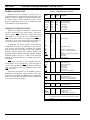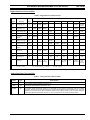
1
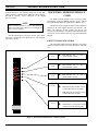
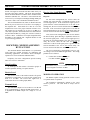
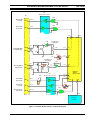
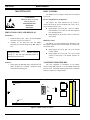
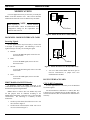
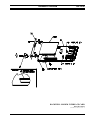
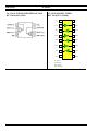
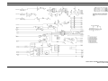
LBI-39152 MAINTENANCE MANUAL ROCKWELL MODEM INTERFACE CARD, ROA 117 2247/1 RS-232 INTERFACE CARD, ROA 117 2247/2 TABLE OF CONTENTS Page SPECIFICATIONS......................................................................................................................................... 2 INTRODUCTION........................................................................................................................................... 3 DESCRIPTION ............................................................................................................................................... 3 INSTALLATION ............................................................................................................................................ 3 RS-232 INTERFACE CARD ......................................................................................................................... 3 FRONT PANEL INDICATORS................................................................................................................ 3 DESCRIPTION ......................................................................................................................................... 3 ROCKWELL MODEM INTERFACE CARD............................................................................................. 4 FRONT PANEL INDICATORS................................................................................................................ 4 DESCRIPTION ......................................................................................................................................... 5 CIRCUIT ANALYSIS ............................................................................................................................... 5 ROCKWELL MODEM ASSEMBLY RYTUA 92101/1.............................................................................. 6 Data Encoding .................................................................................................................................... 6 Receive Level ..................................................................................................................................... 6 Transmit Level.................................................................................................................................... 6 Receive Line Signal Detector (RLSD)................................................................................................ 6 MODES OF OPERATION........................................................................................................................ 6 HARDWARE CIRCUITS ......................................................................................................................... 8 POWER-ON INITIALIZATION............................................................................................................... 8 Digital Interface Characteristics.......................................................................................................... 9 Analog Interface Characteristics ......................................................................................................... 9 MAINTENANCE ............................................................................................................................................ 10 RM INSTALLATION AND REMOVAL ................................................................................................. 10 RMIC JUMPERS....................................................................................................................................... 10 ALIGNMENT PROCEDURES ................................................................................................................. 10 TROUBLESHOOTING............................................................................................................................. 11 REPAIR ..................................................................................................................................................... 11 MODIFICATIONS ......................................................................................................................................... 12 ROCKWELL MODEM INTERFACE CARD .......................................................................................... 12 Inverting Signals ................................................................................................................................. 12 RMIC Modified for RS-232 Receive.................................................................................................. 12 RS-232 INTERFACE CARD .................................................................................................................... 12 CTS To RTS Connection.................................................................................................................... 12 ericssonz LBI-39152 SPECIFICATIONS* ASSEMBLY DIAGRAMS..............................................................................................................................13 PARTS LISTS..................................................................................................................................................15 IC DATA ..........................................................................................................................................................17 OUTLINE DIAGRAM....................................................................................................................................19 SCHEMATIC DIAGRAMS ...........................................................................................................................21 FIGURES AND TABLES Figure 1 - RS-232 Interface Front Panel ....................................................................................................3 Figure 2 - Rockwell Modem Interface Card Front Panel ...........................................................................4 Figure 3 - Rockwell Modem Interface Card Block Diagram......................................................................7 Figure 4 - RMIC Jumper Locations............................................................................................................10 Figure 5 - RMIC DIP Switch S1 ................................................................................................................11 Figure 6 - RMIC RS-232 Receive Mod (PWB top) ...................................................................................12 Figure 7 - RMIC RS-232 Receive Mod (PWB bottom) .............................................................................12 Table 1 - R96FT Hardware Circuits...........................................................................................................8 Table 2 - Digital Interface Characteristics..................................................................................................9 Table 3 - Analog Interface Characteristics .................................................................................................9 SPECIFICATIONS* ITEM SPECIFICATION RS-232 INTERFACE CARD DIMENSIONS (H x L) 100 mm x 220 mm CONNECTIONS 96 pin DIN connector mating to VME backplane interface. ROCKWELL MODEM INTERFACE CARD POWER +5 Vdc ±5%, 1A max. +12 Vdc ±5%, 250mA max. -12 Vdc ±5%, 250 mA max. DIMENSIONS (H x L) 100 mm x 220 mm CONNECTIONS 96 pin DIN connector mating to VME backplane interface. ROCKWELL MODEM (RTYUA 92101/1) POWER +5 Vdc ±5%; 300 mA typical +12 Vdc ±5%; 20 mA typical -12 Vdc ±5%; 50 mA typical TEMPERATURE Operating Storage 0°C to + 60°C (32 to 140°F) -40°C to +80°C (-40 to 176°F) RELATIVE HUMIDITY Up to 90% noncondensing. DIMENSIONS (W x L x H) 100 mm x 82 mm x 7.6 mm above and 3.3 mm below. * These specifications are intended for use during servicing. Refer to appropriate Specification Sheet for the complete specification. Copyright September 1995, Ericsson Inc. 2 INTRODUCTION INTRODUCTION This manual provides maintenance information for the EDACS Compact Vertical Voter (CV2) Interface Cards including the Rockwell Modem Interface Card (RMIC) and the RS-232 Interface Card. LBI-39152 Configuration Table (Refer to LBI-39153) to ensure the proper module is installed in the proper slot. Prior to use, the Gain Switches (S1-1 thru 4 and S1 5 thru 8) in the RMIC should be set according to the Configuration and Alignment instructions contained in LBI39149, Compact Vertical Voter Maintenance Manual and the application's Interconnect Diagrams. The CV2 Interface Cards are available as an RS-232 Interface Card (ROA 117 2247/2) or as a Rockwell Modem Interface Card (RMIC) (ROA 117 2247/1). When the RMIC is properly installed and operational, all Front Panel voltage (+5V, +12V, and -12V) indicators should be on. This will indicate that all voltages are applied to the module. If any of the Front Panel voltage indicators are off, refer to the Maintenance section of this manual. The RMIC is used when the Selector or Digital Receiver connect to other equipment via analog paths such as phone lines where bandwidth is <3000 Hz. Ensure the RMIC jumpers are properly installed. Information for installing the jumpers is available in the Maintenance section of this manual. DESCRIPTION In Simulcast systems, the RMIC is normally used to provide the analog connection from the voter (Selector) to the site and the IMC switch. Auxiliary Receivers may also be connected via Rockwell Modems. The RS-232 Interface Card is used to make connection between the Selector or Digital Receiver #1 and their associated equipment via RS-232 paths. In Simulcast systems without an IMC switch, the RS232 Interface Card is used in slot 2 to connect the Selector to the site. If the system uses VDI, an RS-232 Interface Card is also installed in slot 4 to connect a separate input to Digital Receiver #1. An RS-232 Interface Card is also used when the Auxiliary Receiver Site is connected by RS-232. The RMIC Card is only used with Auxiliary Receiver Sites containing modems. INSTALLATION Installation or removal of the CV2 Interface Cards involves sliding the assembly out of the VME Shelf. NOTE NOTE 2 CV Interface Cards may be plugged and unplugged from the voter shelf with power applied. However, exercise care when using the extender card since the long ground pins are only on the interface cards. The physical position (slot) of the module when installed in the voter shelf will depend on variables such as; number of channels, number of sites and type of system (Voted, Simulcast, and the presence of VDI). Therefore, prior to installing any CV2 Interface Cards, refer to the Card NOTE NOTE Jumper and Switch settings presented in this manual are for reference only. Always refer to the specific application’s Installation Procedures and Interconnect Diagrams for the settings required for proper operation of the system. RS-232 INTERFACE CARD The RS-232 Interface Card is used to make connection between the Selector or Digital Receiver #1 and their associated equipment via RS-232 paths. FRONT PANEL INDICATORS R S 2 3 2 The RS-232 Interface Card’s front panel is shown in Figure 1. It has no front panel indicators. DESCRIPTION When the Voter is connected to the Main Site via an RS-232 path, and there is no requirement for a RM to connect to an IMC switch, the RS-232 Interface Card for Digital Receiver #1 is Figure 1 - RS-232 Interface Front Panel 3 LBI-39152 ROCKWELL MODEM INTERFACE CARD positioned in Slot 2. This permits routing receiver data (RX DATA) from the Control Point or Main Site GETC directly through an RS-232 serial connection to the Digital Receiver's GPTC. NOTE NOTE When installed in Simulcast system using Intraplex MUX, the connection is RS-232 even though the sites are not co-located. The RS-232 Interface Card is also used in slot 4 when the Voter is connected to the Main Site for Voted Digital Interconnect (VDI). ROCKWELL MODEM INTERFACE CARD The RMIC contains RS-232 to TTL converters, phone line interface, Rockwell Modem interface circuits, and the Rockwell Modem (RM), all mounted on a VME size card. The RS-232 to TTL converters allow a clean jumperless interface to the Voter Digital Receivers and Selector. The phone line interface circuits include line drivers and receivers and transformers. The Rockwell modem interface circuits are used to initialize the new piggy-back Rockwell Modem. FRONT PANEL INDICATORS The 9600 Baud Modem Interface Module’s front panel indicators, shown in Figure 2, are described in the following text. +5V (V1) ® +12V (V2) ® -12V (V3) ® +5V M O D E M ON indicates the +5 volts is present and F1 is good. ON indicates the +12 volts is present and F3 is good. +12V -12V RLSD ON indicates the -12 volts is present and F2 is good. CTS I F C RLSD (V12) Received Line Signal Detect. ® ❍ EYE CTS (V11) ON indicates the modem receiver is in the Data state (receive data). OFF indicates the modem receiver is in the idle state, no input. Clear To Send. ® ON indicates a CTS control signal is being sent to the Selector CPU. Figure 2 - Rockwell Modem Interface Card Front Panel 4 ROCKWELL MODEM INTERFACE CARD NOTE NOTE The numbers shown in parentheses refer to the circuit diagram’s reference designator. +5V The +5 volt Indicator, +5V (V1), is ON during normal operation indicating fuse F1 is good and +5 Vdc (VCC) is being applied to the module circuitry. +12V The +12 volt Indicator, +12V (V2), is ON during normal operation indicating fuse F3 is good and +12 Vdc (VDD) is being applied to the module circuitry. -12V The -12 volt Indicator, -12V (V3), is ON during normal operation indicating fuse F3 is good and -12 Vdc (VSS) is being applied to the module circuitry. RLSD The Received Line Signal Detect indicator, RLSD (V12), is ON. when the received line power is greater than the selected threshold level at the end of the training state and the receiver is in the data state. When the indicator is off, the received signal power is less than the selected threshold level at the end of the training state and the receiver is in the idle state. CTS The Clear To Send indicator, CTS (V11), is turned ON by the Rockwell Modem after it receives an RTS, telling the processor that the modem is set up and data may be sent. DESCRIPTION The RMIC is controlled by its corresponding Digital Receivers or Selector and provides a high speed synchronous serial interface between EDACS components in the Voter, Main Site, and remote Receiver Stations. In addition, the Selector sends and receives data from the Main Site through the modem interface. The data transfer rate is typically 9600 bits per second (bps) using conditioned 3002 four-wire telephone lines. The telephone line transformers T1 and T2, couple the four-wire telephone line to the RMIC. The RM demodulates the incoming analog signal which comes from phone lines via T1 and converts it to TTL 9600 baud data. A TTL to RS-232 converter on the RMIC converts the data to RS-232 levels and sends it to the Selector or Digital Receiver for processing. LBI-39152 An RS-232 9600 baud transmit data signal comes from the Selector and is converted to TTL in the RMIC. The RM converts this data into an analog signal which can be carried by phone line. The analog signal is buffered on the RMIC and applied via T2 to the phone line. CIRCUIT ANALYSIS The Digital Receiver or Selector's General Purpose Trunking Card (GPTC) interface to the 9600 baud RMIC through the VME Shelf Backplane. The microcomputer (U1) on the Selector or Digital Receiver provides transmit and receive data to the RM via the Phone Modem (U32) on the GPTC. Refer to the Block Diagram in Figure 3. Receive Transformer T1 receives data from the telephone line and couples the data to the modem board at X2 pin 33. A voltage follower (U4-1) drives the data to the RM. Gain Switch S1-5 thru S1-8 sets the telephone line level to the proper modem level. The receive level is normally set to 300 mV at U4 pin 7 (X2 pin 33) by closing the one section of switch S1 sections 5 thru 8 which sets the level closest to 300 mV. Regulator diodes V4 and V5 provide surge protection. The Write Pulse Generation circuit timer U3 generates a very slow square wave with a period of 2 minutes when monitored at U3 pin 3. On each negative edge to U1 pin 5, a 2 microsecond positive going pulse is generated at U1 pin 6. This pulse is inverted by V8 and is applied to the WRITE input of the RM (X1 pin 12). This causes fixed data on the D0 thru D7 inputs to be written into the RM Control Register addressed by RS0 thru RS3. This assures that the RM is always initialized and runs in the desired mode. As long as the RM sees data coming in, the RSLD LED will be ON. In voter applications, all data is continuous, so the RSLD LED should be ON all the time. The receiver data (RXD) passes unchanged through XOR gate U2-0 and is converted from TTL to RS-232 by U5. The receiver data (MRXD) is then sent to the GPTC Phone Modem U32 and transferred to the BD Bus and processed by the GPTC microcomputer U1. Transmit In voter applications, RTS is controlled by the Selector and jumper X7 should be on X3 pins 2 & 3. When data is to be sent, the GPTC microcomputer sends a Request-to-Send (RTS) signal to the RMIC and waits for a Clear-to-Send (CTS) signal from the modem board. The RTS signal is converted from RS-232 to TTL by U5 and sent on to the Rockwell Modem. When the Rockwell Modem is ready, a CTS signal is sent. Front panel indicator V11 is illuminated 5 LBI-39152 ROCKWELL MODEM ASSEMBLY RYTUA 92101/1 and the CTS signal is converted from TTL to RS-232 by U5 and sent to the GPTC (MCTS). The GPTC microcomputer directs the Phone Modem to send the data to the RM via the TXDATA (MTXD) line. The data is converted from RS232 to TTL by U5 and passes unchanged through XOR gate U2 section 3 and is sent to the Rockwell Modem (TXD). The serial transmit data out (TXA) is obtained from the RM at X2 pin 34, and sent to U4 section 0 for coupling to the telephone line. Gain Switch S1-1 thru S1-4 sets the telephone line level to the proper transmit reference level. The output level is normally set as close to 0 dBm (0.77 volts rms) as possible, when measured across card connector X5 pins B28 and B29, by closing one section of switch S1 sections 1 thru 4. Transformer T2 couples output data from the RMIC to the telephone line. Regulator diodes V6 and V7 provide surge protection. ROCKWELL MODEM ASSEMBLY RYTUA 92101/1 The Rockwell Modem model R96FT is a synchronous serial 9600 bps modem designed for multipoint and networking applications. The R96FT allows full-duplex operation over 4-wire dedicated conditioned lines. Proprietary fast train configurations provide training times of 23 ms for V.29FT/9600. Data Encoding At 9600 bps, the data stream is divided in groups of four-bits (quadbits) forming a 16-point structure. Receive Line Signal Detector ( RLSD ) Response For Fast Train configurations, the receiver enters the training state upon detecting a significant increase in the received signal power. If the received line signal power is greater than the selected threshold level at the end of the training state, the receiver enters the data state and RLSD is activated. If the received line signal power is less than the selected threshold level at the end of the training state, the receiver returns to the idle state and RLSD is not activated. Also, in Fast Train configurations, the receiver initiates the turn-off delay upon detecting a significant decrease in the received signal power. If the received signal power is less than the selected threshold at the end of the turn-off delay, the receiver enters the idle state and RLSD is deactivated. If the received signal power is greater than the selected threshold at the end of the turn-off delay, the receiver returns to the data state and RLSD is left active. The receive threshold is programmable, however, only one setting is used for all EDACS applications. The setting parameters are as follows: • Greater than -43 dBm ( RLSD on) Less than -48 dBm ( RLSD off) NOTE NOTE Performance may be at a reduced level when the received signal is less than -43 dBm. Receive Level The receiver circuit of the modem satisfies all specific performance requirements for received line signal levels from -5 to -43 dBm. The received line signal level is measured at the receiver analog input (RXA). Transmit Level The transmitter output level is accurate to ±1.0 dB and is set to approximately -1 dBm at the RM output (TXA). It is adjustable at the RMIC output over a range of -1 to -18 dBm. 6 MODES OF OPERATION The R96FT capable of being operated in either a serial or a parallel mode of operation. The transmitter automatically defaults to the serial mode at power-on. The serial mode is always used in Voters. ROCKWELL MODEM ASSEMBLY RYTUA 92101/1 LBI-39152 U5 RS-232 To TTL Converter X5 U2-0 RS-232 RXD To GPTC MRXD B23 3 14 D 2 3 1 U2-3 RS-232 TXD From GPTC MTXD B24 6 11 R 13 11 12 X1-26 X2-48 TXD S1-1 thru S1-4 Gain Switch U4-0 1 T2 B28 Transmitting Half of Telephone Line B29 1 4 3 3 - 4558 V7 6 + RXD 2 Tx Level R2 620 X2-34 TXA V6 V12 X1-27 Vcc S1-5 thru S1-8 Gain Switch T1 B27 Receiving Half of Telephone Line B26 1 4 3 U4-1 1 V5 6 X4 2 X6 6 - Rx Level 3 5 + 7 X2-33 4558 V4 U5 X2-50 MRTS X3 3 2 Rockwell Modem RYTUA 92101 RTS RS-232 To TTL Converter X2-49 B22 RXA R1 620 VDD RS-232 RTS From GPTC RLSD 2 1 15 R CTS XTCLK X2-51 RS-232 CTS To GPTC B21 MCTS WR X1-12 V11 X7 7 D 10 Vcc U2-2 RS-232 TXCLK From GPTC B24 MTXCLK 4 R 13 10 8 9 WRITE Write Pulse Generator U3 and U1 Figure 3 - Rockwell Modem Interface Card Block Diagram 7 LBI-39152 ROCKWELL MODEM ASSEMBLY RYTUA 92101/1 Table 1 - R96FT Hardware Circuits HARDWARE CIRCUITS Hardware circuits are assigned to specific pins in a 61-pin DlP connector. Signal names and descriptions of the hardware circuits, including the microprocessor interface, are listed in Table 1, R96FT Hardware Circuits. In the table, the column titled "Type" refers to designations found in the Hardware Circuit Characteristics. POWER-ON INITIALIZATION When power is applied to the R96FT, a period of 50 to 350 ms is required for power supply settling. The poweron-reset signal ( POR ) remains low during this period. Approximately 10 ms after the low to high transition of POR , the modem is ready to be configured, and RTS may be activated. If the 5 Vdc power supply drops below 3.5 Vdc for more than 30 msec, the POR cycle is generated. Name Type DIP Pin Description No. A. OVERHEAD: Ground (A) AGND 30, 31 Ground (D) DGND 29, 37, 53 Digital Ground Return Analog Ground Return +5 volts PWR 1,45,61 +5 Vdc Supply +12 volts PWR 32 +12 Vdc Supply -12 volts PWR 36 -12 Vdc Supply POR I/OB 2 Power-on-reset B. MICROPROCESSOR INTERFACE: D7 D6 D5 D4 D3 D2 D1 D0 I/OA I/OA I/OA I/OA I/OA I/OA I/OA I/OA 3 4 5 6 7 8 9 10 At POR time the modem defaults to the following configuration: Fast train, V.29, 9600 bps, no echo protector tone, 1700 Hz carrier frequency, scrambled ones segment disabled, serial data mode, internal clock, cable equalizers disabled, transmitter digital delay equalizer disabled, link amplitude equalizer disabled, link delay equalizer disabled, transmitter output level set to -1 dBm ±1 dB, interrupts disabled, receiver threshold set to -43 dBm, and train-ondata enabled. RS3 RS2 RS1 RS0 IA IA IA IA 16 17 18 19 CS0 CS1 CS2 READ WRITE IRQ IA IA IA IA IA OB 20 21 13 14 12 11 Chip Select -Transmitter Device Chip Select - Receiver Sample Rate Device Chip Select - Receiver Baud Rate Device Read Enable Write Enable Interrupt Request POR can be connected to a user supplied power-onreset signal in a wire-or configuration. A low active pulse of 3 µsec or more applied to the POR pin causes the modem to reset. The modem is ready to be configured 10 msec after POR is removed. RDCLK TDCLK XTCLK RTS CTS TXD RXD RLSD 23 46 51 50 49 48 26 27 Receive Data Clock Transmit Data Clock External Transmit Clock Request to Send Clear to Send Transmitter Data Receiver Data Received Line Signal Detector Resistor R7 and capacitor C9 on the RMIC provide a POWER-ON-CLEAR (POC) signal to the RM. The control word written to the RM by the WRITE pulse commands the RM to use the external clock and enables the 30 millisecond short echo protection tone (SEPT). Data Bus (8 Bits) Register Select (4 Bits) C. V.24 INTERFACE: OC OC IB IB OC IB OC OC D. ANCILLARY CIRCUITS: OC OC OD OD RBCLK TBCLK FRXD FRLSD 22 47 59 52 Receiver Baud Clock Transmitter Baud Clock FSK Receiver Data (inverted data) FSK Received Line Signal Detector E. ANALOG SIGNALS: TXA RXA AA AB 34 33 Transmitter Analog Output Receiver Analog Input 56 55 57 58 Eye Pattern Data - X Axis Eye Pattern Data - Y Axis Eye Pattern Data Eye Pattern Synchronizing Signal F. DIAGNOSTIC: EYEX EYEY EYECLK EYESYNC OC OC OA OA NOTES: 1. Pins not used: 15, 24, 25, 28, 35, 38-44, 54, and 60. 2. Unused inputs tied to +5V or ground require individual 10K ohm resistors. 8 ROCKWELL MODEM ASSEMBLY RYTUA 92101/1 LBI-39152 Digital Interface Characteristics Table 2 - Digital Interface Characteristics Input/Output Type Symbol Parameter Units IA IB IC VIH Input Voltage, High V 2.0 Min. 2.0 Min. 2.0 Min. VIL Input Voltage, Low V 0.8 Max. 0.8 Max. 0.8 Max. OA OB 1 VOH Output Voltage, High V 2.4 Min. VOL Output Voltage, Low V 0.4 Max. 2 IIN Input Current, Leakage µA IOH Output Current, High mA -0.1 Max. IOL Output Current, Low mA 1.6 Max. IL Output, Current, Leakage µA IPU Pull-up Current (Short Circuit) µA CL Capacitive Load pF CD Capacitive Drive pF Circuit Type: Notes OD 2.2 Min. 0.4 Max. 2 0.4 Max. 2 6 0.6 Max. 7 ±2.5 Max. I/O A I/O B 2.0 Min. 5.25 Max. 2.0 Min. 0.8 Max. 0.8 Max. 1 2.4 Min. 3 0.4 Max. 2 0.4 Max. 5 2.4 Min. ±2.5 Max. 4 1.6 Max. 1.6 Max. ±10 Max. -240 Max. -240 Max. -10 Min. -10 Min. 5 TTL 1. I Load = -100 µA 2. I Load = 1.6 mA OC 5 TTL w/Pull-up -240 Max. -10 Min. -260 Max. -100 Min. 20 TTL w/Pull-up 100 100 100 TTL Open-Drain Open-Drain w/Pull-up 3. I Load = -40 µA 4. VIN = 0.4 to 2.4 Vdc, VCC = 5.25 Vdc 5. I Load = 0.36 mA 6. I Load = -400 µA TTL 10 40 100 100 3-State Transceiver OpenDrain w/Pull-up 7. I Load = 2.0 mA Analog Interface Characteristics Table 3 - Analog Interface Characteristics Name Type Characteristics TXA AA The transmitter output impedance is 604 ohms ±1%. RXA AB The receiver input impedance is 60K ohms ±23%. AUXIN AC The auxiliary analog input allows access to the transmitter for the purpose of interfacing with user provided equipment. Because this is a sampled data input, any signal above 4800 Hz will cause aliasing errors. The input impedance is 1K ohms, and the gain to transmitter output is TLVL setting +0.6 dB -l.4 dB. If unused, this input must be grounded near the modem connector. If used, it must be driven from a low impedance source. 9 LBI-39152 MAINTENANCE RMIC JUMPERS MAINTENANCE The RMIC has two jumpers which must be installed prior to use. CAUTION OBSERVE PRECAUTIONS FOR HANDLING ELECTROSTATIC SENSITIVE DEVICES h Receive Telephone Line Termination The jumper, X6, when installed on X4 inserts or removes R1 from the receive telephone line circuit. R1 is used to balance the line on T1. q RM INSTALLATION AND REMOVAL q Installation: 1. 2. Install jumper X6 on X4 pins 2 and 3 to remove R1 from circuit. Orient the RM so pin 1 lines up with the RMIC connector X1 pin 1 (see Figure 4). RM RTS Control Carefully set the RM pins into the RMIC connectors X1 and X2 and press the RM firmly to seat. The jumper, X7, when installed on X3 determines if the RTS signal is generated on board the RMIC or controlled by an external device. q NOTE NOTE q Keying plug should be located in RMIC connector X2 pin 35. This will align with RM position 35 which has the pin removed. Install jumper X7 on X3 pins 1 & 2 for internal control of RTS. Install jumper X7 on X3 pins 2 & 3 for external control of RTS (this is the normal position for Voters). ALIGNMENT PROCEDURES Removal: 1. Install jumper X6 on X4 pins 1 and 2 to add R1 and terminate receive data for 600 ohm telephone line (default position). Gently grasp the RM and while rocking back and forth, lift RM out of RMIC connectors being careful not to bend any pins. X1 30 The only alignment or adjustment on the RMIC involves using DIP switch S1 to set the modem Output and Receive levels. Each DIP switch segment selects a different amount of signal off a voltage divider. 1 R44 1 C B A R43 Pin not used S1 8 7 6 5 4 3 2 1 Front T1 RX Level X4 1 R45 X5 TX Level T2 U5 X3 Key Plug 1 32 31 X2 61 Figure 4 - RMIC Jumper Locations 10 C B A MAINTENANCE 64748 64748 Transmit Level Receive Level 1 2 3 4 5 6 7 8 Figure 5 - RMIC DIP Switch S1 Output Level The Output level is set by S1 sections 1 thru 4. q Observe output level across card connector X5 pins B28 and B29. Set Output level as near to .77 Vrms (0 dBm) as possible by closing one of the sections of S1 sections 1 thru 4. Receive Level The Receive level is set by S1 sections 5 thru 8. q Set Receive level as near to 300 mVrms as possible by closing one of the sections of S1 sections 5 thru 8. TROUBLESHOOTING OPEN q q LBI-39152 Observe Receive level at X2 pin 33 (U4 pin 7). Most problems encountered by the RMIC will be caused by associated equipment, incorrect DIP switch or jumper settings, or incorrect slot positioning. If difficulties are encountered, check all DIP switch settings and verifying the correct positions of jumpers. Use of the Troubleshooting Guide may be helpful in isolating RMIC problems. If the RMIC appears to be defective, replace the unit with a known good RMIC. If this resolves the problem, the RMIC is probably defective. REPAIR Field repair of the RMIC is extremely limited. We recommend contacting Ericsson Support Services at 1-800528-7711 (outside the USA, call 804-528-7711) for specific instructions regarding the repair or replacement of the defective unit. TROUBLESHOOTING GUIDE SYMPTOM AREA TO CHECK POSSIBLE PROBLEM 5V LED off. +5 volt power. Check 5 volt fuse F1. +12V LED off. +12 volt power. Check +12 volt fuse F3. -12V LED off. -12 volt power. Check -12 volt fuse F2. RMIC fails to receive or transmit data a. Rockwell Modem a. Replace RM with a known good unit. b. Jumpers b. Verify proper jumper settings. 11 LBI-39152 MODIFICATIONS MODIFICATIONS For some applications it may be necessary to modify the RMIC or RS-232 Interface card. This section describes modifications which the service technician may encounter: U5 NOTE NOTE When replacing one RMIC or RS-232 Interface card with another, ensure all modifications and configuration settings on the replacement unit match the unit removed. Cut here Figure 6 - RMIC RS-232 Receive Mod (PWB top) ROCKWELL MODEM INTERFACE CARD Inverting Signals In some applications it may be necessary to invert some or all input or output signals. The following is a list of signals and steps necessary for inverting the signal: • RDCLK T1 To invert the RDCLK signal, remove the zero ohm resistor R38. • RXD Cut here To invert the RXD signal, remove the zero ohm resistor R37. • XTCLK To invert the XTCLK signal, remove zero ohm resistor R40. • TXD To invert the TXD signal, remove zero ohm resistor R39. Figure 7 - RMIC RS-232 Receive Mod (PWB bottom) 3. Two zero ohm resistors REP 264 001/0 (part of mod kit 350A1693G1) or jumper wires were installed at R43 and R44. RS-232 INTERFACE CARD RMIC Modified for RS-232 Receive CTS To RTS Connection In Simulcast systems, the RMIC connected to the Control Point GETC must receive signals via an RS-232 line and transmit signals through the RM. In Voter applications it is necessary to tie the RTS and CTS lines together. RMICs ROA 117 2247/1 (Rev. R1 and R2 only) used for this purpose must be modified according to the Modification Instructions 350A1692 (part of the Mod Kit 350A1693G1). The following is a summary of those instructions: 12 1. On the top of the board, the solder run to U5-3 was cut as shown in Figure 6. 2. On the bottom of the board, the solder run to T1-6 was cut as shown in Figure 7. For RS-232 Interface cards ROA 117 2247/2 (Rev. R1) a jumper wire was installed between X5-B21 and B22. For revision R2 and later, R45 was added and no modification is necessary. ASSEMBLY DIAGRAM LBI-39152 ROCKWELL MODEM INTERFACE CARD ROA 117 2247/1 (1/1078 ROA 117 2247/1, Sh. 1, Rev. A) 13 LBI-39152 RS-232 INTERFACE CARD ROA 117 2247/2 (1/1078 ROA 117 2247/2, Sh. 1, Rev. A) 14 ASSEMBLY DIAGRAM PARTS LIST ROCKWELL MODEM INTERFACE CARD 131 32-ROA 117 2247/1 Revision: C SYMBOL PART NUMBER DESCRIPTION -------------- CAPACITORS ---------C1 thru C4 RJE 584 3168/47 C6 RJC 464 3045/1 Tantalum chip: 47 µF ±20%, 16 V. SYMBOL R35 LBI-39152 PART NUMBER REP 645 623/12 RJA 528 4064/1 Metal film: 1 nF ±5%, size 1206. C8 RJE 584 3168/47 Tantalum chip: 47 µF ±20%, 16 V. C9 RJE 584 3108/1 Tantalum chip: 10 µF ±20%, 10 V. C10 thru C15 RJC 464 3045/1 Ceramic Chip: 10 nF 50V -10%. Ceramic chip: 120 Ohm, 1%, 1/4w. R36 REP 645 623/12 Ceramic chip: 120 Ohm, 1%, 1/4w. R37 thru R40 REP 645 62 Zero-ohm jumper. R41 REP 625 425/1 Ceramic chip: 10k, 1206, 5%, 1/8w. R42 REP 625 425/1 Ceramic chip: 10k, 5%, 1/8w. S1 RMF 356 004/08 Switch, DIP. T1 REG 135 57/1 Transformer, telephone. T2 REG 135 57/1 Transformer, telephone. ---------------- SWITCHES ------------ Ceramic Chip: 10 nF 50V -10%. C7 DESCRIPTION ----------- TRANSFORMERS ------- ------ INTEGRATED CIRCUITS - --------------------- FUSES --------------- U1 RYT 306 2024/C Digital: CMOS 2 x Monostable Multivibrator; sim to 74HC4538. F1 NGH 241 04/1 Fuse, 1A, slow action 250 V, glass 5 x 20mm. U2 RYT 306 2019/C Digital: CMOS Quad 2-Input Exclusive OR Gate; sim to 74HC86. F2 NGH 241 03/25 Fuse, 0.25A, slow action 250 V, glass 5 x 20mm. U3 RYT 108 6003/C Monolithic Timer; sim to TLC555. U4 RYT 101 6164/1 Linear, Dual Op Amp; sim to 4558. U5 RYT 109 6073/1 EIA232-D and CCITT V.28 driver/receiver; sim to MC145406. F3 NGH 241 03/25 Fuse, 0.25A, slow action 250 V, glass 5 x 20mm. --------------- RESISTORS ------------ R1 REP 645 623/62 Ceramic chip: 620 Ohm, 1%, 1/4w. R2 REP 645 623/62 Ceramic chip: 620 Ohm, 1%, 1/4w. R3 REP 645 623/22 Ceramic chip: 220 Ohm 1%, 1/4w. R4 REP 625 426/33 Ceramic chip: 330k, 5%, 1/8w. --- DIODES and TRANSISTORS V1 thru V3 RKZ 433 637/1 Diode, LED, 90 degree red, T1 pkg. V4 thru V7 RKZ 223 01/8 Regulator Diode; sim to BZX84C4V7. R5 REP 625 426/33 Ceramic chip: 330k, 5%, 1/8w. R6 thru R17 REP 625 425/1 Ceramic chip: 10k, 5%, 1/8w. V8 thru V10 RYN 121 675/1 Transistor: Silicon NPN, low profile; sim to MMBT3904. R18 REP 625 424/47 Ceramic chip: 4.7k, 5%, 1/8w. V11 RKZ 433 637/1 Diode, LED, 90 degree red, T1 pkg. RKZ 433 637/1 Diode, LED, 90 degree red, T1 pkg. R19 REP 625 424/27 Ceramic chip: 2.7k, 5%, 1/8w. V12 R20 REP 625 424/22 Ceramic chip: 2.2k, 5%, 1/8w. V13 RYN 121 675/1 Transistor: Silicon NPN, low profile; MMBT3904. V14 RYN 121 675/1 Transistor: Silicon NPN, low profile; MMBT3904. X1 RNV 403 843/031 Connector, 31 contact. R21 REP 625 424/22 Ceramic chip: 2.2k, 5%, 1/8w. R22 thru R24 REP 625 424/1 Ceramic chip: 1k, 5%, 1/8w. R25 thru R28 REP 625 425/1 Ceramic chip: 10k, 5%, 1/8w. X2 RNV 403 843/031 Connector, 31 contact. R29 REP 645 624/24 Ceramic chip: 2.4K, 1%, 1/4w. X3 RPV 380 10/03 Pin strip header. R30 REP 645 624/12 Ceramic chip: 1.2K Ohm 1% 1/4w. X4 RPV 380 10/03 Pin strip header. R31 REP 645 623/62 Ceramic chip: 620 Ohm, 1%, 1/4w. X5 RPV 403 209/102 Connector, 96 contact. R32 REP 645 623/62 Ceramic chip: 620 Ohm, 1%, 1/4w. X6 RNV 207 03/1 Shunt, jumper. RNV 207 03/1 Shunt, jumper. RPV 380 10/03 Pin strip header. ------------- CONNECTORS --------- R33 REP 625 423/47 Ceramic chip: 470, 5%, 1/8w. X7 R34 REP 645 623/24 Ceramic chip: 240 Ohm, 1%, 1/4w. X8 15 LBI-39152 SYMBOL X9 PARTS LIST PART NUMBER RPV 380 10/03 RS-232 INTERFACE CARD 131 32-ROA 117 2247/2 Revision: B DESCRIPTION Pin strip header. SYMBOL ------------ FUSE HOLDERS -------XF1 NFN 102 04 Holder, Fuse. XF2 NFN 102 04 Holder, Fuse. XF3 NFN 102 04 Holder, Fuse. ----------- MISCELLANEOUS ------- 2 TVA 117 2225 R2 Printed wiring board. 3 SXA 120 4174/3 Modem Interface Front Panel. 4 NTM 201 1079 Hardware Kit. 6 RNY 101 01/4 Keying Plug. MODEM RYTUA 921 01/1 Modem, 9600 baud; sim to Rockwell Modem R96FT with DIP connector. PART NUMBER DESCRIPTION --------------- RESISTORS ----------R43 REP 264 001/0 Resistor, 0 Ohm, 0207. R44 REP 264 001/0 Resistor, 0 Ohm, 0207. R45 REP 264 001/0 Resistor, 0 Ohm, 0207. X5 RPV 403 209/102 Connector, 96 contact. 2 TVA 117 2225 R2 3 SXA 120 4174/4 RS-232 Interface Front Panel. 4 NTM 201 1079 Hardware Kit. ------------- CONNECTORS --------- ----------- MISCELLANEOUS ------Printed wiring board. PRODUCTION CHANGES Changes in the equipment to improve performance or simplify circuits are identified by a "Revision Letter," which is stamped after the model number of the unit. The revision stamped on the unit includes all previous revisions. Refer to the parts list for the descriptions of the parts affected by these revisions. Rev. R2A - ROA 117 2247/1 Connectors X1 and X2 changed to improve installation of Rockwell Modem. X1 and X2 changed from RNV 403 105/031 to RNV 403 843/031. PRODUCTION CHANGES Changes in the equipment to improve performance or simplify circuits are identified by a "Revision Letter," which is stamped after the model number of the unit. The revision stamped on the unit includes all previous revisions. Refer to the parts list for the descriptions of the parts affected by these revisions. Rev. R2A - ROA 117 2247/2 Jumper R45 added to connect CTS to RTS. (In revision R1A, a short piece of 19A700134P10 DA wire was installed between X5-B21 and X5-B22.) Connector X5, which was inadvertently omitted, was added to the parts list. 16 IC DATA LBI-39152 U1 - CMOS 2 X MONOSTABLE MULTIVIBRATOR RYT 306 2024/C (74HC4538) FUNCTION TABLE CA 1 INPUTS Vcc 16 Reset OUTPUTS +Triggr - Trigg Q Q RA 2 15 CB RESET A 3 14 RB L X X L H Tr A+ 4 13 RESET B X H X L H Tr A- 5 12 Tr B+ QA 6 11 Tr B- X X L L H QA 7 10 QB H L GND 8 9 QB H CAUTION h H X = H or L OBSERVE PRECAUTIONS FOR HANDLING ELECTROSTATIC SENSITIVE DEVICES = from L to H = from H to L U2 - 2-INPUT EXCLUSIVE - OR - GATE RYT 306 2019/C (74HC86) Vcc 4B 4A 4Y 14 13 12 11 3B 10 3A 9 U3 - MONOLITHIC TIMER RYT 108 6003/C (TLC555ID) GND 1 8 VDD TRIG 2 7 DSCH OUT 3 6 THRES RESET 4 5 CONT 3Y 8 VDD RESET (8) CONTROL R 1 2 3 4 5 6 7 1A 1B 1Y 2A 2B 2Y GND (4) (5) R1 THRESHOLD OUTPUT (6) R 1 (3) S R CAUTION h OBSERVE PRECAUTIONS FOR HANDLING ELECTROSTATIC SENSITIVE DEVICES TRIGGER (2) DISCHARGE (7) GND (1) 17 LBI-39152 IC DATA U4 - DUAL WIDE BANDWIDTH OP AMP RYT 101 6164/1 (4558) U5 - MONOLITHIC TIMER RYT 109 6073/1 (145406) VDD 1 Rx1 2 Tx1 3 Rx2 4 Tx2 5 Rx3 6 Tx3 7 VSS 8 D = Driver R = Receiver DI = Data In DO = Data Out 18 R D R D R D 16 VCC 15 DO1 14 DI1 13 DO2 12 DI2 11 DO3 10 DI3 9 GND OUTLINE DIAGRAM LBI-39152 ROCKWELL MODEM AND RS-232 INTERFACE CARD ROA 117 2247/1 and ROA 117 2247/2 (1078-ROA 117 2247, Sh. 1, Rev. B) 19 Ericsson Inc. Private Radio Systems Mountain View Road Lynchburg, Virginia 24502 1-800-528-7711 (Outside USA, 804-528-7711) Printed in U.S.A. ADDENDUM NO. 1 TO LBI-39152 PURPOSE This addendum corrects typographic errors and reflects recent changes to a modification referenced in this manual. Page 7, Figure 3 The pin number in X5 for “RS-232 TXCLK From GPTC” is incorrect and should be changed from B24 to B25 as shown in the following diagram. As Shown Change to Show U5 VDD RS-232 RTS From GPTC B22 RS-232 CTS To GPTC B21 RS-232 TXCLK From GPTC B24 MRTS X3 3 2 MCTS U5 RS-232 To TTL Converter 2 1 15 R X7 MTXCLK 7 4 D R 10 13 VDD RS-232 RTS From GPTC B22 RS-232 CTS To GPTC B21 RS-232 TXCLK From GPTC B25 MRTS X3 3 2 MCTS MTXCLK RS-232 To TTL Converter 2 1 15 R X7 7 4 D R 10 13 Page 12, RMIC Modified for RS-232 Receive The instructions for modifying the RMIC (ROA 117 2247/1) have been changed so the technician will move the jumper on X3. Add the following step to the “RMIC Modified for RS-232 Receive” section. Add the Following 4. Move jumper X7 from X3 pins 1 & 2 to X3 pins 3 & 4. Ericsson Inc. Private Radio Systems Mountain View Road Lynchburg, VA 24502 1-800-528-7711 (Outside USA, 804-528-7711) Printed in U.S.A. SCHEMATIC DIAGRAM LBI-39152 ROCKWELL MODEM AND RS-232 INTERFACE CARD ROA 117 2247/1 and ROA 117 2247/2 (1911-ROA 117 2247, Sh. 1, Rev. C) 21 LBI-39152 ROCKWELL MODEM AND RS-232 INTERFACE CARD ROA 117 2247/1 and ROA 117 2247/2 (1911-ROA 117 2247, Sh. 2, Rev. C) 22 SCHEMATIC DIAGRAM