1
This file is provided FREE OF CHARGE from the
electromaniacs.com community
You are free to distribute this file to other persons
who needs it , but without of charge
Also on http://electromaniacs.com you can find
thousands of service manuals , schematics free of
charge
28KF-84H
SERVICE MANUAL
SE0028KF84H00
Issued:24th July 2003
GA-200 CHASSIS
PAL I SYSTEM COLOUR TELEVISION
MODEL
28KF-84H
In the interests of user safety (required by safety
regulations in some countries) the set should be restored to its original condition and only parts identical to those specified should be used.
CONTENTS
ELECTRICAL SPECIFICATIONS ................... 3
IMPORTANT SERVICING NOTES ................. 4
CONTROLS & TERMINALS ........................... 5
ADJUSTMENT PROCEDURES ...................... 6
LED FLASHING CODES ............................... 13
PRINTED WIRING BOARDS ........................ 14
COMPONENT LOCATION TABLES ............... 22
CHASSIS LAYOUT ......................................... 29
SCHEMATIC DIAGRAMS ............................... 32
BLOCK DIAGRAM ....................................... 45
TROUBLESHOOTING TABLES ..................... 46
ICs ADDITIONAL INFORMATION .................. 51
PARTS LISTING ............................................. 67
SERVICING NOTES.................................... 77
SOURCE OF DOCUMENTATION .................. 79
SHARP CORPORATION
1
This document has been published to
be used for after sales service only.
28KF-84H
SERVICE MANUAL UPDATE LOG SHEET
Technical Report No.
Technical Bulletin No.
Cause / Solution
Part No.
Page No.
Application
Data /Serial No.
Use this page to keep any special servicing information as Technical Report (Bulletin), Technical Information, etc.
If only part number changes are required, just change part number directly the part number in the Parts Listing Section.
If you need more information, please refer to the Technical Report (Bulletin).
2
28KF-84H
ELECTRICAL SPECIFICATIONS
•Focus ................. High Bipotencial Electrostatic
•Power Input .................... 220V-240 Volts AC 50Hz
•Sweep Deflection ............................. Magnetic
•Power Consumption
Normal Operation (Method IEC60107) ...............100W
Stand-by Operation ..........................................1.5W
•Picture Intermediate frequency .......... 38.9MHz
•Sound Carrier Trap ........................... 32.9MHz
•Audio Power Output Rating (MPO) / Impedance
Internal Left Speaker ................................. 10W, 7Ω
Internal Right Speaker ............................... 10W, 7Ω
•Adjacent Sound Carrier Trap ............. 40.9MHz
•Adjacent Picture Carrier Trap ........... 30.9MHz
•Speakers
Left / Right ................................................. 12 x 6cm
•Aerial Input Impedance
VHF/UHF ................. 75 ohm Unbalanced
•Convergence (Maximum Misconvergence)
Static (Centre) between any two colours ... 0.03
Dynamic after static equals zero
Within 28 x 15 cm rectangle ........... 0.13
56 x 30 cm rectangle........................ 0.15
Everywhere else .......................................... 0.18
•Tuning Ranges ..... 45.75MHz thru 855.25 MHz
VHF: IR A - J / CC01-CC68 (Hiperband)
UHF: I21 - I69 CH
cm
cm
cm
cm
•White Level
Set brightness control to get total picture tube cathode current of 600 µA under no signal condition.
Maximum necessary correction of each picture tube cathode current to get 8950 degrees K-20 MPCD
screen temperature should not exceed 15% of its original value.
X=0.290 ± 0.015
Y=0.284 ± 0.015
Specifications are subject to change without prior notice.
WARNING
The chassis in this receiver is partially hot. Use an isolation transformer between the line cord plug
and power receptacle, when servicing this chassis.
To prevent electric shock, do not remove cover. No user-serviceable parts inside. Refer servicing to
qualified service personnel.
3
28KF-84H
IMPORTANT SERVICING NOTES
Only qualified service personnel are allowed to carry out maintenance and repair of this receiver.
Servicing of High Voltage System and CRT
It is important that the static charge is removed from the high voltage system when carrying out work on the
receiver. This can be achieved by connecting a 10K resistor (with a suitably insulated lead) from the CRT
cavity connector to the CRT ground tag. This must be carried out with the AC supply disconnected from the
receiver.
Note the following:
• The CRT in this receiver employs Integral Implosion Protection.
• If the CRT has to be changed it MUST be replaced with the correct type for continued safe working.
• DO NOT lift the CRT by its neck.
• When handing the CRT, ensure that shatterproof goggles are worn.
• Ensure that the CRT is discharge before handling.
X-Ray
This receiver is designed to keep any x-ray emission to an absolute minimum. Some fault conditions and
servicing procedures may produce potentially hazardous x-ray radiation levels. This is a problem when in
close proximity to the receiver for long periods of time. To reduce any risks associated with this, please
observe the following precautions:
1. When undertaking any servicing on this chassis, DO NOT increase the EHT to more than 33 KV, (at a
instantaneous beam current of 1800µA).
2. Ensure that during normal operation the EHT does not exceed 30 KV (at a beam current of 1300µA). This
level has been preset in the factory. Always check that this level has not been exceeded after carrying out
any repair on the receiver.
3. DO NOT replace the CRT with any other type than that specified in the parts listing as this may cause
excessive x-ray radiation.
Before returning the receiver to the customer
In addition to the above checks, the following should also be carried out before returning the receiver to the
customer.
1. Inspect all the leads to ensure that they are dressed correctly and that they are not obstructed or pinched
by any other parts.
2. Ensure that all protective devices are in good condition. These will include nonmetallic control knobs,
insulating fish papers, cabinets backs, compartment covers or shields, mechanical insulators, etc.
4
28KF-84H
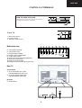
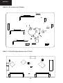
CONTROLS & TERMINALS
HOW TO OPEN THE DOOR
8
Lift the projection at the lower right of the door with
your finger in the direction of the arrow.
1
2
3
!
"
#
$%
$$
69,'(2
9,'(2
/6*,
$ $
!
! "!
#$ %&'!
" #$%("$!
# $)
$% ('*+,$%*, '$!
$$ *('-!
$ *('#.!
$ /.$012345466.!
&
&+
5'''
$8',2
$'()
$ )*,*)!.
*+,$%*, '$,$)(
)%$*'7!.
*+,$%*, '$(
')
*
6&$57
3(5,7(/(9,6,21
*
$97(50,1$/
$
$
5
28KF-84H
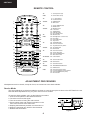
REMOTE CONTROL
1.
19.
2.
20.
TV
1. Stand-by button (TV)
Video
2. Power button (VCR)
TV
3. 0 ~ 9 digit buttons
4. Flash back button
Teletext
5. GREEN button
6. RED button
TV
7. Volume DOWN button
8. MENU button
3.
Teletext
4.
5.
6.
21.
22.
23.
9.
10.
11.
12.
13.
14.
REVEAL button
LIST button
STORE button
CANCEL button
HALF PAGE button
RESET button
Video
15.
16.
17.
18.
Rewind/picture search reverse
Play button
Pause/Still button
Stop button
TV
19. TV/VIDEO button
20. Channel Call button
21. Single/Double entry button
Teletext
22. YELLOW button
23. BLUE button
TV
24.
25.
26.
27.
TV /Teletext
28. CLOCK button
TV
24.
7.
25.
26.
8.
27.
9.
28.
10.
11.
29.
12.
31.
13.
32.
TV
29. Sound mode button
14.
15.
16.
33.
34.
Teletext
30. HOLD button
35.
36.
TV
31. Sound Mute button
Teletext
32. TEXT/MIX/PICTURE button
33. INDEX button
Video
34.
35.
36.
37.
30.
17.
18.
37.
Channel UP button
Volume UP button
Channel DOWN button
Wide mode button
Channel UP button (VCR)
Fast forward/picture search forward
Channel DOWN button (VCR)
Record button
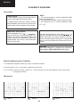
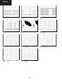
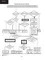
ADJUSTMENT PROCEDURES
All adjustments to this chassis, except for focus, are carried out in the Service Mode.
Service Mode
The Service Mode is provided to enable the engineer to correctly set up the receiver to the CRT fitted in the set.
Note that these adjustments may vary from one receiver to another.
To enter the Service Mode, carry out the following procedure.
1. Connect a test pattern to the antenna terminal.
2. Tune the receiver to this signal.
3. Turn the receiver off using the mains switch.
4. Press volume down and channel up buttons on the
front of the receiver at the same time.
5. Keeping these buttons pressed, turn the mains on.
6. When the set starts up it will be in Service Mode.
7. Release the two buttons.
6
1
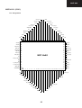
Figure 1
8
28KF-84H
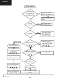
• Use the channel up and down buttons to move between the options.
• Use the volume control buttons to change the data.
• To store the data, use the stand-by button on the remote control.
• To exit the Service Mode, turn the receiver off using the mains switch.
When the Service Mode is entered the following On Screen Display appears:
SERVICE SOFTWARE 28KF84H ∗∗-∗∗∗∗∗
SW on: XXXX SW off: XXXX Hours ON: XXXX
The figures displayed in the “XXXX” locations are hexadecimal representations of the number of times that particular
function has been executed. For example if the hexadecimal number displayed after “SW ON” was 0E4A, this would
correspond to the receiver being turned on 3658 times.
X
Adjustment menu:
The following adjustments can be carried out in the Service Mode.
01. Horizontal Shift
02. East West Width
03. Pin Phase
04. Pin Amp
05. Upper corner correction
06. Lower corner correction
07. Extreme Corner Correction
08. Vertical Linearity
09. Vertical Angle
10. Vertical Bow
11. Vertical Amplitude
12. S Correction
13. Vertical Shift
14. Red Cut Off
15. Green Cut Off
16. Blue Cut Off
17. Alter NVM Pag (Page)
18. Alter NVM Pos (Position)
19. Alter NVM Val (Value)
20. Teletext Mix Mode Contrast
21. Teletext Contrast
22. OSD Contrast
23. DVCO Adjustment (Only PAL)
24. DVCO Adjustment (Only NTSC)
25. AGC Adjustment
26. Auto Installation On/Off
When in the Service Mode it is possible to access certain functions by using the teletext keys as below.
• By pressing the Blue button each adjustment can be directly accessed via the remote control. Referring to the
list above, press the Blue button followed by the adjustment number, this will directly access the selected
adjustment. If any number above 26 is selected, the set will revert to the Service Mode entry page. To access a
number less than 10, use the 0 key first, i.e. 02.
• Press the Yellow button to go straight to the AGC adjustment.
• Press the Green button once to enter “FACTORY VOLUME” level. Use volume control keys to change the
setting. The original value will be recovered after resetting the TV set.
• Press the Green button twice to enter “FACTORY BALANCE” level. Use volume control keys to change the
setting. The original value will be recovered after resetting the TV set.
• Press the Red button once to enter “FACTORY CONTRAST” level. Use volume control keys to change the
setting. The adjustment is stored automatically.
• Press the Red button twice to enter “FACTORY BRIGHTNESS” level. Use volume control keys to change the
setting. The adjustment is stored automatically.
• Press the Red button three times to enter “FACTORY COLOUR” level. Use volume control keys to change the
setting. The adjustment is stored automatically.
• If buttons 0 through 9 are pressed, the set will automatically go to that program number.
Note that in case the blue button has been used before, the program number should be requested by using two
digit number (01...99).
• By pressing the Menu button, the unit will normalise Picture and Audio settings. The Auto Installation is then
turned “on”.
7
28KF-84H
The following geometry adjustments can be carried out. Detailed instructions on how to execute these are given on the
following pages:
Horizontal
• Horizontal Shift
• East West Width
• Pin Phase
• Pin Amp
• Vertical angle
• Vertical bow
• Upper Corner Amplitude
• Lower Corner Symmetry
• Extreme Corner Symmetry
Vertical
• Vertical Amplitude
• S Correction
• Vertical Shift
• Vertical Linearity
Just in case the TV set requires a full geometry adjustment, please proceed first with Vertical according to the above order, and after that, adjust Horizontal according to the above
order.
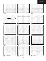
Horizontal Shift
Adjust the horizontal shift so that the picture is centred.
The effect of this adjustment is shown in figure 2.
• When the volume up button is pressed, the picture moves to the left.
• When the volume down button is pressed, the picture moves to the right.
• Press the stand-by button on the remote control to store.
Figure 2
East West Width
Adjust the East West Width so that 8% over-scan is achieved.
The effect of this adjustment is shown in figure 3.
• When the volume up button is pressed, horizontal scanning increases.
• When the volume down button is pressed, horizontal scanning decreases.
• Press the stand-by button on the remote control to store.
Figure 3
Pin Phase
Adjust the Pin Phase so that the picture is symmetrical top and bottom.
The effect of this adjustment is shown in figure 4.
• When the volume up button is pressed, side pincushion changes.
• When the volume down button is pressed, side pincushion changes.
• Press the stand-by button on the remote control to store.
Figure 4
Pin Amp
Adjust the Pin Amplitude so that the picture is centred.
The effect of this adjustment is shown in figure 5.
• When the volume up button is pressed, side pincushion changes from pincushion to
barrel shape.
• When the volume down button is pressed, side pincushion changes from barrel
shape to pincushion.
• Press the stand-by button on the remote control to store.
8
Figure 5
28KF-84H
Upper Corner Correction
Adjust the Upper Corner Correction so that the picture is centred.
The effect of this adjustment is shown in figure 6.
• When the volume up button is pressed, side pincushion changes from pincushion to
barrel shape.
• When the volume down button is pressed, side pincushion changes from barrel shape to
pincushion.
• Press the stand-by button on the remote control to store.
Figure 6
Lower Corner Correction
Adjust the Lower Corner Correction so that the picture is centred.
The effect of this adjustment is shown in figure 7.
• When the volume up button is pressed, side pincushion changes from pincushion to
barrel shape.
• When the volume down button is pressed, side pincushion changes from barrel shape to
pincushion.
• Press the stand-by button on the remote control to store.
Figure 7
Extreme Corner Correction
Adjust the Extreme Corner Correction so that the picture is centred.
The effect of this adjustment is shown in figure 8.
• When the volume up button is pressed, side pincushion changes from pincushion to
barrel shape.
• When the volume down button is pressed, side pincushion changes from barrel shape to
pincushion.
• Press the stand-by button on the remote control to store.
Figure 8
Vertical Linearity
Adjust the Vertical Linearity so that the upper and lower parts of the picture are symmetrical.
The effect of this adjustment is shown in figure 9.
• When the volume up button is pressed, the upper picture scanning decreases and the
lower picture scanning increases.
• When the volume down button is pressed, the upper picture scanning increases and the
lower picture scanning decreases.
• Press the stand-by button on the remote control to store.
Figure 9
Vertical Angle
Adjust the Vertical Angle so that the picture is centred.
The effect of this adjustment is shown in figure 10.
• When the volume up button is pressed, the vertical angle changes to right.
• When the volume down button is pressed, the vertical angle changes to left.
• Press the stand-by button on the remote control to store.
9
Figure 10
28KF-84H
Vertical Bow
Adjust the Vertical Bow so that the picture is centred.
The effect of this adjustment is shown in figure 11.
• When the volume up button is pressed, the vertical bow changes to left.
• When the volume down button is pressed, the vertical bow changes to right.
• Press the stand-by button on the remote control to store.
Figure 11
Vertical Amplitude
Adjust the Vertical Amplitude so that 8% over-scan is achieved.
The effect of this adjustment is shown in figure 12.
• When the volume up button is pressed, the vertical size of the picture increases.
• When the volume down button is pressed, the vertical size of the picture decreases.
• Press the stand-by button on the remote control to store.
Figure 12
S Correction
Adjust the S Correction so that the picture symmetrical between the top, centre and bottom.
The effect of this adjustment is shown in figure 13.
• When the volume up button is pressed, the top and bottom scanning decreases and the
centre scanning increases.
• When the volume down button is pressed the top and bottom scanning increases and the
centre scanning decreases.
• Press the stand-by button on the remote control to store.
Figure 13
Vertical Shift
Adjust the Vertical Shift so that the picture is centred.
The effect of this adjustment is shown in figure 14.
• When the volume up button is pressed, the picture moves up.
• When the volume down button is pressed, the picture moves down.
• Press the stand-by button on the remote control to store.
Figure 14
Colour Adjustments
The following adjustments should only be carried out when the CRT, IC850, IC851
or IC852 are replaced.
G2 and Cut Off Adjustments
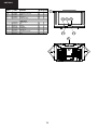
150 V
1. Follow the procedure below to set the G2
1.1 Tune the set to the output of a signal generator (cross hatch pattern).
1.2 2. In the user menu, set the picture levels to the FACTORY settings
(normalized).
1.3 Connect the oscilloscope to the RED cathode (pin 8 of CRT socket)
and adjust G2 to read 150V on the sensor pulse as in the drawing:
Note: Oscilloscope should be adjusted for vertical TV field trigger and synchronized with
video signal.
10
CH1 gnd
Figure 15
28KF-84H
2. Follow the procedure below to set the Cut Off
2.1 Adjust G2.
2.2 Tune a white pattern.
2.3 Adjust colour to minimum.
2.4 Position colorimeter in the centre of screen.
2.5 Adjust brightness and contrast to obtain a luminance of ≈20 NITS.
2.6 Operate in Service Mode and select location RED CUT OFF, GREEN CUT OFF and BLUE CUT OFF, to
obtain colour coordinates:
X=0.290 ± 0.015
Y=0.284 ± 0.015
To increase press volume-up button and to decrease press volume down button.
RED CUT OFF
alter «X» coordinate.
GREEN CUT OFF alter «Y» coordinate.
BLUE CUT OFF
alter «X» and «Y» coordinate.
They will be stored automatically.
Colour Adjustment Alternative Method
In case that the required equipment (Colorimeter / oscilloscope) is not available, please follow the procedures below to
obtain correct G2 and Grey scale settings (R-G-B Cut Off).
Alternative Method to set the G2
Follow the procedure below to set the G2:
1. Tune the set to the output of a signal generator (Cross-hatch pattern).
2. In the user menu, set the picture levels to the FACTORY settings (normalized).
3. Connect a DC voltimeter at the Red amplifier output (Pin 9 IC850) and adjust G2 to read 145VDC (±5V).
Alternative Method to set Cut Off
Do not change the Cut RED value (50%).
1. Adjust G2.
2. Tune a grey scale pattern.
3. Adjust colour to minimum.
4. Operate in Service Mode and select location GREEN CUT OFF and BLUE CUT OFF.
5. Adjust these parameters until achieve a correct grey scale tracking.
To increase press volume-up button and to decrease press volume down button.
Press the Store button of Remote Control to store all values.
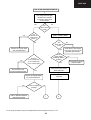
Changing NVM Data
To change the data contained within the Non Volatile Memory, it is necessary to first select the page the data is stored in,
then the position and finally to change the data itself. The procedure below outlines this process.
1. While on ALTER NVM PAGE, use the volume up/down buttons to change this data (it is shown in hexadecimal format).
2. Press the channel up button and ALTER NVM POSITION appears, use the volume up/down buttons to change this
data (it is shown in hexadecimal format).
3. Press the channel up button and ALTER NVM VALUE appears, use the volume up/down buttons to change this data
(data is shown in hexadecimal format).
11
28KF-84H
4. Once this data has been set, press the stand-by button to store.
5. If another NVM value has to be changed, use the channel down button to select the page or position and repeat as
necessary.
Note:
DO NOT change any NVM data, unless you have been advised to do so by a Sharp representative. If data is incorrectly
changed, serious damage may occur to the receiver.
Contrast Adjustments
Three types of contrast levels can be varied as listed below:
• TELETEXT MIX MODE CONTRAST
• TELETEXT CONTRAST
• OSD CONTRAST
Use the volume up/down buttons to adjust to a suitable level, they will be stored automatically.
DVCO Adjustment (PAL)
Carry out the DVCO Adjustment (PAL) as shown below:
1. Receive a color pattern signal (PAL).
2. While in the DVCO ADJUSTMENT (PAL) menu, press the stand-by button.
3. The adjustment will be carried out automatically and stored.
DVCO Adjustment (NTSC)
Carry out the DVCO Adjustment (NTSC) as shown below:
1. Receive a color pattern signal (NTSC 3.58).
2. While in the DVCO ADJUSTMENT (NTSC) menu, press the stand-by button.
3. The adjustment will be carried out automatically and stored.
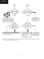
Automatic Gain Control Adjustment
To correctly align the Automatic Gain Control, follow the procedure outlined below:
1. Tune the set into a pattern generator on CH-21.
2. Adjust the signal strength of the pattern generator to 57dB/uV.
3. Enter the Service Mode.
4. Press the channel up button of Remote Control to select “Automatic Gain Control”.
5. Press the stand-by button on the remote control.
6. The adustment will be carried out and stored automatically.
Auto Installation On/Off
To return the receiver to the original Auto Installation mode, using the volume up or down button, set the Auto Installation
On/Off to On. This setting is automatically stored and when the receiver is turned on the next time it will start up in Auto
Installation mode.
Postcode Password Reset
In order to reset the PostCode when password is not on mind, enter and exit the Service Mode.
12
28KF-84H
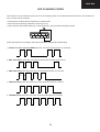
LED FLASHING CODES
This model is not provided with stereo led, so to let “flashing codes” for IC failures detection when the TV set does not
work, we offer the next solution:
• The detection of failure will be made with an external LED.
• The output of the flashing code will be via AV1 (pin 10).
• Insert a generic led diode between pin 10 and ground (i.e. pin 5) as shows the below picture.
20
21
18
19
16
17
14
15
12
13
10
11
8
9
6
7
4
5
2
3
21
1
Follow the sequence according to the below information, as a guide to fault finding.
1. Unable to read or write into NVM: 66% ON, 33% OFF twice and OFF for a second.
On
Off
2. MSP 3410 failure: 66% ON, 33% OFF for three times and OFF for a second.
On
Off
3. SDA 9380 failure: 66% ON, 33% OFF for four times and OFF for a second.
On
Off
4. VSP 9402 failure: 66% ON, 33% OFF for five times and OFF for a second.
On
Off
5. TDA9886 failure: 66% ON, 33% OFF for six times and OFF for a second.
On
Off
13
28KF-84H
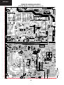
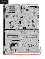
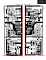
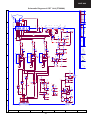
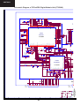
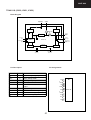
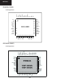
PRINTED WIRING BOARDS
F7351N5 Mother Unit PWB. Component side.
(RC)
J1
23
C701
J4
+
S701
D1002
D1001
E
C
Q706
L701
(OPC)
J5
S703
QP
R1036
4
D1017
(SW1)
1
C1022
3
LP701
(SWRC) M1000
1
24
K7351BM
S705
3
S704
S702
1
25
(ST)
J3
C703
R730
R770
C706
VR701
C799
R774
22
D702
21
D703
D701
20
3
(AA)
C746
1
J17
D704
C704
J196
1
(G)
2
R714
19
R746
R798
C798
R755
C702
POR701
18
C712
+
C753
Q701
S
PRDAR5531BM
FB703
D746
C734
R711
C707
3
+
IC703
D
+
G
T702
R799
2
R749
Q703
G
S
D717
R779
R778
R722
R725
C710
D734
PRDAR5531BM
R718
PRDAR5531BM
D718
C717
+
+
+
J220
C709
D735
G
J47
C902
R758
Q702
R723
S
12
D
D729
C748
13
C796
J42
D752
D
+
C903
R719
R728
HOT
14
C738
R756
JF902
D710
D903
R757
D711
R790
15
+
C711
R909
(M)
1
C705
C725
J41
T3.15AH
R787
1
J35
F701
16
4
C730
D712
C713
J34
J32
17
J33
3
C721
R721
D736
7
1
R657
PRDAR1563BM
L605
J9
R609
D609
C639
T601
JL1.
C617
(L2)
R
C624
D607
J96
R627
D
S
C644
C626
C
C625
D618
Q612
PRDARA027WJ
R668
G
C619
D606
D620
FB601
J132
9
D
R618
B
1
2
J121
G
R612
Q602
+
10
C63
+
D610
D619
C603
Q601
E
R666
J122
J97
D617
7
6
J82
C628
B
E
5
J9
L609
Q605
(L5)
(F)
C630
C609
L606
9
8
J84
D510
J57
J56
R530
R603
C621
D605
D613
TP601
R651
R606
C620
C642
D612
+
R614
TP602
C627
C643
+
C622
JL1
+
C613
+
10
COLD
J58
J59
C640
11
J83
L601
J202
C520
J203
C623
+
+
FB603
L602
L611
R667
S
3
8
J194
7
5
6
K
C602
4
D638
PRDARA027WJ
1
C601
4
J133
5
4
R4
(MO)
J134
A
(VIB)
1
3
21
20
R1009
12
13
D627
R671
J172
+
J171
D611
21
4
11
(AV1)
R663
2
Page 15
C634
20
R215
R660
(L7)
R617
1
R650
5
Y
DIP
(H)
0
X
1
2
3
4
5
6
7
8
9
14
10
11
12
13
14
15
16
17
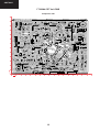
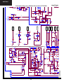
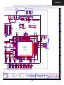
28KF-84H
F7351N5 Mother Unit PWB. Component side.
.
L352
J29
C362
D306
L320
C376
L353
J16
R387
6
J24
C728
T701
D728
5V
R776
J40
IC702
17
IC708
D1010
JF23
IC305
D740
D753
D608
J48
R738
1.8V
J176
J53
14
8V MSP J188
R501
L501
R780
3V3
C752
J189
R704
J190
R601
10
15
IC704
J183
J52
F704
C1047
J54
J208
R553
R796
D722
C504
16
+
J49
J50
D745
J51
R1045
TP701
J191
+
D720
PRDAR5531BM
R734
J46
J206
R345
J44
J37
D721
J207
18
C735
R797
16
J25
FB304
1
Q797
SUBWOOFER
PRDAR5531BM
J39
+
R699
+
IC705
(SB)
13
+
J28
C733
+
R795
R733
L705
J38
19
R390
R391
+
3V3 STBY
C757
F702
CN3
J31
+
C799
+
+
IC706
1
J30
R772
R717
J195
C729
C720
C737
2
20
.
+
FB704
J27
QPWBF7351BMN5
+
R702
J216
C751
21
C377
ESPA¥A
L704
R759
C732
J21
+
FB701
(VS)
R359
J23
L316
C727
D727
+
+
-16V
C726
11
C372
JF70
+
J20
J212
J215
J19
22
C365
L315
+16V
J14
L702
C378
IC302
10
R337
J18
D719
L351
1
(S)
J22
J209
C370
(FRONT)
(YC)
L303
D798
J11
L350
J13
J193
R747
(HD)
L302
23
C361
20
C363
IC301
C351
C1031
+
C1052
C389
24
R358
+
R423
C352
4
IC304
2
6
(FV)
(PHONE)
1
(SS)
C388
5
3
1
10
+
1
R351
C356
+
7 1
3
8
+
QPWBF7351BMN5
25
C742
J177
J180
R1024
J92
J91
J90
J80
J81
J78
J76
J77
J74
J71
J72
J70
J64
J65
J66
J67
J68
J69
J119
J120
J116
J117
J118
J115
J114
J200
R208
J199
R414
R417
6
5
IF1
IF2
IC202
1
SF201
C201
SF202
1
33V
5
C204
R223
J169
J168
J16
R2
R2
R2
DA
CL
J17
AS
C221
L203
TU
+
(RGB)
+
+
C222
16
17
18
19
20
21
22
23
24
25
15
26
27
28
1
AGC
J174
2
C215
2
(AV)
3
D2
D2
1
J173
4
R2
B+
C422
J163
L202
J161
J162
J160
C309
R302
FB303
C303
R413
(VIA)
Page 14
X201
CN1
C304
J157
J155
J156
FB302
R442
2
R301
J144
J145
J143
C318
C316 C317
J153
+
J166
5
1
C205
C312
+
+
+
(CR)
1
J149
J159
+
J152
1
C301
J131
J158
+
R303
R304
C311
+
J154
C308
+
J137
C302
J142
J151
J147
J148
J140
FB301
J198
(FI)
C319
J139
R213
J89
(SA)
C320
R416
J130
J100
R640
J126
7
12
J167
+
J136
J88
1
X301
J141
BLUE
C330
J113
R415
J129
R443
J128
R441
8
J106
J125
+
C417
24
J110
J107
J108
J103
+
C637
J104
J105
J124
J127
4
2
J219
R654
J101
C636
25
J214
J181
J102
1
J95
24
J98
J99
9
L301
2
R666
R344
J73
IC501
J63
R503
J62
R518
R611
J60
J61
D508
J182
R505
J201
J204
25
+
J87
MOD.DIGITAL
1
+
R214
(YA)
C618
+
J94
+
J93
10
J187
+
J84
JF59
FB501
11
+
J85
J197
J179
J185
J186
+
J86
J184
C511
C526
(YB)
+
C524
J205
12
L319
J55
R509
R555
J79
L318
C535
C536
+
J83
J175
+
Q502
JF61
JF60
20
29
Y
C212
30
TH201
31
32
33
X
28KF-84H
J6
C390
J11
J8
C727 C726
L702
J18
D719
(VS)
+
+
R745
FB701
R795
J28
F702
C728
IC705
R744
R741
J37
150V
C749
C708
Q502
J182
J60
R505
J61
R518
R506
R504
J63
JF59
J85
J87
C629
D637
R640
J192
C633
C644
+
R655
J136
J137
C314
C315
R440
R341
C394
D436
C393
R43
R427 R438
C334
C398
R305
R319
C341
C331
K
J153
D426
C403
R314
R321
C338
R320 C340
(VIA)
R428
C336
C333
R306
D429 K
FB302
C433
R
(CR)
D430
J155
J156
K
R316
R310
K D410
Q407
K
K
C342
R311
+
C308
J157
C316
J173
D422
J151
J152
R343
J144
J145
R312
40
+
R411
J154
J166
R420
R419 R421
K
K D423
R313
FB301
R407
D434
K D425
R408
C397
K
C337
R318
C339
D437
+
R441
J142
D405
R452
C343
D424
C417
J141
R304
R412
K
R418
J140
C317
K
R673
Q611
J126
J128
R303
D406
R634
R633
C319
R413
K D409
R410
R325
C396
C345
C344
R323
FB303
K D407 K D408
R641
C637
+
C321
C305
+
R302
C309
C303
R322
K
C392
R324
D431
K
+
C212
+C310
C304
R327
C348
J124
R442
J130
C313
C306
R301
J161
J160
J162
K
D305
+
C347
R326
+
1
C307
K
C346
1
41
D723
J158
J159
R422
C221
C737
Q709
J108
J107
J106
J210
R210
C207
J167
2
L203
J174
TU
K C302
D303 C311
D304 K
Q403
C395
JF9
2
3
C320
R63
D636
+
K K
J125
J139
C312
4
AS
C322
+
J131
J163
J168
J169
L202
R223
+
24
R644
J101
J103
65
R635
C632
J99
J129
J127
IC303
R214
D631
C540
R409
K D411 K
Page 17
C214
C213
C422
+
R531
K
D633
K
J98
X301
+
C328
CN1
R230
+
C204
5
J170
Y
J146 JF54
JF28
R206
JF7
C203
6
C215
1
R309
C325
C3313
D302
K
Q201
12
C206
DA
CL
JF8
D205
IC201
X201
C202 C218
JF6
C324
64
C301
C219
R220
R219
D204
C209
13 R207
J181
J102
R654
C326
J217
R231
B+
R217
R225
R202
9
8
7
R211
R205
R240
C205
C208
24
IF2
C211
J164
R203
R204
JF10
2
(FI)
R209
SF202
J149
IC202
R221
JF5
C323
80
R554
J93
J94
J143
C318
J213
J111
J113
J147
J148
C210
L205
GND 3V3 STBY
1
1
R201
J199
R208
R212
IF1
R370
J198
R222
Q202
R369
(SA)
K D203
K D202
K D201
(YB)
24
J104
R308
12
MOD.DIGITAL
K
C330
7
6
R656
J110
R307
+
R638
J86
D615
J219
J105
J214
J109
J84
J205
J197
J179
C526
R622
J222
J221
R424
R416
R415
R417
R414
J115
J200
J114
R213
J118
J117
J116
8
J120
J119
C1023
24
D
R555
25
2
L802
C736
C506
J88
C618
Q606
1
Q503
R605
+
9
J89
+3V3
JF62
R815
+5V
J95
C817
+1.8V
FB305
J204 J201
K
D507
+
R511
(YA)
25
Q505
C510
J180
C534
10
MOD.DIGITAL
R816
C733
IC502
R549 R536
R515 R537
R544 R512
R513
+
FB501
J187
J62
J208
C522
R510
C503
+
J186
J65
J64
J67
J66
J69
J68
J70
J72
J71
J74
J73
J76
R1024
J77
J78
J80
J81
J90
C502
C511
J185
J92
J175
R509
J184
D508
J177
IC501
C524
11
10
JF61
JF60
L501
J55
C535
R738
R601
D511
R514
C507
L319
J91
IC503
R534
12
F704
R780
+
C536
D753
J48
J191
R502
C525
R545
R535
R548
16
J53
C327
R704
D720
D740
D608
J52
R516
K
J190
+
C742
L318
J79
C504
C329
R345
+
C752
13
J27
D745
J176
R501
J189
1
D750
R737
J49
J50
J183
J188
2
C722
R503
JF23
Q1011
IC305
3V3
C740
Q1004
R1051
K
J195
D721
R1056
R1039
Q1010
1
IC704
1.8V
J206
2
R739
K
R742
J207
D722
J54
R1047
14
+
K
C741
3
R743
IC
R740 D748
R717
J29
R526
C1047 R796
+
15
J46
R1045
D1010
R766
R699
C508
C505
1
S
R1046
D1011
R734
J51
C743
R1025
2
S
Q796
J44
R797
3
R1026
R776
J40
IC708
16
D
R794
R761
G
R1044
R777
R765
R764
C757
G
R553
Q710
R390
C739
C735
+
C731
2
Q797
J38
J39
D728
Q708
R767
1
K
R736
17
3
R775
R733
R735
R771
J25
IC702
J216
J24
C729
J31
C751
D747
C732
K
IC706
C720 +
L705
C1045
JF11
J30
(SB)
R391
R702
+
CN3
D727
R759
R747
R330
J9
C389 C388
K
D308
J19
1
J218
R388
18
3
R423
C406
JF29
R328
C383
R333
R334
+
J20
R338
R339
K
J193
D798
R337
J14
J212 J215
L316
C1052
L303
(YC)
C386
L704
C1046
4
C391
L302
J13
C1044
3
(FV)
3V3
STBY
5V
FB304
IC304
J21
R387
J22
Q307
C370
5
R436
C416
K
J211
20
19
D311
K
J15
L315
R362
11
Q306
C365
L320
D310
+
IC302
20
R380
C371
R374
C366
+
J23
Q308
C377
R356
C367
Q309
R389
21
C369
C379
C372 +
JF70
C376
R360
L351
(SS)
1
J7
(HD)
L350
C352
C374
J16
22
R355
+
C368
C378
R336
C384
C351
IC301
C373
R357
R359
R335
C387
R385
20
C375
Q305
11
+
L353
(S)
R350
+
C1031
1
(FRONT)
R329
23
R346
R384
C354
C364
R331
C362
R382
C358
C350
C361
C1043
R375
R352
C380
C382
+
C363
C357
L352
24
QWBF7351BMN5
8
D306
C356
D307
R351
C359
C353
J12
R353
C360
R358
C381
JF71
R332 C385
JF72
JF73
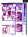
F7351N5 Mother Unit PWB. Copper side.
25
C222
TH201
33
X
32
31
30
29
28
27
26
24
25
16
23
22
21
20
19
18
17
16
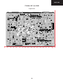
28KF-84H
F7351N5 Mother Unit PWB. Copper side.
R707
E
R1015
JF55
R1032
(RC)
25
R1031
(SW1)
S702
(SWRC)
+
S701
2
1
22
D704
C706
3
J17
C704
T1
20
T2 Q707
R714
C702
1
(G)
Q721
F701
R753
HOT
D707
R752
+
D741
R748
Q704
1
D710
Q902
K
2
K
D618
D619
FB601
Q604
Q602
Q608
R608
C642
D612
2
5
3
4
J132
J133
7
5
6
JF1016
4
JF1015
JF1014
JF1013
12
JF1012
JF1011
JF1010
JF1009
11
R660
JF63
11
2
12
JF1007
K
D640
JF1002
JF1003
R215
13
J171
D611
3
R1009
JF1001
+
K
1
R650
R661
R1049
K
.
JF1004
JF1005
JF1006
C634
R663
D1018
D639
(AV1)
13
6
1
8
F7351BMN5
J172
R662
14
T601
9
D1020
D643
+
+
10
D
A
K
JF24
C613
C610
D610
G
C602
D1021
J150
C432
C620
D620
R616
C608
R617
(H)
15
C622
J97
E
R1010
D404 K
8
7
K
D1019
C412
(AV)
R405
-13V
+
E
R612
D606
C612
D638
K
K
R453
D403
R451
K
D421
(VIB)
D427
K
R407
R629
R630
J134
J165
K
R425
C403
D617
C601
D402
K
9
D609
Q603
K
R406
R651
R606
J56
L609
C
B
J96
R620
(MO)
R426
16
D613
C604
D627
Q406
D411 K D420
R614
C605
R610
J194
R1050
R440
R664
Q614
R665
10
D
S
R626
D642
+
C641
L606
K C607
D644
C R607
K
C1049
C644
R667
R672
B
R631
R760
Q609
K
11
+
JF1008
S
K
Q601
J121
R628
G D622
R441
R437
C628
K
R618
D
D623
R439
D624
D604
R668
D641
C635
R632
R637
+
R627
Q612
IC601
J192
34
K
C603
J122
L601
R530
G Q613
R609
C639
636
+
Q607
D616
D625
R666
12
L611
R645
S
R639
13
R670
K
C631
R669
D607
R635
C632
L605
C617
R214
C624
R531
C606
K
C541
R554
+
R658
D902
R908
JF902
D904
K
Q605
R657
R623
(F)
C609
+
C643
C630
J83
J82
1
R643
J85
J58
J59
C627
R605
R638
D510
R621
R604
G
J84
J57
C640
K
R906
R907
L602
C623
25V
13V
J202
J203
D512
COLD
+
S
14
C901
R901
FB603
C520
C905
C902 K C903
01
Q503
Q901
JF901
R902
C908
C907
C906
R756
D711
R790
R757
R758
C748
Q724
R779
15
R903
+
K
16
R904
R905
R727
J220
C717
D737
2
D901
C716
D718
D708
D713
D736
+
J47
R728
R718
K
C718
K D732
R788
R789
J32
D752
D725
D733
K
R781
C796
K
R726
K
R778
R731
S
17
(M)
K
R909
D729
G
C904
D714
R703 R701
R719
Q703
3
R910
C738
J42
R787
C710
R721
C755
+
R749
C721
7
K D716
R729
C723
R725
C708
D735
Q723
D717
R722
D734
K D730 K D731
R723
K
Q712
R716
R710
3
1
J41
D
18
4
IC709
Q720
R786
R782
R715
C711
C725
J35
S
G
Q705
K
C754
R751
C756
400V
D
R705
C713
6
R750
IC701
R754
D712
R785
R783
C730
R799
G
R709
Q702
10
+
R784
C712
C705
1
19
C753
POR701
R712
R711
Q701
R700
C715
16
R708
K
D
R768
C724
J36
C719
R732
R706
D715
FB703
3
1
J33
4
D743
Q713
4
S
2
J34
T702
Q714
K
1
27
D746
R791
+
R793
C798
R773
R792
R713
3
C714
G
IC703
2
R438
21
3
(AA)
J196
6
Page 16
1
4
R798
17
R770
C701
C746
R730
D701
R747
FB701
D702
R774
J11
C703
R1099
R1017
23
D703
C799
408
24
LP701
C
J3
VR701
D1001
(OPC)
R1014
D1002
(ST)
JF56
JF153
J1
JF151
R1013
D1017
C1022
J5
R1019
Q706
Q1002
Q1003
J4
R1037
R1055
JF58
S703
S704
S705
M1000
R1042
R1030
R1053
.
10
9
17
8
.
7
Y
6
5
4
3
2
1
0
X
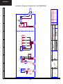
28KF-84H
F7269N4 CRT Unit PWB
Component side
(H)
R883
IC851
C877
R856
B
Q851
1
2
3
4
C5414
B
Q5407
R5415
7
R5417
(SVM)
D5403
J11
C5422
R5445
R5444
R5435
R1617
R5432
R1616
J20
Q5412
C1611
(MO)
C1609
C1613
R1622
R1623
E C
Q1603
10
11
12
JF8
E
E
C
Q1604
1
13
Q5410
(B)
.
F7269BMN4
K7269BM
9
C5427
R5433
R1624
C
1
E
E C
R5447
1
R1621
D871
C1614
R5434
D5408
Q5411
D1607 C
J25
R5431
C1612
J16
C5425
18
R5427
C5405
R1618
R1615
IC1601
B
8
E
Q5406
C
C5407
C890
R871
C1610
C1608
R5449
R5448
E
E
D5409
L2
J5
6
C5421
R5416
C5419
R891 SG861
SG862
R892
R1620
R1619
J15
5
R5419
C5411
C5408 R5418
R5442
ESPA¥A
X
L864
C
Q5405
1
(Q)
Y
0
E
R889
R851
C883
C882
SG860
L1603
R852
C5426
1
C5409
21
+
+
D852
+
J13
C874
(RT)
FB852
D863
C885
C893
R853
R859
D851
C884
B Q5408
R5443
+
C853
R894
9
IC852
R876
4
E
R5437
SC861
9
BLUE
E
5
7
R5424
3
R5421
B11
R884
1
SG863
D867
1
2
R897
C850
J21
6
Q5415
Q861
C852
R5446
C5418
01
R886
C
JF7
J10
C
C856
J14
R881
C857
J17
C
R887
D861
R872
C865
Q860
R882
R874
Q859
+
3
D864
R885
E
E
(G2)
R
D865
R865
R866
JF6
R5440
C871
R862
G
8
C880
R880
R5441
D870
C894
R888
RED 9
IC850
J1
J8
C887
J18
1
JF4
J9
D868
R850
C881
FB850
R858
J4
6
E
R861
D866
J6
D869
Q855
R855
J7
C861
8
4
R895
C888
J12
R1801
JF1
C869
+
R854
R863
SG865
+
(K)
R860
R893
L3
+
Q852
C
C
JF5
J3
E
+
8
C
C5417
R5436
C863
+
E
B
E
+
Q853
E
C868
J23
C895
C854
R857
9
1
E
C
Q854
Q5414
+
C851
Q858
C891
D5411
J19
D862
+
+
C
JF3
R5438
J24
E
L863
1
E
JF2
5
R5420
C5410
9
D5410
Q857
C
10
7
C5420
C5424
GREEN
C
11
R5425
FB851
D5404
R873
R875
R868
R870
R867
R5439
C892
R869
C855
R864
C889
Q856
C862
+
E
+
12
+
C859
13
14
15
16
17
28KF-84H
F7269N4 CRT Unit PWB
Copper side
13
(B)
Q1604
13
12
C889
C859
R869
+
Q858
Q853
R855
Q855
D869
FB850
C861
J7
R858
R860
R863
(K)
D868
J18
J8
J1
C871
C887
+
R5440
C893
C5425
J15
J5
J17
2
C857
1
+
R876
(Q)
1
C856
Q5415
1
IC852
C884
R884
3
C
C
C852
9
C5426
Q859
Q860
R874
R882
Q861
R885
J10
JF7
C865
R881
FB852
C885
R852
R892
D863
C1608
(MO)
Q1603
F7269BMN4
14
+
E
B
1 R1621
+
C
R866
SG862
E
4
E
R5448
C1613
C
JF6
E
C
R853
R859
D851
E
Q5410
15
4
E
+
J16
R1623
C
E
IC1601
5
JF4
D864
R856
R5447
R1622
JF8
R1615
C1611
R1624
R897
C877
+
C1609
R5431
8
6
R862
R865
R5449
+
C5427
R5433
8
+
J25
Q5412
C1610
R1618
R1616
R1617
C
Q5411
E
D871
D5408
C
C1614
R5434
R894
R1619
J20
D5409
7
R1801
D865
J14
R1620
R871
C890
D1607
C5407
R5432
R880
12
R5435
E
10
B
R5427
J12
1
R872
SC861
Q5405
C
E
R867
R870
R873
J6
R895
R851
R861
J13
C874
C881
J3
9 C880 IC850
11
C
E
9
D867
R886
R5442
Q5406
C5405
JF5
J4
(RT)
R5443
R5444
8
C
8
7
G
R
J11
R5445
1
Q852
C
C
9
R854
E
E
R888
6
SG863
L1603
4
L864
C5422
C5408
C5409
R5419
D5403
5
16
R857
E
R5418
C5411
17
J9
R891
SG860
10
JF2
R5438
R850
+
J21
C851
JF3
C891
R5441
R5437
Q5408
C869
11
C
Q856
Q857
C
C888
E
C854
R887
D861
D870
+
E
B
SG865
JF1
12
E
Q854
+
C863
C894
+
1
L863
C5419
R5421
E
C895
+
C
R893
C850
R5417
R5416
(SVM)
C868
+ R5436
SG861
Q5407
Q5414
C5418
D866
J23
E
E
1
C
C883
+
R5424
R889
R5415
D862
J19
B
C882
9
D5411
C5417
C5421
FB851
J24
E
B
3
R868
C5410
D5410
R5420
D5404
C5414
C5420
IC851
C5424
R5446
R875
R864
C862
R883
C855
R5439
C892
(H)
R5425
B
E
C853
D852
Q851
.
Y
11
10
9
8
19
7
6
5
4
3
2
1
0
X
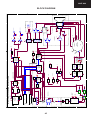
28KF-84H
F7353N3 TVTextPRO Digital Module Unit PWB
Component side
8
C6069
(K)
R6019
J91
IC6002
C6014
J73
J53
R6026
R6024
J24
L6005
FB6045
C6001
+
K7353BM
R6005
J3
FB6002
J85
J69
J64
J86
J67
R6020
J15
FB6003
R6068
J42
J41
J35
J82
J37
J54
J58
R6021
J34
J83
R6038
J21
J33
J19
R6004
J56
J57
J32
L6006
1
J52
R6039
L6004
J11
L6003
L6007
J90
R6063
+
JL2.
J10
1
ESPA¥A
R6061
FB6047
J2
R6043
J8
C6052
(VI)
J74
C6143
J48
J75
JL1.
(YA)
FB6001
(YB)
J84
F7353BMN3
J36
1
.
J96
2
C6070
J16
J14
J20
J40
J61
E
J59
+
R6046
X6002
FB6046
6
3
X6001
+
+
(YC)
1
4
E
Q6005
L6002
J60
C
C6043
R6014
JL2
IC6005
+
J13
L6001
J39
D6012
C6041
C6035
X6003
J1
C6037
C6025
3
5
1 2
1
+
6
J25
JF6012
+
J9
Q6006
C
+
7
J65
(RT)
J92
L6008
JF6013
J93
Y
0
2
1
X
4
3
5
6
7
9
8
10
13
12
11
14
16
15
17
F7353N3 TVTextPRO Digital Module Unit PWB
Copper side
15
12
J13
7
J15
6
J1
C6059
C6055
C6066
C6054
J4
J95
C6057
R6041
C6058
+
C6033
C6064
C6051
4
R6059
C6065
C6050
C6067
5
R6058
3
L6003
J2
FB6037
J3
2
FB6038
(YA)
5
4
3
C6132
C6131
1
C6129
C6130
FB6022 FB6023
FB6027 FB6024
.
6
R6060
(VI)
J12
J11
C6056
FB6036
FB6034
FB6035
C6122
FB6026
J7
C6053
C6047
J104
C6048
L6004
L6006
J19
40
J10
C6049
FB6028
R6016
D6014
+
C6146
R6066
C6145
C6063
C6061
C6038
C6034
C6062
J14
J16
+ C6041
+
J20
FB6045
L6005
FB6050
C6126
FB6032
FB6033
C6127
C6128
F7353BMN3
8
C6043
R6031
J84
J22
C6120
J36
C6068
J96
R6050
J80
20
R6055
1
IC6007
FB6049
C6117
FB6019
FB6021
C6119
K
9
C6045
FB6020
D6015
R6056
C6040
C6035
C6023
J25
R6018
J77
R6039
R6017 C6118
Q6002
J108
R6065
3
C6052
J79
FB6016
FB6018
FB6017
10
R6040
C6044
J24
R6024
R6026
J27
J83
R6038
J34
J33
J32
D6004
K
K
FB6002
C6114
11
J26
C6144
C6030
J54
J21
J52
J37
J82
J35
J41
J86
FB6007
C6106
FB6008
C6107
FB6009
FB6010
C6108
FB6011
C6109
FB6012
C6110
C6115
C6103
FB6005
FB6004
C6102
C6104
FB6006
13
Q6003
J57
J58
C6060
20
C6046
R6020
R6008
7
J9
X6003
R6023
R6021
K
D6001
16
FB6046
80
1
C6042
FB6025
C6121
FB6048
FB6029
C6123
C6124
FB6030
C6125
FB6031
J103
R6003
R6029
R6019
C6006
Q6004
J93
J17
K
J48
14
C6036
R6034
R6033
IC6006
JF6015
FB6044
C6024
C6140
C6139
R6057
JF6014
D6002
J56
JF6012
R6032
D6010
C6031
32
1
K
R6004
C6116
16
R6063
JF6013
R6035
64
(YB)
C6101
17
R6062
R6064
R6068
J94
R6001
C6111
FB6001
K
C6028
J61
R6005
C6112
FB6013
J75
+
C6026
C6027
J8
IC6003
C6001
J42
J85
R6051
C6029
R6061
C6141
FB6014
J100
J101
C6005
Q6008
J64
R6007
J74
R6002
C6017
J67
J69
R6006
R6069
C6039
D6005
J107
FB6047
1
J92
J106
R6052
R6009
81
IC6001
FB6003
16
R6046
R6012
C6008
C6007
R6037
R6036
R6053
R6054
L6002
D6003
J40
Q6001
J102
JF6005
JF6006
IC6002
17
R6042
D6012
K
R6010
R6011
100
C6021
C6020
C6022
J23
C6003
C6004
FB6042
FB6041
FB6040
FB6039
C6136
C6138
D6011
K
80
J63
1
J49
C6013
(K)
C6137
R6014
IC6005
R6047
R6015
C6009
+
C6014
50
+
J91
L6008
C6070
C6015
C6016
J73
JF6004
Q6007
JF6003
J53
C6011
JF6002
R6045
C6010
JF6008
J59
J60
L6007
R6048
R6013
C6012
JF6010
R6049
J90
JF6007
C6018
32
(RT)
JF6009
J68
J65
J105
R6043
+
R6044
C6069
FB6043
8
Q6006
Y
2
1
0
X
28KF-84H
22
22
21
21
20
20
Copper side
23
3
2
1
23
CAUTION !
(M)
T3.15AH
CAUTION !
S6701
F6701
S6701
F6701
CAUTION
24
(M)
THE ACTIVE SECTION
IS INDICATED WITH
THE "
" SYMBOL
24
1
25
2
25
3
Component side
FB452N0B Power Switch Unit PWB
HOT
19
18
18
17
17
16
16
15
15
14
14
13
13
12
12
R6702
R6701
R6702
3
2
1
L6701
4
R6701
4
C6746
1
3
M6702
L6701
2
M6702
LP6701
19
HOT
LP6701
C6701
C6701
C6746
S6704
(AA)
(SWRC)
3
1
4
VOL(-)
C6704
C6707
+
R6706
R6706
S6703
2
R6703
R6705
1
9
8
8
7
7
R6705
R6703
1
(A)
R6704
9
S6703
10
R6704
1
10
1
11
2
11
C6703
(SWRC)
C6703
4
VOL(+)
C6707
(A)
S6702
C6702
S6702
C6702
S6706
C6706
CH(UP)
CH(DOWN)
S6704
C6704
+
C6706
S6706
(YC)
(CC)
D6401
D6401
R6449
R6449
JF6703
6
5
5
4
4
JF6703
(HD)
FB452WJN0
C6428
C6336
6
2 4
L6317
C6337
R6316
35
R6317
7 1
KB452WJ
B
ESPA¥A
(SS)
C6429
JF6701
L6318
4
3
2
0
Y
R6316
1
21
CN4
5
C6336
1
1
L6317
1
6
C6337
R6317
B
7
C6428
2
C6429
2
COLD
3
(HD)
3
3
L6318
FB452BMN0
8
(SS)
COLD (YC)
JF6702
JF6701
X
9
JF6702
(FV)
6
X
0
Y
1
2
3
4
5
6
7
8
9
28KF-84H
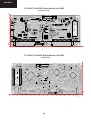
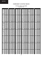
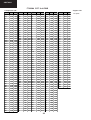
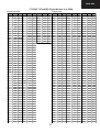
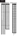
COMPONENT LOCATION TABLES
F7351N5 Mother Unit PWB
Component side
+
**!
*!
!
B!
B(!
B '!
B!
7!
/!
/!
+!
+1!
+>!
!
!
!
/ %!
!
7!
$!
$*!
$!
$$!
$'!
$!
$!
(*!
(!
$!
C!
+( +( 6
6
68>
61
6
68
61
1
6
6
6
68
69
6A
,)66
4448A
>>68
A999
444
4819
A198
>99
AA89
168
16184
A41
4166
86
8684
66
AA8
AA66A
48>8
696
>616
46
>969
8A6
891A
91>>1
64
4A64
8194
>4>9
9>9
9>9
6>88
4888
9A14
A4699
4A86
A696
96A8
A18
8A46
98>8
98>8
8A49
8619
6>9
84A4
44
>6
496
.)64A
8A4
>1A
A>9
16>6
>AA9
84
9>>64
4468
48
9619
9619
4>48
464
848
AAA>
8A91
4911
918
>8
4A1A4
9484
84
AAA>
96
96
1
898
69>99
AA48
966
966
496
96A
8>99
6
848
8A4
84>4
A88
8A94
84
>44
1618
89664
6>8
8A6
88816
>984
886
+
4
>
9
A
6
6
1
1
14
4
4
4
41
>6
>
>4
>>
>9
99
9A
8>
8
168
1
16
18
14
11
14
46
46
46
46A
4
4>
4>*
49
4A
46
4
4
4
48
48*
41
44
4>
49
46
,)84999
1A66
1A66
9
69>99
19
8684
>9
4>>4
4888
8A9
>69
61618
4186
696
>18
881
>166
6194
>A4
946
>9
A61>4
984
8889
9>
886A8
>>6
>899
89444
4
>>8>6
1
9>46
6>8
8969
89988
A6
49
44
414
A4
8>>1
A>66
AA18
A884
98
6A8>8
684
AA8
.)81
>9
8414
89>49
1144
48
44A8
6A96
68>
8A16
A8
6>9
9466
19
649
64
8998
66A8
48
168
168
8>88
849
88>
6186
6A8>8
>A
66198
4986
A999
8>8A9
A4
>99
AA8
69>6
968
9619
9>46
1814
69>6
AA8
69>6
164
9619
968
186
186
644
AA89
A4>>8
+
48
44
4>
486
48
48
488
>6
>6
>6
>68
>61
>64
>6>
>6A
>6
>
>
>
>>
>6
>
>1
>4
>>
>9
>A
>6
>
>
>8
>1
>>
>9
>8
>84
>89
>1
>1
>1
>1>
>A4
>A9
>AA
A6
A6
66
66
,)AA149
>6499
>844
A46
414
66A
489
4
194>8
AA48
44686
1
81>A4
8A16
81A>8
4986
4>148
>6
>A89
46
44A
19
19
68A>9
994
19
9>9
8684
9484
14
1A69
>>96
6996
8>8A9
9>66
>A8
994
A198
A>96
414
A814
AA149
6>88
19>16
18A8
99A6
49
696
66
8A6
.)69
>6
1A9
68
6>99
AA4A1
1986
6>48
944A6
>88
A>4
19>16
68>8
4>9A8
9
8
14848
>888
4619
66
9>A9
199
11889
94
61894
1A>44
9>81
>A19
99
444
96694
>816
>>69
8>
64
>4>9
8A94
9948
64
946
>AA6
8669
944
6489
8
696
8499
A6166
AAA>
AAA>
+
66
6>
68
61
64
8
1
169
16
4
461
464
46>
469
46A
46
4
4
4
4>
49
4A
46
4>
>
>6
>6
>6
>68
>6
>
>
>>
>9
>A
>A*
>6
>
>
>>
>9
>A
>8
>1
>4
>86
>81
>84
>1
>1
22
,)466A4
8118
4AA
4AA
1118
>64
A>>6
98A
9619
A6>18
99
A688
6A8>8
19
>619
48
A8>8
946
69
9A44
AA48
A46
9116
9648
A6166
198
866
9>
99A
6A9
>>9
6A6
444
>4>69
98A
9484
9AAA
A14
1819
914>8
1994
4AA
4194
8684
4986
19
A4
814
114
9A6
.)19A
A8
44>6
86
66
>4>69
48984
19
6114
8168
A911
4>18
9666
8>
>198
4AA
88
68A6
A>9
>668
4>18
194>8
1A84
6644
1A>44
688>6
9
6A968
698
19
19
>A19
9A9
8
64A
64A
1>896
48984
1A69
A68
>696
88>
9A9
9A9
A6
88>
89988
>914
8>
88A8
+
>A9
>A9*
9
+%?B
B
B>6
B>6
B>68
B6
B6
B6
B68
B16
B46
B46
B>6
B>6
(6
(6
(6
(68
(61
(16
(>6
(>6
(>68
(>61
(>64
(>69
<
<66
<6
<6
<6
<68
<61
<64
<6>
<69
<
<6
<
<8
<1
<4
<>
<9
<A
<6
<
,)948
9144
A6>18
A6
11>
6644
>>4
9484
>9618
A4699
1
6>
A6
4998
8188
>844
6A8>8
914
9>>8
99188
84999
146
4149
9>>8
4A6
9A14
A999
8986
A1A6
888
>A6>6
9A4
6A4
6A84
111
8A16
8A89
1>8
18666
449>9
4>69
9A64
6664
649
A
8A9
4898
A68
6
6>4A4
.)696
696
8A464
16184
696
496
>146
9>4
84>
>8
898
9AAA
69>6
8A16
948
A14
>118
8>88
6>9
91
49
866
6AA9
>9
>
8669
>88A9
98419
18A86
14
4A8
>9A9
>>4
>619
>>8>6
>4
>1
496>
496>
1A9
>14A
>>8
>9A9
>88
>446
>446
>446
>446
>446
1944
+
<
<8
<1
<4
<>
<9
<A
<
<6
<
<
<
<8
<4
<>
<A
<8
<86
<8
<8
<8
<88
<81
<8>
<89
<8A
<1
<1
<1
<18
<11
<14
<1>
<19
<1A
<4
<46
<4
<4
<4
<48
<44
<4>
<49
<4A
<>
<>6
<>
<>
<>
,)1A1
9A>9
9A>9
66864
66864
66864
6A84
1819
8>8
1969A
1>A
484
64
>994
914
68
84
68
68
68
949
418
9886
964
964
A489
944A6
944A6
A189
6644
>4>9
69
>19
86>A
86>A
6
1>6
11>6
1>96
49>
4AA
6144
4A64
>41
>99A
A>A8
4AA
>9AA8
6AA9
6996
.)>88
>619
4>99
48
4814
194>8
4>99
>88
4166
88A19
848
848
1146
16>6
16>6
11>9
9
1669
8>8A9
88A19
8946
8946
8946
1499
186
89664
A9>9
>9
>8
889
6>8
6>8
6>8
8A6
A>6
6>48
8188
8188
8188
86
A>6
64
1866
4A8
4A8
66A8
699
>69
4>48
>14
28KF-84H
F7351N5 Mother Unit PWB
Component side
+
<>8
<>1
<>4
<>>
<>A
<9
<96
<9
<9
<9
<98
<91
<94
<9>
<99
<9A
<A
<A6
<A
<A
<A8
<A1
<A4
<A>
<A9
<AA
<6
<66
<6
<6
<6
<68
<61
<64
<6>
<69
<
<
<8
<1
<4
<A
<
<6
<
<8
<1
<>
<9
<A
,)>A84
86
>8A6
86
AA488
98A
48
61
9>
>8A6
441
441
441
49>
441
441
84
441
441
98419
18494
99>
964
AA488
4A>89
649
18666
68A
4AA4
68
66198
>844
689
46
64
8919
AA
899
>A84
A9
6>4
4>69
6>1
1A9
648
19648
6>
>696
>4>98
99>
.)1>89
>46
>449
68
A88
64>14
A814
>A16
19
8669
6>88
68A6
64
A911
144
199
6489
A186
>666
8>4
81
>696
A4699
A4>>8
1>16
4A>4
6A68
>88
6A6A
68A8
68A8
6A6A
AA8
14
1A668
8>89
A>19
69>99
>>8>6
69>99
98868
>9>86
A>19
6111
6>19
9996
9>81
>146
>146
>9
+
<
<6
<
<
<
<8
<1
<>
<9
<A
<8
<86
<8
<8
<88
<84
<8>
<89
<8A
<1
<16
<1
<1
<1
<18
<11
<14
<1>
<19
<1A
<46
<4
<4
<4
<48
<41
<44
<4>
<49
<4A
<>6
<>
<>
<>
<>8
<>4
<>>
<>9
<>A
<96
,)6A4
A89A8
A89A8
1986
4849
48669
8669
68A>9
1994
1994
14>6
1994
1986
669
A1
466A4
44686
9484
19
1>896
19
9A146
19
19
466A4
4691>
>8A6
>>8>6
149
18>9
9AAA
A1
A96
6>19
>>96
>8644
>41
>949
96A8
96
91>16
99A6
A61>4
A48
A448
688
6>98
648
881
699
.)1688
914>8
98
4>9A8
4>9A8
4>9A8
19>16
198
>146
>>6
A9>6
4166
146
891A6
46>8
14A>
>46
89>8
8A1
A9>6
849
1A69
AA
441
89988
>A
6114
6114
66A
66A
6AA9
6AA9
6AA9
>46
66A
66A
66A
66A
66A
66A
66A
66A
66A
66A
66A
66A
66A
66A
99>
66A
+
<9
<9
<9
<98
<91
<94
<9>
<99
<9A
<A6
<A
<A
<A
<A8
<A1
<A4
<A>
<A9
<AA
<B
<B1A
<B46
<B4
<B>6
<BA6
<+
<+
+6
+6
+6
+6
+6
+1
+4
+9
+A
+6
+16
+1
+1
+1
+16
+46
+46
+461
+461*
+464
+46A
+4
+4*
,)A9
198A4
464
48698
4>
96989
4AA4
8AA4
18>4
1849
9669
6189
4619
4619
1A98
>619
A>>A6
9A>9
91A9
18>4
88
1484
1484
4A>89
6A9
814
18>9
9494
9A146
819>
899
A>94
18666
1818
A1414
A1414
6>1
1>96
1>6
616
419
86
>8
>8
>666
1>6
869A8
9619
414
4>48
.)66A
A911
A>9
A>9
A>9
A1>19
A8AA4
AA89
AA89
AA9
AA9
AA9
99A66
9446
9894
>A>14
>6944
>9AA8
>4818
866
6A>9
>89
A999
6
919
69>
9619
9A8
918
A94
AA48
994
19
6416
A48
14
A899
69
444
>>88
168
18>4
6AA9
8684
916A6
916A6
A8899
9
11>6
4194
+
+>6
+>6
+>68
+>61
+>6
666
(7
8
1
4
>
9
>6
D16
D46
D46
D461
D4
D>6
D>6
D>6
D>64
D>A>
66A
68
64
681
6
6
69
8
1
A
6
6
6
6
68
>
81
1
19
1A
9>
23
,)119
84
A69
>11A6
>8A6
A916
A>94
>88
>A>14
A9A9
666>4
>89
8986
A>66
AAA>8
8A>4
>46
666
>A16
4849
A>66
A46
>89
>A>14
A4
898
4>99
>9AA8
A9>68
919
466A4
4AA
4AA
46
6A>
48698
6AA9
4AA
4AA
98>8
16A6
8>416
661>
661>
1819
6>86
4A86
84
8A9
68A
.)19
69>99
AAA6
96694
A8
8684
>14A
1499
88>
149A4
>A>8
8A1
961A8
4>9
18A86
9816
6>88
149A4
1499
9968
4>148
>A>8
8168
8669
A8
4A48
6114
4
66A
9>46
188
8A6
496
1A84
>6
9
88
A6
>16
>8
8188
8188
A9>9
>9
8>4
986
8666
1A44
696
A>19
+
A6
A
8
88
81
84
8>
8
88
88
16
16
161
16A
19
16
11
111
46
46
464
46A
4
4
48
4>
49
4>
486
416
41
418
41>
446
444
44>
4AA
>
>6
>68
>
>8
>>
>9
>A
>
>
>
>1
>9
,)9669
6189
6144
AA844
A984
A894
A4A4
61894
4118
64A
46
68A>9
9>81
816
68
8918
8846
96
99A>4
411
1986
9A18
A14
9446
1418
>A8
A6
696
946
9A4
1814
6A4
6AA9
A8>8
4146
1>4
68>
>68
48>8
>AA69
916A6
A>6
99>
A>69
4AA
89>8
A4
61A9
19
>A16
.)>816
>816
>494
>>8
>>8
>>8
>>8
6
81
44>6
>449
>46
19
69A44
6AA9
6699
816
68A8
918
68489
6186
>198
6AA9
4>
A8899
688
494
>>8
4A8
884
68489
>84>4
A4>>8
6A
>>8>6
1846
>A4
84119
99A>4
1
>>6
91A9
>1>49
4>
8>99
A186
9A9
AA8
144
8
+
>6
>
>8
>9
>84
>8>
>8A
>11
>14
>1>
>19
>1A
>>6
>>8
>>4
>>9
>>A
>96
>9>
>A6
>A1
>A4
>A>
>A9
>AA
A6A
%B6
%B1
$>6
$>6
$>6
$>68
$>61
$B6
$B6
'46
'>6
'>6*
'>6
'>6
'%'
'/6
>6
&6
&6
,)>89
98
>>49
99849
146
496
1
198
A119
849
164
6>19
>A86
6A
1994
8A49
99A
688>6
68
64
9686
>68
>119
816
>A
198
14A1
4A9
68A>
8918
4616
>1>
98161
A9>9
>AA69
A6
1A668
46>8
>>4
>>4
9A6
688A1
989
>8644
1A66
.)6918
>>69
1>896
94
9144
A198
149
>>184
19
19
9
A68
6>8
6>8
4>486
4A9
>169
9
9
19
>146
1649
4A6
9996
4619
89988
)844
68
84999
96
96
96
96
88A4
194
16184
8>89
8669
9>
9>
1A98
1894
68>
8694
4A8
28KF-84H
F7351N5 Mother Unit PWB
Copper side
+
6
68
688
681
684
68A
6
6
64
6>
69
6A
6
8
9
A
61
64
6>
6
8
1
8
1
4
>
9
A
8
4
>
9
A
86
8
8
8
88
81
84
8>
,)A186
16888
816
44
4A6
864
9A146
99A6
A18
>899
9A146
4A86
A8
6>86
6946
68
9A146
9A64
8986
8919
44
6994
8889
A>>6
9AAA
846
88
A>6
1A
1A
8998
4869
86>A
111
96
864
>>184
99>
9948
946
9A6
>>966
9>A46
9186
9484
8>A68
1>689
8>A68
18>4
19
.)9619
>
8>4
98868
98868
>69
8A6
9>6
8>A9
84>4
8499
8946
16>6
888
1
1
994
8>A9
16>6
1499
88>68
A4
46>64
89>49
89>49
148
4A>4
>88
>446
>99
49196
49196
44A8
>4818
484
16>6
44>6
864
A848
>4
4
88>9
968
49
968
A18
968
88>9
>4
>494
+
89
16
1
18
1>
19
1A
46
48
44
4>
49
4A
>
>
>8
>1
>A
96
9
9
9
98
91
94
9>
A6
A
A
A
A8
A1
A4
A>
A9
86
864
8
84
8
8
16
16
161
164
16>
169
16
1
11
,)1
9A64
99188
964>6
>68
94668
>9
A>A8
648
918
9A146
9A146
9A146
>99A
A489
9494
6194
6869
496
>A
16888
16888
16888
86>9
>AA9
16888
>A4
>>966
18>4
98868
>416
19648
8A>8
>A6>6
>>966
46>9
4869
A884
44
A884
8998
888
888
>198
1A9
8A16
A69
19
489
164
.)89A
984
4>9
64
A8
A4
4A9
A49
9466
9
9
A814
8
19
A814
91
6>4
91
1A44
1>
1>
A9>6
>>8
68>
1A66
49
A69
A9>6
9>A4
A4
9469
1
9>A4
918
6>8
849
>88
4A8
49
1A6
1
49
6>A16
64
6>A16
6>9
64
68
164
8
+
18
186
18
468
461
464
46>
469
46
4
4A
4
4
4
41
48
>69
>8
>1
>4
>9
>A
>
>
>8
>
>4
>A
>86
>8
>8
>8A
>18
>11
>14
9>
A6
A68
A61
A64
A6>
A69
6
69
6A
66
6
6
,)4>9
>844
1>A99
48669
1>A
99A
964
9894
48
A688
>A19
64>
4649
49A6
46>9
646
496
19
1418
1846
94949
184
649
964
1649
866
94A8
9>9
64
9684
A9>9
19
4AA
4681
44686
649
A18
864
AA9
A616
699
464
9A98
4>A>6
6>88
66
66
1>
9A98
9A98
.)66A
>9894
99484
9188
>>A>9
A416
A64>9
46
4>
4>18
4A8
A6A
9648
44A8
48669
AA8
>449
99849
4619
89>8
919
4194
>A4
986
4194
>A1>9
1A69
>696
198
816
188
184
464
11>6
464
A6>6
8684
4
8684
8118
8118
8118
114
1A8
>>
>A86
64
8A6
8A16
8>8A9
+
6
6
6
6
68
61
6>
69
6
86
86
868
861
864
86>
869
86A
86
8
86
8
8
8
88
81
84
8>
8A
86
8
88
84
8>
16>
1
1
468
41
44
4
4
48
41
4
4
44
4>
4A
24
,)9A98
9A98
9A98
8A>8
A>>4
>>88
A68
99A>4
98A
6A44
96A
169>4
8A464
198
>88
AA4
866
1819
>99
89
4>
464
4>A9
A8
8118
1>96
>89
9414
8>1>8
99849
>A19
1A199
>969
>969
1846
66864
9886
4619
A9964
8A16
6699
4A64
696
6699
6968
>888
>416
>
>416
6>88
.)8A16
114
8>8A9
16184
8A16
668
496
AA4
69
649
9466
161
49
84
>>
8
8
8
8
968
84
84
A616
>4
884
A18
918
19A
A848
A6
849
61>8
8
164
A18
6968
A6
6A6
>6944
9968
A>4
1A9
1144
A886
A8899
968
968
>8A6
4A916
8A94
+
486
48
48
48
488
>6>
>69
>
>8
>1
>4
>
>1
>6
>
>
>
>>
>8
>8
>8>
>89
>16
A6
A6
A68
B61
(6
(6
(16
(16
(46
(>6
(>6A
<6A
<
<
<84
<1
<16
<41
<A
<6
<
<
<>
<9
<
<
<4
,)6>88
8>48
886
696
9448
8499
968
A6
886
9619
18948
489
9894
A>66
468
A814
A814
1814
849
8>6
A8614
>A>8
AA8
>
A18
>69
994
98
>198
1819
96A
4649
186
8>A9
>68
4>>4
61AA8
4186
8118
89>8
886
496
41498
94
>899
16A1
68
14186
1994
18A86
.)>66
4849
149A4
88
9A869
48984
>88
6689
14>6
>416
14>6
889
>88
>A
>A
919
488
964
4666
>844
946
>1664
4>
A884
64
199
A14>
86486
1A84
66
66
4998
449>9
4A4>
918
>A8
>8
88A19
68>
1
A>9
4898
114
A>944
>84>4
11>
94A88
>4A4
>4A4
449>9
+
<4
<>
<9
<A
<B6
<B66
<B66
<B66
<B668
<B661
<B664
<B66>
<B669
<B66A
<B66
<B6
<B6
<B6
<B68
<B61
<B64
<B
<B1
<B1
<B
<B8
<B9
<BA
<B1
<B18
<B11
<B14
<B19
<B4
<B4
<B4
<B>
<B>
<B>
<B>
<B9
<BA
<BA6
+61
+96
D66
D66
D668
D66
D6
,)61AA8
6AA4
6>>>
6>8
9A146
8>88
81844
8A8
848
86486
994
>698
164
19
>16
AA>
9A8
688
688
688
688
A68
89>8
669
9A98
8199
1A199
>816
6914
4>
66A
9>99
A444
669
A
6>88
669
61618
99188
94>44
6946
6>1
>>
68A9
649
1A>
8684
16888
4A86
4A8A8
.)4646
A4
4646
4646
81844
688
688
688
688
688
688
688
688
688
688
688
688
>41
1146
918
869A8
944
888
9466
114
>4
>8
>19
8489
89664
A68
8698
A1
8188
9
>66
6896
8619
8666
8666
A6
416
81>A4
8918
916A6
888
899
18A86
8969
8>
28KF-84H
F7351N5 Mother Unit PWB
Copper side
+
D6
D6
D61
D64
D6>
D69
D6A
D86
D864
D86>
D16
D161
D46
D468
D464
D46>
D469
D46A
D4
D4
D48
D>68
D>61
D>6>
D>69
D>6A
D>6
D>
D>
D>8
D>6
D>
D>
D>8
D>A4
DA6
DA6
66
6
68
61
6>
6A
61
64
66
6
6
6>
6A
,)>666
9
49
1164
419
46
419
4A86
1A19
4>
4989
A14
A6A
A94
8619
9188
9446
16
>46
>189
696
869A8
8A>98
81>6
AA488
6>69
>99
148
169>4
1418
A9>9
88>68
1
9448
86>A
A
466
49
918
4A9
4A9
64
68A6
A1414
A9A19
119
4681
>488
8118
191>
.)8>A9
194
89
6A6
A>68
688>6
68A>9
6896
86486
8414
6A8>8
6A>9
119
16966
9464
A>6
19
1A84
4814
9A869
1669
1>>8
1A>44
A684
946
>A6>6
4>486
1A>44
>696
>888
4448
>696
19A6
A186
4A48
81>A4
AA18
>69
899
984
6>9
9466
A68
188
8A464
>AA9
>AA9
>AA9
899
8A946
+
68
688
684
68>
68A
616
61
61
611
614
6AA
6
68
61
64
6>
6A
6
>
1
6
86
61
64
6>
69
6A
6
8
4
9
A
6
8
1
4
>
9
,)66A
8>8
488
4A8A8
89
8684
1846
11A8
9>46
1846
6114
68A9
>>96
9>9
419
A696
>68
>14
498
>14
A189
6>1A8
69A4
4A6
6A44
>169
41>4
16
A686
A16>
98>8
A>>4
68
444
6A96
68>
46
>416
A669
>>966
9186
9>A9
9A6
8148
1>689
11>>9
89444
18666
16888
8666
.)8619
14848
46>8
88>96
>69
>41
891A6
>AA9
8619
1649
9466
8918
84>4
8A6
>
8>A9
84>4
16>6
1618
16A
11996
1
89>49
1846
1
164
>8
A48
9A14
9A14
>446
>49
>9A9
>984
A48
8489
A>6
89A
19
A18
89A
1>89
946
84
416
89A
89A
89A
89A
>6>4
+
A
6
8
1
4
9
A
8
8
84
16
1
1
11
14
1>
46
4
4A
>6
>8
>1
96
9
98
91
99
9A
861
864
86>
869
86A
86
8
8
89
8A
86
8
8
88
81
84
8>
89
84
,)1A44
8118
8118
8148
16888
16888
16888
16888
4A4>
9948
>9618
91A9
49A6
1>114
964>6
A18
1994
918
6A9
1849
1>6
>8A6
68
>4464
>169
1A696
498>9
1>84
1118
9
1849
8>1>8
4188
46>9
49414
>A19
A44
>>88
A814
84
84A4
>4
A69
>99
A698
169>4
146
>A19
>A19
68>
.)9466
>6>4
14
9A89
A8
16
984
1A9
1964
6
9469
A4
6>9
>198
14
A49
89
8
94A8
6A68
6964
>8A6
>88
19
A8
8>4
489
6964
6964
A>94
6>19
4>48
496
946
918
84
69
A18
918
A119
A9
A9
968
6896
96>>
44
496
8>A9
8
9466
+
8>
89
8A
886
81
81
81
16
168
164
16
1
1
1
18
11
14
14
1
18
11
14
1>
188
181
189
18A
118
468
461
46>
469
46
44
46
4
4
4
44
49
4A
46
4
4
4
48
41
4>
49
4A
25
,)44>6
44>6
464
496
81>A4
1A
84119
164
A8148
A4699
888
489
8846
86>9
68>
844
6994
16
498
886A8
164
8>416
844
8846
164
164
8>416
498
9A4
44>6
A886
9>46
A64>9
9>99
9448
6A>9
46
99A
A884
8
4A9
9>>9
4A9
46>9
>A19
4>94
4649
46>9
48984
4649
.)>984
4
86486
86486
4>48
416
1418
8
6AA9
6AA9
6A8>8
6466
98
A94
>>4
A94
88
>>4
9>998
4>84
918
98
98
A94
66
4>84
A94
9AA4
A116
A9964
1>A
8A6
84AA6
48
46
64
916A6
A>6
1814
4168
16184
8A16
1499
4898
4>99
44A8
968
46A46
A46
>>A>9
+
48
48
488
481
411
414
419
44
44
448
441
44A
4>6
4>
4>
>66
>6
>6
>61
>64
>6>
>69
>6A
>6
>
>
>1
>4
>4
>>
>A
>
>
>1
>4
>>
>A
>86
>8
>8
>8
>88
>81
>89
>16
>1
>1
>1
>18
>46
,)>6499
1A>44
>844
>9
>688
8666
AA8
666
844
19
4A64
911A9
9619
19>16
>>68
891A6
88>68
8918
1A4A6
>88
4194
4>6
>84>4
>99
46
>>4
4681
46A46
99484
16966
>A>14
98
1418
98A99
9>19
A96
49A6
>994
A4699
19
61894
64A
649
88A4
88816
4681
889
>984
8918
19>16
.)>99
99484
>4A4
A>14
1A4A6
9
A>69
>46
88
1669
1669
A1168
A116
11A8
41>>
4194
146
18494
>118
>A8
496
>A8
1>4
14
>1>49
98868
1>4
14
919
89>8
86A>6
A94
464
>4>4
>696
4989
>AA6
>1664
>A4
4>9A8
>696
>8>1
>8>1
1A668
>A>8
46>8
464
464
146
1986
+
>4
>48
>41
>44
>4>
>49
>>
>>
>>1
>>>
>9
>9
>9
>98
>91
>94
>99
>9A
>A
>A
>A
>A8
91
94
A6
A6
A6
A68
A61
A64
A6>
A69
A6
,)>AA69
A>94
A>94
684
61894
849
9848
4814
89A6
>4464
11>9
4681
411
>6944
1694
19
114
1846
8A464
1866
14
498>9
68
9A89
918
18A8
>9>8
>9>8
>4
A
A
6A
864
.)4>94
>>966
>A8
>8>1
944
4194
>4>4
464
4A48
4>94
89>8
19>16
>118
>146
>9
1A>44
>9
>9
>>A
96694
>>A
4>486
9
4A48
144
81>A4
88>96
84119
8684
>88
89>8
1>
46>9
28KF-84H
F7269N4 CRT Unit PWB
Component side
+
!
!
D!
'!
469
46A
46
4
4
4
48
1861
186>
1869
186A
186
18
188
18>
189
18A
186
18
18
188
181
184
18>
916
91
91
91
918
911
914
91>
91A
94
94
94
941
949
94A
9>
9>8
9>>
996
99
99
99
,)4A64
A>4
>>8
48
>189
16
6>99
4194
A6>6
6484
A416
14A>
AA18
A884
8>644
>8
184
184
86>4
9>6
6A4
88>9
84616
18494
8A1
96>>
4>614
168
>A
>>
66
8A94
41>4
9>6
416
>66
646
A>9
169
1144
994
64
>466
64
194>8
888
888
8>88
>4
>189
.)6A
6A
>4
8A>98
A>9
A68
64
4
9>4
688
1A6
4A8
86
1A9
1A9
49
1A9
68
A88
>>8>6
9819
68
964
1A9
666>4
86
>>
946
>4A4
6466
1A6
86
99A66
49
1A6
1A6
49
49196
198
99A
>16
9>998
9666
11>9
669
84
1814
4A8
669
669
Copper side
+
998
991
99>
999
99A
9A6
9A
9A
9A
9A8
9A1
46>
186
1868
1869
186A
186
18
91
91
94
94
94
948
941
944
94>
949
94A
9>6
9>
B916
B91
B91
(46
(916
(91
(91
<
<6
<
<
<
<8
<1
<4
<>
<9
<A
<6
,)18948
1>16
A119
1418
A9
AA18
41>4
8188
>984
A8AA4
>4818
>18
1>4
144
AA18
AA18
>8
>46
A6
898
186
A814
4166
>494
81>6
4>99
8A16
1669
8>8A9
6886
989
8499
A6
186
6>9
>9
4A1A4
8>8A9
1418
>8
948
186
4849
81>6
4998
9>998
AA64
99A6
64496
6AA9
.)9>A4
>16
84>
66198
49
>1A
A8899
49
8414
>6944
99484
184
1A9
68A8
1
161
6A6
AA8
1>89
99
>9A9
AA646
>8
966
84>4
669
>16
9
9
>864
A9
>446
>>4
>698
464
46>64
64
4
18
8
1989
4A8
669
84>
>9>8
999
1A6
18
A>14
464
+
<
<
<8
<1
<
<8
<1
<4
<>
<9
<A
<B
<B
<B
<B8
<B1
<B4
<B>
<B9
+46
+1
+94
+948
186
44
44
D46
D468
D1861
D1864
D186>
D1869
D186
D18
D18
D188
D181
D91
D91
D91
D918
D911
D914
D91>
D919
D91A
D946
D94
41
44
,)6886
A9
64
468
186
186
18
19
>>9
8
48
6466
6A
1418
688
1418
688
9A14
168
44189
>49
64
8A49
188
>46
6968
4986
>169
AA18
168
9A61
86A>6
168
AA18
168
948
>4818
>8
1
A848
186
>1A
18A8
1418
8188
99
A616
44
>6A8
>46
.)>6944
A1>19
68489
898
>99
4941
>
669
49196
18
968
>9894
A8899
A>69
88A19
>8A6
889
8
186
1989
918
61A9
119
>4A4
>1
11>6
646
6449
8A8
8A8
A>>A6
498A
>4
>A86
>A86
A8899
466
>46
918
918
A898
918
49
68A6
69>6
>16
6>8
6A99
86
44>6
+
4>
49
4A
46
4
4
4
48
96
181
184
18>
189
18A
186
18
188
181
18>
18
18
18
188
181
184
18>
189
18A
1886
188
188
188
1888
1881
1884
188>
1889
188A
916
91
91
91
918
911
914
91>
919
91A
946
94
26
,)8>8
>46
>9>86
>668
A8AA4
16
99>
68
186
1A98
844
4A64
8A94
8A464
6111
8>48
8969
18>4
198
168
198
168
198
198
6416
19
1418
>16
8188
666
AA18
AA18
168
168
1A8
14A>
996
>8A6
16184
>9>86
46A9
4
999
66
A9>9
1418
>9
>9
8>A9
484
.)184
A6
864
A848
186
18A8
8>
918
411
A9A9
9
9
41>94
1A9
69819
>84>4
9>46
4
86486
>>96
1146
66
66
966
99484
>8A6
A8899
49
8A6
>1A84
8A6
11>9
8A6
11>9
A88
>14
61>8
8
4A8
669
>16
1>89
A886
918
A>6
99A66
49196
1>89
49196
669
+ ,)- .)94
>494 88A4
94
19 49196
948
8 49
941
>494 86486
944
8A6 >16
94>
>9 49
949
169 >>4
94A
1418 49
9>6
A9>9 49
9>
A4 966
9>
19 11>9
9>
889 49
9>8
8A94 >16
9>1
411 11>6
9>4
8A>98 6A
996
81844 1669
99
198 >16
99
884 >16
99
916A6 4
998
119 88>9
991
1 6>8
994
88816 >16
99>
1944 >9A9
999
411 48669
99A
968 666
9A
9446 9188
9A
4496 8A4
9A
>1 9>998
9A8
4814 888
9A1
1144 669
9A>
81>6 A>6
$94
9>AA 18A8
$7946
49196 4A699
$794
996 96>>
$794
>4>69 86
$794
>6 18>A
$7948
4A8 >1A84
$7941
A4A8 996
No parts
28KF-84H
F7353N3 TVTextPRO Digital Module Unit PWB
Component side
+
E!
'!
(!
C*!
C!
C!
466
468
461
461
46>
468
468
461
464A
46>6
48
46
B466
B466
B466
B4681
B4684
B468>
(466
(466
(4661
<
<6
<
<
<8
<1
<4
<A
<
<6
<
<8
<1
<
<
<
<8
<1
<4
<>
<A
<86
<8
,)9448
69>6
>
66
6A68
4919
>A16
>666
4A916
8694
1199
>41
4
A848
88A8
696A
88>96
A>14
19A
1989
>449
86
1986
A9A9
A96
1649
866
96
946
946
8
1A69
4A1
9889
198
6449
>9
1989
84>
1>A
1>89
194>8
46A46
484
996
96>>
>9AA8
>A16
9191
9464
.)494
494
1
>69
>69
8411
>698
4A>4
48>>6
484
149A4
4849
148
8188
4998
186
66
46A46
8A94
A9
4A8
A9>9
A>6
>984
88816
8A4
411
19A9
64
>A86
4168
41>94
A9
4168
8
464
81
464
86
4>614
A119
>16
>16
>16
6A9
4919
6A9
4>9
8A6
6A9
Copper side
+
<8
<89
<1
<1
<18
<14
<1>
<19
<1A
<46
<4
<48
<41
<4>
<4A
<>
<>8
<>1
<9
<9
<9
<98
<91
<94
<A
<A6
<A
<A
<A
<A4
<B46
<B46
<+
<+
<+
+466
+466
+466
+4668
+4661
+4664
+466>
+4669
D4661
D4664
4668
4661
468
46A
466
,)99484
411
>4>69
1649
>88
AA149
AA149
AA149
1649
68489
9116
6416
696
94
844
A>66
1164>
19A
9116
996
148
41>94
>914
A>9
>4
696
>46
4814
498
911A9
>9
81A>8
AA9
4>148
1
916A6
989
946
198
4
198
19
89>8
9>46
8A6A9
AA646
A9A9
66A
>A8
4998
.)84
416
6A9
8>88
8>41
AA>
>494
1866
4>18
48
84>4
49
>668
4A8
4A8
194>8
61>8
968
88816
6A9
>16
6449
66
69
44A8
4>99
194>8
4A1A4
4A916
4468
49196
>6944
416
46>64
19
41>>
1814
1418
A>9
888
44>6
41>>
1>868
4681
4A1A4
1
161
48
889
198
+
46
468
464
469
46A
468
4684
464
464
4649
&466
&466
&466
,)>>8
88A19
8>8A9
11A8
1618
1649
9448
A1991
A1991
1
444
>84>4
6A
.)4649
86
86
>16
>16
44A8
114
88816
8A6
64
46
16184
19A9
27
+
466
4668
4661
4664
466>
4669
466A
466
46
46
46
461
464
46>
469
466
46
46
46
468
464
46>
469
46A
466
46
46
468
464
469
46A
4686
468
4688
4681
4684
468>
4689
468A
4616
461
461
4618
4611
4614
461>
4619
461A
4646
464
,)64A8
8A1
88>96
>9
>6A8
11>6
69819
866
4A9
1
A1
98
19
A>A8
14848
484
48>>6
44A8
88816
4A916
>84>4
>198
>864
4998
41>>
88>68
918
1>89
88816
988
8946
184
>A86
4A1>
>8
AA>
>>9
A848
4
6A9
1A6
4>48
88
A
498
A>
99
>9>8
AA9
6A
.)A48
9>4
66
>1A
44>6
9889
119
48
48669
48669
1>868
8A>4
8A6
66
48>>6
>668
>668
>668
411
484
11>
16966
8A>4
8946
889
16>6
4166
4814
46>64
1A84
>619
1>A
11>
A>6
848
41>4
>1A
19
A848
1866
A848
>41
164
4A1
484
11996
1694
46
46
1944
+
464
464
4648
4641
4644
464>
4649
46
46
46
468
464
46>
469
46A
46
4
4
48
41
44
4>
49
4A
46
4
4
4
48
41
44
4>
49
4A
46
4
4
44
4>
49
4A
486
48
488
481
484
466
466
466
4668
,)A
18A8
968
A88
99A6
1696
9144
A884
>88
919
66
A6
99>
866
1
6968
1
6968
6918
6484
6466
148
8A6
114
896
A9>9
>A86
164
>9
6>8
>8
946
4
A68
>>96
414
88>9
69>6
>189
99A66
>A89
>A89
669
11>9
8A
8A
9144
999
66198
1944
.)4>18
4A>4
4681
>494
19
>984
688
6449
6449
6449
6449
646
646
646
646
646
A9
A9
918
646
466
416
66
416
688
A41
6644
A41
A41
A41
A41
A41
A41
A41
A41
A41
A41
4>614
496>
41>94
19A9
46
>984
84>
89664
88816
91
>9
11>9
49
+
4661
466
46
468
461
B4668
B4661
B4664
B466>
B4669
B466A
B466
B46
B46
B46
B468
B464
B46>
B469
B46A
B466
B46
B46
B46
B468
B461
B464
B46>
B469
B46A
B466
B46
B46
B46
B468
B461
B464
B46>
B469
B46A
B4686
B468
B468
B468
B4688
B4689
B468A
B4616
(466
(4664
,)8946
848
99A66
1669
4A1A4
19A6
8
9>>9
>6A8
6A4
>89
198
>>4
6A>9
6A>9
64496
AA646
68A8
A>14
1846
8A6
1694
8A86
8198>
8198>
886
4
8A86
>9
496
19
A6
1A69
898
89A
988
66
9>A4
186
AA9
9666
918
9619
9819
>4
918
86
66AA
9
1>419
.)4814
19
4AA
184
A>6
6449
6449
6449
A68
646
646
646
646
646
A9
A9
466
>4
466
416
9>A4
416
11>
6
A>>A
A41
66
A>
9>6
A41
A41
A41
A41
A41
464
66
66
66
A68
4>99
411
411
411
411
496>
A41
86661
86661
>1A
186
28KF-84H
F7353N3 TVTextPRO Digital
Module Unit PWB. Copper side.
5HI1R
,&
-
-
-
-
-
-
-
-
-
-
-
-
-
-
-
-
-
-
-
-
-
-
-
-
-
-)
-)
-)
-)
-)
-)
-)
-)
-)
-)
-)
4
4
4
4
4
4
5
5
5
5
5
5
5
;XP
<XP
5HI1R
5
5
5
5
5
5
5
5
5
5
5
5
5
5
5
5
5
5
5
5
5
5
5
5
5
5
5
5
5
5
5
5
5
5
5
5
5
5
5
5
5
;XP
<XP
FB452N0B Power Switch
Unit PWB. Component side.
5HI1R
$
;XP
<XP
$$
&&
)9
+'
0
5&
66
6:
6:
6:5&
<&
%5
%5
%5
&
&
&
&
&
&
&
&
&
&
&
&
&1
'
'
)
,&
-
-)
-)
-)
/
/
/
/3
0
5
5
5
5
5
5
5
5
5
5
6
6
6
6
6
6
6
Copper side
No Parts
28
(L5)
29
TP602
(AA)
T601
3
R614
1
TP601
C701
L701
(L2)
(L7)
C713
Q602
(G)
C746
1
Q703
VR701
4
(H)
D638
Q601
Q701
R730
L605
Q702
T702
1
(AV)
4
Q612
(F)
7
1
(MO)
4
3
R746
C799
R747
1
T701
2
(CR)
10
16
D720
TP701
+
(RGB)
(VIA)
C728
X301
(YB)
IC303
IC501
IC503
IC502
L501
C733
+
IC706
(HD)
IC304
Q797
X201
IC201
SF202
IC704
IC301
IC302
SF201
(SWRC)
(YA)
TH201
IC708
(S)
28KF-84H
CHASSIS LAYOUT
PWB A- Mother Unit, F7351N5
+
(AV1)
28KF-84H
PWB B- CRT Socket Unit, F7269N4
(H)
IC851
Q5407
C
(SVM)
(K)
Q5408
(G2)
IC850
L864
(RT)
L2
IC852
(MO)
IC1601
(B)
(Q)
PWB C- TVTextPRO Digital Module Unit, F7353N3
IC6002
X6003
(K)
X6001
IC6006
X6002
(YC)
3
IC6007
IC6001
1
(VI)
IC6003
(YA)
(YB)
30
2 4
6
(HD)
KB452WJ
FB452WJN0
35
B
ESPA¥A
(SS)
COLD (YC)
1
S6702
CH(DOWN)
1
2
(A)
VOL(+)
4
(SWRC)
VOL(-)
M6702
HOT
LP6701
C6701
S6701
CAUTION
(M)
3
2
1
THE ACTIVE SECTION
IS INDICATED WITH
THE "
" SYMBOL
CAUTION !
F6701
31
T3.15AH
7 1
CH(UP)
28KF-84H
PWB D- Power Switch Unit, FB452N0B
S6704
S6703
S6706
28KF-84H
SCHEMATIC DIAGRAMS
Description
SAFETY NOTE:
1. DISCONNECT THE AC PLUG FROM THE AC
OUTLET BEFORE REPLACING PARTS.
2. SEMICONDUCTOR HEAT SINKS SHOULD
BE REGARDED AS POTENTIAL SHOCK HAZARDS WHEN THE CHASSIS IS OPERATING.
NOTE:
1. The unit of resistance « ohm »is omitted (K=1000
ohms. M= Megaohm).
2. All resistors are 1/8 watt. unless otherwise noted.
3. All capacitors are µF, unless otherwise noted
(P= µµF).
IMPORTANT SAFETY NOTE:
SERVICE PRECAUTION:
PARTS MARKED WITH « ! » (
)
ARE IMPORTANT FOR MAINTAINING THE
SAFETY OF THE SET. BE SURE TO REPLACE
THESE PARTS WITH SPECIFIED ONES FOR
MAINTAINING THE SAFETY AND PERFORMANCE OF THE SET.
THE AREA ENCLOSED BY THIS LINE (
) IS
DIRECTLY CONNECTED WITH AC MAINS VOLTAGE.
WHEN SERVICING THE AREA, CONNECT AN ISOLATING TRANSFORMER BETWEEN TV RECEIVER
AND AC LINE TO ELIMINATE HAZARD OF ELECTRIC
SHOCK.
CAUTION
This circuit diagram is original one, therefore
there may be slight difference from yours.
Waveform Measurement Condition
1. Test Equipment: Digital Oscilloscope; Colour TV Pattern Generator
2. Test Conditions: CH-12; Colour Bars; 70dB/µV From RF Input
3. TV Condition: Picture and Audio : Settings
Unplugged Speakers)
Factory Presets ( Only in Audio Measures: Max. Volume With
Waveforms
1
Red In
2
Green In
3
32
Blue In
28KF-84H
4
Red Output
5
Green Output
6
Blue Output
7
Video Output
8
+12V
10
V Switch
11
V Control St-By
12
Vp
13
Vertical Input
14
E-W Control 2
15
Inner Correction
16
Vertical+Input
17
9
VH (1.2kV)
33
18
E-W Output
H Control
28KF-84H
19
Vb (Horizontal)
20
Vc (Horizontal)
21
Headphone L Input
22
Headphone R Input
23
Speaker L Input
24
Speaker L Output
25
Speaker R Output
26
Speaker R Input
27
E-W Control 1
28
V Flyback Vertical
29
Vertical Output
30
Vertical - Input
31
IF Video Output
32
H Protection
34
33
V Protection
28KF-84H
34
H Flyback Pulse
37 Power Supply Switch Voltage 1
35
R/C Pulses
38 Power Supply Switch Voltage 2
36 +400V (Power Supply Voltage)
39
I Sense CRT
40
IF Video In
41
Analog Y Out
42
Analog U Out
43
Analog V Out
44
OSD Blanking
45
SDA5550 Data D3
46
SDA5550 Address A
47
SCL2
48
35
SDA2
28KF-84H
49
52
SCL 3B at SDA5550 pin
SDA1
55 SDA 5550 6MHz Xtal Output
58
VSP9402 20.25 MHz Xtal
Input
SDA at SDA5550 pin
51
SCL1
53
SDA5550 video In
54
SDA5550 6 MHz Xtal
Input
56
SDA9380 24.576 MHz
Xtal Input
57
SDA9380 24.576 MHz
Xtal Output
59
VSP9402 20.25 MHz Xtal
Output
50
36
7
GND
RT OUT
10
JF4
BC547
Q1604
BC557
Q1603
C863
10uF
(16V)
39
(1W)
R1623
100R
R1622
470R
(1W)
R1621
100R
+12V
.
(25V)
C1612
220uF
-13V
(25V)
C1613
220uF
R1624
100R
+13V
C850
330uF
(16V)
+12V
D869
DX0045BM
D868
C5V1
EX0408
R895
3K9
.
.
C1614
10nF
C5418
47uF
(16V)
D5411
C13V
EX0418
C1611
1nF
R1615
1M
.
C1610
100nF
IX1596BM
IC1601
C5419
10uF
(50V)
C852
10nF
D851
DX0045
R853
22K
1K8
R859
100
+12V
R5436
100
Q5414
BC635
TX0108BM
C851
47uF
(16V)
+5V
Q854
BC547
TX0142
R861
1K5
+12V
R873
220
2
R863
R1616
100K
R5437
1R0
(1/2W)
+13V
C853
1000uF
(16V)
D852
DX0045
A1246
2SA1246
Q851
.
(16V)
C1609
10uF
R1618
100K
R856
68
(1/4W)
EX0410
1K8
R868
10pF
C862
.
G
EX0400
D1607
C2V4
6
GN0241
(RT)
47uH
(DF)
L1603
R1619
47K
C887
220uF
(16V)
1K8
C865
7pF
R866
R1617
2K2
+12V
D867
0
D866
0
D865
0
-13V
R862
1K
R865
3K3
D864
DX0045
+12V
R897
150K
R886
220
J14
C6V2
3
R
B
R1620
10K
(16V)
C1608
10uF
D
GN0341CE
(B)
(K)
GN0841CE
8
SENS
+12V
6
GND
JF7
0
JF5
0
JF6
0
B
5
4
G
R
JF3
0
JF2
0
2
3
GND
R860
220
2
JF8
0
3
1
1
+VS
8
SVM IN
1
4
-VS
37
5
7
4
6
3
5
Firma
válida
MADE
+12V
+12V
+12V
R5447
22k
R5433
100
R5431
1K2
+5V
+5V
+5V
3
CDAR1532
10nF
C871
CDAR1532
C874
10nF
Firmado
digitalmente por
ADOLFO
FERNANDEZ
Nombre de
reconocimiento
(DN):
cn=ADOLFO
FERNANDEZ,
o=LABORATORI
O, c=US
Fecha:
2003.07.22
13:16:34 +02'00'
Motivo: Soy el
autor de este
documento
Firma
válida
R5435
220
BC557
0
R851
0
R852
Firmado
digitalmente por
Josep Vila Sola
Nombre de
reconocimiento
(DN): cn=Josep
Vila Sola,
o=SEES,
ou=Engineering,
c=ES
Fecha:
2003.07.22
13:36:19 +02'00'
Motivo: He
revisado este
documento
C890
22nF
C5407
10nF
+12V
R884
68K
R876 (2W)
6K8
C885
560pF
Q5412
TX0143
C5427
560pF
68K
(2W)
6K8
R875
0
R850
R880
68K
(2W)
R883
C883
560pF
TDA6111Q
IC852
VERIFIED
R5434
1K5
BC547
6K8
R872
C881
560pF
IC851
TDA6111Q
C5405
220nF
Q5411
TX0142
R5432
33
+12V
C877
10nF
IC850
TDA6111Q
4
CDAR1532
1
C861
5pF
RT IN
1
1
1
1
1
5
5
6
6
7
7
2
2
2
2
8
9
9
8
8
3
3
2
2
3
3
4
4
4
4
4
5
5
6
6
3
5
5
6
6
7
7
2
7
B
7
9
1
8
A
9
C
8
E
0091GEZZ
FB850
PH2369
Q5405
TX0111
C884
33nF
(250V)
R5427
2K2
DX0045
D5409
Firma
válida
Firmado
digitalmente por
Castillo, Fco.
Nombre de
reconocimiento
(DN): cn=Castillo,
Fco.,
o=Engineering
Dept., ou=SEES,
c=ES
Fecha:
2003.07.23
12:41:05 +02'00'
Motivo: I'm
aproving this
document
BF324
.
200V
.
200V
.
200V
R5443
10
Q5406
TX0135
R5444
10
10
R5442
LN-0091GEZZ
FB852
C882
33nF
(250V)
0091GEZZ
FB851
C880
33nF
(250V)
D5408
DX0045
B
G
R
APPROVED
9
F
8
7
MODEL
DATE
NAME
C5422
47nF
R5445
150
(50V)
C5409
1,2nF
47nF
(400V)
C5408
DX0570
D863
0
R5419
1K
D5403
0
0
R5417
R5418
120K
120K
R5416
R5415
1K
D5410
680
(1/2W)
R894
680
(1/2W)
R891
680
(1/2W)
R888
28KF84H
22-07-2003
CRT
(1/2W)
330
R892
DX0570
D862
(1/2W)
330
R889
DX0570
D861
(1/2W)
330
R887
R
R5421
3.3
(1/4W)
2SC4793
Q5408
C4793
2SA1837
Q5407
A1837
CODE
C5421
470nF
C5420
470nF
47uF
R5424
1K
(2W)
.
F1
G2
3
2
1
4
3
2
1
R5446
10
(SVM)
GN0341CE
SVM OUT
(MO)
GN0441
-13V
+13V
GND
+150V
GND
5
Vh
+200V
4
C5424
68nF
250V
.
.
(H)
GN0541CE
L2
M0017CE
.SC861
3
2
1
PB3DE472Z
200V
-13V
+13V
.
.
1
12
C869
F1
G2 7
G1 5
KB 11
C868
100uF
(250V)
C5414 R5425
22uF 3K3
(160V) (3W)
(250V)
C895
L864
470K
P0179CE
JF1
0
9
H
KG 6
10
H
KR 8
ELECTRONICA ESPANA S.A.
SHARP
6
5
2
1
SIZE
3
4
A-3
Q P W B F 7 2 6 9 B M N 4
B 6
R5420
3.3
(1/4W)
G 5
4
G
9
H
8
11
6
10
9
H.V.
30KV
CRT
DATE
20-01-2003
5
7
1
REVISIONS
UP TO INFO 335
W66ERF022
I
.QSOCV103BMZZ
N
28KF-84H
Schematic Diagram of CRT Unit (F7269N4)
5
6
56nF
(FZ)
C738
11
1M
(1/2W)
R719
1M
(1/2W)
R754
10K
BC857B
VSBC857B
Q704
R753
2K2
22K
R727
BR100/03
SX0004BM
D752
DX0579
D729
1N4937
10
220K
D707
C710
22nF
100
R781
470nF
CF
C716
BC847B
VSBC847B
Q705
D714
C6V8
R752
10K
EX0548BM
R748
(1/2W)
L701
F0108BM
(1%)
R726
5K6
4K7 1%
R731
D730
B6V2
EX0584BM
DX0551
D732
R725
3K3
1K
R773
C754
100nF
R782
47K
C756
100nF
R789
100K
250V
KZ0029CE
C703
10nF
VX0073CE
VR701
R785
100K
POR701
P0001BM
(1%)
470pF
C718
D718
DX0045
DX0045
D717
R715
18K
C723
470pF
DX0551
D731
R751
100K
BC857B
VSBC857B
Q712
R788
22K
GPP20J
DX0641BM
D701
IX1556
330K
BC847B
VSBC847B
Q724
7
(FZ)
C717
10nF
R728
120
100
R779
(1/2W)
R778
100
(1/2W)
R721
120
(FZ)
C721
10nF
(TQ)
(1%)
390K
(TQ)
R710
BC847B
VSBC847B
Q723
1nF
C755
B6V2
EX0584BM
D716
BC857B
VSBC857B
Q721
GPP20J
DX0641BM
D703
R729
22K
10K
R722
330K
R709
27K
R750
22K
R711
10
36
C24
EX0561BM
C24
EX0561BM
D725
C24
EX0561BM
D708
2SK2543
TX0245BM
Q703
D735
C24
EX0561BM
D734
1
(1/2W)
XZ0200BM
R799
R718
37 38
270pF
(1KV)
C730
12
KZ0127
100pF
C796
4n7
(630V)
FZ0205BM
C705
2SK2543
TX0245BM
1KV
(35V)
C748
220uF
82R
(1/3W)
XZ0123BM
R758
DX0045
D711
2
1
4n7
(630V)
FZ0205BM
C725
5
4
6
T701
NZ0591
EZA036WJ
(450V)
68uF
C713
BYV28-600
DX0618BM
D712
3
1
4
6
T702
Z0586BM
100K
R907
100
R909
22uF
(25V)
C902
Q702
220pF
(2KV)
KZ0035CE
C798
2SK2543
TX0245BM
LN0091GE
Q701
FB703
DX0551
R713
10K
(160V)
C712
1uF
R783
220K
0.47uF
(50V)
C903
D715
CRDAR5531
100uF
(25V)
C707
0.56
(3W)
R714
8K2
R705
(TQ)
R712
390K
(TQ)
R708
390K
(TQ)
DX0551
22K
R905
2M2
.
D903
JF902
EX0421BM
R906
D901
R706
390K
R904
(400V)
680nF
C706
1K
R903
BC847B
VSBC847B
Q720
250V
KZ0029CE
(TQ)
(1%)
33K
22K
R901
BC847B
VSBC847B
Q902
1K8
R756
R902
C905
470nF
1K5
R910
C704
10nF
GPP20J
DX0641BM
D704
(15W)
R730
4K7
BC847B
VSBC847B
Q901
FX0111
IC709
TLP165J
R716
BA10393
IC701
R786
1K8
R784
18K
330nF
(275V)
FZ0188BM
C746
GPP20J
DX0641BM
680
C714
D702
BT134W
SX0003BM
Q707
100
(1/2W)
XZ0224BM
R755
9
8
13
10
11
12
14
J4021CE
F702
1R5
(1/2W)
XZ0202
R797
22
(2W )
R759
1M
(CF)
3.3uH
LN0091GE
R707
D740
C740
BYV27/100
DX0621
D719
MBR340RL
DX0605BM
D722
SF26
DX0643BM
D753
SF26
DX0643BM
D745
SF26
DX0643BM
LN-0091GEZZ
FB704
D721
D720
100nF
(25V)
EX0480BM
(2%)
D1017
B5V1
C731
SF26
DX0643BM
(25V)
C743
100nF
BYV27/100
DX0621
D798
470nF
(16V)
C741
1
(1/2W)
XZ0200
R796
1000uF
(25V)
J216
C737
BC557C
TX0230
Q706
FB701
C708
100nF
(25V)
L702
.
+5V
.
+12V
.
+16V
IC706
22
(2W )
R704
IC704
470
(1%)
R1026
3
2
DX0621BM
BYV27/100
D727
1
IX1846
3
3
LM4931CV33
1
3
CRDAR5531BMFW
IX1878
LM317T
IC708
1
PRDAR5531BMFW
IX1846
1,1K
(1%)
R1025
L4931CV33
8
1000uF
(25V)
C732
EZA035WJ
C728
100uF
(200V)
TP701
(25V)
2200uF
C727
(25V)
2200uF
C726
C742
22uF
10uF
(16V )
C752
.
.
.
.
2200uF
(10V)
C720
.
.
.
.
.
+5.5V
+12V
+150V
-16V
+16V
+3.3Vb
+1.8V
+3.3VSTBY
+5VSTBY
VERT+
VERT-
VPROT
16
30
4K7
(1%)
R548
6K8
R535
6K8
R512
BA4558
R534
27K
R549
27K
-13V
.
IC502
100K
R545
5
7
8
6
+VS
5
6
7
8
.
JF55
.
.
C1022
100
R1099
100K
13
.
-13V
1K
R1024
C511
2.2uF
R509
39K
+5V
(25V)
C510
100nF
(25V)
C536
1000uF
.
+5VSTBY
R1017
15K
R544
1K
R513
+13V
560
4
+5VSTBY 10uF
(50V)
R514
12K
3
JF58
R526
R1019
27K
2
+13V
4
-VS
.
3
2
1
R515
1K2
-VS
+VS
BA4558
-13V
.
4
3
2
1
IC503
1K
(1%)
R1042
+3,3VSTBY
1
GN0441
(SWRC)
IR
R749
R703
2K7
R701
22K
EX0543BM
D741
C4V3
R790
270
C701
470nF
(275V)
FZ0219BM
(250V)
KZ0029CE
2
(AA)
CM762F
4
C702
10nF
3
38
-VS
5
4
1
3
6
2
2
7
A
+VS
8
B
1
JF56
(G)
4K7
4K7
R536
R537
.
(25V)
47nF
68nF
(FZ)
C
22
IX1786
TDA7480L
IC501
C382
100nF
R330
10
1nF
C10
.
2
R335
100K
C387
100nF
22uH
(CF)
L319
C383
1nF
C524
20
19
18
17
16
15
14
13
12
11
C525
.
-13V
.
-13V
C535
10uF
(50V)
C522
68nF
C506
100nF
+13V
R333
1K
R331
2K7
.
+13V
(RA)
R337
10
22uH
(CF)
L318
-13V
Schematic Diagram of Mother Board Unit (F7351N5)
Page 39
1
KEY
2
I
2
C
OUTL
D
+12V
F
8
E
6
G
7
H
PLGN0260
28KF-84H
Page 40
DX0551
10
11
39
12
13
3K9
560
R605
+5V
HOUT
ABL
14
1K2
(1/2W)
470
DX0551
D644
R623
2K2
18
220nF
(10V)
HB
1K
4
5
BC847B
VSBC847B
Q607
C607
22pF
DX0045
R601
22nF
C632
56.
(2W)
DX0551
D636
1M
D608
-VS
3
BA4558
2
1
6
+VS
IC601
7
8
C629
68nF
15R
(1/2W)
XZ0214BM
R787
1N4937
DX0579BM
D736
R635
R633
C540
3.3 nF
R651
.
3K3
R641
22K
R727
R604
R760
+13V .
C606
1K8
R644
DX0551
R669
10
330pF
C541
DX0551
D633
0
+5V
R554 R672
100
D631
820K
100uF
(25V)
C636
R531
(UA)
R747
8M2
1/2W
(UA)
R746
8M2
(1/2W)
.
+13V
R666
15
3300pF
4KV
KZ0106GE
C799
56nF
(FZ)
330K
R639
820K
100K
R637
100uF
(25V)
C637
27K
R634
R673
R643
2.2nF
HB
C605
C604
390pF
C633
56pF
R670
0
10K
R640
9
DX0551
D713
D625
2SK2839
TX0244BM
Q613
D609
1N5819
DX0518
Q605
KSC2500
TX0192
1,2
(3W )
(MF)
560
(10V)
C609
470uF
1
(2W )
(10V)
C640
470uF
1.5uH
PA052WJ
L609
VV3ABR22J
10
(1/2W)
XZ0212
(25V)
C612
680pF
R657
FB603
220pF
(500v)
C627
R793
22K
R620
4K7
(FZ)
C717
10nF
BC847B
VSBC847B
Q714
R609
R638
100K
R621
14
A
27
.
+5V
R732
1K5
47uF
(16V)
R792
22K
C734
R603
R658
0
D616
DX0635
DX0551
D637
BC857B
VSBC857B
Q611
2K7
R655
68nF
C715
R632
680
R791
390
2,2nF DX0551
(63v)
C643
680pF
C635
15
R667
. -13V
470
R798
33R
(1/2W)
XZ0218BM
DX0045
D746
B6V2
EX0584BM
D733
VSBC847B
19
(16V)
C641
470nF
RGP02-16E
DX0634BM
D607
D618
DX0045
HB
C610
1nF
(MO)
D606
DX0045
R608
2K2
(25V)
C724
100nF
GN0441CE
SB1H100
DXA021WJ
D610
SB360
DXA011
D605
R607
2K2
BC847B
VSBC847B
Q603
D619
DX0045
C27V
EX0562
1K
D743
R768
4K7
R700
270pF
(1KV)
1
C630
22nF
C628
DX0551
D604
D617
DX0045
47nF
(FZ)
C603
BC847B
VSBC847B
Q604
(25V)
2
3
.
R610
68
HB
(TV)
4
.
-13V
PRDAR1563
BU2525AX
TX0197BM
Q601
EX0421BM
D620
C18
Q602
IC705
KA431AZ
IX1674
FX0113
T1103G
IC703
560
(TQ)
8n2
(630V)
FZ0237BM
C602
LN0091GE
FB601
330K
R741
R740
C2V4
EX0537BM
D748
R795
56
+12V
F704
J4021CE
9
8
2SK2843
TX0236BM
CRDARA027WJFW
C608
100nF
2K2
(1/2W)
R612
DX0551
+13V
.
7
R616
10
D624
C719
100nF
BC857B
VSBC857B
Q608
BC857B
VSBC857B
Q713
10uF
C709
6R8
(1/2W)
XZ0210BM
R718
C730
330pF
(2Kv)
FZ0216BM
DX0551
D737
C24
EX0561BM
D725
4
3
470pF
C718
1
2
R723
3K3
DX0551
D732
D722
(TQ)
(1%)
R743
120K
(35V)
105º
1uF
C751
100nF
(25V)
C736
C733
470uF
(TQ)
R742
120K
(1%)
3
8
7
9
(CF)
3,3uH
L602
D613
1N4935
1K
R737
C621
2.2nF
(500V)
470uF
(35V)
C623
+13V
22
(1/2W)
R611
(CF)
3,3uH
L601
DX0631
D612
1N4935
G2
L7
F1
F2
H.T.
47K
R766
BC847B
VSBC847B
Q709
4V7
EX0544BM
D747
1K
R765
470
R764
T601
F2089BM
4K7
R767
12nF
DX0631
(2Kv)
FZA093WJ
C601
.
33K
R745
BC847B
VSBC847B
Q708
100
R717
+150V
+150V
.
22
(1/2W)
BY459
DX0642BM
20
D638
17
(1%)
4K7
R744
(EB)
27nF
(25V)
C722
1K
R739
C10V
EX0552
D750
1uF
(16V)
(TV)
C749
C740
220pF
R780
MBR340RL
DX0605BM
1N4935
DX0577BM
D740
1
9
2
C738
EW
10
6
5
12
11
7
13
470uF
(35V)
C622
-13V
C620
2.2nF
(500V)
L7
M0017CE
A
+5.5V
C520
470uF
(35V)
+25V
DX0631
(1/2W)
D510
1N4935
GN0541CE
(H)
10uF
(250V)
C634
1
3.3uH
(DF)
2
+13V
.
1N4936
DX0632
D611
27K
R1009
3
4
R663
1R2
(2W)
R1049
4K7
DX0551
D1018
(1/2W)
0
R645
1nF
.
+150V
TP601
0
4V7
EX0544
R654
100
D1019
JF63
(TQ)
R1047
47K
R1010
BC847B
VSBC847B
Q606
BC847B
VSBC847B
Q710
470uF
(6.3V)
EX0544
4V7
D1020
470uF
(6.3V)
C729
L705
330K
P0177CE
C735
3K3
R622
C618
220uF
(16V)
C22
1K5
EX0560BM
D615
R761
0.68
(TQ)
R777
0.68
R794
470
R656
2K2
D728
DX0045
(1/2W)
10K
R614
TP602
.
+5,5V
R775
15K
C1049
R776
1K2
C613
470nF
R660
12K
5K6
(1%)
R733
Q797
2SK2232
TXA003WJ
L2
M0017CE
5K6
(1%)
R735
(25V)
C739
100nF
R736
10K
.
+5,5V
L606
+200V
1
(1/2W)
XZ0200
R650
IC702
KA431AZ
IX1674
3K3
R1039
XZ0208BM
4.7
R530
XZ0204
1/2W
2R2
R617
22K
R1044
R1051
820
.
+3.3VSTBY
BC847B
VSBC847B
Q1004
100
R1056
.
+200v
8
STBY
GND
BC847B
VSBC847B
Q1011
DX0551
D1021
.
+5V
15K
R1050
HFB
ABL
PROT
Page 41
Heater
Page 38
28KF-84H
Schematic Diagram of Mother Board Unit (F7351N5)
RESINT
I
HPROT
H
G
F
E
D
C
B
A
Page 38
IC501
IX1786
21
2
R328
150
C1044
1nF
1
IC304
M5218L
VHIM5218L
C385
220nF
TDA7480L
383
nF
C382
100nF
R330
10
22uH
(CF)
1nF
3
C1043
R335
100K
C387
100nF
L319
3V
(RA)
R337
10
22uH
(CF)
L318
.
-13V
+12V
8
OUTL
7
-INL
6
+INL
5
270
.
10K
R665
R510
8K2
(25V)
(HB)
C384
1nF
(TQ)
R511
150
(HB)
C508
560pF
R334
1K
R332
2K7
L302
12uH
(DF)
C47
EX0568 DX0551
D641
C507
4.7nF
D642
(25V)
C505
100nF
1000uF
(25V)
C526
R336
100K
C502
100nF
22
C386
220nF
-13V
R664
C503
100pF
1
2
3
4
5
6
7
8
9
10
GND
4
+INR
3
-INR
2
OUTR
1
4K7
(1%)
R502
HB
R629
470K
L501
P0271
(1%)
C619
R503
1K
1K
(1%)
R516
-13V
.
DX0551
D511
C8V2
EX0550BM
D308
(FZ)
C388
330nF
R338
220
150
2W
R501
2
1
220nF
(FZ)
C504
L303
12uH
(DF)
(FZ)
29
XZ0101BM
R553
1.2
(1/3W)
C8V2
EX0550BM
D307
C389
330nF
R339
220
R518
1.5
(2W)
EX0564
D512
C33
28
DX0045
D508
+25V
220
R505
N06-90L
TX0239
Q503
BC857B
VSBC857B
Q505
2SA1905Y
2SA1905Y
Q502
(1/2W)
XZ0208BM
R555
4R7
R347
33K
EX0562
R384
22K
BC857B
VSBC857B
Q306
R362
22K
D507
C27
R506
1K
R504
1K
C1031
330uF
(6.3V)
100pF
JF23
HB
2K2
R344
EX0550
C8V2
D723
C320
10uF
(16V)
D305
7V5
EX0549
C304
10uF
(16V)
R303
100
R374
12K
(25V)
C373
100nF
R375
12K
100nF
C321
C309
330uF
(10V)
D304
7V5
EX0549
R304
100
C372
0.47uF
(25V)
C366
100nF
C371
1nF
R305
100K
22K
R380
HB
C357
1nF
0.47uF
C362
46
45
44
43
42
41
(25V)
SC2INR
SC2INL
100K
100K
C317
330nF
(FZ)
(FZ)
2K2
R345
64
63
62
61
60
59
58
57
56
55
54
53
52
51
50
49
C311
10uF
(16V)
R306
100K
NC
AVSS
AVSS
MONO
NC
VREFTOP
SC1_IN_R
SC1_IN_L
ASG1
SC2_IN_R
SC2_IN_L
ASG2
SC3_IN_R
SC3_IN_L
ASG4
SC4_IN_R
SC4_IN_L
NC
AGNDC
AHVSS
C312
10uF
(16V)
TDA7480
IC302
(25V)
C367
100nF
TDA7480
IC301
(25V)
C350
100nF
AHVSS
NC
NC
C310
100nF
(16V)
C303
10uF
20
19
18
17
16
15
14
13
12
11
48
R310
(FZ)
C370
330nF
C316
330nF
C1045
26
27K
R355
C365
220uF
(25V)
L315
+16V 3.3uH
(CF)
JF11
0
C308
3.3uF
(1/2W)
150
R738
100pF
C1046
(FZ)
C356
330nF
22K
R382
SC4INR
R311
.
0
23
20
19
18
17
16
15
14
13
12
11
47
(25V)
C307
100nF
+12V
R346
1K5
R350
2K2
JF4
SC1OUTL
SC4INL
BC847B
VSBC847B
Q305
R385
1M
D306 +5V
DX0045
R351
27K
(25V)
C358
100nF
C302
10uF
R302
100
1
2
3
4
5
6
7
8
9
10
1
2
3
4
5
6
7
8
9
10
(25V)
D303
7V5
EX0549
D302
7V5
EX0549
C301
10uF
R301
100
RH-IX1853BMZZ
MSP3410G
IC303
HB
R356
C379
100nF
(25V) C369
100pF
C306
1nF
10K
R352
12K
C364
100nF C354
(25V) 100pF
C368
100nF
C374
4.7nF
(HB)
C378
220uF
(25V)
(HB)
C359
4.7nF
(25V)
C353
100nF
C363
220uF
(25V)
R357
150
I2C_CL
I2C_DA
I2S_CL
I2S_WS
I2S_DA_OUT
I2S_DA_IN1
ADR_DA
ADR_WS
ADR_CL
DVSUP
DVSUP
DVSUP
DVSS
DVSS
DVSS
I2S_DA_IN2
NC
NC
NC
RESETQ
NC
NC
DAC_R
1
2
3
4
5
6
7
8
9
10
11
12
13
14
15
16
17
18
19
20
21
22
23
24
C305
1nF
HB
(HB)
C375
560pF
(25V)
(FZ)
C376
470nF
680K
P0195CE
-16V
680K
P0195CE
-16V
L352
L353
3.3uH
(CF)
L316
R353
150
(HB)
C360
560pF
L351
3.3uH
(CF)
100
R308
C328
100nF
C313
47nF
100
R309
R307
4K7
C377
1uF
R387
C361
470nF
(FZ)
10K
SCL1
SDA1
1N4148
DX0551
D310
BC847B
VSBC847B
Q307
BC857B
VSBC857B
Q309
R389
R360
10K
FB
R IN
G IN
B IN
FI
SCL1
SDA1
PROT
RESINT
MUTE
(YA)
1
+5V.
0
FB305
+1.8V.
.
.
20
.
.
.
.
.
.
.
.
.
.
.
.
.
.
.
15
14
13
12
11
10
9
8
7
6
5
4
3
2
1
.
.
17
16
.
18
QSOCZ2561CEZZ
(YB)
.
21
.
.
22
19
.
23
.
24
25
QSOCZ2561CEZZ
2
3
4
OUT R
+3.3Vb .
AGC SMPL
RES
SSC-DATA
EW
LED
35
(S)
GN0441CE
GND
GND
OUT L
BC847B
VSBC847B
Q308
25
LEDOPC
OPC
KEY
IR
100K
R359
100K
R358
24
6
C626
6K2
R630
BC847B
VSBC847B
Q614
C534
1nF
LN0091GE
FB501
FB304
LN0091GE
C8V2
EX0550BM
D311
3
C351
220uF
(25V)
(FZ)
C352
100nF
40
CAPL_M
(CF)
39
AHVSUP
L350
3.3uH
30
+16V
28
GN341
37
SC1_OUT_L
C3313
(SS)
2+
27
GN341
UT
38
CAPL_A
+
35
VREF1
34
SC2_OUT_L
36
SC1_OUT_R
32
ASG3
33
SC2_OUT_R
31
NC
29
NC
1nF HB
25
40
26
HEADL
DACM_SUB
HEADR
DACM_L
SC4INL
OUT1
L
DAC_L
SC1OUTR
VREF2
J
SC2OUTL
DACM_R
K
SC2OUTR
_OUT
HEADR
L
M
5
YQ
N
4
OUT0
O
HEADL
100
Q
R391
R
3
100
P
2
R390
1
PROT
RES
MUTE
SC4INR
Page 41
(HD)
28KF-84H
Schematic Diagram of Mother Board Unit (F7351N5)
7
HFB
ABL
PROT
HB
D404
7V5
EX0549
0
R451
(AV1)
GN0241
21
(500V)
20
75
19
EX0549
D403
7V5
17
C4V7
EX0544BM
16
C403
10nF
15
R407
75
EX0546
D420
C5V6
180nF
(400V)
FZ0240BM
C617
150nF
(400V)
FZA073WJZZ
(1/2W)
82K
R627
C624
14
(CR)
GN0241
D421
4V7
EX0544
18
R406
15
13
12
(F)
EX0546
BC857B
VSBC857B
Q406
GN1505BM
D411
C5V6
(250V)
FZ0198BM
11
10
18K
R409
9
390
R437
R439
100
R442
1K2
H
1
L605
ZA016WJ
390
(1/2W)
R668
8
7
H
R318
100
J141
2K2
10
(1/3W)
R441
2
1nF
(500V)
C639
6
4
R438
470
FB302
LN0091GE
EX0554
5
V
5
4
J142
2K2
BC847B
VSBC847B
Q407
+5V
R440
1K
V
D438
C12
3
3
47uF
(10V)
C417
2
1
C338
Page 39
16
14
13
12
Firma
válida
75
R420
10
Firmado
digitalmente por
Castillo, Fco.
Nombre de
reconocimiento
(DN): cn=Castillo,
Fco.,
o=Engineering
Dept., ou=SEES,
c=ES
Fecha:
2003.07.23
12:39:53 +02'00'
Motivo: I'm
aproving this
document
11
82
75
R419
R421
75
R418
BC857B
VSBC857B
R417
75
APPROVED
15
R416
75
220
R422
Q201
R205
220
(1/2W)
10
R223
R230
22K
9
HB
8
7
MODEL
DATE
150
6
10nF
C210
B0201BM
R211
6K8
2
28KF84H
1
BA591
DX0623
I2S_CL
24
23
22
21
20
19
18
17
16
15
14
13
4
C208
10nF
R208
22K
+5V
SIF2
SIF1
OP2
AFC
VP
VPLL
AGND
CVBS
VAGC
REF
VIF1
VIF2
OP1
FMPLL
DEEM
AFD
DGND
AUD
TOP
SDA
SCL
AGC RF
R240
68k
AGC SMPL
SCL1
SDA1
ELECTRONICA ESPANA S.A.
SHARP
330nF
(FZ)
A-1
SIZE
R220
R219
(CF)
6.8uH
L203
R225
47K
SDA1
SCL1
DATE
04-06-2003
C212
470uF
(10V)
1/2W
18K
R213
1/2W
18K
R214
1/2W
C221
JF5
0
390pF
C206
10nF
SCL1
SDA1
AGC RF
R215
8K2
3
HB
10nF
C218
R203
100
R202
100
+5V
R370
3K3
C219
C0278BM
K3953
C222
100uF
(6.3V)
5K6
R206
L301
10uH
(DF)
100
R309
SF201
+5V
.
+200V
1
2
3
4
5
6
7
8
9
10
11
12
C330
330uF
(10V)
R369
3K3
100
R308
SOUT
IX1808BM
TDA9886
IC201
(25V)
C329
100nF
1
2
3
TAGC
NC
NC
I2C_CL
I2C_DA
Q P W B F 7 3 5 1 B M N 5
CODE
D_CTR_OUT1
D201
R222
220K
J161
2K2
R221
680K
BC847B
VSBC847B
Q202
(25V)
C209
100nF
R210
100
+5V
5pF
C327
X301
B0203
18,432MHz
R209
6K8
C0451CE
K9456
BA591
DX0623
3
X201
4MHz
5pF
C326
SF202
D202
(FZ)
C201
470nF
XTAL_IN
MOTHER
BOARD
22-07-2003
5
4
LN0091GE
FB303
EX0554
D437
C12
DX0623
D203
BA591
3
R207
(25V)
C202
100nF
C323
47pF
J162
2K2
R212
22K
GA200
NAME
R204
22K
C205
220nF
C207
1n5
AVSUP
C322
100nF
(25V)
NC
NC
(FZ)
64
63
AVSS
AVSS
SC2INL
Firma
válida
Firmado
digitalmente por
Josep Vila Sola
Nombre de
reconocimiento
(DN): cn=Josep
Vila Sola,
o=SEES,
ou=Engineering,
c=ES
Fecha:
2003.07.22
13:37:15 +02'00'
Motivo: He
revisado este
documento
17
EX0549
C7V5
D410
EX0549
C7V5
D409
EX0549
C7V5
D408
EX0549
C7V5
D407
R415
75
0
31
270
R231
C203
22nF
C422
220uF
(10V)
G IN
VERIFIED
19
18
FI
JF54
C204
100uF
(16V)
(FZ)
C319
330nF
C320
10uF
(16V)
62
61
SC2INR
Firmado
digitalmente por
ADOLFO
FERNANDEZ
Nombre de
reconocimiento
(DN):
cn=ADOLFO
FERNANDEZ,
o=LABORATORI
O, c=US
Fecha:
2003.07.22
13:15:41 +02'00'
Motivo: Soy el
autor de este
documento
21
C4V3
EX0543
D406
(DF)
100K
R312
L202
12uH
BC847B
VSBC847B
Q403
R414
1K
R413
68
0
R815
100K
R313
(FZ)
(FZ)
C318
330nF
C317
330nF
JF6
0
7
TH201A
1
2
3
4
5
6
7
8
9
10
11
REVISIONS
.
.
.
.
.
.
19
18
17
16
15
14
.
.
.
.
.
.
.
.
.
.
.
.
12
11
10
9
8
7
6
5
4
3
2
1
13 .
.
20
21 .
22 .
23 .
N
AGC
SCL
SDA
+B
VT
IF
.
24 .
25
RTUNH0135
UP TO INFO 456
C215
47uF
(16V)
JF9
0
R217
12K
C211 IC202
10nF IX0037
1K2
R443
(YB)
QSOCZ2561CEZZ
+3.3VSTBY
32
34
33
CVBS OUT
FRONT
VI1'
ABL
HPROT
VERT-
VERT+
HFB
HOUT
AV1
AV2
AV3
STBY
VPROT
SSC-CLOCK
Page 40
13
Firma
válida
MADE
0
R452
20
C7V5
EX0549
D405
1nF
(HB)
C433
18K
R411
+5V
SC1INR
SC1INL
GN0241
(VIA)
CVBS OUT
RGB
CZ2107BM
D422
C15
EX0556BM
3K3
R410
AV1
AV
CZ2107BM
C432
1nF
R626
100
C625
1nF
CRDARA027WJFW
2SK2882
TXA002WJ
Q612
C12
EX0554BM
D622
DISPLAY
3K3
R408
R631
330K
.
D623
270
100nF
R319
R628
27K
.
680pF (25V)
C619
270
R629
470K
.
R320
100
C340
BC847B
VSBC847B
.
GND PLUG
.
V OUT
.
N.C.
1nF
HB
DISPLAY
R321
680pF
10uF
.
CHROMA IN
N.C.
.
GND
.
N.C.
.
N.C.
.
AV LINK
.
GND
.
N.C.
C337
L IN
.
SS
.
GND
C341
.
L OUT
.
GND
SOUND
.
R OUT
DISPLAY
.
R IN
HB
1nF
C626
.
100K
.
AVSUP
66
100K
R322
Q609
.
GND PLUG
V IN
.
V OUT RF
.
GND FS
.
GND V IN
.
RED
.
FS
.
N.C.
.
V IN
.
GND V IN
GND
.
GND R
N.C.
.
GREEN
.
N.C.
.
GND G
.
SS
100
.
BLUE
5
2
C343
680pF
65
.
L IN
C324
47pF
ANA_IN1+
67
ANA_IN68
ANA_IN2+
69
SC2INR
270
4
.
SSC-DATA
GND B
AV2
.
70
C325
47pF
R325
XTAL_OUT
72
R327
100K
TESTEN
HB
1
(25V)
73
NC
75
TP
R323
76
AUD_CL_OUT
74
D_CTR_OUT0
78
STANDBYQ
80
ADR_SEL
79
HB
NC
270
71
1nF
C348
SSC-CLOCK
GND
SOUND
FB
.
B IN
L OUT RF
SSC-CLOCK
.
SC1OUTL
R324
SC1INR
100
SC1OUTR
.
SC2OUTL
R OUT RF
12
R IN
R IN
C344
41
R326
100K
5
77
SC2OUTR
680pF
(25V)
11
1nF
10
C347
4
9
1
8
2
6K2
28KF-84H
Schematic Diagram of Mother Board Unit (F7351N5)
14
R
Q
P
O
N
M
SC1INL
L
K
J
28KF-84H
Schematic Diagram of TVTextPRO Digital Module Unit (F7353N3)
I
C6143
100nF
C6141
100nF
R6006
R6063
R6061
KEY
680K
100nF
DX0551
R6001
100K
53
C6008
C6007
100nF
D6015
H
PROT
SCL33
SDA33
+3.3VSTBY
470 (1%)
1K2
(1%)
SDA2
C6003
100nF
R6055
R6056
SCL2
VOUT
AV2
AGC SMPL
+2.5VSTBY
KEY
H100
AV1
V100
+2,5VSTBY
D3
D2
Q60
BC84
VSB
D4
2
1
D1
D4
4
3
D2
D3
7
5
9
6
VSS
XROM
VDD 2.5
VDD 3.3
10
11
12
13
14
15
8
P0.0
P0.1
P0.2
P0.3
P0.4
P0.5
P0.6
P0.7
18
16
17
STOP
21
20
23
22
19
OCF
EXTIF
CVBS
VDDA 2.5
24
25
P2.0
P2.1
VSSA
P2.2
26
27
28
NC
P2.3
ENE
55
L6008
1uH
C6015
C6016
100nF
100nF
27pF
18
D5
19
20
D7
21
C6017
A10
23
OE
24
A11
25
A9
26
A8
27
A13
28
A14
29
A17
30
A18
31
JF6002
32
100nF
090
A10
A3
OE
086
A4
085
A11
084
A5
083
A9
082
A6
081
A8
D4
D5
D6
D7
E
A10
OE
A11
A9
A8
A13
A14
A17
A18
VCC
IX18
FL_RST
A7
D3
C6018
100nF
80
79
D4
D6
22
089
C6036
100nF
R6033
2K2
C6035
68nF
(63V)
R6035
27K
1%
C6070
47uF
C6012
27pF
A2
C6069
10uF
100nF
C6011
17
A7
L6007
1uH
C6013
A13
A12
6MHz
A1
093
+3.3VSTBY
+2.5VSTBY
X6001
A13
A12
78
77
A14
VDD 3.3
VSS
75
74
76
VDD 2.5
73
A15
FL_PGM
72
71
A17
A16
A8
A14
A15
A17
A16
A18
54
70
69
A18
NC
RD
A19
68
52
51
NC
C6010
10nF
A6
66
F
RST
67
50
RESINT
A9
P4.3
NC
49
4K7
MUTE
A5
P4.2
WR
48
220
+3.3VSTBY
D3
087
A11
P1.6
65
R6014
47
63
R6015
SSC-DATA
094
088
A4
P1.5
64
46
NC
RES
D7
JF6005
ALE
P1.4
P1.7
45
A3
PSEN
61
LEDOPC
096
45
091
A10
P1.3
62
44
LED
A0
092
VSS
IX1869BM
P1.2
B
43
P1.1
BLANK/COR
42
D6
097
+3.3VSTBY
VDD 3.3
P1.0
60
41
C6009
100nF
SDA5550
VDD 3.3
59
40
A1
A2
VSS
G
39
+3.3VSTBY
58
G
P3.7
IC6
SS
D0
098
095
FL_CE
IC6001
P3.6
R
38
D7
P3.5
VDDA 2.5
+3.3STBY
A0
P3.4
VSSA
37
57
36
56
R6010
27K
D6
P3.3
D5
099
D0
P3.2
NC
35
D6003
BAS85
DX0606
100
D5
P3.1
XTAL1
34
55
SSC-CLOCK
P3.0
54
33
53
32
R6011
220
IR
XTAL1
31
STBY
HS/SSC
VS
30
29
D1
R6032
270
R6034
68K
R6031
+3.3V
15K
57
C6029
C6027
15pF
R6019
100
33
34
BSOIN
IBEAM
37
35
38
36
VREFH
VBLO
PROTON
VSYNC
H38K
H35K
PWM
15
16
5
1
25
.
24
.
23
.
22
.
21
.
20
.
19
.
18
.
17
.
16
.
.
15
.
.
14
.
.
13
.
.
51
.
.
12
.
.
.
.
.
.
SCL1
.
220K
47
11
10
R6024
ABL
9
J32
100
BC847
VSBC847B
HPROT
8
19
18
17
VERT-
7
22
21
20
VERT+
6
25
24
23
EW
5
26
RO
VPROT
4
28
27
SSC-CLOCK
STBY
3
30
R6023
Q6004 10K
HOUT
RES
SCL1
SDA1
AV2
HOUT
AV1
HFB
VERT-
VERT+
ABL
HPROT
SCL2
SDA2
VOUT
2
31
29
10nF
C6028
15pF
+3.3VSTBY
1
14
X1
2
1
X6002
FH1_2
HD
SWITCH
24.576MHz
B
VREFN
41
39
DCI
HSYNC
56
48
VREFC
42
40
43
Y/R0
VDDA
V/B0
VDDA
SSD
C6026
100nF
C
U/G0
45
44
46
VSSA
VSSD
CLKI
+3.3V
VDDD
VSSD
64
L6002
3.3uH
FLB
13
63
VDDA
IX1805BM
SVM
12
220
VSSMC
11
62
R6053
220
VSSA
32
100nF
R6052
D/A
E/W
SCP
SDA
60
61
C6140
1uF
0
59
VD+
SDA9380B
BOUT
VDDD
C6139
100pF
FB6040
58
C6025
47uF
GOUT
10
SVM
C6024
100nF
ROUT
C6030
57
VD-
R6021
100
56
B
VDDA
IC6006
VDDMC
SCL
G
B2
RESN
55
VSSA
9
54
G2
8
D
47nF
VPROT
7
L6001
10uH
R
53
HSAFE
HPROT
R2
R6020
100
47nF
+8V
SENS
C6022
D6010
DX0551
FBL2
TEST
52
FBL1
SUBST
C6021
47nF
+3,3VSTBY
51
6
50
C6020
X2
2
44
CLEXT
49
R/Y1
15pF
VSSA
C6023
33K
0
3
R6018
3 JF6009
5
3
2
1
0
4
IX-1873BM
JF6007 1
47
C3V3
EX0540BM
48
E
D6005
0
G/U1
JF6015
MC334164
B/V1
IC6005
C6014
47uF
(YA)
(YB)
PS25LB
PS25LB
GZ2541CE
GZ2541CE
TO :
SDA2 - SCL2
MA
TO :
VIDEO_IC
A
FI
MSP
NVM
TUNER
1
2
3
4
42
5
6
Firm
válid
7
Page 43
SDA1 - SCL1
28KF-84H
Schematic Diagram of TVTextPRO Digital Module Unit (F7353N3)
(K)
GN0842
(RT)
GN0242
FB6039
0
1
2
3
4
5
6
7
8
I
+12V
R6046
10K
JF6014
1
2
3
Q6002
Q6003
BC847B
VSBC847B
4
BC847B
VSBC847B
R6017
47K
NC
VCC
S1
WP
S2
SCL
VSS
SDA
C6001
470uF
R6009
3K3
8
R6005
100
6
SCL2
5
R6016
47K
D4
18
D5
19
D6
20
D7
21
23
OE
24
A11
25
A9
26
A8
27
A13
28
A14
29
A17
30
A18
31
D4
D2
D6002
D6001
C3V9
EX0544BM
+3.3STBY
D0
D7
A0
E
A1
A10
A2
OE
A3
A11
A4
A9
A5
A7
A14
A12
A17
A15
A18
A16
VCC
VPP
15
D2
14
D1
R6045
330
R6044
56
Q6007
(1%)
13
D0
12
A0
BC857B
VSBC857B
TX0217
R6054
11
A1
10
A2
+2.5STBY
9
A3
8
A4
7
A5
6
A6
5
R6043
1K
0
D6012
R6042
46
+1.8V
A7
4
A12
3
A15
2
A16
1
VPP
G
8V2
EX0587
BC547
TX0106
+5V
+3.3V
L6006
1uH
3V9
EX0405
D6011
Q6006
(1%)
+8V
R6057
0
680
A6
A13
Q6005
BC337
+12V
16
D1
D6
A8
32
F6002
VSS
D5
22
A10
D3
H
SDA2
IC6002
SST37VF
17
C6006
100nF
R6008
3K3
7
C3V9
EX0544BM
45
+3.3V
(6.3V)
R6004
100
+3.3V
D3
SENS
R6003
5K6
BAS85
B
R6002
5K6
BAS85
39
IC6003
M24128
IX1883
+3.3VSTBY
49
D6014
1
G
SCL33
D6004
2
R
SVM
RO
SCL1
SDA33
SDA1
+3.3VSTBY
50
3
+1.8V
R6041
180K
L6005
1uH
58
JF6004
59
C6061
X6003
20.25MHz
22pF
IX1841BM
L6004
1uH
+3.3V
L6003
1uH
C6060
22pF
B0219BM
C6146
VOUT
C6059 C6058
100nF 100nF
C6037
10uF
(50v)
1
CHROMA IN
10nF
R6066
75
100nF
C6018
100nF
C6063
100nF
C6062
C6064
10nF
C6145
F
2
3
LUMA IN
100nF
C6034
R6065
75
43
(YC)
GN342
22nF
62
63
64
65
61
CVBSO3
CVBSO2
CVBSO1
VDDAC2
VSSAC2
68
656IO6
RIN2
656IO5
VSS33RGB
HOUT
VDD33RGB
VDDARGB
V50
BIN1
(50V)
60
C6057
100nF
59
VI1
58
1
C6065
47nF
56
CR1
55
VI2
VI2
C6066
E
2
57
R6058
75
3
47nF
4
54
53
52
40
C6067
0
FI
51
47nF
C6055
50
49
5
R6059
75
CR1
VI1
C6056
6
(VI)
100nF
GN0642
48
47
46
D
45
44
C6054
43
42
100nF
C6053
41
100nF
C6052
GIN1
FBI2
RIN1
10uF
(50V)
C6049
47nF
40
39
FBI1
VSSAFBI
36
38
37
VSSD4
C6048
100nF
100nF
C6043
10uF
35
22
C6045
R6039
100
VDDAFBI
TDI
656IO0
VSSARGB
VDDD4
H50
21
R6038
100
220K
66
67
GIN2
R6026
5K6
R6024
VDDD1
VDDAPLL
VSSD1
69
70
XIN
XOUT
71
VREF
74
72
73
NC
VDDP1
VSSP1
76
75
AVOUT
VDDDACV
79
77
VSSDACV
AUOUT
IX1868BM
V
656IO4
20
BIN2
34
19
SCL
33
18
VSSAC1
VDDAC1
NC
656IO1
17
CVBS1
VDDP2
32
16
CVBS2
VSP9402A
VSSP2
31
15
656IO7
656IO2
14
IC6007
656CLK
30
13
100nF
CVBS3
NC
VSSD3
C6031
100nF
12
CVBS4
TMS
VDDD3
11
C6042
SDA
CLKOUT
9
10
CVBS5
27
8
7
CVBS6
VDDD2
29
10uF
VSSS2
28
100nF
C6041
6
VSSP3
33K
5
VDDP3
R6029
C6040
CVBS7
RESET
+3.3V
VDD33C
VSSDACY
26
4
VSS33C
AYOUT
25
D6010
DX0551
VDDDACY
24
3
VDDDACU
80
2
100nF
22nF
656IO3
1
41
VOUT
C6038
C6039
23
15K
VSSDACU
C6033 42
22nF
R6031
78
+3.3V
R6032
270
C6047
100nF
C6050
47nF
C6051
47nF
C
C6046
100nF
J93
FI
B IN
0020CE
B IN
G IN
FB
R IN
R IN
G IN
FB
KEY
+1,8V
IR
LEDOPC
EW
LED
SSC-DATA
AGC SMPL
RES
MUTE
+5V
C6044
10nF
RES
V100
SDA1
+3,3V
SCL1
RESINT
SDA1
PROT
HFB
VPROT
SCL1
H100
ABL
VERT+
HPROT
52
21
23
22
24
25
B
.
20
.
19
.
18
.
17
.
16
.
15
.
14
.
13
.
12
.
11
.
10
.
.
9
.
.
8
.
.
7
.
.
6
.
5
.
4
.
3
.
2
.
1
.
FB6002
0091GE
51
R6040
100
YA)
PS25LB
Page 42
GZ2541CE
MADE
- SCL2
O:
VM
Firma
válida
8
VERIFIED
Firmado
digitalmente por
ADOLFO
FERNANDEZ
Nombre de
reconocimiento
(DN):
cn=ADOLFO
FERNANDEZ,
o=LABORATORI
O, c=US
Fecha:
2003.07.22
13:16:09 +02'00'
Motivo: Soy el
autor de este
documento
Firma
válida
9
APPROVED
Firmado
digitalmente por
Josep Vila Sola
Nombre de
reconocimiento
(DN): cn=Josep
Vila Sola,
o=SEES,
ou=Engineering,
c=ES
Fecha:
2003.07.22
13:35:54 +02'00'
Motivo: He
revisado este
documento
NAME
Firmado
digitalmente por
Castillo, Fco.
Nombre de
reconocimiento
(DN): cn=Castillo,
Fco.,
o=Engineering
Dept., ou=SEES,
c=ES
Fecha:
2003.07.23
12:40:25 +02'00'
Motivo: I'm
aproving this
document
Firma
válida
10
DATE
MODEL
13-05-2003
CODE
Digital
Module
22-07-2003
28KF84H
11
43
UP TO INFO 439
Q K I T P 7 3 5 3 B M N 3
A
SHARP
SIZE
A-2
REVISIONS
ELECTRONICA ESPANA S.A.
12
13
14
3
4
44
5
6
Firma
válida
MADE
L6317
12uH
(CF)
(HD)
GN0341
R6316
390
C6336
10nF
CN4
QJACKJ0101SEZZ
Firmado
digitalmente por
ADOLFO
FERNANDEZ
Nombre de
reconocimiento
(DN):
cn=ADOLFO
FERNANDEZ,
o=LABORATORI
O, c=US
Fecha:
2003.07.22
13:16:59 +02'00'
Motivo: Soy el
autor de este
documento
3
2
1
R6317
390
1
5
4
3
GND
2
2
6
7
1
OUT L
A
OUT R
(SS)
GN0341
Firma
válida
VERIFIED
C6337
10nF
B
3
2
C6428
1nF
GND
1
Firmado
digitalmente por
Josep Vila Sola
Nombre de
reconocimiento
(DN): cn=Josep
Vila Sola,
o=SEES,
ou=Engineering,
c=ES
Fecha:
2003.07.22
13:36:46 +02'00'
Motivo: He
revisado este
documento
(YC)
GN0341
L6318
12uH
(CF)
C6429
1nF
JF6701
0
1
2
J6401
QJAKZ0015CE
C
OUT R
LUMA IN
Firma
válida
APPROVED
3
RH-EX0412BMZZ
D6401
C7V5
RH-EX0412BMZZ
D6402
C7V5
JF6703
0
Firmado
digitalmente por
Castillo, Fco.
Nombre de
reconocimiento
(DN):
cn=Castillo, Fco.,
o=Engineering
Dept., ou=SEES,
c=ES
Fecha:
2003.07.23
12:41:46 +02'00'
Motivo: I'm
aproving this
document
4
(SWRC)
GN0441
2
3
180
7
28KF84H
22-07-2003
1
R6704
KZ0079
KZ0079
1K3
S6702
S6706
R6703
CH
CH
SWITCH A / V
GA200
MODEL
DATE
NAME
(16V)
3
C6707
10uF
M6701
CUA004WJZZ
E
CHROMA
IN
GND
D
1
820
R6706
KZ0079
S6704
VOL R6701
120K
1/2W
0
JF5
ELECTRONICA ESPANA S.A.
SHARP
1
A-3
3
4
5
6
(A)
GN0260
2
0
JF4
R6702
120K
1/2W
ESCALA
Q P W B F B 5 1 5 B M N 0
Q P W B F B 4 5 2 B M N 0
CODE
R6705
0
KZ0079
S6703
VOL +
F
2
G
+5V
FECHA
12-02-2003
S6701
P0613BM
H
KEY
FS-C3226
F6701
REVISIONES
UP TO INFO 364
C6701
330nF
(275V)
(M)
GN0360
I
RC
LP6701
P0001
N
28KF-84H
Schematic Diagram of Switch A/V Unit (FB452N0B)
GND
OUT L
45
1
2
3
I2C
Q723
Q724
T701
SC 703
SWITCHED MODE
POWER SUPPLY
PFC
IC701
Q701
T702
REG.
A
IF
VIDEO
AUDIO
+5.5V
-6V
+150V
+16V AUDIO
-16V AUDIO
+12V
IC 706
MAIN REG.
KA431
IC 707
ST-BY REG.
KA431
230V AC 50Hz
SF 202
SAW
SF 201
SAW
VIDEO
AUDIO
RGB
+180V
FRONT VIDEO
AGC
IC202
Y-C
FUSE
R
L
IR
DETECTOR
EMI
FILTER
MAINS AREA
S-VIDEO
M 1000
FRONT MODULE
SCART
AV-1
21 PINS
+33V
TUNER
UV1316/A 1-2
TH 201
+5V
IC 201
TDA 9886
IF
+5V
+150V
+12V
ST-BY
+5.5V
+12V
+3.3V STBY
+2.5V STBY
IC6002
FLASH
MEMORY
.
ST-BY
Q796
IC 706
Q706
+5V
B
+13V
SDA5550
IC6001
OSD
MICROCONTROLLER
OSD
NVM
IC6003
IC704
Q 710
CURRENT
LIMITER
-6V
Q 605
Q 613
H. DRIVER
EW
DRIVER
IC 601
+13V
+3.3V STBY
+5V STBY
I2C33
I2C
AUDIO SUB-CARRIER
CVBS
DIGITAL MODULE TVTextPRO
I2C
4
B
+3.3V
VSP9402
IC 6007
HORIZONTAL
DEFLECTION
Q 601
EW
MODULATOR
Q 602
+3.3V
+5V
LM317T
IC708
1.8V
PROCESSOR
VIDEO
I2C33
D6001
Q6005
C
+8V
EW
SDA9380B
IC 6006
+2.5V
D723
+150V
+13 V
H.OUT
RGB
ROTATION
D6006
Q6007
-13 V
+3.3V STBY
DISPLAY &
DEFLECTION
PROCESSOR
+3.3V
+8V
MSP 3410 G
DYNAMIC MODULE
(ONLY 32")
T 1602
+1.8V
+13V
+8V
SOUND
PROCESSOR
IC303
+5V
C
I2C
A
I2C
28 / 32KF-84H BLOCK DIAGRAM (GA-200 CHASSIS)
T601
TRANSFORMER
FLYBACK
HORIZONTAL
+12V
+16V
+13V
IC 304
+13V
-16V
-13V
+200V
H.V.
FOCUS
+25 V
+12V
SCREEN
TDA6111
AMPLIFIERS
IC850-1-2
RGB
CRT MODULE
HEATER
D
+13V
IC 1601
-13V
BA4558
IC 502
M5218L
TDA7480
IC 302
-13V
TDA7480
-16V
IC 301
+16V
V DRIVER
D
+200 V
SVM
+150V
RGB
SVM
VERTICAL
FLYBACK
Q 503
Q 502
+25V
-13V
VERTICAL
POWER
IC 501
TDA 7480L
+13V
H
E
HORIZ.
DEFLECT.
COIL
VERT.
DEFLECT.
COIL
HEADPHONE CONECTOR
FRONT MODULE
AUDIO OUT R
AUDIO OUT L
E
H.V.
C.R.T.
1
2
3
4
28KF-84H
BLOCK DIAGRAM
28KF-84H
TROUBLESHOOTING TABLES
//0*121/2
113
C
*.
±4(6
(6
;;#.
7
C
(.
C
(.$
(.
C
.0.
#-
'01E!
'
.
A
C
C
*.;
A-
.0/1
-C!
.0+163+13
+13+43B>63
>A93>A3>4
>>
.0$
3(63
(6
.
.0=
1C*!
+46A
7(113
1431>-(4664
946
.03
831
(6
.0
.
4 8 1
8
C
(.%,
0#
;
.#
;
.0
(.
'
0#
;
-(7('*+
"+%
.
C
.#
#
C
*
7
'.
#-
%,#
(.
%,#
486
A
.08(4664-#
#4>
.)#49
.
C
.0(46
.
>
8
.0D46%,
D463D463D4683
D46934634>3
46834643483
4A349
46>!
*Although the checking of these parts could be right, they may be partially damaged. So if the problem remains proceed
to replace all parts.
xx Test Point
46
28KF-84H
//0*121*.*
4
*2
5
*. 4
6
)#>3
4C!
#
(7('*+"+%!
.!
C
*.
±(16
(16
.0#4
43(163(16
.
C
(.
#
-(16
.0(163
(16
.
C
*.
1
-(16
.0(163
16A1
C
(.
8
-(16
.0(16
.
C
*-.)#
-D16.#
D163.8
-(16
C
.0D163D16.
.016316.1!
.0-0.#.
1614
.0#3
#/##
#
='.---$##-.-;0-.#.$#(3
;-
../:$#
0#
xx Test Point
47
28KF-84H
3*31
*.
8-C!3
8-C*!3
19-C*!3
9-C*!
+0-.
..
.0
C
*.
1466
*-#.#
3.0..
$;
0;
.0D466>3D4664
.
C
*.
9461
.0D466>3(4664
.
.0..
E!
C
*.(3
-C*!
1
.0.($;
1
.0.=
(4661.
.0-(4663
(466.0
&466 18 11
C
.0-&466&466
#
14
1>
19
(.;-.
--
*-(466
1A
81
.0(4663(466
.
84
.0-(
C
C
(.
-.#
.0(--
D466D466
8A
16
1
1
.0/D4668
9
.0.+B.#
#!--
(
.0..--
#;.(.#.
.
* XXJF74E and XXKF84H models don’t have a stereo led. Please refer to “LED FLASHING CODES” (Page 13).
xx Test Point
48
28KF-84H
/312
#
.#
$;
-);
=.)
)%-D668
C
*
.16
>9
*
.1
9-C*!
.0./:$#
*-D46!
*
.866
>
C
.011>!3D>A>
.
C
.0(>643(>683
(>69.
C
.0>A93>A3>63
>813>13>3>>3
>>86
C
.0D>A>3B>6
B>68
.#
;
,.0
C
-(7('*+"+%
.#
(.'
0#
;
.0D>6
$;
-B>6!B
!
(.
;
#
-D>6
*.
8C!
8C*!
C*!
*In the original situation (with the Digital Module assembled) this value is 1.8V.
49
.0D>63D>6
.
28KF-84H
C
*-.)#
)$-D463
.'
)
*-.)#
-(>6.
.66>9
C
.0D46
.0(>6
.;
-'/%/($'*7%
$'*'""''/%('"%
$" ($ '%'
.-;
C
..
$
.
3
+$#
#AC!
*-.)#
-(>6
#3
$;.#
C
.0./:$#
*-D46!
-(7('*+"+%
.#
.0$">1!
.
.0B0-
$;(>6!
.0(>6
.;
Note: Once the TV set has been repaired, have in mind to put the TV set in the default situation (undo shortcircuits, specially the applied in Q1004).
50
28KF-84H
ICs ADDITIONAL INFORMATION
TDA9886TS (IC201)
Features
1
FEATURES
• 5 V supply voltage
• Gain controlled wide-band Vision Intermediate
Frequency (VIF) amplifier, AC-coupled
• Multistandard true synchronous demodulation with
active carrier regeneration: very linear demodulation,
good intermodulation figures, reduced harmonics, and
excellent pulse response
• SIF-AGC for gain controlled SIF amplifier, single
reference QSS mixer able to operate in high
performance single reference QSS mode and in
intercarrier mode, switchable via I2C-bus
• Gated phase detector for L and L-accent standard
• Fully integrated VIF Voltage Controlled Oscillator
(VCO), alignment-free, frequencies switchable for all
negative and positive modulated standards via I2C-bus
• AM demodulator without extra reference circuit
• Digital acquisition help, VIF frequencies of 33.4, 33.9,
38.0, 38.9, 45.75, and 58.75 MHz
• I2C-bus control for all functions
• Alignment-free selective FM-PLL demodulator with high
linearity and low noise
• I2C-bus transceiver with pin programmable Module
Address (MAD)
• 4 MHz reference frequency input: signal from
Phase-Locked Loop (PLL) tuning system or operating
as crystal oscillator
• Four I2C-bus addresses via MAD.
• VIF Automatic Gain Control (AGC) detector for gain
control, operating as peak sync detector for negative
modulated signals and as a peak white detector for
positive modulated signals
2
• External AGC setting via pin OP1
• Precise fully digital Automatic Frequency Control (AFC)
detector with 4-bit digital-to-analog converter, AFC bits
readable via I2C-bus
GENERAL DESCRIPTION
The TDA9885 is an alignment-free multistandard
(PAL and NTSC) vision and sound IF signal PLL
demodulator for negative modulation only and
FM processing.
• TakeOver Point (TOP) adjustable via I2C-bus or
alternatively with potentiometer
The TDA9886 is an alignment-free multistandard
(PAL, SECAM and NTSC) vision and sound IF signal PLL
demodulator for positive and negative modulation,
including sound AM and FM processing.
• Fully integrated sound carrier trap for 4.5, 5.5, 6.0,
and 6.5 MHz, controlled by FM-PLL oscillator
3
• Sound IF (SIF) input for single reference Quasi Split
Sound (QSS) mode, PLL controlled
4
APPLICATIONS
• TV, VTR, PC and STB applications.
ORDERING INFORMATION
PACKAGE
TYPE NUMBER
NAME
TDA9885T/V3
SO24
TDA9885TS/V3
SSOP24
TDA9885HN/V3
HVQFN32
TDA9886T/V3
TDA9886TS/V3
SO24
SSOP24
DESCRIPTION
plastic small outline package; 24 leads; body width 7.5 mm
VERSION
SOT137-1
plastic shrink small outline package; 24 leads; body width 5.3 mm
SOT340-1
plastic, heatsink very thin quad flat package; no leads; 32 terminals;
body 5 × 5 × 0.85 mm
SOT617-1
plastic small outline package; 24 leads; body width 7.5 mm
SOT137-1
plastic shrink small outline package; 24 leads; body width 5.3 mm
SOT340-1
51
52
23 (26)
SIF1
18 (20)
AGND
20 (22)
VP
SUPPLY
CAGC
(6, 12, 13, 14, 17,
19, 25, 28, 29, 32)
13
n.c.
VPLL
VIF-PLL
RC VCO
19 (21)
OP1
3 (1)
OUTPUT
PORTS
DGND
7 (5)
SIOMAD
12 (11)
AFC
AUDIO PROCESSING
AND SWITCHES
SOUND TRAPS
4.5 to 6.5 MHz
AFC DETECTOR
21 (23)
FMPLL
4 (2)
MHC108
(4) 6
(3) 5
(7) 8
(18) 17
FM-PLL
filter
NARROW-BAND
FM-PLL DEMODULATOR
sound intercarrier output
and MAD select
10 (9)
SDA
Fig.1 Block diagram.
SCL
22 (24) 11 (10)
OP2
TDA9885
TDA9886
DIGITAL VCO CONTROL
15 (16)
REF
external reference signal
or 4 MHz crystal
I 2C-BUS TRANSCEIVER
MAD
SINGLE REFERENCE QSS MIXER
INTERCARRIER MIXER
AND AM DEMODULATOR
CBL
SIF AGC
VIF-AGC
(1) Not connected for TDA9885.
Pin numbers for TDA9885HN in parenthesis.
24 (27)
1 (30)
VIF1
SIF2
2 (31)
TUNER AGC
16
VAGC (1)
VIF-PLL
filter
handbook, full pagewidth
VIF2
14 (15)
9 (8)
CAGC(neg)
TAGC
TOP
CVAGC(pos)
AFD
audio output
CAF
de-emphasis
network
DEEM
AUD
video output: 2 V (p-p)
[1.1 V (p-p) without trap]
CVBS
28KF-84H
TDA9886TS (IC201)
Block Diagram
28KF-84H
TDA9886TS (IC201)
Pin Description
PIN
SYMBOL
DESCRIPTION
TDA9886T
TDA9886TS
TDA9885T
TDA9885TS
TDA9885HN
VIF1
1
1
30
VIF differential input 1
VIF2
2
2
31
VIF differential input 2
n.c.
−
−
32
not connected
OP1
3
3
1
output port 1; open-collector
FMPLL
4
4
2
FM-PLL for loop filter
DEEM
5
5
3
de-emphasis output for capacitor
AFD
6
6
4
AF decoupling input for capacitor
DGND
7
7
5
digital ground
n.c.
−
−
6
not connected
AUD
8
8
7
audio output
TOP
9
9
8
tuner AGC TakeOver Point (TOP) for resistor adjustment
SDA
10
10
9
I2C-bus data input and output
SCL
11
11
10
I2C-bus clock input
SIOMAD
12
12
11
sound intercarrier output and MAD select with resistor
n.c.
−
−
12
not connected
n.c.
13
13
13
not connected
n.c.
−
−
14
not connected
TAGC
14
14
15
tuner AGC output
REF
15
15
16
4 MHz crystal or reference signal input
VAGC
16
−
−
VIF-AGC for capacitor
n.c.
−
16
17
not connected
CVBS
17
17
18
composite video output
n.c.
−
−
19
not connected
AGND
18
18
20
analog ground
VPLL
19
19
21
VIF-PLL for loop filter
VP
20
20
22
supply voltage
AFC
21
21
23
AFC output
OP2
22
22
24
output port 2; open-collector
n.c.
−
−
25
not connected
SIF1
23
23
26
SIF differential input 1 and MAD select with resistor
SIF2
24
24
27
SIF differential input 2 and MAD select with resistor
n.c.
−
−
28
not connected
n.c.
−
−
29
not connected
Pin Assignments
handbook, halfpage
VIF1 1
24 SIF2
VIF2 2
23 SIF1
OP1 3
22 OP2
FMPLL 4
21 AFC
DEEM 5
AFD 6
20 VP
19 VPLL
DGND 7
TDA9885TS
TDA9886TS 18 AGND
AUD 8
17 CVBS
TOP 9
16 VAGC (1)
SDA 10
15 REF
SCL 11
14 TAGC
SIOMAD 12
13 n.c.
MHC110
(1) Not connected for TDA9885TS.
Fig.3 Pin configuration for SSOP24.
53
54
MONO
SCART4
SCART3
SCART2
SCART1
I2S2
I2S1
Sound IF2
Sound IF1
SCART
DSP
Input
Select
ADC
ADC
Demodulator
Prescale
Prescale
Preprocessing
DAC
SCART
Output
Select
DAC
Headphone
Sound
Processing
DAC
DAC
Loudspeaker
Sound
Processing
SCART2
SCART1
I2S
Headphone
Subwoofer
Loudspeaker
28KF-84H
MSP3410G (IC303)
Block Diagram
Source Select
28KF-84H
MSP3410G (IC303)
Pin Assignments
SC2_IN_L
SC2_IN_R
ASG
SC3_IN_R
ASG
SC3_IN_L
SC1_IN_L
ASG
SC1_IN_R
SC4_IN_R
VREFTOP
SC4_IN_L
NC
NC
MONO_IN
AGNDC
AVSS
AHVSS
AVSS
AHVSS
NC
NC
NC
NC
AVSUP
64 63 62 61 60 59 58 57 56 55 54 53 52 51 50 49 48 47 46 45 44 43 42 41
40
65
CAPL_M
AVSUP
66
39
AHVSUP
ANA_IN1+
67
38
CAPL_A
ANA_IN−
68
37
SC1_OUT_L
ANA_IN2+
69
36
SC1_OUT_R
TESTEN
70
35
VREF1
XTAL_IN
71
34
SC2_OUT_L
XTAL_OUT
72
33
SC2_OUT_R
TP
73
32
NC
AUD_CL_OUT
74
31
NC
NC
75
30
DACM_SUB
MSP 34x0G
NC
76
29
NC
D_CTR_I/O_1
77
28
DACM_L
D_CTR_I/O_0
78
27
DACM_R
ADR_SEL
79
26
VREF2
STANDBYQ
80
25
10 11 12 13 14 15 16 17 18 19 20 21 22 23 24
1
2
3
4
5
6
7
8
9
DACA_L
DACA_R
NC
I2C_CL
NC
I2C_DA
NC
I2S_CL
RESETQ
I2S_WS
NC
I2S_DA_OUT
NC
I2S_DA_IN1
NC
ADR_DA
I2S_DA_IN2
ADR_WS
DVSS
ADR_CL
DVSS
DVSUP
DVSS
DVSUP
55
DVSUP
28KF-84H
TDA7480L (IC501)
10W OUTPUT POWER:
RL = 8Ω/4Ω; THD = 10%
HIGH EFFICIENCY
NO HEATSINK
SPLIT SUPPLY
OVERVOLTAGE PROTECTION
ST-BY AND MUTE FEATURES
SHORT CIRCUIT PROTECTION
THERMAL OVERLOAD PROTECTION
PDIP20 (14+3+3)
DESCRIPTION
The TDA7480L is an audio class-D amplifier assembled in Power DIP package specially designed for high efficiency applications mainly for
TV and Home Stereo sets.
ORDERING NUMBER: TDA7480L
Pin Assignments
-VCC
1
20
-VCC
-VCC
2
19
-VCC
-VCC
3
18
-VCC
OUT
4
17
-VCC
BOOTDIODE
5
16
+VCC POW
BOOT
6
15
VREG
N.C.
7
14
+VCC SIGN
FEEDCAP
8
13
N.C.
FREQ
9
12
STBY/MUTE
10
11
IN
SGN-GND
D96AU537B
Pin Description
N.
Name
1
2
3
4
5
6
7
8
9
10
11
12
13
14
15
16
17
18
19
20
-VCC
-VCC
-VCC
OUT
BOOTDIODE
BOOT
NC
FEEDCAP
FREQUENCY
SGN-GND
IN
ST-BY-MUTE
NC
+VCC SIGN
VREG
+VCC POW
-VCC
-VCC
-VCC
-VCC
Function
NEGATIVE SUPPLY.
NEGATIVE SUPPLY.
NEGATIVE SUPPLY.
PWM OUTPUT
BOOTSTRAP DIODE ANODE
BOOTSTRAP CAPACITOR
NOT CONNECTED
FEEDBACK INTEGRATING CAPACITANCE
SETTING FREQUENCY RESISTOR
SIGNAL GROUND
INPUT
ST-BY/ MUTE CONTROL PIN
NOT CONNECTED
POSITIVE SIGNAL SUPPLY
10V INTERNAL REGULATOR
POSITIVE POWER SUPPLY
NEGATIVE SUPPLY (TO BE CONNECTED TO PIN 16 VIA C5)
NEGATIVE SUPPLY
NEGATIVE SUPPLY
NEGATIVE SUPPLY
56
28KF-84H
TDA6111Q (IC850, IC851, IC852)
Block Diagram
supply voltage
input HIGH
handbook, full pagewidth
feedback
output
6
9
7V
MIRROR
MIRROR
FOLLOWERS
Vbias
7
cathode
transient
output
8
cathode
DC output
C par
inverting
input
non-inverting
input
3
1
DIFFERENTIAL
STAGE
TDA6111Q
black current
measurement
output
5
CURRENT
SOURCE
MIRROR
MIRROR
4
2
MGA058
ground
(substrate)
supply voltage
input LOW
Fig.1 Block diagram.
Pin Description
SYMBOL
PIN
Pin Assignments
DESCRIPTION
Vip
1
non-inverting voltage input
VDDL
2
supply voltage LOW
Vin
3
inverting voltage input
GND
4
ground, substrate
Iom
5
black current measurement
output
VDDH
6
supply voltage HIGH
Vcn
7
cathode transient voltage output
Voc
8
cathode DC voltage output
Vfb
9
feedback voltage output
ndbook, halfpage
V ip
1
VDDL
2
Vin
3
GND
4
I om
5
VDDH
6
Vcn
7
Voc
8
Vfb
9
TDA6111Q
MGA057
Fig.2 Pin configuration.
57
28KF-84H
SDA5550 (IC6001)
CVBS
ADCX4
A[0 to 15]
D[0 to 7]
ALE
PSEN
RD
WR
A[16 to A20]
Block Diagram
$QDORJ0X[
$'&
$'&
6OLFHU
0HPRU\
([WHQVLRQ
6WDFN
,5$0
;
:'7
;
$'&
LQWHUIDFH
06
3HULSKHUDO
%XV
,QWHUIDFH
Core
Counter 1
3RUW/RJLF
;5$0
65$0
.[ELW
%XV
$UELWHU
Counter 0
Interrupt
Controller
&KDUDFWHU
520
.;
8$57
RAM/ROM Interface
V
6)5V
&ORFN
6\QF
6\VWHP
Display logic
H
'LVSOD\*HQHUDWRU
CLUT
Display
Regs
FIFO
B
R
DAC’s
G
P[0 to 4]
$FTXLVLWLRQLQWHUIDFH
Memory
Extension Unit
&DSWXUHFRQWURO
3:0
$FTXLVLWLRQ
3URJUDP520
.;
Pin Assignments
D1
D4
D2
D3
XROM
VDD 2.5
VSS
VDD 3.3
P0.0
P0.1
P0.2
P0.3
P0.4
P0.5
P0.6
P0.7
ENE
STOP
OCF
EXTIF
CVBS
VDDA 2.5
VSSA
P2.0
P2.1
P2.2
P2.3
HS / SSC
VS
4
3
75
76
77
78
79
5
74
81
80
6
73
100
1
7
72
2
8
71
63
9
62
70
18
61
10
19
60
69
20
59
11
21
58
12
22
57
68
23
56
13
24
55
14
25
54
15
26
53
16
27
52
17
28
99
32
29
30
31
98
33
97
34
96
35
95
36
94
37
93
92
39
TVTEXT PRO
SDA 55XX
P-MQFP-100
38
91
40
90
41
89
42
88
43
87
44
86
45
85
46
84
47
83
48
82
49
67
66
65
64
51
50
P3.0
P3.1
P3.2
P3.3
P3.4
P3.5
P3.6
P3.7
VSS
VDD 3.3
P1.0
P1.1
P1.2
P1.3
P1.4
P1.5
P1.6
P4.2
P4.3
RST
FL_RST
A7
A13
A12
A14
VDD 3.3
VSS
VDD 2.5
FL_PGM
A15
A17
A16
A18
A19
RD
WR
P1.7
BLANK / COR
B
G
R
VDDA 2.5
VSSA
XTAL1
XTAL2
58
D5
D0
D6
A0
D7
FL_CE
A1
A2
VDD 3.3
VSS
A10
A3
PSEN
ALE
A4
A11
A5
A9
A6
A8
BLANK/COR
28KF-84H
SDA9380 (IC6006)
Block Diagram
SWITCH D/A VBLO SCP HPROT SSD VPROT PROTON
SCL
PROTECTION
START UP
I²C
SDA
BSOIN
RESN
TEST
FH1_2
VSYNC
HSYNC
φ2
H-OUT
HD
V-OUT
VD+
VD-
EW-OUT
E/W
CONTROL
CLL
CLEXT
PWM
PWM
PW/PH-CORR
IBEAM
CLKI
HSAFE
H35K
H38K
PLL
AVERAGE
BEAM LIMITER
X1
X2
SVM
RGB 2
3
CLAMP
MATRIX
3
YUV
Y
3
BLACK
STRETCH
FBL 2
FBL 1
RGB/YUV 1
SWITCH
3
CLAMP
3
MATRIX
UV
YUV
2
3
SATURATION
CONTROL
3
YUV/RGB 0
Y
3
CLAMP
3
MATRIX
UV
RGB
MATRIX
YUV
3
BRIGHTNESS
CONTROL
VDD(A1..4)
3
CONTRAST
CONTROL
MEASURE
PULSES
3
3
VSS(A1..4)
CUT OFF +
WHITE POINT
DELAY
VDD(D1..2)
VSS(D1..2)
3
VDD(MC)
VSS(MC)
DCI
BLUE STRETCH
3
PEAK DRIVE
LIMITER
3
ROUT
GOUT
BOUT
OUTPUT
BUFFER
SUBST
VREFC
59
VREFH
VREFN
28KF-84H
SDA9380 (IC6006)
Pin Description
Pin No.
Name
Type
Description
1
CLKI
I/TTL
Input for external line locked clock *)
2
X2
Q
Reference oscillator output, Crystal
3
X1
I
Reference oscillator input, Crystal
4
CLEXT
I/TTL
Switching between internal (L) and external clock (H) *)
5
TEST
I/TTL
Switching between normal operation (TEST=L) and test mode
(TEST=H: pins 4, 12, 13, 14, 15, 17, 49, 50, 63, 64 are additional test pins)
6
SUBST
S
7
RESN
I/TTL
8
SCL
I
I²C Bus clock
9
SDA
IQ
I²C Bus data
10
VDD(D)
S
Digital supply
Substrate pin, has to be connected to ground whenever a
power supply or signal is applied
Reset input, active Low
11
VSS(D)
S
Digital ground
12
HD
Q
Control signal output for H driver stage (open drain)
13
H35K
Q/TTL
Goes High when frequency of HSYNC is about 35kHz or more
14
H38K
Q/TTL
Goes High when frequency of HSYNC is about 38kHz
15
PWM
Q/TTL
Pulse width modulated control signal output
16
VSYNC
I/TTL
V-sync input
17
FH1_2
I/TTL
Switching between 1fH mode (L) and 2fH mode (H)
18
HSYNC
I
HSYNC input (CLEXT=H: TTL; CLEXT=L: analog) *)
19
VDD(A1)
S
Analog supply
20
VSS(A1)
S
Analog ground
21
Φ2
I
Line flyback for H-delay compensation
22
VDD(A2)
S
Analog supply
23
VSS(A2)
S
Analog ground
24
E/W
Q
Control signal output for East-West raster correction
25
D/A
Q
Output of an I²C Bus controlled DC voltage
26
VD+
Q
Control signal output for DC coupled V-output stage
27
VD-
Q
Like VD+
28
VDD(A3)
S
Analog supply
29
VSS(A3)
S
Analog ground
30
VPROT
I
Watching external V-output stage (input is the V-saw-tooth from
feedback resistor)
31
HPROT
I
Watching EHT (input is e.g. H-flyback)
32
HSAFE
I
Watching B+ when frequency of HD has to be decreased
33
BSOIN
I
Input for starting Black Switch-Off
34
IBEAM
I
Input for a beam current dependent signal for stabilization of
width, height and H-phase
35
PROTON
Q/TTL
Protection on (goes High after response of H- or V-protection)
60
28KF-84H
SDA9380 (IC6006)
Pin Description
Pin No.
Name
Type
Description
36
VREFH
IQ
37
VBLO
Q/TTL
38
VREFN
IQ
39
VREFC
I
Reference current input
40
DCI
I
Dark current input for cut off and white level control
41
VDD(A4)
S
Analog supply
42
Y/R 0
I
Luminance or R input
43
U/G 0
I
U signal or G input
44
V/B 0
I
V signal or B input
45
VSS(A4)
S
Analog ground
46
R/Y 1
I
First R or Y input for insertion
47
G/U 1
I
First G or U input for insertion
48
B/V 1
I
First B or V input for insertion
49
FBL1
I
Fast blanking input for RGB1
50
FBL2
I
Fast blanking input for RGB2
51
R2
I
Second R input for insertion
52
G2
I
Second G input for insertion
53
B2
I
Second B input for insertion
54
VDD(MC)
S
Analog supply for RGB output stage
55
ROUT
Q
R output
56
GOUT
Q
G output
57
BOUT
Q
B output
58
SCP
Q
Blanking signal with H- and color burst component
(V-component selectable by I²C Bus)
59
VSS(MC)
S
Analog ground for RGB output stage
60
SVM
Q
Luminance output for scan velocity modulation circuit
61
VDD(D)
S
Digital supply
62
VSS(D)
S
Digital ground
63
SSD
I/TTL
Disables softstart
64
SWITCH
Q/TTL
Output of an I²C Bus controlled switch (register 00, bit SW)
Reference voltage
Vertical blanking output
Ground for VREFH
*) The external clock mode can not be used with 18.75, 33.75kHz, 35kHz and 38kHz line frequency.
61
28KF-84H
SDA9380 (IC6006)
FBL1
ROUT
VDD(MC)
B2
G2
R2
FBL2
VSS(MC)
SCP
BOUT
GOUT
SSD
VSS(D)
VDD(D)
SVM
SWITCH
Pin Assignments
64 63 62 61 60 59 58 57 56 55 54 53 52 51 50 49
CLKI
X2
X1
CLEXT
TEST
SUBST
RESN
SCL
SDA
VDD(D)
VSS(D)
HD
H35K
H38K
PWM
VSYNC
1
2
3
4
5
6
7
8
9
10
11
12
13
14
15
16
SDA 9380
48
47
46
45
44
43
42
41
40
39
38
37
36
35
34
33
B/V 1
G/U 1
R/Y 1
VSS(A4)
V/B 0
U/G 0
Y/R 0
VDD(A4)
DCI
VREFC
VREFN
VBLO
VREFH
PROTON
IBEAM
BSOIN
HSAFE
VD+
VDVDD(A3)
VSS(A3)
VPROT
HPROT
E/W
D/A
Φ=2
VDD(A2)
VSS(A2)
VSS(A1)
FH1_2
HSYNC
VDD(A1)
17 18 19 20 21 22 23 24 25 26 27 28 29 30 31 32
VSP9402A (IC6007)
vssdacu
auout
vdddacu
vssdacv
avout
vdddacv
656hin/clkf20
vssp1
vddp1
tclk
xin
xout
vddapll
vssd1
vddd1
vssac2
vddac2
cvbso1
cvbso2
cvbso3
Pin Assignments
80 79 78 77 76 75 74 73 72 71 70 69 68 67 66 65 64 63 62 61
1
2
3
4
5
6
7
8
9
10
11
12
13
14
15
16
17
18
19
20
PRIMUS
VSP 9402A
VSP 9432A
21 22 23 24 25 26 27 28 29 30 31 32 33 34 35 36 37 38 39 40
60
59
58
57
56
55
54
53
52
51
50
49
48
47
46
45
44
43
42
41
656io4
656io3
vout
reset
vddp3
vssp3
clkout
vddd3
vssd3
656io2
656io1
656io0
vssd4
vddd4
vddafbl
vssafbl
fbl1
fbl2
rin1
gin1
vdddacy
ayout
vssdacy
vssd2
vddd2
sda
tms
656vin/blank
656clk
656io7
vssp2
vddp2
scl
v
656io6
656io5
hout
h50
adr/tdi
v50
62
vss33c
vdd33c
cvbs7
cvbs6
cvbs5
cvbs4
cvbs3
cvbs2
cvbs1
vssac1
vddac1
(reserved)
bin2
gin2
rin2
vss33rgb
vdd33rgb
vssargb
vddargb
bin1
63
40
41
37
46
47
48
38
gin1
bin1
fbl1
rin2
gin2
bin2
fbl2
656io7 10
656io6 15
656io5 16
656io4 21
656io3 22
656io2 30
656io1 31
656io0 32
656clk 9
39
rin1
cvbs7 58
cvbs6 57
cvbs5 56
cvbs4 55
cvbs3 54
cvbs2 53
cvbs1 52
63
61
(17)
(18)
(13)
(19)
(14)
74
(41)
8
ITU656
Decoder
BLANK
BLANEN
(23)
clamping
correction
(22)
clamping
correction
(21)
clamping
correction
(5)
τ (27)
(25)
or bypass
YUV
RGB
1H delay
(PAL/SECAM)
(7)
delay
control
(6)
Color
Decoder
Sync
(4)
20
v50
Notch
Deskew
AGC
generator
18
h50
v
14
tclk
71
7
tms
(55)
testcontroller,
memory bist
adr/tdi
19
scl
13
PRIMUS (A32)
VSP9402A
VSP9432A
(20)
(15)
CLKB36
Antialias,
Deskew
ADCF
GAIN
Antialias,
Deskew
ADCB
GAIN
Antialias,
Deskew
ADCG
GAIN
Antialias,
Deskew
YCSEL
(12)
C
CVBS/Y
24
reset
ADCR
GAIN
(3)
ADC2
GAIN
(2)
ADC1
GAIN
656hin/ 656vin/
clkf20
blank
CLKF2PAD
CLKF20
CLAMP
(16)
Source
Select
CLAMP
(1)
Source
Select
62
cvbso2 cvbso3
(56)
sda
6
U,V
saturation
(26)
Y
brightness
contrast
I²C
interface
H
V
clamping signals
to ADCs
F
V
U
Y
(28)
4:2:2
4:4:4
2
down
sampling
(8)
Y delay
FB
U,V
Y
U,V
Y
clamped, filterd sync signal
(42)
Hpostscaler
(43)
line locked or
free-running
(29)
Offset,
Gain
α
Background
generator
(57)
(44)
(34)
(46)
DCTI
(45)
Peaking
(33)
Input
Sync
UVin
Yin
8
(49)
4:4:4
Coarse
Delay
(36)
detection
UV motion
(35)
Y motion
detection
divider
divider
acquisition
H/V-
216 MHz clk
line-locked
Hprescaler
noise
measure
ment (32)
(10)
648 MHz
DTO
648 MHz clk
Pixelmixer
channel
mux (31)
(11)
LL-PLL
(9)
Panorama
generator
(30)
soft-mix
insert
main
70
xin
xtal
oscillator
69
xout
free-running
clocks
Ydelay
read
control
Fine
delay
(50)
8:8:8
(37)
(51)
ITU656
Encoder
Kc
UV noise
reduction UVdelay
(38)
Y noise
reduction
Ky
(55)
Output
Data
Controller
(36, 72 MHz)
line-locked
clocks
(20.25, 40.5 MHz)
data buffer
det_block.vsd 1/.10.2000 D.Wendel
OFFSET
V DAC (54)
GAIN
OFFSET
U DAC (53)
GAIN
OFFSET
Y DAC (52)
GAIN
eDRAM
(39)
memory
controller
BLANK
(40)
Output
Sync
Controller
Output
Sync
data buffer
cvbso1
hout
17
76
79
avout
auout
ayout
vout
23
2
clkout
27
28KF-84H
VSP9402A (IC6007)
Block Diagram
28KF-84H
VSP9402A (IC6007)
Pin Description
pin 9402/32 9412/42 I/O
9402/32
9412/42
remark
52
cvbs1
I
CVBS input
analog input
53
cvbs2
I
CVBS input
analog input
54
cvbs3
I
CVBS input
analog input
55
cvbs4
I
CVBS input or Y1
analog input
56
cvbs5
I
CVBS input or C1
analog input
57
cvbs6
I
CVBS input or Y2
analog input
58
cvbs7
I
CVBS input or C2
analog input
63
cvbso1
O
analog output
62
cvbso2
O
CVBS output 1
CVBS output 2
61
cvbso3
O
CVBS output 3
analog output
70
xin
I
Crystal connection 1
69
xout
O
Crystal connection 2
23
vout
O
vertical output
17
hout
O
horizontal output
3
vssdacy
i656i7
S/I
DAC (Y)
656 input
(MSB)
2
ayout
i656i6
O/I
Y output
656 input
1
vdddacy
i656i5
S/I
DAC (Y)
656 input
80
vssdacu
i656i4
S/I
DAC (U)
656 input
79
auout
i656i3
O/I
U output
656 input
78
vdddacu
i656i2
S/I
DAC (U)
656 input
77
vssdacv
i656i1
S/I
DAC (V)
656 input
76
avout
i656i0
O/I
V output
656 input
(LSB)
75
vdddacv
i656iclk S/I
DAC (V)
656 input
clock
analog output
single or double
scan, dependent
on version
27 MHz nom.
39
rin1
I
R or V in1
analog input
40
gin1
I
G or Y in1
analog input
41
bin1
I
B of U in1
analog input
37
fbl1
I
Fast Blank input 1 (H1)
analog input
46
rin2
I
R or V in2
analog input
47
gin2
I
G or Y in2
analog input
64
28KF-84H
VSP9402A (IC6007)
Pin Description
pin 9402/32 9412/42 I/O
9402/32
9412/42
remark
48
bin2
I
B of U in2
analog input
38
fbl2
I
Fast Blank input 2 (H2)
analog input
I
vertical pulse for RGB input
1)
14
v
6
sda
I/O
I²C-Bus data
13
scl
I
I²C-Bus clk
7
tms
I
testmode select
19
adr / tdi
I
I²C address / test data in
24
reset
I
Reset input
reset, when low
27
clkout
O
Output clock
27 MHz
59
vdd33c
S
supply voltage CVBS
3.3 V
60
vss33c
S
supply voltage CVBS
0V
50
vddac1
S
supply voltage CVBS1
1.8 V
51
vssac1
S
supply voltage CVBS1
0V
64
vddac2
S
supply voltage CVBS2
1.8 V
65
vssac2
S
supply voltage CVBS2
0V
44
vdd33rgb
S
supply voltage RGB
3.3 V
45
vss33rgb
S
supply voltage RGB
0V
42
vddargb
S
supply voltage for RGB
1.8 V
43
vssargb
S
supply voltage for RGB
0V
35
vddafbl
S
supply voltage for FBL
1.8 V
36
vssafbl
S
supply voltage for FBL
0V
68
vddapll
S
supply voltage for PLL
1.8 V
66
vddd1
S
supply voltage for digital
1.8 V digital
67
vssd1
S
supply voltage for digital
0 V digital
5
vddd2
S
supply voltage for digital
1.8 V digital
4
vssd2
S
supply voltage for digital
0 V digital
28
vddd3
S
supply voltage for DRAM
1.8 V digital
29
vssd3
S
supply voltage for digital
0 V digital
34
vddd4
S
supply voltage for digital
1.8 V digital
33
vssd4
S
supply voltage for digital
0 V digital
72
vddp1
S
supply voltage for digital
3.3 V pad
73
vssp1
S
supply voltage for digital
0 V pad
65
connect to
vdd33
28KF-84H
VSP9402A (IC6007)
Pin Description
pin 9402/32 9412/42 I/O
9402/32
12
vddp2
S
supply voltage for digital
3.3 V pad
11
vssp2
S
supply voltage for digital
0 V pad
25
vddp3
S
supply voltage for digital
3.3 V pad
26
vssp3
S
supply voltage for digital
0 V pad
71
tclk
18
20
9412/42
remark
I
testclock
connect to vss
2)
O
Hout 50 Hz
(with skew)
3)
O
Vout 50 Hz
h50
v50
32
656io0
I/O
Digital input / output
31
656io1
I/O
Digital input / output
30
656io2
I/O
Digital input / output
22
656io3
I/O
Digital input / output
21
656io4
I/O
Digital input / output
16
656io5
I/O
Digital input / output
15
656io6
I/O
Digital input / output
10
656io7
I/O
Digital input / output
9
656clk
I/O
Digital input / output clock
74
656hin/clkf20
I/O
separate H input for 656 /
20.25 clock output
8
656vin/blank4)
I/O
separate V input for 656 /
BLANK output
49
vssd55)
S
supply voltage for digital
LSB
MSB
0V
1)
In VSP94xxB and VSP94xxC this pin is shared by v and intr (C800 controller output)
2)
In VSP94xxB and VSP94xxC this pin is shared by h50 and irq (Data-slicer-interrupt)
3)
In VSP94xxB and VSP94xxC this pin is shared by v50 and blank
4)
In 9402 A31 (and higher) and in VSP94xxA/B/C, this pin is shared by 656vin and blank
5)
This pin is not used and not bonded in VSP94xxA. The use of this pin in VSP94xxB/C will be VSS. For
upgradability it is recommended to not leave this pin open.
66
28KF-84H
PARTS LISTING
REPLACEMENT PARTS
Replacement parts which have special safety characteristics are identified in
this manual. Electrical components having such features are identified by
in the Replacement Parts Listing.
The use of a substitute replacement part which does not have the same
safety characteristics as the factory recommended is not permitted.
Replacement parts not shown in this service manual may create shock fire,
or other hazards.
HOW TO ORDER REPLACEMENT PARTS
To have your order completed promptly and correctly please supply the following information.
1. MODEL NUMBER
2. REF. NO.
3. PART NO.
4. DESCRIPTION
5. CODE
6. QUANTITY
*E= $*%*'$ %+(%C$%'(
2
3
2
3 ,
3
2
11
44%B6%
9B+*'66/:E44%B6&688*B/(+
+/+6%66
+/+166
+/+11
+/+1>66
D%*66
(+7688%
(+7*649<
/+%
/+%(/('%)16+' 7
%7(+/+%
/+%%7*"$$( 7$'* * $)6
%*'/*)16
'*'( (+''E"D66161
%7*"$$( 7(+9(%B+*''*($/
$ %
C
$
$
$
$
$
$
$
**
*
*
*
*
*
*
12
**
**
**
**
*
*
*/
23*34'<&7--5
)*
)
)
)
"
"
"
"
'E>1<A
'E>4A&
'E>19
'E818
2
*<"$'/*$$($9EB98/
'" ('( $/* 9<B>8%
66/:B+(E%B%%''%&'9EB98/
B '*+$('/,*9<B>8%
$
$
$
$
*
%
*
B
/
3 ,
3
$$*A61C)
/)'&6A
$91>B,)
/)'&6A>
/)'&64
$98>B,)
$98>B,)
/)'&6A
$98>B,)
$98>B,)
$91>B,)
$98>B,)
$91>B,)
/)'&*66<
/)'&688
$98>B,)
/)'&681
/)'&681
/)'&681
$91>B,)
$98>B,)
/)'&66
/)$&666
$98>B,)
$98>B,)
$98>B,)
$91>B,)
$91>B,)
$98>B,)
$98>B,)
$91>B,)
$98>B,)
$98>B,)
/)'&*66<
$98>B,)
$98>B,)
$98>B,)
$98>B,)
2
''$*A61C'$/(*%'(*+B+C*E
''$"1 64)A6+$(+( (&
/(+($$''* $($' ''"11*&/(+($
''$E98'$/(*
/(+($$''* $($' /(+($$''* $($' ''E$166$*$" 7
/(+($$''* $($' /(+($$''* $($' /(+($$''* $($' /(+($$''* $($' /(+($$''* $($' ''$E99$'$/(*
''$E9A'/$(*
/(+($$''* $($' ''$E18'$/(*
''$E18'$/(*
''$E18'$/(*
/(+($$''* $($' /(+($$''* $($' ''11>/(+($
'(*'8)466/(+($
/(+($$''* $($' /(+($$''* $($' /(+($$''* $($' /(+($$''* $($' /(+($$''* $($' /(+($$''* $($' /(+($$''* $($' /(+($$''* $($' /(+($$''* $($' /(+($$''* $($' ''$E$'$/(*
/(+($$''* $($' /(+($$''* $($' /(+($$''* $($' /(+($$''* $($' $
$
$
$
$
$
$
$
$
$
$
$
$
$
$
$
$
$
$
$
$
$
$
$
$
$
$
$
$
$
$
$
$
$
$
$
$
$
*
**
**
*7
*%
**
**
*
**
**
**
**
**
*
*
**
*
*
*
**
**
**
**
**
**
**
**
**
**
**
**
**
**
*
**
**
**
**
*B
*%
**
*
*
**
**
*
**
**
**
**
**
*E
*B
**
*7
*7
*7
**
**
**
*%
**
**
**
**
**
**
**
**
**
**
*/
**
**
**
**
66
66
66
66
66
668
661
664
66>
669
66
6
686
6868
6861
6864
686>
6869
686A
686
68
686
68
68
616>
6169
616
61
61
6468
6461
6464
646>
6469
/)&64
/)&64
/)&64
/)%&618A
/)%&618A
/)%&618A
/)%&618A
/)&6681
/)%&6116
/)%&6116
/)&611
/)%&6116
/)%&618A
/)%&618A
/)%&618A
/)%&618
/)%&618A
/)%&618A
/)%&618A
/)%&618A
/)%&6184
/)%&6184
/)%&6188
/)%&6114
/)%&614
/)&6681
/)&64
/)&611
/)%&6148
/)&611
/)&*6<
/)&6681
/)&648
/)&6681
(%*1A$/(+($
(%*1A$/(+($
(%*1A$/(+($
% %(%'>1'BE$
% %(%'>1'BE$
% %(%'>1'BE$
% %(%'>1'BE$
(% 889
% %(%'9'BE$
% %(%'9'BE$
(%++889'BE$
% %(%'9'BE$
% %(%'>1'BE$
% %(%'>1'BE$
% %(%'>1'BE$
% %(%'8'BE$
% %(%'>1'BE$
% %(%'>1'BE$
% %(%'>1'BE$
% %(%'>1'BE$
% %(%'14'BE$
% %(%'14'BE$
% %(%'8>'BE$
% %('1'BE$
% %(%'>'BE$
(% 889
(% 8A17$%( "'
(%++889'BE$
% %(%''BE$
(%++889'BE$
(%$467% %*+
(% 889
(%76)4%7$%( "'
(% 889
$
$
$
$
$
$
$
$
$
$
$
$
$
$
$
$
$
$
$
$
$
$
$
$
$
$
$
$
$
$
$
$
$
$
**
**
**
**
**
**
**
**
**
**
**
**
**
**
**
**
**
**
**
**
**
**
**
**
**
**
**
**
**
**
**
**
**
**
*
*
*
**
**
**
**
**
**
**
**
**
**
**
**
**
**
**
**
**
**
**
**
**
**
**
**
**
**
**
*
**
*
**
/1
33
1
'/66
'" /61
'" %"4,*()
(66
(66
(66
(66
(66
(668
(616
(616
(616
(646
(6>6
(6>6
(6>6
(6>68
(6>61
(6>64
(6>69
(6>6A
/)(&969
/)(&66>%
/('*>896,)
/('*>896,)
/)(&91
/(19+,,)
/)(&>94
/(*8119,,)
/(*8119,,)
/(*8119,,)
/)(&114
/)(&4>8
/)B&6
/)(&984
/)(&4>8
/)(&984
/)(&9>9
/)B&6
('*A994'$/(+($
("1>8< %
('*>896'/$
('*>896'/$
($867)D*)9( *$
(19+
('*>896+'/$
(*8119$
(*8119$
(*8119$
(*6A$69$/
(E*8*$*$" 7
''%'67$%+%'( E487($/*C
(+8A$'
(E*8*$*$" 7
(+8A$'
(+>' $%(
'"+%'+41<'$/(*
D66
D66
D661
D664
D66>
D669
D66A
D686
D6864
D686>
$91>B,)
$98>B,)
$98>B,)
$91>B,)
$98>B,)
$98>B,)
$91>B,)
$98>B,)
$91>B,)
$98>B,)
/(+($$''*
/(+($$''*
/(+($$''*
/(+($$''*
/(+($$''*
/(+($$''*
/(+($$''*
/(+($$''*
/(+($$''*
/(+($$''*
$ *&
$
$
$
$
$
$
$
$
$
$
$
$
$
$
$
$
$
$
*7
*B
*B
*B
*
**
*
*
*
*
*
**
**
*
**
*
**
*
*$
*
*E
*E
*
*+
*
*
*
*
*
*
*B
*
*B
*%
*%
$
$
$
$
$
$
$
$
$
$
**
**
**
**
**
**
**
**
**
**
**
**
**
**
**
**
**
**
**
**
*3
1
3
2
D616
D616
D6161
D646
D646
D646
D6468
D6461
D6464
D646>
D6469
D646A
D64
D64
D64
D648
D6>6
D6>6
D6>6
D6>68
D6>61
D6>64
D6>6>
D6>69
D6>6A
D6>6
D6>
D6>
D6>8
D6>6
D6>
D6>
D6>8
D6>A>
D6A6
D6A6
D668
D6
$($' $($' $($' $($' $($' $($' $($' $($' $($' $($' 67
28KF-84H
646A
646
64
64
64
641
644
64>
649
64A
646
64
64
648
641
64
64
644
64>
649
648
648
6488
6>6
6>6
6>6
6>68
6>6>
6>69
6>
6>
6>
6>8
6>1
6>4
6>>
6>9
6>A
6>6
6>
6>
6>
6>1
6>>
6>9
6>A
6>6
6>
6>
6>
6>8
6>1
6>4
6>>
6>86
6>8
6>8
6>81
6>84
6>8>
6>89
6>16
6>1
6>1
6>A9
6A6
6A6
6>
69
6A
66
6
2
/)&619
/)&*6<
/)&64
/)&64
/)&64
/)%&6146
/)&641
/)&6681
/)&6681
/)&6681
/)%&68
/)%&6118
/)%&6188
/)&611
/)&611
/)&611
/)&611
/)&611
/)&611
/)&648
/)&611
/)%&6149
/)&611
/)&648
/)&648
/)&648
/)&648
/)&611
/)%&614
/)&6681
/)&649
/)&611
/)%&6189
/)&611
/)%&6198
/)&6681
/)&6681
/)&64
/)&648
/)&648
/)&6461
/)%&6116
/)%&614
/)&64
/)&6681
/)&61>A
/)%&6198
/)&611
/)&611
/)%&6198
/)%&688
/)%&688
/)&61>A
/)&611
/)&61>>
/)%&618
/)%&614
/)&648
/)&6681
/)%&6188
/)%&61>
/)%&611
/)$&6668
/)&648
/)&64
/)&611
/)%&68
/)%&6896
/)&611
/)%&6188
/)%&6188
/)&611
3
2
3 ,
3
3
2
3 ,
3
(% 19A7( $'"% '$
(%$/66($/*C$%( "'
(% 8A47$%( "'
(% 8A17$%( "'
(% 8A17$%( "'
% %(%''BE$
(%*6($/*C
(% 889
(% 889
(% 889
% %(%&>A9
% %(%''BE$
% %(%'8>'BE$
(%++889'BE$
(%++889'BE$
(%++889'BE$
(%++889'BE$
(%++889'BE$
(%++889'BE$
*%(%C81A&)166
(%++889'BE$
% %(%'8>'BE$
(%++889'BE$
(%76<7$
(%76<7$
(%76<7$
(%76<7$
(%++889'BE$
% %(%'8'BE$
(% 889
(%C9)466($/*C%B>1
(%++889'BE$
% %(%'49'BE$
(%++889'BE$
% %(%'4'BE$
(% 889
(% 889
(%C>,66($/*C
(%$B4%B%*($%
(%$B4%B%*($%
(%86+'+*
% %(%'9'BE$
% %(%'8'BE$
(%C>,66($/*C
(% 889
(% 8A>**
% %(%'4'BE$
(%++889'BE$
(%++889'BE$
% %(%'4'BE$
% %(%&>A8
% %(%&>A8
(% 8A>**
(%++889'BE$
(% 8A1**
% %(%'8'BE$
% %(%'>'BE$
(%$B4%B%*($%
(% 889
% %(%'8>'BE$
% %(%'8'BE$
% %(%'6'BE$
(*66,6/(+($
(%$B4%B%*($%
(%C>,66($/*C
(%++889'BE$
% %(%&>A9
% %(%&>A1
(%++889'BE$
% %(%'8>'BE$
% %(%'8>'BE$
(%++889'BE$
$
$
$
$
$
$
$
$
$
$
$
$
$
$
$
$
$
$
$
$
$
$
$
$
$
$
$
$
$
$
$
$
$
$
$
$
$
$
$
$
$
$
$
$
$
$
$
$
$
$
$
$
$
$
$
$
$
$
$
$
$
$
$
$
$
$
$
$
$
$
$
$
&66
&66
>6
$66
$66
'666
C$'*+8/
C$'*+938/
'1A16)696)>6
$ *E
$ *
$ **
*
*7
*
+66
+66
+66
+66
+66
+61
+64
+69
+6A
+616
+61
+61
+61
+616
+646
+646
+6461
+6464
+646A
+6>6
+6>6
+6>61
)B6E6666
)B49E6666
)B66E6666
)B6E6666
)B6E6666
)BE6666
)BE6666
)B6E6666
)B6E6666
)BE6666
)BE6666
(+6A1%
(+6A1%
(+6>
)BE6666
)BE6666
(+*64<
)BE6666
(+*61<
(+B669
)BE6666
(+6>>%
%*E(+"/6
%*E(+49"/6
%*E(+6"/6
%*E(+"/6
%*E(+"/6
%*E(+"/6
%*E(+"/6
%*E(+"/6
%*E(+"/6
%*E(+"/6
%*E(+"/6
(++/+69'496E'*(CC"%
(++/+69'496E'*(CC"%
(+)866,E(%%
%*E(+"/6
%*E(+"/6
+( (+99141/(+($7*66
%*E(+3"/6
(++/+69'1'*(CC"%
(+8>9A66'/$
%*E(+"/6
(++/+69'6E'*(CC"%
$
$
$
$
$
$
$
$
$
$
$
$
$
$
$
$
$
$
$
$
$
$
**
**
**
**
**
*
*
**
**
*
*
**
**
*
*
*
*
*
**
*B
*
**
**
**
**
**
**
*
*
**
**
*
*
*
*
*7
*
*
*7
*
*
*+
*
*
$B66
$B66
B(+6>9
B(+681%
$*B(+'%EA1$(%% $
$*B(+'%EA814%$
$ *E
$ *
*
*
'646
'6>6
'6>6
' B69A
' 61A
' 6194
B'/*$$($7*)664A
/%/*$$($7*)66(%%
$'( "'B/48166)66
$ *D
$ *%
$ *
*
*
66
66
66
668
661
664
66>
669
66A
66
6
6
61
69
6A
6
6
66
66
66
668
661
664
66>
669
66A
66
6
6
6
64
6>
69
6A
66
6
6
)BA8>8 <
ECC%B68
ECC/B
%*6*6>
)BA8 <
ECC/B6
ECC/1E
ECC/B6
ECC%B68
ECC/B6
ECC/B6
%*6**8>>
%*6*8>4
ECC/B6
ECC/AE
)BA8 <
%*6*6<6>
%*6*/64
%*6*/64
%*6*64
%*6*64
ECC/6E
ECC/6E
ECC%B68
%*6*/1
%*6**>
ECC%B68
%*6*64
%*6*64
ECC/B8>
)BA8 <
)BA8 <
)BA8 <
)BA8 <
%*6*64
ECC%B68
ECC%B68
+B(+8>6 B14
$/('*%*6"B,1
$**('66"B16'*%
%+%66"B64
+B(+6 B14
/(*66"B,16
7A1E16469!$**('
/(*66"B,16
$/('*%*6"B,1
/(*66"B,16
/(*66"B,16
%**('8>6"B64
%+%8>"B64
/(*66"B,16
$/(*A6B,16'*%
+B(+6 B14
%+%66"B643
%+%6"B616
%+%6"B616
%+%6"B64
%+%6"B64
$/(*666"B,16
$/(*666"B,16
$/('*%*6"B,1
%+%3"B616
%+%6"B66
$/('*%*6"B,1
%+%6"B64
%+%6"B64
$/(*668>"B,16
+B(+6 B14
+B(+6 B14
+B(+6 B14
+B(+6 B14
%+%6"B64
$/('*%*6"B,1
$/('*%*6"B,1
$
$
$
$
$
$
$
$
$
$
$
$
$
$
$
$
$
$
$
$
$
$
$
$
$
$
$
$
$
$
$
$
$
$
$
$
$
*
**
**
**
*
**
**
**
**
**
**
**
**
**
**
*
**
**
**
**
**
**
**
**
**
**
**
**
**
**
*
*
*
*
**
**
**
**
**
**
**
**
**
**
**
**
**
**
**
**
**
**
**
**
**
**
*
**
**
**
**
**
**
**
**
**
**
**
**
**
**
**
**
**
**
**
**
**
**
**
**
**
**
**
**
**
**
**
**
**
**
*
**
**
**
**
**
**
**
**
**
**
**
**
**
**
**
**
**
*
*
**
**
**
**
**
**
**
**
**
**
**
**
**
**
**
**
**
*7
**
**
**
*
*
*
*
**
**
**
*%
**
**
**
**
**
**
*
*
*
*%
**
**
*
**
*
**
**
**
**
**
**
*
**
*%
**
**
*
**
**
**
**
*
*
*
**
**
**
**
**
**
**
2
2
2
*3
1
68
*
**
**
**
**
**
**
**
**
**
**
**
**
**
**
**
**
**
**
**
**
**
**
**
**
**
**
**
**
**
**
**
**
**
**
**
**
28KF-84H
6
68
61
64
6>
69
6A
66
6>
69
686
68
68
688
68>
689
616
61
61
61
618
614
61>
619
61A
646
64
64
64
648
641
644
64>
649
64A
6>6
6>
6>
6>
6>8
6>1
6>4
6>>
6>9
6>A
69
69
698
691
694
69>
699
69A
6A4
6A>
686
68>
68
68
68
616
616
6168
6161
6164
616>
6169
616
61
616
61
618
611
614
2
C//8>6<
C//8>6<
C//8>6<
C//16
C//16
ECC%B68
ECC%B68
%*6**>
C//49<
ECC/6E
C//49<
ECC/6E
C//49<
C//49<
ECC/6E
ECC/6E
ECC%B68
%*6*%>
)BA68 <
ECC%B68
C//6<
)BA8 <
ECC/6E
ECC%B68
ECC/8>E
ECC/14E
)BA8>8 <
%*6*/8>8
%*6*%>
ECC%B68
%*6*%>
ECC%B68
ECC%B68
ECC%B68
C//6<
)BA8 <
ECC/6E
%*6*/8>8
ECC%B68
ECC/8>E
ECC/14E
)BA8>8 <
%*6*/61
%*6*%>
ECC%B68
ECC%B68
ECC/6E
ECC/6E
ECCB8
ECCB8
ECC%B68
)BA8 <
)BA8 <
C//6<
C//6<
ECC/B6
%*6*8>4
%*6**>
ECC/6E
ECC/6E
ECC%B68
C//6<
)BA8 <
ECC%B68
ECC%B68
ECC/8>E
ECC/14E
ECC%B68
%*6*/1
%*6*8>>
ECC/B49
)BA49 <
ECC/B8>
%*6*%69
3
2
3 ,
3
$/(*8>B,16'*%!
$/(*8>B,16'*%!
$/(*8>B,16'*%!
$**(''*%
$**(''*%
$/('*%*6"B,1
$/('*%*6"B,1
%+%6"B66
7AE49<16469!$**('
$/(*666"B,16
7AE49<16469!$**('
$/(*666"B,16
7AE49<16469!$**('
7AE49<16469!$**('
$/(*666"B,16
$/(*666"B,16
$/('*%*6"B,1
%+%6"B61
+B(+66 B14
$/('*%*6"B,1
$/(*66B,16'*%
+B(+6 B14
$/(*666"B,16
$/('*%*6"B,1
$/(*8>66B,16'
$**('146B,16
+B(+8>6 B14
%+%638>"B616
%+%6"B61
$/('*%*6"B,1
%+%6"B61
$/('*%*6"B,1
$/('*%*6"B,1
$/('*%*6"B,1
$/(*66B,16'*%
+B(+6 B14
$/(*666"B,16
%+%638>"B616
$/('*%*6"B,1
$/(*8>66B,16'
$**('146B,16
+B(+8>6 B14
%+%"B616
%+%6"B61
$/('*%*6"B,1
$/('*%*6"B,1
$/(*666"B,16
$/(*666"B,16
$*6"B4'*%
$*6"B4'*%
$/('*%*6"B,1
+B(+6 B14
+B(+6 B14
$/(*66B,16'*%
$/(*66B,16'*%
/(*66"B,16
%+%8>"B64
%+%6"B66
$/(*666"B,16
$/(*666"B,16
$/('*%*6"B,1
$/(*66B,16'*%
+B(+6 B14
$/('*%*6"B,1
$/('*%*6"B,1
$/(*8>66B,16'
$**('146B,16
$/('*%*6"B,1
%+%3"B616
%+%8>6B1
7AB4916469!$**('
+B(+49 B14
$/(*668>"B,16
%+%666"B61
$
$
$
$
$
$
$
$
$
$
$
$
$
$
$
$
$
$
$
$
$
$
$
$
$
$
$
$
$
$
$
$
$
$
$
$
$
$
$
$
$
$
$
$
$
$
$
$
$
$
$
$
$
$
$
$
$
$
$
$
$
$
$
$
$
$
$
$
$
$
$
$
$
$
618
611
614
6186
618
646
646
646
6468
6461
6464
646>
6469
646A
646
64
64
64>
649
64A
646
64
64
64
648
641
644
64>
649
64A
646
64
64
648
641
644
64>
64A
6486
648
648
6>6
6>6
6>6
6>68
6>61
6>64
6>6>
6>69
6>6A
6>6
6>
6>
6>8
6>1
6>4
6>>
6>9
6>A
6>6
6>
6>
6>
6>8
6>1
6>4
6>>
6>9
6>A
6>6
6>
6>
6>
6>8
**
**
**
**
**
**
**
**
**
**
**
**
**
**
**
**
**
**
**
**
**
**
**
**
**
**
*
**
**
**
**
**
**
**
**
**
**
**
**
**
**
*
**
**
**
**
**
**
**
**
**
**
**
**
**
**
**
**
**
**
**
**
**
**
**
**
**
**
**
**
**
**
**
**
**
**
**
**
**
**
**
**
**
**
**
**
**
**
**
**
**
**
**
**
**
*
**
**
**
**
*
**
**
**
**
**
**
**
**
*
**
**
**
**
**
*
**
**
**
**
**
**
**
**
**
*
*
**
**
**
**
**
**
**
**
**
*
**
**
**
**
**
**
*
**
*
**
*
69
2
ECC/6E
%*6*/64
%*6*%69
ECC/E
C//<
)B*6A<
)B6>
)BA8> <
C//A<
ECC/E
ECC*8E
C//6<
EC'/68E
)%6>A%
ECC/6E
C//49<
)BA8>8 <
)B686
%*6*>
)B6A9
EC*/E
EC*/E
%*6*8>>
%*6*8>>
)B*6><
EC*/6E
%*6*/64
EC*/E
)B64
ECC/B49
)BA <
C//6<
C//146<
)%*694<
C//496<
%*6*%6>
%*6*%6>
EC*/6E
)%6>A%
ECCB8>8
)BA <
)B6A
)E66A%
)E66A%
)E66A%
)B661
)B>498 <
%*6*%6>
ECC%B68
%*6*/64
)BA <
%*6*61
)%*64<
$)C<B49<
ECC/B49
ECCB8>8
)BA6 <
C//8><
ECC%B68
%*6**9
BCB*/*6<
ECC%>E
C//8><
ECC%B68
)B661
%*6*%9
%*6*%9
)%*61<
%*6*6<8>>
)E67%
ECC%B68
%*6*%69
)%6>1%
%*6*8>4
3
2
3 ,
3
$/(*666"B,16
%+%6"B616
%+%666"B61
$/(*66B,16
7AE<16469!$**('
BE4)*)<66%$
+(*946>189
+B(+8> B14
7AEA<16469!$**('
$/(**('666"B,16'*%
7A8E6469!$**('
$/(*B,16'*%
%*66 B161$
%+%8>6 B6"C 6C&78>6E
$/(*666"B,16
7AE49<16469!$**('
+B(+8>6 B14
96 B866141)*898)<%$
%**('6"B44
+66 B616418168
%*3 B6166
%*3 B6166
%+%8>6B1
%+%8>6B1
16B86641)*818)<%$
%* B6166
%+%6"B616
%*6B6166
+6BE>188
7AB4916469!$**('
+B(+ B14
$/(*B,16'*%
$/(*14B,16'*%
%+%6B1661C&*"C
$/(*49B,16'*%
%**('66"B14
%**('66"B14
%* B6166
%+%8>6 B6"C 6C&78>6E
7AB8>84469!$**('
+B(+3 B14
8>6 B>1&96)8>8)$(%% $
%*6 B963616
%*6 B963616
%*6 B963616
B(+8 >46>148>
B(+496 B1866
%**('66"B14
$/('*%*6"B,1
%+%6"B616
+B(+ B14
%+%"B646
%+%49B816/%() EE9131
$/(%$496)/'*%
7AB4916469!$**('
7AB8>84469!$**('
+B(+6 B14
7AE8><16469!$**('
$/('*%*6"B,1
%+%66"B66
+B(+6 B116
7A>E1469!$**('
7AE8><16469!$**('
$/('*%*6"B,1
B(+8 >46>148>
%+%66"B61
%+%66"B61
%+%66"B66+( %* %
%**('8>6"B,44&
%>6BE1%*&*>< *"*'*
$/('*%*6"B,1
%+%666"B61
%+%8>6 B1"C 1C&78>6E
%+%8>"B64
$
$
$
$
$
$
$
$
$
$
$
$
$
$
$
$
$
$
$
$
$
$
$
$
$
$
$
$
$
$
$
$
$
$
$
$
$
$
$
$
$
$
$
$
$
$
$
$
$
$
$
$
$
$
$
$
$
$
$
$
$
$
$
$
$
$
$
$
$
$
$
$
$
$
**
**
**
**
**
*
**
**
**
**
**
**
**
**
**
**
*
**
**
**
**
**
**
**
**
**
**
**
**
**
**
**
**
**
**
**
**
**
**
**
**
**
*
*
*
**
*%
**
**
**
**
**
*
**
**
**
**
**
**
**
**
**
**
**
**
**
**
*
**
**
**
**
**
**
**
**
*
**
**
*
*
*
**
**
**
**
**
*
**
**
*
*
*
*
*
*
*
*
*
**
**
**
*
**
*
**
**
*
**
**
**
**
*
**
**
*
*
*
*
*
*/
**
**
**
*
**
*
**
**
**
*
**
**
*
**
**
**
**
*
*
*
*B
**
*
**
*
*
**
28KF-84H
3
2
3 ,
3
6>1
6>4
6>>
6>9
6>A
6>86
6>8
6>8
6>8
6>84
6>89
6>8A
6>1
6>1
6>18
6>11
6>14
6>A4
6>A9
6>AA
6A6
6A6
6A61
6
6
68
688
681
684
68A
%*6*6<8>>
ECC%B68
%*6*%69
)BA14 <
ECC%B68
C//<
ECCB8>8
%*6*/4
ECC%B68
)B699
%*6*>
EC'B61
%*6*/61
%*6*64
C//6<
ECC/6E
ECC%B68
)E6>7%
)E661%
)E6647%
%*6*/4
%*6*/8>8
ECCB8>8
%*6*/64
%*6*6<>
ECC/6E
ECC/6E
C//6<
C//6<
ECC/6E
ECC/6E
%**('8>6"B,44&
$/('*%*6"B,1
%+%666"B61
+B(+14 B14
$/('*%*6"B,1
$/(*6B,16'*%
7AB8>84469!$**('
%+%"B616
$/('*%*6"B,1
96)8)6 B>1&$(%% $
%+%6B1
%*"B41$
%+%"B616
%+%6"B64
$/(*66B,16'*%
$/(*666"B,16
$/('*%*6"B,1
%66BE1%*&*6< *"*'*
%*6BE
%*3 B8E&C%%E&<1*6
%+%"B616
%+%638>"B616
7AB8>84469!$**('
%+%6"B616
%+%6"B643
$/(*666"B,16
$/(*666"B,16
$/(*66B,16'*%
$/(*66B,16'*%
$/(*666"B,16
$/(*666"B,16
$
$
$
$
$
$
$
$
$
$
$
$
$
$
$
$
$
$
$
$
$
$
$
$
$
$
$
$
$
$
$
**
**
**
**
**
**
**
**
**
**
**
**
**
**
**
**
**
**
**
*
**
**
**
**
**
**
**
**
**
**
**
**
**
*
*
**
**
**
**
**
*
*
**
**
**
**
**
**
**
*
*
**
**
**
**
**
**
**
**
**
**
**
66
66
668
661
664
66>
669
66A
66
6
6
6
68
61
6>
6
6
6
61
66
6
686
66
66
66
668
661
664
66>
669
66A
66
6
6
6
69
6A
66
6
6
6
)*%6<
)*%6<
$)C<B<
$)C<B<
$)C<B14<
$)C<B1<
)*%<
$)C<B49<
$)C<B6<
$)C<B49<
$)C<B<
)*/9<
)*/9<
)*/9<
$)C<B<
$)C<B498<
$)C<B8<
)*/66<
$)C<B8><
$)C<B<
$)C<B><
$)C<B49<
)*%6<
)*%6<
)*%6<
)*%6<
$)C<B68<
$)C<B68<
$)C<B8><
$)C<B6<
$)C<B6<
$)C<B68<
$)C<B68<
$)C<B68<
$)C<B68<
$)C<B6<
$)C<B><
$)C<B6<
$)C<B><
$)C<B6<
$)C<B6<
%$66/1,9
%$66/1,9
$/%7E)/'
$/(%$6)/'*%
$/(%$14E)/'*%
$/(%$16)/'*%
%$E/1,9
$/(%$49E/'*%
$/(%$66)/'*%
$/(%$49E/'*%
$/%7E)/'
%$9E/1,
%$9E/1,
%$93E/1,
$/(%$E)/'*%
$/(%$496E)/'*%
$/(%$6E)/'*%
%$6/1,
$/(%$8>E)/'*%
$/%7E)/'
$/(%$($>6/'*%
%$64649E/1,6$
%$66/1,9
%$66/1,9
%$66/1,9
%$66/1,9
$/(%$66E)/'*%
$/(%$66E)/'*%
$%$8>E/'*%
$/(%$66)/'*%
$/(%$66)/'*%
$/(%$66E)/'*%
$/(%$66E)/'*%
$/(%$66E)/'*%
$/(%$66E)/'*%
$/(%$66)/'*%
$/(%$($>6/'*%
$/(%$66)/'*%
$/(%$($>6/'*%
$/(%$66)/'*%
$/(%$66)/'*%
$
$
$
$
$
$
$
$
$
$
$
$
$
$
$
$
$
$
$
$
$
$
$
$
$
$
$
$
$
$
$
$
$
$
$
$
$
$
$
$
$
**
**
**
**
**
**
**
**
**
**
**
**
**
**
**
**
**
**
**
**
**
**
**
**
**
**
**
**
**
**
**
**
**
**
**
**
**
**
**
**
**
**
**
**
**
**
**
**
**
**
**
**
**
**
**
**
**
**
**
**
**
**
**
**
**
**
**
**
**
**
**
**
**
**
**
**
**
**
**
**
**
**
68
61
64
6>
66
6
6
6
68
61
64
6>
69
6A
688
681
684
68>
616
61
61
61
611
614
61>
619
61A
646
64
64A
6>6
6>8
6>1
696
69
698
691
69A
6A6
6A
6864
686>
6869
686A
686
68
68
688
681
684
68>
689
68A
686
68
68
68>
689
68A
6886
688
688
688
681
681
616
616
616
6168
6161
6164
616A
616
61
2
70
2
$)C<B><
$)C<B><
$)C<B68<
$)C<B68<
$)C<B66<
$)C<B><
$)C<B><
$)C<B6<
$)C<B6<
$)C<B68<
$)C<B68<
)*%66<
$)C<B<
$)C<B<
)*%%<
)*%%<
$)C<B1<
$)'D<
$)C<B<
)*%><
$)C<B<
$)C<B1<
$)C<B><
$)C<B6<
$)C<B1<
)*%68<
)*%68<
$)C<B6<
$)C<B<
$)C<B<
$)C<B<
$)C<B<
$)C<B<
$)C<B<
$)C<B<
$)C<B<
$)C<B61<
$)C<B6<
)*%6<
)*%6<
$)'D>16<
$)C<B>16<
$)C<B<
$)C<B9<
$)C<B<
$)C<B9<
)*%496<
)*%6<
)*%>16<
)*%>16<
)*%>16<
$)C<B>16<
$)C<B>16<
$)C<B>16<
$)C<B96<
$)C<B<
$)C<BA<
$)C<B8><
$)C<B6<
$)C<B6<
)&6
)*/<
)*/<
$)C<B666<
$)C<B666<
$)1<
$)C<B8>B
)*%6B
$)C<B6<
)*%<
$)C<B6<
)*%A<
$)C<B9<
$)'D1<
3
2
3 ,
3
$/(%$($>6/'*%
$/(%$($>6/'*%
$/(%$66E)/'*%
$/(%$66E)/'*%
$/(%$($'6/
$/(%$>E)/'*%
$/(%$>E)/'*%
$/(%$'*%E/
$/(%$'*%E/
$/(%$66E)/'*%
$/(%$66E)/'*%
%$6/1,9
$/(%$6)/'*%
$/(%$6)/'*%
%$3E/1,8
%$3E/1,8
$/(%$1E)/
&%E/1,9$
$/(%$E)/'*%
%$>E/1,9
$/(%$E)/'*%
$/(%$16)/'*%
$/(%$>)/'*%
$%$($'6E/
$/(%$16)/'*%
%$66E/1,9
%$66E/1,9
$%$($'6E/
$/%7E)/'
$/(%$E)/'*%
$/(%$E)/'*%
$/(%$E)/'*%
$/(%$E)/'*%
$/%7E)/'
$/%7E)/'
$/%7E)/'
$/('*%%$/
$%$($'6E/
%$66/1,9
%$66/1,9
&%>1/1,9$
$/(%$($'>1/
$/(%$E)/'*%
$/(%$9E)/'*%
$/(%$E)/'*%
$/(%$9E)/'*%
%$49/1,9
%$E/1,9
%$>1/1,9
%$>1/1,9
%$>1/1,9
$/(%$($'>1/
$/(%$($'>1/
$/(%$($'>1/
%$6469/1,6$
$/(%$6)/'*%
$"B*%" '/(%$($'A6/
$/(%$8>6)/'*%
$/(%$66)/'*%
$/(%$'*%E/
B"$%$6'*1,
%$E/1,
%$E/1,
$/(%$6)/'*%
$/(%$6)/'*%
%'&%$16/1
$/(%$($'8>E/
%$E/,9
$/(%$'*%E/
%$6/1,9
$/(%$'*%E/
%$AE/1,9
$/(%$9E)/'*%
&%16/1,9$
$
$
$
$
$
$
$
$
$
$
$
$
$
$
$
$
$
$
$
$
$
$
$
$
$
$
$
$
$
$
$
$
$
$
$
$
$
$
$
$
$
$
$
$
$
$
$
$
$
$
$
$
$
$
$
$
$
$
$
$
$
$
$
$
$
$
$
$
$
$
$
$
$
$
**
**
**
**
**
**
**
**
**
**
**
**
**
**
**
**
**
**
**
**
**
**
**
**
**
**
**
**
**
**
**
**
**
**
**
**
**
**
**
**
**
**
**
**
**
**
**
**
**
**
**
**
**
**
**
**
**
**
**
**
**
**
**
**
**
**
**
**
**
**
**
**
**
**
**
**
**
**
**
**
**
**
**
**
**
**
**
**
**
**
**
**
**
**
**
**
**
**
**
**
**
**
**
**
**
**
**
**
**
**
**
**
**
**
**
**
**
**
**
**
**
**
**
**
**
**
**
**
**
**
**
**
**
**
*
**
**
**
**
**
**
**
**
**
**
**
**
**
28KF-84H
61
61
618
611
614
619
614
616
61
618
611
614
61>
6188
6181
6189
618A
611
6118
6111
646
646
6468
6461
646>
6469
646A
646
64
64
648
644
64>
646
64
64
64
644
64>
649
64A
646
64
64
64
648
641
64>
649
64A
6486
648
648
6488
6481
6416
641
6418
6411
6414
641>
6419
6446
644
6448
6441
6444
644>
6449
644A
64>6
64>
64>
6>66
2
$)C<B8>B
$)C<B68<
$)C<B14<
$)C<B<
$)C<B6B
)1<
$)C<B<
)&669
$)C<B98<
$)C<B><
$)C<B49<
$)C<B8><
$)C<B8><
$)C<B6<
$)C<B68<
$)C<B49<
$)C<B><
)&66
$)C<B6<
)&669
$)146<
)E'+<
$)C<B8><
$)C<B14<
$)C<B<
$)'<<
)+"6<
$)C<B496<
)*/6<
)*/<
)*/6<
$)C<B66<
)&668
$)'<8><
$)C<B14<
$)C<B1<
$)C<B<
$)C<B6<
)*/9<
$)C<B><
$)C<B8>8<
$)C<B4<
$)C<B8<
$)C<BA<
$)C<B6<
$)C<B><
$)C<B61<
$)C<B68<
$)C<B68<
$)C<B8<
)*%6<
$)C<B<
$)C<B98<
$)C<B9<
$)C<B666<
)&666
)*/<
)*%6<
$)C<B><
$)C<B<
)&6
$)C<B666<
)*/<
)<
$)C<B><
$)C<B6<
)*%%16<
)*%%16<
)&6
$)C<B66<
$)C<B666<
$)C<B666<
$)C<B8><
$)C<B8><
3
2
3 ,
3
$/(%$($'8>E/
$/(%$66E)/'*%
$/(%$146)/'*%
$%$($'E/
/(%$($'E
%'B(+31/1
$/(%$E)/'*%
B"$%$8>'*1,
%$64696E/1,6$
$/(%$>)/'*%
$/(%$49E/'*%
$%$8>E/'*%
$%$8>E/'*%
$/(%$'*%E/
$/(%$66E)/'*%
$/(%$49E/'*%
$/(%$>)/'*%
B"$%$'*1,
$/(%$66)/'*%
B"$%$8>'*1,
%'&%$14/1
%$B3/ $B +%
$/(%$8>6)/'*%
$/(%$146)/'*%
$/(%$E)/'*%
13E/1,6$
$%'%'B(+/1+
$%$49/'*%
%$/1,
%$3E/1,
%$6E/1,
$/(%$($'6/
B"$%$'*1,
18>E/1,6$
$/(%$146)/'*%
$/(%$1E)/
$/(%$E)/'*%
$/(%$66)/'*%
%$9E/1,
$/(%$>)/'*%
$/(%$8>E)/
%$64643E/1,6$
$/(%$6E)/'*%
$"B*%" '/(%$($'A6/
$/(%$'*%E/
$/(%$>)/'*%
$/('*%%$/
$/(%$66E)/'*%
$/(%$66E)/'*%
$/(%$6E)/'*%
%$6E/1,9
$/(%$E)/'*%
%$64696E/1,6$
$/(%$9E)/'*%
$/(%$6)/'*%
B"$%$6'*1,
%$E/1,
%$66/1,9
$/(%$>E)/'*%
$/(%$E)/'*%
B"$%$6'*1,
$/(%$6)/'*%
%$E/1,
%'B(+3/1
$/(%$($>6/'*%
$%$($'6E/
%$1/1,8
%$1/1,8
B"$%$A6'*1,
$/(%$($'6/
$/(%$6)/'*%
$/(%$6)/'*%
$/(%$8>6)/'*%
$%$8>E/'*%
$
$
$
$
$
$
$
$
$
$
$
$
$
$
$
$
$
$
$
$
$
$
$
$
$
$
$
$
$
$
$
$
$
$
$
$
$
$
$
$
$
$
$
$
$
$
$
$
$
$
$
$
$
$
$
$
$
$
$
$
$
$
$
$
$
$
$
$
$
$
$
$
$
$
6>6
6>6
6>68
6>61
6>64
6>6>
6>69
6>6A
6>6
6>
6>
6>
6>8
6>1
6>4
6>>
6>9
6>A
6>
6>
6>
6>1
6>4
6>>
6>9
6>A
6>6
6>
6>
6>
6>1
6>4
6>>
6>9
6>A
6>86
6>8
6>8
6>8
6>88
6>81
6>84
6>8>
6>89
6>8A
6>16
6>1
6>1
6>1
6>18
6>11
6>14
6>19
6>1A
6>46
6>4
6>48
6>41
6>44
6>4>
6>49
6>>
6>>1
6>>4
6>>>
6>>9
6>>A
6>96
6>9
6>9
6>9
6>98
6>91
6>94
**
**
**
**
**
**
**
**
**
**
**
**
**
**
**
**
**
**
**
**
**
**
**
**
**
**
**
**
**
**
**
**
**
**
**
**
**
**
**
**
**
**
**
**
**
**
**
**
**
**
**
**
**
**
**
**
**
**
**
**
**
**
**
**
**
**
**
**
**
**
**
**
**
**
**
**
**
**
**
**
**
**
**
**
**
**
**
**
**
**
**
*
**
**
**
*%
**
**
**
**
*
**
**
**
**
**
*
**
**
**
**
**
**
**
**
**
**
**
**
**
**
**
**
**
**
**
**
**
**
*
**
**
**
**
*
**
**
*
**
**
**
**
*
**
**
**
**
**
71
2
$)C<B<
$)C<B><
$)6<
$)C<B9<
$)'DA8<
$)C<B61<
$)'DA8<
$)'D8B
$)'D8B
)*%66<
$)'DA8<
$)C<B6<
)+14<
$)C<B9B
$)'DA8<
)*%6<
)&66
)C/61<
)*/<
)*%6<
)*%%<
)*%%<
$)C<B14B
$)C<B<
)*/<
$)C<B<
)ED88>E
$)C<B8>B
$)C<B1<
)*%14B
$)C<B14B
$)C<B6<
$)C<B6<
)*/1<
$)C<B6<
$)'D14<
$)C<B68<
$)'D8B
$)'D8B
$)C<B8>B
$)C<B<
)/*66<
)/*66<
$)C<B8<
)C/61<
$)C<B<
$)C<B68<
$)C<B6<
$)C<B<
$)C<B6<
)&68
)*%9<
)&6
$)6<
$)C<BA<
$)'D49<
$)C<B8><
$)C<B6<
$)C<B8><
$)C<B8><
$)C<B6<
$)C<B6<
$)C<B1<
)*%<
$)'D49<
)*/6<
)*/6<
)*/6<
$)C<B6<
$)C<B8><
$)C<B8<
$)C<B9<
$)C<B68<
$)C<B9<
3
2
3 ,
3
$/%7E)/'
$/(%$>E)/'*%
%'&%$/1
$/(%$9E)/'*%
&%A6E/1,9$
$/('*%%$/
&%A6E/1,9$
&%6E/,9$
&%6E/,9$
%$6/1,9
&%A6E/1,9$
$%$($'6E/
%'B(+6314/1
%$6469E/,6$
&%A6E/1,9$
%$66/1,9
B"$%$49'*1,
%$($'*'6311>/(+($
%$6/1,
%$6E/1,9
%$3E/1,8
%$3E/1,8
%$646134E/,6$
$/%7E)/'
%$6/1,
$/%7E)/'
" %$8>/61
$/(%$($'8>E/
$/(%$1E)/
%$134E/,9
%$646134E/,6$
$%$($'6E/
$/(%$'*%E/
%$16/1,
$/(%$'*%E/
&%146/1,9$
$/(%$66E)/'*%
%&6E/,9$
%&6E/,9$
$/(%$($'8>E/
$/(%$E)/'*%
/(7/+9631>891
/(7/+9631>891
$/(%$6E)/'*%
%$($'*'6311>/(+($
$/%7E)/'
$/(%$66E)/'*%
$%$($'6E/
$/(%$E)/'*%
$%$($'6E/
B"$%$66'*1,
%$39E/1,9
B"$%$9'*1,
%'&%$/1
$/(%$AE)/'*%
&%6349/1,9$+6
$/(%$8>6)/'*%
$/(%$'*%E/
$/(%$8>E)/'*%
$%$8>E/'*%
$/(%$'*%E/
$/(%$'*%E/
$/(%$1E)/'*%
%$3E/1,9
&%6349/1,9$+6
%$66/1,
%$66/1,
%$/1,
$/(%$66)/'*%
$/(%$8>E)/'*%
$/(%$6E)/'*%
$/(%$9E)/'*%
$/(%$66E)/'*%
$/(%$9E)/'*%
$
$
$
$
$
$
$
$
$
$
$
$
$
$
$
$
$
$
$
$
$
$
$
$
$
$
$
$
$
$
$
$
$
$
$
$
$
$
$
$
$
$
$
$
$
$
$
$
$
$
$
$
$
$
$
$
$
$
$
$
$
$
$
$
$
$
$
$
$
$
$
$
$
$
**
**
**
**
**
**
**
**
**
**
**
**
**
**
**
**
**
**
**
**
**
**
**
**
**
**
*
**
**
**
**
**
**
**
**
**
**
**
**
**
**
**
**
**
**
**
**
**
**
**
**
**
**
**
**
**
**
**
**
**
**
**
**
**
**
**
**
**
**
**
**
**
**
**
**
**
**
**
**
**
**
**
**
**
**
**
*
**
**
**
*
*
**
**
**
**
**
**
**
**
*%
**
**
**
**
**
**
**
**
**
**
**
**
**
**
*
*
**
*
**
**
**
**
**
*
**
*
**
**
**
**
**
**
**
**
**
**
**
**
**
**
**
**
**
**
**
**
**
28KF-84H
3
2
3 ,
3
6>9>
6>99
6>9A
6>A6
6>A
6>A
6>A
6>A8
6>A1
6>A4
6>A>
6>A9
6>AA
691
6A6
6A6
6A6
6A68
6A61
6A64
6A6>
6A6A
6A6
66A
66
6>
6A
68
61
64
6A
68
688
68>
68A
616
61
61
614
6AA
)&68
$)C<B<
$)C<B68<
)*/><
$)C<BA<
$)C<B<
$)C<B<
$)C<B8><
)*%146<
)&666
)&66
)&69
)&666
$)C<B666<
$)C<B<
$)C<B<
$)C<B6<
$)C<B><
$)C<B<
$)C<B1<
$)C<B68<
)*%6<
$)C<B1<
)*%><
$)C<B<
$)C<B1<
$)C<B><
)*%6<
$)C<BB
$)C<B8>B
$)C<B<
$)C<B6B
$)C<B<
$)C<B8><
$)C<B8><
$)C<B1<
$)C<B9<
$)C<BB
$)C<B6<
$)C<B6<
B"$%$1'*1,
$/%7E)/'
$/(%$66E)/'*%
%$>6/1,
$"B*%" '/(%$($'A6/
$/%7E)/'
$/%7E)/'
$/(%$8>6)/'*%
%$14/1,9
B"$%$6'*1,
B"$%$1'*1,
B"$%$'*1,
B"$%$6'*1,
$/(%$6)/'*%
$/%7E)/'
$/(%$E)/'*%
$/(%$'*%E/
$/(%$>)/'*%
$/%7E)/'
$/(%$/'*%
$/(%$66E)/'*%
%$66/1,9
$/(%$1E)/
%$>E/1,9
$/(%$E)/'*%
$/(%$1E)/'*%
$/(%$>)/'*%
%$E/1,9
%$6463E/,6$
/(%$($'8>6/
$/(%$E)/'*%
/(%$($'E
$/%7E)/'
$/(%$8>E)/'*%
$%$8>E/'*%
$/(%$1E)/'*%
$/(%$96)/
%$6463E/,6$$!
$/(%$66)/'*%
$/(%$66)/'*%
$
$
$
$
$
$
$
$
$
$
$
$
$
$
$
$
$
$
$
$
$
$
$
$
$
$
$
$
$
$
$
$
$
$
$
$
$
$
$
$
**
**
**
**
**
**
**
**
**
**
**
**
**
**
**
**
**
**
**
**
**
**
**
**
**
**
**
**
**
**
**
**
**
**
**
**
**
**
**
**
*
**
**
**
**
**
**
**
**
*
*
*
*
**
**
**
**
**
**
**
**
**
**
**
**
**
**
**
**
**
**
**
**
**
**
**
**
**
**
**
<666A
<66
<661
<664
<66A
<6
<68
<68
<684
<616
<64
<64
<641
<6A
<66
<B6661
<B6664
<B6669
<B666A
<B66
<B6618
<B6611
<B6614
<B6619
<B664
<B66>
<B66>
<B66>
<B66
<B66>
<B66A
*646A
646A
6>6
**!
*!
*!
!
B!
7!
/!
/!
+!
!
7!
$!
$$!
$!
(*!
C*!
C!
B6>6
B6>68
B66
B66
B668
B661
B616
B646
B646
B6>6
B6>6
B6>68
<6664
<666>
<6669
D 64>B
D$6>
D+7 68%
D+7 68%
D+7 161
D+7 646%
D+7 618%
D+7 68%
D'(66>%B
D+7 688%
D$6>
D+7 688%
D+7 68%
D+7 688%
D+7 68%
D$14%
D$14%
DB$)<86%
DB$)<86%
+ )66A7%
+ )66A7%
+ )66A7%
$)C<B666<
+ )66A7%
+ )66A7%
)*<
+ )66A7%
+ )66A7%
+ )66A7%
$)C<B666<
$)C<B666<
$)C<B666<
)/<$'
$E%'
+"7
+"7
/%*%8<$'61)$)+
%'( ')16)6)*'*(E
+"7
+"7
'(
+"78(
$E%'
+"78(
+"7
+"78(
+"7
%'1<1+)6*
%'1<1+)6*
B"$836*,1+(''%+B"$%
B"$836*,1+(''%+B"$%
B%('%%*
B%('%%*
B%('%%*
$/(%$6)/'*%
B%('%%*
B%('%%*
%'B(+/1
B%('%%*
B%('%%*
B%('%%*
$/(%$6)/'*%
$/(%$6)/'*%
$/(%$6)/'*%
$
$
$
$
$
$
$
$
$
$
$
$
$
$
$
$
$
$
$
$
$
$
$
$
$
$
$
$
$
$
$
$
**
*B
**
**
**
**
**
**
**
**
*B
**
**
**
**
*
*
*
*
**
**
**
**
**
**
*
**
**
**
**
**
**
*
*%
**
**
*
**
**
**
**
**
*%
**
**
**
**
*B
*B
*%
*%
**
**
**
**
**
**
**
**
**
**
**
**
**
2
2
3
2
3 ,
3
$/(%$6)/'*%
$/(%$6)/'*%
$/(%$6)/'*%
$/(%$6)/'*%
$/(%$6)/'*%
$/(%$6)/'*%
%$3E/1,8
%$3E/1,8
$/(%$6)/'*%
$/(%$6)/'*%
%$3E/1,8
%$3E/1,8
$/(%$6)/'*%
$/(%$6)/'*%
$/(%$6)/'*%
$/(%$6)/'*%
$/(%$6)/'*%
$/(%$6)/'*%
$/(%$6)/'*%
$/(%$6)/'*%
$/(%$6)/'*%
$/(%$6)/'*%
$/(%$6)/'*%
$/(%$6)/'*%
$/(%$6)/'*%
$/(%$6)/'*%
$/(%$6)/'*%
$/(%$6)/'*%
$/(%$6)/'*%
$/(%$6)/'*%
$/(%$6)/'*%
$(+( '"%
$(+( '"%
*($'$()$8E868%$
$
$
$
$
$
$
$
$
$
$
$
$
$
$
$
$
$
$
$
$
$
$
$
$
$
$
$
$
$
$
$
$
$
$
**
**
**
**
**
**
**
**
**
**
**
**
**
**
**
**
**
**
**
**
**
**
**
**
**
**
**
**
**
**
**
**
**
**
**
**
**
**
**
**
**
**
**
**
**
**
**
**
**
**
**
**
**
**
**
**
**
**
**
**
**
**
**
**
**
**
**
*
$
$
$
$
*/
*/
*/
**
*D
*D
*D
*
$
$
$
$
$
$
$
$
$
$
$
**
**
**
**
**
*
*
*
**
**
**
*
*
*
**
*
*
*%
*%
*
**
*
$
$
$
$
$
$
$
$
$
$
$
$
**
**
**
**
**
**
*
**
**
**
**
*
**
**
**
**
**
**
*
**
*
**
**
*
$ **
$ *
*
*
1
*3
1
12
2
$)C<B666<
$)C<B666<
$)C<B666<
$)C<B666<
$)C<B666<
$)C<B666<
)*%%<
)*%%<
$)C<B666<
$)C<B666<
)*%%<
)*%%<
$)C<B666<
$)C<B666<
$)C<B666<
$)C<B666<
$)C<B666<
$)C<B666<
$)C<B666<
$)C<B666<
$)C<B666<
$)C<B666<
$)C<B666<
$)C<B666<
$)C<B666<
$)C<B666<
$)C<B666<
$)C<B666<
$)C<B666<
$)C<B666<
$)C<B666<
')$(6866A6>
')$(6866A6>
/)&66>%
(6916
(691
(691
(46
/('*4D)
/('*4D)
/('*4D)
/)(&1A4
('*4D/(+($
('*4D/(+($
('*4D/(+($
(**619/
D691
D6918
D46
D468
D1861
D1864
D186>
D1869
D18
D18
D188
$$*84,,%
/)'&68
/)'&68
/)'&68
/)'&6
/)'&61
$$*9>,,)
$$8>A,,)
/)'&68
/)'&68
/)'&669
''*84$* C
'''18>)'$/(*
'''18>)'$/(*
'''11>)'$/(*
''/)4A/(+($
''B8/
''*9>'$/(*
''8>A'$/(*
'''18>)'$/(*
'''11>)'$/(*
''41
691
691
694
694
694
6948
6949
694A
46>
1869
186A
18
/)&6681
/)&6681
/)&61>6
/)&61>6
/)&61>6
/)&6681
/)%&6869
/)&6681
/)%&6866
/)&6681
/)&6681
/)%&689
(% 889
(% 889
(% 8668**
(% 8668**
(% 8668**
(% 889
% %(%&>A1
(% 889
% %(%&>A8
(% 889
(% 889
% %(%&>A
+6948
+46
(+6>A%
)B8>6E6666
(++/+69'8>6E'*(CC"%
%*E(+8>"/6
33
2
72
28KF-84H
6916
691
691
691
694
6949
694A
69>
69>8
69>>
6996
699
699
699
6998
6991
699>
69A6
69A1
469
46A
46
4
4
4
48
1861
186>
1869
186A
188
189
18A
186
18
18
188
18>
2
%*6*>
%*6*8>4
BCB*/*6<
%*6*69
%*6*64
%*6/%6>
EC%8>
BCB*/*6<
BCB*/*6<
BCB*/*6<
BC**%*E
$*/+14<
BC**%*E
$*/+14<
BC**%*E
$*/+14<
%*6*>
)BA <
%*6*%8>4
%*6*64
%*6*64
BCB*/*68<
DC'*/6<
%*6*%>
%*6*%>
EC*/B6
BCB*/*8<
BCB*/*6<
)B614
DC'*/<
%*6*4
%*6*8>4
%*6*/64
BCB*/*8>8<
BCB*/*8>8<
DC'*/8><
)B449 <
$*/+14<
3
2
3 ,
3
3
2
3 ,
3
%+%6"B64
%+%8>"B64
+B(+6 B116
%+%666B46&4
%+%6"B64
%6)%8>E"*'*
+B(+6 B116
+B(+6 B116
+B(+6 B116
+B(+ B616
%*146B116
+B(+ B616
%*146B116
+B(+ B616
%*146B116
%**('6"B44
+B(+ B14
%+%8>"B616
%+%6"B64
%+%6"B64
+B(+66 B116
B**('666")B
%+%6"B61
%+%6"B61
**('66")B16
B(+6 B116
+B(+6 B116
1A)48>E8>B866$(%% $
B**('666")B
%+%"B646
%+%8>"B64
%+%6"B616
B(+**('8>8*'
B(+**('8>8*'
B(++8> B116
B(+49 B116
%*146B116
$
$
$
$
$
$
$
$
$
$
$
$
$
$
$
$
$
$
$
$
$
$
$
$
$
$
$
$
$
$
$
$
$
$
$
$
$
$
4
48
181
184
189
18A
186
18
188
181
18>
18
18
18
188
181
184
18>
188
188
1888
1881
1884
188>
$)*6<
)*%6<
)*%6<
)*%8<
)*%8<
)*%6<
)*%%<
)*%%<
$)6<
$)+<
)*%<
)*%<
)*%6<
)*%6<
)*%1<
)*%<
)*%6<
)&666
)*%66<
)*%66<
)*%66<
)*%1<
)*%66<
)*%<
%'&%$66/1
%$66/1,9
%$E/1,9
%$6E/1,9
%$6E/1,9
%$E/1,9
%$3/1,8
%$3/1,8
%'&%$E/1
%'&%$3E/1
%$3E/1,9
%$3E/1,9
%$/1,9
%$66/1,9
%$31E/1,9
%$6/1,9
%$66/1,9
B"$%$6'*1,
%$6/1,9
%$6/1,9
%$6/1,9
%$16/1,9
%$6/1,9
%$E/1,9
$
$
$
$
$
$
$
$
$
$
$
$
$
$
$
$
$
$
$
$
$
$
$
$
**
**
**
**
**
**
**
**
**
**
**
**
**
**
**
**
**
**
**
**
**
**
**
**
**
**
**
**
**
**
**
**
**
**
**
**
**
**
**
**
**
*
**
**
**
**
**
**
!
/!6666
E!6666
+!
!
'!
$!
B6916
B691
B691
<668
<B6668
$694
D+7 68%
D+7 618%
D+7 698%
D'(66>%B
D+7 688%
D+7 68%
D+7 68%
+ )66A7%
+ )66A7%
+ )66A7%
/)%&686
)*%66<
D$66
+"7
+"7
+"7
'(
+"78(
+"7
+"7
B%('%%*
B%('%%*
B%('%%*
% %(%&>A4
%$6/1,9
$E/$1)68869/$/(
$
$
$
$
$
$
$
$
$
$
$
$
$
**
**
**
**
**
**
**
**
**
**
**
**
*
**
**
**
**
**
**
**
**
**
**
*
**
*7
$
$
$
$
$
$
*
*
*
**
*
*
*C
*C
*
*%
*
/
$
$
$
$
$
$
**
**
**
**
**
**
**
**
**
*
*
**
$
$
$
$
$
$
$
$
$
$
**
**
**
**
**
**
**
*
**
**
**
**
*
*
**
**
**
*
*
**
$ *
$ *
$ *7
*7
*7
*/
**
**
**
**
**
*
**
**
**
**
*
**
*
**
*
**
**
**
**
**
**
**
**
**
**
**
**
**
*
**
**
**
**
**
**
**
**
**
**
**
**
*
**
*/
*
**
**
**
*%
**
*%
**
*%
**
*
*
*
**
**
**
**
**
**
**
**
**
*%
**
*
**
**
*
*
**
*
**
691
6914
691A
6946
694
694
694
6941
6944
6949
69>
69>
69>1
69>4
6996
699
6998
6994
699>
6999
699A
69A
69A
69A8
69A1
69A>
41
44
4>
49
4A
46
4
4
)*%<
)*%%496<
)*%6<
)*%<
)*%1<
)*%6<
)*%9<
)*%<
)*%9<
)*%9<
)*%49<
)*%<
)*%49<
)*%49<
$)49<
$)49<
$)49<
)*%<
)*/<
)*/749<
)*/<
)*/749<
)*/<
)*/749<
)*%A<
)*%18<
)*%61<
)*%68<
)*%<
)*%68<
)*%8><
)*%6<
$)*6<
)*%8><
%$E/1,9
%$49/1,8
%$66/1,9
%$6/1,9
%$31E/1,9
%$E/1,9
%$39E/1,9
%$3E/1,9
%$39E/1,9
%$39E/1,9
%$439E/1,9
%$6/1,9
%$439E/1,9
%$439E/1,9
%'&%$49E/1
%'&%$49E/1
%'&%$49E/1
%$6/1,9
%$6/1,
$+(496/1,
%$6/1,
$+(496/1,
%$6/1,
$+(496/1,
%$3AE/1,9
%$16E/1,9
%$/1,9
%$66E/1,9
%$3E/1,9
%$66E/1,9
%$8>E/1,9
%$6E/1,9
%'&%$66/1
%$8>6/1,9
12
$
$
$
$
$
$
$
$
$
$
$
$
$
$
$
$
$
$
$
$
$
$
$
$
$
$
$
$
$
$
$
$
$
$
**
**
**
**
**
**
**
**
**
**
**
**
**
**
**
**
**
**
**
**
**
**
**
**
**
**
**
**
**
**
**
**
**
**
2
**
**
**
**
**
**
**
**
**
**
**
**
**
**
**
**
**
**
**
*
**
*
**
*
**
**
**
**
**
**
**
**
**
**
2
3*31
*3
1
(466
(466
(466
(4661
(4664
(466>
/)(&94A
/)(&98</(
/)(&99
/)(&9>
/)(&961
/)(&949
($*1116)*( *$
%$%'8B+*$/9EB98/
(89)/ 1$'
(%$%'48)* $%( "'
($*A96( B( %
($A86**!( *$
D466
D466
D4668
D4661
D4664
D466>
$98>B,)
$98>B,)
$98>B,)
/)'&6>
/)'&664
$91>B,)
/(+($$''* $($' /(+($$''* $($' /(+($$''* $($' ''>/(+($
''18>
/(+($$''* $($' 466
466
466
4668
4661
466
46
46
468
461
/)%&6188
/)%&6188
/)&6464
/)&6464
/)%&6186
/)&611
/)%&619>
/)%&6861
/)&6464
/)&611
% %(%'8>'BE$
% %(%'8>'BE$
(%*$91/(+($$
(%*$91/(+($$
% %(%''BE$
(%++889'BE$
% %(%'9'BE$
% %(%&>AA
(%*$91/(+($$
(%++889'BE$
&466
&466
&466
$666
$688
$6A
C$'*+4366/
C$'*+81>4/:**+
C$'*+61/
33
2
*3
1
73
28KF-84H
2
3
2
3 ,
3
+466
+466
+466
+4668
+4661
+4664
+466>
+4669
)B66E6666
)BE6666
)B66666
)B66666
)B66666
)B66666
)B66666
)B66666
%*E(+6"/6
%*E(+3"/6
%*E(+"/6
%*E(+"/6
%*E(+"/6
%*E(+"/6
%*E(+"/6
%*E(+"/6
$
$
$
$
$
$
$
$
**
*
**
**
**
**
**
**
**
*
**
**
**
**
**
**
%*6*6<8>>
ECC%B68
ECC%B68
ECC%B68
ECC%B68
ECC%B68
ECC/B6
C//>6<
C//>6<
ECC%B68
%*6*/8>4
ECC%B68
ECC%B68
ECC%B68
ECC%B68
ECC/B8>
ECC/B8>
ECC/B8>
C//16<
ECC%B68
%*6*/8>4
ECC%B68
C//16<
C//16<
ECC/B6
ECC%B68
ECC%B68
ECC/B
ECC/B
)BA49 <
ECC%B68
%*6*/64
ECC%B68
ECC/B
ECC%B68
%*6*/64
ECC%B68
%*6*/64
ECC/B6
ECC%B68
ECC%B68
ECC%B68
ECC%B68
ECC/B8>
ECC/B8>
ECC/B8>
%*6*/64
ECC%B68
ECC%B68
ECC%B68
ECC/B8>
ECC%B68
ECC%B68
ECC%B68
C//6<
C//6<
ECC%B68
ECC%B68
ECC/B6
ECC%8>E
ECC%8>E
$)C<B666<
%**('8>6"B,44&
$/('*%*6"B,1
$/('*%*6"B,1
$/('*%*6"B,1
$/('*%*6"B,1
$/('*%*6"B,1
/(*66"B,16
$/(*>B,16'*%!
$/(*>B,16'*%!
$/('*%*6"B,1
%**('8>)"B164
$/('*%*6"B,1
$/('*%*6"B,1
$/('*%*6"B,1
$/('*%*6"B,1
$/(*668>"B,16
$/(*668>"B,16
$/(*668>"B,16
$/(*1B,16'*%
$/('*%*6"B,1
%**('8>)"B164
$/('*%*6"B,1
$/(*1B,16'*%
$/(*1B,16'*%
/(*66"B,16
$/('*%*6"B,1
$/('*%*6"B,1
$**('66"B16'*%
$**('66"B16'*%
+B(+49 B14
$/('*%*6"B,1
%+%6"B616
$/('*%*6"B,1
$**('66"B16'*%
$/('*%*6"B,1
%+%6"B616
$/('*%*6"B,1
%+%6"B616
/(*66"B,16
$/('*%*6"B,1
$/('*%*6"B,1
$/('*%*6"B,1
$/('*%*6"B,1
$/(*668>"B,16
$/(*668>"B,16
$/(*668>"B,16
%+%6"B616
$/('*%*6"B,1
$/('*%*6"B,1
$/('*%*6"B,1
$/(*668>"B,16
$/('*%*6"B,1
$/('*%*6"B,1
$/('*%*6"B,1
$/(*B,16'*%
$/(*B,16'*%
$/('*%*6"B,1
$/('*%*6"B,1
/(*66"B,16
7A8>E1469!$**('
7A8>E1469!$**('
$/(%$6)/'*%
$
$
$
$
$
$
$
$
$
$
$
$
$
$
$
$
$
$
$
$
$
$
$
$
$
$
$
$
$
$
$
$
$
$
$
$
$
$
$
$
$
$
$
$
$
$
$
$
$
$
$
$
$
$
$
$
$
$
$
$
$
$
**
**
**
**
**
**
**
**
**
**
**
**
**
**
**
**
**
**
**
**
**
**
**
**
**
**
**
**
**
**
**
**
**
**
**
**
**
**
**
**
**
**
**
**
**
**
**
**
**
**
**
**
**
**
**
**
**
**
**
**
**
**
3 ,
3
%*6*/64
%*6*/8>4
C//6<
ECC6<61E
ECC%B68
BCB*/*68<
ECC68E
ECC/B6
2
%+%6"B616
%**('8>)"B164
$/(*66B,16'*%
7A61E4469!$**('
$/('*%*6"B,1
+B(+66 B116
$/('*%6"B4
/(*66"B,16
$
$
$
$
$
$
$
$
**
**
**
**
**
**
**
**
**
**
**
**
**
**
**
**
466
466
466
4668
4661
4664
466>
4669
466A
466
46
468
461
464
46>
469
46A
466
46
46
468
464
46A
46
46
46
468
461
469
46A
4686
468
468
468
4688
4681
4684
468A
461
461
4618
4611
4614
461>
4619
461A
4641
4644
$)C<B68<
$)C<B14<
$)C<B14<
)*%6<
)*%6<
$)C<B498<
$)C<B666<
$)C<B<
$)C<B<
$)C<B><
$)C<B<
)*%8><
$)C<B<
$)C<B8><
$)C<B8><
$)C<B<
)*%6<
)*%6<
)*%6<
$)C<B6<
)*%8<
)*%14<
$)C<B<
$)C<B1<
$)C<B><
$)C<B<
$)C<B49<
$)C<B>B
)*%6<
)*%6<
$)C<B6<
$)C<B98<
$)C<B49<
)*%6B
$)C<B146B
$)C<B<
)*%6<
$)C<B666<
$)C<B<
$)C<B<
$)'D666<
$)C<B8>B
$)C<BB
$)'D666<
$)C<B>16<
$)C<B>16<
$)C<B>16<
$)C<B>16<
$/(%$66E)/'*%
$/(%$14E)/'*%
$/(%$14E)/'*%
%$66/1,9
%$66/1,9
$/(%$496E)/'*%
$/(%$6)/'*%
$/(%$E)/'*%
$/(%$E)/'*%
$/(%$>)/'*%
$/(%$6)/'*%
%$83>E/1,9
$/(%$6)/'*%
$/(%$8>E)/'*%
$/(%$8>E)/'*%
$/(%$E)/'*%
%$66/1,9
%$66/1,9
%$66/1,9
$%$($'6E/
%$6E/1,9
%$134E/1,9
$/(%$E)/'*%
$/(%$1E)/'*%
$/(%$($>6/'*%
$/(%$E)/'*%
%$64649E/1,6$
%$646>E/,6$
%$66/1,9
%$66/1,9
$/(%$66)/'*%
/(%$($'96E
$/(%$496)/'*%
%$E/,9
$/(%$'*%14/,6$
$/(%$'*%6/
%$6E/1,9
$/(%$6)/'*%
$/(%$6)/'*%
$/(%$6)/'*%
46/1,9$
/(%$($'8>6/
$/(%$'*%3E/,6$
46/1,9$
$/(%$($'>1/
$/(%$($'>1/
$/(%$($'>1/
$/(%$($'>1/
$
$
$
$
$
$
$
$
$
$
$
$
$
$
$
$
$
$
$
$
$
$
$
$
$
$
$
$
$
$
$
$
$
$
$
$
$
$
$
$
$
$
$
$
$
$
$
$
**
**
**
**
**
**
**
**
**
**
**
**
**
**
**
**
**
**
**
**
**
**
**
**
**
**
**
**
**
**
**
**
**
**
**
**
**
**
**
**
**
**
**
**
**
**
**
**
**
**
**
**
**
**
**
**
**
**
**
**
**
**
**
**
**
**
**
**
**
**
**
**
**
**
**
**
**
**
**
**
**
**
**
**
**
**
**
**
**
**
**
**
**
**
**
**
E!
'!
(!
C*!
C!
C!
B466
B466
B466
B4668
B4661
B4664
B466>
B4669
D+7 698%
D+7 68%
D+7 648%
D+718%
D+718%
D+7 68%
+ )66A7%
+ )66A7%
+ )66A7%
$)C<B666<
$)C<B666<
$)C<B666<
$)C<B666<
$)C<B666<
+"7
% '+"7*C$/('%<$'
+"7
%'1<$1+)6)
%'1<$1+)6)
%'(*$A6 B%('%%*
B%('%%*
B%('%%*
$/(%$6)/'*%
$/(%$6)/'*%
$/(%$6)/'*%
$/(%$6)/'*%
$/(%$6)/'*%
$
$
$
$
$
$
$
$
$
$
$
$
$
$
**
**
**
*
*
**
**
**
**
**
**
**
**
**
*
**
*
*B
*B
**
**
**
**
**
**
**
**
**
2
466
466
4664
466>
4669
466A
466
46
46
46
468
461
464
46>
469
466
46
46
46
468
461
464
46>
469
46A
466
46
46
468
461
464
46>
469
46A
4686
468
468
468
4688
4681
4684
468>
4689
468A
4616
461
461
461
4618
4611
4614
461>
4619
461A
4646
464
464
464
4648
4641
4644
464>
3
2
464A
46>6
4A
486
48
48
481
484
**
**
**
**
**
**
**
**
**
**
**
**
**
**
**
**
**
**
**
**
**
**
**
**
**
**
**
**
**
*
**
**
**
**
**
**
**
**
**
**
**
**
**
**
**
**
**
**
**
**
**
**
**
**
**
**
**
**
**
**
**
**
12
74
28KF-84H
B466A
B466
B46
B46
B46
B468
B464
B46>
B469
B46A
B466
B46
B46
B46
B468
B461
B464
B46>
B469
B46A
B466
B46
B46
B46
B468
B461
B464
B46>
B469
B46A
B4686
B468
B468
B468
B4688
B4689
(466*
<6668
<666>
<66
<66>
<66
<66
<664
<66>
<66
<668A
<664
<6649
<66>>
<66>A
<66A
<66A8
<66A1
<666
<66
<66
<66
<668
<661
<664
<66>
<669
<B466
<B4668
<B4661
<B466>
<B466A
<B468
<B461
<B46>
23
2
$)C<B666<
$)C<B666<
$)C<B666<
$)C<B666<
$)C<B666<
$)C<B666<
$)C<B666<
$)C<B666<
$)C<B666<
$)C<B666<
$)C<B666<
$)C<B666<
$)C<B666<
$)C<B666<
$)C<B666<
$)C<B666<
$)C<B666<
$)C<B666<
$)C<B666<
$)C<B666<
$)C<B666<
$)C<B666<
$)C<B666<
$)C<B666<
$)C<B666<
$)C<B666<
$)C<B666<
$)C<B666<
$)C<B666<
$)C<B666<
$)C<B666<
$)C<B666<
$)C<B666<
$)C<B666<
$)C<B666<
$)C<B666<
D$61$
$)C<B666<
$)C<B666<
$)C<B666<
$)C<B666<
$)C<B666<
$)C<B666<
$)C<B666<
$)C<B666<
)*%6<
$)C<B666<
$)C<B666<
$)C<B666<
$)C<B666<
$)C<B666<
+ )666%
$)C<B666<
$)C<B666<
$)C<B666<
$)C<B666<
$)C<B666<
$)C<B666<
$)C<B666<
$)C<B666<
$)C<B666<
$)C<B666<
$)C<B666<
$)C<B666<
$)C<B666<
$)C<B666<
$)C<B666<
$)C<B666<
$)C<B666<
$)C<B666<
$)C<B666<
3
2
3 ,
3
$/(%$6)/'*%
$/(%$6)/'*%
$/(%$6)/'*%
$/(%$6)/'*%
$/(%$6)/'*%
$/(%$6)/'*%
$/(%$6)/'*%
$/(%$6)/'*%
$/(%$6)/'*%
$/(%$6)/'*%
$/(%$6)/'*%
$/(%$6)/'*%
$/(%$6)/'*%
$/(%$6)/'*%
$/(%$6)/'*%
$/(%$6)/'*%
$/(%$6)/'*%
$/(%$6)/'*%
$/(%$6)/'*%
$/(%$6)/'*%
$/(%$6)/'*%
$/(%$6)/'*%
$/(%$6)/'*%
$/(%$6)/'*%
$/(%$6)/'*%
$/(%$6)/'*%
$/(%$6)/'*%
$/(%$6)/'*%
$/(%$6)/'*%
$/(%$6)/'*%
$/(%$6)/'*%
$/(%$6)/'*%
$/(%$6)/'*%
$/(%$6)/'*%
$/(%$6)/'*%
$/(%$6)/'*%
$E%'((
$/(%$6)/'*%
$/(%$6)/'*%
$/(%$6)/'*%
$/(%$6)/'*%
$/(%$6)/'*%
$/(%$6)/'*%
$/(%$6)/'*%
$/(%$6)/'*%
%$66/1,9
$/(%$6)/'*%
$/(%$6)/'*%
$/(%$6)/'*%
$/(%$6)/'*%
$/(%$6)/'*%
*+" %
$/(%$6)/'*%
$/(%$6)/'*%
$/(%$6)/'*%
$/(%$6)/'*%
$/(%$6)/'*%
$/(%$6)/'*%
$/(%$6)/'*%
$/(%$6)/'*%
$/(%$6)/'*%
$/(%$6)/'*%
$/(%$6)/'*%
$/(%$6)/'*%
$/(%$6)/'*%
$/(%$6)/'*%
$/(%$6)/'*%
$/(%$6)/'*%
$/(%$6)/'*%
$/(%$6)/'*%
$/(%$6)/'*%
$
$
$
$
$
$
$
$
$
$
$
$
$
$
$
$
$
$
$
$
$
$
$
$
$
$
$
$
$
$
$
$
$
$
$
$
$
$
$
$
$
$
$
$
$
$
$
$
$
$
$
$
$
$
$
$
$
$
$
$
$
$
$
$
$
$
$
$
$
$
$
**
**
**
**
**
**
**
**
**
**
**
**
**
**
**
**
**
**
**
**
**
**
**
**
**
**
**
**
**
**
**
**
**
**
**
**
**
**
**
**
**
**
**
**
**
**
**
**
**
**
**
**
**
**
**
**
**
**
**
**
**
**
**
**
**
**
**
**
**
**
**
**
**
**
**
**
**
**
**
**
**
**
**
**
**
**
**
**
**
**
**
**
**
**
**
**
**
**
**
**
**
**
**
**
**
**
**
*
**
**
**
**
**
**
**
**
**
**
**
**
**
**
**
**
**
**
**
**
**
**
**
**
**
**
**
**
**
**
**
**
**
**
2
3
2
3 ,
3
33
486
486
/)%&68
/)%&68
% %(%&>A>1
% %(%&>A>1
+4>
+49
)B6E6666
)B6E6666
%*E(+"/6
%*E(+"/6
44
4>
489
48A
4>6
4>6>
EC*/B6
EC*/B6
EC*/6E
EC*/6E
)B699
%*6*64
**('66")B16
**('66")B16
**('666B,16
**('666B,16
96)8)6 B>1&$(%% $
%+%6"B64
44
4>
4>6
4>6
4>6
4>68
4>64
)*%%A<
)*%%A<
)*/8<
)*/8<
)*%B
)*%9B
)*%9B
%$A6/1,8
%$A6/1,8
%$6E/1,
%$6E/1,
%$3E/,9
%$96/,9
%$96/,9
*!
*!
/!
/!
!
$$!
$$!
$!
$!
C!
C!
6668
B4>6
<486
+4>6
4>6
$4>6
$4>6
$4>6
$4>68
$4>64
D )94
D+7 646%
D )98A
D+7 68%
D+7 646%
D )>A
D+7 68%
D )*>4<
D+7 688%
D )*>48<
D+7 68%
D<*E<66$%
DB$)4%
D<*E661%
+*666
"*668<
D$)64
D$)E66>A7%
D$)E66>A7%
D$)E66>A7%
D$)E66>A7%
DB$/66
DB$/66
+/+B16
+/+66
+/+6A%
(%**!*C$
%'( ')16)6)*'*(E
(%*C$/
+"7
%'( ')16)6)*'*(E
(%*C$$$!
+"7
*7"%**($+* '%8(*$$!
+"78(
*7"%**($+* '%*&(*+
+"7
( (*'"%/ %<*E ( 7$'*
B"$%'1*/16
<*E
% 'C%8,6/ %' (
%%','$>9($/*C
$('/$A17%
'*'(+%$('/
'*'(+%$('/
'*'(+%$('/
'*'(+%$('/
B"$%/+%CB1¡* *$
B"$%/+%CB1¡* *$
/+%
/+% %
/+%
*166>6
76>$*
$*E664
"*'"66'*
D )91
B666
$644>*
D )94
'7* )>6"
'( $)*99< 6
'( $)*9A< 6
'( $)*96< 6
$*E*69<
$*E&*6><
+/$6E*
D )91>
&'*$66666
D )>9
D )>A
D )>8
*
,B+*'16/%+/$/(%
%+)*(*%
*''%C4&!'$/(*
%B+%'( (%'B+*'/(+($
B%('%%'B)494%&
$*%*E%>/4$%*'*%%+%'
(%$%*E%$BB+*'
"E7"** '%%
%$* "*+9,EB98/
D"(E$'*'7"(%9,EB98/
'C(*+ %'( 9,EB98/
*E( 7*$%
*E)*
/*$$($B*%6
*'(%/)41'B+C*E/)949
$%
(%E*!1*C$
(%E!
(%8!(*$/!
$ **
$ **
*
*
$ *
$ *
*
*
$
$
$
$
$
$
**
**
**
**
**
**
**
**
**
**
*
**
$
$
$
$
$
$
$
**
**
**
**
**
**
**
**
**
**
**
**
**
**
$
$
$
$
$
$
$
$
$
$
$
$
$
$
$
$
$
$
$
$
$
$
$
$
$
$
*
**
*
**
**
*
**
*
**
*
**
**
*
*/
*
*
*
**
**
**
**
**
**
*
**
**
*%
**
*%
**
**
*%
**
*%
**
*B
**
*
*%
*
*
*7
*7
**
**
**
**
**
**
*7
*
*
$
$
$
$
$
$
$
$
$
$
$
$
$
$
$
$
$
$
$
$
*
*E
*
*
*
*B
*%
*
**
*
**
*
*
*
*%
*
**
*
*
**
*"
*
*7
*B
*/
*E
*
*7
**
*
*
*B
*
*C
*
*E
**
*B
*+
*%
2
12
12
B!
B666
$!
/!
E!
!
/
75
28KF-84H
'!
$!
(!
(!
2
D )9>
D )91
+/+6%66
D )A66
/%D*6><$*
3
2
3 ,
3
(%'!*C$
$(%'B+*'/(+($
/+%
(%(%(!
$%*E%7(++9<B>8%
$
$
$
$
$
*
**
**
*%
*
*
*%
**
*
*7
$
$
$
$
$
$
$
$
*C
*
))
*
**
**
*
**
*B
))
*7
*
*
7
**
1
1.5 1.3 1.1
2
8
1
***61
7B*66<$*
/( *68<$*
/78%$*
/%D66>4$*
<' )69>$*
7**>4<E*
&'*$866666
*( %'$%'9<B>8%
( (*'
$/**7%
+%%*'(
%"''
%**( %'9<B$*'$
$%
1.4
1.2
2
3
76
3
28KF-84H
SERVICING NOTES
1. How to rewrite the data in NVM.
The NVM (Non Volatile Memory) is a read/write device aimed to keep the data even in the absence of power. The
NVM contains IC configuration data, factory abjustable parametes (geometries, color temperature, etc.) and user
settings (video, audio, programs, etc.).
All data are recovered every time the TV is switched on, including last changes made by the user (brightness,
contrast, etc.).
If the NVM is corrupted and part of the data is lost, there are some internal software mechanisms to recover the
data, but some user data can be lost. It is possible to recover this user data forcing an auto installation and setting
the user settings again.
If the TV set is not working properly and the NVM is under suspician, the following procedure should be carried out
before replacing the NVM by a new one:
1. Enter Service Mode. See page 6.
2. Press the sound mode button (29) at the remote control. The screen will display “PLEASE, PUSH BLUE
BUTTON TO CONFIRM REWRITING NVM!”.
3. Press the blue button to rewrite the NVM or press any other button to cancel.
Once the blue button has been pressed, the text “REWRITING NVM, PLEASE WAIT” will be shown.
After some seconds the TV set will automatically reset and the NVM will be filled with the default values.
If the NVM IC is substituted by a new (BLANK) one, it is possible to write the NVM asking for the file that corresponds
to the model or letting the microcontroller write the default data stored in Flash. This process is automatically
carried out when the blank NVM is soldered and the TV set is switched on for the first time. The TV starting time
is longer than normally due to the rewriting procedure. In both cases, a new geometry adjustment should be done
because of CRT and chassis tolerances.
77
28KF-84H
2. Packing of the Set & Accessories
Pack-ad
SPAKXA017WJZZ
Wrapper
SPAKP2006BMZZ
FRONT
SPAKCA083WJZZ
Carton Box
Batteries
UBATU0013TAZZ
R/C Battery Cover
GCOVHA010WJSA
Remote Control
RRMCG1073BMSA
78
28KF-84H
SOURCE OF DOCUMENTATION
1. TDA 9886, Philips Data Sheet:
TDA9885; TDA9886. I2C-bus controlled single and multistandard alignment-fee IF-PLL demodulators.
Product specification. 2002 Mar 05.
http://www.semiconductors.philips.com/acrobat/datasheets/TDA9885_TDA9886_1.pdf
2. MSP3410G, Micronas Data Sheet:
Preliminary data sheet: “MSP 34x0G Multistandard Sound Processor Family”
Edition March 5, 2001 (6251-476-4PD).
http://www.micronas.com/products/documentation/consumer/msp34x0g/downloads/msp34x0g_4pd.pdf
3. TDA 7480L, ST Microelectronics Data Sheet:
TDA7480L. 10W Mono Class D Amplifier. March 2002.
4. TDA 6111Q, Philips Preliminary specification:
TDA6111Q Video output amplifier. File under Integrated Circuit, IC02.
Data of release: 1995 Feb 07 (9397 747 60011)
http://www.semiconductors.philips.com/acrobat/datasheets/TDA6111Q_2.pdf
5. SDA 5550, Micronas Data Sheet:
Final data sheet: SDA 55xx TVText Pro, July 27, 2001”,
Edition July 27, 2001. First release of the final data sheet (6251-556-1DS).
http://www.micronas.com/products/documentation/consumer/sda55xx/index.php
6. SDA 9380, Micronas Data Sheet.
Preliminary data sheet: SDA 9380-B21 EDDC Enhanced Deflection Controller and RGB Processor.
Edition May 3, 2001 (6251-549-2PD).
http://www.micronas.com/products/documentation/consumer/sda9380/downloads/sda9380_2pd.pdf
7. VSP 9402A, Micronas Data Sheet.
Preliminary data sheet: VSP 94x2A PRIMUS Powerful Scan Rate Converter including Multistandard Color
Decoder.
Edition Oct. 24, 2001 (6251-552-3PD).
http://www.micronas.com/products/documentation/consumer/vsp9402/downloads/vsp94x2a_3pd.pdf
79
28KF-84H
No part of this publication may be reproduced,
stored in a retrieval system, or transmitted in any
form or by any means, electronic, mechanical,
photocopying, recording, or otherwise, without
prior written permission of the publisher.
SHARP ELECTRONICA ESPAÑA S.A.
TV Division
Engineering Dept.
Polígono Industrial Can Sant Joan
Sant Cugat del Vallès
Barcelona
Spain
PRINTED BY:
ON:
Think Ecology, please use
RECYCLED PAPER
80