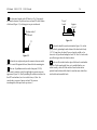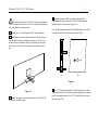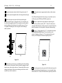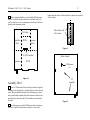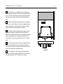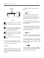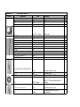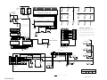
1
ELECRAFT K2 160-10 Meter SSB/CW Transceiver Owner’s Manual Revision XC, Jan. 25, 1999 Copyright 1999 Elecraft All Rights Reserved This revision of the K2 Owner’s Manual is for use by Field Test participants only. Missing or inaccurate information will be corrected in the next revision. K2 Manual 1/24/99 V.XC ©1999 Elecraft 2 Table of Contents 1. INTRODUCTION .............................................................................................................................................................................. 4 2. SPECIFICATIONS............................................................................................................................................................................ 4 3. PREPARATION FOR ASSEMBLY ................................................................................................................................................... 7 4. CONTROL BOARD ........................................................................................................................................................................ 13 5. FRONT PANEL BOARD ................................................................................................................................................................ 22 6. RF BOARD..................................................................................................................................................................................... 34 7. FINAL ASSEMBLY......................................................................................................................................................................... 78 8. OPERATION .................................................................................................................................................................................. 81 9. MODIFICATIONS ......................................................................................................................................................................... 110 10. THEORY OF OPERATION .......................................................................................................................................................... 111 11. TROUBLESHOOTING ................................................................................................................................................................. 119 12. INTERNAL OPTIONS .................................................................................................................................................................. 126 PARTS LIST ......................................................................................................................................................................... APPENDIX A SCHEMATIC ......................................................................................................................................................................... APPENDIX B BLOCK DIAGRAM................................................................................................................................................................ APPENDIX C PHOTOGRAPHS .................................................................................................................................................................. APPENDIX D K2 Manual 1/24/99 V.XC ©1999 Elecraft 3 K2 Manual 1/24/99 V.XC ©1999 Elecraft 4 1. Introduction The Elecraft K2 is a high-performance, synthesized transceiver that provides CW and SSB operation on 160-10 meters. It is a true dualpurpose transceiver, combining the operating features you’d expect in a home-station rig with the small size and weight of a rugged, goanywhere portable. The K2 is also the first transceiver to offer these features in kit form. The basic K2 operates on 80-10 meter CW, with adjustable power output of over 10 watts. You can also customize your K2 by choosing from a wide range of internal option kits. These include: § § § § § § SSB adapter noise blanker 160 meter adapter + receive antenna switch 20W automatic antenna tuner internal rechargeable battery host computer interface For those who prefer a higher-power station, we’ll be adding an internal 100W power amplifier kit in the near future1. Other future options include an internal 6m transverter, high-performance audio filter, and a variety of matching station accessories. The K2 is an intermediate-to-advanced kit, yet you’ll be pleasantly surprised at how uncomplicated it is to build and align. All of the RF (radio-frequency) circuitry is contained on a single board, while two plug-in modules provide user interface (UI) and control functions. 1 The 100W power amp option displaces the ATU and battery. Wiring is minimal, unlike traditional kits which depend on complex wiring harnesses. A unique feature of the K2 is that it provides its own built-in test equipment, including a digital voltmeter, ammeter, wattmeter, and frequency counter. Construction of the kit is sequenced so that these functions are ready to be used when you begin construction of the RF board. In addition to this owner’s manual, you’ll find extensive support for the K2 on our website, www.elecraft.com. Among the available materials are manual updates, application notes, photographs, and information on new Elecraft products. There’s also an Elecraft user forum. We’d like to thank you for choosing the K2 transceiver, and hope it meets your expectations for operation both at home and in the field. Wayne Burdick, N6KR Eric Swartz, WA6HHQ Field-Test Acknowledgements Getting the K2 ready for its field test would not have been possible, or at least would have taken a lot longer, without the help and encouragement of Lerma Swartz, Lillian Svec, Bob Dyer, Shigehiro Kinoshita, Conrad Weiss, and Rob Capon. We’re also grateful for the patience shown by our field testers. K2 Manual 1/24/99 V.XC ©1999 Elecraft 2. Specifications All measurements were made with a 13.8V supply and 50 ohm load at the antenna. Numeric values are typical; your results may be somewhat different. Specifications are preliminary and subject to change without notice. General Size Cabinet Overall 3.0” H x 7.9” W x 8.3” D (7.5 x 20 x 21 cm) 3.4” H x 7.9” W x 9.9” D (8.5 x 20 x 25 cm) Weight 3.3 lbs (1.5 kg) Supply Voltage 8.5 to 15VDC (13.8V nominal); reverse-polarity protection Current drain, Receive 100mA in minimum-current configuration; 150-200mA typical Transmit2 Frequency control 2 1.8A at 10 watts PLL synthesizer w/single VCO covering 6.7-24 MHz in 9 bands; fine steps via DAC-tuned VXCO Varies with band, supply voltage, configuration, and load impedance. 4 K2 Manual 1/24/99 V.XC ©1999 Elecraft 5 Load Tolerance 2:1 or better SWR recommended; will survive occasional operation into high SWR Frequency range, MHz Guaranteed 3.5-4.0, 7.0-7.3, 10.0-10.2, 14.0-14.5, 18.0-18.2, 21.0-21.6, 24.8-25.0, 28.0-28.8 Typical [TBD] 160m (opt.) 1.8-2.0 T-R delay 10ms-1.5sec, adjustable Receiver VFO Stability [TBD] 3 Sensitivity (MDS) 3rd-order Intercept 2nd-order Intercept Preamp On -135dBm 0 to +7.54 +77 Preamp Off -130dBm +14 +78 125dB 96 133dB 97 4.915 MHz (single conversion) Accuracy +/- 30Hz typ. if calibrated Resolution 10 Hz Tuning steps 10 Hz, 50 Hz, and 1000 Hz Dynamic Range, Blocking Two-tone 20 (10 general, 10 pre-assigned to available bands) I.F. Memories Selectivity, CW Transmitter Power Output Duty Cycle SSB 0.5W to 10W (typ.), all bands; power setting resolution 0.1W, power reading accuracy 10% @ 5W 5W, 100% 10W, 50% Spurious products (Transmitter, continued) -40dB or better @ 10W (-50typ) Harmonic content -45dB or better @ 10W (-55typ) RIT/XIT Range: +/- 1.2 kHz, 10 Hz steps Audio output: 1 watt (typ) into 4 ohm load 3 See Frequency Calibration Techniques (Operation section, under Advanced Operating Features). 4 5-pole variable-bandwidth crystal filter, 200-1500 Hz [TBD] Varies with band. K2 Manual 1/24/99 V.XC ©1999 Elecraft Keyer Keying modes Iambic A and B Speed Range Approx. 9 - 40 WPM Messages 3 buffers, 84 bytes each, nonvolatile; auto-repeat 6 K2 Manual 1/24/99 V.XC ©1999 Elecraft 7 3. Preparation for Assembly Overview of the Kit The K2 is a highly modular transceiver, both physically and electrically. This concept extends to the chassis, as can be seen from Figure 3-1. Any chassis element can be removed to facilitate assembly or troubleshooting. (Also see photos in Appendix D.) As shown in Figure 3-2, there are three printed circuit boards (PCBs) in the basic K2 kit: the Front Panel board, Control Board, and RF board. The Front Panel and Control boards plug into the RF board directly to eliminate point-to-point wiring. Gold-plated contacts are used on these connectors for reliability and corrosion resistance. Side Panel RF Control Top Cover Heat Sink Front Panel Front Panel Bottom Cover (Right side panel not shown) Figure 3-2 Figure 3-1 K2 Manual 1/24/99 V.XC ©1999 Elecraft There are six steps in the K2 assembly process: 1. 2. 3. 4. 5. 6. Control Board assembly Front Panel Board assembly RF Board assembly and test, part I (control circuits) RF Board assembly and test, part II (receiver and synthesizer) RF Board assembly and test, part III (transmitter) Final assembly This assembly sequence is important because later steps build on the previous ones. For example, in step 3 you’ll put the modules together for the first time, allowing you to try out the K2’s built-in frequency counter. The counter will then be used in step 4 to align and test the receiver and synthesizer on 40 meters. In step 5 all the pieces will come together when you complete the transmitter and filters, then align the K2 on all bands. The last few details—speaker, tilt stand, etc.—will be wrapped up in step 6. Many illustrations are provided in the manual to clarify assembly steps. In addition, you should familiarize yourself with Appendix D, which provides photographs of the K2 and its three circuit boards in various stages of assembly. Note to Field Testers During field testing of the K2, you will no doubt discover minor problems with the kit's documentation, components, etc. Please contact us if you find something that we've missed. We will suggest corrective measures as quickly as possible, and we'll ship you any parts needed. The next revision of the manual will include a number of additional illustrations and photos. The Theory of Operation and Troubleshooting sections will also be much more extensive, and we’ll add much more information for beginning builders and operators (including a glossary 8 of terms). Revised manual sections will be posted to our website in downloadable form. Unpacking Note: Do not open any of the component bags until instructed to do so. Small components can easily be lost or confused with similar parts if you unpack the entire kit at once. When you open the kit you should find the following items: § § § § § § § § § six chassis pieces, wrapped (Figure 3-1) three printed circuit boards (Figure 3-2) FRONT PANEL board components bag, which includes the LCD and its backlight assembly in individual small bags CONTROL board components bag RF board components bag MISCELLANEOUS components bag 4 ohm Speaker tube of DPDT latching relays Enamel and hookup wire If any of the above items is missing or damaged, contact Elecraft. Your kit has been carefully packed, so it is unlikely that any components are missing. However, if you prefer to do an inventory of parts, you may do so at any major stage in the assembly process using the complete parts list in Appendix A. The parts list includes photographs or illustrations of each type of component. Even if you don’t do an inventory, it is helpful to familiarize yourself with the parts list in case you need to refer to it later. K2 Manual 1/24/99 V.XC ©1999 Elecraft Tools The following specialized tools are supplied with the K2: § § § .050” (1.3mm) Allen Wrench, short handle 5/64” (2mm) Allen Wrench, long handle Double-ended plastic inductor alignment tool 9 Assembly Notes i This symbol is used to alert you to important information about assembly, alignment, or operation of the K2. You should read and understand this information before proceeding. Step-by-Step Assembly In addition to the tools listed above, you will need these standard tools: § § § § § § § Fine-tip soldering iron, 15-25 watt (or a temperature-controlled soldering station) IC-grade, small-diameter solder (DO NOT use acid-core solder or any type of flux) Desoldering tools (wick, solder-sucker, etc.) Needle-nose pliers Small diagonal cutters Small phillips screwdriver Very small flat-blade screwdriver (for 2-56 bezel screws and trimmer capacitors) While not required, the following items are recommended: § § § DMM (digital multimeter) for doing resistance and voltage checks. Even an inexpensive DMM can provide a number of useful capabilities, including diode and capacitance measurement. Illuminated magnifying glass Anti-static work surface and wrist strap (see Integrated Circuits and ESD, below, for more details) Each step in the K2 assembly process is accompanied by a check-box. As you complete each step, put a mark in the box: In some steps you will actually be installing multiple components of a particular type. In this case the instructions will be followed by a table listing all of the components to be installed, so you won’t need to refer to the parts list during assembly. The order that the components are installed corresponds closely to their locations on the PC board. Assembly generally begins with low-profile components such as resistors and diodes, then works up to the higher-profile parts. This keeps the board stable as you turn it over each time to solder. Do not skip any steps; you may find that you’ve installed one component that hinders the installation of another. Top and Bottom Components A number of components in the K2 are mounted on the bottom of the PC boards to improve component spacing or for electrical reasons. Component outline symbols are provided on both sides of each board, so it will always be clear which side a particular component goes on. You’ll be able to tell the top of the board from the bottom easily: the top side has far more parts. K2 Manual 1/24/99 V.XC ©1999 Elecraft Components which are mounted on the bottom of a board are identified on the schematic with this symbol: Identifying Capacitors Small (< 1000 pF) fixed capacitors are usually marked with one, two, or three digits and no decimal point. If one or two digits are used, that is the value in pF (picofarads). If there are three digits, the third digit is usually a multiplier. For example, a capacitor marked “151” would be 150pF (15 with a multiplier of 101). Similarly, “330” would be 33 pF, and “102” would be 1000 pF (or .001µF). Occasionally, capacitor manufacturers use "0" as a decimal place holder rather than a multiplier, so that “330” might actually mean 330 pF, not 33 pF. Markings shown in the parts list should clear up any confusion. If in doubt, you may wish to measure the capacitor using a DMM. Fixed capacitors with values over 1000pF may use a decimal point in the value, such as .001 or .02. This is the value in microfarads (µF). Capacitors also may have a suffix after the value, such as “.001J.” You won’t need to use suffixes in identifying capacitors. Color Code All resistor and RF choke color bands are provided in the text along with their values. However, it is helpful to familiarize yourself with the color code to allow you to identify these components without having to refer to the text or parts list. The color-code chart, Figure 3-3, shows how to read the four color bands on 5% resistors. 1% resistors are similar, except that they use five bands (three significant digits, multiplier, and tolerance). For 10 example, a 1,500 ohm (1.5k) 5% resistor has color bands BROWN, GREEN, and RED. A 1.5k, 1% resistor has color bands BROWN, GREEN, BLACK, BROWN. The multiplier value is 1 rather than 2 in the 1% case because of the third significant digit. The markings on RF chokes reflect their value in microhenries (µH). Like 5% resistors, chokes use two significant digits and a multiplier. Example: an RF choke with color bands RED, VIOLET, BLACK would have a value of 27µH. K2 Manual 1/24/99 V.XC ©1999 Elecraft Resistor Color Code Tolerance (gold = 5%) Multiplier Second Digit First Digit Color Black Brown Red Orange Yellow Green Blue Violet Gray White Digit Multiplier 0 1 2 3 4 5 6 7 8 9 Figure 3-1 x1 x 10 x 100 x 1K x 10K x 100K x 1M 11 K2 Manual 1/24/99 V.XC ©1999 Elecraft Integrated Circuits and ESD The K2 transceiver uses integrated circuits and transistors that can be damaged by electrostatic discharge (ESD). Problems caused by ESD can often be difficult to troubleshoot because components may only be degraded rather than fail completely. To avoid such problems, we recommend that you take the following anti-static precautions: § § § § § § § Remove carpets in your workbench area, or treat them with antistatic spray If you use a rubber floor mat to guard against electric shock, make sure it is of the anti-static type; any other type of rubber mat will increase ESD problems Wear cotton clothing, not polyester or other synthetics Leave all ESD-sensitive components in their anti-static packaging until you actually install them Ground yourself using a wrist strap with a series 1megohm resistor (do NOT ground yourself directly--this poses a shock hazard) Use an anti-static mat Use a grounded soldering iron. When soldering ICs and transistors, you should also keep the chassis and PC boards grounded using jumper clips. Grounding to the soldering iron's temperature control box is acceptable. Sockets are used for only a few of the ICs, including the microprocessor and display driver. You should not use sockets for the other ICs, because they tend to be unreliable and can cause problems in some circuits due to the added lead length. Since sockets are not used in most cases, you must carefully verify the type and orientation of each IC before soldering. IC removal and reinstallation is to be avoided since damage to the IC or the PC board may occur. 12 K2 Manual 1/24/99 V.XC ©1999 Elecraft 13 4. Control Board The control board is the “brain” of the K2. It monitors all signals during receive and transmit, and handles display and control functions via the front panel board. The microprocessor, analog and digital control circuits, automatic gain control (AGC), and audio amplifier are located on this board. Components i Review the precautions described in the previous section before handling any IC’s or transistors. These components can be damaged by static discharge, and the resulting problems are often difficult to troubleshoot. Open the bag of components labeled CONTROL and sort the parts into groups (resistors, diodes, capacitors, etc.). If any of the components are unfamiliar, identify them using the illustrations in the parts list, Appendix A. Doing a components inventory is optional. Locate the control board. It is the smallest of the three K2 PC boards, labeled “K2 CONTROL” on the front side, in the lower righthand corner. The lower left-hand corner is notched. Open the bag labeled MISCELLANEOUS and empty the contents into a small, shallow box or pan. This will prevent loss of any of the small hardware, while still allowing you to locate items as needed. i The Allen wrenches are located in a small bag with the MISCELLANEOUS items. These wrenches may have been oiled during manufacturing. Remove the wrenches and wipe off the oil, if any, then discard the bag. Field Test Notes: Two different sizes of small crimp pins were inadvertently purchased for the field test kits. Two of the pins are for the speaker connector, and the other three--which are different--are for the test probes (counter and voltmeter). The test probe crimp pins (3) and housings (2) are bagged separately and labeled PROBES. i There are four sizes of black-anodized, 4-40 machine screws provided with the kit. The relative sizes of the screws are shown below for identification purposes (not to scale). The 3/16” (4.8mm) pan-head screws are the most numerous, and will be referred to as chassis screws throughout the manual. There is only one Flat-head 3/16” (4.8mm) screw in the kit. K2 Manual 1/24/99 V.XC ©1999 Elecraft Flat-head, 3/16” (4.8mm) Pan-head, 3/16” (4.8mm) (chassis screws) Pan-head, 3/8” (9.5mm) Pan-head, 1/2” (12.7mm) 14 color codes easier to read if you need to re-check the values after installation. Note: When multiple items appear on one line in a component list such as the one below, complete all items on one line before moving on to the next, as indicated by the small arrow. (In other words, install R5 first, then R2, then go to the second line.) __ R5, 33k (ORG-ORG-ORG) ⇒ __ R2, 3.3M (ORG-ORG-GRN) __ R3, 33k (ORG-ORG-ORG) __ R6, 470 (YEL-VIO-BRN) __ R7, 1.96K, 1% (BRN-WHT-BLU-BRN) __ R8, 100, 1% (BRN-BLK-BLK-BLK) __ R9, 806K, 1% (GRY-BLK-BLU-ORG) __ R10, 196K, 1% (BRN-WHT-BLU-ORG) Assembly __ R16, 10 (BRN-BLK-BLK) ⇒ __ R17, 10M (BRN-BLK-BLU) __ R19, 1.5k (BRN-GRN-RED) __ R18, 1.5k (BRN-GRN-RED) __ R21, 10k (BRN-BLK-ORG) __ R20, 2.7ohms (RED-VIO-GLD) All of the components to be installed are on the top (component side) of the control board. On the bottom of the board there is an outline for the audio filter board and its two connectors (J1 and J2), but these items are not part of the basic K2 kit. Solder all of the resistors, then trim the leads as close as possible to the solder joints. (If the leads get in the way during soldering, try soldering and trimming a few leads at a time.) With the top side of the PC board facing you (notch at the lower left), locate the position of resistor R1, near the upper-left corner. The label “R1” appears just below the resistor’s outline. Install a 100k resistor (brown-black-yellow) at R1, with its first color band (brown) at the top. Make sure it is seated flush with the board, then bend the leads on the bottom to hold it in place. Do not solder this resistor until the remaining fixed resistors have been installed in the next step. Install the remaining fixed resistors, which are listed below in leftto-right PC board order. The resistors should all be oriented with the first significant-digit band towards the left or top. This will make the Locate RP6, a 10K, 10-pin resistor network (labeled “10A3.103G”). (“RP” means “resistor pack,” another name for resistor networks.) Note that one end of the resistor network has a dot, indicating pin 1. Locate the component outline for RP6 at the left end of the PC board. Install the resistor network so that the end with the dot is lined up with the “1” label. Make sure the resistor network is seated firmly on the board, then bend the leads at the far ends in opposite directions to hold it in place. (It is not necessary to clip the leads.) Do not solder RP6 yet. K2 Manual 1/24/99 V.XC ©1999 Elecraft i Resistor networks and other components with many leads are difficult to remove once soldered. Double-check the part numbers and orientation before soldering. Install the remaining resistor networks in the order listed below. Do not solder them until the next step. __ RP1, 3.9k, 10 pins (10A3.392G) __ RP7, 33k, 8 pins (8A3.333G) __ RP2, 82k, 8 pins (77083823) __ RP3, 47k, 10 pins (10A3.473G) __ RP5, 470, 10 pins (10A3.471G) __ RP4, 82k, 8 pins (77083823) Solder all of the resistor networks. 15 K2 Manual 1/24/99 V.XC ©1999 Elecraft 16 Install the diodes listed below, beginning with D1, which is in the upper left-hand corner of the PC board. (Refer to the parts list if necessary to identify the different types of diodes.) If a diode has only one band, the end with the band (the cathode) should be oriented towards the banded end of the corresponding PC board outline. If a diode has multiple bands, the widest band indicates the cathode end. __ D1, 1N4148 __ D2, 1N4148 Install and solder the electrolytic capacitors listed below, which are polarized. Be sure that the (+) lead is installed in the hole marked with a “+” symbol. The (+) lead is usually longer than the (–) lead, and the (–) lead is identified by a black stripe (Figure 4-1). - __ D3, 1N5817 Double-check the orientation of the diodes, then solder. Install the small fixed capacitors listed below, beginning with C2 in the upper left-hand corner of the board. (This list includes all of the fixed capacitors on the control board except the tall, cylindrical electrolytic types, which will be installed later.) The list shows both the value and the capacitor labels, using notation explained in the previous section. After installing each capacitor, bend and clip the leads, but do not solder until the next step. Note: Remember to complete all items in each line before moving on to the next. (Install C2, C3, and C4, then C7, etc.) __ C2, .001 (102) ⇒ __ C7, 330 (331) __ C9, .01 (103) __ C5, .01 (103) __ C11, .01 (103) __ C19, .047 (473) __ C23, .01 (103) __ C26, 0.1 (104) __ C34, .001 (102) __ C35, .01 (103) __ C41, .01 (103) __ C3, .01 (103) ⇒ __ C6, .047 (473) __ C10, .01 (103) __ C14, .047 (473) __ C16, .047 (473) __ C21, 33 (33) __ C27, .022 (223) __ C24, .0027 (272) __ C30, .047 (473) __ C36, .0027 (272) __ C37, .01 (103) Solder all of the small fixed capacitors. __ C4, 0.47 (474) __ C8, 39 (39) __ C12, .001 (102) __ C17, .01 (103) __ C18, .01 (103) __ C20, .001 (102) __ C25, 0.1 (104) __ C31, 0.1 (104) __ C40, .01 (103) __ C39, .01 (103) __ C38, 680 (681) + Figure 4-1 __ C1, 2.2µF __ C28, 220µF __ C32, 22µF ⇒ __ C13, 22µF __ C29, 220µF ⇒ __ C15, 100µF __ C33, 2.2µF Install and solder ceramic trimmer capacitor C22. Orient the flat side of this trimmer as shown on its PC board outline. Be sure that the capacitor is seated flush with the PC board, then solder. Using a small flat-blade screwdriver, set C22 to the mid-point in its rotation. The screwdriver slot should be parallel to the outline of crystal X2, just above C22 on the PC board. i The trimmer you just installed, C22, is used to calibrate the master 4.000 MHz crystal oscillator, which determines the accuracy of the built-in frequency counter and VFO. The standard setting given above will suffice in most cases, but if you wish to more accurately calibrate C22, refer to the Operation section under Advanced Operating Features. Locate Q12 (type PN2222A), which is a small, black TO-92 package transistor. Note: Q12 and other TO-92 transistors may have either of the two shapes shown in Figure 4-2. In all cases the flat side of the device should be aligned with the flat side of the component outline. K2 Manual 1/24/99 V.XC ©1999 Elecraft 17 will be eliminated with the next revision of the PC board by using the solder mask to cover the pads on the top of the board. Slip a crystal spacer over the leads of each crystal (X1 and X2). Install crystals X1 and X2 so that they are flat against the board. X1 is 5.068 MHz and is located near the notch in the lower left-hand corner. X2 is 4.000 MHz, and is located near the center of the board. Solder the crystals. Figure 4-2 Install Q12 near the upper left-hand corner of the PC board. Align the flat side of Q12 with its PC board outline as in Figure 4-2. The body of the transistor should be about 1/8” (3mm) above the board; don’t force it down too far or you may break the leads. Bend the leads of the transistor outward slightly on the bottom to hold it in place. Solder Q12. The cases of the crystals should be grounded to minimize signal radiation (Figure 4-3). Insert a 1” (25mm) length of bare, solid hookup wire into the provided grounding hole and solder it on the bottom of the board. Then fold the bare wire over the crystal and solder it to the top of the can. (Don’t overheat the crystals or cover the entire top surface of the crystal with solder; only a small amount of solder is required.) X1 X2 Install the remaining TO-92 package transistors in the order listed below. __ Q12, PN2222A __ Q2, 2N3906 __ Q5, 2N7000 __ Q8, PN2222A __ Q11, PN2222A __ Q1, 2N3906 __ Q3, 2N7000 __ Q4, 2N7000 __ Q6, J310 __ Q7, J310 __ Q9, MPS5179 __ Q10, MPS5179 Figure 4-3 i Solder all of the above transistors. i When installing crystals, you must use the thin spacers provided in the MISCELLANEOUS bag to keep the crystal cans from shorting to their pads on the top of the board. The need for these spaces The voltage regulators, U4 and U5, will be installed in the following steps. These regulators have different output voltages and must not be interchanged. Check the labels on the regulators carefully before soldering; the basic part numbers should match those on the PC board outline. K2 Manual 1/24/99 V.XC ©1999 Elecraft Install U4 (LM2930T-8) and U5 (LM7805), bending the leads as indicated (Figure 4-4). Long-nosed pliers should be used because the indicated bend location may be at the thicker part of the lead. After inserting the leads into the proper holes, secure each IC with a 4-40 x 3/8” (9.5mm) machine, #4 lockwasher, and 4-40 nut. (Note: these regulators may have either plastic or metal mounting tabs.) 18 Install the 2-pin male connectors, P5 and P6. As shown in Figure 4-5, the short end of the connector pins are inserted into the PC board. P5, the voltmeter input connector, can be found near the upper left-hand corner of the board. P6 is used for frequency counter input, which is in the upper right-hand corner. 2-pin connector Bend pins down 90° Top side of PC Board Figure 4-4 Figure 4-5 Solder the voltage regulator ICs. Install a 40-pin IC socket at U6. (The microprocessor will be inserted into the socket in a later step.) Orient the notched end of the socket to the left as shown on the PC board outline. Bend two of the socket’s corner leads slightly to hold the socket in place, then solder only these two pins. If the socket does not appear to be seated flat on the PC board, reheat the solder joints one at a time while pressing on the socket. Solder the remaining pins of the 40-pin socket. i Install the 10-pin, dual-row connector, P4. It is located to the left of P5. It must be seated flat on the board before soldering. Install S1, the miniature slide switch, to the right of P5. At the upper left and right corners of the board you’ll find two short jumpers, each labeled with a ground symbol ( ). These jumpers are provided for connecting clip leads during alignment and test. Form a 3/4 (19mm) length of bare copper hookup wire into a “U” shape for each jumper (Figure 4-6). (You can use a clipped component lead as an alternative to hookup wire.) Solder the jumpers on the bottom of the board. The connectors used in the following steps have plastic bodies that can may melt if too much heat is applied during soldering, causing the pins to be mis-positioned. Limit soldering time for each pin to 3 seconds maximum (1 to 2 seconds should be adequate). Figure 4-6 K2 Manual 1/24/99 V.XC ©1999 Elecraft 19 i Top side of PC Board The three multi-pin connectors along the bottom edge of the board (P1, P2 and P3) must be positioned and soldered carefully. Incorrect alignment of these connectors may cause instability or intermittent operation, and it is very difficult to remove them once they are soldered. Install 6-pin right-angle connector P1 as shown in the side view below (Figure 4-7). Do not solder it until the next step. The plastic part of the connector must be seated flat against the PC board, and the pins must be parallel to the board. Do not bend or trim the pins on the bottom of the board. P3 Figure 4-8 Install P2, a 36-pin, dual-row, right-angle connector. Use the same method you used for P1 and P2. Top side of PC Board P1 Figure 4-7 Solder just the two end pins of P1, then examine the placement of the connector closely. If P1 is not flat against the board, re-heat the solder on the end pins one at a time while pressing firmly on the connector. Once it is in the right position, solder the remaining pins. Install P3, a 20-pin, dual-row right-angle connector (Figure 4-8). Use the same method you used for P1. Do not solder P3 until you are sure that it is seated properly. Locate U2, an 8-pin IC, part number LM833. (LM833 is the basic part number; there may be an additional prefix or suffix as well as other markings.) This and all remaining ICs on the control board are Dual-Inline Packages, or DIPs. Referring to Figure 4-9, identify the notched or dimpled end of the IC. Notch Pin 1 Dimple Pin 1 Figure 4-9 K2 Manual 1/24/99 V.XC ©1999 Elecraft 20 Install U2 in the orientation shown by its PC board outline, near the upper left-hand corner of the PC board, but do not solder it yet. Make sure the notched or dimpled end is lined up with the notched end of the PC board outline. Even though the outline is covered when the IC is installed, you can still verify that the IC is installed correctly by looking at pin 1. The PC board pad corresponding to pin 1 will be either oval or round, while the other pads are all rectangular or square. Prepare the pins of the microcontroller, U6 (Figure 4-10). The two rows of pins must be straight and parallel to each other to establish the proper pin spacing for insertion into the socket. To straighten the pins, hold the microcontroller’s body at each end, then rest one entire row of pins against a hard, flat surface. Gently press down on the pins and rock the IC forward to bend the pins into position. i You may overheat the IC pins or PC pads if you take an excessive length of time to solder. After a few tries, you should be able to solder an IC pin in about 1 or 2 seconds. If it seems to be taking longer, or if your solder joints are not shiny and smooth, review the recommendations on soldering irons and solder in the previous section. Bend two of U2’s corner pins out slightly on the bottom of the board to hold the IC firmly in place, flat against the top of the board. Find pin 1 and verify that its pad is either round or oval. Once U2 is properly seated, solder all eight pins. Install the remaining ICs in the order listed. Bend the pins to hold each IC in place as you did with U2, but do not solder until the next step. The notched or dimpled end of each IC must be aligned with the notched end of its PC board outline. __ U1, NE602 __ U8, MAX534 __ U3, LM6482 __ U9, LM380 __ U7, 25LC160 __ U10, LMC660 Verify the location of pin 1 on each IC by looking at the associated PC board pads, as before. Then solder all of the ICs. Flared Straight Figure 4-10 i When the microcontroller is installed in the next step, you must be careful to avoid bending its pins. Make sure that all pins are lined up with the associated holes in the socket before pressing down on the IC. Watch the pins on both rows as you press down, realigning them with the socket holes individually if necessary. Insert the microcontroller, U6, into its socket. Make sure that pin 1 on the IC itself is lined up with the pin 1 label near the lower left-hand corner of the PCB outline. K2 Manual 1/24/99 V.XC ©1999 Elecraft Visual Inspection Nearly all problems with kits are due to incorrectly installed components or poor solder joints. You can avoid these problems by doing a simple visual inspection; a few minutes spent here may save you hours of troubleshooting time or repair charges. Make sure there are no components installed backwards. Check all diodes, resistor networks, electrolytic capacitors, and ICs. Examine the bottom of the PC board carefully for the following: § § § cold solder joints solder bridges unsoldered pins Resistance Checks While the control board will be fully tested in a later section, you should perform the resistance checks listed below to insure that there are no shorts or opens in the most critical circuits. [Resistance check table TBD] 21 K2 Manual 1/24/99 V.XC ©1999 Elecraft 22 5. Front Panel Board The front panel includes all of the control and display devices that you’ll use when operating the K2, including the liquid-crystal display (LCD), LED bargraph, push-button switches, and potentiometers. These user-interface (UI) elements are controlled by the microcontroller on the control board. Components See Appendix D for photos of the front panel assembly. Locate the front panel PC board, which is just a bit larger than the control board. It is labeled “K2 FP” on the top side, in the lower righthand corner. The hole in the board at the lower left is for the headphone jack, which is mounted on the RF board, not the front panel. The hole at the lower right is for the power switch, which is also mounted on the RF board. Some components are installed on the bottom of the board. The connector on the bottom (at the bottom edge) is J1, which connects the front panel board to the RF board. There are also two standoffs on the bottom that provide increased mechanical stability by allowing the front panel and control boards to be secured together. Some of the assembly steps for this board are similar or identical to those for the control board. The instructions for such steps will be presented more briefly here, but you can refer back to the previous section if necessary. Open the bag labeled FRONT PANEL and sort the parts into groups (resistors, diodes, capacitors, etc.). Observe anti-static precautions when handling ICs and transistors. Assembly i Please pay close attention to all front-panel assembly steps. Your K2’s appearance and operation will be adversely affected if the controls or display are not mounted correctly. Some components must be mounted before others, so you must adhere to the indicated assembly sequence. There are also special instructions for installing components on the bottom of the board. Install the following 1/4-watt fixed resistors, which are listed in left-to-right PC board order. Solder the resistors after all have been installed. (Note: R13 and a few other components in its vicinity are part of the SSB adapter option, and are not included in the basic K2 kit. A check-list of these components is provided at the end of this section.) __ R12, 120 (BRN-RED-BRN) ⇒ __ R10, 33 (ORG-ORG-BLK) K2 Manual 1/24/99 V.XC ©1999 Elecraft __ R9, 220 (RED-RED-BRN) __ R6, 4.7k (YEL-VIO-RED) __ R14, 100k (BRN-BLK-YEL) __ R11, 470 (YEL-VIO-BRN) __ R7, 4.7k (YEL-VIO-RED) 23 K2 Manual 1/24/99 V.XC ©1999 Elecraft 24 Flip the board over and install the following resistors on the bottom of the board. Solder them on the top side. __ R16, 15k (BRN-GRN-ORG) __ R15, 10k (BRN-BLK-ORG) There are two ground jumpers on the front panel board, one at the far left and the other at the lower right, labeled “GND.” Form a 3/4” (19mm) length of bare copper hookup wire into a “U” shape for each jumper, then solder. When you install the resistor networks in the next step, you must align the dotted end of the network with the pin 1 label on the PC board outline. If these networks are installed backwards you may damage one or more front-panel components. Flip the board over and install a 40-pin IC socket at U1. (U1, the LCD driver, will be inserted into this socket in a later step.) Orient the notched end of the socket to the left as shown on the PC board outline. Make sure the socket is seated flat on the PC board before soldering, using the technique described in the previous section. Install the resistor networks listed below. Double-check the orientation and values before soldering. Install the following ICs. Before soldering, verify that the ICs are oriented correctly (pin 1 associated with a round or oval pad). __ RP2, 120, 10 pins (770101121) __ RP1, 100K, 10 pins (10A1.104G) __ U4, TPIC6B595 i __ U3, TPIC6B595 __ U2, 74HC165 i Install and solder the diodes listed below, observing proper orientation as described in the previous section. __ D4, 1N5817 __ D5, 1N5817 __ D6, 1N5817 Install and solder the following capacitors. C9 is located on the bottom of the board and is soldered on the top side. __ C1, .047 (473) __ C2, .01 (103) The bargraph LED will be installed in the following two steps. This component must be seated flat on the PC board or it will interfere with final front panel assembly. Also, any misalignment will be visible from the front of the K2. __ C3, .047 (473) __ C9, .01 (103), on bottom Install PN2222A transistors at Q1 and Q2, near the middle of the board, and solder. These transistors must be mounted so the lead length above the PC board is less than 1/8” (3mm) to prevent them from hitting the front panel. Locate the bargraph LED, DS2, which has a beveled corner or edge that indicates pin 1. Install DS2 as shown on its PC board outline, just to the left of the LCD. Bend two opposite corner pins slightly to hold it to the board, the solder only these two pins. If the bargraph is not perfectly flat against the PC board, re-heat the solder on the corner pins alternately while pressing it down. Once it is in the correct position, solder the remaining pins. K2 Manual 1/24/99 V.XC ©1999 Elecraft Remove any hardware supplied with the microphone jack, J2; the nut and washer will not be used. Install the microphone jack (J2) in the lower left-hand corner of the board, with its polarizing nub at the top (Figure 5-1). Press the jack down until it is completely flat against the PC board. Re-check the orientation of the polarizing nub before soldering. Polarizing nub 25 Install another 3/16” (4.8mm) diameter x 1/4” (6.4mm) long round standoff on the top of the PC board, on the left side of the large square hole in the middle of the board. The standoff mounting hole is just below C2. Use the same hardware as indicated in the previous step. Install two 1/4” (6.4mm) diameter x 1/2” (12.7mm) long hex standoffs on the bottom of the board. The mounting holes for these standoffs are indicated by large pads on the top and bottom. Use a #4 lockwasher between each standoff and the PC board, and secure each with a 3/8” (9.5mm) screw. There are two types of potentiometers supplied with the front panel. Four of them are marked “10K” and one is marked “5K.” Locate the 5k potentiometer, and install it at R3, in the lower left-hand corner. Make sure that the potentiometer body is parallel to the PC board and is pressed against the board as far as it will go before soldering. Figure 5-1 Install two 3/16” (4.8mm) diameter x 1/4” (6.4mm) long round standoffs on the top of the board, adjacent to the microphone jack (Figure 5-2). Secure the standoffs from on the bottom side with chassis screws and #4 lock washers. Recall that “chassis screw” is short-hand for 3/16” (4.8mm) long pan-head machine screws. Figure 5-2 Install the four 10k potentiometers at R1, R2, R4, and R5. Verify correct positioning as you did in the previous step. K2 Manual 1/24/99 V.XC ©1999 Elecraft The front panel attaches to the RF board via J1, a 20-pin singlerow female connector. Flip the board over and install J1 on the bottom of the board (Figure 5-3), soldering just two pins at either end. 26 Top of board Approx. .05-.06” Bottom side of PC Board J1 Figure 5-3 Re-heat the two end pins and press the connector down as needed until J1 is seated flat against the board, then solder the remaining pins. There are 16 pushbutton switches on the front panel, S1-S16, which must be seated at exactly the right height to prevent an uneven appearance (Figure 5-4). Start by installing the switches as indicated on their PC board outlines, but do not solder them yet. (Note: the switches have two pairs of pins at each end. The pairs are interchangeable; either pair can be up or down.) Figure 5-4 Each switch should be seated as indicated in Figure 5-4, with its pins just barely protruding from the bottom of the board and its body 1/16” (1.5mm) above the board. Press each switch carefully as far down as it will go without bending the leads. The “knee” in each switch pin will end up just above the board as shown. Look over all switches from the edges of the board to confirm that they are all at the same height. Once you’re satisfied that they are seated correctly, solder all of the switches. Since the leads do not protrude from the bottom of the board, be sure that some solder flows into the holes and around the leads. K2 Manual 1/24/99 V.XC ©1999 Elecraft Install rectangular gray key caps on S1 and S3 so that the key caps are parallel to the long axis of the PC board (Figure 5-5). The caps are installed simply by pressing them onto the switch plungers. Gray keycaps 27 end. (Do not remove the diffuser backing, which is glued to the bottom surface of the diffuser.) Place one 1/8" (3mm) tall by 1/8" (3mm) diameter plastic standoff on each of the four LED pins. Position the backlight assembly between the two pairs of mounting holes labeled D2 and D3 as shown in the two views of Figure 5-6. The diffuser must be parallel to and 1/8" (3mm) above the PC board. Bend the LED leads slightly to hold the assembly in place. Square Keycap Figure 5-5 Install a square black key cap on S7 as shown above. Install rectangular black key caps on the remaining 13 switches. Straighten the pins of U1, the LCD driver (PCF8566), as you did with the microcontroller on the control board. Insert U1 into its socket on the bottom of the board. (This must be done before continuing with LCD installation, since the LCD’s presence will make pressing U1 into its socket much more difficult.) Be sure that U1 is completely seated and that no pins are bent. i The LEDs in the LED backlight assembly are somewhat fragile. Verify that the LEDs are pressed into the diffuser and are not loose. Locate the LED backlight assembly, which is in a small bag with the other FRONT PANEL components. Carefully remove its protective covering, a thin sheet glued to the top of the diffuser at each Figure 5-6 Examine the backlight/diffuser assembly closely to insure that it is parallel to the front panel board and seated as far down on the board as it will go (exactly 1/8" [3mm] above the board). Once the backlight/diffuser assembly is in its correct position-supported by the plastic spacers and parallel to the PC board--solder the four LED pins. If the assembly is not flat against the boards, re-heat the LED pins one at a time and press it into place. K2 Manual 1/24/99 V.XC ©1999 Elecraft 28 establish the correct spacing from front panel to control board and provide some vibration resistance. i Caution: The LCD and its pins are fragile—handle carefully. Do not remove the protective plastic film from the surface of the LCD until later in this section when the front panel assembly is completed. Pad Remove the LCD from its packing materials, being careful not to bend the pins. Pad Top Edge (Back of PC Board) The LCD has six pins along the bottom edge (three on each side), and 24 pins along the top edge. Locate these holes on the top of the PC board and place the LCD in it proper position as shown in the edge view below (Figure 5-7), but do not solder yet. Figure 5-8 Uninstalled Components LCD Figure 5-7 The LCD must be seated flat against the diffuser as shown in Figure 5-7, and the diffuser must in turn be parallel to the board. If it does not appear to be seated correctly, it may be because the backlight LEDs or spacers are mis-aligned. When the entire assembly is installed correctly, the LCD’s pins will just barely protrude from the bottom of the board. Solder the four corner pins of the LCD, then re-check the alignment of the LCD assembly. If everything looks correct, solder the remaining pins. Attach two 1/4” (6.4mm) dia. self-adhesive rubber pads to the bottom of the front panel board in the positions indicated in Figure 5-8. The pads should be attached as close as possible to the top and side edges of the board, but should not hang over on any edge. These pads At this point you should have several component locations that are not filled. These locations are for parts that are provided with the SSB adapter, which should not be installed until after the basic K2 kit is completed and tested. Full instructions are included with the SSB adapter kit. Check off each of the components in the list below, verifying that they are not installed. You should have no other uninstalled components except for Z1, the optical encoder. __ C4, .01 __ C5, .01 __ C6, .01 __ C7, .01 __ C8, .01 __ R13, 68k, 1% __ RP3, 10k resistor network __ Q3, 2N3906 __ P1 (on the bottom of the board) Visual Inspection Make sure there are no components installed backwards. Check all diodes, resistor networks, electrolytic capacitors, and ICs. Examine the bottom of the PC board carefully as you did with the control board. K2 Manual 1/24/99 V.XC ©1999 Elecraft 29 K2 Manual 1/24/99 V.XC ©1999 Elecraft Resistance Checks Perform the resistance checks listed below to insure that there are no shorts or opens in the most critical circuits. (The front panel board will be fully tested in a later section.) [Resistance checks TBD] 30 Turn the front panel face up. Position the clear plastic LCD bezel over the LCD hole, then secure it with four 2-56 screws (fillister head, stainless steel) as shown in Figure 5-10. Tighten the 2-56 screws only the amount needed to hold the bezel to the front panel. Overtightening may crack the bezel or strip the threaded holes in the panel. E L EC R A F T K 2 T R A NS C E I V ER Front Panel Final Assembly Place the front panel chassis piece in front of you, face-down. Placing it on a soft cloth will protect the finish and labeling. The large round microphone jack hole should be on the right. Position the green plastic filter over the inside of the bargraph LED hole (Figure 5-9). The hole is rectangular, 1” x 1/4” (25 x 6.4mm). Secure the filter to the panel using two small strips of electrician’s tape or other durable tape.5 Do not use thick, double-sided tape since this may interfere with proper positioning of the bargraph LED when the panel is installed. Green Film Tape Figure 5-1 5 Field test note: we may include specialized tape in the future. 2-5 Scre 6 (w) 4 Figure 5-2 LC BD el z e K2 Manual 1/24/99 V.XC ©1999 Elecraft i The optical shaft encoder, Z1, will be connected to the bottom of the PC board by four short wires. The wires must be installed first in order to position the encoder correctly. Prepare four 1.5” (38mm) lengths of bare, solid hookup wire. 31 Insert the front panel PC board into the front panel. The pushbutton switch caps on both sides of the LCD should protrude slightly as shown in the side view, Figure 5-4a. Note: the board/panel assembly will not be rigidly held in place until it is mated with the RF and control boards in a later section. Install the bare wires from on the bottom of the board, using the four pads below the large rectangular hole (Figure 5-11). The wires must be soldered and trimmed on the top of the board. Set the board aside for now. The wires will be connected to the encoder in a later step. (b) (a) Figure 5-4 Figure 5-3 Remove the protective plastic film from the face of the LCD. Be careful not to scratch the glass. A 1/4” (6.4mm) standoff on the PC board should now be visible through the hole just to the left of the encoder mounting hole. Secure the panel to this standoff using a 4-40 x 3/16” (4.8mm) flat-head screw as shown in Figure 5-4b. K2 Manual 1/24/99 V.XC ©1999 Elecraft 32 Remove the hardware from the shaft of the optical encoder, Z1. Insert the encoder through the hole in the front panel board (Figure 5-5a). Attach the encoder to the inside of the front panel using the hardware provided. Figure 5-5 shows the side view (a) and front view (b) with encoder properly installed. The encoder has a small metal tab near the shaft that will only allow it to be installed one way. Do not over-tighten the finishing nut. (Note: the green encoder bushing is metal, not plastic.) Set all potentiometers to approximately midway in their rotation (12 o’clock). Note: When attaching knobs in the next step, you may find it easier to install knobs on the KEYER and POWER controls first. Attach five small knobs to the potentiometer shafts using the smaller of the two Allen wrenches (.050”, 1.3mm). The white line on each knob should be lined up with the center line of its shaft. The knobs should be mounted as close as possible to the panel without rubbing. Locate a 1” (25mm) diameter by 1/16” (1.6mm) thick felt washer (in the MISCELLANEOUS items). Place the washer over the encoder’s finishing nut (Figure 5-6). The washer should be seated directly on the front panel, with the nut completely inside it. (b) (a) Figure 5-5 Attach the four encoder wires you installed earlier to the matching pins on the back of the encoder. Each wire should be wrapped securely around its pin, with no slack in the wire. Trim and solder all four wires, making sure that none of the wires are shorting to each other or to the encoder body, which is conductive. Figure 5-6 Place the large knob on the encoder shaft. Push the knob on until it just touches the felt washer, then tighten one set screw using the larger Allen wrench (5/64”, 2mm). If the knob does not spin freely, loosen the K2 Manual 1/24/99 V.XC ©1999 Elecraft set screw and move the knob out slightly. If the knob is not contacting the felt washer at all, it may “drift” slightly. Tighten both set screws. 33 K2 Manual 1/24/99 V.XC ©1999 Elecraft 34 6. RF Board Most of the K2’s receiver and transmitter circuits are located on the RF board, including filters, oscillators, and RF amplifiers. The front panel and control boards plug into the RF board, and the chassis pieces are designed to form a tight enclosure around it (see photos in Appendix D). In addition, many option boards plug directly into the RF board to minimize wiring. Assembly and testing of the RF board is broken into three parts: Part I: The DC and control circuits are installed so that the front panel and control boards can be plugged in and tested. The I/O controller (U1 on the RF board) is also installed and tested at this time. Once this phase of assembly is completed, you’ll have the K2’s built-in test equipment available for testing and aligning the remaining circuits. Part II: Synthesizer and receiver components are installed and tested. By the end of Part II you’ll have the K2 receiving on 40 meters. Part III. Transmitter components and all remaining filter components are installed. The K2 is then aligned on all bands. Components i Review anti-static precautions before handling transistors or ICs. Open the bag labeled RF and sort the components into related groups. In later steps you’ll sort some of the components according to value to reduce the likelihood of assembly errors. Locate the RF board and place it in front of you with the component side up (the side with most of the parts), and the front edge facing you (the edge with the irregular cutouts). Throughout this section we’ll refer to the different areas of the board in terms of their proximity to you. For example, “front-left” means the corner closest to you on the left. K2 Manual 1/24/99 V.XC ©1999 Elecraft Take a moment to familiarize yourself with the RF board using Figure 6-1 to identify the major sections. If you flip the board over you’ll see that there are a few components on the bottom of the board, primarily in the transmitter section. XMTR fastener from the top side of the board with two chassis screws and two #4 lock washers. Holes offset to the left of center T-R Switch Band-Pass Filters 35 Low-pass Filters Figure 6-1 U1 (I/O Controller) Synthesizer (Back of board) RCVR 2-D Fasteners (5) Figure 6-1 1/4" Standoffs Assembly, Part I Locate a 2-D fastener and hold it vertically as shown in Figure 6-2. Looking at a side with two holes, note that the holes are offset from the center. When you install the fasteners in the following step, be sure to sure to position them so that the holes in the fastener are shifted in the same direction as the holes in the PC board outlines on the bottom of the board. Turn the board over and install 2-D fasteners at five locations on the bottom of the RF board as shown in Figure 6-3. Secure each Figure 6-2 K2 Manual 1/24/99 V.XC ©1999 Elecraft Make sure that 2-D fasteners on the edges line up with the edge of the PC board and do not hang over. If they hang over or do not match their component outlines, they are installed backwards. Install two 3/16” (4.8mm) diameter by 1/4” (6.4mm) long round standoffs on the bottom of the board (see Figure 6-3). Secure these standoffs from the top side with chassis screws and #4 lock washers. Turn the board back over to the top side. Install the 28-pin IC socket at U1, near the middle of the board (Figure 6-1). The notched end of the socket should be at the left. Make sure the socket is flat against the PC board before soldering. (U1 itself will be installed in a later step.) i In the following steps you will install the latching relays (K1K17). Relay pins must not be bent, even after placement on the PC board, as this may cause unreliable mechanical operation. Since the pins cannot be bent to hold the relays on the board, an alternative assembly technique using a flat surface must be used. For this technique to work, the relays must be installed before any of the taller components. Place relays K1-K17 on the top side of the RF board. One end of each relay has a heavy line printed across the top to indicate the pin 1 end. This end must be matched with the same end of the relay’s PC board outline. Do not solder the relays yet. When all of the relays have been placed on the board, lay a flat object such as a book or piece of cardboard on top of the relays to keep them in place, then flip the board over. Solder only two pins (at opposite corners) on each relay. Do not bend or clip relay leads. Turn the board back over and verify that all of the relays are in the correct orientation and are seated flat on the board. 36 Solder all of the remaining relay pins. Install R1 and R2 (1K, BRN-BLK-RED), near the back left corner of the board. Install C1 and C2 (.001µF), which are on the left edge. Install electrolytic capacitors C105 and C106 (2.2µF), located near the front-left corner. Install R35 and R36 (82, GRY-RED-BLK) just to the right of C105. Install R115 (.05, 3 watts) at the front right corner of the board. Form the leads as indicated by the component outline. Install the following components to the left of R115. __ C111, 2.2µF electrolytic __ R113, 82 (GRY-RED-BLK) __ Q23, 2N7000 Install the internal speaker connector, P5, which is near the on-off switch (S1). Position the connector as shown by its component outline, with the vertical locking ramp towards the front of the PC board. Install diode D10 (1N5821), which is located on the right edge of the board. Install the following capacitors near D10: __ C77, .001 (102) __ C196, .047 (473) K2 Manual 1/24/99 V.XC ©1999 Elecraft Install the key jack, J1, at the back-left corner of the board. Before soldering, make sure that the jack is aligned with its PC board outline. Install the headphone jack, J2, on the small board extension near the front left corner. The pins on J2 are not very long, so they will be nearly flush with the bottom of the board. Solder the pin closest to the front edge first (ground), then verify that the jack is seated flat on its plastic nubs before soldering the remaining pins. Install the power switch, S1, at the right front corner. (The key cap will be installed later.) 37 i In the steps that follow you’ll install the connectors that mate with the control and front panel boards. These connectors must be installed properly to insure reliable mechanical connection. They are very difficult to remove once installed, so follow all instructions carefully. Install the 6-pin, single-row female connector, J6, which is just left of the power switch. It must be seated vertically on the board and must not be tilted (Figure 6-4). Solder just one pin near the center of J6. Install the DC input jack, J3, at the back right corner. J6 Install the antenna jack, J4 (BNC), just to the left of J3. (Note: On the revision XC RF board, the holes for J4 may be a very tight fit.) Install the following components near U1 (at the middle of the board). Note: You may need to confirm the part number on U2 (78L06) with a magnifying glass, since it is easy to confuse it with U8 (78L05). __ U2 (78L06) __ C140, .001 (102) __ C139, 0.1 (104) __ R64, 470 (YEL-VIO-BRN) Install the ceramic resonator, Z5, just below U1. (The ceramic resonator looks like a capacitor with three pins.) Figure 6-3 If J6 does not appear to be completely flat against the board, reheat the soldered pin and press down. Once it is installed correctly, solder the remaining pins. Install the 20-pin, dual-row female connector, J8, near the front left corner of the board. Use the same technique you used for J6. This connector must be seated flat on the board before soldering. Install 36-pin dual-row female connector J7 in the same manner as J6 and J8. K2 Manual 1/24/99 V.XC ©1999 Elecraft Flip the board over and install 20-pin male right-angle connector P1 on the bottom of the board (Figure 6-5), but do not solder P1 yet. The short ends of the bent pins are inserted into the holes, and the long ends must be parallel with the board. Front edge of PC Board 38 Flip the board over. You’ll find two additional ground jumpers on the bottom side, one near the middle of the board and the other near the back edge. Install U-shaped ground jumpers in these two locations. Install the I/O controller, U1 (PIC16C72), in its socket (near the middle of the board). Be sure to align the notched or dimpled end of U1 with the notched end of the socked (to the left). Make sure U1 is seated as far down in the socket as it will go and that none of its pins are bent. Examine the RF board carefully for unsoldered pins, solder bridges, or cold solder joints. P1 Figure 6-4 Solder just the two end pins of P1. Look closely at P1 to make sure that its plastic support is pressed down as far as it will go, and that the pins are parallel to the board. If not, re-heat the soldered ends while pressing it into place. Once it is seated properly, solder the remaining pins. To the left and right of the I/O controller, U1, you’ll find two short jumpers labeled "GND" (on the top side of the board). Make and install ground jumpers as you did on the control and front panel boards, using 3/4” (19mm) lengths of bare hookup wire. Set switch S1 on the RF board to the “OFF” position. (Plunger OUT is OFF, plunger IN is ON.) Perform the following resistance checks to insure that there are no shorts in critical areas of the RF board: [resistance checks TBD] K2 Manual 1/24/99 V.XC ©1999 Elecraft 39 i When working with the side panels in the following steps, you may wish to place a soft cloth or piece of cardboard on your work surface to protect the paint. Locate the two side panels, which are mirror images of each other, and arrange them as shown in Figure 6-5. The outside surface of each panel is completely painted. The hardware to be attached in the next step goes on the inside surface, which has a bare aluminum area at the bottom edge. Holes offset away from panel Install three 2-D fasteners on each side panel at the locations indicated in . Use one chassis screw to hold each fastener to the side panel (see Figure 6-7). The two unused holes on each fastener must be offset away from the side panel. Figure 6-6 Left Side Panel (inside surface) Right Side Panel (inside surface) Figure 6-5 K2 Manual 1/24/99 V.XC ©1999 Elecraft i Since the K2 chassis is made up of a number of individual panels and fasteners, you may need to loosen the fasteners and readjust them once or twice during assembly. Attach the side panels to the RF board using two chassis screws per side panel. The side panels are attached to the 2-D fasteners that are already in place on the RF board. Figure 6-8 shows the approximate location of the two screws used to secure the right side panel. 40 The tilt stand is located with the MISCELLANEOUS items. It has three components: two oval feet and a tilt bail (Figure 6-9). Each oval foot has a notch into which the bail will be inserted. Install one of the oval feet on the bottom cover using 3/8” (9.5mm) 4-40 screws, #4 lock washers, and 4-40 nuts. The notch in the foot should be facing inwards (towards the other foot). Install the tilt bail, then the second oval foot. The bail should be compressed firmly between the two feet. You may need to adjust the positions of the feet slightly before tightening the hardware. Make sure that the two feet are at exactly the same distance from the front edge of the bottom cover. If they are not equally spaced, the tilt stand may "rock" when in use. Figure 6-2 Figure 6-1 K2 Manual 1/24/99 V.XC ©1999 Elecraft 41 Before the bottom cover is installed in the next step, make sure that no component on the bottom of the board has an installed height of over 1/4" (6.4mm). Capacitors that protrude above this height must be bent downward at an angle to prevent them from hitting the bottom cover. Turn the RF board/side panel assembly upside down. Position the bottom cover as shown in Figure 6-3 and secure it temporarily using at least two chassis screws. Note: the heat sink and rear feet will not be installed until Part III when the transmitter is assembled. With the entire assembly still upside down or resting on one side panel, plug the front panel assembly into the RF board (Figure 6-3). Align the two assemblies so that connector J1 on the bottom of the front panel PC board mates with P1 on the bottom of the RF board. The arrow in Figure 6-3 shows the approximate location of P1 on the RF board. Once the front panel assembly is in place, the headphone jack (J2) should be just flush with the front panel, and the front panel board should be just touching the 2-D fasteners on the RF board. If this is not the case, the front panel must be pushed farther in. Secure the front panel to the side panels and RF board using 4 chassis screws. (Refer to the photos in Appendix D.) You may need to make slight adjustments to the 2-D fasteners at the top edge. Figure 6-3 K2 Manual 1/24/99 V.XC ©1999 Elecraft Plug the control board assembly into the RF board, with the component side of the control board facing backwards. (Refer to the photos in Appendix D.) All three connectors on the control board must be lined up with the three connectors on the RF board at all pins. Make sure the control board is pushed as far down as it will go; it should be flat against the RF board along its entire edge, with all three connectors properly mated. 42 Once you have tried the control board extraction technique described above, plug the control board back in for the tests that follow. Secure the front panel and control boards together using two 4-40 x 3/8” (9.5mm) pan-head screws (Figure 6-5). Note: The upper left and right corners of the control board may be touching the 2-D fasteners, or there may be a small gap. i If the control board does not plug in easily, you may have one or more connectors installed incorrectly. The long-handled Allen wrench can be used to extract the control board (Figure 6-4). To the left of J7 on the RF board you’ll find the label “LIFT HERE” near a hole at the base of the control board. Insert the Allen wrench into this hole, then rest the knee of the wrench on the nearby screw head. Pry the board up with the wrench while guiding the board out at the top. Figure 6-5 Long-handled allen wrench Figure 6-4 Push the black keycap onto S1’s plunger until it snaps into place. Test S1’s action (push on, push-off). K2 Manual 1/24/99 V.XC ©1999 Elecraft Alignment and Test, Part 1 In this section you’ll test most of the circuits on the control board and front panel. Along the way you’ll become familiar with basic operation of the K2, including use of the front panel switches, display, and menu. Before proceeding with initial test, turn to the first page of the Operation section of the manual to familiarize yourself with the K2’s front panel layout. Do not turn on power to the K2 at this time. 43 For the remaining test and alignment steps, you’ll need a 12-14V power supply or battery. A power supply rated at 300mA or more of output current will suffice for the tests in Parts I and II, but higher currents will be needed for transmitter tests in Part III. Always use a well-regulated and filtered power supply or a battery. If your power supply or battery does not already have a plug that mates with the power jack (J3), use the supplied mating plug and prepare a suitable power cable. The center lead of the plug is positive (+). The Tap/Hold Rule Each of the push-button switches on the front panel has two functions, one activated by a TAP (short press) and the other activated by a HOLD (long press, about 1/2 second). The upper label on each switch shows the TAP function (white lettering), and the lower label shows the HOLD function (yellow lettering). i If you are presently using a 2.1mm DC barrel connector with a low current rating (< 3A), we recommend that you replace it with the supplied mating plug, which is a high-quality 5-amp unit. Plug your power supply or battery into J3 on the rear panel. Fold the tilt stand out to improve the viewing angle if desired. Initial Test i i If any test or alignment step fails, refer to the Troubleshooting section. Set the controls on the front panel as follows: AF GAIN: RF GAIN: KEYER: POWER: OFFSET: midway (12 o’clock) maximum (clockwise) midway minimum (counter-clockwise) midway Perform the following resistance checks: [resistance checks, TBD] When you turn the K2 on for the first time, the nonvolatile configuration memory (EEPROM) will be initialized. This process takes approximately 10 seconds. During this period, the LCD backlight will be OFF, and you will see I N F O 2 0 1 on the LCD. Displays of this kind are referred to as “INFO” messages, and are used to alert you to possible problems. In this case, the info message is just a reminder that EEPROM has been initialized. (If you see any other INFO messages, refer to Troubleshooting.) You Turn on the K2 using S1. If you see or smell smoke, turn off power and disconnect the power supply. See Troubleshooting. After about 10 seconds, the LCD backlight should come on, and the LCD should still be showing I N F O 2 0 1 as described above. K2 Manual 1/24/99 V.XC ©1999 Elecraft Tap any button on the front panel once quickly to clear the I N F O message. You should then see the default K2 frequency display for 40 meters: 7 1 0 0 . 0 0 c . The letter “c” indicates CW mode. The annunciator for VFO A will also be turned on. Turn the K2 off and wait for a few seconds, then turn it back on. The display should now show E L E C R A F T on the LCD for about two seconds, followed by the frequency display. Now that the EEPROM is initialized, this is the display you should always see on power-up. 44 Relay Test Tap the DISPLAY button to return to the frequency display. Tap the BAND+ button. You should see the band change to the next higher band. At the same time, you’ll hear one or more relays. (The relays are of the latching type and can easily be heard when they are switched on or off.) Tap the BAND button 7 more times to verify that you hear relays being switched with each band change. Move the “V SELECT” slide switch on the control board (S1) to the “12V” position. Note that the 160m (1.8 MHz) band does not appear in the list. It will not be available unless the 160m/RXANT option is installed. Tap the DISPLAY button once to select voltage/current display. The display should now show something similar to this: Tap the PRE/ATTN button three times. You should hear relays switch each time. E12.0 i0.06 This would indicate that the power supply voltage (E) is about 12.0V, and the supply current (I) is about 60mA.6 Optical Encoder Test Tap the DISPLAY button to return to the frequency display. Turn the VFO knob in both directions and verify that the frequency changes accordingly. Tap the RATE button to the right of the knob to change the tuning rate, and repeat the VFO test at each rate. 6 The supply voltage reading will reflect a small drop across D10, the reverse-polarity protection diode, typically 0.2V on receive and 0.3V on transmit. Accuracy of both current and voltage readings is about +/- 5%. Voltmeter Probe Assembly (Optional) If you do not have a DMM (digital multimeter), you can use the simple DC voltage probe shown below in conjunction with the built-in voltmeter. The crimp pin and 2-pin housing will be with the MISCELLANEOUS components, in a smaller bag labeled PROBES. Assemble the voltage probe as shown in Figure 6-1 using stranded, 24AWG hookup wire. No ground connection is needed since you will be measuring voltages inside the K2. K2 Manual 1/24/99 V.XC ©1999 Elecraft 45 Hookup wire, 12” (0.3m) Tap the MENU button on the K2. The first menu entry will be displayed: ST L 040 Tinned lead, 0.5” (13mm) Crimp pin Housing Figure 6-1 Plug the voltage probe assembly into P5 on the control board. The probe should be oriented so that the hookup wire is connected to the (+) side of P5. Move the V SELECT slide switch on the control board towards P5. Select voltage/current display mode using the DISPLAY switch. The voltage reading on the LCD should go to 0 0 . 0 . To test the voltage probe, touch the tinned end of the hookup wire to pin 1 of the I/O controller, U1 (RF board). The voltage displayed on the LCD should be approximately 6V. Return the V SELECT slide switch on the control board to the “12V” position. Note: Always disconnect the voltage probe when it is not in use. You should not leave it connected inside the K2 during normal operation, since it may cause shorts or unwanted noise pickup. Menu Tutorial We’ll present a brief tutorial on using the menu here, since you’ll be using the K2 calibration features for some alignment steps. You’ll find complete menu details in the Operation section, including a list of all menu functions. This is the sidetone level menu entry. 0 4 0 is the associated parameter, in this case the sidetone volume setting. The row of annunciators under S T L serves as an underline, reminding you that turning the VFO knob will change the menu entries. Tap the MENU button again and you’ll return to the frequency or voltage/current display, depending on what display mode was selected when you entered the menu. Tap MENU again to bring up the menu. Turn the VFO knob now, and you’ll see the other menu entries and their parameters scroll by. (You can also tap the BAND+ or BAND- buttons to scroll through menu entries.) Scroll the menu until you see INP HAND This menu entry is used to select the keying device. H A N D means that the key jack is configured for a manual handkey or external keyer. Press and hold the MENU button for 1/2 second to activate the EDIT function. (Remember the TAP/HOLD rule: when you HOLD a button in, you activate the function indicated by the lower label on the switch.) The display should now show: INP HAND Notice that the underline has moved to the parameter (H A N D ). This tells you that you’re in EDIT mode, and that turning the VFO knob will now change the parameter for the current menu entry. K2 Manual 1/24/99 V.XC ©1999 Elecraft Turn the VFO knob now to see the various keying input selections. P D L n and P D L r configure the key jack for a keyer paddle, wired for either normal (tip = dot) or reverse (tip = dash) operation. Tap the MENU button again to exit EDIT mode. The underline should return to the menu entry. 46 K2 Manual 1/24/99 V.XC ©1999 Elecraft Using the Calibration Functions Scroll the menu until you see C A L O F F . This is the entry point into the calibration sub-menu, which you’ll be using during alignment. Enter EDIT mode as you did above, moving the underline to the OFF parameter. Then turn the VFO knob to see the various C A L functions, including F C T R (frequency counter), F I L (crystal filter configuration), P L L (VFO calibration), B I A S (driver bias) and S H I / S L O (S-meter calibration). If you select a C A L function, holding EDIT again activates the function. That particular C A L function remains active until you tap MENU again, which returns you to the menu. Another tap of MENU returns you to the normal K2 display. In the following section you’ll activate the C A L F C T R (frequency counter) function. For now, just tap MENU once or twice to return to the normal display. Frequency Counter Probe Assembly (Required) Cut an 8” (20cm) length of RG-174 cable and carefully remove 1/2” (13mm) of the coax jacket from each end. Separate the braid from the center conductor at both ends. Remove 1/4” (6mm) of insulation from each center conductor. At one end, cut the braid off completely right at the coax jacket (a ground connection will not be needed for frequency measurements). The braid should be twisted into a fine bundle at the other end. 47 In the bag labeled MISCELLANEOUS you’ll find the components for the frequency counter probe (Figure 6-1). These components include a 10pF capacitor, two crimp pins, a 2-pin housing, and a 1-pin male connector (probe tip). Solder crimp pins onto the center conductor and shield at the housing end of the cable. At the other end, solder a 10pF disc capacitor to the center conductor using short leads (1/4”, 6mm). Probe tip 10pF RG-174 Coax, 8” (20cm) Housing Heat-shrink tubing Figure 6-1 Use a one-pin male connector as a probe tip. (This is an appropriate probe tip, since it will be inserted into various female test points on the RF board.) Solder the 1-pin connector to the capacitor as shown. Slip a 1.5” (4cm) length of heatshrink tubing onto the probe tip components and shrink the tubing using a heat gun. (If you do not have a heat gun, use a match or butane lighter.) K2 Manual 1/24/99 V.XC ©1999 Elecraft Plug the frequency counter probe assembly into P6, which is at the far left end of the control board (as viewed from the front of the transceiver). The shield wire of the coax cable should be aligned with the ground symbol on P6. Turn on the K2 and tap MENU to bring up the menu, then scroll to the C A L menu entry. Hold EDIT, then scroll the C A L parameter until the display shows C A L F C T R . 48 Notice that turning the AF GAIN control does not affect the sidetone volume. The sidetone is injected into the AF amplifier after the volume control, so AF GAIN affects only the receiver volume. Tap MENU to turn off the sidetone, then scroll up to the sidetone pitch menu entry (ST P) using the VFO knob or by tapping the BAND+ button. The display will show ST P 0.60 Now hold EDIT again to activate the frequency counter function of the C A L sub-menu. The LCD should show 0 0 0 0 . 0 0 . Plug the frequency counter probe into P6 on the control board. The frequency counter circuitry is sensitive, so it may pick up a stray signal and show it on the display. To test the counter, you can read the frequency of the 4 MHz oscillator on the control board. Touch the counter probe tip to the left side of trimmer capacitor C22, which is just below the 16C77 microprocessor. The LCD should now read very close to 4 0 0 0 . 0 0 .7 Remove the frequency counter probe. Audio Amplifier and Tone Generator Test Plug in a pair of low-impedance (4 to 32 ohm) headphones, stereo or mono. Enter the MENU and scroll to the sidetone level menu entry (S T L ). Hold EDIT to activate the sidetone. You should now hear a clean 600-Hz audio tone. Turning the VFO knob should vary the volume. 7 This is not a valid indication of the actual microprocessor clock frequency, since this oscillator is used as the reference for the frequency counter. For details on calibrating the frequency counter, refer to the Operation section under Advanced Operating Features. This indicates that the sidetone pitch is set for 0 . 6 0 kHz (600 Hz). Hold EDIT to turn on the sidetone, then vary the VFO knob. The pitch of the sidetone should change to match the display. Keyer In the following steps you’ll test the keyer (audio tone generation only). This tests the keyer jack, speed control, and potentiometer read circuits, including the A-to-D converter on the microcontroller. Plug a keyer paddle into the key jack. The plug must be stereo (2 circuit). (A mating stereo plug for the keyer jack is supplied with the kit.) Using the menu’s I N P entry, set up the keyer input for either P D L n or P D L r as described previously. Adjust the KEYER control. As soon as you turn it, the display should show the keying speed (approx. 9-40WPM). While listening with headphones, test the keyer paddle to verify that both dot and dash are working. K2 Manual 1/24/99 V.XC ©1999 Elecraft S-Meter Alignment The bargraph S-meter zero and sensitivity will be coarsely set in the following steps. This process tests most of the AGC circuitry on the control board, as well as the LED bargraph and its drive circuits. Smeter settings can be fine-tuned in Part II of the RF board alignment using on-the-air signals. Using the menu, select the C A L S L O function (S-meter zero). Activate it by holding EDIT a second time as described previously. Turn the VFO knob until you see only the left-most segment of the LED bargraph lit. Then turn the knob a bit more clockwise until this LED just turns off. Exit the C A L S L O function, then select C A L S H I (S-meter full-scale sensitivity). Turn the RF GAIN control fully counter-clockwise (minimum gain). Adjust the VFO knob until you see segment 9 of the bar graph lit, then turn it a bit more counter-clockwise until segment 10 just turns on (right-most segment). Turn the RF gain control back to its full clockwise position. The bargraph LEDs should all be off when you get to maximum gain. Exit the C A L S H I function. Bargraph Current Test In the following steps, you’ll test the current measurement circuit by using the bargraph LEDs to establish a known current drain. This also tests the bargraph LED brightness control circuit. Enter the menu and verify that G R P H (LED bargraph mode) is set for D O T , not B A R or O F F . 49 Set the RF gain control for minimum gain. Segment 10 of the LED bargraph should now be on if you have done the S-meter adjustment as described above. Using the menu, select the L C D menu entry. Change the parameter from N I T E to D A Y . At this point you’ll see the L C D backlight turn off, and segment 10 of the LED bargraph will get much brighter. Exit the menu and tap DISPLAY to switch to voltage/current mode. Write down the current reading. Use the menu to change the G R P H mode to B A R . All 10 segments of the LED should now be on. Exit the menu and check the current. It should now be about 150mA higher. Use the menu to change G R P H back to D O T , and L C D back to N I T E . i As you can see, the combination of L C D D A Y and G R P H B A R can result in high peak current drain on receive. When operating from a battery, D O T or O F F should be used to conserve power. More information about conserving power is provided in the Advanced Operating Features section. K2 Manual 1/24/99 V.XC ©1999 Elecraft 50 Assembly, Part II are listed in the order they appear on the RF board, starting with R9 (near the left edge, about halfway back). In this section you’ll install the components for the synthesizer and receiver circuits, the largest group of components in the kit. Most of the components to be installed are on the front half of the board (see Figure 6-1). Note: Remember to complete each line of resistors before proceeding to the next line (i.e., install R9, then R16, then R10). After all of the parts are installed, individual stages will be aligned and tested. Detailed troubleshooting procedures are provided in the Troubleshooting section should you need them. In some steps a large number of components will be installed, then soldered as a group. You should check for unsoldered pins after completing each group, but you’ll also do a careful examination of the entire board in the final steps to catch any pins that may have been missed. Unplug the control board. To avoid damaging any control board components, use the long-handled Allen wrench as described in Part I. Remove the bottom cover. Remove the screws from the front panel assembly and unplug it from the RF board. Pull it straight out from the bottom edge, near the middle of the panel. This may be easier to do with the transceiver sitting on its right side so that you can steady it with one hand and pull with the other. Remove the side panels by taking out the two screws along the bottom edge of each panel. __ R9, 100k (BRN-BLK-YEL) ⇒ __ R10, 1k (BRN-BLK-RED) __ R32, 10k (BRN-BLK-ORG) __ R30, 120 (BRN-RED-BRN) __ R20, 270 (RED-VIO-BRN) __ R25, 2.7k (RED-VIO-RED) __ R15, 33 (ORG-ORG-BLK) __ R13, 10k (BRN-BLK-ORG) __ R17, 100k (BRN-BLK-YEL) __ R5, 2.7k (RED-VIO-RED) __ R16, 10k (BRN-BLK-ORG) __ R31, 10k (BRN-BLK-ORG) __ R33, 15k (BRN-GRN-ORG) __ R28, 27k (RED-VIO-ORG) __ R22, 3.3M (ORG-ORG-GRN) __ R24, 2.7k (RED-VIO-RED) __ R14, 10k (BRN-BLK-ORG) __ R12, 560 (GRN-BLU-BRN) __ R11, 560 (GRN-BLU-BRN) __ R78, 22 (RED-RED-BLK) __ R6, 100 (BRN-BLK-BRN) __ R92, 33 (ORG-ORG-BLK) __ R93, 820 (GRY-RED-BRN) __ R72, 470 (YEL-VIO-BRN) __ R96, 2.7k (RED-VIO-RED) __ R73, 2.7k (RED-VIO-RED) __ R7, 68 (BLU-GRY-BLK) __ R91, 820 (GRY-RED-BRN) __ R76, 10 (BRN-BLK-BLK) __ R95, 2.7k (RED-VIO-RED) __ R74, 47 (YEL-VIO-BLK) __ R97, 33 (ORG-ORG-BLK) __ R80, 680 (BLU-GRY-BRN) __ R81, 1.8k (BRN-GRY-RED) __ R82, 18 (BRN-GRY-BLK) __ R101, 10k (BRN-BLK-ORG) __ R107,100k (BRN-BLK-YEL) __ R111 5.6k (GRN-BLU-RED) __ R112, 22 (RED-RED-BLK) __ R90, 470 (YEL-VIO-BRN) __ R89, 100 (BRN-BLK-BRN) __ R88, 470 (YEL-VIO-BRN) __ R84, 18 (BRN-GRY-BLK) __ R85, 150 (BRN-GRN-BRN) __ R83, 4.7 ohms (YEL-VIO-GLD) Sort all of the remaining 1/4-watt resistors by value before installing them in the next step. This will lessen the chance of an assembly error and decrease time spent hunting for each value. Install the resistor networks. Start with RP2, which is in the front left-hand corner. Install the following 1/4-watt resistors, orienting them so that the first band is at the left or towards the bottom of the board. The resistors __ RP2, 100K, 8 pins (8A3.104G) __ RP3, 10K, 8 pins (8A3.103G) __ RP6, 100K, 8 pins (8A3.104G) __ RP4, 100K, 6 pins (6A3.104G) K2 Manual 1/24/99 V.XC ©1999 Elecraft __ RP5, 100K, 6 pins (6A3.104G) 51 K2 Manual 1/24/99 V.XC ©1999 Elecraft 52 Install the following diodes, starting with D18 in the front-left corner. Be sure to orient the diodes according to their PC board outlines. Install the TO-92 package transistors listed below. Start with Q17, near the middle-left edge. __ D18, 1N4148 __ D7, 1N4007 __ Q17, 2N7000 __ Q19, J310 __ D11, 1N4148 __ D13, 1N4148 __ D6, 1N4007 The varactor diodes have a small plastic package, like a TO-92 transistor, but with two leads. Sort the varactor diodes into two groups: type MVAM108 and type MV209. This will help avoid mixing them up during assembly, since they look identical. The K2 will not function correctly if these diodes are interchanged. Install the MVAM108 diodes listed below. Orient the diodes so that the flat side of each diode matches the flat side of its PC board outline. They should be seated approximately 1/8" (3mm) above the board. Note: D17, D21 and D22 are in the front-left corner. D37 and D38 are near the SSB option connector (J11). D29 through D34 are on the right side near the crystal filter. __ D17 __ D21 __ D37 __ D38 __ D29 __ D32 __ D30 __ D33 __ D22 __ D31 __ D34 __ Q16, PN2222A __ Q20, 2N7000 __ Q18, J310 __ Q24, J310 i In the following steps you'll be installing two metal-can transistors (TO-39 package). Due to a PC board fabrication error, we have supplied thin plastic spacers for each transistor. The spacers will no longer be necessary with the next board revision. You’ll find the spacers in the MISCELLANEOUS items. Place plastic transistor spacers on the leads of Q21 and Q22 (2N5109). Install Q21, which is located near U1 in the middle of the board. Bend the leads on the bottom to hold Q21 in place, then solder. Install Q22, which is to the right of the "ELECRAFT" label. Make sure Q22 is flat against the board before soldering. Carefully press a 3/4” (19mm) diameter by 0.25” (6.4mm) tall star heat sink onto Q22. The heatsink should be pressed all the way down as far as it will go, and should be positioned so that it doesn’t touch the components around the transistor. You may need to spread the heatsink apart slightly using a screwdriver as you guide it on. Install Q12 (2N7000), which is to the right of Q22. Install the MV209 diodes listed below. D16 and D23-D26 are in the front-left corner. D39 is to the right of J7 (control board). __ D16 __ D25 __ D39 __ D23 __ D26 __ D24 Sort all of the remaining capacitors by value to reduce the possibility of assembly errors in the next step. If you are unsure of any capacitor’s value and do not have a capacitance meter, the pictures in the parts list (Appendix A) may help. K2 Manual 1/24/99 V.XC ©1999 Elecraft 53 Install C167 (.001µF), which is near J11, the connector for the SSB adapter. The leads on this capacitor should be formed to match its PC board outline. Install the following capacitors, starting with C86 in the front-left corner. Since you’ve become familiar with capacitor labeling, only the values are listed here. As before, integer values are in pF and fractional values are in µF. Bend and trim each capacitor’s leads as it is installed. __ C86, 0.1 __ C100, .001 __ C70, 5pF __ C73, 47 ⇒ __ C84, 120 __ C95, .01 __ C71, 82 __ C74, 20 ⇒ __ C85, 120 __ C96, 1µF (105) __ C72, 270ƒ __ C82, .001 __ C79, .001 __ C55, .01 __ C65, 0.1 __ C80, .001 __ C59, 0.1 __ C61, .01 __ C54, .01 __ C81, .001 __ C38, .001 __ C58, .01 __ C68, 5pF __ C76, 10pF __ C63, .01 __ C89, .001 __ C62, .01 __ C156, .047 __ C52, .01 __ C146, .01 __ C153, 39 __ C64, .001 __ C92, .022 __ C87, .01 __ C154, 270 __ C158, .01 __ C141, .01 __ C151, 0.1 __ C155, .01 __ C67, 0.1 __ C94, 0.047 __ C175, .01 __ C144, 100 __ C53, .01 __ C57, .001 __ C145, .01 __ C172, .01 __ C177, .022 __ C178, 0.1 __ C169, 390 __ C159, .01 __ C163, .01 __ C170, .047 __ C166, .047 __ C184, .01 __ C174, 82 __ C176, 0.1 __ C168, .01 __ C143, .01 __ C162, .047 __ C173, 220 __ C165, .01 __ C160, .01 __ C142, .01 __ C164, .01 __ C180, 22 __ C185, 0.1 __ C182, 180 __ C181, .01 Install the following ICs, aligning the notched end of each IC with the notch on its component outline. U6 is at the front-left. __ U6, LMC662 __ U3, LT1252 __ U11, NE602 __ U5, LTC1451 __ U10, NE602 __ U12, MC1350 __ U4, MC145170 __ U9, LT1252 Install U8 (LM78L05), which has a plastic TO-92 package like a transistor. U8 is located near the front left corner of the board. Option-bypass jumpers W5, W2 and W3 are located on the right side of the board, near the crystal filter. Use a short length of bare hookup wire for each jumper. These jumpers should be formed so that they lie flat on the board, and should not touch any adjacent components. Test points TP1, TP2, and TP3 are single-pin female connectors. You may find it easiest to turn the board up on edge before installing them so they’ll stay in place while soldering. TP1 and TP3 are in the synthesizer area of the board. TP2 is near the SSB option connector, J11. Install the following RF chokes, with the first color band to the left. RFC13 is near the middle of the board; RFC16 is near the front. __ RFC13 and __ RFC16, 100µH (BRN-BLK-BRN) Install the receive mixer, Z6 (TUF-1), below the “ELECRAFT” label at the middle of the board. Make sure that Z6 is lined up with its component outline and is flush with the board before soldering. Install the electrolytic capacitors in the order listed below, starting with C60 near the far left-hand edge. Insert the (+) lead of each capacitor into the hole with the (+) symbol. __ C60, 100µF __ C93, 10µF __ C103, 220µF K2 Manual 1/24/99 V.XC ©1999 Elecraft 54 K2 Manual 1/24/99 V.XC ©1999 Elecraft There are two sets of pre-matched crystals used on the RF board: 12.096 MHz (quantity 2) and 4.915 MHz (quantity 9). Sort the crystals into two groups. Slip a thin, plastic crystal spacer onto the leads of each crystal. Install the two 12.096 MHz crystals, X1 and X2, at the lower left. The crystals should be seated flat on the board before soldering (it is OK to bend the pins to hold them to the board). To the left of X1 and X2 you’ll find pads for grounding the crystal cases. Use short lengths of bare wire to ground the crystals on at the top of the can as you did with the crystals on the control board. You may wish to make use of clipped component leads. 55 Locate a 3/8” (9.5mm) diameter ferrite toroidal core (type FT3743). Ferrite cores can be identified by their dull appearance; ceramic (powdered iron) cores are more polished. Be careful not to confuse this type of core with the other black cores in the kit, which are either much larger or have a polished finish. Find RFC14’s component outline on the RF board, near the front left-hand corner. Compare this component outline to Figure 6-1, which shows two views of a typical single-layer toroidal inductor. RFC14 will be mounted vertically as shown at the right side of the drawing, with one wire exiting at the core’s upper left, and the other at the lower right. There are pads on the PC board in these two locations. Install 4.915 MHz crystals at X3 through X11. X3 and X4 are near the front-middle of the board, and the others are to the right of these. Ground the cases of X3-X11 in the same manner as X1 and X2. Sort the slug-tuned shielded inductors into two groups: 1µH (“T1050”) and 4.7µH (“T1005”). You should have four 1µH and eight 4.7µH inductors. Install 4.7µH slug-tuned inductors at L30 and L34. Make sure that the inductors are labeled “T1005.” Press these inductors down as far as they’ll go, and verify that they’re seated flat against the board before soldering. i In the following steps you’ll install several toroidal inductors, which like other inductors can have “L,” “RFC,” or “T” reference designators. They are not difficult to wind, but they must be wound as indicated in the instructions or the transceiver will not operate correctly. (The number of turns shown in illustrations will not be the actual number of turns required in some cases, so count your turns carefully. Turns counting is explained below.) Remove insulation Figure 6-1 To wind RFC14, cut a 9” (23cm) length of #24 red enamel-coated wire, then “sew” the long end of the wire through the core exactly 10 times. Each pass through the core counts as one turn. When you’re finished, the winding should look very similar to Figure 6-1. Note: All toroids will be wound with #24 red enamel wire unless otherwise noted. K2 Manual 1/24/99 V.XC ©1999 Elecraft Verify that the turns of RFC14 are not bunched together. They should occupy about 85% of the core’s circumference. If the turns are bunched together, RFC14’s inductance value will not be correct. (Unless otherwise specified, 85% of the core should always be used.) Stripping Toroid Leads The best stripping method is to dip the leads into a solder pot, which removes the insulation and tins the leads at the same time. However, the most commonly-used method is to burn the insulation off by heating it with a match or small butane lighter for a few seconds, then use finegrain sandpaper to remove the enamel residue. Avoid scraping insulation off with a razor blade, as this may nick the wire. Strip and tin the leads of the toroid before you mount it on the board. (See above for stripping techniques.) As shown in Figure 6-1, you should remove the enamel from the leads up to about 1/8” (3mm) from the core. Install RFC14 vertically as shown by its component outline, near the front left-hand corner of the board, then pull the leads taut on the bottom of the board. Solder the leads of RFC14. When soldering, make sure that the solder binds well to the leads. If the lead appears to be an “island” in a small pool of solder, chances are it is not making good contact. It’s a good idea to measure from pad to pad using an ohmmeter to be sure the leads are making contact. i T5 is a toroidal transformer, with two windings. When describing transformers, we’ll always refer to these windings using pairs of numbers. These numbers are printed next to each pad on the PC board, and they also appear on the schematic drawing (Appendix B). T5’s windings are 1–2 and 3–4. 56 T5 will be wound on a yellow powdered-iron core (T50-6, 1/2” [12.7mm] diameter). Wind the first winding, 1-2, using 16 turns of #24 red enamel wire (15”, 38cm). This winding must occupy 85% of the core, and will look very similar to Figure 6-1. Remember that each pass through the core counts as one turn. Carefully strip and tin the leads of T5’s 1-2 winding. T5’s other winding, 3–4, uses 4 turns of #24 green enamel wire (7”, 18cm). Wind the 3–4 winding on top of the 1–2 winding, interleaving the turns as shown in Figure 6-1. Strip and tin the leads of the 3–4 winding. Field Test Technical Note: T5’s 3–4 winding must be wound out of phase (as illustrated) to accommodate an error in the PCB layout. It will be corrected with a PC layout change in the next revision of the kit. 3 1 Green, 4 turns 2 4 Figure 6-1 K2 Manual 1/24/99 V.XC ©1999 Elecraft 57 Install T5 as shown by its component outline in the synthesizer area of the board. Figure 6-2 shows how the 1–2 and 3–4 windings are oriented with the numbered pads. Pull T5’s leads taut on the bottom of the board, but do not solder yet. 2 1 Secure T5 to the board as shown in Figure 6-2 using a 3/8” (9.5mm) diameter nylon washer, 1/2” (12.7mm) long nylon 4-40 screw, and a #4 nylon nut. Tighten the nylon nut just enough to hold the assembly in place. Do not over-tighten as this will strip the threads. Solder T5, checking for good solder joints as before. 3 4 3 Figure 6-3 1 Install T7 as shown by its component outline near the front-right corner of the board, with the windings oriented as shown in Figure 6-3. Pull the leads taut on the bottom and solder. 2 4 Figure 6-2 T7 is a toroidal transformer wound on a 3/8” (9.5mm) diameter ferrite core (black, FT37-43). T7’s orientation and windings are shown in Figure 6-3. Wind T7’s 3–4 winding first, using 11 turns of red enamel wire (12”, 30cm). Next, wind the 1–2 winding using 3 turns of green enamel wire (5”, 13cm). Strip and tin the leads of both windings. K2 Manual 1/24/99 V.XC ©1999 Elecraft 58 i T6 is the only toroidal inductor in the kit that is wound with #28 wire; all others use #24. Transformer T6 is mounted vertically, near the middle of the board. It uses a different winding technique where the wires for the two windings are twisted together before winding. Locate the two lengths of #28 enamel wire, one red and one green. Twist them together over their entire length. The wires should cross over each other about once every 1/2” or 1cm. Wind the twisted wires onto a 3/8” (9.5mm) ferrite core (FT3743), using exactly 10 turns. Use the same method you used when winding non-twisted wires, covering about 85% of the core. Figure 6-4 shows how the winding should look (your turns count will be 10 rather than 8 as in the drawing). 2 (GRN) 1 (RED) 4 (GRN) 3 (RED) Figure 6-4 When winding is completed, clip and untwist the ends of the red/green pairs so that the leads of the transformer looks like those in Figure 6-4. The pin numbers shown match the component outline, with the red wires numbered 1-3 and the green wires numbered 2-4. Strip and tin all four wires. Be very careful not to strip the leads so close to the core that the red/green wire pairs might short together. Install T6 vertically, with the numbered wires inserted as indicated in Figure 6-4. Pull the leads taut on the bottom, then solder. Install the components listed below, starting with C4 in the back left corner (near the key jack). Orient the components as you have in previous steps. K2 Manual 1/24/99 V.XC ©1999 Elecraft __ C39, .001 __ C5, 100 __ C6, 5pF __ C4, 820 __ C9, .001 __ C7, 100 __ C8, 820 __ W6 (option bypass jumper) __ R38, 1k (BRN-BLK-RED) __ C108, .01 __ D1, 1N4007 __ D2, 1N4007 __ RFC1, 100µH (BRN-BLK-BRN) __ C107, .01 __ C110, .01 __ D5, 1N4007 __ R37, 100k (BRN-BLK-YEL) __ C109, .01 __ D3, 1N4007 __ D4, 1N4007 __ R39, 1k (BRN-BLK-RED) __ Q2, ZVN4424A __ C114, .01 __ C113, .01 __ W1 (option bypass jumper) 59 K2 Manual 1/24/99 V.XC ©1999 Elecraft 60 RFC3 is wound on an FT37-43 core (black) using 16 turns of #24 red enamel wire (12”, 30cm). Wind this inductor in the same manner as RFC14. Install RFC3 vertically as shown on the board, just to the left of jumper W1. Install 4.7µH slug-tuned shielded inductors at L1 and L2, near the back-left edge of the board. Install the 40-meter low-pass filter components, which are listed below. These components are located just above Q22 (2N5109 transistor with heatsink). L25 and L26 are wound on T44-2 cores (red) using 16 turns of #24 red enamel (15”, 38cm). __ C225, 470 __ C227, 470 __ L25 __ L26 __ C226, 820 Flip the RF board over with the front edge still facing you. Install the following components on the bottom side of the board, starting with C207 at the back left. Once all components have been installed, solder them on the top side, being careful not to damage any adjacent topmounted components. front panel connector (P1). It must be seated flat against the bottom of the PC board to prevent mechanical instability. Hold it firmly against the board on the bottom while bending its leads on the top side, then trim the leads and solder on the top of the board. Install shielded solenoidal inductor L31 (12µH) in the same manner as L33. It is located on the bottom of the board to the right of L33. When soldering L31, be careful not to damage diode D18, which is on the top side of the board near one of L31’s leads. Install the final group of components listed below on the bottom of the board. The list is in approximately left-to-right order within groups, starting with C183, which is near the front left corner. __ C183, .01 __ C150, 330 __ C161, .01 __ C90, .047 __ C157, .047 __ R79, 1.8k (BRN-GRY-RED) __ R75, 680 (BLU-GRY-BRN) __ R94, 82 (GRY-RED-BLK) __ R100, 820 (GRY-RED-BRN) __ R77, 220 (RED-RED-BRN) __ R99, 470 (YEL-VIO-BRN) __ R98, 120 (BRN-RED-BRN) __ RFC11 100µH (BRN-BLK-BRN) and __ RFC12, __ D36, 1N4007 __ C207, .001 __ C204, .001 __ C133, .01 __ C119, .01 __ C104, 68pF __ C216, .001 __ C208, .001 __ C135, 0.1 __ C17, .001 __ R34, 2.7k (RED-VIO-RED) __ C223, .001 __ C195, .001 __ C122, 56 __ C27, .001 Note: Check the color bands on the following RF choke carefully. This is a 10 millihenry choke, not 10 microhenries. __ RFC10, 10mH (BRN-BLK-ORG) __ R65, 10k (BRN-BLK-ORG) __ RFC2, 100µH (BRN-BLK-BRN) __ RFC7, 15µH (BRN-GRN-BLK) Locate L33, a 39µH shielded solenoidal inductor (black case, not color coded). L33 is mounted on the bottom of the PC board near the K2 Manual 1/24/99 V.XC ©1999 Elecraft 61 The component outline and one pad for resistor R8 (100 ohms, BRN-BLK-BRN) were left off the revision XC PC board. To find the correct location for R8, first find K16 and R76, just below U1 (near the middle of the board). Next, turn the board over and find K16’s pads on the bottom as shown in Figure 6-5. Install R8 between the two pads shown in the drawing. The upper pad is unused, but the lower pad is occupied by one lead of R7. Bend R8’s lower lead so that it just touches this pad, then solder. Visual Inspection Examine the bottom (solder side) of the RF board carefully for unsoldered pins, solder bridges, or cold solder joints. Since this is a large board, you should break the examination up into three parts: __ perimeter of the board __ front half __ back half Examine the top (component side) of the RF board for unsoldered pins, solder bridges, or cold solder joints. This step is necessary because some components are installed on the bottom of the board. Make sure switch S1 on the RF board is in the “OFF” position. (Plunger OUT is OFF.) (K16) Perform the following resistance checks to insure that there are no shorts in critical areas of the receiver or synthesizer: [resistance checks TBD] R8 Install the two side panels and secure with four chassis screws. (R7) Plug in the front panel assembly. Secure the front panel with four chassis screws. Plug in the control board. Figure 6-5 Secure the front panel and control boards together using two 4-40 x 3/8” (9.5mm) pan-head screws. Install the bottom cover and secure it temporarily using at least two chassis screws. K2 Manual 1/24/99 V.XC ©1999 Elecraft Alignment and Test, Part II In this section you’ll test and align the synthesizer and receiver circuits. Once this is completed you’ll be able to test the receiver using all modes on 40 meters. Connect your power supply or battery. Turn on the K2. You should see E L E C R A F T on the LCD, followed by the standard frequency display. Perform the following voltage checks. [voltage checks TBD] PLL Reference Oscillator Test Plug the frequency counter probe into P6 on the control board. Connect the probe tip to the PLL reference oscillator test point, TP3. (This test point is located very close to the left side of the control board, near U4 on the RF board.) Using the menu, select C A L F C T R , then hold EDIT a second time to enable the frequency counter. The counter should show a frequency of 12090 kHz +/- 20 kHz. If you see a reading of 0000 kHz or one that is changing rapidly, you may not have the frequency counter probe connected properly. If you see a stable frequency reading that is nowhere near 12090 kHz, chances are you have a problem in the PLL reference oscillator. In this case refer to Troubleshooting. When you’re in frequency counter mode, the BAND+ and BANDbuttons can be used to check the range of the PLL reference oscillator. First, tap BAND+ and write down the frequency reading (typically about 12098 kHz). Then tap BAND- and write down this frequency reading (about 12085 kHz). 62 Subtract the lower frequency reading from the higher reading. If the result is less than 10 kHz or more than 20 kHz you may have a problem in the PLL reference oscillator stage. Typically the range is about 13 kHz. VCO Test Use BAND+ or BAND- to select the 80-meter band, and set the VFO for a frequency of about 4000.10 kHz. Connect the frequency counter probe to the VCO test point, TP1. Activate the frequency counter using C A L F C T R as before. You should now see a frequency counter reading in the 8 to 10 MHz range. It may or may not be stable at this time (i.e., the frequency may be changing). If the reading is 0000 kHz or is changing rapidly, you probably don’t have the counter cable connected to the VCO test point. If the reading is fairly stable but not between 8 and 10 MHz, there’s a good chance that you have a problem in the VCO circuit. Refer to Troubleshooting. Disconnect the frequency counter probe and completely remove it from the transceiver for now. Exit CAL FCTR mode and return to the frequency display by tapping the MENU button. VCO Alignment In the following steps you’ll adjust the VCO inductor (L30) so that the VCO control voltage is in the proper range. Make sure the is frequency still set at about 4000.10 kHz. Connect a DMM (digital multimeter) to the left end of resistor R30 (near the center of the synthesizer area of the RF board). Use a small alligator clip to insure a good connection. (You can also use the K2 Manual 1/24/99 V.XC ©1999 Elecraft built-in voltmeter measure the VCO control voltage. Refer to Voltmeter Probe Assembly in Part I.) i It is possible to damage the slugs in slug-tuned inductors if you use a metal tool or if you tune the slug too far in or out. The tuning tool provided will not damage the slugs, and will prevent turning it in too far. Use only this tool. Using the wide end of the plastic tuning tool, adjust the slug in inductor L30 until the voltage at R30 reads 7.0V. If the voltmeter reading does not change at all as you tune L30 through its full range, refer to Troubleshooting. If the voltage changes but you cannot get to 7.0V, you have probably wound the VCO inductor (T5) incorrectly or have installed the wrong value at L30 or C72. Set the VFO for approximately 3500 kHz. Measure and write down the VCO control voltage at this frequency in Table 1, below, using pencil. For each remaining band, set the VFO to the low and frequencies listed below and write down the VCO control voltages.8 Table 1. VCO Voltage Readings Band 80m 40m 30m 20m 17m 15m 12m 10m 8 Low Freq. 3500 7000 10000 14000 18000 21000 24800 28000 Voltage High Freq. Voltage ______ 4000 7.0 ______ 7300 ______ ______ 10200 ______ ______ 14400 ______ ______ 18200 ______ ______ 21500 ______ ______ 25000 ______ ______ 28800 ______ Usable VFO coverage extends well beyond the ranges given in the table. 63 If the VCO control voltage readings are < 1.5V or > 7.5V on some bands, you have probably installed the wrong value at one or more of the VCO capacitors (C70-C76) or varactor diodes (D21-D26). If you replace any of these components you’ll need to repeat the entire VCO alignment process. BFO Test Connect the frequency counter to the BFO test point (TP2), which is on the right side of the RF board near the crystal filter. Using the menu, select C A L F C T R . The counter should show a frequency of 4913 +/- 3 kHz. If you see a reading of 0000 kHz or one that is changing rapidly, you may not have the frequency counter probe connected properly. If you see a stable frequency reading that is nowhere near 4913 kHz, you may have installed the wrong crystals in the BFO (X3/X4). When you’re in frequency counter mode, the BAND+ and BANDbuttons can be used to check the range of the BFO. First, tap BAND+ and write down the frequency reading below (typically about 4916 kHz). Then tap BAND- and write down this frequency reading (about 4911 kHz). BFO High Freq.BFO Low Freq. Range (kHz) ____________ ____________ __________ Subtract the lower frequency reading from the higher reading. If the result is less than 3.5 kHz or more than 6.5 kHz you may have a problem in the BFO. Typically the range is about 5 kHz. K2 Manual 1/24/99 V.XC ©1999 Elecraft BFO Alignment The K2 uses a variable-bandwidth crystal filter, allowing the operator to set up three filter bandwidths for each operating mode. Filter set up is done with the C A L F I L menu function. You must run C A L F I L as explained in the following steps to complete setup of the factory defaults. Note: More details can be found in Operation / Calibration Functions / Filter Settings. This section lists all of the factory default filter and BFO values. Follow the procedure below to complete setup of the factory default filter settings for CW-Normal mode.9 1. Select CW mode (using MODE) and FL1 (using XFIL). 2. Select C A L F I L in the menu; hold EDIT to confirm. 3. The display will now show F L 1 0 4 0 c , showing that CW filter FL1 is set to 40.10 4. Tap the BAND(-) switch. The display will change to BF1 1 5 9 c . This indicates that the BFO setting for CW filter FL1 is 159. 5. Change the BF1 value from 159 to 160 then back to 159. 6. Tap the XFIL button to move to the next filter. The built-in frequency counter will first measure, display, and record the BFO frequency for filter FL1 (roughly 4913kHz). 7. The display will now show B F 2 1 5 9 c , the BFO setting for the second CW filter (FL2). Modify the setting by a small amount as before, then tap XFIL again to record the change and move on to the next filter. 8. The display will now show B F 3 1 5 9 c . Modify the setting as before, then tap XFIL. This completes set up of the CW-Normal filters. 9 A future version of the firmware will automate this procedure. This is not a direct indication of the filter bandwidth. See Calibration Functions/Filter Settings in the Operation section of the manual. 10 64 Using the same technique, set up the defaults for the other operating modes (CW Reverse, LSB, USB, and RTTY): 9. Hold CW REV to change to CW Reverse. The display will show B F 1 1 5 9 c but with a "bar" over the C. Perform steps 5-8. (above) to accept the defaults for all three CW Reverse filters. 10. Tap MODE to change to LSB. The display should show F L 1 1 5 9 L . Repeat steps 5-8 to accept all of the LSB filter defaults. 11. Tap MODE to change to USB. The display should show F L 1 2 0 5 U . Repeat steps 5-8 for all USB filter defaults. 12. Tap MODE to change to RTTY. The display should show F L 1 1 5 0 R . Repeat steps 5-8 for all RTTY filter defaults. Tap the MENU switch to exit CAL FIL and return to the frequency display. VFO Linearization The following procedure is used to linearize VFO tuning. For best results, you should perform this calibration step at room temperature (approx. 20-25°C). The VFO will then tune correctly at both lower and higher operating temperatures. Connect the internal frequency counter cable to the VFO output test point (TP1). Use the procedure listed below to linearize the VFO on 40 meters. If you see any INFO messages, refer to Troubleshooting. 1. Use BAND+ or BAND- to select 40 meters. 2. Set the VFO to 7100.10 kHz. 3. Enter the menu and select C A L P L L , then hold EDIT a second time to start the VFO linearization sequence. 4. The frequency counter will show the VCO frequency as it decreases through a 5 kHz range. The letter N will flash to indicate storage of 51 calibration table entries. K2 Manual 1/24/99 V.XC ©1999 Elecraft 5. When calibration is completed (about 2 minutes), you'll hear a short alert tone and see the message E N D on the LCD. You can then tap any button to return to normal operation. 65 K2 Manual 1/24/99 V.XC ©1999 Elecraft I.F. Amplifier Alignment Note: L34 is a slug-tuned inductor, located near the right front corner of the RF board, very close to the Control board. The label for L34 is difficult to see with the Control board plugged in. Using the wide end of the plastic tuning tool, adjust the slug in L34 until it is near the top of the can. Stop turning the slug when it appears to be at the top or as soon as you feel any resistance. Turn L34’s slug one full turn clockwise (back down into the can). This setting will suffice in most cases. After receiver alignment is completed you may wish to peak this adjustment using a weak CW signal. A moderate filter bandwidth (500Hz) should be used. 40-Meter Band Pass Filter Alignment Set the band to 40 meters using BAND+ or BAND-. Make sure the RF GAIN control is fully clockwise (max. gain). Tap PRE/ATTN until the PRE annunciator turns on. 66 Note: you have an efficient antenna (such as a full-size dipole, beam, vertical, or long wire), you should be able to turn the preamp OFF when using 40 meters. This completes 40-meter receiver alignment. In Part III you’ll install the remaining band-pass filters and align the transmitter and receiver on all bands. You may wish become familiar with the K2’s receiver features before proceeding with Part III (see Operation). Assembly, Part III In this final RF board assembly section you’ll install the transmitter components, as well as the remaining band-pass and low-pass filters. This will allow you to align and test the K2 on all bands. Turn off the K2 and disconnect the power supply. Unplug the control board. Use the long-handled Allen wrench as described in Part I. Remove the bottom cover. Connect a pair of headphones (stereo or mono) to the front panel jack, and turn the AF gain control to about midway. Remove the screws from the front panel assembly and unplug it from the RF board. Connect an antenna or signal generator to the antenna jack on the rear panel. If you use a signal generator, set it for approx. 7150 kHz at an output level of about -100 dBm. Remove the side panels by taking out the two screws along the bottom edge of each panel. Tune in a signal in the range of 7100-7200 kHz if possible. (If you cannot find a signal, you can use atmospheric noise from the antenna to peak the filter.) Using the plastic tuning tool, adjust both L1 and L2 (back left corner) for peak signal strength. (You may be able to use the bargraph if the signal is strong enough.) If you do not hear any signals or noise, see Troubleshooting. K2 Manual 1/24/99 V.XC ©1999 Elecraft 67 Install the following 1/4-watt resistors, starting with R46 which is just to the left of I/O controller U1. __ R46, 270 (RED-VIO-BRN) ⇒ __ R59, 4.7k (YEL-VIO-RED) __ R49, 120 (BRN-RED-BRN) __ R41, 560 (GRN-BLU-BRN) __ R45, 47 (YEL-VIO-BLK) __ R61, 120 (BRN-RED-BRN) __ R40, 470 (YEL-VIO-BRN) __ R55, 33 (ORG-ORG-BLK) __ R53, 4.7 ohms (YEL-VIO-GLD) __ R56, 33 (ORG-ORG-BLK) __ R54, 4.7 ohms (YEL-VIO-GLD) __ R62, 2.7k (RED-VIO-RED) __ R67, 1.5K, 1% (BRN-GRN-BLK-BRN) __ R68, 237 ohms, 1% (RED-ORG-VIO-BLK) __ R69, 100k (BRN-BLK-YEL) ⇒ __ R66, 2.7k (RED-VIO-RED) __ C11, 1800 __ C15, 560 __ C19, 330 __ C25, 330 __ C36, 330 __ C31, 56 __ C48, 220 __ C115, .01 __ C116, 33 __ C131, 0.1 __ C130, 0.1 __ C127, 680 __ C197, 100 __ C211, 10 __ C138, .047 __ C220, 220 ⇒ __ C212, 150 __ C200, 150 __ C192, 1200 __ C203, 47 __ C202, 120 i There are two types of ceramic trimmer capacitors used in the band-pass filters: 30pF and 50pF. Since the two are difficult to tell apart, we have added a red mark on the body of the 50pF trimmers. Install the trimmers listed below, starting with C21 near the backleft corner. Orient the flat side of each trimmer capacitor with the flat side of its component outline. This orientation is required to prevent RF pickup during alignment. Install the capacitors listed below. C12 is near the back left corner. Integer values are in pF; fractional values are in µF. Note: C13 and C14 will not be installed; they are included with the 160m/Receive Antenna option. __ C12, 560 __ C16, 1800 __ C20, 47 __ C24, 47 __ C37, .001 __ C49, .001 __ C43, 33 __ C45, 2pF __ C118, .01 __ C120, 0.1 __ C124, 0.1 __ C129, .01 __ C190, 1200 __ C210, 82 __ C219, 12 __ C221, 39 __ C213, 33 __ C199, 220 __ C201, 220 __ C26, .001 __ C22, 3pF __ C30, 330 __ C35, 56 __ C33, 3pF __ C42, 220 __ C47, 33 __ C117, .047 __ C121, 0.01 __ C128, 680 __ C191, 1800 __ C198, 27 __ C218, 150 __ C222, 100 __ C214, 68 __ C21, 50pF (red mark) __ C32, 30pF __ C44, 30pF __ C23, 50pF (red mark) __ C34, 30pF __ C46, 30pF Set all of the trimmer capacitors just installed to their mid-way point (see Figure 6-1). Use a small flat-blade screwdriver. Figure 6-1 Install L5, a 33µH RF choke (ORG-ORG-BLK), near the backleft corner. Install the following transistors, which are located just above the I/O Controller (U1). __ Q10, 2N7000 __ Q13, PN2222A __ Q11, PN2222A K2 Manual 1/24/99 V.XC ©1999 Elecraft Ferrite-bead assemblies Z1 and Z2 will be installed vertically near transformer T3 as indicated by their component outlines. To make these assemblies, string two ferrite beads onto a 1” (25mm) length of hookup wire as shown in Figure 6-2. 68 Flip the RF board over and install the following components on the bottom, working from left to right. __ R63, 220 (RED-RED-BRN) Note: bend the leads of the following 1/2 watt resistor as shown by its component outline. __ R58, 180 ohms, 1/2 watt (BRN-GRY-BRN) __ RFC8, __ RFC9, __ RFC4, 10µH (BRN-BLK-BLK) __ RFC6, 0.68µH (BLU-GRY-SILVER) __ RFC5, 10µH (BRN-BLK-BLK) __ R50, 1.5 ohms (BRN-GRN-GLD) Figure 6-2 Install Z1 and Z2, bending the leads on the bottom of the board to hold them in place. Make sure that the beads are seated flat against the PC board, then solder. Install trimmer potentiometer R60 (100 ohms), which is near Q13. Set the trimmer to its midpoint. Locate D9, a 1N34A diode. This is a glass-packaged diode that is somewhat fragile. Install D9 near the right edge of the board. __ R48, 120 (BRN-RED-BRN) __ R43, 22 (RED-RED-BLK) __ R47, 47 (YEL-VIO-BLK) __ R42, 4.7 ohms (YEL-VIO-GLD) __ R44, 2.7k (RED-VIO-RED) Make sure you have separated the remaining slug-tuned shielded inductors into 1µH and 4.7 types. Install these inductors in the order indicated below, on the top of the board. These inductors are difficult to remove once soldered, so double-check the part numbers. Install electrolytic capacitors C126 (47µF) and C137 (100µF), both near R60. Insert the (+) lead of each capacitor into the hole with the (+) symbol. __ L3, 4.7µH __ L8, 4.7µH __ L4, 4.7µH __ L9, 4.7µH Install electrolytic capacitor C125 (22µF) which is near U1. __ L10, 1µH __ L12, 1µH __ L11, 1µH __ L13, 1µH Place a thin plastic transistor insulator over the leads of Q5 before installing it. Install Q5 (2N5109). Be sure Q5 is firmly seated on the board and has its tab oriented as shown by the component outline before soldering. K2 Manual 1/24/99 V.XC ©1999 Elecraft 69 i TO-220 package transistors Q6, 7, and 8 look identical, but Q6 is different. Locate the two 2SC1969’s, Q7 and Q8, and set them to one side. The 2SC2166 transistor, Q6, will be installed first. Attach a self-adhesive thermal pad to the PC board on top of the component outline for Q6. The hole in the thermal pad must be aligned precisely with Q6's mounting hole on the board. Prepare the leads of Q6 as you did with the voltage regulators on the Control board, then insert Q6 as shown by its component outline. Secure Q6 to the board using a 4-40 x 3/8” (9.5mm) screw, #4 lockwasher and 4-40 nut. The body of the transistor must not contact the leads of any adjacent components. i It is very important to wind and install toroidal transformers T1 through T4 exactly as described in the following steps. Remember that transformer windings are identified by numbered pairs of leads, which correspond to the PC board and schematic. T1 is wound on an FT37-43 ferrite core (black) and has windings similar to those shown in Figure 6-3. The 1–2 winding is 9 turns of red enamel wire (10”, 25cm). The 3–4 winding is 3 turns of green enamel wire (5”, 13cm). Prepare T1’s leads as in Part II. Completely remove the insulation to within about 1/8” (3mm) of the core, then tin the leads. 3 1 Solder Q6. Wind and install each of the low-pass filter inductors listed below, starting at the back-right with L16 and L17 (80 meters). Wind each of the toroids using the core type and number of turns indicated (use red #24 enamel wire). Review the toroid winding instructions and illustrations for RFC14 (Part II) before proceeding. Note: The black cores used below are all of the powdered-iron (ceramic) type. If necessary you can identify them by measuring their diameter, which is 0.44” (11mm). __ L16 __ L17 __ L18 __ L19 __ L20 T44-2 (red), 21 turns T44-2 (red), 21 turns T44-2 (red), 9 turns T44-2 (red), 8 turns T44-2 (red), 7 turns 19” (48cm) 19” (48cm) 10” (25cm) 9” (23cm) 8” (18cm) __ L21 __ L22 __ L23 __ L24 T44-10 (black), 9 turns T44-10 (black), 8 turns T44-10 (black), 11 turns T44-10 (black), 10 turns 10” (25cm) 9” (23cm) 11” (28cm) 10” (25cm) 2 4 Figure 6-3 Install T1 horizontally near Q5, inserting the leads into the matching numbered holes as indicated by the above illustration and by the component outline. K2 Manual 1/24/99 V.XC ©1999 Elecraft 70 T2 is wound on the same core type as T1, and its windings are also similar to Figure 6-3. T2’s 1–2 winding is 12 turns of red enamel wire (13”, 33cm), and its 3–4 winding is 8 turns of green (9”, 23cm). A (GRN) Prepare T2’s leads as before. Install T2 horizontally, just to the right of Q6. Transformer T3 is mounted vertically, to the right of T2. The wires for the two windings must be twisted together before winding. First, cut two 14” (36cm) lengths of enamel wire, one red, and one green. Then twist the wires together over their entire length. The wires should cross over each other about once every 1/2” or 1cm. C (RED) B (GRN) D (RED) Wind the twisted wires onto a 1/2” (12.7mm) ferrite core (FT5043), using exactly 10 turns and covering about 85% of the core. Figure 6-4 shows how the winding should look (except that you’ll have 10 turns, not 8). Note that the leads of T3 are labeled with letters A through D to avoid confusing them with the numbered leads of T2 and T4. Separate T3’s leads as shown in Figure 6-4. Strip and tin the leads, being careful not to let the red/green wire pairs short together. Install T3 vertically as shown by its component outline. T3 must be seated flat against the PC board, with its leads pulled tight on the bottom side. Figure 6-4 K2 Manual 1/24/99 V.XC ©1999 Elecraft 71 Locate the “binocular” (2-hole) ferrite core for T4. Wind 2 turns of #22 Teflon-insulated hookup wire (5”, 13cm) through the core as shown in Figure 6-5. This forms the 1–2 winding. Cut and strip the two leads using the lengths shown. Before installing T4, verify that the screws holding the 2-D fastener beneath it are tightened, and that #4 internal-tooth lock washers were used. It is important that these screws not come loose sometime after T4 has been installed. Install T4 to the right of T3, inserting leads for the 1–2 and 3–4 windings into their matching numbered holes. T4 should rest directly on top of the screws that secure the 2-D fastener beneath it. T4 should also be parallel to the board, not tilted to one side. Pull the leads taught on the bottom and bend them to hold the transformer in place. Do not solder T4 yet. 1 2 Use two 2” (5cm) lengths of bare hookup wire to form the 5–6 and 7–8 windings on T4 (Figure 6-7). Route the links through the core first, then bend them down and insert them into their numbered holes and solder. Do not solder the link windings yet. 1/2” (13mm) 7/8” (22mm) Figure 6-5 5 6 8 7 Wind a 3-turn winding (3–4) on top of the 1-2 winding, but with the wire starting and ending on the opposite side (Figure 6-6). Use 7” (18cm) of #22 Teflon-insulated hookup wire. 3 Figure 6-7 4 Figure 6-6 Adjust the windings of T4 as needed so that the transformer is positioned directly above its component outline. Pull the leads tight on the bottom, then solder. Inspect all four transformers in the transmitter area closely, on both top and bottom, for shorts or cold solder joints. K2 Manual 1/24/99 V.XC ©1999 Elecraft i Q7 and Q8 (2SC1969) must be installed on the bottom of the PC board with their metal tabs facing the heatsink as explained in the following steps. Locate the component outlines on the bottom of the board before proceeding. Prepare the leads of Q7 as shown in Figure 6-8. Bend the leads upward, away from the tab--the opposite of the way you bent the leads of Q6. Do not install Q7 yet. 72 Make sure the smaller part of the shoulder washer is pressed into the hole in Q7’s metal tab (Figure 6-8). Temporarily secure Q7 and its hardware with a 4-40 nut and #4 lockwasher. Once Q7 and its hardware appears to be flat against the PC board as shown in Figure 6-8, solder Q7 on the top of the board. Repeat the steps above for the other PA transistor, Q8. Uninstalled Components At this point you should have several component locations that are not filled. These locations are for parts that are provided with individual option kits, which should not be installed until after the basic K2 kit is completed and tested. Figure 6-8 Check off the components in the list below, verifying that they are not installed. The option module associated with each component is indicated for reference. Insert a 4-40 x 1/2” (12.7mm) screw through the PC board hole for Q7’s tab (see Figure 6-8). Then slip the hardware listed below onto this mounting screw from the bottom side. (Note: The shoulder washer can be found with the MISCELLANEOUS components.) Top side of the board, transmitter section: __ 1/4” (6.4mm) dia., 0.15” (4mm) long self-retaining standoff (gray) __ #4 nylon shoulder washer (Keystone #3049) Top side of the board, receiver section: Note: The self-retaining standoff provides a small amount of friction to prevent the screw from sliding out during later assembly steps. __ C75 (160m/RXANT) __ J5 (low-level AF output) __ J9 (SSB adapter) __ P3 (Battery or PA) Place Q7 on the bottom of the board so that the leads are inserted into the PC board as indicated by Q7’s component outline. Do not solder yet. __ C13 (160m/RXANT) __ J13 (Transverter I/O) __ P6 (ATU or PA) Bottom of the board: __ R4 (160m/RXANT option) __ C14 (160m/RXANT) __ J14 (160m/RXANT) __ J11 (SSB adapter) __ J12 (Noise Blanker) __ J10 (SSB adapter) K2 Manual 1/24/99 V.XC ©1999 Elecraft Install the two side panels and secure with four chassis screws as you did in Part I and Part II. Plug in the front panel assembly and make sure the connectors are completely mated. Secure the front panel with four chassis screws. 73 Attach two self-adhesive thermal pads to the inside of the heat sink as shown in Figure 6-1. The holes in the thermal pads must be aligned precisely with the transistor mounting holes as shown. Install the bottom cover and secure it temporarily using at least two chassis screws. Plug in the control board. Make sure that all three connectors are completely mated. Secure the front panel and control boards together using two 4-40 x 3/8” (9.5mm) pan-head screws. Attach two round rubber feet to the heatsink using 4-40 x 3/8” (9.5mm) screws, #4 lock washers, and 4-40 nuts. (The rubber feet can be found with the MISCELLANEOUS items.) Remove the finishing nuts and washers from the shafts of the antenna and key jacks. They will be re-installed later. Turn the K2 up on its right side panel, with the back of the transceiver facing you. Examine the bottom of the RF board in the transmitter area. Make sure that no component has an installed height of over 1/4" (6.4mm). Capacitors that protrude above this height must be bent downward at i In the next an angle to prevent them from hitting the heat sink. step you'll install thermal insulation pads for the power amplifier transistors, Q7 and Q8. These pads must be positioned on the heat sink correctly to keep the collectors of the transistors from shorting to ground. Proper positioning is also required to insure good heat conduction. Figure 6-1 Remove the 4-40 nuts and #4 lock washers from the mounting screws for Q7 and Q8, but do not pull the screws out. (If you pull these screws out, the associated hardware will fall off and will have to be reinstalled.) Back out the mounting screws for Q7 and Q8 just enough so that the heatsink can be fitted into position. The ends of the screws should still protrude slightly from the transistor tabs. Slip the heatsink over the rear-panel connectors first, then rotate it into position on the bottom of the board. Once it’s in place, press the Q7/Q8 mounting screws all the way back in so that they protrude from the heatsink. Between the Q7/Q8 mounting holes you’ll find two holes in the heatsink; these provide access to the 2-D fastener between the transistors. Use two chassis screws to hold the heatsink firmly in place at this location. (The 2-D fastener provides a low-impedance ground return path for Q7/Q8.) Secure Q7 and Q8 on the bottom of the heatsink using 4-40 nuts and #4 lock washers. Do not over-tighten the nuts. K2 Manual 1/24/99 V.XC ©1999 Elecraft Using an ohmmeter on a low resistance scale, check for a short from Q7 or Q8 collector to ground. (This test should also be performed any time the heat sink is removed and re-installed.) If a short is measured, remove the heatsink and investigate the cause. The most likely reason for a short is mis-alignment of a shoulder washer or thermal pad. There are four more #4 holes in the heatsink: two on the bottom and two on the back panel. Use four chassis screws to secure the heatsink to the side panels and RF board at these locations. You may need to adjust the positions of the 2-D fasteners on the side panels. Install the washers and finishing nuts that you removed earlier from the antenna and key jacks. 74 Connect a 50 ohm dummy load to the antenna jack. The dummy load should be rated at 5 watts or higher. Connect a pair of headphones and a key or keyer paddle. Set the POWER control to 0.0 watts. Turn on the K2. You should see E L E C R A F T on the LCD, followed by the frequency display. Select voltage/current display mode by pressing DISPLAY to make sure the receiver is not drawing excess current. (Typical current drain will be 100-200mA depending on menu settings.) Return to frequency display mode. Switch to CW and select FL2 using XFIL. Alignment and Test, Part III In this section you’ll complete alignment and test of the K2 on all bands. Make sure the power switch, S1, is in the OFF position (out). Perform the following resistance checks: [resistance checks TBD] Connect your power supply or battery. For transmitter tests, a battery or well-regulated power supply that can handle at least 2 amps is recommended. Avoid using a switching power supply unless it is well shielded and includes EMI filtering. A linear supply will typically generate much less noise. Use the menu to set up the desired CW sidetone volume and pitch if you have not already done so. Also set up the desired keying device using I N P . If you’re using a hand key or external keyer, use I N P H A N D . To use the internal keyer, select P D L n or P D L r (normal or reverse paddle). Use SPOT to verify that the sidetone is functioning. Tap any button to turn the SPOT tone off. K2 Manual 1/24/99 V.XC ©1999 Elecraft 40-Meter Transmitter Alignment i To align the transmitter you’ll need some means for monitoring power output as you adjust the band-pass filters. An analog wattmeter or oscilloscope is ideal. However, in the instructions that follow we’ll assume that you’re using the K2’s built-in digital wattmeter, which will also provide satisfactory results. Set the POWER control for 3.0 watts. Switch to the 40 meter band and set the VFO for mid-band (about 7150 kHz). Locate the 40-meter band-pass filter inductors, L1 and L2, and be prepared to adjust them using the wide end of the tuning tool. i You should limit key-down (TUNE) periods to about 5 or 10 seconds during tune-up for safety reasons. If you see or smell smoke turn the K2 off immediately and refer to Troubleshooting. 75 If necessary, repeat the adjustment of L1 and L2 one or two times to be sure that you have the inductors peaked correctly. If you cannot get power output to 3.0 watts or higher, see Troubleshooting. Make sure the bar graph is set for D O T mode using the G R P H menu entry. Set power output to 5.0W using the POWER control. Tap DISPLAY to enter voltage/current display mode. When the display is showing voltage and current, holding TUNE does not activate the wattmeter. This allows you to check your voltage and current in transmit mode. Hold TUNE and note the change in voltage and current. Current drain at 5 watts is typically 1 to 1.5 amps.12 If the current reading is much higher than this, or if the voltage drops more than 1V, you may have a problem in the transmitter (see Troubleshooting). Return to frequency display using the DISPLAY switch. Set the POWER control for 10.0 watts. Note: While in TUNE mode, it is normal to see power increase a few tenths of a watt. You may also see a sudden jump in power if power output was 0.0 watts when you entered TUNE mode. If you see such a jump in power output, tap any key to exit TUNE mode. The next time you hold TUNE, power will be back to your original setting.11 Hold TUNE to put the K2 into transmit mode and activate the built-in wattmeter. Using the tuning tool, adjust L1 for maximum output. Tap any button to exit TUNE mode. Hold TUNE just long enough to verify that the wattmeter reads approximately 10 watts. If you then switch to voltage/current display and hold TUNE again, you should see a current drain of typically 1.5 to 2 amps. This completes transmitter alignment and test on 40 meters. Hold TUNE again and adjust L2 for maximum output. Tap any button to exit. 12 11 This type of power jump will be handled automatically in a future firmware revision. The K2 transmitter is most efficient at 10 watts. If you plan to operate exclusively at 5 watts or less, see Modifications for ways to improve lowpower efficiency. K2 Manual 1/24/99 V.XC ©1999 Elecraft 76 VFO Linearization (All Bands) In Part II you completed the VFO linearization procedure on 40 meters. In the following steps you’ll do the VFO linearization on the remaining bands. This step must be completed before you can operate on any band besides 40 meters. Connect the frequency counter cable to the VCO test point (TP1). i Since some inductors are shared between two bands, you must always align the remaining bands in the order indicated. Specifically, 30 meters must be aligned before 20 meters, 15 meters must be aligned before 17 meters, and 10 meters must be aligned before 12 meters. Switch to 30 meters (10100 kHz) and turn on the preamp. Adjust L8 and L9 for maximum signal strength. Switch to 80 meters. Set the VFO for 3700.10 MHz. Perform steps 3-5 of the VFO Linearization procedure from Part Switch to 20 meters (14100 kHz) and turn on the preamp. Adjust C21 and C23 for maximum signal strength. II. Linearize the VFO on the remaining bands using the starting frequencies listed below. Check off each band as it is completed. __ 10000.10 __ 21200.10 __ 14200.10 __ 24900.10 __ 18100.10 __ 28300.10 Receiver Pre-Alignment (Optional) Since the same filters are used on both receive and transmit, it is possible to align all the remaining bands on transmit only. However, you can pre-align the filters on receive by using either a signal generator, separate ham transceiver, or antennas for each band. This pre-alignment on receive will make transmitter alignment easier, since the filter adjustments will already be at or close to their final values. Switch to 80 meters and set the VFO for about 3750 kHz (midband). Turn on the RF preamp by tapping PRE/ATTN until you see the PRE annunciator turn on. Use a signal generator or an antenna to inject a signal or noise at the this frequency. Adjust L3 and L4 for maximum signal strength. Switch to 15 meters (21100 kHz) and turn on the preamp. Adjust L10 and L11 for maximum signal strength. Switch to 17 meters (18100 kHz) and turn on the preamp. Adjust C32 and C34 for maximum signal strength. Switch to 10 meters (28200 kHz) and turn on the preamp. Adjust L12 and L13 for maximum signal strength. Switch to 12 meters (24900 kHz) and turn on the preamp. Adjust C44 and C46 for maximum signal strength. This completes receiver alignment. Note: If you have efficient antennas on 80, 40 and 30 meters you probably will not need the preamp turned on for these bands. K2 Manual 1/24/99 V.XC ©1999 Elecraft 77 Transmitter Alignment Note: If you did the receiver alignment, above, you may find that little or no transmit adjustment is required on most bands. If you used a signal generator to align the receiver, you probably won’t need to adjust the filters on transmit at all. Set the POWER control for 3.0 watts. Switch to 80 meters and set the VFO for about 3750 kHz (midband). Hold TUNE and adjust L3 and L4 for maximum power as indicated on the internal wattmeter. (Use a more sensitive analog instrument if available.) Limit TUNE time to 5 or 10 seconds. i The remaining bands should always be aligned in the order listed below as explained in the Receiver Alignment instructions. Switch to 30 meters (10100 kHz) and adjust L8 and L9 for maximum power output. Switch to 20 meters (14100 kHz) and adjust C21 and C23 for maximum power output. Switch to 15 meters (21100 kHz) and adjust L10 and L11 for maximum power output. Switch to 17 meters (18100 kHz) and adjust C32 and C34 for maximum power output. Switch to 10 meters (28200 kHz) and adjust L12 and L13 for maximum power output. Switch to 12 meters (24900 kHz) and adjust C44 and C46 for maximum power output. This completes transmitter alignment. K2 Manual 1/24/99 V.XC ©1999 Elecraft 78 7. Final Assembly Place the top cover upside down as shown in Figure 7-1, with the rear panel facing backwards. The drawing shows how the speaker and external speaker jack will be wired in the steps that follow. As shown in Figure 7-1, there are two spare holes provided in the top cover for the battery bracket. Use two 4-40 x 3/8” (9.5mm) screws to fill the two holes, securing them with #4 lock washers and 4-40 nuts. A 24” (60cm) length of two-conductor speaker cable is supplied with the kit. Cut the speaker cable into two pieces, one 16” (40cm) long and the other 8” (20cm) long. Install the external speaker jack in the hole labeled “EXT SPKR” on the rear panel. Battery bracket support screws Solder crimp pins to the two the wires at one end of the 16” (40cm) length of speaker cable (Figure 7-2). Insert the copper wire into the pin 1 position of a two-pin housing as shown. Insert the other wire into the pin 2 position. Copper wire 8” (20cm) Pin 1 side 16” (40cm) Housing Crimp pin Figure 7-2 Figure 7-1 Attach the speaker to the top cover in the position shown using four 3/8” (9.5mm) long 4-40 screws, #4 lock washers, and 4-40 nuts. Connect the other end of this cable to the external speaker jack as shown in Figure 7-3. The copper wire must be connected to the “AF” lug of the speaker jack. Solder only the copper wire. K2 Manual 1/24/99 V.XC ©1999 Elecraft 79 for clarity. They should be pulled tight to hold the two lengths of speaker cable together. Trim any excess cable tie length. Ground SP AF Copper wire Note: An extra .01µF bypass capacitor is provided with the MISCELLANEOUS items that may be used if needed to suppress RF pickup at your speaker terminals or at the EXT. SPKR jack. If you hear loud clicks in the internal or external speaker when transmitting at moderate to high power levels, you may need the bypass cap. [TBD] Hole Covers Figure 7-3 Connect one end of the 8” (20cm) speaker cable to the speaker terminals. The copper wire should be connected to the lug marked (+). Solder both wires. Connect the other end of this cable to the external speaker jack as shown in Figure 7-4. The copper wire must be connected to the lug marked “SP.” Solder all three lugs. Hole covers for the accessory connector holes in the top cover and heat sink were not available in time for field test. These will be supplied free of charge to field testers when they become available. Finishing Touches Examine the control board one last time to be sure that it is correctly plugged into the RF board. All three connectors must be mated completely. If you have not completed alignment on all bands, you may wish to do so at this time. Ground SP Copper wire Figure 7-4 Use cable ties at the points shown in Figure 7-1 to hold the speaker wiring in place. The drawing shows the cable ties un-cinched Connect the frequency counter test cable to the BFO test point (TP2). This will allow you to modify your filter and BFO settings if necessary during normal operation. If there are any missing chassis screws in the bottom cover, heat sink, side panels, or front panel, install them now. Plug the speaker into P5 on the RF board, just behind the on-off switch, S1. The connector is keyed so that it can only be plugged in one way. Place the top cover onto the chassis and secure it using 8 chassis screws. K2 Manual 1/24/99 V.XC ©1999 Elecraft Field test note: The embossed serial number labels did not arrive in time for the initial field-test shipment. They will be sent to you at a later date. For tracking purposes, your serial number has been assigned and has been sent to you by e-mail. Attach the self-adhesive serial number label to the rear panel of the heatsink in the space provided. Write the serial number on the inside cover of your manual. This completes assembly of your K2. To get the most out of all the K2’s features, please turn to the Operation section. 80 K2 Manual 1/24/99 V.XC ©1999 Elecraft 81 8. Operation BA ND A ND M E MO R Y S E L E C TIO N MO D E IND IC ATO R A N NU NC IAT O R S BA ND + S1 + RC L F BA N D - EL EC RAFT K 2 DIS P L AY 5 NUM E R IC K E Y PA D (1- 9) T R A N SC E I V E R M O DE 9 + 20 40 + R F /A L C A NT 1/2 RF 3 5 7 10 ALC + NB A N T 2 P R E A TT A B R IT A /B 1 A =B 2 3 VOX RE V S P L IT P R E /AT T AGC X F IL + X IT 4 5 6 ST O RE TU NE SPO T CW R V A F IL M E NU NB R IT X IT MSG + E DIT + LE V E L PF1 KE Y E R A F G A IN PO W E R 8 7 PF2 R EC 0 R F G A IN R A TE + -1 0 +1 ON OFF LO C K V FO MIC R O P HO N E JA CK 9 K 2 F R O NT PA N E L N UM E R IC K E Y PA D (0) R IT /X IT O F FS E T PO W E R O N/O F F K2 Manual 1/24/99 V.XC ©1999 Elecraft 82 INTERNAL BATTERY DISABLE SWITCH ATU OPTION TRANS VERTER OPTION HOST ADAPTER AND AUX I/O INT. BATTERY OFF EXT. SPKR ON ANT 1 UNBAL ANT 2 GND AUX. I/O ANTENNA TUNER IN XVTR OUT ANTENNA KEY 12VDC RCV. ANT. + - 12V BATTERY OR POWER SUPLY 50ž MAIN ANTENNA (DO NOT USE IF ATU IS INSTALLED) ELECRAFT K2 SER. NO. SEPARATE RECEIVE ANTENNA (PART OF 160M/RXANT. OPTION) K2 REAR PANEL KEYER PADDLE, EXT. KEYER, OR HANDKEY K2 Manual 1/24/99 V.XC ©1999 Elecraft This section of the manual explains how to set up and operate the K2. The first four sections provide a quick overview, and can later be used as a reference: § § § § Connections Controls and Display Using the Menu Calibration Functions The remaining sections are more tutorial in nature and go into detail regarding specific types of operation: § § § § Basic K2 Operation CW Operation SSB Operation Advanced Operating Features We recommend that you try out the various controls and functions as they're introduced. Note: The synthesizer, crystal filters, and a few other circuits must be calibrated before operation. This is normally done during assembly and test. Refer back to the RF Board Alignment sections if necessary (Parts I, II, and III). Connections Power Supply The K2 was designed to operate from a wide range of supply voltages to enhance reliability and stability under field conditions. Any 9-15V DC supply can be used, although 12-14V is recommended for best performance. It is possible to operate from as low as 8.5V if necessary. (In fact, a 9V alkaline battery can power the receiver in a pinch.) Below 8.5V, synthesizer performance will be degraded, and transmitting is not recommended. 83 Typical peak transmit current requirements are on the order of 1 amp at 5 watts, and 2 amps at 10W, when working into a well-matched antenna. 3A or more may be needed at the highest power settings when working into a high-SWR load. (You can use voltage/current display mode to monitor transmitter performance.) Receive-mode current drain averages only 100-200mA depending on how various menu parameters are set up. See Advanced Operating Features for details on minimizing current drain during battery operation. A heavy-duty (5 amp) mating connector for the K2’s power input jack is provided with the kit. Internal Battery: An optional 12V, 3AH rechargeable battery can be installed inside the K2. To recharge the battery, simply connect the K2 to an external power supply via the power jack, J3. This power supply must be set for 13.8-14.0VDC or battery life will be reduced. You can also operate the radio from this supply while it is charging the battery if it has a high enough current rating. If you must temporarily connect an external battery or a power supply that is not set to 13.8-14.0V, you should turn off the internal battery using the BATTERY switch on the upper rear panel. This will prevent the external supply from reducing the internal battery’s usable life due to underchaging. (The BATTERY switch is included as part of the internal battery kit.) External Battery: If an external battery is used, the internal battery should be disabled (see above). Otherwise, the external battery may supply charging current to the internal battery at an inadequate (low) voltage, reducing the internal battery’s life. K2 Manual 1/24/99 V.XC ©1999 Elecraft Alternative Energy Sources: Operation directly from a solar panel or other alternative energy source is possible, but the source must be well regulated and filtered. The alternative energy source could also be used to charge a battery, which in turn is used to power the transceiver. A small (300mA) solar panel can keep the K2's internal battery recharged indefinitely for casual operation, completely eliminating reliance on AC power. Note that the voltage regulator must be designed to turn its output off completely if the input voltage drops too low to maintain 13.8-14.0V at the output. Antenna A well-matched 50 ohm antenna or an antenna tuner should be used with the K2. If the antenna is not close to 50 ohms, power output readings shown on the K2 display will be inaccurate. Some high SWR conditions may result in excessive current drain. If for any reason you’re not sure how well your antenna is matched, do not operate at higher than 5W output. You can use the K2’s voltage/current display to check voltage and current on transmit. Keying Devices Any type of hand key, bug, or external keyer can be plugged into the KEY jack, or you can use the K2's built-in memory keyer. In all cases, you must use a stereo plug with the keying device (a suitable plug is provided with the kit). Please refer to the CW Operation section for details on selecting a keying device and using the internal keyer. Microphone A standard 8-pin microphone jack is provided on the front panel. This jack is not pre-wired. Instead, there is a dual 8-pin jumper block on the bottom of the front panel PC board that can be used to configure the mic jack for nearly any compatible microphone. (The jumper 84 block and other mic interface components are supplied with the SSB adapter.) Selected control functions are supported for some microphones, including UP, DOWN, and FUNCTION. (Additional details will be provided in the next manual revision.) Headphones Any type of mono or stereo headphones at nearly any impedance will work with the K2. However, for best results we recommend high-quality, 8 to 32 ohm stereo headphones. While it is possible to use a 1/4” to 1/8” adapter to handle phones with a 1/4” plug, the adapter tends to get in the way. You may wish to stick with headphones that have a standard 1/8” plug, which includes virtually all portable-stereo headphones. A right-angle plug is particularly well suited to this application since the bulk of the plug and cable will be kept out of the way, below the panel. External Speaker The K2 has a built-in, high-sensitivity 4 ohm speaker. You can also plug in an external 4 or 8 ohm speaker at the “EXT. SPKR” jack on the upper rear panel. (Elecraft plans to offer a an external speaker kit at a later date.) Option Connectors A number of mounting holes are provided on the back panel of the K2 for specific option connectors. For details, refer to the Internal Options section of the manual. K2 Manual 1/24/99 V.XC ©1999 Elecraft Controls and Display This section explains the function of the K2’s switches, potentiometers, LED bargraph, and LCD. Power Switch The power switch is located at the lower-right corner of the front panel. Push once to turn on (IN) and push again to turn off (OUT). Push-button Switches and the TAP/HOLD Rule In addition to the power switch, there are 16 light-touch push-button switches on the front panel of the K2. Each of these switches has two labels, one above the switch in white ink, and one below it in yellow. Thus each switch has two functions, making 32 functions immediately accessible. Note: If you tap or hold a switch associated with a missing option module, you'll see a "NOT INST" (not installed) message on the LCD. To access an upper (white) switch function, TAP the switch briefly. To access a lower (yellow) function, HOLD the switch down for about one-half second. When you HOLD a switch in, you can release it any time after an action has taken place, usually indicated by an LCD message. 85 functions as an S-meter on receive, and on transmit displays power output. If you have installed the SSB adapter, you can switch to ALC rather than RF display on transmit (see SSB operation). Power-Up Messages: The LCD will display ELECRAFT for two seconds on power-up if the self-test passed. You can tap any switch during this time to check the firmware revision (see Advanced Operating Features). After displaying ELECRAFT for two seconds, the display will show the operating frequency and mode, as well as other indications (see below). If a problem is detected at power-up, the display will show INFO 100 or a similar message. The numbers shown in INFO messages correspond to the numbered paragraphs in the Troubleshooting section. Some INFO messages indicate a serious problem that should be investigated before continuing operation. Mode Indicator: A lower-case letter at the right end of the display tells you what operating mode the K2 is presently in: ‘C’ (CW), ‘L’ (LSB), ‘U’ (USB), or ‘R’ (RTTY). If a small bar appears above the letter C, it means that the CW sideband is inverted. We refer to this as CW reverse operation. The mode indicator will also flash very slowly when the transceiver is in a special operating mode: § Even though the TAP/HOLD distinction can be inferred from the switch label, we’ll use the unambiguous words tap and hold rather than press when referring to switches. § LCD and Bargraph Meter The K2 has an eight-character backlit LCD, plus a 10-segment LED bargraph. The LCD shows the operating frequency and other information depending on selected display mode. The bargraph When you're using CW, holding the VOX button alternates between TEST and OPERATE. When TEST is selected, keying activity or message playback activates the sidetone but does not transmit. The mode letter (C) will flash as a reminder. When you're using LSB or USB, holding VOX alternates between PTT and SPEECH. When SPEECH (voice-activated transmit) is selected, the mode letter (L or U) flashes. K2 Manual 1/24/99 V.XC ©1999 Elecraft 86 Annunciators: In addition to the eight 7-segment characters, the LCD provides eight Chevron-shaped annunciators, or status indicators. Annunciators will be turned on or will flash slowly under certain conditions. For each annunciator there is also a small text label on the panel. The annunciators provide the following indications: Potentiometers NB ANT2 PRE ATTN A B RIT XIT Turning this control CCW (counter-clockwise) decreases receiver RF sensitivity. At the same time it increases the bargraph S-meter indication to remind you that you’re not at full receive sensitivity. The farther CCW the control is set, the stronger a signal must be before it results in a meter deflection above the selected level. noise blanker on (requires noise blanker option) antenna 2 selected (requires ATU option) pre-amp on attenuator in (-10dB) VFO A selected (flashes in SPLIT mode) VFO B selected (flashes in SPLIT mode) RIT turned on (flashes) XIT turned on (flashes) Decimal Points: The decimal point to the right of the 1kHz digit is always on when the display is showing operating frequency. It will flash slowly if the VFO is locked. The decimal point to the right of the MHz digit is flashed during scanning, and the decimal point to the left of the mode letter will flash slowly as a reminder if you turn off AGC. (See Advanced Operating Features.) AF GAIN receiver audio level RF GAIN receiver RF level13 KEYER keyer speed control14 When you turn this knob, keyer speed in words per minute (WPM) will be displayed. The speed can be set from about 9 to 40WPM. POWER power output control When you turn this knob, transmit power output will be displayed in 0.1 watt increments from 0.0 to about 12.0 watts. See Basic K2 Operation for details on power output settings. OFFSET RIT/XIT offset This control provides a range of +/- 1.2kHz in 10Hz steps when RIT and/or XIT is enabled. (For wider splits, use SPLIT mode.) Varying this control automatically selects the 10Hz/step tuning rate. 13 As in many transceivers, this control actually varies the I.F. gain. The KEYER and POWER controls can be used when transmitting, but setting resolution will be reduced to improve RF noise immunity. 14 K2 Manual 1/24/99 V.XC ©1999 Elecraft 87 Switch Functions Switch functions are listed here in short form for reference, but you’ll also find switch usage details in sections that follow. If a switch tap or hold must be followed by a single-digit number, the range of valid numbers is shown in parentheses. A/B VFO REV TAP HOLD select A or B VFO quick alternate VFO check AGC CW RV TAP HOLD select FAST/SLOW AGC15 select normal/opp. CW RX BAND + RCL TAP HOLD next higher band recall memory (#0-9) XIT PF2 TAP HOLD turn on XIT programmable function 2 BAND – STORE TAP HOLD next lower band store memory (#0-9) A=B SPLIT TAP HOLD both VFO’s set to current VFO SPLIT/NORMAL xcv MENU EDIT TAP HOLD enter the menu edit parameter XFIL AFIL TAP HOLD select xtal filter FL1-3 set audio filter mode DISPLAY RF/ALC TAP HOLD select display mode select TX bargraph mode MSG REC TAP HOLD play CW message (#7-9) record CW message (#7-9) ANT1/2 TUNE TAP HOLD select antenna 1/2 key transmitter Numeric Keypad NB LEVEL TAP HOLD noise blanker OFF/ON select noise blanker mode RATE LOCK TAP HOLD VFO 10/50/1000 Hz/step lock/unlock VFO (DP flashes) MODE VOX TAP HOLD select op mode (C,L,U,R) VOX/PTT, OPER/TEST PRE/ATTN SPOT TAP HOLD turn on preamp or atten. CW audio spot signal on/off RIT PF1 TAP HOLD turn on RIT (ann. flashes) programmable function 1 The ten switches to the right of the VFO serve as a numeric keypad for frequency STORE/RCL, direct frequency entry, and CW message record/playback. The RATE/LOCK switch is used for digit ‘0’, and the other nine switches are used for digits ‘1’ through ‘9’ as labeled to the right of each switch. 15 AGC can also be turned off; see Advanced Operating Features. K2 Manual 1/24/99 V.XC ©1999 Elecraft 88 Using the Menu Menu Functions The K2 menu is used for settings that are not changed very often. To access the menu, tap the MENU switch. All menu functions are listed below for reference. Details on specific functions can be found in the Calibration Functions, Basic K2 Operation, CW Operation, and SSB Operation sections. Menu parameter settings are stored in EEPROM so they will not be lost when you turn off the K2. When you enter the menu, the display will show the menu entry last used, with its name underlined. For example, you might see: LCD DAY, indicating that the LCD is in “day” mode (i.e., backlight off). You can select a different menu entry by turning the VFO knob or by tapping the BAND+ and BAND- switches. This process of moving through the menu entries is referred to as scrolling. Once you’ve selected a menu entry to change, hold the EDIT switch to modify the parameter. This will cause the parameter to be underlined, rather than the menu entry name. In the case of LCD, the parameter can be DAY or NITE. As with the menu entries themselves, parameters can be changed with either the knob or the BAND+/- switches. When you’re finished with the parameter change, tap MENU to return to scrolling. Another tap of MENU will return you to normal operation. The Edit Shortcut If you know that the menu entry you want is the last one you accessed, you can use the edit shortcut: just jump right into edit mode by holding EDIT. You can change the parameter as usual, then exit by holding EDIT once more. (Tapping MENU at this point will return to menu scroll mode as usual.) ST L ST P DLAY INP IAB SSBA SSBP LCD GRPH OPT TRN ATU RANT CAL PF1/PF2 sidetone level: 0-250 (sidetone volume) sidetone pitch: 0.40 to 0.80kHz in 10Hz steps QSK (break-in) delay: 0.00 to 1.50 seconds (0.01 sec increments from 0.00-0.10, 0.10 sec increments from 0.10-1.50) CW input selection: PDLn (internal keyer, paddle normal) PDLr (internal keyer, paddle reversed) HAND (handkey or external keying device) iambic mode: A or B SSB audio level (mic gain): 0-31 SSB speech processor level: 0-31 DAY (backlight off, bargraph very bright) or NITE (backlight on, bargraph normal brightness) LED bargraph selection: OFF, DOT or BAR (bargraph OFF applies only to receive mode; see Advanced Operating Features) receiver optimization: PERFormance or BATTery (See Advanced Operating Features) internal transverter control: OFF or ON automatic antenna tuner control: OFF or ON receive antenna switch: OFF or ON (per-band) (See Advanced Operating Features) calibration submenu (see Calibration Functions) Programmable Function buttons (see Advanced Operating Features) K2 Manual 1/24/99 V.XC ©1999 Elecraft 89 Menu Defaults Calibration Function Defaults When you first power-up the K2, the following defaults are setup: When you first power-up the K2, the following Calibration defaults are setup: Bargraph mode = DOT; sidetone level = 40; sidetone pitch = 0.60 (600Hz); iambic mode A; QSK delay = 0.02 (20ms); LCD = NITE (backlight on, bargraph low brightness); input device = HAND; OPT = PERF (optimization for performance rather than battery); programmable functions: PF1 = ST L, PF2 = ST P. Calibration Functions The CAL menu entry, short for calibration, is actually a separate menu in itself, providing functions that are used primarily for alignment and test. However, you may use some of the CAL functions more often. For example, CAL FIL is a powerful function that allows you to customize filter selections for each operating mode. To use CAL, enter the menu and change the CAL parameter from OFF to one of the functions listed below. Hold EDIT a second time to initiate the calibration function. Complete details on how to use each CAL function are provided below. CAL Functions - Quick Reference OFF FCTR FIL PLL BIAS S LO S HI -frequency counter filter settings VFO linearization driver bias level S-meter zero S-meter sensitivity BIAS = 144; S LO = 178; S HI = 27. Also see Filter Settings, below, for crystal filter defaults. Frequency Counter(CAL FCTR) Before using the counter (CAL FCTR), you must connect the internal frequency counter input to the signal to be counted. A short test cable is provided for connecting the counter input to any of several internal K2 signals during alignment. Once you’ve connected the test cable, use the menu to select the CAL FCTR function. Hold EDIT again to enable the counter. It is also possible to mount a connector of your choice on the rear panel of the K2 and use the frequency counter externally (see Modifications). Note: See Advanced Operating Features for suggestions on how to accurately calibrate the frequency counter. K2 Manual 1/24/99 V.XC ©1999 Elecraft Filter Settings (CAL FIL) CAL FIL is used to specify crystal filter bandwidths and BFO offsets for each operating mode. In most cases you’ll start with the default narrow/medium/wide filter settings and modify them slightly to achieve the best filter sound. An alternative, discrete passband tuning (DPT), is covered at the end of this section. Note: This section applies to both CW and SSB reception using the variable-bandpass crystal filter. However, if you have the SSB adapter installed, chances are you’ll use the specialized filter supplied with that module for SSB reception. Figure 8-1 shows representative filters for CW-normal mode. (The horizontal axis is frequency.) What you actually hear is the difference between the carrier frequency and the BFO (beat frequency oscillator). For example, if you were using FL2 or FL3 and were tuned to the signal shown at 4913.0 kHz, you’d hear a 1000Hz signal. But you would not hear this signal if you were using FL1, since its upper cut-off frequency is below the signal. FL1 BFO 1,2,3 FL2 Signal (4913.0) (4912.0) Figure 8-1 FL3 90 K2 Manual 1/24/99 V.XC ©1999 Elecraft 91 In the previous example, the BFO was set for the same frequency for all three filters. Figure 8-2 shows the same filters as used on CW Reverse (opposite-sideband CW). In this case the BFO must be at a frequency above each filter, so the BFOs settings are all different. The K2 compensates for these changes in BFO setting, however, so when you use CW reverse you’ll still hear the 1000Hz signal shown in Figure 8-1, and the filters will function identically. FL1 FL2 BFO 1 FL3 BFO 2 Figure 8-2 BFO 3 K2 Manual 1/24/99 V.XC ©1999 Elecraft 92 Filter Defaults (Narrow/Medium/Wide) On initial power-up the filters will be set as shown below. These values give you narrow/medium/wide filters (FL1/2/3) for each mode. You will probably need to modify at least the BFO settings due to unit-to-unit component variations. Mode Filter Setting FL1 CW Normal 40 CW Reverse 40 RTTY 40 LSB 180 USB 180 FL2 70 70 70 200 200 BFO Setting FL3 BF1 150 159 150 187 150 150 230 159 230 205 BF2 159 190 150 159 215 BF3 159 202 150 159 230 Interpreting Filter Numbers: The numbers in the table above can each have values from 0-255. For Filter Settings, the smaller the value, the more narrow the bandwidth will be. (A filter setting of 70 corresponds to a moderately narrow CW bandwidth.) For BFO Settings, smaller numbers place the BFO farther below the filter passband. (A BFO setting of 159 puts the BFO just below the filter, and is about the average setting you'd use for CW-Normal or LSB operation.) Modifying Filter Settings: The following example shows how to change the BFO setting for the first CW filter (FL1). Before you attempt to modify any filters, make sure the frequency counter test cable is connected to the BFO test point (TP2). Also, connect an antenna and adjust the AF gain so that you can hear some noise while adjusting the settings. 1. Select CAL FIL in the menu; hold EDIT to confirm. 2. The display will now be similar to "FL1 040c". In this case it shows that CW-normal filter FL1 is set to 40. 3. Tap BAND- to display the BFO setting rather than the filter setting. The display will change to "BF1 159c". This shows that the BFO setting for CW filter FL1 is 159. (Tapping BAND+ will return to the filter setting.) 4. Sweep the BF1 value through the entire 0-255 range using the VFO knob. You’ll hear the pitch of the noise change. At some point in the adjustment range you’ll hear the pitch go very low and then to zero-this is where the BFO has passed through the center of the filter. Note the value of this zero-pitch number (typically 170-180). 5. Set the BF1 value to a number that is lower than the zero-pitch number (this is required for CW Normal mode). For CW normal mode, a number between 150 and 165 is generally about right, but you’ll have to set it “by ear” for the best sound. Ideally, you’ll want a BFO setting that works best with your sidetone pitch. This may require some experimentation. 6. Tap the MENU button to exit CAL FIL. The built-in frequency counter will then measure, display, and record the new BFO frequency for filter FL1 (roughly 4913kHz). When you’re using CAL FIL you can modify more than one filter at a time. For example, in step 6 above you could have tapped XFIL to switch to BF2 rather than return to normal operation. Similarly, you can hold CW REV to change to CW Reverse, and tap MODE to change to LSB, USB, or RTTY. Important notes on Filter Settings: § § § When setting up filters for CW Normal, LSB, and RTTY: position the BFO below the zero-pitch number (see step 4, above). Generally, you’ll use the same BFO setting for all three filters for these modes as shown in Figure 8-1. When setting up filters for CW Reverse and USB: position the BFO above the zero-pitch number. The BFO settings will generally be different for all three filters in these modes, because the upper edge of the filter passband changes as bandwidth changes. An example was shown in Figure 8-2. Since the K2 inverts the sideband, the LSB and USB filters are swapped on 15 meters (21 MHz) and above. This has two implications: (1) to avoid confusion, always do LSB and USB filter K2 Manual 1/24/99 V.XC ©1999 Elecraft 93 adjustments on one of the lower bands (160-17m); (2) if you use DPT (see below), you’ll have to set up both the LSB and USB filters this way to maintain consistency on all bands. Discrete Passband Tuning (DPT): An alternative to setting up filters for narrow/medium/wide is to set them up for discrete passband tuning (DPT). In this case, you'll set up the three filters for a particular mode so that their bandwidths are all the same, but their BFO settings are different. The filters can then be used in a manner similar to "Passband Tuning" or "I.F. Shift", but with discrete steps (FL1-3) instead of a continuous control. Figure 8-3 shows the relationship between filter and BFO settings when CW-Reverse is configured for DPT. The filters are all set for the same bandwidth, but BFO 1, 2, and 3 are now at various distances from the filters. Thus the center frequency of the passband shifts as you move from one filter to the next. FL1,2,3 BFO 1 BFO 2 Figure 8-3 BFO 3 To get a feeling for how DPT sounds, try using the following configuration for the CW Reverse and LSB filters (your optimal settings will be somewhat different). Keep the CW Normal and USB filters set up as before for comparison. Remember, the LSB and USB filters are swapped on 15m and above, so if you decide to use DPT for SSB reception you should set up both the LSB and USB filters in this way. Mode Filter Setting FL1 CW Reverse 70 LSB 200 FL2 70 200 BFO Setting FL3 BF1 70 194 200 162 BF2 198 159 BF3 203 155 94 Repeat steps 4-8 for each remaining band. VFO Linearization (CAL PLL) 16 and must be used once on each band. nonlinear on bands that are not yet calibrated. You can repeat CAL (One reason you might re-run CAL PLL is after calibrating the frequency counter to WWV; see Advanced Operating Features.) CAL BIAS allows you to set the bias current in the driver stage (Q6) on transmit. Normally you'll leave this setting at the default. (Alternative revision of the manual.) S-meter Zero Level (CAL S LO) step at room temperature (approx. 20-25° linearity will then be acceptable over a wide range of operating temperatures. 1. 2. 3. 4. 1. 2. 3. turned off 5. exit CAL mode by tapping MENU test point (TP1). 4. Exit the menu if you were using it. 5. Switch to the band you wish to calibrate. (If you plan to calibrate all bands, keep a checklist to avoid skipping any.) Set the VFO to a frequency that is a 100kHz boundary near the middle of the desired tuning range (e.g., 7100.10). Enter the menu and select CAL PLL; hold EDIT a second time to 8. short alert tone and see the message "END" on the LCD. You can then tap any button to return to normal operation. Note: If you Troubleshooting. 16 What you're actually calibrating is the relationship between the PLL Circuit Details for a complete explanation of how the frequency synthesizer works.) S-meter Sensitivity (CAL S HI) 1. 2. 3. 4. barely turned off 5. exit CAL mode by tapping MENU You may want to experiment with this setting to match the K2's S-meter no absolute standard for S-units. S-meter indications are best used as a relative indication of signal strength or signal-to-noise ratio. K2 Manual 1/24/99 V.XC ©1999 Elecraft Basic K2 Operation Receiver Configuration When using bands above 7 MHz (40 meters), you'll probably want to use the preamp (about +12dB) to improve the overall signal-to-noise ratio. The preamp is seldom needed at 7Mhz or below due to high atmospheric noise. However, if you use an inefficient antenna on these bands, such as a mobile whip, the additional gain may be needed. If you experience very strong in-band interference, you can turn off the preamp. If necessary, an additional 10dB of attenuation can be switched in by turning on the attenuator. 95 active as well depending on installed options. If you have the host interface adapter option installed, a time display mode will be available that shows UTC. In frequency display mode, the LCD will show the operating frequency, mode indicator, and any annunciators that are enabled. This is the display you’ll use most often. In voltage/current display mode, the LCD will show supply voltage in 0.1V increments and supply current in 0.02A increments. Voltage/current display is useful for monitoring battery condition and transmitter performance. It can also be used in conjunction with a simple voltage probe to check DC voltages inside the K2. See Advanced Operating Features for details on additional receiver configuration issues. A two-position slide switch on the control board, S1, selects either 12V monitoring or the voltage probe. If the voltage/current display shows 0.0 volts, it is likely that you have S1 in the probe position. LCD and Bargraph Configuration Frequency Selection If you're operating outdoors, use the menu to select LCD DAY, which turns off the LCD backlight and puts the LED bargraph into highbrightness mode. Indoors or at night, use LCD NITE, which turns the backlight on and reduces the bargraph brightness. The basic K2 kit covers the 80 through 10 meter bands. If you have the 160m/RXANT option installed, 160 meters will also be available. If you have a transverter installed, it will be the next band above 10 meters. You can also tune well above and below most bands, and can listen to WWV at 10, 15, and 20Mhz.17 You have a choice of OFF, DOT, or BAR for the LED bargraph. If you select DOT, just one bargraph segment representing the current meter level will be illuminated. If you select BAR, all LED segments to the left of the current level will also be illuminated, resulting in a more visible display. OFF mode turns off the bargraph completely during receive (see Advanced Operating Features). Display Modes Tapping the DISPLAY button alternates between frequency display mode and voltage/current display mode. Other display modes may be You can change bands in one of three ways: § 17 tap BAND+ or BAND- The receiver is not intended to be general coverage; narrow band-pass filters are used at the front end to reject out-of-band signals. While it is possible to tune continuously from one band to another using the VFO, band switching will not take place as you cross into another band. If you attempt to tune too far outside an available band, receiver sensitivity and transmit power will greatly decrease, and at some point the synthesizer will lose lock. This behavior will be modified in a subsequent firmware release. 96 § § hold RCL (memory recall); see below use direct frequency entry; see below K2 Manual 1/24/99 V.XC ©1999 Elecraft Whenever you change bands or recall a frequency memory, your current operating frequency, mode, and a number of other band- number of the memory you wish to recall. In both cases you can cancel the operation by tapping any non-numeric switch. update also occurs periodically if you’ve moved the VFO (see Backup Timer, below). The parameters that are saved on a per-band/per- hold rather than a numeric keypad digit when doing either a store or recall, you will initiate scanning. See Advanced § § § § § § § Direct Frequency Entry: To do direct frequency entry, both BAND+ and BAND- simultaneously. When you see – – – LCD, release the BAND switches, then enter the target frequency using the numeric keypad. To enter a frequency in the 160 meter band, you § 10Mhz, you need only enter 4 digits (e.g., 7040 requires no leading '0'). capability) Receive antenna on/off (see Advanced Operating Features) Default Frequency Memories: band memory is preset as follows: There are three possible results from using direct frequency entry, as § within the current band, only the current § § § § VFO A is set to 100kHz above the band edge VFO B is set to the CW QRP frequency for that band Other defaults include: CW mode; VFO A; fast AGC; preamp ON above 40 meters and OFF on 40m and below; noiseblanker results, and the entire configuration for the target band will be loaded, except that the current VFO will now be at the frequency you § you’ll be switched to the closest available band, and the frequency will be set to the one last used on that band. For example, if you try General memories #0-8 are preset to the same values as the 160-10 meter band memories, respectively. Ten frequency memories are provided, numbered 0 through 9. Each memory stores the same information that is stored To store the current setup in a frequency memory, hold STORE until you see "ENT 0-9," then tap one of the numeric keypad switches. To the K2 will switch to 40 meters and setup the VFOs as they last were on this band. K2 Manual 1/24/99 V.XC ©1999 Elecraft 98 Tuning Rates and VFO Lock Filter Selection Three VFO tuning rates are provided, selected by tapping the RATE/LOCK switch. Tuning rates include 10Hz, 50Hz, and 1kHz per step, which equate to 1kHz, 5kHz, and 100kHz per turn. 50Hz/step is ideal for casual "hunting," while 10Hz/step provides very fine tuning. 1kHz/step is useful for quickly moving to another part of the band. Each operating mode provides three user-programmable filter settings: FL1, FL2, and FL3. The filter number is selected with the XFIL switch. Each time you tap XFIL, the next filter will be selected and the display will flash the number of the new filter. Even though the filter number is not continuously displayed, it won’t be long before you know just by listening which filter is selected. The last filter selected for each mode is stored in EEPROM. The frequency display changes to remind you of the current tuning rate. At 10Hz/step, two decimal places are shown (100Hz and 10Hz). When you select 50Hz/step, the 10Hz digit is blanked. When you select 1kHz/step, both decimal places are blanked. The VFO can be locked (frequency change disabled) by holding the RATE/LOCK switch until "LOC" is displayed on the LCD. The decimal point will then flash slowly as a reminder. Holding the switch again cancels lock and displays "NOR" (normal). Mode Selection Tap MODE to cycle through the four operating modes, noting the change in the mode indicator letter. The last operating mode selected for each band is stored in EEPROM. Refer to CW Operation, SSB Operation and RTTY Operation for more details on using each of these modes. You can set up your filters in two different ways, depending on your needs: § § narrow/medium/wide discrete passband tuning (DPT) You can also use a combination of these settings. (See Calibration Functions for more information on setting up filters.) Using Narrow/Medium/Wide Filters: If you've set up your filters in narrow/medium/wide format, which is the default, simply select a filter that provides the desired level of interference rejection. Narrower bandwidths will improve the signal-to-noise ratio. On a quiet band or when searching over a wide range, try a wider bandwidth setting. You can modify your filter settings even in the field by using the CAL FIL function. For example, you might want to narrow all three filters somewhat for contest operation. Using Discrete Passband Tuning (DPT): If you have configured your filters for DPT, you can select one of the three filters based not only on interference rejection but also on overall sound of the filter passband. This is especially useful for SSB reception, where you can shift the filter up or down in relation to the received signal to improve speech intelligibility. 99 Power Control Note: When you first power-up the K2, VFO B on each band will be prerange of the control is about 0 to 12 watts in 0.1–watt steps. After adjusting the POWER control, you can send a few CW characters or new level. The POWER control sets only the power, which may exceed the power that the transmitter can achieve for a given supply voltage, SWR, etc. To see power output, use the TUNE switch. During TUNE, the display always shows the actual power Split and Reverse Operation Split This is useful for DX work, since many DX stations will ask you to call them above or below their carrier frequency to avoid interference. To LCD. Holding SPLIT in again will display "NOR" (normal). The active VFO annunciator (A or B) will flash slowly when you’re in SPLIT mode power displayed will be accurate to within about 10% if the load at the antenna is matched (50 ohms). transmit frequencies are different. Also, each time you transmit when in SPLIT mode, the transmit frequency is displayed for a minimum of 1/2 recommended. Current drain may be excessive, and the CW keying waveform may change. To be safe, reduce the power setting if you’re When you're using split, you can switch between your transmit and receive frequencies by tapping A/B. However, there are times when you or if the voltage/current display shows that the current drain is too high. In this case you can hold in the REV switch (reverse), which temporarily swaps the VFOs. When you release REV, the LCD will return inserted between the K2 and the antenna. (The optional receive antenna switch may be helpful in this case; see Advanced Operating VFO Selection There are two VFOs, A and B, which are maintained on a per-band annunciator will be turned on. To set the unused VFO equal in frequency to the current VFO, tap A=B. The currently-selected VFO running SPLIT (see below). operators can simultaneously hold in the REV switch and adjust the VFO knob--all with one hand--to quickly find a clear spot to transmit. K2 Manual 1/24/99 V.XC ©1999 Elecraft 100 RIT and XIT current operating frequency in EEPROM. As long as you stay on a particular frequency, no further updates will be done. You can turn on RIT (receive incremental tuning) by tapping the RIT switch. The RIT annunciator turns on and flashes slowly to remind you that transmit and receive frequencies are different. The knob below RIT and XIT controls the receive offset (+/- 1.2kHz). The front panel labeling shows the approximate offset, but the exact offset can be determined by comparing the frequency displays with RIT on and off.18 By backing up the frequency data only when you move and then stop for at least 30 seconds, the last significant frequency that you were on is saved--i.e., the last one where you may have had a QSO or listened for a while. This is similar in concept to the “last channel recall” button on a TV remote control. When XIT is turned on it works similarly, except that the transmit frequency is varied with the offset control. This can be useful for small-split operation (for example, when a DX station you're listening to says to call "UP 1" kHz), or to adjust your transmitted frequency at the request of another station. Transmitted frequency is not displayed at all times, so if you need to determine the exact setting of the offset control when using XIT, you can briefly turn on RIT. It's OK to have both XIT and RIT on at the same time. In this case the offset control can be thought of as an extension to the main tuning knob, but covering only a small frequency range. As with SPLIT, if you have RIT or XIT enabled, the transmit frequency will be displayed when you transmit and the receive frequency will be restored a minimum of 1/2 second later. Backup Timer While you're moving the VFO, a 30-second data backup timer is being continuously re-started. Once you have completely stopped tuning the VFO for at least 30 seconds, the K2 will then save your 18 We did not include detent on the offset knob because experience has shown that knob detent mechanisms degrade over time, making it difficult to adjust the offset near the zero point. However, you can always return the offset knob to the zero point by simply matching the RIT-on and RIT-off frequency displays. The K2's frequency backup method is quite different from the way many other radios operate. Typically, a battery-backed-up RAM is used, and your current operating frequency is updated continuously. However, we chose to use a high-reliability EEPROM memory instead (good for over 1 million writes, so you can't wear it out). The advantage to this method is that the backup battery is eliminated. This is a very high failure-rate item in many devices, particularly if a battery socket is used. CW Operation The K2 provides a number of features specifically for the CW operator: § § § § § § § § § fast I.F.-derived AGC with fast/slow/off control full break-in operation with no relays accurate control of CW speed, sidetone volume, and sidetone pitch/receive offset built-in memory keyer with Iambic modes A and B, plus three programmable message buffers and auto-repeat "smart" scanning (see Advanced Operating Features) software-selectable paddle selection (normal or reverse) multiple, user-configurable crystal filter bandwidths and CW reverse (opposite sideband CW) dedicated SPOT switch for accurate matching of received signals optional low-noise analog audio filter This section explains how to get the most out of the K2's CW features. K2 Manual 1/24/99 V.XC ©1999 Elecraft The SPOT Switch Keying Device Selection The SPOT switch can be used to zero-in on received signals or to test A single connector in the back is provided for your keyer paddle, hand the menu. menu entry as explained in the MENU section. You must use a STEREO plug, even if you use a handkey or external keyer. This When you use SPOT, the receiver audio will not be muted. This allows middle contact on the plug (often called the “ring” contact) is only used with keyer paddles. that of the sidetone, which guarantees that you’ll be very close to the station’s frequency if you call. (Exception: If you’re using RIT, XIT, or just the normal transmit/receive offset.) plug’s “tip” contact, and DASH to the “ring” contact. If your paddle is already wired backwards from this, or if you’re left-handed, use the needed. Unfortunately, matching audio pitch is a little tricky for some operators. hearing seems to “disappear” under the sidetone--that is, until you can’t hear any difference between the two. When this happens, you’ll know the Basic CW Setup indicator changes to 'C'. You may also want to select one of the three filter settings at this time using the XFIL switch. FL1 is typically If you want to try out the keying without actually transmitting, hold the VOX switch until the display shows TEST. The ‘C’ on the LCD VOX switch in again returns to OPERATE. Key the rig in TEST mode and listen to the sidetone volume and pitch. The pitch can be changed using the ST P entry (sidetone pitch). These functions are performed often, so you might want to assign Some first-time SPOT users end up tuning the received signal to a harmonic of the sidetone pitch, or vice-versa. But if you keep the K2 Manual 1/24/99 V.XC ©1999 Elecraft Using the Internal Keyer In addition to sidetone level and pitch, three menu entries are provided to set up the keyer: § § § IAB allows you to select Iambic mode A or B (mode A is similar to Curtis mode A; mode B is similar to Super CMOS Keyer III mode B) INP selects paddle normal (PDLn), paddle reverse (PDLr), or handkey/ext. keyer (HAND) dLAY allows you to set fast or slow break-in delay (a setting of 0.05 is excellent for casual full-break-in operation) All of these settings are stored in EEPROM, so you won’t lose them when you turn power off. Use the KEYER control to select the desired CW speed. The display shows the speed in WPM as soon as you start turning the knob. You can even adjust the speed while transmitting. Message Memories To record a message: hold REC, and when prompted tap a numbered switch (7, 8 or 9) to select one of the three message buffers. (You can cancel message record before it starts by tapping any non-numeric switch.) The display will then show REC 084, indicating that 84 bytes of storage are available. This number will count down towards 0 as soon as you start sending. Tap REC immediately upon completing the message to exit record mode. To play back a message, tap MSG, then tap a single digit (7, 8 or 9). Use TEST mode (via the VOX switch) if you want to listen to the message without transmitting. Message play can be canceled at any time by hitting another switch or by tapping the key or keyer paddle. 102 Auto-Repeat: Any of the three message memories can be auto-repeated when played. To initiate auto-repeat, tap MSG as usual, but HOLD the numeric switch (7, 8 or 9) rather than TAPping it. The message will then play back continuously until you tap any switch or hit your key or paddle. The length of the pause between messages during auto-repeat is set during message record. For example, if you want a 3-second delay, wait 3 seconds after completing the message before you stop recording. The delay time is also proportional to the CW speed setting. If you included a 3-second delay and recorded your message at 20WPM, the delay will be only 1.5 seconds if you play it back at 40WPM. CW Reverse CW Reverse capability--that is, the ability to listen to CW using the opposite sideband--has two primary uses: 10. allows you to choose whether signals increase or decrease in pitch as you tune up the band19 11. provides you with an additional three CW filter settings that can be used in various ways to reduce interference (see Calibration Functions) To switch to the opposite sideband, hold the CW RV (CW reverse) switch. A bar will appear above the mode character (‘C’) on the LCD. You can then use XFIL to select one of the filters configured in CAL FIL for CW reverse. 19 The single-conversion mixing scheme used in the K2 causes sideband inversion on 15-10 meters, resulting in the following idiosyncrasy: on 160-17 meters in CW normal mode, the pitch of signals goes up as you tune higher in frequency, while on 15-10 meters in normal mode, the pitch goes down. (CW reverse mode inverts this characteristic.) However, we chose not to automatically switch to CW reverse on 15-10m, since the CW reverse filters "sound" slightly different due to passband asymmetry. K2 Manual 1/24/99 V.XC ©1999 Elecraft 103 § Whenever you change the sidetone pitch using the ST P menu entry, you’re also changing the CW receive offset. The two always match stations at same pitch as the sidetone, your transmitted signal will be right on that station’s frequency. This is especially important when Use the CAL FIL menu function to setup three filter bandwidths for LSB and 3 for USB. For instructions and recommended settings see § Nearly all SSB operation on 14MHz and above is on USB, while LSB is used on 7MHz and below. For AM reception you can use symmetrical at wide bandwidths so you may find that one sideband sounds somewhat better than the other. To see how the receive offset tracks the sidetone pitch, try this experiment. First, use the SPOT switch to tune in a station at your Operating Features). use the ST P entry to change the pitch. As soon as you exit the menu, you’ll notice that the station you were listening to has also been Note that changing the sidetone pitch does not shift the BFO in relation to the crystal filter. This will not be a problem if you're using SSB Transceive Note: If you transmit using LSB or USB modes with the basic (CW-only) K2, keep in mind the following: using a very narrow filter, then change your sidetone pitch by a large amount, you may want to use CAL FIL to shift the BFO so that the If you select LSB or USB mode and hit the DOT paddle or a hand SSB Operation receive offset will be set to zero. (The key jack’s DOT line doubles as the mic jack’s push-to-talk line when the SSB adapter is installed.) When you hold the TUNE button, the K2 switches internally to CW Even if you have not installed the SSB adapter, you'll find this section with any mode selected. on a CW-only K2, as well as SSB and RTTY transceive operation. SSB and AM Receive by using a wide-band setting of the variable-bandwidth crystal filter. K2 Manual 1/24/99 V.XC ©1999 Elecraft 104 RTTY (Radio Teletype) Operation Scanning An “R” (RTTY) mode setting is provided so that the variable crystal filter can be set up specifically for receiving RTTY. This may be useful if you wish to connect a TU (Terminal Unit) to the K2’s audio output to decode and display RTTY signals. To set up filters and BFO offsets for receiving RTTY, refer to the Calibration Functions section. The K2's scanning feature lets the K2 tune any band segment continuously, keeping the receiver audio squelched until signals of interest are found. Scanning works for both CW and SSB signals, and when properly set up will not respond to carriers (key-down signals with no modulation). It is especially useful for automating "hunt and pounce" (starting at one end of a band and working up) and for monitoring your favorite band. Typically, AFSK (audio frequency shift keying) is used to generate RTTY signals. To transmit AFSK you'll need the SSB adapter. (More details next manual revision.) To use scanning: § FSK (using directly modulation of the carrier frequency in CW mode) may be supported in a future release of the K2 firmware. RTTY-Mode Controls § § RTTY mode is identical to SSB modes for control purposes. See SSB Transceive. Advanced Operating Features § Once you've mastered the basics of operating the K2, you may wish to explore some of the more specialized features and techniques described in this section. These include: § § § § § § § scanning reducing current drain for portable operation using a separate receive antenna programmable function keys (PF1/PF2) AGC on/off control firmware version number display VFO frequency calibration techniques § Setup VFOs A and B for the two ends of the band of interest. VFO A must be set for a frequency lower than VFO B. Setup the desired operating mode, preamp/attenuator selection, filter selection, tuning rate, and AGC speed (slow or fast); see scanning tips below. Store this setting in any memory (using the STORE switch), but instead of tapping the switch for the desired memory (0-9), hold the numbered switch to initiate scanning. You can also initiate scanning when you recall a stored memory; hold RCL, then hold the numbered switch as with STORE. This allows you to keep up to 10 of your favorite scan ranges around for instant recall. If the scan routine finds a station but you'd like to listen to it at a different pitch or move past the signal manually, you can turn the VFO knob without exiting scan mode. This is absolutely necessary when scanning for SSB signals, since the scan routine is based on envelope detection only and cannot auto-tune a signal.20 You can exit scan mode at any time by tapping a switch or hitting your key or paddle. Once scanning is initiated, the receiver will be squelched and the VFO will start tuning up the band looking for signals. When the frequency set up in VFO B is reached, VFO A's frequency will be re-loaded. During 20 It is possible to auto-tune to SSB signals, but the required fast audio sampling and DSP are beyond the present capabilities of the K2. K2 Manual 1/24/99 V.XC ©1999 Elecraft scanning, the MHz decimal point flashes quickly. When the scanning routine finds a signal, this decimal point is flashed more slowly. Once a signal has disappeared, the frequency will be incremented by 300Hz and scan resumed. (This usually prevents CW signals from locking in a second time.) 105 K2 Manual 1/24/99 V.XC ©1999 Elecraft 106 § the scanning routine will stop scanning and "examine" each carrier for about 1 second to see if it is varying in amplitude. The receiver will Tips for successful scanning: § § use a narrow filter if the band is even moderately noisy--otherwise the scanning routine will stop too often on noise use SLOW AGC if you wish to have scanning resume after a few locked onto stations indefinitely scan at 10Hz/step or 50Hz/step unless you're trying to cover a very broad frequency range; if you use 1kHz/step you'll need to post-mixer amplifier current by about 50mA and automatically forces the bargraph to use DOT mode if set for BAR. Receiver § very strong in-band stations nearby. Set GRPH to OFF; this completely disables the S-meter and forces DOT mode for transmit power display. Set LCD to DAY to turn off the LCD backlight. This is most segment that is turned on in DAY mode uses about 18mA. (Each segment uses only 6mA in NITE mode.) each setting. All of these settings are stored in EEPROM so they will be in effect whenever you turn the K2 on. § tailor the lock rate by backing down the RF gain control, even while scanning is in progress If you have installed the 160m/RXANT option, you'll be able to use a separate receiving antenna. This capability is included with the 160m If you're operating from a battery and wish to extend battery life, you can use the menu to configure the K2 for minimum current drain. headphones (preamp off; OPT BATT; GRPH OFF; LCD DAY). Driving a speaker to high volume levels will increase current drain. However, the receive antenna switch can be used on any band, and is configured on a per-band basis. Your receive antenna must be connected To enable the receive antenna, you must first switch to the desired band. Next, use the menu to change the RANT option to ON. This will affect current drain. These will have only a small effect on transmit current drain, however. Reduce power output to the lowest effective level if receive antennas often, you can program one of the two programmable function buttons for RANT (see below). § § § external transmit attenuator for very low power operation (QRPp). You can use one or two antennas. If two antennas are used, the setup is antenna. If you wish to use a single antenna, you can use a BNC "Y" K2 Manual 1/24/99 V.XC ©1999 Elecraft adapter on the RCV ANT jack. Connect the antenna to one side of the "Y," then run a small coaxial cable from the other side of the "Y" to the transmit attenuator output. Note that this configuration will result in a small (approx. 3dB) loss in receive signal strength due to the extra load that the attenuator presents to the receiver. 107 K2 Manual 1/24/99 V.XC ©1999 Elecraft Programmable Function Keys (PF1/PF2) The PF1 and PF2 switches (below RIT and XIT, respectively) can be programmed as direct edit shortcuts to any two menu entries of your choice. (See Edit Shortcut in the Menu section.) To program PF1 or PF2, enter the menu and scroll to PF1 or PF2, then change the parameter to the desired entry. To use PF1 or PF2, simply HOLD that switch, then change the parameter (which will be flashing) using the knob or BAND+/- switches. To return to normal operation, TAP the PF1 or PF2 switch again. AGC On/Off Control Some operators prefer to turn AGC off and use manual gain control under certain weak-signal conditions, since AGC has the effect of "compressing" signals--that is, making all signals have relatively constant amplitude at the audio output. To turn off AGC, hold both the AGC and PRE/ATTN switches simultaneously. Release the switches when you see the message "OFF" flashed on the LCD. To remind you that AGC is off, the decimal point to the left of the mode indicator will flash slowly. When you turn off AGC, received signals will no longer affect the Smeter level. Turning the RF GAIN control counter-clockwise will still cause the reading to change, however, giving you a visual confirmation that you've reduced gain manually. Firmware Version Number Display You can check the K2's firmware version by holding in any switch on power-up. Two numbers will then be displayed briefly. For example, you might see: "1.02 1.00" 108 K2 Manual 1/24/99 V.XC ©1999 Elecraft The first number is the main processor's firmware revision. The second number is the I/O controller's firmware revision. Both numbers should be reported when contacting Elecraft with questions about the K2. Frequency Calibration Techniques The VFO is only as accurate as the built-in frequency counter, which in turn is only as accurate as the 4.000 MHz oscillator on the control board. This oscillator can be fine-tuned using C22. C22 can be set more accurately using one of the following methods. The first method is more direct. The second method can only be used if you have already run CAL PLL one time, and even then it will be somewhat less accurate. In either case, if you change C22 you’ll have to re-run CAL PLL and CAL FIL to realize any benefit in VFO accuracy. § § The simplest way to set the 4.000 MHz oscillator frequency is to connect both the internal counter and a known-calibrated external counter to the same arbitrary signal. Adjust C22 until they read the same. (This is more accurate than simply measuring the 4.000 MHz oscillator with the external counter, since nearly any external counter probe will load down the crystal oscillator, resulting in a reading error.) If you have a calibrated signal source (or can receive WWV), you can use the K2’s receiver to zero-beat a known signal to determine how far off the VFO is, then compensate. (Use LSB or USB since these modes don’t introduce a receive offset.) For example, suppose you zero-beat WWV, then find that the K2 dial is set for 10000.30 kHz. To compensate, connect the internal counter to the VCO test point and adjust C22 until the VCO reading is 0.30 kHz higher. Don’t forget to re-run CAL PLL and CAL FIL after setting C22. 109 K2 Manual 1/24/99 V.XC ©1999 Elecraft 110 9. Modifications It is Elecraft's policy to encourage kit owners to experiment with their own (careful) modifications to kits. You can build in your own accessories and make changes to the circuitry if desired. However, this policy has one firm limitation: If your modification damages the kit or alters normal operation, it may not be repairable by Elecraft should you have difficulty. All modifications should be done in such a way that they can be easily disabled (turned off, unplugged, etc.). This will allow us to test and repair your kit if it becomes necessary. Note that repair charges will be higher if our technician has to un-modify your modification for any reason. Improving Transmitter Efficiency at Low Power Levels The K2 is capable of 10W PEP output on 160-10 meter SSB. Of necessity, this means that the transmitter driver and PA stages are biased much closer to class A than they would be if the K2 were a CWonly rig. Also, a push-pull final amplifier stage is typically less efficient than a single-ended stage. The result is that the K2 transmitter is most efficient at 10W output, whether on CW or SSB, with efficiency decreasing as power decreases. If you plan to operate exclusively at or near the 5W PEP/CW level, you can wind the driver and PA transformers differently to improve efficiency at this level. You can remove one turn from the 3–4 winding on T4 to immediately improve current drain by some 25 to 30% at 5 watts. A related driver transformer change was still in the experimental phase at the time of this writing and will be posted to our web site [TBD]. Other Suggested Modifications § § § § § § The side panels are quite strong (.080 aluminum), so a carrying handle could be added. A transmit attenuator could be built into the top cover, with its own BNC connectors; you could use this to experiment with QRPp (very low power) operation. You can install your own internal battery, rechargeable or not. Avoid batteries that may leak or outgas when overheated. The internal frequency counter can be used to count external signals if you run a coaxial cable from its input to the rear panel. Avoid routing cables near the synthesizer, crystal filters, I.F. amplifier, or PA transistors. The space in the top cover could be used to build a manual antenna tuner, assuming you don't mind putting holes in the top. Several BNC-size holes are available on the upper rear panel for connecting antennas. A low-level audio signal is available at J5 on the RF board (Aux. AF). This signal could be used to drive an external audio filter/amplifier, RTTY terminal unit, etc. You'll need to supply your own connector to get at this signal (3 pin, 0.1" spacing). At present the holes in the upper rear panel are not covered (unless you put in some accessories). Field Testers are invited to help us come up with an economical way to cover the holes. 111 10. Theory of Operation Before reading this section you should become familiar with the schematics System Overview The K2’s modular design allows flexibility in configuration and provides for accommodated in the future. The front panel and its PC board can easily be unplugged from the front of the unit by removing just four screws, and is The block diagram (Appendix C) shows overall signal flow in the K2. Transmit and receive paths are shown for sideband operation. For CW circuit boards: Front Panel Control Board MCU, DC control, AGC, and AF amplifier All RF circuitry, relays, and I/O controller (IOC) The K2 receiver is a single-conversion superhet, utilizing double-tuned band-pass filters on each band and down-conversion to a low I.F (4.915 This functional division allows related circuits to be grouped together, but low I.F. is compatible with narrow, variable-bandwidth CW crystal filtering and allows the use of fast I.F.-derived AGC. An I.F. of 4.915 MHz also sections of the transceiver. The RF board serves as a “mother board,” while the front panel and control boards plug into the RF board at its front edge. controlled to allow upper and lower sideband reception on any band, as well as CW on either sideband. AM signals can be received in SSB modes thanks ground-plane layers forming a partial enclosure that helps minimize radiated digital noise. improved intermodul transmit is not currently supported. ation performance when compared to up-conversion designs that use only a with a unique 2-D fastener used at each joint and also for PCB support. This design provides a rugged but light-weight enclosure that is ideal for field or The top cover, which includes the upper portion of the rear panel, can support a variety of built-in options such as an internal battery, automatic with a 100W power amplifier module, converting the K2 into a mediumpower station. conversion also requires the use of a second I.F. to obtain good CW performance, increasing cost and producing additional spurious signals. (An filter. While this results in minimal parts count, it was not considered since the resulting CW and AGC performance would have been poor.) to generate an output at the operating frequency, which is filtered by the band-pass and low-pass filters. A highly stable power amplifier chain K2 Manual 1/24/99 V.XC ©1999 Elecraft provides 10 watts output or more on all bands, and the output level can be set accurately in 0.2W increments. The transmit strip is conservatively rated to provide excellent reliability and immunity to high SWR. The same push-pull final amp design could be pushed to over 40W on the lower bands. Highisolation PIN-diode T-R switching is used to provide silent, no-relays QSK. (Please refer to the RF Board section for further details.) Coverage of 160-10 meters is provided by a single wide-range VCO (voltage-controlled oscillator). High-side and low-side injection are both used, depending on the band, so the overall VCO range is limited to about 6 to 24 MHz. Only one VCO is needed, with a single high-Q inductor and three small DPDT relays configured to select one or more fixed capacitors. The VCO is driven by a PLL synthesizer. 5 kHz frequency steps are used at the PLL, while 10Hz increments are provided by a 12-bit DAC driving an 11 MHz VCXO (PLL reference oscillator). Microcontroller (MCU) The K2’s microprocessor is an integral part of all transceiver operations. Firmware is used to advantage to provide many functions traditionally provided by discrete control logic. For example, the VCXO (PLL reference oscillator) is linearized on each band by a firmware auto-calibration routine, with resulting tables stored in EEPROM. Another example is firmware ALC, which is used on CW to maintain the user-specified power level across all bands. The SSB adapter, when installed, provides its own optimized hardware ALC. Extensive use of firmware also results in many useful operating features not usually found on transceivers in this price class. These features include builtin test equipment (frequency counter and digital voltmeter), auto-calibration, dual VFOs, memories, split operation, RIT/XIT, and a versatile keyer. Provisions have also been made in firmware to support a wide range of option modules. (See full feature list elsewhere on the web site.) Latching Relays Latching relays are used for all filter, VCO, and option switching, so there is no relay current drawn during normal operation. This, combined with careful power control at all stages in the transceiver, results in receive-mode current drain as low as 100mA. The latching relays are all controlled by a 112 single device, the I/O Controller (see below), which also handles other miscellaneous I/O tasks on the RF board. DPDT relays are used for all filter switching, reducing the number of relays needed by a factor of two. 50-ohm switching is used for all filters, and this combined with careful layout and guard-banding of the relays results in excellent filter input/output isolation. 113 Co-Processors and the AuxBus switching is handled by co-processors. There is only one co-processor in the basic K2, the I/O Controller (IOC). Some option modules, such as the SSB allows future modifications to be made to option boards without changing the transceiver itself. It also reduces cost of the basic K2, since fewer main- The IOC, as well as all co-processors on option modules, go into “sleep” mode with their own 4 MHz clocks suspended during normal operation. For receiver EMI. When the operator performs an operation that changes relay states, the main them a configuration command. These commands are transmitted on a onewire network called the AuxBus. The AuxBus network line sits at a logic receiver is muted during commands, so the operator never hears any digital noise due to AuxBus activity. be turned off when ambient lighting is sufficient (“DAY” mode) because the LCD is transflective, i.e. it can either reflect or transmit light. The LCD annunciators which indicate the settings of various controls. A 10-segment LED bargraph, DS2, is used to display received and select OFF, DOT or BAR mode for the bargraph, with OFF or DOT modes typically used to save current during battery operation. U3 and U4 are 8things. Q1 and Q2 form a brightness control. When the NIGHT(low) control line is pulled to ground by U3, the bargraph supply voltage drops to 2.7V, case. When NIGHT(low) is left high for daytime use, each LED draws about 18mA, and the LCD backlight is OFF. tuning steps of 10, 50, or 1000 Hz per increment are used, resulting in 1, 5 and 100 kHz per turn, respectively. The encoder is also used to modify under certain operating conditions. S1-S16 are pushbutton switches. Switch data is read by U2, an 8-bit parallel- change. However, the AuxBus may also be used during transmit to relay numeric data such as SWR or ALC from a coprocessor to the main transmitted signal. Front Panel into the RF board via a 20-pin single-row connector, P1. The Front Panel is made up of a number of user-interface elements as detailed below. corresponds to a TAP (short press) and the bottom label corresponds to a HOLD (long press, ~0.5s). Switch combinations are also supported, although frequency entry mode, and AGC with PRE/ATTN turns AGC on or off). Potentiometers R1, R2 and R5 (Keyer Speed, Power Out, and RIT/XIT “VPOTS” line, so their position can be read. Firmware hysteresis is used for these controls to prevent noise from interfering with the readings, with more leads go directly to the input of the AF amp on the Control Board. (The entire path from product detector to AF amp is balanced to prevent common- backplanes (triplexed). Its driver, U1, receives display commands via an I2 interface. The LCD backlight LEDs, D2 and D3, are used to provide enough brightness to handle low-lighting situations (“NITE” mode in the menu), modern transceivers, the RF Gain control actually controls the receiver’s IF gain; it varies the DC control voltage on pin 5 of U12 (RF Board). K2 Manual 1/24/99 V.XC ©1999 Elecraft The circuitry associated with J2, the mic jack, is only present if the SSB option is installed. P1 is a configuration header that the user can wire as needed to support any of several industry-standard microphones with an 8pin circular connector. Q3 and its associated resistors are used to multiplex the UP, DOWN, and FUNCTION lines from P1 onto the VPOTS line to allow the mic to send commands to the MCU. The PTT line from the MIC activates the DOT-PTT line to initiate transmit. The MICAF line, mic audio output, is amplified and processed by circuitry on the SSB adapter (see Option Modules). Control Board The control board plugs into the RF board via connectors P1, P2, and P3 (along the bottom edge of the schematic). P1 handles for AGC signals while P2 provide miscellaneous I/O. Redundant connections are provided for ground, supply voltages, low-impedance signals (such as audio output) and a few other critical signals. U6 is a PIC16C77 microcontroller (MCU), with 8K of EPROM, 300+ bytes RAM, serial I/O, parallel I/O, and A-to-D inputs. It is self-contained with the exception of its 4MHz crystal oscillator, X2. Even when running at 4MHz, the PIC processor is very efficient: it only draws a few milliamps at 5V. Also, since the program and data memories are located on-chip, there is very little noise radiation from the MCU. To get the most out of the available I/O on the MCU, much of the communication from MCU to the rest of the K2 is done via serial interfaces: § § § § § RS232: Used for communicating with a host computer via P4 (Aux I/O) I2C: Display driver data SPI: The serial peripheral interface is used to access various peripherals, including the PLL and DACs. AuxBus: 1-wire data network for co-processor control Shift register I/O: serial-to-parallel shift registers are used to access MOSFET LED drivers on the front panel; a parallel-to-serial shift register on the front panel is used for reading pushbuttons. 114 In addition to the microcontroller the control board provides a number of specialized hardware interfaces. Circuitry is described moving from left to right, top to bottom on the schematic. U10A and associated circuitry are used to accurately control power output as well as provide CW waveform shaping. Q9 and Q10 form a two-stage amplifier, supplying a square wave signal to the MCU when the frequency counter is enabled and a probe is connected to P6. The counter amp is turned off at all times except when one of the calibration routines is being used. The four outputs from the quad DAC (U8) provide: audio tones (via U10B), BFO frequency control (U10D), and crystal filter bandwidth control (U10C). Audio tone pitch, amplitude, and wave shape are controlled in firmware to yield clean sidetone from 400-800 Hz, as well as general-purpose tones. The bandwidth control line doubles as the transmitter driver bias control on transmit. Note: The sidetone signal is actually generated at pin 25 of the microprocessor, while sidetone volume is set by the DAC using Q5 as a variable-drain-voltage saturated switch. The DAC cannot be used to generate sidetone directly because the 60dB channel-to-channel isolation is not adequate to prevent slight modulation of the VBFO and BVIAS lines on transmit. U7 provides 2K bytes of non-volatile configuration data storage. This memory is used for VCO lookup tables, CW messages, frequency memories and other variables that must be permanently saved. The EEPROM can be written millions of times without loss of data. During normal operation on a single frequency (such as when in a QSO), the EEPROM is not accessed at all. However, whenever the VFO is moved, a 30-second timer is triggered. Once the VFO has stopped moving for 30 seconds, the EEPROM is updated with the latest VFO frequency. In this way, the K2 always saves the most recent “important” frequency. (The EEPROM update also takes place any time you change bands or operating modes, etc., so you don’t have to wait for 30 seconds to record an important configuration change.) An alternative strategy used by many rigs is to use battery-backed-up RAM, continuously recording the operating frequency. However, we preferred to eliminate the K2 Manual 1/24/99 V.XC ©1999 Elecraft backup battery, which often has a high failure rate and must be periodically replaced. The control board provides a built-in voltmeter and ammeter: Using S1, the operator can monitor either the internal 12V supply voltage or the voltage from a test probe plugged into P5. U3B buffers the DC signal from the probe, and also is used in conjunction with Q11 to provide supply current monitoring. The current sense resistor, which has a value of 50 milliohms, is located on the RF board (R115). U4 is a low-dropout 8V regulator, which is stable with a K2 input DC voltage as low as 8.2V. Since all signal-generating and signal monitoring stages in the K2 run from this 8V supply, the transceiver will function normally even when running from very depleted batteries; most transceivers use a higher regulated voltage for these stages and in some cases will not operate reliably even at a battery voltage of 11V. (Transmit power will be scaled back and a warning message displayed if the battery voltage drops below a critical value or if current drain is excessive.) U5 provides 5V for logic circuits on the front panel and control board, but this signal does not appear on the RF board, so noise is minimized. 8V Switching: Q1 and Q2 provide stable +8V sources on transmit (8T) and receive (8R). (Also note that Q23 on the RF board is used to guarantee that 8R goes to 0V on receive to maintain proper reverse voltage on T-R switch diodes.) An optional audio filter module can be mounted on the bottom of the control board. This filter will provide analog and/or digital signal processing functions. The audio filter module has its own co-processor so that it can be enhanced in the future. Q6 and Q7 disconnect the AF amplifier from the product detector on transmit, which is necessary for clean QSK. U9 is an LM380 audio amp IC, supplying approximately 1W of audio drive to a 4-ohm speaker in the cover of the K2. Sidetone is injected post-volume control so that sidetone and receiver audio volume can be controlled independently. The AGC circuit is the only RF stage located on the control board. Mixer/oscillator U1 generates a low-level signal at about 5.068MHz, then mixes it with the 4.915Mhz I.F. signal from the RF board to produce a new 115 auxiliary I.F. of about 150 kHz. This auxiliary I.F. signal is then amplified by U2B and detected by D1 to create a positive-going AGC voltage, which is then routed back to the RF board to control the I.F. amp (U12). While it is possible to generate the same AGC voltage by simply amplifying and detecting the 4.915 MHz signal itself, this technique often necessitates shielding of the AGC RF amplifier stages to prevent radiation of the I.F. or BFO signals back into the receiver I.F. strip. We obtain all of the gain at 150 kHz instead, so the 4.915 MHz signal is not re-radiated. 150 kHz is high enough to obtain fast AGC response—two orders of magnitude faster than is possible when audio-derived AGC is employed. K2 Manual 1/24/99 V.XC ©1999 Elecraft RF Board The RF board is the largest of the three K2 boards, and serves as a structural element that the chassis and the other boards attach to. This board contains all of the RF circuits (amplifiers, oscillators, filters, etc.). Refer to the RF board schematic (Appendix B). Sheet 1: Synthesizer The K2 uses a PLL (phase-locked-loop) synthesizer IC (U4) in conjunction with a wide-range, band-switched VCO (Q18). The synthesizer provides approximately +7dBm output from 6 to 24 MHz, which is then injected at the transmit and receive mixers (sheet 2). Phase noise performance of the synthesizer is very good despite its low parts count and absence of shielding. U4 provides coarse tuning (5 kHz steps). Fine steps are achieved using a 12bit DAC (U5) to tune a voltage-controlled crystal oscillator (Q19), which is the PLL reference oscillator. The reference oscillator range needed on each band varies in proportion to the VCO output frequency. To cover exactly 5 kHz in 10 Hz steps on each band, an automatic calibration routine is provided in firmware. The DAC is swept from its highest output voltage down, and the DAC word needed to select each 100 Hz step is recorded in EEPROM on a per-band basis. 10 Hz steps are then interpolated based on the 100 Hz table data. Crystals X1 and X2 in the PLL reference oscillator have carefully controlled characteristics. They de-Q each other to increase the tuning range of the VCXO to about 10-12 kHz, which is required in order to tune the full 5 kHz on the lowest band (160m), but still provides better than 10 Hz resolution on the highest bands. The synthesizer design is unique in that three inexpensive DPDT latching relays are used to select one of eight VCO ranges, thus requiring only a single high-Q VCO inductor (T5). The relays are optimally interconnected to allow for maximum coverage of the nine HF bands, plus a large out-of-band tuning range. Computer simulation was used to find a relay topology that allowed for the use of standard 5% fixed capacitors along with the smallest practical varactor diode capacitance. As a result, the VCO exhibits low noise on all bands and has a low max/min tuning ratio on each band. 116 In order to provide some allowance for unit-to-unit variance in T5, a much higher value slug-tuned inductor (L30) is placed across T5’s high-impedance winding. L30 has only a small effect on the Q of T5, but provides about a 20% tuning range. The combined parallel inductance is very small (only 1uH), resulting in a very large C/L ratio on the lowest bands. U3 buffers the VCO signal. Q16/Q17 provide stable ALC to keep the VCO voltage fairly constant over the entire frequency range despite variations in the VCO transistor, Q18. (Next revision: include VCO tuning range table [TBD]) Sheet 2: Receiver and Low-Level Transmitter Circuits The receiver is a single-conversion superhet with an I.F. (intermediate frequency) of 4.915 MHz. The preamp and attenuator are switched in using latching relays so that no current is required except when switching them on or off. The mixer is a diode ring type, providing good dynamic range (Z6), and is followed by a strong post-mixer amplifier, Q22. The current drain in Q22 can be reduced by the operator using a menu option that turns off Q12. A 5-pole variable-bandwidth crystal filter is used on CW (X7-X11). This filter is optimized for use at low bandwidths (~200 to 500 Hz), but can be set both narrower and wider as needed with only a small additional loss. The shape factor and passband ripple content are optimized at around 300 Hz. (On SSB, a separate fixed filter is switched in; this filter is located on the SSB adapter.) AGC is derived from the output of the I.F. amp by using an auxiliary, lowfrequency I.F. of about 150 kHz (see Control Board). The AGC signal is then applied to pin 5 of the I.F. amp (U12). A second crystal filter (X6/X5) follows the I.F. amp. This filter is also tunable, but over a smaller bandwidth range. Varactor diode D39’s capacitance is increased during CW use, but on SSB is quite broad. The product detector is a Gilbert-cell mixer/oscillator (U11). Due to the loss in the second crystal filter, the input voltage to U11 never exceeds the range that the device can handle. K2 Manual 1/24/99 V.XC ©1999 Elecraft U11 also provides the BFO signal, which is tunable over about a 4 to 5kHz range by varactor diodes D37 and D38. X3 and X4 have carefully-controlled characteristics and are well matched. As in the PLL VCXO (Q19, sheet 1), the two crystals de-Q each other to increase the tuning range of the BFO. On transmit, BFO buffer/attenuator is turned on. Q24’s drain voltage is controlled by the microprocessor, providing BFO amplitude control. PIN diode D36 provides additional reduction in low-level signal leakage when Q24 is turned off. U10 mixes the VCO with the BFO on transmit, and video amplifier U9 increases the signal level while providing a low-impedance output to drive the bandpass filters (sheet 3). Sheet 3: Filters and I/O Controller The band-pass and low-pass filters are switched with latching relays to minimize loss and current drain. Only five band-pass filters and seven DPDT relays are required to cover nine bands (160-10m). This is accomplished by switching fixed capacitors in or out using two additional relays. For example, on 160 meters, relay K3 places C13 and C14 into the 80m band-pass filter. But relay K3 also used to switch the 30meter band-pass filter to 20 meters by shorting C21 and C23 to ground. A similar technique is used for the 10/12 and 15/17 meter filters. The band-pass response is a compromise on 80 and 160 meters but on all other bands is similar to what would be obtained with separate filters. The low-pass filters also serve double-duty in most cases; five filters cover 8 bands (80-10m). The 30/20m filter uses three pi-sections to provide good roll-off of the 20 MHz second harmonic when operating on 30 meters. Most of the filters are elliptic, aiding attenuation of specific harmonics. But elliptic filters are not needed on 40 and 80 meters since these each cover only one band. The 2nd harmonic attenuation provided by the push-pull power amplifier is quite good even pre-filter (sheet 4). DPDT relays are used for the low-pass and band-pass filters rather than the traditional SPDT approach which requires twice as many relays. This is possible by virtue of careful guard-banding techniques on both top and bottom of the PC board in the filter areas. Isolation between input and output of each filter is excellent across the entire frequency range. 117 The T-R switch (D1-D5) provides very high isolation using low-cost silicon diodes with a PIN characteristic (1N4007). Q2 is a very high-voltage MOSFET that provides a ground path on receive for D3 and D4, but on transmit this transistor can easily handle the high voltages present on the power amplifier collectors. U1, a low-cost 28-pin PIC microprocessor (16C72), drives all of the latching relays and a few other I/O lines. U1 is referred to it as the I/O controller (IOC) because it handles nearly all I/O functions for the main processor. It also has the job of determining whether the 160m/RXANT option board is installed by sensing the presence or absence of the two relays on the module. Finally, the IOC contains all of the per-band and per-memory initialization data in ROM, which is sent to the main processor as needed to initialize EEPROM data tables. A number of different regional band plans and other customized parameters can be accommodated in U1’s data tables. The latching relays are wired with a single common drive line so that when one relay needs to be turned on or off, the others are pulled in the opposite direction. This arrangement requires no drivers of any kind. U1’s I/O lines are protected from relay transients by its own internal shottky clamping diodes to 6V and ground. Measured transients are well within the current rating of the clamping diodes. Transients are reduced in amplitude by the series resistance of the other non-switched relays and U1’s own MOSFET driver impedance. The relays are rated at 5V nominal (250ohm coils). The actual impressed voltage is in the 5V to 6V range, depending on ambient temperature, reflecting the best and worst-case sink/source current limits of the 16C72. The IOC communicates with the main processor over the 1-wire AuxBus. U1’s 4 MHz clock is turned off and the device is in sleep mode at all times, except when it is processing an AuxBus message, so there is no digital noise on receive. Note that the main processor runs from a 5V supply while the IOC runs from 6V. The AuxBus is designed to accommodate devices running at both voltage levels. Sheet 4: Transmitter Amplifier Q5 and Q6 are class-A pre-driver and driver stages, respectively. Q5’s bias is provided directly by the 8V transmit line (8T), while Q6’s bias is switched on by the 8T line but is gated by Q10. This is necessary because the DAC K2 Manual 1/24/99 V.XC ©1999 Elecraft output that supplies the bias voltage for the driver is used as the crystal filter bandwidth control voltage on receive. The bias to Q6 can be varied under firmware control to optimize efficiency for CW vs. SSB and at different output levels. This is useful in maintaining high overall efficiency during battery operation. Q7 and Q8 form a conservatively-rated push-pull power amplifier that can easily supply 10 watts output on all bands. Q11 and Q13 are used as a bias voltage regulator. The bias regulator is effectively out of the circuit on CW because of the large size of resistor R62, resulting in approximately a class-B bias level. On SSB, resistor R63 is grounded by the I/O controller, causing much more current flow through Q13 and stabilizing the bias for class AB operation. R60 is adjusted for the desired class AB standing current using voltage/current monitor mode on the LCD. 118 K2 Manual 1/24/99 V.XC ©1999 Elecraft 11. This section provides detailed troubleshooting tables that will help you find and correct problems with the K2. There are five tables (listed below). Your troubleshooting experience may be helpful to future K2 builders. Feel free to contact us to report the problem and how you solved it (e-mail shown. In most cases you’ll know which table to look in based on the symptoms you observe. If in doubt, start with the General Troubleshooting Table Conventions: When referring to components on the various K2 “RF/U11,” which means U11 on the RF board. General Troubleshooting Receiver Transmitter 000-049 050-099 NOTE: This table will be expanded when the manual is next revised. 150-199 200-249 INFO Messages: conditions. If this happens you’ll see a message such as “INFO 100” on the LCD. The 3-digit number in the INFO message tells you which Note: INFO messages can be cleared by pressing any switch. However, the cause of these messages should be investigated before continuing to operate Problem Unit appears to be completely dead Troubleshooting Steps Make sure your power supply or battery is § turned on (no display, no audio) § § Troubleshooting Tips: When you locate your problem in the table, follow § If you have a problem that isn’t addressed specifically, you can often locate the cause using a combination of signal tracing, DC voltage and resistance important to keep in mind that actual component failures are fairly rare. In most cases you’ll find that a broken interface cable, cold solder joint, 005 No display, but applicable Examine power cable for shorts or opens Verify control board is plugged in and that its connectors are fully seated Check for 12VDC at the power jack Make sure speaker, battery, and other backwards Measure the +5V and +8V regulated power supplies. If either is incorrect, check the § § front panel connector is properly mated with the RF board K2 Manual 1/24/99 V.XC ©1999 Elecraft § 010 Battery voltage too low for proper voltage regulation § § If the front panel is plugged in correctly but the problem still persists, check all LCD voltages and control lines (060) If you saw INFO 010 on the LCD, your battery voltage is too low (< 8.5V). This usually happens on transmit when your battery is weak. Disconnect the battery from the K2 and measure its voltage; if the battery voltage quickly rises back to 11 or 12V, the K2 may be loading the battery down. But if the battery stays stabilizes at under about 10V when measured outside of the K2, it has become fully discharged or may be defective. If you suspect the K2 is pulling the voltage down, tap any button to clear the INFO message then use DISPLAY to show the voltage and current drain. If the current drain is > 200mA with no signal and the bargraph OFF, something is shorting either the 12V line or one of the regulators (050). Make sure that a working antenna is connected; check antenna switch, tuner, SWR bridge, etc. See Receiver Troubleshooting (100) Front panel or control board may not be plugged in correctly Check the MCU (075) Check all regulated supply voltages (050) § Check receive-mode current drain (140) § Connect the K2 to a known 50 ohm load (preferably a dummy load); if current drain returns to normal, you probably have a mismatched antenna and will have to improve the match or reduce output power If you have set the power level control significantly above the level that the transmitter is capable of, current may increase significantly; try reducing the power § § 011 No audio, but display is OK 012 Display, VFO knob, switches, or potentiometers do not function correctly or are intermittent 015 Current drain excessive on receive 016 Current drain excessive on transmit § § § § 120 § § 018 Supply voltage drops when K2 is turned on § § 019 Supply voltage drops too low when transmitter is keyed § § 025 Battery won’t charge up to the correct voltage, or discharges too quickly § § § 030 VFO frequency “jumps” or drifts, or operating frequency § setting Use voltage/current monitor mode to see if the power supply voltage drops below 11V on transmit; if so, you may be exceeding the capability of your power supply or battery (025) If the power supply voltage and antenna impedance are correct, the driver or PA transistors may not be operating efficiently (150) Use voltage/current monitor mode to see if the receive-mode current drain is too high (015) If voltage drops but current drain is normal, you probably have a power supply problem or a battery that is not fully charged (025); review power supply requirements (Specifications) Use voltage/current monitor mode to see if transmit-mode current drain is too high (016) If voltage drops but current drain on transmit is normal, you probably have a weak battery or inadequate power supply (025) Batteries must be charged using the right voltage or their usable life will be greatly reduced; if you have the K2 internal battery option, refer to the charging instructions in the option manual Battery life can be extended by reducing power output and by turning off selected features using the menu; see Operation Always disable the K2’s internal battery using the rear-panel battery on-off switch if you plan to use an external battery OR reduced-voltage power supply that is inadequate for charging purposes You must align both the VFO and BFO using the CAL PLL and CAL FIL before operating the K2; otherwise the VFO cannot 121 Remove the microprocessor to see if it is appears to be incorrect not be locked (see Operation as well as RF board Alignment and Test, Part II) Make sure the supply voltage is above 8.5V § function correctly. If you used CAL FIL to change the BFO settings, make sure you placed the BFO on § if the voltage is still too low, replace the regulator. Trace and inspect the entire 8V path on the +8V too low (< 7.5V) § each operating mode (see Operation, Filter Settings) If you tune beyond the lock range of the § easily break the 8V line to eliminate parts of the circuit in your search for the problem. may “hunt” near the end of this range. If you are in a range that the VCO should be § components or shorts. Unsolder the output pin of the 8V regulator and measure its voltage to see if the you lift one end of this inductor it will disconnect the entire synthesizer from the (see RF board Alignment and Test, Part II) For VFO and BFO troubleshooting, see Control Circuits (TBD) § with the 8V line, for example R112 in series with the I.F. amplifier (U12). If you measure Problem Regulated voltage(s) incorrect may find a circuit that is drawing high current or is shorted. Example: If you Troubleshooting Steps Remove all option boards, since any one of § § § +5V too low (< 4.5V) § the other, it would indicate that U12 had a current drain of 180mA, which is much too regulated supply line Make sure that the DC input voltage at J3 is > 8.5 (the minimum voltage needed by the 052 If +8V is too low (< 7.5V) go to 053 Remove the front panel to see if it is was 060 LCD § § is likely to be on the control board. Pull the control board out and inspect the entire 5V line looking for heat-damaged used to identify all components on the 5V line. chart) If the bar-graph is also not working, check the 5V regulator ( ) Remove the front panel hardware and panel from the front panel PC board and inspect components. You may have LCD driver U1 in backwards or it may have a bent pin. Check the values of R15 and R16 on the § voltage for the LCD itself. Re-install the front panel board and turn on K2 Manual 1/24/99 V.XC ©1999 Elecraft 075 Possible MCU problem § § § 080 Possible IOC Problem § § § § § the K2. Using a voltmeter, measure the voltages on pins 16 and 17 of front panel connector J1 (ICLK and IDAT). These lines should show DC voltages between 0 and 5V due to data transmission from the microprocessor to the LCD driver. If the voltages are fixed at either 0V or 5V rather than being somewhere in-between, the MCU may not be functioning (075) Measure the voltage on pin 31 of the MCU (U6, control board). If it is not 5V, check the 5V regulator (052). Remove the control board and carefully inspect the microprocessor. Make sure it is not installed backwards, has no bent pins, and is seated firmly in its socket. Verify that the MCU oscillator components all have the correct values and are soldered properly, with no shorts (X2, C21, C22). If you saw the message INFO 080, the I/O controller (IOC, RF/U1) did not respond to messages from the main processor (MCU). Turn power OFF and back ON; if you hear some relays switching on power-up, the IOC may be OK, and the problem is likely to be with the AuxBus (081) If you do not hear any relays switching on power-up, your IOC (RF/U1) may be defective. Inspect U1 carefully to see if you have installed it backwards or if any pins are bent. Pull U1 out, check its pins, then re-install it, making sure all pins make good contact with the IC socket. Remove the bottom cover and verify that all pins of U1’s socket are soldered, as well as those of the 6V regulator (RF/U2), and U1’s 4 MHz oscillator (RF/Z5). With power ON, check all voltages associated with U1. You should see 6V at 122 081 AuxBus problem § § § 090 EEPROM test #1 failed § 091 EEPROM test #2 failed § § pins 1 and 20 at all times, even when the IOC is sleeping (not being accessed by the MCU). Check the voltage at pin 28 of the IOC (RF/U1). It should be between 5 and 6V. If it is zero volts, you probably have a short somewhere on the AuxBus line. Turn power OFF, then measure pin 28 of U1 to ground. If it is a short, pull the control board out to see if the short is on that board. If the voltage at pin 28 is between 5V and 6V, try pressing the BAND+ button a number of times while watching the voltage carefully (use an oscilloscope if possible). The voltage should drop below 5V briefly if the MCU (CTRL/U6) is sending a message to the IOC. If the voltage does not change at all, the MCU itself may not be sending AuxBus messages. Check the AuxBus signal at the MCU, pin 40 (CTRL/U6). If you don’t see this voltage drop below 5V briefly when the band is changed, the MCU may not be functioning (075). If you saw the message INFO 090 or INFO 091 on the LCD, one of the EEPROM write tests has failed. Check all voltages on the EEPROM (CTRL/U7). Remove the control board and inspect U7 and surrounding traces. Verify that U7 is properly soldered. Receiver (100-149) Problem 100 No audio output from receiver § Troubleshooting Steps If you hear normal audio output on some bands but not all of them, check the band- K2 Manual 1/24/99 V.XC ©1999 Elecraft § § § § § § § § § § 110 AF amp not working § pass and low-pass filters and T-R switch (120) Make sure you have headphones or speaker connected and do not have the AF gain set at minimum (counter-clockwise) Check the key or key jack for a short to ground Make sure the RF gain control is not set for minimum gain If you have the 160m/RXANT option board installed, you may have menu entry rANT turned ON but no receive antenna connected Peak the band-pass filters if you have not already done so Turn the AF gain to maximum (clockwise). If you don’t hear any “hiss” at the receiver output, troubleshoot the AF amplifier (110) Check the 8V regulated supply voltage and troubleshoot if necessary (053) Measure the 8R line (+8V receive) at the anode of D6 on the RF board. It should be 8V +/- 0.5V. If not, look for a problem in the 8V switching circuitry (control board). Use a 3’ long piece of hookup wire to do “signal injection,” working backwards from the audio amplifier stage. Start by touching the wire to pin 4 of RF/U11 (product detector). If you don’t hear a hum when you touch the wire to this pin, the AF amp input may be shorted or open on the control board. Next, touch the wire to pin 1 on RF/U11. If you don’t hear an increase in noise, look for a problem in the product detector circuit. Continue tracing backwards until you find where the signal is getting lost. Try using signal injection if the problem is occurring in an earlier stage of the receiver. Use the menu to set a sidetone level of 60 (ST L 060). Press SPOT. If you hear a strong tone, the A.F. amplifier itself is probably 123 § 120 Signal loss only on some bands § § § § § 140 Receiver current drain is too high § § working; check the mute circuit (CTRL/Q6 and Q7) and trace the volume control lines back to the product detector (RF/U11) Remove the control board and inspect the entire A.F. amplifier and mute circuit for mis-installed components, shorts, and opens If you have the 160m/RXANT option installed, make sure you have menu entry rANT set to OFF, or if it is ON that you have a receive antenna connected Try peaking the band-pass filters on the affected bands Inspect all components in the T-R switch area, and check all T-R switch voltages Trace the signal from band-pass filters back all the way to the antenna using an RF signal generator Make sure the VCO is oscillating on affected bands by using the frequency counter If you saw the message INFO 140, your receive-mode current drain was measured at over 400mA during normal operation. Continue with the checks below. Use DISPLAY to show voltage and current on the LCD. If the current shown is > 300mA with no incoming signal or > 200mA with the bargraph turned OFF and no signal, you may have a short or excessive load on the 8V or 8R lines (053). K2 Manual 1/24/99 V.XC ©1999 Elecraft 124 Transmitter (150-199) Problem 150 General Transmitter problem § § § § § 155 Power output is too low § § § § § § § 160 Power output fluctuates § Troubleshooting Steps If power output is too low, go to 155 If power output slowly increases during keydown, go to 160 If current drain on transmit is too high for the given power level, go to 175 If the transmitter output power seems to be unstable go to 160 If the transmitter stops transmitting by itself go to 170 Check power output when using a 50 dummy load; if the output is correct on a dummy load but not when using an antenna, your antenna is probably not matched Check all component values on the top side of the RF board Examine transformers T1-T4 carefully; these must be wound as indicated in part III of the RF board assembly section (see this section for drawings) Check all DC voltages in the transmitter area (TBD: voltage chart) Make an RF probe (see any ARRL Handbook) and signal-trace through the transmitter to find where the signal is getting lost Check for any components getting too hot during transmit Turn the K2 OFF and remove the heat sink; visually inspect all parts and check for shorts or opens If you stay in key-down (TUNE) mode for several seconds, it is normal to see some increase in power; this is due to slow junction heating in the final amplifier transistors. It is not indicative of a problem unless current drain is too high for the given § § 170 Output power drops to zero when transmitting § 175 Current drain too high on transmit § § § power output. If power goes up and down significantly during normal keying, you may have a poorly-matched antenna OR you may have power set too high for your battery or power supply to handle; try reducing power to see if it stabilizes If the transmitter is truly unstable (oscillating) even when connected to a 50 load, you may have an incorrect component value or a toroid-winding error; go through the checks at 155 If you have transmit power set too high for your battery or power supply, the supply voltage may drop so low on transmit that it resets the MCU (CTRL/U6) or the I/O controller (RF/U1). Reduce power. You may have power set higher than the final amplifier can achieve, resulting in overdrive of all transmitter stages. Try reducing power to see if normal current drain is observed at lower power levels (TBD: power vs. current chart) Use the menu to check the setting of CAL BIAS. It should be 144 (TBD) for normal operation. If it is too high, the driver current may be excessive (RF/Q6). If it is too low, the driver gain will be reduced and it may not drive the PA transistors effectively. Damaged PA transistors or other components could cause inefficiency in any stage of the transmitter. Check all DC voltages and components, and signal trace if necessarily (155) K2 Manual 1/24/99 V.XC ©1999 Elecraft Operation and Alignment (200-249) Problem 201 EEPROM § not a problem indication. You will see INFO 201 one time on power-up. The only other install a new version of the firmware that requires a reformat of EEPROM. (In most EEPROM reformat, however.) INFO 230 is displayed if you try to use CAL 230 connected to frequency counter 231 connected to frequency counter counter cable to the BFO test point (RF/TP2) INFO 231 is displayed if you try to use CAL counter cable to the VCO test point (RF/TP1) INFO 235 is displayed if CAL PLL cannot PLL ref. oscillator range error band due to inadequate PLL reference oscillator range (RF/Q19). This is most likely to happen on 160m, but § problem with this oscillator. Re-test the PLL reference oscillator using the procedure described under “PLL Reference § Alignment and Test section. If the PLL reference oscillator range is found to be inadequate, check X1 and X2 for component values in the area of Q19. Look for unsoldered pins, incorrect capacitor K2 Manual 1/24/99 V.XC ©1999 Elecraft 126 12. Internal Options The K2 can be customized using a variety of internal options, which are briefly described in this section. For more details, please refer to the assembly and operation instructions that come with each option kit. The options described here can only be installed inside the K2 cabinet. Most option modules include their own dedicated microcontroller that is accessed via the Elecraft AuxBus. This method of control allows for future expansion without replacement of the main processor. Option microcontrollers are turned off at all times during receive, so there's no added digital noise. SSB Adapter: The SSB adapter allows the K2 to transmit and receive LSB and USB on all bands. Peak envelope power (PEP) is approximately 10 watts. This adapter includes its own crystal filter that is optimized for SSB transmit and receive. Space is also provided for a second filter that can be custom built by the user or purchased from Elecraft. Either filter can be a fixedbandwidth CW or RTTY filter if desired. When the SSB adapter is installed, the user can configure the mic gain and speech processing level using two menu entries. An on-board microcontroller handles commands from the AuxBus as well as optimized ALC, filter configuration, and BFO control. Noise Blanker: The noise blanker is a very small module that fits just above the I.F. post amp. It is effective on a wide range of noise sources, and includes multiple programmable gain settings. The noiseblanker is controlled using two dedicated front-panel functions, NB and LEVEL. Automatic Antenna Tuner (ATU): The automatic antenna tuner is extremely compact--less than 1.5 x 1.5 x 5 inches (38 x 38 x 127mm)--and fits into the top cover between the internal battery bracket and rear panel. The ATU itself is intended to match unbalanced lines, but an external balun is included for versatility. The ATU includes an integral A/B antenna switch, SWR bridge, and dual-configuration L-network to handle a wide range of impedances. The antenna switch is controlled by the front-panel "ANT2" button. All relays are of the latching type, resulting in nearly zero current drain except when an antenna is being tuned. Note: If you install the PA (Power Amp) option, you cannot install the ATU option. Antenna Switch/SWR Bridge: This option is a low-cost subset of the ATU option. It includes only the dual antenna switch and forward/reflected power metering. (Availability for this option has not yet been determined.) Note: If you install the PA (Power Amp) option, you cannot install the Antenna Switch/SWR Bridge option. However, the PA may include its own antenna switch and/or SWR bridge (to be determined). Host Interface and Aux. I/O: The host interface adapter fits into the top cover, and can be installed even if the battery and ATU (or PA) are present. A DB9 connector is used to receive commands from a compatible computer or terminal, with adjustable baud rate. A real-time-clock option is also planned for the host interface adapter, which would allow time (UTC) to be displayed on the K2's LCD. In addition to the RS232 interface, the host adapter’s connector provides a number of control lines that can be used with external equipment. These include 8V signals for transmit and receive. K2 Manual 1/24/99 V.XC ©1999 Elecraft Internal 12V Battery: The internal battery is a 12V, 3A-hour gel cell that ATU and/or host adapter is present. Recharging requires an external 13.814.0V regulated power supply. aluminum battery bracket; gold-plated connectors; ultra-low-drop reversepolarity protection diode; and a heavy-duty 10A on/off switch that is Note: If you install the PA (Power Amp) option, you cannot install the Power Amp (PA): A complete description of the PA module will appear in Note: If you have installed the ATU, Antenna Switch, or internal battery 160M/RX ANT Switch: The 160 meter module kit includes: (1) low-pass switch (DPDT relay); (3) receive antenna jack (BNC); and (4) VCO and band-pass filter components for 160 meters. The receive antenna switch can operators frequently use a low-noise receiving antenna such as a Beverage. Audio Filter: the next revision of the manual. Transverter Interface: transverter (internal or external) that requires a 0dBm input signal on transmit. (Some transverters use a higher-power input signal, and can Six Meter Transverter: A complete description of the 6m transverter option under consideration. Appendix A K2 Front Panel Board Parts List Picture Ref. Bumpers; rubber, adhesive Value 1/4"d x 1/16" Description Qty For front Panel Mounting 1 C1, C3 .047 Red Monolithic Ceramic Caps 2 C2, C4, C5, C6, C7, C8, C9 .01 Red Monolithic Ceramic Caps; C4-C8 are for SSB OPTION 2 D2, D3 D4, D5, D6 backlight LEDs + diffuser 1N5817 LCD Backlights mounted in Diffuser 2 3 DS1 VIM-838-DP 7 Segment LCD Display 1 DS2 10LED array Hi-eff. Green LED Bargraph 1 bivar spacers for LCD LED Backlights 4 #4, lockwasher 4-40 , screw. 3/8 BLK 4-40, screw 4-40, screw; 3/16" BLK 4-40, standoff 4-40, standoff 20p female internal tooth machine, phillips, Pan-head 3/8" long Black 3/16”, flathead phillips, 82 deg, 0.21 dia head machine, phillips, Pan-head 3/16" long Black threaded hex 0.5" x 0.25" dia. 1/4 L x 3/16 D, threaded, round, Al FP to RF Board 20 pin x 1 Socket 5 2 1 3 2 3 1 8p male rectangular, black Mic Jack; Male; PCB Mount 1 13 HW Note: All 4-40 HW is in Misc. bag. HW HW HW HW HW HW J1 J2 Keycap Appendix A K2 Front Panel Board Parts List Picture Ref. Value Description Qty Keycap Keycap rectangular, gray square, black Band up/down; S1, S3 Rate / Lock Key; S7 2 1 KN11 Knob, 1.6" diam Main Tuning Knob, Black, 6mm bushings 1 KN2, KN3, KN4, KN5, KN6 Misc P1 Knob, 0.5" diam Lexan display panel cover 8x2,male Black,Bezel Smallfor Knobs, 6mm bushings Clear LCD Cover (Screws are in Misc Bag) dual-row 8-pin low-profile header, SSB option 5 1 0 Q1, Q2 Q3 PN2222A 2N3906 R1, R2, R4, R5 10K POT SSB option Keyer Speed, Power Out, I.F. Gain, RIT/XIT Offset Pots R3 R10 R11 R12 R13 R14 R15 R16 R6, R7 R9 5K POT 33 470 120 68K 100K 10K 15K 4.7K 220 Audio taper Pot - Volume Control 1/4w resistor 1/4w resistor 1/4w resistor 1%, SSB option 1/4w resistor 1/4w resistor 1/4w resistor 1/4w resistor 1/4w resistor 1 1 1 1 0 1 1 1 2 1 RP1 RP2 100K SIP; 10A1-104G 120 SIP; 770101121 SIP Resistor pack, 10pin, 9r, Yellow SIP Resistor pack, 10pin , 9r, Blue 1 1 2 0 4 Appendix A K2 Front Panel Board Parts List Picture Ref. Description SIP Resistor Pack 8pin , 4r, ISO; SSB option Qty 0 S1, S2, S3, S4, S5, S6, S7, S8, S9, S10, S11, S12, S13, S14, S15, S16 switch, push button Socket 40 pin DIP socket Front Panel push button switches For LCD driver 16 1 U1 U2 PCF8566PN 74HC165N LCD Driver, 40 Pin 8-bit PISO SR 1 1 U3, U4 TPIC6B595N 8-bit SIPO SR w/DMOS fet O.D. outputs 2 RP3 In Misc. Bag Value 10K SIP Washer, Felt Z1 1" x 1/16" Felt Washer for Main Tuning Dial Shaft Encoder Shaft Encoder; straight pins 1 Appendix A Picture K2 Control Board Parts List Designators Value Description QTY C22 C1, C33 var,8-50pF 2.2µF Ceramic trimmer Electrolytic 1 2 C10, C11 C17, C18, C23, C3, C35, C37, C39, C40, C41, C5, C9 C13, C32 C14, C16, C19, C30, C6 C15 C2, C12, C20, C34 C21 C24, C36 C25, C26,C31 C27 C28, C29 C38 C4 C7 C8 D1, D2 D3 .01 22µF .047 100µF .001 33 .0027 0.1 .022 220µF 680 0.47uF 330 39 1N4148 1N5817 Red Monolithic Ceramic Caps Electrolytic Red Monolithic Ceramic Caps Electrolytic Red Monolithic Ceramic Caps NPO Ceramic 13 2 5 1 4 1 2 2 1 2 1 1 1 1 2 1 4-40,screw #4,lockwasher 4-40,nut 5p Female 3/8". Pan-head phillips, Black Lockwasher, Internal Tooth Note: All 4-40 HW is in Misc. bag. HW HW HW J1 Red Monolithic Ceramic Caps Electrolytic NPO Monolithic NPO NPO Ceramic Audio Filter OPTION 4 2 2 0 Appendix A Picture K2 Control Board Parts List Designators J2 Value 3p Female Description Audio Filter OPTION QTY 0 Appendix A Picture K2 Control Board Parts List Designators P1 Value 6P male P2 18x2 male P3 P4 P5, P6 R1 R10 R16 R17 R18, R19 R2 R20 R21 R3, R5 R6 R7 R8 R9 RP1 RP2, RP4 RP3 RP5 RP6 RP7 10x2 male 5x2 male 2p male 100K 196K 10 10M 1.5K 3.3M 2.7 ohm 10K 33K 470 1.96k 100 806K S1 Description To RF Board, J6 QTY 1 1 33K SIP; 8A3-333G 1% 1% 1% SIP; ,5R ISO, 10 pins, Blue SIP; 4R ISO, 8 pins, Blue SIP; 5R ISO, 10 pins, Yellow SIP; 5R ISO, 10 pins, Yellow Sip ; 5R ISO, 10 pins, Yellow SIP; 4R ISO, 8 pins , Yellow 1 1 2 1 1 1 1 2 1 1 1 2 1 1 1 1 1 2 1 1 1 1 SPDT Slide Switch; voltage probe 1 3.9K SIP; 770103392 82K SIP; 77083823 47K SIP; 10A3-473G 470 SIP; 10A3-471G 10K SIP; 10A3-103G 0.1 centers. Volt Meter, Freq. Counter Inputs 1% Appendix A Picture K2 Control Board Parts List Designators Socket U1 U2 U3 Value 40 pin socket SA602AN LM833N LMC6482AIN Description Socket for Pic16C77 uP AGC Mixer U4 LM2930T-8 8V Regulator, TO-220 package 1 U5 78M05 5V Regulator; TO-220 package 1 U6 U7 U8 U9 U10 Q1, Q2 Q3, Q4, Q5 Q6, Q7 Q8, Q11, Q12 Q9,Q10 X1 X2 PIC16C77-04/SP 25LC160 MAX534 LM380N-8 LMC660 2N3906 2N7000 J310 PN2222A MPS5179 5.068Mhz 4.000MHz MCU, Programmed EEPROM Quad, 8-bit DAC Audio Amplifier 1 1 1 1 1 2 3 2 3 2 1 1 Frequency Probe Amplifier low-profile crystal for IF AGC Mixer low-profile crystal for PIC uP QTY 1 1 1 1 Appendix A Picture K2 RF Board Parts List Designators Value Description QTY C1, C2, C9, C17, C26, C27, C37, C38, C39, C49, C57, C64, C77, C79, C80, C81, C82, C89, C100, C140, C167, C195, C204, C207, C208, C216, C223 C103 C104, C214 C105, C106, C111 C11, C16, C191 C12, C15 .001 220uF 68 2.2uF 1800 560 Red Monolithic Ceramic Caps Electrolytic NPO 100v Electrolytic NPO, 80/160m BPF NPO, 80/160m BPF C125 22uF Electrolytic 1 C126 47uF Electrolytic 1 C127, C128 680 NPO 2 C13, C14,C190, C192 C144, C5, C7, C197, C222 C153, C221 C169 C180 C182 C19, C25, C30, C36, C150 1200 100 39 390 22 180 330 NPO, 80M BPF, C190, C192 160m OPTION NPO; TX injection, 40m BPF NPO NPO NPO NPO NPO, TX Vid Amp Shaping, 15/17m BPF 2 5 2 1 1 1 5 27 1 2 3 2 2 Appendix A Picture K2 RF Board Parts List Designators Value Description QTY C198 27 NPO 100v 1 C20, C24, C73, C203 C200, C212, C218 47 150 NPO NPO 100v 4 3 C21, C23 C219 C22 C31, C35, C122 C33 C4, C8, C226 C42, C48, C173,C199, C201, C220 C43, C47,C116, C213 var,8-50pF 12 3pf 56 3pf 820 220 33 ceramic trimmer; RED Ink on side NPO 100v NPO, 20/30m BPF NPO, 15/17m BPF NPO NPO, 40m BPF NPO, 10/12m BPF NPO 2 1 1 3 1 3 6 4 C44, C46, C32, C34 C45 var,5-30pF 2pf ceramic trimmer NPO, 10/12m BPF 4 1 C52, C53, C54, C55, C58, C61, C62, C63, C87, C95, C107, C108, C109, C110, C113, C114, C115, C118, C119, C120, C121, C129, C133, C141, C142, C143, C145, C146 C155, C158, C159, C160, C161, C162, C163, C164, C165, C168, C170, C172, C175, C181, C183, C184 .01 Red Monolithic Ceramic Caps 44 Appendix A Picture K2 RF Board Parts List Designators Value Description QTY C59, C65, C67, C86, C124, C130, C131, C135, C139, C151, C176, C178, C185 C6, C68, C70 C60, C137 C71, C174, C210 C72, C154 C74 C75, C225, C227 C76, C211 C84, C85, C202 0.1 5pf 100uF 82 270 20 470 10 120 Red Monolithic Ceramic Caps NPO, 40m BPF; other Electrolytic NPO NPO NPO NPO 100v (C75 for 160m OPTION) NPO 100v NPO 100v C90, C94, C117, C138, C156, C157, C162, C166, C196 C92, C177 C93 C96 D1, D2, D3, D4, D5, D6, D7, D36 .047 .022 10uF 1uF 1N4007 Red Monolithic Ceramic Caps D10 D11, D13, D18 1N5821 1N4148 D16, D23, D24, D25, D26, D39 D17, D21, D22, D29, D30, D31, D32, D33, D34, D37, D38 MV209 Varactor Diode. 2 pins 6 MVAM108 Varactor Diode. 2 pins 11 Electrolytic Mono.(5kHz trap) 13 3 2 3 2 1 2 2 3 9 2 1 1 8 1 3 Appendix A Picture K2 RF Board Parts List Designators D9 1N34A Description Germanium. RF Power Detector; 1N270 Also OK; Glass Body Heatsink Heatsink TO5 Flush crown Heatsink; 0.75" diameter In Misc. Bag HW 2-D,fastener 9 In Misc. Bag HW standoff, 0.158" x 1/4" D; Grey Plastic round Standoffs for PA self retaining transistors 2 HW thermal insulator, TO220 3 Note: All 4-40 Metal HW is in HW Misc. bag. HW HW HW HW Value #4 lock washers 4-40 nut 4-40 screw x 1/2” 4-40 screw x 3/16” 4-40 standoff Adhesive; Grey-Blue; internal tooth for PA, Driver mounting pan-head phillips, black ; for PA Trans. Mounting pan-head phillips, black 0.187”x 0.25”long threaded; round QTY 1 1 14 3 2 32 2 Appendix A Picture K2 RF Board Parts List Designators HW Description washer, nylon, 0.5" diameter; Mounting for T5 - VCO #4, washer, nylon nut, nylon; Mounting for T5 - VCO 4-40, nut, nylon screw, panhead, nylon; Mounting for T5 4-40,screw, nylon x 1/2" VCO J1 J10 J11 J12 J13 J14 Stereo Jack 3p,Female 12p,female 8p,Female 8p,Female 16p,female Keyer Jack, Threaded; Vertical Orientation SSB OPTION SSB OPTION NB OPTION XVTR OPTION 160m OPTION 1 0 0 0 0 0 J2 Stereo+iso sw. Headphone Jack; Horizontal Orientation 1 J3 J4 2.1mm jack BNC 1 1 J5 J6 J7 3p,Female 6p,female 18x2,female 12V Power Jack; 2.1 mm Barrel, 5A Antenna Jack (opt for low-level AF output; usersupplied) RF to Control board RF to control board J8 10x2,female RF to control board 1 HW HW Value QTY 2 2 1 0 1 1 Appendix A Picture K2 RF Board Parts List Designators J9 Packed in K1, K2, K3, K4, K5, K6, K7, K8, K9, Tube in Main K10, K11, K12, K13, K14, K15, K16, K17 Box keycap on/off switch Value 3p,Female Description SSB OPTION Latching Relay, 5V OMRON Relays; Black; G6HU-2 Power Switch Cap; rectangular L10, L11, L12, L13 Var,1uh; T1050 L16, L17, L18, L19, L20, L25, L26 T44-2 Toroid L21, L22, L23, L24 T44-10 Toroid L30, L1, L2, L3, L4, L8, L9, L34 Var,4.7µH; T1005 L31 L33 L5 12µH 39uH 33µH P1 20p,male, RA P3, P6 2p,male 0.156 TOKO Variable Can, 15/17m BPF, 10/12m BPF; Small adjustment slot 80m LPF(2.66uH); 20/30m LPF(.579uH, .435uH, .371uH); 1.36uH, 40M LPF; 0.44" Diameter, Red 12/10m LPF(.32uH, .26uH); 17/15mLPF(.45uH); ; 0.44" Diameter, Black TOKO Variable Can, VCO, IF, 40m BPF, 80/160m BPF, 20/30m BPF; Large Adjustment slot solenoidal, shielded (PLL ref osc.), DELEVAN; Black solenoidal, shielded, DELEVAN; Black solenoidal, Green; RFC (80/160m BPF) To Front Panel, J1 (gold) locking ramp; 12V Aux in; Battery, ATU OPT QTY 0 17 1 4 7 4 8 1 1 1 1 0 Appendix A Picture K2 RF Board Parts List Designators P5 Q10, Q12, Q17, Q20, Q23 Q11, Q13, Q16 Q18, Q19, Q24 Q2 Value 2p,male 2N7000 PN2222A J310 ZVN4424A Description For Speaker; 0.1"; Locking Ramp; Brown TO92 TO92 TO92 TO92a Q5, Q21, Q22 Q6 2N5109 2SC2166 Pre-Amp, Post Amp, Pre-Driver; TO5 Driver; TO-220 3 1 Q7, Q8 R115 R1, R2, R10, R38, R39 R11, R12, R41 R111 R13, R14, R16, R31, R32, R65, R101 R15, R55, R56, R92, R97 R20, R46 R22 R28 R30, R48, R49, R61, R98 R33 R35, R36, R94, R113 R4 R40, R64, R72, R88, R90, R99 R42, R83 R43, R78, R112 R45, R47, R74 R5, R24, R25, R34, R44, R62, R66, R73, R95, R96 2SC1969 0.05 ohm 1K 560 5.6K 10K 33 270 3.3M 27K 120 15K 82 1.3K 470 4.7 22 47 Push Pull PA Finals; TO-220 1%, 3W Current Sense Resistor; Black 2 1 5 3 1 7 5 2 1 1 5 1 4 0 6 2 3 3 2.7K 160m OPTION QTY 1 5 3 3 1 10 Appendix A Picture K2 RF Board Parts List Designators R50 Value 1.5 ohm Description Driver Emitter Resistor QTY 1 Appendix A Picture K2 RF Board Parts List Designators R53, R54 R58 R59 R6, R8, R89 4.7 ohm 180 4.7K 100 R60 R63, R77 R67 R68 R7 R75, R80 R76 R79, R81 R82, R84 R85 R9, R17, R37, R69, R107 R91, R93, R100 100, POT - Trimmer 220 1.5k 237 68 680 10 1.8K 18 150 100K 820 PA Bias Adj. RFC1, RFC2, RFC11, RFC12, RFC13, RFC16 RFC10 RFC14 100µH 1mH FT37-43 Toroid Soleniodal inductor; Green 5kHz trap, Green 100µH, 16T; Grey; 0.37" Diameter 6 1 1 RFC3 FT37-43 Toroid 60uH, 10T; T-R Input Choke; Grey; 0.37" Diameter 1 RFC4, RFC5, RFC8, RFC9 10uH RFC6 0.68µH Value Description 1/2W 1% 1% Soleniodal inductor; Green Solenoidal inductor; Driver Freq. Compensation QTY 2 1 1 2 1 2 1 1 1 1 1 2 2 1 5 3 4 1 Appendix A Picture K2 RF Board Parts List Designators RFC7 Value 15uH Description Soleniodal inductor; Green QTY 1 Appendix A Picture K2 RF Board Parts List Designators RP2, RP6 Value 100K SIP; 8A3-104G Description 8 Pin SIP,4R ISO, Yellow QTY 2 RP3 RP4,RP5 10K SIP; 8A3-103G 100K SIP; 6A3-104G 8 Pin SIP,4R ISO, Yellow 6 Pin SIP,3R ISO, Yellow 1 2 S1 Socket DPDT 28 pin socket 1 1 T1 FT37-43 Toroid T2 FT37-43 Toroid T3 FT50-43 Toroid Power On/Off Switch Skinny DIP socket for 16C72 uP 9:3 ; Pre-Driver to Driver; Grey; 0.37" Diameter 12:8; Driver to PA Transformer; Grey; 0.37"" Diameter 10T bifilar; PA Collector Feed; Grey; 0.5" Diameter T4 Multi Ap Core T5 T50-6 Toroid T6 T7 TP1, TP2, TP3 FT37-43 Toroid FT37-43 Toroid test point, female 3:3:1:1, 2 Hole Balun Core; PA Output; Grey 1.3uH, 16:4 ; 90% of core for primary; VCO; -0.5" Yellow 10T bifilar,; RF preamp; Grey; 0.37" Diameter 3:11 ; xfil to IF amp; Grey; 0.37" Diameter VFO, BFO, PLL ref. U1 U10, U11 U12 16C72 NE602AN MC1350P Relay Driver PIC; I/O Controller; OTP programmed TX Mixer; Prod. Detector IF Amp / AGC 1 1 1 1 1 1 1 3 1 2 1 Appendix A Picture In Main Box In Main Box K2 RF Board Parts List Designators Value Description QTY U2 U3, U9 U4 U5 U6 78L06AWC LT1252 MC145170P1 LTC1451 LMC662 6v Reg. For relays VFO Buffer; TX Buffer PLL 12-Bit DAC for Reference Freq. Of PLL (rail-to-rail out); PLL Loop filter 1 2 1 1 1 U8 78L05 1 W1, W2, W3, W5, W6 Wire Wire X1, X2 1" bare wire #24 #28 12.096MHz 5-volt reg. (100mA); TO-92 Use Component Leads from resistors and capacitors For Toroids, Green and Red For Toroids, Green and Red HC-49 Crystal X3, X4, X5, X6, X7, X8, X9, X10, X11 4.915Mhz HC-49 Crystal 9 Z1, Z2 Ferrite Beads 2 ferrite beads ea. on bare wire (see text) 4 Z5 4.000MHz Ceramic resonator w/caps; 3 pin; Blue 1 0 1 1 2 Appendix A Picture K2 RF Board Parts List Designators Z6 Value TUF-1 Mixer Description Mini-circuits Mixer; 4 Pin metal rectangular can. QTY 1 Appendix A Picture K2 Misc. Items Designators Value Cx 10pf Cx Heatshrink .01 0.25" x 6" HW HW HW HW 2-56,screw x 1/8" 2-D,fastener #4 lockwasher 4-40 nut HW 4-40 x 3/8” HW HW HW HW Jx Misc Misc 4-40,3/16” shoulder washers, nylon Tie wrap - Small Tilt stand with 4 feet mono 1/8” phone jack green plastic filter male pin Description For Freq. Probe Red Monolithic Ceramic Cap; Bypass for external speaker jack. for Test Probes fillister head, stainless, 2-56 x 1/8”,slotted; for front Lexan bezel mount (+ 9 from RF bill of materials) speaker mounting; feet pan-head phillips screw, black anodized ; spkr; FPctrl bd; feet; top 2 hole plugs. pan-head phillips screw, black anodized (includes 4 spares) For PA transistor mounting. Black. For ext speaker wire (Tilt Stand, Left Front/ Right Feet; Rear Feet) w/switch, panel mount (ext. speaker jack) For bar graph LED array;(In envelope.) For Freq. Probe (In envelope.) QTY 1 1 4 2 12 10 14 14 2 3 1 1 1 1 Appendix A Picture K2 Misc. Items Designators Misc Value female crimp pins Description for speaker to RF board connector (larger pins for brown shell) QTY 2 Misc female crimp pins Misc Misc wire, 2 conductor plastic tuning tool Misc Misc Other Other Allen wrench Allen wrench TO-5 Insulative spacer Crystal Ins. Spacer for test cable connectors (smaller pins for white shell. In envelope.) (24”) speaker wire, dual conductor#22 AWG stranded for VCO and BPF slug-tuned inductors long-handled for large knobs and for Control board removal;(In envelope.) short-handled for small knob; (In envelope.) Only needed for Rev. XC Only needed for Rev. XC Px 2p female conn. Housing 0.1” spacing; locking ramp.; brown; for speaker 1 Px Px Px Wire Wire 2p female conn. Housing 2.1mm male conn. stereo 1/8” phone plug Coax, RG-174 Green hook-up, solid 0.1” spacing, white (for test probes) 2.1mm male; Mates with DC power jack) (for key/keyer/paddle input) For Freq. Probe (In envelope.) General use 1 1 1 8" 2' 3 1 1 1 1 3+ 11+ Appendix A Designators K2 Box Contents Value Bag, Front Panel Parts Bag, Control Parts Bag, RF Parts Bag, Misc. Parts Description QTY Includes H/W for all Boards 1 1 1 1 B1 B2 B3 left side right side front panel K2 enclosure K2 enclosure K2 enclosure 1 1 1 B4 B5 B6 rear panel / heatsink K2 enclosure top cover K2 enclosure bottom cover K2 enclosure 1 1 1 K1, K2, K3, K4, K5, K6, K7, K8, K9, K10, K11, K12, K13, K14, K15, K16, K17 Manual, K2 PCB PCB PCB SP1 Wire, Enameled Wire, Enameled Wire, Enameled Wire, Enameled Wire, Teflon Latching Relay Front Panel Control RF Speaker Red #24 Green #24 Red #28 Green #28 White, #22 5V, OMRON; Black; G6HU-2; Used on RF Board; Packed on plastic tube. K2 Assembly, Operations Manual 4 ohm For LPF's, RFC's and Transformers For LPF's, RFC's and Transformers For pre-amp transformer For pre-amp transformer For PA output transformer 17 1 1 1 1 1 1 1 1 1 1 20 15 S23 S22 S21 S20 S19 S18 S17 S16 S15 S14 S13 S12 S11 S10 S9 S8 S7 S6 25 /BANK1 1B,C,DP 1A,G,D 1F,E,AN 2B,C,DP 2A,G,D 2F,E,AN 3B,C,DP 3A,G,D BAND+ RECALL F. ENTRY S1 7 10 3F,E,AN 4B,C,DP 4A,G,D 4F,E,AN 5B,C,DP 5A,G,D 5F,E,AN 6B,C,DP 6A,G,D 6F,E,AN 7A,G,D 7F,E,AN 8B,C,DP 8A,G,D 8F,E,AN DS1 S5 S4 S3 S1 30 7B,C,DP Backlight LEDs S2 S0 5A 3 4 5 R9 R11 470 40 35 6 ANT1/2 TUNE S4 STORE F. ENTRY D6 S11 D1 S5 S0 S1 S2 S3 S6 15 S4 S7 BP2 BP3 BP0 BP1 S10 VLCD S8 S11 10 MENU EDIT S5 NB LEVEL S6 D7 RATE LOCK #0 S7 D0 D3 5 3 4 2 C9 1 /MIC RD /BANK2 /BANK1 /SPD RD 8 11 12 13 14 15 16 17 18 19 20 R15 10K 5A 7 DS2 6 R16 15K .01 LED Array 5 6 S0 9 10 8 4 7 7 D6 S14 RIT PF1 #7 XIT PF2 #8 S15 S16 MSG REC #9 D0 D7 First switch label corresponds to switch TAP, Second label corresponds to switch HOLD. Third labels are special cases: 1. S1 and S2 are pressed simultaneously to enable direct frequency entry. 2. S7-S16 are used as a numeric keypad (#0 through #9) for direct frequency entry, memory recall, etc. 3 8 6 D2 XFIL AFIL #6 Pushbutton Switches 2 9 10 5 S13 100K 2V R12 120 4 AGC CW REV #5 S12 D1 RP1 D0 D1 D2 D3 D4 D5 D6 D7 IDAT ICLK 3 PRE/ATTN SPOT #4 20 1 2 D3 D4 D5 21 S9 S12 A2 VSS A1 SA0 S15 A0 S13 S16 OSC 5 25 S14 S17 CLK S18 S20 SCL /SYNC 1 VDD S21 SDA 4.0V DAY (18mA/LED) 2.7V NIGHT (6mA/LED) (based on LED Vf=1.9V) 120 D4 BAND- U1 PCF8566 30 S19 S22 S23 PN2222A RP2 A=B SPLIT #3 (S0 through S23 connected to DS1; only S0 and S23 shown) Q2 C1 .047 S10 S23 /NIGHT Q1 S9 /BANK2 R10 33 LCD Driver A/B REV #2 /BANK1 D5 S3 220 S8 COM1 VIM-838-DP 8-DIGIT LCD COM2 2 COM3 1 COM3 COM1 D3 COM2 D2 Bargraph Brightness Control DISPLAY RF/ALC S2 D2 5A /BANK2 MODE VOX #1 (spare) 9 10 ENC A ENC B 11 10 3 19 13 8 12 9 2 10 3 19 11 13 8 12 9 2 5 4 3 14 13 6 H G F E D C R1 8 16 7 9 10 /SPD RD D4 R2 SR CK SR DOUT 5A U3 SR WRT C2 .01 cw ccw C3 .047 /SR RD SR CK SR DIN 5A U4 TPIC6B595N 10K Keyer Speed GND VCC /QH QH SER CLK 12 15 5A 5A U2 74HC165 2 11 1 B A SH/LD 2 1 3 CLK INH 18 17 /Q7 SOUT GND GND 16 15 /Q4 /Q6 /Q5 SIN SRCK GND 14 6 5 7 /SRCLR /Q3 /Q2 RCK 4 /Q0 /Q1 /G VCC 17 16 15 18 SOUT GND /Q7 GND /Q6 /Q5 SIN GND 7 6 5 14 /Q4 SRCK /SRCLR /Q3 /Q2 RCK /Q0 /Q1 /G 4 V+ B A V- VCC Z1 Shaft Encoder 1 4 /ENC RD 10K Power Out TPIC6B595N /BANK1 cw ccw To RF Board, P1 D5 J1 5A 7 GND 8 8 GND 13 14 15 16 17 18 19 R5 R4 20 V POTS 10K RIT/XIT Offset R.F. Gain /DOT-PTT /BANK2 cw 5A ccw cw ccw D6 1N5817 Q3 C8 5 RP3 10K 2N3906 V POTS 2 4 R13 68.1K, 1% R7 4.7K V POTS RP3 10K .01 C4 C5 C6 C7 .01 .01 .01 .01 P1 Mic Config. 12 5A R14 R3 R6 RP3 cw 100K 5A AF Gain 1 ccw 3 /MIC RD 4.7K IDAT 6 5V 7 11 ICLK 5 6 10 MIC AF 6 FUNC 5 9 /SR RD 4 UP 8 ENC A DN 7 SR CK 3 3 4 6 SR DIN PTT 5 10K RP3 10K 7 4 SR WRT 2 2 8 3 SR DOUT AF 2 AUXBUS (NC) 1 1 1 ENC B J2 Mic 5K (audio taper) These components are supplied with option K2-SSB. See manual for mic configuration. Elecraft K2 Front Panel Board By W. Burdick Rev. E. Swartz = X C Date Sht. 1/25/99 On bottom of PC board. Appendix B ©1999 Elecraft 1 of 1 3 1 P4 2 2 2 1 3 4 D3 1N5817 HOST 8T R21 10K 1 - C31 0.1 AUXBUS Q8 PN2222A + 1 40 5A MCLR V SMTR 6 5 V ALC .001 I SENSE 8 7 3 9 10 4 2 1 RB5 IDAT RB4 /SR RD .01 RB3 RA4 RB2 SR CK V POTS RA5 RB1 SR WRT ENC A RE0 RB0 SR DIN /SLOW AGC RP3 47K RP2 82K RA3 V SENSE 8R C5 RA1 /AGC OFF RE1 VDD RE2 VSS 1 V PWR V RFDET 3 4 RP7 33K 5A 4 RP4 5 C39 .01 RP5 470 4.000MHz RP5 470 RP4 82K 3 82K 5A X2 C21 33 6 15 3 2 1 C37 .01 2 Q9 MPS5179 MPS5179 /DOT-PTT RD5 RX OSC2 RD4 TX RC0 RC7 RC1 RC6 25 RC2 RC5 SCK RC3 RC4 /DAC2CS RD0 RD3 RD1 RD2 VDD PDE DGND SCLK DOUT /CS 2 1 2 /DAC1CS 3 RP7 33K 4 /CS VCC SDO /HOLD /WP SCK VSS 7 2 - 1% 7 5A 6 A u d i o F i l t e r PD2 SCK 5 SDI SDO AUXBUS 1 2 R19 1.5K J2 Q11 (20mA res.) SCK /DAC2CS /DOT-PTT PD2 AUXBUS V ALC V BIAS-XFIL 8T EXT ALC 8R 12V IN V POTS IDAT 12 14 16 18 20 22 24 26 28 30 32 34 36 2 4 6 8 10 12 14 16 18 5 20 5 7 9 11 13 15 17 19 21 23 25 27 29 31 33 35 1 3 5 7 9 11 13 15 17 8 7 3 4 5 P2 6 P1 To RF Board, J6 To RF Board, J7 P3 To RF Board, J8 SDO /DASH VOL1 /PLLCS AF OUT PD1 V BFO 8T 8 8R 2 8R ENC B 10K SR WRT RP6 SR DIN 12V 5A 8A V AGC ICLK C3 .01 R16 10 On bottom of PC board. 12V 220µF C28 220µF 7 AF Amp C41 .01 Elecraft K2 Control Board By W. Burdick Rev. = 10 C29 AF OUT 10K 1 6 RP4 82K 19 9 + 3 + 22µF + 10 C32 8 8 8 NC BYPASS 6 1 RP5 470 R20 2.7 R.F. GAIN 6 X1 5.068MHz I.F. OUT RP4 82K C30 .047 1 RP6 1 4 7 3 5 2 LM380N-8 U2A LM833 R1 C7 330 2 6 4 VOL1 7 U9 5A 4 R2 3.3M 8A 100K VOL2 v+ C8 39 12V 5A 8A IN1 8R 10K 7 C10 .01 9 1 2 nc 6 8 + C2 .001 RP6 2 3 .001 5 3 RP6 10K D1 1N4148 5 V- RX V RFDET 10 8A 7 U2B .022 C27 OUT 1 + 5 2 VOL2 GND R3 33K - 4 8 Q4 Q12 PN2222A 33K 6 V+ 7 IN2 8 1 C26 0.1 GND R5 C25 0.1 2N7000 6 RP1 3.9K C11 C9 .01 5 D C23 .01 V SMTR 2 8A U1 NE602 + /SLOW AGC .047 D 10 Q7 J310 G 3 C6 .047 C19 .047 Q2 2N3906 G RP1 3.9K 8R 5A S Q6 4 D2 1N4148 OUT GND C14 10M /MUTE J310 Q3 C4 0.47µH RP6 10K 3 S TX 9 78M05 IN 1.96k, 1% AGC Mute U5 R7 I SENSE C1 2.2µF 1 2 5V Reg. PN2222A 0.00-5.10A 2 R17 3 V SENSE U3B /AGC OFF 4 RP1 3.9K SR CK 196K, 1% .047 AF OUT 7 5 Q1 2N3906 LMC6482AIN - 4 J1 C16 ENC A + 6 3 R18 C15 R10 PD1 12V 1.5K 8V Switching 100µF 4 /SR RD 5 U3A + 47K 8T C13 22µF 1 3 0-25.5V (0.1V res.) SR DOUT C17 .01 10 9 RP3 8 U7 25LC160 + R9 806K, 1% + 100 Voltage Sense 8 EEPROM 8A OUT GND V BIAS-XFIL - U10C RP2 1 IN 47K + U4 8 U10D 7 RP3 9 8 /EECS LM2930T-8 R8 25V max. 8 6 82K 8V Low-Dropout Reg. 1 RP2 5 10 2 12V Note: Current sense resistor is R115 on the RF board. 11 11 9 5A INT (12V) 14 - 10 /CLR MCU S1 V BFO + 13 5A HOST 21 Current Sense EXT. 8A 4 12 U8 MAX534 16C77 P5 .01 C40 .001 U6 12V IN 2.2µF U10B 12 8 1 Volt Meter Input - + C36 .0027 5A 13 DIN + 7 - C35 .01 7 82K 20 /PLLCS AGND UPO 7 C20 TONE C33 6 14 REF /LDAC 4 /DASH OSC1 /MUTE COUNT P6 RD6 ENC B C22 8-50 Q10 100kHz-40MHz RD7 VSS 30 4 C38 680 1 Freq. Ctr Input VDD 5 6 5V FCTR LMC660 5 6 5 15 OUTD OUTA 3 10 EXT ALC 2 4 16 OUTC OUTB 5A 3 RP7 33K Q5 2N7000 Quad, 8-bit DAC SR DOUT 35 8 .0027 TONE 5 ALC 12V C12 .001 RA2 RP3 47K + 6 5 ICLK RB6 RP3 47K C24 AUXBUS RB7 RA0 C34 R6 470 TONEVOL Aux I/O RP7 33K .01 8A LMC660 82K RP2 SIDETONE C18 U10A V PWR E. Swartz X C Date 1/25/99 Sht. 1 of 1 Appendix B ©1999 Elecraft PLL Reference Oscillator (VCXO) 12.096MHz Q19 J310 X1 D18 1N4148 PLL Synthesizer C89 5B 8B TP3 1 OSCIN G 5 X2 C86 0.1 S C84 120 RP2 100K 3 R22 3.3M PDOUT DIN VSS RP2 D17 MV209 100K R25 12 6 2.7K R30 7 /PLLCS LD CLK FV DOUT FR 10 7 8 + C92 .022 9 5 K15 1 SCK 3 /DAC2CS 8B 8A CLK VCC DIN VOUT LD /CS REF DOUT GND 4 8 IN 8 7 3 6 2 + 1 - 6 RX VFO 4 R14 10K C61 .01 R33 15K nc R11 560 R12 560 8 8B 8B 3 C63 .01 2 9 nc D21 Q17 2N7000 D22 MVAM108 8 C76 10 C74 20 VFO ALC G D11 1N4148 S 3 K13 1.6Vpp R9 100K D C60 100µF OUT U6A LMC662 T5 1.2µH 3 - 4 C58 .01 R10 1K 2 4 5 12-Bit DAC 9 7 C90 .047 C103 220µF C175 .01 1 2 C73 47 RP3 10K RP3 10K C70 C71 5pF 82 R16 10K C59 0.1 8 3 (Vout = 0 to 4.096V) + 9 7 + 2 SDO RFC16 100µH 7 3 + U5 LTC1451 5B U8 78L05 U3 LT1252 TX VFO C64 .001 TP1 2 7 8B Buffer 2 4 5B D13 1N4148 3 Relays are shown in RESET position. See relay table (sheet K14 3). 8 R13 10K 4 D26 1 VFO Range Selection 7 D25 4 RP2 100K R17 100K 10K R32 10K RP3 10K C93 10µF Q18 J310 S 2 U6B LMC662 6 U4 MC145170 D G R31 120 R20 270 C100 .001 D23 5 2.7K 11 /ENB C65 0.1 33 D24 - 6 RFC14 100µH 3 D16 MV209 FIN RFC10 10mH 27K + 4 R24 13 SCK 2 PH R REFOUT R15 8B C68 5 7 14 C67 0.1 VFO R28 RP3 10K 15 4 SDO C87 .01 C85 120 1 16 VDD PH V OSCOUT L30 4.7µH C96 1µF .01 C94 .047 8 5 6 RP2 100K 8B .001 D 2 L31 12µH C95 C75 470 C62 .01 Q16 PN2222A C72 270 4 Key/Keyer/Paddle J3 2 4 6 8 10 12 SCK /DAC2CS /DOT-PTT AF OUT PD2 V ALC AUXBUS 8T EXT ALC 12V IN 8R V POTS ENC A SR DOUT 16 18 20 22 24 26 28 30 32 34 2 36 C196 .047 6 8 10 12 14 16 18 9 11 12V 5A 8A 13 15 17 19 21 SR DIN 23 25 27 29 31 33 1 35 3 VOL1 5 7 9 11 13 15 17 + - 19 SDO 7 /DASH 5 /PLLCS 3 R115 F r o n t C106 2.2µF P a n e l 8R B o a r d OFF 18 19 R113 82 20 R.F. GAIN 17 5A 16 IDAT 15 ICLK 14 V POTS 13 ENC A 12 /SR RD 11 SR CK 10 SR DIN 9 SR WRT 8 SR DOUT 7 AUXBUS 6 ENC B 5 S1 Power Q23 2N7000 8T + P5 4 MIC AF 2 3 /DOT-PTT 2 VOL1 1 J2 Elecraft Speaker C111 2.2µF = ©1999 Elecraft (See control board) P1 1 Phones ON 0.05 , 1%, 3W Current Sense + 2 12V IN 12V R36 82 + D10 1N5821 P3 Aux. 12V 20 1 AF OUT V AGC R.F. GAIN I.F. OUT 1 8R 4 J8 6 PD1 5 V BFO 4 ENC B 3 8T 2 VOL2 C105 2.2µF 14 8R /DOT-PTT 1 AF OUT R35 82 12V DC VOL2 J7 C1 .001 /DASH C2 .001 V BIAS-XFIL J6 SR WRT 1K SR CK 1K 12V 5A 8A ICLK R1 /SR RD R2 IDAT C o n t r o l B o a r d V RFDET J1 On bottom of PC board. K2 By W. Burdick Rev. E. Swartz X C RF Board Date Sht. 1/25/99 Appendix B 1 of 4 C165 8R 12V C52 .01 R72 470 R73 2.7K K16 C142 .01 .01 R82 C160 .01 C143 .01 9 2 C141 .01 9 2 C53 .01 RFC12 100µH R78 22 RX VFO 18 N o i s e B l a n k e r C158 +7dBm R74 47 7 4 7 K17 4 J12 8 3 8 3 .01 R81 C159 .01 4 RFC11 100µH C163 1.8K 1 2 3 4 5 6 R7 68 R6 100 R8 100 Z6 C145 .01 T6 4 1 12V 2 C161 .01 3 TUF-1 Q21 2N5109 BPF Attenuator R5 R75 680 -10dB 2.7K -6dB, Z= 150 R89 2N5109 680 R83 4.7 R79 1.8K 100 W5 NB Bypass R88 470 R84 18 R90 470 +14dB C164 .01 C146 .01 R77 220 Buffer .047 8R Q22 R80 RF Preamp R76 10 D7 1N4007 C170 3 Rcv. Mixer (Sh. 3) AUXBUS D6 1N4007 1 8 .01 12V 2 7 C162 .01 8R R85 150 HI IP Q12 2N7000 Post-Mixer Amp. R97 33 12V C151 U9 LT1252 0.1 7 R96 2.7K Variable-Bandwidth Crystal Filter 3 + 6 2 C54 .01 IF Amp V BIAS-XFIL - R92 4 33 R95 R93 820 R101 10K 2.7K RFC13 100µH RP4, RP5: V XFIL2 C185 Product Det. and BFO 8R C166 100K R112 22 0.1 U12 RP4 R94 82 RP4 3 1 RP5 3 RP5 5 .047 5 C150 W2 X7 X10 X9 2 1 T7 6 D34 4 2 X8 3 RP5 3 1 C157 .047 8T D29 RP4 5.6K 1 MC1350 4 C55 .01 4 2 2N7000 6 W3 X11 5 330 6 7 8 C178 R107 100K X6 820 0.1 D31 D29-D34: 4 MVAM108 3 J9 2 3 4 5 6 7 8 9 10 11 22 D39 MV209 S S B 2nd Xtal Filter 6 MIC AF V RFDET 8T /DOT-PTT AUXBUS PD1 7 C174 V BFO 82 1 R98 120 8A EXT ALC X3 C168 RP6 C173 220 XFIL Out 8R 8T C177 .022 V3 V AGC C183 .01 PD2 5 12 XFIL In C156 .047 1 J10 1 Xmit Mixer 2 C176 0.1 2 C180 C184 .01 3 1 V+ C181 .01 SSB Control J11 2 2 1 C182 180 I.F. OUT 1 3 NE602 8 D33 D32 Aux. AF U11 X5 4 D30 R91 820 R100 8A L34 4.7uH AGC 2 J5 V XFIL2 R111 Q20 100K 8 .01 2 X4 7 RP6 100K D38 MVAM108 V ALC L33 Q24 J310 A d a p t e r 39µH D D37 G TP2 4 3 8 5 4 V+ 1 C153 39 * U10 NE602 .001 2 5 C169 390 C167 R99 470 V3 6 7 C154 270 D36 1N4007 6 C172 .01 RP6 100K C155 .01 * Remove C167 when SSB Adapter is installed. TX VFO RP6 100K MVAM108 S C144 100pF BFO Buffer/Attenuator Elecraft K2 By W. Burdick Rev. E.Swartz = X C RF Board Date Sht. 1/25/99 On bottom of PC board. Appendix B ©1999 Elecraft 2 of 4 4 3 L1 C7 100 5 C6 C4 820 2 L2 40m X v e r t e r I n t e r f a c e 8 C8 820 4.7µH 4.7µH 1 2 20m/160m 3 L3 4.7µH K3 8 K2A R4 820 80/160m 2 3 4 5 6 7 8 RFC2 100µH D2 1N4007 C114 .01 1N4007 D3 D4 C24 47 4.7µH C21 C23 8-50pF R39 1K R37 D5 R38 1K XVTR Bypass 7 8-50pF 9 8 8 2 K9A C109 .01 Q2 T-R Switch (Sh. 4) 8 3 K6 8 2 C211 10 Low-Pass Filters C210 82 K10A C46 5-30pF K7B IN 12V OUT AUXBUS C139 9 U1 160RY RXRY 1 28 RA1 RB5 K3 RB4 K1 RA2 K14 RA3 RB3 K4 RA4 RB2 K5 RA5 RB1 K7 VSS RB0 K6 OSC1 VDD /CLASS AB 160m-K1 K3 K8 K12 K4 K9 K9 K11 K11 K6 K7 K10 K10 K13 K13, K14, K13, K13, K15 K13, K13, 1 C39 20 OSC2 VSS RC0 RC7 RC1 RC6 RC2 RC5 K11 RC3 RC4 K12 10 .001 HI IP 14 10 8 3 2 C225 C226 470 820 K10 C227 470 9 K12A K12B RF Output Detector R67 1.5K D9 V RFDET 1N34A 2.7K 1% R68 237 1% C77 R69 100K .001 K9 ALL RELAY BYPASS CAPACITORS ARE .001µF C207 LPF Relays C17, C27, C195, C204, C207, C216 C216 RY COM C223 C57 .001 Elecraft C208 .001 = ©1999 Elecraft 7 L26 40m K8 C195 All relays are single-coil latching type and are shown in the RESET position. Relay pins 5 and 6 are not connected internally. K11B 15 K17 C204 NOTE: 1 10 Pre/Attn. Relays K16 K14, K15 K15 L25 R66 C82 .001 K14 K15 K14, K15 K15 25 C17 K2 K2, K1 K3, K4 K5 K5, K6, K7 Z5 4.0MHz VCO 9 C222 100 C220 220 4 K2 10 SET Relays 160m 80m 40m 30m 20m 17m 15m 12m 10m 1 RB6 5 LPF 10 RA0 K13 K15 C218 150 C221 39 RB7 1 VCO Relays 8 C219 12 K11A BPF Relays MCLR L24 3 C140 .001 PIC16C72 C81 C79 Band-Pass Filters C80 0.1 C9 C48 220 C26 1µH C27 10/12m C37 1µH BPF K10B 7 L23 R64 470 6V 8 L13 6V C49 L12 C42 220 C214 68 C212 2 U2 78L06 C47 33 2 C38 C45 BPF (Sh. 2) Band 17/15m I/O Controller 7 C43 33 2 9 C213 33 7 4 5-30pF 4 3 L22 3 12/10m C104 68 C203 47 7 L21 (Sh. 4) K5B K9B C201 220 C199 220 C197 100 ZVN4424A 9 C202 120 C200 150 C198 27 LPF PRE-DRIVER 9 7 L20 L19 3 4 K7A 9 1200 150 12m/15m C44 C192 C191 1800 L18 30/20m 4 C107 .01 RFC7 15µH 8 C36 330 10m/17m K5A 7 K8B C113 .01 100µH D1 1N4007 C35 56 L11 1µH 2 L17 C190 1200 2 G 8T 15/17m L10 1µH R65 10K 16 3 RX Ant. Bypass 7 2 C30 330 15 L16 D 9 C34 5-30pF 14 4 4 R34 2.7K S 4 5-30pF 13 100µH RFC1 K4B 3 C33 C32 12 80m RFC3 100K 1N4007 8 C25 330 K4A 3 11 160RY W1 8R 2 10 8R L9 C19 C31 56 9 9 K2B L4 4.7µH 20/30m 2 8 1 7 4 L8 4.7µH 330 7 AUXBUS W6 C22 3 C20 3 6 8R 8 C16 1800 C110 .01 47 5 K8A 30m/80m 4 4 RXRY RY COM 6V 8T 3 P6 Aux. RF C108 .01 7 C15 560 1200 C11 1800 2 C14 2 8R 9 3 1 33µH C13 C12 560 1 6 0 m / R X A n t. J13 K1B L5 6V J14 9 K1A 4 J4 Ant. 7 C5 100 On bottom of PC board. K2 By W. Burdick Rev. E. Swartz X C RF Board Date 1/25/99 Sht. 3 of 4 Appendix B 12V RFC4 10µH + C119 .01 C126 47µF C133 .01 R45 47 C135 0.1 Z1 C127 RFC5 T2 10µH 12:8, FT37-43 680 Q7 2SC1969 2 3 LPF C122 56 C115 .01 1 RFC8 10µH R53 4.7 4 R55 33 (Sh. 3) C129 .01 5 6 C A 1 3 R58 2 4 1/2W T3 2 RFC6 R54 4.7 R49 3 C116 33 8T C120 .01 C121 .01 120 R56 33 RFC9 10µH D C130 0.1 180 7 8 0.68µH 4 Q8 1 T4 2:3:1:1 2SC1969 T1 9:3, FT37-43 R44 2.7K B C128 680 Q6 2SC2166 R40 C118 470 .01 R48 120 Z2 R47 47 C131 0.1 R50 Q5 2N5109 PRE-DRIVER Power Amplifier (PA) 1.5 (Sh. 3) + C124 C125 22µF 0.1 R42 Driver 4.7 R41 560 S C117 R43 22 Q10 2N7000 0.047 8T PA Bias G D 8T R46 270 R59 4.7K Pre-Driver R61 120 Q13 PN2222A V BIAS-XFIL Q11 PN2222A + 2N3906, PN2222A, 2N5109 MPS5179 2N7000 R60 100 J310 C137 100µF C138 PA Bias Set .047 CCW = MIN BIAS S G D E B C D S G C B E /CLASS AB R63 220 R62 2.7K Elecraft K2 By W. Burdick Rev. E.Swartz = X C RF Board Date Sht. 1/25/99 On bottom of PC board. Appendix B 4 of 4 T-R BANDPASS FILTERS T-R T-R POWER AMP (10W) DRIVER LOW-PASS FILTERS AGC 4.915MHz ATTEN. AND PREAMP POSTMIXER AMP RCV MIXER NOISE BLANKER XMIT MIXER BUFFER PLL SYNTH. VCO 6 - 24MHz KEY Common Transmit Receive T-R MCUAND SUPPORT CIRCUITS CRYSTAL FILTERS T-R BAL. MOD. I.F. AMP PROD. DETECTOR BFO 4.915MHz AFAMP DISPLAY ANDCONTROLS ELECRAFT K2 BLOCK DIAGRAM W. Burdick/E. Swartz K2 Appendix C © 1999 Elecraft. All rights reserved. Rev. XC