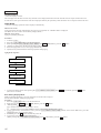
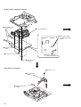
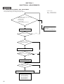
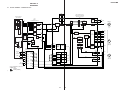
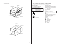
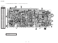
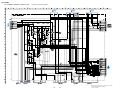
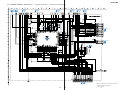
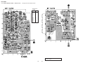
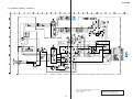
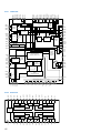
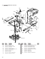
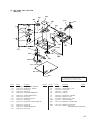
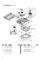
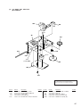
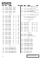
1
HCD-F3MD SERVICE MANUAL E Model HCD-F3MD is the Amplifier, CD player, MD Deck and Tuner section in CMT-F3MD. US and foreign patents licensed from Dolby Laboratories. Model Name Using Similar Mechanism HCD-MD373 CD CD Mechanism Type CDM55A-5SBD32 Section Base Unit Name BU-5SBD32 Optical Pick-up Name KSS-213BH/Z-NP Model Name Using Similar Mechanism HCD-MD373 MD MD Mechanism Type MDM-5GA Section Base Unit Name MBU-5A Optical Pick-up Name KMS-260B/S1NP SPECIFICATIONS Amplifier section Laser output DIN power output (Rated):20 + 20 watts (6 ohms at 1 kHz, DIN, 240 V) 18 + 18 watts (6 ohms at 1 kHz, DIN, 220 V) Continuous RMS power output (Reference): 25 + 25 watts (6 ohms at 1 kHz, 10% THD, 240 V) 23 + 23 watts (6 ohms at 1 kHz, 10% THD, 220 V) Peak Music Power Output: 400 watts Inputs TAPE IN (phono jacks): voltage 250 mV, impedance 47 kilohms Outputs TAPE OUT (phono jacks): voltage 250 mV, impedance 1 kilohm PHONES (stereo minijack): accepts headphones of 8 ohms or more. SPEAKER: accepts impedance of 6 to 16 ohms. Frequency response Max. 44.6 µW* *This output is the value measured at a distance of 200 mm from the objective lens surface on the Optical Pick-up Block with a 7 mm aperture. 2 Hz – 20 kHz Laser output Sampling frequency Frequency response MiniDisc digital audio system Semiconductor laser (λ=780 nm) Emission duration: continuous Max. 44.6 µW* *This output is the value measured at a distance of 200 mm from the objective lens surface on the Optical Pick-up Block with a 7 mm aperture. 44.1 kHz 5 Hz – 20 kHz Laser Compact disc and digital audio system Semiconductor laser (λ=780 nm) Emission duration: continuous Aerial 531 – 1,602 kHz (with the interval set at 9 kHz) 530 – 1,710 kHz (with the interval set at 10 kHz) AM loop aerial External aerial terminals 450 kHz General Power requirements 110 – 120 V or 220 – 240 V AC, 50/60 Hz Power consumption 70 watts during normal operation Approx. 3 watts in standby mode (clock displayed) Approx. 1 watt in standby mode (clock not displayed) Dimensions (w/h/d) incl. projecting parts and controls Approx. 215 × 150 × 335 mm Approx. 4.9 kg Mass Tuner section FM stereo, FM/AM superheterodyne tuner CD player section System Tuning range Intermediate frequency MD deck section System Laser AM tuner section Design and specifications are subject to change without notice. FM tuner section Tuning range Aerial Aerial terminals Intermediate frequency 87.5 – 108.0 MHz (50 kHz step) FM lead aerial 75 ohms unbalanced 10.7 MHz COMPACT DISC DECK RECEIVER SELF-DIAGNOSIS FUNCTION The self-diagnosis function consists of error codes for customers, which are displayed automatically when errors occur, and error codes, which show the error history in the test mode during servicing. For details on how to view error codes for the customer, refer to the following box in the instruction manual. For details on how to check error codes during servicing, refer to the following “Procedure for using the Self-Diagnosis Function (Error History Display Mode)”. Self-diagnosis Display This system has a Self-diagnosis display function to let you know if there is a system malfunction. The display shows a code made up of three letters and a message alternately to show you the problem. To solve the problem refer to the following list. If any problem persists, consult your nearest Sony dealer. C13/REC Error Recording could not be performed properly. cMove the system to a stable place, and start recording over from the beginning. The MD is dirty or scratched, or the MD does not meet the standards. cReplace the MD and start recording over from the beginning. C13/Read Error The MD deck cannot read the disc information properly. cRemove the MD once, then insert it again. C14/Toc Error The MD deck cannot read the disc information properly. cReplace the MD. cErase all the recorded contents of the MD using the All Erase function on page 38. C11/Protected The MD is protected against erasure. cRemove the MD and slide the tab to close the slot (see page 24). C12/Cannot Copy You tried to record a CD or MD with a format that the system does not support, such as a CDROM. cRemove the disc and turn off the system once, then turn it on again. C41/Cannot Copy The sound source is a copy of a commercially available music software, or you tried to record a CD-R (Recordable CD). cThe Serial Copy Management System prevents making a digital copy (see page 53). You cannot record a CD-R. PROCEDURE FOR USING THE SELF-DIAGNOSIS FUNCTION (ERROR HISTORY DISPLAY MODE) Note 1: About “R” As this unit has only a few buttons, some operations require the use of remote commander (RM-SF3MD/provided with unit: 1-476-068-11) buttons. These operations are indicated as “R” in this manual. Example: MENU/NO “R” ...Press the [MENU/NO] button of the remote commander. Note 2: Incorrect operations may be performed if the MD test mode is not entered properly. In this case, press the I/1 button to turn the power off, and retry to enter the MD test mode. Note 3: Perform the self-diagnosis function in the “error history display mode” in the MD test mode. The following describes the least required procedure. Be careful not to enter other modes by mistake. If you set other modes accidentally, press the MENU/NO “R” button to exit the mode. Procedure: 1. Press the I/1 button to turn the power on. 2. Press the [FUNCTION] button to set the MD function. 3. Press three buttons of s (MD) , zREC and I/1 simultaneously to enter the MD test mode and display “[Check]”. 4. Press the l m or M L button to display “[Service]”, and press the ENTER/YES “R” button. 5. Press the l m or M L button to display “ERR DP MODE”. 6. Press the ENTER/YES “R” button to enter the error history mode and display “total rec”. 7. Select the contents to be displayed or executed using the l m or M L button. 8. Press the [CD-MD SYNC] button will display or execute the contents selected. 9. Press the [CD-MD SYNC] button another time returns to step 7. 10. Press the MENU/NO “R” button displays “ERR DP MODE” and release the error history mode. 11. To release the MD test mode, press the [REPEAT] button to display “Initialize” and release the MD test mode. 2 ITEMS OF ERROR HISTORY MODE ITEMS AND CONTENTS Selecting the Test Mode Display Details of History total rec Displays the recording time. Displayed as “rssssssh”. The displayed time is the total time the laser is set to the high power state. This is about 1/4 of the actual recording time. The time is displayed in decimal digits from 0h to 65535h. total play Displays the play time. Displayed as “pssssssh”. The time displayed is the total actual play time. Pauses are not counted. The time is displayed in decimal digits from 0h to 65535h. retry err Displays the total number of retries during recording and number of retry errors during play. Displayed as “rss pss”. “r” indicates the retries during recording while “p” indicates the retry errors during play. The number of retries and retry errors are displayed in hexadecimal digits from 00 to FF. total err Displays the total number of errors. Displayed as “total ss”. The number of errors is displayed in hexadecimal digits from 00 to FF. err history Displays the 10 latest errors. Displayed as “0s E@@”. s indicates the history number. The smaller the number, the more recent is the error. (00 is the latest). @@ indicates the error code. Refer to the following table for the details. The error history can be switched by pressing the l m or M L button. er refresh Mode which erases the “retry err”, “total err”, and “err history” histories. When returning the unit to the customer after completing repairs, perform this to erase the past error history. After pressing the [CD-MD SYNC] button and “er refresh?” is displayed, press the ENTER/YES “R” button to erase the history. “Complete!” will be displayed momentarily. Be sure to check the following when this mode has been executed. • The data has been erased. • The mechanism operates normally when recording and play are performed. tm refresh Mode which erases the “total rec” and “total play” histories. These histories serve as approximate indications of when to replace the optical pick-up. If the optical pickup has been replaced, perform this operation and erase the history. After pressing the [CD-MD SYNC] button and “tm refresh?” is displayed, press the ENTER/YES “R” button to erase the history. “Complete!” will be displayed momentarily. Be sure to check the following when this mode has been executed. • The data has been erased. • The mechanism operates normally when recording and play are performed. Table of Error Codes Error Code E00 E01 E02 Details of Error No error Error Code E05 Details of Error FOK has deviated Disc error. PTOC cannot be read E06 Cannot focus (Servo has deviated) (DISC ejected) E07 Recording retry Disc error. UTOC error E08 Recording retry error (DISC not ejected) E09 Playback retry error E03 Loading error E04 Address cannot be read (Servo has deviated) (Access error) E0A Playback retry error (C2 error) 3 TABLE OF CONTENTS SELF-DIAGNOSIS FUNCTION ..................................... 2 1. SERVICING NOTES ............................................... 5 2. GENERAL ................................................................... 16 3. DISASSEMBLY ......................................................... 18 4. TEST MODE ............................................................... 26 5. ELECTRICAL ADJUSTMENTS MD Section ..................................................................... 30 CD Section ...................................................................... 38 6. DIAGRAMS 6-1. 6-2. 6-3. 6-4. 6-5. 6-6. 6-7. 6-8. 6-9. 6-10. 6-11. 6-12. 6-13. 6-14. 6-15. 6-16. 6-17. 6-18. 6-19. 6-20. 6-21. 6-22. 6-23. 6-24. 6-25. 6-26. 6-27. Block Diagram – CD SERVO Section – ....................... Block Diagram – MD SERVO Section (1/2) – ............. Block Diagram – MD SERVO Section (2/2) – ............. Block Diagram – MAIN Section – ................................ Note for Printed Wiring Boards and Schematic Diagrams ....................................................... Printed Wiring Board – BD (CD) Board – .................... Schematic Diagram – BD (CD) Board – ....................... Schematic Diagram – BD (MD) Board (1/2) – ............. Schematic Diagram – BD (MD) Board (2/2) – ............. Printed Wiring Board – BD (MD) Board – ................... Schematic Diagram – BD SW (MD) Board – ............... Printed Wiring Board – BD SW (MD) Board – ............ Schematic Diagram – LOADING (CD) Board – .......... Printed Wiring Board – LOADING (CD) Board – ....... Printed Wiring Board – MD DIGITAL Board – ........... Schematic Diagram – MD DIGITAL Board – .............. Printed Wiring Board – MAIN Board – ........................ Schematic Diagram – MAIN Board (1/3) – .................. Schematic Diagram – MAIN Board (2/3) – .................. Schematic Diagram – MAIN Board (3/3) – .................. Printed Wiring Boards – AMP/SP Boards – .................. Schematic Diagram – AMP/SP Boards – ...................... Printed Wiring Board – PANEL Board – ...................... Schematic Diagram – PANEL Board – ........................ Printed Wiring Board – POWER Board – ..................... Schematic Diagram – POWER Board – ........................ IC Pin Function Description ........................................... 7. EXPLODED VIEWS ................................................ 80 8. ELECTRICAL PARTS LIST ............................... 86 39 40 41 42 43 44 45 46 47 48 49 49 49 49 50 51 52 53 54 55 56 57 58 59 60 61 70 Notes on chip component replacement • Never reuse a disconnected chip component. • Notice that the minus side of a tantalum capacitor may be damaged by heat. Flexible Circuit Board Repairing • Keep the temperature of the soldering iron around 270 ˚C during repairing. • Do not touch the soldering iron on the same conductor of the circuit board (within 3 times). • Be careful not to apply force on the conductor when soldering or unsoldering. CAUTION Use of controls or adjustments or performance of procedures other than those specified herein may result in hazardous radiation exposure. This appliance is classified as a CLASS 1 LASER product. The CLASS 1 LASER PRODUCT MARKING is located on the rear exterior. Laser component in this product is capable of emitting radiation exceeding the limit for Class 1. The following caution label is located inside the unit. SAFETY-RELATED COMPONENT WARNING!! COMPONENTS IDENTIFIED BY MARK 0 OR DOTTED LINE WITH MARK 0 ON THE SCHEMATIC DIAGRAMS AND IN THE PARTS LIST ARE CRITICAL TO SAFE OPERATION. REPLACE THESE COMPONENTS WITH SONY PARTS WHOSE PART NUMBERS APPEAR AS SHOWN IN THIS MANUAL OR IN SUPPLEMENTS PUBLISHED BY SONY. 4 SECTION 1 SERVICING NOTES NOTES ON HANDLING THE OPTICAL PICK-UP BLOCK OR BASE UNIT MODEL IDENTIFICATION — Back panel — The laser diode in the optical pick-up block may suffer electrostatic break-down because of the potential difference generated by the charged electrostatic load, etc. on clothing and the human body. During repair, pay attention to electrostatic break-down and also use the procedure in the printed matter which is included in the repair parts. The flexible board is easily damaged and should be handled with care. PART No. For CD NOTES ON LASER DIODE EMISSION CHECK The laser beam on this model is concentrated so as to be focused on the disc reflective surface by the objective lens in the optical pick-up block. Therefore, when checking the laser diode emission, observe from more than 30 cm away from the objective lens. LASER DIODE AND FOCUS SEARCH OPERATION CHECK Carry out the “S curve check” in “CD section adjustment” and check that the S curve waveforms is output three times. Model Hong Kong model Part No. Korean model 4-229-548-1[] 4-232-128-0[] Taiwan model 4-232-129-0[] For MD NOTES ON LASER DIODE EMISSION CHECK Never look into the laser diode emission from right above when checking it for adjustment. It is feared that you will lose your sight. CLEANING OBJECTIVE LENS OF OPTICAL PICK-UP • In cleaning the objective lens of optical pick-up, be sure the following below. 1. In cleaning the lens, do not apply an excessive force. As the optical pick-up is vulnerable, application of excessive force could damage the lens holder. 2. In cleaning, do not use a cleaner other than exclusive cleaning liquid (KK-91 or isopropyl alcohol). 3. Wipe the objective lens spirally from center toward outside. (See Figure A) (Figure A) 4. Eject the disk, if loaded. 5. Disconnect the power cord from the socket to shut off the power supply. 6. When cleaning the objective lens of optical pick-up in CD, refer to “HOLDER (BU) ASS’Y” on page 24 for removing HOLDER (BU) ASS’Y. 5 DRAWING OUT THE TRAY WHEN THE POWER IS OFF tray (CDM) A Move the cam block in the direction of arrow A with a finger. CLEANING THE OPTICAL PICK-UP (CD PLAYER) CD mechanism deck floating screw (PTPWH M2.6) optical pick-up block Clean the lens block with a cotton bud. 6 SERVICE POSITION OF THE MD MECHANISM DECK SERVICE POSITION OF THE CD MECHANISM DECK MD mechanism deck CD mechanism deck SERVICE POSITION OF THE POWER BOARD POWER board CN993 AMP board CN802 MAIN board Extension cable (4P) (J-2501-042-A) Extension cable (3P) (J-2501-045-A) 7 MC COLD RESET • The cold reset clears all data including preset data stored in the RAM to initial conditions. Execute this mode when returning the set to the customer. Procedure: 1. Press the I/1 button to turn the power on. 2. While pressing the [PLAY MODE/TUNING MODE] and s (CD) buttons, press the I/1 button. 3. The set is reset, and displays “COLD RESET”, then becomes standby status. MC HOT RESET • This mode resets the set with the preset data kept stored in the memory. The hot reset mode function is same as if the power cord is plugged in and out. Procedure: 1. Press the I/1 button to turn the power on. 2. While pressing the [PLAY MODE/TUNING MODE] and HS (CD) buttons, press the I/1 button. 3. The set is reset, and becomes standby state. LED/FLUORESCENT INDICATOR TUBE AND KEY TEST Procedure: 1. Press the I/1 button to turn the power on. 2. While pressing the [PLAY MODE/TUNING MODE] and A (CD) buttons, press the I/1 button. 3. LEDs and fluorescent indicator tube are all turned on. 4. Press the HS (MD) button to enter the key test mode, and display “Key0 Vol0”. 5. Each time a button is pressed, “Key” value increases. However, once a button is pressed, it is no longer taken into account. “Vol” value increases like 0, 1, 2 ... if turn the [VOLUME] knob clockwise, or it decreases like 9, 8, 7 ... if turn the [VOLUME] knob counterclockwise. 6. To release from this mode, press three buttons in the same manner as step 2, or disconnect the power cord. Note: l m and M L buttons are no longer taken into account, if it pressed within for a second. CHANGE-OVER THE AM TUNING INTERVAL • The AM tuning interval can be changed over 9 kHz or 10 kHz. Procedure: 1. Press the I/1 button to turn the power on. 2. Press the [FUNCTION] button to set the TUNER function, and press the [TUNER/BAND] button to select the band “AM”. 3. Press the I/1 button to turn the power off. 4. When the power off, press the I/1 button while pressing the [PLAY MODE/TUNING MODE] button, and the display of fluorescent indicator tube changes to “AM 9k STEP” or “AM 10k STEP”, and thus the tuning interval is changed over. 8 MD SECTION JIG FOR CHECKING BD (MD) BOARD WAVEFORM The special jig (J-2501-149-A) is useful for checking the waveform of the BD (MD) board. The names of terminals and the checking items to be performed are shown as follows. GND : Ground I+3V : For measuring IOP (Check the deterioration of the optical pick-up laser) IOP : For measuring IOP (Check the deterioration of the optical pick-up laser) TEO : Tracking error signal (Traverse adjustment) VC : Reference level for checking the signal RF : RF signal (Check jitter) Mechanism deck CN110 6P connector 5P connector RF VC TEO IOP I+3V GND RF VC 1 RF VC for TEO MDM-3 IOP 5 I+3V TEO IOP I+3V GND 1 VC RF TEO for IOP MDM-5 I+3V 6 GND 9 Note : About “R” As this unit has only a few buttons, some operations require the use of remote commander (RM-SF3MD/provided with unit: 1-476-068-11) buttons. These operations are indicated as “R” in this manual. Example: MENU/NO “R” ...Press the [MENU/NO] button of the remote commander. IOP DATA RECORDING AND DISPLAY WHEN OPTICAL PICK-UP AND NON-VOLATILE MEMORY (IC171 ON THE BD (MD) BOARD) ARE REPLACED The IOP value labeled on the optical pick-up can be recorded in the non-volatile memory. By recording the value, it will eliminate the need to look at the value on the label of the optical pick-up. When replacing the optical pick-up or non-volatile memory (IC171 on the BD (MD) board), record the IOP value on the optical pick-up according to the following procedure. Record Procedure: 1. Press the I/1 button to turn the power on. 2. Press the [FUNCTION] button to set the MD function. 3. While pressing the s (MD) and zREC buttons, press the I/1 button to enter the MD test mode and display “[Check]”. 4. Press the l m or M L button to display “[Service]”, and press the ENTER/YES “R” button. 5. Press the l m or M L button to display “Iop Write”, and press the ENTER/YES “R” button. 6. The display becomes “Ref=@@@.@” (@ is an arbitrary number) and the numbers which can be changed will blink. 7. Input the IOP value written on the optical pick-up. To select the number : Press the l m or M L button. To select the digit : Press the [SYNC REC] button. 8. When the ENTER/YES “R” button is pressed, the display becomes “Measu=@@@.@” (@ is an arbitrary number). 9. As the adjustment results are recorded for the step7 value. Leave it as it is and press the ENTER/YES “R” button. 10. “Complete!” will be displayed momentarily. The value will be recorded in the non-volatile memory and the display will become “Iop Write”. 11. Press the [REPEAT] button to complete. “Standby” will be displayed. Display Procedure: 1. Press the I/1 button to turn the power on. 2. Press the [FUNCTION] button to set the MD function. 3. While pressing the s (MD) and zREC buttons, press the I/1 button to enter the MD test mode and display “[Check]”. 4. Press the l m or M L button to display “[Service]”, and press the ENTER/YES “R” button. 5. Press the l m or M L button to display “Iop Read”, and press the ENTER/YES “R” button. 6. “@@.@/##.#” is displayed and the recorded contents are displayed. @@.@ : indicates the Iop value labeled on the pick-up. ##.# : indicates the Iop value after adjustment 7. To release, press the [CD-MD SYNC] button or MENU/NO “R” button to display “Iop Read”. Then press the [REPEAT] button to display “Standby”. 10 CHECKS PRIOR TO PARTS REPLACEMENT AND ADJUSTMENTS Before performing repairs, perform the following checks to determine the faulty locations up to a certain extent. Details of the procedures are described in “5 Electrical Adjustments”. Criteria for Determination (Unsatisfactory if specified value is not satisfied) Measure if unsatisfactory: • 0.9 mW power Specified value : 0.84 to 0.92 mW • 7.0 mW power Specified value : 6.8 to 7.2 mW • Clean the optical pick-up • Adjust again • Replace the optical pick-up lop (at 7mW) • Labeled on the optical pickup Iop value ± 10mA • Replace the optical pick-up Traverse check (5-6-3 : See page 32) • Traverse waveform Specified value : Below 10% offset • Replace the optical pick-up Focus bias check (5-6-4 : See page 33) • Error rate check Specified value : For points A, B C1 error : About 200 AD error : Below 2 For point C C1 error : Below 50 AD error : Below 2 • Replace the optical pick-up C PLAY check (5-6-5 : See page 33) • Error rate check Specified value: a. When using test disc (MDW-74/AU-1) C1 error : Below 80 AD error : Below 2 b. When using check disc (TDYS-1) C1 error : Below 50 • Replace the optical pick-up Self-recording/playback check (5-6-6 : See page 33) • CPLAY error rate check Specified value: C1 error : Below 80 AD error : Below 2 If always unsatisfactory: • Replace the overwrite head • Check for disconnection of the circuits around the overwrite head Laser power check (5-6-2 : See page 32) If occasionally unsatisfactory: • Check if the overwrite head is distorted • Check the mechanism around the sled Temperature compensation offset check (5-6-1 : See page 32) • Unsatisfactory if displayed as T=@@ (##) [NG” NG (@@, ## are both arbitrary numbers) • Check for disconnection of the circuits around D101 (BD (MD) board) • Check the signals around IC101, IC121, CN102, CN103 (BD (MD) board) Note: The criteria for determination above is intended merely to determine if satisfactory or not, and does not serve as the specified value for adjustments. When performing adjustments, use the specified values for adjustments. 11 RETRY CAUSE DISPLAY MODE • In this test mode, the causes for retry of the unit during recording can be displayed on the fluorescent indicator tube. During playback, the “track mode” for obtaining track information will be set. This is useful for locating the faulty part of the unit. • The following will be displayed : During recording and stop : Retry cause, number of retries, and number of retry errors. During playback : Information such as type of disc played, part played, copyright. These are displayed in hexadecimal. Procedure: 1. Load a recordable disc whose contents can be erased into the unit. 2. Press the MENU/NO “R” button. When “Edit Menu” is displayed on the fluorescent indicator tube, press the l m or M L button to display “All Erase?”. 3. Press the ENTER/YES “R” button. 4. When “All Erase??” is displayed on the fluorescent indicator tube, the music calendar number blinks. 5. Press the ENTER/YES “R” button to display “Complete!!”, and press the s (MD) button immediately. Wait for about 10 seconds while pressing the button. 6. When the “TOC” displayed on the fluorescent display tube goes off, release the s (MD) button. 7. Press the zREC button to start recording. Then press the HS (MD) button and start recording. If recording cannot be performed, press the [FUNCTION] button and set a different function. 8. To check the “track mode”, press the HS (MD) button to start play. 9. To release the test mode, press the I/1 button, and turn the power off. When “TOC” disappears, disconnect the power plug from the outlet. If the test mode cannot be released, refer to “MC COLD RESET” on page 8). Fig. 1 Reading the Test Mode Display (During recording and stop) Fig. 2 Reading the Test Mode Display (During playback) RTs@@c##e** Fluorescent indicator tube display @@ ###** $$ Fluorescent indicator tube display @@ : ## : ** : $$ : @@ : Cause of retry ## : Number of retries ** : Number of retry errors Parts No. (name of area named on TOC) Cluster Address Sector Track mode (Track information such as copyright information of each part) Reading the Retry Cause Display Higher Bits Hexa1 decimal b7 b6 b5 b4 b3 b2 b1 b0 Hexadecimal 8 Bit Binary Lower Bits Occurring conditions Cause of Retry 4 2 1 8 4 2 0 0 0 0 0 0 0 1 01 shock When track jump (shock) is detected 0 0 0 0 0 0 1 0 02 ader5 When ADER was counted more than five times continuously 0 0 0 0 0 1 0 0 04 0 0 0 0 1 0 0 0 08 Discontinuous address When ADIP address is not continuous When DIN unlock is detected DIN unlock 0 0 0 1 0 0 0 0 10 FCS incorrect When not in focus 0 0 1 0 0 0 0 0 20 IVR rec error When ABCD signal level exceeds the specified range 0 1 0 0 0 0 0 0 40 CLV unlock When CLV is unlocked 1 0 0 0 0 0 0 0 80 Access fault When access operation is not performed normally Reading the Display: Convert the hexadecimal display into binary display. If more than two causes, they will be added. Example When 42 is displayed: Higher bit: 4 = 0100 t b6 Lower bit : 2 = 0010 t b1 In this case, the retry cause is combined of “CLV unlock” and “ader5”. When A2 is displayed: Higher bit: A = 1010 t b7+b5 Lower bit : 2 = 0010 t b1 The retry cause in this case is combined of “access fault”, “IVR rec error”, and “ader5”. 12 Reading the Retry Cause Display Higher Bits Lower Bits HexaHexadecimal 8 4 2 1 8 4 2 1 decimal Bit b7 b6 b5 b4 b3 b2 b1 b0 Binary Details When 1 When 0 0 0 0 0 0 0 0 1 01 Emphasis OFF Emphasis ON 0 0 0 0 0 0 1 0 02 Monaural Stereo 0 0 0 0 0 1 0 0 04 0 0 0 0 1 0 0 0 08 This is 2-bit display. Normally 01. 01:Normal audio. Others:Invalid 0 0 0 1 0 0 0 0 10 Audio (Normal) Invalid 0 0 1 0 0 0 0 0 20 Original Digital copy 0 1 0 0 0 0 0 0 40 Copyright No copyright 1 0 0 0 0 0 0 0 80 Write prohibited Write allowed Reading the Display: Convert the hexadecimal display into binary display. If more than two causes, they will be added. Example When 84 is displayed: Higher bit: 8 = 1000 t b7 Lower bit : 4 = 0100 t b2 In this case, as b2 and b7 are 1 and others are 0, it can be determined that the retry cause is combined of “emphasis OFF”, “monaural”, “original”, “copyright exists”, and “write allowed”. Example When 07 is displayed: Higher bit: 0 = 0000 t All 0 Lower bit : 7 = 0111 t b0+b1+b2 In this case, as b0, b1, and b2 are 1 and others are 0, it can be determined that the retry cause is combined of “emphasis ON”, “stereo”, “original”, “copyright exists”, and “write prohibited”. Hexadecimal t Binary Conversion Table Hexadecimal Binary Hexadecimal Binary 0 0000 8 1000 1 0001 9 1001 2 0010 A 1010 3 0011 B 1011 4 0100 C 1100 5 0101 D 1101 6 0110 E 1110 7 0111 F 1111 13 CD SECTION CD TEXT DISPLAY • This unit displays CD text. Text is displayed for the first 50 tracks only and will not be displayed from the 51st track onwards. Do not suspect a fault in this case. In some cases, some special characters will not be displayed and may be replaced by other characters. Do not suspect a fault in this case. AGING MODE • Mode for repeating operations of the CD player automatically. When errors occur: Aging stops and a message indicating that an error has occurred such as “CD MEC ERR” is displayed. (For details of errors, refer to “Error History Display Mode”) When no errors occur: Aging is repeatedly performed. Procedure: 1. Load any CD disc. 2. Press the [FUNCTION] button to set the CD function. 3. While pressing the [PLAY MODE/TUNING MODE] and HS (MD) buttons, press the I/1 button. 4. “AGING” is displayed on the fluorescent display tube briefly. 5. When the aging mode is set, it starts aging automatically. 6. Operations are performed in the following sequence during aging. Aging mode sequence: TOC read Playback track 1 Playback last track CD disc tray open CD disc tray open 7. To release from this mode, while pressing the [PLAY MODE/TUNING MODE] and HS (CD) buttons, press the I/1 button. (Hot reset is executed) Error History Display Mode Mode for checking the history of errors which have occurred in the CD player. Execute this mode after ending the aging mode. Procedure: 1. Press the [FUNCTION] button to set the CD function. 2. While pressing the M L and s (MD) buttons, press the I/1 button. 3. “EMC@@EDC**” is displayed. @@ : Number of mechanism errors (Past 3 errors) ** : Number of errors (NO DISC ERROR) which occurred after chucking (Past 3 errors) 4. To check the history of mechanism errors, press the [PLAY MODE/TUNING MODE] button, and to check BD errors, press the [REPEAT] button, and switch the display. 5. To release, press the I/1 button and turn the power off. 6. To erase the error history, perform COLD reset. (While pressing the [PLAY MODE/TUNING MODE] and s (CD) buttons, press the I/1 button) 14 • Reading the Mechanism Error History Display (To switch the history, press the [PLAY MODE/TUNING MODE] button) Display E@@M**#*$* @@ : Error number. 00 is the latest * : Invalid # : Load in operations related D : Operations stopped due to problems other than mechanism related during CLOSE E : Operations stopped due to problems other than mechanism related during OPEN C : Operations stopped due to problems other than mechanism related during chucking up $ : Load out operations related 1 : Operations stopped during chucking up 2 : Operations stopped during chucking down • Reading the BD Error History Display (To switch the history, press the [REPEAT] button) Display E@@D##$$%* @@ : Error number. 00 is the latest ## : Error details 01 : Focus error 02 : GFS error 03 : Setup error $$ : Retry performed/not performed 00 : Determined as NO DISC without chucking retry 02 : Determined as NO DISC after chucking retry % : State when determined as NO DISC 1 : When stopped 2 : During setup 3 : During TOC READ 4 : During access 5 : During playback 6 : During PAUSE 7 : During manual search (during playback) 8 : During manual search (during pause) : Invalid * 15 SECTION 2 GENERAL This section is extracted from instruction manual. LOCATION OF CONTROLS • Front View 1 I/1 button and indicator 2 MD disc slot 3 MD A button and MD disc indicator 4 MD H S button and indicator 5 MD s button 6 CD disc tray 7 CD A button and CD disc indicator 8 CD H S button and indicator 9 CD s button 0 Fluorescent indicator tube qa Remote sensor qs TUNER/BAND button qd VOLUME knob qf FUNCTION button qg PHONES jack qh PLAY MODE, TUNING MODE button qj REPEAT, STEREO/MONO button qk CD-MD SYNC button ql zREC button and indicator w; MD/CD l m/M L, TUNUNG +/– buttons • Rear View 1 TAPE IN/OUT jacks 2 SPEAKER IMPEDANCE 6-16 Ω terminals 3 AM ANTENNA terminals 4 TAPE CONTROL jack 5 FM 75 Ω COAXIAL jack 6 AC power cord 16 3 N (play) button Parts descriptions for the remote 9 DBFB button X (pause) button 5 6 x (stop) button Press to label a CD, MD and preset station, or to set the clock. (pages 5, 18, 35, 45) Press to display the disc title or track title scrolling. (pages 19, 23, 36) qa CLEAR button Note ./> (AMS: Automatic Music You cannot perform the following operations with the remote; — TUNING MODE setting for the tuner — STEREO/MONO setting for the tuner — Removing discs — Recording on the MD — One Touch Play Press to reinforce the bass sound. (page 44) 0 SCROLL button 9 CURSORT/t, m/M buttons You can use the supplied remote to control the system. 8 0 Sensor) buttons 7 4 VOL +/– buttons Press to cancel the selection. (pages 16, 18, 21, 35, 45) qa Press to adjust the volume. MENU/NO button Press to set Programme Play, or to label a CD, MD and preset station. 1 ENTER/YES button 2 Press to set the clock, Programme Play and to label a CD, MD and preset station, or to enter the settings in “Edit Menu” or “Setup Menu”. DISP button Press to show the various information. (pages 17 and 23) 3 5 SLEEP button Press to set Sleep Timer. (page 46) 6 PLAY MODE button Press to select normal play, Shuffle Play or Programme Play. (pages 15, 16, 21, 25) REPEAT button Press to play a track or all the tracks repeatedly (pages 15 and 20). MUSIC MENU button Press to select the type of the preset equalizer. (page 44) 4 7 NAME EDIT buttons Press to display the text input screen and to select the type of characters to be input. (pages 19, 35, 45) 2 The sound source buttons SPACE button MD button CD button TAPE button FUNCTION button Press to switch the sound source. Each time you press this button, the sound source changes as follows; t CD t TUNER TAPE T Press to enter a space directly when labelling a CD, MD and preset stion. (pages 19, 36, 46) 8 CLOCK/TIMER SELECT button Additional Information CHARACTER button 1 ?/1 (power) switch Press to check timer settings, or to set the timer on/off. (pages 48 and 49) CLOCK/TIMER SET button Press to set the clock and timer functions. (pages 5, 47, 48) MD T TUNER/BAND button Press to select the tuner for the sound source, or to select the FM or AM band. 60 61 Step 2: Setting the time (continued) Step 2: Setting the time 1 2 3,5 CURSORT DISP Getting Started You must set the time beforehand to use the timer functions. 5 Press . or > to set the minute. 6 Press ENTER/YES. The clock starts. If you made a mistake Press CURSORT or t repeatedly until the incorrect item flashes, then set it again. 3,5 4 4,6 To change the preset time You can change the preset time while the system is off. 1 Press DISP to display the clock. 2 Press CLOCK/TIMER SET. 3 Repeat steps 3 to 6 of “Setting the time”. Tip 1 Turn on the system. 2 Press CLOCK/TIMER SET. The upper dot of the colon flashes for the first 30 seconds, and the lower dot flashes for the last 30 seconds of each minute. The clock appears and the hour indication flashes. 3 4 Press . or > to set the hour. Press ENTER/YES or CURSORt . The minute indication flashes. continued 5 6 17 SECTION 3 DISASSEMBLY Note: Follow the disassembly procedure in the numerical order given. CASE 2 case 1 two screws (case3 TP2) 1 two screws (case3 TP2) FRONT PANEL SECTION 3 Remove the cord. 5 screw (BVTT3 × 6) 9 MD mechanism deck section 8 screw (BVTP2.6 × 8) 8 screw (BVTP2.6 × 8) 1 wire (flat type) (25 core) (CN107) 6 claw BACK PANEL ASS’Y (Page 22) 2 ground wire 7 q; front panel section 4 three screws (BVTT3 × 6) 6 claw 1 wire (flat type) (29 core) (CN11) 18 6 claw MD MECHANISM DECK (MDM-5GA) 2 four step screws (BVTPWH M3) 1 connector (CN601) 6 MD mechanism deck (MDM-5GA) 4 wire (flat type) (23 core) (CN103) 4 wire (flat type) (21 core) (CN102) 3 5 bracket (MDM) SLIDER (CAM) 7 slider (cam) • NOTE FOR INSTALLATION OF SLIDER (CAM) Set the shaft of cam gear to be at the position in the figure. 3 bracket (guide L) A 1 two screws (DIA2.6) 2 ground wire Set the shaft of lever (O/C) to be at the position in the figure. 4 leaf spring (electrostatic) When attaching the slider (cam), this part of the over write head should be inside arrow A. 5 two screws (DIA.2.6) 6 bracket (guide R) 19 BD (MD) BOARD, BASE UNIT (MBU-5A) 5 two flexible boards (CN101, 104) 7 base unit (MBU-5A) CN103 CN102 1 Remove two solders of spindle motor leads (M901). 6 BD (MD) board 4 screw (M1.7) 2 Remove two solders of sled motor leads (M902). 3 three screws (DIA.2.6) OVER WRITE HEAD (HR901) 2 screw (P1.7 × 6) 3 over write head (HR901) 1 flexible board (CN104) 20 SPINDLE MOTOR ASS’Y (M901), SLED MOTOR ASS’Y (M902) 3 gear (SL-B) 4 three screws (B2 × 5) 1 screw (M1.7) 2 gear (SL-A) 5 spindle motor ass’y (M901) 6 two screws (P1.7 × 2.5) 7 sled motor ass’y (M902) OPTICAL PICK-UP OF MD (KMS-260B/S1NP) 4 Turn over the optical pick-up. 6 optical pick-up (KMS-260B/S1NP) 5 flexible board 1 screw (B2 × 8) 2 leaf spring (shaft) 3 main shaft 21 BACK PANEL ASS’Y 4 back panel ass’y 1 six screws (BVTP3 × 10) 3 claw 2 claw 3 claw SP BOARD, POWER BOARD AND MAIN BOARD 4 two connectors (CN991, 992) 4 connector (CN993) 5 two screws (BVTT3 × 6) 8 connector (CN994) 9 POWER board 3 wire (flat type) (25 core) (CN109) 2 SP board 3 wire (flat type) (15 core) 1 two connectors (CN881, 882) q; MAIN board 7 6 screw (BVTT3 × 6) 6 screw (BVTT3 × 6) 4 connector (CN110) 22 CD MECHANISM DECK (CDM55A-5SBD32) 4 holder (MDM) 3 screw (BVTT3 × 6) 7 CD mechanism deck (CDM55A-5SB32) 5 screw (BVTT3 × 6) 1 wire (flat type) (19 core) (CN109) 6 two claws 3 screw (BVTT3 × 6) 2 connector (CN110) TRAY (CDM), GEAR AND CAM (CDM55) 4 belt (CDM55) Note: when drawing out the tray (CDM), refer to service notes DRAWING OUT THE TRAY WHEN THE POWER IS OFF on page 6 . 7 roller 5 bushing 8 gear (B) 6 pulley (LDG) 9 gear (A) q; cam (CDM55) 2 Push the claw in the direction of arrow A. A 1 tray (CDM) 3 Drawing out the tray (CDM). 2 Release the lock while pressing this claw in the arrow direction. 23 HOLDER (BU) ASS’Y 1 floating screw (PTPWH M2.6) 2 Remove the holder (BU) ass’y in the direction of the arrow. OPTICAL PICK-UP OF CD (KSS-213BH/Z-NP) 5 optical pick-up (KSS-213BH/Z-NP) 3 wire (flat type) (16 core) 4 1 Release the lever in the direction of arrow A. A 2 sled shaft 24 BD (CD) BOARD, BASE (BU-5S) ASS’Y (M101) AND SLED MOTOR ASS’Y (M102) 4 two screws (B2 × 4) 6 gear (M) 9 base (BU-5S) ass’y (M101) 8 two insulators (BU) 2 Remove the four solders. 8 two insulators (BU) 7 flatness gear (P) 5 sled motor ass’y (M102) M101 M102 3 BD (CD) board 1 screw (BVTP2.6 × 8) 25 SECTION 4 TEST MODE Note : About “R” As this unit has only a few buttons, some operations require the use of remote commander (RM-SF3MD/provided with unit: 1-476-068-11) buttons. These operations are indicated as “R” in this manual. Example: MENU/NO “R” ...Press the [MENU/NO] button of the remote commander. 4-1. PRECAUTIONS FOR USE OF TEST MODE • As loading related operations will be performed regardless of the test mode operations being performed, be sure to check that the disc is stopped before setting and removing it. Even if the A (MD) button is pressed while the disc is rotating during continuous playback, continuous recording, etc., the disc will not stop rotating. Therefore, it will be ejected while rotating. Be sure to press the A (MD) button after pressing the MENU/NO “R” button and the rotation of disc is stopped. 4-1-1. Recording laser emission mode and operating buttons • Continuous recording mode (CREC MODE) • Laser power check mode (LDPWR CHECK) • Laser power adjustment mode (LDPWR ADJUST) • Traverse (MO) check (EF MO CHECK) • Traverse (MO) adjustment (EF MO ADJUST) • When pressing the zREC button. 4-2. SETTING THE TEST MODE The following are two methods of entering the test mode. Procedure 1: 1. Press the I/1 button to turn the power on. 2. Press the [FUNCTION] button to set the MD function. 3. While pressing the s (MD) and zREC buttons, press the I/1 button to enter the MD test mode and display “[Check]”. When the test mode is set, “[Check]” will be displayed. Press the l m or M L button switches between the following four groups; ···y [Check] y [Adjust] y [Service] y [Develop] y ···. Procedure 2: 1. Press the I/1 button to turn the power on. 2. Press the [FUNCTION] button to set the MD function. 3. While pressing the s (MD) and [CD-MD SYNC] buttons, press the I/1 button to enter the MD test mode and display “TEMP CHECK”. By setting the test mode using this method, only the “Check” group of method 1 can be executed. 4-3. RELEASING THE TEST MODE Press the [REPEAT] button. 4-4. BASIC OPERATIONS OF THE TEST MODE All operations are performed using the l m or M L button , ENTER/YES “R” button, and MENU/NO “R” button. The functions of these buttons are as follows. Function name Function l m , M L buttons Changes parameters and modes ENTER/YES “R” button Proceeds onto the next step. Finalizes input MENU/NO “R” button Returns to previous step. Stops operations 26 4-5. SELECTING THE TEST MODE There are 31 types of test modes as shown below. The groups can be switched by pessing the l m or M L button. After selecting the group to be used, press the ENTER/YES “R” button. After setting a certain group, press the l m or M L button switches between these modes. Refer to “Group” in the table for details can be selected. All items used for servicing can be treated using group S. So be carefully not to enter other groups by mistake. Display Contents Mark Group (*) TEMP CHECK Temperature compensation offset check C S LDPWR CHECK Laser power check C S EF MO CHECK Traverse (MO) check C S EF CD CHECK Traverse (CD) check C S FBIAS CHECK Focus bias check C S Scurve CHECK S letter check (X) C VERIFYMODE Non-volatile memory check (X) C DETRK CHECK Detrack check (X) C TEMP ADJUST Temperature compensation offset adjustment A S LDPWR ADJUST Laser power adjustment A S EF MO ADJUST Traverse (MO) adjustment A S EF CD ADJUST Traverse (CD) adjustment A S FBIAS ADJUST Focus bias adjustment A S EEP MODE Non-volatile memory control MANUAL CMD (X) (!) D Command transmission (X) D SVDATA READ Status display (X) ERR DP MODE Error history display, clear SLED MOVE Sled check (X) D ACCESS MODE Access check (X) D 0920 CHECK Outermost circumference check (X) D HEAD ADJUST Head position check (X) D CPLAY2 MODE Same functions as CPLAY MODE (X) D CREC2 MODE Same functions as CREC MODE (X) ADJ CLEAR Initialization of non-volatile memory of adjustment value A S AG Set (MO) Auto gain output level adjustment (MO) A S AG Set (CD) Auto gain output level adjustment (CD) A Iop Read IOP data display Iop Write IOP data write INFORMATION Microprocessing version display C CPLAY MODE Continuous playback mode C A S D CREC MODE Continuous recording mode C A S D D S D C A Group (*) C: Check S: Service S S S S A: Adjust D: Develop • For details of each adjustment mode, refer to “5. Electrical Adjustments”. For details of “ERR DP MODE”, refer to “Self-Diagnosis Function” on page 2. • If a different mode has been selected by mistake, press the MENU/NO “R” button to release that mode. • Modes with (X) in the Mark column are not used for servicing and therefore are not described in detail. If these modes are set accidentally, press the MENU/NO “R” button to release the mode immediately. Be especially careful not to set the modes with (!) as they will overwrite the non-volatile memory and reset it, and as a result, the unit will not operate normally. 27 4-5-1. Operating the Continuous Playback Mode 1. Entering the continuous playback mode (1) Set the disc in the unit. (Whichever recordable discs or discs for playback only are available.) (2) Press the l m or M L button and display “CPLAY MODE”. (3) Press the ENTER/YES “R” button to change the display to “CPLAY MID”. (4) When access completes, the display changes to “C1 = AD = ”. Note: The numbers “ ” displayed show you error rates and ADER. 2. Changing the parts to be played back (1) Press the ENTER/YES “R” button during continuous playback to change the display as below. “CPLAY MID” t “CPLAY OUT” t “CPLAY IN” When pressed another time, the parts to be played back can be moved. When access completes, the display changes to “C1 = AD = ”. (2) Note: The numbers “ ” displayed show you error rates and ADER. 3. Ending the continuous playback mode (1) Press the MENU/NO “R” button. The display will change to “CPLAY MODE”. (2) Press the A (MD) button and take out the disc. Note: The playback start addresses for IN, MID, and OUT are as follows. IN : 40h cluster MID : 300h cluster OUT : 700h cluster 4-5-2. Operating the Continuous Recording Mode (Use only when performing self-recording/palyback check.) 1. Entering the continuous recording mode (1) Set a recordable disc in the unit. (2) Press the l m or M L button and display “CREC MODE”. (3) Press the ENTER/YES “R” button to change the display to “CREC MID”. )” and [z REC] indicator lights up. (4) When access completes, the display changes to “CREC ( Note: The numbers “ ” displayed shows you the recording position addresses. 2. Changing the parts to be recorded (1) When the ENTER/YES “R” button is pressed during continuous recording, the display changes as below. “CREC MID” t “CREC OUT” t “CREC IN” (2) When pressed another time, the parts to be recorded can be changed. [z REC] indicator goes off. When access completes, the display changes to “CREC ( )” and [z REC] indicator lights up. Note: The numbers “ ” displayed shows you the recording position addresses. 3. Ending the continuous recording mode (1) Press the MENU/NO “R” button. The display changes to “CREC MODE” and [z REC] indicator goes off. (2) Press the A (MD) button and take out the disc. Note 1: The recording start addresses for IN, MID, and OUT are as follows. IN : 40h cluster MID : 300h cluster OUT : 700h cluster Note 2: The MENU/NO “R” button can be used to stop recording anytime. Note 3: Do not perform continuous recording for long periods of time above 5 minutes. Note 4: During continuous recording, be careful not to apply vibration. 4-5-3. Non-Volatile Memory Mode (EEP MODE) This mode reads and writes the contents of the non-volatile memory. It is not used in servicing. If the unit entered this mode accidentally, press the MENU/NO “R” button immediately to release it. 4-6. FUNCTIONS OF OTHER BUTTONS Function Contents H S (MD) Sets continuous playback when pressed in the STOP state. When pressed during continuous playback, the tracking servo turns ON/OFF s (MD) Stops continuous playback and continuous recording ML The sled moves to the outer circumference only when this is pressed lm The sled moves to the inner circumference only when this is pressed CLEAR “R” Switches between the pit and groove modes when pressed PLAY MODE/TUNING MODE Switches the spindle servo mode (CLV-S y CLV-A) DISP “R” Switches the displayed contents each time the button is pressed A (MD) Ejects the disc REPAET Releases the test mode 28 4-7. TEST MODE DISPLAYS Each time the DISP “R” button is pressed, the display changes in the following order. 1. Mode display Displays “TEMP ADJUST”, “CPLAYMODE”, etc. 2. Error rate display Displays the error rate in the following way. C1 = ssss AD = ss C1 = Indicates the C1 error. AD = Indicates ADER. 3. Address display The address is displayed as follows. (MO: recordable disc, CD: playback only disc) Press the CLEAR “R” button to switches between the groove display and pit display. h = ssss s = ssss (MO pit and CD) h = ssss a = ssss (MO groove) h = Indicates the header address. s = Indicates the SUBQ address. a = Indicates the ADIP address. Mode display Error rate display Note: “–” is displayed when servo is not imposed. Address display 4. Auto gain display (Not used in servicing) The auto gain is displayed as follows. AG = ss/ss[ss] Auto gain display (Not used in servicing) 5. Detrack check display (Not used in servicing) The detrack is displayed as follows. ADR = sssssss Detrack check display (Not used in servicing) IVR display (Not used in servicing) 6. IVR display (Not used in servicing) The IVR is displayed as follows. [ss][ss][ss] MEANINGS OF OTHER DISPLAYS Contents Display When Lit When Off H (MD)* During continuous playback (CLV: ON) STOP (CLV: OFF) S (MD)* Tracking servo OFF Tracking servo ON zREC* Recording mode ON Recording mode OFF SYNC CLV low speed mode CLV normal mode L.SYNC ABCD adjustment completed OVER Tracking offset cancel ON 1 Tracking auto gain OK REPEAT Focus auto gain OK DISC High reflection Low reflection SHUF CLV-S CLV-A MONO CLV LOCK CLV UNLOCK Tracking offset cancel OFF * : Indicate by LED. 29 SECTION 5 ELECTRICAL ADJUSTMENTS MD SECTION 5-1. PARTS REPLACEMENT AND ADJUSTMENT • Check and adjust the mechanism deck as follows. The procedure changes according to the part replaced • Abbreviation OP : Optical pick-up OWH : Overwrite head • Temperature compensation offset check • Laser power check • Traverse check • Focus bias check • C PLAY check • Self-recording/playback check OK NG Check the sled and spindle mechanisms. Other causes can be suspected. Parts Replacement and Repair Has the OWH been replaced? YES NO Has OP, IC171, IC101, or IC121 been replaced? YES Initial setting of the adjustment value NO Has OP or IC171 been replaced? NO YES IOP information recording (IOP value labeled on OP) Has IC171 or D101 been replaced? YES Temperature compensation offset adjustment • Laser power adjustment • Traverse adjustment • Focus bias adjustment • Error rate adjustment • Focus bias check • Auto gain adjustment 30 NO Note : About “R” As this unit has only a few buttons, some operations require the use of remote commander (RM-SF3MD/provided with unit: 1-476-068-11) buttons. These operations are indicated as “R” in this manual. Example: MENU/NO “R” ...Press the [MENU/NO] button of the remote commander. 5-2. PRECAUTIONS FOR CHECKING LASER DIODE EMISSION To check the emission of the laser diode during adjustments, never view directly from the top as this may lose your eye-sight. 5-3. PRECAUTIONS FOR USE OF OPTICAL PICK-UP (KMS-260B) As the laser diode in the optical pick-up is easily damaged by static electricity, solder the laser tap of the flexible board when using it. Before disconnecting the connector, desolder first. Before connecting the connector, be careful not to remove the solder. Also take adequate measures to prevent damage by static electricity. Handle the flexible board with care as it breaks easily. pick-up flexible board 2. Set the test mode when performing adjustments. After completing the adjustments, release the test mode. Perform the adjustments and checks in “group S” of the test mode. 3. Perform the adjustments to be needed in the order shown. 4. Use the following tools and measuring devices. • Check Disc (MD) TDYS-1 (Part No. 4-963-646-01) • Test Disc (MDW-74/AU-1) (Part No. 8-892-341-41) • Laser power meter LPM-8001 (Part No. J-2501-046-A) or MD Laser power meter 8010S (Part No. J-2501-145-A) • Oscilloscope (Measure after performing CAL of prove) • Digital voltmeter • Thermometer • Jig for checking BD board waveform (Part No. : J-2501-149-A) 5. When observing several signals on the oscilloscope, etc., make sure that VC and ground do not connect inside the oscilloscope. (VC and ground will become short-circuited) 6. Using the above jig enables the waveform to be checked without the need to solder. (Refer to Servicing Notes on page 9) 7. As the disc used will affect the adjustment results, make sure that no dusts nor fingerprints are attached to it. laser tap Laser power meter Optical pick-up flexible board 5-4. PRECAUTIONS FOR ADJUSTMENTS 1. When replacing the following parts, perform the adjustments and checks with a in the order shown in the following table. Optical Pick-up IC171 1. Initial setting of adjustment value a a BD Board D101 × When performing laser power checks and adjustment (electrical adjustment), use of the new MD laser power meter 8010S (Part No. J-2501-145-A) instead of the conventional laser power meter is convenient. It sharply reduces the time and trouble to set the laser power meter sensor onto the objective lens of optical pick-up. IC101, IC121 IC192 a × 5-5. CREATING CONTINUOUSLY-RECORDED DISC 2. Recording of IOP information (Value on the optical pick-up label) a a × × × 3. Temperature compensation offset adjustment × a a × × 4. Laser power adjustment a a × a a 5. Traverse adjustment a a × a × * This disc is used in focus bias adjustment and error rate check. The following describes how to create a continuous recording disc. 1. Insert a disc (blank disc) commercially available. 2. Press the l m or M L button and display “CREC MODE”. 3. Press the ENTER/YES “R” button again to display “CREC MID”. Display “CREC (0300)” and start to recording. 4. Complete recording within 5 minutes. 5. Press the MENU/NO “R” button and stop recording . 6. Press the A (MD) button and remove the disc. 6. Focus bias adjustment a a × a × The above has been how to create a continuous recorded data for the focus bias adjustment/check and MO error rate check. 7. Error rate check a a × a × Note : • Be careful not to apply vibration during continuous recording. 8. Auto gain output level adjustment a a × a × 31 5-6. CHECK PRIOR TO REPAIRS These checks are performed before replacing parts according to “approximate specifications” to determine the faulty locations. For details, refer to “Checks Prior to Parts Replacement and Adjustments” (See page 11). 5-6-1. Temperature Compensation Offset Check When performing adjustments, set the internal temperature and room temperature of 22 °C to 28 °C. Checking Procedure: 1. Press the l m or M L button to display “TEMP CHECK”. 2. Press the ENTER/YES “R” button. 3. “T=@@(##) [OK” should be displayed. If “T=@@ (##) [NG” is displayed, it means that the results are bad. (@@ indicates the current value set, and ## indicates the value written in the non-volatile memory) 5-6-2. Laser Power Check Before checking, check the IOP value of the optical pick-up. (Refer to 8. Recording and Displaying IOP Information) Connection : laser power meter Optical pick-up objective lens digital voltmeter BD (MD) board CN110 pin 5 (I+3V) CN110 pin 4 (IOP) + – Checking Procedure: 1. Set the laser power meter on the objective lens of the optical pick-up. (When it cannot be set properly, press the l m button or M L button to move the optical pick-up) Connect the digital voltmeter to CN110 pin 5 (I+3V) and CN110 pin 4 (IOP) on the BD (MD) board. 2. Then, press the l m or M L button to display “LDPWR CHECK”. 3. Press the ENTER/YES “R” button once to display “LD 0.9 mW $ ”. Check that the reading of the laser power meter become 0.84 to 0.92 mW. 4. Press the ENTER/YES “R” button once more to display “LD 7.0 mW $ ”. Check that the reading the laser power meter and digital voltmeter satisfy the specified value. Specified Value: Laser power meter reading : 7.0 ± 0.2 mW Digital voltmeter reading : Value on the optical pick-up label ±10% (Optical pick-up label) KMS260A 27X40 B0825 Note 1: After step 4, each time the ENTER/YES “R” button is pressed, the display will be switched “LD 0.7 mW $ ”, “LD 6.2 mW $ ”, and “LD Wp $ ”. Nothing needs to be performed here. 5-6-3. Traverse Check Note 1:Data will be erased during MO reading if a recorded disc is used in this adjustment. Note 2:If the traverse waveform is not clear, connect the oscilloscope as shown in the following figure so that it can be seen more clearly. oscilloscope (DC range) BD (MD) board 330 k Ω CN110 pin 3 (TEO) CN110 pin 1 (VC) + – 10 pF Connection : oscilloscope (DC range) BD (MD) board CN110 pin 3 (TEO) CN110 pin 1 (VC) + – V: 0.1 V/div H: 10 ms/div Checking Procedure: 1. Connect an oscilloscope to CN110 pin 3 (TEO) and CN110 pin 1 (VC) on the BD (MD) board. 2. Load a disc (any available on the market). (Refer to Note 1) 3. Press the M L button to move the optical pick-up outside the pit. 4. Press the l m or M L button to display “EF MO CHECK”. 5. Press the ENTER/YES “R” button to display “EFB = MO-R”. (Laser power READ power/Focus servo ON/tracking servo OFF/spindle (S) servo ON) 6. Observe the waveform of the oscilloscope, and check that the specified value is satisfied. Do not press the l m or M L button. (Read power traverse checking) Traverse Waveform A VC B Specified value : Below 10% offset value Offset value (%) = IA – BI X 100 2 (A + B) 7. Press the ENTER/YES “R” button to display “EFB = MO-W”. 8. Observe the waveform of the oscilloscope, and check that the specified value is satisfied. Do not press the l m or M L button. (Write power traverse checking) Traverse Waveform A VC lOP=82.5 mA in this case lOP (mA) = Digital voltmeter reading (mV)/1 (Ω) 5. Press the MENU/NO “R” button to display “LDPWR CHECK” and stop the laser emission. (The MENU/NO “R” button is effective at all times to stop the laser emission) 32 B Specified value : Below 10% offset value Offset value (%) = IA – BI X 100 2 (A + B) 9. Press the ENTER/YES “R” button to display “EFB = MO-P”. Then, the optical pick-up moves to the pit area automatically and servo is imposed. 10. Observe the waveform of the oscilloscope, and check that the specified value is satisfied. Do not Press the l m or M L button. Traverse Waveform A VC B Specified value : Below 10% offset value Offset value (%) = IA – BI X 100 2 (A + B) 11. Press the ENTER/YES “R” button to display “EF MO CHECK” The disc stops rotating automatically. 12. Press the A (MD) button and take out the disc. 13. Load the check disc (MD) TDYS-1. 14. Press the l m or M L button and display “EF CD CHECK”. 15. Press the ENTER/YES “R” button to display “EFB = CD”. Servo is imposed automatically. 16. Observe the waveform of the oscilloscope, and check that the specified value is satisfied. Do not press the l m or M L button. Traverse Waveform A VC B Specified value : Below 10% offset value Offset value (%) = IA – BI X 100 2 (A + B) 17. Press the ENTER/YES “R” button to display “EF CD CHECK”. 18. Press the A (MD) button and take out the check disc. 5-6-4. Focus Bias Check Change the focus bias and check the focus tolerance amount. Checking Procedure : 1. Load the test disk (MDW-74/AU-1). 2. Press the l m or M L button to display “CPLAY MODE”. 3. Press the ENTER/YES “R” button twice to display “CPLAY MID”. 4. Press the MENU/NO “R” button when “C1 = AD = ” is displayed. 5. Press the l m or M L button to display “FBIAS CHECK”. 6. Press the ENTER/YES “R” button to display “ / c = ”. The first four digits indicate the C1 error rate, the two digits after [/] indicate ADER, and the 2 digits after [c =] indicate the focus bias value. Check that the C1 error is below 50 and ADER is below 2. 7. Press the ENTER/YES “R” button to display “ / b = ”. Check that the C1 error is about 200 and ADER is below 2. 8. Press the ENTER/YES “R” button to display “ / a = ”. Check that the C1 error is about 200 and ADER is below 2. 9. Press the MENU/NO “R” button, then press the A (MD) button and take out the test disc. 5-6-5. C PLAY Check MO Error Rate Check Checking Procedure : 1. Load the test disk (MDW-74/AU-1). 2. Press the l m or M L button to display “CPLAY MODE”. 3. Press the ENTER/YES “R” button to display “CPLAY MID”. 4. The display changes to “C1 = AD = ”. 5. If the C1 error rate is below 80, check that ADER is below 2. 6. Press the MENU/NO “R” button to stop playback, then press the A (MD) button and take out the test disc. CD Error Rate Check Checking Procedure : 1. Load the check disc (MD) TDYS-1. 2. Press the l m or M L button to display “CPLAY MODE”. 3. Press the ENTER/YES “R” button twice to display “CPLAY MID”. 4. The display changes to “C1 = AD = ”. 5. Check that the C1 error rate is below 50. 6. Press the MENU/NO “R” button to stop playback, then press the A (MD) button and take out the check disc. 5-6-6. Self-Recording/playback Check Prepare a continuous recording disc using the unit to be repaired and check the error rate. Checking Procedure : 1. Load a recordable disc (blank disc). 2. Press the l m or M L button to display “CREC MODE”. 3. Press the ENTER/YES “R” button to display “CREC MID”. 4. When recording starts, lights up [z REC] indicator and display “CREC @@@@” (@@@@ is the address). 5. About 1 minute later, press the MENU/NO “R” button to stop continuous recording. 6. Press the l m or M L button to display “CPLAY MODE”. 7. Press the ENTER/YES “R” button to display “CPLAY MID”. AD = ” will be displayed. 8. “C1 = 9. Check that the C1 error becomes below 80 and the AD error below 2. 10. Press the MENU/NO “R” button to stop playback, then press the A (MD) button and take out the disc. 5-7. INITIAL SETTING OF ADJUSTMENT VALUE Note: Mode which sets the adjustment results recorded in the non-volatile memory to the initial setting value. However the results of the temperature compensation offset adjustment will not change to the initial setting value. If initial setting is performed, perform all adjustments again excluding the temperature compensation offset adjustment. For details of the initial setting, refer to “5-4. Precautions on Adjustments” and execute the initial setting before the adjustment as required. Setting Procedure : 1. Press the l m or M L button to display “ADJ CLEAR”. 2. Press the ENTER/YES “R” button. “Complete!” will be displayed momentarily and initial setting will be executed, after which “ADJ CLEAR” will be displayed. 33 5-8. RECORDING AND DISPLAYING THE IOP INFORMATION The IOP data can be recorded in the non-volatile memory. The IOP value on the optical pick-up label and the IOP value after the adjustment will be recorded. Recording these data eliminates the need to read the label on the optical pick-up. Recording Procedure : 1. Press the l m or M L button to display “Iop Write”, and press the ENTER/YES “R” button. 2. The display becomes Ref=@@@.@ (@ is an arbitrary number) and the numbers which can be changed will blink. 3. Input the IOP value on the optical pick-up label. To select the number : Press the l m or M L button. To select the digit : Press the [SYNC REC] button. 4. When the ENTER/YES “R” button is pressed, the display becomes “Measu=@@@.@” (@ is an arbitrary number). 5. As the adjustment results are recorded for the step 4 value. Leave it as it is and press the ENTER/YES “R” button. 6. “Complete!” will be displayed momentarily. The value will be recorded in the non-volatile memory and the display will become “Iop Write”. Display Procedure : 1. Press the l m or M L button to display “Iop Read”. 2. “@@.@/##.#” is displayed and the recorded contents are displayed. @@.@ indicates the IOP value on the optical pick-up label. ##.# indicates the IOP value after adjustment 3. To end, press the [CD-MD SYNC] button or MENU/NO “R” button to display “Iop Read”. 5-9. TEMPERATURE COMPENSATION OFFSET ADJUSTMENT Save the temperature data at that time in the non-volatile memory as 25 ˚C reference data. Note : 1. Usually, do not perform this adjustment. 2. Perform this adjustment in an ambient temperature of 22 ˚C to 28 ˚C. Perform it immediately after the power is turned on when the internal temperature of the unit is the same as the ambient temperature of 22 ˚C to 28 ˚C. 3. When D101 has been replaced, perform this adjustment after the temperature of this part has become the ambient temperature. Adjusting Procedure : 1. Press the l m or M L button to display “TEMP ADJUST”. 2. Press the ENTER/YES “R” button to select the “TEMP ADJUST” mode. 3. “TEMP = [OK]” and the current temperature data will be displayed. 4. To save the data, press the ENTER/YES “R” button. When not saving the data, press the MENU/NO “R” button. 5. When the ENTER/YES “R” button is pressed, “TEMP = SAVE” will be displayed and turned back to “TEMP ADJUST” display then. When the MENU/NO “R” button is pressed, “TEMP ADJUST” will be displayed immediately. Specified Value : The “TEMP = ” should be within “E0 - EF”, “F0 - FF”, “00 0F”, “10 - 1F” and “20 - 2F”. 5-10. LASER POWER ADJUSTMENT Check the IOP value of the optical pick-up before adjustments. (Refer to 8. Recording and Displaying IOP Information) Connection : laser power meter Optical pick-up objective lens digital voltmeter BD (MD) board CN110 pin 5 (I+3V) CN110 pin 4 (IOP) + – Adjusting Procedure : 1. Set the laser power meter on the objective lens of the optical pick-up. (When it cannot be set properly, press the l m or M L button to move the optical pick-up) Connect the digital voltmeter to CN110 pin 5 (I+3V) and CN110 pin 4 (IOP) on the BD (MD) board. 2. Press the l m or M L button to display “LDPWR ADJUST”. (Laser power : For adjustment) 3. Press the ENTER/YES “R” button once to display “LD 0.9 mW $ ”. 4. Press the l m or M L button so that the reading of the laser power meter becomes 0.85 to 0.91 mW. Press the ENTER/YES “R” button after setting the range knob of the laser power meter, and save the adjustment results. (“LD SAVE $ ” will be displayed for a moment) 5. Then “LD 7.0 mW $ ” will be displayed. 6. Press the l m or M L button so that the reading of the laser power meter becomes 6.9 to 7.1 mW, press the ENTER/YES “R” button to save it. Note: Do not perform the emission with 7.0 mW more than 15 seconds continuously. 7. Then, press the l m or M L button to display “LDPWR CHECK”. 8. Press the ENTER/YES “R” button once to display “LD 0.9 mW $ ”. Check that the reading of the laser power meter become 0.85 to 0.91 mW. 9. Press the ENTER/YES “R” button once more to display “LD 7.0 mW $ ”. Check that the reading the laser power meter and digital voltmeter satisfy the specified value. Note down the digital voltmeter reading value. Specified Value: Laser power meter reading : 7.0 ± 0.2 mW Digital voltmeter reading : Value on the optical pick-up label ±10% (Optical pick-up label) KMS260A 27X40 B0825 lOP=82.5 mA in this case lOP (mA) = Digital voltmeter reading (mV)/1 (Ω) 10. Press the MENU/NO “R” button to display “LDPWR CHECK” and stop the laser emission. (The MENU/NO “R” button is effective at all times to stop the laser emission.) 11. Press the l m or M L button to display “Iop Write”. 34 12. Press the ENTER/YES “R” button. When the display becomes Ref=@@@.@ (@ is an arbitrary number), press the ENTER/ YES “R” button to display “Measu=@@@.@” (@ is an arbitrary number). 13. The numbers which can be changed will blink. Input the Iop value noted down at step 9. To select the number : Press the l m or M L button. To select the digit : Press the [SYNC REC] button. 14. When the ENTER/YES “R” button is pressed, “Complete!” will be displayed momentarily. The value will be recorded in the non-volatile memory and the display will become “Iop Write”. Note 1: After step 4, each time the ENTER/YES “R” button is pressed, the display will be switched “LD 0.7 mW $ ”, “LD 6.2 mW $ ”, and “LD Wp $ ”. Nothing needs to be performed here. 7. Press the ENTER/YES “R” button and save the result of adjustment to the non-volatile memory (“EFB = SAVE” will be displayed for a moment. Then “EFB = MO-W” will be displayed). 8. Press the l m or M L button so that the waveform of the oscilloscope becomes the specified value. (When the l m or M L button is pressed, the of “EFB” changes and the waveform changes) In this adjustment, waveform varies at intervals of approx. 2%. Adjust the waveform so that the specified value is satisfied as much as possible. (Write power traverse adjustment) Traverse Waveform A 5-11. TRAVERSE ADJUSTMENT VC B Note 1:Data will be erased during MO reading if a recorded disc is used in this adjustment. Note 2:If the traverse waveform is not clear, connect the oscilloscope as shown in the following figure so that it can be seen more clearly. oscilloscope (DC range) BD (MD) board 330 k Ω CN110 pin 3 (TEO) + – CN110 pin 1 (VC) 10 pF Connection : oscilloscope (DC range) Specification A = B 9. Press the ENTER/YES “R” button, and save the adjustment results in the non-volatile memory. (“EFB = SAVE” will be displayed for a moment) MO-P” will be displayed. 10. “EFB = The optical pick-up moves to the pit area automatically and servo is imposed. 11. Press the l m or M L button until the waveform of the oscilloscope moves closer to the specified value. In this adjustment, waveform varies at intervals of approx. 2%. Adjust the waveform so that the specified value is satisfied as much as possible. BD (MD) board CN110 pin 3 (TEO) CN110 pin 1 (VC) Traverse Waveform + – V: 0.1 V/div H: 10 ms/div Adjusting Procedure : 1. Connect an oscilloscope to CN110 pin 3 (TEO) and CN110 pin 1 (VC) on the BD (MD) board. 2. Load a disc (any available on the market). (Refer to Note 1) 3. Press the M L button to move the optical pick-up outside the pit. 4. Press the l m or M L button to display “EF MO ADJUST”. 5. Press the ENTER/YES “R” button to display “EFB = MO-R”. (Laser power READ power/Focus servo ON/tracking servo OFF/spindle (S) servo ON) 6. Press the l m or M L button so that the waveform of the oscilloscope becomes the specified value. (When the l m or M L button is pressed, the of “EFB= ” changes and the waveform changes) In this adjustment, waveform varies at intervals of approx. 2%. Adjust the waveform so that the specified value is satisfied as much as possible. (Read power traverse adjustment) Traverse Waveform A A VC B Specification A = B 12. Press the ENTER/YES “R” button, and save the adjustment results in the non-volatile memory. (“EFB = SAVE” will be displayed for a moment) Next “EF MO ADJUST” is displayed. The disc stops rotating automatically. 13. Press the A (MD) button and take out the disc. 14. Load the check disc (MD) TDYS-1. 15. Press the l m or M L button to display “EF CD ADJUST”. 16. Press the ENTER/YES “R” button to display “EFB = CD”. Servo is imposed automatically. 17. Press the l m or M L button so that the waveform of the oscilloscope moves closer to the specified value. In this adjustment, waveform varies at intervals of approx. 2%. Adjust the waveform so that the specified value is satisfied as much as possible. Traverse Waveform VC B Specification A = B A VC B Specification A = B 35 18. Press the ENTER/YES “R” button, display “EFB = SAVE” for a moment and save the adjustment results in the non-volatile memory. Next “EF CD ADJUST” will be displayed. 19. Press the A (MD) button and take out the disc. 5-12. FOCUS BIAS ADJUSTMENT Adjusting Procedure : 1. Load the continuously-recorded disc. (Refer to “5-5. CREATING CONTINUOUSLY-RECORDED DISC”) 2. Press the l m or M L button to display “CPLAY MODE”. 3. Press the ENTER/YES “R” button to display “CPLAY MID”. 4. Press the MENU/NO “R” button when “C1 = AD = ” is displayed. 5. Press the l m or M L button to display “FBIAS ADJUST”. 6. Press the ENTER/YES “R” button to display “ / a = ”. The first four digits indicate the C1 error rate, the two digits after [/] indicate ADER, and the 2 digits after [a =] indicate the focus bias value. 7. Press the M L button and find the focus bias value at which the C1 error rate becomes about 200 (Refer to Note 2). / b = ”. 8. Press the ENTER/YES “R” button to display “ 9. Press the l m button and find the focus bias value at which the C1 error rate becomes about 200. / c = ”. 10. Press the ENTER/YES “R” button to display “ 11. Check that the C1 error rate is below 50 and ADER is 00. Then press the ENTER/YES “R” button. 12. If the “( )” in “ ( )” is above 20, press the ENTER/YES “R” button. If below 20, press the MENU/NO “R” button and repeat the adjustment from step 2. 13. Press the A (MD) button and take out the disc. Note 1: The relation between the C1 error and focus bias is as shown in the following figure. Find points A and B in the following figure using the above adjustment. The focal point position C is automatically calculated from points A and B. Note 2: As the C1 error rate changes, perform the adjustment using the average vale. C1 error about 200 5-14. FOCUS BIAS CHECK Change the focus bias and check the focus tolerance amount. Checking Procedure : 1. Load the continuously-recorded disc. (Refer to “5-5. CREATING CONTINUOUSLY-RECORDED DISC”) 2. Press the l m or M L button to display “CPLAY MODE”. 3. Press the ENTER/YES “R” button twice to display “CPLAY MID”. 4. Press the MENU/NO “R” button when “C1 = AD = ” is displayed. 5. Press the l m or M L button to display “FBIAS CHECK”. / c = ”. 6. Press the ENTER/YES “R” button to display “ The first four digits indicate the C1 error rate, the two digits after [/] indicate ADER, and the 2 digits after [c =] indicate the focus bias value. Check that the C1 error is below 50 and ADER is below 2. 7. Press the ENTER/YES “R” button and display “ / b= ”. Check that the C1 error is about 200 and ADER is below 2. 8. Press the ENTER/YES “R” button and display “ / a= ”. Check that the C1 error is about 200 and ADER is below 2. 9. Press the MENU/NO “R” button, then press the A (MD) button and take out the disc. Note 1: If the C1 error and ADER are above other than the specified value at points A (step 8. in the above) or B (step 7. in the above), the focus bias adjustment may not have been carried out properly. Adjust perform the beginning again. 5-15. AUTO GAIN CONTROL OUTPUT LEVEL ADJUSTMENT B C A Focus bias value (F. BIAS) 5-13. ERROR RATE CHECK 5-13-1. CD Error Rate Check Checking Procedure : 1. Load the check disc (MD) TDYS-1. 2. Press the l m or M L button and display “CPLAY MODE”. 3. Press the ENTER/YES “R” button twice and display “CPLAY MID”. 4. The display changes to “C1 = AD = ”. 5. Check that the C1 error rate is below 20. 6. Press the MENU/NO “R” button to stop playback, then press the A (MD) button and take out the check disc. 36 5-13-2. MO Error Rate Check Checking Procedure : 1. Load the continuously-recorded disc. (Refer to “5-5. CREATING CONTINUOUSLY-RECORDED DISC”) 2. Press the l m or M L button to display “CPLAY MODE”. 3. Press the ENTER/YES “R” button to display “CPLAY MID”. 4. The display changes to “C1 = AD = ”. 5. If the C1 error rate is below 50, check that ADER is below 2. 6. Press the MENU/NO “R” button to stop playback, then press the A (MD) button and take out the test disc. Be sure to perform this adjustment when the optical pick-up is replaced. If the adjustment results becomes “Adjust NG!”, the optical pickup may be faulty or the servo system circuits may be abnormal. 5-15-1. CD Auto Gain Control Output Level Adjustment Adjusting Procedure : 1. Load the check disc (MD) TDYS-1. 2. Press the l m or M L button to display “AG Set (CD)”. 3. When the ENTER/YES “R” button is pressed, the adjustment will be performed automatically. “Complete!!” will then be displayed momentarily when the value is recorded in the non-volatile memory, after which the display changes to “AG Set (CD)”. 4. Press the A (MD) button and take out the check disc. 5-15-2. MO Auto Gain Control Output Level Adjustment Adjusting Procedure : 1. Load the test disc (MDW-74/AU-1). 2. Press the l m or M L button to display “AG Set (MO)”. 3. When the ENTER/YES “R” button is pressed, the adjustment will be performed automatically. “Complete!!” will then be displayed momentarily when the value is recorded in the non-volatile memory, after which the display changes to “AG Set (MO)”. 4. Press the A (MD) button and take out the test disc. Adjustment Location: – BD (MD) BOARD (Side A) – CN101 D101 GND I+3V IOP CN110 TEO RF VC NOTE IC171 – BD (MD) BOARD (Side B) – IC101 IC121 IC192 Note: It is useful to use the jig for checking BD (MD) board waveform. (Refer to Servicing Notes on page 9) 37 Note: Clear RF signal waveform means that the shape “◊” can be clearly distinguished at the center of the waveform. CD SECTION Note : 1. CD Block is basically designed to operate without adjustment. Therefore, check each item in order given. 2. Use YEDS-18 disc (3-702-101-01) unless otherwise indicated. 3. Use an oscilloscope with more than 10 MΩ impedance. 4. Clean the object lens by an applicator with neutral detergent when the signal level is low than specified value with the following checks. RF signal waveform VOLT/DIV : 200 mV TIME/DIV : 500 ns level : 1.45 ±0.3 Vp-p S-Curve Check oscilloscope E-F Balance (1 Track Jump) Check BD (CD) board TP(FE) TP(VC) + – oscilloscope BD (CD) board Procedure : 1. Connect an oscilloscope to TP (FE) and TP (VC). 2. Connect between TP (FE1) and TP (GND) by lead wire. 3. Connect between TP (AGCCON) and TP (GND) by lead wire. 4. Press the I/1 button to turn the power on. 5. Load a disc (YEDS-18) and press the H S (CD) button to actuate the focus search. (In consequence of open and close the disc tray, actuate the focus search) 6. Confirm that the oscilloscope waveform (S-curve) is symmetrical between A and B. And confirm peak to peak level within 4 ±1 Vp-p. TP(TE) TP(VC) + – Procedure: 1. Connect an oscilloscope to TP (TE) and TP (VC) board. 2. Press the I/1 button to turn the power on. 3. Load a disc (YEDS-18) and playback the number five track. 4. Press the H S (CD) button. (Becomes the 1 track jump mode.) 5. Confirm that the level B and A (DC voltage) on the oscilloscope waveform. 1 track jump waveform Center of waveform S-curve waveform symmetry B A within 4 ±1 Vp-p A (DC voltage) 0V B level=1.3 ±0.6 Vp-p 7. After check, remove the lead wire connected in step 2 and 3. Note : • Try to measure several times to make sure than the ratio of A : B or B : A is more than 10 : 7. • Take sweep time as long as possible and light up the brightness to obtain best waveform. Specification level: A × 100=less than ±22% B 6. After check, remove the lead wire connected in step 1. Adjustment Location: – BD (CD) BOARD (Conductor Side) – RF Level Check oscilloscope BD (CD) board TP(RF) TP(VC) + – TP (VC) Procedure : 1. Connect an oscilloscope to TP (RF) and TP (VC). 2. Connect between TP (AGCCON) and TP (GND) by lead wire. 3. Press the I/1 button to turn the power on. 4. Load a disc (YEDS-18) and playback the number five track. 5. Confirm that the oscilloscope waveform is clear and check RF signal level is correct or not. 6. After check, remove the lead wire connected in step 2. TP (RF) TP (AGCCON) TP (FE) TP (TE) 38 Symmetry TP (FE1) HCD-F3MD SECTION 6 DIAGRAMS 6-1. BLOCK DIAGRAM – CD SERVO Section – FILTER DIGITAL SIGNAL PROCESSOR, DIGITAL FILTER, D/A CONVERTER, DIGITAL SERVO PROCESSOR IC101 VCC VC A C D B A C B D A 5 C 7 D 8 B 6 RF SUMMING AMP F RF EQ AMP FILO 16K RAM RF 16 51 FF 14 49 48 TRACKING ERROR AMP E 11 F 10 AUTOMATIC POWER CONTROL Q101 3 LD XTA1 RF AC ASYMMETRY CORRECTION EFM DEMODULATION DIGITAL PLL FD LASER DIODE PD TE SUBCODE PROCESSOR 13 CPU INTERFACE VC BUFFER APCLD/PD AMP 12 LDON PD SERIAL IN INTERFACE 22 21 T+ TRACKING COIL T– 2 AXIS DEVICE F+ FOCUS COIL F– SD+ M102 (SLED) M SD– SP+ M101 (SPINDLE) 05 40 M • R-ch is omitted due to same L-ch. • SIGNAL PATH : CD PLAY : MD REC (DIGITAL) SP– RFDC FE TE SE CH2FIN 5 CH2RIN 6 30 31 CH1FIN 2 CH1RIN 3 FFDR FRDR 17 CH3OUTF 18 CH3OUTR OPERATIONAL AMPLIFIER ANALOG SWITCH A/D CONVERTER PWM (Page 40) DOUT 60 A 59 32 DATA XLAT 81 58 CLOK SCOR XLON 32 33 CH3RIN 23 SRDR CH3FIN 24 SFDR 29 28 CH4SIN 25 26 TFDR TRDR 5 6 82 7 19 20 14 SENS DATA XLT CLOK SCOR PWM SERVO DSP TRACKING PWM GENERATOR TRACKING SERVO (Page 42) SERVO INTERFACE SCLK SSTP LOUT1 LOUT2 FOCUS PWM GENERATOR FOCUS SERVO SRDR SFDR SLED PWM GENERATOR SLED SERVO AIN2 LOUT2 DIGITAL CLV MUTE 20 39 B MAIN SECTION AIN1 PWM GENERATOR FFDR FRDR MDP 56 XRST SQSO 33 9 27 SQCK S101 (LIMIT) 15 CH4OUTF 16 CH4OUTR X101 16.9344MHz 67 XRST 3 SQSO 1 SQCK 2 SENS 8 LMUT TFDR TRDR 14 CH1OUTF 13 CH1OUTR D OUT 66 3rd ORDER NOISE SHAPER 11 CH2OUTR 12 CH2OUTF SERVO AUTO SEQUENCER OVER SAMPLING DIGITAL FILTER 43 39 41 HOLD SW IC102 FOCUS/TRACKING COIL DRIVE, SPINDLE/SLED MOTOR DRIVE DIGITAL OUT ASY0 VREF LD POWER D/A INTERFACE STAO ASY1 VC 4 ERROR CORRECTOR TIMING LOGIC BD (MD) SECTION (1/2) FOCUS ERROR AMP E F 55 DATA BUS E 56 53 PCO CTLV 54 IC103 RF AMP, FOCUS/TRACKING ERROR AMP DETECTOR FILI OPTICAL PICK-UP BLOCK (KSS-213BH/Z-NP) 39 70 57 HOLD 71 72 CD-L C 77 MAIN SECTION 76 (Page 42) 75 R-CH HCD-F3MD BLOCK DIAGRAM – MD SERVO Section (1/2) – DIGITAL SERVO SIGNAL PROCESSOR, DIGITAL SIGNAL PROCESSOR EFM/ACIRC ENCODER/DECODER, SHOCK-PROOF MEMORY CONTROLLER, ATRAC ENCODER/DECODER IC121 OVER WRITE HEAD DRIVE IC181 MORFO MORFI RFO AGCI RF AMP BPF A B C D TX ABCD ABCD AMP E F FOCUS ERROR AMP IV AMP AT AMP FE ADAGC ADIN 10 VC ADFG CVB TRACKING ERROR AMP TEMPI TEMP AMP TE SE CSLED SAMPLING RATE CONVERTER SERIAL 12 WBLADJ EQADJ 3TADJ APCREF APC 11 65 ABCD OSCI ANALOG MUX 34 VC SUBCODE PROCESSOR VC FE 66 VC 68 TE 75 SE 74 SQSY DQSY MNT3 MNT2 MNT1 MNT0 MONITOR CONTROL A/D CONVERTER SENS SRDT SCLK SWDT XLAT 30 78 32 ADFG 26 28 27 ADIP DEMODULATOR/ DECODER APC SPINDLE SERVO PARALLEL DECODER SWDT VC SERVO DSP PWM GENERATOR CPU I/F 3 16 SCLK 17 XLAT 18 FOCNT 20 82 81 80 79 FOCNT 22 23 25 93 94 95 10 13 83 88 89 86 85 92 91 25 D0 D3 49 • 48 • 50 • 51 26 DADT 28 27 BCK LRCK DIVIDER IC123 16 512FS 11 12 SQSY DQSY 4 3 2 1 MNT3 9 8 6 5 7 SENS SRDT SCLK SWDT XLATCH MNT2 MNT1 MNT0 D-RAM IC124 A09 34 31 • 36 40 • 45 3 4 17 16 1 • 2 • 18 • 19 6 9 • 11 15 • 5 XWE XRAS XCAS XOE DQ1 DQ4 A0 A9 LDON WRPWR HF MODULE SW IC103,Q102-104 HF MODULE TRACKING COIL MOD SLED/SPINDLE MOTOR DRIVE, FOCUS/TRACKING COIL DRIVE IC152 FOCUS COIL TRK– TRK+ FSC+ FSC– M902 (SLED) M M901 (SPINDLE) M SLED+ SLED– SPDL+ SPDL– 10 12 DRIVER 14 15 21 23 DRIVER 18 19 27 25 DRIVER 29 30 6 8 DRIVER 3 4 PSB 16 TFDR TRDR FRDR FFDR SFDR SRDR SPFD SPRD XRST DIG-RST 05 40 40 (Page 39) 21 XWE 47 XRAS 46 XCAS 44 XOE 43 A00 A BD (CD) SECTION ADDT AUTO SEQUENCER DTRF CKRF XLRF AUTOMATIC POWER CONTROL Q162, 163 ILCC CLOCK GENERATOR BOTM 64 PEAK 63 35 31 XBCK LRCK 20 PD VICONV LD DOUT AUX1 DOUT 20 DIGITAL AUDIO I/F RFI APCREF FFDR FRDR TFDR TRDR SFDR SRDR LASER ON SW Q101 PD ATRAC ENCODER/ DECODER LEVEL SHIFT IC202 (1/2) 19 SCTX XINT DADT TEMPR D101 14 PLL SHOCK RESISTANT MEMORY CONTROLLER RECP 15 67 29 BPF ADFM VCC VC 3 33 EFM, ACIRC, ENCODER/ DECODER IV AMP E-F BALANCE VC 57 PCO FILI FILO CLTV XRST 4 5 6 7 8 9 E 38 BOTM 36 PEAK 37 PEAK & BOTTOM J C B D A AUX P-P F I RF RF AGC & EQ 59 60 61 62 FG IN DETECTOR ADDT RF AMP, FOCUS/TRACKING ERROR AMP IC101 48 47 46 40 I 1 J 2 100 EFMO 4 5 6 OPTICAL PICK-UP BLOCK (KMS-260B/S1NP) 1 2 3 DIN0 DIN1 SPFD • SIGNAL PATH : MD PLAY : MD REC (ANALOG) : MD REC (DIGITAL) 14 XINIT OVER WRITE HEAD DRIVE Q181,182 15 9 • 12 10 • 13 8 • 11 FILTER HR901 OVER WRITE HEAD SPRD 6-2. D BD (MD) SECTION (2/2) (Page 41) HCD-F3MD 6-3. BLOCK DIAGRAM – MD SERVO Section (2/2) – A/D,D/A CONVERTER IC201 18 DATAO MD REC-L (AD IN L) VINL1 2 VINR1 4 R-CH VOUTL 26 VOUTR 24 R-CH MD-L (DATA OUT L) ADDT MD LEVEL-L BCK LRCK DADT 16 BCK 17 WS 19 DATAI X201 22MHz 512FS OSC IC202 (2/2) 12 SYSCLK L3MODE 13 L3CLK 14 L3DATA 15 512FS MD MECHANISM CONTROLLER IC316 D BD (MD) SECTION (1/2) (Page 40) SCTX XINT SQSY DQSY MNT3 MNT2 MNT1 MNT0 SENS SRDT SCLK SWDT XLATCH LIMIT-IN 72 73 27 75 79 80 81 82 78 36 37 35 66 63 SCTX XINT SQSY DQSY MNT3(S-LOCK) MNT2(X-BUSY) MNT1(SHOCK) MNT0(F-OK) SENS SRDT SCLK SWDT XLATCH LIMIT-IN L3-CLK 21 L3-DATA 22 L3-MODE 69 LEVEL-L 3 X OUT 13 X IN 15 X302 10MHz I2C DATA 30 I2C CLK I2C-SDA 29 I2C-SLK E MAIN SECTION (Page 42) 57 67 65 77 LD ON WRPWR MOD DIG-RST LDON WR PWR MOD DIG-RST LIMIT IN 63 S101 (LIMIT) REFLECT 58 S102-1 (REFLECT RATE DETECT) PROTECT 59 S102-2 (PROTECT DETECT) PACK-OUT 53 S602 (PACK OUT) PB- P 60 S604 (PB POSITION) REC-P 74 S601 (REC POSITION) IIC DRIVER Q112 IIC DRIVER Q111 1 SDA 5 SCK CN102 LOADING 2 10 MOTER DRIVE 4 9 IC153 6 M903 (LOADING) M LOADING SW Q350 SDA SCL EEPROM IC171 5 6 54 LD-IN 55 LD OUT 56 LD-LOW 88 87 SDA SCL TAPE CONTROL P.DOWN 18 P.DOWN S.RST 12 RESET • R-ch is omitted due to same L-ch. • SIGNAL PATH : MD PLAY : MD REC (ANALOG) 05 41 41 HCD-F3MD 6-4. BLOCK DIAGRAM – MAIN Section – MUTING CONTROL Q551 MUTING Q841 6 1 POWER AMP 10 IC801 TUNER UNIT ANTENNA L STEREO AM TUNED DO COAXIAL FM 75Ω DI CLK CE ˚MUTE RY881 + R-CH DBFB SW Q301 DBFB DET D881 PROTECT SW Q872–873 OVER LOAD DET Q802, 871 50 L SPEAKER IMPEDANCE 6 – 16Ω – 51 54 TM881 – RELAY DRIVE Q881 R R-CH + 53 55 52 MUTING CONTROL Q552 49 MUTING Q801 REMOTE CONTROL RECEIVER IC602 BD (CD) SECTION (Page 39) R J601 R-CH PHONES D602–609 R-CH VOLUME ROTARY ENCODER S601 59 32 56 81 58 82 19 33 57 86 87 88 93 89 CD-L (Page 39) PROTECT-IN CD-RESET SQ-DATA-IN SENS CD DATA CD-LAT CD CLK SCOR SQ-CLK HOLD VOL A VOL B SIRCS HEADPHONE KEY 0 KEY 1 KEY 2 OPEN IN-SW 70 OPEN-SW 71 LOAD-IN LOAD-OUT 67 66 REC OUT CONT 62LAT 62DATA 62CLK FL-RESET FL-CHIP SELECT FL-CLK FL-DATA CD-POWER POWER-ON AC-CUT RESET FL-ON XOUT XIN SUBXIN SUBXOUT 83 38 47 48 34 36 37 35 5 43 22 12 42 13 15 10 11 S1 CD TRAY OPEN/CLOSE DETECT 6 5 MOTOR DRIVER 2 10 IC171 LOADING MOTOR DRIVE M M103 (LOADING) DATA 21 X502 32.768kHz 25 R-CH CLK LAT 20 E 94 30 29 X501 16MHz SELECT SWITCH MICON INTERFACE I2C-SCL I2C-SDA MD-LEVEL L MD-REC-L MD-L 79 BASS TU 39 TC 38 CD 37 MD 36 BD (CD) SECTION R 72 IC501 MASTER CONTROLLER MUTING CONTROL Q102 35 26 R-CH J101 TAPE OUT 91 LED LED STANDBY 59 32 56 81 58 82 19 33 57 STKPOWER F-RY 50 51 54 53 55 52 49 MUTING Q101 (Page 41) 27 R-CH R L BD (MD) SECTION (2/2) 1 3 STEREO TUNED ST-DIN ST-DOUT ST-CLK ST-CE ST-MUTE TA-MUTE L CLOSE 50 51 54 53 55 52 49 6 MD-REC-L I2C-SDA I2C-SDL J101 TAPE IN LED DRIVE Q607–610 S602–616 IC601 FL CONTROLLER IC301 INPUT SELECT SWITCH, TONE CONTROL, ELECTRICAL VOLUME 1 DIG11 11 DIG1 62 DIG14 22 FLUORESCENT INDICATOR TUBE FL601 RST CS SCK SDATA 13 14 15 16 T900 POWER TRANSFORMER VF1 64 DIG12 24 SEG34 DIG0 12 GRID DRIVE S601 31 SEG27 33 SEG26 Q501 VF SW Q972, 973 VF2 D986 FL ON SWITCH Q974 D987 59 SEG0 –30V REG Q971 VP (–30V) P.DOWN B.UP +5V (FOR POWER ON) B.UP +2.7V (FOR STANDBY) RESET B.UP +3.3V D924 BT922 FOR BACK-UP RECTIFIER D975–978 REGULATOR CONTROL Q975 (Korean model) CHARGER Q921 + 3 D922 +5.6V REG IC921 2 AC IN RECTIFIER D971–974 1 D921 SYS +5V D923 AC ON RESET Q941 AC OFF DETECTOR IC941 D946 RECTIFIER D992, 993 D943 T901 SUB POWER TRANSFORMER +B • R-ch is omitted due to same L-ch. D941 ST+12V RECTIFIER D832 –B VOLTAGE SELECTOR 220 – 240V 110 – 120V Hong Kong, Taiwan models • SIGNAL PATH A+7.5V : TUNER 3 : CD PLAY +7.5V REG IC902 2 1 3 +12V REG IC901 1 RECTIFIER D982–985 3 +5V REG IC913 1 RECTIFIER D981 3 +3.9V REG IC912 2 1 D101 (Korean model) : MD PLAY DIG+5V A+3.3V : MD REC (ANALOG) D912 : TAPE IN (PLAY) SYS+3.3V RY991 D913 RESET SWITCH Q931 : TAPE OUT (REC) 3 MD RESET IC931 5 D914 B.UP +3.3V RELAY DRIVER Q991 D911 A+5V CD+5V 05 CD ON SWITCH Q912 42 42 B+ SWITCH Q911 MOTOR +7V 3 +5V REG IC911 1 3 +7V REG IC903 1 • Circuit Boards Location 6-5. NOTE FOR PRINTED WIRING BOARDS AND SCHEMATIC DIAGRAMS (In addition to this, the necessary note is printed in each block) Note on Printed Wiring Boards: • X : parts extracted from the component side. • Y : parts extracted from the conductor side. • b : Pattern from the side which enables seeing. (The other layers' patterns are not indicated.) AMP board MD DIGITAL board SP board Caution: Pattern face side: (Side B) Parts face side: (Side A) Parts on the pattern face side seen from the pattern face are indicated. Parts on the parts face side seen from the parts face are indicated. • Indication of transistor. Note on Schematic Diagram: • All capacitors are in µF unless otherwise noted. pF: µµF 50 WV or less are not indicated except for electrolytics and tantalums. • All resistors are in Ω and 1/4 W or less unless otherwise specified. f • : internal component. • 2 : nonflammable resistor. • 5 : fusible resistor. • C : panel designation. Note: The components identified by mark 0 or dotted line with mark 0 are critical for safety. Replace only with part number specified. C Q These are omitted. B E TUNER UNIT Q PANEL board MAIN board B C E These are omitted. POWER board SW board BD (MD) board BD (CD) board LOADING board 43 43 • U : B+ Line. • V : B– Line. • Voltages are taken with a VOM (Input impedance 10 MΩ). Voltage variations may be noted due to normal production tolerances. • Waveforms are taken with a oscilloscope. Voltage variations may be noted due to normal production tolerances. • Circled numbers refer to waveforms. • Signal path. F : TUNER J : CD PLAY E : MD PLAY j : MD REC (ANALOG) l : MD REC (DIGITAL) d : TAPE IN (PLAY) G : TAPE OUT (REC) • Abbreviation HK : Hong Kong model KR : Korean model TW :Taiwan model HCD-F3MD 6-6. PRINTED WIRING BOARD – BD (CD) Board – • See page 43 for Circuit Boards Location. TP(VC) TP(RF) (Page 52) MAIN BOARD CN109 TP(AGCCON) TP(FE) TP(TE) TP(FE1) 19 05 05 OPTICAL PICK-UP BLOCK KSS-213BH/Z-NP 44 44 HCD-F3MD 6-7. SCHEMATIC DIAGRAM – BD (CD) Board – • See page 62 for waveforms. • See page 63 for IC Block Diagrams. TP (VC) TP (RF) RF AMP, FOCUS/TRACKING ERROR AMP TP (TE) TP (FE) TP ( ) TP ( Q101 AUTOMATIC POWER CONTROL ) DIGITAL SIGNAL PROCESSOR, DIGITAL FILTER, D/A CONVERTER, DIGITAL SERVO PROCESSOR M102 (SLED) M101 (SPINDLE) SLED/SPINDLE MOTOR DRIVE, FOCUS/TRACKING COIL DRIVE MAIN BOARD (3/3) CN109 (Page 55) 05 • Voltages and waveforms are dc with respect to ground under no-signal conditions. no mark : CD PLAY 45 45 The components identified by mark 0 or dotted line with mark 0 are critical for safety. Replace only with part number specified. HCD-F3MD 6-8. SCHEMATIC DIAGRAM – BD (MD) Board (1/2) – • See page 62 for waveforms. • See page 63 for IC Block Diagrams. • Voltages and waveforms are dc with respect to ground under no-signal conditions. no mark : MD STOP ( ) : MD PLAY < > : MD REC : Impossible to measure ∗ OPTICAL PICK-UP BLOCK (KMS-260B/S1NP) The components identified by mark 0 or dotted line with mark 0 are critical for safety. Replace only with part number specified. (SPINDOL) (SLEB) Q102-104 HF MODULE SW LASER ON SW SPINDLE/SLED MOTOR DRIVE, FOCUS/TRACKING COIL DRIVE Q162, 163 AUTOMATIC POWER CONTROL RF AMP, FOCUS, TRACKING ERROR AMP PIN FUNCTION IC101 CXA2523AR 05 BD (MD) BOARD (2/2) 46 46 (Page 47) HCD-F3MD 6-9. SCHEMATIC DIAGRAM – BD (MD) Board (2/2) – • See page 62 for waveforms. • See page 63 for IC Block Diagrams. BD (MD) BOARD (1/2) (Page 46) MD DIGITAL BOARD CN104 DIVIDER B (Page 51) PIN FUNCTION MD DIGITAL BOARD CN103 C (Page 51) BA033FP-E2 S102-1 REFLECT RATE DETECT S102-2 PROTECT DETECT -1 -2 (LIMIT) 05 • Voltages and waveforms are dc with respect to ground under no-signal conditions. no mark : MD STOP ( ) : MD PLAY < > : MD REC : Impossible to measure ∗ 47 47 HCD-F3MD 6-10. PRINTED WIRING BOARD – BD (MD) Board – • See page 43 for Circuit Boards Location. • Semiconductor Location Ref. No. (Page 50) Location D101 D181 D183 A-1 D-3 D-3 IC103 IC123 IC171 B-1 C-2 D-1 Q102 Q103 Q104 B-1 C-1 B-1 (Page 50) • Semiconductor Location Ref. No. There are a few cases that the part isn't mounted in model is printed on diagrams. 48 48 Location IC101 IC121 IC124 IC152 IC181 IC192 A-1 C-2 C-1 B-3 C-3 C-3 Q101 Q162 Q163 Q181 Q182 B-1 B-1 B-1 C-2 C-2 HCD-F3MD 6-11. SCHEMATIC DIAGRAM – BD SW (MD) Board – 6-13. SCHEMATIC DIAGRAM – LOADING (CD) Board – S1 CD TRAY OPEN/CLOSE DETECT MD DIGITAL BOARD CN102 CN151 5P CLOSE CLOSE GND OPEN J H OPEN (Page 51) LOAD + LOAD – M103 (LOADING) MAIN BOARD (3/3) (Page 55) 05 05 6-12. PRINTED WIRING BOARD – BD SW (MD) Board – • See page 43 for Circuit Boards Location. 6-14. PRINTED WIRING BOARD – LOADING (CD) Board – • See page 43 for Circuit Boards Location. (Page 52) MAIN BOARD CN110 ( M903 ) (LOADING) J S1 MD DIGITAL BOARD CN102 ( ) CLOSE m OPEN (Page 50) 12 S1 CD TRAY OPEN/CLOSE DETECT 05 05 49 49 12 HCD-F3MD 6-15. PRINTED WIRING BOARD – MD DIGITAL Board – • See page 43 for Circuit Boards Location. SW BOARD CN601 5 1 1 6 (Page 49) 10 7 BD(MD) BOARD CN102 (Page 48) BD(MD) BOARD(2/2) CN103 (Page 48) (Page 52) MAIN BOARD CN107 05 05 50 50 HCD-F3MD 6-16. SCHEMATIC DIAGRAM – MD DIGITAL Board – • See page 62 for waveforms. • See page 63 for IC Block Diagrams. (Page 54) • Voltages and waveforms are dc with respect to ground under no-signal conditions. no mark : MD STOP ( ) : MD PLAY < > : MD REC : Impossible to measure ∗ (Page 47) (Page 49) (Page 47) 51 51 HCD-F3MD 6-17. PRINTED WIRING BOARD – MAIN Board – (Page 50) • Semiconductor Location Ref. No. • See page 43 for Circuit Boards Location. (Page 44) (Page 56) Location D171 D901 D911 D912 D913 D914 D921 D922 D923 D924 D941 D942 D943 D946 E-2 B-7 D-7 D-6 D-6 D-6 E-6 E-5 E-5 E-5 E-7 E-5 E-4 C-4 IC171 IC301 IC501 IC901 IC902 IC903 IC911 IC912 IC913 IC921 IC931 IC941 E-2 C-9 C-3 B-7 B-6 C-7 C-7 D-7 C-6 E-6 D-5 E-4 Q101 Q102 Q111 Q112 Q151 Q301 Q351 Q501 Q551 Q552 Q911 Q912 Q921 Q931 Q941 B-11 C-4 E-11 E-11 A-11 C-10 D-10 D-6 D-5 D-4 B-6 B-6 E-5 D-4 E-4 (Page 58) (Page 49) (Page 60) There are a few cases that the part isn't mounted in model is printed on diagrams. 52 52 HCD-F3MD 6-18. SCHEMATIC DIAGRAM – MAIN Board (1/3) – • See page 63 for IC Block Diagrams. (Page 57) (Page 55) (Page 54) (Page 54) 53 53 (Page 55) (Page 54) • Voltages and waveforms are dc with respect to ground under no-signal (detuned) conditions. no mark : TUNER HCD-F3MD 6-19. SCHEMATIC DIAGRAM – MAIN Board (2/3) – • See page 63 for IC Block Diagrams. (Page 53) (Page 53) (Page 53) (Page 61) (Page 51) (Page 55) (Page 55) (Page 55) (Page 55) 54 54 (Page 55) (Page 55) • Voltages and waveforms are dc with respect to ground under no-signal (detuned) conditions. no mark : TUNER HCD-F3MD 6-20. SCHEMATIC DIAGRAM – MAIN Board (3/3) – (Page 54) (Page 53) (Page 54) • See page 62 for Waveforms. (Page 54) • See page 63 for IC Block Diagrams. (Page 54) (Page 54) (Page 53) (Page 54) (Page 45) (Page 49) (Page 59) 55 55 • Voltages and waveforms are dc with respect to ground under no-signal (detuned) conditions. no mark : TUNER ( ) : CD HCD-F3MD 6-21. PRINTED WIRING BOARDS – AMP/SP Boards – • See page 43 for Circuit Boards Location. • Semiconductor Location Ref. No. Location D801 D802 D832 D851 D852 A-2 A-2 B-3 D-2 C-2 IC801 B-1 Q801 Q802 Q841 Q851 Q852 Q871 Q872 Q873 D-1 A-2 A-3 D-1 C-2 A-2 A-2 A-2 (Page 52) (Page 60) There are a few cases that the part isn't mounted in model is printed on diagrams. 56 56 HCD-F3MD 6-22. SCHEMATIC DIAGRAM – AMP/SP Boards – (Page 61) • Voltages and waveforms are dc with respect to ground under no-signal (detuned) conditions. no mark : TUNER (Page 53) 57 57 The components identified by mark 0 or dotted line with mark 0 are critical for safety. Replace only with part number specified. HCD-F3MD 6-23. PRINTED WIRING BOARD – PANEL Board – • See page 43 for Circuit Boards Location. • Semiconductor Location Ref. No. FL601 FLUORESCENT INDICATOR TUBE (Page 52) 58 58 Location D661 D663 D664 D665 D667 D668 A-2 E-3 B-3 D-2 C-3 A-8 IC601 IC602 C-6 B-3 Q601 Q661 Q662 Q663 Q664 Q665 Q666 Q667 C-4 B-2 B-3 D-2 B-3 D-2 D-2 B-2 HCD-F3MD 6-24. SCHEMATIC DIAGRAM – PANEL Board – • See page 62 for Waveform. • See page 63 for IC Block Diagram. (Page 55) • Voltages and waveforms are dc with respect to ground under no-signal (detuned) conditions. no mark : TUNER 59 59 HCD-F3MD 6-25. PRINTED WIRING BOARD – POWER Board – • See page 43 for Circuit Boards Location. (Page 52) • Semiconductor Location Ref. No. Location D971 D972 D973 D974 D975 D976 D977 D978 D979 D980 D981 D982 D983 D984 D985 D986 D987 D991 D992 D993 B-3 B-2 B-3 B-2 A-3 A-3 A-3 A-3 A-2 A-3 B-1 A-1 A-1 A-1 A-1 A-5 A-5 A-4 C-2 C-2 Q971 Q972 Q973 Q974 Q975 Q991 B-2 A-5 A-5 A-4 B-3 B-3 (Page 56) There are a few cases that the part isn't mounted in model is printed on diagrams. 60 60 HCD-F3MD 6-26. SCHEMATIC DIAGRAM – POWER Board – (Page 57) (Page 54) • Voltages and waveforms are dc with respect to ground under no-signal (detuned) conditions. no mark : TUNER 61 61 The components identified by mark 0 or dotted line with mark 0 are critical for safety. Replace only with part number specified. • Waveforms – BD (CD) Board – – BD (MD) Board – 1 IC101 yh (XTAI) 1 IC101 1, 2 (I, J) (MD play mode) 6 IC121 wk (XBCK) 16.9344MHz – MAIN Board – – PANEL Board – 1 IC202 9 1 IC501 q; (SUBXIN) 1 IC601 wa (XIN) 4.1Vp-p 3.8Vp-p 0.46Vp-p 3.1Vp-p – MD DIGITAL Board – 2.8224MHz 22MHz 1.8Vp-p 0.8Vp-p 32.768kHz 2.34 µs 2 IC101 ta (RFAC) (CD play mode) 2 IC101 4 (A) (MD play mode) 7 IC121 wl (FS256) Approx. 100mVp-p 1.45±0.3Vp-p 2 IC201 qs (SYSCLK) 3 IC101 8, 9 (E, F) (MD play mode) Approx. 60mVp-p Approx. 500mVp-p 3 IC201 qh (BCK) 3.3Vp-p 3.2Vp-p 176.4kHz 4 IC101 el (FE) (CD play mode) 2.8224MHz 4 IC121 qh (OSCI) Approx. 200mVp-p 4 IC201 qj (WS) 3.8Vp-p 1.7Vp-p 22.581MHz 5 IC101 wh (MDP) 44.1kHz 5 IC121 wj (LRCK) 5 IC316 qg (XIN) 3.2Vp-p 2.4Vp-p 16MHz 22MHz 8 IC121 o; (FS4) 2.5Vp-p 44.1kHz 10MHz 7.5 µs 62 1.9Vp-p 4.4Vp-p 3.8Vp-p 11.29MHz 3 IC101 ra (TE) (CD play mode) 2 IC501 qg (XIN) 62 • IC Block Diagrams – BD (CD) Board – VDD VSS AVDD3 PCO FILI FILO CLTV AVSS3 RFAC BIAS ASYI ASYO AVDD0 IGEN AVSS0 ADIO RFDC CE TE CXD2587Q DOUT IC101 60 59 58 57 56 55 54 53 52 51 50 49 48 47 46 45 44 43 42 41 LRCK 61 D/A INTERFACE PCMD 62 ERROR CORRECTOR INTERNAL BUS DIGITAL OUT DIGITAL PLL 16K RAM 40 SE 39 FE 38 VC ASYMMETRY CORRECTION OPERATIONAL AMPLIFIER ANALOG SWITCH EFM DEMODULATOR A/D CONVERTER BCK 63 EMPH 64 XVDD 65 XTAI XTAO XVSS AVDD1 AOUT1 AIN1 66 67 68 69 70 71 TIMING LOGIC CLOCK GENERATOR SERVO DSP LOUT1 72 AVSS1 73 AVSS2 74 LOUT2 75 SUBCODE PROCESSOR PWM PWM RMUT 79 LMUT 80 TRACKING SERVO TRACKING PWM GENERATOR SLED SERVO SLED PWM GENERATOR SERVO INTERFACE OVER SAMPLING DIGITAL FILTER AIN2 76 FOCUS PWM GENERATOR 26 MDP 25 LOCK MIRR, DFCT, FOK DETECTOR 24 FOK 23 DFCT 22 MIRR SERVO AUTO SEQUENCER C2PO SCOR SCLK VDD ATSK SYSM WFCK XUGF XPCK GFS 9 10 11 12 13 14 15 16 17 18 19 20 4 SPOA SPOB XLON 5 6 7 8 DATA XLAT CLOK SENS XRST 21 COUT CH4BIN CH4SIN' CH4SIN CH3FIN CH3RIN CAPAIN3 GND MUTE POWVCC CH3OUTR CH3OUTF CH4OUTR CH4OUTF BA5974FP-E2 PRFVCC IC102 SQSO SQCK CPU INTERFACE 3 FRDR FFDR TRDR TFDR SRDR SFDR DIGITAL CLV SERIAL IN INTERFACE 1 2 33 32 31 30 29 28 27 SSTP 3rd ORDER NOISE SHAPER AOUT2 77 AVDD2 78 PWM GENERATOR FOCUS SERVO 37 XTSL 36 TES1 35 TEST 34 VSS 28 27 26 25 24 23 22 21 20 19 18 17 16 15 F R R MUTE INTERFACE F LEVEL SHIFT THERMAL SHUTDOWN F INTERFACE F R F R INTERFACE 1 2 3 4 5 6 7 8 9 10 11 12 13 14 CH1RIN CAPAIN1 CH2FIN CH2RIN CAPAIN2 GND VREFIN POWVCC CH2OUTR CH2OUTF CH1OUTR CH1OUTF R CH1FIN R VREFOUT F 63 IC103 CXA2568M-T6 VCC HOLD 1 VCC APC PD AMP + – 24 VCC 23 LC/PD APC LD AMP VEE 22 LD ON + – + – + – 21 HOLD SW 20 AGC CONT VEE AGC VTH 2 50µA LD 3 VCC + – PD 4 19 RF BOT VC + – + – + – VC A 5 + – B 6 VEE 18 RFTC RF SUMMING AMP C 7 + – VC RF EQ AMP VC D 8 + – 17 RF I 16 RF O 15 RFE VC FOCUS ERROR AMP VEE VEE 9 + – 14 FE VC VC + – F 10 – + – + E 11 TRACKING ERROR AMP VC VC VC BUFFER VC 12 VC 64 + – VC VEE VCC 13 TE – BD (MD) Board – – + RF AGC RF PEAK 44 43 42 41 40 39 38 37 USROP RF AGC + – EQ USRC DET + – RFA1 AGCI 45 COMPO 46 COMPP OPN 47 ADDC RFO 48 OPO MORFI CXA2523AR MORFO IC101 EQ BPF3T RFA2 I 1 J 2 –1 – –2 – RFA3 HLPT –1 A 3 IVR WBL TEMP PEAK –2 BOTTOM PBSW GRVA WBL 35 ABCD 34 FE – – – – AA 36 BOTM PBH –1 GRV + – 4 3T PTGR – 1 – –2 – + VC P-P –2 OFST CVB AUX SW PEAK3T 3T 33 AUX BPFC ABCDA 32 ADFG B + – 5 IVR C 31 ADAGC BB + – 6 IVR + + – – 30 ADIN FEA CC DET BPF22 D – – + + + – 7 IVR ADIP AGC WBL ATA DD WBL E + – 8 IVR 29 ADFM + – EE EE' –1 PTGR – + – + –2 –1 TESW EBAL –2 ESW + – 9 IVR FF IV + – 26 TE TEA 3T 25 WBLADJ VI CONV EQ AUXSW PD 10 + TG WBL FF' FBAL GSW 28 SE 27 CSLED EFB F TG SEA BGR COMMAND – + – VREF SCRI - PARA DECODE APC 11 14 15 16 17 18 19 20 21 22 23 24 TEMPI TEMPR SWDT SCLK XLAT XSTBY F0CNT VREF EQADJ VCC 3TADJ 13 GND APCREF 12 65 MNT1 2 DCHG APC ADFG F0CNT XLRF CKRF DTRF APCREF LDDR TRDR TFDR PWM GENERATOR EACH BLOCK MONITOR CONTROL MNT2 3 DVDD 92 91 90 89 88 87 86 85 84 83 82 81 80 79 78 77 76 SPINDLE SERVO MNT0 1 FFDR FRDR FS4 SRDR SFDR SPRD 94 93 AUTO SEQUENCER 100 99 98 97 96 95 SPFD FGIN TEST1 TEST2 TEST3 DVSS CXD2654R EFMO IC121 75 TE 74 SE 73 AVSS MNT3 4 72 ADRB ADIP DECODER 71 ADRT 70 AVDD SWDT 5 69 ADIO SCLK 6 EACH BLOCK CPU I/F XLAT 7 SRDT 8 68 VC SERVO DSP SENS 9 A/D CONVERTER 67 AUX1 ANALOG MUX XRST 10 66 FE 65 ABCD 64 BOTM SQSY 11 63 PEAK SUBCODE PROCESSOR DQSY 12 62 CLTV EFM/ACIRC ENCODER/ DECODER PLL RECP 13 SHOCK RESISTANT MEMORY CONTROLLER XINT 14 61 FILO 60 FILI 59 PCO TX 15 58 AVSS OSCI 16 CLOCK GENERATOR OSCO 17 XTSL 18 EACH BLOCK DIGITAL AUDIO I/F DIN0 19 DIN1 20 COMP SAMPLING RATE CONVERTER 57 RFI 56 BIAS 55 AVDD 54 ASYI DOUT 21 53 ASYO DATAI 22 ATRAC ENCODER/DECODER LRCKI 23 XBCKI 24 52 MVCI ADDT 25 ADDRESS/DATA BUS A00 - A11, D0 - D3 D2 D0 D1 XWE XRAS A09 XCAS XOE DVSS A11 A08 A07 A06 A05 A04 A10 A01 A00 CAPA+ IN2R IN2F VM2 OUT2F PGND2 OUT2R VM12 OUT1R PGND1 OUT1F VM1 IN1F IN1R VDD BH6511FS 32 31 30 29 28 27 26 25 24 23 22 21 20 19 18 17 CHARGE PUMP. OSC AMP AMP INTERFACE AMP AMP INTERFACE PREDRIVE PREDRIVE PREDRIVE PREDRIVE AMP AMP 1 2 3 4 5 6 7 8 9 10 11 12 13 14 15 16 VM4 OUT4F PGND4 OUT4R VM34 OUT3R PGND3 OUT3F VM3 IN3F IN3R PSB PSB IN4F INTERFACE IN4R AMP VG AMP VDD GND INTERFACE 66 A02 A03 DVDD FS256 LRCK 31 32 33 34 35 36 37 38 39 40 41 42 43 44 45 46 47 48 49 50 CAPA– IC152 XBCK DADT 26 27 28 29 30 51 D3 – MD DIGITAL Board – VREF 7 VCONT 6 VREF 3 1 VINL2 6 LOGIC PREDRIVER VINL1 2 PGA VADCN VM 8 UDA1341TS VADCP IN1 9 IC201 VSS(AD) IN2 10 LB1830M-S-TE-L VDD(AD) IC153 7 5 PGA 0DB/6DB SWITCH ADC2L 0DB/6DB SWITCH ADC2R ADC1L 8 VINR2 ADC1R VDDD 10 DIGITAL AGC VSSD 11 DIGITAL MIXER 22 AGCSTAT 9 OVERFLOW DECIMATION FILTER DATAO 18 OUT2 GND 5 OUT1 VS BCK 16 DIGITAL WS 17 INTERFACE L3-BUS 14 L3CLOCK 13 L3MODE INTERFACE DATAI 19 DSP FEATURES QMUTE 23 INTERPOLATION FILTER 15 L3DATA 12 SYSCLK PRAK DETECTOR 20 TEST1 NOISE SHAPER VREF 28 21 TEST2 DAC VOUTL 26 DAC VCC 4 25 27 VSS(DAC) 3 VDD(DAC) 1 2 4 VINR1 24 VOUTR 67 – MAIN Board – M62428AFP600C AVDD VREFI 1 SUR R 2 SUR C 3 REF AMP – + VREF 42 AGND 41 VREFO SURROUND SW MIC AMP AGND + – IC301 40 MIC IN IN1A 4 39 IN2A IN1B IN1C B A A B BUFF AMP1 6 38 IN2B BUFF AMP2 + – 37 IN2C + – IN1D MIX AMP1 7 + – – + 5 MIX AMP2 36 IN2D 8 35 REC OUT2 INBAS1 9 34 INBAS2 BASS AMP1 BASS AMP2 + – + – REC OUT1 NFBAS1 10 33 NFBAS2 32 FBAS2 FTRE1 12 31 FTRE2 + – + – FBAS1 11 TONE AMP1 TONE OUT1 13 VOL IN1 14 TONE AMP2 BASS BOOST SW 30 TONE OUT2 BASS BOOST SW FBB1 15 29 VOL IN2 28 FBB2 BB AMP1 27 NFBB2 + – FIN AMP2 FIN AMP1 BB AMP2 + – + – + – NFBB1 16 INBB1 17 26 INBB2 OUT1 18 25 OUT2 24 AVDD DGND 19 LATCH 20 DATA 21 68 23 DVDD CPU INTERFACE 22 CLK IC171 LB1641 IC931 T.S.D O.C.P MOTOR DRIVE MOTOR DRIVE 4 5 6 7 8 CLAMP FWD.IN REV.IN VCC 1 VCC 2 9 10 MOTOR DRIVE 3 NOISE FILTER 2 NOISE FILTER GND 1 MOTOR DRIVE FWD/REV/STOP CONTROL LOGIC M62016L COM + – INTERRUPT SIGNAL GENERATING BLOCK COM + – RESET SIGNAL GENERATING BLOCK 1 2 3 4 5 GND INT RESET CD VCC – PANEL Board – IC601 M66004M8FP DIG11 1 | | DIG0 12 64 DIG12 | | 61 DIG15 DIGITAL OUTPUT CIRCUIT RES 13 INDICATION CONTROLLER SERIAL RECEIVE CIRCUIT P1 17 P0 18 VCC1 19 XOUT 20 XIN 21 VSS 22 OUTPUT PORT (2BIT) INDICATION CONTROL RESISTOR CLOCK GENERATOR CIRCUIT CODE/COMMAND CONTROL CIRCUIT CODE SELECT CS 14 CLK 15 DATA 16 RAM WRITE (35BIT x 16) INDICATION CODE RESISTOR (8BIT x 16) DECODER DECODER (35BIT x 16) CODE WRITE 60 VCC2 SEG35 23 | | SEG27 31 SEGMENT OUTPUT CIRCUIT 59 SEG0 | | 33 SEG26 VP 32 69 6-27. IC PIN FUNCTION DESCRIPTION • BD (MD) BOARD IC101 CXA2523AR (RF AMP, FOCUS/TRACKING ERROR AMP) Pin No. Pin Name I/O Description 1 I I I-V converted RF signal I input from the optical pick-up block detector 2 J I I-V converted RF signal J input from the optical pick-up block detector 3 VC O Middle point voltage (+1.65V) generation output terminal 4 to 9 A to F I Signal input from the optical pick-up detector 10 PD I Light amount monitor input from the optical pick-up block laser diode 11 APC O Laser amplifier output terminal to the automatic power control circuit 12 APCREF I Reference voltage input for setting laser power from the CXD2654R (IC121) 13 GND — 14 TEMPI I Connected to the temperature sensor 15 TEMPR O Output terminal for a temperature sensor reference voltage 16 SWDT I Writing serial data input from the CXD2654R (IC121) 17 SCLK I Serial data transfer clock signal input from the CXD2654R (IC121) 18 XLAT I Serial data latch pulse signal input from the CXD2654R (IC121) 19 XSTBY I Standby signal input terminal 20 F0CNT I Center frequency control voltage input terminal of internal circuit (BPF22, BPF3T, EQ) input from the CXD2654R (IC121) 21 VREF O Reference voltage output terminal 22 EQADJ I Center frequency setting terminal for the internal circuit (EQ) 23 3TADJ I Center frequency setting terminal for the internal circuit (BPF3T) 24 VCC — 25 WBLADJ I Center frequency setting terminal for the internal circuit (BPF22) 26 TE O Tracking error signal output to the CXD2654R (IC121) 27 CSLED I Connected to the external capacitor for low-pass filter of the sled error signal 28 SE O Sled error signal output to the CXD2654R (IC121) 29 ADFM O FM signal output of the ADIP 30 ADIN I Receives a ADIP FM signal in AC coupling 31 ADAGC I Connected to the external capacitor for ADIP AGC 32 ADFG O ADIP duplex signal (22.05 kHz ± 1 kHz) output to the CXD2654R (IC121) 33 AUX O Auxiliary signal (I3 signal/temperature signal) output to the CXD2654R (IC121) 34 FE O Focus error signal output to the CXD2654R (IC121) 35 ABCD O Light amount signal (ABCD) output to the CXD2654R (IC121) 36 BOTM O Light amount signal (RF/ABCD) bottom hold output to the CXD2654R (IC121) 37 PEAK O Light amount signal (RF/ABCD) peak hold output to the CXD2654R (IC121) 38 RF O Playback EFM RF signal output to the CXD2654R (IC121) 39 RFAGC I Connected to the external capacitor for RF auto gain control circuit 40 AGCI I Receives a RF signal in AC coupling 41 COMPO O User comparator output terminal 42 COMPP I User comparator input terminal 43 ADDC I Connected to the external capacitor for cutting the low band of the ADIP amplifier 44 OPO O User operational amplifier output terminal 45 OPN I User operational amplifier inversion input terminal 46 RFO O RF signal output terminal 47 MORFI I Receives a MO RF signal in AC coupling 48 MORFO O MO RF signal output terminal 70 Ground terminal “L”: standby (fixed at “H” in this set) Not used (open) Power supply terminal (+3.3V) Not used (open) Not used (fixed at “L”) Not used (open) Not used (fixed at “L”) • BD (MD) BOARD IC121 CXD2654R (DIGITAL SIGNAL PROCESSOR, DIGITAL SERVO PROCESSOR, EFM/ACIRC ENCODER/DECODER, SHOCK PROOF MEMORY CONTROLLER, ATRAC ENCODER/DECODER) Pin No. Pin Name I/O Description 1 MNT0 (FOK) O Focus OK signal output to the MD mechanism controller (IC316) “H” is output when focus is on (“L”: NG) 2 MNT1 (SHOCK) O Track jump detection signal output to the MD mechanism controller (IC316) 3 MNT2 (XBUSY) O Busy monitor signal output to the MD mechanism controller (IC316) 4 MNT3 (SLOCK) O Spindle servo lock status monitor signal output to the MD mechanism controller (IC316) 5 SWDT I Writing serial data signal input from the MD mechanism controller (IC316) 6 SCLK I (S) Serial data transfer clock signal input from the MD mechanism controller (IC316) 7 XLAT I (S) Serial data latch pulse signal input from the MD mechanism controller (IC316) 8 SRDT O (3) Reading serial data signal output to the MD mechanism controller (IC316) 9 SENS O (3) Internal status (SENSE) output to the MD mechanism controller (IC316) 10 XRST I (S) Reset signal input from the MD mechanism controller (IC316) 11 SQSY O Subcode Q sync (SCOR) output to the MD mechanism controller (IC316) “L” is output every 13.3 msec Almost all, “H” is output 12 DQSY O Digital In U-bit CD format subcode Q sync (SCOR) output to the MD mechanism controller (IC316) “L” is output every 13.3 msec Almost all, “H” is output 13 RECP I Laser power selection signal input from the MD mechanism controller (IC316) “L”: playback mode, “H”: recording mode 14 XINT O Interrupt status output to the MD mechanism controller (IC316) 15 TX O Recording data output enable signal input from the MD mechanism controller (IC316) Writing data transmission timing input (Also serves as the magnetic head on/off output) 16 OSCI I System clock signal (512Fs=90.3168 MHz) input terminal 17 OSCO O System clock signal (512Fs=90.3168 MHz) output terminal 18 XTSL I Input terminal for the system clock frequency setting “L”: 45.1584 MHz, “H”: 22.5792 MHz (fixed at “H” in this set) 19 DIN0 I Digital audio signal input terminal when recording mode 20 DIN1 I Digital audio signal input terminal when recording mode 21 DOUT O Digital audio signal output terminal when playback mode 22 DATAI I Serial data input terminal 23 LRCKI I L/R sampling clock signal (44.1 kHz) input terminal 24 XBCKI I Bit clock signal (2.8224 MHz) input terminal 25 ADDT I Recording data input from the A/D, D/A converter (IC201) 26 DADT O Playback data output to the A/D, D/A converter (IC201) 27 LRCK O L/R sampling clock signal (44.1 kHz) output to the A/D, D/A converter (IC201) 28 XBCK O Bit clock signal (2.8224 MHz) output to the A/D, D/A converter (IC201) 29 FS256 O Clock signal (11.2896 MHz) output terminal “L”: reset Not used (open) Not used Not used (fixed at “L”) Not used (fixed at “L”) Not used (fixed at “L”) Not used (open) 30 DVDD — Power supply terminal (+3.3V) (digital system) 31 to 34 A03 to A00 O Address signal output to the D-RAM (IC124) 35 A10 O Address signal output to the external D-RAM 36 to 40 A04 to A08 O Address signal output to the D-RAM (IC124) 41 A11 O Address signal output to the external D-RAM 42 DVSS — Ground terminal (digital system) 43 XOE O Output enable signal output to the D-RAM (IC124) 44 XCAS O Column address strobe signal output to the D-RAM (IC124) Not used (open) Not used (open) “L” active “L” active * I (S) stands for schmitt input, I (A) for analog input, O (3) for 3-state output, and O (A) for analog output in the column I/O. 71 Pin No. Pin Name I/O Description 45 A09 O Address signal output to the D-RAM (IC124) 46 XRAS O Row address strobe signal output to the D-RAM (IC124) “L” active 47 XWE O Write enable signal output to the D-RAM (IC124) “L” active 48 D1 I/O 49 D0 I/O 50 D2 I/O 51 D3 I/O 52 MVCI I (S) 53 ASYO O 54 ASYI I (A) 55 AVDD — 56 BIAS I (A) 57 RFI I (A) 58 AVSS — 59 PCO O (3) Phase comparison output for master clock of the recording/playback EFM master PLL Filter input for master clock of the recording/playback master PLL Two-way data bus with the D-RAM (IC124) Digital in PLL oscillation input from the external VCO Not used (fixed at “L”) Playback EFM full-swing output terminal Playback EFM asymmetry comparator voltage input terminal Power supply terminal (+3.3V) (analog system) Playback EFM asymmetry circuit constant current input terminal Playback EFM RF signal input from the CXA2523AR (IC101) Ground terminal (analog system) 60 FILI I (A) 61 FILO O (A) Filter output for master clock of the recording/playback master PLL 62 CLTV I (A) Internal VCO control voltage input of the recording/playback master PLL 63 PEAK I (A) Light amount signal (RF/ABCD) peak hold input from the CXA2523AR (IC101) 64 BOTM I (A) Light amount signal (RF/ABCD) bottom hold input from the CXA2523AR (IC101) 65 ABCD I (A) Light amount signal (ABCD) input from the CXA2523AR (IC101) 66 FE I (A) Focus error signal input from the CXA2523AR (IC101) 67 AUX1 I (A) Auxiliary signal (I3 signal/temperature signal) input from the CXA2523AR (IC101) 68 VC I (A) Middle point voltage (+1.65V) input from the CXA2523AR (IC101) 69 ADIO 70 AVDD O (A) Monitor output of the A/D converter input signal — Not used (open) Power supply terminal (+3.3V) (analog system) 71 ADRT I (A) A/D converter operational range upper limit voltage input terminal (fixed at “H” in this set) 72 ADRB I (A) A/D converter operational range lower limit voltage input terminal (fixed at “L” in this set) 73 AVSS — 74 SE I (A) Sled error signal input from the CXA2523AR (IC101) 75 TE I (A) Tracking error signal input from the CXA2523AR (IC101) 76 DCHG I (A) Connected to the +3.3V power supply 77 TEST4 I 78 ADFG I (S) 79 F0CNT O Filter f0 control signal output to the CXA2523AR (IC101) 80 XLRF O Serial data latch pulse signal output to the CXA2523AR (IC101) 81 CKRF O Serial data transfer clock signal output to the CXA2523AR (IC101) 82 DTRF O Writing serial data output to the CXA2523AR (IC101) 83 APCREF O Control signal output to the reference voltage generator circuit for the laser automatic power control 84 TEST0 O Input terminal for the test 85 TRDR O Tracking servo drive PWM signal (–) output to the BH6511FS (IC152) Ground terminal (analog system) Input terminal for the test Not used (fixed at “H”) ADIP duplex FM signal (22.05 kHz ± 1 kHz) input from the CXA2523AR (IC101) Not used (open) 86 TFDR O Tracking servo drive PWM signal (+) output to the BH6511FS (IC152) 87 DVDD — Power supply terminal (+3.3V) (digital system) 88 FFDR O Focus servo drive PWM signal (+) output to the BH6511FS (IC152) * I (S) stands for schmitt input, I (A) for analog input, O (3) for 3-state output, and O (A) for analog output in the column I/O. 72 Pin No. Pin Name I/O Description 89 FRDR O Focus servo drive PWM signal (–) output to the BH6511FS (IC152) 90 FS4 O Clock signal (176.4 kHz) output terminal (X’tal system) 91 SRDR O Sled servo drive PWM signal (–) output to the BH6511FS (IC152) 92 SFDR O Sled servo drive PWM signal (+) output to the BH6511FS (IC152) 93 SPRD O Spindle servo drive PWM signal (–) output to the BH6511FS (IC152) 94 SPFD O 95 FGIN I (S) 96 TEST1 I 97 TEST2 I 98 TEST3 I 99 DVSS — Ground terminal (digital system) 100 EFMO O EFM signal output to the overwrite head driver (IC181) when recording mode Not used (open) Spindle servo drive PWM signal (+) output to the BH6511FS (IC152) FG signal input terminal Not used (fixed at “L”) Input terminal for the test (fixed at “L”) * I (S) stands for schmitt input, I (A) for analog input, O (3) for 3-state output, and O (A) for analog output in the column I/O. 73 • MD DIGITAL BOARD IC316 M30624MG-A16FP (MD MECHANISM CONTROLLER) Pin No. Pin Name I/O 1 WMOUT O Serial data output to the equipment connected to other unit 2 WMCLK I Serial data transfer clock signal input from the equipment connected to other unit Not used (fixed at “L”) 3 LEVEL-L O Left channel level output to the master controller (IC501) 4 LEVEL-R O Right channel level output to the master controller (IC501) 5 LEDDATA O Serial data output terminal for the LED driver 6 — O Not used (open) 7 LEDCLK O Serial data transfer clock signal output terminal for the LED driver 8 BYTE I External data bus line byte selection signal input 9 CNVSS — 10 XIN-T I Sub system clock input terminal (32.768 kHz) 11 XOUT-T O Sub system clock output terminal (32.768 kHz) 12 S.RST I System reset signal input from the reset signal generator (IC931) “L”: reset For several hundreds msec. after the power supply rises, “L” is input, then it changes to “H” 13 XOUT O Main system clock output terminal (10 MHz) 14 GND — Ground terminal 15 XIN I 16 3.3V — 17 NMI I Non-maskable interrupt input terminal (fixed at “H” in this set) 18 P.DOWN I Power down detection signal input terminal 19 WMSYNC I Sync signal input from the equipment connected to other unit 20 I2CBUSY O Busy signal output for the I2C bus 21 L3CLK O L3 bus data transfer clock signal output to the A/D, D/A converter (IC201) 22 L3DATA O L3 bus data output to the A/D, D/A converter (IC201) 23 — O Not used (open) 24 ELEUP O Mini-disc elevator up/down motor control signal output terminal “H” active Not used (open) 25 — O Not used (open) 26 ELEDOWN O Mini-disc elevator up/down motor control signal output terminal “H” active Not used (open) 27 SQSY I Subcode Q sync (SCOR) input from the CXD2654R (IC121) “L” is input every 13.3 msec Almost all, “H” is input 28 RESET SW I Reset switch input terminal 29 I2CCLK I/O Shift clock signal input/output terminal for the I2C bus 30 I2CDATA I/O Serial data input/output terminal for the I2C bus 31 FLDATA O Display serial data output terminal 32 — O Not used (open) 33 FLCLK O Display serial data transfer clock signal output terminal 34 FLCS O Display serial chip select signal output terminal 35 SWDT O Writing data output to the CXD2654R (IC121) 36 SRDT I Reading data input from the CXD2654R (IC121) 37 SCLK O Serial clock signal output to the CXD2654R (IC121) 38 OPTSEL0 O Selection signal output for the optical input signal 39 SENSOR I Elevator position detect sensor input terminal Not used (fixed at “L”) 40 SENSOR2 I Elevator position detect sensor input terminal Not used (fixed at “L”) 41 HEADDOWN O Over write head up/down motor control signal output terminal “H” active Not used (open) 74 Description Not used (open) Not used (open) Not used (open) “L”: 16 bit, “H”: 8 bit (fixed at “L”) Ground terminal Not used (fixed at “L”) Not used (open) Main system clock input terminal (10 MHz) Power supply terminal (+3.3V) “L”: power down, normally: “H” “L” active “L”: reset Not used (fixed at “L”) Not used (pull up) Not used (fixed at “L”) Not used (open) Not used (open) “L” active Not used (open) Not used (open) Pin No. Pin Name I/O Description 42 HEADUP O Over write head up/down motor control signal output terminal “H” active Not used (open) 43 JOG0 I Jog dial pulse input terminal (A phase input) Not used (open) 44 JOG1 I Jog dial pulse input terminal (B phase input) Not used (open) 45 WMINV O Clock signal phase inversion control signal output to the equipment connected to other unit Not used (open) 46 LEDLAT O Serial data latch pulse output to the LED driver “L” active 47 OPTSEL1 O Selection signal output terminal for digital signal 48 DARST O Reset signal output terminal “L”: reset 49 MUTE O Audio line muting control signal output terminal “L”: line muting on Not used (open) 50 STB O Power control strobe signal output for the external device “L”: standby mode, “H”: power on Not used (open) 51 CHACK-IN I Detection input from the disc loading in detect switch (S573) “L”: disc chucking, others: “H” Not used 52 HOME I Detection input from the elevator home position detect switch “L”: home position, others: “H” Not used (fixed at “L”) 53 PACK-OUT I Detection input from the disc loading out detect switch (S602) “L”: loading out position, others: “H” 54 LDIN O Mini-disc loading motor control signal output to the motor driver (IC153) “H” active *1 55 LDOUT O Mini-disc loading motor control signal output to the motor driver (IC153) “H” active *1 56 LD-LOW I The loading motor drive voltage control signal output to the motor driver (IC153) “H” active Not used (open) 57 LDON O Laser diode on/off control signal output to the automatic power control circuit “H”: laser on 58 REFLECT I Detection input from the disc reflection rate detect switch (S102-1) “L”: high reflection rate disc, “H”: low reflection rate disc 59 PROTECT I Rec-proof claw detect input from the protect detect switch (S102-2) “H”: write protect Not used (pull down) Not used (open) Not used (open) 60 PB-P I Detection input from the playback position detect switch (S604) “L” active 61 REC/PB O Not used (open) 62 3.3V — Power supply terminal (+3.3V) 63 LIMIT-IN I 64 GND — Detection input from the sled limit-in detect switch (S101) The optical pick-up is inner position when “L” Ground terminal Laser modulation select signal output to the HF module switch circuit Playback power: “H”, Stop: “L”, Recording power: 0.5 sec 65 MOD O 2 sec *1 Mini-disc loading motor (M903) control Mode Loading Eject Stop Brake LDIN (pin tf) “H” “L” “L” “H” LDOUT (pin tg) “L” “H” “L” “H” Terminal 75 Pin No. Pin Name I/O Description 66 XLATCH O Serial data latch pulse signal output to the CXD2654R (IC121) 67 WRPWR O Laser power select signal output to the CXD2654R (IC121) and HF module switch circuit “L”: playback mode, “H”: recording mode 68 LOADING SEL: L I Setting terminal for the loading control method “H”: not used IN switch (fixed at “L”) 69 L3MODE O L3 bus mode control signal output to the A/D, D/A converter (IC201) 70, 71 — I Not used (fixed at “H”) 72 SCTX O Recording data output enable signal output to the CXD2654R (IC121) and over write head driver (IC181) Writing data transmission timing output (Also serves as the magnetic head on/off output) 73 XINT I Interrupt status input from the CXD2654R (IC121) 74 REC-P O Detection input from the recording position detect switch (S601) “L”: recording position 75 DQSY I Digital In U-bit CD format subcode Q sync (SCOR) input from the CXD2654R (IC121) “L” is input every 13.3 msec Almost all, “H” is input 76 — I Not used (open) 77 DIGRST O Reset signal output to the CXD2654R (IC121) and BH6511FS (IC152) “L”: reset 78 SENS I Internal status (SENSE) input from the CXD2654R (IC121) 79 MNT3 I Spindle servo lock status monitor signal input from the CXD2654R (IC121) 80 MNT2 I Busy signal input from the CXD2654R (IC121) 81 MNT1 I Track jump detection signal input from the CXD2654R (IC121) 82 MNT0 I Focus OK signal input from the CXD2654R (IC121) “H” is input when focus is on (“L”: NG) 83 SENSOR SW O Control signal output for the sensor gain selection 84 DISK5 I Detection input from the disc detect switch “L”: disc is set Not used (fixed at “L”) 85 DISK1 I Detection input from the disc detect switch “L”: disc is set Not used (fixed at “L”) 86 DISK2 I Detection input from the disc detect switch “L”: disc is set Not used (fixed at “L”) Not used (fixed at “L”) 87 SCL O Serial clock signal output to the EEPROM (IC171) 88 SDA I/O Two-way data bus with the EEPROM (IC171) 89 DISK4 I Detection input from the disc detect switch “L”: disc is set Not used (fixed at “L”) 90 DISK3 I Detection input from the disc detect switch “L”: disc is set Not used (fixed at “L”) 91 HEADSWDOWN I Detection input from the over write head down position detect switch “L”: down position Not used (fixed at “L”) 92 HEADSW-UP I Detection input from the over write head up position detect switch “L”: up position Not used (fixed at “L”) 93 to 95 KEY3 to KEY1 I Key input terminal (A/D input) 96 AVSS — 97 KEY0 I Key input terminal (A/D input) 98 VREF I Reference voltage (+3.3V) input terminal (for A/D converter) 99 +3.3V — 100 WMIN I 76 Not used (fixed at “H”) Ground terminal (for A/D converter) Not used (fixed at “H”) Power supply terminal (+3.3V) Serial data input from the equipment connected to other unit Not used (fixed at “L”) • MAIN BOARD IC501 M30620MCA-A51FP (MASTER CONTROLLER) Pin No. Pin Name I/O Description 1 STKPOWER O Power amplifier (IC801) on/off selection signal output terminal “H”: power amplifier on 2 P O Power on/off control signal output terminal 3 F-RY O Speakers on/off relay (RY881) drive signal output terminal “H”: speakers on 4 R-RY O Rear speakers on/off relay drive signal output terminal “H”: speakers on 5 CD-POWER O Power on/off control signal output for the CD servo section “L”: standby, “H”: power on 6 TA-MUTE O Line muting on/off signal output terminal “L”: muting on 7 DBFB-H O H/L selection signal output terminal for DBFB 8 BYTE I External data bus line byte selection signal input “L”: 16 bits, “H”: 8 bits Not used (fixed at “L”) Not used (open) Not used (open) Not used (open) 9 CNVSS — 10 SUBXIN I Sub system clock input terminal (32.768 kHz) 11 SUBXOUT O Sub system clock output terminal (32.768 kHz) 12 RESET I System reset signal input from the reset signal generator (IC941) “L”: reset For several hundreds msec. after the power supply rises, “L” is input, then it changes to “H” 13 XOUT O Main system clock output terminal (16 MHz) 14 VSS — Ground terminal 15 XIN I 16 Ground terminal Main system clock input terminal (16 MHz) VCC — 17 NMI I Non-maskable interrupt input terminal Fixed at “H” in this set 18 WAKE-UP I System wake up signal input terminal Not used (fixed at “L”) 19 SCOR I Subcode sync (S0+S1) detection signal input from the CXD2587Q (IC101) 20 RDS-INT I Interrupt status input from the tuner pack 21 RDS-DATA I Serial data input from the tuner pack 22 AC-CUT I AC off detection signal input from the voltage detector (IC941) “L”: AC off 23 PL-CLK O Serial data transfer clock signal output to pro-logic circuit 24 PL-DATA O Serial data output to pro-logic circuit 25 PL-LAT O Serial data latch pulse output to pro-logic circuit 26 TIMER-LED O LED drive signal output of the timer indicator 27 PROTECT-IN I Over load detection signal input for speaker output “L”: over load 28 MD-RESET O MD reset signal output terminal 29 IIC-SCL I/O Shift clock signal input/output terminal for the IIC bus 30 Power supply terminal (+5V) Not used (open) Not used (open) Not used (open) Not used (open) Not used (open) Not used (open) Not used (open) IIC-DAT I/O Data input/output terminal for the IIC bus 31 TXD — Not used (fixed at “L”) 32 SQ-DATA-IN I Subcode Q data input from the CXD2587Q (IC101) 33 SQ-CLK O Subcode Q data reading clock signal output to the CXD2587Q (IC101) 34 FL-RESET O Reset signal output to the FL driver (IC601) “L”: reset 35 FL-DATA O Serial data output to the FL driver (IC601) 36 FL-CHIP SELECT O Chip select signal output to the FL driver (IC601) “L”: active 37 FL-CLK O Serial data transfer clock signal output to the FL driver (IC601) 38 62LAT O Serial data latch pulse signal output to the M62428AFP (IC301) 39 STBY-LED O LED drive signal output of the standby indicator 40, 41 V-CINE O Not used (open) 42 FL-ON O FL power on/off control signal output terminal 43 POWER-ON O Standby relay drive signal output terminal “L”: standby, “H”: power on 44 B-FREQ O Not used (open) 45 FUNC-SEL1 O Function selection signal output terminal Not used (open) Not used (open) Not used (open) 77 Pin No. Pin Name I/O 46 OPT-SEL O 47 62DATA O Serial data output to the M62428AFP (IC301) 48 62CLK O Serial data transfer clock signal output to the M62428AFP (IC301) 49 ST-MUTE O Tuner muting control signal output to the tuner pack “L”: muting on 50 STEREO I FM stereo detection signal input from the tuner pack 51 TUNED I Tuning detection signal input from the tuner pack 52 ST-CE O PLL chip enable signal output to the tuner pack 53 ST-DOUT O PLL serial data output to the tuner pack 78 Description Optical signal selection signal output terminal Not used (open) 54 ST-DIN I PLL serial data input from the tuner pack 55 ST-CLK O PLL serial data transfer clock signal output to the tuner pack 56 SENSE I Internal status detection monitor input from the CXD2587Q (IC101) 57 HOLD O Automatic power control hold signal output to the CXA2568M (IC103) 58 CD-LAT O Serial data latch pulse output to the CXD2587Q (IC101) 59 CD-RESET O Reset signal output to the CXD2587Q (IC101) and BA5974FP (IC102) 60 DISC-SENS I Detection input from the disc in detect switch Not used (fixed at “H”) 61 TABLE-SENS I Detection input from the disc tray detect switch Not used (fixed at “H”) 62 VCC — Power supply terminal (+5V) 63 TABLE-L O Disc tray open/close motor drive signal output terminal Not used (open) 64 VSS — Ground terminal 65 TABLE-R O Disc tray open/close motor drive signal output terminal Not used (open) 66 LOAD-OUT O CD loading motor control signal output to the motor driver (IC171) 67 LOAD-IN O CD loading motor control signal output to the motor driver (IC171) 68 UP-SW I Not used (fixed at “L”) 69 DISC-LED I Not used (fixed at “L”) 70 IN-SW I Detection input from the CD disc tray open/close detect switch (S1) “L”: CD disc tray close 71 OUT-SW I Detection input from the CD disc tray open/close detect switch (S1) “L”: CD disc tray open 72 LED O LED drive signal output of the CD playback indicator (D665 (green)) “L”: LED on 73 LED O LED drive signal output of the MD disc in indicator (D664) “H”: LED on 74 LED O LED drive signal output of the MD playback indicator (D661 (green)) “L”: LED on 75 LED O LED drive signal output of the MD pause indicator (D661 (amber)) “L”: LED on 76 LED O LED drive signal output of the CD playback indicator (D665 (amber)) “L”: LED on 77 LED O LED drive signal output of the CD disc in indicator (D667) “H”: LED on 78 LED O LED drive signal output of the MD recording indicator (D663) “H”: LED on 79 STANDBY O LED drive signal output of the standby indicator (D668) “H”: LED on 80 LED O LED drive signal output terminal Not used (open) 81 CD-DATA O Serial data output to the CXD2587Q (IC101) 82 CD-CLK O Serial data transfer clock signal output to the CXD2587Q (IC101) 83 REC OUT CONT O Muting on/off control signal output of tape output signal “L”: muting on 84 JOGA I Jog dial pulse input from the rotary encoder A phase input Not used (open) 85 JOGB I Jog dial pulse input from the rotary encoder B phase input Not used (open) 86 VOL A I Jog dial pulse input from the rotary encoder (S601 VOLUME) A phase input 87 VOL B I Jog dial pulse input from the rotary encoder (S601 VOLUME) B phase input 88 SIRCS I Remote control signal input from the remote control receiver (IC602) 89 KEY0 I Key input terminal (A/D input) S602 (I/1 key input) Pin No. Pin Name I/O Description 90 KEY1 I Key input terminal (A/D input) keys input) 91 KEY2 I Key input terminal (A/D input) S609 to 616 (FUNCTION, +M L, TUNER/BAND, –l m, z REC, CD-MD SYNC, STEREO/MONO REPEAT, TUNING MODE/PLAY MODE keys input) 92 MD-REC-R I R-ch level input from the MD mechanism controller (IC316) 93 HEADPHONE I Headphone detection signal input terminal “H”: headphone in 94 MD-REC-L I L-ch level input from the MD mechanism controller (IC316) 95 MODEL-IN I 96 AG — 97 SPEC-IN I S603 to 608 (CDs, CDHS, CDA, MDs, MDHS, MDA, Model destination setting terminal Ground terminal Model specification setting terminal 98 VREF I 99 AVCC — Power supply terminal (+5V) 100 TEST — Test setting terminal (fixed at “L”) Reference voltage (+5V) input terminal 79 SECTION 7 EXPLODED VIEWS NOTE: • -XX and -X mean standardized parts, so they may have some difference from the original one. • Color Indication of Appearance Parts Example: KNOB, BALANCE (WHITE) . . . (RED) ↑ ↑ Parts Color Cabinet's Color • Abbreviation HK : Hong Kong model TW : Taiwan model KR : Korean model • Items marked “*” are not stocked since they are seldom required for routine service. Some delay should be anticipated when ordering these items. • The mechanical parts with no reference number in the exploded views are not supplied. • Hardware (# mark) list and accessories and packing materials are given in the last of the electrical parts list. The components identified by mark 0 or dotted line with mark 0 are critical for safety. Replace only with part number specified. 11 (1) 21 CASE, FRONT PANEL SECTION 11 9 20 10 21 #2 MDM-5GA not supplied 20 19 7 19 #1 8 12 FL601 13 19 10 14 3 4 16 15 5 2 17 not supplied 1 #1 18 supplied with S601 Ref. No. Part No. Description 1 2 2 3 3 4-228-468-01 4-228-471-01 4-228-471-11 X-4952-957-4 X-4952-996-4 KNOB (VOL) PLATE (FL), INDICATION (SILVER) PLATE (FL), INDICATION (WHITE) PANEL ASSY, FRONT (S) (SILVER) PANEL ASSY (W), FRONT (WHITE) 4 5 7 8 * 9 4-216-729-71 4-223-771-21 A-4475-916-A 4-212-590-22 4-228-798-41 LID (CARTRIDGE) SPRING (LID) PANEL BOARD, COMPLETE HOLDER (FL) CASE (SILVER) * 9 10 11 4-228-798-51 CASE (WHITE) 3-363-099-11 SCREW (CASE 3 TP2) 4-212-589-01 SCREW (+BVTPWH M3), STEP 80 Remark Ref. No. Part No. Description 12 13 14 15 16 4-221-097-02 1-777-240-11 1-791-211-11 A-4475-917-A 1-773-212-11 BRACKET (MDM) WIRE (FLAT TYPE) (21 CORE) WIRE (FLAT TYPE) (23 CORE) MD DIGITAL BOARD, COMPLETE WIRE (FLAT TYPE) (25 CORE) 17 18 18 19 20 1-792-756-11 4-228-469-01 4-228-469-11 4-951-620-01 4-996-223-01 WIRE (FLAT TYPE) (29 CORE) PANEL, LOADING (SILVER) PANEL, LOADING (WHITE) SCREW (2.6X8), +BVTP INSULATOR (F) (BLACK) 21 FL601 4-999-347-01 INSULATOR (R) (GREEN) 1-517-985-11 INDICATOR TUBE, FLUORESCENT Remark (2) CHASSIS SECTION T900 52 #1 not supplied 60 51 T901 57 62 53 #3 #2 not supplied #2 #1 58 #1 55 #2 59 #1 CDM55A-5SBD32 #1 61 not supplied #1 #1 not supplied #1 56 The components identified by mark 0 or dotted line with mark 0 are critical for safety. Replace only with part number specified. Ref. No. Part No. Description 51 51 52 52 53 A-4475-921-A A-4475-925-A A-4475-920-A A-4475-924-A X-4953-470-1 AMP BOARD, COMPLETE (HK, TW) AMP BOARD, COMPLETE (KR) POWER BOARD, COMPLETE (HK, TW) POWER BOARD, COMPLETE (KR) PANEL ASSY, BACK 55 56 56 57 1-674-628-12 A-4475-919-A A-4475-923-A 1-693-473-31 SP BOARD MAIN BOARD, COMPLETE (HK, TW) MAIN BOARD, COMPLETE (KR) TUNER (FM/AM TUNER UNIT) (TW) Remark Ref. No. Part No. Description Remark 57 58 59 60 61 1-693-473-41 3-703-244-00 1-773-115-11 1-773-006-11 1-569-972-21 TUNER (FM/AM TUNER UNIT) (HK, KR) BUSHING (2104), CORD WIRE (FLAT TYPE) (19 CORE) WIRE (FLAT TYPE) (15 CORE) SOCKET, SHORT 2P 0 62 0 62 0 T900 0 T901 1-769-079-21 1-769-744-11 1-433-970-11 1-433-966-11 CORD, POWER (KR) CORD, POWER (HK, TW) TRANSFORMER, POWER TRANSFORMER, POWER 81 (3) MD MECHANISM DECK SECTION (MDM-5GA) 113 124 111 112 113 121 110 114 119 115 108 122 #8 120 109 123 116 not supplied 102 M903 117 #8 118 101 106 104 #4 105 MBU-5A #8 Ref. No. Part No. Description * 101 * 102 * 104 105 106 1-671-115-21 4-996-217-01 4-996-218-01 4-996-277-01 4-996-226-01 SW BOARD CHASSIS BRACKET (GUIDE R) SPRING (O/C), TENSION LEVER (O/C) * 108 109 110 111 112 4-996-225-01 4-988-466-11 4-996-219-01 4-996-220-01 4-996-221-01 BRACKET (GUIDE L) SPRING (ELECTROSTATIC), LEAF GEAR (CAM GEAR) GEAR (A) GEAR (B) 113 114 82 4-933-134-01 SCREW (+PTPWH M2.6X6) 4-996-224-01 SCREW (1.7X3), +PWH Remark Ref. No. Part No. Description 115 116 117 118 119 4-996-227-14 4-996-229-01 4-998-763-14 A-4680-200-G 4-996-214-01 LEVER (HEAD) SPRING (HEAD LEVER), TORSION SPRING (SHUTTER), LEAF HOLDER COMPLETE ASSY SPRING (SLIDER), TENSION 120 121 122 123 * 124 4-996-216-01 4-996-215-11 X-4949-668-3 X-4949-667-4 4-996-211-11 SPRING (HOLDER), TENSION SPRING (LOCK LEVER), TENSION SLIDER ASSY HOLDER ASSY SLIDER (CAM) M903 X-4949-264-1 MOTOR ASSY, LOADING (MD) Remark (4) MD BASE UNIT SECTION (MBU-5A) 165 152 164 HR901 166 171 #6 163 #7 167 #7 170 #7 168 172 169 156 162 not supplied #7 155 #7 #5 not supplied 159 #6 M901 160 161 S102 #7 154 157 #7 152 153 158 M902 151 152 Part No. Description 165 166 167 168 169 4-996-261-01 4-996-264-01 4-996-265-01 4-996-256-11 4-996-257-01 GEAR (SL-B) SPRING (SHAFT), LEAF SHAFT, MAIN SL (BASE) RACK (SL) SPRING, COMPRESSION GEAR (SL-C) PC BOARD, FLEXIBLE BASE (BU-A) OPTICAL PICK-UP KMS-260B/S1NP 170 171 172 HR901 M901 4-996-263-01 4-988-560-01 4-211-036-01 1-500-502-11 A-4672-475-A SPRING (CLV), TORSION SCREW (+P 1.7X6) SCREW (1.7X2.5), +PWH HEAD, OVER WRITE MOTOR ASSY, SPINDLE (MD) CHASSIS, BU BASE (BU-B) MAGNET, ABSORPTION GEAR (SL-A) M902 S102 A-4672-474-A MOTOR ASSY, SLED (MD) 1-762-148-21 SWITCH, PUSH (2 KEY) (PROTECT/REFLECT RATE DETECT) Ref. No. Part No. Description 151 152 * 153 * 154 155 A-4699-893-A 3-372-761-01 4-996-267-01 4-996-255-01 4-900-590-01 BD (MD) BOARD, COMPLETE SCREW (M1.7), TAPPING BASE (BU-D) BASE (BU-C) SCREW, PRECISION SMALL 156 157 * 158 * 159 0 160 4-996-258-01 4-996-262-01 1-667-954-11 4-210-664-11 A-4672-541-A * 161 * 162 163 164 4-996-252-01 4-996-254-01 4-967-688-11 4-996-260-01 Remark Ref. No. The components identified by mark 0 or dotted line with mark 0 are critical for safety. Replace only with part number specified. Remark 83 (5) CD MECHANISM DECK SECTION (CDM55A-5SBD32) 213 211 not supplied 212 207 209 219 208 210 206 205 220 201 204 214 203 215 M103 214 214 not supplied (BU-5SBD32) 202 216 216 #4 218 not supplied Ref. No. Part No. Description 201 202 203 204 205 4-925-315-31 1-674-336-12 4-220-231-01 4-220-229-01 4-220-239-01 DAMPER LOADING BOARD TRAY (CDM) LEVER (SW) SPRING, TORSION 206 207 208 209 210 4-220-237-01 4-220-238-01 4-220-234-01 4-221-815-01 4-220-233-01 GEAR (A) GEAR (B) PULLEY (LDG) ROLLER CAM (CDM55) 211 4-221-816-01 BELT (CDM55) 84 Remark Ref. No. 217 Part No. Description 212 213 214 215 216 4-221-916-01 A-4672-773-A 4-985-672-01 4-220-230-01 4-959-996-01 BUSHING PULLEY (AT) ASSY SCREW (+PTPWH M2.6), FLOATING CHASSIS SPRING (932), COMPRESSION 217 218 219 220 M103 A-4672-772-A 4-221-817-02 4-224-629-11 4-220-951-02 A-4672-771-A HOLDER (BU) ASSY SHAFT (BU) SHEET (AT) SHEET (KH) MOTOR (LD) ASSY (LOADING) (CD) Remark (6) CD BASE UNIT SECTION (BU-5SBD32) 255 256 #12 zC 257 253 254 M102 254 M101 (including zC) 258 252 251 The components identified by mark 0 or dotted line with mark 0 are critical for safety. Replace only with part number specified. Ref. No. Part No. Description 251 * 252 253 254 0 255 4-951-620-01 A-4724-375-A 4-917-565-01 4-951-940-01 8-820-113-01 SCREW (2.6X8), +BVTP BD (CD) BOARD, COMPLETE SHAFT, SLED INSULATOR (BU) OPTICAL PICK-UP KSS-213BH/Z-NP Remark Ref. No. 256 257 258 M101 M102 Part No. Description 1-782-817-11 4-917-567-01 4-917-564-01 X-4952-989-1 X-4917-504-1 WIRE (FLAT TYPE) (16 CORE) GEAR (M) GEAR (P), FLATNESS BASE (BU-5S) ASSY (CD) MOTOR ASSY (SLED) (CD) Remark 85 SECTION 8 ELECTRICAL PARTS LIST AMP NOTE: • Due to standardization, replacements in the parts list may be different from the parts specified in the diagrams or the components used on the set. • -XX and -X mean standardized parts, so they may have some difference from the original one. • RESISTORS All resistors are in ohms. METAL: Metal-film resistor. METAL OXIDE: Metal oxide-film resistor. F: nonflammable • Abbreviation HK : Hong Kong model KR : Korean model TW : Taiwan model Ref. No. Part No. • Items marked “*” are not stocked since they are seldom required for routine service. Some delay should be anticipated when ordering these items. • SEMICONDUCTORS In each case, u: µ, for example: uA. . : µA. . uPA. . : µPA. . uPB. . : µPB. . uPC. . : µPC. . uPD. . : µPD. . • CAPACITORS uF: µF • COILS uH: µH Description Remark Ref. No. D851 D852 A-4475-921-A AMP BOARD, COMPLETE (HK, TW) A-4475-925-A AMP BOARD, COMPLETE (KR) ******************** Part No. The components identified by mark 0 or dotted line with mark 0 are critical for safety. Replace only with part number specified. When indicating parts by reference number, please include the board. Description Remark 8-719-911-19 DIODE 1SS119-25 8-719-911-19 DIODE 1SS119-25 < FUSE > 11-533-293-11 FUSE HOLDER 0 F801 0 F802 < CAPACITOR > 1-532-504-31 FUSE (T4AL/250V) 1-532-504-31 FUSE (T4AL/250V) < IC > C801 C802 C803 C804 C805 1-124-721-11 1-162-286-31 1-126-964-11 1-162-288-31 1-126-051-11 ELECT CERAMIC ELECT CERAMIC ELECT 10uF 220PF 10uF 330PF 47uF 20% 10% 20% 10% 20% 50V 50V 50V 50V 50V IC801 C806 C807 C808 C821 C822 1-126-051-11 1-136-495-11 1-136-495-11 1-126-965-11 1-126-052-11 ELECT FILM FILM ELECT ELECT 47uF 0.068uF 0.068uF 22uF 100uF 20% 5% 5% 20% 20% 50V 50V 50V 50V 50V Q801 Q802 Q841 Q851 Q852 8-729-044-08 8-729-620-05 8-729-900-80 8-729-044-08 8-729-620-05 C823 C824 C831 C832 C833 1-136-165-00 1-164-159-11 1-126-052-11 1-136-165-00 1-126-860-11 FILM CERAMIC ELECT FILM ELECT 0.1uF 0.1uF 100uF 0.1uF 3300uF 5% 20% 5% 20% 50V 50V 50V 50V 35V Q871 Q872 Q873 8-729-119-76 TRANSISTOR 8-729-620-05 TRANSISTOR 8-729-620-05 TRANSISTOR C834 C835 C836 C841 C851 1-136-165-00 1-126-860-11 1-136-165-00 1-126-960-11 1-124-721-11 FILM ELECT FILM ELECT ELECT 0.1uF 3300uF 0.1uF 1uF 10uF 5% 20% 5% 20% 20% 50V 35V 50V 50V 50V R801 R802 R803 R804 R805 1-249-421-11 1-249-429-11 1-249-437-11 1-249-437-11 1-249-417-11 CARBON CARBON CARBON CARBON CARBON 2.2K 10K 47K 47K 1K 5% 5% 5% 5% 5% 1/4W 1/4W 1/4W 1/4W 1/4W C852 C853 C854 C855 C856 1-162-286-31 1-126-964-11 1-162-288-31 1-126-051-11 1-126-051-11 CERAMIC ELECT CERAMIC ELECT ELECT 220PF 10uF 330PF 47uF 47uF 10% 20% 10% 20% 20% 50V 50V 50V 50V 50V R806 R807 R808 0 R809 R810 1-249-437-11 1-260-103-11 1-260-103-11 1-217-151-00 1-249-417-11 CARBON CARBON CARBON METAL CARBON 47K 2.2K 2.2K 0.22 1K 5% 5% 5% 10% 5% 1/4W 1/2W 1/2W 2W F 1/4W C857 C858 C871 1-136-495-11 FILM 1-136-495-11 FILM 1-126-933-11 ELECT 0.068uF 0.068uF 100uF 5% 5% 20% 50V 50V 16V R811 R812 0 R821 R822 R823 1-249-431-11 1-260-076-11 1-212-881-11 1-260-328-11 1-260-328-11 CARBON CARBON FUSIBLE CARBON CARBON 15K 10 100 1K 1K 5% 5% 5% 5% 5% 1/4W 1/2W 1/4W F 1/2W 1/2W R824 R825 0 R831 R841 R842 1-249-441-11 1-249-433-11 1-212-881-11 1-249-437-11 1-249-437-11 CARBON CARBON FUSIBLE CARBON CARBON 100K 22K 100 47K 47K 5% 5% 5% 5% 5% 1/4W 1/4W 1/4W F 1/4W 1/4W 1-249-441-11 CARBON 1-247-807-31 CARBON 100K 100 5% 5% 1/4W 1/4W < CONNECTOR > CN801 * CN802 1-770-731-11 CONNECTOR, BOARD TO BOARD 12P 1-564-518-11 PLUG, CONNECTOR 3P < DIODE > D801 D802 D832 86 8-719-911-19 DIODE 1SS119-25 8-719-911-19 DIODE 1SS119-25 8-719-028-23 DIODE D3SBA20-4101 8-749-920-13 IC STK4132MK2 < TRANSISTOR > TRANSISTOR TRANSISTOR TRANSISTOR TRANSISTOR TRANSISTOR 2SD1915 (F)-T (TA). SO 2SC2603-EF DTC114ES 2SD1915 (F)-T (TA). SO 2SC2603-EF 2SA1175-HFE 2SC2603-EF 2SC2603-EF < RESISTOR > R843 R844 AMP Ref. No. Part No. Description Remark R845 R851 R852 1-249-441-11 CARBON 1-249-421-11 CARBON 1-249-429-11 CARBON 100K 2.2K 10K 5% 5% 5% 1/4W 1/4W 1/4W R853 R854 R855 R856 R857 1-249-437-11 1-249-437-11 1-249-417-11 1-249-437-11 1-260-103-11 CARBON CARBON CARBON CARBON CARBON 47K 47K 1K 47K 2.2K 5% 5% 5% 5% 5% 1/4W 1/4W 1/4W 1/4W 1/2W R858 0 R859 R860 R861 R862 1-260-103-11 1-217-151-00 1-249-417-11 1-249-431-11 1-260-076-11 CARBON METAL CARBON CARBON CARBON 2.2K 0.22 1K 15K 10 5% 10% 5% 5% 5% 1/2W 2W F 1/4W 1/4W 1/2W Ref. No. BD (CD) Part No. Description C157 C159 C161 C162 C163 1-163-009-11 1-163-019-00 1-126-206-11 1-126-205-11 1-126-206-11 CERAMIC CHIP CERAMIC CHIP ELECT CHIP ELECT CHIP ELECT CHIP 0.001uF 0.0068uF 100uF 47uF 100uF 10% 10% 20% 20% 20% 50V 50V 6.3V 6.3V 6.3V Remark C165 C167 C168 C171 C172 1-163-038-11 1-163-235-11 1-163-235-11 1-163-009-11 1-163-123-00 CERAMIC CHIP CERAMIC CHIP CERAMIC CHIP CERAMIC CHIP CERAMIC CHIP 0.1uF 22PF 22PF 0.001uF 180PF 5% 5% 10% 5% 25V 50V 50V 50V 50V C181 C182 1-163-009-11 CERAMIC CHIP 1-163-123-00 CERAMIC CHIP 0.001uF 180PF 10% 5% 50V 50V < CONNECTOR > R871 1-249-441-11 CARBON 100K 5% 1/4W R872 1-249-429-11 CARBON 10K 5% 1/4W R873 1-249-439-11 CARBON 68K 5% 1/4W R874 1-249-437-11 CARBON 47K 5% 1/4W ************************************************************** A-4724-375-A BD (CD) BOARD, COMPLETE *********************** * CN101 CN102 < FERRITE BEAD/SHORT > FB101 FB102 FB103 FB104 < CAPACITOR > 1-778-874-11 CONNECTOR, FFC (LIF (NON-ZIF)) 19P 1-777-937-11 CONNECTOR, FFC/FPC 16P 1-500-445-21 1-216-295-11 1-500-445-21 1-216-295-11 FERRITE SHORT FERRITE SHORT 0uH 0 0uH 0 C101 C102 C103 C104 C108 1-163-005-11 1-164-004-11 1-163-005-11 1-163-009-11 1-164-004-11 CERAMIC CHIP CERAMIC CHIP CERAMIC CHIP CERAMIC CHIP CERAMIC CHIP 470PF 0.1uF 470PF 0.001uF 0.1uF 10% 10% 10% 10% 10% 50V 25V 50V 50V 25V C109 C110 C111 C112 C113 1-163-011-11 1-164-182-11 1-163-251-11 1-163-038-11 1-163-038-11 CERAMIC CHIP CERAMIC CHIP CERAMIC CHIP CERAMIC CHIP CERAMIC CHIP 0.0015uF 10% 0.0033uF 10% 100PF 5% 0.1uF 0.1uF 50V 50V 50V 25V 25V Q101 C114 C115 C116 C117 C118 1-163-038-11 1-126-607-11 1-126-607-11 1-126-209-11 1-163-009-11 CERAMIC CHIP ELECT CHIP ELECT CHIP ELECT CHIP CERAMIC CHIP 0.1uF 47uF 47uF 100uF 0.001uF 25V 4V 4V 4V 50V R101 R102 R103 R104 R105 1-216-077-00 1-216-097-11 1-216-077-00 1-216-085-00 1-216-073-00 RES-CHIP RES-CHIP RES-CHIP METAL CHIP METAL CHIP 15K 100K 15K 33K 10K 5% 5% 5% 5% 5% 1/10W 1/10W 1/10W 1/10W 1/10W C119 C121 C122 C123 C124 1-163-235-11 1-163-038-11 1-126-206-11 1-163-021-11 1-107-823-11 CERAMIC CHIP CERAMIC CHIP ELECT CHIP CERAMIC CHIP CERAMIC CHIP 22PF 0.1uF 100uF 0.01uF 0.47uF 50V 25V 6.3V 50V 16V R106 R107 R108 R109 R110 1-216-049-11 1-216-073-00 1-216-061-00 1-216-121-11 1-216-025-11 RES-CHIP METAL CHIP METAL CHIP RES-CHIP RES-CHIP 1K 10K 3.3K 1M 100 5% 5% 5% 5% 5% 1/10W 1/10W 1/10W 1/10W 1/10W C125 C126 C127 C128 C129 1-163-038-11 1-163-038-11 1-128-065-11 1-163-038-11 1-163-031-11 CERAMIC CHIP CERAMIC CHIP ELECT CHIP CERAMIC CHIP CERAMIC CHIP 0.1uF 0.1uF 68uF 0.1uF 0.01uF 25V 25V 10V 25V 50V R111 R113 R114 R116 R117 1-216-121-11 1-216-121-11 1-216-073-00 1-216-001-00 1-216-049-11 RES-CHIP RES-CHIP METAL CHIP METAL CHIP RES-CHIP 1M 1M 10K 10 1K 5% 5% 5% 5% 5% 1/10W 1/10W 1/10W 1/10W 1/10W C130 C131 C133 C140 C141 1-164-346-11 1-124-779-00 1-125-838-11 1-164-346-11 1-164-346-11 CERAMIC CHIP ELECT CHIP CERAMIC CHIP CERAMIC CHIP CERAMIC CHIP 1uF 10uF 2.2uF 1uF 1uF 16V 16V 6.3V 16V 16V R119 R123 R124 R131 R135 1-216-041-00 1-216-073-00 1-216-097-11 1-216-033-00 1-216-295-11 METAL CHIP METAL CHIP RES-CHIP METAL CHIP SHORT 470 10K 100K 220 0 5% 5% 5% 5% 1/10W 1/10W 1/10W 1/10W C143 C151 C153 C154 C156 1-163-038-11 1-163-235-11 1-163-038-11 1-110-501-11 1-163-235-11 CERAMIC CHIP CERAMIC CHIP CERAMIC CHIP CERAMIC CHIP CERAMIC CHIP 0.1uF 22PF 0.1uF 0.33uF 22PF 25V 50V 25V 16V 50V R136 R137 R138 R143 R144 1-216-295-11 1-216-295-11 1-216-295-11 1-216-103-00 1-216-103-00 SHORT SHORT SHORT METAL CHIP METAL CHIP 0 0 0 180K 180K 5% 5% 1/10W 1/10W The components identified by mark 0 or dotted line with mark 0 are critical for safety. Replace only with part number specified. 20% 20% 20% 10% 5% 20% 10% 10% 20% 20% 10% 5% 10% 5% < IC > IC101 IC102 IC103 8-752-386-85 IC CXD2587Q 8-759-549-28 IC BA5974FP-E2 8-752-085-51 IC CXA2568M-T6 < TRANSISTOR > 8-729-010-08 TRANSISTOR MSB710-R < RESISTOR > 87 BD (CD) Ref. No. BD (MD) Part No. Description R147 R148 R149 R158 R159 1-216-069-00 1-216-001-00 1-216-001-00 1-216-111-00 1-216-101-00 METAL CHIP METAL CHIP METAL CHIP METAL CHIP METAL CHIP 6.8K 10 10 390K 150K 5% 5% 5% 5% 5% 1/10W 1/10W 1/10W 1/10W 1/10W Remark R161 R162 R171 R172 R173 1-216-308-00 1-216-101-00 1-216-078-00 1-216-073-00 1-216-077-00 METAL CHIP METAL CHIP RES-CHIP METAL CHIP RES-CHIP 4.7 150K 16K 10K 15K 5% 5% 5% 5% 5% 1/10W 1/10W 1/10W 1/10W 1/10W R181 R182 R183 1-216-078-00 RES-CHIP 1-216-073-00 METAL CHIP 1-216-077-00 RES-CHIP 16K 10K 15K 5% 5% 5% 1/10W 1/10W 1/10W < NETWORK RESISTOR > RN101 RN102 1-233-576-11 RES, CHIP NETWORK 100 1-233-576-11 RES, CHIP NETWORK 100 < SWITCH > S101 1-572-085-11 SWITCH, LEAF (LIMIT) Ref. No. Part No. Description Remark C135 1-163-038-11 CERAMIC CHIP 0.1uF 25V C136 C142 C143 C144 C146 1-126-206-11 1-163-251-11 1-163-251-11 1-163-251-11 1-163-038-11 ELECT CHIP CERAMIC CHIP CERAMIC CHIP CERAMIC CHIP CERAMIC CHIP 100uF 100PF 100PF 100PF 0.1uF 20% 5% 5% 5% 6.3V 50V 50V 50V 25V C151 C152 C153 C156 C158 1-126-206-11 1-163-038-11 1-163-021-11 1-163-038-11 1-163-019-00 ELECT CHIP CERAMIC CHIP CERAMIC CHIP CERAMIC CHIP CERAMIC CHIP 100uF 20% 0.1uF 0.01uF 10% 0.1uF 0.0068uF 10% 6.3V 25V 50V 25V 50V C160 C161 C163 C164 C167 1-104-601-11 1-104-601-11 1-163-021-11 1-163-021-11 1-163-038-11 ELECT CHIP ELECT CHIP CERAMIC CHIP CERAMIC CHIP CERAMIC CHIP 10uF 10uF 0.01uF 0.01uF 0.1uF 10V 10V 50V 50V 25V C168 C169 C171 C181 C183 1-163-038-11 1-125-822-11 1-163-038-11 1-104-913-11 1-163-038-11 CERAMIC CHIP TANTALUM CERAMIC CHIP TANTALUM CHIP CERAMIC CHIP 0.1uF 10uF 0.1uF 10uF 0.1uF C184 C185 C187 C188 C189 1-117-970-11 1-164-611-11 1-104-913-11 1-163-021-11 1-163-989-11 ELECT CHIP CERAMIC CHIP TANTALUM CHIP CERAMIC CHIP CERAMIC CHIP 22uF 0.001uF 10uF 0.01uF 0.033uF 20% 10% 20% 10% 10% 10V 500V 16V 50V 25V C190 C191 C196 C197 1-126-206-11 1-163-038-11 1-163-038-11 1-163-038-11 ELECT CHIP CERAMIC CHIP CERAMIC CHIP CERAMIC CHIP 100uF 0.1uF 0.1uF 0.1uF 20% 6.3V 25V 25V 25V 20% 20% 10% 10% 20% 20% 25V 10V 25V 16V 25V < VIBRATOR > X101 1-767-408-21 VIBRATOR, CRYSTAL (16.9344MHz) ************************************************************** A-4699-893-A BD (MD) BOARD, COMPLETE ************************ < CAPACITOR > C101 C102 C103 C104 C105 1-125-822-11 1-163-038-11 1-125-822-11 1-125-822-11 1-163-021-11 TANTALUM CERAMIC CHIP TANTALUM TANTALUM CERAMIC CHIP 10uF 0.1uF 10uF 10uF 0.01uF 20% C106 C107 C108 C109 C111 1-163-275-11 1-163-038-11 1-163-038-11 1-163-037-11 1-164-344-11 CERAMIC CHIP CERAMIC CHIP CERAMIC CHIP CERAMIC CHIP CERAMIC CHIP 0.001uF 0.1uF 0.1uF 0.022uF 0.068uF 10% 10% 50V 25V 25V 25V 25V C112 C113 C115 C116 C117 1-163-017-00 1-109-982-11 1-164-489-11 1-163-037-11 1-163-809-11 CERAMIC CHIP CERAMIC CHIP CERAMIC CHIP CERAMIC CHIP CERAMIC CHIP 0.0047uF 1uF 0.22uF 0.022uF 0.047uF 5% 10% 10% 10% 10% 50V 10V 16V 25V 25V D101 D181 D183 C118 C119 C121 C122 C123 1-163-038-11 1-125-822-11 1-125-822-11 1-163-021-11 1-163-038-11 CERAMIC CHIP TANTALUM TANTALUM CERAMIC CHIP CERAMIC CHIP 0.1uF 10uF 10uF 0.01uF 0.1uF 20% 20% 10% 25V 10V 10V 50V 25V IC101 IC103 IC121 IC123 IC124 8-752-080-95 8-729-903-10 8-752-389-44 8-759-096-87 8-759-334-38 IC CXA2523AR TRANSISTOR FMW1-T-148 IC CXD2654R IC TC7WU04FU (TE12R) IC MSM51V4400-70TS-K C124 C127 C128 C129 C130 1-163-038-11 1-163-038-11 1-163-021-11 1-107-823-11 1-163-251-11 CERAMIC CHIP CERAMIC CHIP CERAMIC CHIP CERAMIC CHIP CERAMIC CHIP 0.1uF 0.1uF 0.01uF 0.47uF 100PF 10% 10% 5% 25V 25V 50V 16V 50V IC152 IC171 IC181 IC192 8-759-430-25 8-759-640-39 8-759-481-17 8-759-460-72 IC IC IC IC C131 C132 C133 C134 1-163-023-00 1-107-823-11 1-163-017-00 1-163-038-11 CERAMIC CHIP CERAMIC CHIP CERAMIC CHIP CERAMIC CHIP 0.015uF 5% 0.47uF 10% 0.0047uF 5% 0.1uF 50V 16V 50V 25V 20% 20% 10% 5% 10V 25V 10V 10V 50V < CONNECTOR > CN101 CN102 CN103 CN104 CN110 1-569-479-51 1-784-833-21 1-784-834-21 1-770-687-11 1-695-440-21 CONNECTOR, FPC 21P CONNECTOR, FFC (LIF (NON-ZIF)) 21P CONNECTOR, FFC (LIF (NON-ZIF)) 23P CONNECTOR, FFC/FPC 4P PIN, CONNECTOR (PC BOARD) 6P < DIODE > 8-719-988-61 DIODE 1SS355TE-17 8-719-046-86 DIODE F1J6TP 8-719-046-86 DIODE F1J6TP < IC/TRANSISTOR > BH6511FS BR24C02F-WE2 MC74ACT08DTR2 BA033FP-E2 < COIL/SHORT > 88 L101 L102 L103 1-414-813-11 FERRITE 1-414-813-11 FERRITE 1-414-813-11 FERRITE 0uH 0uH 0uH BD (MD) Ref. No. Part No. Description Remark L105 L106 1-414-813-11 FERRITE 1-414-813-11 FERRITE 0uH 0uH L121 L122 L151 L152 L153 1-414-813-11 1-414-813-11 1-412-029-11 1-412-029-11 1-412-032-11 FERRITE FERRITE INDUCTOR CHIP INDUCTOR CHIP INDUCTOR CHIP 0uH 0uH 10uH 10uH 100uH L154 L161 L162 L181 1-412-032-11 1-414-813-11 1-414-813-11 1-216-295-11 INDUCTOR CHIP FERRITE FERRITE SHORT 100uH 0uH 0uH 0 < TRANSISTOR > Q101 Q102 Q103 Q104 Q162 8-729-028-91 8-729-026-53 8-729-028-99 8-729-028-99 8-729-101-07 TRANSISTOR TRANSISTOR TRANSISTOR TRANSISTOR TRANSISTOR Q163 Q181 Q182 8-729-028-91 TRANSISTOR 8-729-018-75 FET 8-729-017-65 FET RT1P441M-TP-1 2SA1576A-T106-QR RT1N144M-TP-1 RT1N144M-TP-1 2SB798-T1DK RT1P441M-TP-1 2SJ278MYTR 2SK1764KYTR < RESISTOR > R103 R104 R105 R106 R107 1-216-049-11 1-216-073-00 1-216-065-00 1-216-133-00 1-216-113-00 RES-CHIP METAL CHIP RES-CHIP METAL CHIP METAL CHIP 1K 10K 4.7K 3.3M 470K R109 R110 R111 R112 R113 1-216-295-11 1-216-073-00 1-216-295-11 1-216-089-11 1-216-049-11 SHORT METAL CHIP SHORT RES-CHIP RES-CHIP 0 10K 0 47K 1K R115 R117 R120 R121 R123 1-216-049-11 1-216-113-00 1-216-025-11 1-216-097-11 1-216-295-11 RES-CHIP METAL CHIP RES-CHIP RES-CHIP SHORT R124 R125 R127 R129 R130 1-216-025-11 1-216-025-11 1-216-025-11 1-216-295-11 1-216-295-11 R131 R132 R133 R134 R135 Ref. No. Part No. Description R149 R150 R151 R152 R158 1-216-073-00 1-216-295-11 1-216-073-00 1-216-073-00 1-216-097-11 METAL CHIP SHORT METAL CHIP METAL CHIP RES-CHIP 10K 0 10K 10K 100K R159 R160 R161 R162 R163 1-216-097-11 1-216-295-11 1-216-057-00 1-216-057-00 1-216-057-00 RES-CHIP SHORT METAL CHIP METAL CHIP METAL CHIP R164 R165 R166 R167 R169 1-216-045-00 1-216-097-11 1-216-298-00 1-216-065-00 1-219-724-11 R170 R171 R173 R175 R177 LOADING Remark 5% 1/10W 5% 5% 5% 1/10W 1/10W 1/10W 100K 0 2.2K 2.2K 2.2K 5% 1/10W 5% 5% 5% 1/10W 1/10W 1/10W METAL CHIP RES-CHIP METAL CHIP RES-CHIP METAL CHIP 680 100K 2.2 4.7K 1 5% 5% 5% 5% 1% 1/10W 1/10W 1/10W 1/10W 1/4W 1-216-073-00 1-216-073-00 1-216-121-11 1-216-065-00 1-216-061-00 METAL CHIP METAL CHIP RES-CHIP RES-CHIP METAL CHIP 10K 10K 1M 4.7K 3.3K 5% 5% 5% 5% 5% 1/10W 1/10W 1/10W 1/10W 1/10W R179 R180 R182 R183 R184 1-216-085-00 1-216-073-00 1-216-089-11 1-216-089-11 1-216-073-00 METAL CHIP METAL CHIP RES-CHIP RES-CHIP METAL CHIP 33K 10K 47K 47K 10K 5% 5% 5% 5% 5% 1/10W 1/10W 1/10W 1/10W 1/10W R185 R186 R188 R189 R190 1-216-081-00 1-216-089-11 1-216-073-00 1-216-073-00 1-216-073-00 METAL CHIP RES-CHIP METAL CHIP METAL CHIP METAL CHIP 22K 47K 10K 10K 10K 5% 5% 5% 5% 5% 1/10W 1/10W 1/10W 1/10W 1/10W R195 R196 R197 R198 1-216-073-00 1-216-295-11 1-216-295-11 1-216-296-00 METAL CHIP SHORT SHORT SHORT 10K 0 0 0 5% 1/10W 5% 5% 5% 5% 5% 1/10W 1/10W 1/10W 1/10W 1/10W 5% 1/10W 5% 5% 1/10W 1/10W 1K 470K 100 100K 0 5% 5% 5% 5% 1/10W 1/10W 1/10W 1/10W RES-CHIP RES-CHIP RES-CHIP SHORT SHORT 100 100 100 0 0 5% 5% 5% 1-216-073-00 1-216-097-11 1-216-117-00 1-216-049-11 1-216-061-00 METAL CHIP RES-CHIP METAL CHIP RES-CHIP METAL CHIP 10K 100K 680K 1K 3.3K 5% 5% 5% 5% 5% 1/10W 1/10W 1/10W 1/10W 1/10W * CN151 R136 R137 R140 R142 R143 1-216-049-11 1-216-295-11 1-216-029-00 1-216-073-00 1-216-073-00 RES-CHIP SHORT METAL CHIP METAL CHIP METAL CHIP 1K 0 150 10K 10K 5% 1/10W S1 5% 5% 5% 1/10W 1/10W 1/10W R144 R145 R146 R147 R148 1-216-025-11 1-216-073-00 1-216-037-00 1-216-025-11 1-216-045-00 RES-CHIP METAL CHIP METAL CHIP RES-CHIP METAL CHIP 100 10K 330 100 680 5% 5% 5% 5% 5% 1/10W 1/10W 1/10W 1/10W 1/10W < SWITCH > S101 S102 1/10W 1/10W 1/10W 1-762-596-21 SWITCH, PUSH (1 KEY) (LIMIT) 1-762-148-21 SWITCH, PUSH (2 KEY) (PROTECT/REFLECT RATE DETECT) ************************************************************** 1-674-336-12 LOADING BOARD ************** < CONNECTOR > 1-568-943-11 PIN, CONNECTOR 5P < SWITCH > 1-771-799-11 SWITCH, LEVER (SLIDE) (CD TRAY OPEN/CLOSE DETECT) ************************************************************** 89 MAIN Ref. No. Part No. Description Remark A-4475-919-A MAIN BOARD, COMPLETE (HK, TW) A-4475-923-A MAIN BOARD, COMPLETE (KR) ********************* Ref. No. Part No. Description C363 C364 C365 C366 1-126-957-11 1-130-473-00 1-124-721-11 1-136-165-00 ELECT MYLAR ELECT FILM 0.22uF 0.0015uF 10uF 0.1uF 20% 5% 20% 5% 50V 50V 50V 50V Remark C367 C501 C502 C503 C504 1-136-165-00 1-164-025-51 1-164-025-51 1-162-306-11 1-162-306-11 FILM CERAMIC CERAMIC CERAMIC CERAMIC 0.1uF 18PF 18PF 0.01uF 0.01uF 5% 5% 5% 30% 30% 50V 50V 50V 16V 16V C505 C506 C507 C508 C521 1-164-159-11 1-162-306-11 1-126-933-11 1-162-282-31 1-164-159-11 CERAMIC CERAMIC ELECT CERAMIC CERAMIC 0.1uF 0.01uF 100uF 100PF 0.1uF 30% 20% 10% 50V 16V 16V 50V 50V C901 C902 C903 C904 C905 1-124-721-11 1-124-721-11 1-124-721-11 1-126-964-11 1-126-926-11 ELECT ELECT ELECT ELECT ELECT 10uF 10uF 10uF 10uF 1000uF 20% 20% 20% 20% 20% 50V 50V 50V 50V 10V C906 C911 C912 C913 C914 1-124-721-11 1-126-052-11 1-124-721-11 1-126-964-11 1-126-926-11 ELECT ELECT ELECT ELECT ELECT 10uF 100uF 10uF 10uF 1000uF 20% 20% 20% 20% 20% 50V 50V 50V 50V 10V C915 C916 C917 C921 C922 1-126-964-11 1-126-926-11 1-126-933-11 1-126-964-11 1-126-926-11 ELECT ELECT ELECT ELECT ELECT 10uF 1000uF 100uF 10uF 1000uF 20% 20% 20% 20% 20% 50V 10V 16V 50V 10V C923 C931 C932 C933 C934 1-126-933-11 1-126-933-11 1-126-960-11 1-164-159-11 1-162-306-11 ELECT ELECT ELECT CERAMIC CERAMIC 100uF 100uF 1uF 0.1uF 0.01uF 20% 20% 20% 16V 16V 50V 50V 16V C935 C941 C942 C943 C945 1-164-159-11 1-126-947-11 1-164-159-11 1-164-159-11 1-164-159-11 CERAMIC ELECT CERAMIC CERAMIC CERAMIC 0.1uF 47uF 0.1uF 0.1uF 0.1uF 7-685-646-79 SCREW +BVTP 3X8 TYPE2 N-S < CAPACITOR > BT922 C101 C102 C103 C141 1-125-623-11 1-162-282-31 1-162-294-31 1-126-964-11 1-126-933-11 DOUBLE LAYER CERAMIC CERAMIC ELECT ELECT 0.22F 100PF 0.001uF 10uF 100uF 10% 10% 20% 20% 5.5V 50V 50V 50V 16V C142 C143 C144 C145 C151 1-126-933-11 1-126-933-11 1-126-964-11 1-126-964-11 1-162-282-31 ELECT ELECT ELECT ELECT CERAMIC 100uF 100uF 10uF 10uF 100PF 20% 20% 20% 20% 10% 16V 16V 50V 50V 50V C152 C153 C161 C166 C167 1-162-294-31 1-126-964-11 1-126-933-11 1-162-290-31 1-162-294-31 CERAMIC ELECT ELECT CERAMIC CERAMIC 0.001uF 10uF 100uF 470PF 0.001uF 10% 20% 20% 10% 10% 50V 50V 16V 50V 50V C168 C169 C171 C172 C173 1-162-282-31 1-162-282-31 1-164-159-11 1-162-306-11 1-126-933-11 CERAMIC CERAMIC CERAMIC CERAMIC ELECT 100PF 100PF 0.1uF 0.01uF 100uF 10% 10% 30% 20% 50V 50V 50V 16V 16V C174 C175 C301 C302 C303 1-164-159-11 1-164-159-11 1-126-964-11 1-162-302-11 1-126-964-11 CERAMIC CERAMIC ELECT CERAMIC ELECT 0.1uF 0.1uF 10uF 20% 0.0022uF 30% 10uF 20% 50V 50V 50V 16V 50V C304 C305 C306 C307 C310 1-130-475-00 1-124-721-11 1-162-302-11 1-126-964-11 1-162-294-31 MYLAR ELECT CERAMIC ELECT CERAMIC 0.0022uF 10uF 0.0022uF 10uF 0.001uF 5% 20% 30% 20% 10% 50V 50V 16V 50V 50V C311 C312 C313 C314 C315 1-124-721-11 1-136-165-00 1-126-957-11 1-130-473-00 1-124-721-11 ELECT FILM ELECT MYLAR ELECT 10uF 0.1uF 0.22uF 0.0015uF 10uF 20% 5% 20% 5% 20% 50V 50V 50V 50V 50V C316 C317 C323 C324 C325 1-136-165-00 1-136-165-00 1-124-721-11 1-124-724-11 1-130-477-00 FILM FILM ELECT ELECT MYLAR 0.1uF 0.1uF 10uF 47uF 0.0033uF 5% 5% 20% 20% 5% 50V 50V 50V 50V 50V C326 C351 C352 C353 C354 1-162-286-31 1-126-964-11 1-162-302-11 1-126-964-11 1-130-475-00 CERAMIC ELECT CERAMIC ELECT MYLAR 220PF 10uF 0.0022uF 10uF 0.0022uF 10% 20% 30% 20% 5% 50V 50V 16V 50V 50V C355 C356 C357 C360 C361 1-124-721-11 1-162-302-11 1-126-964-11 1-162-294-31 1-124-721-11 ELECT CERAMIC ELECT CERAMIC ELECT 10uF 0.0022uF 10uF 0.001uF 10uF 20% 30% 20% 10% 20% 50V 16V 50V 50V 50V D171 D901 D911 D912 D913 8-719-947-13 8-719-024-99 8-719-024-99 8-719-911-19 8-719-911-19 C362 1-136-165-00 FILM 0.1uF 5% 50V D914 8-719-911-19 DIODE 1SS119-25 90 30% 20% 50V 35V 50V 50V 50V < CONNECTOR > * CN101 * CN102 CN103 CN105 CN106 1-766-955-11 1-566-856-11 1-770-731-11 1-784-776-11 1-568-683-11 CONNECTOR, BOARD TO BOARD 11P SOCKET, CONNECTOR 5P (TAPE CONTROL) CONNECTOR, BOARD TO BOARD 12P CONNECTOR, FFC 15P PIN, CONNECTOR (PC BAORD) 2P CN107 CN109 * CN110 CN111 1-784-786-11 1-784-780-11 1-568-954-11 1-568-844-11 CONNECTOR, FFC 25P CONNECTOR, FFC 19P PIN, CONNECTOR 5P CONNECTOR, FFC 29P < DIODE > DIODE DIODE DIODE DIODE DIODE MTZJ-T-72-4.7B 11ES2-NTA2B 11ES2-NTA2B 1SS119-25 1SS119-25 MAIN Ref. No. Part No. Description D921 D922 D923 D924 8-719-024-99 8-719-911-19 8-719-911-19 8-719-911-19 DIODE DIODE DIODE DIODE 11ES2-NTA2B 1SS119-25 1SS119-25 1SS119-25 Remark D941 D942 D943 D946 8-719-911-19 8-719-911-19 8-719-911-19 8-719-911-19 DIODE DIODE DIODE DIODE 1SS119-25 1SS119-25 1SS119-25 1SS119-25 < GROUND TERMINAL > EP1 EP2 1-537-770-21 TERMINAL BOARD, GROUND 1-537-770-21 TERMINAL BOARD, GROUND < IC > IC171 IC301 IC501 IC901 IC902 8-759-822-09 8-759-494-40 8-759-675-41 8-759-394-35 8-759-604-86 IC IC IC IC IC LB1641 M62428AFP600C M30620MCA-A51FP BA12T M5F7807L IC903 IC911 IC912 IC913 IC921 8-759-450-49 8-759-647-11 8-759-445-59 8-759-647-11 8-759-647-11 IC IC IC IC IC BA07T uPC2905HF BA033T uPC2905HF uPC2905HF IC931 IC941 8-759-481-02 IC M62016L 8-759-637-58 IC PST592C-T < JACK > J101 1-779-653-12 JACK, PIN (TAPE IN/OUT) Ref. No. Part No. Description Remark R132 R141 R151 R152 R153 1-247-807-31 1-249-417-11 1-249-441-11 1-249-417-11 1-249-429-11 CARBON CARBON CARBON CARBON CARBON 100 1K 100K 1K 10K 5% 5% 5% 5% 5% 1/4W 1/4W 1/4W 1/4W 1/4W R154 R155 R156 R171 R172 1-249-417-11 1-249-441-11 1-249-441-11 1-249-409-11 1-249-414-11 CARBON CARBON CARBON CARBON CARBON 1K 100K 100K 220 560 5% 5% 5% 5% 5% 1/4W 1/4W 1/4W 1/4W 1/4W R302 R303 R304 R306 R309 1-247-843-11 1-249-441-11 1-249-417-11 1-249-417-11 1-249-437-11 CARBON CARBON CARBON CARBON CARBON 3.3K 100K 1K 1K 47K 5% 5% 5% 5% 5% 1/4W 1/4W 1/4W 1/4W 1/4W R312 R313 R314 R315 R316 1-249-424-11 1-247-885-00 1-249-433-11 1-247-903-00 1-249-441-11 CARBON CARBON CARBON CARBON CARBON 3.9K 180K 22K 1M 100K 5% 5% 5% 5% 5% 1/4W 1/4W 1/4W 1/4W 1/4W R321 R322 R323 R324 R325 1-249-435-11 1-247-903-00 1-249-417-11 1-249-417-11 1-249-417-11 CARBON CARBON CARBON CARBON CARBON 33K 1M 1K 1K 1K 5% 5% 5% 5% 5% 1/4W 1/4W 1/4W 1/4W 1/4W R326 R352 R353 R354 R356 1-249-413-11 1-247-843-11 1-249-441-11 1-249-417-11 1-249-417-11 CARBON CARBON CARBON CARBON CARBON 470 3.3K 100K 1K 1K 5% 5% 5% 5% 5% 1/4W 1/4W 1/4W 1/4W 1/4W R359 R362 R363 R364 R365 1-249-437-11 1-249-424-11 1-247-885-00 1-249-433-11 1-247-903-00 CARBON CARBON CARBON CARBON CARBON 47K 3.9K 180K 22K 1M 5% 5% 5% 5% 5% 1/4W 1/4W 1/4W 1/4W 1/4W R366 R391 R501 R502 R505 1-249-441-11 1-247-830-11 1-247-807-31 1-249-417-11 1-249-437-11 CARBON CARBON CARBON CARBON CARBON 100K 910 100 1K 47K 5% 5% 5% 5% 5% 1/4W 1/4W 1/4W 1/4W 1/4W R506 R507 R508 R509 R510 1-249-417-11 1-247-807-31 1-247-807-31 1-247-807-31 1-249-417-11 CARBON CARBON CARBON CARBON CARBON 1K 100 100 100 1K 5% 5% 5% 5% 5% 1/4W 1/4W 1/4W 1/4W 1/4W R511 R512 R513 R514 R515 1-247-807-31 1-247-807-31 1-247-807-31 1-247-807-31 1-247-807-31 CARBON CARBON CARBON CARBON CARBON 100 100 100 100 100 5% 5% 5% 5% 5% 1/4W 1/4W 1/4W 1/4W 1/4W R516 R517 R518 R519 R520 1-247-807-31 1-247-807-31 1-247-807-31 1-249-417-11 1-249-417-11 CARBON CARBON CARBON CARBON CARBON 100 100 100 1K 1K 5% 5% 5% 5% 5% 1/4W 1/4W 1/4W 1/4W 1/4W R521 R522 1-247-807-31 CARBON 1-247-807-31 CARBON 100 100 5% 5% 1/4W 1/4W < TRANSISTOR > Q101 Q102 Q111 Q112 Q151 8-729-620-05 8-729-900-63 8-729-048-96 8-729-048-96 8-729-620-05 TRANSISTOR TRANSISTOR FET FET TRANSISTOR 2SC2603-EF DTA124ES 2SK1825 2SK1825 2SC2603-EF Q301 Q351 Q501 Q551 Q552 8-729-620-05 8-729-620-05 8-729-422-73 8-729-422-73 8-729-900-63 TRANSISTOR TRANSISTOR TRANSISTOR TRANSISTOR TRANSISTOR 2SC2603-EF 2SC2603-EF UN4212 UN4212 DTA124ES Q911 Q912 Q921 Q931 Q941 8-729-118-01 8-729-422-73 8-729-620-05 8-729-620-05 8-729-620-05 TRANSISTOR TRANSISTOR TRANSISTOR TRANSISTOR TRANSISTOR 2SB1116-K UN4212 2SC2603-EF 2SC2603-EF 2SC2603-EF < RESISTOR > R101 R102 R103 R104 R105 1-249-441-11 1-249-417-11 1-249-429-11 1-249-417-11 1-249-441-11 CARBON CARBON CARBON CARBON CARBON 100K 1K 10K 1K 100K 5% 5% 5% 5% 5% 1/4W 1/4W 1/4W 1/4W 1/4W R106 R111 R112 R113 R114 1-249-441-11 1-249-393-11 1-249-393-11 1-249-437-11 1-249-441-11 CARBON CARBON CARBON CARBON CARBON 100K 10 10 47K 100K 5% 5% 5% 5% 5% 1/4W 1/4W 1/4W 1/4W 1/4W 91 MAIN Ref. No. MD DIGITAL Part No. Description Remark R523 R524 R525 1-249-417-11 CARBON 1-247-807-31 CARBON 1-249-417-11 CARBON 1K 100 1K 5% 5% 5% 1/4W 1/4W 1/4W R526 R527 R528 R529 R530 1-247-807-31 1-247-807-31 1-247-807-31 1-247-807-31 1-247-807-31 CARBON CARBON CARBON CARBON CARBON 100 100 100 100 100 5% 5% 5% 5% 5% 1/4W 1/4W 1/4W 1/4W 1/4W R531 R532 R533 R534 R535 1-249-417-11 1-249-417-11 1-249-417-11 1-249-417-11 1-249-417-11 CARBON CARBON CARBON CARBON CARBON 1K 1K 1K 1K 1K 5% 5% 5% 5% 5% 1/4W 1/4W 1/4W 1/4W 1/4W R536 R537 R538 R539 R540 1-249-417-11 1-249-417-11 1-249-417-11 1-249-417-11 1-249-417-11 CARBON CARBON CARBON CARBON CARBON 1K 1K 1K 1K 1K 5% 5% 5% 5% 5% 1/4W 1/4W 1/4W 1/4W 1/4W R541 R542 R543 R544 R545 1-249-417-11 1-249-417-11 1-249-417-11 1-249-417-11 1-249-417-11 CARBON CARBON CARBON CARBON CARBON 1K 1K 1K 1K 1K 5% 5% 5% 5% 5% 1/4W 1/4W 1/4W 1/4W 1/4W R547 R548 R549 R550 R551 1-247-807-31 1-247-807-31 1-247-807-31 1-247-807-31 1-249-437-11 CARBON CARBON CARBON CARBON CARBON 100 100 100 100 47K 5% 5% 5% 5% 5% 1/4W 1/4W 1/4W 1/4W 1/4W R552 R553 R554 R555 R556 1-249-429-11 1-249-417-11 1-249-417-11 1-249-429-11 1-249-429-11 CARBON CARBON CARBON CARBON CARBON 10K 1K 1K 10K 10K 5% 5% 5% 5% 5% 1/4W 1/4W 1/4W 1/4W 1/4W R557 R558 R559 R560 R561 1-249-429-11 1-249-429-11 1-249-429-11 1-249-427-11 1-249-427-11 CARBON CARBON CARBON CARBON CARBON 10K 10K 10K 6.8K 6.8K 5% 5% 5% 5% 5% 1/4W 1/4W 1/4W 1/4W 1/4W R562 R563 R564 R565 R566 1-249-427-11 1-249-417-11 1-249-417-11 1-249-412-11 1-249-426-11 CARBON CARBON CARBON CARBON CARBON 6.8K 1K 1K 390 5.6K 5% 5% 5% 5% 5% 1/4W 1/4W 1/4W 1/4W 1/4W R567 R568 R569 R570 R573 1-247-843-11 1-249-429-11 1-249-429-11 1-249-429-11 1-247-807-31 CARBON CARBON CARBON CARBON CARBON 3.3K 10K 10K 10K 100 5% 5% 5% 5% 5% 1/4W 1/4W 1/4W 1/4W 1/4W R591 R592 R911 R921 R922 1-249-425-11 1-249-425-11 1-249-409-11 1-247-807-31 1-249-429-11 CARBON CARBON CARBON CARBON CARBON 4.7K 4.7K 220 100 10K 5% 5% 5% 5% 5% 1/4W 1/4W 1/4W 1/4W 1/4W R923 R925 R926 R931 R932 1-249-433-11 1-249-411-11 1-249-385-11 1-247-887-00 1-249-441-11 CARBON CARBON CARBON CARBON CARBON 22K 330 2.2 220K 100K 5% 5% 5% 5% 5% 1/4W 1/4W 1/6W 1/4W 1/4W 92 Ref. No. Part No. Description Remark R933 R941 R942 R943 R946 1-249-433-11 1-249-413-11 1-249-429-11 1-249-437-11 1-249-433-11 CARBON CARBON CARBON CARBON CARBON 22K 470 10K 47K 22K 5% 5% 5% 5% 5% 1/4W 1/4W 1/4W 1/4W 1/4W R947 R949 1-249-437-11 CARBON 1-249-429-11 CARBON 47K 10K 5% 5% 1/4W 1/4W < VIBRATOR > X501 1-781-107-21 VIBRATOR, SERAMIC (16MHz) X502 1-567-098-41 VIBRATOR, CRYSTAL (32.768kHz) ************************************************************** A-4475-917-A MD DIGITAL BOARD, COMPLETE ************************** < CAPACITOR > C171 C172 C201 C202 C203 1-163-038-11 1-126-206-11 1-163-234-11 1-163-229-11 1-163-021-11 CERAMIC CHIP ELECT CHIP CERAMIC CHIP CERAMIC CHIP CERAMIC CHIP 0.1uF 100uF 20PF 12PF 0.01uF C216 C341 C342 C343 C350 1-126-205-11 1-126-205-11 1-126-206-11 1-126-205-11 1-163-038-11 ELECT CHIP ELECT CHIP ELECT CHIP ELECT CHIP CERAMIC CHIP 47uF 47uF 100uF 47uF 0.1uF C351 C352 C353 C355 C357 1-163-038-11 1-126-205-11 1-163-038-11 1-163-251-11 1-163-021-11 CERAMIC CHIP ELECT CHIP CERAMIC CHIP CERAMIC CHIP CERAMIC CHIP 0.1uF 47uF 0.1uF 100PF 0.01uF C358 C359 C360 C362 C363 1-163-251-11 1-163-251-11 1-163-251-11 1-163-038-11 1-163-251-11 CERAMIC CHIP CERAMIC CHIP CERAMIC CHIP CERAMIC CHIP CERAMIC CHIP 100PF 100PF 100PF 0.1uF 100PF 5% 5% 5% C503 C509 C510 C522 C527 1-126-206-11 1-126-206-11 1-126-206-11 1-163-038-11 1-163-038-11 ELECT CHIP ELECT CHIP ELECT CHIP CERAMIC CHIP CERAMIC CHIP 100uF 100uF 100uF 0.1uF 0.1uF 20% 20% 20% C528 C529 C2001 1-163-038-11 CERAMIC CHIP 1-163-038-11 CERAMIC CHIP 1-163-125-00 CERAMIC CHIP 0.1uF 0.1uF 220PF 20% 5% 5% 10% 20% 20% 20% 20% 20% 5% 10% 5% 5% 25V 6.3V 50V 50V 50V 6.3V 6.3V 6.3V 6.3V 25V 25V 6.3V 25V 50V 50V 50V 50V 50V 25V 50V 6.3V 6.3V 6.3V 25V 25V 25V 25V 50V < CONNECTOR > CN101 CN102 CN103 CN104 1-793-311-11 1-784-687-41 1-784-834-21 1-784-833-21 CONNECTOR, FFC (LIF (NON-ZIF)) 25P PIN, CONNECTOR (PC BOARD) 7P CONNECTOR, FFC (LIF (NON-ZIF)) 23P CONNECTOR, FFC (LIF (NON-ZIF)) 21P < IC > IC153 IC201 IC202 IC316 8-759-481-19 8-759-553-65 8-759-564-53 8-759-657-09 IC IC IC IC LB1830M-S-TE-L UDA1341TS MC74HCU04ADTR2 M30624MG-A16FP MD DIGITAL Ref. No. Part No. Description Remark Ref. No. Part No. 1-424-675-11 INDUCTOR 1-500-445-21 FERRITE 1-500-445-21 FERRITE 8-729-028-99 TRANSISTOR Remark 33uH 0uH 0uH C601 C602 C603 C604 C605 1-162-306-11 1-162-306-11 1-124-261-00 1-162-306-11 1-162-306-11 CERAMIC CERAMIC ELECT CERAMIC CERAMIC 0.01uF 0.01uF 10uF 0.01uF 0.01uF 30% 30% 20% 30% 30% 16V 16V 50V 16V 16V RT1N144M-TP-1 C606 C623 C635 C636 C640 1-162-306-11 1-162-306-11 1-126-964-11 1-128-551-11 1-162-282-31 CERAMIC CERAMIC ELECT ELECT CERAMIC 0.01uF 0.01uF 10uF 22uF 100PF 30% 30% 20% 20% 10% 16V 16V 50V 25V 50V C648 C649 C650 C651 C652 1-162-286-21 1-162-286-21 1-162-286-21 1-162-286-21 1-162-286-21 CERAMIC CERAMIC CERAMIC CERAMIC CERAMIC 220PF 220PF 220PF 220PF 220PF 10% 10% 10% 10% 10% 50V 50V 50V 50V 50V C653 C654 C655 C656 C657 1-162-286-21 1-162-286-21 1-162-286-21 1-162-286-21 1-162-286-21 CERAMIC CERAMIC CERAMIC CERAMIC CERAMIC 220PF 220PF 220PF 220PF 220PF 10% 10% 10% 10% 10% 50V 50V 50V 50V 50V C658 C659 C660 C661 C662 1-162-286-21 1-162-286-21 1-162-286-21 1-162-286-21 1-162-286-21 CERAMIC CERAMIC CERAMIC CERAMIC CERAMIC 220PF 220PF 220PF 220PF 220PF 10% 10% 10% 10% 10% 50V 50V 50V 50V 50V C664 C665 C671 C672 C673 1-124-261-00 1-104-664-11 1-162-294-31 1-162-294-31 1-164-159-21 ELECT ELECT CERAMIC CERAMIC CERAMIC 10uF 47uF 0.001uF 0.001uF 0.1uF 20% 20% 10% 10% 50V 16V 50V 50V 50V C674 1-162-294-31 CERAMIC 0.001uF 10% 50V < TRANSISTOR > Q350 Description < CAPACITOR > < COIL > L181 L201 L202 PANEL < RESISTOR > R201 R202 R203 R204 R205 1-216-121-11 1-216-041-00 1-216-049-11 1-216-089-11 1-216-113-00 RES-CHIP METAL CHIP RES-CHIP RES-CHIP METAL CHIP 1M 470 1K 47K 470K 5% 5% 5% 5% 5% 1/10W 1/10W 1/10W 1/10W 1/10W R207 R210 R330 R331 R333 1-216-025-11 1-216-041-00 1-216-073-00 1-216-097-11 1-216-073-00 RES-CHIP METAL CHIP METAL CHIP RES-CHIP METAL CHIP 100 470 10K 100K 10K 5% 5% 5% 5% 5% 1/10W 1/10W 1/10W 1/10W 1/10W R349 R351 R352 R353 R358 1-216-073-00 1-216-057-00 1-216-053-00 1-216-053-00 1-216-073-00 METAL CHIP METAL CHIP METAL CHIP METAL CHIP METAL CHIP 10K 2.2K 1.5K 1.5K 10K 5% 5% 5% 5% 5% 1/10W 1/10W 1/10W 1/10W 1/10W R361 R363 R366 R367 R370 1-216-073-00 1-216-073-00 1-216-097-11 1-216-097-11 1-216-073-00 METAL CHIP METAL CHIP RES-CHIP RES-CHIP METAL CHIP 10K 10K 100K 100K 10K 5% 5% 5% 5% 5% 1/10W 1/10W 1/10W 1/10W 1/10W R383 R384 R385 R386 R391 1-216-073-00 1-216-073-00 1-216-073-00 1-216-073-00 1-216-073-00 METAL CHIP METAL CHIP METAL CHIP METAL CHIP METAL CHIP 10K 10K 10K 10K 10K 5% 5% 5% 5% 5% 1/10W 1/10W 1/10W 1/10W 1/10W R395 R400 R816 R817 R818 1-216-073-00 1-216-073-00 1-216-174-00 1-216-174-00 1-216-174-00 METAL CHIP METAL CHIP RES-CHIP RES-CHIP RES-CHIP 10K 10K 100 100 100 5% 5% 5% 5% 5% 1/10W 1/10W 1/8W 1/8W 1/8W R819 R2002 R2004 R2005 R2006 1-216-174-00 1-216-073-00 1-216-041-00 1-216-025-11 1-216-025-11 RES-CHIP METAL CHIP METAL CHIP RES-CHIP RES-CHIP 100 10K 470 100 100 5% 5% 5% 5% 5% 1/8W 1/10W 1/10W 1/10W 1/10W R2007 R2008 R2009 1-216-025-11 RES-CHIP 1-216-073-00 METAL CHIP 1-216-073-00 METAL CHIP 100 10K 10K 5% 5% 5% 1/10W 1/10W 1/10W < CONNECTOR > CN601 < LED > D661 D663 D664 D665 D667 8-719-056-13 8-719-812-44 8-719-032-86 8-719-056-13 8-719-032-86 D668 8-719-812-44 LED TLO124 (I/1) LED LED LED LED LED SML79423C-TP15 (MD PLAY/PAUSE) TLO124 (z REC) SEL5420E (MD) SML79423C-TP15 (CD PLAY/PAUSE) SEL5420E (CD) < FLUORESCENT INDICATOR TUBE > FL601 1-517-985-11 INDICATOR TUBE, FLUORESCENT < IC > < VIBRATOR > X201 1-767-286-11 VIBRATOR, CRYSTAL (22MHz) X302 1-781-155-21 VIBRATOR, CERAMIC (10MHz) ************************************************************** 1-779-757-11 SOCKET, CONNECTOR (L TYPE) 29P IC601 IC602 8-759-297-23 IC M66004M8FP 8-759-459-85 IC NJL63H400A < JACK > A-4475-916-A PANEL BOARD, COMPLETE ********************** J601 1-764-106-21 JACK (PHONES) 4-212-590-22 HOLDER (FL) 93 PANEL Ref. No. POWER Part No. Description Remark < TRANSISTOR > Q601 Q661 Q662 Q663 Q664 8-729-620-05 8-729-900-63 8-729-900-63 8-729-900-80 8-729-900-80 TRANSISTOR TRANSISTOR TRANSISTOR TRANSISTOR TRANSISTOR Q665 Q666 Q667 8-729-900-63 TRANSISTOR 8-729-900-63 TRANSISTOR 8-729-900-80 TRANSISTOR 2SC2603-EF DTA124ES DTA124ES DTC114ES DTC114ES Ref. No. < RESISTOR > Description Remark 1-762-875-21 SWITCH, KEYBOARD (FUNCTION) 1-762-875-21 SWITCH, KEYBOARD (TUNING +, MD/CD M L) S611 S612 1-762-875-21 SWITCH, KEYBOARD (TUNER/BAND) 1-762-875-21 SWITCH, KEYBOARD (TUNING –, MD/CD l m) 1-762-875-21 SWITCH, KEYBOARD (z REC) 1-762-875-21 SWITCH, KEYBOARD (CD-MD SYNC) 1-762-875-21 SWITCH, KEYBOARD (STEREO/MONO, REPEAT) S613 S614 S615 DTA124ES DTA124ES DTC114ES Part No. S609 S610 S616 R601 R603 R607 R608 R609 1-249-441-11 1-249-417-11 1-249-441-11 1-249-434-11 1-249-417-11 CARBON CARBON CARBON CARBON CARBON 100K 1K 100K 27K 1K 5% 5% 5% 5% 5% 1/4W 1/4W 1/4W 1/4W 1/4W R610 R611 R612 R615 R616 1-249-417-11 1-249-417-11 1-249-417-11 1-247-807-31 1-247-807-31 CARBON CARBON CARBON CARBON CARBON 1K 1K 1K 100 100 5% 5% 5% 5% 5% 1/4W 1/4W 1/4W 1/4W 1/4W R617 R618 R619 R620 R621 1-247-807-31 1-247-807-31 1-247-807-31 1-247-807-31 1-247-807-31 CARBON CARBON CARBON CARBON CARBON 100 100 100 100 100 5% 5% 5% 5% 5% 1/4W 1/4W 1/4W 1/4W 1/4W R639 R641 R642 R643 R644 1-249-393-11 1-249-415-11 1-249-417-11 1-249-419-11 1-247-843-11 CARBON CARBON CARBON CARBON CARBON 10 680 1K 1.5K 3.3K 5% 5% 5% 5% 5% 1/4W 1/4W 1/4W 1/4W 1/4W R645 R646 R647 R648 R649 1-249-425-11 1-249-415-11 1-249-417-11 1-249-419-11 1-247-843-11 CARBON CARBON CARBON CARBON CARBON 4.7K 680 1K 1.5K 3.3K 5% 5% 5% 5% 5% 1/4W 1/4W 1/4W 1/4W 1/4W R650 R651 R652 R661 R662 1-249-425-11 1-249-429-11 1-249-435-11 1-249-409-11 1-249-407-11 CARBON CARBON CARBON CARBON CARBON 4.7K 10K 33K 220 150 5% 5% 5% 5% 5% 1/4W 1/4W 1/4W 1/4W 1/4W R663 R664 R665 R666 R667 1-249-415-11 1-249-410-11 1-249-409-11 1-249-407-11 1-249-410-11 CARBON CARBON CARBON CARBON CARBON 680 270 220 150 270 5% 5% 5% 5% 5% 1/4W 1/4W 1/4W 1/4W 1/4W R668 1-249-413-11 CARBON 470 5% 1/4W 1-762-875-21 SWITCH, KEYBOARD (TUNING MODE, PLAY MODE) ************************************************************** A-4475-920-A POWER BOARD, COMPLETE (HK, TW) A-4475-924-A POWER BOARD, COMPLETE (KR) *********************** 11-533-293-11 FUSE HOLDER (HK, TW) < CAPACITOR > C971 C972 C973 C974 C975 1-136-165-00 1-126-936-11 1-136-165-00 1-128-576-11 1-126-964-11 FILM ELECT FILM ELECT ELECT 0.1uF 3300uF 0.1uF 100uF 10uF 5% 20% 5% 20% 20% 50V 16V 50V 63V 50V C976 C981 C982 C983 C984 1-126-964-11 1-136-165-00 1-135-933-11 1-136-165-00 1-126-943-11 ELECT FILM ELECT FILM ELECT 10uF 0.1uF 22000uF 0.1uF 2200uF 20% 5% 20% 5% 20% 50V 50V 16V 50V 25V 0.01uF 2.2uF 20% 20% 250V 50V 0 C991 C992 1-113-925-11 CERAMIC 1-126-961-11 ELECT < CONNECTOR > CN991 * CN992 * CN993 * CN994 1-564-321-00 1-564-687-11 1-564-519-11 1-770-730-11 PIN, CONNECTOR 2P PIN, CONNECTOR 3P PLUG, CONNECTOR 4P CONNECTOR, BOARD TO BOARD 11P < DIODE > D971 D972 D973 D974 D975 8-719-024-99 8-719-024-99 8-719-024-99 8-719-024-99 8-719-024-99 DIODE DIODE DIODE DIODE DIODE 11ES2-NTA2B 11ES2-NTA2B 11ES2-NTA2B 11ES2-NTA2B 11ES2-NTA2B < SWITCH > D976 D977 D978 D979 D980 8-719-024-99 8-719-024-99 8-719-024-99 8-719-983-86 8-719-947-12 DIODE DIODE DIODE DIODE DIODE 11ES2-NTA2B 11ES2-NTA2B 11ES2-NTA2B MTZJ-T-72-33A MTZJ-T-72-4.7A DIODE DIODE DIODE DIODE DIODE D3SBA20-4101 11ES2-NTA2B 11ES2-NTA2B 11ES2-NTA2B 11ES2-NTA2B S601 S602 S603 S604 S605 1-418-632-11 1-762-875-21 1-762-875-21 1-762-875-21 1-762-875-21 ENCODER, ROTARY (VOLUME) SWITCH, KEYBOARD (I/1) SWITCH, KEYBOARD (s (CD)) SWITCH, KEYBOARD (HS (CD)) SWITCH, KEYBOARD (A (CD)) D981 D982 D983 D984 D985 8-719-028-23 8-719-024-99 8-719-024-99 8-719-024-99 8-719-024-99 S606 S607 S608 1-762-875-21 SWITCH, KEYBOARD (s (MD)) 1-762-875-21 SWITCH, KEYBOARD (HS (MD)) 1-762-875-21 SWITCH, KEYBOARD (A (MD)) D986 D987 D991 8-719-911-19 DIODE 1SS119-25 8-719-911-19 DIODE 1SS119-25 8-719-911-19 DIODE 1SS119-25 94 The components identified by mark 0 or dotted line with mark 0 are critical for safety. Replace only with part number specified. POWER Ref. No. D992 D993 Part No. Description Remark Ref. No. Description SW Remark < DIODE > D881 D882 < FUSE > 0 F991 Part No. 8-719-911-19 DIODE 1SS119-25 8-719-911-19 DIODE 1SS119-25 SP 8-719-911-19 DIODE 1SS119-25 8-719-911-19 DIODE 1SS119-25 1-532-388-31 FUSE (T2AL/250V) (HK, TW) < COIL > < TRANSISTOR > Q971 Q972 Q973 Q974 Q975 8-729-018-59 8-729-922-37 8-729-922-37 8-729-900-63 8-729-620-05 TRANSISTOR TRANSISTOR TRANSISTOR TRANSISTOR TRANSISTOR Q991 8-729-620-05 TRANSISTOR 1-420-872-00 COIL, AIR-CORE 1-420-872-00 COIL, AIR-CORE < TRANSISTOR > Q881 8-729-111-29 TRANSISTOR 2SD1616A-K < RESISTOR > 2SC2603-EF < RESISTOR > 0 R971 R972 R973 R974 R975 1-219-153-11 1-249-421-11 1-249-425-11 1-249-413-11 1-249-413-11 FUSIBLE CARBON CARBON CARBON CARBON 10 2.2K 4.7K 470 470 5% 5% 5% 5% 5% 1/4W F 1/4W 1/4W 1/4W 1/4W R976 R977 R978 R979 R980 1-249-429-11 1-249-429-11 1-249-441-11 1-249-417-11 1-249-417-11 CARBON CARBON CARBON CARBON CARBON 10K 10K 100K 1K 1K 5% 5% 5% 5% 5% 1/4W 1/4W 1/4W 1/4W 1/4W 0 R981 0 R982 R991 R992 R993 1-219-121-11 1-219-124-11 1-249-429-11 1-249-429-11 1-249-417-11 FUSIBLE FUSIBLE CARBON CARBON CARBON 0.22 0.68 10K 10K 1K 5% 5% 5% 5% 5% 1/4W F 1/4W F 1/4W 1/4W 1/4W 1-249-417-11 CARBON 1-247-843-11 CARBON 1K 3.3K 5% 5% 1/4W 1/4W R994 R995 L881 L882 2SB1375 (LB-SONY) 2SD2144S-UVW 2SD2144S-UVW DTA124ES 2SC2603-EF 0 R881 0 R882 0 R883 0 R884 R885 1-215-864-00 1-215-864-00 1-215-864-00 1-215-864-00 1-247-903-00 METAL OXIDE METAL OXIDE METAL OXIDE METAL OXIDE CARBON 150 150 150 150 1M 5% 5% 5% 5% 5% 1W 1W 1W 1W 1/4W R886 R887 R888 R889 R890 1-249-431-11 1-249-431-11 1-249-421-11 1-247-843-11 1-249-429-11 CARBON CARBON CARBON CARBON CARBON 15K 15K 2.2K 3.3K 10K 5% 5% 5% 5% 5% 1/4W 1/4W 1/4W 1/4W 1/4W 0 R891 R892 R893 R894 R895 1-216-454-11 1-260-076-11 1-260-076-11 1-260-076-11 1-260-076-11 METAL OXIDE CARBON CARBON CARBON CARBON 390 10 10 10 10 5% 5% 5% 5% 5% 2W F 1/2W 1/2W 1/2W 1/2W 0 R896 1-216-454-11 METAL OXIDE 390 5% 2W F F F F F < RELAY > RY881 1-755-170-11 RELAY (12V) < RELAY > < TERMINAL > 0 RY991 1-755-276-11 RELAY, POWER TM881 1-537-238-31 TERMINAL BOARD (SPEAKER IMPEDANCE 6-16Ω) ************************************************************** < SWITCH > 0 S991 1-571-309-11 SWITCH (VOLTAGE SELECTOR) (HK, TW) 1-671-115-21 SW BOARD ********** * < TRANSFORMER > 0 T900 1-433-970-11 TRANSFORMER, POWER 0 T992 1-424-485-11 FILTER, LINE ************************************************************** < CONNECTOR > * CN601 1-674-628-12 SP BOARD ********* < SWITCH > S601 S602 S604 < CAPACITOR > C881 C882 C883 C884 C885 1-126-959-11 1-136-495-11 1-136-495-11 1-136-495-11 1-136-495-11 ELECT FILM FILM FILM FILM 1-506-486-11 PIN, CONNECTOR 7P 0.47uF 0.068uF 0.068uF 0.068uF 0.068uF 20% 5% 5% 5% 5% 50V 50V 50V 50V 50V 1-572-126-21 SWITCH, PUSH (1 KEY) (REC POSITION) 1-572-126-21 SWITCH, PUSH (1 KEY) (PACK OUT) 1-771-264-11 SWITCH, PUSH (DETECTION) (1 KEY) (PB POSITION) ************************************************************** < CONNECTOR > * CN881 * CN882 1-770-747-11 CONNECTOR, BOARD TO BOARD 12P 1-770-747-11 CONNECTOR, BOARD TO BOARD 12P The components identified by mark 0 or dotted line with mark 0 are critical for safety. Replace only with part number specified. 95 HCD-F3MD Ref. No. Part No. Description Remark Ref. No. Part No. Description Remark MISCELLANEOUS ************** 13 14 16 17 57 1-777-240-11 1-791-211-11 1-773-212-11 1-792-756-11 1-693-473-31 WIRE (FLAT TYPE) (21 CORE) WIRE (FLAT TYPE) (23 CORE) WIRE (FLAT TYPE) (25 CORE) WIRE (FLAT TYPE) (29 CORE) TUNER (FM/AM TUNER UNIT) (TW) 57 59 60 61 0 62 1-693-473-41 1-773-115-11 1-773-006-11 1-569-972-21 1-769-079-21 TUNER (FM/AM TUNER UNIT) (HK, KR) WIRE (FLAT TYPE) (19 CORE) WIRE (FLAT TYPE) (15 CORE) SOCKET, SHORT 2P CORD, POWER (KR) 0 62 * 158 0 160 0 255 256 1-769-744-11 1-667-954-11 A-4672-541-A 8-820-113-01 1-782-817-11 CORD, POWER (HK, TW) PC BOARD, FLEXIBLE OPTICAL PICK-UP KMS-260B/S1NP OPTICAL PICK-UP KSS-213BH/Z-NP WIRE (FLAT TYPE) (16 CORE) 1-500-502-11 X-4952-989-1 X-4917-504-1 A-4672-771-A A-4672-475-A HEAD, OVER WRITE BASE (BU-5S) ASSY (CD) MOTOR ASSY (SLED) (CD) MOTOR (LD) ASSY (LOADING) (CD) MOTOR ASSY, SPINDLE (MD) HR901 M101 M102 M103 M901 M902 M903 S102 A-4672-474-A MOTOR ASSY, SLED (MD) X-4949-264-1 MOTOR ASSY, LOADING (MD) 1-762-148-21 SWITCH, PUSH (2 KEY) (PROTECT/REFLECT RATE DETECT) 0 T901 1-433-966-11 TRANSFORMER, POWER ************************************************************ ************** HARDWARE LIST ************** #1 #2 #3 #4 #5 7-685-871-01 7-685-647-79 7-685-650-91 7-685-533-19 7-627-852-08 SCREW +BVTT 3X6 (S) SCREW +BVTP 3X10 TYPE2 TT (B) SCREW +BVTP 3X16 TYPE2 TT (B) SCREW +BTP 2.6X6 TYPE2 N-S SCREW, PRECISION +P 1.7X2.5 #6 7-621-772-40 SCREW +B 2X8 #7 7-621-772-20 SCREW +B 2X5 #8 7-685-133-19 SCREW (DIA. 2.6) (IT3B) #12 7-621-772-10 SCREW +B 2X4 ************************************************************ ACCESSORIES & PACKING MATERIALS ******************************* 0 0 1-569-008-21 ADAPTOR, CONVERSION 2P (TW) 1-770-019-11 ADAPTOR, CONVERSION PLUG 3P (HK) The components identified by mark 0 or dotted line with mark 0 are critical for safety. Replace only with part number specified. 9-929-273-11 Sony Corporation Audio Entertainment Group 96 2000K05016-1D Printed in Japan C 2000. 11 Published by General Engineering Dept.