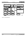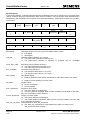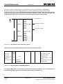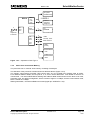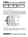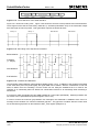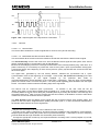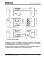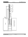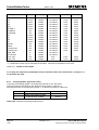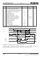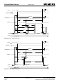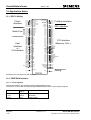
1
SIMATIC NET DPC31 Siemens PROFIBUS-DP Controller with C31 Core Hardware Description Date 12/14/00 5+/ #6+%0'6 &2%*CTFY CTG &GUETKRVKQP 5 KG O G PU 2 4 1 ( +$ 7 5 & 2 % Q P VTQ NNG T Y KVJ KP VG I TC VG F % % Q TG C EEQ TF KP I VQ ' 0 8 Q NW O G 8 G TU KQ P & C VG SchnittStellenCenter DPC31 HW .KCDKNKV[ 'ZENWUKQP 9G JCXG VGUVGF VJG EQPVGPVU QH VJKU FQEWOGPV TGICTFKPI CITGGOGPV YKVJ VJG JCTFYCTG CPF UQHVYCTG FGUETKDGF 0GXGTVJGNGUU FGXKCVKQPU ECPOV DG TWNGF QWV UQ VJCV YG CTG PQV IWCTCPVGGKPI EQORNGVG CITGGOGPV *QYGXGT VJG FCVC KP VJKU FQEWOGPV KU EJGEMGF RGTKQFKECNN[ 4GSWKTGF EQTTGEVKQPU CTG KPENWFGF KP UWDUGSWGPV GFKVKQPU 9G ITCVGHWNN[ CEEGRV UWIIGUVKQPU HQT KORTQXGOGPV %QR[TKIJV %QR[TKIJV % 5KGOGPU #) #NN TKIJVU TGUGTXGF 7PNGUU RGTOKUUKQP JCU DGGP GZRTGUUN[ ITCPVGF RCUUKPI QP VJKU FQEWOGPV QT EQR[KPI KV QT WUKPI CPF UJCTKPI KVU EQPVGPV KU PQV CNNQYGF 1HHGPFGTU YKNN DG JGNF NKCDNG #NN TKIJVU TGUGTXGF KP VJG GXGPV C RCVGPV KU ITCPVGF QT C WVKNKV[ OQFGN QT FGUKIP KU TGIKUVGTGF 6JG VTCFG OCTMU 5+/#6+% 5+0'% . CTG RTQVGEVGF D[ NCY HQT 5KGOGPU VJTQWIJ CRRNKECVKQPTGIKUVTCVKQP #NN QVJGT RTQFWEV CPF U[UVGO PCOGU CTG TGIKUVGTGF VTCFG OCTMU QH VJGKT TGURGEVKXG RTQRTKGVQTU CPF CTG VQ DG VTGCVGF CU UWEJ 5WDLGEV VQ VGEJPKECN EJCPIG Page 2 12/00 Version V 1.0 DPC31 HW Description Copyright (C) Siemens AG 2000. All rights reserved. DPC31 HW SchnittStellenCenter Versions Version Nr. 0.x 1.0 Date Page 14.12.00 div. DPC31 HW Description Copyright (C) Siemens AG 2000. All rights reserved. Information first Version RS485 wiring corrected RXD_RXS und XCTS_RXA Data Buffer Version V1.0 Page 3 12/00 SchnittStellenCenter DPC31 HW Inhaltsverzeichnis 1 INTRODUCTION 7 2 OVERVIEW 8 3 2.1 General Data 8 2.2 Differences Between the DPC31 and the SPC3/SPC4 8 2.3 Function Overview (Block Diagram) 9 2.4 Pin Description 11 MEMORY ASSIGNMENT 12 3.1 Memory Area Distribution in the DPC31 12 3.2 Control Unit Parameters (Latches/Registers) 12 3.3 Organizational Parameters (RAM) 14 4 ASIC INTERFACE 20 5 COMMUNICATION FUNCTIONS OF THE SEQUENTIAL CONTROL SYSTEM 21 6 5.1 Setting Up the DP Buffer Structures 5.1.1 Structure of the Buffers 5.1.2 Request Interface for DPS (Instruction Queue) 5.1.3 Acknowledgement Interface (Indication_Queue) 21 21 21 23 5.2 DPS Module, Description of the Interface 5.2.1 Set_Slave_Address, SSA (SAP55) 5.2.2 Set_Param, Prm (SAP61) 5.2.3 Check_Config, CCFg (SAP62) 5.2.4 Slave_Diagnosis (SAP60) 5.2.5 Write_Read_Data (Default SAP) 5.2.6 Global_Control (SAP58) 5.2.7 Read_Inputs (SAP56) 5.2.8 Read_Outputs (SAP57) 5.2.9 Get_Config (SAP59) 24 25 26 28 28 29 31 33 33 33 USER FUNCTIONS ON THE C31 CONTROLLER Page 4 12/00 Version V 1.0 34 DPC31 HW Description Copyright (C) Siemens AG 2000. All rights reserved. DPC31 HW 7 8 DESCRIPTION OF THE HARDWARE BLOCKS 35 7.1 Universal Processor Interface 7.1.1 Bus Interface Unit (BIU) 7.1.2 IO Interface 7.1.3 Interface Signals 7.1.4 Interrupt Controller of the µP Interface in the DPC31 35 35 40 41 41 7.2 44 Synchronous Serial Interface (SSC Interface) 7.3 80C31 Core and Interface 7.3.1 Reset Phase of the C31 7.3.2 80C31 Core and Internal Memory 7.3.3 Expansion Interface to the 80C31 Core 7.3.4 Interface Signals 48 48 49 51 51 7.4 52 C31 Interrupt Controller in the DPC31 7.5 Serial PROFIBUS Interface 7.5.1 Asynchronous Physics Unit (NRZ) 7.5.2 Synchronous Physics Unit (Manchester) 52 52 53 7.6 61 DPS Watchdog Timer 7.7 Watchdog Timer 7.7.1 Automatic Baudrate Detection 7.7.2 Baudrate Monitoring 7.7.3 Response Monitoring 61 61 61 62 7.8 Clock Supply 7.8.1 PLL 62 62 TEST SUPPORT 8.1 9 SchnittStellenCenter 64 Emulator Connection for the C31 64 ELECTRICAL SPECIFICATIONS 65 9.1 Maximum Limits 66 9.2 Permitted Operating Values 66 9.3 Guaranteed Operating Range for the Specified Parameters 66 9.4 Power Loss 66 9.5 Pad Cells 9.5.1 Power-Up of the Supply Voltage 9.5.2 Structure of the Pad Cells with 5V Tolerance 9.5.3 DC Specification of the Pad Cells 67 67 67 69 9.6 AC Specification 9.6.1 Driver Capability 9.6.2 Timing Diagrams, Signal Run Times 69 69 70 DPC31 HW Description Copyright (C) Siemens AG 2000. All rights reserved. Version V1.0 Page 5 12/00 SchnittStellenCenter 10 DPC31 HW MECHANICAL SPECIFICATION 10.1 PQFP 100 Casing 82 82 11 DPC31 PINOUT 83 12 APPLICATION NOTES 84 12.1 DPC31 Wiring 84 12.2 PROFIBUS Interface 12.2.1 Pin Assignment 12.2.2 Wiring Example RS485 Interface 13 84 84 86 APPENDIX 88 13.1 Addresses 88 13.2 General Definitions of Terms 89 13.3 Order Numbers 89 Page 6 12/00 Version V 1.0 DPC31 HW Description Copyright (C) Siemens AG 2000. All rights reserved. DPC31 HW SchnittStellenCenter 1 Introduction Siemens offers to its users several ASICs for data exchange between automation devices that, on the basis of EN 50170 Volume 2, support or completely process the data traffic between the individual automation stations. To support intelligent master/slave solutions, that is implementations with a micro-processor, the following ASICs are available. All ASICs do the following: support the transmission rates of 9.6 kBits/s … 12000 kbit/s, autonomously set themselves to the transmission rate specified by the master and monitor it. After these ASICs receive a correct message, they autonomously generate the requested response messages. In the ASPC2 (Advanced Siemens PROFIBUS Controller), many components of Layer2 of the OSI model are already integrated according to ISO, but it still needs the support of a processor. This ASIC supports baudrates up to 12000 kbit/s; however, in its complexity, it is conceived more for master applications. The SPC3 (Siemens PROFIBUS Controller), through the integration of the complete PROFIBUS DP slave protocol, considerably relieves the processor of an intelligent PROFIBUS slave. However, in the field of automation, there are also simple devices such as switches, thermoelements, etc. that do not require a microprocessor for recording their states. For a low cost adaptation of such devices, two additional ASICs are available: the SPM2 (Siemens PROFIBUS Multiplexer, Version 2) and LSPM2 (Lean Siemens PROFIBUS Multiplexer). These chips process as DP slaves in the bus system. The LSPM2 has the same functions as the SPM2 but with a lower number of I/O and diagnostic ports. The DPC31 (DP Controller with integrated 8031 core) is a highly integrated PROFIBUS slave ASIC. The DPC31 is a slave controller for both PROFIBUS DP/DPV1 and PA applications. The uses of this chip cover a wide area. On the one hand, it can be used for simple, intelligent applications that make do with the integrated C31 core. On the other hand, it can be used for high performance slave solutions that have increased communication requirements. This requirement is met with an internal RAM that has been increased to 6kByte. Approximately 5.5kByte of communication memory is available to the user. The DPC31 has the following main features: rd • integrated standard C31 core with an additional 3 timer (Timer 2) • low processor load through the integration of the complete DP slave protocol • simple processor interface for a large number of processors: INTEL: 8032, Siemens: C166 Motorola: HC11, HC16, HC916 • SSC interface (SPI) for interfacing serial EEPROMs, A/D converters, etc. • integration of synchronous as well as asynchronous bus physics 80x86 This document explains the hardware configuration and the wiring of the DPC31. In addition, Siemens offers a separate software package that relieves the user of local H/W register manipulations and memory calculations. The package provides a convenient C-interface for interfacing Profibus communication with the slave process. DPC31 HW Description Copyright (C) Siemens AG 2000. All rights reserved. Version V1.0 Page 7 12/00 SchnittStellenCenter DPC31 HW 2 Overview 2.1 General Data Package: Baudrate: 100 Pin PQFP Asynchronous: 9.6, 19.2, 45.45, 93.75, 187.5, 500 kBd, 1.5, 3, 6 & 12 MBd Synchronous: 31.25 kBd Bus Interface: 8-Bit asynchronous/synchronous Intel and Motorola interface C31 Ports: Standard Port Interface (4 Ports) for external memory expansion and emulator interface 2 SSC Interface: Synchronous serial interface (SPI) for connecting serial E PROMs, A/D converters, etc. Memory Area 6 kByte (approx. 5.5 kByte utilizable) can be directly addressed and can be broken down into data and code memory Environmental Cond.: 3.3V ±10%; -40 to +85 °C 2.2 Differences Between the DPC31 and the SPC3/SPC4 Characteristics General: Package External µP Interface Family Preprocessing External Memory Expansion (C31) SSC Interface (SPI) DPC31 SPC3 100 Pin PQFP parallel, 8 bits Siemens, Intel, Motorola yes, via int. C31 yes, Flash, RAM etc. 2 SPC4 44 Pin PQFP parallel, 8 bits Siemens, Intel, Motorola no no 44 Pin PQFP parallel, 8 bits Siemens, Intel, Motorola no no no no I/O Interface Internal PLL Communication RAM yes, for example E PROM up to 64 kByte, A/D conv. (AD7714) yes, up to 40 bits yes, input 12 MHz max. 5.5 kByte no no 1.4 kByte no no 1.14 kByte (1.64 for SPC41) PB Communication: Baudrate async. RS485 sync. Manchester 9.6 kBd to 12 MBd 31.25kBd 9.6 kBd to 12 MBd no 9.6 kBd to 12 MBd 31.25 kBd DP Slave Receive Resources fully integrated exchange buffer fully integrated exchange buffer partially integrated polling list no no no no Integrated User Functions: 2 E PROM Read/Write yes DPV1 Protocol Available in FW Table 2.2-1: Differences with respect to SPC3 and SPC4 Page 8 12/00 Version V 1.0 DPC31 HW Description Copyright (C) Siemens AG 2000. All rights reserved. SchnittStellenCenter DPC31 HW 2.3 Function Overview (Block Diagram) Figure 2.3-1 shows the block diagram of the DPC31. The DPC31 has a bus interface for connecting an external micro-processor. It is a parameterizable, synchronous/asynchronous 8-bit interface for various Siemens, Intel, and Motorola micro-controllers/processors. Via the 13-bit address bus, the user can directly access the internal 5.5k RAM or the register cells. If the application does not need an external processor, the ports of the bus interface can be used as I/O. This makes 27 I/O bits available that the internal C31 can address individually. The sequence control enters various events (for example, indication events, error events, etc.) in the interrupt controller that are signalled to the slave firmware via the interrupt pin. These events can be enabled individually via a mask register. Acknowledgement is made via the acknowledge register. 2 The SSC interface (SPI) is used for connecting a serial E PROM or an A/D converter (such as AD7714). This interface is laid out only as a master interface. The C31 interface includes the ports of the standard controller. Via this interface, an external memory- and I/O expansion can be implemented. Via corresponding CS signals, the code and data address areas are coded out that are not used internally. In addition, up to 13 bits of I/O can be connected via these ports. The C31/32 emulator (Hitex etc.) is also controlled via this interface. Via the register cells, the following are accessed: internal registers, the DPS(DP Slave) control units and the SSC module. The DPS control units represent the user interface to the DPS layer that is implemented via individual buffers. These control units exchange the buffers. The integrated C31 is fully compatible with the standard microcontroller. Also integrated is a 256 byte data RAM. Via a second interrupt controller, the interrupt events mentioned above can also be entered in the C31. This makes it possible to distribute interrupt events between an external and an internal application. The bus physics unit includes the asynchronous Layer1 (RS485: 9.6kBd to 12 MBd) and the synchronous Layer1 (IEC 1158-2; Manchester encoded: 31.25kBd) which also allows the chip to be operated in an intrinsically safe environment. In the clock unit, an analog PLL is integrated, to which an external 12MHz quartz must be connected. With it, the PLL generates the internal 48MHz clock pulse for the asynchronous mode. In the synchronous mode, the PLL is switched off and an external clock pulse of 4 to 16 MHz is applied. In addition, power management is implemented in the clock unit which switches off internal clock pulses in certain states. As outputs, the internal working clock pulse divided by 2 and by 4 is available. DPC31 HW Description Copyright (C) Siemens AG 2000. All rights reserved. Version V1.0 Page 9 12/00 SchnittStellenCenter 3 3 8 B-Type Port H µP-Int SB I/O-Int PH2.. Port G SB, PG7.. DPC31 HW 8 8 Port F Port E AB7.. DB7.. PF7.. PE7.. 3 Interrupt Controller SSC Interface (SPI) Register Cells SB Port D 8 Port C 8 Port B Mem-Exp. SB, I/O AB15. I/O I/O Interf. PB7.. PD4.. - ROM (24k x 8) (DPS Control Units) RAM DBX 8 4 8 Port A AB/DB7.. - C31 Interface (Emulator Port) Bus Interface (Intel, Motorola, I/O) Code RAM (0-4k) for C31 4 Reset BootTyp1..0 Multiport RAM Controller RAM (256 x 8) 6kByte) Communication RAM (5.5-0.5k) C31 Core ROM Sequence Control Send-ReceiveUnit 1 PLL + Clock-Unit 2 Vdd Vss 1 1 Timer Unit Physics Unit asynchron 1 2 synchron 4 XPLLE Clkout1X2 12 MHz N Clkout1X4 Interrupt Controller 3 Test 13 Vdd/Vss Figure 2.3-1: Block Diagram DPC31 Page 10 12/00 Version V 1.0 DPC31 HW Description Copyright (C) Siemens AG 2000. All rights reserved. SchnittStellenCenter DPC31 HW 2.4 Pin Description The DPC31 has a 100 pin PQFP package with the following signals: Function Group C31 Interface µP Interface SSC Interface PLL + Clock Unit Physics Unit General Test Supply Name Pins Type Voltage Proof PA PB PC PD ALE XPSEN XCSDATA XCSCODE BOOTTYP DBX PE PF PG PH BUSTYP SSCLK SSDO SSDI XTAL1_CLK XTAL2 AVDD AGND XPLLEN 8 8 8 8 1 1 1 1 2 1 8 8 8 3 3 1 1 1 1 1 1 1 1 I/O I/O I/O I/O I/O I/O O O I I I/O I/O I/O I/O I O O I I O 5V 5V 5V 5V 5V 5V 5V 5V 5V 5V 5V 5V 5V 5V 5V 5V 5V 5V 3.3V 3.3V I 5V CLKOUT1X2 CLKOUT1X4 RTS_TXE TXD_TXS XCTS_RXA RXD_RXS RESET NTEST1 NTEST2 TST1 VDD GND 1 1 1 1 1 1 1 1 1 1 4 9 100 O O O O I I I I I I 5V 5V 3.3V 3.3V 5V 5V 5V 5V 5V 5V Total Function Corresponds to P0 for the discrete type Corresponds to P1 for the discrete type Corresponds to P2 for the discrete type Corresponds to P3 for the discrete type Address Latch Enable For emulation only Chip select for external RAM Chip select for external ROM Type for loading the user program Switch to In Circuit Emulator Connection for SPI Chips, Clock Connection for SPI Chips, Data_Out Connection for SPI Chips, Data_In Quartz connection / Clock supply Quartz connection Separate VDD supply for PLL Separate GND supply for PLL Switching off the PLL and supply clock pulse via XTAL1_CLK Clock pulse output CLK/2 (without reset) Clock pulse output CLK/4 (without reset) Reset Input Test Pin Test Pin Test Pin +3.3V 0V Figure 2.4-1: DPC31 Pin List Because of the 5V-tolerant I/O, and in order to ensure the least possible power loss, no pull-up or pull-down resistors are integrated in the pad cells; that is, all unused inputs or all output ports (since these are switched as input after reset) are to be applied to one defined level (Ports A, B, D, E, F, G, and H). This is not necessary for Port C since it is permanently configured as output. A bus contention is permitted for a maximum of 20ns. DPC31 HW Description Copyright (C) Siemens AG 2000. All rights reserved. Version V1.0 Page 11 12/00 SchnittStellenCenter DPC31 HW 3 Memory Assignment 3.1 Memory Area Distribution in the DPC31 Table 3.1-1 shows the distribution of the internal 8k address space of the DPC31. Via this address space, the user interface to communication (DPS) is mapped. It does not matter whether the user program is running internally on the C31 or on the external micro-processor; the interface is identical in both cases. The address area is subdivided into a 2K address space for the register cells and a 6k address space for the internal RAM. The internal registers (interrupt controller, Mode Register1, DPS control units, SSC interface) are located in the register area. Certain registers can only be read or written. The RAM starts at address 800h. In the first area, the internal work cells are located (bit array, variables). The user is not to access this area. The sequential control system uses these cells for processing the protocol. Starting with address 0840h, the organizational parameters (parameter cells, buffer ptr(pointer) are located in the RAM. In the parameter cells, general parameter assignment data is transferred (Param Register, station address, Ident No., etc.), or status displays are stored (status register, GC_Command, Score_Register, etc.). The buffer pointers describe the entire buffer management for the SAPs. At address 08A0H, the buffers generated by the user start, corresponding to the parameter assignment of the organizational parameters. The sequence of the buffers can be selected as required. All buffers or lists must be located on segment addresses (32 bytes segmentation). 1FFFh Code Area for the Internal C31 Communic- Buffer Area ation Area 08A0h 0840h 0800h RAM 0000h Register Organizational Parameters Internal Work Area SSC-Interface Control Unit Parameters Latches/Registers Table 3.1-1: Memory Area Distribution in the Internal RAM of the DPC31 The stack for the sequential control system needs 64 bytes. A buffer for temporarily storing the receive message requires 32 bytes. 3.2 Control Unit Parameters (Latches/Registers) The register cells that are, for example, in the interrupt controller and the DPS control units, are located in the address area of 0000-003Ch (XDATA). These cells can either be read or written only. The address assignments are shown in Table 3.2-1. When writing the register cells, the unassigned bit positions are ‘don’t care’. Page 12 12/00 Version V 1.0 DPC31 HW Description Copyright (C) Siemens AG 2000. All rights reserved. DPC31 HW Address 0000h 0001h 0002h 0003h 0004h 0005h 0006h 0007h 0008h ... 000Fh 0010h 0011h ... 001Fh 0020h 0021h 0022h 0023h 0024h ... 002Fh 0030h Name Int-Req-Reg7..0 Int-Req-Reg15..8 Int-Req-Reg23..16 Int-Req-Reg28..24 Int-Reg7..0 Int-Reg15..8 Int-Reg23..16 Int-Reg28..24 SchnittStellenCenter Meaning (read access!) Interrupt Controller Register Reserved C31_Control Register7..0 Refer to Chapter 4 Reserved SSC_Rcv-Buf7..0 SSC_Sts-Reg3..0 SSC_Ctrl1-Reg7..0 SSC_Ctrl2-Reg2..0 Receive buffer of the SSC interface Status register of the SSC interface Control register of the SSC interface Control register of the SSC interface Reserved User_SSA_Ok Cmd1..0 0031h User_Prm_Ok Cmd1..0 0032h User_Prm_Not_Ok Cmd1..0 0033h 0034h 0035h Reserved 0036h User_Cfg_Not_Ok-Cmd1..0 0037h 0038h 0039h 003Ah 003Bh 003Ch 003Dh ... 07FFh User_Diag_Read-Cmd User_Get_Cfg_Read-Cmd User_New_Din-Cmd1..0 User_Din_Puffer-State7..0 User_New_Dout-Cmd3..0 User_Dout_Puffer-State7..0 User_Cfg_Ok Cmd1..0 The user acknowledges the user SSA data of an SSA message positively The user acknowledges the user parameter assignment data of a prm message positively The user acknowledges the user parameter assignment data of a prm message negatively The user acknowledges the configuring data of a CfG message positively The user acknowledges the configuring data of a Cfg message negatively The user makes a new diag buffer available The user makes a new Get_Cfg buffer available The user makes a new Din buffer available The user reads the current Din buffer assignment The user fetches the last Dout buffer from the N state The user reads the current Dout buffer assignment Reserved Table 3.2-1: Assignment of the Internal Register Cells for READ DPC31 HW Description Copyright (C) Siemens AG 2000. All rights reserved. Version V1.0 Page 13 12/00 SchnittStellenCenter DPC31 HW 0000h 0001h 0002h 0003h 0004h 0005h 0006h 0007h 0008h 0009h 000Ah 000Bh 000Ch 000Dh 000Eh 000Fh 0010h 0011h 0012h 0013h 0014h ... 001Fh 0020h 0021h Int-Req-Reg7..0 Int-Req-Reg15..8 Int-Req-Reg23..16 Int-Req-Reg28..24 Int-Ack-Reg7..0 Int-Ack-Reg15..8 Int-Ack-Reg23..16 Int-Ack-Reg28..24 Int-Mask-Reg7..0 Int-Mask-Reg15..8 Int-Mask-Reg23..16 Int-Mask-Reg28..24 Int-EOI-Reg0 Interrupt Controller Register SSC_Transmit-Buf7..0 SSC_Sts-Reg7..0 Receive buffer of the SSC interface Status register of the SSC interface 0022h 0023h 0024h 0025h 0026h ... 07FFh SSC_Ctrl1-Reg7..0 SSC_Ctrl2-Reg2..0 SSC_Int_Enable-Reg3..0 SSC_Baudrate-Reg7..0 Control register of the SSC interface Control register of the SSC interface Interrupt_Enable register of the SSC interface Baudrate register of the SSC interface reserved C31_Ctrl-Reg6..0 Mode-Reg1-Set7..0 Mode-Reg1-Reset7..0 User_InstQ_Write-Cmd7..0 Refer to Chapter 6 Refer to Chapter 6 Refer to Chapter 6 Transfers a new request to the sequential control system reserved reserved Table 3.2-1: Assignment of the Internal Register Cells for WRITE 3.3 Organizational Parameters (RAM) The organizational parameters are stored by the user in the RAM under the addresses specified in the table below. These parameters primarily describe the parameter cells and the buffer pointers of the communication profile (buffer management). Page 14 12/00 Version V 1.0 DPC31 HW Description Copyright (C) Siemens AG 2000. All rights reserved. DPC31 HW 0800h ... 083Fh 0840h 0841h 0842h 0843h 0844h 0845h 0846h 0847h SchnittStellenCenter reserved Internal Work Area Status-Register7..0 Status-Register15..8 Param-Register7..0 Param-Register15..8 Param-Register23..16 Param-Register31..24 TS_Adr_Register6..0 Real_No_Add_Change7..0 see below see below see below see below see below see below Profibus station Address of the DPC31 (this slave) This parameter indicates whether the DP slave address may be changed at a later time. After reset, the slave firmware must set this parameter if it permits the Set_Slave_Address SAP. 0 = Address may be changed Otherwise = Address may not be changed 0848h 0849h WD_Baud_Control_Val7..0 Interframe GAP_Time5..0 084Ah DPS_User_Wd_Val7..0 084Bh 084Ch 084Dh 084Eh 084Fh 0850h 0851h 0852h 0853h 0854h 0855h 0856h 0857h DPS_User_Wd_Val15..8 reserved GC_Command7..0 Ident_Low7..0 Ident_High7..0 reserved reserved reserved reserved reserved reserved InstQ_Base-Ptr7..0 InstQ_Length7..0 0858h 0859h 085Ah 085Bh InstQ_Read-Ptr7..0 InstQ_Write-Ptr7..0 IndQ_Base-Ptr7..0 IndQ_Length7..0 085Ch 085Dh 085Eh 085Fh 0860h 0861h 0862h 0863h 0864h 0865h IndQ_Read-Ptr7..0 IndQ_Write-Ptr7..0 Dout_Puffer-Length7..0 Dout_Puffer1-Ptr7..0 Dout_Puffer2-Ptr7..0 Dout_Puffer3-Ptr7..0 Dout_Puffer4-Ptr7..0 Din_Puffer-Length7..0 Din_Puffer1-Ptr7..0 Din_Puffer2-Ptr7..0 If the DPC31 then receives a Set_Slave_ Address message, it enters the current value here. The root value for baudrate monitoring is parameterized. The Interframe GAP time (4...32 bits) is to be parameterized here for synchronous bus physics. In the DPS_Mode, the user is monitored with an internal 16-bit watchdog timer. The timer is decremented every 10 msec and must be reset by the user cyclically to the start value ’DPS_User_ WD_Value15..0’. Resetting, enabling, and disabling the timer is initiated with ’DPS_User-Wd’ request in the Instruction_Queue. Preset with 0 GC command last received PNO Ident Number Low PNO Ident Number High Preset with 0 Preset with 0 Preset with 0x47 Preset with 0x4F Preset with 0x53 Preset with 0 0x52 (segment pointer to the instruction queue) 0x1E (length of the instruction queue in bytes (multiple of the length of an entry -> n*5)) Byte offset to the next entry to be read (preset with 0x00 ) Byte offset to the next free entry (preset with 0x00 ) 0x53 (segment pointer to the indication queue) 0xXX (length of the indication queue in bytes (multiple of the length of an entry -> n*3)) Byte offset to the next entry to be read (preset with 0x00) Byte offset to the next free entry (preset with 0x00) Length of the 4 Dout buffers Segment Pointer to Dout Buffer1 Segment Pointer to Dout Buffer2 Segment Pointer to Dout Buffer3 Segment Pointer to Dout Buffer4 Length of the 3 Din buffers Segment Pointer to Din Buffer1 Segment Pointer to Din Buffer2 DPC31 HW Description Copyright (C) Siemens AG 2000. All rights reserved. Version V1.0 Page 15 12/00 SchnittStellenCenter 0866h 0867h 0868h 0869h 086Ah 086Bh 086Ch 086Dh 086Eh 086Fh 0870h 0871h 0872h 0873h 0874h ... 09DFh 09E0h ... 0A21h 0A22h ... 0A3Fh 0A40h ... 0A5Fh 0XXXh ... 0XXXh 0XXXh ... 1FFFh DPC31 HW Din_Puffer3-Ptr7..0 User_SSA_Puffer-Ptr7..0 MAC_SSA_Puffer-Ptr7..0 User_Prm_Puffer-Ptr7..0 MAC_Prm_Puffer-Ptr7..0 reserved reserved User_Cfg_Puffer-Ptr7..0 MAC_Cfg_Puffer-Ptr7..0 User_Diag_Reply_PufferPtr7..0 MAC_Diag_Reply_PufferPtr7..0 User_GCfg_Reply_PufferPtr7..0 MAC_GCfg_Reply_PufferPtr7..0 MAC_GC_Puffer-Ptr7..0 Segment Pointer to Din Buffer3 Segment Pointer to User SSA Buffer Segment Pointer to Mac SSA Buffer Segment Pointer to User Prm Buffer Segment Pointer to Mac-Prm Buffer Preset with 0 Preset with 0 Segment Pointer to User Cfg Buffer Segment Pointer to Mac Cfg Buffer Segment Pointer to User-Diag Buffer reserved Preset with 0x00 reserved Preset with 0xFF reserved Preset with 0x00 Instruction Queue Space for 6 instructions Preset with 0 Indication Queue Space for xx indications(dependent of the parameter) Preset with 0 Segment Pointer to Mac Diag Buffer Segment Pointer to User-Get-Cfg Buffer Segment Pointer to Mac-Get-Cfg Buffer Segment Pointer to Global Ctrl Buffer Buffer Area Table 3.3-2: Assignment of the Organizational Parameters Page 16 12/00 Version V 1.0 DPC31 HW Description Copyright (C) Siemens AG 2000. All rights reserved. SchnittStellenCenter DPC31 HW Meaning of the Register Cells: Status Register: WD-State1..0 1 0 DPS-State1..0 1 0 7 3 0 Diag_Flag 4 DPC31 Release3..0 2 1 0 0 2 3 15 2 MAC State 0 Baudrate3..0 1 0 8 The status register displays the current MAC status, the DPS status, and the watchdog timer status. In addition, the baudrate that was found, and the release number of the DPC31 is also entered. MAC State: Diag_Flag: DPS-State1..0: WD-State1..0: Baudrate3..0: DPC31-Release3..0: The state of the MAC =0 The MAC is in the ‘Offline’ state =1 The MAC is in ‘Passive Idle’ State Diagnostic Buffer =0 The diagnostic buffer was fetched by the master (if Diag.Stat_Diag=0). =1 The diagnostic buffer was not fetched by the master. The state of the DPS State Machine =00 State ‘Wait_Prm’ =01 State ‘Wait_Cfg’ =10 State ‘Data_Exchange’ The state of the Watchdog SM =00 State ‘Baud_Search’ =01 State ‘Baud_Control’ =10 State ‘DP_Control’ The baudrate found by the DPC31 =0000 12 MBd (asyn.) =0001 6 MBd (asyn.) =0010 3 MBd (asyn.) =0011 1.5 MBd (asyn.), 31.25 kBd (syn.) =0100 500 kBd (asyn.) =0101 187.5 kBd (asyn.) =0110 93.75 kBd (asyn.) =0111 45.45 kBd (asyn.) =1000 19.2 kBd (asyn.) =1001 9.6 kBd (asyn.) Release number of the DPC31: The release number consists of two groups. DPC31-Release1..0: numbers the compatible versions DPC31-Release3..2: is the index within a compatible version. =0000 DPC31 Step A Rest not possible so far DPC31 HW Description Copyright (C) Siemens AG 2000. All rights reserved. Version V1.0 Page 17 12/00 SchnittStellenCenter DPC31 HW Param Register: In the Param Register, individual parameter bits are transferred that are to be changed only in the MAC state ‘Offline’, however. When the request ‘MAC_Start’ (refer to Chapter 5.1.2) is executed, these parameters are distributed by the sequential control system to the individual modules. Subsequent changes are not taken into account. 0 Early_ Ready EOI_ Timebase Quick_Sync _New GIM_EN XRTS/ ADD 0 0 7 0 0 0 New_GC_ Int_Mode 0 1 Freeze_ Supported Sync_ Supported 15 0 DP_Mode 8 0 1 En_Change _Cfg_Puffer XAsyn/Syn 0 0 0 0 23 0 27 XRTS/ADD: GIM_EN: Quick_Sync_New: EOI_Timebase: Early_Ready: 1 Preamble1 Preamble0 24 Switchover Output TxE (syn. physics) for different driver control =0 RTS Signal. =1 ADD Signal Galvanic Isolation Mode for syn. physics =0 The power-saving interface is switched off =1 The power-saving interface is switched on (possible only for 31.25kBd) Switching on the improved quick sync =0 The improved quick synchronizer is off. =1 The improved quick synchronizer is on. Time base of the EOI timer =0 The interrupt inactive time is 1 to 2 µsec . =1 The interrupt inactive time is 1 to 2 msec. Early Ready Signal =0 Ready is generated if the data is valid (Read) or if the data is taken over (write). =1 Ready is moved ahead by one clock pulse. Enable of DPS =0 DPS is not enabled. =1 DPS is enabled. Sync_Supported: Support of Sync_Mode =0 The Sync_Mode is not supported. =1 The Sync_Mode is supported. Data is made available in the N-Buffer of the DoutSM (not comparable to ASIC LSPM 2). Freeze_Supported: Support of Freeze_Mode =0 The Freeze_Mode is not supported. =1 The Freeze_Mode is supported. Data is frozen from the N-buffer of the Din SM (not comparable to LSPM 2). New_GC_Int_Mode: Interrupt Mode for ‘New_GC_Command’ =0 The ‘New_GC_Command Int’ is generated only if there is a change in the ‘GC_Command’ (basic setting). DP_Mode: Page 18 12/00 Version V 1.0 DPC31 HW Description Copyright (C) Siemens AG 2000. All rights reserved. DPC31 HW SchnittStellenCenter =1 The ‘New_GC_Command Int’ is generated for each receipt of a GC message. XAsyn/Syn: Setting the bus physics =0 Asynchronous physics; the work clock pulse is fixed at 48 MHz (via PLL) Baudrate: 9.6 kBd to 12 MBd (basic setting) =1 Synchronous physics; the work clock pulse can be set: 2, 4, 8 or 16 MHz Baudrate: fixed at 31.25 kBd En_Change_Cfg_Buffer: Enable of the buffer exchange (User_Cfg_Buffer for MAC_GCfg_Rbuffer) =0 The buffers won’t be exchanged. =1 With ‘User_Cfg_Ok Cmd’, the above-mentioned buffers are exchanged. The exchange is confirmed with the interrupt ‘Get_Cfg_Buffer_Changed’ . Setting the external clock pulse supply at Pin XTAL1_CLK (not via PLL). The internal Syn_Clkin1..0: C31 processes with half the clock frequency! =00 External clock = 2 MHz ⇒ Baudrates: 31.25 (not released!) =01 External clock = 4 MHz ⇒ Baudrates: 31.25 =10 External clock = 8 MHz ⇒ Baudrates: 31.25 =11 External clock = 16 MHz ⇒ Baudrates: 31.25 For the syn. physics, the preamble length is parameterized in number of bytes. Preamble1..0: =00 ⇒ 1 byte =01 ⇒ 2 bytes =10 ⇒ 4 bytes =11 ⇒ 8 bytes DPC31 HW Description Copyright (C) Siemens AG 2000. All rights reserved. Version V1.0 Page 19 12/00 SchnittStellenCenter DPC31 HW 4 ASIC Interface Interrupt Controller Register (Int Mask Reg, Int Ack Reg, Int Req Reg, Int and Int EOI Reg): The meaning of these registers will be explained in later chapters. The interrupt controller exists twice (for ext. µP and C31). Both are instances are mapped onto the same addresses. Mode Register1: (ext. µP and C31, write access) Mode Register1 is used for parameterizing single bits. These bits are control bits and internally directly affect the hardware. The meaning is described below. Different addresses are used for setting and resetting (Mode Register1 set/reset). A logical ‘1’ is written to those bit positions that are to be changed. All other bit positions must be logical. ‘0’ Int_ Polarity 0 0 0 Dis_C31 Dis_Clkout1X4 Dis_Clkout1X2 0 7 Dis_Clkout1X2: Dis_Clkout1X4: Dis_C31: Int_Polarity: 0 The clock output ‘Clkout1X2’ is switched off (½ of the internal clock: asyn=24MHz, syn=1 to 8 MHz). After being switched on and in the reset phase, the output is initially active. =0 Clkout1X2 is active (default). =1 Clkout1X2 is inactive. The clock output ‘Clkout1X4’ is switched off (¼ of the internal clock: asyn=12MHz, syn=0.5 to 4 MHz). After being switched on and in the reset phase, the output is initially active. =0 Clkout1X4 is active (default). =1 Clkout1X4 is inactive. The internal C31 is switched off (clock switched off). =0 C31 is active (default). =1 C31 is inactive (absolute powerdown mode). Polarity of the interrupt output =0 The interrupt output is low-active (basic setting). =1 The interrupt output is high active. C31_Control Register: (ext. µP and C31, read/write access) In the C31_Control register, the settings specific to the C31 are made. The boot type bits are not to be parameterized by the user; the assignment of the chip pins ‘BOOTTYP_0/_1’ determines the boot type. 0 0 0 Bit Position 6 5 4 3 2 1 0 Default Value 0 0 0 0 0 - - r/w r/w r/w r/w r/w r r Boot Type: Reserved (0) Bit1 Bit0 Boot Type Bit1 Bit0 Settings of the boot type pins for processing in the boot routine by the =00 Boot Type 1a =01 Boot Type 1b =10 Boot Type 2 =11 Boot Type 3 C31: Presently, only Boot Type 2 is permitted! Page 20 12/00 Version V 1.0 DPC31 HW Description Copyright (C) Siemens AG 2000. All rights reserved. DPC31 HW SchnittStellenCenter 5 Communication Functions of the Sequential Control System PROFIBUS Layer2 and the DP slave module are implemented in the sequential control system. Layer2 is composed of a MAC (media access control) part and an FLC (interface services) part. In the following, the Layer2 module is simply called MAC module. The user can influence only the cells that are described here. 5.1 Setting Up the DP Buffer Structures To set up the DP buffers, the corresponding buffer pointers are entered in the organizational parameters and the buffers lengths are entered in the buffers. All pointers are 8-Bit segment buffer pointers. During access, the sequential control system adds an 8-Bit offset address to the segment address that has been shifted by 5-Bits (x32) (result: 13-Bit physical address). Therefore, the list and buffer start addresses, have a granularity of 32 bytes. 5.1.1 Structure of the Buffers Figure 5.1-1 shows the structure of the request buffers and response buffers for the DPS SAPs Header Field: SAP Buffers Data Field: Reserved Length_Data_Buffer Reserved Reserved Reserved Reserved Data 0 Data 1 ..... Data 243 Figure 5.1-1: Structure of the SAP Buffers Length_Data_Buffer: This value specifies the length of the data field in the request buffer. If the net data length of the request message is larger than the available buffer length, the MAC responds with “No Resource’. Except for the DIN and Dout buffers, the user must enter the length in all buffers! 5.1.2 Request Interface for DPS (Instruction Queue) User requests to the DPS module are transferred via a request interface. This request list is a polling list onto which the user transfers communication requests. Figure 5.1-2 shows the organization of the Instruction_Queue. With each entry (5 bytes respectively), the user must also transfer the command to the sequential control system. This is done with a write operation with any data value to the register cell ‘User_InstQ_Write Cmd’. The organization of the Instruction_Queue includes the following parameters: InstQ_Base Ptr: InstQ_Length: InstQRd Ptr: InstQ_Wr Ptr: The Instruction_Queue segment pointer Describes the length of the Instruction_Queue and is a multiple of the length of an entry (n*5) An Offset_Pointer which points to the next entry that is to be read (and is managed by the DPC31) An Offset_Pointer which points to the next free entry (and is managed by the user) DPC31 HW Description Copyright (C) Siemens AG 2000. All rights reserved. Version V1.0 Page 21 12/00 SchnittStellenCenter DPC31 HW The queue is empty if ‘InstQ_Wr ptr’ and ‘InstQ_Rd ptr’ point to the same position. One entry in the queue always must remain empty (wildcard, any content!); otherwise, an empty queue can’t be distinguished from a full queue. The user must control the wrap in the queue. After each entry, the user places the InstQ_Wr ptr behind this entry on the next free position. If this is the end of the queue, the InstW_Wr ptr will then have to be placed on the beginning of the queue (wrap around). Entry 1: Addr. Entry 2: ..... Entry n: Wildcard: InstQ_Base Ptr Command_Code Value1 Value2 Value3 Value4 Command_Code Value1 Value2 Value3 Value4 InstQ_Rd Ptr (MAC) InstQ_Wr Ptr (User) Command_Code Value1 Value2 Value3 Value4 reserved reserved reserved reserved reserved Figure 5.1-2: Organization of the Instruction_Queue Table 5.1-3 lists all possible requests with the necessary command codes. Request Com_ Code Value1 Value2 Value3 Value4 Comment MAC_Start MAC_Stop MAC_New_TRDY User_LeaveMaster DPS_User_Wd 10h 11h 12h 15h - - - - - - - MAC enters Pas_ Idle MAC enters Offline Transfer of TRDY The user initiates a ‘Leave Master’ Control of the DPS User_ Watchdog timer 20h TRDY7..0 00h=reset 01h=enable 02h=disable Table 5.1-3: Overview of User_MAC/DPS Requests The request ‘MAC_Stop’ is confirmed for the user after it has been executed. For this confirmation, a corresponding entry is made in the Indication_Queue (refer to Chapter 5.1.3). Page 22 12/00 Version V 1.0 DPC31 HW Description Copyright (C) Siemens AG 2000. All rights reserved. SchnittStellenCenter DPC31 HW 5.1.3 Acknowledgement Interface (Indication_Queue) FMA confirmations (for example, MAC_Reset con; refer to Chapter 5.1.2) are transferred to the user in an Indication_Queue (polling list). Figure 5.1-3 shows the organization of the Indication_Queue. With each entry (3 bytes respectively), the ‘IndQ_Entry Int’ is additionally generated for the user. If the queue is full and the MAC is to make another entry, this indication is abandoned and the ‘IndQ_Full Int’ is set (refer to Chapter 7.1.4). The user should avoid this condition by dimensioning the queue accordingly large. There is no effect on the bus (for example, no RR if the queue is full). The organization of the Indication_Queue includes the following parameters: IndQ_Base Ptr: The Indication_Queue segment pointer IndQ_Length: Describes the length of the Indication_Queue, and is a multiple of the length of an entry (n*3) IndQRd Ptr: An Offset_Pointer and points to the next entry that is to be read (and is managed by the user) IndQ_Wr Ptr: An Offset_Pointer and points to the next free entry (and is managed by the MAC) The queue is empty if ‘IndQ_Wr Ptr’ and ‘IndQ_Rd Ptr’ point to the same position. One entry in the queue always has to remain empty (refer to Chapter 5.1.2). Table 5.1-4 lists all possible indications with the associated command codes. Entry 1: Addr. IndQ_Len Entry 2: ..... Entry n: Wildcard: IndQ_Base Ptr Command_Code Value1 Value2 Command_Code Value1 Value2 IndQ_Rd Ptr (User) IndQ_Wr Ptr (MAC) Command_Code Value1 Value2 reserved reserved reserved Figure 5.1-3: Organization of the Indication_Queue Request MAC_Stop Confirmation DPS_User WD Expired Com_Code Value1 81h 84h Value2 - - Comment MAC_Stop was executed DPS_User Watchdog timer expired Table 5.1.4: Overview of Indications and Confirmations Note: MAC_Stop confirmation confirms the MAC transition to the Offline mode after the current request has been processed. DPC31 HW Description Copyright (C) Siemens AG 2000. All rights reserved. Version V1.0 Page 23 12/00 SchnittStellenCenter 5.2 DPC31 HW DPS Module, Description of the Interface DPS is enabled in the param register with ‘DP_Mode=1’, and started in the Instruction_Queue with the MAC request ‘MAC_Start’. The user can disable the SAP55 (Set_Slave_Address). The DPS protocol is integrated completely into the DPC31. All other DP SAPs are always enabled except for the following: default SAP, SAP 56, SAP57, and SAP58. The remaining four SAPs are enabled only when the ‘Data_Exchange’ mode is entered. ‘C ’ D e fa u lt_ S A P : In d _ B u f f e r P tr R e sp _ B u f f e r P tr ‘D ’ ‘N ’ ‘F ’ ‘U ’ D out B uffer ‘D ’ ‘N ’ ‘F ’ ‘U ’ D in B u f f e r S AP 57: S AP 56: R e sp _ B u f f e r_ P tr R e sp _ B u f f e r_ P tr S AP 58: In d _ B u f f e r P tr ‘D ’ S AP 60: R e sp _ B u f f e r_ P tr ‘D ’ ‘U ’ S AP 59: R e sp _ B u f f e r_ P tr ‘D ’ ‘U ’ S AP 55: In d _ B u f f e r P tr ‘D ’ ‘U ’ S AP 61: In d _ B u f f e r P tr ‘D ’ ‘U ’ S AP 62: In d _ B u f f e r P tr ‘D ’ ‘U ’ M A C _G C B uffer U _ D ia g B u f f e r U _G C fg B uffer U _S S A B uffer U _ P rm B u f f e r U _C fg B uffer B u ffe r A rra n g e m e n t Figure 5.2-1: DPS Buffer Structure Figure 5.2-1 shows the DPS buffer structure. The buffers (length and buffer ptr) are configured by the user in the ‘Offline Mode’ in the DPS buffer management. For the Dout data, four buffers of the same length are available that are implemented as exchange buffers. One buffer each is assigned to the incoming data transfer ‘D’ and the user ‘U’. The third buffer is either in a Next ‘N’ or Free ‘F’ mode. The MAC stores the data in ‘D’. After receiving, ‘D’ is moved to ‘N’, and a new buffer is fetched from the ‘N’ or ‘F’. The user fetches its output data from ‘N’. In the fourth buffer ‘C’, the user makes the substitute values available for the Clear mode (failsafe). If the DPC31 receives Clear messages or if DPS leaves the ‘Data_Exchange’ mode, the 'C' buffer is transferred to the user in the state ‘U’. The buffers are moved through the corresponding exchange. DPS then also performs the buffer exchange for the user. Page 24 12/00 Version V 1.0 DPC31 HW Description Copyright (C) Siemens AG 2000. All rights reserved. SchnittStellenCenter DPC31 HW The Din data is controlled via three exchange buffers of the same length. One buffer each is assigned to the data transfer ‘D’ and the user ‘U’. The third buffer is either in a Next “N” mode, or Free ‘F’ mode. When sending, the MAC fetches the Din data from ‘D’. The user prepares new Din data in ‘U’ and then moves it to ‘N’. DPS then changes the buffers from ‘N’ to ‘D’. For the diagnostic SAP and the Get_Cfg SAP (SAP60/59), two buffers respectively are available that may have different lengths. The 'D' buffer is always assigned to the MAC for sending and the 'U' buffer belongs to the user for preparing new data. DPS exchanges the buffers upon user request. In SAP55 (Set_Slave_Address), SAP61 (Set_Param), and SAP62 (Check_Config), one indication buffer respectively is available, to which the received data is stored. At the indication, this buffer is exchanged for the corresponding buffer in DPS buffer management (User_SSA buffer, User_Prm buffer, or User_Cfg buffer) and then the corresponding DPS control unit is triggered. 5.2.1 Set_Slave_Address, SSA (SAP55) Two exchange buffers of the same length are available for this SAP. One buffer is integrated as indication buffer in the SAP_SCB (MAC_SSA buffer) and the other is included in DPS buffer management as User_SSA buffer. The indication is always transferred to the user in User_SSA Buffer. The user can disable the SSA service by setting the ‘MAC_SSA_Buffer Ptr=00h’ at power-up. The DPC31 then responds to an SSA request with ‘no service activated’. The new ‘Station Address’ and the parameter ‘Real_No_Add_Change’ are stored by the user and retransferred to the software modules “MAC and DPS” after every restart caused by a voltage failure, for example. If the DPC31 receives a Set_Slave_Address message, and if the SAP55 is enabled, the MAC first checks whether the indication buffer has the corresponding size. If not, the MAC responds with ‘No Resource’. Otherwise, it sends a short acknowledgement and after the send process transfers this buffer to the DPS module. The MAC has already accepted the new station address, however. 7 6 5 4 3 2 1 0 Byte Name 0-5: 6: 7: 8: 9: 10-249: Buffer Header New_Slave_Address Ident_Number_High Ident_Number_Low No_Add_Change Rem_Slave-Data Figure 5.2-2: Assignment in the Data Field of the SSA Indication Buffer In the following states, the DPS module ignores the SSA indication: • DP_SM mode ‘Wait_Cfg’, ‘Data_Exchange’ • Net data length less than 4 bytes • Parameter ‘Real_No_Add_Change’ is ‘True’ (FFh) • New station address is larger than 125 • Ident No. is wrong DPC31 HW Description Copyright (C) Siemens AG 2000. All rights reserved. Version V1.0 Page 25 12/00 SchnittStellenCenter DPC31 HW User_SSA_OK Cmd (Read Operation): 0 0 0 0 0 0 User_Ack1 User_Ack0 User_Ack1..0 = 00 ⇒ User_SSA_Finished User_Ack1..0 = 01 ⇒ SSA_Conflict User_Ack1..0 = 11 ⇒ Not_Allowed User_Ack1..0 = 10 ⇒ not possible Table 5.2-5: Coding of User_SSA_OK Cmd The acknowledgement ‘User_SSA_OK Cmd’ is a read access to a register cell with the corresponding codes ‘Not_Allowed’, ‘User_SSA_Finished’, or ‘SSA_Conflict’. The SSA_State_Machine is reset also when the DPS is powered up -that is, after the user has transferred ‘MAC_Start’ in the request list- or the watchdog has expired in the mode ‘DP_Control’. If the SSA message is repeated because the short acknowledgement was faulty on the bus, the MAC ignores it because it has already accepted the new station address. 5.2.2 Set_Param, Prm (SAP61) For this SAP, two exchange buffers of the same length are available. One buffer is integrated as the indication buffer (MAC_Prm buffer) and the other is located as the User_Prm buffer in DPS buffer management. The indication is always transferred to the user in the User_Prm buffer. The DPS module accepts this request in any DPS mode (Wait_Prm, Wait_Cfg, Data_Ex). However, the message has to have at least a length of >= 7 bytes; otherwise, it is ignored. 7 6 5 4 3 2 1 0 Byte Name Lock_ Req Unlock_ Req Sync_ Req Freeze_ Req WD_ On Res. Res. Res. 0-5: 6: Buffer Header Station Status res 7: 8: 9: 10: 11: 12: 13: WD_Fact_1 WD_Fact_2 MinTSDR Ident_Number_High Ident_Number_Low Group_Ident DPV1_Status_1 (Spec_User_Prm_Byte) DPV1_Status_2 DPV1_Status_3 Rem_Slave-Data DPV1_ Enable Failsafe res res res. WD_ Base res 14: 15: 16-249: Figure 5.2-3: Assignment in the Data Field of the PRM Indication Buffer Byte 13 is permanently reserved for the DPC31 and must not be used for User Prm data. The bytes 13 to 15 are reserved according to DPV1 and should not be used for User Prm data in order to make a compatible change to DPV1 possible. Page 26 12/00 Version V 1.0 DPC31 HW Description Copyright (C) Siemens AG 2000. All rights reserved. SchnittStellenCenter DPC31 HW DPS evaluates the first 7 bytes or the first 10 bytes for longer Prm messages (refer to Figure 5.2-3). The evaluation is performed according to EN 50 170 Volume 2 and will not be discussed in more detail in this description. In the case of negative validation, DPS sets corresponding diagnostic bits and branches into the ‘Wait_Prm mode’. If the master requests ‘Sync_Req’ or ‘Freeze_Req’ and the application does not support ‘Sync’ or ‘Freeze’ (Sync_Supported=0, Freeze_Supported=0 in the param register), the Prm message is not accepted and the diagnostic flag ‘Diag.Not_Supported = 1’ is set. In case of positive validation (new, valid message), DPS makes the transition to ‘Wait_Cfg’, and executes the following responses, depending on the data length: • If ‘Lock_Req = 0’ and ‘Unlock_Req = 0’, only the parameter ‘MinTSDR’ is accepted internally (S/R unit) and no response is initiated to the user. If ‘MinTSDR = 00H’, the old value is saved. The S/R unit waits at least 11 TBit prior to sending its response messages. If a MinTSDR < 11 is parameterized, the time is set to 11 by the ASIC. • If ‘Lock_Req = 1’ and ‘Unlock_Req = 0’, the DPS accepts the following values: Flag: WD_ON; watchdog factors: WD_FACT1/2; the min station delay response: MinTSDR (if it differs from 0 and >10); group generation: Group_Ident; the master address: Master_Add. For messages that are longer than 7 net parameter data bytes, the bits from the Spec_User_Prm_Byte are also accepted; otherwise, these bits are assigned default values. The user indication New_Prm_Data is then triggered. The acknowledgements ‘User_Prm_OK cmd/User_Prm_Not_OK cmd’ are read accesses to defined register cells with the corresponding messages ‘Not_Allowed’, ‘User_Prm_Finished’, or ‘Prm_Conflict’ (refer to Table 5.2-6). User_Prm_OK Cmd (Read Operation): 0 0 0 0 0 0 User_Ack1 User_Ack0 User_Ack1..0= 00 ⇒ User_Prm_Finished User_Ack1..0 = 01 ⇒ Prm_Conflict User_Ack1..0 = 11 ⇒ Not_Allowed User_Ack1..0 = 10 ⇒ not possible User_Prm_Not_OK Cmd (Read Operation): 0 0 0 0 0 0 User_Ack1 User_Ack0 User_Ack1..0= 00 ⇒ User_Prm_Finished User_Ack1..0 = 01 ⇒ Prm_Conflict User_Ack1..0 = 11 ⇒ Not_Allowed User_Ack1..0 = 10 ⇒ not possible Table 5.2.6: Coding of User_Prm_(Not)_OK Cmd DPC31 HW Description Copyright (C) Siemens AG 2000. All rights reserved. Version V1.0 Page 27 12/00 SchnittStellenCenter 5.2.3 DPC31 HW Check_Config, CCFg (SAP62) For this SAP, two exchange buffers of the same length are allocated. One buffer is integrated as the indication buffer (MAC_Cfg buffer) and the other is included as the User_Cfg buffer in DPS buffer management. The indication is always transferred to the user in the User_Cfg buffer. This service is accepted by DPS in any DP mode. If the Check_Config message does not come from ‘Master_Add’ i.e., the locking master, DPS ignores this message. The user evaluates the configuration data. After DPS has received a plausible Cfg message, there will be an indication. That is, DPS exchanges the indication buffer in the Cfg SAP for the User_Cfg buffer from DPS buffer management and generates the ‘New_Cfg_Data interrupt’. There is no response at this time in the DP_SM. The user must then check the ‘User_Config_Data’ and acknowledge either positively or negatively (see below). User_Cfg_Ok Cmd (Read Operation): 0 0 0 0 0 0 User_Ack1 User_Ack0 User_Ack1..0 = 00 ⇒ User_Cfg_Finished User_Ack1..0 = 01 ⇒ Cfg_Conflict User_Ack1..0 = 11 ⇒ Not_Allowed User_Ack1..0 = 10 ⇒ not possible User_Cfg_Not_Ok Cmd (Read Operation): 0 0 0 0 0 0 User_Ack1 User_Ack0 User_Ack1..0 = 00 ⇒ User_Cfg_Finished User_Ack1..0 = 01 ⇒ Cfg_Conflict User_Ack1..0 = 11 ⇒ Not_Allowed User_Ack1..0 = 10 ⇒ not possible Table 5.2.7: Coding of User_Cfg_(Not)_OK Cmd During operation, if the interrupts ‘New_Prm_Data’ and ‘New_Cfg_Data’ are pending at the user at the same time, the user must follow the sequence Set_Param and then Check_Config acknowledgement. 5.2.4 Slave_Diagnosis (SAP60) The diagnostic data of DPS in the DPC31 can be fetched by the master any time. When the buffers are exchanged by the user, the internal ‘Diag_Flag’ is set in. Furthermore, the Diag_Flag is entered in the status register. If ‘Diag_Flag’ is activated, the MAC responds at the next Write_Read_Data message with high priority response data. This signals to the associated master that new diagnostic data is present at the slave. If DPS does not have any input data, it responds with a high-priority SD2 message with a dummy net byte (00h). After this high priority reply, the master fetches the new diagnostic data with a Slave_Diagnosis message. The ‘Diag_Flag’ is then reset and the user ‘Diag_Fetched interrupt’ is generated. However, if the user signals ‘Diag.Stat_Diag = 1” (static diagnosis; refer to structure of the Diagnosis_Reply buffers), the ‘Diag_Flag’ remains activated even after the associated master has fetched the diagnosis. The user can poll the ‘Diag_Flag’ in the status register. DPS sets ‘Diag_Flag=0’ for ‘Power_On’, caused by a reset or the startup of the watchdog timer in the ‘DP_Control mode’; or ‘Diag_Flag = 1’ when entering ‘Data_Exchange’. The Diag_Buffer_SM is also reset when DPS is powering up. That is, after the user has transferred ‘MAC_Start’ in the request list or the watchdog has expired in the ‘DP_Control’ mode. Page 28 12/00 Version V 1.0 DPC31 HW Description Copyright (C) Siemens AG 2000. All rights reserved. SchnittStellenCenter DPC31 HW Structure of the Diagnosis_Reply Buffers: The user transfers the Diagnostic_Reply buffer shown in Figure 5.2-4. The buffer control area is located in th th the first 6 bytes. In the 7 byte, the user only enters the bit ‘Diag.Ext_Diag’ and in the 8 byte the bit ‘Diag.Stat_Diag’. The remaining bits in these two bytes can be assigned as required. The user sets up Byte 9 (StationStatus_3), Byte 11,12 (Ident_Number) and Byte 13..250 (Ext_Diag data) completely. Byte 10 is used as wildcard for ‘Master_Add’ and can be assigned as required. During buffer exchange, DPS enters the internal Diagnosis_Flags in Bytes 7 and 8 and also enters the ‘Master_Add’ in Byte 10 (refer to Figure 5.2-5). 7 6 5 4 3 2 1 0 Byte Name - - - - Diag.Ext _Diag - - - 0-5: 6: Buffer Header StationStatus_1 - - - - - - - 7: StationStatus_2 Diag.Ext Diag_ Overflow - 0 0 0 0 0 Diag.Stat_ Diag 0 0 8: StationStatus_3 - - - - - - - 9: 10: 11: 12-249: Wildcard Ident_Number_High Ident_Number_Low Ext_Diag-Data Figure 5.2-4: Structure of the User_Diag_Reply Buffer 7 6 5 4 3 2 1 0 Byte Name 0 Diag. Prm_ Fault 0 0 Diag.Ext _Diag Diag. Cfg_ Fault 1 Diag. Station_ Not_Rdy Diag. Stat_ Diag 0 0-5: 6: Buffer Header StationStatus_1 Diag. Sync_ Mode Diag.Not Supported Diag. Freeze_ Mode Diag. Prm_ Req 7: StationStatus_2 0 0 0 0 0 0 8: StationStatus_3 9: 10: 11: 12-249: Master_Address Ident_Number_High Ident_Number_Low Ext_Diag-Data 0 Diag.Ext Diag_ Overflow 0 Diag. WD_On Figure 5.2-5: Structure of the MAC_Diag_Reply Buffer 5.2.5 Write_Read_Data (Default SAP) The MAC accepts the Write_Read_Data message only in the ‘Data_Exchange’ mode and only from the ‘Master_Add’ i.e., the locking master; otherwise, a negative acknowledgement ‘RS’ is generated. If the received net data (output data) does not fit into indication buffer ‘D’, the service is ignored and the response is 'no resource’. The length of the indication buffer ‘D’ corresponds exactly to the data output configuration of the respective slave. If the received output data is less than the length of the indication buffer, there is a configuration error. In this case, DPS does the following: it sets ‘Diag.Cfg_Fault =1 ‘ (refer to diagnostic data), executes the ‘Leave_Master macro’ transitioning to ‘Wait_Prm’) and transmits the input data from the response buffer. Otherwise, the received net data is written to the assigned indication buffer and the net data that is to be sent is fetched from the assigned response buffer. For the output data, 4 exchange buffers are available and for the input data, 3 exchange buffers. With the read operation ‘User_Dout_Buffer state’, the user receives the current buffer assignment without initiating a buffer exchange! DPC31 HW Description Copyright (C) Siemens AG 2000. All rights reserved. Version V1.0 Page 29 12/00 SchnittStellenCenter DPC31 HW User_New_Dout Cmd (Read Operation): 0 0 0 0 U_Buffer_Cleared U_Buffer_State U_Buffer1 U_Buffer_State = 0 ⇒ no new U_Buffer U_Buffer_State = 1 ⇒ new U_Buffer U_Buffer_Cleared = 0 ⇒ received data U_Buffer_Cleared = 1 ⇒ substitute values U_Buffer0 U_Buffer1..0=00 ⇒ Buffer4 U_Buffer1..0=01 ⇒ Buffer1 U_Buffer1..0=10 ⇒ Buffer2 U_Buffer1..0=11 ⇒ Buffer3 User_Dout_Buffer State (Read Operation): F_Buffer1 F_Buffer0 U_Buffer1 U_Buffer0 N_Buffer1 N_Buffer0 F/N-Buffer1..0 = 00 ⇒ Nil U-Buffer1..0 = 00 ⇒ Buffer4 F/N-Buffer1..0 = 01 ⇒ Buffer1 F/N-Buffer1..0 = 10 ⇒ Buffer2 F/N-Buffer1..0 = 11 ⇒ Buffer3 U-Buffer1..0 = 01 ⇒ Buffer1 U-Buffer1..0 = 10 ⇒ Buffer2 U-Buffer1..0 = 11 ⇒ Buffer3 D_Buffer1 D_Buffer0 D-Buffer1..0=00⇒not possible D-Buffer1..0= 01 ⇒ Buffer1 D-Buffer1..0= 10 ⇒ Buffer2 D-Buffer1..0= 11 ⇒ Buffer3 Table 5.2-8: Coding of User_New_Dout Cmd, User_Dout_Buffer State With the read operation ‘User_Din_Buffer State’, the user receives the current buffer assignment without the buffer being exchanged! User_New_Din Cmd (Read Operation): 0 0 0 0 0 0 U_Buffer1 U_Buffer0 U_Buffer1..0=00⇒not possible U_Buffer1..0 = 01 ⇒ Buffer1 U_Buffer1..0 = 10 ⇒ Buffer2 U_Buffer1..0 = 11 ⇒ Buffer3 User_Din_Buffer State (Read Operation): F_Buffer1 F_Buffer0 U_Buffer1 U_Buffer0 N_Buffer1 F/N-Buffer1..0 = 00 ⇒ Nil F/N-Buffer1..0 = 01 ⇒ Buffer1 F/N-Buffer1..0 = 10 ⇒ Buffer2 F/N-Buffer1..0 = 11 ⇒ Buffer3 N_Buffer0 D_Buffer1 D_Buffer0 U/D-Buffer1..0=00 ⇒ not possible U/D-Buffer1..0 = 01 ⇒ Buffer1 U/D-Buffer1..0 = 10 ⇒ Buffer2 U/D-Buffer1..0 = 11 ⇒ Buffer3 Table 5.2-9: Coding of User_New_Din Cmd and User_Din_Buffer State At startup, the DP_SM goes to ‘Data_Exchange’ only after a positive user acknowledgement of User_Cfg_OK cmd’ has followed a Check_Config message, and additionally, the first valid Din buffer was made available in ‘N’ with the ‘User_New_Din cmd’. DPS_User Watchdog: After power-up (‘Data_Exchange’ mode), it is possible that the DPC31 continuously replies to Write_Read_Data messages without the user fetching the received Dout buffers or making new Din buffers available. If the user processor should “hang”, the master would not notice it. For that reason, a ‘DPS_User Page 30 12/00 Version V 1.0 DPC31 HW Description Copyright (C) Siemens AG 2000. All rights reserved. SchnittStellenCenter DPC31 HW watchdog’ is implemented in DPS. This timer can be enabled or disabled any time via the request interface (DPS_User WD, Enable; or DPS_User WD, Disable). Note: In the case of the SPC3, the processor is monitored via a counter. The DPS_User_Watchdog is an internal 16bit RAM cell that is started by a user-parameterized value ’DPS_User WD Value15..0’, and is decremented every 10 msec. If the timer reaches the value ’0000h’, DPS does the following: it executes ‘Leave_Master’, locks the DPS_User WD, and enters the event ‘DPS_User_WD Expired’ in the Indication_Queue. The user has to cyclically set this timer to its initial value. To do this, the user must transfer ’DPS_User WD, Reset’ via the request interface. DPS then reloads the timer to the parameterized value ’DPS_User WD Value15..0’. With ‘DPS_USER WD, Enable’ request, the DPS_User WD is automatically set to its initial valu and started. 5.2.6 Global_Control (SAP58) The MAC accepts the Global_Control message only in the ‘Data_Exchange’ mode and only from ‘Master_Add’. Under all other instances, the service is ignored. If more than two net data bytes (Control_Command, Group_Select) are received (refer to Table 5.2-10) or if there is no indication buffer, DPS also does not accept this service. 7 6 5 4 3 2 1 0 Byte Name Res. Res. Sync Unsync Freeze Unfreeze Clear_ Data Res. 0-5: 6: Buffer Header Control_Command 7: Group_Select Table 5.2-10: Data Format of the Global_Control Message The parameter Group_Select establishes which group(s) is(are) to be addressed. The Global_Control message becomes effective if the bit by bit AND operation of the Group_Ident, transferred in the Set_Parameter message, with the Group_Select parameter supplies a value unequal to 0 on at least one bit position. If Group_Select is equal to 0, all slaves are addressed. DPC31 HW Description Copyright (C) Siemens AG 2000. All rights reserved. Version V1.0 Page 31 12/00 SchnittStellenCenter DPC31 HW Byte Control_Command: Bit 7, 6, 0: Bit 5: Bit 4: Bit 3: Bit 2: Bit 1: Reserved The designation “Reserved” indicates that these bits are reserved for future function expansions. If such a bit is set, DPS sets ’Diag.Not_Supported=1’, and the “Leave_Master macro’ is executed. However, if the user parameterizes ‘Check_No_GC_Reserved=1’ in the param register, the Reserved bits are not checked. Sync The output data transferred with a Write_Read_Data message is changed from ‘D’ to ‘N’ (DX_OUT interrupt is generated). The subsequently transferred output data is kept in ‘D’ until the next ‘Sync’ command is made. The same reaction occurs for ‘Sync_Supported=0’ as does for a set Reserved bit. Unsync The command ‘Unsync’ cancels the ‘Sync’ command. In addition, as in the case of ‘Sync’, the previously transferred output data is changed from ‘D’ to “N’. Freeze The input data is fetched from ‘N’ to ‘D’, and “frozen”. New input data will be fetched only if the master sends the next ‘Freeze’ command. The same reaction occurs for ‘Freeze_Supported=0’ as does for a set Reserved bit. Unfreeze With ‘Unfreeze’, freezing the input data is cancelled. In addition, as in the case of ‘Freeze’, new input data that was made available is fetched from ‘N’ to ‘D’. Clear_Data With this command, the Dout buffer is not deleted and it is not changed; rather, the mode ‘N_Cl=1’ is set in the Dout_Buffer_ SM, and the user interrupt ‘DX_OUT’ is generated. If the user then fetches his new Dout data, the C and U buffers are exchanged and the user gets the message ‘U_Buffer_Cleared’. With ‘sync’, data buffers are made available synchronously. However, this does not provide for synchronous mapping directly to the I/O as is the case with the LSPM2. Although the application is interrupted via the ‘DX_OUT interrupt’, the transfer time from the buffer that was made available to the I/O is subject to interrupt latency. To bypass it, the interrupt ‘DX_OUT’ can directly be applied to the port PB3 if a global control message is received with ‘Sync’, provided ‘Enable DX_OUT_Port=1’ was parameterized in the C31_Control register beforehand. Thus, external HW support, or separate interrupt processing could bring about the transfer from the buffer to the I/O in a fixed time reference. With ‘Freeze’, the available Din buffer in ‘N’ is frozen to ‘D’. Thus, in distinction to the LSPM2, no updating is provided at this time from the I/O. To circumvent this, the user would have to make the input data, if it changes, available immediately in the N buffer (high processor capacity required). For each valid Global_Control message, the Control_Command byte is stored in the RAM cell ‘GC_Command’. At initialization, DPS preassigns FFh (not a valid value) to the RAM cell ‘GC_Command’. The user can read and interpret this cell. Depending on the setting of ‘New_GC_Int mode’ (refer to Param Register), the interrupt ‘New_GC_Command’ is generated. With ‘New_GC_Int mode = 0’, the interrupt is generated only if the Control_Command byte for the last received Global_Control message has changed. With ‘New_GC_Int mode=1’, the interrupt is generated after each receipt of a GC message. Failsafe Mode: To support the failsafe mode, a ‘Spec_Clear_Mode’ is implemented in the DPC31. The master generates such a Clear mode by sending a Global_Control message with ‘Clear_Data=1’. The Din data has to continue to be fetched during this Clear_Mode. For this, the master has to send the Write_Read_Data message with the parameterized number of Dout data bytes=00h. However, in the case of many slave applications, the value 00h does not correspond to the Clear mode (for example, substitute values for analog modules). Here, the user generates the corresponding substitute values. If the Global_Control message was not received because of a bus fault, this slave does not know that it should be in the Clear mode; therefore, the subsequently received Dout data bytes with the value 00h can’t be replaced with the substitute values. To support the failsafe mode, the DPC31 also accepts Write_Read_Data messages without output data even though the parameterized Dout length ‘Dout_Buffer length # 0’ is set. After the receipt of this message, the C buffer where the substitute values are stored, is then included in the buffer cycle. If the user fetches this Page 32 12/00 Version V 1.0 DPC31 HW Description Copyright (C) Siemens AG 2000. All rights reserved. DPC31 HW SchnittStellenCenter buffer, the display ‘U_Buffer_Cleared’ is set with ‘User_New_Dout command’ (refer to Table 5.2-8) and the user receives the information that it is cleared data (substitute values). 5.2.7 Read_Inputs (SAP56) The Read_Input message is accepted by the MAC only with request data length = 0, in the mode ‘Data_Exchange’, from any master. For this, DPS enters the corresponding validation values in ‘SAP56 of the SAP_SCB’. In the other modes, the DPC31 responds with ‘no service activated’ (modes ‘Wait_Prm, Wait_Cfg’) or ‘no resource’ (request data length # 0). The exchange of the Read_Input buffer has been described previously. Between the initial call and the repetition if there is a buffer change from ‘U’ -> ‘N’ -> ‘D’ (through User_New_Din command), the new input data is sent at the repetition. 5.2.8 Read_Outputs (SAP57) The Read_Output message is accepted by the MAC only with request data length = 0, in the mode ‘Data_Exchange’, from any master. For this, DPS enters the corresponding validation values in ‘SAP57 of the SAP_SCB’. In the other modes, the DPC31 responds with ‘no service activated/no resource’. The exchange of the Read_Output buffer has been described previously. Between the initial call and the repetition if there is a buffer change from ‘N’ -> ‘U’ (through User_New_Dout command), the new output data is sent at the repetition. 5.2.9 Get_Config (SAP59) The Get_Config message is accepted in all modes. If the call message contains request data, the MAC acknowledges with ‘no resource’. DPC31 HW Description Copyright (C) Siemens AG 2000. All rights reserved. Version V1.0 Page 33 12/00 SchnittStellenCenter DPC31 HW 6 User Functions on the C31 Controller The DPC31 contains an integrated C31 core that is available entirely for user functions. One of the two external interrupts (XINT0) is already being used for interfacing the communication component and is therefore no longer available to the application. Page 34 12/00 Version V 1.0 DPC31 HW Description Copyright (C) Siemens AG 2000. All rights reserved. DPC31 HW SchnittStellenCenter 7 Description of the Hardware Blocks 7.1 Universal Processor Interface The DPC31 has a parallel 8-bit interface with a 13-bit address bus. It supports all 8-bit processors and microcontrollers as follows: 80C31/32 by Intel and the Motorola HC11 family. It also supports the 8/16 bit processors and micro-controllers of the 80C166 family by Siemens, X86 by Intel and the HC16/HC916 family by Motorola. In addition, a clock pulse scaler is integrated which makes the internal work clock pulse (divided by 2 (pin CLKOUT1X2) or 4 (pin CLKOUT1X4) available as system clocks in order to be able to connect a slower controller without additional effort in a lowcost application (refer to Chapter 7.8.1). Both clock outputs can be switched off separately via Mode Register1. For asynchronous physics, the DPC31 is wired to a quartz of 12MHz (XTAL1_CLK, XTAL2). An integrated PLL generates the internally needed work clock pulse (48MHz: refer to Chapter 7.8.1). In the case of synchronous physics, the DPC31 can be operated in a mode that is particularly low in power loss. This can be achieved only for low clock pulse rates. The PLL is switched off in this case (XPLLEN = VDD) and the variable supply clock pulse of (2), 4, 8, or 16 MHz is applied directly to XTAL1_CLK. 7.1.1 Bus Interface Unit (BIU) The BIU is the interface to the connected processor/microcontroller. It allows the CPU accesses to the internal 5.5kByte dual port RAM and the registers. It is a synchronous or asynchronous 8-Bit interface with a 13-Bit address bus. The interface can be configured via 3 bus type pins (BusType2..0) (refer to Table 7.1-1). With it, the connected processor family (Intel/Motorola bus control signals such as XWR,XRD, and R_W, the – data format) and the synchronous (rigid) or asynchronous bus timing is specified. Figure 7.1-1, Figure 7.1-2, Figure 7.1-3, and Figure 7.1-4 show different Intel and Motorola system configurations. In the C31 mode, the internal address latch and the integrated decoder must be used. In Figure 7.1-1, the minimum configuration of a system with external µP and DPC31 is shown; the chip is connected to an EPROM version of the controller. In terms of additional components, only a quartz crystal is needed in this configuration. If a controller is to be used without integrated program memory, the addresses have to be latched additonally for the external memory (refer to Figure 7.1-2). The connection diagram in Figure 7.1-3 applies to all Intel/Siemens processors that offer asynchronnous bus timing and interpret the Ready signal. Notes: If the DPC31 is connected to an 80286 or something similar, it is to be taken into account that the processer accesses words; that is, either a swapper is needed that switches, during reading, the corresponding characters from the DPC31 to the corresponding byte position of the 16-Bit data bus. Otherwise the least significant address bit is not connected and the 80286 must make word accesses and correspondingly only interpret the lower byte as shown in Figure 7.1-3. DPC31 HW Description Copyright (C) Siemens AG 2000. All rights reserved. Version V1.0 Page 35 12/00 SchnittStellenCenter BusType2..0 0 1 1 (synchronous Motorola) 0 1 0 (asynchronous Motorola) 0 0 1 (synchronous Intel) 0 0 0 (asynchronous Intel) DPC31 HW The DPC31 Processor Interface supports the following micro-controllers: MOTOROLA micro-controller with the following features: - Synchronous (rigid) bus; timing without evaluation of XDSACK (PH2) - 8-Bit non-multiplexed bus: DB7-0 (PE7..0), AB12-0 (PG4..0, PF7..0) The following can be connected : - HC11- types: K, N, M and F1 - HC16- and HC916- types with programmable ECLK timing - For all other HC11-types with a multiplexed bus, the addresses AB7-0 have to be selected externally from the data DB7-0. Address decoder is switched off in the DPC31; CS-signal is supplied from the outside: - For micro-controllers with chip select logic: K, F1, HC16, HC916, the chip selection signals can be programmed regarding the address area, priority, polarity, and the window width in the write and read cycle. -For micro-controllers without chip selection logic: N, M and others, an external chip select logic is needed. This means additional HW effort and fixed asignments. Condition: - The DPC31 output clock (CLKOUT1X2/4) has to be at least four times larger than the E Clock. The DPC31 clock (48MHz) has to be at least ten times larger than the desired system clock (E Clock). Pin CLKOUT1X4 is to be wired with this (E_Clock = 3MHz at 48MHz DPC31 clock). MOTOROLA micro-controller with the following features: - Asynchronous bus; timing with evaluation of XDSACK (PH2) - 8-Bit non-multiplexed bus: DB7-0 (PE7..0); AB12-0 (PG4..0, PF7..0) The following can be connected: - HC16 and HC916 types Address decoder in the DPC31 is switched off; CS signal is applied from the outside - Chipselect signals are present in all micro-controllers and can be programmed. INTEL, CPU Basis 80C31/32, micro-controllers of various manufacturers: - Synchronous (rigid) bus timing without XRDY (PH2) evaluation - 8-Bit multiplexed bus ADB7-0 (PE7..0), The following can be connected: - Micro-controller families, such as INTEL, SIEMENS, PHILIPS ... Address decoder is switched on in the DPC31; CS signal is generated internally: - The lower address bits AB7-0 are stored with the ALE signal in an internal address latch. In the DPC31, the internal CS decoder is activated that generates its own signal from the addresses AB12- 0 . The integrated address decoder is permanently wired, so that the DPC31 Always has to be addressed under the fixed addresses AB7...0=000xxxxxb, Whereby the DPC31 selects the corresponding address window from the Signals AB4-0. - In this mode, the CS pin (PG6) has to be on VDD (high potential) Wiring: refer to Figure 7.1-1, Figure 7.1-2. Apply ADB7-0 to DPC31-Pin PE7..0, AB15-8 to DPC31-Pin PF7..0, and the DPC31-Pin PG4..0 to VSS. INTEL and SIEMENS 16/8-Bit micro-controller families - Asynchronous bus; timing with evaluation of XRDY (PH 2) - 8-Bit non-multiplexed bus: DB7-0 (PE7..0); AB12-0 (PG4..0, PF7..0) The following can be connected: - Micro-controller families; for example, SIEMENS, 80C16x and INTEL X86 Address decoder in DPC31 is switched off; CS signal is applied from the outside - External address decoding is always required - External chip selection logic, if not available in micro-controller. Table 7.1-1 The Different Configurations of the Processor Interface Page 36 12/00 Version V 1.0 DPC31 HW Description Copyright (C) Siemens AG 2000. All rights reserved. SchnittStellenCenter DPC31 HW Q uartz 12/24 M H z 12 M H z C lk Scaler:2/4 80C 32/ C 501 PG (7) W R RD IN T0 PH (0) R TS_TXE D PC 31 PG (5) TXD _TXS Port0 AB7..0 PE (7..0) A/D 7..0 R XD _R XS Latch PH (1) ALE XC TS_R XA VD D Port2 PG (6) CS PF (7..0) AB 15..8 D ecoder SER Bus Interface PG (4..0) Bus Type (2..0) R eset R ESET 001 Figure 7.1-1: Low Cost System (C31 Mode) DPC31 HW Description Copyright (C) Siemens AG 2000. All rights reserved. Version V1.0 Page 37 12/00 SchnittStellenCenter DPC31 HW Q uartz 12/24 M H z 12 M H z Scaler:2/4 R TS_TXE C lk D PC 31 W R RD IN T0 PG (7) TXD _TXS PH (0) PG (5) AB7..0 80C 32/ C 501 PE (7..0) PH (1) D B 7..0 R XD _R XS Latch ALE XC TS_R X A/D 7..0 Port0 Port2 A dreßLatch PF (7..0) AB 15..8 AB 7..0 VD D CS D ecoder PG (6) PG (4..0) AB 15..8 PSEN BusType (2..0) A dress Decoder R eset RD W R 001 EPR O R ESET SER Bus Interface R AM Figure 7.1-2: C31 System with External Memory (C31 Mode) Page 38 12/00 Version V 1.0 DPC31 HW Description Copyright (C) Siemens AG 2000. All rights reserved. SchnittStellenCenter DPC31 HW CS Q uartz 12/24 M H z 12 M H z R eset S caler :2/4 R TS _TX E D P C 31 C lk W R P G (7) RD IN TR P H (0) P G (5) R EAD Y P H (2) TX D _TX S 80286 DB + B us C ontr. (82288) + 82244 PE (7..0) D B 7..0 D B 15..0 R X D _R X S X C TS _R X A AB A B 23..0 P G (4..0),P F(7..0) A B 13..1 ! B usType R ESET P G (6) (2..0) A dress D ecoder RD C Sb SER B us Interface 000 W R D river,C ontrolLogic E PR O C SR AM RAM C SEPR O M Figure 7.1-3: 80286 System as an Example for Mode X86 Q uartz 12 M H z 12 M H z XR eset Scaler:2/4 R TS_TXE C lk 3 M Hz E_C lock PG (7) R /W TXD _TXS PH (0) PG (5) IR Q +5V M 68H C 11 D PC 31 DB PH (1) R XD _R XS PE (7..0) D B 7..0 XC TS_R XA AB AB 15..0 AB 12..0 CS PG (4..0),PF(7..0) PG (6) Bus Type (2..0) AS 011 R /W R ESET SER Bus Interface CS Driver,C ontrolLogic EPR O R AM Figure 7.1-4: M68HC11 System as an Example for Synchronous Motorola Mode DPC31 HW Description Copyright (C) Siemens AG 2000. All rights reserved. Version V1.0 Page 39 12/00 SchnittStellenCenter DPC31 HW Q uartz 12/24 M H z 12 M H z XR eset Scaler:2/4 R TS_TXE G nd C lk AS TXD _TXS PH (0) PG (5) D SAC K DB D PC 31 PH (1) R /W IR Q M 68H C 16 PG (7) PH (2) PE (7..0) D B 7..0 D B 15..0 R XD _R XS XC TS_R XA AB AB 23..0 AB 12..0 CS PG (4..0),PF(7..0) (12..0) PG (6) BusType (2 0) AS 010 R /W R ESET SER Bus Interface CS Driver,C ontrolLogic EPR O R AM Figure 7.1-5: M68HC16 System as an Example for Asynchronous Motorola Mode 7.1.2 IO Interface If the DPC31 is to be operated without external processor, an I/O interface is available instead of the processor interface (can be set via the bus type pins). This I/O interface consists of four ports (PE7..0, PF7..0, PG7..0, PH2..0). Each port bit can be configured as input or output by the internal application (C31). The outputs can be addressed bit by bit as well as byte by byte. Reading is always byte by byte. To configure the I/O bits, each port has a Direction Register (Dir_Reg). The output status is kept in a register bit (refer to Table 7.1-2). After reset, all ports are switched to input. The addressing of these I/O ports is provided in Chapter 7.3.2. BusType2..0 1 - (I/O Interface) PH2..0 PG7..0 PF7..0 PE7..0 Dir_Reg_H2..0 (0=Out;1=In) Addresses: Dir_Reg_G7..0 (0=Out;1=In) Addresses: Dir_Reg_F7..0 (0=Out;1=In) Addresses: Dir_Reg_E7..0 (0=Out;1=In) Addresses: Adr_H2..0=ByteAddress Adr_H0=BitAddress Adr_H1=BitAddress Adr_H2=BitAddress Adr_G7..0=ByteAddress Adr_G0=BitAddress Adr_G1=BitAddress Adr_G2=BitAddress Adr_G3=BitAddress Adr_G4=BitAddress Adr_G5=BitAddress Adr_G6=BitAddress Adr_G7=BitAddress Adr_F7..0=ByteAddress Adr_F0=BitAddress Adr_F1=BitAddress Adr_F2=BitAddress Adr_F3=BitAddress Adr_F4=BitAddress Adr_F5=BitAddress Adr_F6=BitAddress Adr_F7=BitAddress Adr_E7..0=ByteAddress Adr_E0=BitAddress Adr_E1=BitAddress Adr_E2=BitAddress Adr_E3=BitAddress Adr_E4=BitAddress Adr_E5=BitAddress Adr_E6=BitAddress Adr_E7=BitAddress Table 7.1-2: IO Interface on the Processor Interface Page 40 12/00 Version V 1.0 DPC31 HW Description Copyright (C) Siemens AG 2000. All rights reserved. SchnittStellenCenter DPC31 HW 7.1.3 Interface Signals Pin Name Signal Names Comment µP Interface IO Interface Intel async. DB7..0 Motorol. Motorol. sync. async. DB7..0 DB7..0 PF7..0 PG4..0 PG5 Intel sync. DB7..0/ AB7..0 AB15..8 GND X/INT AB8..1 AB13..9 X/INT AB7..0 AB12..8 X/INT PG6 PG7 PH0 VDD XWR XRD XCS XWR XRD PH1 PH2 BUSTYP2..0 RESET ALE ”001” RESET VDD XRDY ”000” RESET PE7..0 PE7..0 I/O AB7..0 AB12..8 X/INT I/ O I I O PF7..0 PG4..0 PG5 I/O I/O I/O XCS E-Clock R_W XCS GND R_W I I I PG6 PG7 PH0 I/O I/O I/O VDD ”011” RESET AS XDSACK ”010” RESET I O I I PH1 PH2 ”1 - - ” RESET I/O I/O I I high-resistance at reset Interrupt, polarity can be parameterized Chipselect Intel: Write / Motorola: E-Clock Intel: Read / Motorola: Read/Write Address Latch Enable Ready Signal Setting of the interface Reset input Table 7.1-3: Interface Signals for µP and IO Interface The data bus outputs are high-resistance during the reset phase. In the test mode, all outputs are switched to high resistance. 7.1.4 Interrupt Controller of the µP Interface in the DPC31 Via the interrupt controller, the processor is informed of various events. These consist primarily of indication messages and different error events. The controller has no priorization level and does not provide an interrupt vector (not compatible with 8259A). It consists of the following: an interrupt request register (IRR), interrupt mask register (IMR), interrupt register (IR) and an interrupt acknowledge register (IAR). The structure is shown in Figure 7.1-6. In the IRR, every event is stored. Via the IMR, individual events can be suppressed. If, for example, the DPS indications are evaluated only by the internal C31, the corresponding masks have to be set here and enabled for the C31 in the interrupt controller. The entry in the IRR is independent of the interrupt mask. Events that are not masked out in the IMR generate the X/INT Interrupt (Pin PG5) via a cumulative network. For debugging, the user can set every event in the IRR (only those bits are activated that are to be set). Each interrupt event that was processed by the processor has to be cleared via the IAR (except for New_Prm_Data, New_DDB_Prm_Data, New_Cfg_Data). A log ‘1’ is to be written to the corresponding bit position. If a new event and an acknowledgement of the previous event are pending at the same time at the IRR, the event remains stored. If the processor subsequently enables a mask, it has to be ensured that there is no past entry in the IRR. To make sure, the position must be cleared in the IRR prior to the mask enable. Prior to exiting the interrupt routine, the processor has to set the ”End of Interrupt Signal (EOI) = 1” in the EOI register (see below). With this edge change, the interrupt line is switched inactive. If an event should still be stored, the interrupt output becomes active again only after an interrupt inactive time of at least 1µs or 1ms, or at most 2µs or 2ms (refer to Chapter 9.6.2.2). Via ‘EOI_Timebase’ (Param Register, refer to Chapter 3.3), this interrupt inactive time can be set (EOI_Timebase=0 -> 1µs; EOI_Timebase=1 -> 1ms). This makes it possible to reenter the interrupt routine when using an edge-triggered interrupt input. DPC31 HW Description Copyright (C) Siemens AG 2000. All rights reserved. Version V1.0 Page 41 12/00 SchnittStellenCenter DPC31 HW Host IRR Write IAR IRR Read IRR EOI INT-Pol INT PG5 Profibus Sequencer IAR IRR IMR FF IRR IMR FF IAR IAR IRR Read IRR Write INT EOI IRR C31 Core DPC31 PD2/XINT0 Figure 7.1-6: Interrupt Controller of the µP Interface and C31 Core in the DPC31 The polarity of the interrupt input can be parameterized (Mode Register1; refer to Chapter 3.3: INT_Pol). After the HW reset, the output is low-active. Interrupt Request Register, IRR (writable, readable): New_GC_ Command Go/Leave_ Data_ Exchange IndQ_Full IndQ_Entry 0 0 Diag_ Fetched 7 DX_OUT_ Overflow 0 DX_OUT Diag_ Buffer_ Changed Get_Cfg_ Buffer_ Changed New_Cfg_ Data 0 New_Prm_ Data 15 0 0 0 0 0 0 0 12/00 0 16 0 0 0 0 28 Page 42 New_SSA _Data 8 23 0 WD_State_ Changed Version V 1.0 SSC_ Interface RAM_ Access_ Violation 0 24 DPC31 HW Description Copyright (C) Siemens AG 2000. All rights reserved. DPC31 HW WD_State_Changed: Diag_Fetched: IndQ_Entry: IndQ_Full: Go/Leave_Data_Exchange: New_GC_Command: New_SSA_Data: New_Prm_Data: New_Cfg_Data: Get_Cfg_Buffer_Changed: Diag_Buffer_Changed: DX_OUT: DX_OUT_Overflow: RAM_Access_Violation: SSC_Interface: SchnittStellenCenter The state of the WD_SM has changed (change between ‘Baud_Search, ‘Baud_Control’ or ‘DP_Control’. The master fetched the diagnostic buffer An entry was made in the indication queue The Indication_Queue is full. The pending indication could not be transferred DPS has entered the ‘Data_Exchange’ mode or has exited it DPS has received a Global_Control message with a modified ‘GC_Command byte’ (New_GC_Int_Mode=0) and has stored this byte in the RAM cell ‘GC_Command’. If ‘New_GC_Int_Mode=1’, this interrupt is set for every received Global_Control message. DPS has received a ‘Set_Slave_Address message’ and has made the data available in the User_SSA buffer. DPS has received a ‘Set_Param message’ and has made the data available in the User_Prm buffer. DPS has received a ‘Check_Cfg message’ and has made the data available in the User_Cfg buffer. Upon request by ‘User_New_Get_Cfg_Buf’, DPS has exchanged the Get_Config buffers and has made the old buffer available again to the user. Upon request by “User_New_Diag_Buf’, DPS has exchanged the diagnostic buffers and has made the old buffer available again to the user. DPS has received a ‘Write_Read_Data/GC message’ and made the new output data available in the N buffer. In the case of ‘Power_On’, ‘Clear’, or ‘Leave_Master’, the DPS_SM makes a cleared C buffer available and generates this interrupt also. By parameterizing ‘Enable DX_Out_Port=1’ in the C31_Control register, the interrupt ‘DX_OUT’ can be applied directly to Port PB3. DPS has received a ‘Write_Read_Data/GC message’ and has made the new output data available in the N buffer. However, the old data wasn’t fetched and is no longer available. In the sync mode, the frozen output data in the D buffer was overwritten because there was no GC message. The memory was accessed outside the communication memory. The SSC interface generated an interrupt. After reset, the Interrupt is cleared. Interrupt Register, IR (readable only): For bit assignment, refer to Interrupt Request Register. Interrupt Mask Register, IMR (writable, can be changed during operation): For bit assignment, refer to Interrupt Request Register. Bit = 1: Mask is set and the interrupt is disabled Bit = 0: Mask is cleared and the interrupt is enabled. After reset, all bits are set. Interrupt Acknowledge Register, IAR ( writable, can be changed during operation): For bit assignment, refer to Interrupt Request Register. Bit = 1: Bit = 0: The IRR bit is cleared. The IRR bit remains unchanged. After reset, all bits are cleared. DPC31 HW Description Copyright (C) Siemens AG 2000. All rights reserved. Version V1.0 Page 43 12/00 SchnittStellenCenter DPC31 HW Interrupt EOI Register, EOI (writable, can be changed during operation) EOI is triggered with the write operation to the register cell ‘Interrupt EOI Register’. The write data is don’t care. 7.2 Synchronous Serial Interface (SSC Interface) In the DPC31, a universal synchronous serial interface is integrated. In addition, several SPI slave blocks (ser. E²PROMs or AD transformers) can be connected to this interface (Figure 7.2-1). This SSC interface has full duplex capability, and only supports the master mode. 5V 5V SSDO SSDI SSCLK 5V Port .. 5V Port .. CS-N SCK SO SI DPC31 E2PROM (AT25640) CS-N SCK SO SI AD Transf. (AD7714) Figure 7.2-1: SPI Interface at the DPC31 To connect SPI devices (ser. E²PROM, AD transformer), an output port is needed per SPI device, in addition to the SSC channel, in order to generate the chip select signal. Page 44 12/00 Version V 1.0 DPC31 HW Description Copyright (C) Siemens AG 2000. All rights reserved. SchnittStellenCenter DPC31 HW Description of the SSC Module: The SSC module consists of a transmit channel and a receive channel. Each channel contains a 9-bit shift register, and an 8-bit buffer. Character widths of 1 to 8-bit are supported. The user operates the transmit buffer. If the transmit buffer is empty, the transmitter generates the Transmit Buffer Empty which can be polled via the status register, or which, with a corresponding enable in the Interrupt Enable Register, activates the SSC interrupt. After loading the transmit buffer, Transmit Buffer Empty enters inactive. As soon as the transmit shift register is free, the data byte is transferred there and shifted out. The clock (SSCLK) is generated only as long as the shift process is running. During continuous sending, the user always writes the next data byte to the transmit buffer while one is being shifted out. In the receiver, the arriving bits are shifted to the Receiver Shift Register. After 8 data bits have been received, or 9 bits with enabled parity, this data byte is accepted in the receive buffer and Receive Buffer Full is generated. This state can be polled via the status register or it can be activated as SSC _Interface interrupt if there is a corresponding enable in the Interrupt Enable Register. If there is continuous receiving, the user reads a data byte from the receive buffer while the next one is arriving at the receiver shift register. Error states (Receive Buffer Overflow, RECERR; or Parity Error, PERR) can be polled in the status register or can be generated as SSC_Interface interrupt (enable in the Interrupt Enable Register). Because of the full duplex channel in the SSC module, it can receive while it is sending. However, the protocols process only half-duplex (SPI E²PROM, etc.). For that reason, the received data is to be ignored (disable the corresponding interrupts). The last received data byte is always in the receive buffer. To receive user data, dummy data bytes have to be sent so that the SSC module generates a clock pulse. Register Assignment of the SSC Module: The user (external µP or C31) addresses the SSC module in the address range from 0020h to 0025h. It can be polled or operated with interrupt output. The interrupt runs to the two interrupt controllers (refer to Chapter 7.1.4). Control1 Register: Bit Position Default 7 BREN 6 - 5 PODD 4 PPOS 3 PEN 2 HCB 1 CPOL 0 CPHA 0 rw 0 r 0 rw 0 rw 0 rw 0 rw 1 rw 1 rw CPHA: Clock Phase Control Bit =0 Acceptance of the receive data at the leading clock edge; sending at the back clock edge. =1 Shifting the send data at the leading clock edge; receiving at the back clock edge. CPOL: Clock Polarity Control Bit =0 Clock idle state is ‘low’; leading clock edge is a low-to-high =1 Clock idle state is ‘high’; leading clock edge is high-to-low edge. Heading Control Bit =0 Send/receive LSB first. =1 Send/receive MSB first. Parity Control Bit =0 Generating/checking parity disabled. =1 Generating/checking parity enabled. Parity Position Control Bit =0 Send/receive parity bit last. =1 Send/receive parity bit first. HCB: PEN: PPOS: DPC31 HW Description Copyright (C) Siemens AG 2000. All rights reserved. Version V1.0 edge. Page 45 12/00 SchnittStellenCenter PODD: DPC31 HW Parity Selection Bit =0 Even parity bit (parity bit generates in the data byte an even number of ‘1’s). =1 Uneven parity bit (parity bit generates in the data byte an uneven number of ‘1’s). Baudrate Enable Bit =0 Baudrate generator is disabled (power save). =1 Baudrate generator is enabled. BREN: Control2 Register: Bit Position 7 - 6 - 5 - 4 - 3 - 2 DW 2 1 DW 1 0 DW 0 Default 0 r 0 r 0 r 0 r 0 r 0 r/w 0 r/w 0 r/w 3 RECERR 0 r/w 2 PERR 1 RBFU 0 TBEM 0 r/w 0 r 1 r Bit DW 2..0 Function Data Width Selection 000: Transfer data with 8 bit length 001: Transfer data with 1 bit length 010: Transfer data with 2 bit length 011: Transfer data with 3 bit length 100: Transfer data with 4 bit length 101: Transfer data with 5 bit length 110: Transfer data with 6 bit length 111: Transfer data with 7 bit length Status Register: Bit Position Default TBEM: RBFU: PERR: RECERR: BUSY: 7 BUSY 6 - 5 - 4 - 0 r 0 r 0 r 0 r Transmit Buffer Empty Flag =0 Transmit buffer is full. =1 Transmit buffer is empty. Receive Buffer Full Flag =0 Receive buffer is empty. =1 Receive buffer is full. Parity Error Flag =0 No parity error in data byte. =1 Parity error in data byte; has to be reset by the user. Receive Error Flag =0 No receive buffer overflow. =1 Receive buffer overflow; has to be reset by the user. Busy Flag =0 No action; SSC module can be reparameterized. =1 Action on the bus; reparameterization not permitted. These bits are ORed to the interrupt ‘SSC_Interface’. They must have been enabled in the Interrupt Enable Register. Page 46 12/00 Version V 1.0 DPC31 HW Description Copyright (C) Siemens AG 2000. All rights reserved. SchnittStellenCenter DPC31 HW Interrupt Enable Register: Bit Position 7 - 6 - Default ENTBEM: ENRBFU: ENPERR: ENRECERR: 5 - 4 - 3 ENRECERR 0 w 2 ENPERR 0 w 1 ENRBFU 0 w 0 ENTBEM 0 w EnableTransmit Buffer Empty Interrupt =0 Transmit Buffer Empty Interrupt is disabled. =1 Transmit Buffer Empty Interrupt is enabled. Enable Receive Buffer Full Interrupt =0 Receive Buffer Full Interrupt is disabled. =1 Receive Buffer Full Interrupt is enabled. Enable Parity Error Interrupt =0 Parity Error Interrupt is disabled. =1 Parity Error Interrupt is enabled. Enable Receive Error Interrupt =0 Receive Error Interrupt is disabled. =1 Receive Error Interrupt is enabled. Baudrate Register: An 8-bit division factor (G) is loaded in the baud register. This value specifies the baudrate according to the following formula: (fsys = internal system clock). At 48 MHz, synchronous transmission of 12 MBaud maximum is possible. BR = fsys / 4(G+1) DPC31 HW Description Copyright (C) Siemens AG 2000. All rights reserved. Version V1.0 Page 47 12/00 SchnittStellenCenter 7.3 DPC31 HW 80C31 Core and Interface The internal C31 core is SW-compatible with Industrial Standard 8031 (including command execution times). In addition, it has Timer2 from the 80C32 and the internal work memory consisting of 256 bytes. Below, this internal processor is called “C31”. All functions of the controller can be used by the user except port PD2, where the interrupt of the sequential control system is located. The C31 runs with half of the input frequency (for asynchronous with 24MHz, for synchronous with 2, 4, or 8 MHz). In order to get the original performance of the C31, Ports A, B, and D must be wired with external pullup resistors. Address Port C is always on Output and thus does not have to be wired with pull-up resistors. The same applies to Port D2 (XINT0), Port D6 (XWR) and Port D7 (XRD). Notes: The ports E, F, G and H are configured as input or output channels by the user program if the interface is set to I/O (BUSTYPE2..0 = "1 - -"). 7.3.1 Reset Phase of the C31 The reset phase of the C31 needs a minimum time span of 30 elementary periods. The build-up time of the PLL is at 200 µs after the supply voltage and the external quartz have stabilized. 7.3.1.1.1.1.1 Boot Type Setting In order to start the DPC31, the boot type has to be set. Presently, only Boot Type 2 is permissible. BOOT TYPE Bit 1 Bit 0 0 0 0 1 1 0 1 1 Type 1a Type 1b Type 2 Type 3 Table 7.3-1: Boot Type Settings 7.3.1.2 Boot Type 2 Two variants are possible for Boot Type 2: 1. The internal C31 core processes the program that is stored in the externally connected EPROM (Port A .. D). Ports E .. H are free and can be used for I/O. 2. The µP/I/O interface (ports E .. H) can be used for connection to an external µP system (with EPROM) or as I/O channels. Via the SPI interface, an A/D transformer and/or an EPROM can be connected in addition. Page 48 12/00 Version V 1.0 DPC31 HW Description Copyright (C) Siemens AG 2000. All rights reserved. DPC31 HW SchnittStellenCenter µP-System (Intel/Motorola) DPC31 4 DP/ azyklische Protokolle PBInter face uP/ I/OInter face SSCInterface !! ODER !! 27 2 Aktoren Sensoren Diagnose ser. EEPROM 2 I/OInter face UART Interrupt, Timer 8 8E/A-Interface C31Erw. ROM (Flash) OTP RAM Figure 7.3-1: Operation in Boot Type 2 7.3.2 80C31 Core and Internal Memory The processor has an “internal” work memory consisting of 256 bytes. The data area of the processor is broken down into different blocks (Figure 7.3-2): The register cells (interrupt controller, DPS control units, etc.) are located from Address 000h to 004Fh. From Address 0050h to 008Fh, the I/O ports E, F, G, and H can be addressed. From 0090h to 07FFh is an unused area. The internal RAM follows starting with address 0800h broken down into the block: work cells, parameter cells, and buffer management, which consists of approx. 0.5 kByte, and the communication area, which consists of 5.5 kByte. Starting with 2000h, the external RAM is accessed (signal pin: XCSDATA = low). DPC31 HW Description Copyright (C) Siemens AG 2000. All rights reserved. Version V1.0 Page 49 12/00 SchnittStellenCenter DPC31 HW External RAM (Data Memory) FFFFh 2000h 1FFFh int. CRAM (5.5 kByte) S/R_UnitTemp Buffer Internal Stack (for sequential control system) Buffer Management Parameter Cells Internal Variables Area that can’t be used approx. 09FFh Start internal RAM 07FFh 0090h Port H Direction Register Port H (1 = Input, 0 = Output) ByteAddress H2..0 BitAddress H2 BitAddress H1 BitAddress H0 Port G Direction Register Port G (1 = Input, 0 = Output) ByteAddress G7..0 BitAddress G7 ... BitAddress G0 Port F Direction Register Port F (1 = Input, 0 = Output) ByteAddress F7..0 BitAddress F7 ... BitAddress F0 Port E Direction Register Port E (1 = Input, 0 = Output) ByteAddress E7..0 BitAddress E7 BitAddress E6 BitAddress E5 BitAddress E4 BitAddress E3 BitAddress E2 BitAddress E1 BitAddress E0 DPS Control Units SSC Interface Parameter Register / Delay Timer Interrupt Controller Figure 7.3-2: X Data Area of the Internal Processor Page 50 12/00 Version V 1.0 0089h 0088h 0082h ... 0080h 0079h 0078h 0077h ... 0070h 0069h 0068h 0067h ... 0060h 0059h 0058h 0057h 0056h 0055h 0054h 0053h 0052h 0051h 0050h 004Fh 0000h DPC31 HW Description Copyright (C) Siemens AG 2000. All rights reserved. SchnittStellenCenter DPC31 HW 7.3.3 Expansion Interface to the 80C31 Core Via the ports A, B, C, and D, the ALE and XPSEN signal, all signals of the C31 are taken outside. The C31 must always be operated with address and data bus because the internal memory of the DPC31 is connected to it. The exact assignment is provided in Table 7.3-2 (function/alternative function). PD2 is not to be used; here, the interrupt of the sequential control system is located that is always taken permanently to the outside. In addition, the following signals are generated: “XCSDATA” (chip select external data memory (RAM)) and “XCSCODE” (chip select external program memory (ROM)). XCSDATA = low if the access is made to the external data area (starting with address 2000h). XSCODE = low, if the external code area is accessed (for Boot Type 2, continuous). These signals are always to be connected so that there will not be driver conflicts when connecting an In Circuit Emulator (ICE). This makes connecting a standard In Circuit Emulator for an 8052 controller (24 MHz) possible. For this, the pin has to be wired DBX = high. 7.3.4 Interface Signals Pin Name Function Alternative Fct. I/O T2 DebugMode (ICE) Comment DBX = '1' Type Signal Type Name AB7..0 / I/O Multiplexed address/data bus DB7..0 I I I/O T2EX I PB0 Type Signal Name I/O AB7..0 DB7..0 I/O P1.0 PB1 I/O P1.1 PB2..7 I/O PC7..0 I/O P1.2 P1.7 AB15..8 PD0 I/O PD1 I/O PD2 I/O XINT0 O - PD3 I/O P3.3 I/O XINT1 I PD4 I/O P3.4 I/O T0 I I PD5 I/O P3.5 I/O T1 I I PD6 I/O XWR O - XWR I PD7 I/O XRD O - XRD I ALE I/O ALE O - ALE I Address Latch Enable XPSEN I/O XPSEN O - XPSEN I XCSDATA O XCSDATA O - XCSDATA O Output Enable for CodeMemory Chip Select for Data Memory XCSCODE O XCSCODE O - XCSCODE O Chip Select for Code Memory DBX DBX I - DBX I In Circuit Emulator debug mode PA7..0 I Type Signal Name / I/O - - I - - I O - AB15..8 I P3.0 I/O RXD I - I P3.1 I/O TXD O - I XINT0 O Interrupt of the seq. ctrl. syst. - I Ext. interrupt ... I/O Address bus more significant byte Table 7.3-2: Interface Signals of the C31 DPC31 HW Description Copyright (C) Siemens AG 2000. All rights reserved. Version V1.0 Page 51 12/00 SchnittStellenCenter 7.4 DPC31 HW C31 Interrupt Controller in the DPC31 Via this interrupt controller, the C31 can be provided with the same interrupt events as the external µP (refer to Chapter 7.1.4). It is structured exactly as the other interrupt controller. Each event is stored in the IRR. Via the IMR, individual events can be suppressed. If, for instance, the DPS indications are to be evaluated by the external processor, the corresponding masks have to be set here and be enabled in the interrupt controller for the external processor. The entry in the IRR is independent of the interrupt mask. The event signals that are not masked out in the IMR generate the C31 interrupt via a summation network. For debugging, the user can set any event in the IRR (activate only the bits that are to be reset). Before leaving the interrupt routine, the C31 has to set the “End of Interrupt signal (EOI) = 1” in the EOI register. With this edge change, the interrupt line is switched inactive. If an event should still be stored, the interrupt output becomes active again only after an interrupt inactive time of at least 1µs or at the most 2µs (refer to Chapter 9.6.2.3). The interrupt registers IRR, IR, IMR, IAR, and the EOI register are described in Chapter 7.1.4. These interrupt registers -assigned only to the C31- can be accessed by the C31 under the same addresses as the interrupt registers assigned to the host interface. Only the interrupt outputs (ports PG5 and PD2) are different. 7.5 Serial PROFIBUS Interface 7.5.1 Asynchronous Physics Unit (NRZ) 7.5.1.1 Transmitter The transmitter converts the parallel data structure into a serial data stream. The asynchronous UART process processes with a start bit and a stop bit that frame 9 information bits (8 data bits; 1 even parity bit). The start bit is always log ‘0’, and the stop bit as well as the idle state are always log ‘1’. The least significant bit is transmitted first. The transmitter switches the request to send (RTS) active first. After a minimum waiting time of 4 elementary periods (at XCTS active), it then starts the transmission process. (To connect a modem, the XCTS input is available. After RTS is active, the transmitter must hold back the first message character until the modem activates XCTS. During message transmission, the transmitter no longer queries the XCTS.) When closing transmission, the transmitter deactivates the RTS. 7.5.1.2 Receiver The receiver converts the serial data stream into the parallel data structure. It scans the serial data stream with the 4-fold transmission speed. One requirement of the PROFIBUS protocol is that no idle states are permitted between the message characters. The DPC31 transmitter ensures that this specification is adhered to. In order to check outside systems (for example, S/W solutions) with respect to this point, supplementary logic is implemented in the DPC31 receiver. The receiver checks whether start bit synchronization takes place (not at the ED character of a message) after the stop bit. By parameterizing “DIS_START_CONTROL=1” (in the param register, or ‘Set_Param message’ for DP), this subsequent start bit check is switched off. Due to the 4-fold scan, a maximum distortion of the serial input signal of X = -47% to y = +22% in reference to the falling startbit edge is permissible. Page 52 12/00 Version V 1.0 DPC31 HW Description Copyright (C) Siemens AG 2000. All rights reserved. SchnittStellenCenter DPC31 HW 7.5.1.3 Interface Signals Pin Name Signal Name TXD_TXS RXD_RXS RTS_TXE XCTS_RXA TxD RxD RTS XCTS Input=I Output=O O I O I Comment Send Data Receive Data Enable of the send drivers Sender Enable Figure 7.5-1: Asynchronous PROFIBUS Interface of the DPC31 In the test mode, all outputs are switched to high resistance. 7.5.2 Synchronous Physics Unit (Manchester) The synchronous interface makes data transmission according to IEC 1158-2 possible. It includes services of the interface -defined in this standard- between the following: data link layer and physical layer ((FDL Ph layer interface), the sublayers Ph DIS (DCE independent sublayer) and Ph MDS (medium dependent sublayer) for wire media and the corresponding MDS-MAU interface. In addition, the station management physical layer interface is implemented (parts of the service primitives, optionally defined in Standard IEC 1158-2). The so-called “medium access unit (MAU)” is not implemented, which includes the following: the initial pulse shaper, the line driver, the receive amplifier, the receive filters and the line coupling (if needed, with remote supply setup). The MAU can be set up with little effort with the SIM1 Analog ASIC. Transmitter Manchester Encoder/ Delimiter Generator Tx-Register/ Tx-Buffer Tx-Control/ FCS-Generator TxS, RTS/ADD Gap-Timer 8 Receiver S/R_Unit Rx-Control/ FCS-Check Rx-Register/ Rx-Buffer Clock Recovery Manchester Decoder/ Delimiter Detector Receive Filter RxS Figure 7.5-2: Block Diagram of the Synchronous Interface. 7.5.2.1 Transmitter The transmitter converts the parallel data structure into a serial data stream. The synchronous transmission procedure according to IEC 1158-2 processes with Manchester coding and start and end delimiters. Each message is preceded by a preamble. The length of the preamble is stored in the preamble register (refer to 3.3). In contrast to the asynchronous interface, the most significant data bit is transmitted first1. The transmitter generates a 16-bit CRC field and attaches it to the data field. 1 according to IEC 1158-2, Chapter 7. DPC31 HW Description Copyright (C) Siemens AG 2000. All rights reserved. Version V1.0 Page 53 12/00 SchnittStellenCenter DPC31 HW PREAMBLE SD 1...8 Byte 1 Byte FC+DA+SA+Data 1...249 Byte FCS (CRC) ED 2 Byte 1 Byte Figure 7.5-3: Frame Structure of the Serial Interface Figure 7.5-4 shows the coding rules . Figure 7.5-5 shows the structure of the preamble and of the delimiters. These figures show that the elementary characters (= smallest quantization unit) at the transmitter output have the length of half a bit period. Their generation requires the double bit clock. Binary "0" Binary "1" NON DATA+ NON DATA- Figure 7.5-4: Bit Coding of the Synchronous Interface Bit Boundaries 1 0 1 N+ 1 N+ 1 0 1 N- 1 0 N- N+ 0 1 0 Preamble (1...8 Byte) N- N+ 0 Start Delimiter N- 1 0 1 End Delimiter Figure 7.5-5: Preamble and Delimiters The transmitter makes different output signals available (Figure 7.5-5). In addition to the signals RTS (enable of the send driver) and TxS (send signal), the signal ADD can be utilized. With the combination of TxS and ADD, an adder circuit for activating a current control unit can easily be established as it is used for the interface of an intrinsically safe bus station.The combination RxS/TxS is an advantage when activating a transformer. It is useful to make the signals RTS and ADD available at a joint output (RTS/ADD). Switching between the two modes can be parameterized (Param Register; refer to 3.3). In order to ensure the minimum gap between two messages, the transmitter is disabled at the end of a message for the duration of a minimum interframe gap time. The gap timer is loaded with the current value for the interframe gap time from the interframe GAP_Time register (Chapter 3.3). Page 54 12/00 Version V 1.0 DPC31 HW Description Copyright (C) Siemens AG 2000. All rights reserved. SchnittStellenCenter DPC31 HW RTS 1 0 1 0 1 0 1 0 1 N+ N- N+ N- 1 0 1 TxS ADD Figure 7.5-6: Output Signals of the Synchronous Transmitter 7.5.2.2 Receiver 7.5.2.2.1.1.1 Receive Filter The receive filter conditions the receive signal RxS for clock recovery and for decoding. 7.5.2.2.1.1.2 Manchester Decoder and Clock Recovery This unit includes all the resources that are needed to decode the data from the filtered receive signal. The Clock Recovery recovers the clock CLK1 from the filtered receive signal and the system clock CLK16 (whose nominal frequency corresponds to the 16-fold data rate). Because of the ambiguity of the zero crossings2 and because of the normally relatively long “catch time” of a phase control loop, it is necessary to provide the clock recovery with a quick synchronization setup (quick synchronizer) which, at the beginning of each receive process, quickly synchronizes the recovered clock with the receive signal. The signal RxA, generated by the line activity detector, switches the synchronizer into a “quick synchronization mode” at the beginning of a message. In this mode, the fourth zero crossing (or the first of the signal supplied by the preamble filter leads to four zero crossings)3 resynchronization(Zero_Phase=transition to the initial state) respectively. After the quick synchronization phase, the receive clock is corrected only with ± 1/16 clock period regarding phase deviation from the signal FRxS4. This state is retained until the next falling edge of the signal RxA. The DPC31 has an improved quick synchronizer. To activate it, the user must set the bit ‘Quick_Sync_New=1’ in the param register (refer to Chapter 3.3). In this mode, the DPC31 attempts to more accurately determine the bit center during the preamble phase by recording the duration of the last high and th low phase before the 4 edge. From the average of these two numbers, it calculates a correction value which is taken into account when the bit center is specified. The data decoder scans the filtered receive signal with the recovered receive clock (positive edge), and passes on the scan value, weighted with the polarity information (POL=1, or POL=0) that was transferred by the decoder state machine as receive signal RxD. 2 Only the zero crossings in bit center can be utilized for clock recovery. According to IEC 1158-2 (Chapter 9.6), at least four bits are available to the preamble for synchronization. Multiple synchronization during this phase does not provide advantages. A decrease in the error frequency would be attainable through notification via several bits (three maximum) 4 Through this rigid phase control loop, the required detection according to IEC 1158-2 (Chapter 9.7) of halfbit slip errors is ensured . 3 DPC31 HW Description Copyright (C) Siemens AG 2000. All rights reserved. Version V1.0 Page 55 12/00 SchnittStellenCenter 7.5.2.3 DPC31 HW Power-Saving Serial Interface Figure 7.5-7 shows three different interfaces of the SIM1 at the DPC31. If no galvanic isolation of the bus interface (SIM1) is required by the application-specific electronics, the send signals (TxS, TxE) and receive signals (RxS, RxA) are passed on without processing in the DPC31 to the synchronous bus physics unit (Figure 7.5-8a) with the parameter assignment GIM_EN=’0’ (Galvanic Isolation Mode, refer to Param Register, Chapter 3.3) in the interface of the power-saving serial interface. The output levels RxA and RxS are adjusted via the supply input VIF (SIM1). To galvanically isolate the lines for the data- and auxiliary signals, different isolated components and circuits can be used (Figure 7.5-7b and c). The conventional type provides for an optocoupler each for the signals TxS, TxE, RxS (and RxA). Otherwise, processing the send and receive signals in the interface of the powersaving serial interface is as shown in Figure 7.5-7a. To implement a power-saving method of working with optocouplers, an interface logic was conceived (Figure 7.5-7c) which is to be activated via the parameter assignment GIM_EN=’1’. This circuit generates short pulse-width modulated transmission pulses only in the case of edge transitions of the data stream from which the data signal is recovered in the secondary circuit. The mean power input can thus be reduced to low values. The following are pointed out as special features: • Combination of the control and data signals in a transmission channel (TxSD, RxSD); thus, reducing the interface width for send and receive direction from 4 to 2 optocoupler channels. • Suitable for 5V and 3V engineering • Use of conventional optocoupler blocks with simple selection at the manufacturer; can also be used for optocouplers with higher power requirements and approval for intrinsically safe circuits. • The power-saving interface can be used only for a transmission rate of 31.25kBd (refer to Param Register, Chapter 3.3). Page 56 12/00 Version V 1.0 DPC31 HW Description Copyright (C) Siemens AG 2000. All rights reserved. SchnittStellenCenter DPC31 HW Elektronik TxS TxS TxS TxSD TxE TxE GIM_EN='0' TxS1 Bus TxSD TxE1 Modulator ApplikationsRTS/ADD A IEC-MAU Syn. Physik GIM_EN='0' RxS RxS (RxA) RxA B RxS RxS1 RxSD Demodulator RxA1 XCTS GIM_EN='0' DPC31 GIM=L a) Ohne galvanische Trennung GIM_EN='0' TxS TxS TxS Bus TxSD TxS1 TxSD TxE1 ApplikationsElektronik Modulator TxE RTS/ADD A TxE IEC-MAU Syn. Physik RxS RxS GIM_EN='0' B RxS RxS1 RxSD Demodulator RxA1 XCTS (RxA) (RxA) GIM_EN='0' DPC31 0V GND GIM=L b) Herkömmliche Trennung mit Optokopplern TxS_IM TxS TxS GIM_EN='1' Bus TxSD TxS1 TxSD TxE1 ApplikationsElektronik Modulator TxE RTS/ADD A TxE IEC-MAU Syn. Physik B RxS_IM RxS Komparator RxS1 GIM_EN='1' RxSD GIM_EN='1'' XCTS Demodulator RxA1 RxS (RxA) RxA DPC31 0V GND GIM=H c) Stromsparende Trennung mit Optokopplern Figure 7.5-7: Interface to the Communication Controller DPC31 The interface logic of the power-saving serial interface includes a pulse modulator and a pulse demodulator as in the SIM1 (Figure 7.5-7c). The comparator for regeneration of the analog receive signal behind the optocoupler is not integrated into the DPC31 but must be set up externally. Pulse Duration Modulator: In the galvanic isolation mode (GIM_EN=’1’), the PDM (Figure 7.5-8) converts the serial signal that is to be transmitted into a duration-modulated pulse sequence; the rising edge of the send DPC31 HW Description Copyright (C) Siemens AG 2000. All rights reserved. Version V1.0 Page 57 12/00 SchnittStellenCenter DPC31 HW signal (TxS1) is assigned a long pulse and the falling edge is assigned a short pulse. Likewise with the edges of the static auxiliary signal (TxE1 or RTS/ADD), a long and short pulse is generated which are added to the pulse sequence of the data signal. The summation signal thus generated (TxS_IM) is used for sampling the LED of an optocoupler. UVCVKUEJGU $GINGKVUKIPCN 6Z# &CVGPUKIPCN 6Z5 5WOOGPUKIPCN \WT .'&#PUVGWGTWPI 6Z5A+/ V 6Z5 V &CVGPUKIPCN V V 4'5 V 4'5 6Z# $GINGKVUKIPCN V 6Z5A+/ V Figure 7.5-8: Signal Shaping in the Modulator Pulse Duration Demodulator: In the galvanic isolation mode (GIM_EN=’1’), the useful signal for the PDM is recovered from the collector signal of the optocoupler transistors by using a comparator. The following digital circuit component (integrated into the DPC31) evaluates the length of the output pulses of the comparator and recovers from it the data signal and the auxiliary signal. The circuit diagram of the demodulator is shown in Figure 7.5-9. The signal characteristic with respect to time is shown in Figure 7.510. When using RxS_IM, the pin RxA is to be applied to GND. Page 58 12/00 Version V 1.0 DPC31 HW Description Copyright (C) Siemens AG 2000. All rights reserved. SchnittStellenCenter DPC31 HW 8 8 DPC31 +( 8%% #WUICPI 4Z5 RxS_IManal. 2GIGN #PR & 5 3 (( %.VV %.4 3 5 & 3 (( #WUICPI 4Z' %.4 )0& )0& %.VV 3 Figure 7.5-9: Circuit of the Demodulator in principle 1 Ausgang Optokoppler = RxS_IManal. t2 t1 t3 t3 t2 t1 2 Ausgang Komparator t1 t3 3 Ausgang Zeitstufe t3 4 Ausgang Flipflop FF1 = RxS1 5 Ausgang Flipflop FF2 6 Ausgang Oder = RxE1 t4 t4 t4 t4 7 Freigabe Zeitstufe t4 t4 Figure 7.5-10: Signal Evaluation of the Demodulator DPC31 HW Description Copyright (C) Siemens AG 2000. All rights reserved. Version V1.0 Page 59 12/00 SchnittStellenCenter DPC31 HW The leading edge of each arriving pulse (2) triggers a timer with the run time t3. The following condition with regard to time applies: t1 < t3 < t2. When t3 expires, the pulse length on t1 and t2 is polled. Depending on the pulse duration t1 or t2 that was detected respectively, the flipflop FF1 is set to L or H. The output of the flipflop thus corresponds to the serial data signal RxS1 (4). The output signal (5) of an additional flipflop FF2 is combined with the signal (4) via an or function. When 2 short pulses arrive consecutively, both flipflops are reset. The or-function results in an L, which is recognized as the end of the static signal RxE1 (6). With the signal (7), an additional retriggerable timer t4 (40 µs ≤ t4 ≤ 100 µs) resets the two evaluation flipflops during transmission pauses in order to suppress undefined setting through interference signals. Pulses of < 0.5 µs that are pending at the comparator output are reliably suppressed; pulses ≥ 1 µs are reliably detected. Alternative Suggestion regarding Comparator Circuitry: The wiring of the comparator output described under Figure 7.5-9 has the disadvantage that the comparator has to be supplied with the external voltage 5V via the input V IF, and a level adaptation is necessary at the output. In addition, a control area up to the positive supply voltage has to be ensured. The circuit variant below (Figure 7.5-11) avoids these disadvantages. The two voltage dividers R2 / R3 and R4 / R5 move the work area of the comparator to the center of the internal supply voltage VCC; an offset results from the difference of the values R2 and R4 in the idle state; R6 causes a decrease in amplitude; C2 a delay of the reference voltage in the active circuit state. The capacitor C1 decouples the external voltage 5V and the internal VCC. This comparator circuit is not integrated into the DPC31 and must be implemented externally. 8 %% 8 4 4 M M % 4 #WUICPI 1RVQMQRRNGT M 4GHGTGP\URCPPWPI 4 P RxS_IM anal. M PCEJ -QRRGNMQPFGPUVQT % -QOR 4 4 M M % RH #WUICPI -QORCTCVQT )0& Figure 7.5-11: Wiring of the Comparator with Bridge Network Page 60 12/00 Version V 1.0 DPC31 HW Description Copyright (C) Siemens AG 2000. All rights reserved. DPC31 HW 7.5.2.4 SchnittStellenCenter Interface Signals Pin Name Signal Name TXD_TXS RXD_RXS RTS_TXE Input=I Output=O TxS (TxS_IM) O RxS (RxS_IM) I TxE O XCTS_RXA RxA Comment Send signal (for asyn. physics TxD) Receive signal (for asyn. physics RxD) Enable of the send drivers/addition signal (for asyn. physics RTS) I Auxiliary signal for receive (has not been needed so far in the syn. physics unit (apply to GND); for asyn. physics XCTS) Figure 7.5-12: Synchronous PROFIBUS Interface of the DPC31 In the test mode, all outputs are switched to high resistance. 7.6 DPS Watchdog Timer 7.7 Watchdog Timer 7.7.1 Automatic Baudrate Detection The DPC31 is able to recognize the baudrate automatically. The “Baud_Search” mode is entered after each RESET as well as after the expiration of the Watchdog(WD) timer in the ‘Baud_Control’ mode. The DPC31 starts the search for the set baudrate always with the highest baudrate. If during the monitoring time no SD1, SD2, or SD3 message has been received completely and faultlessly, the search is continued with the next lower baudrate. After detecting the correct baudrate, the DPC31 switches to the “Baud_Control” mode and monitors the baudrate. The monitoring time can be parameterized (WD_Baud_Control_Val). The watchdog processes in this case with a clock of 100 Hz (10 msec). Each faultlessly received message to its own station address resets the watchdog. If the timer expires, the DPC31 reswitches to the Baud_Search mode. 7.7.2 Baudrate Monitoring In ‘Baud_Control’, the baudrate that was found is monitored continuously. With each faultless address to the DPC31s own station address, the watchdog is reset. The monitoring time is the result of multiplying ‘WD_Baud_Control_Val’ (to be parameterized by the user) by the time base (10 ms). If the monitoring time the DP protocol with the DPC31 expires, the WD_SM reenters ‘Baud_Search’. If the user handles (DP_Mode =1; refer to Mode Register 0), the watchdog is used for the ‘DP_Control’ mode after a ‘Set_Param message’ with enabled response monitoring ‘WD_On = 1’ was received. If the master monitoring ‘WD_On = 0’ is switched off, the watchdog timer remains in the baudrate monitoring mode. The PROFIBUS DP state machine is not reset if the timer expires; that is, the slave remains in the DATA_EXchange mode. DPC31 HW Description Copyright (C) Siemens AG 2000. All rights reserved. Version V1.0 Page 61 12/00 SchnittStellenCenter 7.7.3 DPC31 HW Response Monitoring The ‘DP_Control’ mode is used for response monitoring of the DP master (Master_Add). The set monitoring time is the result of multiplying both watchdog factors and then multiplying by the time base valid at the moment (1 ms or 10 ms): TWD = (1 ms or 10 ms) * WD_Fact_1 * WD_Fact_2 (refer to Byte 7 of the parameter assignment message). The two watchdog factors (WD_Fact_1, WD_Fact_2) and the time base that represent a value for the monitoring time can be loaded by the user with the ‘Set_Param message’ with any value between 1 and 255. Exception: the setting WD_Fact_1=WD_Fact_2=1 is not permissible. This setting is not checked by the circuit. With the permissible watchdog factors, monitoring timing between 2 ms and 650s can thus be implemented regardless of the baudrate. If the monitoring time expires, the DPC31 reenters ‘Baud_Control’ and the DPC31 generates the ‘WD_DP_Control_Timeout interrupt’. In addition, the state machine is reset; that is, the reset modes of buffer management are generated. If another master takes over the DPC31, it either switches to ‘Baud_Control’ (WD_On = 0) or it remains in ‘DP_Control’ (WD_On =1) depending on the enabled response monitoring. 7.8 7.8.1 Clock Supply PLL In the asynchronous mode, the clock pulse is generated with an integrated oscillator and an analog-PLL in the DPC31. The oscillator pins (XTAL1_CLK and XTAL2) are, as shown in Figure 7.8-1, wired with the values according to Table 7.8.2. The following PLL quadruples the input frequency of 12 MHz (pin XPLLEN = low). The DPC31 now has the internal system frequency of fSYS = 48MHz. It is not possible to connect the PLL with an external clock pulse generator. The internal system clock has an inaccuracy from the external quartz (here assumed to be ± 150 ppm) plus the inaccuracy of the PLL (± 400 ppm). The rise time of the PLL is at 200 µs after the supply voltage and the external quartz have stabilized. In the synchronous mode, the lower system frequency (fSYS = 16/8/4(/2)MHz) is supplied via an external clock pulse generator directly at pin XTAL1_CLK. The integrated oscillator and the PLL are switched off in that case (pin XPLLEN = high, power-save mode). (2 MHz system frequency is not enabled.) To connect an external µProcessor, the output CLKOUT1X2 (fSYS /2) and/or CLKOUT1X4 (fSYS /4) can be used. The outputs are active after being switched on -also during the reset phase- and can be switched off via Mode Register0. The internal processing clock pulse is fSYS/2. The bus physics unit is operated with the scanning frequency (4-fold for asynchronous, 16-fold for synchronous). Page 62 12/00 Version V 1.0 DPC31 HW Description Copyright (C) Siemens AG 2000. All rights reserved. SchnittStellenCenter DPC31 HW DPC31 XPLLEN C1 XTAL1_CLK MUX Q1 C2 OSC XTAL2 PLL CLK_UNIT AVDD AGND CLKOUT1X2 CLKOUT1X4 Figure 7.8-1: Block Diagram of Clock Supply Pin Name XTAL1_CLK XTAL2 XPLLEN CLKOUT1X2 CLKOUT1X4 Pad I O I O O Comment Quartz connection / direct clock input (for syn. mode) Quartz connection Selection PLL or clock input Half of the internal clock (clock for In Circuit Emulator) Quarter of the internal clock Table 7.8-1: Pins for the Clock Supply Component Q1 C1 C2 Value 12 MHz 35 pF 35 pF Table 7.8-2: Component Values of Oscillator Wiring DPC31 HW Description Copyright (C) Siemens AG 2000. All rights reserved. Version V1.0 Page 63 12/00 SchnittStellenCenter DPC31 HW 8 Test Support The DPC31 has three test pins (TST1,NTEST1, NTEST2). For operation, all pins are to be at 0 Volt. To switch the outputs to high-resistance (In Circuit Test), NTEST1/2 are to be at 1. 8.1 Emulator Connection for the C31 To emulate the C31 that is integrated in the DPC31, a standard emulator (such as Hitex MX51AH) can be connected. The interfacing is shown in Figure 8.1-1. The emulator must be used with the SAB-C501-40 or a type compatible with the timing, because of the more relaxed timing of the processor. Problem Case: If the C165 (@20MHz) without tristate time waitstate for DPC31 accesses and the C31 emulator (@24MHz) are operated together, there may be access conflicts to the internal DPC31 RAM. Remedy: For accesses by the C165 to the DPC31, the tristate time waitstate is to be set accordingly. Page 64 12/00 Version V 1.0 DPC31 HW Description Copyright (C) Siemens AG 2000. All rights reserved. RES RESET CLKIN CLKOUT1X2 ALE DPC31 HW Description Copyright (C) Siemens AG 2000. All rights reserved. P0 PA PC P2 PB P1 P3rest PDrest P3.2 P3.6 PD2 PD6 (z.B. Hitex MX51AH mit PV-Kabel und SAB-C501) IN-CIRCUIT-EMULATOR #PSEN ALE XPSEN DPC31 P3.7 PD7 XCSDATA XCSCODE DBX VDD Addr-Latch 8 8 16 RAM AB DB #RD #WR #CS AB DB ROM #OE AB(15..0) DB(7..0) #RD #WR DPC31 HW Version V1.0 SchnittStellenCenter Table 8.1-1: Emulationwiring to the DPC31 Page 65 12/00 SchnittStellenCenter DPC31 HW 9 Electrical Specifications 9.1 Maximum Limits Parameters Name DC Supply Voltage Input Voltage Output Voltage DC Output Voltage Operating Temperature Storage Temperature Power Loss for PQFP-100 Junction Temperature Rth Junction Case Rth Case Ambient Condition VDD VI VO IO IO T opt Tstg Pvmax ϑjmax Rthj→c Rthc→a IOL = 3.0mA IOL = 9.0mA Limits Unit -0.5 to +4.6 -0.5 to +6.6 and VI < VDD + 3.0 -0.5 to +6.6 and Vo < VDD + 3.0 10 30 -40 to +85 -65 to +150 530 125 10 (Meas. Point Center Casing) 85 V V V mA mA °C °C mW °C K/W K/W Table 9.1-1: Maximum Limits 9.2 Permitted Operating Values Parameters DC Supply Voltage Input Voltage (low level) Input Voltage (high level) Input Rise Time Input Fall Time Busfight Time Schmitt-Trig. Input Rise Time Schmitt-Trig. Input Fall Time Name Min. Max. Unit VDD VIL VIH tr tf tBF tr tf 3.0 0 2.0 0 0 0 0 0 3.6 0.8 5.5 200 200 20 10 10 V V V ns ns ns ms ms Table 9.2-1: Permitted Operating Values 9.3 Guaranteed Operating Range for the Specified Parameters Parameters DC Supply Voltage Operating Temperature Name Min. Max. Unit VDD Topt 3.0 -40 3.6 +85 V °C Table 9.3-1: Guaranteed Operating Range of the Specified Parameters 9.4 Power Loss Power Loss: (all values worst case estimate) Asynchronous: approx. 450 mW at 12 MBd Synchronous: approx. 10 mW at 31.25 kBd and 2MHz clock (C31 switched off) approx. 15 mW at 31.25 kBd and 2MHz clock (C31 core @ 1MHz) approx. 50 mW at 31.25 kBd and 16MHz clock (C31 core @ 8MHz) Power Loss: Asynchronous: Page 66 12/00 (all values measured typically) approx. 200 mW at 12 MBd Version V 1.0 DPC31 HW Description Copyright (C) Siemens AG 2000. All rights reserved. DPC31 HW Synchronous: 9.5 9.5.1 approx. approx. 3 mW approx. 5 mW approx. 20 mW approx. 43 mW 3 at at at at mW at 31.25 31.25 31.25 31.25 SchnittStellenCenter 31.25 kBd and 2MHz clock (C31 switched off) kBd and 2MHz clock (C31 core @ 1MHz) kBd and 4MHz clock (C31 core @ 2MHz) kBd and 8MHz clock (C31 core @ 4MHz) kBd and 16MHz clock (C31 core @ 8MHz) Pad Cells Power-Up of the Supply Voltage If the DPC31 is used in modules with mixed voltage supply (3.3V and 5V), the voltage difference between the supply pins (VDD = 3.3V ±10%) and the signal pins (VI/O) is to be no larger than +3.0V at any time (VI/O − VDD < 3.0V). If this value is exceeded, the DPC31 will be destroyed. Einschalten der Baugruppe Ausschalten der Baugruppe V I/O max. 3,0V V DD Figure 9.5-1: Voltage Ramp 9.5.2 Structure of the Pad Cells with 5V Tolerance The input pad cells used have a tolerance of 5V; that is, they are provided with a protective circuit. This means that, although they are supplied internally with only 3.3V, the input level may be 5.5V maximum. Table 9.5-1 shows the operating points. The 5V-tolerant output pad cells are also provided with a special protective circuit. When driving the 0-level, there is no difference with respect to the conventional pad cells. The 1-level is driven actively up to VDD 0.3V. Starting with this voltage, the external pull-up resistor pulls the level to VDD2 (5V). This pull-up is needed only if a 5V-CMOS input is to be driven. For reasons of interference immunity, TTL-level is recommended . DPC31 HW Description Copyright (C) Siemens AG 2000. All rights reserved. Version V1.0 Page 67 12/00 SchnittStellenCenter DPC31 HW DPC31 Board VDD2 (5.0V) VDD (3.3V) Pullup Protection Circuit Pad GND Figure 9.5-2: Wiring of an Output Pad Cell with 5V Tolerance Page 68 12/00 Version V 1.0 DPC31 HW Description Copyright (C) Siemens AG 2000. All rights reserved. SchnittStellenCenter DPC31 HW 9.5.3 DC Specification of the Pad Cells Parameters Name Condition Min. Typ. Max. Unit Input Voltage 0-Level VIL 0 0.8 V Input Voltage 1-Level VIH 2.0 5.5 V Output Voltage 0-Level VOL IOL = 0 mA 0.1 V Output Voltage 1-Level VOH IOH = 0 mA Schmitt Trig. +ve threshhold VP 1.2 2.4 V Schmitt Trig. -ve threshold VN 0.6 1.8 V Schmitt Trig. Hysteresis VH 0.3 1.5 V ±10 µA Input Leakage Current Output Current 0-Level 3 mA cell / 5V tolerant Output Current 1-Level 3 mA cell / 5V tolerant Output Current 0-Level 9 mA cell / 5V tolerant Output Current 1-Level 9 mA cell / 5V tolerant Output Current 0-Level 9 mA cell / 3.3V Output Current 1-Level 9 mA cell / 3.3V Tristate Output Leakage Current Short Circuit Current II VDD − 0.2 V ±10 -5 VI = VDD or GND IOL VOL = 0.4 V 3 mA IOH VOH = 2.4 V −2 mA IOL VOL = 0.4 V 9 mA IOH VOH = 2.4 V −2 mA IOL VOL = 0.4 V 9 mA IOH VOH = 2.4 V −9 mA IOZ VO = VDD or GND ±10 µA IOS VO = 0 V −250 mA CIN @ f = 1 MHz 10 20 pF Output Capacity COUT @ f = 1 MHz 10 20 pF I/O Capacity CI/O @ f = 1 MHz 10 20 pF Input Capacity Table 9.5-1: DC Specification of the Pad Cells 9.6 AC Specification 9.6.1 Driver Capability The run times at the chip outputs always depend on the driver capacity of the pad cells as well as on the assumed capacitive load. The capacitive load that was used as a basis for the following timing specifications is shown in Table 9.6-1. To specify the maximum and minimum runtimes, the variations of temperature range and supply voltage range shown in Table 9.3-1 were included also. DPC31 HW Description Copyright (C) Siemens AG 2000. All rights reserved. Version V1.0 Page 69 12/00 SchnittStellenCenter Signal Name PA PB PC PD ALE XPSEN *** XCSDATA XCSCODE PE PF PG PH SSCLK SSDO CLKOUT1X2 CLKOUT1X4 RXD_RXS XCTS_RXA RTS_TXE TXD_TXS DPC31 HW Direction Driver Type Voltage Capacity Load In/Out In/Out In/Out In/Out In/Out In/Out Out Out In/Out In/Out In/Out In/Out Out Out Out Out In In Out Out Tristate Tristate Tristate Tristate Tristate Tristate Tristate Tristate Tristate Tristate Tristate Tristate Tristate Tristate Tristate Tristate Tristate Tristate Tristate Tristate 5V tolerant 5V tolerant 5V tolerant 5V tolerant 5V tolerant 5V tolerant 5V tolerant 5V tolerant 5V tolerant 5V tolerant 5V tolerant 5V tolerant 5V tolerant 5V tolerant 5V tolerant 5V tolerant 5V tolerant 5V tolerant 3.3V * 3.3V * 3 mA 3 mA 3 mA 3 mA 3 mA 3 mA 3 mA 3 mA 9 mA 3 mA 3 mA 3 mA 9 mA 9 mA 9 mA 9 mA 120 pF ** 80 pF 80 pF 80 pF 80 pF 10 pF 80 pF 80 pF 100 pF 100 pF 100 pF 100 pF 100 pF 100 pF 50 pF 50 pF 9 mA 9 mA 50 pF 50 pF *) No pull-up resistors! **) including the capacity of the emulation connection (70 pF) ***) XPSEN to be used only for activating the emulator; otherwise, XCSCODE is to be used Table 9.6-1: ID Data of the Outputs If, in reality, the capacitive load deviates from the assumed values, the result will be a change of 0.7 ns maximum per 10pF. 9.6.2 Timing Diagrams, Signal Run Times In general, the following applies: all signals that start with ‘X’ are ‘low active’. The signal runtimes are based on the capacitive loads shown in Table 9.6-1. All timing that refers to the elementary period “T” is defined according to Table 9.6-2. XPLLEN 1 0 Comment Direct Clock Supply Quartz Connection (12 MHz) ⇒ Internal Clock: 48 MHz T 1/CLK 20.83 ns Table 9.6-2: Definition of the Elementary Period T Page 70 12/00 Version V 1.0 DPC31 HW Description Copyright (C) Siemens AG 2000. All rights reserved. SchnittStellenCenter DPC31 HW 9.6.2.1 Clock Supply (XPLLEN = ‘1’) No. Parameters 1 2 3 4 Min Clock High Time Clock Low Time Rise Time Fall Time Max Unit 1 1 ns ns ns ns 7.5 9.8 Table 9.6-3: Input Clock TCLH TCLL 1 2 2,4V CLK 0,6V 3 4 Figure 9.6-1: Clock Timing 9.6.2.2 Clock Outputs The clock outputs (CLKOUT1X2 and CLKOUT1X4) are active during the RESET also. They are derived from the PLL (when XPLLEN = ‘0’). The clock outputs thus have the inaccuracy of the PLL (frequency stability: ±400ppm; phase jitter: 1.5ns). Refer also to Chapter 7.8.1. 9.6.2.3 Interrupt After acknowledging an interrupt with EOI, there is at least a 1us or 1 ms wait in the DPC31 prior to a new interrupt being read out. No. 1 Parameters Interrupt Inactive Time (if EOI_Timebase = 0) Interrupt Inactive Time (if EOI_Timebase = 1) Min Max Unit 1 1 2 2 µs ms Table 9.6-4: Interrupt Inactive Time after EOI X/INT 1 EOI Figure 9.6-2: Peripheral Mode, Interrupt EOI Timing DPC31 HW Description Copyright (C) Siemens AG 2000. All rights reserved. Version V1.0 Page 71 12/00 SchnittStellenCenter DPC31 HW 9.6.2.3.1.1.1 Profibus Interface No. Parameters 1 RTS ↑ to TXD Setup Time 2 RTS ↓ to TXD Hold Time Min Max Unit 4T 0 5T 0 4T + TBIT ns ns ns ns XAsyn/Syn = low XAsyn/Syn = high XAsyn/Syn = low XAsyn/Syn = high 6T T:= elementary period TBIT: elementary period of the transition clock pulse of the Profibus Interface XCTS_RXA = ‘0’! Table 9.6-5: Specification of the Profibus Interface RTS 1 2 TxD Figure 9.6-3: Transmit Timing, XCTS constant log. ‘0’ 9.6.2.4 µP Interface 9.6.2.4.1 Synchronous Intel Mode (80C32) No. Parameters Min 1 2 3 Address to ALE ↓ Setup time Address (AB8..15) hold time after XRD ↑ or XWR ↑ XRD ↓ to Data Out (access to RAM) XRD ↓ to Data Out (access to the registers) ALE ↓ to XRD ↓ Data hold time after XRD ↑ Data hold time after XWR ↑ Data setup time to XWR ↑ XRD ↑ to ALE ↑ XRD Pulse Width XWR Pulse Width Address hold time after ALE ↓ ALE Pulse Width XRD, XWR cycle time ALE ↓ to XWR ↓ XWR ↑ to ALE ↑ 10 5 4 5 6 7 8 10 11 12 13 14 15 16 Max 4T+27 4T+27 20 3 10 10 10 6T − 10 4T 10 10 6T + 30 20 10 8 Unit ns ns ns ns ns ns ns ns ns ns ns ns ns ns ns ns Table 9.6-6: Timing Values in the Synchronous Intel Mode Page 72 12/00 Version V 1.0 DPC31 HW Description Copyright (C) Siemens AG 2000. All rights reserved. SchnittStellenCenter DPC31 HW In the synchronous Intel mode, the DPC31 stores the least significant address bits with the falling edge of ALE. At the same time, it expects the most significant address bits at the address bus; from them, it generates itself a chip select signal. The request for an access to the DPC31 is generated from the falling edge of the read signal or the rising edge of the write signal. 13 8 ALE 12 1 AB(15..8) 2 VALID D B(7..0)/ AB(7..0) VALID Addresses 4 D ata O ut Addresses 5 3 10 XR D 14 XW R = log.'1' Figure 9.6-4: Synchronous Intel Mode, Processor Read Timing 13 16 12 ALE 1 AB(15..8) D B(7..0)/ AB(7..0) 2 VALID VALID Addresses D ata In 15 XW R Addresses 6 7 11 14 XR D = log.'1' Figure 9.6-5: Synchronous Intel Mode, Processor Write Timing 9.6.2.4.2 Asynchronous Intel Mode (X86 Mode) In 80X86 operation, the DPC31 in principle behaves like a memory with Ready logic; the access timing depends on the type of access. The request for an access to the DPC31 is generated from the falling edge of the Read signal or the rising edge of the Write signal. DPC31 HW Description Copyright (C) Siemens AG 2000. All rights reserved. Version V1.0 Page 73 12/00 SchnittStellenCenter DPC31 HW No. Parameters Min 20 21 Address setup time to XRD ↓ or XWR ↓ XRD ↓ to Data valid (access to RAM) XRD ↓ to Data valid (access to the registers) Address (AB12..0) hold time after XRD or XWR ↑ XCS ↓ Setup time to XRD ↓ or XWR ↓ XRD Pulse Width Data hold time after XRD ↑ Read/Write inactive Time XCS hold time after XRD ↑ or XWR ↑ XRD/XWR ↓ to XRDY ↓ (normal Ready) XRD/XWR ↓ to XRDY ↓ (early Ready) XREADY hold time after XRD or XWR Data setup time to XWR ↑ Data hold time after XWR ↑ XWR Pulse Width XRD, XWR cycle time last XRD ↓ to XCS ↓ XCS ↑ to next XWR ↑ XWR ↑ to next XWR ↑ (XCS don’t care) 0 22 23 24 25 26 27 28 29 30 31 32 33 34 35 36 37 Max 4T+27 4T+27 0 -5 6T − 10 3 10 0 8 5T + 25 4T + 25 25 4 10 10 4T 6T 4T+10 4T 6T Unit ns ns ns ns ns ns ns ns ns ns ns ns ns ns ns ns ns ns ns Table 9.6-7: Timing Values in the Asynchronous Intel Mode VALID AB(13..1) 20 22 21 DB(7..0) Data Out 25 24 XRD 35 23 26 27 XCS XREADY (normal) 28 30 29 XREADY (early) 34 XWR = log.'1' Figure 9.6-6: Asynchronous Intel Mode, Processor Read Timing The Ready signal is generated by the DPC31 synchronously to the clock supplied and reset by the deactivation the Read or Write signal. With XRD = 1, the data bus is switched to Tristate. Page 74 12/00 Version V 1.0 DPC31 HW Description Copyright (C) Siemens AG 2000. All rights reserved. SchnittStellenCenter DPC31 HW VALID AB(13..1) 22 20 DB(7..0) Data In 31 XWR 32 33 26 23 27 XCS 36 30 28 XREADY (normal) XREADY (early) 29 37 34 XRD = log.'1' Figure 9.6-7: Asynchronous Intel Mode, Processor Write Timing 9.6.2.4.3 Synchronous Motorola Mode (E_Clock mode; for example, 68HC11) If the DPC31 supplies the CPU with the clock, the output clock has to be 4 times larger than the E_CLOCK. The DPC31 input clock (CLK) has to be at least 10 times larger than the desired system clock (E_Clock). Therefore, the clock output CLKOUT1x4 that specifies the E_Clock of 3 MHz is to be used (asyn. physics). The request for a read access to the DPC31 is generated from the rising edge of the E_Clock (in addition: XCS = ‘0’, R_W = ‘1’) and for a write access from the falling edge of the E_Clock (in addition: XCS = ‘0’, R_W = ‘0’). No. 40 41 42 43 44 45 46 47 48 49 50 51 Parameters Min E_Clock Pulse Width Address (AB12..0) setup time to E_Clock ↑ Address (AB12..0) hold time after E_Clock ↓ E_Clock ↑ to Data Active Delay E_Clock ↑ to Data valid (access to RAM) E_Clock ↑ to Data valid (access to the registers) Data hold time after E_Clock ↓ R_W setup time to E_Clock ↑ R_W hold time after E_Clock ↓ XCS setup time to E_Clock ↑ XCS hold time after E_Clock ↓ Data setup time to E_Clock ↓ Data hold time after E_Clock ↓ Max 4T + 67 10 5 3 3 10 5 0 0 10 10 4T + 27 4T + 27 8 Unit ns ns ns ns ns ns ns ns ns ns ns ns ns Table 9.6-8: Timing Values for the Synchronous Motorola Mode DPC31 HW Description Copyright (C) Siemens AG 2000. All rights reserved. Version V1.0 Page 75 12/00 SchnittStellenCenter DPC31 HW 40 E_Clock 44 41 42 VALID AB(12..0) 43 DB(7..0) 45 Data Invalid Data Valid 46 47 R_W 48 49 XCS AS = log.'1' Figure 9.6-8: Synchronous Motorola Mode, Processor Read Timing 40 E_Clock 41 42 VALID AB(12..0) 50 DB(7..0) 51 Data Valid 46 47 R_W 48 49 XCS AS = log.'1' Figure 9.6-9: Synchronous Motorola Mode, Processor Write Timing 9.6.2.4.4 Asynchronous Motorola Mode (for example, 68HC16) In the asynchronous Motorola mode, the DPC31 behaves in principle like a memory with Ready logic and the access timing depends on the type of accesses. The request for a Read access to the DPC31 is generated from the rising edge of the AS signal (in addition: XCS = ‘0’, R_W = ‘1’) and for a write access from the rising edge of the AS signal (in addition: XCS = ‘0’, R_W = ‘0’). Page 76 12/00 Version V 1.0 DPC31 HW Description Copyright (C) Siemens AG 2000. All rights reserved. SchnittStellenCenter DPC31 HW No. 60 61 62 63 64 65 66 67 68 69 70 71 72 73 74 75 76 77 78 79 Parameters Min Address setup time to AS ↓ AS ↓ to Data valid (access to RAM) AS ↓ to Data valid (access to the registers) Address (AB12..0) hold time after AS ↑ R_W ↓ setup time to AS ↓ AS Pulse Width Data hold time after AS ↑ AS inactive time R_W hold time after AS ↑ XCS ↓ setup time to AS ↓ XCS hold time after AS ↑ AS ↓ to XDSACK ↓ (standard Ready) AS ↓ to XDSACK ↓ (early Ready) XDSACK hold time after AS ↑ AS cycle time Data setup time to AS ↑ Data hold time after AS ↑ AS Pulse Width last AS ↓ (Read) to XCS ↓ XCS ↑ to next AS ↑ (Write) AS to next AS (Write, XCS don’t care) Ç Max 0 4T + 27 4T + 27 10 10 6T − 10 3 10 10 -5 0 8 5T + 25 4T + 25 25 4 6T 10 10 4T 4T+10 4T 6T Ç Unit ns ns ns ns ns ns ns ns ns ns ns ns ns ns ns ns ns ns ns ns ns Table 9.6-9: Timing Values for the Asynchronous Motorola Mode VALID AB(12..0) 60 62 61 DB(7..0) Data Out 65 64 63 AS 66 67 R_W 77 68 69 XCS XDSACK (normal) 70 72 71 XDSACK (early) 73 E_Clock = log.'0' Figure 9.6-10: Asynchronous Motorola Mode, Processor Read Timing DPC31 HW Description Copyright (C) Siemens AG 2000. All rights reserved. Version V1.0 Page 77 12/00 SchnittStellenCenter DPC31 HW The Ready signal XDSACK is generated by the DPC31 synchronously to the supplied clock pulse and it is reset with the deactivation of the AS signal. AS = 1 switches the data bus to Tristate. AB(12..0) VALID 62 60 DB(7..0) Data In 74 75 76 66 AS 67 63 R_W 68 69 XCS 70 XDSACK (normal) XDSACK (early) 78 72 79 71 73 E_Clock = log.'0' Figure 9.6-11: Asynchronous Motorola Mode, Processor Write Timing 9.6.2.5 Symbol tLHLL tAVLL tLLAX tLLIV tLLPL tPLPH tPLIV tPXIX tPXIZ tAVIV tAZPL tPLSCL tSCLSCH tSCXIX tSCXIZ C31 Memory Interface (internal C31 on external memory) Parameters Min ALE pulse width Address setup to ALE Address hold after ALE ALE low to valid instr in ALE to XPSEN XPSEN pulse width XPSEN to valid instr in Input instruction hold after XPSEN Input instruction float after XPSEN Address to valid instr in Address float to XPSEN XPSEN to XCSCODE XCSCODE pulse width Input instruction hold after XCSCODE Input instruction float after XCSCODE Max 4T − 1.0 2T − 8.8 2T − 9.7 8T − 31.6 2T − 4.7 6T − 1.5 6T − 27.0 0 2T + 4.0 10T − 45.6 0 18.3 6T − 1.5 0 2T − 14.3 Unit ns ns ns ns ns ns ns ns ns ns ns ns ns ns ns (CL for Port A = 120pF; CL for XPSEN = 10pF; CL for all others = 80pF) Table 9.6-10: Timing Values for Accesses to Code Memory Page 78 12/00 Version V 1.0 DPC31 HW Description Copyright (C) Siemens AG 2000. All rights reserved. SchnittStellenCenter DPC31 HW tLHLL tLLPL ALE tPLSCL tSCLSCH XCSCODE tPLPH XPSEN tAVLL tPLIV tPXIZ tAZPL tLLAX tPXIX tLLIV tSCXIZ tSCXIX Instr. In A0-A7 tAVIV PA A0-A7 PC A8-A15 A8-A15 Figure 9.6-12: Code Read Cycle Symbol tRLRH tWLWH tLLAX2 tRLDV tRHDX tRHDZ tLLDV tAVDV tLLWL tAVWL tWHLH tQVWX tQVWH tWHQX tRLAZ tAVSDL tSDLSDH Parameters XRD pulse width XWR pulse width Address hold after ALE XRD to valid data in Data hold after XRD Data float after XRD ALE low to valid data in Address to valid data in ALE to XWR or XRD Address valid to XWR or XRD XWR or XRD high to ALE high Data valid to XWR↓ Data setup to XWR Data hold after XWR Address float after XRD Address valid to XCSDATA XCSDATA pulse width Min Max 12T − 0.7 12T − 0.8 4T + 1.9 10T − 33.9 0 6T + 1.0 8T − 7.3 2T − 2.0 2T − 6.5 14T − 7.3 2T + 1.7 4T + 1.1 16T − 31.7 18T − 41.7 6T + 2.5 2T − 0.,8 0 12.6 24T − 5.0 (CL for Port A = 120pF; CL for XPSEN = 10pF; CL for all others = 80pF) Unit ns ns ns ns ns ns ns ns ns ns ns ns ns ns ns ns ns Table 9.6-11: Timing Values for Accesses to the Data Memory DPC31 HW Description Copyright (C) Siemens AG 2000. All rights reserved. Version V1.0 Page 79 12/00 SchnittStellenCenter DPC31 HW tWHLH ALE XPSEN tAVSDL tSDLSDH XCSDATA tLLWL tRLRH XRD tAVWL tRLDV tRLAZ tLLDV tRHDZ tAVLL tAVDV tRHDX tLLAX2 PA Instr. In A0-A7 PC A8-A15 Data In Figure 9.6-13: Data Read Cycle tWHLH ALE XPSEN tAVSDL tSDLSDH XCSDATA tWLWH tLLWL XWR tAVWL tQVWX tWHQX tLLAX2 tAVLL PA A0-A7 tQVWH Data Out PC A8-A15 Figure 9.6-14: Data Write Cycle Page 80 12/00 Version V 1.0 DPC31 HW Description Copyright (C) Siemens AG 2000. All rights reserved. SchnittStellenCenter DPC31 HW 9.6.2.6 SSC Interface (SPI) Symbol fSSCLK tCYC tWH tWL tSU tH tV tHO Parameters Min Operating Frequency Cycle Time Clock High Time Clock Low Time Data Setup Time (Inputs) Data Hold Time (Inputs) Data Valid Time after Enable Edge Data Hold Time (Outputs, after Enable Edge) Max Unit 12 MHz ns ns ns ns ns ns ns 83,3 40 40 28 0 1,0 -1,0 Table 9.6-12: Timing Values of the SSC Interface tCYC tV tWH tWL tHO tSU tH SSCLK(0,1) SSCLK(0,0) SSCLK(1,1) SSCLK(1,0) SSDO SSDI Figure 9.6-15: SSC Interface Timing Diagram DPC31 HW Description Copyright (C) Siemens AG 2000. All rights reserved. Version V1.0 Page 81 12/00 SchnittStellenCenter DPC31 HW 10 Mechanical Specification 10.1 PQFP 100 Casing 100 pin plastic QFP (14 x 20) pin pitch = 0.65mm (NEC CODE: S100GF-65-JBT) 23.2 +_ 0.2 20.0 +_ 0.2 50 14.0 +_ 0.2 17.2 +_ 0.2 80 100 1 0.32 +0.08 - 0.07 30 0.13 0.65 M 2.7 +0.06 0.17 - 0.05 1.6 +_ 0.2 0.8 +_ 0.2 0.10 Figure 10.1-1: Page 82 12/00 QFP-100 Casing (all data in mm) Version V 1.0 DPC31 HW Description Copyright (C) Siemens AG 2000. All rights reserved. SchnittStellenCenter DPC31 HW 11 DPC31 Pinout Pin Name Typ Pin Name Typ Remarks 1 GND Supply Remarks 51 PA7 In/Out 3mA 2 VDD Supply 52 VDD Supply 3 NTEST1 In 53 GND Supply 4 NTEST2 In 54 PB0 In/Out 3mA 5 TST1 In 55 PB1 In/Out 3mA 6 RESET In 56 PB2 In/Out 3mA 7 AGND Supply 57 PB3 In/Out 3mA 8 AVDD Supply 58 PB4 In/Out 3mA Schmitt-Trig. 9 GND Supply 59 PB5 In/Out 3mA 10 PE0 In/Out 9mA 60 PB6 In/Out 3mA 11 PE1 In/Out 9mA 61 PB7 In/Out 3mA 12 PE2 In/Out 9mA 62 GND Supply 13 PE3 In/Out 9mA 63 PC0 In/Out 3mA 14 PE4 In/Out 9mA 64 PC1 In/Out 3mA 15 PE5 In/Out 9mA 65 PC2 In/Out 3mA 16 PE6 In/Out 9mA 66 PC3 In/Out 3mA 17 PE7 In/Out 9mA 67 PC4 In/Out 3mA 18 PF0 In/Out 3mA 68 PC5 In/Out 3mA 19 PF1 In/Out 3mA 69 PC6 In/Out 3mA 20 PF2 In/Out 3mA 70 PC7 In/Out 3mA 21 PF3 In/Out 3mA 71 PD0 In/Out 3mA 22 PF4 In/Out 3mA 72 PD1 In/Out 3mA 23 PF5 In/Out 3mA 73 PD2 In/Out 3mA 24 PF6 In/Out 3mA 74 PD3 In/Out 3mA 25 PF7 In/Out 3mA 75 PD4 In/Out 3mA 26 PG0 In/Out 3mA 76 PD5 In/Out 3mA 27 PG1 In/Out 3mA 77 PD6 In/Out 3mA 28 GND Supply 78 PD7 In/Out 3mA 29 VDD Supply 79 VDD Supply 30 PG2 In/Out 3mA 80 GND Supply 31 PG3 In/Out 3mA 81 BOOTTYP0 In 32 PG4 In/Out 3mA 82 BOOTTYP1 In 33 PG5 In/Out 3mA 83 DBX In 34 PG6 In/Out 3mA 84 BUSTYP0 In 35 PG7 In/Out 3mA 85 BUSTYP1 In 36 PH0 In/Out 3mA 86 BUSTYP2 In 37 PH1 In/Out 3mA 87 RXD_RXS In Schmitt-Trig. 38 PH2 In/Out 3mA 88 XCTS_RXA In Schmitt-Trig. 39 XCSDATA Out 3mA 89 XPLLEN In 40 GND Supply 90 SSDI In 41 XCSCODE Out 3mA 91 GND Supply 42 XPSEN In/Out 3mA 92 SSCLK Out 9mA 43 ALE In/Out 3mA 93 SSDO Out 9mA 44 PA0 In/Out 3mA 94 CLKOUT1X4 Out 9mA 45 PA1 In/Out 3mA 95 TXD_TXS Out 9mA, 3.3V 46 PA2 In/Out 3mA 96 RTS_TXE Out 9mA, 3.3V 47 PA3 In/Out 3mA 97 GND Supply 48 PA4 In/Out 3mA 98 XTAL1_CLK In 49 PA5 In/Out 3mA 99 XTAL2 Out 50 PA6 In/Out 3mA 100 CLKOUT1X2 Out Table 11.1-1: 9mA Pin Assignment of the QFP-100 Casing (signals starting with ‘X’ are low active) DPC31 HW Description Copyright (C) Siemens AG 2000. All rights reserved. Version V1.0 Page 83 12/00 SchnittStellenCenter DPC31 HW 12 Application Notes 12.1 DPC31 Wiring 89 98 99 100 94 8 7 ClockInterface Mode Pins 3 4 5 81 82 84 85 86 GND GND GND GND VDD GND GND GND Host interface or I/O-Interface VDD XPLLEN XTAL1_CLK XTAL2 CLKOUT1X2 CLKOUT1X4 AVDD AGND RXD_RXS XCTS_RXA TXD_TXS RTS_TXE 87 88 95 96 Profibus-Interface SSDI 90 SSCLK 92 SSDO 93 NTEST1 NTEST2 TST1 BOOT0 BOOT1 BUS0 BUS1 BUS2 SSC-Interface PA0 PA1 PA2 PA3 PA4 PA5 PA6 PA7 44 45 46 47 48 49 50 51 AD0 AD1 AD2 AD3 AD4 AD5 AD6 AD7 D0 D1 D2 D3 D4 D5 D6 D7 10 11 12 13 14 15 16 17 PE0 PE1 PE2 PE3 PE4 PE5 PE6 PE7 PC0 PC1 PC2 PC3 PC4 PC5 PC6 PC7 63 64 65 66 67 68 69 70 A8 A9 A10 A11 A12 A13 A14 A15 A0 A1 A2 A3 A4 A5 A6 A7 18 19 20 21 22 23 24 25 PF0 PF1 PF2 PF3 PF4 PF5 PF6 PF7 PB0 PB1 PB2 PB3 PB4 PB5 PB6 PB7 54 55 56 57 58 59 60 61 P1.0/T2 P1.1/T2EX P1.2/Res P1.3/IRR14 P1.4 P1.5 P1.6 P1.7 A8 A9 A10 A11 A12 26 27 30 31 32 PG0 PG1 PG2 PG3 PG4 PD0 PD1 PD2 PD3 PD4 PD5 PD6 PD7 71 72 73 74 75 76 77 78 P3.0/RXD P3.1/TXD XINT0 RESERVED P3.3/XINT1 P3.4/T0 P3.5/T1 XWR XRD X/INT XCS XWR 33 PG5 34 PG6 35 PG7 XRD 36 37 38 XRDY 6 XCSDATA XCSCODE XPSEN ALE PH0 PH1 PH2 RESET DBX C31 Interface (Memory, I/Os,..) 39 41 42 43 83 Debug DPC31 Example here: Intel asynchron with 80C165 12.2 PROFIBUS Interface 12.2.1 Pin Assignment Data is transmitted in the operating mode RS485 (RS485 physics). The DPC31 is connected to the galvanically isolated interface driver via the following signals: Signal Name RTS TXD RXD Page 84 12/00 Input/ Output Output Output Input Function Request to Send Send Data Receive Data Version V 1.0 DPC31 HW Description Copyright (C) Siemens AG 2000. All rights reserved. DPC31 HW SchnittStellenCenter The PROFIBUS interface is implemented as 9-pole SUB D connector with the following pin assignment: Pin 1 - free Pin 2 - free Pin 3 - B line Pin 4 - Request to Send (RTS) Pin 5 - Ground 5V (M5) Pin 6 - Potential 5V (potential free P5) Pin 7 - free Pin 8 - A line Pin 9 - free The line shield is to be connected to the connector housing. The free pins are used optionally in the EN 50170 Vol.2 and should correspond to this description if the user uses them. Attention: The designations A and B for the lines at the connector correspond to the names in the RS485 standard and not to the pin name of driver ICs. The line length from the driver to the connector is to be kept as short as possible. If the higher baudrates of 3 to 12 MBaud are used, suitable connectors are to be used. These connectors compensate for line influences regarding all possible line combinations. DPC31 HW Description Copyright (C) Siemens AG 2000. All rights reserved. Version V1.0 Page 85 12/00 Page 86 12/00 68n M 68n 680R M Version V 1.0 OUT 680R 68n 68n 2.2 .. 22nF 500 V 680R 2M 2P5 2M 2P5 & 2M 2P5 74HC132 2 1K2 1M Shield to bus Driver select : Differential voltage > 2V 2 1 1 75ALS176D U+ EN1 GND EN2 2M 100K Important : electrical isolation P5 and 2P5 680R 1K2 68n 2P5 300R 100K Layout : lines must be kept as short as possible . U- IN UEN U+ U+ U+ U- EN OUT HCPL7101 / 7721 / 0721 U- IN U+ HCPL7101 / 7721 / 0721 EN HCPL0601 300R M P5 P5 P3.3 300R M 300R 680R RXD TXD CTS RTS A - line 2P5 2M RTS B - line 9 8 7 6 5 4 3 2 1 SchnittStellenCenter DPC31 HW 12.2.2 Wiring Example RS485 Interface 10..20K DPC31 HW Description Copyright (C) Siemens AG 2000. All rights reserved. DPC31 HW SchnittStellenCenter Explanation of the Circuit: At the bus driver 75ALS176D, the EN2 input is to be connected to ground so that the DPC31 can listen in during transmission. No additional filters are to be installed in the send and receive line in order to keep the capacity of the lines as low as possible (15 .. 25 pF). DPC31 HW Description Copyright (C) Siemens AG 2000. All rights reserved. Version V1.0 Page 87 12/00 SchnittStellenCenter DPC31 HW 13 Appendix 13.1 Addresses 13.1.1.1.1.1.1 PROFIBUS Trade Organization PNO Office Haid-und-Neu-Strasse 7 76131 Karlsruhe/Germany Phone: (0721) 9658-590 13.1.1.1.1.1.2 Technical Contact Persons at the Interface Center in Germany Siemens AG A&D SE E32 Martin Mittelberger/Xaver Schmidt Mailing Address: Postfach 2355 90713 Fuerth/Germany Street Address: Wuerzburger Strasse 121 90766 Fuerth/Germany Phone: (0911) 750 2072/2079 Fax: (0911) 750 2100 Mailbox: (0911) 737972 EMail: [email protected] [email protected] 13.1.1.1.1.1.3 Technical Contact Persons at the Interface Center in the USA PROFIBUS Interface Center 3000 Bill Garland Road Johnson City, TN 37605-1255 Fax: (423) 461-2103 Phone: (423) 461-2576 E-Mail: Page 88 12/00 [email protected] Version V 1.0 DPC31 HW Description Copyright (C) Siemens AG 2000. All rights reserved. DPC31 HW SchnittStellenCenter 13.2 General Definitions of Terms ASPC2 DPS Din Dout MAC MSAC1 SPC2 SPC3 SPM2 LSPM2 DP FMS MS PLL SM nd Advanced Siemens PROFIBUS Controller, 2 Generation DP Slave Input Data Output Data Medium Access Control Master Slave Acyclic Communication Class1 Master nd Siemens PROFIBUS Controller, 2 Generation rd Siemens PROFIBUS Controller, 3 Generation nd Siemens PROFIBUS Multiplexer, 2 Generation nd Lean Siemens PROFIBUS Multiplexer, 2 Generation Distributed IO Fieldbus Message Specification Micro-Sequenzer Phase Lock Loop State Machine 13.3 Order Numbers The DPC31 can be ordered via your Siemens contact person on location. Please use the order numbers with the number of units reference provided below: Product Order Number Delivery Units No. of Units ASIC DPC 31 6ES7 195-0BE00-0XA0 6ES7 195-0BE10-0XA0 6ES7 195-0BE20-0XA0 6ES7 195-0BE30-0XA0 6ES7 195-0BE40-0XA0 6ES7 195-2BB00-0XA0 Mini Package. Single Tray Tray Box 17-Tray Box 34-Tray Box Diskette 5 60 300 5100 10200 FW DPV1 DPC 31 DPC31 HW Description Copyright (C) Siemens AG 2000. All rights reserved. Version V1.0 Page 89 12/00 Siemens AG Division Automation Engineering Combination Engineering PO Box 23 55, D-90713 Fuerth/Germany SIEMENS Aktiengesellschaft Siemens AG Subject to change without prior notice Printed in the Fed. Rep. of Germany Order No. J31070-E2257-R300-A1-0009