1
SERVICE MANUAL
ELECTRONIC
CASH REGISTER
MODEL ER-A450T
SRV Key : LKGIM7113RCZZ
PRINTER : PR-45M
("U" and "A" version)
CAUTION
EXTREME CAUTION MUST BE TAKEN WHEN SERVICING THIS MACHINE. WHEN THE
MODE SWITCH IS IN THE OFF POSITION, VOLTAGE IS STILL SUPPLIED TO THE ENTIRE
MACHINE.
WHEN WORKING ON THIS MACHINE MAKE SURE THAT THE POWER CORD IS
REMOVED FROM THE WALL OUTLET.
CONTENTS
CHAPTER 1. SPECIFICATIONS . . . . . . . . . . . . . . . . . . . . . . . . . . . . . . . . . . 1-1
CHAPTER 2. OPTIONS . . . . . . . . . . . . . . . . . . . . . . . . . . . . . . . . . . . . . . . . . 2-1
CHAPTER 3. SERVICE RESET AND MASTER RESET . . . . . . . . . . . . . . . . 3-1
CHAPTER 4. HARDWARE DESCRIPTION . . . . . . . . . . . . . . . . . . . . . . . . . . 4-1
CHAPTER 5. TEST FUNCTION . . . . . . . . . . . . . . . . . . . . . . . . . . . . . . . . . . . 5-1
CHAPTER 6. DOWN LOAD FUNCTION . . . . . . . . . . . . . . . . . . . . . . . . . . . . 6-1
CHAPTER 7. SERVICE PRECAUTION . . . . . . . . . . . . . . . . . . . . . . . . . . . . . 7-1
CHAPTER 8. CIRCUIT DIAGRAM & PWB LAYOUT . . . . . . . . . . . . . . . . . . . 8-1
PARTS GUIDE
Parts marked with " " are important for maintaining the safety of the set. Be sure to replace these parts with specified
ones for maintaining the safety and performance of the set.
SHARP CORPORATION
This document has been published to be used
for after sales service only.
The contents are subject to change without notice.
CHAPTER 1. SPECIFICATIONS
1. Appearance/Rating
1) Rating
Power source
Power consumption
120V 10% AC , 60Hz
Standby: 14 W
Operating: 37 W (max.)
Operating temperature 32 - 104 °F (0°C - 40°C)
Operating humidity
10% - 90% (RH)
Physical dimensions,
16.5(W) x 16.8(D) x 11.5(H) in.
including the drawer
(420(W) x 427(D) x 292(H)mm)
Weight
27.6 lbs ( 13.5 kg )
PLU/
SUB
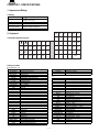
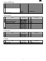
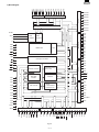
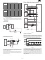
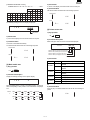
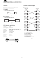
2. Keyboard
UPC
AMT
SCALE
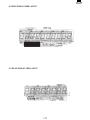
1) Standard keyboard layout
RECEIPT JOURNAL
RCPT
RA
PO
SLIP
1
%1
CASH
#
CL
RFND @/FOR
VOID
FINAL
NC
PBLU
7
4
1
0
8
5
2
5
10
15
20
14
9
14
19
3
8
13
18
2
7
12
17
1
6
11
16
9
6
3
00
OPEN
AUTO
TARE
TAX1
FS
SHIFT SHIFT
TAX2
FS
SHIFT TEND
CHK
CH
MDSE
SBTL
SBTL
CA/AT
Fig. 2-1
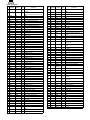
2) Key top name
Standard Key Top
KEY TOP
RECEIPT
JOURNAL
0 to 9,00
•
@/FOR
CL
1 to 20
PLU/SUB
TAX1 SHIFT
TAX2 SHIFT
UPC
SLIP
%1
CASH #
RCPT
(-) 1
NC
PBLU
FINAL
AMT
AUTO
RA
PO
RFND
VOID
SCALE
OPEN TARE
CH
CHK
MDSE SBTL
SBTL
CA/AT
DESCRIPTION
Receipt paper feed key
Journal paper feed key
Numeric keys
Decimal point key
Multiplication / Split-pricing key
Clear key
Department keys
PLU / Subdepartment key
Tax 1 shift key
Tax 2 shift key
UPC key
Slip print key
Percent 1 key
Cashier code entry key
Receipt print key
Discount 1 key
New charge account balance key
Previous balance lookup key
Final key
Amount key
Automatic sequencing key
Received on account key
Paid out key
Refund key
Void key
Scale key
Open tare key
Charge key
Check key
Merchandise subtotal key
Subtotal key
Cash/amount tendered key
KEY TOP
FS SHIFT
FS TEND
DESCRIPTION
Food stamp shift key
Food stamp tendered
Optional Key Top
KEY TOP
21 to 50
TAX3 SHIFT
TAX4 SHIFT
(-)2 - 4
000
#
NS
TAX
DEPT #
REPEAT
INQ
AUTO2 - 10
RA2
PO2
CH2 - 5
CA2
CONV1 - 4
CHK2
RFND SALE
B-DAY
NON DELETE
PRICE CHANGE
P1 - 3
SRVC
DEP
DEP RFND
1–1
DESCRIPTION
Department keys
Tax 3 shift key
Tax 4 shift key
Discount 2 - 4 keys
Triple zero key
Non-add code key
No sale key
Tax key
Department No. entry key
Repeat key
UPC inquiry key
Automatic sequencing 2 - 10 keys
Received on account 2 key
Paid out 2 key
Charge 2 - 5 keys
Cash total 2 key
Currency conversion 1 - 4 keys
Check 2 key
Refund sales key
Birthday date entry key
Non delete key
Price change key
UPC price level 1 - 3 keys
Service key
Deposit key
Deposit refund key
Display contents
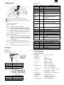
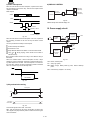
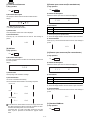
3. Mode switch
<Segment>
SRV
Amount
Minus sign
Error
PGM Mode
VOID Mode
RFND SALE
Mode
MA
SM
OP
REG
OP,X/Z
OFF
MGR
X1/Z1
PGM1
X2/Z2
PGM2
Position
1-8
4-10
10
10
10
1-10
(SRV)
CASH,
CHECK,
CHARGE
SUB TOTAL
/ short tender
Change
(SRV')
Fig. 3-1
The key can be removed in the REG or OFF position.
In the SRV’ mode, key inputs are prohibited and no display is present.
[Functions]
•
•
•
•
Function for each key position
SRV’: System reset
SRV:
Service mode (Service programming)
• PGM1: Allows programming of items frequently changed (e.g.
department, PLU pricing, and discount rate setting).
• OP X/Z: Allows X or Z operation by clerks or cashiers.
• REG: Allows registrations.
• MGR: Allows the operations, by authorized person such as a
manager (e.g. correction after transaction finished or
cancellation of entry limits), which are not permitted to
ordinary cashiers.
10
10
Decimal point
TAB
Sentinel
Price Level-3
Price Level-2
Scale entry
period.
Switching off the display to prevent key board entries.
4. Display
1) Layout
10-8
xxF : FS amount
9-10
5-10
8
9
2-3
10
Not zero-suppressed
Not zero-suppressed
Endless count, starting from 2.
_
- xx - : cashier code (xx = code 1-99)
U : Light up when the validation printing is
compulsory
P : Light up when the slip printing is
compulsory (REG/MGR/VOID mode)
10
Position
4-1
4-1
10
9
8
7
Description
Based on setuper multiplication.
SRV JOB#901
PGM JOB#2321
For UPC code entry
For UPC code entry
Item unit price
5. Specifications
Operator display
PLU/SUB
DEPT
1) Printer (PR-45M)
• No. of station:
• Validation:
• Printing system:
• No. of dot:
REPEAT
P3
P2
$
Cashier code
RCPT
OFF
CID sentinel indicator
• Dot pitch:
Fig. 4-1
7 segment display (LED)
10
Yellow Green
14.2 (H) ✕ 8.0 (W) mm
Customer display (Pop-up display)
Fig. 4-2
288 dots
288 dots
Horizontal: 0.125 mm
Vertical:
0.125 mm
1.25 mm (W) × 3.0 mm (H):
At 10 × 24 dots
• Reliability:
• Paper end sensor:
1–2
Receipt:
Journal:
• Character size:
(Manual feed):
7 segment display (LED)
7
Yellow Green
14.2 (H) ✕ 8.0 (W) mm
Line thermal
10 dots (W) × 24 dots (H)
• Print speed:
• Paper feed speed
$
2: Receipt and Journal
No
• Font:
• Printing capacity:
• Print pitch:
No. of positions
Color of display
Character size
C : Light up whenever the change due
amount appears in the display.
c
<Decimal point>
• X1/Z1: Allows reading and resetting of daily sales total.
• X2/Z2: Allows reading or resetting sales totals for a specified
No. of positions
Color of display
Character size
- : Floating
E
P
u
rrrrrrrrrr :
Light up only at the starting of RFND
SALE
f : Light up when a registration is finalized
by depressing CASH, CHECK,
CHARGE key
10
Foreign
Currency
SUB TOTAL
Food Stamp
Change
Department
PLU
Repeat
Receipt OFF
Cashier No.
VP
compulsory
Slip
compulsory
PGM2: Allows programming of an item that is not changed frequently, in addition to the PGM1 mode programming.
• OFF:
10
Description
Receipt:
Journal:
Max. 24 characters
Max. 24 characters
Column distance: 1.5 mm
Row distance:
3.75 mm
Approximate 50 mm/s (13.3 lines/sec)
Approximate 40 mm/s
Mechanism MCBF 5 million lines
Head life 5 × 10⁷ pulses
Yes (Receipt and Journal)
• Cutter:
Manual
• Paper near end sensor: No
• Printing area:
2) Paper
Number of thermal head heater elements 864 dots
(688dots)
36
(288dots)
14
36
(288dots)
(112dots)
Description
Name
Heat-quality paper
Roll dimension
44.5 ±0.5 mm in width
Thickness
0.06 mm to 0.08 mm
3) Cutter
• Method: Manual
6. Drawer
4.5
4
Item
0.125
1) Specification
(1) Drawer box and drawer
44.5±0.5
44.5±0.5
(Units : mm)
• Print format:
0.125
1.5 (12dots)
1.5 (12dots)
0.125
Model name
SK-423
Size
420 (W) x 427(L: included lock key) x
112(H: included rubber leg)
Color
GRAY 368
Material
Metal
Bell
-
Release lever
Standard equipment; Located at the
bottom
Drawer open sensor
Standard equipment
2) Money case
3.0 (24dots)
3.75 (30dots)
For
"U" version
For
"A" version
Separation from the drawer
Allowed
Allowed
Separation of the coin
compartments from the money case
Disallowed
Disallowed
Bill separator
-
YES
Number of compartments
5B/5C
4B/8C
Bill compartments
Bill separator
Coin compartments
3.75 (30dots)
3) Lock
Location of the lock
Front
Method of locking
and unlocking
Locking:
Insert the drawer lock key into
the lock and turn it 90
degrees counterclockwise.
Unlocking:
Insert the drawer lock key into
the lock and turn it 90
degrees clockwise.
Key No.
UNIT: mm
1–3
SK1-1
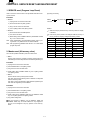
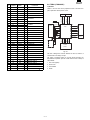
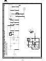
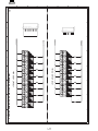
2) Port 1 (CH8)
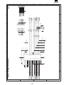
7. RS232 Interface
Channel No.:
Port 1(CH8)
Channel No.:
Port 2(CH1)
1
/CD
2
RD
3
SD
4
/ER
5
GND
6
/DR
7
/RS
8
/CS
on the RS connector PWB
/CI
+5V
SW2
9
1) Port 2 (CH1)
SD
4
/ER
5
GND
6
/DR
7
/RS
8
/CS
on the Main PWB
/CI
VCC
Pin No.9 : /CI signal (Default)
SW3
+5V
RD
3
9
SW2
Pin No.9 : +5V signal
CI
+5V
2
CI
/CD
SW2
1
The No.9 pin signal of the Port 1 (CH8) can be selected between the
/CI signal and the +5V signal by changing the connection of the SW2
(initial value: /CI signal)
NOTE:
Optional bar code reader: When connecting an ER-A6HS1, connect
it to the Port 1 (or 2) and switch the No.9 pin signal to the +5V
signal.
When connecting other RS232 devices to either the Port 1 (or 2),
make sure the No.9 pin signal is proper before connecting the device.
If you want to connect an RS232 device to the ECR with the No.9
pin of the port 1 (or 2) set to +5V, make sure the AC cable of the
ECR is disconnected from the wall outlet to protect the device.
Pin No.9 : /CI signal (Default)
VCC SW3 /CI
3
1
Pin No.9 : Vcc(+5V) signal
VCC SW3 /CI
3
1
1–4
CHAPTER 2. OPTIONS
1. System configuration
ER-A6HS1 or
LOCAL PURCHASE
(NOTE1)
This symbol sho ws
NEW MODEL
BARCODE READER
LOCAL PURCHASE
ER-A450T
LOCAL PURCHASE
ER-03RA
RS-232
2port
COMPUTER
MASTER MA CHINE
CABLE
OPTION RAM
PC UTILITY
ER-02FD EXE
or
ER-01/02FD
LOCAL PURCHASE
3.5 inch FDD
CABLE
LOCAL PURCHASE
LOCAL PURCHASE
SLIP PRINTER
CABLE
LOCAL PURCHASE
LOCAL PURCHASE
PRINT DATA
CABLE
ER-04D W
REMOTE DRA WER
Note : Only 2 peripherals max may be connected at any one
Fig. 1-1
2–1
time.
2. Options (SHARP only)
No.
NAME
MODEL
DESCRIPTION
1
EXPANSION RAM CHIP
ER-03RA
2
REMOTE DRAWER
ER-04DW
3
PRESETS LOADER
ER-01FD/02FD
FD unit
4
KEY TOP KIT
ER-11KT7
1 × 1 KEY TOP UNIT
ER-12KT7
1 × 2 KEY TOP UNIT
5
BARCODE READER
512K bytes RAM CHIP
ER-22KT7
2 × 2 KEY TOP UNIT
ER-11DK7G
1 × 1 DUMMY KEY KIT
ER-51DK7G
5 × 1 DUMMY KEY KIT
ER-A6HS1
3. Service options
No.
NAME
PARTS CODE
PRICE
RANK
DESCRIPTION
1
SERVICE KEY
2
MODE KEY GRIP COVER
AL
OP key only
3
DRIP-PROOF KEYBOARD COVER
BE
Include the switch cover
4
JOURNAL NEAR END SENSOR UNIT
BB
Q’ty: 1
Screw (Sensor unit – Top cabinet)
AA
Q’ty: 1
Screw (Sensor unit – Earth wire – Top cabinet)
AA
Q’ty: 1
Screw (Earth wire – Top cabinet)
AA
Q’ty: 1
Earth wire
AF
Q’ty: 1
Connector (2pin)
AA
Q’ty: 1
TEXT PRESET KEYBOARD COVER
BH
5
AF
4. Service tools
No.
NAME
PARTS CODE
PRICE
RANK
1
RS-232 LOOP BACK CONNECTOR
BU
2
KEY TOP REMOVER
AX
3
2 × 2 KEY TOP INSTALLING JIG
BP
DESCRIPTION
5. Supplies
No.
NAME
PARTS CODE
PRICE
RANK
DESCRIPTION
1
Thermal roll paper
AY
5 roll/pack
2
Thermal roll paper
BA
5 roll/pack (High preservation type)
2–2
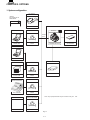
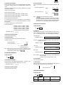
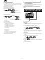
CHAPTER 3. SERVICE RESET AND MASTER RESET
1. SERVICE reset (Program Loop Reset)
[key setup procedure]
Used to return the machine back to its operational state after a lockup has occurred.
Procedure
*2
• Method 1
MRS-2
executed
1) Unplug the AC cord from the wall outlet.
0
Key position set
Free key
0
2) Set the mode switch to (SRV′) position.
*1
Free key setup
complete.
Disable
3) Plug in the AC cord to the wall outlet.
4) Turn to (SRV) position from (SRV′) position.
NOTES:
• Method 2
1: When the 0 key is pressed, the key of the key number on display
is disabled.
1) Set the mode switch to PGM2 position.
2) Turn off the AC switch.
2: Push the key on the position to be assigned. With this, the key of
the key number on display is assigned to that key position.
3) While holding down JOURNAL FEED key and RECEIPT FEED
key, Turn on the AC switch.
Key number
Key name
Key number
Note: When disassembling and reassembling always power up using method 1 only. Method 2 will not reset the CKDC8.
1
Numeric key "0"
10
Numeric key "9"
2
Numeric key "1"
11
Numeric key "00"
Note: SRV programming job#926-B must be set to "4" to allow PGM
program loop reset.
3
Numeric key "2"
12
Numeric key "000"
4
Numeric key "3"
13
Decimal point key
5
Numeric key "4"
14
CL key
6
Numeric key "5"
15
@/FOR
2. Master reset (All memory clear)
Key name
7
Numeric key "6"
16
SBTL key
There are two possible methods to perform a master reset.
8
Numeric key "7"
17
CA/AT key
• MRS-1
9
Numeric key "8"
Used to clear all memory contents and return machine back to its
initial settings and return keyboard back to default keyboard layout.
Procedure
1) Unplug the AC cord from the wall outlet.
2) Set the MODE switch to the (SRV′) position.
3) Plug in the AC cord to the wall outlet.
4) While holding down JOURNAL FEED key, turn to (SRV) position
from (SRV′) position.
• MRS-2
Used to clear all memory and keyboard contents.
This reset returns all programming back to defaults. The keyboard
must be entered by hand.
This reset is used if an application needs different keyboard layout
other than that supplied by a normal MRS-1.
Procedure
1) Unplug the AC cord from the wall outlet.
2) Set the MODE switch to the (SRV′) position.
3) Plug in the AC cord to the wall outlet.
4) While holding down JOURNAL FEED key and RECEIPT FEED
key, turn to (SRV) position from (SRV′) position.
5) Key position assignment:
After the execution of MRS-2, only the RECEIPT FEED and
JOURNAL FEED keys can remain effective on key assignment.
Any key can be assigned on any key position on the main keyboard.
3–1
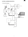
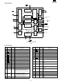
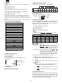
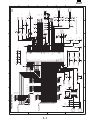
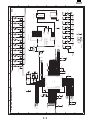
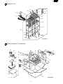
CHAPTER 4. HARDWARE DESCRIPTION
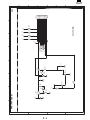
1. Hard ware block diagram
DRAWER
STANDARD
OPTIONAL
RAM1
RAM2
256KB
512KB
CPU
ER-03RA:512KB
STANDARD
GATE ARRAY
TPRC1
ROM
MPCA7
512KB
OPERATER DISPLAY
1 LINE
7SEG 10DIG
CUSTOMER DISPLAY
1 LINE
7SEG 7DIG
PRINTER
PR-45M
CKDC8
SWITCH
KEY BOARD
RS232
I/F
OPC2
1 ports
RS232
I/F
CH1
Fig. 1-1
4–1
2. Description of main LSI’s
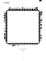
2-1. CPU (HD6415108-10)
112
111
110
109
108
107
106
105
104
103
102
101
100
99
98
97
96
95
94
93
92
91
90
89
88
87
86
85
STBY
MD2
MD1
MD0
VCC
RFSH
LWR
HWR
RD
AS
E
X
VSS
XTAL
EXTAL
VSS
TXD2
RXD2
TXD1
RXD1
SCK2
UASKC
IRQ1
IRQ0
VCC
AVCC
AN3
AN2
1) Pin configuration
84
83
82
81
80
78
78
77
76
75
74
73
72
71
70
69
68
67
66
65
64
63
62
61
60
59
58
57
29
30
31
32
33
34
35
36
37
38
39
40
41
42
43
44
45
46
47
48
49
50
51
52
53
54
55
56
1
2
3
4
5
6
7
8
9
10
11
12
13
14
15
16
17
18
19
20
21
22
23
24
25
26
27
28
A8
A9
A10
A11
A12
A13
A14
A15
VSS
A16
A17
A18
A19
A20
A21
A22
A23
VSS
WAIT
BACK
BREQ
P33
P34
P35
P36
P37
VCC
P40
RES
NMI
VSS
P10
P11
P12
P13
P14
P15
P16
P17
D0
D1
D2
D3
D4
D5
D6
D7
VSS
A0
A1
A2
A3
A4
A5
A6
A7
HD6415108-10 pin configuration
Fig. 2-1
4–2
AN1
AN0
AVSS
VSS
P67
P66
P65
P64
P63
P62
P61
P60
P57/STOP
P56
P55
P54
P53
P52
P51
P50
VSS
P47
P46
P45
P44
P43
P42
P41
P10
P11
P12
P13
P14
P15
P16
P17
D7
D6
D5
D4
D3
D2
D1
D0
2) Block diagram
P27/A23
Data bus
P26/A22
Port 1
Port 2
P25/A21
P24/A20
P23/A19
P22/A18
P21/A17
Watch
dog timer
E
MD2
MD1
H8/500 CPU
A15
A14
A13
A12
A11
A10
A9
A8
A7
A6
A5
A4
A3
A2
A1
A0
Address bus
Clock
oscillator
X
Address bus
XTAL
Data bus (Lower)
EXTAL
Data bus (Upper)
P20/A16
DTC
MD0
RES
STBY
NMI
Interruption controller
AS
P37
RD
P36
HWR
P35
16bit free running
timer x 2ch
Refresh controller
RFSH
Port 3
LWR
P34
P33
BREQ
Wait state
controller
8bit timer
A/D convertor
Serial
communication
interface x 2ch
VCC
BACK
WAIT
VCC
P47
VCC
VSS
P45
Port 4
VSS
FTI2
VSS
VSS
FTI1
P43
VSS
P42
VSS
P41/TMCI
VSS
P40
VSS
AVCC
Fig. 2-2
4–3
P50
P51
P52
P53
P54
P56
FMRS
Port 5
STOP/P57
P67
P66
RS/P65
RR/P64
CD/P63
CS/P62
DR/P61
ER/P60
AN0
Port 6
AN1
P73
IRQ0
IRQ1
Port 7
IRQ2
SCK2
RXD1
TXD1
RXD2
TXD2
Port 8
AN2
AVSS
3) Pin description
PIN
No.
1
2
SYMBOL
SIGNAL
NAME
/RES
/RESET
NMi
NMi
IN/
OUT
PIN
No.
FUNCTION
SIGNAL
NAME
SYMBOL
/PRST
FUNCTION
IN
RESET INPUT from CKDC WUTH
BUFFER
IN
NON-MASKABLE INTERRUPT
INPUT FOR SSP INTERRUPT INPUT
61
P45
/NEJ
IN
Near END signal journal
62
P46
NU
IN
(NU) GND
GND
63
P47
/NER
IN
EVENT READ CANCEL (to CKDC)
64
VSS
VSS
60
P44
IN/
OUT
IN
Printer (PR-45) Reset signal from
MPCA
3
VSS
VSS
4
P10
ERC
OUT
5
P11
LDRQ
OUT
LOAD REQUEST (to CKDC)
65
P50
TRG1
OUT
Nu (GND)
6
P12
/SHEN
IN
SHIFT ENABLE (from CKDC)
66
P51
/PSTOP
OUT
Nu (GND)
7
P13
/FRES
OUT
FISCAL MEMORY RESET (Nu)
67
P52
/CKDCR2
OUT
Nu (GND)
8
P14
BUSY
IN
FISCAL MEMORY BUSY (Nu)
68
P53
OPDS
IN
Nu (GND)
9
P15
/RDY
IN
FISCAL MEMORY READY (Nu)
69
P54
FVPON
OUT
Nu (GND)
10
P16
PDS
IN
POP-UP DISPLAY SENSOR (Nu)
70
P55
FMRS
IN
Nu (GND)
11
P17
IN
GND
71
P56
/SLIPLMP
OUT
Nu (GND)
12
D0
D0
I/O
DATA BUS 0
72
P57
/STOP
OUT
Nu (GND)
13
D1
D1
I/O
DATA BUS 1
P60
/ERS
14
D2
D2
I/O
DATA BUS 2
OUT
ER signal for RS232 (Equipment
Ready)
15
D3
D3
I/O
DATA BUS 3
74
P61
/DRS
IN
16
D4
D4
I/O
DATA BUS 4
75
P62
/CSS
IN
CS signal for RS232 (Clear to Send)
17
D5
D5
I/O
DATA BUS 5
76
P63
/CDS
IN
CD signal for RS232 (Carrier Detect)
18
D6
D6
I/O
DATA BUS 6
P64
/RR
19
D7
D7
I/O
DATA BUS 7
20
VSS
VSS
P65
/RSS
21
A0
A0
OUT
ADDRESS BUS 0
22
A1
A1
OUT
ADDRESS BUS 1
79
P66
(/RI), /CI
IN
CI signal for RS232 (Calling Indicator)
80
P67
HP
IN
Nu (GND)
81
VSS
VSS
82
AVSS
AVSS
IN
GND
83
AN0
Vrf
IN
Vrf
84
AN1
VHTEST
IN
VH Test input
85
AN2
VPTEST
IN
+24V test input
86
AN3
TM
IN
Thermal head thermistor level test
87
AVCC
AVCC
IN
+5V
88
VCC
VCC
89
P80
/iRQ0
IN
P81
/iRQ1
(/RSRQ)
IN
A2
A2
OUT
ADDRESS BUS 2
24
A3
A3
OUT
ADDRESS BUS 3
A4
A4
OUT
A5
A5
OUT
ADDRESS BUS 5
27
A6
A6
OUT
ADDRESS BUS 6
28
A7
A7
OUT
ADDRESS BUS 7
A8
A8
OUT
78
ADDRESS BUS 4
26
29
77
GND
23
25
73
ADDRESS BUS 8
30
A9
A9
OUT
ADDRESS BUS 9
31
A10
A10
OUT
ADDRESS BUS 10
32
A11
A11
OUT
ADDRESS BUS 11
33
A12
A12
OUT
ADDRESS BUS 12
34
A13
A13
OUT
ADDRESS BUS 13
35
A14
A14
OUT
ADDRESS BUS 14
36
A15
A15
OUT
37
VSS
VSS
38
A16
A16
OUT
ADDRESS BUS 16
39
A17
A17
OUT
ADDRESS BUS 17
40
A18
A18
OUT
ADDRESS BUS 18
41
A19
A19
OUT
ADDRESS BUS 19
42
A20
A20
OUT
ADDRESS BUS 20
43
A21
A21
OUT
ADDRESS BUS 21
44
A22
A22
OUT
45
A23
A23
OUT
46
VSS
VSS
47
/WAIT
/WAIT
IN
48
/BACK
/BACK
OUT
90
Near END signal receipt
GND
DR signal for RS232 (Data set Ready)
OUT
RR signal for RS232 (Ready to
Receive) (Nu)
OUT
RS signal for RS232 (Request to
Send)
GND
+5V
Interrupt signal 0 from MPCA
Interrupt signal from OPTION PWB
91
P82
/iRQ2
IN
92
P83
SCK2
OUT
93
P84
RXD
IN
94
P85
TXD
OUT
P86
RXD2
P87
TXD2
97
VSS
VSS
98
EXTAL
EXTAL
IN
X-TAL (19.66MHz)
ADDRESS BUS 22
99
XTAL
XTAL
IN
X-TAL (19.66MHz)
ADDRESS BUS 15
GND
95
96
ADDRESS BUS 23
100 VSS
VSS
GND
101 φ
φ
Wait signal from MPCA
102 E
Bus control request acknowledge
103 /AS
/AS
Interrupt signal (Nu) pull-up
CKDC & FMC i/F sync shift clock
RS232C RECEIVE DATA
RS232C SEND DATA
IN
CKDC, Fiscal memory unit I/F shift
input data
OUT
CKDC, Fiscal memory unit I/F shift
output data
GND
GND
OUT
System clock (9.83MHz)
OUT
E clock (NU)
OUT
Address strobe
49
/BREQ
/BREQ
IN
Bus control request
104 /RD
/RD
OUT
Read
50
P33
DOPS
IN
Drawer open sensor signal
105 /HWR
/WR
OUT
Write
51
P34
/DR0
OUT
Drawer open drive signal
106 /LWR
52
P35
/DR1
OUT
Option drawer 1 drive signal
107 /RFSH
/RFSH
53
P36
NU
IN
(Nu) GND
108 VCC
VCC
54
P37
NU
IN
(Nu) GND
109 MD0
MD0
IN
55
VCC
VCC
+5V
110 MD1
MD1
IN
+5V (MODE 3)
56
P40
/IFV
IN
(Nu) pull-up
111 MD2
MD2
IN
GND (MODE 3)
P41
/PTMG
IN
Printer (PR-45) timing signal from
MPCA
112 /STBY
/STBY
IN
+5V (Nu)
58
P42
/TOF
IN
(Nu) pull-up
59
P43
/BOF
IN
(Nu) pull-up
57
4–4
OUT
Nu
OUT
Refresh cycle (NU)
+5V
+5V (MODE 3)
2-2. G.A (MPCA7)
160
159
158
157
156
155
154
153
152
151
150
149
148
147
146
145
144
143
142
141
140
139
138
137
136
135
134
133
132
131
130
129
128
127
126
125
124
123
122
121
NU
DOTEN
TWAIT
NU
NU
NU
NU
NU
STH2
SCK2
HTS2
SLMTR
SLMTS
SLMTD
RJMTR
RAS3
NU
GND
VCC
ASKRX
NU
NU
NU
RJMTD
RJMTS
DT5
DT6
DT7
GND
DT1
DT2
DT3
DT4
RJTMG
RJRST
RAS1
RAS2
ROS2
ROS1
OPTCS
1) Pin configuration
120
119
118
117
116
115
114
113
112
111
110
109
108
107
106
105
104
103
102
101
100
99
98
97
96
95
94
93
92
91
90
89
88
87
86
85
84
83
82
81
41
42
43
44
45
46
47
48
49
50
51
52
53
54
55
56
57
58
59
60
61
62
63
64
65
66
67
68
69
70
71
72
73
74
75
76
77
78
79
80
1
2
3
4
5
6
7
8
9
10
11
12
13
14
15
16
17
18
19
20
21
22
23
24
25
26
27
28
29
30
31
32
33
34
35
36
37
38
39
40
D3
GND
D4
D5
D6
D7
SSPRQ
RESET
INT2
INT3
RXDI
TXDI
SCKI
IRQ0
A0
A1
A2
A3
A4
A5
GND
VCC
A6
A7
A8
A9
A10
A11
A12
A13
A14
A15
A16
A17
A18
A19
A20
A21
A22
NU
RF
JF
PCUT
FCUT
VF
STAMP
SLF
SLRS
SLMTD
RES
TRG
TRG
POFF
INT1
HTS1
SCK1
STH1
NU
NU
VCC
GND
NU
VRESC
SLTMG
SLRST
AS
RD
WR
PHAI
SDT7
SDT6
SDT5
GND
SDT4
SDT3
SDT2
SDT1
D0
D1
D2
GATE ARRAY (LZ9AH39)
MPCA7
Fig. 2-3
4–5
EXINT0
EXINT1
EXINT2
EXINT3
WRO
RDO
RA15
RA16
GND
RA17
RA18
EXWAIT
WAIT
NU
MCR1
NU
DAX1
RCKX
IRRX
GND
VCC
UATX
UARX
UASCK
IRTX
RCO
NU
NU
NU
NU
MA15
TEST
MD0
MD1
IPLON
INT4
PRST
PTMG
TRGI
A23
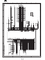
2) Block diagram
A23~A0
IRLON
ROS1
ROS2
RAS1
RAS2
Address decode
External CS
Internal CS
RASEL
Image
control
SSPRQ
SSP comparison register
BAR.
RAS3
OPTCS
IRTX
IRRX
RCI
ASKRX
I/R Control
D0~D7
Buffer
AS
CHS
serial select
RD
TXDI
SCKI
RXDI
HTS1
SCK1
STH1
HTS2
SCK2
STH2
Multiplexer
WR
RDO
WRO
Φ
Read/write
control
Φ
RESET
INT4
RES
Divider
VRESC
INT1
INT2
POFF
WAIT
EXWAIT
INT3
INTO
control
MD0
MD1
EXINT0
EXINT1
WAIT
control
EXINT2
EXINT3
CAPS
select
IRQ0
Print mode PMD
TEST
MTD
MTD
RJRST
SLRST
*PRST
RJTMG
RJMTR
Motor
drive
Print gate
SLMTS
SLTMG
Print pulse control
PTMG
SLMTR
Printer control port
SLMTD
SLF
SLRS
VF
RF
JF
FCUT
4–6
PCUT
Fig. 2-4
STAMP
TRGI
SDT1~7
DT1~9
TRG
DOTEN
TRG
* Output selection with CAPS.
PRST/PTMG.
SLMTD
3) Pin description
Pin
No.
1
2
3
4
5
6
7
8
9
10
11
12
13
14
15
16
17
18
19
20
21
22
Signal
name
VCC
GND
INTMCR
In/
Out
Out
Out
Out
Out
Out
Out
Out
Out
Out
Out
Out
Out
In
In
Out
Out
In
—
—
—
—
—
23
VRESC
Out
24
25
26
27
28
29
SLTMG
SLRST
AS
RD
WR
φ
In
In
In
In
In
In
30
SDT7
Out
31
SDT6
Out
32
SDT5
Out
33
GND
—
34
SDT4
Out
35
SDT3
Out
36
SDT2
Out
37
SDT1
Out
38
39
40
41
42
43
44
45
46
47
48
49
50
D0
D1
D2
D3
GND
D4
D5
D6
D7
SPRQ
RESET
SHEN
INT3
I/O
I/O
I/O
I/O
—
I/O
I/O
I/O
I/O
Out
In
In
In
RF
JF
PCUT
FCUT
VF
STAMP
SLFS
SLRS
SLMTD
RES
TRG
TRG
POFF
INT1
HTS1
SCK1
STH1
RAS VZ
—
Function
Receipt side paper feed solenoid (NU)
Journal side paper feed solenoid (NU)
Printer partial cut signal (NU)
Printer auto cut signal (NU)
Multi line validation paper feed (NU)
Printer stamp signal (NU)
Slip printer paper feed singnal (NU)
Slip printer release signal (NU)
Slip printer motor drive signal (NU)
Peripheral output reset
Dot head trigger signal (NU)
Dot head trigger signal (NU)
Power off signal input
(NU)
8 bit serial port output (for CKDC8)
Serial port shift clock output (for CKDC8)
8 bit serial port input (for CKDC8)
Chip select (NU)
Nu
+5V
GND
Interrupt (NU)
Turns active when reset and power
down is met
Slip printer timing signal (NU)
Slip printer reset signal (NU)
Address strobe
Read strobe
Write strobe
(φ) System clock (9.83 MHz)
Slip printer printhead drive signal (dot7)
(NU)
Slip printer printhead drive signal (dot6)
(NU)
Slip printer printhead drive signal (dot5)
(NU)
GND
Slip printer printhead drive signal (dot4)
(NU)
Slip printer printhead drive signal (dot3)
(NU)
Slip printer printhead drive signal (dot2)
(NU)
Slip printer printhead drive signal (dot1)
(NU)
Data bus 0
Data bus 1
Data bus 2
Data bus 3
GND
Data bus 4
Data bus 5
Data bus 6
Data bus 7
SSP interrupt request to CPU
MPCA reset
Shift enable from CKDC8
Interrupt signal (Nu)
4–7
Pin
No.
51
52
53
54
55
56
57
58
59
60
61
62
63
64
65
66
67
68
69
70
71
72
73
74
75
76
77
78
79
80
81
82
83
84
85
86
87
88
89
90
91
92
93
94
Signal
name
RXD2
TXD2
SCK2
IRQ0
A0
A1
A2
A3
A4
A5
GND
VCC
A6
A7
A8
A9
A10
A11
A12
A13
A14
A15
A16
A17
A18
A19
A20
A21
A22
LCDC
A23
TRGI
PTMG
PRST
RDY
IPLON
MD1
MD0
TEST
MA15
MA18
MA19
RCVRDY1
RCVRDY2
In/
Out
Out
In
In
Out
In
In
In
In
In
In
—
—
In
In
In
In
In
In
In
In
In
In
In
In
In
In
In
In
In
—
In
In
Out
Out
In
In
In
In
In
—
—
—
—
—
95
RC0
—
96
97
98
99
100
101
102
103
104
105
106
IRTX
UASCK
UARX
UATX
VCC
GND
IRRX
RCI
DAX1
DAX2
MCR1
—
—
—
—
—
—
—
—
—
—
—
Function
8 bit serial port output to CPU
8 bit serial port input from CPU
Serial port shift clock input from CPU.
Interrupt request to CPU
Address bus 0
Address bus 1
Address bus 2
Address bus 3
Address bus 4
Address bus 5
GND
+5V
Address bus 6
Address bus 7
Address bus 8
Address bus 9
Address bus 10
Address bus 11
Address bus 12
Address bus 13
Address bus 14
Address bus 15
Address bus 16
Address bus 17
Address bus 18
Address bus 19
Address bus 20
Address bus 21
Address bus 22
LCD CS (NU)
Address bus 23
Dot pulse control/drive signal (NU: GND)
Printer timing signal to CPU
Printer reset signal to CPU
Ready from FMC unit
To option connector (NU) +5V
Mode select input (GND)
Mode select input (GND)
+5V
Image address 15
Nu
Nu
Nu: +5V
Nu: +5V
Remote control encord signal for CPU
(NU)
I/R output for LED (NU)
I/R serial data shift clock (NU)
I/R serial data for CPU (NU)
I/R serial data from CPU (NU) +5V
+5V
GND
I/R input from I/R unit (NU) +5V
I/R input from I/R unit (NU) +5V
System clock (NU)
Nu
Nu
EXWAIT
In
110
111
112
113
114
115
116
117
118
119
120
RA18
RA17
GND
RA16
RA15
RDO
WRO
EXINT3
EXINT2
EXINT1
EXINT0
Out
Out
—
Out
Out
Out
Out
In
In
In
In
121
OPTCS
Out
122
123
124
125
126
127
128
129
130
131
132
133
134
135
136
137
138
139
140
141
142
143
144
145
ROS1
ROS2
RAS2
RAS1
RJRST
RJTMG
DT4
DT3
DT2
DT1
GND
DT7
DT6
DT5
MTD
MTD
DOT9
DOT8
SYNC
ASKRX
VCC
GND
—
Out
Out
Out
Out
In
In
Out
Out
Out
Out
—
Out
Out
Out
Out
Out
Out
Out
—
—
—
—
—
Out
146
RJMTR
In
147
148
149
150
151
152
153
154
155
156
157
158
159
160
SLMTD
SLMTS
SLMTR
HTS2
SCK2
STH2
—
—
—
—
—
Out
Out
In
Out
Out
In
—
—
—
—
—
IN
Out
—
LCDWT
DOTEN
RASP
1) Pin configulation
Nu
Wait request signal
External wait control input signal (NU)
+5V
Nu
Nu
GND
Nu
Nu
Expansion RD signal
Option
Expansion WR signal
RS232C /CD interrupt
Option PWB (PULL UP)
RS232C /CI interrupt
Option PWB (PULL UP)
Chip select base signal for expansion
option
ROM 1 chip select signal
ROM 2 chip select signal (NU)
RAM 2 chip select signal
RAM 1 chip select signal
Printer reset signal
FOR TPRC (NU) +5V
Printer dot signal 4 (NU)
Printer dot signal 3 (NU)
Printer dot signal 2 (NU)
Printer dot signal 1 (NU)
GND
Printer dot signal 7 (NU)
Printer dot signal 6 (NU)
Printer dot signal 5 (NU)
Printer motor drive signal (NU)
Printer motor drive signal (NU)
Printer dot signal 9 (NU)
Printer dot signal 8 (NU)
Nu (+5V)
I/R input from I/R unit (NU) Pull-up
+5V
GND
Nu
Nu
Printer motor lock detection signal (NU)
GND
Nu
Nu
GND
Serial output to FMC unit
Serial clock to FMC unit
Serial input to FMC unit
Nu
Nu
Nu
Nu
Nu
TPRC wait signal
Dot drive enable signal (Nu)
Nu
NU
NU
G10
G9
G8
G7
G6
G5
G4
G3
G2
G1
BUZ
/POFF
NU
ST8
109
2-3. CKDC8
Function
64
63
62
61
60
59
58
57
56
55
54
53
52
51
50
49
MCR2
WAIT
RAS3
In/
Out
—
Out
DP
SA
SB
SC
SD
SE
SF
SG
GND
VDD
KR4
KR10
KR11
NU
HTS
STH
1
2
3
4
5
6
7
8
9
10
11
12
13
14
15
16
48
47
46
45
44
43
42
41
40
39
38
37
36
35
34
33
CKDC8
ST7
ST6
/RESETS
/SHEN
ERC
LDRQ
GND
GND
/RES0
VDD
GND
KR7
17
18
19
20
21
22
23
24
25
26
27
28
29
30
31
32
Signal
name
/SCK
ST0
ST1
ST2
ST3
ST4
ST5
VDD
GND
NU
KR0
KR1
KR2
KR3
KR5
KR6
Pin
No.
107
108
2) Pin assignment (CKDC8)
4–8
Pin
No.
SYMBOL
SIGNAL
NAME
IN/
OUT
1
DP
DP
OUT DISPLAY SEGMENT Dp
2
A
SA
OUT DISPLAY SEGMENT a
3
B
SB
OUT DISPLAY SEGMENT b
4
C
SC
OUT DISPLAY SEGMENT c
5
D
SD
OUT DISPLAY SEGMENT d
6
E
SE
OUT DISPLAY SEGMENT e
7
F
SF
OUT DISPLAY SEGMENT f
OUT DISPLAY SEGMENT g
FUNCTION
8
G
SG
9
VSS0
GND
10
VDD0
VDD
11
KR4
KR4
IN
KEY RETURN 4
12
KR10
KR10
IN
KEY RETURN (feed clerk
MRS sw)
13
KR11
KR11
IN
KEY RETURN (MODE sw)
14
KR8
NU
IN
GND
15
HTS
HTS
IN
16
STH
STH
OUT
17
/SCK
/SCK
18
ST0
ST0
OUT KEY STROBE 0
19
ST1
ST1
OUT KEY STROBE 1
20
ST2
ST2
OUT KEY STROBE 2
21
ST3
ST3
OUT KEY STROBE 3
22
ST4
ST4
OUT KEY STROBE 4
23
ST5
ST5
OUT KEY STROBE 5
24
VDD1
VDD
VDD
25
AXSS
GND
GND
GND
VDD
IN
SHIFT CLOCK
26
KR9
NU
27
KR0
KR0
IN
KEY RETURN 0
GND
28
KR1
KR1
IN
KEY RETURN 1
29
KR2
KR2
IN
KEY RETURN 2
30
KR3
KR3
IN
KEY RETURN 3
31
KR5
KR5
IN
KEY RETURN 5
Pin
No.
SYMBOL
SIGNAL
NAME
IN/
OUT
32
KR6
KR6
IN
KEY RETURN 6
33
KR7
KR7
IN
KEY RETURN 7
34
AVRF
GND
37
XT2
38
XT1
32.768 KHz
39
IC
40
X2
41
X1
42
VSS1
GND
43
LDRQ
LDRQ
44
45
46
ERC
SHEN
/RES1
Auto cutter Pulse motor
IN
GND
POF,RES
4.19 MHz
ERC
/SHEN
/RESETS
IN
IN
CPU
(H8/500)
RTRM,PTJM
/RES0
XRS,XJS
RVPON,JVPON
VDD
/RESET
TPRC1 is the LSI circuit of the peripheral circuits of the microcomputer required for thermal printer control.
PFP,PCRES
AVDD
36
1) General
CTAO,CTBO
35
2-4. TPRC1 (F258024PC)
FUNCTION
A0~23
SO
D0~7
CLOCK
TPRC1
LORD REQUEST
RD
SI
EVENT READ CANCEL
WR
LATCH
WAIT
ST1~4
INT
HCD
PHAI
PHUP,PSP,
PST,POP
OUT SHIFT ENABLE
OUT SYSTEM TO RESET
Thermal
head
Switch
sensor
ST7
ST7
OUT KEY STROBE 7
49
ST8
ST8
OUT KEY STROBE 8
50
ST9
NU
OUT KEY STROBE 9
51
/POFF
/POFF
52
BUZ
BUZ
53
T0
G1
OUT DISPLAY DIGIT 1
54
T1
G2
OUT DISPLAY DIGIT 2
55
T2
G3
OUT DISPLAY DIGIT 3
Fig. 2-6
56
T3
G4
OUT DISPLAY DIGIT 4
57
T4
G5
OUT DISPLAY DIGIT 5
The CPU is designed for use with H8/500. The bus I/F, however, is
not restricted to the design concept.
58
T5
G6
OUT DISPLAY DIGIT 6
59
T6
G7
OUT DISPLAY DIGIT 7
60
T7
G8
OUT DISPLAY DIGIT 8
The printer is designed mainly for use with PR-58. However, the
thermalhead composition (the dot number and the block number) is
rather flexible.
61
T8
G9
OUT DISPLAY DIGIT 9
1. Auto cutter (Option)
62
T9
G10
OUT DISPLAY DIGIT 10
2. Pulse motor
63
T10
NU
OUT DISPLAY DIGIT 11
3. Thermalhead
64
ID
NU
OUT DISPLAY SEGMENT
4. Switch
IN
CG ROM
BRAS
(BRAS)
48
BWR
OUT KEY STROBE 6
BRD
ST6
BD0~2
ST6
BA0~15
47
POWER OFF
PB RAM
(SRAM)
OUT BUZZER
4–9
160
159
158
157
156
155
154
153
152
151
150
149
148
147
146
145
144
143
142
141
140
139
138
137
136
135
134
133
132
131
130
129
128
127
126
125
124
123
122
121
NU
GND
RESET
BRAS
BRAS
BD0
BD1
BD2
GND
GND
GND
BD3
BD4
GND
BD5
BD6
BD7
BA0
VCC
VCC
VCC
PHAI
BA1
BA2
BA3
BA4
BA5
BA6
GND
GND
GND
BA7
BA8
BA9
BA10
BA11
BA12
P.P
GND
GND
2) Pin configuration
120
119
118
117
116
115
114
113
112
111
110
109
108
107
106
105
104
103
102
101
100
99
98
97
96
95
94
93
92
91
90
89
88
87
86
85
84
83
82
81
41
42
43
44
45
46
47
48
49
50
51
52
53
54
55
56
57
58
59
60
61
62
63
64
65
66
67
68
69
70
71
72
73
74
75
76
77
78
79
80
1
2
3
4
5
6
7
8
9
10
11
12
13
14
15
16
17
18
19
20
21
22
23
24
25
26
27
28
29
30
31
32
33
34
35
36
37
38
39
40
WI
BACK
A3
A4
A5
A6
A7
A8
A9
GND
GND
GND
A10
A11
A12
A13
A14
A15
A16
VCC
VCC
VCC
A17
A18
A19
A20
A21
A22
A23
GND
GND
RD
WR
AS
POF
INT
WO
INH
BREQ
NU
GND
GND
ST1
GND
ST2
ST3
ST4
ST5
ST6
LATCH
GND
GND
GND
SI
SO
CLOCK
INHDEC
CSEN
TEST2
VCC
VCC
VCC
VCC
TEST1
D0
D1
D2
D3
D4
GND
GND
GND
D5
D6
D7
A0
A1
A2
NU
INTI
Fig. 2-7
4 – 10
PTJM
PTRM
BA13
BA14
BA15
BRD
BWR
CGS
GND
GND
GND
JAS
JBS
JCS
JDS
RAS
RBS
VCC
VCC
VCC
VCC
VCC
GND
RCS
RDS
CTAO
CTBO
VHCOM
JVPON
GND
GND
GND
RVPON
PFP
PCRES
PHUP
JPE
ROE
EBACK
EBREQ
3) Block diagram
INHBEC
CSEN
CGS
RES
DECODEK UNIT
RD,WR
A0~23
SYSTEM
I/F
POF,INH
HOST BUS I/F UNIT
PDCTLU
D0~7
HEAD CONTROL
TIMER UNIT
POP,PHUP,PFP,PCRES
PTRM,PTJM
PORT
WO
MOTOR CONTROL
TIMER UNIT
WI
CLOCK,SO,ST1~5,HCO
HEAD
I/F
SI
INTERRUPT
CIRCUIT
INT
INTI
EBAK,EPEQ
EBRK,EACK
MISC.
CUTTER CONTROL
TIMER UNIT
RVPON,JVPON,
RAS,RBS,RCS,RDS,
JAS,JBD,JCS,JDS
MOTOR
CONTROL
TEST
CIRCUIT
CLOCK
GEN.
PHAI
(Φ)
TEST1,TEST2
CTAO,CTBO
CUTTER
CONTROL
PB I/F UNIT
BA0~15
BRAS,BRAS
BRD,BWR
BD0~7
TPRC1 BLOCK DIAGRAM
Fig. 2-8
4) Pin description
Pin
No.
Signal
name
In/Out
Pin
No.
Function
Signal
name
In/Out
Function
1
GND
—
GND
18
CSEN
I
GND
2
GND
—
GND
19
TEST2
I
+5V internal counter timer test pin
3
ST1
O
Head drive strobe signal 1
20
Vcc
—
+5V
4
GND
—
GND
21
Vcc
—
+5V
5
ST2
O
Head drive strobe signal 2
22
Vcc
—
+5V
6
ST3
O
Head drive strobe signal 3
23
Vcc
—
7
ST4
O
Head drive strobe signal 4
24
TEST1
8
ST5
O
NU
25
D0
I/O
Data bus 0: Internal register, print buffer
data IO
26
D1
I/O
Data bus 1: Internal register, print buffer
data IO
27
D2
I/O
Data bus 2: Internal register, print buffer
data IO
28
D3
I/O
DAta bus 3: Internal register, print buffer
data IO
29
D4
I/O
Data bus 4: Internal register, print buffer
data IO
30
GND
—
GND
31
GND
—
GND
32
GND
—
GND
33
D5
I/O
Data bus 5: Internal register, print buffer
data IO
9
ST6
O
NU
10
LATCH
O
Head latch signal
11
GND
—
GND
12
GND
—
GND
13
GND
—
GND
14
SI
I
Data return line, thermalhead -- TPRC1
15
SO
O
Send data from TPRC1 to thermalhead
Data from PB-RAM or zero data are
outputted at the falling of CLOCK signal.
16
16
17
CLOCK
INHDEC
O
I
Thermalhead CLOCK signal
SO is outputted at the edge of I Ä O,
and is taken at the edge of o Ä I.
GND
4 – 11
I
+5V
+5V internal counter timer test pin
Pin
No.
Signal
name
In/Out
Function
Pin
No.
Signal
name
In/Out
Function
34
D6
I/O
Data bus 6: Internal register, print buffer
data IO
84
JPE
I
Journal paper empty
85
PHUP
I
Printer head up
35
D7
I/O
Data bus 7: Internal register, print buffer
data IO
86
PCRES
I
Auto cutter unit reset signal input (Nu)
87
PFP
I
Auto cutter unit FP signal input (Nu)
88
RVPON
O
Receipt side paper feed pulse motor
common power control signal (Nu)
36
A0
I
Address bus 0
37
A1
I
Address bus 1
38
A2
I
Address bus 2
89
GND
—
GND
39
TPRCRQ2
—
Request signal
90
GND
—
GND
40
INTI
I
+5V
91
GND
—
GND
41
WI
I
+5V
JVPON
O
42
BACK
I
BACK
Journal side paper feed pulse motor
common power control signal (Nu)
43
A3
I
Address bus 3
93
VHCOM
O
Head drive common power control
44
A4
I
Address bus 4
94
CTBO
O
Cutter motor control signal (Nu)
45
A5
I
Address bus 5
95
CTAO
O
Cutter motor control signal (Nu)
46
A6
I
Address bus 6
96
RDS
O
47
A7
I
Address bus 7
Receipt side paper feed pulse motor
drive signal, phase D
48
A8
I
Address bus 8
97
RCS
O
Receipt side paper feed pulse motor
drive signal, phase C
98
GND
—
+5V
99
Vcc
—
+5V
100 Vcc
—
+5V
101 Vcc
—
+5V
102 Vcc
—
+5V
103 Vcc
—
+5V
104 RBS
O
Receipt side paper feed pulse motor
drive signal, phase B
105 RAS
O
Receipt side paper feed pulse motor
drive signal, phase A
106 JDS
O
Journal side paper feed pulse motor
drive signal, phase D
107 JCS
O
Journal side paper feed pulse motor
drive signal, phase C
108 JBS
O
Journal side paper feed pulse motor
drive signal, phase B
109 JAS
O
Journal side paper feed pulse motor
drive signal, phase A
49
A9
50
GND
—
I
GND
51
GND
—
GND
52
GND
—
GND
53
A10
I
Address bus 10
54
A11
I
Address bus 11
55
A12
I
Address bus 12
56
A13
I
Address bus 13
57
A14
I
Address bus 14
58
A15
I
Address bus 15
92
Address bus 9
59
A16
I
60
Vcc
—
+5V
61
Vcc
—
+5V
62
Vcc
—
+5V
63
A17
I
Address bus 17
64
A18
I
Address bus 18
65
A19
I
Address bus 19
66
A20
I
Address bus 20
110 GND
—
GND
67
A21
I
Address bus 21
111 GND
—
GND
68
A22
I
Address bus 22
112 GND
—
GND
69
A23
I
Address bus 23
113 CGS
O
NU
70
GND
—
GND
114 BWR
O
PB-RAM write strobe signal
71
GND
—
GND
115 BRD
O
PB-RAM read strobe signal
72
RD
I
Read strobe signal: Gate enable of data
bus D0 - D7 tri-state buffer
116 BA15
O
NU
117 BA14
O
Address 14 for PB-RAM
73
WR
I
Write strobe signal: Write enable into
the internal register and the print buffer.
118 BA13
O
Address 13 for PB-RAM
119 PTRM
I
Receipt motor connector sensor signal
120 PTJM
I
Journal motor connector sensor signal
121 GND
—
GND
122 GND
—
GND
123 POPI
O
GND
124 BA12
O
Address bus 12 for PB-RAM
125 BA11
O
Address bus 11 for PB-RAM
126 BA10
O
Address bus 10 for PB-RAM
127 BA9
O
Address bus 9 for PB-RAM
128 BA8
O
Address bus 8 for PB-RAM
129 BA7
O
Address bus 7 for PB-RAM
74
AS
I
Address bus 16
AS
75
POF
I
Power off signal
76
INT
O
Interrupt signal
77
78
WO
INH
O
I
Wait request signal to the CPU
Head drive inhibit
79
BREQ
O
Bus request to CPU
80
—
—
NU
81
82
83
EBREQ
EBACK
RPE
I
O
I
Bus request from option
Bus acknowledge to option
Receipt paper empty
4 – 12
Pin
No.
Signal
name
In/Out
130 GND
—
GND
131 GND
—
GND
132 GND
—
GND
133 BA6
O
Address bus 6 for PB-RAM
134 BA5
O
Address bus 5 for PB-RAM
135 BA4
O
Address bus 4 for PB-RAM
136 BA3
O
Address bus 3 for PB-RAM
137 BA2
O
Address bus 2 for PB-RAM
138 BA1
O
Address bus 1 for PB-RAM
139 PHAI
I
Pin
No.
144
145
146
147
148
149
150
151
152
153
154
155
156
157
158
159
160
Function
TPRC1 clock input pin (9.83 MHz)
140 Vcc
—
+5V
141 Vcc
—
+5V
142 Vcc
—
+5V
143 BA0
O
Address bus 0 for PB-RAM
Signal
name
BD7
BD6
BD5
GND
BD4
BD3
GND
GND
GND
BD2
BD1
BD0
BRAS
BRAS
RESET
GND
NU
In/Out
I/O
I/O
I/O
—
I/O
I/O
—
—
—
I/O
I/O
I/O
O
O
I
—
—
Function
Data bus 7 for PB-RAM
Data bus 6 for PB-RAM
Data bus 5 for PB-RAM
GND
Data bus 4 for PB-RAM
Data bus 3 for PB-RAM
GND
GND
GND
Data bus 2 for PB-RAM
Data bus 1 for PB-RAM
Data bus 0 for PB-RAM
PB-RAM chip select: Active HIGH (Nu)
PB-RAM chip select: Active LOW
TPRC1 reset signal
GND
GND
2-5. OPC2
160
159
158
157
156
155
154
153
152
151
150
149
148
147
146
145
144
143
142
141
140
139
138
137
136
135
134
133
132
131
130
129
128
127
126
125
124
123
122
121
MCLK
RST
RSLCT1
RSLCT0
/RIN
/WIN
SYCBKD
TRNEMPD
RCVRDYD
TRNRDYD
/DSRD
/CTSD
RCVDTD
/RTSD
/DTRD
TRNDTD
/CSD
GND
VCC
SYCBKC
TRNEMPC
RCVRDYC
TRNRDYC
/DSRC
/CTSC
RCVDTC
/RTSC
/DTRC
TRNDTC
/CSC
GND
SYCBKB
TRNEMPB
RCVRDYB
TRNRDYB
/DSRB
/CTSB
RCVDTB
/RTSB
/DTRB
1) Pin configuration
120
119
118
117
116
115
114
113
112
111
110
109
108
107
106
105
104
103
102
101
100
99
98
97
96
95
94
93
92
91
90
89
88
87
86
85
84
83
82
81
41
42
43
44
45
46
47
48
49
50
51
52
53
54
55
56
57
58
59
60
61
62
63
64
65
66
67
68
69
70
71
72
73
74
75
76
77
78
79
80
1
2
3
4
5
6
7
8
9
10
11
12
13
14
15
16
17
18
19
20
21
22
23
24
25
26
27
28
29
30
31
32
33
34
35
36
37
38
39
40
/CI2
/CS2
/CD3
BRK3
TRNEMP3
RCVRDY3
TRNRDY3
/CTS3
RCVDT3
/CI3
/CS3
D0
D1
D2
D3
GND
D4
D5
D6
D7
GND
VCC
X1
X2
XOUT
TRCK
AB0
AB1
US1CH
PX
/POF
/RSRQ
/TRV
RXDATA0
TXE
/TRRQ
/TRQ1
/TRQ2
A0
A1
SL00
SL01
SL02
SL10
SL11
SL12
SL20
SL21
SL22
SL30
SL31
SL32
/CD0
BRK0
TRNEMP0
RCVRDY0
TRNRDY0
/CTS0
RCVDT0
VCC
GND
/CI0
/RTS0
/CS0
/CD1
BRK1
TRNEMP1
RCVRDY1
TRNRDY1
/CTS1
RCVDT1
/CI1
/RTS1
/CS1
/CD2
TRNEMP2
RCVRDY2
TRNRDY2
CTS2Z
RCVDT2
4 – 13
TRNDTB
/CSB
GND
SYCBKA
TRNEMPA
RCVRDYA
TRNRDYA
/DSRA
/CTSA
RCVDTA
/RTSA
/DTRA
TRNDTA
/CSA
UTST
DBTST
RCVCLK
TRNCLK
RES
GND
VCC
/W
/R
DB7
DB6
DB5
DB4
GND
DB3
DB2
DB1
DB0
/RES
/WR
/RD
/OPTCS
A5
A4
A3
A2
2) Block diagram
OPC2
OPC1
DATA BUS
OPC1~USART
BAUD RATE GENERATOR
BAUD RATE GENERATOR
USART
USART
USART
USART
A
B
C
D
USART
Common input
3) Pin description
Pin
NO.
Name
1
2
ER-A770
I/O
SL00
VCC
ISU
SL01
GND
ISU
3
SL02
GND
ISU
4
SL10
GND
ISU
5
SL11
GND
ISU
6
SL12
GND
ISU
7
SL20
GND
ISU
8
SL21
GND
ISU
9
SL22
GND
ISU
10
SL30
GND
ISU
11
SL31
GND
ISU
12
SL32
GND
ISU
13
/CD0
/DCD1
IS
14
BRK0
BRK1
Pin
NO.
Description
RS-232/UNIT0
channel select
RS-232/UNIT1
channel select
RS-232/UNIT2
channel select
RS-232/UNIT3
channel select
Name
ER-A770
I/O
Description
26
BRK1
BRK2
IS
GND
27
TRNEMP1
TRENMP2
IS
GND
28
RCVRDY1
RCVRDY2
IS
GND
29
TRNRDY1
TRNRDY2
IS
GND
30
/CTS1
/CTS2
IS
+5V
31
RCVDT1
RCVDT2
IS
RS-232 reception
data signal
32
/CI1
/CI2
IS
RS-232 control
signal /CI input
33
/RTS1
/RTS2
O
RS-232 request to
send signal
34
/CS1
/CS2
O
RS-232 chip select
signal
RS-232 control
signal /CD input
35
/CD2
VCC
IS
+5V
36
TRNEMP2
TRENMP3
IS
GND
IS
RS-232 break signal
37
RCVRDY2
RCVRDY3
IS
GND
38
TRNRDY2
TRNRDY3
IS
GND
39
CTS2Z
/CTS3
IS
+5V
40
RCVDT2
RCVDT3
IS
GND
15
TRNEMP0
TRENMP1
IS
RS-232 transmission
buffer empty signal
16
RCVRDY0
RCVRDY1
IS
RS-232 data reception
enable signal
17
TRNRDY0
TRNRDY1
IS
RS-232 transmission
enable signal
18
/CTS0
/CTS1
IS
RS-232 clear to
send signal
19
RCVDT0
RCVDT1
IS
RS-232 reception
data signal
41
/CI2
VCC
IS
+5V
42
/CS2
/CS3
O
NU
43
/CD3
/SINT
IS
RS-232: /CD,
IN-LINE : /P1
44
BRK3
GND
IS
GND
45
TRNEMP3
GND
IS
GND
20
VCC
VCC
+5V
46
RCVRDY3
GND
IS
GND
21
GND
GND
GND
47
TRNRDY3
GND
IS
GND
22
/CI0
/CI1
RS-232 control
signal /CI input
48
/CTS3
GND
IS
GND
49
RCVDT3
GND
IS
GND
50
/CI3
GND
IS
GND
IS
23
/RTS0
/RTS1
O
RS-232 request to
send signal
24
/CS0
/CS1
O
RS-232 chip select
signal
51
/CS3
/SRCS
O
RS-232/INLINE chip
select signal
D0
D0
IO
Data bus (CPU)
/CD1
/DCD2
IS
RS-232 control
signal /CD input
52
25
53
D1
D1
IO
Data bus (CPU)
4 – 14
Pin
NO.
Name
ER-A770
I/O
Description
54
D2
D2
IO
Data bus (CPU)
IO
55
D3
D3
56
GND
GND
Pin
NO.
Name
ER-A770
I/O
99
/W
/WRH
O
Data bus (CPU)
Description
Write signal
(to USART)
GND
100
VCC
VCC
+5V
GND
GND
GND
57
D4
D4
IO
Data bus (CPU)
101
58
D5
D5
IO
Data bus (CPU)
102
RES
RES USART
O
59
D6
D6
IO
Data bus (CPU)
Reset signal
(to USART)
60
D7
D7
IO
Data bus (CPU)
103
TRNCLK
GND
I
GND
61
GND
GND
GND
104
RCVCLK
GND
I
GND
62
VCC
VCC
+5V
105
DBTST
/SRCS
ID
63
X1
NC
106
UTST
VCC
ID
+5V
64
X2
#
107
/CSA
/CS1
IS
USART_A chip select
65
XOUT
CLK_USART
O
Clock (USART)
66
TRCK
NC
O
NC
108
TRNDTA
TXD1
O
RS-232 transmission
data signal
67
AB0
AH0
O
Address bus for
USART
109
/DTRA
/DTR1
O
RS-232 data
terminal ready signal
68
AB1
AH1
O
Address bus for
USART
110
/RTSA
NC
O
NC
69
US1CH
GND
IS
GND
111
RCVDTA
RCVDT1
IS
RS-232 reception
data signal
70
PX
NC
O
NC
112
/CTSA
GND
IS
GND
71
/POF
/POFF
IS
POFF signal
72
/RSRQ
/IRQ1
3S
RS232 INTRRUPT
113
/DSRA
/DSR1
IS
RS-232 data set
ready signal
73
/TRV
GND
IS
GND
74
RXDATA0
NC
O
NC
114
TRNRDYA
TRNRDY1
O
RS-232 data
transmission enable
signal
75
TXE
/SRESET
O
INLINE SOFT
RESET
115
RCVRDYA
RCVRDY1
O
RS-232 data reception
enable signal
76
/TRRQ
/TRQ2
3S
INLINE INTRRUPT
TRNEMPA
TRNEMP1
O
/TRQ1
/TRQ1
ON6
TIMER INTRRUPT
(RS232)
116
77
RS-232 transmission
buffer empty signal
TIMER INTRRUPT
(INLINE)
117
SYCBKA
BRK1
IO
Break code
detection signal
118
GND
GND
119
/CSB
/CS2
IS
USART_B chip select
120
TRNDTB
TXD2
O
NC
121
/DTRB
/DTR2
O
NC
122
/RTSB
NC
O
NC
123
RCVDTB
RCVDT2
IS
GND
GND
O OSI14 NC
I OSI14 System clock
78
/TRQ2
NC
ON6
79
A0
A0
I
Address bus for CPU
80
A1
A1
I
Address bus for CPU
81
A2
A2
I
Address bus for CPU
82
A3
A3
I
Address bus for CPU
83
A4
A4
I
Address bus for CPU
84
A5
A5
I
Address bus for CPU
85
/OPTCS
/OPTCS
I
Option chip select
(from MPCA)
RS-232/INLINE
USART chip select
GND
124
/CTSB
GND
IS
125
/DSRB
/DSR2
IS
GND
126
TRNRDYB
TRNRDY2
O
NC
127
RCVRDYB
RCVRDY2
O
NC
86
/RD
/RDO
I
Read signal
(from CPU)
87
/WR
/WRO
I
Write signal
(from CPU)
128
TRNEMPB
TRNEMP2
O
NC
129
SYCBKB
BRK2
IO
NC
130
GND
GND
/CS3
IS
USART_C chip
select
88
/RES
/RES
IS
Reset signal
(from CPU)
89
DB0
DB0
IO
DATA BUS (USART)
131
/CSC
90
DB1
DB1
IO
DATA BUS (USART)
132
TRNDTC
TXD3
O
NC
91
DB2
DB2
IO
DATA BUS (USART)
133
/DTRC
/DTR3
O
NC
92
DB3
DB3
IO
DATA BUS (USART)
134
/RTSC
/RTS3
O
NC
93
GND
GND
GND
135
RCVDTC
RCVDT3
IS
GND
94
DB4
DB4
IO
DATA BUS (USART)
136
/CTSC
GND
IS
GND
95
DB5
DB5
IO
DATA BUS (USART)
137
/DSRC
/DSR3
IS
GND
96
DB6
DB6
IO
DATA BUS (USART)
138
TRNRDYC
TRNRDY3
O
NC
97
DB7
DB7
IO
DATA BUS (USART)
139
RCVRDYC
RCVRDY3
O
NC
98
/R
/RDH
O
Read signal
(to USART)
140
TRNEMPC
TRNEMP3
O
NC
141
SYCBKC
NC
IO
NC
4 – 15
GND
Pin
NO.
Name
ER-A770
142
VCC
VCC
143
GND
GND
144
/CSD
VCC
IS
+5V
145
TRNDTD
NC
O
NC
146
/DTRD
NC
O
NC
I/O
+5V
GND
147
/RTSD
NC
O
NC
148
RCVDTD
GND
IS
GND
149
/CTSD
GND
IS
GND
150
/DSRD
GND
IS
GND
151
TRNRDYD
NC
O
NC
152
RCVRDYD
NC
O
NC
153
TRNEMPD
NC
O
NC
154
SYCBKD
NC
IO
NC
155
/WIN
/WRH
I
156
/RIN
/RDH
I
Read signal
157
RSLCT0
AH0
I
Address bus
158
RSLCT1
AH1
I
Address bus
159
RST
RES USART
IS
Reset signal
160
MCLK
CLK USART
I
I
TTL input
ID
TTL input with pull down
IS
TTL Schmidt input
ISU
TTL Schmidt input with pull up
IO
TTL I/O
3S
3-state Buffer (6mA)
ON6
Open drain (6mA)
2) CKDC8 oscillation circuit
Description
X1
4.19MHz
X2
40
1
2
3
X1
41
CKDC 8
XT2
R164
330K
37
X2
32.768KHz
XT1
Write signal
38
C106
18P
HD404728A91FS
C105
33P
Fig. 3-2
Clock (4.91MHz)
Two oscillators are connected to the CKDC8.
The main clock X1 generates 4.19MHz which is used during power
on.
When power is turned off, the CKDC8 goes into the standby mode
and the main clock stops.
The sub-clock X2 generates 32.768KHz which is primarily used to
update the internal RTC (real time clock). During the standby mode, it
keeps oscillating to update the clock and monitoring the power recovery.
4. Reset (POFF) circuit
3. Clock generator
+24V
+5V
1) CPU (HD64151010FX)
D7
1SS133
R114
8.2KG
R118
R115
15KG
X4
19.66MHz
CPU
(HD64151010FX)
98
13
54
3
8
+
2
C83
1µ 50V
101
56K
+
MPCA7
IRQ0
EXTAL
R119
2.7K
99
INT0
XTAL
R117
2.7K
R116
9.1KG
ZD2
MTZ5.1A
-
B
1
/POFF
IC7A
4 KIA393F
C37
1000P
48
PHAI
POFF
Fig. 3-1
89
IRQ0
Basic clock is supplied from a 19.66 MHz ceramic oscillator.
The CPU contains an oscillation circuit from which the basic clock is
internally driven. If the CPU was not operating properly, the signal
does not appear on this line in most cases.
CPU
1
RESET (FROM CKDC 8)
72
STOP (TO CKDC 8)
Fig. 4-1
In order to prevent memory loss at a time of power off and power
supply failure of the ECR, the power supply condition is monitored at
all times. When a power failure is met, the CPU suspends the execution of the current program and immediately executes the power-off
program to save the data in the CPU registers in the external S-RAM
with the signal STOP forced low to prepare for the power-off situation.
The signal STOP is supplied to the CKDC8 as signal RESET to reset
the devices.
This circuit monitors +24V supply voltage.
4 – 16
The voltage at the (–) pin of the comparator IC7A is always maintained to 5.1V by means of the zener diode ZD2, while +24V supply
voltage is divided through the resistors R114, R115 and R116, and is
applied to the (+) pin. When normal +24V is in supply, 6.8V is supplied to the (+) pin, therefore, signal POFF is at a high level. When
+24V supply voltage decreases due to a power off or any other
reason, the voltage at the (+) pin also decreases. When +24V supply
voltage drops, the voltage at the (+) pin drops below +5.1V, which
causes POFF to go low, thus predicting the power-off situation.
0 page memory map
000000H
ROM image area
32KB
004000H
VDD
RAS3
14
4
6
5
VDD
CKDC8
14
9
RESETS
IC12B
74HC00S
14
1
8
3
10
/RESET
2
IC12A
74HC00S
IC12C
74HC00S
R245
10K
008000H
/(RAS3./RESET)
VDD
C86
1000P
C188
1000P
RAM image area
slightly smaller than32KB
C175
1000P
00F800H
STOP
The STOP signal from the CPU is converted into the RESETS signal
by the CKDC8.
00FFFFH
The RESETS signal from the CKDC8 is converted into the RESET
signal at the gate backed-up by the VRAM power, performing the
system reset.
RAM image area
00FE80H
NOT USE
Internal I/O area
00FF80H
1BFFFFH
1FFFFFH
RAM area
00FFFFH
5. Memory control
Fig. 5-2
• ROM image area: Image is formed in ROM area address
1) Memory map
C00000H to C07FFFH. This area is identical to IPL ROM area
which will beseparately developed.
All range memory map
000000H
1C0000H
Internal I/O
External I/O
Memory image area
• RAM image area: Image is formed in RAM area address 1F0000H
(*1)
(*2)
(*3)
to 1F7E7FH. ( Note)
Note:
Image can be formed in lower 32KB of RAS2.
ROM area memory map
C00000H
RAM area
(10M byte)
ROS1
(512K Byte)
C00000H
C80000H
ROM area
(3M byte)
FFFFFFH
External I/O area
(0 page)
ROS2
(Not used)
Expansion I/O area (1M byte)
CA0000H
Fig. 5-1
( 1) “Internal I/O” means the registers in the H8/510.
( 2) “External I/O” means the base system I/O area to be addressed in page 0.
D00000H
( 3) "Memory image area" means the lower 32KB of ROM area
which is projected to 000000H ~ 007FFFH for allowing reset
start and other vector addressing, or the lower 32KB of ROM
area which is projected to 008000H ~ 00FE7FH for allowing 0
page addressing of work RAM area.
ROS3
NOT USE
EFFFFFH
( 4) “Expansion I/O” means expansion I/O device area which is
addressed to area other than page 0.
Fig. 5-3
4 – 17
2) Block diagram
RAM area memory map
100000H
Data bus
ROS1
ROM1
NOT USE
CPU
MPCA6
1C0000H
RAS1 128K Byte
1E0000H
Address bus
RAS2 128K Byte
RAM1
RAS2
RAM2
RAS3 (OPTION)
200000H
RAS3
512K Byte
Fig. 5-6
(OPTION)
ROM control
280000H
C80000H~CFFFFFH
ROS2
(MAX 2MB)
C00000H~C7FFFFH
Address
400000H
ROS1
Address
decorder
A23~A14
000000H~007FFFH
NOT USE
(IPLON)
BFFFFFH
Fig. 5-4
Note:
MPCA7
RAS2 signal is formed as OR in the image area of 0 page.
(lower32KB).
Fig. 5-7
IPLON:
I/O area memory map
IPL board detection signal incorporated in the option slot.
Note used in the ER-A445P. (Not used)
Access is performed with two ROM chip select signals ROS1 and
ROS2, which decode 512KB address area respectively to accessmax. 4MB ROM.
00FF80H
(*1)
MPCCS
RAM control
00FFA0H
200000H~3FFFFFH
NOT USE
RAS3
1C0000H~1DFFFFH
MCR1 (NOT USE)
Address
MCR2 (NOT USE)
A23~A14
RAS1
00FFC0H
Address
decorder
(*2)
OPCCS1
008000H~
00F7FFH
*1
00FFD0H
(*2)
RAS2
OPCCS2
1E0000H~1FFFFFH
00FFE0H
NOT USE
00FFE8H
NOT USE
DOI
D
S8F
CK
Q
00FFF0H
Control register
NOT USE
00FFFFH
R
RESET
MPCA7
Fig. 5-5
Note 1: MPCCS signal is the base signal for MPCA7 internal register decoding, and does not exist as an internal signal.
Fig. 5-8
Access is performed with two RAM chip select signals, RAS2 and
RAS3. The control register in MPCA7 allows selection of page image
memory area. (RAS1 is selected for initializing.)
Note 2: OPCCS1 and OPCCS2 signals are decoded in the OPC
(optionperipheral controller) using the base signal OPTCS
for option decoding. They does not exist as external signals.
: For 0 page image area, selection between RAS2 and RAS3 can
bemade with the control register. The 0 page control register
performs initializing at the timing of no stack process immediately after resetting.
4 – 18
As the address detection system, the break address register comparison system is employed though the mapping system and employed in
the conventional monitor RAM. The address register located in MPCA
is always compared with the system address bus to monitor and
generate the NMI signal at a synchronized timing and to go to the
NMI exception process.
In the exception process routine of the service routine, the entry
address is checked to go to the SSP sub routine.
Entry to the break address register (BAR) is performed through the
address FFFF00H or later decoded in MPCA7.
6. SSP circuit
1) Block diagram
This is the circuit employed for implementing the Special Service
Preset(SSP).
(Block diagram)
SSPRQ
NMI
2) SSP register
A0~23
The break address register (BAR) is accessed through the direct
address of FFFF00H~FFFFFFH. Entry number is 32 entry.
D0~D7
CPU
FFFF00
H
MPCA7
Fig. 6-1
(MPCA7 block diagram)
O
D0~
D7
N
1
2
2
3
3
4
BAR0
5
Coincide
BAR1
6
SSPRQ
(NMI)
BAR N
0
1
4
Comparator
BAR 0
7
7
Coincide
REGCS
SPE
(Enable register)
Decode
BAR2
A23~
A0
Control signal
ROMCS
Fig. 6-2
Fig. 6-3
Each BAR is composed of 4 a byte address. The bit composition is as
follows:
A19 A18 A17 A16 A15
A8
A7
A2
EN
1
2
3
4
Upper bits
Intermediate bits
Lower bits
Enable register
EN (bit7) = 1 Enable
= 0 Inhibit
Don't care for "-----."
< BAR composition >
Fig. 6-4
is the enable register. The entry registers of the break address are
assigned to , , and . Each bit of address corresponds to each
bit position, writing to , , and
is performed without shifting. The
corresponding area is the 1MB space of ROS1 and ROS2.
4 – 19
3) SSP register access method
Access to SSP break address register is performed through the temporary register as shown below:
A19 A18 A17 A16 A15
A8
A7
A2
EN
Temporary
Temporary
4
WR
1
2
3
WR
Fig. 6-5
Information on which break register the SSP break is detected and is
read as binary data by reading address FFFFFFH (*1).
If there are 32 break registers, the binary expression is made with the
above 5 bits, and 0th is “00000B” and 31st is “11111B.”
When detected simultaneously by two or more break registers, one
with the smaller BAR number is read as binary data.
The break signals (NMI) and the above detection data (CMP0~4) are
held until the above detection data are read. Thus, the reading is
made in the NMI sub routine. (Clear by FFFFFFH read.)
Enable flags can be accessed individually.
Though enable register
can be accessed individually, writing to
break address registers
and
is performed at the same time as
writing to break address register
through the temporary register.
Therefore, set
and
to temporary, then write into
last.
Since the temporary register is commonly used by BAR sets, the
following register setting is performed after completion of setting of
each break address register.
SSP control method
1: FFFFFFH is not fully decoded. (FFFF00H~FFFFFFH). Therefore any unnecessary read access in parentheses should not
be performed.
Access to the enable register and the break address register is only
possible when writing to them from the CPU.
bit 7
6
5
0
0
0
4
3
2
1
0
CMP4 CMP3 CMP2 CMP1 CMP0 (FFFFFFH)
7. PRINTER control circuit
2) Paper feed circuit
Address bus
Data bus
TPRC1
RPFA/JPFA
RAS/JAS
RPFB/JPFB
RBS/JBS
TPRC1
PRINTER
(PR-45)
RCS/JCS
RDS/JDS
B
4AC16
RPFC/JPFC
RPPD/JPFD
VRCOM/VJCOM
• A pulse motor is used as the paper feed motor.
• Drive sequence of the pulse motor is as follows:
CPU
MPCA7
Fig. 7-1
• The thermal printer (PR-45M) is controlled by the thermal printer
controller (TPRC1). The PB-RAM connected to TPRC1 serves as
a print data buffer.
4 – 20
A
C
D
DRIVER
P.BRAM
RECEIVER
1) Block diagram
M
Receipt feed motor: The motor rotates counterclockwise.
9. Key, display, time buzzer controls
Phase
Step No.
A
B
C
D
1
ON
OFF
ON
OFF
2
ON
OFF
OFF
ON
3
OFF
ON
OFF
ON
4
OFF
ON
ON
OFF
MPCA7
HTS
STH
SCK
RESET
HTS1
STH1
SCK1
RESET
INT2
POFF
Journal feed motor: The motor rotates clockwise.
HTS
STH
SCK
RES1
Phase
Step No.
A
B
C
D
1
ON
OFF
OFF
ON
2
ON
OFF
ON
OFF
3
OFF
ON
ON
OFF
4
OFF
ON
OFF
ON
CPU
LDRQ
ERC
SHEN
P11
P10
P12
RES
LDRQ
ECR
SHEN
P-OFF
Note 1: ON = Conducting
OFF = Not conducting
POFF
VDD
Note 2: The step No. is performed by the internal process of TPRC1.
• When the motor is locked, the circuit is connected to the CPU
RES0
RES0
RESET
through MPCA6.
ST0~ST7
KR0~KR7
KR10,KR11
Key board
3) Print circuit
ST0~ST7
KR0~7,KR10,KR11
Driver
STRB1~STRB5
LATCH
TPRC 1
PB
RAM
G1~G10
a~g,DP
Thermal
printer
head
SO
SI
T0~T9
a~g,DP
Driver
CLOCK
Display
VH
VHCOM
2
B
VCC
+24V
BUZZER
VRES
CKDC 8
Fig. 9-1
1) Power on sequence
During service interruption, the CKDC8 senses POF within 500msec.
When service interruption is cancelled by turning on the power, the
CKDC8 cancels resetting of the CPU in the command mode. After
initializing each port, the CPU reads the start condition (1 byte).
8. Drawer drive circuit
VRESC +24V
+24V
POF
51
DR0
52
DR1
DRAW0
IC9
DRAW1
Drawer
solenoid
RES1
CPU
SHEN
TD62308F
50
R161 22K
DOSP
R163
47K
LDRQ
C105
1000P
R162
4.7K
1
2
Start condition
Next command
Fig. 9-2
Fig. 8-1
After sampling POF High, the CKDC8 performs a mode scan and key
scan at , then cancels resetting of the CPU. After being cancelled,
the CPU initializes each port at
and reads the start condition.
The drawer is directly supported by the CPU. No action starts when
the power supply is not steady as the output stage of the driver is
pulled VP by VRESC signal.
After being cancelled, the CPU reads the start condition while it also
sets the shift mode. If, however, the first starting is made in other than
SRV mode after the CKDC8 resets the CPU without request from the
CPU, the CKDC8 sets the start condition as if the start condition was
made in SRV mode.
Drawer open and close is sensed with the microswitch provided in the
drawer whose signal level is converted with R161 and R162 which is
read directly by the CPU.
4 – 21
2) Power off sequence
4) DISPLAY CONTROL
When the CPU senses a service interruption, it performs the necessary procedures for the CPU to stop. Then the CPU outputs a reset
request to the CKDC8.
LED-display
(for operator)
G1-G10
SA-SG,DP
Reset request
SHEN
DON'T CARE
CKDC5
LED-display
(for customer)
Driver
SCK
Fig. 9-6
CKDC8 directly drives the LED display unit.
LDRQ
TL
20µsec or more
TH
10. Power supply circuit
20µsec or more
RES1
TL+TH <
= 140µsec
Fig. 9-3
Power
trans.
When the CPU senses a service interruption or an error, it performs
the necessary procedure for the CPU to stop and issues a reset
request.
F1
+
~
Switching
regulator
+24V
~
F2
The CPU procedures necessary for reset request
VCH
+5V
All CPU interrupts are made DI.
SCK is driven to low.
Battery
circuit
Keep LDRQ at LOW level for 20usec or more and drive it HIGH.
VDD
DC-DC
Converter
circuit
Loop
to
. During looping, access should not be made to
external memory.
It should be within 140usec from rising of one LDRQ to rising of
another.
Fig. 10-1
When, the CKDC8 senses a service interruption at POF, it stops
displaying. A service interruption procedure is performed after receiving reset request from the CPU. If the reset request is not sent from
the CPU within 100msec the service interruption procedure is started
after 110 ±10msec to go into the stand-by mode.
+24V: Printer, solenoid power
+5V: VCC (Logic power)
VDD: Battery charge, Battery Back-up power, CKDC-8 Back-up
power
POF
VCH: Fiscal memory unit (Not in "U" and "A")
RES1
110±10msec
Fig. 9-4
3) Key and switch scanning
356.25µsec
ST0
38µsec
ST9
KR0~KR7
KR10,KR11
Fig. 9-5
As the strobe signal, 8 bits of ST0 - 8 are used.
KR0 - KR7 are used as the key return signal. KR10 is used as the
return signal of the paper feed key. KR11 is used as the return signal
of the mode switch.
4 – 22
CHAPTER 5. TEST FUNCTION
1. General
4. Test contents
1) This diagnostic program has been developed for diagnosing machine functions in the field. The program is contained within the
ER-A450S.
The diagnostic program is stored in the external ROM which will
be executed by the CPU (H8/510) which requires the following
diagnostic operations:
[1] Display & Buzzer test
1) Key operation
100
a) Proper power supply voltages are mandatory for logic circuits
(+5V, VDD, POFF, +12.5V, +24V).
CA/AT
2) Functional description
Displays the following message on the front and the rear display
boards.
b) CPU input/output pins, CPU internal logic, CKDC8, MPCA7,
system bus and common ROM/RAM must be working properly.
1. 2. 3. 4. 5. 6. 7. 8. 9. 0.
2. Operational procedure
A decimal point shifts from the lower number of digit by one digit (per
200m sec.).
To start the diagnostic program, you must enter the following command.
Next, the display the following segments (for approx. 1 sec.).
SRV mode :
XXX
CA/AT
Test code
8. 8. 8. 8. 8. 8. 8. 8. 8. 8.
The key assignment must be properly set and the ROM and RAM
must be operating properly to go into this mode. This is necessary
because the control jumps to the program area in the SRV mode. A
master reset must be performed before operating the ECR for the first
time or the ER-03RA is installed. After any other options is installed, a
program reset is required. When the master reset or program reset is
performed, be sure to check the printout on the journal paper.
The above two kinds of displays repeat continuously.
The buzzer sounds continuously during test.
3) Check items
a) The display must be correctly shown at each position.
b) The luminosity of displays must be uniform and even at each
position.
For Farther details on the MRS procedures, please refer to page 3-1.
c) Abnormal buzzer sound indicate a problem.
4) Test termination
3. Test command list
Press any key. The test terminates and the test No. and message is
printed
With the SRV mode and the following test code entry, the test start.
CODE
100
101
102
104
105
106
108
109
110
111
120
130
150
200
501
550
DESCRIPTION
Display & Buzzer test
Key code & Cashier key test
R/J printer test
Keyboard test
Mode switch test
Printer sensor test
Calendar osilator test
SSP test
Drawer open sensor test (For standard drawer)
Drawer open sensor test (For remote drawer)
Standard RAM test
Standard ROM test
Printer dot pulse width adjustment
Option RAM test
RS-232 channel 1 Loop back check
RS-232 channel 8 Loop back check
100
[2] Key code & Cashier key test
1) Key operation
101
CA/AT
2) Functional description
Key code, MRS switch state and Cashier code are displayed.
Key code
(Not used)
Cashier code
5–1
3) Check items
2) Functional description
a) Cashier code (One hole cashier key: Not for the "U" and "A".)
Five lines of special characters are printed as follows on the receipt
and the journal regardless of receipt (ON/OFF) switch setting.
Display
State
000
Off
001
Cashier key No.1
002
Cashier key No.2
003
Cashier key No.3
RECEIPT
↓
↓
014
Cashier key No.14
015
Cashier key No.15
JOURNAL
b) Key code
HARDWARE CODE" of the following keys will be displayed every
time the keys are pressed.
"---" indicates that a key is struck twice and also that input data is
not accepted.
[KEY POSITION CODE]
<ALL KEY>
65
68
67
58
77
78
66
55
56
57
48
38
R
J
63
62
61
52
51
60
40
45
35
46
47
37
74
43
33
42
32
41
31
49
30
76
75
36
28
27
14
23
24
22
72
21
71
20
70
15
05
16
17
18
04
13
03
12
02
11
01
10
00
26
25
06
07
08
LOGO
3) Check items
1. Check that the slanted lines of special characters are clearly
printed.
<ER-A450T STANDARD KEY BOARD LAYOUT>
2. Check that the characters are printed at a uniform density.
65
68
67
58
77
78
66
55
56
57
48
38
3. Check the paper feed operation and the logo print.
R
J
63
62
61
52
51
40
45
35
46
47
37
4) Test termination
74
43
33
42
32
41
31
30
76
75
36
28
27
14
23
24
22
72
21
71
70
15
05
16
17
18
This check is terminated automatically.
The termination print is not performed.
04
13
03
12
02
11
01
00
26
25
06
08
[4] Keyboard test
1) Key operation
4) Test termination
XXXX 104
Change the mode switch to any other position except the SRV position to terminate the test.
CA/AT
XXXX: Sumcheck data
The test terminates and the test No. and message is printed
Standard keyboard layout sum check data
ER-A450T
101
2254
2) Functional description
The keyboard test is performed with the sum check data of the key
code.
The sum check data is input into to the upper upper four digits before
the diagnostics code.
The data are compared with the added data which are added until the
final key (CA/AT) is pressed. If the data agree with the added data,
the end print is made. If not, the error print is made.
The sum check data is obtained by totalizing all key hardware codes
except for the (CA/AT) key and converting the total into a decimal figure.
[3] R/J printer test
1) Key operation
102
CA/AT
[ALL KEY LAYOUT]
R
3F 3E 3D 34
33
44
43
3A 4D 4E
42
37
38
39
3C 28
2D 23
30
26
2E 2F 25
A4 2B 21
2A 20
29
1F 32
1E 4C 4B 24
1C 1B
0E 17
16
15
47
46
0F 05
10
11
12
0A 00
1A 19
06
07
08
04
5–2
J
41
18
0D 03
48
0C 02
0B 01
14
[STANDARD KEYBOARD LAYOUT]
3) Check items
SUMCHECK DATA = A4 + 0E + 04 + 2B + 17 + ⋅ ⋅ ⋅ ⋅ ⋅ ⋅ ⋅ ⋅ = 2254
R
J
3F 3E 3D 34
44
43
3A 4D 4E
42
37
38
39
33
28
2D 23
30
2A 20
29
1F
1E 4C 4B 24
1C 1B
16
15
47
46
0F 05
10
11 12
0B 01
00
1A 19
06
08
04
0D 03
0C 02
The test terminates and the test No. and message is printed
Normal end
2E 2F 25
0E 17
48
4) Test termination
26
A4 2B 21
18
a) Check of the display in the test and the content of end print.
105
Error
The following message on the front display is displayed.
E-----
105
1 0 4
[6] Printer sensor test
1) Key operation
Key code
106
CA/AT
3) Check items
a) Check of the display in the test and the content of end print.
2) Functional description
4) Test termination
State of the paper near end sensor is sensed and displayed.
This check is terminated automatically.
The test terminates and the test No. and message is printed
1 0 6
WX-YZ
Normal end
State of NER (Receipt paper near end sensor)
104
State of NEJ (Journal paper near end sensor)
State of RPES (Receipt paper end sensor)
Error
State of JPES (Journal paper end sensor)
E-----
104
3) Check items
Displayed
[5] Mode switch test
W (NER)
1) Key operation
CA/AT
105
X (NEJ)
0
Receipt paper near end sensor:
Detected
1
Receipt paper near end sensor: Not
detected
0
Journal paper near end sensor: Detected
1
Journal paper near end sensor: Not
detected
0
Receipt paper end sensor: Detected
2) Functional description
Display the following message on the operator display.
1 0 5
Y (RPES)
Z (JPES)
X
Description
1
Receipt paper end sensor: Not detected
0
Journal paper end sensor: Detected
1
Journal paper end sensor: Not detected
"1" is always display when no sensor is used.
When the Mode Switch is moved in the following order, a numerical
value corresponding to each position of the mode switch is displayed
at X.
Mode:
x :
SRV
PGM2
PGM1
OFF
OP X/Z
0
1
2
9
3
SRV
X2/Z2
X1/Z1
MGR
REG
0
7
6
5
4
4) Test termination
Press any key. The test terminates and the test No. and message is
printed
106
5–3
[7] Calendar oscillator test
[9] Drawer open sensor test (For standard test)
1) Key operation
1) Key operation
108
110
CA/AT
CA/AT
2) Functional description
2) Functional description
This program is used to test the calendar oscillator function.
State of the drawer open sensor is sensed and displayed.
Display:
1 1 0
X
3) Check items
"✻✻ – ✻✻" shows the current time.
"–" is blinking. (500ms ON and OFF)
X
3) Check items
Time elapsed after master reset must be displayed.
Description
O
Drawer open sensor detected. (Drawer opend)
C
Drawer open sensor not detected. (Drawer closed)
a) Check opening of the specified drawer.
4) Test termination
b) Check the display indication when the drawer is open and closed.
Press any key. The terminates and the test No. and message is
printed
4) Test termination
Press any key. The test terminates and the test No. and message is
printed
108
110
[8] SSP test
1)Key operation
109
[10] Drawer open sensor test (For remote drawer)
CA/AT
1) Key operation
2) Functional description
111
If an SSP is programmed, its contents are automatically checked and
the result is printed.
CA/AT
2) Functional description
Display:
State of the drawer open sensor is sensed and displayed.
1 0 9
1 1 1
X
3) Check items
Check printing of the termination message.
3) Check items
4) Test termination
X
This check is terminated automatically.
O
Drawer open sensor detected. (Drawer opend)
The test terminates and the test No. and message is printed
C
Drawer open sensor not detected. (Drawer closed)
Description
a) Check opening of the specified drawer.
Normal end
b) Check the display indication when the drawer is open and closed.
109
4) Test termination
Press any key. The test terminates and the test No. and message is
printed
Error
E-----
109
111
SSP table full
F-----
109
[11] Standard RAM test
In this SSP check, set the data for check in the empty area of SSP
entry REG and erase the data for check after completion of check.
Therefore SSP setting before check is not cleared.
If therefore there is no SSP entry REG remained for the SSP
check, F-print is performed to terminate the program without
check.
1) Key operation
120
5–4
CA/AT
2) Functional description
4) Test termination
Perform the following check for the standard RAM 256 KByte SRAM.
The memory contents should not be changed before and after the
check.
The test automatically terminates with the following termination message.
Normal termination print
Perform the following processes for memory address to be checked
(1C0000H~1FFFFFH).
130
ROM1
27040
E––––
ROM1
27040
PASS1: Save memory data.
Error termination print
PASS2: Write data "0000H."
PASS3: Read and compare data "0000H," write data "5555H."
130
PASS4: Read and compare data "5555H," write data "AAAAH."
PASS5: Read and compare data "AAAAH."
Note: "
" means the ROM version number.
The underlined section (10 bytes) of code table is provided in
the ROM as standard and the table content is always printed.
The table position is the upper 10 digits of the ROM address.
The check sum correction address is the last address -0FH.
PASS6: Restore the memory data.
If a compare error occurs in the check sequence PASS1-PASS6, an
error print is made. If no error occurs through all addresses, the check
ends normally.
The following address check is performed further.
[13] A/D conversion test
Check point address =
1) Key operation
1C0000H, 1C0001H, 1C0002H, 1C0004H
1C0008H, 1C0010H, 1C0020H, 1C0040H
1C0080H, 1C0100H, 1C0200H, 1C0400H
1C0800H, 1C1000H, 1C2000H, 1C4000H
1C8000H, 1D0000H, 1E0000H, 1F0000H
7-SEGMENT DISPLAY:
CA/AT
151
2) Contents
1 2 0
The digital conversion value of the input signal to the CPU A/D convertor is displayed sequentially. The display channel changes at approx. 1 sec. intervals by a timer control and is displayed repeatedly.
3) Check the following items:
Thermistor input
Check the termination printout.
1 5 1
7-SEGMENT DISPLAY:
4) Test termination
1
XXXX
The test terminates after printing the termination printout.
Vrf input: Vrf means the presumed voltage of VRF when VCC is
supposed to be +0.5V.
Termination printout:
Normal termination
Abnormal termination
Ex – – – – –
120
120
7-SEGMENT DISPLAY:
2
XXXX
1 5 1
3
XXXX
1 5 1
4
XXXX
+24V input
X = 1: Data check error
2: Address check error
7-SEGMENT DISPLAY:
Note: When an error occurs, the error print is performed and the
check is terminated. The error occurrence address is shown in
hexadecimal at positions shown with
.
Head input
7-SEGMENT DISPLAY:
[12] Standard ROM test
Note: "XXXXX": The 10 bit data of the A/D convertor displayed in
decimal number.
Therefore, its connect may be 0000 ∼ 1024.
1) Key operation
130
1 5 1
CA/AT
3) Confirmation
2) Functional description
Check the display content.
The sum check of the standard ROM (C00000H - C7FFFFH) is performed. If the lower two digits of SUM is 10H, it is normal.
4) Termination
7-SEGMENT DISPLAY:
When the mode switch is set to any mode other than SRV mode, the
termination print is made and the test is terminated.
1 3 0
151
3) Check the following items:
Test termination print
Check the printout after the test.
[14] Option RAM test
1) Key operation
5–5
200
CA/AT
JOB
#NO.
RAM NO.
Memory to be
checked
Address area to be
checked
200
Option RAM
ER-03RA
200000H ∼ 27FFFFH
2) Content
[16] RS-232 channel 8 check
The following process is performed for memory addresses to be
checked.
Loop back connector for D-SUB 9pin : UKOG-6705RCZZ
PASS1: memory data save
PASS2: Data "0000H" write
PASS3: Data "0000H" read and comparison, data "5555H" write
PASS4: Data "5555H" read and comparison, data "AAAAH" write
PIN No.
1
2
3
4
5
6
7
8
9
SIGNAL NAME
CD
RD
SD
ER
GND
DR
RS
CS
CI
PASS5: Data "AAAAH" read and comparison
1) Key operation check
PASS6: Memory data restore
The program is activated by JOB#501 or JOB#550
If a compare error is found in the check sequence from PASS1 to
PASS6, the error print (error code E1) is performed. If there is no
error found to the end of the last address, the operation is completed
normally.
Then the following address check is performed. " " shows a valid
address, and "✕" shows an invalid address.
In case of an error, the error code E2 is printed.
CA/AT
: Channel 1
550
CA/AT
: Channel 8
2) Functional description
If the channel specified by the JOB#CODE is not set, the machine will
result in a misoperation. When the channel is set, the machine conducts the loop check concerning the channel specified by
JOB#CODE by using the loopback connector.
Check Address
200000H
200001H
200002H
200004H
200008H
200010H
200020H
200040H
200080H
200100H
200200H
200400H
200800H
201000H
202000H
204000H
208000H
210000H
220000H
240000H
260000H
7-SEGMENT DISPLAY:
SRV mode: 501
The following three items are checked:
Control signal check
Data transfer check
Timer check (RS-232 onboard timer)
Check
Control signal check (ERn-DRn•CIn, RSn-CDn•CSn loop check)
OUTPUT
ERn
RSn
OFF
OFF
OFF
ON
ON
OFF
ON
ON
CIn
OFF
OFF
ON
ON
CDn
OFF
ON
OFF
ON
CSn
OFF
ON
OFF
ON
The read check about the above INPUT items and interrupt check of
CS, CI and CD are performed.
Read check:
ER and RS are switched over in the order as
shown in the above table to confirm the logic of
DR, CI, CD and CS.If the read logic is different
from the one in the table, error print-outs occur.
Interrupt check: Allows the interruption of either of CS, CI and CD
one by one. (The mask is released.)
The interruption does not take place when each
signal is turned on. Or if the interruption occurs
when a signal is turned off, error print-outs occur.
2 0 0
3) Check the following items.
Check the termination print.
Each of the above checks should be made in four cycles.
4) Test termination
Check
The test terminates after printing the termination message.
Termination print
E1---
200
(data check error)
E2---
200
(address check error)
Data transfer check (SDn-RDn loop check)
In this check, a transfer of 256-byte loopback data of $00∼
$FF.
Note) The above check should be made with the baud rate set at
9600BPS.
Check
200
INPUT
DRn
OFF
OFF
ON
ON
(normal end)
: Error address
Timer check
Before making check
, set the corresponding timer at
10ms for RCVDT activation, and check to see that:
1) TRQ1 is not generated during the execution of check
.
[15] RS-232 Channel 1 check
2) TRQ1 is generated in 10msec. after check
ished.
is fin-
3) Check the followin item
If an error occurs during the above checks, the following error printouts occur. Even if an error occurs during check , the test is continued after the corresponding error print-out has occurred. An error
occurs during the execution of check
or , the test is terminated
after the corresponding error print-out has occurred.
5–6
Note that when check ,
or
terminates, the termination printout occurs irrespective of any errors that have occurred during the
check. (The program terminates normally only when no error print-out
has occurred.)
ERROR ERROR PRINT
1
Contents
E1-ER DR
ERn-DRn ERR
2
E2-ER CI
ERn-CIn ERR
3
E3-RS CD
RSn-CDn ERR
4
E4-RS CS
RSn-CSn ERR
5
E5-CI INT
Interruption error of CIn
6
E6-CD INT
Interruption error of CDn
7
E7-CS INT
Interruption error of CSn
8
E8-TXEMP
TXEMPn error
9
E9-TXEMP I
Interruption error of TXEMPn
10
E10-TXRDY
TXRDYn error
11
E11-TXRDY I
Interruption error of TXRDYn
E12-RCVRDY
RCVRDYn error
(Reception is impossible. TRQ1 has
occurred during execution of check
E13-RCVRDY I
Interruption error of RCVRDY
E14-SD RD
SDn-RDn ERR
(Data error)
E15-SD RD
SDn-RDn ERR
(Data error, Flaming error)
E16-TIMER
TIMERn error
(TMRQn cannot be set after
termination of check .)
E17-TIMER I
Interruption error of TRQ1
12
13
14
15
16
17
.)
Errors that may occur during check
(control signal check): E1∼ E7
Errors that may occur during check
(data transfer check): E8∼ E15
Errors that may occur during check
E17
(timer check): E12, E16 and
4) Test termination
The program automatically terminates when a check is finished.
Termination print-out:
50nn
nn
:
01 or 50
Ref.:Print generated when an error occurs
When no communication is established:
(w/o loopback connector)
Diag #550 (ch8)
Contents of print
Diag #501 (ch1)
Print of an error
encountered first
The contents of the printout are different even if the error is the same.
5–7
CHAPTER 6. DOWN LOAD FUNCTION
1. General
3. Location of connector pins
RAM data can be transmitted in the following two methods.
ECR-ECR cable
Save the data before servicing as follows:
ECR
9PIN D-SUB
9PIN D-SUB
ECR
ECR
ECR
• Cable: 9 pin D-SUB – 9 pin D-SUB
ECR
SD
3
3
SD
RD
2
2
RD
RTS
7
7
RTS
DCD
1
1
DCD
DTR
4
4
DTR
DSR
6
6
DSR
CTS
8
8
CTS
SG
5
5
SG
ECR
Fig. 1-1
ECR
ER-02FD
• Cable: 9 pin D-SUB – 25 pin D-SUB
ECR
ER-02FD
Fig. 1-2
2. SIO interface specification
1) Operation:
Simplex
2) Line configuration:
Direct connect
3) Data rate:
19200, 9600, 4800, 2400, 1200, 600,
300BPS (Selected by SRV JOB#903-A)
4) Sync mode:
Asynchronous
5) Checking:
Vertical parity (odd)
6) Code:
7 bits (ASCII)
7) Bit sequence:
LSB first
8) Line level:
RS232 level
SD : TRANSMITTED DATA
RD : RECEIVED DATA
DTR: DATA TERMINAL READY
DSR: DATA SET READY
RTS: REQUEST TO SEND
DCD: DATA CARRIER DETECTOR
CTS: CLEAR TO SEND
9) Data forma:
LSB
b1
MSB
b2
b3
b4
b5
b6
b7
Parity
bit
Start bit
Fig. 3-1
P
Stop
bit
FIg. 2-1
6–1
ECR-ER-02FD cable
5. Data format
25PIN D-SUB
9PIN D-SUB
ER-02FD
ECR
SD
3
2
A single byte image of the RAM data to be transmitted is divided into
a high order 4 bits and low order 4 bits and converted into ASCII
code. Then, the image of the memory is sent in the following format:
SD
1
RD
3
4
Data (128bytes)
2
3
2
RD
Memory top address: 0000H ∼ FFFFH
Top address of the memory to be transmitted in ASCII number.
RTS
4
7
RTS
Page:1F ∼ 27,00
Page of the memory to be transmitted in ASCII number.
DCD
8
1
DCD
Sum check
End code: Hex
DTR
20
4
0D
NOTE:
DTR
• In order that contents of RAM memory may avoid over-riding
DSR
6
6
pages for this job, the RAM image is sent in unit of 64 bytes from
the address 0000. In other words, 128 bytes are sent at one time
on the transmit data format.
DSR
RAM DATA FORMAT
CTS
5
8
CTS
Exhibit:
BD
SG
7
5
7E
83
FC
03
B6
SG
42 44 37 45 38 33 46 43 30 33 42 36
FG
1
FRAME GROUND is connected
to the shield of the cable.
Code table
HEX
0
1
2
3
4
5
6
7
SD : TRANSMITTED DATA
RD : RECEIVED DATA
DTR: DATA TERMINAL READY
DSR: DATA SET READY
RTS: REQUEST TO SEND
DCD: DATA CARRIER DETECTOR
CTS: CLEAR TO SEND
FG : FRAME GROUND
ASCII
30
31
32
33
34
35
36
37
Character
0
1
2
3
4
5
6
7
HEX
8
9
A
B
C
D
E
F
Fig. 3-2
6. END record
4. Application specification
The following service (SRV) modes are available for the serial data
transfer of the ECR
30 30 30 30
1) Data transmit (Source side)
2
3
4
1
All data
996
@/FOR
X
CA/AT
(Baud rate
setting: #903-A)
SBTL
End message:
Fixed to 30303030.
End massage:
Fixed to 4646.
Sum check
(Auto baud rate setting: ECR to ECR only)
End code:
X: 0=SSP DATA
2) Data receive (Target)
998
@/FOR
CA/AT
(Baud rate setting: #903-A)
SBTL
(Auto baud rate setting: ECR to ECR only)
6–2
CR (0D)
ASCII
38
39
41
42
43
44
45
46
Character
8
9
A
B
C
D
E
F
7. Operational method
8. Saving/Loading of data to/From the FD
unit Configuration
1) To prepare an ECR to receive data from another ECR or the
ER-02FD, the memory size of the receiving unit must be the same
as or greater than the sending unit.
1) Turn off the power switch of the ER-02FD, and set the DIP
switches of the FD unit as follows:
2) Master reset the receiving ECR.
ER-02FD (The ER-01FD functions of the ER-02FD are
used.)
3) Connect loader cable between ECRs.
4) Set the receiving ECR ready to receive.
998
DS-1
1
2
3
4
5
6
7
8
OFF ON OFF ON OFF OFF OFF ON
CA/AT
(Baud rate setting: #903-A)
@/FOR
1
X
DS-2
2
3
4
ON OFF OFF
SBTL
(Auto baud rate setting: ECR to ECR only)
Data rate
4
6
OFF OFF
ON OFF
OFF ON
ON
ON
5) Start the sending ECR.
All data
@/FOR
996
X
CA/AT
(Baud rate
setting: #903-A)
Rate [bps]
19200
9600
4800
2400
Disk format
CCP/M: OFF
PC-DOS: ON
SBTL
(Auto baud rate setting: ECR to ECR only)
X: 0 = SSP
2) Connect the cable.
6) Transmission status.
Saving data
Description of error status
1: Application error (Command error)
1) Turn on the power switch and insert a floppy disk which has been
formatted.
2: Application error (Parity error)
2) Start the SEND JOB on the ECR side as follows:
3: Application error (Check sum error)
All data
4: Application error (Data size error)
996
5: Hard ware error
6: Power off error
@/FOR
X
CA/AT
X: 0 = SSP
7: Time out error
11: Application error (Transmit data size error)
3) Data transmission is started and the green lamp on the ER-02FD
blinks.
12: Application error (Block sequence error)
Loading data
7) Service reset the receiving ECR.
1) Turn on the power switch and insert the floppy disk which stores
the data.
2) Start the RECEIVE JOB on the ECR side as follows:
998
@/FOR
CA/AT
3) Press the SEND key on the FD unit.
4) Data transmission is started and the Green lamp on the ER-02FD
blinks.
5) Service reset the ECR.
6–3
9. PC software utility
(1) Outline
(2) Environment
This Specification document describes the "02FD.EXE" PC utility.
PC and ER-A450T are connected by RS232.
The "02FD.EXE" works with the Windows95/98 operating systems
and has the following functions by connecting ER-A450T via RS232.
Connect the PORT2(CH1) of the ER-A450T to the RS-232 interface
of the PC.
ER-A450T
02FD.EXE : All RAM Data Upload/Download
Channel No. Channel No.
Port1(CH8) Port2(CH1)
RS232 cable
PC
RS232 Cable pin out :
[ER-A450T]
No
Procedure on P.C. side
1
Install "02FD.EXE" on the P.C.
ALL RAM Data UpLoad : Go to "2"
ALL RAM Data DownLoad : Go to "9"
2
ALL RAM Data UpLoad ( ER-A450T -> PC )
3
"Execute "02FD.EXE" on P.C"
*Don’ t execute the other Software at the same time.
4
Set the Communication method by "Setting" Button."
No
2
Push "OK" Button.
5
Push "POS -> PC" Button.
And Select the Receiving File.
6–4
[PC]
SD
3
3
SD
RD
2
2
RD
RTS
7
7
RTS
DCD
1
1
DCD
DTR
4
4
DTR
DSR
6
6
DSR
CTS
8
8
CTS
SG
5
5
SG
Procedure on ER-A450T side
Place the SRV key in the SRV mode.
No
Procedure on P.C. side
No
6
Procedure on ER-A450T side
Entry of JOB#996 in the SRV mode
@/FOR
996
CA/AT
ER-A450T shows
00000
7
Communication starts.
8
UpLoad is completed.
The initial Window is shown.
"Push "Exit" Button."
8
UpLoad is completed.
9
ALL RAM Data Download ( PC -> ER-A450T )
9
Place the SRV key in the SRV mode.
10
Execute "02FD.EXE" on P.C
*Don’ t execute the other Software at the same time.
11
Set the Communication method by "Setting" Button.
12
Entry of JOB#998 in the SRV mode
@/FOR
998
ER-A450T shows
00000
Push "OK" Button.
13
Push "PC -> POS" Button.
And Select the Receiving File.
14
Communication starts.
15
Download is completed.
The initial Window is shown.
Push "Exit" Button.
6–5
15
Download is completed.
16
Execute "Service Reseth" on ER-A450T
CA/AT
CHAPTER 7. SERVICE PRECAUTION
1. Error code table
When the following error codes are displayed, press the
key and take a proper action according to the table below.
Error
Error status
Action
code
E01
Registration error
Make a correct key entry.
E02
Misoperation error
Make a correct key entry.
E03
Undefined code is entered.
Enter a correct code, or declare it by the programming.
E04
Joumal paper is nearly empty.
Replace joumal paper roll with a new one.
E05
Secret code error
Enter a correct secret code.
E07
Memory is full.
Expand the file within the capacity of memory.
E08
Insert slip paper.
Insert slip paper.
E09
Invalid cashier code is enterd.
Enter a correct cashier code.
E11
Compulsory depression of the
key for direct finalization
Press the
key and continue the operation.
E12
Compulsory tendering
Make a tendering operation.
E13
Compulsory of PBLU entry
Make a PBLU entry.
E16
Check digit error
Enter a correct code.
E26
File type error
E31
Compulsory non-add code entry
Enter a non-add code.
E32
No entry of your cashier code.
Make a cashier code entry.
E33
The current cashier code should not be changed.
Change a cashier after finalizing the transaction.
E34
Overflow limitation error
Make a registration within a limit of entry.
E35
The open price entry is inhibited.
Make a preset price entry.
E36
The perset price entry is inhibited.
Make an open price entry.
E37
Ther direct finalization is inhibited.
Make a tendering operation.
E38
Read error of scale
E67
Registration buffer is full.
E76
The drawer is still opened.
Close the drawer.
E77
Price shift error
E79
Reading of undefined vendor coupon UPC
E86
Communication error at ECR copy
E87
Data format error at ECR copy
E88
Time out error at ECR copy
E94
Age verification error
2. Conditions for soldering circuit parts
To solder the following parts manually, follow the conditions described below.
PARTS NAME
PARTS CODE
LOCATION
Front LED (HDSP5621)
Front LED PWB: FND1-5
Pop-up LED (HDSP-F501#S02)
Pop-up LED PWB: FND1-10
CONDITIONS FOR SOLDERING
315°C/2 sec.
315°C/2 sec.
3. Caution to be taken when removing the TOP CABINET
After removing the ER-A450T’s TOP CABINET, put the TOP CABINET on the positions given below to prevent the cable that connects the MAIN
PWB and POWER SUPPLY PWB from disconnecting.
1) Put the TOP CABINET on the left of the DRAWER CABINET.
Put a sheet on the DRAWER CABINET and put the TOP CABINET upright on the sheet, as shown below.
[ Front view ]
2) Put the TOP CABINET behind the drawer
Put a base (proper height) behind the drawer and put the TOP
CABINET upright on the base, as shown below.
[ Right side view ]
Main PWB
Main PWB
Top
cabinet
Cable
Top cabinet
Power supply PWB
Power transformer
Power supply PWB
Cable
Power transformer
Drawer cabinet
Sheet
Drawer cabinet
Base
7–1
A
B
C
D
7
6
5
PS CN
1
2
CN8
8
FROM PS PWB
GND
+24V
C83
1u/50V
+24V
R114
8.2KG
7
9.1KG
R116
R115
15KG
FUSE
UL. CSA
1A/125V
F1
2
3
ZD1
UDZ5.1B
R117
2.7K
+24V
C84
4
8
D7
1
7
8
6
BA10393F
56K
R118
1SS353
IC7A
1
50V
0.1uF
<P-OFF CIRCUIT>
50V
100uF
C266
1. MAIN PWB CIRCUIT DIAGRAM
POWER SUPPLY(MAIN PWB)
R119
2.7K
2
C85
220P
/P0FF
KA34063
3
5
IC6
C87
1000P
+5V
4
6
5
Q23
C4153
6
5
4
8
+24V
3-8C
10
R111
HEAT SINK
CHAPTER 8. CIRCUIT DIAGRAM & PWB LAYOUT
8
BA10393F
7
IC7B
SFPL52V
D6
220uH
L1
4
4
1KF
R113
R112
3.6KF
C80
1000uF
16V
3
3
VBT
PTZ6.2A
ZD2
1SR154-400
C86
0.1uF/50V
R120
150
R121
180
D4 1SR154-400
D5
2
2
C81
BT1
BATTERY
2
1
330uF/16V
BT CN
CN9
1
C82
330uF/16V
VDD
+5V
VCH
1/12
1
A
B
C
D
A
B
C
D
+24V
DR CN
DS
/DRAW0
+24V
CN10
DR CN
1
2
3
1
2
3
8
C110
10K X8
C121
C122
C123
C124
C125
C118
C119
C120
A16
A17
A18
A19
A20
A21
A22
A23
A0
A1
A2
A3
A4
A5
A6
A7
A8
A9
A10
A11
A12
A13
A14
A15
+5V
C102
0.1U
+24V
100PX8
10K X8
9
16
2
7
15
10
4
5
7
TD62308F
IC9
C106
100U/35V
R169
R170
COM
100PX8
10K X8
R167
R168
1
8
3
6
14
11
12
13
C126
C127
C128
C129
C130
C131
C132
C133
R197
R195
R196
R198
R199
R200
R201
R202
+5V
R165
R166
7
R187
R188
R189
R190
R191
R192
R193
R194
C112
C114
C117
C113
C115
C116
C101
0.1U
C111
D0
D1
D2
D3
D4
D5
D6
D7
C109
0.1U
UL CSA
T400mAL
/250V
100PX8
+24V
F3
A[0..23]
DS
/DRAW1
CN11
3-8B
3-8C
D[0..7]
+5V
CPU(HD6415108)
8
+5V
7-7A
22K
6
R162
4.7K
100PX8
10K X8
R161
/BREQ
/WAIT
/BACK
C134
C135
C136
C137
C138
C139
C140
C141
R173
R174
R175
R176
R177
R178
R179
R180
/DR0
/DR1
C103
0.1U
7-6C
3-3B
R171
R172
6
R122
10K
+5V
C88
100P
C105
1000P
47K
R163
C104
100P
8-2B
+5V
R139
R140
R141
R142
R143
R144
R145
R146
SR-1
SR?
1
2
3
4
5
6
7
8
VCC 9
10
11
12
13
14
15
16
17
18
19
20
21
22
23
24
25
26
27
28
29
30
31
32
33
34
35
36
37
38
39
40
41
42
43
44
45
46
47
48
49
50
51
52
53
54
55
56
5
4-4C
4-4C
C93
0.1u
+5V
/RDY
BUSY
/FRES
<NOTE>
100
100
100
100
100
100
100
100
PDS
8-4B
ERC
8-4B
LDRQ
/SHEN
FRES
8-8B
BUSY_A
/RDY_A
5-6A
/RESET
NMI
3-8B
R164
4.7K
+5V
5
C95
0.1u
C144
1000P
R183
100
C143
1000P
R182
100
C142
1000P
R181
100
CPU(HD6415108)
/RES
NMI
VSS
D0
D1
D2
D3
D4
D5
D6
D7
D8
D9
D10
D11
D12
D13
D14
D15
VSS
A0
A1
A2
A3
A4
A5
A6
A7
A8
A9
A10
A11
A12
A13
A14
A15
VSS
A16
A17
A18
A19
A20
A21
A22
A23
VSS
WAIT
BACK
BREQ
DOPS
P34
P35
P36(DR3)
P37(DR4)
VCC
P40
IC8
C94
0.1u
/RDY_A
BUSY_A
FRES
4
C50
STBY
MD2
MD1
MD0
VCC
RFSH
LWR
HWR
RD
AS
E
PHAI
VSS
XTAL
EXTAL
VSS
TXD2
RXD2
TXD1
RXD1
SCK2
SCK1
IRQ1
IRQ0
VCC
AVCC
VPPS
VPTEST
VPR
VPJ
AVSS
VSS
HP P67
RCO P66
P65
P64
P63
P62
P61
P60
STOP P57
P56
FMRS
P54
P53
P52
P51
TRGI
VSS
OPBS
SHEN
NEJ
P44
P43
P42
P41
C96
47u16V
4
112
111
110
109
108
107
106
105
104
103
102
101
100
99
98
97
96
95
94
93
92
91
90
89
88
87
86
85
84
83
82
81
80
79
78
77
76
75
74
73
72
71
70
69
68
67
66
65
64
63
62
61
60
59
58
57
C97
47u16V
+5V
C147
330P
R186
10K
+5V
1
3
TM
Vrf
3
C146
330P
10K
R185
C145
330P
R184
10K
+5V
+5V
C98
330p
R137
10K
+5V
7-1D
7-8A
100
C99
330p
R138
10K
R160
3.6K"F"
+5V
R126
4.7K
FIL2
100P
NOTE
/PTMG
/PRST
4.7KX4
10K
2
10K
10K
R156
NU
R150
0ohm
R203
0ohm
0ohm
R157
R158
0ohm
+5V
2
1
16K"F"
C100
10-7C
+5V
R151
R155
10K
+5V
10K
R153
+5V
/CDS
/CSS
/DRS
/ERS
/RI
/RSS
3.6K"F"
R147
R148
6-2C
3-8B
D8
R125
1SS353
10K
R154
C107
1000P
PHAI
3-8B
10K
R130
/IRQ1
/IRQ0
+5V
C89
47P
+5V
3-8C
3-8C
10-7C
10-7C
3-8B
3-8C
/AS
/RD
/WR
TXD2
RXD2
TXD
RXD
SCK2
R152
+5V
R128
1K
R124
C108
1000P
R123
+5V
+5V
R132
10K
R150,153,155,157 : ERA450 ONLY
R151,156,158,203 : ERA455 ONLY
3-4A
3-4A
R149
+5V
R127
1K
+5V
2
C90
100P
R134
10K
+5V
+5V
+5V
C91
100P
C92
100P
R136
10K
+5V
6-4B
FVHS
+5V
(R129)
47
R131
100
R133
100
R135
16K"F"
R159
X4
19.66MHz
D28
1SS353
2
3
1
2
1
NER CN
CN12
+24V
NEJ CN
CN13
3-8C
2/12
1
A
B
C
D
Symbol/PartsCod)
- - - - - - - - - - - - - - - - - - - - - - - - - - - - - - - - - - - - - - - - - - - - - - - - - - - - - - -
A
B
C
D
2-1D
2-1D
2-1C
2-1D
8-4B
8-7A
8-4B
1-1A
6-2C
7
2-1C
2-1C
2-1C
2-1C
A[0..23]
8-8B
5-6A
2-5C
D[0..7]
/AS
/RD
/WR
PHAI
8
NMI
C149
330P
(R204)
10K
+5V
RXD2
TXD2
SCK2
/IRQ0
/RESET
/SHEN
C148
0.01u
HTS
/SCK
STH
/POFF
/RES
A23
A6
A7
A8
A9
A10
A11
A12
A13
A14
A15
A16
A17
A18
A19
A20
A21
A22
A0
A1
A2
A3
A4
A5
D4
D5
D6
D7
D0
D1
D2
D3
C150
330P
R205
10K
+5V
C151
330P
R206
10K
+5V
7
C152
330P
R207
10K
+5V
7-2C
+5V
R210
10K
VRESC
R209
10K
+5V
C153
330P
R208
10K
+5V
GATE ARRAY(MPCA7)
8
+5V
6
1
2
3
4
5
6
7
8
9
10
11
12
13
14
15
16
17
18
19
20
21
22
23
24
25
26
27
28
29
30
31
32
33
34
35
36
37
38
39
40
41
42
43
44
45
46
47
48
49
50
51
52
53
54
55
56
57
58
59
60
61
62
63
64
65
66
67
68
69
70
71
72
73
74
75
76
77
78
79
80
6
G.A(MPCA7)
RF
JF
PCUT
FCUT
VF
STAMP
SLF
SLRS
SLMTD
RES
TRG
TRG
INT0
INT1
HTS1
SCK1
STH1
RASVZ
N.U
VCC
VSS
INTMCR
VRESC
SLTMG
SLRST
AS
RD
WR
PHAI
SDT7
SDT6
SDT5
VSS
SDT4
SDT3
SDT2
SDT1
D0
D1
D2
D3
VSS
D4
D5
D6
D7
SSPRQ
RESET
INT2
INT3
RXDI
TXDI
SCK1
IRQ0
A0
A1
A2
A3
A4
A5
VSS
VCC
A6
A7
A8
A9
A10
A11
A12
A13
A14
A15
A16
A17
A18
A19
A20
A21
A22
LCDC
IC10
5
5
RASP
DOTEN
TWAIT
N.U
N.U
N.U
N.U
N.U
STH2
SCK2
HTS2
SLMTR
SLMTS
SLMTD
RJMTR
RAS3
NU
VSS
VCC
ASKRX
SYNC
DOT8
DOT9
RJMTD
RJMTS
DOT5
DOT6
D0T7
VSS
DOT1
DOT2
DOT3
DOT4
RJTMG
RJRST
RAS1
RAS2
ROS2
ROS1
OPTCS
EXINT0
EXINT1
EXINT2
EXINT3
WR0
RD0
RA15
RA16
VSS
RA17
RA18
EXWAIT
WAIT
MCR2
MCR1
DAX2
DAX1
RCRX
IRRX
VSS
VCC
UATX
UARX
UASCK
IRTX
RCO
RCVRDY2
RCVRDY1
MA19
MA18
MA15
TEST
MD0
MD1
IPLON
INT4
PRST
PTMG
TRGI
A23
160
159
158
157
156
155
154
153
152
151
150
149
148
147
146
145
144
143
142
141
140
139
138
137
136
135
134
133
132
131
130
129
128
127
126
125
124
123
122
121
120
119
118
117
116
115
114
113
112
111
110
109
108
107
106
105
104
103
102
101
100
99
98
97
96
95
94
93
92
91
90
89
88
87
86
85
84
83
82
81
+5V
4
4
+5V
R211
10K
+5V
2-2A
2-2A
/PRST
/PTMG
R212
10K
R214
10K
R228
100
+5V
3
C157
330P
/TWAIT
R227
100
4-4C
C158
330P
R217
10K
+5V
C167
1000P
R216
10K
+5V
/RDY
R215
10K
R231
10K
+5V
C166
1000P
5-8B
R213
10K
+5V
2-6B
R229
10K
MA15
R225
10K
+5V
/WAIT
+5V
C170
100P
+5V
3
+5V
C160
330P
R219
10K
+5V
C154
0.1u
C159
330P
R218
10K
+5V
R226
100
C168
1000P
7-6B
C161
330P
R220
10K
+5V
2
C155
10u50V
C162
330P
R221
10K
+5V
2
C156
0.1u
C163
330P
R222
10K
+5V
C164
330P
R223
10K
+5V
C165
330P
R224
10K
+5V
C169
330P
R230
10K
+5V
1
/WR0
/RD0
6-2C
6-2C
6-2C
6-2C
5-7C
/ROS1
/OPTCS
/EXINT0
/TRQ1
5-3D
5-5D
7-7B
5-7B
4-4C
4-4C
4-4C
RAS1
RAS2
/TPRCRQ
RAS3
FRD
FSCK
FSD
3/12
1
A
B
C
D
A
B
C
D
8
C173
0.1u/50V
+24
1
FMC (NOT USED)
8
7
2
3
3.9K
+5V
VR1
5K
R235
R241
68 "F"
IC11
KIA7812
7
10K
R236
Q25
A1036
R232
820
6
C171
0.1u/50V
6
Q26
KRC106S
1.2K
C172
10u/50V
R233
R234
3.3K
Q24
KTA1664
5
5
JP2
4
2-5C
3-1D
3-1D
3-1D
2-5C
2-5C 3-3A
4
/FRES
FSD
FRD
FSCK
BUSY
/RDY
VCH
3
R237
56K
+5V
3
R238
56K
+5V
R239
56K
+5V
2
R240
56K
NOT USE
+5V
2
1
2
3
4
5
6
7
8
9
10
11
FMC CN
GND
VPP
VCH
FRES
FSD
FRD
FSCK
BUSY
RDY
VCON
VPF
CN14
1
4/12
1
A
B
C
D
A
B
C
D
+5V
/RESETS
8-8B
13
12
1
4
VDD
MA15
IC12D
74HC00S
8
10K
R245
3-4A
11
10K
R244
8
2
1
C174
1000P
RAS3
7
IC12A
74HC00S
1
4
VDD
C177
0.1u
7
RESET
3-2C
/RD
/WR
7PIN:GND
+5V
/ROS1
C176
47U/16V
D[0..7]
A[0..18]
IC12C
74HC00S
1
4
VDD
100P
C187
3-2C
2-8D
4-7D
3-8C
2-8C
2-1D
2-1D
C188
1000P
10
9
MEMORY
8
3
13
14
15
A16
A15
A12
A7
A6
A5
A4
A3
A2
A1
A0
D0
D1
D2
6
6
C179
10U/16V
21
20
19
18
17
24
23
22
32
31
30
29
28
27
26
25
+5V
D7
D6
D5
D4
D3
A10
A18
A17
A14
A13
A8
A9
A11
+5V
2-5D
3-8B
/(RAS3./RESET)
D7
D6
D5
D4
D3
OE
A10
CE
VCC
A18/PGM
A17
A14
A13
A8
A9
A11
C178
0.1uF
2M
4M
/RESET
IC12B
74HC00S
1
4
VDD
32P DIP
GND
D0
D1
D2
VPP
A16
A15
A12
A7
A6
A5
A4
A3
A2
A1
A0
ROM1
C175
1000P
5
4
16
1
2
3
4
5
6
7
8
9
10
11
12
IC13
6
6-5B
5
5
D0
D1
D2
A16
A14
A12
A7
A6
A5
A4
A3
A2
A1
A0
C180
100P
4
1M SRAM
GND
D0
D1
D2
N.C
A16
A14
A12
A7
A6
A5
A4
A3
A2
A1
A0
IC14
C182
10U/16V
C181
0.1uF
16
13
14
15
1
2
3
4
5
6
7
8
9
10
11
12
3-2C
RAS2
4
D7
D6
D5
D4
D3
OE
A10
CS
VCC
A15
CS2
WE
A13
A8
A9
A11
21
20
19
18
17
24
23
22
32
31
30
29
28
27
26
25
VDD
D7
D6
D5
D4
D3
A10
A13
A8
A9
A11
VDD
3
0 OHM
R243
0 OHM
R242
A15
3
D0
D1
D2
A16
A14
A12
A7
A6
A5
A4
A3
A2
A1
A0
3-2C
2
RESET
D7
D6
D5
D4
D3
OE
A10
CS
VCC
A15
CS2
WE
A13
A8
A9
A11
100P
C183
1M SRAM
GND
D0
D1
D2
N.C
A16
A14
A12
A7
A6
A5
A4
A3
A2
A1
A0
IC15
C185
10/16V
C184
0.1uF
16
13
14
15
1
2
3
4
5
6
7
8
9
10
11
12
RAS1
2
21
20
19
18
17
24
23
22
32
31
30
29
28
27
26
25
100p
C186
VDD
D7
D6
D5
D4
D3
A10
A13
A8
A9
A11
VDD
1
5/12
1
A
B
C
D
A
B
C
D
7
8
D[0..7]
A[0..18]
13
14
15
D0
D1
D2
C189
0.1uF
GND
D0
D1
D2
N.C
A16
A14
A12
A7
A6
A5
A4
A3
A2
A1
A0
7
C190
10U/16V
16
1
2
3
4
5
6
7
8
9
10
11
12
A18
A16
A14
A12
A7
A6
A5
A4
A3
A2
A1
A0
IC16
RAM
OPTION MEMORY/OPT CN
8
VDD
DIP
D7
D6
D5
D4
D3
OE
A10
CS
VCC
A15
CS2
WE
A13
A8
A9
A11
A10
D7
D6
D5
D4
D3
21
20
19
18
17
A13
A8
A9
A11
A15
A17
24
23
22
32
31
30
29
28
27
26
25
VDD
6
/RD
/WR
6
100P
C191
2-1D
2-1D
5
/(RAS3./RESET)
/RD
/WR
5
5-6B
PRCN
40
39
38
37
36
35
34
33
32
31
30
29
28
27
26
25
24
23
22
21
20
19
18
17
16
15
14
13
12
11
10
9
8
7
6
5
4
3
2
1
CN16
40
39
38
37
36
35
34
33
32
31
30
29
28
27
26
25
24
23
22
21
20
19
18
17
16
15
14
13
12
11
10
9
8
7
6
5
4
3
2
1
4
4
/RPFA
/RPFB
/RPFC
/RPFD
PHUPS
FVHS
/RPES
VRCOM
TM1
+5V
/STRB4
/STRB3
SO
VH
VH
VH
VH
SI
CLOCK
/LATCH
/STRB2
/STRB1
/JPFA
/JPFB
/JPFD
/JPFC
/JPES
VH
CUTM+
CUTMCUTS
VJCOM
+5V
/RPFA
/RPFB
/RPFC
/RPFD
PHUPS
FVHS
/RPES
VRCOM
SI
CLOCK
/LATCH
/STRB2
/STRB1
/STRB4
/STRB3
SO
TM1
/JPFA
/JPFB
/JPFD
/JPFC
/JPES
VH
CUTM+
CUTMCUTS
VJCOM
3
3
/WR0
/RESET
/RD0
/TRQ1
/RES
/IRQ1
/POFF
/EXINT0
/OPTCS
2
2
/WR0
/RESET
/RD0
/TRQ1
/RES
/IRQ1
/POFF
/EXINT0
/OPTCS
A0
A1
A2
A3
A4
A5
D7
D6
D5
D4
D3
D2
D1
D0
VDD
+5V
+24V
1
1
2
3
4
5
6
7
8
9
10
11
12
13
14
15
16
17
18
19
20
21
22
23
24
25
26
27
28
29
30
31
32
33
34
EFT CN
GND
GND
+5V
+5V
VDD
/WR0
/RESET
/RD0
/TRQ1
/RES
/IRQ1
/POFF
/EXINT0
/OPTCS
A0
A1
A2
A3
A4
A5
D7
D6
D5
D4
D3
D2
D1
D0
+24V
+24V
GND
GND
GND
GND
CN15
6/12
1
A
B
C
D
A
B
C
D
6-4C
6-4C
7
D0
VH
TM1
D3
D2
D1
B18
A19
A18
A8
A7
A6
A5
A4
A3
A2
A1
A[0..23]
D[0..7]
6-4B
SI
SO
CLOCK
/LATCH
/STRB2
/STRB3
/STRB4
/STRB1
6-4B
C216
100P
8
2-3C
+5V
133F
5
IC28B
74HC00S
FUSE
R260
1.5A/125V
20K
1
4
4
TM
6
C226
0.1u
2
9
10
1
4
7
8
7-1B
IC28C
74HC00S
VHC
IC18A
4 BA10393F
1
7
IC18B
8 BA10393F
8
3
6
5
+24V
R257
1.15KF
R258
+5V
D4
D5
D6
A0
D7
A9
A10
A11
A12
A13
A14
A15
A16
A17
4
F2
68F
R255
C232
10u10V
44
43
42
41
40
39
38
37
36
35
34
33
32
31
30
29
28
27
26
25
24
23
+5V
13
12
2-1D
2-1D
2-1D
1-2A
3-1C
3-3D
IC28D
74HC00S
+5V
11
NU
+5V
R261
R262
R263
R264
R265
R266
R267
R268
R269
R270
R271
R272
R273
10kX13
/BREQ
/RD
/WR
/AS
/POFF
/TPRCRQ
/TWAIT
/BACK
2-6B
D5
D6
D7
2-6A
1
4
4.7K
R259
A17
A18
A19
A20
A21
A22
A23
A10
A11
A12
A13
A14
A15
A16
A3
A4
A5
A6
A7
A8
A9
A0
A1
A2
D0
D1
D2
D3
D4
R253
10K
+5V
C245
330P
R252
10K
+5V
C244
330P
R251
10K
+5V
C243
330P
R250
10K
+5V
C242
330P
R249
10K
+5V
C241
330P
R248
10K
+5V
C240
330P
NC
A19
A8
A9
A10
A11
A12
A13
A14
A15
A16
BHE
VSS
D15/A-1
D7
D14
D6
D13
D5
D12
D4
VCC
C239
330P
R247
10K
+5V
4.7K
7PIN:GND
R254
18KF
+5V
C229
0.1u
ROM16M
NC
A18
A17
A7
A6
A5
A4
A3
A2
A1
A0
CE/CE
VSS
OE/OE
D0
D8
D1
D9
D2
D10
D3
D11
R256
B24
B25
B26
C238
330P
B23
IC25
C233
10u100V
B1
1
2
3
4
5
6
7
8
9
10
11
12
13
14
15
16
17
18
19
20
21
22
B19
B20
B21
B22
R246
10K
+5V
GATE ARRAY(TPRC1)
8
6
C192
C193
C194
C195
C196
C197
C198
C199
C200
C201
C202
C224
C203
6
1
2
3
4
5
6
7
8
9
10
11
12
13
14
15
16
17
18
19
20
21
22
23
24
25
26
27
28
29
30
31
32
33
34
35
36
37
38
39
40
41
42
43
44
45
46
47
48
49
50
51
52
53
54
55
56
57
58
59
60
61
62
63
64
65
66
67
68
69
70
71
72
73
74
75
76
77
78
79
80
GND
GND
ST1
GND
ST2
ST3
ST4
ST5
ST6
LATCH
GND
GND
GND
SI
SO
CLOCK
INHDEC
CSEN
TEST2
VCC
VCC
VCC
VCC
TEST1
D0
D1
D2
D3
D4
GND
GND
GND
D5
D6
D7
A0
A1
A2
NU
INT1
WI
BACK
A3
A4
A5
A6
A7
A8
A9
GND
GND
GND
A10
A11
A12
A13
A14
A15
A16
VCC
VCC
VCC
A17
A18
A19
A20
A21
A22
A23
GND
GND
RD
WR
AS
POF
INT
WO
INH
BREQ
NU
IC17
+5V
47pX13
BA2
BA3
BA4
BA5
BA6
BA7
BA8
BA9
BA10
BA11
BA12
BA13
BA14
G.A(TPRC1)
5
47pX5
5
+5V
C264
C265
C222
C223
C220
C225
C221
BA0
BA1
/BRD
/BWR
CGS
10kX5
R275
R277
R276
R278
R274
NU
GND
RESET
BRAS
BRAS
BD0
BD1
BD2
GND
GND
GND
BD3
BD4
GND
BD5
BD6
BD7
BA0
VCC
VCC
VCC
PHAI
BA1
BA2
BA3
BA4
BA5
BA6
GND
GND
GND
BA7
BA8
BA9
BA10
BA11
BA12
POPI
GND
GND
PTJM
PTRM
BA13
BA14
BA15
BRD
BWR
CGS
GND
GND
GND
JAS
JBS
JCS
JDS
RAS
RBS
VCC
VCC
VCC
VCC
VCC
GND
RCS
RDS
CTAO
CTBO
VHCOM
JVPON
GND
GND
GND
RVPON
PFP
PCRES
PHUP
JPE
RPE
EBACK
EBREQ
C230
0.1u
+5V
160
159
158
157
156
155
154
153
152
151
150
149
148
147
146
145
144
143
142
141
140
139
138
137
136
135
134
133
132
131
130
129
128
127
126
125
124
123
122
121
120
119
118
117
116
115
114
113
112
111
110
109
108
107
106
105
104
103
102
101
100
99
98
97
96
95
94
93
92
91
90
89
88
87
86
85
84
83
82
81
C215
47P
CUTM-
6-4C
CUTM+
AUTO CUT
C214
47P
4
R310
R309
R317
4
R292
1K
JAS
JBS
JDS
JCS
BD5
BD6
BD7
BD3
BD4
BD0
BD1
BD2
C206
0.1u
C204
47P
R288
10K
+5V R290
1K
B12
B3
5
3
C207
0.1u
7
2
6
1
+24V
5V
3
RAS
RBS
RCS
RDS
R321
R322
R323
R296
JAS
JBS
JDS
JCS
R297
R320
R298
R299
Q31
A1036
SMD
6-4B
6-4C
COM
COM
2
4
6
8
2
4
6
8
D7
D6
D5
D4
D3
OE
A10
CS
VCC
/WE
A13
A8
A9
A11
3
RAM(256K)
SOP
GND
D0
D1
D2
A14
A12
A7
A6
A5
A4
A3
A2
A1
A0
IC21
CUTS
PHUPS
1KX4
(IC24)
TA8428K
4
14
11
12
13
1
2
3
4
5
6
7
8
9
10
/RESET
0 OHM
R307
R308
1K
1KX4
C234
10u50V
B17
B16
RCS
RDS
R293
1K
RAS
RBS
BD0
BD1
BD2
BA14
BA12
BA7
BA6
BA5
BA4
BA3
BA2
BA1
BA0
5-6A
47pX9
+5V
C208
C209
C210
C212
C211
C213
C219
C217
C218
10KX9
R289 1K
+5V
PTJM
2-1C
PHAI
R313
R312
R311
R291
1K
+5V
/BRD
/BWR
CGS
PTRM
BA13
BA14
BA7
BA8
BA9
BA10
BA11
BA12
BA1
BA2
BA3
BA4
BA5
BA6
(R315)
R316
R314
4AC16
1
R284
2.2K
3
5
7
9
3
5
7
9
1K
R279
10K
R283
2.2K
10
10
COM
IC23
4AC16
1
IC22
BD7
BD6
BD5
BD4
BD3
BA10
R300
5.6K
R303
+5V
19
18
17
16
15
22
21
20
28
27
26 BA13
25
BA8
24
BA9
23
BA11
VDD
3-7C
VRESC
Q27
C2412K
R285
10K
B4
B5
B6
B7
B8
B9
B10
B11
JP3
JP4
2
1
4
330P
R281
33K
Q29
C2412K
2
R286
5.6K
+24V 100K
R294
2SJ263
Q28
R282
10K
1W 8.2
4
8
+24V
1SS353
D11
1
3
+5V
C228
1000P
4
2
5
JP5
B13
B2
R319
5.6K
3
1
B15
B14
KIA431A
PTRM
PTJM
1
VRCOM
VJCOM
VHC
2
R340
100K
R339
100K
/RPES
/JPES
6-4B
6-4C
7-7A
7-4C
7-4C
C268
0.1uF
6-4B
C267
0.1uF
6-4C
2-3C
C236
10u16V
7/12
1
(C231)
10u16V
IC26
Vrf
C235
2200u/50V
+5V
R318
5.6K
IC19B
BA10393F
7
IC19A
BA10393F
+24V
4
8
Q30
2SJ328-Z
10K
R287
5
6
D10
1SS
353
3
2
+24V
240
R304
1
8
4
IC20B
BA10393F
8
6
C227
47P
+24V
IC20A
BA10393F
+5V
7
R306
4.7K
+5V
+5V
(R280)
R301
100K
R302
33K
R305
4.7K
C237
330P
D9
1SS353
R295
33K
+5V
3
C205
6-4B
/RPFA
/RPFB
/RPFC
/RPFD
6-4C
/JPFA
/JPFB
/JPFD
/JPFC
IC28A
74HC00S
1
2
A
B
C
D
A
B
C
D
7
2-5C
3-8B
/SHEN
9-8C
9-8B
9-8B
9-8B
1-1A
8
C5
0.1U
VDD
C2
330P
G1
G2
G3
G4
G5
G6
G7
G8
G9
G10
5-8A
/RES0
KR5
KR6
KR7
/POFF
C3
9-8B
3-8C
DP
SA
SB
SC
SD
SE
SF
SG
KR4
/SCK
2200P
C6
10U/16V
/RESETS
R1
10K
BD10
VDD
C1
7
C4
10U/16V
1SS353
D1
BD9
10U/16V
36
53
54
55
56
57
58
59
60
61
62
63
45
46
24
34
35
9
25
VDD
BD8
VDD
BD1
/RESET
T0
T1
T2
T3
T4
T5
T6
T7
T8
T9
T10
SHEN
/RES1
VDD1
AVRF
AVDD
VSS0
AVSS
DISPLAY DRIVER(CKDC8)
8
X2
6
4 6
1
1 1
2 4 1 2 3 4 0 5 6 7 8 1 7
V
V
/
S
D
K S
S I D
D
R C
1 D P A B C 0 D E F G 4 K
CKDC8
IC2
K K K / X X I X X B K K K
R R R P T T C 2 1 U R R R
7 6 5 O 2 1
Z 3 2 1
F
3 3 3 5 3 3 3 4 4 5 3 2 2
3 2 1 1 7 8 9 0 1 2 0 9 8
(R5)
1M
32.768KHZ
330K
R6
6
KR0
KR9
KR8
ST9
ST8
ST7
ST6
ST5
ST4
ST3
ST2
ST1
ST0
KR11
KR10
ERC
LDRQ
HTS
STH
3
1
2
G[1..10]
330P
C7
27
26
14
50
49
48
47
23
22
21
20
19
18
13
12
44
43
15
16
BD5
X1
4.19MHz
C11
22p
C10
27p
ST9
ST8
ST7
ST6
ST5
ST4
ST3
ST2
ST1
ST0
C8
330P
BD4
BD6
KRC106SX10
VCH
5
R2
330
R8
12K
10K
R27
KR3
KR2
KR1
G9
R18
220
Q12
A1663
G10'
9-8B
KR0
BD3
BD2
BD7
Q22
C9
330P
G10
R17
220
R7
12K
5
Q21
KR11
KR10
9-8B
9-8B
9-8B
G9'
R28
10K
G8
Q20
9-8C
9-8C
2.2K
R3
R19
220
Q1
A1663
R9
12K
DP
BZ1
G7
R20
220
4
Q10
C2412K
2
1
+5V
Q19
Q11
KRC106S
DP'
ERC
LDRQ
HTS
STH
ST[0..9]
BUZZER
G8'
DP
R4
12K
R10
12K
Q2
A1663
4
Q18
G'
SG
IC3
SG
IC3B
DP'
G'
F'
E'
D'
C'
B'
A'
G7'
G6'
G5'
G4'
G3'
G2'
G1'
POP CN(15P)
CN3
G7'
G8'
G9'
G10'
PDS'
SF
3
SF
IC3C
C13
F'
3
1
4
POP CN(5P)
CN2
KID65003P
2
1
5
G'
G5'
G4
NU
F'
1
2
3
4
5
C14
E'
SE
G7'
PDS
8
9
IC3H
4
1
3
G7'
G8'
G9'
G10'
PDS'
SE
IC3D
1
2
3
4
5
6
7
8
9
10
11
12
13
14
15
Q16
DP'
G'
F'
E'
D'
C'
B'
A'
G7' PDS'
G6'
G5'
G4'
G3'
G2'
G1'
R23
220
Q5
A1663
R13
12K
TO POP UP LED PWB
Q17
NORMAL:G7'
C12
1000P
DP'
G6'
G5
R22
220
Q4
A1663
R12
12K
FISCAL:PDS
D2
1SS353
NOTE
2-5C
2-5C
3-8C
3-8C
9-8D
G7'
G6
R21
220
Q3
A1663
R11
12K
3
E'
D'
JP8
SD
SD
IC3E
C15
G7'
5
1
2
JP1 0 OHM
G3'
2
SC
G2
SC
1
R25
220
C'
IC3A
C16
65003
D'
R15
12K
Q7
A1663
0 OHM
1
2
3
Q15
0 OHM JP6
PDS
G4'
G3
R24
220
Q6
A1663
R14
12K
2
1
6
C'
Q13
SB
Q14
G1'
Q9
A1663
6
1
1
1
2
3
4
5
6
7
8
9
B'
1
2
3
4
5
6
7
8
9
10
11
SA
SA
IC3G
C18
A'
7
1
0
FRONT CN(9P)
A'
B'
C'
D'
E'
F'
G'
DP'
GND
CN22
1000PX7
C19
G[1'..10']
8/12
1
A'
FRONT CN(11P)
PDS'
G1'
G2'
G3'
G4'
G5'
G6'
G7'
G8'
G9'
G10'
CN1
TO FRONT LED PWB
SB
IC3F
C17
B'
G2'
G1
R26
220
Q8
A1663
R16
12K
1
A
B
C
D
A
B
C
D
8-4B
8-8B
8-4B
8-4B
7
43
8
30
44
29
J
16
15
R
45
31
17
3
46
32
18
4
47
33
19
5
KEY BOARD
KR11
/RES0
KR10
ST[0..9]
6
48
34
20
7
49
35
21
57
58
59
/RES0
61
CN17
5
CL4
CL3
CL2
CL1
KR10
OFF
1
2
3
4
5
CLERK_CN
CL4
CL3
CL2
CL1
KR10
3
ST4
ST3
ST2
ST1
ST0
ST5
ST4
ST3
ST4
ST5
ST6
ST7
7
50
36
22
8
47K
R324
ST2
51
37
23
9
63
52
38
24
10
64
53
39
25
11
65
54
40
26
12
66
60
KR11
55
41
27
13
67
56
42
28
14
68
62
6
MODE_SW_11P
1
2
3
4
5
6
7
8
9
10
11
KR10
8-7A
8-5C
8-8C
ST6
KR0
KR1
KR2
KR3
KR4
KR5
KR6
KR7
1SS353
D12
ON
1
2
SW1
MRS SW
4
ST8
ST7
ST6
1SS353X4
D27
D26
D25
D24
CN18
4
ST1
ST3
ST2
ST1
ST0
5
ST5
1
2
3
4
5
6
7
8
9
10
11
6
ST0
KEY I/F(MAIN PWB)
8
3
1SS353X11
D23
D22
D21
D20
D19
D18
D17
D16
D15
D14
D13
3
ST8A
ST7A
ST6A
ST5A
ST4A
ST3A
ST2A
ST1A
ST0A
ST5A
ST4A
11
10
9
8
7
6
5
4
3
2
1
CN20
47KX9
K
R
0
56
55
54
39
43
45
47
49
51
R326
KEY_CN_9P
KEY_CN
11
10
9
8
7
6
5
4
3
2
1
CN19
1
2
K
R
1
R328
1
42
41
40
38
29
44
46
48
50
2
2
K
R
3
R327
R325
K
R
2
3
3
68
14
26
11
NC
17
19
21
23
2
27
28
52
53
31
30
32
34
36
4
K
R
4
R329
4
67
13
12
10
NC
16
18
20
9
KEY74
5
K
R
5
R330
5
60
66
65
64
NC
NC
6
7
22
KEYBOARD
6
K
R
6
R331
6
58
59
63
57
NC
3
4
5
8
7
8
1
K
R
7
R332
7
62
61
24
25
15
NC
33
35
37
K
R
1
0
R333
8
9
9
9/12
1
A
B
C
D
A
B
C
D
VCC
7
6
C273
33uF/10V
"OS"
8
VCC
C274
10uF/50V
7
AB0
AB1
CLK_USART
/CS2
/CS1
/CS2
/CS1
C276
10K X 2
R349
VCC
6
C275
R348
/CI2
/RTS2
/CTS2
/DCD2
EMI FILTER
VCC
100pF X 2
FL1
C270
330pF
R342
10K
C277
330pF
R362
10K
VCC
/DCD1
RS232C CIRCUIT DIAGRAM (OPC2)
8
R347
0
VCC
A[0..5]
/TRQ1
/POFF
/IRQ1
D[0..7]
R343
0
VCC
RCVDT2
BRK2
TRNEMP2
RCVRDY2
TRNRDY2
5
X5
9.83M
/CI1
/RTS1
/CTS1
RCVDT1
5
0X2
A0
A1
R366
1M
D4
D5
D6
D7
D0
D1
D2
D3
R346
BRK1
TRNEMP1
RCVRDY1
TRNRDY1
R361
0 ohm
R350
0 ohm
R345
VCC
VCC
4
4
1
2
3
4
5
6
7
8
9
10
11
12
13
14
15
16
17
18
19
20
21
22
23
24
25
26
27
28
29
30
31
32
33
34
35
36
37
38
39
40
41
42
43
44
45
46
47
48
49
50
51
52
53
54
55
56
57
58
59
60
61
62
63
64
65
66
67
68
69
70
71
72
73
74
75
76
77
78
79
80
OPC2
SL00
SL01
SL02
SL10
SL11
SL12
SL20
SL21
SL22
SL30
SL31
SL32
CD0
BRK0
TRNEMP0
RCVRDY0
TRANRDY0
CTS0
RCVDT0
VCC
GND
CI0
RTS0
CS0
CD1
BRK1
TRNEMP1
RCVRDY1
TRNRDY1
CTS1
RCVDT1
CI1
RTS1
CS1
CD2
TRNEMP2
RCVRDY2
TRNRDY2
CTS2
RCVDT2
CI2
CS2
CD3
BRK3
TRNEMP3
RCVRDY3
TRNRDY3
CTS3
RCVDT3
CI3
CS3
D0
D1
D2
D3
GND
D4
D5
D6
D7
GND
VCC
X1
X2
XOUT
TRCK
AB0
AB1
US1CH
PX
POF
RSRQ
TRV
RXDATA0
TXE
TRRQ
TRQ1
TRQ2
A0
A1
IC29
MCLK
RST
RSLCT1
RSLCT0
RIN
WIN
SYCBKD
TRNEMPD
RCVRDYD
TRNRDYD
DSRD
CTSD
RCVDTD
RTSD
DTRD
TRNDTD
CSD
GND
VCC
SYCBKC
TRNEMPC
RCVRDYC
TRNRDYC
DSRC
CTSC
RCVDTC
RTSC
DTRC
TRNDTC
CSC
GND
SYCBKB
TRNEMPB
RCVRDYB
TRNRDYB
DSRB
CTSB
RCVDTB
RTSB
DTRB
TRNDTB
CSB
GND
SYCBKA
TRNEMP1
RCVRDYA
TRNRDYA
DSRA
CTSA
RCVDTA
RTSA
DTRA
TRNDTA
CSA
UTST
DBTST
RCVCLK
TRNCLK
RES
GND
VCC
W
R
DB7
DB6
DB5
DB4
GND
DB3
DB2
DB1
DB0
RES
VR
RD
OPTCS
A5
A4
A3
A2
3
160
159
158
157
156
155
154
153
152
151
150
149
148
147
146
145
144
143
142
141
140
139
138
137
136
135
134
133
132
131
130
129
128
127
126
125
124
123
122
121
120
119
118
117
116
115
114
113
112
111
110
109
108
107
106
105
104
103
102
101
100
99
98
97
96
95
94
93
92
91
90
89
88
87
86
85
84
83
82
81
3
VCC
/CS1
A5
A4
A3
A2
RCVDT1
BRK1
TRNEMP1
RCVRDY1
TRNRDY1
/CS2
BRK2
TRNEMP2
RCVRDY2
TRNRDY2
CLK_USART
RES_YSART
AB1
AB0
/RDH
/WRH
2
R363
C288
VCC
330pF X 2
C289
/WRH
/RDH
RCVDT2
C271
0.1uF
R364
VCC
R365
0
C310
10uF/16V
10K X 2
/RES
/WR0
/RD0
/OPTCS
/DTR1
TXD1
/DSR1
/DTR2
TXD2
2
1
/WRH
/RDH
RCVDT2
/DSR2
10/12
1
A
B
C
D
A
B
C
D
7
/RI
/DRS
/CSS
2-2B
2-2B
2-2B
8
/CDS
RXD
2-2B
2-2C
TXD
/ERS
2-2B
2-2C
/RSS
2-2B
7
0.1U
C253
C252
0.1U
RS232C CONNECTOR (RSCN1)
8
6
6
24
19
22
26
5
8
21
20
6
7
16
15
14
12
/EN
R5OUT
R4OUT
R3OUT
R2OUT
R1OUT
T4IN
T3IN
T2IN
T1IN
C2-
C2+
C1-
C1+
0.1U
C251
1
0
V
C
C
/SHDN
R5IN
R4IN
R3IN
R2IN
R1IN
T4OUT
T3OUT
T2OUT
T1OUT
V-
V+
IC27
1 MAX211
0
1
1
+5V
25
18
23
27
4
9
28
1
3
2
17
13
5
5
C254
0.1U
C255
0.1U
C246
C247
+5V
C248
O OHM
ICP
4
C249
4
R334
100X5
R338
R337
R336
1000PX5
C250
2
3
4
5
6
7
8
9
10
/DR
RD
/RS
SD
/CS
/ER
/CI
R335
1
/CD
FB5
FB4
FB3
FB2
FB1
FB8
FB7
FB6
RS CN
/DR
RD
/RS
SD
/CS
/ER
/CI
+5V
GND
/CD
CN21
3
3
/DR
RD
/RS
SD
/CS
/ER
/CI
5V
GND
/CD
DRCN1
2
3
4
5
6
7
8
9
10
1
2
/DR
RD
/RS
SD
/CS
/ER
/CI
+5V
/CD
2
/CS
/DR
/CI
/CD
RD
SD
/ER
/RS
/CI
/ER
/CS
SD
/RS
RD
/DR
/CD
1
5
9
4
8
3
7
2
6
1
DSUB9
RSCN1
11/12
1
A
B
C
D
A
B
C
D
/DCD1
RCVDT1
TXD1
/DTR1
/RTS1
/CTS1
/DSR1
/CI1
7
8
20
TXD1
5
26
22
19
/DCD1
/CI1
/DSR1
/CTS1
24
8
RCVDT1
7
6
/DTR1
21
7
16
15
14
12
/RTS1
C309
0.1U
C292
0.1U
/EN
R5OUT
R4OUT
R3OUT
R2OUT
R1OUT
T4IN
T3IN
T2IN
T1IN
C2-
C2+
C1-
C1+
0.1U
C311
RS232C CONNECTOR (RSCN2)
8
1
0
V
C
C
1
0
1
1
VCC
V-
V+
IC31
6
MAX211
/SHDN
R5IN
R4IN
R3IN
R2IN
R1IN
T4OUT
T3OUT
T2OUT
T1OUT
6
25
18
23
27
4
9
28
1
3
2
17
13
C304
C308
0.1U
C293
0.1U
5
C303
5
C305
R360
R359
R358
R356
R357
100 X 5
4
1000P*5
C307
C312
10uF/50V
C306
VCC
4
/ER1
/SD1
/RD1
/CD1
/CI11
/CS11
/RS1
/DR1
VCC
FB30
FB21
FB31
FB17
FB18
FB19
FB20
FB22
3
0.5A
ICP1
CON9
/CS11
/DR1
/CI11
/CD1
/RD1
/SD1
/ER1
/RS1
SW3
806P
1
1
2
3
4
5
6
7
8
9
2
3
4
5
6
7
8
9
DRCN2
CN24
3
/CS11
/DR1
/CI11
/CD1
/RD1
/SD1
/ER1
/RS1
/ER1
/SD1
/RD1
/CD1
/CI11
/CS11
/RS1
/DR1
2
2
/CI11
/ER1
/CS11
/SD1
/RS1
/RD1
/DR1
/CD1
1
5
9
4
8
3
7
2
6
1
DSUB9
RSCN2
12/12
1
A
B
C
D
(1) SIDE A
2. MAIN PWB LAYOUT
(2) SIDE B
A
B
C
D
7
6
8
FND5
G10'
R8
27
R8
30
7
DP'
DP'
G9'
G'
R7
27
G'
FND4
R7
30
FND4
G8'
G8'
R6
27
R6
30
F'
F'
5
G7'
G7'
6
E'
R4
30
D'
G5'
FND2
R3
30
G4'
C'
R5
27
FND3
E'
G6'
R4
27
D'
G5'
5
FND2
R3
27
G4'
C'
<POP UP LED PWB>
R5
30
FND3
G6'
<FRONT LED PWB>
3. FRONT PWB/POP UP PWB CIRCUIT DIAGRAM
8
R2
27
G3'
R2
30
G3'
B'
B'
FND1
FND1
G2'
G2'
4
R1
27
R1
30
4
A'
A'
G1'
G1'
3
A'..DP'
G1'..G8'
A'..DP'
G1'..G10'
3
1
2
3
4
5
6
7
8
9
10
11
12
13
14
15
FRONT CN(20P)
PDS'
G1'
G2'
G3'
G4'
G5'
G6'
G7'
G8'
G9'
G10'
A'
B'
C'
D'
E'
F'
G'
DP'
GND
CN1
2
POP CN(NORMAL)
G1
G2
G3
G4
G5
G6
G7
A'
B'
C'
D'
E'
F'
G'
DP'
CN1
1
2
3
4
5
6
7
8
9
10
11
12
13
14
15
16
17
18
19
20
2
1
1
1/1
A
B
C
D
4. FRONT DISPLAY PWB LAYOUT
5. POP-UP DISPLAY PWB LAYOUT
A
B
C
D
7
8
|LINK
|450CKDC.SCH
|450CPU.SCH
|450FMC.SCH
|450FRT.SCH
|450GA.SCH
|450KEY.SCH
|450MM.SCH
|450OM.SCH
|450POP.SCH
|450POWER.SCH
|450PR.SCH
|450PS.SCH
|450RS.SCH
|450TP.SCH
|RS1.SCH
|RS2.SCH
CORE
POWER UNIT
7
PS CN
1
2
CN1
6. PS PWB CIRCUIT DIAGRAM
8
C1
M0.033u
F1
6
3
UL. CSA T2.5AL/125V
6
4
2
CP301
BD1
1
1
2
(C2)
(4700UF)
(50V)
5
C5
3300UF
50V
CAR BT CN
CN17
5
C6
3300UF
50V
R1
18K
4
22UF/50v
C3
4
5
4
IC1
7
6,8PIN:NC
2 3
LM2574HVN
1
Q1
3
KTD998
3
R2
10
HEAT SINK
D2
PS156R
L1
180uH
2
2
1.2KF
R4
R3
22KF
C4
2200uF/50V
1
1
2
1
TO MAIN PWB
GND
+24V
+24V
1/1
A
B
C
D
7. PS PWB LAYOUT
ER-A450TU/A
PARTS GUIDE
MODEL
ER-A450T
PRINTER:PR-45M
SRV KEY:LKGIM7113BHZZ
(for U.S.A,Canada)
CONTENTS
1
2
3
4
5
6
7
8
9
F
G
H
■
Exteriors
Keyboard unit
Packing material & Accessories
Drawer box unit (SK423 type)
Main PWB unit(include Block6)
RS232C PWB unit
PS PWB unit
Front LED PWB unit
Pop up LED PWB unit
Printer PWB unit
Articles for consumption
Service route options
Index
Parts marked with "!" are important for maintaining the safety of the set.Be sure replace these parts with
specified ones for maintaining the safety and performance of the set.
SHARP CORPORATION
This document has been published to be
used for after sales service only.
The contents are subject to change without
notice.
ER-A450TU/A
1 Exteriors
NO.
!
!
1
2
5
6
7
8
9
10
13
14
16
17
18
19
20
21
22
23
27
28
29
30
31
32
34
35
38
39
41
43
44
45
46
48
49
62
63
64
65
66
67
68
70
71
72
74
75
76
77
PARTS CODE
PFILW6976BHSA
GCABB7861BHZZ
CPWBF7504BH01
PFILW6961BHSF
QCNW-7878BHZZ
GCABB7857BHZE
XBBSC30P08000
HDECP6864BHSB
GCOVH7144BHZZ
LANGK2897BHZZ
XUPSD40P10000
GFTAF6921BHSC
XEBSD30P08000
QCNW-7880BHZZ
UBATZ6661BHZZ
GCOVH7143BHZZ
CPWBF7552BH01
CPWBX2878BH02
QACCD8411BHNA
XHBSD40P06000
RTRNP2421BHZZ
QCNW-7872BHZZ
LBNDJ2003SCZZ
XNESD30-24000
XHBSD30P04000
QTANZ6661BHZZ
CPWBF7554BH04
PRDAF6666BHZA
XEBSD30P10000
QCNW-7121RCZZ
XBPSD30P06K00
KI-OB2359BHZZ
LHLDZ6847BHZZ
GCOVA7140BHZZ
PFILD6973BHZZ
LX-BZ6644BHZZ
GCOVH7147BHZZ
CPWBX2878BH02
GCOVH7142BHZA
LX-BZ6782BHZZ
XBPBZ40P08K00
QTANP0004BHZZ
NROLP6651BHSC
LX-BZ6644BHZZ
PCAPH1005ACZZ
LX-BZ6792BHZZ
XEBSD30P14000
QCNW-7898BHZZ
QCNW-3112BHZZ
PRICE NEW
RANK MARK
AU
N
AN
BC
AP
N
AK
BD
AA
AM
N
AH
AQ
AA
AH
AA
AF
BA
AH
BC
CL
N
AX
AA
BF
N
AK
AA
AA
AA
AE
BK
N
AN
AA
AD
AA
CA
AS
AZ
AS
AA
AK
CL
N
AT
AA
AA
AE
AE
AA
AC
AF
AA
AP
AE
PART
RANK
D
D
E
D
C
D
C
D
D
C
C
D
C
C
B
D
E
E
B
C
B
C
C
C
C
C
E
C
C
C
C
E
C
D
D
C
D
E
D
C
C
C
C
C
D
C
C
C
C
DESCRIPTION
Front filter
Pop up cabinet
Pop up LED PWB unit(NORMAL)
Pop up filter
Flat cable(Pop-up) (15P)
Top cabinet (Gray282)
Screw (3×8)
Deco panel
RS232C cover
RS232C angle B
Screw (4×10)
Clerk cover A
Screw (3×8)
Battery cable
Battery (Ni-MH)
Battery cover
Front LED PWB unit
Main PWB unit
AC cord (SP-035)(Y-G)
Screw (4×6)
Power transformer
PS cable
Cable band (Large)
Nut (M3)
Screw (3×4)
Faston terminal
PS PWB unit
Heat sink
Screw (3×10)
Printer GND wire
Screw (M3×6K)
Printer unit (PR-45M)
Printer stand
Printer cover
Journal filter
Screw (M3.5×8S)
PS cover
Main PWB unit
Trans cover
Screw (3×6)
Screw (4×8K)
Earth terminal
Paper plate roller
Screw (M3.5×8S)
Connector cover (9pin)
Bolt(D-sub screw)
Screw (3×14)
Flat cable (40P)
GND wire (RS PWB-KEY BOARD)
–1–
[include No.71]
[RS232C PWB]
[Q1(HEAT SINK fixing)]
ER-A450TU/A
1 Exteriors
2
5
49
1
48
8
70
7
9
6
10
72
45
13
75
74
76
14
75
B
44
44
77
64
18
34
43
16
17
46
41
18
19
34
18
20
27
21
62
41
18
28
31
18
63
18
67
29
68
30
23
18
32
B
38
66
66
18
18
22
39
18
18
65
71
34
35
RCP00363
–2–
34
A
ER-A450TU/A
2 Keyboard unit
NO.
1
2
3
5
6
7
8
9
10
11
14
15
16
17
18
19
20
101
501
PARTS CODE
LANGQ7604BHZZ
LKGIW0001BHZA
QCNW-7881BHZZ
XJPSD30P08000
LKGIM7111BHZZ
LKGIM7129BHZZ
LKGIM7110BHZZ
JKNBZ6897BHSA
JKNBZ6896BHZA
JKNBZ6899BHSA
JKNBZ6898BHZZ
JKNBZ6905BHZZ
JKNBZ6908BHZZ
JKNBZ6911BHZZ
JKNBZ6912BHZZ
JKNBZ6914BHZZ
JKNBZ6913BHZZ
JKNBZ6915BHZZ
JKNBZ6916BHZZ
JKNBZ6917BHZZ
JKNBZ6918BHZZ
JKNBZ6919BHZZ
JKNBZ6920BHZZ
LFRM-6700BHZZ
PGUMM6725BHZZ
PSHEP6854BHZZ
LPLTM6705BHZZ
XJPSD30P06000
LHLDZ6836BHZZ
LHLDZ6837BHZZ
CLABH2264BHZZ
KI-OK2011BHZZ
PRICE NEW
RANK MARK
AG
AS
AG
AA
AE
AE
AE
AH
AG
AK
AH
AF
AK
AK
AK
AK
AK
AK
AK
AK
AK
AK
AK
BB
AZ
BD
AX
AA
AE
AE
AN
N
BN
N
PART
RANK
C
B
C
C
B
B
B
C
C
C
C
C
C
C
C
C
C
C
C
C
C
C
C
D
C
C
C
C
C
C
D
E
DESCRIPTION
Mode sw angle
Mode sw(body)
Mode sw cable
Screw (3×8)
OP key (OP)
SM key (SM)
MA key (MA)
Key cap (1×1)
Key top (1×1)
Key cap (1×2)
Key top (1×2)
Key top (0)
Key top (.)
Key top (1)
Key top (2)
Key top (4)
Key top (3)
Key top (5)
Key top (6)
Key top (7)
Key top (8)
Key top (9)
Key top (00)
Key frame
Key rubber
Key sheet unit
Key plate
Screw (3×6)
Holder R (WHITE)
Holder L (YELLOW)
Key label
Key board
[include No.7∼20,101]
3 Packing material & Accessories
NO.
1
2
3
4
5
6
7
10
11
12
13
14
15
18
19
20
PARTS CODE
SPAKA8418BHZZ
PSHEP6681BHZZ
SPAKA8417BHZZ
SPAKC8416BHSA
SSAKH4231CCZZ
SSAKH3015CCZZ
TINSE2437BHZZ
TINSE2438BHZZ
TINSF2439BHZZ
SSAKH3012CCZZ
LKGIM7331BHZZ
LKGIM7111BHZZ
LKGIM7129BHZZ
LKGIM7110BHZZ
TCADH6795BHZZ
TCADH6788BHZA
LANGK7613BHZZ
RCORF6699BHZZ
UBNDA6630BHZZ
NGERH2317BHZZ
PGIDH2394BHZZ
PRICE NEW
RANK MARK
AX
AF
AX
AY
N
AA
AA
BC
N
BC
N
BC
N
AA
AE
AE
AE
AE
AC
AC
AN
AU
AK
AR
AK
PART
RANK
D
D
D
D
D
D
D
D
D
D
B
B
B
B
D
D
C
C
C
C
C
DESCRIPTION
Packing add L
Packing sheet
Packing add R
Packing case
Vinyl bag (140×500mm)
Vinyl bag (200×300mm)
Instruction book E
Instruction book E
Instruction book F
Vinyl bag (80×120mm)
Lock key (1pc)
OP key (OP)
SM key (SM)
MA key (MA)
Caution card (Red)
Caution card (Black)
Fixing angle B
Core (BNF28)
AC cord band (4mm×200mm)(Green)
Spool
G/Wheel
–3–
[U.S.A]
[Canada]
[Canada]
[U.S.A]
[Canada]
[Canada]
ER-A450TU/A
2 Keyboard unit
6
9
7
5
5
10
8
1
19
20
3
2
11
14
15
16
501
18
17
A
18
18
18
18
18
RCP00364
3 Packing material & Accessories
11
2
12
5
15
18
14
3
13
10
19
20
1
7
6
4
–4–
RCP00365
ER-A450TU/A
4 Drawer box unit (SK423 type)
NO.
1
3
4
5
6
7
8
9
10
11
12
13
14
15
16
17
18
20
21
22
23
24
25
26
27
28
29
30
31
32
33
34
35
36
37
38
39
40
41
42
57
58
59
60
501
502
503
504
505
901
PARTS CODE
CCABM7862BHZA
CCABM7864BHZA
PGUMM6695BHZZ
NROLP6650BHZZ
XUBSD30P08000
LBRC-6666BHZZ
MSPRT6714BHZZ
MLEVF6695BHZZ
PSKR-6629BHZZ
SSAKA5004CCZZ
PSKR-6628BHZZ
GCAS-6682BHZZ
LX-BZ6776BHZZ
QSW-M6872BHZZ
CPLU-6647BH02
CFRM-6683BH01
LX-BZ6775BHZZ
MSPRT6713BHZZ
XRESJ50-06000
MCAMM6633BHZA
LFRM-6682BHZZ
XWSSD40-10000
XNESD40-32000
PGUMM6696BHZZ
XHBSD30P12000
MSPRC6712BHZZ
NROLP6650BHZZ
XNESD60-50000
XWSSD60-15000
GDRW-6680BHZZ
GDRW-6678BHZZ
GCOVA7146BHZZ
LKGIW7330BHZZ
PRNGT6637BHZZ
LKGIM7331BHZZ
MSPRK6718BHZZ
LPLTM6674BH01
LPLTM6674BHZE
SPAKA8255BHZZ
XHBSD40P15000
MSPRB6711BHZZ
XHPSC30P08000
DUNT-1306BHZA
GCAS-6678BHZZ
LBRC-6663BHZZ
LANGK7623BHZZ
XHPSD30P08000
CCAS-6682BH01
GDRW-6682BHZZ
GDRW-6684BHZZ
CLOK-6676BH01
CFRM-6682BH02
CCAS-6678BH01
(Unit)
GBOXD7151BHZZ
GBOXD7152BHZZ
PRICE NEW
RANK MARK
BL
BL
AE
AP
AA
AQ
AE
AK
AL
AA
AG
AZ
AA
AR
AY
AW
AA
AD
AA
AE
AN
AA
AA
AE
AA
AF
AP
AA
AA
BE
BF
AV
AY
AA
AE
AF
AX
AZ
AC
AA
AD
AA
AX
BC
AQ
AH
AA
BF
BH
BH
BH
AQ
BF
BY
BY
PART
RANK
D
D
C
C
C
C
C
C
C
D
C
D
C
B
B
D
C
C
C
C
D
C
C
C
C
C
C
C
C
D
D
D
B
C
B
C
D
D
D
C
C
C
E
D
C
C
C
E
D
D
E
D
E
E
E
DESCRIPTION
Cabinet frame unit
Cabinet frame unit
Stopper gum
Roller
Screw (3×8)
Bracket (for 5B)
Bill spring
Bill lever
Bill separator
Vinyl bag (100×300mm)
Separator
Money case (5B/5C)
Screw
Micro switch
Solenoid + Drawer cable
Lock frame unit
Screw (3×5)
Open lever spring
E type ring (5mm)
Lock cam
Bell frame
Screw
Nut (M4)
Gum leg
Screw (3×12)
Push out spring
Roller
Nut (M6)
Washer (6mm)
Drawer case frame unit
Drawer case frame unit
Front cover
Lock key (body)
Key ring
Lock key (1pc)
Lock key spring
Bottom plate
Bottom plate
Paper pad
Screw (4×15)
Earth spring
Screw (3×8)
Lock key unit
Money case (4B/8C)
Bill bracket (for 4B)
Fixing angle A
Screw (3×8)
Money case unit (5B/5C)
Drawer case unit (for 5B/5C)
Drawer case unit (for 4B/8C)
Lock unit
Bell frame unit
Money case unit (4B/8C)
Drawer box unit (SK-423 5B/5C)
Drawer box unit (SK-423 4B/8C)
–5–
[U.S.A]
[Canada]
[U.S.A]
[Canada]
[Canada]
[Canada]
[U.S.A]
[U.S.A]
[Canada]
[U.S.A]
[Canada]
[Canada]
[Canada]
[Canada]
[Canada]
[U.S.A]
[U.S.A]
[Canada]
[Canada]
[U.S.A]
[Canada]
ER-A450TU/A
4 Drawer box unit (SK423 type)
15
1
3
5
5
4
58
7
5
9 10
5
27
25
26
24
11
15
13
14
16
17
18
23
28
8
504
22
503
57
28
29
30
for CANADA
31
29
501
30
32
505
21
20
for U.S.A.
502
33
34
59
38
42
36
60
5
35
5
5
6
7
5
8
5
25
39
25
37
38
12
39
25
40
39
41
RCP00366
–6–
ER-A450TU/A
5 Main PWB unit(include Block6)
NO.
!
!
!
1
2
3
4
5
6
7
8
9
10
11
12
13
14
15
16
17
18
19
20
21
22
23
24
25
26
27
28
29
30
31
32
33
34
35
36
37
38
39
40
41
42
43
44
45
46
47
48
49
50
51
52
53
54
55
56
PARTS CODE
PRDAF6656BHZZ
QCNCM1101BHZZ
QCNCM7057BHZZ
QCNCM7207BH4J
QCNCW6882BH1A
QCNCW7081BHZZ
QCNCW7118BH0I
QCNCW7118BH1A
QCNCW7201BH1E
QCNCW7245BH1J
QCNCW7246BH0H
QCNW-3098BHZZ
QCNW-3099BHZZ
QCNW-7889BHZZ
QFS-K2005BHZZ
QFS-A1037CCZZ
QFS-B0300QCZZ
QFSHD2109AFZZ
QSOCZ2042SC32
RALMB6646BHZZ
RC-EZ336ARC1A
RCILC6647BHZZ
RCORF6702BHZZ
RCORF7002BHZZ
RCORF7002BHZZ
RCORF7002BHZZ
RCORF7002BHZZ
RCORF7002BHZZ
RCORF7002BHZZ
RCRSP6664RCZZ
RCRSP6676RCZZ
RCRSZ6644RCZZ
RCRSZ6662RCZZ
VCCCTV1HH101J
VCCCTV1HH101J
VCCCTV1HH101J
VCCCTV1HH101J
VCCCTV1HH101J
VCCCTV1HH220J
VCCCTV1HH221J
VCCCTV1HH270J
VCCCTV1HH331J
VCCCTV1HH331J
VCCCTV1HH331J
VCCCTV1HH331J
VCCCTV1HH470J
VCCCTV1HH470J
VCCCTV1HH470J
VCCCTV1HH470J
VCEAGA1CW106M
VCEAGA1CW106M
VCEAGA1CW337M
VCEAGA1CW476M
VCEAGA1HW105M
VCEAGA1HW106M
VCEAGA1HW107M
VCEAGA1HW228M
VCEAGD1CW108M
VCEAGU2AW106M
VCKYTV1HB102K
VCKYTV1HB102K
VCKYTV1HB102K
VCKYTV1HB102K
VCKYTV1HB103K
VCKYTV1HB222K
VCKYTV1HF104Z
VCKYTV1HF104Z
VCKYTV1HF104Z
VCKYTV1HF104Z
VCKYTV1HF104Z
VHD1SR1544001
VHD1SS353//-1
VHD1SS353//-1
VHDSFPL52V/-1
VHEPTZ6.2A/-1
VHEUDZ5.1B/-1
VHI27040RBX1A
VHI4AC16///-1
VHI5108CP7H-1
VHIBA10393F-1
PRICE NEW
RANK MARK
AK
AC
AB
AQ
AG
AB
AG
AG
AK
AG
AG
AP
AN
AG
AF
AC
AE
AC
AE
AQ
AB
AK
AF
AE
AE
AE
AE
AE
AE
AF
AG
AD
AE
AA
AA
AA
AA
AA
AA
AA
AC
AA
AA
AA
AA
AA
AA
AA
AA
AA
AA
AB
AB
AB
AA
AA
AB
AE
AB
AA
AA
AA
AA
AB
AA
AA
AA
AA
AA
AA
AB
AB
AB
AC
AH
AC
BN
N
AK
AW
AC
PART
RANK
C
C
C
C
C
C
C
C
C
C
C
C
C
C
A
A
A
C
C
B
C
C
C
C
C
C
C
C
C
B
B
B
B
C
C
C
C
C
C
C
C
C
C
C
C
C
C
C
C
C
C
C
C
C
C
C
C
C
C
C
C
C
C
C
C
C
C
C
C
C
B
B
B
B
B
B
B
B
B
B
DESCRIPTION
Heat sink
Connector (5273-2)(2P)
Connector (5045-3)(3pin)
Connector (Printer)(40P)(6229ZiF DIP)
Connector (11P)(52011-1110)(ST TYPE)
Connector (2P)(5267-02A)(Blue)
Connector (K/B)(9P)(5229-09CPB)
Connector (11P)(5229-11CPB)
Connector (15P)(52806-1510)
Connector (10P)(52007-1010)
Connector (52007-0810)
DS CN cable 1
DS CN cable 2(RS232 cable)
GND wire (M.PWB ↔K/B ↔DRAWER)
Fuse (T400mA/250V)
Fuse (1.5A)(MINI TYPE)
Fuse (1A 125V)(QFS-B0300BHZZ)
Fuse holder (HD2109AF)
IC socket (32pin)
Buzzer (RALMB6646BHZA)
Capacitor (10WV 33µF)
Coil (220µH)
EMI filter (100pF)
Chip core (EFCB322513TS)
Chip core (EFCB322513TS)
Chip core (EFCB322513TS)
Chip core (EFCB322513TS)
Chip core (EFCB322513TS)
Chip core (EFCB322513TS)
Crystal (19.66MHz)
X-TAL (32.768KHz)
Crystal (4.19MHz)
Crystal (9.83MHz)
Capacitor (50WV 100PF)
Capacitor (50WV 100PF)
Capacitor (50WV 100PF)
Capacitor (50WV 100PF)
Capacitor (50WV 100PF)
Capacitor (50WV 22PF)
Capacitor (50WV 220PF)
Capacitor (50WV 27pF)
Capacitor (50WV 330PF)
Capacitor (50WV 330PF)
Capacitor (50WV 330PF)
Capacitor (50WV 330PF)
Capacitor (50WV 47PF)
Capacitor (50WV 47PF)
Capacitor (50WV 47PF)
Capacitor (50WV 47PF)
Capacitor (16WV 10µF)
Capacitor (16WV 10µF)
Capacitor (16WV 330µF)
Capacitor (16WV 47µF)
Capacitor (50WV 1µF)
Capacitor (50WV 10µF)
Capacitor (50WV 100µF)
Capacitor (50WV 2200µF)
Capacitor (16WV 1000µF)
Capacitor (100WV 10µF)
Capacitor (50WV 1000PF)
Capacitor (50WV 1000PF)
Capacitor (50WV 1000PF)
Capacitor (50WV 1000PF)
Capacitor (50WV 0.010µF)
Capacitor (50WV 2200pF)
Capacitor (50WV 0.10µF)
Capacitor (50WV 0.10µF)
Capacitor (50WV 0.10µF)
Capacitor (50WV 0.10µF)
Capacitor (50WV 0.10µF)
Diode (1SR1544001)
Diode (1SS353)
Diode (1SS353)
Diode (SFPL52V)
Zener diode (PTZ6.2A)
Zener diode (UDZ5.1B)
EPROM (4M)(27040RBX1A)
IC (4AC16)
S-RAM (1M SOP)(5108CP7H-1)
IC (BA10393F)
–7–
[Q23]
[CN8]
[CN10,11]
[CN16]
[CN17]
[CN9]
[CN20]
[CN19]
[CN3]
[CN1]
[CN22]
[CN21∼DRCN1]
[DRCN2]
[M.PWB∼K/B,DRAWER]
[F3]
[F2]
[F1]
[F1,F2]
[IC13,16]
[BZ1]
[C273]
[L1]
[FL1,FIL2]
[B1,2,4,5,6,7,8,9,10,11,13]
[B14,15,16,17,18,19,20,21,22,23,24,25,26]
[BD1,2,3,4,5,6,7,8,9,10]
[FB1,2,3,4]
[FB5,6,7,8]
[FB17,18,19,20,21,22,30,31]
[X4]
[X2]
[X1]
[X5]
[C88,90,91,92,104,110,111,112,113,114,115]
[C116,117,118,119,120,121,122,123,124,125]
[C126,127,128,129,130,131,132,133,134,135]
[C136,137,138,139,140,141,170,180,183,186]
[C187,191,216,275,276]
[C11]
[C85]
[C10]
[C2,7,8,9,98,99,145,146,147,149,150,151]
[C152,153,157,158,159,160,161,162,163]
[C164,165,169,205,237,238,239,240,241]
[C242,243,244,245,270,277,288,289]
[C89,192,193,194,195,196,197,198,199,200]
[C201,202,203,204,208,209,210,211,212,213]
[C214,215,217,218,219,220,221,222,223,224]
[C225,227]
[C1,4,6,179,182,185,190,236]
[C274,310,312]
[C81,82]
[C96,97,176]
[C83]
[C155]
[C266]
[C235]
[C80]
[C233]
[C12,13,14,15,16,17.18,19,87,105,107]
[C108,142,143,144,166,167,168,174,175,188,228]
[C246,247,250,303,304,305,306,307]
[C248,249]
[C148]
[C3]
[C5,84,86,93,94,95,101,102,103,109,154,156]
[C177,178,181,184,189]
[C226,230,251,252,254]
[C253]
[C255,264,265,267,268,271,292,293,308,309,311]
[D4,5]
[D1,2,8,13,14,15,16,17]
[D18,19,20,21,22,23,24,25,26,27,28]
[D6]
[ZD2]
[ZD1]
[IC13]
[IC22,23]
[IC14]
[IC7,18,20]
ER-A450TU/A
5 Main PWB unit(include Block6)
NO.
57
58
59
60
61
62
63
64
65
66
67
68
69
70
71
72
73
74
75
76
77
78
79
80
81
82
83
84
85
86
87
88
89
90
91
92
93
94
95
96
97
98
99
100
101
102
103
104
105
106
107
108
901
PARTS CODE
VHID780021505
VHIF258024PC/
VHIG76C256F70
VHIH641510810
VHIKA34063A-1
VHIKIA431F/-1
VHIKID65003AP
VHILZ9AH39/-1
VHILZ9FT18/-1
VHIMAX211CAIVHISN74HC00DR
VHITD62308F-1
VHVICPS0.5/-1
VRS-TS2AD000J
VRS-TS2AD000J
VRS-TS2AD000J
VRS-TS2AD100J
VRS-TS2AD101J
VRS-TS2AD101J
VRS-TS2AD101J
VRS-TS2AD101J
VRS-TS2AD102F
VRS-TS2AD102J
VRS-TS2AD102J
VRS-TS2AD103J
VRS-TS2AD103J
VRS-TS2AD103J
VRS-TS2AD103J
VRS-TS2AD103J
VRS-TS2AD103J
VRS-TS2AD103J
VRS-TS2AD103J
VRS-TS2AD103J
VRS-TS2AD103J
VRS-TS2AD103J
VRS-TS2AD103J
VRS-TS2AD103J
VRS-TS2AD104J
VRS-TS2AD105J
VRS-TS2AD123J
VRS-TS2AD151J
VRS-TS2AD153G
VRS-TS2AD163F
VRS-TS2AD181J
VRS-TS2AD183F
VRS-TS2AD203J
VRS-TS2AD221J
VRS-TS2AD222J
VRS-TS2AD223J
VRS-TS2AD241J
VRS-TS2AD272J
VRS-TS2AD331J
VRS-TS2AD334J
VRS-TS2AD362F
VRS-TS2AD472J
VRS-TS2AD472J
VRS-TS2AD473J
VRS-TS2AD473J
VRS-TS2AD562J
VRS-TS2AD563J
VRS-TS2AD680F
VRS-TS2AD822G
VRS-TS2AD912G
VRSTS2AD1151F
VRSTS2AD1330F
VS2SA1036KQRC
VS2SC2412K/-1
VS2SC4153-/-1
VS2SJ328-Z/-1
VSKRC106S//-1
VSKTA1663//-1
XBPSD30P06000
(Unit)
CPWBX2878BH02
PRICE NEW
RANK MARK
AT
AZ
BC
BA
AP
AK
AE
BA
AZ
BB
AG
AH
AF
AA
AA
AA
AA
AA
AA
AA
AA
AA
AA
AA
AA
AA
AA
AA
AA
AA
AA
AA
AA
AA
AA
AA
AA
AA
AA
AA
AA
AA
AA
AA
AA
AA
AA
AA
AA
AA
AA
AA
AA
AA
AA
AA
AA
AA
AA
AA
AA
AA
AA
AA
AA
AB
AB
AG
AP
AD
AE
AA
CL
N
PART
RANK
B
B
B
B
B
B
B
B
B
B
B
B
B
C
C
C
C
C
C
C
C
C
C
C
C
C
C
C
C
C
C
C
C
C
C
C
C
C
C
C
C
C
C
C
C
C
C
C
C
C
C
C
C
C
C
C
C
C
C
C
C
C
C
C
C
B
B
B
B
B
B
C
E
DESCRIPTION
IC (CKDC8)(D780021505)
IC (F258024PC)
IC (G76D256F70)
CPU (H641510810)
IC (KA34063A)
IC (KIA431F)
IC (KD65003AP)
IC (MPCA7)
IC (OPC2)(LZ9FT18)
IC (MAX211)
IC (74HC00)
IC (TD62308F)
IC-protector (ICPS0.5)
Resistor (1/10W 0Ω ±5%)
Resistor (1/10W 0Ω ±5%)
Resistor (1/10W 0Ω ±5%)
Resistor (1/10W 10Ω ±5%)
Resistor (1/10W 100Ω ±5%)
Resistor (1/10W 100Ω ±5%)
Resistor (1/10W 100Ω ±5%)
Resistor (1/10W 100Ω ±5%)
Resistor (1/10W 1KΩ ±1%)
Resistor (1/10W 1.0KΩ ±5%)
Resistor (1/10W 1.0KΩ ±5%)
Resistor (1/10W 10KΩ ±5%)
Resistor (1/10W 10KΩ ±5%)
Resistor (1/10W 10KΩ ±5%)
Resistor (1/10W 10KΩ ±5%)
Resistor (1/10W 10KΩ ±5%)
Resistor (1/10W 10KΩ ±5%)
Resistor (1/10W 10KΩ ±5%)
Resistor (1/10W 10KΩ ±5%)
Resistor (1/10W 10KΩ ±5%)
Resistor (1/10W 10KΩ ±5%)
Resistor (1/10W 10KΩ ±5%)
Resistor (1/10W 10KΩ ±5%)
Resistor (1/10W 10KΩ ±5%)
Resistor (1/10W 100KΩ ±5%)
Resistor (1/10W 1MΩ ±5%)
Resistor (1/10W 12KΩ ±5%)
Resistor (1/10W 150Ω ±5%)
Resistor (1/10W 15KΩ ±2%)
Resistor (1/10W 16KΩ ±1%)
Resistor (1/10W 180Ω ±5%)
Resistor (1/10W 18KΩ ±1%)
Resistor (1/10W 20KΩ ±5%)
Resistor (1/10W 220Ω ±5%)
Resistor (1/10W 2.2KΩ ±5%)
Resistor (1/10W 22KΩ ±5%)
Resistor (1/10W 240Ω ±5%)
Resistor (1/10W 2.7KΩ ±5%)
Resistor (1/10W 330Ω ±5%)
Resistor (1/10W 330KΩ ±5%)
Resistor (1/10W 3.6KΩ ±1%)
Resistor (1/10W 4.7KΩ ±5%)
Resistor (1/10W 4.7KΩ ±5%)
Resistor (1/10W 47KΩ ±5%)
Resistor (1/10W 47KΩ ±5%)
Resistor (1/10W 5.6KΩ ±5%)
Resistor (1/10W 56KΩ ±5%)
Resistor (1/10W 68Ω ±1%)
Resistor (1/10W 8.2KΩ ±2%)
Resistor (1/10W 9.1KΩ ±2%)
Resistor (1/10W 1.15KΩ ±1%)
Resistor (1/10W 133Ω ±1%)
Transistor (2SA1036KQRC)
Transistor (2SC2412K)
Transistor (2SC4153)
Transistor (2SJ328-Z)
Transistor (KRC106S)
Transistor (KTA1663)
Screw (M3×6)
Main PWB unit
–8–
[IC2]
[IC17]
[IC21]
[IC8]
[IC6]
[IC26]
[IC3]
[IC10]
[IC29]
[IC27,IC31]
[IC12,28]
[IC9]
[ICP,ICP1]
[JP1,307]
[R243,150,157]
[R343,345,346,347,361,365]
[R111]
[R131,133,135,139,140,141,142,143,144,145]
[R146,181,182,183,226,227,228,334,335]
[R336,337,338]
[R356,357,358,359,360]
[R113]
[R127,128,289,290,291,292,293,296,297,298]
[R299,303,308,320,321,322,323]
[R1,27,28,122,130,132,134,136,137,138]
[R152,153,154,155.165,166,167,168,169]
[R170,171,172,173,174,175,176,177,178,179]
[R180,184,185,186,187,188,189,190,191,192]
[R193,194,195,196,197,198,199,200,201,202]
[R205,206,207,208,209,210,211,212,213]
[R214,215,216,217,218,219,220,221,222,223]
[R224,225,229,230,231,244,245,246]
[R247,248,249,250,251,252,253,261,262,263]
[R264,265,266,267,268,269,270,271,272]
[R273,274,275,276,277,278,285]
[R287,288,309,310,311,312,313,314,316,317]
[R342,348,349,362,363,364]
[R339,340]
[R366]
[R4,7,8,9,10,11,12,13,14,15,16]
[R120]
[R115]
[R148,159]
[R121]
[R254]
[R260]
[R17,18,19,20,21,22,23,24,25,26]
[R3,284]
[R161]
[R304]
[R117,119]
[R2]
[R6]
[R112,147,160]
[R123,124,125,126,149,162,164,256,259]
[R305,306]
[R163,324,325,326,327,328,329,330]
[R331,332,333,341]
[R286,300,318,319]
[R118]
[R255]
[R114]
[R116]
[R257]
[R258]
[Q31]
[Q10,29]
[Q23]
[Q30]
[Q11,13,14,15,16,17,18,19,20,21,22]
[Q1,2,3,4,5,6,7,8,9,12]
[Q23]
ER-A450TU/A
6 RS232C PWB unit
NO.
1
2
3
4
5
PARTS CODE
QCNCM1060AC03
QCNCM7125BH0I
QCNCM7176BH0I
QCNCW1057ACZZ
QCNW-7890BHZZ
PRICE NEW
RANK MARK
AB
AN
AD
AB
AF
PART
RANK
C
C
C
C
C
Connector (Short Pin 3P)
Connector ((9P) MLX 87023-6066))
Connector (Key)(53014-0910)
Connector (Short socket)
GND wire (RS.PWBDRAWER)
PRICE NEW
RANK MARK
AA
AN
AC
AD
AL
AG
AC
AC
AS
AB
AB
AT
AA
AL
AE
AU
AA
AA
AA
AA
AS
AA
PART
RANK
C
C
C
C
C
C
A
C
C
C
C
C
C
B
B
B
C
C
C
C
B
C
Screw (M3.5×8S)
Heat sink
Connector (5273-2)(2P)
Connector (35313-0210)(CAR BATTERY)
PS DC cable
GND wire
Fuse (125V/2.5A)(QFS-B0324BHZZ)
Fuse holder (HD2109AF)
Choke coil (180µH)
Capacitor (50WV 22µF)
Capacitor (50WV 2200µF)
Capacitor (50WV 3300µF)(VCEAGA1HW338M)
Capacitor (50WV 0.033µF)
Diode (CP301)
Diode (PS156R)
IC (LM2574HVN-ADJ)
Resistor (1/4W 10Ω ±5%)
Resistor (1/4W 1.2KΩ ±2%)(VRD-RC2EY122F)
Resistor (1/4W 18KΩ ±5%)
Resistor (1/4W 22KΩ ±2%)(VRD-RC2EY223F)
Transistor (2SD998)
Screw (M3×6)
DESCRIPTION
[SW2,SW3]
[RS CN1,RSCN2]
[CN24(MALE TYPE)]
[SW2-CI,SW3-1]
[DRCN1,DRCN2]
7 PS PWB unit
NO.
!
PARTS CODE
LX-BZ6644BHZZ
PRDAF6666BHZA
QCNCM1101BHZZ
QCNCW7242BH0B
QCNW-7915BHZZ
QCNW-7886BHZZ
QFS-B0324QCZZ
QFSHD2109AFZZ
RCILC6653BHZZ
VCEAGA1HW226M
VCEAGA1HW228M
VCEAGU1HW338M
VCQYNA1HM333K
VHDCP301///-1
VHDPS156///-1
VHILM2574-ADJ
VRD-RC2EY100J
VRD-RC2EY122G
VRD-RC2EY183J
VRD-RC2EY223G
VSKTD998///-1
XBPSD30P06000
(Unit)
901 C P W B F 7 5 5 4 B H 0 4
1
2
3
4
5
6
7
8
9
10
11
12
13
14
15
16
17
18
19
20
21
22
BK
N
E
DESCRIPTION
[Q1(HEAT SINK fixing)]
[Q1]
[CN1]
[CN17]
[+24V,GND]
[PWB∼TRANS]
[F1]
[F1]
[L1]
[C3]
[C4]
[C5,6]
[C1]
[BD1]
[D2]
[IC1]
[R2]
[R4]
[R1]
[R3]
[Q1]
[Q1(TR fixing)]
PS PWB unit
8 Front LED PWB unit
NO.
PARTS CODE
1 QCNW-7877BHZZ
2 VHPHDSP5621-1
3 VRD-RC2EY300J
(Unit)
901 C P W B F 7 5 5 2 B H 0 1
PRICE NEW
RANK MARK
AN
AM
AA
BC
PART
RANK
C
Front LED cable (18P)
B
LED (2SEG GREEN)(HDSP5621)
C
Resistor (1/4W 30Ω ±5%)
E
DESCRIPTION
[BOND]
[FND1,2,3,4,5]
[R1,2,3,4,5,6,7,8]
Front LED PWB unit
9 Pop up LED PWB unit
NO.
PARTS CODE
QCNCW7202BH1E
QCNW-7878BHZZ
VHPHDSP5621-1
VRD-RC2EY270J
(Unit)
901 C P W B F 7 5 0 4 B H 0 1
1
2
3
4
PRICE NEW
RANK MARK
AK
AK
AM
AA
BC
PART
RANK
C
C
B
C
E
DESCRIPTION
Connector (52807-1510)
Flat cable (15P)
LED (2SEG GREEN)(HDSP5621)
Resistor (1/4W 27Ω ±5%)
Pop up LED PWB unit(NORMAL)
10 Articles for consumption
NO.
PARTS CODE
1 TPAPR6645RC05
2 TPAPR6655RC05
PRICE NEW
RANK MARK
AY
BA
PART
DESCRIPTION
RANK
S
Roll paper (5rolls/pack)
S
Roll paper (5rolls/pack)(High preservation type)
–9–
[CN1]
[CN1]
[FND1∼FND4]
[R10,12,14,16,18,20,22,24]
ER-A450TU/A
11 Service route options
NO.
PARTS CODE
1 LKGIM7113BHZZ
2 LKGIM7126BHZZ
3 GCOVH7126BHZZ
DUNTK3677BH03
XEBSD30P08000
XHBSD30P04000
4
LX-BZ6778BHZZ
QCNW-7895BHZZ
QCNCM6865RC0B
5 GCOVB7153BHZZ
11 U K O G - 6 7 0 5 R C Z Z
12 U K O G - 6 6 3 4 R C Z Z
13 U K O G - 6 7 2 5 B H Z Z
101 D U N T K 3 6 7 7 B H Z Z
102 M L E V F 6 7 0 6 B H Z Z
103 L P L T M 6 6 9 0 B H Z Z
104 M S P R C 6 7 5 6 B H Z Z
105 L A N G K 7 5 4 7 B H Z A
106 X B P S D 2 0 P 0 8 0 0 0
107 X B P S D 3 0 P 0 4 0 0 0
108 Q S W - M 6 8 8 7 B H Z Z
109 Q C N W - 7 8 8 3 B H Z Z
PRICE NEW
RANK MARK
AF
AX
BE
BB
AA
AA
AA
AF
AA
BH
BC
AX
BB
AM
AF
AF
AD
AM
AA
AA
AV
AK
PART
RANK
S
S
S
S
S
S
S
S
S
S
S
S
S
S
S
S
S
S
S
S
S
S
DESCRIPTION
Service key
Mode key grip cover (OP key only)
Drip-proof keyboard cover (include the switch cover)
Journal near end sensor
(includ No.101∼109)[Journal side]
Screw (3×8)
(Sensor unit-Top cabinet)[Q’ty:1]
Screw (3×4)
(Sensor unit-Earth wire-Top cabinet)[Q’ty:1]
Screw
(Earth wire-Top cabinet)[Q’ty:1]
Earth wire
[Q’ty:1]
Coneector (2pin)
[Q’ty:1]
Text preset keyboard cover
RS-232 loop back connector
Key top remover
Key top installing jig (2×2)
E/S lever unit
End S/W lever
End S/W holder
End switch lever spring
N/E sensor angle
Screw (M2×8)
Screw (3×4)
END switch
N/E sensor cable(J)
– 10 –
ER-A450TU/A
■
Index
PARTS CODE
[C]
CCABM7862BHZA
CCABM7864BHZA
CCAS-6678BH01
CCAS-6682BH01
CFRM-6682BH02
CFRM-6683BH01
CLABH2264BHZZ
CLOK-6676BH01
CPLU-6647BH02
CPWBF7504BH01
"
CPWBF7552BH01
"
CPWBF7554BH04
"
CPWBX2878BH02
"
"
[D]
DUNT-1306BHZA
DUNTK3677BH03
DUNTK3677BHZZ
[G]
GBOXD7151BHZZ
GBOXD7152BHZZ
GCABB7857BHZE
GCABB7861BHZZ
GCAS-6678BHZZ
GCAS-6682BHZZ
GCOVA7140BHZZ
GCOVA7146BHZZ
GCOVB7153BHZZ
GCOVH7126BHZZ
GCOVH7142BHZA
GCOVH7143BHZZ
GCOVH7144BHZZ
GCOVH7147BHZZ
GDRW-6678BHZZ
GDRW-6680BHZZ
GDRW-6682BHZZ
GDRW-6684BHZZ
GFTAF6921BHSC
[H]
HDECP6864BHSB
[J]
JKNBZ6896BHZA
JKNBZ6897BHSA
JKNBZ6898BHZZ
JKNBZ6899BHSA
JKNBZ6905BHZZ
JKNBZ6908BHZZ
JKNBZ6911BHZZ
JKNBZ6912BHZZ
JKNBZ6913BHZZ
JKNBZ6914BHZZ
JKNBZ6915BHZZ
JKNBZ6916BHZZ
JKNBZ6917BHZZ
JKNBZ6918BHZZ
JKNBZ6919BHZZ
JKNBZ6920BHZZ
[K]
KI-OB2359BHZZ
KI-OK2011BHZZ
[L]
LANGK2897BHZZ
LANGK7547BHZA
LANGK7613BHZZ
LANGK7623BHZZ
LANGQ7604BHZZ
LBNDJ2003SCZZ
LBRC-6663BHZZ
LBRC-6666BHZZ
LFRM-6682BHZZ
LFRM-6700BHZZ
LHLDZ6836BHZZ
LHLDZ6837BHZZ
LHLDZ6847BHZZ
PARTS CODE
NO.
PRICE
RANK
NEW
MARK
4- 1
4- 1
4-505
4-501
4-504
4- 16
2-101
4-503
4- 15
1- 5
9-901
1- 22
8-901
1- 38
7-901
1- 23
1- 64
5-901
BL
BL
BF
BF
AQ
AW
AN
BH
AY
BC
BC
BC
BC
BK
BK
CL
CL
CL
4- 42
11- 4
11-101
AX
BB
AM
E
S
S
4-901
4-901
1- 8
1- 2
4- 57
4- 12
1- 48
4- 32
11- 5
11- 3
1- 65
1- 21
1- 13
1- 63
4- 31
4- 31
4-502
4-502
1- 17
BY
BY
BD
AN
BC
AZ
AZ
AV
BH
BE
AT
AH
AH
AK
BF
BE
BH
BH
AH
E
E
D
D
D
D
D
D
S
S
D
D
D
D
D
D
D
D
D
1- 10
AM
2222222222222222-
8
7
10
9
11
11
11
11
11
11
11
11
11
11
11
11
AG
AH
AH
AK
AF
AK
AK
AK
AK
AK
AK
AK
AK
AK
AK
AK
1- 45
2-501
CA
BN
1- 14
11-105
3- 14
4- 59
2- 1
1- 31
4- 58
4- 6
4- 22
2- 14
2- 19
2- 20
1- 46
AQ
AM
AN
AH
AG
AA
AQ
AQ
AN
BB
AE
AE
AS
N
N
N
N
N
N
N
PART
RANK
D
D
E
E
D
D
D
E
B
E
E
E
E
E
E
E
E
E
D
C
C
C
C
C
C
C
C
C
C
C
C
C
C
C
C
N
E
E
C
S
C
C
C
C
C
C
D
D
C
C
C
LKGIM7110BHZZ
"
LKGIM7111BHZZ
"
LKGIM7113BHZZ
LKGIM7126BHZZ
LKGIM7129BHZZ
"
LKGIM7331BHZZ
"
LKGIW0001BHZA
LKGIW7330BHZZ
LPLTM6674BH01
LPLTM6674BHZE
LPLTM6690BHZZ
LPLTM6705BHZZ
LX-BZ6644BHZZ
"
"
LX-BZ6775BHZZ
LX-BZ6776BHZZ
LX-BZ6778BHZZ
LX-BZ6782BHZZ
LX-BZ6792BHZZ
[M]
MCAMM6633BHZA
MLEVF6695BHZZ
MLEVF6706BHZZ
MSPRB6711BHZZ
MSPRC6712BHZZ
MSPRC6756BHZZ
MSPRK6718BHZZ
MSPRT6713BHZZ
MSPRT6714BHZZ
[N]
NGERH2317BHZZ
NROLP6650BHZZ
"
NROLP6651BHSC
[P]
PCAPH1005ACZZ
PFILD6973BHZZ
PFILW6961BHSF
PFILW6976BHSA
PGIDH2394BHZZ
PGUMM6695BHZZ
PGUMM6696BHZZ
PGUMM6725BHZZ
PRDAF6656BHZZ
PRDAF6666BHZA
"
PRNGT6637BHZZ
PSHEP6681BHZZ
PSHEP6854BHZZ
PSKR-6628BHZZ
PSKR-6629BHZZ
[Q]
QACCD8411BHNA
QCNCM1060AC03
QCNCM1101BHZZ
"
QCNCM6865RC0B
QCNCM7057BHZZ
QCNCM7125BH0I
QCNCM7176BH0I
QCNCM7207BH4J
QCNCW1057ACZZ
QCNCW6882BH1A
QCNCW7081BHZZ
QCNCW7118BH0I
QCNCW7118BH1A
QCNCW7201BH1E
QCNCW7202BH1E
QCNCW7242BH0B
QCNCW7245BH1J
QCNCW7246BH0H
QCNW-3098BHZZ
QCNW-3099BHZZ
QCNW-3112BHZZ
QCNW-7121RCZZ
QCNW-7872BHZZ
– 11 –
NO.
PRICE
RANK
NEW
MARK
PART
RANK
2- 6
3- 12
2- 6
3- 12
11- 1
11- 2
2- 6
3- 12
3- 11
4- 35
2- 2
4- 33
4- 37
4- 37
11-103
2- 17
1- 62
1- 71
7- 1
4- 17
4- 13
11- 4
1- 66
1- 74
AE
AE
AE
AE
AF
AX
AE
AE
AE
AE
AS
AY
AX
AZ
AF
AX
AA
AA
AA
AA
AA
AA
AA
AF
B
B
B
B
S
S
B
B
B
B
B
B
D
D
S
C
C
C
C
C
C
S
C
C
4- 21
4- 8
11-102
4- 40
4- 27
11-104
4- 36
4- 18
4- 7
AE
AK
AF
AD
AF
AD
AF
AD
AE
C
C
S
C
C
S
C
C
C
3- 19
4- 4
4- 28
1- 70
AR
AP
AP
AE
C
C
C
C
1111344251743244-
72
49
6
1
20
3
25
15
1
39
2
34
2
16
11
9
AC
AS
AP
AU
AK
AE
AE
AZ
AK
AN
AN
AA
AF
BD
AG
AL
D
D
D
D
C
C
C
C
C
C
C
C
D
C
C
C
1657115665655555975555111-
27
1
2
3
4
3
2
3
4
4
5
6
7
8
9
1
4
10
11
12
13
77
43
30
AX
AB
AC
AC
AA
AB
AN
AD
AQ
AB
AG
AB
AG
AG
AK
AK
AD
AG
AG
AP
AN
AE
AD
AK
N
N
B
C
C
C
S
C
C
C
C
C
C
C
C
C
C
C
C
C
C
C
C
C
C
C
ER-A450TU/A
PARTS CODE
QCNW-7877BHZZ
QCNW-7878BHZZ
"
QCNW-7880BHZZ
QCNW-7881BHZZ
QCNW-7883BHZZ
QCNW-7886BHZZ
QCNW-7889BHZZ
QCNW-7890BHZZ
QCNW-7895BHZZ
QCNW-7898BHZZ
QCNW-7915BHZZ
QFS-A1037CCZZ
QFS-B0300QCZZ
QFS-B0324QCZZ
QFSHD2109AFZZ
"
QFS-K2005BHZZ
QSOCZ2042SC32
QSW-M6872BHZZ
QSW-M6887BHZZ
QTANP0004BHZZ
QTANZ6661BHZZ
[R]
RALMB6646BHZZ
RC-EZ336ARC1A
RCILC6647BHZZ
RCILC6653BHZZ
RCORF6699BHZZ
RCORF6702BHZZ
RCORF7002BHZZ
RCRSP6664RCZZ
RCRSP6676RCZZ
RCRSZ6644RCZZ
RCRSZ6662RCZZ
RTRNP2421BHZZ
[S]
SPAKA8255BHZZ
SPAKA8417BHZZ
SPAKA8418BHZZ
SPAKC8416BHSA
SSAKA5004CCZZ
SSAKH3012CCZZ
SSAKH3015CCZZ
SSAKH4231CCZZ
[T]
TCADH6788BHZA
TCADH6795BHZZ
TINSE2437BHZZ
TINSE2438BHZZ
TINSF2439BHZZ
TPAPR6645RC05
TPAPR6655RC05
[U]
UBATZ6661BHZZ
UBNDA6630BHZZ
UKOG-6634RCZZ
UKOG-6705RCZZ
UKOG-6725BHZZ
[V]
VCCCTV1HH101J
VCCCTV1HH220J
VCCCTV1HH221J
VCCCTV1HH270J
VCCCTV1HH331J
VCCCTV1HH470J
VCEAGA1CW106M
VCEAGA1CW337M
VCEAGA1CW476M
VCEAGA1HW105M
VCEAGA1HW106M
VCEAGA1HW107M
VCEAGA1HW226M
VCEAGA1HW228M
"
VCEAGD1CW108M
VCEAGU1HW338M
VCEAGU2AW106M
VCKYTV1HB102K
VCKYTV1HB103K
VCKYTV1HB222K
NO.
8- 1
1- 7
9- 2
1- 19
2- 3
11-109
7- 6
5- 14
6- 5
11- 4
1- 76
7- 5
5- 16
5- 17
7- 7
5- 18
7- 8
5- 15
5- 19
4- 14
11-108
1- 68
1- 35
PRICE
RANK
NEW
MARK
PART
RANK
AN
AK
AK
AF
AG
AK
AG
AG
AF
AF
AP
AL
AC
AE
AC
AC
AC
AF
AE
AR
AV
AE
AE
C
C
C
C
C
S
C
C
C
S
C
C
A
A
A
C
C
A
C
B
S
C
C
20
21
22
9
15
23
24
25
26
27
28
29
AQ
AB
AK
AS
AU
AF
AE
AF
AG
AD
AE
BF
B
C
C
C
C
C
C
B
B
B
B
B
4- 38
3- 3
3- 1
3- 4
4- 10
3- 10
3- 6
3- 5
AC
AX
AX
AY
AA
AA
AA
AA
3- 13
3- 13
3- 7
3- 7
3- 7
10- 1
10- 2
AC
AC
BC
BC
BC
AY
BA
13111111-
20
18
12
11
13
BA
AK
AX
BC
BB
B
C
S
S
S
555555555555757575555-
29
30
31
32
33
34
35
36
37
38
39
40
10
41
11
42
12
43
44
45
46
AA
AA
AA
AC
AA
AA
AA
AB
AB
AB
AA
AA
AB
AB
AB
AE
AT
AB
AA
AB
AA
C
C
C
C
C
C
C
C
C
C
C
C
C
C
C
C
C
C
C
C
C
555735555551-
N
N
N
N
N
D
D
D
D
D
D
D
D
D
D
D
D
D
S
S
PARTS CODE
VCKYTV1HF104Z
VCQYNA1HM333K
VHD1SR1544001
VHD1SS353//-1
VHDCP301///-1
VHDPS156///-1
VHDSFPL52V/-1
VHEPTZ6.2A/-1
VHEUDZ5.1B/-1
VHI27040RBX1A
VHI4AC16///-1
VHI5108CP7H-1
VHIBA10393F-1
VHID780021505
VHIF258024PC/
VHIG76C256F70
VHIH641510810
VHIKA34063A-1
VHIKIA431F/-1
VHIKID65003AP
VHILM2574-ADJ
VHILZ9AH39/-1
VHILZ9FT18/-1
VHIMAX211CAIVHISN74HC00DR
VHITD62308F-1
VHPHDSP5621-1
"
VHVICPS0.5/-1
VRD-RC2EY100J
VRD-RC2EY122G
VRD-RC2EY183J
VRD-RC2EY223G
VRD-RC2EY270J
VRD-RC2EY300J
VRS-TS2AD000J
VRS-TS2AD100J
VRS-TS2AD101J
VRS-TS2AD102F
VRS-TS2AD102J
VRS-TS2AD103J
VRS-TS2AD104J
VRS-TS2AD105J
VRSTS2AD1151F
VRS-TS2AD123J
VRSTS2AD1330F
VRS-TS2AD151J
VRS-TS2AD153G
VRS-TS2AD163F
VRS-TS2AD181J
VRS-TS2AD183F
VRS-TS2AD203J
VRS-TS2AD221J
VRS-TS2AD222J
VRS-TS2AD223J
VRS-TS2AD241J
VRS-TS2AD272J
VRS-TS2AD331J
VRS-TS2AD334J
VRS-TS2AD362F
VRS-TS2AD472J
VRS-TS2AD473J
VRS-TS2AD562J
VRS-TS2AD563J
VRS-TS2AD680F
VRS-TS2AD822G
VRS-TS2AD912G
VS2SA1036KQRC
VS2SC2412K/-1
VS2SC4153-/-1
VS2SJ328-Z/-1
VSKRC106S//-1
VSKTA1663//-1
VSKTD998///-1
[X]
XBBSC30P08000
XBPBZ40P08K00
XBPSD20P08000
XBPSD30P04000
XBPSD30P06000
"
– 12 –
NO.
PRICE
RANK
5- 47
7- 13
5- 48
5- 49
7- 14
7- 15
5- 50
5- 51
5- 52
5- 53
5- 54
5- 55
5- 56
5- 57
5- 58
5- 59
5- 60
5- 61
5- 62
5- 63
7- 16
5- 64
5- 65
5- 66
5- 67
5- 68
8- 2
9- 3
5- 69
7- 17
7- 18
7- 19
7- 20
9- 4
8- 3
5- 70
5- 71
5- 72
5- 73
5- 74
5- 75
5- 76
5- 77
5-100
5- 78
5-101
5- 79
5- 80
5- 81
5- 82
5- 83
5- 84
5- 85
5- 86
5- 87
5- 88
5- 89
5- 90
5- 91
5- 92
5- 93
5- 94
5- 95
5- 96
5- 97
5- 98
5- 99
5-102
5-103
5-104
5-105
5-106
5-107
7- 21
AA
AA
AB
AB
AL
AE
AC
AH
AC
BN
AK
AW
AC
AT
AZ
BC
BA
AP
AK
AE
AU
BA
AZ
BB
AG
AH
AM
AM
AF
AA
AA
AA
AA
AA
AA
AA
AA
AA
AA
AA
AA
AA
AA
AA
AA
AA
AA
AA
AA
AA
AA
AA
AA
AA
AA
AA
AA
AA
AA
AA
AA
AA
AA
AA
AA
AA
AA
AB
AB
AG
AP
AD
AE
AS
1- 9
1- 67
11-106
11-107
5-108
7- 22
AA
AA
AA
AA
AA
AA
NEW
MARK
N
PART
RANK
C
C
B
B
B
B
B
B
B
B
B
B
B
B
B
B
B
B
B
B
B
B
B
B
B
B
B
B
B
C
C
C
C
C
C
C
C
C
C
C
C
C
C
C
C
C
C
C
C
C
C
C
C
C
C
C
C
C
C
C
C
C
C
C
C
C
C
B
B
B
B
B
B
B
C
C
S
S
C
C
ER-A450TU/A
PARTS CODE
XBPSD30P06K00
XEBSD30P08000
"
XEBSD30P10000
XEBSD30P14000
XHBSD30P04000
"
XHBSD30P12000
XHBSD40P06000
XHBSD40P15000
XHPSC30P08000
XHPSD30P08000
XJPSD30P06000
XJPSD30P08000
XNESD30-24000
XNESD40-32000
XNESD60-50000
XRESJ50-06000
XUBSD30P08000
XUPSD40P10000
XWSSD40-10000
XWSSD60-15000
NO.
111111111414442214444144-
44
18
4
41
75
34
4
26
28
39
41
60
18
5
32
24
29
20
5
16
23
30
PRICE
RANK
AA
AA
AA
AA
AA
AA
AA
AA
AA
AA
AA
AA
AA
AA
AA
AA
AA
AA
AA
AA
AA
AA
NEW
MARK
PART
RANK
PARTS CODE
C
C
S
C
C
C
S
C
C
C
C
C
C
C
C
C
C
C
C
C
C
C
– 13 –
NO.
PRICE
RANK
NEW
MARK
PART
RANK
COPYRIGHT
2000 BY SHARP CORPORATION
All rights reserved.
Printed in Japan.
No part of this publication may be reproduced,
stored in a retrieval system, or transmitted,
in any form or by any means,
electronic, mechanical, photocopying, recording, or otherwise,
without prior written permission of the publisher.
SHARP CORPORATION
Information Systems Group
Quality & Reliability Control Center
Yamatokoriyama, Nara 639-1103, Japan
2000 December Printed in Japan