1
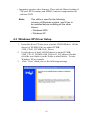
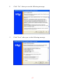
DVMB-554E
Socket 479 Intel Core™ 2 Duo/Core™
Duo/Core™ Solo Processor-based
533/667 MHz FSB Mini-ITX Motherboard
with PCI-E/DDR2/Dual GbE LAN/Video
Capture
User Manual
1
Copyright
This document is copyrighted, 2006, by Advantech Co., Ltd. All rights are
reserved. Advantech Co., Ltd. reserves the right to make improve- ments
to the products described in this manual at any time without notice. No
part of this manual may be reproduced, copied, translated or transmit- ted
in any form or by any means without the prior written permission of
Advantech Co., Ltd. Information provided in this manual is intended to be
accurate and reliable. However, Advantech Co., Ltd. assumes no
responsibility for its use, nor for any infringements upon the rights of third
parties which may result from its use.
Acknowledgements
• AWARD is a trademark of Phoenix Technologies Ltd.
• IBM and PC are trademarks of International Business Machines Corporation.
• Intel®, Core™ 2 Duo/Core™ Duo/Core™ Solo are trademarks of Intel
Corporation.
• WinBond is a trademark of Winbond Corporation.
• All other product names or trademarks are the properties of their
respective owners.
Printed in Taiwan
2
June 2007
A Message to the Customer
Advantech Customer Services
Each and every Advantech product is built to the most exacting specifications to ensure reliable performance in the harsh and demanding conditions typical of industrial environments. Whether your new Advantech
equipment is destined for the laboratory or the factory floor, you can be
assured that your product will provide the reliability and ease of operation
for which the name Advantech has come to be known.
Your satisfaction is our primary concern. Here is a guide to Advantech’s
customer services. To ensure you get the full benefit of our services,
please follow the instructions below carefully.
Technical Support
We want you to get the maximum performance from your products. So if
you run into technical difficulties, we are here to help. For the most frequently asked questions, you can easily find answers in your product documentation. These answers are normally a lot more detailed than the ones
we can give over the phone.
So please consult this manual first. If you still cannot find the answer,
gather all the information or questions that apply to your problem, and
with the product close at hand, call your dealer. Our dealers are well
trained and ready to give you the support you need to get the most from
your Advantech products. In fact, most problems reported are minor and
are able to be easily solved over the phone.
In addition, free technical support is available from Advantech engineers
every business day. We are always ready to give advice on application
requirements or specific information on the installation and operation of
any of our products.
3
Certifications
This device complies with the requirements in part 15 of the FCC rules:
Operation is subject to the following two conditions:
• This device may not cause harmful interference
• This device must accept any interference received, including interference that may cause undesired operation
This equipment has been tested and found to comply with the limits for a
Class A digital device, pursuant to Part 15 of the FCC Rules. These limits
are designed to provide reasonable protection against harmful interference when the equipment is operated in a commercial environment. This
equipment generates, uses, and can radiate radio frequency energy and, if
not installed and used in accordance with the instruction manual, may
cause harmful interference to radio communications. Operation of this
device in a residential area is likely to cause harmful interference in
which case the user will be required to correct the interference at his/her
own expense. The user is advised that any equipment changes or modifications not expressly approved by the party responsible for compliance
would void the compliance to FCC regulations and therefore, the user's
authority to operate the equipment.
Caution!
There is a danger of a new battery exploding if it
is incorrectly installed. Do not attempt to
recharge, force open, or heat the battery.
Replace the battery only with the same or
equivalent type recommended by the manufacturer. Discard used batteries according to the
manufacturer’s instructions.
4
Product warranty
Advantech warrants to you, the original purchaser, that each of its products will be free from defects in materials and workmanship for two years
from the date of purchase.
This warranty does not apply to any products which have been repaired or
altered by persons other than repair personnel authorized by Advantech,
or which have been subject to misuse, abuse, accident or improper installation. Advantech assumes no liability under the terms of this warranty as a
consequence of such events.
If an Advantech product is defective, it will be repaired or replaced at no
charge during the warranty period. For out-of-warranty repairs, you will
be billed according to the cost of replacement materials, service time and
freight. Please consult your dealer for more details.
If you think you have a defective product, follow these steps:
1.
Collect all the information about the problem encountered. (For
example, type of PC, CPU speed, Advantech products used, other
hardware and software used, etc.) Note anything abnormal and list
any on-screen messages you get when the problem occurs.
2.
Call your dealer and describe the problem. Please have your manual, product, and any helpful information readily available.
3.
If your product is diagnosed as defective, obtain an RMA (return
material authorization) number from your dealer. This allows us to
process your return more quickly.
4.
Carefully pack the defective product, a fully-completed Repair and
Replacement Order Card and a photocopy proof of purchase date
(such as your sales receipt) in a shippable container. A product
returned without proof of the purchase date is not eligible for warranty service.
5.
Write the RMA number visibly on the outside of the package and
ship it prepaid to your dealer.
5
Initial Inspection
Before you begin installing your motherboard, please make sure that the
following materials have been shipped:
•
DVMB-554E Socket 479 Intel Core™ 2
Duo/Core™ Duo/Core™ Solo Processorbased Industrial Mini-ITX Motherboard
P/N: 9692055000E
•
1 DVA-210 4*Channels BNC Connector
Module with bracket
P/N: 9692A21000E
•
1 CD with driver utility and manual
P/N: 2066554E00
•
1 flat cable for DVA-210
P/N: 1700000860
•
2 Serial ATA HDD data cable
P/N: 1700002155
•
1 Parallel ATA HDD power cable
IDE44/40/40P 63cm
P/N: 1701440630
•
1 Parallel ATA HDD power cable
IDE44/44P 15cm
P/N: 1701440159
•
1 ATX 12V power converter cable
P/N: 1700003411
•
1 CPU Heat Sink
P/N: 1960004032
•
1 PS/2 Y cable for KB&MS
P/N: 1700060202
•
2 warranty card
P/N: 2190000902
If any of these items are missing or damaged, contact your distributor or
sales representative immediately. We have carefully inspected the DVMB554E mechanically and electrically before shipment. It should be free of
marks and scratches and in perfect working order upon receipt. As you
unpack the DVMB-554E, check it for signs of shipping damage. (For
example, damaged box, scratches, dents, etc.) If it is damaged or it fails to
meet the specifications, notify our service department or your local sales
representative immediately. Also notify the carrier. Retain the shipping
carton and packing material for inspection by the carrier. After inspection,
we will make arrangements to repair or replace the unit.
6
Table of Contents
Chapter 1 Hardware Configuration...........................................13
1.1 Introduction .................................................................... 13
1.2 Features .......................................................................... 14
1.3 Specifications ................................................................. 14
1.3.1 System.................................................................. 14
1.3.2 Memory................................................................ 15
1.3.3 Input/Output ......................................................... 15
1.3.4 Graphics ............................................................... 15
1.3.5 Ethernet LAN ....................................................... 16
1.3.6 Industrial features ................................................. 16
1.3.7 Mechanical and environmental specifications....... 16
1.4 Jumpers and Connectors................................................. 17
1.5 Board Layout: Jumper and Connector Locations ........... 19
1.6 DVMB-554E Block Diagram......................................... 20
1.7 Safety Precautions .......................................................... 21
1.8 Jumper Settings.............................................................. 22
1.8.1 How to set jumpers............................................... 22
1.8.2 CMOS clear (J3)................................................... 22
1.8.3 Watchdog timer output (J4) .................................. 23
1.8.4 COM2 RS 232/422/485 mode selector (J2) .......... 24
1.8.5 LVDS Power 3.3V/5V selector (J6) ..................... 24
1.9 System Memory ............................................................. 25
1.9.1 CPU FSB and memory speed ............................... 25
1.10 Memory Installation Procedures................................... 25
1.11 Cache Memory ............................................................. 25
1.12 Processor Installation ................................................... 26
Chapter 2 Connecting Peripherals .............................................28
2.1 Introduction.................................................................... 28
2.2 Primary IDE Connector (CN11)..................................... 28
2.3 USB Ports and LAN Ports (CN4, CN5, CN9, CN10)..... 29
2.4 VGA and DVI connector module (V1)........................... 30
2.5 Serial port module: COM1/COM2 (CM1) .................... 30
2.6 External PS/2 and Composite TV-Out (CN2) ................. 31
2.7 Fan Connector (FN1/FN2/FN3) ..................................... 31
7
2.8 Front Panel Connectors (CNX1/CN13).......................... 32
2.8.1 Power LED and Keyboard Lock (CN13).............. 32
2.8.2 External Speaker (CNX1-17)................................ 32
2.8.3 Reset Connector (CNX1-18) ................................ 33
2.8.4 HDD LED Connector (CNX1-19) ........................ 33
2.8.5 ATX Soft Power Switch (CNX1-21) .................... 33
2.8.6 SM Bus Connector (CNX1-29) ............................ 33
2.9 H/W Monitor Alarm (CN12).......................................... 34
2.10 Line Out, Mic In Connector (CN3) .............................. 34
2.11 Aux Line-In Connector (CN7)...................................... 35
2.12 Serial ATA Interface (SA1, SA2) .................................. 35
2.13 DVA-210 Connector (VDO1)....................................... 36
2.14 Auxiliary 4-pin power connector (ATX1) ..................... 36
2.15 GPIO connector (GPIO1)............................................. 37
2.16 LVDS connector (VCN1) ............................................. 38
2.17 LCD Inverter Power connector (BKL1) ....................... 39
Chapter 3 Award BIOS Setup.....................................................41
3.1 Introduction .................................................................... 41
3.1.1 CMOS RAM Auto-backup and Restore................ 41
3.2 Entering Setup................................................................ 42
3.3 Standard CMOS Setup ................................................... 42
3.3.1 Date ...................................................................... 42
3.3.2 Time ..................................................................... 42
3.3.3 IDE channel 0/1 Master/Slave .............................. 42
3.3.4 Halt On................................................................. 43
3.3.5 Memory................................................................ 43
3.4 Advanced BIOS Features ............................................... 44
3.4.1 CPU Features........................................................ 45
3.4.2 Hard Disk Boot Priority........................................ 45
3.4.3 Virus Warning ...................................................... 45
3.4.4 CPU L1, L2 & L3 Cache ...................................... 45
3.4.5 Quick Power On Self Test .................................... 45
3.4.6 First/Second Boot Device ..................................... 45
3.4.7 Boot Other Device................................................ 45
3.4.8 Boot Up NumLock Status..................................... 46
3.4.9 Gate A20 Option................................................... 46
8
3.4.10 Typematic Rate Setting....................................... 46
3.4.11 Typematic Rate (Chars/Sec) ............................... 46
3.4.12 Typematic Delay (msec) ..................................... 46
3.4.13 Security Option .................................................. 46
3.4.14 APIC Mode ........................................................ 46
3.4.15 MPS Version Control For OS ............................. 47
3.5 Advanced Chipset Features ............................................ 47
3.5.1 DRAM Timing Selectable .................................... 48
3.5.2 CAS Latency Time ............................................... 48
3.5.3 DRAM RAS# to CAS# Delay .............................. 48
3.5.4 DRAM RAS# Precharge ...................................... 49
3.5.5 Precharge Delay (t RAS) ...................................... 49
3.5.6 System Memory Frequency .................................. 49
3.5.7 System BIOS Cacheable....................................... 49
3.5.8 Video BIOS Cacheable......................................... 49
3.5.9 Memory Hole At 15M-16M ................................. 49
3.5.10 PCI-Express Root Port Func............................... 49
3.5.11 PEG / Onchip VGA Control ............................... 50
3.5.12 On-Chip Frame Buffer Size................................ 50
3.5.13 DVMT Mode...................................................... 50
3.5.14 DVMT / FIXED Memory Size ........................... 50
3.5.15 Boot Display....................................................... 50
3.5.16 Panel Number ..................................................... 50
3.5.17 Init Display First................................................. 51
3.6 Integrated Peripherals..................................................... 51
3.6.1 IDE HDD Block Mode ......................................... 52
3.6.2 IDE DMA Transfer Access................................... 52
3.6.3 On-Chip Primary / Secondary IDE Device ........... 52
3.6.4 SATA Mode.......................................................... 52
3.6.5 On-Chip Serial ATA ............................................. 53
3.6.6 PATA IDE Mode .................................................. 53
3.6.7 SATA Port ............................................................ 53
3.6.8 USB Controller..................................................... 53
3.6.9 USB 2.0 Controller............................................... 54
3.6.10 USB Keyboard / Mouse Support ........................ 54
3.6.11 AC97 Audio........................................................ 54
9
3.6.12 Onboard LAN1 Control...................................... 54
3.6.13 Onboard LAN2 Control...................................... 54
3.6.14 Capture Controller .............................................. 54
3.6.15 Onboard Serial Port 1 ......................................... 54
3.6.16 Onboard Serial Port 2 ......................................... 54
3.6.17 UART Mode Select ............................................ 55
3.6.18 RxD, TxD Active................................................ 55
3.6.19 IR Transmission Delay ....................................... 55
3.6.20 UR2 Duplex Mode ............................................. 55
3.6.21 Use IR Pins......................................................... 55
3.6.22 Watch Dog Timer Select .................................... 55
3.7 Power Management Setup.............................................. 56
3.7.1 PCI Express PM Function .................................... 57
3.7.2 ACPI Function...................................................... 57
3.7.3 Power Management .............................................. 57
3.7.4 Video Off Method ................................................ 57
3.7.5 Video Off In Suspend ........................................... 57
3.7.6 Suspend Type ....................................................... 58
3.7.7 Modem Use IRQ................................................... 58
3.7.8 Suspend Mode ...................................................... 58
3.7.9 HDD Power Down ............................................... 58
3.7.10 Soft-Off by PWR-BTTN..................................... 58
3.7.11 PowerOn by LAN............................................... 58
3.7.12 CPU THRM-Throttling....................................... 58
3.7.13 PowerOn by Modem........................................... 58
3.7.14 PowerOn by Alarm............................................. 58
3.7.15 Primary IDE 0 (1) and Secondary IDE 0 (1)....... 58
3.7.16 FDD, COM, LPT PORT..................................... 59
3.7.17 PCI PIRQ [A-D]#............................................... 59
3.7.18 PWRON After PWR-Fail ................................... 59
3.8 PnP/PCI Configurations ................................................. 60
3.8.1 Reset Configuration Data...................................... 60
3.8.2 Resources Controlled By ...................................... 60
3.8.3 PCI / VGA Palette Snoop ..................................... 60
3.8.4 Maximum Payload Size........................................ 60
3.9 PC Health Status............................................................. 61
10
3.9.1 CPU Warning Temperature................................... 61
3.9.2 Current System Temperature ................................ 61
3.9.3 Current CPU Temperature .................................... 61
3.9.4 CPU FAN Speed................................................... 61
3.9.5 System FAN 1 / 2 Speed....................................... 61
3.9.6 VCORE and Other Voltages ................................. 61
3.9.7 Shutdown Temperature......................................... 61
3.10 Frequency / Voltage Control ......................................... 62
3.10.1 Spread Spectrum................................................. 62
3.11 Password Setting .......................................................... 63
3.12 Save & Exit Setup ........................................................ 63
3.13 Exit Without Saving ..................................................... 63
Chapter 4 Chipset Installation ....................................................65
4.1 Before you begin ............................................................ 65
4.2 Introduction .................................................................... 65
4.3 Windows XP Driver Setup ............................................. 66
Chapter 5 VGA Setup ..................................................................70
5.1 Introduction .................................................................... 70
5.2 Windows XP Driver Setup ............................................. 70
Chapter 6 Video capture installation .........................................74
6.1 Driver installation of video capture chip ........................ 74
6.2 Installation of DVMB-554E Demo Program.................. 82
6.3 Demo Program Functionality ......................................... 86
6.3.1 Device.................................................................. 86
6.3.2 Switch Channels .................................................. 87
6.3.3 Resolution............................................................ 88
6.3.4 Frame Rate........................................................... 89
6.3.5 Video Mux........................................................... 90
6.3.6 Video Standard .................................................... 91
6.3.7 Snap Buffer.......................................................... 92
6.3.8 Sensor Control ..................................................... 93
6.3.9 Micro Control ...................................................... 94
6.3.10 GPIO control ..................................................... 94
11
1
General Information
12
Chapter 1 Hardware Configuration
1.1 Introduction
The DVMB-554E is designed with the Intel® 945GM and the ICH7MDH for industrial applications that require both high-performance
computing and enhanced power management capabilities. The
motherboard supports Intel Core™ 2 Duo/Core™ Duo/Core™ Solo
Processor up to 2.16GHz with 533/667 MHz front side bus and Dual
Channel DDRII 533/667 MHz memory up to 4 GB.
The DVMB-554E offers high-performance cost-saving integrated graphics,
built on the Intel® 945GM chipset and features the unique Intel® Extreme
Graphics architecture that maximizes VGA performance and shares
system memory up to 224MB. Better still, the DVMB-554E also provides
incredible visual quality, versatile display options, 8-bit Dual Channel
LVDS and a TV-out(NTSC/PAL) interface.
In addition to powerful computing capabilities, the DVMB-554E comes
with advanced I/O enhancements. The DVMB-554E possess multiple
high performance onboard I/O capabilities which include one PCIExpress x4 slot; one Mini-PCI socket; eight high-speed USB 2.0 ports;
two Serial ATA ports supporting up to two devices with software Serial
ATA RAID 0,1; AC-97 audio; two RS-232 ports; one parallel ATA port.
These powerful I/O capabilities ensure even more reliable data storage
capabilities and suitable for work with high-speed I/O peripherals.
With all these exceptional features and outstanding performance, DVMB554 is simply the best, most advanced yet power saving platform for
today and tomorrow’s up-and-coming applications.
13
1.2 Features
• PCI&PCI Express architecture: Designed with the Intel 945GM and
ICH7M-DH PCI-Express chipset, the DVMB-554E has dual/single
Giga- bit LAN via PCI-E x1 bus, 1 Mini-PCI socket and 1 PCI-E x 4
slot.
• High Performance I/O Capability: Mini-PCI and Dual Gigabit LAN
via PCI- E x1 bus, 2 SATA connectors and 8 USB 2.0 ports.
• Standard Mini-ITX form factor with industrial features: DVMB554E provides industrial features like long product life, reliable
operation under wide temperature range, watchdog timer, CMOS backup
functions, etc.
• BIOS CMOS backup and restore: When BIOS CMOS setup has been
completed, data in the CMOS RAM is automatically backed up to the
Flash ROM. This is particularly useful in harsh environments which
may cause setup data loss such as battery failure. Upon such an error
occurring, BIOS will check the data, and automatically restore the
original data for booting.
• Automatically power on after power failure: It is often required to
have an unattended system come back to operation when power
resumes after a power failure. Advantech's industrial motherboard
allows users to set the system to power on automatically without pushing the power on button.
1.3 Specifications
1.3.1 System
• CPU: Socket 479 Intel Core™ 2 Duo/Core™ Duo/Core™ Solo up to
2.16GHz 533/667 MHz FSB.
• L2 Cache: CPU has built-in 2MB or 4MB CPU full-speed L2 cache.
• BIOS: Award Flash BIOS (4Mb Flash Memory)
• System Chipset: Intel 945GM with ICH7M-DH
• SATA/EIDE hard disk drive interface: Two on-board SATA
connectors with data transmission rate up to 150 MB/s, and supports up
to two devices with software Serial ATA RAID 0,1. One on-board IDE
connector supporting up to two enhanced IDE devices. Supports PIO
mode 4 (16.67MB/s data transfer rate) and ATA 33/66/100
(33/66/100MB/s data transfer rate.) BIOS enabled/disabled.
14
1.3.2 Memory
• RAM: Up to 4 GB in four 240-pin DIMM sockets. Supports dual-channel DDRII 400/533/667 SDRAM.
1.3.3 Input/Output
• PCI Express slots: 1 PCI-E x 3 with PCI-E x 4 expansion slot (this
expansion slot works with Advantech Riser card) and 1 PCI-E x 1 gold
finger.
• PCI Bus: 1 Mini-PCI socket, 32-bit, 33 MHz PCI 2.2 compliant
• Serial ports: Two serial ports, one DB-9 (RS 232)connector and one
on-board pin header (RS 232/422/485). Ports can be individually configured to COM1, COM2, or disabled
• Keyboard and PS/2 mouse connector: One 6-pin Mini-DIN connectors are located on the mounting bracket and work with special Y cable
for easy connection to a PS/2 keyboard and mouse.
• USB port: Supports up to eight USB 2.0 ports with transmission rate
up to 480Mbps.
1.3.4 Graphics
•
•
•
•
•
Controller: Intel Graphics Media Accelerator 950
Display memory: Dynamically shared system memory up to 224 MB.
VGA: Up to 2048x1536 resolution@75Hz
LVDS interface: Support up to UXGA(1600X1200)
TV-Out: NTSC/PAL.
15
1.3.5 Ethernet LAN
• Supporting single/dual 10/100/1000Base-T Ethernet port(s) via PCI
Express x1 bus which provides 500 MB/s data transmission rate.
• Controller:
Marvell 88E8053 PCI-E Gigabit LAN; featuring AI NET2
1.3.6 Industrial features
• Watchdog timer: Can generate a system reset or IRQ11. The watchdog timer is programmable, with each unit equal to one second or one
minute (255 levels)
1.3.7 Mechanical and environmental specifications
• Operating temperature: 0 ~ 60° C (32 ~ 140° F, Depending on CPU)
• Storage temperature: -20 ~ 70° C (-4 ~ 158° F)
• Humidity: 20 ~ 95% non-condensing
• Power supply voltage: +3.3V, ±5 V, ±12 V
• Power consumption: Maximum: +5 V at 2.4A, +3.3V at 3A, +12V at
1.3A Intel Core Duo 2GHz (667 MHz FSB), 2 x 1GB DDR2 667
SDRAM)
• Board size: 170 x 170 mm (6.69" x 6.69")
• Board weight: 0.7 kg (1.68 lb)
16
1.4 Jumpers and Connectors
Connectors on the DVMB-554E motherboard link it to external devices
such as hard disk drives and a keyboard. In addition, the board has a number of jumpers used to configure your system for your application.
The tables below list the function of each of the board jumpers and connectors. Later sections in this chapter give instructions on setting jumpers. Chapter 2 gives instructions for connecting external devices to your
motherboard.
Table 1.1: Jumpers
Label
Function
J2
COM2 RS232/422/485 selectors
J3
CMOS Clear
J4
Watchdog timer output selection
J5
AT/ATX mode selector
J6
LVDS Power 3.3V/5V selector
Table 1.2: Connectors
Label
Function
CM1
Serial port module: COM1/COM2
CN2
External PS/2 and Composite TV-Out
CN3
Line Out/MIC In connector
CN4
LAN2; USB ports 3, 4
CN5
LAN1; USB ports 1, 2
CN6
Rear Panel audio connector
CN7
AUX-IN connector
CN8
IrDA connector
CN9
USB ports 5, 6
CN10
USB ports 7, 8
CN11
Primary IDE connector
CN12
Hardware Monitor connector
CN13
Power LED
17
Table 1.2: Connectors
Label
Function
CNX1
Power/Reset/HDD LED/Alarm specker connector
GPIO1
GPIO connector
VDO1
DVA-210 connector
FN1
FAN connector
FN2
FAN connector
FN3
FAN connector
SMBUS1
SMBus Extend connector
SA1
Serial ATA1
SA2
Serial ATA2
VCN1
LVDS connector
BKL1
LCD Inverter Power/Back light connector
V1
VGA and DVI connector module
ATX1
ATX 12 V auxiliary power connector
ATX2
20-pin ATX power connector
18
1.5 Board Layout: Jumper and Connector Locations
Figure 1.1: Jumper and Connector locations
F
i
g
u
r
F
Figure 1.2: Rear Panel Placement
19
1.6 DVMB-554E Block Diagram
Figure 1.3: DVMB-554E Block Diagram
20
1.7 Safety Precautions
Warning!
Always completely disconnect the power cord
from your chassis whenever you work with the
hardware. Do not make connections while the
power is on. Sensitive electronic components
can be damaged by sudden power surges. Only
experienced electronics personnel should open
the PC chassis.
Caution!
Always ground yourself to remove any static
charge before touching the motherboard. Modern electronic devices are very sensitive to
static electric charges. As a safety precaution,
use a grounding wrist strap at all times. Place
all electronic components on a static-dissipative
surface or in a static-shielded bag when they
are not in the chassis.
Caution!
The computer is provided with a battery-powered Real-time Clock circuit. There is a danger
of explosion if battery is incorrectly replaced.
Replace only with same or equivalent type recommended by the manufacturer. Discard used
batteries according to manufacturer's instructions.
Caution!
There is a danger of a new battery exploding if it
is incorrectly installed. Do not attempt to
recharge, force open, or heat the battery.
Replace the battery only with the same or
equivalent type recommended by the manufacturer. Discard used batteries according to the
manufacturer’s instructions.
21
1.8 Jumper Settings
This section provides instructions on how to configure your motherboard
by setting the jumpers. It also includes the motherboards's default settings
and your options for each jumper.
1.8.1 How to set jumpers
You can configure your motherboard to match the needs of your application by setting the jumpers. A jumper is a metal bridge that closes an electrical circuit. It consists of two metal pins and a small metal clip (often
protected by a plastic cover) that slides over the pins to connect them. To
“close” (or turn ON) a jumper, you connect the pins with the clip. To
“open” (or turn OFF) a jumper, you remove the clip. Sometimes a jumper
consists of a set of three pins, labeled 1, 2, and 3. In this case you connect
either pins 1 and 2, or 2 and 3. A pair of needle-nose pliers may be useful
when setting jumpers.
1.8.2 CMOS clear (J3)
The DVMB-554E motherboard contains a jumper that can erase CMOS
data and reset the system BIOS information. Normally this jumper should
be set with pins 1-2 closed. If you want to reset the CMOS data, set J1 to
2-3 closed for just a few seconds, and then move the jumper back to 1-2
closed. This procedure will reset the CMOS to its default setting.
Table 1.3: CMOS (J3)
Function
Jumper Setting
* Keep CMOS data
1-2 closed
Clear CMOS data
2-3 closed
* default setting
22
1.8.3 Watchdog timer output (J4)
The DVMB-554E contains a watchdog timer that will reset the CPU or
send a signal to PIRQE in the event the CPU stops processing. This
feature means the DVMB-554E will recover from a software failure or an
EMI problem. The J4 jumper settings control the outcome of what the
computer will do in the event the watchdog timer is tripped.
Table 1.4: Watchdog timer output (J4)
Function
Jumper Setting
IRQ11
1
1-2 closed
* Reset
1
2-3 closed
*default setting
Note:
The interrupt output of the watchdog timer is a
low level signal. It will be held low until the
watchdog timer is reset.
Table 1.5: ATX/AT Mode selector (J5)
Function
Jumper Setting
AT Mode
1
1-2 closed
ATX Mode
1
2-3 closed
23
1.8.4 COM2 RS 232/422/485 mode selector (J2)
Users can use J2 to select among RS 232/422/485 modes for COM2.
The default setting is RS 232.
Table 1.6: COM2 RS 232/422/485 mode selector (J2)
Function
Jumper Setting
RS232
(5-6) + (7-9) + (8-10) + (13-15) + (14-16) closed
RS422
(3-4) + (9-11) + (10-12) + (15-17) + (16-18) closed
RS485
(1-2) + (9-11) + (10-12) + (15-17) + (16-18) closed
1.8.5 LVDS Power 3.3V/5V selector (J6)
Table 1.7: LVDS Power 3.3V/5V selector (J6)
Function
Jumper Setting
5V
1
1-2 closed
*3.3V
1
2-3 closed
*default setting
24
1.9 System Memory
The DVMB-554E has two sockets for 240-pin memory modules (SODIMMs). All these sockets use 1.8 V unbuffered double data rate
synchronous DRAMs (DDR SDRAM). They are available in capacities
of 256, 512 and 1024 MB. The sockets can be filled in any combination
with DIMMs of any size, giving a total memory size between 256 MB
and 2GB.
1.9.1 CPU FSB and memory speed
The DVMB-554E can accept DDR2 SDRAM memory chips without
parity. Also note: The DVMB-554E accepts DDR2 400/533/667MHz
SDRAM, and DDR2 SDRAM. The DVMB-554E does NOT support
ECC (error checking and correction).
1.10 Memory Installation Procedures
To install DIMMs, first make sure the two handles of the DIMM socket
are in the “open” position. i.e. The handles lean outward. Slowly slide the
DIMM module along the plastic guides on both ends of the socket. Then
press the DIMM module right down into the socket, until you hear a click.
This is when the two handles have automatically locked the mem- ory
module into the correct position of the DIMM socket. To remove the
memory module, just push both handles outward, and the memory module will be ejected by the mechanism in the socket.
1.11 Cache Memory
The CPU that DVMB-554E supports built-in 2MB or 4MB cache memory.
25
1.12 Processor Installation
Warning:
Without a fan or heat sink, the CPU will overheat and cause damage to both the CPU and
the single board computer. To install a CPU,
first turn off your system. Locate the processor
socket 479.
The DVMB-554E is designed for Intel Core™ 2 Duo/Core™
Duo/Core™ Solo (socket 479) up to 2.16 GHz. Follow these steps to
install the pro- cessor:
1.
Turn the screw to loosen the processor socket.
2.
Align the triangular marking on the processor with the small arrow
on the corner of the socket.
3.
Turn the screw to its original position.
4.
Install the heat sink on the CPU. The concave of heat sink should
face to location of capacitors to avoid contacting with capacitors.
26
2
Connecting
Peripherals
27
Chapter 2 Connecting Peripherals
2.1 Introduction
You can access most of the connectors from the top of the board as it is
being installed in the chassis. If you have a number of cards installed or
have a packed chassis, you may need to partially remove the card to make
all the connections.
2.2 Primary IDE Connector (CN11)
You can attach up to two IDE (Integrated Drive Electronics) drives to the
DVMB-554E’s built-in controller. The primary (CN11) connector can
each accommodate two drives.
Wire number 1 on the cable is red or blue and the other wires are gray.
Connect one end to connector CN11 on the motherboard. Make sure that
the red/blue wire corresponds to pin 1 on the connector (in the upper right
hand corner). See Chapter 1 for help finding the connector.
Unlike floppy drives, IDE hard drives can connect in either position on
the cable. If you install two drives to a single connector, you will need to
set one as the master and the other as the slave. You do this by setting the
jumpers on the drives. If you use just one drive on the connector, you
should set the drive as the master. See the documentation that came with
your drive for more information.
Connect the first hard drive to the other end of the cable. Wire 1 on the
28
cable should also connect to pin 1 on the hard drive connector, which is
labeled on the drive circuit board. Check the documentation that came
with the drive for more information.
2.3 USB Ports and LAN Ports (CN4, CN5, CN9, CN10)
The DVMB-554E provides up to eight ports of USB (Universal Serial Bus)
interface which gives complete Plug & Play and hot swapping for up to
127 external devices. The USB interface complies with USB Specification Rev. 2.0 supporting transmission rate up to 480 Mbps and is fuse
protected. The USB interface can be disabled in the system BIOS setup.
The DVMB-554E is equipped with one or two high-performance 1000
Mbps Ethernet LANs. They are supported by all major network operating
systems. The RJ-45 jacks on the rear plate provide convenient or 1000
Base-T operation.
Table 2.1: LAN LED indicator
Lan mode
Lan Indicator
1Gbps Link on
LED1 Green on
100Mbps Link on
LED1 Orange on
Active
LED2 Green flash
29
2.4 VGA and DVI connector module (V1)
The DVMB-554E includes DVI and VGA interface that can drive dual
displays.
2.5 Serial port module: COM1/COM2 (CM1)
The DVMB-554E offers two serial ports. The user can use J2 to select
among RS 232/422/485 modes for COM2. The default setting is RS 232
for both COM1 and COM2. These ports can connect to serial devices,
30
such as a mouse or printer, or to a communications network.
The IRQ and address ranges for both ports are fixed. However, if you
want to disable the port or change these parameters later, you can do this
in the system BIOS setup.
Different devices implement the RS-232/422/485 standards in different
ways. If you are having problems with a serial device, be sure to check
the pin assignments for the connector.
2.6 External PS/2 and Composite TV-Out (CN2)
The DVMB-554E provides a PS/2 keyboard/mouse connector. A 6-pin
mini-DIN connector is located on the rear face plate. It comes with an
external Y cable to convert from the 6-pin mini-DIN connector to PS/2
keyboard and PS/2 mouse connection.
2.7 Fan Connector (FN1/FN2/FN3)
31
If fan is used, this connector supports cooling fans of 500 mA (6W) or less.
2.8 Front Panel Connectors (CNX1/CN13)
There are several external switches to monitor and control the DVMB554.
2.8.1 Power LED and Keyboard Lock (CN13)
CN13 is a 5-pin connector for the power LED. Refer to Appendix B for
detailed information on the pin assignments. If a PS/2 or ATX power sup- ply
is used, the system's power LED status will be as indicated below:
Table 2.2: PS/2 or ATX power supply LED status
Power mode
LED (PS/2 power)
LED (ATX power)
System On
On
On
System Suspend
Fast flashes
Fast flashes
System Off
Off
Slow flashes
2.8.2 External Speaker (CNX1-17)
It is a 4-pin connector for an external speaker. If there is no external speaker,
the DVMB-554E provides an onboard buzzer as an alternative. To enable the
buzzer, set pins 3-4 as closed.
32
2.8.3 Reset Connector (CNX1-18)
Many computer cases offer the convenience of a reset button. Connect the wire
from the reset button
2.8.4 HDD LED Connector (CNX1-19)
You can connect an LED to this connector to indicate when the HDD is active.
2.8.5 ATX Soft Power Switch (CNX1-21)
If your computer case is equipped with an ATX power supply, you should
connect the power on/off button on your computer case to this connector. This
connection enables you to turn your computer on and off.
2.8.6 SM Bus Connector (CNX1-29)
This connector is reserved for Advantech's SNMP-1000 HTTP/SNMP
Remote System Manager. The SNMP-1000 allows users to monitor the
internal voltages, temperature and fans from a remote computer through an
Ethernet network.
CN29 can be connected to CN19 of SNMP-1000. Please be careful about the
pin assignments, pin 1 must be connected to pin 1 and pin 2 to pin 2 on both
ends of cable.
33
2.9 H/W Monitor Alarm (CN12)
Close: Enable OBS Alarm
Open: Disable OBS Alarm
2.10 Line Out, Mic In Connector (CN3)
The Line Out is to output the audio signal to external audio device, like
speakers or headphones. The Mic In is for the audio signal input via
microphones.
34
2.11 Aux Line-In Connector (CN7)
The connector is for audio devices with a Line-in connector.
2.12 Serial ATA Interface (SA1, SA2)
In addition to the EIDE interface (up to two devices), the DVMB-554E
features a high performance serial ATA interface (up to 150 MB/s) which
eases cabling to hard drives with thin and long cables.
35
2.13 DVA-210 Connector (VDO1)
DVMB-554E has 4 video capture chips on board. So it can support up to 4
cameras. To be connecting with cameras, DVMB-554E needs to work with
DVA-210 for video capture. DVA-210 is a 4 channel video module with
BNC connectors and you can find it in DVMB-554E accessory box.
2.14 Auxiliary 4-pin power connector (ATX1)
To ensure the enough power is supplied to the motherboard, one auxiliary
4 pin power connector is available on the DVMB-554E. ATX1 must be
used to provide sufficient 12 V power to ensure the stable operation of the
system.
36
2.15 GPIO connector (GPIO1)
The DVMB-554E provides a GPIO interface, GPIO1, which is a 20 pin
connector. Advantech provides SDK for this GPIO and have 7 pins for input
and 8 pins for output. Please refer to pin assignments for GPIO1
connector as below.
GPIO connector (GPIO1)
Pin
signal
pin
signal
pin
signal
pin
signal
1
+5V
6
Input
11
Output
16
Input
2
+5V
7
Output
12
Input
17
Output
3
Output
8
Input
13
Output
18
GND
4
Input
9
Output
14
Input
19
GND
5
Output
10
Input
15
Output
20
GND
37
2.16 LVDS connector (VCN1)
The DVMB-554E provides a LVDS interface supports 18 bits LCD
panels. Pin assignments for LVDS connector VCN1 are listed as
below.
LVDS connector (VCN1)
Pin
signal
pin
signal
pin
signal
pin
signal
1
VDDS
AFE
11
GND
21
OD2+
31
DDC_
CLK
2
VDDS
AFE
12
GND
22
OD2+
32
DDC_
DAT
3
GND
13
OD1-
23
GND
33
GND
4
GND
14
OD1-
24
GND
34
GND
5
VDDS
AFE
15
OD1+
25
OCK-
35
OD3-
6
VDDS
AFE
16
OD1+
26
OCK-
36
OD3-
7
OD0-
17
GND
27
OCK+
37
OD3+
8
OD0-
18
GND
28
OCK+
38
OD3+
9
OD0+
19
OD2-
29
GND
39
HPLG
10
OD0+
20
OD2-
30
GND
40
VCON
38
2.17 LCD Inverter Power connector (BKL1)
VP1 is connected to Inverter which can provide power to LCD Panel. The
DVMB-554E can provide a LVDS display.
39
3
BIOS Setup
40
Chapter 3 Award BIOS Setup
3.1 Introduction
Award’s BIOS ROM has a built-in setup program that allows users to
modify the basic system configuration. This type of information is stored
in battery backed-up memory (CMOS RAM) so that it retains the setup
information when the power is turned off.
3.1.1 CMOS RAM Auto-backup and Restore
The CMOS RAM is powered by an onboard button cell battery. When
you finish BIOS setup, the data in CMOS RAM will be automatically
backed up to Flash ROM. If operation in harsh industrial environments
causes a soft error, BIOS will recheck the data in CMOS RAM and automatically restore the original data in Flash ROM to CMOS RAM for
booting.
Note:
If you intend to change the CMOS setting without restoring the previous backup, you have to
click on “DEL” within two seconds of the
“CMOS checksum error...” display screen message appearing. Then enter the “Setup” screen
to modify the data. If the “CMOS checksum
error...” message appears again and again,
please check to see if you need to replace the
battery in your system.
41
3.2 Entering Setup
Turn on the computer and press <Del> to enter the BIOS setup.
Figure 3.1: Award BIOS Setup initial screen
3.3 Standard CMOS Setup
3.3.1 Date
The date format is <week>, <month>, <day>, <year>.
3.3.2 Time
The time format is <hour> <minute> <second>, based on the 24-hour
clock.
3.3.3 IDE channel 0/1 Master/Slave
• IDE HDD Auto-Detection: Press “Enter” to select this option for
automatic device detection.
• IDE Device Setup:
Auto: Automatically detects IDE devices during POST
None: Select this when no IDE device is used. The system will skip the
auto-detection step to make system start up faster.
Manual: User can manually input the correct settings.
• Access Mode: The options are CHS/LBA/Large/Auto
• Capacity: Capacity of currently installed hard disk.
• Cylinder: Number of cylinders
42
• Head: Number of heads
• Precomp: Write precomp
• Landing Zone: Landing zone
• Sector: Number of sectors
3.3.4 Halt On
This category determines whether system start-up will halt or not when
an error is detected during power up.
The options are: No Errors/All Errors/All, But Keyboard/All, But Diskette/All, But Disk/Key
3.3.5 Memory
This category displays base memory, extended memory, and total memory detected during POST (Power On Self Test).
Figure 3.2: Standard CMOS Features Screen
43
3.4 Advanced BIOS Features
The “Advanced BIOS Features” screen appears when choosing the
“Advanced BIOS Features” item from the “Initial Setup Screen” menu. It
allows the user to configure the DVMB-554E according to his particular
requirements. Below are some major items that are provided in the
Advanced BIOS Features screen. A quick booting function is provided
for your convenience. Simply enable the Quick Booting item to save
yourself valuable time.
Figure 3.3: Advanced BIOS features screen
44
3.4.1 CPU Features
Delay Prior to thermal
This feature controls the activation of the Thermal Monitor's automatic
mode. It allows you to determine when the Pentium 4's Thermal Monitor
should be activated in automatic mode after the system boots. For example, with the default value of 16 Minutes, the BIOS activates the Thermal
Monitor in automatic mode 16 minutes after the system starts booting up.
The choices are 4 Min, 8 Min, 16 Min, and 32 Min.
C1E Function
CPU C1E Function select. Default value is Auto
Execute Disable Bit
When disabled, forces the XD feature flag to always return 0.
3.4.2 Hard Disk Boot Priority
Set hard disk boot device priority.
3.4.3 Virus Warning
Enables or disables the virus warning.
3.4.4 CPU L1, L2 & L3 Cache
Enabling this feature speeds up memory access. The commands are
“Enabled” or “Disabled.”
3.4.5 Quick Power On Self Test
This allows the system to skip certain tests to speed up the boot-up procedure.
3.4.6 First/Second Boot Device
The BIOS tries to load the OS from the devices in the sequence set here.
The options are: “Floppy”, “LS120”, “CDROM”, “Hard Disk”,
“ZIP100”, “USB-FDD”, “USB-ZIP”, “USBCDROM”, “LAN1”,
“LAN2” and “Disabled”.
3.4.7 Boot Other Device
Use this to boot another device. The options are “Enabled” and “Disabled”.
45
3.4.8 Boot Up NumLock Status
Sets the boot up status Num Lock. The options are “On” and “Off”.
3.4.9 Gate A20 Option
“Normal”: A pin in the keyboard controller controls GateA20. Fast
(Default) lets chipset control GateA20.
3.4.10 Typematic Rate Setting
The typematic rate is the rate key strokes repeat as determined by the keyboard controller. The commands are “Enabled” or “Disabled”. Enabling
allows the typematic rate and delay to be selected.
3.4.11` Typematic Rate (Chars/Sec)
The BIOS accepts the following input values (characters/second) for
typematic rate: 6, 8, 10, 12, 15, 20, 24, and 30.
3.4.12 Typematic Delay (msec)
Typematic delay is the time interval between the appearances of two consecutive characters, when the key is continuously depressed. The input
values for this category are: 250, 500, 750, and 1000 (ms).
3.4.13 Security Option
This category determines whether the password is required when the system boots up or only when entering setup. The options are:
• System: The system will not boot, and access to Setup will be also
denied unless the correct password is entered at the prompt.
• Setup: The system will boot, but access to Setup will be denied unless
the correct password is entered at the prompt.
Note:
To disable security, select PASSWORD SETTING in the main menu. Then, you will be asked
to enter a password. Simply press <Enter> to
disable security. When security is disabled, the
system will boot and you can enter Setup freely.
3.4.14 APIC Mode
This setting allows you to enable the APIC mode. The choices are “Disabled” or “Enabled.”
46
3.4.15 MPS Version Control For OS
This specifies the version of the Multiprocessor Specification (MPS) to
be used. Version 1.4 has extended configuration tables to improve support for multiple PCI bus configurations and provide future expandability
- use this for NT, and possibly Linux. It is also required for a secondary
PCI bus to work without the need for a bridge. Leave it as 1.1 for older
server Operating Systems.
3.5 Advanced Chipset Features
By choosing the “Advanced Chipset Features” option from the “Initial
Setup Screen” menu, the screen below will be displayed. This sample
screen contains the manufacturer’s default values for the DVMB-554E,
as shown in Figure 3-5:
Figure 3.5: Advanced chipset features screen (a)
Figure 3.5: Advanced chipset features screen (b)
Note:
DRAM default timings have been carefully chosen and should ONLY be changed if data is
being lost. Please first contact technical support.
3.5.1 DRAM Timing Selectable
This item allows you to control the DRAM speed. The selections are
“Manual” or “By SPD”.
3.5.2 CAS Latency Time
When DRAM Timing Selectable is set to [Manual], this field is adjustable. This controls the CAS latency, which determines the time interval
between SDRAM starting a read command and receiving it. The options
are [3T], [4T], [5T], and [Auto].
3.5.3 DRAM RAS# to CAS# Delay
When DRAM Timing selectable is set to [Manual], this field is adjustable. When DRAM is refreshed, the rows and columns are addressed separately. This setup item allows user to determine the timing of the
transition from RAS (row address strobe) to CAS (column address strobe).
The less the clock cycles are, the faster the DRAM speed is. Set- ting
options are [2T] to [5T], and [Auto].
3.5.4 DRAM RAS# Precharge
When the DRAM Timing Selectable is set to [Manual], this field is
adjustable. This setting controls the number of cycles for Row Address
Strobe (RAS) to be allowed to precharge. If no sufficient time is allowed
for the RAS to accumulate its charge before DRAM refresh, refreshing
may be incomplete and DRAM may fail to retain data. This item applies
only when synchronous DRAM is installed in the system. Setting options
are [2T] to [5T], and [Auto].
3.5.5 Precharge Delay (t RAS)
This item allows you to select the value in this field, depending on
whether the board has paged DRAMs or EDO (extended data output)
DRAMs. The choices are: “4” to “15” and “Auto”.
3.5.6 System Memory Frequency
To adjust the frequency of memory. The choices are: "533MHz",
"667MHz" and "Auto".
3.5.7 System BIOS Cacheable
Selecting “Enabled” allows caching of the system BIOS ROM at F0000hFFFFFh, resulting in better system performance. However, if any program writes data to this memory area, a system error may occur. The
Choices are “Enabled”, and “Disabled”.
3.5.8 Video BIOS Cacheable
Selecting “Enabled” allows caching of the video BIOS, resulting in better
system performance. However, if any program writes to this memory area,
a system error may occur. The choices are “Enabled”, and “Dis- abled”.
3.5.9 Memory Hole At 15M-16M
Enabling this feature reserves 15 MB to 16 MB memory address space for
ISA expansion cards that specifically require this setting. This makes
memory from 15 MB and up unavailable to the system. Expansion cards
can only access memory up to 16 MB. The default setting is “Disabled”.
3.5.10 PCI-Express Root Port Func
PCI Express Port 1/2/3/4
The default setting is “Auto.” The choices are “Enabled,” “Disabled,” and
“Auto.”
PCI-E Compliancy Mode
This allows the user to select the PCI-E compliant mode. The options are
[v1.0], and [v1.0a].
3.5.11 PEG / Onchip VGA Control
Use this field to select PEG or Onchip VGA. The default is AUTO.
3.5.12 On-Chip Frame Buffer Size
The On-Chip Frame Buffer Size can be set to 1 MB or 8 MB. This memory is shared with the system memory.
3.5.13 DVMT Mode
Displays the active system memory mode.
3.5.14 DVMT / FIXED Memory Size
Specify the size of DVMT / FIXED system memory to allocate for video
memory.
3.5.15 Boot Display
Choose the boot display device.The default setting is "Auto" The choices
are “VBIOS Default”, “CRT”, “LFP”and “LFP+CRT”.
3.5.16 Panel Number
These fields allow you to select the LCD Panel type. The default values
for these ports are:
• 640x480, 18bit SC
• 800x600, 18bit SC
• 1024x768, 18bit SC
• 1028x1024, 18bit DC
3.5.17 Init Display First
Choose the first display interface to initiate while booting. The choice is
“PCI Slot” or “Onboard”.
3.6 Integrated Peripherals
Figure 3.6: Integrated peripherals
51
Figure 3.7: On-Chip IDE Device
3.6.1 IDE HDD Block Mode
If your IDE hard drive supports block mode select Enabled for
automatic detection of the optimal number of block read/writes per
sector the drive can support.
3.6.2 IDE DMA Transfer Access
Use this field to enable or disable IDE DMA transfer access.
3.6.3 On-Chip Primary / Secondary IDE Device
IDE Primary Master/Slave PIO/UDMA Mode (Auto). The channel
has both a master and a slave, making four IDE devices possible.
Because two IDE devices may have a different Mode timing (0, 1, 2,
3, 4), it is necessary for these to be independent. The default setting
“Auto” will allow auto detection to ensure optimal performance.
3.6.4 SATA Mode
The setting choices for the SATA Mode are IDE, RAID and AHCI
Mode. Select [IDE] if you want to have SATA function as IDE. Select
[AHCI] for Advanced Host Controller Interface (AHCI) feature, with
improved SATA performance and native command queuing. Select
[RAID] to use SATA for RAID.
Note:
Please refer to the PDF-format Intel(R) Matrix
Storage Technology Quickstartguide and Intel(R) Matrix Storage
Manager User's Manual in this CD (in the MANUAL folder) to
know the necessary steps to build and configure your RAID 0, 1
system using Intel(R) Matrix Storage Technology and Matrix
52
Storage Manager.
3.6.5 On-Chip Serial ATA
Choose the status of serial ATA. The default setting is “Auto” which
lets the system arrange all parallel and serial ATA resources
automatically. The “Disabled” setting disables the SATA controller.
The “Combined Mode” combines PATA and SATA, and maximum of
2 IDE drives in each channel. The “Enhanced Mode” enables both
SATA and PATA, and a maximum of 6 IDE drives are supported. The
“SATA Only” setting means SATA is operating in legacy mode.
3.6.6 PATA IDE Mode
This item shows the parallel ATA channel. It is Secondary.
3.6.7 SATA Port
The PATA IDE mode must to be set to Secondary and SATA will
display
“P0, P2 is Primary". It means SATA0 and SATA2 act as Primary
Chan- nel.We have one configuration with this setting by spec. and
can’t swap the channel.
Figure 3.8: Onboard Device
3.6.8 USB Controller
Select Enabled if your system contains a Universal Serial Bus (USB)
con- troller and you have USB peripherals. The choices are “Enabled”
and
53
“Disabled”.
3.6.9 USB 2.0 Controller
This entry is to disable/enable the USB 2.0 controller only. The BIOS
itself may/may not have high-speed USB support. If the BIOS has
high speed USB support built in, the support will automatically turn
on when a high speed device is attached. The choices are “Enabled”
or “Disabled”.
3.6.10 USB Keyboard / Mouse Support
Select Enabled if you plan to use an USB keyboard. The choices are
“Enabled” and “Disabled”.
3.6.11 AC97 Audio
Select “Disable” if you do not want to use AC-97 audio. Options are
“Auto”, and “Disabled”.
3.6.12 Onboard LAN1 Control
Options are “Enabled” and “Disabled”. Select “Disabled” if you
don’t want to use onboard LAN controller1.
3.6.13 Onboard LAN2 Control
Options are “Enabled” and “Disabled”. Select Disabled if you don’t
want to use the onboard LAN controller2.
Note: Correct sequence of onboard Lan controllers(Lan1 & Lan2)
shows in the "Onboard Device" BIOS view.
3.6.14 Capture Controller
Options are “Normal Mode” and “Enhanced Mode”. Select Enhanced
Mode if you want to have more effective video capture performance.
Default setting is Normal Mode.
Note:
DRAM default timings have been carefully
cho- sen and should ONLY be changed if
data is being lost. Please first contact
technical sup- port.
Super I/O Device:
3.6.15 Onboard Serial Port 1
The settings are “3F8/IRQ4”, “2F8/IRQ3”, “3E8/IRQ4”,
“2E8/IRQ3”, and “Disabled” for the on-board serial connector.
3.6.16 Onboard Serial Port 2
The settings are “3F8/IRQ4”, “2F8/IRQ3”, “3E8/IRQ4”,
54
“2E8/IRQ3”, and “Disabled” for the on-board serial connector.
3.6.17 UART Mode Select
This item allows you to select UART mode. The choices: “IrDA”,
“ASKIR”, and “Normal”.
3.6.18 RxD, TxD Active
This item allows you to determine the active level of the RxD and TxD
serial lines. The Choices: “Hi, Hi”, “Lo, Lo”, “Lo, Hi”, and “Hi, Lo”.
3.6.19 IR Transmission Delay
This item allows you to enable/disable IR transmission delay.
The choices are “Enabled” and “Disabled”.
3.6.20 UR2 Duplex Mode
This item allows you to select the IR half/full duplex function.
The choices are “Half” and “Full”.
3.6.21 Use IR Pins
The choices are “RxD2, TxD2” and “IR-Rx2Tx2”.
Figure 3.9: Watch Dog Timer
3.6.22 Watch Dog Timer Select
Allow User select watch Dog time or disable..
55
3.7 Power Management Setup
The power management setup controls the single board computer's
“green” features to save power. The following screen shows the
manufac- turer’s defaults.
Figure 3.10: Power management setup screen (a)
Figure 3.10: Power management setup screen (b)
56
3.7.1 PCI Express PM Function
This allow you to control Power On by onboard LAN chip feature.
3.7.2 ACPI Function
The choices are: “Enabled” and “Disabled”.Power Management
This category allows you to select the type (or degree) of power
saving and is directly related to the following modes:
• HDD Power Down
• Suspend Mode
There are three selections for Power Management, and they have
fixed mode settings.
Table 3.1: Power Saving
Saving Mode
Function
Min Saving
Minimum power management., Suspend Mode = 1
hr., and HDD Power Down = 15 min.
Max Saving
Maximum power management., Suspend Mode = 1
min., and HDD Power Down = 1 min.
User Defined
(Default)
Allows you to set each mode individually. When not
disabled, each of the ranges are from 1 min. to 1
hr. except for HDD Power Down which ranges
from 1 min. to 15 min., and disabled.
3.7.3 Power Management
This item allows user to select system power saving mode.
Min Saving Minimum power management. Suspend Mode=1
hr.
z
Max Saving Maximum power management. Suspend Mode=1
min.
z
User Define Allows user to set each mode individually.
Suspend
Mode= Disabled or 1 min ~1 hr.
z
3.7.4 Video Off Method
Use this to select the method to turn off the video. The choices are
“Blank
Screen”, “V/H SYNC+ Blank”, and “DPMS”.
3.7.5 Video Off In Suspend
When the system is in suspend mode, the video will turn off. The
choices are “No” and “Yes”.
57
3.7.6 Suspend Type
The choices are “Stop Grant” and “PwrOn Suspend”.
3.7.7 Modem Use IRQ
This determines the IRQ that the MODEM can use.The choices are “3”,
“4”, “5”, “7”, “9”, “10”, “11”, and “NA”.
3.7.8 Suspend Mode
This item allows user to determine the time of system inactivity, all
devices except the CPU will be shut off.
3.7.9 HDD Power Down
This item allows user to determine the time of system inactivity, the
hard disk drive will be powered down.
3.7.10 Soft-Off by PWR-BTTN
If you choose “Instant-Off”, then pushing the ATX soft power switch
but- ton once will switch the system to “system off” power mode. You
can choose “Delay 4 sec”. If you do, then pushing the button for more
than 4 seconds will turn off the system, whereas pushing the button
momentarily
(for less than 4 seconds) will switch the system to “suspend” mode.
3.7.11 PowerOn by LAN
This item allows you to power on the system by LAN. The choices are
“Enabled” and “Disabled”.
3.7.12 CPU THRM-Throttling
This option controlls the CPU speed as a percentage of regular power.
the choices are 87.5%, 75%, 62.5%, 50%, 37.5%, 25% .12% and
12.5%.
3.7.13 PowerOn by Modem
To enabled or disable the function to power on the system via a
Modem connection from a remote host. The choice “Enabled” and
“Disabled”.
3.7.14 PowerOn by Alarm
The choices are “Enabled” and “Disabled”. Fields that follow
below indicate date of current month and time of alarm settings, if
enabled.
3.7.15 Primary IDE 0 (1) and Secondary IDE 0 (1)
When Enabled, the system will resume from suspend mode if Primary
IDE 0 (1) or Secondary IDE 0 (1) becomes active. The choices are
“Enabled” and “Disabled”.
58
3.7.16 FDD, COM, LPT PORT
When Enabled, the system will resume from suspend mode if the
FDD, interface, COM port, or LPT port is active. The choices are
“Enabled” and “Disabled”.
3.7.17 PCI PIRQ [A-D]#
When Enabled, the system resumes from suspend mode if an
interrupt occurs. The choices are “Enabled” and “Disabled”.
3.7.18 PWRON After PWR-Fail
Use this to set up the system after power failure. The “Off” setting
keeps the system powered off after power failure, the “On” setting
boots up the system after failure, and the “Former-Sts” returns the
system to the status before power failure.
59
3.8 PnP/PCI Configurations
Figure 3.11: PnP/PCI configurations screen
3.8.1 Reset Configuration Data
The default is Disabled. Select Enabled to reset Extended System Configuration Data (ESCD) if you have installed a new add-on card, and system
configuration is in such a state that the OS cannot boot.
3.8.2 Resources Controlled By
The commands here are “Auto(ESCD)” or “Manual”. Choosing “Manual” requires you to choose resources from the following sub-menu.
“Auto(ESCD)” automatically configures all of the boot and Plug and Play
devices, but you must be using Windows 95 or above.
3.8.3 PCI / VGA Palette Snoop
This is set to “Disabled” by default.
3.8.4 Maximum Payload Size
This allows you to set the maximum TLP payload size for PCI Express
devices. The options are [128 bytes], [256 bytes], [512 bytes], [1024
bytes], [2048 bytes], and [4096 bytes].
60
3.9 PC Health Status
Figure 3.12: PC Health Status Screen
3.9.1 CPU Warning Temperature
This item will prevent the CPU from overheating. The choices are “Disabled”, “60C/140F”, “63C/145F”, “66C/151F”, “70C/158F”, “75C/
167F”, “80C/176F”, “85C/185F”, “90C/194F”, and “95C/205F”.
3.9.2 Current System Temperature
This shows you the current temperature of system.
3.9.3 Current CPU Temperature
This shows the current CPU temperature.
3.9.4 CPU FAN Speed
This shows the current CPU FAN operating speed.
3.9.5 System FAN 1 / 2 Speed
This shows the current System FAN operating speed.
3.9.6 VCORE and Other Voltages
This shows the voltage of VCORE, +1.5V, +3.3, +5V, +12V, -12V, -5V,
VBAT(V), and 5VSB(V).
3.9.7 Shutdown Temperature
This item enables users to set the limitation of CPU temperature, the range
is from 85°C through 100°C.
61
3.10 Frequency / Voltage Control
Figure 3.14: Spread Spectrum Control screen
3.10.1 Spread Spectrum
This setting allows you to reduce EMI by modulating the signals the CPU
generates so that the spikes are reduced to flatter curves. This is achieved
by varying the frequency slightly so that the signal does not use any particular frequency for more than a moment. The choices are “Disabled”
and “Enabled”.
62
3.11 Password Setting
Follow these steps to change the password.
1.
Choose the “Set Password” option from the “Initial Setup Screen”
menu and press <Enter>. The screen displays the following message:
Please Enter Your Password
2.
Press <Enter>.
3.
If the CMOS is good and this option has been used to change the
default password, the user is asked for the password stored in the
CMOS. The screen displays the following message:
Please Confirm Your Password
4.
Type the current password and press <Enter>.
5.
After pressing <Enter> (ROM password) or the current password
(user-defined), you can change the password stored in the CMOS.
The password must be no longer than eight (8) characters.
Remember, to enable the password setting feature, you must first select
either “Setup” or “System” from the “Advanced BIOS Features” menu.
3.12 Save & Exit Setup
If you select this and press <Enter>, the values entered in the setup utilities will be recorded in the CMOS memory of the chipset. The processor
will check this every time you turn your system on and compare this to
what it finds as it checks the system. This record is required for the system to operate.
3.13 Exit Without Saving
Selecting this option and pressing <Enter> lets you exit the setup program
without recording any new values or changing old ones.
63
4
Chipset Installation
64
Chapter 4 Chipset Installation
4.1 Before you begin
To facilitate the installation of the enhanced display drivers and utility
software, read the instructions in this chapter carefully. The drivers for the
DVMB-554E are located on the software installation CD. The Intel®
Chipset Software Installation Utility is not required on any systems
running Windows NT 4.0. Updates are provided via Service Packs from
Microsoft*.
Note:
The files on the software installation CD are
compressed. Do not attempt to install the drivers by copying the files manually. You must use
the supplied SETUP program to install the drivers.
Before you begin, it is important to note that most display drivers need to
have the relevant software application already installed in the system
prior to installing the enhanced display drivers. In addition, many of the
installation procedures assume that you are familiar with both the relevant software applications and operating system commands. Review the
relevant operating system commands and the pertinent sections of your
application software’s user manual before performing the installation.
4.2 Introduction
The Intel® Chipset Software Installation (CSI) utility installs the Windows INF files that outline to the operating system how the chipset components will be configured. This is needed for the proper functioning of
the following features:
• Core PCI PnP services
• IDE Ultra ATA 100/66/33 and Serial ATA interface support
• USB 1.1/2.0 support (USB 2.0 driver needs to be installed separately
for Win98)
• Identification of Intel® chipset components in the Device Manager
65
• Integrates superior video features. These include filtered sealing of
720 pixel DVD content, and MPEG-2 motion compensation for
software DVD
Note:
This utility is used for the following
versions of Windows system, and it has to
be installed before installing all the other
drivers:
• Windows 2000
• Windows XP
4.3 Windows XP Driver Setup
1.
2.
3.
Insert the driver CD into your system's CD-ROM drive. All the
drivers of DVMB-554E are under DVMB554E_CD\01_DVMB-554E_Driver.
For the driver of Intel 945GM chipset is under DVMB554E_CD\ 01_DVMB-554E_Driver\01_945 chipset. Double
click the icon which is in the folder to install driver. To take
Windows XP as example.
Click “Next” when you see the following message.
66
4.
Click “Yes” when you see the following message.
5.
Click “Next” when you see the following message.
67
6.
When the following message appears, click “Finish” to complete
the installation and restart Windows.
68
5
VGA Setup
69
Chapter 5 VGA Setup
5.1 Introduction
The Intel 945GM integrated graphics controller provides an analog display port, LVDS and TV-out interface. You need to install the VGA
driver to enable the function.
The Intel 945GM integrated graphics controller includes the following
features.
• Intel Graphics Media Accelerator 950: Incorporating the latest
Microsoft* DirectX*9 support capabilities, it allows software developers to create lifelike environments and characters. Dual independent
display, enhanced display modes for widescreen flat panels, and optimized 3D support deliver an intense and realistic visual experience
without requiring a separate graphics card.
• Intel Dynamic Video Memory Technology (DVMT3.0): DVMB554E handles diverse applications by providing the maximum
availability of system memory for general computer usage, while
supplying addi- tional graphics memory when a 3D-intensive
application requests it. The amount of video memory is dependent
upon the amount of pre- allocated memory set for your system plus
something called Dynamic Video Memory Technology (DVMT).
• LVDS Interface: DVMB-554E provide 18-bit dual channel LVDS
inter- face supporting up to WUXGA(1600X1200) panel resolution.
• TV-Out: DVMB-554E Supports PAL/ NTSC TV systems
5.2 Windows XP Driver Setup
Insert the driver CD into your system's CD-ROM drive and find Graphic
driver under DVMB-554E_CD\01_DVMB-554E_Driver\ 02_Graphics.
The following installation procedure is for Windows XP. For other operating systems please do a manual installation.
70
1.
Click “Next” to continue the installation.
2.
You will see a welcome window. Please click “Yes” to continue the
installation.
.
71
3.
Click “Finish” to complete the installation and restart the computer
now or later.
72
6
Video capture installation
73
Chapter 6 Video capture
installation
6.1 Driver installation of video capture
chip
Step 1: Pop-up the “System Properties” window, choose the
“Hardware” page, and press the “Device Manager” bottom.
74
Step 2: Click the PC icon and press the left bottom of the mouse.
Press the “Scan for hardware changes”.
75
Step 3: The system will show the un-known devices like below
window.
76
Step 4: Click the below icon to specify the driver location.
77
Step 5: Specify the driver under the DVMB-554E_CD\01_DVMB554E_Driver\05_BT878 Driver
78
Step 6: Push the “Next” bottom to process the installation.
Step 7: Continuing the installation.
79
Step 8: Press the “Finish” bottom to finish the first circle installation.
Then repeat the installation step 1~8 until all the un-known devices
are all installed.
80
Step 9: From below window, we know there are 8 new items are
installed.
81
6.2 Installation of DVMB-554E Demo
Program
Step 1: Install the DVMB-554E demo program. The executive file is
in the path: DVMB-554E_CD\02_DVMB554E_Software_Develop_Kit \Demo Program
82
Step 2: Press the “Next” bottom to begin the installation.
Step 3: Accept the license agreement and continue the installation.
83
Step 4: Key in your name and company name. Then press the
“Next” bottom to continue.
Step 5: Choose the setup type you want and next.
84
Step 6: Beginning the installation.
Step 7: Finished the installation of DVS-350 demo program.
85
Step 8: There will be a DVMB554.exe icon on the desktop. Execute
the demo program.
6.3 Demo Program Functionality
Below is the demo program window. The left side panels are the
preview windows of video inputs. The right side panels are the
function parameter settings.
6.3.1 Device
Each device is representative of one Conexant Fusion 878A video
capture chip. User can set different parameters to different 878A
chip.
86
6.3.2 Switch Channels
Set the “Switch Channels” to decide how many input for each 878A
video chip. Each 878A chip can switch to 4 channel video inputs to
share 30/25 frame per second. For more information, please refer
to DVMB554SDK_Manual
87
6.3.3 Resolution
Set the video capturing resolution. Please refer to
DVMB554SDK_Manual
Notice: For the resolution of VGA or D1, the capture video will
have the interlace effect on the video image. In other words, there
will be lines in the capture image especially when the targeted
image is moving. To eliminate this effect, user might need to set
the resolution down to 640x240 and use specific algorisms to
compensate the image interlace between the scanning even field
image and odd field image. For CIF/320x240 resolution, there will
be no interlace effect.
88
6.3.4 Frame Rate
Set the frame rate for video capturing for specific channel. Please
refer to DVMB554SDK_Manual
89
6.3.5 Video Mux
Set the “Video Mux” to specify the video input channel for setting
parameter. Please refer to DVMB554SDK_Manual
90
6.3.6 Video Standard
Set the video standard of your cameras. Please refer to
DVMB554SDK_Manual.
91
6.3.7 Snap Buffer
Press the “Snap Buffer” to get the image data of specific channel
video input. The snap image will be show on the up panel.
92
.
6.3.8 Sensor Control
To set the brightness, contrast, hue and saturation of specific
channel. Please refer to DVMB554SDK_Manual
93
6.3.9 Micro Control
Specify or get the word address(0~127).with a value. Please refer
to DVMB554SDK_Manual
6.3.10 GPIO control
To get a specified DI value or to set a specified DO value. Please
refer to DVMB554SDK_Manual
94