1
....
•
•
•
,
•
~
•
,•
•
--
-
•
•
•
(\
-
-•
MODEL 5872
-
MATTEL ELECTRONICS
5150 Rosecrans Avenue
Hawthorne. California 90250
-
I
•
\
•
•
,_.
.
TABLE OF CONTENTS
-.
.
'.
.'
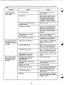
1. SPECiFiCATIONS·,; .........................................
Page 1
•
•
..
2. OPERATING INSTRUCTIONS ................................ Page 2
3. SYSTEM DESCRIPTION AND OPERATION ................... Page 5
•
•
4. SYSTEM TESTING. . . . . . . . . . . . . . . . . . . . . . . . • . . . . . . . . . . . . . . . . .. Page 9
.
.
~ ..'
..
5. DISASSEMBLY PROCEDURE ................................ Page 9
6. PRELIMINARY CHECKLIST ................................. Page 10
7. TROUBLESHOOTING ...................................... Page 11
_., 8. ADJUSTMENTS ............................................ Page 20
PARTS LIST ............................................................................................... Page 21
.
10. SCHEMATIC DIAGRAM ..................................... Page 25
.
.
•
•
•
·.
•
"
.
•
..
•
...
.-
~. .
•
•
...
•
•
- ,
--- '--,
..
•
-
•
•
•
.
·
•
.
.
•
•
•
•• •
•
•
•
•
•
•
•
..
•
•
-.
•
..
.
•
•
--
•
•
!
•
SPECIFICATIONS
•
MICROPROCESSOR (CPU) -
General Instrument CP-1610 16-bit processor.
MEMORY - 7K internal ROM, RAM, and 1/ 0 structures, remaining 64K address space available for
external programs.
CONTROLS - Two removable hand controllers: 12-bulton numeric keypad, four action buttons,
16-position directional movement disc.
SOUND -
Programmable sound generator (PSG) capable of producing three simultaneous sound
patterns.
16 different color hues:
COLOR REPRODUCTION -
Black
Blue
Red
Tan
Dark Green
Light Green
Yellow
White
VIDEO RESOLUTION -
Gray
Cyan
Orange
Brown
Magenta
Light Blue
Yellow-Green
Purple
192 vertical x 160 horizontal picture elements.
VOLTAGE REQUIREMENTS DIMENSIONS: (WxDxH) -
120VAC 60 Hz
10" x 6'14' x 3"
WEIGHT - Console Assembly with Packing Material and Accessories Console Assembly alone - 2.3 lb.
4.7 lb.
ACCESSORIES - Antenna Switch Box, Switch Box Cable (15 feet), Wall-Mounted Power Transformer, and Owner's Manual.
·,
,
•
•
-1-
•
•
OPERATING INSTRUCTIONS
A.
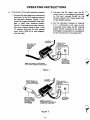
2. Connect the RF cable from the RF f"""'\
output jack on the Master Component. ~
to the jack marked GAME on the ~
antenna switch box. Place switch box
to the GAME position.
Connection to the color television receiver
•
1. Connect the tWin lead from the antenna
switch box to the VHF antenna input of
the television receiver. Figure 1 illustrates the proper connection when twin
lead is used from antenna system;
Figure 2 illustrates the proper connection when coaxial cable is used. If the
TV receiver has only 75 ohm coaxial
input, then a 300 to 75 ohm adaptor
must be used.
3. Set the television receiver to channel
3 or 4, whichever is not used in your
broadcast area. Place the RF channel
select switch (located at the back of
the Master Component) to correspond
to the channel set on the television.
TO MASTER __
COMPONENT
I
FLAT "TWIN LEAD"
WIRE FROM TV
ANTENNA OR
TYPICAL UHFNHF
TV RECEIVER
ANTENNA TERMINALS
ANTENNA
SYSTEM
•
,
SWITCH
BOX
VHF ANTENNA
TERMINAL FOR
COAX TYPE OF
NOTE: NO CHANGE TO YOUR EXISTING
UHF ANTENNA CONNECTION IS REOUIRED.
ANTENNA WIRE
. Figure 1
ROUND VHF
. ANTENNA OR
SYSTEM WIRE
ROUNO"COAX"TO
FLAT "TWIN LEAD"
BALUN CONVERTER'
AVAILABLE AT MOST
ELECTRONICS
PARTS STORES
•
TO MASTER __
COMPONENT
'
TYPICAL UKFNHF
TV RECEIVER ANTENNA
TERMINALS
ALTERNATE
VHF ANTENNA
TERMINAL
NOTE: NO CHANGE TO
YOUR EXISTING UHF ANTENNA
CONNECTION IS REOUIRED.
Figure 2
-2-
•
•
•
keypad) is UP on the screen, etc. For further
instructions, refer to the individual game
cartridges.
B. Power Connection
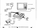
1. Plug the transformer unit into a 120 Volt
60 Hz wall outlet.
2. Insert the other end of the power cord
into the rear-panel power socket.
To operate the directional disc, depress the
outer edge of the disc with one finger and rotate
it around the edge to change the direction on
the object you are moving. You have the ability
to move the object in any desired direction.
C. Gameplay
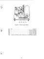
1. Turn TV set ON.
2. Insert the game cartridge in the slot
located on the right side of the Master
Component (Figure 3).
The keypad buttons and directional disc
cannot be operated simultaneously. However,
the action buttons and directional disc may
be operated simultaneously.
3. Remove the Hand Controllers from their
holder on the Master Component.
When returning the Hand Controller to the
Master Component, coil the cable beneath it in
the cradle. To avoid permanently overstretching the coiled cables, they should not be pulled
out to their extreme length.
4. Depress the ON/OFF/RESET switch
button to turn on the Master Component.
5. RESET: Tapping the ON/OFF/RESET
button will cause the game being played
to be reset to the title page. POWER
OFF: To turn the MasterComponent off,
depress the ON/OFF/RESET button for
3 seconds and then release it.
E.
Intermission and Time Out
1. If, for any reason, you wish to interrupt
your game, you may use the Intermission Code. Removing the game
overlay and pressing 1 and 9 simultaneously on either Hand Controller
will cause the television screen to go
blank and game play to stop. To resume
game play, simply depress any key on
either Hand Controller.
D. Hand Controllers
The Master Component is equipped with two
Hand Controllers (each Hand Controller may
be unplugged where the coiled cord meets the
Master Component.) There are 12 keys on the
keypad. These are used for feeding data into
the Master Component.
•
2. If NO functions on either Hand Controller are activated for approximately
5 minutes, the television screen WILL
AUTOMATICALLY GO BLANK and the
game play will stop. To resume game
play, simply depress any key on either
Hand Controller. The purpose of this
unique feature is to eliminate the
possibility of a permanent playfield
image being imprinted on the television screen.
With each cartridge, there are 2 overlays which
fit over the keypads on the 2 Hand Controllers.
These overlays are keyed to the particular
game being played and determine how the
keys on the keypad relate to the cartridge.
Slip the overlay under the keypad frame.
There are 2 action buttons on both sides of the
Hand Controllers. The upper buttons, one on
each side, perform the same function for the
convenience of either right- or left-handed
players. The lower buttons perform varying
functions. The functions of all the buttons
depend on the cartridge being used and are
different for each cartridge overlay.
,
NOTICE TO PROJECTION TV OWNERS:
Operating the Master Component for extended
periods of time on a projection TV system may
cause the stationary game objects to become
permanently imprinted on the projection TV
picture tube(s). This is especially true when
the brightness and contrast controls are set
extremely high for game viewing. Please
observe the following precautions to minimize
the chances of a game image being imprinted
on the screen:
The disc at the base of the Hand Controller
,,r--. is a directional control for those cartridges
in which direction is a factor. There are 16
directional positions on the disc. The direction
of the disc corresponds to direction of the
television screen. UP on the disc (toward the
-3-
,
o
TRANSFORMER
UNIT
(Plugs into AC
Wall Outlet)
COLOR TELEVISION
•
I
POWER PLUG
(Plug into rear
01 Master
Component)
•
TV CONNECTION
TO SWITCH BOX
j.
,
HAND
CONTROLLER
ON/OFF/RESET
BUTTON
MASTER
COMPONENT
GAME
CARTRIDGE
I
o
ANTENNA SWITCH BOX
(To be located on rear of TV)
o
0)
Figure 3 -
MATTEL INTELLIVIS
ASTER COMPONENT (Wiring Diagram)
o
_
- - - - - - -- - - - - - -- - - - - - - - - - - - - - - - - - - .-, ..-.. ..
~
"
•
1. Always use lowest possible brightness
and contrast control settings during
game operation.
•
3. FollOw your projection TV owner's
manual for proper viewing conditions
for programming.
2. Games containing stationary white or
light colored objects should not be
played for extended periods of time.
SYSTEM DESCRIPTION AND OPERATION
The Intellivision II system consists of a Master
Component with two detachable hand controllers, an antenna switch box, RF connecting
cable and a wall-mounted transformer unit.
The Master Component operates in conjunction with a color television set and an I ntellivision game cartridge. Peripheral equipment
(such as the Intellivoice'· Voice Synthesis unit)
may also be used with the Intellivision II
system.
switch, power supply board assembly, logic
board assembly, and two hand controller
assemblies. Recessed compartments at the
top of the console are provided for storage
of the hand controllers and cables. A slot in
the right-hand side of the Console Assembly
is the insertion port for the game cartridge.
The ON/OFF/RESET switch is located at the
lower left-hand corner of the Console
Assembly.
The Master Component system is based on
two processors. One is a 16 bit microprocessor
(CPU) that computes the game action against
the stored program rules. The second is the
Standard Television Interface Circuit (STIC)
that interprets a condensed memory area and
uses this to generate a color video signal.
The video signal is applied to the RF modulator
to provide the television signal. The user's
color television receiver is used for the video
display.
A. ON/OFF/RESET SWITCH, This switch has
three main functions: When the Master Component is off, depressing this switch will
apply power to the unit. When the Master
Component is on, quickly tapping this switch
will reset the game in play. Finally, when the
Master Component is on, holding this switch
down for about 3 seconds and then releasing
it will turn power to the unit off.
B. POWER SUPPLY BOARD ASSEMBLY. The
Power Supply Board converts the AC voltage
from the wall-mounted transformer unit into
the various DC voltages necessary to operate
the Master Component. Additional circuitry on
the Power Supply Board senses the activation
of the ON/OFF/RESET switch and causes the
Master Component to turn on or off. Electrical
connection to the Logic Board is via a 10-pin
connector.
User interaction with the game programming is
accomplished by the inputting of numerical
control and directional information through
the hand controllers.
The audio is accomplished by using a programmable sound generator (PSG) integrated
circuit (IC) which generates the audio signal
to drive the RF modulator. The user's television receiver is used for the audio output.
The Power Supply Board utilizes a switching
regulator design to accurately and continuously sense the current being drawn by
the Master Component. In this design, the
incoming voltage is rectified and then converted into a square wave. The switching
CONSOLE ASSEMBLY. The Console Assembly
contains all electrical circuitry necessary for
recall and processing of the program data
stored in the game cartridge. Integral with
the Console Assembly are the ON/OFF/RESET
-5.
_ ___
.__
_
__ •
__ •
•
_
A
•
---------------------------_..._
•
... .. .
regulator senses the current drain and varies
the duty cycle (on time of the square wave
compared to the total period) of the square
wave. This assures a constant voltage during
varying levels of power consumption.
C. LOGIC BOARD ASSEMBLY. The Logic
Board Assembly consists essentially of . 12
integrated circuits and their associated components, a channel select switch, and an RF
modulator, all of which are mounted on the
same printed circuit board. A 44-pin connector
is provided for game cartridge connection.
Two 9-pin connectors are provided for connection of the Hand Controllers. The Logic
Board processes program data from the game
cartridge and also converts the processed
data to an RF signal for color television
operation.
D. HAND CONTROLLER ASSEMBLIES. The
Hand Controller Assemblies each consist of
a printed circuit matrix, a numerical keypad,
two pairs of side-mounted push buttons, and
a 16-position directional control disc. The
Hand Controllers provide a means of calling
up program jnformation from the game cartridge for processing by the Central Processing
Unit (CPU).
ANTENNA SWITCH BOX AND CABLE. The
antenna switch box provides the interface
between the console assembly and television
set. Two spade lugs on the switch box ar.e
provided for connection to the television set.
Two screws on the switch box are provided for
connection to the antenna. The antenna switch
box serves to select either the console assembly or the external antenna as the source of
RF input to the television set. For the 75 ohm
impedance antenna systems, a balun transformer is required.
TRANSFORMER UNIT. The wall-mounted
transformer unit converts 120 Volts AC household current to 16 Volts AC. The transformer
unit connects to the console assembly through
a 2-wire cable, which may be unplugged from
the console for easy storage.
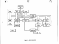
THEORY OF OPERATION. Referring to Figure
4, System Block Diagram, the system is based
on the use of two processors which time-share
a bidirectional bus. The Central Processing
Unit (CPU) algorithmically computes the game
action against program material stored in the
ROM game cartridge. The Standard Television·
Interface Chip (STIC) interprets a condensed
memory area and uses the information to
generate the television display.
The STIC also letches moving and background
picture information from the graphics memory
and presents the data as video output. This is
done by dividing the television screen into
an x-v coordinate system. For example, the
STIC fetches a pattern or game figure from
graphics memory to be used in gameplay.
The CPU tells the STiC where to position it
on the television screen.
CENTRAL PROCESSING UNIT (CPU). The
CPU is a complete, 16 bit, single chip, high
speed metal oxide semiconductor, large scale
integrated circuit (MOS-LSI) microprocessor.
It utilizes a 16-bit bidirectional bus to transfer
data, addresses and instructions between the
microprocessor. memory, and peripheral
devices. Two phase timing and synchronization signals are applied to the CPU by the
STiC. The CPU bus control outputs serve to
define the status of bus operations.
STANDARD TELEVISION INTERFACE CHIP
(STIC). The STIC operates within the system
by time-sharing a 14-bit bidirectional bus.
The STIC's main function is to provide eight
coordinate-positioned "foreground" objects.
The second function provides a background
display facility. The "background" mode
utilizes a dedicated area of external memory
to store character control codes for each
display position. Both modes utilize external
memory for the storage of character patterns.
The STIC accepts data, address and graphics
information from a common multiplexed bus.
Demultiplexing and system synchronization
are accomplished through three sets of control
signals. Note that the data bus is always
duplex or bidirectional.
The main synchronization (which operates
at television frame rate) synchronizes the CPU
algorithms to the intended display sequences,
obtains the "background" character descrip. tors from the external memory and serves to
enable the external devices via the 14-bit bus
when in the CPU-controlled mode. The second
set of control signals is used to specify address,
read and write of the external memory where
graphic character patterns are stored. When
•
"C)
•
•
SCRATCH PAD
RAMS
21UL
rI
I
I
I
I
-
- - --
-
-,
I
I
I
RO-950t
ROM
I
PROGRAM
ROM
RO-3-9506
I
I
I
I
I
CPU
CP-1610
~
....
I
SYSTEM
RAM
RA-3-9600
I
I
I
I
I
I
I
I
I
I
.:..,
RO-9504
ROM
I
I
I
I
L
.... L
I
•
GAME
CARTRIDGE
______
I
I
I
I
I
...J
"1
..s..
SOUND
GENERATOR
AY-3-8914
lINEAR/ANALDG/
OIGITAL
LAO
3"
.....
•
1A
STIC
AY-3-8900·1
7COLOR
AY-3-8915
HAND
CONTROLLERS
RF
MODULATOR
POWER
SUPPlY
-"
Figure 4 -
BLOCK DIAGRAM
RF
OUTPUT
GRAPHICS
ROM
RO-3-9503
~
7-
GRAPHICS
RAMS
2114L
1-1-1
- - - - - - - - - - - - - - - - - - - - - --_._-_._--_. __
..., ..,
•
in the CPU-controlled mode, the graphics
control bus links the graphics memory to
the CPU main memory. The third set of controls
is used to specify address, read and write
sequences to/from the STIC whIm the system
is in the CPU-controlled mode. Video output
codes from the STIC are applied to the color
oscillator/master clock generator for
processing.
ROM contains system operating data. System
program data from the executive ROM is
transmitted along a 16-bit bidirectional data
bus. The program ROM contains program data
common to all external programs. Data from
the program ROM is transmitted along a 16-bit
bidirectional bus. A scratch pad memory RAM
associated with the program ROM is provided
for computation of the program ROM data .
Interconnection of the program ROM and
the scratch pad memory RAM is accomplished
through a 14-bit bidirectional data bus.
•
GRAPHICS MEMORY. The graphics memory
consists of a graphics read only memory
(ROM) and two graphics random access
memories (RAMs) . The two graphics RAMs
are connected to the graphics ROM by an
B-bit static address bus. Address and read
instructions are applied to the graphics ROM
by the STIC. Output from the graphics memory
is applied to the 14-bit secondary data bus.
PROGRAMMABLE SOUND GENERATOR.
The programmable sound generator (PSG.)
is a large scale integrated circuit (LSI) designed to produce a wide variety of sounds.
All control signals to the PSG are provided
by the CPU. Two B-bit general purpose I/O
ports are provided for user interface via the
hand controllers. The PSG output is available
from three independenlly programmed analog
outputs. The outputs of the PSG is combined
on a single line, amplified and then applied
to the RF modulator to produce the audio
output at the television set.
COLOR OSCILLATOR/MASTER CLOCK
GENERATOR. The color oscillator/master
clock generator decodes the video output
from the STIC and generates a clock signal for
system control. Oscillator frequency input
is obtained from a 7.159090 MHz crystal and
its associated trimmer capacitor. The clock
generator provides a 3.579545 MHz clock
signal output. Video information from the
STIC is applied to five inputs to produce
composite sync. color burst, line blanking,
screen blanking and video output. The analog
outputs of the color oscillator are combined
by four external precision resistors to provide
a composite video signal to the RF Modulator.
SYSTEM RANDOM ACCESS MEMORY (SYS·
TEM RAM). The System RAM is a dual port
interface, 16-bit wide storage area which
serves as the control decoder for CPU control
data. The System RAM receives data from the
CPU via a 16-bit bidirectional time-multiplexed
bus. The direction of data travel is from the
CPU to the graphics memory except during a
bus reversal condition. This condition is
indicated when the CPU requests a read from
a graphics address on the 14-bit graphics
bus. A 3-bit control bus from the CPU provides
StTODe signals to the System RAM .tor the
on-chip address latch and main memory area.
•
PROGRAM READ ONLY MEMORY (PRO·
GRAM ROM). The internal program area is
comprised of an executive or system ROM
and a scratch pad memory. The executive
-B-
•
•
•
SYSTEM TESTING
•
Master Component and depress the
reset switch. Check for mistakes in
lettering on title picture, jumbled playfield or unwanted characters .
DIAGNOSTIC TEST ROUTINE. The diagnostic test routine should be performed before
disassembly of the Master Component. Full
instructions covering the operation and analysis of results are included with the Diagnostic
Test Cartridge.
,
c. If any problems occur. remove customers Game Cartridge and check
Master Component with a known-good
Game Cartridge.
CUSTOMER'S GAME CARTRIDGE TEST.
Test the customer's Game Cartridge as follows:
d. With the known-good Game Cartridge
inserted. if problems are not observed,
then the customer's Game Cartridge
is defective. If problems are still
observed. troubleshoot the Master
Component.
a. Verify that Master Component is connected to television set as outlined
in the Operating Instructions.
b. Set the Antenna Switch Box to GAME .
Insert customer's Game Cartridge in
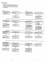
DISASSEMBLY PROCEDURE
a. Remove two Phillips-head screws
securing the top housing assembly to
the bottom housing assembly.
Before disassembly of the Master Component.
follow the steps in the Testing Procedure
section to determine the most likely cause of
the malfunction. Additionally, check the wallmounted AC adaptor prior to disassembly for
the possibility of its malfunctioning. Refer
to the Troubleshooting Procedure section for
instructions on testing the wall-mounted ~C
adaptor. Disassemble the Master Component
only to the extent necessary to accomplish
repairs .
b. Turn console assembly right side up.
Gently pull the front of the top housing
assembly up and away from the bottom
housing assembly . Small catches in the
rear of the console assembly prevent
the top and bottom housing assemblies
from being pulled directly apart.
•
c. Remove the 3 Phillips-head screws
holding the Power Supply Board to the
standoffs on the Logic Board .
WARNING
MAKE SURE THE MASTER COMPONENT
IS UNPLUGGED FROM THE AC ADAPTOR
BEFORE DISASSEMBLY. REMOVE ANY
GAME CARTRIDGE FROM THE UNIT, DISCONNECT THE RF CABLE FROM THE RF
OUTPUT JACK AND THE HAND CONTROLLERS FROM THEIR SOCKETS.
d. Gently lift the Power Supply Board
straight up from the Logic Board.
e. Remove 4 Phillips-head screws holding
the Logic Board to the lower housing
assembly.
f. Grasp the LogiC Board at the 44-pin
game connector and gently pull it
straight up and away from the lower
housing assembly. Be sure to allow
the Channel Select switch to clear its
opening in the lower housing assembly.
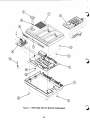
DISASSEMBLY OF CONSOLE ASSEMBLY.
Disassemble the Master Component in a clean,
well-illuminated area. Refer to Exploded
Diagram (Figure 5, Page 22).
Turn console assembly upside down on a
surface protected by a soft cloth or a piece
of carpet.
-9-
•
- - - - - - - - - -- - - - - - - - - - - - - - -- -_ .... . _ - - - .
•
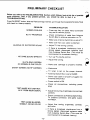
PRELIMINARY CHECKLIST
Before you refer to the TROUBLESHOOTING Section which follows, look at this list of possible
quick solutions. Then, If any problem persists, you should be able to find it in
TROUBLESHOOTING.
•
:'
Press ON/RESET button. With the Test Cartridge inserted, go through the DIAGNOSTIC ROUTINE
and check for these problems:
PROBLEM
POSSIBLE SOLUTION
SCREEN IS BLANK
-
Press any key on either Hand Controller
key pad to recover picture.
NO TV PROGRAMS
-
Check connection of cable from Antenna
Switch Box to antenna connector on TV.
-
Make sure Antenna Switch Box is set at TV .
-
Make sure that coax cable is attached.
-
Adjust TV fine tuning controls.
-
If there is broadcast interference from a
strong Signal, disconnect antenna coax
from Antenna Switch Box. (This must be
reconnected for broadcast viewing.)
-
Turn up TV volume control.
-
Adjust fine tuning.
WHITE-GRAY SCREEN
OR SCREEN IS ONE COLOR
-
Make sure cartridge is properly inserted.
SNOWY SCREEN (NO RF CARRIER)
-
Make sure:
-
TV tuner is set on the proper channel.
-
Antenna Switch Box is set at GAME.
-
Game coax cable is properly plugged into
Antenna Switch Box.
-
Power switch is ON.
-
Check all connections, including power
plug.
-
Adjust fine tuning, brightness, and contrast
controls.
-
Check connections at Antenna Switch Box,
TV antenna connector, and game output
connector.
-
Adjust fine tuning, brightness, contrast,
and color.
-
If there is broadcast interference from a
strong Signal, disconnect antenna cable
from Antenna Switch Box. (This must be
reconnected for broadcast viewing.)
BUZZING OR DISTORTED SOUND
.
NO GAME SOUND EFFECTS
•
TEST IMAGE NOT DISTINCT,
AS IF FROM WEAK SIGNAL
TEST IMAGE BLURRED,
WOBBLY, OR NO COLOR
-10-
,
"
•
•
•
TROUBLESHOOTING
Fro m a design aspect. the Intellivision II Master
Component is a complex configuration of
electronic hardware. However. from a repair
aspect. the Master Component may be divided
int o small building blocks, each part modifying
or adding to the signals in its own special way .
Whenever possible, the repair of the Master
Component is simplified by looking at symptoms that occur when a component fails .
It IS recommended that the first few time you ,
the repair technician, troubleshoot a defective
Master Component. start at the beginning of
this troubleshooting procedure and fOllow
through until the problem is corrected . Familiarity will quickly be gained in identifying
the appropriate voltages and waveforms found
•
-11 -
at various parts o f the circuit. At this time . you
witl be able to qui c kly identify the symptoms
ex hibited by the Master Component and perfor m the requ ired repair .
When changing Integrated Circuits (ICs) :
• ALWAYS USE A KNOWN-GOOD IC.
o
ALWAYS FOLLOW PROPER PROCEDURES AND CAUTIONS FOR HANDLING
MOS DEVICES.
• BE SURE OF CORRECT fC ORIENTATION
AND PIN INSERTION.
o
CHANGE ONLY ONE IC AT A TIME AND
LEAVE IN THE KNOWN·GOOD IC UNTIL
THE FAULTY ONE IS FOUND .
TROUBLESHOOTING PROCEDURE:
Run the Diagnostic Test Routine." a fault is discovered. then the FAILURE display
will indicate the ICs most likely to have failed. Replace these ICs. " this does not
solve the problem. or if you are unable to run the Diagnostic Test Routine. follow
this Troubleshooting Guide.
AC Adaplor
Power Supply
Measure 16-20 VAC between cenler aM
Duler sleeve 01 AC Adaptor.
Unplug concentrIC plug 01 AC Adaplor from
fear of Master Component. Plug AC Adaptor
Inlo
YES
live 120VAC 60Hz oullet.
ill
NO
Disassemble Master Component 10 reveal
Ihe Power Supply Boarel allact'Ie<J to lhe logiC
Board. Plug known-good AC Adaptor inlO
Master Componenl .
~re 16·20VAC
YES
6.
YES
1)0
NO
replace Power Supply Board.
"Ie ... RESET S~~~~dn wi'h,n
seconds. Voltage .11 TP8
be about
-5VDC .
P;;;- and
to OV wh ile 51 pressed .
YES
Witn reterence to Ground (TP3) measure:
-11 '0 -2.4 VOC " TP4
••
b -545 fO -5.95 VOC ., TP5
ND
Check Ihill Reset Bullon IS nOI making inlermlltam conlaCI. Replace Power Supply Board
with a known-oood one. II problem is slill
apparen!. Inen taul! is in LoOic Board. Conl.nue lollowlnQ Sleps ;n this Troublesl1Ooting
Guide.
Replace Resel Bullon S1.
YES
c -11 .5 fo -12.5 VOC" TPS
1. -485 '0 -5 .•5 VOC " TP7
NO
Remove Reset Bunon S1 It vOllage does
nol appear. then check for shOrted (races
between 51 aM Power Supply Board . Replace Power Supply Board ,
YES
Check AC Jack J2. C38. C39. Flail(! tall If aces
belween Jl and Power SUpply BoarO. "OK.
Depress Reser Bullon S1. Voltage al TP8
should
In
NO
Replace AC Adaplor .
Measure abou' -11V!.' TPS wl,h MIC 0".
across TPl and TP2
~power;
gOOd one If
Inen taul! .s .n
inQ steps 10 this
.
With a knownis not measured.
Conllnue tollow-
19 Guide.
to logiC Board SchematIC IFigure
. measure 7 15909 MHz al.V peak·
at Ipg.
Measure 3.579545 MHz al 4 Vp-p at TPIQ.
..!!.!..
Measure 1.789n2 MHz at5Vp-p .11 TP11 and
TP11.
NO
NO
,
•
Replace
or U3 ..
Rem ove STIC chia U• . II Signal appears.
replace U4 " 51.11 no s.gnal check lOr
shoneo [races , Replace UIC.
Replace e'YSlal )(1 Check C17 and C16.
Replace UtO With a known-gOOd one .
In
...!!!.
Measure 1.789772 MHz at IOVp-p al TP13and
TP'.
NO
-
lhe follOWing order : u_, U2. Ug,
Replace. In me 101l0wlng oraer : U1. then U9
.
t
Removefor.nycari;~;~~~?!{~~l~f~!~'l
Check
prager
at
IBeI).
IP.6 ISC21 and TP17 IBOIR!. The RESET
With cartridge still removed . check
proper waveform al TP18 (8Cl
TP19
bullon will netC! 10 be pressed every few
secondS so the waveform does no. disagpear.
bullon will need to be pressed every lew
seconos so Ihe waveform does not disappear
fBC2
10
Replace . In the lollow.ng oraer: U1. U2. then
U9.
DUn
and TP20 IBOfR
oun
'0'
oun
Ihe RESET
NO
-
Check lor oroken or ShorltO PC traces . CheCk
for shorted or bent pms at game cartridge
Sockel JI. Replace U9.
YES
Plug cartridge Into game socket. Check 10f
proper waveform al TP21 (BCl IN). TP22
II problem IS nOI solved. continue with Ihe
Symptom/Remedy guide starting on the
nUl page.
YES
fBC2 'NI. .nd TP23IBOIR INI .
ND
RecheCk sionals at IP18. TP19. and TP20. If
OK. check game socket Jl and game cartridge ton a knawn-good M/C) . II Signals
ilft nOI OK. reglaee 0.4. then ti6.
-
-12-
-13-
YES
----------------------------------- ------------------- . _ - - - - - •
•
•
If the problem is not found and corrected with the procedures on the previous page, then follow this Symptom/Remedy
Guide:
SYMPTOM
SUSPECT
Snow on TV (with or
without diagnostic test
pattern visible.)
•
REMEDY
Unit is not turning on.
Review voltage check in Trouble·
shooting Guide.
Fuse is blown.
Check continuity of fuse on Logic
Board. Replace if open. If new fuse
blows quickly, check for proper
voltages from Power Supply Board.
If voltages 0 K, check for shorted
,
components or traces on Logic Board.
Voltage at pin 2 of RF Modulator is
not about +6 VDC.
Check R7 and CIS.
RF Modulator is defective.
Connect a known-good Modulator in
paraliel with the Modulator. Connect
the RF Cable to the known-good
Modulator and touch the cases together.
If this clears the problem, replace
Modulator.
Solder bridges or foreign material
are causing shorts.
Inspect for solder bridges or foreign
material on the Logic Board.
The +12 VDC supply i. defective.
Troubleshoot the +12 VDC supply and
distribution on the Logic Board.
-1
Grey·white screen with NO
flash observed on the TV
screen when the reset switch
Clock circuitry not functioning.
Review procedure in Troubleshooting
Guide on troubleshooting clock
circuitry.
is depressed.
5.7 VDC to STIC missing.
Measure 5.7 VDC at pin 20 of STIC
(U4). If not, troubleshoot 5.7 VDC
distribution system on Logic Board.
-2.25 VDC to STIC miosing.
Measure -2.5 VDC at pin 40 of STIC
(U41. If not, troubleshoot -2.25 VDC
distribution system on Logic Board.
Solder bridges or foreign material
Remove any foreign material or solder
causing shorts on Logic Board.
bridges.
Grey-white screen WITH
The test cartridge is incorrectly or
Insert cartridge correctly.
flash occurring on the TV
screen when reset switch
is depressed.
incompletely inserted into the
Master Component.
is defective.
Visually inspect socket for bent pins,
foreign material, etc.
DefectivI Test Cartridge.
Try another cartridge.
Clock Signal path not complete.
Review procedure in Troubleshooting
Guide on checking clock circuitry.
+5 VDC supply problems.
Troubleshoot +5 VDC supply and
Master Component cartridge socket
distribution path.
Defective IC.
Insert test cartridge and run Diagnostic
Test Routine. Replace any ICs that are
indicated as failed.
-14-
,i•
•
!,
•
,
•
i
SYMPTOM
Grey-white screen WITH
flls h ocC llrr in, on tM TV
scre.n when rel it switch
SUSPECT
Defective IC (co nti nue d I.
,
is depreald.
(co nti nue d)
REMEDY
If Test Ro uti ne will no t run (using I
kno wn -go od tes t can rid ge) Ind III
voltages are OK , rep llc e tM ICs in the
following ord er: Ul , U2, U4, U3,
or U6.
,
Incorrect or missing bus control
Incorrect, ex tr., or missing
video patterns or characters.
signals,
Guide on che cki ng bus con tro l signlls.
Solder bridges or foreign material
causing sho ns.
Remove any foreign mattrial or solder
sho ns.
One or more les are defective.
Ins en tes t can rid ge Ind Dil gno stic Te st
Ro uti ne. Replece Iny indicated
ICs. Most graphics pro ble ms Ire c.. ,se d
by U2, U4, U5, U7, or US.
Incorrect or missing DC Voltages.
Check for cor rec t DC vol tlg es on 8Ic h
IC (refer to SchematiC, Figure SI.
Test Clrtridge is defective .
Try a kno wn -go od Te st C.n rid ge.
Solder bridges or foreign material
Remove any foreign material or solder
,
Distorted TV picture.
Review procedure in Troubleshooting
is causing shorts.
sho ns.
Interference fro m a nearby television
or radio tra nsm itte r.
Sw itch television and Master Co mp on ent
to ano the r channel and lor disconnect
•
the antenna wire from the antenna
switch box.
The tlSt setup is incorrect.
Check all television controls and can·
nections for agreement between the TV
VHF cha nne l sel ect or and the Master
Co mp on ent cha nne l selector.
STIC IC (U4) or Co lor IC (U l01 is
defective,
Defective RF mo dul ato r.
vid lo OK),
known-good ones.
I
I
I
I
Co nne ct a kno wn ·go od mo dul ato r in
parallel wit h the mo dul ato r. Co nne ct
the RF coble to the kno wn -go od
mo du lat or and tou ch the tw o mo du·
lat or cases tog eth er. If the pro ble m
clea<1, rep lac e the mo dul ato r.
Solder bridges or foreign material
No sound (picture and
Replace the se ICs (one at a tim el wit h
•
Remove any foreign material or solder
causing shorts.
bridges.
TV volume tum ed dow n,
Check TV Vo lum e setting.
I
i
i
I,
'-
•
!I
!
-15 -
,._-
1
1
•
•
•
SYMPTOM
No sound (picture and
video OK).
(continued)
SUSPECT
•
REMEDY
Sound IC (UG), U3, or U9 is
defective.
Scope for audio signal at pin 4 of UG
during Audio Test on Test Cartridge.
If no Audio, replace UG, U9, then U3.
If signal at pin 4 of U6 OK, but no
signal at pin 9 of U9, replace US.
A F Modulator is defective.
First check the audio input lead of the
modulator for signal. If signal is pres ent, connect a known-good modulator
in parallel w ith the modulator. Connect
the RF cable to the known-good modu ·
lator and touch the two modulator cases
together. Run the Sound Test on the
Test Cartridge. If sound is OK , replace
the modulator.
Hand Controller
malfunctions.
,
The picture suddenly goes
blank during the diagnostic
test .
Solder bridges or foreign material
causing shorts.
Remove solder bridges or foreign
material.
The Hand Controller is defective.
Plug in a known-good Hand Controller
and perform the Hand Controller Test.
UG or U3 is defective .
Replace U6, then U3.
The 9 pin connector on the Logic Board
for the Hand Controllers is defective.
Check the 9 pin connector and assO -
Other les are defective.
Replace, in the following order : U4 ,
U2, Ul, U12, and U13.
The test cartridge is defective.
Try another cartridge. Also check (he
Master Component cartridge slot .
One or more ICs are defective.
Replace. in the following order : Ul ,
U2. and U4 .
•
Picture action "freeze-up."
Chann_1 Select switch does
not operate correctly.
-
ciated traces on the Logic Board.
The reset button is defective.
Check the reset bunon.
Crystal X 1 is defective.
GENTLY tap the crystal and observe
the picture.
Foreign material is causing an
intermittent short.
Inspect the Log ic Board for fore ign
material. .
One or more les are defective.
Replace, in the following order : U I ,
U4, U2, and U3 .
The Test Cartridge is defective .
Try another cartridge.
The Master Component cartridge socket
is defective.
(nspect the cartridge socket for bent
pins, foreign materials, etc.
The switch i. defective.
Replace the switch.
Th_ modulator is defective.
Connect a known-good modulator in
parallel with the modulator. Connect
the RF cable to the known-good
modulator and touch the two cases
together. Switch the Channel Sel.ct.
If the channel now changes, replace
the modulator.
-16-
.
•
•
•
'SYMPTOM
SUSPECT
REMEDY
-I~------------------------------1-----------------The picture has the wrong
The TV control. are .et wrong.
•
Check all TV controls .
colors or no colo rs_
The crystal X 1 is set to the wrong
frequency .
Check the frequency at pin 15 of U I O.
It should be 3.579545 MHz +1- 100Hz .
Adjust the frequency by adjust ing
var iable capac itor (C 17) .
STIC (U4) or Color (UIO) IC, are
Replace U4 . then UIO.
defective.
Solder bridges or foreign material
Remove any solder bridges or foreign
causing a shan .
material.
•
•
-17-
..
~
-
.".
I
,
,
"
,
I
I
I
,•
,
"
..
,
,, "
,"
•
,
,
,
,
••
r- ~.-. ~
,
,
'
.
a .. .
"
" :":; ".
,
'
~.
...
.. -_.
..
o
~
••
...... _---
. _"flrU
'--- .
,
--.
,
."~
~
.-- .
---.
._--
- .......-. -.
". ,
.."
'. ..."",--
, _. .- .
,
,
•w
..'
,
"
'"
.. -'
,,
s
.. J,
."r
..
•
,
'
..
.-.-
>
.--.
,
....
'-.
..
_• .
' ""
~---
'.,
"
"
..
o
.~.
~ "' _
"
. ..
",1
,
)
• .,
'"
0
,
•
,
,
.
•
,
..
•
!
"
....,
.
, "
,
,
, .,
.....
.".• .
•
•
" ,..
.
... . . ,.
- -...
... ..
: ..
,
.. _.
-•..• . - ... ., ... .. ..
"
'
.
,
. .... .
•
. '. .. .
· 18·
,
"
,
,,
I
r
.,
I ..
r
I
I
!
•
~
o
,
--
.
"
'
'..
"
-
--~ .
.•.•i=...... .-.-. ,
I
.., ,.
•
,
'
'
..,-..
• •
"
",
,
~
.
.
F~
"
.,
'I..
,~
' ?""~
.
' :'
•
...
:J
o
>-
<t
...J
,....
z
z""
c
'"
-
'"..:
o
III
,
U
I
Q.
•1, ,.
Ul
Ol
::>
-.
"
.
,
' , , " '"
"
:~~~. .."..
...
,~:!~~-';'-"
"
•
,
,
,
•
•
•
•
•
..
TP7 TP5
.
TP3
~
TP6
Figure 6 -
TP1
TP3
TP4
TP5
TP6
TP7
TP8
TP4
TP2
TP1
Power Supply Board
- TP 2 ...... . ... . .. ,., ....... . ..... .. ........... " _.... 16-20VAC
............ . .............. . .... . . . .......... Ground Connection
· ............... . ................. . ......... .. -2.10 to -2.40 VDC
· ..... .. .... . ... . ... .. .... . . ..... . . ...... . .. .. +5.45 to +5.95 VDC
.............................................. +11.5 to +12.5 VDC
· ...........................................
.. +4.85 to +5.15 VDC
•
.. Control (+21VDC/unit Off. +5VDC/unit On. OVDC/Reset pressed)
-19-
- - - --
- - - -- - -- - -- ---_ .
•
..
•
ADJUSTMENTS
MASTER CLOCK ADJUSTMENT.
CAUTION: Use care not to damage the
core.
1. Connect a frequency counter with a
high input impedance (lOOK ohms or
higher) to pin 15 of U10 and ground .
2. Adjust C 17 (variable capacitor) so the
frequency counter indicates 3.579545
MHz ± 100Hz.
4. Set Channel Select switch to channel 4.
Verify the frequenc y counter reads
67 .65MHz ± 250kHz .
SOUND BUZZ ADJUSTMENT.
1. Adjust volume on TV set for a normal
level. No sync buzz or hash sound
should be heard.
RF OUTPUT ADJUSTMENT.
1. Connect a frequency counter with
minimum input sensitivity of 2mV RMS
at 70MHz to RF Output Jack .
2. If a buzz is heard, adjust the sound coil
on RF modulator for minimum buzz.
Use only a non - ferrous adjustment
tool.
2. Set Channel Select switch to channel 3.
3. Depress and hold RESET Button and
adjust video frequency core on RF
Modulator so frequency counter reads
61 .250MHz ± 250kHz. Use only a nonferrous adjustment tool.
•
CAUTION: Use care not to damage the
core.
3. If the buzz cannot be reduced to a satisfactory level , replace the modulator.
•
Top View
SOUND
I
I
UM1285-8
--
VIDEO
RF Modulator
-20-
I
r \
!~
•
-
•
•
PARTS LIST
•
REF.
DESIGNATION
DESCRIPTION
PART NUMBER
CD
Lower Housi ng. . . . . . . . . . . . . . . . • . . . . . . . . . . . . . • . . . . . . . 5872 ·21 09
(3)
Rubber Foot ... . . . . . . . . . . . . . . . . . ...... . . . . . . . . . . . . . 2609-9489
Label - FCC & Serial No. . .... . ... . .... .. ..• • .. •• ...... 5872.0350
o
Logic Board with parts
. . . . . . . . . . . . . . . . . . . . . . . . . . . . . . . . . . . . N/A
R1, R16·R31
Resistor, 5.6K ohm 5% 1/4W ., .. .. . . . . . . . . . . . . . . . . . . . . . . 0095·0961
R3
Resistor, 2.7K ohm 5% 1/4W . . . . . . • . . . . . . . . . . . . . . . . . . . . . 0095·0881
R4
Aesistor, 5.4K ohm 5% 1/4W . . . . . . . . . . . . . . . . . . . . . . . . . . . . 0084.0929
R5
Resistor, 11 K ohm 5% 1/4W . . . . . . . . • . . . . . . . . . . . . . . . . . . . . 0095·0032
R6
Aesistor, 22K ohm 5% 1/4W . . . . . . . . . . ....... • . . . . . . . • ... 0095·0102
A7
Resistor, 180 ohm 5% 1/2W ... • .. . . . . . . . . . • . . . . . . . . . . . . . 0095·0556
R8
Aesistor, 150 ohm 5% 1/4W ... . .. . . . . . . . . . . . . . • ... • ..... 0095.0580
R9
Resistor, 10K ohm 5% 1/4W ... • ...... • . . . . . . . . • ... • ..... 0095.0022
R13
Resistor, 18K ohm 5% 1/4W ... . . . .. • ... •. .. .. .. . ... . .... 0095·0082
C1·C5, C7·C11,
C13·C15, C18, C30,
C33,C35,C36
Capacitor, 0.1 uF 25V . . . . . . . . . . • . . . . . . • ... . ... •• .. . ... 0085·1510
C16
Capacitor,20pF 15V NPO . . . . . . . . • ... , . . . . . . .• . . . . . . . . . 0085.0720
C17
Capacitor, variable 5·50pF .... • . . . . . . . . . . • . . . . . . . . . . . . . . 0099-0730
•
C19
CapaCitor, 4.7uF 6.3V Elect.
C20
Capacitor, nop F 15 V . . . . . . . . . . . . • . . • . . . . • . . . . . . . . . . . . 0085.0028
CR1,CR3
Diode,1N4001
CR2, CR5, CR6
Diode, 1N914 . . . . . . . . . . . . . . . • ... • . . . . . . . • . . . • . . . . . . 0099.1040
LED1
Light Emitting Diode (LED) . . . . . . . . . • ... • • .. . . . . . . . . . . . . 5872·0080
U1
Integrated Circuit, CP1610 (CPU) . . . . . . . . . . . . . . . • . . . . . . . . . 0098·0520
U2
Integrated Circuit, RA·3·9600 (SRAM) .... . . . . . . . . .... • • .... 0098·0530
U3
Integrated CirCUit, RO·3·9506 (PROM) . . . . . . . . • ... . ... . ..... 5872·0020
U4
Integrated Circuit, AY·3·8900·1 (STIC) ... • . . . . . . . •• .. •• .... 0098-0640
U5
Integrated Circuit, RO·3·9503 (GROM) . . . . . • . . . . . . • ... • .... 0098·0570
U6
Integrated CirCUit, AY·3·8914 (Sound) . . . . . . , , .. • ... • ... . ... 0098-0660
U7,U8,U12,U13
Integrated Circuit, 2114L (RAM)
U9
Integrated Circuit, LAD . . . . . . . . . . . . . . . . . . .. .• .. • ... • ... 5872·0010
U10
Integrated Circuit, AY·3·8915 (Color) .... • . . . . . . . • . . . . . . . . . 0098·0680
. ... . . . ... .• . . . . . . . . . . . •.... 0085·0031
.....• . ... • . . . . . . . • . . . . . . . . . . . . . . . . . . 0099·1030
-21-
. . . . . . . . . . . . . . . . • . . . . . . . . 0098·0710
- - --
- - -- - - - - - - - --
- - _........
.: ,.
•
5
8
11
I
\
I
,I
J
4
,
•
•
/
10
•
,
3
•
•
i
•
,,
••
..
~.
14
2
Figure 7 - EXPLODED VIEW OF MASTER COMPONENT
-22-
.
•
•
•
REF.
DESIGNATION
DESCRIPTION
Xl
Crystal. 7.15909MHz +/- 0 .003% ..... . .•...• . . . .. . " ... ,. 0089'()158
Hl
RF Modulator .. " .. ' , ...... , .... • •. , . .. , ... , . . ' , , , . 2609-4689
51
Domed Switch. Reset " . ' .... , ..• . ..• , ...•... ', .... '"
S2
Switch. Channel Select , . , " , . . . . . . . . . . • . . . . . ... . .. " .. 5872·9559
PART NUMBER
0099·1140
IC Socket. 40·pin DIP (for Ul. U2 and U4) , ..... . . . .• . . . •.... 0099·1510
Connector. 10·pin (Power supply to Logic 80ard) ...•...• .. ' . ' . . 5872·9359
Jl
Connector. 44·pin (Game cartridge) . ...... . .. . . . . . . . . . .. . .. 5872·9399
Adaptor (for Jl) . .. . .. . .. .. , . .. . . .... . . ... . .. .. .. .. . . 5872·2169
P4A. P4B
Connector. 91'in (Hand controller) ' .. , .. ' .. , .. . • .... • . , " . 0099·2580
Jack. AC Power. ' . , , , . , .. , . . .. .... . ' ..•. . . ' . , . .... , , 5872·9099
Fl
Fuse, 2.0 Amp . .. ... . ... . .. . . . . . . . . . . . ... .•. . , ••.. .. 0089·0115
L.l·L.6
Ferrite Sead ... , . , " ' , ..... . . • •.. . . ...• . .• ... . • . . .. 0099·1360
o
Power Supply Board with parts, . . . . . . . . . . . . . . . . . . . . .• ' ... 5872·9539
®
ON/OFF/RESET Button . . . . . . . . . . . . . . . . . . . . . . • . . . . • . . . 5872·2129
®
Spring (RESET Button) . .....••..• • •...... . . . ••... . .... 2609-4269
Q)
Pushnut Fastener . .... .. . . . . . . . . . . . . . . . . . • •. . . .. . .... 0405·0852
®
Upper Housing Assembly (upper housing
with inlay) . . .... . , .. .. " . , ' . . . , ... • . . . . . . ' .. . . ... 5872·9719
®
Inlay (for upper housing) . . ... . . . . .. ... . ... . . . . . . . ... . .. 58724519
@
@
@
@
@
@
@
light Pipe (for LEO) .. , .... . . , . . •. . . . .... . • ...•..... . . 5872·2199
Hand Controller. with all parts . . . . . . . . . . . . . . . • • . . • . . . .... 5872·9059
Screw. 8·18x3/8" (Logic board to lower housing) ... . •...••..... 0405'()176
Screw. 8·18x3/8" (Adaptor to lower housing) . . . . . . • . . .•. . .... 0150'()220
Screw. 8·18x3/4" (Upper to lower housing) . . . . . . . . . . . . . ... , .. 0405·0832
Lockwasher. 4-40 (Standoff to logic board) ... ' .•. • ... •. ...... 0150'()080
Nut. 440 (Standoff to logic board) . . . . . . . . . . . . . •.. . .. . . . . . 0150·0070
Switchbox ... . .... .. . . ... . . . . . . . . . . ... ... .. .. .. . ... 2609·9609
A F Cable .. . . . ..... .. . . . • . . . . . . . . . . . . . . . . . . . . . . . . . 2609·9599
Wall·Mounted Transformer . . . . . . . . . . . . . . . . . • . . •. . . . . . . . . 5872·9629
-23-
•
DISASSEMBLY NOTES:
•
•
•
•
•
-24-
o
~
'. .--I.Z
>
()
,
VJ
- .
•
•
/)
•
OO C)
0
OOD
0.0
I
0
,
,I
...~
,,
,
,,
I,
...II
~";',....
<t
o
Q0
/
1
\,
,
,
,
i----- \
I
,)
'-
1
·t
· 0
.
-,
-"'"
"
'",..
'"
•
•
•
,
•
~
•
0
•
•
•
• •
•
-
7"
~
..1
V
4:
~
.
~
;r
a
\.)
•
,
,
·
•·
·
·
·
',.
I