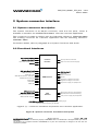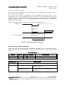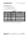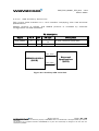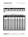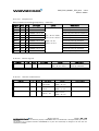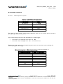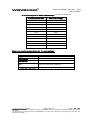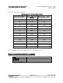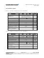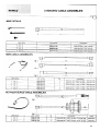
1
WISMO Quik Q2500 series
WISMO Quik Q2501
Product Specification
Reference: WM_PRJ_Q2501_PTS_001
Revision: 003
Date: March 2004
Page : 1 / 93
© 2003
All rights reserved
This document is the sole and exclusive property of WAVECOM. Not to be distributed or divulged without prior written
agreement.
Ce document est la propriété exclusive de WAVECOM. Il ne peut être communiqué ou divulgué à des tiers sans son
autorisation préalable.
WM_PRJ_Q2501_PTS_001 – 003
March 2004
Document Information
Revision
001
002
003
Date
Nov 03
Feb 04
March 04
History of the evolution
First Edition
Deletion of GPS external interruption
(GPS_EXTINT1).
Addition of GSM baseband activation indicator
(GSM_BBEN) § 3.6.9
Addition of a dedicated GPIO for SIM 3V/1V8 or
3V/5V selection.
Addition of electrical characteristics § 3.9 & 4.2
Renaming of GSM_TXBURST as GSM_PAC_EN
Modification of Figures 6, 7, 19, 23.
Update of § 1.1, 2.4, 3.4, 3.5.2.2.1, 3.5.3,
3.5.4.1, 3.6.3.2, 3.6.5, 3.6.6, 3.6.7, 3.7.1,
3.7.5, 4.3.1, 4.3.2
Rectifying the pin-out location in Figure 7
Page: 2 / 93
© 2003
All rights reserved
This document is the sole and exclusive property of WAVECOM. Not to be distributed or divulged without prior written
agreement.
Ce document est la propriété exclusive de WAVECOM. Il ne peut être communiqué ou divulgué à des tiers sans son
autorisation préalable.
WM_PRJ_Q2501_PTS_001 – 003
March 2004
Overview
This document describes the WISMO Quik Q2501 module. This module is an
E-GSM/DCS - GPRS 900/1800 MHz dual band transceiver plus a 16-channel
GPS receiver.
The WISMO Quik Q2501 memory configuration is:
GSM/GPRS part: 32 Mbits of Flash memory and 4 Mbits of SRAM,
GPS part 8 Mbits of Flash memory.
This module is dedicated to automotive applications, driven by AT commands.
This document:
•
Describes the architecture of the WISMO Quik Q2501 and interworking
between GSM/GPRS and GPS functionalities,
•
Presents all the interfaces available on the WISMO Quik Q2501,
•
Gives the electrical and mechanical characteristics of the WISMO Quik
Q2501.
Page: 3 / 93
© 2003
All rights reserved
This document is the sole and exclusive property of WAVECOM. Not to be distributed or divulged without prior written
agreement.
Ce document est la propriété exclusive de WAVECOM. Il ne peut être communiqué ou divulgué à des tiers sans son
autorisation préalable.
WM_PRJ_Q2501_PTS_001 – 003
March 2004
Contents
1
References .................................................................................... 9
1.1
Reference Documents .............................................................................9
1.2
Glossary ..................................................................................................9
1.3
Abbreviations ........................................................................................11
General presentation ......................................................................... 14
1.4
Features ................................................................................................14
1.5
Architecture ..........................................................................................16
1.5.1
Functional architecture ..................................................................16
1.5.2
RF architecture ..............................................................................17
1.5.3
Baseband architecture ...................................................................19
1.6
Firmwares .............................................................................................21
1.6.1
GSM/GPRS Firmware ....................................................................21
1.6.2
GPS Firmware ...............................................................................21
1.7
Operating modes...................................................................................22
1.7.1
System modes...............................................................................22
1.7.2
Serial links configuration................................................................22
1.7.3
RF connectors configuration ..........................................................24
1.8
2
2.1
GPS active antenna management..........................................................25
System connector interface ........................................................ 26
System connector description ...............................................................26
2.2
Functional interfaces .............................................................................26
2.2.1
Important notes .............................................................................27
2.2.2
Minimum requirements for application ..........................................27
2.3
System Connector pin-out.....................................................................28
2.4
System connector multiplexing .............................................................29
2.5
Common GSM/GPS interface.................................................................31
2.5.1
Power supply ................................................................................31
2.5.2
Module activation ..........................................................................33
2.5.3
Alternative download control .........................................................35
2.5.4
Reset signal ...................................................................................35
2.5.5
Activity status indication ...............................................................36
2.6
GSM interface .......................................................................................37
2.6.1
Serial links .....................................................................................37
2.6.2
General Purpose I/O .......................................................................40
2.6.3
Peripheral Bus ...............................................................................41
2.6.4
SIM interface .................................................................................43
2.6.5
Keyboard interface .........................................................................43
Page: 4 / 93
© 2003
All rights reserved
This document is the sole and exclusive property of WAVECOM. Not to be distributed or divulged without prior written
agreement.
Ce document est la propriété exclusive de WAVECOM. Il ne peut être communiqué ou divulgué à des tiers sans son
autorisation préalable.
WM_PRJ_Q2501_PTS_001 – 003
March 2004
2.6.6
2.6.7
2.6.8
2.6.9
2.6.10
2.6.11
Audio interface ..............................................................................44
Buzzer interface .............................................................................46
Output signals ...............................................................................47
GSM Baseband activation indicator ...............................................48
External interruption ......................................................................48
Auxiliary analog signals .................................................................48
2.7
GPS
2.7.1
2.7.2
2.7.3
2.7.4
2.7.5
interface ........................................................................................49
GPS activation ...............................................................................49
GPS serials links ............................................................................50
Dead reckoning interface ...............................................................52
Output signal.................................................................................52
GPS antenna power supply ...........................................................53
2.8
Operating mode configuration ...............................................................53
2.9
Electrical characteristics ........................................................................54
2.9.1
Power Supply ................................................................................54
2.9.2
Digital I/O.......................................................................................62
2.9.3
ON/~OFF signal .............................................................................66
2.9.4
~RST signal ...................................................................................66
2.9.5
SIM interface .................................................................................67
2.9.6
Audio interface ..............................................................................68
2.9.7
Auxiliary signals ............................................................................71
2.9.8
Dead reckoning interface ...............................................................72
2.9.9
GPS activation ...............................................................................73
2.9.10 GSM transmission activity status ..................................................73
3
RF interface ................................................................................ 74
3.1
RF connectors .......................................................................................74
3.2
Electrical characteristics ........................................................................75
3.3
RF performances ...................................................................................75
3.3.1
GSM RF performances...................................................................75
3.3.2
GPS RF performances ....................................................................76
3.4
Antenna specifications ..........................................................................77
3.4.1
GSM.DCS Antenna ........................................................................77
3.4.2
GPS antenna..................................................................................77
4
Mechanical specifications .......................................................... 78
4.1
Physical characteristics .........................................................................78
4.2
Mechanical drawings ............................................................................78
5
Environmental Specifications...................................................... 80
5.1
Operational conditions of functioning ....................................................80
5.2
Environmental qualification ...................................................................81
Page: 5 / 93
© 2003
All rights reserved
This document is the sole and exclusive property of WAVECOM. Not to be distributed or divulged without prior written
agreement.
Ce document est la propriété exclusive de WAVECOM. Il ne peut être communiqué ou divulgué à des tiers sans son
autorisation préalable.
WM_PRJ_Q2501_PTS_001 – 003
March 2004
6
Appendix..................................................................................... 82
6.1
Standard and Recommendations...........................................................82
6.1.1
GSM/GPRS mode...........................................................................82
6.1.2
GPS mode .....................................................................................84
6.2
Safety recommendations (for information only) .....................................85
6.2.1
RF safety .......................................................................................85
6.2.2
General safety................................................................................86
6.3
System Connector data sheet................................................................88
6.4
RF Connector data sheet .......................................................................90
Page: 6 / 93
© 2003
All rights reserved
This document is the sole and exclusive property of WAVECOM. Not to be distributed or divulged without prior written
agreement.
Ce document est la propriété exclusive de WAVECOM. Il ne peut être communiqué ou divulgué à des tiers sans son
autorisation préalable.
WM_PRJ_Q2501_PTS_001 – 003
March 2004
Table of figures
Figure1: Functional architecture ....................................................................... 16
Figure 2: GSM/DCS RF front-end...................................................................... 17
Figure 3: GPS RF front-end............................................................................... 18
Figure 4: GSM/GPRS baseband architecture..................................................... 19
Figure 5: GPS baseband architecture ............................................................... 20
Figure 6: System connector functional description ........................................... 26
Figure 7: System connector pin-out.................................................................. 28
Figure 8: Typical power supply voltage in GSM/GPRS mode ............................ 32
Figure 9: Power-ON sequence diagram (no PIN code activated) ....................... 34
Figure 10: Power-OFF sequence diagram......................................................... 34
Figure 11: Reset sequence diagram.................................................................. 36
Figure 12: GSM interface - Serial Links............................................................. 37
Figure 13: Main GSM serial link signals ........................................................... 38
Figure 14: Auxiliary GSM serial link signals ...................................................... 39
Figure 15: SPI Bus............................................................................................ 41
Figure 16: 2-wire interface bus......................................................................... 42
Figure 17: Buzzer output .................................................................................. 46
Figure 18: GPS interface - Serial Links .............................................................. 50
Figure 19: Main GPS serial link......................................................................... 50
Figure 20: Auxiliary GPS serial link ................................................................... 51
Figure 21: Default configuration ....................................................................... 74
Figure 22: Single Coax configuration ................................................................ 74
Page: 7 / 93
© 2003
All rights reserved
This document is the sole and exclusive property of WAVECOM. Not to be distributed or divulged without prior written
agreement.
Ce document est la propriété exclusive de WAVECOM. Il ne peut être communiqué ou divulgué à des tiers sans son
autorisation préalable.
WM_PRJ_Q2501_PTS_001 – 003
March 2004
Caution
Information furnished herein by WAVECOM are accurate and reliable. However
no responsibility is assumed for its use. Please read carefully the safety
precautions for an application based on WISMO Quik Q2501 module.
In addition, WAVECOM reserves the right to modify this information with an aim
of improving the accuracy of information provided herein.
General information about WAVECOM and its range of products is available at
the following internet address: http://www.wavecom.com
Trademarks
WAVECOM and WISMO are trademarks or registered trademarks of WAVECOM
S.A. All other company and/or product names mentioned may be trademarks or
registered trademarks of their respective owners.
Page: 8 / 93
© 2003
All rights reserved
This document is the sole and exclusive property of WAVECOM. Not to be distributed or divulged without prior written
agreement.
Ce document est la propriété exclusive de WAVECOM. Il ne peut être communiqué ou divulgué à des tiers sans son
autorisation préalable.
WM_PRJ_Q2501_PTS_001 – 003
March 2004
1 References
1.1 Reference Documents
[1]
Automotive Environmental Control Plan for WISMO Quik Q2501
Ref. WM_PJQ_Q2501_DCP_001
[2]
WISMO Quik Q2501 Customer Design Guidelines
Ref. WM_PRJ_Q2501_PTS_002
[3]
WISMO Quik Q2501 Process Customer Guideline
Ref. WM_PRJ_Q2501_PTS_003
[4]
AT Commands Interface Guide for revision X50
Ref. WM_ASW_OAT_UGD_016
[5]
Specific AT commands for GPS management
Ref. WM_RNASW_Q2501_UGD_001
1.2 Glossary
Term
Definition
Performing a FIX
Means the GPS receiver is able to compute a
position
Dead reckoning
GPS Feature that allows navigation with poor/no
satellites view by the aid of external sensors that
provide course (odometer) and heading
(gyroscope).
Single Coax
WAVECOM concept that allows the user to use
only one single coaxial cable for both GSM and
GPS RF signal to connect the WISMO Quik Q2501
module to the antennas.
The antennas are most of the time physically
distinct but connected to the WISMO Quik Q2501
module by a single coaxial cable through an
antenna switch system, saving a second coaxial
cable.
Cold Start
Powering up a unit after it has been turned off for
an extended period of time and no longer contains
current ephemeris data. In Cold Start Scenario, the
receiver has no knowledge on last position,
approximate time or satellite constellation. The
receiver starts to search for signals blindly. This is
normal behavior, if no backup battery is connected.
Cold Start time is the longest startup time for GPS
receivers and can be several minutes.
Page: 9 / 93
© 2003
All rights reserved
This document is the sole and exclusive property of WAVECOM. Not to be distributed or divulged without prior written
agreement.
Ce document est la propriété exclusive de WAVECOM. Il ne peut être communiqué ou divulgué à des tiers sans son
autorisation préalable.
WM_PRJ_Q2501_PTS_001 – 003
March 2004
Term
Definition
Hot Start
Start mode of the GPS receiver when current
position, clock offset, approximate GPS time and
current ephemeris data are all available. In Hot
Start Scenario, the receiver was off for less than
2 hours. It uses its last Ephemeris data to calculate
a position fix.
Warm Start
Start mode of a GPS receiver when current
position, clock offset and approximate GPS time are
known. Almanac data is retained, but the
ephemeris data is cleared. In Warm Start Scenario,
the receiver knows - due to a backup battery or by
other techniques – his last position,
approximate time and almanac. Thanks to this, it
can quickly acquire satellites and get a
position fix faster than in cold start mode.
Coarse Acquisition
Code (C/A Code)
The standard positioning signal the GPS satellite
transmits to the civilian user. It contains the
information the GPS receiver uses to fix its position
and time. Accurate to 24 meter. This code is a
sequence of 1023 pseudorandom binary biphase
modulations on the GPS carrier (L1) at a chipping
rate of 1.023 MHz, thus having a code repetition
period of 1 millisecond. The code was selected to
provide good acquisition properties. Also known as
the "civilian code.".
Page: 10 / 93
© 2003
All rights reserved
This document is the sole and exclusive property of WAVECOM. Not to be distributed or divulged without prior written
agreement.
Ce document est la propriété exclusive de WAVECOM. Il ne peut être communiqué ou divulgué à des tiers sans son
autorisation préalable.
WM_PRJ_Q2501_PTS_001 – 003
March 2004
1.3 Abbreviations
Abbreviation Definition
AC
Alternative Current
ADC
Analog to Digital Converter
A/D
Analog to Digital conversion
AGC
Automatic Gain Control
AT
ATtention (prefix for modem commands)
AUX
AUXiliary
C/A
Coarse Acquisition code (C/A Code)
CB
Cell Broadcast
CBS
Cell Broadcast Service
CEP
Circular Error Probable
CLK
ClocK
C/N
Carrier to Noise ratio
CMOS
Complementary Metal Oxide Semiconductor
COCOM
COordinating COMmittee for Multilateral Export Controls
CPU
Central Processing Unit
CS
Coding Scheme
CTS
Clear To Send
DAC
Digital to Analog Converter
dB
Decibel
dBc
Decibel relative to the Carrier power
dBi
Decibel relative to an Isotropic radiator
dBm
Decibel relative to one milliwatt
DC
Direct Current
DCD
Data Carrier Detect
DCE
Data Communication Equipment
DCS
Digital Cellular System
DR
Dead Reckoning
DSP
Digital Signal Processing
DSR
Data Set Ready
DTE
Data Terminal Equipment
DTR
Data Terminal Ready
DTX
Discontinuous Transmission
Page: 11 / 93
© 2003
All rights reserved
This document is the sole and exclusive property of WAVECOM. Not to be distributed or divulged without prior written
agreement.
Ce document est la propriété exclusive de WAVECOM. Il ne peut être communiqué ou divulgué à des tiers sans son
autorisation préalable.
WM_PRJ_Q2501_PTS_001 – 003
March 2004
Abbreviation Definition
EFR
Enhanced Full Rate
E-GSM
Extended GSM
EN
Enable
ESD
ElectroStatic Discharges
ETSI
European Telecommunications Standards Institute
FR
Full Rate
GCF
GSM Certification Forum
GND
GrouND
GPI
General Purpose Input
GPIO
General Purpose Input Output
GPO
General Purpose Output
GPRS
General Packet Radio Service
GPS
Global Positioning System
GSM
Global System for Mobile communications
HR
Half Rate
IF
Intermediate Frequency
I
Input
I/O
Input / Output
I2C
Inter-Integrated Circuit
KSPS
Kilo Samples Per Second
LDO
Low Drop Out regulator
LED
Light Emitting Diode
LNA
Low Noise Amplifier
LSB
Less Significant Bit
MAX
MAXimum
MIC
MICrophone
MIN
MINimum
MO
Mobile Originated
MS
Mobile Station
MT
Mobile Terminated
NMEA
National Marine Electronics Association
O
Output
PA
Power Amplifier
PBCCH
Packet Broadcast Control CHannel
PCB
Printed Circuit Board
Page: 12 / 93
© 2003
All rights reserved
This document is the sole and exclusive property of WAVECOM. Not to be distributed or divulged without prior written
agreement.
Ce document est la propriété exclusive de WAVECOM. Il ne peut être communiqué ou divulgué à des tiers sans son
autorisation préalable.
WM_PRJ_Q2501_PTS_001 – 003
March 2004
Abbreviation Definition
PCL
Power Control Level
PIO
Peripheral Input Output
PLL
Phase Lock Loop
PWM
Pulse Width Modulation
RAM
Random Access Memory
RF
Radio Frequency
RHCP
Right Hand Circular Polarization
RI
Ring Indicator
ROM
Read Only Memory
RMS
Root Mean Square
RST
ReSeT
RTC
Real Time Clock
RTCM
Radio Technical Commission for Maritime services
RTS
Request To Send
RX
Receive
SBAS
Satellite Based Augmentation System
SEP
Spherical Error Probability
SIM
Subscriber Identification Module
SMS
Short Message Service
SPI
Serial Peripheral Interface
SPL
Sound Pressure Level
SPK
SpeaKer
SRAM
Static RAM
TCH
Traffic CHannel
TDMA
Time Division Multiple Access
TU
Typical Urban fading profile
TUHigh
Typical Urban, High speed fading profile
TX
Transmit
TYP
TYPical
UART
Universal Asynchronous Receiver-Transmitter
VSWR
Voltage Stationary Wave Ratio
WAA
Wide Area Augmentation System
3GPP
3rd Generation Partnership Project
Page: 13 / 93
© 2003
All rights reserved
This document is the sole and exclusive property of WAVECOM. Not to be distributed or divulged without prior written
agreement.
Ce document est la propriété exclusive de WAVECOM. Il ne peut être communiqué ou divulgué à des tiers sans son
autorisation préalable.
WM_PRJ_Q2501_PTS_001 – 003
March 2004
General presentation
1.4 Features
WISMO Quik Q2501 is a self-contained E-GSM/DCS-GPRS 900/1800 dual-band
module with 16 channels GPS receiver.
Following table presents the WISMO Quik Q2501 features:
Feature
Information
Physical characteristics Size: 58.4 x 32.2 x 6.3 mm
Weight: 11 g
Complete shielding
Module control
Full set of AT commands for GSM/GPRS including GSM
07.07 and 07.05 AT command sets.
Specific AT commands for GPS management on same
link as GSM/GPRS AT commands
Direct reception of GPS data through serial link
Status indication for GSM and for GPS functions
GSM/DCS
Frequency bands:
•
Rx (E-GSM 900): 925 to 960 MHz.
•
Rx (DCS 1800): 1805 to 1880 MHz.
•
Tx (E-GSM 900): 880 to 915 MHz.
•
Tx (DCS 1800): 1710 to 1785 MHz.
Transmit power:
GPRS
•
Class 4 (2 W) at E-GSM
•
Class 1 (1 W) at DCS
GPRS multislot class 10
Multislot class 2 supported
PBCCH support
Coding schemes: CS1 to CS4
Voice Features
GSM Voice Features with Emergency calls 112
Full Rate (FR)/ Enhanced Full Rate (EFR) / Half Rate (HR)
Echo cancellation and noise reduction
Full duplex Hands free
SMS
SMS MT, MO and SMS CB
SMS storage into SIM card
Page: 14 / 93
© 2003
All rights reserved
This document is the sole and exclusive property of WAVECOM. Not to be distributed or divulged without prior written
agreement.
Ce document est la propriété exclusive de WAVECOM. Il ne peut être communiqué ou divulgué à des tiers sans son
autorisation préalable.
WM_PRJ_Q2501_PTS_001 – 003
March 2004
Feature
GSM Supplementary
Services
Information
Call Forwarding, Call Barring
Multiparty
Call Waiting, Call Hold
USSD
Data / Fax
Data circuit asynchronous, transparent, and nontransparent up to 14400 bits/s.
Fax Group 3 compatible
SIM interface
3 V only SIM interface
1.8 & 5 V SIM interfaces are available with external
adaptation
SIM Tool Kit Release 99.
GPS
GPS L1 civil frequency 1575.42 MHz
16 channels GPS receiver
Accuracy:
•
2.5 m CEP
•
GPS 2 m CEP (depending on accuracy of
correction data); SBAS/WAAS supported.
Start-up times:
•
Hot start: < 3.5 sec
•
Warm start: 33 sec
•
Cold start: 34 sec
Signal reacquisition < 1 s
Protocols:
•
NMEA-0183 input/output
•
UBX binary input/output
•
RTCM in
Interface available for Dead Reckoning
Real Time Clock
Real Time Clock with calendar and alarm
RTC update with GPS information
Temperature sensor
Internal sensor for module temperature monitoring via
AT commands or embedded OpenAT application.
Advanced antennas
management
Single Coax connectivity
GPS active antenna management (3 V / 5 V compatible)
with internal protection circuit
Possible use of an auto-powered GPS active antenna.
Page: 15 / 93
© 2003
All rights reserved
This document is the sole and exclusive property of WAVECOM. Not to be distributed or divulged without prior written
agreement.
Ce document est la propriété exclusive de WAVECOM. Il ne peut être communiqué ou divulgué à des tiers sans son
autorisation préalable.
WM_PRJ_Q2501_PTS_001 – 003
March 2004
1.5 Architecture
1.5.1 Functional architecture
POWER SUPPLY INTERFACE
RF GSM
FRONT END
W
I
S
M
O
GSM / GPRS
Audio filter
Q
2
5
0
1
BASEBAND
GSM / GPS
ANTENNA
ANTENNAS
S
Y
S
T
E
M
C
N
N
E
C
T
O
R
CONTROL
GPS
ANTENNA
GPS
GSM Flash memory
BASEBAND
RF PORTS
RF GPS
FRONT END
GPS Flash memory
Figure1: Functional architecture
Page: 16 / 93
© 2003
All rights reserved
This document is the sole and exclusive property of WAVECOM. Not to be distributed or divulged without prior written
agreement.
Ce document est la propriété exclusive de WAVECOM. Il ne peut être communiqué ou divulgué à des tiers sans son
autorisation préalable.
WM_PRJ_Q2501_PTS_001 – 003
March 2004
1.5.2 RF architecture
The RF part of WISMO Quik Q2501 have separate RF front-ends for GSM/GPRS
and GPS.
1.5.2.1
GSM RF architecture
GSM RF
Transceiver
DAC
DIGITAL
FILTERS
ADC
LOW IF
CONVERTER
SAW
FILTERS
LNA
DUAL RF
SWITCHES
GSM
Baseband
Unit
RECEIVER PART
LOW TO RF FREQUENCY CONVERTER
Antenna Control
module
POWER
AMPLIFIERS
+ CONTROLLERS
OFFSET PLL TRANSMITTER
VC-TCXO 26 MHz
TRANSMITTER PART
Figure 2: GSM/DCS RF front-end
The GSM/DCS Radio Frequency part is based on two specific dual band chips
including:
GSM Transceiver:
•
Low-IF Receiver,
•
Dual RF (Radio Frequency) synthesizer,
•
Digital IF to Baseband Converter,
•
Offset PLL (Phase Lock Loop) transmitter.
Power Amplifier:
•
Dual band Power Amplifier with controller and integrated antenna switch.
Page: 17 / 93
© 2003
All rights reserved
This document is the sole and exclusive property of WAVECOM. Not to be distributed or divulged without prior written
agreement.
Ce document est la propriété exclusive de WAVECOM. Il ne peut être communiqué ou divulgué à des tiers sans son
autorisation préalable.
WM_PRJ_Q2501_PTS_001 – 003
March 2004
1.5.2.2
GPS RF architecture
Figure 3: GPS RF front-end
The GPS Radio Frequency part is based on two specific GPS chips:
•
GPS LNA: Low Noise Amplifier,
•
GPS RF transceiver including :
•
RF frequency Down-converter,
•
Low frequency LC filter,
•
AGC loop circuit,
•
Analog to digital converter.
Page: 18 / 93
© 2003
All rights reserved
This document is the sole and exclusive property of WAVECOM. Not to be distributed or divulged without prior written
agreement.
Ce document est la propriété exclusive de WAVECOM. Il ne peut être communiqué ou divulgué à des tiers sans son
autorisation préalable.
WM_PRJ_Q2501_PTS_001 – 003
March 2004
1.5.3 Baseband architecture
The baseband part of WISMO Quik Q2501 includes separate baseband units for
GSM-GPRS and for GPS.
1.5.3.1
GSM-GPRS baseband architecture
RF GPS
FRONT END
GPS BASEBAND
GPS ENABLE
W
I
S
M
O
GPS POWER
GSM POWER
XTAL 32 KHZ
RTC BACKUP
GSM ENABLE
Q
2
5
0
1
S
Y
S
T
E
M
C
O
N
N
E
C
T
O
R
RTC 32 KHZ
A/D
CONVERTER
TEMPERATURE
SENSOR
I/O
CONTROLLER
ANTENNAS
CONTROL
I2C/SPI
CONTROLLER
CTRL
UART SWITCH
GSM aux UART2
GSM main UART1
RESET CIRCUIT
FOR
GSM
STACK
SRAM
FLASH
SIM INTERFACE
CPU
DSP
MEMORY
MANAGEMENT
UNIT
SIM
CONTROLLER
KEYBOARD
CONTROLLER
BUZZER INTERFACE
AUDIO INTERFACES
R
F
I
N
T
E
R
F
A
C
E
RF GSM
FRONT END
VOCODER
GSM/GPRS BASEBAND
Figure 4: GSM/GPRS baseband architecture
This GSM/GPRS baseband chipset of WISMO Quik Q2501 is based on a 0.25 µm
mixed CMOS technology, which allows massive integration as well as low
current consumption.
Page: 19 / 93
© 2003
All rights reserved
This document is the sole and exclusive property of WAVECOM. Not to be distributed or divulged without prior written
agreement.
Ce document est la propriété exclusive de WAVECOM. Il ne peut être communiqué ou divulgué à des tiers sans son
autorisation préalable.
WM_PRJ_Q2501_PTS_001 – 003
March 2004
1.5.3.2
GPS baseband architecture
GPS BASEBAND
FOR
GPS
FW
FLASH
RESET CIRCUIT
GPS ENABLE
W
I
S
M
O
Q
2
5
0
1
ROM
SRAM
CPU
GPS
ACCELERATOR
GPS POWER
GSM POWER
GPS
CORRELATOR
R
F
I
N
T
E
R
F
A
C
E
RF GPS
FRONT END
GSM ENABLE
SPI
CONTROLLER
I/O
CONTROLLER
S
Y
S
T
E
M
C
O
N
N
E
C
T
O
R
MEMORY
MANAGEMENT
UNIT
GPS auxiliary serial link
UART0
ANTENNAS
CONTROL
GPS UART1 (not connected)
UART SWITCH
CTRL
GPS main serial link UART2
RTC BACKUP
RTC 32kHz
GSM/GPRS BASEBAND
XTAL 32 KHZ
RF GSM
FRONT END
Figure 5: GPS baseband architecture
The GPS baseband chipset of WISMO Quik Q2501 is based on an ARM7TDMI
processor core and uses a 0.18 µm CMOS technology. The embedded GPS
processor includes a 16-channel GPS correlator.
Page: 20 / 93
© 2003
All rights reserved
This document is the sole and exclusive property of WAVECOM. Not to be distributed or divulged without prior written
agreement.
Ce document est la propriété exclusive de WAVECOM. Il ne peut être communiqué ou divulgué à des tiers sans son
autorisation préalable.
WM_PRJ_Q2501_PTS_001 – 003
March 2004
1.6 Firmwares
The GSM & GPS firmwares run independently from each other on two different
processors.
1.6.1 GSM/GPRS Firmware
WISMO Quik Q2501 module includes a complete GSM/GPRS firmware offering a
set of AT commands to control the module.
Some specific
environment.
customers
applications
can
be
developed
with
Open
AT
For detailed information about GSM/GPRS AT commands, refer to document [4].
1.6.2 GPS Firmware
WISMO Quik Q2501 offers a full GPS firmware, which performs the basic GPS
operations, including tracking, acquisition, navigation and position data output.
The GPS output data are compliant with NMEA 0183 protocol.
A specific AT commands set has been developed within the GSM/GPRS
firmware in order to control the GPS firmware.
For detailed information about AT commands specific to GPS operations, refer to
document [5].
Page: 21 / 93
© 2003
All rights reserved
This document is the sole and exclusive property of WAVECOM. Not to be distributed or divulged without prior written
agreement.
Ce document est la propriété exclusive de WAVECOM. Il ne peut être communiqué ou divulgué à des tiers sans son
autorisation préalable.
WM_PRJ_Q2501_PTS_001 – 003
March 2004
1.7 Operating modes
1.7.1 System modes
Modes
Functions
GSM/GPRS and GPS ON
Default Configuration
GSM/GPRS only
Both GSM/GPRS and GPS features are available.
This is the default configuration at module power
on.
Only
the
GSM/GPRS
The GPS feature is OFF.
feature
Only
the
GPS
feature
The GSM/GPRS feature is OFF.
GPS only
is
is
available.
available.
(in fact, the GSM µP is in idle state. Since the GPS
is managed by the GSM µP, it can be totally
switched off)
The choice between these three possible system modes is available by software
or hardware. See Specific AT commands for GPS management document [5] for
details.
1.7.2 Serial links configuration
Modes
Functions
GPS is controlled only by the customer application using
UBX protocol and NMEA frames are retrieved on the GPS
main serial link only. There is no other way to retrieve GPS
information.
GPS Auxiliary serial link is used for UBX protocol only.
External mode
GSM/GPRS is controlled by AT Commands on the GSM
main serial link. The GSM auxiliary serial link is available
for use by application software (with Open AT for example)
Default
configuration
GSM/GPRS AT Commands
Available for OpenAT application
Application
(DTE)
GSM Main Serial Link
GSM Auxiliary Serial Link
WISMO Q2501
(DCE)
NMEA Frames
& UBX protocol
GPS Main Serial Link
Page: 22 / 93
© 2003
All rights reserved
This document is the sole and exclusive property of WAVECOM. Not to be distributed or divulged without prior written
agreement.
Ce document est la propriété exclusive de WAVECOM. Il ne peut être communiqué ou divulgué à des tiers sans son
autorisation préalable.
WM_PRJ_Q2501_PTS_001 – 003
March 2004
Modes
Functions
GPS is controlled by the customer application using
specific AT commands through the GSM main serial link.
GPS information can be retrieved either by specific AT
commands on GSM main serial link or directly on the GPS
main serial link (NMEA frames).
The GSM main serial link is used for AT commands to
control both GSM/GPRS and GPS. The GSM auxiliary serial
link is not available because used internally for GSM – GPS
communication.
Internal mode
GSM/GPRS AT commands
GPS AT Commands
Not available
(internal control of GPS function)
Application
(DTE)
GSM Main Serial Link
GSM Auxiliary Serial Link
WISMO Q2501
(DCE)
NMEA Frames
GPS Main Serial Link
The choice between these modes is available by software. See Specific AT
commands for GPS management document [5] for details.
The WISMO Quik Q2501 module is a DCE (Data Communication Equipment).
The names of the WISMO Quik Q2501 module serial link signals are given view
from the application DTE (Data Terminal Equipment).
Example: GSM_TXD2 means GSM Main Serial Link transmit line of the
application DTE what fits with the receive line (RX) of the WISMO Q2501
module.
Page: 23 / 93
© 2003
All rights reserved
This document is the sole and exclusive property of WAVECOM. Not to be distributed or divulged without prior written
agreement.
Ce document est la propriété exclusive de WAVECOM. Il ne peut être communiqué ou divulgué à des tiers sans son
autorisation préalable.
WM_PRJ_Q2501_PTS_001 – 003
March 2004
1.7.3 RF connectors configuration
Modes
Functions
Dedicated GSM and GPS antennas are connected by TWO
separate RF connectors.
CONNECTED TO
GSM ANTENNA
GSM
ANTENNA
PORT
Default
configuration
GPS
ANTENNA
PORT
CONNECTED TO
GPS ANTENNA
GSM/DCS/GPS antennas are connected
connector” by a SINGLE coaxial cable.
to
“GSM
RF
“GPS RF connector” is left unconnected.
GSM
ANTENNA
PORT
CONNECTED TO
GSM/DCS/GPS
ANTENNA
Single Coax
configuration
GPS
ANTENNA
PORT
Note: See 3.3.2 for intrinsic limitations of Single Coax
configuration
The choice between these two possible configurations for antenna connection is
available by software. See Specific AT commands for GPS management
document [5] for details.
Page: 24 / 93
© 2003
All rights reserved
This document is the sole and exclusive property of WAVECOM. Not to be distributed or divulged without prior written
agreement.
Ce document est la propriété exclusive de WAVECOM. Il ne peut être communiqué ou divulgué à des tiers sans son
autorisation préalable.
WM_PRJ_Q2501_PTS_001 – 003
March 2004
1.8 GPS active antenna management
Wismo Quik Q2501 module can manage a GPS active antenna in both default
RF connection and Single Coax mode. This function can be useful to protect the
module power supply.
Active antenna management is in charge of the GSM baseband and is based on
a current consumption monitoring:
•
Connected: current consumption is within the limits
•
Short circuit: antenna current consumption over the upper limit; the
antenna is automatically disconnected to protect power supply.
•
Open circuit: the antenna current consumption is below the lower limit.
This information is not available in Single Coax configuration.
Specific AT commands are available in both internal and external for this
function (see [5] for details).
Page: 25 / 93
© 2003
All rights reserved
This document is the sole and exclusive property of WAVECOM. Not to be distributed or divulged without prior written
agreement.
Ce document est la propriété exclusive de WAVECOM. Il ne peut être communiqué ou divulgué à des tiers sans son
autorisation préalable.
WM_PRJ_Q2501_PTS_001 – 003
March 2004
2 System connector interface
2.1 System connector description
The system connector is an 80-pin connector, with 0.5 mm pitch, which is
available to interface the WISMO Quik Q2501 with the customer application.
This connector is made by Molex with the following reference: MX53748-0808
The matting connector for customer application has the following reference:
MX52991-0808.
For further details, refer to paragraph 6.3, System Connector data sheet.
2.2 Functional interfaces
Main Power Supply(*)
Module Activation(*)
Download mode control
Common
Interface
Activity Status Indication
Real Time Clock Power Supply
Reset(*)
GSM main Serial link(*)
SIM Interface(*)
GSM aux serial link
Keyboard
GSM SPI / I2C
GSM Burst Emission Indication
GSM External Interrupt
Audio interfaces
GSM Interface
Analogue to Digital Converter
GSM GPIO
Digital to Analogue Converter
GSM GPO
3V power supply for peripherals
GSM GPI
GPS activation(*)
GPS Main Serial Link(*)
GPS Auxiliary Selrial Link
GPS External Interrupt
Buzzer
GPS
Interface
GPS Active antenna management
GPS SPI Bus for Dead Reckoning
1.8V power supply for peripherals
GROUND Connection(*)through solder joint of shielding legs
(see mechanical drawing for details)
Legend: (*) = minimum interfaces required for the customer application.
Figure 6: System connector functional description
Page: 26 / 93
© 2003
All rights reserved
This document is the sole and exclusive property of WAVECOM. Not to be distributed or divulged without prior written
agreement.
Ce document est la propriété exclusive de WAVECOM. Il ne peut être communiqué ou divulgué à des tiers sans son
autorisation préalable.
WM_PRJ_Q2501_PTS_001 – 003
March 2004
2.2.1 Important notes
1. Some of the WISMO interface signals are multiplexed in order to limit
number of pins but this architecture implies some limitation.
2. All external signals must be inactive when the WISMO module is OFF to
avoid any damage when starting and allow WISMO module to start
correctly.
3. The WISMO Quik Q2501 shielding case is the grounding.
2.2.2 Minimum requirements for application
To be able to drive correctly the WISMO Quik Q2501 module, the use of some
interfaces is mandatory on the customer application. These interfaces are given
in Figure 6 (displayed in bold characters).
Page: 27 / 93
© 2003
All rights reserved
This document is the sole and exclusive property of WAVECOM. Not to be distributed or divulged without prior written
agreement.
Ce document est la propriété exclusive de WAVECOM. Il ne peut être communiqué ou divulgué à des tiers sans son
autorisation préalable.
WM_PRJ_Q2501_PTS_001 – 003
March 2004
2.3 System Connector pin-out
1
GPS_RXD2
GPS_TXD2
2
3
GPS_RXD0
GPS_TXD0
4
5
GPS_SCK
GSM_BBEN
6
7
GPS_REVERSE
GPS_MOSI
8
9
GPS_EXTINT0
RESERVED
10
11
GPS_MISO
RESERVED
12
13
GPS_PCS0_N
RESERVED
14
15
GPS_PCS1_N
RESERVED
16
17
GPS_TIMEPULSE
GPS_VANT
18
19
GPS_VCORE
GSM_PAC_EN
20
21
GPS_EN
GPIO1
22
23
SIM_CLK
GPIO2
24
25
SIM_RST
ON/~OFF
26
27
SIM_DATA
SDA/SPI_IO
28
29
SIM_VCC
SCL/SPI_CLK
30
31
AUXDAC
BOOT
32
33
ROW0
~RST
34
35
ROW1
~INTR
36
37
ROW2
GPI
38
39
ROW3
GPO2
40
41
ROW4
GPO1
42
43
COL0
GPIO0
44
45
COL1
GPO0
46
47
COL2
GPO3
48
49
COL3
GSM_RTS1
50
51
COL4
GSM_RXD1
52
53
GPIO3
GSM_DTR1
54
55
GPIO5
GSM_DSR1
56
57
GSM_CTS1
AUXADC
58
59
GSM_TXD1
VCC
60
61
SPK1P
MIC1P
62
63
SPK1N
MIC1N
64
65
SPK2P
MIC2P
66
67
SPK2N
MIC2N
68
69
BUZ
SIM_PRES
70
71
GSM_DCD1
FLASH_LED
72
73
GPIO4
GSM_RI1
74
75
VBATT
VCC_RTC
76
77
VBATT
VBATT
78
79
VBATT
VBATT
80
Ground Connection through solder joint of shielding legs
(see mechanical drawing for details)
Figure 7: System connector pin-out
Page: 28 / 93
© 2003
All rights reserved
This document is the sole and exclusive property of WAVECOM. Not to be distributed or divulged without prior written
agreement.
Ce document est la propriété exclusive de WAVECOM. Il ne peut être communiqué ou divulgué à des tiers sans son
autorisation préalable.
WM_PRJ_Q2501_PTS_001 – 003
March 2004
2.4 System connector multiplexing
Pin #
Multiplex 1
Multiplex 2
Reset State
Comments
1
GPS_RXD2
PIO controlled
after Reset
2
GPS_TXD2
PIO controlled
after Reset
3
GPS_RXD0
PIO controlled
after Reset
4
GPS_TXD0
PIO controlled
after Reset
5
GPS_SCK
PIO controlled
after Reset
6
GSM_BBEN
Ouput
7
GPS_REVERSE
Input
Driven low
8
GPS_MOSI
PIO controlled
after Reset
Driven low
9
GPS_EXTINT0
10
RESERVED
11
GPS_MISO
12
RESERVED
13
GPS_PCS0_N
14
RESERVED
15
GPS_PCS1_N
16
RESERVED
17
GPS_TIMEPULSE
Input
18
GPS_VANT
Input
19
GPS_VCORE
20
GSM_PAC_EN
21
GPS_EN
Input
22
GPIO1
Input
Input
Driven low
Pull up external
GPS_VCORE
PIO controlled
after Reset
Driven low
PIO controlled
after Reset
Pull up external
GPS_VCORE
PIO controlled
after Reset
Driven high
resistor
to
resistor
to
Output
Output Low
23
SIM_CLK
24
GPIO2
Output Low
25
SIM_RST
Output Low
26
ON/~OFF
Input
27
SIM_DATA
28
SDA
29
SIM_VCC
30
SCL
Input
Output Low
SPI_IO
Input
If used pull-up
resistor to VCC
an
external
If
an
external
Output
SPI_CLK
Input
used
pull-up
Page: 29 / 93
© 2003
All rights reserved
This document is the sole and exclusive property of WAVECOM. Not to be distributed or divulged without prior written
agreement.
Ce document est la propriété exclusive de WAVECOM. Il ne peut être communiqué ou divulgué à des tiers sans son
autorisation préalable.
WM_PRJ_Q2501_PTS_001 – 003
March 2004
Pin #
Multiplex 1
Multiplex 2
Reset State
Comments
resistor to VCC
31
AUXDAC
Tri-state
32
BOOT
Input
33
ROW0
Output
34
~RST
Input/output
35
ROW1
Output
36
~INTR
Input
37
ROW2
Output
38
GPI
39
ROW3
40
GPO2
41
ROW4
Output
42
GPO1
Output Low
43
COL0
Input
44
GPIO0
GSM_TXD2
Input
GSM_RXD2
Output High
Not available in Internal mode
Output
GSM_CTS2
Input
45
COL1
46
GPO0
47
COL2
48
GPO3
49
COL3
Input
50
GSM_RTS1
Input
51
COL4
Input
52
GSM_RXD1
53
GPIO3
Input
54
GSM_DTR1
Input
55
GPIO5
56
GSM_DSR1
Output High
57
GSM_CTS1
Output High
58
AUXADC
Input
59
GSM_TXD1
Input
60
VCC
61
SPK1P
62
MIC1P
Input
63
SPK1N
Tri-state
64
MIC1N
Input
65
SPK2P
Tri-state
66
MIC2P
Input
67
SPK2N
Tri-state
68
MIC2N
Input
Not available in Internal mode
Multiplexed with 1.8 V and
5 V SIM card management
signal
Not available in Internal mode
Input
SPI_AUX
Output High
Input
SPI_EN
Output High
Output High
GSM_RTS2
Input
Not available in Internal mode
Output
Tri-state
Page: 30 / 93
© 2003
All rights reserved
This document is the sole and exclusive property of WAVECOM. Not to be distributed or divulged without prior written
agreement.
Ce document est la propriété exclusive de WAVECOM. Il ne peut être communiqué ou divulgué à des tiers sans son
autorisation préalable.
WM_PRJ_Q2501_PTS_001 – 003
March 2004
Pin #
Multiplex 1
Multiplex 2
Reset State
69
BUZ
70
SIM_PRES
Input
71
GSM_DCD1
Input
72
FLASH_LED
Input
73
GPIO4
Input
74
GSM_RI1
Input
75
VBATT
Input
76
VCC_RTC
Input
77
VBATT
Input
78
VBATT
Input
79
VBATT
Input
80
VBATT
Input
Comments
Open collector
2.5 Common GSM/GPS interface
2.5.1 Power supply
2.5.1.1
Main power supply
WISMO Quik Q2501 is powered by a single power supply signal VBATT, for
both GSM and GPS functions.
Pin description
Signal
Pin #
I/O
I/O type
VBATT
75
77
78
79
80
I
Supply
Description
Main power supply
The power supply constraints for GPS are not critical compared to GSM/GPRS.
Actually, the power supply is one of the key issues in the design of a GSM/GPRS
application. Due to the bursted nature transmission, the power supply must be
able to deliver high current peaks in a short time.
The GSM RF Power Amplifier current flows with a ratio of:
Max current 1/8 of the time
GSM/GPRS class 2 – 2 RX / 1 TX),
(around
577 µs
every
4.615 ms
for
Max current 2/8 of the time (around 1154 µs every 4.615 ms for
GSM/GPRS class 10 – 3 RX / 2 TX).
Page: 31 / 93
© 2003
All rights reserved
This document is the sole and exclusive property of WAVECOM. Not to be distributed or divulged without prior written
agreement.
Ce document est la propriété exclusive de WAVECOM. Il ne peut être communiqué ou divulgué à des tiers sans son
autorisation préalable.
WM_PRJ_Q2501_PTS_001 – 003
March 2004
Because VBATT supplies directly the GSM RF power amplifier component, it is
essential to keep a minimum voltage ripple at this connection in order to avoid
any phase error or spectrum modulation degradation. See paragraph 2.9
Electrical characteristics for detailed information.
Refer to document [2] for further information about power supply design.
Vmax
VBATT
Uripp
Uripp
Vmin
IBATT
T=577µs
T = 4.615ms
Legend:
In GSM or GPRS class 2 modes
In GPRS class 10 mode
Figure 8: Typical power supply voltage in GSM/GPRS mode
2.5.1.2
RTC back-up power supply
If using the WISMO Quik Q2501 internal Real Time Clock (RTC), it is necessary
to provide a back-up power supply because:
•
When the WISMO Quik Q2501 module is powered on, the RTC power
supply is provided by the module.
When the WISMO Quik Q2501 module is powered off, a back-up power supply
is needed to save RTC date and time information for GSM part and to save
Backup RAM with RTC data, valid almanac and ephemeredes to perform a Hot
start or a War mstart for GPS part (The GPS will perform a FIX faster).
Nevertheless, since it is possible to retrieve GPS time and date information, it is
not necessary to use this backup power supply interface.
If the RTC is not used, this pin can be left open.
Note: Only after GPS have been supplied, the RTC section and the back-up
battery switch will be initialized properly. If only VCC_RTC is applied first, the
current consumption of the RTC and back up SRAM is undetermined.
Page: 32 / 93
© 2003
All rights reserved
This document is the sole and exclusive property of WAVECOM. Not to be distributed or divulged without prior written
agreement.
Ce document est la propriété exclusive de WAVECOM. Il ne peut être communiqué ou divulgué à des tiers sans son
autorisation préalable.
WM_PRJ_Q2501_PTS_001 – 003
March 2004
Pin description
Signal
Pin #
I/O
I/O type
VCC_RTC
76
I/O
Supply
Description
RTC back-up power supply
2.5.2 Module activation
2.5.2.1
General description
This input is used to switch ON or OFF the WISMO Quik Q2501 module.
A high logic level has to be provided on the ON/~OFF pin to switch the module
on. This signal can be left at high level until switching the module off.
To be able to switch the module off, the ON/~OFF pin has to be released before
using AT+CPOF command through the firmware.
Pin description
Signal
Pin #
I/O
ON/~OFF
26
I
2.5.2.2
I/O type
Description
Module Activation
Internal
100 kΩ pull
down
Operating sequences
2.5.2.2.1 Power ON
Once the module is supplied by the power source, the application must set the
ON/~OFF signal to high to start the module power ON sequence.
The ON/~OFF signal must be held for 1 s minimum. After this time, an internal
mechanism keeps it on hold.
During the power ON sequence, an internal reset is automatically performed by
the module for 240 ms (typical) 560 ms (max).
During this phase, any external reset should be avoided.(External Reset is an
emergency Reset).
Once the initialization is complete (timing is SIM and network dependent) the AT
interface answers « OK » to the application. For this, the application has to send
AT↵.
If the application manages hardware flow control, the AT command can be sent
during the initialization phase. Another solution is to use the AT+WIND
command to get an unsolicited status from the module.
For further details, please refer to the AT commands documentation (AT+WIND,
AT+WAIP).
Page: 33 / 93
© 2003
All rights reserved
This document is the sole and exclusive property of WAVECOM. Not to be distributed or divulged without prior written
agreement.
Ce document est la propriété exclusive de WAVECOM. Il ne peut être communiqué ou divulgué à des tiers sans son
autorisation préalable.
WM_PRJ_Q2501_PTS_001 – 003
March 2004
POWER SUPPLY
ON/~OFF
Ton/off-hold
(1 s min)
INTERNAL RST
Trst
(240 ms typ)
AT answers « OK »
STATE OF THE MODULE
Module OFF
IBB+RF < 10 µA
RESET mode
IBB+RF=20 to 40 mA
Module ON
IBB+RF<120 mA
(no loc. update)
Module READY
SIM and Network dependent
IBB+RF = overall current consumption (Base Band + RF part)
Figure 9: Power-ON sequence diagram (no PIN code activated)
2.5.2.2.2 Power OFF
To properly power OFF the module, the application must set the ON/~OFF signal
to low and then send the AT+CPOF command to de-register from the network
and switch off the module. Once the « OK » response is issued by the module,
the power supply can be switched off.
POWER SUPPLY
ON/~OFF
AT+CPOF
AT COMMAND
OK response
Network dependent
STATE OF THE MODULE
Module
READY
Module OFF
IBB+RF<100 µA
IBB+RF = overall current consumption (Base Band + RF part)
Figure 10: Power-OFF sequence diagram
Page: 34 / 93
© 2003
All rights reserved
This document is the sole and exclusive property of WAVECOM. Not to be distributed or divulged without prior written
agreement.
Ce document est la propriété exclusive de WAVECOM. Il ne peut être communiqué ou divulgué à des tiers sans son
autorisation préalable.
WM_PRJ_Q2501_PTS_001 – 003
March 2004
2.5.3 Alternative download control
If the standard X-modem download procedure does not work correctly, an
alternative download procedure can be selected with the BOOT pin. This
alternative procedure requires a specific downloading software tool.
The Alternative Download procedure can be used for both the GSM & GPS
sections.
The alternative download procedure is started when this input is low during the
power ON of the modem.
In normal mode, this pin has to be left open.
If used, this input has to be driven by an open collector or an open drain:
•
If Boot pin= 1, module is in normal mode
•
If Boot pin= 0, module is in alternative download mode
Pin description
Signal
Pin #
I/O
I/O type
BOOT
32
I
CMOS
Description
Alternative download control
2.5.4 Reset signal
2.5.4.1
General description
The ~RST signal is used as an input to force a reset procedure by providing low
level. This reset procedure has to be considered as an emergency reset or for
alternative download procedure described above.
This signal can also be used as an output to provide a reset to an external
device. If no external reset is necessary this pin can be left open.
Pin description
Signal
Pin #
I/O
~RST
34
I/O
I/O type
Description
4.7k pull-up Reset
Additional comments on reset process:
The reset process is activated EITHER by the external ~RST signal OR by an
internal signal (coming from a reset generator). This automatic reset is activated
at Power-up.
The module remains in RESET state mode as long as the ~RST signal is held
low.
Warning: A software reset is always preferred to a hardware reset. This signal
should be used only for “emergency” resets.
Page: 35 / 93
© 2003
All rights reserved
This document is the sole and exclusive property of WAVECOM. Not to be distributed or divulged without prior written
agreement.
Ce document est la propriété exclusive de WAVECOM. Il ne peut être communiqué ou divulgué à des tiers sans son
autorisation préalable.
WM_PRJ_Q2501_PTS_001 – 003
March 2004
2.5.4.2
Reset sequence
To activate the « emergency » reset sequence, the ~RST signal has to be set to
low for 500 µs minimum.
As soon as the reset is complete, the AT interface answers « OK » to the
application. For this, the application has to send AT↵. If the application manages
hardware flow control, the AT command can be sent during the initialization
phase. Another solution is to use the AT+WIND command to get an unsolicited
status from the module.
For further details, refer to AT commands documentation [4].
EXTERNAL RST
Min:500 µs
Typ:2 ms
Module READY
STATE OF THE MODULE
AT answers “OK”
Module ON Module READY
IBB+RF<120 mA
RESET mode without
loc update
IBB+RF=20
to 40 mA
SIM and network dependent
Figure 11: Reset sequence diagram
2.5.5 Activity status indication
The GSM and GPS activity status indication signals can be used to drive two
LEDs through an open-collector transistor according to the module activity
status.
Pin description
Signal
Pin #
I/O
I/O type
Description
FLASH_LED
72
I/O
CMOS/2x
GPS_TIMEPULSE
17
I/O
GSM Status
1V8_CMOS GPS Status
FLASH_LED
GSM status
OFF
Module in download mode or module OFF
ON
Permanent
Module switched ON, not registered
on the network
Slow flash
LED ON for 200 ms,
OFF for 2 s
Module switched ON, registered on
the network, no communication in
progress.
Page: 36 / 93
© 2003
All rights reserved
This document is the sole and exclusive property of WAVECOM. Not to be distributed or divulged without prior written
agreement.
Ce document est la propriété exclusive de WAVECOM. Il ne peut être communiqué ou divulgué à des tiers sans son
autorisation préalable.
WM_PRJ_Q2501_PTS_001 – 003
March 2004
FLASH_LED
GSM status
Quick flash
LED ON for 200 ms,
OFF for 600 ms
Module switched ON, registered on
the network, communication in
progress
GPS status
GPS_TIMEPULSE
OFF
GPS part OFF or not enough satellites in view
ON
LED ON for 100 ms,
OFF for 900 ms
GPS part performs a positioning (FIX).
(default duty cycle, can
be modified by
software)
2.6 GSM interface
2.6.1 Serial links
WISMO Quik Q2501 provides 2 serial links connected to the GSM baseband
unit:
•
GSM Main serial link: GSM_UART1,
•
GSM Auxiliary serial link: GSM_UART2.
GSM_TXD1
GSM_RXD1
GSM_RTS1
GSM_CTS1
DTE
GSM_DSR1
GSM_DTR1
GSM_DCD1
GSM Main
Serial Link
(UART1)
GSM_RI1
GSM_TXD2
GSM_RXD2
DTE
GSM_RTS2
GSM_CTS2
GSM
Auxiliary
Serial Link
(UART2)
Figure 12: GSM interface - Serial LinksGSM Main Serial Link
A flexible 8-wire serial interface is available complying with V24 technical
specifications.
Page: 37 / 93
© 2003
All rights reserved
This document is the sole and exclusive property of WAVECOM. Not to be distributed or divulged without prior written
agreement.
Ce document est la propriété exclusive de WAVECOM. Il ne peut être communiqué ou divulgué à des tiers sans son
autorisation préalable.
WM_PRJ_Q2501_PTS_001 – 003
March 2004
This serial link is used for AT commands communication, for GSM function only
(external mode) or for both GSM and GPS functions (internal mode).
Pin description
Signal
Pin #
I/O
I/O type
Description
GSM_TXD1
59
I
CMOS
GSM_RXD1
52
O
3X
GSM_RTS1
50
I
CMOS
GSM_CTS1
57
O
3X
CT106 – Clear To Send
GSM_DSR1
56
O
3X
CT107 – Data Set Ready
GSM_DTR1
54
I
CMOS
GSM_DCD1
71
O
CMOS/2X
CT109 – Data Carrier Detect
GSM_RI1
74
O
CMOS/2X
CT125 – Ring Indicator
CT103 – Transmit Serial Data
CT104 – Receive Serial Data
CT105 – Request To Send
CT108-2 – Data Terminal Ready
GSM_TXD1
GSM_RXD1
GSM_RTS1
GSM_CTS1
DTE
GSM_DSR1
GSM_DTR1
GSM_DCD1
GSM_RI1
GND
Q2501 GSM
Main Serial Link
Figure 13: Main GSM serial link signals
The WISMO Quik Q2501 has been designed to allow a certain flexibility in the
use of the serial interface signals.
However, the use of GSM_CTS1 and GSM_RTS1 signals for hardware flow
control in order to avoid data corruption during transmission is mandatory.
This is not the case for GSM_DTR1 and GSM_DSR1 signals which can be left
disconnected if not used.
Page: 38 / 93
© 2003
All rights reserved
This document is the sole and exclusive property of WAVECOM. Not to be distributed or divulged without prior written
agreement.
Ce document est la propriété exclusive de WAVECOM. Il ne peut être communiqué ou divulgué à des tiers sans son
autorisation préalable.
WM_PRJ_Q2501_PTS_001 – 003
March 2004
2.6.1.2
GSM Auxiliary Serial Link
A flexible 4-wire serial interface is available complying with V24 technical
specifications.
In external mode, this serial link is available for application operations (OpenAT
data exchanges for example).
In internal mode, this serial is not available because used within the WISMO
module for GPS control operations.
Pin description
Signal
Pin #
I/O
I/O type
GSM_TXD2
38
I
CMOS
GSM_RXD2
40
O
3X
GSM_RTS2
55
I
CMOS
GSM_CTS2
44
O
3X
Description
CT103 – Transmit Serial Data
Multiplexed with GPI
CT104 – Receive Serial Data
Multiplexed with GPO2
CT105 – Request To Send
Multiplexed with GPIO5
CT106 – Clear To Send
Multiplexed with GPIO0
GSM_TXD2
GSM_RXD2
DTE
GSM_RTS2
GSM_CTS2
GND
Q2501 GSM
Auxiliary Serial Link
Figure 14: Auxiliary GSM serial link signals
Page: 39 / 93
© 2003
All rights reserved
This document is the sole and exclusive property of WAVECOM. Not to be distributed or divulged without prior written
agreement.
Ce document est la propriété exclusive de WAVECOM. Il ne peut être communiqué ou divulgué à des tiers sans son
autorisation préalable.
WM_PRJ_Q2501_PTS_001 – 003
March 2004
2.6.2 General Purpose I/O
The WISMO Quik Q2501 provides:
•
up to 6 GSM General Purpose I/O,
•
up to 4 GSM General Purpose Output,
•
up to 1 GSM General Purpose Input
They can be used to control any external devices.
Pin description
Signal
Pin #
I/O
I/O type
Description
GPIO0
44
I/O
CMOS/3X
GPIO1
22
I/O
CMOS/2X
GPIO2
24
I/O
CMOS/2X
GPIO3
53
I/O
CMOS/2X
GPIO4
73
I/O
CMOS/2X
GPIO5
55
I/O
CMOS/3X
GPO0
46
O
3X
Multiplexed with SPI_AUX
GPO1
42
O
3X
Multiplexed with 1.8 V or 5 V SIM
card management signal
GPO2
40
O
3X
Multiplexed with GSM_RXD2
GPO3
48
O
3X
Multiplexed with SPI_EN
GPI
38
I
CMOS
Multiplexed with GSM_CTS2
Multiplexed with GSM_RTS2
Multiplexed with GSM_TXD2
When using internal mode as described in § 1.7.2, all the signals multiplexed
with GSM_UART2 are not available (GPIO0, GPIO2, GPIO5 and GPI).
Page: 40 / 93
© 2003
All rights reserved
This document is the sole and exclusive property of WAVECOM. Not to be distributed or divulged without prior written
agreement.
Ce document est la propriété exclusive de WAVECOM. Il ne peut être communiqué ou divulgué à des tiers sans son
autorisation préalable.
WM_PRJ_Q2501_PTS_001 – 003
March 2004
2.6.3 Peripheral Bus
One peripheral bus is available on the WISMO Quik Q2501 System Connector. It
can be used to drive SPI peripherals (3-wire interface) or standard 2-wire
peripherals.
The choice between these two types of peripherals is exclusive due to signal
multiplexing.
2.6.3.1
SPI bus
The SPI bus includes clock (SPI_CLK), I/O (SPI_IO) and enable signals (SPI_EN,
SPI_AUX) complying with SPI bus standard. The maximum speed transfer is
13 Mb/s.
Pin description
Signal
Pin #
I/O
I/O type
Description
SDA/SPI_IO
28
I/O
CMOS/3X
SCL/SPI_CLK
30
O
3X
SPI clock
SPI_EN
48
O
3X
Main SPI enable signal
Multiplexed with GPO3
SPI_AUX
46
O
3X
Auxiliary SPI enable signal
Multiplexed with GPO0
SPI data signal
SDA/SPI_IO
SCL/SPI_CLK
Application
WISMO Q2501
Peripheral
SPI_AUX
SPI_EN
Figure 15: SPI Bus
Page: 41 / 93
© 2003
All rights reserved
This document is the sole and exclusive property of WAVECOM. Not to be distributed or divulged without prior written
agreement.
Ce document est la propriété exclusive de WAVECOM. Il ne peut être communiqué ou divulgué à des tiers sans son
autorisation préalable.
WM_PRJ_Q2501_PTS_001 – 003
March 2004
2.6.3.2
2-wire interface
The 2-wire serial interface includes clock and data signals complying with a
standard speed clock of 96 kbit/s. The maximum speed clock is 400 kbits/s.
Pin description
Signal
Pin #
I/O
I/O type
Description
SCL/SPI_CLK
30
O
3X
Serial Clock
SDA/SPI_IO
28
I/O
CMOS/3X
Serial Data
SDA/SPI_IO
Application
WISMO Q2501
Peripheral
SCL/SPI_CLK
Figure 16: 2-wire interface bus
Page: 42 / 93
© 2003
All rights reserved
This document is the sole and exclusive property of WAVECOM. Not to be distributed or divulged without prior written
agreement.
Ce document est la propriété exclusive de WAVECOM. Il ne peut être communiqué ou divulgué à des tiers sans son
autorisation préalable.
WM_PRJ_Q2501_PTS_001 – 003
March 2004
2.6.4 SIM interface
The WISMO Quik Q2501 module is designed to interface with 3V SIM cards
only, in compliance with ETS 300 641 and 3GPP TS 51.011 V5.0.0
recommendations (refer to § 6.1.1).
Nevertheless, it is possible to manage 1.8V/3V or 3V/5V SIM cards using an
external voltage level shifter controlled by the GPO1 output signal (refer to
§ 2.6.2 and to document [2]: Customer Design Guidelines).
Pin description
Signal
Pin #
I/O
I/O type
Description
SIM_CLK
23
O
2X
SIM Clock
SIM_RST
25
O
2X
SIM Reset
SIM_DATA
27
I/O
CMOS / 3X
SIM Data
SIM_VCC
29
O
-
SIM_PRES
70
I
CMOS
SIM Power Supply
SIM Card Detect
Note for SIM_PRES connection:
•
When not used SIM_PRES has to be tied to VCC.
•
When used, a low to high transition means that the SIM card is inserted
and a high to low transition means that the SIM card is removed.
2.6.5 Keyboard interface
This interface provides 10 connections:
•
5 rows (ROW0 to ROW4),
•
5 columns (COL0 to COL4).
The scanning is a digital one, and the debouncing is done in the WISMO
module. No discrete components like resistors or capacitors are needed.
The keyboard scanner is equipped with internal pull-down resistors for the rows
and pull-up resistors for the columns. Current only flows from the column pins
to the row pins.
Pin description
Signal
Pin #
I/O
I/O type
Description
ROW0
33
I/O
CMOS / 1X
Row scan
ROW1
35
I/O
CMOS / 1X
Row scan
ROW2
37
I/O
CMOS / 1X
Row scan
ROW3
39
I/O
CMOS / 1X
Row scan
ROW4
41
I/O
CMOS / 1X
Row scan
COL0
43
I/O
CMOS / 1X
Column scan
COL1
45
I/O
CMOS / 1X
Column scan
Page: 43 / 93
© 2003
All rights reserved
This document is the sole and exclusive property of WAVECOM. Not to be distributed or divulged without prior written
agreement.
Ce document est la propriété exclusive de WAVECOM. Il ne peut être communiqué ou divulgué à des tiers sans son
autorisation préalable.
WM_PRJ_Q2501_PTS_001 – 003
March 2004
Signal
Pin #
I/O
COL2
47
I/O
COL3
49
I/O
COL4
51
I/O
I/O type
CMOS / 1X
CMOS / 1X
CMOS / 1X
Description
Column scan
Column scan
Column scan
2.6.6 Audio interface
Two different microphone inputs (MIC1 and MIC2) and two different speaker
outputs (SPK1 and SPK2) are supported.
Main audio interface is made up of MIC2 inputs (microphone) and SPK2 outputs
(speaker).
Auxiliary audio interface is made up of MIC1 inputs (microphone) and SPK1
outputs (SPK1). Auxiliary audio interface is appropriate for a hands-free system
or a handset with biasing external to the module.
The WISMO Quik Q2501 module also includes echo cancellation and noise
reduction features improving quality of hands-free function.
In some cases, ESD protection must be added on the audio interface lines.
2.6.6.1
Microphone inputs
2.6.6.1.1 General description
The main microphone inputs (MIC2) already include the biasing for an electret
microphone allowing an easy connection to a handset.
The auxiliary microphone inputs (MIC1) do not include an internal bias.
For both microphone paths the connection can be either differential or singleended but using a differential connection in order to reject common mode noise
and TDMA noise is strongly recommended.
The use of a single-ended connection requires a very good ground plane, a very
good filtering as well as shielding in order to avoid any disturbance on the audio
path.
2.6.6.1.2 Main Microphone Inputs (MIC2)
MIC2 inputs include an internal convenient biasing for an electret microphone.
This electret microphone can be directly connected on these inputs, either in
differential or single-ended mode.
The gain is internally adjusted through AT commands.
AC coupling is already embedded in the module.
Pin description
Signal
Pin #
I/O
I/O type
Description
MIC2P
66
I
Analog
Microphone 2 positive input
MIC2N
68
I
Analog
Microphone 2 negative input
Page: 44 / 93
© 2003
All rights reserved
This document is the sole and exclusive property of WAVECOM. Not to be distributed or divulged without prior written
agreement.
Ce document est la propriété exclusive de WAVECOM. Il ne peut être communiqué ou divulgué à des tiers sans son
autorisation préalable.
WM_PRJ_Q2501_PTS_001 – 003
March 2004
2.6.6.1.3 Auxiliary Microphone Inputs (MIC1)
MIC1 inputs do not include internal bias, making these inputs the standard ones
for an external headset or a hands-free kit, connected either in differential or
single-ended mode.
Note: to get a good TDMA noise filtering for the biasing of MIC1, a
recommended solution is the use of an external supply instead of using VCC (pin
60) provided by the WISMO Quik Q2501 module.
To use these inputs with an electret microphone, bias has to be generated
outside the WISMO Quik Q2501 module according to the characteristics of this
electret microphone.
AC coupling is already embedded in the module.
Pin description
Signal
Pin #
I/O
I/O type
MIC1P
62
I
Analog
Microphone 1 positive input
MIC1N
64
I
Analog
Microphone 1 negative input
2.6.6.2
Description
Speaker outputs
2.6.6.2.1 General description
These outputs are differential and the output power can be adjusted by step of
2 dB.
Outputs can be directly connected to a speaker.
The gain of the speaker outputs is internally adjusted and can be tuned using an
AT command (refer to AT commands documentation [4]).
2.6.6.2.2 Main Speaker Outputs (SPK2)
Pin description
Signal
Pin #
I/O
I/O type
Description
SPK2P
65
O
Analog
Speaker 2 positive output
SPK2N
67
O
Analog
Speaker 2 negative output
2.6.6.2.3 Auxiliary Speaker Outputs (SPK1)
Pin description
Signal
Pin #
I/O
I/O type
Description
SPK1P
61
O
Analog
Speaker 1 positive output
SPK1N
63
O
Analog
Speaker 1 negative output
Page: 45 / 93
© 2003
All rights reserved
This document is the sole and exclusive property of WAVECOM. Not to be distributed or divulged without prior written
agreement.
Ce document est la propriété exclusive de WAVECOM. Il ne peut être communiqué ou divulgué à des tiers sans son
autorisation préalable.
WM_PRJ_Q2501_PTS_001 – 003
March 2004
2.6.7 Buzzer interface
The buzzer output (BUZ) is an open collector output driven by a PWM which
allows a direct connection to a buzzer supplied with VBATT.
VBATT
BUZ
Buzzer
PWM
Figure 17: Buzzer output
Pin description
Signal
Pin #
I/O
I/O type
BUZ
69
O
Open
collector
Description
Buzzer output
Page: 46 / 93
© 2003
All rights reserved
This document is the sole and exclusive property of WAVECOM. Not to be distributed or divulged without prior written
agreement.
Ce document est la propriété exclusive de WAVECOM. Il ne peut être communiqué ou divulgué à des tiers sans son
autorisation préalable.
WM_PRJ_Q2501_PTS_001 – 003
March 2004
2.6.8 Output signals
2.6.8.1
Power supply for external devices
This output can be used to power some external functions. VCC has to be used
as a 2.8 V digital power supply. This power supply is available when the module
is on.
Pin description
Signal
Pin #
I/O
I/O type
VCC
60
O
Supply
2.6.8.2
Description
2.8 V Power supply for external
digital devices
GSM transmission activity status
WISMO Quik Q2501 provides a status
transmission activity (GSM_PAC_EN).
indication
about
the
GSM
RF
This output can be used for example as a power supply synchronization in order
to guarantee a correct current supply during transmission bursts.
Pin description
Signal
Pin #
I/O
I/O type
GSM_PAC_EN
20
O
Digital
Description
GSM transmission activity status
This signal indicates following status:
•
GSM_PAC_EN=0: no operation
•
GSM_PAC_EN=1: indicates increased power consumption during
transmission
Page: 47 / 93
© 2003
All rights reserved
This document is the sole and exclusive property of WAVECOM. Not to be distributed or divulged without prior written
agreement.
Ce document est la propriété exclusive de WAVECOM. Il ne peut être communiqué ou divulgué à des tiers sans son
autorisation préalable.
WM_PRJ_Q2501_PTS_001 – 003
March 2004
2.6.9 GSM Baseband activation indicator
The GSM Baseband activation indicator (GSM_BBEN) is available on system
connector. This output signal is driving and supplying by RTC part and can be
used as an external information allowing the main power supply (VBATT) to be
externally switched OFF.
Pin description
Signal
Pin #
I/O
I/O type
GSM_BBEN
6
O
CMOS
VCC_RTC /
1X
Description
Indicator of GSM Baseband
activation
2.6.10 External interruption
The WISMO module provides an external interrupt input (~INTR) which is
activated on high to low edge.
This input can be used for instance to automatically power off the module by an
external event.
Pin description
Signal
Pin #
I/O
I/O type
~INTR
36
I
CMOS
Description
External Interrupt
2.6.11 Auxiliary analog signals
2.6.11.1 Analog to Digital Converter
WISMO Quik Q2501 provides an analog to digital converter.
This input can be used for example to monitor external temperature, useful for
safety power-off in case of application over heating.
Pin description
Signal
Pin #
I/O
I/O type
AUXADC
58
I
Analog
Description
A/D converter
Page: 48 / 93
© 2003
All rights reserved
This document is the sole and exclusive property of WAVECOM. Not to be distributed or divulged without prior written
agreement.
Ce document est la propriété exclusive de WAVECOM. Il ne peut être communiqué ou divulgué à des tiers sans son
autorisation préalable.
WM_PRJ_Q2501_PTS_001 – 003
March 2004
2.6.11.2 Digital to Analog Converter
WISMO Quik Q2501 provides a digital to analog converter.
This output voltage level varies according to a programmable value. It can be
used as a programmable voltage generator.
Pin description
Signal
Pin #
I/O
I/O type
AUXDAC
31
O
Analog
Description
D/A converter
2.7 GPS interface
2.7.1 GPS activation
The GPS function can be activated/deactivated either by software or by
hardware command through the GPS_EN signal available on the system
connector and acting as:
An input when GPS activation is hardware controlled,
An output when GPS activation is software controlled; in that case,
GPS_EN output is externally used as a GPS activation indicator.
The choice between hardware or software control is performed by AT command
(see AT+WGPSM command in document [5]).
In case of conflict between hardware control and software control, the latest one
has priority.
Hardware Activation:
Hardware activation pin for GPS function is available on the system connector
(GPS_EN):
high logic level: enable the GPS section.
The voltage level of this signal has to be maintained between 2.4 V and
VBATT.
low logic level: disable the GPS section.
Software Activation:
GPS function activation/deactivation is controlled by AT commands (see AT
WGPSM command in document [5]).
When software control is selected, any action on GPS_EN input is without effect.
Pin description
Signal
Pin #
I/O
GPS_EN
21
I/O
I/O type
Description
1V8_CMOS Activation of the GPS function
Page: 49 / 93
© 2003
All rights reserved
This document is the sole and exclusive property of WAVECOM. Not to be distributed or divulged without prior written
agreement.
Ce document est la propriété exclusive de WAVECOM. Il ne peut être communiqué ou divulgué à des tiers sans son
autorisation préalable.
WM_PRJ_Q2501_PTS_001 – 003
March 2004
2.7.2 GPS serials links
WISMO Quik Q2501 provides 2 serial links connected to the GPS baseband unit:
•
GPS Main serial link: GPS_UART2
•
GPS Auxiliary serial link: GPS_UART0
GPS Main
Serial Link
(UART2)
GPS_TXD2
DTE
GPS_RXD2
GPS_TXD0
DTE
GPS_RXD0
GPS Auxiliary
Serial Link
(UART0)
Figure 18: GPS interface - Serial LinksGPS Main Serial Link
This 2-wire serial interface is a 3 V interface complying with V24 technical
specifications.
In default configuration, this interface makes GPS NMEA frames available
(see § 1.7 for further details).
Pin description
Signal
Pin #
I/O
GPS_RXD2
1
O
GPS_TXD2
2
I
I/O type
Description
Open
CT104 - Receive serial data
Collector
with internal
10 kΩ Pull-up
resistor
2V8 CMOS
CT103 - Transmit serial data
GPS_TXD2
WISMO Q2501
(DCE)
GPS_RXD2
External
Application
(DTE)
Figure 19: Main GPS serial link
Page: 50 / 93
© 2003
All rights reserved
This document is the sole and exclusive property of WAVECOM. Not to be distributed or divulged without prior written
agreement.
Ce document est la propriété exclusive de WAVECOM. Il ne peut être communiqué ou divulgué à des tiers sans son
autorisation préalable.
WM_PRJ_Q2501_PTS_001 – 003
March 2004
2.7.2.2
GPS Auxiliary Serial Link
This 2-wire serial interface is a 1.8 V interface complying with V24 technical
specifications.
Default protocol is RTCM, and NMEA protocol is available by software
configuration via GPS baseband.
Pin description
Signal
Pin #
I/O
I/O type
Description
GPS_RXD0
3
O
1V8_CMOS
CT104 - Receive serial data
1X
GPS_TXD0
4
I
1V8_CMOS CT103 - Transmit serial data
GPS_TXD0
WISMO Q2501
(DCE)
GPS_RXD0
External
Application
(DTE)
Figure 20: Auxiliary GPS serial link
Page: 51 / 93
© 2003
All rights reserved
This document is the sole and exclusive property of WAVECOM. Not to be distributed or divulged without prior written
agreement.
Ce document est la propriété exclusive de WAVECOM. Il ne peut être communiqué ou divulgué à des tiers sans son
autorisation préalable.
WM_PRJ_Q2501_PTS_001 – 003
March 2004
2.7.3 Dead reckoning interface
WISMO Quik Q2501 module provides a full-digital interface for dead reckoning
function: SPI bus (GPS_SCK, GPS_MOSI and GPS MISO) with 2 different chip
select (GPS_PCS0_N and GPS_PCS1_N), and 2 GPI (GPS_REVERSE and
GPS_EXTINT0).
The SPI bus is used to drive an ADC for temperature monitoring (GPS_PCS0_N)
and for gyroscope (GPS_PCS1_N).
The distance information is given by the odometer and optionally by the reverse
indicator.
Pin description
Signal
Pin #
I/O
I/O type
Description
GPS_SCK
5
I
GPS_MOSI
8
I/O
1V8_CMOS/ SPI data (Master Output Slave In)
1X
- Not used for dead reckoning
GPS_MISO
11
I/O
1V8_CMOS/ SPI data (Master Input Slave Out)
1X
for dead reckoning
GPS_PCS0_N
13
O
1V8_CMOS Temperature sensor for dead
1X
reckoning
GPS_PCS1_N
15
O
1V8_CMOS Gyroscope connection for dead
1X
reckoning
GPS_REVERSE
7
I
1V8_CMOS Reverse indicator input for dead
reckoning
GPS_EXTINT0
9
I
1V8_CMOS Odometer input for dead reckoning
1V8_CMOS SPI clock for dead reckoning
2.7.4 Output signal
2.7.4.1
1.8 V external power supply
A 1.8 V power supply output is available on the System Connector for external
digital devices.
Pin description
Signal
Pin #
I/O
I/O type
Description
GPS_VCORE
19
O
Supply
1.8 V supply for external digital
devices
This supply is available when the GPS part is activated.
Page: 52 / 93
© 2003
All rights reserved
This document is the sole and exclusive property of WAVECOM. Not to be distributed or divulged without prior written
agreement.
Ce document est la propriété exclusive de WAVECOM. Il ne peut être communiqué ou divulgué à des tiers sans son
autorisation préalable.
WM_PRJ_Q2501_PTS_001 – 003
March 2004
2.7.5 GPS antenna power supply
A voltage input is available on the System Connector in order to supply a GPS
active antenna connected to the WISMO Quik Q2501 module.
This power supply DOES NOT need to be protected, since the protection is
already embedded in the module.
Pin description
Signal
Pin #
I/O
I/O type
GPS_VANT
18
I
Supply
Description
GPS antenna external supply
If 5V Antennas are used, it is necessary to provide 5V on this pin.
If 3V antennas are used:
o
If the current sinked by the antenna does not exceed 10 mA, the
antenna can be powered by the internal 3 V Supply. Connect
GPS_VANT to VBATT.
o
if the current exceeds 10 mA, it is necessary to provide 3 V on this
pin
If Single Coax option is used, it is mandatory to provide a 5 V supply on
this pin.
2.8 Operating mode configuration
Operating
mode
ON/~OFF
GPS_EN
GSM_BBEN
(input signal)
(input signal)
(output signal)
Module OFF
Low
Low
Low
GSM/GPRS only
High
Low
High
GPS only
High
High
High (see Note)
GSM/GPRS/GPS
High
High
High
Note: in GPS only mode, the GSM function of the WISMO module keeps on to
be supplied (GSM_BBEN=1) in order to control:
the GPS antenna supply,
the GPS reset,
etc.
Page: 53 / 93
© 2003
All rights reserved
This document is the sole and exclusive property of WAVECOM. Not to be distributed or divulged without prior written
agreement.
Ce document est la propriété exclusive de WAVECOM. Il ne peut être communiqué ou divulgué à des tiers sans son
autorisation préalable.
WM_PRJ_Q2501_PTS_001 – 003
March 2004
2.9 Electrical characteristics
2.9.1 Power Supply
2.9.1.1
Introduction
The table below sums up the power supply inputs / outputs available on the
WISMO Q2501 module:
Power suply
Pin #
I/O
Description
VBATT
75, 77,
78, 79,
80
I
Main power supply for both GPS and GSM
functions
GPS_VANT
18
I
GPS antenna supply
VCC
60
O
2.8 V Power supply for external digital
devices
GPS_VCORE
19
O
1.8 V Power supply for external digital
devices
VCC_RTC
76
I/O
2.9.1.2
RTC back-up power supply
Main power supply (VBATT)
Parameter
Condition
Min
Typ
Max
Unit
Maximum output power
2.0 A peak
3.4
3.8
4.5
V
VBATT voltage
Rising time
Ripple voltage
(Uripp) before RF
parameters are
damaged
Drop Voltage
10
µs
f*≤100 kHz
10
mVpp
100 kHz <f*<400 kHz
3
mVpp
f*=400 kHz
3
mVpp
f*=600/800/1000 kHz
0.5
mVpp
At T=25 °C
f*=500/700/900 kHz
1
mVpp
And
f*=1100 kHz
1
mVpp
V=3.8 V
f*=1200 kHz
1
mVpp
f*=1300 kHz
2
mVpp
f*=1400/1600 kHz
1
mVpp
f*=1500/1700 kHz
3
mVpp
f*=1800 kHz
3
mVpp
300
mV
Maximum output power / V=3.8 V
f*=ripple frequency measured in the burst.
Page: 54 / 93
© 2003
All rights reserved
This document is the sole and exclusive property of WAVECOM. Not to be distributed or divulged without prior written
agreement.
Ce document est la propriété exclusive de WAVECOM. Il ne peut être communiqué ou divulgué à des tiers sans son
autorisation préalable.
WM_PRJ_Q2501_PTS_001 – 003
March 2004
Vmax
Voltage drop
VBATT
Uripp
Uripp
Vmin
VBATT with capacitive effect on power supply
Vmax
T=577µs
Voltage drop
VBATT
Uripp
Uripp
Vmin
T = 4.615 ms
Legend:
In GSM or GPRS class 2 modes
In GPRS class 10 mode
When supplying the module with a battery, the total DC impedance (battery +
protections + PCB traces) should be <150 mOhms.
2.9.1.3
GPS antenna external supply (GPS_VANT)
Parameter
Condition
Input voltage
Input Current
2.9.1.4
Min
Typ
Max
Unit
2.8
3.3
or
5
5.5
V
30
50
mA
GPS_VANT=3.3 or 5 V
2.8 V Power supply for external digital devices (VCC)
Parameter
Condition
Min
Typ
Max
Unit
Ouput voltage
I=10 mA
2.74
2.8
2,85
V
10
mA
Output Current
Page: 55 / 93
© 2003
All rights reserved
This document is the sole and exclusive property of WAVECOM. Not to be distributed or divulged without prior written
agreement.
Ce document est la propriété exclusive de WAVECOM. Il ne peut être communiqué ou divulgué à des tiers sans son
autorisation préalable.
WM_PRJ_Q2501_PTS_001 – 003
March 2004
2.9.1.5
1.8 V Power supply for external digital devices (GPS_VCORE)
Parameter
Condition
Min
Typ
Max
Unit
Output voltage
I = 1 mA
1.65
1.8
1.95
V
1
mA
Output Current
2.9.1.6
RTC backup supply (VCC_RTC)
Conditions taken into account for the measurements mentioned in the table
hereafter are:GSM_BBEN (pin 6) not used.
Parameter
Condition
Input voltage
Min
Typ
2.25
Max
Unit
2.75
V
Input Current
VCC=0 V;
T° = 25°C
VCC_RTC=2.5 V
20
33
µA
Input Current
VCC=0V;
T°:-20°C / 55°C
VCC_RTC=2.5V
25
38
µA
Output voltage
T°:-40°C/+85°C
2.58
V
Output current
VCC_RTC= 2.35 V
200
µA
2.25
Page: 56 / 93
© 2003
All rights reserved
This document is the sole and exclusive property of WAVECOM. Not to be distributed or divulged without prior written
agreement.
Ce document est la propriété exclusive de WAVECOM. Il ne peut être communiqué ou divulgué à des tiers sans son
autorisation préalable.
WM_PRJ_Q2501_PTS_001 – 003
March 2004
2.9.1.7
Power consumption
2.9.1.7.1 Power consumption in OFF mode
Parameter
Condition
IVBATT
Module supplied
Module in OFF state
No software running
Min
Nom
Max
Unit
8
13
µA
Note: information mentioned above are given assuming a 50 Ω RF output for
GSM.
2.9.1.7.2 Power consumption in GSM/GPRS mode only
Power consumption in E-GSM/GPRS 900 MHz mode only (GPS OFF)
Parameter
Condition
IVBATT
Min
Nom
Max
Unit
Average Idle mode
13.7
16.5
mA
IVBATT
Average Idle
synchronised 32K
mode
paging 0.5 s
6.8
8.1
mA
IVBATT
Average E-GSM
(1Rx/1Tx) @PCL5
225
239
mA
IVBATT
Average E-GSM
(1Rx/1Tx) @PCL8
159
169
mA
IVBATT
Average GPRS Cl 2
(2Rx/1Tx) @ PCL5
230
245
mA
IVBATT
Average GPRS Cl 2
(2Rx/1Tx) @ PCL8
160
172
mA
IVBATT
Average GPRS Cl 10
(3Rx/2Tx) @ PCL5
400
425
mA
IVBATT
Average GPRS Cl 10
(3Rx/2Tx) @ PCL8
270
285
mA
IVBATT
During RX bursts
85
98
mA peak
IVBATT
During TX bursts
@PCL5
1.50
1.80
A peak
IVBATT
During TX bursts
@PCL8
775
785
mA peak
Power Control Level: PCL5=2 W typ.; PCL8=0.5 W typ; no DTX
Page: 57 / 93
© 2003
All rights reserved
This document is the sole and exclusive property of WAVECOM. Not to be distributed or divulged without prior written
agreement.
Ce document est la propriété exclusive de WAVECOM. Il ne peut être communiqué ou divulgué à des tiers sans son
autorisation préalable.
WM_PRJ_Q2501_PTS_001 – 003
March 2004
Power consumption in DCS/GPRS 1800 MHz mode only (GPS OFF)
Parameter
Condition
IVBATT
Min
Nom
Max
Unit
Average Idle mode
13.7
16.5
mA
IVBATT
Average Idle
synchronised 32K
mode paging 0.5 s
6.8
8.1
mA
IVBATT
Average DCS
(1Rx/1Tx) @PCL0
164
175
mA
IVBATT
Average DCS
(1Rx/1Tx) @PCL3
122
130
mA
IVBATT
Average GPRS Cl 2
(2Rx/1Tx) @ PCL0
166
178
mA
IVBATT
Average GPRS Cl 2
(2Rx/1Tx) @ PCL3
122
131
mA
IVBATT
Average GPRS Cl 10
(3Rx/2Tx) @ PCL0
285
300
mA
IVBATT
Average GPRS Cl 10
(3Rx/2Tx) @ PCL3
198
206
mA
IVBATT
During RX bursts
85
100
mA peak
IVBATT
During TX bursts
@PCL0
0.85
1
A peak
IVBATT
During TX bursts
@PCL3
0.520
0.535
A peak
Power Control Level: PCL0=1 W typ.; PCL3=0.25 W typ; no DTX
2.9.1.7.3 Power consumption in GPS mode only
Values mentioned below include the GSM part consumption relating to the
control of the antenna switching (dual and single coax), the reset of GPS, the
ON/OFF command of GPS and the management of AT commands.
Parameter
Condition
Min
Nom
Max
Unit
IVBATT
GPS antenna internally
supplied (internal LDO
used 10 mA)
81.8
101.1
mA
IVBATT
GPS antenna externally
supplied (GPS_VANT
input used)
71.8
91.1
mA
IGPS_VANT
GPS_VANT= 5V or 3V3
30
50
mA
Page: 58 / 93
© 2003
All rights reserved
This document is the sole and exclusive property of WAVECOM. Not to be distributed or divulged without prior written
agreement.
Ce document est la propriété exclusive de WAVECOM. Il ne peut être communiqué ou divulgué à des tiers sans son
autorisation préalable.
WM_PRJ_Q2501_PTS_001 – 003
March 2004
2.9.1.7.4 Power consumption in GSM/GPRS/GPS mode
GSM/GPRS/GPS consumption is the addition of both GSM/GPRS and GPS
consumptions.
GPS antenna supplied through the GPS_VANT pin is independent of VBATT
consumption. However, when using the GPS_VANT input for supplying the GPS
antenna, it can be considered that if the GPS antenna consumption is 10 mA,
this value can be added to VBATT consumption. That rule is also valid when
using the internal power source (LDO) for supplying the GPS antenna.
Power consumption in E-GSM/GPRS 900 MHz/GPS mode
Parameter
Condition
IVBATT
Min
Nom
Max
Unit
Average Idle mode
78.7
99.5
mA
IVBATT
Average Idle
synchronised 32K
mode paging 0.5 s
71.8
91.1
mA
IVBATT
Average E-GSM
(1Rx/1Tx) @PCL5
290
322
mA
IVBATT
Average E-GSM
(1Rx/1Tx) @PCL8
224
252
mA
IVBATT
Average GPRS Cl 2
(2Rx/1Tx) @ PCL5
295
328
mA
IVBATT
Average GPRS Cl 2
(2Rx/1Tx) @ PCL8
225
255
mA
IVBATT
Average GPRS Cl 10
(3Rx/2Tx) @ PCL5
465
508
mA
IVBATT
Average GPRS Cl 10
(3Rx/2Tx) @ PCL8
335
368
mA
IVBATT
During RX bursts
150
181
mA peak
IVBATT
During TX bursts
@PCL5
1.565
1.883
A peak
IVBATT
During TX bursts
@PCL8
0.840
0.868
A peak
Power Control Level: PCL5=2 W typ.; PCL8=0.5 W typ
Power consumption in DCS/GPRS 1800 MHz/GPS mode
Parameter
Condition
IVBATT
Min
Nom
Max
Unit
Average Idle mode
78.7
99.5
mA
IVBATT
Average Idle
synchronised 32K
mode paging 0.5 s
71.8
91.1
mA
IVBATT
Average DCS
(1Rx/1Tx) @PCL0
229
258
mA
Page: 59 / 93
© 2003
All rights reserved
This document is the sole and exclusive property of WAVECOM. Not to be distributed or divulged without prior written
agreement.
Ce document est la propriété exclusive de WAVECOM. Il ne peut être communiqué ou divulgué à des tiers sans son
autorisation préalable.
WM_PRJ_Q2501_PTS_001 – 003
March 2004
Parameter
Condition
IVBATT
Min
Nom
Max
Unit
Average DCS
(1Rx/1Tx) @PCL3
187
213
mA
IVBATT
Average GPRS Cl 2
(2Rx/1Tx) @ PCL0
231
261
mA
IVBATT
Average GPRS Cl 2
(2Rx/1Tx) @ PCL3
187
214
mA
IVBATT
Average GPRS Cl 10
(3Rx/2Tx) @ PCL0
350
383
mA
IVBATT
Average GPRS Cl 10
(3Rx/2Tx) @ PCL3
263
289
mA
IVBATT
During RX bursts
150
183
mA peak
IVBATT
During TX bursts
@PCL0
0.915
1.083
A peak
IVBATT
During TX bursts
@PCL3
0.585
0.618
A peak
Power Control Level: PCL0=1 W typ.; PCL3=0.25 W typ
Page: 60 / 93
© 2003
All rights reserved
This document is the sole and exclusive property of WAVECOM. Not to be distributed or divulged without prior written
agreement.
Ce document est la propriété exclusive de WAVECOM. Il ne peut être communiqué ou divulgué à des tiers sans son
autorisation préalable.
WM_PRJ_Q2501_PTS_001 – 003
March 2004
2.9.1.8
Thermal dissipation
At VBATT=3.8 V
Operating mode
Condition
Module OFF
mode
Min
Nom
Max
Unit
30
µW
E-GSM 900
@PCL5
0.63
W
(GPS OFF)
@PCL8
0.55
W
DCS1800
@PCL0
0.51
W
(GPS OFF)
@PCL3
0.44
W
E-GSM 900
@PCL5
0.65
W
GPRS class 2
@PCL8
0.55
W
@PCL5
1.08
W
@PCL8
0.91
W
DCS 1800
@PCL0
0.52
W
GPRS class 2
@PCL3
0.44
W
@PCL0
0.86
W
@PCL3
0.70
W
E-GSM 900
@PCL5
0.90
W
GPRS class 2
@PCL8
0.80
W
@PCL5
1.33
W
@PCL8
1.16
W
DCS 1800
@PCL0
0.77
W
GPRS class 2
@PCL3
0.69
W
@PCL0
1.11
W
@PCL3
0.95
W
(GPS OFF)
E-GSM 900
GPRS class 10
(GPS OFF)
(GPS OFF)
DCS 1800
GPRS class 10
(GPS OFF)
GPS
E-GSM 900
GPRS class 10
GPS
GPS
DCS 1800
GPRS class 10
GPS
Power Control Level: PCL5=2 W typ, PCL0=1 W typ, PCL8=0.5 W typ, PCL3=0.25 W typ.
Page: 61 / 93
© 2003
All rights reserved
This document is the sole and exclusive property of WAVECOM. Not to be distributed or divulged without prior written
agreement.
Ce document est la propriété exclusive de WAVECOM. Il ne peut être communiqué ou divulgué à des tiers sans son
autorisation préalable.
WM_PRJ_Q2501_PTS_001 – 003
March 2004
2.9.2 Digital I/O
2.9.2.1
General characteristics
Two types of digital I/O are available inside the WISMO Q2501 module:
CMOS 1.8 V,
CMOS 2.8 V (comply with 3 Volts CMOS).
Operating conditions
Parameter
I/O type
VIL
CMOS
VIH
CMOS
VOL
1X
0.1 V
IOL = -1 mA
2X
0.1 V
IOL = -2 mA
3X
0.1 V
IOL = -3 mA
VOH
Min
Max
Condition
0.3 x VCC*
0.7 x VCC*
1X
1.7 V or 2.7 V**
IOH = 1 mA
2X
1.7 V or 2.7 V**
IOH = 2 mA
3X
1.7 V or 2.7 V**
IOH = 3 mA
* with VCC= 1.8 V or 2.8 V according to the type of CMOS voltage
**1.7 V for CMOS 1.8 V or 2.7 V for CMOS 2.8 V
2.9.2.2
Signal
General purpose input output
Pin
I/O
Type
Input
Comment
Output
GPIO0
44
I/O
CMOS 2V8
CMOS 2V8/3X
GPIO1
22
I/O
CMOS 2V8
CMOS 2V8/2X
GPIO2
24
I/O
CMOS 2V8
CMOS 2V8/2X
GPIO3
53
I/O
CMOS 2V8
CMOS 2V8/2X
GPIO4
73
I/O
CMOS 2V8
CMOS 2V8/2X
GPIO5
55
I/O
CMOS 2V8
CMOS 2V8/3X
GPO0
46
O
-
CMOS 2V8/3X/tri-state
GPO1
42
O
-
CMOS 2V8/3X/tri-state
GPO2
40
O
-
CMOS 2V8/3X/tri-state
GPO3
48
O
-
CMOS 2V8/3X/tri-state
GPI
38
I
CMOS 2V8
-
Page: 62 / 93
© 2003
All rights reserved
This document is the sole and exclusive property of WAVECOM. Not to be distributed or divulged without prior written
agreement.
Ce document est la propriété exclusive de WAVECOM. Il ne peut être communiqué ou divulgué à des tiers sans son
autorisation préalable.
WM_PRJ_Q2501_PTS_001 – 003
March 2004
2.9.2.3
Signal
Serial links
Pin
I/O
I/O type
Level
GPS Auxiliary Serial Link
GPS_TXD0 4
I
CMOS 1.8 V VIL ≤ 0.3 x VCC
VIH ≥ 0.7 x VCC
GPS_RXD0 3
O
CMOS 1.8 V VOL ≤ 0.1V
VOH ≥ 1.6V
GPS Main Serial Link
GPS_TXD2 2
I
CMOS 2.8 V VIL ≤ 0.3 x VCC
VIH ≥ 0.7 x VCC
GPS_RXD2 1
O
CMOS 2.8 V VOL ≤ 0.1V
VOH ≥ 2.7 V
GSM Auxiliary Serial Link
GSM_TXD2 38
I
CMOS 2.8 V VIL ≤ 0.3 x VCC
VIH ≥ 0.7 x VCC
GSM_RXD2 40
O
CMOS
VOL ≤ 0.1V
2.8 V / 3X
VOH ≥ 2.7 V
tri-state
GSM_CTS2 44
O
CMOS
VOL ≤ 0.1V
2.8 V / 3X
VOH ≥ 2.7 V
GSM_RTS2 55
I
CMOS 2.8 V VIL ≤ 0.3 x VCC
VIH ≥ 0.7 x VCC
GSM Main Serial Link
GSM_TXD1 59
I
CMOS 2.8 V VIL ≤ 0.3 x VCC
VIH ≥ 0.7 x VCC
GSM_RXD1 52
O
CMOS
VOL ≤ 0.1V
2.8 V / 3X
VOH ≥ 2.7 V
GSM_CTS1 57
O
CMOS
VOL ≤ 0.1V
2.8 V / 3X
VOH ≥ 2.7 V
GSM_RTS1 50
I
CMOS 2.8 V VIL ≤ 0.3 x VCC
VIH ≥ 0.7 x VCC
GSM_DSR1 56
O
CMOS
VOL ≤ 0.1V
2.8 V / 3X
VOH ≥ 2.7 V
GSM_DTR1 54
I
CMOS 2.8 V VIL ≤ 0.3 x VCC
VIH ≥ 0.7 x VCC
GSM_DCD1 71
O
CMOS
VOL ≤ 0.1V
2.8 V / 2X
VOH ≥ 2.7 V
GSM_RI1
74
O
CMOS
VOL ≤ 0.1V
2.8 V / 2X
VOH ≥ 2.7 V
Comment
Multiplexed with GPI
Multiplexed with
GPO5
Multiplexed with
GPIO0
Multiplexed with
GPIO5
* with VCC= 1.8 V or 2.8 V according to the type of CMOS voltage
**1.7 V for CMOS 1.8 V; 2.7 V for CMOS 2.8 V.
The rising time and falling time of the reception signals (mainly GSM_RTS1)
have to be less than 200 ns.
Page: 63 / 93
© 2003
All rights reserved
This document is the sole and exclusive property of WAVECOM. Not to be distributed or divulged without prior written
agreement.
Ce document est la propriété exclusive de WAVECOM. Il ne peut être communiqué ou divulgué à des tiers sans son
autorisation préalable.
WM_PRJ_Q2501_PTS_001 – 003
March 2004
2.9.2.4
Keyboard
Row/Column scanning frequency = 200 Hz.
Signal
Pin I/O
I/O type
Level
Comment
ROW0
33
I/O CMOS 2.8 V/1X
Internal pull-down resistor
ROW1
35
I/O CMOS 2.8 V/1X
Internal pull-down resistor
ROW2
37
I/O CMOS 2.8 V/1X
Internal pull-down resistor
ROW3
39
I/O CMOS 2.8 V/1X
VIL ≤ 0.3 x VCC*
Internal pull-down resistor
ROW4
41
I/O CMOS 2.8 V/1X
VIH ≥ 0.7 x VCC*
Internal pull-down resistor
COL0
43
I/O CMOS 2.8 V/1X
VOL ≤ 0.1V
Internal pull-up resistor
COL1
45
I/O CMOS 2.8 V/1X
VOH ≥ 2.7 V
Internal pull-up resistor
COL2
47
I/O CMOS 2.8 V/1X
Internal pull-up resistor
COL3
49
I/O CMOS 2.8 V/1X
Internal pull-up resistor
COL4
51
I/O CMOS 2.8 V/1X
Internal pull-up resistor
*VCC = 2.8 V
2.9.2.5
Boot signal
Signal
BOOT
Pin
I/O
I/O type
32
I
CMOS 2.8 V
Level
VIL ≤ 0.3 x VCC*
VIH ≥ 0.7 x VCC*
Comment
Internal 100 kΩ
pull-up resistor
*VCC = 2.8 V
2.9.2.6
Status indicators
Signal
Pin
I/O
FLASH_LED
72
O
CMOS
2.8 V/2X
GPS_TIMEPULSE
17
O
CMOS
1.8 V
6
O
CMOS
2.8 V / 1X
GSM_BBEN
I/O type
Level
Comment
VOL ≤ 0.1V
VOH ≥ 2.7 V
VOL ≤ 0.1V
VOH ≥ 1.7 V
VOL ≤ 0.1V
VOH ≥ 2.7 V
Page: 64 / 93
© 2003
All rights reserved
This document is the sole and exclusive property of WAVECOM. Not to be distributed or divulged without prior written
agreement.
Ce document est la propriété exclusive de WAVECOM. Il ne peut être communiqué ou divulgué à des tiers sans son
autorisation préalable.
WM_PRJ_Q2501_PTS_001 – 003
March 2004
2.9.2.7
SPI Bus
Signal
SPI_IO
Pin
I/O
I/O type
28
I/O
CMOS
2.8 V / 3X
Level
VIL ≤ 0.3 VCC*
VIH ≥ 0.7 VCC*
Comment
Multiplexed
SDA
with
VOL ≤ 0.1V
VOH ≥ 2.7 V
SPI_CLK
30
O
CMOS
VOL ≤ 0.1V
Duty cycle=50 %
2.8 V / 3X
VOH ≥ 2.7 V
External pull-up
resistor required.
Multiplexed with
SCL
SPI_EN
48
SPI_AUX
46
O
O
CMOS
2.8 V / 3X
VOL ≤ 0.1V
CMOS
2.8 V / 3X
VOL ≤ 0.1V
Level
VOH ≥ 2.7 V
VOH ≥ 2.7 V
Multiplexed
GPO3
with
Multiplexed with
GPO0
*VCC = 2.8 V
2.9.2.8
2-wire Bus
Signal
SDA
Pin
I/O
I/O type
28
I/O
CMOS
2.8 V / 3X
VIL ≤ 0.3 VCC*
VIH ≥ 0.7 VCC*
Comment
Multiplexed
SPI_IO
with
VOL ≤ 0.1V
VOH ≥ 2.7 V
SCL
30
O
CMOS
VOL ≤ 0.1V
Duty cycle=50 %
2.8 V / 3X
VOH ≥ 2.7 V
External pull-up
resistor required.
Multiplexed with
SPI_CLK
*VCC = 2.8 V
Page: 65 / 93
© 2003
All rights reserved
This document is the sole and exclusive property of WAVECOM. Not to be distributed or divulged without prior written
agreement.
Ce document est la propriété exclusive de WAVECOM. Il ne peut être communiqué ou divulgué à des tiers sans son
autorisation préalable.
WM_PRJ_Q2501_PTS_001 – 003
March 2004
2.9.3 ON/~OFF signal
Electrical Characteristics
Parameter
Min
Input Impedance ( R )
10
Max
Unit
kΩ
Input Impedance ( C )
50
pF
Operating conditions
Parameter
Min
Max
Unit
VIL
0
0.2 x VBATT
V
VIH
0.8 x VBATT
V
2.9.4 ~RST signal
Electrical Characteristics
Parameter
Min
Input Impedance ( R )
4.7
Input Impedance ( C )
Max
Unit
kΩ
10
nF
Operating conditions
Parameter
Min
Max
*VT-
1.1V
1.2 V
*VT+
1.7V
1.9 V
VOL
VOH
0.4 V
2.0 V
Condition
IOL = -50 µA
IOH = 50 µA
* VT-, VT+ : Hysteresis Level
Page: 66 / 93
© 2003
All rights reserved
This document is the sole and exclusive property of WAVECOM. Not to be distributed or divulged without prior written
agreement.
Ce document est la propriété exclusive de WAVECOM. Il ne peut être communiqué ou divulgué à des tiers sans son
autorisation préalable.
WM_PRJ_Q2501_PTS_001 – 003
March 2004
2.9.5 SIM interface
Parameter
Conditions
SIM_DATA VIH
IIH = ± 20 µA
SIM_DATA VIL
IIL = 1 mA
Min
Typ
Max
0.7xSIM_VCC
Unit
V
0.3 x
V
SIM_VCC
SIM_RST,
SIM_DATA
Source current
= 20 µA
SIM_VCC –
0.1 V
V
SIM_CLK VOH
SIM_RST,
SIM_DATA
Sink current = 200 µA
0.10
V
3.00
V
SIM_CLK VOL
SIM_VCC*
ISIM_VCC <= 6 mA
Output Voltage
2.70
2.80
SIM_CLK
Rise/Fall Time
Loaded with
30 pF
50
ns
SIM_RST,
SIM_DATA
Rise/Fall Time
Loaded with
30 pF
1
µs
SIM_CLK
Frequency
Loaded with
30 pF
3.25
MHz
3.00
V
0.10
V
SIM_PRES VOH
SIM_PRES VOL
2.70
2.80
(*): given for the 3 V interface. An external voltage level shifter is needed to
handle 1.8 V or 5 V SIM cards.
Page: 67 / 93
© 2003
All rights reserved
This document is the sole and exclusive property of WAVECOM. Not to be distributed or divulged without prior written
agreement.
Ce document est la propriété exclusive de WAVECOM. Il ne peut être communiqué ou divulgué à des tiers sans son
autorisation préalable.
WM_PRJ_Q2501_PTS_001 – 003
March 2004
2.9.6 Audio interface
2.9.6.1
Microphone inputs
Internal audio filter characteristics
Frequency
Gain
0-150 Hz
< -22dB
150-180 Hz
< -11dB
180-200 Hz
< -3dB
200-3700 Hz
0dB
>4000 Hz
< -60dB
The gain of MIC inputs is internally adjusted and can be tuned from 30 dB to
51 dB using an AT command.
Input Gain Range dynamic is splitted into 2 subranges:
Controller 1 (subrange from 30 to 51 dB)
Controller 2 (subrange from –6 to 10 & 30 to 51)
Tables hereafter give the microphone gain versus maximum input voltage for
each input gain subrange.
Microphone gain vs Max input voltage (using controller 1)
Transmit Gain (dB)
Max Vin (mVrms)
30
43.80
33
31.01
36
21.95
39
15.54
42
11
45
7.79
48
5.51
51
3.9
Page: 68 / 93
© 2003
All rights reserved
This document is the sole and exclusive property of WAVECOM. Not to be distributed or divulged without prior written
agreement.
Ce document est la propriété exclusive de WAVECOM. Il ne peut être communiqué ou divulgué à des tiers sans son
autorisation préalable.
WM_PRJ_Q2501_PTS_001 – 003
March 2004
Microphone gain vs Max input voltage (using controller 2)
Transmit Gain (dB)
Max Vin (mVpp)
- 6.5
3031
-6.0
2861
…
…
0.0
1434
…
…
+9.5
480
+10.0
454
+ 30.3
43.80
+ 30.8
41.36
…
…
+ 50.8
4.14
+ 51.3
3.90
Recommended characteristics for the microphone:
Type
electret 2 V – 0.5 mA
Impedance
2 kΩ
Sensitivity
-40 to –50 dB
SNR
> 50 dB in a frequency
between 300 and 3400 Hz
Frequency response
compatible with the GSM specifications.
bandwidth
Page: 69 / 93
© 2003
All rights reserved
This document is the sole and exclusive property of WAVECOM. Not to be distributed or divulged without prior written
agreement.
Ce document est la propriété exclusive de WAVECOM. Il ne peut être communiqué ou divulgué à des tiers sans son
autorisation préalable.
WM_PRJ_Q2501_PTS_001 – 003
March 2004
2.9.6.2
Speaker outputs
Speaker gain vs Max output voltage
Receive Gain (dB) (*)
Max output level
(Vrms)
Max.speaker load (Ω)
+2
1.74
150
0
1.38
50
-2
1.099
32
-4
0.873
32
-6
0.693
32
-8
0.551
32
-10
0.437
32
-12
0.347
32
-14
0.276
32
-16
0.219
32
-18
0.174
32
-20
0.138
32
-22
0.110
32
-24
0.087
32
-26
0.069
32
-26
0.069
32
(*) analog gain: might not be significant
The control of the receive gain is done by AT commands.
Recommended characteristics for the speaker:
Type
Impedance
Sensitivity
Frequency response
10 mW, electro-magnetic
32 to 150 Ω
110 dB SPL min. (0 dB = 20 µPa)
compatible with the GSM specifications
Page: 70 / 93
© 2003
All rights reserved
This document is the sole and exclusive property of WAVECOM. Not to be distributed or divulged without prior written
agreement.
Ce document est la propriété exclusive de WAVECOM. Il ne peut être communiqué ou divulgué à des tiers sans son
autorisation préalable.
WM_PRJ_Q2501_PTS_001 – 003
March 2004
2.9.7 Auxiliary signals
2.9.7.1
Analog to Digital Converter (AUXADC)
Parameter
Min
Resolution
Sampling rate
Max
Unit
10
bits
17 for each channel or
Ksp/s
68 on specific channel
Input signal range
0
2.8V
V
Offset error
+/- 90
mV
Full scale error
+/- 25
mV
Integral linearity error
+/- 2
LSB
Differential linearity error
+/- 1
LSB
Input Impedance ( R )
100 (typ)
MΩ
Input Impedance ( C )
4 (typ)
pF
Current consumption
active state
in
600
µA
Current consumption
power down state
in
1
µA
2.9.7.2
Digital to Analog Converter (AUXDAC)
Parameter
Min
Resolution
Max
8
Output voltage
0.16
Unit
bits
2.64
V
Offset error
+/- 50
mV
Full scale error
+/- 50
mV
+/- 2
LSB
+/- 0.5
LSB
Integral linearity error
Differential linearity error
Output load ( R )
1
kΩ
Output load ( C )
200
pF
Current consumption
active state
in
560
µA
Current consumption
power down state
in
1
µA
5
µs
Setting time
Page: 71 / 93
© 2003
All rights reserved
This document is the sole and exclusive property of WAVECOM. Not to be distributed or divulged without prior written
agreement.
Ce document est la propriété exclusive de WAVECOM. Il ne peut être communiqué ou divulgué à des tiers sans son
autorisation préalable.
WM_PRJ_Q2501_PTS_001 – 003
March 2004
2.9.7.3
Buzzer output
Operating conditions
Parameter
Condition
VOL
Min
Max
Unit
IAVERAGE= 40 mA
0.6
V
IPEAK
VBATT = VBATT max
80
mA
IAVERAGE
VBATT = VBATT max
40
mA
Recommended characteristics for the buzzer:
2.9.7.4
Type
electro-magnetic.
Impedance
7 to 30 Ω
Sensitivity
90 dB SPL min @ 10 cm
External interrupt (~INTR)
Electrical characteristics
Parameter
Min
Max
Unit
VIL
-0.5V
0.7V
Volt
VIH
2.2V
3.0V
Volt
2.9.8 Dead reckoning interface
Signal
Pin
I/O
I/O type
GPS_SCK
5
I
CMOS
1.8 V / 1X
GPS_MOSI
8
I/O
CMOS
1.8 V / 1X
GPS_MISO
11
I/O
CMOS
1.8 V / 1X
GPS_PCS0_N
13
O
CMOS
1.8 V / 1X
GPS_PCS1_N
15
O
CMOS
1.8 V / 1X
GPS_REVERSE
7
I
CMOS 1.8 V
GPS_EXTINT0
9
I
CMOS 1.8 V
Level
Comment
Page: 72 / 93
© 2003
All rights reserved
This document is the sole and exclusive property of WAVECOM. Not to be distributed or divulged without prior written
agreement.
Ce document est la propriété exclusive de WAVECOM. Il ne peut être communiqué ou divulgué à des tiers sans son
autorisation préalable.
WM_PRJ_Q2501_PTS_001 – 003
March 2004
2.9.9 GPS activation
Signal
GPS_EN
Pin
I/O
21
I/O
I/O type
Level
CMOS
VIL ≤ 0.3 VCC*
2.8 V / 2X
VIH ≥ 0.7 VCC*
Comment
Output: 100
impedance
kΩ
VOL ≤ 0.1V
VOH ≥ 2.7 V
*VCC = 2.8 V
2.9.10 GSM transmission activity status
Signal
GSM_PAC_EN
Pin
I/O
20
O
I/O type
Level
CMOS
VOL ≤ 0.1V
2.8 V / 3X
VOH ≥ 2.7 V
Tri-state
Comment
This signal is also
used
internally.
Misuse
can
degrade
GSM
performances.
Page: 73 / 93
© 2003
All rights reserved
This document is the sole and exclusive property of WAVECOM. Not to be distributed or divulged without prior written
agreement.
Ce document est la propriété exclusive de WAVECOM. Il ne peut être communiqué ou divulgué à des tiers sans son
autorisation préalable.
WM_PRJ_Q2501_PTS_001 – 003
March 2004
3 RF interface
3.1 RF connectors
The RF connections between the WISMO Quik Q2501 module and the customer
application is made by two MMS type coaxial connectors, manufactured by
Radiall.
Both RF connectors are available on the top side of the module, named:
•
GSM/DCS RF connector
•
GPS RF connector
The MMS connector stands on three pliable legs in order to guarantee the
receptacle stability after the placement. A snap-on mating system ensures a
correct positive connection each time.
Detailed information about MMS connector is available in this document,
paragraph RF Connector data sheet, 6.4.
According to RF interface configuration described in § 1.7.3, these connectors
are used differently:
•
Default configuration: GSM/DCS antenna connected to GSM/DCS RF
connector and GPS antenna connected to GPS RF connector.
•
Single Coax configuration: only one coaxial cable connected to GSM/DCS
RF connector to drive GSM/DCS and GPS antenna.
Figure 21: Default configuration
Figure 22: Single Coax configuration
Note:
WAVECOM strongly recommends not to use IMS plug equivalent connectors,
because it does not mate correctly with the Radiall receptacle.
Page: 74 / 93
© 2003
All rights reserved
This document is the sole and exclusive property of WAVECOM. Not to be distributed or divulged without prior written
agreement.
Ce document est la propriété exclusive de WAVECOM. Il ne peut être communiqué ou divulgué à des tiers sans son
autorisation préalable.
WM_PRJ_Q2501_PTS_001 – 003
March 2004
3.2 Electrical characteristics
Both RF connections impedance is 50 Ω nominal.
The DC impedance of the GPS interface is < 5 Ω
The DC impedance of the GSM interface is:
o
floating if the Single Coax option is not used,
o
< 5 Ω if the Single Coax option is used.
3.3 RF performances
3.3.1 GSM RF performances
GSM RF performances are compliant with the ETSI recommendation GSM
05.05.
The main parameters for Receiver are:
•
E-GSM900 Reference Sensitivity = -104 dBm Static & TUHigh
•
DCS1800 Reference Sensitivity = -104 dBm Static & TUHigh
•
Selectivity @ 200 kHz: > +9 dBc
•
Selectivity @ 400 kHz: > +41 dBc
•
Linear dynamic range: 63 dB
•
Co-channel rejection: >= 9 dBc
And for Transmitter:
•
Maximum output power (E-GSM900): 33 dBm +/- 2 dB at ambient
temperature.
•
Maximum output power (DCS1800): 30 dBm +/- 2 dB at ambient
temperature.
•
Minimum output power (E-GSM900): 5 dBm +/- 5 dB at ambient
temperature.
•
Minimum output power (DCS1800): 0 dBm +/- 5 dB at ambient
temperature.
Page: 75 / 93
© 2003
All rights reserved
This document is the sole and exclusive property of WAVECOM. Not to be distributed or divulged without prior written
agreement.
Ce document est la propriété exclusive de WAVECOM. Il ne peut être communiqué ou divulgué à des tiers sans son
autorisation préalable.
WM_PRJ_Q2501_PTS_001 – 003
March 2004
3.3.2 GPS RF performances
The main parameters for receiver are:
Parameter
Receiver type
Specification
L1 frequency (1575.42 MHz)
C/A code
16-channels
8192 search bins
Max. Update Rate
4 Hz
Accuracy_
Position:
2.5m CEP2 / 5.0m SEP3
(Selective Availability off)
Position DGPS or SBAS1:
2.0m CEP / 3.0m SEP
Acquisition
Fast
acquisition
mode
Normal
mode
High
sensitivity
mode
Cold start4
34 s
36 s
41 s
Warm start
33 s
Hot start
< 3.5 s
Signal Reacquisition
<1s
Sensitivity6
Acquisition
Timepulse Accuracy
Fast
acquisition
mode
Normal
mode
High
sensitivity
mode
-134 dBm
-138 dBm
-140 dBm
-146 dBm
-149 dBm
Tracking
-143 dBm
RMS
50 ns
99 %
<100 ns
Granularity
43 ns
Dynamics
Operational Limits
≤4g
COCOM restrictions
1
Depends on accuracy of correction data of DGPS or SBAS service
2
CEP=Circular Error Probability: The radius of a horizontal circle, centered at the antenna’s true position, containing 50 % of the fixes.
3
SEP=Spherical Error Probability: The radius of the sphere, centered at the true position, containing 50 % of the fixes.
4
Measured with good visibility and –125 dBm signal strength
5
Demonstrated with active antenna
In Single Coax configuration:
when the module is in idle mode (GSM or GPRS), loss is < 0.1 dB in C/N,
when the module is in GSM TCH/FS or TCH/data mode, loss is roughly
4 dB in C/N.
Because of high number of GSM slots allocated in packet data transmission
(GPRS), the use of single coax configuration is not recommended with GPRS.
Page: 76 / 93
© 2003
All rights reserved
This document is the sole and exclusive property of WAVECOM. Not to be distributed or divulged without prior written
agreement.
Ce document est la propriété exclusive de WAVECOM. Il ne peut être communiqué ou divulgué à des tiers sans son
autorisation préalable.
WM_PRJ_Q2501_PTS_001 – 003
March 2004
3.4 Antenna specifications
3.4.1 GSM.DCS Antenna
A GSM/DCS dual-band antenna shall work in these frequency bands and have
the following characteristics:
Characteristics
E-GSM 900
DCS 1800
Frequency TX
880 to 915 MHz
1710 to 1785 MHz
Frequency RX
925 to 960 MHz
1805 to 1880 MHz
Impedance
VSWR
50 Ohms
Rx max
1.5 : 1
Tx max
1.5 : 1
Polarization
Typical radiated gain
Linear
0 dBi in one direction at least
Note: WAVECOM recommends a VSWR max. of 1.5:1 for the Rx and the Tx.
All aspects of this specification will be fulfilled even with a VSWR max. of 2:1 for
the Rx and the Tx.
3.4.2 GPS antenna
The GPS antenna must fulfill the following requirements:
Characteristics
Frequency RX
Impedance
VSWR
GPS
1575.42 MHz +/-1.023 MHz
50 Ohms
Rx max
Polarization
Antenna gain
1.5 : 1
RHCP
15 dB typ.
45 dB max.
Typical radiated gain
5 dBi in one direction at least
Supply voltage
3 V or 5 V
Supply current
10 mA max. for internal supply
(internal LDO)
50 mA max. for external supply
(GPS_VANT input)
Note:
If a classical patch antenna is followed by an LNA, care must be taken
when placing the antennas: the DCS1800 transmission can saturate the
GPS thus decreasing the GPS performances.
if combined antennas are used, isolation of GSM/DCS & GPS is a key
parameter.
Page: 77 / 93
© 2003
All rights reserved
This document is the sole and exclusive property of WAVECOM. Not to be distributed or divulged without prior written
agreement.
Ce document est la propriété exclusive de WAVECOM. Il ne peut être communiqué ou divulgué à des tiers sans son
autorisation préalable.
WM_PRJ_Q2501_PTS_001 – 003
March 2004
4 Mechanical specifications
4.1 Physical characteristics
The WISMO Quik Q2501 module has a complete self-contained shield.
•
Dimensions: 58.4 x 32.2 x 6.3 mm external dimensions (except shielding
legs)
•
Weight: 11 g
4.2 Mechanical drawings
The next page gives the mechanical specifications of WISMO Quik Q2501.
Page: 78 / 93
© 2003
All rights reserved
This document is the sole and exclusive property of WAVECOM. Not to be distributed or divulged without prior written
agreement.
Ce document est la propriété exclusive de WAVECOM. Il ne peut être communiqué ou divulgué à des tiers sans son
autorisation préalable.
WM_PRJ_Q2501_PTS_001 – 003
March 2004
5 Environmental Specifications
5.1 Operational conditions of functioning
3 different operating classes have been defined:
Class A:
The module shall have full function during and after an external
influence. The performances meet the minimum requirements.
Class B:
The module is fully functional (phone calls sending and receiving,
SMS, GPRS) but GSM/DCS performances can be out of ETSI
minimum requirements. All functions will return to normal after the
external influence has been removed.
Class C:
The functional requirements will not be fulfilled during external
influence, but will return to full function automatically after that the
external influence has been removed.
Following table gives the temperature ranges corresponding to these classes for
GSM/DCS function and for GPS function.
GSM/DCS
GPS
A
Temperature range
-20 °C to +55 °C for GSM 900
-10 °C to +55 °C for GSM 1800
B
A
-35 °C to +85 °C
C
C
-40 °C to +85 °C
Storage
Storage
-50 °C to +90 °C
Page: 80 / 93
© 2003
All rights reserved
This document is the sole and exclusive property of WAVECOM. Not to be distributed or divulged without prior written
agreement.
Ce document est la propriété exclusive de WAVECOM. Il ne peut être communiqué ou divulgué à des tiers sans son
autorisation préalable.
WM_PRJ_Q2501_PTS_001 – 003
March 2004
5.2 Environmental qualification
Test Designation
Standards
Resistance to Heat IEC 60068-2-2
Resistance to cold
test
IEC 60068-2-30 Db
Cooking Test
-
Damp heat test
IEC 60068-2-3
Damp heat cycle
test
IEC 60068-2-30 Db
Temperature
change
IEC 60068-2-14 Nb
Thermal Shock
IEC 60068-2-14
Resistance
to sinusoidal
vibration
IEC 60068-2-6 Fc
Resistance
to random
vibration
IEC 60068-2-64
Resistance
to mechanical
shock
IEC 68-2-27
ESD Test
IEC 1000-4-2
Definition / Severities
Temperature: +85°C
Duration: 504 h
Storage temperature: -40 ±2 °C
Storage time: 72 h
Temperature: +70 ±2°C
Duration: 100 days
Storage temperature: +40 ±2°C
Storage humidity: HR 95 ±3%
Storage time: 21 days
Upper temperature: +55 ±2°C
Storage humidity: HR 95 ±3%
Number of cycles: 10
Low temperature: -40°±2°C
High temperature: +85 ±2°C
Total duration: 11 days
Low temperature: -40°±2°C
High temperature: +85 ±2°C
Total duration: 200 hours
[10 Hz to 16 Hz]: ±5 mm (peak)
[16 Hz to 62 Hz]: 5 g (peak)
[62 Hz to 200Hz]: 3 g (peak)
[200 Hz to 1000 Hz] 1g (peak)
Test duration: 20 cycles
Sweep directions: X / Y / Z
Frequency range: 10 Hz - 2000 Hz
Spectrum level:
• 0.1 g2/Hz at 10 Hz
• 0.01 g2/Hz at 250 Hz
• 0.0005 g2/Hz at 1000 Hz
• 0.0005 g2/Hz at 2000 Hz
Duration: 16 h
Vibration axis: X / Y / Z
Peak acceleration: 30 g / 100 g /
200 g
Direction: ±X, ±Y, ±Z
1 kV contact discharge on 80-pin
connector
2 kV contact discharge on RF
connector
For more details refer to Automotive Environmental Control Plan ([1]).
Page: 81 / 93
© 2003
All rights reserved
This document is the sole and exclusive property of WAVECOM. Not to be distributed or divulged without prior written
agreement.
Ce document est la propriété exclusive de WAVECOM. Il ne peut être communiqué ou divulgué à des tiers sans son
autorisation préalable.
WM_PRJ_Q2501_PTS_001 – 003
March 2004
6 Appendix
6.1 Standard and Recommendations
6.1.1 GSM/GPRS mode
The WISMO Quik Q2501 is compliant with the following GSM ETSI, 3GPP and
GCF recommendations for GSM/GPRS Phase II.
Specification Reference
Title
3GPP TS 45.005
v5.5.0 Technical Specification Group GSM/EDGE. Radio
(2002-08) Release 5
Access Network; Radio transmission and reception
GSM 02.07 V8.0.0 (1999- Digital cellular telecommunications system (Phase 2+);
07)
Mobile Stations (MS) features (GSM 02.07 version
8.0.0 Release 1999)
GSM 02.60 V8.1.0 (1999- Digital cellular telecommunications system (Phase 2+);
07)
General
Packet
Radio
Service
(GPRS);
Service
description, Stage 1 (GSM 02.60 version 8.1.0 Release
1999)
GSM 03.60 V7.9.0 (2002- Technical Specification Group Services and System
09)
Aspects;
Digital cellular telecommunications system (Phase 2+);
General
Packet
Radio
Service
(GPRS);
Service
description; Stage 2 (Release 1998)
3GPP TS
(2002-04)
43.064
V5.0.0 Technical Specification Group GERAN; Digital cellular
telecommunications system (Phase 2+); General Packet
Radio Service (GPRS); Overall description of the GPRS
radio interface; Stage 2 (Release 5)
3GPP TS
(2002-08)
03.22
V8.7.0 Technical Specification Group GSM/EDGE. Radio
Access Network; Functions related to Mobile Station
(MS) in idle mode and group receive mode; (Release
1999)
3GPP TS
(2001-12)
03.40
V7.5.0 Technical Specification Group Terminals;
Technical realization of the Short Message Service
(SMS)
(Release 1998)
3GPP TS
(2000-09)
03.41
V7.4.0 Technical Specification Group Terminals; Technical
realization of Cell Broadcast Service (CBS) (Release
1998)
Page: 82 / 93
© 2003
All rights reserved
This document is the sole and exclusive property of WAVECOM. Not to be distributed or divulged without prior written
agreement.
Ce document est la propriété exclusive de WAVECOM. Il ne peut être communiqué ou divulgué à des tiers sans son
autorisation préalable.
WM_PRJ_Q2501_PTS_001 – 003
March 2004
Specification Reference
Title
ETSI EN 300 903 V8.1.1 Digital cellular telecommunications system (Phase 2+);
(2000-11)
Transmission planning aspects of the speech service in
the GSM
Public Land Mobile Network (PLMN) system (GSM
03.50 version 8.1.1 Release 1999)
3GPP TS
(2002-05)
3GPP TS
(2002-09)
04.06
04.08
V8.2.1 Technical Specification Group GSM/EDGE Radio Access
Network; Mobile Station - Base Station System (MS BSS) interface; Data Link (DL) layer specification
(Release 1999)
V7.18.0 Technical Specification Group Core Network;
Digital cellular telecommunications system (Phase 2+);
Mobile radio interface layer 3 specification (Release
1998)
3GPP TS
(2001-12)
04.10
3GPP TS
(2000-09)
04.11
V7.1.0 Technical Specification Group Core Networks;
Mobile radio interface layer 3 Supplementary services
specification; General aspects (Release 1998)
V7.1.0 Technical Specification Group Core Network; Digital
cellular
telecommunications
system
(Phase 2+);
Point-to-Point (PP) Short Message Service (SMS)
support on mobile radio interface
(Release 1998)
3GPP TS 45.005
(2002-08)
v5.5.0 Technical Specification Group GSM/EDGE. Radio
Access Network; Radio transmission and reception
(Release 5)
3GPP TS
(2002-08)
45.008
V5.8.0 Technical Specification Group GSM/EDGE
3GPP TS
(2002-08)
45.010
3GPP TS
(2002-06)
46.010
Radio Access Network; Radio subsystem link control
(Release 5)
V5.1.0 Technical Specification Group GSM/EDGE
Radio
Access
Network;
synchronization (Release 5)
Radio
subsystem
V5.0.0 Technical Specification Group Services and System
Aspects;
Full rate speech; Transcoding (Release 5)
3GPP TS
(2002-06)
46.011
V5.0.0 Technical Specification Group Services and System
Aspects;
Full rate speech; Substitution and muting of lost
frames for
full rate speech channels (Release 5)
3GPP TS
(2002-06)
46.012
V5.0.0 Technical Specification Group Services and System
Aspects;
Full rate speech; Comfort noise aspect for full rate
speech traffic channels (Release 5)
Page: 83 / 93
© 2003
All rights reserved
This document is the sole and exclusive property of WAVECOM. Not to be distributed or divulged without prior written
agreement.
Ce document est la propriété exclusive de WAVECOM. Il ne peut être communiqué ou divulgué à des tiers sans son
autorisation préalable.
WM_PRJ_Q2501_PTS_001 – 003
March 2004
Specification Reference
3GPP TS
(2002-06)
46.031
Title
V5.0.0 Technical Specification Group Services and System
Aspects;
Full rate speech; Discontinuous Transmission (DTX) for
full rate speech traffic channels (Release 5)
3GPP TS
(2002-06)
46.032
V5.0.0 Technical Specification Group Services and System
Aspects;
Full rate speech; Voice Activity Detector (VAD) for full
rate speech traffic channels (Release 5)
TS 100 913V8.0.0 (1999- Digital cellular telecommunications system (Phase 2+);
08)
General on Terminal Adaptation Functions (TAF) for
Mobile Stations (MS) (GSM 07.01 version 8.0.0
Release 1999)
GSM 09.07 V8.0.0 (1999- Digital cellular telecommunications system (Phase 2+);
08)
General requirements on interworking between the
Public Land Mobile Network (PLMN) and the
Integrated Services Digital Network (ISDN) or Public
Switched Telephone Network (PSTN) (GSM 09.07
version 8.0.0 Release 1999)
3GPP TS 51.010-1 v5.5.0 Technical Specification Group GSM/EDGE ; Radio
(2003-09)
Access Network ;Digital cellular telecommunications
system (Phase 2+);Mobile Station (MS) conformance
specification;
Part
1:
Conformance
specification
(Release 5)
3GPP TS
(2001-12)
51.011
V5.0.0 Technical Specification Group Terminals; Specification
of the Subscriber Identity Module - Mobile Equipment
(SIM - ME) interface (Release 5)
ETS 300 641 (1998-03)
Digital cellular telecommunications system (Phase 2);
Specification of the 3 Volt Subscriber Identity Module Mobile Equipment (SIM-ME) interface (GSM 11.12
version 4.3.1)
GCF-CC V3.13 (2004-03)
Global Certification Forum – Certification criteria
6.1.2 GPS mode
The Wismo Quik Q2501 is compliant with:
NMEA 0183,
EN 61162-1 (Ed. 2000)
EN 61162-2 (Ed. 1998).
Page: 84 / 93
© 2003
All rights reserved
This document is the sole and exclusive property of WAVECOM. Not to be distributed or divulged without prior written
agreement.
Ce document est la propriété exclusive de WAVECOM. Il ne peut être communiqué ou divulgué à des tiers sans son
autorisation préalable.
WM_PRJ_Q2501_PTS_001 – 003
March 2004
6.2 Safety recommendations (for information only)
IMPORTANT
FOR THE EFFICIENT AND SAFE OPERATION OF
YOUR GSM APPLICATION BASED ON WISMO Quik Q2501
PLEASE READ THIS INFORMATION CAREFULLY
6.2.1 RF safety
6.2.1.1
General
Your application using the WISMO Quik Q2501 module is based on the GSM
standard for cellular technology. The GSM standard is spread all over the world.
It covers Europe, Asia and some parts of America and Africa. This is the most
used telecommunication standard.
Your GSM terminal is actually a low power radio transmitter and receiver. It
sends out and receives radio frequency energy. When you use your GSM
application, the cellular system which handles your calls controls both the radio
frequency and the power level of your cellular modem.
6.2.1.2
Exposure to RF energy
There has been some public concern about possible health effects of using GSM
terminals.
Although research on health effects from RF energy has focused on the current
RF technology for many years, scientists have begun research regarding newer
radio technologies, such as GSM.
After existing research had been reviewed, and after compliance to all applicable
safety standards had been tested, it has been concluded that the product was
fitted for use.
If you are concerned about exposure to RF energy there are things you can do to
minimize exposure. Obviously, limiting the duration of your calls will reduce
your exposure to RF energy. In addition, you can reduce RF exposure by
operating your cellular terminal efficiently by following the below guidelines.
6.2.1.3
Efficient terminal operation
For your GSM terminal to operate at the lowest power level, consistent with
satisfactory call quality:
•
If your terminal has an extendible antenna, extend it fully. Some models
allow you to place a call with the antenna retracted. However your GSM
terminal operates more efficiently with the antenna fully extended.
•
Do not hold the antenna when the terminal is « IN USE ». Holding the
antenna affects call quality and may cause the modem to operate at a
higher power level than needed.
Page: 85 / 93
© 2003
All rights reserved
This document is the sole and exclusive property of WAVECOM. Not to be distributed or divulged without prior written
agreement.
Ce document est la propriété exclusive de WAVECOM. Il ne peut être communiqué ou divulgué à des tiers sans son
autorisation préalable.
WM_PRJ_Q2501_PTS_001 – 003
March 2004
6.2.1.4
Antenna care and replacement
Do not use the GSM terminal with a damaged antenna. If a damaged antenna
comes into contact with the skin, a minor burn may result. Replace a damaged
antenna immediately. Consult your manual to see if you may change the
antenna yourself. If so, use only a manufacturer-approved antenna. Otherwise,
have your antenna repaired by a qualified technician.
Use only the supplied or approved antenna. Unauthorized antennas,
modifications or attachments could damage the terminal and may contravene
local RF emission regulations or invalidate type approval.
6.2.2 General safety
6.2.2.1
Driving
Check the laws and the regulations regarding the use of cellular devices in the
area where you have to drive as you always have to comply with them. When
using your GSM terminal while driving, please:
•
give full attention to driving,
•
pull off the road and park before making or answering a call if driving
conditions so require.
6.2.2.2
Electronic devices
Most electronic equipment, for example in hospitals and motor vehicles, is
shielded from RF energy. However RF energy may affect some improperly
shielded electronic equipment.
6.2.2.3
Vehicle electronic equipment
Check your vehicle manufacturer representative to determine if any on-board
electronic equipment is adequately shielded from RF energy.
6.2.2.4
Medical electronic equipment
Consult the manufacturer of any personal medical devices (such as pacemakers,
hearing aids, etc...) to determine if they are adequately shielded from external RF
energy.
Turn your terminal OFF in health care facilities when any regulations posted in
the area instruct you to do so. Hospitals or health care facilities may be using RF
monitoring equipment.
Page: 86 / 93
© 2003
All rights reserved
This document is the sole and exclusive property of WAVECOM. Not to be distributed or divulged without prior written
agreement.
Ce document est la propriété exclusive de WAVECOM. Il ne peut être communiqué ou divulgué à des tiers sans son
autorisation préalable.
WM_PRJ_Q2501_PTS_001 – 003
March 2004
6.2.2.5
Aircraft
Turn your terminal OFF before boarding any aircraft.
Use it on the ground only with crew permission.
Do not use it in the air.
To prevent possible interference with aircraft systems, Federal Aviation
Administration (FAA) regulations require you to have permission from a crew
member to use your terminal while the aircraft is on the ground. To prevent
interference with cellular systems, local RF regulations prohibit using your
modem while airborne.
6.2.2.6
Children
Do not allow children to play with your GSM terminal. It is not a toy. Children
could hurt themselves or others (by poking themselves or others in the eye with
the antenna, for example). Children could damage the modem, or make calls
that increase your modem bills.
6.2.2.7
Blasting areas
To avoid interfering with blasting operations, turn your unit OFF when in a
« blasting area » or in areas posted: « turn off two-way radio ». Construction
crew often use remote control RF devices to set off explosives.
6.2.2.8
Potentially explosive atmospheres
Turn your terminal OFF when in any area with a potentially explosive
atmosphere. It is rare, but your modem or its accessories could generate sparks.
Sparks in such areas could cause an explosion or fire resulting in bodily injuries
or even death.
Areas with a potentially explosive atmosphere are often, but not always, clearly
marked. They include fuelling areas such as petrol stations; below decks on
boats; fuel or chemical transfer or storage facilities; and areas where the air
contains chemicals or particles, such as grain, dust, or metal powders.
Do not transport or store flammable gas, liquid, or explosives, in
compartment of your vehicle which contains your terminal or accessories.
the
Before using your terminal in a vehicle powered by liquefied petroleum gas
(such as propane or butane) ensure that the vehicle complies with the relevant
fire and safety regulations of the country in which the vehicle is to be used.
Page: 87 / 93
© 2003
All rights reserved
This document is the sole and exclusive property of WAVECOM. Not to be distributed or divulged without prior written
agreement.
Ce document est la propriété exclusive de WAVECOM. Il ne peut être communiqué ou divulgué à des tiers sans son
autorisation préalable.
WM_PRJ_Q2501_PTS_001 – 003
March 2004
6.3 System Connector data sheet
Following next page summarizes the MOLEX MX53748-0808
datasheet (also available from http://www.molex.com/).
connector
Page: 88 / 93
© 2003
All rights reserved
This document is the sole and exclusive property of WAVECOM. Not to be distributed or divulged without prior written
agreement.
Ce document est la propriété exclusive de WAVECOM. Il ne peut être communiqué ou divulgué à des tiers sans son
autorisation préalable.
0.50mm (.020") Pitch
Board-to-Board
Plug
Features and Benefits
Stacking height: 3.0mm
Sizes 20 to 80 circuits
Locking feature provides secure mating
High temperature housing
Durable blade on beam contact interface
Anti-flux design
Electrical
Voltage: 50V
Current: 0.5A
Contact Resistance: 50mΩ max.
Dielectric Withstanding Voltage: 500V AC
Insulation Resistance: 100 MΩ min.
■
■
■
■
■
■
Physical
Housing: White glass-filled LCP plastic, UL 94V-0
Contact: Brass
Plating: Gold over Nickel
Operating Temperature: -40 to +105˚C
Reference Information
Packaging: Embossed tape
Mates With: 52991
Designed In: Millimeters
Mating Dimensions
53748 • 52991
H=3.0mm W=5.4mm
A
53748
SMT, Dual Row
Vertical Stacking
0.40 to 1.60mm (.016 to .063") Pitch
FEATURES AND SPECIFICATIONS
H
W
CATALOG DRAWING (FOR REFERENCE ONLY)
ORDERING INFORMATION AND DIMENSIONS
Circuits
20
30
40
50
60
70
80
Order No.
With Vacuum Pick-up Tape
Without
53748-0204
53748-0304
53748-0404
53748-0504
53748-0604
53748-0704
Dimension
Vacuum Pick-up Tape
53748-0208
53748-0308
53748-0408
53748-0508
53748-0608
53748-0708
53748-0808
A
8.80 (.346)
11.30 (.170)
13.80 (.444)
16.30 (.641)
18.80 (.740)
21.30 (.838)
23.80 (.937)
4.50
7.00
9.50
12.00
14.50
17.00
19.50
B
(.177)
(.275)
(.374)
(.472)
(.570)
(.669)
(.767)
Carrier Tape Width
16.00
24.00
24.00
32.00
32.00
44.00
44.00
(.630)
(.945)
(.945)
(1.260)
(1.260)
(1.732)
(1.732)
Note: Contact Molex for embossed tape specifications
Note: Use only one connector per daughterboard in order to insure proper mating alignment
MX01
A-23
WM_PRJ_Q2501_PTS_001 – 003
March 2004
6.4 RF Connector data sheet
The 3 next pages are the RADIALL data sheets for the MMS connector (also
available from http://www.radiall.com/).
Page: 90 / 93
© 2003
All rights reserved
This document is the sole and exclusive property of WAVECOM. Not to be distributed or divulged without prior written
agreement.
Ce document est la propriété exclusive de WAVECOM. Il ne peut être communiqué ou divulgué à des tiers sans son
autorisation préalable.
84
85
86