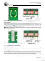
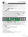
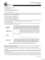
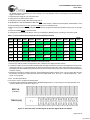
1
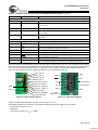
CYV15G0404DXB Evaluation Board Users Guide
Cypress Semiconductor Corporation
•
3901 North First Street
•
San Jose, CA 95134
•
408-943-2600
Revised October 4, 2004
[+] Feedback
CYV15G0404DXB Evaluation Board
Users Guide
TABLE OF CONTENTS
1.0 OVERVIEW ...................................................................................................................................... 5
2.0 KIT CONTENTS ............................................................................................................................... 5
3.0 FEATURES OF THE CYV15G0404DXB ......................................................................................... 5
4.0 FUNCTIONAL DESCRIPTION OF CYV15G0404DXB .................................................................... 6
4.0 CYV15G0404DXB TRANSCEIVER LOGIC BLOCK DIAGRAM ..................................................... 6
5.0 BOARD PHOTOGRAPH AND PIN DESCRIPTIONS .................................................................... 10
6.0 ADJUSTING SETTINGS ON THE BOARD ................................................................................... 17
6.1 Speed Select Jumpers .............................................................................................................. 17
6.2 DIP Switches ............................................................................................................................. 17
6.3 Asserting Values to Control Latches ......................................................................................... 17
6.4 Reference Clock Input Options ................................................................................................. 18
7.0 TEST MODES ................................................................................................................................ 19
7.1 BIST Test Set-up ...................................................................................................................... 19
7.1.1 Single Channel BIST Set-up ........................................................................................................... 19
7.1.1.1 Equipment Required .................................................................................................................................... 19
7.1.1.2 Test Equipment Set-up ................................................................................................................................ 20
7.1.1.3 Test Set-up .................................................................................................................................................... 20
7.1.1.4 External Loopback Mode ............................................................................................................................. 21
7.1.2 Four Channel BIST Set-up with Global Enable ............................................................................... 22
7.1.2.1 Equipment Required .................................................................................................................................... 22
7.1.2.2 Test Set-up .................................................................................................................................................... 22
7.2 Parallel Data Test Mode ........................................................................................................... 23
7.2.1 Equipment Required ....................................................................................................................... 23
7.2.2 Parallel Data Test Set-up ................................................................................................................ 24
7.2.2.1 Encoder Enable Mode .................................................................................................................................. 24
7.2.2.2 Encoder Bypass Mode ................................................................................................................................. 25
7.3 Reclocker Test Mode ................................................................................................................ 27
7.3.1 Equipment Required ....................................................................................................................... 27
7.3.2 Test Equipment Set-up ................................................................................................................... 28
7.3.3 Test Set-up ...................................................................................................................................... 28
APPENDIX A: Schematic Diagram of CYV15G0404DXB Evaluation Board .................................... 30
APPENDIX B: PCB Layout for CYV15G0404DXB Evaluation Board ................................................ 38
APPENDIX C: Bill Of Material (BOM) CYV15G0404DXB Evaluation Board .................................... 55
Page 2 of 56
[+] Feedback
CYV15G0404DXB Evaluation Board
Users Guide
LIST OF FIGURES
Figure 4-1. CYV15G0404DXB Block Diagram ........................................................................................ 6
Figure 4-2. Transmit Path Block Diagram................................................................................................ 7
Figure 4-3. Receive Path Block Diagram................................................................................................. 8
Figure 4-4. Device Configuration Control Block Diagram ........................................................................ 9
Figure 5-1. Photograph of Board with Numbering of Connectors .......................................................... 10
Figure 5-2. Channel A Connectors ........................................................................................................ 11
Figure 5-3. Optical Interface Signals ..................................................................................................... 13
Figure 5-4. JTAG Interface Signals ....................................................................................................... 13
Figure 6-1. Speed Select Control with Jumpers .................................................................................... 17
Figure 6-2. Controlling Dip Switch Settings ........................................................................................... 17
Figure 6-3. Write Enable and Reset Buttons ......................................................................................... 17
Figure 6-4. Top View of REFCLK Connectors....................................................................................... 18
Figure 7-1. BIST Mode Operation.......................................................................................................... 19
Figure 7-2. Pictorial Representation of the Internal BIST Set-up........................................................... 20
Figure 7-3. The Eye Diagram through the Signal Analyzer ................................................................... 21
Figure 7-4. SMA Connectors for External Loopback Mode ................................................................... 22
Figure 7-5. Loop Enable, Use Local Clock, and Input Select DIP Switches .......................................... 22
Figure 7-6. Optical Connector for External Loopback Mode.................................................................. 22
Figure 7-7. Loop Enable, Use Local Clock, and Input Select DIP Switches .......................................... 22
Figure 7-8. Generated Clock, Data and Control Signals for Encoded Mode from DG2020 .................. 24
Figure 7-9. Generated Clock and Data Signals for Encoder Bypass Mode from DG2020 .................... 25
Figure 7-10. Pictorial Representation of the Reclocker Test Equipment Set-up ................................... 28
Page 3 of 56
[+] Feedback
CYV15G0404DXB Evaluation Board
Users Guide
LIST OF TABLES
Table 5-1. Description of Connectors of the CYV15G0404DXB Evaluation Board .............................
Table 5-2. Description of External Control Pins for Connectors J31 to J41 .........................................
Table 5-3. Device Control Latch Description .......................................................................................
Table 5-4. Device Control Latch Configuration ....................................................................................
Table 6-1. Device Control Latch Configuration Example .....................................................................
Table 7-1. Device Control Latch Configuration for BIST on Channel A ...............................................
Table 7-2. Device Control Latch Configuration Table for Global Configuration ...................................
Table 7-3. Device Control Latch Configuration for Parallel Data Test Mode .......................................
Table 7-4. Input Register Bit Assignments ..........................................................................................
Table 7-5. Output Register Bit Assignments ........................................................................................
Table 7-6. Device Control Latch Configuration for Parallel Data Test Mode, Unencoded ...................
Table 7-7. Device Control Latch Configuration for Bist on Channel A .................................................
11
14
14
16
18
21
23
25
26
26
27
29
Page 4 of 56
[+] Feedback
CYV15G0404DXB Evaluation Board
Users Guide
1.0
Overview
The CYV15G0404DXB Quad Independent-Channel HOTLink II™ Transceiver is a point-to-point or point-to-multipoint communications building block that allows the transfer of data over high-speed serial links (optical fiber, balanced, and unbalanced copper
transmission lines) at signaling speeds ranging from 195–1500 MBaud per serial link. The independence of each channel
provides the ability to simultaneously transport different types of data at different signaling rates across multiple channels.
This user’s guide describes the operation and interface of the CYV15G0404DXB evaluation board. The evaluation board allows
users to become familiar with the functionality of the CYV15G0404DXB.
2.0
Kit Contents
• CYV15G0404DXB-EVAL (the evaluation board)
• Dear Customer letter
• A CD containing
— CYV15G0404DXB data sheet
— CYV15G0404DXB Evaluation Board User’s Guide
— CYV15G0404DXB application notes
— 0404EN.PDA and 0404BYP.PDA files for the DG2020 parallel data generator
— BSDL model
3.0
Features of the CYV15G0404DXB
• Quad channel transceiver for 195- to 1500-MBaud serial signaling rate
— Aggregate throughput of up to 12 Gbits/second
• Second-generation HOTLink® technology
• Compliant with multiple standards
— ESCON®, DVB-ASI, SMPTE 292M, SMPTE 259M, Fibre Channel and Gigabit Ethernet (GbE) (IEEE802.3z)
— 8B/10B coded data or 10 bit uncoded data
• Truly independent channels
— Each channel can perform reclocker function
— Each channel can operate at a different signaling rate
— Each channel can transport a different type of data
• Selectable input/output clocking options
• Internal phase-locked loops (PLLs) with no external PLL components
• Selectable differential PECL-compatible serial inputs per channel
— Internal DC-restoration
• Redundant differential PECL-compatible serial outputs per channel
— Source matched for 50Ω transmission lines
— No external bias resistors required
— Signaling-rate controlled edge-rates
• MultiFrame™ Receive Framer provides alignment options
— Bit and byte alignment
— Comma or Full K28.5 detect
— Single or Multi-byte Framer for byte alignment
— Low-latency option
• Synchronous LVTTL parallel interface
• JTAG boundary scan
• Built-In Self-Test (BIST) for at-speed link testing
Page 5 of 56
[+] Feedback
CYV15G0404DXB Evaluation Board
Users Guide
• Compatible with
— Fiber-optic modules
— Copper cables
— Circuit board traces
• Per-channel Link Quality Indicator
— Analog signal detect
— Digital signal detect
• Low-power 3W @ 3.3V typical
• Single 3.3V supply
• 256-ball thermally enhanced BGA
• 0.25µ BiCMOS technology
4.0
Functional Description of CYV15G0404DXB
Figure 4-1 shows the block diagram of CYV15G0404DXB, which has four pairs of transmit and receive channels (A,B,C,D). Each
of the four modules represents a transceiver channel. The left side of the transceiver represents the transmitter, which is
composed of a phase-align buffer, 8B/10B encoder and serializer. The right side of the transceiver is the receiver, which is
composed of a deserializer, framer, 8B/10B decoder and elasticity buffer.
TXDD[7:0]
TXCTD[1:0]
x11
x10
x11
x10
x11
x10
x11
Phase
Align
Buffer
Elasticity
Buffer
Phase
Align
Buffer
Elasticity
Buffer
Phase
Align
Buffer
Elasticity
Buffer
Phase
Align
Buffer
Elasticity
Buffer
Encoder
8B/10B
Decoder
8B/10B
Encoder
8B/10B
Decoder
8B/10B
Encoder
8B/10B
Decoder
8B/10B
Encoder
8B/10B
Decoder
8B/10B
TX
RX
TX
RX
TX
RX
INB1±
INB2±
OUTC1±
OUTC2±
INC1±
INC2±
Serializer
TX
Deserializer
RX
IND1±
IND2±
Deserializer
OUTB1±
OUTB2±
Deserializer
Serializer
INA1±
INA2±
Serializer
Deserializer
OUTA1±
OUTA2±
Serializer
Framer
Framer
OUTD1±
OUTD2±
Framer
Framer
RXDD[7:0]
RXSTD[2:0]
RXDC[7:0]
RXSTC[2:0]
REFCLKD±
TXDC[7:0]
TXCTC[1:0]
REFCLKC±
RXDB[7:0]
RXSTB[2:0]
REFCLKB±
TXDB[7:0]
TXCTB[1:0]
x10
TXDA[7:0]
TXCTA[1:0]
RXDA[7:0]
RXSTA[2:0]
REFCLKA±
CYV15G0404DXB Transceiver Logic Block Diagram
Figure 4-1. CYV15G0404DXB Block Diagram
Page 6 of 56
[+] Feedback
CYV15G0404DXB Evaluation Board
Users Guide
Figure 4-2 shows the transmitter section of CYV15G0404DXB in more detail. The building blocks of the channel include the
phase-align buffer, the 8B/10B encoder and the serializer (shifter). When the reclocker function is enabled, the recovered serial
data is reclocked and retransmitted through the serial outputs.
Transmit Path Block Diagram
REFCLKA+
REFCLKA-
RCLK[A..D] are Internal Reclocker Character Clock Signals
RED[A..D] are Internal Reclocker Serial Data Signals
TXLB[A..D] are Internal Serial Loopback Signals
0
OE[2..1]A
Transmit PLL
Clock Multiplier A
1
RCLKA
RCLKENA
SPDSELA
TXRATEA
= Internal Signal
Bit-Rate Clock
Character-Rate Clock A
TXCLKOA
TXERRA
TXCLKA
REDA
PABRSTA
10
10
10
10
Shifter
Phase-Align
Phase-Align
Buffer
Buffer
2
TXCTA[1:0]
Input
Register
TXDA[7:0]
Register
1
8
BIST
BIST LFSR
LFSR
0
OE[2..1]A
TXBISTA
RCLKENA
Encoder
8B/10B
Encoder
TXCKSELA
ENCBYPA
OUTA1+
OUTA1-
1
OUTA2+
OUTA2-
0
TXLBA
REFCLKB+
REFCLKB-
0
OE[2..1]B
Transmit PLL
Clock Multiplier B
1
RCLKB
RCLKENB
SPDSELB
TXRATEB
Bit-Rate Clock
Character-Rate Clock B
TXCLKOB
TXERRB
TXCLKB
REDB
PABRSTB
10
10
10
10
Shifter
2
TXCTB[1:0]
Phase-Align
Phase-Align
Buffer
Buffer
Input
Register
TXDB[7:0]
Register
1
8
BIST
BIST LFSR
LFSR
0
OE[2..1]B
TXBISTB
RCLKENB
Encoder
8B/10B
Encoder
TXCKSELB
ENCBYPB
OUTB1+
OUTB1-
1
OUTB2+
OUTB2-
0
TXLBB
REFCLKC+
REFCLKC-
0
OE[2..1]C
Transmit PLL
Clock Multiplier C
1
RCLKB
RCLKENC
SPDSELC
TXRATEC
Bit-Rate Clock
Character-Rate Clock C
TXCLKOC
TXERRC
TXCLKC
REDC
PABRSTC
RCLKENC
10
10
Register
10
Shifter
10
BIST
BIST LFSR
LFSR
Input
Register
2
TXCTC[1:0]
Phase-Align
Phase-Align
Buffer
Buffer
8
TXDC[7:0]
OE[2..1]C
TXBISTC
1
Encoder
8B/10B
Encoder
TXCKSELC
0
ENCBYPC
OUTC1+
OUTC1-
1
OUTC2+
OUTC2-
0
TXLBC
REFCLKD+
REFCLKD-
0
OE[2..1]D
Transmit PLL
Clock Multiplier D
1
RCLKD
RCLKEND
SPDSELD
Character-Rate Clock D
TXCLKOD
TXERRD
TXCLKD
REDD
PABRSTD
RCLKEND
10
10
Register
10
Shifter
10
BIST
BIST LFSR
LFSR
Input
Register
2
OE[2..1]D
TXBISTD
1
8
TXDD[7:0]
ENCBYPD
Encoder
8B/10B
Encoder
0
Phase-Align
Phase-Align
Buffer
Buffer
TXCKSELD
TXCTD[1:0]
TXRATED
Bit-Rate Clock
OUTD1+
OUTD1-
1
OUTD2+
OUTD2-
0
TXLBD
Figure 4-2. Transmit Path Block Diagram
Page 7 of 56
[+] Feedback
CYV15G0404DXB Evaluation Board
Users Guide
Figure 4-3 shows the receive section of the CYV15G0404DXB. The serial data input passes through the clock and data recovery
PLL, the deserializer, the framer, the 10B/8B decoder, and the elasticity buffer. When the reclocker function is enabled, the serial
data (REDx) and recovered character clock (RCLKx) are passed to the transmitter, where the data is retransmitted.
Receive Path Block Diagram
RCLK[A..D] are Internal Reclocker Character Clock Signals
RED[A..D] are Internal Reclocker Serial Data Signals
TXLB[A..D] are Internal Serial Loopback Signals
= Internal Signal
RESET
TRST
JTAG
Boundary
Scan
Controller
SPDSELA
RXPLLPDA
RCLKENA
SPDSELB
Elasticity
Buffer
Output
Register
TXLBA
ULCA
Clock &
Data
Recovery
PLL
LFIA
10B/8B
BIST
INA2+
INA2–
TDI
TDO
Framer
INA1+
INA1–
TCLK
REDA
Shifter
Receive
Signal
Monitor
LPENA
INSELA
TMS
8
3
RXDA[7:0]
RXSTA[2:0]
RECLKA
Clock
Select
RXPLLPDB
RCLKENB
ULCB
Elasticity
Buffer
Output
Register
TXLBB
Clock &
Data
Recovery
PLL
10B/8B
BIST
INB2+
INB2–
LFIB
Framer
INSELB
INB1+
INB1–
RXCLKA+
RXCLKA–
REDB
Shifter
Receive
Signal
Monitor
LPENB
÷2
8
3
RXDB[7:0]
RXSTB[2:0]
RECLKB
Clock
Select
RXPLLPDC
RCLKENC
INC2+
INC2–
TXLBC
ULCC
SPDSELD
Clock &
Data
Recovery
PLL
Elasticity
Buffer
INC1+
INC1–
LFIC
10B/8B
BIST
INSELC
RXCLKB+
RXCLKB–
REDC
Framer
Receive
Signal
Monitor
Shifter
LPENC
÷2
Output
Register
SPDSELC
8
3
RXDC[7:0]
RXSTC[2:0]
RECLKC
Clock
Select
RXPLLPDD
RCLKEND
ULCD
SDASEL[A..D][1:0]
RECLKD
LDTDEN
RFMODE[A..D][1:0]
RFEN[A..D]
FRAMCHAR[A..D]
DECMODE[A..D]
RXBIST[A..D]
RXCKSEL[A..D]
DECBYP[A..D]
RXRATE[A..D]
Clock
Select
Output
Register
TXLBD
Clock &
Data
Recovery
PLL
Elasticity
Buffer
IND2+
IND2–
LFID
10B/8B
BIST
IND1+
IND1–
RXCLKC+
RXCLKC–
REDD
Framer
Receive
Signal
Monitor
INSELD
Shifter
LPEND
÷2
÷2
8
3
RXDD[7:0]
RXSTD[2:0]
RXCLKD+
RXCLKD–
Figure 4-3. Receive Path Block Diagram
Page 8 of 56
[+] Feedback
CYV15G0404DXB Evaluation Board
Users Guide
Figure 4-4 shows the device configuration and control block diagram. The inputs are the external signals WREN, ADDR[3:0], and
DATA[7:0] and will be described in subsequent sections. The outputs are the internal signals that are described in Table 5-4.
Device Configuration and Control Block Diagram
WREN
ADDR[3:0]
DATA[7:0]
Device Configuration and Control
Interface
= Internal Signal
RFMODE[A..D][1:0]
RFEN[A..D]
FRAMCHAR[A..D]
DECMODE[A..D]
RXBIST[A..D]
RXCKSEL[A..D]
DECBYP[A..D]
RXRATE[A..D]
SDASEL[A..D][1:0]
RXPLLPD[A..D]
TXRATE[A..D]
TXCKSEL[A..D]
PABRST[A..D]
TXBIST[A..D]
OE[A..D][2..1]
ENCBYP[A..D]
GLEN[11..0]
FGLEN[2..0]
Figure 4-4. Device Configuration Control Block Diagram
Page 9 of 56
[+] Feedback
CYV15G0404DXB Evaluation Board
Users Guide
5.0
Board Photograph and Pin Descriptions
Figure 5-1 shows the different connectors and pins of the CYV15G0404DXB evaluation board. Table 5-1 provides a description
of each connector.
Figure 5-1. Photograph of Board with Numbering of Connectors
3.3V (J48)
OPTICAL (XT1x)
OPT (J25)
(DT6)
3.3V LED
(see Fig. 5)
Channel B I/O
(see Fig. 5)
Channel A I/O
LFIx(D1x, J19x)
VCC LED (D6)
GND(J49)
VCC(J50)
B
OUTB
(J18)LVTTL
(J11,12)SMA
REFCLKA
INB
(Y1B)
OSC
TXERR(J9B)
A
OUTA
OSC(Y1C)
INA
(J18)LVTTL
(J11,12)SMA
REFCLKB
OSC(Y1C)
D
TXERR(J9D,A)
(J9C)
TXERR
IND
OUTD
(J18C)LVTTL
(J11,12)SMA
REFCLKC
Factory Test Settings (J18D)LVTTL
(J11,12)SMA
LDTDEN(J38)
REFCLKD
C
OUTC
(Y1D)
OSC
INC
SERIN/OUT(J13-16)x
LPEN(S2)
WREN/RESET DATA(S4) RCLKEN(S7)
Channel C I/O (see Fig. 5)
(S6)
(S5)
Channel
D
I/O
(see Fig. 5)
JTAG(J44)
ULC(S3)
ADDR(S1)
SPDSELx(see Fig. 9)
INSEL(S3)
Page 10 of 56
[+] Feedback
CYV15G0404DXB Evaluation Board
Users Guide
Figure 5-2 shows the parallel I/O and reference clock connectors for channel A. Channels B, C, and D have a similar layout of
connectors. Note that TXERR is not located at the same position for the other channels. Refer to Figure 5-1 for their locations.
J17A(RXCLKA+
SMA)
J8A(RXCLKA+)
Y1A(OSC)
J7A(RXCLKA-)
J6A(RXSTA)
J11A(REFCLKA+
SMA)
J5A(RXDA)
J18A(REFCLKA)
J4A(TXCLKOA)
J3A(TXCLKA)
J12A(REFCLKASMA)
J10A(TXCKLOA
SMA)
J2A(TXCTA)
J1A(TXDA)
J9A(TXERRA)
Figure 5-2. Channel A Connectors
Table 5-1 gives a brief description of the connectors on the evaluation board. An “x” following a connector or signal name
represents all four channels; e.g., Connector J1x for TXDx represents the connectors J1A, J1B, J1C, and J1D for the buses
TXDA[7:0], TXDB[7:0], TXDC[7:0], and TXDD[7:0], respectively. For a more detailed description of the connectors and signals,
refer to the data sheet.
Table 5-1. Description of Connectors of the CYV15G0404DXB Evaluation Board
Connectors
Signals
Description
J1x
TXDx[7:0]
LVTTL Input
J2x
TXCTx[1:0]
LVTTL Input
J3x
TXCLKx
LVTTL Input
J4x
TXCLKOx
LVTTL Output
J5x
RXDx[7:0]
LVTTL Output
J6x
RXSTx[2:0]
LVTTL Output
J7x
RXCLKx-
LVTTL Output
J8x
RXCLKx+
LVTTL Output
J9x
TXERRx
LVTTL Output
J10x
TXCLKOx
SMA Connector for TXCLKOx
J11x
REFCLKx+
SMA Connector for REFCLKx +
• Transmit parallel data input for channel x
• Transmit control signals for channel x
• Transmit clock input for channel x
• Buffered version of internal character rate clock
• Receive parallel data output for channel x
• Receive parallel data status output for channel x
• Complement of recovered clock at the receiver for channel x
• Recovered clock at the receiver for channel x
• Transmit path error signal for channel x
• Buffered version of internal character rate clock
• Positive input of reference clock for channel x
Page 11 of 56
[+] Feedback
CYV15G0404DXB Evaluation Board
Users Guide
Table 5-1. Description of Connectors of the CYV15G0404DXB Evaluation Board (continued)
Connectors
Signals
Description
J12x
REFCLKx-
SMA Connector for REFCLKx -
J13x, J14x
SERINx1+, SERINx1-
SMA Connectors for serial data input of channel x
• Negative input of reference clock for channel x
• PECL compatible primary differential serial data inputs
• Routed through 50-Ohm impedance
• AC coupling capacitors present
• 100-Ohm differential load present
J15x, J16x
SEROUTx1-,
SEROUTx1+
SMA Connectors for serial data output of channel x
• PECL-compatible primary differential serial data CML outputs
• Routed through 50-Ohm impedance
• AC coupling capacitors present
• Expects to see a 50-Ohm single ended or 100-Ohm differential termination in
the receive ends
J17x
RXCLKx+
SMA Connector for RXCLKx
• Recovered clock at the receiver for channel x
J18x
REFCLKx+
Headers to probe the reference clock for channel x
J19x
LFIx
Header to probe the Link Fault Indicator status for channel x
J25
OPT
LVTTL Output
• Headers to probe the signals for the optical modules
• Control Signals: OPT_RATE_SEL, OPT_TX_DISABLE
• Output Signals: OPT_TX_FAULT_x, OPT_LOS_x (x = A,B,C,D)
J26
ADDR[3:0]
Headers to control the configuration addressing bus or to probe the ADDR[3:0]
dip switches
J27
LPENx
Header to control Loop Enable signal or probe the LPEN dip switch for channel x
J28
INSELx
Header to control the Receive Input Selector or probe the INSEL dip switch for
channel x
J29
ULCx
Header to control the Use Local Clock signal or probe the ULC dip switch for
channel x
J30
DATA[7:0]
Headers to control the configuration data bus or probe the DATA[7:0] dip switches
J1
RCLKENx
Header to control the Reclocker Enable signal or probe the RCLKEN dip switch
for channel x
XT1x
Optical Modules
Option for Small Form-Factor Pluggable (SFP) optical modules.
The optical modules make use of the secondary input (INx2+) and secondary
output (OUTx2+) in each transceiver channel.
D1x
LFIx,
asynchronous
• Link Fault Indication output LEDs
• Signal active LOW. LED is lit when signal is active.
• Logical OR of six internal conditions:
— Received serial data frequency outside expected range
— Analog amplitude below expected levels
— Transition density lower than expected
— Receive channel disabled
— ULCx is LOW
— Absence of REFCLKx±
Y1x
REFCLK±
14-pin DIP socket for an external Crystal Oscillator to provide an independent
reference clock for channel x.
Page 12 of 56
[+] Feedback
CYV15G0404DXB Evaluation Board
Users Guide
Table 5-1. Description of Connectors of the CYV15G0404DXB Evaluation Board (continued)
Connectors
Signals
Description
Power
D6
Power Indicator
Indicates if the power supply is ON. The LED glows when the power supply is ON.
J48
3.3V
Banana Jack Connector for power supply to the board
DT6
Power Indicator
Indicates if the power supply is ON. The LED glows when the power supply is ON.
J50
VCC
Banana Jack Connector for power supply to the chip
• +3.3 V DC
• +3.3 V DC
J49
GND
Banana Jack
• Ground
Switches
S1
ADDR[3:0]
Configuration Addressing Bus Dip Switches
S2
LPENx
Loop Enable Dip Switch for channel x
S3
ULCx
INSELx
Use Local Clock Dip Switch for channel x
Receive Input Selector Dip Switch for channel x
S4
DATA[7:0]
Configuration Data Bus Dip Switches
S5
WREN
Control Write Enable Push-Button Switch (Active LOW)
S6
RESET
Asynchronous Device Reset (Active LOW)
S7
RCLKENx
Reclocker Enable for channel x
JTAG
JTAG Interface
Standard JTAG Interface. CYV15G0404DXB does not have a dedicated JTAG
reset. It has a built-in power-on-reset circuit for resetting the JTAG logic.
Figure 5-3 shows the optical interface connector J25, along with the signal name for each pin. For a description of each signal,
refer to the Small-form Factor Pluggable (SFP) Transceiver Multi-source agreement (MSA). Figure 5-4 shows the JTAG interface
connector and the signal names for each pin. For a description of each signal, consult the CYV15G0404DXB data sheet.
Figure 5-4 also shows the control pin header JTAG RESET (J41). It is described in Table 5-2.
OPT_LOS_D
OPT_LOS_C
OPT_LOS_B
OPT_LOS_A
OPT_TX_FAULT_D
OPT_TX_FAULT_C
GND
OPT_TX_FAULT_B
VCC
OPT_TX_FAULT_A
No Connection
OPT_TX_DISABLE
OPT_RATE_SEL
Figure 5-3. Optical Interface Signals
GND
TDO
TRST
VCC
TDI
No Connection
TCK
No Connection
TMS
GND
JTAG
RESET(J41)
Figure 5-4. JTAG Interface Signals
Table 5-2 provides a brief description of all the control pins from J31 to J41.
The SPDSELX signals are 3-level inputs. This means that they operate at three voltage levels, termed as:
• HIGH (Direct connection to VCC)
• MID (Open)
• LOW (Direct connection to VSS, i.e., GND).
Page 13 of 56
[+] Feedback
CYV15G0404DXB Evaluation Board
Users Guide
Table 5-2. Description of External Control Pins for Connectors J31 to J41
Pin Name
Characteristics
SPDSELA (J34)
SPDSELB (J33)
SPDSELC (J32)
SPDSELD (J31)
Serial Rate Select
3-Level Select
LDTDEN (J38)
Level Detect Transition Density Enable
• LOW = 195–400 MBd
• MID = 400–800 MBd
• HIGH = 800–1500 MBd
• When HIGH, the Signal Level Detector, Range Controller, and Transition Density Detector are all
enabled
• When LOW, only the Range Controller is enabled
LTEN1 (J37)
Factory Test 1
SCANEN2(J36)
Factory Test 2
TMEN3(J35)
Factory Test 3
WREN(J39)
Control Write Enable Header
• This input should be HIGH
• This input should be left open or LOW
• This input should be left open or LOW
• When the jumper is connected across the middle and right pins (see Figure 6-3 on page 17), the
push-button signal controls the WREN input to the chip
• When the jumper is connected across the middle and left pins, WREN is permanently ACTIVE (LOW)
RESET(J40)
Asynchronous Global Reset Header
• When HIGH, the push-button signal controls the RESET input to the chip
• When LOW, RESET is permanently ACTIVE (LOW)
JTAG RESET(J41)
Asynchronous JTAG Reset Header
• When closed, the global RESET signal will reset the JTAG interface
• When open, the global RESET signal has no effect on the JTAG interface
Table 5-3 provides a brief description of the control latches for the configuration interface. For a detailed description, please refer
to the datasheet. When a signal has multiple bits (e.g., RFMODEx[1:0] = 10), the right-most bit is the LSB (bit 0).
Table 5-3. Device Control Latch Description
Pin Name
RFMODEx[1:0]
Characteristics
Reframe Mode Select
• When RFMODEx[1:0] = 00, low-latency framer is selected
• When RFMODEx[1:0] = 01, alternate mode Multi-byte framer is selected
• When RFMODEx[1:0] = 10, Cypress-mode Multi-byte framer is selected
• RFMODEx[1:0] = 11 is reserved for test
FRAMCHARx
Framing Character Select
• When 1, framer looks for either disparity of the K28.5 character
• When 0, framer looks for either disparity of the 8-bit Comma characters
DECMODEx
Receiver Decoder Mode Select
• When 1, the Cypress Decoding Mode is used
• When 0, the Alternate Decoding Mode is used
DECBYPx
Receiver Decoder Bypass
• When 1, the decoder is enabled
• When 0, the decoder is bypassed and raw 10-bit characters are passed through
Page 14 of 56
[+] Feedback
CYV15G0404DXB Evaluation Board
Users Guide
Table 5-3. Device Control Latch Description (continued)
Pin Name
RXCKSELx
Characteristics
Receive Clock Select
• When 1, the associated Output Registers are clocked by REFCLKx
• When 0, the associated Output Registers are clocked by the recovered byte clock
RXRATEx
Receive Clock Rate Select.
• When 1, RXCLK output for channel x is half the character rate
• When 0, RXCLK output for channel x is the full character rate
When RXCKSELx = 1 and REFCLKx± is a half-rate clock, RXRATEx isn’t interpreted and the
RXCLKx± clock outputs follow the reference clock operating at half the character rate.
SDASEL1x[1:0]
Primary Serial Data Input Signal Detector Amplitude Select.
• When SDASEL1x[1:0] = 00, the Analog Signal Detector is disabled
• When SDASEL1x[1:0]= 01, the peak-peak differential voltage threshold level is 140 mv
• When SDASEL1x[1:0]= 10, the peak-peak differential voltage threshold level is 280 mv
• When SDASEL1x[1:0]= 11, the peak-peak differential voltage threshold level is 420 mv
SDASEL2x
Secondary Serial Data Input Signal Detector Amplitude Select.
• When SDASEL2x[1:0] = 00, the Analog Signal Detector is disabled
• When SDASEL2x[1:0]= 01, the peak-peak differential voltage threshold level is 140 mv
• When SDASEL2x[1:0]= 10, the peak-peak differential voltage threshold level is 280 mv
• When SDASEL2x[1:0]= 11, the peak-peak differential voltage threshold level is 420 mv
ENCBYPx
Transmit Encoder Bypass
• When 1, the encoder is enabled
• When 0, the encoder is bypassed and raw 10-bit characters are transmitted
TXCKSELx
Transmit Clock Select
• When 1, the associated Input Registers are clocked by REFCLKx
• When 0, the associated Input Registers are clocked by the TXCLKx input
TXRATEx
Transmit PLL Clock Rate Select
• When 1, the transmit PLL multiplies REFCLKx by 20 to generate the bit-rate clock
• When 0, the transmit PLL multiplies REFCLKx by 10 to generate the bit-rate clock
RFENx
Reframe Enable
• When 1, the framer is enabled
• When 0, the framer is disabled
RXPLLPDx
Receive Channel Enable
• When 1, the PLL and analog circuitry are enabled
• When 0, the PLL and analog circuitry are disabled
RXBISTx
Receive BIST Disable
• When 1, the receiver BIST function is disabled
• When 0, the receiver BIST function is enabled
TXBISTx
Transmit BIST Disable
• When 1, the transmitter BIST function is disabled
• When 0, the transmitter BIST function is enabled
OE2x
Secondary Differential Serial Data Output Driver Enable
• When 1, the output driver is enabled allowing data to be transmitted
• When 0, the output driver is disabled
Page 15 of 56
[+] Feedback
CYV15G0404DXB Evaluation Board
Users Guide
Table 5-3. Device Control Latch Description (continued)
Pin Name
Characteristics
OE1x
Primary Differential Serial Data Output Driver Enable
• When 1, the output driver is enabled allowing data to be transmitted
• When 0, the output driver is disabled
PABRSTx
Transmit Clock Phase Alignment Buffer Reset
• When a 0 is written, the phase of TXCLKx relative to REFCLKx is initialized
• This is a self clearing latch, eliminating the requirement of writing a 1 to complete the initialization
of the Phase Alignment Buffer
GLEN[11..0]
Global Enable
• When 1 for a given address, that address can participate in a global configuration
• When 0 for a given address, that address will not participate in a global configuration
FGLEN[2..0]
Force Global Enable
• When 1 for the associated global channel, FGLEN forces the global update of the target latch banks
Table 5-4 shows the mapping of latches in the device. Each row of the table is defined by an address, ADDR[3:0]. The Chnl
column lists the channel being configured for the particular address. The Type column lists whether the signals for the particular
address are static or dynamic. A detailed description of the latch types is in the datasheet. The data signals DATA[7:0] will
determine the value of the respective control latches upon assertion. The Reset Value of an address is the value in the latch
bank of that address after a global reset. For example, at address 0 (0000b), the reset value is 10111111. Thus, RFMODEA1 =
1, RFMODEA0 = 0, FRAMCHARA=1, DECMODEA = 1, DECBYPA = 1, RXCKSELA = 1, RXRATEA = 1, and GLEN0 = 1.
Table 5-4. Device Control Latch Configuration
ADDR
Chnl
Type
DATA7
DATA6
DATA5
DATA4
DATA3
DATA2
DATA1
DATA0
Reset
Value
0
(0000b)
A
S
RFMODE
A[1]
RFMODE
A[0]
FRAMCHAR
A
DECMODE
A
DECBYP
A
RXCKSEL
A
RXRATE
A
GLEN0
10111111
1
(0001b)
A
S
SDASEL2
A[1]
SDASEL2
A[0]
SDASEL1
A[1]
SDASEL1
A[0]
ENCBYP
A
TXCKSEL
A
TXRATE
A
GLEN1
10101101
2
(0010b)
A
D
RFEN
A
RXPLLPD
A
RXBIST
A
TXBIST
A
OE2
A
OE1
A
PABRST
A
GLEN2
10110011
3
(0011b)
B
S
RFMODE
B[1]
RFMODE
B[0]
FRAMCHAR
B
DECMODE
B
DECBYP
B
RXCKSEL
B
RXRATE
B
GLEN3
10111111
4
(0100b)
B
S
SDASEL2
B[1]
SDASEL2
B[0]
SDASEL1
B[1]
SDASEL1
B[0]
ENCBYP
B
TXCKSEL
B
TXRATE
B
GLEN4
10101101
5
(0101b)
B
D
RFEN
B
RXPLLPD
B
RXBIST
B
TXBIST
B
OE2
B
OE1
B
PABRST
B
GLEN5
10110011
6
(0110b)
C
S
RFMODE
C[1]
RFMODE
C[0]
FRAMCHAR
C
DECMODE
C
DECBYP
C
RXCKSEL
C
RXRATE
C
GLEN6
10111111
7
(0111b)
C
S
SDASEL2
C[1]
SDASEL2
C[0]
SDASEL1
C[1]
SDASEL1
C[0]
ENCBYP
C
TXCKSEL
C
TXRATE
C
GLEN7
10101101
8
(1000b)
C
D
RFEN
C
RXPLLPD
C
RXBIST
C
TXBIST
C
OE2
C
OE1
C
PABRST
C
GLEN8
10110011
9
(1001b)
D
S
RFMODE
D[1]
RFMODE
D[0]
FRAMCHAR
D
DECMODE
D
DECBYP
D
RXCKSEL
D
RXRATE
D
GLEN9
10111111
10
(1010b)
D
S
SDASEL2
D[1]
SDASEL2
D[0]
SDASEL1
D[1]
SDASEL1
D[0]
ENCBYP
D
TXCKSEL
D
TXRATE
D
GLEN10
10101101
11
(1011b)
D
D
RFEN
D
RXPLLPD
D
RXBIST
D
TXBIST
D
OE2
D
OE1
D
PABRST
D
GLEN11
10110011
12
(1100b)
GLBL
S
RFMODE
GL[1]
RFMODE
GL[0]
FRAMCHAR
GL
DECMODE
GL
DECBYP
GL
RXCKSEL
GL
RXRATE
GL
FGLEN0
N/A
13
(1101b)
GLBL
S
SDASEL2
GL[1]
SDASEL2
GL[0]
SDASEL1
GL[1]
SDASEL1
GL[0]
ENCBYP
GL
TXCKSEL
GL
TXRATE
GL
FGLEN1
N/A
14
(1110b)
GLBL
D
RFEN
GL
RXPLLPD
GL
RXBIST
GL
TXBIST
GL
OE2
GL
OE1
GL
PABRST
GL
FGLEN2
N/A
15
(1111b)
All
Mask
D
D7
D6
D5
D4
D3
D2
D1
D0
11111111
Page 16 of 56
[+] Feedback
CYV15G0404DXB Evaluation Board
Users Guide
6.0
Adjusting Settings on the Board
To successfully operate the device, the SPDSELx settings and configuration interface must be correctly configured. This section
provides directions on how to configure the device.
6.1
Speed Select Jumpers
To set the appropriate operating range for each channel’s transmit and receive PLL, jumpers need to be placed on the correct
SPDSELx headers for each channel. Shown in Figure 6-1 is a picture of the headers and the set-up of the jumpers. SPDSELD
is set to low by connecting a jumper across the right and center pins. The white dot that is beside each pin of the right column
represents the LOW level. SPDSELC is set to HIGH by connecting a jumper across the left and center pins. SPDSELB and
SPDSELA are set to MID by having no jumpers connected.
Dot = LOW
Set to LOW
Set to MID
Set to HIGH
Figure 6-1. Speed Select Control with Jumpers
6.2
DIP Switches
The 2-level dip switches (DATA[7:0](S4), ADDR[3:0] (S1), RCLKEN[D..A] (S7), INSEL[D..A] (S3), ULC[D..A] (S3), and LPEN[D:A]
(S2)) are set HIGH or LOW as illustrated in Figure 6-2. Once again, the side of the switch with a dot represents the LOW level side.
Push this side
to set HIGH
Push this side
to set LOW
Dot = LOW
Use this number
scheme
Figure 6-2. Controlling Dip Switch Settings
Jumpers connected
to enable WREN,
RESET buttons
Press to Reset
the Device
Press to latch in
data values
Figure 6-3. Write Enable and Reset Buttons
Note. Disregard the numbering scheme that is inscribed directly on the DIP switches. Follow the numbering inscribed on the
board, directly below each switch. See Figure 6-2.
6.3
Asserting Values to Control Latches
1. Using the ADDR (S1) DIP switches shown in Figure 6-2, select the target address. For example, if the target address
ADDR[3:0] = 1010, press ADDR0 to the LOW side (see Figure 6-2), ADDR1 to the HIGH side, ADDR2 to the LOW side and
ADDR3 to the HIGH side.
2. Using the DATA (S4) DIP switches shown in Figure 6-2, select the values of the latches for the appropriate address bank.
Table 6-1 provides an example of a control latch configuration for address 10 (ADDR[3:0] = 1010), where DATA[7:0]
=10111010. The colored background represents a logic-1 value and the white background represents a logic-0 value.
3. Once the data signals are set up, they can be latched into the respective control latches by pressing the WREN (S5) push
button (see Figure 6-3).
Page 17 of 56
[+] Feedback
CYV15G0404DXB Evaluation Board
Users Guide
Table 6-1. Device Control Latch Configuration Example
ADDR
10
(1010b)
6.4
Chnl Type
D
S
DATA7
DATA6
DATA5
DATA4
DATA3
DATA2
DATA1
DATA0
Reset Value
SDASEL2
D[1] = ‘1’
SDASEL2
D[0] = ‘0’
SDASEL1
D[1] = ‘1’
SDASEL1
D[0] = ‘1’
ENCBYP
D = ‘1’
TXCKSEL
D = ‘0’
TXRATE
D = ‘1’
GLEN10
= ‘0’
10101101
Reference Clock Input Options
The reference clock signal, REFCLKx, can have three different types of input: Single-ended SMA, Differential SMA, and the
Crystal Oscillator. Figure 6-4 shows the SMA connectors, Crystal Oscillator, and headers to probe REFCLKx.
Crystal Oscillator
The crystal oscillator is the default source for the REFCLKx signal. It provides a single-ended input. Each channel has an oscillator
with a different frequency. The default frequencies for each channel are: channel A runs at 125.0 MHz, channel B at 106.25 MHz,
channel C at 27.0 MHz, and channel D at 20.0 MHz. When attaching the oscillator, line up the sharp corner of the oscillator with
the sharp corner of the white outline on the silkscreen (see Figure 6-4).
Single-ended SMA
To use the single-ended SMA option, connect an appropriate cable to either the REFCLKx+ or REFCLKx- SMA connector (see
Figure 6-4). The crystal oscillator for that channel must also be disconnected from the 14-pin DIP socket.
Differential SMA
To use the differential SMA option, connect appropriate cables to both the REFCLKx+ and REFCLKx- SMA connectors (see
Figure 6-4). The crystal oscillator for that channel must also be disconnected from the 14-pin DIP socket.
Crystal Oscillator
SMA Connector for
REFCLKx+ input
Ground
Probe of REFCLKx+
Probe of REFCLKxSMA Connector for
REFCLKx- input
Corner of oscillator
Corner of silk screen
outline
Figure 6-4. Top View of REFCLK Connectors
Page 18 of 56
[+] Feedback
CYV15G0404DXB Evaluation Board
Users Guide
7.0
Test Modes
The different test modes discussed in this document are BIST, parallel data, and reclocker test modes, including independent
clocking on multiple channels.
BIST Mode
CYV15G0404DXB has the Built-In Self-Test (BIST) capability. Each transmit and receive channel contains an independent BIST
Pattern Generator and Checker. This BIST hardware allows at-speed testing of the high-speed serial data paths in each transmit
and receive section, and across the interconnecting links.
Figure 7-1 shows the two BIST modes of operation: External loopback BIST mode and Internal loopback BIST mode.
OUTx±
TX
TX BIST LFSR
RX
RX BIST LFSR
INx±
Int. BIST
Parallel Inputs Ignored
Ext. BIST
Figure 7-1. BIST Mode Operation
To switch between BIST modes, use the LPENx DIP switch. LPENx = HIGH for Internal and LPENx = LOW for External BIST
mode for channel x. For external BIST mode, connect two SMA-to-SMA cables from SEROUTx1+ to SERINx1+ and from
SEROUTx1- to SERINx1-. For internal BIST mode, no cables are required. An example of external BIST mode is described in
Section 7.1.1.4 on page 21.
Two examples of BIST will be described in the sections.
• Single Channel BIST
• Four Channel BIST
Parallel Data Test Mode
The variations discussed in this document for this mode are
• Parallel-in — parallel-out mode (Encoder Enabled) at two different frequencies
• Parallel-in — parallel-out mode (Encoder Bypassed)
• Parallel-in — serial-out mode (testing the transmit side).
The detailed description of each test will comprise
• Equipment required (equipment, cable etc.)
• Test set-up
• Result verification
• Operational variations
7.1
BIST Test Set-up
7.1.1
Single Channel BIST Set-up
7.1.1.1 Equipment Required
Equipment needed:
• CYV15G0404DXB evaluation board
• Instrument grade power supply 3-amp current limit @ 3.3V
• Oscilloscope (500 MHz or better).
Optional Equipment:
• Digital signal analyzer (to observe eye diagrams)
• Pulse generator (20–150 MHz)
Page 19 of 56
[+] Feedback
CYV15G0404DXB Evaluation Board
Users Guide
Cables needed:
• SMA to SMA coaxial cables
• Power supply cables (banana plug cables).
7.1.1.2 Test Equipment Set-up
Figure 7-2 shows the test set-up for BIST on channel A. The signal analyzer in the diagram is optional. See Section 6.4 on page
18 for REFCLKx input options. The BIST tests will use the Crystal Oscillator option. To use the optional pulse generator instead
of the supplied oscillators, connect an SMA-to-SMA cable using the single-ended SMA option (see Section 6.4 on page 18). If
using the pulse generator, make sure the SPDSELx control is set correctly (see Section 6.1 on page 17).
Signal Analyzer
Ext Trigger
Input
3.3V 3.0A
Power Supply
Pulse Generator
Output
TXCLKOA
SEROUTA1
3.3V GND 3.3V
REFCLKA
OSC
CYV15G0404DX
Evaluation Board
Oscilloscope
Input
3.3V
RXSTA[2:1]
GND
Vcc
Figure 7-2. Pictorial Representation of the Internal BIST Set-up
7.1.1.3 Test Set-up
The intention of this set-up is to test the CYV15G0404DXB in BIST mode. For this test, the device will transmit BIST data across
Channel A and receive the same BIST data across the same channel by looping back the serial data within the device (referred
to as Internal Loopback mode). Follow the procedure below for the test set-up.
1. Ensure that there are no SMA cables connected to the REFCLKA± inputs. Make sure the 125 MHz oscillator is connected to
the14-pin DIP socket for Channel A. This test is using the Crystal Oscillator clock option (see Section 6.4 on page 18).
2. Adjust the power supply to 3.3V and 3A limit. Apply power to the board and chip by connecting 3.3V banana plugs to J48 and
J50. Connect a banana plug from ground on the power supply to J49.
3. Verify that the power supply LEDs (D6 and DT6) are on.
4. Set SPDSELA to HIGH (see Figure 6-1 on page 17).
5. Set LPENA(S2) to HIGH, ULCA(S3) to HIGH, and RCLKENA(S7) to LOW. The value of INSELx does not matter during internal
loopback mode.
6. Make sure the jumpers for WREN (J39) and RESET(J40) are configured to enable the push buttons (see Figure 6-3 on page
17).
7. Press and release RESET to reset the board.
8. Verify that all LFIx LEDs are ON, indicating line faults on all channels.
9. Configure the control signals for channel A according to the configuration table below (refer to Section 6.3 on page 17).
Page 20 of 56
[+] Feedback
CYV15G0404DXB Evaluation Board
Users Guide
Table 7-1. Device Control Latch Configuration for BIST on Channel A
ADDR
Chnl
Type
DATA7
DATA6
DATA5
DATA4
DATA3
DATA2
DATA1
DATA0
Reset Value
0
(0000b)
A
S
RFMODE
A[1] = ‘1’
RFMODE
A[0] =’0
FRAMCHAR
A = ‘1’
DECMODE
A = ‘1’
DECBYP
A = ‘1’
RXCKSEL
A = ‘1’
RXRATE
A = ‘1’
GLEN0
= ‘1’
10111111
1
(0001b)
A
S
SDASEL2
A[1] = ‘1’
SDASEL2
A[0] = ‘0’
SDASEL1
A[1] = ‘1’
SDASEL1
A[0] = ‘0’
ENCBYP
A = ‘1’
TXCKSEL
A = ‘1’
TXRATE
A =’0’
GLEN1
= ‘1’
10101101
2
(0010b)
A
D
RFEN
A = ‘1’
RXPLLPD
A = ‘1’
RXBIST
A = ‘0’
TXBIST
A = ‘0’
OE2
A = ‘1’
OE1
A = ‘1’
PABRST
A = ‘0’
GLEN2
= ‘1’
10110011
Steps 10 through 12 are for result verification of the BIST on channel A:
10.Verify that the LFIA LED turns off.
11.Connect a probe from the oscilloscope to RXSTA1 and verify that RXSTA1 signal has pulses of approximately 8.0-ns (1/125.0
MHz) width and 4.2-µs (8.0 ns/character * 527 characters/BIST sequence) period.
12.Verify that RXSTA2 remains low to indicate that there are no BIST errors.
Optional: Check the BIST serial out data as an eye diagram by following the procedure below.
13.Change LPENA (S2) to LOW. Notice that the LFIA LED will turn ON.
14.Connect a pair of serial outputs (SEROUTA1+/SEROUTA1-) to the digital signal analyzer using SMA cables.
15.Trigger the analyzer by connecting an SMA-to-SMA cable from TXCLKOA (J10) to the trigger input of the analyzer.
16.Verify on the analyzer that the eye diagram looks as shown in Figure 7-3. Make sure that the eye-width is 1-bit period.
Figure 7-3. The Eye Diagram through the Signal Analyzer
Note: This test can be repeated for other channels by changing the configuration of the associated bits for each channel.
7.1.1.4 External Loopback Mode
Electrical Transmission
For external loopback, connect SMA-to-SMA cables from SEROUTA1+ (J16A) to SERINA1+ (J13A) and from SEROUTA1(J15A) to SERINA1- (J14A). See Figure 7-4. Also, the control signals for Loop Enable, Use Local Clock and Input Select need
to be configured (see Figure 7-5). Set LPENA = LOW for external loopback mode, set ULCA = HIGH for clock and data recovery,
and set RCLKENA = LOW to disable the reclocker function. Lastly, set INSELA = HIGH to select the SERINA1 SMA connectors.
To run an external loopback BIST test, repeat the procedure in Section 7.1.1.3 on page 20, but replace the values for LPENA,
ULCA, RCLKENA, and INSELA in Step 5 with the values listed in this section.
Page 21 of 56
[+] Feedback
CYV15G0404DXB Evaluation Board
Users Guide
Set ULCA = HIGH
(Clock & Data
Recovery)
Set LPENA = LOW
Set INSELA = HIGH
(Ext. Loopback)
(SMA Connectors)
Set RCLKENA = LOW
(Reclocker Disabled)
Figure 7-4. SMA Connectors for External Loopback Mode
Figure 7-5. Loop Enable, Use Local Clock, and Input
Select DIP Switches
Optical Transmission
For external loopback with an optical signal, connect an optical module into the optical connector (XT1A). See Figure 7-6. Also,
the control signals for Loop Enable, Use Local Clock and Input Select need to be configured (see Figure 7-7). Set LPENA = LOW
for external loopback mode, set ULCA = HIGH for clock and data recovery, and set RCLKENA = LOW to disable the reclocker
function. Lastly, set INSELA = LOW to select the optical connector.
To run an external loopback BIST test, repeat the procedure in Section 7.1.1.3 on page 20, but replace the values for LPENA,
ULCA, RCLKENA, and INSELA in Step 5 with the values listed in this section. The locations of the optical control and error signals
are shown in Figure 5-3 on page 13.
Set ULCA = HIGH
(Clock & Data
Recovery)
Set LPENA = LOW
Set INSELA = LOW
(Ext. Loopback)
(Optical Connectors)
Set RCLKENA = LOW
(Reclocker Disabled)
Figure 7-6. Optical Connector for External Loopback Mode
7.1.2
Figure 7-7. Loop Enable, Use Local Clock, and Input
Select DIP Switches
Four Channel BIST Set-up with Global Enable
7.1.2.1 Equipment Required
Equipment needed is the same as mentioned in Section 7.1.1.1 on page 19. This test will use the onboard clocks for each channel.
To reconnect the clocks, see Figure 6-4 on page 18.
7.1.2.2 Test Set-up
The purpose of this test is to display the device’s ability to operate each channel at a different frequency or in a different mode.
Also, this test will familiarize the user with the global configuration of the control latches. The Global Enable function can simultaneously configure multiple channels with the same settings. To show how to prevent a channel from participating in the global
configuration, Channel A will have the Global Enable function (GLENx) disabled. Follow the procedure below.
Page 22 of 56
[+] Feedback
CYV15G0404DXB Evaluation Board
Users Guide
1. Ensure that there are no SMA cables connected to the REFCLKx inputs. Make sure the oscillators are all connected to their
respective 14-pin DIP sockets. This test is using the Crystal Oscillator clock option (see Section 6.4 on page 18). Make sure
channel A is running at 125 MHz, channel B at 106.25 MHz, channel C at 27 MHz, and channel D at 20 MHz.
2. Adjust Power Supply to 3.3V and 3A limit. Apply power to the board and device.
3. Verify that the power supply LEDs (D6 and DT6) are on.
4. Place jumpers on J31–J34 so that SPDSELA = HIGH, SPDSELB = HIGH, SPDSELC = LOW and SPDSELD = LOW (see
Figure 6-1 on page 17).
5. Set LPENx (A,B,C,D) to HIGH, ULCx to HIGH, and RCLKENx to LOW.
6. Make sure the jumpers for WREN (J39) and RESET(J40) are configured to enable the push buttons (see Figure 6-3 on page
17).
7. Press and release the RESET button.
8. Verify that the LFIx LED’s are all on.
To prevent the Channel A latches from being affected by the global configuration, the Global Enable Control bits for Channel A
(GLEN0, GLEN1, and GLEN2) need to be set to 0. All of these control bits are located at bit 0 of each address. To leave the other
Channel A latches (bits 1 to 7) in their original states, they need to be masked out by following the next step.
9. Set ADDR[3:0] =1111 to select the mask latch bank. Set DATA[7:0] = 00000001 to mask out bits 1 to 7. Press the WREN button.
10.To change GLEN0, set ADDR[3:0] = 0000 and DATA[7:0] = 00000000. Press WREN. This will only change GLEN0 to 0.
11.Follow the same procedure as in step 10 to set both GLEN1 (ADDR[3:0] = 0001) and GLEN2 (ADDR[3:0] =0010) to 0.
12.Remove all the masks by setting ADDR[3:0] =1111 and DATA[7:0] = 11111111. Press WREN.
13.To run the BIST on Channels B, C, and D, configure the control signals according to the configuration table below. Note:
FGLEN0, FGLEN1, and FGLEN2 are all 0 so that Channel A is not altered. Colored background = 1, white = 0.
Table 7-2. Device Control Latch Configuration Table for Global Configuration
ADDR Chnl Type
DATA7
DATA6
DATA5
DATA4
DATA3
DATA2
DATA1
DATA0 Reset Value
12
GLBL
(1100b)
S
RFMODE
GL[1] =’1’
RFMODE
GL[0] = ‘0’
FRAMCHAR
GL = ‘1’
DECMODE
GL = ‘1’
DECBYP
GL = ‘1’
RXCKSEL
GL = ‘1’
RXRATE
GL = ‘0’
FGLEN0
=’0’
N/A
13
GLBL
(1101b)
S
SDASEL2 SDASEL2
GL[1] = ‘1’ GL[0] = ‘0’
SDASEL1
GL[1] = ‘1’
SDASEL1
GL[0] =’0’
ENCBYP
GL = ‘1’
TXCKSEL
GL = ‘1’
TXRATE
GL = ‘0’
FGLEN1
=’0’
N/A
14
GLBL
(1110b)
D
RXBIST
GL = ‘0’
TXBIST
GL =’0’
OE2
GL = ‘1’
OE1
GL = ‘1’
PABRST
GL = ‘0’
FGLEN2
=‘0’
N/A
RFEN
GL =’1’
RXPLLPD
GL = ‘1’
The following steps are for result verification of the four channel BIST:
14.Verify that the LED’s for LFIB, LFIC, and LFID, are now off. The LFIA LED should still be on.
15.Check the RXSTx1 signal for all four channels. RXSTA1 should always be LOW because its BIST wasn’t enabled. RXSTB1
should have pulses of approximately 9.4-ns width and 4.9-µs period. RXSTC1 should have pulses of approximately 37.0-ns
width and 19.4-µs period and RXSTD1 should have pulses of approximately 50.0-ns width and 26.3-µs period.
16.Verify that RXSTB2, RXSTC2, and RXSTD2 remain low to indicate that there are no BIST errors.
17.To force all channels (including channel A) to run a BIST, run the same configuration as in step 13, but with FGLEN0, FGLEN1,
and FGLEN2 set to 1.
18.Verify that the LFIA LED turns off.
19.Check that RXSTA1 has pulses of approximately 8-ns width and 4.2-µs period.
20.Verify that RXSTA2 remains low to indicate that there are no BIST errors.
7.2
Parallel Data Test Mode
7.2.1
Equipment Required
Equipment needed:
• CYV15G0404DXB evaluation board
• Instrument-grade power supply 3 Amp @ 3.3V
• Parallel Data Generator: DG2020 from TekTronix (settings will be provided by Cypress) or equivalent
• Logic Analyzer: TDA700 series from TekTronix or equivalent.
Page 23 of 56
[+] Feedback
CYV15G0404DXB Evaluation Board
Users Guide
Cables needed:
• Two SMA-to-SMA coaxial cables
• Power supply cables
• DG2020 cables with appropriate connectors
• Logic analyzer cables with appropriate connectors
7.2.2
Parallel Data Test Set-up
For this test, channels A, B, and C will accept parallel data from the DG2020, transmit and receive the data serially in internal
loopback mode, and output the same parallel data to the Logic Analyzer. Channel D will accept parallel data from the DG2020
and will output the data serially to the Signal Analyzer.
• Channel A—100 MHz in encoder enable mode.
• Channel B—50 MHz in encoder enable mode.
• Channel C—100 MHz in encoder bypass mode.
• Channel D—100 MHz in encoder bypass mode.
This test is separated into two sections (encoder enable mode and encoder bypass mode) because the DG2020 does not have
enough wires to supply data for four channels. Follow the procedure below for the test set-up.
7.2.2.1 Encoder Enable Mode
1. Load the Cypress supplied file 0404EN.PDA in DG2020 data generator. If you are using a different data generator, use a
waveform similar to the one shown in Figure 7-8.
REFCLK
(100 MHz.)
TXDATA [7:0]
00
01 02 04 08 10 20 40 80 00 FF FE FD FB F7 EF DF BF 7F FF 00 AA 55 AA 55
TXCT0
REFCLK50
Figure 7-8. Generated Clock, Data and Control Signals for Encoded Mode from DG2020
Note. The outputs of the DG2020 for this PDA file are mapped to POD-A bits 0–11. If outputs need to be remapped for a particular
test set-up, consult the DG2020 user’s manual.
2. Connect two TXDATA lines of the DG2020 to J1A and J1B (TXDATA[7:0] to TXDA[7:0] and TXDB[7:0], respectively).
3. Connect two TXCT0 lines to TXCTx0 (x = A and B). Ground TXCTx1 on J2x by placing a shunt across the two pins of row 1
(TXCTx1).
4. Connect the REFCLK line of the DG2020 to REFCLKA+ (J12A) and connect REFCLK50 to REFCLKB+ (J12B). Make sure
the oscillators (Y1A and Y1B) are disconnected. This test is using the single-ended SMA clock option for both channels (see
Section 6.4 on page 18).
5. Connect the Logic Analyzer TDA700 to read the receive data lines on J5x (x= A and B) for RXDx[7:0] and on J6x for RXSTx[2:0].
6. Connect two clock inputs of the logic analyzer to RXCLKx+ (x = A and B) on J17x. The clocking of the logic analyzer needs
to be set to external. On the TDA700 series logic analyzer, go to the “SET-UP” window. After selecting external clocking, press
Page 24 of 56
[+] Feedback
CYV15G0404DXB Evaluation Board
Users Guide
the “MORE” button to customize your clock's settings. Your clock definition needs to be changed to the RXCLKA clock to
trigger on the faster clock.
7. Adjust the power supply to 3.3V and 3 Amps limit.
8. Apply power to the board and the device.
9. Verify that the power supply LEDs (D6 and DT6) are on.
10.Set SPDSELA = HIGH and SPDSELB = MID. Set ULCx = HIGH, LPENx = HIGH for internal loopback, and RCLKENx = LOW.
11.Start transmitting data from the data generator, making sure it is in REPEAT mode.
12.Make sure the jumpers for WREN (J39) and RESET(J40) are configured to enable the push buttons (see Figure 6-3 on page
17).
13.Press and release RESET to reset the board.
14.Configure the control latches as listed in Table 7-3 for addresses 0 (0000b) through 5 (0101b) for channels A and B.
Table 7-3. Device Control Latch Configuration for Parallel Data Test Mode
ADDR
Chnl Type
DATA7
DATA6
DATA5
DATA4
DATA3
DATA2
DATA1
DATA0
Reset
Value
0
(0000b)
A
S
RFMODE
A[1] = ‘1’
RFMODE
A[0] =’0
FRAMCHAR
A = ‘1’
DECMODE
A = ‘1’
DECBYP
A = ‘1’
RXCKSEL
A = ‘1’
RXRATE
A = ‘0’
GLEN0
= ‘1’
10111111
1
(0001b)
A
S
SDASEL2
A[1] = ‘1’
SDASEL2
A[0] = ‘0’
SDASEL1
A[1] = ‘1’
SDASEL1
A[0] = ‘0’
ENCBYP
A = ‘1’
TXCKSEL
A = ‘1’
TXRATE
A =’0’
GLEN1
= ‘1’
10101101
2
(0010b)
A
D
RFEN
A = ‘1’
RXPLLPD
A = ‘1’
RXBIST
A = ‘1’
TXBIST
A = ‘1’
OE2
A = ‘1’
OE1
A = ‘1’
PABRST
A = ‘0’
GLEN2
= ‘1’
10110011
3
(0011b)
B
S
RFMODE
B[1] = ‘1’
RFMODE
B[0] =’0
FRAMCHAR
B = ‘1’
DECMODE
B = ‘1’
DECBYP
B = ‘1’
RXCKSEL
B = ‘1’
RXRATE
B = ‘0’
GLEN3
= ‘1’
10111111
4
(0100b)
B
S
SDASEL2
B[1] = ‘1’
SDASEL2
B[0] = ‘0’
SDASEL1
B[1] = ‘1’
SDASEL1
B[0] = ‘0’
ENCBYP
B = ‘1’
TXCKSEL
B = ‘1’
TXRATE
B =’0’
GLEN4
= ‘1’
10101101
5
(0101b)
B
D
RFEN
B = ‘1’
RXPLLPD
B = ‘1’
RXBIST
B = ‘1’
TXBIST
B = ‘1’
OE2
B = ‘1’
OE1
B = ‘1’
PABRST
B = ‘0’
GLEN5
= ‘1’
10110011
The following steps are done for result verification on channels A and B:
1. Run the logic analyzer. After it has acquired the data, it will pause and display the data received.
2. Compare the data on channel A with the transmitted data.The data should be the same as the transmitted data except for the
period when TXCT0 is 1. During that period, the 00h input will produce a 05h output, which is the K28.5 framing sequence.
RXSTA[2:0] should be 0 (000b) during data transmission. When the K28.5 framing sequence is being transmitted, RXSTA[2:0]
should be 3 (011b)
3. Repeat the procedure for channel B. However, because REFCLKB is half the frequency rate, only every other data value will
be clocked in. Therefore, the data output from the receiver will be either 05, 01, 04,10, 40,... or 05,00,02,08,20, 80,.... (see
Figure 7-8 on page 24).
7.2.2.2 Encoder Bypass Mode
For channels C and D, complete the following steps:
1. Load the Cypress supplied file 0404BYP.PDA in DG2020 data generator. If you are using your own data generator, use a
waveform similar to the one shown in Figure 7-9.
REFCLK
000
1FF
3FF
37F
2FF
3BF
3DF
3EF
3F7
3FB
3FD
3FE
3FF
200
000
100
080
040
020
010
008
004
001
002
TXDATA [9:0]
17C
(100 MHz.)
Figure 7-9. Generated Clock and Data Signals for Encoder Bypass Mode from DG2020
Page 25 of 56
[+] Feedback
CYV15G0404DXB Evaluation Board
Users Guide
Note. The output of the DG2020 for this PDA file are mapped to POD-A bits 0–11. If outputs need to be remapped for a particular
test set-up, consult the DG2020 user’s manual.
2. Using the bit assignment scheme in Table 7-4, connect two TXDATA parallel cables from the DG2020 to J1C and J2C (TXDATA[9:0] to TXDC[7:0] and TXCTC[1:0]). Connect two more TXDATA cables from the DG2020 to J1D and J2D using the
same assignment scheme.
Table 7-4. Input Register Bit Assignments
Signal Name
Unencoded
TXDx0 (LSB)
TXDATA0
TXDx1
TXDATA1
TXDx2
TXDATA2
TXDx3
TXDATA3
TXDx4
TXDATA4
TXDx5
TXDATA5
TXDx6
TXDATA6
TXDx7
TXDATA7
TXCTx0
TXDATA8
TXCTx1 (MSB)
TXDATA9
3. Connect two REFCLK lines of the DG2020 to REFCLKC+ (J12C) and REFCLKD+ (J12D). Make sure the oscillators (Y1C and
Y1D) are disconnected. This test is using the single-ended SMA clock option for both channels (see Section 6.4 on page 18)
4. Connect the Logic Analyzer TDA700 to read the receive data lines on J5C for RXDC[7:0] and on J6C for RXSTC[2:0]. Follow
the bit assignment in Table 7-5
Table 7-5. Output Register Bit Assignments
Signal Name
BYPASS ACTIVE
(DECBYP = 0)
RXSTC2 (LSB)
COMDET
RXSTC1
DATA0
RXSTC0
DATA1
RXDC0
DATA2
RXDC1
DATA3
RXDC2
DATA4
RXDC3
DATA5
RXDC4
DATA6
RXDC5
DATA7
RXDC6
DATA8
RXDC7 (MSB)
DATA9
5. Connect a clock input of the logic analyzer to RXCLKC on J17C. The clocking of the logic analyzer needs to set to external.
On the TDA700 series logic analyzer, go to the “SET-UP” window. After selecting external clocking, press the “MORE” button
to customize your clock's settings. Your clock definition needs to be set to the RXCLKC input.
6. Connect a pair of serial outputs (SEROUTD1/SEROUTD1) to the digital signal analyzer using SMA cables.
7. Trigger the analyzer by connecting an SMA-to-SMA cable from TXCLKOD (J10D) to the trigger input of the analyzer.
8. Adjust the power supply to 3.3 volts and 3 amps limit and apply power to the board and the device.
9. Verify that the power supply LED’s (D6 and DT6) are on.
10.Set SPDSELC = HIGH and SPDSELD = HIGH. Set ULCx = HIGH, LPENx = HIGH for internal loopback, and RCLKENx = LOW.
11.Start transmitting data from the data generator, making sure it is in REPEAT mode.
12.Make sure the jumpers for WREN (J39) and RESET(J40) are set HIGH to enable the push buttons (see Figure 6-3 on page 17).
13.Press and release RESET to reset the board.
14.Configure the control latches as listed in Table 7-6 for addresses 6 (0110b) through 11 (1011b) for channels C and D.
Page 26 of 56
[+] Feedback
CYV15G0404DXB Evaluation Board
Users Guide
Table 7-6. Device Control Latch Configuration for Parallel Data Test Mode, Unencoded
ADDR Ch Type
DATA7
DATA6
DATA5
DATA4
DATA3
DATA2
DATA1
DATA0
Reset Value
6
(0110b)
C
S
RFMODE
C[1] = ‘1’
RFMODE
C[0] =’0
FRAMCHAR
C = ‘1’
DECMODE
C = ‘1’
DECBYP
C = ‘O’
RXCKSEL
C = ‘1’
RXRATE
C = ‘0’
GLEN6
= ‘1’
10111111
7
(0111b)
C
S
SDASEL2
C[1] = ‘1’
SDASEL2
C[0] = ‘0’
SDASEL1
C[1] = ‘1’
SDASEL1
C[0] = ‘0’
ENCBYP
C = ‘0’
TXCKSEL
C = ‘1’
TXRATE
C =’0’
GLEN7
= ‘1’
10101101
8
(1000b)
C
D
RFEN
C = ‘1’
RXPLLPD
C = ‘1’
RXBIST
C = ‘1’
TXBIST
C = ‘1’
OE2
C = ‘1’
OE1
C = ‘1’
PABRST
C = ‘0’
GLEN8
= ‘1’
10110011
9
(1001b)
D
S
RFMODE
D[1] = ‘1’
RFMODE
D[0] =’0
FRAMCHAR
D = ‘1’
DECMODE
D = ‘1’
DECBYP
D = ‘0’
RXCKSEL
D = ‘1’
RXRATE
D = ‘0’
GLEN9
= ‘1’
10111111
10
(1010b)
D
S
SDASEL2
D[1] = ‘1’
SDASEL2
D[0] = ‘0’
SDASEL1
D[1] = ‘1’
SDASEL1
D[0] = ‘0’
ENCBYP
D = ‘0’
TXCKSEL
D = ‘1’
TXRATE
D =’0’
GLEN10
= ‘1’
10101101
11
(1011b)
D
D
RFEN
D = ‘1’
RXPLLPD
D = ‘1’
RXBIST
D = ‘1’
TXBIST
D = ‘1’
OE2
D = ‘1’
OE1
D = ‘1’
PABRST
D = ‘0’
GLEN11
= ‘1’
10110011
The following steps are done for result verification on channels C and D:
1. For channel C, after the logic analyzer has acquired the data, it will pause and display the data received. Compare the data
with the transmitted data.The data should be same as the transmitted data.
2. For channel D, verify on the analyzer that the eye diagram looks as shown in Figure 7-3 on page 21. Make sure that the eye
width is 1-bit period
7.3
Reclocker Test Mode
7.3.1
Equipment Required
Equipment needed:
• CYV15G0404DXB evaluation board
• Instrument grade power supply 3-amp current limit @ 3.3V
• Oscilloscope (500 MHz or better).
• Pulse generator (20–150 MHz)
Cables needed:
• SMA to SMA coaxial cables
• Power supply cables (banana plug cables).
Page 27 of 56
[+] Feedback
CYV15G0404DXB Evaluation Board
Users Guide
7.3.2
Test Equipment Set-up
Figure 7-2 shows the test equipment set-up for BIST on channel A and reclocker mode for channel B.
3.3V 3.0A
Power Supply
3.3V GND 3.3V
Oscilloscope
3.3V
GND
SEROUTA1
Input
RXSTA[2:1]
Output
Pulse Generator
Output
Vcc
SERINA1
REFCLKA
CYV15G0404DXB
Evaluation Board
REFCLKB
SEROUTB1
SERINB1
Figure 7-10. Pictorial Representation of the Reclocker Test Equipment Set-up
7.3.3
Test Set-up
The intention of this set-up is to test the CYV15G0404DXB in reclocker mode. For this test, channel A will transmit BIST data
which will be received by channel B. Channel B will reclock the data and retransmit it to channel A. Follow the procedure below
for the test set-up.
1. Connect a SMA cable from one output of the pulse generator to the REFCLKA+ input. Connect a SMA cable from the other
output of the pulse generator to the REFCLKB+ input. Set the frequency of the pulse generator to 125 MHz. This test is using
the Single-ended SMA clock option (see Section 6.4 on page 18).
2. Connect two SMA cables from SEROUTA+ to SERINB+ and from SEROUTA- to SERINB-. Connect two more SMA cables
from SEROUTB+ to SERINA+ and from SEROUTB- to SERINA-.
3. Adjust the power supply to 3.3V and 3A limit. Apply power to the board and chip by connecting 3.3V banana plugs to J48 and
J50. Connect a banana plug from ground on the power supply to J49.
4. Verify that the power supply LEDs (D6 and DT6) are on.
5. Set SPDSELA and SPDSELB to HIGH (see Figure 6-1 on page 17).
6. Set LPEN[A..B](S2) to LOW, ULC[A..B](S3) to HIGH, and INSEL[A..B] to HIGH. Set RCLKENA(S7) to LOW, and RCLKENB(S7) to HIGH.
7. Make sure the jumpers for WREN (J39) and RESET(J40) are configured to enable the push buttons (see Figure 6-3 on page
17).
8. Press and release RESET to reset the board.
9. Verify that all LFIx LEDs are ON, indicating line faults on all channels.
10.Configure the control signals for channels A and B according to the configuration table below (refer to Section 6.3 on page
17). Note that for channel B, only address 5 needs to be configured.
Page 28 of 56
[+] Feedback
CYV15G0404DXB Evaluation Board
Users Guide
Table 7-7. Device Control Latch Configuration for Bist on Channel A
ADDR
Chnl
Type
DATA7
DATA6
DATA5
DATA4
DATA3
DATA2
DATA1
DATA0
Reset Value
0
(0000b)
A
S
RFMODE
A[1] = ‘1’
RFMODE
A[0] =’0
FRAMCHAR
A = ‘1’
DECMODE
A = ‘1’
DECBYP
A = ‘1’
RXCKSEL
A = ‘1’
RXRATE
A = ‘1’
GLEN0
= ‘1’
10111111
1
(0001b)
A
S
SDASEL2
A[1] = ‘1’
SDASEL2
A[0] = ‘0’
SDASEL1
A[1] = ‘1’
SDASEL1
A[0] = ‘0’
ENCBYP
A = ‘1’
TXCKSEL
A = ‘1’
TXRATE
A =’0’
GLEN1
= ‘1’
10101101
2
(0010b)
A
D
RFEN
A = ‘1’
RXPLLPD
A = ‘1’
RXBIST
A = ‘0’
TXBIST
A = ‘0’
OE2
A = ‘1’
OE1
A = ‘1’
PABRST
A = ‘0’
GLEN2
= ‘1’
10110011
5
(0101b)
B
D
RFEN
B = ‘0’
RXPLLPD
B = ‘1’
RXBIST
B = ‘1’
TXBIST
B = ‘1’
OE2
B = ‘1’
OE1
B = ‘1’
PABRST
B = ‘0’
GLEN5
= ‘1’
10110011
Steps 10 through 12 are for result verification of the BIST on channel A:
11.Verify that the LFIA and LFIB LEDs turn off.
12.Connect a probe from the oscilloscope to RXSTA1 and verify that RXSTA1 signal has pulses of approximately 8.0-ns width
and 4.2-µs period.
13.Verify that RXSTA2 remains low to indicate that there are no BIST errors.
Page 29 of 56
[+] Feedback
CYV15G0404DXB Evaluation Board
Users Guide
Appendix A: Schematic Diagram of
CYV15G0404DXB Evaluation Board
Page 30 of 56
[+] Feedback
CYV15G0404DXB Evaluation Board
Users Guide
Figure A-1. CYV15G0404DXB Eval Board Top-level Schematic Ch. A
Page 31 of 56
[+] Feedback
CYV15G0404DXB Evaluation Board
Users Guide
Figure A-2. CYV15G0404DXB Eval Board Top-level Schematic Ch. B
Page 32 of 56
[+] Feedback
CYV15G0404DXB Evaluation Board
Users Guide
Figure A-3. CYV15G0404DXB Eval Board Top-level Schematic Ch. C
Page 33 of 56
[+] Feedback
CYV15G0404DXB Evaluation Board
Users Guide
Figure A-4. CYV15G0404DXB Eval Board Top-level Schematic Ch. D
Page 34 of 56
[+] Feedback
CYV15G0404DXB Evaluation Board
Users Guide
Figure A-5. CYV15G0404DXB Eval Board Optical Schematic
Page 35 of 56
[+] Feedback
CYV15G0404DXB Evaluation Board
Users Guide
Figure A-6. CYV15G0404DXB Eval Board Control Signal Schematic
Page 36 of 56
[+] Feedback
CYV15G0404DXB Evaluation Board
Users Guide
Figure A-7. CYV15G0404DXB Eval Board Input Power Schematic
Page 37 of 56
[+] Feedback
CYV15G0404DXB Evaluation Board
Users Guide
Appendix B: PCB Layout for
CYV15G0404DXB Evaluation Board
Page 38 of 56
[+] Feedback
CYV15G0404DXB Evaluation Board
Users Guide
Figure B-1. CYV15G0404DXB Evaluation Board Fabrication Drawing
Page 39 of 56
[+] Feedback
CYV15G0404DXB Evaluation Board
Users Guide
Figure B-2. CYV15G0404DXB Evaluation Board Assembly Drawing
Page 40 of 56
[+] Feedback
CYV15G0404DXB Evaluation Board
Users Guide
Figure B-3. CYV15G0404DXB Eval Board Top Silk Layer
Page 41 of 56
[+] Feedback
CYV15G0404DXB Evaluation Board
Users Guide
Figure B-4. CYV15G0404DXB Eval Board Top Pastemask Layer
Page 42 of 56
[+] Feedback
CYV15G0404DXB Evaluation Board
Users Guide
Figure B-5. CYV15G0404DXB Eval Board Top Solder Mask Layer
Page 43 of 56
[+] Feedback
CYV15G0404DXB Evaluation Board
Users Guide
Figure B-6. CYV15G0404DXB Eval Board Top Layer
Page 44 of 56
[+] Feedback
CYV15G0404DXB Evaluation Board
Users Guide
Figure B-7. CYV15G0404DXB Eval Board Ground Plane Layout
Page 45 of 56
[+] Feedback
CYV15G0404DXB Evaluation Board
Users Guide
Figure B-8. CYV15G0404DXB Eval Board First Internal Layer
Page 46 of 56
[+] Feedback
CYV15G0404DXB Evaluation Board
Users Guide
Figure B-9. CYV15G0404DXB Eval Board Device Power Layer Layout
Page 47 of 56
[+] Feedback
CYV15G0404DXB Evaluation Board
Users Guide
Figure B-10. CYV15G0404DXB Eval Board Second Internal Layer Layout
Page 48 of 56
[+] Feedback
CYV15G0404DXB Evaluation Board
Users Guide
Figure B-11. CYV15G0404DXB Eval Board Power Layout
Page 49 of 56
[+] Feedback
CYV15G0404DXB Evaluation Board
Users Guide
Figure B-12. CYV15G0404DXB Eval Board Third Internal Layer Layout
Page 50 of 56
[+] Feedback
CYV15G0404DXB Evaluation Board
Users Guide
Figure B-13. CYV15G0404DXB Eval Board Bottom Layer Layout
Page 51 of 56
[+] Feedback
CYV15G0404DXB Evaluation Board
Users Guide
Figure B-14. CYV15G0404DXB Eval Board Bottom Solder Mask Layer Layout
Page 52 of 56
[+] Feedback
CYV15G0404DXB Evaluation Board
Users Guide
Figure B-15. CYV15G0404DXB Eval Board Bottom Pastemask Layer Layout
Page 53 of 56
[+] Feedback
CYV15G0404DXB Evaluation Board
Users Guide
Figure B-16. CYV15G0404DXB Eval Board Bottom Silkscreen Layout
Page 54 of 56
[+] Feedback
CYV15G0404DXB Evaluation Board
Users Guide
Appendix C: Bill Of Material (BOM)
CYV15G0404DXB Evaluation Board
Page 55 of 56
[+] Feedback
CYV15G0404DXB Evaluation Board
Users Guide
Part List, Cypress J1409, Assembly of 10 Boards
Item
1
Count
24
2
49
3
9
4
1
5
16
6
9
7
32
8
4
9
6
10
4
RefDes
C1A-C1D, C2AC2D, C3A-C3D,
C4A-C4D, C5AC5D, C6A-C6D
CB10-CB14,
CB20-CB51,
CB1A-CB1D,
CB3A-CB3D,
CB5A-CB5D
CB2A-CB2D,
CB4A-CB4D,
CT10
CT20
Compt/ Packg
SMDC0603
Description
CAP CERAMIC 2200PF 50V X7R 0603
Manufacturer & P/N
BC Components: 0603B222K500BT
SMDC0805
CAP CERAMIC 0.1UF 25V X7R 0805
BC Components: 0805B104K250BT
SMDC6032
CAP TANT 10UF 16V 10% Low ESR SMT B
(EIA)
Kemet: T494B106K016AS
C-TANT-D
R31A-R31D,
R39A-R39D,
R49A-R49D,
R50A-R50D
R38A-R38D,
R48A-R48D,
RT5
R32A-R32D,
R33A-R33D,
R34A-R34D,
R35A-R35D,
R45A-R45D,
R46A-R46D,
RT1A-RT1D,
RT2A-RT2D
R33A-R33D
SMDR0603
CAP TANT 100UF 10V 10% Low ESR SMT D
(EIA)
RES 0.0 OHM 1/16W 5% 0603 SMD
SMDR0603
RES 27.0 OHM 1/10W 1% SMD 0603
Yageo America:
9T06031A27R0FBHFT
SMD 0603
RES 100 OHM 1/16W .1% 0603 SMD
Susumu Co: RR0816P-101-B-T5
SMD 0603
RES 49.9 OHM 1/10W 1% SMD 0603
R101, R40AR40D, RT1
R30A-R30D
SMDR0603
RES 365 OHM 1/10W 1% SMD 0603
SMDR0603
RES 4.70K OHM 1/10W 1% SMD 0603
SMDR0603
RES 10.0K OHM 1/10W 1% SMD 0603
EXB2HV
RES ARRAY 27 OHM 5% 8 RES SMD
Yageo America:
9T06031A49R9FBHFT
Yageo America:
9T06031A3650FBHFT
Yageo America:
9T06031A4701FBHFT
Yageo America:
9T06031A1002FBHFT
Panasonic: EXB-2HV270JV
11
9
12
8
R50-R54, R1R4
RN1A-RN1D,
RN2A-RN2D
RN3, RN5,
RN6, RN7
LB1A- LB1D,
LB2A-LB2D
D5, DT5
D6, DT6
D1A-D1D
J48-J50
13
4
14
8
15
16
17
18
2
2
4
3
19
32
20
21
1
2
J10A-J10D,
J11A-J11D,
J12A-J12D,
J13A-J13D,
J14A-J14D,
J15A-J15D,
J16A-J16D,
J17A-J17D
U1
U3, U4
22
4
XT1A-XT1D
23
4
Y1A-Y1D
24
25
26
27
2
3
2
14
28
26
29
30
31
32
4
4
5
9
33
34
35
36
1
1
8
8
S3,S4
S1,S2, S7
S5, S6
J31-J40, J18AJ18D
J19A-J19D, J3AJ3D, J4A-J4D,
J7A-J7D, J8AJ8D, J9A-J9D,
J41, J2
J2A-J2D
J6A-J6D
J26-J29, J1
J30, J1A-J1D,
J5A-J5D
J25
JTAG
767SMD
Kemet: T494D107K010AS
Yageo Amercia:
9C06031A0R00JLHFT
RES NET 15RES 4.7K OHM 2% 16PIN SMD
CTS Corp: 767161472G
DO500
LED2M7X3M5
LED2M7X3M5
CONJBANANA
FERRITE BEAD MULTILAYER
Z=32Ohms/100MHz 600mA
DIODE ZENER 5.1V 1W 5% DO-41
LED GREEN CLEAR SMD
LED RED CLEAR SMD
CONN JACK BANANA UNINS PANEL MOUNT
Diodes Inc: 1N4733A-T
Lite-On: LTL-94PGKTA
Lite-On: LTL-94PEKTA
Johnson_Components: 108-0740-001
SMA_TH_VERT
CONN SMA RECEPTACLE STRAIGHT PCB
Amphenol: 901-144-8RFX
SMDL0805
VISHAY:ILBB0805RK320V
BGA256SKT_COMBO IC CYP15G0404DX_BGA
Cypress: CYP15G0404DXB
SOT143
IC RESET CIRCUIT 3.30V SOT143, VTH 3.08V MAXIM: MAX6315US31D3-T
MSA_SFP
CONN SFP CAGE ASSEMBLY
Stratos: SFP437-001
SOCKET IC FOR RELAYS .300 4POS
Mill Max Corp: 110-93-314-10-001000
SWITCH 8 POS DIP EXT ROCK SEALED
SWITCH 4 POS DIP EXT ROCK SEALED
SWITCH LIGHT TOUCH 160GF SMD
CONN HEADER .100 SINGL STR 3POS
Grayhill: 76SB08S
Grayhill: 76SB04S
Panasonic: EVQ-PPBA25
Sullins: PZC03SAAN
HDR100STR2X1
CONN HEADER .100 SINGL STR 2POS
AMP: 87227-1
HDR100STR2X2
HDR100STR2X3
HDR100STR2X4
HDR100STR2X8
HEADER2X2-HDR100STR2X2-HDR100SA
HEADER2X3-HDR100STR2X3-HDR100SA
HEADER2X4-HDR100STR2X4-HDR100SA
HEADER2X8-HDR100STR2X8-HDR100SA
AMP: 87227-2
AMP: 87227-3
AMP: 87227-4
AMP: 87227-8
HDR100STR2X13
HDR100STR2X5
STANOFFS
Screw
HEADER2X13-HDR100STR2X13-HDR10A
CONN HEADER 10POS .100 VERT GOLD
STANDOFF HEX 4-40 1.0" S. STEEL
SCREW MACHINE PHILLIPS 4-40X1/4
AMP: 1-87227-3
Molex: 70246-1021
Keystone Electronics: 1921D
Building Fasteners: PMS 440 0025 PH
DIP14_3
DIP300_16
DIP300_8
SW6M0X3M5
JUMPER3
ESCON is a registered trademark of IBM. HOTLink is a registered trademark and HOTLink II and MultiFrame are trademarks of
Cypress. All product and company names mentioned in this document may be the trademarks of their respective holders.
Page 56 of 56
© Cypress Semiconductor Corporation, 2004. The information contained herein is subject to change without notice. Cypress Semiconductor Corporation assumes no responsibility for the use
of any circuitry other than circuitry embodied in a Cypress product. Nor does it convey or imply any license under patent or other rights. Cypress products are not warranted nor intended to be
used for medical, life support, life saving, critical control or safety applications, unless pursuant to an express written agreement with Cypress. Furthermore, Cypress does not authorize its
products for use as critical components in life-support systems where a malfunction or failure may reasonably be expected to result in significant injury to the user. The inclusion of Cypress
products in life-support systems application implies that the manufacturer assumes all risk of such use and in doing so indemnifies Cypress against all charges.
[+] Feedback
Mouser Electronics
Authorized Distributor
Click to View Pricing, Inventory, Delivery & Lifecycle Information:
Cypress Semiconductor:
CYV15G0404DX-EVAL