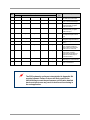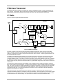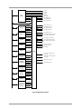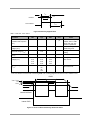
1
Data Sheet: JN5148-001 IEEE802.15.4 Wireless Microcontroller Features: Transceiver Overview The JN5148-001 is an ultra low power, high performance wireless microcontroller targeted at JenNet and ZigBee PRO networking applications. The device features an enhanced 32-bit RISC processor offering high coding efficiency through variable width instructions, a multistage instruction pipeline and low power operation with programmable clock speeds. It also includes a 2.4GHz IEEE802.15.4 compliant transceiver, 128kB of ROM, 128kB of RAM, and a rich mix of analogue and digital peripherals. The large memory footprint allows the device to run both a network stack (e.g. ZigBee PRO) and an embedded application or in a coprocessor mode. The operating current is below 18mA, allowing operation direct from a coin cell. Enhanced peripherals include low power pulse counters running in sleep mode designed for pulse counting in AMR applications and a unique Time of Flight ranging engine, allowing accurate location services to be 2 implemented on wireless sensor networks. It also includes a 4-wire I S audio interface, to interface directly to mainstream audio CODECs, as well as conventional MCU peripherals. Block Diagram Time of Flight Engine RAM 128kB ROM 128kB SPI 2-Wire Serial 2.4GHz Radio O-QPSK Modem • • 2.4GHz IEEE802.15.4 compliant Time of Flight ranging engine • 128-bit AES security processor • MAC accelerator with packet formatting, CRCs, address check, auto-acks, timers • 500 & 667kbps data rate modes • Integrated sleep oscillator for low power • On chip power regulation for 2.0V to 3.6V battery operation • Deep sleep current 100nA • Sleep current with active sleep timer 1.25µA • <$0.50 external component cost • Rx current 17.5mA • Tx current 15.0mA • Receiver sensitivity -95dBm • Transmit power 2.5dBm Features: Microcontroller • Low power 32-bit RISC CPU, 4 to 32MHz clock speed • Variable instruction width for high coding efficiency • Multi-stage instruction pipeline • 128kB ROM and 128kB RAM for bootloaded program code & data • JTAG debug interface • 4-input 12-bit ADC, 2 12-bit DACs, 2 comparators • 3 application timer/counters, • 2 UARTs ZigBee PRO and JenNet networks • SPI port with 5 selects • 2-wire serial interface Smart metering (e.g. AMR) • 4-wire digital audio interface Home and commercial building automation • Watchdog timer • Low power pulse counters • Up to 21 DIO 32-bit RISC CPU Timers UAR Ts XTAL Watchdog Timer Power Management 32-byte OTP eFuse IEEE802.15.4 MAC Accelerator 4-Wire Audio Sleep Counters 12-bit ADC, Comparators 128-bit AES Encryption Accelerator 12-bit DACs, Temp Sensor Benefits Applications • Single chip integrates transceiver and microcontroller for wireless sensor networks • Large memory footprint to run ZigBee PRO or JenNet together with an application • • • • • • Very low current solution for long battery life Highly featured 32-bit RISC CPU for high performance and low power System BOM is low in component count and cost Extensive user peripherals © NXP Laboratories UK 2013 • • Robust and secure low power wireless applications • Location Aware services – e.g. Asset Tracking • Industrial systems • Telemetry 8x8mm 56-lead Punched QFN • Remote Control Lead-free and RoHS compliant • Toys and gaming peripherals JN-DS-JN5148-001 1v9 Industrial temp (-40°C to +85°C) 1 Contents 1 Introduction 6 1.1 Wireless Transceiver 1.2 RISC CPU and Memory 1.3 Peripherals 1.4 Block Diagram 6 6 7 8 2 Pin Configurations 9 2.1 Pin Assignment 2.2 Pin Descriptions 2.2.1 Power Supplies 2.2.2 Reset 2.2.3 32MHz Oscillator 2.2.4 Radio 2.2.5 Analogue Peripherals 2.2.6 Digital Input/Output 10 12 12 12 12 12 13 13 3 CPU 15 4 Memory Organisation 16 4.1 ROM 4.2 RAM 4.3 OTP eFuse Memory 4.4 External Memory 4.4.1 External Memory Encryption 4.5 Peripherals 4.6 Unused Memory Addresses 16 17 17 17 18 18 18 5 System Clocks 19 5.1 16MHz System Clock 5.1.1 32MHz Oscillator 5.1.2 24MHz RC Oscillator 5.2 32kHz System Clock 5.2.1 32kHz RC Oscillator 5.2.2 32kHz Crystal Oscillator 5.2.3 32kHz External Clock 19 19 19 20 20 20 20 6 Reset 21 6.1 Internal Power-on Reset 6.2 External Reset 6.3 Software Reset 6.4 Brown-out Detect 6.5 Watchdog Timer 21 22 22 23 23 7 Interrupt System 24 7.1 System Calls 7.2 Processor Exceptions 7.2.1 Bus Error 7.2.2 Alignment 7.2.3 Illegal Instruction 7.2.4 Stack Overflow 7.3 Hardware Interrupts 24 24 24 24 24 24 25 2 JN-DS-JN5148-001 1v9 © NXP Laboratories UK 2013 8 Wireless Transceiver 26 8.1 Radio 8.1.1 Radio External Components 8.1.2 Antenna Diversity 8.2 Modem 8.3 Baseband Processor 8.3.1 Transmit 8.3.2 Reception 8.3.3 Auto Acknowledge 8.3.4 Beacon Generation 8.3.5 Security 8.4 Security Coprocessor 8.5 Location Awareness 8.6 Higher Data Rates 26 27 27 29 30 30 30 31 31 31 31 31 32 9 Digital Input/Output 33 10 Serial Peripheral Interface 35 11 Timers 38 11.1 Peripheral Timer/Counters 11.1.1 Pulse Width Modulation Mode 11.1.2 Capture Mode 11.1.3 Counter/Timer Mode 11.1.4 Delta-Sigma Mode 11.1.5 Example Timer / Counter Application 11.2 Tick Timer 11.3 Wakeup Timers 11.3.1 RC Oscillator Calibration 38 39 39 40 40 41 41 42 43 12 Pulse Counters 44 13 Serial Communications 45 13.1 Interrupts 13.2 UART Application 46 46 14 JTAG Debug Interface 47 15 Two-Wire Serial Interface 48 15.1 Connecting Devices 15.2 Clock Stretching 15.3 Master Two-wire Serial Interface 15.4 Slave Two-wire Serial Interface 48 49 49 50 16 Four-Wire Digital Audio Interface 51 17 Random Number Generator 53 18 Sample FIFO 54 19 Intelligent Peripheral Interface 55 19.1 Data Transfer Format 19.2 JN5148 (Slave) Initiated Data Transfer 19.3 Remote (Master) Processor Initiated Data Transfer 55 56 56 © NXP Laboratories UK 2013 JN-DS-JN5148-001 1v9 3 20 Analogue Peripherals 58 20.1 Analogue to Digital Converter 20.1.1 Operation 20.1.2 Supply Monitor 20.1.3 Temperature Sensor 20.2 Digital to Analogue Converter 20.2.1 Operation 20.3 Comparators 59 59 60 60 60 60 61 21 Power Management and Sleep Modes 62 21.1 Operating Modes 21.1.1 Power Domains 21.2 Active Processing Mode 21.2.1 CPU Doze 21.3 Sleep Mode 21.3.1 Wakeup Timer Event 21.3.2 DIO Event 21.3.3 Comparator Event 21.3.4 Pulse Counter 21.4 Deep Sleep Mode 62 62 62 62 62 63 63 63 63 63 22 Electrical Characteristics 64 22.1 Maximum Ratings 22.2 DC Electrical Characteristics 22.2.1 Operating Conditions 22.2.2 DC Current Consumption 22.2.3 I/O Characteristics 22.3 AC Characteristics 22.3.1 Reset and Voltage Brown-Out 22.3.2 SPI MasterTiming 22.3.3 Intelligent Peripheral (SPI Slave) Timing 22.3.4 Two-wire Serial Interface 22.3.5 Four-Wire Digital Audio Interface 22.3.6 Wakeup and Boot Load Timings 22.3.7 Bandgap Reference 22.3.8 Analogue to Digital Converters 22.3.9 Digital to Analogue Converters 22.3.10 Comparators 22.3.11 32kHz RC Oscillator 22.3.12 32kHz Crystal Oscillator 22.3.13 32MHz Crystal Oscillator 22.3.14 24MHz RC Oscillator 22.3.15 Temperature Sensor 22.3.16 Radio Transceiver 64 64 64 65 66 66 66 68 68 69 70 70 71 71 72 73 73 74 74 75 75 76 4 JN-DS-JN5148-001 1v9 © NXP Laboratories UK 2013 Appendix A Mechanical and Ordering Information 81 A.1 56-pin QFN Package Drawing A.2 PCB Decal A.3 Ordering Information A.4 Device Package Marking A.5 Tape and Reel Information A.5.1 Tape Orientation and Dimensions A.5.2 Reel Information: 180mm Reel A.5.3 Reel Information: 330mm Reel A.5.4 Dry Pack Requirement for Moisture Sensitive Material 81 82 83 84 85 85 86 87 87 Appendix B Development Support 88 B.1 Crystal Oscillators B.1.1 Crystal Equivalent Circuit B.1.2 Crystal Load Capacitance B.1.3 Crystal ESR and Required Transconductance B.2 32MHz Oscillator B.3 32kHz Oscillator B.4 JN5148 Module Reference Designs B.4.1 Schematic Diagram B.4.2 PCB Design and Reflow Profile 88 88 88 89 90 92 94 94 96 Related Documents RoHS Compliance Status Information Disclaimers Trademarks Version Control Contact Details © NXP Laboratories UK 2013 97 97 97 98 98 99 100 JN-DS-JN5148-001 1v9 5 1 Introduction The JN5148-001 is an IEEE802.15.4 wireless microcontroller that provides a fully integrated solution for applications using the IEEE802.15.4 standard in the 2.4 - 2.5GHz ISM frequency band [1], including JenNet and ZigBee PRO. It includes all of the functionality required to meet the IEEE802.15.4, JenNet and ZigBee PRO specifications and has additional processor capability to run a wide range of applications including, but not limited to Smart Energy, Automatic Meter Reading, Remote Control, Home and Building Automation, Toys and Gaming. Applications that transfer data wirelessly tend to be more complex than wired ones. Wireless protocols make stringent demands on frequencies, data formats, timing of data transfers, security and other issues. Application development must consider the requirements of the wireless network in addition to the product functionality and user interfaces. To minimise this complexity, NXP provides a series of software libraries and interfaces that control the transceiver and peripherals of the JN5148. These libraries and interfaces remove the need for the developer to understand wireless protocols and greatly simplifies the programming complexities of power modes, interrupts and hardware functionality. In view of the above, the register details of the JN5148 are not provided in the datasheet. The device includes a Wireless Transceiver, RISC CPU, on chip memory and an extensive range of peripherals. Hereafter, the JN5148-001 will be referred to as JN5148. 1.1 Wireless Transceiver The Wireless Transceiver comprises a 2.45GHz radio, a modem, a baseband controller and a security coprocessor. In addition, the radio also provides an output to control transmit-receive switching of external devices such as power amplifiers allowing applications that require increased transmit power to be realised very easily. Appendix B.4, describes a complete reference design including Printed Circuit Board (PCB) design and Bill Of Materials (BOM). The security coprocessor provides hardware-based 128-bit AES-CCM* modes as specified by the IEEE802.15.4 2006 standard. Specifically this includes encryption and authentication covered by the MIC –32/ -64/ -128, ENC and ENC-MIC –32/ -64/ -128 modes of operation. The transceiver elements (radio, modem and baseband) work together to provide IEEE802.15.4 Medium Access Control (MAC) under the control of a protocol stack. Applications incorporating IEEE802.15.4 functionality can be rapidly developed by combining user-developed application software with a protocol stack library. 1.2 RISC CPU and Memory A 32-bit RISC CPU allows software to be run on chip, its processing power being shared between the IEEE802.15.4 MAC protocol, other higher layer protocols and the user application. The JN5148 has a unified memory architecture, code memory, data memory, peripheral devices and I/O ports are organised within the same linear address space. The device contains 128kbytes of ROM, 128kbytes of RAM and a 32-byte One Time Programmable (OTP) eFuse memory. 6 JN-DS-JN5148-001 1v9 © NXP Laboratories UK 2013 1.3 Peripherals The following peripherals are available on chip: • Master SPI port with five select outputs • Two UARTs with support for hardware or software flow control • Three programmable Timer/Counters – all three support Pulse Width Modulation (PWM) capability, two have capture/compare facility • Two programmable Sleep Timers and a Tick Timer • Two-wire serial interface (compatible with SMbus and I C) supporting master and slave operation • Four-wire digital audio interface (compatible with I²S) • Slave SPI port for Intelligent peripheral mode (shared with digital I/O) • Twenty-one digital I/O lines (multiplexed with peripherals such as timers and UARTs) • Four channel, 12-bit, Analogue to Digital converter • Two 12-bit Digital to Analogue converters • Two programmable analogue comparators • Internal temperature sensor and battery monitor • Time Of Flight ranging engine • Two low power pulse counters • Random number generator • Watchdog Timer and Voltage Brown-out • Sample FIFO for digital audio interface or ADC/DAC • JTAG hardware debug port 2 User applications access the peripherals using the Integrated Peripherals API. This allows applications to use a tested and easily understood view of the peripherals allowing rapid system development. © NXP Laboratories UK 2013 JN-DS-JN5148-001 1v9 7 1.4 Block Diagram SPICLK SPIMOSI SPIMISO SPISEL0 Tick Timer Programmable Interrupt Controller SPI Master 32-bit RISC CPU SPISEL1 SPISEL2 SPISEL3 SPISEL4 DIO0/SPISEL1 DIO1/SPISEL2/PC0 DIO2/SPISEL3/RFRX DIO3/SPISEL4/RFTX UART0 TXD0 RXD0 RTS0 CTS0 DIO4/CTS0/JT AG_T CK DIO5/RTS0/JT AG_T MS DIO6/TXD0/JTAG_TDO DIO7/RXD0/JTAG_T DI UART1 TXD1 RXD1 RTS1 CTS1 DIO8/T IM0CK_GT /PC1 DIO9/T IM0CAP/32KXTALIN/32KIN DIO10/T IM0OUT /32KXT ALOUT Fro m Perip herals RAM 128kB ROM 128kB OTP eFuse TIM0CK_GT TIM0OUT TIM0CAP Timer0 VB_XX VDD1 Voltage Regulators VDD2 RESET N Brown-out Detect Reset Wakeup Timer0 Watchdog Timer 32kHz RC Osc 32kHz Clock Gen 32MHz Clock Generator XT AL_IN XT AL_OUT Supply Monitor ADC1 ADC2 ADC3 ADC4 M U X DAC1 DAC1 DAC2 DAC2 COMP2M COMP2P 2-wire Interf ace Sample FIFO 24MHz RC Osc SIF_D SIF_CLK IP_DO IP_DI IP_INT IP_CLK IP_SEL MUX DIO17/CT S1/IP_SEL/DAI_SCK/ JTAG_T CK DIO18/RT S1/IP_INT /DAI_SDOUT / JTAG_T MS DIO19/T XD1/JTAG_T DO DIO20/RXD1/JT AG_T DI PC0 PC1 JTAG_TDI JTAG_TMS JTAG_TCK JTAG_TDO JTAG Debug 32KXTALIN 32KXTALOUT Clock Divider Multiplier Pulse Counters Antenna Div ersity ADO ADE 4-wire Digital Audio Interf ace I2S_OUT I2S_DIN I2S_CLK I2S_SYNC Wireless Transceiv er ADC Temperature Sensor COMP1M/ EXT _PA_B COMP1P/ EXT _PA_C CPU and 16MHz System Clock 32KIN DIO14/SIF_CLK/IP_CLK DIO15/SIF_D/IP_DO DIO16/RXD1/IP_DI/JT AG_TDI DIO 16/IP_DI TIM2OUT Timer2 Intelligent Peripheral Wakeup Timer1 32kHz Clock Select TIM1CK_GT TIM1OUT TIM1CAP Timer1 1.8V DIO11/T IM1CK_GT /T IM2OUT DIO12/T IM1CAP/ADO/DAI_WS DIO13/T IM1OUT /ADE/DAI_SDIN Security Coprocessor T ime Of Flight Digital Baseband Comparator1 Radio Comparator2 RF_IN VCOT UNE IBAIS Figure 1: JN5148 Block Diagram 8 JN-DS-JN5148-001 1v9 © NXP Laboratories UK 2013 DIO3/SPISEL4/RFTX DIO4/CTS0/JTAG_TCK 44 43 DIO5/RTS0/JTAG_TMS 45 DIO6/TXD0/JTAG_TDO DIO8/TIM0CK_GT/PC 1 48 46 VDD2 49 DIO7/RXD0/JT AG_TDI DIO9/TIM0CAP/32KXT ALIN/32KIN 50 47 DIO10/T IM0OUT/32KXT ALOUT 51 DIO11/T IM1CK_GT /TIM2OUT 52 53 DIO12/T IM1CAP/ADO/DAI_WS DIO13/T IM1OUT/ADE/DAI_SDIN DIO14/SIF_C LK/IP_CLK 55 54 DIO15/SIF_D/IP_DO 56 2 Pin Configurations DIO16/RXD 1/IP_DI/JTAG_TDI DIO 16/IP_DI 1 42 DIO2/SPISEL3/RFRX DIO17/CTS1/IP_SEL/DAI_SC K/JTAG_TCK 2 41 DIO1/SPISEL2/PC0 VSS3 3 40 VB_DIG 4 39 RESETN DIO19/T XD1/JTAG_TDO 5 38 DIO0/SPISEL1 VSS2 6 37 SPISEL0 VSSS 7 36 SPIMOSI XTAL_OUT 8 35 VB_RAM XTAL_IN 9 34 SPIMISO VB_SYNTH 10 33 SPICLK VCOTUNE 11 32 VSS1 VB_VCO 12 31 DIO20/RXD 1/JTAG_TDI VDD1 13 30 DAC2 IBIAS 14 29 DAC1 15 16 17 18 19 20 21 22 23 24 25 26 27 28 VB_RF2 RF_IN VB_RF COMP1M COMP1P ADC1 ADC2 ADC3 ADC4 COMP2M COMP2P VB_A NC VSSA (Paddl e) VREF DIO18/RTS1/IP_INT/DAI_SDOUT/JT AG_TMS Figure 2: 56-pin QFN Configuration (top view) © NXP Laboratories UK 2013 Note: Please refer to Appendix B.4 JN5148 Module Reference Design for important applications information regarding the connection of the PADDLE to the PCB. JN-DS-JN5148-001 1v9 9 2.1 Pin Assignment Pin No Power supplies Signal Type Description 10, 12, 16, 18, 27, 35, 40 VB_SYNTH, VB_VCO, VB_RF2, VB_RF, VB_A, VB_RAM, VB_DIG 1.8V Regulated supply voltage 13, 49 VDD1, VDD2 3.3V Supplies: VDD1 for analogue, VDD2 for digital 32, 6, 3, 7, Paddle VSS1, VSS2, VSS3, VSSS, VSSA 0V Grounds (see appendix A.2 for paddle details) 28 NC No connect General 39 RESETN 8, 9 XTAL_OUT, XTAL_IN CMOS 1.8V Reset input System crystal oscillator Radio 11 VCOTUNE 1.8V VCO tuning RC network 14 IBIAS 1.8V Bias current control 17 RF_IN 1.8V RF antenna Analogue Peripheral I/O 21, 22, 23, 24 ADC1, ADC2, ADC3, ADC4 3.3V ADC inputs 15 VREF 1.8V Analogue peripheral reference voltage 29, 30 DAC1, DAC2 3.3V DAC outputs 19, 20 COMP1M/EXT_PA_B, COMP1P/EXT_PA_C 3.3V Comparator 1 inputs and external PA control 25, 26 COMP2M, COMP2P 3.3V Comparator 2 inputs Digital Peripheral I/O Primary Alternate Functions 33 SPICLK CMOS 36 SPIMOSI CMOS SPI Clock Output SPI Master Out Slave In Output 34 SPIMISO CMOS SPI Master In Slave Out Input 37 SPISEL0 38 DIO0 SPISEL1 41 DIO1 SPISEL2 42 DIO2 43 CMOS SPI Slave Select Output 0 CMOS DIO0 or SPI Slave Select Output 1 PC0 CMOS DIO1, SPI Slave Select Output 2 or Pulse Counter0 Input SPISEL3 RFRX CMOS DIO2, SPI Slave Select Output 3 or Radio Receive Control Output DIO3 SPISEL4 RFTX CMOS DIO3, SPI Slave Select Output 4 or Radio Transmit Control Output 44 DIO4 CTS0 JTAG_TCK CMOS DIO4, UART 0 Clear To Send Input or JTAG CLK 45 DIO5 RTS0 JTAG_TMS CMOS DIO5, UART 0 Request To Send Output or JTAG Mode Select 46 DIO6 TXD0 JTAG_TDO CMOS DIO6, UART 0 Transmit Data Output or JTAG Data Output 47 DIO7 RXD0 JTAG_TDI CMOS DIO7, UART 0 Receive Data Input or JTAG Data Input 48 DIO8 TIM0CK_GT PC1 CMOS DIO8, Timer0 Clock/Gate Input or Pulse Counter1 Input 50 DIO9 TIM0CAP 32KXTALIN CMOS DIO9, Timer0 Capture Input, 32K External Crystal Input or 32K Clock Input 10 32KIN JN-DS-JN5148-001 1v9 © NXP Laboratories UK 2013 Digital Peripheral I/O Signal Type Description 32KXTALOUT CMOS DIO10, Timer0 PWM Output or 32K External Crystal Output TIM1CK_GT TIM2OUT CMOS DIO11, Timer1 Clock/Gate Input or Timer2 PWM Output DIO12 TIM1CAP ADO DAI_WS CMOS DIO12, Timer1 Capture Input, Antenna Diversity or Digital Audio Word Select 54 DIO13 TIM1OUT ADE DAI_SDIN CMOS DIO13, Timer1 PWM Output, Antenna Diversity or Digital Audio Data Input 55 DIO14 SIF_CLK IP_CLK CMOS DIO14, Serial Interface Clock or Intelligent Peripheral Clock Input 56 DIO15 SIF_D IP_DO CMOS DIO15, Serial Interface Data or Intelligent Peripheral Data Out 1 DIO16 IP_DI CMOS DIO16 or Intelligent Peripheral Data In 2 DIO17 CTS1 IP_SEL DAI_SCK JTAG_TCK CMOS DIO17, UART 1 Clear To Send Input, Intelligent Peripheral Device Select Input or Digital Audio Clock or JTAG CLK 4 DIO18 RTS1 IP_INT DAI_SDOUT JTAG_TMS CMOS DIO18, UART 1 Request To Send Output, Intelligent Peripheral Interrupt Output or Digital Audio Data Output or JTAG Mode Select 5 DIO19 TXD1 JTAG_TDO CMOS DIO19 or UART 1 Transmit Data Output or JTAG Data Out 31 DIO 20 RXD1 JTAG_TDI CMOS DIO 20, UART 1 Receive Data Input or JTAG data In Pin No Primary 51 DIO10 TIM0OUT 52 DIO11 53 Alternate Functions The PCB schematic and layout rules detailed in Appendix B.4 must be followed. Failure to do so will likely result in the JN5148 failing to meet the performance specification detailed herein and worst case may result in device not functioning in the end application. © NXP Laboratories UK 2013 JN-DS-JN5148-001 1v9 11 2.2 Pin Descriptions 2.2.1 Power Supplies The device is powered from the VDD1 and VDD2 pins, each being decoupled with a 100nF ceramic capacitor. VDD1 is the power supply to the analogue circuitry; it should be decoupled to ground. VDD2 is the power supply for the digital circuitry; and should also be decoupled to ground. A 10uF tantalum capacitor is required. Decoupling pins for the internal 1.8V regulators are provided which require a 100nF capacitor located as close to the device as practical. VB_RF, VB_A and VB_SYNTH should be decoupled with an additional 47pF capacitor, while VB_RAM and VB_DIG require only 100nF. VB_RF and VB_RF2 should be connected together as close to the device as practical, and only require one 100nF capacitor and one 47pF capacitor. The pin VB_VCO requires a 10nF capacitor in parallel with a 47pF capacitor. Refer to B.4.1 for schematic diagram. VSSA, VSSS, VSS1, VSS2, VSS3 are the ground pins. Users are strongly discouraged from connecting their own circuits to the 1.8v regulated supply pins, as the regulators have been optimised to supply only enough current for the internal circuits. 2.2.2 Reset RESETN is a bi-directional active low reset pin that is connected to a 40kΩ internal pull-up resistor. It may be pulled low by an external circuit, or can be driven low by the JN5148 if an internal reset is generated. Typically, it will be used to provide a system reset signal. Refer to section 6.2, External Reset, for more details. 2.2.3 32MHz Oscillator A crystal is connected between XTALIN and XTALOUT to form the reference oscillator, which drives the system clock. A capacitor to analogue ground is required on each of these pins. Refer to section 5.1 16MHz System Clock for more details. The 32MHz reference frequency is divided down to 16MHz and this is used as the system clock throughout the device. 2.2.4 Radio The radio is a single ended design, requiring a capacitor and just two inductors to match to 50Ω microstrip line to the RF_IN pin. An external resistor (43kΩ) is required between IBIAS and analogue ground to set various bias currents and references within the radio. 12 JN-DS-JN5148-001 1v9 © NXP Laboratories UK 2013 2.2.5 Analogue Peripherals Several of the analogue peripherals require a reference voltage to use as part of their operations. They can use either an internal reference voltage or an external reference connected to VREF. This voltage is referenced to analogue ground and the performance of the analogue peripherals is dependant on the quality of this reference. There are four ADC inputs, two pairs of comparator inputs and two DAC outputs. The analogue I/O pins on the JN5148 can have signals applied up to 0.3v higher than VDD1. A schematic view of the analogue I/O cell is shown in Figure 3: Analogue I/O Cell In reset and deep sleep, the analogue peripherals are all off and the DAC outputs are in a high impedance state. In sleep, the ADC and DACs are off, with the DAC outputs in high impedance state. The comparators may optionally be used as a wakeup source. Unused ADC and comparator inputs should be left unconnected. VDD1 Analogue I/O Pin Analogue Peripheral VSSA Figure 3: Analogue I/O Cell 2.2.6 Digital Input/Output Digital I/O pins on the JN5148 can have signals applied up to 2V higher than VDD2 (with the exception of pins DIO9 and DIO10 that are 3V tolerant) and are therefore TTL-compatible with VDD2 > 3V. For other DC properties of these pins see section 22.2.3 I/O Characteristics. When used in their primary function all Digital Input/Output pins are bi-directional and are connected to weak internal pull up resistors (40kΩ nominal) that can be disabled. When used in their secondary function (selected when the appropriate peripheral block is enabled through software library calls) then their direction is fixed by the function. The pull up resistor is enabled or disabled independently of the function and direction; the default state from reset is enabled. A schematic view of the digital I/O cell is in Figure 4: DIO Pin Equivalent Schematic. © NXP Laboratories UK 2013 JN-DS-JN5148-001 1v9 13 VDD2 Pu OE RPU O DIO[x] Pin RPROT I VSS IE Figure 4: DIO Pin Equivalent Schematic In reset, the digital peripherals are all off and the DIO pins are set as high-impedance inputs. During sleep and deep sleep, the DIO pins retain both their input/output state and output level that was set as sleep commences. If the DIO pins were enabled as inputs and the interrupts were enabled then these pins may be used to wake up the JN5148 from sleep. 14 JN-DS-JN5148-001 1v9 © NXP Laboratories UK 2013 3 CPU The CPU of the JN5148 is a 32-bit load and store RISC processor. It has been architected for three key requirements: • Low power consumption for battery powered applications • High performance to implement a wireless protocol at the same time as complex applications • Efficient coding of high-level languages such as C provided with the NXP Software Developer’s Kit It features a linear 32-bit logical address space with unified memory architecture, accessing both code and data in the same address space. Registers for peripheral units, such as the timers, UARTs and the baseband processor are also mapped into this space. The CPU has access to a block of 15 32-bit General-Purpose (GP) registers together with a small number of special purpose registers which are used to store processor state and control interrupt handling. The contents of any GP register can be loaded from or stored to memory, while arithmetic and logical operations, shift and rotate operations, and signed and unsigned comparisons can be performed either between two registers and stored in a third, or between registers and a constant carried in the instruction. Operations between general or special-purpose registers execute in one cycle while those that access memory require a further cycle to allow the memory to respond. The instruction set manipulates 8, 16 and 32-bit data; this means that programs can use objects of these sizes very efficiently. Manipulation of 32-bit quantities is particularly useful for protocols and high-end applications allowing algorithms to be implemented in fewer instructions than on smaller word-size processors, and to execute in fewer clock cycles. In addition, the CPU supports hardware Multiply that can be used to efficiently implement algorithms needed by Digital Signal Processing applications. The instruction set is designed for the efficient implementation of high-level languages such as C. Access to fields in complex data structures is very efficient due to the provision of several addressing modes, together with the ability to be able to use any of the GP registers to contain the address of objects. Subroutine parameter passing is also made more efficient by using GP registers rather than pushing objects onto the stack. The recommended programming method for the JN5148 is by using C, which is supported by a software developer kit comprising a C compiler, linker and debugger. The CPU architecture also contains features that make the processor suitable for embedded, real-time applications. In some applications, it may be necessary to use a real-time operating system to allow multiple tasks to run on the processor. To provide protection for device-wide resources being altered by one task and affecting another, the processor can run in either supervisor or user mode, the former allowing access to all processor registers, while the latter only allows the GP registers to be manipulated. Supervisor mode is entered on reset or interrupt; tasks starting up would normally run in user mode in a RTOS environment. Embedded applications require efficient handling of external hardware events. When using JenOS, prioritised interrupts are supported, with 15 priority levels, and can be configured as required by the application. To improve power consumption a number of power-saving modes are implemented in the JN5148, described more fully in section 21 - Power Management and Sleep Modes. One of these modes is the CPU doze mode; under software control, the processor can be shut down and on an interrupt it will wake up to service the request. Additionally, it is possible under software control, to set the speed of the CPU to 4, 8, 16 or 32MHz. This feature can be used to trade-off processing power against current consumption. © NXP Laboratories UK 2013 JN-DS-JN5148-001 1v9 15 4 Memory Organisation This section describes the different memories found within the JN5148. The device contains ROM, RAM, OTP eFuse memory, the wireless transceiver and peripherals all within the same linear address space. 0xFFFFFFFF 0xF0020000 RAM (128kB) 0xF0000000 Unpopulated RAM Echo 0x04000000 Peripherals 0x02000000 0x00020000 ROM (128kB) 0x00000000 Figure 5: JN5148 Memory Map 4.1 ROM The ROM is 128k bytes in size, and can be accessed by the processor in a single CPU clock cycle. The ROM contents include bootloader to allow external Flash memory contents to be bootloaded into RAM at runtime, a default interrupt vector table, an interrupt manager, IEEE802.15.4 MAC and APIs for interfacing on-chip peripherals. The operation of the boot loader is described in detail in Application Note [7]. The interrupt manager routes interrupt calls to the application’s soft interrupt vector table contained within RAM. Section 7 contains further information regarding the handling of interrupts. ROM contents are shown in Figure 6. 0x00020000 Spare APIs IEEE802.15.4 Stack Boot Loader Interrupt Manager 0x00000000 Interrupt Vectors Figure 6: Typical ROM contents 16 JN-DS-JN5148-001 1v9 © NXP Laboratories UK 2013 4.2 RAM The JN5148 contains 128kBytes of high speed RAM. It can be used for both code and data storage and is accessed by the CPU in a single clock cycle. At reset, a boot loader controls the loading of segments of code and data from an external memory connected to the SPI port, into RAM. Software can control the power supply to the RAM allowing the contents to be maintained during a sleep period when other parts of the device are un-powered. Typical RAM contents are shown in Figure 7. 0x04020000 CPU Stack (Grows Down) Application MAC Address MAC Data Interrupt Vector Table 0x04000000 Figure 7: Typical RAM Contents 4.3 OTP eFuse Memory The JN5148 contains a total of 32bytes of eFuse memory; this is a One Time Programmable (OTP) memory that can be used to support on chip 64-bit MAC ID and a 128-bit AES security key. A limited number of bits are available for customer use for storage of configuration information; configuration of these is made through use of software APIs. For further information on how to program and use the eFuse memory, please contact technical support via the online tech-support system. Alternatively, NXP can provide an eFuse programming service for customers that wish to use the eFuse but do not wish to undertake this for themselves. For further details of this service, please contact your local NXP sales office. 4.4 External Memory An external memory with an SPI interface may be used to provide storage for program code and data for the device when external power is removed. The memory is connected to the SPI interface using select line SPISEL0; this select line is dedicated to the external memory interface and is not available for use with other external devices. See Figure 8 for connection details. JN5148 Serial Memory SPISEL0 SS SPIMISO SDO SPIMOSI SDI SPICLK CLK Figure 8: Connecting External Serial Memory © NXP Laboratories UK 2013 JN-DS-JN5148-001 1v9 17 At reset, the contents of this memory are copied into RAM by the software boot loader. The Flash memory devices that are supported as standard through the JN5148 bootloader are given in Table 1. NXP recommends that where possible one of these devices should be selected. Manufacturer Device Number SST (Silicon Storage Technology) 25VF010A (1Mbit device) Numonyx M25P10-A (1Mbit device), M25P40 (4Mbit device) Table 1: Supported Flash Memories Applications wishing to use an alternate Flash memory device should refer to application note [2] JN-AN-1038 Programming Flash devices not supported by the JN51xx ROM-based bootloader. This application note provides guidance on developing an interface to an alternate device. 4.4.1 External Memory Encryption The contents of the external serial memory may be encrypted. The AES security processor combined with a user programmable 128-bit encryption key is used to encrypt the contents of the external memory. The encryption key is stored in eFuse. When bootloading program code from external serial memory, the JN5148 automatically accesses the encryption key to execute the decryption process. User program code does not need to handle any of the decryption process; it is transparent. With encryption enabled, the time taken to boot code from external flash is increased. 4.5 Peripherals All peripherals have their registers mapped into the memory space. Access to these registers requires 3 clock cycles. Applications have access to the peripherals through the software libraries that present a high-level view of the peripheral’s functions through a series of dedicated software routines. These routines provide both a tested method for using the peripherals and allow bug-free application code to be developed more rapidly. For details, see the JN51xx Integrated Peripherals API User Guide (JN-UG-3066)[5]. 4.6 Unused Memory Addresses Any attempt to access an unpopulated memory area will result in a bus error exception (interrupt) being generated. 18 JN-DS-JN5148-001 1v9 © NXP Laboratories UK 2013 5 System Clocks Two system clocks are used to provide timing references into the on-chip subsystems of the JN5148. A 16MHz clock, generated by a crystal-controlled 32MHz oscillator, is used by the transceiver, processor, memory and digital and analogue peripherals. A 32kHz clock is used by the sleep timer and during the startup phase of the chip. 5.1 16MHz System Clock The 16MHz system clock is used by the digital and analogue peripherals and the transceiver. A scaled version (4,8,16 or 32MHz) of this clock is also used by the processor and memories. For most operations it is necessary to source this clock from the 32MHz oscillator. Crystal oscillators are generally slow to start. Hence to provide a faster start-up following a sleep cycle a fast RC oscillator is provided that can be used as the source for the 16MHz system clock. The oscillator starts very quickly and is typically 24MHz causing the system clock to run at 12MHz. Using a clock of this speed scales down the speed of the processor and any peripherals in use. For the SPI interface this causes no functional issues as the generated SPI clock is slightly slower and is used to clock the external SPI slave. Use of the radio is not possible when using the 24MHz RC oscillator. Additionally, timers and UARTs should not be used as the exact frequency will not be known. The JN5148 device can be configured to wake up from sleep using the fast RC oscillator and automatically switch over to use the 32MHz xtal as the clock source, when it has started up. This could allow application code to be downloaded from the flash before the xtal is ready, typically improving start-up time by 550usec. Alternatively, the switch over can be controlled by software, or the system could always use the 32MHz oscillator as the clock source. 5.1.1 32MHz Oscillator The JN5148 contains the necessary on chip components to build a 32MHz reference oscillator with the addition of an external crystal resonator and two tuning capacitors. The schematic of these components are shown in Figure 9. The two capacitors, C1 and C2, should typically be 15pF and use a COG dielectric. Due to the small size of these capacitors, it is important to keep the traces to the external components as short as possible. The on chip transconductance amplifier is compensated for temperature variation, and is self-biasing by means of the internal resistor R1. The electrical specification of the oscillator can be found in section 22.3.13. Please refer to Appendix B for development support with the crystal oscillator circuit. JN5148 XTALIN R1 XTALOUT C1 C2 Figure 9: 32MHz Crystal Oscillator Connections 5.1.2 24MHz RC Oscillator An on-chip 24MHz RC oscillator is provided. No external components are required for this oscillator. The electrical specification of the oscillator can be found in section 22.3.14. © NXP Laboratories UK 2013 JN-DS-JN5148-001 1v9 19 5.2 32kHz System Clock The 32kHz system clock is used for timing the length of a sleep period (see section 21 Power Management and Sleep Modes) and also to generate the system clock used internally during reset. The clock can be selected from one of three sources through the application software: • 32kHz RC Oscillator • 32kHz Crystal Oscillator • 32kHz External Clock Upon a chip reset or power-up the JN5148 defaults to using the internal 32kHz RC Oscillator. If another clock source is selected then it will remain in use for all 32kHz timing until a chip reset is performed. 5.2.1 32kHz RC Oscillator The internal 32kHz RC oscillator requires no external components. The internal timing components of the oscillator have a wide tolerance due to manufacturing process variation and so the oscillator runs nominally at 32kHz ±30%. To make this useful as a timing source for accurate wakeup from sleep, a frequency calibration factor derived from the more accurate 16MHz clock may be applied. The calibration factor is derived through software, details can be found in section 11.3.1. For detailed electrical specifications, see section 22.3.11. 5.2.2 32kHz Crystal Oscillator In order to obtain more accurate sleep periods, the JN5148 contains the necessary on-chip components to build a 32kHz oscillator with the addition of an external 32.768kHz crystal and two tuning capacitors. The crystal should be connected between 32KXTALIN and 32KXTALOUT (DIO9 and DIO10), with two equal capacitors to ground, one on each pin. Due to the small size of the capacitors, it is important to keep the traces to the external components as short as possible. The electrical specification of the oscillator can be found in section 22.3.12. The oscillator cell is flexible and can operate with a range of commonly available 32.768kHz crystals with load capacitances from 6 to 12.5pF. However, the maximum ESR of the crystal and the supply current are both functions of the actual crystal used, see appendix B.1 for more details. JN5148 32KXTALIN 32KXTALOUT Figure 10: 32kHz crystal oscillator connections 5.2.3 32kHz External Clock An externally supplied 32kHz reference clock on the 32KIN input (DIO9) may be provided to the JN5148. This would allow the 32kHz system clock to be sourced from a very stable external oscillator module, allowing more accurate sleep cycle timings compared to the internal RC oscillator. (See section 22.2.3 I/O Characteristics, DIO9 is a 3V tolerant input) 20 JN-DS-JN5148-001 1v9 © NXP Laboratories UK 2013 6 Reset A system reset initialises the device to a pre-defined state and forces the CPU to start program execution from the reset vector. The reset process that the JN5148 goes through is as follows. When power is applied, the 32kHz RC oscillator starts up and stabilises, which takes approximately 100µsec. At this point, the 32MHz crystal oscillator is enabled and power is applied to the processor and peripheral logic. The logic blocks are held in reset until the 32MHz crystal oscillator stabilises, typically this takes 0.75ms. Then the internal reset is removed from the CPU and peripheral logic and the CPU starts to run code beginning at the reset vector, consisting of initialisation code and the resident boot loader. [7] Section 22.3.1 provides detailed electrical data and timing. The JN5148 has five sources of reset: • Internal Power-on Reset • External Reset • Software Reset • Watchdog timer • Brown-out detect Note: When the device exits a reset condition, device operating parameters (voltage, frequency, temperature, etc.) must be met to ensure operation. If these conditions are not met, then the device must be held in reset until the operating conditions are met. (See section 22.3) 6.1 Internal Power-on Reset For the majority of applications the internal power-on reset is capable of generating the required reset signal. When power is applied to the device, the power-on reset circuit monitors the rise of the VDD supply. When the VDD reaches the specified threshold, the reset signal is generated and can be observed as a rising edge on the RESETN pin. This signal is held internally until the power supply and oscillator stabilisation time has elapsed, when the internal reset signal is then removed and the CPU is allowed to run. VDD Internal RESET RESETN Pin Figure 11: Internal Power-on Reset When the supply drops below the power on reset ‘falling’ threshold, it will re-trigger the reset. Use of the external reset circuit show in Figure 12 is suggested. © NXP Laboratories UK 2013 JN-DS-JN5148-001 1v9 21 VDD JN5148 R1 18k RESETN C1 470nF Figure 12: External Reset Generation The external resistor and capacitor provide a simple reset operation when connected to the RESETN pin. 6.2 External Reset An external reset is generated by a low level on the RESETN pin. Reset pulses longer than the minimum pulse width will generate a reset during active or sleep modes. Shorter pulses are not guaranteed to generate a reset. The JN5148 is held in reset while the RESETN pin is low. When the applied signal reaches the Reset Threshold Voltage (VRST) on its positive edge, the internal reset process starts. Multiple devices may connect to the RESETN pin in an open-collector mode. The JN5148 has an internal pull-up resistor connect to the RESETN pin. The pin is an input for an external reset, an output during the power-on reset and may optionally be an output during a software reset. No devices should drive the RESETN pin high. RESETN pin Reset Internal Reset Figure 13: External Reset 6.3 Software Reset A system reset can be triggered at any time through software control, causing a full chip reset and invalidating the RAM contents. For example this can be executed within a user’s application upon detection of a system failure. When performing the reset, the RESETN pin is driven low for 1µsec; depending on the external components this may or may not be visible on the pin. In addition, the RESETN line can be driven low by the JN5148 to provide a reset to other devices in the system (e.g. external sensors) without resetting itself. When the RESETN line is not driven it will pull back high through either the internal pull-up resistor or any external circuitry. It is essential to ensure that the RESETN line pulls back high within 100µsec after the JN5148 stops driving the line; otherwise a system reset will occur. Due to this, careful consideration should be taken of any capacitance on this line. For instance, the RC values recommended in section 6.1 may need to be replaced with a suitable reset IC 22 JN-DS-JN5148-001 1v9 © NXP Laboratories UK 2013 6.4 Brown-out Detect An internal brown-out detect module is used to monitor the supply voltage to the JN5148; this can be used whilst the device is awake or is in CPU doze mode. Dips in the supply voltage below a variable threshold can be detected and can be used to cause the JN5148 to perform a chip reset. Equally, dips in the supply voltage can be detected and used to cause an interrupt to the processor, when the voltage either drops below the threshold or rises above it. The brown-out detect is enabled by default from power-up and can extend the reset during power-up. This will keep the CPU in reset until the voltage exceeds the brown-out threshold voltage. The threshold voltage is configurable to 2.0V, 2.3V, 2.7V and 3.0V and is controllable by software. From power-up the threshold is set by eFuse settings and the default chip configuration is for the 2.3V threshold. It is recommended that the threshold is set so that, as a minimum, the chip is held in reset until the voltage reaches the level required by the external memory device on the SPI interface. 6.5 Watchdog Timer A watchdog timer is provided to guard against software lockups. It operates by counting cycles of the 32kHz system clock. A pre-scaler is provided to allow the expiry period to be set between typically 8ms and 16.4 seconds. Failure to restart the watchdog timer within the pre-configured timer period will cause a chip reset to be performed. A status bit is set if the watchdog was triggered so that the software can differentiate watchdog initiated resets from other resets, and can perform any required recovery once it restarts. If the source of the 32kHz system clock is the 32kHz RC oscillator then the watchdog expiry periods are subject to the variation in period of the RC oscillator. After power up, reset, start from deep sleep or start from sleep, the watchdog is always enabled with the largest timeout period and will commence counting as if it had just been restarted. Under software control the watchdog can be disabled. If it is enabled, the user must regularly restart the watchdog timer to stop it from expiring and causing a reset. The watchdog runs continuously, even during doze, however the watchdog does not operate during sleep or deep sleep, or when the hardware debugger has taken control of the CPU. It will recommence automatically if enabled once the debugger un-stalls the CPU. © NXP Laboratories UK 2013 JN-DS-JN5148-001 1v9 23 7 Interrupt System The interrupt system on the JN5148 is a hardware-vectored interrupt system. The JN5148 provides several interrupt sources, some associated with CPU operations (CPU exceptions) and others which are used by hardware in the device. When an interrupt occurs, the CPU stops executing the current program and loads its program counter with a fixed hardware address specific to that interrupt. The interrupt handler or interrupt service routine is stored at this location and is run on the next CPU cycle. Execution of interrupt service routines is always performed in supervisor mode. Interrupt sources and their vector locations are listed in Table 2 below: Interrupt Source Vector Location Interrupt Definition Bus error 0x08 Typically cause by an attempt to access an invalid address or a disabled peripheral Tick timer 0x0e Tick timer interrupt asserted Alignment error 0x14 Load/store address to non-naturally-aligned location Illegal instruction 0x1a Attempt to execute an unrecognised instruction Hardware interrupt 0x20 System call 0x26 interrupt asserted System call initiated by b.sys instruction Trap 0x2c caused by the b.trap instruction or the debug unit Reset 0x38 Caused by software or hardware reset. Stack Overflow 0x3e Stack overflow Table 2: Interrupt Vectors 7.1 System Calls The b.trap and b.sys instructions allow processor exceptions to be generated by software. A system call exception will be generated when the b.sys instruction is executed. This exception can, for example, be used to enable a task to switch the processor into supervisor mode when a real time operating system is in use. (See section 3 for further details.) The b.trap instruction is commonly used for trapping errors and for debugging. 7.2 Processor Exceptions 7.2.1 Bus Error A bus error exception is generated when software attempts to access a memory address that does not exist, or is not populated with memory or peripheral registers or when writing to ROM. 7.2.2 Alignment Alignment exceptions are generated when software attempts to access objects that are not aligned to natural word boundaries. 16-bit objects must be stored on even byte boundaries, while 32-bit objects must be stored on quad byte boundaries. For instance, attempting to read a 16-bit object from address 0xFFF1 will trigger an alignment exception as will a read of a 32-bit object from 0xFFF1, 0xFFF2 or 0xFFF3. Examples of legal 32-bit object addresses are 0xFFF0, 0xFFF4, 0xFFF8 etc. 7.2.3 Illegal Instruction If the CPU reads an unrecognised instruction from memory as part of its instruction fetch, it will cause an illegal instruction exception. 7.2.4 Stack Overflow When enabled, a stack overflow exception occurs if the stack pointer reaches a programmable location. 24 JN-DS-JN5148-001 1v9 © NXP Laboratories UK 2013 7.3 Hardware Interrupts Hardware interrupts generated from the transceiver, analogue or digital peripherals and DIO pins are individually masked using the Programmable Interrupt Controller (PIC). Management of interrupts is provided in the peripherals library [5]. For details of the interrupts generated from each peripheral see the respective section in this datasheet. Interrupts can be used to wake the JN5148 from sleep. The peripherals, baseband controller, security coprocessor and PIC are powered down during sleep but the DIO interrupts and optionally the pulse counters, wake-up timers and analogue comparator interrupts remain powered to bring the JN5148 out of sleep. Prioritised external interrupt handling (i.e., interrupts from hardware peripherals) is provided to enable an application to control an events priority to provide for deterministic program execution. The priority Interrupt controller provides 15 levels of prioritised interrupts. The priority level of all interrupts can be set, with value 0 being used to indicate that the source can never produce an external interrupt, 1 for the lowest priority source(s) and 15 for the highest priority source(s). Note that multiple interrupt sources can be assigned the same priority level if desired. If while processing an interrupt, a new event occurs at the same or lower priority level, a new external interrupt will not be triggered. However, if a new higher priority event occurs, the external interrupt will again be asserted, interrupting the current interrupt service routine. Once the interrupt service routine is complete, lower priority events can be serviced. © NXP Laboratories UK 2013 JN-DS-JN5148-001 1v9 25 8 Wireless Transceiver The wireless transceiver comprises a 2.45GHz radio, modem, a baseband processor, a security coprocessor and PHY controller. These blocks, with protocol software provided as a library, implement an IEEE802.15.4 standardsbased wireless transceiver that transmits and receives data over the air in the unlicensed 2.4GHz band. 8.1 Radio Figure 14 shows the single ended radio architecture. Radio D-Type Lim4 Lim3 Lim2 Lim1 LNA Switch Calibration Reference & Bias ADC PA synth sigma delta Figure 14: Radio Architecture The radio comprises a low-IF receive path and a direct modulation transmit path, which converge at the TX/RX switch. The switch connects to the external single ended matching network, which consists of two inductors and a capacitor, this arrangement creates a 50Ω port and removes the need for a balun. A 50Ω single ended antenna can be connected directly to this port. The 32MHz crystal oscillator feeds a divider, which provides the frequency synthesiser with a reference frequency. The synthesiser contains programmable feedback dividers, phase detector, charge pump and internal Voltage Controlled Oscillator (VCO). The VCO has no external components, and includes calibration circuitry to compensate for differences in internal component values due to process and temperature variations. The VCO is controlled by a Phase Locked Loop (PLL) that has an internal loop filter. A programmable charge pump is also used to tune the loop characteristic. The receiver chain starts with the low noise amplifier / mixer combination whose outputs are passed to a lowpass filter, which provides the channel definition. The signal is then passed to a series of amplifier blocks forming a limiting strip. The signal is converted to a digital signal before being passed to the Modem. The gain control for the RX path is derived in the automatic gain control (AGC) block within the Modem, which samples the signal level at various points down the RX chain. To improve the performance and reduce current consumption, automatic calibration is applied to various blocks in the RX path. In the transmit direction, the digital stream from the Modem is passed to a digital sigma-delta modulator which controls the feedback dividers in the synthesiser, (dual point modulation). The VCO frequency now tracks the applied modulation. The 2.4 GHz signal from the VCO is then passed to the RF Power Amplifier (PA), whose power control can be selected from one of three settings. The output of the PA drives the antenna via the RX/TX switch 26 JN-DS-JN5148-001 1v9 © NXP Laboratories UK 2013 8.1.1 Radio External Components In order to realise the full performance of the radio it is essential that the reference PCB layout and BOM are carefully followed. See Appendix B.4. The radio is powered from a number of internal 1.8V regulators fed from the analogue supply VDD1, in order to provide good noise isolation between the digital logic of the JN5148 and the analogue blocks. These regulators are also controlled by the baseband controller and protocol software to minimise power consumption. Decoupling for internal regulators is required as described in section 2.2.1, Power Supplies For single ended antennas or connectors, a balun is not required, however a matching network is needed. The RF matching network requires three external components and the IBIAS pin requires one external component as shown in schematic in B.4.1. These components are critical and should be placed close to the JN5148 pins and analogue ground as defined in Table 8: JN5148 Printed Antenna Reference Module Components and PCB Layout Constraints. Specifically, the output of the network comprising L2, C1 and L1 is designed to present an accurate match to a 50 ohm resistive network as well as provide a DC path to the final output stage or antenna. Users wishing to match to other active devices such as amplifiers should design their networks to match to 50 ohms at the output of L1 VB_RF1 RF_IN VB_RF2 VREF C20 100nF R1 43K IBIAS VB_RF L1 5.6nH L2 2.7nH C3 100nF To Coaxial Socket or Integrated Antenna C12 47pF VB_RF C1 47pF Figure 15 External Radio Components 8.1.2 Antenna Diversity Support is provided for antenna diversity. Antenna diversity is a technique that maximises the performance of an antenna system. It allows the radio to switch between two antennas that have very low correlation between their received signals. Typically, this is achieved by spacing two antennas around 0.25 wavelengths apart or by using two orthogonal polarisations. So, if a packet is transmitted and no acknowledgement is received, the radio system can switch to the other antenna for the retry, with a different probability of success. The JN5148 provides an output (ADO) on DIO12 that is asserted on odd numbered retries and optionally its complement (ADE) on DIO13, that can be used to control an antenna switch; this enables antenna diversity to be implemented easily (see Figure 16 and Figure 17). © NXP Laboratories UK 2013 JN-DS-JN5148-001 1v9 27 Antenna A Antenna B A ADO (DIO[12]) B SEL RF Switch: Single-Pole, Double-Throw (SPDT) ADE (DIO[13]) SELB COM Device RF Port Figure 16 Simple Antenna Diversity Implementation using External RF Switch ADE (DIO[13]) ADO (DIO[12]) TX Active RX Active 1st TX-RX Cycle 2nd TX-RX Cycle (1st Retry) Figure 17 Antenna Diversity ADO Signal for TX with Acknowledgement If two DIO pins cannot be spared, DIO13 can be configured to be a normal DIO pin, and the inverse of ADO generated with an inverter on the PCB. 28 JN-DS-JN5148-001 1v9 © NXP Laboratories UK 2013 8.2 Modem The modem performs all the necessary modulation and spreading functions required for digital transmission and reception of data at 250kbps in the 2450MHz radio frequency band in compliance with the IEEE802.15.4 standard. It also provides a high data rate modes at 500 and 667kbps. RX Gain AGC Symbol Detection (Despreading) Demodulation IF Signal RX Data Interface TX VCO Modulation Spreading Sigma-Delta Modulator TX Data Interface Figure 18 Modem Architecture Features provided to support network channel selection algorithms include Energy Detection (ED), Link Quality Indication (LQI) and fully programmable Clear Channel Assessment (CCA). The Modem provides a digital Receive Signal Strength Indication (RSSI) that facilitates the implementation of the IEEE 802.15.4 ED function and LQI function. The ED and LQI are both related to receiver power in the same way, as shown in Fig19. LQI is associated with a received packet, whereas ED is an indication of signal power on air at a particular moment. The CCA capability of the Modem supports all modes of operation defined in the IEEE 802.15.4 standard, namely Energy above ED threshold, Carrier Sense and Carrier Sense and/or energy above ED threshold. Figure 19 Energy Detect Value vs Receive Power Level © NXP Laboratories UK 2013 JN-DS-JN5148-001 1v9 29 8.3 Baseband Processor The baseband processor provides all time-critical functions of the IEEE802.15.4 MAC layer. Dedicated hardware guarantees air interface timing is precise. The MAC layer hardware/software partitioning, enables software to implement the sequencing of events required by the protocol and to schedule timed events with millisecond resolution, and the hardware to implement specific events with microsecond timing resolution. The protocol software layer performs the higher-layer aspects of the protocol, sending management and data messages between endpoint and coordinator nodes, using the services provided by the baseband processor. Tx Bitstream Append Checksum Tx/Rx Frame Buffer Serialiser Status Protocol Timers Supervisor Radio Protocol Timing Engine CSMA CCA Security Coprocessor AES Codec Control Rx Bitstream Verify Checksum Encrypt Port Backoff Control Deserialiser Decrypt Port Processor Bus Figure 20: Baseband Processor 8.3.1 Transmit A transmission is performed by software writing the data to be transferred into the Tx/Rx Frame Buffer, together with parameters such as the destination address and the number of retries allowed, and programming one of the protocol timers to indicate the time at which the frame is to be sent. This time will be determined by the software tracking the higher-layer aspects of the protocol such as superframe timing and slot boundaries. Once the packet is prepared and protocol timer set, the supervisor block controls the transmission. When the scheduled time arrives, the supervisor controls the sequencing of the radio and modem to perform the type of transmission required. It can perform all the algorithms required by IEEE802.15.4 such as CSMA/CA, GTS without processor intervention including retries and random backoffs. When the transmission begins, the header of the frame is constructed from the parameters programmed by the software and sent with the frame data through the serialiser to the Modem. At the same time, the radio is prepared for transmission. During the passage of the bitstream to the modem, it passes through a CRC checksum generator that calculates the checksum on-the-fly, and appends it to the end of the frame. If using slotted access, it is possible for a transmission to overrun the time in its allocated slot; the Baseband Processor handles this situation autonomously and notifies the protocol software via interrupt, rather than requiring it to handle the overrun explicitly. 8.3.2 Reception During reception, the radio is set to receive on a particular channel. On receipt of data from the modem, the frame is directed into the Tx/Rx Frame Buffer where both header and frame data can be read by the protocol software. An interrupt may be provided on receipt of the frame header. As the frame data is being received from the modem it is passed through a checksum generator; at the end of the reception the checksum result is compared with the checksum at the end of the message to ensure that the data has been received correctly. An interrupt may be 30 JN-DS-JN5148-001 1v9 © NXP Laboratories UK 2013 provided to indicate successful packet reception. During reception, the modem determines the Link Quality, which is made available at the end of the reception as part of the requirements of IEEE802.15.4. 8.3.3 Auto Acknowledge Part of the protocol allows for transmitted frames to be acknowledged by the destination sending an acknowledge packet within a very short window after the transmitted frame has been received. The JN5148 baseband processor can automatically construct and send the acknowledgement packet without processor intervention and hence avoid the protocol software being involved in time-critical processing within the acknowledge sequence. The JN5148 baseband processor can also request an acknowledge for packets being transmitted and handle the reception of acknowledged packets without processor intervention. 8.3.4 Beacon Generation In beaconing networks, the baseband processor can automatically generate and send beacon frames; the repetition rate of the beacons is programmed by the CPU, and the baseband then constructs the beacon contents from data delivered by the CPU. The baseband processor schedules the beacons and transmits them without CPU intervention. 8.3.5 Security The transmission and reception of secured frames using the Advanced Encryption Standard (AES) algorithm is handled by the security coprocessor and the stack software. The application software must provide the appropriate encrypt/decrypt keys for the transmission or reception. On transmission, the key can be programmed at the same time as the rest of the frame data and setup information. 8.4 Security Coprocessor Processor Interface AES Block Encrpytion Controller AES Encoder Key Generation The security coprocessor is available to the application software to perform encryption/decryption operations. A hardware implementation of the encryption engine significantly speeds up the processing of the encrypted packets over a pure software implementation. The AES library for the JN5148 provides operations that utilise the encryption engine in the device and allow the contents of memory buffers to be transformed. Information such as the type of security operation to be performed and the encrypt/decrypt key to be used must also be provided. Figure 21: Security Coprocessor Architecture 8.5 Location Awareness The JN5148 provides the ability for an application to obtain the Time Of Flight (TOF) between two network nodes. The TOF information is an alternative metric to that of the existing Energy Detect value (RSSI) that has been typically used for calculating the relative inter-nodal separation, for subsequent use in a location awareness system. For short ranges RSSI will typically give a better accuracy than TOF, however for distances above 5 to 10 meters TOF will offer significant improvements in accuracy compared to RSSI. In general, the RSSI error scales with distance, such that if the distance doubles then the error doubles. © NXP Laboratories UK 2013 JN-DS-JN5148-001 1v9 31 8.6 Higher Data Rates To support the demands of applications that require high data throughputs such as in audio or data streaming applications, the JN5148 supports higher data rate modes that offer 500kbps or 667kbps on air transmission rates. The switching between standard and higher data rates is controlled via software, When operating in a higher data rate mode standard IEEE802.15.4 features, such as clear channel assessment, can still be used. This allows the JN5148 in a higher data rate mode to co-exist in an IEEE802.15.4 based network (adhering to the correct bit rates and frame timing etc.) whilst at the same time providing the benefit of the higher data rate where required. When operating in a higher data rate mode, the receive sensitivity will be degraded by at least 3dB. 32 JN-DS-JN5148-001 1v9 © NXP Laboratories UK 2013 9 Digital Input/Output There are 21 Digital I/O (DIO) pins, which can be configured as either an input or an output, and each has a selectable internal pull-up resistor. Most DIO pins are multiplexed with alternate peripheral features of the device, see section 2.1. Once a peripheral is enabled it takes precedence over the device pins. Refer to the individual module sections for a full description of the alternate peripherals functions. Following a reset (and whilst the reset input is held low), all peripherals are off and the DIO pins are configured as inputs with the internals pull-ups turned on. When a peripheral is not enabled, the DIO pins associated with it can be used as digital inputs or outputs. Each pin can be controlled individually by setting the direction and then reading or writing to the pin. The individual pull-up resistors, RPU, can also be enabled or disabled as needed and the setting is held through sleep cycles. The pull-ups are generally configured once after reset depending on the external components and functionality. For instance, outputs should generally have the pull-ups disabled. An input that is always driven should also have the pull-up disabled. When configured as an input each pin can be used to generate an interrupt upon a change of state (selectable transition either from low to high or high to low); the interrupt can be enabled or disabled. When the device is sleeping, these interrupts become events that can be used to wake the device up. Equally the status of the interrupt may be read. See section 21 Power Management and Sleep Modes for further details on sleep and wakeup. The state of all DIO pins can be read, irrespective of whether the DIO is configured as an input or an output. Throughout a sleep cycle the direction of the DIO, and the state of the outputs, is held. This is based on the resultant of the GPIO Data/ Direction registers and the effect of any enabled peripherals at the point of entering sleep. Following a wake-up these directions and output values are maintained under control of the GPIO data / direction registers. Any peripherals enabled before the sleep cycle are not automatically re-enabled, this must be done through software after the wake-up. For example, if DIO0 is configured to be SPISEL1 then it becomes an output. The output value is controlled by the SPI functional block. If the device then enters a sleep cycle, the DIO will remain an output and hold the value being output when entering sleep. After wake-up the DIO will still be an output with the same value but controlled from the GPIO Data/Direction registers. It can be altered with the software functions that adjust the DIO, or the application may re-configure it to be SPISEL1. Unused DIO pins are recommended to be set as inputs with the pull-up enabled. Two DIO pins can optionally be used to provide control signals for RF circuitry (eg switches and PA) in high power range extenders. DIO3 / RFTX is asserted when the radio is in the transmit state and similarly, DIO2 / RFRX is asserted when the radio is in the receiver state. © NXP Laboratories UK 2013 JN-DS-JN5148-001 1v9 33 SPICLK SPIMOSI SPIMISO SPI Master SPISEL0 SPISEL1 DIO0/SPISEL1 SPISEL2 DIO1/SPISEL2/PC0 SPISEL3 DIO2/SPISEL3/RFRX SPISEL4 DIO3/SPISEL4/RFTX TXD0 DIO4/CTS0/JTAG_TCK RXD0 UART0 DIO5/RTS0/JTAG_TMS RTS0 DIO6/TXD0/JTAG_TDO CTS0 DIO7/RXD0/JTAG_TDI TXD1 UART1 RXD1 DIO8/TIM0CK_GT/PC1 RTS1 DIO9/TIM0CAP/32KXTALIN/32KIN CTS1 DIO10/TIM0OUT/32KXTALOUT TIM0CK_GT Timer0 DIO11/TIM1CK_GT/TIM2OUT TIM0OUT DIO12/TIM1CAP/ADO/DAI_WS TIM0CAP DIO13/TIM1OUT/ADE/DAI_SDN TIM1CK_GT Timer1 DIO14/SIF_CLK/IP_CLK TIM1OUT DIO15/SIF_D/IP_DO TIM1CAP Timer2 TIM2OUT 2-wire Interface SIF_D DIO16/IP_DI MUX SIF_CLK DIO17/CTS1/IP_SEL/DAI_SCK/ JTAG_TCK DIO18/RTS1/IP_INT/DAI_SDOUT/ JTAG_TMS IP_DO IP_DI Intelligent Peripheral DIO19/TXD1/JTAG_TDO IP_INT IP_CLK DIO20/RXD1/JTAG_TDI IP_SEL Pulse Counters PC0 PC1 JTAG_TDI JTAG Debug JTAG_TMS JTAG_TCK JTAG_TDO Antenna Diversity ADO ADE I2S_OUT 4-wire Digital Audio Interface I2S_DIN I2S_CLK I2S_SYNC Figure 22 DIO Block Diagram 34 JN-DS-JN5148-001 1v9 © NXP Laboratories UK 2013 10 Serial Peripheral Interface The Serial Peripheral Interface (SPI) allows high-speed synchronous data transfer between the JN5148 and peripheral devices. The JN5148 operates as a master on the SPI bus and all other devices connected to the SPI are expected to be slave devices under the control of the JN5148 CPU. The SPI includes the following features: • Full-duplex, three-wire synchronous data transfer • Programmable bit rates (up to 16Mbit/s) • Programmable transaction size up to 32-bits • Standard SPI modes 0,1,2 and 3 • Manual or Automatic slave select generation (up to 5 slaves) • Maskable transaction complete interrupt • LSB First or MSB First Data Transfer • Supports delayed read edges SPICLK SPI Bus Cycle Controller SPIMOSI Clock Divider LSB CHAR_LEN Data Data Buffer Clock Edge Select DIV 16 MHz SPIMISO Select Latch SPISEL [4..0] Figure 23: SPI Block Diagram The SPI bus employs a simple shift register data transfer scheme. Data is clocked out of and into the active devices in a first-in, first-out fashion allowing SPI devices to transmit and receive data simultaneously. There are three dedicated pins SPICLK, SPIMOSI, SPIMISO that are shared across all devices on the bus. MasterOut-Slave-In or Master-In-Slave-Out data transfer is relative to the clock signal SPICLK generated by the JN5148. The JN5148 provides five slave selects, SPISEL0 to SPISEL4 to allow five SPI peripherals on the bus. SPISEL0 is a dedicated pin; this is generally connected to a serial Flash/ EEPROM memory holding application code that is downloaded to internal RAM via software from reset. SPISEL1 to 4, are alternate functions of pins DIO0 to 3 respectively. The interface can transfer from 1 to 32-bits without software intervention and can keep the slave select lines asserted between transfers when required, to enable longer transfers to be performed. When the device reset is active, the three outputs SPISEL, SPICLK and SPI_MOSI are tri-stated and SPI_MISO is set to be an input. The pull-up resistors associated with all four pins will be active at this time. © NXP Laboratories UK 2013 JN-DS-JN5148-001 1v9 35 SS SO User Defined SI SS Slave 4 C SI SO User Defined C SS Slave 3 SO C SI C User Defined SO User Defined SI Slave 2 SS SS Slave 1 SO C SI Slave 0 Flash/ EEPROM Memory SPISEL 1 SPISEL 2 42 41 38 37 JN5148 43 SPISEL 3 SPISEL 4 SPISEL 0 36 SPIMOSI 33 SPICLK 34 SPIMISO Figure 24: Typical JN5148 SPI Peripheral Connection The data transfer rate on the SPI bus is determined by the SPICLK signal. The JN5148 supports transfers at selectable data rates from 16MHz to 125kHz selected by a clock divider. Both SPICLK clock phase and polarity are configurable. The clock phase determines which edge of SPICLK is used by the JN5148 to present new data on the SPIMOSI line; the opposite edge will be used to read data from the SPIMISO line. The interface should be configured appropriately for the SPI slave being accessed. SPICLK Polarity (CPOL) Phase (CPHA) Mode 0 0 0 SPICLK is low when idle – the first edge is positive. Valid data is output on SPIMOSI before the first clock and changes every negative edge. SPIMISO is sampled every positive edge. 0 1 1 SPICLK is low when idle – the first edge is positive. Valid data is output on SPIMOSI every positive edge. SPIMISO is sampled every negative edge. 1 0 2 SPICLK is high when idle – the first edge is negative. Valid data is output on SPIMOSI before the first clock edge and is changed every positive edge. SPIMISO is sampled every negative edge. 1 1 3 SPICLK is high when idle – the first edge is negative. Valid data is output on SPIMOSI every negative edge. SPIMISO is sampled every positive edge. Description Table 3 SPI Configurations If more than one SPISEL line is to be used in a system they must be used in numerical order starting from SPISEL0. For instance if 3 SPI select lines are to be used, they must be SPISEL0, 1 and 2. A SPISEL line can be automatically deasserted between transactions if required, or it may stay asserted over a number of transactions. For devices such as memories where a large amount of data can be received by the master by continually providing SPICLK transitions, the ability for the select line to stay asserted is an advantage since it keeps the slave enabled over the whole of the transfer. A transaction commences with the SPI bus being set to the correct configuration, and then the slave device is selected. Upon commencement of transmission (1 to 32 bits) data is placed in the FIFO data buffer and clocked out, at the same time generating the corresponding SPICLK transitions. Since the transfer is full-duplex, the same number of data bits is being received from the slave as it transmits. The data that is received during this transmission can be read (1 to 32 bits). If the master simply needs to provide a number of SPICLK transitions to allow data to be 36 JN-DS-JN5148-001 1v9 © NXP Laboratories UK 2013 sent from a slave, it should perform transmit using dummy data. An interrupt can be generated when the transaction has completed or alternatively the interface can be polled. If a slave device wishes to signal the JN5148 indicating that it has data to provide, it may be connected to one of the DIO pins that can be enabled as an interrupt. Figure 25 shows a complex SPI transfer, reading data from a FLASH device, that can be achieved using the SPI master interface. The slave select line must stay low for many separate SPI accesses, and therefore manual slave select mode must be used. The required slave select can then be asserted (active low) at the start of the transfer. A sequence 8 and 32 bit transfers can be used to issue the command and address to the FLASH device and then to read data back. Finally, the slave select can be deselected to end the transaction. Instruction Transaction SPISEL 0 1 2 3 4 5 6 7 8 9 10 28 29 30 31 SPICLK Instruction (0x03) 24-bit Address 23 MSB SPIMOSI 22 21 3 2 1 0 SPIMISO Read Data Bytes Transaction(s) 1-N SPISEL 0 1 2 3 4 5 8 7 6 9 8N-1 10 SPICLK SPIMOSI SPIMISO value unused by peripherals 7 MSB 6 5 4 3 2 1 0 7 MSB Byte 1 6 5 3 2 1 0 LSB Byte 2 Byte N Figure 25: Example SPI Waveforms – Reading from FLASH device using Mode 0 © NXP Laboratories UK 2013 JN-DS-JN5148-001 1v9 37 11 Timers 11.1 Peripheral Timer/Counters Three general-purpose timer/counter units are available that can be independently configured to operate in one of five possible modes. Timer 0 and 1 support all 5 modes of operation and Timer 2 supports PWM and Delta-Sigma modes only. The timers have the following: • 5-bit prescaler, divides system clock by 2 • Clocked from internal system clock (16MHz) • 16-bit counter, 16-bit Rise and Fall (period) registers • Timer: can generate interrupts off Rise and Fall counts. Can be gated by external signal • Counter: counts number of transitions on external event signal. Can use low-high, high-low or both transitions • PWM/Single pulse: outputs repeating Pulse Width Modulation signal or a single pulse. Can set period and mark-space ratio • Capture: measures times between transitions of an applied signal • Delta-Sigma: Return-To-Zero (RTZ) and Non-Return-to-Zero (NRZ) modes • Timer usage of external IO can be controlled on a pin by pin basis prescale value as the clock to the timer (prescaler range is 0 to 16) Int Enable INT Interrupt Generator Rise = Capture Generator TIMxCAP OE S Fall TIMxOUT Capture Enable = R PWM/DeltaSigma Delta-Sigma Gate SYSCLK Prescaler Counter Gate TIMxCK_GT Edge Select PWM/∆−Σ PWM/∆−Σ Reset Reset Generator S/w Reset System Reset Single Shot Figure 26: Timer Unit Block Diagram 38 JN-DS-JN5148-001 1v9 © NXP Laboratories UK 2013 The clock source for the timer unit is fed from the 16MHz system clock. This clock passes to a 5-bit prescaler where a prescale value. For example, a prescale value of value of 0 leaves the clock unmodified and other values divide it by 2 2 applied to the 16MHz system clock source results in a timer clock of 4MHz. The counter is optionally gated by a signal on the clock/gate input (TIMxCK_GT). If the gate function is selected, then the counter is frozen when the clock/gate input is high. An interrupt can be generated whenever the counter is equal to the value in either of the High or Low registers. The internal Output Enable (OE) signal enables or disables the timer output. The Timer 0 signals CK_GT, CAP and OUT are alternate functions of pins DIO8, 9 and 10 respectively and Timer 1 signals CK_GT, CAP and OUT are alternate functions of pins DIO11, 12, and 13 respectively. Timer 2 OUT is an alternate function of DIO11 If operating in timer mode it is not necessary to use any of the DIO pins, allowing the standard DIO functionality to be available to the application. Note, timer 0 may only be used as an internal timer or in counter mode (counting events) if an external 32kHz crystal is used. If timer 2 is used in PWM or Delta-Sigma mode then timer 1 does not have access to its clock/gate pin. Therefore, it can not operate in counter mode (counting events) or use the gate function. 11.1.1 Pulse Width Modulation Mode Pulse Width Modulation (PWM) mode allows the user to specify an overall cycle time and pulse length within the cycle. The pulse can be generated either as a single shot or as a train of pulses with a repetition rate determined by the cycle time. In this mode, the cycle time and low periods of the PWM output signal can be set by the values of two independent 16-bit registers (Fall and Rise). The counter increments and its output is compared to the 16-bit Rise and Fall registers. When the counter is equal to the Rise register, the PWM output is set to high; when the counter reaches the Fall value, the output returns to low. In continuous mode, when the counter reaches the Fall value, it will reset and the cycle repeats. The PWM waveform is available on TIMxOUT when the output driver is enabled. Rise Fall Figure 27: PWM Output Timings 11.1.2 Capture Mode The capture mode can be used to measure the time between transitions of a signal applied to the capture input (TIMxCAP). When the capture is started, on the next low-to-high transition of the captured signal, the count value is stored in the Rise register, and on the following high-to-low transition, the counter value is stored in the Fall register. The pulse width is the difference in counts in the two registers multiplied by the period of the prescaled clock. Upon reading the capture registers the counter is stopped. The values in the High and Low registers will be updated whenever there is a corresponding transition on the capture input, and the value stored will be relative to when the mode was started. Therefore, if multiple pulses are seen on TIMxCAP before the counter is stopped only the last pulse width will be stored. © NXP Laboratories UK 2013 JN-DS-JN5148-001 1v9 39 9 5 4 3 CLK CAPT tRISE tRISE tFALL tFALL Capture Mode Enabled Rise x Fall 3 9 x 14 7 Figure 28: Capture Mode 11.1.3 Counter/Timer Mode The counter/timer can be used to generate interrupts, based on the timers or event counting, for software to use. As a timer the clock source is from the system clock, prescaled if required. The timer period is programmed into the Fall register and the Fall register match interrupt enabled. The timer is started as either a single-shot or a repeating timer, and generates an interrupt when the counter reaches the Fall register value. When used to count external events on TIMxCK_GT the clock source is selected from the input pin and the number of events programmed into the Fall register. The Fall register match interrupt is enabled and the counter started, usually in single shot mode. An interrupt is generated when the programmed number of transitions is seen on the input pin. The transitions counted can configured to be rising, falling or both rising and falling edges. Edges on the event signal must be at least 100nsec apart, i.e. pulses must be wider than 100nsec. 11.1.4 Delta-Sigma Mode A separate delta-sigma mode is available, allowing a low speed delta-sigma DAC to be implemented with up to 16-bit resolution. This requires that a resistor-capacitor network is placed between the output DIO pin and digital ground. A stream of pulses with digital voltage levels is generated which is integrated by the RC network to give an analogue voltage. A conversion time is defined in terms of a number of clock cycles. The width of the pulses generated is the period of a clock cycle. The number of pulses output in the cycle, together with the integrator RC values, will determine the resulting analogue voltage. For example, generating approximately half the number of pulses that make up a complete conversion period will produce a voltage on the RC output of VDD1/2, provided the RC time constant is chosen correctly. During a conversion, the pulses will be pseudo-randomly dispersed throughout the cycle in order to produce a steady voltage on the output of the RC network. The output signal is asserted for the number of clock periods defined in the High register, with the total period being 16 2 cycles. For the same value in the High register, the pattern of pulses on subsequent cycles is different, due to the pseudo-random distribution. The delta-sigma convertor output can operate in a Return-To-Zero (RTZ) or a Non-Return-to-Zero (NRZ) mode. The NRZ mode will allow several pulses to be output next to each other. The RTZ mode ensures that each pulse is separated from the next by at least one period. This improves linearity if the rise and fall times of the output are different to one another. Essentially, the output signal is low on every other output clock period, and the conversion 17 cycle time is twice the NRZ cycle time ie 2 clocks. The integrated output will only reach half VDD2 in RTZ mode, since even at full scale only half the cycle contains pulses. Figure 29 and Figure 30 illustrate the difference between RTZ and NRZ for the same programmed number of pulses. 40 JN-DS-JN5148-001 1v9 © NXP Laboratories UK 2013 1 2 3 N 1 2 3 N 217 Conversion cycle 1 Conversion cycle 2 Figure 29: Return To Zero Mode in Operation 1 2 3 N Conversion cycle 1 1 216 2 3 N Conversion cycle 2 Figure 30: Non-Return to Zero Mode 11.1.5 Example Timer / Counter Application Figure 31 shows an application of the JN5148 timers to provide closed loop speed control. Timer 0 is configured in PWM mode to provide a variable mark-space ratio switching waveform to the gate of the NFET. This in turn controls the power in the DC motor. Timer 1 is configured to count the rising edge events on the clk/gate pin over a constant period. This converts the tacho pulse stream output into a count proportional to the motor speed. This value is then used by the application software executing the control algorithm. If required for other functionality, then the unused IO associated with the timers could be used as general purpose DIO. +12V JN5148 48 Timer 0 50 51 52 Timer 1 1N4007 M Tacho CLK/GATE CAPTURE PWM IRF521 CLK/GATE 53 CAPTURE 54 PWM 1 pulse/rev Figure 31: Closed Loop PWM Speed Control Using JN5148 Timers 11.2 Tick Timer The JN5148 contains a hardware timer that can be used for generating timing interrupts to software. It may be used to implement regular events such as ticks for software timers or an operating system, as a high-precision timing reference or can be used to implement system monitor timeouts as used in a watchdog timer. Features include: • 32-bit counter © NXP Laboratories UK 2013 JN-DS-JN5148-001 1v9 41 • 28-bit match value • Maskable timer interrupt • Single-shot, Restartable or Continuous modes of operation Match Value = Match Tick Timer Interrupt & SysClk & Counter Reset Int Enable Run Mode Control Mode Figure 32: Tick Timer The Tick Timer is clocked from a continuous 16MHz clock, which is fed to a 32-bit wide resettable up-counter, gated by a signal from the mode control block. A match register allows comparison between the counter and a programmed value. The match value, measured in 16MHz clock cycles is programmed through software, in the range 0 to 0x0FFFFFFF. The output of the comparison can be used to generate an interrupt if the interrupt is enabled and used in controlling the counter in the different modes. Upon configuring the timer mode, the counter is also reset. If the mode is programmed as single shot, the counter begins to count from zero until the match value is reached. The match signal will be generated which will cause an interrupt if enabled, and the counter will stop counting. The counter is restarted by reprogramming the mode. If the mode is programmed as restartable, the operation of the counter is the same as for the single shot mode, except that when the match value is reached the counter is reset and begins counting from zero. An interrupt will be generated when the match value is reached if it is enabled. Continuous mode operation is similar to restartable, except that when the match value is reached, the counter is not reset but continues to count. An interrupt will be generated when the match value is reached if enabled. 11.3 Wakeup Timers Two 32-bit wakeup timers are available in the JN5148 driven from the 32kHz internal clock. They may run during sleep periods when the majority of the rest of the device is powered down, to time sleep periods or other long period timings that may be required by the application. The wakeup timers do not run during deep sleep and may optionally be disabled in sleep mode through software control. When a wakeup timer expires it typically generates an interrupt, if the device is asleep then the interrupt may be used as an event to end the sleep period. See Section 21 for further details on how they are used during sleep periods. Features include: 42 • 35-bit down-counter • Optionally runs during sleep periods • Clocked by 32kHz system clock; either 32kHz RC oscillator, 32kHz XTAL oscillator or 32kHz clock input JN-DS-JN5148-001 1v9 © NXP Laboratories UK 2013 A wakeup timer consists of a 35-bit down counter clocked from the selected 32 kHz clock. An interrupt or wakeup event can be generated when the counter reaches zero. On reaching zero the counter will continue to count down until stopped, which allows the latency in responding to the interrupt to be measured. If an interrupt or wakeup event is required, the timer interrupt should be enabled before loading the count value for the period. Once the count value is loaded and counter started, the counter begins to count down; the counter can be stopped at any time through software control. The counter will remain at the value it contained when the timer was stopped and no interrupt will be generated. The status of the timers can be read to indicate if the timers are running and/or have expired; this is useful when the timer interrupts are masked. This operation will reset any expired status flags. 11.3.1 RC Oscillator Calibration The RC oscillator that can be used to time sleep periods is designed to require very little power to operate and be self-contained, requiring no external timing components and hence is lower cost. As a consequence of using on-chip resistors and capacitors, the inherent absolute accuracy and temperature coefficient is lower than that of a crystal oscillator, but once calibrated the accuracy approaches that of a crystal oscillator. Sleep time periods should be as close to the desired time as possible in order to allow the device to wake up in time for important events, for example beacon transmissions in the IEEE802.15.4 protocol. If the sleep time is accurate, the device can be programmed to wake up very close to the calculated time of the event and so keep current consumption to a minimum. If the sleep time is less accurate, it will be necessary to wake up earlier in order to be certain the event will be captured. If the device wakes earlier, it will be awake for longer and so reduce battery life. In order to allow sleep time periods to be as close to the desired length as possible, the true frequency of the RC oscillator needs to be determined to better than the initial 30% accuracy. The calibration factor can then be used to calculate the true number of nominal 32kHz periods needed to make up a particular sleep time. A calibration reference counter, clocked from the 16MHz system clock, is provided to allow comparisons to be made between the 32kHz RC clock and the 16MHz system clock when the JN5148 is awake. Wakeup timer0 counts for a set number of 32kHz clock periods during which time the reference counter runs. When the wakeup timer reaches zero the reference counter is stopped, allowing software to read the number of 16MHz clock ticks generated during the time represented by the number of 32kHz ticks programmed in the wakeup timer. The true period of the 32kHz clock can thus be determined and used when programming a wakeup timer to achieve a better accuracy and hence more accurate sleep periods For a RC oscillator running at exactly 32,000Hz the value returned by the calibration procedure should be 10000, for a calibration period of twenty 32,000Hz clock periods. If the oscillator is running faster than 32,000Hz the count will be less than 10000, if running slower the value will be higher. For a calibration count of 9000, indicating that the RC oscillator period is running at approximately 35kHz, to time for a period of 2 seconds the timer should be loaded with 71,111 ((10000/9000) x (32000 x 2)) rather than 64000. © NXP Laboratories UK 2013 JN-DS-JN5148-001 1v9 43 12 Pulse Counters Two 16-bit counters are provided that can increment during all modes of operation (including sleep), based on pulses received on 2 dedicated DIO inputs; DIO1 and DIO8. The pulses can be de-bounced using the 32kHz clock to guard against false counting on slow or noisy edges. Increments occur from a configurable rising or falling edge on the respective DIO input. Each counter has an associated 16-bit reference that is loaded by the user. An interrupt (and wakeup event if asleep) may be generated when a counter reaches its pre-configured reference value. The two counters may optionally be cascaded together to provide a single 32-bit counter, linked to DIO1. The counters do not saturate at 65535, but naturally roll-over to 0. Additionally, the pulse counting continues when the reference value is reached without software interaction so that pulses are not missed even if there is a long delay before an interrupt is serviced or during the wakeup process. The system can work with signals up to 100kHz, with no debounce, or from 5.3kHz to 1.7kHz with debounce. When using debounce the 32kHz clock must be active, so for minimum sleep currents the debounce mode should not be used. 44 JN-DS-JN5148-001 1v9 © NXP Laboratories UK 2013 13 Serial Communications The JN5148 has two independent Universal Asynchronous Receiver/Transmitter (UART) serial communication interfaces. These provide similar operating features to the industry standard 16550A device operating in FIFO mode. Each interface performs serial-to-parallel conversion on incoming serial data and parallel-to-serial conversion on outgoing data from the CPU to external devices. In both directions, a 16-byte deep FIFO buffer allows the CPU to read and write multiple characters on each transaction. This means that the CPU is freed from handling data on a character-by-character basis, with the associated high processor overhead. The UARTs have the following features: • Emulates behaviour of industry standard NS16450 and NS16550A UARTs • 16 byte transmit and receive FIFO buffers reduce interrupts to CPU, with direct access to fill levels of each • Adds / deletes standard start, stop and parity communication bits to or from the serial data • Independently controlled transmit, receive, status and data sent interrupts • Optional modem flow control signals CTS and RTS • Fully programmable data formats: baud rate, start, stop and parity settings • False start bit detection, parity, framing and FIFO overrun error detect and break indication • Internal diagnostic capabilities: loop-back controls for communications link fault isolation • Flow control by software or automatically by hardware Divisor Latch Interrupt ID Register Internal Interrupt Interrupt Logic Line Status Register Processor Bus Interrupt Enable Register RTS Baud Generator Logic Registers Line Control Register Receiver Logic Receiver FIFO Receiver Shift Register RXD Modem Status Register CTS Modem Signals Logic Modem Control Register FIFO Control Register Transmitter Logic Transmitter FIFO Transmitter Shift Register TXD Figure 33: UART Block Diagram The serial interface contains programmable fields that can be used to set number of data bits (5, 6,7 or 8), even, odd, set-at-1, set-at-0 or no-parity detection and generation of single or multiple stop bit, (for 5 bit data, multiple is 1.5 stop bits; for 6, 7 or 8 data bits, multiple is 2 bits). The baud rate is programmable up to 1Mbps, standard baud rates such as 4800, 9600, 19.2k, 38.4k etc. can be configured. For applications requiring hardware flow control, two control signals are provided: Clear-To-Send (CTS) and RequestTo-Send (RTS). CTS is an indication sent by an external device to the UART that it is ready to receive data. RTS is an indication sent by the UART to the external device that it is ready to receive data. RTS is controlled from software, while the value of CTS can be read. Monitoring and control of CTS and RTS is a software activity, normally performed as part of interrupt processing. The signals do not control parts of the UART hardware, but simply indicate to software the state of the UART external interface. Alternatively, the Automatic Flow Control mode can be set © NXP Laboratories UK 2013 JN-DS-JN5148-001 1v9 45 where the hardware controls the value of the generated RTS (negated if the receive FIFO fill level is greater than a programmable threshold of 8, 11, 13 or 15 bytes), and only transmits data when the incoming CTS is asserted. Software can read characters, one byte at a time, from the Receive FIFO and can also write to the Transmit FIFO, one byte at a time. The Transmit and Receive FIFOs can be cleared and reset independently of each other. The status of the transmitter can be checked to see if it is empty, and if there is a character being transmitted. The status of the receiver can also be checked, indicating if conditions such as parity error, framing error or break indication have occurred. It also shows if an overrun error occurred (receive buffer full and another character arrives) and if there is data held in the receive FIFO. UART 0 signals CTS, RTS, TXD and RXD are alternate functions of pins DIO4, 5, 6 and 7 respectively and UART 1 signals CTS, RTS, TXD and RXD are alternate functions of pins DIO17, 18, 19 and 20 respectively. If CTS and RTS are not required on the devices external pins, then they may be disabled, this allows the DIOx function to be used for other purposes. Note: With the automatic flow control threshold set to 15, the hardware flow control within the UART block negates RTS when the receive FIFO is about to become full. In some instances it has been observed that remote devices that are transmitting data do not respond quickly enough to the de-asserted CTS and continue to transmit data. In these instances the data will be lost in a receive FIFO overflow. 13.1 Interrupts Interrupt generation can be controlled for the UART block, and is divided into four categories: • Received Data Available: Is set when data in the Rx FIFO queue reaches a particular level (the trigger level can be configured as 1, 4, 8 or 14) or if no character has been received for 4 character times. • Transmit FIFO Empty: set when the last character from the Tx FIFO is read and starts to be transmitted. • Receiver Line Status: set when one of the following occur (1) Parity Error - the character at the head of the receive FIFO has been received with a parity error, (2) Overrun Error - the Rx FIFO is full and another character has been received at the Receiver shift register, (3) Framing Error - the character at the head of the receive FIFO does not have a valid stop bit and (4) Break Interrupt – occurs when the RxD line has been held low for an entire character. • Modem Status: Generated when the CTS (Clear To Send) input control line changes. 13.2 UART Application The following example shows the UART connected to a 9-pin connector compatible with a PC. As the JN5148 device pins do not provide the RS232 line voltage, a level shifter is used. PC COM Port 1 6 5 9 JN5148 TXD 46 CTS 44 UART0 RXD 47 RTS RS232 Lev el Shif ter 45 Pin Signal 1 2 3 4 5 6 7 8 9 CD RD TD DTR SG DSR RTS CTS RI Figure 34: JN5148 Serial Communication Link 46 JN-DS-JN5148-001 1v9 © NXP Laboratories UK 2013 14 JTAG Debug Interface The JN5148 includes an IEEE1149.1 compliant JTAG port for the sole purpose of software code debug with NXP's Software Developer’s Kit. The JTAG interface is disabled by default and is enabled under software control. Therefore, debugging is only possible if enabled by the application. Once enabled, the application executes as normal until the external debugger controller initiates debug activity. The Debugger supports breakpoints and watchpoints based on four comparisons between any of program counter, load/store effective address and load/store data. There is the ability to chain the comparisons together. There is also the ability, under debugger control to perform the following commands: go, stop, reset, step over/into/out/next, run to cursor and breakpoints. In addition, under control of the debugger, it is possible to: • Read and write registers on the wishbone bus • Read ROM and RAM, and write to RAM • Read and write CPU internal registers The Debugger interface is accessed, depending upon the configuration, through the pins used for UART0 or UART1. This is enabled under software control and is dealt with in JN-AN-1118 JN5148 Application Debugging [4]. The following table details which DIO are used for the JTAG interface depending upon the configuration. DIO Assignment Signal UART0 pins UART1 pins clock (TCK) 4 17 control (TMS) 5 18 data out (TDO) 6 19 data in (TDI) 7 20 Table 4 Hardware Debugger IO If doze mode is active when debugging is started, the processor will be woken and then respond to debugger commands. It is not possible to wake the device from sleep using the debug interface and debugging is not available while the device is sleeping. When using the debug interface, program execution is halted, and control of the CPU is handed to the debugger. The watchdog, tick timer and the three timers described in section 11 are stalled while the debugger is in control of the CPU. When control is handed from the CPU to the debugger or back a small number of CPU clock cycles are taken flushing or reloading the CPU pipeline. Because of this, when a program is halted by the debugger and then restarted again, a small number of tick timer cycles will elapse. It is possible to prevent all hardware debugging by blowing the relevant Efuse bit. The JTAG interface does not support boundary scan testing. It is recommended that the JN5148 is not connected as part of the board scan chain. © NXP Laboratories UK 2013 JN-DS-JN5148-001 1v9 47 15 Two-Wire Serial Interface The JN5148 includes industry standard two-wire synchronous Serial Interface operates as a Master (MSIF) or Slave (SSIF) that provides a simple and efficient method of data exchange between devices. The system uses a serial data line (SIF_D) and a serial clock line (SIF_CLK) to perform bi-directional data transfers and includes the following features: Common to both master and slave: • Compatible with both I C and SMbus peripherals • Support for 7 and 10-bit addressing modes • Optional pulse suppression on signal inputs 2 Master only: • Multi-master operation • Software programmable clock frequency • Clock stretching and wait state generation • Software programmable acknowledge bit • Interrupt or bit-polling driven byte-by-byte data-transfers • Bus busy detection Slave only: • Programmable slave address • Simple byte level transfer protocol • Write data flow control with optional clock stretching or acknowledge mechanism • Read data preloaded or provided as required 15.1 Connecting Devices The clock and data lines, SIF_D and SIF_CLK, are alternate functions of DIO15 and DIO14 respectively. The serial interface function of these pins is selected when the interface is enabled. They are both bi-directional lines, connected internally to the positive supply voltage via weak (45kΩ) programmable pull-up resistors. However, it is recommended that external 4.7kΩ pull-ups be used for reliable operation at high bus speeds, as shown in Figure 35. When the bus is free, both lines are HIGH. The output stages of devices connected to the bus must have an opendrain or open-collector in order to perform the wired-AND function. The number of devices connected to the bus is solely dependent on the bus capacitance limit of 400pF. VDD JN5148 RP DIO14 SIF Pullup Resistors RP SIF_CLK SIF_D DIO15 D1_IN CLK1_IN D2_IN CLK2_IN CLK1_OUT D2_OUT CLK2_OUT D1_OUT DEVICE 1 DEVICE 2 Figure 35: Connection Details 48 JN-DS-JN5148-001 1v9 © NXP Laboratories UK 2013 15.2 Clock Stretching Slave devices can use clock stretching to slow down the transfer bit rate. After the master has driven SIF_CLK low, the slave can drive SIF_CLK low for the required period and then release it. If the slave’s SIF_CLK low period is greater than the master’s low period the resulting SIF_CLK bus signal low period is stretched thus inserting wait states. Clock held low by Slave SIF_CLK Master SIF_CLK SIF_CLK Slave SIF_CLK SIF_CLK Wired-AND SIF_CLK Figure 36: Clock Stretching 15.3 Master Two-wire Serial Interface When operating as a master device, it provides the clock signal and a prescale register determines the clock rate, allowing operation up to 400kbit/s. Data transfer is controlled from the processor bus interface at a byte level, with the processor responsible for indicating when start, stop, read, write and acknowledge control should be generated. Write data written into a transmit buffer will be written out across the two-wire interface when indicated, and read data received on the interface is made available in a receive buffer. Indication of when a particular transfer has completed may be indicated by means of an interrupt or by polling a status bit. The first byte of data transferred by the device after a start bit is the slave address. The JN5148 supports both 7-bit and 10-bit slave addresses by generating either one or two address transfers. Only the slave with a matching address will respond by returning an acknowledge bit. The master interface provides a true multi-master bus including collision detection and arbitration that prevents data corruption. If two or more masters simultaneously try to control the bus, a clock synchronization procedure determines the bus clock. Because of the wired-AND connection of the interface, a high-to-low transition on the bus affects all connected devices. This means a high-to-low transition on the SIF_CLK line causes all concerned devices to count off their low period. Once the clock input of a device has gone low, it will hold the SIF_CLK line in that state until the clock high state is reached when it releases the SIF_CLK line. Due to the wired-AND connection, the SIF_CLK line will therefore be held low by the device with the longest low period, and held high by the device with the shortest high period. Start counting low period Start counting high period Wait State SIF_CLK1 Master1 SIF_CLK SIF_CLK2 Master2 SIF_CLK SIF_CLK Wired-AND SIF_CLK Figure 37: Multi-Master Clock Synchronisation After each transfer has completed, the status of the device must be checked to ensure that the data has been acknowledged correctly, and that there has been no loss of arbitration. (N.B. Loss of arbitration may occur at any point during the transfer, including data cycles). An interrupt will be generated when arbitration has been lost. © NXP Laboratories UK 2013 JN-DS-JN5148-001 1v9 49 15.4 Slave Two-wire Serial Interface When operating as a slave device, the interface does not provide a clock signal, although it may drive the clock signal low if it is required to apply clock stretching. Only transfers whose address matches the value programmed into the interface’s address register are accepted. The interface allows both 7 and 10 bit addresses to be programmed, but only responds with an acknowledge to a single address. Addresses defined as “reserved” will not be responded to, and should not be programmed into the address register. A list of reserved addresses is shown in Table 5. Address Name Behaviour 0000 000 General Call/Start Byte Ignored 0000 001 CBUS address Ignored 0000 010 Reserved Ignored 0000 011 Reserved Ignored 0000 1XX Hs-mode master code Ignored 1111 1XX Reserved Ignored 1111 0XX 10-bit address Only responded to if 10 bit address set in address register Table 5 : List of two-wire serial interface reserved addresses Data transfer is controlled from the processor bus interface at a byte level, with the processor responsible for taking write data from a receive buffer and providing read data to a transmit buffer when indicated. A series of interrupt status bits are provided to control the flow of data. For writes, in to the slave interface, it is important that data is taken from the receive buffer by the processor before the next byte of data arrives. To enable this, the interface may be configured to work in two possible backoff modes: • Not Acknowledge mode – where the interface returns a Not Acknowledge (NACK) to the master if more data is received before the previous data has been taken. This will lead to the termination of the current data transfer. • Clock Stretching mode – where the interface holds the clock line low until the previous data has been taken. This will occur after transfer of the next data but before issuing an acknowledge For reads, from the slave interface, the data may be preloaded into the transmit buffer when it is empty (i.e. at the start of day, or when the last data has been read), or fetched each time a read transfer is requested. When using data preload, read data in the buffer must be replenished following a data write, as the transmit and received data is contained in a shared buffer. The interface will hold the bus using clock stretching when the transmit buffer is empty. Interrupts may be triggered when: 50 • Data Buffer read data is required – a byte of data to be read should be provided to avoid the interface from clock stretching • Data Buffer read data has been taken – this indicates when the next data may be preloaded into the data buffer • Data Buffer write data is available – a byte of data should be taken from the data buffer to avoid data backoff as defined above • The last data in a transfer has completed – i.e. the end of a burst of data, when a Stop or Restart is seen • A protocol error has been spotted on the interface JN-DS-JN5148-001 1v9 © NXP Laboratories UK 2013 16 Four-Wire Digital Audio Interface The JN5148 includes a four-wire digital audio interface that can be used for interfacing to audio CODECs. The following features are supported: • Compatible with the industry standard I²S interface • Option to support I²S, left justified and right justified modes • Optional support for connection to mono sample FIFO with data transferred on the left or right channel • Master only • Transmit on falling edge and receive on rising edge • Up to 8MHz maximum clock range • Maximum system size of 32-bits, allowing up to 16-bits per channel (left or right channels) • Option for pad bit insertion, allowing length of transfer per channel to be anything from 16 to 32 bits • Data Transfer size range of 1 to 16-bits per channel • Option to invert WS (normally 0 for left, but allow 1 for left instead) • Continuous clock output option to support CODECs which use it as a clock source • Separate input and output data lines • Option to invert idle state of WS (to indicate left or right) The Word Select (WS), Data In (SDIN), Clock (SCK) and Data Out (SDOUT) lines are alternate functions of DIO lines 12,13,17 and 18 respectively. Data transfer is always bidirectional. Data placed in the Data Buffer before a transfer command is issued will be transmitted on SDOUT whilst the data received on SDIN will be placed in the Data Buffer at the end of the transfer. Indication that a transfer has completed is by means of an interrupt or by polling a status bit. Left channel data is always sent first, with MSB first on each channel. The interface will always transfer both left and right channel data. For mono data transfer, the user should pad out the unused channel with 0’s, and ignore any data returned on the unused channel. The length of a data transfer is derived as follows: • When padding is disabled – Data Transfer Length = 2 x Data Transfer Size • When padding is enabled – Data Transfer Length = 2 x (16 + Extra Pad Length) Timing of the 3 main modes is shown in Figure 38, Figure 39 and Figure 40. The Data Buffer shows how the data is stored and how it will be transferred onto the interface. SD Max Size indicates how the maximum transfer size (16 with no additional padding) will transfer, whilst SD 3-bits indicates how 3 bits of data will be aligned when padding is enabled. Received data in the Data Buffer will always be padded out with 0’s if the Data Transfer Size is less than 16bits, and any bits received beyond 16-bits when extra padding is used, will be discarded. In the examples, the polarity of WS is shown with Left channel = 0, and the idle state is Right Channel. © NXP Laboratories UK 2013 JN-DS-JN5148-001 1v9 51 Data Buffer Right R2 R1 R0 Left L2 L1 L0 SCK Left Right WS SD Max Size MSB MSB-1 MSB-2 SD 3-bits L2 L1 L0 0 LSB MSB MSB-1 MSB-2 0 R2 R1 R0 LSB 0 0 Figure 38: I²S Mode Data Buffer Right R2 R1 R0 Left L2 L1 L0 SCK Left Right WS SD Max Size MSB MSB-1 MSB-2 SD 3-bits L2 L1 L0 0 LSB MSB MSB-1 MSB-2 0 R2 R1 R0 LSB 0 0 Figure 39: Left Justified Mode Data Buffer Right R2 R1 R0 Left L2 L1 L0 SCK Left Right WS SD Max Size MSB MSB-1 SD 3-bits 0 0 L2 L1 LSB MSB MSB-1 L0 0 0 LSB R2 R1 R0 Figure 40: Right Justified Mode 52 JN-DS-JN5148-001 1v9 © NXP Laboratories UK 2013 17 Random Number Generator A random number generator is provided which creates a 16-bit random number each time it is invoked. Consecutive calls can be made to build up any length of random number required. Each call takes approximately 0.25msec to complete. Alternatively, continuous generation mode can be used where a new number is generated approximately every 0.25msec. In either mode of operation an interrupt can be generated to indicate when the number is available, or a status bit can be polled. The random bits are generated by sampling the state of the 32MHz clock every 32kHz system clock edge. As these clocks are asynchronous to each other, each sampled bit is unpredictable and hence random. © NXP Laboratories UK 2013 JN-DS-JN5148-001 1v9 53 18 Sample FIFO A 10 deep FIFO is provided to buffer data between the CPU and either the four-wire digital audio interface or the DAC/ ADC. It supports single channel input and output data, up to 16 bits wide. When used it can reduce the rate at which the processor has to generate/process data, and this may allow more efficient operation. Interrupts can be generated based on fill levels and also FIFO empty and full conditions. Normal configuration of the digital audio interface or the DAC/ ADC is still required when accessing the data via the FIFO. When used with the DAC / ADC functions a timing signal is generated by the DAC/ ADC functions to control the transfer of data to and from the FIFO and the analogue peripherals. The transfers will occur at the sample rate configured within the DAC / ADC functions. When the FIFO is linked to the four-wire digital audio interface, timer 2 must be used to generate an internal timing signal to control the flow of data across the interface. The timer does not require any external pins to be enabled. The timer should be set up to produce a PWM output with a rising edge generated every time a digital audio transfer is required. The transfer rate is typically configured to be the audio sample rate, e.g. 8kHz. If the transfer rate is too fast or slow data will be transferred correctly between the FIFO and the digital audio block. 54 JN-DS-JN5148-001 1v9 © NXP Laboratories UK 2013 19 Intelligent Peripheral Interface The Intelligent Peripheral (IP) Interface is provided for systems that are more complex, where there is a processor that requires a wireless peripheral. As an example, the JN5148 may provide a complete JenNet or ZigBee PRO wireless network interface to a phone, computer, PDA, set-top box or games console. No resources are required from the main processor compared to a transceiver as the complete wireless protocol may be run on the internal JN5148 CPU. The wireless peripheral may be controlled via one of the UARTs but the IP interface is intended to provide a high-speed, low-processor-overhead interface. The intelligent peripheral interface is a SPI slave interface and uses pins shared with other DIO signals. The interface is designed to allow message passing and data transfer. Data received and transmitted on the IP interface is copied directly to and from a dedicated area of memory without intervention from the CPU. This memory area, the intelligent peripheral memory block, contains 64 32-bit word receive and transmit buffers. System Processor (e.g. in cellphone, computer) JN5148 Intelligent Peripheral Interface IP_INT SPIINT IP_DO SPIMISO IP_DI SPIMOSI IP_SEL SPISEL IP_CLK SPICLK SPI MASTER CPU Figure 41: Intelligent Peripheral Connection The interface functions as a SPI slave. It is possible to select the clock edge of IP_CLK on which data on the IP_DIN line of the interface is sampled, and the state of data output IP_DOUT is changed. The order of transmission is MSB first. The IP_DO data output is tri-stated when the device is inactive, i.e. the device is not selected via IP_SEL. An interrupt output line IP_INT is available so that the JN5148 can indicate to an external master that it has data to transfer. The interface can be clocked at up to 8MHz The IP interface signals IP_CLK, IP_DO, IP_DI, IP_SEL, IP_INT are alternate functions of pins DIO14 to 18 respectively. 19.1 Data Transfer Format Transfers are started by the remote processor asserting the IP_SEL line and terminated by the remote processor deasserting IP_SEL. Data transfers are bi-directional and traffic in both directions has a format of status byte, data length byte (of the number of 32-bit words to transfer) and data packet (from the receive and transmit buffers), as shown in Figure 42 The first byte transferred into the JN5148 is a status byte with the format shown in Table 6. This is followed by a padding byte that should be set to zero. The first byte output by the JN5148 is a padding byte, that should be ignored, followed by a status byte with the format shown in Table 6 Bit Field 7:2 RSVD 1 TXQ 0 RXRDY Description Reserved, set to 0 1: Data queued for transmission 1: Buffer ready to receive data Table 6: IP Status Byte Format © NXP Laboratories UK 2013 JN-DS-JN5148-001 1v9 55 If data is queued for transmission and the recipient has indicated that they are ready for it (RXRDY in incoming status byte was 1), the next byte to be transmitted is the data length in words (N). If either the JN5148 or the remote processor has no data to transfer, then the data length should be set to zero. The transaction can be terminated by the master after the status and padding bytes have been sent if it is not possible to send data in either direction. This may be because neither party has data to send or because the receiver does not have a buffer available. If the data length is non-zero, the data in the JN5148 transmit memory buffer is sent, beginning at the start of the buffer. At the same time that data bytes are being sent from the transmit buffer, the JN5148 receive buffer is being filled with incoming data, beginning from the start of the buffer. The remote processor, acting as the master, must determine the larger of its incoming or outgoing data transfers and deassert IP_SEL when all of the transmit and receive data has been transferred. The data is transferred into or out of the buffers starting from the lowest address in the buffer, and each word is assembled with the MSB first on the serial data lines. Following a transaction, IP_SEL must be high (deasserted) for at least 400nsec before a further transaction can begin. IP_SEL IP_CLK IP_DI Status (8-bit) IP_DO padding (8-bit) padding (8-bit) data length or 0s (8-bit) N words of data Status (8-bit) data length or 0s (8-bit) N words of data Figure 42: Intelligent Peripheral Data Transfer Waveforms The N words of data transferred on the interface are also formatted. The first three bytes, of the first word, must be zero. These are followed by a one byte length field that must be one less than the data length shown in the data length field in Figure 42, i.e. N-1. Following this are the (N-1) words of data. The application running on the JN5148 has high level software functions for sending and receiving data on this interface. The function of generating and interpreting the individual bytes on the interface is handled by hardware within the device. The remote processor must generate, and interpret, the signals in the interface. For instance, this may be done with a configurable SPI master interface. 19.2 JN5148 (Slave) Initiated Data Transfer To send data, the data is written into either buffer 0 or 1 of the intelligent peripheral memory area. Then the buffer number is written together with the data length. If the call is successful, the interrupt line IP_INT will signal to the remote processor that there is a message ready to be sent from the JN5148. When a remote processor starts a transfer to the JN5148 by deasserting IP_SEL, then IP_INT is deasserted. If the transfer is unsuccessful and the data is not output then IP_INT is reasserted after the transfer to indicate that data is still waiting to be sent. The interface can be configured to generate an internal interrupt whenever a transaction completes (for example IP_SEL becomes inactive after a transfer starts). It is also possible to mask the interrupt. The end of the transmission can be signalled by an interrupt, or the interface can be polled. To receive data the interface must be firstly initialised and when this is done, the bit RXRDY sent in the status byte from the IP block will show that data can be received by the JN5148. Successful data arrival can be indicated by an interrupt, or the interface can be polled. IP_INT is asserted if the JN5148 is configured to be able to receive, and the remote processor has previously attempted to send data but the RXRDY indicated that it could not be sent. To send and receive at the same time, the transmit and receive buffers must be set to be different. 19.3 Remote (Master) Processor Initiated Data Transfer The remote processor (master) must initiate a transfer to send data to the JN5148 (slave) by asserting the slave select pin, IP_SEL, and generating its status byte on IP_DI with TXRDY set. After receiving the status byte from the JN5148, the master should check that the JN5148 has a buffer ready by reading the RXRDY bit of the received status byte. If the RXRDY bit is 0 indicating that the JN5148 cannot accept data, it must terminate the transfer by deasserting IP_SEL unless it is receiving data from the JN5148. If the RXRDY bit is 1, indicating that the JN5148 can accept data, then the master should generate a further 8 clocks on IP_CLK in order to transfer its own message length on IP_DI. The master must continue clocking the interface until sufficient clocks have been generated to send 56 JN-DS-JN5148-001 1v9 © NXP Laboratories UK 2013 all the data specified in the length field to the JN5148. The master must then deassert IP_SEL to show the transfer is complete. The master may initiate a transfer to read data from the JN5148 by asserting the slave select pin, IP_SEL, and generating its status byte on IP_DI with RXRDY set. After receiving the status byte from the JN5148, it should check that the JN5148 has a buffer ready by reading the TXRDY bit of the received status byte. If the TXRDY bit is 0, indicating that the JN5148 does not have data to send, it must terminate the transfer by deasserting IP_SEL unless it is transmitting data to the JN5148. If the TXRDY bit is 1, indicating that the JN5148 can send data, then the master must generate a further 8 clocks on IP_CLK in order to receive the message length on IP_DO. The master must continue clocking the interface until sufficient clocks have been generated to receive all the data specified in the length field from the JN5148. The master should then deassert IP_SEL to show the transfer is complete. Data can be sent in both directions at once and the master must ensure both transfers have completed before deasserting IP_SEL. © NXP Laboratories UK 2013 JN-DS-JN5148-001 1v9 57 20 Analogue Peripherals The JN5148 contains a number of analogue peripherals allowing the direct connection of a wide range of external sensors, switches and actuators. Chip Boundary VREF Supply Voltage (VDD1) Vref Internal Reference ADC1 Vref select ADC2 ADC ADC3 ADC4 Temp Sensor COMP1P COMP1M Comparator 1 COMP2P COMP2M Comparator 2 DAC1 DAC1 DAC2 DAC2 Processor Bus Figure 43: Analogue Peripherals In order to provide good isolation from digital noise, the analogue peripherals are powered by a separate regulator, supplied from the analogue supply VDD1 and referenced to analogue ground VSSA. A common reference Vref for the ADC and DAC can be selected between an internal bandgap reference or an external voltage reference supplied to the VREF pin. Gain settings for the ADC and DAC are independent of each other. The ADC and DAC are clocked from a common clock source derived from the 16MHz clock 58 JN-DS-JN5148-001 1v9 © NXP Laboratories UK 2013 20.1 Analogue to Digital Converter The 12-bit analogue to digital converter (ADC) uses a successive approximation design to perform high accuracy conversions as typically required in wireless sensor network applications. It has six multiplexed single-ended input channels: four available externally, one connected to an internal temperature sensor, and one connected to an internal supply monitoring circuit. 20.1.1 Operation The input range of the ADC can be set between 0V to either the reference voltage or twice the reference voltage. The reference can be either taken from the internal voltage reference or from the external voltage applied to the VREF pin. For example, an external reference of 1.2V supplied to VREF may be used to set the ADC range between 0V and 2.4V. VREF Gain Setting Maximum Input Range Supply Voltage Range (VDD) 1.2V 1.6V 1.2V 1.6V 0 0 1 1 1.2V 1.6V 2.4V 3.2V 2.2V - 3.6V 2.2V - 3.6V 2.6V - 3.6V 3.4V - 3.6V Table 7 ADC/DAC Maximum Input Range The input clock to the ADC is 16MHz and can be divided down to 2MHz, 1MHz, 500kHz and 250kHz. During an ADC conversion the selected input channel is sampled for a fixed period and then held. This sampling period is defined as a number of ADC clock periods and can be programmed to 2, 4, 6 or 8. The conversion rate is ((3 x Sample period) + 14) clock periods. For example for 500kHz conversion with sample period of 2 will be (3 x 2) + 14 = 20 clock periods, 40usecs or 25kHz. . The ADC can be operated in either a single conversion mode or alternatively a new conversion can be started as soon as the previous one has completed, to give continuous conversions. If the source resistance of the input voltage is 1kΩ or less, then the default sampling time of 2 clocks should be used. The input to the ADC can be modelled as a resistor of 5kΩ(typ) and 10kΩ (max) to represent the on-resistance of the switches and the sampling capacitor 8pF. The sampling time required can then be calculated, by adding the sensor source resistance to the switch resistance, multiplying by the capacitance giving a time constant. Assuming normal exponential RC charging, the number of time constants required to give an acceptable error can be calculated, 7 time constants gives an error of 0.1%, so for 12-bit accuracy 10 time constants should be the target. For a source with zero resistance, 10 time constants is 800 nsecs, hence the smallest sampling window of 2 clock periods can be used. Sample Switch 5 K ADC pin ADC front end 8 pF Figure 44 ADC Input Equivalent Circuit The ADC sampling period, input range and mode (single shot or continuous) are controlled through software. When the ADC conversion is complete, an interrupt is generated. Alternatively the conversion status can be polled. When operating in continuous mode, it is recommended that the interrupt is used to signal the end of a conversion, since conversion times may range from 10 to 152 µsecs. Polling over this period would be wasteful of processor bandwidth. To facilitate averaging of the ADC values, which is a common practice in microcontrollers, a dedicated accumulator has been added, the user can define the accumulation to occur over 2,4,8 or 16 samples. The end of conversion © NXP Laboratories UK 2013 JN-DS-JN5148-001 1v9 59 interrupt can be modified to occur at the end of the chosen accumulation period, alternatively polling can still be used. Software can then be used to apply the appropriate rounding and shifting to generate the average value, as well as setting up the accumulation function. For detailed electrical specifications, see section 22.3.8. 20.1.2 Supply Monitor The internal supply monitor allows the voltage on the analogue supply pin VDD1 to be measured. This is achieved with a potential divider that reduces the voltage by a factor of 0.666, allowing it to fall inside the input range of the ADC when set with an input range twice the internal voltage reference. The resistor chain that performs the voltage reduction is disabled until the measurement is made to avoid a continuous drain on the supply. 20.1.3 Temperature Sensor The on chip temperature sensor can be used either to provide an absolute measure of the device temperature or to detect changes in the ambient temperature. In common with most on chip temperature sensors, it is not trimmed and so the absolute accuracy variation is large; the user may wish to calibrate the sensor prior to use. The sensor forces a constant current through a forward biased diode to provide a voltage output proportional to the chip die temperature which can then be measured using the ADC. The measured voltage has a linear relationship to temperature as described in section 22.3.15. Because this sensor is on chip, any measurements taken must account for the thermal time constants. For example, if the device just came out of sleep mode the user application should wait until the temperature has stabilised before taking a measurement. 20.2 Digital to Analogue Converter The Digital to Analogue Converter (DAC) provides two output channels and is capable of producing voltages of 0 to Vref or 0 to 2Vref where Vref is selected between the internal reference and the VREF pin, with a resolution of 12-bits and a minimum conversion time of 10µsecs (2MHz clock). 20.2.1 Operation The output range of each DAC can be set independently to swing between 0V to either the reference voltage or twice the reference voltage. The reference voltage is selected from the internal reference or the VREF pin. For example, an external reference of 0.8V supplied to VREF may be used to set DAC1 maximum output of 0.8V and DAC2 maximum output of 1.6V. The DAC output amplifier is capable of driving a capacitive load up to that specified in section 22.3.9 Programmable clock periods allow a trade-off between conversion speed and resolution. The full 12-bit resolution is achieved with the 250kHz clock rate. See section 22.3.9 electrical characteristics, for more details. The conversion period of the DACs are given by the same formula as the ADC conversion time and so can vary between 10 and 152uS. The DAC values may be updated at the same time as the ADC is active. The clock divider ratio, interrupt enable and reference voltage select are all controlled through software, options common to both the ADC and DAC. The DAC output range and initial value can be set and the subsequent updates provided by updating only the DAC value. Polling is available to determine if a DAC channel is busy performing a conversion. The DAC can be disabled which will power down the DAC cell. Simultaneous conversions with DAC1 and DAC2 are possible. To use both DACs at the same time it is only necessary to enable them and supply the digital values via the software. The DACs should not be used in single shot mode, but continuous conversion mode only, in order to maintain a steady output voltage. 60 JN-DS-JN5148-001 1v9 © NXP Laboratories UK 2013 20.3 Comparators The JN5148 contains two analogue comparators COMP1 and COMP2 that are designed to have true rail-to-rail inputs and operate over the full voltage range of the analogue supply VDD1. The hysteresis level (common to both comparators) can be set to a nominal value of 0mV, 10mV, 20mV or 40mV. In addition, the source of the negative input signal for each comparator (COMP1M and COMP2M) can be set to the internal voltage reference, the output of DAC1 or DAC2 (COMP1 or COMP2 respectively) or the appropriate external pin. The comparator outputs are routed to internal registers and can be polled, or can be used to generate interrupts. The comparators can be disabled to reduce power consumption. The comparators have a low power mode where the response time of the comparator is slower than normal and is specified in section 22.3.10. This mode may be used during non-sleep operation however it is particularly useful in sleep mode to wake up the JN5148 from sleep where low current consumption is important. The wakeup action and the configuration for which edge of the comparator output will be active are controlled through software. In sleep mode the negative input signal source, must be configured to be driven from the external pins. © NXP Laboratories UK 2013 JN-DS-JN5148-001 1v9 61 21 Power Management and Sleep Modes 21.1 Operating Modes Three operating modes are provided in the JN5148 that enable the system power consumption to be controlled carefully to maximise battery life. • Active Processing Mode • Sleep Mode • Deep Sleep Mode The variation in power consumption of the three modes is a result of having a series of power domains within the chip that may be controllably powered on or off. 21.1.1 Power Domains The JN5148 has the following power domains: • VDD Supply Domain: supplies the wake-up timers and controller, DIO blocks, Comparators, 32kHz RC and crystal oscillators. This domain is driven from the external supply (battery) and is always powered. The wake-up timers and controller, and the 32kHz RC and crystal oscillators may be powered on or off in sleep mode through software control. • Digital Logic Domain: supplies the digital peripherals, CPU, ROM, Baseband controller, Modem and Encryption processor. It is powered off during sleep mode. • Analogue Domain: supplies the ADC, DACs and the temperature sensor. It is powered off during sleep mode and may be powered on or off in active processing mode through software control. • RAM Domain: supplies the RAM during sleep mode to retain the memory contents. It may be powered on or off for sleep mode through software control. • Radio Domain: supplies the radio interface. It is powered during transmit and receive and controlled by the baseband processor. It is powered off during sleep mode. The current consumption figures for the different modes of operation of the device is given in section 22.2.2. 21.2 Active Processing Mode Active processing mode in the JN5148 is where all of the application processing takes place. By default, the CPU will execute at the selected clock speed executing application firmware. All of the peripherals are available to the application, as are options to actively enable or disable them to control power consumption; see specific peripheral sections for details. Whilst in Active processing mode there is the option to doze the CPU but keep the rest of the chip active; this is particularly useful for radio transmit and receive operations, where the CPU operation is not required therefore saving power. 21.2.1 CPU Doze Whilst in doze mode, CPU operation is stopped but the chip remains powered and the digital peripherals continue to run. Doze mode is entered through software and is terminated by any interrupt request. Once the interrupt service routine has been executed, normal program execution resumes. Doze mode uses more power than sleep and deep sleep modes but requires less time to restart and can therefore be used as a low power alternative to an idle loop. Whilst in CPU doze the current associated with the CPU is not consumed, therefore the basic device current is reduced as shown in the figures in section 22.2.2.1. 21.3 Sleep Mode The JN5148 enters sleep mode through software control. In this mode most of the internal chip functions are shutdown to save power, however the state of DIO pins are retained, including the output values and pull-up enables, 62 JN-DS-JN5148-001 1v9 © NXP Laboratories UK 2013 and this therefore preserves any interface to the outside world. The DAC outputs are placed into a high impedance state. When entering into sleep mode, there is an option to retain the RAM contents throughout the sleep period. If the wakeup timers are not to be used for a wakeup event and the application does not require them to run continually, then power can be saved by switching off the 32kHz oscillator if selected as the system clock through software control. The oscillator will be restarted when a wakeup event occurs. Whilst in sleep mode one of four possible events can cause a wakeup to occur: transitions on DIO inputs, expiry of wakeup timers, pulse counters maturing or comparator events. If any of these events occur, and the relevant interrupt is enabled, then an interrupt is generated that will cause a wakeup from sleep. It is possible for multiple wakeup sources to trigger an event at the same instant and only one of them will be accountable for the wakeup period. It is therefore necessary in software to remove all other pending wakeup events prior to requesting entry back into sleep mode; otherwise, the device will re-awaken immediately. When wakeup occurs, a similar sequence of events to the reset process described in section 6.1 happens, including the checking of the supply voltage by the Brown Out Detector 6.4. The 32MHz oscillator is started up, once stable the power to CPU system is enabled and the reset is removed. Software determines that this is a reset from sleep and so commences with the wakeup process. If RAM contents were held through sleep, wakeup is quicker as the application program does not have to be reloaded from Flash memory. See section 22.3.6 for wake-up timings. 21.3.1 Wakeup Timer Event The JN5148 contains two 35-bit wakeup timers that are counters clocked from the 32kHz oscillator, and can be programmed to generate a wake-up event. Following a wakeup event, the timers continue to run. These timers are described in section 11.3. Timer events can be generated from both of the two timers; one is intended for use by the 802.15.4 protocol, the other being available for use by the Application running on the CPU. These timers are available to run at any time, even during sleep mode. 21.3.2 DIO Event Any DIO pin when used as an input has the capability, by detecting a transition, to generate a wake-up event. Once this feature has been enabled the type of transition can be specified (rising or falling edge). Even when groups of DIO lines are configured as alternative functions such as the UARTs or Timers etc, any input line in the group can still be used to provide a wakeup event. This means that an external device communicating over the UART can wakeup a sleeping device by asserting its RTS signal pin (which is the CTS input of the JN5148). 21.3.3 Comparator Event The comparator can generate a wakeup interrupt when a change in the relative levels of the positive and negative inputs occurs. The ability to wakeup when continuously monitoring analogue signals is useful in ultra-low power applications. For example, the JN5148 can remain in sleep mode until the voltage drops below a threshold and then be woken up to deal with the alarm condition. 21.3.4 Pulse Counter The JN5148 contains two 16 bit pulse counters that can be programmed to generate a wake-up event. Following the wakeup event the counters will continue to operate and therefore no pulse will be missed during the wake-up process. These counters are described in section 12. To minimise sleep current it is possible to disable the 32K RC oscillator and still use the pulse counters to cause a wake-up event, provided debounce mode is not required. 21.4 Deep Sleep Mode Deep sleep mode gives the lowest power consumption. All switchable power domains are off and certain functions in the VDD supply power domain, including the 32kHz oscillator are stopped. This mode can be exited by a power down, a hardware reset on the RESETN pin, or a DIO event. The DIO event in this mode causes a chip reset to occur. © NXP Laboratories UK 2013 JN-DS-JN5148-001 1v9 63 22 Electrical Characteristics 22.1 Maximum Ratings Exceeding these conditions may result in damage to the device. Parameter Min Max Device supply voltage VDD1, VDD2 -0.3V 3.6V Supply voltage at voltage regulator bypass pins VB_xxx -0.3V 1.98V Voltage on analogue pins XTALOUT, XTALIN, VCOTUNE, RF_IN. -0.3V VB_xxx + 0.3V Voltage on analogue pins VREF, ADC1-4, DAC1-2, COMP1M, COMP1P, COMP2M, COMP2P, IBIAS -0.3V VDD1 + 0.3V Voltage on 5v tolerant digital pins SPICLK, SPIMOSI, SPIMISO, SPISEL0, DIO0-8 & DIO11-20, RESETN -0.3V Lower of (VDD2 + 2V) and 5.5V Voltage on 3v tolerant digital pins DIO9, DIO10 -0.3V VDD2 + 0.3V Storage temperature -40ºC 150ºC Reflow soldering temperature according to IPC/JEDEC J-STD-020C ESD rating 4 260ºC Human Body Model 1 Charged Device Model 2.0kV 2 500V 1) Testing for Human Body Model discharge is performed as specified in JEDEC Standard JESD22-A114. 2) Testing for Charged Device Model discharge is performed as specified in JEDEC Standard JESD22-C101. 22.2 DC Electrical Characteristics 22.2.1 Operating Conditions Supply 64 Min Max VDD1, VDD2 2.0V 3.6V Ambient temperature range -40ºC 85ºC JN-DS-JN5148-001 1v9 © NXP Laboratories UK 2013 22.2.2 DC Current Consumption VDD = 2.0 to 3.6V, -40 to +85º C 22.2.2.1 Active Processing Mode: Min CPU processing 32,16,8 or 4MHz Typ Max Unit Notes 1600 + 280/MHz µA SPI, GPIOs enabled. When in CPU doze the current related to CPU speed is not consumed. Radio transmit 15.0 mA CPU in software doze – radio transmitting Radio receive 17.5 mA CPU in software doze – radio in receive mode The following current figures should be added to those above if the feature is being used ADC 655 µA Temperature sensor and battery measurements require ADC DAC 215 / 235 µA One / both 73 / 0.8 µA Normal / low-power UART 90 µA For each UART Timer 30 µA For each Timer 2-wire serial interface 70 µA Comparator 22.2.2.2 Sleep Mode Mode: Min Typ Max Unit Notes Sleep mode with I/O wakeup 0.12 µA Waiting on I/O event Sleep mode with I/O and RC Oscillator timer wakeup – measured at 25ºC 1.25 µA As above, but also waiting on timer event. If both wakeup timers are enabled then add another 0.05µA 32kHz crystal oscillator 1.5 µA As alternative sleep timer The following current figures should be added to those above if the feature is being used RAM retention– measured at 25ºC 2.2 µA For full 128kB retained Comparator (low-power mode) 0.8 µA Reduced response time 22.2.2.3 Deep Sleep Mode Mode: Deep sleep mode– measured at 25ºC © NXP Laboratories UK 2013 Min Typ Max 100 JN-DS-JN5148-001 1v9 Unit nA Notes Waiting on chip RESET or I/O event 65 22.2.3 I/O Characteristics VDD = 2.0 to 3.6V, -40 to +85º C Parameter Internal DIO pullup resistors Min Typ Max Unit Notes 22 24 31 35 34 40 56 63 53 63 92 104 kΩ VDD2 = 3.6V, 25C VDD2 = 3.0V, 25C VDD2 = 2.2V, 25C VDD2 = 2.0V, 25C 5V Tolerant I/O only Digital I/O High Input (except DIO9, DIO10) VDD2 x 0.7 Lower of (VDD2 + 2V) and 5.5V V Digital I/O High Input ( DIO9, DIO10) VDD2 x 0.7 VDD2 V Digital I/O low Input -0.3 VDD2 x 0.27 V Digital I/O input hysteresis 140 310 mV 230 DIO High O/P (2.7-3.6V) VDD2 x 0.8 VDD2 V With 4mA load DIO Low O/P (2.7-3.6V) 0 0.4 V With 4mA load DIO High O/P (2.2-2.7V) VDD2 x 0.8 VDD2 V With 3mA load DIO Low O/P (2.2-2.7V) 0 0.4 V With 3mA load DIO High O/P (2.0-2.2V) VDD2 x 0.8 VDD2 V With 2.5mA load DIO Low O/P (2.0-2.2V) 0 0.4 V With 2.5mA load mA VDD2 = 2.7V to 3.6V VDD2 = 2.2V to 2.7V VDD2 = 2.0V to 2.2V Current sink/source capability 4 3 2.5 IIL - Input Leakage Current 50 nA Vcc = 3.6V, pin low IIH - Input Leakage Current 50 nA Vcc = 3.6V, pin high 22.3 AC Characteristics 22.3.1 Reset and Voltage Brown-Out VPOT VDD Internal RESET tSTAB RESETN Figure 45: Internal Power-on Reset without showing Brown-Out 66 JN-DS-JN5148-001 1v9 © NXP Laboratories UK 2013 tRST VRST RESETN Internal RESET tSTAB Figure 46: Externally Applied Reset VDD = 2.0 to 3.6V, -40 to +85º C Parameter Min Unit Notes 1 µs Assumes internal pullup resistor value of 100K worst case and ~5pF external capacitance VDD2 x 0.7 V Minimum voltage to avoid being reset External Reset pulse width to initiate reset sequence (tRST) External Reset threshold voltage (VRST) Max Internal Power-on Reset threshold voltage (VPOT) 1.47 1.42 V Rising Falling Reset stabilisation time (tSTAB) 0.84 ms Note 1 Brown-out Threshold Voltage (VTH) 1.87 2.16 2.54 2.83 Brown-out Hysteresis (VHYS) 1 Typ 1.95 2.25 2.65 2.95 2.01 2.32 2.73 3.04 45 60 85 100 V Configurable threshold with 4 levels mV Corresponding to the 4 threshold levels Time from release of reset to start of executing ROM code. Loading program from Flash occurs in addition to this. DVDD VTH + VHYS VTH VPOT Internal BOReset Internal POR Figure 47: Power on Reset followed by Brown-out Detect © NXP Laboratories UK 2013 JN-DS-JN5148-001 1v9 67 22.3.2 SPI MasterTiming SS CLK (mode=0,1) tSSH tSSS tCK CLK (mode=2,3) tHI MISO (mode=0,2) tSI tHI MISO (mode=1,3) tSI tVO MOSI (mode=1,3) tVO MOSI (mode=0,2) Figure 48: SPI Timing (Master) Parameter Symbol Min Max Unit Clock period tCK 62.5 - ns Data setup time tSI 16.7 @ 3.3V 18.2 @ 2.7V 21.0 @ 2.0V - ns Data hold time tHI 0 Data invalid period tVO - 15 ns ns Select set-up period tSSS 60 - ns Select hold period tSSH 30 (SPICLK = 16MHz) 0 (SPICLK<16MHz, mode=0 or 2) 60 (SPICLK<16MHz, mode=1 or 3) - ns 22.3.3 Intelligent Peripheral (SPI Slave) Timing IP_SEL tsss tssh tck IP_CLK tsi thi IP_DI tlz tvo thz IP_DO Figure 49: Intelligent Peripheral (SPI Slave) Timing 68 JN-DS-JN5148-001 1v9 © NXP Laboratories UK 2013 Parameter Symbol Min Max Unit Clock period tck 125.0 - ns Data setup time tsi 15 - ns Data hold time thi 15 Data invalid period tvo - 40 ns Select set-up period tsss 15 - ns Select hold period tssh 15 - ns ns Select asserted to output data driven tlz 20 ns Select negated to data output tri-stated thz 20 ns 22.3.4 Two-wire Serial Interface SIF_D tF tLOW tSU;DAT tR tSP tHD;STA tBUF tR SIF_CLK S tHD;STA tF tHD;DAT tSU;STA tSU;STO Sr P S tHIGH Figure 50: Two-wire Serial Interface Timing Standard Mode Parameter Fast Mode Symbol SIF_CLK clock frequency Hold time (repeated) START condition. After this period, the first clock pulse is generated LOW period of the SIF_CLK clock HIGH period of the SIF_CLK clock Unit Min Max Min Max fSCL 0 100 0 400 kHz tHD:STA 4 - 0.6 - µs tLOW tHIGH 4.7 - 1.3 - µs 4 - 0.6 - µs Set-up time for repeated START condition tSU:STA 4.7 - 0.6 - µs Data setup time SIF_D tSU:DAT 0.25 - 0.1 - µs Rise Time SIF_D and SIF_CLK tR - 1000 20+0.1Cb 300 ns Fall Time SIF_D and SIF_CLK tF - 300 20+0.1Cb 300 ns Set-up time for STOP condition tSU:STO 4 - 0.6 - µs Bus free time between a STOP and START condition tBUF 4.7 - 1.3 - µs Pulse width of spikes that will be suppressed by input filters (Note 1) tSP - 60 - 60 ns Capacitive load for each bus line Cb - 400 - 400 pF Noise margin at the LOW level for each connected device (including hysteresis) Vnl 0.1VDD - 0.1VDD - V Noise margin at the HIGH level for each connected device (including hysteresis) Vnh 0.2VDD - 0.2VDD - V Note 1: This figure indicates the pulse width that is guaranteed to be suppressed. Pulse with widths up to 125nsec may alos get suppressed. © NXP Laboratories UK 2013 JN-DS-JN5148-001 1v9 69 22.3.5 Four-Wire Digital Audio Interface tck SCK thc tdtr tlc WS/SDOUT tsr thr SDIN Parameter Symbol Maximum Frequency (8MHz) Generic Unit Min Max Min Max DAI_SCK clock period tck 125 - 125 - ns LOW period of the DAI_SCK clock tlc 43 - 0.35tck - ns HIGH period of the DAI_SCK clock thc 43 - 0.35tck - ns Transmit delay time tdtr - 50 - 0.4tck ns Receive set-up time tsr 25 - 0.2tck - ns Receive hold time thr 0 - 0 - ns 22.3.6 Wakeup and Boot Load Timings Parameter 70 Min Typ Max Unit Time for crystal to stabilise ready for Boot Load 0.84 ms Time for crystal to stabilise ready for radio activity 1.0 ms Wake up from Deep Sleep or from Sleep (memory not held) 0.84 + 0.5* program size in kBytes ms Wake up from Sleep (memory held) 0.84 ms Wake up from CPU Doze mode 0.2 µs Wake up from Sleep using 24MHz RC oscillator (memory held) 0.29 ms JN-DS-JN5148-001 1v9 Notes Reached oscillator amplitude threshold Assumes SPI clock to external Flash is 16MHz © NXP Laboratories UK 2013 22.3.7 Bandgap Reference VDD = 2.0 to 3.6V, -40 to +85ºC Parameter Voltage Min Typ Max Unit 1.156 1.192 1.216 V DC power supply rejection 58 dB Temperature coefficient -35 +30 ppm/ºC Point of inflexion +25 ºC Notes at 25ºC 20 to 85ºC -40ºC to 20ºC 22.3.8 Analogue to Digital Converters VDD = 3.0V, VREF = 1.2V, -40 to +85ºC Parameter Min Typ Resolution Max Unit Notes 12 bits 500kHz Clock Current consumption 655 µA Integral nonlinearity ±5 LSB 0 to Vref range LSB Guaranteed monotonic Differential nonlinearity -1 +2 Offset error + 10 mV Gain error - 20 mV Internal clock 500 kHz No. internal clock periods to sample input Conversion time Input voltage range 2, 4, 6 or 8 Vref (Internal) Vref (External) Input capacitance © NXP Laboratories UK 2013 Programmable 40 0.04 16MHz input clock, ÷32 Vref or 2*Vref µs 500kHz Clock with sample period of 2 V Switchable. Refer to 20.1.1 See Section 22.3.7 Bandgap Reference 1.15 1.2 1.6 8 JN-DS-JN5148-001 1v9 V Allowable range into VREF pin pF In series with 5K ohms 71 22.3.9 Digital to Analogue Converters VDD = 3.0V, VREF = 1.2V, -40 to +85ºC Parameter Min Resolution Typ Unit 12 bits Current consumption 215 (single) 235 (both) µA Integral nonlinearity ±2 LSB Differential nonlinearity -1 +1 LSB Offset error ± 10 mV Gain error ± 10 mV Internal clock 2MHz, 1MHz, 500kHz, 250kHz Output settling time to 0.5LSB Notes Guaranteed monotonic 16MHz input clock, programmable prescaler 5 µs With 10k ohms & 20pF load µs 2MHz Clock with sample period of 2 Minimum Update time 10 Output voltage swing 0 Lower of Vdd-1.2 and Vref V Output voltage swing Gain =0 Output voltage swing 0 Lower of 2x(Vdd-1.2 ) and Vdd-0.2 and 2xVref V Output voltage swing Gain =1 Vref (Internal) See Section 22.3.7 Bandgap Reference VREF (External) 0.8 Resistive load 10 1.2 Capacitive load Digital input coding 72 Max 1.6 20 V Allowable range into VREF pin kΩ To ground pF Binary JN-DS-JN5148-001 1v9 © NXP Laboratories UK 2013 22.3.10 Comparators VDD = 2.0 to 3.6V -40 to +85ºC Parameter Min Analogue response time (normal) Typ Max Unit 80 125 ns +/- 250mV overdrive 10pF load 105 + 125 ns Digital delay can be up to a max. of two 16MHz clock periods µs +/- 250mV overdrive No digital delay mV Programmable in 3 steps and zero Total response time (normal) including delay to Interrupt controller Analogue response time (low power) Hysteresis Vref (Internal) 2.4 4 12 28 10 20 40 16 26 50 See Section 22.3.7 Bandgap Reference Common Mode input range 0 Current (normal mode) 54 Current (low power mode) 73 V Vdd V 102 µA 0.8 Notes µA 22.3.11 32kHz RC Oscillator VDD = 2.0 to 3.6V, -40 to +85 ºC Parameter Min Current consumption of cell and counter logic 32kHz clock native accuracy Typ Max 1.45 1.25 1.05 -30% 32kHz Unit µA +30% ±250 ppm Variation with temperature -0.010 %/°C -1.1 %/V © NXP Laboratories UK 2013 JN-DS-JN5148-001 1v9 3.6V 3.0V 2.0V Typical is at 3.0V 25°C Calibrated 32kHz accuracy Variation with VDD2 Notes For a 1 second sleep period calibrating over 20 x 32kHz clock periods 73 22.3.12 32kHz Crystal Oscillator VDD = 2.0 to 3.6V, -40 to +85ºC Parameter Min Typ Max Unit Notes Current consumption of cell and counter logic 1.5 µA This is sensitive to the ESR of the crystal,Vdd and total capacitance at each pin Start – up time 0.8 s Assuming xtal with ESR of less than 40kohms and CL= 9pF External caps = 15pF (Vdd/2mV pk-pk) see Appendix B Input capacitance 1.4 pF Transconductance 17 uA/V External Capacitors (CL=9pF) 15 pF Vdd-0.2 Vp-p Amplitude at Xout Bondpad and package Total external capacitance needs to be 2*CL, allowing for stray capacitance from chip, package and PCB 22.3.13 32MHz Crystal Oscillator VDD = 2.0 to 3.6V, -40 to +85ºC Parameter Current consumption Min Typ Max Unit Notes 300 375 450 µA Excluding bandgap ref. Start – up time 0.84 ms Assuming xtal with ESR of less than 40ohms and CL= 9pF External caps = 15pF see Appendix B Input capacitance 1.4 pF Bondpad and package Transconductance DC voltages, XTALIN / XTALOUT 3.65 4.30 5.16 mA/V 390/425 425/465 470/520 mV External Capacitors (CL=9pF) 15 pF Amplitude detect threshold 320 mVp-p 74 JN-DS-JN5148-001 1v9 Total external capacitance needs to be 2*CL, allowing for stray capacitance from chip, package and PCB Threshold detection accessible via API © NXP Laboratories UK 2013 22.3.14 24MHz RC Oscillator VDD = 2.0 to 3.6V, -40 to +85ºC Parameter Min Typ Current consumption of cell Max Unit 160 µA Clock native accuracy -22% 24MHz +28% Calibrated centre frequency accuracy -7% 24MHz +7% Variation with temperature -0.015 %/°C 0.15 %/V Variation with VDD2 Notes Startup time 1 us 22.3.15 Temperature Sensor VDD = 2.0 to 3.6V, -40 to +85ºC Parameter Min Typ Max Unit Notes -40 - 85 °C -1.44 -1.55 -1.66 mV/°C Accuracy - - ±10 °C Non-linearity - - 2.5 °C 855 mV Includes absolute variation due to manufacturing & temp mV Typical at 3.0V 25°C Operating Range Sensor Gain Output Voltage 630 Typical Voltage Resolution © NXP Laboratories UK 2013 745 0.154 0.182 0.209 JN-DS-JN5148-001 1v9 °C/LSB 0 to Vref ADC I/P Range 75 22.3.16 Radio Transceiver This JN5148 meets all the requirements of the IEEE802.15.4 standard over 2.0 - 3.6V and offers the following improved RF characteristics. All RF characteristics are measured single ended. This part also meets the following regulatory body approvals, when used with NXP’s Module Reference Designs. Compliant with FCC part 15, rules, IC Canada, ETSI ETS 300-328 and Japan ARIB STD-T66 The PCB schematic and layout rules detailed in Appendix B.4 must be followed. Failure to do so will likely result in the JN5148 failing to meet the performance specification detailed herein and worst case may result in device not functioning in the end application. Parameter Min Typical Max Notes RF Port Characteristics Type Impedance Single Ended 1 Frequency range ESD levels (pin 17) 50ohm 2.400 GHz 2.4-2.5GHz 2.485GHz TDB 1) With external matching inductors and assuming PCB layout as in Appendix B.4. 76 JN-DS-JN5148-001 1v9 © NXP Laboratories UK 2013 Radio Parameters: 2.0-3.6V, +25ºC Parameter Min Typical Max Unit Notes Receiver Characteristics Receive sensitivity -92 -95 dBm Nominal for 1% PER, as per 802.15.4 section 6.5.3.3 +5 dBm For 1% PER, measured as sensitivity Adjacent channel rejection (-1/+1 ch) 19/34 dBc For 1% PER, with wanted signal 3dB, above sensitivity. (Note1,2) (modulated interferer) [CW Interferer] [27/49] Alternate channel rejection (-2 / +2 ch) 40/45 dBc For 1% PER, with wanted signal 3dB, above sensitivity. (Note1,2) (modulated interferer) [CW Interferer] [54/54] Maximum input signal Other in band rejection 2.4 to 2.4835 GHz, excluding adj channels 48 dBc For 1% PER with wanted signal 3dB above sensitivity. (Note1) Out of band rejection 52 dBc For 1% PER with wanted signal 3dB above sensitivity. All frequencies except wanted/2 which is 8dB lower. (Note1) dBm Measured conducted into 50ohms 30MHz to 1GHz 1GHz to 12GHz dB For 1% PER at with wanted signal 3dB above sensitivity. Modulated Interferers at 2 & 4 channel separation (Note1) dB -95 to -10dBm. Available through Hardware API Spurious emissions (RX) -61 Intermodulation protection RSSI linearity <-70 -58 40 -4 +4 Transmitter Characteristics Transmit power Output power control range +0.5 +2.5 dBm -35 dB Spurious emissions (TX) dBm <-70 -40 Transmit Power Spectral Density © NXP Laboratories UK 2013 Measured conducted into 50ohms 30MHz to 1GHz, 1GHz to12.5GHz, The following exceptions apply 1.8 to 1.9GHz & 5.15 to 5.3GHz <-70 EVM [Offset] In three 12dB steps (Note3) 10 [2.0] 15 % -38 -20 dBc JN-DS-JN5148-001 1v9 At maximum output power At greater than 3.5MHz offset, as per 802.15.4, section 6.5.3.1 77 Radio Parameters: 2.0-3.6V, -40ºC Parameter Min Typical Max Unit Notes Receiver Characteristics Receive sensitivity -93.5 -96.5 dBm Nominal for 1% PER, as per 802.15.4 section 6.5.3.3 +9 dBm For 1% PER, measured as sensitivity Adjacent channel rejection (-1/+1 ch) 19/34 dBc For 1% PER, with wanted signal 3dB, above sensitivity. (Note1,2) (modulated interferer) [CW Interferer] [TBC] Alternate channel rejection (-2 / +2 ch) 40/45 dBc For 1% PER, with wanted signal 3dB, above sensitivity. (Note1,2) (modulated interferer) [CW Interferer] [TBC] Maximum input signal Other in band rejection 2.4 to 2.4835 GHz, excluding adj channels 47 dBc For 1% PER with wanted signal 3dB above sensitivity. (Note1) Out of band rejection 49 dBc For 1% PER with wanted signal 3dB above sensitivity. All frequencies except wanted/2 which is 8dB lower. (Note1) dBm Measured conducted into 50ohms 30MHz to 1GHz 1GHz to 12GHz dB For 1% PER at with wanted signal 3dB above sensitivity. Modulated Interferers at 2 & 4 channel separation (Note1) dB -95 to -10dBm. Available through Hardware API Spurious emissions (RX) -60 Intermodulation protection RSSI linearity <-70 -57 39 -4 +4 Transmitter Characteristics Transmit power Output power control range +0.75 +2.75 dBm -35 dB Spurious emissions (TX) dBm <-70 -38 Transmit Power Spectral Density 78 Measured conducted into 50ohms 30MHz to 1GHz, 1GHz to12.5GHz, The following exceptions apply 1.8 to 1.9GHz & 5.15 to 5.3GHz <-70 EVM [Offset] In three 12dB steps (Note3) 9 [2.0] 15 % -38 -20 dBc JN-DS-JN5148-001 1v9 At maximum output power At greater than 3.5MHz offset, as per 802.15.4, section 6.5.3.1 © NXP Laboratories UK 2013 Radio Parameters: 2.0-3.6V, +85ºC Parameter Min Typical Max Unit Notes Receiver Characteristics Receive sensitivity -90 -93 dBm Nominal for 1% PER, as per 802.15.4 section 6.5.3.3 +3 dBm For 1% PER, measured as sensitivity Adjacent channel rejection (-1/+1 ch) 19/34 dBc For 1% PER, with wanted signal 3dB, above sensitivity. (Note1,2) (modulated interferer) [CW Interferer] [TBC] Alternate channel rejection (-2 / +2 ch) 40/45 dBc For 1% PER, with wanted signal 3dB, above sensitivity. (Note1,2) (modulated interferer) [CW Interferer] [TBC] Maximum input signal Other in band rejection 2.4 to 2.4835 GHz, excluding adj channels 49 dBc For 1% PER with wanted signal 3dB above sensitivity. (Note1) Out of band rejection 53 dBc For 1% PER with wanted signal 3dB above sensitivity. All frequencies except wanted/2 which is 8dB lower. (Note1) dBm Measured conducted into 50ohms 30MHz to 1GHz 1GHz to 12GHz dB For 1% PER at with wanted signal 3dB above sensitivity. Modulated Interferers at 2 & 4 channel separation (Note1) dB -95 to -10dBm. Available through Hardware API Spurious emissions (RX) -62 Intermodulation protection RSSI linearity <-70 -59 41 -4 +4 Transmitter Characteristics Transmit power Output power control range -0.2 +1.8 dBm -35 dB Spurious emissions (TX) dBm <-70 -42 Transmit Power Spectral Density © NXP Laboratories UK 2013 Measured conducted into 50ohms 30MHz to 1GHz, 1GHz to12.5GHz, The following exceptions apply 1.8 to 1.9GHz & 5.15 to 5.3GHz <-70 EVM [Offset] In three 12dB steps (Note3) 10 [2.0] 15 % -38 -20 dBc JN-DS-JN5148-001 1v9 At maximum output power At greater than 3.5MHz offset, as per 802.15.4, section 6.5.3.1 79 Note1: Blocker rejection is defined as the value, when 1% PER is seen with the wanted signal 3dB above sensitivity, as per 802.15.4 section 6.5.3.4 Note2: Channels 11,17,24 low/high values reversed. Note3: Up to an extra 2.5dB of attenuation is available if required. 80 JN-DS-JN5148-001 1v9 © NXP Laboratories UK 2013 Appendix A Mechanical and Ordering Information A.1 56-pin QFN Package Drawing Controlling Dimension: mm Symbol millimetres A Min. ------ Nom. ------ Max. 0.9 A1 A2 0.00 ------ 0.01 0.65 0.05 0.7 A3 b 0.2 0.20 Ref. 0.25 0.3 D D1 D2 8.00 bsc 6.20 E E1 E2 L 6.60 8.00 bsc 7.75 bsc 6.20 0.30 6.40 0.40 6.60 0.50 0° 0.50 bsc ------ 12° 0.09 ------ ------ e υ1 R 7.75 bsc 6.40 Tolerances of Form and Position aaa bbb 0.10 0.10 ccc 0.05 Figure 51: 56-pin QFN Package Drawings © NXP Laboratories UK 2013 JN-DS-JN5148-001 1v9 81 A.2 PCB Decal The following PCB decal is recommended; all dimensions are in millimetres (mm). Figure 52: PCB Decal 82 The PCB schematic and layout rules detailed in Appendix B.4 must be followed. Failure to do so will likely result in the JN5148 failing to meet the performance specification detailed herein and worst case may result in device not functioning in the end application. JN-DS-JN5148-001 1v9 © NXP Laboratories UK 2013 A.3 Ordering Information The standard qualification for the JN5148 is Industrial temperature range: -40ºC to +85ºC, packaged in a 56-pin QFN package. Ordering Code Format: JN5148/XXX XXX: ROM Variant 001 Supports all available networking stacks Ordering Codes: Part Number Ordering Code Description JN5148-001 JN5148/001 JN5148 microcontroller The chip is available in three different reel quantities: • 500 on 180mm reel • 1000 on 180mm reel • 2500 on 330mm reel Where this Data Sheet is denoted as “Advanced” or “Preliminary”, devices will be either Engineering Samples or Prototypes. Devices of this status are marked with an Rx suffix after the ROM identifier to identify the revision of silicon during these product phases - for example JN5148-001R1-T. The Standard Supply Multiple (SSM) for Engineering Samples or Prototypes is 50 units with a maximum of 250 units. If the quantity of Engineering Samples or Prototypes ordered is less than a reel quantity, then these will be shipped in tape form only, with no reel and will not be dry packaged in a moisture sensitive environment. The SSM for Production status devices is one reel, all reels are dry packaged in a moisture sensitive bag see A.5.3. © NXP Laboratories UK 2013 JN-DS-JN5148-001 1v9 83 A.4 Device Package Marking The diagram below shows the package markings for JN5148. The package on the left along with the legend information below it, shows the general format of package marking. The package on the right shows the specific markings for a JN5148-001 device, that came from assembly build number 1000135 and was manufactured week 12 of 2008. Jennic Jennic JNXXXX -SSS FFFFFFF YYWW JN5148-001 1000135 0812 Figure 53: Device Package Marking Legend: JN Jennic XXXX 4 digit part number SSS 3 digit software ROM identifier FFFFFFF 7 digit assembly build number YY 2 digit year number WW 2 digit week number Where this Data Sheet is denoted as “Advanced” or “Preliminary”, devices will be either Engineering Samples or Prototypes. Devices of this status have an Rx suffix after the software ROM identifier, for example JN5148-001R1. 84 JN-DS-JN5148-001 1v9 © NXP Laboratories UK 2013 A.5 Tape and Reel Information A.5.1 Tape Orientation and Dimensions The general orientation of the 56QFN package in the tape is as shown in Figure 54. Figure 54: Tape and Reel Orientation Figure 55 shows the detailed dimensions of the tape used for 8x8mm 56QFN devices. ALL DIMENSIONS IN MILLIMETRES UNLESS OTHERWISE STATED Reference Ao Bo Ko F P1 W Dimensions (mm) 8.30 ±0.10 8.30 ±0.10 1.10 ±0.10 7.50 ±0.10 12.00 ±0.10 16.00 ±0.30 (I) Measured from centreline of sprocket hole to centreline of pocket (II) Cumulative tolerance of 10 sprocket holes is ±0.20mm (III) Measured from centreline of sprocket hole to centreline of pocket (IV) Other material available Figure 55: Tape Dimensions © NXP Laboratories UK 2013 JN-DS-JN5148-001 1v9 85 A.5.2 Reel Information: 180mm Reel 9 11 Surface Resistivity Between 10e – 10e Ohms Square Material High Impact Polystyrene, environmentally friendly, recyclable All dimensions and tolerances are fully compliant with EIA-481-B and are specified in millimetres. 6 window design with one window on each side blanked to allow adequate labelling space. Figure 56: 180mm Reel Dimensions 86 JN-DS-JN5148-001 1v9 © NXP Laboratories UK 2013 A.5.3 Reel Information: 330mm Reel 9 11 Surface Resistivity Between 10e – 10e Ohms Square Material High Impact Polystyrene with Antistatic Additive All dimensions and tolerances are fully compliant with EIA-481-B and are specified in millimetres. 3 window design to allow adequate labelling space. Figure 57: 330mm Reel Dimensions A.5.4 Dry Pack Requirement for Moisture Sensitive Material Moisture sensitive material, as classified by JEDEC standard J-STD-033, must be dry packed. The 56 lead QFN package is MSL2A/260°C, and is dried before sealing in a moisture barrier bag (MBB) with desiccant bag weighing at 67.5 grams of activated clay and a humidity indicator card (HIC) meeting MIL-L-8835 specification. The MBB has a moisture-sensitivity caution label to indicate the moisture-sensitive classification of the enclosed devices. © NXP Laboratories UK 2013 JN-DS-JN5148-001 1v9 87 Appendix B Development Support B.1 Crystal Oscillators This section covers some of the general background to crystal oscillators, to help the user make informed decisions concerning the choice of crystal and the associated capacitors. B.1.1 Crystal Equivalent Circuit Cs Rm Lm Cm C1 Where C2 Cm is the motional capacitance Lm is the motional inductance. This together with Cm defines the oscillation frequency (series) Rm is the equivalent series resistance ( ESR ). CS is the shunt or package capacitance and this is a parasitic B.1.2 Crystal Load Capacitance The crystal load capacitance is the total capacitance seen at the crystal pins, from all sources. As the load capacitance (CL) affects the oscillation frequency by a process known as ‘pulling’, crystal manufacturers specify the frequency for a given load capacitance only. A typical pulling coefficient is 15ppm/pF, to put this into context the maximum frequency error in the IEEE802.15.4 specification is +/-40ppm for the transmitted signal. Therefore, it is important for resonance at 32MHz exactly, that the specified load capacitance is provided. The load capacitance can be calculated using: CL Total capacitance = CT 1 × CT 2 CT 1 + CT 2 CT 1 = C1 + C1P + C1in C1 is the capacitor component C1P is the PCB parasitic capacitance. With the recommended layout this is about 1.6pF C1in is the on-chip parasitic capacitance and is about 1.4pF typically. Similarly for CT 2 Where Hence for a 9pF load capacitance, and a tight layout the external capacitors should be 15pF 88 JN-DS-JN5148-001 1v9 © NXP Laboratories UK 2013 B.1.3 Crystal ESR and Required Transconductance The resistor in the crystal equivalent circuit represents the energy lost. To maintain oscillation, power must be supplied by the amplifier, but how much? Firstly, the Pi connected capacitors C1 and C2 with CS from the crystal, apply an impedance transformation to Rm, when viewed from the amplifier. This new value is given by: Rˆ m = Rm CS +CL CL 2 The amplifier is a transconductance amplifier, which takes a voltage and produces an output current. The amplifier together with the capacitors C1 and C2, form a circuit, which provides a negative resistance, when viewed from the crystal. The value of which is given by: RNEG = Where gm CT 1 × CT 2 × ω 2 gm is the transconductance ω is the frequency in rad/s Derivations of these formulas can be easily found in textbooks. In order to give quick and reliable oscillator start-up, a common rule of thumb is to set the amplifier negative resistance to be a minimum of 4 times the effective crystal resistance. This gives gm CT 1 × CT 2 × ω 2 CS +CL R 4 ≥ CL m 2 This can be used to give an equation for the required transconductance. gm ≥ 4 Rm×ω 2[CS (CT 1+CT 2)+CT 1×CT 2]2 CT 1×CT 2 Example: Using typical 32MHz crystal parameters of Rm =40Ω, CS =1pF and CT 1 = CT 2 =18pF ( for a load capacitance of 9pF), the equation above gives the required transconductance ( gm ) as 2.59mA/V. The JN5148 has a typical value for transconductance of 4.3mA/V The example and equation illustrate the trade-off that exists between the load capacitance and crystal ESR. For example, a crystal with a higher load capacitance can be used, but the value of max. ESR that can be tolerated is reduced. Also note, that the circuit sensitivity to external capacitance [ C1 , C2 ] is a square law. Meeting the criteria for start-up is only one aspect of the way these parameters affect performance, they also affect the time taken during start-up to reach a given, (or full), amplitude. Unfortunately, there is no simple mathematical model for this, but the trend is the same. Therefore, both a larger load capacitance and larger crystal ESR will give a longer start-up time, which has the disadvantages of reduced battery life and increased latency. © NXP Laboratories UK 2013 JN-DS-JN5148-001 1v9 89 B.2 32MHz Oscillator The JN5148 contains the necessary on-chip components to build a 32 MHz reference oscillator with the addition of an external crystal resonator, two tuning capacitors. The schematic of these components are shown in Figure 58. The two capacitors, C1 and C2, will typically be 15pF ±5% and use a COG dielectric. For a detailed specification of the crystal required and factors affecting C1 and C2 see Appendix B.1. As with all crystal oscillators the PCB layout is especially important, both to keep parasitic capacitors to a minimum and to reduce the possibility of PCB noise being coupled into the oscillator. JN5148 R1 XTALIN XTALOUT C1 C2 Figure 58: Crystal oscillator connections The clock generated by this oscillator provides the reference for most of the JN5148 subsystems, including the transceiver, processor, memory and digital and analogue peripherals. 32MHz Crystal Requirements Parameter Min Crystal Frequency Typ Max Notes 32MHz Crystal Tolerance 40ppm Crystal ESR Range (Rm) 10Ω Crystal Load Capacitance Range (CL) 6pF 9pF Including temperature and ageing 60Ω See below for more details 12pF See below for more details Not all Combinations of Crystal Load Capacitance and ESR are Valid Recommended Crystal External Capacitors (C1 & C2) Load Capacitance 9pF and max ESR 40 Ω 15pF For recommended Crystal 90 JN-DS-JN5148-001 1v9 CL = 9pF, total external capacitance needs to be 2*CL. , allowing for stray capacitance from chip, package and PCB © NXP Laboratories UK 2013 As is stated above, not all combinations of crystal load capacitance and ESR are valid, and as explained in Appendix B.1.3 there is a trade-off that exists between the load capacitance and crystal ESR to achieve reliable performance. For this reason, we recommend that for a 9pF load capacitance crystals be specified with a maximum ESR of 40 ohms. For lower load capacitances the recommended maximum ESR rises, for example, CL=7pF the max ESR is 61 ohms. For the lower cost crystals in the large HC49 package, a load capacitance of 9 or 10pF is widely available and the max ESR of 30 ohms specified by many manufacturers is acceptable. Also available in this package style, are crystals with a load capacitance of 12pF, but in this case the max ESR required is 25 ohms or better. Below is measurement data showing the variation of the crystal oscillator amplifier transconductance with temperature and supply voltage, notice how small the variation is. Circuit techniques have been used to apply compensation, such that the user need only design for nominal conditions. 32MHz Crystal Oscillator Transconductance (mA/V) 4.35 4.3 4.25 4.2 4.15 4.1 -40 -20 0 20 40 60 80 100 Temperature (C) 32MHz Crystal Oscillator Transconductance (mA/V) 4.31 4.3 4.29 4.28 2 2.2 2.4 2.6 2.8 3 3.2 3.4 3.6 Supply Voltage (VDD) © NXP Laboratories UK 2013 JN-DS-JN5148-001 1v9 91 B.3 32kHz Oscillator In order to obtain more accurate sleep periods, the JN5148 contains the necessary on-chip components to build an optional 32kHz oscillator with the addition of an external 32.768kHz crystal and two tuning capacitors. The crystal should be connected between XTAL32K_IN and XTAL32K_OUT (DIO9 and DIO10), with two equal capacitors to ground, one on each pin. The schematic of these components are shown in Figure 59. The two capacitors, C1 and C2, will typically be in the range 10 to 22pF ±5% and use a COG dielectric. As with all crystal oscillators the PCB layout is especially important, both to keep parasitic capacitors to a minimum and to reduce the possibility of PCB noise being coupled into the oscillator. JN5148 XTAL32K_OUT XTAL32K_IN Figure 59: 32kHz crystal oscillator connections The electrical specification of the oscillator can be found in 22.3.12. The oscillator cell is flexible and can operate with a range of commonly available 32kHz crystals with load capacitances from 6 to 12.5p, and ESR up to 80KΩ. It achieves this by using automatic gain control (AGC), which senses the signal swing. As explained in Appendix B.1.3 there is a trade-off that exists between the load capacitance and crystal ESR to achieve reliable performance. The use of an AGC function allows a wider range of crystal load capacitors and ESR’s to be accommodated than would otherwise be possible. However, this benefit does mean the supply current varies with the supply voltage (VDD), value of the total capacitance at each pin, and the crystal ESR. This is described in the table and graphs below. 32kHz Crystal Requirements Parameter Min Typ Crystal Frequency 32kHz Supply Current 1.6uA Supply Current Temp. Coeff. Max Notes Vdd=3v, temp=25 C, load cap =9pF, Rm=25K 0.1%/ C Vdd=3v Crystal ESR Range (Rm) 10KΩ 25KΩ 80KΩ See below for more details Crystal Load Capacitance Range (CL) 6pF 9pF 12.5pF See below for more details Not all Combinations of Crystal Load Capacitance and ESR are Valid 92 JN-DS-JN5148-001 1v9 © NXP Laboratories UK 2013 Three examples of typical crystals are given, each with the value of external capacitors to use, plus the likely supply current and start-up time that can be expected. Also given is the maximum recommended ESR based on the start-up criteria given in Appendix B.1.3. The values of the external capacitors can be calculated using the equation in Appendix B.1.2 . Load Capacitance Ext Capacitors Current Start-up Time Max ESR 9pF 15pF 1.6uA 0.8Sec 70KΩ 6pF 9pF 1.4uA 0.6sec 80KΩ 12.5pF 22pF 2.4uA 1.1sec 35KΩ Below is measurement data showing the variation of the crystal oscillator supply current with voltage and with crystal ESR, for two load capacitances. Normalised Current (IDD) 32KHz Crystal Oscillator Current 1.6 1.4 1.2 1 0.8 0.6 2.2 2.4 2.6 2.8 3 3.2 3.4 3.6 Supply Voltage (VDD) Normalised Current (IDD) 32KHz Crystal Oscillator Current 1.6 1.4 1.2 9pF 12.5pF 1 0.8 0.6 10 20 30 40 50 60 70 80 Crystal ESR (K ohm) © NXP Laboratories UK 2013 JN-DS-JN5148-001 1v9 93 B.4 JN5148 Module Reference Designs For customers wishing to integrate the JN5148 device directly into their system, NXP provide a range of Module Reference Designs, covering standard and high-power modules fitted with different Antennae To ensure the correct performance, it is strongly recommended that where possible the design details provided by the reference designs, are used in their exact form for all end designs, this includes component values, pad dimensions, track layouts etc. In order to minimise all risks, it is recommended that the entire layout of the appropriate reference module, if possible, be replicated in the end design. For full details, consult the Standard Module Reference Design JN-RD-6015 [6]. B.4.1 Schematic Diagram Two Wire Serial Port C16 100nF A schematic diagram of the JN5148 PCB antenna reference module is shown in Figure 60. Details of component values and PCB layout constraints can be found in Table 8. Timers UART0/JTAG VDD DIO16 CTS1 VSS3 56 55 54 53 52 51 50 49 48 47 46 CTS0 SPISEL4 RTS0 TXD0 RXD0 TIM0CK_GT VDD2 TIM0CAP TIM0OUT TIM1CK_GT TIM1CAP SIF_D SIF_CLK UART1/JTAG TIM1OUT SPI Selects 45 44 43 1 42 JN5148 2 41 3 40 SPISEL3 SPISEL2 VB_DIG C7 100nF 9 34 10 33 11 32 12 31 13 30 14 29 21 22 23 24 25 26 27 SPISEL1 Serial Flash Memory SPISEL0 SPIMOSI VB_RAM SPIMISO SPICLK VSS1 1 SS VCC 8 VDD C6 100nF VDD 2 SD0 HOLD 7 3 WP CLK 6 4 VSS SDI 5 SPICLK SPIMOSI RXD1 DAC2 DAC1 28 NC 20 RESETN C8 100nF 19 VB_A 18 C2P 17 C9 47pF C20 100nF 16 C2M 15 R1 43K C14 100nF VDD1 IBIAS 35 ADC4 VDD C13 10uF C24 47pF VB_VCO 8 ADC3 C18 47pF VCOTUNE (NC) C2 10nF C15 100nF VB_SYNTH 36 ADC2 C11 15pF VSSA 7 ADC1 XTAL_IN 37 C1P XTAL_OUT 6 C1M VSSS Y1 38 VREF C10 15pF 5 VB_RF1 VSS2 39 RF_IN TXD1 RXD1 4 VB_RF2 RTS1 VB_RF L1 5.6nH C3 100nF L2 2.7nH C12 47pF VB_RF To Coaxial Socket Or Integrated Antenna Analogue IO C1 47pF Figure 60: JN5148 Printed Antenna Reference Module Schematic Diagram 94 JN-DS-JN5148-001 1v9 © NXP Laboratories UK 2013 Component Designator Value/Type Function C13 10uF Power source decoupling C14 100nF Analogue Power decoupling Adjacent to U1 pin 13 C16 100nF Digital power decoupling Adjacent to U1 pin 49 C15 100nF VB Synth decoupling Less than 5mm from U1 pin 10 C18 47pF VB Synth decoupling Less than 5mm from U1 pin 10 C2 10nF VB VCO decoupling Less than 5mm from U1 pin 12 C24 47pF VB VCO decoupling Less than 5mm from U1 pin 12 C3 100nF VB RF decoupling Less than 5mm from U1 pin 16 and U1 pin 18 C12 47pF VB RF decoupling Less than 5mm from U1 pin 16 and U1 pin 18 C8 100nF VB A decoupling Less than 5mm from U1 pin 27 C9 47pF VB A decoupling Less than 5mm from U1 pin 27 C6 100nF VB RAM decoupling Less than 5mm from U1 pin 35 C7 100nF VB Dig decoupling Less than 5mm from U1 pin 40 R1 43k I Bias Resistor Less than 5mm from U1 pin 14 C20 100nF Vref decoupling Less than 5mm from U1 pin 15 U2 4Mbit Serial Flash Memory (Numonyx M25P40) Y1 32MHz Crystal (AEL X32M000000S025) (CL = 9pF, Max ESR 40R) C10 15pF +/-5% COG Crystal Load Capacitor Adjacent to pin 8 and Y1 pin 1 C11 15pF +/-5% COG Crystal Load Capacitor Adjacent to pin 9 and Y1 pin 3 C1 47pF AC Coupling Phycomp 2238-869-15479 Must be copied directly from the reference design. L1 5.6nH RF Matching Inductor MuRata LQP15MN5N6B02 L2 2.7nH Load Inductor MuRata LQP15MN2N7B02 R2 PCB Layout Constraints Not fitted Table 8: JN5148 Printed Antenna Reference Module Components and PCB Layout Constraints The paddle should be connected directly to ground. Any pads that requiring connection to ground should do so by connecting directly to the paddle. © NXP Laboratories UK 2013 JN-DS-JN5148-001 1v9 95 B.4.2 PCB Design and Reflow Profile PCB and land pattern designs are key to the reliability of any electronic circuit design. The Institute for Interconnecting and Packaging Electronic Circuits (IPC) defines a number of standards for electronic devices. One of these is the "Surface Mount Design and Land Pattern Standard" IPC-SM-782 [3], commonly referred to as “IPC782". This specification defines the physical packaging characteristics and land patterns for a range of surface mounted devices. IPC782 is also a useful reference document for general surface mount design techniques, containing sections on design requirements, reliability and testability. NXP strongly recommends that this be referred to when designing the PCB. The suggested reflow profile is shown in Figure 61. The specific paste manufacturers guidelines on peak flow temperature, soak times, time above liquidus and ramp rates should also be referenced. Figure 61: Recommended Reflow Profile for Lead-free Solder Paste or PPF lead frame 96 JN-DS-JN5148-001 1v9 © NXP Laboratories UK 2013 Related Documents [1] IEEE Std 802.15.4-2003 IEEE Standard for Information Technology – Part 15.4 Wireless Medium Access Control (MAC) and Physical Layer (PHY) Specifications for Low-Rate Wireless Personal Area Networks (LR-WPANs). [2] JN-AN-1038 Programming Flash devices not supported by the JN51xx ROM-based bootloader [3] IPC-SM-782 Surface Mount Design and Land Pattern Standard [4] JN-AN-1118 JN5148 Application Debugging [5] JN-UG-3066 JN51xx Integrated Peripherals API User Guide [6] JN-RD-6015 Standard Module Reference Design [7] JN-AN-1003 Boot Loader Operation RoHS Compliance JN5148 devices meet the requirements of Directive 2002/95/EC of the European Parliament and of the Council on the Restriction of Hazardous Substance (RoHS) and of the China RoHS (SJ/T11363 – 2006) requirements which st came into force on 1 March 2007. Status Information The status of this Data Sheet is. Production NXP products progress according to the following format: Advance The Data Sheet shows the specification of a product in planning or in development. The functionality and electrical performance specifications are target values of the design and may be used as a guide to the final specification. Integrated circuits are identified with an Rx suffix, for example JN5148-001R1. NXP reserves the right to make changes to the product specification at anytime without notice. Preliminary The Data Sheet shows the specification of a product that is commercially available, but is not yet fully qualified. The functionality of the product is final. The electrical performance specifications are target values and may used as a guide to the final specification. Integrated circuits are identified with an Rx suffix, for example JN5148-001R1. NXP reserves the right to make changes to the product specification at anytime without notice. Production This is the production Data Sheet for the product. All functional and electrical performance specifications, where included, including min and max values are derived from detailed product characterization. This Data Sheet supersedes all previous document versions. NXP reserves the right to make changes to the product specification at anytime. © NXP Laboratories UK 2013 JN-DS-JN5148-001 1v9 97 Disclaimers Limited warranty and liability — Information in this document is believed to be accurate and reliable. However, NXP Semiconductors does not give any representations or warranties, expressed or implied, as to the accuracy or completeness of such information and shall have no liability for the consequences of use of such information. NXP Semiconductors takes no responsibility for the content in this document if provided by an information source outside of NXP Semiconductors. In no event shall NXP Semiconductors be liable for any indirect, incidental, punitive, special or consequential damages (including - without limitation lost profits, lost savings, business interruption, costs related to the removal or replacement of any products or rework charges) whether or not such damages are based on tort (including negligence), warranty, breach of contract or any other legal theory. Notwithstanding any damages that customer might incur for any reason whatsoever, NXP Semiconductors’ aggregate and cumulative liability towards customer for the products described herein shall be limited in accordance with the Terms and conditions of commercial sale of NXP Semiconductors. Right to make changes — NXP Semiconductors reserves the right to make changes to information published in this document, including without limitation specifications and product descriptions, at any time and without notice. This document supersedes and replaces all information supplied prior to the publication hereof. Suitability for use — NXP Semiconductors products are not designed, authorized or warranted to be suitable for use in life support, life-critical or safety-critical systems or equipment, nor in applications where failure or malfunction of an NXP Semiconductors product can reasonably be expected to result in personal injury, death or severe property or environmental damage. NXP Semiconductors and its suppliers accept no liability for inclusion and/or use of NXP Semiconductors products in such equipment or applications and therefore such inclusion and/or use is at the customer’s own risk. Applications — Applications that are described herein for any of these products are for illustrative purposes only. NXP Semiconductors makes no representation or warranty that such applications will be suitable for the specified use without further testing or modification. Customers are responsible for the design and operation of their applications and products using NXP Semiconductors products, and NXP Semiconductors accepts no liability for any assistance with applications or customer product design. It is customer’s sole responsibility to determine whether the NXP Semiconductors product is suitable and fit for the customer’s applications and products planned, as well as for the planned application and use of customer’s third party customer(s). Customers should provide appropriate design and operating safeguards to minimize the risks associated with their applications and products. NXP Semiconductors does not accept any liability related to any default, damage, costs or problem which is based on any weakness or default in the customer’s applications or products, or the application or use by customer’s third party customer(s). Customer is responsible for doing all necessary testing for the customer’s applications and products using NXP Semiconductors products in order to avoid a default of the applications and the products or of the application or use by customer’s third party customer(s). NXP does not accept any liability in this respect. Export control — This document as well as the item(s) described herein may be subject to export control regulations. Export might require a prior authorization from competent authorities. Limiting values — Stress above one or more limiting values (as defined in the Absolute Maximum Ratings System of IEC 60134) will cause permanent damage to the device. Limiting values are stress ratings only and (proper) operation of the device at these or any other conditions above those given in the Operating Conditions section or the Electrical Characteristics sections of this document is not warranted. Constant or repeated exposure to limiting values will permanently and irreversibly affect the quality and reliability of the device. AEC unqualified products — This product has not been qualified to the appropriate Automotive Electronics Council (AEC) standard Q100 or Q101 and should not be used in automotive applications, including but not limited to applications where failure or malfunction of an NXP Semiconductors product can reasonably be expected to result in personal injury, death or severe property or environmental damage. NXP Semiconductors accepts no liability for inclusion and/or use of NXP Semiconductors products in such equipment or applications and therefore such inclusion and/or use is for the customer’s own risk. Product specification — The information and data provided in a Product data sheet shall define the specification of the product as agreed between NXP Semiconductors and its customer, unless NXP Semiconductors and customer have explicitly agreed otherwise in writing. In no event however, shall an agreement be valid in which the NXP Semiconductors product is deemed to offer functions and qualities beyond those described in the Product data sheet All products are sold subject to NXP Semiconductors’ terms and conditions of sale, supplied at the time of order acknowledgment and published at http://www.nxp.com/profile/terms. Trademarks All trademarks are the property of their respective owners. 98 JN-DS-JN5148-001 1v9 © NXP Laboratories UK 2013 Version Control Version Notes 1.0 12th December 2008 – First issue, released as Advance Information 1.1 15th May 2009 – Major revision 1.2 15th July – Released as Preliminary and revised Electrical Parameters section 1.3 20th January 2010 – Revision to sections 1.1, 2.2.1 & 8.1 – 8.4 and figs 1,2,22 & 47. Also, the bill of materials and reference design number have been updated. 1.4 2nd April 2010 – Released as Production with revised Electrical Parameters section 1.5 14th September 2010 – Logo updated and support for JenNet added 1.6 24th November 2010 – Ordering information changed 1.7 5th May 2011 – Tape and reel information updated 1.8 12th September 2012 – NXP branding applied 1.9 6th September 2013 – Modified description of interrupts within the CPU in Chapter 3 © NXP Laboratories UK 2013 JN-DS-JN5148-001 1v9 99 Contact Details NXP Laboratories UK Ltd (Formerly Jennic Ltd) Furnival Street Sheffield S1 4QT United Kingdom Tel: +44 (0)114 281 2655 Fax: +44 (0) 114 281 2951 For the contact details of your local NXP office or distributor, refer to the NXP web site: www.nxp.com 100 JN-DS-JN5148-001 1v9 © NXP Laboratories UK 2013