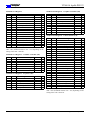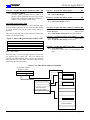
1
VIA Technologies Delivering Value Apollo PLE133 Chipset VT8601A North Bridge Single-Chip Socket-370 PCI North Bridge with 133 / 100 / 66 MHz Front Side Bus, Integrated AGP 2D / 3D Graphics Accelerator and Advanced Memory Controller supporting PC133 / PC100 SDRAM for Desktop PC Systems Revision 1.82 October 22, 2001 VIA TECHNOLOGIES, INC. Copyright Notice: Copyright © 1998, 1999, 2000, 2001 VIA Technologies Incorporated. Printed in the United States. ALL RIGHTS RESERVED. No part of this document may be reproduced, transmitted, transcribed, stored in a retrieval system, or translated into any language, in any form or by any means, electronic, mechanical, magnetic, optical, chemical, manual or otherwise without the prior written permission of VIA Technologies Incorporated. VT82C586B, VT82C596B, VT82C686A, VT82C686B, VT82C598, VT82C598MVP, VT8501, VT82C691, VT82C692, VT82C693, VT82C693A, VT82C694, VT82C694A, VT82C694X, VT8601, VT8601A, VT8602, Mobile South, Super South, Apollo MVP3, Apollo MVP4, Apollo Pro, Apollo ProPlus, Apollo Pro133, Apollo Pro133A, Apollo PM601, and Apollo PLE133 may only be used to identify products of VIA Technologies. VIA C3TM is a registered trademark of VIA Technologies, Inc. PS/2TM is a registered trademark of International Business Machines Corp. Celeron, PentiumTM , Pentium-IITM, Pentium-IIITM, MMXTM, and Intel are registered trademarks of Intel Corp. AMD6K86TM, AMD-K6TM, and AMD-K6-2TM are registered trademarks of Advanced Micro Devices Corp. Windows 95TM, Windows 98TM, and Plug and PlayTM are registered trademarks of Microsoft Corp. PCITM is a registered trademark of the PCI Special Interest Group. All trademarks are the properties of their respective owners. Disclaimer Notice: No license is granted, implied or otherwise, under any patent or patent rights of VIA Technologies. VIA Technologies makes no warranties, implied or otherwise, in regard to this document and to the products described in this document. The information provided by this document is believed to be accurate and reliable to the publication date of this document. However, VIA Technologies assumes no responsibility for any errors in this document. Furthermore, VIA Technologies assumes no responsibility for the use or misuse of the information in this document and for any patent infringements that may arise from the use of this document. The information and product specifications within this document are subject to change at any time, without notice and without obligation to notify any person of such change. Offices: USA Office: 440 Mission Court, Suite 220 Fremont, CA 94539 USA Tel: (510) 683-3300 Fax: (510) 683-3301 or 687-4654 Taipei Office: 8th Floor, No. 533 Chung-Cheng Road, Hsin-Tien Taipei, Taiwan ROC Tel: (886-2) 218-5452 Fax: (886-2) 218-5453 Online Services: Home Page: http://www.via.com.tw (Taiwan) –or- http://www.viatech.com (USA) FTP Server: ftp.via.com.tw (Taiwan) BBS: 886-2-2185208 Technologies, Inc. VT8601A Apollo PLE133 Delivering Value REVISION HISTORY Document Release 0.92 0.93 0.94 1.0 1.1 1.11 1.2 1.3 1.4 1.5 1.6 1.7 1.71 1.8 1.81 1.82 Date 12/9/98 12/16/98 1/20/99 6/4/99 Revision Initial internal release Updated pinouts to match engineering rev 0.5 document dated 12/1/98 Updated pinouts to match engineering rev 0.8 document dated 12/22/98 Added 133 MHz Support to Feature Bullets Updated / Fixed Pin Descriptions: Fixed description of strap options on MA2, MA8, and MA11-14; Removed Auxiliary Memory Port; Added REQ/GNT[4-7]#; Added GND & VCC3 pins to increase pin count to 510 (updated mech spec); Fixed definitions of RESET# & CRSTI# and changed CRSTI# to CPURSTD#; Removed PWRGD function from SERR#; Fixed definitions of SRAS#, SCAS#, and SWE#; Added note to PLLTST description Updated Device 0 Rx50-53, 68[4], 69, 6B[5-1], 6C[7-4], 70[3,0, 72[0], 76[7], 79[10], 7A (added); Device 1 Rx41[0], 42[0] 6/23/99 Updated feature bullets & overview and fixed misc formatting problems Fixed REQ/GNT4# pinouts and CKE & DQM naming polarity Device 0 Bus 0 updated Rx2-3 Device ID, 69[7-6], 6D[6-5], 76[6] Device 0 Bus 0 added Rx2C-D, 2E-F, 50[1], 51[5], 53[2], removed 6E-6F Device 0 Bus 1 updated Rx0-3 Vendor & Device ID, Rx7-6[7] Removed AC timing specs 7/8/99 Fixed pin descriptions of CPURSTD# and SUSP 8/23/99 Fixed typo in device 0 Rx50[7] description; added comment about default state Fixed system freq divider settings (MA pin descriptions, Dev 0 Rx68[1-0]) 9/8/99 Fixed strap options on MA2-6 and MA13 pin descriptions Fixed Device 0 Rx52[7] strap option and removed (reserved) Device 0 Rx52[5] Removed “VIA Confidential” watermark 2/2/00 Added DSTN modes to intro/overview panel interface section Removed incorrect notes under CPU interface pin descriptions Fixed MA11 strapping and VCC3/VSUS3 pin descriptions Fixed Device 0 Bus 0 Rx50[1] and Rx51[1] defaults Fixed Electrical Specs absolute max temp ratings 10/24/00 Changed product name to Apollo PLE133; Fixed typos in pinout table Changed temp specs to be based on case instead of ambient; added power table Changed orientation of pin 1 in mech diagram to match part marking 11/1/00 Fixed product name on cover page; Fixed strap descriptions Fixed Rx50[7], Rx68[1-0], 6B[4], 6C[4], D0Bus1 Rx4[9], Graphics CR39[0] 12/1/00 Removed EDO, FP, VCM and PC66 DRAM support (no longer fully tested) Added VIA Cyrix III CPU to suported CPUs list and changed 686A to 686B Added PLLTST pin I/O type Fixed table formatting errors introduced as a result of Word 2000 upgrade Fixed Rx6B[4] and 6C[4]; Fixed spelling errors in Functional Description 4/26/01 Fixed various typographical and formatting errors 7/3/01 Updated company address; updated processors list Removed LVDS and direct panel drive support; removed MA3-6 straps Fixed SUSP pin description; Fixed Device 0 Rx6A; moved VGA regs intro 10/8/01 Clarified the difference between chipset name and north bridge part number Changed “VIA Cyrix III” to “VIA C3”; Fixed max memory to be 1.5GB Updated Device 0 Rx68[4], 69[7-6, 1], 6B[1]; Updated chip marking specs 10/22/01 Fixed strap pin definitions for MA14,12,11 & updated Rx50[7], 68[1-0] to match Revision 1.82 October 22, 2001 -i- Initials DH DH DH DH DH DH DH DH DH DH DH DH DH DH DH DH Revision History Technologies, Inc. VT8601A Apollo PLE133 Delivering Value TABLE OF CONTENTS REVISION HISTORY.......................................................................................................................................................................... I TABLE OF CONTENTS.................................................................................................................................................................... II LIST OF FIGURES ........................................................................................................................................................................... IV LIST OF TABLES ............................................................................................................................................................................. IV PRODUCT FEATURES.......................................................................................................................................................................1 SYSTEM OVERVIEW.........................................................................................................................................................................6 APOLLO PLE133 CORE LOGIC OVERVIEW ....................................................................................................................................7 APOLLO PLE133 GRAPHICS CONTROLLER OVERVIEW ................................................................................................................8 Capability Overview..................................................................................................................................................................8 System Capabilities....................................................................................................................................................................9 High Performance 64-bit 2D GUI ............................................................................................................................................9 Highly Integrated RAMDACTM & Clock Synthesizer...........................................................................................................9 Full Feature High Performance 3D Engine ............................................................................................................................9 Video Processor........................................................................................................................................................................10 Video Capture and DVD .........................................................................................................................................................10 Versatile Frame Buffer Interface...........................................................................................................................................10 Hi-Res and Hi-Ref Display Support ......................................................................................................................................10 CRT Power Management (VESA DPMS).............................................................................................................................11 Flat Panel Monitor Interface ..................................................................................................................................................11 Video Capture Interface .........................................................................................................................................................11 Complete Hardware Compatibility .......................................................................................................................................11 PINOUTS .............................................................................................................................................................................................12 PIN DESCRIPTIONS .........................................................................................................................................................................15 REGISTERS ........................................................................................................................................................................................23 REGISTER OVERVIEW ....................................................................................................................................................................23 REGISTER SUMMARY TABLES........................................................................................................................................................23 MISCELLANEOUS I/O......................................................................................................................................................................33 CONFIGURATION SPACE I/O ..........................................................................................................................................................33 REGISTER DESCRIPTIONS...............................................................................................................................................................34 Device 0 Bus 0 Header Registers - Host Bridge ....................................................................................................................34 Device 0 Bus 0 Host Bridge Registers ....................................................................................................................................36 CPU Interface Control........................................................................................................................................................................36 DRAM Control ..................................................................................................................................................................................39 PCI Bus Control .................................................................................................................................................................................44 GART / Graphics Aperture Control....................................................................................................................................................48 AGP Control ......................................................................................................................................................................................50 Device 1 Bus 0 Header Registers - PCI-to-AGP Bridge ......................................................................................................52 Device 1 Bus 0 PCI-to-AGP Bridge Registers.......................................................................................................................54 AGP Bus Control ...............................................................................................................................................................................54 Device 0 Bus 1 Header Registers - Graphics Accelerator....................................................................................................55 Device 0 Bus 1 Graphics Accelerator Registers....................................................................................................................58 Graphics Accelerator PCI Bus Master Registers.................................................................................................................................59 Capture / ZV Port Registers................................................................................................................................................................64 DVD Registers ...................................................................................................................................................................................65 VGA Registers..........................................................................................................................................................................68 VGA Standard Registers - Introduction ..............................................................................................................................................68 Revision 1.82 October 22, 2001 -ii- Table of Contents Technologies, Inc. VT8601A Apollo PLE133 Delivering Value Attribute Controller Registers (AR)....................................................................................................................................................69 VGA Status / Enable Registers ...........................................................................................................................................................69 VGA Sequencer Registers (SR)..........................................................................................................................................................70 VGA RAMDAC Registers .................................................................................................................................................................70 VGA Graphics Controller Registers (GR) ..........................................................................................................................................71 VGA CRT Controller Registers (CR) ................................................................................................................................................72 VGA Extended Registers ........................................................................................................................................................73 VGA Extended Registers – Non-Indexed I/O Ports ............................................................................................................................73 VGA Extended Registers – Sequencer Indexed ..................................................................................................................................74 VGA Extended Registers – Graphics Controller Indexed ...................................................................................................................84 VGA Extended Registers – CRT Controller Indexed ..........................................................................................................................90 VGA Extended Registers – CRTC Shadow ......................................................................................................................................104 3D Graphics Engine Registers..............................................................................................................................................105 Operational Concept.........................................................................................................................................................................105 Drawing ...........................................................................................................................................................................................106 Geometry Primitives.........................................................................................................................................................................107 Synchronization................................................................................................................................................................................110 Functional Blocks.............................................................................................................................................................................110 Bus Interface ....................................................................................................................................................................................110 Span Engine............................................................................................................................................................................111 Graphics Engine Core ...........................................................................................................................................................112 Graphics Engine Organization..........................................................................................................................................................115 Setup Engine Registers.....................................................................................................................................................................116 Vertex Registers ...............................................................................................................................................................................117 Rasterization Engine Registers .........................................................................................................................................................118 Pixel Engine Registers......................................................................................................................................................................125 Texture Engine Registers..................................................................................................................................................................131 Memory Interface Registers .............................................................................................................................................................133 Data Port Area..................................................................................................................................................................................133 FUNCTIONAL DESCRIPTIONS ...................................................................................................................................................134 GRAPHICS CONTROLLER POWER MANAGEMENT ......................................................................................................................134 Power Management States....................................................................................................................................................134 Power Management Clock Control .....................................................................................................................................134 Power Management Registers ..............................................................................................................................................134 ELECTRICAL SPECIFICATIONS ...............................................................................................................................................135 ABSOLUTE MAXIMUM RATINGS ..................................................................................................................................................135 DC CHARACTERISTICS.................................................................................................................................................................135 POWER CHARACTERISTICS ..........................................................................................................................................................136 AC TIMING SPECIFICATIONS .......................................................................................................................................................136 MECHANICAL SPECIFICATIONS .............................................................................................................................................137 Revision 1.82 October 22, 2001 -iii- Table of Contents Technologies, Inc. VT8601A Apollo PLE133 Delivering Value LIST OF FIGURES FIGURE 1. FIGURE 2. FIGURE 3. FIGURE 4. FIGURE 5. FIGURE 6. FIGURE 7. FIGURE 8. FIGURE 9. VT8601A BALL DIAGRAM (TOP VIEW)................................................................................................................12 VT8601A PIN LIST (NUMERICAL ORDER) ..........................................................................................................13 VT8601A PIN LIST (ALPHABETICAL ORDER) ...................................................................................................14 GRAPHICS APERTURE ADDRESS TRANSLATION...........................................................................................48 PHYSICAL REGION DESCRIPTOR TABLE FORMAT ......................................................................................60 PCI BUS MASTER ADDRESS TRANSLATION .....................................................................................................60 FRAME BUFFER PARAMETERS ............................................................................................................................97 LIVE VIDEO DISPLAY PARAMETERS .................................................................................................................97 MECHANICAL SPECIFICATIONS - 510-PIN BALL GRID ARRAY PACKAGE ..........................................137 LIST OF TABLES TABLE 1. VT8601A PIN DESCRIPTIONS....................................................................................................................................15 TABLE 2. REGISTER SUMMARY ................................................................................................................................................23 TABLE 3. SYSTEM MEMORY MAP ............................................................................................................................................39 TABLE 4. MEMORY ADDRESS MAPPING TABLE .................................................................................................................39 TABLE 5. VGA/MDA MEMORY/IO REDIRECTION................................................................................................................54 TABLE 6. SUPPORTED PCI COMMAND CODES .....................................................................................................................55 TABLE 7. INTERRUPT SOURCES AND CONTROLS ..............................................................................................................57 TABLE 8. GRAPHICS CLOCK FREQUENCIES – 14.31818 MHZ REFERENCE.................................................................76 TABLE 9. DPMS SEQUENCE - HARDWARE TIMER MODE .................................................................................................87 TABLE 10. DPMS SEQUENCE - HARDWARE MODE IN SIMULTANEOUS DISPLAY MODE ......................................87 TABLE 11. HARDWARE CURSOR PIXEL OPERATION ........................................................................................................94 TABLE 12. PCI POWER MANAGEMENT STATES ................................................................................................................134 TABLE 13. ABSOLUTE MAXIMUM RATINGS .......................................................................................................................135 TABLE 14. DC CHARACTERISTICS .........................................................................................................................................135 TABLE 15. DC CHARACTERISTICS .........................................................................................................................................136 TABLE 16. AC TIMING MIN / MAX CONDITIONS ................................................................................................................136 Revision 1.82 October 22, 2001 -iv- Table of Contents Technologies, Inc. VT8601A Apollo PLE133 Delivering Value VIA VT8601A Apollo PLE133 133 / 100 / 66 MHz Single-Chip Socket-370 PCI North Bridge, With Integrated AGP 2D / 3D Graphics Accelerator and Advanced Memory Controller supporting PC133 / PC100 SDRAM For Desktop PC Systems PRODUCT FEATURES • General − 510 BGA Package (35mm x 35mm ) − 2.5 Volt core with 3.3V CMOS I/O − Supports GTL+ I/O buffer Host interface − Supports separately powered 5.0V tolerant interface to PCI bus and Video interface − 2.5V, 0.25um, high speed / low power CMOS process − PC98 / 99 compatible using VIA VT82C686B (352-pin BGA) south bridge chip for Desktop and Mobile applications − 133 / 100 / 66 MHz CPU Front Side Bus (FSB) Operation • High Integration − Single chip implementation for 64-bit Slot-1 and Socket-370 CPUs, 64-bit system memory, 32-bit PCI with integrated 2D / 3D GUI accelerator − Apollo PLE133 Chipset: VT8601A system controller and VT82C686B PCI to ISA bridge − Chipset includes dual UltraDMA-100 / 66 / 33 EIDE, AC-97 link, 4 USB ports, integrated Super-I/O, hardware monitoring, keyboard / mouse interfaces, and RTC / CMOS • High Performance CPU Interface − Supports VIA C3 and Intel CeleronTM and Pentium IIITM processors − 133 / 100 / 66 MHz CPU Front Side Bus (FSB) − Built-in PLL (Phase Lock Loop) circuitry for optimal skew control within and between clocking regions − Five outstanding transactions (four In-Order Queue (IOQ) plus one input latch) − Supports WC (Write Combining) cycles − Dynamic deferred transaction support − Sleep mode support − System management interrupt, memory remap and STPCLK mechanism CPU 133 MHz 133 MHz 100 MHz 100 MHz 100 MHz 66 MHz 66 MHz DRAM 133 MHz 100 MHz 133 MHz 100 MHz 66 MHz 100 MHz 66 MHz Revision 1.82 October 22, 2001 GUI Core 100 MHz 100 MHz 100 MHz 100 MHz 66 MHz 100 MHz 66 MHz Internal AGP 66 MHz 66 MHz 66 MHz 66 MHz 66 MHz 66 MHz 66 MHz PCI 33 MHz 33 MHz 33 MHz 33 MHz 33 MHz 33 MHz 33 MHz -1- Comments Synchronous (DRAM uses CPU clock) Pseudo-synchronous (DRAM uses GUI clock) Pseudo-synchronous (DRAM uses GUI clock) Synchronous (DRAM uses CPU clock) Pseudo-synchronous (DRAM uses GUI clock) Pseudo-synchronous (DRAM uses GUI clock) Synchronous (DRAM uses CPU clock) Product Features Technologies, Inc. VT8601A Apollo PLE133 Delivering Value • Internal Accelerated Graphics Port (AGP) Controller − AGP v1.0 compliant − Pipelined split-transaction long-burst transfers up to 533 MB/sec − Eight level read request queue − Four level posted-write request queue − Thirty-two level (quadwords) read data FIFO (128 bytes) − Sixteen level (quadwords) write data FIFO (64 bytes) − Intelligent request reordering for maximum AGP bus utilization − Supports Flush/Fence commands − Graphics Address Relocation Table (GART) − One level TLB structure − Sixteen entry fully associative page table − LRU replacement scheme − Independent GART lookup control for host / AGP / PCI master accesses − Windows 95 OSR-2 VXD and integrated Windows 98 / NT5 miniport driver support • Concurrent PCI Bus Controller − PCI bus is synchronous / pseudo-synchronous to host CPU bus − 33 MHz operation on the primary PCI bus − Supports up to five PCI masters − Peer concurrency − Concurrent multiple PCI master transactions; i.e., allow PCI masters from both PCI buses active at the same time − Zero wait state PCI master and slave burst transfer rate − PCI to system memory data streaming up to 132Mbyte/sec − PCI master snoop ahead and snoop filtering − Six levels (double-words) of CPU to PCI posted write buffers − Byte merging in the write buffers to reduce the number of PCI cycles and to create further PCI bursting possibilities − Enhanced PCI command optimization (MRL, MRM, MWI, etc.) − Forty-eight levels (double-words) of post write buffers from PCI masters to DRAM − Sixteen levels (double-words) of prefetch buffers from DRAM for access by PCI masters − Supports L1/L2 write-back forward to PCI master read to minimize PCI read latency − Supports L1/L2 write-back merged with PCI master post-write to minimize DRAM utilization − Delay transaction from PCI master reading DRAM − Read caching for PCI master reading DRAM − Transaction timer for fair arbitration between PCI masters (granularity of two PCI clocks) − Symmetric arbitration between Host/PCI bus for optimized system performance − Complete steerable PCI interrupts − PCI-2.2 compliant, 32 bit 3.3V PCI interface with 5V tolerant inputs Revision 1.82 October 22, 2001 -2- Product Features Technologies, Inc. VT8601A Apollo PLE133 Delivering Value • Advanced High-Performance DRAM Controller − DRAM interface synchronous or pseudosynchronous with CPU FSB speed of 133 / 100 / 66 MHz − DRAM interface may be faster than CPU by 33 MHz to allow use of PC100 with 66 MHz Celeron CPU or use of − − − − − − − − − − − − − − − − − − − − − − − − PC133 with 100 MHz VIA C3 or Intel Pentium II or Pentium III CPU DRAM interface may be slower than CPU by 33 MHz to allow use of older memory modules with a newer CPU Concurrent CPU, AGP, and PCI access Different DRAM timing for each bank Dynamic Clock Enable (CKE) control for SDRAM power reduction in high speed systems Mixed 1M / 2M / 4M / 8M / 16M / 32MxN DRAMs 6 banks DRAMs supported up to 1.5GB (256Mb DRAM technology) Flexible row and column addresses 64-bit data width only 3.3V DRAM interface with 5V-tolerant inputs Programmable I/O drive capability for MA, command, and MD signals Two-bank interleaving for 16Mbit SDRAM support Two-bank and four bank interleaving for 64Mbit SDRAM support Supports maximum 8-bank interleave (i.e., 8 pages open simultaneously); banks are allocated based on LRU Independent SDRAM control for each bank Seamless DRAM command scheduling for maximum DRAM bus utilization (e.g., precharge other banks while accessing the current bank) Four cache lines (16 quadwords) of CPU to DRAM write buffers Four cache lines of CPU to DRAM read prefetch buffers Read around write capability for non-stalled CPU read Speculative DRAM read before snoop result Burst read and write operation x-1-1-1-1-1-1-1 back-to-back accesses for SDRAM from CPU or from DRAM controller BIOS shadow at 16KB increment Decoupled and burst DRAM refresh with staggered RAS timing CAS before RAS or self refresh Revision 1.82 October 22, 2001 -3- Product Features Technologies, Inc. VT8601A Apollo PLE133 Delivering Value • General Graphic Capabilities − 64-bit Single Cycle 2D/3D Graphics Engine − Supports 2 to 8 Mbytes of Frame Buffer − Real Time DVD MPEG-2 and AC-3 Playback − Video Processor − I2C Serial Interface − Integrated 24-bit 230MHz True Color DAC − Extended Screen Resolutions up to 1600x1200 − Extended Text Modes 80 or 132 columns by 25/30/43/60 rows − DirectX 6 and OpenGL ICD API • Graphics Performance − Sustained 1M polygons/second and 100M pixels/second − 30fps DVD playback of 9.8Mbps MPEG-2 video with 30% headroom − Host Based AC-3 decode at only 8% utilization • High Performance rCADE3D™ Accelerator − 32 entry command queue, 32 entry data queue − 4Kbyte texture cache with over 90% hit rates − Pipelined Single Cycle Setup/Texturing/Rendering Engines − DirectDraw™ acceleration − Multiple buffering and page flipping − − − − Setup Engine 32-bit IEEE floating point input data Slope and vertex calculations Back facing triangle culling 1/16 sub-pixel positioning − − − − − − − Rendering Engine High performance single pass execution Diffused and specula lighting Gouraud and flat shading Anti-aliasing including edge, scene, and super-sampling OpenGL compliant blending for fog and depth-cueing 16-bit Z-buffer 8/16/32 bit per pixel color formats − − − − − − Texturing Engine 1/2/4/8-bits per pixel compact palletized textures 16/32-bits per pixel quality non-palletized textures Pallet formats in ARGB 565, 1555, or 444 Tri-linear, bi-linear, and point-sampled filtering Mip-mapping with multiple Level-Of-Detail (LOD) calculations and perspective correction Color keying for translucency − − − − − − 2D GUI Engine 8/15/16/24/32-bits per pixel color formats 256 Raster Operations (ROPs) Accelerated drawing: BitBLTs, lines, polygons, fills, patterns, clipping, bit masking Panning, scrolling, clipping, color expansion, sprites 32x32 and 64x64 Hardware Cursor DOS graphics and text modes Revision 1.82 October 22, 2001 -4- Product Features Technologies, Inc. VT8601A Apollo PLE133 Delivering Value • DVD − Hardware-Assisted MPEG-2 Architecture for DVD with AC-3 − Simultaneous motion compensation and front-end processing (parsing, decryption and decode) − Supports full DVD 1.0, VCD 2.0 and CD-Karaoke − Microsoft DirectShow 3.0 native support, backward compatible to MCI − No additional frame buffer requirements − Sub-picture hardware eliminates Run-Length-Decoder and Alpha Blending overhead − Dynamic frame and field de-interlace filtering for high quality playback on VGA monitors (Bob and Weave) − Tamper-proof software CSS implementation − Freeze, Fast-Forward, Slow Motion, Reverse − Pan-and-Scan support for 16:9 sequence • Video Processor − On-chip Color Space Converter (CSC) − Anti-tearing via two frame buffer based capture surfaces − Minifier for video stream compression and filtering − Horizontal/vertical interpolation with edge recovery − Dual frame buffer apertures for independent memory access for graphics and video − YUV 4:2:2/4:1:1/4:2:0 and RGB formats − Video Module Interface (VMI) to MPEG and video decoder − Vertical Blank Interval for Intercast™ − Overlay differing video and graphic color depths − Minifier Video Module Interface (VMI) to MPEG and video decode − Display two simultaneous video streams from both internal AGP and VMI − Two scalers and Color Space Converters (CSC) for independent windows • Digital Flat Panel (DFP) Interface − 85 MHz Flat Panel Monitor interface supports 1024x768 panels − Uses external TMDS transmitters for advanced panel interfaces • Power Management Support − Dynamic power down of SDRAM (CKE) − Independent clock stop controls for CPU / SDRAM, AGP, and PCI bus − PCI and AGP bus clock run and clock generator control − VTT suspend power plane preserves memory data − Suspend-to-DRAM and Self-Refresh operation − EDO self-refresh and SDRAM self-refresh power down − 8 bytes of BIOS scratch registers − Low-leakage I/O pads • Testability − Build-in NAND-tree pin scan test capability Revision 1.82 October 22, 2001 -5- Product Features Technologies, Inc. VT8601A Apollo PLE133 Delivering Value SYSTEM OVERVIEW The Apollo PLE133 chipset consists of the VT8601A North Bridge (described by this document) and the VT82C686B South Bridge (described in a separate data sheet). The VT8601A is a PC system logic North Bridge for Socket-370 CPUs with integrated 2D/3D Graphics accelerator. The core logic portion of the chip is based on the VIA Apollo Pro133 with integrated graphics accelerator provided by an industry leading Graphics supplier. The combination of the two leading edge technologies provides a stable, cost-effective, and high performance solution to both the Desktop and Mobile personal computer markets. As shown in Figure 1 below, the Apollo PLE133 will interface to: • Socket-370 Front-Side Bus (133, 100 and 66 MHz) • PC133 / PC100 SDRAM Memory Interface • PCI Bus (33 MHz) • Analog RGB Monitor with DDC • Digital Monitor Transmitters (TMDS) • Video Capture / Playback CODECs VIA C3 or Intel Celeron / Pentium III Processor TMDS TV Signal TV Encoder CNTLs VT8601A North Bridge 510 BGA D R A MA[13:0] M MD[63:0] VMI PCI SLOTS PCI BUS SMBUS VT82C686B South Bridge 352 BGA Dual-IDE AC-Link AC-97 ISA SLOTS ISA Bus BIOS ROM 4x USB Serial Ports Floppy Disk Parallel Port Figure 1: Apollo PLE133 High Level System Diagram Revision 1.82 October 22, 2001 -6- System Overview Technologies, Inc. VT8601A Apollo PLE133 Delivering Value Apollo PLE133 Core Logic Overview The Apollo PLE133 chipset is a high performance, cost-effective and energy efficient solution for the implementation of Integrated 2D / 3D Graphics - PCI - ISA desktop and notebook personal computer systems from 66 MHz to 133 MHz based on 64bit Socket-370 VIA C3 / Intel Celeron and Pentium III processors. The complete solution consists of the VT8601A “System Media Accelerator” (SMA) north bridge (510 BGA) and either the VT82C596B (324 BGA) or the VT82C686B (352 BGA) PCIto-ISA south bridge. Both south bridges are PC98 / PC99 compliant with integrated UltraDMA-66 / 33 IDE, 4 USB ports, and a complete power management feature set. The VT82C686B also integrates HW monitoring, Super-I/O functions (floppy disk drive interface and serial / parallel ports), and AC-97 link supporting digital audio and HSP modem functions. Apollo PLE133 supports six banks of DRAMs up to 1.5GB. The DRAM controller supports PC133 and PC100 Synchronous DRAM (SDRAM). The Synchronous DRAM interface allows zero wait state bursting between the DRAM and the data buffers at 100 or 133 MHz. The six banks of DRAM can be composed of an arbitrary mixture of 1M / 2M / 4M / 8M / 16M / 32MxN DRAMs. The DRAM Controller is optimized to run synchronous with the CPU Front Side Bus (FSB) frequency of 100 or 133 MHz or pseudosynchronous to the Front Side Bus with the SDRAM and FSB frequencies differing by 33 MHz. Apollo PLE133 also supports full AGP v1.0 capability with the internal 2D/3D Graphics Engine for maximum software compatibility. An eight level request queue plus a four level post-write request queue with thirty-two and sixteen quadwords of read and write data FIFO’s respectively are included for deep pipelined and split AGP transactions. A single-level GART TLB with 16 full associative entries and flexible CPU/AGP/PCI remapping control is also provided for operation under protected mode operating environments. Both Windows-95 VXD and Windows-98 / NT5 miniport drivers are supported. Apollo PLE133 supports one 32-bit 3.3 / 5V system bus (PCI) that is synchronous to the CPU bus. The chip also contains a builtin AGP bus-to-PCI bus bridge to allow simultaneous concurrent operations on each bus. Five levels (doublewords) of post write buffers are included to allow for concurrent CPU and PCI operation. For PCI master operation, forty-eight levels (doublewords) of post write buffers and sixteen levels (doublewords) of prefetch buffers are included for concurrent PCI bus and DRAM/cache accesses. The chip also supports enhanced PCI bus commands such as Memory-Read-Line, Memory-Read-Multiple and MemoryWrite-Invalid commands to minimize snoop overhead. In addition, advanced features are supported such as snoop ahead, snoop filtering, L1 / L2 write-back forward to PCI master, and L1 / L2 write-back merged with PCI post write buffers to minimize PCI master read latency and DRAM utilization. Delay transaction and read caching mechanisms are also implemented for further improvement of overall system performance. For sophisticated notebook implementations, the Apollo PLE133 north bridge provides independent clock stop control for the CPU / SDRAM, PCI, and AGP buses and Dynamic CKE control for powering down of the SDRAM. A separate suspend-well plane is implemented for the SDRAM control signals for Suspend-to-DRAM operation. Coupled with the 324-pin Ball Grid Array VIA VT82C596B south bridge chip, a complete notebook PC main board can be implemented with no external TTLs. Revision 1.82 October 22, 2001 -7- System Overview Technologies, Inc. VT8601A Apollo PLE133 Delivering Value Apollo PLE133 Graphics Controller Overview The Apollo PLE133 Graphics Controller is a highly integrated display control device that incorporates a 64-bit 3D/2D graphic engine and video accelerator with advanced DVD video and optional TV output capability. It provides a flexible and high performance solution for graphics and video playback acceleration for various color depth and resolution modes. The Apollo PLE133 Graphics Controller supports a video capture port to import captured live MPEG 1 or MPEG 2 video streams, or DVD decompressed video streams to be overlaid with a graphics stream of mixed color depth displays. In supporting dual live videos, the Apollo PLE133 Graphics Controller offers independent dual video windows ready for videoconferencing and with linear scaling capability. Integrating the programmable phase lock loop with high speed LUT DACs, the Apollo PLE133 Graphics Controller is a true price/performance solution for the modern multimedia based entertainment PC. Capability Overview The Apollo PLE133 Graphics Controller is a fully integrated CRT and TV 64-bit 2D/3D Accelerator. The high performance graphics engine offers high speed 3D image processing in full compliance and compatibility with IBM® VGA and VESA™ extended VGA. As an integrated controller, it allows unprecedented cost and performance advantages by eliminating the need for an external frame buffer while at the same time gaining local access to a larger amount of memory. Many functions can now be eliminated that previously consumed large amounts of bandwidth. The Apollo PLE133 Graphics Controller, equipped with a single-cycle 3D GUI Engine, pipelines 3D rendering process architecture in hardware, providing real-time interactions with solid 3D models in CAD/CAM, 3D modeling, and 3D games. It supports all key 3D rendering operations, including: Gouraud shading for smooth object surfaces, texture mapping for realistic object textures, 16-bit hardware Z-buffering for fast 3D depth calculations, and Alpha Blending for transparency effects. The Apollo PLE133 Graphics Controller’s highly innovative design, a full 64-bit memory interface with a high performance graphics engine which can support a RAMDAC™ running up to 230MHz, dramatically improves GUI functions and significantly promotes overall system operation. The Apollo PLE133 Graphics Controller supports a full AGP implementation internally to remain compatible with existing software and programming models. However, since the engine is integrated it enjoys a higher bandwidth and lower latency than is possible with discrete solutions. AGP operations can include direct access of the system memory by the 2D/3D engine to provide increased texture memory. To meet the requirements of a PC99 graphics adapter in a multimedia PC, the Apollo PLE133 Graphics Controller supports planar video format for MPEG-1, MPEG-2, and DVD-video playback. The dual video playback is capable of overlaying windows for videoconferencing and multimedia displays. Advanced features of the Apollo PLE133 Graphics Controller, such as color space conversion, video scaling, dual video windows, dual-view display, Video Module Interface (VMI), Vertical Blanking Interleave (VBI), a 24-bit True Color DAC, and triple clock synthesizers allow performance at peak levels. By using an extended 16-bit VMI port the Apollo PLE133 Graphics Controller can support DTV resolution. This port can operate as either an input for Video Capture or as an output for Video display. The Apollo PLE133 Graphics Controller is capable of supporting three simultaneous displays: CRT, Flat Panel Monitor & Video, each with a different “window” or desktop. The Apollo PLE133 integrated Graphics Controller supports a rich featured flat panel monitor interface that can be used with external TMDS transmitters to support the latest DVI displays. Revision 1.82 October 22, 2001 -8- System Overview Technologies, Inc. VT8601A Apollo PLE133 Delivering Value System Capabilities The Apollo PLE133 Graphics Controller’s main system features include: • • • • • • • • • • • • • High Performance single cycle GUI Highly Integrated RAMDAC™ and Triple Clock Synthesizer Full Feature High Performance 3D Graphics Engine High speed internal AGP Bus Mastering data bus supporting DVD video playback & 3D Hardware implementation of motion compensation Dual Video Windows for Videoconferencing TrueVideo Processor DirectDrawTM and DirectVideoTM Hardware Support Versatile Motion Video Capture/Overlay/Playback Support Flexible Frame Buffer Memory Interface Advanced Mobile Power Management CRT Power Management (VESA™ DPMS) PC99 Hardware Support High Performance 64-bit 2D GUI The 64-bit graphics engine of the Apollo PLE133 Graphics Controller significantly improves graphics performance through specialized hardware that accelerates the most frequently used GUI operations and matches the high-speed requirements of CPUs. Functions directly supported in hardware include: BitBLTs, image and text transfer, line draw, short stroke vector draw, rectangle fills, and clipping. The graphics engine supports 256 Raster Operations (ROPs) for up to 32-bit packed pixel graphic modes. The ROP3 Processor in the Apollo PLE133 Graphics Controller is able to perform Boolean functions which allow many additional operations, including transparency, pattern masking, color expansion alignment, and pattern enhancement. Additionally, the graphics engine features linear display memory addressing (up to 4GB memory space), accelerated color expansion modes for graphics text procession, and memory-mapped I/O registers on the graphics engine for faster access time. Graphic functions are optimized by a 64-bit internal data bus and a four-color hardware cursor/pop-up icon, operating up to a 128x128x2 pixel image, which offloads the CPU. The hardware cursor mechanism can also be used to display patterns stored in the system memory. This pop-up icon is very useful to display user friendly information instantly through simple hot key operations. This advanced function combination allows significant performance increases over standard Super VGA designs and provides outstanding graphics acceleration on GUIs, such as Microsoft Windows 98. Highly Integrated RAMDACTM & Clock Synthesizer The highly integrated design of the Apollo PLE133 Graphics Controller offers a “no TTL” solution for cost-effective, highperformance multimedia subsystem designs for the PC and compatible notebooks. The 64-bit memory data bus supporting SDRAM and SGRAM memory provides faster data transfer rates for improved system throughput. The Apollo PLE133 Graphics TM TM Controller has a built-in, high speed RAMDAC . The RAMDAC is composed of one 256x24 and one 256x18 color lookup table and a triple loop frequency synthesizer, providing the read/write timing control for the Frame Buffer Memory and the refresh of the TV/CRT display. The integrated frequency synthesizer provides a 125MHz memory clock for high speed DRAM access and a 230MHz video clock which supports various refresh rates up to 85Hz at 1280x1024. Full Feature High Performance 3D Engine The Apollo PLE133 Graphics Controller is equipped with an advanced Graphics Drawing, Single Cycle 3D Graphics Engine that performs premium 3D functions at a high level of more than 1M triangles per second. The 3D engine supports Microsoft Direct3D. The 3D Engine is set up to off-load the CPU from major 3D tasks including slope calculation, sub-pixel positioning, and Tri-striping. By balancing the 3D pipeline and reducing parameter passing, the Apollo PLE133 Graphics Controller provides very high levels of performance. The 3D engine is integrated with a triangle set-up engine that sets up triangles according to vertex input data and accomplishes various functions for 3D rendering. Gouraud shading provides smooth shading for colors across surfaces, perspective correction texture mapping to correct texture data based on the perspective, bi-linear texture filtering for interpolating, alpha blending to compensate colors for the opacity of two colors blended, Z-buffering (16-bit/24-bit), video texturing to overlay 2D video play-back onto 3D images, fogging to simulate weather effects, palletized texture mapping (1-, 4-, or 8-bit) for memory and bandwidth reduction, and anti-aliasing to reduce or eliminate jaggies resulted from alias rendering. The 3D engine also works with the APM system, conserving power while 3D operations are suspended. Revision 1.82 October 22, 2001 -9- System Overview Technologies, Inc. VT8601A Apollo PLE133 Delivering Value Video Processor Video processor features include: on-chip hardware Color Space Conversion (CSC) for faster data conversion on the fly, Horizontal/Vertical (H/V) scaling with interpolation, edge recovery algorithm logic, gamma correction, and overlay control with different color depths from graphics. The Apollo PLE133 Graphics Controller also includes a fully integrated GUI accelerator, read cache, and command FIFO that optimize memory bandwidth and maximize graphics performance. The Apollo PLE133 Graphics Controller, with an integrated Video Display and a Capture Engine, supports dual apertures on the PCI bus which enables independent graphic and video data to be transported simultaneously to and from different memory areas TM TM and greatly accelerates the performance of both DirectDraw and DirectVideo . The Apollo PLE133 Graphics Controller can provide dual video windows that display different images from different video sources (from the PCI bus and from the capture port) on the same screen. The video image is stored in off-screen memory and is retrieved by the Video Display Processing block for video processing. With the help of DirectDraw™ acceleration for sprites, page flipping, double buffering, and color keying, video processing is performed by utilizing a proprietary edge recovery algorithm for sharper line visibility, de-interlacing, antitearing, multitap horizontal filtering, dithering, and scaling operations with bilinear interpolation in both horizontal and vertical directions. Linear scaling permits zoom in/out to any size without any restrictions. In addition, the on-chip hardware Color Space Conversion (CSC) accelerates conversion for 16 bit YUV pixels into linear true color 32 bit RGB pixels on the fly. The additional X and Y minifiers are capable of shrinking video images to any linear fractions, which saves bus bandwidth and memory space. The YUV planar logic of the Apollo PLE133 Graphics Controller supports a YUV 420 format that can eliminate redundant video stream decoding procedures. The load of the CPU is reduced while performing software MPEG or software video conferencing. The color and luminance control provided by the Apollo PLE133 Graphics Controller offers color compensations to prevent color distortion for display devices such as a CRT or TV with Gamma correction and hue adjustment control. The Video Conferencing feature allows remote and local video images to be displayed simultaneously on the same screen. Video Capture and DVD The Apollo PLE133 Graphics Controller has a Video Module Interface (VMI) and advanced hardware interface logic allowing it to be directly connected to many MPEG and video decoders such as the C-Cube CL450/480, SGS 3400/3500, Philips 7110/1 and Brooktree BT819/817/827/829. The Apollo PLE133 Graphics Controller, integrated with a DVD video hardware block for motion compensation, gives existing PCs the ability to play DVD video in MPEG-2 format at high bandwidths with very good video quality. A new industry standard is being set for transmission of non-video data over a TV broadcast signal during vertical blanking dead time. This technology is referred to as Intercast. The Apollo PLE133 Graphics Controller has the ability to take the entire video stream over the video port, sending the visible video stream to the display memory for display in a window, stripping the VBI data from the stream, and then sending this data to the CPU for processing using PCI Bus Mastering. Versatile Frame Buffer Interface The Apollo PLE133 Graphics Controller features a versatile frame buffer interface aperture into main system memory. Optimized performance can be achieved with the single cycle memory bus interface using programmable DRAM timing. The display queue has been increased to reduce the frequency of memory bus requests, optimizing memory bus efficiency for the graphic controller. With the support of the internal AGP aperture, the Apollo PLE133 Graphics Controller has access to system memory through the GART. In the execute mode, the Apollo PLE133 Graphics Controller is able to use both the dedicated graphics portion and the general portion of system memory for graphics operations. As a result, DVD and 3D rendering performance and quality are greatly enhanced. Hi-Res and Hi-Ref Display Support Apollo PLE133 Graphics Controller display enhancements dramatically improve CRT resolution. These enhancements include support of non-interlaced 1280x1024x64K, 1024x768x16M, 800x600x16M, and 640x480x16M colors for “full spectrum” color. Extended text modes of 80 or 132 columns by 25, 30, 43, or 60 rows provide an extended graphics area frequently used in many spreadsheet and database applications. Extended graphics and text modes are supported by software drivers that provide a “readyto-go” solution, minimizing the need for additional driver development. A virtual screen can be created with the Apollo PLE133 Graphics Controller . When this function is enabled, a selected portion of a large image can be shown on a smaller display. The image can also be moved across the whole screen, either up or down. 2 The Apollo PLE133 Graphics Controller is able to automatically detect DDC monitors with I C signaling. Revision 1.82 October 22, 2001 -10- System Overview Technologies, Inc. VT8601A Apollo PLE133 Delivering Value CRT Power Management (VESA DPMS) The Apollo PLE133 Graphics Controller conforms to the standard power management schemes defined by VESA™ for CRTs. The Apollo PLE133 Graphics Controller supports four states of VESA™ Display Power Management Signaling (DPMS), which decrease monitor power consumption after timeout periods. VESA™ DPMS power down states (ready, standby, suspend, and off) specify HSYNC and VSYNC signals to control the monitor power down state. Flat Panel Monitor Interface The Apollo PLE133 Flat Panel Monitor interface is designed to support industry standard TFT panel based Flat Panel Monitors via external TMDS transmitters. The interface supports both 18-bit and 24-bit display modes. Optionally, an 18+18 panel can be supported utilizing external latches. Pin PD[23] PD[22] PD[21] PD[20] PD[19] PD[18] PD[17] PD[16] PD[15] PD[14] PD[13] PD[12] PD[11] PD[10] PD[9] PD[8] PD[7] PD[6] PD[5] PD[4] PD[3] PD[2] PD[1] PD[0] 24 Bit TFT B0 B1 G0 G1 R0 R1 B2 B3 G2 G3 R2 R3 B4 B5 B6 B7 G4 G5 G6 G7 R4 R5 R6 R7 18 Bit TFT S2 S1 Notes S2 used for external 18+18 S1 used for external 18+18 B0 B1 G0 G1 R0 R1 B2 B3 B4 B5 G2 G3 G4 G5 R2 R3 R4 R5 Video Capture Interface The Video Module Interface (VMI) is supported for video devices such as MPEG1 and MPEG2. Additionally, the zero-wait state host write buffer, read cache, and memory mapped I/O increase operating speeds and contribute to peak performance levels. All I/O interfaces are 5V tolerant, capable of interfacing with external devices operating at 5V, even though the Apollo PLE133 Graphics Controller runs at 2.5V. Graphics system throughput is further enhanced by a command FIFO, allowing maximum bus transfer speed for applications such as Windows™ or AutoCAD™ that directly access video memory. Complete Hardware Compatibility The Apollo PLE133 Graphics Controller is fully compliant with the VESA™ DDC and VAFC standards. The Apollo PLE133 Graphics Controller is 100% VGA compatible at both the BIOS and Driver level, allowing full compatibility with virtually any VGA application software. The Apollo PLE133 Graphics Controller provides hardware support to DirectDraw™, offering high speed game graphics on Windows 98. The Apollo PLE133 Graphics Controller meets the requirements of PC99 as well, supporting a unique ID for each customer and a unique ID for each model. Revision 1.82 October 22, 2001 -11- System Overview Technologies, Inc. VT8601A Apollo PLE133 Delivering Value PINOUTS Figure 1. VT8601A Ball Diagram (Top View) Key 1 A GND RGB NC NC NC NC HD62 HD57 HD63 GND HD45 HD38 HD34 HD31 HD16 HD13 HD3 B GND S GND NC NC NC HD50 HD59 HD48 HD51 HD44 HD22 HD32 HD33 HD19 HD24 C VCC S RED NC NC NC HD60 HD55 GND HD41 HD49 HD43 HD28 HD26 GND D VCC R BLUE GRN GND HD61 HD53 HD54 HD47 HD42 HD37 HD36 HD29 HD25 HD23 VTT GTL REF E 2 3 VSYNC HSYNC IRSET 4 COMP 5 HD56 6 HD58 7 HD46 8 HD40 9 HD27 10 HD39 F EVDD SDA SCL ETST# SUSP GND VCC3 HD52 VCCI VCC3 G EBLT PD0 FLM SCLK LP VCC3 G7 8 9 10 H PD2 PD1 DE PD5 EVEE VCC3 H CRT J PD4 PD3 PD8 PD7 PD11 VCCI J K PD12 PD10 PD13 PD20 PD16 PD6 K L PD17 PD15 PD18 VCC3 PD9 PD14 L M PD23 IMIO IMIIN PD21 PD22 PD19 M N VD14 VD13 GND VD15 VD12 GND N P GND VD9 VD10 VD11 VD8 GND P R VD6 VD4 VD7 VD5 VD3 VD0 R T VD2 VD1 VHS VCC3 TVD4 TVD6 T 12 13 14 CPU Pins 21 22 23 24 25 26 HD12 GND HA18 HA20 HA22 HA10 HA28 HA3 GND HD2 HD10 HD1 HA26 HA29 HA23 HA25 HA21 HA13 HA5 HA6 HD20 HD9 HD5 HD4 GND HA27 HA31 HA19 HA16 HA9 HA11 HA8 HD7 HD11 HD8 HD6 HD15 HA30 HA17 HA12 GND HA4 HA14 BNR# HA24 GTL REF CPU RSTD# HA7 HREQ 0# HREQ 4# BPRI# HREQ 1# HREQ 2# HREQ 3# DEFER# HIT# H TRDY# HITM# 15 HD18 HD17 HD0 GND VCC3 VCCI VTT VCC3 GND HA15 16 17 18 19 G20 VCC3 H HCLK LOCK# H J VCCA VCCA GND RS2# DBSY# VCCI MCLK DRDY# ADS# O RS0# BREQ 0# GND MCLK I RS1# PLLTST MD1 MD32 16 K17 K VCC3 Panel L GND VCC3 GND GND VCC3 GND L L GNDA GNDA MD33 MD35 MD3 MD2 Pins M VCC3 GND GND GND GND VCC3 M M GND MD34 MD0 MD5 MD36 MD4 N GND GND GND GND GND GND N N GND MD39 MD37 MD7 MD38 MD6 Video P GND GND GND GND GND GND P P GND MD12 MD8 MD41 MD9 MD40 Pins R VCC3 GND GND GND GND VCC3 R R MD44 MD10 MD43 MD11 MD42 T GND VCC3 GND GND VCC3 GND T T GND MD15 MD13 MD46 MD14 MD45 SWEC# MD47 SWEA# SWEB# CKE2 CKE0 U10 U V TVD0 TVD1 TVD3 TVCK TVHS VCCI V TVout W VCC D VCC V1 TVVS XTLO INTA# VCC3 W Pins Y GND V1 GND V2 VCC V2 VLF1 XTLI NC VCC3 Y7 8 AD30 GND 20 15 VCC5 VCC3 GND 19 CPU RST# HD14 17 14 TVD2 GND VCC3 18 HD30 16 13 TVD5 NC HD21 15 12 VCLK NC HD35 14 11 TVD7 NC 13 K10 VVS VLF2 11 12 Pins U AA 11 9 11 PCI Pins 10 11 AD16 VCCI VCC3 AD25 AD21 DEV SEL# PAR CBE1# 12 12 13 13 14 14 15 15 GND GND GND AD10 AD7 AD5 PCLK 16 16 U17 17 18 Mem U VCC3 SCAS A# Pins V VCCI VSUS3 DQM 0 W CS5# VSUS3 DQM 1 Y20 VCC3 CS4# CS3# CS2# 19 SCASC# SCASB# CKE1 CKE3 GND GND DQM 5 DQM 4 CS1# CS0# VCC3 VCCI MD58 VCC3 GND VSUS2 MA0 SRAS A# CKE5 CKE4 MD63 MD29 MD56 MD54 MD20 MD18 VSUS3 MA1 MA4 MA3 MA2 MA6 MA5 SRASB# SRASC# AB NC NC NC NC GNT 0# AC NC REQ 5# REQ 6# GND REQ 0# AD29 AD24 AD23 AD17 IRDY# AD15 AD11 AD6 AD4 PREQ# MD31 MD60 MD25 MD23 MD52 MD49 SUST# GND MA7 AD REQ 7# GNT 5# GNT 6# REQ 3# REQ 1# AD28 CBE3# GND CBE2# TRDY# AD14 AD9 GND PWR OK PGNT# MD61 MD27 MD57 GND MD21 MD50 MD16 DQM 6 MA11 MA9 MA8 AE GNT 7# GNT 4# GNT 3# REQ 2# AD1 PCI RST# MD48 DQM 3 MA12 MA13 BA0 MA10 GND REQ 4# GNT 2# GNT 1# AD0 PCK RUN# MD17 DQM 7 DQM 2 MA14 BA1 GND AF LOCK# AD31 Revision 1.82 October 22, 2001 AD27 AD26 AD20 AD22 AD19 AD18 FRM# GND STOP# SERR# AD13 AD12 AD8 CBE0# AD2 AD3 -12- MD30 MD62 MD59 MD28 MD26 GND MD55 MD24 MD22 MD53 MD19 MD51 Pinouts Technologies, Inc. VT8601A Apollo PLE133 Delivering Value Figure 2. VT8601A Pin List (Numerical Order) Pin # Pin Name Pin # Pin Name Pin # Pin Name Pin # Pin Name D02 A BLUE G05 O LP N26 IO MD06 A01 P GNDRGB A02 IO NC D03 A GRN G06 P VCC3 P01 P GND A03 IO NC P02 IO VD09 D04 P GND G21 P VCC3 A04 IO NC D05 IO HD61 G22 I HCLK P03 IO VD10 A05 IO NC D06 IO HD53 G23 I HLOCK# P04 IO VD11 A06 IO HD62 D07 IO HD54 G24 IO HIT# P05 IO VD08 A07 IO HD57 D08 IO HD47 G25 IO HTRDY# P06 P GND A08 IO HD63 D09 IO HD42 G26 I HITM# P21 P GND D10 IO HD37 H01 O PD02 P22 IO MD12 A09 P GND A10 IO HD45 D11 IO HD36 H02 O PD01 P23 IO MD08 A11 IO HD38 D12 IO HD29 H03 O DE P24 IO MD41 A12 IO HD34 D13 IO HD25 H04 O PD05 P25 IO MD09 A13 IO HD31 D14 IO HD23 H05 O EVEE / P26 IO MD40 A14 IO HD16 D15 IO HD07 R01 IO VD06 H06 P VCC3 A15 IO HD13 D16 IO HD11 R02 IO VD04 H21 P VCCA A16 IO HD03 D17 IO HD08 R03 IO VD07 H22 P VCCA A17 IO HD12 D18 IO HD06 H23 IO RS0# R04 IO VD05 D19 IO HD15 R05 IO VD03 A18 P GND H24 P GND A19 O CPURST# D20 IO HA30 H25 IO RS2# R06 IO VD00 A20 IO HA18 D21 IO HA17 H26 IO DBSY# R22 IO MD44 A21 IO HA20 D22 IO HA12 J01 O PD04 R23 IO MD10 A22 IO HA22 J02 O PD03 R24 IO MD43 D23 P GND A23 IO HA10 D24 IO HA04 J03 O PD08 R25 IO MD11 A24 IO HA28 D25 IO HA14 J04 O PD07 R26 IO MD42 A25 IO HA03 D26 IO BNR# J05 O PD11 T01 IO VD02 E01 O VSYNC T02 IO VD01 A26 P GND J06 P VCCI E02 O HSYNC T03 IO VHS B01 P GNDS J21 P VCCI E03 A IRSET J22 O MCLKO B02 P GND T04 P VCC3 B03 IO NC E04 A COMP J23 IO DRDY# T05 O TVD4 B04 IO NC E05 IO HD56 J24 IO ADS# T06 O TVD6 B05 IO NC E06 IO HD58 J25 O BREQ0# T21 P GND B06 IO HD50 E07 IO HD46 T22 IO MD15 J26 P GND B07 IO HD59 E08 IO HD40 K01 O PD12 T23 IO MD13 B08 IO HD48 E09 IO HD27 K02 O PD10 T24 IO MD46 B09 IO HD51 E10 IO HD39 K03 O PD13 T25 IO MD14 B10 IO HD44 K04 O PD20 T26 IO MD45 E11 P VTT B11 IO HD22 K05 O PD16 U01 IO VVS E12 P GTLREF B12 IO HD32 E13 IO HD35 K06 O PD06 U02 O TVD7 B13 IO HD33 E14 IO HD21 U03 IO VCLK K21 P VCC3 B14 IO HD19 E15 IO HD30 K22 I MCLKI U04 O TVD5 B15 IO HD24 E16 IO HD14 K23 IO RS1# U05 O TVD2 B16 IO HD02 E17 IO HD18 K24 I PLLTST U06 P VCC5 B17 IO HD10 E18 IO HD17 K25 IO MD01 U21 P VCC3 B18 IO HD01 E19 IO HD00 K26 IO MD32 U22 O SCASA# B19 IO HA26 E20 IO HA24 L01 O PD17 U23 IO MD47 B20 IO HA29 L02 O PD15 U24 O SWEA#/ E21 P GTLREF B21 IO HA23 E22 O CPURSTD# L03 O PD18 U25 O SWEB#/ / CKE2 B22 IO HA25 E23 IO HA07 U26 O SWEC#/ / CKE0 L04 P VCC3 B23 IO HA21 E24 IO HREQ0# L05 O PD09 V01 O TVD0 B24 IO HA13 E25 IO HREQ4# L06 O PD14 V02 O TVD1 B25 IO HA05 E26 IO BPRI# V03 O TVD3 L21 P GNDA B26 IO HA06 F01 O EVDD V04 O TVCLK L22 P GNDA F02 IO SDA L23 IO MD33 V05 O TVHS C01 P VCCS C02 A RED F03 IO SCL L24 IO MD35 V06 P VCCI C03 IO NC F04 I ETST# L25 IO MD03 V21 P VCCI C04 IO NC F05 I SUSP L26 IO MD02 V22 P VSUS3 C05 IO NC M01 O PD23 V23 O DQM0 F06 P GND C06 IO HD60 M02 O IMIO V24 O SCASC# / CKE1 F07 P VCC3 C07 IO HD55 F08 IO HD52 M03 I IMIIN V25 O SCASB# / CKE3 M04 O PD21 C08 P GND F09 P VCCI V26 P GND C09 IO HD41 M05 O PD22 F10 P VCC3 W01 P VCCD C10 IO HD49 M06 O PD19 F12 P VCC3 W02 P VCCV1 C11 IO HD43 W03 O TVVS F13 P GND M21 P GND C12 IO HD28 M22 IO MD34 W04 O XLTO F14 P GND C13 IO HD26 M23 IO MD00 W05 O INTA# F16 P GND M24 IO MD05 C14 P GND F17 P VCC3 W06 P VCC3 C15 IO HD20 M25 IO MD36 W21 O CS5# F18 P VCCI C16 IO HD09 M26 IO MD04 F19 P VTT W22 P VSUS3 C17 IO HD05 N01 IO VD14 W23 O DQM1 F20 P VCC3 C18 IO HD04 N02 IO VD13 F21 P GND W24 P GND F22 IO HA15 W25 O DQM5 C19 P GND N03 P GND C20 IO HA27 F23 IO HREQ1# N04 IO VD15 W26 O DQM4 C21 IO HA31 F24 IO HREQ2# N05 IO VD12 Y01 P GNDV1 C22 IO HA19 F25 IO HREQ3# N06 P GND Y02 P VCCV2 C23 IO HA16 F26 IO DEFER# Y03 A VLF1 N21 P GND C24 IO HA09 G01 O EBLT N22 IO MD39 Y04 I XLTI C25 IO HA11 G02 O PD00 N23 IO MD37 Y05 IO NC C26 IO HA08 G03 O FLM N24 IO MD07 Y06 P VCC3 G04 O SCLK N25 IO MD38 D01 P VCCR Y21 P VCC3 Center GND Pins (28 pins): L11, L13-14, L16, M12-15, N11-16, P11-16, R12-15, T11, T13-14, T16 Center VCC3 Pins (8 pins): L12, L15, M11, M16, R11, R16, T12, T15 Revision 1.82 October 22, 2001 -13- Pin # Y22 Y23 Y24 Y25 Y26 AA01 AA02 AA03 AA04 AA05 AA06 AA07 AA08 AA09 AA10 AA13 AA14 AA15 AA17 AA18 AA19 AA20 AA21 AA22 AA23 AA24 AA25 AA26 AB01 AB02 AB03 AB04 AB05 AB06 AB07 AB08 AB09 AB10 AB11 AB12 AB13 AB14 AB15 AB16 AB17 AB18 AB19 AB20 AB21 AB22 AB23 AB24 AB25 AB26 AC01 AC02 AC03 AC04 AC05 AC06 AC07 AC08 AC09 AC10 AC11 AC12 AC13 AC14 AC15 AC16 AC17 AC18 AC19 AC20 AC21 AC22 AC23 AC24 AC25 O O O O O P A IO IO IO P P IO P P P P P P P IO P P P O O O O IO IO IO IO O IO IO IO IO IO IO IO IO IO I IO IO IO IO IO IO P O O O O IO IO IO P I IO IO IO IO IO IO IO IO IO I IO IO IO IO IO IO I P O O Pin Names Pin # CS4# CS3# CS2# CS1# CS0# GNDV2 VLF2 NC NC NC GND VCC3 AD16 VCCI VCC3 GND GND GND VCC3 VCCI MD58 VCC3 GND VSUS2 MA00 / strap SRASA# SRASB# / CKE5 SRASC# / CKE4 NC NC NC NC GNT0# AD30 AD25 AD21 DEVSEL# PAR CBE1# AD10 AD07 AD05 PCLK MD63 MD29 MD56 MD54 MD20 MD18 VSUS3 MA01 / strap MA04 MA03 MA02 / strap NC REQ5# REQ6# GND REQ0# AD29 AD24 AD23 AD17 IRDY# AD15 AD11 AD06 AD04 PREQ# MD31 MD60 MD25 MD23 MD52 MD49 SUST# GND MA07 / strap MA06 AC26 AD01 AD02 AD03 AD04 AD05 AD06 AD07 AD08 AD09 AD10 AD11 AD12 AD13 AD14 AD15 AD16 AD17 AD18 AD19 AD20 AD21 AD22 AD23 AD24 AD25 AD26 AE01 AE02 AE03 AE04 AE05 AE06 AE07 AE08 AE09 AE10 AE11 AE12 AE13 AE14 AE15 AE16 AE17 AE18 AE19 AE20 AE21 AE22 AE23 AE24 AE25 AE26 AF01 AF02 AF03 AF04 AF05 AF06 AF07 AF08 AF09 AF10 AF11 AF12 AF13 AF14 AF15 AF16 AF17 AF18 AF19 AF20 AF21 AF22 AF23 AF24 AF25 AF26 Pin Name O IO IO IO I I IO IO P IO IO IO IO P I O IO IO IO P IO IO IO O O O O IO O O I IO IO IO IO IO IO IO IO IO IO I IO IO IO IO IO IO IO O O O O P I O O IO IO IO IO P IO IO IO IO IO IO IO IO P IO IO IO IO O O O P MA05 REQ7# GNT5# GNT6# REQ3# REQ1# AD28 CBE3# GND CBE2# TRDY# AD14 AD09 GND PWROK PGNT# MD61 MD27 MD57 GND MD21 MD50 MD16 DQM6 MA11 / strap MA09 / strap MA08 / strap GNT7# GNT4# GNT3# REQ2# LOCK# AD27 AD20 AD19 FRAME# STOP# AD13 AD08 AD02 AD01 RESET# MD30 MD59 MD26 MD55 MD22 MD19 MD48 DQM3 MA12 / strap MA13 / strap MA10 / strap GND REQ4# GNT2# GNT1# AD31 AD26 AD22 AD18 GND SERR# AD12 CBE0# AD03 AD00 PCKRUN# MD62 MD28 GND MD24 MD53 MD51 MD17 DQM7 DQM2 MA14 / strap GND Pinouts Technologies, Inc. VT8601A Apollo PLE133 Delivering Value Figure 3. VT8601A Pin List (Alphabetical Order) Pin # Pin Name AF14 IO AD00 AE14 IO AD01 AE13 IO AD02 AF13 IO AD03 AC14 IO AD04 AB14 IO AD05 AC13 IO AD06 AB13 IO AD07 AE12 IO AD08 AD12 IO AD09 AB12 IO AD10 AC12 IO AD11 AF11 IO AD12 AE11 IO AD13 AD11 IO AD14 AC11 IO AD15 AA08 IO AD16 AC09 IO AD17 AF08 IO AD18 AE08 IO AD19 AE07 IO AD20 AB08 IO AD21 AF07 IO AD22 AC08 IO AD23 AC07 IO AD24 AB07 IO AD25 AF06 IO AD26 AE06 IO AD27 AD06 IO AD28 AC06 IO AD29 AB06 IO AD30 AF05 IO AD31 J24 IO ADS# D02 A BLUE D26 IO BNR# E26 IO BPRI# J25 O BREQ0# AF12 IO CBE0# AB11 IO CBE1# AD09 IO CBE2# AD07 IO CBE3# E04 A COMP A19 O CPURST# E22 O CPURSTD# Y26 O CS0# Y25 O CS1# Y24 O CS2# Y23 O CS3# Y22 O CS4# W21 O CS5# H26 IO DBSY# H03 O DE F26 IO DEFER# AB09 IO DEVSEL# V23 O DQM0 W23 O DQM1 AF24 O DQM2 AE23 O DQM3 W26 O DQM4 W25 O DQM5 AD23 O DQM6 AF23 O DQM7 J23 IO DRDY# G01 O EBLT F04 I ETST# F01 O EVDD H05 O EVEE G03 O FLM AE09 IO FRAME# A09 P GND A18 P GND A26 P GND B02 P GND C08 P GND C14 P GND C19 P GND D04 P GND D23 P GND F06 P GND Center GND Pins (28 pins): Center VCC3 Pins (8 pins): Pin # Pin Name Pin # Pin Name Pin # Pin Name B16 IO HD02 AA23 O MA00 / strap F13 P GND A16 IO HD03 AB23 O MA01 / strap F14 P GND C18 IO HD04 AB26 O MA02 / strap F16 P GND C17 IO HD05 AB25 O MA03 F21 P GND D18 IO HD06 AB24 O MA04 H24 P GND D15 IO HD07 AC26 O MA05 J26 P GND D17 IO HD08 AC25 O MA06 M21 P GND C16 IO HD09 AC24 O MA07 / strap N03 P GND B17 IO HD10 AD26 O MA08 / strap N06 P GND D16 IO HD11 AD25 O MA09 / strap N21 P GND A17 IO HD12 AE26 O MA10 / strap P01 P GND A15 IO HD13 AD24 O MA11 / strap P06 P GND E16 IO HD14 AE24 O MA12 / strap P21 P GND D19 IO HD15 AE25 O MA13 / strap T21 P GND A14 IO HD16 AF25 O MA14 / strap V26 P GND E18 IO HD17 K22 I MCLKI W24 P GND E17 IO HD18 J22 O MCLKO AA06 P GND B14 IO HD19 M23 IO MD00 AA13 P GND C15 IO HD20 K25 IO MD01 AA14 P GND E14 IO HD21 L26 IO MD02 AA15 P GND B11 IO HD22 L25 IO MD03 AA21 P GND D14 IO HD23 M26 IO MD04 AC04 P GND B15 IO HD24 M24 IO MD05 AC23 P GND D13 IO HD25 N26 IO MD06 AD08 P GND C13 IO HD26 N24 IO MD07 AD13 P GND E09 IO HD27 P23 IO MD08 AD19 P GND C12 IO HD28 P25 IO MD09 AF01 P GND D12 IO HD29 R23 IO MD10 AF09 P GND E15 IO HD30 R25 IO MD11 AF18 P GND A13 IO HD31 P22 IO MD12 AF26 P GND B12 IO HD32 T23 IO MD13 L21 P GNDA B13 IO HD33 T25 IO MD14 L22 P GNDA A12 IO HD34 T22 IO MD15 A01 P GNDRGB E13 IO HD35 AD22 IO MD16 B01 P GNDS D11 IO HD36 AF22 IO MD17 Y01 P GNDV1 D10 IO HD37 AB21 IO MD18 AA01 P GNDV2 AB05 O GNT0# A11 IO HD38 AE21 IO MD19 AF04 O GNT1# E10 IO HD39 AB20 IO MD20 AF03 O GNT2# E08 IO HD40 AD20 IO MD21 AE03 O GNT3# C09 IO HD41 AE20 IO MD22 AE02 O GNT4# D09 IO HD42 AC19 IO MD23 AD02 O GNT5# C11 IO HD43 AF19 IO MD24 AD03 O GNT6# B10 IO HD44 AC18 IO MD25 AE01 O GNT7# A10 IO HD45 AE18 IO MD26 D03 A GRN E07 IO HD46 AD17 IO MD27 D08 IO HD47 AF17 IO MD28 E12 P GTLREF B08 IO HD48 AB17 IO MD29 E21 P GTLREF A25 IO HA03 C10 IO HD49 AE16 IO MD30 D24 IO HA04 B06 IO HD50 AC16 IO MD31 B25 IO HA05 B09 IO HD51 K26 IO MD32 B26 IO HA06 F08 IO HD52 L23 IO MD33 E23 IO HA07 D06 IO HD53 M22 IO MD34 C26 IO HA08 D07 IO HD54 L24 IO MD35 C24 IO HA09 C07 IO HD55 M25 IO MD36 A23 IO HA10 E05 IO HD56 N23 IO MD37 C25 IO HA11 A07 IO HD57 N25 IO MD38 D22 IO HA12 E06 IO HD58 N22 IO MD39 B24 IO HA13 B07 IO HD59 P26 IO MD40 D25 IO HA14 C06 IO HD60 P24 IO MD41 F22 IO HA15 D05 IO HD61 R26 IO MD42 C23 IO HA16 A06 IO HD62 R24 IO MD43 D21 IO HA17 A08 IO HD63 R22 IO MD44 A20 IO HA18 G24 IO HIT# T26 IO MD45 C22 IO HA19 G26 I HITM# T24 IO MD46 A21 IO HA20 G23 I HLOCK# U23 IO MD47 B23 IO HA21 E24 IO HREQ0# AE22 IO MD48 A22 IO HA22 F23 IO HREQ1# AC21 IO MD49 B21 IO HA23 F24 IO HREQ2# AD21 IO MD50 E20 IO HA24 F25 IO HREQ3# AF21 IO MD51 AC20 IO MD52 B22 IO HA25 E25 IO HREQ4# B19 IO HA26 E02 O HSYNC AF20 IO MD53 C20 IO HA27 G25 IO HTRDY# AB19 IO MD54 A24 IO HA28 M02 O IMIO AE19 IO MD55 B20 IO HA29 M03 I IMIIN AB18 IO MD56 D20 IO HA30 W05 O INTA# AD18 IO MD57 C21 IO HA31 AC10 IO IRDY# AA19 IO MD58 G22 I HCLK E03 A IRSET AE17 IO MD59 E19 IO HD00 AE05 IO LOCK# AC17 IO MD60 B18 IO HD01 G05 O LP AD16 IO MD61 L11, L13-14, L16, M12-15, N11-16, P11-16, R12-15, T11, T13-14, T16 L12, L15, M11, M16, R11, R16, T12, T15 Revision 1.82 October 22, 2001 -14- Pin # AF16 AB16 A02 A03 A04 A05 B03 B04 B05 C03 C04 C05 Y05 AA03 AA04 AA05 AB01 AB02 AB03 AB04 AC01 AB10 AF15 AB15 G02 H02 H01 J02 J01 H04 K06 J04 J03 L05 K02 J05 K01 K03 L06 L02 K05 L01 L03 M06 K04 M04 M05 M01 AD15 K24 AC15 AD14 C02 AC05 AD05 AE04 AD04 AF02 AC02 AC03 AD01 AE15 H23 K23 H25 U22 V25 V24 G04 F03 F02 AF10 AA24 AA25 AA26 AE10 F05 AC22 U24 IO IO IO IO I O O O O O O O O O O O O O O O O O O O O O O O O O I I I A I I I I I I I I I IO IO IO O O O O IO IO IO O O O IO I I O Pin Names Pin # MD62 MD63 NC NC NC NC NC NC NC NC NC NC NC NC NC NC NC NC NC NC NC PAR PCKRUN# PCLK PD00 PD01 PD02 PD03 PD04 PD05 PD06 PD07 PD08 PD09 PD10 PD11 PD12 PD13 PD14 PD15 PD16 PD17 PD18 PD19 PD20 PD21 PD22 PD23 PGNT# PLLTST PREQ# PWROK RED REQ0# REQ1# REQ2# REQ3# REQ4# REQ5# REQ6# REQ7# RESET# RS0# RS1# RS2# SCASA# SCASB# / CKE3 SCASC# / CKE1 SCLK SCL SDA SERR# SRASA# SRASB# / CKE5 SRASC# / CKE4 STOP# SUSP SUST# SWEA# U25 U26 AD10 V04 V01 V02 U05 V03 T05 U04 T06 U02 V05 W03 F07 F10 F12 F17 F20 G06 G21 H06 K21 L04 T04 U21 W06 Y06 Y21 AA07 AA10 AA17 AA20 U06 H21 H22 W01 F09 F18 J06 J21 V06 V21 AA09 AA18 D01 C01 W02 Y02 U03 R06 T02 T01 R05 R02 R04 R01 R03 P05 P02 P03 P04 N05 N02 N01 N04 T03 Y03 AA02 AA22 V22 W22 AB22 E01 E11 F19 U01 Y04 W04 Pin Name O O IO O O O O O O O O O O O P P P P P P P P P P P P P P P P P P P P P P P P P P P P P P P P P P P IO IO IO IO IO IO IO IO IO IO IO IO IO IO IO IO IO IO A A P P P P O P P IO I O SWEB#/ / CKE2 SWEC#/ / CKE0 TRDY# TVCLK TVD0 TVD1 TVD2 TVD3 TVD4 TVD5 TVD6 TVD7 TVHS TVVS VCC3 VCC3 VCC3 VCC3 VCC3 VCC3 VCC3 VCC3 VCC3 VCC3 VCC3 VCC3 VCC3 VCC3 VCC3 VCC3 VCC3 VCC3 VCC3 VCC5 VCCA VCCA VCCD VCCI VCCI VCCI VCCI VCCI VCCI VCCI VCCI VCCR VCCS VCCV1 VCCV2 VCLK VD00 VD01 VD02 VD03 VD04 VD05 VD06 VD07 VD08 VD09 VD10 VD11 VD12 VD13 VD14 VD15 VHS VLF1 VLF2 VSUS2 VSUS3 VSUS3 VSUS3 VSYNC VTT VTT VVS XLTI XLTO Pinouts Technologies, Inc. VT8601A Apollo PLE133 Delivering Value PIN DESCRIPTIONS Table 1. VT8601A Pin Descriptions CPU Interface Signal Name Pin # I/O Signal Description HA[31:3]# see pin list IO HD[63:0]# ADS# BNR# see pin list J24 D26 IO IO IO BPRI# E26 IO DBSY# H26 IO DEFER# F26 IO DRDY# HIT# J23 G24 IO IO HITM# G26 I HLOCK# G23 I J25 E25, F25, F24, F23, E24 O IO HTRDY# G25 IO RS[2:0]# H25, K23, H23 IO A19 E22 O O Host Address Bus. Connect to the address bus of the host CPU. These pins are inputs during CPU cycles, but are driven by the VT8601A during cache snooping operations. Host CPU Data. These signals are connected to the CPU data bus. Address Strobe. The CPU asserts ADS# in T1 of the CPU bus cycle. Block Next Request. Used to block the current request bus owner from issuing new requests. This signal is used to dynamically control the processor bus pipeline depth. Priority Agent Bus Request. The owner of this signal will always be the next bus owner. This signal has priority over symmetric bus requests and causes the current symmetric owner to stop issuing new transactions unless the HLOCK# signal is asserted. The VT82C693 drives this signal to gain control of the processor bus. Data Bus Busy. Used by the data bus owner to hold the data bus for transfers requiring more than one cycle. Defer. The VT8601A uses a dynamic deferring policy to optimize system performance. The VT8601A also uses the DEFER# signal to indicate a processor retry response. Data Ready. Asserted for each cycle that data is transferred. Hit. Indicates that a cacheing agent holds an unmodified version of the requested line. Also driven in conjunction with HITM# by the target to extend the snoop window. Hit Modified. Asserted by the CPU to indicate that the address presented with the last assertion of EADS# is modified in the L1 cache and needs to be written back. Host Lock. All CPU cycles sampled with the assertion of HLOCK# and ADS# until the negation of HLOCK# must be atomic. Bus Request 0. Bus request output to CPU. Request Command. Asserted during both clocks of the request phase. In the first clock, the signals define the transaction type to a level of detail that is sufficient to begin a snoop request. In the second clock, the signals carry additional information to define the complete transaction type. Host Target Ready. Indicates that the target of the processor transaction is able to enter the data transfer phase. Response Signals. Indicates the type of response per the table below: RS[2:0]# Response type 000 Idle State 001 Retry Response 010 Defer Response 011 Reserved 100 Hard Failure 101 Normal Without Data 110 Implicit Writeback 111 Normal With Data CPU Reset. Reset output to CPU CPU Reset Delayed. CPU Reset output delayed by 2T. BREQ0# HREQ[4:0]# CPURST# CPURSTD# Revision 1.82 October 22, 2001 -15- Pinouts Technologies, Inc. VT8601A Apollo PLE133 Delivering Value DRAM Interface Signal Name Pin # I/O Signal Description MD[63:0] MA[14:0] / Strap Options see pin list AF25, AE25, AE24, AD24, AE26, AD25, AD26, AC24, AC25, AC26, AB24, AB25, AB26, AB23, AA23 IO O/I CKE5# / SRASB#, CKE4# / SRASC#, CKE3# / SCASB#, CKE2# / SWEB#, CKE1# / SCASC#, CKE0# / SWEC# CS[5-0]# AA25, AA26, V25, U25, V24, U26 W21, Y22, Y23, Y24, Y25, Y26 AF23, AD23, W25, W26, AE23, AF24, W23, V23 AA24, AA25, AA26 IO Memory Data. Memory Address. DRAM address lines. These pins are also used for power-up strapping options (sampled on the rising edge of RESET#): MA14,12 Rx68[1-0] CPU FSB Freq (0=66, 1=100, 2=rsvd, 3=133) MA13 Rx52[7] GTL I/O Buffer Pullup (L=Enable, H=Disable) MA11 Rx50[7] In-Order Queue Depth (L=4-level, H=1-level) MA10-9 North Bridge Clock Delay (0-3 Clocks) MA8, 2 Graphics Clock Select (0=Normal, 1-3=Test) MA7 Graphics Test Mode (L=Normal, H=Test) MA1-0 Graphics Clock Delay (0-3 Clocks) All pins have internal pull-downs for default low (L). Strap high (H) using 4.7KΩ TO VCC3. SDRAM Clock Enable. Clock enables 5-0 may be connected to the DRAM modules in any order. Each DRAM module requires 2 clock enables. Note: These pins are powered by VSUS DQM[7:0] O Chip Select. One per bank (powered by VSUS) O Data Mask. One per byte lane (powered by VSUS) Row Address Command Indicator. For support of up to three Synchronous DRAM DIMM slots (these are copies of the same logical signal). “A” controls banks 0-1 (module 0), “B” controls banks 2-3 (module 1), and “C” controls banks 4-5 (module 2). U22, O Column Address Command Indicator. For support of up to three SCASA#, V25, Synchronous DRAM DIMM slots (these are copies of the same logical SCASB# / CKE3 V24 signal). “A” controls banks 0-1 (module 0), “B” controls banks 2-3 SCASC# / CKE1 (module 1), and “C” controls banks 4-5 (module 2). U24, O Write Enable Command Indicator. For support of up to three SWEA#, U25, Synchronous DRAM DIMM slots (these are copies of the same logical SWEB# / CKE2, U26 signal). “A” controls banks 0-1 (module 0), “B” controls banks 2-3 SWEC# / CKE0 (module 1), and “C” controls banks 4-5 (module 2). Note: These pins are powered by VSUS. Note: Clocking of the memory subsystem uses memory clock (MCLK); see the clock pin group at the end of the pin descriptions section for descriptions of the clock pins. Note: Connect all memory interface pins except MD to the DRAM modules through 22Ω series resistors (see the Apollo PLE133 Design Guide” for more specific connection details and PCB layout recommendations). SRASA#, SRASB# / CKE5, SRASC# / CKE4 Revision 1.82 October 22, 2001 O -16- Pinouts Technologies, Inc. VT8601A Apollo PLE133 Delivering Value PCI Bus Interface Signal Name Pin # I/O Signal Description see pin list IO CBE[3:0]# AD7, AD9, AB11, AF12 IO PAR FRAME# AB10 AE9 IO IO IRDY# AC10 IO TRDY# AD10 IO STOP# AE10 IO DEVSEL# AB9 IO LOCK# AE5 IO SERR# AF10 IO PREQ# AC15 I PGNT# AD15 O AD1, AC3, AC2, AF2, AD4, AE4, AD5, AC5 AE1, AD3, AD2, AE2, AE3, AF3, AF4, AB5 W5 I Address/Data Bus. The standard PCI address and data lines. The address is driven with FRAME# assertion and data is driven or received in following cycles. Command/Byte Enables. Commands are driven with FRAME# assertion. Byte enables corresponding to supplied or requested data are driven on following clocks. Parity. A single parity bit is provided over AD[31:0] and C/BE[3:0]. Frame. Assertion indicates the address phase of a PCI transfer. Negation indicates that one more data transfer is desired by the cycle initiator. 10KΩ pullup to VCC3. Initiator Ready. Asserted when initiator is ready for data transfer. 10KΩ pullup to VCC3. Target Ready. Asserted when target is ready for data transfer. 10KΩ pullup to VCC3. Stop. Asserted by the target to request the master to stop the current transaction. 10KΩ pullup to VCC3. Device Select. This signal is driven by the PLE133 when a PCI initiator is attempting to access main memory. It is an input when the PLE133 is acting as a PCI initiator. 10KΩ pullup to VCC3. Lock. Used to establish, maintain, and release resource lock. 10KΩ pullup to VCC3. System Error. The PLE133 will pulse this signal when it detects a system error condition (10KΩ pullup to VCC3). South Bridge Request. This signal comes from the South Bridge. PREQ# is the South Bridge request for the PCI bus. 10KΩ pullup to VCC3. South Bridge Grant. This signal driven by the PLE133 to grant PCI access to the South Bridge. 10KΩ pullup to VCC3. PCI Master Request. PCI master requests for use of the PCI bus. 2.2KΩ pullup to VCC5. PCI Master Grant. Permission is given to the master to use the PCI bus. 2.2KΩ pullup to VCC3. AD[31:0] REQ[7:0]# GNT[7:0]# O PCI Interrupt Out. INTA# is an asynchronous active low output used to signal an event that requires handling. It is driven by the integrated graphics controller. Note: Clocking of the PCI interface is performed with PCLK; see the clock pin group at the end of the pin descriptions section for descriptions of the clock input pins. INTA# Revision 1.82 October 22, 2001 O -17- Pinouts Technologies, Inc. VT8601A Apollo PLE133 Delivering Value Clock / Reset Control Signal Name Pin # I/O HCLK G22 I MCLKI K22 I MCLKO J22 O PCLK AB15 I PCKRUN# AF15 IO XLTI Y4 I XLTO W4 O RESET# AE15 I CPURST# CPURSTD# PWROK SUST# A19 E22 AD14 AC22 O O I I F5 I SUSP Signal Description Host Clock. This pin receives the host CPU clock. This clock is used by all logic in the host CPU domain. It is driven by the external clock synthesizer. Memory Clock In. This clock is used by internal clock logic to maintain the proper phase relationship with MCLKO. It is driven by the external clock synthesizer. Memory Clock Out. Created on-chip from MCLKI and used by the memory controller as a timing reference for creation of all memory timing sequences. It is connected to the external clock chip for use in maintaining proper phase relationships. PCI Clock. This clock is used by all on-chip logic in the PCI clock domain. This input must be 33 MHz maximum to comply with PCI specification requirements and must be synchronous with the host CPU clock (HCLK) with an HCLK:PCLK frequency ratio of 2:1 (66MHz CPU clock) or 3:1 (100 MHz CPU clock). The PCI clock needs to be controlled to within 1.5 ± 0.5 nsec relative to the host CPU clock (CPU leads). PCI Clock Run. For implementation of PCI bus clock control for low-power PCI bus operation. Refer to the “PCI Mobile Design Guidelines” and “Apollo PLE133 Design Guide” documents for additional information. Crystal Input. 14.31818 MHz for the video clock synthesizer reference. Connect to a 14.31818 MHz clock source if a crystal not used. Connect to main ground plane GND with 10Pf if using a crystal. Crystal Output. 14.31818 MHz for the video clock synthesizer reference. Leave open if a clock source is used instead of a crystal. Connect to main ground plane GND with 10Pf if using a crystal. Reset. Driven from the South Bridge PCIRST# signal. When asserted (low), this signal resets the PLE133 and sets all register bits to the default value. This signal also connects to the PCI bus (South Bridge RESET drives the ISA bus if implemented). The rising edge of this signal is used to sample all power-up strap options (see memory interface MA pins). CPU Reset. CPU Reset output to the host CPU. CPU Reset Delayed 2T. Alternate CPU Reset output to the host CPU Power OK. Connect to South Bridge and Power Good circuitry. Suspend Status. For implementation of the Suspend-to-DRAM feature. Input logic for this pin is powered by VSUS. Connect to the South Bridge SUST# pin or to a 10KΩ pullup to VSUS if not used. Suspend. Used to put the integrated graphics controller into suspend state. Input logic for this pin is powered by VCC3. Connect to South Bridge GPO pin or to a 10KΩ pullup to VCC3 if not used. Miscellaneous Signal Name ETST# IMIO IMIIN Pin # I/O F4 M2 M3 I O I Revision 1.82 October 22, 2001 Signal Description Test Mode Enable. 4.7KΩ pullup to VCC3 for normal operation. IMI Out. Leave open. IMI In. 4.7KΩ pullup to VCC3. -18- Pinouts Technologies, Inc. VT8601A Apollo PLE133 Delivering Value CRT Interface Signal Name Pin # I/O RED C2 A GRN BLUE HSYNC D3 D2 E2 A A O VSYNC E1 O SDA F2 IO SCL F3 IO Signal Description Red. Red analog output to the CRT. Connect 75Ω load resistor to GNDR (RGB Return) and connect to VGA connector through a series ferrite bead and 10pF capacitors to GNDR on both input and output sides of the bead (see “Apollo PLE133 Design Guide”). Green. Green analog output to the CRT. Connect same as RED. Blue. Blue analog output to the CRT. Connect same as RED. Horizontal Sync. Digital horizontal sync output to the CRT. Also used (with VSYNC) to signal power management state information to the CRT per the VESA™ DPMS™ standard. Connect to VGA connector through a series 47Ω resistor and 120pF capacitor to ground (see “Apollo PLE133 Design Guide”). Vertical Sync. Digital vertical sync output to the CRT. Also used (with HSYNC) to signal power management state information to the CRT per the VESA™ DPMS™ standard. Connect to VGA connector through a series 47Ω resistor and 120pF capacitor to ground (see “Apollo PLE133 Design Guide”). DDC Data/Address. Serial I2C protocol for VESA™ DDC2B signaling to the CRT. Connect this pin to VCC5 through a 4.7KΩ pullup. Connect to the VGA connector only (pin 12 of the connector). Connect through a ferrite bead and 120pF capacitor to ground (on the output side of the bead). Refer to the “Apollo PLE133 Design Guide” for additional information. DDC Clock. Serial I2C protocol for VESA™ DDC2B signaling to the CRT. Connect this pin to VCC5 through a 4.7KΩ pullup. Connect to the VGA connector only (pin 15 of the VGA connector). Connect through a ferrite bead and 120pF capacitor to ground (on the output side of the bead). Refer to the “Apollo PLE133 Design Guide” for additional information. DFP Interface Signal Name Pin # I/O Signal Description (see pin list) O Panel Data. Digital pixel data outputs to the panel. PD[23-0] G4 O Shift Clock. Clock for transferring digital pixel data. SCLK H3 O Data Enable. Indicates valid data on PD[23-0]. DE G5 O Line Pulse. Digital monitor equivalent of HSYNC. LP G3 O First Line Marker. Digital monitor equivalent of VSYNC. FLM F1 O EVDD Enable Panel VDD Power. H5 O EVEE Enable Panel VEE Power. G1 O EBLT Enable Panel Backlight. Note: Connect SHFCLK, DE, LP, and FLM to external TMDS transmitters through series 22Ω resistors. See the “Apollo PLE133 Design Guide” for DFP interface design examples and additional information. Revision 1.82 October 22, 2001 -19- Pinouts Technologies, Inc. VT8601A Apollo PLE133 Delivering Value TV Input / Video Interface Signal Name Pin # I/O Signal Description N4, N1, N2, N5, P4, P3, P2, P5, IO Video Capture / Playback Data. R3, R1, R4, R2, R5, T1, T2, R6 T3 IO Video Horizontal Sync. Connect to TV decoder if used. VHS U1 IO Video Vertical Sync. Connect to TV decoder if used. VVS U3 IO Video Clock. Connect to TV decoder through a series 22Ω resistor. VCLK Note: Refer to the “Apollo PLE133 Design Guide” for video interface design examples. VD[15-0] TV Output Interface Signal Name Pin # I/O Signal Description U2, T6, U4, T5, V3, U5, V2, V1 O TV Output Data. Connect to TV encoder if used. TVD[7-0] V5 O TV Horizontal Sync. Connect to TV encoder if used. TVHS W3 O TV Vertical Sync. Connect to TV encoder if used. TVVS V4 O TVCLK TV Clock. Connect to TV encoder through a series 22Ω resistor. Note: Refer to the “Apollo PLE133 Design Guide” for TV interface design examples. Revision 1.82 October 22, 2001 -20- Pinouts Technologies, Inc. VT8601A Apollo PLE133 Delivering Value Clock Power / Ground and Filtering Signal Name Pin # I/O VCCA H21, H22 P GNDA L21, L22 P VCCV1 W2 P GNDV1 Y1 P VLF1 Y3 A VCCV2 Y2 P GNDV2 AA1 P VLF2 AA2 A PLLTST K24 I Signal Description Power for North Bridge Clock Circuitry (2.5V ±5%). Connect to VCCI through a ferrite bead and decouple to GNDA with 0.001Uf and 0.1Uf ceramic and 10Uf tantalum capacitors (see “Apollo PLE133 Design Guide”). Ground for North Bridge Clock Circuitry. Connect to main ground plane GND through a ferrite bead. (see “Apollo PLE133 Design Guide”). Power for Video Clock Synthesizer 1 Analog Circuitry (2.5V ±5%). Connect to VCCI through a ferrite bead and decouple to GNDV1 with 0.001Uf and 0.1Uf ceramic and 10Uf tantalum capacitors (see “Apollo PLE133 Design Guide”). Ground for Video Clock Synthesizer 1. Connect to main ground plane through a ferrite bead. Low Pass Filter Capacitor for Video Clock Synthesizer 1. Connect to GNDV1 through a 560Pf capacitor. Power for Video Clock Synthesizer 2 Analog Circuitry (2.5V ±5%). Connect to VCCI through a ferrite bead and decouple to GNDV2 with 0.001Uf and 0.1Uf ceramic and 10Uf tantalum capacitors (see “Apollo PLE133 Design Guide”). Ground for Video Clock Synthesizer 2. Connect to main ground plane through a ferrite bead. Low Pass Filter Capacitor for Video Clock Synthesizer 2. Connect to GNDV2 through a 560Pf capacitor. PLL Test. Pull down with 4.7K resistor for normal operation. RAMDAC Output Power / Ground and Analog Control Signal Name Pin # I/O VCCS C1 P GNDS B1 P COMP E4 A IRSET E3 A GNDRGB A1 P Signal Description Power for RAMDAC Current Source Circuitry (2.5V ±5%). Connect to VCCI through a ferrite bead and decouple to GNDS with 0.001uF and 0.1uF ceramic and 10uF tantalum capacitors (see “Apollo PLE133 Design Guide”). Ground for RAMDAC Current Source Circuitry. Connect to main ground plane through a ferrite bead. Compensation Capacitor. RAMDAC analog control. Connect to VCCS using a 0.1 uF capacitor. RAMDAC Current Set Point Resistor. RAMDAC analog control. Connect to GNDS through a 360Ω 1% resistor. RGB Video Output Return. Connection point for the RGB load resistors. Also used as a shield for the RGB video output traces to the VGA display connector. Connects to RGB return pins 6, 7, and 8 of the VGA connector. Connect to main ground plane through a ferrite bead. Refer to the “Apollo PLE133 Design Guide” for more specific connection and PCB layout details. Commonly Used Prefix / Suffix Letters in Signal Names: I = Internal Logic A = North Bridge Clock Synthesizer M = Memory (SDRAM) Interface V1 = Video Clock Synthesizer PLL1 H = Host CPU Interface V2 = Video Clock Synthesizer PLL2 P = PCI Bus Interface D = Video Clocks Digital Data Path G = AGP Bus (internal in PLE133) R = RAMDAC Digital Data Path GM = Graphics Memory Interface S = RAMDAC Current Source U (or USB) = USB (Universal Serial Bus) RGB = Analog Video Out Return H (or HWM) = Hardware Monitoring TV = TV Out SUS = Suspend Power V = TV In / Video Capture Revision 1.82 October 22, 2001 -21- Pinouts Technologies, Inc. VT8601A Apollo PLE133 Delivering Value Digital Power and Ground Signal Name Pin # I/O VCC5 U6 P VCC3 P VSUS3 F7, F10, F12, F17, F20, G6, G21, H6, K21, L4, L12, L15, M11, M16, R11, R16, T4, T12, T15, U21, W6, Y6, Y21, AA7, AA10, AA17, AA20 V22, W22, AB22 VSUS2 AA22 P VCCI P VCCD F9, F18, J6, J21, V6, V21, AA9, AA18 W1 VCCR D1 P E11, F19 E12, E21 P P A9, A18, A26, B2, C8, C14, C19, D4, D23, F6, F13-F14, F16, F21, H24, J26, L11, L13, L14, L16, M12-M15, M21, N3, N6, N11-N16, N21, P1, P6, P11-P16, P21, R12-R15, T11, T13, T14, T16, T21, V26, W24, AA6, AA13-AA15, AA21, AC4, AC23, AD8, AD13, AD19, AF1, AF9, AF18, AF26 A2-A5, B3-B5, C3-C5, Y5, AA3-AA5, AB1-AB4, AC1 P Power for Video Clock Synthesizer Digital Logic (2.5V ±5%). Connect to VCCI through a ferrite bead and decouple to main ground plane GND with 0.001uF and 0.1uF ceramic and 10uF tantalum capacitors (see “Apollo PLE133 Design Guide”). Power for RAMDAC Video Output Digital Logic (2.5V ±5%). Connect to VCCI through a ferrite bead and decouple to main ground plane GND with 0.001uF and 0.1uF ceramic and 10uF tantalum capacitors (see “Apollo PLE133 Design Guide”). CPU Interface Termination Voltage (1.5V ±10%). CPU Interface GTL+ Voltage Reference. 2/3 VTT ±2%. Derived from the termination voltage to the pullup resistors. Determines the noise margin for the host CPU interface signals. Internally connects to + + the GTL sense amp on each GTL input or I/O pin. Ground. Connect to primary PCB ground plane. - No Connect. VTT GTLREF GND NC Revision 1.82 October 22, 2001 P P Signal Description Power for Display / Video Interfaces (5V ±5%). Power for CRT H/VSYNC, DFP interface, video interface, and TV interface. Used to provide adequate output voltage swing for driving external video devices. Also used to provide 5V input tolerance from those interfaces. Power for On-Board Interfaces (3.3V ±5%). Power for host CPU / L2 Cache interface, PCI bus interface, and memory interface (except pins listed below under VSUS). Suspend Power (3.3V ±5%). Power for memory interface signals SRASC#, SCASC#, SWEC#, SWEB#, RAS[5-0]#, CAS[7-0]#, and SUST#. Connect to VCC3 if suspend functions are not implemented. Suspend Power (2.5V ±5%). Connect to VCCI if suspend functions are not implemented. Power for On-Chip Internal Logic (2.5V ±5%). -22- Pinouts Technologies, Inc. VT8601A Apollo PLE133 Delivering Value REGISTERS Register Overview Register Summary Tables The following tables summarize the configuration and I/O registers of the PLE133. These tables also document the power-on default value (“Default”) and access type (“Acc”) for each register. Access type definitions used are RW (Read/Write), RO (Read/Only), “—” for reserved / used (essentially the same as RO), and RWC (or just WC) (Read / Write 1’s to Clear individual bits). Registers indicated as RW may have some read/only bits that always read back a fixed value (usually 0 if unused); registers designated as RWC or WC may have some read-only or read write bits (see individual register descriptions following these tables for details). All offset and default values are shown in hexadecimal unless otherwise indicated. Revision 1.82 October 22, 2001 Table 2. Register Summary I/O Ports Port # 22 CFB-8 CFF-C -23- I/O Port PCI / AGP Arbiter Disable Configuration Address Configuration Data Default 00 0000 0000 0000 0000 Acc RW RW RW Register Summary Tables Technologies, Inc. VT8601A Apollo PLE133 Delivering Value Device 0 Bus 0 Registers - Host Bridge PCI Configuration Registers Offset 1-0 3-2 5-4 7-6 8 9 A B C D E F 13-10 14-27 28-2B 2D-2C 2F-2E 33-30 37-34 34-3B 3C-3D 3E-3F Device-Specific Configuration Registers (continued) Default Acc Configuration Header Vendor ID RO 1106 Device ID RO 0601 Command 0006 RW Status 0290 WC Revision ID RO nn Program Interface 00 RO Sub Class Code 00 RO Base Class Code RO 06 -reserved- (cache line size) 00 — Latency Timer 00 RW Header Type 00 RO Built In Self Test (BIST) 00 RO Graphics Aperture Base 0000 0008 RW -reserved- (base address registers) 00 — -reserved- (unassigned) 00 — Subsystem Vendor ID 0000 RW Subsystem ID 0000 RW -reserved- (expan ROM base addr) 00 — Capability Pointer 0000 00A0 RO -reserved- (unassigned) 00 — -reserved- (interrupt line & pin) 00 — -reserved- (min gnt and max latency) 00 — Offset 70 71 72 73 74 75 76 77 78 79 7A 7B-7D 7E-7F 80-FF PCI Bus Control PCI Buffer Control CPU to PCI Flow Control 1 CPU to PCI Flow Control 2 PCI Master Control 1 PCI Master Control 2 PCI Arbitration 1 PCI Arbitration 2 Chip Test (do not program) PMU Control 1 PMU Control 2 Miscellaneous Control -reservedDLL Test Mode (do not program) -reserved- Default 00 00 00 00 00 00 00 00 00 00 00 00 00 00 Acc RW RW RW RW RW RW RW RW RW RW RW — RW — Offset 83-80 84 85-87 8B-88 8C-8F GART/TLB Control GART/TLB Control Graphics Aperture Size -reserved- (unassigned) Gr. Aperture Translation Table Base -reserved- (unassigned) Default 0000 0000 00 00 0000 0000 00 Acc RW RW — RW — AGP Control AGP ID AGP Next Item Pointer AGP Specification Revision -reserved- (unassigned) AGP Status AGP Command AGP Control AGP Latency -reserved- (unassigned) Default 02 00 10 00 0700 0203 0000 0000 00 00 00 Acc RO RO RO — RO RW RW RW — Offset 50 51 52 53 55-54 57-56 CPU Interface Control Request Phase Control Response Phase Control Dynamic Defer Timer Miscellaneous Non-Cacheable Region #1 Non-Cacheable Region #2 Default 02 02 10 00 0000 0000 Acc RW RW RW RW RW RW Offset A0 A1 A2 A3 A7-A4 AB-A8 AC AD AC-EF Offset 59-58 5A-5F 5A 5B 5C 5D 5E 5F 60 61 62 63 64 65 66 67 68 69 6A 6B 6C 6D 6E-6F DRAM Control MA Map Type DRAM Row Ending Address: Bank 0 Ending (HA[29:22]) Bank 1 Ending (HA[29:22]) Bank 2 Ending (HA[29:22]) Bank 3 Ending (HA[29:22]) Bank 4 Ending (HA[29:22]) Bank 5 Ending (HA[29:22]) DRAM Type ROM Shadow Control C0000-CFFFF ROM Shadow Control D0000-DFFFF ROM Shadow Control E0000-FFFFF DRAM Timing for Banks 0,1 DRAM Timing for Banks 2,3 DRAM Timing for Banks 4,5 -reserved- (unassigned) DRAM Control DRAM Clock Select DRAM Refresh Counter DRAM Arbitration Control SDRAM Control DRAM Control Drive Strength -reserved- (unassigned) Default 0000 Acc RW Offset BIOS Scratch F0-F7 BIOS Scratch Default 00 Acc RW 01 01 01 01 01 01 00 00 00 00 EC EC EC 00 00 00 00 01 00 00 00 RW RW RW RW RW RW RW RW RW RW RW RW RW RW RW RW RW RW RW RW — Offset F8 F9 FA FB Miscellaneous Control DRAM Arbitration Timer 1 DRAM Arbitration Timer 9 CPU Direct Access FB Base Address Frame Buffer Conrol Default 00 00 00 00 Acc RW RW RW RW Offset FC FD FF-FE Back Door Control Back Door Control 1 Back Door Control 2 Back Door Device ID Default 00 00 0000 0000 Acc RW RW RW Device-Specific Configuration Registers Revision 1.82 October 22, 2001 -24- Register Summary Tables Technologies, Inc. VT8601A Apollo PLE133 Delivering Value Device 1 Bus 0 Registers - PCI-to-AGP Bridge PCI Configuration Registers Offset 1-0 3-2 5-4 7-6 8 9 A B C D E F 10-17 18 19 1A 1B 1C 1D 1F-1E 21-20 23-22 25-24 27-26 28-3D 3F-3E Configuration Header Vendor ID Device ID Command Status Revision ID Program Interface Sub Class Code Base Class Code -reserved- (cache line size) Latency Timer Header Type Built In Self Test (BIST) -reserved- (base address registers) Primary Bus Number Secondary Bus Number Subordinate Bus Number -reserved- (secondary latency timer) I/O Base I/O Limit Secondary Status Memory Base Memory Limit (Inclusive) Prefetchable Memory Base Prefetchable Memory Limit -reserved- (unassigned) PCI-to-AGP Bridge Control Revision 1.82 October 22, 2001 Device-Specific Configuration Registers Default 1106 8601 0007 0220 nn 00 04 06 00 00 01 00 00 00 00 00 00 F0 00 0000 FFF0 0000 FFF0 0000 00 00 Acc RO RO RW WC RO RO RO RO — RW RO RO — RW RW RW — RW RW RO RW RW RW RW — RW -25- Offset 40 41 42 43-4F AGP Control CPU-to-AGP Flow Control 1 CPU-to-AGP Flow Control 2 AGP Master Control -reserved- (unassigned) Default 00 00 00 00 Acc RW RW RW — Register Summary Tables Technologies, Inc. VT8601A Apollo PLE133 Delivering Value Device 0 Bus 1 Registers - 2D / 3D Graphics Accelerator PCI Configuration Registers Offset 1-0 3-2 5-4 7-6 8 9 A B F-C 13-10 17-14 1B-18 2B-1C 2D-2C 2F-2E 33-30 3B-34 3C 3D 3E-3F Offset 40-8F 93-90 97-94 98-FF Configuration Header Vendor ID Device ID PCI Command PCI Status Revision ID Register Level Sub Class Code Base Class Code -reservedMemory Base 0 (8MB display mem) Memory Base 1 (128K mem map IO) Memory Base 2 (8MB video overlay) -reservedSubsystem Vendor ID Subsystem ID Expansion ROM Base -reservedInterrupt Line Interrupt Pin -reservedDevice-Specific Configuration -reservedPower Management 1 Power Management 2 -reserved- AGP Registers (2300-23FF) Default 1023 8500 0003 0220 nn 00 00 03 — E000 0000 E080 0000 E040 0000 — 0000 0000 0000 0001 — 0B 01 — Default — — — — Acc R R RW RW R R R R — RW RW RW — RW RW RW — RW R — Acc — RW RW — PCI Bus Master Registers (2204, 2300, 231x, 232x) I/O Port 2207-2204 2303-2300 2313-2310 2315-2314 2317-2316 231B-2318 231D-231C 231F-231E 2323-2320 PCI Bus Master Registers Master Status Master Control System Side Start Address Master Height Master Width FB Start Address & Pitch System Side Pitch -reservedClear Data Revision 1.82 October 22, 2001 Default — — — — — — — — — Acc R RW RW RW RW RW RW — RW -26- I/O Port 2303-2300 2307-2304 230F-2308 2323-2310 2333-2324 2337-2334 233F-2338 I/O Port 2343-2340 2347-2344 234B-2348 234F-234C 2353-2350 2357-2354 235B-2358 235F-235C 2363-2360 2367-2364 236B-2368 236F-236C 2373-2370 237F-2374 I/O Port 2383-2380 2387-2384 238B-2388 23AF-238C I/O Port 23B3-23B0 23B7-23B4 23FF-23B8 AGP Configuration Regs (See PCI Bus Master Regs) Capability List -reserved(See PCI Bus Master Regs) -reservedCapability List Address -reservedAGP Operation Registers FB Command List Start Addr FB Command List Size Ch 1 FB Start Addr / Pitch Ch 1 Frame Buffer Size Ch 1 System Start Address Ch 1 & 2 System Side Pitch Ch 2 System Start Address Ch 2 FB Start Addr / Pitch Ch 2 FB Size Ch Arb Counter Threshold Channel 1/0 Control Global & Channel 2 Control Cmd List / Ch 0/1/2 Op Status -reservedAGP Configuration Regs Capability Identifier AGP Status AGP Command -reservedAGP Command Buffer Regs Command Buffer Start Addr Command Buffer End Addr -reserved- Default Acc — — RW — — — — Default — — — — — — — — — — — — — — Default — — — — Default — — — — RW — Acc RW RW RW RW RW RW RW RW RW RW RW RW RW — Acc RW RW RW — Acc RW RW — Register Summary Tables Technologies, Inc. VT8601A Apollo PLE133 Delivering Value Capture Registers (2200) I/O Port 2203-2200 Capture Registers Capture Command Extended Registers – Non-Indexed I/O Ports Default Acc — RW DVD Registers (2280-22FF) I/O Port 2280 2281 2282 2283 2285-2284 2287-2284 228B-2288 228F-228C 2293-2290 2297-2294 229B-2298 229F-229C 22A0 22A1 22A2 22A3 22A5-22A4 22A7-22A6 22AB-22A8 22AF-22AC 22B3-22B0 22B7-22B4 22BB-22B8 22BF-22BC 22C1-22C0 22CF-22C2 22D0 22D3-22D1 22FF-22D4 DVD Registers MC ID MC Control MC Frame Buffer Config -reservedMC Status MC Command Queue MC Y-Reference Address MC U-Reference Address MC V-Reference Address MC Display Y-Addr Offset MC Display U-Addr Offset MC Display V-Addr Offset MC H Macroblock Count -reservedMC V Macroblock Count -reservedMC Frame Buffer Y-Length -reservedColor Palette Entries -reservedSP BUF0 Pixel Start Address SP BUF1 Pixel Start Address SP BUF0 Cmd Start Address SP BUF1 Cmd Start Address SP Y Display Offset -reservedDigital TV Encoder Control Digital TV Encoder CFC -reserved- Revision 1.82 October 22, 2001 Default — — — — — — — — — — — — — — — — — — — — — — — — — — — — — Acc R RW RW — RW RW RW RW RW RW RW RW RW — RW — RW — RW — RW RW RW RW RW — RW RW — -27- Extended Non-Indexed Regs Default Acc I/O Port 3D8 Alt Destination Segment Addr 00 RW 3D9 Alt Source Segment Address — RW 3xB Alt Clock Select — RW Note: 3xB notation indicates that these registers are accessible at either 3BB or 3DB depending on the setting of the color / mono bit. Register Summary Tables Technologies, Inc. VT8601A Apollo PLE133 Delivering Value Standard VGA Registers Standard VGA Registers – Graphics Controller (GR) Default Acc Port Index VGA Registers 3B4/5 0-18 CRT Controller (Mono Mode) — RW 3BA — Input Status 1 (Mono Mode) — R 3C0/1 0-14 Attribute Controller — RW 3C2 — Input Status 0 — R 3C2 — Miscellaneous Output (Write) — W 3C3 — Video Subsystem Enable — RW 3C4/5 0-4 Sequencer — RW 3C6 — RAMDAC Pixel Mask — RW 3C7 — RAMDAC Read Index — W 3C8 — RAMDAC Write Index — W 3C8 — RAMDAC Index Readback — R 3C9 0-FF RAMDAC Palette Data — RW 3CC — Miscellaneous Output (Read) — R 3CE/F 0-8 Graphics Controller — RW 3D4/5 0-18 CRT Controller (Color Mode) — RW 3DA — Input Status 1 (Color Mode) — R 46E8 — Display Adapter Enable — RW Note: CRTC registers are accessible at either 3B4 / 3B5 or 3D4 / 3D5 (shorthand notation 3x4 / 3x5) depending on the setting of the color / mono bit. Standard VGA Registers – Attribute Controller (AR) Port Index Attribute Controller Regs 3C0 — Index 3C0/1 0-F Color Palette 3C0/1 10 Attribute Mode Control 3C0/1 11 Overscan Color 3C0/1 12 Color Plane Enable 3C0/1 13 Horizontal Pixel Panning 3C0/1 14 Color Select Default — — — — — — — Acc RW RW RW RW RW RW RW Default — — — — — — Acc RW RW RW RW RW RW Standard VGA Registers – Sequencer (SR) Port 3C4 3C5 3C5 3C5 3C5 3C5 Index — 0 1 2 3 4 Sequencer Registers Index Reset Clocking Mode Map Mask Character Map Select Memory Mode Revision 1.82 October 22, 2001 -28- Port 3CE 3CF 3CF 3CF 3CF 3CF 3CF 3CF 3CF 3CF Index — 0 1 2 3 4 5 6 7 8 Graphics Controller Regs Index Set / Reset Enable Set / Reset Color Compare Data Rotate Read Map Select Graphics Mode Miscellaneous Color Don’t Care Bit Mask Default — — — — — — 00 — — — Acc RW RW RW RW RW RW RW RW RW RW Standard VGA Registers – CRT Controller (CR) Default Acc Port Index CRT Controller Registers 3x4 — Index — RW 3x5 0 Horizontal Total 00 RW 3x5 1 Horizontal Display Ena End 00 RW 3x5 2 Horizontal Blanking Start 00 RW 3x5 3 Horizontal Blanking End 00 RW 3x5 4 Horizontal Retrace Start RW FF 3x5 5 Horizontal Retrace End 00 RW 3x5 6 Vertical Total 00 RW 3x5 7 Overflow 00 RW 3x5 8 Preset Row Scan 00 RW 3x5 9 Maximum Scan Line 00 RW 3x5 A Cursor Start 00 RW 3x5 B Cursor End 00 RW 3x5 C Start Address High 00 RW 3x5 D Start Address Low 00 RW 3x5 E Cursor Location High 00 RW 3x5 F Cursor Location Low 00 RW 3x5 10 Vertical Retrace Start 00 RW 3x5 11 Vertical Retrace End 00 RW 3x5 12 Vertical Display Enable End 00 RW 3x5 13 Offset 00 RW 3x5 14 Underline Location 00 RW 3x5 15 Vertical Blanking Start 00 RW 3x5 16 Vertical Blanking End 00 RW 3x5 17 CRTC Mode Control 00 RW 3x5 18 Line Compare 00 RW Note: CRTC registers are accessible at either 3B4 / 3B5 or 3D4 / 3D5 (shorthand notation 3x4 / 3x5) depending on the setting of the color / mono bit. Register Summary Tables Technologies, Inc. VT8601A Apollo PLE133 Delivering Value Extended Registers – VGA Sequencer Indexed Port 3C5 3C5 3C5 3C5 3C5 3C5 3C5 3C5 3C5 3C5 3C5 3C5 3C5 3C5 3C5 3C5 3C5 3C5 3C5 3C5 3C5 3C5 3C5 3C5 3C5 3C5 3C5 3C5 3C5 3C5 3C5 3C5 3C5 3C5 3C5 3C5 3C5 3C5 3C5 Index 8 9 A B C C D D E E F 10 11 12 13-17 18 19 1A 1B 1C-1F 20 21 23-22 24 25 26-36 37 38 39-4F 52-50 53 56-54 57 58-59 5A-5F 62-60 63 66-64 67-7F Extended Sequencer Regs Old-New Status Graphics Controller Version -reservedVersion/Old-New Mode Ctrl Configuration Port 1 Configuration Port 2 Old Mode Control 2 New Mode Control 2 Old Mode Control 1 New Mode Control 1 Power-up Mode 2 VESA™ Big BIOS Control Protection Threshold -reservedVCLK1 Frequency Control 0 VCLK1 Frequency Control 1 VCLK2 Frequency Control 0 VCLK2 Frequency Control 1 -reservedClk Syn / RAMDAC Setup Signature Control Signature Data Power Management Ctrl Monitor Sense -reservedVideo Key Mode Feature Connector Control -reservedPlayback Color Key Data -reservedPlayback Color Key Mask Playback Vid Key Mode Fun -reservedScratch Pad 0-5 2nd Playback Color Key Data -reserved2nd Playback ColorKey Mask -reserved- Revision 1.82 October 22, 2001 Default 00 58 — F3 B7 — 20 10 A8 40 BF 00 00 21 — 00 00 00 00 — 00 00 — 0E — — 00 00 — — — — — — — — — — — Acc R R — RW RW RW RW RW RW RW RW RW RW RW — RW RW RW RW — RW RW R RW R — RW RW — RW — RW RW — RW RW — RW — -29- Index 82-80 85-83 88-86 8A-89 8C-8B 90-8D 94-91 95 96 97 98 99 9B-9A 9D-9C 9E 9F A3-A0 A7-A4 AB-A8 New Video Display Regs W1 U FB Start Address W1 V FB Start Address W2 FB Start Address W2 H Scaling Factor W2 V Scaling Factor W2 Live Video Start W2 Live Video End W2 Live Vid Line Buf Level New Live Video Win Ctrl 0 New Live Video Win Ctrl 1 New Live Video Win Ctrl 2 New Live Video Win Ctrl 3 Vid Row Byte Off. (W1-UV) Vid Row Byte Offset(W2-Y) Line Buf Req Threshold VBI Control VBI Frame Buffer Address VBI Capture Start VBI Capture End VBI V Interrupt Position Capture Row Byte Offset Window 1 HSB Control Window 2 HSB Control 2nd Display Addr Select Video Sharpness 2nd Capture Addr Select -reservedContrast Control Dual View MUX Control Miscellaneous Control Bits -reservedWindow 2 Live Video Ctrl -reservedRow Byte Offset (W2-UV) W2 U-Frame Start Address W2 V-Frame Start Address Digital TV Interface Control W2 V Count Status Dual View Control W1 V Count Status Port 3C5 3C5 3C5 3C5 3C5 3C5 3C5 3C5 3C5 3C5 3C5 3C5 3C5 3C5 3C5 3C5 3C5 3C5 3C5 3C5 3C5 3C5 3C5 3C5 3C5 3C5 3C5 3C5 3C5 3C5 3C5 3C5 3C5 3C5 3C5 3C5 3C5 3C5 3C5 3C5 DF-DE Port 3C5 Index Reserved Registers E0-FF -reserved- AD-AC AF-AE B1-B0 B3-B2 B6-B4 B7 BA-B8 BB BC BD BE BF-CD CE CF D1-D0 D4-D2 D7-D5 D9-D8 DB-DA DD-DC Default — — — — — — — — 00 00 00 00 — — 00 — — — — — — — — — — — — — — 00 — 00 — — — — — — — — Acc RW RW RW RW RW RW RW RW RW RW RW RW RW RW RW RW RW RW RW RW RW RW RW RW RW RW — RW RW RW — RW — RW RW RW RW R RW R Default — Acc RW Register Summary Tables Technologies, Inc. VT8601A Apollo PLE133 Delivering Value Extended Registers – VGA Graphics Controller Indexed Default Acc Port Index Extd Graphics Ctrlr Regs 3CE/F E Old / New Src Segment Addr 00 RW 3CE/F F Misc Extended Function Ctrl 00 RW 3CE/F 10-1F -reserved— — 3CE/F 20-2F Power Management Regs 20 Standby Timer Control 0xxx0000b RW 21 Power Management Control 1 00 RW 22 Power Management Control 2 00 RW 23 Power Status — RW 24 Soft Power Control RW E0 25 Power Control Select RW FF 26 DPMS Control 00 RW 28-27 GPIO Control 0000 RW 29 -reserved— — 2A Suspend Pin Timer 00 RW 2B -reserved— — 2C Miscellaneous Pin Control 00 RW 2D-2E -reserved— — 2F Miscellaneous Internal Ctrl 00 RW 3CE/F 30-5A -reserved— — 3CE/F 5A-5F Scratch Pad 0-5 — RW 3CE/F 60-7F -reserved— — Revision 1.82 October 22, 2001 -30- Register Summary Tables Technologies, Inc. VT8601A Apollo PLE133 Delivering Value Extended Registers – VGA CRT Controller Indexed Port Index Extended CRTC Registers 3x5 0E CRT Module Test 3x5 19 CRT Interlace Control 3x5 1A Arbitration Control 1 3x5 1B Arbitration Control 2 3x5 1C Arbitration Control 3 3x5 1D-1E -reserved3x5 1F Software Programming 3x5 20 Command FIFO 3x5 21 Linear Addressing 3x5 22 CPU Latch Readback 3x5 23 -reserved3x5 24 VGA Attribute State 3x5 25 RAMDAC RW Timing 3x5 26 -reserved3x5 27 CRT High Order Start 3x5 28 -reserved3x5 29 RAMDAC Mode 3x5 2A In terface Select 3x5 2B Horiz. Parameter Overflow 3x5 2C -reserved3x5 2D GE Timing Control 3x5 2E -reserved3x5 2F Performance Tuning 3x5 30-33 -reserved3x5 35-34 GE IO Linear Address Base 3x5 36 Graphics / Video Engine Ctrl 3x5 37 I2C Control 3x5 38 Pixel Bus Mode 3x5 39 PCI Interface Control 3x5 3A Physical Address Control 3x5 3B Clock and Tuning 3x5 3C Misc Control 3x5 3D-3F -reserved3x5 40-50 Hardware Cursor Registers 43-40 HW Cursor Position 45-44 HW Cursor Pattern Location 47-46 HW Cursor Offset 4F-48 HW Cursor Color 50 HW Cursor Control 3x5 51 Bus Grant Termination Ctrl 3x5 52 Shared Frame Buffer Ctrl 3x5 53-54 -reserved3x5 55 PCI Retry Control 3x5 56 Display Pre-end Control 3x5 57 Display Pre-end Fetch Param. 3x5 58-5D -reserved3x5 5E Capture / ZV Port Control 3x5 5F Test Control 3x5 60-61 -reserved3x5 62 Enhancement 0 3x5 63 Enhancement 1 3x5 64 DPA Extra 3x5 65-7F -reserved- Revision 1.82 October 22, 2001 Default 00 — 00 00 00 — — 00 00 — — — 0F — 00 — 00 10 00 — 00 — 03 — 0000 00 82 00 0000000nb 00 0n000001b 00 — Acc RW RW RW RW RW — RW RW RW RO — RO RW — RW — RW RW RW — RW — RW — RW RW RW RW RW RW RW RW — — — — — — — 000x0010b — 0F 00 — — x0000000b 00 — 04 00 — — RW RW RW RW RW RW RW — RW RW RW — RW RW — RW RW RW — -31- Port Index 3x5 80-BF 81-80 83-82 85-84 89-86 8D-8A 8F-8E 91-90 94-92 95 96 97 9A-98 9B 9C 9D 9E 9F A1-A0 A3-A2 A5-A4 A7-A6 A9-A8 ABAC AD AE AF B1-B0 B3-B2 B5-B4 B7-B6 B8 B9 BBBDBE BF 3x5 C0-CF 3x5 D3-D0 3x5 D4-FF Extended CRTC Registers Default Video / Capture Engine Horiz Scaling Factor (W1) — Vert Scaling Factor (W1) — -reserved— Video Window Start (W1) — Video Window End — Video Display Engine Flag — Row Byte Offset (W1, W1-Y) — Vid Start Addr (W1-Y or W1) — Vid Win Line Buffer Thresh — Line Buf Lev Ctl (W1-Y, W1) — Video Display Engine Flag — Capture Video Start Address — Video Display Status — Capture Control 1 — Capture Control 2 — Capture Control 3 — Capture Control 4 — Capture Vertical Total — Capture Horizontal Total — Capture Vertical Start — Capture Vertical End — Capture Horizontal Start — Capture Horizontal End — Capture Vert Sync Pulse — Capture Horiz Sync Pulse — Capture CRTC Control — Capture CRTC Control — Capture Horiz Minify Factor — Capture Vert Minify Factor — DST Pixel Width Count — DST Pixel Height Count — Capture FIFO Control 1 — Capture FIFO Control 2 — Chromakey Comp Data 0 Lo — Chromakey Comp Data 0 Hi — Capture Control — Display Engine Flag 4 — -reserved— VGA / Digital TV Sync Ctrl 1 — -reserved— Acc RW RW — RW RW RW RW RW RW RW RW RW RW RW RW RW RW RW RW RW RW RW RW RW RW RW RW RW RW RW RW RW RW RW RW RW RW — RW — Extended Registers – CRTC Shadow Port 3x5 3x5 3x5 3x5 3x5 3x5 3x5 3x5 3x5 Index 00 03 04 05 06 07 10 11 16 CRTC Shadow Registers Horizontal Total Horizontal Blanking End Hoprizontal Retrace Start Horizontal Retrace End Vertical Total Overflow Vertical Retrace Start Vertical Retrace End Vertical Blanking End Default — — — — — — — — — Acc RW RW RW RW RW RW RW RW RW Register Summary Tables Technologies, Inc. VT8601A Apollo PLE133 Delivering Value 3D Graphics Engine Registers These registers are addressed at offsets from the Graphics Engine Base Address (GEbase). All registers are 32-bit. Offset Span Engine Registers Default Acc 3-0 Parameter Source 1 — RW 7-4 Parameter Source 2 — RW B-8 Parameter Destination 1 — RW F-C Parameter Destination 2 — RW Offset VGA Core Registers Default Acc 13-10 Right View Display Base Addresses — RW 17-14 Left View Display Base Addresses — RW 1B-18 Block Write Start Address — RW 1F-1C Block Write Area / End Address — RW 23-20 GE Status — R 27-24 GE Control — W 2B-28 GE Debug — R 2F-2C Wait Mask — RW Offset Rasterization & Setup Engine Regs Default Acc 33-30 Primitive Attribute — RW 37-34 -reserved— — 3B-38 -reserved— — 3F-3C Primitive Type — W 3F-3C Setup Engine Status — R Offset Pixel Engine Registers Default Acc 43-40 -reserved— — 47-44 Drawing Command — RW 4B-48 Raster Operation (ROP) — RW 4F-4C Z-Function — RW 53-50 Texture Function — RW 57-54 Clipping Window 0 — RW 5B-58 Clipping Window 1 — RW 5F-5C -reserved— — 63-60 Color 0 — RW 67-64 Color 1 — RW 6B-68 Color Key — RW 6F-6C Pattern and Style — RW 73-70 Pattern Color — RW 77-74 Pattern Foreground Color — RW 7B-78 Pattern Background Color — RW 7F-7C Alpha — RW 83-80 Alpha Function — RW 87-84 Bit Mask — RW 8B-88 -reserved— — 8F-8C -reserved— — 93-90 -reserved— — 97-94 -reserved— — 9B-98 -reserved— — 9F-9C -reserved— — Revision 1.82 October 22, 2001 -32- Offset Texture Engine Registers A3-A0 Texture Control A7-A4 Texture Color AB-A8 Palette Data AF-AC Texture Boundary Offset Command List Control Registers B3-B0 -reservedB7-B4 -reservedOffset Memory Interface Registers BB-B8 Destination Stride & Buffer 0 BF-BC Destination Stride & Buffer 1 C3-C0 Destination Stride & Buffer 2 C7-C4 Destination Stride & Buffer 3 CB-C8 Source Stride & Buffer 0 CF-CC Source Stride & Buffer 1 D3-D0 Source Stride & Buffer 2 D7-D4 Source Stride & Buffer 3 DB-D8 Z Depth & Buffer DF-DC Texture Base Level 0 (1:1 Map) E3-E0 Texture Base Level 1 E7-E4 Texture Base Level 2 EB-E8 Texture Base Level 3 EF-EC Texture Base Level 4 F3-F0 Texture Base Level 5 F7-F4 Texture Base Level 6 FB-F8 Texture Base Level 7 FF-FC Texture Base Level 8 (mallest) Offset Data Port Area 1xxxx Data Port Area Default — — — — Default — — Default — — — — — — — — — — — — — — — — — — Default — Acc RW RW W RW Acc — — Acc RW RW RW RW RW RW RW RW RW RW RW RW RW RW RW RW RW RW Acc Register Summary Tables Technologies, Inc. VT8601A Apollo PLE133 Delivering Value Miscellaneous I/O Configuration Space I/O One I/O port is defined in the PLE133: Port 22. All registers in the PLE133 (listed above) are addressed via the following configuration mechanism: Port 22 – PCI /AGP Arbiter Disable ................................RW 7-2 Reserved .........................................always reads 0 1 AGP Arbiter Disable 0 Respond to GREQ# signal..................... default 1 Do not respond to GREQ# signal 0 PCI Arbiter Disable 0 Respond to all REQ# signals ................. default 1 Do not respond to any REQ# signals, including PREQ# This port can be enabled for read/write access by setting bit-7 of Device 0 Configuration Register 78. Mechanism #1 These ports respond only to double-word accesses. Byte or word accesses will be passed on unchanged. Port CFB-CF8 - Configuration Address..........................RW 31 Configuration Space Enable 0 Disabled ..................................................default 1 Convert configuration data port writes to configuration cycles on the PCI bus 30-24 Reserved ......................................... always reads 0 23-16 PCI Bus Number Used to choose a specific PCI bus in the system 15-11 Device Number Used to choose a specific device in the system (devices 0 and 1 are defined) 10-8 Function Number Used to choose a specific function if the selected device supports multiple functions (only function 0 is defined). 7-2 Register Number (also called the "Offset") Used to select a specific DWORD in the configuration space 1-0 Fixed ......................................... always reads 0 Port CFF-CFC - Configuration Data...............................RW Refer to PCI Bus Specification Version 2.2 for further details on operation of the above configuration registers. Revision 1.82 October 22, 2001 -33- Register Summary Tables Technologies, Inc. VT8601A Apollo PLE133 Delivering Value Register Descriptions Device 0 Offset 7-6 - Status ............................................RWC 15 Detected Parity Error 0 No parity error detected ..........................default 1 Error detected in either address or data phase. This bit is set even if error response is disabled (command register bit-6). ......write one to clear 14 Signaled System Error (SERR# Asserted) ......................................... always reads 0 13 Signaled Master Abort 0 No abort received....................................default 1 Transaction aborted by the master .................... .....................................write one to clear 12 Received Target Abort 0 No abort received....................................default 1 Transaction aborted by the target ...................... ........................................ write 1 to clear 11 Signaled Target Abort........................ always reads 0 0 Target Abort never signaled 10-9 DEVSEL# Timing 00 Fast 01 Medium.................................... always reads 01 10 Slow 11 Reserved 8 Data Parity Error Detected 0 No data parity error detected ..................default 1 Error detected in data phase. Set only if error response enabled via command bit-6 = 1 and VT8601A was initiator of the operation in which the error occurred........write one to clear 7 Fast Back-to-Back Capable ............... always reads 1 6 Reserved ......................................... always reads 0 5 66MHz Capable .................................. always reads 0 4 Supports New Capability list............. always reads 1 3-0 Reserved ......................................... always reads 0 Device 0 Bus 0 Header Registers - Host Bridge All registers are located in PCI configuration space. They should be programmed using PCI configuration mechanism 1 through CF8 / CFC with bus number, function number, and device number equal to zero. Device 0 Offset 1-0 - Vendor ID ........................................ RO 15-0 ID Code (reads 1106h to identify VIA Technologies) Device 0 Offset 3-2 - Device ID.......................................... RO 15-0 ID Code (reads 0601h to identify the VT8601A) Device 0 Offset 5-4 - Command ........................................RW 15-10 Reserved .........................................always reads 0 9 Fast Back-to-Back Cycle Enable .........................RO 0 Fast back-to-back transactions only allowed to the same agent........................................ default 1 Fast back-to-back transactions allowed to different agents 8 SERR# Enable.......................................................RO 0 SERR# driver disabled........................... default 1 SERR# driver enabled (SERR# is used to report parity errors if bit-6 is set). 7 Address / Data Stepping .......................................RO 0 Device never does stepping ................... default 1 Device always does stepping 6 Parity Error Response.........................................RW 0 Ignore parity errors & continue ............. default 1 Take normal action on detected parity errors 5 VGA Palette Snoop ...............................................RO 0 Treat palette accesses normally ............. default 1 Don’t respond to palette accesses on PCI bus 4 Memory Write and Invalidate Command..........RO 0 Bus masters must use Mem Write ......... default 1 Bus masters may generate Mem Write & Inval 3 Special Cycle Monitoring .....................................RO 0 Does not monitor special cycles ............ default 1 Monitors special cycles 2 Bus Master ...........................................................RO 0 Never behaves as a bus master 1 Can behave as a bus master ................... default 1 Memory Space.......................................................RO 0 Does not respond to memory space 1 Responds to memory space.................... default 0 I/O Space ...........................................................RO 0 Does not respond to I/O space .............. default 1 Responds to I/O space Device 0 Offset 8 - Revision ID ..........................................RO 7-0 VT8601A Chip Revision Code Device 0 Offset 9 - Programming Interface......................RO 7-0 Interface Identifier ........................... always reads 00 Device 0 Offset A - Sub Class Code...................................RO 7-0 Sub Class Code........reads 00 to indicate Host Bridge Device 0 Offset B - Base Class Code..................................RO 7-0 Base Class Code ..reads 06 to indicate Bridge Device Device 0 Offset D - Latency Timer ...................................RW Specifies the latency timer value in PCI bus clocks. 7-3 2-0 Revision 1.82 October 22, 2001 -34- Guaranteed Time Slice for CPU ............... default=0 Reserved (fixed granularity of 8 clks) ...always read 0 Bits 2-1 are writeable but read 0 for PCI specification compatibility. The programmed value may be read back in Offset 75 bits 5-4 (PCI Arbitration 1). Device 0 Bus 0 Header Registers - Host Bridge Technologies, Inc. VT8601A Apollo PLE133 Delivering Value Device 0 Offset E - Header Type....................................... RO 7-0 Header Type Code ............reads 00: single function Device 0 Offset 2D-2C – Subsystem Vendor ID ..............RW 15-0 Subsystem Vendor ID......................... default = 0000 Device 0 Offset F - Built In Self Test (BIST) ................... RO 7 BIST Supported ......reads 0: no supported functions 6-0 Reserved .........................................always reads 0 Device 0 Offset 2F-2E – Subsystem ID.............................RW 15-0 Subsystem ID....................................... default = 0000 Device 0 Offset 13-10 - Graphics Aperture Base.............RW 31-28 Upper Programmable Base Address Bits....... def=0 27-20 Lower Programmable Base Address Bits....... def=0 These bits behave as if hardwired to 0 if the corresponding Graphics Aperture Size register bit (Device 1 Offset 84h) is 0. Device 0 Offset 37-34 - Capability Pointer .......................RO Contains an offset from the start of configuration space. 31-0 AGP Capability List Pointer ........ always reads A0h 27 26 25 24 23 22 21 20 (This Register) (Gr Aper Size) 7 6 5 4 3 2 1 0 RW RW RW RW RW RW RW RW 1M RW RW RW RW RW RW RW 0 2M RW RW RW RW RW RW 0 0 4M RW RW RW RW RW 0 0 0 8M RW RW RW RW 0 0 0 0 16M RW RW RW 0 0 0 0 0 32M RW RW 0 0 0 0 0 0 64M RW 0 0 0 0 0 0 0 128M 0 0 0 0 0 0 0 0 256M 19-0 Reserved .................................always reads 00008 Note: The locations in the address range defined by this register are prefetchable. Revision 1.82 October 22, 2001 -35- Device 0 Bus 0 Header Registers - Host Bridge Technologies, Inc. VT8601A Apollo PLE133 Delivering Value Device 0 Bus 0 Host Bridge Registers CPU Interface Control Device 0 Offset 50 – Request Phase Control (02h)..........RW 7 CPU Hardwired IOQ (In Order Queue) Size Default per the strap on pin MA11 during reset. This register bit can be written to 1 to restrict the chip to one level of IOQ. 0 4-Level ...... default if no external strap resistor 1 1-Level 6 Read-Around-Write 0 Disable ................................................... default 1 Enable 5 Reserved .........................................always reads 0 4 Defer Retry When HLOCK Active 0 Disable ................................................... default 1 Enable Note: always set this bit to 1 3-2 Reserved .........................................always reads 0 1 Fast Speculative Read 0 Disable 1 Enable .................................................... default 0 CPU / PCI Master Read DRAM Timing 0 Start DRAM read after snoop complete ...... def 1 Start DRAM read before snoop complete Revision 1.82 October 22, 2001 Device 0 Offset 51 – Response Phase Control (02h) .......RW 7 CPU Read DRAM 0WS for Back-to-Back Read Transactions 0 Disable ....................................................default 1 Enable Setting this bit enables maximum read performance by allowing continuous 0-wait-state reads for pipelined line reads. If this bit is not set, there will be at least 1T idle time between read transactions. 6 CPU Write DRAM 0WS for Back-to-Back Write Transactions 0 Disable ....................................................default 1 Enable Setting this bit enables maximum write performance by allowing continuous 0-wait-state writes for pipelined line writes ands sustained 3T single writes. If this bit is not set, there will be at least 1T idle time between write transactions. 5 DRAM Read Request Rate 0 3T ......................................................default 1 2T 4 Fast Response (HIT/HITM Sampled 1T Earlier) 0 Disable ....................................................default 1 Enable 3 Non-Posted IOW 0 Disable ....................................................default 1 Enable 2 CPU Read DRAM Prefetch Buffer Depth 0 1-level prefetch buffer ............................default 1 4-level prefetch buffer 1 CPU-to-DRAM Post-Write Buffer Depth 0 1-level post-write buffer 1 4-level post-write buffer ........................default 0 Concurrent PCI Master / Host Operation 0 Disable – the CPU bus will be occupied (BPRI asserted) during the entire PCI operation .....def 1 Enable – the CPU bus is only requested before ADS# assertion -36- Device 0 Bus 0 Host Bridge Registers Technologies, Inc. VT8601A Apollo PLE133 Delivering Value Device 0 Offset 52 – Dynamic Defer Timer (10h) ...........RW 7 GTL I/O Buffer Pullup........... default = MA13 Strap 0 Disable 1 Enable The default value of this bit is determined by a strap on the MA13 pin during reset. 6 RAW Write Retire After 2 Writes 0 Disable ................................................... default 1 Enable 5 Reserved .........................................always reads 0 4-0 Snoop Stall Count 00 Disable dynamic defer 01-1F Snoop stall count ......................... default = 10h Revision 1.82 October 22, 2001 Device 0 Offset 53 – Miscellaneous (00h).........................RW 7 HREQ Function 0 Disable ....................................................default 1 Enable 6 DRAM Frequency Higher Than CPU FSB 0 Disable ....................................................default 1 Enable Setting this bit enables the DRAM subsystem to run at a higher frequency than the CPU FSB frequency. When setting this bit, register bit Rx69[6] must also be set and only SDRAM memory type DIMM modules may be installed. An EDO / SDRAM mix in the DRAM subsystem is not supported in this case. 5 AGP/PCI-to-CPU Master / CPU-to-PCI Slave Concurrency 0 Disable ....................................................default 1 Enable 4 HPRI Function 0 Disable ....................................................default 1 Enable 3 P6Lock Function 0 Disable ....................................................default 1 Enable 2 P6Lock 0 Disable ....................................................default 1 Enable 1-0 Reserved ......................................... always reads 0 -37- Device 0 Bus 0 Host Bridge Registers Technologies, Inc. VT8601A Apollo PLE133 Delivering Value Device 0 Offset 55-54 - Non-Cacheable Region #1 ..........RW 15-3 Base Address - A<28:16>............................ default=0 As noted below, the base address must be a multiple of the region size. 2-0 Range (Region Size) 000 Disable ................................................... default 001 64K 010 128K (Base Address A16 must be 0) 011 256K (Base Address A16-17 must be 0) 100 512K (Base Address A16-18 must be 0) 101 1M (Base Address A16-19 must be 0) 110 2M (Base Address A16-20 must be 0) 111 4M (Base Address A16-21 must be 0) Revision 1.82 October 22, 2001 Device 0 Offset 57-56 - Non-Cacheable Region #2..........RW 15-3 Base Address MSBs - A<28:16> ................ default=0 As noted below, the base address must be a multiple of the region size. 2-0 Range (Region Size) 000 Disable ....................................................default 001 64K 010 128K (Base Address A16 must be 0) 011 256K (Base Address A16-17 must be 0) 100 512K (Base Address A16-18 must be 0) 101 1M (Base Address A16-19 must be 0) 110 2M (Base Address A16-20 must be 0) 111 4M (Base Address A16-21 must be 0) -38- Device 0 Bus 0 Host Bridge Registers Technologies, Inc. VT8601A Apollo PLE133 Delivering Value DRAM Control Device 0 Offset 5A-5F – DRAM Row Ending Address: All of the registers in this group default to 01h: These registers are normally set at system initialization time and not accessed after that during normal system operation. Some of these registers, however, may need to be programmed using specific sequences during power-up initialization to properly detect the type and size of installed memory (refer to the VIA Technologies VT8601A BIOS porting guide for details). Offset 5A – Bank 0 Ending (HA[30:23]).....................RW Offset 5B – Bank 1 Ending (HA[30:23]) .....................RW Offset 5C – Bank 2 Ending (HA[30:23]).....................RW Offset 5D – Bank 3 Ending (HA[30:23]).....................RW Offset 5E – Bank 4 Ending (HA[30:23]) .....................RW Table 3. System Memory Map Space Start DOS 0 VGA 640K BIOS 768K BIOS 784K BIOS 800K BIOS 816K BIOS 832K BIOS 848K BIOS 864K BIOS 880K BIOS 896K BIOS 960K Sys 1MB Bus D Top Init 4G-64K Size 640K 128K 16K 16K 16K 16K 16K 16K 16K 16K 64K 64K — Address Range 00000000-0009FFFF 000A0000-000BFFFF 000C0000-000C3FFF 000C4000-000C7FFF 000C8000-000CBFFF 000CC000-000CFFFF 000D0000-000D3FFF 000D4000-000D7FFF 000D8000-000DBFFF 000DC000-000DFFFF 000E0000-000EFFFF 000F0000-000FFFFF 00100000-DRAM Top DRAM Top-FFFEFFFF 64K FFFEFFFF-FFFFFFFF Offset 5F – Bank 5 Ending (HA[30:23]) .....................RW Note: BIOS is required to fill the ending address registers for all banks even if no memory is populated. The endings have to be in incremental order. Comment Cacheable Used for SMM Shadow Ctrl 1 Shadow Ctrl 1 Shadow Ctrl 1 Shadow Ctrl 1 Shadow Ctrl 2 Shadow Ctrl 2 Shadow Ctrl 2 Shadow Ctrl 2 Shadow Ctrl 3 Shadow Ctrl 3 Can have hole Device 0 Offset 60 – DRAM Type.....................................RW 7-6 Reserved ......................................... always reads 0 5-4 DRAM Type for Bank 5/4 00 Reserved..................................................default 01 Reserved 10 Reserved 11 SDRAM 3-2 DRAM Type for Bank 3/2.......................... default=0 1-0 DRAM Type for Bank 1/0.......................... default=0 000Fxxxx alias Table 4. Memory Address Mapping Table MA: 13 12 11 16Mb (0xx) 11 11 64Mb (100) 24 13 12 2/4 bank 24 13 12 x4, x8, x16; 4-bank x32 Device 0 Offset 59-58 - DRAM MA Map Type ...............RW 15-13 Bank 5/4 MA Map Type 0xx 16Mb SDRAM....................................... default 100 64/128Mb SDRAM (x4, x8, x16, 4-bank x32) 101 Reserved (Do Not Program) 110 Reserved (Do Not Program) 111 Reserved (Do Not Program) 12 Reserved (Do Not Program) ...................... default=0 11-8 Reserved Bank 1/0 MA Map Type (see above) Reserved (Do Not Program) ...................... default=0 3-1 0 Bank 3/2 MA Map Type (see above) Reserved (Do Not Program) ...................... default=0 Revision 1.82 October 22, 2001 7 19 10 19 10 6 18 9 18 9 5 17 8 17 8 4 16 7 16 7 3 15 6 15 6 2 14 5 14 5 1 13 4 11 4 0 12 3 23 3 Row Bits Col Bits x4: 10 col x8: 9 col x16: 8 col x32: 8 col "PC" = "Precharge Control" (refer to SDRAM specifications) 16Mb 11x10, 11x9, and 11x8 configurations supported 64Mb x4: 12x10 4bank, 13x10 2bank x8: 12x9 4bank, 13x9 2bank x16: 12x8 4bank, 13x8 2bank x32: 11x8 4bank 128Mb same as 64Mb .........................................always reads 0 7-5 4 10 9 8 22 21 20 PC 24 23 22 21 20 PC 26 25 -39- Device 0 Bus 0 Host Bridge Registers Technologies, Inc. VT8601A Apollo PLE133 Delivering Value Device 0 Offset 61 - Shadow RAM Control 1 ..................RW 7-6 CC000h-CFFFFh 00 Read/write disable.................................. default 01 Write enable 10 Read enable 11 Read/write enable 5-4 C8000h-CBFFFh 00 Read/write disable.................................. default 01 Write enable 10 Read enable 11 Read/write enable 3-2 C4000h-C7FFFh 00 Read/write disable.................................. default 01 Write enable 10 Read enable 11 Read/write enable 1-0 C0000h-C3FFFh 00 Read/write disable.................................. default 01 Write enable 10 Read enable 11 Read/write enable Device 0 Offset 63 - Shadow RAM Control 3..................RW 7-6 E0000h-EFFFFh 00 Read/write disable ..................................default 01 Write enable 10 Read enable 11 Read/write enable 5-4 F0000h-FFFFFh 00 Read/write disable ..................................default 01 Write enable 10 Read enable 11 Read/write enable 3-2 Memory Hole 00 None ......................................................default 01 512K-640K 10 15M-16M (1M) 11 14M-16M (2M) 1-0 SMI Mapping Control 00 Disable SMI Address Redirection ..........default 01 Allow access to DRAM Axxxx-Bxxxx for both normal and SMI cycles 10 Reserved 11 Allow SMI Axxxx-Bxxxx DRAM access Device 0 Offset 62 - Shadow RAM Control 2 ..................RW 7-6 DC000h-DFFFFh 00 Read/write disable.................................. default 01 Write enable 10 Read enable 11 Read/write enable 5-4 D8000h-DBFFFh 00 Read/write disable.................................. default 01 Write enable 10 Read enable 11 Read/write enable 3-2 D4000h-D7FFFh 00 Read/write disable.................................. default 01 Write enable 10 Read enable 11 Read/write enable 1-0 D0000h-D3FFFh 00 Read/write disable.................................. default 01 Write enable 10 Read enable 11 Read/write enable Revision 1.82 October 22, 2001 Note: The A0000-BFFFF address range is reserved for use by VGA controllers for system access to the VGA frame buffer. Since frame buffer accesses are normally directed to the system VGA controller (with its separate memory subsystem), system DRAM locations in the A0000-BFFFF range would normally be unused. Setting the above bits appropriately allows this block of system memory to be used by directing Axxxx-Bxxxx accesses to corresponding memory addresses in system DRAM instead of directing those accesses to the PCI bus for VGA frame buffer access. -40- Device 0 Bus 0 Host Bridge Registers Technologies, Inc. VT8601A Apollo PLE133 Delivering Value Device 0 Offset 64 - DRAM Timing for Banks 0,1..........RW Device 0 Offset 65 - DRAM Timing for Banks 2,3..........RW Device 0 Offset 66 - DRAM Timing for Banks 4,5..........RW Settings for Registers 64-66 7 Precharge Command to Active Command Period 0 TRP = 2T 1 TRP = 3T ................................................ default 6 Active Command to Precharge Command Period 0 TRAS = 5T 1 TRAS = 6T .............................................. default 5-4 CAS Latency 00 1T 01 2T 10 3T ..................................................... default 11 Reserved 3 Reserved (Do Not Program) .................... default = 0 2 ACTIVE Command to CMD Command Period 0 2T 1 3T ..................................................... default 1-0 Bank Interleave 00 No Interleave.......................................... default 01 2-way 10 4-way 11 Reserved Revision 1.82 October 22, 2001 Device 0 Offset 68 - DRAM Control.................................RW 7 Reserved (Do Not Program) ................... default = 0 6 Bank Page Control 0 Allow only pages of the same bank active ...def 1 Allow pages of different banks to be active 5 Reserved (Do Not Program) ................... default = 0 4 Internal Graphics Controller Frequency 0 66 / 100 MHz ..........................................default 1 133 MHz This bit must be set to 1 if the DRAM frequency is 133 MHz. If the DRAM frequency is set to 100 or 66 MHz this bit it ignored. (see also table under Rx69[7-6]). 3 Reserved (Do Not Program) .................... default = 0 2 Burst Refresh 0 Disable ....................................................default 1 Enable (burst 4 times) 1-0 System Frequency Divider................................... RO 00 CPU / PCI Frequency Ratio = 2x (66 MHz) 01 CPU / PCI Frequency Ratio = 3x (100 MHz) 10 -reserved11 CPU / PCI Frequency Ratio = 4x (133 MHz) These bits are latched from MA[14, 12] at the rising edge of RESET#. Without external strapping resistors, the default setting of these bits is 00 (66 MHz). -41- Device 0 Bus 0 Host Bridge Registers Technologies, Inc. VT8601A Apollo PLE133 Delivering Value Device 0 Offset 69 – DRAM Clock Select (00h)...............RW 7-6 DRAM Operating Frequency Select .................. RW Rx68[1-0] Rx69[7-6] Rx68[4] CPU/DRAM/VGA 00 00 x 66/66/66 (default) 00 01 x 66/100/100 01 00 x 100/100/100 01 10 x 100/66/66 01 01 1 100/133/133 10 00 1 133/133/133 10 10 x 133/100/100 All other combinations are reserved. The internal graphics controller runs synchronous to the DRAM and at the same frequency (if the DRAM controller frequency is set to 133, Rx68[4] must also be set to 1). 5 256M bit DRAM Support 0 Disable ................................................... default 1 Enable (DCLKRD becomes output) 4 DRAM Controller Command Register Output 0 Disable ................................................... default 1 Enable 3 Fast DRAM Precharge for Different Bank 0 Disable ................................................... default 1 Enable 2 DRAM 4K Pages (for 64Mbit DRAM) 0 Disable ................................................... default 1 Enable 1 Reserved (Do Not Program) .................... default = 0 0 Reserved .........................................always reads 0 Revision 1.82 October 22, 2001 Device 0 Offset 6A - Refresh Counter ..............................RW 7-0 Refresh Counter (in units of 16 MCLKs) 00 DRAM Refresh Disabled........................default 01 32 MCLKs 02 48 MCLKs 03 64 MCLKs 04 80 MCLKs 05 96 MCLKs … … The programmed value is the desired number of 16MCLK units minus one. Device 0 Offset 6B - DRAM Arbitration Control (01h) .RW 7-6 Arbitration Parking Policy 00 Park at last bus owner .............................default 01 Park at CPU side 10 Park at AGP side 11 Reserved 5 Fast Read to Write Turnaround 0 Disable ....................................................default 1 Enable 4 Reserved ......................................... always reads 0 3 MD Bus Second Level Strength Control 0 Normal slew rate control ........................default 1 More slew rate control 2 CAS Second Level Strength Control 0 Normal slew rate control ........................default 1 More slew rate control 1 Reserved (Do Not Program) .................... default = 0 0 Multi-Page Open 0 Disable (page registers marked invalid and no page register update which causes non pagemode operation) 1 Enable .....................................................default -42- Device 0 Bus 0 Host Bridge Registers Technologies, Inc. VT8601A Apollo PLE133 Delivering Value Device 0 Offset 6C - SDRAM Control..............................RW 7-5 Reserved .........................................always reads 0 4 CKE Configuration 0 RASA = CSA, RASB = CSB, CKE0=CKE0, CKE1 = CKE1 1 RASA = CSA, RASB = CSB, CKE3-2 = CSA7-6 CKE5-4 = CSB7-6 CKE1 = GCKE (Global CKE) CKE0 = FENA (FET Enable) 3 Fast AGP TLB lookup 0 Disable ................................................... default 1 Reduce the lookup time from 4T to 2T 2-0 SDRAM Operation Mode Select 000 Normal SDRAM Mode.......................... default 001 NOP Command Enable 010 All-Banks-Precharge Command Enable (CPU-to-DRAM cycles are converted to All-Banks-Precharge commands). 011 MSR Enable CPU-to-DRAM cycles are converted to commands and the commands are driven on MA[13:0]. The BIOS selects an appropriate host address for each row of memory such that the right commands are generated on MA[13:0]. 100 CBR Cycle Enable (if this code is selected, CAS-before-RAS refresh is used; if it is not selected, RAS-Only refresh is used) 101 Reserved 11x Reserved Device 0 Offset 6D - DRAM Drive Strength ...................RW 7 Reserved ......................................... always reads 0 6-5 Delay DRAM Read Latch 00 Disable ....................................................default 01 0.5 ns 10 1.0 ns 11 1.5 ns 4 MD Drive 0 6 mA ......................................................default 1 8 mA 3 SDRAM Command Drive Strength (SRAS#, SCAS#, SWE#) 0 16mA ......................................................default 1 24mA 2 MA[2:13] / WE# Drive Strength 0 16mA ......................................................default 1 24mA 1 CAS# Drive Strength 0 8 mA ......................................................default 1 12 mA 0 RAS# Drive Strength 0 16mA ......................................................default 1 24mA Rx6B[0] Rx64-66[1-0] Rx68[7-6] Remark 0 00 00 Non-page mode, every access starts from precharge-active cmd 1 00 00 Only one page active at a time (recommended setting) 1 01 or 10 00 Only allow sub-bank of a SDRAM bank active at a time, # of subbank depends on Rx64-66<1:0> 1 01 or 10 01 Allow mutliple sub-banks across different SDRAM banks active, but if EDO is accessed, all SDRAM pages will be closed 1 01 or 10 11 Allow maximum 8 pages of SDRAM, EDO opened Revision 1.82 October 22, 2001 -43- Device 0 Bus 0 Host Bridge Registers Technologies, Inc. VT8601A Apollo PLE133 Delivering Value PCI Bus Control These registers are normally programmed once at system initialization time. Device 0 Offset 70 - PCI Buffer Control ..........................RW 7 CPU to PCI Post-Write 0 Disable ................................................... default 1 Enable 6 PCI Master to DRAM Post-Write 0 Disable ................................................... default 1 Enable 5 Reserved 4 PCI Master to DRAM Prefetch Disable 0 Enable..................................................... default 1 Disable 3 CPU-to-PCI Buffer Available Cycle Reduction 0 Normal operation ................................... default 1 Reduce 1 cycle when the CPU-to-PCI buffer becomes available after being full (PCI and AGP buses) 2 PCI Master Read Caching 0 Disable ................................................... default 1 Enable 1 Delay Transaction 0 Disable ................................................... default 1 Enable 0 Slave Device Stopped Idle Cycle Reduction 0 Normal Operation .................................. default 1 Reduce 1 PCI idle cycle when stopped by a slave device (PCI and AGP buses) Revision 1.82 October 22, 2001 Device 0 Offset 71 - CPU to PCI Flow Control 1 ............RW 7 Dynamic Burst 0 Disable ....................................................default 1 Enable (see note under bit-3 below) 6 Byte Merge 0 Disable ....................................................default 1 Enable 5 Reserved (do not program) ........................ default = 0 4 PCI I/O Cycle Post Write 0 Disable ....................................................default 1 Enable 3 PCI Burst 0 Disable ....................................................default 1 Enable (bit7=1 will override this option) bit-7 bit-3 Operation 0 0 Every write goes into the write buffer and no PCI burst operations occur. 0 1 If the write transaction is a burst transaction, the information goes into the write buffer and burst transfers are later performed on the PCI bus. If the transaction is not a burst, PCI write occurs immediately (after a write buffer flush). 1 x Every write transaction goes to the write buffer; burstable transactions will then burst on the PCI bus and non-burstable won’t. This is the normal setting. 2 PCI Fast Back-to-Back Write 0 Disable ....................................................default 1 Enable 1 Quick Frame Generation 0 Disable ....................................................default 1 Enable 0 1 Wait State PCI Cycles 0 Disable ....................................................default 1 Enable -44- Device 0 Bus 0 Host Bridge Registers Technologies, Inc. VT8601A Apollo PLE133 Delivering Value Device 0 Offset 72 - CPU to PCI Flow Control 2 .........RWC 7 Retry Status 0 Retry occurred less than retry limit........ default 1 Retry occurred more than x times (where x is defined by bits 5-4) ..................write 1 to clear 6 Retry Timeout Action 0 Retry Forever (record status only) ......... default 1 Flush buffer for write or return all 1s for read 5-4 Retry Limit 00 Retry 2 times .......................................... default 01 Retry 16 times 10 Retry 4 times 11 Retry 64 times 3 Clear Failed Data and Continue Retry 0 Flush the entire post-write buffer........... default 1 When data is posting and master (or target) abort fails, pop the failed data if any, and keep posting 2 CPU Backoff on PCI Read Retry Failure 0 Disable ................................................... default 1 Backoff CPU when reading data from PCI and retry fails 1 Reduce 1T for FRAME# Generation 0 Disable ................................................... default 1 Enable 0 Reduce 1T for CPU Read of PCI Slave 0 Disable .................................................. Default 1 Enable Revision 1.82 October 22, 2001 Device 0 Offset 73 - PCI Master Control 1......................RW 7 Reserved ......................................... always reads 0 6 PCI Master 1-Wait-State Write 0 Zero wait state TRDY# response............default 1 One wait state TRDY# response 5 PCI Master 1-Wait-State Read 0 Zero wait state TRDY# response............default 1 One wait state TRDY# response 4 Disable Prefetch when Doing Delay Transaction 0 Enable .....................................................default 1 Disable 3 Assert STOP# after PCI Master Write Timeout 0 Disable ....................................................default 1 Enable 2 Assert STOP# after PCI Master Read Timeout 0 Disable ....................................................default 1 Enable 1 LOCK# Function 0 Disable ....................................................default 1 Enable 0 PCI Master Broken Timer Enable 0 Disable ....................................................default 1 Enable. Force into arbitration when there is no FRAME# 16 PCICLK’s after the grant. Does not apply to south bridge PREQ# input Device 0 Offset 74 - PCI Master Control 2......................RW 7 PCI Master Read Prefetch by Enhance Command 0 Always Prefetch......................................default 1 Prefetch only if Enhance command 6 PCI Master Write Merge 0 Disable ....................................................default 1 Enable 5 Reserved ......................................... always reads 0 4 Dummy Request Handling............Should be set to 1 0 As VP3 ....................................................default 1 Complete Fix 3 PCI Delay Transaction Time-Out 0 Disable ....................................................default 1 Enable 2 Backoff CPU Immediately on CPU to AGP Retry 0 Disable ....................................................default 1 Enable 1-0 CPU/PCI Master Latency Timer Control 00 AGP Master Reloads MLT timer ...........default 01 Falling edge of AGP Master Request reloads MLT timer 10 Rising Edge of AGP Master Request clears MLT timer and falling edge reloads the timer 11 Reserved (illegal setting) -45- Device 0 Bus 0 Host Bridge Registers Technologies, Inc. VT8601A Apollo PLE133 Delivering Value Device 0 Offset 75 - PCI Arbitration 1 .............................RW 7 Arbitration Mechanism 0 PCI has priority ...................................... default 1 Fair arbitration between PCI and CPU 6 Arbitration Mode 0 REQ-based (arbitrate at end of REQ#) .. default 1 Frame-based (arbitrate at FRAME# assertion) 5-4 Latency Timer ........... read only, reads Rx0D bits 2:1 3-0 PCI Master Bus Time-Out (force into arbitration after a period of time) 0000 Disable ................................................... default 0001 1x32 PCLKs 0010 2x32 PCLKs 0011 3x32 PCLKs 0100 4x32 PCLKs ... ... 1111 15x32 PCLKs Device 0 Offset 76 - PCI Arbitration 2.............................RW 7 CPU-to-PCI Post-Write Retry Failed 0 Continue retry attempt ............................default 1 Go to arbitration 6 CPU Latency Timer Bit-0 .................................... RO 0 CPU has at least 1 PCLK time slot when CPU has PCI bus .............................................default 1 CPU has no time slot 5-4 Master Priority Rotation Control 00 Disabled (arbitration per Rx75 bit-7) .....default 01 Grant to CPU after every PCI master grant 10 Grant to CPU after every 2 PCI master grants 11 Grant to CPU after every 3 PCI master grants With setting 01, the CPU will always be granted access after the current bus master completes, no matter how many PCI masters are requesting. With setting 10, if other PCI masters are requesting during the current PCI master grant, the highest priority master will get the bus after the current master completes, but the CPU will be guaranteed to get the bus after that master completes. With setting 11, if other PCI masters are requesting, the highest priority will get the bus next, then the next highest priority will get the bus, then the CPU will get the bus. In other words, with the above settings, even if multiple PCI masters are continuously requesting the bus, the CPU is guaranteed to get access after every master grant (01), after every other master grant (10) or after every third master grant (11). 3-2 High Priority REQ Select 00 REQ4 ......................................................default 01 REQ0 10 REQ1 11 REQ2 1 CPU-to-PCI QW High DW Read Access to PCI Slave Allow Backoff 0 Disable ....................................................default 1 Enable 0 High Priority Request Support 0 Disable ....................................................default 1 Enable Device 0 Offset 77 - Chip Test Mode................................RW 7-6 Reserved (no function) ....................... always reads 0 5-0 Reserved (do not use) ................................. default=0 Revision 1.82 October 22, 2001 -46- Device 0 Bus 0 Host Bridge Registers Technologies, Inc. VT8601A Apollo PLE133 Delivering Value Device 0 Offset 78 - PMU Control 1 .................................RW 7 I/O Port 22 Access 0 CPU access to I/O address 22h is passed on to the PCI bus ............................................. default 1 CPU access to I/O address 22h is processed internally 6 Suspend Refresh Type 0 CBR Refresh .......................................... default 1 Self Refresh 5 Reserved .........................................always reads 0 4 Dynamic Clock Control 0 Normal (clock is always running).......... default 1 Clock to various internal functional blocks is disabled when those blocks are not being used 3 Reserved .........................................always reads 0 2 AGPSTP# Control 0 Disable ................................................... default 1 Enable 1 Reserved .........................................always reads 0 0 Memory Clock Enable (CKE) Function 0 CKE Disable (pins used as MECC[2-0])..... def 1 CKE Enable (pins used for CKE[2-0]#) Device 0 Offset 7A – Miscellaneous Control ...................RW 7 No Time-Out Arbitration for Consecutive Frame Accesses 0 Enable .....................................................default 1 Disable 6-4 Reserved ......................................... always reads 0 3 Background PCI-to-PCI Write Cycle Mode 0 Enable .....................................................default 1 Disable 2-1 Reserved ......................................... always reads 0 0 South Bridge PCI Master Force Timeout When PCI Master Occupancy Timer Is Up 0 Disable ....................................................default 1 Enable Device 0 Offset 7E – PLL Test Mode ...............................RW 7-6 Reserved (status)................................................... RO 5-0 Reserved (do not use) ................................. default=0 Device 0 Offset 7F – PLL Test Mode ...............................RW 7-0 Reserved (do not use) ................................. default=0 Device 0 Offset 79 – PMU Control 2.................................RW 7 CPU Interface Controller Dynamic Clock Stopping 0 Disable ................................................... default 1 Enable 6 DRAM Controller Dynamic Clock Stopping 0 Disable ................................................... default 1 Enable 5 AGP Controller Dynamic Clock Stopping 0 Disable ................................................... default 1 Enable 4 PCI Interface Controller Dynamic Clock Stopping 0 Disable ................................................... default 1 Enable 3 Pseudo Power Good 0 Disable ................................................... default 1 Enable 2 South Bridge has High Priority 0 Disable ................................................... default 1 Enable 1-0 Reserved .........................................always reads 0 Revision 1.82 October 22, 2001 -47- Device 0 Bus 0 Host Bridge Registers Technologies, Inc. VT8601A Apollo PLE133 Delivering Value GART / Graphics Aperture Control The function of the Graphics Address Relocation Table (GART) is to translate virtual 32-bit addresses issued by an AGP device into 4K-page based physical addresses for system memory access. In this translation, the upper 20 bits (A31A12) are remapped, while the lower 12 address bits (A11-A0) are used unchanged. Since address translation using the above scheme requires an access to system memory, an on-chip cache (called a "Translation Lookaside Buffer" or TLB) is utilized to enhance performance. The TLB in the 82C501 contains 16 entries. Address "misses" in the TLB require an access of system memory to retrieve translation data. Entries in the TLB are replaced using an LRU (Least Recently Used) algorithm. A one-level fully associative lookup scheme is used to implement the address translation. In this scheme, the upper 20 bits of the virtual address are used to point to an entry in a page table located in system memory. Each page table entry contains the upper 20 bits of a physical address (a "physical page" address). For simplicity, each page table entry is 4 bytes. The total size of the page table depends on the GART range (called the "aperture size") which is programmable in the VT8601A. Addresses are translated only for accesses within the "Graphics Aperture" (GA). The Graphics Aperture can be any power of two in size from 1MB to 256MB (i.e., 1MB, 2MB, 4MB, 8MB, etc). The base of the Graphics Aperture can be anywhere in the system virtual address space on an address boundary determined by the aperture size (e.g., if the aperture size is 4MB, the base must be on a 4MB address boundary). The Graphics Aperture Base is defined in register offset 10 of device 0. The Graphics Aperture Size and TLB Table Base are defined in the following register group (offsets 84 and 88 respectively) along with various control bits. This scheme is shown in the figure below. 31 12 11 Virtual Page Address 0 Page Offset index TLB Base Page Table 31 12 11 Physical Page Address 0 Page Offset Figure 4. Graphics Aperture Address Translation Revision 1.82 October 22, 2001 -48- Device 0 Bus 0 Host Bridge Registers Technologies, Inc. VT8601A Apollo PLE133 Delivering Value Device 0 Offset 83-80 - GART/TLB Control ...................RW 31-16 Reserved .........................................always reads 0 15-8 Reserved (test mode status)..................................RO 7 Flush Page TLB 0 Disable ................................................... default 1 Enable 6-4 Reserved (always program to 0)......................... RW Device 0 Offset 84 - Graphics Aperture Size...................RW 7-0 Graphics Aperture Size 11111111 1M 11111110 2M 11111100 4M 11111000 8M 11110000 16M 11100000 32M 11000000 64M 10000000 128M 00000000 256M 3 PCI Master Address Translation for GA Access 0 Addresses generated by PCI Master accesses of the Graphics Aperture will not be translateddefaultOffset 8B-88 - GA Translation Table Base......................RW 31-12 Graphics Aperture Translation Table Base 1 PCI Master GA addresses will be translated Pointer to the base of the translation table in system 2 AGP Master Address Translation for GA Access memory used to map addresses in the aperture range 0 Addresses generated by AGP Master accesses (the pointer to the base of the "Directory" table). of the Graphics Aperture will not be translateddefault 11-3 Reserved ......................................... always reads 0 1 AGP Master GA addresses will be translated 2 One Cycle TLB Flush Command 1 CPU Address Translation for GA Access 0 Disable ....................................................default 0 Addresses generated by CPU accesses of the 1 Enable ....................................should be set to 1 Graphics Aperture will not be translated ..... def 1 Graphics Aperture Enable 1 CPU GA addresses will be translated 0 Disable ....................................................default 0 AGP Address Translation for GA Access 1 Enable Graphics Aperture Address [31:28] 0 Addresses generated by AGP accesses of the Note: To disable the Graphics Aperture, set this bit Graphics Aperture will not be translated ..... def to 0 and set all bits of the Graphics Aperture Size to 1 AGP GA addresses will be translated 0. To enable the Graphics Aperture, set this bit to 1 Note: For any master access to the Graphics Aperture range, and program the Graphics Aperture Size to the snoop will not be performed. desired aperture size. 0 Reserved ......................................... always reads 0 Note: If TLB miss, the TLB table is fetched by the address: Gr Ap Trans Table Base [31:12] + A[27:22], A[21:12], 2’b00 Revision 1.82 October 22, 2001 -49- Device 0 Bus 0 Host Bridge Registers Technologies, Inc. VT8601A Apollo PLE133 Delivering Value AGP Control Device 0 Offset A3-A0 - AGP Capability Identifier........ RO 31-24 Reserved .......................................always reads 00 23-20 Major Specification Revision ......always reads 0001 Major revision # of AGP spec device conforms to 19-16 Minor Specification Revision ......always reads 0000 Minor revision # of AGP spec device conforms to 15-8 Pointer to Next Item ....... always reads 00 (last item) 7-0 AGP ID .. (always reads 02 to indicate it is AGP) Device 0 Offset AC - AGP Control...................................RW 7 Reserved ....................................... always reads 0s 6 AGP Read Synchronization 0 Disable ....................................................default 1 Enable (the CPU to AGP cycle will be delayed if the CMFIFO contains a GART access) 5 AGP Read Snoop CMFIFO 0 Disable ....................................................default 1 Enable (AGP read address will snoop the CMFIFO; if hit, AGP read will be started after the write is retired) 4 AGP Master Request has Higher Priority if AGP Controller is Parking at AGP Master 0 Disable ....................................................default 1 Enable 3 2X Rate Supported (read also at RxA4[1]) 0 Not supported..........................................default 1 Supported 2 LPR In-Order Access (Force Fence) 0 Fence/Flush functions not guaranteed. AGP read requests (low/normal priority and high priority) may be executed before previously issued write requests. ..............................default 1 Force all requests to be executed in order (automatically enables Fence/Flush functions). Low (i.e., normal) priority AGP read requests will never be executed before previously issued writes. High priority AGP read requests may still be executed prior to previously issued write requests as required. 1 AGP Arbitration Parking 0 Disable ....................................................default 1 Enable (GGNT# remains asserted until either GREQ# de-asserts or data phase ready) 0 2T AGP to DRAM Request Generation 0 Disable ....................................................default 1 Enable Device 0 Offset A7-A4 - AGP Status ................................ RO 31-24 Maximum AGP Requests.................always reads 07 Max # of AGP requests the device can manage (8) 23-10 Reserved ....................................... always reads 0s 9 Supports SideBand Addressing .........always reads 1 8-2 Reserved ....................................... always reads 0s 1 2X Rate Supported Value returned can be programmed by writing to RxAC[3] .........................................always reads 1 0 1X Rate Supported..............................always reads 1 Device 0 Offset AB-A8 - AGP Command ........................RW 31-24 Request Depth (reserved for target) .. always reads 0s 23-10 Reserved ....................................... always reads 0s 9 SideBand Addressing Enable 0 Disable ................................................... default 1 Enable 8 AGP Enable 0 Disable ................................................... default 1 Enable 7-2 Reserved ....................................... always reads 0s 1 2X Mode Enable 0 Disable ................................................... default 1 Enable 0 1X Mode Enable 0 Disable ................................................... default 1 Enable Device 0 Offset AD – AGP Latency Register ..................RW 7-4 Reserved ....................................... always reads 0s 3-0 AGP Latency Timer(units of 16 GCLKs) 0000 Free Run..................................................default Revision 1.82 October 22, 2001 -50- Device 0 Bus 0 Host Bridge Registers Technologies, Inc. VT8601A Apollo PLE133 Delivering Value Device 0 Offset F7-F0 – BIOS Scratch Register..............RW 7-0 No Hardware Function Device 0 Offset FC – Back Door Control 1......................RW 7-2 Reserved ......................................... always reads 0 1 Back-Door Max # of AGP Requests Allowed 0 Read RXA7 will return 7........................default 1 Read RxXA7 will have number programmed at RxFD 0 Back-Door Device ID Enable 0 Use Rx3-2’s value for Rx3-2 read..........default 1 Use the value in RxFE-FF Device 0 Offset F8 – DRAM Arbitration Timer 1 ..........RW 7-4 AGP Timer (units of 4 DRAM Clocks) 3-0 Host Timer (units of 4 DRAM Clocks) Device 0 Offset F9 – DRAM Arbitration Timer 2 ..........RW 7-4 VGA High Priority Timer (units of 16 DRAM Clocks) 3-0 VGA Timer (units of 16 DRAM Clocks) Device 0 Offset FD – Back Door Control 2......................RW 7-3 Reserved 2-0 Back-Door Max # of AGP Requests the Device can Handle 000 1-Request ................................................default 001 2-Requests … … 111 8-Requests Device 0 Offset FA – CPU Direct Access Frame Buffer Base Address A[28:21] .......................................................RW 7-0 A[28:21] Device 0 Offset FF-FE – Back Door Device ID ...............RW 15-0 Back-Door Device ID................................ default = 0 Device 0 Offset FB – Frame Buffer Control ....................RW 7 VGA Enable 0 Disable ................................................... default 1 Enable 6 VGA Reset ..................................(Write 1 to Reset) 5-4 Frame Buffer Size 00 None ..................................................... default 01 2M 10 4M 11 8M 3 CPU Direct Access Frame Buffer 0 Disable ................................................... default 1 Enable 2-0 CPU Direct Access Frame Buffer Base Address <31:29> Revision 1.82 October 22, 2001 -51- Device 0 Bus 0 Host Bridge Registers Technologies, Inc. VT8601A Apollo PLE133 Delivering Value Device 1 Bus 0 Header Registers - PCI-to-AGP Bridge Device 1 Offset 7-6 - Status (Primary Bus)...................RWC 15 Detected Parity Error......................... always reads 0 14 Signaled System Error (SERR#)....... always reads 0 13 Signaled Master Abort 0 No abort received....................................default 1 Transaction aborted by the master with Master-Abort (except Special Cycles)............... ........................................ write 1 to clear 12 Received Target Abort 0 No abort received....................................default 1 Transaction aborted by the target with TargetAbort ........................................ write 1 to clear 11 Signaled Target Abort........................ always reads 0 10-9 DEVSEL# Timing 00 Fast 01 Medium.................................... always reads 01 10 Slow 11 Reserved 8 Data Parity Error Detected ............... always reads 0 7 Fast Back-to-Back Capable ............... always reads 0 6 User Definable Features..................... always reads 0 5 66MHz Capable .................................. always reads 1 4 Supports New Capability list............. always reads 0 3-0 Reserved ......................................... always reads 0 All registers are located in PCI configuration space. They should be programmed using PCI configuration mechanism 1 through CF8 / CFC with bus number and function number equal to zero and device number equal to one. Device 1 Offset 1-0 - Vendor ID ........................................ RO 15-0 ID Code (reads 1106h to identify VIA Technologies) Device 1 Offset 3-2 - Device ID.......................................... RO 15-0 ID Code (reads 8601h to identify the VT8601A PCIto-PCI Bridge device) Device 1 Offset 5-4 - Command ........................................RW 15-10 Reserved .........................................always reads 0 9 Fast Back-to-Back Cycle Enable .........................RO 0 Fast back-to-back transactions only allowed to the same agent........................................ default 1 Fast back-to-back transactions allowed to different agents 8 SERR# Enable.......................................................RO 0 SERR# driver disabled........................... default 1 SERR# driver enabled (SERR# is used to report parity errors if bit-6 is set). 7 Address / Data Stepping .......................................RO 0 Device never does stepping ................... default 1 Device always does stepping 6 Parity Error Response.........................................RW 0 Ignore parity errors & continue ............. default 1 Take normal action on detected parity errors 5 VGA Palette Snoop ...............................................RO 0 Treat palette accesses normally ............. default 1 Don’t respond to palette writes on PCI bus (10-bit decode of I/O addresses 3C6-3C9 hex) 4 Memory Write and Invalidate Command..........RO 0 Bus masters must use Mem Write ......... default 1 Bus masters may generate Mem Write & Inval 3 Special Cycle Monitoring .....................................RO 0 Does not monitor special cycles ............ default 1 Monitors special cycles 2 Bus Master ..........................................................RW 0 Never behaves as a bus master 1 Enable to operate as a bus master on the primary interface on behalf of a master on the secondary interface ............................... default 1 Memory Space......................................................RW 0 Does not respond to memory space 1 Enable memory space access ................ default 0 I/O Space ..........................................................RW 0 Does not respond to I/O space 1 Enable I/O space access ........................ default Revision 1.82 October 22, 2001 Device 1 Offset 8 - Revision ID ..........................................RO 7-0 VT8601A Chip Revision Code (00=First Silicon) Device 1 Offset 9 - Programming Interface......................RO This register is defined in different ways for each Base/SubClass Code value and is undefined for this type of device. 7-0 Interface Identifier ........................... always reads 00 Device 1 Offset A - Sub Class Code...................................RO 7-0 Sub Class Code. reads 04 to indicate PCI-PCI Bridge Device 1 Offset B - Base Class Code..................................RO 7-0 Base Class Code ..reads 06 to indicate Bridge Device Device 1 Offset D - Latency Timer ....................................RO 7-0 Reserved ......................................... always reads 0 Device 1 Offset E - Header Type .......................................RO 7-0 Header Type Code .......... reads 01: PCI-PCI Bridge Device 1 Offset F - Built In Self Test (BIST) ....................RO 7 BIST Supported ...... reads 0: no supported functions 6 Start Test ........... write 1 to start but writes ignored 5-4 Reserved ......................................... always reads 0 3-0 Response Code ......... 0 = test completed successfully -52- Device 1 Bus 0 Header Registers - PCI-to-AGP Bridge Technologies, Inc. VT8601A Apollo PLE133 Delivering Value Device 1 Offset 18 - Primary Bus Number ......................RW 7-0 Primary Bus Number ............................... default = 0 This register is read write, but internally the chip always uses bus 0 as the primary. Device 1 Offset 3F-3E – PCI-to-PCI Bridge Control .....RW 15-4 Reserved ......................................... always reads 0 3 VGA-Present on AGP 0 Forward VGA accesses to PCI Bus........default 1 Forward VGA accesses to AGP Bus Note: VGA addresses are memory A0000-BFFFFh and I/O addresses 3B0-3BBh, 3C0-3CFh and 3D03DFh (10-bit decode). "Mono" text mode uses B0000-B7FFFh and "Color" Text Mode uses B8000BFFFFh. Graphics modes use Axxxxh. Mono VGA uses I/O addresses 3Bx-3Cxh and Color VGA uses 3Cx-3Dxh. If an MDA is present, a VGA will not use the 3Bxh I/O addresses and B0000-B7FFFh memory space; if not, the VGA will use those addresses to emulate MDA modes. 2 Block / Forward ISA I/O Addresses 0 Forward all I/O accesses to the AGP bus if they are in the range defined by the I/O Base and I/O Limit registers (device 1 offset 1C1D) ......................................................default 1 Do not forward I/O accesses to the AGP bus that are in the 100-3FFh address range even if they are in the range defined by the I/O Base and I/O Limit registers. 1-0 Reserved ......................................... always reads 0 Device 1 Offset 19 - Secondary Bus Number...................RW 7-0 Secondary Bus Number............................ default = 0 Note: PCI#2 must use these bits to convert Type 1 to Type 0. Device 1 Offset 1A - Subordinate Bus Number...............RW 7-0 Primary Bus Number ............................... default = 0 Note: PCI#2 must use these bits to decide if Type 1 to Type 1 command passing is allowed. Device 1 Offset 1C - I/O Base ............................................RW 7-4 I/O Base AD[15:12]...........................default = 1111b 3-0 I/O Addressing Capability ....................... default = 0 Device 1 Offset 1D - I/O Limit ..........................................RW 7-4 I/O Limit AD[15:12] ................................. default = 0 3-0 I/O Addressing Capability ....................... default = 0 Device 1 Offset 1F-1E - Secondary Status ....................... RO 15-0 Reserved ...................................always reads 0000 Device 1 Offset 21-20 - Memory Base...............................RW 15-4 Memory Base AD[31:20] ................. default = 0FFFh 3-0 Reserved .........................................always reads 0 Device 1 Offset 23-22 - Memory Limit (Inclusive) ..........RW 15-4 Memory Limit AD[31:20] ........................ default = 0 3-0 Reserved .........................................always reads 0 Device 1 Offset 25-24 - Prefetchable Memory Base ........RW 15-4 Prefetchable Memory Base AD[31:20] def = 0FFFh 3-0 Reserved .........................................always reads 0 Device 1 Offset 27-26 - Prefetchable Memory Limit ......RW 15-4 Prefetchable Memory Limit AD[31:20]................... ............................................... default = 0 3-0 Reserved .........................................always reads 0 Revision 1.82 October 22, 2001 -53- Device 1 Bus 0 Header Registers - PCI-to-AGP Bridge Technologies, Inc. VT8601A Apollo PLE133 Delivering Value Device 1 Bus 0 PCI-to-AGP Bridge Registers Device 1 Offset 41 - CPU-to-AGP Flow Control 2.......RWC 7 Retry Status 0 No retry occurred ....................................default 1 Retry Occurred.........................write 1 to clear 6 Retry Timeout Action 0 No action taken except to record status ........def 1 Flush buffer for write or return all 1s for read 5-4 Retry Count 00 Retry 2, backoff CPU .............................default 01 Retry 4, backoff CPU 10 Retry 16, backoff CPU 11 Retry 64, backoff CPU 3 Post Write Data on Abort 0 Flush entire post-write buffer on target-abort or master abort ........................................default 1 Pop one data output on target-abort or masterabort 2 CPU Backoff on AGP Read Retry Timeout 0 Disable ....................................................default 1 Enable 1-0 Reserved ......................................... always reads 0 AGP Bus Control Device 1 Offset 40 - CPU-to-AGP Flow Control 1 ..........RW 7 CPU-AGP Post Write 0 Disable ................................................... default 1 Enable 6 CPU-AGP Dynamic Burst 0 Disable ................................................... default 1 Enable 5 CPU-AGP One Wait State Burst Write 0 Disable ................................................... default 1 Enable 4 AGP to DRAM Prefetch 0 Disable ................................................... default 1 Enable 3 AGP Master Allowed Before CPU-to-AGP Post Write Buffer is Not Flushed 0 Disable ................................................... default 1 Enable This option is always enabled for PCI 2 MDA Present on AGP 0 Forward MDA accesses to AGP ............ default 1 Forward MDA accesses to PCI Note: Forward despite IO / Memory Base / Limit Note: MDA (Monochrome Display Adapter) addresses are memory addresses B0000h-B7FFFh and I/O addresses 3B4-3B5h, 3B8-3BAh, and 3BFh (10-bit decode). 3BC-3BE are reserved for printers. Note: If Rx3E bit-3 is 0, this bit is a don't care (MDA accesses are forwarded to the PCI bus). 1 AGP Master Read Caching 0 Disable ................................................... default 1 Enable 0 AGP Delay Transaction 0 Disable ................................................... default 1 Enable Device 1 Offset 42 - AGP Master Control .......................RW 7 Read Prefetch for Enhance Command 0 Always Perform Prefetch........................default 1 Prefetch only if Enhance Command 6 AGP Master One Wait State Write 0 Disable ....................................................default 1 Enable 5 AGP Master One Wait State Read 0 Disable ....................................................default 1 Enable 4 Extend AGP Internal Master for Efficient Handling of Dummy Request Cycles 0 Disable ....................................................default 1 Enable This bit is normally set to 1. 3 AGP Delay Transaction Timeout 0 Disable ....................................................default 1 Enable 2 Prefetch During Delay Transaction 0 Enable .....................................................default 1 Disable 1 Reserved ......................................... always reads 0 0 Reserved (do not use) ............................... default = 0 Table 5. VGA/MDA Memory/IO Redirection 3E[3] 40[2] VGA MDA VGA MDA is is Pres. Pres. on on 0 PCI PCI 1 0 AGP AGP 1 1 AGP PCI Axxxx, B0000 3Cx, B8xxx -B7FFF 3Dx 3Bx Access Access I/O I/O PCI PCI PCI PCI AGP AGP AGP AGP AGP PCI AGP PCI Revision 1.82 October 22, 2001 -54- Device 1 Bus 0 PCI-to-AGP Bridge Registers Technologies, Inc. VT8601A Apollo PLE133 Delivering Value Device 0 Bus 1 Header Registers - Graphics Accelerator The Apollo PLE133 2D / 3D Graphics Accelerator is fully compliant with PCI bus interface protocol revision 2.2. The controller implements slave functions of PCI to accept cycles initiated by PCI masters targeted for its internal registers, RAMDAC™, frame buffer, and/or BIOS. It will accept only one data transaction for non-memory type transfers; however burst read/write transfers for frame buffer accesses are also implemented for performance enhancement. Bursting is disabled when accessing memory mapped I/O. Data parity will be generated for read cycles. The PCI configuration space is fully implemented. Due to the second memory base register, all I/O registers can be memory mapped; which allows more than one graphics controller to be installed within a system by mapping memory and I/O to different locations. All configuration registers are located in PCI configuration space and should be programmed using PCI configuration mechanism 1 through CF8 / CFC with bus number equal to one and function number and device number equal to zero. To support the PC AT architecture, palette snooping is supported. There are two different palette snooping modes: (1) snooping due to PCI retry, and (2) snooping due to master abort. Both modes are supported. The video BIOS will automatically determine the correct snooping mode in a PCI based system during power up. The PLE133 follows the PCI 2.2 specification running at 33 MHz or lower system clock frequencies. For packed pixel modes, if the first data TRDY is not generated within 16 clocks, a retry will be issued. During bursting, if successful data is not generated within 8 clocks, a retry will also be issued. There are three memory base registers. The first defines the memory base location for the graphics frame buffer. The second defines the memory base for the memory mapped I/O locations. The third defines the memory base for the second video aperture. With this second aperture, graphics data and video data can be sent to the PLE133 simultaneously. The PLE133 supports the PCI Bus Master mode which can send captured video data directly to system memory for processing. The registers to control the PCI Bus Master are defined in following sections (they are all in PCI configuration space). The table below lists the commands implemented by the PLE133 graphics controller PCI interface. Note that codes not listed (0000 interrupt acknowledge, 0001 special cycle, 0100, 0101, 1000, 1001 reserved, and 1101 dual address cycle) are not decoded and DEVSEL# is not generated. No action takes place inside the chip for these codes. Offset 1-0 - Vendor ID (1023h) ..........................................RO 15-0 ID Code ................................. always reads 1023h Table 6. Supported PCI Command Codes Offset 3-2 - Device ID (8500h)............................................RO 15-0 ID Code ................................. always reads 8500h Command Code Command 0010 0011 0110 0111 1010 1011 1100 1110 1111 I/O Read I/O Write Memory Read Memory Write Configuration Read Configuration Write Memory Read Multiple (treated as simple memory read) Memory Read Line (treated as simple memory read) Memory Write and Invalid (treated as simple memory write) Revision 1.82 October 22, 2001 -55- Device 0 Bus 1 Header Registers - Graphics Accelerator Technologies, Inc. VT8601A Apollo PLE133 Delivering Value Offset 5-4 - Command........................................................RW 15-10 Reserved .........................................always reads 0 9 Fast Back-to-Back Cycle Enable .........................RO 0 Fast back-to-back transactions only allowed to the same agent 1 Fast back-to-back transactions allowed to different agents 8 SERR# Enable.......................................................RO 0 SERR# driver disabled........................... default 1 SERR# driver enabled (SERR# is used to report parity errors if bit-6 is set). 7 Address / Data Stepping .......................................RO 0 Device never does stepping ................... default 1 Device always does stepping 6 Parity Error Response..........................................RO 0 Ignore parity errors & continue ............. default 1 Take normal action on detected parity errors 5 VGA Palette Snoop ..............................................RW 0 Treat palette accesses normally ............. default 1 Don’t respond to palette accesses on PCI bus 4 Memory Write and Invalidate Command..........RO 0 Bus masters must use Mem Write ......... default 1 Bus masters may generate Mem Write & Inval 3 Special Cycle Monitoring .....................................RO 0 Does not monitor special cycles ............ default 1 Monitors special cycles 2 Bus Master ..........................................................RW 0 Never behaves as a bus master .............. default 1 Can behave as a bus master 1 Memory Space......................................................RW 0 Does not respond to memory space 1 Responds to memory space.................... default 0 I/O Space ..........................................................RW 0 Does not respond to I/O space 1 Responds to I/O space ........................... default Revision 1.82 October 22, 2001 Offset 7-6 - Status ............................................................RWC 15 Detected Parity Error 0 No parity error detected ..........................default 1 Error detected in either address or data phase. This bit is set even if error response is disabled (command register bit-6). ......write one to clear 14 Signaled System Error (SERR# Asserted) ......................................... always reads 0 13 Signaled Master Abort (Bus Master Only) 0 No abort received....................................default 1 Transaction aborted by the master .................... .....................................write one to clear 12 Received Target Abort (Bus Master Only) 0 No abort received....................................default 1 Transaction aborted by the target ...................... ........................................ write 1 to clear 11 Signaled Target Abort........................ always reads 0 0 Target Abort never signaled 10-9 DEVSEL# Timing 00 Fast 01 Medium.................................... always reads 01 10 Slow 11 Reserved 8 Data Parity Error Detected (Bus Master Only) 0 No data parity error detected ..... always reads 0 1 Error detected in data phase 7 Fast Back-to-Back Capable 0 Not capable .............................................default 1 Capable 6 Reserved ......................................... always reads 0 5 66MHz Capable .................................. always reads 1 4 Supports New Capability list............. always reads 0 3-0 Reserved ......................................... always reads 0 -56- Device 0 Bus 1 Header Registers - Graphics Accelerator Technologies, Inc. VT8601A Apollo PLE133 Delivering Value Offset 8 - Revision ID ......................................................... RO 8-0 VT8601A Graphics Controller Revision Code Offset 3C – Interrupt Line ................................................RW 7-0 Interrupt Line .......................................default = 0Bh Offset 9 - Programming Interface .................................... RO 7-0 Interface Identifier............................always reads 00 Offset 3D – Interrupt Pin ...................................................RO 7-0 Interrupt Pin ....................always reads 01h (INTA#) Offset A - Sub Class Code.................................................. RO 7-0 Sub Class Code..................................always reads 00 Interrupts There are several interrupt sources and their corresponding controls in the PLE133 as shown in the following table: Offset B - Base Class Code ................................................ RO 7-0 Base Class Code Reads 03 to indicate Graphics Controller Table 7. Interrupt Sources and Controls Source 3 Offset 13-10 - Graphics Memory Base 0 ..........................RW 31-0 Graphics Memory Base 0 ......... default = E000 0000 Defines an 8MB space for display memory Offset 17-14 - Graphics Memory Base 1 ..........................RW 31-0 Graphics Memory Base 0 ......... default = E080 0000 Defines a 128KB space for memory mapped I/O 1) 2) 3) Offset 1B-18 - Graphics Memory Base 2 .........................RW 31-0 Graphics Memory Base 0 ......... default = E040 0000 Defines an 8MB space for off-screen video overlay 4) 5) Offset 2D-2C – Subsystem Vendor ID..............................RW 15-0 Subsystem Vendor ID............................. default = 00 Mask Clear Status 1 Capture CR9B[7] CR9B[6] CR9B[4] 2 Capture VSYNC 2 Capture Even Field 2 Capture Odd Field 2 Capture Blank 4 GE 2122[7] 2122[7] 2120[4] VGA5 CR11[5] CR11[4] Write 0 to clear. Selected by CR9E[7:6] Video capture logic can generate an interrupt which is selected from one of four sources determined by CR9E.[7:6]. This interrupt is enabled by CR9B[7]. To clear this bit write 0 to CR9B[6]. Whether an interrupt is generated can be determined from CR9B[4]. The GE interrupt is similar to the capture interrupt. The VGA interrupt is similar to the capture interrupt except that there is no status bit. Offset 2F-2E - Subsystem ID .............................................RW 15-0 Subsystem ID........................................... default = 00 Offset 33-30 –Graphics ROM Base ..................................RW 31-0 Graphics ROM Base..................default = 0000 0001 Revision 1.82 October 22, 2001 -57- Device 0 Bus 1 Header Registers - Graphics Accelerator Technologies, Inc. VT8601A Apollo PLE133 Delivering Value Device 0 Bus 1 Graphics Accelerator Registers Offset 93-90 – Power Management 1................................ RO 31-27 Reserved .........................................always reads 0 PME# not supported 26 D2 State (Suspend) Supported...........always reads 1 The D2 state is supported 25 D1 State (Standby) Supported...........always reads 1 The D1 state is supported 24-22 Reserved .........................................always reads 0 21 Device Specific Initialization..............always reads 1 Special DSI is required from the video BIOS 20 Reserved .........................................always reads 0 Auxiliary power source not supported 19 Reserved .........................................always reads 0 PME# generation not supported 18-16 PCI PM Version # .........................always reads 001b 15-8 Next Item Pointer................................always reads 0 7-0 PCI PM Capable .............................always reads 01h This device is PCI PM capable Revision 1.82 October 22, 2001 Offset 97-94 – Power Management 2 ...............................RW 31-24 Reserved ......................................... always reads 0 Power dissipation reporting not supported 23-16 Reserved ......................................... always reads 0 15 D3 Cold Supported ............................. always reads 0 D3 cold not supported 14-13 Data Scale ......................................... always reads 0 Power dissipation reporting not supported 12-9 Power Consumed / Dissipated ........... always reads 0 Power dissipation reporting not supported 8 Reserved ......................................... always reads 0 PME# for D3 cold not supported 7-2 Reserved ......................................... always reads 0 1-0 Power State 00 Fully On ..................................................default 01 Standby 10 Suspend 11 D3hot, similar to suspend -58- Device 0 Bus 1 Graphics Accelerator Registers Technologies, Inc. VT8601A Apollo PLE133 Delivering Value Graphics Accelerator PCI Bus Master Registers Port 2300 – Graphics Bus Master Control ......................RW 31-16 Reserved ......................................... always reads 0 15 PCI Master Read Data to GE SRCQ 0 Disable ....................................................default 1 Enable 14-11 Bytes in DW to be Cleared When enabling block transfer with clear, one bits define which byte(s) in the DW will be cleared 10 Enable Bit with Clear 0 Disable ....................................................default 1 Enable 9 Invert C / Z Position 0 Hardware assumes C is located in bits 15:0 and Z in bits 31:16 ..................................default 1 Hardware assumes C is located in bits 31:16 and Z in bits 15:0 8 Enable Z Stripping 0 Disable ....................................................default 1 Enable 7-5 Reserved ......................................... always reads 0 4 Bus Master Interrupt 0 Disable ....................................................default 1 Enable 3 Master Latency 0 Disable ....................................................default 1 Enable 2 Write Command ........................................ default =0 Writing this bit to 1 will trigger the hardware to begin a write operation. After finishing the operation, hardware will automatically clear this bit. 1 Read Command ........................................ default =0 Writing this bit to 1 will trigger the hardware to begin a read operation. After finishing the operation, hardware will automatically clear this bit. 0 Scatter / Gather 0 Disable ....................................................default 1 Enable The PLE133 PCI Bus Master controller supports both read/write and scatter/gather. Software can take advantage of this feature to transfer data between system memory and the frame buffer. After software sets the proper registers and commands, the PCI master begins to transfer data automatically between system memory and the frame buffer. This allows the CPU to do other jobs at the same time, thus increasing performance. Software should use the PCI Bus Master functionality to transfer big chunks of data such as video capture data for video conferencing applications or texture data for 3-D applications. For small chunks of data, direct CPU access to the Frame Buffer is the preferred method. The software sequence used to control bus master operation is as follows: Software first sets registers such as the system memory starting address, page table starting address / height / width, and frame buffer starting address and line offset. Software finally sets the bus master control register where either bit 1 (for reads) or bit 2 (for writes) is set as the command bit. After the command bit is set, the hardware will begin to transfer data automatically based on the parameters specified. After the transfer is finished, the hardware will issue an interrupt. Software can then poll the status bit to get the transfer status. The hardware will clear the command bit after the transfer is finished. Software cannot issue new commands until the previous command is completed. All Registers are memory mapped. The memory address base is defined in PCI configuration register “Memory Base 1” (offset 17h-14h). Port 2204 – Graphics Bus Master Status ......................... RO 31-3 Reserved .........................................always reads 0 2 Bus Master Interrupt Status 1 End of Transfer 0 Still processing....................................... default 1 End of Transfer (Idle) 0 Bus Master Error Status 0 Normal ................................................... default 1 Error Detected This error is ususlly detected because the total page table size is less than the size defined in the “Graphics Bus Master Height” register at index 2314h. Revision 1.82 October 22, 2001 -59- Graphics Accelerator PCI Bus Master Registers Technologies, Inc. VT8601A Apollo PLE133 Delivering Value Port 2310 – Graphics Bus Master System Start Addr ...RW 31-0 System Start Address If scatter / gather is enabled, bits 31:12 point to the physical region translation table (the page starting address must be aligned on 4KB address boundaries) and bits 11:0 are the offset within a page. Port 2314 – Graphics Bus Master Height........................RW 15-10 Reserved ......................................... always reads 0 9-0 Source Data Height Port 2316 – Graphics Bus Master Width.........................RW 15-12 Reserved ......................................... always reads 0 11-0 Source Data Width (in bytes) Physical Region Descriptor Table While system memory is allocated in a non-contiguous space, software needs to provide a physical region description table in system memory and pass the table's starting address to hardware. Port 2318 – Graphics Bus Master FB Start Addr/Pitch RW 31-22 Frame Buffer Line Offset (FB pitch) in quadwords 21-20 Reserved ......................................... always reads 0 19-0 Frame Buffer Start Address (quadword aligned) The table size must less than or equal to 4K bytes and the table cannot cross the 4K boundary. Port 231C – Graphics Bus Master System Pitch ............RW 15-12 Reserved ......................................... always reads 0 11-0 System Row Byte Offset (pitch) in bytes Figure 5. Physical Region Descriptor Table Format BYTE3 | BYTE2 | Page 0 physical address Page 1 physical address ...... Page n physical address BYTE1 | BYTE0 |EOT |EOT Port 2320 – Graphics Bus Master Clear Data.................RW 31-0 Clear Data Value Used as the “clear” value for “block transfer with clear” |EOT EOT = End of Table Each table entry is 4 bytes in length. Hardware assumes that the physical page is always 4K. Bits 31:2 indicate the physical page starting address. Bit 0 of the first byte indicates the end of the table. Bus Master operation terminates when the last descriptor has been retired. Figure 6. PCI Bus Master Address Translation System Start Address Register at 2210 31 ................ 12 11 ...... 0 Physical Region Description Table Physical Memory Revision 1.82 October 22, 2001 -60- Graphics Accelerator PCI Bus Master Registers Technologies, Inc. VT8601A Apollo PLE133 Delivering Value Graphics Accelerator AGP Registers Command List Format The command list is stored in AGP memory in groups. Each group has the following format: Bit Bit 63 48 32 31 16 0 QuadWord 0 Data 0 Header 1 Data 2 Data 1 2 Data 4 Data 3 … … … n/2+1 Pad/Data n-1 Data n – 1/2 The header is a 32-bit word that contains information about this group, such as the amount of useful data in the group. A group is always padded to a quadword boundary. Padding DWORDs are discarded by the channel. The format of the header is as follows: 31 Consecutive Addressing 0 Disabled (all data in this group will be written to the register with the destination address specified in the “ADDR” field in bits 29-8) 1 Enabled (All data in this group will be written to registers ADDR, ADDR+4, … ADDR+4 * (LEN-1) sequentially 30 Wait 0 Don’t Wait (send data to the Graphics Engine as long as it can receive it) 1 Wait (until the GE is idle, then send data) 29-8 Register Address of the First Data (ADDR) 15-0 Number of DWORDs of Data in this Group (LEN) The default base I/O address for the AGP registers is 2300h. The AGP control unit has 3 channels. These channels can work independently and in parallel. Each channel has its own capabilities: Channel 0: Execution mode texture access. Channel 1: Command List Operation. lists from AGP memory. Executes command Channel 2: Data Move. Moves data from AGP memory to frame buffer or to the Capture/MPEG2 FIFO. Also moves data from the frame buffer to AGP memory. Graphics AGP Configuration Registers Port 2304 – Graphics AGP Capability List .....................RW 31-0 xx Port 2334 – Graphics AGP Capability List Address ......RW 31-0 xx Graphics AGP Operation Registers Port 2340 – Graphics AGP FB Command List Start .....RW 31-19 Reserved .........................................always reads 0 18-0 Frame Buffer Command List Start Address Port 2344 – Graphics AGP FB Command List Size .......RW 31-19 Reserved .........................................always reads 0 18-3 Frame Buffer Command List Size (in quadwords) Value programmed is the desired size minus one 2-0 Reserved .........................................always reads 0 Revision 1.82 October 22, 2001 -61- Graphics Accelerator PCI Bus Master Registers Technologies, Inc. VT8601A Apollo PLE133 Delivering Value Port 2348 – Graphics AGP Channel 1 FB Start/Pitch ...RW 31-22 Frame Buffer Line Offset (in quadwords) 21-19 Reserved .........................................always reads 0 18-0 Frame Buffer Starting Address Port 2364 –Channel Arbitration Counter Threshold.....RW 31-28 Reserved ......................................... always reads 0 26-24 Channel 2 System Arbitration Threshold 23-20 Channel 2 System Arbitration Threshold 19-16 Channel 2 System Arbitration Threshold 15-12 Reserved ......................................... always reads 0 11-8 ?? 7-0 ?? Port 234C – Graphics AGP Channel 1 FB Size ..............RW 31-13 X Direction (in quadwords minus one) 12-10 Reserved .........................................always reads 0 9-0 Y Direction (in pixels minus one) Port 2368 – Graphics AGP Channel I/O Control ...........RW 31-27 Reserved ......................................... always reads 0 26 Reserved (Do not Program)....................... must be 0 25 Reserved ......................................... always reads 0 24 Reserved (Do not Program)....................... must be 0 23-22 Reserved ......................................... always reads 0 21-20 Reserved (Do not Program)..................... must be 01 19 Channel 1 Read Enable 0 Disable ....................................................default 1 Enable 18 Channel 1 Interrupt Enable 0 Disable ....................................................default 1 Enable 17 Channel 1 Destination Select 0 Frame Buffer...........................................default 1 GE Command FIFO 16 Channel 1 Enable 0 Disable ....................................................default 1 Enable 15-1 Reserved ......................................... always reads 0 0 Channel 0 Enable 0 Disable ....................................................default 1 Enable Port 2350 – Graphics AGP Channel 1 System Start ......RW 31-3 Channel 1 System Memory Start Address (quadword aligned) 2-1 Reserved .........................................always reads 0 0 Command List Operation Trigger This bit is the same as bit-19 of register 2368h (Channel 1 Read Enable). It is used to trigger command list operation and force bit-17 of register 2368h (Channel 1 Destination Select) to 1 (to select the GE Command FIFO). Port 2354 – Graphics AGP Chan 1/2 System Pitch ........RW 31-27 Reserved .........................................always reads 0 26-16 Ch 2 System Memory Line Offset (in quadwords) 15-11 Reserved .........................................always reads 0 10-0 Ch 1 System Memory Line Offset (in quadwords) Port 2358 – Graphics AGP Channel 2 System Start ......RW 31-3 Channel 2 System Memory Start Address (quadword aligned) 2-0 Reserved .........................................always reads 0 Port 235C – Graphics AGP Channel 2 FB Start/Pitch ..RW 31-22 Frame Buffer Line Offset (in quadwords) 21-19 Reserved .........................................always reads 0 18-0 Frame Buffer Starting Address Port 2360 – Graphics AGP Channel 2 FB Size ...............RW 31-27 Reserved .........................................always reads 0 26-16 Ch 2 System Memory Line Offset (in quadwords) 15-11 Reserved .........................................always reads 0 10-0 Ch 1 System Memory Line Offset (in quadwords) Revision 1.82 October 22, 2001 -62- Graphics Accelerator PCI Bus Master Registers Technologies, Inc. VT8601A Apollo PLE133 Delivering Value Port 236C – Graphics AGP Global & Chan 2 Control ..RW 31-26 Reserved .........................................always reads 0 25-24 Sideband Address (SBA) Standby Latency Timer 23 High Priority Command Enable 0 Disable ................................................... default 1 Enable 22 Long Read Command Enable 0 Disable ................................................... default 1 Enable 21 System Side Channel 2 Priority 20 System Side Channel 1 Priority 19 System Side Channel 0 Priority 18 Reserved .........................................always reads 0 17 Frame Buffer Channel 2 Priority 16 Frame Buffer Channel 1 Priority 15-5 Reserved .........................................always reads 0 4-3 Channel 2 Read Operation Select 00 Disabled ................................................. default 01 Read from Frame Buffer to AGP 10 Write from AGP to Capture / MPEG / FB 11 -reserved2 Channel 2 Interrupt Enable 0 Disable ................................................... default 1 Enable 1-0 Channel 2 Write Target Select 00 Write to Frame Buffer............................ default 01 Write to Capture / MPEG / FB 1x -reserved- Port 2370 –AGP Status ......................................................RW 31-18 Reserved ......................................... always reads 0 17 Channel 2 Interrupt Status 0 No interrupt pending...............................default 1 Interrupt Pending 16 Channel 2 Busy Status 0 Idle ......................................................default 1 Busy 15-10 Reserved ......................................... always reads 0 9 Channel 1 Interrupt Status 0 No interrupt pending...............................default 1 Interrupt Pending 8 Channel 1 Busy Status 0 Idle ......................................................default 1 Busy 7-2 Reserved ......................................... always reads 0 1 Channel 0 Interrupt Status 0 No interrupt pending...............................default 1 Interrupt Pending 0 Channel 0 Busy Status 0 Idle ......................................................default 1 Busy Graphics AGP Configuration Registers Port 2380 – Graphics AGP Capability Identifier ...........RW 31-0 xx Port 2384 – Graphics AGP Status ....................................RW 31-0 xx Port 2388 – Graphics AGP Command.............................RW 31-0 xx Revision 1.82 October 22, 2001 -63- Graphics Accelerator PCI Bus Master Registers Technologies, Inc. VT8601A Apollo PLE133 Delivering Value Command List Operation Capture / ZV Port Registers The PLE133 implements an internal block called the “Command List Control Unit” to process command lists. Command list operation is invisible to software. After initialization of the Command List Control Unit, software can set registers as if there is no Command List Control Unit. If an engine is idle and there are no pending commands in the command buffer, data will be passed to the corresponding register directly. Otherwise, address and data will be stored into the command buffer to be processed later. When the engine is idle, the Command List Control Unit will fetch commands from the command buffer which is located in video memory and send it to the engine. There are two registers that determine the lower and upper bounds of the command buffer, the Command Buffer Start and Command Buffer End registers. The Command List Control Unit uses the command buffer in a round robin fashion, i.e., the address is wrapped around when it passes the end of the buffer. Port 2200 – Capture / ZV Port Command ......................RW 31-28 Reserved ......................................... always reads 0 27-24 Address 1 23-20 Reserved ......................................... always reads 0 19-16 Address 0 15-8 Data 1 7-0 Data 0 Registers in the Setup Engine, Rasterization Engine, Pixel Engine, Memory Interface, and data from the host CPU and the drawing environment can be buffered by the Command List Control Unit. Command List Control registers and VGA extension registers cannot be buffered. Every entry in the command buffer is 64-bit with the lower 32 bits for the register address and the higher 32 bits for register data. In order to optimize memory bandwidth usage, the Command List Control Unit maintains one read and one write FIFO in its interface to memory in order to burst information from the read/write command list. Port 23B0 –Command Buffer Start Address...................RW 31-30 Command List Mode 00 Disable Command Buffer ...................... default 01 Enable Command Buffer 10 Flush Command Buffer Then Disable (after first completing any commands in the existing command buffer) 11 -reserved29-24 Reserved .........................................always reads 0 23-0 Command Buffer Start Address Starting address of the command buffer in bytes (quadword aligned). Writing to this register will set the internal buffer start and end pointers to this address. Port 23B0 –Command Buffer End Address ....................RW 31-24 Reserved .........................................always reads 0 23-0 Command Buffer End Address End address of the command buffer in bytes (quadword aligned). This address should be programmed to one more than the address of the last byte of the command buffer. Revision 1.82 October 22, 2001 -64- Graphics Accelerator PCI Bus Master Registers Technologies, Inc. VT8601A Apollo PLE133 Delivering Value DVD Registers Port 2280 – MC Version ID............................................... RO 7-0 Version ID Port 2282 – MC Frame Buffer Configuration.................RW 7 Interlaced Display 6 TV Flicker Filter Bypass 0 Use TV CRTC ........................................default 1 Use VGA CRTC 5 Request Threshold of Display Command Queue 4 Request Threshold of PBF 3 Request Threshold of PFF 2 Hardware SP RL-Decode Disable 0 Enable .....................................................default 1 Disable 1-0 Frame Buffer Configuration 00 4-frame....................................................default 01 3.5-frame 10 3.5-frame HHR 11 3-frame Port 2281 – MC Control ....................................................RW 7 Debug Mode 0 Disable ................................................... default 1 Enable 6 MC Completion Interrupt 0 Disable ................................................... default 1 Enable 5 VO Completion Interrupt 0 Disable ................................................... default 1 Enable 4 Host Bus Identification 0 AGP ..................................................... default 1 PCI 3 Decode Overwrite 0 Enable..................................................... default 1 Disable 2-1 IDCT Data Format 00 -reserved- ............................................... default 01 9 bits 10 8 bits 11 16 bits 0 MC Mode 0 Disable ................................................... default 1 Enable Revision 1.82 October 22, 2001 -65- Graphics Accelerator PCI Bus Master Registers Technologies, Inc. VT8601A Apollo PLE133 Delivering Value Port 2287-2284 – MC Command Queue ..........................RW 31-12 Page Table Address Port 2285-2284 – MC Status .............................................RW 15 Task Pop Out Done Status 14-12 FIFO Status 11 SP Command Present 0 SP Command is Absent ......................... default 1 SP Command is Present 10-9 Video Output Display Fields 00 -reserved- ............................................... default 01 Top 10 Bottom 11 Both 8-6 Video Output Display Buffer 000 F0 ..................................................... default 001 F1 010 F2 011 F3 100 H0 101 H1 110 H2 111 -reserved5-4 MC Buffer 2 Bit-1 = 0 Bit-1 = 1 00 H0 top 01 H1 bottom 10 H2 both 11 No Buf 2 n/a 3-2 MC Buffer 1 Bit-1 = 0 Bit-1 = 1 00 H0 F0 01 H1 F1 10 H2 F2 11 n/a F3 1 MC Buffer is Field 0 Not Field ................................................ default 1 Field 0 MC Command in Queue 0 Disable ................................................... default 1 Enable This register changes definition when written with bit-0 = 1. This address then becomes “MC Status” with the definition of the bits matching the following bit definitions until MC-Status bit-0 is cleared by hardware. Revision 1.82 October 22, 2001 11 MC Decode Done Status 10-9 Video Output Display Fields 00 -reserved- ................................................default 01 Top 10 Bottom 11 Both 8-6 Video Output Display Buffer 000 F0 ......................................................default 001 F1 010 F2 011 F3 100 H0 101 H1 110 H2 111 -reserved5-4 MC Buffer 2 Bit-1 = 0 Bit-1 = 1 00 H0 top 01 H1 bottom 10 H2 both 11 No Buf 2 n/a 3-2 MC Buffer 1 Bit-1 = 0 Bit-1 = 1 00 H0 F0 01 H1 F1 10 H2 F2 11 n/a F3 1 MC Buffer is Field 0 Not Field .................................................default 1 Field 0 MC Status 0 Not in progress........................................default 1 In Progress The bit definitions above are valid only when bit-0 is equal to 1. When hardware clears bit-0, bit definitions revert to those defined by the “MC Command Queue” register defined in the left hand column of this page. -66- Graphics Accelerator PCI Bus Master Registers Technologies, Inc. VT8601A Apollo PLE133 Delivering Value Port 228B-2288 – MC Y-Reference Address ...................RW 31-20 Reserved .........................................always reads 0 19-0 Y-Reference Start Address (quadword aligned) Port 22AB-22A8 – Color Palette Entries .........................RW Port 228F-228C – MC U-Reference Address ..................RW 31-20 Reserved .........................................always reads 0 19-0 U-Reference Start Address (quadword aligned) Port 22B3-22B0 – SP BUF0 Pixel Start Address ............RW Port 22B7-22B4 – SP BUF1 Pixel Start Address ............RW Port 2293-2290 – MC V-Reference Address....................RW 31-20 Reserved .........................................always reads 0 19-0 V-Reference Start Address (quadword aligned) Port 22BB-22B8 – SP BUF0 Command Start Address ..RW Port 22BF-22BC – SP BUF1 Command Start Address .RW Port 2297-2294 – MC Display Y-Address Offset ............RW 31-20 Reserved .........................................always reads 0 19-0 Y Address Offset Y address offset (quadword aligned) of first display pixel relative to the first pixel (top left hand corner) of the picture. Port 22C1-22C0 – SP Y Display Offset ............................RW Port 22D0 – Digital TV Encoder Control ........................RW Port 229B-2298 – MC Display U-Address Offset............RW 31-20 Reserved .........................................always reads 0 19-0 U Address Offset U address offset (quadword aligned) of first display pixel relative to the first pixel (top left hand corner) of the picture. Port 22D3-22D1 – Digital TV Encoder CFC ...................RW Port 229F-229C – MC Display V-Address Offset ...........RW 31-20 Reserved .........................................always reads 0 19-0 V Address Offset V address offset (quadword aligned) of first display pixel relative to the first pixel (top left hand corner) of the picture. Port 22A0 – MC H Macroblock Count ............................RW 7-0 Number of Horizontal Macroblocks Port 22A2 – MC V Macroblock Count ............................RW 7-0 Number of Vertical Macroblocks Port 22A5-22A4 – MC Frame Buffer Y Length..............RW 15-0 Number of Pixels in a Y Frame Revision 1.82 October 22, 2001 -67- Graphics Accelerator PCI Bus Master Registers Technologies, Inc. VT8601A Apollo PLE133 Delivering Value groups except the Attribute Controller (due to the unusual nature of Attribute Controller indexing using a single I/O port which makes access to this register group more cumbersome). This document will detail the functions of all the standard VGA registers first. All extended functions will then be separately documented in following sections. VGA Registers VGA Standard Registers - Introduction The standard VGA register set consists of five sets of indexed registers plus several individually addressed registers. All VGA registers are addressed at specific I/O port addresses defined by the VGA legacy standard. Regarding notation used in this document, indexed registers (including extended registers) may be referenced using a 2letter mnemonic from the following table followed by the index number: The non-indexed registers (also called the “Status / Enable” registers) are: Attribute Controller Graphics Controller CRT Controller Sequencer Input Status Register 0 Read at 3C2 Input Status Register 1 Read at 3BA or 3DA Miscellaneous Register Read at 3CC, Write at 3C2 Video Subsystem Enable Read/Write at 3C3 Display Adapter Enable Read/Write at 46E8 For example, index register 26h of the 3CE / 3CFh indexed register group could also be referred to as GR26. Bit-7 if this register, using this notation, would be GR26[7]. The indexed register sets each control different functional blocks inside the hardware VGA logic. These register sets are: Attribute Controller Sequencer Graphics Controller CRT Controller RAMDAC AR GR CR SR Register groups, for the most part, are included in this document in order by I/O port address. Some registers are included out of order with other registers in the same functional block. Refer to the table of contents and the register summary tables at the beginning of the register section of this document for further information and help in finding descriptive information for a specific register. 21 registers (0-14h) at 3C0/1 5 registers (0-4h) at 3C4/5 9 registers (0-8h) at 3CE/F 25 registers (0-18h) at 3x4/5 256 24-bit registers at 3C7-3C9 Indexed registers typically require two sequential port addresses, the first of which is the index and the second of which is the data. In other words, the index is written to the first port address and then the data corresponding to that indexed register is read from or written to the second port address. The exceptions to this are the Attribute Controller and the RAMDAC. For the Attribute Controller, the index is written at 3C0 as expected. Data reads (but not writes) can be performed from port 3C1 in the standard way. However, generally most data read and all data write operations use the same 3C0 port as used for the index. Data and address are accessed on alternate operations to 3C0 with an internal flag to keep track of where the next operation is to be performed (reads from 3BA or 3DA reset the flag to point at the index register). The other exception to the 2-port index/data structure is the RAMDAC which uses three port addresses. In this case, there are two locations provided for the index, 3C7 and 3C8, with the data at 3C9. There is actually only one index register, but automatic pre / post incrementation is performed differently depending on whether the index is written at the “Read” address (3C7) or the “Write” address (3C8). The current index value may be read at 3C8. Refer to the RAMDAC register group for further explanation of the operation of the index registers and sequential access to the three data bytes of each indexed data location. For standard VGA registers, primarily only the bit definitions are provided here. Since the operation of these bits was standardized long ago, full explanation of the operation of these bits is not provided in this document. Detailed explanation of these bits is provided by many fine indiustry publications (check your local computer book store or the internet for further information). The number of registers listed above for each indexed register group is the number of registers defined by the VGA standard. The operation of these “base” registers will always be exactly the same from one vendor’s implementation of the VGA to another. Typically, however, there are additional nonstandard / extended functions implemented in higher numbered index values. That is the case for this chip as well, where extended functions are provided in all indexed register Revision 1.82 October 22, 2001 -68- VGA Registers Technologies, Inc. VT8601A Apollo PLE133 Delivering Value Attribute Controller Registers (AR) VGA Status / Enable Registers For this indexed register group, the index is accessed at 3C0 as expected. However, although data operations can be performed using port 3C1 in the standard way, data is generally accessed at 3C0 as well. In other words, data and address are accessed on alternate operations to 3C0 with an internal flag to keep track of where the next operation is to be performed. The state of the internal flag may be read back in the extended registers (see CR24). To set the internal flag to select the index (i.e., to set the flag so that the next access to port 3C0h points to the index register), read port 3BAh or 3DAh (depending on the state of the color / mono bit in the Miscellaneous Output Register at 3C2[0]). Attribute Controller register data may be read at 3C1 (the internal flag is not toggled) but must be written at 3C0. Port 3C2 – VGA Input Status 0 .........................................RO 7 Vertical Retrace Interrupt Pending 6-5 Reserved ......................................... always reads 0 4 Switch Sense 3-0 Reserved ......................................... always reads 0 Port 3xA – VGA Input Status 1 .........................................RO This register is accessible at either 3BA or 3DA (shorthand notation 3xA) depending on the setting of Miscellaneous Output Register at 3C2[0]. 7-6 Reserved ......................................... always reads 0 5-4 Diagnostic 3 Vertical Retrace 2-1 Reserved ......................................... always reads 0 0 Display Enable (Inverted) Port 3C0 – VGA Attribute Controller Index...................RW 7-6 Reserved .........................................always reads 0 5 Palette Address Source 4-0 Attribute Controller Index Only the lower 5 bits are implemented to allow access to Attribute Controller registers 0-14h. Port 3C2 – VGA Miscellaneous Output Register (Write)WO Port 3CC – VGA Miscellaneous Output Register (Read)RO 7 Vertical Sync Polarity 6 Horizontal Sync Polarity 5 Page Bit for Odd / Even 4 Reserved ......................................... always reads 0 3-2 Clock Select 1 Enable RAM 0 I/O Address Select 0 CRTC registers at 3Bx, Input Status 1 at 3BA 1 CRTC registers at 3Dx, Input Status 1 at 3DA Port 3C0/3C1 Index 0-F – Attr Ctrlr Color Palette........RW 7-6 Reserved .........................................always reads 0 5-0 Color Value Port 3C0/3C1 Index 10 – Attr Ctrlr Mode Control ........RW 7 P5 / P4 Select 6 Pixel Width 5 Pixel Panning Compatibility 4 Reserved .........................................always reads 0 3 Select Background Intensity or Enable Blink 2 Enable Line Graphics Character Mode 1 Display Type 0 Graphics / Text Mode Port 3C3 – VGA Video Subsystem Enable......................RW 7-1 Reserved ......................................... always reads 0 0 Video Subsystem Enable Port 3C0/3C1 Index 11 – Attr Ctrlr Overscan Color .....RW 7-0 Overscan Color Port 46E8h – VGA Display Adapter Enable ...................RW 7-4 Reserved ......................................... always reads 0 3 Display Adapter Enable 2-0 Reserved ......................................... always reads 0 Port 3C0/3C1 Index 12 – Attr Ctrlr Color Plane Ena....RW 7-6 Reserved .........................................always reads 0 5-4 Video Status Mux 3-0 Color Plane Enable for Color Planes 3-0 Port 3C0/3C1 Index 13 – Attr Ctrlr H Pixel Panning ....RW 7-4 Reserved .........................................always reads 0 3-0 Horizontal Pixel Pan Port 3C0/3C1 Index 14 – Attr Ctrlr Color Select ...........RW 7-4 Reserved .........................................always reads 0 3-0 Color Select Bits 7-4 Revision 1.82 October 22, 2001 -69- VGA Registers Technologies, Inc. VT8601A Apollo PLE133 Delivering Value VGA Sequencer Registers (SR) VGA RAMDAC Registers Port 3C4 – VGA Sequencer Index....................................RW 7-0 Sequencer Index Only the lower 3 bits are implemented in a standard VGA to point to Sequencer registers 0-4. However, all 8 bits are implemented here to allow for extended registers up to index FF. Port 3C6 – VGA RAMDAC Pixel Mask..........................RW 7-0 Palette Address Mask Port 3C6 – VGA RAMDAC Command...........................RW This register is a non-standard VGA register (“extension register”) located at the same port address as the VGA RAMDAC Pixel Mask register. In order to maintain compatibility with standard VGA operations, access to this register is restricted: access is enabled by performing four successive accesses to the Pixel Mask register at 3C6 (i.e., read 3C6 four times). Port 3C5 Index 0 – Sequencer Reset ................................RW 7-2 Reserved .........................................always reads 0 1 Synchronous Reset 0 Asynchronous Reset Port 3C5 Index 1 – Sequencer Clocking Mode ...............RW 7-6 Reserved .........................................always reads 0 5 Screen Off 4 Shift 4 3 Dot Clock 2 Shift Load 1 Reserved .........................................always reads 0 0 8/9 Dot Clocks 7-4 Port 3C5 Index 2 – Sequencer Map Mask .......................RW 7-4 Reserved .........................................always reads 0 3 Enable Map 3 2 Enable Map 2 1 Enable Map 1 0 Enable Map 0 3 2 1 0 Port 3C5 Index 3 – Sequencer Character Map Select ....RW 7-6 Reserved .........................................always reads 0 5 Character Map Select A 4 Character Map Select B 3-2 Character Map Select A 1-0 Character Map Select B Color Mode Select 0000 Pseudo-Color Mode ................................default 0001 Hi-Color Mode (15-bit direct interface) 0010 Muxed Pseudo-Color Mode (16-bit pixel bus) 0011 XGA Color Mode (16-bit direct interface) 01xx -reserved10xx -reserved1100 -reserved1101 True Color Mode (24-bit direct interface) 111x -reservedReserved ......................................... always reads 0 DAC Disable 0 DAC On (if SR20[0] = 1) .......................default 1 DAC Off Reserved ......................................... always reads 0 RAMDAC Enable 0 Disable (Bypass) RAMDAC ..................default 1 Enable RAMDAC Port 3C7 – VGA RAMDAC Read Index .........................WO Port 3C5 Index 4 – Sequencer Memory Mode ................RW 7-4 Reserved .........................................always reads 0 3 Chain 4 2 Odd / Even 1 Extended Memory 0 Reserved .........................................always reads 0 Port 3C8 – VGA RAMDAC Write Index ........................WO Port 3C8 – VGA RAMDAC Index Readback..................RO 7-0 RAMDAC Index Port 3C9 Index 0-FF – RAMDAC Color Palette ............RW 7-0 RAMDAC Color Data There are 768 data entries in the palette consisting of 256 three-byte entries. R, G, and B 8-bit values are accessed on successive operations to this port with the index autoincremented after every 3 accesses. Refer to a VGA programmers guide for further information. Revision 1.82 October 22, 2001 -70- VGA Registers Technologies, Inc. VT8601A Apollo PLE133 Delivering Value VGA Graphics Controller Registers (GR) Port 3CE – VGA Graphics Controller Index ..................RW 7 Reserved .........................................always reads 0 6-0 Graphics Controller Index Only the lower 4 bits are implemented in a standard VGA to allow access to Graphics Controller registers 0-8. However, 7 bits are implemented here to allow for extended registers up to index 7F. Port 3CF Index 5 – Graphics Controller Mode ..............RW 7 Reserved ......................................... always reads 0 6 256 Color Mode......................................... default = 0 5 Shift Register............................................. default = 0 4 Odd / Even ............................................... default = 0 3 Read Mode ............................................... default = 0 2 Reserved ......................................... always reads 0 1-0 Write Mode ............................................... default = 0 Port 3CF Index 0 – Graphics Controller Set / Reset ......RW 7-4 Reserved .........................................always reads 0 3-0 Set / Reset Planes 3-0 Port 3CF Index 1 – Graphics Controller Set / Reset EnaRW 7-4 Reserved .........................................always reads 0 3-0 Enable Set / Reset Planes 3-0 Port 3CF Index 2 – Graphics Controller Color CompareRW 7-4 Reserved .........................................always reads 0 3-0 Color Compare Planes 3-0 Port 3CF Index 6 – Graphics Controller Miscellaneous RW 7-4 Reserved ......................................... always reads 0 3-2 Memory Map 1 Chain Odd Maps to Even 0 Graphics Mode Port 3CF Index 7 – Graphics Ctrlr Color Don’t Care ...RW 7-4 Reserved ......................................... always reads 0 3-0 Color Don’t Care Planes 3-0 Port 3CF Index 8 – Graphics Controller Bit Mask ........RW 7-0 Bit Mask Port 3CF Index 3 – Graphics Controller Data Rotate....RW 7-4 Reserved .........................................always reads 0 3 Function Select 2-0 Rotate Count Port 3CF Index 4 – Graphics Ctrlr Read Map Select ....RW 7-2 Reserved .........................................always reads 0 1-0 Map Select Revision 1.82 October 22, 2001 -71- VGA Registers Technologies, Inc. VT8601A Apollo PLE133 Delivering Value Port 3x5 Index A – VGA CRTC – Cursor Start .............RW 7-6 Reserved ......................................... always reads 0 5 Cursor On/Off........................................... default = 0 4-0 Cursor Row Scan Start ............................ default = 0 VGA CRT Controller Registers (CR) CRTC registers are accessible at either 3B4 / 3B5 or 3D4 / 3D5 (shorthand notation 3x4 / 3x5) depending on the setting of Miscellaneous Output Register 3C2 bit-0 Port 3x5 Index B – VGA CRTC – Cursor End...............RW 7 Reserved ......................................... always reads 0 6-5 Cursor Skew .............................................. default = 0 4-0 Cursor Row Scan End.............................. default = 0 Port 3x4 – VGA CRT Controller Index ...........................RW 7-0 CRT Controller Index Only the lower 5 bits are implemented in a standard VGA to allow access to CRTC registers 0-18h. However, all 8 bits are implemented here to allow for extended registers up to index FF. Port 3x5 Index C / D – VGA CRTC Start Addr Hi/Lo ..RW ............................................... default = 0 Port 3x5 Index 0 – VGA CRTC – H Total.......................RW 7-0 Horizontal Total ........................................ default = 0 Port 3x5 Index E / F – VGA CRTC Cursor Loc Hi/Lo..RW ............................................... default = 0 Port 3x5 Index 1 – VGA CRTC – H Display Ena End ...RW 7-0 Horizontal Display Enable End............... default = 0 Port 3x5 Index 10 – VGA CRTC – V Retrace Start .......RW 7-0 Vertical Retrace Pulse Start .................... default = 0 Port 3x5 Index 2 – VGA CRTC – H Blank Start ............RW 7-0 Horizontal Blanking Start........................ default = 0 Port 3x5 Index 11 – VGA CRTC – V Retrace End ........RW 7 CR0-7 Write Protect................................. default = 0 6 Reserved ......................................... always reads 0 5 Vertical Interrupt Enable ........................ default = 0 4 Vertical Interrupt Clear........................... default = 0 3-0 Vertical Retrace Pulse End...................... default = 0 Port 3x5 Index 3 – VGA CRTC – H Blank End..............RW 7 Reserved .........................................always reads 0 6-5 Display Enable Skew ................................ default = 0 4-0 Horizontal Blanking End ......................... default = 0 Port 3x5 Index 12 – VGA CRTC – V Display Ena End .RW 7-0 Vertical Display Enable End ................... default = 0 Port 3x5 Index 4 – VGA CRTC – H Retrace Start .........RW 7-0 Horizontal Retrace Pulse Start......... default = 0FFh Port 3x5 Index 13 – VGA CRTC – Offset .......................RW 7-0 Display Screen Logical Line Width ........ default = 0 Port 3x5 Index 5 – VGA CRTC – H Retrace End ..........RW 7 Horizontal Blanking End ......................... default = 0 6-5 Horizontal Retrace Delay......................... default = 0 4-0 Horizontal Retrace Pulse End ................. default = 0 Port 3x5 Index 14 – VGA CRTC – Underline Location RW 7 Reserved ......................................... always reads 0 6 Double Word Mode .................................. default = 0 5 Count By 4 .............................................. default = 0 4-0 Underline Location ................................... default = 0 Port 3x5 Index 6 – VGA CRTC – V Total .......................RW 7-0 Vertical Total ............................................ default = 0 Port 3x5 Index 15 – VGA CRTC – V Blank Start ..........RW 7-0 Vertical Blanking Start ............................ default = 0 Port 3x5 Index 7 – VGA CRTC – Overflow ....................RW 7 Vertical Retrace Start Bit-9 ..................... default = 0 6 Vertical Display Enable End Bit-9 .......... default = 0 5 Vertical Total Bit-9 ................................... default = 0 4 Line Compare Bit-8 .................................. default = 0 3 Vertical Blank Start Bit-8 ........................ default = 0 2 Vertical Retrace Start Bit-8 .................... default = 0 1 Vertical Display Enable End Bit-8 .......... default = 0 0 Vertical Total Bit-8 ................................... default = 0 Port 3x5 Index 16 – VGA CRTC – V Blank End............RW 7-0 Vertical Blanking End.............................. default = 0 Port 3x5 Index 17 – VGA CRTC – Mode Control..........RW 7 Hardware Rese.......................................... default = 0 6 Word / Byte Mode..................................... default = 0 5 Address Wrap ........................................... default = 0 4 VSYNC Update Select (VGA Extended Capability) 0 Base may only be updated during Vsync .....def 1 Base address may be updated during Hsync 3 Count By 2 ............................................... default = 0 2 Horizzontal Retrace Select....................... default = 0 1 Select Row Scan Counter ......................... default = 0 0 Compatibility Mode Support .................. default = 0 Port 3x5 Index 8 – VGA CRTC – Preset Row Scan .......RW 7 Reserved .........................................always reads 0 6-5 Byte Panning ............................................. default = 0 4-0 Preset Row Scan........................................ default = 0 Port 3x5 Index 9 – VGA CRTC – Max Scan Line ..........RW 7 200 to 400 Line Conversion...................... default = 0 6 Line Compare Bit-9 .................................. default = 0 5 Vertical Blank Start Bit-9 ........................ default = 0 4-0 Maximum Scan Line................................. default = 0 Revision 1.82 October 22, 2001 Port 3x5 Index 18 – VGA CRTC – Line Compare .........RW 7-0 Line Compare ........................................... default = 0 -72- VGA Registers Technologies, Inc. VT8601A Apollo PLE133 Delivering Value VGA Extended Registers VGA Extended Registers – Non-Indexed I/O Ports Port 3xB – Alternate Clock Select ....................................RW 3xB notation indicates that this register is accessible at either 3BB or 3DB depending on the setting of the color / mono bit. 7-5 New Mode Control Register Bits 3-1 .......... def = 00 These bits have the same function as SRD[3-1] 4-2 Reserved ......................................... always reads 0 1-0 Video Clock Select ........................................ def = 00 Port 3D8 – Alternate Destination Segment Addr............RW 7 Reserved .........................................always reads 0 6-0 Alternative Destination Segment Address.. def = 00 Read / write of this register is enabled by GRF[2]. This register becomes active when GR6[3-2] are not 00. Port 3D9 – Alternate Source Segment Address...............RW 7 Reserved .........................................always reads 0 6-0 Alternative Source Segment Address ......... def = 00 Read / write of this register is enabled by GRF[2]. This register becomes active when GR6[3-2] are not 00. Revision 1.82 October 22, 2001 -73- VGA Extended Registers Technologies, Inc. VT8601A Apollo PLE133 Delivering Value VGA Extended Registers – Sequencer Indexed SR8 – Old / New Status ...................................................... RO 7 Old / New Status (see SRB, SRC, SRD, SRE, GRE) 0 Old ..................................................... default 1 New 6 Interlace Scan Field 0 Odd ..................................................... default 1 Even 5 Reserved .........................................always reads 0 4 Command FIFO Empty 0 Empty ..................................................... default 1 Not Empty 3-0 Reserved .........................................always reads 0 SRD – Mode Control 2 (Old) ............................................RW 7-6 Reserved ......................................... always reads 0 5 Reserved ........................................always reads 1 4 Reserved ......................................... always reads 0 3 CPU Bandwidth Select 0 Normal ....................................................default 1 Non-interrupted CPU access during VBLANK 2-0 Reserved ......................................... always reads 0 SRD – Mode Control 2 (New) ...........................................RW 7-4 Display FIFO Memory Request Threshold Ctrl 0000 Empty 0 level 0001 Empty 4 level..........................................default 0010 Empty 8 lrevel 0011 Empty 12 level 0100 Empty 16 level 0101 Empty 20 level 0110 Empty 24 level 0111 Empty 28 level 1000 Empty 32 level 1001 Empty 36 level 1010 Empty 40 level 1011 Empty 44 level 1100 Empty 48 level 1101 Empty 52 level 1110 Empty 56 level 1111 Empty 60 level 3 Reserved ......................................... always reads 0 2-1 Video Clock Divide 00 Divide by 1..............................................default 01 Divide by 2 10 Divide by 4 11 Divide by 1.5 0 Reserved ......................................... always reads 0 SR9 – Graphics Controller Version.................................. RO 7-0 Version Number ..............................always reads 58h SRB – Version / Old-New Mode Control .........................RW 7-0 Graphics Controller Version # ......always reads F3h A write to this register will change the Old / New Mode Control registers (SRD, SRE, and GRE) to the “old” definition. A read from this register will change the Old / New Mode Control registers to the “new” definition. SRC – Configuration Port 1 ..............................................RW Access to this register is enabled by SRE_Old[5] = 1 (“Select Configuration Port 1”) and writes are enabled by SRE_New[7] = 1 (“Configuration Port Write Enable”). 7 6 5 4 3 2-0 Reserved ....................................... always reads 1 Memory Bus Width 0 32-bit Memory Bus ................................ default 1 64-bit Memory Bus Note: Although the PLE133 integrated graphics controller does not control memory directly (the system memory controller is used to access graphics memory as a portion of system memory), some functional blocks in the graphics controller (such as video) use this bit to manage their data bus widths. Reserved ....................................... always reads 1 Video Subsystem Enable 0 46E8 1 3C3 ..................................................... default Video BIOS Size 0 64K ..................................................... default 1 32K Reserved ................................. always reads 111b SRC – Configuration Port 2 ..............................................RW Access to this register is enabled by SRE_Old[5] = 0 (“Select Configuration Port 2”) and writes are enabled by SRE_New[7] = 1 (“Configuration Port Write Enable”). 7-0 Reserved for BIOS Revision 1.82 October 22, 2001 -74- VGA Extended Registers Technologies, Inc. VT8601A Apollo PLE133 Delivering Value SRE – Mode Control 1 (Old).............................................RW 7 Reserved ....................................... always reads 1 6 IRQ Polarity Select 0 Active High ............................................ default 1 Active Low 5 Configuration Port (SR0C) Select 0 Select Port 2 1 Select Port 1 .......................................... default 4 Reserved .........................................always reads 0 3 Memory Bus ......................................................... RO 0 8-bit 1 16-bit ....................................... always reads 1 2-1 256K Bank Select 00 Bank 0 .................................................... default 01 Bank 1 10 Bank 2 11 Bank 3 Note: an inverted value will be written to bit-1 These bits (and 3C2[5]) are write enabled when GR06[3-2] = 00. 3C2[5] is used as a page select to select one of the two 64KB pages. 0 RAMDAC Pixel Clock Invert 0 Normal ................................................... default 1 Invert pixel clock to RAMDAC SRF – Power-up Mode 2....................................................RW This register is write protected by SRE_New[7]. 7 Reserved ........................................always reads 1 6 BIOS Control 0 Disabled ..................................................default 1 Enabled 5 Palette Mode 0 Master Abort Mode 1 Intel Retry Mode....................................default 4 Linear / Bank Addressing Control 0 Linear Only 1 Linear / Bank .........................................default 3-0 Reserved for BIOS............................. default = 1111 SR10 – VESA™ Big BIOS Control ..................................RW 7 Extended VESA™ Big BIOS Enable 0 Disabled .................................................default 1 Enabled 6-5 Video Address Select ............................................RO 00 A0000-A7FFF.........................................default 01 -reserved10 B0000-B7FFF 11 B8000-BFFFF These bits are decoded from GR6[3-2] 4-1 Reserved ......................................... always reads 0 0 Page Select 0 Select the original C0000-C7FFF access .....def 1 Select extended access defined by bits 6-5 Bit-0 of this register is write protected by SRE_New[7]. SRE – Mode Control 1 (New)............................................RW 7 Configuration Port Write Enable ........... default = 0 0 Write Protect 1 Write Enable Ports effected: SRC, SRF, CR28-2A, SRE_New[6-4] (this register), and SR10[0] 6 CPU Bandwidth Select for Text Mode 0 132-Column Text 1 Other Text ............................................. default 5-0 64K Bank Select ........................................ default = 0 Bit-1 should be inverted when performing writes These bits are enabled when GR06[3-2] are written with any value other than 00. SR11 – Protection ..........................................................RW 7-0 Register Protection Enable .................... default = 00 87 Unprotect all extended registers except those which may still be protected by SRE_New[7] 92 Unprotect all extended registers independent of SRE_New[7] If any value other than the ones listed above is programmed into this register, all extended registers will be write protected. SR12 – Threshold ..........................................................RW 7-4 Queue Threshold Playback and Capture..... def = 2 Threshold of the display queue when both playback and capture are enabled (for definition see SRD.new). 3-0 Queue Threshold Playback or Capture........ def = 1 Threshold of the display queue when either playback or capture are enabled (for definition see SRD.new) The old threshold is used when neither playback nor capture is enabled. All three thresholds cannot be set to 0. Other definitions are the same as the original. Revision 1.82 October 22, 2001 -75- VGA Extended Registers Technologies, Inc. VT8601A Apollo PLE133 Delivering Value Graphics Clock Synthesizer Control SR18 – VCLK1 Frequency Control 0 ..............................RW 7-0 VCLK1 Frequency Generator Numerator..... def=0 SR20 – Clock Synthesizer / RAMDAC Setup .................RW 7 Reserved ......................................... always reads 0 6 Multiplex Mode Sync Mechanism 0 Normal Mode..........................................default 1 Enable synchronization in multiplexed mode for high VCLK tracking 5 Simultaneous VAFC and Playback 0 Simultaneous VAFC / playback display.default 1 Playback only 4 VAFC and Playback Display Overlay 0 VAFC is on top .......................................default 1 Playback is on top 3 DAC Test Mode 0 Disable ....................................................default 1 Enable 2 Video Mode 0 Disable ....................................................default 1 Enable 1-0 Video Mode Select x0 5-5-5 Hi-color .................................. default = 0 x1 5-6-5 XGA-color 0x Video Playback, True-color 1x Video Playback, 256-color SR19 – VCLK1 Frequency Control 1 ..............................RW 7-6 VCLK1 Frequency Generator K-Factor ........ def=0 5-0 VCLK1 Frequency Generator Denominator . def=0 SR1A – VCLK2 Frequency Control 0..............................RW 7-0 VCLK2 Frequency Generator Numerator..... def=0 SR1B – VCLK2 Frequency Control 1..............................RW 7-6 VCLK2 Frequency Generator K-Factor ........ def=0 5-0 VCLK2 Frequency Generator Denominator . def=0 Table 8. Graphics Clock Frequencies – 14.31818 MHz Reference Denominator Value Numerator Value N M K Actual Frequency Expected Frequency Frequency Error % 88 89 88 83 85 84 84 84 43 46 42 43 43 4A 48 46 44 44 42 44 44 44 44 44 04 07 02 03 05 05 3E 4F 5D 30 4A 42 43 48 1B 33 18 21 23 63 53 43 33 34 22 39 3B 42 44 4A 22 3C 19 22 3A 4B 62 79 93 48 74 66 67 72 27 51 24 33 35 99 83 67 51 52 34 57 59 66 68 74 34 60 25 34 58 75 8 9 8 3 5 4 4 4 3 6 2 3 3 10 8 6 4 4 2 4 4 4 4 4 4 7 2 3 5 5 2 2 2 2 2 2 2 2 1 1 1 1 1 1 1 1 1 1 1 1 1 1 1 1 0 0 0 0 0 0 25.057 28.311 36.153 40.091 41.932 44.148 44.744 47.727 50.114 52.798 57.273 58.705 61.568 63.835 65.148 67.116 70.398 71.591 75.170 77.557 79.943 88.295 90.682 97.841 100.227 108.182 118.125 120.273 135.000 169.773 25.175 28.322 36.000 40.000 42.000 44.000 44.900 48.000 50.350 52.800 57.270 58.800 61.600 64.000 65.000 67.200 70.400 72.000 75.000 77.000 80.000 88.000 90.000 98.000 100.000 108.000 118.000 120.000 135.000 170.000 -0.0047 -0.0004 0.0043 0.0023 -0.0016 0.0034 -0.0035 -0.0057 -0.0047 0.0000 0.0000 -0.0016 -0.0005 -0.0026 0.0023 -0.0012 0.0000 -0.0057 0.0023 0.0072 -0.0007 0.0034 0.0076 -0.0016 0.0023 0.0017 0.0011 0.0023 0.0000 -0.0013 05 5A 90 5 0 200.455 200.000 0.0023 The clock frequency can be derived by multiplying the reference frequency times (N+8) / [(M+2) x 2K] Revision 1.82 October 22, 2001 -76- VGA Extended Registers Technologies, Inc. VT8601A Apollo PLE133 Delivering Value Graphics Signature Analyzer Registers Graphics Connector Control Registers SR21 – Signature Control..................................................RW 7 Signature Generator Enable 0 Disable (readback 0 indicates done) ...... default 1 Enable (readback 1 indicates busy) 6 Signature Source Select 0 TV / CRT ............................................... default 1 LCD 5-0 Bit Select ............................................... default = 0 SR25 – Monitor Sense.........................................................RO 7-3 Reserved ......................................... always reads 0 2-0 Monitor Sense Result: [red, green, blue] SR37 – Video Key Mode....................................................RW 7 Feature Connector Input Clock Polarity 0 Normal ....................................................default 1 Inverted 6 Signal Output (AFC Processing) 0 Signal output is sent before AFC processingdef 1 Signal output is sent after AFC processing 5-4 Feature Connector Input Pixel Clock Tuning 00 0 ns ......................................................default 01 4 ns 10 8 ns 11 12 ns delay of pixel clock with respect to data 3-0 Overlay Key Type 0000 VGA Port Only .......................................default 0001 Color Key & Video Key 0010 Color Key & not Video Key 0011 Color Key 0100 Not Color Key & Video Key 0101 Video Key 0110 Color Key XOR Video Key 0111 Color Key | Video Key 1000 Not Color Key & Not Video Key 1001 Color Key XNOR Video Key 1010 Not Video Key 1011 Color Key | Not Video Key 1100 Not Color Key 1101 Not Color Key | Video Key 1110 Not Color Key | Not Video Key 1111 Video Port Only SR23-22 – Signature Data.................................................. RO 15-0 Signature Data Graphics Power Management Control Registers SR24 – Power Management Control ................................RW 7 RAMDAC Clock During RAMDAC Powerdown 0 14.318 MHz .......................................... default 1 14.31818 MHz divided by 2 6 Enable VCLK2 VCO Directly (without warmup sequence) 0 Enable 1 Don’t Enable .......................................... default 5-4 Clock Input Divisor Divisor for 14.318 MHz clock input to MCLK to drive DRAM refresh cycles in power managed modes. 00 1 ..................................................... default 01 2 10 4 11 8 3 Power Management Slow MCLK 0 Use divided MCLK during standby & suspend 1 Use MCLK during standby & suspend........ def 2 Enable MCLK VCO Directly (without warmup sequence) 0 Enable 1 Don’t Enable ......................................... default 1 Enable MCLK VCO Directly (without warmup sequence) 0 Enable 1 Don’t Enable ......................................... default 0 DAC Power 0 Off ..................................................... default 1 On Revision 1.82 October 22, 2001 SR38 – Advanced Feature Connector (AFC) Control ...RW 7 Reserved ......................................... always reads 0 6 DCLK Rate (set after other bits for syncronization) 0 PCLK ......................................................default 1 PCLK / 2 5 DCLK Phase Select (if bit-6 = 1) 0 180 degree phase shift ............................default 1 In phase 4 DCLK Output Polarity 0 Normal when bit-6 = 0............................default 1 Inverted 3 VCLK Input Polarity 0 Normal ....................................................default 1 Inverted 2-1 Reserved ......................................... always reads 0 0 Pixel Data Bus Output Enable Control 0 Disable Output Drive..............................default 1 Disable drive only when EVIDEO# is low -77- VGA Extended Registers Technologies, Inc. VT8601A Apollo PLE133 Delivering Value Graphics Playback Control Registers Graphics Second Playback Control Registers SR52-50 – Playback Color Key Data................................RW 23-16 Playback Color Key for True Color Mode 15-8 Playback Color Key for High Color Mode 7-0 Playback Color Key for 256 Color Mode SR62-60 – 2nd Playback Color Key Data .........................RW 23-16 Playback Color Key for True Color Mode 15-8 Playback Color Key for High Color Mode 7-0 Playback Color Key for 256 Color Mode SR56-54 – Playback Color Key Mask ..............................RW 23-16 Playback Color Key Mask for True Color Mode 15-8 Playback Color Key Mask for High Color Mode 7-0 Playback Color Key Mask for 256 Color Mode SR66-64 – 2nd Playback Color Key Mask ........................RW 23-16 Playback Color Key Mask for True Color Mode 15-8 Playback Color Key Mask for High Color Mode 7-0 Playback Color Key Mask for 256 Color Mode SR57 – Playback Video Key Mode Function...................RW 7-0 Overlay Key Type Defines all 256 defferent types of mixing among VGA Color Key, Playback Window Key, and Video Chroma Key (very similar to ROP3 code). Below are some common combinations: 00 VGA Port Only F0 Color Key Only CC Playback Key Only AA Chromakey Only 88 Playback Key & Chromakey C0 Colorkey & Playback Key 80 Colorkey & Playback key & Chromakey FF Video Port Only Graphics BIOS Scratch Pad Registers SR5A – Scratch Pad 0 ........................................................RW SR5B – Scratch Pad 1 ........................................................RW SR5C – Scratch Pad 2 ........................................................RW SR5D – Scratch Pad 3 ........................................................RW SR5E – Scratch Pad 4 ........................................................RW SR5F – Scratch Pad 5.........................................................RW Revision 1.82 October 22, 2001 -78- VGA Extended Registers Technologies, Inc. VT8601A Apollo PLE133 Delivering Value Graphics Video Display Registers SR82-80 – Window 1 U-Plane FB Start Address ............RW 23-20 Reserved .........................................always reads 0 19-0 W1 U-Plane FB Start Address When operating in planar mode, this field defines the frame buffer starting address for the U-plane for the first live video window SR8C-8B – Window 2 Vertical Scaling Factor ...............RW 15 W2 Vertical Minify / Zoom Select 0 Zoom ......................................................default 1 Minify 14 W2 Vertical Filtering 0 Off ......................................................default 1 On SR85-83 – Window 1 V-Plane FB Start Address ............RW 23-20 Reserved .........................................always reads 0 19-0 W1 V-Plane FB Start Address When operating in planar mode, this field defines the frame buffer starting address for the V-plane for the first live video window Zoom Selected (Bit-15 = 0) 13-0 W2 Vertical Zoom Factor Same format as for the first live video window as defined in CR82 and CR83 Minify Selected (Bit-15 = 1) 13-10 Reserved 9-0 W2 Vertical Minify Factor SR88-86 – Window 2 Frame Buffer Start Address.........RW 23-20 Reserved .........................................always reads 0 19-0 Window 2 Frame Buffer Start Address Frame buffer starting address for the second live video window (packed YUV format only) SR90-8D – Window 2 Live Video Start ...........................RW 31-28 Reserved ......................................... always reads 0 27-16 W2 Vertical Starting Point 15-12 Reserved ......................................... always reads 0 11-0 W2 Horizontal Starting Point SR8A-89 – Window 2 Horizontal Scaling Factor............RW 15 W2 Horizontal Minify / Zoom Select 0 Zoom ..................................................... default 1 Minify SR94-91 – Window 2 Live Video End..............................RW 31-30 W2 Line Buffer Level Bits 8-7 (see SR95) 29-28 Reserved ......................................... always reads 0 27-16 W2 Vertical Ending Point 15-12 Reserved ......................................... always reads 0 11-0 W2 Horizontal Ending Point Zoom Selected (Bit-15 = 0) 14 Reserved 13-0 W2 Horizontal Zoom Factor Same format as for the first live video window as defined in CR80 and CR81 SR95 – Window 2 Live Video Line Buffer Level ............RW 7 Reserved ......................................... always reads 0 6-0 W2 Line Buffer Level Bits 6-0 (see SR91[31-30]) Minify Selected (Bit-15 = 1) 14-13 W2 Tap 12-10 W2 Horizontal Minify Integer (Inverter) 9-0 W2 Horizontal Minify Factor Revision 1.82 October 22, 2001 -79- VGA Extended Registers Technologies, Inc. VT8601A Apollo PLE133 Delivering Value SR96 – New Live Video Window Control 0.....................RW 7 W2 Horizontal Interpolation 0 Interpolation ........................................... default 1 Duplication 6 W1 Vertical Interpolation U and V Components 0 Enable..................................................... default 1 Disable This bit is effective only if window 1 vertical Y interpolation is enabled (CR8E[12] = 1) 5 Reserved .........................................always reads 0 4 656 0 Disable ................................................... default 1 Enable 3 W2 Color Space Converter (CSC) Bypass 0 Disable ................................................... default 1 Enable 2 Reserved .........................................always reads 0 1 MC Even / Odd Inverter 0 Disable ................................................... default 1 Enable 0 MC Interlace Display 0 Disable ................................................... default 1 Enable SR98 – New Live Video Window Control 2 ....................RW 7-6 Two Live Window Chroma Key Select 00 Chroma key only ....................................default 01 Window 1 & chroma key 10 Window 2 & chroma key 11 (Window 1 | Window 2) & chroma key 5-4 W1 Anti-Flicker Removal 00 Disable ....................................................default 01 One field is shifted up 1 line 10 One field is shifted up 2 lines 11 One field is shifted up 3 lines 3 W1 Anti-Flicker Removal Field Selection 0 Odd field is shifted up ............................default 1 Even field is shifted up 2-1 W2 Anti-Flicker Removal 00 Disable ....................................................default 01 One field is shifted up 1 line 10 One field is shifted up 2 lines 11 One field is shifted up 3 lines 0 W2 Anti-Flicker Removal Field Selection 0 Odd field is shifted up ............................default 1 Even field is shifted up SR99 – New Live Video Window Control 3 ....................RW 7 Reserved ......................................... always reads 0 6 Capture Addres Swap Enable 0 Disable ....................................................default 1 Enable 5 Capture Address Swap 0 No swap ..................................................default 1 Swap 4-2 W2 HDE Delay Adjust ............................. default = 0 1-0 Reserved ......................................... always reads 0 SR97 – New Live Video Window Control 1.....................RW 7 Reserved .........................................always reads 0 6 Planar Mode X (Horizontal) Y/UV Ratio 0 2x ..................................................... default 1 4x 5-4 Planar Mode Y (Vertical) Y/UV Ratio 00 2x (Yp420) ............................................. default 01 4x (Yp410) 1x 1x (Yp422) 3 Reserved .........................................always reads 0 2-0 Window Mode ..................................... default = 000b Interpolation Line Buffers Format 000 YUV422 H-V (96+48) x 64 001 Planar H-V (96+48) x 64 01x YUV FIFO H 96 x 64 100 MPEG2 YUV422 H-V 2x(96+48)x64 101 MPEG2 Planar H-V 2x(96+48)x64 11x YUV422 H-V (V-YUV) 2x(96+48)x64 For 1xx, only one h/w overlay window is supported SR9B-9A – Window 1 UV Video Row Byte Offset .........RW 15-14 Reserved ......................................... always reads 0 13-0 W1 UV Plane Video Row Byte Offset (the bytes in a row) SR9D-9C – Window 2 Y Video Row Byte Offset............RW 15-14 Reserved ......................................... always reads 0 13-0 W2 Y Plane Video Row Byte Offset (the bytes in a row) SR9E – Line Buffer Request Threshold ..........................RW 7 Reserved ......................................... always reads 0 6-0 Line Buffer Request Threshold Level .......... def = 0 Revision 1.82 October 22, 2001 -80- VGA Extended Registers Technologies, Inc. VT8601A Apollo PLE133 Delivering Value SR9F – VBI Control ..........................................................RW 7 VBI Interrupt Status ........................................... RO 6 Reserved .........................................always reads 0 5 VBI Bit-8 4 VBI IV Bit-8 3 VBI Interrupt 0 Disable ................................................... default 1 Enable 2 VBI Enable 0 Disable ................................................... default 1 Enable 1-0 VBI Data Format in Frame Buffer 00 Every field data overwrite...................... default 01 Data in even/odd format 10 Every two field data write contiguous 11 -reserved- SRAD-AC – VBI Vertical Interrupt Position .................RW 15 Reserved ......................................... always reads 0 14-12 Dithering Mode 000 Bypass dithering .....................................default 001 -reserved010 24 bpp dither to 16 bpp 011 24 bpp chop to 16 bpp 100 24 bpp dither to 15 bpp 101 24 bpp chop to 15 bpp 110 24 bpp dither to RGB8 111 24 bpp chop to RGB8 11 Capture CSC 0 Disable ....................................................default 1 Enable 10-0 VINST[10-0] SRA3-A0 - VBI Frame Buffer Address............................RW 31-20 VBI Row Byte Offset 19-0 VBI Start Address SRA7-A4 – VBI Capture Start..........................................RW 31-27 Reserved .........................................always reads 0 26-16 VBI Vertical Start 15-11 Reserved .........................................always reads 0 10-0 VBI Horizontal Start SRAB-A8 – VBI Capture End ..........................................RW 31-27 Reserved .........................................always reads 0 26-16 VBI Vertical End 15-11 Reserved .........................................always reads 0 10-0 VBI Horizontal End Revision 1.82 October 22, 2001 -81- VGA Extended Registers Technologies, Inc. VT8601A Apollo PLE133 Delivering Value SRAF-AE – Capture Row Byte Offset .............................RW 15 Reserved .........................................always reads 0 14 Capture Address Initial Control 13-0 Capture Row Byte SRBD – Dual View Mux Control......................................RW 7-3 Reserved ......................................... always reads 0 2-0 CRT / TV View Multiplexing Control 00x Color key 1 determines top window (1=W1)def 010 Video window 1 overlay 011 Video window 2 overlay 10x Window key defines window 1 on top 11x Window key defines window 2 on top SRB1-B0 – Window 1 HSB Control .................................RW 15-10 Brightness 9-5 Sin(Hue) * Saturation * 8 (bit-9 is the sign bit) 4-0 Cos(Hue) * Saturation * 8 (bit-4 is the sign bit) Hue range is 0-360 degrees (default = 0) Saturation range is 0-1.875 (default = 1) SRBE – Miscellaneous Control Bits .................................RW 7 Planar Capture 0 Off ......................................................default 1 On 6-5 Capture Start Address W/R Control (CR98[190]) 0x W/R Y address........................................default 10 W/R U address 11 W/R V address 4 Video Engine Power Saving Mode 0 On ......................................................default 1 On 3 Reserved ......................................... always reads 0 2 Interpolation Bypass 0 Interpolation............................................default 1 Bypass 1 Window 2 HSCB Enable 0 Bypass.....................................................default 1 Enable 0 Window 1 HSCB Enable 0 Bypass.....................................................default 1 Enable SRB3-B2 – Window 2 HSB Control .................................RW 15-10 Brightness 9-5 Sin(Hue) * Saturation * 8 (bit-9 is the sign bit) 4-0 Cos(Hue) * Saturation * 8 (bit-4 is the sign bit) Hue range is 0-360 degrees (default = 0) Saturation range is 0-1.875 (default = 1) SRB6-B4 – Second Display Address Select......................RW 23-20 Reserved .........................................always reads 0 19-0 Second Display Address for Double Buffering Second display address for double buffering instead of capture address SRB7 – Video Sharpness....................................................RW 7-0 Video Sharpness Factor SRBA-B8 – Second Capture Address Select....................RW 23-20 Reserved .........................................always reads 0 19-0 Second Capture Address for Double Buffering Second capture address for double buffering instead of display address SRCE – Window 2 Live Video Control ...........................RW 7 Reserved ......................................... always reads 0 6 W2 Vertical Interpolation 0 Disable ....................................................default 1 Enable 5 Planar Mode X (Horizontal) Y/UV Ratio 0 2x ......................................................default 1 4x 4-3 Planar Mode Y (Vertical) Y/UV Ratio 00 2x (Yp420)..............................................default 01 4x (Yp410) 1x 1x (Yp422) 2-0 Window Mode..................................... default = 000b Interpolation Line Buffers Format 000 YUV422 H-V (96+48) x 64 001 Planar H-V (96+48) x 64 01x YUV FIFO H 96 x 64 100 MPEG2 YUV422 H-V 2x(96+48)x64 101 MPEG2 Planar H-V 2x(96+48)x64 11x YUV422 H-V (V-YUV) 2x(96+48)x64 For 1xx, only one h/w overlay window is supported SRBC – Contrast Control..................................................RW 7-4 Window 2 Contrast 3-0 Window 1 Contrast Revision 1.82 October 22, 2001 -82- VGA Extended Registers Technologies, Inc. VT8601A Apollo PLE133 Delivering Value SRD1-D0 – Window 2 UV Row Byte Offset ....................RW 15-14 Reserved .........................................always reads 0 13-0 W2 UV Plane Video Row Byte Offset (the bytes in a row) SRDB-DA – Window 2 V-Count Status............................RO 15-0 W2 V Count Status SRDD-DC – Dual View Control .......................................RW 15-11 Reserved ......................................... always reads 0 10-9 Dual View Control - SHIF 8 Dual View Control – G Window Enable 7 Dual View Control – W2 Double Buffer Enable 6 Dual View Control – W1 Double Buffer Enable 5 Dual View Control – W2 Address Trans Enable 4 Dual View Control – W1 Address Trans Enable 3 Dual View Control – Digital TV Enable 2 Dual View Control – Digital Video LUT Write 1 Dual View Control – Digital Video LUT Read 0 Dual View Control – Digital Video CRT SRD4-D2 – Window 2 U-Frame Start Address...............RW 23-20 Reserved .........................................always reads 0 19-0 W2 U-Frame Start Address SRD7-D5 – Window 2 V-Frame Start Address...............RW 23-20 Reserved .........................................always reads 0 19-0 W2 V-Frame Start Address SRD9-D8 – Digital TV Interface Control ........................RW (see also CRD0, VGA / Digital TV Sync Control) SRDF-DE – Window 1 V-Count Status ............................RO 15-13 Reserved ......................................... always reads 0 12 DVV Sync 11-0 W1 V Count Status 15-14 Reserved .........................................always reads 0 13 DIVS I/O Control 12 DTVI Signal Output Control, except DIVS (Vsync) 11 Dual View Clock Inversion Control 10 Dual View Clock Control for DTVI 9 DICLK Inversion Control 8 DIVS Inversion Control 7 DIHS Inversion Control 6-5 YUV Order Inversion Control 4, 1 Data Out Control 00 VGA / Video Overlay Data x1 TV Data 10 Data Direct from Video Engine 3-0 HS / VS / CLK Control 0000 VGAHS, VGAVS, and PCLK x100 VGAHS, VGAVS, and SPKTV 1000 VGAHS, VGAVS, and PCLK x 2 xxx1 DVHS, DVVS, and LCDCLK xx10 TVHS, TVVS, and TVCLK Revision 1.82 October 22, 2001 -83- VGA Extended Registers Technologies, Inc. VT8601A Apollo PLE133 Delivering Value VGA Extended Registers – Graphics Controller Indexed GRE – Old Source Segment Address ...............................RW 7-3 Reserved .........................................always reads 0 2-1 Source Segment Address Select............... default = 0 0 Reserved .........................................always reads 0 GRF – Miscellaneous Extended Function Control .........RW 7 Reserved ......................................... always reads 0 6 Character Clock Division Control Bit-1 (see bit-3) 00 No division..............................................default 01 Divide by 2 10 Divide by 3 11 -reserved5 Symmetric / Asymmetric DRAM Address 0 Symmetric...............................................default 1 Asymmetric 4 Compressed Chain 4 Mode for CPU Path 0 Disable ....................................................default 1 Enable 3 Character Clock Division Control Bit-0 (see bit-6) 2 Alternate Bank & Clock Select 0 Disable 3D8, 3D9, and 3xB....................default 1 Enable 3D8, 3D9, and 3xB 1 Compressed Chain 4 Mode Display Path 0 Disable ....................................................default 1 Enable 0 Source Segment Address Register Enable 0 Disable GRE ...........................................default 1 Enable GRE All bits except 2 and 0 are write protected by SRE_New[7] GRE – New Source Segment Address ..............................RW 7 Reserved .........................................always reads 0 6-0 Source Segment Address Select............... default = 0 Bit-1 is written inverted Revision 1.82 October 22, 2001 -84- VGA Extended Registers Technologies, Inc. VT8601A Apollo PLE133 Delivering Value Power Management Registers GR20 – Standby Timer Control........................................RW 7 Timer Initialize & Enable 0 Enable Timer.......................................... default 1 Initialize and hold standby and DPMS timer 6-4 Timer Testing ....................................................... RO 3-0 Reserved .........................................always reads 0 GR22 – Power Management Control 2............................RW 7 Timer Test Mode 0 Disable ....................................................default 1 Enable 6 Refresh Clock Select 0 Crystal input or external clock (XMCLK) provides refresh clock during suspend ...default 1 REFCLK is used as refresh clock during suspend for 64ms refresh (ignore “Suspend DRAM Refresh Mode” bits 5-4 below) 5-4 Suspend DRAM Refresh Mode 00 No refresh ...............................................default 01 Self refresh 10 Crystal clock provides rate for 8ms refresh 11 Crystal clock provides rate for 64ms refresh 3 Disable GPIO 0 Allow GPIO 7-0 pins to drive data in.....default 1 Disable GPIO 7-0 pins (and their shared functions) from driving data. Tristates input buffers on pins so no power is consumed if GPIO pins are set to input mode. 2 Reserved ......................................... always reads 0 1 Hardware / Software Oscillator Select 0 Software controls oscillator off with bit-0 (prevents automatic oscillator shutdown without direct software control of the “Oscillator Disable” bit) ...............................def 1 Hardware controls oscillator off (allow oscillator shutdown when power states are entered using hardware mechanisms) 0 Oscillator Disable 0 Enable normal function ..........................default 1 Disable (oscillator off) GR21 – Power Management Control 1 ............................RW 7 Power Management Pin Polarity 0 Active High ............................................ default 1 Active Low 6 PCI Power Management 0 Disable ................................................... default 1 Enable 5 Suspend Mode 0 Normal mode.......................................... default 1 Enter Suspend Mode 4 Suspend Input Pin 0 Disable ................................................... default 1 Enable 3 D3 to D0 Reset 0 Disable ................................................... default 1 Enable 2 Standby Input Pin 0 Disable ................................................... default 1 Enable 1 CLKRUN# Mechanism 0 Disable ................................................... default 1 Enable 0 Consistent Standby / Suspend 0 The bits in the PCI PM configuration registers will be OR’ed with bits 5 and 3 of this register for connection to the internal PM state machine .................................................. default 1 The bits in the PCI PM configuration registers will be the same as bits 5 and 3 of this register to allow software coherency Revision 1.82 October 22, 2001 -85- VGA Extended Registers Technologies, Inc. VT8601A Apollo PLE133 Delivering Value GR23 – Power Status .........................................................RW 7 Power Management Pin Polarity (see GR21[7]) 6-5 Chip Power Status 00 Ready 01 Standby 10 Suspend 11 -reserved4 LCD Power Sequence Status 0 LCD power sequencing is not occurring at this time 1 LCD power sequencing is occurring at this time 3-2 Panel Power Sequencing 00 Fast panel power sequencing ................. default 01 -reserved10 -reserved11 Slow panel power sequencing 1-0 DPMS Power Status 00 On Mode (CRT interface is active and RAMDAC is full on) ............................. default 01 Standby Mode (Hsync disabled, Vsync active, DAC off, RAMDAC color palette lookup table (LUT) video data path is off but LUT I/O is allowed) 10 Suspend Mode (Vsync disabled, Hsync active, RAMDAC is off but contents are retained) 11 Off Mode (Hsync and Vsync disabled, DAC LUT is full off) In hardware mode, these bits indicate the status of CRT Hsync and Vsync as well as the internal RAMDAC power state (the “off” mode state can be read only in CRT only mode). In software mode, these bits control the state of the CRT Hsync and Vsync signals but not the power state of the internal RAMDAC. In simultaneous display modes, the power state of the RAMDAC is not controlled by the DPMS Power State (bits 1-0), but by the Chip Power State (bits 6-5). GR24 – Software Power Control ......................................RW 7 VCLK 0 Disable 1 Enable ....................................................default 6 MCLK 0 Disable 1 Enable ....................................................default 5 CPU & DRAM Data Bus 0 Disable 1 Enable ....................................................default 4 Reserved ......................................... always reads 0 3 ENPBLT (Panel and/or Backlight Enable) Control Software Power Control 0 Drive ENPBLT Low...............................default 1 Drive ENPBLT High Hardware Power Control (timers, pin, register bit) 0 ENPBLT is active low ............................default 1 ENPBLT is active high 2 Panel VDD 0 Disable ....................................................default 1 Enable 1 Panel Interface Signals 0 Disable ....................................................default 1 Enable 0 Panel VEE 0 Disable ....................................................default 1 Enable GR25 – Power Control Select ...........................................RW When any of bits 7-6 or 3-0 are set to 1, the corresponding power control bit reads back the logic state of the internal power management engine. For all bits below, 0 selects hardware power control and 1 selects software power control. 7 6 5 4 3 2 1 0 Revision 1.82 October 22, 2001 -86- Power Control for VCLK .............................. def = 1 Power Control for MCLK ............................ def = 1 Power Control for the Data Bus ................... def = 1 Power Control for the RAMDAC ................ def = 1 The RAMDAC is software enabled in GR26[7-6] Power Control for Panel Enable / Backlight def = 1 (see GR24[3]) Power Control for Panel VDD ..................... def = 1 Power Control for Panel Interface Signals . def = 1 Power Control for Panel VEE ...................... def = 1 VGA Extended Registers Technologies, Inc. VT8601A Apollo PLE133 Delivering Value GR26 – DPMS Control ......................................................RW 7-6 RAMDAC Internal Power Control 00 Normal ................................................... default 01 DAC off (used in LCD only mode) 10 Standby (DAC off, LUT in low power mode, I/O allowed to LUT). May be used in LUT bypass mode. 11 Suspend (DAC off, LUT access disallowed but LUT contents are preserved) 5-4 Reserved .........................................always reads 0 3 DPMS Control 0 Software Control Mode: DPMS controlled by GR23[1-0] in simultaneous display and CRTonly modes (may be used to decouple the power modes of the CRT and LCD during simultaneous display) ......................... default 1 Hardware Control Mode: DPMS controlled by internal power states. 2-0 Reserved .........................................always reads 0 DPMS Control Modes DPMS Software Control Mode In simultaneous display mode, the software control mode can be used to control DPMS low power states independent of the chip power states. In CRT display mode, software mode gives total DPMS control to software. Pseudo-standby may be controlled by bits 7 and 6, as well as BLANK# timing. DPMS Hardware Control Mode Table 9. DPMS Sequence - Hardware Timer Mode Power Level DPMS Mode High - Activity detected On Moderate - 16 min inactivity Standby Low - 32 min inactivity Suspend Lowest - 64 min inactivity Off DPMS hardware timer mode is defined as CRT only mode with the DPMS control mode bit set to hardware (bit 3 =1). Activity detection is set by register GR21[2:0]. Status is indicated in bits 1 and 0. The timer may be controlled by software from GR20[7]. Table 10. DPMS Sequence - Hardware Mode in Simultaneous Display Mode Power Level DPMS Mode High - Chip on state On Moderate - Chip standby Off Low - Chip suspend Off Lowest - Chip off state Off In simultaneous display mode with hardware DPMS set, DPMS states are sequenced by the timer, pin, and register bits that control the chip power states. Revision 1.82 October 22, 2001 -87- VGA Extended Registers Technologies, Inc. VT8601A Apollo PLE133 Delivering Value GR28-27 – GPIO Control ..................................................RW 15-8 GPIO Direction 7-0 0 Read ..................................................... default 1 Write 7-0 GPIO Data 7-0........................................... default = 0 GR2F – Miscellaneous Internal Control..........................RW 7 PCLK Control 0 VGA Compatible ....................................default 1 PCLK equals VCLK 6 Reserved ......................................... always reads 0 5 Hsync Skew Control 0 One skew in graphics, two skew in text .default 1 No skew 4-3 Reserved ......................................... always reads 0 2 Double Logical Line Width 0 Disable ....................................................default 1 Enable 1 Text Mode Display FIFO Prefetch Cycles Select 0 Multiple of 8 ...........................................default 1 Multiple of 4 0 Enable Display FIFO Threshold Control 0 Disable ....................................................default 1 Enable (can also be enabled by AR10[0]) GR2A – Suspend Pin Timer ..............................................RW 7 Motion Video Port Suspend 0 Disable ................................................... default 1 Enable 6-0 Reserved .........................................always reads 0 GR2C – Miscellaneous Pin Control..................................RW 7 Reserved .........................................always reads 0 6 Use PDINV pin as GPIO5 0 Disable ................................................... default 1 Enable 5-4 Reserved .........................................always reads 0 3 Use INT# pin as PSTATUS 0 Disable ................................................... default 1 Enable 2 Tristate P35-0, DE, SFCLK, LP, FLM 0 Tristate ................................................... default 1 Enable 1 Tristate ENPVEE, ENPVDD, ENPBLT 0 Tristate ................................................... default 1 Enable 0 Reserved .........................................always reads 0 Revision 1.82 October 22, 2001 -88- VGA Extended Registers Technologies, Inc. VT8601A Apollo PLE133 Delivering Value Scratch Pad Registers These registers are reserved for use by software. GR5A – Scratch Pad 0 .......................................................RW GR5B – Scratch Pad 1 .......................................................RW GR5C – Scratch Pad 2 .......................................................RW GR5D – Scratch Pad 3 .......................................................RW GR5E – Scratch Pad 4 .......................................................RW GR5F – Scratch Pad 5........................................................RW Revision 1.82 October 22, 2001 -89- VGA Extended Registers Technologies, Inc. VT8601A Apollo PLE133 Delivering Value VGA Extended Registers – CRT Controller Indexed CRE – CRT Module Test...................................................RW 7 Extended Memory Access Above 256KB 0 Disable ................................................... default 1 Enable 6 VGA Misc Output Register (3C2) Write Protect 0 Writes to 3C2 Allowed .......................... default 1 Write Protect 3C2 5 CRT Start Address Bit-16 4-3 Reserved ........................................alwatys reads 0 2 Interlaced Mode 0 Disable ................................................... default 1 Enable 1-0 Reserved for Test (Do Not Program) ..... default = 0 CR1A – Arbitration Control 1..........................................RW 7-0 Display Queue Kill Counter .................... default = 0 Controls how many requests can be accepted by the arbiter before changing the owner to another agent (00 disables the counter). CR1B – Arbitration Control 2 ..........................................RW 7-0 High Priority Arbiter Kill Counter ........ default = 0 Controls how many requests can be accepted by the arbiter before changing the owner to another agent (00 disables the counter). CR1C – Arbitration Control 3..........................................RW 7-0 Low Priority Arbiter Kill Counter ......... default = 0 Controls how many requests can be accepted by the arbiter before changing the owner to another agent (00 disables the counter). CR19 – CRT Interlace Control .........................................RW 7-0 Interlaced Vsync Adjust Value Revision 1.82 October 22, 2001 -90- VGA Extended Registers Technologies, Inc. VT8601A Apollo PLE133 Delivering Value CR1F – Software Programming .......................................RW 7-4 Reserved .........................................always reads 0 3-0 Display Memory Size 0011 1MB 0111 2MB 1111 4MB 0100 8MB All other codes are reserved Memory size is automatically detected during system setup. CR29 – RAMDAC Mode...................................................RW 7 External DAC 0 Disable .....................................................defaul 1 Enable 6 Reserved ......................................... always reads 0 5-4 CRTC Offset[9:8] for High or True Color Modes 3 GE I/O Decode 0 Disable .....................................................defaul 1 Enable 2 RAMDAC 0 External....................................................defaul 1 Internal 1-0 RS[3-2] for RAMDAC (if register access definition is selected) This register is write protected by SRE_New[7] CR20 – Command FIFO....................................................RW 7-6 Reserved .........................................always reads 0 5 Write Buffer 0 Disable .................................................... defaul 1 Enable 4 16-Bit Planar Mode 0 Disable .................................................... defaul 1 Enable 3-0 Reserved .........................................always reads 0 CR2A – Interface Select ....................................................RW 7 Reserved ......................................... always reads 0 6 Internal Data Path Width 0 8/16-bit.....................................................defaul 1 32-bit 5 Reserved ........................................always reads 1 4 Power Down Mode Using ROMCS# 0 Enable ......................................................defaul 1 Disable 3-0 Reserved ......................................... always reads 0 This register is write protected by SRE_New[7] CR21 – Linear Addressing ................................................RW 7-6 Reserved .........................................always reads 0 5 Linear Memory Access 0 Disable .................................................... defaul 1 Enable 4-0 Reserved .........................................always reads 0 This register is write protected by SRE_New[7]. CR22 – CPU Latch Readback........................................... RO 7-0 Latched Data Pointed to by GR4 (VGA Read Map Select Register ) CR24 – VGA Attribute State ............................................ RO 7 VGA Attribute State 0 Index ...................................................... defaul 1 Data 6-0 Reserved .........................................always reads 0 CR25 – RAMDAC Read/Write Timing ...........................RW 7 PCLK / P[7-0] BufferTristate Control 0 Enable...................................................... defaul 1 Disable 6-4 Reserved .........................................always reads 0 3-0 RAMDAC Read / Write Wait States ..... def =1111b CR27 – CRT High Order Start Address..........................RW 7 Vertical Total Bit-10 ................................. default = 0 6 Vertical Blanking Start Bit-10 ................ default = 0 5 Vertical Retrace Start Bit-10 .................. default = 0 4 Vertical Display Enable End Bit-10 ....... default = 0 3 Line Compare Bit-10 ............................... default = 0 2-0 Start Address Bits 19-17 .......................... default = 0 Revision 1.82 October 22, 2001 -91- VGA Extended Registers Technologies, Inc. VT8601A Apollo PLE133 Delivering Value CR2B – Horizontal Parameter Overflow.........................RW 7-5 Reserved .........................................always reads 0 4 Horizontal Blank Start Bit-8.................... default = 0 3 Horizontal Retrace Start Bit-8 ............... default = 0 2 Horizontal Interlace Parameter Bit-8 .... default = 0 1 Horizontal Display Enable Bit-8 ............ default = 0 0 Horizontal Total Bit-8 ............................. default = 0 CR35-34 – Graphics Engine I/O Linear Address Base ..RW 15-0 Graphics Engine Linear Address Base... default = 0 CR36 – Graphics Engine / Video Engine Control ..........RW 7 Graphics Engine 0 Disable ....................................................default 1 Enable 6 PCI Video Minifier 0 Bypass.....................................................default 1 Go through minifier 5 Video Aperture 0 Disable ....................................................default 1 Enable 4 Graphics Engine Software Reset Writing a one to this bit resets the graphics engine 3 Graphics Engine I/O 0 Disable ....................................................default 1 Enable 2 String Write 0 Disable ....................................................default 1 Enable 1-0 Graphics Engine Register Mapping 00 I/O mapped at 21xxh ..............................default 01 Memory mapped at B7Fxxh 10 Memory mapped at BFFxxh 11 Memory mapped using the GE base register CR2D – GE Timing Control..............................................RW 7-5 Reserved .........................................always reads 0 4-3 GE Sample Clock Delay Selection........... default = 0 2-0 GE Frame Buffer Read Delay Cycles ..... default = 0 CR2F – Performance Tuning ............................................RW 7 Reserved .........................................always reads 0 6 DRAM Refresh Cycle Control Bit-1 (Bit-0 is CR11[6]) 00 3 refresh cycles per horizontal line 01 5 refresh cycles per horizontal line 10 1 refresh cycles per horizontal line 11 2 refresh cycles per horizontal line 5 Blank TimingSelect 0 Normal blank.......................................... default 1 Blank is the inverse of display enable 4 Display FIFO Depth Control 0 32 deep ................................................... default 1 8 deep 3-2 Memory Read Ready Control 00 -reserved................................................. default 01 Fast read cycle (same as 10) 10 Fast read cycle (same as 01) 11 Normal read cycle 1 Clock Source 0 VCLK2 1 VCLK1 .................................................. default 0 Pin Scan (Test Only) ................................. default = 1 Revision 1.82 October 22, 2001 CR37 – I2C / SMB Control ................................................RW 7 SMBCLK Buffer is Open Drain........ always reads 1 6 I2C SMBCLK Status ............................................ RO 5-4 Reserved ......................................... always reads 0 3 I2C Operation 0 Read ......................................................default 1 Write 2 Reserved ......................................... always reads 0 1 I2C SMBCLK Signal 0 Low 1 High .....................................................default 0 I2C SMBDAT Signal 0 Low ......................................................default 1 High -92- VGA Extended Registers Technologies, Inc. VT8601A Apollo PLE133 Delivering Value CR38 – Pixel Bus Mode .....................................................RW 7-6 Reserved .........................................always reads 0 5 Packed 24-Bit True-Color Mode 0 Disable ................................................... default 1 Enable 4 Standard VGA Mode in 64-Bit Configuration 0 Disable ................................................... default 1 Enable 3 True Color Mode 0 Disable ................................................... default 1 Enable 2 High Color Mode 0 Disable ................................................... default 1 Enable 1 Reserved .........................................always reads 0 0 16-Bit Pixel Bus 0 Disable ................................................... default 1 Enable This register is protected by SRE_New[7] CR3A – Physical Address Control ...................................RW 7 Reserved ......................................... always reads 0 6 AGP / PCI Select 0 PCI ......................................................default 1 AGP 5 Both IO 0 Disable ....................................................default 1 Enable 4 Memory Address Linearization 0 Disable ....................................................default 1 Enable 3 Reserved ......................................... always reads 0 2 AGP Software Reset 0 Normal ....................................................default 1 Reset 1 PCI Configuration Subsystem ID Write 0 Disable ....................................................default 1 Enable 0 Enhanced Register I/O Scheme 0 Disable ....................................................default 1 Enable CR39 – PCI Interface Control ..........................................RW 7 Pixel Data Format 0 Little Endian........................................... default 1 Big Endian 6-5 Memory Data with Big Endian Format 00 Pass Through (PT) ................................. default 01 Word Swap (WS) 10 Half Swap (HS) 11 Full Swap (FS) 4-3 BE[3-0]# With Big Endian Format 00 Pass Through (PT) ................................. default 01 Word Swap (WS) 10 Half Swap (HS) 11 Full Swap (FS) 2 PCI Burst Write 0 Disable ................................................... default 1 Enable 1 PCI Burst Read 0 Disable ................................................... default 1 Enable 0 MMIO Control 0 Disable ................................................... default 1 Enable (64KB VGA I/O space can be memory mapped within the 4GB memory space) This register is protected by SRE_New[7] CR3B – Clock and Tuning ................................................RW 7 Observe Clock Source 0 VCLK1 ...................................................default 1 VCLK2 6-4 Clock Source Mode Select 0xx Internal Clock Chip 000 V/MCLK test mode, observe MCLK 001 V/MCLK test mode, observe VCLK1 010 V/MCLK test mode, observe VCLK2 011 Normal operation 1xx External Clock Chip Bit 6 default is set from MA7 Bits 5-4 default is set from MA8,2 inverted 3 Clock Control 0 When bits 6-4 = 00x, clock is normal ....default 1 When bits 6-4 = 00x, clock is divided by 2 2-1 Reserved ......................................... always reads 0 0 Vertical Retrace Memory Refresh 0 Disable 1 Enable ....................................................default This register is protected by SRE_New[7] Revision 1.82 October 22, 2001 CR3C – Miscellaneous Control ........................................RW 7-3 Same Definition as GRF[7-3]................... default = 0 2 Reserved ......................................... always reads 0 1 Same Definition as GRF[1] ...................... default = 0 0 Mode Select 1 ............................................ default = 0 0 This register has no function ..................default The original GRF[7-0] bits are used 1 GRF[7-3, 1] accessed via this register only GRF[2, 0] accessed at original register only Original GRF[3] is R/W but has no function This register is protected by SRE_New[7] -93- VGA Extended Registers Technologies, Inc. VT8601A Apollo PLE133 Delivering Value CR50 – Hardware Cursor Control...................................RW 7 Hardware Cursor Enable 0 Disable ...................................................default 1 Enable 6 Hardware Cursor Mode 0 MS Windows™ Compatible .................default 1 X11 Compatible 5 Hardware Cursor Color Control 3 0 Disable ...................................................default 1 Enable 4 Hardware Cursor Color Control 2 0 Disable ....................................................default 1 Enable 3-2 Reserved ......................................... always reads 0 1-0 Hardware Cursor Size 00 128x128 .................................................default 01 64x64 10 32x32 11 -reserved- Hardware Cursor Registers The PLE133 supports a Windows® compatible hardware cursor. The hardware cursor operates only in extended planar and packed pixel modes. The cursor size can be selected between 32x32 and 64x64. Two 2-bits-per-pixel images define the cursor shape. The table below shows how these two bits operate on each pixel. The hardware cursor pattern is stored in off-screen memory. Table 11. Hardware Cursor Pixel Operation Plane 0 Plane 1 Pixel Operation Pixel Operation (AND) (XOR) (Windows®) (X11) 1 0 Transparent Cursor BG Color 1 1 VGA Data Inversion Cursor FG Color 0 1 Cursor FG Color Transparent 0 0 Cursor BG Color Transparent CR43-40 – Hardware Cursor Position .............................RW 31-28 Reserved .........................................always reads 0 27-16 Hardware Cursor Position Y Dimension 15-12 Reserved .........................................always reads 0 11-0 Hardware Cursor Position X Dimension CR45-44 – Hardware Cursor Pattern Location..............RW 15-12 Reserved .........................................always reads 0 11-0 Hardware Cursor Map Mask Storage Location 1KB aligned in the frame buffer CR47-46 – Hardware Cursor Offset ................................RW 15 Reserved .........................................always reads 0 14-8 Hardware Cursor Position Y-Offset 7 Reserved .........................................always reads 0 6-0 Hardware Cursor Position X-Offset CR4F-48 – Hardware Cursor Color.................................RW 63-56 Reserved .........................................always reads 0 55-32 Hardware Cursor Background Color 31-24 Reserved .........................................always reads 0 23-0 Hardware Cursor Foreground Color Revision 1.82 October 22, 2001 -94- VGA Extended Registers Technologies, Inc. VT8601A Apollo PLE133 Delivering Value Additional CRTC Extended Registers CR51 – Bus Grant Termination Control .........................RW 7-0 Bus Grant Termination Position This regiester is active if CR52[6] = 1 CR5E – Capture / ZV Port Control .................................RW 7 Capture Idle ..........................................................RO 6 Capture Command Port 0 Disable ....................................................default 1 Enable new command port (2203-2200h) 5-3 Reserved ......................................... always reads 0 2 PCI I/O Write Retry 0 Disable ....................................................default 1 Enable 1 PCI I/O Read Retry 0 Disable ....................................................default 1 Enable 0 Capture Interface 0 Disable ....................................................default 1 Enable This bit is protected by SRE_New[7] CR52 – Shared Frame Buffer Control .............................RW 7, 5 Shared Frame Buffer (SFB) 00 Disable ................................................... default 01 Enable SFB slave mode 1 (8ma I/O buffer) 10 Enable SFB master mode 11 Enable SFB slave mode 2 (16ma I/O buffer) 6 Bus Grant Termination Position Control 0 Disable ................................................... default 1 Enable 4 Reserved .........................................always reads 0 3-0 Bus Grant Low Pulse (MCLKs) ........... def = 0010b CR55 – PCI Retry Control ................................................RW 7 PCI Retry in Memory Write Command 0 Disable ................................................... default 1 Enable 6 PCI Retry in Memory Read Command 0 Disable ................................................... default 1 Enable 5-0 Number of PCICLKs * 2 for STOP# ....... def = 0Fh Number of PCICLKs, multiplied by 2, for generating STOP# during the first data phase CR5F – Test Control ..........................................................RW 7 Internal Control Test Output 0 Normal ....................................................default 1 Internal control signals are output to P15-0 P15 GEREQ P14 GEBUSY P13 CMDIN P12 GEWAIT P11 CMATCH P10 KGECYC P9 WBMT P8 GERTRY P7 BLANKTV P6 WRSTY P5 WRSTU P4 WRSTV P3 WRST1 P2 Y0EN P1 UEN P0 YUVEN 6 Capture Input Interrupt Polarity Select 0 Normal ....................................................default 1 Test data is output to pixel bus P15-0 5-1 Reserved ......................................... always reads 0 0 Stop DISPQ REQ Test 0 Normal ....................................................default 1 Stop DISPQ REQ CR56 – Display Pre-end Fetch Control............................RW 7-2 Reserved .........................................always reads 0 1 Display Queue Pre-end Fetch 0 Disable ................................................... default 1 Enable 0 Display Queue Pre-end Fetch Parameter Bit-8 Used with CR57.......................................... default = 0 CR57 – Display Pre-end Fetch Parameter.......................RW 7-0 Display Queue Pre-end Fetch Parameter Bit-8 Used with CR56[0] ..................................... default n/a Revision 1.82 October 22, 2001 -95- VGA Extended Registers Technologies, Inc. VT8601A Apollo PLE133 Delivering Value CR62 – Enhancement 0......................................................RW 7 Pause GE Operation (GEPAUSE) 0 Normal GE Operation ............................ default 1 Pause GE Operation 6 PCI Retry for GE (ENGERTRY) 0 Disable ................................................... default 1 Enable 5 Short Command (ENSHRT) 0 Disable ................................................... default 1 Enable 4 Direct Read Even if GE is Busy (ENDIRRD) 0 Disable ................................................... default 1 Enable 3 Reserved .........................................always reads 0 2 Low Priority Arbitration Policy 0 Fixed Priority 1 Round Robin ......................................... default 1 High Priority Arbitration Policy 0 Fixed Priority ......................................... default 1 Round Robin 0 Frame Buffer Memory Size Select 0 8MB ..................................................... default 1 4MB Revision 1.82 October 22, 2001 CR63 – Enhancement 1 .....................................................RW 7-6 Reserved ......................................... always reads 0 5-4 Memory Folding Control 00 Normal ....................................................default 01 FOLD6 10 FOLD7 11 -reserved3-2 Reserved ......................................... always reads 0 1-0 Extended FIFO Latency Control (LATV[5-4]) Combined with CR30 CR64 – DPA Extra ..........................................................RW 7 DPA On/Off 0 On ......................................................default 1 Off 6 DPA Bypass 0 Normal ....................................................default 1 Bypass 5-3 Reference Feedback Clock Delay Maximum 2ns ............................................. default = 0 2-0 Reference Internal Clock Delay Maximum 2ns ............................................. default = 0 -96- VGA Extended Registers Technologies, Inc. VT8601A Apollo PLE133 Delivering Value video Y-component storage area, and W1-U (V) is the first live video U (V) -component storage area. In the following register definitions, a register with W1 (W2) indicates that this parameter is applicable to the first (second) live video window only. Video Display and Capture Engine Registers The PLE133 integrates video display and capture engines, which support YUV 4:2:2, YUV12 (planar) or YUV 4:1:1 data formats to accelerate software playback and video capture functions. Video images can be captured through a special video capture port or the PCI bus. Dual apertures on the PCI bus enable graphics and video data to be transported simultaneously without any software involvement. The video image can be smoothed through a programmable multi-tap filter to reduce the jig-jag effect after minification. The video data can be minified to save bus bandwidth or memory space and written into offscreen memory. The video display engine fetches YUV 4:2:2 or planar video data from offscreen memory and can be scaled up with linear interpolation in both X and Y directions. The video data stream is converted into a True Color RGB24 data stream and multiplexed with the graphics data. Two live video windows can be supported. The graphics data and video data can be handled smoothly in different color depths with color key support. A hardware anti-tear mechanism prevents the tearing effect due to frame buffer update and eases the burden of software to flip the page. Since the hardware synchronizes the capture or PCI video address pointer with the playback VSYNC, the built-in algorithm ensures the playback frame buffer is free from the frame update. For the parameters defined here, refer to the following figures. Frame Buffer Graphics 3D5.94-92 W1 (YUV) W1-Y 3D5.9A-98 W1’ 3C5.82-80 W1-U 3C5.85-83 W1-V 3C5.88-86 W2 Note that W1’ is defined for the anti-tearing function. W1 is the first live video storage area and W2 is the second live video storage area. W1 could be in either packed pixel or planar format, while W2 can only be packed pixel mode. If W1 is in packed pixel mode, then W1-U and W1-V are not used. If W1 is in planar mode, then W1-Y is the first live Figure 7. Frame Buffer Parameters VSYNC 1 2 3 4 5678 HSYNC W1 W2 Graphics 1: CR92-CR91, 2: 3X58E-CR8D, 3: CR8B-CR8A, 4: CR87-CR86, 5: CR89-CR88, 6: CR8D-CR8C, 7: SR90-SR8F, 8: SR94-SR93 Figure 8. Live Video Display Parameters Revision 1.82 October 22, 2001 -97- VGA Extended Registers Technologies, Inc. VT8601A Apollo PLE133 Delivering Value CR81-80 – Window 1 Horizontal Scaling Factor............RW 15 Horizontal Minify / Zoom Enable 0 Horizontal Zoom Enable........................ default 1 Horizontal Minify Enable CR89-86 – Window 1 Video Window Start.....................RW 31-28 Reserved ......................................... always reads 0 27-16 Video Window Vertical Start In pixel delays from the edge of VSYNC 15-12 Reserved ......................................... always reads 0 11-0 Video Window Horontal Start In pixel delays from the rising edge of HSYNC Minify Enabled: 14-13 Tap 1 12-10 Horizontal Minify Integer (Inverter), Hsrc/Hdst – 1 9-0 Horizontal Minify Factor, (Hdst/Hsrc) * 1024 Zoom Enabled: 13-0 Horizontal Zoom Factor, (Hdst/(Hsrc-2)-1) * 1024 CR8D-8A – Video Window End .......................................RW 31-28 Reserved ......................................... always reads 0 27-16 Video Window Vertical End In pixel delays from the edge of VSYNC 15-12 Reserved ......................................... always reads 0 11-0 Video Window Horontal End In pixel delays from the rising edge of HSYNC CR83-82 – Window 1 Vertical Scaling Factor ................RW 15 Vertical Minify / Zoom Enable 0 Vertical Zoom Enable ............................ default 1 Vertical Minify Enable 14 Vertical Filtering 0 Disable ................................................... default 1 Enable 13-10 Reserved .........................................always reads 0 9-0 Vertical Minify / Zoom Factor (Vdst/Vsrc) * 1024 Revision 1.82 October 22, 2001 -98- VGA Extended Registers Technologies, Inc. VT8601A Apollo PLE133 Delivering Value CR8F-8E – Video Display Engine Flags ..........................RW 15 Planar Capture Mode 0 Planar 420 Capture................................. default 1 Planar 422 Capture 14 VSYNC Test / Graphics Engine Reset 0 Disable ................................................... default 1 Enable 13 Edge Recovery Algorithm Control 0 Disable ................................................... default 1 Enable 12 Window 1 Vertical Interpolation 0 Disable ................................................... default 1 Enable 11 Window 1 Horizontal Interpolation 0 Disable ................................................... default 1 Enable 10 CSC / Bypass Select 0 CSC ..................................................... default 1 Bypass 9 Line Toggle for Line Buffer 0 Normal ................................................... default 1 Toggle (Reversed) 8 Reserved .........................................always reads 0 7-5 Window 1 HDEO Delay Adjust............... default = 4 4 Video Window 1 0 Disable ................................................... default 1 Enable 3 CCIR-/ DTV Input Video Data Control 0 CCIR Format.......................................... default 1 DTV Format 2-1 W1 / W2 Line Buffer Page Break Level Control 00 8 levels ................................................... default 01 16 levels 1x 32 levels 0 Video Window 2 0 Disable ................................................... default 1 Enable CR95 – Video Window Line Buffer Threshold...............RW 7 Line Buffer Level Bit-8 (used with CR96) 6-0 W1 / W2 Line Buffer Request Threshold Value When the line buffer is less than this value, a memory request will be issued. The value programmed in this register must be less than the line buffer level (see bit-7 and CR96). CR96 – Window 1 / W1-Y Line Buffer Level Control ...RW 7-0 Line Buffer Levels (bit-8 is in CR95[7]) RGB8: (pixel # + 2) / 8 rounded up YUV 4:2:2: (Pixel # + 2) / 4 rounded up For W1-U or W1-V, the level is this value divided by 4 or 16, depending on the panar format (YUV12 or YUV9) CR97 – Video Display Engine Flags.................................RW 7 Start Address Reload Control 0 CR94[4]=0 address can be reloaded any time 1 CR94[4]=0 only reloaded during Vsync x CR94[4]=1 address not reloaded 6 Video Start Reference Select 0 HSYNC / VSYNC ..................................default 1 Use fixed signals (fixed relationship with HDE and VDE) as video start reference 5 Address Point Invert 0 Normal ....................................................default 1 Invert 4 Odd / Even Invert (Anti-tearing) 0 Normal ....................................................default 1 Invert 3 Playback Test Mode Select (RGB Data Select) 2 Playback Test Mode 0 Disable ....................................................default 1 Enable 1 Anti-tearing Sync Select 0 VGA Vsync.............................................default 1 Playback Vsync 0 Anti-tearing 0 Disable ....................................................default 1 Enable This bit is automatically disabled if there is only one video stream and dual live video mode is enabled. In this mode, the even field is used for one live video stream and the odd field is used for the other live video stream. CR91-90 – Window 1 / W1-Y Row Byte Offset...............RW 15-14 Reserved .........................................always reads 0 13-0 Video Row Byte Offset Programmed with the number of bytes in a row CR94-92 – Window 1 / W1-Y Video Start Address ........RW 23-21 Reserved .........................................always reads 0 20 Used with CR97 bit-7 19-0 Video Start Addres (in bytes) Revision 1.82 October 22, 2001 CR9A-98 – Capture Video Start Address........................RW 23-20 Reserved ......................................... always reads 0 19-0 Capture Video Start Address Controlled by SRBE (3C5 index BE). -99- VGA Extended Registers Technologies, Inc. VT8601A Apollo PLE133 Delivering Value CR9B – Video Display Status.........................................RWC 7 Capture Interrupt 0 Disable ................................................... default 1 Enable 6 Capture Interrupt Clear ................. Write 1 to Clear 5 VGA Vertical Blank..............................................RO 4 Capture Interrupt Status .....................................RO 3 Display Double Buffer Status ..............................RO 2 VDQ (Capture FIFO) Empty ..............................RO 1 Capture VSYNC Status........................................RO 0 Capture Video Display Enable (VDE) Status ....RO Revision 1.82 October 22, 2001 -100- CR9C – Capture Control 1 ...............................................RW 7-6 Frame Capture Control 00 Interlace Capture.....................................default 01 Even/odd 60fps capture 10 Even field 30fps capture 11 Odd field 30fps capture 5 External HDE Select 0 Use Internal HDE ...................................default 1 Use External HDE 4 Capture Enable 0 Disable ....................................................default 1 Enable 3 Genlock Enable 0 Disable ....................................................default 1 Enable 2 Motion Effect Algorithm 0 Skip 2 lines..............................................default 1 Skip 1 line 1 Capture Hsync Polarity 0 Normal ....................................................default 1 Invert 0 Capture Vsync Polarity 0 Normal ....................................................default 1 Invert VGA Extended Registers Technologies, Inc. VT8601A Apollo PLE133 Delivering Value CR9D – Capture Control 2................................................RW 7 Capture DTV / CCIR Format Select 0 CCIR ..................................................... default 1 DTV 6-4 Horizontal Filter Tap 0xx Bypass .................................................... default 100 2 Tap 101 3Tap 110 5 Tap 111 9 Tap 3 UV Swap 0 Normal ................................................... default 1 Swap 2 YUV Swap 0 Normal ................................................... default 1 Swap 1 Philips 9051 Format Select 0 Normal ................................................... default 1 UV9051 Format 0 TV 8-Bit Control 0 16-bit capture input ................................ default 1 8-bit capture input CR9E – Capture Control 3................................................RW 7-6 Capture Input Data Mode 00 YUV 4:2:2.............................................. default 01 YUV 4:1:1 10 RGB 565 11 -reserved5 CGS Clock Double 0 Normal ................................................... default 1 Double 4 Capture Clock Polarity 0 Normal ................................................... default 1 Invert 3-2 Capture Clock Delay Select 00 No delay ................................................. default 01 3 ns 10 6 ns 11 9 ns 1 Hsync Delay 0 Normal ................................................... default 1 Delay 0 PCI Frame Start and Busy 0 PCI Video Not Busy .............................. default 1 PCI Video Busy Revision 1.82 October 22, 2001 -101- CR9F – Capture Control 4................................................RW 7-6 Capture Interrupt Source 00 Capture vsync .........................................default 01 Capture even field 10 Capture odd field 11 Capture blank 5 IBM MPEG2 Mode Enable 0 Normal ....................................................default 1 IBM MPEG2 Mode 4 Production Test Mode for Capture 0 Normal ....................................................default 1 For test purposes, the ESYNC# pin is used instead of capture Vsync and EDCLK# is used instead of external CLK 3-1 Capture Clock Divide Factor Select Capture clock divide factor when the internal pixel clock is source: 000 Divide by 1..............................................default 001 Divide by 2 010 Divide by 3 011 Divide by 4 100 Divide by 5 101 Divide by 6 110 Select 14.318 MHz Clock 111 Select 28.636 MHz Clock 0 Capture Clock Select 0 Use external capture clock......................default 1 Use internal pixel clock divided by the factor above VGA Extended Registers Technologies, Inc. VT8601A Apollo PLE133 Delivering Value CRA1-A0 – Capture Vertical Total..................................RW 15-11 Reserved .........................................always reads 0 10-0 Capture Vertical Total CRA3-A2 – Capture Horizontal Total .............................RW 15-9 Reserved .........................................always reads 0 8-0 Capture Horizontal Total CRA5-A4 – Capture Vertical Start ..................................RW 15-11 Reserved .........................................always reads 0 10-0 Capture Vertical Start CRA7-A6 – Capture Vertical End....................................RW 15-11 Reserved .........................................always reads 0 10-0 Capture Vertical End CRA9-A8 – Capture Horizontal Start..............................RW 15-10 Reserved .........................................always reads 0 9-0 Capture Horizontal Start CRAB-AA – Capture Horizontal End .............................RW 15-10 Reserved .........................................always reads 0 9-0 Capture Horizontal End CRAC – Capture Vertical Sync Pulse Width..................RW 7-4 Reserved .........................................always reads 0 3-0 Capture Vertical Sync Pulse Width CRAD – Capture Horizontal Sync Pulse Width .............RW 7-6 Reserved .........................................always reads 0 5-0 Capture Horizontal Sync Pulse Width Revision 1.82 October 22, 2001 -102- CRAE – Capture CRTC Control .....................................RW 7 Time Base 0 One Time Base .......................................default 1 Two Time Base 6 Frame Reset 0 Field reset................................................default 1 Frame reset 5 Capture Clock Divide by 2 0 Select original capture clock...................default 1 Select inverted capture clock before divide by two 4 Odd / Even Field Invert 0 Normal ....................................................default 1 Invert 3 CRTC Hsync Load 0 Enable .....................................................default 1 Disable 2 CRTC Vsync Load 0 Enable .....................................................default 1 Disable 1 CRTC Horizontal Reset 0 Enable .....................................................default 1 Disable 0 CRTC Vertical Reset 0 Enable .....................................................default 1 Disable CRAF – Capture CRTC Control......................................RW 7 Video Exist Select 0 Video exist capture .................................default 1 Always capture 6 Capture Sync and Direct 0 Input ......................................................default 1 Output 5 Reserved ......................................... always reads 0 4 Capture CRTC Input Clock Mode 0 Normal ....................................................default 1 Clock divided by 2 when in 8-bit pixel bus mode 3 External CRTC Input Clock Mode 0 Clock devided by 1 .................................default 1 Clock devided by 2 2 External Pixel Clock Mode 0 Clock devided by 1 .................................default 1 Clock devided by 2 1 CRTC Mode 0 Targa Mode.............................................default 1 XPCV Mode 0 MPEG2 Vsync Select 0 Original Vsync........................................default 1 Field ID VGA Extended Registers Technologies, Inc. VT8601A Apollo PLE133 Delivering Value CRB1-B0 – Capture Horizontal Minify Factor...............RW 15 Reserved .........................................always reads 0 14-10 Planar Capture FIFO Level (for both U and V) 9-0 Capture Horizontal Minify Factor CRB3-B2 – Capture Vertical Minify Factor ...................RW 15 Reserved .........................................always reads 0 14-10 Planar Capture FIFO Threshold (for both U & V) 9-0 Capture Vertical Minify Factor CRB5-B4 – DST Pixel Width Count ................................RW 15-12 Reserved .........................................always reads 0 11-0 DST Pixel Width Count CRB7-B6 – DST Pixel Height Count................................RW 15-11 Reserved .........................................always reads 0 10-0 DST Pixel Height Count CRB8 – Capture FIFO Control 1 .....................................RW 7-6 Capture FIFO Page Break 00 8 leveldefault 01 16 level 1x 32 level 5 Interlace Double Buffering 0 Disable ................................................... default 1 Enable 4-0 Capture FIFO Level Control 0 Targa Mode ............................................ default 1 XPCV Mode CRB9 – Capture FIFO Control 2 .....................................RW 7 ENNENZOOM 6 Planar 422 Display 0 Disable ................................................... default 1 Enable 5 Planar Mode Window Indicator Indicate which window is in planar mode 4-0 Capture FIFO Request Threshold Control 0 Targa Mode ............................................ default 1 XPCV Mode Revision 1.82 October 22, 2001 -103- CRBB-BA – Chromakey Comp Data 0 Low ...................RW 15-0 Chromakey Compare Data 0 (Lower Threshold CRBD-BC – Chromakey Comp Data 0 High..................RW 15-0 Chromakey Compare Data 0 (Higher Threshold CRBE – Capture Control .................................................RW 7-6 Reserved ......................................... always reads 0 5 Video WBUF Status .............................................RO 0 Empty ......................................................default 1 Not empty 4 Second Aperture Direct Access (bypass video capture) 3 Interpolation Control 2 Video Engine Clock Enable 0 Off ......................................................default 1 On 1 Flicker-Free Function 0 Disable ....................................................default 1 Flicker-free when input is in interlace mode 0 Reserved ......................................... always reads 0 CRBF – Display Engine Flags 4........................................RW 7 Video Line Buffer Read Reset Select...... default = 0 6-4 Window 2 Video Data Format 000 YUV 422.................................................default 001 -reserved010 RGB 16 011 -reserved1xx -reserved3 Interpolation Bypass 1 ............................ default = 0 2-0 Window 1 Video Data Format 000 YUV 422.................................................default 001 -reserved010 RGB 16 011 -reserved1xx -reserved- VGA Extended Registers Technologies, Inc. VT8601A Apollo PLE133 Delivering Value Digital TV Control Registers VGA Extended Registers – CRTC Shadow CRD3-D0 – VGA / Digital TV Sync Control 1 ................RW 31-27 Reserved .........................................always reads 0 26-16 Vertical Data Load 15 VGA Slave Mode for DTV 0 Disable ................................................... default 1 Enable 14 H/V Data Load 0 Disable ................................................... default 1 Enable 13 Digital Hsync Direction 0 Input ..................................................... default 1 Output 12-9 Reserved .........................................always reads 0 8-0 Horizontal Data Load Read/Write of Shadow registers is controlled by extended register GR30[6] (port 3CE/3CF index 30h). If GR30[6]=1, read/write operations to CRTC indices 0, 3-7, 10-11, and 16 are performed to the shadow registers instead of to the normal registers. Bit definitions for these registers are identical to the standard CRTC register set. CR00 – Shadow Horizontal Total.....................................RW CR03 – Shadow Horizontal Blank End ...........................RW CR04 – Shadow Horizontal Retrace Start.......................RW CR05 – Shadow Horizontal Retrace End ........................RW CR06 – Shadow Vertical Total .........................................RW (see also CRD8, Digital TV Interface Control) CR07 – Shadow Overflow .................................................RW CR10 – Shadow Vertical Retrace Start ...........................RW CR11 – Shadow Vertical Retrace End.............................RW CR16 – Shadow Vertical Blanking End...........................RW Revision 1.82 October 22, 2001 -104- VGA Extended Registers Technologies, Inc. VT8601A Apollo PLE133 Delivering Value 3D Graphics Engine Registers This section describes how to program the PLE133 graphics engine for different operations. When the Setup Engine is to be used, the following steps should be taken to perform the drawing functions: • Software sets up the drawing environment. • Software issues a drawing command. • Software continuously sends triangles to Setup engine. • Software sends a triangle with last flag set or a null triangle to Setup engine to signal end of operation. Operational Concept From a programmer’s point of view, operations that can be applied to the PLE133 fall into the following categories: • Reset: This operation resets the GE to default status. • Status: This operation returns the GE status. • Drawing Environment: The operations set environment for drawing. • Frame Buffer Control: The operations set control for the frame buffer. • Drawing: Draw an object. • Geometry Primitives: Describe a geometry primitive. Drawing Environment defines a set of conditions that decide the operations to be applied to each pixel. Drawing Environment operations are straight-forward. There is a group of registers that defines the drawing environment. By directly setting these registers, a program can control the drawing environment. Frame Buffer Control decides how to access the frame buffer. Like the Drawing Environment, there is a group of registers that define the frame buffer access. By directly setting these registers, a program can control frame buffer access. Revision 1.82 October 22, 2001 -105 3D Graphics Engine Registers Technologies, Inc. VT8601A Apollo PLE133 Delivering Value Drawing Bitblt - Frame Buffer to Frame Buffer A Note on CPU as the Source of Operation Blt operation may involve a pattern. If it does, and the pattern is stored in the frame buffer, the pattern parameters (P1, P2, P3) must also be set. The following registers must be set to provide the source and destination rectangles of blt: Ps1, Pd1, Ps2, and Pd2. These registers can be set in any order. If a register is set several times, only the last one is effective. After all the registers are set, the program starts blting by writing a blt command to Command Register. Any operation that uses the CPU as the source of operation (such as the Blt shown in section x) requires the host CPU to feed data into data registers III and IV (BA+56 and 60). Since the PLE133 is using the 64-bit internal data path, any data (32bit) from the CPU will be packed into 64-bit before use. Therefore, there are two registers for the CPU to write. These two registers are arranged as shown in the following diagram. 31 Bitblt - CPU to Frame Buffer Data Register IV BA+60 63 The operation for blting from the CPU is similar to the blting from the frame buffer except that Ps1 and Ps2 are not needed and the data from the CPU must immediately follow the setting of the Command Register. For all commands that require data from the CPU, the command and data are considered atomic; i.e., the data should follow the command immediately and no other command or parameter can be placed in between. The data can be written to Data Register III and IV. Alternatively, it can be written to a memory-mapped space designated by PLE133 apertures. The same rule applies to drawing text from the CPU to the frame buffer. 0 31 32 31 Data Register III BA+56 0 0 Writing to Data Register IV triggers data in both registers to be sent to the engine for processing. However, the hardware may expose the two registers as a mapped space to save software from toggling between the two registers. Geometry Primitive To draw a geometry primitive, the host must issue a drawing command by writing to the Command Register first and then set up the geometry as described in later in this document. Text Text glyph can be from the CPU or the frame buffer. When the glyph is from the CPU, the registers to be set are Pd1 and Pd2 for text location. When the glyph is stored in the frame buffer, the registers to be set are Ps1, Ps2, Pd1, and Pd2 to provide both the glyph and text locations. These registers can be set in any order. If a register is set several times, only the last one is effective. After all the registers are set, the program starts blting by writing a text command to Command Register. The major difference between text and Blt is that a text source data is 8-bit aligned while the bitblt is 64-bit aligned. That is, for text, each new line starts at the byte boundary, while for a bitblt, at the 64-bit boundary. Revision 1.82 October 22, 2001 -106 3D Graphics Engine Registers Technologies, Inc. VT8601A Apollo PLE133 Delivering Value Geometry Primitives The PLE133 supports the following geometry primitives: line, and polygon. Each geometry primitive can be further modified for 3D, shading, and texture mapping. A different mechanism, called sequential loading, performs the geometry primitive set up operation. Loading Mechanism There are two ways to set up a geometry primitive, random loading and sequential loading. Like the random access, the order is not important in random loading, but the address is. Writing to a certain address in the register space causes a certain pre-determined action. On the other hand, like sequential access, the order decides the data semantics in sequential loading. The PLE133 uses sequential loading in the Rasterization Engine and the Setup Engine. In the PLE133, parameters don’t have to be the fixed addresses. PLE133 parameters are treated as a data stream and interpreted based on the type of primitive. Parameters must be set in a stream as follows: Stream Bytes Data 0 4 Stream Head Parameter 1 4+P1 4+P2 Parameter 2 Parameter 3 ...... 4+Pn ...... Parameter n+1 P1 is the number of bytes for parameter 1, P2-P1 for parameter 2, etc. For the Rasterization Engine, there are 9 kinds of parameters: Bresenham Edge, DDA Edge, Z, Texture, Perspective, Color, Specular/fog Start, Specular, and Fog. Parameters must appear in the following order: Edge(Major), Texture, Perspective, Color, Specular/fog Start, Specular, Fog, Z, Edge(Minor) There are two kinds of edges and only one kind can appear in a parameter stream. Bresenham Edge can only appear in 2D primitives (without values for iterators). For the Setup Engine, there is only one kind of parameter: vertex. However, each primitive could have one or three vertices. The size of each vertex is variable depending on triangle attribute. Only polygon and line primitives can use this sequential loading feature. In the following sections, each primitive is addressed in detail. Revision 1.82 October 22, 2001 -107 3D Graphics Engine Registers Technologies, Inc. VT8601A Apollo PLE133 Delivering Value Polygon General polygons can only be drawn by directly using the Rasterization Engine. In the PLE133, all polygons must be Ymonolithic, meaning, when walking from the vertex with minimal Y to the vertex with maximum Y, the Y coordinates of the vertices are monolithically increased. A polygon is drawn by drawing a series of segments: Sequence Content 0 Drawing Command (Polygon) 1 Full Polygon Segment 2 Polygon Segment (Full or Partial) 3 Polygon Segment (Full or Partial) …. n …. Polygon Segment (Full or Partial) or a Null Primitive A partial segment consists of only one primitive type and one minor edge parameter. A full segment consists of one primitive type, edge parameter(s), and interpolation parameters (Z, color, texture, etc.). The rule is whenever a new major edge is in the segment a full segment must be used, otherwise a partial segment has to be used. Most bit fields in primitive type define the data to be loaded to Rasterization Engine. If the “Re-load” bit is set, they also define the data set to be passed to Pixel Engine. The primitive type of the first and only the first segment must have the “Reload” bit set to signal Rasterization Engine the data set to be passed to Pixel Engine. The primitive type of the last and only the last segment must have the “Last” bit set to signal the end of the sequence. The last of the primitive can be a Null primitive (others must be polygon). Null primitive has no parameter. This mechanism can be used to draw a single polygon, as well as multiple polygons with the same attributes (e.g. 3D texture mapped). All that is required is that somewhere in the sequence we pass a full segment with starting edges of a new polygon. The following example shows how to draw two shaded polygons. Sequence Content 0 Drawing Command 1 Full Segment including Primitive Type: Re-loading, Major & minor edge, color Major edge L1 Color Parameter for L1 Minor edge L2 2 Partial Segment including Primitive Type: minor edge Minor Edge L3 3 Full Segment including Primitive Type: Major edge, color Major Edge L4 Color for L4 4 Partial Segment including Primitive Type: Minor edge Minor Edge L5 5 Full Segment including: Primitive Type: Major & minor edge, color, negative scan direction Major edge L6 Color Parameter for L6 Minor edge L7 6 Partial Segment including: Primitive Type: Minor edge, “Last” Minor Edge L8 L2 L1 L7 L3 L4 L6 L8 L5 The following sections are about complete segments (a full segment with both major and minor edges) with different attributes. A normal full segment may not have the minor edge parameter. A partial segment has no other parameters except the minor edge. Revision 1.82 October 22, 2001 -108 3D Graphics Engine Registers Technologies, Inc. VT8601A Apollo PLE133 Delivering Value 2-D Sequence 0 1 2 Content Primitive Type Major Edge Parameter Minor Edge Parameter 3-D Sequence 0 1 2 Content Primitive Type Major Edge Parameter Minor Edge Parameter 3-D Shaded Sequence Content 0 Primitive Type 1 Major Edge Parameter 2 Z Parameter 3 Color Parameter 4 Alpha Parameter (optional) 5 Minor Edge Parameter Texture Mapped Shaded Without perspective correction: Sequence Content 0 Primitive Type 1 Major Edge Parameter 2 Texture Coordinate Parameter 3 Optional Auxiliary Texture Data Parameter for linear interpolation 4 Color Parameter 5 Minor Edge Parameter Texture Mapped Without perspective correction: Sequence Content 0 Primitive Type 1 Major Edge Parameter 2 Texture Coordinate Parameter 3 Optional Auxiliary Texture Data Parameter for linear interpolation 4 Minor Edge Parameter With perspective correction: Sequence Content 0 Primitive Type 1 Major Edge Parameter 2 Texture Coordinate Parameter 3 Auxiliary Texture Data Parameter 4 Perspective Factor Parameter 5 Color Parameter 6 Alpha Parameter (optional) 7 Minor Edge Parameter With perspective correction: Sequence Content 0 Primitive Type 1 Major Edge Parameter 2 Texture Coordinate Parameter 3 Auxiliary Texture Data Parameter 4 Perspective Factor Parameter 5 Minor Edge Parameter Shaded Sequence 0 1 2 3 4 3-D Texture Mapped Shaded Without perspective correction: Sequence Content 0 Primitive Type 1 Major Edge Parameter 2 Z Parameter 3 Texture Coordinate Parameter 4 Optional Auxiliary Texture Data Parameter for linear interpolation 5 Color Parameter 6 Alpha Parameter (optional) 7 Minor Edge Parameter Content Primitive Type Major Edge Parameter Color Parameter Alpha Parameter Minor Edge Parameter 3-D Texture Mapped Without perspective correction: Sequence Content 0 Primitive Type 1 Major Edge Parameter 2 Z Parameter 3 Texture Coordinate Parameter 4 Optional Auxiliary Texture Data Parameter for linear interpolation 5 Minor Edge Parameter With perspective correction: Sequence Content 0 Primitive Type 1 Major Edge Parameter 2 Z Parameter 3 Texture Coordinate Parameter 4 Auxiliary Texture Data Parameter 5 Perspective Factor Parameter 6 Color Parameter 7 Alpha Parameter (optional) With perspective correction: Sequence Content 0 Primitive Type 1 Major Edge Parameter 2 Z Parameter 3 Texture Coordinate Parameter 4 Auxiliary Texture Data Parameter 5 Minor Edge Parameter Revision 1.82 October 22, 2001 -109 3D Graphics Engine Registers Technologies, Inc. VT8601A Apollo PLE133 Delivering Value Triangle Synchronization Triangles can be drawn using the Polygon Mechanism described above. Additionally, triangles can also be drawn by using the Setup Engine if they meet certain criteria. Triangles and polygons can also be freely mixed in a drawing sequence. The PLE133 supports stand-alone triangles as well as a triangle list in a sequence as follows: Reset and status operations can be performed in any order and at any time including in the middle of another operation. However, be aware of the consequence (reset) and what to expect (status). Sequence 0 1 2 3 … 1 Content Drawing Command (Polygon) Triangle primitive Triangle primitive Triangle primitive … Triangle primitive Generally, Drawing Environment and Frame Buffer Control operations should be performed before the drawing operation to take effect. The primitive operation is considered atomic; i.e., no other operation (except for status and reset) can be performed inside a Geometry Primitive operation. Functional Blocks Each primitive consists of a triangle attribute and one or three vertices. The order of the data in each primitive is: Triangle Attribute, Vertex 0, Vertex 1 (optional), Vertex 2 (optional). Whether vertices 1 and 2 are to be loaded depends on the Triangle Attribute. Writing to BA+192 triggers a loading sequence in the Setup Engine. The order of the data in a vertex is: Z, RGBA, UV, W, XY. Not every one has to appear in every vertex. Whether a particular item is present in a vertex is decided by the Triangle Attribute. For example, the Data in a stream for a texture mapped triangle strip may look like: Triangle Attribute, U0V0, X0Y0. Due to the limited precision of the setup engine, only triangles smaller than a certain size will be passed. Software will only pass triangles smaller than 64x128 or 128x64 to the hardware. Also, delta values of RGBAUVZ across a triangle will be less than 128. There is no limitation on the delta of W since it is impossible to exceed 1. The PLE133 hardware is divided into 6 major functional blocks. They are: • • • • • • Bus Interface (BI) VGA core (VGA) Setup Engine (SE) Rasterization Engine (RE) Pixel Engine (PE) Memory Interface (MI) Each functional block conceptually works independently of other blocks. The term "Graphics Engine (GE)” indicates the combination of the Setup Engine, the Rasterization Engine, and the Pixel Engine. Bus Interface The bus interface block connects the AGP bus on one side and the GE and VGA on the other side. Line Parameters for line primitives are very similar to their polygon counter-parts. The differences are as follows: There are only major edge parameters. All the dXm values (dRm, dUm, etc.) are ignored. The following example shows these differences for a texture mapped primitive: Sequence 0 1 2 3 4 Polygon Content Drawing Command Primitive Type Major Edge Texture Parameter Minor Edge Line Content Drawing Command Primitive Type Major Edge Texture Parameter Using the same mechanism for multiple polygons, multiple lines can also be drawn by issuing one drawing command. Revision 1.82 October 22, 2001 -110 3D Graphics Engine Registers Technologies, Inc. VT8601A Apollo PLE133 Delivering Value Span Engine PS1, PS2, PD1, and PD2 are used in blt and text operations to define source and destination rectangles. GEbase + 0 - Parameter Source 1.....................................RW 31-28 Reserved .........................................always reads 0 27-16 Y-coordinate Parameter Source 1 Start High 12 bits of parameter source 1 starting address in Y coordinate 15-12 Reserved .........................................always reads 0 11-0 X-coordinate Parameter Source 1 Start Low 12 bits of parameter source 1 starting address in X coordinate GEbase + 8 - Parameter Destination 1.............................RW 31-28 Reserved ......................................... always reads 0 27-16 Y-coordinate Parameter Destination 1 Start High 12 bits of parameter destination 1 starting address in Y coordinate 15-12 Reserved ......................................... always reads 0 11-0 X-coordinate Parameter Destination 1 Start Low 12 bits of parameter destination 1 starting address in X coordinate GEbase + 4 - Parameter Source 2.....................................RW 31-28 Reserved .........................................always reads 0 27-16 Y-coordinate Parameter Source 2 Start High 12 bits of parameter source 2 starting address in Y coordinate 15-12 Reserved .........................................always reads 0 11-0 X-coordinate Parameter Source 2 Start Low 12 bits of parameter source 2 starting address in X coordinate GEbase + C - Parameter Destination 2............................RW 31-28 Reserved ......................................... always reads 0 27-16 Y-coordinate Parameter Destination 2 Start High 12 bits of parameter destination 2 starting address in Y coordinate 15-12 Reserved ......................................... always reads 0 11-0 X-coordinate Parameter Destination 2 Start Low 12 bits of parameter destination 2 starting address in X coordinate Revision 1.82 October 22, 2001 -111 3D Graphics Engine Registers Technologies, Inc. VT8601A Apollo PLE133 Delivering Value Graphics Engine Core GEbase + 10 - Right View Display Base Address ...........RW 31 Right View Active 0 Inactive (use VGA style for display start address) .................................................. default 1 Active (use the base register address in this register for the display starting address) 30-24 Reserved .........................................always reads 0 23-0 Right View Display Starting Address Writing to this register sets Status Register bit-21 to 0. Later when the address is used to display a frame, the status bit is changed to 1. GEbase + 14 - Left View Display Base Address ..............RW 31 Left View Active 0 Disable (only Right View Display Starting Address is used) ..................................... default 1 Enable (Right View Display Starting Address is used for the right view and this register for the left view; hardware will use these two addresses alternately) 30-24 Reserved .........................................always reads 0 23-0 Left View Display Starting Address Writing to this register sets Status Register bit-20 to 0. Later when the address is used to display a frame, the status bit is changed to 1. Revision 1.82 October 22, 2001 -112 GEbase + 18 – Block Write Start Address ......................RW 31 Linear Mode 0 Fill a rectangle area.................................default 1 Fill a linear area 30-24 Reserved ......................................... always reads 0 23-0 Starting Address (in multiples of 64 bytes) GEbase + 1C – Block Write Area / End Address ...........RW Rectangle Area Fill Mode 31-28 Reserved ......................................... always reads 0 27-16 Height of the Area 15-12 Reserved ......................................... always reads 0 11-0 Width of the Area (in bytes) Stride is Destination Stride in port 21C0h Linear Area Fill Mode 31-0 End Address (in multiples of 64 bytes inclusive) Writing to this register triggers a Memory Set operation. Color for this operation is specified in the Foreground register. 3D Graphics Engine Registers Technologies, Inc. VT8601A Apollo PLE133 Delivering Value GEbase + 20 – Graphics Engine Status............................ RO Writing to this register resets the GE. 31 Bresenham Engine Status 0 Idle 1 Busy 30 Setup Engine Status 0 Idle 1 Busy 29 SP / DPE Status 0 Idle 1 Busy 28 Memory Interface Status 0 Idle 1 Busy (access for screen refresh doesn’t count) 27 Command List Processing Status 0 Idle 1 Busy 26 Block Write Status 0 Idle 1 Busy 25 Command Buffer Status 0 Not full 1 Full 24 Reserved .........................................always reads 0 23 PCI Write Buffer Status 0 Empty 1 Not empty 22 Z Check Status 0 Engine busy: All Z tests performed so far have failed in the command being executed. Engine idle: All Z tests performed in the last command have failed. 1 Otherwise Logically, this bit is the OR of all Z test results performed in the latest command 21 Effective Status 0 Current display base register is not yet effective (the frame is not displayed) 1 It is effective 20 Left View Status 0 Current display base register is not yet effective (the frame is not displayed) 1 It is effective 19 Last View Displayed / Being Displayed 0 Right View 1 Left View 18-11 Reserved .........................................always reads 0 10-0 Scan Line Currently Being Displayed Revision 1.82 October 22, 2001 -113 There are two input FIFOs to buffer data and commands from the host, the Command FIFO (8 levels deep) and the Bresenham FIFO (2 levels deep). Drawing commands, Drawing Environment, and Frame Buffer Control are routed through the Command FIFO. Primitive Type and Geometry Primitives are routed through the Bresenham FIFO. Commands in the Command FIFO don’t take effect until a prior command is executed or the task in progress is finished. Parameters in the Bresenham FIFO don’t take effect until a prior parameter is phased out (reaches the end of an edge). 3D Graphics Engine Registers Technologies, Inc. VT8601A Apollo PLE133 Delivering Value GEbase + 24 – Graphics Engine Control ........................ WO 7 Reset 0 Normal operation ................................... default 1 Reset all internal registers and pointers. Reset is performed by setting this bit to 1 and then back to 0. 6-4 Reserved .........................................always reads 0 3-0 Debug Module Select ................................ default = 0 GE Register 28 Module to Debug 000 None undefined 001 Setup Engine SE Status 010 Rasterization Engine RE Status 011 Pixel Engine PE Status 100 Memory Interface MI Status 101 Cmd List Ctrl Unit Cmd List Start Address 110 Cmd List Ctrl Unit Cmd List End Address 111 -reservedn/a GEbase + 2C – Graphics Engine Wait Mask ..................RW 31-0 Wait Mask When writing to this register, hardware will monitor the value of M (Wait Mask & Status). If M is not 0, the Graphics Engine (including the RE, SE, PE, and MI) will not accept new registers from the host CPU or AGP bus. This register is cleared by the hardware when M = 0. Only bits 31-28, 26, 23, and 21-20 are effective (all other bits are ignored). GEbase + 28 – Graphics Engine Debug ........................... RO 31-0 Engine Module Status (See register 24 bits 3-0 above) Revision 1.82 October 22, 2001 -114 3D Graphics Engine Registers Technologies, Inc. VT8601A Apollo PLE133 Delivering Value Graphics Engine Organization The PLE133 Graphics Engine consists of the following units: Setup Engine, Rasterization Engine, and Pixel Engine. These units are organized as follows: AGP Setup Engine Memory Interface The interfaces among the components are: • • AGP to Pixel Engine: Set drawing environment registers. AGP to Rasterization Engine: Set primitives: edge walking, slopes. AGP or Setup Engine: Set vertices, culling info. Setup Engine to Rasterization Engine: Set primitives: edge walking, slopes. Rasterization Engine to Pixel Engine: Pixel Data, addresses and coordinates. Pixel Engine to Memory Interface: Addresses and coordinates, pixel data. Each unit performs the following functions: • • • Setup Engine: Back face culling, slope calculation. Rasterization Engine: Edge walking, color interpolation, Z, texture coordinates, perform perspective correction. Pixel Engine: Generate addresses and coordinate for all memory accesses: read/write Z, read texture, read source/destination, write destination (draw buffer), 2-D functions, bi/tri-linear interpolation, blending and modulation, ROP, Z test, alpha test, transparency, etc. Revision 1.82 October 22, 2001 S/W sets up the drawing environment. S/W issues a drawing command. S/W continuously sends triangles to the Setup Engine (or primitives to the Rasterization Engine). S/W sends a triangle with last flag set or a null triangle to the Setup Engine to signal the end of the operation (or its equivalent to the Rasterization Engine). Triangles sent to the Setup Engine can be interleaved with primitives sent to the Rasterization Engine in step 3 above. Pixel Engine • • • • • • Rasterization Engine • • When the Setup Engine is to be used, the following steps should be taken to perform drawing functions: -115 The Setup Engine uses the same sequential loading mechanism as in the Rasterization Engine. The order of loading is: Triangle Attribute, Vertex 0, Vertex 1 (optional), Vertex 2 (optional). Whether vertex 1 and 2 are to be loaded depends on the Primitive Type. Writing to BA+4Ch triggers a loading sequence to the Setup Engine. The order of data in a vertex is: RGBA, SrgbF, W, UV, Z, XY. Not every one will appear in every vertex. Whether a particular item will be present in a vertex is decided by the Triangle Attribute. For example, the data in a stream for a texture mapped triangle strip may look like: Triangle Attribute, U0V0, X0Y0. GEbase + 2C – Setup Engine Status..................................RO 31-0 Overflow Status This register records setup engine overflow status. For every triangle, the entire register is shifted left one bit with bit-0 then set to reflect whether the triangle has slope overflow. This register is usefuil for debugging purposes. This register resides in the VGA address space and is not decoded by the setup engine. 3D Graphics Engine Registers Technologies, Inc. VT8601A Apollo PLE133 Delivering Value Setup Engine Registers GEbase + 30 – Setup Engine Primitive Attribute ...........RW 31 Z Parameter 0 Absent .................................................... default 1 Present (Setup Engine calculates Z slope) 30 Texture Parameter 0 Absent .................................................... default 1 Present (SE calculates Z slope) 29 Perspective Factor Parameter 0 Absent .................................................... default 1 Present (SE calculates W slope) 28 Color Parameter 0 Absent .................................................... default 1 Present (SE calculates color slope) 27 Specular Color Parameter 0 Absent .................................................... default 1 Present (SE calculates specular slope) 26 Fog Parameter 0 Absent .................................................... default 1 Present (SE calculates fog slope) 25 Step Mode 0 Disable ................................................... default 1 Enable (SE will process the next primitive only when it finishes the current primitive. There is no parallelism between primitives) 24-20 Reserved .........................................always reads 0 19-15 LOD Adjust ............................................... default = 0 3.2 signed # to be added to calculate the LOD value 14-7 Reserved .........................................always reads 0 6 5 4 3 2 1 0 Z Normalization (Setup Engine Only) 0 Disable ....................................................default 1 Enable Flat Mode (applies to diffuse color, alpha, specular color, and fog) 0 Smooth color or no color ........................default 1 Flat color. SE sends only starting values to RE Full Vertex Info 0 Disable ....................................................default 1 Enable. Indicates that all vertex data are needed for the triangle. Software still needs to set bits 31-25. However in this case, the data order in a vertex is: X, Y, Z, W, RGBA, SrgbF, U, V. Even though the vertex actually contains all the data, software doesn’t necessarily set this bit. When this bit is not set, hardware decodes vertex data as described in the Vertex Register descriptions. Sub-Pixel Precision (Rasterization Engine Only) 0 Disable ....................................................default 1 Enable Anti-Aliasing (RE Only) 0 Disable (walk at pixel precision) ............default 1 Enable (walk at sub-pixel precision) Auto Direction for Scan Line Ends (RE Only) 0 Disable ....................................................default 1 Enable. Bits 31-2 must be 0. Scan order is passed to the Pixel Engine based on the comparison result of two end points instead of the bit in the Primitive Type register. Software should only use this bit for 2D polygons with Bresenham edge walking. Bresenham Edge Walking (RE Only) 0 Use DDA to walk through edges............default 1 Use Bresenham algorithm to walk through edges This register is decoded by the Setup Engine and passed to the Rasterization Engine by the Setup Engine. This register and its equivalent part in the Rasterization Engine are “partially” pipelined in the sense that there are only two levels of pipe for this register in both engines while there are many levels for other data. The two levels are the decoding level and the execution level. Both the Rasterization Engine and the Setup Engine use this register to decide what kind of operation to perform and what kind of data stream to expect. It must be set before any parameter can be loaded. Revision 1.82 October 22, 2001 -116 3D Graphics Engine Registers Technologies, Inc. VT8601A Apollo PLE133 Delivering Value GEbase + 3C –Setup Engine Primitive Type.................. WO Writing to this register signals the Graphics Engine to begin sequential loading. The engine will interpret the contents of this register and the Primitive Attribute register to decide the amount and types of parameters to expect. Like vertices, there is a FIFO for Triangle Attributes. The queue has three entries. Writing to this register adds it to the queue. The Setup Engine starts working whenever a triangle attribute is received and stops after it is finished processing a triangle with L = 1. 31-30 Loading Target 00 Rasterization Engine. Send bits 19-0 to the RE. Sequential loading data will also be sent to the RE................................................. default 01 Setup Engine. Send bits 29-0 to the SE. Sequential loading data will also be sent to the SE. Internally, a flag is set to prevent the SE from decoding the data and sending it to the RE. The SE will clear this flag when it is idle. 1x -reserved29 Null Primitive 0 Regular Primitive ................................... default 1 Null Primitive 28 Last Primitive 0 Regular Primitive ................................... default 1 Last Primitive 27-26 Culling Attribute (Setup Engine Target Only) 00 No culling............................................... default 01 Clockwise culling 10 Counter-clockwise culling 11 No culling 25 Reserved .........................................always reads 0 24 (V2, V0) Edge Anti-Aliasing Flag............ default = 0 23 (V1, V2) Edge Anti-Aliasing Flag ........... default = 0 22 (V1, V1) Edge Anti-Aliasing Flag ........... default = 0 21 Full Vertices Information 0 Partial Vertices Information. Two of the vertices are from the previous triangle. Only one vertex is to be loaded from the vertex queue to the working registers. .............. default 1 All vertices are new. All three working registers are to be loaded from the vertex queue. 20-19 Working Vertex Index Index of the working vertex that is to be replaced. This field is always 0 if F = 1. 18-3 Reserved .........................................always reads 0 2 Debug Control 0 Discard triangle on overflow ................. default 1 Draw triangle on overflow 1-0 Flat Color Vertex Index Vertex index for flat color (Index of vertex whose color is passed to the RE as the starting color) Revision 1.82 October 22, 2001 -117 Vertex Registers Inside the setup engine, one set of registers is provided to store the three vertices is is currently working on and an additional set is provided to store three pending vertices. Note that it doesn’t always require 3 vertices to define a triangle (depending on the Triangle Attribute Register, it may be either 1 or 3 vertices). Vertex information includes coordinate, texture, color, and depth. Some may be absent in a data stream. If any appear in a vertex, they must be present in the following order: Color, Specular Color, W, U, V, Z, X, Y. The formats are shown below: Vertex Register 1 - Color Value 31-24 Alpha Value 23-16 Red Value 15-8 Green Value 7-0 Blue Value Vertex Register 2 - Specular Color Value 31-24 Fog Value 23-16 Specular Red Value 15-8 Specular Green Value 7-0 Specular Blue Value Vertex Register 3 - W Value 31-0 Texture W Coordinate. 32-bit floating # in (0, 1.0) Vertex Register 4 - U Value 31-0 Texture U Coordinate. 32-bit floating number Vertex Register 5 - V Value 31-0 Texture V Coordinate. 32-bit floating number Vertex Register 6 - Z Value 31-0 Z Coordinate. 32-bit floating number Vertex Register 7 - X Value 31-0 X Coordinate. 32-bit floating number Vertex Register 8 - Y Value 31-0 Y Coordinate. 32-bit floating number Floating Point Number Format All floating point numbers are converted by on-chip hardware into internal fixed point integer format. All floating point numbers are specified in IEEE 32-bit floating point number format (shown below): 31 Sign 30-23 Exponent (excess-127 format) 22-0 Mantissa (fractional part of a number in “1.nn” format where the integer part is always 1) 3D Graphics Engine Registers Technologies, Inc. VT8601A Apollo PLE133 Delivering Value Rasterization Engine Registers The major responsibilities of the Rasterization Engine are: • • • • Receive data from host: Set registers, sequential loading of parameters. Edge walking: Generate end points of polygon edges or pixels on a line. Interpolation: Calculate values such as texture coordinates on a polygon / line. Perspective correction: Perform perspective correction. In the PLE133, the Rasterization Engine performs color (including alpha) interpolation, texture coordinate (perspective corrected) generation, Z coordinate interpolation, and texture gradient (perspective corrected) calculations. Host access to the Rasterization Engine is by sequential writes to minimize AGP bandwidth requirements. This is not needed for the Setup Engine to access the Rasterization Engine. In addition, if sequential parameters were used to interface between the Setup Engine and the Rasterization Engine, it would incur extra cost for the Setup Engine to pack data and would also reduce performance. Therefore, the Setup Engine accesses working registers in the Rasterization Engine directly. To synchronize operation, hardware must wait until the Setup Engine becomes idle to accept data from the host to the Rasterization Engine. Revision 1.82 October 22, 2001 -118 Both Rasterization and Setup Engines share one interface to the AGP Write Buffer. The first reason is that both Rasterization Engine and Setup Engine use stream decoding to receive data from the host. Once they are inside a stream, they must act quickly to grab data to prevent other components from taking the data. Having two stream decoders in the graphics engine is a potential source for problems. The second reason is that both the Rasterization Engine and Setup Engine handle the same types of data. Coupling them tightly makes the design easier and reduces problems that arise from synchronization. The third reason is for better synchronization between the two engines. The engine interfaces to the host through both random access registers and sequential loading. There are two random access registers: Primitive Attribute and Primitive Type. The Primitive Attribute register consists of most parameter information from the Rasterization Engine’s Primitive Type and the Setup Engine’s Triangle Attribute register. The address space that can be used by sequential loading parameters is from Base Address + 40h to Base Address + FFh. Software should not use addresses outside this space for parameters. Sequential loading must use the address in this space starting at 0x40H in ascending order. For example, the first address must be 40h, the next must be 44h, etc. In order to give time to notify the other component to stop decoding, address 40h is exclusively reserved for sequential loading. 3D Graphics Engine Registers Technologies, Inc. VT8601A Apollo PLE133 Delivering Value GEbase + 30 – RE Primitive Attribute.............................RW 31 Z Parameter 0 Absent .................................................... default 1 Present (Rasterization Engine calculates Z slope) 30 Texture Parameter 0 Absent .................................................... default 1 Present (RE calculates texture info) 29 Perspective Factor Parameter 0 Absent .................................................... default 1 Present (RE performs perspective correction) 28 Color Parameter 0 Absent .................................................... default 1 Present (RE calculates Gouraud color (RGBA)) 27 Specular Color Parameter 0 Absent .................................................... default 1 Present (RE calculates specular color) 26 Fog Parameter 0 Absent .................................................... default 1 Present (RE calculates fog) 25 Step Mode 0 Disable ................................................... default 1 Enable (RE will process the next primitive only when it finishes the current primitive. No parallelism exists between primitives) 24-20 Reserved .........................................always reads 0 19-15 LOD Adjust ............................................... default = 0 3.2 signed # to be added to calculate the LOD value 14-7 Reserved .........................................always reads 0 6 5 4 3 2 1 0 Z Normalization (Setup Engine Only) 0 Disable ....................................................default 1 Enable Flat Mode (applies to diffuse color, alpha, specular color, and fog) 0 Smooth color or no color ........................default 1 Flat color. RE forces deltas to 0. Full Vertex Info 0 Disable ....................................................default 1 Enable. Indicates that all vertex data are needed for the triangle. Software still needs to set bits 31-25. However in this case, the data order in a vertex is: X, Y, Z, W, RGBA, SrgbF, U, V. Even though the vertex actually contains all the data, software doesn’t necessarily set this bit. When this bit is not set, hardware decodes vertex data as described in the Vertex Register descriptions. Sub-Pixel Precision (Rasterization Engine Only) 0 Disable ....................................................default 1 Enable Anti-Aliasing (RE Only) 0 Disable (walk at pixel precision) ............default 1 Enable (walk at sub-pixel precision) Auto Direction for Scan Line Ends (RE Only) 0 Disable ....................................................default 1 Enable. Bits 31-2 must be 0. Scan order is passed to the Pixel Engine based on the comparison result of two end points instead of the bit in the Primitive Type register. Software should only use this bit for 2D polygons with Bresenham edge walking. Bresenham Edge Walking (RE Only) 0 Use DDA to walk through edges............default 1 Use Bresenham algorithm to walk through edges This register is decoded by the Setup Engine and passed to the Rasterization Engine by the Setup Engine. This register and its equivalent part in the Rasterization Engine are “partially” pipelined in the sense that there are only two levels of pipe for this register in both engines while there are many levels for other data. The two levels are the decoding level and the execution level. Both the Rasterization Engine and the Setup Engine use this register to decide what kind of operation to perform and what kind of data stream to expect. It must be set before any parameter can be loaded. Revision 1.82 October 22, 2001 -119 3D Graphics Engine Registers Technologies, Inc. VT8601A Apollo PLE133 Delivering Value GEbase + 3C – RE Primitive Type .................................. WO Writing to this register signals the Graphics Engine to begin sequential loading, but doesn’t cause anything to be drawn.. The engine will interpret the contents of this register and decide the amount and types of parameters to expect. 31-30 Loading Target 00 Rasterization Engine. Send bits 19-0 to the RE. Sequential loading data will also be sent to the RE................................................. default 01 Setup Engine. Send bits 29-0 to the SE. Sequential loading data will also be sent to the SE. Internally, a flag is set to prevent the SE from decoding the data and sending it to the RE. The SE will clear this flag when it is idle. 1x -reserved29 Null Primitive 0 Regular Primitive ................................... default 1 Null Primitive 28 Last Primitive 0 Regular Primitive ................................... default 1 Last Primitive 27-26 Operation Code (RE Target Only) 00 Line ..................................................... default 01 Polygon 1x -reserved25 Major Edge Parameter 0 Parameter is Absent (parameter stream doesn’t include values for the iterators) ............. default 1 Parameter is Present (parameter stream also includes values for the iterators) 24 Major Edge Anti-Aliasing 0 Don’t anti-alias major edge.................... default 1 Anti-alias major edge (effective only if E = 1) 23 Minor Edge Parameter 0 Absent .................................................... default 1 Present 22 Minor Edge Anti-Aliasing 0 Don’t anti-alias minor edge ................... default 1 Anti-alias minor edge (effective only if M = 1) 21 Scan Direction 0 Positive (Major edge = left edge). ......... default 1 Negative (Major edge = right edge) 20-16 Reserved .........................................always reads 0 15-0 End Coordinate ........................................default -= 0 End coordinate of the primitive (inclusive). 12.4 signed integer. Revision 1.82 October 22, 2001 -120 3D Graphics Engine Registers Technologies, Inc. VT8601A Apollo PLE133 Delivering Value Bresenham Edge Parameters Bresenham Edge parameters describe an edge of a primitive or a line. DDA Edge Parameters DDA Edge parameters describe an edge of a primitive or a line. DoubleWord 0 – Start Coordinates 31-16 Start YS1 Starting coordinate of the line in the Y direction (signed 12.4 number). The fractional part must be 0. This parameter is ignored in minor edges. 15-0 Start XS1 Starting coordinate of the line in the X direction (signed 12.4 number). The fractional part must be 0. DoubleWord 0 – Start Coordinates 31-16 Start YS1 Starting coordinate of the line in the Y direction (signed 12.4 number). The fractional part must be 0. This parameter is ignored in minor edges. 15-0 Start XS1 Starting coordinate of the line in the X direction (signed 12.4 number). The fractional part must be 0. DoubleWord 1 – Drawing Direction / Bresenham Constant 31 YS Drawing Direction 0 Positive 1 Negative 30 XS Drawing Direction 0 Positive 1 Negative 29 Swap 0 Normal (X / Y not swapped) 1 X / Y swapped 28-16 Bresenham (or Modified) Constant 15-13 Reserved .................................................... ignored 12-0 Bresenham (or Modified) Constant DoubleWord 1 – Drawing Direction / Edge Slope 31 YS Drawing Direction 0 Positive 1 Negative 30 XS Drawing Direction 0 Positive 1 Negative 29 Swap 0 Normal (X / Y not swapped) 1 X / Y swapped 28-26 Reserved .................................................... ignored 25-0 Edge Slope 12.14 signed number DoubleWord 2 – Error Term / Strip Length 31-29 Reserved ........................... must be written as zero 28-16 Initial Error Term 15-12 Reserved ........................... must be written as zero 11-0 Strip Length Strip length of modified Bresenham line. When a DDA edge is used as a polygon boundary, the fractional bits should round up to the next integer. Interpolation values should be adjusted accordingly. DDA edge walking shares the same logic as Bresenham edge walking by using an error advance method. In DDA walking, fractional bits should be rounded up to the next integer. Rounding up is performed by changing drawing convention according to whether the fractional parts are 0 as follows: • Left fractional is 0: Left inclusive. • Left fractional is not 0: Left exclusive. • Right fractional is 0: Right exclusive. • Right fractional is not 0: Right inclusive. Because the error advance method is used for DDA walking, the fractional part is always one step ahead of the coordinate. For the starting point of a line, the fractional part is assumed to be 0. Revision 1.82 October 22, 2001 -121 3D Graphics Engine Registers Technologies, Inc. VT8601A Apollo PLE133 Delivering Value Color Parameters Color parameters are used for Gouraud shading. They consist of starting values, incremental along the X and Y axis. In flat color mode, this parameter only has the starting value. DoubleWord 0 – Initial Values 31-24 Initial Alpha Value Initial Alpha value on main edge (left edge of trapezoid or long edge of triangle). Unsigned integer. 23-16 Initial Red Value Initial Red value on main edge (left edge of trapezoid or long edge of triangle). Unsigned integer. 15-8 Initial Green Value Initial Green value on main edge (left edge of trapezoid or long edge of triangle). Unsigned integer. 7-0 Initial Blue Value Initial Blue value on main edge (left edge of trapezoid or long edge of triangle). Unsigned integer. DoubleWord 1 – X-Axis Blue Gradient 31-0 X-Axis Blue Gradient Gradient of Blue along the X axis over the primitive surface. Signed 20.12 number. DoubleWord 2 – Y-Axis Blue Gradient 31-0 Y-Axis Blue Gradient Gradient of Blue along the Y axis over the primitive surface. Signed 20.12 number. DoubleWord 3 – X-Axis Green Gradient 31-0 X-Axis Green Gradient Gradient of Green along the X axis over the primitive surface. Signed 20.12 number. DoubleWord 4 – Y-Axis Green Gradient 31-0 Y-Axis Green Gradient Gradient of Green along the Y axis over the primitive surface. Signed 20.12 number. Z Value Parameters To the Rasterization Engine, the Z value is always a 25.8 signed integer internally regardless of Z buffer depth. It always passes a 24-bit unsigned integer to the Pixel Engine. It is the Pixel Engine’s responsibility to scale Z to the depth of the Z buffer. Z parameters are used to calculate depth information. Z values consist of starting values, incremental along the X and Y axis. DoubleWord 0 – Initial Z Value 31-0 Initial Z Value Initial Z value on main edge (left edge of trapezoid or long edge of triangle). Signed 25.7 integer. DoubleWord 1 – X-Axis Z Gradient 31-0 X-Axis Z Gradient Gradient of Z along the X axis over the primitive surface. Signed 25.7 number. DoubleWord 2 – Y-Axis Z Gradient 31-0 Y-Axis Z Gradient Gradient of Z along the Y axis over the primitive surface. Signed 25.7 number. DoubleWord 3 – Minimum Z Threshold 31-24 Reserved .................................................... ignored 23-0 Minimum Z Threshold Minimum of Z threshold. Unsigned 24-bit integer. DoubleWord 4 – Maximum Z Threshold 31-24 Reserved .................................................... ignored 23-0 Maximum Z Threshold Maximum of Z threshold. Unsigned 24-bit integer. DoubleWord 5 – X-Axis Red Gradient 31-0 X-Axis Red Gradient Gradient of Red along the X axis over the primitive surface. Signed 20.12 number. DoubleWord 6 – Y-Axis Red Gradient 31-0 Y-Axis Red Gradient Gradient of Red along the Y axis over the primitive surface. Signed 20.12 number. DoubleWord 7 – X-Axis Alpha Gradient 31-0 X-Axis Alpha Gradient Gradient of Alpha along the X axis over the primitive surface. Signed 20.12 number. DoubleWord 8 – Y-Axis Alpha Gradient 31-0 Y-Axis Alpha Gradient Gradient of Alpha along the Y axis over the primitive surface. Signed 20.12 number. Revision 1.82 October 22, 2001 -122 3D Graphics Engine Registers Technologies, Inc. VT8601A Apollo PLE133 Delivering Value Texture Coordinate Parameters Texture parameters are used for texture mapping. They consist of starting values, incremental along the X and Y axis. DoubleWord 0 – Initial U Value 31-0 Initial U Value Initial U value on main edge (left edge of trapezoid or long edge of triangle). Signed 16.16 integer. DoubleWord 1 – Initial U Value 31-0 Initial U Value Initial U value on main edge (left edge of trapezoid or long edge of triangle). Signed 16.16 integer. DoubleWord 2 – X-Axis U Gradient 31-0 X-Axis U Gradient Gradient of U along the X axis over the primitive surface. Signed 16.16 number. DoubleWord 3 – Y-Axis U Gradient 31-0 Y-Axis U Gradient Gradient of U along the Y axis over the primitive surface. Signed 16.16 number. Perspective Factor Parameters Perspective factor parameters are used for perspective corrected texture mapping. They consist of W starting values incremental along the X and Y axis. DoubleWord 0 – Initial W Value 31-0 Initial W Value Initial W value on main edge (left edge of trapezoid or long edge of triangle). Signed 4.28 integer. DoubleWord 1 – X-Axis W Gradient 31-0 X-Axis W Gradient Gradient of W along the X axis over the primitive surface. Signed 4.28 number. DoubleWord 2 – Y-Axis W Gradient 31-0 Y-Axis W Gradient Gradient of W along the Y axis over the primitive surface. Signed 4.28 number. DoubleWord 4 – X-Axis V Gradient 31-0 X-Axis V Gradient Gradient of V along the X axis over the primitive surface. Signed 16.16 number. DoubleWord 5 – Y-Axis V Gradient 31-0 Y-Axis V Gradient Gradient of V along the Y axis over the primitive surface. Signed 16.16 number. Revision 1.82 October 22, 2001 -123 3D Graphics Engine Registers Technologies, Inc. VT8601A Apollo PLE133 Delivering Value Specular / Fog Start Value The specular / fog start value is used for specular shading or fogging. DoubleWord 0 – Start Value 31-24 Initial Fog Value Initial Fog value on main edge (left edge of trapezoid or long edge of triangle). Unsigned integer. 23-16 Initial Red Value Initial Red value on main edge (left edge of trapezoid or long edge of triangle). Unsigned integer. 15-8 Initial Green Value Initial Green value on main edge (left edge of trapezoid or long edge of triangle). Unsigned integer. 7-0 Initial Blue Value Initial Blue value on main edge (left edge of trapezoid or long edge of triangle). Unsigned integer. Fog Parameters Fog parameters are used for fogging. These parameters are not present in flat color mode and consist of starting values incremental along the X and Y axis. DoubleWord 0 – X-Axis Fog Gradient 31-0 X-Axis Fog Gradient Gradient of Fog along the X axis over the primitive surface. Signed 20.12 number. DoubleWord 1 – Y-Axis Fog Gradient 31-0 Y-Axis Fog Gradient Gradient of Fog along the Y axis over the primitive surface. Signed 20.12 number. Specular Parameters Specular parameters are used for specular shading. These parameters are not present in flat color mode and consist of starting values incremental along the main direction ((dx, dy) = (M1, 1)), and incremental along the X axis. DoubleWord 0 – X-Axis Blue Gradient 31-0 X-Axis Blue Gradient Gradient of Blue along the X axis over the primitive surface. Signed 20.12 number. DoubleWord 1 – Y-Axis Blue Gradient 31-0 Y-Axis Blue Gradient Gradient of Blue along the Y axis over the primitive surface. Signed 20.12 number. DoubleWord 2 – X-Axis Green Gradient 31-0 X-Axis Green Gradient Gradient of Green along the X axis over the primitive surface. Signed 20.12 number. DoubleWord 3 – Y-Axis Green Gradient 31-0 Y-Axis Green Gradient Gradient of Green along the Y axis over the primitive surface. Signed 20.12 number. DoubleWord 4 – X-Axis Red Gradient 31-0 X-Axis Red Gradient Gradient of Red along the X axis over the primitive surface. Signed 20.12 number. DoubleWord 5 – Y-Axis Red Gradient 31-0 Y-Axis Red Gradient Gradient of Red along the Y axis over the primitive surface. Signed 20.12 number. Revision 1.82 October 22, 2001 -124 3D Graphics Engine Registers Technologies, Inc. VT8601A Apollo PLE133 Delivering Value Data from the Host Pixel Engine Registers The major responsibilities of the Pixel Engine are to perform per-pixel operations and to control data flow and its sequence. The Pixel engine interfaces to the Rasterization Engine and the host to accept data. It also interfaces to the Memory Interface to access video memory. Inside the Pixel Engine, there are several blocks: the Span Engine, the Data Path, and the Texture Engine. Operation of the Data Path and the Texture Engine are under control of the Span Engine. The Memory Interface accepts memory access requests from the Pixel Engine, translates the address into a linear address, and executes the requests. AGP Span A Rasterization Data Path D The Pixel Engine can accept data from the host through either the 32-bit data port register at 9Ch or data in the 1xxxh address space. Software passes only enough DWORDs to hardware. Software doesn’t pack data to 64-bit boundaries. It only packs to 32-bit boundaries. For bitblts, packing is done per-scanline. I.e., for every scanline, the host will send just enough DWORDs to the engine. For text, packing is done per-command. I.e., the scanline may be broken inside a DWORD. For a string of texts, the number of DWORDs of data passed to the Graphic Engine can be odd numbers except for the last character. For the last character, software should pass either an even number of DWORDs (by padding a garbage DWORD as necessary) or by setting a drawing environment register after all data is sent. Texture Engine A D Memory Interface The 0 - FFh “Engine” register address space is partitioned into six sections: 0 - 0Fh 10 - 2Fh 30 - 3Fh 44 - 9Fh A0 – AFh B0 – BFh C0 – FFh Span Engine VGA core Unified Rasterization and Setup Engines Pixel Engine Texture Engine Command List Control Unit Memory Interface Addresses 40h - FFh are also used for sequential loading overlapping with other registers in this space. Addresses 10000 - 1FFFFh are used as a data port area. Revision 1.82 October 22, 2001 -125 3D Graphics Engine Registers Technologies, Inc. VT8601A Apollo PLE133 Delivering Value GEbase + 44 – Drawing Command ..................................RW Writing to the Drawing Command register starts a drawing operation. When this register is set, the drawing environment registers and memory interface registers are locked in. Any change to these registers will not affect this drawing operation. Furthermore, the Pixel Engine will not accept any data from the host or from the Rasterization Engine without a drawing command. After a drawing command is issued, the Pixel Engine will selectively accept data from the host or Rasterization Engine depending on the command. Specifically, the Pixel Engine only accepts data from the host if the command is text or blt and the BS field indicates the source is from the host. The Pixel Engine only accepts data (scanlines, Z, color, etc.) from the Rasterization Engine if the command is line or polygon. 31-28 Operation Code 0000 Null Command....................................... default 0001 -reserved0010 Line 0011 -reserved01xx -reserved1000 Bit-Blt (see note below) 1001 Text (see note below) 1010 (See BitBlt) 1011 Trapezoid / Polygon 1100 (See Bit Blt) 1101 (See Text) 1110 Trapezoid / Polygon 1111 -reservedNote: for Text and BitBlt opcodes, bit 29 indicates whether the PE can accept data from the host while bit-30 indicates whether the PE can accept data from the RE. 27 Line Style 0 No style, solid line, or other operation (blt, polygon, text) 1 Style line 26 Z Operations 0 Disable Z operations (must be 0 for text, blt) 1 Enable Z operations 25 Alpha Test 0 Disable (must be 0 for text) 1 Enable 24 Texture Function 0 Disable (must be 0 for blt, text) 1 Enable 23 Alpha Blending 0 Disable (must be 0 for text) 1 Enable 22 Specular Color 0 Disable (must be 0 for blt, text) 1 Enable 21 Fog 0 Disable (must be 0 for blt, text) 1 Enable Revision 1.82 October 22, 2001 -126 20 Source Color Expansion 0 Disable 1 Enable (bits 26-21 must be 0) 19 Source Color 0 Transparent (applies to mono source and constant color line) 1 Opaque (should be enabled for any operation with a “solid Source”, such as Gouraud shading, constant color fill, color to screen blt, texture mapping, etc.) 18-17 Source Surface ID 16-15 Destination Surface ID 14-12 Source Offset Mono source pixel offset. Bit-19 must be 1. 11 Double Specular Color 0 Disable 1 Enable. Specular color (RGB) is doubled before being added to diffuse color. 10 Texture Transparency 0 Disable texture color key 1 Enable texture color key 9 Lit-Texture 0 Disable 1 Enable 8 Dither 0 Disable 1 Enable. Use 4x4 dither matrix (including fog and alpha) 7 Source Color Key 0 Disable 1 Enable (Key is FG) 6 Destination Color Key 0 Disable 1 Enable 5 Bit Mask 0 Disable 1 Enable 4 ROP 0 Disable 1 Enable 3-2 Blt Source or Constant Color Line or Polygon 00 Source from host (bits 26-20 must be 0 for blt) 01 Source from frame buffer 10 Source is constant (FG). Includes constand line and constant polygon. 11 Block write fill This field must be set to 00 for text / line / polygon. 1 Blt Direction (BLT Only) 0 Positive direction in X and Y 1 Negative direction in X and Y Must be set to 0 for polygons, lines, and text. 0 Clipping 0 Disable 1 Enable 3D Graphics Engine Registers Technologies, Inc. VT8601A Apollo PLE133 Delivering Value GEbase + 48 – Raster Operation (ROP) ..........................RW 31-8 Reserved .........................................always reads 0 7-0 ROP3 Code Revision 1.82 October 22, 2001 -127 GEbase + 4C – Z Function ................................................RW 31 Z-Bias 0 Disable 1 Enable 30-17 Reserved ......................................... always reads 0 16-7 Z-Bias Value 6 Test Alpha 0 Disable 1 Enable 5 Z-Buffer Write 0 Disable 1 Enable 4-3 Reserved ......................................... always reads 0 2-0 Z-Buffer Compare 000 Compare False. Z and RGB values will not be written to memory. 001 Compare Less Than. Z and RGB values will be written to memory if the current Z value is less than the Z value in memory. 010 Compare Equal. Z and RGB values will be written to memory if the current Z value is equal to the Z value in memory. 011 Compare Less Than or Equal. Z and RGB values will be written to memory if the current Z value is less than the Z value in memory. 100 Compare Greater Than. Z and RGB values will be written to memory if the current Z value is greater than the Z value in memory. 101 Compare Not Equal. Z and RGB values will be written to memory if the current Z value is not equal to the Z value in memory. 110 Compare Greater Than or Equal. Z and RGB values will be written to memory if the current Z value is greater than or equal to the Z value in memory. 111 Compare True. Z and RGB values will be written to memory. 3D Graphics Engine Registers Technologies, Inc. VT8601A Apollo PLE133 Delivering Value GEbase + 50 – Texture Function ......................................RW 31-22 Maximum U 21-12 Minimum U 11-5 Reserved .........................................always reads 0 4 Mask 0 Disable 1 Enable 3-2 Texture Alpha 00 Texel alpha 01 Source alpha 10 Modulated alpha: texel alpha x source alpha 11 -reserved1-0 Texture Color 00 Texel color 01 Source color 10 Modulated color: texel color x source color 11 -reserved- GEbase + 54 – Clipping Window 0...................................RW 31-28 Reserved .........................................always reads 0 27-16 Clipping Window Top .............................. default = 0 15-12 Reserved .........................................always reads 0 11-0 Clipping Window Left ............................. default = 0 GEbase + 60 – Color 0 (Foreground) ...............................RW 31-0 Foreground Color Value GEbase + 64 – Color 1 (Background) ..............................RW 31-0 Background Color Value Note: In 16- and 8- bit modes, the color must be duplicated to fill an entire 32-bit word. 32-bit color is in ARGB format (i.e., Alpha, Red, Green, and Blue in bytes 3-0 respectively) and 16-bit color is in RGB 565 format (5 bits of Red, 6 bits of Green, and 5 bits of Blue). GEbase + 68 – Color Key ..................................................RW 31-26 Reserved ......................................... always reads 0 25 Destination Polarity 0 Draw on Equal 1 24 Source Polarity 0 Draw on Equal 1 23-0 Destination Color Key Color Unlike foreground and background, the color is not replicated in 16-bit or 8-bit modes. GEbase + 58 – Clipping Window 1...................................RW 31-28 Reserved .........................................always reads 0 27-16 Clipping Window Bottom ........................ default = 0 15-12 Reserved .........................................always reads 0 11-0 Clipping Window Right .......................... default = 0 Revision 1.82 October 22, 2001 -128 3D Graphics Engine Registers Technologies, Inc. VT8601A Apollo PLE133 Delivering Value GEbase + 6C – Pattern and Style .....................................RW 31 Pattern Color Expansion 0 Disable ................................................... default 1 Enable 30 Pattern Transparency 0 Opaque ................................................... default 1 Transparent 29 Pattern Size 0 8 x 8 pixels ............................................. default 1 32 x 32 pixels (mono only) 28 Pattern Register Segment 0 Low Segment ......................................... default 1 High Segment Note: The pattern cache is divided into two segments for double pattern purposes. This bit serves two purposes: First as the starting segment for loading a pattern into the pattern cache, the corresponding address is latched into an internal register which will automatically increase by one when data is loaded. Second as the segment base of the current pattern when applying a pattern. 27-24 Reserved .........................................always reads 0 23-16 Pattern Style Step The # of pixels each mask bit should be mapped to: 00 1 Pixel per mask bit................................ default 01 2 pixels per mask bit 02 3 pixels per mask bit … … FF 256 pixels per mask bit 15-0 Pattern Style Mask Determines the line drawing style (e.g., dotted line). Bit-0 maps to the first pixel. Writing to the low byte of ths register (GEbase + 6C) causes the internal style count to be reset to 0. When 3D operations are enabled (smooth shading, texture, Z), style line must be transparent and style applies to color as well as Z. GEbase + 74 – Pattern Foreground Color.......................RW 31-0 Foreground Color Value .......................... default = 0 GEbase + 78 – Pattern Background Color ......................RW 31-0 Background Color Value ......................... default = 0 Note: In 16- and 8- bit modes, the color must be duplicated to fill an entire 32-bit word. 32-bit color is in ARGB format (i.e., Alpha, Red, Green, and Blue in bytes 3-0 respectively) and 16-bit color is in RGB 565 format (5 bits of Red, 6 bits of Green, and 5 bits of Blue). GEbase + 70 – Pattern Color.............................................RW 31-0 Pattern Color Value Must follow the command. The pattern data could be repeated up to 64 times to fill out the pattern register file. Revision 1.82 October 22, 2001 -129 3D Graphics Engine Registers Technologies, Inc. VT8601A Apollo PLE133 Delivering Value GEbase + 7C – Alpha .........................................................RW 31-16 Reserved .........................................always reads 0 15-8 Source Constant Alpha 7-0 Destination Constant Alpha GEbase + 84 – Bit Mask.....................................................RW 31-0 Bit Mask One bits indicate that the corresponding color bit will not be written to the frame buffer. Revision 1.82 October 22, 2001 -130 GEbase + 80 – Alpha Function .........................................RW 31-24 Reserved ......................................... always reads 0 23 Alpha Write 0 Disable ....................................................default 1 Enable. Draw each pixel with a blended alpha value if alpha blending is enabled. Otherwise draw with source alpha (the upper byte of the Foreground Color register if not available). This bit should be set in 8-bit and 16-bit color modes. 22 Constant Source Alpha 0 Disable ...................................................default 1 Enable 21 Constant Destination Alpha 0 Disable ...................................................default 1 Enable 20 Result Alpha 0 The result of blending ............................default 1 Source alpha 19-16 Alpha Test Function 0000 Never accept the pixel 0001 Accept if alpha < reference alpha 0010 Accept if alpha == reference alpha 0011 Accept if alpha <= reference alpha 0100 Accept if alpha > reference alpha 0101 Accept if alpha != reference alpha 0110 Accept if alpha >= reference alpha 0111 Always accept the pixel 1xxx -reserved15-8 Reference Alpha Value 7-4 Destination Blending Factor 0000 (0,0,0,0) 0001 (1,1,1,1) 0010 (RS,GS,BS,AS) 0011 (1,1,1,1) - (RS,GS,BS,AS) 0100 (AS,AS,AS,AS) 0101 (1,1,1,1) – (AS,AS,AS,AS) 0110 (AD,AD,AD,AD) 0111 (1,1,1,1) – (AD,AD,AD,AD) 1xxx -reserved3-0 Source Blending Factor 0000 (0,0,0,0) 0001 (1,1,1,1) 001x -reserved0100 (AS,AS,AS,AS) 0101 (1,1,1,1) – (AS,AS,AS,AS) 0110 (AD,AD,AD,AD) 0111 (1,1,1,1) – (AD,AD,AD,AD) 1000 (RD,GD,BD,AD) 1001 (1,1,1,1) - (RD,GD,BD,AD) 1010 (F,F,F,1); F = min (AS, 1-AD) 1011 -reserved11xx -reserved- 3D Graphics Engine Registers Technologies, Inc. VT8601A Apollo PLE133 Delivering Value Texture Engine Registers The texture Engine handles texture access and filtering. It is controlled by the Span Engine. It accepts texture coordinates from the Rasterization Engine, generates and passes addresses to the Memory Interface, accepts raw texel data from the Memory Interface, does filtering, and passes the results to the Data Path. GEbase + A0 – Texture Control .......................................RW Textures are aligned to 64-bit boundaries on a scanline basis. 31 Texture Access Control 0 Disable (use cache) 1 Enable (bypass cache) 30 Filtering Control 0 Filter with color key. Treat alpha value for keyed texels as 0 1 Downgrade filtering function based on fractional bits of UV and key test result. Set alpha to 0 for keyed texels. 29-28 Texture U Boundary Checking Function 00 Texture U wraparound 01 Texture U mirroring 10 Texture U clamping 11 -reserved27-26 Texture V Boundary 00 Texture V wraparound 01 Texture V mirroring 10 Texture V clamping 11 -reserved25 Texture in System Memory 0 Texture is stored in graphics memory 1 Texture is stored in system memory 24 Reserved (must be 0) 23 MipMap 0 Disable 1 Enable 22 Intra-map Filter 0 Disable 1 Enable (do filtering inside a LOD level) 21 Inter-map Filter 0 Disable 1 Enable (do filtering inside a LOD level) M must be 1. 20 Magnify Filter (when LOD < 0) 0 Point Sample 1 Bi-linear Revision 1.82 October 22, 2001 -131 19 Tiling 0 Texture is not tiled 1 Texture is tiled. Tile size is determined by texel depth: Texel Depth (bpp) Tile Size 1 16 x 16 2 8 x 16 4 8x8 8 4x8 16 4x4 32 2x4 Inside each tile, texels are organized into 2x2 subtiles in row major 18 Texture Color Key 0 Disable 1 Enable 17 Texture Anisotropy 0 Disable 1 Enable 16-15 Palette Data Format 00 565 RGB 01 1555 ARGB 10 4444 ARGB 11 -reserved14-12 Texel Depth 000 1-bpp palettized 001 2-bpp palettized 010 4-bpp palettized 011 8-bpp palettized 100 16-bpp 565 RGB 101 16-bpp 1555 ARGB 110 16-bpp 4444 ARGB 111 32-bpp ARGB 11-8 Texture Map Levels (TML) (Range 0-8) The number of maps in the MipMap (0 = 1 map) 7-4 Y-Axis Texture Memory Size (TRY) (Range 0-8) This field determines the number of lsb’s (2**TRY) of parameter V to be used in the Y axis. Any bit higher than this will be ignored (wraparound). 3-0 X-Axis Texture Memory Size (TRX) (Range 0-8) This field determines the number of lsb’s (2**TRX) of parameter U to be used in the X axis. Any bit higher than this will be ignored (wraparound). Note: For MipMap textures, TRX/TRY is the size of the original texture (1:1 map) 3D Graphics Engine Registers Technologies, Inc. VT8601A Apollo PLE133 Delivering Value GEbase + A4 – Texture Color ...........................................RW 31-24 Alpha Constant alpha value when there is no alpha in the texture format 23-0 Texture Color Key Texture transparency color (888 RGB) GEbase + A8 – Texture Palette Data............................... WO 31-16 Texel n+1 15-0 Texel n An internal counter is used in loading the texture palette. Writing to the Texture register (GEbase+A0) resets the counter to 0. Writing to the Texture Palette Data register writes the data to the place pointed to by the counter then increments the counter by 1. Each write writes two entries into the palette. Texture Filtering Texture data read back from the Memory Interface first goes through palette translation if the texture is palettized. The texture is then converted into common internal 8888 ARGB format. If the texture doesn’t have alpha data, then a constant alpha value is used. If the texture color key is enabled and the texture color matches the key, set alpha to 0. Bi-linear or trilinear filtering is then performed on RGB and alpha. If the color key is enabled and the result alpha is 0, the corresponding pixel should be discarded. This is done by attaching a validity bit with texture data passed from the Texture Engine to the Data Path. It should be noted that filtering depends on the LOD value. When LOD < 0, a different filter may be applied. In bi-linear filtering, if the texel nearest to the texture coordinate is masked by the color key, then the texel is considered as masked. Otherwise, the texel is considered not masked. GEbase + AC – Texture Boundary...................................RW 31-22 Maximum V 21-12 Minimum V 11-8 Reserved .........................................always reads 0 7 Reverse Texture Format 0 Disable 1 Enable 6 Texture Cache 0 Disable 1 Enable 5 Texture Map Shift 0 Disable 1 Enable 4-3 Compressed Texture Format 00 No compression 01 DXT1 format 10 DXT2 format 11 -reserved2-0 Dither Shift 000 Disable LOD dithering 001 100% LOD dithering 010 80% LOD dithering 011 60% LOD dithering 100 40% LOD dithering 101 20% LOD dithering 11x -reserved- Revision 1.82 October 22, 2001 -132 3D Graphics Engine Registers Technologies, Inc. VT8601A Apollo PLE133 Delivering Value Memory Interface Registers The registers in this group include stride and buffer base address registers for frame buffer control. There are three base addresses: source base address (added to blt source), destination base address (added to color destination), and Z base address (added to Z addresses). There are 9 texture base registers for up to 9 levels of MipMaps: level 0 (1:1 map) up to level 8 (smallest). The texture may be in the frame buffer or in system memory. GEbase + B8 – Destination Stride / Buffer Base 0 ..........RW GEbase + E0 – Texture Base MipMap Level 1 ...............RW GEbase + BC – Destination Stride / Buffer Base 1 .........RW GEbase + E4 – Texture Base MipMap Level 2 ...............RW GEbase + C0 – Destination Stride / Buffer Base 2..........RW GEbase + E8 – Texture Base MipMap Level 3 ...............RW GEbase + C4 – Destination Stride / Buffer Base 3..........RW GEbase + EC – Texture Base MipMap Level 4 ..............RW GEbase + C8 – Source Stride / Buffer Base 0..................RW GEbase + F0 – Texture Base MipMap Level 5 ...............RW GEbase + CC – Source Stride / Buffer Base 1.................RW GEbase + F4 – Texture Base MipMap Level 6 ...............RW GEbase + D0 – Source Stride / Buffer Base 2..................RW GEbase + F8 – Texture Base MipMap Level 7 ...............RW GEbase + D4 – Source Stride / Buffer Base 3..................RW All eight of the above registers have the same bit definitions: GEbase+FC – Texture Base MipMap Level 8 (Smallest)RW All nine of the above registers have the same bit definitions: GEbase+DC – Texture Base MipMap Level 0 (1:1 Map)RW 31-0 Texture Base Address (in bytes) Base addresses always start on QWORD boundaries so bits 2-0 are always 0. 31-29 Bits Per Pixel 000 8 bits per pixel 001 16 bits per pixel (565 format) 010 32 bits per pixel 011 -reserved100 -reserved101 16 bits per pixel (555 format) 11x -reserved28-20 Stride (pixels divided by 8) 19-0 Buffer Base Address (in quadwords) Data Port Area GEbase + 10000-1FFFFh – Data Port Area ....................RW GEbase + D8 – Z Depth / Z Buffer Base ..........................RW 31-30 Z Depth 00 16 bits 01 24 bits (32 bits are allocated in the frame buffer with the MSB not used) 1x -reserved29 Reserved .........................................always reads 0 28-20 Z Stride 19-0 Z Buffer Base Address (in quadwords) Revision 1.82 October 22, 2001 -133 3D Graphics Engine Registers Technologies, Inc. VT8601A Apollo PLE133 Delivering Value FUNCTIONAL DESCRIPTIONS Graphics Controller Power Management Power Management Registers The PLE133 Graphics Controller power mangement feature set complies with AGP and PCI power management requirements. Power Management States Power management states (D0-D3) for both ACPI and PCI Bus Power Management (PCI PM) refer to the same states described in the Device Class PM Reference Specification for Display Devices, which are equivalent to the VESA™ DPMS power states. System software should access the PLE133’s configuration registers to perform PCI PM state transitions. Power management control for the PLE133 Graphics Controller is provided by extended registers SR24 (Power Management Control), GR20 (Standby Timer Control), GR21 (Power Management Control 1), GR22 (Power Management Control 2), GR23 (Power Status), GR24 (Soft Power Control), GR25 (Power Control Select), GR26 (DPMS Control), GR2728 (GPIO Control), GR2A (Suspend Pin Timer), GR2C (Miscellaneous Pin Control), GR2F (Miscellaneous Internal Control), and Graphics Controller PCI Configuration Indices 90-97 (PCI Power Management Registers 1 and 2). Table 12. PCI Power Management States PCI PM State State 0 (D0) State 1 (D1) State 2 (D2) State 3 (D3) Desktop Notebook Graphics Graphics DPMS State 0 Proprietary State 0 Fully On Fully On DPMS State 1 Proprietary State 1 Standby Standby (Hsync Off) (VCLK Off) DPMS State 2 Proprietary State 2 Suspend Suspend (Vsync Off) (MCLK/VCLK Both Off) DPMS State 3 Same as State 2 Off (H/Vsync Both Off) Power Management Clock Control If the system “South Bridge” sends a request to the PLE133 to power down the memory controller, the PLE133 first uses PCKRUN# (the same signal appearing external to the PLE133) to check to see if the internal graphics controller needs to access main memory. The graphics controller logic will detect PCKRUN# high for 2 or 3 PCICLK’s and check if there are any: Internal buffers not emptied PCI Master or AGP Master actions pending If either condition exists, the graphics controller logic will assert PCKRUN# low for 2 PCICLK’s to signal the clock generator to keep PCICLK running. PME# is not implemented since there are no wake-up conditions. Revision 1.82 October 22, 2001 -134- Functional Descriptions Technologies, Inc. VT8601A Apollo PLE133 Delivering Value ELECTRICAL SPECIFICATIONS Absolute Maximum Ratings Table 13. Absolute Maximum Ratings Symbol Parameter Min Max Unit Notes 0 85 oC 1 Storage temperature -55 125 oC 1 Input voltage -0.5 VRAIL + 10% Volts 1, 2 Output voltage -0.5 VRAIL + 10% Volts 1, 2 TC Case operating temperature TS VIN VOUT Note 1: Stress above the conditions listed may cause permanent damage to the device. Functional operation of this device should be restricted to the conditions described under operating conditions. Note 2. VRAIL is defined as the VCC level of the respective rail. The CPU interface can be 3.3V or 2.5V. Memory can be 3.3V only. PCI can be 3.3V or 5.0V. Video can be 3.3V or 5.0V. Flat Panel can be 3.3V only. DC Characteristics TC = 0-85oC, VRAIL = VCC +/- 5%, VCORE = 2.5V +/- 5%, GND=0V Table 14. DC Characteristics Symbol Parameter Min Max Unit VIL Input Low Voltage -0.50 0.8 V VIH Input High Voltage 2.0 VCC+0.5 V Condition VOL Output Low Voltage - 0.55 V IOL=4.0mA VOH Output High Voltage 2.4 - V IOH=-1.0mA IIL Input Leakage Current - +/-10 uA 0<VIN<VCC IOZ Tristate Leakage Current - +/-20 uA 0.55<VOUT<VCC Revision 1.82 October 22, 2001 -135- Electrical Specifications Technologies, Inc. VT8601A Apollo PLE133 Delivering Value Power Characteristics TC = 0-85oC, VRAIL = VCC +/- 5%, VCORE = 2.5V +/- 5%, GND=0V Table 15. DC Characteristics Symbol Parameter Typ Max Unit Condition ICC5 Power Supply Current – VCC5 mA Max operating frequency ICC3 Power Supply Current – VCC3 mA Max operating frequency ISUS3 Power Supply Current – VSUS3 mA Max operating frequency ISUS2 Power Supply Current – VSUS2 mA Max operating frequency ICCI Power Supply Current – VCCI mA Max operating frequency ICCD Power Supply Current – VCCD mA Max operating frequency ICCR Power Supply Current – VCCR mA Max operating frequency ITT Power Supply Current – VTT mA Max operating frequency IREF Power Supply Current – GTLREF mA Max operating frequency PD Power Dissipation W Max operating frequency 3.5 AC Timing Specifications AC timing specifications provided are based on external zero-pf capacitance load. Min/max cases are based on the following table: Table 16. AC Timing Min / Max Conditions Parameter Min Max Unit 5.0V Power 4.75 5.25 Volts 3.3V Power 3.135 3.465 Volts 2.5V Power 2.375 2.625 Volts 0 85 oC Case Operating Temperature Drive strength for selected output pins is programmable. See Rx6D for details. Revision 1.82 October 22, 2001 -136- Electrical Specifications Technologies, Inc. VT8601A Apollo PLE133 Delivering Value MECHANICAL SPECIFICATIONS 30.00 R EF 4.00*45º (4X) 26 25 24 23 22 21 Chipset Name 20 19 18 17 15 14 Apollo PLE133 13 12 11 VT8601A YYWWCE TAIWAN LLLLLLLLL C M 10 Date Code Year (YY) Date Code Week (WW) Country of Assembly Chip Revision (CE) Lot Code (L) 30.00 REF 16 9 8 7 6 Part Number (optional – if not marked, chipset name should be used for part identification) 5 4 3 2 1 A B C D E F G H J K L M N P R T U V W Y AA PIN #1 C O R N ER AB AC AD AE AF Ø 0.10 S C Ø 0.30 S C A S B S Ø 0.75 ±0.15 (510x) 26 25 24 23 22 21 20 19 18 17 16 15 14 13 12 11 10 9 8 7 6 5 4 3 2 1 A B C D E 1.27 F 510-Pin BG A G H J K 35.00 ±0.20 L 31.75 M N P R T 35x35x2.33 m m JE D E C Spec M O -151 U V W Y AA AB AC AD AE AF 1.27 B 31.75 A 35.00 ±0.20 0.15 C 1.17 REF 0.20(4X) 30º TYP SEATING PLAN E 0.60 ±0.10 2.33 ±0.13 0.56 REF C Figure 9. Mechanical Specifications - 510-Pin Ball Grid Array Package Revision 1.82 October 22, 2001 -137- Mechanical Specifications