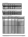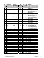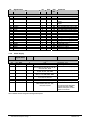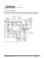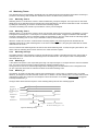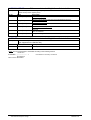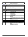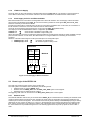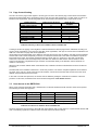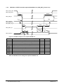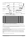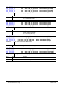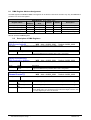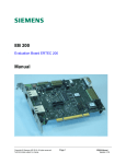
1
. ERTEC 200 Enhanced Real-Time Ethernet Controller Manual Copyright © Siemens AG 2007. All rights reserved. Technical data subject to change Page 1 ERTEC 200 Manual Version 1.1.0 Edition (04/2007) Disclaimer of Liability We have checked the contents of this manual for agreement with the hardware and software described. Since deviations cannot be precluded entirely, we cannot guarantee full agreement. However, the data in this manual are reviewed regularly. Necessary corrections are included in subsequent editions. Suggestions for improvement are welcomed. Copyright © Siemens AG 2006. All rights reserved The reproduction, transmission or use of this document or its contents is not permitted without express written authority. Offenders will be liable for damages. All rights, including rights created by patent grant or registration of a utility model or design, are reserved. All product and system names are registered trademarks of their respective owner and must be treated as such. Technical data subject to change. Copyright © Siemens AG 2007. All rights reserved. Technical data subject to change Page 2 ERTEC 200 Manual Version 1.1.0 Turfschipper 41 2292 JC Wateringen The Netherlands tel. +31 (0)174 671 800 fax. +31 (0)174 671 801 e-mail [email protected] Products ASICs LSPM2 RoHS (6-pack) LSPM2 RoHS (66-pack) EUR 95,- per pack EUR 919,- per pack SPC3 Step-C RoHS (6-pack) SPC3 Step-C RoHS (96-pack) EUR 75,- per pack EUR 1052,- per pack SPC3 Step-C Low Voltage RoHS (5-pack) SPC3 Step-C Low Voltage RoHS (160pack) EUR 85,- per pack EUR 1600,- per pack SPC4-2 RoHS (5-pack) SPC4-2 RoHS (160-pack) EUR 92,- per pack EUR 2288,- per pack DPC31 Step-B RoHS (6-pack) DPC31 Step-B RoHS (60-pack) EUR 95,- per pack EUR 877,- per pack DPC31 Step-C1 RoHS (6-pack) DPC31 Step-C1 RoHS (60-pack) EUR 95,- per pack EUR 868,- per pack SIM1-1 RoHS (160-pack) SIM1-2 RoHS (60-pack) EUR 4890,- per pack EUR 900,- per pack ERTEC 200 (5-pack) ERTEC 200 (70-pack) EUR 120,- per pack EUR 950,- per pack ERTEC 400 (5-pack) ERTEC 400 (70-pack) EUR 250,- per pack EUR 2300,- per pack Please contact us for larger quantities or check out: www.procentec.com Page 1 / 2 ING bank Rijswijk (ZH) 67.87.34.909 – Chamber of commerce The Hague nr. 27165526 – BTW/VAT NL816153073.B01 Conditions are applied on all offers and orders, which are deposited for (public) inspection at the chamber of commerce in The Hague. Turfschipper 41 2292 JC Wateringen The Netherlands tel. +31 (0)174 671 800 fax. +31 (0)174 671 801 e-mail [email protected] Firmware and development kits SPC3 ANSI-C software DPC31 Development kit EUR 680,EUR 2470,- ERTEC 200 Development Kit ERTEC 200 Productline license EUR 4500,EUR 4900,- ERTEC 400 Development Kit ERTEC 400 Productline license EUR 4500,EUR 4900,- Tools ProfiScript - Certification software ProfiTrace - Analyzer on USB ProfiCaptain - DP Master EUR 800,- (HW excl.) www.procentec.com/profiscript EUR 1400,- www.procentec.com/profitrace2 EUR 500,- (HW excl.) www.procentec.com/proficaptain Training PROFIBUS Product Development Certified PROFIBUS Engineer Certified PROFIBUS Installer EUR 995,- www.procentec.com/ppd EUR 1850,- www.procentec.com/cpe EUR 750,- www.procentec.com/cpi Page 2 / 2 ING bank Rijswijk (ZH) 67.87.34.909 – Chamber of commerce The Hague nr. 27165526 – BTW/VAT NL816153073.B01 Conditions are applied on all offers and orders, which are deposited for (public) inspection at the chamber of commerce in The Hague. Preface Target Audience of this Manual This manual is intended for hardware developers who want to use the ERTEC 200 for new products. Experience working with processors and designing embedded systems and knowledge of Ethernet are required for this. It described all ERTEC function groups in details and provides information that you must take into account when configuring your own PROFINET IO device hardware. The manual serves as a reference for software developers. The address areas and register contents are described in detail for all function groups. Structure of this Manual o Section 1 Overview of the architecture and the individual function groups of the ERTEC 200. o Section 2 ARM946E-S processor systems. o Section 3 Bus system of the ERTEC 200. o Section 4 I/O of the ERTEC 200. o Section 5 General hardware functions. o Section 6 External memory interface (EMIF). o Section 7 Local bus unit (LBU). o Section 8 DMA controller o Section 9 Ethernet PHYs o Section 10 Memory partitioning of the ERTEC 200. o Section 11 HW tools for test, trace, and debugging. o Section 12 List of terms and references Scope of the Manual This manual applies to the following product: ERTEC 200 Version 01 and higher Copyright © Siemens AG 2007. All rights reserved. Technical data subject to change Page 3 ERTEC 200 Manual Version 1.1.0 This manual will be updated as required. You can find the current version of the manual on the Internet at http://www.siemens.com/comdec. Guide To help you quickly find the information you need, this manual contains the following aids: o A complete table of contents as well as a list of all figures and tables in the manual are provided at the beginning of the manual. o A glossary containing definitions of important terms used in the manual is located following the appendices. o References to other documents are indicated by the document reference number enclosed in slashes (/No./). The complete title of the document can be obtained from the list of references at the end of the manual. Additional Support If you have questions regarding use of the described block that are not addressed in the documentation, please contact your Siemens representative. Please send your written questions, comments, and suggestions regarding the manual to the hotline via the email address indicated above. In addition, you can receive general information, current product information, FAQs, and downloads pertaining to your application on the Internet at: http://www.siemens.com/comdec Technical Contacts for Germany / Worldwide Siemens AG Automation & Drives Phone: Phone: Fax: E-mail: 0911/750-2736 0911/750-2080 0911/750-2100 [email protected] ComDeC Street address: Mailing address: Würzburgerstr.121 P.O. Box 2355 90766 Fürth Federal Republic of Germany 90713 Fürth Federal Republic of Germany Technical Contacts for USA PROFI Interface Center: One Internet Plaza PO Box 4991 Fax: (423)- 262- 2103 Phone: (423)- 262- 2576 E-mail: [email protected] Johnson City, TN 37602-4991 Copyright © Siemens AG 2007. All rights reserved. Technical data subject to change Page 4 ERTEC 200 Manual Version 1.1.0 Contents 1 Introduction ............................................................................................................................9 1.1 Applications of the ERTEC 200 .............................................................................................................. 9 1.2 Features of the ERTEC 200 ................................................................................................................... 9 1.3 Structure of the ERTEC 200................................................................................................................... 10 1.4 ERTEC 200 Package ............................................................................................................................. 11 1.5 Signal Function Description.................................................................................................................... 12 1.5.1 GPIO 0 to 31 and Alternative Functions......................................................................................... 12 1.5.2 JTAG and Debug ........................................................................................................................... 13 1.5.3 Trace Port ...................................................................................................................................... 13 1.5.4 Clock and Reset ............................................................................................................................ 14 1.5.5 Test Pins........................................................................................................................................ 14 1.5.6 EMIF (External Memory Interface) ................................................................................................. 14 1.5.7 LBU, MII Interface or ETM Trace Interface .................................................................................... 16 1.5.8 Ethernet PHY1 and PHY2.............................................................................................................. 18 1.5.9 Power Supply................................................................................................................................. 19 2 ARM946E-S Processor ..........................................................................................................21 2.1 Structure of ARM946E-S........................................................................................................................ 21 2.2 Description of ARM946E-S .................................................................................................................... 22 2.3 Operating Frequency of ARM946E-S..................................................................................................... 22 2.4 Cache Structure of ARM946E-S............................................................................................................. 22 2.5 Tightly Coupled Memory (TCM) ............................................................................................................. 22 2.6 Memory Protection Unit (MPU) .............................................................................................................. 23 2.7 Bus Interface of ARM946E-S ................................................................................................................. 23 2.8 ARM946E-S Embedded Trace Macrocell (ETM9).................................................................................. 23 2.9 ARM Interrupt Controller (ICU) ............................................................................................................... 23 2.9.1 Prioritization of Interrupts ............................................................................................................... 24 2.9.2 Trigger Modes................................................................................................................................ 24 2.9.3 Masking the Interrupt Inputs .......................................................................................................... 24 2.9.4 Software Interrupts for IRQ ............................................................................................................ 24 2.9.5 Nested Interrupt Structure.............................................................................................................. 24 2.9.6 EOI End-Of-Interrupt...................................................................................................................... 24 2.9.7 IRQ Interrupt Sources .................................................................................................................... 25 2.9.8 FIQ Interrupt Sources .................................................................................................................... 25 2.9.9 IRQ Interrupts as FIQ Interrupt Sources ........................................................................................ 26 2.9.10 Interrupt Control Register............................................................................................................... 26 2.9.11 ICU Register Description ............................................................................................................... 27 2.10 ARM946E-S Register ............................................................................................................................. 31 3 Bus System of the ERTEC 200..............................................................................................32 3.1 “Multilayer AHB” Communication Bus .................................................................................................... 32 3.1.1 AHB Arbiter.................................................................................................................................... 32 3.1.2 AHB Master-Slave Coupling .......................................................................................................... 32 3.2 APB I/O Bus ........................................................................................................................................... 32 4 I/O on APB bus .......................................................................................................................33 4.1 BOOT ROM............................................................................................................................................ 33 4.1.1 Booting from External ROM ........................................................................................................... 34 4.1.2 Booting via SPI .............................................................................................................................. 34 4.1.3 Booting via UART .......................................................................................................................... 34 4.1.4 Booting via LBU ............................................................................................................................. 34 4.1.5 Memory Swapping ......................................................................................................................... 34 4.2 General Purpose I/O (GPIO) .................................................................................................................. 35 4.2.1 Address Assignment of GPIO Registers ........................................................................................ 36 4.2.2 GPIO Register Description............................................................................................................. 36 4.3 Timer 0/1/2 ............................................................................................................................................. 38 4.3.1 Timer 0 and Timer 1....................................................................................................................... 38 4.3.1.1 Timer 0/1 Interrupts............................................................................................................... 39 4.3.1.2 Timer 0/1 Prescaler............................................................................................................... 39 4.3.1.3 Cascading of Timers 0/1 ....................................................................................................... 39 4.3.2 Timer 2........................................................................................................................................... 39 4.3.3 Address Assignment of Timer Registers........................................................................................ 40 4.3.4 Timer Register Description ............................................................................................................ 40 4.4 F-Timer Function .................................................................................................................................... 43 4.4.1 Address Assignment of F-Timer Registers .................................................................................... 44 Copyright © Siemens AG 2007. All rights reserved. Technical data subject to change Page 5 ERTEC 200 Manual Version 1.1.0 4.4.2 F-Timer Register Description ......................................................................................................... 44 4.5 Watchdog Timers ................................................................................................................................... 45 4.5.1 Watchdog Timer 0.......................................................................................................................... 45 4.5.2 Watchdog Timer 1.......................................................................................................................... 45 4.5.3 Watchdog Interrupt ........................................................................................................................ 45 4.5.4 WDOUT0_N................................................................................................................................... 45 4.5.5 WDOUT1_N................................................................................................................................... 45 4.5.6 Watchdog Registers....................................................................................................................... 46 4.5.7 Address Assignment of Watchdog Registers................................................................................. 46 4.5.8 Watchdog Register Description ..................................................................................................... 46 4.6 UART Interface....................................................................................................................................... 48 4.6.1 Address Assignment of UART Registers ....................................................................................... 49 4.6.2 UART Register Description............................................................................................................ 50 4.7 Synchronous Interface SPI..................................................................................................................... 54 4.7.1 Address Assignment of SPI Register ............................................................................................. 55 4.7.2 SPI Register Description................................................................................................................ 56 4.8 System control register........................................................................................................................... 58 4.8.1 Address Assignment of System Control Registers ........................................................................ 58 4.8.2 System Control Register Description ............................................................................................. 59 5 General Hardware Functions ................................................................................................64 5.1 Clock Generation and Clock Supply....................................................................................................... 64 5.1.1 Clock Supply in ERTEC 200 .......................................................................................................... 64 5.1.2 JTAG Clock Supply........................................................................................................................ 65 5.1.3 Clock Supply for PHYs and Ethernet MACs .................................................................................. 65 5.2 Reset Logic of the ERTEC 200 .............................................................................................................. 65 5.2.1 PowerOn reset ............................................................................................................................... 65 5.2.2 Hardware Reset ............................................................................................................................. 66 5.2.3 Watchdog Reset ............................................................................................................................ 66 5.2.4 Software reset................................................................................................................................ 66 5.2.5 IRT Switch Reset ........................................................................................................................... 66 5.3 Address Space and Timeout Monitoring ................................................................................................ 67 5.3.1 AHB Bus Monitoring....................................................................................................................... 67 5.3.2 APB Bus Monitoring....................................................................................................................... 67 5.3.3 EMIF Monitoring ............................................................................................................................ 67 5.4 Configuration Options on the ERTEC 200.............................................................................................. 67 6 External Memory Interface (EMIF) ........................................................................................69 6.1 Address Assignment of EMIF Registers................................................................................................. 70 6.2 EMIF Register Description ..................................................................................................................... 70 7 Local Bus Unit (LBU). ............................................................................................................74 7.1 Page Range Setting ............................................................................................................................... 76 7.2 Page Offset Setting ................................................................................................................................ 76 7.3 LBU Address Mapping ........................................................................................................................... 77 7.4 Page Control Setting .............................................................................................................................. 78 7.5 Host Access to the ERTEC200 .............................................................................................................. 78 7.5.1 LBU Read from ERTEC 200 with separate Read/Write line (LBU_RDY_N active low) ................. 79 7.5.2 LBU Write to ERTEC 200 with separate Read/Write line (LBU_RDY_N active low)...................... 80 7.5.3 LBU Read from ERTEC 200 with common Read/Write line (LBU_RDY_N active low) ................. 81 7.5.4 LBU Write to ERTEC 200 with common Read/Write line (LBU_RDY_N active low) ...................... 82 7.6 Host Interrupt Handling: ......................................................................................................................... 82 7.7 Address Assignment of LBU Registers .................................................................................................. 83 7.8 LBU Register Description ....................................................................................................................... 83 8 DMA-Controller.......................................................................................................................85 8.1 DMA Register Address Assignment ....................................................................................................... 86 8.2 Description of DMA Registers ................................................................................................................ 86 9 10 Multiport Ethernet PHY..........................................................................................................88 Memory Description...............................................................................................................91 10.1 Memory Partitioning of the ERTEC 200 ................................................................................................. 91 10.2 Detailed Memory Description ................................................................................................................. 92 11 Test and Debugging...............................................................................................................94 11.1 ETM9 Embedded Trace Macrocell ......................................................................................................... 94 11.1.1 Trace Modes.................................................................................................................................. 94 11.1.2 Features of the ETM9 Module ....................................................................................................... 94 Copyright © Siemens AG 2007. All rights reserved. Technical data subject to change Page 6 ERTEC 200 Manual Version 1.1.0 11.1.3 ETM9 Registers ............................................................................................................................. 94 11.2 Trace Interface ....................................................................................................................................... 95 11.3 JTAG Interface ....................................................................................................................................... 95 11.4 Debugging via UART.............................................................................................................................. 95 12 Miscellaneous.........................................................................................................................96 12.1 Acronyms/Glossary: ............................................................................................................................... 96 12.2 References: ............................................................................................................................................ 97 Copyright © Siemens AG 2007. All rights reserved. Technical data subject to change Page 7 ERTEC 200 Manual Version 1.1.0 List of Figures Figure 1: ERTEC 200 Block Diagram .................................................................................................................... 10 Figure 2: ERTEC 200 Package Description .......................................................................................................... 11 Figure 3: Structure of ARM946E-S Processor System .......................................................................................... 21 Figure 4: GPIO Cell on GPIO Port [31:0] of the ERTEC 200................................................................................. 35 Figure 5: Block Diagram of F-Counter ................................................................................................................... 43 Figure 6: Watchdog Timing.................................................................................................................................... 45 Figure 7: Block Diagram of UART ......................................................................................................................... 48 Figure 8: Block Diagram of SPI ............................................................................................................................. 54 Figure 9: Clock Generation in ERTEC 200 ............................................................................................................ 64 Figure 10: Clock Supply of Ethernet Interface ....................................................................................................... 65 Figure 11: Power-Up Phase of the PLL ................................................................................................................. 66 Figure 12: Interconnection of Addresses between Host and ERTEC 200 LBU ..................................................... 77 Figure 13: LBU-Read-Sequence with separate RD/WR line ................................................................................. 79 Figure 14: LBU-Write-Sequence with separate RD/WR line.................................................................................. 80 Figure 15: LBU-Read-Sequence with common RD/WR line.................................................................................. 81 Figure 16: LBU-Write-Sequence with common RD/WR line .................................................................................. 82 List of Tables Table 1: ERTEC 200 Pin Assignment and Signal Description ............................................................................... 19 Table 2: Overview of IRQ Interrupts ...................................................................................................................... 25 Table 3: Overview of FIQ Interrupts....................................................................................................................... 25 Table 4: Overview of Interrupt Control Register..................................................................................................... 27 Table 5: CP15 Registers - Overview ..................................................................................................................... 31 Table 6: Overview of AHB Master-Slave Access................................................................................................... 32 Table 7: Access Type and Data Width of the I/O................................................................................................... 33 Table 8: Selection of Download Source................................................................................................................. 34 Table 9: Overview of GPIO Registers.................................................................................................................... 36 Table 10: Overview of Timer Registers ................................................................................................................. 40 Table 11: Overview of F-Timer Registers .............................................................................................................. 44 Table 12: Overview of WD Registers..................................................................................................................... 46 Table 13: Baud Rates for UART at FUARTCLK=50 MHz ........................................................................................... 49 Table 14: Overview of UART Registers................................................................................................................. 49 Table 15: Overview of SPI Registers..................................................................................................................... 55 Table 16: Overview of System Control Registers .................................................................................................. 59 Table 17: Overview of ERTEC 200 Clocks ............................................................................................................ 64 Table 18: Configurations for ERTEC 200 .............................................................................................................. 68 Table 19: Overview of EMIF Registers .................................................................................................................. 70 Table 20: Setting of Various Page Sizes ............................................................................................................... 76 Table 21: Setting of Various Offset Areas ............................................................................................................. 76 Table 22: Address Mapping from the Perspective of an External Host Processor on the LBU Port ...................... 77 Table 23: Summary of Accesses to Address Areas of ERTEC 200....................................................................... 78 Table 24: Host Access to Address Areas of ERTEC 200 ...................................................................................... 78 Table 25: LBU Read access timing with seperate Read/Write line........................................................................ 79 Table 26: LBU Write access timing with seperate Read/Write line ........................................................................ 80 Table 27: LBU Read access timing with common Read/Write line ........................................................................ 81 Table 28: LBU Write access timing with common Read/Write line ........................................................................ 82 Table 29: Overview of LBU Registers.................................................................................................................... 83 Table 30: DMA Transfer Modes............................................................................................................................. 85 Table 31: I/O Synchronization Signals................................................................................................................... 85 Table 32: Overview of DMA Registers................................................................................................................... 86 Table 33: Partitioning of Memory Areas ................................................................................................................ 91 Table 34: Detailed Description of Memory Segments............................................................................................ 93 Table 35: Pin Assignment of JTAG Interface......................................................................................................... 95 Copyright © Siemens AG 2007. All rights reserved. Technical data subject to change Page 8 ERTEC 200 Manual Version 1.1.0 1 Introduction The ERTEC 200 is intended for the implementation of PROFINET devices with RT and IRT functionality. With its integrated ARM946 processor and 2-port Ethernet switch with integrated PHYs and the option to connect an external host processor system to a local bus interface, it meets all the requirements for implementing PROFINET devices with integrated switch functionality. 1.1 1.2 Applications of the ERTEC 200 Interface connection for high-precision drive control, including for PC-based systems Distributed I/O with real-time Ethernet interfacing PROFINET RT and IRT functionality Features of the ERTEC 200 The ERTEC 200 is a high-performance Ethernet controller with the following integrated function groups: • • • • • • • • • • • • • • • • • • • • High-performance ARM 946 processor with D-cache, I-cache, D-TCM memory Multilayer AHB bus master/slave with AHB arbiter IRT switch with 64-Kbyte communication RAM 2 Ethernet channels with integrated PHYs Local Bus Unit (LBU) for connecting an external host processor (with boot capability) SDRAM controller SRAM controller DMA controller, 1-channel 45 IO, with assignable parameters UART (with boot capability) SPI (with boot capability) 3 timers F-timer Watchdog IRQ and FIQ interrupt controller PLL with clock generator 8 Kbytes of BOOT ROM 304-pin FBGA housing Different test functions JTAG debug and trace interface Copyright © Siemens AG 2007. All rights reserved. Technical data subject to change Page 9 ERTEC 200 Manual Version 1.1.0 1.3 Structure of the ERTEC 200 The figure below shows the function groups with the common communication paths. JTAG / Debug 48 TRACE_ CLK 7 ARM946ES 74 48 Local Bus Unit 16 Bit (LBU) MemoryController (EMIF) Master Slave ARMInterruptController DMAController Master Slave 1 1 1 1 PLL Clock-Unit 1 BSTAP with I-Cache (8kByte), D-Cache (4kByte), D-TCM (4kByte) F_CLK ARM9 clock MUX 25MHz REF_ CLK ETM 1 Reset 4 Test 100MHz External Memory Interface 50MHz LBU / MII + SMI / ETM / GPIO APB Interface 50MHz / 32 Bit Master Slave 14 13 Input stage Decode 13 Input stage 50 MHz/32Bit GPIO 32 P Slave Multi-Layer-AHB AHB/APB Bridge Slave Decode Master Input stage Slave MUX/Arb. MUX/Arb. Input stage MUX/Arb. 1 x UART 5 P 3 16 16 Slave MC-Bus (50MHz) 2 System Control Slave 3 x Timer, Watchdog, F-Timer 32 Bit SC-Bus (50MHz) Switch Control EthernetPort2 GPIO, UART, SPI, Timer, Watchdog, r K-SRAM t s 64 kByte 2-Port Switch Slave EthernetPort1 8 Master 32 Bit SMI o SPI1 Interface Slave Slave AHBWrapper Slave Master AHBWrapper 32 MII-1 MII-0 BootROM (8 kByte) PHY PHY (Port 1) (Port 2) 7 MC-PLL Signals PHY2 PHY1 21 20 ERTEC200 Figure 1: ERTEC 200 Block Diagram Copyright © Siemens AG 2007. All rights reserved. Technical data subject to change Page 10 ERTEC 200 Manual Version 1.1.0 1.4 ERTEC 200 Package The ERTEC 200 is supplied in an FBGA package with 304 pins. The distance between the pins is 0.8 mm. The package dimensions are 19 mm x 19 mm. Figure 2: ERTEC 200 Package Description Soldering instructions for the ERTEC 200 can be found in the following documents: /10/ Soldering instructions for lead-based block. /11/ Soldering instructions for lead-free block. /12/ Code description for soldering. When working with modules, always take precautionary measures against electrostatic charge (ESD – Electrostatic Sensitive Devices). Copyright © Siemens AG 2007. All rights reserved. Technical data subject to change Page 11 ERTEC 200 Manual Version 1.1.0 1.5 Signal Function Description ERTEC 200 Pin Description The ERTEC 200 Ethernet communication block is available in a 304-pin FBGA package. The signal names of the ERTEC 200 are described in this section. 1.5.1 GPIO 0 to 31 and Alternative Functions Various signals are multiplexed on the same pin. These multiplexed signals can contain up to four different functions. The alternative functions are assigned in GPIO registers GPIO_PORT_MODE_L and GPIO_PORT_MODE_H (see Section 4.2.2). The table describes all signals with their different functions and associated pin numbers. No. Signal Name Alternative Function 1 Alternative Function 2 Alternative Function 3 I/O (Reset) Pull- PIN No. Comment General Purpose I/O / I/O GPIO0 P1-DUBLEXLED_N B/O/(I) up D19 GPIO1 P2-DUBLEXLED_N B/O/(I) up B20 GPIO2 P1-SPEED10LED_N B/O/O/(I) up D17 P2-SPEED10LED_N B/O/O/(I) up B19 GPIO or PHY-LED (O) B/O/(I) up A19 GPIO or PHY-LED (O) B/O/(I) up D16 GPIO or PHY-LED (O) GPIO6 P1-SPEED_N100LED (TX/FX) P2-SPEED100LED_N (TX/FX) P1-LINKLED_N P2-LINKLED_N P1-RX-LED_N GPIO (interruptcapable) or PHY-LED (O) GPIO (interruptcapable) or PHY-LED (O) GPIO or PHY-LED (O) P1-TX-LED_N B/O/O/O/(I) up B18 GPIO or PHY-LED (O) GPIO7 P2-RX-LED_N P2-TX-LED_N B/O/O/O/(I) up D15 GPIO or PHY-LED (O) GPIO8 UART-TXD B/O/(I) up B17 GPIO or UART (O) 10 GPIO9 UART-RXD B/I (I) up A17 GPIO or UART (I) 11 GPIO10 UART-DCD_N B/I (I) up B16 GPIO or UART (I) 12 GPIO11 UART-DSR_N B/I (I) up E16 GPIO or UART (I) 13 GPIO12 UART-CTS_N B/I (I) up A16 GPIO or UART (I) 14 GPIO13 Reserved B/O/(I) up B15 GPIO 15 GPIO14 DBGACK B/O/(I) up E15 GPIO or DEBUG (O) 16 GPIO15 B/O/(I) up E14 GPIO or Watchdog (O) 17 GPIO16 B/O/(I) up A13 GPIO or SPI1 (O) 18 GPIO17 WD_WDOUT0_ N SPI1_SSPCTL OE SPI1_SSPOE B/O/(I) up F14 GPIO or SPI1 (O) 19 GPIO18 SPI1_SSPRXD B/I (I) up B12 GPIO or SPI1 (I) 20 GPIO19 SPI1_SSPTXD B/O/(I) up D13 GPIO or SPI1 (O) 21 GPIO20 B/O/(I) up D11 GPIO or SPI1 (O) 22 GPIO21 SPI1_SCLKOU T SPI1_SFRMOU T B/O/(I) up A11 GPIO or SPI1 (O) 1 2 3 GPIO3 4 5 6 7 8 GPIO4 GPIO5 P1-ACTIVELED_N P2-ACTIVELED_N 9 Copyright © Siemens AG 2007. All rights reserved. Technical data subject to change 12 ERTEC 200 Manual Version 1.1.0 No. Signal Name Alternative Function 1 Alternative Function 2 Alternative Function 3 I/O (Reset) Pull- PIN No. Comment General Purpose I/O / I/O 23 GPIO22 SPI1_SFRMIN DBGACK B/I/O/(I) up F10 24 GPIO23 SPI1_SCLKIN Reserved B/I/O/(I) up D10 25 26 GPIO24 GPIO25 B/I (I) B/O/(I) up up B11 B9 27 28 29 30 31 GPIO26 GPIO27 GPIO28 GPIO29 GPIO30 PLL_EXT_IN_N TGEN_OUT1_N *1 TGEN_OUT2_N TGEN_OUT3_N TGEN_OUT4_N TGEN_OUT5_N TGEN_OUT6_N B/O/(I) B/O/(I) B/O/(I) B/O/(I) B/O/(I) up up up up up A7 B10 F9 E9 B8 32 GPIO31 DBGREQ B/I (I) up E8 GPIO or SPI1 (I) or Debug (O) This GPIO is used as chip select when booting from Nand Flash or SPI ROM. GPIO or SPI1 (I) This GPIO is used as chip select when booting from SPI Flash or SPI EEPROM. GPIO or MC_PLL (I) GPIO or MC_PLL (O) GPIO or MC_PLL (O) GPIO or MC_PLL (O) GPIO or MC_PLL (O) GPIO or MC_PLL (O) GPIO (interruptcapable) or MC_PLL (O) GPIO (interruptcapable) or DEBUG (I) *1 For an IRT application pin GPIO25 is default parameterized as alternate function1 (TGEN_OUT1_N). A synchronous clock is issued at this pin. During the certification process of a PROFINET IO DEVICE with IRT functionality this pin has to be accessible from outside (mandatory). Different GPIO’s are used on the Evaluation Board EB200. See Dokument /14/ Table 6. 1.5.2 No. JTAG and Debug Signal Name I/O (Reset) Pull- PIN No. Comment Debug / JTAG (BOUNDARY SCAN) 33 34 35 36 37 38 39 1.5.3 No. TRST_N TCK TDI TMS TDO SRST_N TAP_SEL I (I) I (I) I (I) I (I) O (O) B (O) I (I) up up up up up U10 W7 U9 V7 V9 V8 W8 JTAG Reset JTAG Clock JTAG Data In JTAG Test Mode Select JTAG Data Out Hardware Reset Select TAP Controller: 0: Boundary Scan TAP Controller selected 1: ARM-TAP Controller selected or Scan Clock (Scan mode) Trace Port Signal Name I/O (Reset) Pull- PIN No. Comment Trace Port/Other 40 41 TRACECLK Reserved B (O) I (I) up Copyright © Siemens AG 2007. All rights reserved. Technical data subject to change AB4 U19 ETM Trace Clock Connect pin to GND 13 ERTEC 200 Manual Version 1.1.0 1.5.4 No. Clock and Reset Signal Name I/O (Reset) Pull- PIN No. Comment CLOCK / RESET GENERATION 42 43 44 45 CLKP_A CLKP_B F_CLK REF_CLK 46 RESET_N 1.5.5 No. I (I) O I (I) Dependent on PIN CONFIG[1] I (I) B14 D14 B13 A15 Quartz connection Quartz connection F_CLK for F-counter Tristate or reference clock output, 25 MHz up B7 PowerOn reset Pull- PIN No. Test Pins Signal Name I/O (Reset) Comment TEST 47 48 49 50 1.5.6 No. TEST_N (3) TMC1 (3) TMC2 (3) TACT_N (3) I (I) I (I) I (I) I (I) up dn T5 G5 H6 J5 Test mode Test configuration Test configuration TESTACT-TAP reset EMIF (External Memory Interface) Signal Name Alternative Reset Function I/O (Reset) Pull- PIN No. Comment EMIF (External Memory Interface) 51 DTR_N 52 OE_DRIVER_N 53 A0 54 A1 55 A2 56 A3 57 A4 58 A5 59 A6 60 A7 61 A8 62 A9 63 A10 64 A11 65 A12 BOOT0 Copyright © Siemens AG 2007. All rights reserved. Technical data subject to change B (I) up O (O) E7 Direction signal for external driver or scan clock (Scan mode) ERTEC 200 boot mode (external PD may be necessary) D8 Enable signal for external driver or scan clock (Scan mode) Address bit 0 SDRAM: Bank address 0 Address bit 1 SDRAM: Bank address 1 Address bit 2 SDRAM: Address 0 Address bit 3 SDRAM: Address 1 Address bit 4 SDRAM: Address 2 Address bit 5 SDRAM: Address 3 Address bit 6 SDRAM: Address 4 Address bit 7 SDRAM: Address 5 Address bit 8 SDRAM: Address 6 Address bit 9 SDRAM: Address 7 Address bit 10 SDRAM: Address 8 Address bit 11 SDRAM: Address 9 Address bit 12 SDRAM: Address 10 B4 O (O) A3 O (O) B3 O (O) B2 O (O) D4 O (O) C2 O (O) C1 O (O) D2 O (O) D1 O (O) E2 O (O) E1 O (O) F2 O (O) F1 O (O) 14 ERTEC 200 Manual Version 1.1.0 No. Signal Name Alternative Reset Function I/O (Reset) Pull- PIN No. Comment EMIF (External Memory Interface) 66 A13 G2 67 A14 68 A15 BOOT1 B (I) dn H2 69 A16 BOOT2 B (I) dn J2 70 A17 BOOT3 B (I) up K2 71 A18 CONFIG1 B (I) up K1 72 A19 CONFIG2 B (I) up E4 73 A20 CONFIG3 B (I) dn F4 74 A21 CONFIG4 B (I) up G4 75 A22 CONFIG5 B (I) dn H5 76 A23 CONFIG6 B (I) up H4 77 78 79 80 81 82 83 84 85 86 87 88 89 90 91 92 93 94 95 96 97 98 99 100 101 102 103 104 105 106 107 108 D0 D1 D2 D3 D4 D5 D6 D7 D8 D9 D10 D11 D12 D13 D14 D15 D16 D17 D18 D19 D20 D21 D22 D23 D24 D25 D26 D27 D28 D29 D30 D31 B (I) B (I) B (I) B (I) B (I) B (I) B (I) B (I) B (I) B (I) B (I) B (I) B (I) B (I) B (I) B (I) B (I) B (I) B (I) B (I) B (I) B (I) B (I) B (I) B (I) B (I) B (I) B (I) B (I) B (I) B (I) B (I) up up up up up up up up up up up up up up up up up up up up up up up up up up up up up up up up M2 N2 P1 P2 R1 T2 U1 U2 V2 W1 W2 Y2 AA1 AA2 AB2 AA3 K4 K5 J6 K6 N5 N6 P6 R5 R6 P4 R4 T4 U4 W4 W5 W6 O (O) G1 O (O) Copyright © Siemens AG 2007. All rights reserved. Technical data subject to change 15 Address bit 13 SDRAM: Address 11 Address bit 14 SDRAM: Address 12 Address bit 15 ERTEC 200 boot mode (ext. PU may be necessary) Address bit 16 / ERTEC 200 boot mode (ext. PU may be necessary) Address bit 17 / ERTEC 200 boot mode (ext. PD may be necessary) Address bit 18 / ERTEC 200 system configuration (external PD may be necessary) Address bit 19 / ERTEC 200 system configuration (external PD may be necessary) Address bit 20 / ERTEC 200 system configuration (external PU may be necessary) Address bit 21 / ERTEC 200 system configuration (external PD may be necessary) Address bit 22 / ERTEC 200 system configuration (external PU may be necessary) Address bit 23 / ERTEC 200 system configuration (external PD may be necessary) Data bit 0 Data bit 1 Data bit 2 Data bit 3 Data bit 4 Data bit 5 Data bit 6 Data bit 7 Data bit 8 Data bit 9 Data bit 10 Data bit 11 Data bit 12 Data bit 13 Data bit 14 Data bit 15 Data bit 16 Data bit 17 Data bit 18 Data bit 19 Data bit 20 Data bit 21 Data bit 22 Data bit 23 Data bit 24 Data bit 25 Data bit 26 Data bit 27 Data bit 28 Data bit 29 Data bit 30 Data bit 31 ERTEC 200 Manual Version 1.1.0 No. Signal Name Alternative Reset Function I/O (Reset) Pull- PIN No. Comment EMIF (External Memory Interface) 109 110 111 WR_N RD_N CS_PER0_N O (O) O (O) 112 113 114 115 116 117 118 119 120 121 122 123 124 CS_PER1_N CS_PER2_N CS_PER3_N BE0_DQM0_N BE1_DQM1_N BE2_DQM2_N BE3_DQM3_N RDY_PER_N CLK_SDRAM CS_SDRAM_N RAS_SDRAM_N CAS_SDRAM_N WE_SDRAM_N O (O) O (O) O (O) O (O) O (O) O (O) O (O) I (I) B (O) O (O) O (O) O (O) O (O) 1.5.7 No. A4 B5 D5 O (O) up A5 A6 B6 N4 V1 J4 P5 D7 M1 L1 M5 L2 M4 Write strobe Read strobe Chip Select Bank 1 (ROM); boot area Chip select bank 2 Chip select bank 3 Chip select bank 4 Byte enable 0 for D(7:0) Byte enable 1 for D(15:8) Byte enable 2 for D(23:16) Byte enable 3 for D(31:24) Ready signal Clock for SDRAM Chip-Select for SDRAM RAS for SDRAM CAS for SDRAM Write Enable for SDRAM LBU, MII Interface or ETM Trace Interface Function 1 Function 2 Function 3 Function 4 LBU PHY Debug and GPIO[44:32] Config (6,5,2)=011b ETM Trace and GPIO[44:32] Config (6,5,2)=101b Reserved Config (6,5,2)=xx0b IO (Reset See Config [6,5,2]) Pull - PIN No. Comment [6,5,2]=111b LBU / MII Interface/ ETM Trace Interface 125 LBU_A0 RXD_P10 ETMEXTOUT 126 LBU_A1 RXD_P11 ETMEXTIN1 127 LBU_A2 RXD_P12 TRACEPKT7 128 LBU_A3 RXD_P13 TRACEPKT6 129 LBU_A4 CRS_P1 TRACEPKT5 130 LBU_A5 RX_ER_P1 TRACEPKT4 131 LBU_A6 RX_DV_P1 TRACEPKT3 132 LBU_A7 COL_P1 TRACEPKT2 133 LBU_A8 RXD_P20 TRACEPKT1 134 LBU_A9 RXD_P21 TRACEPKT0 135 LBU_A10 RXD_P22 TRACESYNC 136 LBU_A11 RXD_P23 PIPESTA2 137 LBU_A12 CRS_P2 PIPESTA1 138 LBU_A13 RX_ER_P2 PIPESTA0 139 LBU_A14 RX_DV_P2 140 LBU_A15 COL_P2 Copyright © Siemens AG 2007. All rights reserved. Technical data subject to change I/O/O/I (ETM : I) I/O/I/I (ETM : I) I/O/O/I (ETM : I) I/O/O/I (ETM : I) I/O/O/I (ETM : I) I/O/O/I (ETM : I) I/O/O/I (ETM : I) I/O/O/I (ETM : I) I/O/O/I (ETM : I) I/O/O/I (ETM : I) I/O/O/I (ETM : I) I/O/O/I (ETM : I) I/O/O/I (ETM : I) I/O/O/I (ETM : I) I/O/I/I I/O/I/I 16 up AB3 LBU or MII or ETM up AA4 LBU or MII or ETM up AA5 LBU or MII or ETM up AB5 LBU or MII or ETM up AA6 LBU or MII or ETM up AB6 LBU or MII or ETM up AA7 LBU or MII or ETM up AB7 LBU or MII or ETM up AA8 LBU or MII or ETM up AB8 LBU or MII or ETM up AA9 LBU or MII or ETM up AA10 LBU or MII or ETM up AB10 LBU or MII or ETM up AA11 LBU or MII or ETM up AB11 LBU or MII up W11 LBU or MII ERTEC 200 Manual Version 1.1.0 No. Function 1 Function 2 Function 3 Function 4 LBU PHY Debug and GPIO[44:32] Config (6,5,2)=011b ETM Trace and GPIO[44:32] Config (6,5,2)=101b Reserved Config (6,5,2)=xx0b IO (Reset See Config [6,5,2]) Pull - PIN No. Comment up W9 LBU or GPIO up W10 LBU or GPIO up V10 LBU or GPIO up W12 LBU or GPIO up V12 LBU or GPIO up V13 LBU or GPIO LBU or GPIO [6,5,2]=111b LBU / MII-Interface 141 LBU_A16 GPIO32 GPIO32 up U13 TX_CLK_P1 I/B/B/B (GPIO:I) I/B/B/B (GPIO:I) I/B/B/B (GPIO:I) I/B/B/B (GPIO:I) I/B/B/B (GPIO:I) I/B/B/B (GPIO:I) I/B/B/B (GPIO:I) I/O/I/I 142 LBU_A17 GPIO33 GPIO33 143 LBU_A18 GPIO34 GPIO34 144 LBU_A19 GPIO35 GPIO35 145 LBU_A20 GPIO36 GPIO36 146 LBU_SEG_0 GPIO37 GPIO37 147 LBU_SEG_1 GPIO38 GPIO38 148 LBU_WR_N up AA12 LBU_RD_N TX_CLK_P2 I/O/I/I up AB13 150 LBU_CS_R_ N GPIO39 GPIO39 I/B/B/B (GPIO : I) up AB12 151 LBU_CS_M_ N GPIO40 GPIO40 I/B/B/B (GPIO : I) up U14 152 153 154 LBU_BE0_N LBU_BE1_N LBU_D0 RX_CLK_P1 RX_CLK_P2 TXD_P10 up up up AB14 AA13 AA14 155 LBU_D1 TXD_P11 up W15 LBU or MII 156 LBU_D2 TXD_P12 up AB16 LBU or MII 157 LBU_D3 TXD_P13 up AA16 LBU or MII 158 LBU_D4 TX_EN_P1 up AB17 LBU or MII 159 LBU_D5 TX_ERR_P1 up AA17 LBU or MII 160 LBU_D6 TXD_P20 up AB18 LBU or MII 161 LBU_D7 TXD_P21 up AA18 LBU or MII 162 LBU_D8 TXD_P22 up AB19 LBU or MII 163 LBU_D9 TXD_P23 up AA19 LBU or MII 164 LBU_D10 TX_EN_P2 up AA20 LBU or MII 165 LBU_D11 TX_ERR_P2 I/O/I/I I/O/I/I B/O/I/O (LBU : I) B/O/I/O (LBU : I) B/O/I/O (LBU : I) B/O/I/O (LBU : I) B/O/I/O (LBU : I) B/O/I/O (LBU : I) B/O/I/O (LBU : I) B/O/I/O (LBU : I) B/O/I/O (LBU : I) B/O/I/O (LBU : I) B/O/I/O (LBU : I) B/O/I/O (LBU : I) LBU or MII LBU-Mode: CONFIG[5] = 0 Write Control (Low-Active) CONFIG[5] = 1 RD/WR Control (WR=0/RD=1) LBU or MII LBU-Mode: CONFIG[5] = 0 Read Control (Low Active) CONFIG[5] = 1 ------LBU or GPIO LBU-Mode: CS for paging configuration register LBU or GPIO LBU-Mode: CS for ERTEC 200 resources LBU or MII LBU or MII LBU or MII 149 up AB21 LBU or MII Copyright © Siemens AG 2007. All rights reserved. Technical data subject to change 17 ERTEC 200 Manual Version 1.1.0 No. Function 1 Function 2 Function 3 Function 4 LBU PHY Debug and GPIO[44:32] Config (6,5,2)=011b ETM Trace and GPIO[44:32] Config (6,5,2)=101b Reserved Config (6,5,2)=xx0b IO (Reset See Config [6,5,2]) Pull - PIN No. Comment up W14 LBU or MII up V15 LBU or MII up V16 LBU or MII up W16 LBU or GPIO up W19 LBU or GPIO LBU-Mode: LBU_RDY signal: Polarity depends on Input CONFIG[6]; Output active while LBU_CS_R/M_N is active LBU or GPIO LBU-Mode: Low-active interrupt (no open drain) LBU or GPIO LBU-Mode: Low-active interrupt (no open drain) [6,5,2]=111b LBU / MII-Interface 166 LBU_D12 SMI_MDC 167 LBU_D13 SMI_MDIO 168 LBU_D14 RES_PHY_N 169 LBU_D15 GPIO41 GPIO41 170 LBU_RDY_N GPIO42 GPIO42 171 LBU_IRQ0_N GPIO43 GPIO43 O/B/B/B (GPIO:I) up AA21 172 LBU_IRQ1_N GPIO44 GPIO44 O/B/B/B (GPIO:I) up W18 1.5.8 No. B/O/I/O (LBU : I) B/O/I/O (LBU : I) B/O/I/O (LBU : I) B/B/B/B (GPIO:I) (LBU : I) O/B/B/B (GPIO:I) Ethernet PHY1 and PHY2 Signal Name I/O Pull- PIN No. Comment PHY1 and PHY2 173 174 175 176 177 178 179 180 181 182 183 184 185 186 187 DGND4 DVDD4 DVDD3 DGND3 P2VDDARXTX P2VSSARX P2RxN P2RxP P2VSSATX1 P2TxN P2TxP P2VSSATX2 P2RDxP P2RDxN P2TDxP I I I I I I B B I B B I I I O T17 R21 R22 R17 N18 N17 P22 P21 M18 M21 M22 L19 U22 U21 Y21 188 P2TDxN O W21 189 190 191 192 193 194 195 P2SDxP P2SDxN VSSAPLLCB VDDACB VDDAPLL EXTRES ATP I I I I I B B V19 U18 L18 H22 K19 L21 L22 Copyright © Siemens AG 2007. All rights reserved. Technical data subject to change 18 Digital GND supply Digital 1.5 V supply Digital 1.5 V supply Digital GND supply Analog Port Tx/Rx 1.5 V supply Analog port GND supply Port2 differential receive input Port2 differential receive input Analog port GND supply Port2 differential transmit output Port2 differential transmit output Analog port GND supply Port2 FX differential receive input Port2 FX differential receive input Port2 FX differential transmit output Port2 FX differential transmit output Port2 FX differential SD input Port2 FX differential SD input Analog central GND supply Analog central 3.3 V supply Analog central 1.5 V supply Resistor reference 12.4 kOhm Analog test function ERTEC 200 Manual Version 1.1.0 No. Signal Name I/O Pull- PIN No. Comment PHY1 and PHY2 196 197 198 P1SDxN P1SDxP P1TDxN I I O F19 G19 C22 199 P1TDxP O C21 P1RDxN P1RDxP P1VSSATX2 P1TxP P1TxN P1VSSATX1 P1RxP P1RxN P1VSSARX P1VDDARXTX GND33ESD VDD33ESD DGND2 DVDD2 DVDD1 DGND1 I I I B B I B B I I I I I I I I E21 E22 K18 J22 J21 K17 G21 G22 J17 J19 H18 F22 G17 H19 G18 H21 200 201 202 203 204 205 206 207 208 209 210 211 212 213 214 215 1.5.9 Port1 FX differential SD input Port1 FX differential SD input Port1 FX differential transmit output Port1 FX differential transmit output Port1 FX differential receive input Port1 FX differential receive input Analog port GND supply Port1 differential transmit output Port1 differential transmit output Analog port GND supply Port1 differential receive input Port1 differential receive input Analog port GND supply Analog Port Tx/Rx 1.5 V supply Analog test GND supply Analog test 3.3 V supply Digital GND supply Digital 1.5 V supply Digital 1.5 V supply Digital GND supply Power Supply No. Voltage Signal Name I/O PIN No. Comment Power Supply 216 217 218-238 PLL_AVDD PLL_AGND VDD Core P P P 239- 253 GND Core P 254-267 VDD IO P 268-281 GND IO P 282-285 286-288 289-304 VDDQ (PECL) GND (PECL) Not Used Pins P P E12 F13 D6, D9, D12, D18, E5, E13, E18, F6, F17, L4, R2, T21, U6, U8, U17, V4, V5, V18, W13, W17, AA15 A21, E6, E11, E17, F5, F7, F16, G6, L5, T6, U16, V6, V11, V14, AA22 A2, A9, A10, A14, A18, B22, H1, N1, W22, Y1, Y22, AB9, AB15, AB20 A8, A12, A20, B1, B21, E10, F8, F15, J1, T1, U5, U7, U15, V17 D21, D22, R19, V21 F18, T18, T19 E19, F21, H17, J18, K21, K22, M19, N19, N21, N22, P17, P18, P19, R18, T22, V22 PLL analog, 1.5 V PLL analog GND SV Core 1.5 V (21 pins) GND CORE (15 pins) SV IO 3.3 V (14 pins) GND IO (14 pins) SV Q PECL 3.3 V GND IO (PCI) Not Used Pins (4 pins) (3 Pins) (16 Pins) For improved heat dissipation connect these pint to GND. However, these pins can also remain unconnected. Table 1: ERTEC 200 Pin Assignment and Signal Description Copyright © Siemens AG 2007. All rights reserved. Technical data subject to change 19 ERTEC 200 Manual Version 1.1.0 Signal description: IO = I: B: Signal direction from perspective of the application Input Bidirectional O: P: Output Power supply Pull- = Internal pull-up/pull-down resistor connected to the signal pin up: Internal pull-up dn: Internal pull-down PU/PD = External resistances necessary, depending on application PU: External pull-up PD: External pull-down _N in last position of signal name signifies: Signal is Low active Example: INTA_N Note: (1) The BOOT[3:0] pins are read into the “BOOT_REG” system configuration register during the active RESET phase. After a reset, these pins are available as normal function pins. (2) The CONFIG [6:1] pins are read into the “CONFIG_REG” system configuration register during the active RESET phase. After a reset, these pins are available as normal function pins. (3) The TMC1 and TMC2 test pins are shorted to ground during operation. TEST_N and TACT_N can remain open. (4) The GPIOs[31:0] and LBU pins can contain up to 4 different functions. The IO function pins have a different circuitry, corresponding to the selected function. Example of IO Function: B/O/O/I/ (I) Æ Function 0 = Bidirectional, Function 1 = Output, Function 2 = Output, Function 3 = Input, (I) = IO Function during RESET = Input For LBU, PHY-Debug or ETM-Trace-Interface the IO - function is active during Reset, which is selected with the pins CONFIG[6,5,2]. Default the Function 3 (ETM-Trace, GPIO[44:32]) is set with internal Pullup- and Pulldown-resistors. Unusual feature: ETM-outputs are switched to inputs during Reset. They are changed to outputs after the Trace-Modul is switched on with the debug-module. Different LBU- and GPIO-Pins have bidirectional functions. The value in the bracket is the default value during Reset, if they are selected with CONFIG[6,5,2]. Example: CONFIG[6, 5, 2] = xx0 Æ Function 1 Æ LBU-Mode All IO-Pins for Function1 are active during Reset e.g. LBU_A0 is input Æ Input during Reset LBU_D0 is bidirectional Æ Input during Reset The alternative GPIO functions are selected by assigning parameters for the GPIO_PORT_MODE_L and GPIO_PORT_MODE_H registers. The tabs are described in Section 4.2.2. The alternative LBU/MII functions are selected with the configuration pins CONFIG[6,5,2] in the user design. Copyright © Siemens AG 2007. All rights reserved. Technical data subject to change 20 ERTEC 200 Manual Version 1.1.0 2 ARM946E-S Processor The ARM946E-S processor is implemented in the ERTEC 200. This description is based on /1/ and /2/. 2.1 Structure of ARM946E-S An ARM946E-S processor system is used. The figure below shows the structure of the processor. In addition to the processor core, the system contains one data cache, one instruction cache, a memory protection unit (MPU), a system control coprocessor, and a tightly coupled memory. The processor system has an interface to the integrated AHB bus. Figure 3: Structure of ARM946E-S Processor System Copyright © Siemens AG 2007. All rights reserved. Technical data subject to change 21 ERTEC 200 Manual Version 1.1.0 2.2 Description of ARM946E-S The ARM946E-S processor system is a member of the ARM9 Thumb family. It has a processor core with Harvard architecture. Compared to the standard ARM9 family, the ARM946E-S has an enhanced V5TE architecture permitting faster switching between ARM and Thumb code segments and an enhanced multiplier structure. In addition, the processor has an integrated JTAG interface. 2.3 Operating Frequency of ARM946E-S The processor can be operated at 50 MHz, 100 MHz, or 150 MHz. The operating frequency is set during the reset phase via the configuration pins CONFIG[4] and CONFIG[3]. Communication with the components of the ERTEC 200 takes place via the AHB bus at a frequency of 50 MHz. 2.4 Cache Structure of ARM946E-S The following caches are integrated in the ARM946E-S. • 8 Kbytes of instruction cache with lock function • 4 Kbytes of data cache with lock function Both caches are “Four-Way Set Associative” caches with 1-Kbyte segments. Each segment consists of 32 lines with 32 bytes (8 x 4 bytes). The D-cache has “write buffers" with write-back function. The lock function enables the user to lock (LOCK) the contents of the cache segments. This function enables the command set for fast routines to be maintained permanently in the instruction cache. This mechanism can only be applied at the segment level with the ARM946E-S. Both caches are locked after a reset. These caches can only be enabled if the Memory Protection Unit is also enabled. The I-cache can be enabled by setting Bit 12 of the CP15 control register. The D-cache can be enabled by setting Bit 2 of the CP15 control register. Access to this area is blocked if the cache is not enabled. For additional information about Caching refer to Document /1/ Section 3. For more information on the description of the ARM946 registers, refer to Section 2.10 of this document. 2.5 Tightly Coupled Memory (TCM) A 4-Kbyte data-tightly coupled memory (D-TCM) is implemented in the ARM946E-S processor of the ERTEC 200. The memory is locked after a reset. The D-TCM can be placed in the address area of the ARM946E-S as desired and must be used together with a region of the memory protection unit. Data from high-speed routines such as isochronous control can be placed in the D-TCM. The D-TCM can be enabled by setting Bit 16 of the CP15 control register. In addition, the address area of the D-TCM must be set in the Tightly-Coupled Memory register. For more information about the D-TCM refer to document /1/ Section 5. For more information on the description of the ARM946 registers, refer to Section 2.10 of this document. Copyright © Siemens AG 2007. All rights reserved. Technical data subject to change 22 ERTEC 200 Manual Version 1.1.0 2.6 Memory Protection Unit (MPU) The memory protection unit enables the user to partition specific memory areas (I-cache, D-cache, or DTCM) into various regions and to assign different attributes to them. A maximum of 8 regions of variable size can be set. If regions overlap, the attributes of the higher region number apply. Settings for each region: • Base address of region • Size of region • Cache and “write buffer” configuration • Read/write access enable for privileged users/users Settings are made in the following registers of the ARM946E-S: Register 2 “Cache configuration register” Register 3 “Write buffer control register” Register 5 “Access permission register” Register 6 “Protection region/base size register” The base address defines the start address of the region. It must always be a multiple of the size of the region. Example: The region size is 4 Kbytes. The starting address is then always a multiple of 4 Kbytes. Before the MPU is enabled, at least one region must have been assigned. Otherwise, the ARM946E-S can assume a state that can only be cancelled by a reset. The MPU can be enabled by setting Bit 0 of the CP15 control register. If the MPU is disabled, the I-cache- and D-cache cannot be accessed, even if they are enabled. For more information about the MPU refer to Document /1/ Section 4. For more information on the description of the ARM946 registers, refer to Section 2.10 of this document. 2.7 Bus Interface of ARM946E-S The ARM946E-S uses an AHB bus master interface to the multilayer AHB bus for opcode fetches and data transfers. The interface operates at a fixed frequency of 50 MHz. The data bus and address bus each have a width of 32 bits. For more information about the bus interface and write buffer, and about the different transfer types, refer to Document /1/ Section 6. 2.8 ARM946E-S Embedded Trace Macrocell (ETM9) An ETM9 module is connected at the ARM946E-S. This module permits debugging support for data and instruction traces in the ERTEC 200. The module contains all signals required by the processor for the data and instruction traces. The ETM9 module is operated by means of the JTAG interface. The trace information is provided outwards to the trace port via a FIFO memory. A detailed description can be found in Section 11 2.9 ARM Interrupt Controller (ICU) The interrupt controller supports the FIQ and IRQ interrupt levels of the ARM946 processor. An interrupt controller with 8 interrupt inputs is implemented for FIQ. Six interrupt inputs (FIQ0-5) are occupied by the ERTEC 200, and 2 interrupt inputs (FIQ6-7) can be programmed optionally as IRQ sources. The high-priority FIQ interrupts are used for watchdog and address area monitoring and for debugging. An interrupt controller for 16 interrupt inputs is implemented for IRQ. Of the 16 IRQ inputs, two IRQ sources can be selected for as Fast-Interrupt_Requests (FIQ6-7) for processing. The assignment is made by specifying the IRQ number of the relevant interrupt input in the FIQ1REG / FIQ2REG register. The interrupt inputs selected as FIQ must be disabled for the IRQ logic. All other interrupt inputs can continue to be processed as IRQs. The interrupt controller is operated at a clock frequency of 50 MHz. Interrupt-request signals generated with a higher frequency must be lengthened accordingly for error-free detection. Copyright © Siemens AG 2007. All rights reserved. Technical data subject to change 23 ERTEC 200 Manual Version 1.1.0 2.9.1 Prioritization of Interrupts It is possible to set the priorities of the IRQ and FIQ interrupts. Priorities 0 to 15 can be assigned to IRQ interrupts while priorities 0 to 7 can be assigned to FIQ interrupts. The highest priority is 0 for both interrupt levels. After a reset, all IRQ interrupt inputs are set to priority 15 and all FIQ interrupt inputs are set to priority 7. A priority register is associated with each interrupt input. PRIOREG0 to PRIOREG15 are for the IRQ interrupts and FIQPR0 to FIQPR7 are for the FIQ interrupts. A priority must not be assigned more than once. A check for the assignment of identical priorities is not performed in the ICU logic. All interrupt requests with a lower or equal priority can be blocked at any time in the IRQ priority resolver by assigning a priority in the LOCKREG register. If an interrupt that is to be blocked is requested at the same time as the write access to the LOCKREG register, an IRQ signal is output. However, the signal is revoked after two clock cycles. If an acknowledgement is to be generated nonetheless, the transferred interrupt vector is the default vector. 2.9.2 Trigger Modes The “Edge-triggered” and “Level-triggered” operating modes are available for each interrupt input. The trigger type is defined by means of the assigned bit in the TRIGREG register. For the “Edge-triggered” mode setting, differentiation can be made between a positive and negative edge evaluation. This is made in the EDGEREG register. In “Level-triggered” mode, the active level of the interrupt request is high active. By default, the IRQ interrupt parameters are assigned as described in Section 2.9.7, and the FIQ interrupts parameters are assigned as described in Section 2.9.8. In “Edge-triggered” mode, the interrupt input signal must be present for at least one clock cycle. In “Level-triggered” mode, the input signal must be present until the ARM946E-S CPU is confirmed. Shorter signals result in loss of the event. 2.9.3 Masking the Interrupt Inputs Each IRQ interrupt can be enabled or disabled individually. The MASKREG register is available for this purpose. The interrupt mask acts only after the IRREG interrupt request register. That is, an interrupt is entered in the IRREG register in spite of the block in the MASKREG register. After a reset, all mask bits are set and, thus, all interrupts are disabled. At a higher level, all IRQ interrupts can be disabled globally via a command. When IRQ interrupts are enabled globally via a command, only those IRQ interrupts that are enabled by the corresponding mask bit in the MASKREG register are enabled. For the FIQ interrupts, only selective masking by the mask bits in the FIQ_MASKREG register is possible. After a reset, all FIQ interrupts are disabled. A detected FIQ interrupt request is entered in the FIQ interrupt request register. If the interrupt is enabled in the mask register, processing takes place in the priority logic. If the interrupt request is accepted by the ARM946 CPU and an entry is made in the in-service request register (ISR), the corresponding bit is reset in the IRREG register. Each bit that is set in the IRREG register can be deleted via software. For this purpose, the number of the bit to be reset in the IRCLVEC register is transferred to the interrupt controller. 2.9.4 Software Interrupts for IRQ Every IRQ interrupt request can be triggered by setting the bit corresponding to the input channel in the software interrupt register SWIRREG. Multiple requests can also be entered in the 16-bit SWIRREG register. The software interrupt requests are received directly in the IRREG register and, thus, treated like a hardware IRQ. Software interrupts can only be triggered by the ARM946E-S processor because only it has access authorization to the interrupt controller. 2.9.5 Nested Interrupt Structure When enabled by the interrupt priority logic, an IRQ interrupt request causes an IRQ signal to be output. Similarly, an FIQ interrupt request causes the FIQ signal to be output to the CPU. When the request is accepted by the CPU, the bit corresponding to the physical input in the register ISRREG is set. The IRQ/FIQ signal is revoked. The ISR bit of the accepted interrupt remains set until the CPU returns an End-Of-Interrupt command to the interrupt controller. As long as the ISR bit is set, interrupts with lower priority in the priority logic of the interrupt controller are disabled. Interrupts with a higher priority are allowed by the priority logic to pass and generate an IRQ/FIQ signal to the CPU. As soon as the CPU accepts this interrupt, the corresponding ISR bit in the ISRREG register is also set. The CPU then interrupts the lower-priority interrupt routine and executes the higher interrupt routine first. Lower-priority interrupts are not lost. They are entered in the IRREG register and are processed at a later time when all higher-priority interrupt routines have been executed. 2.9.6 EOI End-Of-Interrupt A set ISR bit is reset by the End-Of-Interrupt command. The CPU must communicate this to the interrupt controller with the EOI command after processing of the corresponding interrupt server routine. To communicate the EOI command to the interrupt controller, the CPU writes any value to the IRQEND/FIQEND registers. The interrupt controller decides independently which ISR bit will be reset with the EOI command. If several ISR bits are set, the interrupt controller deletes the ISR bit of the highest-priority interrupt request at the time of the EOI command. The interrupt cycle is considered complete for the interrupt controller when all set ISR bits have been reset by the corresponding number of EOI commands. After this, lower-priority interrupts that have occurred in the meantime and have been entered in the RREG register can be processed in the priority logic. During one or more accepted interrupts, the priority distribution of the IRQ/FIQ interrupt inputs must not be changed because the ICU can otherwise no longer correctly assign the EOI commands. Copyright © Siemens AG 2007. All rights reserved. Technical data subject to change 24 ERTEC 200 Manual Version 1.1.0 The CPU accepts an IRQ-/FIQ request by reading the IRVEC/FIVEQ register. This register contains the binary-coded vector number of the highest priority interrupt request at the moment. Each of the two interrupt vector registers can be referenced using two different addresses. The interrupt controller interprets the reading of the vector register with the first address as an “interrupt acknowledge”. This causes the sequences for this interrupt to be implemented in the ICU logic. Reading of the vector register with the second address is not linked to the “acknowledge function”. This is primarily useful for the debugging functions in order to read out the content of the interrupt vector register without starting the acknowledge function of the interrupt controller. 2.9.7 IRQ Interrupt Sources Interrupts from the following function groups of the ERTEC 200 are available to the IRQ interrupt controller: Interrupt-Nr. Function Block 0 Timer IRQ Interrupts Signal Name Default Setting TIM_INT0 Rising edge Comment Timer 0 1 Timer TIM_INT1 Rising edge Timer 1 3:2 GPIO GPIO (1:0) Assignable External input ERTEC 200 GPIO[1:0] 5:4 GPIO GPIO (31:30) Assignable External input ERTEC 200 GPIO[31:30] 6 Timer TIM_INT2 Rising edge Timer 2 7 ----- ------ ----- 8 UART UART_INTR High level Group interrupt UART 9 PHY0/1 P0/1_INTERP Rising edge Interrupt von PHY 0/1 10 SPI SSP_INTR Rising edge Group interrupt SPI 11 SPI SSP_ROR_INTR Rising edge Receive overrun interrupt SPI 12 IRT switch IRQ0_SP Rising edge High-priority IRT interrupt 13 IRT switch IRQ1_SP Rising edge Low-priority IRT interrupt 14 ----- ----- ----- 15 DMA DMA_INT Rising edge Reserved Reserved DMA controller, DMA transfer complete Table 2: Overview of IRQ Interrupts 2.9.8 FIQ Interrupt Sources Interrupts from the following function groups of the ERTEC 200 are available to the FIQ interrupt controller: FIQ Interrupts Signal Name Default Setting Interrupt-Nr. Function Block 0 Watchdog Rising edge 1 APB bus Rising edge 2 Multilayer AHB Rising edge 3 PLL-Status-Register Rising edge 4 ARM-CPU 5 6 7 Comment Access to non-existing address at the APB (1) Access to non-existing address at the AHB (1) Group interrupt of: EMIF: I/O time-out PLL: Loss state PLL: Lock State see system control register "PLL_STAT_REG" COMM_Rx Rising edge Receive comm channel interrupt ARM-CPU COMM_Tx Rising edge Transmit comm channel interrupt Optional Optional from IRQ Rising edge User-programmable IRQ source Optional Optional from IRQ Rising edge User-programmable IRQ source Table 3: Overview of FIQ Interrupts (1) Access to non-existing addresses is detected by the individual function groups of the ERTEC 200 and triggers a pulse with duration Tp = 2/50 MHz. For evaluation of this interrupt, the connected FIQ input must be specified as an edge-triggered input. Copyright © Siemens AG 2007. All rights reserved. Technical data subject to change 25 ERTEC 200 Manual Version 1.1.0 2.9.9 IRQ Interrupts as FIQ Interrupt Sources Interrupts from the IRQ interrupt can be placed on FIQ6 and FIQ7 können. The interrupts of the FIQ interrupt controller are used for debugging, monitoring address area access, and for the watchdog. FIQ interrupts no. 4 and 5 are the interrupts for embedded ICE RT communication. The UART can also be used as a debugger in place of the ICE. Effective real-time debugging is possible when the IRQ interrupt sources of the UART are mapped to the FIQs with the number 6 or 7. This enables debugging of interrupt routines. 2.9.10 Interrupt Control Register The interrupt control registers are used to specify all aspects of control, prioritization, and masking of the IRQ/FIQ interrupt controllers. ICU (Base Address 0x5000_0000) Register Name Offset Address Address Area Access Default Description IRVEC 0x0000 4 bytes R 0xFFFFFFFF Interrupt vector register FIVEC 0x0004 4 bytes R 0xFFFFFFFF Fast interrupt vector register LOCKREG 0x0008 4 bytes R/W 0x00000000 Priority lock register FIQ1SREG 0x000C 4 bytes R/W 0x00000000 Fast int. request 1 select register (FIQ6 on FIQ interrupt controller) FIQ2SREG 0x0010 4 bytes R/W 0x00000000 Fast int. request 2 select register (FIQ7 on FIQ interrupt controller) IRQACK 0x0014 4 bytes R 0xFFFFFFFF Interrupt vector register with IRQ acknowledge FIQACK 0x0018 4 bytes R 0xFFFFFFFF Fast interrupt vector register with FIQ acknowledge IRCLVEC 0x001C 4 bytes W 0x---- Interrupt request clear vector MASKALL 0x0020 4 bytes R/W 0x00000001 Mask for all interrupts IRQEND 0x0024 4 bytes W 0x---- End of IRQ interrupt FIQEND 0x0028 4 bytes W 0x---- End of FIQ interrupt FIQPR0 0x002C 4 bytes R/W 0x00000007 FIQ priority register on input FIQ0 of the FIQ interrupt controller FIQPR1 0x0030 4 bytes R/W 0x00000007 FIQ priority register on input FIQ1 of the FIQ interrupt controller FIQPR2 0x0034 4 bytes R/W 0x00000007 FIQ priority register on input FIQ2 of the FIQ interrupt controller FIQPR3 0x0038 4 bytes R/W 0x00000007 FIQ priority register on input FIQ3 of the FIQ interrupt controller FIQPR4 0x003C 4 bytes R/W 0x00000007 FIQ priority register on input FIQ4 of the FIQ interrupt controller FIQPR5 0x0040 4 bytes R/W 0x00000007 FIQ priority register on input FIQ5 of the FIQ interrupt controller FIQPR6 0x0044 4 bytes R/W 0x00000007 FIQ priority register on input FIQ6 of the FIQ interrupt controller FIQPR7 0x0048 4 bytes R/W 0x00000007 FIQ priority register on input FIQ7 of the FIQ interrupt controller FIQISR 0x004C 4 bytes R 0x00000000 FIQ in-service register FIQIRR 0x0050 4 bytes R 0x00000020 FIQ request register FIQ_MASKREG 0x0054 4 bytes R/W 0x000000FF FIQ interrupt mask register IRREG 0x0058 4 bytes R 0x000001xx Interrupt request register MASKREG 0x005C 4 bytes R/W 0x0000FFFF Interrupt mask register ISREG 0x0060 4 bytes R 0x00000000 In-service register TRIGREG 0x0064 4 bytes R/W 0x00000000 Trigger select register EDGEREG 0x0068 4 bytes R/W 0x00000000 Edge select register SWIRREG 0x006C 4 bytes R/W 0x00000000 Software interrupt register PRIOREG 0 0x0070 4 bytes R/W 0x0000000F Priority register 0 Copyright © Siemens AG 2007. All rights reserved. Technical data subject to change 26 ERTEC 200 Manual Version 1.1.0 PRIOREG 1 0x0074 ... ... ... ... 4 bytes R/W 0x0000000F .... .... .... PRIOREG15 0x00AC Table 4: Overview of Interrupt Control Register 4 bytes R/W 0x0000000F Priority register 15 2.9.11 ICU Register Description IRVEC Description R Name IRVEC 31:4 Vector ID FIVEC 31:3 Vector ID LOCKREG Bit No. 3–0 7 Bit No. 3–0 7 IRQACK Description Bit No. 3–0 31 - 4 Description For pending, valid interrupt: Binary code of FIQ number. Default vector: Bit[2:0] = 1 For pending valid Bit[31:3] = 0. Default vector: Bit[31:3] = 1 R/W Name LOCKPRIO LOCKENABLE Addr.: 0x5000_0008 Default: 0x0000_0000 Description Binary code of lock priority. 0=Lock inactive / 1=Lock active R/W Addr.: 0x5000_000C Default: 0x0000_0000 Fast interrupt request 1 select register Declaration of an IRQ input as FIQ6 (input FIQ6 on FIQ interrupt controller) Name FIQ1SREG FIQ1SENABLE FIQ2SREG Description Default: 0xFFFF_FFFF Priority lock register Specification of a priority for blocking interrupt requests of lower and equal priority FIQ1SREG Description Addr.: 0x5000_0004 Fast interrupt vector register Number of the highest-priority pending fast interrupt request Name FIVEC Bit No. 3–0 7 Description For pending, valid interrupt: Binary code of input number. Default vector: Bit[3:0] = 1 For pending, valid interrupt: Bit[31:4] = 0. Default vector: Bit[31:4] = 1 R Bit No. 2:0 Description Default: 0xFFFF_FFFF Interrupt vector register Input with highest priority pending interrupt request Bit No. 3:0 Description Addr.: 0x5000_0000 Description Number of the input to be selected (binary code) 0=Ignore FIQ declaration 0=Take into account FIQ declaration R/W Addr.: 0x5000_0010 Default: 0x0000_0000 Fast interrupt request 2 select register Declaration of an IRQ input as FIQ7 (input FIQ7 on FIQ interrupt controller) Name FIQ2SREG FIQ2SENABLE Description Number of the input to be selected (binary code) 0=Ignore FIQ declaration 0=Take into account FIQ declaration R Addr.: 0x5000_0014 Default: 0xFFFF_FFFF Interrupt vector register with IRQ acknowledge Confirmation of highest-priority pending interrupt request by reading the associated interrupt vector Name Description IRVEC Binary code of input number Vector ID Valid IRQ vector: always ‘0’. Default vector: always ‘1’ (also bits 3 – 0). Copyright © Siemens AG 2007. All rights reserved. Technical data subject to change 27 ERTEC 200 Manual Version 1.1.0 FIQACK Description Bit No. 2–0 31 – 3 R IRCLVEC Description Bit No. 3–0 7 Bit No. 0 W Name IRCLVEC unused Bit No. Bit No. Name MASKALL Bit No. 2–0 7–3 Bit No. 7–0 Default: '1' Description '0' = Enable all non-masked IRQ interrupt inputs (consideration given to set mask bits) '1' = Global disable for all IRQ interrupt inputs (independent of the interrupt mask) W Addr.: 0x5000_0024 Default: ---- W Addr.: 0x5000_0028 Default: ---- End-of-interrupt (FIQ) Communicates to the FIQ interrupt controller the completion of the interrupt service routine associated with the fast interrupt request Name Description Not used R/W …. R/W Addr.: 0x5000_002C Default: 0x0000_0007 Addr.: 0x5000_0048 Default: 0x0000_0007 FIQ priority registers Priority of the fast interrupt request at input FIQ0 to FIQ7 of the FIQ interrupt controller Name FIQPR0 to 7 Not used FIQISR Description Addr.: 0x5000_0020 End-of-interrupt (IRQ) Communicates to the IRQ interrupt controller the completion of the interrupt service routine associated with the current request Name Description Not used FIQPR0 … FIQPR7 Description Default: ---- Description Binary code of the input number of the request to be deleted R/W FIQEND Description Addr.: 0x5000_001C Mask all Interrupts Global disable for all IRQ interrupt inputs IRQEND Description Default: 0xFFFF_FFFF Interrupt request clear vector Immediate deletion of an interrupt request in the interrupt request register MASKALL Description Addr.: 0x5000_0018 Fast interrupt vector register with FIQ acknowledge Confirmation of fast interrupt request by reading the associated interrupt vector Name Description FIVEC Binary code of FIQ number Vector ID Valid FIQ vector: always ‘1’. Default vector: always ‘1’ (also bits 2 – 0). Description Binary code of the priority R Addr.: 0x5000_004C Default: 0x0000_0000 FIQ in-service register Indication of the fast interrupt requests confirmed by the CPU Name FIQISR Description Inputs 0 to 7 of the FIQ interrupt controller '0' = Fast interrupt request not confirmed '1' = Fast interrupt request has been confirmed Copyright © Siemens AG 2007. All rights reserved. Technical data subject to change 28 ERTEC 200 Manual Version 1.1.0 FIQIRR R Description Bit No. 7–0 Name FIQIRR FIQ_MASKREG Description Bit No. 7–0 Bit No. 15 – 0 Bit No. 15 – 0 Name FIQ_MASKREG Bit No. 15 – 0 Bit No. 15 – 0 EDGEREG Description Bit No. 15 – 0 Default: 0x0000_00FF Addr.: 0x5000_0058 Default:0x0000_01xx Interrupt request register Storage of interrupt requests that have occurred Name IRREG Description Interrupt input 0 to 15 0=Interrupt request inactive/1=Interrupt request active Bit 5, 4, 3, 2 depending on GPIO 31, 30, 1, 0 R/W Addr.: 0x5000_005C Default: 0x0000_FFFF Interrupt mask register Enable/disable of interrupt inputs Name MASKREG Description Interrupt input 0 to 15 0=Interrupt input enabled/1=Interrupt input disabled R Addr.: 0x5000_0060 Default: 0x0000_0000 In-service register Indication of the interrupt requests confirmed by the CPU Name ISREG TRIGREG Description Addr.: 0x5000_0054 Description FIQ interrupt input 0 to 7 0' = Interrupt input enabled '1' = Interrupt input disabled R ISREG Description Description Inputs 0 to 7 of the FIQ interrupt controller '0' = No request '1' = Request is occurred R/W MASKREG Description Default: 0x0000_0020 Interrupt mask register for FIQ Enable/disable of FIQ interrupt inputs IRREG Description Addr.: 0x5000_0050 FIQ request register Indication of the fast interrupt request detected with a positive edge Description Interrupt input 0 to 15 0=Interrupt request not confirmed 1=Interrupt request has been confirmed R/W Addr.: 0x5000_0064 Default: 0x0000_0000 Trigger select register Selection of interrupt detection Name TRIGREG Description Interrupt input 0 to 15 0=Interrupt detection via edge 1=Interrupt detection via level R/W Addr.: 0x5000_0068 Default: 0x0000_0000 Edge select register Edge selection for interrupt detection (only if edge detection is specified for the associated input) Name Description EDGEREG Interrupt input 0 to 15 0=Interrupt detection via positive edge 1=Interrupt detection via negative edge Copyright © Siemens AG 2007. All rights reserved. Technical data subject to change 29 ERTEC 200 Manual Version 1.1.0 SWIRREG R/W Description Bit No. 15 – 0 Name SWIRREG PRIOREG 0 … PRIOREG 15 Description Bit No. 3–0 Addr.: 0x5000_006C Default: 0x0000_0000 Software interrupt register Specification of interrupt requests Description Interrupt input 0 to 15 0=No interrupt request 1=Set interrupt request R/W …. R/W Addr.: 0x5000_0070 Default: 0x0000_000F Addr.: 0x5000_00AC Default: 0x0000_000F Priority register Specification of priority of an interrupt request at the associated input Name PRIOREG Description Binary code of the priority Copyright © Siemens AG 2007. All rights reserved. Technical data subject to change 30 ERTEC 200 Manual Version 1.1.0 2.10 ARM946E-S Register The ARM946E-S uses CP15 registers for system control. Consequently, the following settings are possible: • Configure cache type and cache memory area • Configure tightly coupled memory area • Configure memory protection unit for various regions and memory types • Assign system option parameters • Configure “Little Endian” or “Big Endian” operations Register Access Description 0 R ID code register (1) Cache type register (1) Tightly coupled memory size register (2) 1 W/R Control register 2 W/R Cache configuration register (2) 3 W/R Write buffer control register 4 xxx Undefined 5 W/R Access permission register (2) 6 W/R Protection region base/size register (2) 7 W Cache operation register 8 xxx Undefined 9 W/R Cache lockdown register (2) 10 xxx Undefined 11 xxx Undefined 12 xxx Undefined 13 W/R Trace process ID register 14 xxx 15 W/R Undefined RAM/TAG-BIST test register (1) Test state register (1) Cache debug index register (1) Trace control register Table 5: CP15 Registers - Overview (1) Registers contain multiple information entries that are selected by the “opcode_2” or “CRm” fields. (2) Separate registers for instruction and data (see detailed description of registers). Undefined means: When this register is read, the read value is undefined. When this register is written to, unforeseeable configuration changes can occur in the ARM946. Refer to documents /1/ and /2/ for a detailed description of the ARM946 registers. Copyright © Siemens AG 2007. All rights reserved. Technical data subject to change 31 ERTEC 200 Manual Version 1.1.0 3 Bus System of the ERTEC 200 Internally, the ERTEC 200 has two buses. High-performance communication bus (multilayer AHB bus) I/O bus (APB bus) The following function blocks are connected directly to the multilayer AHB bus: ARM946E-S (Master) IRT switch (Master/Slave) LBU (Master) Interrupt controller (Slave) EMIF interface (Slave) DMA-Controller (Master/Slave) The master can access the remaining I/O connected to the low-performance APB bus via an AHB/APB bridge. 3.1 “Multilayer AHB” Communication Bus The multilayer AHB bus is characterized by a high bus availability and data transmission. It is a 32-bit wide bus with multimaster capability. It operates at a frequency of 50 MHz and has the functionality of the ARM-AHB bus (see Document /4/ Section 3). Connecting of several AHB segments in the multi-layer AHB bus enables 4 masters to access different slaves simultaneously. 3.1.1 AHB Arbiter Arbiters control the access when multiple masters access a slave simultaneously. Each AHB arbiter uses the same arbitration process. “Round robin” is specified. Alternatively, a fixed priority assignment of the AHB master can be set by parameter assignment of the ARB_MODE bit in the M_LOCK_CNTL system control register. Fixed priority assignment should be avoided due to the dynamic sequences on the multilayer AHB bus. The round robin arbitration procedure prevents mutual blocking of the AHB master over a long period on the multilayer AHB bus. With fixed priority assignment, the ARM has the highest priority assignment, followed by IRT, DMA, and LBU with the lowest priority. 3.1.2 AHB Master-Slave Coupling The table below shows which AHB masters can communicate with which AHB slaves. AHB Master-Slave Coupling Slave Master APB Slave 1 EMIF Slave 2 DMA Slave 3 IRT Slave 4 INT-Control Slave 5 ARM X X X X X IRT X DMA X X LBU X X X Table 6: Overview of AHB Master-Slave Access For closed-loop control applications, attention must be paid that AHB masters do not block each other over a long period. This would be possible if, for example, an IRT master and an ARM master want to access the same EMIF slave with a time lag. In this case, the ARM master would have to pause in a “Wait” until the IRT master enables the EMIF slave again. To prevent this situation, monitoring is integrated into the IRT switch, which enables the slave momentarily via an IDLE state after 8 consecutive data transfers (burst or single access). In this phase, another AHB master can access this slave. 3.2 APB I/O Bus The APB bus is connected by means of an AHB/APB bridge on the multilayer AHB bus. The APB bus has a width of 32 bits and operates at a frequency of 50 MHz. Copyright © Siemens AG 2007. All rights reserved. Technical data subject to change 32 ERTEC 200 Manual Version 1.1.0 4 I/O on APB bus The ERTEC 200 block has multiple I/O function blocks. They are connected to the 32-bit APB I/O bus. The ARM946E-S, DMA controller and LBU interface can access the I/O. The following I/O are available. 8 Kbyte Boot ROM 32-bit GPIO (*) UART SPI interface Timer 0 - 2 F-timer Watchdog System control register (*) The complete 32 bits for GPIO input/output are only available if alternative functions are not assigned. The I/O function blocks connected to the APB bus have data interfaces of different widths. The data width and the supported access mechanisms are shown in the table below. Non-permitted access types such as byte-by-byte loading of timer reload registers are not intercepted on the hardware side. Bit 31:24 Access Types Bit 23:16 Bit 15:8 Bit 7:0 Wait States on the AHB Read Write 32 bit 8 bit 8 bit 8 bit 16 bit Function Block Timer0/1/2, F-Counter, System-Control-Register, Watchdog, Boot_Rom 2 0 2 0 GPIO 2 2 0 0 SPI1 UART 8 bit 16 bit 32 bit - - 16 bit - 8 bit Table 7: Access Type and Data Width of the I/O Accesses to non-decoded-out memory or register areas trigger an FIQ1 interrupt. Access by a generated “Ready” signal from the APB address decoder is closed. Write accesses do not affect the system. Read accesses supply undefined data. 4.1 BOOT ROM The ERTEC 200 is implemented with a BOOT ROM whose integrated opcode enables software to be downloaded from an external storage medium. Various routines are available for the different boot and download modes. In order to select the source and the mode, four BOOT[3:0] inputs are available on the ERTEC 200. During the active reset phase, the boot pins are read in and stored in the BOOT REG register in the system control register area. After startup of the processor, the system branches to the appropriate BOOT routine based on the coding and the download is performed. After the download is complete, the loaded functions are executed. After RESET has become inactive, the BOOT pins are available as normal EMIF pins. The following actions lead to a boot operation: • HW reset • Watchdog Reset • Software reset caused by setting the XRES_SOFT bit in the reset control register (system control register area) Copyright © Siemens AG 2007. All rights reserved. Technical data subject to change 33 ERTEC 200 Manual Version 1.1.0 The following download modes are supported: BOOT(3) 0 0 0 1 1 1 0 0 0 0 0 1 BOOT(2) 0 0 0 0 0 0 0 1 1 1 1 0 BOOT(1) 0 0 1 0 0 1 1 0 0 1 1 1 BOOT(0) 0 1 0 0 1 0 1 0 1 0 1 1 BOOTING OF External ROM with 8-bit data width External ROM with 16-bit data width External ROM with 32-bit data width Fast External ROM with 8-bit data width Fast External ROM with 16-bit data width Fast External ROM with 32-bit data width Reserved Reserved SPI1 UART LBU Reserved Table 8: Selection of Download Source Booting from Flash or EEPROM with 8/16/32-bit data width via EMIF I/O Bank 0 (CS_PER0_N). Booting from serial EEPROMs/Flashes via the SPI interface. The GPIO[22] control cable is used as the chip select for the serial BOOT ROM. The storage medium is selected by means of the GPIO[23] control cable. Booting from a host processor system via the LBU bus. In this case, the code is downloaded from the host processor. Booting from UART. With the bootstrap method, a routine for operation of the serial interface is first downloaded. This routine then controls the actual program download. 4.1.1 Booting from External ROM This boot mode is provided for applications for which the majority of the user firmware runs on the ARM946E-S. The boot process is determined entirely by the external image. Thus, the boot process can be carried out with a minimum initialization. 4.1.2 Booting via SPI SPI-compatible EEPROMs as well as SPI-compatible Data Flash memories can be used as an SPI source. GPIO cable GPIO[23] is used to select the type. • GPIO[23] = 0 Æ SPI-compatible Data Flash e.g., AT45DB011B • GPIO[23] = 1 Æ SPI-compatible EEPROM e.g., AT25HP256 The GPIO[22] GPIO cable is used as the chip select for the SDI memory. The serial protocols by Motorola, Texas Instruments, and NSC are supported in principle. 4.1.3 Booting via UART Boot mode via UART uses a bootstrap method that first downloads to the ERTEC200 a routine for operating the serial interface, which then performs the actual download of the program. After the boot operation, the UART interface can be used in a different capacity (e.g., as a terminal interface). 4.1.4 Booting via LBU Booting via the LBU interface must be carried out actively by the external host processor. The LBU host can then transfer the user code to the memory of the ERTEC 200. The ARM boot software for booting via LBU does not read out any module ID. The module ID must be stored in a memory medium (e.g. SPI-EEPROM) read out by the host processor via the LBU interface. Depending on the ID, the host processor starts its boot process with the appropriate user software. 4.1.5 Memory Swapping The reset vector of the ARM946E-S points to address 0x0000_0000. For this reason, the boot ROM is placed starting at address 0x0000_0000 after RESET. The boot ROM can also be addressed in its mirror area (see Section 10.2).When the boot operation is complete, SRAM or SDRAM can be swapped to address 0x0000_0000 in order to create the exception vector table for the ARM946E-S starting from address 0x0000_0000 - 0x0000_001F. The original address areas for boot ROM, SRAM, and SDRAM are not affected by memory swapping. Memory swapping takes place in the MEM-SWAP system control register. Copyright © Siemens AG 2007. All rights reserved. Technical data subject to change 34 ERTEC 200 Manual Version 1.1.0 4.2 General Purpose I/O (GPIO) Up to 45 General Purpose Inputs/Outputs are available in the ERTEC 200. These are divided into two groups: • GPIO[31:0] 32 bits on the APB I/O bus • GPIO[44:32] 13 bits as an alternative function on the LBU interface The GPIOs [31 : 0] can be used as follows • Inputs • Outputs • One of up to 3 additional special functions (Watchdog, Timer, F-Timer, UART, SPI, ETM and MC-PLL) The direction of the IO can be programmed bit-by-bit in the "GPIO_IOCTRL“ register. The function selection of the special I/O functions can be programmed in the GPIO_PORT_MODE_L and GPIO_PORT_MODE_H registers. The GPIO inputs [1 : 0] and [31 : 30] can also be used as external interrupt inputs. They are connected at the IRQ interrupt controller of the ARM946. The polarity of the GPIO interrupts can be specified with the GPIO_POLSEL register (see GPIO register description) The following figure shows the structure of a GPIO[31 : 0] pin as a normal I/O function or as an alternative function. Alternate function 1,2,3 (if input) GPIO IN Pin of ERTEC200 GPIO OUT (i) GPIO(i) Alternate function 1,2,3 (if output) GPIO_PORT MODE_L&..._H (2*i+1, 2*i) GPIO IOCTRL(i) Figure 4: GPIO Cell on GPIO Port [31:0] of the ERTEC 200 The GPIOs [44 : 32] are available on the LBU bus when the LBU interface is not used. The selection is made with the configuration pin CONFIG[2] = 1. The GPIOs[44:32] can then be used as normal inputs or outputs. The direction of the GPIOs[44:32] can be programmed bit-by-bit in the "GPIO_IOCTRL2“ register. Copyright © Siemens AG 2007. All rights reserved. Technical data subject to change 35 ERTEC 200 Manual Version 1.1.0 4.2.1 Address Assignment of GPIO Registers The GPIO registers are 32 bits in width. The registers can be read or written to with 8-bit, 16-bit, or 32-bit accesses. GPIO (Base Address 0x4000_2500) Register Name Offset Address Address Area Access Default Description GPIO_IOCTRL 0x0000 4 bytes W/R 0xFFFFFFFF Configuration register for GPIO GPIO_OUT 0x0004 4 bytes W/R 0x00000000 Output register for GPIO GPIO_IN 0x0008 4 bytes R Port assignment Input register for GPIO Function assignment of GPIO port 0 to 15 Function assignment of GPIO port 16 to 31 Interrupt polarity of GPIO interrupt Configuration register for GPIO2 GPIO_PORT_MODE_L 0x000C 4 bytes W/R 0x00000000 GPIO_PORT_MODE_H 0x0010 4 bytes W/R 0x00000000 GPIO_POLSEL 0x0014 4 bytes W/R 0x00000000 GPIO2_IOCTRL 0x0020 4 bytes W/R 0x00001FFF GPIO2_OUT 0x0024 4 bytes W/R 0x00000000 Output register for GPIO2 GPIO2_IN 0x0028 4 bytes R Port assignment Input register for GPIO2 Table 9: Overview of GPIO Registers 4.2.2 GPIO Register Description GPIO_IOCTRL Description Bit No. 31 - 0 W/R Addr.: 0x4000_2500 Default: 0xFFFF_FFFF Configuration register for General Purpose IO[31:0] Name GPIO_IOCTRL[31:0] Description 0 : GPIOx is output 1: GPIOx is input x = Bit 0 ... 31 GPIO_ OUT Description Bit No. 31..0 W/R Name GPIO_OUT[31:0] GPIO_IN Description Bit No. 31..0 Bit No. 1:0 3:2 5:4 7:6 9:8 11:10 13:12 15:14 Default: 0x0000_0000 Description 0: GPIO outputx = 0, 1: GPIO outputx = 1 R Addr.: 0x4000_2508 Default: Port assignment Input register for General Purpose IO[31:0] Name GPIO_IN[31:0] GPIO_PORT_MODE_L Description Addr.: 0x4000_2504 Output register for General Purpose IO[31:0] Description 0: GPIO inputx = 0, 1: GPIO inputx = 1 W/R Addr.: 0x4000_250C Default: 0x0000_0000 Configuration register for GP-IO[15:0] Function assignment: 00 = Function 0; 01 = Function 1; 10 = Function 2; 11 = Function 3 Name Description GPIO0_PORT_MODE Port GPIO[0]; GPIO1_PORT_MODE Port GPIO[1]; GPIO2_PORT_MODE Port GPIO[2]; GPIO3_PORT_MODE Port GPIO[3]; GPIO4_PORT_MODE Port GPIO[4]; GPIO5_PORT_MODE Port GPIO[5]; GPIO6_PORT_MODE Port GPIO[6]; GPIO7_PORT_MODE Port GPIO[7]; Copyright © Siemens AG 2007. All rights reserved. Technical data subject to change 36 ERTEC 200 Manual Version 1.1.0 17:16 19:18 21:20 23:22 25:24 27:26 29:28 31:30 GPIO8_PORT_MODE GPIO9_PORT_MODE GPIO10_PORT_MODE GPIO11_PORT_MODE GPIO12_PORT_MODE GPIO13_PORT_MODE GPIO14_PORT_MODE GPIO15_PORT_MODE GPIO_PORT_MODE_H Description Bit No. 1:0 3:2 5:4 7:6 9:8 11:10 13:12 15:14 17:16 19:18 21:20 23:22 25:24 27:26 29:28 31:30 Description Name Reserved POLSEL GPIO31 2 POLSEL GPIO30 1 POLSEL GPIO1 0 POLSEL GPIO0 GPIO2_ IOCTRL Description Default: 0x0000_0000 W/R Addr.: 0x4000_2514 Default: 0x0000_0000 Description Reserved 0: GPIO31 is not inverted to ICU [IRQ5] 1: GPIO31 is inverted to ICU [IRQ5] 0: GPIO30 is not inverted to ICU [IRQ4] 1: GPIO30 is inverted to ICU [IRQ4] 0: GPIO1 is not inverted to ICU [IRQ3] 1: GPIO1 is inverted to ICU [IRQ3] 0: GPIO0 is not inverted to ICU [IRQ2] 1: GPIO0 is inverted to ICU [IRQ2] W/R Addr.: 0x4000_2520 Default: 0x0000_1FFF Configuration register for General Purpose IO [44:32] Name Reserved GPIO2_IOCTRL[44:32] GPIO2_ OUT Bit No. 31..13 12..0 Addr.: 0x4000_2510 Interrupt polarity for GPIO interrupts [31/30/1/0] Bit No. 31..4 3 Description W/R Configuration register for GP-IO[31:16] Function assignment: 00 = Function 0; 01 = Function 1; 10 = Function 2; 11 = Function 3 Name Description GPIO16_PORT_MODE Port GPIO[16]; GPIO17_PORT_MODE Port GPIO[17]; GPIO18_PORT_MODE Port GPIO[18]; GPIO19_PORT_MODE Port GPIO[19]; GPIO20_PORT_MODE Port GPIO[20]; GPIO21_PORT_MODE Port GPIO[21]; GPIO22_PORT_MODE Port GPIO[22]; GPIO23_PORT_MODE Port GPIO[23]; GPIO24_PORT_MODE Port GPIO[24]; GPIO25_PORT_MODE Port GPIO[25]; GPIO26_PORT_MODE Port GPIO[26]; GPIO27_PORT_MODE Port GPIO[27]; GPIO28_PORT_MODE Port GPIO[28]; GPIO29_PORT_MODE Port GPIO[29]; GPIO30_PORT_MODE Port GPIO[30]; GPIO31_PORT_MODE Port GPIO[31]; GPIO_POLSEL Bit No. 31..13 12..0 Port GPIO[8]; Port GPIO[9]; Port GPIO[10]; Port GPIO[11]; Port GPIO[12]; Port GPIO[13]; Port GPIO[14]; Port GPIO[15]; Description Reserved 0: GPIOx = Output, 1: GPIOx = Input W/R Addr.: 0x4000_2524 Default: 0x0000_0000 Output register for General Purpose IO [44:32] Name Reserved GPIO2_OUT[44:32] Description Reserved 0: GPIO outputx = 0, 1: GPIO outputx = 1 Copyright © Siemens AG 2007. All rights reserved. Technical data subject to change 37 ERTEC 200 Manual Version 1.1.0 GPIO2_ IN Description R Addr.: 0x4000_2528 Bit No. Name Description 31..13 12..0 Reserved GPIO2_IN[44:32] Reserved 0: GPIO inputx = 0, 1: GPIO inputx = 1 4.3 Default: Port assignment Input register for General Purpose IO [44:32] Timer 0/1/2 Three independent timers are integrated in the ERTEC 200. They can be used for internal monitoring of diverse software routines. Each timer is assigned an interrupt that is connected to the IRQ interrupt controller of the ARM946. Access to these 3 timers is always 32 bits in width. 4.3.1 Timer 0 and Timer 1 Both timers have the following functionality: 32-bit count register Input clock can be switched to: 50 MHz clock (default setting) 8-bit prescaler per timer (can be assigned separately) Down-counting Load/reload function Start, stop and continue functions Interrupt when counter state 0 is reached Count register can be read/write-accessed The timers 0 / 1 are deactivated after reset. The timers are enabled by setting the “RUN/XStop” bit in the status/control register of the respective timer. The timer then counts downwards from its loaded 32-bit starting value. When the timer value reaches 0, a timer interrupt is generated. The interrupt can then be evaluated by the IRQ interrupt controller. Depending on the reload mode, the two timers behave as follows: • Reload mode = 0 The corresponding time stops when attaining the value = 0. • Reload mode = 1 The corresponding timer is reloaded with the 32-bit reload value and automatically restarted. The timer can also be reloaded with the reload value during normal timer function (count value ! = 0). This occurs by setting the “LOAD” bit in the status/control register of the timer. Normally, the timer clock operates at 50 MHz, which is generated by the internal PLL. Each timer can also be operated with an 8-bit prescaler. This can be used to increase the timer time accordingly. Copyright © Siemens AG 2007. All rights reserved. Technical data subject to change 38 ERTEC 200 Manual Version 1.1.0 4.3.1.1 Timer 0/1 Interrupts The timer 0/1 interrupt is active (High) starting from the point at which the timer value is counted down to 0. The timer interrupt is deactivated (Low) when the reload value is automatically reloaded or the "LOAD“ bit is set by the user. The interrupt is not reset when the reload value 0 is loaded. If the timer is deactivated (Run/XStop = 0), the interrupt is also deactivated. If the timer operates in reload mode without a prescaler, the interrupt is present only for one 50 MHz cycle. This must be taken into account when assigning the relevant interrupt input (level/edge evaluation). 4.3.1.2 • • • • • • • • 4.3.1.3 Timer 0/1 Prescaler An 8-bit prescaler is available for timer 0/1. Both prescalers are deactivated after RESET and deactivated by setting the Run/xStop_V bit in the control register. Settings can be made independently for each prescaler. Both prescalers have their own 8-bit reload register. If the reload value or starting value of the prescaler is 0, prescaling does not occur. The current prescaler value cannot be read out. There are no status bits for the prescalers indicating the value 0. The prescalers always run in Reload mode. Cascading of Timers 0/1 If the "Cascading" bit is set, both timers can be cascaded to form one 64-bit timer. The cascaded timer is enabled via the status/control register of Timer 1. The interrupt of Timer 1 is active. The interrupt of Timer 0 must be disabled when the timers are cascaded. When prescalers are specified, the prescaler of Timer 1 is used. The user must provide for data consistency in the user software when reading out the 64-bit timer. 4.3.2 Timer 2 Timer2 has the following functionality: 16-bit count register Fixed 50 MHz input clock Up-counter 16-bit reload value Start/stop function Interrupt when counter state 0 is reached Different function modes can be assigned (one-shot, cycle, and retrigger mode) Timer 2 can be used for general monitoring functions. Timer2-Modi: • One-Shot-Mode: TIM2_CTRL_REGISTER( OneShot_Mode = 1, Timer_Mode = 0) When Timer2 is started with Run/xStop_T2=1, it counts up from zero until it reaches the reload value. When the reload value is reaches, Timer 2 is stopped, and the Timer2 interrupt is generated. Timer2 remains at the reload value. If RUN/xSTOP = 0 is set, then Timer2 is reset to zero, and the Timer2 interrupt is deactivated again. • Cycle mode: TIM2_CTRL_REGISTER( OneShot_Mode = 0, Timer_Mode = 0) If the timer is started with Run/xStop_T2=1, it counts up from zero until it reaches the reload value. When the reload value is reached, the Timer2 interrupt is activated, Timer 2 is reset to zero, and the count process resumes. If RUN/xSTOP = 0 is set, then Timer2 is stopped, the Timer2 value is reset to zero, and if the Timer2 interrupt was activated, it is deactivated again. • Retrigger mode: TIM2_CTRL_REGISTER( OneShot_Mode = 0, Timer_Mode = 1) The timer is operated in one-shot mode with retriggering of UART RxD. If the timer is started with Run/xStop_T2=1, then the timer only counts when the UART-RxD cable is at level 1. When the level is 1, the timer value is reset to zero. Further operation of the timer and the interrupt generation are the same as in one-shot mode. Copyright © Siemens AG 2007. All rights reserved. Technical data subject to change 39 ERTEC 200 Manual Version 1.1.0 4.3.3 Address Assignment of Timer Registers The timer registers are 32 bits in width. For read/write access of the timer registers to be meaningful, a 32-bit access is required. However, a byte-by-byte write operation is not intercepted by the hardware. Timer (Base Address 0x4000_2000) Register Name Offset Address Address Area Access Default Description CTRL_STAT0 0x0000 4 bytes R/W 0x00000000 Control/status register timer 0 CTRL_STAT1 0x0004 4 bytes R/W 0x00000000 Control/status register timer 1 RELD0 0x0008 4 bytes R/W 0x00000000 Reload register timer 0 RELD1 0x000C 4 bytes R/W 0x00000000 Reload register timer 1 CTRL_PREDIV 0x0010 4 bytes R/W 0x00000000 Control register for both prescalers RELD_PREDIV 0x0014 4 bytes R/W 0x00000000 Reload register for both prescalers TIM0 0x0018 4 bytes R 0x00000000 Timer 0 value register TIM1 0x001C 4 bytes R 0x00000000 Timer 1 value register TIM2_CTRL 0x0020 4 bytes R/W 0x00000000 Timer 2-Control Register TIM2 0x0024 4 bytes R 0x00000000 Timer 2 count value register Table 10: Overview of Timer Registers 4.3.4 Timer Register Description CTRL_STAT0 Description Bit No. 0 R/W Addr.: 0x4000_2000 Default: 0x0000_0000 Control/status register 0. Configuration and control bits for Timer No. 0 . Name Run/xStop *) 1 Load 2 Reload mode *) 3 4 5 Reserved Reserved Status 31-6 Reserved Description Stop/start of timer: 0: Timer is stopped 1: Timer is running Note: If this bit = 0, the timer interrupt is inactive (0) and the status bit (Bit 5) is reset (0). Trigger=Load the timer with the reload register value: 0: Not relevant 1: Timer is loaded with the value of the reload register (irrespective of Bit 0=Run/xStop) While this bit can be read back, it only has an effect at the instant of writing. Writing a value of 1 to this bit is sufficient to trigger the timer; a 0/1 edge is not needed. Reload mode (continuous mode) of the timer: 0: Timer stops at value 00000000h 1: Timer is loaded with the reload register value when the timer value is 00000000h and the timer continues running Important note: If timers 0 and 1 are cascaded, the Reload mode setting of Timer 0 is irrelevant. Not relevant (can be read/write-accessed) Not relevant (read=0) Timer status (writing is ignored) 0: Timer has not expired 1: Timer has expired (count is 0 and Run/xStop=Bit 0=1) Note: This bit can only be read as 1 if Run/xStop (Bit 0) is active (1). Not relevant (read=0) Important note: The bits designated with *) are not applicable if the timers are cascaded! See CTRL_STAT1 Copyright © Siemens AG 2007. All rights reserved. Technical data subject to change 40 ERTEC 200 Manual Version 1.1.0 CTRL_STAT1 Description Bit No. 0 R/W Addr.: 0x4000_2004 Default: 0x0000_0000 Control/status register 1. Configuration and control bits for Timer No. 1. Name Run/xStop *) 1 Load 2 Reload mode *) 3 4 5 Reserved Reserved Status 6 Cascading 31-7 Reserved Description Stop/start of timer: 0: Timer is stopped 1: Timer is running Note: If this bit = 0, the timer interrupt is inactive (0) and the status bit (Bit 5) is reset (0). Trigger=Load the timer with the reload register value: 0: Not relevant 1: Timer is loaded with the value of the reload register (irrespective of Bit 0=Run/xStop) While this bit can be read back, it only has an effect at the instant of writing. Writing a value of 1 to this bit is sufficient to trigger the timer; a 0/1 edge is not needed. Reload mode (continuous mode) of the timer. 0: Timer stops at value 00000000h 1: Timer is loaded with the reload register value when the timer value is 00000000h and the timer continues running Not relevant (can be read/write-accessed) Not relevant (read=0) Timer status (writing is ignored) 0: Timer has not expired 1: Timer has expired (count is 0 and Run/xStop=Bit 0=1) Note: This bit can only be read as 1 if Run/xStop (Bit 0) is active (1). Cascading of timer 0: Not relevant 1: Cascading of timers 0 and 1 Not relevant (read=0) Important note: The bits designated with *) are relevant to Timer 0 as well if the timers are cascaded! RELD0 RELD1 Description Bit No. 31:0 R/W R/W Bit No. 0 Default: 0x0000_0000 Default: 0x0000_0000 Reload registers 0 to 1. Reload value for timers 0 to 1. Name Reload [31:0] CTRL_PREDIV Description Addr.: 0x4000_2008 Addr.: 0x4000_200C Description Reload value of timer R/W Addr.: 0x4000_2010 Default: 0x0000_0000 Control register for the two prescalers Name Run/xStop_V0 1 Load_V0 2 Run/xStop_V1 3 Load_V1 31-4 Reserved Description Stop/start of prescaler 0: 0: Prescaler 0 is stopped 1: Prescaler 0 is running Trigger = loading of prescaler 0 with the reload register value: 0: Not relevant 1: Prescaler 0 is loaded with the value of the reload register While this bit can be read back, the trigger only has an effect at the instant of writing. The prescaler is loaded independently of the status of Run/xStop_V0. Stop/start of prescaler 1: 0: Prescaler 1 is stopped 1: Prescaler 1 is running Trigger = loading of prescaler 1 with the reload register value: 0: Not relevant 1: Prescaler 1 is loaded with the value of the reload register While this bit can be read back, the trigger only has an effect at the instant of writing. The prescaler is loaded independently of the status of Run/xStop_V1. Not relevant (read=0) Remark about the prescalers: The current counter value of the prescalers cannot be read. In addition, there are no status bits for the prescalers indicating when the counter state is 0. The prescalers always run cyclically (in Reload mode). Copyright © Siemens AG 2007. All rights reserved. Technical data subject to change 41 ERTEC 200 Manual Version 1.1.0 RELD_PREDIV Description Bit No. 7:0 15:8 31-16 Name Prediv [7:0] Prediv [15:8] Reserved TIM0 TIM1 Bit No. 31:19 18 Name Timer [31:0] Name Reserved Timer_Mode 16 Run/xStop Addr.: 0x4000_2020 Default: 0x0000_0000 Description Reserved 0: Cyclic 1: Retrigger via UART_RXD signal (for RXD at log. '0') 0: Cycle timer: Timer 2 is loaded with 0000h when timer value = reload value and continues to run 1: OneShot-Timer: Timer 2 stops when timer value = reload value 0: Stop Timer 2, reset Timer 2, deactivate INT 1: Start Timer 2 Reload value of Timers 2 Reload [15:0] TIM2 Bit No. 31:16 15:0 Default: 0x0000_0000 Default: 0x0000_0000 Description Current value of the timer R/W OneShot_Mode Description Addr.: 0x4000_2018 Addr.: 0x4000_201C Timer 2 Control Register 17 15:0 Default: 0x0000_0000 Timer Register 0-1. Values of timers 0-1. TIM2_CTRL Description Addr.: 0x4000_2014 Description Reload value of prescaler 0 Reload value of prescaler 1 Not relevant (read=0) R R Description Bit No. 31:0 R/W Reload register for the two prescalers R Addr.: 0x4000_2024 Default: 0x0000_0000 Timer Register 2. Values of Timer 2. Name Reserved Timer [15:0] Description Reserved Current value of Timer 2 Copyright © Siemens AG 2007. All rights reserved. Technical data subject to change 42 ERTEC 200 Manual Version 1.1.0 4.4 F-Timer Function An F-timer is integrated in the ERTEC 200 in addition to the system timers. This timer works independently of the system clock and can be used for fail-safe applications, for example. The F-timer is triggered via the alternative “F_CLK” function at the external “BYP_CLK” input. External triggering is not possible if the ARM946E-S is operated in a reserved test mode (Config[4:3] = 11). The following signal pins are available for the F-timer on the ERTEC 200. • External counter cable 1 F_CLK Description of function: The asynchronous input signal of the external independent time base is applied at a synchronization stage via the BYP_CLK input pin (alternative F_CLK function). To rule out occurrences of metastable states at the counter input, the synchronization stage is implemented with three flip-flop stages. The count pulses are generated in a series-connected edge detection. All flip-flops run at the APB clock of 50 MHz. The F_COUNTER_VAL register is reset using an asynchronous block reset or by writing the value 0x XXXX 55AA (X means “don’t care) to the F-counter register “FCOUNT_RES”. The next count pulse sets the counter to 0xFFFF FFFF and the counter is decremented at each additional count pulse. The FCOUNT_RES register is cleared again at the next clock cycle. The count value can be read out by a 32-bit read access. While an 8-bit or 16-bit read access is possible, it is not useful because it can result in an inconsistency in the read count values. Note on input frequency: The maximum input frequency for the F-CLK is one-quarter of the APB clock. In the event of a quartz failure on the ERTEC 200, a minimum output frequency between 40 and 90 MHz is set at the PLL. This yields a minimum APB-CLK frequency of PLLOUTmin 40 MHz / 6 = 6.6666 MHz. To rule out a malfunction in the edge evaluation, the F-CLK can not exceed APB-CLKmin 6.66 MHz/4 = 1.6666 MHz The figure below shows the function blocks of the F-counter. CONFIG(4:3) BYP_CLK DIRECT_IN CLK APB Sync Stage: 3 stages + edge detect+ enable CLK_APB F-COUNTER-EN 32-Bit Down-Counter EN Reset FCOUNT_RES Write: F-Counter-Res Data = 0xXXXX 55AAh F_CLK Read: F-Counter-Val F-Counter-Val(31:0) APB-Bus Figure 5: Block Diagram of F-Counter Copyright © Siemens AG 2007. All rights reserved. Technical data subject to change 43 ERTEC 200 Manual Version 1.1.0 4.4.1 Address Assignment of F-Timer Registers The F-timer registers are 32 bits in width. The registers can be written to in 32-bit width only. F-Counter (Base Address 0x4000_2700) Register Name Offset Address Address Area Access Default Description F-COUNTER-VAL 0x0000 4 bytes R 0x00000000 F-counter value register F-COUNTER-RES 0x0004 4 bytes W 0x00000000 Reset register for F-counter Table 11: Overview of F-Timer Registers 4.4.2 F-Timer Register Description F-COUNTER-VAL Description Bit No. 31:0 Name F-CNT-VAL[31:0] F-COUNTER-RES Description Bit No. 31:16 15:0 R Addr.: 0x4000_2700 Default: 0x0000_0000 Timer value of F-counter Description Timer value of F-timer W Addr.: 0x4000_2704 Default: 0x0000_0000 Reset register for F-counters. A reset of the F-counter is performed only if 0xXXXX 55AAh is entered in this register. Resets are thus possible via 16-bit and 32-bit accesses. Name F-CNT-RES[31:16] Description More significant word of F-counter reset (don’t care) F-CNT-RES[15:0] Less significant word of F-counter reset Copyright © Siemens AG 2007. All rights reserved. Technical data subject to change 44 ERTEC 200 Manual Version 1.1.0 4.5 Watchdog Timers Two watchdog timers are integrated in the ERTEC 200. The watchdog timers are intended for stand-alone monitoring of processes. The working clock of 50 MHz is derived from the PLL the same as the processor clock. 4.5.1 Watchdog Timer 0 Watchdog timer 0 is a 32-bit down-counter to which the WDOUT0_N output is assigned. This output can be used at the GPIO[15]-pin as an alternative function (see GPIO and signal descriptions). The timer is locked after a reset. It is started by setting the “Run/XStop_Z0” bit in the “CTRL/STATUS” watchdog register. A maximum monitoring time of 85.89 s (at a resolution of 20 ns) can be assigned. 4.5.2 Watchdog Timer 1 Watchdog timer 1 is a 36-bit down-counter in which only the upper 32 bits can be programmed. The WDOUT1_N output is assigned to watchdog timer 1. This output is not routed to the outside. Rather, it triggers a hardware reset internally. The timer is locked after a reset. It is started by setting the “Run/XStop_Z1” bit in the “CTRL/STATUS” watchdog register. A maximum monitoring time of 1374.3 s (at a resolution of 320 ns) can be assigned. When the “LOAD” bit is set in the “CTRL/STATUS” watchdog register, both watchdog timers are reloaded with the applicable reload values of their reload registers. In the case of watchdog timer 1, bits [35:4] are loaded with the reload value. Bits 3:0 are set to 0. The count values of the watchdog timers can also be read. When watchdog timer 1 is read, bits [35:4] are read out. The status of the two watchdog timers can be read out in the “CTRL/STATUS” register. 4.5.3 Watchdog Interrupt The WDINT interrupt of the watchdog is routed to the FIQ interrupt controller. The FIQ0 interrupt is only active (High) if watchdog timer 0 is in “RUN mode” and watchdog timer 0 has reached zero. The exception to this is a load operation with reload value = 0. 4.5.4 WDOUT0_N If the value is not equal to 0, the output changes to High. The output changes to Low again when the count has reached zero. The output can also be reset by stopping and then restarting watchdog timer 0. The signal can be used as an external output signal at the GPIO[15] port if the alternative function is assigned for this pin. The output can thus inform an external host about an imminent watchdog event. 4.5.5 WDOUT1_N The WDOUT_N signal is at High after a reset of when watchdog timer 1 goes to Stop. If watchdog timer 1 is started, WDOUT1_N changes to Low when the timer reaches zero. It remains Low until watchdog timer 1 is loaded with the reset value again by setting the “LOAD” bit. The exception is when reload value = 0 is loaded. A hardware reset is triggered internally with WDOUT1_N. The figure below shows the time sequence of the watchdog interrupt and the two watchdog signals: X R E SE T R u n /X St op _Z 1 (intern) R u n /X St op _Z 0 // // // // // // (intern) XW D OU T 0 // // // WDINT (intern) XW DOU T1 // // // Z aeh l er 0 = 0 T r i gger n L oesch en v on X W D O U T 0 d u r ch R u n /X St op _Z 0 -> 0-> 1 Z aeh l er 1= 0 Figure 6: Watchdog Timing Copyright © Siemens AG 2007. All rights reserved. Technical data subject to change 45 ERTEC 200 Manual Version 1.1.0 4.5.6 Watchdog Registers The watchdog registers are 32 bits in width. For read/write access of the watchdog registers to be meaningful, a 32-bit access is required. However, a byte-by-byte write operation is not intercepted by the hardware. To prevent the watchdog registers from being written to inadvertently, e.g., in the event of an undefined computer crash, the writable watchdog registers are provided with write protection. The upper 16 bits of the registers are so-called key bits. In order to write a valid value in the lower 16 bits, the key bits must be set to 0x 9876 yyyy (yyyy is the 16-bit value to be written). 4.5.7 Address Assignment of Watchdog Registers Watchdog (Base Address 0x4000_2100) Offset Address Address Area Register Name Access Default Description CTRL/STATUS 0x0000 4 bytes R/W 0x00000000 Control/status register WD RELD0_LOW 0x0004 4 bytes R/W 0x0000FFFF Reload register 0_Low Bits 0-15 RELD0_HIGH 0x0008 4 bytes R/W 0x0000FFFF Reload register 0_High Bits 16-31 RELD1_LOW 0x000C 4 bytes R/W 0x0000FFFF RELD1_HIGH 0x0010 4 bytes R/W 0x0000FFFF Reload register 1_High Bits 20-35 WDOG0 0x0014 4 bytes R 0xFFFFFFFF Watchdog timer 0 value register WDOG1 0x0018 4 bytes R 0xFFFFFFFF Watchdog timer 1 value register Reload register 1_Low Bits 4-19 Table 12: Overview of WD Registers 4.5.8 Watchdog Register Description CTRL/STATUS Description Addr.: 0x4000_2100 Default: 0x0000_0000 Control/status register Configuration and control bits for the watchdog. Bit No. 0 Name Run/xStop_V0 1 Run/xStop_Z1 2 Load(Trigger) 3 Status_Counter 0 4 Status_Counter 1 15-5 31-16 R/W Reserved Key bits Description Enable/disable watchdog counter 0: 0: Watchdog counter 0 disabled 1: Watchdog counter 0 enabled Note: If this bit = 0, the WDOUT0_n output of the ERTEC 200 is active (0), the interrupt of the watchdog (WDINT) is “0”, and the status bit of counter 0 (Bit 3) is “0”. Enable/disable watchdog counter 1: 0: Watchdog counter 1 disabled 1: Watchdog counter 1 enabled Note: If this bit = 0, the WDOUT1_N output of the ERTEC 200 is passive (1) and the status bit of counter 1 (Bit 4) is “0”. Watchdog trigger (load watchdog counters 0 and 1 with the value of the reload registers): 0: Do not trigger watchdog 1: Trigger watchdog While this bit can be read back, it only has an effect at the instant of writing. Writing a value of 1 to this bit is sufficient to trigger the watchdog counter; a 0/1 edge is not needed. The trigger signal acts on both watchdog counters. Watchdog status counter 0 (writing is ignored): 0: Watchdog counter 0 has not expired 1: Watchdog counter 0 has expired Note: This bit can only be read as ‘1’ if Run/xStop_Z0 is active (1). Watchdog status counter 1 (writing is ignored): 0: Watchdog counter 1 has not expired 1: Watchdog counter 1 has expired Note: This bit can only be read as ‘1’ if Run/xStop_Z1 is active (1). Not relevant (read=0) Key bits for writing to this register (read=0). If bits 31-16=9876h, writing of bits 0-4 of this register has an effect; otherwise, no effect. Copyright © Siemens AG 2007. All rights reserved. Technical data subject to change 46 ERTEC 200 Manual Version 1.1.0 RELD0_LOW Description Bit No. 15-0 31-16 R/W Name Reload0 [15:0] Key bits RELD0_HIGH Description Bit No. 15-0 31-16 R/W Bit No. 31-0 Name Reload1 [19:4] Key bits Bit No. 31-0 Addr.: 0x4000_210C Default: 0x0000_FFFF Description Reload value for bits 19:4 of watchdog counter 1. Key bits for writing to this register (read=0). If bits 31-16=9876h, writing of bits 0-15 of this register has an effect; otherwise, no effect. R/W Addr.: 0x4000_2110 Default: 0x0000_FFFF Reload register 1_High. Reload value for bits 35:20 of watchdog counter 1. Name Reload1 [35:20] Key bits Description Reload value for bits 35-20 of watchdog counter 1. Key bits for writing to this register (read=0). If bits 31-16=9876h, writing of bits 0-15 of this register has an effect; otherwise, no effect. R Addr.: 0x4000_2114 Default: 0xFFFF_FFFF Watchdog value 0. Value of watchdog counter 0. Name WDOG0[31:0] WDOG1 Description Default: 0x0000_FFFF Description Reload value for bits 31-16 of watchdog counter 0. Key bits for writing to this register (read=0). If bits 31-16=9876h, writing of bits 0-15 of this register has an effect; otherwise, no effect. R/W WDOG0 Description Addr.: 0x4000_2108 Reload register 1_Low. Reload value for bits 19:4 of watchdog counter 1. RELD1_HIGH Bit No. 15-0 31-16 Description Reload value for bits 15:0 of watchdog counter 0. Key bits for writing to this register (read=0). If bits 31-16=9876h, writing of bits 0-15 of this register has an effect; otherwise, no effect. Name Reload0 [31:16] Key bits Description Description Default: 0x0000_FFFF Reload register 0_High. Reload value for bits 31:16 of watchdog counter 0. RELD1_LOW Bit No. 15-0 31-16 Addr.: 0x4000_2104 Reload register 0_Low. Reload value for bits 15:0 of watchdog counter 0. Description Bit [31:0] of watchdog counter 0. R Addr.: 0x4000_2118 Default: 0xFFFF_FFFF Watchdog value 1. Value of watchdog counter 1. Name WDOG1[36:4] Description Bit [36:4] of watchdog counter 1. Copyright © Siemens AG 2007. All rights reserved. Technical data subject to change 47 ERTEC 200 Manual Version 1.1.0 4.6 UART Interface A UART interface is implemented in the ERTEC 200. The inputs and outputs of the UART interface are available as an alternative function at GPIO port [12:8]. For this purpose, the I/O must be assigned to the relevant inputs and outputs and the alternative function must be assigned (see GPIO register description). If the UART is used, the pins are no longer available as standard I/O. The data bit width for read/write access on the APB bus is 8 bits. The following signal pins are available for the UART on the ERTEC 200. • • • Transmit cable Receive cable Control cable 1 1 3 TXD RXD DCD_N CTS_N DSR_N TM The UART is implemented as ARM Prime Cell (PL010) macros. It is similar to standard UART 16C550. For a detailed description, refer to /5/. The figure below shows the structure of the UART. Figure 7: Block Diagram of UART The UARTs differ from standard UART 16C550 as follows: • Receive FIFO trigger level is set permanently to 8 bytes. • Receive errors are stored in the FIFO. • Receive errors do not generate an interrupt. • The internal register address mapping and the register bit functions are different. The following standard UART 16C550 features are not supported: • 1.5 Stop bits • “Forcing stick parity” function The UART has an interrupt source: • UARTINTR UART – group interrupt The interrupt is available on the IRQ interrupt controller of the ARM946E-S. The UART can be controlled by the AEM946 processor or the DMA controller. In DMA mode, the FIFO must be switched off because FIFO does not indicate the fill level. Because the DMA controller is only a single-channel controller, only send or receive control can take place via the DMA controller. The other channel must be controlled via software. Copyright © Siemens AG 2007. All rights reserved. Technical data subject to change 48 ERTEC 200 Manual Version 1.1.0 The baud rate generation is derived from the internal 50 MHz APB clock. The resulting deviations from the standard baud rates used are so small that a secure data transmission is achieved. The baud rate is calculated according to the following formula: FUARTCLK FUARTCLK BR = ----------------------------(BAUDDIV+1) x 16 or BAUDDIV = (-----------------------------) - 1 BR x 16 This yields the following error tolerance calculation: (BR –BRI) where BRI is the ideal baud rate Ep = ----------------- x 100% BRI The following table shows the baud rate values to be set and the deviations from the standard baud rates. The associated error percentages are within the baud rate tolerance range. BRI 115200 76800 57600 38400 19200 14400 9600 2400 1200 110 BAUDDIV 26 40 53 80 162 216 325 1301 2603 28408 BR 115740 76219 57870 38580 19171 14400.9 9585.9 2400.15 1200.077 110.0004 EP % +0,47 -0,76 +0,47 +0,47 -0,15 +0,006 -0,15 +0,006 +0,006 +0.0003 Table 13: Baud Rates for UART at FUARTCLK=50 MHz The UART can also be used as a BOOT medium if, for example, functions from an external PC are to be loaded to the ERTEC 200 and executed. The BOOT medium is selected by the BOOT[3:0] inputs during the active reset phase. The BOOT loader then takes over setting of the UART signal pins and loading of the program code. The “Boot strap loader” functionality is also used. If the user does not utilize the UART, it can also be used as a debugging interface. 4.6.1 Address Assignment of UART Registers The UART registers are 8 bits in width. UART (Start 0x4000_2300) Register Name Offset Address Address Area Access Default Description UARTDR 0x0000 1 bytes R/W 0x-- Read/write data from interface UARTRSR/UARTECR 0x0004 1 bytes R/W 0x00 Receive status register (read) Error clear register (write) UARTLCR_H 0x0008 1 bytes R/W 0x00 Line control register high byte UARTLCR_M 0x000C 1 bytes R/W 0x00 Line control register middle byte UARTLCR_L 0x0010 1 bytes R/W 0x00 Line control register low byte UARTCR 0x0014 1 bytes R/W 0x00 Control register UARTFR 0x0018 1 bytes R 0x9- Flag register UARTIIR/UARTICR 0x001C 1 bytes R/W 0x00 Int identification register (read) Interrupt clear register (write) UARTILPR 0x0020 1 bytes R/W 0x00 IrDA Low Power Counter Register (not supported in the ERTEC200) 0x0024 - 0x003C Reserved 0x0040 - 0x0098 Reserved for test purposes 0x009C - 0x00FF Reserved for future extension Table 14: Overview of UART Registers Copyright © Siemens AG 2007. All rights reserved. Technical data subject to change 49 ERTEC 200 Manual Version 1.1.0 4.6.2 UART Register Description UARTDR Description Bit No. 7–0 R/W Addr.: 0x4000_2300 Default: 0x-- UART data registers Name ------- Description WRITE: If FIFO is enabled, the written data are entered in the FIFO. If FIFO is disabled, the written data are entered in the Transmit holding register (the first word in the Transmit FIFO). READ: If FIFO is enabled, the received data are entered in the FIFO. If FIFO is disabled, the received data are entered in the Receive holding register (the first word in the RECEIVE FIFO). NOTE: When data are received, the UARTDR data register must be read out first and then the UARTRSR error register. UARTRSR/UARTECR Description Bit No. 7–0 R/W Addr.: 0x4000_2304 Default: 0x00 UART receive status register (read) UART receive error clear register (write) Name ------- (Write) Framing errors, parity errors, break errors, and overrun errors are deleted. 0 FE (Read) Framing error = 1 Received character does not have a valid stop bit 1 PE (Read) Parity error = 1 Parity of received character does not match the assigned parity in the UARTLCR_H register Bit 2. 2 BE (Read) Break error = 1 3 OE (Read) Overrun-Error = 1 7–4 ------- (Read) Description A break was detected. A break means that the received data are at LOW for longer than a standard character with all control bits. If the FIFO is full and a new character is received. Reserved Value is undefined NOTE: When new data are displayed, the UARTDR data register must be read out first and then the UARTRSR error register. The error register is not updated until the data register is read. Copyright © Siemens AG 2007. All rights reserved. Technical data subject to change 50 ERTEC 200 Manual Version 1.1.0 UARTLCR_H Description Bit No. 0 R/W Addr.: 0x4000_2308 Default: 0x00 UART line control register high byte bit rate and control register bits 22 to 16 Name BRK Send break = 1 A LOW level is sent continuously at the Transmit output. 1 PEN Parity enable = 1 Parity check and generation are enabled. 2 EPS 3 STP2 4 FEN If PEN = 1 Even parity select = 1 Even parity (1) for check and generation. Even parity select = 0 Odd parity (0) for check and generation. Two stop bit select = 1 Two stop bits are appended at the end of the frame when sending. Two stop bit select = 0 One stop bit is appended at the end of the frame when sending. FIFO enable = 1 FIFO modes for sending and receiving are enabled. FIFO enable = 0 FIFO is disabled. Sending/receiving is then performed via 1-byte holding registers. Word length indicates the number of data bits within a frame. 6–5 WLEN Description 00 01 10 11 7 ------- UARTLCR_M Description Bit No. 7–0 Bit No. 7–0 Reserved Value is undefined R/W Addr.: 0x4000_230C Default: 0x00 UART line control register middle byte baud rate high byte bits 15 - 8 Name BAUD DIVMS UARTLCR_L Description 5-bit data 6-bit data 7-bit data 8-bit data Description Baud rate divisor high byte R/W Addr.: 0x4000_2310 Default: 0x00 UART line control register low byte baud rate low byte bits 7 - 0 Name BAUD DIVLS Description Baud rate divisor low byte NOTE: The baud rate divisor is calculated according to the following formula: FUARTCLK BAUDDIV = ------------------------- - 1 16 * baud rate Zero is not a valid divisor. UARTLCR consists of 3 bytes. Writing of bytes is complete when UARTLCR_H has been written. If one of the first two bytes is to be changed, UARTLCR_H must be written at the end following the change. Example: Write UARTLCR_L and/or UARTLCR_M, write UARTLCR_H as acceptance. Write UARTLCR_H only means write and accept UARTLCR_H bits. Copyright © Siemens AG 2007. All rights reserved. Technical data subject to change 51 ERTEC 200 Manual Version 1.1.0 UARTCR Description Bit No. 0 R/W Addr.: 0x4000_2314 Default: 0x00 UART control registers Name UARTEN Description UART Enable = 1 UART sending/receiving of data is enabled 1 SIREN 2 SIRLP SIR enable = 1 IrDA SIR Endec is enabled. The bit can only be changed if UARTEN = 1 IrDA SIR Low power mode 3 MSIE Modem status interrupt enable = 1 4 RIE Receive interrupt enable = 1 Receive interrupt is enabled 5 TIE Transmit interrupt enable = 1 Transmit interrupt is enabled 6 RTIE Receive timeout interrupt enable = 1 7 LBE Loop back enable UARTFR Description Bit No. 0 R Interrupt is enabled Receive timeout interrupt is enabled Addr.: 0x4000_2318 Default: 0x9- UART flag registers Name CTS Description Clear To Send This bit is the inverse signal of UART input CTS. 1 DSR Data Set Ready This bit is the inverse signal of UART input DSR. 2 DCD Data Carrier Detect This bit is the inverse signal of UART input DCD. 3 BUSY UART Busy The bit is set if send data are in progress or if the Transmit FIFO is not empty. 4 RXFE 5 TXFF 6 RXFF 7 TXFE Receive FIFO Empty = 1 if FIFO is disabled and Receive holding register is empty FIFO is disabled and Receive FIFO buffer is empty Transmit FIFO Full = 1 if FIFO is disabled and Transmit holding register is full FIFO is enabled and Transmit FIFO buffer is full Receive FIFO Full = 1 if FIFO is disabled and Receive holding register is full FIFO is enabled and Receive FIFO buffer is full Transmit FIFO Empty = 1 if FIFO is disabled and Transmit holding register is empty FIFO is enabled and Transmit FIFO buffer is empty Copyright © Siemens AG 2007. All rights reserved. Technical data subject to change 52 ERTEC 200 Manual Version 1.1.0 UARTIIR/UARTICR Description Bit No. 0 R/W Addr.: 0x4000_231C Default: 0x00 UART interrupt identification register (read) UART interrupt clear register (write) Name MIS (Read) Modem Interrupt Status This bit is set if UARTMSINTR is active. 1 RIS (Read) Receive Interrupt Status This bit is set if UARTRXINTR is active. 2 TIS (Read) Transmit Interrupt Status This bit is set if UARTTXINTR is active. 3 RTIS (Read) Receive Timeout Interrupt Status This bit is set if UARTRTINTR is active. 7–4 ----- (Read) 7–0 ----- (Write) Reserved Value is undefined Writing to this register deletes the MIS bit irrespective of the value written. UARTILPR Description Description R/W Addr.: 0x4000_2320 Default: 0x00 UART IrDA low power counter registers (not supported in the ERTEC 200) Bit No. 7–0 Name ILPDVSR Description 8-bit low power divisor value NOTE: The low power divisor is calculated according to the following formula: FUARTCLK ILPDVSR = ---------------------- - 1 FIrLPBAUD16 FIrLPBAUD16 is nominally 1.8432 MHz Zero is not a valid divisor. Copyright © Siemens AG 2007. All rights reserved. Technical data subject to change 53 ERTEC 200 Manual Version 1.1.0 4.7 Synchronous Interface SPI An SPI interface is implemented in the ERTEC 200. The inputs and outputs of the SPI interface are available as an alternative function at GPIO port [23:16]. For this purpose, the I/O must be assigned to the relevant inputs and outputs and the alternative function must be assigned (see GPIO register description). If the SPI interface is used, the pins are no longer available as standard GPIO. The base frequency for the internal bit rate generation is the 50 MHz APB clock. The data bit width for read/write access is 16 bits. The following signal pins are available for the SPI interface on the ERTEC 200. • • • • • Transmit cable Receive cable Clock cable Enables SFRs 1 1 2 2 2 SSPTXD SSPRXD SCLKIN/ SCLKOUT SSPCTLOE/SSPOE SFRMIN/SFRMOUT The SPI interface is implemented as ARM Prime CellTM (PL021) Macros. For a detailed description, refer to /6/. The figure below shows the structure of the SPI macro. Figure 8: Block Diagram of SPI The SPI interface supports the following modes: • • • Motorola SPI-compatible mode Texas Instruments synchronous serial interface National Semiconductor microwire interface The SPI interface has the following features: • • • Separate send and receive FIFOs for 8 entries with 16-bit data width Data frame of 4 to 16 bits can be assigned The following bit rates can be assigned 769 Hz to 25 MHz in master mode Maximum of 4.16 MHz in slave mode The SPI interface has the following interrupt sources: • SSPINTR Group interrupt • SSPRORINTR Overrun error interrupt Both interrupts are available on the IRQ interrupt controller of the ARM946E-S. The SPI module can be operated by the ARM946 or the internal DMA controller. Copyright © Siemens AG 2007. All rights reserved. Technical data subject to change 54 ERTEC 200 Manual Version 1.1.0 For the synchronous clock output of the SPI interface, the following frequencies are calculated according to the assigned SPI registers: 50 MHz SCLKOUT = ----------------------------CPSDRV * (1+SCR) The SPI parameters can assume the following values: CPSDRV SCR From 2 to 254 From 0 to 255 This yields a frequency range of • • 769 Hz 25 MHz[Master]/8.33 MHz[Slave] (CPSDRV = 254, SCR = 255) to (CPSDRV = 2, SCR = 0) The SPI interface can also be used as a BOOT medium if, for example, functions from a serial EEPROM are to be loaded to the ERTEC 200 and executed. The BOOT medium is selected by the BOOT[3:0] inputs during the active reset phase. (See BOOT ROM description). The BOOT loader then takes over setting of the SPI signal bins and loading of the program code. For BOOT mode with SPI interface, the GPIO[22] is used as a chip select signal. 4.7.1 Address Assignment of SPI Register The SPI registers are 16 bits in width. Reading or writing the SPI register is useful only in 16-bit access. However, a byte-by-byte write operation is not intercepted by the hardware. SPI (Base Address 0x4000_2200) Register Name Offset Address Address Area SSPCR0 0x0000 Access Default Description R/W 0x0000 SSP control register 0 2 bytes SSPCR1 0x0004 1 bytes R/W 0x00 SSP control register 1 SSPDR 0x0008 2 bytes R/W 0x---- Rx/Tx FIFO data register SSPSR 0x000C 1 bytes R 0x03 SSP status register SSPCPSR 0x0010 1 bytes R/W 0x00 SSPIIR/SSPICR 0x0014 1 bytes R/W 0x00 SSP clock prescale register Int identification register (read) Interrupt clear register (write) Reserved 0x0018 - 0x003C 0x0040 - 0x0090 Reserved for test purposes 0x0094 - 0x00FF Reserved for future extension Table 15: Overview of SPI Registers Copyright © Siemens AG 2007. All rights reserved. Technical data subject to change 55 ERTEC 200 Manual Version 1.1.0 4.7.2 SPI Register Description SSPCR0 R/W Description Bit No. 3-0 5-4 6 7 15-8 Addr.: 0x4000_2200 Default: 0x0000 Control register 0. Configuration frame format and baud rate for SPI. Name DSS Data Size Select Description 0000 0001 0010 0011 0100 0101 0110 0111 1000 1001 1010 1011 1100 1101 1110 1111 9-Bit Data 10-Bit Data 11-Bit Data 12-Bit Data 13-Bit Data 14-Bit Data 15-Bit Data 16-Bit Data 00 01 FRF Frame Format SPO Serial Clock Output Polarity SPH Phase of Transmission Bit SCR Serial Clock Rate Reserved (undefined) Reserved (undefined) Reserved (undefined) 4-Bit Data 5-Bit Data 6-Bit Data 7-Bit Data 8-Bit Data Motorola SPI frame format TI synchronous serial frame format 02 National Microwire frame format 03 Reserved (undefined operation) Can only be used in Motorola SPI frame format. 0 Received bits are engaged on the rising edge of SCLKIN/OUT. Sent bits are switched on the falling edge of SCLKIN/OUT. 1 Received bits are engaged on the falling edge of SCLKIN/OUT. Sent bits are switched on the rising edge of SCLKIN/OUT. Can only be used in Motorola SPI frame format. 0 Received MSB is expected after frame signal has gone to Low 1 Received MSB is expected ½ clock cycle after frame signal has gone to Low The serial clock rate is taken for calculation of the Transmit/Receive bit rate. The calculation formula is as follows: FSSPCLK ---------------------------------------CPSDVSR x (1 + SCR) SCR := 1 to 255 CPSDVSR := 2 to 254 (for a description, refer to SSPCPSR Register) SSPCR1 R/W Description Bit No. 0 Addr.: 0x4000_2204 Default: 0x0000 Control register 1. Configuration frame format and baud rate for SPI. Name RIE Description Receive FIFO interrupt enable: 0 = Receive FIFO half full or more interrupt SSPRXINTR is disabled 1 = Receive FIFO half full or more interrupt SSPRXINTR is enabled 1 TIE Transmit FIFO interrupt enable: 0 = Transmit FIFO half full or less interrupt SSPTXINTR is disabled 1 = Transmit FIFO half full or less interrupt SSPTXINTR is enabled 2 RORIE Receive FIFO overrun interrupt enable: 0 = FIFO overrun display interrupt SSPRORINTR is disabled (When this bit is deleted, the SSPRORINTR interrupt is also deleted if this interrupt was currently being enabled) 1 = FIFO overrun display interrupt SSPRORINTR is enabled 3 LBM Loop back mode 0 = Normal serial operation is active 1 = Loop back mode is active. (The output of the Transmit serial shifter is connected internally to the input of the Receive serial shifter.) 4 SSE Synchronous serial port enable: 0 = SPI port is disabled 1 = SPI port is enabled 5 MS Master/slave mode select (This bit can only be changed if Bit 4 SSE = 0) 0 = Device is master (default) 1 = Device is slave 6 SOD Slave-Mode-Output Disable (This bit is only relevant in slave mode MS = 1) In “Multiple slave systems," the master can send a broadcast message to all slaves in the system in order to ensure that only one slave drives data at its Transmit output 0 = SPI can drive the SSPTXD output in slave mode 1 = SPI must not drive the SSPTXD output in slave mode Copyright © Siemens AG 2007. All rights reserved. Technical data subject to change 56 ERTEC 200 Manual Version 1.1.0 15-7 Reserved Read: Value is undefined Write: Should always be written with zero ------- SSPDR R/W Addr.: 0x4000_2208 Default: 0x---- Description SPI data register Bit No. Name Description Transmit/Receive FIFO 15-0 DATA (15:0) Read = Receive FIFO Write = Transmit FIFO (If < 16 bits of data, the user must write the data to the Transmit FIFO in the proper format. When data are read, they are read out correctly from the Receive FIFO.) SSPSR R Addr.: 0x4000_220C Default: 0x0000 Description SPI status register Bit No. Name Description Transmit FIFO empty 0 TFE 1 TNF 2 RNE 3 RFF 4 BSY 15-5 ------------ SSPCPSR 0 = Transmit FIFO is not empty 1 = Transmit FIFO is empty Transmit FIFO not full 0 = Transmit FIFO is full 1 = Transmit FIFO is not full Receive FIFO not empty 0 = Receive FIFO is empty 1 = Receive FIFO is not empty Receive FIFO full 0 = Receive FIFO is not full 1 = Receive FIFO is full SPI busy flag 0 = SPI is 1 = SPI is sending and/or receiving a frame or the Transmit FIFO is not empty. Reserved Read: Value is undefined Write: Should always be written with zero R/W Addr.: 0x4000_2210 Default: 0x0000 Description SPI clock prescale register Bit No. Name Description Clock prescale divisor 7-0 CPSDVSR 15-5 ------------ (Value between 2 and 254. For formula, refer to SSPCR0 Register.) When the value is read, bit 0 is always zero. Reserved Read: Value is undefined Write: Should always be written with zero Copyright © Siemens AG 2007. All rights reserved. Technical data subject to change 57 ERTEC 200 Manual Version 1.1.0 SSPIIR/SSPICR Description Bit No. 0 1 2 15-3 15-0 4.8 R/W Addr.: 0x4000_2214 Default: 0x0000 SPI interrupt identification register (read) SPI interrupt clear register (write) Name Description RIS (Read) SPI Receive FIFO service request interrupt status 0 = SSPRXINTR is not active 1 = SSPRXINTR is active TIS (Read) SPI Transmit FIFO service request interrupt status 0 = SSPTXINTR is not active 1 = SSPTXINTR is active SPI Receive FIFO overrun interrupt status RORIS (Read) ---------- (Read) ---------- (Write) 0 = SSPRORINTR is not active 1 = SSPRORINTR is active Read: Reserved Value is undefined Write: Receive overrun interrupt is deleted without check to determine whether data are currently being written. System control register The system control registers are ERTEC 200-specific control registers that can be read and written to from the individual AHB masters from the APB bus. For a listing of all system control registers and their address assignments as well as a detailed description, refer to the following sections. 4.8.1 Address Assignment of System Control Registers The system control registers are 32 bits in width. System Control Registers (Base address 0x4000_2600) Register Name Offset Address Address Area Access Default Description ID_REG 0x0000 4 bytes R 0x40270100 ID ERTEC 200 BOOT_REG 0x0004 4 bytes R Boot-Pins Boot mode pins Boot[3:0] SER_CFG_REG 0x0008 4 bytes R Config-Pins RES_CTRL_REG 0x000C 4 bytes W/R 0x00000004 RES_STAT_REG 0x0010 4 bytes R 0x00000004 PLL_STAT_REG 0x0014 4 bytes R/W 0x00070005 Status register for PLL/FIQ3 ERTEC 200 config pins Config[6:1] Control register for reset of ERTEC 200 Status register for reset of ERTEC 200 QVZ_AHB_ADR 0x0028 4 bytes R 0x00000000 Address of incorrect addressing on multilayer AHB QVZ_AHB_CTRL 0x002C 4 bytes R 0x00000000 Control signals of incorrect addressing on multilayer AHB QVZ_AHB_M 0x0030 4 bytes R 0x00000000 Master detection of incorrect addressing on multilayer AHB QVZ_APB_ADR 0x0034 4 bytes R 0x00000000 Address of incorrect addressing on AHB QVZ_EMIF_ADR 0x0038 4 bytes R 0x00000000 MEM_SWAP 0x0044 4 bytes R/W 0x00000000 M_LOCK_CTRL 0x004C 4 bytes R/W 0x00000000 AHB master lock enable. Masterselective enable of AHB lock functionality ARM9_CTRL 0x0050 4 bytes R/W 0x00001939 Controller of ARM9 and ETM inputs ARM9_WE 0x0054 4 bytes R/W 0x00000000 Write protection register for ARM9_CTRL ERTEC 200_TAG 0x0058 4 bytes R 0x000101xx TAG number of current switching status PHY_CONFIG 0x005C 4 bytes R/W 0x00000000 PHY1/PHY2 Configuration registers PHY_STATUS 0x0060 4 bytes R 0x00000000 PHY1/PHY2 Status registers Copyright © Siemens AG 2007. All rights reserved. Technical data subject to change 58 Address that leads to timeout on EMIF Memory Swapping in Segment 0 on the AHB bus ERTEC 200 Manual Version 1.1.0 UART_CLK 0x0070 4 bytes R/W 0x00000000 UART clock selection 50MHz/6MHz Table 16: Overview of System Control Registers 4.8.2 System Control Register Description ID_REG R Description Bit No. 31..16 15..8 7..0 Name ERTEC200-ID HW-RELEASE METALL-FIX Description Bit No. 31..7 6 .. 1 0 Description ERTEC 200 identifier: 4027h HW release: 01h Metal fix: 00h R Addr.: 0x4000_2604 Name Reserved BOOT[3:0] Description Reserved Reading of Boot[3] pin R Addr.: 0x4000_2608 Default:Configpins[6:1] ERTEC 200 config pins CONFIG[6:1] can be read. Name Reserved CONFIG[6:1] Reserved Description Reserved Reading of CONFIG[6:1] pin Reserved RES_CTRL_REG Description Default: Bootpins[3:0] Boot mode pins BOOT[3:0] can be read CONFIG_REG Description Default: 0x4027_0100 Identification of ERTEC 200. BOOT_REG Bit No. 31..4 3 .. 0 Addr.: 0x4000_2600 W/R Addr.: Control register for reset of ERTEC 200 0x4000_260C Default: 0x0000_0004 Bit No. 31..13 Name Reserved Description Reserved 12:3 PULSE_DUR Pulse duration of SW or watchdog reset. TRES_PULSE = (8 x n + 8) x TCLK; APB clock period (1/50 MHz = 20 ns) TCLK: n: Value of PULSE_DUR (0 .. 1023) 2 The integrated PHYs require a reset duration of > 100µs. This requires the setting n > 625. 0: The IRTE switch controller is not reset for the watchdog/soft reset. 1: The IRTE switch controller is reset for the watchdog/soft reset. 1: Software reset (not latching) 1: Enable watchdog reset EN_WD_SOFT_ RES_IRTE XRES_SOFT WD_RES_FREI 1 0 RES_ STAT _REG Description Bit No. 31..3 2 1 0 R Addr.: 0x4000_2610 Default: 0x0000_0004 Status register for reset of ERTEC 200. Only the bit of the last reset event occurrence is set. The two other bits are reset. Name Reserved HW_RESET SW_RESET WD_RESET Description Reserved 1: Last reset was PowerOn or Hardware reset 1: Last reset was Software reset 1: Last reset was Watchdog reset Copyright © Siemens AG 2007. All rights reserved. Technical data subject to change 59 ERTEC 200 Manual Version 1.1.0 PLL_STAT_REG Description Bit No. 31..18 17 R/W Name Reserved INT_MASK_LOSS 16 INT_MASK_LOCK 15..6 5 Reserved INT_QVZ_EMIF_ STATE 4 3 Reserved INT_LOSS_STATE 2 INT_LOCK_STATE 1 PLL_INPUT_CLK_LO SS 0 PLL_LOCK QVZ_AHB_ADR Description Bit No. 31:0 Bit No. 31:7 6:4 3:1 0 Default: 0x0007_0005 Description Reserved INT_MASK_LOSS: Interrupt masking for INT_LOSS_STATE 0: Interrupt is enabled 1: Interrupt is masked Read/write accessible INT_MASK_LOCK: Interrupt masking for INT_LOCK_STATE 0: Interrupt is enabled 1: Interrupt is masked Read/write accessible Reserved Interrupt timeout at EMIF (INT_QVZ_EMIF_ STATE): 0: Interrupt request is inactive 1: Interrupt request is active Read access only; This bit represents the value of Bit 7 of EMIF register Extended_Config. Reserved Interrupt loss state (INT_LOSS_STATE): 0: Interrupt request is inactive 1: Interrupt request is active This bit indicates whether the PLL input clock has failed (latching). Read/write accessible Interrupt lock state (INT_LOCK_STATE): 0: Interrupt request is inactive 1: Interrupt request is active This bit indicates whether the PLL was in unlocked state (latching). Read/write accessible Loss: Monitoring status of PLL input clock 1: PLL input clock not detected 0: PLL input clock available This bit indicates the current monitoring status of the PLL input clock. Read access only Lock: Engages at operating frequency; status of PLL: 0: PLL is unlocked 1: PLL is locked This bit represents the current lock state of the PLL. Read access only R Addr.: 0x4000_2628 Default: 0x0000_0000 Address of incorrect addressing on multilayer AHB Name QVZ_AHB_ADR QVZ_AHB_CTRL Description Addr.: 0x4000_2614 Status register for PLL of ERTEC 200 and interrupt control for FIQ3 Description Address R Addr.: 0x4000_262C Default: 0x0000_0000 Control signals of an incorrect addressing on the multi-layer AHB Name Reserved HBURST HSIZE HWRITE Description Reserved HBURST HSIZE HWRITE 0: HREAD 1: HWRITE Copyright © Siemens AG 2007. All rights reserved. Technical data subject to change 60 ERTEC 200 Manual Version 1.1.0 QVZ_AHB_M Description Bit No. 31:4 3 2 1 0 R Name Reserved QVZ_AHB_DMA QVZ_AHB_IRT QVZ_AHB_LBU QVZ_AHB_ARM946 QVZ_APB_ADR Description Bit No. 31:0 Name QVZ_EMIF_ADR Addr.: 0x4000_2634 Default: 0x0000_0000 Description Address R Addr.: 0x4000_2638 Default: 0x0000_0000 Description Address R/W Addr.: 0x4000_2644 Default: 0x0000_0000 Memory Swapping in Segment 0 on the AHB (ROM, EMIF-SDRAM, EMIF-Standard-Memory) Name Reserved MEM_SWAP M_LOCK_CTRL Description R Address that leads to timeout on EMIF MEM_SWAP Bit No. 31:2 1:0 Description Reserved DMA IRT LBU ARM946 Name QVZ_APB_ADR Description Description Default: 0x0000_0000 Address of incorrect addressing on AHB QVZ_EMIF_ADR Bit No. 31:0 Addr.: 0x4000_2630 Master identifier of an incorrect addressing on the multilayer AHB Description Reserved Selection of memory in Segment 0 on the AHB: 00: Boot ROM starting with Addr 0h 01: EMIF-SDRAM starting at Adr 0h 10: EMIF-Standard-Memory starting at Adr 0h 11: No memory starting from Addr 0h, Locked I-Cache can be placed on Addr 0h R/W Addr.: 0x4000_264C Default: 0x0000_0000 AHB master lock enable. Master-selective enable of AHB lock functionality. Bit No. 31:4 3 Name Reserved Reserved 2 Reserved 1 Reserved 0 Reserved Description Reserved Select arbitration algorithm for AHB arbiter (ARB_MODE). 0: Round robin 1: Fixed priority assignment This bit should not be changed (default: round robin)! Lock enable of AHB master IRT: 0: Lock disabled 1: Lock enabled Lock-Enable AHB-Master LBU: 0: Lock disabled 1: Lock enabled Lock enable of AHB master ARM9: 0: Lock disabled 1: Lock enabled Copyright © Siemens AG 2007. All rights reserved. Technical data subject to change 61 ERTEC 200 Manual Version 1.1.0 ARM9_CTRL Description Bit No. 31:14 13 12 R/W 11 DBGEN 10 MICEBYPASS 9 INITRAM 8:0 SYSOPT[8:0] ARM9_WE Description Bit No. 31:1 0 Name ---- Description Name Reserved REVISION_ID VERSION_ID DEBUG_ID Description 1 Default: 0x0000_0000 Description Reserved Write enable for ARM9_CTL register 1: ARM9_CTRL can be write accessed. 0: ARM9_CTRL is read-only. R/W Addr.: 0x4000_2658 Default: 0x0001_01xx Tag number of current ASIC switching state. PHY_CONFIG 15 :14 13 Addr.: 0x4000_2654 Write access register for the ARM9_CTRL register ERTEC 200_TAG Bit No. 31:17 16 Default: 0x0000_1939 DBGEN: Enable of embedded ARM9 debugger 1: Debugger is enabled. 0: Debugger is disabled. MICEBYPASS: Bypass of TCK synchronization to the ARM9 clock. 0: TCK is synchronized to ARM 9 clock 1: TCK is not synchronized to ARM 9 clock INITRAM: Indicates whether the TCMs are enabled after a (SW) reset. 1: TCMs enabled 0: TCMs disabled This bit is only reset by the external RESET_N reset. SW and watchdog resets have no effect on this bit. ETM-Option SYSOPT(8:0): Indicates the implemented ETM options. Default value: 139H R/W WE_ARM9_CTRL Bit No. 31:24 24:16 15:8 7:0 Addr.: 0x4000_2650 Check of ARM9 inputs that are not accessible from external pins. This register can only be written to if the Write enable bit is set in the ARM9_WE register. This register can only be changed for debugging purposes! Name Description Reserved Reserved BIGENDIAN BIGENDIAN (read only) DisableGateTheClk: DISABLE_GATE_THE 1: ARM9 processor clock runs freely CLK 0: ARM9 processor clock is paused by a Wait-for-Interrupt. Description Reserved: 00h Revision-ID: 01h Version-ID: 01h Debug-ID: 18h R/W Addr.: 0x4000_265C Default: 0x0000_0000 Configuration of PHY1 and PHY2 Name PHY_RES_SEL P2_AUTOMDIXEN Description reserved 0: PHY reset connected to chip reset like IRTE 1 1: PHY reset connected to IRTE output reset_phy_n Reserved 1: Enable AutoMDIX state machine 0: Disable AutoMDIX state machine If CONFIG(6,5,2)=“111“ Bit not writeable, fix to default value. Copyright © Siemens AG 2007. All rights reserved. Technical data subject to change 62 ERTEC 200 Manual Version 1.1.0 12:10 P2_PHY_MODE 9 P2_FX_ MODE 8 P2_PHY_ENB 7:6 5 P1_AUTOMDIXEN 4:2 P1_PHY_ MODE 1 P1_FX_ MODE 0 P1_PHY_ENB PHY_ STATUS Description Bit No. 31:9 8 7:1 0 Name P2_PWRUPRST UART_CLK Bit No. 31:1 0 R Addr.: 0x4000_2660 Default: 0x0000_0000 Status of PHY1 and PHY2 P1_PWRUPRST Description 000: 10BASE-T HD, Auto-Neg disabled 001: 10BASE-T FD, Auto-Neg disabled 010: 100BASE-TX/FX HD, Auto-Neg disabled 011: 100BASE-TX/FX FD, Auto-Neg disabled 100: 100BASE-TX HD announced, Auto-Neg enabled 101: 100BASE-TX HD announced, Auto-Neg enabled, Repeater Mode 110: PHY starts in Power Down Mode 111: Auto-Neg enabled, AutoMDIX enabled, everything is possible 1: The 100BASE-FX Interface is enabled (only meaningful when P2_PHY_Mode =“010“ or “011“) 0: The 100BASE-FX Interface is disabled 0: PHY2 disabled (Powerdown Mode) 2 1: PHY2 enabled 1, 3 Reserved 1: Enable AutoMDIX state machine 0: Disable AutoMDIX state machine 000: 10BASE-T HD, Auto-Neg disabled 001: 10BASE-T FD, Auto-Neg disabled 010: 100BASE-TX/FX HD, Auto-Neg disabled 011: 100BASE-TX/FX FD, Auto-Neg disabled 100: 100BASE-TX HD announced, Auto-Neg enabled 101: 100BASE-TX HD announced, Auto-Neg enabled, Repeater Mode 110: PHY starts in Power Down Mode 111: Auto-Neg enabled, AutoMDIX enabled, everything is possible 1: The 100BASE-FX interface is enabled (only meaningfule when P1_PHY_Mode =“010“ or “011“) 0: The 100BASE-FX interface is disabled 0: PHY1 disabled (Powerdown Mode) 2 1, 2 1: PHY1 enabled Description Reserved 0: PHY2 in Powerdown mode or internal reset is still active 1: PHY2 is ready for operation Reserved 0: PHY1 in Powerdown mode or internal reset is still active 1: PHY1 is ready for operation R/W Addr.: 0x4000_2670 Default: 0x0000_0000 Enables switching of the UART clock from 50 MHz (default) to 6 MHz. At 6 MHz, a UART baud rate of 187.5 kBd is possible. Name Reserved UART_TAKT Description Reserved UART clock: 0: 50 MHz 1: 6 MHz If the PHY is 'Disabled' and then 'Enabled' again, a Disable Time of > 100 µs must be adhered to by the SW. P1/2_PHYENABLE = 1 triggers a reset extension internally in PHY beyond 5.2 ms. During this time, the PLL and all analog and digital components are powered up. The ready to operate status is signaled in the PHY_Status-Register with P1/2_PWRUPRST = 1. 2 3 Copyright © Siemens AG 2007. All rights reserved. Technical data subject to change 63 ERTEC 200 Manual Version 1.1.0 5 General Hardware Functions 5.1 Clock Generation and Clock Supply The clock system of the ERTEC 200 basically consists of four clock systems that are decoupled through asynchronous transfers. This includes the following clock systems: • ARM946E-S together with AHB bus, APB bus, and IRT • LBU • JTAG Interface • PHYs and Ethernet MACs 5.1.1 Clock Supply in ERTEC 200 The required clocks are generated in the ERTEC 200 by means of internal PLL and/or through direct infeed. The following table provides a detailed list of the clocks: MODULE ARM946ES AHB/EMIF/ICU/LBU IRTE (except MAC-MII) APB JTAG MAC-MII/PHY CLOCK SOURCE PLL PLL PLL PLL JTAG-Clock CLKP_A FREQUENCY 50/100/150 MHz (scalable) 50 MHz 50/100 MHz 50 MHz 0-10 MHz 25 MHz Table 17: Overview of ERTEC 200 Clocks A PLL is integrated to generate the internal clocks in the ERTEC 200. The clock supply of the PLL takes place via the following input pins: ¾ 25 MHz quartz at the inputs CLKP_A and CLKP_B or ¾ 25 MHz clock generator at input CLKP_A The input clock is divided down by a factor of 12.5 MHz and fed into the PLL. The PLL generates a clock of 300 MHz, which supplies the following clock generator. This generates all system clock required for the ERTEC 200. The following figure shows the generation of the ERTEC 200 clocks: CONFIG4 CONFIG3 CONFIG1 HCLKEN Gen. HCLKEN (ARM9) BYPASS_CLK 100MHz 25 CLKP_A MHz BYPASS_CLK_IN OS C Divider 1:2 PLL_IN (12,5 MHz) APLL MUX 2 PLL_OUT (300 MHz) CLK_IN Clock Generation CLKP_B REF_CLK 25 MHz Lock -Timer Power up (650us) Lock Monitor Loc k 0 1 Enable 0 1 MUX CLK_ARM 0 1 MUX CLK_100 0 1 MUX CLK_50 & CLK_UART PLL_LOCK_STATE PHY_CLK SCAN_CLK(2:0) SCANMODE Figure 9: Clock Generation in ERTEC 200 Synchronous clocks CLK_50MHz and CLK_100MHz are used primarily in the ERTEC 200. For the ARM946E-S processor, the required processor clock can be set via the configuration pins CONFIG[4:3]: ¾ CONFIG4, CONFIG3 = 00 Æ ARM946 processor clock is 50 MHz. ¾ CONFIG4, CONFIG3 = 01 Æ ARM946 processor clock is 100 MHz. ¾ CONFIG4, CONFIG3 = 10 Æ ARM946 processor clock is 150 MHz. ¾ CONFIG4, CONFIG3 = 11 Æ Reserved Copyright © Siemens AG 2007. All rights reserved. Technical data subject to change 64 ERTEC 200 Manual Version 1.1.0 5.1.2 JTAG Clock Supply The clock supply for the JTAG interface is implemented using the JTAG_CLK pin. The frequency range is between 0 and 10 MHz. The boundary scan and the ICE macro cell of the ARM946E-S are enabled via the JTAG interface. 5.1.3 Clock Supply for PHYs and Ethernet MACs Both Ethernet MACs are connected to the integrated PHYs via the MII interface. The clock supply of the PHYs takes place via the internal 25MHz clock CLKP_A. From this the PHYs generate the clock signals RX_CLK and TX_CLK, which are necessary for the Ethernet MACs. Instead of the internal PHYs, external PHYs can also be connected to the ERTEC 200. In this case, the connections of the MII interface of the MACs on the LBU interface must be made available. The clock can be supplied to the external PHYs via the output pin REF_CLK (25MHz clock). The output pin can be enabled/disabled with the configuration pin CONFIG1: CONFIG1 = 0 Æ Clock 25 MHz is enabled at output REF_CLK CONFIG1 = 1 Æ Clock 25 MHz is disabled at output REF_CLK When external PHYs are used or to debug the Ethernet interfaces, the MII interface signals are made available at output pins of the LBU interface. In both cases, the LBU interface is no longer available for connecting an external host processor. Selection of the MII interface signals on LBU pins takes place via configuration pins: ¾ CONFIG[6,5,2] = 111b Æ Connection of external PHYs ¾ CONFIG[6,5,2] = 011b Æ MII interface signals in debug mode ERTEC200 MII MII PHY0 (MII) MII Mode TX_CLK Buffer RX_CLK Buffer TX_CLK Ethernet port RX_CLK Ethernet port PHY1 (MII) CLKP_A (25 MHz) Figure 10: Clock Supply of Ethernet Interface 5.2 Reset Logic of the ERTEC 200 The reset logic resets the entire circuitry of the ERTEC 200. The reset system of the ERTEC 200 is enabled by the following events: • Hardware reset via external RESET_N pin • Software reset via XRES_SOFT bit in the RES_CTRL_REG system control register • Watchdog reset via watchdog timer overflow The triggering reset event can be read out in the RES_STAT_REG system control register. 5.2.1 PowerOn reset The external hardware reset circuitry is connected at the RESET_N pin of the ERTEC 200. Activating the hardware reset causes an internal reset of the entire circuitry including the clock system of the ERTEC 200 and saves the BOOT and CONFIG pins to the internal registers. The hardware reset must be present steadily for at least 35 µs (see figure below). Afterwards, the PLL powers up within tLock = 645 µs. In the ERTEC 200, the PowerOn reset phase is increased for this time, and the clock system is not switched in until the end of the startup phase. Communication from the debugger via the JTAG interface is not possible during this time. The following figure shows the power-up phase of the PLL after a reset. Copyright © Siemens AG 2007. All rights reserved. Technical data subject to change 65 ERTEC 200 Manual Version 1.1.0 f/MHz tLOCK = 645 µs 300 active Reset Power-up PLL t/µs 35 Figure 11: Power-Up Phase of the PLL The lock status of the PLL is monitored by the hardware. Loss of the input clock and PLL not locked status is signaled with interrupt FIQ3. The state of the PLL can also be read out in the PII_STAT_REG system control register. A filter is integrated at the RESET_N input, which suppresses spikes up to 5 ns. The SRST_N reset signal is available for the debugger. The signal is activated while RESET_N is active and the internal PowerOn-reset extension is running. This enables the debugger to recognize the PowerOn-reset phase. 5.2.2 Hardware Reset The hardware reset is triggered via the bidirectional SRST_N pin (open drain output). The reset is normally only activated by the debugger. During the active hardware-reset phase, the entire internal logic is reset without the clock system. In addition, the configuration and boot pins are not read in or saved, either. During the hardware reset phase, the debugger can communication with the embedded ICE logic via the JTAG interface, enabling a single-step trace from the reset address. As with the RESET_N input a filter that suppresses spikes up to 5 ns is also integrated here. For booting after a hardware reset, the boot mode that was saved during the PowerOn reset is used. During PowerON and hardware reset, the PowerOn/Hardware-reset bit is set in the RES_STAT_REG system control register, which remains unaffected by the triggered reset function. This register can be evaluated after a restart. 5.2.3 Watchdog Reset The watchdog reset involves software monitoring by the hardware. Monitoring is based on a time setting in the watchdog timer. This is started when the watchdog is activated. Retriggering the timer at a specified reload value prevents the watchdog reset from being triggered. If the timer is not retriggered, the watchdog reset is enabled after the timer expires if the watchdog function is active with the WD_RES_FREI bit. The watchdog reset is controlled in the ERTEC 200 by means of assignable pulse stretching (PV). The watchdog reset resets the complete ERTEC 200 circuit. As is the case with the hardware reset, the watchdog reset bit is set in the RES_STAT_REG system control register, which remains unaffected by the triggered reset function. This register can be evaluated after a restart. Via the alternative function, the watchdog event on GPIO[15] can be signaled to an external host processor. The watchdog reset also resets the IRT switch controller when the EN_WD_SOFT_RES_IRTE bit is set in the RES_CTRL_REG system control bit. For booting after a watchdog reset, the boot mode that was saved during the PowerOn reset is used. 5.2.4 Software reset A software reset can be triggered in the ERTEC 200 by setting the XRES_SOFT bit in the reset control register. The software reset bit is set in the RES_STAT_REG system control register when the reset is triggered. The RES_STAT_REG system control register is unaffected by the triggered reset function and can be evaluated after restart. The software reset also resets the IRT switch controller when the EN_WD_SOFT_RES_IRTE bit is set in the RES_CTRL_REG system control bit. For booting after a software reset, the boot mode that was saved during the PowerOn reset is used. 5.2.5 IRT Switch Reset The switch module can be reset by means of a register in the IRT switch. The reset function of the switch module is retained until the bit is revoked again. The internal PHYs can be reset either via the RESET_N pin or by the IRT switch controller via PHY_RES_N. The selection of the reset used for the PHYs is specified with the PHY_RES_SEL bit in the PHY_CONFIG system control register. Whenever the SMI interface is not activated in the IRT switch the PHY_RES_N is active and, if the appropriate selection is made, maintains the PHYs in reset state (little power loss from the PHYs) for this phase. Copyright © Siemens AG 2007. All rights reserved. Technical data subject to change 66 ERTEC 200 Manual Version 1.1.0 5.3 Address Space and Timeout Monitoring Monitoring mechanisms are incorporated in the ERTEC 200 for detection of incorrect addressing, illegal accesses, and timeout. The following I/O are monitored: • AHB bus • APB bus • EMIF 5.3.1 AHB Bus Monitoring Separate address space monitoring is assigned for each of the four AHB masters (ARM946, IRT, DMA, LBU). If an AHB master addresses an unused address space, the access is acknowledged with an error response and an FIQ2 interrupt is triggered at the ARM946 interrupt controller. The incorrect access address is stored in the QVZ_AHB_ADR system control register and the associated access type (read, write, HTRANS, HSIZE) is stored in the QVZ_AHB_CTRL system control register. The master that caused the access error is stored in the QVZ_AHB_M system control register. In the case of an access violation by LBU as an AHB master, an interrupt request is also enabled and stored in the IRT switch. The LBU interrupt LBU_IRQ0_N is output on the LBU bus. If more than one AHB master causes an access violation simultaneously (accurate within one AHB clock cycle), only the violation of the highest priority AHB master is indicated in the registers (see Section 3.1.1). Diagnostic registers QVZ_AHB_ADR, QVZ_AHB_CTRL, and QVZ_AHB_M remain locked for subsequent access violations until the QVZ_AHB_CTRL register has been read. 5.3.2 APB Bus Monitoring The APB address space is monitored on the APB bus. If incorrect addressing is detected in the APB address space, access to the APB side and AHB side is terminated with an "OKAY" response because the APB bus does not recognize response-type signaling. An FIQ1 interrupt is triggered on the ARM946 interrupt controller. The incorrect access address is placed in the QVZ_APB_ADR system control register. The QVZ_APB_ADR system control register is locked for subsequent address violations until it has been read. 5.3.3 EMIF Monitoring In the case of the EMIF, the external RDY_PER_N ready signal is monitored. In order to enable monitoring, "Extended_Wait_Mode" must be switched on in the Async_Bank_0_Config to Async_Bank_3_Config configuration registers. If one of the four memory areas that are selected via the CS_PER0_N to CS_PER3_N chip select outputs is addressed, the memory controller of the ERTEC 200 waits for the RDY_PER_N input signal. The monitoring duration is set in the ASYNC_WAIT_CYCLE_CONFIG EMIF register and is active if timeout monitoring (Bit 7) is set in the EXTENDED_CONFIG EMIF register. The specified value (maximum of 255) multiplied by 16 AHB clock cycles yields the monitoring time, i.e., the time that the memory controller waits for the Ready signal. After this time elapses, a Ready signal is generated for the memory controller and an FIQ3 interrupt is generated for the ARM946 interrupt controller. In addition, the address of the incorrect access is stored in the QVZ_EMIF_ADR system control register. The QVZ_EMIF_ADR system control register is locked for subsequent address violations until it has been read. The set FIQ3 interrupt is then removed if timeout monitoring is reset. 5.4 Configuration Options on the ERTEC 200 EMIF pins, which are stored in a SER_Con_REG SYSTEM CONTROL register during an active RESET_N PowerOn reset, are present for setting various operating modes. These pins are available as EMIF pins during normal operation. CONFIG[1] CONFIG[2] CONFIG[4,3] CONFIG[6,5] Æ Æ Æ Æ Enable/disable REF_CLK output Enable/disable LBU function Select 50/100/150 Mhz clock frequency for ARM946E-S If LBU is disabled: PHY debug, GPIO[44:32], select ETM9 on LBU port Copyright © Siemens AG 2007. All rights reserved. Technical data subject to change 67 ERTEC 200 Manual Version 1.1.0 Config [6] - Config [5] - Config [4] - Config [3] - Config [2] - Config [1] 1 0 - 1 - - 0 - - 0 - - 0 - 1 - - - 0 - 0 - - - 0 - 0 1 - - 1 - 1 0 - - 1 - 1 - 1 - 0 0 1 1 0 1 0 1 1 - - Meaning REF_CLK tristate REF_CLK output (25 MHz) LBU = On, LBU-CFG: LBU_WR_N has read/write control LBU = On, LBU-CFG: Separate read and write line LBU = On, LBU_POL_RDY: LBU_RDY_N is high active LBU = On, LBU_POL_RDY: LBU_RDY_N is low active LBU = off, GPIO44-32 = on int. PHYs = On, ext. MII = PHY debugging, ETM9 = Off LBU = off, GPIO44-32 = on int. PHYs = On, ext. MII = Off, ETM9 = On Reserved ARM clock 50 MHz ARM clock 100 MHz ARM clock 150 MHz Reserved Table 18: Configurations for ERTEC 200 Copyright © Siemens AG 2007. All rights reserved. Technical data subject to change 68 ERTEC 200 Manual Version 1.1.0 6 External Memory Interface (EMIF) In order to access an external memory area, an External Memory InterFace is incorporated in the ERTEC 200. The interface contains one SDRAM memory controller and one SRAM memory control each for asynchronous memory and I/O. Both interfaces can be assigned separately as active interfaces. That is, the data bus is driven actively to High at the end of each access. The internal pull-ups keep the data bus actively at High. External pull-ups are not required. When writing, this occurs after the end of the strobe phase. When reading, this occurs after a specified time has elapsed after the end of the strobe phase to avoid driving against the externally read block. For the SDRAM controller, this time is equivalent to one AHB bus cycle. For the asynchronous controller, the time is equivalent to the time required for the hold phase to elapse, which corresponds to the time from the rising edge of RD_N to the rising edge of the chip select signal. By default, the active interface is switched on. The following signal pins are available for the EMIF on the ERTEC 200. • • • • • • • • Data bus Address bus Memory CS Byte enable RD/WR Async. Ready DIR SDRAM 32 bit 24 bit 4 4 2 1 2 5 D[31 : 0] A[23 : 0] CS_PER0_N - CS_PER3_N BE0_DQM0_N – BE3_DQM3_N RD_N/WR_N RDY_PER_N DTR_N/OE_DRIVER_N CLK_SDRAM/CS_SDRAM_N /RAS_SDRAM_N /CAS_SDRAM_N /WE_SDRAM_N The SDRAM controller has the following features: 16-bit or 32-bit data bus width can be assigned PC100 SDRAM-compatible (50 Mhz clock frequency) 1 bank with a maximum of 128 Mbytes of SDRAM or 2 banks, each with 64 Mbytes of SDRAM or 4 banks, each with 32 Mbytes of SDRAM for 32-bit data bus width Supports various SDRAMs with the following properties: o CAS latency 2 or 3 clock cycles o 1/2/4 internal banks can be addressed (A1 : 0) o 8/9/10/11 bits column address (A13, 11:2) o Maximum of 13 row addresses (A14 : 2) SDRAMS with a maximum of 4 banks are supported. The SDRAM controller can keep all 4 banks open simultaneously. In terms of addresses, these four banks correspond to one quarter of the SDRAM address area on the AHB bus. As long as the alternating accesses are in the respective page, no page miss can occur. The refresh counter is always in operation. Moreover, it cannot be switched off when SDRAM is not being used. The asynchronous memory controller has the following features: 8-bit, 16-bit, or 32-bit data bus width can be assigned 4 chip selects Maximum of 16 Mbytes per chip select can be addressed Different timing can be assigned for each chip select Ready signal can be assigned differently (synchronous/asynchronous) for each chip select Chip select CS_PER0_N can be used for a BOOT operation from external memory Data bus width of the external memory for a BOOT operation is selected via the BOOT[3:0] input pins Default setting “Slow timing” for BOOT operation Timeout monitoring can be assigned Supports the following asynchronous blocks o SRAM o Flash PROM o External I/O blocks When setting the asynchronous timing, you must ensure that the access length (with ready control) does not exceed the duration of 2 SDRAM refresh operations. Failure to do so can cause some refresh operations to be lost. Note that 32-bit access to blocks that are 8 bits wide requires 4 access attempts. During this time, the SDRAM cannot be refreshed. Copyright © Siemens AG 2007. All rights reserved. Technical data subject to change 69 ERTEC 200 Manual Version 1.1.0 6.1 Address Assignment of EMIF Registers The EMIF registers are 32 bits in width. These registers can only be written to with double words. EMIF (Base Address 0x7000_0000) Register Name Offset Address Address Area Access Default Description Revision_Code_and _Status 0x0000 4 bytes R 0x00000100 Revision code and status register Async_Wait_Cycle _Config 0x0004 4 bytes W/R 0x40000080 Async wait cycle config register SDRAM_Bank_ Config 0x0008 4 bytes W/R 0x000020A0 SDRAM bank config register SDRAM_Refresh _Control 0x000C 4 bytes W/R 0x00000190 Setting of refresh rate Indication for timeout Async_BANK0_ Config 0x0010 4 bytes W/R 0x3FFFFFF2 Timing/data bus width for access via async. interface CS_PER0_N Async_BANK1_ Config 0x0014 4 bytes W/R 0x3FFFFFF2 Timing/data bus width for access via async. interface CS_PER1_N Async_BANK2_ Config 0x0018 4 bytes W/R 0x3FFFFFF2 Timing/data bus width for access via async. interface CS_PER2_N Async_BANK3_ Config 0x001C 4 bytes W/R 0x3FFFFFF2 Timing/data bus width for access via async. interface CS_PER3_N Extended_Config 0x0020 4 bytes W/R 0x03030000 Setting of additional functionalities Table 19: Overview of EMIF Registers 6.2 EMIF Register Description Revision Code and Status Description Bit No. 31..16 15..8 7..0 Name Reserved MAJOR_REVISION MINOR_REVISION Async wait cycle config Description R Addr.: 0x7000_0000 Default: 0x0000_0100 Addr.: 0x7000_0004 Default: 0x4000_0080 Revision code and status register Description Reserved 01h 00h W/R Async wait cycle config register Bit No. 31 30 Name Reserved WP 29..8 7..0 Reserved MAX_EXT_WAIT Description Reserved Wait polarity 0: Wait if RDY_PER_N = 0 1: Wait if RDY_PER_N = 1 Reserved This value multiplied by 16 is equivalent to the number of AHB clock cycles that the async. controller waits for RDY_PER_N before access is terminated with timeout IRQ. Copyright © Siemens AG 2007. All rights reserved. Technical data subject to change 70 ERTEC 200 Manual Version 1.1.0 SDRAM Bank Config Description W/R Addr.: 0x7000_0008 Default: 0x0000_20A0 SDRAM bank config register Bit No. 31..14 13* Name Reserved CL 12..11 10..8* Reserved ROWS 7 6..4 Reserved IBANK 3 2..0 Reserved PAGESIZE Description Reserved CAS latency 0: SDRAM is activated with CAS latency = 2 1: SDRAM is activated with CAS latency = 3 Reserved 000: 8-row address lines 001: 9-row address lines 010: 10-row address lines 011: 11-row address lines 100: 12-row address lines 101: 13-row address lines 110: Reserved 111: Reserved Reserved Internal SDRAM bank setup (number of banks in the SDRAM) 000: 1 bank 001: 2 banks 010: 4 banks 011 .. 111: Reserved Reserved Page size 000: SDRAM with 8-column address lines 001: SDRAM with 9-column address lines 010: SDRAM with 10-column address lines 011: SDRAM with 11-column address lines 100..111: Reserved *) Attention: Writing to SDRAM_Bank_Config(15:7) executes the Mode Register Set command on the SDRAM if Bit 29 (init_done) is set in the SDRAM_Refresh_Control register (i.e., the SDRAM power-up sequence has been executed). SDRAM Refresh Control Description Bit No. 31 30 29 28..13 12..0 W/R Addr.: 0x7000_000C Default: 0x0000_0190 Setting of refresh rate, indication for timeout Name Reserved AT read only INIT_DONE read only Reserved REFRESH_RATE Description Reserved Asynchronous timeout Set to 1 in event of timeout SDRAM initialization done 0: SDRAM power-up sequence is running 1: SDRAM power-up sequence is complete Reserved Refresh rate Number of AHB clock cycles between 2 SDRAM refresh cycles The refresh counter is always on, even if SDRAM is not used. In this case, refresh_rate = 0x1FFF (maximum value) should be set to keep the load as small as possible. Copyright © Siemens AG 2007. All rights reserved. Technical data subject to change 71 ERTEC 200 Manual Version 1.1.0 Async Bank 0 Config Async Bank 1 Config Async Bank 2 Config Async Bank 3 Config Description W/R W/R W/R W/R Addr.: 0x7000_0010 Addr.: 0x7000_0014 Addr.: 0x7000_0018 Addr.: 0x7000_001C Default: 0x3FFF_FFF2 Default: 0x3FFF_FFF2 Default: 0x3FFF_FFF2 Default: 0x3FFF_FFF2 Setting of timing and data bus width for access via asynchronous interface CS_PER0_N CS_PER3_N. (The AHB clock is 20 ns in length) Bit No. 31 Name EWS_XAS 30 EW 29..26 W_SU 25..20 W_STROBE 19..17 W_HOLD 16..13 R_SU 12..7 R_STROBE 6..4 R_HOLD 3..2 1..0 Reserved ASIZE Description Extend Wait Timing Mode 0: RDY_PER_N = asynchronous 1: RDY_PER_N = synchronous Extend Wait mode 0: RDY_PER_N = don’t care 1: Wait until RDY_PER_N is active Write strobe setup cycles (w_su + 1) AHB clock cycles between valid address, data, and chip select and falling edge of the write signal. Write strobe duration cycles (w_strobe + 1) AHB clock cycles between falling and rising edges of the write signal. Write strobe hold cycles (w_hold + 1) AHB clock cycles between rising edge of the write signal and change of address, data, and chip select. Read strobe setup cycles (r_su + 1) AHB clock cycles between valid address and chip select and falling edge of the read signal (RD_N). Read strobe duration cycles (r_strobe + 1) AHB clock cycles between falling and rising edges of the read signal. Read strobe hold cycles (r_hold + 1) AHB clock cycles between rising edge of the read signal and change of address and chip select. Reserved Asynchronous bank size 00: 8-bit data bus 01: 16-bit data bus 1x: 32-bit data bus Copyright © Siemens AG 2007. All rights reserved. Technical data subject to change 72 ERTEC 200 Manual Version 1.1.0 Extended Config Description W/R Addr.: 0x7000_0020 Default: 0x0303_0000 Setting of additional functionalities Bit No. 31 30 Name Reserved TEST_1 29 TEST_2 28..26 25 Reserved ADB 24 ASDB 23..20 19 Reserved TEST_3 18 17..16 Reserved BURST_LENGTH 15 14 Reserved TRCD/TCD 13..9 8 Reserved SDSIZE 7 ATIRQ 6..0 Reserved Description Reserved Test Mode 1 0: 200 µs delay after system reset (SDRAM power-up) 1: Delay after system reset is immediately terminated Test Mode 2 0: Normal function 1: All SDRAM accesses are misses Reserved Active data bus After each access to the SDRAM, the data bus is driven actively to 1 in order to support integrated pull-ups. Asynchronous active data bus After each access to the asynchronous area, the data bus is driven actively to 1 at the end of the Hold phase in order to support integrated pull-ups. Reserved Test Mode 3 0: Normal function 1: DTR_N = Test Output Reserved SDRAM burst length 00: 1 01: 2 10: Full Page, Read INCR_S burst length = 4 11: Full Page, Read INCR_S burst length = 8 Reserved Time between the SDRAM commands Activate and read/write, precharge and activate 0: 1 AHB clock cycles 1: 2 AHB clock cycle Reserved SDRAM bank size 0: 32-bit data bus 1: 16-bit data bus 0: Timeout watchdog for asynchronous accesses disabled 1: Timeout watchdog for asynchronous accesses enabled After the watchdog expires (256 AHB clock cycles), an interrupt is triggered. Setting Bit 7 to 0 deletes interrupt source. Reserved Programming specification for EMIR registers: For a correct setting of the SDRAM, the values for Burst_Length and SDRAM bank width must match up in the Extended Config register. The bits must be set before the MODE-Register-SET command is initiated; otherwise, they are not transferred to the SDRAM. The Mode-Register-Set command is initiated by writing to the bits [15:8] of the SDRAMBank-Config register when bit 29 = 1 in the SDRAM Refresh Control register. SDRAM 32-bit data width: Extended Config[8] = 0 Extended Config[17:16] = 11 Full Page, Read INCR_S Burst Length = 8 Extended Config[17:16] = 10 Full Page, Read INCR_S Burst Length = 4 Extended Config[17:16] = 00 Burst Length = 1 SDRAM 16-bit data width: Extended Config[8] = 1 Extended Config[17:16] = 11 Full Page, Read INCR_S Burst Length = 8 Extended Config[17:16] = 10 Full Page, Read INCR_S Burst Length = 4 Extended Config[17:16] = 01 Burst Length = 2 All other settings cause malfunctions The Mode Register Set command is initiated by writing to the bit in the register SDRAM_Bank_Config[15:8]. (Register SDRAM_Refresh-Control[29] =1) Copyright © Siemens AG 2007. All rights reserved. Technical data subject to change 73 ERTEC 200 Manual Version 1.1.0 7 Local Bus Unit (LBU). The ERTEC 200 can also be operated from an external host processor. The LBU bus interfaces are available for this purpose: The bus system is selected using the CONFIG[2] input pin. CONFIG[2] = 0 CONFIG[2] = 1 activated) LBU bus system is active LBU bus system is inactive (supplemental function PHY debug, ETM trace, GPIO[44:32] can be The LBU is a 16-bit data interface. The following signal pins are available for the LBU on the ERTEC 200. • • • • • • • • • • Data bus Address bus Memory CS Register CS RD/WR config RD/WR Ready Byte selection Page segment selection Interrupt outputs 16 bit 21 bit 1 1 1 2 2 2 2 2 LBU_D[15 : 0] LBU_A[20 : 0] LBU_CS_M_N LBU_CS_R_N LBU_CFG LBU_WR_N / LBU_RD_N LBU_POL_RDY, LBU_RDY_N LBU_BE[1 : 0] LBU_SEG[1 : 0] LBU_IRQ0_N, LBU_IRQ1_N Four different pages within the ERTEC 200 can be accessed via the LBU. Each page can be set individually. The settings for the four pages are made via the LBU page registers. Five page registers are available per page. These registers are used for the size, offset, and access width settings of the page. The "LBU_CS_R_N" chip select signal can be used to access the page registers. The following settings are possible for each page: • Access size of a page between 256 bytes and 2 Mbytes with 2-page range register • Offset (segment) of page in 4-Gbyte address area with 2-page offset register • Access type (data bit width) with 1 page control register After the page register has been configured, the ERTEC 200 internal address area is accessed via the LBU_CS_M_N chip select signal. The LBU supports accesses to the address area with separate read and write cables or with a common read/write cable. The access type is set using the Config[5] configuration input. CONFIG[5] RD/WR Control 0 Separate RD/WR cable 1 LBU_WR_N has RD/WR control The polarity of the ready signal is set via the Config[6] configuration input. CONFIG[6] LBU_RDY_N 0 Low active 1 High active LBU_RDY_N is a tristate output and must be pulled to his “ready” level by an external pull-down or pull-up resistor. During an access from the LBU-Interface to the ERTEC 200 (CS with RD or WR activ) , the LBU_RDY_N switched to inactiv (Wait) first. LBU_RDY_N will be active for a 50 MHz-Clock if data will be read or write. After that LBU_RDY_N switched back to tristate. The external Pull- (up/down) resistor drives the ready state. Copyright © Siemens AG 2007. All rights reserved. Technical data subject to change 74 ERTEC 200 Manual Version 1.1.0 The four segments are addressed via the two LBU_SEG[1:0] inputs. LBU_SEG[1 : 0] Addressed Segment 00 LBU_PAGE0 01 LBU_PAGE1 10 LBU_PAGE2 11 LBU_PAGE3 Copyright © Siemens AG 2007. All rights reserved. Technical data subject to change 75 ERTEC 200 Manual Version 1.1.0 7.1 Page Range Setting The page size of each page is set in the PAGEx_RANGE_HIGH and PAGEx_RANGE_LOW range registers (x = 0 to 3). Together, the two page range registers yield a 32-bit address register. The size of the page varies between 256 bytes and 2 MBytes. Therefore, Bits 0 to 7 and Bits 22 to 31 of the PAGEx_RANGE register remain unchanged at a value of 0 even if a value of 1 is entered. If no bit at all is set in one of the PAGE RANGE registers, the range of this page is set to 256 bytes, by default. If several bits are set to 1 in one of the PAGE RANGE registers, the range is always calculated based on the most significant bit (see Example 2 in the table below). PAGEx_RANGE_HIGH 31 2423 16 00000000 00010000 00000000 00000110 00000000 00000010 00000000 00000000 PAGEx_RANGE_LOW 15 8 7 0 01000000 00000000 00000000 00000000 00000000 00000000 00000001 00000000 Size of Page x 1 Mbyte 256 Kbytes 128 Kbytes 256 bytes Table 20: Setting of Various Page Sizes The largest page determines the number of addresses that have to be connected to the LBU. In the page range table above, the largest page is 1 Mbyte (i = Bit 20). The maximum addresses are calculated from Amax = 20 – 1. In this case, address cables A [19:0] are required. This addressing mechanism results in a mirroring of the specified page size in the total segment. 7.2 Page Offset Setting The page offset of each page is set in the PAGEx_OFFSET_HIGH and PAGEx_OFFSET_LOW range registers (x = 0 to 3). Together, the two page offset registers yield a 32-bit address register. The register is evaluated in such a way that the offset is evaluated only up to the highest set bit of the associated page range register. These bits are then switched to the AHB bus as the highest address. The following table shows some examples for an offset calculation. PAGEx_ OFFSET _HIGH 31 2423 16 01000000 00000000 00010000 00000000 00000000 00000001 00000000 00000000 PAGEx_ OFFSET _LOW 15 8 7 0 00000000 00000000 00000000 00000000 00000000 00000000 00000001 00000000 Offset for Page x 1 Gbyte 256 Mbytes 64 Kbytes 256 bytes Table 21: Setting of Various Offset Areas Because the host computer can always access the page registers, the pages can be reassigned at any time This is useful, for example, if a page is to be used to initialize the I/O. If access to this address area is no longer required after the initialization, the page can then be reassigned in order to access other address areas of the ERTEC 200. Copyright © Siemens AG 2007. All rights reserved. Technical data subject to change 76 ERTEC 200 Manual Version 1.1.0 7.3 LBU Address Mapping The following table illustrates an example of the ERTEC 200 Address Mapping from the Perspective of an External Host Processor: Seg(1:0) AD(19:0) 00 00 00 01 01 01 01 01 01 10 10 10 10 10 10 11 11 11 11 11 11 0_0000h SEGMENT Distribution 1MB SEGMENT Size 1MB F_FFFFh 0_0000h 64k 1MB 0_FFFFh 1_0000h Comment Page SDRAM (1 Mbyte) Range: 0010 0000h Offset: 2000 0000h Page KRAM (64 Kbytes) Range: 0001 0000h Offset: 1010 0000h 64k Mirrored F_FFFFh 0_0000h 1_FFFFh 2_0000h 128k 1MB Page ext. SRAM (128 Kbytes) Range: 0002 0000h Offset: 3000 0000h 1MB Page APB I/O Range: 0000 4000h Offset: 4000 0000h 128k Mirrored F_FFFFh 0_0000h 0_3FFFh 0_4000h 16k 16k Mirrored F_FFFFh Table 22: Address Mapping from the Perspective of an External Host Processor on the LBU Port In this example, a maximum of 1 MB is addressed. The addresses A[19:0] of the host processor are wired to the LBU_ADR [19:0] for this purpose. In addition, the addresses A[21:20] are necessary for the segment selection. These are connected to the LBU pins LBU_SEG[1:0]. ADR(19:0) Host ADR(21:0) LBU_ADR(19:0) LBU_ADR(20) ADR(21:20) ETEC200 LBU LBU_SEG(1:0) Figure 12: Interconnection of Addresses between Host and ERTEC 200 LBU Copyright © Siemens AG 2007. All rights reserved. Technical data subject to change 77 ERTEC 200 Manual Version 1.1.0 7.4 Page Control Setting The user can use the page control register to set the type of access to the relevant page. Certain areas of the ERTEC 200 must be implemented with a 32-bit data access in order to ensure data consistency. For other areas, an 8-bit or 16bit data access is permitted. The following table shows which ERTEC 200 address areas require 32-bit access. ERTEC 200 Area 32-Bit Access Required System control register Timer 0 / 1 / 2 F-counter Watchdog IRT register SDRAM KRAM (as user RAM) KRAM (Switch RAM) Residual APB I/O (UARTs, SPI, GPIO) X x x x x - 32-Bit Access Possible x x x - x Table 23: Summary of Accesses to Address Areas of ERTEC 200 A setting is made in the paging control registers to indicate whether the relevant page area is addressed according to a 16-bit or 32-bit organization. In the case of a page with 16-bit organization, each byte or word access is forwarded to the AHB bus. In the case of a page with 32-bit organization, 32-bit read access is implemented on the AHB bus when the LOW word is read. In addition, the LOW word is forwarded and the HIGH word is stored temporarily in the LBU. A subsequent read access to the HIGH word address outputs the temporarily stored value. This ensures consistent reading of 32-bit data on a 16-bit bus. In the case of 32-bit write access, the LOW word is first stored temporarily in the LBU area. When the HIGH word is write accessed, a 32-bit access to the AHB bus is implemented. Byte accesses are forwarded directly to the AHB bus and are therefore not useful for a 32-bit page. When the host accesses address areas of the ERTEC 200, a distinction must be made between 16-bit and 32-bit host processors. The data width of the variables is defined for a 16-bit host processor. The various compilers implement the accesses in any order. In the case of a 32-bit access by the user software, it must be ensured that LOW word access to the 32-bit address area precedes HIGH word access. In the case of a 32-bit host processor, the access order is defined by setting the "external bus controller" of the host processor. In this case, the address area access must be assigned as "Little Endian access." 7.5 Host Access to the ERTEC200 When a host accesses the ERTEC 200, it behaves like a 16-bit Little Endian block with 8-bit and 16-bit access options. The following accesses are supported: LBU_BE1_N LBU_BE0_N LBU_A0 AHB Access 1 0 0 8-Bit LOW 0 1 1 8-Bit HIGH 0 0 0 16-Bit Rest Not permitted Table 24: Host Access to Address Areas of ERTEC 200 Access by the host is asynchronous to the AHB clock of the ERTEC 200. For this reason, it is synchronized with the AHB clock. The following figures show different read- and write sequences with the timings: Copyright © Siemens AG 2007. All rights reserved. Technical data subject to change 78 ERTEC 200 Manual Version 1.1.0 7.5.1 LBU Read from ERTEC 200 with separate Read/Write line (LBU_RDY_N active low) LBU_CS_R_N/ LBU_CS_M_N tRCSH tCSRS LBU_RD_N tRR tARS LBU_A(20:0)A/ LBU_SEG(1:0)/ LBU_BE(1:0)_N tRRE tRAH tRAP LBU_RDY_N tRDE tRTD tRDH LBU_D(15:0) Figure 13: LBU-Read-Sequence with separate RD/WR line Parameter Description Min Max tCSRS chip select asserted to read pulse asserted delay 0 ns tARS address valid to read pulse asserted setup time 0 ns tRRE read pulse asserted to ready enabled delay 5 ns 12 ns tRDE read pulse asserted to data enable delay 5 ns 12 ns tRAP ready active pulse width 17 ns 23 ns tRTD ready asserted to data valid delay tRCSH read pulse deasserted to chip select deasserted delay 0 ns tRAH address valid to read pulse deasserted hold time 0 ns tRDH data valid/enabled to read pulse deasserted hold time 0 ns tRR read recovery time 25 ns 5 ns 12 ns Table 25: LBU Read access timing with seperate Read/Write line Copyright © Siemens AG 2007. All rights reserved. Technical data subject to change 79 ERTEC 200 Manual Version 1.1.0 7.5.2 LBU Write to ERTEC 200 with separate Read/Write line (LBU_RDY_N active low) LBU_CS_R_N/ LBU_CD_M_N tWCSH tCSWS LBU_WR_N tWR tAWS LBU_A(20:0)/ LBU_SEG(1:0) LBU_BE(1:0)_N tWRE tRTW tWAH LBU_RDY_N tRAP tWDV tWDH LBU_D(15:0) Figure 14: LBU-Write-Sequence with separate RD/WR line Parameter tCSWS tAWS tWRE tWDV tRAP tWCSH tWAH tRTW tWDH tWR Description chip select asserted to write pulse asserted delay address valid to write pulse asserted setup time write pulse asserted to ready enabled delay write pulse asserted to data valid delay ready active pulse width write pulse deasserted to chip select deasserted delay address valid to write pulse deasserted hold time ready asserted to write pulse deasserted delay data valid/enabled to read pulse deasserted hold time write recovery time Min 0 ns 0 ns 5 ns 17 ns 0 ns 0 ns 0 ns 0 ns 25 ns Max 12 ns 40 ns 23 ns Table 26: LBU Write access timing with seperate Read/Write line Copyright © Siemens AG 2007. All rights reserved. Technical data subject to change 80 ERTEC 200 Manual Version 1.1.0 7.5.3 LBU Read from ERTEC 200 with common Read/Write line (LBU_RDY_N active low) LBU_CS_R_N/ LBU_CS_M_N tRR tWCS LBU_WR tCWH tACS LBU_A(20:0)/ LBU_SEG(1:0)/ LBU_BE(1:0)_N tCRE tCAH tRAP LBU_RDY tCDE tCDH tRTD LBU_D(15:0) Figure 15: LBU-Read-Sequence with common RD/WR line Parameter tWCS tACS tCRE tCDE tRAP tRTD tCWH tRAH tRDH tRR Description write signal deasserted to chip select asserted setup time address valid to chip select asserted setup time chip select asserted to ready enabled delay chip select asserted to data enable delay ready active pulse width ready asserted to data valid delay write signal inactive to chip select deasserted hold time address valid to chip select deasserted hold time data valid/enabled to chip select deasserted hold time read recovery time Min 2 ns 0 ns 5 ns 5 ns 17 ns 0 ns 0 ns 0 ns 25 ns Max 12 ns 12 ns 23 ns 5 ns 12 ns Table 27: LBU Read access timing with common Read/Write line Copyright © Siemens AG 2007. All rights reserved. Technical data subject to change 81 ERTEC 200 Manual Version 1.1.0 7.5.4 LBU Write to ERTEC 200 with common Read/Write line (LBU_RDY_N active low) LBU_CS_R_N/ LBU_CS_M_N tWR tWCS LBU_WR_N tCWH tACS LBU_A(20:0)/ LBU_SEG(1:0)/ LBU_BE(1:0)_N tCRE tRTC tCAH LBU_RDY tRAP tCDV tCDH LBU_D(15:0) Figure 16: LBU-Write-Sequence with common RD/WR line Parameter tWCS tACS tCRE tCDV tRAP tCWH tCAH tRTC tCDH tWR Description write signal asserted to chip select setup time address valid to chip select asserted setup time chip select asserted to ready enabled delay chip select asserted to data valid delay ready active pulse width write signal deasserted to chip select deasserted hold time address valid to chip select deasserted hold time ready asserted to chip select deasserted delay data valid/enabled to chip select deasserted hold time write recovery time Min 2 ns1 0 ns 5 ns 17 ns 0 ns 0 ns 0 ns 0 ns 25 ns Max 12 ns 40 ns 23 ns Table 28: LBU Write access timing with common Read/Write line 1 The setup time tWCS must be maintained under all circumstances; otherwise the LBU unit drives the ERTEC 200 databus. The ERTEC 200 has two LBU chip select inputs. One for access to the page configuration register (LBU_CS_R_N) and one to access to the ERTEC 200 memory address space (LBU_CS_M_N). Only one of these chip select signals may be active at a time and it is not allowed to change the chip select during the complete access. 7.6 Host Interrupt Handling: The ERTEC 200 generates 2 interrupt signals, LBU_IRQ0_N and LBU_IRQ1_N, to the external host. Both interrupts are generated in the IRT switch interrupt controller. Both signals are set by default to Low Active. However, they can also be assigned different parameters in the IRT switch. Mailbox handling between the ARM946E-S and an external host is possible via the IRT switch interrupt controller. An interrupt request from the ARM946E-S to the host processor is initiated by writing to the Activate_HP_Interrupt register. An interrupt request from the host processor to the ARM946E-S is initiated by writing to the Activate_SP_Interrupt register. Both registers can only be written to. Any value can be written. Copyright © Siemens AG 2007. All rights reserved. Technical data subject to change 82 ERTEC 200 Manual Version 1.1.0 7.7 Address Assignment of LBU Registers The LBU registers are 16 bits in width. These registers can only be written to with words. The LBU paging configuration registers are addressed via the "LBU_CS_R_N” input. LBU Register Name Offset Address Address Area Access Default Description LBU_P0_RG_L 0x0000 2 bytes W/R 0x0000 LBU pagex range register 0 Low LBU_P0_RG_H 0x0002 2 bytes W/R 0x0001 LBU pagex range register 0 High LBU_P0_OF_L 0x0004 2 bytes W/R 0x0000 LBU pagex offset register 0 Low LBU_P0_OF_H 0x0006 2 bytes W/R 0x1010 LBU pagex offset register 0 High LBU_P0_CFG 0x0008 2 bytes W/R 0x0000 LBU configuration register 0 LBU_P1_RG_L 0x0010 2 bytes W/R 0x0000 LBU pagex range register 1 Low LBU_P1_RG_H 0x0012 2 bytes W/R 0x0010 LBU pagex range register 1 High LBU_P1_OF_L 0x0014 2 bytes W/R 0x0000 LBU pagex offset register 1 Low LBU_P1_OF_H 0x0016 2 bytes W/R 0x1000 LBU pagex offset register 1 High LBU_P1_CFG 0x0018 2 bytes W/R 0x0001 LBU configuration register 1 LBU_P2_RG_L 0x0020 2 bytes W/R 0x0000 LBU pagex range register 2 Low LBU_P2_RG_H 0x0022 2 bytes W/R 0x0020 LBU pagex range register 2 High LBU_P2_OF_L 0x0024 2 bytes W/R 0x0000 LBU pagex offset register 2 Low LBU_P2_OF_H 0x0026 2 bytes W/R 0x3000 LBU pagex offset register 2 High LBU_P2_CFG 0x0028 2 bytes W/R 0x0000 LBU configuration register 2 LBU_P3_RG_L 0x0030 2 bytes W/R 0x0800 LBU pagex range register 3 Low LBU_P3_RG_H 0x0032 2 bytes W/R 0x0000 LBU pagex range register 3 High LBU_P3_OF_L 0x0034 2 bytes W/R 0x2000 LBU pagex offset register 3 Low LBU_P3_OF_H 0x0036 2 bytes W/R 0x4000 LBU pagex offset register 3 High LBU_P3_CFG 0x0038 2 bytes W/R 0x0001 LBU configuration register 3 Table 29: Overview of LBU Registers 7.8 LBU Register Description LBU_P0_RG_L LBU_P1_RG_L LBU_P2_RG_L LBU_P3_RG_L Description Bit No. 15..0 W/R W/R W/R W/R Addr.: LBU_CS_R_N+0x00 Addr.: LBU_CS_R_N+0x10 Addr.: LBU_CS_R_N+0x20 Addr.: LBU_CS_R_N+0x30 Default: 0x0000_0000 Default: 0x0000_0000 Default: 0x0000_0000 Default: 0x0000_0800 Low word of LBU Pagex_Range_register Name Description Lower 16 bits for area setting 15:8 are read/write accessible 7:0 are read-only (value: 00h) Copyright © Siemens AG 2007. All rights reserved. Technical data subject to change 83 ERTEC 200 Manual Version 1.1.0 LBU_P0_RG_H LBU_P1_RG_H LBU_P2_RG_H LBU_P3_RG_H Description Bit No. 15..0 W/R W/R W/R W/R Name Description Description Upper 16 bits for area setting 15:6 are read-only (value: 000h) 5:0 are read/write accessible W/R W/R W/R W/R Name Description Default: 0x0000_0000 Default: 0x0000_0000 Default: 0x0000_0000 Default: 0x0000_2000 Description Lower 16 bits for offset setting 15:8 are read/write accessible 7:0 are read-only (value: 00h) W/R W/R W/R W/R Addr.: LBU_CS_R_N+0x06 Addr.: LBU_CS_R_N+0x16 Addr.: LBU_CS_R_N+0x26 Addr.: LBU_CS_R_N+0x36 Default: 0x0000_1010 (KRAM) Default: 0x0000_1000 (IRT-Reg) Default: 0x0000_3000 (EMIF) Default: 0x0000_4000 (Periph.) High word of LBU Pagex_Offset_register Name Description Upper 16 bits for offset setting LBU_P0_CFG LBU_P1_CFG LBU_P2_CFG LBU_P3_CFG Description Bit No. 15..1 0 Addr.: LBU_CS_R_N+0x04 Addr.: LBU_CS_R_N+0x14 Addr.: LBU_CS_R_N+0x24 Addr.: LBU_CS_R_N+0x34 Low word of LBU Pagex_Offset_register LBU_P0_OF_H LBU_P1_OF_H LBU_P2_OF_H LBU_P3_OF_H Bit No. 15..0 Default: 0x0000_0001 (64k) Default: 0x0000_0010 (1M) Default: 0x0000_0020 (2M) Default: 0x0000_0000 (2 k) High word of LBU Pagex_Range_register LBU_P0_OF_L LBU_P1_OF_L LBU_P2_OF_L LBU_P3_OF_L Bit No. 15..0 Addr.: LBU_CS_R_N+0x02 Addr.: LBU_CS_R_N+0x12 Addr.: LBU_CS_R_N+0x22 Addr.: LBU_CS_R_N+0x32 W/R W/R W/R W/R Addr.: LBU_CS_R_N+0x08 Addr.: LBU_CS_R_N+0x18 Addr.: LBU_CS_R_N+0x28 Addr.: LBU_CS_R_N+0x38 Default: 0x0000_0000 (16Bit) Default: 0x0000_0001 (32Bit) Default: 0x0000_0000 (16Bit) Default: 0x0000_0001 (32Bit) Configuration for the individual pages Name PAGE_X_32 Description Reserved 1: Page is a 32-bit page 0: Page is a 16-bit page Copyright © Siemens AG 2007. All rights reserved. Technical data subject to change 84 ERTEC 200 Manual Version 1.1.0 8 DMA-Controller The ERTEC 200 has a 1-channel DMA controller. This enables data to be transferred without placing an additional load on the ARM946E-S. The following data transfers are possible: SOURCE TARGET SYNCHRONIZATION Peripheral (1) Memory Peripheral(1) Memory Memory Peripheral(1) Peripheral(1) Memory Source Target Source and Target None Table 30: DMA Transfer Modes Note (1) Due to the single-channel structure, the DMA controller can only service one direction (transmit or receive) in serial interfaces. In the case of full-duplex operation, the other direction must be processed via software. Properties of the DMA controller: • AHB master interface for the transfer of data • AHB slave interface for ARM946E-S access to the DMA register • 4 request inputs for synchronization of the DMA controller with the SPI or UART I/O • Source and destination address must always be 4-byte aligned (bits 1:0 are ignored) • A bit width of 8 / 16 / 32 can specified independently for the source or for the target. Here, the bit width can be smaller than the bit width of source or target. • The block size to be transferred is indicated in number of bytes and must be aligned with the set bus width. That is, if a bus width of 32-bits is assigned as byte count for target or source, only one byte count with 4 bytes aligned can be used. • Changed-Address-Mode/Hold-Address-Mode must be set individually for source and target. Synchronization signals of UART and SPI for DMA transfers: SOURCE DESCRIPTION SPI1_SSPRXDMA SPI1_SSPTXDMA UART_UARTRXINTR UART_UARTTXINTR RX-FIFO not empty TX-FIFO empty UART Receive Interrupt UART Transmit Interrupt Table 31: I/O Synchronization Signals Description of the address modes: • Change-Address-Mode: Increments or decrements the target and/or source address after each transfer (byte, 2 bytes, 4 bytes). The byte counter is incremented or decremented in accordance with the transferred bytes. • Hold-Address-Mode: In this mode, the target or source addressed is fixed. ¾ The DMA transfer can be initiated by the software via a DMA control register or by a hardware signal Software control: The transfer can be started or stopped by writing to the Start/Abort DMA configuration register bit. Hardware control: The data transfer is controlled by activating the synchronization signal (see table "I/O Synchronization Signals"). As soon as the sync signal is deactivated, the DMA controller stops the transfer. With the next activation of the sync signal, the data transfer is resumed by the DMA controller. ¾ When the DMA transfer is complete, a DMA_INTR interrupt takes place. In the case of a transfer to the UART or SPI, the interrupt takes place after the last byte is transferred. Copyright © Siemens AG 2007. All rights reserved. Technical data subject to change 85 ERTEC 200 Manual Version 1.1.0 8.1 DMA Register Address Assignment The DMA registers are 32 bits in width. The registers can be written to with 32-bit accesses only. Only the ARM946E-S processor can access the registers. Register Name DMA-Register (Start 0x8000_0000) Offset Address Access Default Address Area Description DMAC0_SRC_ADDR_REG 0x0000 4 bytes R/W 0x00000000 DMA Start address register DMAC0_DEST_ADDR_REG 0x0004 4 bytes R/W 0x00000000 DMA target address register DMAC0_CONTR_REG 0x0008 4 bytes R/W 0x00000000 DMA control register DMAC0_CONF_REG 0x000C 4 bytes R/W 0x00000000 DMA configuration register Table 32: Overview of DMA Registers 8.2 Description of DMA Registers (DMAC0SrcAddrReg) DMA-Source Address Description Bit No. 31..0 Name START_ADDRESS (DMAC0DestAddrReg) DMA-Destination Address Description Bit No. 31..0 31..24 23..21 20..16 15..0 Addr.: 0x8000_0000 Default: 0x0000_0000 Description Start address Only word addresses are permitted; bits 0 and 1 are ignored W/R Addr.: 0x8000_0004 Default: 0x0000_0000 Target address oft he data block to be transferred by the DMA controller Name DESTINATION_ADD RESS (DMAC0ContrReg) Channel Control (*) Description W/R Start address of the data block to be transferred by the DMA controller Description Target address Only word addresses are permitted; bits 0 and 1 are ignored W/R Addr.: 0x8000_0008 Default: 0x0000_0000 To define the data block length. Reserved D_DELAY_EXTENTI ON S_DELAY_EXTENTI ON BYTE_COUNT Extends the D_Delay in number of 50 MHz clocks (see Channel Config) Extends the S_Delay in number of 50 MHz clocks (see Channel Config) Number of bytes to be transferred. The byte count must be aligned with the set bus width; that is, if a 32-bit byte count is set for the target or source, only one 4-byte aligned byte count can be used. Copyright © Siemens AG 2007. All rights reserved. Technical data subject to change 86 ERTEC 200 Manual Version 1.1.0 (DMAC0ConfReg) Channel Config (*) Description W/R Addr.: 0x8000_000C Default: 0x0000_0000 Control Bits. 31 START/ABORT 30 29 28..27 Reserved INTR_ENABLE (****) SYNCHRONIZATION 26..24 23..22 S_ADDR_MODE 21..19 S_DMA_REQU 18..16 S_WIDTH 15..14 D_ADDR_MODE 13..11 D_DMA_REQU 10..8 D_WIDTH 7..4 D_DELAY(***) 3..0 S_DELAY(***) Write: 0: Stop Transfer 1: Start Transfer Read: 0: Transfer completed or stopped 1: Transfer not yet complete Reserved 1: Enable interrupt 00: None 01: Destination 10: Source 11: Both Reserved 00: Increment source address 01: Decrement source address 10: Keep source address 11: Reserved 000: SSP_SSPRXDMA 001: SSP_SSPTXDMA 010: UART_UARTRXINTR 011: UART_UARTTXINTR Rest: not used 000: 8 bit 001: 16 bit 010: 32 bit Rest: not permitted 00: Increment destination address 01: Decrement destination address 10: Keep destination address 11: Reserved (affect destination address incrementation) 000: SSP_SSPRXDMA 001: SSP_SSPTXDMA 010: UART_UARTRXINTR 011: UART_UARTTXINTR Rest: Not used 000: 8 bit 001: 16 bit 010: 32 bit Rest: Not permitted Write inactive delay counter: The DMA controller puts the specified number of clocks (50 MHz) in between two write access operations. Read inactive delay counter: The DMA controller puts the specified number of clocks (50 MHz) in between two read access operations. *: Byte count and destination width (D_Width) must match up. If Halfword is selected in D_Width, then bit 0 is ignored by byte count (considered to be “0”). If Word is selected in D_Width, then bit 1:0 is ignored by byte count (considered to be “00”). **: The DMA is started with 'Start/Abort = 1' and stopped during operation with 'Start/Abort = 0'. The DMA has to be started by setting bit 31 to ‘1’. The remaining bits are locked while the DMA is in operation. If the DMA has been stopped, it requires at least 2 clocks (50 MHz) before it can be restarted. ***: With the delay counter, there is a wait time until the next request if the target (UART, SPI 1) is too slow. With the following settings, the specified delay values must be maintained. Otherwise, the DMA will incorrectly process the relevant request signal and will access the corresponding I/O module too soon: - Synchronization = Destination + D_DMA_Requ = SSP_SSPTXDMA: ⇒ D_Delay >= 4 - Synchronization = Destination + D_DMA_Requ = UART_UARTTXINTR: ⇒ D_Delay >= 5 - Synchronization = Source + S_DMA_Requ = SSP_SSPRXDMA: ⇒ S_Delay >= 0 - Synchronization = Source + S_DMA_Requ = UART_UARTRXINTR: ⇒ S_Delay >= 0 ****: When synchronization is used, the interrupt takes place only after the target request has been activated again. When D_Delay is used, the interrupt takes place only after the delay of the last write access. Copyright © Siemens AG 2007. All rights reserved. Technical data subject to change 87 ERTEC 200 Manual Version 1.1.0 9 Multiport Ethernet PHY A 2-fold multiport PHY (Physical Layer Transceiver) that supports the following transfer modes is integrated in the ERTEC 200: • 10BASE-T • 100BASE-TX • 100BASE-FX These transfer modes are available separately for each port and can be set differently. The PHY is compatible with the following standards: • IEEE802.3 • IEEE802.3u • ANSI X3.263-1995 • ISO/IEC9314 The data interface with the Ethernet MACs takes place via MII. The management interface can be addressed via the MDIO interface (SMI interface). The 25 MHz clock supply is to be provided as follows: • 25 MHz quartz on the ERTEC 200 pins CLKP_A and CLKP_B or • 25 MHz clock on the ERTEC 200 pin CLKP_A In addition to the basic functionalities of the transfer modes 10BASE-T, 100BASE-TX, and 100BASE-FX, the PHYs also support: • Auto-negotiation • Auto-crossing • Auto-polarity The following PHY registers can be assigned via the SMI interface: Register-Nr. 0 1 2 3 4 5 6 7 8 - 15 16 17 18 19 20 - 26 27 28 29 30 31 Description Basic-Control-Register Basic-Status-Register PHY-Identifier 1 PHY-Identifier 2 Auto Negotiation Advertisement Register Auto Negotiation Link Partner Ability Register Auto Negotiation Expansion Register Next Page Timing Register Non-supported registers Silicon Revision Code ModeControl/ Status Register Special Modes SMII Configuration Status Register Reserved Control/Status Indication Register Special Internal Testability Register Interrupt Source Register Interrupt mask register PHY Special Control/Status Register Group Basic Basic Extended Extended Extended Extended Extended Extended -----Vendor-specific Vendor-specific Vendor-specific Vendor-specific Vendor-specific Vendor-specific Vendor-specific Vendor-specific Vendor-specific Vendor-specific For an exact description of the PHY registers, refer to /13/. During a hardware reset or when leaving the Power Down State (Px_PHY_ENB = 1), an initial configuration is set on an internal Config port of the PHY. This configuration can be modified later in the PHY register set. The internal Config port comprises the following parameter assignment, which at present can be permanently set or set via software in the PHY_CONFIG system control register. Copyright © Siemens AG 2007. All rights reserved. Technical data subject to change 88 ERTEC 200 Manual Version 1.1.0 • • • • • • • • • • P1/2_PHYADDRESS4..0 P1/2_PHYMODE2..0 P1/2_MIIMODE1..0 P1/2_SMIISOURCESYNC P1/2_FXMODE P1/2_AUTOMIDIXEN P1/2_NPMSGCODE2..0 P1/2_PHYENABLE REG2OUIIN15..0 REG3OUIIN15..0 (1) The values for both registers are composed as follows: Port1 = 00000b; Port2 = 00001b see PHY_CONFIG in the SYSTEM-CONTROL register area MII-Interface (permanently set) Normal SMII-Mode see PHY_CONFIG in the SYSTEM-CONTROL register area see PHY_CONFIG in the SYSTEM-CONTROL register area 000b see PHY_CONFIG in the SYSTEM-CONTROL register area Default Value for SMII-Register2 (0x0033) (1) Default Value for SMII-Register3 (0x2001) (1) The NEC-OUI is 0x003013 and is interpreted as 1 2 0 0 3 4 0 0 ............... 0 0 0 0 0 0 0 0 0 3 0 0 1 1 3 0 0 1 1 2 3 2 4 0 0 Bit 1 0 0 1 0 Hex format OUI format The PHY-ID is composed of the OUI [24:3] + Manufacturer Model Number[5:0] + Revision Number[3:0] 0 0 0 0 0 0 0 0 0 0 1 1 0 0 1 1 0 0 1 0 0 0 OUI[24:3] Manufacturer Model Number[5:0] 0 0 0 0 0 0 Revision Number[3:0] 0 0 3 3 2 REG2OUIIN 0 0 0 0 0 1 1 REG3OUIIN The parameters mentioned above for the internal Config port can be changed in the PHY_CONFIG register. In addition, the P1_PHY_ENB /P2_PHY_ENB bits are also activated in this register. The parameters and the enable bit can be transferred with a write access, as the required setup time of 200 ns is ensured by the ERTEC 200 hardware. With the PHY_RES_SEL select bit in the PHY_CONFIG register, the user can select which reset pin is used for the PHYs: • PHY_RES_SEL = 0 RESET_N from ERTEC 200 Power-ON-Reset • PHY_RES_SEL = 1 PHY_RESET_N from IRT-Switch If the Power-ON-reset is used, then the PHYs are active after the RESET phase. If the PHY_Reset_N is used, and the SMI module in the IRT switch has not been activated, then the PHYs remain in the reset state (no power loss from the PHYs). The HW reset must be present for at least 100µs. In the case of a software reset via the PHY_CONFIG register, the reset duration is increased internally to 256µs to stabilize the PLL. Each PHY has 6 LED outputs that are routed to the GPIOs[7:0] as an alternative function. Four status displays per PHY can be wired to external LEDs. The following displays are available in parallel: • P1/P2_DUPLEX_N (Half/Full) • P1/P2_SPEED_N (100BASE-TX/FX Status, 10BASE-T Status) • P1/P2_LINK_STATUS_N (On/Off) • P1/P2_ACTIVITY_N (No/Receive, No/Transmit, No/Activity) Power management functionality of the PHYs: • Hardware-Power-Down: This state is attained via hardware reset. The PHY is switched off, limiting the power loss to approximately 0 mW per PHY. This state is exited when bit P1_PHY_ENB /P2_PHY_ENB=1. All analog and digital modes are initialized, and the configuration is stored. After this, the PHY register set can be assigned parameters for the first time. Internally, a reset extension of 5.2 ms is initiated in the PHY with P1/P2_PHY_ENB=1 to stabilize the PLL and all analog and digital components. The operational readiness is displayed in the PHY_STATUS register with bit P1/P2_PWRUPRST=1. • Software-Power-Down: Activated via the PHY register 0 Basic-Control-Register Bit11. The PHY then goes into the LOW-Power-State. The MDIO interface continues to be active. Activities on the MII interface are suppressed. The power loss in Low-Power-State is approximately 15 mW per PHY. After the Power-Down Mode is complete, the digital modules are reinitialized, but the configuration is not saved again. When the Power Down state is exited, a 256-µs reset is generated internally to stabilize the PLL before the PHY is again ready for operation. • Automatic-Power-Down: Set via the PHY register 17 ModeControl/ Status Register Bit 13. If there is no activity on the MII interface, then the Power Down mode is automatically entered. The power loss in Low- Copyright © Siemens AG 2007. All rights reserved. Technical data subject to change 89 ERTEC 200 Manual Version 1.1.0 Power-State is approximately 15 mW per PHY. The Low-Power-Mode is exited again with Link-Pulses or Packets on the MII interface. The digital modes are reinitialized, but the configuration is not saved again. When the Power Down state is exited, a 256-µs reset is generated internally to stabilize the PLL before the PHY is again ready for operation. Both PHYs generate one interrupt each, which are placed on interrupt input IRQ9 of the ARM946E-S interrupt controller. The following event trigger the interrupt: • • • • • • • • INT1: INT2: INT3: INT4: INT5: INT6: INT7: INT8: Auto-Negotiation Page Received Parallel Detection Fault Auto-Negotiation LP-Acknowledge Link Down Remote Fault Detected Auto-Negotiation complete ENERGY On generated SMII elastic buffer overflow/underflow The external circuitry of the UTP interface and the 100BASE-FX is presented in the description /xx/. If the internal PHYs are not used, and external PHYs are connected to the MII interface instead, then all supply voltages must still be routed to the internal PHYs and the reference voltage placed on the EXTRES pin. All other inputs of the TX/FX interface must be connected to GND or VDD. Copyright © Siemens AG 2007. All rights reserved. Technical data subject to change 90 ERTEC 200 Manual Version 1.1.0 10 Memory Description This section presents a detailed description of the memory areas of all integrated function groups. 10.1 Memory Partitioning of the ERTEC 200 The table below lists the AHB masters along with their options for accessing various memory areas. Start- and Endadress Seg. Function Area for ARM9 Function Area for IRTE Function Area for LBU Function Area for DMA 0 Boot ROM(0-8kB) EMIF-SDRAM (0-128MB) EMIF-Memory (0-64MB) D-TCM(4kB) locked I-Cache (2/4/6kB) Boot ROM(0-8kB) EMIF-SDRAM (0-128MB) EMIF-Memory (0-64MB) Boot ROM(0-8kB) EMIF-SDRAM (0-128MB) EMIF-Memory (0-64MB) Boot ROM(0-8kB) EMIF-SDRAM (0-128MB) EMIF-Memory (0-64MB) 1 IRT-SwitchController IRT-SwitchController IRT-SwitchController Not used 2 EMIF (SDRAM) EMIF (SDRAM) EMIF (SDRAM) EMIF (SDRAM) 3 EMIF ( Area: Bank 0-3) EMIF ( Area: Bank 0-3) EMIF ( Area: Bank 0-3) EMIF ( Area: Bank 0-3) 4 all APB interfaces incl. Boot-ROM Not used all APB interfaces incl. Boot-ROM all APB interfaces incl. Boot-ROM 5 ARM-ICU Not used Not used Not used 6 Not used Not used Not used Not used 7 EMIF-Register Not used EMIF-Register Not used 8 DMA Not used Not used Not used 9 - 15 Not used Not used Not used Not used 0000 0000 0FFF FFFF 1000 0000 1FFF FFFF 2000 0000 2FFF FFFF 3000 0000 3FFF FFFF 4000 0000 4FFF FFFF 5000 0000 5FFF FFFF 6000 0000 6FFF FFFF 7000 0000 7FFF FFFF 8000 0000 8FFF FFFF 9000 0000 FFFF FFFF Table 33: Partitioning of Memory Areas The D-TCM with a maximum size of 4 Kbytes can be displayed on any aligned address area. The ARM946E-S then accesses the D-TCM under this address and not the AHB bus. In addition, the locked I-cache of 2/4/6 Kbytes can be displayed on any aligned address area. Only the ARM946E-S can access both address areas. IRT accesses to its own KRAM do not use the AHB bus. These accesses are implemented in the IRT switch controller. The KRAM can be addressed starting from the memory area 0x1010_0000. An access in the non-permissible register area is detected by an IRT-internal error signal and not by an AHB acknowledgement time-out error. Copyright © Siemens AG 2007. All rights reserved. Technical data subject to change 91 ERTEC 200 Manual Version 1.1.0 10.2 Detailed Memory Description The table below presents a detailed description of the memory segments. Mirrored segments should not be used for addressing to ensure compatible memory expansion at a later date. Segment 0 Contents Boot-ROM (0-8kB) or EMIF-SDRAM (0-128MB) or EMIF-Memory(0-64MB) or Locked I-Cache (2/4/6kB) Größe 256 MB Adressbereich 0000_0000 0FFF_FFFF Beschreibung After Reset: Boot-ROM (8kB physical.; memory swap=00b); After memory swap: EMIF-SDRAM (128MB physical.; memory swap=01b); or EMIF memory (64MB physical.; memory swap=10b); From ARM9 perspective, the locked Icache (2/4/6 Kbytes) or a D-TCM (4 Kbytes) can be displayed. Note2 1 IRT switch 256 MB 1000_0000 1FFF_FFFF 2 MB physical; - 0-1MB for IRT-Register - 1-2MB for KRAM (64 kByte) Note1 128 MByte 2 EMIF (SDRAM) 256 MB 2000_0000 2FFF_FFFF 3 EMIF IO Bank 0 16 MB 3000_0000 30FF_FFFF EMIF IO Bank 1 16 MB 3100_0000 31FF_FFFF When a smaller device is interfaced, mirroring over the entire 16 Mbytes EMIF IO Bank 2 16 MB 3200_0000 32FF_FFFF When a smaller device is interfaced, mirroring over the entire 16 Mbytes EMIF IO Bank 3 16 MB 3300_0000 33FF_FFFF When a smaller device is interfaced, mirroring over the entire 16 Mbytes 3400_0000 3FFF_FFFF Not used 4 When a smaller memory area is used, mirroring over the entire area When a smaller device is interfaced, mirroring over the entire 16 Mbytes 4000_00004000_1FFF 8 kByte physical 8 kB Timer 0 - 2 256 Byte 4000_2000 4000_20FF 32 Byte physical Note2 Watchdog 256 Byte 4000_2100 4000_21FF 28 Byte physical Note2 256 Byte 4000_2200 4000_22FF 256 Byte physical SPI 256 Byte 4000_2300 4000_23FF 256 Byte physical UART 256 Byte 4000_2400 4000_24FF 256 Byte physical Reserved GPIO 256 Byte 4000_2500 4000_25FF 32 Byte physical Note2 System control register block 256 Byte 4000_2600 4000_26FF F counter 256 Byte 4000_2700 4000_27FF 164 Byte physical System control register block ERTEC 200 Note2 8 Byte physical Note2 Internal boot ROM Reserviert Copyright © Siemens AG 2007. All rights reserved. Technical data subject to change 4000_28004FFF_FFFF 92 ERTEC 200 Manual Version 1.1.0 Segment Contents Größe Adressbereich 5 ARM-ICU 256 MB 5000_00005FFF_FFFF 6 Not used 256 MB 6000_00006FFF_FFFF 7 EMIF-Register 256 MB 7000_00007FFF_FFFF 8 DMA-Register 256 MB 8000_0000FFFF_FFFF Not used 1,75 GB 9000_0000FFFF_FFFF 9 - 15 Beschreibung ARM – Interrupt-Controller 128 Byte physical Note2 Steuer-Register for external Memory-Interface 64 Byte physical Note2 DMA-Controller 16 Byte physikalisch Note2 Table 34: Detailed Description of Memory Segments Note: 1. Access to IRT registers and KRAM should only occur in the address areas indicated above (first 2 Mbytes). An access to areas within the 2 Mbytes that are not occupied by the IRT registers and KRAM result in undefined access (acknowledgement timeout). The read or written data are not valid. While the 2-Mbyte areas are mirrored within the 8-Mbyte physical address area, different access types are used: ¾ 2-4-Mbyte area for unaligned consistent 16-bit accesses to IRT ¾ 4-6-Mbyte area for unaligned consistent 32-bit accesses to IRT ¾ 6-8 Mbytes is not supported (supplies undefined values) The 8-Mbyte address area is mirrored 32 times within the 256 Mbytes. 2. Memory areas are mirrored according to the following formula: N= Memory size -------------------------------------------Physical memory size n Physical memory size is limited to values of 2 (2, 4, 8, ... 128, 256 etc.) Example: The physical memory size of the watchdog is 28 bytes. However, 32 bytes are taken for calculating the number of mirrorings N. In this case, the number of mirrorings N = 8. Access to the 4 unused bytes does not result in an acknowledgement timeout, but the read or written values are undefined. Copyright © Siemens AG 2007. All rights reserved. Technical data subject to change 93 ERTEC 200 Manual Version 1.1.0 11 Test and Debugging 11.1 ETM9 Embedded Trace Macrocell An ETM9 module is integrated in the ARM946E-S of the ERTEC 200 to enable the instruction code and data to be traced. The ARM946E-S supplies the ETM module with the signals needed to carry out the trace functions. The ETM9 module is operated by means of the Trace interface or JTAG interface. The trace information is stored in an internal FIFO and forwarded to the debugger via the interface. The ETM interface is available as an alternative function on the LBU port. It is selected via the configuration pins CONGIG[6, 5, 2] = 101 b. 11.1.1 Trace Modes • • Normal mode with 4- or 8-bit data width Transmission mode o Fullrate mode at 50 or 100 MHz (data are accepted via debugger on rising trace clock edge) o Halfrate mode at 150 MHz (data are accepted via debugger on both trace clock edges) 11.1.2 Features of the ETM9 Module In the ERTEC 200, the ETM9 module is medium type. It has the following features: • 4 address comparators • 2 data comparators with filter function • 1 trigger input (available externally via GPIO) • 1 trigger output (available externally via GPIO) • 8 memory map decoders for decoding the physical address area of the ERTEC 200 (*1) • 1 sequencer • 2 counters *1 Supplemental to the ETM0 specification, the 8 MMD regions have been decoded via the hardware: • SEG0: 0k – 4k : Instruction and data access to I-cache • SEG0: full : Instruction and data access to BOOT ROM / SDRAM / CS0 • SEG1: 0M – 1M : Data access to IRT register • SEG1: 1M – 2M : Instruction and data access to IRT KRAM • SEG2: 0M – 256M : Instruction and data access to external SDRAM • SEG3: 0k – 16k : Instruction and data access to external CS0 (normally Flash) • SEG3: 16k – 32k : Instruction and data access to external CS1 (normally SRAM) • SEG4,5,7,8: full : Data access to internal registers (APB, ICU, EMIF, DMA) For more information on the ETM, refer to Section 9 of /1/. 11.1.3 ETM9 Registers The ETM registers are not described in this document because they are handled differently according the ETM version being used. For a detailed description, refer to /7/. Copyright © Siemens AG 2007. All rights reserved. Technical data subject to change 94 ERTEC 200 Manual Version 1.1.0 11.2 Trace Interface The trace interface is parameterized, enabled, and disabled by means of a connected debugger (e.g. by Lauterbach) on the JTAG interface. A Trace port is provided in the ERTEC 200 for tracing internal processor states: • PIPESTA [2:0] • TRACESYNC • TRACECLK • TRACEPKT[7:0] The PIPESTA[2:0], TRACEPKT[7:0], and TRACESYNC signals are alternative signal pins at the LBU interface. The trace interface is activated with the configuration pins CONFIG[6,5,2] = 101. The trace interface can be assigned parameters in the debugger with 4-bit or 8-bit data width. If a data width of 4 bits is assigned, the TRACEPKT[3:0] signals are automatically switched to trace function. If a data width of 8 bits is assigned, the TRACEPKT[7:4] signals are also switched to trace function. For connectors, pinning, and hardware circuitry for the Trace interface, refer to /7/. 11.3 JTAG Interface Besides the debug function, the JTAG interface is also used for the boundary scan (see /9/). In addition to the JTAG interface, the DBGREQ and DBGACK signals are available as alternative function pins for debugging. Due to the different debuggers (Hitex or MC types), an internal pull-up resistor at the TRST_N JTAG pin is not included. The user has to ensure the proper circuitry for the utilized debugger . The standard connector for JTAG interfaces is a 20-pin connector with a pin spacing of 0.1 inch. All JTAG pins and the two additional DBGREQ and DBGACK pins are connected here. The connector is assigned as follows: Function Vcc-Sense TRST_N TDI TMS TCK RTCK (#1) TDO RST (#1) DBGREQ DBGACK Pin No. 1 3 5 7 9 11 13 15 17 19 Pin No. 2 4 6 8 10 12 14 16 18 20 Function Vcc GND GND GND GND GND GND GND GND GND Table 35: Pin Assignment of JTAG Interface For connectors, pinning, signal description, and hardware circuitry for a standard JTAG interface for the multi-ICE debugger, for example, refer to /8/. In addition to the standard JTAG connector, the pins can also be connected to the Trace interface. For connectors, pinning, and hardware circuitry for JTAG signals at the Trace interface, refer to /7/. 11.4 Debugging via UART If the UART is not used for user-specific tasks, it can also be used as a debugging interface. An effective realtime debugging is possible if the IRQ interrupt sources of the UARTare mapped to the FIQs with numbers 6 or 7. This enables debugging of interrupt routines. Copyright © Siemens AG 2007. All rights reserved. Technical data subject to change 95 ERTEC 200 Manual Version 1.1.0 12 Miscellaneous 12.1 Acronyms/Glossary: AHB AMBA APB BIST ComDeC DTCM ERTEC EMIF ETM FIQ GPIO ICE ICU IRQ IRT ITCM JTAG LBU MAC MII MPU PD PU RT SPI SRT SW UART WS AMBA Advanced High Performance Bus (Multimaster, Bursts) Advanced Microcontroller Bus Architecture AMBA Advanced Peripheral Bus (Single master, bursts) Built In Self Test Communication, Development & Certification Data Tightly Coupled Memory Enhanced Real-Time Ethernet Controller External Memory Interface Embedder Trace Macrocell Fast Interrupt Request General Purpose Input/Output In Circuit Emulator Interrupt Controller Unit Interrupt Request Isochronous Real Time Instruction Tightly Coupled Memory Joint Test Action Group Local Bus Unit Media Access Controller Media Independent Interface Memory Protection Unit Pull Down Pull Up Real Time Standard Serial Peripheral Interface Soft Real Time Software Universal Asynchronous Receiver / Transmitter Warteschlange (queue) Copyright © Siemens AG 2007. All rights reserved. Technical data subject to change 96 ERTEC 200 Manual Version 1.1.0 12.2 References: /1/ /2/ /3/ /4/ /5/ /6/ /7/ /8/ /9/ /10/ /11/ /12/ /13/ /14/ Technical Reference Manual ARM946E-S REV1 16 February 2001 (DDI 0201A_946ES.PDF); Technical Reference Manual ARM946E-S 16 December 1999 (DDI_ 0165A_9E-S_TRM. PDF); AHB PCI Bridge Revision2.5 08 July 2002 (amba2pci_rev2.5.pdf); AMBA Specification (Revision 2.0), 1999; ARM TM ARM Prime Cell UART (PL010) Technical Reference Manual; ARM TM ARM Prime Cell Synchronous Serial Port (PL021) Technical Reference Manual; Embedded Trace Macrocell Architecture Specification (ETM_Spec.PDF); Multi-ICE System Design Consideration Applic.-Note 72 (DAI0072A_Multiicedesign-Notes.PDF); IEEE Standard Test Access Port and Boundary-Scan Architecture (1149.1 IEEE Boundary Scan 2001.PDF); IR35-107-3.pdf LeadfreeIR50_60.pdf Codeexpl.pdf PHY_Data_Sheet.pdf EB 200 Manual V1.1.0 (EB200_Manual_V110.PDF); Copyright © Siemens AG 2007. All rights reserved. Technical data subject to change 97 ERTEC 200 Manual Version 1.1.0