1
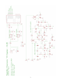
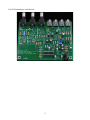
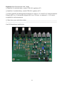
Assembly Manual
V1R2B-Rev1.0D
for 4 State QRP
MagicBox - Solid State Transmit/Receive System
Designed by: Jim Kortge, K8IQY
Copyright 2009-2012 - All rights reserved
This system is the result of some brainstorming with Terry Fletcher, WA0ITP and Joe Porter, W0MQY
at the Dayton Hamvention in 2009. We were talking about kits that might be suitable as revenue
generators to fund the Ozarkcon activities in 2010 and beyond. The "MagicBox" project is the result.
It is an all solid state, Transmit/Receive switching system that allows one to connect single band CW
transmitters (up to a maximum of 10 watts) and receivers together to turn the pair into a transceiving
station, "like magic". The system can be used on any band from 160 through 10 meters. It can handle
both solid state and cathode keyed, tube transmitters. It supports full QSK CW up to about 50 WPM.
And, a non-QSK mode is also provided, for those who don't like QSK CW.
There are five pieces of functionality within the system. First, is a keying circuit to turn on the
transmitter. Second, is a PIN diode switch used to connect the transmitter to the antenna so that it can
transmit and also to isolate the output impedance of the transmitter from loading the receiver. Third, is
a four element, series-shunt switch that disconnects the receiver from the antenna and shorts the
receiver input to ground while the transmitter is transmitting. Forth, is another series-shunt switch
(three elements) used to disconnect the receive audio from the speaker (headphones) during transmit.
Fifth, is an sine wave audio oscillator and series switch that supplies side tone audio to the speaker
(headphones) during transmit so that transmit keying can be monitored. All of the control timing for
the system is supplied from an AVR ATtiny2313 microprocessor.
1
The next pages contain an image of the supplied printed circuit board and the schematics for the
system.
2
3
4
PCB Stuffing
Stuffing the PCB will be done by installing all of the connectors and headers. Following that, all of the
resistors will be installed, starting from the lowest value and proceeding to the highest. Then, all of the
capacitors will be installed, using the same scheme. That will be followed by the inductors and
transformers, and then the diodes. When all of the passive parts are on the board, groups of integrated
circuits and transistors will be installed followed by simple tests to assure that circuits are active and
performing to specification. It is highly suggested that you print out both schematic sheets and use a
highlighter to mark each component as it is installed. This will assist you later on if you have parts left
over and wonder where they were supposed to go.
Connectors and Headers
[ ] Start construction by installing Power Jack J1. Hold this part toward the rear of the PCB so that is
projects out from beyond the edge of the board.
[ ] Install the 4 audio jacks at locations J5, J6, J8 and J9.
[ ] Install the 3 BNC jacks at locations J2, J3 and J4.
[ ] Install a 2-pin header at locations J7, J11, J12, J13 and J14. Supplied with the kit is a break-a-way
20-pin header to be used for the 2-pin and the 3-pin headers. Use sharp diagonal cutters or a hobby
razor saw to make the appropriate cuts.
[ ] Install a 3-pin header at J10.
[ ] Install the 20-pin IC socket at location U1. Make sure to get the orientation correct; match the
notch in the socket with that of the silkscreen overlay. Once it is soldered in, it cannot be removed
without destroying the printed circuit board.
5
Your PCB should look like this:
Resistors
[ ] Install the large, 1 watt, 180 Ohm (Brown-Grey-Brown) resistor at R12. This is the only 1 watt
resistor; all of the others are 1/4 watt. Note: The leads of this resistor should be bent as
shown in this detailed photo, so that it will fit the hole pattern and slightly elevate the
resistor above the board for cooling.
[ ] Install 220 Ohm (Red-Red-Brown) resistors at R36, R43 and R44.
[ ] Install 470 Ohm (Yellow-Violet-Brown) resistors at R3, R4, R14, R18, R35, R40, R42, R47 and
R48.
[ ] Install 4.7K Ohm (Yellow-Violet-Red) resistors at R1, R2, R7, R8, R9, R11, R13, R15 (next to
R18), R16, R17, R20, R21, R22, R23, R24, R26, R27, R28, R29, R30, R31, R33, R34, R37, R38, R39,
R41, R45 and R49. Since there are so many resistors of this value, it is suggested that they be installed
in groups of 7, 7, 7 and then the remaining 8, shown by the colored highlights.
[ ] Install the 36K Ohm (Orange-Blue-Orange) resistor at R25.
[ ] Install 47K Ohm (Yellow-Violet-Orange) resistors at R10 and R19.
[ ] Install the 10M Ohm (Brown-Black-Blue) resistor at R46.
6
[ ] Install the 1K trimmer resistor (blue potentiometer) at R32.
Your PCB should now look like this:
Capacitors
[ ] Install 0.02 uF (green color - marked 2A203K) at C19, C20 and C21.
[ ] Install 0.1 uF (tan color - marked 104) capacitors at C1, C5, C6, C7, C8, C9, C10, C11 and C12.
[ ] Install 2.2 uF (black color - marked 2u2) capacitors at C13, C22, C24 and C27. Note the + polarity
marking on these capacitors; they need to be installed with this + matching the + on the PCB.
[ ] Install 22 uF (black color - marked 22uF) capacitors at C2, C3, C4, C17 and C28. Note the +
polarity marking on these capacitors; they need to be installed with this + matching the + on the PCB.
[ ] Install 33 uF (black color - marked 33uF, 6.3v, non-polar) capacitors at C25 and C26.
[ ] Install 47 uF (black color - marked 47uF, 6.3v, non-polar) capacitors at C15, C16 and C23.
[ ] Capacitors for locations C14 and C18 are not needed nor provided.
7
Your PCB should now look like this:
8
Inductors/Transformers
[ ] Install 100 uH (beige color - marked Brown-Black-Brown) molded inductors at L1, L3 and L4.
These look a bit like fat, 1/4 watt resistors.
[ ] Wind and install transformers T1 and T2. The "Winding T1 and T2" page contains notes on winding
these transformers, along with some photos of their construction.
Your PCB should now look like this:
9
Diodes
[ ] Install the 1N5818 (black body - marked 1N5818) diode at D1.
[ ] Install the 1N459A (black body - marked 1N459A) diode at D2. Save one lead from this diode so
that it can be used as a jumper on the IC socket U1 later on in a testing stage.
[ ] Install the 1N4007 (black body - marked 1N4007) diode at D3.
Your PCB should now look like this:
10
Regulators (look like transistors with 3 leads)
[ ] Install the 10 volt (black body - marked 750L10C) regulator at IC1.
[ ] Install the 5 volt (black body - marked 750L05C) regulator at IC2.
[ ] Put the supplied 2-pin shorting shunt on header J14. Apply 12-15 volts DC to J1 and check that the
left pad of R1 is at +5 volts and the left pad of R25 is at +10 volts. A variation of +/- 0.25 volts is
acceptable for each measurement.
[ ] Write down your results/observations_________________________________________________
_________________________________________________________________________________
Your PCB should now look like this:
11
Transistors
Transistors will be installed in groups so that testing can be performed. After successful testing, the
next group will be added. Using this approach will ensure that the completed project works as
designed.
[ ] Install 2N3904 transistors at locations Q14 and Q15.
[ ] Install a 2N7000 transistor at location Q16. Note that 2N7000 transistors are sensitive to static, so
touch a metal object before picking up this type of transistor. Building over a cookie tin is suggested as
a means of providing the metal object, plus it keeps parts from falling off of the work bench.
[ ] Plug a speaker or headphones into J6. Apply power to J1 and confirm that a 700 Hz tone is coming
out of the speaker. Rotate trimmer resistor R32 through its full range and confirm that the audio level
changes from nothing to full volume. This is a test of the side tone oscillator and its mute switch.
[ ] Write down your results/observations_________________________________________________
_________________________________________________________________________________
[ ] Install 2N7000 transistors at locations Q11, Q12 and Q13.
[ ] Connect a test lead from the lower lead of R21 to ground. Place a jumper (diode lead saved from an
earlier step) from pin 20 to pin 16 on IC socket U1. Plug a speaker or headphones into J5 . Apply
power to J1 and confirm that a 700 Hz tone from the side tone oscillator is coming out of the speaker.
This is a test of the audio muting switch when using the side tone oscillator as an audio source.
[ ] Write down your results/observations_________________________________________________
_________________________________________________________________________________
[ ] Install 2N7000 transistors at locations Q1 and Q2.
[ ] Connect an antenna or other RF signal source to J3. Connect the antenna lead of a receiver to J2.
Apply power to J1 and confirm that band noise or signals from the signal source can be heard on the
receiver. This is a test of the series switches that connect the receiver to the antenna during receive.
[ ] Write down your results/observations_________________________________________________
_________________________________________________________________________________
[ ] Install 2N7000 transistors at locations Q3 and Q6. These are the shunt switch elements but won't be
tested until later system tests.
[ ] Install a 2N3906 transistor at location Q9.
[ ] Install 2N7000 transistors at locations Q7 and Q10.
[ ] Connect an antenna or other RF signal source to J4. Connect the antenna lead of a receiver to J3.
Apply power to J1 and confirm that band noise or signals from the signal source can be heard on the
receiver. This is a test of the PIN diode switch that connects the transmitter to the antenna when
transmitting.
12
[ ] Write down your results/observations_________________________________________________
_________________________________________________________________________________
[ ] Install a 2N3906 transistor at location Q4.
[ ] Install 2N7000 transistors at locations Q5 and Q8.
[ ] Install a 2N7000 transistor at location Q18.
[ ] Install the IRF510 transistor at location Q17. The heat sink side of the transistor is away from the
1/8 inch audio jacks as shown on the PCB overlay.
Your PCB should now look like this:
Integrated Circuits
[ ] Install the ATtiny2313 chip. Make sure that it is oriented to match the socket. Installing the chip
may require bending in the leads on the sides so that they line up with the socket pins. To do this step,
put the chip on a hard surface on its side, and while pushing down on the chip, rock it toward the lead
ends. Repeat this operation on the other side. When the leads are 90 degrees to the body on each side,
it will go into the socket with a small amount of force.
13
Operational Checks
If an RF Signal Generator is available, connect it to the Antenna Out BNC connector J3. If no signal
generator is available, connect an antenna to J3. Using a BNC jumper, connect the antenna lead of a
receiver to the Receiver Out connector J2. Connect a key to the Key(er) connector J8. Turn on the
receiver. Apply power to the MagicBox. If using a signal generator, adjust the amplitude to 50 microvolts and tune the receiver to find this signal. If using an antenna, confirm that antenna noise is being
heard. Press the key and confirm that the signal into the receiver is greatly attenuated. Remove power
from the MagicBox.
[ ] Write down your results/observations_________________________________________________
_________________________________________________________________________________
Place a shorting shunt on the 2-pin header J11. This places the MagicBox in Non-QSK mode. Apply
power to the MagicBox. Press the key and confirm that the receiver returns to listening mode after an
approximate 1-second delay. Remove power from the MagicBox. Remove the shunt and place it over
one of the pins for safe keeping.
[ ] Write down your results/observations_________________________________________________
_________________________________________________________________________________
Continuing with the above setup, connect the audio output of the receiver to the Audio In jack J5. (Use
the wiring information on the “Connection Diagram” page for the receiver to MagicBox audio lead.)
Connect a speaker or headphones to the Speaker/Phones jack J6. Apply power to the MagicBox. Turn
on the receiver and confirm that receive audio is coming out of the speaker/headphones. Press the key
and confirm that the audio signal from the receiver is cut off and the MagicBox side tone is being
heard. The side tone level can be adjusted to a comfortable listening level with trimmer R32. Remove
power from the MagicBox.
[ ] Write down your results/observations_________________________________________________
_________________________________________________________________________________
Remove the signal generator or antenna from the Antenna Out BNC connector J3. Turn off the
receiver. Remove the receiver antenna connection. Connect a dummy load/watt meter to the Antenna
Out BNC J3 connector. Connect the RF output of the transmitter to the Transmit In BNC connector J4.
Connect the keying lead of the transmitter to the Transmit Key jack J9 of the MagicBox. Apply power
to the MagicBox. Turn on the transmitter. Press the key and confirm that transmitted RF is being
shown on the watt meter. Turn off the transmitter. Remove power from the MagicBox.
[ ] Write down your results/observations_________________________________________________
_________________________________________________________________________________
Continuing with the above setup, reconnect the receiver antenna to the Receiver Out BNC connector
J2. Turn on the receiver. Apply power to the MagicBox. Turn on the transmitter. Key the transmitter
and confirm that RF is being shown on the watt meter and that the side tone is being heard from the
speaker.
[ ] Write down your results/observations_________________________________________________
_________________________________________________________________________________
14
With both receiver and transmitter connected to the MagicBox, key the transmitter several times and
assure that the receiver is being muted except for the sidetone and the transmitter is keying properly.
[ ] Write down your results/observations_________________________________________________
_________________________________________________________________________________
Replace the dummy load with a suitable antenna and try the system on the air. Confirm that the
receiver is being muted except for the side tone and the transmitter is keying properly.
[ ] Write down your results/observations_________________________________________________
_________________________________________________________________________________
This completes the assembly and testing of the MagicBox. If you are going to operate it without a
case, put some rubber feet on the bottom of the PCB to keep it up off of the table so that
something isn't inadvertently shorted out.
15
Connection Diagram
Note: The audio connection from the receiver should be wired to the MagicBox using a stereo plug on
the MagicBox end, with the ground on the ring terminal and the signal lead on the tip terminal. The J5
and J6 jacks should have their mounting barrels insulated from chassis ground with a 1/16 inch length
of 1/4 inch shrink tubing over the mounting barrel. No nut is used on either of these two jacks.
16
Packaging Considerations
Now that you've completed your MagicBox T/R System, you may have decided to put it into some
kind of enclosure. This document will aid your efforts in doing that. However, just so you know, it will
work just fine without being in an enclosure; it was designed to work "out in the open" with just a set
of rubber feet attached to the bottom of the PCB so that the pads are not at risk of being shorted out.
That said, here is a run down of the various 2 and 3 pin headers that are on the PCB. They provide
convenient attachments for the various switches and display LEDs that can be implemented.
Header
J14
J12
J7
J13
J10
Function
Connection point for a SPST N/O switch to turn power on and off.
Connection point for a power indicator LED.
Connection point for a SPST N/O switch to key the MagicBox, used for tuneup.
Connection point for a "transmitting" indicator LED.
Connection point for a SPST N/O switch to "leak" some receive audio to output jack J6
so that a receiver can be zero beat with the transmit frequency.
A toggle switch is recommended for the power off/on switch, but a latching push button switch could
also be used.
The J7 and J10 switching functions can be implemented in a variety of ways. A single DPDT ON-OffON toggle switch (used on my prototype) could be used with the upper contacts used for the J7
connections, and the lower contacts used for the J10 connections. When using the J10 "spotting
function", the transmitter needs to be on, so the upper contacts would "make" when this switch is in
either direction from the center off position. If it is desired to not have the capability of keying the
transmitter on and leaving both hands free, one could implement either or both of the J7 and J10
functions using momentary, push button switches or a toggle switch with momentary contacts at one or
both "ON" positions.
The MagicBox was designed to fit into a Ten Tec TP41 case. The MagicBox web site has a drilling
template on it, showing locations and hole sizes for the various BNC and 1/8 inch jacks that are on the
PCB, which can be used when installing the MagicBox in this case. Note that no mounting nuts are
used on 1/8 inch jacks J5 and J6. The holes for these two jacks should be oversized enough to allow a
1/16 inch piece of 1/4 inch diameter shrink tubing to be placed over the shaft of these jacks, insulating
them from the case. Any additional hole locations and sizes for implementing the functions
documented above are left to the builder's discretion, since these will vary wildly depending on the
switches and LEDs used.
17
MagicBox Specifications
General
160 through 10 meter operation
5.3" X 4.0 " PCB, fits TenTec TP-41 case
Approximately 120 parts
Beginning builder skills level project
Construction time approximately 8 hours
System
Power Supply
10-15 volts dc; 120 milliamps
RF Section
Receive Mode
Antenna to Receiver Input Loss:
Transmitter to Receiver Input Isolation:
Transmit Mode
Maximum transmit power
Transmitter Output to Antenna Loss:
Antenna to Receiver Input Isolation:
Less than 2 dB, 1.8 - 28 MHz
Greater than 25 dB, 1.8 - 28 MHz
Less than 10 watts
Less than 0.25 dB, 1.8 - 28 MHz
Greater than 90 dB, 1.8 - 10 MHz
Greater than 85 dB, 14 MHz
Greater than 80 dB, 28 MHz
Audio Section (32 Ohm source and load)
Receive Mode
Receiver Audio Loss:
Less than 2 dB
Transmit Mode
Receiver Audio Isolation:
Greater than 200 dB
QSK Mode
Non-QSK Mode
Transmitter Types
Keying
Up to 50 WPM
1 second receiver delay
Solid state or cathode keyed tube
18
Bill of Material
19
Instructions for Winding T1 and T2
Start by marking each core with a "dot" on one end using a blue "Sharpie" marking pen. Touch the spot
several time to make sure that a permanent dot exists. This "dot" end by our convention will be the
secondary side of each transformer, and have a 2-turn winding on it.
Start the secondary winding with a 3-inch piece of #28 wire, supplied with the kit. Place it in one of the
holes, on the "dot" end of the core, leaving about 1-inch lead sticking out. Take the lead coming out the
opposite end, bend it around, and push it back through the other hole. That's one turn. Repeat the
operation pushing the longer lead back through the hole where you started, bending the lead around
again, and pushing it back through the opposite hole. Snug up the windings by gently pulling on each
lead with a pair of small pliers. The core with the secondary winding will look the the photo below.
If you look at the end of the core opposite where the two leads exit, you should see two wires as shown
in the next photo.
Next, we have to add the 4-turn primary winding. This starts with a 5-inch piece of #28 wire. On the
opposite end of the core from where the secondary winding leads exit, push most of the wire through a
hole, leaving about a 1-inch lead sticking out. As we did with the secondary winding, bend the free end
of this wire around and push it back through the core using the other hole. That's 1-turn that we have
wound. Following this example, repeat that process for 3 more turns. As you go along, try to keep the
windings tight within the core and laying organized and flat so that all of the turns can be added. When
you have the 4-turns on the core, it will look that the next photo.
Notice that the primary winding lead that was being pushed through the core holes ends up about
twice as long as the beginning end. That's a good check that 4-turns has been wound. Cut each of the
leads to about 1/2- inch, scrape off the insulation, and tin the wire up to within 1/8-inch of the core.
The transformer is now ready to install on the PCB. Repeat the process for the other core.
20