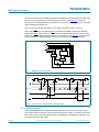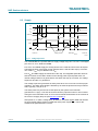
1
TDA8007BHL Multiprotocol IC card interface Rev. 9.1 — 18 June 2012 Product data sheet 1. General description The TDA8007BHL is a cost-effective card interface for dual smart card readers. Controlled through a parallel bus, it meets all requirements of ISO 7816, GSM 11-11, EMV4.2 and EMV 2000. It is addressed on a non-multiplexed 8-bit databus, by means of address registers AD0, AD1, AD2 and AD3. TDA8007BHL/C3 can be also addressed through a multiplexed access. The integrated ISO UART and the time-out counters allow easy use even at high baud rates with no real time constraints. Due to its chip select, external input/output and interrupt features, it greatly simplifies the realization of a reader of any number of cards. It gives the cards and the reader a very high level of security, due to its special hardware against ESD, short-circuiting, power failure, etc. The integrated step-up converter allows operation within a supply voltage range of 2.7 V to 6 V. TDA8007BHL/C4 supports only non multiplex access and TDA8007BHL/C3 support both non multiplexed and multiplexed access. 2. Features and benefits Control and communication through an 8-bit parallel interface, compatible with non-multiplexed memory access, TDA8007BHL/C3 can be also addressed through a multiplexed memory access Specific ISO UART with parallel access input/output for automatic convention processing, variable baud rate through frequency or division ratio programming, error management at character level for T = 0 and extra guard time register FIFO for 1 to 8 characters in reception mode Parity error counter in reception mode and in transmission mode with automatic re-transmission Dual VCC generation: 5 V ± 5 %, 65 mA (max.); 3 V ± 8 %, 50 mA (max.) or 1.8 V ± 10 %, 30 mA (max.); with controlled rise and fall times Dual cards clock generation (up to 10 MHz), with three times synchronous frequency doubling (fXTAL, 1⁄2fXTAL, 1⁄4fXTAL and 1⁄8fXTAL) Cards clock stop (at high or low level) or 1.25 MHz (from internal oscillator) for cards Power-down mode Automatic activation and deactivation sequence through an independent sequencer Supports the asynchronous protocols T = 0 and T = 1 in accordance with: ISO 7816 and EMV4.2 Versatile 24-bit time-out counter for Answer To Reset (ATR) and waiting times processing Specific Elementary Time Unit (ETU) counter for Block Guard Time (BGT): 22 in T = 1 and 16 in T = 0 Minimum delay between two characters in reception mode: TDA8007BHL NXP Semiconductors Multiprotocol IC card interface – in Protocol T = 0: 11.8 ETU – in Protocol T = 1: 10.8 ETU Supports synchronous cards Current limitations in the event of short-circuit (pins I/O1, I/O2, VCC1, VCC2, RST1 and RST2) Special circuitry for killing spikes during power-on/power-off Supply supervisor for power-on/power-off reset Step-up converter (supply voltage from 2.7 V to 6 V), doubler, tripler or follower according to VCC and VDD Additional input/output pin allowing use of the ISO UART for another analog interface (pin I/OAUX) Additional interrupt pin allowing detection of level toggling on an external signal (pin INTAUX) Fast and efficient swapping between the three cards due to separate buffering of parameters for each card Chip select input allowing use of several devices in parallel and memory space paging Enhanced ESD protections on card side (except C4x, C8x): 6 kV (min.) Software library for easy integration within the application Power-down mode for reducing current consumption when no activity. 3. Applications Multiple smart card readers for multiprocessor applications (EMV banking, digital pay TV and access control, etc.). 4. Quick reference data Table 1. Quick reference data VDD = 3.3 V; fXTAL = 10 MHz; GND = 0 V; Tamb = 25 C; unless otherwise specified. Symbol Parameter VDD supply voltage VDDA analog Conditions Min Typ Max Unit 2.7 - 6.0 V step-up converter VDD - 6.0 V cards inactive; fXTAL = 0 Hz - - 350 A cards active; VCC = 5 V; fCLK = 0 Hz; fXTAL = 0 Hz - - 3 mA supply voltage IDD(pd) supply current in power-down mode IDD(sm) supply current in sleep mode cards active; fCLK = 0 Hz - - 5.5 mA IDD(oper) supply current in operating mode ICC1 = 65 mA; ICC2 = 15 mA; fXTAL = 20 MHz; fCLK = 10 MHz; VDD = 2.7 V - - 315 mA TDA8007BHL Product data sheet All information provided in this document is subject to legal disclaimers. Rev. 9.1 — 18 June 2012 © NXP B.V. 2012. All rights reserved. 2 of 51 TDA8007BHL NXP Semiconductors Multiprotocol IC card interface Table 1. Quick reference data …continued VDD = 3.3 V; fXTAL = 10 MHz; GND = 0 V; Tamb = 25 C; unless otherwise specified. Symbol Parameter Conditions Min Typ Max Unit VCC card supply output voltage 5 V card including static loads 4.75 5.0 5.25 V with 40 nC dynamic loads on 200 nF capacitor 4.6 - 5.4 V including static loads 2.78 - 3.22 V with 24 nC dynamic loads on 200 nF capacitor 2.75 - 3.25 V including static loads 1.65 - 1.95 V with 12 nC dynamic loads on 200 nF capacitor 1.62 - 1.98 V 5 V card; operating - - 65 mA 3 V card; operating - - 50 mA 3 V card 1.8 V card ICC card supply output current 1.8 V card; operating - - 30 mA overload detection - 100 - mA ICC1 + ICC2 sum of both card supply operating; 5 and 3 V cards output currents - - 80 mA SR slew rate on VCC (rise and fall) 0.05 0.16 0.22 V/s tdeact deactivation cycle duration - - 150 s CL(max) = 300 nF tact activation cycle duration - 225 s fXTAL crystal frequency 4 - 20 MHz fext external frequency 0 - 20 MHz Tamb ambient temperature 40 - +85 °C applied to pin XTAL1 5. Ordering information Table 2. Ordering information Type number Package Name Description Version TDA8007BHL/C3 LQFP48 plastic low profile quad flat package; 48 leads; body 7 7 1.4 mm SOT313-2 TDA8007BHL/C4 LQFP48 plastic low profile quad flat package; 48 leads; body 7 7 1.4 mm SOT313-2 TDA8007BHL Product data sheet All information provided in this document is subject to legal disclaimers. Rev. 9.1 — 18 June 2012 © NXP B.V. 2012. All rights reserved. 3 of 51 TDA8007BHL NXP Semiconductors Multiprotocol IC card interface 6. Block diagram VDD VDDA 100 nF GND 19 27 1 RSTOUT DELAY 48 220 nF SAP SAM 23 21 26 SUPPLY AND SUPERVISOR 220 nF SBP SBM 22 24 STEP-UP CONVERTER AGND 25 20 VUP 220 nF 22 nF 40 39 45 44 43 42 36 37 28 29 30 31 32 33 34 35 38 2 41 6 4 8 10 ISO7816 UART INTERFACE CONTROL INT ALE AD0 AD1 AD2 AD3 RD WR D0 D1 D2 D3 D4 D5 D6 D7 CS I/OAUX INTAUX 9 3 ANALOG DRIVERS AND SEQUENCERS TIME-OUT COUNTER 5 7 14 12 16 18 17 CLOCK CIRCUIT 11 13 15 C41 C81 CLK1 RST1 VCC1 I/O1 PRES1 CGND1 C42 C82 CLK2 RST2 VCC2 I/O2 PRES2 CGND2 INT OSC TDA8007B XTAL OSC 47 XTAL1 46 XTAL2 fce534 Fig 1. Block diagram TDA8007BHL Product data sheet All information provided in this document is subject to legal disclaimers. Rev. 9.1 — 18 June 2012 © NXP B.V. 2012. All rights reserved. 4 of 51 TDA8007BHL NXP Semiconductors Multiprotocol IC card interface 7. Pinning information 37 WR 38 CS 39 ALE 40 INT 41 INTAUX 42 AD3 43 AD2 44 AD1 45 AD0 46 XTAL2 RSTOUT 1 36 RD I/OAUX 2 35 D7 I/O1 3 34 D6 C81 4 33 D5 PRES1 5 32 D4 C41 6 CGND1 7 CLK1 8 29 D1 VCC1 9 28 D0 31 D3 TDA8007BHL 30 D2 SBM 24 VDDA 23 SBP 22 SAP 21 VUP 20 GND 19 RST2 18 VCC2 17 25 AGND CLK2 16 26 SAM C82 12 CGND2 15 27 VDD I/O2 11 C42 14 RST1 10 PRES2 13 Fig 2. 47 XTAL1 48 DELAY 7.1 Pinning fce678 Pin configuration 7.2 Pin description Table 3. TDA8007BHL Product data sheet Pin description Symbol Pin Description RSTOUT 1 PMOS open-drain output for resetting external devices I/OAUX 2 input or output for an I/O line from an auxiliary smart card interface I/O1 3 input or output for the data line to/from card 1 (ISO C7 contact) C81 4 auxiliary I/O for ISO C8 contact (synchronous cards, for instance) for card 1 PRES1 5 card 1 presence contact input (active high) C41 6 auxiliary I/O for ISO C4 contact (synchronous cards, for instance) for card 1 CGND1 7 ground for card 1; must be connected to GND CLK1 8 clock output to card 1 (ISO C3 contact) VCC1 9 card 1 supply output voltage (ISO C1 contact) RST1 10 card 1 reset output (ISO C2 contact) I/O2 11 input or output for the data line to/from card 2 (ISO C7 contact) All information provided in this document is subject to legal disclaimers. Rev. 9.1 — 18 June 2012 © NXP B.V. 2012. All rights reserved. 5 of 51 TDA8007BHL NXP Semiconductors Multiprotocol IC card interface Table 3. Pin description …continued Symbol Pin Description C82 12 auxiliary I/O for ISO C8 contact (synchronous cards, for instance) for card 2 PRES2 13 card 2 presence contact input (active high) C42 14 auxiliary I/O for ISO C4 contact (synchronous cards, for instance) for card 2 CGND2 15 ground for card 2; must be connected to GND CLK2 16 clock output to card 2 (ISO C3 contact) VCC2 17 card 2 supply output voltage (ISO C1 contact) RST2 18 card 2 reset output (ISO C2 contact) GND 19 ground VUP 20 connection for the step-up converter capacitor; connect a low ESR capacitor of 220 nF to AGND SAP 21 contact 1 for the step-up converter; connect a low ESR capacitor of 220 nF between pins SAP and SAM SBP 22 contact 3 for the step-up converter; connect a low ESR capacitor of 220 nF between pins SBP and SBM VDDA 23 positive analog supply voltage for the step-up converter; may be higher than VDD; decouple with a good quality capacitor to GND SBM 24 contact 4 for the step-up converter; connect a low ESR capacitor of 220 nF between pins SBP and SBM AGND 25 analog ground for the step-up converter SAM 26 contact 2 for the step-up converter; connect a low ESR capacitor of 220 nF between pins SAP and SAM VDD 27 positive supply voltage; decouple with a good quality capacitor to GND D0 to D7 28, 29, 30, 31, 32, 33, 34, 35 input/output of data 0-7; TDA8007BHL/C3 in case of mulitplexed configuration: address 0-7 RD 36 read or write selection input; high for read, low for write WR 37 enable pin; same behavior as CS\ (active low) CS 38 chip select input (active low) ALE 39 TDA8007BHL/C4: Not connected; TDA8007BHL/C3: address latch enable input in case of multiplexed configuration, connect to VDD in non-multiplexed configuration TDA8007BHL Product data sheet INT 40 NMOS interrupt output (active low) INTAUX 41 auxiliary interrupt input AD3 42 register selection address 3 input AD2 43 register selection address 2 input AD1 44 register selection address 1 input All information provided in this document is subject to legal disclaimers. Rev. 9.1 — 18 June 2012 © NXP B.V. 2012. All rights reserved. 6 of 51 TDA8007BHL NXP Semiconductors Multiprotocol IC card interface Table 3. Pin description …continued Symbol Pin Description AD0 45 register selection address 0 input XTAL2 46 connection for an external crystal XTAL1 47 connection for an external crystal or input for an external clock signal DELAY 48 connection for an external delay capacitor 8. Functional description Remark: Throughout this document, it is assumed that the reader is familiar with ISO7816 terminology. 8.1 Interface control The TDA8007BHL/C3 is sensitive to ESD in functional mode. This sensitivity is seen on pin ALE: an electrostatic discharge causes an edge on this pin and changes its mode of communication. When the mode of communication is the multiplexed mode, this has no impact. But when the mode used is the non-multiplexed mode, the ESD may change the mode to multiplexed mode, which is irreversible without power-off/power-on. The TDA8007BHL/C4 is an evolution of the C3 version in which the communication mode is set to non-multiplexed and can not be changed. 8.1.1 Non-Multiplexed configuration The TDA8007BHL/C4 is only in the non-multiplexed configuration (Figure 3), where the TDA8007BHL/C3 offers a multiplexed configuration in addition to a non-mulitplexed configuration. The configuration can be chosen through the ALE-pin. If pin ALE is tied to VDD or ground, the TDA8007BHL/C3 will be in the non-multiplexed configuration. The TDA8007BHL can be controlled via an 12-bit parallel bus (bits D0 to D7 and bits A0 to A3). The address bits are determined by means of pins AD0 to AD3. The read or write control signal is on pin RD and a data write or read active low enable signal is on pin WR. Signals CS and WR play the same role. In read operations (see Figure 4) with signal RD = high, the data corresponding to the chosen address is available on the bus when both signals CS and WR are low. In write operations (see Figure 5 and 6) with signal RD = low, the data present on the bus is written when signals CS and WR are low. In both configurations, the TDA8007BHL/C4 is selected only when signal CS = low. Signal INT is an active low interrupt signal. TDA8007BHL Product data sheet All information provided in this document is subject to legal disclaimers. Rev. 9.1 — 18 June 2012 © NXP B.V. 2012. All rights reserved. 7 of 51 TDA8007BHL NXP Semiconductors Multiprotocol IC card interface CS D0 to D7 AD0 to AD3 WR RD REC REGISTERS 001aam017 Fig 3. Non-multiplexed bus configuration AD0 to AD3 RD t1 t2 t3 CS WR D0 to D7 DATA OUT fce840 Fig 4. TDA8007BHL Product data sheet Control with non-multiplex bus (read) All information provided in this document is subject to legal disclaimers. Rev. 9.1 — 18 June 2012 © NXP B.V. 2012. All rights reserved. 8 of 51 TDA8007BHL NXP Semiconductors Multiprotocol IC card interface AD0 to AD3 RD t7 CS t6 WR t4 D0 to D7 t5 DATA IN fce841 Fig 5. Control with non-multiplex bus (Write with CS) AD0 to AD3 RD t7 CS WR t6 D0 to D7 t4 t5 DATA IN fce842 Fig 6. Control with non-multiplex bus (Write with EN) 8.1.2 Multiplexed configuration The TDA8007BHL/C3 offers a multiplexed configuration in addition to a nun multiplexed configuration. The TDA8007BHL/C4 does not offer the multiplexed configuration. TDA8007BHL Product data sheet All information provided in this document is subject to legal disclaimers. Rev. 9.1 — 18 June 2012 © NXP B.V. 2012. All rights reserved. 9 of 51 TDA8007BHL NXP Semiconductors Multiprotocol IC card interface If a microcontroller with a multiplexed address and data bus (such as 80C51) is used, then pins D0 to D7 may be directly connected to port P0 to P7, see Figure 7. Automatic switching to the multiplexed bus configuration occurs only for TDA8007BHL/C3, if a rising edge is detected on signal ALE. In this event, pins AD0 to AD3 play no role and may be tied to VDD or ground. When signal CS = low, the demulitplexing of address and data is performed internally using signal ALE, a low pulse on pin RD allows the selected register to be read, a LOW pulse on pin WR allows the selected register to be written to, see Figure 8. Using a 80C51 microcontroller, the TDA8007BHL/C3 is simply controlled with MOVX instructions. AD0 to AD3 CS D0 to D7 ALE WR RD LATCH REC MUX MUX addresses RD WR REGISTERS fce679 Fig 7. Multiplexed bus recognition ALE tW(ALE) tAVLL tW(RD) tAVLL t(RWH-AH) CS t(RWH-AH) t(AL-RWL) t(AL-RWL) ADDRESS D0 to D7 DATA READ ADDRESS DATA WRITE t(DV-WL) RD t(RL-DV) tW(WR) WR fce680 Fig 8. Control with multiplexed bus (read and write) 8.2 Control registers The TDA8007BHL has two complete analog interfaces which can drive cards 1 and 2. The data to and from these two cards shares the same ISO UART. The data to and from a third card (card 3), externally interfaced (with a TDA8020 or TDA8004 for example), may also share the same ISO UART. TDA8007BHL Product data sheet All information provided in this document is subject to legal disclaimers. Rev. 9.1 — 18 June 2012 © NXP B.V. 2012. All rights reserved. 10 of 51 TDA8007BHL NXP Semiconductors Multiprotocol IC card interface Cards 1, 2 and 3 have dedicated registers for setting the parameters of the ISO UART (see Figure 9). Programmable Divider Register (PDR) Guard Time Register (GTR) UART Configuration register 1 (UCR1) UART Configuration Register 2 (UCR2) Clock Configuration Register (CCR) Cards 1 and 2 also have dedicated registers for controlling their power and clock configuration. The Power Control Register (PCR) for card 3 is controlled externally. Register PCR is also used for writing or reading on the auxiliary card contacts C4 and C8. Card 1, 2 or 3 can be selected via the Card Select Register (CSR). When one card is selected, the corresponding parameters are used by the ISO UART. Register CSR also contains one bit for resetting the ISO UART (bit RIU = 0). This bit is reset after power-on and must be set to logic 1 before starting with any one of the cards. It may be reset by software when necessary. When the specific parameters of the cards have been programmed, the UART may be used with the following registers: UART Receive Register (URR) UART Transmit Register (UTR) UART Status Register (USR) Mixed Status Register (MSR). In reception mode, a FIFO of 1 to 8 characters may be used and is configured with the FIFO Control Register (FCR). This register is also used for the automatic re-transmission of Not AcKnowledged (NAK) characters in transmission mode. The Hardware Status Register (HSR) gives the status of the supply voltage, of the hardware protections and of the card movements. Registers HSR and USR give interrupts on pin INT when some of their bits have been changed. Register MSR does not give interrupts and may be used in the polling mode for some operations; for this use, some of the interrupt sources within the registers USR and HSR may be masked. A 24-bit time-out counter may be started to give an interrupt after a number of ETU programmed into the Time-Out Registers TOR1, TOR2 and TOR3. This will help the microcontroller in processing different real-time tasks (ATR, WWT, BWT, etc.). This counter is configured with a Time-Out counter Configuration (TOC) register. It may be used as a 24-bit counter or as a 16-bit plus 8-bit counter. Each counter can be set to start counting once data has been written, or on detection of a START bit on the I/O, or as auto-reload. TDA8007BHL Product data sheet All information provided in this document is subject to legal disclaimers. Rev. 9.1 — 18 June 2012 © NXP B.V. 2012. All rights reserved. 11 of 51 xxxxxxxxxxxxxxxxxxxxx xxxxxxxxxxxxxxxxxxxxxxxxxx xxxxxxx x x x xxxxxxxxxxxxxxxxxxxxxxxxxxxxxx xxxxxxxxxxxxxxxxxxx xx xx xxxxx xxxxxxxxxxxxxxxxxxxxxxxxxxx xxxxxxxxxxxxxxxxxxx xxxxxx xxxxxxxxxxxxxxxxxxxxxxxxxxxxxxxxxxx xxxxxxxxxxxx x x xxxxxxxxxxxxxxxxxxxxx xxxxxxxxxxxxxxxxxxxxxxxxxxxxxx xxxxx xxxxxxxxxxxxxxxxxxxxxxxxxxxxxxxxxxxxxxxxxxxxxxxxxx xxxxxxxx xxxxxxxxxxxxxxxxxxxxxxxxx xxxxxxxxxxxxxxxxxxxx xxx CARD SELECT REGISTER HARD STATUS REGISTER NXP Semiconductors TDA8007BHL Product data sheet GENERAL ISO UART TIME-OUT REGISTER 1 UART STATUS REGISTER UART TRANSMIT REGISTER TIME-OUT REGISTER 2 MIXED STATUS REGISTER UART RECEIVE REGISTER Rev. 9.1 — 18 June 2012 All information provided in this document is subject to legal disclaimers. TIME-OUT REGISTER 3 FIFO CONTROL REGISTER TIME-OUT CONFIGURATION CARD 3 PROGRAM DIVIDER REGISTER 1 PROGRAM DIVIDER REGISTER 2 PROGRAM DIVIDER REGISTER 3 GUARD TIME REGISTER 1 GUARD TIME REGISTER 2 GUARD TIME REGISTER 3 UART CONFIGURATION REGISTER 11 UART CONFIGURATION REGISTER 21 UART CONFIGURATION REGISTER 31 UART CONFIGURATION REGISTER 12 UART CONFIGURATION REGISTER 22 UART CONFIGURATION REGISTER 32 CLOCK CONFIGURATION REGISTER 1 CLOCK CONFIGURATION REGISTER 2 CLOCK CONFIGURATION REGISTER 3 POWER CONTROL REGISTER 1 POWER CONTROL REGISTER 2 12 of 51 © NXP B.V. 2012. All rights reserved. Fig 9. Registers summary fce682 TDA8007BHL CARD 2 Multiprotocol IC card interface CARD 1 TDA8007BHL NXP Semiconductors Multiprotocol IC card interface 8.2.1 General registers 8.2.1.1 Card select register The Card Select Register (CSR) is used for selecting the card on which the UART will act, and also to reset the ISO UART. Table 4. [1] 7 6 5 4 3 2 1 0 CS7 CS6 CS5 CS4 RIU SC3 SC2 SC1 Register value at reset: all significant bits are cleared after reset, except bits CS7 to CS4 which are set to their default value Table 5. Register CSR (address 00h; write and read)[1] Bit Symbol Description 7 CS7 6 CS6 IC identifier: default value for identification the IC 0010 = TDA8007BHL/C2 5 CS5 4 CS4 3 RIU reset ISO UART: When reset, this bit resets a large part of the UART registers to their initial value. Bit RIU must be reset before any activation; logic 0 for at least 10 ns duration. Bit RIU must be set to logic 1 by software before any action on the UART can take place. 2 SC3 select card 3: If bit SC3 = 1, then card 3 is selected. 1 SC2 select card 2: If bit SC2 = 1, then card 2 is selected. 0 SC1 select card 1: If bit SC1 = 1, then card 1 is selected. [1] 8.2.1.2 Register CSR (address 00h; write and read)[1] 0011 = TDA8007BHL/C3 or TDA8007BHL/C4 Bits SC1, SC2 and SC3 must be set at one at a time. After reset no card is selected by default Hardware status register The Hardware Status Register (HSR) gives the status of the chip after a hardware problem has been detected. Table 6. 7 HS7 [1] TDA8007BHL Product data sheet Register HSR (address 0Fh; read only)[1] 6 5 4 3 2 1 0 PRTL2 PRTL1 SUPL PRL2 PRL1 INTAUXL PTL Register value at reset: all significant bits are cleared after reset, except bit SUPL which is set within pulse RSTOUT. All information provided in this document is subject to legal disclaimers. Rev. 9.1 — 18 June 2012 © NXP B.V. 2012. All rights reserved. 13 of 51 TDA8007BHL NXP Semiconductors Multiprotocol IC card interface Table 7. Description of HSR bits Bit Symbol Description 7 HS7 not used 6 PRTL2 protection 2: Bit PRTL2 = 1 when a fault has been detected on card reader 2. Bit PRTL 2 is the OR-function of the protection on pin VCC2 and pin RST2. 5 PRTL1 protection 1:. Bit PRTL1 = 1 when a fault has been detected on card reader 1. Bit PRTL 1 is the OR-function of the protection on pin VCC1 and pin RST1. 4 SUPL supervisor latch. Bit SUPL = 1 when the supervisor has been activated. 3 PRL2 presence latch 2: Bit PRL2 = 1 when a level change has occurred on pin PRES2. 2 PRL1 presence latch 1: Bit PRL1 = 1 when a level change has occurred on pin PRES1. 1 INTAUXL auxiliary interrupt change: Bit INTAUXL = 1 if the level on pin INTAUX has been changed. 0 PTL overheating: Bit PTL = 1 if overheating has occurred. When at least one of the bits PRTL2, PRTL1, PRL2, PRL1 or PTL is high, then INT is low. The bits having caused the interrupt are cleared when register HSR has been read-out. The same occurs with INTAUXL, if not disabled. In case of an emergency deactivation (by bits PRTL2, PRTL1, SUPL, PRL2, PRL1 or PTL), bit START (bit 0 in the PCR) is automatically reset by hardware. At power-on, or after a supply voltage drop-out, bit SUPL is set and pin INT = low. Pin INT will return to high level at the end of the alarm pulse RSTOUT (see Figure 3). Bit SUPL will be reset only after a status register read-out outside the alarm pulse. A minimum time of 2 µs is needed between two successive read operations of register HSR, as well as between reading of register HSR and activation (write in register PCR). 8.2.1.3 Time-out registers The three Time-Out Registers (TOR1, TOR2 and TOR3) form a programmable 24-bit ETU counter, or two independent counters (one 16-bit and one 8-bit). The value to load in registers TOR1, TOR2 and TOR3 is the number of ETU to count. The time-out counters may only be used when a card is active with a running clock. Table 8. 7 TOL7 [1] TDA8007BHL Product data sheet 6 5 4 3 2 1 0 TOL6 TOL5 TOL4 TOL3 TOL2 TOL1 TOL0 Register value at reset: all bits are cleared after reset. Table 9. [1] Register TOR1 (address 09H; write only)[1] Register TOR2 (address 0AH; write only)[1] 7 6 5 4 3 2 1 0 TOL15 TOL14 TOL13 TOL12 TOL11 TOL10 TOL9 TOL8 Register value at reset: all bits are cleared after reset. All information provided in this document is subject to legal disclaimers. Rev. 9.1 — 18 June 2012 © NXP B.V. 2012. All rights reserved. 14 of 51 TDA8007BHL NXP Semiconductors Multiprotocol IC card interface Table 10. [1] 8.2.1.4 Register TOR3 (address 0Bh; write only)[1] 7 6 5 4 3 2 1 0 TOL23 TOL22 TOL21 TOL20 TOL19 TOL18 TOL17 TOL16 Register value at reset: all bits are cleared after reset. Time-out configuration register The Time-Out Configuration (TOC) register is used for setting different configurations of the time-out counter as given in Table 11; all other configurations are undefined. Table 11. [1] 7 6 5 4 3 2 1 0 TOC7 TOC6 TOC5 TOC4 TOC3 TOC2 TOC1 TOC0 Register value at reset: all bits are cleared after reset. Table 12. TDA8007BHL Product data sheet Register TOC (address 0Bh; read and write)[1] Card registers (address 00h to F5h Register Description 00H All counters are stopped. 05H Counters 2 and 3 are stopped; counter 1 continues to operate in auto-reload mode. 61H Counter 1 is stopped, and counters 3 and 2 form a 16-bit counter. Counting the value stored in registers TOR3 and TOR2 is started after 61H is written in register TOC. An interrupt is given, and bit TO3 is set within register USR when the terminal count is reached. The counter is stopped by writing 00H in register TOC, and should be stopped before reloading new values in registers TOR2 and TOR3. 65H Counter 1 is an 8-bit auto-reload counter, and counters 3 and 2 form a 16-bit counter. Counter 1 starts counting the content of register TOR1 on the first START bit (reception or transmission) detected on pin I/O after 65H is written in register TOC. When counter 1 reaches its terminal count, an interrupt is given, bit TO1 in register USR is set, and the counter automatically restarts the same count until it is stopped. It is not allowed to change the content of register TOR1 during a count. Counters 3 and 2 are wired as a single 16-bit counter and start counting the value in registers TOR3 and TOR2 when 65H is written in register TOC. When the counter reaches its terminal count, an interrupt is given and bit TO3 is set within register USR. Both counters are stopped when 00H is written in register TOC. Counters 3 and 2 shall be stopped by writing 05H in register TOC before reloading new values in registers TOR2 and TOR3. 68H Counters 3, 2 and 1 are wired as a single 24-bit counter. Counting the value stored in registers TOR3, TOR2 and TOR1 is started after 68H is written in register TOC. The counter is stopped by writing 00H in register TOC. It is not allowed to change the content of registers TOR3, TOR2 and TOR1 within a count. 71H Counter 1 is stopped, and counters 3 and 2 form a 16-bit counter. Counting the value stored in registers TOR3 and TOR2 and is started on the first START bit detected on pin I/O (reception or transmission) after the value has been written, and then on each subsequent START bit. It is possible to change the content of registers TOR3 and TOR2 during a count; the current count will not be affected and the new count value will be taken into account at the next START bit. The counter is stopped by writing 00H in register TOC. In this configuration, registers TOR3, TOR2 and TOR1 must not be all zero. All information provided in this document is subject to legal disclaimers. Rev. 9.1 — 18 June 2012 © NXP B.V. 2012. All rights reserved. 15 of 51 TDA8007BHL NXP Semiconductors Multiprotocol IC card interface Table 12. Card registers (address 00h to F5h …continued Register Description 75H Counter 1 is an 8-bit auto-reload counter, and counters 3 and 2 form a 16-bit counter. Counter 1 starts counting the content of register TOR1 on the first START bit (reception or transmission) detected on pin I/O after 75H is written in register TOC. When counter 1 reaches its terminal count, an interrupt is given, bit TO1 in register USR is set, and the counter automatically restarts the same count until it is stopped. Changing the content of register TOR1 during a count is not allowed. Counting the value stored in registers TOR3 and TOR2 is started on the first START bit detected on pin I/O (reception or transmission) after the value has been written, and then on each subsequent START bit. It is possible to change the content of registers TOR3 and TOR2 during a count; the current count will not be affected and the new count value will be taken into account at the next START bit. The counter is stopped by writing 00H in register TOC. In this configuration, registers TOR3, TOR2 and TOR1 must not be all zero. 7CH Counters 3, 2 and 1 are wired as a single 24-bit counter. Counting the value stored in registers TOR3, TOR2 and TOR1 is started on the first START bit detected on pin I/O (reception or transmission) after the value has been written, and then on each subsequent START bit. It is possible to change the content of registers TOR3, TOR2 and TOR1 during a count; the current count will not be affected and the new count value will be taken into account at the next START bit. The counter is stopped by writing 00H in register TOC. In this configuration, registers TOR3, TOR2 and TOR1 must not be all zero. 85H Same as value 05H, except that all the counters will be stopped at the end of the 12th ETU following the first received START bit detected after 85H has been written in register TOC. E5H Same configuration as value 65H, except that counter 1 will be stopped at the end of the 12th ETU following the first START bit detected after E5H has been written in register TOC. F1H Same configuration as value 71H, except that the 16-bit counter will be stopped at the end of the 12th ETU following the first START bit detected after F1H has been written in register TOC. F5H Same configuration as value 75H, except the two counters will be stopped at the end of the 12th ETU following the first START bit detected after F5H has been written in register TOC. The time-out counter is very useful for processing the clock counting during ATR, the Work Waiting Time (WWT) or the waiting times defined in protocol T = 1. It should be noted that the 200 and nmax clock counter (nmax = 368 for TDA8007BHL/C4) used during ATR is done by hardware when the start session is set, specific hardware controls the functionality of BGT in T = 1 and T = 0 protocols and a specific register is available for processing the extra guard time. Writing to register TOC is not allowed as long as the card is not activated with a running clock. Before restarting the 16-bit counter (counters 3 and 2) by writing 61H, 65H, 71H, 75H, F1H or F5H in the TOC; or the 24-bit counter (counters 3, 2 and 1) by writing 68H in the TOC; it is mandatory to stop them by writing 00h in the TOC. Detailed examples of how to use these specific timers can be found in application note “AN01054”. TDA8007BHL Product data sheet All information provided in this document is subject to legal disclaimers. Rev. 9.1 — 18 June 2012 © NXP B.V. 2012. All rights reserved. 16 of 51 TDA8007BHL NXP Semiconductors Multiprotocol IC card interface 8.2.2 ISO UART registers 8.2.2.1 UART Transmit Register (UTR) Table 13. [1] Register UTR (address 0DH; write only)[1] 7 6 5 4 3 2 1 0 UT7 UT6 UT5 UT4 UT3 UT2 UT1 UT0 Register value at reset: all bits are cleared after reset. When the microcontroller wants to transmit a character to the selected card, it writes the data in direct convention in the UART transmit register. The transmission: • Starts at the end of writing (on the rising edge of signal WR\) if the previous character has been transmitted and if the extra guard time has expired • Starts at the end of the extra guard time if this one has not expired • Does not start if the transmission of the previous character is not completed • With a synchronous card (bit SAN within register UCR2 is set), only signal D0 is relevant and is copied on pin I/O of the selected card. 8.2.2.2 UART Receive Register (URR) Table 14. [1] Register URR (address 0DH; read only)[1] 7 6 5 4 3 2 1 0 UR7 UR6 UR5 UR4 UR3 UR2 UR1 UR0 Register value at reset: all bits are cleared after reset. When the microcontroller wants to read data from the card, it reads it from the UART Receive Register (URR) in direct convention: • With a synchronous card, only D0 is relevant and is a copy of the state of the selected card I/O • When needed, this register may be tied to a FIFO whose length ‘n’ is programmable between 1 and 8; if n >1, then no interrupt is given until the FIFO is full and the controller may empty the FIFO when required • With a parity error: a. _ In protocol T = 0; the received byte is not stored in the FIFO and the error counter is incremented. The error counter is programmable between 1 and 8. When the programmed number is reached, then the bit PE is set in the status register USR and INT0 falls low. The error counter must be reprogrammed to the desired value after its count has been reached b. _In protocol T = 1; the character is loaded in the FIFO and the bit PE is set whatever the programmed value in the parity error counter • When the FIFO is full, then the bit RBF in the status register USR is set. This bit is reset when at least one character has been read from URR • When the FIFO is empty, then the bit FE is set in the status register USR as long as no character has been received. TDA8007BHL Product data sheet All information provided in this document is subject to legal disclaimers. Rev. 9.1 — 18 June 2012 © NXP B.V. 2012. All rights reserved. 17 of 51 TDA8007BHL NXP Semiconductors Multiprotocol IC card interface 8.2.2.3 Mixed Status Register (MSR) The MSR relates the status of pin INTAUX, the cards presence contacts PRES1 and PRES2, the BGT counter, the FIFO empty indication and the transmit or receive ready indicator TBE/RBF. It also gives useful indications when switching the clock to or from 1/2 fint and when driving the TDA8007BHL/C4 with fast controllers. No bits within register MSR act upon signal INT. Table 15. Register MSR (address 0Ch; read only)[1] 7 CLKSW [1] 6 FE 5 BGT 4 CRED 3 PR2 2 PR1 1 INTAUX 0 TBE/RBF Register value at reset: bits TBE/RBF, BGT and CLKSW are cleared after reset; bits FE and CRED are set after reset. Table 16. Description of MSR bits Bit Symbol Description 7 CLKSW clock switch: Bit CLKSW is set when the TDA8007BHL/C4 has performed a required clock switch from 1⁄nfXTAL to ⁄2fint, and is reset when the TDA8007BHL/C4 has performed a required clock switch from 1⁄ f to 1⁄ f 2 int n XTAL. The application must wait until this bit is set or reset before sending a new command to the card. This bit is reset at power-on. 6 FE FIFO Empty: Bit FE is set when the reception FIFO is empty. It is reset when at least one character has been loaded in the FIFO. 5 BGT block guard time: In protocol T = 1, bit BGT is linked with a 22-ETU counter which is started at every START bit on pin I/O. Bit BGT is set if the count is finished before the next START bit. This helps to verify that the card has not answered before 22 ETU after the last transmitted character, or that the reader is not transmitting a character before 22 ETU after the last received character. In protocol T = 0, bit BGT is linked with a 16-ETU counter which is started at every START bit on pin I/O. Bit BGT is set if the count is finished before the next START bit. This helps to verify that the reader is not transmitting a character before 16 ETU after the last received character. TDA8007BHL Product data sheet 4 CRED control ready: It is advised bit CRED is used for driving the TDA8007BHL/C4 with high speed controllers. Before writing in registers TOC or UTR, or reading from register URR, check if bit CRED is set. If reset, it means that the writing or reading operation will not be correct because the controller is acting faster than the required time for this operation: 3 PR2 card 2 present: Bit PR2 = 1 when card 2 is present. All information provided in this document is subject to legal disclaimers. Rev. 9.1 — 18 June 2012 © NXP B.V. 2012. All rights reserved. 18 of 51 TDA8007BHL NXP Semiconductors Multiprotocol IC card interface Table 16. Description of MSR bits …continued Bit Symbol Description 2 PR1 card 1 present. Bit PR1 = 1 when card 1 is present. 1 INTAUX auxiliary interrupt. Bit INTAUX is set when pin INTAUX = high and it is reset when pin INTAUX = low. 0 TBE/RBF transmit buffer empty/receive buffer full. Bit TBE/RBF = 1 when: - changing from reception mode to transmission mode - the reception FIFO is full. - a character has been transmitted by the UART Bit TBE/RBF = 0 after power-on or after one of the following: - when bit RIU is reset - when a character has been written to register UTR - when at least one character has been read in the FIFO - when changing from transmission mode to reception mode. I/O bit RBF bit FE tSB(FE) INT tSB(RBF) RD CS tW(RD) bit CRED tRD(URR) tRD(URR) 001aam014 Fig 10. Minimum time between two read operations in register URR - non-multiplexed bus TDA8007BHL Product data sheet All information provided in this document is subject to legal disclaimers. Rev. 9.1 — 18 June 2012 © NXP B.V. 2012. All rights reserved. 19 of 51 TDA8007BHL NXP Semiconductors Multiprotocol IC card interface I/O bit TBE INT RD CS tW(WR) bit CRED tWR(UTR) 001aam016 Fig 11. Minimum time between two write operations in register UTR - non-multiplexed bus RD CS TW(RD) bit CRED 001aam018 TWR(TOC) Fig 12. Minimum time between two write operations in register TOC - non-multiplexed bus TDA8007BHL Product data sheet All information provided in this document is subject to legal disclaimers. Rev. 9.1 — 18 June 2012 © NXP B.V. 2012. All rights reserved. 20 of 51 TDA8007BHL NXP Semiconductors Multiprotocol IC card interface I/O bit RBF bit FE tSB(FE) INT tSB(RBF) RD tW(RD) bit CRED tRD(URR) tRD(URR) fce903 Fig 13. Minimum time between two read operations in register URR - multiplexed mode TDA8007BHL/C3 I/O bit TBE INT WR tW(WR) bit CRED fce902 tWR(UTR) Fig 14. Minimum time between two write operations in register UTR - multiplexed mode TDA8007BHL/C3 WR tW(WR) bit CRED fce904 tWR(TOC) Fig 15. Minimum time between two write operations in register TOC - multiplexed mode TDA8007BHL/C3 TDA8007BHL Product data sheet All information provided in this document is subject to legal disclaimers. Rev. 9.1 — 18 June 2012 © NXP B.V. 2012. All rights reserved. 21 of 51 TDA8007BHL NXP Semiconductors Multiprotocol IC card interface 8.2.2.4 FIFO Control Registers (FSR) The FCR relates the parity error count and the FIFO length. Table 17. [1] Register FCR (address 0Ch; write only)[1] 7 6 5 4 3 2 1 0 FC7 PEC2 PEC1 PEC0 FC3 FL2 FL1 FL0 Register value at reset: all relevant bits are cleared after reset. Table 18. Description of FCR bits Bit Symbol Description 7 FC7 not used 6 PEC2 Parity Error Count 5 PEC1 4 PEC0 PEC2, PEC1 and PEC0 determine the number of allowed repetitions reception The value 000 indicates that, if only one parity error has occurred, bit PE is set; the value 111 indicates that bit PE will be set after 8 parity errors. In protocol T = 0: If a correct character is received before the programmed error number is reached, the error counter will be reset - If the programmed number of allowed parity errors is reached, bit PE in register USR will be set as long as register USR has not been read - If a transmitted character has been NAK by the card, then the TDA8007BHL/C4 will automatically re-transmit it a number of times equal to the value programmed in bits PEC2, PEC1 and PEC0; the character will be resent at 15 ETU In transmission mode, if bits PEC2, PEC1 and PEC0 are logic 0, then the automatic re-transmission is invalidated; the character manually rewritten in register UTR will start at 13.5 ETU. 3 FC3 not used 2 FL2 FIFO length. Bits FL2, FL1 and FL0 determine the depth of the FIFO: 1 FL1 0 8.2.2.5 • • 000 = length 1 111 = length 8. FL0 UART Status Register (USR) The USR is used by the microcontroller to monitor the activity of the ISO UART and that of the time-out counter. If any of the status bits FER, OVR, PE, EA, TO1, TO2 or TO3 are set, then signal INT = low. The bit having caused the interrupt is reset 2 ms after the rising edge of signal RD during a read operation of register USR. If bit TBE/RBF is set and if the mask bit DISTBE/RBF within register UCR2 is not set, then also signal INT = low. Bit TBE/RBF is reset 3 clock cycles after data has been written in register UTR, or 3 clock cycles after data has been read from register URR, or when changing from transmission mode to reception mode. In order to avoid counting these clock cycles, bit CRED (described in register MSR) may be used. TDA8007BHL Product data sheet All information provided in this document is subject to legal disclaimers. Rev. 9.1 — 18 June 2012 © NXP B.V. 2012. All rights reserved. 22 of 51 TDA8007BHL NXP Semiconductors Multiprotocol IC card interface If LCT mode is used for transmitting the last character, then bit TBE is not set at the end of the transmission. Table 19. [1] Register USR (address 0Eh; read only)[1] 7 6 5 4 3 2 1 0 TO3 TO2 TO1 EA PE OVR FER TBE/RBF Register value at reset: all relevant bits are cleared after reset. Table 20. Description of USR bits Bit Symbol Description 7 TO3 Time-Out counter 3. Bit TO3 is set when counter 3 has reached its terminal count. 6 TO2 Time-Out counter 2. Bit TO2 is set when counter 2 has reached its terminal count. 5 TO1 Time-Out counter 1. Bit TO1 is set when counter 1 has reached its terminal count. 4 EA Early answer is high if the first START bit on the I/O during ATR has been detected between the first 200 and 368 clock pulses with RST low (all activities on the I/O during the first 200 clock pulses with RST low are not taken into account) and before the first 368 clock pulses with RST high. These two features are re-initialized at each toggling of RST 3 PE Parity Error (PE). In protocol T = 0, bit PE = 1 if the UART has detected a number of received characters with parity errors equal to the number written in bits PEC2, PEC1 and PEC0 or if a transmitted character has been NAK by the card a number of times equal to the value programmed in bits PEC2, PEC1 and PEC0. It is set at 10.5 ETU in the reception mode and at 11.5 ETU in the transmission mode. In protocol T = 0, a character received with a parity error is not stored in register FIFO (the card should repeat this character). In protocol T = 1, a character with a parity error is stored in the FIFO and the parity error counter is not active. 2 OVR Overrun (OVR). Bit OVR = 1 if the UART has received a new character whilst register FIFO was full. In this case, at least one character has been lost. 1 FER Framing Error (FER). Bit FER = 1 when pin I/O was not in the high impedance state at 10.25 ETU after a START bit. It is reset when register USR has been read-out. 0 TBE/RBF Transmission Buffer Empty (TBE)/Reception Buffer Full (RBF). Bits TBE and RBF share the same bit within register USR: when in transmission mode the relevant bit is TBE; when in reception mode it is RBF. Bit TBE = 1 when the UART is in transmission mode and when the microcontroller may write the next character to transmit in register UTR. It is reset when the microcontroller has written data in the transmit register or when bit T/R within register UCR1 has been reset either automatically or by software. After detection of a parity error in transmission, it is necessary to wait 13.5 ETU before rewriting the character which has been NAK by the card. (Manual mode, see Table 18) Bit RBF = 1 when register FIFO is full. The microcontroller may read some of the characters in register URR, which clears bit RBF. TDA8007BHL Product data sheet All information provided in this document is subject to legal disclaimers. Rev. 9.1 — 18 June 2012 © NXP B.V. 2012. All rights reserved. 23 of 51 TDA8007BHL NXP Semiconductors Multiprotocol IC card interface 8.2.3 Card registers When cards 1, 2 or 3 are selected, the following registers may be used for programming some specific parameters. 8.2.3.1 Programmable Divider Register (PDR) The programmable divider registers PDR1, PDR2 and PDR3 are used for counting the cards clock cycles forming the ETU (see Figure 16). These are auto-reload 8-bit counters. Table 21. [1] Register PDR1,PRDR2, PDR3 (address 02h; read and write) 7 6 5 4 3 2 1 0 PD7 PD6 PD5 PD4 PD3 PD2 PD1 PD0 Register value at reset: all bits are cleared after reset. fCLK 2fCLK MULTIPLEXER PROGRAMMABLE DIVIDER REGISTER (1 to 256) PRESCALER (31 or 32) bit CKU ETU fce905 Fig 16. Block diagram 8.2.3.2 UART Configuration Registers (UCR) 2 The UART configuration registers 2 UCR12, UCR22 and UCR32, relate the UART configuration. Table 22. 7 UC27 [1] Product data sheet 6 5 DISTBE/RBF DISAUX 4 PDWN 3 SAN 2 1 AUTOCONV CKU 0 PSC Register value at reset: all bits are cleared after reset. Table 23. TDA8007BHL Register UCR1,UCR2, UCR3 (address 03h; read and write)[1] Description of UCR2 bits Bit Symbol Description 7 UC27 not used 6 DISTBE/RBF disable TBE/RBF interrupt bit. If bit DISTBE/RBF = 1, then reception or transmission of a character will not generate an interrupt. This feature is useful for increasing communication speed with the card; in this case, a copy of the bit TBE/RBF within register MSR must be polled (and not the original) in order not to lose priority interrupts which can occur in register USR. 5 DISAUX disable auxiliary interrupt. If bit DISAUX in register UCR2 is set, then a change on pin INTAUX will not generate an interrupt, but bit INTAUXL will be set. Therefore, it is necessary to read register HSR before bit DISAUX is to be reset to avoid an interrupt by bit INTAUXL. In order to avoid an interrupt during a change of card, it is better to set bit DISAUX in register UCR2 for all cards. All information provided in this document is subject to legal disclaimers. Rev. 9.1 — 18 June 2012 © NXP B.V. 2012. All rights reserved. 24 of 51 TDA8007BHL NXP Semiconductors Multiprotocol IC card interface Table 23. Description of UCR2 bits Bit Symbol Description 4 PDWN power-down mode. If bit PDWN is set by software, the crystal oscillator is stopped. This mode allows low power consumption in applications where this is required. During the Power-down mode, it is not possible to select a card other than the one currently selected. There are five ways of escaping from the Power-down mode: - withdraw card 1 or 2 - Select the TDA8007BHL/C4 by resetting bit CS (this assumes that the TDA8007BHL/C4 had been deselected after setting Power-down mode) - insert card 1 or card 2 - Bit INTAUXL has been set due to a change on pin INTAUX - If pin CS = low permanently, reset bit PDWN by software. After any of these events, the TDA8007BHL/C4 will leave the Power-down mode. Except in the case of a read operation of register HSR, signal INT will be pulled to low level. The system microcontroller may then read the status registers after 5 ms, and signal INT will return to high level (if the system microcontroller has woken the TDA8007BHL/C4 by re-selecting it, then no bits will be set in the status registers). Note that the Power-down mode can only be entered if bit SUPL has been cleared. 3 SAN synchronous/asynchronous card. Bit SAN = 1 by software if a synchronous card is expected. The UART is then bypassed and only bit 0 in registers URR and UTR is connected to pin I/O. In this case the clock is controlled by bit SC in register CCR. 2 AUTOCONV auto convention. If bit AUTOCONV = 1, then the convention is set by software using bit CONV in register UCR1. If the bit is reset, then the configuration is automatically detected on the first received character whilst the start session (bit SS) is set. Bit AUTOCONV must not be changed during a card session. TDA8007BHL Product data sheet 1 CKU clock UART. For baud rates other than those given in Table 24, there is the possibility to set bit CKU = 1. In this case, the ETU will last half the number of card clock cycles equal to prescaler PDRx. Note that bit CKU = 1 has no effect if fCLK = fXTAL. This means, for example, that 76800 baud is not possible when the card is clocked with the external frequency on pin XTAL1. 0 PSC prescale Select. If bit PSC = 1, then the prescaler value is 32. If bit PSC = 0, then the prescaler value is 31. One ETU will last a number of cards clock cycles equal to prescaler PDRx. All baud rates specified in the ISO 7816 norm are achievable with this configuration (see Table 24). All information provided in this document is subject to legal disclaimers. Rev. 9.1 — 18 June 2012 © NXP B.V. 2012. All rights reserved. 25 of 51 TDA8007BHL NXP Semiconductors Multiprotocol IC card interface Table 24. Baud rate selection using values F and D[1] PSC = 31: fCLK = 3.58 MHz; PSC = 32: fCLK = 4.92 MHz D F 10 11 12 13 1 31;12 9600 0 31;12 9600 1 31;18 6400 2 31;24 4800 31;36 3200 31;48 2400 31;60 1920 32;16 9600 32;24 6400 32;32 4800 32;48 3200 32;64 2400 2 31;6 19200 31;6 19200 31;9 12800 31;12 9600 31;18 6400 31;24 4800 31;30 3840 32;8 19200 32;12 12800 32;16 9600 32;24 6400 32;32 4800 3 31;3 38400 31;3 38400 31;6 19200 31;9 12800 31;12 9600 31;15 7680 32;4 38400 32;6 25600 32;8 19200 32;12 12800 32;16 9600 31;6 19200 32;2 76800 32;3 51300 32;4 38400 32;6 25600 32;8 19200 31;3 38400 32;1 153600 32;2 76800 32;3 51300 32;4 38400 4 3 4 31;3 38400 5 5 6 9 6 32;1 153600 8 31;2 57600 31;1 31;1 115200 115200 31;3 38400 31;4 28800 9 [1] 31;5 23040 32;2 76800 32;2 76800 32;4 38400 31;3 38400 Example: 31;12 in the table means prescaler set to 31 and PDR set to 12 8.2.3.3 Guard Time Registers (GTR) The guard time registers GTR1, GTR2 and GTR3 are used for storing the number of guard ETU given by the card during ATR. In transmission mode, the UART will wait this number of ETU before transmitting the character stored in register UTR. When register GTRx = FF: • In protocol T = 1 TDA8007BHL/C4 operates at 10.8 ETU • In protocol T = 0 TDA8007BHL/C4 operates at 11.8 ETU. Table 25. 7 GT7 [1] 8.2.3.4 Register GTR1, GTR2, GTR3 (address 05H; read and write)[1] 6 5 4 3 2 1 0 GT6 GT5 GT4 GT3 GT2 GT1 GT0 Register value at reset: all bits are cleared after reset. UART Configuration Registers (UCR) 1 The UART configuration registers 1 (UCR11, UCR21 and UCR31) set the parameters of the ISO UART. Table 26. 7 UC17 [1] TDA8007BHL Product data sheet Register UCR11, UCR21 and UCR31 (address 06H; read and write)[1] 6 5 4 3 2 1 0 FIP FC PROT T/R LCT SS CONV Register value at reset: all bits are cleared after reset. All information provided in this document is subject to legal disclaimers. Rev. 9.1 — 18 June 2012 © NXP B.V. 2012. All rights reserved. 26 of 51 TDA8007BHL NXP Semiconductors Multiprotocol IC card interface Table 27. 8.2.3.5 Description of UCRx1 bits Bit Symbol Description 7 UC17 not used 6 FIP Force Inverse Parity (FIP). If bit FIP is set to logic 1, the UART will NAK a correctly received character, and will transmit characters with wrong parity bits. 5 FC Test. Bit FC is a test bit, and must be left at logic 0. 4 PROT Protocol (PROT). Bit PROT is set if the protocol is T = 1 (asynchronous) and bit PROT = 0 if the protocol is T = 0. 3 T/R Transmit/Receive (T/R). Bit T/R is set by software for transmission mode. A change from logic 0 to 1 will set bit TBE in register USR. Bit T/R is automatically reset by hardware if bit LCT has been used before transmitting the last character. 2 LCT Last Character to Transmit (LCT). Bit LCT is set by software before writing the last character to be transmitted in the UTR. It allows automatic change to reception mode. It is reset by hardware at the end of a successful transmission. When LCT is being reset, the bit T/R is also reset and the ISO 7816 UART is ready for receiving a character. 1 SS Software convention Setting (SS). Bit SS is set by software before ATR for automatic convention detection and early answer detection. It is automatically reset by hardware at 10.5 ETU after reception of the initial character. 0 CONV Convention (CONV). Bit CONV is set if the convention is direct. Bit CONV is either automatically written by hardware according to the convention detected during ATR, or by software if the bit AUTOCONV in register UCR2X is set. Clock Configuration Registers (CCR) The clock configuration registers CCR1, CCR2 and CCR3 relate the clock signals: • For cards 1 and 2, register CCRx defines the clock for the selected card • For cards 1, 2 and 3, register CCRx defines the clock to the ISO UART. It should be noted that, if bit CKU in the prescaler register of the selected card (register UCR2) is set, then the ISO UART is clocked at twice the frequency of the card, which allows baud rates not foreseen in ISO 7816 norm to be reached. Table 28. 7 CC7 [1] Product data sheet 6 5 4 3 2 1 0 CC6 SHL GST SC AC2 AC1 AC0 Register value at reset: all bits are cleared after reset. Table 29. TDA8007BHL Register CCR1, CCR2 and CCR3 (address 01H; read and write)[1] Description of CCRx bits Bit Symbol Description 7 CC7 not used 6 CC6 not used 5 SHL Stop High or Low (SHL). If bit CST = 1, then the clock is stopped at low level if bit SHL = 0, and at high level if bit SHL = 1. All information provided in this document is subject to legal disclaimers. Rev. 9.1 — 18 June 2012 © NXP B.V. 2012. All rights reserved. 27 of 51 TDA8007BHL NXP Semiconductors Multiprotocol IC card interface Table 29. Description of CCRx bits …continued Bit Symbol Description 4 CST Clock Stop (CST). In the case of an asynchronous card, bit CST defines whether the clock to the card is stopped or not; if bit CST is reset, then the clock is determined by bits AC0, AC1 and AC2. 3 SC Synchronous Clock (SC). In the event of a synchronous card, then contact CLK is the copy of the value of bit SC; in reception mode, the data from the card is available to bit UR0 after a read operation of register URR; in transmission mode, the data is written on the I/O line of the card when register UTR has been written to and remains unchanged when another card is selected. 2 to 0 AC Alternating Clock (AC). All frequency changes are synchronous, thus ensuring that no spikes or unwanted pulse widths occur during changes. 000 = fXTAL 001 = 1⁄2fXTAL 010 = 1⁄4fXTAL 011 = 1⁄8fXTAL 100 to 111 = 1⁄2fint Clock switching constraints: • fint is the frequency delivered by the internal oscillator • In case of fCLK = fXTAL, the duty cycle must be ensured by the incoming clock signal on pin XTAL1 • When switching from 1⁄nfXTAL to 1⁄2fXTAL or vice verse, only bit AC2 must be changed (bits AC1 and AC0 must remain the same). When switching from 1⁄nfXTAL to 1⁄2fXTAL to clock stopped or vice verse, only bits CST and SHL must be changed • When switching from 1⁄nfXTAL to 1⁄2fXTAL or vice verse, a delay can occur between the command and the effective frequency change on CLK (the fastest switching time is from 1⁄2fXTAL to 1⁄2fint or vice verse, the best for duty cycle is from 1⁄8fXTAL to 1⁄2fint or vice verse) • It is necessary to survey the bit CLKSW in register MSR before re-transmitting commands to the card. 8.2.3.6 Power Control Registers (PCR) The power control registers PCR1 and PCR2: • Start or stop card sessions • Read from or write to auxiliary card contacts C4 and C8 • Are available only for cards 1 or 2. To deactivate the card, only bit START should be reset. Table 30. 7 PCR7 [1] TDA8007BHL Product data sheet Register PCR1 and PCR2 (address 07H; read and write)[1] 6 5 4 3 2 1 0 PCR6 C8 C4 1V8 RSTIN 3V/5V START Register value at reset: all bits are cleared after reset. All information provided in this document is subject to legal disclaimers. Rev. 9.1 — 18 June 2012 © NXP B.V. 2012. All rights reserved. 28 of 51 TDA8007BHL NXP Semiconductors Multiprotocol IC card interface Table 31. TDA8007BHL Product data sheet Description of PCRx bits Bit Symbol Description 7 PCR7 not used 6 PCR6 not used 5 C8 Contact 8 (C8). When writing to register PCR, pin C8 will output the value of bit C8. When reading from register PCR, bit C8 will store the value on pin C8 4 C4 Contact 4 (C4). When writing to register PCR, pin C4 will output the value of bit C4. When reading from register PCR, bit C4 will store the value on pin C4. 3 1V8 1.8 V cards. If bit 1V8 is set, then VCC = 1.8 V: it should be noted that no specification is guaranteed with this VCC voltage when the supply voltage VDD is inferior to 3 V 2 RSTIN Reset In (RSTIN). When the card is activated, pin RST is the copy of the value written in bit RSTIN. 1 3V/5V 3 V or 5 V cards. If bit 3V/5V = 1, then VCC = 3 V; if bit 3V/5V = 0, then VCC = 5 V. 0 START Start. If the microcontroller sets bit START = 1, then the selected card is activated (see Section 8.6); if the microcontroller resets bit START = 0, then the card is deactivated (see Section 8.7). Bit START is automatically reset in case of emergency deactivation. To deactivate the card, only bit START should be reset. All information provided in this document is subject to legal disclaimers. Rev. 9.1 — 18 June 2012 © NXP B.V. 2012. All rights reserved. 29 of 51 xxxxxxxxxxxxxxxxxxxxx xxxxxxxxxxxxxxxxxxxxxxxxxx xxxxxxx x x x xxxxxxxxxxxxxxxxxxxxxxxxxxxxxx xxxxxxxxxxxxxxxxxxx xx xx xxxxx xxxxxxxxxxxxxxxxxxxxxxxxxxx xxxxxxxxxxxxxxxxxxx xxxxxx xxxxxxxxxxxxxxxxxxxxxxxxxxxxxxxxxxx xxxxxxxxxxxx x x xxxxxxxxxxxxxxxxxxxxx xxxxxxxxxxxxxxxxxxxxxxxxxxxxxx xxxxx xxxxxxxxxxxxxxxxxxxxxxxxxxxxxxxxxxxxxxxxxxxxxxxxxx xxxxxxxx xxxxxxxxxxxxxxxxxxxxxxxxx xxxxxxxxxxxxxxxxxxxx xxx NXP Semiconductors TDA8007BHL Product data sheet 8.2.4 register summary Table 32. Rev. 9.1 — 18 June 2012 All information provided in this document is subject to legal disclaimers. 2 1 0 Value[1] at reset Value[1] when RIU = 0 RIU SC3 SC2 SC1 00110000 0011 0000 SC AC2 AC1 AC0 XX00 0000 XXuu uuuu PD4 PD3 PD2 PD1 PD0 0000 0000 uuuu uuuu DISTBE/R DISAUX BF PDWN SAN AUTOC CKU PSC X000 0000 uuuu uuuu GT7 GT6 GT5 GT4 GT3 GT2 GT1 GT0 0000 0000 uuuu uuuu R/W not used FIP FC PROT T/R LCT SS CONV X000 0000 Xuuu 00uu R/W not used not used C8 C4 1V8 RSTIN 3V/5V START XX11 0000 XX11 uuuu Addr Name R/W 7 6 5 4 3 00 CSR[2] 01 CCR[2] R/W 0 0 1 0 R/W not used not used SHL CST 02 PDR[2] R/W PD7 PD6 PD5 03 UCR[2] R/W not used 05 GTR[2] R/W 06 UCR[2] 07 PCR[2] 08 TOC R/W TOC7 TOC6 TOC5 TOC4 TOC3 TOC2 TOC1 TOC0 0000 0000 0000 0000 09 TOR1 W TOL7 TOL6 TOL5 TOL4 TOL3 TOL2 TOL1 TOL0 0000 0000 uuuu uuuu 0A TOR2 W TOL15 TOL14 TOL13 TOL12 TOL11 TOL10 TOL9 TOL8 0000 0000 uuuu uuuu OB TOR3 W TOL23 TOL22 TOL21 TOL20 TOL19 TOL18 TOL17 TOL16 0000 0000 uuuu uuuu 0C MSR R CLKSW FE BGT CRED PR2 PR1 INTAUX TBE/RBF 0101 XXX0 u1u1 uuu0 0C FCR W not used PEC2 PEC1 PEC0 not used FL2 FL1 FL0 X000 X000 Xuuu Xuuu 0D URR R UR7 UR6 UR5 UR4 UR3 UR2 UR1 UR0 0000 0000 0000 0000 0D UTR W UT7 UT6 UT5 UT4 UT3 UT2 UT1 UT0 0000 0000 0000 0000 0E USR R TO3 TO2 TO1 EA PE OVR FER TBE/RBF 0000 0000 0000 0000 HSR R not used PRTL2 PRTL1 SUPL PRL2 PRL1 INTAUXL PTL X001 0000 Xuuu XXXu [2] Registers PDR, GTR, UCR1, UCR2, CCR and PCR vary according to the card selected. 30 of 51 © NXP B.V. 2012. All rights reserved. TDA8007BHL X = undefined; u = no change. Multiprotocol IC card interface [1] TDA8007BHL NXP Semiconductors Multiprotocol IC card interface 8.3 Supply Vth1 VDD Vth2 CDELAY tw RSTOUT SUPL INT Status read Supply dropout Power-on Reset by CDELAY Power-off fce683 Fig 17. voltage supervisor The TDA8007BHL/C4 operates within a supply voltage range of 2.7 V to 6 V. The supply pins are VDD, VDDA, GND and AGND. Pins VDDA and AGND supply the analog drivers to the cards and have to be decoupled externally because of the large current spikes that the cards and the step-up converter can create. VDDA may be different from VDD. Pins VDD and GND supply the remainder of the chip. An integrated spike killer ensures that the contacts to the cards remain inactive during power-up and power-down. An internal voltage reference is generated for use within the step-up converter, the voltage supervisor and the VCC generators. The voltage supervisor generates an alarm pulse when VDD is too low to ensure proper operation. The alarm pulse length is defined by an external capacitor tied to pin DELAY and is typically 1 ms per 2 nF. The alarm pulse may be used as a reset pulse by the system microcontroller (pin RSTOUT = high). It can also be used to block any spurious noise on card contacts during the microcontrollers reset, or to force an automatic deactivation of the contacts in the event of a supply drop-out (see Section 8.5 and 8.7). After power-on, or after a voltage drop, bit SUPL is set within register HSR and remains set until register HSR is read-out outside the alarm pulse. Signal INT = low for the duration that signal RSTOUT is active. TDA8007BHL Product data sheet All information provided in this document is subject to legal disclaimers. Rev. 9.1 — 18 June 2012 © NXP B.V. 2012. All rights reserved. 31 of 51 TDA8007BHL NXP Semiconductors Multiprotocol IC card interface 8.4 Step up converter Except for the VCC generator and the other cards contacts buffers, the whole circuit is powered by VDD, and VDDA. If the supply voltage is 2.5 V, then a higher voltage is needed for the ISO contacts supply. When a card session is requested by the microcontroller, the sequencer first enables the step-up converter (a switched capacitors type) which is clocked by an internal oscillator at a frequency of approximately 2.5 MHz. Supposing that VCC is the maximum of VCC1 and VCC2, then the possible situations are: • VCC = 5 V – For VDD = 3 V the step-up converter acts as a voltage tripler with regulation of VUP at approximately 5.5 V – For VDD = 5 V the step-up converter acts as a voltage doubler with regulation of VUP at approximately 5.5 V • VCC = 3 V – For VDD = 3 V the step-up converter acts as a voltage doubler with regulation of VUP at approximately 4.0 V – For VDD = 5 V the step-up converter acts as a voltage follower and VDD is applied to VUP • VCC = 1.8 V – T he step-up converter acts as a voltage follower for any value of VDD. The recognition of the supply voltage is done by the TDA8007BHL/C4 at approximately 3.5 V. The output voltage VUP is fed to the VCC generators. VCC and GNDC are used as a reference for all other card contacts. 8.5 ISO 7816 security The correct sequence during activation and deactivation of the cards is ensured by two specific sequencers, the clock is defined by a division ratio of the internal oscillator. Activation (bit START = 1 in registers PCR1 or PCR2) is only possible if the card is present (pin PRES is active high with an internal current source to ground) and if the supply voltage is correct (voltage supervisor not active). The presence of the cards is signalled to the microcontroller by register HSR. Bits PR1 or PR2 in register MSR are set if card 1 or 2 is present. Bits PRL1 or PRL2 are set if pins PRES1 or PRES2 have been toggled. During a session, the sequencer performs an automatic emergency deactivation on one card in the event of card take-off, or short-circuit. Both cards are automatically deactivated in the event of a supply voltage drop, or overheating. Register HSR is updated and the INT line falls so that the system microcontroller is aware of what happened. TDA8007BHL Product data sheet All information provided in this document is subject to legal disclaimers. Rev. 9.1 — 18 June 2012 © NXP B.V. 2012. All rights reserved. 32 of 51 TDA8007BHL NXP Semiconductors Multiprotocol IC card interface 8.6 Activation sequence When the cards are inactive, pins VCC, CLK, RST, C4x, C8x and I/O are at low level and have a low impedance with respect to ground. The step-up converter is stopped. When everything is satisfactory (voltage supply, card present and no hardware problems), the system microcontroller may initiate an activation sequence of a present card. After selecting the card and leaving the UART reset mode, and then configuring the necessary parameters for the counters and the UART, bit START can be set within register PCR at t0 (see Figure 18) 1. The step-up converter is started (t1); if one card was already active, then the step-up converter was already on and nothing more occurs at this step. 2. Pin VCC starts rising (t2) from 0 V to 3 V or 5 V with a controlled rise time of 0.17 V/µs (typical). 3. Pin I/O rises to VCC (t3); pins C4x and C8x also rise if bits C4 and C8 within register PCR have been set to logic 1 (integrated 14 k pull-up resistors to VCC). 4. Clock pulse CLK is sent to the card (t4) and pin RST is enabled. 5. After a number of CLK pulses that can be counted with the time-out counter, bit RSTIN may be set by software and pin RST will then rise to VCC. 6. The sequencer is clocked by 1⁄64fint which leads to a time interval of t = 25 µs (typical). Thus: t1 = 0 to 1⁄64t t2 = t1 + 3⁄2t t3 = t1 + 7⁄2 t4 = t1 + 4t. START VUP VCC I/O RSTIN CLK RST t2 t0 t3 t4 = tact ATR fce684 t1 Fig 18. Activation sequence TDA8007BHL Product data sheet All information provided in this document is subject to legal disclaimers. Rev. 9.1 — 18 June 2012 © NXP B.V. 2012. All rights reserved. 33 of 51 TDA8007BHL NXP Semiconductors Multiprotocol IC card interface 8.7 Deactivation sequence When the session is completed, the microcontroller resets bit START at t10. The circuit then executes an automatic deactivation sequence (see Figure 19): 1. The card is reset by signal RST = low (t11). 2. Clock pulse CLK is stopped (t12). 3. Pins I/O, C4x and C8x fall to 0 V (t13). 4. Pin VCC falls to 0 V with typical 0.17 V/µs slew rate (t14). 5. The step-up converter is stopped (t15) and pins CLK, RST, VCC and I/O become low impedance to ground, if both cards are inactive. Thus: t11 = t10 + 1⁄64t t12 = t11 + 1⁄2t t13 = t11 + t t14 = t11 + 3⁄2t t15 = t11 + 7⁄2t tde = time that VCC needs to decrease to less than 0.4 V. START RST CLK I/O VCC VUP t10 t11 t12 t13 t14 t15 fce685 tde Fig 19. Deactivation sequence TDA8007BHL Product data sheet All information provided in this document is subject to legal disclaimers. Rev. 9.1 — 18 June 2012 © NXP B.V. 2012. All rights reserved. 34 of 51 TDA8007BHL NXP Semiconductors Multiprotocol IC card interface 9. Limiting values Table 33. Limiting values In accordance with the Absolute Maximum Rating System (IEC 60134). Symbol Parameter VDD Conditions Min Max Unit supply voltage 0.5 +6.5 V VDDA analog supply voltage 0.5 +6.5 V VI input voltage on pins SAM, SAP, SBM, SBP and VUP 0.5 +7.5 V on all other pins 0.5 VDD + 0.5 V Tamb = - 25 to +85 °C - 700 mW 55 +150 °C - 125 °C on pins I/O1, I/O2, VCC1, VCC2, RST1, RST2, CLK1, CLK2, CGND1, CGND2, PRES1 and PRES2 6 +6 kV on pins C4x, C8x 5 +5 kV on all other pins 2 +2 kV Ptot total power dissipation Tstg storage temperature Tj junction temperature Vesd [1] electrostatic discharge voltage [1] human body model Human body model as define in JEDEC Standard JESD22-A114-B dated June 2000 10. Thermal characteristics Table 34. Thermal characteristics Symbol Package name Parameter Conditions Typ Unit Rth(j-a) LQFP48 thermal resistance from junction to ambient in free air 78 K/W 11. Characteristics Table 35. Characteristics VDD = 3.3 V; VDDA = 3.3 V; Tamb = 25 °C; unless otherwise specified. Symbol Parameter Conditions Min Typ Max Unit 2.7 - 6.0 V step-up converter VDD - 6.0 V cards inactive; fXTAL = 0 Hz - - 350 A cards active; VCC = 5 V; fCLK = 0 Hz; fXTAL = 0 Hz - - 3 mA cards active; fCLK = 0 Hz - - 5.5 mA Supplies VDD supply voltage VDDA analog supply voltage IDD(pd) IDD(sm) supply current in power-down mode supply current in sleep mode TDA8007BHL Product data sheet All information provided in this document is subject to legal disclaimers. Rev. 9.1 — 18 June 2012 © NXP B.V. 2012. All rights reserved. 35 of 51 TDA8007BHL NXP Semiconductors Multiprotocol IC card interface Table 35. Characteristics …continued VDD = 3.3 V; VDDA = 3.3 V; Tamb = 25 °C; unless otherwise specified. Symbol Parameter Conditions Min Typ Max Unit IDD(oper) supply current in operating modem 5 V cards ICC1 = 65 mA; ICC2 = 15 mA; fXTAL = 20 MHz; fCLK = 10 MHz; VDD = 2.7 V - - 315 mA VDD = 2.7 V - - 215 mA VDD = 5 V - - 100 mA 2.10 - 2.50 V 50 - 170 mV 3 V cards ICC1 = 50 mA; ICC2 = 30 mA; fXTAL = 20 MHz; fCLK = 10 MHz Voltage supervisor; see Figure 17 Vth1 threshold voltage on pin VDD Vhys1 hysteresis on Vth1 falling Capacitor connection: pin DELAY Vth2 threshold voltage - 1.25 - V Vo output voltage - - VDD + 0.3 V Io output current VDELAY = 0 V (charge) - 2 - µA VDELAY = VDD (discharge) - 2 - mA 1 - - nF - 10 - ms Co output capacitance tW alarm pulse width CDELAY = 22 nF Output: pin RSTOUT (open-drain output) Active high option VOH high-level output voltage IOH = 1mA 0.8VDD - VDD + 0.3 V IOL low-level output current VOL = 0 V - - 10 µA Active low option IOH high-level output current VOH = 5 V - - 10 µA VOL low-level output voltage IOL = 2 mA 0.3 - +0.4 V Crystal oscillator fXTAL crystal frequency 4 - 20 MHz fext external frequency on pin XTAL1 0 - 20 MHz 2 2.5 3.7 MHz at least one 5 V card - 5.7 - V both 3 V cards - 4.1 - V 3.4 3.5 3.6 V 0 - 0.1 V Step-up converter fint internal oscillator frequency VVUP voltage on pin VUP Vdet(dt) detection voltage on pin VDD for doubler or tripler selection Reset output to the cards: pins RST1 and RST2 Vo(inactive) output voltage in inactive mode no load Io(inactive) = 1 mA 0 - 0.3 V Io(inactive) output current in inactive mode Vo = 0 V 0 - 1 mA VOL low-level output voltage IOL = 200 mA 0 - 0.3 V VOH high-level output voltage IOH = -200µA VCC 0.5 - VCC V TDA8007BHL Product data sheet All information provided in this document is subject to legal disclaimers. Rev. 9.1 — 18 June 2012 © NXP B.V. 2012. All rights reserved. 36 of 51 TDA8007BHL NXP Semiconductors Multiprotocol IC card interface Table 35. Characteristics …continued VDD = 3.3 V; VDDA = 3.3 V; Tamb = 25 °C; unless otherwise specified. Symbol Parameter Conditions Min Typ Max Unit tr rise time CL = 30 pF - - 0.1 µs tf fall time CL = 30 pF - - 0.1 µs no load 0 - 0.1 V Io(inactive) = 1 mA 0 - 0.3 V Vo = 0 V 0 - 1 mA - Clock output to the cards: pins CLK1 and CLK2 Vo(inactive) output voltage in inactive mode Io(inactive) output current in inactive mode VOL low-level output voltage IOL = 200 µA 0 0.3 V VOH high-level output voltage IOH = -200µA VCC 0.5 - VCC V tr rise time CL = 30 pF - - 8 ns tf fall time CL = 30 pF - - 8 ns fCLK clock frequency idle configuration (1 MHz) 1 - 1.85 MHz operational 0 - 10 MHz CL = 30 pF 45 - 55 % CL = 30 pF 0.2 - - V/ns no load 0 - 0.1 V Io(inactive) = 1 mA 0 - 0.3 V Vo = 0 V - - -1 mA duty factor SR slew rate (rise and fall) Card supply output voltage: pins VCC1 and Vo(inactive) output voltage in inactive mode Io(inactive) output current in inactive mode VCC output voltage in active mode ICC output current VCC2[1] 5 V card; ICC < 65 mA 4.75 5 5.25 V 3 V card; ICC < 50 mA 2.78 3 3.22 V 1.8 V card; ICC < 30 mA 1.65 1.8 1.95 V 5 V card; current pulses of 40 nC with I < 200 mA, t < 400 ns and f < 20 MHz 4.6 - 5.4 V 3 V card; current pulses of 24 nC with I < 200 mA, t < 400 ns and f < 20 MHz 2.75 - 3.25 V 1.8 V card; current pulses of 12 nC with I < 200 mA, t < 400 ns and f < 20 MHz 1.62 - 1.98 V 5 V card; VCC = 0 to 5 V - - - 65 mA 3 V card; VCC = 0 to 3 V - - - 50 mA 1.8 V card; VCC = 0 to 1.8 V - - - 30 mA - - - 80 mA 0.05 0.16 0.22 V/µs ICC1 + ICC sum of both output currents 2 SR slew rate up or down; maximum capacitance of 300 nF Data lines: pins I/O1 and I/O2[2] Rpu internal pull-up resistance Vo(inactive) output voltage in inactive mode Io(inactive) output current in inactive mode TDA8007BHL Product data sheet between pin I/O and VCC 11 14 17 k no load 0 - 0.1 V Io(inactive) = 1 mA - - 0.3 V Vo = 0 V - - -1 mA All information provided in this document is subject to legal disclaimers. Rev. 9.1 — 18 June 2012 © NXP B.V. 2012. All rights reserved. 37 of 51 TDA8007BHL NXP Semiconductors Multiprotocol IC card interface Table 35. Characteristics …continued VDD = 3.3 V; VDDA = 3.3 V; Tamb = 25 °C; unless otherwise specified. Symbol Parameter Conditions Min Typ Max Unit V Configured as output VOL low-level output voltage IOL = 1 mA 0 - 0.3 VOH high-level output voltage IOH < 20 µA 0.8VCC - VCC + 0.25 V IOH < 40 µA for 5 V and 3 V cards 0.75VCC - VCC + 0.25 V CL < 30 pF - - 0.1 µs to(r), to(f) output transition time (rise and fall time) Configured as input VIL low-level input voltage 0.3 - +0.8 V VIH high-level input voltage 1.5 - VCC V IIL low-level input current VIL = 0 V - - 600 µA ILIH high-level input leakage current VIH = VCC - - 20 µA ti(r), ti(f) input transition time (rise and fall time) CL < 30 pF - - 1.2 µs no load 0 - 0.1 V Io(inactive) = 1 mA - - 0.3 V Vo = 0 V - - -1 mA - 200 - ns Auxiliary cards contacts: pins C41, C81, C42 and Vo(inactive) output voltage in inactive mode C82[3] Io(inactive) output current in inactive mode tW(pu) active pull-up pulse width Rint(pu) internal pull-up resistance between pins C4x or C8x and VCC 8 10 12 k fmax maximum frequency on card contact pins - - 1 MHz V Configured as output VOL low-level output voltage IOL = 1 mA 0 - 0.3 VOH high-level output voltage IOH < -20µA 0.8VCC - VCC + 0.25 V IOH < -40µA for 5 and 3 V cards 0.75VCC - VCC + 0.25 V CL = 30 pF - - 0.1 µs - - +0.8 V to(r), to(f) output transition time (rise and fall time) Configured as input VIL low-level input voltage VIH high-level input voltage 1.5 - VCC V IIL low-level input current VIL = 0 V - - 600 µA ILIH high-level input leakage current VIH = VCC - - 20 µA ti(r), ti(f) input transition time (rise and fall time) CL = 30 pF - - 1.2 µs tact activation sequence duration see Figure 18 - - 130 µs tde deactivation sequence duration see Figure 19 - - 150 µs Timing Protection and limitation ICC(sd) shutdown and limitation current at pin VCC - 100 - mA II/O(lim) limitation current on pin I/O 15 - +15 mA ICLK(lim) limitation current on pin CLK 70 - +70 mA TDA8007BHL Product data sheet All information provided in this document is subject to legal disclaimers. Rev. 9.1 — 18 June 2012 © NXP B.V. 2012. All rights reserved. 38 of 51 TDA8007BHL NXP Semiconductors Multiprotocol IC card interface Table 35. Characteristics …continued VDD = 3.3 V; VDDA = 3.3 V; Tamb = 25 °C; unless otherwise specified. Symbol Parameter IRST(sd) Conditions Min Typ Max Unit shutdown current on pin RST - - 20 - mA IRST(lim) limitation current on pin RST 20 - +20 mA Tsd shutdown temperature - 150 - °C Card presence inputs: pins PRES1 and PRES2 VIL low-level input voltage - - 0.3VDD V VIH high-level input voltage 0.7VDD - - V IOL low-level output leakage current VOL = 0.4 V - - 10 µA IOH high-level output leakage current VOH = 2.5 V - - 55 µA Bidirectional data bus: pins D0 to D7 Configured as input VIL low-level input voltage - - 0.3VDD V VIH high-level input voltage 0.7VDD - - V ILIL low-level input leakage current 20 - +20 µA ILIH high-level input leakage current 20 - +20 µA CL load capacitance - - 10 pF Configured as output VOL low-level output voltage IOL = 5 mA - - 0.2VDD V VOH high-level output voltage IOH = 5 mA 0.8VDD - - V to(r), to(f) output transition time (rise and fall time) CL = 50 pF - - 25 ns Logic inputs: pins AD0, AD1, AD2, AD3, INTAUX, CS, RD and WR VIL low-level input voltage 0.3 - 0.3VDD V VIH high-level input voltage 0.7VDD - VDD + 0.3 V ILIL low-level input leakage current 20 - +20 µA ILIH high-level input leakage current 20 - +20 µA CL load capacitance - 10 pF Logic inputs: pins ALE: only applicable for TDA8007BHL/C3 VIL low-level input voltage 0.3 - 0.3VDD V VIH high-level input voltage 0.7VDD - VDD + 0.3 V ILIL low-level input leakage current 20 - +20 µA ILIH high-level input leakage current 20 CL load capacitance - +20 µA - 10 pF Auxiliary input and output: pin I/OAUX[4] Rint(pu) internal pull-up resistance between pin I/OAUX and VDD 11 - 17 k fmax maximum frequency on pin I/OAUX - - 1 MHz Configured as input VIL low-level input voltage 0.3 - 0.3VDD V VIH high-level input voltage 0.7VDD - VDD + 0.3 V ILIH high-level input leakage current 20 - +20 µA IIL low-level input current - - 600 µA TDA8007BHL Product data sheet VIL = 0 V All information provided in this document is subject to legal disclaimers. Rev. 9.1 — 18 June 2012 © NXP B.V. 2012. All rights reserved. 39 of 51 TDA8007BHL NXP Semiconductors Multiprotocol IC card interface Table 35. Characteristics …continued VDD = 3.3 V; VDDA = 3.3 V; Tamb = 25 °C; unless otherwise specified. Symbol Parameter Conditions ti(r), ti(f) input transition time (rise and fall time) CL = 30 pF Min Typ Max Unit - - 1.2 µs mV Configured as output VOL low-level output voltage IOL = 1 mA - - 300 VOH high-level output voltage IOH = 40 mA 0.75VDD - VDD + 0.25 V to(r), to(f) output transition time (rise and fall time) CL = 30 pF - - 0.1 µs IOH = 2 mA - - 0.3 V - - 10 µA Interrupt line: pin INT (open-drain output) VOH low-level output voltage ILIH high-level input leakage current [1] To meet these specifications, two ceramic multilayer capacitors with low ESR of minimum 100 nF should be used. [2] Pin I/O1 has an integrated 14 k pull-up resistance to VCC1 and pin I/O2 has an integrated 14 k pull-up resistance to VCC2. [3] Pins C41 and C81 have an integrated 10 k pull-up resistance to VCC1 and pins C42 and C82 have an integrated 10 k pull-up resistance to VCC2. [4] Pin I/OAUX has a 14 k pull-up resistance to VDD. 12. Timings Table 36. Timings VDD = 3.3 V; VDDA = 3.3 V; Tamb = 25°C; unless otherwise specified. Symbol Parameter Conditions Min. Typ. Max. Unit Timing for non-multiplexed bus Read control; see Figure 4 t1 RD high to CS low 10 - - ns t2 access time CS low to data out valid - - 50 ns t3 CS high to data out (high) - - 10 ns Write control; see Figure 5 and 6 t4 data valid to end-of-write 10 - - ns t5 data hold time 10 - - ns t6 RD low to CS or WR low 10 - - ns t7 address stable to CS or WR high 10 - - ns Timing for bit CRED Read operations in UART receive register; see Figure 9 tW(RD) RD pulse width 10 - - ns tRD(URR) RD low to bit CRED = 1 tW(RD) + 2Tcy(CLK) - tW(RD) + 3Tcy(CLK) ns tSB(FE) set bit time FE 10.5 - - ETU tSB(RBF) set time bit RBF 10.5 - - ETU ns Write operations in UART transmit register; see Figure 10 tW(WR) WR pulse width 10 - - tWR(UTR) WR low to I/O low tW(WR) + 2Tcy(CLK) - tW(WR) + 3Tcy(CLK) ns 10 - - Write operations in time-out configuration register; see Figure 11 tW(WR) WR pulse width TDA8007BHL Product data sheet All information provided in this document is subject to legal disclaimers. Rev. 9.1 — 18 June 2012 ns © NXP B.V. 2012. All rights reserved. 40 of 51 TDA8007BHL NXP Semiconductors Multiprotocol IC card interface Table 36. Timings VDD = 3.3 V; VDDA = 3.3 V; Tamb = 25°C; unless otherwise specified. Symbol Min. Typ. Max. Unit 1 ---------PSC - 2 ---------PSC ETU TCY(XTAL1) XTAL1 cyle time 50 - - ns tW(ALE) ALE pulse width 20 - - ns tAVLL address valid to ALE low 10 - - ns t(AL-RWL) ALE low to RD or WR low 10 - - ns tW(RD) RD pulse width for register URR 2TCY(XTAL1) - - ns for other registers 10 - - ns tWR(TOC) Parameter Conditions [1] WR low to bit CRED = 1 Timing for multiplexed bus, only applicable for TDA8007BHL/C3 t(RL-DV) RD low to data read valid - 50 ns t(RWH-AH) RD or WR high to ALE high 10 - - ns tW(WR) WR pulse width 10 - - ns t(DV-WL) data write valid to WR low 10 - - ns [1] - - PSC is the programmed prescaler value (31 or 32). TDA8007BHL Product data sheet All information provided in this document is subject to legal disclaimers. Rev. 9.1 — 18 June 2012 © NXP B.V. 2012. All rights reserved. 41 of 51 xxxx xxxxxxxxxxxxxxxxxxxxxxxxxxxxxx x xxxxxxxxxxxxxx xxxxxxxxxx xxx xxxxxx xxxxxxxxxxxxxxxxxxxxxxx xxxxxxxxxxxxxxxxxxxxxx xxxxx xxxxxx xx xxxxxxxxxxxxxxxxxxxxxxxxxxxxx xxxxxxxxxxxxxxxxxxxxxx xxxxxxxxxxx xxxxxxx xxxxxxxxxxxxxxxxxxx xxxxxxxxxxxxxxxx xxxxxxxxxxxxxx xxxxxx xx xxxxxxxxxxxxxxxxxxxxxxxxxxxxxxxx xxxxxxxxxxxxxxxxxxxxxxxx xxxxxxx xxxxxxxxxxxxxxxxxxxxxxxxxxxxxxxxxxxxxxxxxxxxxx xxxxxxxxxxx xxxxx x x Y1 C5 22 pF BP1 address bus VDD I/OAUX I/O1 C81 PRES1 K1 C41 10 kΩ 43 AD2 AD3 42 INTAUX 41 INT 40 ALE 39 CS 38 WR 37 AD1 44 AD0 45 XTAL2 46 35 3 34 4 33 32 5 6 31 TDA8007BHL/C4 7 CLK1 8 VCC1 9 RST1 10 I/O2 11 C82 12 30 29 28 27 26 C3 100 nF D4 D3 D2 D1 D0 VDD data bus SAM AGND D0 D1 D2 D3 D4 D5 D6 D7 VDD C13 100 nF C14 10 μF (16 V) C12 220 nF C10 100 nF 42 of 51 © NXP B.V. 2012. All rights reserved. C9 10 kΩ Fig 20. Application diagram for TDA8007BHL/C4 D5 15 CLK2 16 VCC2 17 RST2 18 GND 19 VUP 20 SAP 21 SBP 22 VDDA 23 SBM 24 C11 220 nF K1 VDD D6 10 μF (16 V) VDD 001aam015 TDA8007BHL C8 220 nF 100 nF K2 D7 Multiprotocol IC card interface C1 C2 C3 C4 RD RD CGND2 CARD CONNECTOR 1 14 25 13 C2 100 nF C5 C6 C7 C8 XTAL1 2 CGND1 VDD CS 36 1 C42 K2 48 RSTOUT PRES2 Rev. 9.1 — 18 June 2012 All information provided in this document is subject to legal disclaimers. C1 C2 C3 C4 47 DELAY 100 nF C1 100 nF C5 C6 C7 C8 INTin VDD MICROCONTROLLER C6 CARD CONNECTOR 1 A0 A1 A2 A3 NXP Semiconductors 22 pF 13. Application information TDA8007BHL Product data sheet C4 xxxxxxxxxxxxxxxxxxxxx xxxxxxxxxxxxxxxxxxxxxxxxxx xxxxxxx x x x xxxxxxxxxxxxxxxxxxxxxxxxxxxxxx xxxxxxxxxxxxxxxxxxx xx xx xxxxx xxxxxxxxxxxxxxxxxxxxxxxxxxx xxxxxxxxxxxxxxxxxxx xxxxxx xxxxxxxxxxxxxxxxxxxxxxxxxxxxxxxxxxx xxxxxxxxxxxx x x xxxxxxxxxxxxxxxxxxxxx xxxxxxxxxxxxxxxxxxxxxxxxxxxxxx xxxxx xxxxxxxxxxxxxxxxxxxxxxxxxxxxxxxxxxxxxxxxxxxxxxxxxx xxxxxxxx xxxxxxxxxxxxxxxxxxxxxxxxx xxxxxxxxxxxxxxxxxxxx xxx NXP Semiconductors TDA8007BHL Product data sheet C4 22 pF Y1 C5 22 pF BP1 VDD VDD I/OAUX I/O1 C81 PRES1 K1 C3 100 nF 34 4 33 5 32 6 TDA8007BHL 31 IC1 30 7 CLK1 8 VCC1 9 RST1 10 I/O2 11 C82 12 D6 7 D5 6 D4 5 D3 4 D2 3 2 D0 28 VDD 27 SAM 26 AGND 25 1 15 CLK2 16 VCC2 17 RST2 18 GND 19 VUP 20 SAP 21 SBP 22 VDDA 23 SBM 24 0 P0(7:0) 7 6 5 4 3 2 1 0 TX RX fce690 C15 VDD C13 100 nF C14 10 μF (16 V) 100 nF VDD C12 220 nF C8 220 nF C11 220 nF K2 C10 100 nF C9 43 of 51 © NXP B.V. 2012. All rights reserved. CARD 2 10 μF (16 V) VDD Fig 21. TDA8007BHL/C3 application VDD TDA8007BHL CARD_READ_LM01 U2 D7 D1 29 C7 100 nF K1 43 AD2 AD3 42 INTAUX 41 INT 40 ALE 39 CS 38 WR 37 AD1 AD0 3 13 C2 100 nF 44 35 VSS 21 20 XTAL1 22 19 XTAL2 18 23 P3.7 24 17 P3.6 25 16 P3.5 26 15 P3.4 27 14 P3.3 28 13 P3.2 29 12 P3.1 30 11 89C51 P3.0 31 10 RST 32 9 P1.7 8 33 P1.6 7 34 P1.5 6 35 P1.4 5 36 P1.3 4 37 P1.2 3 38 P1.1 2 39 P1.0 1 40 Multiprotocol IC card interface C8 C7 C6 C5 C11 C21 C31 C41 XTAL2 2 RD CGND2 Normally closed switch 45 36 CGND1 CARD 1 C4 C3 C2 C1 C51 C61 C71 C81 46 DELAY 1 14 CARD_READ_LM01 U1 C41 K2 48 RSTOUT 47 100 nF C1 100 nF C42 C8 C7 C6 C5 C11 C21 C31 C41 PRES2 Rev. 9.1 — 18 June 2012 All information provided in this document is subject to legal disclaimers. C4 C3 C2 C1 C51 C61 C71 C81 XTAL1 C6 P2.0 P2.1 P2.2 P2.3 P2.4 P2.5 P2.6 P2.7 PSEN ALE EA P0.7 P0.6 P0.5 P0.4 P0.3 P0.2 P0.1 P0.0 VCC TDA8007BHL NXP Semiconductors Multiprotocol IC card interface 14. Package outline LQFP48: plastic low profile quad flat package; 48 leads; body 7 x 7 x 1.4 mm SOT313-2 c y X 36 25 A 37 24 ZE e E HE A A2 (A 3) A1 w M θ bp pin 1 index Lp L 13 48 detail X 12 1 ZD e v M A w M bp D B HD v M B 0 2.5 5 mm scale DIMENSIONS (mm are the original dimensions) UNIT A max. A1 A2 A3 bp c D (1) E (1) e HD HE L Lp v w y mm 1.6 0.20 0.05 1.45 1.35 0.25 0.27 0.17 0.18 0.12 7.1 6.9 7.1 6.9 0.5 9.15 8.85 9.15 8.85 1 0.75 0.45 0.2 0.12 0.1 Z D (1) Z E (1) θ 0.95 0.55 7o o 0 0.95 0.55 Note 1. Plastic or metal protrusions of 0.25 mm maximum per side are not included. REFERENCES OUTLINE VERSION IEC JEDEC SOT313-2 136E05 MS-026 JEITA EUROPEAN PROJECTION ISSUE DATE 00-01-19 03-02-25 Fig 22. Package outline SOT313-2 (LQFP48) TDA8007BHL Product data sheet All information provided in this document is subject to legal disclaimers. Rev. 9.1 — 18 June 2012 © NXP B.V. 2012. All rights reserved. 44 of 51 TDA8007BHL NXP Semiconductors Multiprotocol IC card interface 15. Handling information All input and output pins are protected against ElectroStatic Discharge (ESD) under normal handling. When handling Metal-Oxide Semiconductor (MOS) devices ensure that all normal precautions are taken as described in JESD625-A, IEC 61340-5 or equivalent standards. 16. Soldering of SMD packages This text provides a very brief insight into a complex technology. A more in-depth account of soldering ICs can be found in Application Note AN10365 “Surface mount reflow soldering description”. 16.1 Introduction to soldering Soldering is one of the most common methods through which packages are attached to Printed Circuit Boards (PCBs), to form electrical circuits. The soldered joint provides both the mechanical and the electrical connection. There is no single soldering method that is ideal for all IC packages. Wave soldering is often preferred when through-hole and Surface Mount Devices (SMDs) are mixed on one printed wiring board; however, it is not suitable for fine pitch SMDs. Reflow soldering is ideal for the small pitches and high densities that come with increased miniaturization. 16.2 Wave and reflow soldering Wave soldering is a joining technology in which the joints are made by solder coming from a standing wave of liquid solder. The wave soldering process is suitable for the following: • Through-hole components • Leaded or leadless SMDs, which are glued to the surface of the printed circuit board Not all SMDs can be wave soldered. Packages with solder balls, and some leadless packages which have solder lands underneath the body, cannot be wave soldered. Also, leaded SMDs with leads having a pitch smaller than ~0.6 mm cannot be wave soldered, due to an increased probability of bridging. The reflow soldering process involves applying solder paste to a board, followed by component placement and exposure to a temperature profile. Leaded packages, packages with solder balls, and leadless packages are all reflow solderable. Key characteristics in both wave and reflow soldering are: • • • • • • TDA8007BHL Product data sheet Board specifications, including the board finish, solder masks and vias Package footprints, including solder thieves and orientation The moisture sensitivity level of the packages Package placement Inspection and repair Lead-free soldering versus SnPb soldering All information provided in this document is subject to legal disclaimers. Rev. 9.1 — 18 June 2012 © NXP B.V. 2012. All rights reserved. 45 of 51 TDA8007BHL NXP Semiconductors Multiprotocol IC card interface 16.3 Wave soldering Key characteristics in wave soldering are: • Process issues, such as application of adhesive and flux, clinching of leads, board transport, the solder wave parameters, and the time during which components are exposed to the wave • Solder bath specifications, including temperature and impurities 16.4 Reflow soldering Key characteristics in reflow soldering are: • Lead-free versus SnPb soldering; note that a lead-free reflow process usually leads to higher minimum peak temperatures (see Figure 23) than a SnPb process, thus reducing the process window • Solder paste printing issues including smearing, release, and adjusting the process window for a mix of large and small components on one board • Reflow temperature profile; this profile includes preheat, reflow (in which the board is heated to the peak temperature) and cooling down. It is imperative that the peak temperature is high enough for the solder to make reliable solder joints (a solder paste characteristic). In addition, the peak temperature must be low enough that the packages and/or boards are not damaged. The peak temperature of the package depends on package thickness and volume and is classified in accordance with Table 37 and 38 Table 37. SnPb eutectic process (from J-STD-020C) Package thickness (mm) Package reflow temperature (C) Volume (mm3) < 350 350 < 2.5 235 220 2.5 220 220 Table 38. Lead-free process (from J-STD-020C) Package thickness (mm) Package reflow temperature (C) Volume (mm3) < 350 350 to 2000 > 2000 < 1.6 260 260 260 1.6 to 2.5 260 250 245 > 2.5 250 245 245 Moisture sensitivity precautions, as indicated on the packing, must be respected at all times. Studies have shown that small packages reach higher temperatures during reflow soldering, see Figure 23. TDA8007BHL Product data sheet All information provided in this document is subject to legal disclaimers. Rev. 9.1 — 18 June 2012 © NXP B.V. 2012. All rights reserved. 46 of 51 TDA8007BHL NXP Semiconductors Multiprotocol IC card interface temperature maximum peak temperature = MSL limit, damage level minimum peak temperature = minimum soldering temperature peak temperature time 001aac844 MSL: Moisture Sensitivity Level Fig 23. Temperature profiles for large and small components For further information on temperature profiles, refer to Application Note AN10365 “Surface mount reflow soldering description”. TDA8007BHL Product data sheet All information provided in this document is subject to legal disclaimers. Rev. 9.1 — 18 June 2012 © NXP B.V. 2012. All rights reserved. 47 of 51 TDA8007BHL NXP Semiconductors Multiprotocol IC card interface 17. Revision history Table 39. Revision history Document ID Release date Data sheet status Change notice Supersedes TDA8007BHL v. 9.1 20120618 Product data sheet - TDA8007BHL v. 9 - TDA8007BHL v. 8 Modifications: TDA8007BHL v. 9 Modifications: TDA8007BHL v. 8 Modifications: TDA8007B_7 Modifications: • Small text correction 20120612 • 20110111 • Product data sheet Table 35 “Characteristics”: Card presence inputs: pins PRES1 and PRES2: values updated Product data sheet - TDA8007B_7 Text changed to dedicate this data sheet to the C4 as well as the C3 variant. 20100512 Product data sheet - TDA8007B_6 • The format of this data sheet has been redesigned to comply with the new identity guidelines of NXP Semiconductors. • • Legal texts have been adapted to the new company name where appropriate. Text changed to dedicate this data sheet to the C4 variant. TDA8007B_6 20030218 Product specification - TDA8007B_5 TDA8007B_5 20021115 Product specification - TDA8007B_4 TDA8007B_4 20020215 Product specification - TDA8007B_3 TDA8007B_3 20001109 Product specification - TDA8007B_2 TDA8007B_2 20000829 Product specification - TDA8007B_1 TDA8007B_1 19991111 Objective specification - - TDA8007BHL Product data sheet All information provided in this document is subject to legal disclaimers. Rev. 9.1 — 18 June 2012 © NXP B.V. 2012. All rights reserved. 48 of 51 TDA8007BHL NXP Semiconductors Multiprotocol IC card interface 18. Legal information 18.1 Data sheet status Document status[1][2] Product status[3] Definition Objective [short] data sheet Development This document contains data from the objective specification for product development. Preliminary [short] data sheet Qualification This document contains data from the preliminary specification. Product [short] data sheet Production This document contains the product specification. [1] Please consult the most recently issued document before initiating or completing a design. [2] The term ‘short data sheet’ is explained in section “Definitions”. [3] The product status of device(s) described in this document may have changed since this document was published and may differ in case of multiple devices. The latest product status information is available on the Internet at URL http://www.nxp.com. 18.2 Definitions Draft — The document is a draft version only. The content is still under internal review and subject to formal approval, which may result in modifications or additions. NXP Semiconductors does not give any representations or warranties as to the accuracy or completeness of information included herein and shall have no liability for the consequences of use of such information. Short data sheet — A short data sheet is an extract from a full data sheet with the same product type number(s) and title. A short data sheet is intended for quick reference only and should not be relied upon to contain detailed and full information. For detailed and full information see the relevant full data sheet, which is available on request via the local NXP Semiconductors sales office. In case of any inconsistency or conflict with the short data sheet, the full data sheet shall prevail. Product specification — The information and data provided in a Product data sheet shall define the specification of the product as agreed between NXP Semiconductors and its customer, unless NXP Semiconductors and customer have explicitly agreed otherwise in writing. In no event however, shall an agreement be valid in which the NXP Semiconductors product is deemed to offer functions and qualities beyond those described in the Product data sheet. 18.3 Disclaimers Limited warranty and liability — Information in this document is believed to be accurate and reliable. However, NXP Semiconductors does not give any representations or warranties, expressed or implied, as to the accuracy or completeness of such information and shall have no liability for the consequences of use of such information. NXP Semiconductors takes no responsibility for the content in this document if provided by an information source outside of NXP Semiconductors. In no event shall NXP Semiconductors be liable for any indirect, incidental, punitive, special or consequential damages (including - without limitation - lost profits, lost savings, business interruption, costs related to the removal or replacement of any products or rework charges) whether or not such damages are based on tort (including negligence), warranty, breach of contract or any other legal theory. Notwithstanding any damages that customer might incur for any reason whatsoever, NXP Semiconductors’ aggregate and cumulative liability towards customer for the products described herein shall be limited in accordance with the Terms and conditions of commercial sale of NXP Semiconductors. Right to make changes — NXP Semiconductors reserves the right to make changes to information published in this document, including without limitation specifications and product descriptions, at any time and without notice. This document supersedes and replaces all information supplied prior to the publication hereof. TDA8007BHL Product data sheet Suitability for use — NXP Semiconductors products are not designed, authorized or warranted to be suitable for use in life support, life-critical or safety-critical systems or equipment, nor in applications where failure or malfunction of an NXP Semiconductors product can reasonably be expected to result in personal injury, death or severe property or environmental damage. NXP Semiconductors and its suppliers accept no liability for inclusion and/or use of NXP Semiconductors products in such equipment or applications and therefore such inclusion and/or use is at the customer’s own risk. Applications — Applications that are described herein for any of these products are for illustrative purposes only. NXP Semiconductors makes no representation or warranty that such applications will be suitable for the specified use without further testing or modification. Customers are responsible for the design and operation of their applications and products using NXP Semiconductors products, and NXP Semiconductors accepts no liability for any assistance with applications or customer product design. It is customer’s sole responsibility to determine whether the NXP Semiconductors product is suitable and fit for the customer’s applications and products planned, as well as for the planned application and use of customer’s third party customer(s). Customers should provide appropriate design and operating safeguards to minimize the risks associated with their applications and products. NXP Semiconductors does not accept any liability related to any default, damage, costs or problem which is based on any weakness or default in the customer’s applications or products, or the application or use by customer’s third party customer(s). Customer is responsible for doing all necessary testing for the customer’s applications and products using NXP Semiconductors products in order to avoid a default of the applications and the products or of the application or use by customer’s third party customer(s). NXP does not accept any liability in this respect. Limiting values — Stress above one or more limiting values (as defined in the Absolute Maximum Ratings System of IEC 60134) will cause permanent damage to the device. Limiting values are stress ratings only and (proper) operation of the device at these or any other conditions above those given in the Recommended operating conditions section (if present) or the Characteristics sections of this document is not warranted. Constant or repeated exposure to limiting values will permanently and irreversibly affect the quality and reliability of the device. Terms and conditions of commercial sale — NXP Semiconductors products are sold subject to the general terms and conditions of commercial sale, as published at http://www.nxp.com/profile/terms, unless otherwise agreed in a valid written individual agreement. In case an individual agreement is concluded only the terms and conditions of the respective agreement shall apply. NXP Semiconductors hereby expressly objects to applying the customer’s general terms and conditions with regard to the purchase of NXP Semiconductors products by customer. No offer to sell or license — Nothing in this document may be interpreted or construed as an offer to sell products that is open for acceptance or the grant, conveyance or implication of any license under any copyrights, patents or other industrial or intellectual property rights. All information provided in this document is subject to legal disclaimers. Rev. 9.1 — 18 June 2012 © NXP B.V. 2012. All rights reserved. 49 of 51 TDA8007BHL NXP Semiconductors Multiprotocol IC card interface Export control — This document as well as the item(s) described herein may be subject to export control regulations. Export might require a prior authorization from competent authorities. Quick reference data — The Quick reference data is an extract of the product data given in the Limiting values and Characteristics sections of this document, and as such is not complete, exhaustive or legally binding. Non-automotive qualified products — Unless this data sheet expressly states that this specific NXP Semiconductors product is automotive qualified, the product is not suitable for automotive use. It is neither qualified nor tested in accordance with automotive testing or application requirements. NXP Semiconductors accepts no liability for inclusion and/or use of non-automotive qualified products in automotive equipment or applications. In the event that customer uses the product for design-in and use in automotive applications to automotive specifications and standards, customer (a) shall use the product without NXP Semiconductors’ warranty of the product for such automotive applications, use and specifications, and (b) whenever customer uses the product for automotive applications beyond NXP Semiconductors’ specifications such use shall be solely at customer’s own risk, and (c) customer fully indemnifies NXP Semiconductors for any liability, damages or failed product claims resulting from customer design and use of the product for automotive applications beyond NXP Semiconductors’ standard warranty and NXP Semiconductors’ product specifications. Translations — A non-English (translated) version of a document is for reference only. The English version shall prevail in case of any discrepancy between the translated and English versions. 18.4 Trademarks Notice: All referenced brands, product names, service names and trademarks are the property of their respective owners. 19. Contact information For more information, please visit: http://www.nxp.com For sales office addresses, please send an email to: [email protected] TDA8007BHL Product data sheet All information provided in this document is subject to legal disclaimers. Rev. 9.1 — 18 June 2012 © NXP B.V. 2012. All rights reserved. 50 of 51 TDA8007BHL NXP Semiconductors Multiprotocol IC card interface 20. Contents 1 2 3 4 5 6 7 7.1 7.2 8 8.1 8.1.1 8.1.2 8.2 8.2.1 8.2.1.1 8.2.1.2 8.2.1.3 8.2.1.4 8.2.2 8.2.2.1 8.2.2.2 8.2.2.3 8.2.2.4 8.2.2.5 8.2.3 8.2.3.1 8.2.3.2 8.2.3.3 8.2.3.4 8.2.3.5 8.2.3.6 8.2.4 8.3 8.4 8.5 8.6 8.7 9 10 11 12 13 14 15 General description . . . . . . . . . . . . . . . . . . . . . . 1 Features and benefits . . . . . . . . . . . . . . . . . . . . 1 Applications . . . . . . . . . . . . . . . . . . . . . . . . . . . . 2 Quick reference data . . . . . . . . . . . . . . . . . . . . . 2 Ordering information . . . . . . . . . . . . . . . . . . . . . 3 Block diagram . . . . . . . . . . . . . . . . . . . . . . . . . . 4 Pinning information . . . . . . . . . . . . . . . . . . . . . . 5 Pinning . . . . . . . . . . . . . . . . . . . . . . . . . . . . . . . 5 Pin description . . . . . . . . . . . . . . . . . . . . . . . . . 5 Functional description . . . . . . . . . . . . . . . . . . . 7 Interface control . . . . . . . . . . . . . . . . . . . . . . . . 7 Non-Multiplexed configuration . . . . . . . . . . . . . 7 Multiplexed configuration . . . . . . . . . . . . . . . . . 9 Control registers . . . . . . . . . . . . . . . . . . . . . . . 10 General registers . . . . . . . . . . . . . . . . . . . . . . 13 Card select register . . . . . . . . . . . . . . . . . . . . 13 Hardware status register. . . . . . . . . . . . . . . . . 13 Time-out registers. . . . . . . . . . . . . . . . . . . . . . 14 Time-out configuration register . . . . . . . . . . . . 15 ISO UART registers . . . . . . . . . . . . . . . . . . . . 17 UART Transmit Register (UTR) . . . . . . . . . . . 17 UART Receive Register (URR) . . . . . . . . . . . 17 Mixed Status Register (MSR) . . . . . . . . . . . . . 18 FIFO Control Registers (FSR) . . . . . . . . . . . . 22 UART Status Register (USR) . . . . . . . . . . . . . 22 Card registers . . . . . . . . . . . . . . . . . . . . . . . . . 24 Programmable Divider Register (PDR). . . . . . 24 UART Configuration Registers (UCR) 2 . . . . . 24 Guard Time Registers (GTR) . . . . . . . . . . . . . 26 UART Configuration Registers (UCR) 1 . . . . . 26 Clock Configuration Registers (CCR) . . . . . . . 27 Power Control Registers (PCR) . . . . . . . . . . . 28 register summary . . . . . . . . . . . . . . . . . . . . . . 30 Supply. . . . . . . . . . . . . . . . . . . . . . . . . . . . . . . 31 Step up converter . . . . . . . . . . . . . . . . . . . . . . 32 ISO 7816 security . . . . . . . . . . . . . . . . . . . . . . 32 Activation sequence . . . . . . . . . . . . . . . . . . . . 33 Deactivation sequence . . . . . . . . . . . . . . . . . . 34 Limiting values. . . . . . . . . . . . . . . . . . . . . . . . . 35 Thermal characteristics . . . . . . . . . . . . . . . . . 35 Characteristics . . . . . . . . . . . . . . . . . . . . . . . . . 35 Timings . . . . . . . . . . . . . . . . . . . . . . . . . . . . . . . 40 Application information. . . . . . . . . . . . . . . . . . 42 Package outline . . . . . . . . . . . . . . . . . . . . . . . . 44 Handling information. . . . . . . . . . . . . . . . . . . . 45 16 16.1 16.2 16.3 16.4 17 18 18.1 18.2 18.3 18.4 19 20 Soldering of SMD packages . . . . . . . . . . . . . . Introduction to soldering. . . . . . . . . . . . . . . . . Wave and reflow soldering. . . . . . . . . . . . . . . Wave soldering . . . . . . . . . . . . . . . . . . . . . . . Reflow soldering . . . . . . . . . . . . . . . . . . . . . . Revision history . . . . . . . . . . . . . . . . . . . . . . . Legal information . . . . . . . . . . . . . . . . . . . . . . Data sheet status . . . . . . . . . . . . . . . . . . . . . . Definitions . . . . . . . . . . . . . . . . . . . . . . . . . . . Disclaimers . . . . . . . . . . . . . . . . . . . . . . . . . . Trademarks . . . . . . . . . . . . . . . . . . . . . . . . . . Contact information . . . . . . . . . . . . . . . . . . . . Contents. . . . . . . . . . . . . . . . . . . . . . . . . . . . . . 45 45 45 46 46 48 49 49 49 49 50 50 51 Please be aware that important notices concerning this document and the product(s) described herein, have been included in section ‘Legal information’. © NXP B.V. 2012. All rights reserved. For more information, please visit: http://www.nxp.com For sales office addresses, please send an email to: [email protected] Date of release: 18 June 2012 Document identifier: TDA8007BHL