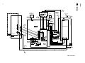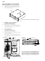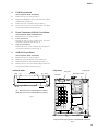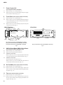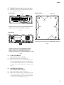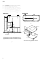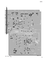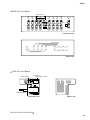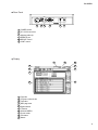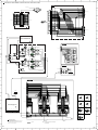
1
SAMPLING REVERBERATOR/
DSP EXPANSION BOARD/REMOTE CONTROLLER
SERVICE MANUAL
•DB-SREV1
This document is printed on chlorine free (ECF) paper with soy ink.
PA
011555
•SREV1
CONTENTS
SPECIFICATIONS ············································································ 3
PANEL LAYOUT ··············································································· 4
CIRCUIT BOARD LAYOUT ······························································ 5
DIMENSIONS ··················································································· 6
WIRING····························································································· 7
BLOCK DIAGRAM ············································································ 9
DISASSEMBLY PROCEDURE······················································· 11
I/O CARD INSTALLATION······························································ 16
DB-SREV1 INSTALLATION···························································· 17
LSI PIN DESCRIPTION ·································································· 19
IC BLOCK DIAGRAM······································································ 24
CIRCUIT BOARDS ········································································· 29
TEST PROGRAM ··········································································· 41
ERROR MESSAGES ······································································ 44
MIDI IMPLEMENTATION CHART ·················································· 46
PARTS LIST
RC-SREV1 SERVICE MANUAL
SREV1/RC-SREV1 OVERALL CIRCUIT DIAGRAM
1/2
SREV1:
20001225-500000
RC-SREV1: 20001225-150000
DB-SREV1: 20001225-200000
HAMAMATSU, JAPAN
1.415K-0671
Printed in Japan '01.02
SREV1
IMPORTANT NOTICE
This manual has been provided for the use of authorized Yamaha Retailers and their service personnel. It has been assumed that
basic service procedures inherent to the industry, and more specifically Yamaha Products, are already known and understood by
the users, and have therefore not been restated.
WARNING:
Failure to follow appropriate service and safety procedures when servicing this product may result in personal
injury, destruction of expensive components and failure of the product to perform as specified. For these
reasons, we advise all Yamaha product owners that all service required should be performed by an authorized
Yamaha Retailer or the appointed service representative.
IMPORTANT:
This presentation or sale of this manual to any individual or firm does not constitute authorization, certification,
recognition of any applicable technical capabilities, or establish a principal-agent relationship of any form.
The data provided is belived to be accurate and applicable to the unit(s) indicated on the cover. The research engineering, and
service departments of Yamaha are continually striving to improve Yamaha products. Modifications are, therefore, inevitable and
changes in specification are subject to change without notice or obligation to retrofit. Should any discrepancy appear to exist,
please contact the distributor's Service Division.
WARNING:
Static discharges can destroy expensive components. Discharge any static electricity your body may have
accumulated by grounding yourself to the ground bus in the unit (heavy gauge black wires connect to this bus).
IMPORTANT:
Turn the unit OFF during disassembly and parts replacement. Recheck all work before you apply power to the
unit.
LITHIUM BATTERY HANDLING
This product uses a lithium battery for memory back-up.
WARNING:
Lithium batteries are dangerous because they can be exploded by improper handling. Observe the following
precautions when handling or replacing lithium batteries.
Leave lithium battery replacement to qualified service personnel.
Always replace with batteries of the same type.
When installing on the PC board by soldering, solder using the connection terminals provided on the battery cells.
Never solder directly to the cells. Perform the soldering as quickly as possible.
Never reverse the battery polarities when installing.
Do not short the batteries.
Do not attempt to recharge these batteries.
Do not disassemble the batteries.
Never heat batteries or throw them into fire.
ADVARSEL!
Lithiumbatteri-Eksplosionsfare ved fejlagtig håndtering. Udskiftning må kun ske med batteri af samme fabrikat og type. Levér det
brugte batteri tilbage til leverandøren.
VARNING
Explosionsfara vid felaktigt batteribyte.
Använd samma batterityp eller en ekvivalent typ som rekommenderas av apparattillverkaren.
Kassera använt batteri enligt fabrikantens instruktion.
VAROITUS
Paristo voi räjähtää, jos se on virheellisesti asennettu.
Vaihda paristo ainoastaan laitevalmistajan suosittelemaan tyyppiin.
Hävitä käytetty paristo valmistajan ohjeiden mukaisesti.
The following information complies with Dutch Official Gazette 1995. 45; ESSENTIALS OF ORDER ON THE COLLECTION OF
BATTERIES.
• Please refer to the diassembly procedure for the removal of Back-up Battery.
• Leest u voor het verwijderen van de backup batterij deze beschrijving.
WARNING: CHEMICAL CONTENT NOTICE!
The solder used in the production of this product contains LEAD. In addition, other electrical/electronic and/or plastic (where
applicable) components may also contain traces of chemicals found by the California Health and Welfare Agency (and possibly
other entities) to cause cancer and/or birth defects or other reproductive harm.
DO NOT PLACE SOLDER, ELECTRICAL/ELECTRONIC OR PLASTIC COMPONENTS IN YOUR MOUTH FOR ANY REASON
WHAT SO EVER!
Avoid prolonged, unprotected contact between solder and your skin! When soldering, do not inhale solder fumes or expose eyes
to solder/flux vapor!
If you come in contact with solder or components located inside the enclosure of this product, wash your hands before handling
food.
WARNING
Components having special characteristics are marked
originally installed.
2
and must be replaced with parts having specification equal to those
SREV1
SPECIFICATIONS
SREV1
Internal
External
Sampling rate
Internal processing
Program Memories
Indicators
2-channel, 4-channel mode
2-channel x2 mode
INPUT
OUTPUT
FS LOCK
Others
PC Card slot
CD-ROM drive
Cooling fan
Power requirements
Power consumption
Dimensions (W x H x D)
Weight
Free-air operating temperature
Power cord length
Supplied accessories
Options
48 kHz
44.1 kHz or 48 kHz
32 bit
6 (P01–P06)
12 (P01–P12)
SIGNAL x4 (–34 dB), CLIP x4
SIGNAL x4 (–34 dB), CLIP x4
48K, 44.1K
POWER, PC Card, CD-ROM
PCMCIA (Type II), PC Card ATA spec, FAT16
ISO9660 Level 2 format
x2
U.S.A. & Canada 120 V AC, 60 Hz
Europe 230 V AC, 50 Hz
120 W
480 x 141.7 x 451.8 mm (18.9 x 5.6 x 17.8 inches)
11.5 kg (25.3 lbs)
5˚ C to 40˚ C (41˚ F to 104˚ F)
2.5 m
Power cord, CD-ROM (Reverb programs, data), Owner’s Manual
RC-SREV1, DB-SREV1, MY8-AD, MY4-AD, MY4-DA, MY8-AT, MY8-AE, MY8-TD
Digital Input Specifications
Connection
Format
Data Length
Level
DIGITAL IN 1, 2
AES/EBU
24 bit
RS-422
*1. XLR-3-31 type connectors are balanced (pin 1–ground, pin 2–hot (+), and pin 3–cold (–).
Connector
XLR-3-31 type *1
Digital Output Specifications
Connection
DIGITAL OUT 1, 2
*1. Channel status:
Format
Data Length
Level
AES/EBU *1
24 bit
RS-422
Type: 2 audio channels.
Sampling rate: depends on internal configuration.
*2. XLR-3-32 type connectors are balanced (pin 1–ground, pin 2–hot (+), and pin 3–cold (–).
Connector
XLR-3-32 type *2
Control I/O Specifications
Connection
SERIAL 1, 2
MIDI IN
MIDI OUT
WORD CLOCK IN
REMOTE
SLOT (x2)
Format
—
MIDI
MIDI
—
—
mini YGDAI
Level
RS-422
—
—
TTL 75 Ω
RS-422
—
Connector
8-pin mini DIN
5-pin DIN
5-pin DIN
BNC
9-pin D-sub (female)
—
Remote Cable Wiring Diagram
SREV1
RC-SREV1
IMPORTANT NOTICE FOR THE UNITED KINGDOM
Connecting the Plug and Cord
IMPORTANT.
The wires in this main lead are coloured in
accordance with the following code:
BLUE:
NEUTRAL
BROWN: LIVE
As the colours of the wires in the main lead of this apparatus may not
correspond with the coloured markings identifying the terminals in
your plug, proceed as follows:
The BLUE wire must be connected to the terminal that is marked with
the letter N (or coloured BLACK).
The BROWN wire must be connected to the terminal that is marked
with the letter L (or coloured RED).
Be certain that neither core is connected to the earth terminal of the
three pin plug.
9-pin D-sub
(male)
NC
RX–
TX+
NC
+12V
NC
RX+
TX–
GND
1
2
3
4
5
6
7
8
9
1
2
3
4
5
6
7
8
9
NC
TX–
RX+
NC
+12V
NC
TX+
RX–
GND
9-pin D-sub
(female)
DB-SREV1
Dimensions (W x H x D):
Weight:
Supplied accessories:
195 x 15 x 330 mm
0.5 kg
FPC (Flat Cable) x2
Screw
3
SREV1
PANEL LAYOUT
Front Panel
1
2
5
6
7
8
3
4
9 10 11
1 Air Inlet
2 INPUT and OUTPUT signal indicators
3 FS LOCK indicators
4 POWER switch & indicator
5 MEMORY CARD slot
6 Memory card eject button
7 Memory card activity indicator
8 CD-ROM drive
9 Disc activity indicator
10 CD-ROM eject button
11 Emergency disc eject hole
Rear Panel
12
14
13
15
16
12
17
18
19
20
21
12 Cooling fan outlets
13 SLOTs 1 & 2
14 AC IN connector
15 Grounding screw
16 DIGITAL OUT (AES/EBU) connectors
17 DIGITAL IN (AES/EBU) connectors
18 MIDI IN & OUT ports
19 SERIAL 1 & 2 ports
20 REMOTE port
21 WORD CLOCK IN connector
4
SREV1
CIRCUIT BOARD LAYOUT
Top View
Fan
DC Fan Motor
AC Inlet
CNV
SUB 2/4
CN604
CN705
CN603
CN706
CN701
CN1
SUB 1/4
CN1
Power Supply Unit
CN702
CN704 CN703
Power
transformer
CNV
CN7
CN3
CN4
(DB-SREV1)
CN803
CN802
CN801
PCM
Bottom View
SUB 3/4
SUB 4/4
DC Fan Motor
Fan
CN110
CN115
CN124
CN101
CPU
Power Supply Unit
SUB 2/4
CD-ROM
CN117
CN301
PCM
CNV
CD-ROM Drive
SUB 4/4
CN5
CN6
CNV
CN803
(DB-SREV1)
CN802
3NA-V651940-3,4
5
SREV1
43.5
362.5
451.8
440
34
11.8
DIMENSIONS
21.5
21.5
437
141.7
132
480
9.7
Unit: mm
81
318
81
6
WIRNIG
CN705
FAN
(V5789100)
200
SUB 2/4
AC Inlet
FAN
(V3125300)
240
240
680
680
160
710
720
650
CPU
CNV
Power Supply Unit
SUB 1/4
(DB-SREV1)
650
CNV
670
140
440
Power Transformer
CD-ROM
660
PCM
740
CN706
SUB 3/4
750
SUB 4/4
A
3NA-V651940-2
SREV1
7
730
SREV1
Location
Part No.
140
XY916A00(J)
Connector Assembly & Unit
Power Transformer
Destination
Power Transformer
Remarks
SUB 1/4-CN702
4P
XY917A00(U, V)
SUB 1/4-CN703
6P
XY918A00(H,B,W)
SUB 1/4-CN704
5P
160
V3125300
Fan
Fan
CPU-CN110
3P
200
V5789100
DC Fan Motor
DC Fan Motor
CPU-CN112
3P
240
V6512600
ACIN
AC Inlet
SUB 4/4-CN803
3P
Power Supply Unit-CN1
440
(VR79270)
650
MFA30100
660
670
680
KR
MFA30100
MFA25300
MFA36080
SUB 1/4-CN701
Power Supply Unit-CN2
4P/3P
CPU-CN117
SUB 3/4-CN801
9P
CPU-CN122
CNV-CN2
30P
CPU-CN123
CNV-CN3
30P
CPU-CN113
PCM-CN502
30P
CPU-CN114
PCM-CN503
30P
CPU-CN109
CDROM-CN902
25P
CPU-CN111
CDROM-CN903
25P
CPU-CN120
SUB 2/4-CN601
36P
CPU-CN121
SUB 2/4-CN602
36P
710
(V651290)
REM-PS
CPU-CN115
Power Supply Unit-CN5
2P
720
(V651300)
CPU-PS
CPU-CN101
Power Supply Unit-CN6
4P
730
(V651310)
YGDA-PS
SUB 2/4-CN603
Power Supply Unit-CN7
4P
740
(V651320)
CNV1-PS
CNV-CN1
Power Supply Unit-CN3
10P
750
(VR78120)
KR
CPU-CN124
SUB 4/4-CN802
2P
A
(V651320)
CNV(Option)-PS
CNV(DB-SREV1)-CN1
Power Supply Unit-CN4
10P
CN705
VY914700
B&C
SUB 1/4-CN705
SUB 2/4-CN604
7P
CN706
VQ613000
B&C
SUB 1/4-CN706
CPU-CN301
4P
8
IC151
(28P)
IC148
(16P)
IC149
(16P)
CPU
IC165
(44P)
BLOCK DIAGRAM
IC150
(28P)
SUB 2/4
CN606
BUFFER
CN603
CN605
IC155,156,167
(20P)
CN602
BUFFER
YD [1-15] YA [0-10]
SUB 3/4
D-FF
D-FF
CN117
SLOT 1,2
MIDI
2
IC163,164
(16P)
SERIAL
CN2,3
CN118,119
CN122,123
IC180-184
(20P)
IC159
(176P)
4MB
IC105
(28P)
CF CARD
MEMORY
IC113
(44P)
CD [0-15]
CA [4,14-25] CA [1-3]
CN108
CN109,
111
IC123,137,138
CD-ROM
Drive
IC108,
109
Lithium Battery
BT101
IC111,112
BUFFER
CN902,
903
CN901
SUB 4/4
CD-ROM
112,113
MEMORY CARD
(PCMCIA)
POWER
!
CN113,
114
CN705
CN502,
503
FLASH-ROM
IC127-131
Address bus
IC140,141
(42P)
IC177-179
BUFFER
Data bus
4MB
IC143
(176P)
IC153,154
(42P)
CD [0-15]
CA [1-7]
X102
8MHz
CD [0-31], CA [0-21]
IC107
(48P)
(DB-SREV1)
CN2,3
BUFFER
166
174
REMOTE
CNV
2
156
1
CNV
CD [0-7], CA [1-6]
IC114
(48P)
32
CN121
BUFFER
CD [0-31]
CA [2-9]
CN801
14,15
16,17
20,21
23
IC173-177
IC161,162
(20P)
CN604
PCM
CN501
SUB 1/4
CN706
CN701
FUSE
PCMCIA POWER
INTERFACE SW
!
Power
Supply
Unit
CN2
CN3
!
CN4
CN702-704
CN301
IC132
(16P)
CN803
CN7
CN1
!
Power
Transformer
!
AC INLET
FG
to CNV-CN1
to CNV(DB-SREV1)-CN1
CN5,6
CN101,115
38CA1-8818094-2
SREV1
9
CPU Section
AUDIO Section
CPU
IC150 (28P)
JK104
5
1
IN
IC151 (28P)
JK105
15
CN122, 123
67
68
55
CN2, 3
CNV
15 10
13
5
2
56
IC1~16, 35~50
(128P)
57
58
10
X103
DIGITAL (AES / EBU)
25.6MHz
JK106
1
OUT
13
JK107
2
IC148 (16P)
16
7
65
16
7
66
69
70
IC143
(176P)
IC1~16, 35~50
(128P)
59
60
IC149 (16P)
CN118,
119
CN2, 3
CNV
(DB-SREV1)
SUB 2/4
CN601
SLOT 1
CN120
65
66
67
68
55
56
57
58
CN606
1
SLOT 2
IC159
(176P)
69
70
71
72
59
60
61
62
CN605
3
X104
60MHz
1
MULTIPLEXER
4
3
2
1
15
14
JK108
WORD CLOCK IN
5
IC160
(15P)
36
IC165
(44P)
COUNTER
9
1
IC302
(14P)
X301
6.144MHz
SREV1
10
38CA1-8818094-3
SREV1
DISASSEMBLY PROCEDURE
1.
Top Cover (Time required: about 5 minutes)
1-1
Remove the fourteen (14) screws marked [850]. The top
cover can then be removed. (Fig. 1)
Top cover
[850] x14
[850]: Bind Head Tapping Screw-B A4.0X8 MFZN2BL (VC688800)
Fig. 1
2.
2-1
2-2
3.
3-1
3-2
3-3
DB-SREV1 (CNV Circuit Board)
(Time required: about 8 minutes)
Remove the top cover. (See procedure 1.)
Remove the two (2) screws marked [A] and the two (2)
screws marked [B]. The CNV circuit board (DB-SREV1)
can then be removed. (Fig. 2, 3)
CNV Circuit Board
(Time required: about 10 minutes)
Remove the top cover. (See procedure 1.)
Remove the DB-SREV1 CNV circuit board, if it is being
installed. (See procedure 2.)
Remove the two (2) screws marked [350] and the two (2)
screws marked [360]. The CNV circuit board can then be
removed. (Fig. 2, 3)
<Top View>
A
CNV
SUB 1/4
<SEC A-A'>
(DB-SREV1)
[360] [B]
CNV
CNV
(DB-SREV1)
[360] [B]
PCM
[B]
[125]
[460]
[460]
A'
Power transformer
PCM
11
[150]
[B]: Bind Head Tapping Screw-B 3.0X8 MFZN2BL (EP600190)
[125]: Bind Head Tapping Screw-B 3.0X8 MFZN2BL (EP600190)
[150]: Bind Head Tapping Screw-B A4.0X8 MFZN2BL (VC688800)
[360]: Bind Head Tapping Screw-B 3.0X8 MFZN2BL (EP600190)
[460]: Bind Head Tapping Screw-B 3.0X8 MFZN2BL (EP600190)
Fig. 2
SREV1
4.
4-1
4-2
4-3
4-4
5.
5-1
5-2
5-3
PCM Circuit Board
(Time required: about 15 minutes)
Remove the top cover. (See procedure 1.)
Remove the DB-SREV1 CNV circuit board, if it is being
installed. (See procedure 2.)
Remove the CNV circuit board. (See procedure 3.)
Remove the two (2) screws marked [460]. The PCM
circuit board can then be removed. (Fig. 2)
Power Transformer, SUB 1/4 Circuit Board
(Time required: about 8 minutes each)
Remove the top cover. (See procedure 1.)
Power Transformer
Remove the four (4) screws marked [150]. The power
transformer can then be removed. (Fig. 2)
SUB 1/4 Circuit Board
Remove the two (2) screws marked [125]. The SUB 1/4
circuit board can then be removed. (Fig. 2)
6.
SUB 2/4 Circuit Board
6-1
6-2
6-3
6-4
(Time required: about 15 minutes)
Remove the top cover. (See procedure 1.)
Remove the power transformer. (See procedure 5-2.)
Remove the SUB 1/4 circuit board (See procedure 5-3.)
Remove the four (4) screws marked [120]. The SUB 2/4
circuit board can then be removed. (Fig. 4)
<Left Side View>
<Top View>
[350]
[A]
(DB-SREV1)
Finger guard
Fan guard
CNV
[A]
[350]
Fan guide
Fan support metal
SUB 2/4
Fan
DC fan motor
CNV
[A]: Bind Head Screw A3.0X6 MFZN2BL (VP156600)
[350]: Bind Head Screw A3.0X6 MFZN2BL (VP156600)
[120] x4
Fig. 3
Power supply unit
SUB 4/4
[120]: Bind Head Tapping Screw-B 3.0X8 MFZN2BL (EP600190)
Fig. 4
12
SREV1
7.
Power Supply Unit
7-1
7-2
(Time required: about 10 minutes)
Remove the top cover. (See procedure 1.)
Remove the six (6) screws marked [60]. The power supply
unit can then be removed. (Fig. 4, 5)
8.
Front Panel (Time required: about 10 minutes)
8-1
8-2
Remove the top cover. (See procedure 1.)
Remove the two (2) screws marked [600] and the eight (8)
screws marked [610]. The left and rihgt mount brackets
can then be removed. (Fig. 5)
Remove the six (6) screws marked [570] The front panel
can then be removed. (Fig. 6)
8-3
<Right Side View>
<Front View>
Right side: 4pcs
[610]
Left side: 4pcs
[570]
[60]
Mount bracket
[610]
9.
9-1
9-2
9-3
9-4
[600]
Right side: 1pc.
Left side: 1pc.
[570]
[60]: Bind Head Screw A4.0X8 MFZN2BL (VP156800)
[600]: Oval Head Screw B4.0X10 MFZN2BL (V6221000)
[610]: Oval Head Screw 4.0X8 MFZN2BL (VS153600)
[570]: Oval Head Screw B4.0X10 MFZN2BL (V6221000)
Fig. 5
Fig. 6
SUB 3/4 Circuit Board, SUB 4/4 Circuit Board
(Time required: about 15 minutes each)
Remove the top cover. (See procedure 1.)
Remove the front panel (See procedure 8.)
SUB 3/4 Circuit Board
Remove the two (2) screws for [410] and pull out the SUB
3/4 circuit board from the two of the sub-chassis. (Fig. 7)
SUB 4/4 Circuit Board
Pull out the power switch knob. (Fig. 7)
Remove the two (2) screws marked [430]. The SUB 4/4
circuit board can then be removed. (Fig. 4, 7)
10.
DC Fan Motor (Time required: about 10 minutes)
10-1
10-2
Remove the top cover. (See procedure 1.)
Remove the four (4) screws marked [230]. The DC fan
motor can then be removed with both the fan guard and the
fan guide. (Fig. 4, 8)
11.
Fan (Time required: about 10 minutes)
11-1
11-2
Remove the top cover. (See procedure 1.)
Remove the four (4) screws marked [190]. The Fan can
then be removed with both the finger guard and the fan
support metal. (Fig. 4, 8)
13
Front panel
[60]
[570]
SREV1
12
Bottom Cover (Time required: about 5 minutes)
12-1
Remove the twelve (12) screws marked [830]. The bottom
cover can then be removed. (Fig. 9)
<Front View>
Sub chassis
<Bottom View>
Hook
SUB 3/4
[410]
SUB 4/4
Bottom cover
[430]
[830]
Hook
Power switch knob
[410]: Bind Head Tapping Screw-B 3.0X8 MFZN2BL (EP600190)
[430]: Bind Head Screw A3.0X6 MFZN2BL (VP156600)
[830]
[830]
Fig. 7
<Rear View>
[190] x4
[230] x4
Finger guard
Fan guard
[830]
[830]: Bind Head Tapping Screw-B A4.0X8 MFZN2BL (VC688800)
Rear panel
[310]
[310]
CPU
[310]
[300] [290]
[300]
Fig. 9
[190]: Bind Head Screw SP 4.0X25 MFZN2BL (VR116500)
[230]: Pan Head Screw SP 4.0X20 MFZN2BL (VR116500)
[300]: Bind Head Screw A3.0X6 MFZN2BL (VP156600)
[310]: Bind Head Tapping Screw-B A3.0X8 MFZN2BL (VP157000)
Fig. 8
13
13-1
13-2
14
14-1
14-2
CPU Circuit Board
(Time required: about 10 minutes)
Remove the bottom cover. (See procedure 12.)
Remove the two (2) jack sockets marked [290], the three
(3) screws marked [300], the ten (10) screws marked [310],
the screw marked [320] and the two (2) screws marked
[330]. The CPU circuit board can then be removed. (Fig.
8, 10, 11)
CD-ROM Circuit Board
(Time required: about 5 minutes)
Remove the bottom cover. (See procedure 12.)
Remove the CN angle bracket by removing the two (2)
screws marked [520]. The CD-ROM circuit board can then
be removed with pulling out the connector of the CD-ROM
circuit board from the CD-ROM drive. (Fig. 10)
14
SREV1
15
CD-ROM Drive (Time required: about 10 minutes)
15-1
15-2
15-3
Remove the bottom cover. (See procedure 12.)
Remove the CD-ROM circuit board. (See procedure 14.)
Remove the three (3) screws marked [530]. The CD-ROM
drive can then be removed with the CD angle. (Fig. 10)
Remove the CD angle from the CD-ROM drive by
removing the four (4) screws marked [500]. (Fig. 12)
15-4
<Bottom View>
CD-ROM
CN angle bracket
CPU
[330]
<Left Side View>
CPU
[320]
[320]: Bind Head Screw A3.0X6 MFZN2BL (VP156600)
Fig. 11
[520]
[530] [520]
CD-ROM drive
[330]
[500] x4
[530]
CD angle
[530]
CD-ROM drive
[330]: Bind Head Tapping Screw-B 3.0X8 MFZN2BL (EP600190)
[520]: Bind Head Tapping Screw-B A3.0X8 MFZN2BL (VP157000)
[530]: Bind Head Tapping Screw-B A3.0X8 MFZN2BL (VP157000)
CD angle
[500]: Pan Head Screw 2.0X2 MFZN2Y (V6881500)
Fig. 10
15
Fig. 12
SREV1
INSTALLING I/O CARDS
This section explains how to install mini YGDAI cards in the SREV1.
1.
Turn off the SREV1.
2.
Undo the two fixing screws and remove the slot cover, as shown below.
Keep the cover and fixing screws in a safe place for future use.
3.
Insert the card between the guide rails and slide it all the way into the slot, as shown below. You may have to
push firmly to plug the card into the SREV1 connector.
4.
Secure the card using the attached thumbscrews. Do not leave the thumb-screws loose, as the card will not be
grounded correctly.
16
SREV1
DB-SREV1 INSTALLATION
*
1.
Before installing the DB-SREV1 (CNV) circuit board,
turn off the SREV1 and disconnect the power cord.
Top Cover Removal
Remove the fourteen (14) screws marked [850]. The top
cover can then removed. (Fig. 1)
Top cover
[850] x14
[850]: Bind Head Tapping Screw-B A4.0X8 MFZN2BL (VC688800)
Fig. 1
2.
CNV Circuit Board Removal
Remove the two (2) screws marked [350] and the two (2)
screws marked [360]. The CNV circuit board can then be
removed. (Fig. 2, 3)
3.
*
Cables Connection
Connect the two supplied cables to the CPU circuit board
(CN118, CN119) so that the printed side appears as shown
as in Figure 4, and then close the securing clips on each
side of the connectors.
The two supplied cables are identical.
<Top View>
A
CNV
<SEC A-A'>
(DB-SREV1)
[360] [B]
CNV
CNV
(DB-SREV1)
[360] [B]
[B]
[B]: Bind Head Tapping Screw-B 3.0X8 MFZN2BL (EP600190)
[360]: Bind Head Tapping Screw-B 3.0X8 MFZN2BL (EP600190)
A'
17
PCM
Fig. 2
SREV1
<Left Side View>
[350]
[A]
CNV
CNV
(DB-SREV1) [A]
3 Printed side 4
[350]
5
CN118
CN119
CN122
[A]: Bind Head Screw A3.0X6 MFZN2BL (VP156600)
[350]: Bind Head Screw A3.0X6 MFZN2BL (VP156600)
CPU
CN123
1
2
Fig. 3
4.
Fig. 4
CNV Circuit Board Installation
Reinstall the previously removed CNV circuit board,
remembering to replace the two (2) internal fixing screws
marked [360] and two (2) external fixing screws marked
[350]. (Fig. 2, 3)
Reconnect the two cable connectors and the power supply
connector. (Table 1)
5.
DB-SREV1 (CNV) Circuit Board Installation
5-1
Cut and remove the cable fastener holding the power supply
cable intended for the DB-SREV1(CNV) circuit board.
Install the DB-SREV1 (CNV) circuit board above the
existing CNV circuit board, secure it by using two (2)
internal fixing screws marked [B] and two (2) external
fixing screws marked [A]. (Fig. 2, 3)
Connect the two cable connectors and the power supply
connector, as shown in Figure 5. (Table 1)
5-2
5-3
3
4
6
• Connector Assembly
1
2
3
4
5
6
PARTS NO
MFA30100
MFA30100
MFA30140
MFA30140
(V6513200)
(V6513200)
DESTINATION
CPU-CN122
CNV-CN2
CPU-CN123
CNV-CN3
CPU-CN118
DB-SREV1(CNV)-CN2
CPU-CN119
DB-SREV1(CNV)-CN3
Power Supply Unit-CN3 CNV-CN1
Power Supply Unit-CN4 DB-SREV1(CNV)-CN1
REMERKS
30P/L=100mm
30P/L=100mm
30P/L=140mm
30P/L=140mm
10P
10P
CN2
CN3
CNV
* Connector assembly listed above are not available as service parts
except MFA30100 and MFA30140.
Table 1
6.
CN1
(DB-SREV1)
Fig. 5
Re-attach the SREV1 Top Cover
Replace the fourteen (14) fixing screws marked [850].
The top cover can then be Replaced. (Fig. 1)
7.
Checking that the DB-SREV1 (CNV) Circuit
Board is Working Correctly
If the DB-SREV1 (CNV) circuit board is working correctly,
when the SREV1 is turned on the two rows of INPUT and
OUTPUT front panel indicators light up alternately in a
streaming pattern from left to right. If the indicators do not
light up like this, the DB-SREV1 (CNV) circuit board is not
working correctly, in which case you should check that it's
installed in accordance with these instructions.
8.
Execute Test Program
Execute test program No. 5 in Section 5-2 and check if
operation is normal. (Refer to page 42.)
18
LSI PIN DESCRIPTION
YM3436DK (XG948E00) DIR2 (Digital Format Interface Receiver) ····················································· 19
YM3437C-F (XM530A00) DIT2 (Digital Format Interface Transmitter) ················································ 19
SH7709A (XY065A00) CPU ················································································································· 20
YSS910-S (XV988A00) DSP6 (Digital Signal Processor) ···································································· 21
YSS916-H (XW867A00) CNV3 DSP (Convolver)················································································· 22
MBCG46183-129 (XV833A00) Gate Array·························································································· 23
YSD917-ME2 (XW526A00) DIR5 (Digital Format Interface Receiver) ················································· 23
YM3436DK (XG948E00) DIR2 (Digital Format Interface Receiver)
PIN
NO.
1
2
3
4
5
6
7
8
9
10
11
FUNCTION
PIN
NO.
23
24
25
26
27
28
29
30
31
32
33
NAME
I/O
NAME
I/O
DAUX
HDLT
DOUT
VFL
OPT
SYNC
MCC
WC
MCB
MCA
SKSY
I
O
O
O
O
O
O
O
O
O
I
Auxiliary input for audio data
Asynchronous buffer operation flag
Audio data output
Parity flag output
Fs x 1 Synchronous output signal for DAC
Fs x 1 Synchronous output signal for DSP
Fs x 64 Bit clock output
Fs x 1 Word clock output
Fs x 128 Bit clock output
Fs x 256 Bit clock output
Clock synchronization control input
RSTN
Vdda
CTLN
PCO
(NC)
CTLP
Vssa
TSTN
KM2
KM0
FS1
I
12
XI
I
34
FS0
O
13
14
XO
P256
O
O
Crystal oscillator connection or external
clock input
Crystal oscillator connection
VCO oscillating clock connection
35
36
CSM
EXTW
I
I
15
16
17
18
19
LOCK
Vss
TC
DIM1
DIM0
O
37
38
39
40
41
DDIN
LR
Vdd
ERR
EMP
I
O
O
I
I
PLL lock flag
Logic section power (GND)
PLL time constant switching output
Data input mode selection
Data input mode selection
20
DOM1
I
Data output mode selection
42
CD0
O
21
DOM0
I
Data output mode selection
43
CCK
I
22
KM1
I
Clock mode switching input 1
44
CLD
I
I
O
I
I
I
I
O
O
O
CPU: IC165
FUNCTION
System reset input
VCO section power (+5 V)
VCO control input N
PLL phase comparison output
VCO control input P
VCO section power (GND)
Test terminal. Open for normal use
Clock mode switching input 2
Clock mode switching input 0
Channel status sampling frequency
display output 1
Channel status sampling frequency
display output 0
Channel status output method selection
External synchronous auxiliary input
word clock
EIAJ (AES/EBU) data input
PLL word clock output
Logic section power (+5 V)
Data error flag output
Channel status emphasis control code
output
3-wire type microcomputer interface data
output
3-wire type microcomputer interface clock
input
3-wire type microcomputer interface load
input
YM3437C-F (XM530A00) DIT2 (Digital Format Interface Transmitter)
PIN
NO.
1
2
3
4
19
NAME
I/O
Vss
MCLK
DM0
DM1
I
I
I
5
6
7
RSTN
WCIN
DIN
I
I
I
8
VDD
PIN
NAME I/O
NO.
Ground
9 MUTE
I
Master clock input
10
VFL
I
DIN/BCLK/WCLK format select
11 CCK/CCB I
DM1,DM0=0,0 DSP,LDSP (64 bit,LSB first) 12 CIN/UDB I
DM1,DM0=0,1stereo,DSP (64 bit,MSB first)
DM1,DM0=1,0 DSP2 (128 bit,MSB first)
DM1,DM0=1,1 BB (64 bit,MSB first)
System reset
13 CLD/AUXTN I
Word clock input
14 CNTR/BLKIN I
Digital audio serial data input
15
CSM
I
FUNCTION
Power supply (+5 V)
16
DOUT
O
CPU: IC148, 149
FUNCTION
Mute
Validity flag
C,U bit clock input/C bit data input
C,U bit data input/U bit data input
End of C,U bit input/16,20 bit/24 bit select
32 bit counter reset/Top of block
Channel status input mode select
CSM=0 Asynchronous mode,
CSM=1 Synchronous mode
Digital interface formatted data output
SREV1
SH7709A FP-208C (XY065A00) CPU
PIN
NO.
NAME
1
MD1
2
MD2
3
Vcc-RTC*1
4
XTAL2
5
EXTAL2
6
Vss-RTC*1
7
NMI
8 IRO0/IRL0/PTH[0]
9 IRO1/IRL1/PTH[1]
10 IRO2/IRL2/PTH[2]
11 IRO3/IRL3/PTH[3]
12 IRO4/PTH[4]
13
D31/PTB[7]
14
D30/PTB[6]
15
D29/PTB[5]
D28/PTB[4]
16
17
D27/PYB[3]
18
D26/PTB[2]
19
VssO
20
D25/PTB[1]
21
VccO
22
D24/PTB[0]
23
D23/PTA[7]
24
D22/PTA[6]
25
D21/PTA[5]
26
D20/PTA[4]
27
Vss
28
D19/PTA[3]
29
Vcc
30
D18/PTA[2]
31
D17/PTA[1]
32
D16/PTA[0]
33
VssO
34
D15
35
VccO
36
D14
37
D13
38
D12
39
D11
40
D10
41
D9
42
D8
43
D7
44
D6
45
VssO
46
D5
47
VccO
48
D4
49
D3
50
D2
51
D1
D0
52
A0
53
A1
54
A2
55
A3
56
VssO
57
A4
58
VccO
59
A5
60
A6
61
A7
62
A8
63
A9
64
A10
65
A11
66
A12
67
A13
68
VssO
69
A14
70
VccO
71
A15
72
A16
73
A17
74
A18
75
A19
76
A20
77
A21
78
Vss
79
A22
80
Vcc
81
A23
82
VssO
83
A24
84
VccO
85
A25
86
BS/PTK[4]
87
RD
88
89 WE0/DOMLL
90 WE1/DOMLU/WE
91 WE2/DOMUL/ICIORD/PTK[6]
92 WE3/DOMUU/ICIOWR/PTK[7]
RD/WR
93
94 AUDSYNC/PTE[7]
VssO
95
96 CS0/MCS[0]
VccO
97
CS2/PTK[0]
98
CS3/PTK[1]
99
CS4/PTK[2]
100
101 CS5/CE1A/PTK[3]
CS6/CE1B
102
103 CE2A/PTE[4]
104 CE2B/PTE[5]
I/O
I
I
O
I
I
I
I
I
I
I
I/O
I/O
I/O
I/O
I/O
I/O
I/O
I/O
I/O
I/O
I/O
I/O
I/O
I/O
I/O
I/O
I/O
I/O
I/O
I/O
I/O
I/O
I/O
I/O
I/O
I/O
I/O
I/O
I/O
I/O
I/O
I/O
I
I
I
I
I
I
I
I
I
I
I
I
I
I
I
I
I
I
I
I
I
I
I
I
I
I
I/O
O
O
O
I/O
I/O
O
I/O
O
I/O
I/O
I/O
I/O
I/O
I/O
I/O
FUNCTION
Clock mode
Clock mode
Power supply for RTC (1.8 V)
Crystal oscillator for RTC
Crystal oscillator for RTC
Ground
Non-maskable interrupt request
Interrupt request/Input port H
Interrupt request/Input port H
Interrupt request/Input port H
Interrupt request/Input port H
Interrupt request/Input port H
Data bus/Port B
Data bus/Port B
Data bus/Port B
Data bus/Port B
Data bus/Port B
Data bus/Port B
Ground
Data bus/Port B
Power supply (3.3 V)
Data bus/Port B
Data bus/Port A
Data bus/Port A
Data bus/Port A
Data bus/Port A
Ground
Data bus/Port A
Power supply (1.8 V)
Data bus/Port A
Data bus/Port A
Data bus/Port A
Ground
Data bus
Power supply (3.3 V)
Data bus
Data bus
Data bus
Data bus
Data bus
Data bus
Data bus
Data bus
Data bus
Ground
Data bus
Power supply (3.3 V)
Data bus
Data bus
Data bus
Data bus
Data bus
Address bus
Address bus
Address bus
Address bus
Ground
Address bus
Power supply (3.3 V)
Address bus
Address bus
Address bus
Address bus
Address bus
Address bus
Address bus
Address bus
Address bus
Ground
Address bus
Power supply (3.3 V)
Address bus
Address bus
Address bus
Address bus
Address bus
Address bus
Address bus
Ground
Address bus
Power supply (1.8 V)
Address bus
Ground
Address bus
Power supply (3.3 V)
Address bus
Bus cycle signal start/Port K
Read strobe
D7-D0 select sugnal/DOM (SDRAM)
D15-D8 select signal/DOM (SDRAM)
D23-D16 select signal/DOM (SDRAM)/PCMCIA I/O read/Port K
D31-D24 select signal/DOM (SDRAM)/PCMCIA I/O write/Port K
Read/Write
AUD sync. signal/Port E
Ground
Chip select/Mask ROM chip select
Power supply (3.3 V)
Chip select2/Port K
Chip select3/Port K
Chip select4/Port K
Chip select5/CE1/Port K
Chip select6/CE1
Card enable/Port E
Card enable/Port E
CPU: IC105
PIN
NO.
105
106
107
108
109
110
111
112
113
114
115
116
117
118
119
120
121
122
123
124
125
126
127
128
129
130
131
132
133
134
135
136
137
138
139
140
141
142
143
144
145
146
147
148
149
150
151
152
153
154
155
156
157
158
159
160
161
162
163
164
165
166
167
168
169
170
171
172
173
174
175
176
177
178
179
180
181
182
183
184
185
186
187
188
189
190
191
192
193
194
195
196
197
198
199
200
201
202
203
204
205
206
207
208
NAME
I/O
CKE/PTK[5]
RAS3L/PTJ[0]
RAS2L/PTJ[1]
CASLL/CASL/PTJ[2]
VssO
CASLH/CASU/PTJ[3]
VccO
CASHL/PTJ[4]
CASHH/PTJ[5]
DACK0/PTD[5]
DACK1/PTD[7]
CAS2L/PTE[6]
CAS2H/PTE[3]
RAS3U/PTE[2]
RAS2U/PTE[1]
TDO/PTE[0]
BACK
BREO
WAIT
RESETM
ADTRG/PTH[5]
IOISI6/PTG[7]
ASEMD0/PTG[6]
ASEBRKAK/PTG[5]
PTG[4]
AUDATA[3]/PTG[3]
AUDATA[2]/PTG[2]
Vss
AUDATA[1]/PTG[1]
Vcc
AUDATA[0]/PTG[0]
TRST/PTF[7]/PINT[15]
TMS/PTF[6]/PINT[14]
TDI/PTF[5]/PINT[13]
TCK/PTF[4]/PINT[12]
IRLS[3]/PTF[3]/PINT[11]
IRLS[2]/PTF[2]/PINT[10]
IRLS[1]/PTF[1]/PINT[9]
IRLS[0]/PTF[0]/PINT[8]
MD0
Vcc-PLL1*2
CAP1
Vss-PLL1*2
Vss-PLL2*2
CAP2
Vcc-Pll2*2
AUDCK/PTH[6]
Vss
Vss
Vcc
XTAL
EXTAL
STATUS0/PTJ[6]
STATUS1/PTJ[7]
TCLK/PTH[7]
IROOUT
VssO
CKIO
VccO
TxD0/SCPT[0]
SOK0/SCPT[1]
TxD1/SCPT[2]
SCK1/SCPT[3]
TxD2/SCPT[4]
SCK2/SCPT[5]
RTS2/SCPT[6]
RxD0/SCPT[0]
RxD1/SCPT[2]
Vss
RxD2/SCPT[4]
Vcc
CTS2/IRO5/SCP[7]
MCS[7]/PTC[7]/PINT[7]
MCS[6]/PTC[6]/PINT[6]
MCS[5]/PTC[5]/PINT[5]
MCS[4]/PTC[4]/PINT[4]
VssO
WAKEUP/PTD[3]
VccO
RESETOUT/PTD[2]
MCS[3]/PTC[3]/PINT[3]
MCS[2]/PTC[2]/PINT[2]
MCS[1]/PTC[1]/PINT[1]
MCS[0]/PTC[0]/PINT[0]
DRAK0/PTD[1]
DRAK1/PTD[0]
DREQ0/PTD[4]
DREQ1/PTD[6]
RESETP
CA
MD3
MD4
MD5
AVss
AN[0]/PTL[0]
AN[1]/PTL[1]
AN[2]/PTL[2]
AN[3]/PTL[3]
AN[4]/PTL[4]
AN[5]/PTL[5]
AVcc (3.3 V)
AN[6]/DA[1]/PTL[6]
AN[7]/DA[0]/PTL[7]
AVss
I/O
I/O
I/O
I/O
I/O
I/O
I/O
I/O
I/O
I/O
I/O
I/O
I/O
I/O
O
I
I
I
I
I
I
I/O
I
I/O
I/O
I/O
I/O
I
I
I
I
I
I
I
I
I
I
O
I
I/O
I/O
I/O
O
I/O
O
I/O
O
I/O
O
I/O
I/O
I
I
I
I
I/O
I/O
I/O
I/O
I/O
I/O
I/O
I/O
I/O
I/O
I/O
I/O
I
I
I
I
I
I
I
I
I
I
I
I
I
I
I
-
FUNCTION
CK enable/Port K
DRAM row address strobe/Port J
DRAM row address strobe/Port J
Column address strobe (low)/Port J
Ground
Column address strobe (high)/Port J
Power supply (3.3 V)
HL Column address strobe/Port J
HH Column address strobe/Port J
DMA acknowledge transfer strobe 0/Port D
DMA acknowledge transfer strobe 1/Port D
Column address strobe (low)/Port E
Column address strobe (high)/Port E
DRAM address strobe/Port E
DRAM address strobe/Port E
Test data output/Port E
Bus acknowledge
Bus request
Hardware wait request
Reset
Analog trigger/Input port H
Write protect/Area 6 input/Input port G
ASE mode/Input port G
ASE break acknowledge/Input port G
Input port G
AUD data/Input port G
AUD data/Input port G
Ground
AUD data/Input port G
Power supply (1.8 V)
AUD data/Input port G
Test reset/Input port F/Interrupt port
Test mode switch/Input port F/Interrupt port
Input test data/Input port F/Interrupt port
Test clock/Input port F/Interrupt port
Interrupt request/Input port F/Interrupt port
Interrupt request/Input port F/Interrupt port
Interrupt request/Input port F/Interrupt port
Interrupt request/Input port F/Interrupt port
Clock mode
PLL1 Power supply (1.8 V)
PLL1 capacitor
PLL1 Ground
PLL2 Ground
PLL2 capacitor
PLL2 Power supply (1.8 V)
AUD clock/Input port H
Ground
Ground
Power supply (1.8 V)
Clock oscillator
Clock/Crystal oscillator
cessor status/Port J
Pross./Port J
Clock/Port H
'Interrupt request
Ground
System Clock
Power supply (3.3 V)
Data transmission 0/Output port
Serial clock/Port
Data transmission 1/Output port
Serial clock/Port
Data transmission 2/Output port
Serial clock/Port
Request to send 2/Output port
Data reception 0/Output port
Data reception 1/Output port
Ground
Data reception 2/Output port
Power supply (1.8 V)
Clear to send 2/Interrupt request/Input port
Mask chip select/Port C/Interrupt port
Mask chip select/Port C/Interrupt port
Mask chip select/Port C/Interrupt port
Mask chip select/Port C/Interrupt port
Ground
Standby mode/Port D
Power supply (3.3 V)
Reset output/Port D
Mask chip select/Port C/Interrupt port
Mask chip select/Port C/Interrupt port
Mask chip select/Port C/Interrupt port
Mask chip select/Port C/Interrupt port
DMA transfer request/IPort D
DMA transfer request/IPort D
DMA transfer request/Input port D
DMA transfer request/Input port D
Power on reset
Chip active/Hardware stand by request
Area 0 bus allocation
Area 0 bus allocation
Area 0 bus allocation
Ground
AD converter input/Input port L
AD converter input/Input port L
AD converter input/Input port L
AD converter input/Input port L
AD converter input/Input port L
AD converter input/Input port L
Analog Power supply (3.3 V)
AD converter input/Input port L
AD converter input/Input port L
Ground
20
SREV1
YSS910-S (XV988A00) DSP6 (Digital Signal Processor)
PIN
NO.
NAME
1
2
3
4
5
6
7
8
9
10
11
12
13
14
15
16
17
18
19
20
21
22
23
24
25
26
27
28
29
30
31
32
33
34
35
36
37
38
39
40
41
42
43
44
45
46
47
48
49
50
51
52
53
54
55
56
57
58
59
60
61
62
63
64
65
66
67
68
69
70
71
72
73
74
75
76
77
78
79
80
81
82
83
84
85
86
87
88
Vdd
Vss
XI
XO
Vdd
/SYNCI
/SYNCO
Vdd
CKI
CKO
CKSEL
Vss
MCKS
/SSYNC
/IC
/TEST
BTYP
/IRQ
TRIG
Vdd
Vss
/CS
/WR
/RD
CA7
CA6
CA5
CA4
CA3
CA2
CA1
Vss
Vdd
CD15
CD14
CD13
CD12
CD11
CD10
CD09
CD08
CD07
CD06
Vss
Vdd
Vdd
CD05
CD04
CD03
CD02
CD01
CD00
/WAIT
Vss
SI0
SI1
SI2
SI3
SI4
SI5
SI6
SI7
Vss
Vdd
SO0
SO1
SO2
SO3
SO4
SO5
SO6
SO7
Vss
DB00
DB01
DB02
DB03
DB04
DB05
DB06
DB07
DB08
DB09
DB10
DB11
DB12
Vdd
Vdd
21
I/O
I
O
I
O
I
O
I
I
I
I
I
I
O
I/O
I
I
I
I/O
I/O
I/O
I/O
I/O
I/O
I/O
FUNCTION
Power supply (3.3 V)
Ground
System master clock input (60 MHz or 30 MHz)
System master clock output (High or 30 MHz)
Power supply (5 V)
Sync. signal input
Sync. signal output
Power supply (5 V)
System clock input (30 MHz)
System clock output (30 MHz)
System master clock select (0: 60 MHz, 1: 30 MHz)
Ground
Serial I/O master clock input (128 x Fs)
Serial I/O Sync. signal output
Initial clear
Test mode setting (0: Test, 1: Normal)
Data bus type select (0: 8 bit, 1: 16 bit)
IRQ output
Trigger signal input/output
Power supply (5 V)
Ground
chip select signal input
Write signal input
Read signal input
Address bus of internal register
Ground
Power supply (3.3 V)
I/O
I/O
I/O
I/O
I/O
I/O
I/O
I/O
I/O
I/O
Data bus of internal register
Ground
Power supply (3.3 V)
Power supply (5 V)
I/O
I/O
I/O
I/O
I/O
I/O
O
I
I
I
I
I
I
I
I
Data bus of internal register
WAIT output
Ground
Serial data input
Ground
Power supply (5 V)
O
O
O
O
O
O
O
O
Serial data output
Ground
I/O
I/O
I/O
I/O
I/O
I/O
I/O
I/O
I/O
I/O
I/O
I/O
I/O
Parallel data bus
Power supply (5 V)
Power supply (3.3 V)
PIN
NO.
NAME
Vss
89
DB13
90
DB14
91
DB15
92
DB16
93
DB17
94
DB18
95
DB19
96
DB20
97
DB21
98
DB22
99
Vss
100
Vdd
101
DB23
102
DB24
103
DB25
104
DB26
105
DB27
106
DB28
107
DB29
108
DB30
109
DB31
110
111 TIMO//DBOE
112
Vss
113
Vdd
114
DA00
115
DA01
116
DA02
117
DA03
118
DA04
119
DA05
120
DA06
121
DA07
122
Vss
123
DA08
124
DA09
125
DA10
126
DA11
127
DA12
128
DA13
129
DA14
130
DA15
131
Vss
132
Vdd
133
(n.c)
134
Vdd
135
DA16
136
DA17
137
DA18
138
DA19
139
DA20
140
DA21
141
DA22
142
DA23
143
Vss
144
DA24
145
DA25
146
DA26
147
DA27
148
DA28
149
DA29
150
DA30
151
DA31
152
Vdd
153
Vss
154
A00
155
A01
156
A02
157
A03
158
A04
159
A05
160
A06
161
A07
162
A08
163
A09
164
Vss
165
Vdd
166
A10
167
A11
168
A12
169
A13
170
A14
171 A15/RAS
172 A16/CAS
173 A17/CE
174
/WE
175
/OE
176
Vdd
CPU: IC143, 159
I/O
FUNCTION
Ground
I/O
I/O
I/O
I/O
I/O
I/O
I/O
I/O
I/O
I/O
Parallel data bus
Ground
Power supply (3.3 V)
I/O
I/O
I/O
I/O
I/O
I/O
I/O
I/O
I/O
I/O
I/O
I/O
I/O
I/O
I/O
I/O
I/O
I/O
Parallel data bus
Timing signal output/ Parallel data bus output/ input
Ground
Power supply (5 V)
Memory data bus
Ground
I/O
I/O
I/O
I/O
I/O
I/O
I/O
I/O
Memory data bus
Ground
Power supply (3.3 V)
Not used
Power supply (5 V)
I/O
I/O
I/O
I/O
I/O
I/O
I/O
I/O
Memory data bus
Ground
I/O
I/O
I/O
I/O
I/O
I/O
I/O
I/O
Memory data bus
Power supply (5 V)
Ground
O
O
O
O
O
O
O
O
O
O
Memory address (SRAM, PSRAM, DRAM)
Ground
Power supply (3.3 V)
O
O
O
O
O
O
O
O
O
O
Memory address (SRAM, PSRAM, DRAM)
Memory address (SRAM, PSRAM)
Memory address (SRAM, PSRAM), /RAS (DRAM)
Memory address (SRAM, PSRAM), /CAS (DRAM)
Memory address (SRAM), /CE (PSRAM)
Memory write enable signal
Memory output enable signal
Power supply (5 V)
SREV1
YSS916-H (XW867A00) CNV3 DSP (Convolver)
PIN
NAME
NO.
1
VSS
2 VDD33
3
CSN
4 WRN
5
RDN
6 WAITN
7
A4
8
A3
9
A2
10
A1
11 DACKN
12 DREQN
13
VSS
14 VDD33
15 VDD25
16
D00
17
D01
18
D02
19
D03
20
D04
21
D05
22
D06
23
D07
24
VSS
25
D08
26
D09
27
D10
28
D11
29
D12
30
D13
31
D14
32
D15
33
VSS
34 VDD33
35 VDD25
36
D16
37
D17
38
D18
39
D19
40
D20
41
D21
42
D22
43
D23
44
VSS
45
D24
46
D25
47
D26
48
D27
49
D28
50
D29
51
D30
52
D31
53
VSS
54 VDD33
55 VDD25
56
n.c
57
n.c
58
n.c
59
n.c
60
n.c
61
DI0
62
DI1
63
SO0
64
SO1
I/O
I
I
I
O
I
I
I
I
I
O
I/O
I/O
I/O
I/O
I/O
I/O
I/O
I/O
FUNCTION
Ground (GND)
Power supply (+3.3 V)
Chip select
Write
Read
Wait
Address bus
DMA strobe
DMA request
Ground (GND)
Power supply (+3.3 V)
Power supply (+2.5 V)
Data bus
Ground (GND)
I/O
I/O
I/O
I/O
I/O
I/O
I/O
I/O
Data bus
Ground (GND)
Power supply (+3.3 V)
Power supply (+2.5 V)
I/O
I/O
I/O
I/O
I/O
I/O
I/O
I/O
Data bus
Data bus
Ground (GND)
I/O
I/O
I/O
I/O
I/O
I/O
I/O
I/O
Data bus
Ground (GND)
Power supply (+3.3 V)
Power supply (+2.5 V)
Not used
I
I
O
O
Data input
Serial data output
PIN
NAME
NO.
65
VSS
66 VDD33
67 VDD25
68 SCLK
69 RSTN
70 OVFN
71 TXFN
72
VSS
73 BCLK
74 WCLK
75 WSEL0
76 WSEL1
77 FSSEL
78 BUSWD
79 BUSW
80
TST
81
VSS
82 VDD33
83 TST00
84 TST01
85 TST02
86 TST03
87 TST04
88 TST05
89 TST06
90 TST07
91 TST08
92 TST09
93
VSS
94 VDD25
95
MI1
96
MI0
97
SI1
98
SI0
99
DO1
100
DO0
101
VSS
102 VDD33
103 VDD25
104 TST10
105 TST11
106 TST12
107 TST13
108 TST14
109 TST15
110 TST16
111 TST17
112 TST18
113 TST19
114 TST20
115
VSS
116 VDD33
117 VDD25
118 TST21
119 TST22
120 TST23
121 TST24
122 TST25
123 TST26
124 TST27
125 TST28
126 TST29
127 TST30
128 TST31
CNV: IC1–16, 35–50
I/O
FUNCTION
I
I
O
O
Ground (GND)
Power supply (+3.3 V)
Power supply (+2.5 V)
System clock
Reset
Overflow flag
Coefficient tactor write interdiction flag
Ground (GND)
Bit clock
Word clock
I
I
I
I
I
I
I
I
O
O
O
O
O
O
O
O
O
O
Serial data format
Fs select
DMA data bus (24/16 bit) switch
data bus (32/16bit) switch
Test pin
Ground (GND)
Power supply (+3.3 V)
Test output
Ground (GND)
Power supply (+2.5 V)
I
I
I
I
O
O
Mixing input
Serial data input
Data output
Ground (GND)
Power supply (+3.3 V)
Power supply (+2.5 V)
O
O
O
O
O
O
O
O
O
O
O
Test output
Ground (GND)
Power supply (+3.3 V)
Power supply (+2.5 V)
O
O
O
O
O
O
O
O
O
O
O
Test output
22
SREV1
MBCG46183-129 (XV833A00) Gate Array
PIN
NAME
NO.
1
D5
2
D6
D7
3
4 /IRQ0
5 /IRQ1
6
Vss
7 /IRQ2
8 IRQ3
/RD
9
/WR
10
/CE
11
12 /ASTB
13 TESTSIO
14
RX0
15
TX0
16
RX1
17
TX1
18
Vss
19
VDD
20
RX2
21 TX2/BO2
22 RX30
23 TX30
24 TX31
I/O
I/O
I/O
I/O
I/O
I/O
I/O
I/O
I
I
I
I
I
I
O
I
O
I
O
I
O
I
FUNCTION
Data Bus
Interrupt Request Port 0
Interrupt Request Port 1
Ground
Interrupt Request Port 2
Interrupt Request Port 3
Read Signal Input
Write Signal Input
Chip Enable Input
Address Strobe (Not used: to ground)
Input with Pull-down Resistor (50 k)
Receive Data 0
Transmit Data 0
Receive Data 1
Transmit Data 1
Ground
Power Supply
Receive Data 2
Transmit Data 2
Receive Data 30
Transmit Data 30
Receive Data 31
CPU: IC114
PIN
NAME I/O
NO.
25 TX31
O
26 RX32
I
27 TX32
O
28 RX33
I
29 TX33
I/O
30
/IC
I
31
Vss
32
XI
I
Vss
33
XO
34
I/O
35
A0
I
36
A1
I
37
A2
I
38
A3
I
39
A4
I
A5
40
I
41 CPUCLK I
42
Vss
43
VDD
44
D0
I/O
45
I/O
D1
46
D2
I/O
47
D3
I/O
48
I/O
D4
FUNCTION
Transmit Data 31
Receive Data 32
Transmit Data 32
Receive Data 33
Transmit Data 33
Initial Clear
Ground
Quartz Crystal Input
Ground
Quartz Crystal Onput
Address Bus
CPU Clock
Ground
Power Supply
Data Bus
YSD917-ME2 (XW526A00) DIR5 (Digital Format Interface Receiver)
PIN
NAME
NO.
1 AVDD
2
PCO
3 AVSS
4
M/S
5 DDIN
6 TEST
7
/IC
8
VSS
9
XO
10
XI
11
MCK
12
VDD
13
SDO
14 SDBCK
23
I/O
-
O
I
O
O
FUNCTION
PLL analog power supply (+5 V)
PLL phase comparison output
Analog ground
Master/Slave mode select
Didital audio interface data input
Test pin, not used
Initial clear
Ground
Crystal osc. output (24.576 MHz)
Crystal osc. input (24.576 MHz)
System clock output (12.288 MHz)
Power supply (+5 V)
Serial data output
Serial data I/O bit clock (64 fs)
PIN
NO.
15
16
17
18
19
20
21
22
23
24
25
26
27
28
NAME
I/O
SDWCK I/O
SDMCK O
VSS
SYNC/U O
FS128/C O
DBL/V
O
ERR/BS O
/LOCK
O
INT
O
VDD
/CS
I
SO
SI
I
SCK
CPU: IC150, 151
FUNCTION
Serial data I/0 word clock (Fs)
Master clocl for serial output (256 or 128 x Fs)
Ground
Synch. signal for serial output/U bit data output
Serial data master clocl output (128 fs)/C bit data output
Double rate lock output/Validity flag output
Data error flag output/Block start
PLL lock flag
Interrupt output
Power supply (+5 V)
Chip select
Data output
Data input
Bit clock input
SREV1
IC BLOCK DIAGRAM
TC74VHC04F EL (XM332A00)
TC74VHCT04AF (XT777A00)
Hex Inverter
TC74VHC08FT (XV891A00)
Quad 2 Input AND
TC74VHC32FT (XY945A00)
Quad 2 Input OR
CPU: IC301
CPU: IC121, 158
CPU: IC117, 133
1
1A
14
1Y
2
13
6A
2A
3
12
6Y
2Y
4
11
5A
3A
5
10
5Y
6
9
7
8
3Y
Vss
1A
1
14
VDD
1A
1
14
Vcc
1B
2
13
4B
1B
2
13
4B
1Y
3
12
4A
1Y
3
12
4A
2A
4
11
4Y
2A
4
11
4Y
2B
5
10
3B
2B
5
10
3B
2Y
6
9
3A
2Y
6
9
3A
8
3Y
GND
7
8
3Y
VDD
4A
7
4Y
VSS
TC74VHC125FT (XY074A00)
Quad 3-State Bus Buffer
TC74VHCT126AFT (XY057A00)
Bus Buffer
CPU: IC139
CPU: IC146
CPU: IC145
1
1D
2
1CK
3
4
1PR
5
1Q
6
1Q
D
CLR
1CLR
CLR
TC74VHC74FT (XV892A00)
Dual D-Type Flip-Flop
CK
PR
CK
Q
PR
L
H
L
H
H
H
H
L
L
H
H
H
2D
11
Q
9
Q
X
X
X
f
f
L
2CLR
12
10
Q
INPUTS
CLR CLK
VCC
13
PR
7
GND
D
14
8
C1
1
14
Vcc
1G
1
14
Vcc
A1
2
13
C4
1A
2
13
4G
Y1
3
12
A4
2Y
3
12
4A
C2
4
11
Y4
2G
4
11
4Y
A2
5
10
C3
2A
5
10
3G
Y2
6
9
A3
2Y
6
9
GND
7
8
Y3
GND
7
8
2CK
2PR
2Q
2Q
D
OUTPUTS
Q
Q
X
X
X
H
L
X
H
L
H
H
L
QO
3A
3Y
L
H
H
L
H
QO
TC74VHC138FT (XZ495A00)
3 to 8 Demultiplexer
TC74VHC139FT (XV893A00)
Dual 2 to 4 Demultiplexer
TC74ACT174F (XY938A00)
Hex D-Type Flip-Flop
CNV: IC19–22
CPU: IC157, 169, 171
CNV: IC18
CPU: IC163, 164
A
1
16
Vcc
1G
1
B
2
B
Y0
15
YO
1A
2
C
3
C
Y1
14
1B
3
G2A
4
G2A Y2
13
Y2
1Y0
4
G2B
5
G2B Y3
12
Y3
1Y1
5
6
G1
Y4
11
Y4
1Y2
Y7
7
Y7
Y5
Y6
10
Y5
1Y3
7
GND
8
9
Y6
GND
8
CLEAR
1
1Q
2
Q
1D
3
2B
2D
2Y0
2Q
11
2Y1
10
9
16
Vcc
Q
15
6Q
DCK
C KD
14
6D
4
DCK
G
5D
Q
C KD
G
Q
13
5
12
5Q
3D
6
4D
3Q
7
C KD
G
Q
11
2Y2
DCK
G
Q
10
4Q
2Y3
GND
8
9
CK
16
Vcc
G
15
2G
A
14
2A
Y0
B
13
Y1
Y0
12
Y1
Y2
Y3
A
Select
G
A
G
Y1
B
Output
Enable
G1
Output
6
Y2
Y3
G
24
SREV1
TC74VHCT245AFT (XT744A00)
TC74VHC245FT (XU797A00)
Octal 3-State Bus Transceiver
TC74HC251AF (XQ968A00)
3-State 8 to 1 Data Selector
HD74LV393AFPEL (IS039300)
Dual 4-Bit Binary Counter
CPU: IC160
CPU: IC302
CPU: IC119, 120, 123, 155, 165–168, 170
172–174, 179–184
CNV: IC23–34
D1R
A1
A2
A3
A4
A5
1
2
3
4
5
6
20
19
1
2
2
1
3
0
1A
1
14
VDD (Vcc)
4
1 CLEAR
2
13
2A
14
5
1QA
3
CL
QA
12
2 CLEAR
D6
13
6
1QB
4
QB
CL
QA
11
2QA
D7
12
7
1QC
5
A
QC
QB
10
2QB
A
11
A
1QD
6
QD
A
QC
9
B
10
B
Vss
(GND)
7
QD
8
9
C
16
Vcc
D2 D3 D4
15
D1
D5
4
D0
Y
5
Y
W
6
W
STROBE
7
S
GND
8
DATE
INPUTS
Vcc
DATA
INPUTS
G
18
B1
17
16
15
OUTPUTS
B2
B3
C
DATA
SELECT
B4
A6
7
14
A7
8
13
A8
9
12
B7
10
11
B8
GND
3
2QC
2QD
B5
B6
HD74LVC540AT (XZ512A00)
Bus Buffer
TC74VHCT574AFT (XY059A00)
Octal D-Type Flip-Flop
SN75124N (XE737A00)
Line Receiver
CNV: IC17
CPU: IC161, 162
CPU: IC144
1
Vcc
Output
Control
1
Vcc
1A
1
16
Vcc
D
CK
Q
OE
19
Q0
1B
2
15
1S
20
2
19
D0
2
3
18
D1
3
D
CK
Q
OE
18
Q1
2R
3
14
1R
4
17
D2
4
D
CK
Q
OE
17
Q2
2S
4
13
1Y
5
16
D3
5
D
CK
Q
OE
16
Q3
2A
5
12
3A
6
15
D4
6
D
CK
Q
OE
15
Q4
2B
6
11
3S
D5
7
D
CK
Q
OE
14
Q5
2Y
7
10
3R
Q
OE
13
Q6
GND
8
9
3Y
Q
OE
12
Q7
11
Clock
VCCA
1
24
VCCB
DIR
2
23
NC
A1
3
22
G
A2
4
21
B1
20
B2
7
GND
20
14
8
13
D6
8
D
CK
9
12
D7
9
D
CK
10
11
GND
10
SN75C1168NSR (XU073A00)
Line Driver/Receiver
TC74LVXC3245FS (XY907A00)
Dual Supply Octal Bus Transceiver
CPU: IC125, 142
CPU: IC127–131
G3
3 EN1 (BA)
3 EN2 (AB)
1
2
VCCA
VCCB
1
24
A3
5
1B
1
16
Vcc
A4
6
19
B3
1A
2
15
1D
A5
7
18
B4
1R
3
14
A6
8
17
B5
1DE
4
13
A7
9
16
B6
2R
5
A8
10
15
B7
GND
11
14
B8
GND
12
13
GND
DIR
12
Logic
Level
Converter
1Y
1Z
2DE
6
11
2Z
2B
7
10
2Y
GND
8
9
2D
2A
2
G
A1
A8
22
21
3
Same as above block
10
14
B1
B8
(TOP VIEW)
11
12
13
INPUTS
OUTPUTS
DIR
L
L
A=B
OUTPUT
INPUT
L
H
B=A
INPUT
OUTPUT
H
X
Z
X : Don't Care
Z : High lmpedance
25
FUNCTION
G
A-BUS
B-BUS
High lmpedance
SREV1
TC74LVX4245FS (XU229A00)
Dual Supply Octal Bus Transceiver
VCCA
1
24
VCCB
DIR
2
23
VCCB
TC7S04F (XM182A00)
Inverter Gate
A1
3
22
G
CPU: IC135
A2
4
21
B1
A3
5
20
B2
A4
6
19
B3
NC
1
A5
7
18
B4
IN
2
A6
8
17
B5
VSS
3
A7
9
16
B6
CPU: IC137, 138, 175–178
VCCA
VCCB
1
DIR
2
G
22
A1
3
A8
23
24
Logic
Level
Converter
21
Same as above block
10
14
A8
10
15
B7
GND
11
14
B8
GND
12
13
GND
5
VDD
4
OUT
B1
B8
(TOP VIEW)
11
12
13
INPUTS
G
DIR
OUTPUTS
FUNCTION
A-BUS
B-BUS
L
L
A=B
OUTPUT
INPUT
L
H
B=A
INPUT
OUTPUT
H
X
Z
High lmpedance
X : Don't Care
Z : High lmpedance
TC7W04FU (XP004A00)
Triple Inverter
TC7S32FU (XP351A00)
OR
DS26C32ATMX (XU815A00)
Quad Differential Line Receiver
CPU: IC152
CPU: IC136, 147
CPU: IC124
IN A
1
3Y
2
7
1Y
IN B
2
2A
3
6
3A
Vss
3
GND
4
5
2Y
5
4
Vss
OUT
INPUT A
1
-
16
Vcc
INPUT A
2
+
15
INPUT B
OUTPUT A
3
14
INPUT B
ENABLE
4
13
OUTPUT B
OUTPUT C
5
12
ENABLE
INPUT C
6
11
OUTPUT D
INPUT C
7
10
INPUT D
GND
8
9
INPUT D
+
-
-
Vcc
+
8
-
1
+
1A
MC26LS30DR2 (XL334A00)
Line Driver
CPU: IC126
SINGLE-ENDED MODE
EIA-423
16
Input A
2
15
13
Input B
3
14
12
Input C
6
11
7
10
9
Input D
SR-A
Out A
DIFFERENTIAL MODE
EIA-422
Enable AB
Input A
3
2
SR-B
Out B
SR-C
Out C
SR-D
Out D
Input D 7
6
Enable CD
Vcc
VEE
15
Out A
14 Out B
11
Out C
10 Out D
1 Gnd 5
8 Mode
4
Vcc
1
16
Inputs
SR-A
Input A
2
15
Output A
Input B/
Enable AB
3
14
Output B
Mode
4
13
SR-B
GND
5
12
SR-C
Input C/
Enable CD
6
11
Output C
Input D
7
10
Output D
VEE
8
9
SR-D
Operation
Vcc
VEE
Mode
Differential
(EIA-422-A)
+5.0
GND
Single-Ended
(EIA-423-A)
+5.0
-5.0
X
0
X
Outputs
A B C D
A B C D
0
0
0
0
0
0
1
1
1
1
1
0
1
X
1
0
1
0
1
0
0
0
0
1
Z
1
0
1
0
1
0
0
0
X
X X X X
0
0
1
0
0
0
0
0
1
0
0
0
0
0
0
0
1
0
0
0
1
0
0
1
1
0
1
X
0
0
0
0
1
1
0
Z
0
1
0
0
0
1
0
0
1
0
0
1
0
Z
0
0
0
1
0
0
1
1
0
1
Z
0
0
0
0
1
Z Z Z Z
X = Don't Care
Z = High Impedance (Off)
26
SREV1
CY2305 (XY937A00)
Clock Buffer
CPU: IC110
REF
1
8
CLK OUT
CLK2
2
7
CLK4
CLK1
3
6
VDD
GND
4
5
CLK3
TPS2211IDBR (XY906A00)
PCMCIA Power Interface Switch
CPU: IC132
TPS2211
CARD
S1
3.3V
CS
3
3.3V
4
5V
5
VCCD0
1
16
SHDN
5V
6
VCCD1
2
15
VPPD0
12V
9
3.3V
3
14
VPPD1
3.3V
4
13
AVCC
5V
5
12
AVCC
5V
6
11
AVCC
S2
S3
13
17
Vcc1
12
51
Vcc2
11
S4
S5
18 Vpp1
GND
OC
7
8
10
9
AVPP
12V
S6
CS
Internal
Current Monitor
CPU
CONTROLLER
16
SHDN
15
VPPD0
14
VPPD1
1
VCCD0
2
VCCD1
8
OC
Thermal
GND
7
27
10
52 Vpp2
SREV1
CIRCUIT BOARDS CONTENTS
CD-ROM Circuit Board (XY898B0) ·············································································· 34
CNV Circuit Board (XY897B0) ····················································································· 29
CPU Circuit Board (XY898B0) ····················································································· 33
PCM Circuit Board (XY898B0) ····················································································· 37
SUB 1/4 Circuit Board (XY899B0) ··············································································· 38
SUB 2/4 Circuit Board (XY899B0) ··············································································· 39
SUB 3/4 Circuit Board (XY899B0) ··············································································· 40
SUB 4/4 Circuit Board (XY899B0) ··············································································· 40
Note: See parts list for details of circuit board component parts.
28
SREV1
CIRCUIT BOARDS
CNV Circuit Board
A
A'
3NA-V587900
29
1
SREV1
A
to CPU-CN122
CPU-CN118 (as for DB-SREV1)
to Power supply unit-CN3
Power supply unit-CN4 (as for DB-SREV1)
Component side
A'
3NA-V587900
to CPU-CN123
CPU-CN119 (as for DB-SREV1)
1
30
SREV1
CNV Circuit Board
B
B'
3NA-V587900
31
1
SREV1
B
Pattern side
B'
3NA-V587900
1
32
SREV1
CPU Circuit Board
WORD CLOCK IN
REMOTE
SERIAL
2
to DC fan motor
IN
OUT
not connect
1
C
MIDI
not installed
CF CARD
not installed
33
to SUB 1/4
-CN706
to PCM
-CN502
to PCM
-CN503
to SUB 3/4
-CN801
to CNV-CN2
to CNV-CN3
to CNV (DB-SREV1)
-CN3
to CNV (DB-SREV1)
-CN2
C'
3NA-V587910-2
2
SREV1
C
DIGITAL(AES/EBU)
IN
1
OUT
2
1
2
to Fan
to Power supply unit-CN5
to SUB 4/4-CN802
to Power supply unit-CN6
C'
to SUB 2/4-CN602
to SUB 2/4-CN601
Component side
CD-ROM Circuit Board
-CN3
to CNV-CN2
-CN3
CD-ROM
drive
• Lithium Battery
Battery V6696200
to CNV-CN3
Component side
Notice for back-up battery removal
Remove the solder; remove the back-up
battery.
Verwijder het soldeertin, verwijder daarna
de batterij.
CPU, CD-ROM: 3NA-V587910-2
2
34
SREV1
CPU Circuit Board
D
D'
CD-ROM Circuit Board
Pattern side
CPU, CD-ROM: 3NA-V587910-3
35
1
SREV1
D
D'
3NA-V587910-3
1
Pattern side
36
SREV1
PCM Circuit Board
to CPU-CN113
MEMORY CARD
to CPU-CN114
Component side
Pattern side
37
3NA-V587910-2
3NA-V587910-3
1
1
SREV1
SUB 1/4 Circuit Board
to SUB 2/4-CN604
to CPU-CN301
to Power supply unit-CN2
to Power transformer
to Power transformer
3NA-V587920
2
to Power transformer
Component side
Pattern side
38
SREV1
SUB 2/4 Circuit Board
to Power supply unit-CN7
to SUB 1/4-CN705
SLOT1
SLOT2
to CPU-CN120
to CPU-CN121
Component side
Pattern side
3NA-V587920
39
2
SREV1
SUB 3/4 Circuit Board
to CPU-CN117
INPUT
CLIP
CH1
INPUT
CLIP
CH2
INPUT
CLIP
CH3
INPUT
CLIP
CH4
OUTPUT OUTPUT OUTPUT OUTPUT
CLIP
CLIP
CLIP
CLIP
CH1
CH2
CH3
CH4
INPUT INPUT INPUT INPUT
SIGNAL SIGNAL SIGNAL SIGNAL
CH1
CH2
CH3
CH4
OUTPUT OUTPUT OUTPUT OUTPUT
SIGNAL SIGNAL SIGNAL SIGNAL
CH1
CH2
CH3
CH4
FS LOCK
48K
FS LOCK
44.1K
Component side
Pattern side
SUB 4/4 Circuit Board
to AC inlet,
Power supply unit-CN1
to CPU-CN124
POWER ON/OFF
Component side
SUB 3/4, SUB 4/4: 3NA-V587920
Pattern side
2
40
SREV1
UPGRADE AND TEST PROGRAM
1.
Outline of test program
3.
• The test program is a separate and individual application from the regular
program. (Not provided with this program)
• The test program is provided in a file titled “diag.bin”.
• The test program is used by connecting the [SERIAL-1] terminal of the
SREV1 and the RS232C terminal on an IBM-compatible PC using a
DSUB9p-miniDIN8p cable.
• The terminal software “TeraTerm” is required when using on an IBMcompatible PC.
“TeraTerm” can be downloaded from the URL shown below.
http://www.vector.co.jp/authors/VA002416/teraterm.html
(The address may be changed in future.)
MY8 Card
-AT
-AE
-TD
[1]
wait for ready: [0]
exec_device_diagnostic: [14]
soft_reset 0:
soft_reset 1:
device not ready
CF=Slave, CD-ROM=Master
4.
[9]
[8]
SLOT 1
[5]
IBM-compatible PC
SREV1 Diagnostics version 0.7
Copyright(C) 2000 YAMAHA Corporation All rights reserved.
diag>
Optical cable
Cable
VZ729000
Starting the test program
Turn on the power and after the normal application has started, start the test
program using the PC card with the test program in it.
Once the test program has been started, the following will appear on the
“TeraTerm” terminal software.
SLOT 2
AES/EBU IN 1
AES/EBU IN 2
AES/EBU OUT 1
AES/EBU OUT 2
WORDCLOCK IN
REMOTE
SERIAL 1
SERIAL 2
MIDI IN
MIDI OUT
[6]
Operating the test program
The various tests in the test program are started by entering them in the
command line of the “TeraTerm” terminal software. As a result, the following
will appear on the “TeraTerm” terminal software.
5. Test items
5-1. serv, total check
The inspection of the overall assembly is started by entering “serv” from the
terminal. This will start the inspection and the progress status of the inspection
for each item will be displayed on the terminal.
diag> serv
The inspection is completed. If all the items are OK, the following is displayed.
[ Service Tests are All OK ]
MEMORY CARD
CD-ROM
diag>
If there were items that were NG, the following list will be displayed.
[11]
PC ATA Card
2.
[10]
CD-ROM Disk
Preparations for inspection
No.
[1]
[5]
[6]
[8][9]
[10]
[11]
Items
Use a DSUB9p-miniDIN8p Cable to connect the [SERIAL1] terminal and the RS232C terminal on the PC (*1)
Use a canon cable to connect [AES/EBU IN-1] and
[AES/EBU OUT-1]
Use a canon cable to connect [AES/EBU IN-2] and
[AES/EBU OUT-2]
If there is a MY8 card in the option slot, loop back (*2).
Insert the CD-ROM Disc (*3) provided in the SREV1 package
into the CD-ROM drive.
Insert the PC ATA Card (*4) into the [MEMORY CARD] slot.
*1 Use an IBM-compatible PC that has a COM port. The settings for the
COM port are: 8bit, Non-Parity, 1 Stop bit, No Flow Control.
*2 Refer to the items relating to the details of individual inspections (MY8)
for information about the loop back of the MY8 card.
*3 This the CD-ROM disc included in the package with the product.
*4 Store the test program “diag.bin” in the PC ATA card for the inspection.
Dowload “diag.bin” from the YSISS home page.
41
[ Results of Service Tests ]
----- Test of AES/EBU-1 ------DIR5-1 Lock
.. NG [X]
DIT2-1 -> DIR5-1 Subcode .. NG [XXXX. XXXX. XXXX. XXXX. XXXX. XXXX. XXXX. XXXX]
DIT2-1 -> DIR5-1 Signal.. NG [XXXX. XXXX. XXXX. XXXX. XXXX]
----- Test of MY Slot-2 ------Card Detect
.. OK [MY8-AE]
Status (Lock/Hold) .. NG [XXXX]
Audio Line
.. NG [XXXX. XXXX]
diag>
5-2. Individual checks
Inspections of the following items are performed.
Individual
No. commands
Description
Notes
1 System Checks the SDRAM, SRAM, Battery
Tests that LEDs come on. Visually
Must be confirmed
2
LEDs confirm that the LEDs come on in the
visually.
predetermined sequence.
Checks the internal Card, CD-ROM
3
Drive
Drive, PCMCIA Slot
4
DSP6 Checks the DSP6 and DRAM.
Automatically determines
Checks access to the CNV circuit the number of CNV circuit
5
CNV
board.
boards. Makes two checks
if there is a DB-SREV1
6
AES Checks AES/EBU IN/OUT
Insert two MY cards.
Checks the miniYGDAI slot.
7
my8
Automatically determines
the type of the MY cards.
SREV1
5-2-1. sys
In the FlashROM and SDRAM program section, operation is normal if the
test program starts.
Checks the SDRAM coefficient buffer range, backup RAM (SRAM) and
battery.
Inspection items
SDRAM (Data Bus)
SDRAM (Addr Bus)
Backup RAM (Data Bus)
Backup RAM (Addr Bus)
Battery
Check these areas if NG
SDRAM (IC111, IC112), IC110
SDRAM (IC111, IC112), IC110
SRAM (IC108, IC109)
SRAM (IC108, IC109)
BT101, IC103
Inspection items
Check these areas if NG
CPU Interface (BWR/BRR) [oX] IC159
[Xo] IC143
[XX] IC153, IC154, IC159
DRAM Interface (Data Bus) [oX] IC153, IC154, IC159
[Xo] IC140, IC141, IC143
DRAM Interface (Addr Bus) [oX] IC153, IC154, IC159
[Xo] IC140, IC141, IC143
DRAM Interface (MPR)
[oX] IC159
[Xo] IC143
PIO Connection
IC159, IC143
If all the items are NG, check the system clock (60 MHz).: X104
If all of the DRAM items are NG, check 128Fs, Sync.: IC165
5-2-2. led
The LEDs will come on in the sequence shown below. Visually check that
they come on as indicated.
Inspection items
Notes
All LEDs
All LEDs come on for 1 second.
The LEDs come on one at a time in 0.3 second
Each LED
intervals. The sequence for the LEDs to come on is
shown in the figure below. Two cycles are performed.
All LEDs Blink All LEDs blink for 3 seconds.
5-2-5. cnv
Checks the CNV circuit boards.
Inspection items
CPU Interface (Data Bus)
CPU Interface (Addr Bus)
CPU Interface (IRQ)
Data1 (Pulse <- Rand)
Coef2 (Linear <- Pulse)
Check these areas if NG
IC160, IC161, IC162, IC163, IC170, IC171
IC164, IC170, IC171
IC301
IC168, IC170
IC168, IC170
Since DSP6 is used for inspecting Data1and Coef, make sure that the DSP6
has passed its test before proceeding.
5-2-6. aes
Checks AES/EBU IN/OUT
5-2-3. drive
Checks the internal Card, CD-ROM Drive, PCMCIA Slot
Insert the CD-ROM disk included in the package for the product in the CDROM drive.
Insert the PC ATA card for inspection into the PCMCIA slot.
Inspection items
Check these areas if NG
A: Internal CF Card CF101, IC113, IC117, IC123, IC137, IC138
CD-ROM circuit board, CD-ROM Drive, CN109,
B: CD-ROM Drive
CN110, IC113, IC117, IC123, IC137, IC138
PCMM circuit board, IC117, IC121, IC127, IC128,
C: PCMCIA Slot
IC129, IC130, IC132, IC135, IC136, IC139
A: Internal CF Card, B: If both of the CD-ROM drives are NG, remove
the FPC cable for CN109 and CN110. and reinspect the internal CF card.
5-2-4. dsp6
Checks the DSP6 and DRAM.
Inspection items
Check these areas if NG
CPU Interface (Data Bus) [oX] IC159
[Xo] IC143
[XX] IC113, IC177, IC178, IC143, IC159
CPU Interface (Data Bus) [oX] IC159
[Xo] IC143
[XX] IC113, IC169
CPU Interface (CS, TXB) [oX] IC159
[Xo] IC143
[XX] IC113, IC179
CPU Interface (Addr Bus) [oX] IC159
[Xo] IC143
[XX] IC113, IC179
Inspection items
DIR5-1 Micon Interface
DIR5-1 Lock
DIT2-1 -> DIR5-1 Subcode
DIT2-1 -> DIR5-1 Signal
DIR5-2 Micon Interface
DIR5-1 Lock
DIT2-2 -> DIR5-2 Subcode
DIT2-2 -> DIR5-2 Signal
Check these areas if NG
IC113, IC145, IC146, IC150, IC156,
IC157, IC158,IC162
IC142, IC150
IC113, IC142, IC148, IC157, IC158, IC162
IC142, IC148
IC113, IC145, IC146, IC151, IC156,
IC157, IC158, IC162
IC142, IC151
IC113, IC142, IC149, IC157, IC158, IC162
IC142, IC149
5-2-7. my8
Checks the miniYGDAI slot.
Automatically identifies the MY cards in the slot. If the cards are MY-8AE,
MY8-AT, MY8-TD, the following checks are performed. Only card
identification is performed for all other cards. There is a need to loop back
MY-8AE, MY8-AT, MY8-TD cards.
Inspection items
Card Detect
Status (Lock/Hold)
Audio Line
MY8-AE
Check these areas if NG
IC113, IC155, IC157, IC158
IC160, IC165, IC167
IC166, IC172
1 - 5 INPUT1/2 Hot - OUTPUT1/2 Hot
14 - 18 INPUT1/2 Cold - OUTPUT1/2 Cold
2 - 6 INPUT3/4 Hot - OUTPUT3/4 Hot
15 - 19 INPUT3/4 Cold - OUTPUT3/4 Cold
13
25
3-7
1 16 - 20
14 4 - 8
17 - 21
INPUT5/6 Hot - OUTPUT5/6 Hot
INPUT5/6 Cold - OUTPUT5/6 Cold
INPUT7/8 Hot - OUTPUT7/8 Hot
INPUT7/8 Cold - OUTPUT7/8 Cold
10, 12, 13, 21, 22, 23, 24, 25 GND
9, 11 OPEN
42
SREV1
1 - 13
2 - 12
3 - 11
4 - 10
MY8-TD
13
25
DO1.2 - DI1.2
DO3.4 - DI3.4
DO5.6 - DI5.6
DO7.8 - DI7.8
5-9
LRCKO - LRCKI
18 - 21
EMPO - EMPI
1
6-8
14 19 - 20 FS0O - FS0I
FS1O - FS1I
7, 14, 15, 16, 17, 22, 23, 24, 25
GND
MY8-AE
IN
OUT
Optical Cable
for ADAT
6. Upgrading
6-1. Upgrading SREV1 (using a PCMCIA card)
(1) Start up SREV1 in the normal manner.
(2) Insert the PC Card with the new version of the application version
“srev1.bin” in it into the PCMCIA slot.
(3) Connect the [SERIAL-1] terminal and the RS-232C terminal on the PC.
(4) Use the PC to start “TeraTerm”.
(5) Select “File”
“Send file” from the “TeraTerm menu”.
(6) Select “pcmcia_update.bin” from the “TeraTerm: Send file” dialog box.
(7) Check the option for binary in the “TeraTerm: Send file” dialog box.
(8) Click the “Open” button in the “TeraTerm: Send file” dialog box.
Then, the “TeraTerm: Send file” dialog box closes, and then the following
message will appear to shown that the version has been upgraded. It takes
approximately 15 seconds to perform the upgrade.
Once the upgrade has been completed, the system will automatically reboot.
Version up from PCMCIA
delete a:srev1.bin.bak
rename a:srev1.bin a:srev1.bin.bak
copy c:srev1.bin a:srev1.bin
done.
Reboot SREV1
* tp
*) Download “srev1.bin” and “pcmcia_update.bin” from the YSISS home
page and save in the PC card.
*) The contents of pcmcia_update.bin are as shown below.
F0 43 74 1E 07 11 00 00 7F 00 00 00 70 F7 (Binary Data 14bytes)
*) If there is absolutely no response from SREV1, the problem is with the
connection.
Check the cables and other connections.
43
6-2. Upgrading RC-SREV1
SREV1 application file “srev1.bin” there is a execution module for RC-SREV1.
When RC-SREV1 and SREV1 are connected and the version of RC-SREV1
is not compatible with the version of SREV1, the following message will
appear on the screen for RC-SREV1.
VERSION MISMATCH
PUSH ANY KEY TO DOWNLOAD
Push any key to start the download from SREV1 to RC-SREV1 to perform
the upgrade .It takes approximately 3.5 minutes from the time the key is
pushed until the upgrade is completed. Once completed, RC-SREV1 will
automatically reboot.
SREV1
ERROR MESSAGES
Message
Reason
VERSION MISMATCH.
PUSH ANY KEY TO DOWNLOAD.
The software versions of the SREV1 and
RC-SREV1 do not match.
COMMUNICATION
TIMEOUT.
Communication with the SREV1 failed.
WRITE PROTECTED.
A write protected Quick memory, program, or
project was selected.
INSERT MEDIA.
No media inserted.
TITLE IS EMPTY!
No title has been entered or only spaces.
!!! LOW BATTERY !!!
The SREV1’s internal backup battery is getting low.
!!! NO BATTERY !!!
RESTORED FROM BACKUP.
DATA FILE NOT FOUND!
INSERT PCMCIA CARD.
DATA FILE NOT FOUND!
INSERT CD-ROM DISC.
EMPTY DATA! SOME DATA
ISN’T LOADED.
CAN’T SAVE THIS PROGRAM.
NO SUFFICIENT SPACE!
CAN’T SAVE THIS PROGRAM.
DESTINATION WRITE
PROTECTED!
COULD NOT COMMUNICATE
WITH SREV1. CHECK THE
CABLE CONNECTION AND
SREV1’S POWER, THEN
TURN ON RC-SREV1 AGAIN.
44
The SREV1’s internal backup battery is flat and
the contents of the battery-backed memory were
lost. The contents were restored from the backup
file on the Internal card.
When the SREV1 was restarted, the Reverb mode
changed, or a project loaded, the programs were
loaded from the PC Card but the necessary impulseresponse data could not be found.
When the SREV1 was restarted, the Reverb mode
changed, or a project loaded, the programs were
loaded from the CD-ROM but the necessary
impulse-response data could not be found.
Solution
Press any button to download the necessary software
from the SREV1 to the RC-SREV1 in order to match
the software versions.
Turn off both the SREV1 and RC-SREV1 and check the
remote cable connections, also check for breaks in the
cable.
Turn off the protection in order to store or edit the title.
The CD-ROM is always write protected.
Insert the necessary media. Note that it takes the SREV1
between 20 and 30 seconds to recognize CD-ROMs.
Enter some characters for the title.
Ask your Yamaha dealer to change the battery as soon
as possible.
Ask your Yamaha dealer to change the battery as soon
as possible.
Insert the PC Card containing the necessary impulseresponse data.
Insert the CD-ROM containing the necessary impulseresponse data.
The impulse-response data for the program was
not loaded.
Load the necessary impulse-response data, or load the
program again.
The program cannot be stored due to lack of
space on the PC Card or Internal card.
You tried to edit the title of a program or project on
the Library page, but the destination file is write
protected.
Insert another PC Card, or delete some unnecessary
programs in order to free some space.
Communication between the SREV1 and RCSREV1 failed during startup.
Use another title, or turn off the write protection.
If the RC-SREV1 is powered by an optional AC
adapter, make sure that the SREV1 is turned on.
Turn off both the SREV1 and RC-SREV1 and check
the remote cable connections, also
check for breaks in the cable.
SREV1
Confirmation Messages
Message
CURRENT IS EDITED.
RECALL PROGRAM OK?
CURRENT IS EDITED,
LOAD LIBRARY OK?
SAME LIBRARY EXISTS!
OVERWRITE OK?
DELETE LIBRARY OK?
CURRENT IS EDITED.
LOAD PROJECT OK?
SAME PROJECT EXISTS!
OVERWRITE OK?
DELETE PROJECT OK?
LOAD DATA OK?
CHANGE REV MODE OK?
Condition
Appears when you recall a program from the Quick
memory page, but the current program contains
unsaved changes.
Appears when you recall a program from the Library
page, but the current program contains unsaved
changes.
Appears when you save the current program on
the Library page, but a program with the same
title already exists.
Appears when you edit the title of the selected
program on the Library page, but a program with
the same title already exists.
Appears when you delete the selected program
on the Library page.
Appears when you recall a project from the Project
page, but the current program contains unsaved
changes.
Appears when you save a project on the Project
page, but a program with the same title already
exists.
Appears when you edit the title of the selected
project on the Project page, but a program with the
same title already exists.
Appears when you delete the selected project on
the Project page.
Appears when you load the selected impulseresponse data from the Data Load page.
Appears when you select a different Reverb mode
on the Setup page.
Solution
To discard the current program’s unsaved changes and
recall the program, press OK. To cancel the operation,
press CANCEL.
To discard the current program’s unsaved changes and
load the program, press OK. To cancel the operation,
press CANCEL.
To save and overwrite the existing program, press OK.
To cancel the operation, press CANCEL.
To overwrite the existing program, press OK.
To cancel the operation, press CANCEL.
Press OK to delete the selected program. To cancel the
operation, press CANCEL.
To discard the current program’s unsaved changes and
load the project, press OK. To cancel the operation, press
CANCEL.
To save and overwrite the existing program, press OK.
To cancel the operation, press CANCEL.
To save and overwrite the existing program, press OK.
To cancel the operation, press CANCEL.
Press OK to delete the selected program. To cancel the
operation, press CANCEL.
Press OK to load the selected impulse-response data.
To cancel the operation, press CANCEL.
Press OK to switch to the Reverb mode. To cancel the
operation, press CANCEL.
General Messages
Message
INITIALIZING...
SETTING REV MODE...
RECALLING PROGRAM...
STORING PROGRAM...
LOADING LIBRARY...
SAVING LIBRARY...
CHANGING TITLE...
DELETING LIBRARY...
CHANGING PROTECT MODE...
DOWNLOADING FILE LIST...
LOADING DATA...
DOWNLOADING FILE LIST...
LOADING PROJECT...
SAVING PROJECT...
CHANGING TITLE...
DELETING PROJECT...
CHANGING PROTECT MODE...
DOWNLOADING FILE LIST...
Meaning
The RC-SREV1’s internal information is being updated.
The Reverb mode is being changed.
A Quick memory program is being recalled on the Program page.
The current program is being stored to the selected Quick memory.
The selected program is being loaded on the Library page.
The current program is being saved on the Library page.
The title of the selected program is being changed on the Library page.
The selected program is being deleted on the Library page.
The protection setting of the selected program is being changed on the Library page.
The program list is being downloaded from the selected drive on the Library page.
The selected impulse-response data is being loaded on the Data Load page.
The impulse-response data list is being downloaded from the selected drive on the Library page.
The selected project is being loaded on the Project page.
The selected project is being saved on the Project page.
The title of the selected project is being changed on the Project page.
The selected project is being deleted on the Project page.
The protection setting of the selected project is being changed on the Project page.
The project list is being downloaded from the selected drive on the Project page.
45
SREV1
MIDI IMPLEMENTATION CHART
[Sampling Reverberator]
Date :1 Oct 2000
MIDI Implementation Chart
Model: SREV1
Function...
Transmitted
Recognized
Version : 1.0
Remarks
Basic
Channel
Default
Changed
1 - 16
1 - 16
1 - 16
1 - 16
Memorized
Mode
Default
Messages
Altered
x
x
**************
OMNI OFF/OMNI ON
x
x
Memorized
Note
Number: True voice
x
**************
x
x
Velocity
Note ON
Note OFF
x
x
x
x
After
Touch
Key's
Ch's
x
x
x
x
x
x
x
o
Pitch Bend
Control
0–95
Assignable
Change
Prog x
Change: True #
x
x
**************
x
System Exclusive
x
x
x
x
x
x
x
x
System
: Clock
Real Time: Commands
x
x
x
x
Aux
Messages
x
x
x
x
x
x
x
x
System
Common
: Song Pos.
: Song Sel.
: Tune
:Local ON/OFF
:All Notes OFF
:Active Sens
:Reset
Assignable
Parameter Change
Notes
Mode 1 : OMNI ON , POLY
Mode 3 : OMNI OFF, POLY
46
Mode 2 : OMNI ON ,MONO
Mode 4 : OMNI OFF,MONO
o : Yes
x : No
SAMPLING REVERBERATOR
PARTS LIST
CONTENTS
OVERALL ASSEMBLY······························································································································ 2
DB-SREV1 (Option)··································································································································· 4
ELECTRICAL PARTS ························································································································· 5~11
Notes: DESTINATION ABBREVIATIONS
A:
B:
C:
D:
E:
F:
H:
I :
J:
Australian model
British model
Canadian model
German model
European model
French model
North European model
Indonesian model
Japanese model
M: South African model
O: Chinese model
Q: South-east Asia model
T: Taiwan model
U: U.S.A. model
V: General export model (110 V)
W: General export model (220 V)
N,X: General export model
Y: Export model
WARNING
Components having special characteristics are marked
specification equal to those originally installed.
•
•
•
•
•
and must be replaced with parts having
The numbers in “ QTY ” show quantities for each unit.
The parts with “ - - ” in “ PART NO. ” are not available as spare parts.
The mark “
” in the remarks column indicates that these parts are interchangeable.
The second letter of the shaded (
) part number is O, not zero.
The second letter of the shaded (
) part number is I, not one.
SREV1
OVERALL ASSEMBLY
230
840
870
850
210
850
860
290
30
300
190
170
300
250
310
315
90
240
220
10
160
200
610
100
180
220
590
900
70
600
20
350
260
610
510
880
125
120
130
490
320
500
80
340
520
480
360
150
270
530
460
660
440
650
670
50
390
380
470
40
720
470
680
330
330
740
710
570
60
730
410
370
610
580
430
600
540
590
550
2
800
810
560
140
750
820
830
SREV1
REF NO.
*
*
*
*
*
*
*
*
*
*
*
*
*
*
*
*
*
*
*
*
*
*
*
*
10
10
10
20
30
40
50
50
60
70
80
90
100
110
110
110a
110a
110b
110c
110d
120
125
130
140
140
140
150
160
170
180
190
200
210
220
230
240
240a
240b
250
260
270
280
280a
280b
280c
290
300
310
315
320
330
340
350
360
370
380
390
410
430
440
460
470
480
PART NO. DESCRIPTION
OVERALL ASSEMBLY
Overall Assembly
-Overall Assembly
-Overall Assembly
-CB069250 Cord Holder
CB095100 Holder, Cord
CB836200 Cord Binder
V6523400 Rear Panel
V6523500 Rear Panel
V6523600 Rear Panel
V6521200 Side Panel
VC688800 Bind Head Tapping Screw-B
V6521300 Side Panel
V6513400 Power Supply Unit
V6513500 Power Supply Unit
VP156800 Bind Head Screw
VC688800 Bind Head Tapping Screw-B
Stay
-VC688800 Bind Head Tapping Screw-B
V6521800 OPT Angle
Circuit Board
-Circuit Board
-AAX20980 Circuit Board
AAX20990 Circuit Board
AAX21000 Circuit Board
AAX21010 Circuit Board
AAX21020 Circuit Board
EP600190 Bind Head Tapping Screw-B
EP600190 Bind Head Tapping Screw-B
VC688800 Bind Head Tapping Screw-B
XY916A00 Power Transformer
XY917A00 Power Transformer
XY918A00 Power Transformer
VC688800 Bind Head Tapping Screw-B
V3125300 Fan
VN003900 Finger Guard
VM964700 Fan Support Metal
VR116500 Bind Head Screw
V5789100 DC Fan Motor
VK949100 Fan Guard
V6444900 Fan Guide
VR116500 Pan Head Screw
V6512600 Connector Assembly
V5065200 AC Inlet
VC362700 Ferrite Core
EP600190 Bind Head Tapping Screw-B
EG340360 Bind Head Screw
CB069250 Cord Holder
Circuit Board
-AAX21030 Circuit Board
AAX21040 Circuit Board
AAX21050 Circuit Board
VT362500 Jack Socket
VP156600 Bind Head Screw
VP157000 Bind Head Tapping Screw-B
EP630220 Bind Head Tapping Screw-P
VP156600 Bind Head Screw
EP600190 Bind Head Tapping Screw-B
V5879000 Circuit Board
VP156600 Bind Head Screw
EP600190 Bind Head Tapping Screw-B
V6522400 Sub Chassis
V6523100 Grille
VN413300 Bonding Tapping Screw-B
EP600190 Bind Head Tapping Screw-B
VP156600 Bind Head Screw
Connector Assembly
-EP600190 Bind Head Tapping Screw-B
VC688800 Bind Head Tapping Screw-B
CD Angle
--
*: New Parts
REMARKS
SREV1
J
U,V
H,B,W
QTY
RANK
8
2
01
01
02
2
01
6
2
01
01
4
01
2
2
4
01
01
01
4
01
08
05
09
01
09
06
(V651940)
(V651950)
(V651960)
BK-1
K-103G
S-70B
J
U,V
H,B,W
LEFT
A4.0X8 MFZN2BL
RIGHT
YSW01-U
YSW01-H
A4.0X8 MFZN2BL
A4.0X8 MFZN2BL
J,U,V
H,B,W
(V652150)
A4.0X8 MFZN2BL
SUB
SUB
SUB 1/4
SUB 1/4
SUB 2/4
SUB 3/4
SUB 4/4
3.0X8 MFZN2BL
3.0X8 MFZN2BL
A4.0X8 MFZN2BL
UL CSA
CEE
A4.0X8 MFZN2BL
MMS-06E12DL
FG-06ULB
J,U,V
H,B,W
J,U,V
H,B,W
(V587920)
(V668460)
J
U,V
H,B,W
4
SP 4.0X25 MFZN2BL
DC KDE1208PTS3-6
FG-08UL PDR-601
SP 4.0X20 MFZN2BL
ACIN ASSY
M1908-C 3P
FR25/15/12-1400L
3.0X8 MFZN2BL
4.0X8 MFZN2BL
BK-1
CPU
CPU
PCM
CD-ROM
17L-003A3
A3.0X6 MFZN2BL
A3.0X8 MFZN2BL
3.0X8 MFZN2BL
A3.0X6 MFZN2BL
3.0X8 MFZN2BL
CNV
A3.0X6 MFZN2BL
3.0X8 MFZN2BL
3.0X8 MFZN2BL
3.0X8 MFZN2BL
A3.0X6 MFZN2BL
9P 300mm C&C 2mm
3.0X8 MFZN2BL
A4.0X8 MFZN2BL
2
4
2
2
01
03
04
01
01
01
(V587910)
2
3
8
2
2
01
01
01
01
01
01
2
2
01
01
6
2
2
01
01
01
2
8
01
01
(VR79270)
(V652190)
RANK: Japan only
3
SREV1
REF NO.
* 490
* 500
510
520
530
* 540
* 550
560
570
580
* 590
600
610
* 650
* 660
* 670
* 680
710
720
730
740
750
780
* 800
810
820
830
* 840
850
860
870
880
900
920
*
*
PART NO.
V6700100
V6881500
-VP157000
VP157000
V6522300
V6522800
VL813000
V6221000
VL812900
V7447100
V6221000
VS153600
MFA30100
MFA30100
MFA25300
MFA36080
-----CB069250
V6522000
CB806590
VR138400
VC688800
V6522100
VC688800
VZ678500
VP156900
EG340360
VA039300
--
DESCRIPTION
CD-ROM Drive
Pan Head Screw
Angle Bracket, CN
Bind Head Tapping Screw-B
Bind Head Tapping Screw-B
Front Panel
Cover
Escutcheon, Power Switch
Oval Head Screw
Power Switch Knob
Mount Bracket
Oval Head Screw
Oval Head Screw
Cable
Cable
Cable
Cable
Connector Assembly
Connector Assembly
Connector Assembly
Connector Assembly
Connector Assembly
Cord Holder
Bottom Cover
Leg Black
Bind Head Tapping Screw-B
Bind Head Tapping Screw-B
Top Cover
Bind Head Tapping Screw-B
IF Plate
Bind Head Screw
Bind Head Screw
Label
Caution Label
V5800000
VB927800
VB928000
V6190800
XZ449A00
--
ACCESSORIES
AC Cord
AC Cord
AC Cord
AC Cord
Optical Disk
Connector Assembly
REMARKS
SR242S
2.0X2 MFZN2Y
QTY
RANK
CD-ROM
4
(V735450)
A3.0X8 MFZN2BL
A3.0X8 MFZN2BL
2
3
01
01
B4.0X10 MFZN2BL
6
03
01
03
POWER ON/OFF
2
2
8
2
2
2
2
B4.0X10 MFZN2BL
4.0X8 MFZN2BL
30P 100mm P=1.0
30P 100mm P=1.0
25P 300mm P=1.0
36P 80mm P=1.0
REM-PS ASSY VH-2P
CPU-PS ASSY VH-4P
YGDA-PS ASSY PH-4P
CNV1-PS ASSY VH10P
2P 500mm C&C 2mm
BK-1
01
01
(V651290)
(V651300)
(V651310)
(V651320)
(VR78120)
2
01
ABS
4.0X12 MFZN2BL
A4.0X8 MFZN2BL
4
4
12
03
01
01
A4.0X8 MFZN2BL
14
2
4
01
05
01
01
03
A4.0X12 MFZN2BL
4.0X8 MFZN2BL
U,V
U,V
J 3P 15A
CSA
VDE
BS
CD-ROM 650MB 12cm
CNV(Option)-PS VH10P
(V533510)
2
09
08
08
08
J
U,V
H,W
B
(V651320)
*: New Parts
RANK: Japan only
DB-SREV1 (Option)
REF NO.
*
*
PART NO. DESCRIPTION
DSP EXPANSION BOARD
VP156600 Bind Head Screw
EP600190 Bind Head Tapping Screw-B
MFA30140 Cable
V5879000 Circuit Board
*: New Parts
4
REMARKS
QTY
RANK
2
2
2
01
01
DB-SREV1
A3.0X6 MFZN2BL
3.0X8 MFZN2BL
30P 140mm P=1.0
CNV
RANK: Japan only
SREV1
ELECTRICAL PARTS
REF NO.
*
*
*
*
*
*
*
*
*
*
C1
-55
C56
C57
C58
C60
C61
C63
-104
C106
C107
C109
C110
C112
C113
C115
-156
C158
C159
C161
C162
C164
C165
C167
-226
C227
-238
C239
-290
C292
C293
C295
C296
C298
C299
C301
-342
C344
C345
C347
C348
C350
C351
C353
-394
C396
C397
C399
C400
C402
C403
C405
-446
CN1
CN2
PART NO. DESCRIPTION
ELECTRICAL PARTS
V5879000 Circuit Board
Circuit Board
-AAX21030 Circuit Board
AAX21040 Circuit Board
AAX21050 Circuit Board
Circuit Board
-Circuit Board
-AAX20980 Circuit Board
AAX20990 Circuit Board
AAX21000 Circuit Board
AAX21010 Circuit Board
AAX21020 Circuit Board
V5879000
US135100
US135100
UR818470
US135100
US135100
US135100
US135100
US135100
US135100
US135100
US135100
US135100
US135100
US135100
US135100
US135100
US135100
US135100
US135100
US135100
US135100
US135100
US135100
US135100
US135100
UR818470
UR818470
US135100
US135100
US135100
US135100
US135100
US135100
US135100
US135100
US135100
US135100
US135100
US135100
US135100
US135100
US135100
US135100
US135100
US135100
US135100
US135100
US135100
US135100
US135100
US135100
US135100
US135100
LB932100
VT387400
*: New Parts
Circuit Board
Ceramic Capacitor-F (chip)
Ceramic Capacitor-F (chip)
Electrolytic Cap.
Ceramic Capacitor-F (chip)
Ceramic Capacitor-F (chip)
Ceramic Capacitor-F (chip)
Ceramic Capacitor-F (chip)
Ceramic Capacitor-F (chip)
Ceramic Capacitor-F (chip)
Ceramic Capacitor-F (chip)
Ceramic Capacitor-F (chip)
Ceramic Capacitor-F (chip)
Ceramic Capacitor-F (chip)
Ceramic Capacitor-F (chip)
Ceramic Capacitor-F (chip)
Ceramic Capacitor-F (chip)
Ceramic Capacitor-F (chip)
Ceramic Capacitor-F (chip)
Ceramic Capacitor-F (chip)
Ceramic Capacitor-F (chip)
Ceramic Capacitor-F (chip)
Ceramic Capacitor-F (chip)
Ceramic Capacitor-F (chip)
Ceramic Capacitor-F (chip)
Ceramic Capacitor-F (chip)
Electrolytic Cap.
Electrolytic Cap.
Ceramic Capacitor-F (chip)
Ceramic Capacitor-F (chip)
Ceramic Capacitor-F (chip)
Ceramic Capacitor-F (chip)
Ceramic Capacitor-F (chip)
Ceramic Capacitor-F (chip)
Ceramic Capacitor-F (chip)
Ceramic Capacitor-F (chip)
Ceramic Capacitor-F (chip)
Ceramic Capacitor-F (chip)
Ceramic Capacitor-F (chip)
Ceramic Capacitor-F (chip)
Ceramic Capacitor-F (chip)
Ceramic Capacitor-F (chip)
Ceramic Capacitor-F (chip)
Ceramic Capacitor-F (chip)
Ceramic Capacitor-F (chip)
Ceramic Capacitor-F (chip)
Ceramic Capacitor-F (chip)
Ceramic Capacitor-F (chip)
Ceramic Capacitor-F (chip)
Ceramic Capacitor-F (chip)
Ceramic Capacitor-F (chip)
Ceramic Capacitor-F (chip)
Ceramic Capacitor-F (chip)
Ceramic Capacitor-F (chip)
Base Post Connector
Connector, FFC
REMARKS
CNV
CPU
CPU
PCM
CD-ROM
SUB
SUB
SUB 1/4
SUB 1/4
SUB 2/4
SUB 3/4
SUB 4/4
CNV
0.1000 16V Z
0.1000 16V Z
470.00 6.3V
0.1000 16V Z
0.1000 16V Z
0.1000 16V Z
0.1000 16V Z
0.1000 16V Z
0.1000 16V Z
0.1000 16V Z
0.1000 16V Z
0.1000 16V Z
0.1000 16V Z
0.1000 16V Z
0.1000 16V Z
0.1000 16V Z
0.1000 16V Z
0.1000 16V Z
0.1000 16V Z
0.1000 16V Z
0.1000 16V Z
0.1000 16V Z
0.1000 16V Z
0.1000 16V Z
0.1000 16V Z
470.00 6.3V
470.00 6.3V
0.1000 16V Z
0.1000 16V Z
0.1000 16V Z
0.1000 16V Z
0.1000 16V Z
0.1000 16V Z
0.1000 16V Z
0.1000 16V Z
0.1000 16V Z
0.1000 16V Z
0.1000 16V Z
0.1000 16V Z
0.1000 16V Z
0.1000 16V Z
0.1000 16V Z
0.1000 16V Z
0.1000 16V Z
0.1000 16V Z
0.1000 16V Z
0.1000 16V Z
0.1000 16V Z
0.1000 16V Z
0.1000 16V Z
0.1000 16V Z
0.1000 16V Z
0.1000 16V Z
VH 10P TE
52610 30P TE
QTY
RANK
SREV1
SREV1/DB-SREV1 (XY897B0)
(V587910)(XY898B0)
(XY898B0)
(XY898B0)
(XY898B0)
J,U,V
(V587920)(XY899B0)
H,B,W
(V668460)(XY899B0)
J,U,V
(XY899B0)
H,B,W
(XY899B0)
(XY899B0)
(XY899B0)
(XY899B0)
SREV1/DB-SREV1
(XY897B0)
01
01
01
01
01
01
01
01
01
01
01
01
01
01
01
01
01
01
01
01
01
01
01
01
01
01
01
01
01
01
01
01
01
01
01
01
01
01
01
01
01
01
01
01
01
01
01
01
01
01
01
01
01
02
05
RANK: Japan only
5
SREV1
CN3
IC1
-16
IC17
IC18
IC19
-22
IC23
-34
IC35
-50
K1
K2
R5
-12
R13
-16
R18
-21
R101
R102
R103
R104
-107
R108
R109
R110
-113
RA1
-16
X1
PART NO.
VT387400
XW867A00
XW867A00
XZ512A00
XV893A00
XZ495A00
XZ495A00
XU797A00
XU797A00
XW867A00
XW867A00
VC719300
VC719300
RD354100
RD354100
RD354330
RD354330
RD356200
RD356200
RD354330
RD354330
RD356470
RD354100
RD354100
RD354330
RD354330
RD356200
RD356200
RE047100
RE047100
V5964800
DESCRIPTION
Connector, FFC
IC
IC
IC
IC
IC
IC
IC
IC
IC
IC
Terminal Plate
Terminal Plate
Carbon Resistor (chip)
Carbon Resistor (chip)
Carbon Resistor (chip)
Carbon Resistor (chip)
Carbon Resistor (chip)
Carbon Resistor (chip)
Carbon Resistor (chip)
Carbon Resistor (chip)
Carbon Resistor (chip)
Carbon Resistor (chip)
Carbon Resistor (chip)
Carbon Resistor (chip)
Carbon Resistor (chip)
Carbon Resistor (chip)
Carbon Resistor (chip)
Resistor Array
Resistor Array
Quartz Crystal Unit
* BT101
C101
C104
C105
C107
C108
C110
C111
C113
C114
C117
-120
C121
C122
-124
C126
-133
C134
C135
C136
C137
-144
C145
C146
C147
-150
C155
C156
C163
-165
C166
-AAX21030
AAX21040
AAX21050
VB659000
ES200030
VH870600
V6696200
US135100
UR818470
UR818470
UR818470
UR818470
UR818470
US135100
UR818470
UR837220
US135100
US135100
VV020600
US135100
US135100
US135100
US135100
UR837220
US062470
US062470
US135100
US135100
UR837220
UR837220
US135100
US135100
US135100
US135100
US135100
US135100
VV020600
Circuit Board
Circuit Board
Circuit Board
Circuit Board
Bind Head Screw
Hexagonal Nut
LED Socket
Lithium Battery
Ceramic Capacitor-F (chip)
Electrolytic Cap.
Electrolytic Cap.
Electrolytic Cap.
Electrolytic Cap.
Electrolytic Cap.
Ceramic Capacitor-F (chip)
Electrolytic Cap.
Electrolytic Cap.
Ceramic Capacitor-F (chip)
Ceramic Capacitor-F (chip)
Monolithic Ceramic Cap.
Ceramic Capacitor-F (chip)
Ceramic Capacitor-F (chip)
Ceramic Capacitor-F (chip)
Ceramic Capacitor-F (chip)
Electrolytic Cap.
Ceramic Capacitor-SL(chip)
Ceramic Capacitor-SL(chip)
Ceramic Capacitor-F (chip)
Ceramic Capacitor-F (chip)
Electrolytic Cap.
Electrolytic Cap.
Ceramic Capacitor-F (chip)
Ceramic Capacitor-F (chip)
Ceramic Capacitor-F (chip)
Ceramic Capacitor-F (chip)
Ceramic Capacitor-F (chip)
Ceramic Capacitor-F (chip)
Monolithic Ceramic Cap.
REF NO.
*
*
*
*
*
*
*
*
*
*
*
*
*: New Parts
6
REMARKS
52610 30P TE
YSS916-H
YSS916-H
HD74LVC540AT
TC74VHC139FT
TC74VHC138FT
TC74VHC138FT
TC74VHC245FT
TC74VHC245FT
YSS916-H
YSS916-H
P-424
P-424
10 63M J
10 63M J
33 63M J
33 63M J
2.0K 63M J
2.0K 63M J
33 63M J
33 63M J
4.7K 63M J
10 63M J
10 63M J
33 63M J
33 63M J
2.0K 63M J
2.0K 63M J
10KX4
10KX4
60MHz DSO751SV
CPU
CPU
PCM
CD-ROM
3.0X8 MFZN2BL
#1 3.0 MFZN2BL
RANK
05
14
14
03
02
01
01
03
03
14
14
01
01
01
01
01
01
01
01
01
01
01
01
01
01
01
01
01
01
01
05
CNV3 DSP
CNV3 DSP
BUFFER
DECODER
DECODER
DECODER
BUFFER
BUFFER
CNV3 DSP
CNV3 DSP
(V587910)(XY898B0)
(XY898B0)
(XY898B0)
(XY898B0)
2
2
MEMORY CARD
CR1/2 6.L-F1ST4
0.1000 16V Z
470.00 6.3V
470.00 6.3V
470.00 6.3V
470.00 6.3V
470.00 6.3V
0.1000 16V Z
470.00 6.3V
22.00 16.0V
0.1000 16V Z
0.1000 16V Z
3.300 10V K
0.1000 16V Z
0.1000 16V Z
0.1000 16V Z
0.1000 16V Z
22.00 16.0V
470P 50V J
470P 50V J
0.1000 16V Z
0.1000 16V Z
22.00 16.0V
22.00 16.0V
0.1000 16V Z
0.1000 16V Z
0.1000 16V Z
0.1000 16V Z
0.1000 16V Z
0.1000 16V Z
3.300 10V K
QTY
01
01
01
01
01
01
01
01
01
01
01
01
01
01
01
01
01
01
01
01
01
01
01
01
01
01
01
01
01
01
01
01
01
RANK: Japan only
SREV1
REF NO.
*
*
*
*
*
*
*
*
C167
C168
-182
C183
C184
C185
C186
C187
-197
C198
-201
C202
C203
-206
C207
-209
C210
C211
-215
C216
C217
C218
-221
C222
C223
C224
-250
C251
C252
C253
C254
-276
C301
-303
C304
C305
-308
C309
C310
CF101
CN101
CN107
CN108
CN109
CN110
CN111
CN112
CN113
CN114
CN115
CN116
CN117
CN118
CN119
CN120
CN121
CN122
CN123
CN124
CN301
CN501
CN502
CN503
CN901
CN902
CN903
D101
-111
D301
D302
PART NO.
VV020600
US035100
US135100
UR837220
US135100
US135100
UR837220
US135100
US135100
US035100
US035100
US062100
US035100
US035100
US135100
US135100
US035100
US135100
US135100
UR837100
UR837100
US135100
US135100
VI230900
VI230900
US135100
US135100
VR813300
US135100
UR837220
US135100
US135100
US135100
US135100
UR866100
US062330
US062330
US135100
US135100
XZ504A00
LB933040
VB390100
V6626700
VY940100
VB858200
VY940100
VB389900
VT387400
VT387400
LB933020
VY730000
VB390500
VT387400
VT387400
V6592500
V6592500
VT387400
VT387400
VB858100
VB390000
V4794000
VT387400
VT387400
V4805400
VY940100
VY940100
VT332900
VT332900
VT332900
VT332900
*: New Parts
DESCRIPTION
Monolithic Ceramic Cap.
Ceramic Capacitor-B (chip)
Ceramic Capacitor-F (chip)
Electrolytic Cap.
Ceramic Capacitor-F (chip)
Ceramic Capacitor-F (chip)
Electrolytic Cap.
Ceramic Capacitor-F (chip)
Ceramic Capacitor-F (chip)
Ceramic Capacitor-B (chip)
Ceramic Capacitor-B (chip)
Ceramic Capacitor-SL(chip)
Ceramic Capacitor-B (chip)
Ceramic Capacitor-B (chip)
Ceramic Capacitor-F (chip)
Ceramic Capacitor-F (chip)
Ceramic Capacitor-B (chip)
Ceramic Capacitor-F (chip)
Ceramic Capacitor-F (chip)
Electrolytic Cap.
Electrolytic Cap.
Ceramic Capacitor-F (chip)
Ceramic Capacitor-F (chip)
Monolithic Ceramic Cap.
Monolithic Ceramic Cap.
Ceramic Capacitor-F (chip)
Ceramic Capacitor-F (chip)
Ceramic Capacitor-B (chip)
Ceramic Capacitor-F (chip)
Electrolytic Cap.
Ceramic Capacitor-F (chip)
Ceramic Capacitor-F (chip)
Ceramic Capacitor-F (chip)
Ceramic Capacitor-F (chip)
Electrolytic Cap.
Ceramic Capacitor-SL(chip)
Ceramic Capacitor-SL(chip)
Ceramic Capacitor-F (chip)
Ceramic Capacitor-F (chip)
CF Card
Base Post Connector
Connector Base Post
Connector, Card
Connector, FFC
Connector Base Post
Connector, FFC
Connector Base Post
Connector, FFC
Connector, FFC
Base Post Connector
Connector Socket
Connector Base Post
Connector, FFC
Connector, FFC
Connector, FFC
Connector, FFC
Connector, FFC
Connector, FFC
Connector Base Post
Connector Base Post
Connector, PC CARD
Connector, FFC
Connector, FFC
Connector
Connector, FFC
Connector, FFC
Diode
Diode
Diode
Diode
REMARKS
3.300 10V K
0.1000 16V K
0.1000 16V Z
22.00 16.0V
0.1000 16V Z
0.1000 16V Z
22.00 16.0V
0.1000 16V Z
0.1000 16V Z
0.1000 16V K
0.1000 16V K
100P 50V J
0.1000 16V K
0.1000 16V K
0.1000 16V Z
0.1000 16V Z
0.1000 16V K
0.1000 16V Z
0.1000 16V Z
10.00 16.0V
10.00 16.0V
0.1000 16V Z
0.1000 16V Z
B 4700P 50V J
B 4700P 50V J
0.1000 16V Z
0.1000 16V Z
0.22 16V K
0.1000 16V Z
22.00 16.0V
0.1000 16V Z
0.1000 16V Z
0.1000 16V Z
0.1000 16V Z
1.00 50.0V
330P 50V J
330P 50V J
0.1000 16V Z
0.1000 16V Z
HB288032C5
VH 4P SE
PH 5P TE
MI21A-50PD-SF
52610 25P TE
PH 3P SE
52610 25P TE
PH 3P TE
52610 30P TE
52610 30P TE
VH 2P SE
17LE 9P SE
PH 9P TE
52610 30P TE
52610 30P TE
FMN 36P SE
FMN 36P SE
52610 30P TE
52610 30P TE
PH 2P SE
PH 4P TE
IC1 68P SE
52610 30P TE
52610 30P TE
KX14-50K5D1 50P TE
52610 25P TE
52610 25P TE
1SS355 TE-17
1SS355 TE-17
1SS355 TE-17
1SS355 TE-17
QTY
RANK
01
01
01
01
01
01
01
01
01
01
01
01
01
01
01
01
01
01
01
01
01
01
01
01
01
01
01
01
01
01
01
01
01
01
01
01
01
01
01
CF CARD MEMORY
01
01
CF CARD
01
01
05
05
01
04
03
05
05
MEMORY CARD
05
05
01
01
09
05
05
01
01
01
01
RANK: Japan only
7
SREV1
REF NO.
*
*
*
*
*
*
*
*
*
*
*
*
*
*
*
*
*
*
*
*
*
*
*
*
D304
EM101
-113
IC103
IC104
IC105
IC107
IC108
IC109
IC110
IC111
IC112
IC113
IC114
IC117
IC119
IC120
IC121
IC122
IC123
IC124
IC125
IC126
IC127
-131
IC132
IC133
IC134
IC135
IC136
IC137
IC138
IC139
IC140
IC141
IC142
IC143
IC144
IC145
IC146
IC147
IC148
IC149
IC150
IC151
IC152
IC153
IC154
IC155
IC156
IC157
IC158
IC159
IC160
IC161
IC162
IC163
IC164
IC165
IC166
-168
IC169
IC170
IC171
IC172
-174
IC175
-178
IC179
IC180
PART NO.
VT332900
FZ006920
FZ006920
XY067A00
XW818A00
XY065A00
XZ562A00
XY967A00
XY967A00
XY937A00
XZ561A00
XZ561A00
XZ479A00
XV833A00
XM332A00
XT744A00
XU797A00
XY945A00
XY068A00
XT744A00
XU815A00
XU073A00
XL334A00
XY907A00
XY907A00
XY906A00
XT777A00
VR903700
XM182A00
XP351A00
XU229A00
XU229A00
XV892A00
XV932A00
XV932A00
XU073A00
XV988A00
XE737A00
XY057A00
XY074A00
XP351A00
XM530A00
XM530A00
XW526A00
XW526A00
XP004A00
XV932A00
XV932A00
XU797A00
XU797A00
XV893A00
XY945A00
XV988A00
XQ968A00
XY059A00
XY059A00
XY938A00
XY938A00
XG948E00
XT744A00
XT744A00
XV893A00
XU797A00
XV893A00
XT744A00
XT744A00
XU229A00
XU229A00
XT744A00
XU797A00
*: New Parts
8
DESCRIPTION
Diode
LC Filter
LC Filter
IC
IC
IC
IC
IC
IC
IC
IC
IC
IC
IC
IC
IC
IC
IC
IC
IC
IC
IC
IC
IC
IC
IC
IC
Photo Coupler
IC
IC
IC
IC
IC
IC
IC
IC
IC
IC
IC
IC
IC
IC
IC
IC
IC
IC
IC
IC
IC
IC
IC
IC
IC
IC
IC
IC
IC
IC
IC
IC
IC
IC
IC
IC
IC
IC
IC
IC
IC
IC
REMARKS
1SS355 TE-17
LS MT B271KB
LS MT B271KB
MAX793SCSE
LT1117CST 1.25V
SH7709A
MBM29LV800BA-90PFT
CY62256VLL-70SNC
CY62256VLL-70SNC
CY2305
TC59SM716AFT-80
TC59SM716AFT-80
EPM7032AETC44-10
MBCG46183-129
TC74VHC04F EL
TC74VHCT245AFT
TC74VHC245FT
TC74VHC32FT
LM2664
TC74VHCT245AFT
DS26C32ATMX
SN75C1168NSR
MC26LS30DR2
TC74LVXC3245FS
TC74LVXC3245FS
TPS2211IDBR
TC74VHCT04AF
HCPL-M600
TC7S04F
TC7S32FU
TC74LVX4245FS
TC74LVX4245FS
TC74VHC74FT
MSM5118160D-60J
MSM5118160D-60J
SN75C1168NSR
YSS910-S
SN75124N
TC74VHCT126AFT
TC74VHC125FT
TC7S32FU
YM3437C-F
YM3437C-F
YSD917-ME2
YSD917-ME2
TC7W04FU
MSM5118160D-60J
MSM5118160D-60J
TC74VHC245FT
TC74VHC245FT
TC74VHC139FT
TC74VHC32FT
YSS910-S
TC74HC251AF
TC74VHCT574AFT
TC74VHCT574AFT
TC74ACT174F
TC74ACT174F
YM3436DK
TC74VHCT245AFT
TC74VHCT245AFT
TC74VHC139FT
TC74VHC245FT
TC74VHC139FT
TC74VHCT245AFT
TC74VHCT245AFT
TC74LVX4245FS
TC74LVX4245FS
TC74VHCT245AFT
TC74VHC245FT
QTY
RANK
01
01
01
SYSTEM RESET
REGULATOR 1.25V
CPU
FLASH ROM 8M
SRAM 256K
SRAM 256K
CLOCK BUFFER
SDRAM 128M
SDRAM 128M
FPGA
SIO4
INVERTER
BUFFER
BUFFER
OR
REGULATOR
BUFFER
LINE RECEIVER
LINE DRIVER/RECEIVER
LINE DRIVER
TRANSCEIVER
TRANSCEIVER
PCMCIA POWER INTERFACE SW
INVERTER
INVERTER
OR
TRANSCEIVER
TRANSCEIVER
D-FF
DRAM 16M
DRAM 16M
LINE DRIVER/RECEIVER
DSP6
LINE RECEIVER
BUFFER
BUFFER
OR
DIT2
DIT2
DIR5
DIR5
INVERTER
DRAM 16M
DRAM 16M
BUFFER
BUFFER
DECODER
OR
DSP6
MULTIPLEXER
D-FF
D-FF
D-FF
D-FF
DIR2
BUFFER
BUFFER
DECODER
BUFFER
DECODER
BUFFER
BUFFER
TRANSCEIVER
TRANSCEIVER
BUFFER
BUFFER
07
14
06
01
07
03
07
06
05
08
01
04
01
01
04
04
12
12
05
10
05
01
07
07
02
12
12
03
03
10
03
11
07
07
03
07
07
04
04
07
03
RANK: Japan only
SREV1
PART NO.
-184 XU797A00
IC301 XV891A00
* IC302 IS039300
J301
-JK101 VN997100
JK102 VN997100
JK103 VK519000
JK104 VS133800
JK105 VS133800
JK106 VS133700
JK107 VS133700
* JK108 V6415900
K101 VC719300
K103 VB966900
K104 VB966900
K111 VT696400
K112 VT696400
K113 VS644300
L101 VS740100
-104 VS740100
L105 VV493200
-108 VV493200
L109 VP246100
-112 VP246100
L113 VQ193600
L114 VQ193600
LD501 V5295900
R103 RD255110
R104 RD254470
R107 RD356470
-114 RD356470
R115 RD354220
R117 RD354220
R118 RD354220
R120 RD356470
-122 RD356470
R123 RD357220
R124 RD357220
R125 RD356470
R126 RD356470
R127 RD356100
R128 VC730400
R129 RD357100
R130 RD357100
R131 RD356100
R132 RD356100
R133 RD255150
R134 RD254100
R135 RD254100
R136 VC731200
R137 RD357100
R138 RD357100
R139 RD254100
R140 RD254100
R141 RD255470
R142 RD255470
R143 RD254100
R144 RD254100
R145 RD255470
R146 RD255470
R147 RD356470
R148 RD255220
-150 RD255220
R151 RD353470
R152 RD354750
R153 RD254100
R154 RD254100
R155 RD255110
R156 RD255110
* R157 RD355300
*: New Parts
REF NO.
DESCRIPTION
IC
IC
IC
Jumper Wire
DIN Connector
DIN Connector
DIN Connector
XLM Connector
XLM Connector
XLM Connector
XLM Connector
BNC Connector
Terminal Plate
Style Pin
Style Pin
Holder, Cannon Connector
Holder, Cannon Connector
Support, PCB
Chip Inductance
Chip Inductance
Noise Filter
Noise Filter
Pulse Transformer
Pulse Transformer
Chip Solid Inductance
Chip Solid Inductance
LED
Carbon Resistor (chip)
Carbon Resistor (chip)
Carbon Resistor (chip)
Carbon Resistor (chip)
Carbon Resistor (chip)
Carbon Resistor (chip)
Carbon Resistor (chip)
Carbon Resistor (chip)
Carbon Resistor (chip)
Carbon Resistor (chip)
Carbon Resistor (chip)
Carbon Resistor (chip)
Carbon Resistor (chip)
Carbon Resistor (chip)
Metal Oxide Film Resistor
Carbon Resistor (chip)
Carbon Resistor (chip)
Carbon Resistor (chip)
Carbon Resistor (chip)
Carbon Resistor (chip)
Carbon Resistor (chip)
Carbon Resistor (chip)
Metal Oxide Film Resistor
Carbon Resistor (chip)
Carbon Resistor (chip)
Carbon Resistor (chip)
Carbon Resistor (chip)
Carbon Resistor (chip)
Carbon Resistor (chip)
Carbon Resistor (chip)
Carbon Resistor (chip)
Carbon Resistor (chip)
Carbon Resistor (chip)
Carbon Resistor (chip)
Carbon Resistor (chip)
Carbon Resistor (chip)
Carbon Resistor (chip)
Carbon Resistor (chip)
Carbon Resistor (chip)
Carbon Resistor (chip)
Carbon Resistor (chip)
Carbon Resistor (chip)
Carbon Resistor (chip)
REMARKS
TC74VHC245FT
TC74VHC08FT
HD74LV393AFPEL
0.55
8P TCS7927
8P TCS7927
5P3 YKF51-50
NC3FAH1-0
NC3FAH1-0
NC3MAH
NC3MAH
1P YKS11-0067
P-424
IMSA-6024 L=35
IMSA-6024 L=35
PRO R3
PRO R3
Y1E20-00
BLM21B751S 2125
BLM21B751S 2125
ZJYS51R5-2PT
ZJYS51R5-2PT
P17H
P17H
BLM21A121SPT
BLM21A121SPT
SLP-235B
110.0 0.1 J
47.0 0.1 J
4.7K 63M J
4.7K 63M J
22 63M J
22 63M J
22 63M J
4.7K 63M J
4.7K 63M J
22K 63M J
22K 63M J
4.7K 63M J
4.7K 63M J
1.0K 63M J
47.0 1W J
10K 63M J
10K 63M J
1.0K 63M J
1.0K 63M J
150.0 0.1 J
10.0 0.1 J
10.0 0.1 J
100.0 1W J
10K 63M J
10K 63M J
10.0 0.1 J
10.0 0.1 J
470.0 0.1 J
470.0 0.1 J
10.0 0.1 J
10.0 0.1 J
470.0 0.1 J
470.0 0.1 J
4.7K 63M J
220.0 0.1 J
220.0 0.1 J
4.7 63M J
75 63M J
10.0 0.1 J
10.0 0.1 J
110.0 0.1 J
110.0 0.1 J
300 63M J
QTY
BUFFER
AND
COUNTER
03
01
(VA078900)
SERIAL 2
SERIAL 1
MIDI IN/OUT
DIGITAL(AES/EBU) IN 1
DIGITAL(AES/EBU) IN 2
DIGITAL(AES/EBU) OUT 1
DIGITAL(AES/EBU) OUT 2
WORDCLOCK IN
MEMORY CARD
RANK
04
04
04
04
04
04
04
01
01
01
04
04
03
03
03
04
04
07
07
01
01
01
01
01
01
01
01
01
01
01
01
01
01
01
01
01
01
01
01
01
01
01
01
01
01
01
01
01
01
01
01
01
01
01
01
01
01
01
01
01
01
01
01
01
RANK: Japan only
9
SREV1
REF NO.
* -161
R162
-165
R166
-170
R171
R172
R173
R174
R175
R176
R177
R178
R179
R301
R302
R303
R304
R305
R306
R307
R308
R309
R310
R311
R312
R313
R314
-318
R319
R320
R321
-328
R329
-335
R336
-341
R343
RA101
-108
RA109
-111
RA112
-136
RA137
SW101
TR101
TR102
* X102
* X103
X104
* X301
*
*
*
*
*
C701
C702
C703
C704
C705
-708
C709
PART NO.
RD355300
RD357100
RD357100
RD354330
RD354330
RD355820
RD355150
RD354100
RD257100
RD257100
RD256470
RD256470
RD357100
RD355470
RD356470
RD356470
RD357100
RD356430
RD358100
RD358100
RD357100
RD356150
RD359100
RD357100
RD355330
RD354100
RD354100
RD355100
RD355100
RD357100
RD357100
RD354680
RD354680
RD354330
RD354330
RD354680
RD354680
RD357100
RE047100
RE047100
RE046470
RE046470
RE047100
RE047100
RE046100
VR044000
VU383400
VU383400
V6592600
V6592700
VU800300
V6592800
DESCRIPTION
Carbon Resistor (chip)
Carbon Resistor (chip)
Carbon Resistor (chip)
Carbon Resistor (chip)
Carbon Resistor (chip)
Carbon Resistor (chip)
Carbon Resistor (chip)
Carbon Resistor (chip)
Carbon Resistor (chip)
Carbon Resistor (chip)
Carbon Resistor (chip)
Carbon Resistor (chip)
Carbon Resistor (chip)
Carbon Resistor (chip)
Carbon Resistor (chip)
Carbon Resistor (chip)
Carbon Resistor (chip)
Carbon Resistor (chip)
Carbon Resistor (chip)
Carbon Resistor (chip)
Carbon Resistor (chip)
Carbon Resistor (chip)
Carbon Resistor (chip)
Carbon Resistor (chip)
Carbon Resistor (chip)
Carbon Resistor (chip)
Carbon Resistor (chip)
Carbon Resistor (chip)
Carbon Resistor (chip)
Carbon Resistor (chip)
Carbon Resistor (chip)
Carbon Resistor (chip)
Carbon Resistor (chip)
Carbon Resistor (chip)
Carbon Resistor (chip)
Carbon Resistor (chip)
Carbon Resistor (chip)
Carbon Resistor (chip)
Resistor Array
Resistor Array
Resistor Array
Resistor Array
Resistor Array
Resistor Array
Resistor Array
Push Switch
Transistor Array
Transistor Array
Quartz Crystal Unit
Quartz Crystal Unit
Quartz Crystal Unit
Quartz Crystal Unit
--AAX20980
AAX20990
AAX21000
AAX21010
AAX21020
EG330290
VP206500
VH870600
UR639470
UR639470
VR086500
VR086500
UR848220
UR848220
UR866100
Circuit Board
Circuit Board
Circuit Board
Circuit Board
Circuit Board
Circuit Board
Circuit Board
Bind Head Screw
Fuse Holder
LED Socket
Electrolytic Cap.
Electrolytic Cap.
Electrolytic Cap.
Electrolytic Cap.
Electrolytic Cap.
Electrolytic Cap.
Electrolytic Cap.
*: New Parts
10
REMARKS
300 63M J
10K 63M J
10K 63M J
33 63M J
33 63M J
820 63M J
150 63M J
10 63M J
10.0K 0.1 J
10.0K 0.1 J
4.7K 0.1 J
4.7K 0.1 J
10K 63M J
470 63M J
4.7K 63M J
4.7K 63M J
10K 63M J
4.3K 63M J
100K 63M J
100K 63M J
10K 63M J
1.5K 63M J
1.0M 63M J
10K 63M J
330 63M J
10 63M J
10 63M J
100 63M J
100 63M J
10K 63M J
10K 63M J
68 63M J
68 63M J
33 63M J
33 63M J
68 63M J
68 63M J
10K 63M J
10KX4
10KX4
4.7KX4
4.7KX4
10KX4
10KX4
1KX4
SKQDAA
UMX1N (NPN+NPN)
UMX1N (NPN+NPN)
8.0MHz DSO751SV
25.6MHz DSO751SB
60.0MHz DOC-49S2
6.144MHz DSO751SB
SUB
SUB
SUB 1/4
SUB 1/4
SUB 2/4
SUB 3/4
SUB 4/4
SP 3.0X8 MFZN2Y
EYF-52BC
RANK
01
01
01
01
01
01
01
01
01
01
01
01
01
01
01
01
01
01
01
01
01
01
01
01
01
01
01
01
01
01
01
01
01
01
01
01
01
01
01
01
01
01
01
01
01
01
01
RESET
07
J,U,V
H,B,W
J,U,V
H,B,W
(V587920)(XY899B0)
(V668460)(XY899B0)
(XY899B0)
(XY899B0)
(XY899B0)
(XY899B0)
(XY899B0)
4
10
POWER
4700 16.0V
4700 16.0V
3300 35.0V
3300 35.0V
220.00 25.0V
220.00 25.0V
1.00 50.0V
QTY
01
01
01
02
02
03
03
01
01
01
RANK: Japan only
SREV1
REF NO.
*
*
*
*
*
*
*
C801
CN601
CN602
CN603
CN604
CN605
CN606
CN701
CN702
CN703
CN704
CN705
CN706
CN801
CN802
CN803
D601
D701
-708
D709
D710
DB701
DB702
FZ701
FZ702
-705
FZ701
-705
IC701
IC702
IC703
IC704
K701
-704
LD801
LD802
LD803
LD804
LD805
LD806
LD807
LD808
LD809
LD810
LD811
LD812
LD813
LD814
LD815
LD816
LD817
LD818
LD819
SW801
PART NO.
VY675000
V2363600
V2363600
VB858300
VB858600
VU328200
VU328200
LB932040
LB932040
VB390200
VB390100
VY914700
VQ613000
VB858800
VB389800
LB932030
V5454500
VF195600
VF195600
VD631600
VD631600
VQ379300
VQ379300
KB003570
KB003530
KB003530
KB003040
KB003040
XK309A00
XJ607A00
XD854A00
XD853A00
VF336100
VF336100
VV195400
VV195400
VV195400
VV195400
VV195400
VV195400
VV195400
VV195400
VV195400
V5295900
VD118700
VD118700
VD118700
VD118700
VD118700
VD118700
VD118700
VD118700
VV195400
V7256400
DESCRIPTION
Capacitor
Connector, FFC
Connector, FFC
Connector Base Post
Connector Base Post
Plug
Plug
Base Post Connector
Base Post Connector
Connector Base Post
Connector Base Post
Connector Assembly
Connector Assembly
Connector Base Post
Connector Base Post
Base Post Connector
Diode
Diode
Diode
Diode
Diode
Diode Stack
Diode Stack
Fuse
Fuse
Fuse
Fuse
Fuse
IC
IC
IC
IC
Heat Sink
Heat Sink
LED
LED
LED
LED
LED
LED
LED
LED
LED
LED
LED
LED
LED
LED
LED
LED
LED
LED
LED
Push Switch
REMARKS
0.010 250V J.U.C.S
FMN 36P TE
FMN 36P TE
PH 4P SE
PH 7P SE
PHEC 100P TE
PHEC 100P TE
VH 4P TE
VH 4P TE
PH 6P TE
PH 5P TE
7P 140mm B&C 2mm
4P 450mm B&C 2mm
PH 9P SE
PH 2P TE
VH 3P TE
1FWJ43N
11ES4 TA1
11ES4 TA1
1SS133,176,HSS104
1SS133,176,HSS104
S1VB20 1.0A 200V
S1VB20 1.0A 200V
2.00A JU
1.00A 250V JU
1.00A 250V JU
1.00A S
1.00A S
NJM7905FA
NJM7805FA
NJM7915FA
NJM7815FA
QTY
RANK
01
SLOT 2
SLOT 1
J,U,V
J,U,V
J,U,V
H,B,W
H,B,W
REGULATOR -5V
REGULATOR +5V
REGULATOR -15V
REGULATOR +15V
GL8EG22
GL8EG22
GL8EG22
GL8EG22
GL8EG22
GL8EG22
GL8EG22
GL8EG22
GL8EG22
SLP-235B
GL8HD22
GL8HD22
GL8HD22
GL8HD22
GL8HD22
GL8HD22
GL8HD22
GL8HD22
GL8EG22
SDDLB1
INPUT SIGNAL CH1
INPUT SIGNAL CH2
INPUT SIGNAL CH3
INPUT SIGNAL CH4
OUTPUT SIGNAL CH1
OUTPUT SIGNAL CH2
OUTPUT SIGNAL CH3
OUTPUT SIGNAL CH4
FS LOCK 44.1K
POWER
INPUT CLIP CH1
INPUT CLIP CH2
INPUT CLIP CH3
INPUT CLIP CH4
OUTPUT CLIP CH1
OUTPUT CLIP CH2
OUTPUT CLIP CH3
OUTPUT CLIP CH4
FS LOCK 48K
POWER ON/OFF
01
01
05
05
01
01
01
01
01
01
01
01
01
01
01
01
02
02
01
01
01
01
01
03
02
03
03
01
01
01
01
01
01
01
01
01
*
*
V6513400 Power Supply Unit
V6513500 Power Supply Unit
YSW01-U
YSW01-H
J,U,V
H,B,W
*
*
*
XY916A00 Power Transformer
XY917A00 Power Transformer
XY918A00 Power Transformer
UL CSA
CEE
J
U,V
H,B,W
V5789100 DC Fan Motor
DC KDE1208PTS3-6
09
V3125300 Fan
MMS-06E12DL
08
V5065200 AC Inlet
M1908-C 3P
03
V6700100 CD-ROM Drive
SR242S
*
*: New Parts
CD-ROM
RANK: Japan only
11
REMOTE CONTROLLER
SERVICE MANUAL
This document is printed on chlorine free (ECF) paper with soy ink.
PA
011555
20001225-150000
2/2
CONTENTS
SPECIFICATIONS ············································································ 3
PANEL LAYOUT ··············································································· 4
BLOCK DIAGRAM ············································································ 6
DIMENSIONS ··················································································· 7
CIRCUIT BOARD LAYOUT ······························································ 8
DISASSEMBLY PROCEDURE······················································· 10
LSI PIN DESCRIPTION ·································································· 13
IC BLOCK DIAGRAM······································································ 15
CIRCUIT BOARDS ········································································· 17
TEST PROGRAM ··········································································· 22
UPGRADING RC-SREV1 ······························································· 25
PARTS LIST
HAMAMATSU, JAPAN
Printed in Japan '01.02
RC-SREV1
IMPORTANT NOTICE
This manual has been provided for the use of authorized Yamaha Retailers and their service personnel. It has been assumed that
basic service procedures inherent to the industry, and more specifically Yamaha Products, are already known and understood by
the users, and have therefore not been restated.
WARNING:
Failure to follow appropriate service and safety procedures when servicing this product may result in personal
injury, destruction of expensive components and failure of the product to perform as specified. For these
reasons, we advise all Yamaha product owners that all service required should be performed by an authorized
Yamaha Retailer or the appointed service representative.
IMPORTANT:
This presentation or sale of this manual to any individual or firm does not constitute authorization, certification,
recognition of any applicable technical capabilities, or establish a principal-agent relationship of any form.
The data provided is belived to be accurate and applicable to the unit(s) indicated on the cover. The research engineering, and
service departments of Yamaha are continually striving to improve Yamaha products. Modifications are, therefore, inevitable and
changes in specification are subject to change without notice or obligation to retrofit. Should any discrepancy appear to exist,
please contact the distributor's Service Division.
WARNING:
Static discharges can destroy expensive components. Discharge any static electricity your body may have
accumulated by grounding yourself to the ground bus in the unit (heavy gauge black wires connect to this bus).
IMPORTANT:
Turn the unit OFF during disassembly and parts replacement. Recheck all work before you apply power to the
unit.
WARNING: CHEMICAL CONTENT NOTICE!
The solder used in the production of this product contains LEAD. In addition, other electrical/electronic and/or plastic (where
applicable) components may also contain traces of chemicals found by the California Health and Welfare Agency (and possibly
other entities) to cause cancer and/or birth defects or other reproductive harm.
DO NOT PLACE SOLDER, ELECTRICAL/ELECTRONIC OR PLASTIC COMPONENTS IN YOUR MOUTH FOR ANY REASON
WHAT SO EVER!
Avoid prolonged, unprotected contact between solder and your skin! When soldering, do not inhale solder fumes or expose eyes
to solder/flux vapor!
If you come in contact with solder or components located inside the enclosure of this product, wash your hands before handling
food.
WARNING
Components having special characteristics are marked
originally installed.
2
and must be replaced with parts having specification equal to those
RC-SREV1
SPECIFICATIONS
Display
Controls
Control Surface
Rear Panel
Buttons
Control Surface
Rear Panel
Indicators
Power requirements
Power consumption
Dimensions (W x H x D)
Weight
Free-air operating temperature
Supplied accessories
Options
320 x 240 dot graphical LCD with fluorescent backlight and contrast
and brightness controls
Data wheel
60 mm motorized fader x4
BRIGHT, CONT
BYPASS, PROGRAM, PARAMETER MAIN, PARAMETER FINE, UTILITY,
–1/DEC, +1/INC, CURSOR ( / / / ), ENTER
POWER switch
BYPASS, INPUT CLIP x4, OUTPUT CLIP x4
12 V DC
7.2 W
206 x 66.3 x 276.7 mm (8.1 x 2.6 x 10.9 inches)
2.05 kg (4.51 lbs)
0˚ C to 45˚ C (32˚ F to 113˚ F)
20 meter remote cable
AC adapter (Yamaha PA-6)
Control I/O
Connection
REMOTE
DC 12V IN
Remote Cable Wiring Diagram
Format
—
—
Level
RS-422
12 V DC
Connector
9-pin D-sub (female)
2.1 mm mini power type
SREV1
9-pin D-sub
(male)
RC-SREV1
NC
RX–
TX+
NC
+12V
NC
RX+
TX–
GND
1
2
3
4
5
6
7
8
9
1
2
3
4
5
6
7
8
9
NC
TX–
RX+
NC
+12V
NC
TX+
RX–
GND
9-pin D-sub
(female)
3
RC-SREV1
PANEL LAYOUT
Top Panel
8
1
9
2
10
3
11
4
5
12
6
13
7
1 Display
2 BYPASS button & indicator
3 PROGRAM button
4 PARAMETER MAIN button
5 PARAMETER FINE button
6 UTILITY button
7 Motorized faders
8 INPUT CLIP indicators
9 OUTPUT CLIP indicators
10 –1/DEC & +1/INC buttons
11 DATA wheel
12 Cursor buttons (
13 ENTER button
4
/
/
/
)
RC-SREV1
Rear Panel
14
15 16
17
18
19
14 POWER switch
15 DC 12V IN connector
16 Adapter cable clip
17 REMOTE port
18 BRIGHT control
19 CONT control
Display
24
25
26
20
27
21
28
22
23
29
20 Page title
21 Program number & title
22 Page tabs
23 Main page area
24 Bypass status
25 FS status
26 Selected SREV1
27 Reverb mode
28 Edit status
29 Meters
5
RC-SREV1
BLOCK DIAGRAM
REM 6/6
LED201-LED208
Power
Inverter
Unit
CN1
CN213
LCD
320 240dots
monochrome
LC97704A
CXA-L0605
-VJL
PARAMETER
(Rotary Encorder)
REM 5/6
REM 4/6
REM 2/6
CN203
LED211
Fade
Position
CN208
CN109,
110
Fader
Fader
Fader
Fader
(Sheet 3/6)
Motor
Control
REM 3/6
CN206
SW206-SW212
SW201-SW205
CN6,8
CN9,10
CN3
CN14
CN13
LCD CONT
IC18 (8P)
DC-DC
CONVERTER
VR2
BUFFER
LCD
BRIGHT
IC14,15
(20P)
CN4
VR1
BUFFER
42,43
Port
MTU
IC19
(20P)
VRAM
256K
8 32k
IC19
(28P)
LCD
CONTROLLER
SED1353F-0A
IC12 (100P)
IC16,26
(16P)
2
LED
DRIVER
A/D
Data bus
CPU
SH-2
(HD6417014F28)
IC6
(112P)
Serial 1
Address bus
72
X1
6.7584MHz
Serial 0
74
RS232C
DRIVER
RS485
DRIVER
Flash ROM
8M
MBN29F8008
A-70PFTNT
IC5 (48P)
SRAM
1M
8 32k
IC7
(32P)
SRAM
1M
8 32k
IC8
(32P)
IC4
(8P)
DC Power
D1
DEBUG
CONNECTOR
REMOTE
CN17
D2
JK4
REM 1/6
DC 12V IN
38CA1-8817998
6
RC-SREV1
DIMENSIONS
276.7
(5)
66.3
271.7
206
Unit: mm
7
RC-SREV1
CIRCUIT BOARD LAYOUT
REM 1/6
LCD
REM 1/6-CN1
40
40
CN111
CN20
A
CN18
CN18
CN14
270
CN213
REM
6/6
CN13
CN3
CN9
CN4
CN10
CN6
CN8
REM 2/6CN111
CN109
CN203
CN110
CN206
CN203
REM
4/6
REM 2/6
CN208
CN4
REM 2/6CN109
REM 2/6CN110
CN208
CN206
Power Inverter Unit
REM 3/6
REM 5/6
3NC2-V652850
8
2
RC-SREV1
40
270
REM 1/6
CN14
CN13
REM 6/6
LCD
CN213
Fig. A
Location
Part No.
Connector Assembly
Destination
Remarks
40
V5605200
FFC
LCD
REM 1/6-CN14
12P
(LCD)
XH
LCD
REM 1/6-CN20
2P
270
MF109100
FFC
REM 6/6-CN213
REM 1/6-CN13
9P
CN4
(V700120)
SAN&51021
REM 1/6-CN4
Power Inverter Unit
5P
CN18
(V700110)
SAN&BH
REM 1/6-CN18
Power Inverter Unit
2P
CN109
(V684060)
SAN&PH
REM 2/6-CN109
REM 1/6-CN9
13P
CN110
(V684140)
SAN&PH
REM 2/6-CN110
REM 1/6-CN10
12P
CN111
(V652810)
SAN&PH
REM 2/6-CN111
REM 1/6-CN11
6P
CN203
(VM85710)
SAN&PH
REM 4/6-CN203
REM 1/6-CN3
3P
CN206
(VP91350)
SAN&PH
REM 3/6-CN206
REM 1/6-CN6
8P
CN208
(VY91480)
SAN&PH
REM 5/6-CN208
REM 1/6-CN8
7P
9
RC-SREV1
DISASSEMBLY PROCEDURE
1.
Side Pad (L), Side Pad (R)
1-1
1-2
(Time required: about 3 minutes)
Remove the two (2) screws marked [330]. The left side
pad can then be removed. (Fig. 1)
Remove the two (2) screws marked [350]. The right side
pad can then be removed. (Fig. 1)
Side pad (L)
Side pad (R)
[330]
[350]
[330]: Bind Head Tapping Screw-B SP 3.0X10 MFZN2BL (VH741100)
[350]: Bind Head Tapping Screw-B SP 3.0X10 MFZN2BL (VH741100)
Fig. 1
2.
Bottom Cover (Time required: about 5 minutes)
2-1
2-2
Remove the left and right side pads. (See procedure 1.)
Remove the ten (10) screws marked [310]. The bottom
cover can then be removed. (Fig. 2, 3, 4)
3.
REM 1/6 Circuit Board, Power Inverter Unit
3-1
3-2
3-3
Remove the left and right side pads. (See procedure 1.)
Remove the bottom cover. (See procedure 2.)
REM 1/6 Circuit Board (Time required: about 10 minutes)
Remove the two (2) jack sockets marked [170], the screw marked
[180], the screw marked [190] and the two (2) screws marked
[200]. The REM 1/6 circuit board can then be removed. (Fig. 4, 5)
Power Inverter Unit (Time required: about 8 minutes)
Remove the two (2) screws marked [220]. The power inverter
unit can then be removed. (Fig. 5)
3-4
<Left Side View>
[310]
Left side: 4pcs
Right side: 4pcs
<Bottom View>
[310]
Bottom cover
[310]
[310]: Bind Head Tapping Screw-B 3.0X8 MFZN2BL (EP600190)
Fig. 2
[310]
[310]: Bind Head Tapping Screw-B 3.0X8 MFZN2BL (EP600190)
10
Fig. 3
RC-SREV1
4.
REM 6/6 Circuit Board
4-1
4-2
4-3
4-4
(Time required: about 10 minutes)
Remove the left and right side pads. (See procedure 1.)
Remove the bottom cover. (See procedure 2.)
Remove the REM 1/6 circuit board. (See procedure 3-3.)
Remove the two (2) screws marked [70]. The REM 6/6
circuit board can then be removed. (Fig. 5)
<Bottom View>
<Rear View>
[310]
REM 1/6
[180]
[70]
REM 1/6
[190]
[170]
REM 6/6
[200]
[200]
[110]
[90]
REM 5/6
[220]
[180]: Bind Head Tapping Screw-B 3.0X6 MFZN2BL (EP600230)
[190]: Bind Head Screw 3.0X8 MFZN2BL (VB659000)
[310]: Bind Head Tapping Screw-B 3.0X8 MFZN2BL (EP600190)
REM 2/6
Power inverter unit
REM 3/6
Fig. 4
[220]
[90]
[70]: Bind Head Tapping Screw-B 3.0X6 MFZN2BL (EP600230)
[90]: Bind Head Tapping Screw-B 3.0X6 MFZN2BL (EP600230)
[110]: Bind Head Tapping Screw-B 3.0X6 MFZN2BL (EP600230)
[200]: Bind Head Tapping Screw-B 3.0X6 MFZN2BL (EP600230)
[220]: Bind Head Screw 2.0X3 MFZN2Y (VQ717600)
Fig. 5
5.
Top Panel (Time required: about 15 minutes)
5-1
5-2
5-3
5-4
5-5
Remove the left and right side pads. (See procedure 1.)
Remove the bottom cover. (See procedure 2.)
Remove the REM 1/6 circuit board. (See procedure 3-3.)
Pull out the four fader knobs from the control panel side.
Remove the seven (7) screws marked [150]. The top panel
can then be removed. (Fig. 6)
6.
REM 2/6 Circuit Board
6-1
6-2
6-3
6-4
6-5
(Time required: about 20 minutes)
Remove the left and right side pads. (See procedure 1.)
Remove the bottom cover. (See procedure 2.)
Remove the REM 1/6 circuit board. (See procedure 3-3.)
Remove the top panel. (See procedure 5.)
Remove the eight (8) screws marked [140]. The REM2/6
circuit board can then be removed. (Fig. 5, 6)
7.
REM 3/6 Circuit Board, REM 4/6 Circuit Board
7-1
7-2
(Time required: about 20 minutes)
Remove the left and right side pads. (See procedure 1.)
Remove the bottom cover. (See procedure 2.)
11
RC-SREV1
7-3
7-4
7-5
7-6
7-7
Remove the REM 1/6 circuit board. (See procedure 3-3.)
Remove the top panel. (See procedure 5.)
Remove the REM 2/6 circuit board. (See procedure 6.)
REM 3/6 Circuit Board
Remove the four (4) screws marked [110]. The REM 3/6
circuit board can then be removed. (Fig. 5)
REM 4/6 Circuit Board
Pull out the knob wheel from the control panel side. (Fig. 6)
Remove the hexagonal nut marked [130]. The REM 4/6
circuit board can then be removed. (Fig. 6)
8.
REM 5/6 Circuit Board
8-1
8-2
8-3
8-4
8-5
8-6
8-7
(Time required: about 20 minutes)
Remove the left and right side pads. (See procedure 1.)
Remove the bottom cover. (See procedure 2.)
Remove the REM 1/6 circuit board. (See procedure 3-3.)
Remove the power inverter unit. (See procedure 3-4.)
Remove the top panel. (See procedure 5.)
Remove the REM 2/6 circuit board (See procedure 6.)
Remove the two (2) screws marked [90]. The REM 5/6
circuit board can then be removed. (Fig. 5)
9
LCD (Time required: about 15 minutes)
9-1
9-2
9-3
9-4
9-5
Remove the left and right side pads. (See procedure 1.)
Remove the bottom cover. (See procedure 2.)
Remove the REM 1/6 circuit board. (See procedure 3-3.)
Remove the top panel. (See procedure 5.)
Remove the four (4) screws marked [50]. The LCD can
then be removed. (Fig. 6)
[50]
Top panel
LCD
[50]
Knob wheel
[140] x8
[130]
REM 2/6
[150]
[150]
[150]
[50]: Bind Head Screw 2.6X6 MFZN2BL (EG320220)
[140]: Flat Head Screw 3.0X4 MFZN2Y (VD016900)
[150]: Bind Head Tapping Screw-B 3.0X8 MFZN2BL (EP600190)
Fig. 6
12
REM 4/6
RC-SREV1
LSI PIN DESCRIPTION
HD6417014F28 (XU147A00) CPU
PIN
NO.
1
2
3
4
5
6
7
8
9
10
11
12
13
14
15
16
17
18
19
20
21
22
23
24
25
26
27
28
29
30
31
32
33
34
35
36
37
38
39
40
41
42
43
44
45
46
47
48
49
50
51
52
53
54
55
56
NAME
I/O
PE14
PE15
VSS
A0
A1
A2
A3
A4
A5
A6
A7
A8
A9
A10
A11
A12
A13
A14
A15
A16
VCC
A17
VSS
/RAS
/CASL
/CASH
VSS
RDWR / PB5
A18
A19
A20
PB9 /A21
VSS
/RD
/WDTOVF
/WRH
VCC
/WRL
VSS
/CS1
/CS0
O
O
I
O
O
O
O
O
O
O
O
O
O
O
O
O
O
O
O
O
I
O
I
O
O
O
O
O
O
O
O
O
I
O
O
O
I
O
I
O
O
O
I
O
O
I
O
I
I
O
I
I/O
I/O
I/O
I
I/O
PA9 / TCLKD
/IRQ2 / TCLKC
/CS3
/CS2
/IRQ1
TXD
RXD
/IRQ0
PA1 / TXD0
PA0 / RXD0
D15
D14
D13
VSS
D12
FUNCTION
Port E
Port E
Ground
Address bus
Power supply
Address bus
Ground
Row address strobe
Column address strobe (low)
Column address strobe (high)
Ground
DRAM read/write / Port B
Address bus
Port B / Address bus
Ground
Read
Watch dog timer overflow
High write
Power supply
Low write
Ground
Chip select
Chip select
Port A / Timer clock
Interrupt request / Timer clock
Chip select
Chip select
Interrupt request
Data transmission
Data reception
Interrupt request
Port A / Data transmission
Port A / Data reception
Data bus
Ground
Data bus
REM: IC6
PIN
NO.
57
58
59
60
61
62
63
64
65
66
67
68
69
70
71
72
73
74
75
76
77
78
79
80
81
82
83
84
85
86
87
88
89
90
91
92
93
94
95
96
97
98
99
100
101
102
103
104
105
106
107
108
109
110
111
112
NAME
I/O
D11
D10
D9
D8
VSS
D7
D6
D5
VCC
D4
D3
D2
D1
D0
VSS
XTAL
MD3
EXTAL
MD2
NMI
VCC
MD1
MD0
PLLVCC
PLLCAP
PLLVSS
PA15 / CK
/RES
PE0
PE1
PE2
PE3
PE4
VSS
AN0 / PF0
AN1 / PF1
AN2 / PF2
AN3 / PF3
AN4 / PF4
AN5 / PF5
AVSS
AN6 / PF6
AN7 / PF7
AVCC
VSS
PE5
VCC
PE6
PE7
PE8
PE9
PE10
VSS
PE11
PE12
PE13
I/O
I/O
I/O
I/O
I
I/O
I/O
I/O
I
I/O
I/O
I/O
I/O
I/O
I
I
I
I
I
I
I
I
I
I
I
I
O
I
I
I
I
I
I
I
I
I
I
I
I
I
I
I
I
I
I
O
I
O
O
O
O
O
I
O
O
O
FUNCTION
Data bus
Ground
Data bus
Power supply
Data bus
Ground
Crystal oscillator
Mode control
Crystal oscillator
Mode control
Non-maskable interrupt request
Power supply
Mode control
Mode control
PLL Power supply
PLL capacitor
PLL Ground
Port A / Clock
Reset
Port E
Ground
Analog input / Port F
Analog ground
Analog input / Port F
Analog input / Port F
Power supply
Ground
Port E
Power supply
Port E
Ground
Port E
13
RC-SREV1
SED1353F-0A (XY766A00) LCD CONTROLLER
PIN
NAME
NO.
1
DB7
2
Vss
3
VDD
4
DB8
5
DB9
6 DB10
7 DB11
8 DB12
9 DB13
10 DB14
11 DB15
12
AB0
13
AB1
14
AB2
15
AB3
16
AB4
17
AB5
18
AB6
19
AB7
20
AB8
21
AB9
22 AB10
23 AB11
24 AB12
25 AB13
26 AB14
27 AB15
28 AB16
29 AB17
30 AB18
31 AB19
32 RESET
33
VA0
34
VA1
35
VA2
36
VA3
37
VA4
38
VA5
39
VA6
40
VA7
41
VA8
42
VA9
43 VA10
44
VD0
45
VD1
46
VD2
47
VD3
48
VD4
49
VD5
50
VD6
14
I/O
I/O
I/O
I/O
I/O
I/O
I/O
I/O
I/O
I/O
I
I
I
I
I
I
I
I
I
I
I
I
I
I
I
I
I
I
I
I
I
O
O
O
O
O
O
O
O
O
O
O
I/O
I/O
I/O
I/O
I/O
I/O
I/O
FUNCTION
Data bus
Ground
Power supply
Data bus
UDS# column address strobe
Address bus
Reset
VRAM address bus
VRAM data bus
PIN
NO.
51
52
53
54
55
56
57
58
59
60
61
62
63
64
65
66
67
68
69
70
71
72
73
74
75
76
77
78
79
80
81
82
83
84
85
86
87
88
89
90
91
92
93
94
95
96
97
98
99
100
REM: IC12
NAME
I/O
VD7
Vss
VDD
VD8
VD9
VD10
VD11
VD12
VD13
VD14
VD15
VA11
VA12
VA13
VA14
VA15
VWE#
VCS0#
VCS1#
UD3
UD2
UD1
UD0
LD3
LD2
LD1
LD0
YD
LP
WF/XSCL2
XSCL
LCDENB
VOE#
IOCS#
IOW#
IOR#
MEMCS#
MEMW#
MEMR#
READY
BHE#
OSC1
OSC2
DB0
DB1
DB2
DB3
DB4
DB5
DB6
I/O
I/O
I/O
I/O
I/O
I/O
I/O
I/O
I/O
O
O
O
O
O
O
O
O
O
O
O
O
O
O
O
O
O
O
O
O
O
O
I
I
I
I
I
I
O
I
I
O
I/O
I/O
I/O
I/O
I/O
I/O
I/O
FUNCTION
VRAM data bus
Ground
Power supply
VRAM data bus
VRAM address bus
Chip select
Chip select
Data bus
Data bus
Scan start signal
X driver latch puls
Data bus shift clock
Write enable
Read enable
Memory write
Memory read
Ready
LDS# row address strobe
Clock
Clock
Data bus
RC-SREV1
IC BLOCK DIAGRAM
MM74HC74ASJX (XY153A00)
Dual D-Type Flip-Flop
MM74HC138SJX (XY353A00)
3 to 8 Demultiplexer
REM: IC2
REM: IC23
REM: IC10, 11
1
1Y
2
2A
3
2Y
3A
3Y
GND
14
13
12
4
11
5
10
6
9
7
8
1CLR
1
1D
2
6Y
2CLR
A
1
16
Vcc
3
CK
D
12
2D
B
2
B
Y0
15
YO
1PR
4
PR
CK
11
2CK
C
3
C
Y1
14
Y1
1Q
5
Q
PR
10
2PR
G2A
4
G2A Y2
13
Y2
Q
9
2Q
G2B
5
G2B Y3
12
Y3
Q
8
2Q
6
G1
Y4
11
Y4
Y7
7
Y7
Y5
Y6
10
Y5
GND
8
9
Y6
5A
6
1Q
5Y
D
Q
7
GND
4A
VCC
13
1CK
VDD
6A
14
CLR
1A
CLR
MM74HC14SJX (XW104A00)
Hex Inverter
A
Select
Output
Enable
G1
Output
4Y
INPUTS
CLR CLK
PR
L
H
L
H
H
H
H
L
L
H
H
H
X
X
X
f
f
L
D
OUTPUTS
Q
Q
X
X
X
H
L
X
H
L
H
H
L
QO
L
H
H
L
H
QO
TC74ACT174F (XY938A00)
Hex D-Type Flip-Flop
MM74HC245ASJX (XW107A00)
Octal 3-State Bus Transceiver
TC74AC273F (XR281A00)
Octal D-Type Flir Flop
REM: IC16, 26
REM: IC19
REM: IC14, 15
CLEAR
1
16
Vcc
1Q
2
15
6Q
Q
Q
G
1D
3
DCK
2D
4
2Q
5
DCK
G
Q
3D
6
3Q
7
DCK
G
Q
GND
D1R
A1
1
20
2
19
G
6D
A2
3
C KD
G
Q
13
5D
A3
4
12
5Q
A4
5
16
11
4D
A5
6
15
C KD
G
Q
10
4Q
A6
7
14
CK
A7
8
13
9
12
10
11
8
9
A8
GND
CLEAR
1
1Q
2
Q
1D
3
CL
D CK
B2
2D
4
B3
D CK
CL
2Q
5
Q
B4
3Q
6
Q
B5
3D
7
CL
D CK
B6
4D
8
D CK
CL
B7
4Q
9
Q
B8
GND
10
G
18
14
C KD
Vcc
B1
17
SN75179BPSR (XT619A00)
Line DRIVER
TA7291S (XF557A00)
Motor Driver DRIVER
REM: IC4
REM: IC101–104
Vcc
Vref
2
8
Vcc
1
8
A
R
2
7
B
D
3
6
Z
GND
4
5
Y
7
OUTPUTS
R
3
6
REG
20
VCC
Q
19
8Q
CL
CK D
18
8D
CK D
CL
Q
17
7D
16
7Q
Q
CL
CK D
15
6Q
14
6D
CK D
CL
Q
13
5D
12
5Q
11
CLOCK
Vs
OUT1
M
Receiver
Driver
INPUTS
D
OUTPUTS
Y
Z
H
H
L
L
L
H
DIFFERENTIAL INPUT
A-B
VID
0.2V
-0.2V < VID < 0.2V
VID
-0.2V
H: "H" Level
L: "L" Level
?: incertitude
1
Heat
protector
H
OUT2
IN2
2
3
4
5
6
7
8
9
IN1
OUT2
GND OUT1
Vcc
NC
VS
Vref
?
L
9
1
IN1
IN2
5
GND
15
RC-SREV1
CE-3101-T (XW701A00)
DC-DC Converter
REM: IC18
16
Control
1
8
GND
Vin
2
7
N.C.
GND
3
6
Vset
N.C.
4
5
Vout
RC-SREV1
CIRCUIT BOARDS
REM 1/6 Circuit Board (XY817B0)··············································································· 18
REM 2/6 Circuit Board (XY817B0)··············································································· 20
REM 3/6 Circuit Board (XY817B0)··············································································· 20
REM 4/6 Circuit Board (XY817B0)··············································································· 17
REM 5/6 Circuit Board (XY817B0)··············································································· 17
REM 6/6 Circuit Board (XY817B0)··············································································· 17
Note: See parts list for details of circuit board component parts.
REM 4/6 Circuit Board
REM 5/6 Circuit Board
to REM 1/6-CN8
PARAMETAR
BYPASS
to REM 1/6-CN3
PROGRAM PARAMETER PARAMETER
MAIN
FINE
UTILITY
Component side
Component side
Pattern side
Pattern side
REM 6/6 Circuit Board
to REM 1/6-CN13
CH4
CH3
CH2
CH1
INPUT
CLIP
3NA-V582610-2
3NA-V582610-3
3
CH4
CH3
CH2
CH1
OUTPUT
CLIP
Component side
Pattern side
4
17
RC-SREV1
REM 1/6 Circuit Board
to LCD
to REM 2/6-CN111
to REM 3/6-CN206
to REM 6/6-CN213
to REM 4/6-CN203
POWER
ON/OFF
to REM 2/6-CN109
DC12V IN
not connect
REMOTE
to REM 2/6-CN110
LCD BRIGHT
to REM 5/6-CN208
LCD CONT
to Power Inverter Unit
to Power Inverter Unit
to LCD
Component side
3NA-V582610-2
18
3
RC-SREV1
REM 1/6 Circuit Board
Pattern side
3NA-V582610-3
4
19
RC-SREV1
REM 2/6 Circuit Board
Fader
to REM 1/6-CN10
to REM 1/6-CN9
to REM 1/6-CN11
Component side
REM 3/6 Circuit Board
CURSOR RIGHT
CURSOR
UP
to REM 1/6-CN6
+1/INC
CURSOR
DOWN
CURSOR LEFT
-1/DEC
ENTER
Component side
3NA-V582610-2
20
3
RC-SREV1
REM 2/6 Circuit Board
Pattern side
REM 3/6 Circuit Board
Pattern side
3NA-V582610-3
4
21
RC-SREV1
TEST PROGRAM
1.
Range of application
The results of the inspection by LED
This provides the stipulations for the dedicated remote controller for the
sampling reverberator.
Inspection
Number
CH
2. Preparations
2-1. Jig types
Inspection
Number
1. Power supply adaptor PA-6
2. Dsub male 9-pin loop-back jig (connected as shown in the figure).
2. DSUB Connection
1 2 3 4 5
3
4
1
2
3
4
5
6
7
8
<The inspection number 6 is OK.>
CH
1
2
3
4
<The inspection number 6 is NG.>
3-1-2-1. Initial test
• Outline
Checks the LCD controller and VRAM.
• Screen example
2-2. Connections
Connect the power supply adapter and loop-back connector jig.
<<< Initial Test >>>
OK
LCD CONTROLLER (IC12) OK
VRAM
(IC9) OK
3. Inspection procedure
3-1. Inspection items
Item
Initial Test
LED Test
LCD Test
Switch Test
Rotally Encoder Test
Fader Test
Fader Calibration
RS422 Test
...END...
Fader Aging
: Requires inspection
2
3-1-2. Description of the inspection items
6 7 8 9
No.
1
2
3
4
5
6
7
8
9
10
1
Inspection
: Inspect as necessary
3-1-1. Starting the diagnostic program (hereafter, diagnosis)
Executing the diagnosis
Turn on the power while simultaneously pressing the [UTILITY] and
[PROGRAM] keys. The diagnosis will be executed and this menu screen
will appear.
Push 'ENTER' key to continue
• End
Press the ENTER key to return to the menu screen.
3-1-2-2. LED Test
• Outline
Inspect the LEDs visually.
• Screen example
<<< LED Test >>>
END
RC-SREV1 DIAGNOSTIC: PROGRAM V1.02
[]
1. Initial Test
[]
2. LED Test
[]
3. LCD Test
[]
4. Switch Test
[]
5. Rotally Encoder Test
[]
6. Fader Test
[]
7. Fader Calibration
[]
8. RS422 Test
9. .....END.....
10. Fader Aging
* Operate the BRIGHT and CONT knobs. Check that the brightness and
contrast adjustment is operating normally.
* For each test by using the cursor key [ ] or [ ] to select items from
the menu. Press the [ENTER] key to execute.
* The results of the inspection are shown as follows.
• LED: If OK, the CLIP LEDs for the inspection number section will
come on. If NG, the same LEDs will go out and other LEDs will
come on. (Upper right diagram)
• LCD: The progress status and results of the inspection (as OK, NG
or END) are displayed.
22
Push 'ENTER' key to continue
• Description
(1) The LEDs will come on in the sequence shown BYAPASS, INPUT
CLIP, OUTPUT CLIP. Check that each LED comes on correctly.
(2) At the end, all LEDs will go out and then come on. Check that all LEDs
come on.
* To stop while in progress, press the [ENTER] key.
• End
Press the [ENTER] key to return to the menu screen.
RC-SREV1
3-1-2-3. LCD Test
• Outline
Inspect the LCD visually.
• Description
The display on the LCD appears in the following sequence: diagonal, all black
and all white. Confirm visually.
(1) Diagonal display
Press the [ENTER] key to move to the
next item.
(2) All black display
• Screen example
<<< Switch Test >>>
OK
Release All SW
:
Release BYPASS
Release PROGRAM
Release PARAM/MAIN
Release PARAM/FINE
Release UTILITY
Release -1/DEC
Release +1/INC
Release UP
Release LEFT
Release RIGHT
Release DOWN
Release ENTER
OK
(SW201, PE4 )
(SW202, PE3 )
(SW203, PE2 )
(SW204, PE1 )
(SW205, PE0 )
(SW206, PE14)
(SW207, PE13)
(SW208, PE12)
(SW209, PE11)
(SW210, PE10)
(SW211, PE9 )
(SW212, PE8 )
:
:
:
:
:
:
:
:
:
:
:
:
OK
OK
OK
OK
OK
OK
OK
OK
OK
OK
OK
OK
Push 'ENTER' key to continue
Press the [ENTER] key to move to the
next item.
(3) All white display
Press the [ENTER] key to move to the
next item.
(4) End
<<< LCD Test >>>
END
• Description
(1) An initial check is performed to check if there are any switches in the
pressed state. Do not touch the switches while this initial check is being
performed.
(2) The keys are pressed in the sequence shown in the test pattern figure.
(Normally, the name of the next key to be pressed is displayed.)
(3) When all the keys have been checked, the OK mark is displayed. (If a
switch is defective and the check cannot proceed, press [ENTER] key
to force terminate the operation.)
Note) After a check has been performed for multiple switches being
pressed, the program will go to the next switch check. Because
of this, do not touch any of the other switches if a high-speed
test is to be performed.
• End
Press the [ENTER] key to return to the menu screen.
3-1-2-5. Encoder Test
• Outline
Inspect the rotary encoder.
• Screen example
<<< Rotally Encoder Test >>>
ENCODER --->
ENCODER <---
:
:
OK
OK
OK
Push 'ENTER' key to continue
• End
Press the [ENTER] key to return to the menu screen.
3-1-2-4. Switch Test
• Outline
Inspect the keys.
Push 'ENTER' key to continue
• Description
(1) If “ENCODER--->”is displayed, turn the encoder in a clockwise direction.
(1 cycle or more)
(2) If “ENCODER<---”is displayed, turn the encoder in a counter-clockwise
direction. (1 cycle or more)
* If the program has ended normally, the OK mark will appear. If the
encoder is defective and the program cannot proceed, the time
will expire. It can also be terminated by pressing the [ENTER] key.
23
RC-SREV1
3-1-2-8. Comm.Test
• Outline
A check of the REMOTE communication port is performed.
• Screen example
• End
Press the [ENTER] key to return to the menu screen.
3-1-2-6. Fader Test
• Outline
Inspect the motor fader.
• Screen example
<<< RS422 Test >>>
<<< Fader Test >>>
OK
OK
Make Test Loop and Press Enter !
Connect Tx Rx
OK
Refuse Tx Rx, Press Enter !
NON CONNECT Tx Rx OK
[0] [1] [2] [3]
------------------------------------SPD=0 : 232 236 291 300
SPD=1 : 342 344 404 404
SPD=2 : 592 606 673 661
SPD=3 : 703 709 790 783
------------------------------------OK OK OK OK
Push 'ENTER' key to continue
Push 'ENTER' key to continue
• Description
Change the movement distance and driver voltage of each fader and
measure.
• End
Press the [ENTER] key to return to the menu screen.
3-1-2-7. Fader Calibration
• Outline
Motor fader correction is performed.
• Screen example
<<< Rotally Encoder Test >>>
ENCODER --->
ENCODER <---
:
:
• Description
(1) When “Make Test Loop and Press Enter!” is displayed, connect the loop
back connector jig to the [REMOTE] terminal. After connecting, press
the [ENTER] key to check the status of the connection.
(2) When “Refuse Tx Rs, Press Enter!” is displayed, remove the loop back
connector jig from the [REMOTE] terminal. After removing, press the
[ENTER] key to check the status of the non-connection.
• End
Press the [ENTER] key to return to the menu screen.
3-1-2-9. END
• Outline
Inspection is completed.
• Screen example
OK
OK
OK
<<< .....END Test..... >>>
END
All Diag. is OK !!!
Push 'ENTER' key to continue
Push 'ENTER' key to continue
• Description
After the fader calibration has been automatically performed, measure the
return movement time of each fader is measured. If even one is NG, it will
not be OK. Change the fader or perform “Fader Aging” as needed.
• End
Press the [ENTER] key to return to the menu screen.
24
• Description
Inspection is completed. At this time, only when all the required inspection
items are terminated and the results are OK will the “All Diag is OK” shown
above be displayed. If the program could not be executed or if there were NG
items, a list of those items will be displayed.
• End
Press the [ENTER] key to return to the menu screen.
RC-SREV1
3-1-2-10. Fader Aging
• Outline
Fader aging is performed.
• Screen example
<<< Fader Aging >>>
END
11/100
Push 'ENTER' key to continue
• Description
Here, 100 return cycles of the up/down movement of the fader is performed.
Use this if there is a fader with exceptionally bad operation.
• End
Press the [ENTER] key to return to the menu screen.
UPGRADING RC-SREV1
Refer to “6-2. Upgrading RC-SREV1” (Page 43) in the SREV1 test program.
25
REMOTE CONTROLLER
PARTS LIST
CONTENTS
OVERALL ASSEMBLY······························································································································ 2
ELECTRICAL PARTS ··························································································································· 4~6
Notes: DESTINATION ABBREVIATIONS
A:
B:
C:
D:
E:
F:
H:
I :
J:
Australian model
British model
Canadian model
German model
European model
French model
North European model
Indonesian model
Japanese model
M: South African model
O: Chinese model
Q: South-east Asia model
T: Taiwan model
U: U.S.A. model
V: General export model (110 V)
W: General export model (220 V)
N,X: General export model
Y: Export model
WARNING
Components having special characteristics are marked
specification equal to those originally installed.
•
•
•
•
•
and must be replaced with parts having
The numbers in “ QTY ” show quantities for each unit.
The parts with “ - - ” in “ PART NO. ” are not available as spare parts.
The mark “
” in the remarks column indicates that these parts are interchangeable.
The second letter of the shaded (
) part number is O, not zero.
The second letter of the shaded (
) part number is I, not one.
RC-SREV1
OVERALL ASSEMBLY
20
380
40
10
50
325
190
150
170
370
310
390
330
360
140
320
180
130
310
30
210
220
160a
150
150
160e
160d
160f
200
345
270
70
90
160b
160c
340
110
350
300
290
310
2
RC-SREV1
REF NO.
*
*
*
*
*
*
*
*
*
*
*
*
*
*
*
*
*
*
10
20
30
40
50
70
90
110
130
140
150
160
160a
160b
160c
160d
160e
160f
170
180
190
200
210
220
270
290
300
310
320
325
330
340
345
350
360
370
380
390
PART NO.
-V6528900
V6529200
V6528600
V5605200
EG320220
EP600230
EP600230
EP600230
V2431400
VD016900
EP600190
-AAX20920
AAX20930
AAX20940
AAX20950
AAX20960
AAX20970
VT362500
EP600230
VB659000
EP600230
V6627900
VQ717600
MF109100
V6735800
V6528700
EP600190
V6529300
-VH741100
V6529400
-VH741100
VC407100
VB659000
V7421900
V6529100
DESCRIPTION
OVERALL ASSEMBLY
Top Panel
Cover
Sub Chassis
LCD
Bind Head Screw
Bind Head Tapping Screw-B
Bind Head Tapping Screw-B
Bind Head Tapping Screw-B
Hexagonal Nut
Flat Head Screw
Bind Head Tapping Screw-B
Circuit Board
Circuit Board
Circuit Board
Circuit Board
Circuit Board
Circuit Board
Circuit Board
Jack Socket
Bind Head Tapping Screw-B
Bind Head Screw
Bind Head Tapping Screw-B
Power Inverter Unit
Bind Head Screw
Connector Assembly
Bottom Sheet
Bottom Cover
Bind Head Tapping Screw-B
Side Pad
Shield Sheet
Bind Head Tapping Screw-B
Side Pad
Shield Sheet
Bind Head Tapping Screw-B
Cord Column
Bind Head Screw
Knob, Fader
Knob Wheel
ACCESSORY
V6527300 Cabel
*: New Parts
REMARKS
RC-SREV1
LM320191
2.6X6 MFZN2BL
3.0X6 MFZN2BL
3.0X6 MFZN2BL
3.0X6 MFZN2BL
9.0X11
3.0X4 MFZN2Y
3.0X8 MFZN2BL
REM
REM 1/6
REM 2/6
REM 3/6
REM 4/6
REM 5/6
REM 6/6
17L-003A3
3.0X6 MFZN2BL
3.0X8 MFZN2BL
3.0X6 MFZN2BL
CXA-L0605-VJL
2.0X3 MFZN2Y
9P 100mm P=1.25
4
2
2
4
8
7
RANK
23
01
01
01
01
01
01
01
(V582610)
2
01
01
01
01
2
01
10
01
2
01
2
01
02
01
2
3.0X8 MFZN2BL
LEFT
LEFT
SP 3.0X10 MFZN2BL
RIGHT
RIGHT
SP 3.0X10 MFZN2BL
3.0X8 MFZN2BL
S Gray/Dark Gray
QTY
(V652850)
(V738140)
(V738150)
Faders
PARAMETER
4
DSUB 9P 20m
RANK: Japan only
3
RC-SREV1
ELECTRICAL PARTS
REF NO.
*
*
*
*
*
*
*
*
*
*
*
*
C1
C2
C3
C4
C5
C6
C7
C8
C9
C10
C11
C16
-24
C25
C26
C27
C28
C29
-34
C35
C36
-39
C42
C43
C44
C45
C46
C47
C48
C50
C51
C52
C101
-108
C109
-112
C113
C114
C115
C116
C117
C118
-121
CN3
CN4
CN6
CN8
CN9
CN10
PART NO. DESCRIPTION
ELECTRICAL PARTS
Circuit Board
-AAX20920 Circuit Board
AAX20930 Circuit Board
AAX20940 Circuit Board
AAX20950 Circuit Board
AAX20960 Circuit Board
AAX20970 Circuit Board
REM
REM 1/6
REM 2/6
REM 3/6
REM 4/6
REM 5/6
REM 6/6
-AAX20920
AAX20930
AAX20940
AAX20950
AAX20960
AAX20970
--VT839000
Circuit Board
Circuit Board
Circuit Board
Circuit Board
Circuit Board
Circuit Board
Circuit Board
LED Spacer
LED Cover
Push Button
REM
REM 1/6
REM 2/6
REM 3/6
REM 4/6
REM 5/6
REM 6/6
US145100
US145100
VH340400
US145100
US135100
US063150
US135100
US063150
VI254700
VI254700
US145100
US135100
US135100
US062470
US135100
US061220
US061220
US135100
US135100
UR827470
US135100
US135100
UI547100
US135100
UR867220
VH340400
US063100
US135100
US135100
US135100
US061470
US062100
US135100
US135100
UR838220
UR838220
UR847470
UR847470
US135100
US135100
UR847470
US135100
US135100
VB389900
-VB390400
VB390300
VF283100
VB390800
Ceramic Capacitor-F (chip)
Ceramic Capacitor-F (chip)
Electrolytic Cap.
Ceramic Capacitor-F (chip)
Ceramic Capacitor-F (chip)
Ceramic Capacitor-B (chip)
Ceramic Capacitor-F (chip)
Ceramic Capacitor-B (chip)
Electrolytic Cap.
Electrolytic Cap.
Ceramic Capacitor-F (chip)
Ceramic Capacitor-F (chip)
Ceramic Capacitor-F (chip)
Ceramic Capacitor-SL(chip)
Ceramic Capacitor-F (chip)
Ceramic Capacitor-CH(chip)
Ceramic Capacitor-CH(chip)
Ceramic Capacitor-F (chip)
Ceramic Capacitor-F (chip)
Electrolytic Cap.
Ceramic Capacitor-F (chip)
Ceramic Capacitor-F (chip)
Electrolytic Cap.
Ceramic Capacitor-F (chip)
Electrolytic Cap.
Electrolytic Cap.
Ceramic Capacitor-B (chip)
Ceramic Capacitor-F (chip)
Ceramic Capacitor-F (chip)
Ceramic Capacitor-F (chip)
Ceramic Capacitor-CH(chip)
Ceramic Capacitor-SL(chip)
Ceramic Capacitor-F (chip)
Ceramic Capacitor-F (chip)
Electrolytic Cap.
Electrolytic Cap.
Electrolytic Cap.
Electrolytic Cap.
Ceramic Capacitor-F (chip)
Ceramic Capacitor-F (chip)
Electrolytic Cap.
Ceramic Capacitor-F (chip)
Ceramic Capacitor-F (chip)
Connector Base Post
Connector Assembly
Connector Base Post
Connector Base Post
Connector Base Post
Connector Base Post
0.1000 25V Z
0.1000 25V Z
330.00 25.0V
0.1000 25V Z
0.1000 16V Z
1500P 50V K
0.1000 16V Z
1500P 50V K
470.00 16.0V
470.00 16.0V
0.1000 25V Z
0.1000 16V Z
0.1000 16V Z
470P 50V J
0.1000 16V Z
22P 50V J
22P 50V J
0.1000 16V Z
0.1000 16V Z
47.00 10.0V
0.1000 16V Z
0.1000 16V Z
10.00 25.0V
0.1000 16V Z
22.00 50.0V
330.00 25.0V
1000P 50V K
0.1000 16V Z
0.1000 16V Z
0.1000 16V Z
47P 50V J
100P 50V J
0.1000 16V Z
0.1000 16V Z
220.00 16.0V
220.00 16.0V
47.00 25.0V
47.00 25.0V
0.1000 16V Z
0.1000 16V Z
47.00 25.0V
0.1000 16V Z
0.1000 16V Z
PH 3P TE
SAN&51021 5P
PH 8P TE
PH 7P TE
PH 13P TE
PH 12P TE
*: New Parts
4
REMARKS
PRO R3
QTY
RANK
12
03
RC-SREV1
(V582610)(XY817B0)
(XY817B0)
(XY817B0)
(XY817B0)
(XY817B0)
(XY817B0)
(XY817B0)
(V582610)(XY817B0)
(XY817B0)
(XY817B0)
(XY817B0)
(XY817B0)
(XY817B0)
(XY817B0)
BYPASS
(V733240)
(V738550)
BYPASS,PROGRAM,P.-MAIN,
P.-FINE,UTILITY,-1/DEC,
+1/INC,CURSOR,ENTER
01
01
01
01
01
01
01
01
01
01
01
01
01
01
01
01
01
01
01
01
01
01
01
01
01
01
01
01
01
01
01
01
01
01
01
01
01
01
01
01
01
01
01
01
(V700120)
01
01
01
01
RANK: Japan only
RC-SREV1
REF NO.
*
*
*
*
*
*
CN11
CN13
CN14
CN17
CN18
CN20
CN109
CN110
CN111
CN203
CN206
CN208
CN213
D1
D2
D3
-6
D7
D8
-11
EC201
EM1
-4
EM5
-8
IC1
IC2
IC4
IC5
IC6
IC7
IC8
IC9
IC10
IC11
IC12
IC13
IC14
IC14
IC15
IC15
IC16
IC18
IC19
IC23
IC24
IC26
IC101
-104
IC105
IC106
JK4
K1
K2
L1
L2
LD201
LD202
LD203
LD204
LD205
LD206
LD207
LD208
LD211
R1
R2
R3
R4
R5
PART NO.
VB390200
VQ047200
VQ047300
V6164700
-LB918040
------VQ044400
V2320300
V2320300
VT332900
VT332900
VP974300
VT332900
VT332900
VR021100
FZ007070
FZ007070
FZ006920
FZ006920
XT442A00
XW104A00
XT619A00
XZ782A00
XU147A00
XV976A00
XV976A00
XZ388A00
XY353A00
XY353A00
XY766A00
XS721A00
XY198A00
XH233A00
XY198A00
XH233A00
XY938A00
XW701A00
XW107A00
XY153A00
XP226A00
XY938A00
XF557A00
XF557A00
XW617A00
XW617A00
VJ207400
VC719300
VP050400
VH746100
V4678200
VZ533800
VZ533800
VZ533800
VZ533800
VZ533800
VZ533800
VZ533800
VZ533800
V5295900
RD354100
RD354100
RD355150
RD356100
RD356100
*: New Parts
DESCRIPTION
Connector Base Post
Connector, FFC
Connector, FFC
Connector, D-Sub
Connector Assembly
Connector Base Post
Connector Assembly
Connector Assembly
Connector Assembly
Connector Assembly
Connector Assembly
Connector Assembly
Connector, FFC
Diode
Diode
Diode
Diode
Diode
Diode
Diode
Encoder
LC Filter
LC Filter
LC Filter
LC Filter
IC
IC
IC
IC
IC
IC
IC
IC
IC
IC
IC
IC
IC
IC
IC
IC
IC
IC
IC
IC
IC
IC
IC
IC
IC
IC
DC-IN Jack
Terminal Plate
Switch Panel
Choke Coil
Coil
LED
LED
LED
LED
LED
LED
LED
LED
LED
Carbon Resistor (chip)
Carbon Resistor (chip)
Carbon Resistor (chip)
Carbon Resistor (chip)
Carbon Resistor (chip)
REMARKS
PH 6P TE
52045 9P TE
52045 12P TE
17LE-23090-27(D40)
SAN&BH 2P
XH 4P TE
SAN&PH 13P 140L
SAN&PH 12P 200L
SAN&PH 6P 160L
SAN&PH 3P 100L
SAN&PH 8P 200L
7P 160mm B&C 2mm
52044 9P SE
RK33
RK33
1SS355 TE-17
1SS355 TE-17
D3S6M-4002
1SS355 TE-17
1SS355 TE-17
EC16B242040SA
LS MT X222MB
LS MT X222MB
LS MT B271KB
LS MT B271KB
SI-8050S
MM74HC14SJX
SN75179BPSR
MBM29F800BA-70PFTN
HD6417014F28
M5M51008CFP-70H
M5M51008CFP-70H
W24257S-70LL-EL10
MM74HC138SJX
MM74HC138SJX
SED1353F-0A
UPC78L05T
MM74HC273SJX
SN74HC273NSR
MM74HC273SJX
SN74HC273NSR
TC74ACT174F
CE-3101-T
MM74HC245ASJX
MM74HC74ASJX
IC-PST591DMT
TC74ACT174F
TA7291S
TA7291S
NJM7810DLA
NJM7810DLA
16V DC 3A HEC2305
P-424
IFB485
PLT09H-2003R 20uH
HP-022Z 180uH
SLR-325VRT31(TA)
SLR-325VRT31(TA)
SLR-325VRT31(TA)
SLR-325VRT31(TA)
SLR-325VRT31(TA)
SLR-325VRT31(TA)
SLR-325VRT31(TA)
SLR-325VRT31(TA)
SLP-253B Green
10 63M J
10 63M J
150 63M J
1.0K 63M J
1.0K 63M J
QTY
RANK
01
01
02
REMOTE
(V700110)
01
(V684060)
(V684140)
(V652810)
(VM85710)
(VP91350)
(VY91480)
PARAMETER
REGULATOR +5V SWITCH
INVERTER
LINE DRIVER
FLASH ROM 8M
CPU
SRAM 1M
SRAM 1M
VRAM 256K
DECODER
DECODER
LCD CONTROLLER
REGULATOR +5V
D-FF
D-FF
DC-DC CONVERTER
BUFFER
D-FF
SYSTEM RESET
D-FF
MOTOR DRIVER
MOTOR DRIVER
REGULATOR +10V
REGULATOR +10V
DC 12V IN
INPUT CLIP CH1
INPUT CLIP CH2
INPUT CLIP CH3
INPUT CLIP CH4
OUTPUT CLIP CH1
OUTPUT CLIP CH2
OUTPUT CLIP CH3
OUTPUT CLIP CH4
BYPASS
01
01
01
01
01
03
01
01
04
01
01
01
01
05
01
05
09
07
07
02
02
01
03
03
03
03
09
03
01
03
03
03
02
02
01
01
11
04
05
01
01
01
01
01
01
01
01
01
01
01
01
01
01
RANK: Japan only
5
RC-SREV1
REF NO.
*
*
*
*
*
R6
-8
R9
R10
R11
R12
R14
R15
R16
R17
R18
-21
R22
R24
R25
R26
R27
R34
R36
-43
R44
R45
R46
R47
R48
-51
R52
R101
-108
R109
-112
R113
-116
R117
-120
R121
-124
R125
-128
RA1
-4
RA5
-12
SW1
SW2
SW201
SW202
SW203
SW204
SW205
SW206
SW207
SW208
SW209
SW210
SW211
SW212
TR101
-108
VR1
VR2
VR101
VR102
VR103
VR104
X1
*
PART NO.
RD357100
RD357100
RD356100
RD357100
RD356100
RD357100
RD358510
RD358510
RD357100
RD357100
RD354330
RD354330
RD357100
RD355200
RD355220
RD356300
RD357100
RD355820
RD355820
RD355820
RD357620
RD357100
RD357100
RD356470
RD354100
RD354100
RD356510
RD357100
RD357100
RD356510
RD356510
RD357150
RD357150
RD356510
RD356510
VC756300
VC756300
RD355100
RD355100
RE044330
RE044330
RE047100
RE047100
V3449700
VR044000
VV056000
VV056000
VV056000
VV056000
VV056000
VV056000
VV056000
VV056000
VV056000
VV056000
VV056000
VV056000
VD303700
VD303700
V6630100
V6630000
VZ523400
VZ523400
VZ523400
VZ523400
V3719200
REMARKS
10K 63M J
10K 63M J
1.0K 63M J
10K 63M J
1.0K 63M J
10K 63M J
510K 63M J
510K 63M J
10K 63M J
10K 63M J
33 63M J
33 63M J
10K 63M J
200 63M J
220 63M J
3.0K 63M J
10K 63M J
820 63M J
820 63M J
820 63M J
62K 63M J
10K 63M J
10K 63M J
4.7K 63M J
10 63M J
10 63M J
5.1K 63M J
10K 63M J
10K 63M J
5.1K 63M J
5.1K 63M J
15K 63M J
15K 63M J
5.1K 63M J
5.1K 63M J
10.0 2W J
10.0 2W J
100 63M J
100 63M J
33X4
33X4
10KX4
10KX4
SDDJE1-R-1
SKQDAA
SKQNAE025A
SKQNAE025A
SKQNAE025A
SKQNAE025A
SKQNAE025A
SKQNAE025A
SKQNAE025A
SKQNAE025A
SKQNAE025A
SKQNAE025A
SKQNAE025A
SKQNAE025A
2SC3326 A,B TE85R
2SC3326 A,B TE85R
B10K
B10K
B10K
B10K
6.7584MHz SMD-49
V5605200 LCD
LM320191
V6627900 Power Inverter Unit
CXA-L0605-VJL
*: New Parts
6
DESCRIPTION
Carbon Resistor (chip)
Carbon Resistor (chip)
Carbon Resistor (chip)
Carbon Resistor (chip)
Carbon Resistor (chip)
Carbon Resistor (chip)
Carbon Resistor (chip)
Carbon Resistor (chip)
Carbon Resistor (chip)
Carbon Resistor (chip)
Carbon Resistor (chip)
Carbon Resistor (chip)
Carbon Resistor (chip)
Carbon Resistor (chip)
Carbon Resistor (chip)
Carbon Resistor (chip)
Carbon Resistor (chip)
Carbon Resistor (chip)
Carbon Resistor (chip)
Carbon Resistor (chip)
Carbon Resistor (chip)
Carbon Resistor (chip)
Carbon Resistor (chip)
Carbon Resistor (chip)
Carbon Resistor (chip)
Carbon Resistor (chip)
Carbon Resistor (chip)
Carbon Resistor (chip)
Carbon Resistor (chip)
Carbon Resistor (chip)
Carbon Resistor (chip)
Carbon Resistor (chip)
Carbon Resistor (chip)
Carbon Resistor (chip)
Carbon Resistor (chip)
Metal Oxide Film Resistor
Metal Oxide Film Resistor
Carbon Resistor (chip)
Carbon Resistor (chip)
Resistor Array
Resistor Array
Resistor Array
Resistor Array
Switch
Push Switch
Tact Switch
Tact Switch
Tact Switch
Tact Switch
Tact Switch
Tact Switch
Tact Switch
Tact Switch
Tact Switch
Tact Switch
Tact Switch
Tact Switch
Transistor
Transistor
Rotary Variable Resistor
Rotary Variable Resistor
Slide Pot., Motor Drive
Slide Pot., Motor Drive
Slide Pot., Motor Drive
Slide Pot., Motor Drive
Quartz Crystal Unit
QTY
RANK
01
01
01
01
01
01
01
01
01
01
01
POWER ON/OFF
BYPASS
PROGRAM
PARAMETER MAIN
PARAMETER FINE
UTILITY
-1/DEC
+1/INC
CURSOR UP
CURSOR LEFT
CURSOR RIGHT
CURSOR DOWN
ENTER
LCD BRIGHT
LCD CONT
Fader
Fader
Fader
Fader
01
01
01
01
01
01
01
01
01
01
01
01
01
01
01
01
01
01
01
01
01
01
01
01
01
01
01
01
01
03
01
01
01
01
01
01
01
01
01
01
01
01
01
01
01
08
08
08
08
03
23
RANK: Japan only
1
2
3
4
5
6
7
8
9
10
11
12
SREV1
SREV1 OVERALL CIRCUIT DIAGRAM 1/3 (CPU)
A
A
to CD-ROM Power
CPU
FAN
FAN
(V3125300)
(V5789100)
to Power Supply Unit-CN5
LINE DRIVER/
RECEIVER
REMOTE
BUFFER
B
B
LINE DRIVER
to Power Supply Unit -CN6
BUFFER
SERIAL
CLOCK BUFFER
to SUB4/4 -CN802
REGULATOR
Photo Coupler
C
C
LINE RECEIVER
MIDI
REGULATOR 1.25V
(to P-1)
INVERTER
CF CARD
MEMORY
SIO4
D
D
(to P-1)
TRANSCEIVER
SYSTEM RESET
BUFFER
RESET
CPU
Lithium
Battery
(to L-1)
TRANSCEIVER
to SUB1/4 -CN706
(to P-1)
FPGA
to CD-ROM - CN903
E
E
INVERTER
(to P-1)
to CD-ROM - CN902
(to P-1)
F
TRANSCEIVER
TRANSCEIVER
SDRAM
SRAM
to PCM-CN503
FLASH ROM
OR
F
TRANSCEIVER
G
G
OR
Battery V6696288
OR
Notice for back-up battery removal
Remove the solder; remove the back-up
battery.
+
to PCM-CN502
Verwijder het soldeertin, verwijder daama
de batterij.
D-FF
SRAM
_
TRANSCEIVER
H
H
TRANSCEIVER
SDRAM
not installed
AND
INVERTER
PCMCIA POWER
INTERFACE SW
I
I
BUFFER
BUFFER
DRAM
BUFFER
BTK
BUFFER
J
to SUB2/4-CN602
J
to SUB2/4-CN601
BTK
DRAM
TRANSCEIVER
TRANSCEIVER
DSP6 (2)
DSP6 (1)
DRAM
DRAM
TRANSCEIVER
K
BUFFER
K
TRANSCEIVER
(to E-8)
LINE RECEIVER
L
BUFFER
BUFFER
L
WORD CLOCK IN
DECODER
COUNTER
DIT2 (1)
1
BUFFER
IN
M
DIGITAL(AES/EBU)
BUFFER
MULTIPLEXER
LINE DRIVER/
RECEIVER
1
INVERTER
OUT
DECODER
DIR2
D-FF
DIR5 (1)
2
OR
BUFFER
to CNV-CN2
DIT2 (2)
2
to CNV-CN2 (DB-SREV1)
M
BUFFER
D-FF
N
N
to CNV-CN3 (DB-SREV1)
BUFFER
BUFFER
BUFFER
D-FF
to SUB3/4-CN801
DIR5 (2)
O
BUFFER
D-FF
to CNV-CN3
BUFFER
BUFFER
O
DECODER
(to D-2)
OR
(to D-2)
(to F-1)
P
P
(to C-9)
(to D-2)
(to E-8)
38CC1-8817875
Note : See parts list for details of circuit board
component parts
: Ceramic Capacitor
: Metal Oxide Film Resistor
Q
Q
SREV1
1
3
SREV1
2
3
4
5
6
7
8
9
10
11
12
1
2
3
4
5
6
7
8
9
10
11
12
SREV1
SREV1 OVERALL CIRCUIT DIAGRAM 2/3 (CNV)
A
A
CNV
BUFFER
(to I-10)
B
CNV3 DSP
CNV3 DSP
CNV3 DSP
B
CNV3 DSP
BUFFER
C
to CPU-CN122, CPU-CN118 (DB-SREV1)
TC74VHC245T
BUFFER
TC74VHC245T
BUFFER
C
to CPU-CN123, CPU-CN119 (DB-SREV1)
BUFFER
D
CNV3 DSP
CNV3 DSP
CNV3 DSP
CNV3 DSP
DECODER
BUFFER
D
E
E
CNV3 DSP
CNV3 DSP
CNV3 DSP
BUFFER
DECODER
BUFFER
F
CNV3 DSP
DECODER
BUFFER
DECODER
BUFFER
to Power Supply Unit -CN3,
Power Supply Unit -CN4(DB-SREV1)
F
DECODER
G
G
BUFFER
BUFFER
CNV3 DSP
CNV3 DSP
CNV3 DSP
CNV3 DSP
H
H
BUFFER
I
I
} (to B-10)
CNV3 DSP
CNV3 DSP
CNV3 DSP
CNV3 DSP
J
J
K
K
CNV3 DSP
CNV3 DSP
CNV3 DSP
CNV3 DSP
L
L
M
M
CNV3 DSP
CNV3 DSP
CNV3 DSP
CNV3 DSP
N
N
O
O
CNV3 DSP
CNV3 DSP
CNV3 DSP
CNV3 DSP
P
P
38CC1-817877 2
: Ceramic Capacitor
Note : See parts list for details of circuit board
component parts
Q
Q
SREV1
1
SREV1
2
3
4
5
6
7
8
9
10
11
12
1
2
3
4
5
6
7
8
9
10
11
12
SREV1
SREV1 OVERALL CIRCUIT DIAGRAM 3/3 (CD-ROM, PCM, SUB1/4, SUB2/4, SUB3/4, SUB4/4 )
A
A
PCM
from CPU-CN107
B
B
CD-ROM
to CPU-CN113
CD-ROM
MEMORY
CARD
indicator
C
to CPU-CN109
C
to CPU-CN111
MEMORY CARD
(PCMCIA)
D
D
38CC1-8817875
1
to CPU-CN114
E
E
38CC1-8817875
1
Power Transformer
F
F
SUB3/4
SUB1/4
REGULATOR +5V
to CPU-CN117
to CPU-CN301
G
CH1
CH1
CH2
CH2
CH3
CH3
CH4
CH4
G
INPUT SIGNAL
REGULATOR +5V
INPUT CLIP
CH1
CH1
CH2
CH2
CH3
CH3
CH4
CH4
H
H
REGULATOR –5V
OUTPUT CLIP
OUTPUT SIGNAL
FS LOCK 48K
FS LOCK 44.1K
38CC1-8817876-4 1
I
I
SUB4/4
REGULATOR +15V
POWER indicator
to CPU-CN124
38CC1-8817876-2
POWER
ON
OFF
2
J
J
38CC1-8817876-4 1
SUB2/4
K
K
to CPU-CN120
L
L
AC INLET
FG
NJM7815FA(XD853A00)
REGULATOR +15V
NJM7915FA(XD854A00)
REGULATOR -15V
M
M
32
32
1
1
CN1
CN2
1: OUTPUT
2: INPUT
3: COMMON
1: OUTPUT
2: COMMON
3: INPUT
NJM7805FA(XJ607A00)
REGULATOR +5V
NJM7905FA(XK309A00)
REGULATOR -5V
to CPU-CN121
N
Power Supply Unit
32
32
1
N
1
1: OUTPUT
2: COMMON
3: INPUT
LT1117CST (XW818A00)
REGULATOR +1.25V
1: OUTPUT
2: INPUT
3: COMMON
LM2664M6X (XY068A)
REGULATOR
TAB IS
VOUT
CAP+
V+
CN7
CN6
CN5
CN3
CN4
SD
1
to CPU-CN101
O
to CPU-CN115
GND
2
OUT
3
to CNV-CN1
1: ADJ/GND
2: OUT
3: IN
to CNV-CN1(Option)
O
CAP–
SIVB20 1.0A 200V
(VQ379300)
DIODE STACK
D601
IFWJ43N
38CC1-8817876-3
1
P
P
TO SERVICE PERSONNEL
Critical Components Infomation
Components having special characteristics are marked
and must be replaced with parts having specifications
equel to those originally installed.
SLOT2
: Capacitor
SLOT1
Note : See parts list for details of circuit board
component parts
Q
Q
SREV1
1
SREV1
2
3
4
5
6
7
8
9
10
11
12
A
B
C
D
E
F
G
H
I
J
K
L
M
N
O
P
Q
RC-SREV1
RC-SREV1 OVERALL CIRCUIT DIAGRAM (REM1/6, REM2/6, REM3/6, REM4/6, REM5/6, REM6/6)
1
1
REM 3/6
REM 1/6
–1/DEC
PARAMETER
+1/INC
PARAMETER
2
2
REM 4/6
cursor
REGULATOR +5V
INVERTER
38CC1-8817903-5
ENTER
3
3
38CC1-8817903-4
SYSTEM RESET
MM74HC273SJX
SN74HC273NSR
CPU
REM 5/6
D-FF
4
not installed
PROGRAM
MM74HC273SJX
SN74HC273NSR
LINE DRIVER
REMOTE
4
BYPASS
DECODER
PARAMETER
MAIN
PARAMETER
FINE
D-FF
FLASH ROM
UTILITY
5
5
REGULATOR +5V SWITCH
D-FF
38CC1-8817903-6
!
DC 12V IN
+
–
POWER
ON
OFF
REM 2/6
D-FF
SRAM
MOTOR DRIVER
6
M
6
REGULATOR +10V
D-FF
DECODER
MOTOR DRIVER
M
SRAM
LCD BRIGHT
7
7
DC-DC CONVERTER
LCD CONT
M
MOTOR DRIVER
REGULATOR
+10V
BUFFER
8
M
MOTOR DRIVER
8
LCD CONTROLLER
SRAM
Faders
38CC1-8817903-2
4
38CC1-8817903-3
2
9
9
: Ceramic Capacitor
UPC78L05T (XS721A00)
REGULATOR +5V
10
REM 6/6
SI-8050S(XT442A00)
REGULATOR +5V
10
INPUT CLIP
LCD
1
CH1
CH2
CH3
CH4
CH1
CH2
CH3
CH4
3
1
2
2
3
1: INPUT
2: GND
3: OUTPUT
4
5
320 X 240dots
1: V in
2: SW out
3: GND
4: V os
5: S.S
Note : See parts list for details of circuit board
component parts
NJM7810DLA(XW617A00)
REGULATOR +10V
11
1
2
TO SERVICE PERSONNEL
Critical Components Infomation
Components having special characteristics are marked
and must be replaced with parts having specifications
equel to those originally installed.
3
1: INPUT
2: GND
3: OUTPUT
11
OUTPUT CLIP
CN2
Power Inverter Unit
38CC1-8817903-7
CN1
!
12
12
RC-SREV1
A
RC-SREV1
B
C
D
E
F
G
H
I
J
K
L
M
N
O
P
Q