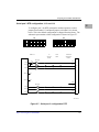
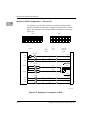
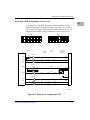
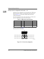
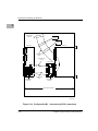
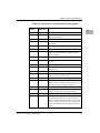
1
MVME712M
Transition Module
Installation and Use
VME712MA/IH2
Notice
While reasonable efforts have been made to assure the accuracy of this document,
Motorola, Inc. assumes no liability resulting from any omissions in this document, or from
the use of the information obtained therein. Motorola reserves the right to revise this
document and to make changes from time to time in the content hereof without obligation
of Motorola to notify any person of such revision or changes.
This material may be read online, downloaded for personal use, or included in another
document as a URL (from this server). The text itself may not be published commercially
in print or electronic form, edited or otherwise altered without the permission of Motorola,
Inc.
It is possible that this publication may contain reference to, or information about Motorola
products (machines and programs), programming, or services that are not announced in
your country. Such references or information must not be construed to mean that Motorola
intends to announce such Motorola products, programming, or services in your country.
Restricted Rights Legend
If the documentation contained herein is supplied, directly or indirectly, to the U.S.
Government, the following notice shall apply unless otherwise agreed to in writing by
Motorola, Inc.
Use, duplication, or disclosure by the Government is subject to restrictions as set forth in
subparagraph (c)(1)(ii) of the Rights in Technical Data and Computer Software clause at
DFARS 252.227-7013.
Motorola, Inc.
Computer Group
2900 South Diablo Way
Tempe, Arizona 85282
Preface
This manual, MVME712M Transition Module and P2 Adapter Board Installation and Use,
provides general information, hardware preparation, installation instructions, and support
information for the MVME712M Transition Module and the P2 Adapter Board.
The modules are used as the interface between the following families of Motorola
VMEmodules, and their peripheral devices:
MVME147 MPU VMEmodule
MVME1600 Single Board Computer (SBC)
MVME162 Embedded Controller
MVME2600 Single Board Computer (SBC)
MVME167 Single Board Controller (SBC)
MVME2700 Single Board Computer (SBC)
MVME177 Single Board Controller (SBC)
MVME3600 VME Processor Module
MVME4600 VME Processor Module
A P2 adapter module and cable are supplied with the MVME712M.
This manual is intended for anyone who wants to design OEM systems, supply additional
capability to an existing compatible system, or in a lab environment for experimental
purposes. A basic knowledge of computers and digital logic is assumed.
To use this manual, you should be familiar with the publications in Related Documentation.
All Motorola PWBs (printed wiring boards) are manufactured by UL-recognized
manufacturers, with a flammability rating of 94V-0.
!
WARNING
This equipment generates, uses, and can radiate electromagnetic energy. It may cause or be susceptible to electromagnetic interference (EMI) if not installed and used in a
cabinet with adequate EMI protection.
European Notice: Board products with the CE marking comply with the EMC
Directive (89/336/EEC). Compliance with this directive implies conformity to the
following European Norms:
EN55022 (CISPR 22) Radio Frequency Interference
EN50082-1 (IEC801-2, IEC801-3, IEEC801-4) Electromagnetic Immunity
The product also fulfills EN60950 (product safety) which is essentially the
requirement for the Low Voltage Directive (73/23/EEC).
This board product was tested in a representative system to show compliance with
the above mentioned requirements. A proper installation in a CE-marked system
will maintain the required EMC/safety performance.
Motorola® and the Motorola symbol are registered trademarks of Motorola, Inc.
PowerPCTM and VMEmoduleTM are trademarks of Motorola, Inc.
All other products mentioned in this document are trademarks or registered trademarks of
their respective holders.
© Copyright Motorola 1989, 1993, 1994, 1996, 1999
All Rights Reserved
Printed in the United States of America
April 1999
Safety Summary
Safety Depends On You
The following general safety precautions must be observed during all phases of operation, service, and repair of this
equipment. Failure to comply with these precautions or with specific warnings elsewhere in this manual violates safety
standards of design, manufacture, and intended use of the equipment. Motorola, Inc. assumes no liability for the
customer’s failure to comply with these requirements.
The safety precautions listed below represent warnings of certain dangers of which Motorola is aware. You, as the user
of the product, should follow these warnings and all other safety precautions necessary for the safe operation of the
equipment in your operating environment.
Ground the Instrument.
To minimize shock hazard, the equipment chassis and enclosure must be connected to an electrical ground. The
equipment is supplied with a three-conductor ac power cable. The power cable must be plugged into an approved
three-contact electrical outlet. The power jack and mating plug of the power cable meet International Electrotechnical
Commission (IEC) safety standards.
Do Not Operate in an Explosive Atmosphere.
Do not operate the equipment in the presence of flammable gases or fumes. Operation of any electrical equipment in
such an environment constitutes a definite safety hazard.
Keep Away From Live Circuits.
Operating personnel must not remove equipment covers. Only Factory Authorized Service Personnel or other
qualified maintenance personnel may remove equipment covers for internal subassembly or component replacement
or any internal adjustment. Do not replace components with power cable connected. Under certain conditions,
dangerous voltages may exist even with the power cable removed. To avoid injuries, always disconnect power and
discharge circuits before touching them.
Do Not Service or Adjust Alone.
Do not attempt internal service or adjustment unless another person capable of rendering first aid and resuscitation is
present.
Use Caution When Exposing or Handling the CRT.
Breakage of the Cathode-Ray Tube (CRT) causes a high-velocity scattering of glass fragments (implosion). To prevent
CRT implosion, avoid rough handling or jarring of the equipment. Handling of the CRT should be done only by
qualified maintenance personnel using approved safety mask and gloves.
Do Not Substitute Parts or Modify Equipment.
Because of the danger of introducing additional hazards, do not install substitute parts or perform any unauthorized
modification of the equipment. Contact your local Motorola representative for service and repair to ensure that safety
features are maintained.
Dangerous Procedure Warnings.
Warnings, such as the example below, precede potentially dangerous procedures throughout this manual. Instructions
contained in the warnings must be followed. You should also employ all other safety precautions which you deem
necessary for the operation of the equipment in your operating environment.
!
WARNING
Dangerous voltages, capable of causing death, are present in
this equipment. Use extreme caution when handling, testing,
and adjusting.
Contents
CHAPTER 1
General Information
Introduction................................................................................................................1-1
Description .................................................................................................................1-1
MVME712M Transition Module........................................................................1-2
P2 Adapter Board................................................................................................1-2
Specifications .............................................................................................................1-3
Cooling Requirements ...............................................................................................1-4
FCC Compliance........................................................................................................1-5
Related Documentation..............................................................................................1-6
MCG Customer Services ...........................................................................................1-7
CHAPTER 2
Preparing and Installing the Hardware
Introduction................................................................................................................2-1
Unpacking the Hardware ...........................................................................................2-1
Preparing the MVME712M Module..........................................................................2-2
DTE/DCE configuration select headers..............................................................2-2
Serial port 1 DCE configuration -- J1 and J11 ............................................2-4
Serial port 1 DTE configuration -- J1 and J11.............................................2-5
Serial port 2 DCE configuration -- J16 and J17 ..........................................2-6
Serial port 2 DTE configuration -- J16 and J17...........................................2-7
Serial port 3 DCE configuration -- J13 and J14 ..........................................2-8
Serial port 3 DTE configuration - J13 and J14 ............................................2-9
Serial port 4 DCE configuration -- J18 and J19 ........................................2-10
Serial port 4 DTE configuration - J18 and J19 ..........................................2-11
Serial port 4 clock configuration select header -- J15 ...............................2-12
SCSI Termination ......................................................................................2-13
Preparing the P2 Adapter Board ..............................................................................2-14
Cables and Connectors.............................................................................................2-15
Installing the MVME712M Module and P2 Adapter Board ...................................2-17
Procedure ..........................................................................................................2-17
Configuration A - Internal SCSI Devices Only ................................................2-19
Configuration B - Internal SCSI Devices Only ................................................2-21
Configuration B1 - Internal SCSI Devices Only ..............................................2-23
Configuration C - Internal and External SCSI Devices ....................................2-25
Configuration C1 - Internal and External SCSI Devices ..................................2-28
vii
Configuration D - Internal and External SCSI Devices ................................... 2-30
Configuration E - External SCSI Devices Only ............................................... 2-33
Configuration F - External SCSI Devices Only ............................................... 2-35
CHAPTER 3
Interconnect Signals
Introduction ............................................................................................................... 3-1
P2 Adapter Board ...................................................................................................... 3-2
P2 connector ....................................................................................................... 3-2
J2 connector ....................................................................................................... 3-2
J3 connector........................................................................................................ 3-7
MVME712M Transition Module .............................................................................. 3-9
J2 connector ....................................................................................................... 3-9
J3 and J4 connectors......................................................................................... 3-14
SCSI interface connector.................................................................................. 3-16
J5 connector...................................................................................................... 3-18
J6 connector...................................................................................................... 3-19
J7 - J10 connectors ........................................................................................... 3-20
J20 connector.................................................................................................... 3-21
J21 connector.................................................................................................... 3-22
viii
List of Figures
Figure 2-1. MVME712M header locations................................................................2-3
Figure 2-2. Serial port 1 configured as DCE .............................................................2-4
Figure 2-3. Serial port 1 configured as DTE..............................................................2-5
Figure 2-4. Serial port 2 configured as DCE .............................................................2-6
Figure 2-5. Serial port 2 configured as DTE..............................................................2-7
Figure 2-6. Serial port 3 configured as DCE .............................................................2-8
Figure 2-7. Serial port 3 configured as DTE..............................................................2-9
Figure 2-8. Serial port 4 configured as DCE ...........................................................2-10
Figure 2-9. Serial port 4 configured as DTE............................................................2-11
Figure 2-10. J15 clock line configuration ................................................................2-12
Figure 2-11. P2 adapter connector locations............................................................2-14
Figure 2-12. Configuration A -- internal-only SCSI connections............................2-20
Figure 2-13. Configuration B -- internal-only SCSI connections............................2-22
Figure 2-14. Configuration B1 -- internal-only SCSI connections..........................2-24
Figure 2-15. Configuration C -- internal and external SCSI connections................2-27
Figure 2-16. Configuration C1 -- internal and external SCSI connections..............2-29
Figure 2-17. Configuration D -- internal and external SCSI connections................2-32
Figure 2-18. Configuration E -- external-only SCSI connections............................2-34
Figure 2-19. Configuration F -- external-only SCSI connections............................2-37
ix
List of Tables
Table 1-1. MVME712M specifications......................................................................1-3
Table 2-1. Serial port jumpers/headers ......................................................................2-2
Table 2-2. VMEmodule headers/switches ...............................................................2-12
Table 2-3. Cables and connectors ..........................................................................2-15
Table 2-4. Cabling configurations............................................................................2-18
Table 3-1. P2 adapter board and MVME712M connectors .......................................3-1
Table 3-2. Connector J2 interconnect signals ...........................................................3-2
Table 3-3. Connector J3 interconnect signals ...........................................................3-7
Table 3-4. Connector J2 interconnect signals ...........................................................3-9
Table 3-5. Connectors J3 and J4 interconnect signals ............................................3-14
Table 3-6. Connector SCSI interface interconnect signals ......................................3-16
Table 3-7. Connector J5 interconnect signals .........................................................3-18
Table 3-8. Connector J6 interconnect signals .........................................................3-19
Table 3-9. Connectors J7 - J10 interconnect signals ...............................................3-20
Table 3-10. Connector J20 interconnect signals .....................................................3-21
Table 3-11. Connector J21 interconnect signals .....................................................3-22
xi
1General Information
1
Introduction
This chapter provides general information about the MVME712M
Transition Module and the P2 adapter board, specifications, cooling
requirements, and FCC compliance.
Description
The MVME712M is an I/O transition module for Motorola’s MPU
VMEmodule, VME Processor Module, Embedded Controller, and Single
Board Computer (SBC) families of processor modules, referred to in this
manual as MVMExxxx.
The MVME712M is used as an interface between the processor module
and its peripheral devices. The purpose of this module is to provide rear
panel industry-standard connectors that simplify external customer cable
requirements.
The P2 adapter board and cables are supplied for interconnection between
the MVME712M and the MVMExxxx. The P2 adapter assembly routes the
I/O signals and grounds from the P2 connector on the chassis backplane,
at the VMEmodule MPU connection, to the MVME712M.
The MVME712M routes the signals to four serial ports, implemented with
four industry standard DB-25 connectors on its front panel. The serial ports
may be configured for EIA-232-D DTE or DCE through jumper
arrangements on the MVME712M.
The MVME712M front panel also has an Ethernet port, a SCSI port, and
a printer port. In addition, the MVME712M routes the EIA-232-D port 2
signals to an internal modem.
1-1
1
General Information
MVME712M Transition Module
The features of the MVME712M include:
❏
Four 25-pin multiprotocol EIA-232-D serial ports
(through P2 adapter)
❏
One independent printer port (through P2 adapter)
❏
Small Computer Systems Interface (SCSI) shielded connector bus
interface (through P2 adapter) for connection to internal and
external devices
❏
Green LED on module to indicate terminator power
❏
Yellow LED on module to indicate transceiver power
❏
SCSI terminating resistors mounted in sockets for end of cable or
middle of cable configuration
❏
Modem connection on module
❏
Radio Frequency Interference (RFI) protection on front panel
❏
Electrostatic Discharge (ESD) protection on front panel
P2 Adapter Board
The MVME712M requires the use of the P2 adapter board. The features of
the P2 adapter board include:
1-2
❏
A connector that permits SCSI cable connection to other SCSI
devices and/or to MVME712M through a flat ribbon cable
❏
SCSI terminating resistors mounted in sockets, for end of cable or
middle of cable configuration
❏
Terminator power developed on the P2 adapter from the
+5 Vdc on connector P2, and fused (1 A) on the P2 adapter
❏
A connector that interfaces the EIA-232-D ports, printer port, SCSI,
and Ethernet signals to the MVME712M
Computer Group Literature Center Web Site
Specifications
Specifications
The following table lists the general specifications for the MVME712M
Transition Module. The subsequent sections detail cooling requirements
and FCC compliance.
A complete functional description of the MVME712M appears in Chapter
2.
Table 1-1. MVME712M specifications
Characteristics
Specifications
Power requirements
+5 Vdc
281 mA maximum
255 mA typical
+12 Vdc
-12 Vdc
Note:+5 Vdc, +12 Vdc, -12Vdc power
supplied by backplane. Used for
internal modem interface.
I/O ports
Serial
Four multiprotocol serial ports
(connected through P2 adapter board)
Printer
Centronics printer port
(connected through P2 adapter board)
Operating temperature
0 degrees to 55 degrees C at point of
entry of forced air (approximately 5
CFM)
Storage temperature
-40 degrees to 85 degrees C
Relative humidity
5% to 90% (non-condensing)
Physical
characteristics
(excluding front panel)
http://www.mcg.mot.com/literature
Height
9.187 inches (233.35 mm)
Depth
3.200 inches (80.0 mm)
Thickness
0.063 inches (1.6 mm)
1-3
1
1
General Information
Cooling Requirements
Motorola VMEmodules are specified, designed, and tested to operate
reliably with an incoming air temperature range from 0 degrees C to 55
degrees C (32 degrees F to 131 degrees F) with forced air cooling.
Temperature qualification is performed in a standard Motorola
VMEsystem 1000 chassis. Twenty-five watt load boards are inserted in the
two card slots, one on each side, adjacent to the board under test to
simulate a high power density system configuration. An assembly of three
axial fans, rated at 71 CFM per fan, is placed directly under the MVME
card cage. The incoming air temperature is measured between the fan
assembly and the card cage where the incoming airstream first encounters
the module under test.
Test software is executed as the module is subjected to ambient
temperature variations. Case temperatures of critical, high power density
integrated circuits are monitored to ensure component vendors
specifications are not exceeded.
While the exact amount of airflow required for cooling depends on the
ambient air temperature and the type, number, and location of boards and
other heat sources, adequate cooling can usually be achieved with 5 CFM
flowing over the module. Less air flow is required to cool the module in
environments having lower maximum ambients.
Under more favorable thermal conditions it may be possible to operate the
module reliably at higher than 55 degrees C with increased air flow. It is
important to note that there are several factors, in addition to the rated
CFM of the air mover, which determine the actual volume of air flowing
over a module.
1-4
Computer Group Literature Center Web Site
FCC Compliance
FCC Compliance
The MVME712M Transition Module was tested in an FCC-compliant
chassis, and meets the requirements for Class A equipment. FCC
compliance was achieved under the following conditions:
❏
Shielded cables on all external I/O ports
❏
Cable shields connected to earth ground via metal shell connectors
bonded to a conductive module front panel
❏
Conductive chassis rails connected to earth ground; this provides
the path for connecting shields to earth ground
❏
Front panel screws properly tightened
For minimum RF emissions, it is essential that the conditions above be
implemented. Failure to do so could compromise the FCC compliance of
the equipment containing the modules.
http://www.mcg.mot.com/literature
1-5
1
1
General Information
Related Documentation
The publications listed below are referenced in this document. To purchase manuals you
may contact Motorola in these ways:
❏
Through your local Motorola sales office
❏
By contacting the Literature Center via phone or fax at the numbers listed
under Product Literature at MCG’s World Wide Web site,
http://www.mcg.mot.com/literature
.
Motorola
Publication Number
Document Title
MVME147-0xx MPU VMEmodule Installation and Use
VME147A/IH
MVME162 Embedded Controller Installation Guide
MVME162IG/D
MVME162FX Embedded Controller Installation and Use
V162FXA/IH
MVME162LX Embedded Controller Installation Guide
MVME162LXIG/D
MVME167 Single Board Computer Installation Guide
MVME167IG/D
MVME177 Single Board Computer Installation and Use
VME177A/IH
MVME1600 Single Board Computer Installation and Use
V1600A/IH
MVME2600 Series Single Board Computer Installation and Use
V2600A/IH
MVME2700 Series Single Board Computer Installation and Use
V2700A/IH
MVME3600 Series VME Processor Module Installation and Use
V3600A/IH
MVME4600 Series VME Processor Module Installation and Use
V4600A/IH
Each Motorola Computer Group manual publication number is suffixed with characters
that represent the revision level of the document, such as /IH2 (second revision).
To obtain the most up-to-date product information in PDF or HTML format, visit our Web
site at http ://www.mcg.mot.com/literature.
1-6
Computer Group Literature Center Web Site
MCG Customer Services
MCG Customer Services
The Motorola Computer Group Customer Services organization provides numerous
services that support the needs of our OEM customers throughout the qualification,
development, deployment, and continued service phases of their product life cycles.
Specific areas of support include:
❏
Helping you identify and address your unique needs for providing
outstanding products to your customers
❏
Extended warranties
❏
24 X 7 access to the high-level technical assistance that is crucial for mission
critical applications around the world
❏
24 X 7 access to the latest technical information on MCG products, including
known problems and a solutions database
❏
Customized training available at the MCG campus or at any of your sites
across the world
❏
Customized documentation and 24 X 7 Internet access to product
documentation
❏
Services Central, a one-stop information source about customer services -program content, pricing, and availability
For information on what services are available, or to purchase a support contract, call us at
Services Central, at 1-800-624-6745 or 602-438-5875, or visit our Web site at
http://www.mcg.mot.com/support.
http://www.mcg.mot.com/literature
1-7
1
2Preparing and Installing
the Hardware
2
Introduction
This manual provides hardware preparation and installation instructions
for the MVME712M Transition Module and P2 adapter board.
Unpacking the Hardware
Note
If the carton is damaged upon receipt, request that carrier’s
agent be present during unpacking and inspection of the
equipment.
Unpack the equipment from the shipping carton. Refer to the packing list
and verify that all items are present. Save the packing material for storing
and reshipping of the equipment.
!
Caution
Avoid touching areas of integrated circuitry; static discharge
can damage circuits.
2-1
Preparing and Installing the Hardware
2
Preparing the MVME712M Module
The locations of the headers, LEDs, terminators, and connectors for the
MVME712M are shown in Figure 2-1. The module has been factory tested
and is shipped with factory-installed jumpers that configure the
MVME712M to provide the system functions required for a VMEbus
system.
The factory default configurations are shown in the following paragraphs
with descriptions of each header. The module is operational with the
factory-installed jumpers.
DTE/DCE configuration select headers
Serial ports 1 through 4 can be configured as a modem (DCE) for
connection to terminal or configured as a terminal (DTE) for connection to
modem. The MVME712M is shipped with the ports configured for DTE
operation.
The following table lists the serial ports with their corresponding jumper
headers.
Table 2-1. Serial port jumpers/headers
Serial Port
Board
Connector
Panel Connector
Jumper Header
DCE/DTE
Port 1
J7
Serial port 1/ Console
J1/J11
Port 2
J8
Serial port 2/ TTY
J16/J17
Port 3
J9
Serial port 3
J13/J14
Port 4
J10
Serial port4
J18/J19
Figures 2-2 through 2-9 illustrate the VME module and MVME712M
transition module with the interconnections and jumper settings for
DCE/DTE configuration on each serial port.
2-2
Computer Group Literature Center Web Site
Preparing the MVME712M Module
2
MVME 712/M
2
1
2
1
J11
J1
14 2
13 1
14 2
13 1
J7
J9
J14
J13
2
1
1
14
1
14
J20
14 2
13 1
14 2
13 1
J15
2
1
J17
J16
12
11
13
25
13
25
14 2
13 1
14 2
13 1
20
19
J19
J18
J8
J10
1
14
13
14
13
SERIAL PORT 2 / TTY01
SERIAL PORT 4
1
1
14
1
14
J21 6
6
J2
A1
C1
DS1
8
15
DS2
J6
SCSI
INTERFACE
ETHERNET
J3
1
9
2
1
49
50
1
C1
R49
8
1
18
36
C2
R50
J4
8
1
PRINTER
A32
C32
C3
49
50
R51
1
19
8
1
2
J5
2-3
http://www.mcg.mot.com/literature
13
25
13
25
SERIAL PORT 1 / CONSOLE
SERIAL PORT 3
2509 9903
Figure 2-1. MVME712M header locations
Preparing and Installing the Hardware
2
Serial port 1 DCE configuration -- J1 and J11
To configure port 1 for DCE (modem to terminal) operation, install
jumpers on headers J1 and remove jumpers on headers J11 as shown
below. The schematic representation of this configuration is shown in
Figure 2-2.
J1
1
3
5
7
J11
9
11
MVMExxxx
13
1
P2
ADAPTER
BOARD
3
64 PIN
CABLE
5
7
9
11
13
MVME712M
TRANSITION
BOARD
8530
DB25
F32
TXDA
MC145406
RXD
D
1.5K
DTRA*
MC145406
RTSA*
+12V
CTS
D
1.5K
+12V
TRXCA*
NC
RTXCA*
NC
DCD
DSR
GND
3
8
5
6
7
MC145406
TXD
RXDA
DCDA*
2
R
MC145406
RTS
CTSA*
4
R
cb212 9212A
Figure 2-2. Serial port 1 configured as DCE
2-4
Computer Group Literature Center Web Site
Preparing the MVME712M Module
Serial port 1 DTE configuration -- J1 and J11
2
To configure port 1 for DTE (terminal to modem) operation, remove
jumpers from header J1 and install jumpers on header J11 as shown below.
This is the default configuration as shipped from the factory. The
schematic representation of this configuration is shown in Figure 2-3.
J1
1
3
5
7
J11
9
11
MVMExxxx
13
1
P2
ADAPTER
BOARD
3
64 PIN
CABLE
5
7
9
11
13
MVME712M
TRANSITION
BOARD
8530
DB25
F32
TXDA
MC145406
TXD
D
1.5K
DTRA*
MC145406
RTSA*
+12V
RTS
D
TRXCA*
NC
RTXCA*
NC
DTR
GND
MC145406
2
20
4
7
RXD
RXDA
DCDA*
3
R
MC145406
CTS
CTSA*
R
5
cb213 9212A
Figure 2-3. Serial port 1 configured as DTE
http://www.mcg.mot.com/literature
2-5
Preparing and Installing the Hardware
2
Serial port 2 DCE configuration -- J16 and J17
To configure port 2 for DCE (modem to terminal) operation, install
jumpers on header J16 and remove jumpers from header J17 as shown
below. The schematic representation of this configuration is shown in
Figure 2-4.
J16
1
3
5
7
J17
9
MVMExxxx
11
1
13
P2
ADAPTER
BOARD
3
64 PIN
CABLE
5
7
9
11
13
MVME712M
TRANSITION
BOARD
8530
DB25
F32
TXDB
MC145406
RXD
D
DTRB*
DCD
D
RTSB*
CTS
D
1.5K
+12V
TRXCB*
NC
RTXCB*
NC
DSR
GND
3
8
5
6
7
MC145406
TXD
RXDB
2
R
DTR
DCDB*
R
20
RTS
CTSB*
4
R
cb214 9212A
Figure 2-4. Serial port 2 configured as DCE
2-6
Computer Group Literature Center Web Site
Preparing the MVME712M Module
Serial port 2 DTE configuration -- J16 and J17
2
To configure port 2 for DTE (terminal to modem) operation, remove
jumpers from header J16 and install jumpers on header J17 as shown
below. This is the default configuration as shipped from the factory. The
schematic representation of this configuration is shown in Figure 2-5.
J16
1
3
5
7
J17
9
11
MVMExxxx
13
1
P2
ADAPTER
BOARD
3
64 PIN
CABLE
5
7
9
11
13
MVME712M
TRANSITION
BOARD
8530
DB25
F32
TXDB
MC145406
TXD
D
DTRB*
DTR
D
RTSB*
RTS
D
TRXCB*
NC
RTXCB*
NC
GND
2
20
4
7
MC145406
RXD
RXDB
DCDB*
R
DCD
R
3
8
CTS
CTSB*
R
5
cb215 9212A
Figure 2-5. Serial port 2 configured as DTE
http://www.mcg.mot.com/literature
2-7
Preparing and Installing the Hardware
2
Serial port 3 DCE configuration -- J13 and J14
To configure port 3 for DCE (modem to terminal) operation, install
jumpers on header J13 and remove jumpers from header J14 as shown
below. The schematic representation of this configuration is shown in
Figure 2-6.
J13
1
3
5
7
J14
9
11
MVMExxxx
1
13
P2
ADAPTER
BOARD
3
64 PIN
CABLE
5
7
9
11
13
MVME712M
TRANSITION
BOARD
8530
DB25
F32
TXDA
MC145406
RXD
D
DTRA*
DCD
D
RTSA*
CTS
D
1.5K
+12V
TRXCA*
NC
RTXCA*
NC
DSR
GND
3
8
5
6
7
MC145406
TXD
RXDA
2
R
DTR
DCDA*
R
20
RTS
CTSA*
4
R
cb216 9212A
Figure 2-6. Serial port 3 configured as DCE
2-8
Computer Group Literature Center Web Site
Preparing the MVME712M Module
Serial port 3 DTE configuration - J13 and J14
2
To configure port 3 for DTE (terminal to modem) operation, remove
jumpers from header J13 and install jumpers on header J14 as shown
below. This is the default configuration as shipped from the factory. The
schematic representation of this configuration is shown in Figure 2-7.
J13
1
3
5
7
J14
9
11
MVME1xxxx
13
1
P2
ADAPTER
BOARD
3
64 PIN
CABLE
5
7
9
11
13
MVME712M
TRANSITION
BOARD
8530
DB25
F32
TXDA
MC145406
TXD
D
DTRA*
DTR
D
RTSA*
RTS
D
TRXCA*
NC
RTXCA*
NC
GND
2
20
4
7
MC145406
RXD
RXDA
DCDA*
R
DCD
R
3
8
CTS
CTSA*
R
5
cb217 9212A
Figure 2-7. Serial port 3 configured as DTE
http://www.mcg.mot.com/literature
2-9
Preparing and Installing the Hardware
2
Serial port 4 DCE configuration -- J18 and J19
To configure port 4 for DCE (modem to terminal) operation, install
jumpers on header J18 and remove jumpers from header J19 as shown
below. The schematic representation of this configuration is shown in
Figure 2-8.
J18
1
3
5
7
J19
9
11
1
13
MVMExxxx
P2
ADAPTER
BOARD
3
5
7
64 PIN
CABLE
9
11
13
MVME712M
TRANSITION
BOARD
8530
DB25
F32
TXDB
DTRB*
RTSB*
MC145406
RXD
D
DCD
D
CTS
D
1.5K
+12V
MC145406
J10
TRXCB*
1
D
TRXC4
1
J15
R
J9
D
RTXCB*
1
DSR
RTXC
RRXC
TTXC
3
8
5
6
15
17
24
RTXC4
R
GND
MC145406
7
TXD
RXDB
2
R
DTR
DCDB*
R
20
RTS
CTSB*
4
R
cb218 9212A
Figure 2-8. Serial port 4 configured as DCE
2-10
Computer Group Literature Center Web Site
Preparing the MVME712M Module
Serial port 4 DTE configuration - J18 and J19
2
To configure port 4 for DTE (terminal to modem) operation, remove
jumpers from header J18 and install jumpers on header J19 as shown
below. This is the default configuration as shipped from the factory. The
schematic representation of this configuration is shown in Figure 2-9.
J18
1
3
5
7
J19
9
11
13
MVMExxxx
1
P2
ADAPTER
BOARD
3
5
7
64 PIN
CABLE
9
11
13
MVME712M
TRANSITION
BOARD
8530
DB25
F32
TXDB
DTRB*
RTSB*
MC145406
TXD
D
DTR
D
RTS
D
2
20
4
MC145406
J10
TRXCB*
1
D
TRXC4
1
J15
R
J9
D
RTXCB*
1
RTXC
RRXC
TTXC
15
17
24
RTXC4
R
GND
7
MC145406
RXD
RXDB
R
DCD
DCDB*
R
3
8
CTS
CTSB*
R
5
cb219 9212A
Figure 2-9. Serial port 4 configured as DTE
http://www.mcg.mot.com/literature
2-11
Preparing and Installing the Hardware
2
Serial port 4 clock configuration select header -- J15
Serial port 4 can be configured to use clock signals by the TRXC4 and
RTXC4 signal lines. Header J15 configurations of the clock lines are
shown in Figure 2-10. The module is shipped without clock lines
connected (no jumpers).
Part of the configuration must be done with headers or switches on the
processor VMEmodule, as listed in the following table.
Table 2-2. VMEmodule headers/switches
Processor Module
Header
Processor Module
Header
MVME147
J8, J9
MVME1600
J8, J15, J16
MVME162
J12
MVME2600
J16, J17, J20
MVME167
J9, J10
MVME2700
J16, J17, J19
MVME177
J9, J10
MVME3600
J9, J10, J16
MVME4600
J9, J10, J16
For more information see Figure 2-9 and the installation guide furnished
with your processor VMEmodule.
J15
1
3 5
7
9 11
TRXC4 TO PORT 4 PIN 15
RTXC4 TO PORT 4 PIN 24
TRXC4 TO PORT 4 PIN 17
RTXC4 TO PORT 4 PIN 17
TRXC4 TO PORT 4 PIN 24
RTXC4 TO PORT 4 PIN 15
cb210 9212A
Figure 2-10. J15 clock line configuration
2-12
Computer Group Literature Center Web Site
Preparing the MVME712M Module
SCSI Termination
2
You must ensure that the SCSI bus is terminated properly. The P2 adapter
and the MVME712M module have sockets for terminating the SCSI lines.
Both the P2 adapter and the MVME712M use three 8-pin SIP resistors.
Refer to the installation instructions for use of the terminators.
http://www.mcg.mot.com/literature
2-13
Preparing and Installing the Hardware
2
Preparing the P2 Adapter Board
The P2 adapter board is required. Preparation of the P2 adapter consists of
removing or replacing the terminating resistors for SCSI. Figure 2-11
shows the component locations. Refer to the installation instructions in
Installing the MVME712M, in this chapter, for use of the terminators.
A P2 mounting bracket kit is also furnished for use on some systems.
J2
A1
B1
C1
A32
B32
C32
J3
2
1
50
49
1
R1
C1
R2
C2
1
2
R3
C3
F1
CR1
C1
B1
A1
C32
B32
A32
P2
cb211 9212
Figure 2-11. P2 adapter connector locations
2-14
Computer Group Literature Center Web Site
Cables and Connectors
Cables and Connectors
2
The MVME712M front panel has four serial ports, one printer port, one
SCSI port, and one Ethernet port. The connectors for these ports, the P2
backplane connector, and two modem connectors are described in the
following table. The P2 adapter board’s MVME712M connector, P2
connector, and SCSI connector are also described in the table.
Cables recommended for use with the connectors are also listed in the
table. Note that not all peripheral cables needed are provided with the
MVME712M. You may need to fabricate or purchase certain cables.
1
Table 2-3. Cables and connectors
MVME712M Board Front Panel
Port
Connector
Description
Cable
Serial ports
1 through 4
J7 through J10 25-pin female DB-25 connectors User-supplied serial
that cable to your serial devices EIA-232-D DTE or DCE cable
(pins used depend upon the
processor VMEmodule)
Printer port
J5
36-pin female connector that
cables to your printer
User-supplied Centronics-type
parallel printer cable, male-to-male
Ethernet port
J6
15-pin female DB-15 connector
that cables to your Ethernet
network controller, or connects
to an adapter box
User-supplied network cable or
user-supplied adapter box to
convert to another medium
SCSI Interface
port
J4
50-pin female connector that
cables to your SCSI devices
User-supplied 50-conductor cable
with SCSI connector(s) as needed
MVME712M Board Top Side
Interconnection
SCSI
Connector
J3
Description
Cable
50-pin male IDC connector that
cables to J3 on the P2 adapter
board and/or to SCSI devices, in
almost all configurations
Part number 30-W2960B01A.
17.5-inch, 50-conductor flat-ribbon
cable furnished with the
MVME712M, used only in the
external-SCSI-only configuration
labeled Configuration E in Table 24 and Figure 2-18. Otherwise, a
user-supplied 50-conductor cable
with SCSI connector(s) as needed
http://www.mcg.mot.com/literature
2-15
Preparing and Installing the Hardware
2
Modem
VME
J20
20-pin male IDC connector,
connects to a user-supplied
modem
User-supplied 20-conductor cable;
usually supplied with the modem
J21
6-pin polarized male connector,
supplies power to the modem
User-supplied 6-conductor cable;
usually supplied with the modem
J2
64-pin male connector that
cables to J2 on the P2 adapter
board
Part number 30-W2514B02.
17.5-inch 64-conductor flat ribbon
cable furnished with the
MVME712M (see Note below)
P2 Adapter Board
Interconnection
VME
SCSI
Note
Connector
Description
Cable
P2
96-pin female DIN 41612
connector that connects to the
chassis backplane
J2
64-pin male connector that
Part number 30-W2514B02.
cables to J2 on the MVME712M 17.5-inch 64-conductor flat ribbon
cable furnished with the
MVME712M (see Note below)
J3
50-pin male IDC connector that Part number 30-W2960B01A.
cables to J3 on the MVME712M 17.5-inch 50-conductor flat-ribbon
and/or to SCSI devices
cable furnished with the
MVME712M, used only in the
external-SCSI-only configuration
labeled Configuration E in Table 24 and Figure 2-18. Otherwise, a
user-supplied 50-conductor cable
with SCSI connector(s) as needed
None needed
If you wish to use your own cable for the P2 signals from J2 on the P2 adapter
board to J2 on the MVME712M, note that the cable should be kept as short as
possible. Any cable over 2.5 to 3 feet is likely to cause signal problems.
The maximum cable length that can be used from the P2 adapter board to the
MVME712M will vary depending on what other cables are attached to the
MVME712. The connections most susceptible to problems caused by long P2
cables are the Ethernet and parallel port connections.
2-16
Computer Group Literature Center Web Site
Installing the MVME712M Module and P2 Adapter Board
Installing the MVME712M Module and P2
Adapter Board
2
The MVME712M can be connected in different configurations. The
installation procedure begins on this page, and continues using the
instructions given for one of the configurations listed in Table 2-2.
Use ESD
Wrist Strap
Motorola strongly recommends that you use an antistatic wrist strap and a
conductive foam pad when installing or upgrading the system. Electronic
components, such as disk drives, computer boards, and memory modules,
can be extremely sensitive to ESD. After removing the component from
the system or its protective wrapper, place the component flat on a
grounded, static-free surface, and in the case of a board, component-side
up. Do not slide the component over any surface.
If an ESD station is not available, you can avoid damage resulting from
ESD by wearing an antistatic wrist strap (available at electronics stores)
that is attached to an unpainted metal part of the system chassis.
!
Connecting modules while power is applied may result in
damage to components on the module.
Caution
!
Warning
Dangerous voltages, capable of causing death, are present in
this equipment. use extreme caution when handling, testing,
and adjusting.
Procedure
To begin the installation of the MVME712M in the system, proceed as
follows:
1. Turn all equipment power OFF and disconnect the power cable
from the AC power source.
2. Remove the chassis cover as instructed in the equipment user’s
manual.
http://www.mcg.mot.com/literature
2-17
Preparing and Installing the Hardware
3. Remove the filler panel(s) from the appropriate card slot(s) at the
rear of the chassis (if the chassis has a rear card cage). Other
modules in the unit may have to be moved to allow space for the
cables connected to the P2 adapter and the MVME712M.
2
4. Continue the installation procedure by choosing one of the
configurations listed in the following table, and described on the
following pages.
Note that the designations A through F are used solely as convenient
references.
Table 2-4. Cabling configurations
2-18
Configuration
Internal SCSI
Devices
A
X
External SCSI
Devices
Pages
2-19, 2-20
B
X
2-21, 2-22
B1
X
2-23, 2-24
C
X
X
2-25, 2-27
C1
X
X
2-28, 2-29
D
X
X
2-30, 2-32
E
X
2-33, 2-34
F
X
2-35, 2-37
Computer Group Literature Center Web Site
Installing the MVME712M Module and P2 Adapter Board
Configuration A - Internal SCSI Devices Only
2
If SCSI devices are to be attached internal to your system, proceed as follows. See
Table 2-12.
1. The MVMExxxx is at one end of the cable, so terminators must be
installed on the P2 adapter module.
2. Install the P2 adapter module to the backplane directly in line with
the P2 connector on the MVMExxxx. Be sure to orient pin 1 of the
adapter with pin 1 of the backplane connector.
3. Connect a user-supplied 50-conductor cable with compatible
pinouts from connector J3 on the P2 adapter to the internal SCSI
devices.
4. Terminators must be installed on the last SCSI device in the system.
5. Attach the furnished 64-conductor cable from connector J2 on the
P2 adapter to connector J2 on the MVME712M. Be sure to orient
cable pin 1 with connector pin 1.
6. Insert the MVME712M module into the selected slots and tighten
the attaching screws, making good contact with the transverse
mounting rails to minimize RF emissions.
7. Make sure that cables will not be pinched by the cover and install
the cover that you previously removed.
8. Connect the power cable to the AC power source and turn the unit
on.
9. The LED (DS1, toward the serial ports) on the MVME712M should
be lit (the LED can be seen through the opening in the front panel).
If not lit, then either a cabling problem exists, a fuse is blown, or
both.
If it is a cabling problem, then fix it. If not, check the fuse on the
MVMExxxx module, and replace if necessary. The fuse on the
MVMExxxx is for Ethernet transceiver power. The resistance of this
fuse should be less than 1 ohm.
http://www.mcg.mot.com/literature
2-19
Preparing and Installing the Hardware
2
TERMINATORS
INSTALLED
T
SCSI
DEVICE
SCSI
DEVICE
MVMExxxx
MVME712M
J9
J7
P1
50-CONDUCTOR
CABLE
J10
J8
64-CONDUCTOR
CABLE
P2 ADAPTER
J6
J4
J2
J3
J3
J2
P2
P2
J5
TERMINATORS
INSTALLED
ENCLOSURE BOUNDARY
cb2349301A
Figure 2-12. Configuration A -- internal-only SCSI connections
2-20
Computer Group Literature Center Web Site
Installing the MVME712M Module and P2 Adapter Board
Configuration B - Internal SCSI Devices Only
2
If SCSI devices are to be attached internal to your system, and cabled for easy
change to configuration C, proceed as follows. See Figure 2-13.
1. The MVMExxxx is at one end of the cable, so terminators must be
installed on the P2 adapter module.
2. The MVME712M is at one end of the cable, so terminators must be
installed on the MVME712M.
3. Install the P2 adapter module to the backplane directly in line with
the P2 connector on the MVMExxxx. Be sure to orient pin 1 of the
adapter with pin 1 of the backplane connector.
4. Connect a user-supplied 50-conductor cable with compatible
pinouts from connector J3 on the P2 adapter to the internal SCSI
devices and on to connector J3 on the MVME712M. This cable
must be a continuous cable.
5. Attach the furnished 64-conductor cable from connector J2 on the
P2 adapter to connector J2 on the MVME712M. Be sure to orient
cable pin 1 with connector pin 1.
6. Insert the MVME712M module into the selected slots and tighten
the attaching screws, making good contact with the transverse
mounting rails to minimize RF emissions.
7. Make sure that cables will not be pinched by the cover and install
the cover that you previously removed.
8. Connect the power cable to the AC power source and turn the unit
on.
9. Both LEDs (DS1 and DS2) on the MVME712M should be lit (the
LEDs can be seen through the opening in the front panel). If not lit,
then either a cabling problem exists, a fuse is blown, or both.
If it is a cabling problem, then fix it. If not, check the fuse on the P2
adapter module and on the MVMExxxx module, and replace if
necessary. The fuse on the P2 adapter module is for SCSI terminator
power. The fuse on the MVMExxxx is for Ethernet transceiver
power. The resistance of each fuse should be less than 1 ohm.
http://www.mcg.mot.com/literature
2-21
Preparing and Installing the Hardware
2
SCSI
DEVICE
SCSI
DEVICE
MVMExxxx
MVME712M
J9
J7
P1
J10
J8
P2 ADAPTER
J6
J4
J2
J3
J3
J2
P2
P2
J5
TERMINATORS
INSTALLED
64-CONDUCTOR
CABLE
TERMINATORS
INSTALLED
50-CONDUCTOR
CABLE
ENCLOSURE BOUNDARY
cb2359301A
Figure 2-13. Configuration B -- internal-only SCSI connections
2-22
Computer Group Literature Center Web Site
Installing the MVME712M Module and P2 Adapter Board
Configuration B1 - Internal SCSI Devices Only
2
If SCSI devices are to be attached internal to your system, and cabled for easy
change to configuration C1, proceed as follows. See Figure 2-14.
1. The MVMExxxx is not at one end of the cable, so terminators must
be removed from the P2 adapter module.
2. The MVME712M is at one end of the cable, so terminators must be
installed on the MVME712M.
3. Install the P2 adapter module to the backplane directly in line with
the P2 connector on the MVMExxxx. Be sure to orient pin 1 of the
adapter with pin 1 of the backplane connector.
4. Connect a user-supplied 50-conductor cable with compatible
pinouts from connector J3 on the MVME712M to connector J3 on
the P2 adapter and on to the internal SCSI devices. This cable must
be a continuous cable.
5. Terminators must be installed on the last SCSI device on the cable.
6. Attach the furnished 64-conductor cable from connector J2 on the
P2 adapter to connector J2 on the MVME712M. Be sure to orient
cable pin 1 with connector pin 1.
7. Insert the MVME712M module into the selected slots and tighten
the attaching screws, making good contact with the transverse
mounting rails to minimize RF emissions.
8. Make sure that cables will not be pinched by the cover and install
the cover that you previously removed.
9. Connect the power cable to the AC power source and turn the unit
on.
10. Both LEDs (DS1 and DS2) on the MVME712M should be lit (the
LEDs can be seen through the opening in the front panel). If not lit,
then either a cabling problem exists, a fuse is blown, or both.
If it is a cabling problem, then fix it. If not, check the fuse on the P2
adapter module and on the MVMExxxx module, and replace if
necessary. The fuse on the P2 adapter module is for SCSI terminator
power. The fuse on the MVMExxxx is for Ethernet transceiver
power. The resistance of each fuse should be less than 1 ohm.
http://www.mcg.mot.com/literature
2-23
Preparing and Installing the Hardware
2
TERMINATORS
INSTALLED
T
SCSI
DEVICE
SCSI
DEVICE
MVMExxxx
MVME712M
J9
J7
P1
50-CONDUCTOR
CABLE
J10
J8
64-CONDUCTOR
CABLE
P2 ADAPTER
J6
J2
J4
J3
J3
J2
P2
P2
J5
50-CONDUCTOR
CABLE
TERMINATORS
INSTALLED
TERMINATORS
REMOVED
ENCLOSURE BOUNDARY
cb236 9301A
Figure 2-14. Configuration B1 -- internal-only SCSI connections
2-24
Computer Group Literature Center Web Site
Installing the MVME712M Module and P2 Adapter Board
Configuration C - Internal and External SCSI Devices
2
If SCSI devices are to be attached internal and external to your system and the
MVMExxxx is at one end of the cable, proceed as follows. See Figure 2-15.
1. The MVMExxxx is at one end of the cable, so terminators must be
installed on the P2 adapter module.
2. The MVME712M is not at one end of the cable, so terminators must
be removed from the MVME712M.
3. Install the P2 adapter module to the backplane directly in line with
the P2 connector on the MVMExxxx. Be sure to orient pin 1 of the
adapter with pin 1 of the backplane connector.
4. Connect a user-supplied 50-conductor cable with compatible
pinouts from connector J3 on the MVME712M to the internal SCSI
devices and on to connector J3 on the P2 adapter. This cable must
be a continuous cable.
5. Attach the furnished 64-conductor cable from connector J2 on the
P2 adapter to connector J2 on the MVME712M. Be sure to orient
cable pin 1 with connector pin 1.
6. Insert the MVME712M module into the selected slots and tighten
the attaching screws, making good contact with the transverse
mounting rails to minimize RF emissions.
7. Connect a user-supplied 50-conductor cable with compatible
pinouts from the SCSI connector on the front panel of the
MVME712M to the external SCSI devices.
8. Terminators must be installed on the last SCSI device on the cable.
9. Make sure that cables will not be pinched by the cover and install
the cover that you previously removed.
10. Connect the power cable to the AC power source and turn the unit
on.
11. Both LEDs (DS1 and DS2) on the MVME712M should be lit (the
LEDs can be seen through the opening in the front panel). If not lit,
then either a cabling problem exists, a fuse is blown, or both.
If it is a cabling problem, then fix it. If not, check the fuse on the P2
adapter module and on the MVMExxxx module, and replace if
necessary. The fuse on the P2 adapter module is for SCSI terminator
http://www.mcg.mot.com/literature
2-25
Preparing and Installing the Hardware
power. The fuse on the MVMExxxx is for Ethernet transceiver
power. The resistance of each fuse should be less than 1 ohm.
2
2-26
Computer Group Literature Center Web Site
Installing the MVME712M Module and P2 Adapter Board
2
SCSI
DEVICE
SCSI
DEVICE
MVMExxxx
MVME712M
J9
J7
P1
J10
J8
50-CONDUCTOR
CABLE
J6
J4
P2 ADAPTER
J2
J3
J3
J2
P2
P2
J5
TERMINATORS
REMOVED
64-CONDUCTOR
CABLE
TERMINATORS
INSTALLED
50-CONDUCTOR
CABLE
SCSI
DEVICE
ENCLOSURE BOUNDARY
SCSI
DEVICE
T
TERMINATORS
INSTALLED
cb237 9301A
Figure 2-15. Configuration C -- internal and external SCSI connections
http://www.mcg.mot.com/literature
2-27
Preparing and Installing the Hardware
Configuration C1 - Internal and External SCSI Devices
2
If SCSI devices are to be attached internal and external to your system and the
internal SCSI device is at one end of the cable, proceed as follows. See Figure 2-16.
1. The MVMExxxx is not at one end of the cable, so terminators must
be removed from the P2 adapter module.
2. The MVME712M is not at one end of the cable, so terminators must
be removed from the MVME712M.
3. Install the P2 adapter module to the backplane directly in line with
the P2 connector on the MVMExxxx. Be sure to orient pin 1 of the
adapter with pin 1 of the backplane connector.
4. Connect a user-supplied 50-conductor cable with compatible
pinouts from connector J3 on the MVME712M to connector J3 on
the P2 adapter and on to the internal SCSI devices. This cable must
be a continuous cable.
5. Terminators must be installed on the last SCSI device on the cable.
6. Attach the furnished 64-conductor cable from connector J2 on the
P2 adapter to connector J2 on the MVME712M. Be sure to orient
cable pin 1 with connector pin 1.
7. Insert the MVME712M module into the selected slots and tighten
the attaching screws, making good contact with the transverse
mounting rails to minimize RF emissions.
8. Connect a user-supplied 50-conductor cable with compatible
pinouts from the SCSI connector on the front panel of the
MVME712M to the external SCSI devices.
9. Terminators must be installed on the last SCSI device on the cable.
10. Make sure that cables will not be pinched by the cover and install
the cover that you previously removed.
11. Connect the power cable to the AC power source and turn the unit
on.
12. Both LEDs (DS1 and DS2) on the MVME712M should be lit (the
LEDs can be seen through the opening in the front panel). If not lit,
then either a cabling problem exists, a fuse is blown, or both.
If it is a cabling problem, then fix it. If not, check the fuse on the P2
adapter module and on the MVMExxxx module, and replace if
necessary. The fuse on the P2 adapter module is for SCSI terminator
power. The fuse on the MVMExxxx is for Ethernet transceiver
power. The resistance of each fuse should be less than 1 ohm.
2-28
Computer Group Literature Center Web Site
Installing the MVME712M Module and P2 Adapter Board
2
TERMINATORS
INSTALLED
T
SCSI
DEVICE
SCSI
DEVICE
MVMExxxx
MVME712M
J9
J7
P1
50-CONDUCTOR
CABLE
J10
J8
64-CONDUCTOR
CABLE
50-CONDUCTOR
CABLE
J6
J4
P2 ADAPTER
J2
J3
J3
J2
P2
P2
J5
TERMINATORS
REMOVED
50-CONDUCTOR
CABLE
TERMINATORS
REMOVED
SCSI
DEVICE
ENCLOSURE BOUNDARY
SCSI
DEVICE
T
TERMINATORS
INSTALLED
cb238 9301A
Figure 2-16. Configuration C1 -- internal and external SCSI connections
http://www.mcg.mot.com/literature
2-29
Preparing and Installing the Hardware
2
Configuration D - Internal and External SCSI Devices
If SCSI devices are to be attached internal and external to your system and neither
the internal SCSI device nor the MVMExxxx is at one end of the cable, proceed as
follows. See Figure 2-17.
1. The MVMExxxx is not at one end of the cable, so terminators must
be removed from the P2 adapter module.
2. The MVME712M is not at one end of the cable, so terminators must
be removed from the MVME712M.
3. Install the P2 adapter module to the backplane directly in line with
the P2 connector on the MVMExxxx. Be sure to orient pin 1 of the
adapter with pin 1 of the backplane connector.
4. Connect a user-supplied 50-conductor cable with compatible
pinouts from connector J3 on the MVME712M to connector J3 on
the P2 adapter and on to the internal SCSI devices and then to a usersupplied panel on the enclosure. This cable must be a continuous
cable.
5. Attach the furnished 64-conductor cable from connector J2 on the
P2 adapter to connector J2 on the MVME712M. Be sure to orient
cable pin 1 with connector pin 1.
6. Insert the MVME712M module into the selected slots and tighten
the attaching screws, making good contact with the transverse
mounting rails to minimize RF emissions.
7. Connect a user-supplied 50-conductor cable with compatible
pinouts from the SCSI connector on the front panel of the
MVME712M to the external SCSI devices.
8. Terminators must be installed on the last SCSI device on the cable.
9. Connect a user-supplied 50-conductor cable with compatible
pinouts from the connector on the user-supplied panel to the
external SCSI devices.
10. Terminators must be installed on the last SCSI device on the cable.
11. Make sure that cables will not be pinched by the cover and replace
the cover.
12. Connect the power cable to the AC power source and turn the unit
on.
13. Both LEDs on the MVME712M should be lit. If not lit, then either
a cabling problem exists, a fuse is blown, or both. If it is a cabling
problem, then fix it. If not, check the fuse on the P2 adapter module
and on the VMEmodule, and replace if necessary. The fuse on the
2-30
Computer Group Literature Center Web Site
Installing the MVME712M Module and P2 Adapter Board
P2 adapter module is for SCSI terminator power. The fuse on the
MVMExxxx is for Ethernet transceiver power. The resistance of
each fuse should be less than 1 ohm.
http://www.mcg.mot.com/literature
2-31
2
Preparing and Installing the Hardware
2
SCSI
DEVICE
T
TERMINATORS
INSTALLED
SCSI
DEVICE
SCSI
DEVICE
MVMExxxx
MVME712M
USER PROVIDED
PANEL
J9
J7
P1
50-CONDUCTOR
CABLE
J10
J8
64-CONDUCTOR
CABLE
50-CONDUCTOR
CABLE
J6
J4
P2 ADAPTER
J2
J3
J3
J2
P2
P2
J5
TERMINATORS
REMOVED
50-CONDUCTOR
CABLE
TERMINATORS
REMOVED
ENCLOSURE BOUNDARY
SCSI
DEVICE
T
TERMINATORS
INSTALLED
cb239 9301A
Figure 2-17. Configuration D -- internal and external SCSI connections
2-32
Computer Group Literature Center Web Site
Installing the MVME712M Module and P2 Adapter Board
Configuration E - External SCSI Devices Only
If SCSI devices are to be attached external to your system and the MVMExxxx is
at one end of the cable, proceed as follows. See Figure 2-18.
1. The MVMExxxx is at one end of the cable, so terminators must be
installed on the P2 adapter module.
2. The MVME712M is not at one end of the cable, so terminators must
be removed from the MVME712M.
3. Install the P2 adapter module to the backplane directly in line with
the P2 connector on the MVMExxxx. Be sure to orient pin 1 of the
adapter with pin 1 of the backplane connector.
4. Attach the furnished 50-conductor cable from connector J3 on the
MVME712M to connector J3 on the P2 adapter.
5. Attach the furnished 64-conductor cable from connector J2 on the
P2 adapter to connector J2 on the MVME712M. Be sure to orient
cable pin 1 with connector pin 1.
6. Insert the MVME712M module into the selected slots and tighten
the attaching screws, making good contact with the transverse
mounting rails to minimize RF emissions.
7. Connect a user-supplied 50-conductor cable with compatible
pinouts from the SCSI connector on the front panel of the
MVME712M to the external SCSI devices.
8. Terminators must be installed on the last SCSI device on the cable.
9. Make sure that cables will not be pinched by the cover and install
the cover that you previously removed.
10. Connect the power cable to the AC power source and turn the unit
on.
11. Both LEDs on the MVME712M should be lit. If not lit, then either
a cabling problem exists, a fuse is blown, or both.
If it is a cabling problem, then fix it. If not, check the fuse on the P2
adapter module and on the VMEmodule, and replace if necessary.
The fuse on the P2 adapter module is for SCSI terminator power.
The fuse on the MVMExxxx is for Ethernet transceiver power. The
resistance of each fuse should be less than 1 ohm.
http://www.mcg.mot.com/literature
2-33
2
Preparing and Installing the Hardware
2
MVMExxxx
MVME712M
J9
J7
P1
J10
J8
64-CONDUCTOR
CABLE
50-CONDUCTOR
CABLE
J6
J4
P2 ADAPTER
J2
J3
J3
J2
P2
P2
J5
TERMINATORS
REMOVED
50-CONDUCTOR
CABLE
TERMINATORS
INSTALLED
SCSI
DEVICE
ENCLOSURE BOUNDARY
SCSI
DEVICE
T
TERMINATORS
INSTALLED
cb240 9301A
Figure 2-18. Configuration E -- external-only SCSI connections
2-34
Computer Group Literature Center Web Site
Installing the MVME712M Module and P2 Adapter Board
Configuration F - External SCSI Devices Only
2
If SCSI devices are to be attached external to your system and the MVME-xxxx is
not at one end of the cable, proceed as follows. See Figure 2-19.
1. The MVMExxxx is not at one end of the cable, so terminators must
be removed from the P2 adapter module.
2. The MVME712M is not at one end of the cable, so terminators must
be removed from the MVME712M.
3. Install the P2 adapter module to the backplane directly in line with
the P2 connector on the MVMExxxx. Be sure to orient pin 1 of the
adapter with pin 1 of the backplane connector.
4. Connect a user-supplied 50-conductor cable with compatible
pinouts from connector J3 on the MVME712M to connector J3 on
the P2 adapter and on to a user-supplied panel on the enclosure. This
cable must be a continuous cable.
5. Attach the furnished 64-conductor cable from connector J2 on the
P2 adapter to connector J2 on the MVME712M. Be sure to orient
cable pin 1 with connector pin 1.
6. Insert the MVME712M module into the selected slots and tighten
the attaching screws, making good contact with the transverse
mounting rails to minimize RF emissions.
7. Connect a user-supplied 50-conductor cable with compatible
pinouts from the SCSI connector on the front panel of the
MVME712M to the external SCSI devices.
8. Terminators must be installed on the last SCSI device on the cable.
9. Connect a user-supplied 50-conductor cable with compatible
pinouts from the connector on the user-supplied panel to the
external SCSI devices.
10. Terminators must be installed on the last SCSI device on the cable.
11. Make sure that cables will not be pinched by the cover and replace
the cover.
12. Connect the power cable to the AC power source and turn the unit
on.
13. Both LEDs on the MVME712M should be lit. If not lit, then either
a cabling problem exists, a fuse is blown, or both.
If it is a cabling problem, then fix it. If not, check the fuse on the P2
adapter module and on the VMEmodule, and replace if necessary.
The fuse on the P2 adapter module is for SCSI terminator power.
http://www.mcg.mot.com/literature
2-35
Preparing and Installing the Hardware
The fuse on the MVMExxxx is for Ethernet transceiver power. The
resistance of each fuse should be less than 1 ohm.
2
2-36
Computer Group Literature Center Web Site
Installing the MVME712M Module and P2 Adapter Board
2
SCSI
DEVICE
T
TERMINATORS
INSTALLED
MVMExxxx
MVME712M
USER PROVIDED
PANEL
J9
J7
P1
50-CONDUCTOR
CABLE
J10
J8
64-CONDUCTOR
CABLE
50-CONDUCTOR
CABLE
J6
J4
P2 ADAPTER
J2
J3
J3
J2
P2
P2
J5
TERMINATORS
REMOVED
50-CONDUCTOR
CABLE
TERMINATORS
REMOVED
ENCLOSURE BOUNDARY
SCSI
DEVICE
T
TERMINATORS
INSTALLED
cb241 9301A
Figure 2-19. Configuration F -- external-only SCSI connections
http://www.mcg.mot.com/literature
2-37
3Interconnect Signals
3
Introduction
This chapter provides the interconnection signals for the MVME712M and
P2 adapter board. The connectors described are listed in the following
table.
All front panel connectors have metal shells and jack posts that are
electrically connected to the front panel. If the front panel is electrically
connected to the chassis ground, then the shells and jack posts are
connected to chassis ground. This allows shielded cable to be used for
effective reduction of EMI and EMC problems.
Table 3-1. P2 adapter board and MVME712M connectors
P2 Adapter MVME712M
Connectors
J2
J2
64-pin DIN connectors, always cabled together
J3
J3
50-pin IDC connectors, cabled together in most
configurations
P2
96-pin DIN connector, connected to the chassis
backplane at the MVMExxxx processor
module’s P2 connector.
J4
50-pin connector for the SCSI port
J5
36-pin Centronics-type connector for the printer
port
J6
15-pin DB-15 connector for the Ethernet
interface
J7 - J10
25-pin DB-25 connectors for the serial ports on
the MVME712M front panel
J20
20-pin IDC connector for connection to a
chassis internal modem
J21
6-pin polarized connector for modem power
3-1
Interconnect Signals
P2 Adapter Board
The following paragraphs provide the interconnection signals for the
connectors on the P2 adapter board.
3
P2 connector
Connector P2 is a standard DIN 41612 triple-row, 96-pin connector. Each
pin connection, signal mnemonic, and signal characteristic for the
connector rows A and C are the same pin-for-pin as connector P2 on the
MVMExxxx processor module. Row B has only +5 Vdc and ground
connected on the P2 adapter.
J2 connector
Connector J2 on the P2 adapter board and connector J2 on the
MVME712M are 64-pin DIN connectors that are the same pin-for-pin.
Each pin connection, signal mnemonic, and signal characteristic for these
connectors is listed in the following table.
Table 3-2. Connector J2 interconnect signals
3-2
Pin
Number
Signal
Mnemonic
Signal Name and Description
A1
C-
COLLISION - (input) (Ethernet) - part of a differential
pair.
A2
T-
TRANSMIT - (output) (Ethernet) - part of a
differential pair.
A3
R-
RECEIVE - (input) (Ethernet) - part of a differential
pair.
A4
+12VF
+12 Vdc power - fused on the MPU board.
A5
GND
GROUND
A6
PRD01
DATA (bit 1) (Printer)
A7
PRD03
DATA (bit 3) (Printer)
A8
PRD05
DATA (bit 5) (Printer)
A9
PRD07
DATA (bit 7) (Printer)
Computer Group Literature Center Web Site
P2 Adapter Board
Table 3-2. Connector J2 interconnect signals (Continued)
Pin
Number
Signal
Mnemonic
Signal Name and Description
A10
PRACK*
DATA ACKNOWLEDGE (Printer) - a low level input
pulse indicating that the next character may be sent.
A11
PRBSY
BUSY (Printer) - an input signal indicating that the
printer cannot receive data.
A12
PRSEL
SELECTED (Printer) - an input signal indicating that
the printer is selected.
A13
PRFAULT*
FAULT (Printer) - an input signal that indicates a
printer fault condition.
A14
TXD3
TRANSMIT DATA (Serial Port 3) - data to be
transmitted is furnished on this line to the modem from
the terminal.
A15
RXD3
RECEIVE DATA (Serial Port 3) - data that is
demodulated from the receive line is presented to the
terminal by the modem.
A16
RTS3
REQUEST TO SEND (Serial Port 3) - RTS is supplied
by the terminal to the modem when it is required to
transmit a message. With RTS off, the modem carrier
remains off. When RTS is turned on, the modem
immediately turns on the carrier.
A17
DTR3
DATA TERMINAL READY (Serial Port 3) - a signal
from the terminal to the modem indicating that the
terminal is ready to send or receive data.
A18-A20
GND
GROUND
A21
CTS1/DCD1
CLEAR TO SEND (Serial Port 1) - CTS is a function
supplied to the terminal by the modem, and indicates
that it is permissible to begin transmission of a
message. When using a modem, CTS follows the offto-on transition of RTS after a time delay.
A22
TXD4
TRANSMIT DATA (Serial Port 4) - data to be
transmitted is furnished on this line to the modem from
the terminal.
A23
RXD4
RECEIVE DATA (Serial Port 4) - data that is
demodulated from the receive line is presented to the
terminal by the modem.
http://www.mcg.mot.com/literature
3-3
3
Interconnect Signals
Table 3-2. Connector J2 interconnect signals (Continued)
3
3-4
Pin
Number
Signal
Mnemonic
Signal Name and Description
A24
RTS4
REQUEST TO SEND (Serial Port 4) - RTS is supplied
by the terminal to the modem when it is required to
transmit a message. With RTS off, the modem carrier
remains off. When RTS is turned on, the modem
immediately turns on the carrier.
A25
TRXC4
TRANSMIT CLOCK (Serial Port 4) - this line can be
configured to clock output data to the modem from the
terminal.
A26
CTS4
CLEAR TO SEND (Serial Port 4) - CTS is a function
supplied to the terminal by the modem, and indicates
that it is permissible to begin transmission of a
message. When using a modem, CTS follows the offto-on transition of RTS after a time delay.
A27
DCD4
DATA CARRIER DETECT (Serial Port 4) - sent by
the modem to the terminal to indicate that a valid
carrier is being received.
A28
RTXC4
RECEIVE CLOCK (Serial Port 4) - this line can be
configured to clock input data from a terminal to a
modem.
A29
TXD2
TRANSMIT DATA (Serial Port 2) - data to be
transmitted is furnished on this line to the modem from
the terminal.
A30
RXD2
RECEIVE DATA (Serial Port 2) - data that is
demodulated from the receive line is presented to the
terminal by the modem.
A31
RTS2
REQUEST TO SEND (Serial Port 2) - RTS is supplied
by the terminal to the modem when it is required to
transmit a message. With RTS off, the modem carrier
remains off. When RTS is turned on, the modem
immediately turns on the carrier.
A32
DTR2
DATA TERMINAL READY (Serial Port 2) - a signal
from the terminal to the modem indicating that the
terminal is ready to send or receive data.
C1
C+
COLLISION + (input) (Ethernet) - a signal to indicate
that multiple stations are contending for access to the
transmission medium.
Computer Group Literature Center Web Site
P2 Adapter Board
Table 3-2. Connector J2 interconnect signals (Continued)
Pin
Number
Signal
Mnemonic
Signal Name and Description
C2
T+
TRANSMIT + (output) (Ethernet) - this line is
intended to operate into terminated transmission lines.
C3
R+
RECEIVE + (input) (Ethernet) - a data input sourced
by the MAU.
C4
PRSTB*
DATA STROBE (Printer) - an active low output pulse
used to clock data from the system to the printer.
C5
PRD00
DATA (bit 0) (Printer)
C6
PRD02
DATA (bit 2) (Printer)
C7
PRD04
DATA (bit 4) (Printer)
C8
PRD06
DATA (bit 6) (Printer)
C9,C10
GND
GROUND
C11
PRPE
PAPER EMPTY (Printer) - out of paper.
C12
INPRIME*
INPUT PRIME (Printer) - an output signal that clears
the printer buffer and initializes the logic.
C13-C15
GND
GROUND
C16
CTS3
CLEAR TO SEND (Serial Port 3) - CTS is a function
supplied to the terminal by the modem, and indicates
that it is permissible to begin transmission of a
message. When using a modem, CTS follows the offto-on transition of RTS after a time delay.
C17
DCD3
DATA CARRIER DETECT (Serial Port 3) - sent by
the modem to the terminal to indicate that a valid
carrier is being received.
C18
TXD1
TRANSMIT DATA (Serial Port 1) - data to be
transmitted is furnished on this line to the modem from
the terminal.
C19
RXD1
RECEIVE DATA (Serial Port 1) - data that is
demodulated from the receive line is presented to the
terminal by the modem.
C20
RTS1
REQUEST TO SEND (Serial Port 1) - RTS is supplied
by the terminal to the modem when it is required to
transmit a message. With RTS off, the modem carrier
remains off. When RTS is turned on, the modem
immediately turns on the carrier.
C21-C25
GND
GROUND
http://www.mcg.mot.com/literature
3-5
3
Interconnect Signals
Table 3-2. Connector J2 interconnect signals (Continued)
Pin
Number
3
3-6
Signal
Mnemonic
Signal Name and Description
PIN
SIGNAL
NUMBER
C26
DTR4
DATA TERMINAL READY (Serial Port 4) - a signal
from the terminal to the modem indicating that the
terminal is ready to send or receive data.
C27-C30
GND
GROUND
C31
CTS2
CLEAR TO SEND (Serial Port 2) - CTS is a function
supplied to the terminal by the modem, and indicates
that it is permissible to begin transmission of a
message. When using a modem, CTS follows the offto-on transition of RTS after a time delay.
C32
DCD2
DATA CARRIER DETECT (Serial Port 2) - sent by
the modem to the terminal to indicate that a valid
carrier is being received.
Computer Group Literature Center Web Site
P2 Adapter Board
J3 connector
Connector J3 on the P2 adapter board and connectors J3 and J4 on the
MVME712M module are 50-pin connectors that are the same pin-for-pin.
Each pin connection, signal mnemonic, and signal characteristic for these
connectors is listed in the following table.
Table 3-3. Connector J3 interconnect signals
Pin
Number
Signal
Mnemonic
Signal Name and Description
1
GND
GROUND
2
DB00*
DATA bus (bit 0) - least significant bit and the lowest
priority during the arbitration phase.
3
GND
GROUND
4
DB01*
DATA bus (bit 1)
5
GND
GROUND
6
DB02*
DATA bus (bit 2)
7
GND
GROUND
8
DB03*
DATA bus (bit 3)
9
GND
GROUND
10
DB04*
DATA bus (bit 4)
11
GND
GROUND
12
DB05*
DATA bus (bit 5)
13
GND
GROUND
14
DB06*
DATA bus (bit 6)
15
GND
GROUND
16
DB07*
DATA bus (bit 7) - most significant bit and the highest
priority during the arbitration phase.
17
GND
GROUND
18
DBP*
DATA bus (parity) - data parity is odd. Use of parity is
a system option. Parity is not valid during the
arbitration phase.
19-24
GND
GROUND
TERMPWR
TERMINATOR POWER
25
26
Not used.
http://www.mcg.mot.com/literature
3-7
3
Interconnect Signals
Table 3-3. Connector J3 interconnect signals (Continued)
Pin
Number
3
3-8
Signal
Mnemonic
Signal Name and Description
27-31
GND
GROUND
32
ATN*
ATTENTION - signal driven by the initiator. Indicates
the attention condition.
33-35
GND
GROUND
36
BSY*
BUS BUSY - OR-tied signal that indicates that the bus
is being used.
37
GND
GROUND
PIN
SIGNAL
NUMBER
38
ACK*
ACKNOWLEDGE - signal driven by an initiator to
indicate an acknowledgment for a REQ/ACK data
transfer handshake.
39
GND
GROUND
40
RST*
RESET - OR-tied signal that indicates the RESET
condition.
41
GND
GROUND
42
MSG*
MESSAGE - signal driven by the target during the
message phase.
43
GND
GROUND
44
SEL*
SELECT - signal used by an initiator to select a target
or by a target to reselect an initiator.
45
GND
GROUND
46
D/C*
DATA/COMMAND - signal driven by the target. It
indicates whether command or data information is on
the data bus. True (low) indicates command.
47
GND
GROUND
48
REQ*
REQUEST - signal driven by a target to indicate a
request for a REQ/ACK data transfer handshake.
49
GND
GROUND
50
O/I*
OUTPUT/INPUT - signal driven by a target which
controls the direction of data movement on the bus.
True (low) indicates input to the initiator. False (high)
indicates output from the initiator. This signal is also
used to distinguish between selection and reselection
phases.
Computer Group Literature Center Web Site
MVME712M Transition Module
MVME712M Transition Module
The following paragraphs provide the interconnection signals for the
connectors on the MVME712M transition module.
3
J2 connector
Connector J2 on the MVME712M and connector J2 on the P2 adapter
board are 64-pin DIN connectors that are the same pin-for-pin. Each pin
connection, signal mnemonic, and signal characteristic for these
connectors is listed in the following table.
Table 3-4. Connector J2 interconnect signals
Pin
Number
Signal
Mnemonic
Signal Name and Description
A1
C-
COLLISION - (input) (Ethernet) - part of a
differential pair.
A2
T-
TRANSMIT - (output) (Ethernet) - part of a
differential pair.
A3
R-
RECEIVE - (input) (Ethernet) - part of a differential
pair.
A4
+12VF
+12 Vdc power - fused on the MPU board.
A5
GND
GROUND
A6
PRD01
DATA (bit 1) (Printer)
A7
PRD03
DATA (bit 3) (Printer)
A8
PRD05
DATA (bit 5) (Printer)
A9
PRD07
DATA (bit 7) (Printer)
A10
PRACK*
DATA ACKNOWLEDGE (Printer) - a low level input
pulse indicating that the next character may be sent.
A11
PRBSY
BUSY (Printer) - an input signal indicating that the
printer cannot receive data.
A12
PRSEL
SELECTED (Printer) - an input signal indicating that
the printer is selected.
A13
PRFAULT*
FAULT (Printer) - an input signal that indicates a
printer fault condition.
http://www.mcg.mot.com/literature
3-9
Interconnect Signals
Table 3-4. Connector J2 interconnect signals (Continued)
3
3-10
Pin
Number
Signal
Mnemonic
Signal Name and Description
A14
TXD3
TRANSMIT DATA (Serial Port 3) - data to be
transmitted is furnished on this line to the modem from
the terminal.
A15
RXD3
RECEIVE DATA (Serial Port 3) - data that is
demodulated from the receive line is presented to the
terminal by the modem.
A16
RTS3
REQUEST TO SEND (Serial Port 3) - RTS is supplied
by the terminal to the modem when it is required to
transmit a message. With RTS off, the modem carrier
remains off. When RTS is turned on, the modem
immediately turns on the carrier.
A17
DTR3
DATA TERMINAL READY (Serial Port 3) - a signal
from the terminal to the modem indicating that the
terminal is ready to send or receive data.
A18-A20
GND
GROUND
A21
CTS1/DCD1
CLEAR TO SEND (Serial Port 1) - CTS is a function
supplied to the terminal by the modem, and indicates
that it is permissible to begin transmission of a
message. When using a modem, CTS follows the offto-on transition of RTS after a time delay.
A22
TXD4
TRANSMIT DATA (Serial Port 4) - data to be
transmitted is furnished on this line to the modem from
the terminal.
A23
RXD4
RECEIVE DATA (Serial Port 4) - data that is
demodulated from the receive line is presented to the
terminal by the modem.
A24
RTS4
REQUEST TO SEND (Serial Port 4) - RTS is supplied
by the terminal to the modem when it is required to
transmit a message. With RTS off, the modem carrier
remains off. When RTS is turned on, the modem
immediately turns on the carrier.
A25
TRXC4
TRANSMIT CLOCK (Serial Port 4) - this line can be
configured to clock output data to the modem from the
terminal.
Computer Group Literature Center Web Site
MVME712M Transition Module
Table 3-4. Connector J2 interconnect signals (Continued)
Pin
Number
Signal
Mnemonic
Signal Name and Description
A26
CTS4
CLEAR TO SEND (Serial Port 4) - CTS is a function
supplied to the terminal by the modem, and indicates
that it is permissible to begin transmission of a
message. When using a modem, CTS follows the offto-on transition of RTS after a time delay.
A27
DCD4
DATA CARRIER DETECT (Serial Port 4) - sent by
the modem to the terminal to indicate that a valid
carrier is being received.
A28
RTXC4
RECEIVE CLOCK (Serial Port 4) - this line can be
configured to clock input data from a terminal to a
modem.
A29
TXD2
TRANSMIT DATA (Serial Port 2) - data to be
transmitted is furnished on this line to the modem from
the terminal.
A30
RXD2
RECEIVE DATA (Serial Port 2) - data that is
demodulated from the receive line is presented to the
terminal by the modem.
A31
RTS2
REQUEST TO SEND (Serial Port 2) - RTS is supplied
by the terminal to the modem when it is required to
transmit a message. With RTS off, the modem carrier
remains off. When RTS is turned on, the modem
immediately turns on the carrier.
A32
DTR2
DATA TERMINAL READY (Serial Port 2) - a signal
from the terminal to the modem indicating that the
terminal is ready to send or receive data.
C1
C+
COLLISION + (input) (Ethernet) - a signal to indicate
that multiple stations are contending for access to the
transmission medium.
C2
T+
TRANSMIT + (output) (Ethernet) - this line is
intended to operate into terminated transmission lines.
C3
R+
RECEIVE + (input) (Ethernet) - a data input sourced
by the MAU.
C4
PRSTB*
DATA STROBE (Printer) - an active low output pulse
used to clock data from the system to the printer.
C5
PRD00
DATA (bit 0) (Printer)
C6
PRD02
DATA (bit 2) (Printer)
http://www.mcg.mot.com/literature
3-11
3
Interconnect Signals
Table 3-4. Connector J2 interconnect signals (Continued)
3
3-12
Pin
Number
Signal
Mnemonic
Signal Name and Description
C7
PRD04
DATA (bit 4) (Printer)
C8
PRD06
DATA (bit 6) (Printer)
C9,C10
GND
GROUND
C11
PRPE
PAPER EMPTY (Printer) - out of paper.
C12
INPRIME*
INPUT PRIME (Printer) - an output signal that clears
the printer buffer and initializes the logic.
C13-C15
GND
GROUND
C16
CTS3
CLEAR TO SEND (Serial Port 3) - CTS is a function
supplied to the terminal by the modem, and indicates
that it is permissible to begin transmission of a
message. When using a modem, CTS follows the offto-on transition of RTS after a time delay.
C17
DCD3
DATA CARRIER DETECT (Serial Port 3) - sent by
the modem to the terminal to indicate that a valid
carrier is being received.
C18
TXD1
TRANSMIT DATA (Serial Port 1) - data to be
transmitted is furnished on this line to the modem from
the terminal.
C19
RXD1
RECEIVE DATA (Serial Port 1) - data that is
demodulated from the receive line is presented to the
terminal by the modem.
C20
RTS1
REQUEST TO SEND (Serial Port 1) - RTS is supplied
by the terminal to the modem when it is required to
transmit a message. With RTS off, the modem carrier
remains off. When RTS is turned on, the modem
immediately turns on the carrier.
C21-C25
GND
GROUND
PIN
SIGNAL
NUMBER
Computer Group Literature Center Web Site
MVME712M Transition Module
Table 3-4. Connector J2 interconnect signals (Continued)
Pin
Number
Signal
Mnemonic
Signal Name and Description
C26
DTR4
DATA TERMINAL READY (Serial Port 4) - a signal
from the terminal to the modem indicating that the
terminal is ready to send or receive data.
C27-C30
GND
GROUND
C31
CTS2
CLEAR TO SEND (Serial Port 2) - CTS is a function
supplied to the terminal by the modem, and indicates
that it is permissible to begin transmission of a
message. When using a modem, CTS follows the offto-on transition of RTS after a time delay.
C32
DCD2
DATA CARRIER DETECT (Serial Port 2) - sent by
the modem to the terminal to indicate that a valid
carrier is being received.
http://www.mcg.mot.com/literature
3-13
3
Interconnect Signals
J3 and J4 connectors
Connectors J3 and J4 on the MVME712M module and connector J3 on the
P2 adapter board are 50-pin connectors that are the same pin-for-pin. Each
pin connection, signal mnemonic, and signal characteristic for these
connectors is listed in the following table.
3
Table 3-5. Connectors J3 and J4 interconnect signals
Pin
Number
Signal
Mnemonic
Signal Name and Description
1
GND
GROUND
2
DB00*
DATA bus (bit 0) - least significant bit and the lowest
priority during the arbitration phase.
3
GND
GROUND
4
DB01*
DATA bus (bit 1)
5
GND
GROUND
6
DB02*
DATA bus (bit 2)
7
GND
GROUND
8
DB03*
DATA bus (bit 3)
9
GND
GROUND
10
DB04*
DATA bus (bit 4)
11
GND
GROUND
12
DB05*
DATA bus (bit 5)
13
GND
GROUND
14
DB06*
DATA bus (bit 6)
15
GND
GROUND
16
DB07*
DATA bus (bit 7) - most significant bit and the highest
priority during the arbitration phase.
17
GND
GROUND
18
DBP*
DATA bus (parity) - data parity is odd. Use of parity is
a system option. Parity is not valid during the
arbitration phase.
19-24
GND
GROUND
TERMPWR
TERMINATOR POWER
25
26
3-14
Not used.
Computer Group Literature Center Web Site
MVME712M Transition Module
Table 3-5. Connectors J3 and J4 interconnect signals
Pin
Number
Signal
Mnemonic
Signal Name and Description
27-31
GND
GROUND
32
ATN*
ATTENTION - signal driven by the initiator. Indicates
the attention condition.
33-35
GND
GROUND
36
BSY*
BUS BUSY - OR-tied signal that indicates that the bus
is being used.
37
GND
GROUND
PIN
SIGNAL
NUMBER
38
ACK*
ACKNOWLEDGE - signal driven by an initiator to
indicate an acknowledgment for a REQ/ACK data
transfer handshake.
39
GND
GROUND
40
RST*
RESET - OR-tied signal that indicates the RESET
condition.
41
GND
GROUND
42
MSG*
MESSAGE - signal driven by the target during the
message phase.
43
GND
GROUND
44
SEL*
SELECT - signal used by an initiator to select a target
or by a target to reselect an initiator.
45
GND
GROUND
46
D/C*
DATA/COMMAND - signal driven by the target. It
indicates whether command or data information is on
the data bus. True (low) indicates command.
47
GND
GROUND
48
REQ*
REQUEST - signal driven by a target to indicate a
request for a REQ/ACK data transfer handshake.
49
GND
GROUND
50
O/I*
OUTPUT/INPUT - signal driven by a target which
controls the direction of data movement on the bus.
True (low) indicates input to the initiator. False (high)
indicates output from the initiator. This signal is also
used to distinguish between selection and reselection
phases.
http://www.mcg.mot.com/literature
3
3-15
Interconnect Signals
SCSI interface connector
The SCSI port is the connector labeled SCSI INTERFACE on the front
panel of the MVME712M, connected to connector J4 on the top of the
board. Each pin connection, signal mnemonic, and signal characteristic for
the SCSI port connector is listed in the following table
3
Table 3-6. Connector SCSI interface interconnect signals
Pin
Number
3-16
Signal
Mnemonic
Signal Name and Description
1-25
GND
GROUND
26
DB00*
DATA bus (bit 0) - least significant bit and the lowest
priority during the arbitration phase.
27
DB01*
DATA bus (bit 1)
28
DB02*
DATA bus (bit 2)
29
DB03*
DATA bus (bit 3)
30
DB04*
DATA bus (bit 4)
31
DB05*
DATA bus (bit 5)
32
DB06*
DATA bus (bit 6)
33
DB07*
DATA bus (bit 7) - most significant bit and the highest
priority during the arbitration phase.
34
DBP*
DATA bus (parity) - data parity is odd. Use of parity is
a system option. Parity is not valid during the
arbitration phase.
35-37
GND
GROUND
38
TERMPWR
TERMINATOR POWER
39,40
GND
GROUND
41
ATN*
ATTENTION - signal driven by the initiator.
Indicates the attention condition.
42
GND
GROUND
43
BSY*
BUS BUSY - OR-tied signal that indicates that the bus
is being used.
44
ACK*
ACKNOWLEDGE - signal driven by an initiator to
indicate an acknowledgment for a REQ/ACK data
transfer handshake.
45
RST*
RESET - OR-tied signal that indicates the RESET
condition.
Computer Group Literature Center Web Site
MVME712M Transition Module
Table 3-6. Connector SCSI interface interconnect signals
Pin
Number
Signal
Mnemonic
Signal Name and Description
46
MSG*
MESSAGE - signal driven by the target during the
message phase.
47
SEL*
SELECT - signal used by an initiator to select a target
or by a target to reselect an initiator.
48
D/C*
DATA/COMMAND - signal driven by the target. It
indicates whether command or data information is on
the data bus. True (low) indicates command.
49
REQ*
REQUEST - signal driven by a target to indicate a
request for a REQ/ACK data transfer handshake.
50
O/I*
OUTPUT/INPUT - signal driven by a target which
controls the direction of data movement on the bus.
True (low) indicates input to the initiator. False (high)
indicates output from the initiator. This signal is also
used to distinguish between selection and reselection
phases.
http://www.mcg.mot.com/literature
3
3-17
Interconnect Signals
J5 connector
Connector J5 is the port labeled PRINTER on the MVME712M front
panel. This is a Centronics type parallel port. Each pin connection, signal
mnemonic, and signal characteristic for the printer port connector is listed
in the following table.
3
Table 3-7. Connector J5 interconnect signals
Pin
Number
Signal
Mnemonic
1
PRSTB*
DATA STROBE - an active low output pulse used to
clock data from the system to the printer.
2
PRD0
DATA (bit 0)
3
PRD1
DATA (bit 1)
4
PRD2
DATA (bit 2)
5
PRD3
DATA (bit 3)
6
PRD4
DATA (bit 4)
7
PRD5
DATA (bit 5)
8
PRD6
DATA (bit 6)
9
PRD7
DATA (bit 7)
10
PRACK*
DATA ACKNOWLEDGE - a low level input pulse
indicating that the next character may be sent.
11
PRBSY
BUSY - an input signal indicating that the printer
cannot receive data.
12
PRPE
PAPER EMPTY - out of paper.
13
PRSEL
SELECTED - an input signal indicating that the printer
is selected.
14,15
16
Not used.
GND
GROUND
19-30
GND
GROUND
31
INPRIME*
INPUT PRIME - an output signal that clears the
printer buffer and initializes the logic.
32
PRFAULT*
FAULT - an input signal that indicates a printer fault
condition.
17,18
33-36
3-18
Signal Name and Description
Not used.
Not used.
Computer Group Literature Center Web Site
MVME712M Transition Module
J6 connector
Connector J6 is the port labeled ETHERNET on the MVME712M front
panel. Each pin connection, signal mnemonic, and signal characteristic for
the Ethernet port connector is listed in the following table.
Table 3-8. Connector J6 interconnect signals
Pin
Number
Signal
Mnemonic
1
Signal Name and Description
Not used.
2
C+
COLLISION + (input) - a signal to indicate that
multiple stations are contending for access to the
transmission medium.
3
T+
TRANSMIT + (output) - this line is intended to
operate into terminated transmission lines.
4
Not used.
5
R+
RECEIVE + (input) - a data input sourced by the
MAU.
6
GND
GROUND
7,8
Not used.
9
C-
COLLISION - (input) - part of a differential pair.
10
T-
TRANSMIT - (output) - part of a differential
pair.
11
Not used.
12
R-
RECEIVE - (input) - part of a differential pair.
13
+12VF
+12 Vdc power - fused on the MPU.
14, 15
http://www.mcg.mot.com/literature
Not used.
3-19
3
Interconnect Signals
J7 - J10 connectors
Connectors J7 through J10 are EIA-232-D 25-pin front panel connectors,
labeled SERIAL PORT1/CONSOLE, SERIAL PORT2/TTY01, SERIAL
PORT 3, and SERIAL PORT 4. Each pin connection, signal mnemonic,
and signal characteristic for the serial port connectors is listed in the
following table.
3
Table 3-9. Connectors J7 - J10 interconnect signals
Pin
Number
Signal
Mnemonic
1
Not used.
2
ETXD
TRANSMIT DATA - data to be transmitted is
furnished on this line to the modem from the terminal.
3
ERXD
RECEIVE DATA - data that is demodulated from the
receive line is presented to the terminal by the modem.
4
RTS
Not used.
5
ECTS
CLEAR TO SEND - CTS is a function supplied to the
terminal by the modem, and indicates that it is
permissible to begin transmission of a message. When
using a modem, CTS follows the off-to-on transition of
RTS after a time delay.
6
EDSR
DATA SET READY - DSR is a function supplied by
the modem to the terminal to indicate that the modem
is ready to transmit data.
7
GND
SIGNAL GROUND - Common return line connected
to the MVMExxxx ground plane. Not connected to
chassis ground.
8
EDCD
DATA CARRIER DETECT - Sent by the modem to
the terminal to indicate that a valid carrier is being
received. Not used by port 1 (J7).
9-14
15
Not used.
ERTXC4
16
17
3-20
Signal Name and Description
TRANSMIT CLOCK (port 4 only) - This line can be
configured to clock output data to the modem from the
terminal.
Not used.
ERRXC4
RECEIVE CLOCK (port 4 only) - This line can be
configured to clock input data from a terminal to a
modem.
Computer Group Literature Center Web Site
MVME712M Transition Module
Table 3-9. Connectors J7 - J10 interconnect signals
Pin
Number
Signal
Mnemonic
18-19
Signal Name and Description
3
Not used.
20
EDTR
DATA TERMINAL READY - A signal from the
terminal to the modem indicating that the terminal is
ready to send or receive data.
ETTXC4
TRANSMIT CLOCK (port 4 only) - This line can be
configured to clock output data to the modem from the
terminal.
21-23
Not used.
24
25
Not used.
J20 connector
Connector J20 is the internal modem port. Each pin connection, signal
mnemonic, and signal characteristic for the modem port connector is listed
in the following table.
Table 3-10. Connector J20 interconnect signals
Pin
Number
Signal
Mnemonic
Signal Name and Description
1
CTS2
CLEAR TO SEND - CTS is a function supplied to
the terminal by the modem, and indicates that it is
permissible to begin transmission of a message.
When using a modem, CTS follows the off-to-on
transition of RTS after a time delay.
2
TXD2
TRANSMIT DATA - data to be transmitted is
furnished on this line to the modem from the
terminal.
3
DCD2
DATA CARRIER DETECT - Sent by the modem to
the terminal to indicate that a valid carrier is being
received.
4
RXD2
RECEIVE DATA - data that is demodulated from
the receive line is presented to the terminal by the
modem.
5-10
http://www.mcg.mot.com/literature
Not used.
3-21
Interconnect Signals
Table 3-10. Connector J20 interconnect signals (Continued)
3
Pin
Number
Signal
Mnemonic
Signal Name and Description
11
DTR2
DATA TERMINAL READY - A signal from the
terminal to the modem indicating that the terminal is
ready to send or receive data.
12
-12VMODEM
-12 Vdc Power - used by the internal modem.
13
+5VMODEM
+5 Vdc Power - used by the internal modem.
14-15
GND
GROUND
16
+12VMODEM
+12 Vdc Power - used by the internal modem.
17-20
Not used.
J21 connector
Connector J21 is the backplane modem power connector. Each pin
connection, signal mnemonic, and signal characteristic for the modem
power connector is listed in the following table.
Table 3-11. Connector J21 interconnect signals
Pin
Number
Signal
Mnemonic
Signal Name and Description
1
+5VMODEM
+5 Vdc Power - supplied by the backplane and routed
to J20.
2
+12VMODE
M
+12 Vdc Power - supplied by the backplane and routed
to J20.
3
-12VMODEM
-12 Vdc Power - supplied by the backplane and routed
to J20.
4
GND
GROUND
5,6
3-22
Not used.
Computer Group Literature Center Web Site
Index
A
D
airflow required 1-4
antistatic wrist strap 2-17
depth 1-3
description, general 1-1
documentation, related 1-6
DTE/DCE configuration select headers 2-2
B
bus interface 1-2
C
cables 2-15
cautions 2-1, 2-17
characteristics, physical 1-3
chassis ground 3-1
clock lines, configuration 2-12
configuration
Serial Port 1 DCE 2-4
Serial Port 1 DTE 2-5
Serial Port 2 DCE 2-6
Serial Port 2 DTE 2-7
Serial Port 3 DCE 2-8
Serial Port 3 DTE 2-9
Serial Port 4 clock lines 2-12
Serial Port 4 DCE 2-10
Serial Port 4 DTE 2-11
transition module serial port 2-2
configuration, jumpers 2-2
connector locations
MVME712M 2-3
P2 adapter 2-14
connectors 2-15, 3-1
MVME712M 2-2
cooling requirements 1-4
E
EIA-232-D port 1-2
Electrostatic Discharge (ESD) 1-2, 2-17
EMI and EMC reduction 3-1
ESD (see Electrostatic Discharge) 1-2
ESD, precautions 2-17
Ethernet signal 1-2
external SCSI devices 2-33, 2-35
F
FCC compliance 1-5
features
P2 adapter board 1-2
transition module 1-2
fuse, resistance of 2-19, 2-21, 2-23, 2-26,
2-28, 2-31, 2-33, 2-36
G
grounding 1-5, 3-1
H
header locations
MVME712M 2-3
P2 adapter 2-14
height 1-3
humidity, relative 1-3
IN-1
Index
I
I/O ports 1-3
installation instructions 2-1, 2-17
installing the MVME712M and P2 adapter
2-17
interconnect signals 3-1, 3-2
ETHERNET connector (MVME712M)
3-19
J2 connector (MVME712M) 3-9
J2 connector (P2 adapter) 3-2
J20 connector (MVME712M) 3-21
J21 connector (MVME712M) 3-22
J3 and J4 (MVME712M) 3-14
J3 connector (P2 adapter) 3-7
J5 connector (MVME712M) 3-18
J6 connector (MVME712M) 3-19
J7-J10 connectors (MVME712M) 3-20
modem,
backplane
power
(MVME712M) 3-22
modem, internal (MVME712M) 3-21
P2 adapter boardP2 adapter board 3-2
P2 connector (P2 adapter) 3-2
PRINTER connector (MVME712M)
3-18
SCSI
INTERFACE
connector
(MVME712M) 3-16
internal and external SCSI devices 2-25,
2-28, 2-30
internal SCSI devices 2-19, 2-21, 2-23
J
I
N
D
E
X
J1, J11 jumpers 2-4, 2-5
J13, J14 jumpers 2-8, 2-9
J15 jumpers 2-12
J16, J17 jumpers 2-6, 2-7
J18, J19 jumpers 2-10, 2-11
J2 connector signals (MVME712M) 3-9
J2 connector signals (P2 adapter) 3-2
J20 connector signals (MVME712M) 3-21
J21 connector signals (MVME712M) 3-22
J3 connector signals (P2 adapter) 3-7
J3, J4 connector signals (MVME712M) 3-14
IN-2
J5 connector signals (MVME712M) 3-18
J6 connector signals (MVME712M) 3-19
J7-J10 connector signals (MVME712M)
3-20
jumper configurations, factory 2-2
L
LEDs, green and yellow 1-2
LEDs, unlit 2-19, 2-21, 2-23, 2-25, 2-28,
2-30, 2-33, 2-35
M
modem connection 1-2
modem port (MVME712M) 3-21
modem power connector (MVME712M)
3-22
MVME712M
connectors 3-1
description 1-1
features 1-2
installing 2-17
interconnect signals 3-9
preparing 2-2
O
operating temperature 1-3
P
P2 adapter board 1-2
connector locations 2-14
connectors 3-1
description 1-1
features 1-2
installing 2-17
preparing 2-14
P2 connector signals (P2 adapter) 3-2
physical characteristics 1-3
power requirements 1-3
preparation, hardware 2-1
preparing the MVME712M 2-2
preparing the P2 adapter board 2-14
printer port 1-2, 1-3
Computer Group Literature Center Web Site
R
Radio Frequency Interference (RFI) 1-2
relative humidity 1-3
RF emission 1-5
RFI (see Radio Frequency Interference) 1-2
S
SCSI (see Small Computer Systems Interface) 1-2
SCSI devices
external 2-33, 2-35
internal 2-19, 2-21, 2-23
internal and external 2-25, 2-28, 2-30
SCSI INTERFACE connector signals
(MVME712M) 3-16
SCSI termination 2-13
SCSI terminators 2-14, 2-19, 2-21, 2-23,
2-25, 2-28, 2-30, 2-33, 2-35
serial port
configuration, transition module 2-2
Serial Port 1 DCE configuration 2-3, 2-4
Serial Port 1 DTE configuration 2-5
Serial Port 2 DCE configuration 2-6
Serial Port 2 DTE configuration 2-7
Serial Port 3 DCE configuration 2-8
Serial Port 3 DTE configuration 2-9
Serial Port 4 clock configuration select 2-12
Serial Port 4 DCE configuration 2-10
Serial Port 4 DTE configuration 2-11
serial ports 1-3
serial ports, EIA-232-D 1-2
shielded cables 1-5
signals, interconnection 3-1
Small Computer Systems Interface (SCSI)
1-2
specifications 1-3
static protection 2-17
storage temperature 1-3
qualification 1-4
range 1-4
storage 1-3
terminator power 1-2
terminators, SCSI 1-2, 2-13, 2-14, 2-19, 2-21,
2-23, 2-25, 2-28, 2-30, 2-33, 2-35
thickness 1-3
transceiver power 1-2
U
unpacking the hardware 2-1
W
warning 2-17
wrist strap, antistatic 2-17
I
N
D
E
X
T
temperature
operating 1-3
http://www.mcg.mot.com/literature
IN-3