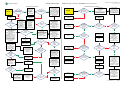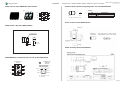
1
SEMC Troubleshooting Manual
K630 - V640 - K660
ABOUT
Troubleshooting Manual
TROUBLESHOOTING
MEASUREMENT POINTS COMPONENT OVERVIEW FUNCTIONAL OVERVIEW
K630 - V640 - K660
APPENDIX
1215-3608 rev. 1
1 (96)
ABOUT
SEMC Troubleshooting Manual
K630 - V640 - K660
Contents
ABOUT
The purpose of this document is to provide enhanced technical information for Sony Ericsson
repair technicians in order to assist during service, repair and troubleshooting operations on Sony
Ericsson mobile phones. It should be used as a complement to other repair instructions and tools
as notified by the local Sony Ericsson representative.
To search for components throughout the entire document use the “search” function in Adobe
Acrobat Reader 7.0 (or later version) and enter the component name or other word. Use zoom to
enlarge.
For easier navigation of the document you can use the bookmarks that appear in the Bookmarks
tab on the left side of the Adobe Acrobat Reader window. Each bookmark jumps to a page in the
document.
Disclaimer
This document is Sony Ericsson confidential and should be treated as confidential in accordance
with the agreement with Sony Ericsson. This document is intended for use by authorized service
technicians only. Sony Ericsson is not to be held responsible for any damages or losses caused
intentionally or unintentionally due to unauthorised use of the information in this document.
Revision History
Rev.
Date
Changes / Comments
1
06/20/2008
Initital revision.
ABOUT
General Information
Contents
2
2
2
TROUBLESHOOTING
Equipment List
On/Off Problems
Flash Problems
Dead Phone Problems
Display Problems
Display Illumination Problems
Key Problems
LED Problems
Main and VGA Camera Problems
Vibrator Problems
Charging Problems
USB/VBUS Charging Problems
SIM Problems
Memory Stick Problems
Audio Internal Problems
Audio External Problems
FM Radio Problems
Bluetooth Problems
GSM Network Problems
WCDMA Network Problems
System Connector Protection Test
Current Consumption Test
Battery and Current Calibration Test
Backup Capacitor Test
Charging Test - ASIC Revision Test
Reference Measurement Points
3
3
9
9
10
11
11
12
12
13
13
14
14
15
15
16
16
17
17
18
18
19
19
21
21
22
23
MEASUREMENT POINTS
Front Side
Back Side
Top Schematic
Application & System Performance Top
System Top
System Control - Clocks & Resets
System Memories
PoP IF
Power Top
Power Regulators & Charging
Power Camera
Power ASICs
Power Memories
Connectivity Top
Connectivity ADC & I2C
Connectivity Cards
24
24
25
26
27
28
29
30
31
32
33
34
35
36
37
38
39
Connectivity Connectivity
Connectivity Keypad
Imaging Top
Imaging Display
Imaging Camera
Access Top
Access GMS & UMTS
Access Bluetooth
Audio Top
Audio Analog
Audio Digital
FM Radio
Test
Squid RF Module - Radio Top
Squid RF Module - Radio Cont UMTS
Squid RF Module - Radio Duplex
Squid RF Module - Radio Top UMTS
Squid RF Module - Radio Receiver UMTS
Squid RF Module - Radio Synthesizer UMTS
Squid RF Module - Radio Power Amplifier UMTS
Thor RF Module - Top
Thor RF Module - GSM/EDGE Tx + FEM
Thor RF Module - GSM/EDGE Rx + Synth
40
41
42
43
44
45
46
47
48
49
50
51
52
53
54
55
56
57
58
59
60
61
62
ABOUT
General information
COMPONENT OVERVIEW
Front Side
Back Side
63
63
64
FUNCTIONAL OVERVIEW
Technical Description
Block Diagram Access
Block Diagram Application
65
65
75
76 ME
APPENDIX
Replaceable Parts
Components - B2100, B3100, L2200
Components - L2401-04, N1002, N1200
Components - N1210, N1400
Components - N2203, N2204, N2205
Components - N3100, N3101, S2400-03
Components - V2202, V2206, V2405
Components - V2420-21, V3101-10, V4201
Components - X1001-03, X1200, X1201-03
Components - X2200, X2402
Components - X2403, X2490, X4200, X4310
Components - X4300
Troubleshooting Software Documentation
Troubleshooting Fixture Setup Instructions
77
77
78
79
80
81
82
83
83
84
85
86
87
88
95
1215-3608 rev. 1
2 (96)
TROUBLESHOOTING
Equipment List
SEMC Troubleshooting Manual
K630 - V640 - K660
K630, V640 and K660 Equipment List
TRS Fixture Kit
K630 and V640
K630 and V640
Location: CSPN-Repair Instructions-Electrical- K630, V640 -Equipment List
TROUBLESHOOTING
K660
Location: CSPN-Repair Instructions-Electrical-K660 -Equipment List
Dummy Battery
K630 and V640
Location: CSPN-Repair Instructions-Electrical- K630, V640 -Equipment List
Part number: NTZ 112 533
K660
Location: CSPN-Repair Instructions-Electrical-K660 -Equipment List
Part number: NTZ 112 533
Instruments
Power Supply Channel 1 VBATT
Agilent 6632B or similar
Location: CSPN-Repair Instructions-Level: Mechanical-Tool Catalogue
Note: Additional information about the equipment used for TRS can be found in the Repair
Tools Catalogue on CSPN or on the following location: CSPN – Repair Instructions – Electrical –
K630, V640 – Equipment List.
K660
Instrument Settings:
Voltage: 3.8 Volt
Limiter: 2A
Note: During the calibration the accurate voltage from the VBATT must be within ±0.015 V. If
this is not fulfilled it will result in a faulty calibration. (For more information about
recommended power supply units, see the Repair Tool Catalogue on CSPN under the Mechanical
level. The Power Supply Channel 1 VBATT must allow reverse current.
Note: Maximal cable length between the Power Supply Channel 1 VBATT and the dummy
battery must be maximum 1m. The cable must have a capacity for at least 16A.
Note: It is very important to follow instrument settings instructions when performing the
Battery Calibration Test.
Power Supply Channel 2 DCIO/SEPI
Agilent 6632B or similar
Location: CSPN-Repair Instructions-Level: Mechanical-Tool Catalogue
Instrument Settings:
Voltage: 5.0 Volt
Limiter: 2A
Note: It is very important to follow instrument setting instructions when performing the
Current Calibration Test.
Note: Additional information about the equipment used for TRS can be found in the Repair
Tools Catalogue on CSPN or on the following location: CSPN – Repair Instructions – Electrical –
K660– Equipment List.
Oscilloscope
Tektronix TDS 2012 or similar
Location: CSPN-Repair Instructions-Level: Mechanical-Tool Catalogue
Digital Multimeter (DMM)
Fluke 83 or similar
1215-3608 rev. 1
3 (96)
TROUBLESHOOTING
Location: CSPN-Repair Instructions-Level: Mechanical-Tool Catalogue The 0, 64 mm Test Probes is recommended by Sony Ericsson when DMM is in use see picture 1. Picture 1
Equipment List
SEMC Troubleshooting Manual
K630 - V640 - K660
PC Package & PC Software
PC Package (Computer)
Location: CSPN-Repair Instructions-Level: Mechanical-Tool Catalogue
Urquell Fault Trace SW with project file
TROUBLESHOOTING
K630 and V640
Location: CSPN-Repair Instructions-Electrical-K630, V640-Trouble Shooting Application
Project File: K630, K660, V640 Project_R1A
Spectrum Analyzer
HP 8595E or similar
Location: CSPN-Repair Instructions-Level: Mechanical-Tool Catalogue
RF probe
HP 85024A or similar
Location: CSPN-Repair Instructions-Level: Mechanical-Tool Catalogue
Mobile Phone Tester
Yokogawa VC230 or similar
Location: CSPN-Repair Instructions-Level: Mechanical-Tool Catalogue
FM Signal Generator
Agilent E4433B or similar
Location: -
K660
Location: CSPN-Repair Instructions-Electrical-K660 -Trouble Shooting Application
Project File: K630, K660, V640 Project_R1A
Drivers
SEPI BOX Drivers
Location: EMMA III-Drivers-SEPI
SE Communication Interface SEPI BOX
Location: CSPN-Repair Instructions-Level: Mechanical-Tool Catalogue
Part number: LTN 214 1484
See Picture 3.
Picture 3
RF Adaptor
Adaptor 33 N-BNC-50-1
Adaptor to Signal Generator RF Output
See Picture 2
Location: Picture 2
1215-3608 rev. 1
4 (96)
TROUBLESHOOTING
Cables
USB Computer Cable
Location: CSPN-Repair Instructions-Level: Mechanical-Tool Catalogue
See Picture 4.
SEMC Troubleshooting Manual
K630 - V640 - K660
Power Cable RED to Power Supply Channel 1 VBATT
Maximum Length: 1m
Location: CSPN-Repair Instructions-Level: Mechanical-Tool Catalogue
Power Cable BLACK to Power Supply Channel 1 VBATT
Maximum Length: 1m
Location: CSPN-Repair Instructions-Level: Mechanical-Tool Catalogue
TROUBLESHOOTING
Picture 4
Equipment List
Customized Power Supply Channel 2 DCIO/SEPI Cable
To perform Current Calibration the phone must be supplied directly through the system
connector. Customize the cable according to following instructions:
STEP 1:
Take the CST-75 battery charger and cut off the charger according to Picture 7.
Picture 7
DSU-60/USB Cable
Location: CSPN-Repair Instructions-Level: Mechanical-Tool Catalogue
Part number: KRY 101 1413
RF Test Cable Flexible
Location: CSPN-Repair Instructions-Level: Mechanical-Tool Catalogue
Part number: RPM 119 885
See Picture 5.
Picture 5
Note: Cable length must be exact 1.3m.
STEP 2:
Connect the CST-75 charger Red or White wire to the Plus Output and the Black wire to the
Minus (GND) Output at Power Supply Channel 2 DCIO/SEPI according to Picture 8.
Picture 8
SEPI Interface Cable – A1
Location: CSPN-Repair Instructions-Level: Mechanical-Tool Catalogue
Part number: KRY 101 1119/1
See Picture 6.
Picture 6
1215-3608 rev. 1
5 (96)
TROUBLESHOOTING
STEP 3:
Cut off isolation material from inside of the charger plug according to Picture 9.
Equipment List
SEMC Troubleshooting Manual
K630 - V640 - K660
Power Supply Channel 2 DCIO/SEPI Cable Connection Setups
Correct DCIO/SEPI Cable setup when TRS Fixture is used.
Picture 9
Picture 12
TROUBLESHOOTING
STEP 4:
Connect DCIO and SEPI Interface Cable – A1 cables according to Picture 10.
Picture 10
Note: Example of DCIO/SEPI and K750 TRS Fixture Setup.
Correct DCIO/SEPI Cable setup when the Dummy Battery is used.
Picture 13
Wrong setup.
Picture 11
Picture 14
1215-3608 rev. 1
6 (96)
TROUBLESHOOTING
Equipment
Equip
ment List
SEMC Troubleshooting Manual
K630 - V640 - K660
Picture 15
Picture 18
TROUBLESHOOTING
STEP 1:
Use Cable according to Picture 15
STEP 4:
Use only wire connected to Pin2 and cut all other wires according to Picture 18. Use a digital multimeter instrument (DMM) and perform diode measurement to select the wire connected to Pin2 at hands free system connector plug. Customized FM Radio Cable
Product Name: Test lead BNC-4mm 1,5m Product Description: Test lead with 4 mm lab plugs at one end and a BNC plug at the other. Manufacturer: PMK Germany Location: http://www.elfa.se/en/ or other supplier. Part number: 46-310-40 (Note: This is ELFA part number)
STEP 2:
Cut the Red lab plug according to Picture 16
STEP 5:
Connect by soldering cable from Picture 16 and cable from Picture 18 according to Picture 19.
Picture 16
Picture 19
STEP 3:
Use any Portable Handsfree (PHF) Cable and cut according to Picture 17
Test Cards
Local SIM
Any functional Local SIM Card, see Picture 20
Picture 17
Picture 20
Note: Minimum Cable length 40 cm.
1215-3608 rev. 1
7 (96)
TROUBLESHOOTING
Equipment List
Test SIM GSM/UMTS
One Test SIM GSM/UMTS is needed to perform Current Consumption Test, see Picture 21.
Location: To buy a Test SIM GSM/UMTS, please contact your supplier of test equipment.
SMK RF Probe
Location: CSPN-Repair Instructions-Level: Mechanical-Tool Catalogue
Part number: SXA 109 6356
Picture 21
Picture 24
SEMC Troubleshooting Manual
K630 - V640 - K660
TROUBLESHOOTING
Sony Memory Stick M2
Any functional Memory Stick Micro M2 Card, see Picture 22
Picture 22
Rohde & Schwarz RF Shield Package (Box)
Location: CSPN-Repair Instructions-Level: Mechanical-Tool Catalogue
Picture 23
1215-3608 rev. 1
8 (96)
TROUBLESHOOTING
SEMC Troubleshooting Manual
K630 - V640 - K660
On/Off Problems - Flash Problems
On/Off problems
START
Flash problems
Is the phone
consuming more than
1mA when the phone
is powered off
Connect:
Dummy Battery connected
to VBATT
Go to
Dead phone
Problems part 1
Yes
Yes
Is it possible to
power on the phone
Yes
Is it possible to power
off the phone
Yes
Go to
Current
Consumption Test
After this go to
Charging Test.
Power up the phone
Connect USB plug
From PC
Download
ITP SW
By using EMMA
Passed
Yes
SL 5 Replace
D2020
SL 4 Escalate
Yes
3.8 Volt DC
at MP 107 (C2412)
VBATI
No
SL 5 Replace
C2412
SL 4 Escalate
SL 5 Replace
D2404
SL 4 Escalate
Yes
No
SL 5 Replace
C2413
SL 4 Escalate
No
No
Is the
phone consuming
any current when
powering on the
phone
Is the phones
behavior as normal
Optimized
charging
Connect a charger
No
Yes
Go to
Key problems
The phone
Indicate charging
on display
No
Yes
No
Is the current
consumption between
10mA to 70mA
Go to USB/VBUS
Charging problems
Go to
Dead Phone
Problems part 1
No
No
Press
2 and 5
Connect USB
Run Pre-config 1 and 2
Run DPY/Z
Successful
Flash
Yes
Yes
No
Go to
System Connector
Protection Test..
After this go to
Flash problems
Disconnect the
phone from
TRS Fixture
3.5 Volt DC
at MP 103 (C2418)
VREG
Yes
Yes
1.8 Volt DC
at MP 105 (C2413)
VDDE18
No
Flash
the phone with
correct CDA
software
CDA Software
Flash
Successful
No
Flash process
started
Max 35 Ohm between
MP 119 (X2400_Pin 10)
and MP 122 (R2432)
Max 35 Ohm between
MP 120 (X2400_Pin 11)
and MP 123 (R2431)
Yes
Yes
SL 5 Replace
D2404 if not Ok then
Replace D2000
SL 4 Escalate
No
SL 5 Replace
R2431 or R2432
SL 4 Escalate
Yes
No
Yes
Flash
The phone with
ITP software
successful
Yes
1. Customize the phone into DPY/Z
2. Startup the phone and wait for
the configuration to take place
(takes less than a minute)
3. Customize with correct CDA
4. Activate the phone
No
Yes
No
Go to
Flash problems
Problem
solved
No
Problem
solved
Yes
No
Replace
System Connector
X2400
Is the
R2431 and R2432
Ok
Problem
solved
No
Claim for a
SW Upgrade
Yes
SL 5 Replace
D2405
SL 4 Escalate
Yes
SL 5 Replace
D2405
SL 4 Escalate
Claim
System Connector
X2400
1215-3608 rev. 1
9 (96)
TROUBLESHOOTING
Step 1:
Perform System
Connector Protection Test
If successful go to step 2.
Step 2:
Phone with Normal SW
Use TRS Fixture
Connect:
Display and Keypad
Connect: VBATT
Try to Flash the phone by
using EMMA III SW
Flash process
starting
when using
EMMA
No
No
No
START
TROUBLESHOOTING
START
SEMC Troubleshooting Manual
K630 - V640 - K660
Dead Phone problems part 2
Dead Phone problems part 1
Step 1:
Try to recover the phone
using EMMA III SW
Press keys 2 and 5
Connect USB Cable
Run pre-config 1 or 2
Run DPY/Z
S2400
Not pressed
Using more than
1mA
current
No
K660: Replace B2100
K630/V640:
SL 5 Replace B2100
SL 4 Escalate
Keep S2400
Pressed or
Connect
DCIO/SEPI Cable
Dead Phone problems
Part 2
(Dead Phone Problems
Part 1 must be finished
before starting here)
VBT27
Voltage
Ok
Are any of
C2205,
N1400, C1409
Short circuit
No
K630/V640:
SL 5 Replace N1400
C2205 or C1409
SL 4 Escalate
K660:
SL 4 Replace N1400
SL 5 Replace
C2205 or C1409
SL 4 Escalate
Yes
Yes
Yes
Step 2:
Use TRS Fixture
Connect VBATT
NOTE:
Yes
32 kHz RTCCLK at
MP 43 (B2100_Pin7)
No
Yes
No
N1002 or N1210
getting hot
Yes
32 kHz RTCCLK at
MP 22 (ST2105)
SL 5 Remove
N2000
SL 4 Escalate
2.2 Volt at
MP 14 (B2100_Pin1
VDD_LP)
No
SL 5 Replace
N2000
SL 4 Escalate
SL 5 Replace
N2000
SL 4 Escalate
No
VDIG
Voltage
Ok
Are any of
C2215,C4213,
C1407, N1400
Short circuit
No
No
K630/V640:
SL 5 Replace
N1400, C2215,
C4213 or C1407
SL 4 Escalate
K660:
SL 4 Replace N1400
SL 5 Replace
C2215, C4213 or
C1407
SL 4 Escalate
Yes
Yes
No
Yes
Using more than
1 mA
current
No
Yes
SL 5 Replace
N2000
SL 4 Escalate
No
Try to trace the
faulty component
with freezing spray
SL 5 Replace
R2200
SL 4 Escalate
0 Volt
Between Power
Supply GND and
PBA GND
No
26 MHz
MCLK at
MP R2106
VCORE18
Voltage
Ok
No
Are any of
C2342 to C2347
or D2000
Short circuit
Yes
SL 5 Replace
Faulty Component
SL 4 Escalate
No
Yes
Yes
Yes
TROUBLESHOOTING
Try to trace the
faulty component
with freezing spray
Do NOT use
DCIO/SEPI Cable!
K660: Replace
N1002 or N1210
K630/V640: Replace
N1210 or
SL 5 Replace N1002
SL 4 Escalate
Dead Phone Problems
1.8 Volt DC at
MP 15 (ST2217)
SL 5 Replace
C2239
SL 4 Escalate
Yes
Check these voltages:
SL 5 Replace
N2000
SL 4 Escalate
Replace
N1200
2.6V MP 41 (ST2204 AUDIO26)
2.5V MP 34 (ST2203 VANA25)
2.7V MP 37 (ST2212 VBT27
2.7V MP 38 (ST2213 VDIG)
1.8V MP 15 (ST2217 VCORE18)
1.2V MP 12 (ST2221 VCORE12)
1.8V DC at
MP 33 (ST2208 VDDE18)
2.8V DC at
MP 36 (R2202
VccA)
No
Yes
SL 5 Replace
D2020
SL 4 Escalate
Try to recover the
phone using
SW Load ITP
Flash process
successful
Yes
Go to
Flash Problems
Yes
VCORE12
Voltage
Ok
No
SL 5 Replace
N2000
SL 4 Escalate
No
Yes
N2400
C2400, C2209,C2430,
C3135,C3136
Short circuit
No
Yes
MP 12 (ST2221)
Short circuit
To PBA GND
SL 5 Check
C2301 to C2305,
C2307,C2308,
C2311
C2313 to C2319
C2322,C2324,D2000
Yes
SL 5 Replace
Faulty Component
and L2200
SL 4 Escalate
No
No
AUDIO26
Voltage
Ok
Yes
Yes
Current
consumption more
than 50mA
Try to Recover the
Phone by
downloading
ITP SW
1.2 Volt DC at
MP 23 (V2206)
3.8 Volt DC at
MP 24 (L2201)
No
No
No
No
Yes
C2326, C2327,
C2328, C2329, C2330,
C2216,D2000
Short circuit
No
VANA25
Voltage
Ok
SL 5 Replace
N2000
SL 4 Escalate
Yes
Yes
Go to
Dead Phone
problems part 2
SL 5 Replace
C2238 and N2202
SL 4 Escalate
SL 5 Replace
N2202
SL 4 Escalate
Yes
Yes
SL 5 Replace
Faulty Component
SL 4 Escalate
No
All voltages
Ok
No
SL 4 Replace
N2400
SL 5 Replace
C2400, C2430,
C3135 or C3136
3.8 Volt DC at
MP 13 (ST2216)
No
SL 5 Replace
L2201
SL 4 Escalate
SL 4 Replace
V2206
SL 5 Replace
N2000
K630/V640:
SL 5 Replace
L2200
SL 4 Escalate
K660:
Replace L2200
1215-3608 rev. 1
10 (96)
TROUBLESHOOTING
SEMC Troubleshooting Manual
K630 - V640 - K660
Display Problems - Display Illumination Problems
Display Illumination problems
Display problems
START
No
Display Backlights
Ok
Yes
Step 1:
Use TRS Fixture and connect Display and
Keypad. If Display working properly at the
fixture then replace Display
If not then continue with the
Step 2:
Load ITP SW into the phone
Use TRS Fixture and connect Display
Connect: VBATT and DCIO/SEPI
Continue with the
Display problems TRS guide
START
Step 1:
Use TRS Fixture and connect Display and
Keypad. If Display working properly at the
fixture then replace Display
If not then continue with
Step 2:
Load ITP SW into the phone
Use TRS Fixture and connect Display
Connect: VBATT and DCIO/SEPI
Continue with the
Display illumination problems TRS guide
Fault trace SW
MMI
Misc
Activate:
Display Backlight
Display Backlights
Ok
1.8 Volt DC
at
MP 8 (ST4200
VDDE18)
Yes
SL 5 Replace
N2000
SL 4 Escalate
No
Flash the phone with
EMMA
SUCR SW
4.3V
Pk-Pk Pulses
(± 0.5V) at MP 21 (L4200)
short after Display
Backlight
Is set
Fault trace SW
MMI
Misc
Deactivate:
Display Backlight
Yes
2.7 Volt DC
at
MP 6 (ST4201
VDIG)
3.8 Volt DC at
MP 95 (TP4200)
Yes
Fault trace SW
MMI
Misc
Activate:
Display Backlight
Yes
Replace
X4200 or Display
15V Pk-Pk
Pulses at MP 95 (TP4200)
short after Display
Backlight
Is set
Yes
0 Volt DC at
MP 94 (TP4201) when
Display Backlight Is
On
No
Display
Ok
SL 5 Replace
N2000
SL 4 Escalate
No
Replace
X4200
No
No
No
Yes
SL 5 Replace
D2000
SL 4 Escalate
SL 5 Replace
V4200
SL 4 Escalate
Yes
No
TROUBLESHOOTING
Go to
Display illumination
problems
Fault trace SW
MMI
Display pattern
Init Screen Testing
Activate:
RGB Color Pattern
Yes
Claim Component
X4200
No
3.8 Volt DC at
MP 19 (V4201
Anode)
No
Yes
SL 5 Replace
V4206 or N2000
SL 4 Escalate
SL 5 Replace
L4201
SL 4 Escalate
Replace
V4201
1215-3608 rev. 1
11 (96)
TROUBLESHOOTING
Key problems
LED problems
START
SL 5 Replace
V2402
SL 4 Escalate
DMM Settings:
Problem with
Phone On
No
Yes
Yes
0 Volt
DC between
MP 83 (S2402 A) and
MP 82 (S2402
C)
No
Short
Circuit between
MP 83 (S2402 A)
MP 92 (PBA GND) and
MP 82 (S2402 C)
MP 92 (PBA
GND)
Problem with
Volume Up
key
Yes
Remove
S2402
More than
2.0 Volt DC between
MP 80 (S2403 A) and
MP 79 (S2403
C)
Yes
Yes
Replace
X2402
Press the
Volume Up key
S2403
Claim Component
X2402
No
0 Volt DC at
MP 78 (TP2003)
Yes
No
Yes
More than
1.7 Volt DC at MP 46
(V2409_Cathode)
Replace
S2402
No
Problem with
Lower Keypad LED
Yes
Yes
SL 5 Replace
D2000
SL 4 Escalate
0 Volt DC at
MP 77 (TP2004)
Yes
Replace
X2402
No
SL 5 Replace
N2000
SL 4 Escalate
No
Replace
S2400
0 Volt DC at
MP 18 (V4205_Pin 1)
No
More than
2.0 Volt DC between
MP 83 (S2402 A) and
MP 82 (S2402
C)
No
SL 5 Replace
D2000
SL 4 Escalate
Short
Circuit between
MP 80 (S2403 A)
MP 92 (PBA GND) and
MP 79 (S2403 C)
MP 92 (PBA
GND)
SL 5 Replace
D2000
SL 4 Escalate
Problem with
Upper Keypad LED
SL 5 Replace
V4205
SL 4 Escalate
Yes
0 Volt DC at
MP 78 (TP2003)
Yes
Replace
X2402
No
SL 5 Replace
N2000
SL 4 Escalate
Replace
S2402
Yes
Replace
V3109 or V3110
No
No
No
K660
0 Volt DC at
MP 20 (V4205_Pin 4)
More than
2.0 Volt DC between
MP 80 (S2403 A) and
MP 79 (S2403
C)
Yes
Replace
S2403
Flash with
EMMA SUCR SW
No
No
Problem with
Web Navigator LED
SL 5 Replace
V4205
SL 4 Escalate
Yes
Yes
Remove
S2403
No
Replace
X2402
SL 5 Replace
N2000
SL 4 Escalate
No
No
0 Volt DC
between
MP 80 (S2403 A) and
MP 79 (S2403
C)
No
Yes
No
Yes
Flash the Phone with
EMMA
SUCR SW
Problem
solved
SL 5 Replace
L2406, V2409
or N2000
SL 4 Escalate
Yes
Yes
Yes
If all Keypad LED working properly at the
TRS Fixture then replace Keypad
If not then continue with the
LED problems TRS guide.
Replace
V3107 or V3108
No
No
Problem
with all
Keypad LED
Yes
Remove
S2400
Yes
Problem
With all other
keys
Display
Backlight
Ok
Yes
No
Press the
Volume Down key
S2402
More than
2.0 Volt DC between
MP 83 (S2402 A) and
MP 82 (S2402
C)
No
0 Volt DC at MP 46
(V2409_Cathode)
Connect
the black probe
To PBA GND
more than 1.7 Volt DC at
MP 46 (V2409
Cathode)
Yes
No
No
Yes
No
Problem with
Volume Down
key
Go to
Display illumination
problems
TROUBLESHOOTING
Problem with
Phone Off
No
Press the On/Off
Key S2400
Diode
Measurement
START
Load ITP SW into the phone.
Use TRS Fixture and connect
Keypad and Display
Connect: VBATT and DCIO/SEPI
Use Fault Trace SW
MMI
Activate:
Display Backlight
Upper Keypad LED, Lower Keypad LED
Web Navigator LED
Replace
S2400
Step 1:
Use TRS Fixture and connect Display and
Keypad. Connect: VBATT
Perform Keyboard Test in Service Tests
If All Keys working properly at the
TRS Fixture then replace Keypad. If not then
disconnect VBATT and continue with the
Key problems TRS guide
Yes
SEMC Troubleshooting Manual
K630 - V640 - K660
Key Problems - LED Problems
Yes
SL 5 Replace
D2000
SL 4 Escalate
0 Volt DC at
MP 71 (TP2005)
Yes
Replace
X2402
No
SL 5 Replace
N2000
SL 4 Escalate
No
SL 5 Replace
V4205
SL 4 Escalate
Yes
0 Volt DC at
MP 16 (V4206_Pin 1)
1215-3608 rev. 1
12 (96)
TROUBLESHOOTING
Main and VGA Camera problems
Vibrator problems
START
Are there
problems with both
Main and VGA
Camera
Claim
VGA Camera
START
Go to
Service Tests and
Perform:
Main and VGA
Camera Test
Yes
VGA Camera
Ok
No
No
Load ITP SW into the
phone. Use TRS Fixture
and connect Display.
Main and VGA Camera
mounted on the PBA.
Connect VBAT and
DCIO/SEPI
Use Fault Trace SW
Perform Main and VGA
Camera Test
Escalate
PBA
Fault trace SW
MMI
Misc
Perform:
Main Camera Test
and
VGA Camera Test
Replace
VGA Camera
No
Is the
problem with
Main Camera
Main and VGA
Camera working
properly
No
Connection
Between PBA
GND and MP 86
(ST4206)
Ok
Yes
Flash with EMMA
SUCR SW
Yes
Clean Pad B4200 A
Clean Pad B4200 B
Yes
No
Activate:
Main Camera Test
again
Replace
Main Camera
TROUBLESHOOTING
Load ITP SW into the phone
Use TRS Fixture.
Connect: VBATT and DCIO/SEPI
Use Fault Trace SW and go to:
MMI-Misc
Activate:
Vibrator Test
If the Vibrator is working properly at the
TRS Fixture then replace Vibrator if not
Continue with the Vibrator problems TRS guide
Yes
Replace
X4300
SEMC Troubleshooting Manual
K630 - V640 - K660
Main and VGA Camera Problems - Vibrator Problems
Yes
2.8 Volt
Pk-Pk Pulses At
MP 49 (C4206
VIBR_OUT)
No
Is
MP 49 (C4206)
short circuit to
Ground
No
SL 5 Replace
N2000
SL 4 Escalate
Yes
Replace
X4310
1.8 Volt DC
at MP 47 (R2280
CAM_LDO_EN) and
MP 88 (TP4300
CAMRESn)
Main Camera
Ok
No
No
SL 5 Replace
D2000
SL 4 Escalate
No
Replace
N2204
No
Replace
N2203
SL 5 Replace
C4206, C4207,V4203
SL 4 Escalate
Yes
Yes
1.3 Volt DC
at MP 61 (TP2205
VCAMSD13)
Claim
Main Camera
Yes
SL 5 Replace
D2000
SL 4 Escalate
Retest
Main and VGA
Camera
13MHz at
MP 11 (L4202)
19MHz at MP 84
(ST4312) and MP 1
(ST4314)
No
Yes
2.8V DC at MP 59
(TP2206 VCAMSD28)
1.8V DC at MP 58
(TP2207 VCAMSD18)
Yes
1215-3608 rev. 1
13 (96)
TROUBLESHOOTING
Charging problems
Use TRS Fixture and
Fault Trace SW
Connect:
VBATT and
DCIO/SEPI
Start
Battery Calibration
Current Calibration
Passed
Yes
Yes
START
5 Volt DC at
MP 25 (ST2201)
Is
MP 87 (TP2202)
Short circuit to
PBA GND
Yes
Step 1:
Perform System Connector Protection Test
If step 1 is Ok then continue with step 2.
Connect
DSU-60/USB Cable
from PC to
the phone
Step 2:
Use Phone with Normal SW
Use TRS Fixture
Connect: VBATT
Yes
SL 5 Replace
N2000
SL 4 Escalate
Yes
SL 5 Replace
D2405
SL 4 Escalate
Yes
SL 5 Replace
R2409
SL 4 Escalate
SL 5 Replace
N2000
SL 4 Escalate
No
TROUBLESHOOTING
Step 1:
Perform System Connector Protection Test
If successful go to step 2.
Step 2:
Load ITP SW into the phone
Connect: Dummy Battery
Connect:VBATT and DCIO/SEPI
Use Fault Trace SW:
Logic, Phone Power
Perform
Battery and Current Calibration
It is very important to follow
instrument settings instructions when performing
the Battery and Current Calibration Test.
Yes
Is the
3.2V and 4.1V DC
at MP 89 (TP2200)
during Battery
Calibration
SEMC Troubleshooting Manual
K630 - V640 - K660
USB/VBUS Charging problems
START
Battery Calibration
Passed
No
Charging Problems - USB/VBUS Charging Problems
No
No
No
Replace
X2200
Use TRS Fixture
Fault Trace SW
Connect:
VBATT and
DCIO/SEPI
SL 5 Replace
R2200
SL 4 Escalate
Flash the phone with
EMMA SUCR SW
and go to
Charging Test
D2405
Getting hot
Replace
System Connector
X2400
No
No
No
5 Volt DC at
MP 126 (C2201)
DCIO
Is
Connection
between PBA GND
and Power Supply
VBATT GND
Ok
No
5 Volt DC at
MP 76 (R2409)
No
Yes
Yes
Start
Current Calibration
(C.C.)
Yes
SL 5 Replace
N2000
SL 4 Escalate
Phone
consuming more
than 10mA
Charger (DCIO)
Current
Yes
The Phone
Consuming
DCIO Current
No
(During Current
Calibration)
MP 28 (C2241
DCIO_INT)
Higher than
3,8 Volt DC
Replace
System Connector
X2400
SL 5 Replace
C2423 and C2424
SL 4 Replace
V2421
No
Yes
Yes
Is
R2201
0.3 Ohm
Disconnect
VBATT and DCIO/SEPI
Yes
MP 126 (R2201
CHSENSEP) Higher
than 3,8 Volt DC
(During C.C.)
SL 5 Replace
N2000
SL 4 Escalate
No
No
SL 5 Replace
R2201
SL 4 Escalate
Replace
V2202
Yes
MP 109
(V2202_Pin 2
CHREG) Lower than
MP 28 (C2241)
(During C.C.)
No
1215-3608 rev. 1
14 (96)
TROUBLESHOOTING
SIM Problems - Memory Stick Problems
SEMC Troubleshooting Manual
K630 - V640 - K660
Memory Stick problems
SIM problems
START
Flash the Phone
with EMMA
SUCR SW
Sim Com Test
Passed
Yes
Remove Test SIM
Disconnect:
Dummy Battery
Use TRS Fixture
and
Fault Trace SW
Load ITP SW into the phone.
Connect:
Dummy Battery to VBATT
Insert Test SIM
Connect:
DCIO/SEPI
Use Fault Trace SW
Fault Trace SW
Logic
SIM Card control
Activate:
SIM Com Test
Load ITP SW into the phone
Use TRS Fixture
Connect :
VBATT and DCIO/SEPI
Insert Memory card
Use Fault Trace SW
Fault trace SW
Logic
SIM Card Control
Activate:
Memory Stick Test
No
Is
X2490
damaged
START
Yes
TROUBLESHOOTING
No
Memory Stick Test
Passed
Activate:
SIMVCC
1.8 Volt DC at
MP 98 (X2403_Pin 1)
No
1.8 Volt DC at
MP 99 (C2411)
Yes
K630/V640:
SL 5 Replace X2403
SL 4 Escalate
K660:
Replace X2403
Yes
SL 5 Replace
C2406 or C2411
SL 4 Escalate
Yes
Are any of
C2406 or C2411
Short circuit
No
SL 5 Replace
N2000
SL 4 Escalate
0 Volt DC at
MP 32 (R2406
MSDETECT)
No
Replace
X2490
No
SL 5 Replace
N2000
SL 4 Escalate
No
SL 5 Replace
D2000
SL 4 Escalate
Yes
Yes
Flash the phone with
EMMA
SUCR SW
No
SIMVCC on
Activate:
SIMRST
No
1.8 Volt DC
at MP 35 (ST2202)
VMC18 only 30 sec
after card has been
inserted
Yes
Replace
X2490
1.8 Volt DC at
MP 100 (X2403_Pin 2)
No
1.8 Volt DC at
MP 104 (C2410)
Yes
Yes
SIMVCC on
SIMRST on
Activate:
SIMCLK
K630/V640:
SL 5 Replace X2403
SL 4 Escalate
K660:
Replace X2403
No
Is
C2410
Short circuit
Yes
SL 5 Replace
C2410
SL 4 Escalate
Problem solved
No
Yes
Yes
Claim Component
X2490
1.0 Volt DC at
MP 102 (X2403_Pin 3)
No
1.0 Volt DC at
MP 30 (ST2400)
No
SL 5 Replace
N2000
SL 4 Escalate
Yes
SIMVCC on
SIMRST on
SIMCLK on
Activate:
SIM DATA
1.8 Volt DC at
MP 97 (X2403_Pin 7)
No
Yes
K630/V640:
SL 5 Replace X2403
SL 4 Escalate
K660:
Replace X2403
No
MP 96
(X2403_Pin 5)
Connected to the
PBA GND
1.8 Volt DC at
MP 29 (ST2401)
Yes
SL 5 Replace
N2000
SL 4 Escalate
No
Yes
10 Kohm between
MP 98 (X2403_Pin1)
(Red Probe) and MP 97
(X2403_Pin 7)
(Black Probe)
Yes
K630/V640:
SL 5 Replace X2403
SL 4 Escalate
K660:
Replace X2403
No
SL 5 Replace
R2419
SL 4 Escalate
SL 5 Replace
N2000
SL 4 Escalate
1215-3608 rev. 1
15 (96)
TROUBLESHOOTING
Audio Internal problems
Yes
2.6 Volt DC
At MP 121 (V2420)
No
Audio External problems
Go to
Audio External
Problems
SL 4 Replace
V3101 or V3102
SL 5 Replace
L3103 or L3104
SL 5 Replace
R2440
SL 4 Escalate
No
START
2.6 Volt DC
At MP 17
(V2405_Pin 3)
No
Replace
V2405
Yes
Fault Trace SW
Audio and FM Radio
Audio Loop test
Audio Input: Mic1
Loop Mode: Analog
Audio Output:
Earphone
Apply Audio Loop
Whistle into the
PBA Mic
Yes
0 Volt DC
At MP 17
(V2405_ Pin 3)
No
More than
100m Volt AC Pk-Pk at
MP 4 (L3103 BEARP)
and MP 5 (L3104
BEARN)
Replace
N2400
Yes
No
Yes
0 Volt DC
on both side
of MP 7 (R2456)
No
More than
100mVolt AC Pk-Pk at
MP 108 (TP3101)
SL 5 Replace
D2000
SL 4 Escalate
Fault Trace SW
Audio and FM Radio
Audio Loop test
Audio Input: Mic1
Loop Mode: Analog
Audio Output:
Loudspeaker
Apply Audio Loop
Whistle into the
PBA Mic
Fault Trace SW
Logic
GPIO Manager
Access:
Set GPIO_07 to Low
Application:
Set GPIO_01 to Low
Yes
SL 5 Replace
N2000
SL 4 Escalate
2.2 Volt DC
At MP 39 (R3131)
Yes
Step 1: Perform
System Connector Protection
Test
Step 2:
Load ITP SW into
the phone.
Use TRS Fixture
Connect: VBATT and DCIO/SEPI
Use Fault Trace SW
Audio Internal
Tested
No
More than
100mV AC Pk-Pk
At MP 117 (L2403 SPL)
and MP 118 (L2404 SPR)
When whistle in to the
AUX mic
Yes
Are any of
L2403 or L2404
damaged
Yes
No
More than
100mV AC Pk-Pk At
MP 125 (C3113) and
MP 101 (C3120)
Replace
B3100
No
Are any of
V3103 and V3104
Short circuit
Yes
No
L2401
Ok
No
Replace
V3103 or V3104
Replace
L2401
Replace
System Connector
X2400
Yes
Yes
SL 5 Replace
N2000
SL 4 Escalate
Replace
N3101
Yes
Is MP 115
(X2400_Pin 3
connected to MP 113
(L2401)
Replace
L2403 or L2404
Replace
System Connector
X2400
No
Yes
Go to
Audio Internal
problems
Flash the phone
with EMMA
SUCR SW
Yes
No
More than
100mVolt AC Pk-Pk
At MP 50 (X3102) and
MP 51 (X3103)
SL 5 Replace
L3108 and L3109
SL 4 Escalate
Yes
No
More than
100mV AC Pk-Pk at MP
124 (C3124 MICP_int)
and MP 110 (C3125
MICN_int)
No
No
Yes
Disconnect
DCIO/SEPI cabel
Insert PHF set
Talk into the AUX
mic
Can you
hear at AUX
earphone when you
speak into the
AUX mic
START
Fault trace SW
Audio and FM Radio
Audio Loop Test
Audio Input: AUX1
Loop Mode: Analog
Audio Output:
AUX Earphone
Apply Audio Loop
TROUBLESHOOTING
Step 1: Perform
System Connector Protection Test
Step 2:
Use TRS Fixture connect Display and
Keypad. Connect VBATT and perform
Audio Service Tests. If all Audio
Service Tests working properly at the
fixture then replace Loudspeaker or
Earphone
If not then
Load ITP SW into the phone.
Use TRS Fixture.
Connect VBATT and DCIO/SEPI
and continue with the Audio internal
problems TRS guide
More than
100m Volt AC Pk-Pk
at MP 3 (X3100) and
MP 2 (X3101)
Yes
SEMC Troubleshooting Manual
K630 - V640 - K660
Audio Internal Problems - Audio External Problems
No
Yes
No
1.9 Volt DC
At MP 48 (TP3104)
and MP 53 (TP3105)
No
1.9 Volt DC
At MP 50 (X3102)
and MP 51
(X3103)
Yes
More than
100mVolt AC Pk-Pk
At MP 44 (C3137) and
MP 45 (C3123)
No
SL 5 Replace
N2000
SL 4 Escalate
Is MP 116
(X2400_Pin 4)
connected to MP 114
(L2402)
No
L2402
Ok
No
Replace
System Connector
X2400
Yes
No
Yes
Are any of
V3105, V3106
C3137 and C3123
short circuit
No
Yes
SL 4 Replace
V3105 or V3106
SL 5 Replace
C3137 or C3123
1.8 Volt DC
At MP 27 (R3137
AMPCTRL)
Yes
No
Replace
N3100
SL 5 Replace
D2000
SL 4 Escalate
Yes
2.2 Volt DC at
MP 75 (C3169)
Yes
No
Replace
L2402
Replace
N3101
SL 5 Replace
N2000
SL 4 Escalate
1215-3608 rev. 1
16 (96)
TROUBLESHOOTING
FM Radio problems
Replace
N3101
PHF
working properly
during
Voice call
No
SL 5 Replace
N2000
SL 4 Escalate
Bluetooth problems
START
Speaker and
FM Radio Tests
working properly
Yes
SEMC Troubleshooting Manual
K630 - V640 - K660
FM Radio Problems - Bluetooth Problems
Go to
Service Tests and
Perform:
Speaker and FM Radio Test
Flash the phone with the
EMMA SUCR SW and retest the phone.
If successful claim SW Flashing
If not then continue with
Bluetooth problems TRS guide.
Yes
No
Disconnect:
DCIO/SEPI Cable
Connect:
Customized FM Radio Cable
Black Lab Plug to
TRS Fixture GND Input and
PHF Connector to the Phone
System Connector
Signal Generator
Instrument Settings:
Yes
3.8 Volt DC
at MP 68 (C3304)
and 1.8V at MP 65
(C3305)
Change the
Bluetooth channels
In Fault Trace SW
and test the output.
Load ITP SW
into the phone.
Use TRS Fixture
Connect VBATT and
DCIO/SEPI
Use Fault Trace SW
Fault trace SW
TX and RX
Bluetooth
Channel 0
Set MaxPwr MOD 0
Use
Spectrum Analyzer
Instrument settings:
Frequency: 2402 MHz
Span: 1MHz
Amplitude: -5dBm
Use Peak Search
K630/V640:
SL 5 Replace
N1400
SL 4 Escalate
K660:
Replace
N1400
Use
Spectrum Analyzer
Span 10MHz
Use Peak Search when
changing the channel.
No
Yes
All channels
passed
Note:
1MHz channel spacing
Is
MOD 1 Freq.
minimum 230 KHz
higher then
MOD 0 Freq.
No
No
Yes
SL 5 Replace
N2000
SL 4 Escalate
TROUBLESHOOTING
Fault trace SW
Audio and FM Radio
FM Radio
Audio Output
Loudspeaker
Frequency:
According to
Instrument Settings
Set FM Radio
K630/V640:
SL 5 Replace
N1400
SL 4 Escalate
K660:
Replace
N1400
START
Load ITP SW
Into the phone
Use TRS Fixture
Connect:
VBATT and DCIO/SEPI
Use Fault Trace SW
Yes
Replace
System Connector
X2400
and clean
X2400 Pins 13 and 14
at PBA
-20dBm at
MP 112 (X2400_Pin 14
BT_ANT)
(±5dBm)
No
Frequency:
Use free Freq. Channel
Example:
103 MHz in Sweden
Any Signal
at MP 112
(X2400_Pin 14)
BT_ANT
Amplitude: 25.0 uVrms
FM Dev:
+/-22.5 kHz
FM Rate: 1kHz
Yes
Fault Trace SW
TX and RX
Bluetooth
Channel 0
Set MaxPwr MOD 1
Use Spectrum Analyzer
with the previous
instrument settings
-10dBm at
MP 74 (Z1400_Pin 1)
(±5dBm)
Yes
SL 5 Replace
C1401 and L1403
SL 4 Escalate
No
K630/V640:
SL 5 Replace
N1400
SL 4 Escalate
K660:
Replace
N1400
No
SL 4 Replace
C3145 or C3146
Any signal at
MP 42 (C3145)
MP 40 (C3146)
No
-10dBm at
MP 72 (Z1400_Pin 5) and
MP 70 (Z1400_Pin 7)
(±5dBm)
No
SL 5 Replace
N1400
L3300 and C3303
SL 4 Escalate
Yes
Yes
Can you
hear 1KHz tone at
TRS Fixture
Loudspeaker
Yes
No
Replace
System Connector
X2400
SL 5 Replace
N2000
SL 4 Escalate
Signal Ok
Yes
No
Claim
System Connector
X2400
SL 5 Replace
R2405,L3301,L2400
SL 4 Escalate
26 MHz Signal
At MP 10 (R2118
BT_CLK)
No
Yes
2.7 Volt DC at
MP 37 (ST2212
VBT27)
More than
60KOhm between
MP 10 (R2118) and
PBA GND
Yes
Yes
No
SL 5 Replace
N2000
SL 4 Escalate
Yes
SL 5 Replace
D2105
SL 4 Escalate
K630/V640:
SL 5 Replace
N1400
SL 4 Escalate
K660:
Replace
N1400
No
1.8 Volt DC
At MP 33 (ST2208
VDDE18) and 2.7 Volt DC
at MP 38 (ST2213
VDIG)
SL 5 Replace
Z1400
SL 4 Escalate
No
SL 5 Replace
N2000
SL 4 Escalate
K630/V640:
SL 5 Replace
N1400
SL 4 Escalate
K660:
Replace
N1400
1215-3608 rev. 1
17 (96)
TROUBLESHOOTING
GSM Network problems
0 Ohm between
MP 85 (R1208) and
MP 81 (R1202)
START
No
Is
Max Pwr 23dBm
Ok
(±3dBm)
Yes
2.8 Volt DC
at MP 36 (R2202
VccA)
SL 5 Replace
N2000
SL 4 Escalate
No
Instrument
Settings:
System Mode:
TX/RX Tester Mode
(WCDMA)
Downlink Channel:
10562
Measurement
Mode: Repeat
Correction: 1.6 dB
Perform RSSI Test at
GSM 900, 1800 and 1900 Band
Instrument Settings
System Mode:
TX/RX Tester Mode (GSM)
GSM BAND:
E-GSM 900, Channel 124
E-GSM 900, Channel 975
DCS 1800, Channel 512
PCS 1900, Channel 512
RF Power ON: -60 dBm
Correction: -1.6 dBm
Measurement Mode:
Repeat,CW
Yes
Yes
No
Fault Trace SW
TX and RX GSM
GSM Mode Settings:
RX Switched
GSM Radio Settings:
Select Band :GSM 850
Channel: 128
GSM RSSI Measurements:
Start RSSI Test
RSSI Test
Passed
No
START
Yes
Fault Trace SW
TX and RX GSM
GSM Mode Settings:
TX Switched
GSM Radio Settings:
Select Band : GSM 850
Channel : 128
Power Level: 5
Instrument Settings:
System Mode:
TX/RX Tester Mode (GSM)
GSM BAND: GSM850
Measurement Mode:
Repeat, Burst
Correction: 1.6 dB
Yes
Go to
SERP Calibration
Signal at
MP 91 (Z1001)
-10dBm
(±5dBm)
Is
measured value
±5dBm
No
Yes
Yes
Replace
N1200 Thor
Yes
No
K630/V640:
SL 5 Replace N1002
SL 4 Escalate
K660:
Replace N1002
(Inside Thor)
No
SL 5 Replace
D2000
SL 4 Escalate
1.8Volt
DC at MP 55
(R2299 DCDC_EN)
And 1.8V at MP 60 (C417
WPA0_EN)
(squid)
No
Yes
Instrument Settings:
System Mode:
TX/RX Tester Mode
(GSM)
GSM BAND: DCS1800
Measurement Mode:
Repeat, Burst
Correction: 1.6 dB
No
Fault Trace SW
TX and RX GSM
GSM Mode Settings:
TX Switched
GSM Radio Settings:
Select Band : GSM 1800
Channel : 512
Power Level: 0
Yes
No
Spectrum Analyzer
Instrument settings
Measure with RF
Probe
TX Freq. 1710.2MHz
Span: 300KHZ,
Amplitude: -5dBm
Replace
N1200 Thor
Is the
measured value
30dBm
(±3dBm)
No
Fault Trace SW
Switch GSM Mode
Settings to:
TX Static
3.4V-3.8V DC at
MP 57 (R2210
VBATI)
No
Replace
N2205
Instrument Settings:
System Mode:
TX/RX Tester Mode
WCDMA
Downlink Channel:
BAND I: 10562
Measurement Mode:
Repeat
Correction: 1.6 dB
Go to
SERP Calibration
1.2V-1.8V DC at
MP 54 (R2221
WPAVCC)
Yes
No
Is
measured value
±5dBm
No
Yes
SL 5 Replace
N2000
SL 4 Escalate
Current
consumption
between
450 – 650 mA
2.7V-2.8V at
MP 36 (R2202 VccA)
1.8V at MP 33 (ST2208
VDDE18)
No
No
Max Pwr.
23dBm
Ok
(±3dBm)
Yes
Replace
N1200
26MHz at
MP 62 (C511 WBCLK)
(inside Squid)
No
Yes
Go to
SERP Calibration
No
Yes
Replace
N1210
Instrument Settings:
System Mode:
TX/RX Tester Mode
WCDMA
Downlink Channel:
BAND I: 10700
Measurement Mode:
Repeat
RF Power ON: -60 dBm
Correction: - 1.6 dBm
Go to
SERP Calibration
Replace
N1210
No
Replace
Faulty Component
Are any of
X1201,X1202, X1203
X1001,X1002,X1003
damaged
Yes
Yes
Go to
WCDMA Network
problems
3.1V-3.3V DC at
MP 56 (L2207
VCC_WPA)
Yes
Yes
Is
measured value
33dBm
(±3dBm)
Yes
1.4V-1.6V
Pk-Pk pulses at
MP 93 (R1000
VAPC)
Go to
SERP Calibration
Yes
Fault Trace SW
TX and RX WCDMA
Radio Settings:
Select Band: BAND I
Fast Select Channels:
Ch LOW
Modes: Max Pwr 23dBm
Replace
N1200
No
Fault Trace SW
Switch GSM Mode
Settings to:
TX Static
Load ITP SW
into the phone.
Use TRS Fixture
Connect:
VBATT: 3.8V, Limiter 3A
DCIO/SEPI: 5V, Limiter 2A
Use Fault Trace SW
SL 5 Replace
R2210
SL 4 Escalate
No
Replace
N1200 Thor
Spectrum Analyzer
Instrument settings
Measure with RF
Probe
TX Freq. 824.2MHz
Span: 300KHz,
Amplitude: -5dBm
Signal at
MP 90 (L1006)
-12dBm
(±5dBm)
0 Ohm
between
MP 85 (R1208) and
MP 81 (R1202)
Replace
X1200
No
Fault Trace SW
TX and RX WCDMA
Radio Settings:
Select Band:
BAND I
Fast Select
Channels:
Ch LOW
Modes:
Max Pwr 23dBm
All Bands
Passed
RSSI Test
WCDMA Network problems
Connect Mobile Phone
Tester
Instrument Settings:
System Mode:
TX/RX Tester Mode (GSM)
GSM BAND: GSM850
RF Power ON: -60 dBm
Correction: -1.6 dBm
Measurement Mode:
Repeat, CW
Go to
GO-NOGO
Test
No
Yes
Phone report
correct value
(±5dBm)
Fault Trace SW
TX and RX WCDMA
Radio Settings:
Select Band : Band I
Fast select channels:
Ch MID
Modes: Read RSSI
RX On:
Read Measurement
1215-3608 rev. 1
18 (96)
TROUBLESHOOTING
Replace
X1200
Yes
Load the ITP SW
into the phone.
Use fixture
Connect 3.8V
Limiter 2A
Use
Fault Trace SW
SEMC Troubleshooting Manual
K630 - V640 - K660
GSM Network Problems - WCDMA Network Problems
TROUBLESHOOTING
System Connector Protection Test - Current Consumption Test
SEMC Troubleshooting Manual
K630 - V640 - K660
Current Consumption Test
System Connector Protection Test
Perform Diode and Ohm measurements with a Multimeter Connect the black probe at ground (Pin 9 on the system connector, X2400)
Step 1:
Insert Local SIM Card and use the phone with the Normal SW (SSW) and dummy battery connected to
Power Supply Channel 1 VBATT according to Picture 1. Instrument settings: Voltage: 3.8 Volt, Limiter 3A. Picture 1
Pin 9GND Pin 12
Pin 1
Pin at
X2400
Diode
Measurements
/ Volt
Ohm
Measurements
/ Ohm
SL 4 Action
SL 5 Action
1
0L
27K
No Action
D2405 if lower than 27KΩ
R2433 if higher than 27KΩ
2
0.0
1.4
No Action
L2400 and L3301
If higher than 1.4Ω
3
2.0
12K
4
1.0
1K
5
0.0
82
6
7
0.0
0L
82
0L
N3101 if lower than
12KΩ L2401 if higher
than 12KΩ
N3101 if lower than
1KΩ L2402 if higher
than 1KΩ
N3101 if lower than
82Ω L2403 if higher
than 82Ω
N3101 if lower than
82Ω L2404 if higher
than 82Ω
Not connected
8
9
1.4
0
1.5K
0
V2420 if lower than
1.5KΩ
No Action
10
0L
430K
No Action
11
0L
470K
12
0L
80K
No Action
V2421 if lower than
80KΩ
Current consumption in off mode should be less than 1mA. If more than 1mA go to Dead Phone problems part 1 TRS guide. Step 2:
Start the phone: L2407 If higher than 12KΩ
L2408 if higher than 1KΩ
L2410 if higher than 82Ω
L2409 if higher than 82Ω
Not connected
L2405, R2440, R2436
if higher than 1.5KΩ
No Action
D2405 if lower than 430KΩ
R2432 if higher than
430KΩ
D2405 if lower than
470KΩ R2431 if higher
than 470KΩ
Measure the deep sleep current max 6mA typical between 0-3mA.
Make sure that the operator is running with deep sleep. (This operation can be switched off by operator if
the network is busy). If the phone is using more than 6mA, then go to EMMA III and perform Software Update Contents Refresh (SUCR).
Step 3 with Mobile Phone Tester Instrument
Insert Test SIM Card and use the phone with the Normal SW (SSW) and dummy battery connected to Power Supply Channel 1 VBATT according to Picture 1. Instrument settings: Voltage: 3.8 Volt, Limiter 3A. Use the Mobile Phone Tester Instrument in signalling mode directly connected to the phone with the RF Connector or use Shield Box if not possible. Phone Display must be on during these tests to get correct
current measurements. Perform Radio TX measurements at GSM and WCDMA Band and compare the result with limits according to the text below. Transmitter
Transmitter
Transmitter
Transmitter
Transmitter
current
current
current
current
current
850 MHz at Ch: 128 power level 5. Typical 400mA
900 MHz at Ch: 1 power level 5. Typical 385mA
1800 MHz at Ch: 512 power level 0. Typical 365mA
1900 MHz at Ch: 512 power level 0. Typical 365mA
WCDMA BAND I Low RX Ch: 10562 at 23dBm output power Max 850mA
If the current consumption is not correct, the fault could be fixed by running SERP calibration if not then go to GSM and WCDMA Network problems TRS guides. If the current consumptions are equal to test limits then go to Charging Test.
1215-3608 rev. 1
19 (96)
TROUBLESHOOTING
Measure the current when the Phone is off. Check the current consumption at Power Supply Channel 1 VBATT.
TROUBLESHOOTING
Step 4 with Fault Trace SW application:
-
Flash the phone with ITP SW
Use the TRS Fixture
Connect the:
Power Supply Channel 2 DCIO/SEPI
Instrument settings: Voltage: 5 Volt, Limiter 2A
-
Connect DCIO/SEPI Cable to the phone
-
Max TX Power WCDMA BAND I
Fault Trace SW settings:
TX and RX WCDMA Radio Settings: Select Band: BAND I Fast Select Channels: Ch LOW Modes: Max Pwr 23dBm Compare the current consumption during Max TX Power Tests with the current consumption limits below.
Max TX Power GSM 850 MHz
Transmitter
Transmitter
Transmitter
Transmitter
Transmitter
Fault Trace SW settings:
Tolerance: ±10%
TX and RX GSM
GSM Mode Settings:
TX Switched
GSM Radio Settings:
Select Band: GSM 850
Channel: 128
Power Level: 5
If the current consumption is not correct, the fault could be fixed by running SERP calibration. If it does not
work then go to GSM and WCDMA Network problems TRS guides.
Perform the following tests:
-
-
SEMC Troubleshooting Manual
K630 - V640 - K660
current
current
current
current
current
GSM 850 MHz at Ch: 128 power level 5. Typical 175mA
GSM 900 MHz at Ch: 1 power level 5. Typical 185mA
GSM 1800 MHz at Ch: 512 power level 0. Typical 170mA
GSM 1900 MHz at Ch: 512 power level 0. Typical 145mA
in WCDMA BAND I RX Ch Low: 10562 Max power level 23 dBm and Rx on 575mA
If the current consumptions are equal to the sheet go to Charging Test.
Max TX Power GSM 900 MHz
Fault Trace SW settings:
TX and RX GSM
GSM Mode Settings:
TX Switched
GSM Radio Settings:
Select Band: GSM 900
Channel: 1
Power Level: 5
-
Max TX Power GSM 1800 MHz
Fault Trace SW settings:
TX and RX GSM
GSM Mode Settings:
TX Switched
GSM Radio Settings:
Select Band: GSM 900
Channel: 512
Power Level: 0
-
Max TX Power GSM 1900 MHz
Fault Trace SW settings:
TX and RX GSM
GSM Mode Settings:
TX Switched
GSM Radio Settings:
Select Band: GSM 900
Channel: 512
Power Level: 0
1215-3608 rev. 1
20 (96)
TROUBLESHOOTING
Power Supply Channel 1 VBATT:
Instrument settings: Voltage: 3.8 Volt, Limiter 3A
Current Consumption Test
TROUBLESHOOTING
SEMC Troubleshooting Manual
K630 - V640 - K660
Battery and Current Calibration Test - Backup Capacitor Test
Backup Capacitor Test
Battery and Current Calibration Test
To perform this test use:
Use the Phone with the ITP SW
-
Phone with the ITP SW
Power Supply Channel 1 VBATT:
X Volt according to the Fault Trace SW Test Instructions: Fault Trace SW-Logic-Phone Power-Battery Calibration and follow test instructions. Limiter: 2A. -
Power Supply Channel 1 VBATT: Instrument settings: Voltage: 3.8V, Limiter: 2A
-
Power Supply Channel 2 DCIO/SEPI: Instrument settings Voltage: 5V, Limiter: 2A
Power Supply Channel 2 DCIO/SEPI:
5.0 Volt
Limiter: 2A
TROUBLESHOOTING
Instrument settings for the Battery Calibration Test
This test should be preformed in 3 steps:
Step1:
If the test Is performed at the Core Level then use dummy battery according to the Equipment
List. If the TRS Fixture is used no dummy battery is needed.
Note: Maximal cable length between Power Supply Channel 1 VBATT and the dummy battery
or the TRS Fixture must be 1m. The cable must have a capacity for at least 16A.
Limits Table for the Battery Calibration Test
Voltage Level on VBATT
Min
Max
3.2 Volt
263
351
3.2 Volt
107
15F
4.1 Volt
789
877
4.1 Volt
315
36D
UNIT
mV
HEX
mV
HEX
Measure the voltage at the Backup capacitor by using Fault Trace SW- Logic - ADC Values –
Read ADC Value (Reading 1).
Step2:
This step should be done 30 seconds after Step 1. Measure the voltage at the Backup capacitor
by using Fault Trace SW - Logic – ADC Values - ADC Channels – Read ADC Value
(Reading 2).
Step3:
Compare the difference between Reading 1 and Reading 2 with the reference table below. If the
Reading 1 value is between 50 and 680 go to Interval 1, if between 681 and 800 go to Interval
2, if between 801 and 880 go to Interval 3 and compare with the Reading 2 – Reading 1 Min and
Max Limits.
Reference Table:
Instrument settings for the Current Calibration Test
If the test is performed at the Core Level then use dummy battery according to the Equipment
List. If the TRS Fixture is used no dummy battery is needed.
Note: The Power Supply Channel 1 VBATT must allow reverse current.
Absolute readout Reading 1
Min
Max
Unit
50
880
Dec
Note: Maximal cable length between Power Supply Channel 1 VBATT and the dummy battery
or the TRS Fixture must be 1m. The cable must have a capacity for at least 16A.
Note: Length of the Power Supply Channel 2 DCIO/SEPI customized cable must be exactly
1,3m.
Power Supply Channel 1 VBATT:
3.8 Volt
Limiter 2A
Power Supply Channel 2 DCIO/SEPI:
5.0 Volt
Limiter: 2A
Limits Table for the Current Calibration Test
Measured Current
Name
Min
100mA
DCIO Current
50
800mA
DCIO Current
725
Max
150
875
Unit
mA
mA
Reading 1 (Dec)
Reading 2 – Reading 1 (Dec)
Min
Max
Interval 1 (50 – 680)
20
210
Interval 2 (681 – 800)
5
30
Interval 3 (801 – 880)
0
10
Note: The upper table contains the absolute limits for the readouts. The lower table contains
the allowed delta between the first and the second readout, separated in time with 30 seconds.
If reading is out of the test limits then replace C2217 Backup capacitor.
If problem is not solved then SL 5 Replace N2000 SL 4 Escalate.
1215-3608 rev. 1
21 (96)
TROUBLESHOOTING
-
Phone with the Normal SW (SSW)
Dummy Battery connected to Power Supply Channel 1 VBATT
Power Supply Channel 1 VBATT instrument settings:
Voltage: 3.0 to 4.2 Volts, according to VBATT row in the Reference Table.
Limiter: 2A
Power Supply Channel 2 DCIO/SEPI instrument settings:
Voltage: 5V
Limiter: 2A
The purpose with this test is to check following items:
-
The following ASICs are tested:
-
Test instructions:
-
Reference Table
VBATT x Volt
Test Time x sec.
DCIO/SEPI
Current mA
Display indicate
charging
that the ASICs Revision State is correct Check if communication to and from the ASIC-s is Ok TROUBLESHOOTING
-
ASIC Revision Test
Charging Test
To perform this test use:
SEMC Troubleshooting Manual
K630 - V640 - K660
Charging Test - ASIC Revision Test
Disconnect the DCIO/SEPI Cable between each measurement and wait for phone to
shut down when changing VBATT voltage.
Take a note of Current measurements at Power Supply Channel 2 DCIO/SEPI and
Display charging indicator status, X seconds after DCIO/SEPI cable has been inserted
according to Test Time row in the reference table below.
Compare test results with the reference table below, tolerance +/-20%.
D2000 (Anja) N2000 (Vera) N1400 (Bluetooth and FM Radio ASIC) To perform this test use:
3.0
15s
3.1
15s
3.2
25s
3.3
25s
3.4
25s
3.5
25s
3.6
25s
3.7
25s
3.8
25s
3.9
25s
4.0
25s
4.1
25s
4.2
40s
220
220
200-400
200
200
200
200
770
770
770
700
430
Nothing
Nothing
Yes
Yes
Yes
Yes
Yes
Yes
Yes
Yes
Yes
Yes
0
Fully
Charged
-
Phone with the ITP SW
TRS Fixture
Power Supply Channel 1 VBATT (Voltage: 3.8V, Limiter: 2A)
Power supply Channel 2 DCIO/SEPI (Voltage: 5V, Limiter: 2A)
Fault Trace SW choose General – Asic Revisions – Read All
Reference return value can be found in the table below.
ASIC
Description
Part Number
D2000
CPU (Anja)
1200-0186
0x2C8
N2000
Power Management (Vera)
1000-8142
0xC5
N1400
Bluetooth:
1200-6182
Firmware Revision
0x5,0x1
Chip ID
0x0,0x0,0x0,0x0
Will always return 0
on STLC because
Chip ID is not
supported.
Power Supply Channel 1 VBATT must allow reverse current. If the charging current is Not equal to the reference table go to Charging problems TRS
Guide. If the charging current is equal to reference table then insert the normal battery and test the charging current to define if the phone battery is working properly. Return Value (hex)
N1400
FM Radio
1200-6182
0x800
Measure the voltage at the battery to define the current level. If the battery is receiving the right current, then the phone and the battery are working properly. 1215-3608 rev. 1
22 (96)
TROUBLESHOOTING
Voltages to N2000
MP
Pnone Off
Phone On
Phone Off
Phone On
Voltages from N2000
MP
Phone Off
Phone On
Clocks to N2000
MP
Phone Off
Phone On
Clocks from N2000
MP
Phone Off
Phone On
VCORE18 from N2202
MP
Phone Off
Phone On
MP 63 (X2200 Pin 3)
VBAT
3.8V
3.8V
MP 89 (TP2200)
VBATI
3.8V
3.8V
MP 87 (TP2202)
BDATA
0.00V
0.00V
MP 26 (C2242)
VDD_REF
3.8V
3.8V
MP 41 (ST2204)
VAUDIO26
0.00V
0.00V
2.6V
MP 34 (ST2203)
VANA25
0.00V
0.00V
2.5V
MP 33 (ST2208)
VDDE18
0.00V
0.00V
1.8V
MP 37 (ST2212)
VBT27
0.00V
0.00V
2.7V
MP 38 (ST2213)
VDIG
0.00V
0.00V
2.7V
MP 12 (ST2221)
VCORE12
0.00V
0.00V
1.2V
MP 36 (R2202)
VccA
0.00V
0.00V
2.8V
MP 31 (C2218)
VDD_LP
2.2V
2.2V
2.2V
MP 52 (ST2210)
VBACKUP
2.2V
2.2V
2.2V
C2217
MP 43 (B2100_Pin7)
RTCCLK
32.768kHz
32.768kHz
MP 22 (ST2105)
RTCCLK
0Hz
32.768kHz
MP 15 (ST2217)
VCORE18
0.00V
1.8V
Power sup 0.00 Volt
Power sup 3.80 Volt
Power sup 3.80 Volt
Completely charged
Power sup 3.80 V
Power sup 0.00 Volt
Power sup 3.80 Volt
Power sup 3.80 Volt
WCDMA N1210
Use Fault Trace SW to activate and deactivate WCDMA Radio
MP
MP 56 (L2207)
MP 54 (R2221)
VCC_WPA
WPAVCC
WCDMA Radio Off
0.00V
0.00V
WCDMA Radio On
3.2V
1.3V
MP 55 (R2299)
DCDC_EN
0.00V
1.8V
MP 36 (R2202)
VccA
2.8V
2.8V
MP 33 (ST2208)
VDDE18
1.8V
1.8V
Power sup 3.80 Volt
Bluetooth N1400
Use Fault Trace SW to activate and deactivate Bluetooth
MP
MP 69 (ST1401)
MP 66 (C1408)
VDIG
VDDE18
Bluetooth Off
2.7V
1.8V
Bluetooth On
2.7V
1.8V
MP 73 (C1409)
VBT27
2.7V
2.7V
MP 64 (C1412)
VDDE18
1.8V
1.8V
MP 10 (R2118)
BT_CLK
26MHz
26MHz
MP 22 (ST2105)
RTCCLK
32.768kHz
32.768kHz
Power sup 3.80 Volt
FM Radio N1400
Use Fault Trace SW to activate and deactivate FM Radio
MP
MP 68 (C3304)
MP 65 (C3305)
VBATI
VDDE18
FM Radio Off
3.8V
1.8V
FM Radio On
3.8V
1.8V
MP 67 (R3301)
RTCCLK
32.768kHz
32.768kHz
Power sup 3.80 Volt
Main Camera
Use Fault Trace SW to activate and deactivate Main Camera. Main Camera must be connected to the PBA
MP
MP 47 (R2280)
MP 61 (TP2205)
MP 59 (TP2206)
MP 58 (TP2207)
CAM_LDO_EN
VCAMSD13
VCAMSD28
VCAMSD18
Main Camera Off
0.00V
0.00V
0.00V
0.00V
Main Camera On
1.8V
1.3V
2.8V
1.8V
MP 11 (L4202)
CAMSYSCLK
0Hz
13MHz
MP 84 (ST4312)
PCLK
0Hz
19MHz
Power sup 3.80 Volt
VGA Camera
Use Fault Trace SW to activate and deactivate VGA Camera. VGA Camera must be connected to the PBA
MP
MP 47 (R2280)
MP 59 (TP2206)
MP 58 (TP2207)
MP 11 (L4202)
CAM_LDO_EN
VCAMSD28
VCAMSD18
CAMSYSCLK
VGA Camera Off
0.00V
0.00V
0.00V
0Hz
VGA Camera On
1.8V
2.8V
1.8V
13MHz
MP 1 (ST4314)
PCLK
0Hz
19MHz
Power sup 3.80 Volt
Memory Card
Memory Card inserted
MP
Phone Off
Phone On
Power sup 0.00 Volt
Power sup 3.80 Volt
Power sup 3.80 Volt
Power sup 3.80 Volt
Power sup 0.00 Volt
Power sup 3.80 Volt
MCLK 26MHz from N1200
MP
Charging
Charging off 1:
DCIO/SEPI not connected.
Charging off 2:
DCIO/SEPI connected.
Phone Off
Phone On
Charging 100mA:
Use
Fault Trace SW:
Start Current Calibration----->
Set VBATT to 3.8
Note: The Current Calibration
Test must be repeted if current
consumtion going under 50mA
at Power Supply Channel 2
when you performing this
measurements.
Charging 800mA:
Use
Fault Trace SW:
Start
Current Calibration-->Set
VBATT to 3.8V-->Perform Step1
Note: The Current Calibration
Test must be repeted if current
consumtion going under 725mA
at Power Supply Channel 2 when
you performing this
measurements.
MP 126 (C2201)
DCIO
0.00V
5.0V
MP 28 (C2241)
DCIO_INT
3.6V
4.7V
MP 109 (V2202 Pin2)
CHREG
3.2V
4.7V
Charging 100mA
5.0V
4.8V
3.8V
3.8V
Charger voltage 5.0 Volt
Charging 800mA
4.5V
4.3V
2.3V
4.2V
Charger voltage 5.0 Volt
MP
Charging off 1
Charging off 2
MP 106 (R2201) Power sup 3.8 Volt
CHSENSEP
3.8V
Charger voltage 0.0 Volt
3.8V
Charger voltage 5.0 Volt
VBUS
USB cable connected to PC
MP
USB Cable disonnected from the
phone
USB Cable connected to the
phone
MP 35 (ST2202)
VMC28
0.00V
2.8V
MP 9 (R2106)
MCLK
0Hz
26MHz
MP 25 (ST2201)
VBUS
Power sup 3.80 Volt
Power sup 3.80 Volt
Power sup 3.80 Volt
Power sup 3.80 Volt
0.00V
5.0V
1215-3608 rev. 1
23 (96)
TROUBLESHOOTING
Voltages from N2000
MP
MP 92 (PBA GND)
GND
0.00V
0.00V
SEMC Troubleshooting Manual
K630 - V640 - K660
Reference Measurement Points
MEASUREMENT POINTS
SEMC Troubleshooting Manual
K630 - V640 - K660
Front Side
MP 1
MP 2
MP 3
MP 4
MP 5
MP 6
MP 7
MP 8
MP 9
MP 10
MP 11
MP 12
MP 13
MP 14
MP 31
MP 32
MP 33
C4329
ST4317
C4222
Same net only
1
Same net only
Same net only
Same net only
Same net only
Same net only
MP 35
R1205
D2105
C2303
MP 36
C2342
C4225
C2328
R2101
ST2106
C4224
C2304
C2327
C4226
R2100
C4223
R2120
R2118
2
Same net only
Same net only
Same net only
Same net only
Same net only
C4227
D2000
R4223
C4302
SP2107
C4301
R4226
R4219
R4224
R4225
C2326
C2329
C2305
MP 38
ST4304
R4336
S4300
C2346
C2341
C2333
MP 39
SP2102
C2339
C2308
C2244
C2243
C2307
SP2106
C2314
C2335
ST2206
C3138
R3134
ST4313
R3131
C3146
C3145
ST2204
C2200
C2215
C2205
C2209
ST2213
ST2212
C2213
R3132
R3133
R3135
C3127
C3126
C3137
C3105
MP 25
C3149
R3103
R3137
MP 24
C3106
N3100
C3104
C3103
C2222
ST3116
C3102
R3110
R3106
MP 45
ST2400
ST2401
R2419
C3128
C3151
C2406
C2220
MP 23
ST2201
MP 22
MP 44
C3112
C3135
C2241
C2210
C2219
L2201
MP 21
C2221
MP 20
ST3114
C3139
V2400
ST3115
MP 43
C3134
C3132
C3123
C2240
C4201
MP 19
R4202
C4202
MP 18
C3166
C2429
C2242
L4200
L3104
V3101
V3102
C3141
L3103
MP 17
MP 42
C3152
R3102
C4208
C3165
C3168
C3140
C2226
ST4250
C3167
C2405
V2206
L2200
C3129
C3164
R2416
L4201
X1001
C2207
C2227
C4230
R4212
C3142
V4201
C2229
R2400
V4200
C4205
MP 41
C3133
R4203
R4211
R4309
N2000
R4204
ST4207
C4212
C2216
C2400
C4200
R3130
C3130
ST2105
R2441
V4205
R4210
R4207
ST4203
X1002
ST2203
R2440
C2204
R2439
R4208
ST4204
C3163
C3136
C2225
R2203
R4209
ST4202
C2230
ST2202
ST2205
C2208
R2422
R2421
V4206
C3155
MP 40
C4229
V2406
C2425
R2436
C2322
R2438
R2437
ST2208
V2405
C2430
R2434
R2222
C2104
N2400
ST2216
C2239
C2214
R2435
ST2241
ST2217
C2202
B2100
R2401
C2238
N2202
C2337
R2403
R2105
R2406
C2102
R2404
C2218
C2319
C2317
R2402
ST2221
X3100
MP 37
C5104
R4308
R4307
X3101
R2102
R2103
R2104
C4316
ST4303
ST4201
R4220
ST4200
C4213
Mp 16
MP 34
C2311
R1203
C2324
MP 15
C2345
R1204
L4202
Same net only
C4204
R4221
C4214
Same net only
26
25
Same net only
C2336
C3150
MP 26
MP 27
MP 28
MP 29
MP 30
1215-3608 rev. 1
24 (96)
MEASUREMENT POINTS
X4300
Same net only
C2330
C5103
Same net only
C2344
C2302
C4221
C2313
C2334
Same net only
C2338
C4228
R2119
C4219
C4220
C2315
R5101
C4218
Same net only
Same net only
C2340
C2347
X4200
C4217
R2121
C4216
C2343
C4215
C2316
C2301
C2121
ST4310
ST4314
ST4316
R4214
C4330
C4336
Same net only
ST2456
R4222
C4203
ST4318
R4213
R2443
C2318
R2220
R4215
R4216
R4217
R4218
C4326
R4305
C4317
C4327
C4328
C4332
ST4324
R2457
C2432
C4325
ST4320
TP3104
MP 54
MP 55
MP 56
MP 57
MP 58
MP 59
MP 60
TP2206
TP2207
MP 61
Mp 62
MP 63
MP 64
MP 65
MP 66
MP 67
MP 68
MP 69
MP 70
MP 71
MP 72
MP 73
MP 74
MP 75
TP2205
MP 76
MP 78
MP 77
C2 4 2 7
MP 53
C2461
MP 52
C2459
MP 51
C2462
MP 50
C2460
MP 49
C2464
MP 48
X3103
MP 47
X3102
MP 46
SEMC Troubleshooting Manual
K630 - V640 - K660
Back Side
C2463
MEASUREMENT POINTS
MP 110
TP3105
TP2003
TP2203
C2448
C302
C2457
C2456
C2458
C2470
C2469
C2467
C2465
C2468
R2445
R 2 4 4 4
4
R2447
7
R2448
C1 4 0 1
C1413
C1416
C1418
C1417
C2422
R2405
V2423
L2407
C2416
L2410
C2415
L2409
N31 01
X2400
R2409
C2421
C3304
C3 3 0 5
R3112
C 3 113
MP 119
R2426
C2 4 0 7
C2413
C2424
V2403
R2428
MP 120
C2412
C 2 4 14
SP2409
SP2403
D2404
R2424
MP 121
C2 4 1 0
SP2404
C2 4 2 8
V2404
R2423
SP2412
C2201
R2425
V2408
C1019
SP2406
MP 122
C2408
V2202
R2201
R1012
C3160
TP2202
C1014
L3100
MP 123
V31 04
V3103
R1104
C3162
C3161
L3101
R1013
C1017
MP 118
D2405
C 3 12 0
R2432
SP2411
V2407
C2409
X1003
R1105
C2411
R3138
L1006
B4200
C1200
0
C1204
4
C4322
X 12 0 0
V3107
C1001
C1006
C1015
1
20
ST3104
R2433
C2423
C2418
B1100
N1002
R1
TP4300
R1208
R3129
R2451
R2452
C2441
C2442
C2445
R2455
R2453
C2443
C2440
R2450
C2444
R2454
C2431
R2442
N1001
C1018
C1005
ST4333
L2400
L207
L206
R1000
L1005
ST4335
C4310
Z1400
C203
C204
C201
TP4201
C1020
C1004
ST4331
L2405
V2420
MP 117
L2411
R1005
R1007
TP2200
ST4328
C4308
L2404
R2431
R1014
2
20
TP4200
X2403
3
C1013
C4311
C4321
R
2
20
C1118
L1100
Z1000
Z1001
ST4334
C4309
ST4312
L2403
V2421
L1101
ST4205
C1105
C4312
C1
L1103
R1006
ST4330
C4 3 0 7
C4320
C4 3 0 6
L1004
C1012
C1
B3100
MP 124
TP3101
V3108
S T 3 10 5
V3109
S2403
3
S T 3 10 7
MP 125
V3110
ST4322
L1102
C1106
C1016
ST4311
ST4329
06
12
3
20
C43
C4
331
C 43
334
ST4319
C1102
ST4332
C4313
C3125
R3304
C3124
C1110
C4305
C1
C4335
C4333
ST4321
C4337
ST4323
ST4325
C507
C 14 12
C1000
L1002
X4310
0
C3169
R1101
C1119
C1101
ST4206
C3303
L3300
MP 116
L2401
L2402
C1109
C4323
C4318
R3302
C1114
C1003
C4319
R3303
L1000
ST4306
X1202
C1211
L3301
L2408
C1113
L1001
X1201
R1200
C1212
C2420
MP 115
C3119
C1002
X1203
R1201
N1200
0
V4203
ST1406
C1116
R4302
C2206
C4315
C4 2 0 7
ST4326
R1400
ST1402
C206
L205
R1100
C2212
C4314
Z101
C510
C1117
R2200
ST2223
3
S T 2 2 2 4
4
X2200
0
C2282
V2200
N2203
N1400
ST1405
R504
C4206
ST2283
R2284
C103
C2211
ST4327
ST3301
C1408
Z201
K402
C102
C228 4
C228 3
C228 7
N2204
C2286
N3001
C2224
ST2281
ST2282
C506
C2 2 17
C228 8
E1003
ST2210
MP 114
ST1403
C3302
C2223
L1403
C1409
R1401
R204
R402
R3128
C2237
ST1401
R203
K401
C2235
R2204
R2280
R2449
C1407
R202
R5
02
R503
MP 113
R201
N1210
C509
C2236
V2440
N3000
C1415
C414
C413
R501
C416
C415
V2402
C420
C508
MP 112
V2441
R2446
X2490
C511
L2207
TP2004
TP2005
C419
TP2201
MP 111
X2402
2
C2404
R403
C303
C304
C417
L2406
C2203
C301
Z301
C 10 0 0
C2234
N2001
N2205
C2231
ST2222
C242
26
R405
C2232
C3 1 0 7
ST2220
C2233
R2299
V2401
V2409
S100
R2210
C418
L 3 10 9
C3 1 0 8
C3109
S2402
MP 79
MP 126
MP 80
MP 81
MP 82
MP 83
MP 84
MP 85
MP 86
MP 87
MP 88
MP 89
MP 90
Mp 91
MP 92
MP 93
MP 94
MP 95
MP 96
MP 97
MP 98
MP 99
MP 100
MP 101
MP 102
MP 103
MP 104
MP 105
MP 106
MP 107
MP 108
MP 109
1215-3608 rev. 1
25 (96)
MEASUREMENT POINTS
S2400
C2245
V3106
L 3 10 8
V3105
MEASUREMENT POINTS
VBATI
VDIG
VDDE18
VCC_WPA
VccA
VAUDIO26
VBT27
VDIG
VCAMSD28
VCAMSD28
VBEAR26
SEMC Troubleshooting Manual
K630 - V640 - K660
Top Schematic
VCAMSD13 VCAMSD18
VCAMSD18
VDDE18
VCAMSD13
VBATI
VBATI
VBOOST
VDDE18
VDIG
VccA
VCC_WPA
VBATI
VBT27
VDDE18
VAUDIO26
KB_LED
VBOOST
VBEAR26
VDIG
KB_LED2
VCAMSD13
VCAMSD28
VCAMSD28
VCAMSD18
VCAMSD18
KB_LED
KB_LED
I2CCLK1
I2CCLK1
I2CDAT1
I2CDAT1
BT_CLKREQ
VAD
BTRESn
BTRESn
Imaging
VAUDIO26
VBATI
MICP/AUXinL
VBT27
VBEAR26
SPL
SPR
RTCCLK
RTCCLK
MICN/AUXinR
KB_LED2
BT_CLK
BT_CLK
VccA
VBATI
VDDE18
VDIG
FMRESn
FM_ANTENNA
ANT
VDDE18
VDDE18
VccA
VAUDIO26
Application & Sys.Performance
VDDE18
VBATI
VBATI
BT_ANT
VCC_WPA
X1203
WPAVCC
MCLKREQ
MCLKREQ
KB_LED1
1
TESTOUT
CAM_LDO_EN
X1202
DCDC_EN
CAMSYSCLK
CAM_LDO_EN
CAM_LDO_EN
MEASUREMENT POINTS
TX_ADSTR
I2CDAT1
CAMSYSCLK
CAMSYSCLK
1
MCLK
I2CCLK1
X1201
KB_LED2
KB_LED1
1
KB_LED1
VCAMSD13
GSM/UMTS
VCC_WPA
VBEAR26
VBT27
VDIG
BT_ANT
RTCCLK
MCLKREQ
I2CDAT1
BT_CLK
I2CCLK1
MICN/AUXinR
RTCCLK
MICN/AUXinR
MICP/AUXinL
BTRESn
MICP/AUXinL
VAD
FMRESn
FM_ANTENNA
FMRESn
SPL
FM_ANTENNA
SPR
MCLK
Audio
TX_ADSTR
DCDC_EN
TESTOUT
WPAVCC
BT_CLKREQ
SPR
Access
SPL
X1003
VAD
1
X1001
1
X1002
BT_CLKREQ
1
WPAVCC
TESTOUT
DCDC_EN
TX_ADSTR
MCLK
BT_ANT
Test
VBOOST
Clamp
GND
E1003
E1002
E1001
1
1
Clamp
GND
1
Clamp
GND
Will be connected
Will be connected
Will be connected
to GND in PCB
to GND in PCB
to GND in PCB
BB1_FENCE_SANIA
1200-7601
BB2_FENCE_SANIA
1200-7604
BB1_FENCE_SANIA
1200-7603
Made for
Top Schematic
Document Nr
Revision
1201-2734 Page 1
6
1215-3608 rev. 1
26 (96)
MEASUREMENT POINTS
BT_CLKREQ
BT_CLKREQ
MCLK
MCLK
VDDE18_ANJA
VAUDIO26
VMC18 VDDE18
VBATI
VDDE18_ANJA VDDE18 VDD_LP
VBATI
VAD
SPL
SPR
VAD
TX_ADSTR
SPL
SPR
VDDE18
VDDE18_ANJA
CAMSYSCLK
BT_CLKREQ MCLKREQ
MCLK
SERVICEn
SERVICEn
ONSWAn
ONSWAn
TESTOUT
VAD
I2CDAT1
TX_ADSTR
I2CCLK1
SPL
MICN/AUXinR
SPR
MICP/AUXinL
VBOOST
SERVICEn
BTRESn
ONSWAn
FMRESn
RTCCLK
RTCCLK
BT_CLK
BT_CLK
CAMSYSCLK
CAMSYSCLK
MCLKREQ
MCLKREQ
BTRESn
BTRESn
FMRESn
FMRESn
System Control
I2CDAT1
I2CDAT1
I2CCLK1
I2CCLK1
I2CDAT1
I2CCLK1
MICN/AUXinR
MICN/AUXinR
MICP/AUXinL
MICP/AUXinL
FM_ANTENNA
FM_ANTENNA
FM_ANTENNA
BT_ANT
BT_ANT
VBOOST
BT_CLK
VAUDIO26
FM_ANTENNA
VBOOST
RTCCLK
VDDE18
MEASUREMENT POINTS
TX_ADSTR
TESTOUT
VDD_LP
VMC18
VDDE18_ANJA
TESTOUT
SEMC Troubleshooting Manual
K630 - V640 - K660
Application & System Performance Top
BT_ANT
VBUS
DCIO
KB_LED
KB_LED1
KB_LED2
KB_LED
KB_LED1
KB_LED2
KB_LED
KB_LED1
KB_LED2
VBACKUP
Connectivity
VBACKUP
VDDE18_ANJA VBATI
VBUS
DCIO
VBUS
VBATI
DCIO
VDDE18
VDDE18
VDD_LP VMC18
VDIG VAUDIO26
VBATI
VBATI
VDDE18
VDDE18
VDDE18_ANJA
VDD_LP
VDIG
VMC18
VDIG
VBACKUP
VDIG
VAUDIO26
VBEAR26
VAUDIO26
VAUDIO26
VBEAR26
VBEAR26
VCAMSD13
VCAMSD28
VCAMSD18
VBT27
VccA
VCC_WPA
WPAVCC
DCDC_EN
WPAVCC
DCDC_EN
VCAMSD13
VCAMSD13
VCAMSD28
VCAMSD28
VCAMSD18
VCAMSD18
VBT27
VBT27
VccA
VccA
VCC_WPA
VCC_WPA
WPAVCC
DCDC_EN
CAD_LDO_EN
CAM_LDO_EN
CAM_LDO_EN
Power
Made for
Application & System Performance
Performance & Applications Top
Document Nr
Revision
1201-2734 Page 2
6
1215-3608 rev. 1
27 (96)
MEASUREMENT POINTS
SEMC Troubleshooting Manual
K630 - V640 - K660
System Top
VDDE18 VDD_LP
VDDE18
VDD_LP
VDDE18
VDDE18
VDD_LP
BT_CLK
CAMSYSCLK
RTCCLK
MCLKREQ
BT_CLKREQ
MCLK
SERVICEn
ONSWAn
BT_CLKREQ
MCLK
SERVICEn
ONSWAn
MEASUREMENT POINTS
VDD_LP
BT_CLK
CAMSYSCLK
RTCCLK
MCLKREQ
BT_CLK
CAMSYSCLK
RTCCLK
MCLKREQ
BT_CLKREQ
MCLK
BTRESn
SERVICEn
FMRESn
ONSWAn
BTRESn
FMRESn
BTRESn
FMRESn
MEMRESn
Clocks & Resets
MEMRESn
MEMRESn
VDDE18_ANJA
VDDE18_ANJA
VDDE18_ANJA
Memories
Made for
Application & System Performance
System Top
Document Nr
Revision
1201-2734 Page 3
6
1215-3608 rev. 1
28 (96)
MEASUREMENT POINTS
SEMC Troubleshooting Manual
K630 - V640 - K660
System Control - Clocks & Resets
VDDE18 VDD_LP
RTCCLK
VDDE18
VDDE18
RTCCLK
VDDE18
VDD_LP
R2121
10ohms
R2119
100Kohms
R2120
0ohms
<NM>
D2105
1
OE
2
A
5
Y
VCC GND
R2118
68ohms
4
3
R2101
100Kohms
BT_CLK
BT_CLK
MP 10
SN74LVC1G125YZPR
1200-0425 1A
C2121
4.7uF
D2000
MEASUREMENT POINTS
Anja-PoP bottom - SYSTEMLEVEL
MCLK
MCLK
CLOCKS
MP 9
2
RTCCLK
ST2106
Strap
1
BT_CLKREQ
BT_CLKREQ
R2100
120Kohms
AB16
MCLK
MCLKREQ
AC16
MCLKREQ
AB17
RTCCLKIN
SYSCLK0
AC18
CAMSYSCLK
AB18
SYSCLK0REQn
SYSCLK1
AC17
SYSCLK2
AB19
RESOUT0n
AC23
MEMRESn
RESOUT1n
AE18
FMRESn
RESOUT2n
AD18
BTRESn
MCLKREQ
CAMSYSCLK
R2104
47ohms
SP2102
INTERRUPTS
AE22
MSACCIRQn
AD22
MSAPPIRQn
T13
PWRRSTn
RESETS
MEMRESn
FMRESn
BTRESn
POWER CONTROL
C2104
1nF
SERVICEn
SERVICEn
AD19
VDD_LP
AB20
APPSLEEP
AD17
DCON
AB23
SERVICEn
C2102 0.1uF
C2203 0.001uF
V5
ACCESS GPIO_16
1A
1A
ANJA-Bottom
1200-0186
ONSWAn
D2000
R2105 100Kohms
ANJA-Bottom
1200-0186
MP 14
ONSWAn
ACCSLEEP
MP 43
B2100
1
VIO
OUT
2
7
NC_2
NC_8
8
3
NC_3
NC_9
9
4
NC_4
NC_10
10
5
NC_5
NC_11 11
6
GND
VCC 12
N2000
SG-3030LC
1200-3231
Ericsson AB 3100
SYSTEM CONTROL
SYSTEM POR
E13
E14
PWRRSTn
E12
IRQA_N
ONSWA_N
IRQB_N
ONSWB_N
PWRRST_N
MP 22
2
F12
DCON
F11
RTC
1
ST2105
ONSWC
F13
B11 XTAL_OUT
Strap
XTAL1
XTAL2
Strap
A10
2
D11
SP2106 SP2107
1
ST2205
CLOCK
SLEEP_A
SLEEP_B
MCLK
AB3100
1000-8142
E11
PWRREQn
D14
H13
1A
Made for
Application & System Performance
System Control - Clocks & Resets
Document Nr
Revision
1201-2734 Page 4
6
1215-3608 rev. 1
29 (96)
MEASUREMENT POINTS
SEMC Troubleshooting Manual
K630 - V640 - K660
System Memories
D2000
Anja-PoP bottom - SYSTEMLEVEL
APPLICATION MEMORYIF(EMIF2)
D2000
Anja-PoP bottom - SYSTEMLEVEL
E4
F4
F5
AP_D00
AP_A01
D12
AP_D01
AP_A02
B15
B12
AP_D02
AP_A03
C15
E16
AP_D03
AP_A04
B16
C16
D14
AP_D04
AP_A05
SH_A01
D2
D15
AP_D05
AP_A06
C17
SH_D01
SH_A02
E2
D16
AP_D06
AP_A07
C18
SH_D02
SH_A03 J10
E15
AP_D07
AP_A08
SH_D03
SH_A04
F2
E17
AP_D08
AP_A09
B19
E18
SHARED MEMORY IF (EMIF1)
E3
B14
E14
SH_D00
B18
G4
SH_D04
SH_A05
F3
AP_D09
AP_A10
D18
G5
SH_D05
SH_A06
G2
D19
AP_D10
AP_A11
C19
H4
SH_D06
SH_A07
G3
C23
AP_D11
AP_A12
C20
H5
SH_D07
SH_A08
H3
E19
AP_D12
AP_A13/AP_SDBS0
D20
D21
SH_D08
SH_A09
J3
AP_D13
AP_A14/AP_SDBS01
B23
J5
SH_D09
SH_A10
J2
E22
AP_D14
AP_A15/AP_SDBS1
B22
K4
SH_D10
SH_A11
K2
E21
AP_D15
AP_A16/ALE/SH_A16
C21
K5
SH_D11
SH_A12
K3
AP_A17/CLE/SH_A17
C22
AP_A18/NF_D00/SH_A18
B20
AP_A19/NF_D01/SH_A19
D23
AP_A20/NF_D02/SH_A20
D22
L4
SH_D12
SH_A13
L2
L5
SH_D13
SH_A14
L3
M4
SH_D14
SH_A15
M3
M5
SH_D15
SH_SDCSn
AP_A21/NF_D03/SH_A21
F24
AP_A22/NF_D04/SH_A22
E24
C7
AP_A23/NF_D05/SH_A23
F23
D3
AP_A24/NF_D06/SH_A24
F25
SH_WEn
D5
AP_A25/NF_D07/SH_A25
G24
AP_A26/CRE/AP_OEn/SH_A26
H25
SH_SDCASn
SH_SDCLK
D6
SH_SDCKEN
C6
SH_SDRAS
D4
AP_CLK
C13
SH_BE0n
E5
AP_SDCLK
C12
SH_BE1n
B5
AP_SDCLK_FB
B13
AP_SDCKEN
E12
ADVn/AP_SDRAS
D13
ANJA-Bottom
1200-0186
VDDE18_ANJA
1A
R2103
3.3Kohms
AP_OEn/REn/AP_SDCAS/SH_OEn
B11
AP_CS0n/NF_CSn/SH_CS0n
C10
AP_CS1n/NF_CSn/SH_CS1n
D10
R2102
3.3Kohms
AP_CS2n/NF_CSn/AP_SDCSn
C11
D11
AP_NF_READY
AP_WAITn
ANJA-Bottom
1200-0186
MEASUREMENT POINTS
J4
J12
AP_BE0n/SH_BE0n
E13
AP_BE1n/SH_BE1n
C14
AP_WEn
E11
1A
D2000
Anja-PoP-bottom - SYSTEMLEVEL
DIRECT-PoP - MEMORY ACCESS
NOR_WPn
J9
NOR_VPP
J13
NOR_DPD
J14
NOR_RSTn
ANJA-Bottom
1200-0186
J15
NAND_WPn
J11
SD_TEMP
D25
MEMRESn
1A
MEMRESn
VDDE18_ANJA
VDDE18_ANJA
Made for
Application & System Performance
System Memories
Document Nr
Revision
1201-2734 Page 5
6
1215-3608 rev. 1
30 (96)
MEASUREMENT POINTS
SEMC Troubleshooting Manual
K630 - V640 - K660
PoP IF
TOP_SH_DATA_BUS
D2020
D2000
TOP_APPLICATION_DATA_BUS
1GbitNANDx8+512MbitSDRAMx16
Anja-PoP_top-SYSTEM-LEVEL
SHAREDMEMORYIF(EMIF1)
SHARED_MEMORY-IF(EMIF1)
D2020
D2000
TOP_SH_A01
T20 SDRAM_A0
SDRAM_DQ0
B7
TOP_SH_D00
Anja-PoP_top-SYSTEM-LEVEL
1GbitNANDx8+512MbitSDRAMx16
T_A6
SH_D01
SH_A02 T_U21
TOP_SH_A02
U21 SDRAM_A1
SDRAM_DQ1
A6
TOP_SH_D01
APPLICATION_MEMORY-IF(EMIF2)
APPLICATIONMEMORYIF(EMIF2)
TOP_SH_D02
T_B6
SH_D02
SH_A03 T_U20
TOP_SH_A03
U20 SDRAM_A2
SDRAM_DQ2
B6
TOP_SH_D02
TOP_SH_D03
T_A5
SH_D03
SH_A04 T_V21
TOP_SH_A04
V21 SDRAM_A3
SDRAM_DQ3
A5
TOP_SH_D03
TOP_SH_D04
T_B5
SH_D04
SH_A05 T_V20
TOP_SH_A05
V20 SDRAM_A4
SDRAM_DQ4
B5
TOP_SH_D04
SH_D05
SH_A06 T_W21
TOP_SH_A06
W21 SDRAM_A5
SDRAM_DQ5
B4
SH_D06
SH_A07 T_Y18
TOP_SH_A07
Y18 SDRAM_A6
SDRAM_DQ6
A4
TOP_SH_D06
TOP_SH_A08
AA19 SDRAM_A7
SDRAM_DQ7
A3
TOP_SH_D07
TOP_SH_A09
Y17 SDRAM_A8
SDRAM_DQ8
C1
TOP_SH_D08
TOP_SH_A10
AA18 SDRAM_A9
SDRAM_DQ9
F2
TOP_SH_D09
TOP_SH_A11
Y16 SDRAM_A10
SDRAM_DQ10
F1
TOP_SH_D10
TOP_SH_A12
AA17 SDRAM_A11
SDRAM_DQ11
G2
TOP_SH_D11
TOP_SH_A13
Y15 SDRAM_A12
SDRAM_DQ12
H1
TOP_SH_D12
SDRAM_DQ13
J2
TOP_SH_D13
SDRAM_DQ14
J1
TOP_SH_D14
SDRAM_DQ15
K2
T_B7
TOP_SH_D01
T_B4
TOP_SH_D05
TOP_SH_D06
T_A4
TOP_SH_D07
T_A3
TOP_SH_D08
T_C1
TOP_SH_D09
T_F2
T_AA19
SH_D07
SH_A08
SH_D08
SH_A09 T_Y17
T_AA18
SH_D09
SH_A10
SH_D10
SH_A11 T_Y16
TOP_SH_D10
T_F1
TOP_SH_D11
T_G2
SH_D11
SH_A12
TOP_SH_D12
T_H1
SH_D12
SH_A13 T_Y15
SH_D13
SH_A14
T_D1
TOP_SH_BA0
D1
SH_A15
T_E1
TOP_SH_BA1
E1
TOP_SH_D13
T_J2
TOP_SH_D14
T_J1
TOP_SH_D15
SH_D14
T_K2
T_AA17
SDRAM_BA0
SDRAM_BA1
SH_D15
TOP_SDRAM_CS_N
SH_SDCSn T_N21
SH_SDCASn T_R21
TOP_SDRAM_CAS_N
SH_WEn T_R20
TOP_SH_D15
R21 SDRAM_CASn
TOP_SDRAM_WE_N
R20 SDRAM_WEn
TOP_SDRAM_CLK
T21 SDRAM_CLK
SH_SDCKE T_M21
TOP_SDRAM_CKE
M21 SDRAM_CKE
SH_SDRAS T_P20
TOP_SDRAM_RAS_N
P20 SDRAM_RASn
SH_BE0n
T_D2
TOP_SDRAM_BE0_N
D2
SDRAM_LDQM
SH_BE1n
T_E2
TOP_SDRAM_BE1_N
E2
SDRAM_UDQM
1A
T_P1
AP_D00
AP_A01 T_A14
TOP_AP_A01
A14 NC_1
NC_34
P1
TOP_AP_D00
TOP_AP_D01
T_P2
AP_D01
AP_A02 T_B15
TOP_AP_A02
B15 NC_2
NC_35
P2
TOP_AP_D01
TOP_AP_D02
T_R1
AP_D02
AP_A03 T_A15
TOP_AP_A03
A15 NC_3
NC_36
R1
TOP_AP_D02
TOP_AP_D03
T_R2
AP_D03
AP_A04 T_B16
TOP_AP_A04
B16 NC_4
NC_37
R2
TOP_AP_D03
TOP_AP_D04
T_T1
AP_D04
AP_A05 T_A16
TOP_AP_A05
A16 NC_5
NC_38
T1
TOP_AP_D04
TOP_AP_D05
T_T2
AP_D05
AP_A06 T_B17
TOP_AP_A06
B17 NC_6
NC_39
T2
TOP_AP_D05
TOP_AP_D06
T_U1
AP_D06
AP_A07 T_A17
TOP_AP_A07
A17 NC_7
NC_40
U1
TOP_AP_D06
TOP_AP_D07
T_U2
AP_D07
AP_A08 T_B18
TOP_AP_A08
B18 NC_8
NC_41
U2
TOP_AP_D07
TOP_AP_D08
T_Y5
AP_D08
AP_A09 T_A18
TOP_AP_A09
A18 NC_9
NC_42
Y5
TOP_AP_D08
TOP_AP_D09
T_AA6 AP_D09
AP_A10 T_A19
TOP_AP_A10
A19 NC_10
NC_43 AA6
TOP_AP_D09
TOP_AP_D10
T_Y6
AP_D10
AP_A11 T_C21
TOP_AP_A11
C21 NC_11
NC_44
Y6
TOP_AP_D10
TOP_AP_D11
T_AA7 AP_D11
AP_A12 T_D20
TOP_AP_A12
D20 NC_12
NC_45 AA7
TOP_AP_D11
TOP_AP_D12
T_Y7
AP_D12
AP_A13 T_D21
TOP_AP_A13
D21 NC_13
NC_46
Y7
TOP_AP_D12
AP_D13
AP_A14/AP_SDBS01_1 T_E20
TOP_AP_A14_1
E20 NC_14
NC_47 AA9
TOP_AP_D13
TOP_AP_D13
N21 SDRAM_CSn
SH_SDCLK T_T21
ANJA-Top
1200-0186_TOP
TOP_SH_D05
TOP_AP_D00
T_AA9
TOP_AP_D14
T_Y9
AP_D14
AP_A14/AP_SDBS01_2 T_L21
TOP_AP_A14_2
L21 NC_15
NC_48
Y9
TOP_AP_D14
TOP_AP_D15
T_AA10
AP_D15
AP_A15/AP_SDBS1_1 T_E21
TOP_AP_A15_1
E21 NC_16
NC_49 AA10
TOP_AP_D15
AP_A15/AP_SDBS1_2 T_L20
TOP_AP_A15_2
L20 NC_17
MCP_PoP_1Gbit NAND_+_512Mbit_SDRAM
1200-0568
1A
TOP_VDD
D2020
D2000
AP_A16 T_F20
TOP_NAND_ALE
F20 NAND_ALE
AP_A17 T_A12
TOP_NAND_CLE
A12 NAND_CLE
AP_A17 T_F21
TOP_AP_A17
F21 NC_18
AP_A18 T_B12
TOP_AP_A18_1
B12 NC_19
AP_A18 T_G20
TOP_NAND_IO0
G20 NAND_IO0
AP_A19 T_G21
TOP_NAND_IO1
G21 NAND_IO1
AP_A20 T_H20
TOP_NAND_IO2
H20 NAND_IO2
AP_A21 T_H21
TOP_NAND_IO3
H21 NAND_IO3
AP_A22 T_J20
TOP_NAND_IO4
J20 NAND_IO4
AP_A23 T_J21
TOP_NAND_IO5
J21 NAND_IO5
Anja-PoP_top-POWER
1GbitNANDx8+512MbitSDRAMx16
AP_A24 T_K20
TOP_NAND_IO6
K20 NAND_IO6
VDD_MEMORIES
VDDMEMORIES
AP_A25 T_K21
TOP_NAND_IO7
K21 NAND_IO7
M20 NAND_REn
TOP_VDD_MEM_00
T_A7
VDD_MEM_00
GND_MEM_00 T_A2
TOP_GND_MEM_00
A2
VSS_1
VDDQ_1
A7
TOP_VDD_MEM_00
AP_A26 T_M20
TOP_NAND_RE_N
TOP_VDD_MEM_01
T_A10 VDD_MEM_01
GND_MEM_01 T_A9
TOP_GND_MEM_01
A9
VSSQ_7
VDDQ_2 A10
TOP_VDD_MEM_01
AP_CLK T_B13
TOP_AP_CLK
TOP_VDD_MEM_02
T_A20 VDD_MEM_02
GND_MEM_02 T_B21
TOP_GND_MEM_02
B21 VSS_2
VDD_1 A20
TOP_VDD_MEM_02
AP_SDCLK
T_M2
TOP_AP_SDCLK
M2
NC_21
TOP_VDD_MEM_03
T_B1
VDD_MEM_03
GND_MEM_03 T_C2
TOP_GND_MEM_03
C2
VDD_2
B1
TOP_VDD_MEM_03
AP_SDCKE
T_V2
TOP_AP_SDCKE
V2
NC_22
TOP_VDD_MEM_04
T_B2
VDD_MEM_04
GND_MEM_04 T_C20
TOP_GND_MEM_04
C20 VSS_N_1
VDD_3
B2
TOP_VDD_MEM_04
TOP_VDD_MEM_05
T_B3
VDD_MEM_05
GND_MEM_05 T_G1
TOP_GND_MEM_05
G1
VSSQ_8
VDDQ_3
TOP_VDD_MEM_06
T_B19 VDD_MEM_06
GND_MEM_06 T_K1
TOP_GND_MEM_06
K1
VSSQ_9
TOP_VDD_MEM_07
T_H2
VDD_MEM_07
GND_MEM_07 T_N1
TOP_GND_MEM_07
N1
VSSQ_10
TOP_VDD_MEM_08
T_L1
VDD_MEM_08
GND_MEM_08 T_W1
TOP_GND_MEM_08
TOP_VDD_MEM_09
T_L2
VDD_MEM_09
GND_MEM_09 T_W20
TOP_VDD_MEM_10
T_N2
VDD_MEM_10
VSSQ_6
B13 NC_20
AP_SDRAS/AP_ADVnT_AA14
TOP_AP_SDRAS_N_1
AA14 NC_23
B3
TOP_VDD_MEM_05
AP_SDRAS/AP_ADVn T_Y11
TOP_AP_SDRAS_N_2
Y11 NC_24
VCC_N_1 B19
TOP_VDD_MEM_06
AP_SDCAS/AP_REn/AP_Oen T_A11
TOP_AP_SDCAS_N_1
A11 NC_25
VDDQ_4
H2
TOP_VDD_MEM_07
AP_SDCAS/AP_REn/AP_Oen T_Y12
TOP_AP_SDCAS_N_2
Y12 NC_26
W1 VSS_3
VDDQ_5
L1
TOP_VDD_MEM_08
T_B14
AP_NF_READY
AP_SDCAS/AP_REn/AP_Oen T_AA15
TOP_AP_SDCAS_N_3
AA15 NC_27
TOP_GND_MEM_09
W20 VSS_4
VDD_4
L2
TOP_VDD_MEM_09
T_AA13
AP_WAITn
GND_MEM_10 T_Y1
TOP_GND_MEM_10
Y1
VSS_5
VDDQ_6
N2
AA12 NAND_CEn
AP_CS0n
T_AA12
TOP_NAND_CE_N
TOP_VDD_MEM_10
AP_CS1n
T_AA11
TOP_AP_CS1_N
AA11 NC_28
TOP_VDD_MEM_11
T_P21 VDD_MEM_11
GND_MEM_11 T_Y2
TOP_GND_MEM_11
Y2
VSS_6
VDD_5 P21
TOP_VDD_MEM_11
AP_CS2n T_N20
TOP_AP_CS2_N
N20 NC_29
TOP_VDD_MEM_12
T_W2 VDD_MEM_12
GND_MEM_12 T_Y3
TOP_GND_MEM_12
Y3
VSS_7
VDD_6 W2
TOP_VDD_MEM_12
AP_BE0n
T_Y4
TOP_AP_BE0_N
Y4
TOP_VDD_MEM_13
T_Y13 VDD_MEM_13
GND_MEM_13 T_Y8
TOP_GND_MEM_13
Y8
VSS_8
VDD_7 Y13
TOP_VDD_MEM_13
AP_BE1n T_AA3
TOP_AP_BE1_N
AA3 NC_31
TOP_VDD_MEM_14
T_Y19 VDD_MEM_14
GND_MEM_14 T_Y10
TOP_GND_MEM_14
Y10 VSS_9
VDD_8 Y19
TOP_VDD_MEM_14
AP_Wen T_A13
TOP_AP_WE_N
A13 NC_32
TOP_VDD_MEM_15
T_AA2 VDD_MEM_15
GND_MEM_15 T_Y14
TOP_GND_MEM_15
Y14 VSS_10
VDD_9 AA2
TOP_VDD_MEM_15
AP_Wen T_V1
TOP_AP_WE2_N
V1
TOP_VDD_MEM_16
T_AA8 VDD_MEM_16
GND_MEM_16 T_Y20
TOP_GND_MEM_16
Y20 VSS_11
VCC_N_2 AA8
TOP_VDD_MEM_16
GND_MEM_17 T_Y21
TOP_GND_MEM_17
Y21 VSS_12
VDD_10 AA20
TOP_VDD_MEM_17
TOP_VDD_MEM_17
T_AA20
VDD_MEM_17
1A
ANJA-Top
1200-0186_TOP
ANJA-Top
1200-0186_TOP
D2000
D2000
Direct_Memory_Signals
TOP_NC_1
A1
NC T_A21
TOP_NC_2
A21 NC_51
NC_50
T_A8
TOP_DMS_1
A8
NC_58
NC
T_M1
TOP_NC_3
M1
NOR_VPP
T_B9
TOP_DMS_2
B9
NC_59
NC T_AA1
TOP_NC_4
AA1 NC_53
NOR_RSTn T_B10
TOP_DMS_3
B10 NC_60
NC T_AA4
TOP_NC_5
AA4 NC_54
TOP_DMS_4
B11 NC_61
TOP_NC_6
AA21 NC_55
NC_BOT0 T_AA16
TOP_NCBOT0
AA16 NC_56
NC_BOT1 T_AA5
TOP_NCBOT1
AA5 NC_57
NOR_DPD T_B11
T_B8
SDTEMP T_B20
1A
TOP_NAND_WP_N
TOP_DMS_5
B8
NC
B20 NC_62
MCP_PoP_1Gbit NAND_+_512Mbit_SDRAM
1200-0568
1A
ANJA-Top
1200-0186_TOP
NC_33
MCP_PoP_1Gbit NAND_+_512Mbit_SDRAM
1200-0568
1A
T_AA21
UNUSED
NC_52
TEST
NAND_WPn
NC_30
1GbitNANDx8+512MbitSDRAMx16
T_A1
NC
NOR_WPn
NAND_WPn
ANJA-Top
1200-0186_TOP
UNUSED
DirectMemorySignals
NAND_WEn AA13
D2020
Anja-PoP_top-NOT_USED
1GbitNANDx8+512MbitSDRAMx16
AnjaPoP_top-SYSTEM-LEVEL
TOP_NAND_WE_N
NAND_Ry/By_N B14
TOP_NAND_Ry_By_N
MCP_PoP_1Gbit NAND_+_512Mbit_SDRAM
1A
1200-0568
D2020
1A
MEASUREMENT POINTS
SH_D00
SH_A01 T_T20
TOP_SH_D00
1A
MCP_PoP_1Gbit NAND_+_512Mbit_SDRAM
1200-0568
1A
Made for
Application & System Performance
PoP IF
Document Nr
Revision
1201-2734 Page 6
6
1215-3608 rev. 1
31 (96)
MEASUREMENT POINTS
SEMC Troubleshooting Manual
K630 - V640 - K660
Power Top
VBATI
VBATI
VCAMSD13
VCAMSD28
VCAMSD18
CAM_LDO_EN
VCAMSD13
VCAMSD28
VCAMSD18
CAM_LDO_EN
VCAMSD13
VCAMSD28
VCAMSD18
CAD_LDO_EN
Power Camera
MEASUREMENT POINTS
VCORE18
Power Memories
VDDE18
VANA25
VCORE12
VDDE18
VANA25
VDDE18_ANJA
VDDE18_ANJA
VDDE18_ANJA
VCORE12
Power Asics
VBUS
DCIO
VBUS
DCIO
VBUS
VBATI
DCIO
VCORE18
VDDE18
VANA25
VCORE12
VMC18
VAUDIO26
VBT27
VDIG
VBEAR26
VBACKUP
VccA
VCC_WPA
WPAVCC
DCDC_EN
WPAVCC
DCDC_EN
WPAVCC
DCDC_EN
VDD_LP
VBATI
VBATI
VBATI
VCORE18
VDDE18
VDDE18
VDDE18
VANA25
VCORE12
VMC18
VAUDIO26
VBT27
VDIG
VBEAR26
VBACKUP
VccA
VCC_WPA
VDD_LP
VMC18
VAUDIO26
VBT27
VDIG
VBEAR26
VBACKUP
VccA
VCC_WPA
VDD_LP
Regulators & Charging
Made for
Application & System Performance
Power Top
Document Nr
Revision
1201-2734 Page 7
6
1215-3608 rev. 1
32 (96)
SEMC Troubleshooting Manual
K630 - V640 - K660
Power Regulators & Charging
VDD_LP
VDDE18
VDD_LP
N2000
Ericsson AB 3100
POWER
TP2200
K14
MP 87
1000-0412
C2211
22pF
TP2202
TP2201
F14
C2212
3.3pF
LDOG
1.5 - 2.85V
LDOD
2.65V
VBAT_B
3
1
Strap
ST2203 2
1
Strap
ST2208 2
1
Strap
ST2212 2
1
Strap
ST2213 2
1
Strap
M13
VBAT_F
LDOH
1.2 - 2.75V
LDOK
1.8 - 2.75V
R2200
25mohms
V2200
2
A
GND
N14
0.1uF C2206
1
C
1
VBAT_G
L12
VANA25
VDDE18
VBT27
VBT27
VDIG
VDIG
LDOC_OUT
C2205
2.2uF
VBEAR26
2
MP 31
C2225
2.2uF
C2209
2.2uF
L14
C2214
2.2uF
N12
D13
VBATI
E1
BUCK_FB
Buck
0.9 - 1.8V
5%
VCORE18
D1
VBAT_C
C2202
4.7uF
C2217
7uAh
1000-0335
C2227
1uF
C2215
1uF
GND
C2200
4.7uF
VBACKUP
MP 52
C2223
0.1uF
C2218
1uF
1
ST2210
Strap
M14
LDOK_OUT
LDOLP_OUT
MOD1
VAUDIO26
G14
LDOH_OUT
LDOC
2.65V
C2216
1uF
G13
LDOF_OUT
LDOE_OUT
LPREG
2V
C2213
4.7uF
BUCK REGULATOR
B12
VMC18
VAUDIO26
R2204 4.7Kohms
L13
LDOD_OUT
LDOF
1.05 - 2.5V
LDOE
0.9 - 2.8V
VANA25
VMC18
VBEAR26
LDOG_OUT
VBAT_E
BDATA
2
ST2204 2
MP 35
MP 41
MP 34
MP 33
MP 37
MP 38
LDO REGULATORS
VDD_LP
X2200
Strap
C2224
VBATI
MP 89
1
33pF
MP 63
ST2202 2
+
MEASUREMENT POINTS
C1
VBUCK
1A
AB3100
1000-8142
VCORE18
L2200
4.7uH
MP 23
VBATI
C2226
100nF
L2201
B1
VSS_BUCK
VBATI
MP 24
1
VCORE12
2
VCORE12
C2219
10uF
V2206
1000-0087
Leadfree
C2240
10uF
C2221 C2243
100nF 10uF
C2222
10uF
NM
C2220
100nF
MEASUREMENT POINTS
ST2221
MP 12
C2244
10uF
Radio Power Supply
N2000
Ericsson AB 3100
POWER
MP 36
RADIO
K12
LDOA
2.8V
VBAT_A
LDOA_OUT
C12
ST2206
VccA
1
C2230
2.2uF
1A
AB3100
1000-8142
VccA
Strap
2
EXT_LDO
C2229
100nF
VDD_A
K13
N2000
Ericsson AB 3100
POWER
VANA25
BATTERY UART
A11
VBATI
VCORE18
BDATA
ST2224
1
FGSENSEP
2
J13
47pF
Strap
2
MP 106
D8 D 3
V2202
4 S
1 S
ST2223
G2
H2
H1
6 D 7D
MP 28
E2
2 G
MP 126
F3
G1
C2201
.1uF
MP 109
MP 13
C2241
1uF
C2242
1uF
C2210
100nF
TRICKLE
F2
1
ST2216
1
2
4
Strap
6
2
CHSENSEN
CHSENSEP
C2238
1uF
CHREG
ST2217
VDD
ECO
3
VOUT
2
Strap
1
1.8
CE
NC
5
GND
R1161D181B
1200-0373
1A
R2222
0ohms
<NM>
C2239
10uF
DCIO_INT
F1
1200-0145
1A
FDMA1027P
5G
VBAT_D
H3
J2
1200-0145 1A
FDMA1027P
N2202
FGSENSEN
CHARGER CONTROL
DCIO
V2202
FGSENSEP
FGSENSEN
1
R2201
100mohms
DCIO
MP 15
FUEL GAUGE
J14
C2207
DCIO
VBUS
VBAT_H
VDD_REF
1A
AB3100
1000-8142
MP 26
PA Power Supply
MP 25
MP 55
MP 54
ST2201
VBUS
2
1
VBUS_VERA
VDDE18
Strap
N2000
2
Ericsson AB 3100
POWER
VBATI
IO LEVELS
A12
Strap
ST2222
MP 56
N2205
DCDC_COM
1
R2299
100Kohms
C2231
22pF
VDD_IO
SW
A2
FB
C3
L2207 3.3uH
VCC_WPA
C1
EN
C2
VCON
A1
PVIN
C2235
C2236
C2237
B1
VDD
4.7uF
100nF
A3
PGND
22pF
<NM>
VCC_WPA
DCDC_IO
D12
C2232
SPARE2
100nF
A14
C2208
1uF
DCDC_EN
WPAVCC
DCDC_EN
R2203
100Kohms
MP 57
1
TEST
REF
A13
C2245
A2
SPARE1
0ohms
R2210
TEST
B10
10uF
C2204
100nF
VREF
C2233
C2234
10uF
6.3V
100nF
ST2220
2
B3
SGND
LM3208TL
1001-0868
IREF
AB3100
1000-8142
1A
Made for
Application & System Performance
Power Regulators & Charging
Document Nr
Revision
1201-2734 Page 8
6
WPAVCC
1215-3608 rev. 1
33 (96)
MEASUREMENT POINTS
SEMC Troubleshooting Manual
K630 - V640 - K660
Power Camera
VBATI
VCAMSD28
VCAMSD18 VCAMSD13
VBATI
VCAMSD13
VCAMSD18
VCAMSD28
MEASUREMENT POINTS
CAM_LDO_EN
VBATI
CAM_LDO_EN
MP 61
MP 47
N2204
D2000
APPLICATION GPIO_04
VCAMSD13
TP2205
LDO REGULATOR
R25
ANJA-Bottom
1200-0186
R2280
100Kohms
A1
EN
C3
IN
B2
GND
ST2281
TPS79913YZU
1200-1852
OUT
C1
NR
A3
2
1
Strap
1.3
C2287
C2286
1uF
C2288
4.7uF
0.01uF
GND
R2284
100Kohms
MP 59
VBATI
VCAMSD28
TP2206
MP 58
VCAMSD18
TP2207
N2203
GND
C2282
1uF
2
VDD
6
CE1
VOUT1
1
4
CE2
VOUT2
3
GND
5
ST2282
R5323Z022B_TR_F
1000-8638
2
Strap
1
2
C2283
4.7uF
ST2283
1 Strap
C2284
4.7uF
Made for
Application & System Performance
Power Camera
Document Nr
Revision
1201-2734 Page 9
6
1215-3608 rev. 1
34 (96)
MEASUREMENT POINTS
SEMC Troubleshooting Manual
K630 - V640 - K660
Power ASICs
D2000
Anja-PoP bottom - POWER
GND (logic & I/O)
VANA25
VCORE12
GND
D2000
GND
J22
VDD I/O (analog)
GND
K16
AB8
VDDIO_2V5
GND
K17
AB15
VDDIO_2V5
GND
K18
D2000
VDD ANALOG
Anja-PoP bottom - POWER
VDDCORE (logic)
VDDCO_1v2
B6
VDDCO_1v2
B9
VDDCO_1v2
B17
VDDCO_1v2
B24
VDDCO_1v2
AD3
VDDCO_1v2
AD24
VDDCO_1v2
AD25
VDDCO_1v2
AE2
VDDCO_1v2
AE24
VDDCO_1v2
AC14
GND
L14
VSSAD
AE11
GND
L15
AB13
VDDAD
GNDAD
AD10
GND
L16
AD8
VCCDA
VSSDA
AD9
GND
L17
AD11
VCCGPAD
VSSGPAD
AC8
GND
L18
N3
VDDCO_AF
VSSCOMMON
AE12
GND
M12
GND
M13
1A
C2330
100nF
C2329
C2327
C2328
VDDE18_ANJA
VDD_1
AD13
VDD_1
VDD1V2
Anja-PoP bottom - POWER
VDD I/O (1.8V)
C2341
M16
GND
M17
GND
N12
GND
N13
GND
N14
GND
N15
GND
N16
GND
P12
GND
P13
GND
P14
GND
P15
GND
R12
VDDIO_1V8
R14
GND
R15
GND
R16
E25
VDDIO_1V8
GND
T12
GND
T15
VDDIO_1V8
VDDIO_1V8
GND
T16
GND
U10
V2
VDDIO_1V8
GND
U17
V25
VDDIO_1V8
GND
V9
AC3
VDDIO_1V8
AE19
VDDIO_1V8
ANJA-Bottom
1200-0186
GND1
GND1
1A
ANJA-Bottom
1200-0186
Ericsson AB 3100
POWER
GROUND
D4
D5
D6
R13
GND
GND
VDDIO_1V8
N2000
D7
D9
D10
E4
E5
E6
E7
E8
E9
E10
F4
F5
V14
F6
AB14
F7
F8
1A
F9
100nF
100nF
C2340
100nF
C2339
C2338
100nF
100nF
C2337
100nF
100nF
C2335
C2336
C2334
100nF
C2333
GND
VDDIO_1V8
N2
100nF
M15
T11
P25
1A
M14
GND
C4
M2
I2CRESETSUPPLY
GND
GND
D2000
C2324
C2322
VDDE18
100nF
100nF
C2318
100nF
C2319
100nF
VSSCO_PLL
VCCAD
B21
AC13
100nF
100nF
C2317
C2316
C2314
100nF
C2315
100nF
100nF
100nF
C2311
C2313
C2308
100nF
100nF
C2307
C2304
100nF
C2305
100nF
C2302
100nF
C2303
100nF
C2301
VDDCO_PLL
AD12
VDDCO_1v2
ANJA-Bottom
1200-0186
100nF
AE15
VDDCO_1v2
VDDCO_1v2
AD16
L13
VDDCO_1v2
AD2
AE25
GND
Strap
AA2
100nF
VDDCO_1v2
VDDCO_1v2
100nF
VDDCO_1v2
T2
100nF
VDDCO_1v2
L25
W25
C2326
VDDCO_1v2
H2
AD15
F10
G3
G4
G5
G6
G7
G8
G9
G10
G11
G12
H4
H5
H6
H7
VSS1
VSS35
VSS2
VSS36
VSS3
VSS37
VSS4
VSS38
VSS5
VSS39
VSS6
VSS40
VSS7
VSS41
VSS8
VSS42
VSS9
VSS43
VSS10
VSS44
VSS11
VSS45
VSS12
VSS46
VSS13
VSS47
VSS14
VSS48
VSS15
VSS49
VSS16
VSS50
VSS17
VSS51
VSS18
VSS52
VSS19
VSS53
VSS20
VSS54
VSS21
VSS55
VSS22
VSS56
VSS23
VSS57
VSS24
VSS58
VSS25
VSS59
VSS26
VSS60
VSS27
VSS61
VSS28
VSS62
VSS29
VSS63
VSS30
VSS64
VSS31
VSS65
VSS32
VSS66
VSS33
VSS67
VANA25
VCORE12
H9
H10
H11
H12
J4
J5
J6
J7
J8
J9
J10
J11
K5
K6
K7
K8
K9
K10
K11
L4
L5
L6
L7
L8
L9
L10
L11
M6
M8
M9
M11
M12
1A
VDDE18_ANJA
VDDE18
VANA25
VCORE12
H8
VSS34
AB3100
1000-8142
VDDE18
MEASUREMENT POINTS
VDDCO_1v2
C25
D24
VSSCO_PLL
VDDCO_1v2
C2
L12
VDDCO_PLL
ANJA-Bottom
1200-0186
100nF
B25
GND
AD14
2
B4
VDDCO_1v2
ST2241
B3
VDDCO_1v2
1
B2
J18
Anja-PoP bottom - POWER
VDDE18_ANJA
Made for
Application & System Performance
Power ASICs
Document Nr
Revision
1201-2734 Page 10
6
1215-3608 rev. 1
35 (96)
MEASUREMENT POINTS
VCORE18
MEASUREMENT POINTS
VCORE18
SEMC Troubleshooting Manual
K630 - V640 - K660
Power Memories
D2000
Anja-PoP bottom - POWER
C2346
C2345
100nF
1uF
C2344
C2347
1uF
C2343
100nF
C2342
GND
100nF
VCORE18
100nF
VDD MEMORIES
J16
K9
VDD_MEM
GND_MEM
L10
VDD_MEM
GND_MEM
J17
M10
VDD_MEM
GND_MEM
K10
N10
VDD_MEM
GND_MEM
K11
P10
VDD_MEM
GND_MEM
K12
R10
VDD_MEM
GND_MEM
K13
T9
VDD_MEM
GND_MEM
K14
U9
VDD_MEM
GND_MEM
K15
U11
VDD_MEM
GND_MEM
L11
U12
VDD_MEM
GND_MEM
M11
U13
VDD_MEM
GND_MEM
N11
U15
VDD_MEM
GND_MEM
N17
U16
VDD_MEM
GND_MEM
P11
U18
VDD_MEM
GND_MEM
P16
V10
VDD_MEM
GND_MEM
R11
V11
VDD_MEM
GND_MEM
R17
V16
VDD_MEM
GND_MEM
T10
V17
VDD_MEM
GND_MEM
T17
GND_MEM
U14
GND_MEM
V18
ANJA-Bottom
1200-0186
1A
GND
Made for
Application & System Performance
Power Memories
Document Nr
Revision
1201-2734 Page 11
6
1215-3608 rev. 1
36 (96)
MEASUREMENT POINTS
VAUDIO26
SEMC Troubleshooting Manual
K630 - V640 - K660
Connectivity Top
VDDE18
VDDE18
VAUDIO26
TESTOUT
VAD
TX_ADSTR
VBACKUP
TESTOUT
TESTOUT
VAD
VAD
TX_ADSTR
VBACKUP
TX_ADSTR
I2CDAT1
VBACKUP
I2CCLK1
I2CDAT1
I2CDAT1
I2CCLK1
I2CCLK1
AID_AD
ADC & DAC
MEASUREMENT POINTS
AID_AD
VDDE18_ANJA
VAUDIO26 VDDE18
VBATI
VBATI
AID_AD
VDDE18
DCIO
VAUDIO26
MICN/AUXinR
VDDE18_ANJA
MICP/AUXinL
FM_ANTENNA
SPL
SPR
SPL
SPR
SPL
VBUS
SPR
BT_ANT
SERVICEn
DCIO
DCIO
MICN/AUXinR
MICN/AUXinR
MICP/AUXinL
MICP/AUXinL
FM_ANTENNA
FM_ANTENNA
VBUS
VBUS
BT_ANT
BT_ANT
SERVICEn
SERVICEn
Connectivity
VDDE18
ONSWAn
ONSWAn
ONSWAn
VDDE18
VBOOST
KB_LED
KB_LED1
KB_LED2
VBOOST
VBOOST
KB_LED
KB_LED
KB_LED1
KB_LED1
KB_LED2
KB_LED2
Keypad
VDDE18
VMC18
VBATI
VBATI
VMC18
VDDE18
Cards
Made for
Application & System Performance
Connectivity Top
Document Nr
Revision
1201-2734 Page 12
6
1215-3608 rev. 1
37 (96)
MEASUREMENT POINTS
SEMC Troubleshooting Manual
K630 - V640 - K660
Connectivity ADC & I2C
NM
VDDE18
N2000
R2400
10Kohms
R2421
4.7Kohms
R2422
4.7Kohms
Ericsson AB 3100
OP AND SERVICES
GPADC AND AUTOADC
A5
TX_ADSTR
TX_ADSTR
A9
AID_AD
VAD
AID_AD
B9
VAD
C9
B8
TESTOUT
A8
RTEMP
C8
D8
OPTOTEMP
B7
VBACKUP
VBACKUP
C7
VAUDIO26
R2442
4.7Kohms
C2431
22pF
<NM>
R2443
4.7Kohms
C2432
22pF
<NM>
C10
LDOD
GPA0
GPA1
GPA2
GPA3
GPA4
GPA5
GPA6
ADC
10bit
AUTO
CTL
GPA7
GPA12
VDD_ADC
AB3100
1000-8142
VDDE18
MEASUREMENT POINTS
TESTOUT
TXON
AD_OUT
C11
1A
C2400
R2401
3.3Kohms
100nF
R2402
3.3Kohms
N2000
D2000
Ericsson AB 3100
OP AND SERVICES
Anja-PoP bottom - CONNECTIVITY
SHARED I2C IF (ACC+APP#0)
I2C IF
I2CSDA
AD23
I2CDAT0
B13
I2CSCL
AC24
I2CCLK0
C13
ANJA-Bottom
1200-0186
1A
SDA
SCL
AB3100
1000-8142
1A
VDDE18
D2000
R2403
3.3Kohms
Anja-PoP bottom - CONNECTIVITY
R2404
3.3Kohms
APPLICATION I2C (APP#1)
ANJA-Bottom
1200-0186
VDDE18
I2CSDA2
AB24
I2CDAT1
I2CSCL2
AA23
I2CCLK1
I2CDAT1
I2CCLK1
1A
VAUDIO26
Made for
Application & System Performance
Connectivity ADC & I2C
Document Nr
Revision
1201-2734 Page 13
6
1215-3608 rev. 1
38 (96)
MEASUREMENT POINTS
SEMC Troubleshooting Manual
K630 - V640 - K660
Connectivity Cards
VMC18
VDDE18
1000-7708
X2490
R2406
470Kohms
8
1000-7708
D2000
T22
5
1000-7708
Anja-PoP bottom - CONNECTIVITY
MP 32
APPLICATION GPIO_12
MMC/SD/MSPRO IF
MCCLK
AC21
MCCLK
MCCMD
AD21
MCCMD
7
MCDAT0
AC19
MCDAT0
1
MCDAT1
AE21
MCDAT1
3
MCDAT2
AE20
MCDAT2
2
MCDAT3
AD20
MCDAT3
4
MCCMDDIR
AC20
MCDATDIR
AB21
R2455 100Kohms
<NM>
<NM>
<NM>
GND
GND
GND
NM
NM
V2408
GND
C
A
1
2
DF2S6.8FS
1000-0282
<NM>
C
A
1
2
DF2S6.8FS
1000-0282
C2445
33pF
C
A
1
2
DF2S6.8FS
1000-0282
V2407
C2444
33pF
C
A
1
2
DF2S6.8FS
1000-0282
C2443
33pF
V2403
C2442
33pF
V2404
R2454 100Kohms
<NM>
R2453 100Kohms
<NM>
R2452 100Kohms
R2451 100Kohms
R2450 100Kohms
C2441
33pF
11
1000-7708
C2448
33pF
1000-7708
<NM>
1000-7708
9
1000-7708
12
1000-7708
13
1000-7708
14
1000-7708
15
1000-7708
16
1000-7708
17
1000-7708
18
1000-7708
19
1000-7708
20
1000-7708
21
1000-7708
22
1000-7708
1A
C2440
33pF
1000-7708
1000-7708
10
1000-7708
NM
C2404
100nF
NM
X2403
VDDE18
SIM IF
VBATI
ERICSSON AB 3100
OP AND SERVICES
R2416
10Kohms
M3
P2
SIM INTERFACE
SDAT V12
N3
SCLK AB5
M1
SRSTn V13
M2
ANJA-Bottom
1200-0186
1A
C2405
100pF
C2406
1uF
VBAT_I
SIMOFF_N
SDAT
SCLK
SRST_N
AB3100
1000-8142
2
SIMCLK
ST2400
SIM IF
C2429
100nF
Anja-PoP bottom - CONNECTIVITY
1
SIMLDO_OUT
SIMDAT
SIMCLK
SIMRST_N
L1
P1
R2419
10Kohms
TP2203
VMC18 VDDE18
MP 98
1
MP 100
2
MP 102
3
MP 96
MP 30
5
MP 97
V2400
<NM>
7
VBATI
SIMVCC
SIMRSTn
SIMCLK
GND
6
SIMDAT
1
1000-9065
MP 99
SIMRSTn
N2000
D2000
MP 104
SIMVCC
C1000
10uF
MEASUREMENT POINTS
ANJA-Bottom
1200-0186
6
1000-7708
8
VMC18
9
VDDE18
10
VBATI
11
SIMDAT
2
ST2401
N2
MP 29
N1
C2407
33pF
<NM>
C2408
33pF
<NM>
C2409
33pF
<NM>
C2428
33pF
<NM>
C2410
0.001uF
C2411
1uF
1A
Made for
Application & System Performance
Connectivity Cards
Document Nr
Revision
1201-2734 Page 14
6
1215-3608 rev. 1
39 (96)
MEASUREMENT POINTS
SEMC Troubleshooting Manual
K630 - V640 - K660
Connectivity Connectivity
D2000
APPLICATION GPIO_01
ANJA-Bottom
1200-0186
P17
VDDE18_ANJA
CFMS_AID_APP
1A
R2434
100Kohms
<NM>
SERVICEn
VAUDIO26
SERVICEn
VDDE18
VBATI
3
VDDE18
VAUDIO26
V2405
4 S
1
3 D
MP 17
SP2403
D2000
Strap
CFMS_AID
2
ACCESS GPIO_06
T4
ST2456
N2400
R2435
100Kohms
C3
C1
1
B2
VCCB
B1
VCCA
A1
A3
C2430
100nF
R2437
4.7Kohms
1000-0270
Si1551DL/NTJD4158CT1G
C2425
47pF
<NM>
5 G
R2440
A1
1Kohms
GND
CTMS
2 G
ACCESS GPIO_07
T5
ST1G3234
1000-0369
U5
EDB_EN
ACCESS GPIO_05
R5
USB_VBUS
ACCESS GPIO_01
M9
USB_PUEN
ACCESS GPIO_00
L9
USB_SUSP
ACCESS GPIO_04
P9
USB_RCV
ACCESS GPIO_03
R9
DFMS
ACCESS GPIO_02
T3
DTMS
R2439
1Kohms
R2438
470ohms
V2405
1000-0270
Si1551DL/NTJD4158CT1G
R2441
47Kohms
AID_AD
VBUS
SP2411
SP2409
DCIO
VCC_UART
2
TXD
SP2412
N4
UART_EN
9
VBUSDET
8
SOFTCON
USB_DP_EDB_RX
4
VP/VPO
USB_DM_EDB_TX
5
VM/VMO
Anja-PoP bottom - CONNECTIVITY
USB TRANSCEIVER IF
16
USB_DAT_VP/UART0RX/USB_OEn/USB_HSDATA1
N5
3
USB_OEn/USB_HSDATA2
P5
7
SUSPEND
6
OE
USB_OEn
ANJA-Bottom
1200-0186
1A
R2423
100Kohms
R2424
100Kohms
R2425
100Kohms
<NM>
C2413
100nF
C2412
100nF
CON_SYSTEM_14P
D2405
C2418
100nF
RXD
1
DP
11
DM
10
A1
MP 122
B1
MP 123
R2431
470Kohms
R2432
470Kohms
GND_DIE
A2
A1
A2
MP 121
RCV
C1
B2
B1
C2
C1
IP4078CX6
1000-0368
B2
C2423
1uF
C2
1A
V2420
BZX585C15
17
1Ghz
1000-2617
BLM15EG121SN1
V2421
BZX585C15
2
DMext/DFMS
L2411
L2409 .056uH
L2410 .056uH
SPL
L2405
100MHz
L2404
100MHz
L2403
100MHz
MP 117
L2402
100MHz
MP 114
L2401
100MHz
MP 113
L2400
100MHz
MP 118
1
VBUS
2
SPEAKER_REF/Line_Ref/FM_Antenna
3
MIC+/AUDIO-L_IN
MP 115
4
MIC-/AUDIO-R_IN
MP 116
5
SPEAKER_L_Debug-TX
6
SPEAKER_R_Debug-RX
7
VIDEO/STROBE
8
AID/ACB/Vppflash
10
D+/DTMS
MP 119
11
D-/DFMS
MP 120
12
DCIO
13
BT_Antenna
MP 111
14
BT_Antenna
MP 112
9
GND
1
DPext/DTMS
SPR
SPL
C2424
0.01uF
145
ISP1110
1000-0350
SPR
<NM>
X2400
14
No ground plane underneath!
13
VREG
1
C
VCC_5V0
2
A
VCC_IO
MP 107
D2000
USB_DAT_VM/UART0TX/USB_HSDATA0
15
12
1
C
1A
MP 103
ISP1110
2
A
ANJA-Bottom
1200-0186
D2404
MP 105
No ground plane underneath!
CSS5012-3A02
1000-7812
BT_ANT
L3301 100MHz
R2433
27Kohms
C2414
1uF
C2415
.01uF
C2416
.01uF
C2422
1uF
220ohms
R2409
0ohms
GND
MP 76
GND
FM_ANTENNA
L2408
R2426
100Kohms
.1uH
L2407
.1uH
R2405
VBUS
Signal routed in outer layer and no ground plane underneath!
MICP/AUXinL
MICP/AUXinL
MICN/AUXinR
VDDE18_ANJA
VBATI
VDDE18
VAUDIO26
VBATI VDDE18 VAUDIO26
NM
V2423
MICN/AUXinR
GBLC03
1200-5204
VDDE18_ANJA
FM_ANTENNA
C2420
.01uF
C2421
.01uF
Made for
Application & System Performance
Connectivity Connectivity
Document Nr
Revision
1201-2734 Page 15
6
1215-3608 rev. 1
40 (96)
MEASUREMENT POINTS
ACCESS GPIO_08
VDDE18
6 D
MP 7
2
R2436
560ohms
1 S
R2428
470Kohms
R2457 0ohms
SP2404 SP2406
V2406
UNR32A7
1000-0271
MEASUREMENT POINTS
SEMC Troubleshooting Manual
K630 - V640 - K660
Connectivity Keypad
VDDE18
MP 46
ONSWAn
VDDE18
L2406 .1uH
b
a
GND
D2000
DF2S6.8FS
1000-0282
1
C
1
C
15V
V2401
2
A
S2400
V2402
BZX585C15
1000-0272
A2
V2409
2
A
K1/K2
A1
EVQ058Z5037
1001-0060
d
c
ONSWAn
C2426
33pF
<NM>
NM 1200-3264
NM
1200-3264
VDDE18
Anja-PoP bottom - CONNECTIVITY
Y24
KEYIN2
KEYOUT2
Y25
Y22
KEYIN3
KEYOUT3
Y23
W22
KEYIN4
KEYOUT4
AA25
AA22
KEYIN5
KEYOUT0
V2440
X2402
V2441
KEYFLEX
CONNECTOR
B6
KEYOUT1
1A
KEYOUT2
B7
KEYOUT3
B8
KEYOUT4
B9
KEYIN5
B10
KEYIN4
A10
A9
KEYIN3
KEYIN0
A6
A5
MP 83
C2461
33pF
<NM>
C2463
33pF
<NM>
C2465
33pF
<NM>
C2470
33pF
<NM>
C2468
33pF
<NM>
A4
A11
C2460
33pF
<NM>
DF2S6.8FS
1000-0282
V3110
2
A
DF2S6.8FS
1000-0282
1
C
ST3107
1
1
C
Strap
2
V3109
2
A
a
EVQ058Z5037
1001-0060
S2403
b
S2402
A1
C2459
33pF
<NM>
c
d
MP 79
d
c
1
ST3105
a
2
DF2S6.8FS
1000-0282
V3108
2
A
DF2S6.8FS
1000-0282
1
C
1
C
Strap
V3107
2
A
KEYIN1
A7
b
1
1001-0060
EVQ058Z5037
ST3104
A8
MP 82
Strap
2
KEYIN2
C2462
33pF
<NM>
C2467
33pF
<NM>
C2464
33pF
<NM>
B5
C2469
33pF
<NM>
B11
A3
MP 80
Z1
Volume Down
Volume Up
Z2
Z3
Volume switches
Z4
MP 78
TP2003
VBOOST
KB_LED
MP 77
VBOOST
B1
KB_LED
A2
B3
KB_LED2
B4
Unused GPIO
ACCESS GPIO_09
ANJA-Bottom
1200-0186
1A
U4
D2000
ACCESS GPIO_14
ANJA-Bottom
1200-0186
KEYIN4
KEYIN3
KEYIN2
KEYIN1
KEYIN0
GND
GND
GND
GND
GND
GND
Chassi
Chassi
Chassi
Chassi
CHLED
VBOOST
KBLED
KBLED1
KBLED2
1A
GND
Made for
Application & System Performance
Connectivity Keypad
D2000
D2000
KEYOUT4
KEYIN5
C2427
33pF
25V
<NM>
C2457
33pF
<NM>
GND
KEYOUT3
1200-5405
26-pin
C2456
33pF
C2458
33pF
<NM>
KEYOUT2
TP2005
KB_LED1
KB_LED2
KEYOUT1
MP 71
TP2004
B2
KB_LED1
KEYOUT0
MEASUREMENT POINTS
ANJA-Bottom
1200-0186
On/Off
R2449 15Kohms
AB22
R2448 15Kohms
KEYOUT1
R2447 15Kohms
AB25
KEYIN1
R2446 15Kohms
KEYOUT0
AA24
R2445 15Kohms
KEYIN0
R2444 15Kohms
KEYPAD INTERFACE
AC22
1A
W2
D2000
ACCESS GPIO_15
ANJA-Bottom
1200-0186
1A
V4
ACCESS GPIO_17
ANJA-Bottom
1200-0186
1A
Y5
ANJA-Bottom
1200-0186
1200-0186
ANJA-Bottom
D2000
ACCESS GPIO_18
ANJA-Bottom
1200-0186
1A
Y4
ACCESS GPIO_10
D2000
U3
D2000
ACCESS GPIO_11
D2000
U2
ACCESS GPIO_13
1A
W5
Document Nr
Revision
1201-2734 Page 16
6
1215-3608 rev. 1
41 (96)
MEASUREMENT POINTS
VDDE18
SEMC Troubleshooting Manual
K630 - V640 - K660
Imaging Top
VCAMSD18 VCAMSD28 VCAMSD13
VCAMSD13
VCAMSD28
VCAMSD18
VDDE18
MEASUREMENT POINTS
CAM_LDO_EN
CAM_LDO_EN
I2CCLK1
I2CCLK1
I2CCLK1
I2CDAT1
I2CDAT1
I2CDAT1
CAMSYSCLK
CAMSYSCLK
CAMSYSCLK
Camera
VDIG
VDDE18
VBATI
VBATI
VBOOST
VBOOST
VBOOST
VDDE18
KB_LED
KB_LED
KB_LED
VDIG
KB_LED1
KB_LED2
KB_LED1
KB_LED2
KB_LED1
KB_LED2
Display
VBATI
VDDE18
VDIG VCAMSD28VCAMSD18VCAMSD13
VBATI
VDDE18
VDIG
VCAMSD28
VCAMSD18
VCAMSD13
Made for
Imaging
Imaging Top
Document Nr
Revision
1201-2734 Page 17
6
1215-3608 rev. 1
42 (96)
MEASUREMENT POINTS
VDDE18
VDIG
SEMC Troubleshooting Manual
K630 - V640 - K660
Imaging Display
MP 6
2
ST4201
1
X4200
Strap
2
ST4200
LCDCONNECTOR
1
Strap
MP 8
C4213
C4214
100nF
100nF
22
21
R4213 33ohms
LCD_RESn
R4214 33ohms
R4215 33ohms
R4216 33ohms
R4217 33ohms
LCD_DAT0
6
LCD_DAT1
12
LCD_DAT2
13
LCD_DAT3
14
15
C4215
D2000
Anja-PoP bottom - IMAGING
C4227
DISPLAY INTERFACE
22pF
22pF
D1
D2
D3
C4217
C4216
22pF
VBATI
C4218
22pF
L23
LCD_DAT2_1
R4221 33ohms
PDI_D4
L24
C4219
PDI_D5
M25
22pF
PDI_D6
K23
PDI_D7
K24
PDI_C0
P23
PDI_C1
P22
PDI_C2
N24
PDI_C3
N18
PDI_C4
N22
16
LCD_DAT6
17
LCD_DAT7
18
19
C4221
C4220
22pF
22pF
R4223 33ohms
R4225 33ohms
R4226 33ohms
LCD_WR
7
LCD_RS
2
LCD_CS
4
LCD_RD
5
3
M22
C4228
22pF
22pF
Max 20mA current
C4224
22pF
C4226
C4203 C4204
33pF
1uF
25V 25V
<NM>
22pF
22pF
VBOOST
LED_LCD
10
9
11
8
1
VBATI
20
MP 95
R4209 10Kohms
VSYNC
2
ST4202
C4230
100nF
VDDE18
VDIG
R4202
0ohms
<NM>
1
V4200
NTJS4405N
L4200
100MHz
3
4
23
24
VDDE18
26
C4202
330pF
25V
REG SEL
E
3
V4206
R4204 10Kohms
BC847CDXV6T1G
1200-0320 1A
4
E
R4212
62Kohms
1%
C4205
33pF
<NM>
4
MP 20
LED1_N
ANODE
LED2_N
CATHODE
LED3_N
VSS
LED5_N
LED4_N
LED6_N
VSS
B4
A4
D3
C3
VBATI
R4208 0ohms
A3
KB_LED2
B3
R4207 10Kohms
VBATI
VSS
VIBRATOR CONTROL
VSS
C14
VIBR_OUT
VDD_VIBR
C
6
<NM>
V4206
E
1
B
2
<NM>
B14
1A
BC847CDXV6T1G
1200-0320 1A
MP 16
C4229
100nF
Chassi
Chassi
MP 49
Vibrator
ST4205
Chassi
2
Chassi
1
B4200
Strap
1A
K1/K2
C4206
2.2uF A1
A2
1
C4207
33pF
<NM>
VIBRATOR
A
MP 86
2
1SS361
ST4206
1
Strap
C4212
33pF
<NM>
KB_LED1
BC847CDXV6T1G
1200-0320 1A
5
2
C4208
1uF
25V
B
ST4204
Strap
2
1
3
V4205
INDICATOR LED CONTROL
RD STR
V4203
R4211
910Kohms
1%
C
Ericsson AB 3100
MMI
CHIP SEL
1001-4123
26-pin
C4201
33pF
<NM>
R4203
150mohms
1A
VBATI
VBATI
VBOOST
1
ST4250
25
B2
VBOOST
AB3100
1000-8142
PMEG3002AEB
6
2
D2
BOOST_ISN
B
N2000
AB3100
1000-8142
5
E3
C2
BOOST_ISP
Strap
2
1098AS_4R7M
TOKO
S
BOOST LED DRIVER
A1 VDD_BOOST
SW_BOOST
V4201
G
MP 21
Strap
1
C4200
Ericsson AB 3100
MMI
MP 18
VBATI
MP 19
2.2uF
N2000
C
5
WR STR
TP4200
L4201
4.7uH
BC847CDXV6T1G
1200-0320 1A
1
LED_LCD
D7
VBATI
LCD_VSYNC
C4225
E
KB_LED
D6
22pF
R4224 33ohms
B
2
TP4201
D5
C4222
R4222 33ohms
1A
D4
C
2
M24
PDI_D3
R4220 33ohms
LCD_DAT5
R4210 10Kohms
MEASUREMENT POINTS
PDI_D2
LCD_DAT4
R4219 33ohms
MP 94
Strap
L22
Strap
ST4207
2
1
6
V4205
22pF
R4218 33ohms
C4223
VBATI
D0
ST4203
M23
PDI_D1
ANJA-Bottom
1200-0186
RES
M18
PDI_D0
PDI_C5
VIO(1.8V)
1
PDI_RESn
VDD(2.75V)
B
VIBR_B3ASL2723
1000-7420
Radio components
VBOOST
VDIG
Made for
Imaging
Display
Document Nr
Revision
1201-2734 Page 18
6
1215-3608 rev. 1
43 (96)
MEASUREMENT POINTS
SEMC Troubleshooting Manual
K630 - V640 - K660
Imaging Camera
MP 88
TP4300
VCAMSD28VCAMSD18VCAMSD13 VDDE18
CAMRESn
VCAMSD18
VCAMSD28
VCAMSD28
GND
GND
GND
GND
GND
GND
GND
GND
GND
GND
GND
5
RESET
7
CIF_STANDBY
2
ST4310
Strap
8
1
1
9
D0
PWDN
D1
XCLK
D2
SIO_C
D3
SIO_D
D4
D5
C4317
33pF
10
VSYNC
6
17
AGND
D6
DGND
D7
2
3
2
4
18
2
14
ST4317
Strap
ST4319
Strap
1
2
1
2
2
13
15
2
12
20
2
11
ST4321
Strap
ST4323
Strap
ST4325
Strap
Strap
ST4318
Strap
C4337 22pF
C4335 22pF
22pF
C4333
C4331 22pF
C4329
Anja-PoP bottom - IMAGING
CAMERA INTERFACE
H23
CI_PCLK
1
H22
CI_HSYNC
F22
CI_VSYNC
1
G22
CI_D0
1
2
19
ST4316
C4336 22pF
Strap
C4334 22pF
2
D2000
ST4320
Strap
1
1
2
1
2
1
ST4322
Strap
ST4324
Strap
1
1
I2CDAT1
I2CCLK1
GND
VDDE18
NM
I2CDAT_CAM
R4308
220Kohms
<NM>
VCAMSD28
14
1
ST4311
5
GND
APPLICATION GPIO_03
T18
MEGA_STANDBY
ANJA-Bottom
NM
ANJA-Bottom
1200-0186 1200-0186
25
26
27
28
R4302
100Kohms
NM
D2000
GND
33pF
GND
CIF_STANDBY
C4318
9
29
R4305
100Kohms
30
31
32
GND
16
GND
18
11
6
APPLICATION GPIO_10
ANJA-Bottom
1200-0186
1A
T24
SIO_C
XCLK
PWDN
PCLK
Chassi
HREF
Chassi
VSYNC
Chassi
D0
Chassi
D1
Chassi
D2
Chassi
D3
Chassi
D4
Chassi
D5
AGND
D6
DGND
D7
C4321
C4322
100nF
100nF
100nF
MP 84
2
PCLK
21
2
10
2
2
19
2
CI_D2
13
23
2
3
8
7
Strap
ST4330
Strap
ST4332
Strap
1
2
1
2
1
ST4334
Strap
Strap
2
1A
GND
GND
33pF
Strap
1
ST4327
Strap
ST4329
Strap
ST4331
Strap
ST4333
Strap
1
1
1
1
1
2
1
RESETB
ST4328
ST4312
1
2
2
4
STROBE
Strap
CI_D5
24
DGND
ST4326
2
12
DGND
1000-7854
2M Camera Sensor Socket
C4320
ST4335
Strap
1
C4323
1
ST4306
GND
C4312
2
Strap
22pF
22pF
C4311
C4302
20
22
22pF
MP 11
DIOVDD_18
SIO_D
C4310
NM
NM
15
C4301
150pF
T25
1A
17
22pF
L4202 0ohms
CAMSYSCLK
APPLICATION GPIO_11
CI_D7
VCAMSD18
C4309
AVDD_28
VCAMSD13
22pF
C4316
100nF
DVDD_13
D2000
CI_D6
K25
X4310
R4307
220Kohms
<NM>
SN74LVC2G66YZPR
1200-0333
1A
CAMSYSCLK
CI_D5
J25
A2
VCC
22pF C4308
GND
C2
C4307
D1
I2CDAT1
D2
22pF
2B
22pF C4306
2C
22pF C4305
2A
C1
ST4303
C4314
1B
CI_D4
K22
Z8
22pF
B1
CI_D3
J24
1200-0374
1A
CLE9120-2711E
QCIF/VGA Camera Socket v2
22pF
1C
I2CCLK_CAM
1
B2
J23
Z7
C4315
1A
CI_D2
G23
Z6
C4313
A1
CI_D1
E20
ANJA-Bottom
1200-0186
Z5
22pF
GND
I2CCLK1
Chassi Chassi
Z4
100pF C4319
S4300
1 Strap 2
ST4304
100Kohms
Chassi Chassi
Z3
VCAMSD18
Strap
Chassi Chassi
Z2
R4336
2
Chassi Chassi
Z1
H24
CI_RESn
MEASUREMENT POINTS
CAM_LDO_EN
HSYNC
VDD
16
CAM_LDO_EN
R4309
100Kohms
<NM>
PCLK
C4332 22pF
AVDD
ST4314
C4328
X4300
C4330 22pF
MP 1
C4326 100nF
C4325 100nF
22pF
Strap
ST4313
1
GND
C4327
GND
2
VDDE18
22pF
VCAMSD13
22pF
VCAMSD18
CAMRESn
Made for
Imaging
Camera
Document Nr
Revision
1201-2734 Page 19
6
1215-3608 rev. 1
44 (96)
MEASUREMENT POINTS
VBATI VDDE18
VccA
VCC_WPA
VDIG
SEMC Troubleshooting Manual
K630 - V640 - K660
Access Top
VBT27
VBATI
VDDE18
VccA
VCC_WPA
VCC_WPA VccA
VDDE18 VBATI
VDIG
VBT27
VBATI
MCLKREQ
MCLKREQ
VDDE18
VccA
VCC_WPA
D2000
Anja-PoP bottom - ACCESS
RADIO CTRLIF
MCLKREQ
AD6
RADDAT
RF_CTRL_CLK
AE6
RADCLK
RF_CTRL_STRB1
AE5
RADSTR
RF_CTRL_STRB2
AD5
ANT_SW0
AC4
ANTSW0
ANT_SW1
AB7
ANTSW1
ANT_SW2
AC7
ANTSW2
ANT_SW3
AD7
ANTSW3
TX_ADC_STRB
AA3
RF_DATA_A
AC6
QDATA_AMP_MSB
RF_DATA_B
AD4
IDATA_FREQ_MSB
RF_DATA_C
AC5
AMP_LSB_FREQ_LSB
RF_DATA_STRB
AB3
DCLK_DATSTR
RF_WCDMA_PA_0_EN
AE10
RF_WCDMA_PA_1_EN
AB6
RF_WCDMA_DCDC_EN
AE7
RF_WCDMA_PWRDET_EN
AE8
RADDAT
ANT
RADCLK
MCLK
RADSTR
TESTOUT
ANT
ANT
MCLK
MCLK
TESTOUT
MEASUREMENT POINTS
RF_CTRL_DATA
TESTOUT
ANTSW0
ANTSW1
ANTSW2
ANTSW3
EGGRADIOIF
QDATA_AMP_MSB
IDATA_FREQ_MSB
AMP_LSB_FREQ_LSB
DCLK_DATSTR
WCDMAPAIF
WPA0_EN
WDETON
WPA0_EN
WDETON
WPAVCC
WPAVCC
WPAVCC
WCDMARADIOIF
AC12
ADC_I_NEG
DAC_I_NEG
AC10
TXIB
AB12
ADC_I_POS
DAC_I_POS
AB10
TXIA
AB11
ADC_Q_NEG
DAC_Q_NEG
AB9
TXQB
AC11
ADC_Q_POS
DAC_Q_POS
AC9
TXQA
AE9
TX_POW
TXIB
RXIB
TXIA
RXIA
TXQB
RXQB
TXQA
RXQA
WTXPOWDET
ANJA-Bottom
1200-0186
2A
GSM & UMTS
WTXPOWDET
RXQA
RXQB
RXIA
RXIB
N2000
TX_ADSTR
Ericsson AB 3100
OP AND SERVICES
TX_ADSTR
DCDC_EN
DCDC_EN
DAC
C4
B5
C5
DAC_CLK
DACO_0
DAC_STR
DACO_1
DAC_DAT
DACO_2
DACO_3
AB3100
1000-8142
A7
B6
A6
VBT27
C6
VDIG
VDDE18
2A
VDDE18
VDIG
VBT27
BT_ANT
BT_ANT
BT_ANT
BT_CLKREQ
BT_CLK
RTCCLK
BTRESn
BT_CLK
RTCCLK
BTRESn
BT_CLKREQ
BT_CLK
RTCCLK
BTRESn
BT_CLKREQ
Bluetooth
Made for
Access
Access Top
Document Nr
Revision
1201-2734 Page 20
6
1215-3608 rev. 1
45 (96)
MEASUREMENT POINTS
MP 85
N1200
ANTSW2
ANTSW3
MCLKREQ
AMP_LSB_FREQ_LSB
RADCLK
RADDAT
RADSTR
H7 ANTSW1
ANTSW2
H8 ANTSW2
ANTSW3
A5 ANTSW3
MCLKREQ
H2 MCLKREQ
AMP_LSB_FREQ_LSB
K2 AMP_LSB_FREQ_LSB
IDATA_FREQ_MSB H1
QDATA_AMP_MSB
RADCLK
E2 RADCLK
RADDAT
C2 RADDAT
RADSTR
J4
VccA
R1203
100Kohms
VDDE18
R1208 0ohms
ANTSTRIP K8
WCDMA1900 K7
C1211 56pF
WCDMA2100 K6
WCDMA850
J7
DCLK_DATSTR
J1
1
R1200
47ohms
R1201
47ohms
C1212 56pF
C1200
0.56pF
<NM>
<NM>
J8
ANTSW1
R_TERM
GND
GND
GND
GND
2
R1206 0ohms
R1202 0ohms
ANT
4
C1202
1.2pF
<NM>
6
C1201
1.2pF
<NM>
C1203
1.2pF
<NM>
J2
MCLK
TESTOUT F2
VBATI
5
C_TERM
CRS5001
1000-8181
MCLK F1
RADSTR1
3
C1204
ANTSW1
THOR_MODULE
ANTSW0
ANTSW0
MP 81
X1200
0.5pF
ANTSW0
SEMC Troubleshooting Manual
K630 - V640 - K660
Access GMS & UMTS
MCLK
TESTOUT
TESTOUT
WBCLK E1
PWR_GND
B5 VBAT
GND14 C1
GND15 C7
K1 VDIGRAD_1V8
GND16 C8
K3 VRADA_2V75
GND17 B1
K4 GND1
GND18 B2
K5 GND2
GND19 B3
J3
GND3
GND20 B4
J5
GND4
GND21 B7
J6
GND5
GND22 B8
F7 GND6
GND23 A1
F8 GND7
GND24 A2
E7 GND8
GND25 A3
E8 GND9
GND26 A4
D1 GND10
GND27 A6
D2 GND11
GND28 A7
D7 GND12
GND29 A8
D8 GND13
GND30 SH1
1200-0158
THOR
MEASUREMENT POINTS
B6 VBAT
5A
VCC_WPA
VBATI
VccA
VDDE18
QDATA_AMP_MSB
QDATA_AMP_MSB
IDATA_FREQ_MSB
IDATA_FREQ_MSB
N1210
DCLK_DATSTR
DCLK_DATSTR
U300_WCDMA_SQUID_1B
R1204
100Kohms
R1205
100Kohms
D6
VDIG_1V8
H5
VRAD_2V75
F1
VBAT
H3
Vcc_PA
H4
WBCLK
TXIA
WTX_IA
B1
TXIA
TXIB
WTX_IB
C1
TXIB
TXQA
WTX_QA
D1
TXQA
TXQB
WTX_QB
E1
TXQB
A4
RADSTR
A3
RADCLK
RXQA
B6
WRX_QA
RXQB
C6
WRX_QB
WPAVcc
A1
WTXPOWDET
F6
WBCLK
WDETON
WPA0_EN
A2
RADDAT
WDETON
E6
WDETON
WPA0_EN
H2
WPA0_EN
H1
WPA1_EN
WCDMA_ANT
H6
RXIA
A5
WRX_IA
RXIB
A6
WRX_IB
RXIA
RXIB
RXQA
RXQB
WPAVCC
WTXPOWDET
GND_shield SH1
U300_WCDMA_SQUID
1200-0050
VBATI VDDE18
VccA
1C
VCC_WPA
VBATI
VDDE18
VccA
VCC_WPA
Made for
Access
GSM 6 UMTS
Document Nr
Revision
1201-2734 Page 21
6
1215-3608 rev. 1
46 (96)
MEASUREMENT POINTS
SEMC Troubleshooting Manual
K630 - V640 - K660
Access Bluetooth
N1400
BLUETOOTH-FM_IO
BT_SYSCON
BTRESn
BT_CLK
RTCCLK
BT_REG_CTRL
J4
BT_CLKREQ_IN1
BT_CLKREQ_OUT1
J7
F9
BT_CLKREQ_IN2
BT_CLKREQ_OUT2
J8
L9
BT_WAKEUP
HOST_WAKEUP/SPI_INT
E8
K7
BT_RSTn
F6
BT_REF_CLK_IN
K9
BT_RTCCLK
E7
ST1405
1
D2000
BT_CLKREQ
ACCESS GPIO_21
W4
1
BT_SPI_DO
R1400 100ohms
D2000
Y3
K6
UART_CTS/SPI_CLK UART_RTS/SPI_CSn
J6
N4
BT_PCM_SYNC
PCMDATB
K5
BT_PCM_A
PCMDATA
M5
BT_PCM_B
G9
BT_GPIO_0
L3
BT_GPIO_8
C1418
BT_PCM_CLK
PCMSYN
C1417
AA5
UART_TXD/SPI_DO
M4
NM 33pF
PCMCLK/I2SCLK
UART_RXD/SPI_DI
G7
PCMCLK
C1416
Anja-PoP bottom - BLUETOOTH
BLUETOOTH PCM/I2S (ACCESS)
PCMSYN/I2SWS
AA4
M3
BT_GPIO_9
AC2
K4
BT_GPIO_10
J3
BT_GPIO_16
GND
VDDE18
ANJA-Bottom
1200-0186
W3
ACCESS GPIO_20
1
2
Y2
ACCESS GPIO_19
BT_SPI_CSn
ANJA-Bottom
1200-0186
1A
BT_ANT
BT_ANT
GPIO
PCMDLD/I2SDLD
PCMULD/I2SULD
BT_SPI_DI
ACCESS GPIO_12
MEASUREMENT POINTS
D2000
2
V3
PCM_INTERFACE
NM 33pF
1A
BT_SPI_INT
ST1403
C1415
ANJA-Bottom
1200-0186
1
H9
R1401 100ohms
NM 33pF
BT_SPI_CLK
NM 33pF
ACCESS GPIO_22
2
ST1402
UART_&_SPI-INTERFACE
1A
BT_CLKREQ
D2000
ST1406
ANJA-Bottom
1200-0186
AB4
2
BT_GPIO_11
K3
VDIG
VDDE18
N1400
VBT27
L7
BT_CONFIG_1
M7
BT_CONFIG_2
N6
BT_CONFIG_3
MP 69
2
ST1401
BTPOWER&GND
1
TESTPINS
G6
BT_AF_PRG
H2
BT_TEST1
G2
BT_TEST2
VDDE18
BLUETOOTH-FM_POWER
CONFIG-PINS
1A
MP 73
Z1400
RF
DEA202450BT-7089
DO-NOT-USE
BT_RFP
K1
MP 72
5
BAL1
UNBAL
1
BT_RFN
J1
MP 70
7
BAL2
NC1
2
6
GND1
NC2
3
8
GND2
GND3
4
BT_RSRV_D
M8
BT_RSRV_RF
M2
BT_RSRV_CL
B2
BT_RSRV_DSM
BT_RSRV_N
BT_RSRV_CL
MP 74
L1403
.0018uH
MP 66
C1413
1.2pF
<NM>
C1401
1.8pF
C1407
C1408
C1409
100nF
100nF
100nF
N7
BT_HVD
L2
BT_HVA1
D3
BT_HVA2
E1
BT_HVA2
E2
E4
E6
BT_HVA2
BT_VSS_ANA
D1
C1412
BT_HVA2
BT_VSS_ANA
D2
100nF
M6
BT_VIO_A
BT_VSS_ANA
E3
J9
BT_VIO_B
BT_VSS_ANA
F1
N3
BT_VIO_C
BT_VSS_ANA
F2
N5
BT_VIO_D
BT_VSS_ANA
F3
G8
BT_VIO_E
BT_VSS_ANA
F4
BT_VSS_ANA
G3
BT_VSS_ANA
G4
BT_VSS_ANA
H3
BT_VSS_ANA
H4
C1
BT_VSS_ANA
G1
C2
BT_VSS_DIG
H6
C3
BT_VSS_DIG
H7
BT_VSS_DIG
H8
BT_VSS_DIG
K8
DEA202450BT
1200-1865
MP 64
BT_VDD_CLD
STLC2592
1200-6182
BT_VSS_DIG
L8
BT_VSS_RF
H1
BT_VSS_RF
J2
BT_VSS_RF
K2
BT_VSS_RF
L1
STLC2592
1200-6182
VDDE18
VDDE18
VDIG
VBT27
VDIG
VBT27
Made for
Access
Bluetooth
Document Nr
Revision
1201-2734 Page 22
6
1215-3608 rev. 1
47 (96)
MEASUREMENT POINTS
VBATI VDDE18
VAUDIO26
SEMC Troubleshooting Manual
K630 - V640 - K660
Audio Top
VBEAR26
VBATI
VDDE18
VAUDIO26
VBEAR26
VBEAR26 VAUDIO26
VBATI
VBATI
MEASUREMENT POINTS
VAUDIO26
VBEAR26
MICN/AUXinR
MICN/AUXinR
MICP/AUXinL
FMR
FML
MICP/AUXinL
VAD
VAD
FMR
SPL
SPL
FML
SPR
SPR
Audio Analog
VDDE18
VBATI
VBATI
VDDE18
FM_ANTENNA
FM_ANTENNA
FMRESn
FMRESn
RTCCLK
RTCCLK
I2CDAT1
I2CDAT1
FMR
I2CCLK1
I2CCLK1
FML
FM Radio
Audio Digital
Audio
Made for
Audio
Audio Top
Document Nr
Revision
1201-2734 Page 23
6
1215-3608 rev. 1
48 (96)
MEASUREMENT POINTS
VBATI
SEMC Troubleshooting Manual
K630 - V640 - K660
Audio Analog
VAUDIO26 VBEAR26
VBATI
VAUDIO26
VBEAR26
VBATI
MP 48
C3106 10uF
R3103
10Kohms
C3
Sensitive node
D2000
AUDIO_PA
VDD
IN+
Vo1
Bypass
V02
SHDN
GND
GND
MP 40
C3146
470nF
MP 42
C3145
470nF
FM_R
C3164
C3166 0.1uF
GND
VBEAR26
MP 44
GND
MP 45
GND
C3123
0.1uF
C3137
0.1uF
VAUDIO26
N2000
Ericsson AB 3100
MMI
C3128
AUDIO IF
M10
MP 75
MP 124
PHFMICP
N9
PHFMICN
P9
FM_L
N8
C3124 100nF
N3101
P8
TJATTE3
V_MIC
B3
INTMICint
B5
INTMIC
D2
MICP
D3
MICN
COO
B2
SP_ref
D1
MICP_int
A1
MICN_int
A2
GND
D4
SPL
SPL_int
A3
D5
SPR
SPR_int
A4
MICN/AUXinR
TJATTE3
1000-0198
LEADFREE
VAD
B1
GND
C1
GND
C2
GND
C3
GND
C4
GND
C5
GND
B4
1A
C3169
1uF
C3119
33pF
R3112
15Kohms
N11
P10
C3133 100nF
C3125 100nF
AUX02_1
C3132 100nF
FM_R
C3126
33pF
<NM>
MP 110
C3127
33pF
<NM>
C3129
33pF
<NM>
C3130
33pF
<NM>
Strap
2
1
ST3114
A5
P12
P11
C3134
33nF
<NM>
P7
P13
P6
C3112
P3
MIC1P
CCO1
MIC1N
CCO2
MIC2P
SPKRP_OUT
MIC2N
SPKRN_OUT
MIC3P
BEARP_OUT
MIC3N
BEARN_OUT
MIC4P
AUXO1_OUT
MIC4N
LINEIN1
LINEIN2
VDD_SPKR
VDD_AUDIO
VDD_BEAR
VDD_AUXO
AUXO2_OUT
MIDR_OUT
PLL_DEC3
PLL_DEC4
VSS_SPKR
VSS_BEAR
P14
C3151
33pF
C3135
100nF
C3136
33pF
MP 2
MP 4
N7
N6
P5
BEARP
M5
BEARN
M4
AUXO1
P4
AUXO2
Earphone
L3103
1GHz
X3101 <NM>
POSITIVE
NEGATIVE
X3100 <NM>
L3104
1GHz
C3139
33pF
N4
C3140
33pF
C3141
33pF
C3142
33pF
MP 5
GND
GND
MP 3
H14
J12
R3134
24Kohms
M7
N5
C3155
3.3nF
10uF
AB3100
1000-8142
C3102
33pF
<NM>
33pF
<NM>
N13
1
C
N10
MICP/AUXinL
GND
MP 51
C3168
DF2S6.8FS
1000-0282
GND
Radio Components
C3105
33pF
<NM>
DF2S6.8FS
1000-0282
V3102
2
1
A
C
GND
NM
C3167
GND
GND
C3104
1uF
NEGATIVE
<NM>
R3133 100ohms
NM
C3162
22pF
22pF
1
C
DF2S6.8FS
1000-0282
V3104
2
A
1
C
DF2S6.8FS
1000-0282
V3103
2
A
0.056uH
C3161 22pF
R3138 1Kohms
L3101
NM
C3160
C3165 0.1uF
R3132 100ohms
33pF
0.056uH
L3100
C3103
220nF
X3103
MP 39
33pF
GND
GND
C3108
33pF
<NM>
R3135 15Kohms
C3163
MP 108
B3100
2
C3107
33pF
<NM>
POSITIVE
<NM>
Cora speaker pad...
R3131 100ohms
R3130 1Kohms
TP3101
GND
L3109 0.1uH
1
ST3116
B2
X3102
C3109
33pF
<NM>
FM_L
1uF
NM
FML
33pF
GND
FMR
1001-2725
MIC_FAYE
2
Strap
1
MEASUREMENT POINTS
NM
VBATI
1
B1
ST3115
Strap
NCP2892A_LEADFREE
1200-5404
LEADFREE
100Kohms
OUT
C2
2
AMPCTRL
R24
R3137
ANJA-Bottom
1200-0186
A2
V3101
2
A
APPLICATION GPIO_05
L3108 0.1uH
B3
DF2S6.8FS
1000-0282
C1
IN-
1
C
A3
DF2S6.8FS
1000-0282
V3106
2
1
A
C
A1
R3110 4.7Kohms
Speaker
V3105
2
A
SPEAKER_P R3102 4.7Kohms
MP 50
TP3105
R3106
10Kohms
N3100
MP 27
TP3104
MP 53
C3138
47nF
1A
C3152
33pF
MP 125
MIDREF
C3113 470nF
C3120 470nF
C3149 220uF
AUX02_1
AUXO1_1
MP 101
C3150 220uF
R3128
68ohms
VAD
SPR
SPL
R3129
68ohms
VAD
SPR
SPL
Made for
Audio
Audio Analog
Document Nr
Revision
1201-2734 Page 24
6
1215-3608 rev. 1
49 (96)
MEASUREMENT POINTS
SEMC Troubleshooting Manual
K630 - V640 - K660
Audio Digital
N2000
Ericsson AB 3100
MMI
MEASUREMENT POINTS
CODEC IF
D2000
Anja-PoP bottom - AUDIO
App_I2S1_CLK
K3
App_I2S1_WS
J3
App_I2S1_DATA_A
J1
APP I2S/PCM#0
V24
I2S0CLK/PCM0CLK
U23
App_I2S0_CLK
L3
I2S0WS/PCM0SYN
U22
App_I2S0_WS
K1
I2S0DLD/PCM0DLD
T23
App_I2S0_DATA_A
K4
WS1
SDO1
K2
SDI1
SCK2
WS2
SDO2
L2
SDI2
I2S0ULD/PCM0ULD
AB3100
1000-8142
APP I2S/PCM#1
W23
SCK1
I2S1CLK/PCM1CLK
V23
I2S1WS/PCM1SYN
U25
I2S1DLD/PCM1DLD
W24
2A
I2S1ULD/PCM1ULD
ANJA-Bottom
1200-0186
2A
App_I2S0_DATA_B
App_I2S1_DATA_B
Made for
Audio
Audio Digital
Document Nr
Revision
1201-2734 Page 25
6
1215-3608 rev. 1
50 (96)
MEASUREMENT POINTS
VBATI
SEMC Troubleshooting Manual
K630 - V640 - K660
FM Radio
VDDE18
VBATI
VDDE18
MEASUREMENT POINTS
VDDE18
N1400
BLUETOOTH-FM_FM
C3303 .01uF
FM_ANTENNA
FM_ANTENNA
FM_RADIO_IO
Signal routed in outer layer
and no groundplane underneath
FM_FMIP
C8
FM_RFGND
C9
D9
L3300
.27uH
FMRESn
FMRESn
I2CCLK1
I2CDAT1
RTCCLK
B8
Strap
2
ST3301
MP 67
1
VBATi
C3302
68pF
<NM>
R3303
0ohms
C3304
22nF
C5
FMR
FM_LOUT
B5
FML
FM_RST
NC
D4
FM_SENB
NC
F7
E9
FM_SCL
NC
F8
D8
FM_SDA
NC
L4
D7
FM_RTCCLK
NC
L5
NC
L6
FM_GND
A3
VDDE18
R3302
0ohms
MP 68
FM_ROUT
A7
FM_GPIO1
A6
FM_GPIO2
A5
FM_GPIO3
A4
FM_VA
B3
FM_VD
FM_GND
B4
D6
FM_VIO
FM_GND
B6
FM_PWR_GND
MP 65
C3305
100nF
FM_GND
B7
FM_GND
C4
FM_GND
C6
FM_GND
C7
FM_GND
D5
FMR
FML
STLC2592
1200-6182
D2000
FM_INT
R3304
3.3Kohms
P18
APPLICATION GPIO_00
ANJA-Bottom
1200-0186
1A
Made for
Audio
FM Radio
Document Nr
Revision
1201-2734 Page 26
6
1215-3608 rev. 1
51 (96)
MEASUREMENT POINTS
SEMC Troubleshooting Manual
K630 - V640 - K660
Test
D2000
Anja-PoP bottom - TEST
JTAG & EMULATION IF
R5101 10Kohms
TDI
P2
TMS
R2
TRSTn
D2000
TDO
P4
Anja-PoP bottom - PLL
RTCK
R4
PLL FILTER
C5103 33nF
PLL_26_VCONT
AE13
R3
TCK
PLL_26_FILTVDD
AE14
C24
TEMU0n
PLL_416_VCONT
AC15
C3
TEMU1n
PLL_416_FILTVDD
AE17
ANJA-Bottom
1200-0186
R2220
100Kohms
ANJA-Bottom
1200-0186
1A
MEASUREMENT POINTS
NM
P3
C5104 33nF
1A
D2000
GND
Anja-PoP bottom - NOTUSED
UNUSED
GND
N9
EFUSE_HV4
D2000
ANJA-Bottom
1200-0186
NetUnused
C5
NetUnused
D17
Anja-PoP bottom - TEST
NetUnused
E23
EMBEDED TRACE IF
NetUnused
G25
N23
ETM_TCLK
C8
NetUnused
ETM_TSYNC
E7
NetUnused
V22
ETM_TPKT0 B10
NetUnused
AB2
ETM_TPKT1 E10
NetUnused
AC25
ETM_TPKT2
D8
NetUnused
AE3
ETM_TPKT3
E9
NetUnused
AE4
ETM_TPKT4
D9
NetUnused
AE16
NetUnused
AE23
ETM_TPKT5
D7
ETM_TPKT6
C9
ETM_TPKT7
B8
ANJA-Bottom
1200-0186
ETM_PSTAT0
E8
D2000
ETM_PSTAT1
B7
ETM_PSTAT2
E6
1A
1A
ANJA-POP-BOT_SUPPORT-BALLS
A1
NetUnused
NetUnused
AD1
A2
NetUnused
NetUnused
AD26
A3
NetUnused
NetUnused
AE1
A24
NetUnused
NetUnused
AE26
A25
NetUnused
NetUnused
AF1
A26
NetUnused
NetUnused
AF2
B1
NetUnused
NetUnused
AF3
B26
NetUnused
NetUnused
AF24
C1
NetUnused
NetUnused
AF25
C26
NetUnused
NetUnused
AF26
ANJA-Bottom
1200-0186
1A
Made for
Test
Document Nr
Revision
1201-2734 Page 27
6
1215-3608 rev. 1
52 (96)
MEASUREMENT POINTS
SEMC Troubleshooting Manual
K630 - V640 - K660
Squid RF Module - Radio Top
VBAT
F1
Vcc_PA
H3
VRAD_2V75
H5
VDIG_1V8
VBAT
Vcc_PA
VDIG_1V8
MEASUREMENT POINTS
D6
VRAD_2V75
VDIG_1V8
VRAD_2V75
VBAT
Vcc_PA
WBCLK
H4
TXIA
B1
TXIB
C1
TXQA
D1
WBCLK
WCDMA_ANT
WCDMA_ANT
H6
TXIA
TXIB
TXQA
TXQB
TXQB
E1
RXIA
RXIA
RADSTR
RADSTR
A4
RADCLK
RADCLK
A3
RADDAT
RADDAT
WDETON
WDETON
A2
E6
H2
RXIB
RXQA
RXQB
WPAVcc
WPA0_EN
WPA0_EN
WPA1_EN
WPA1_EN
WTXPOWDET
RXIB
A5
RXQA
A6
RXQB
B6
C6
WPAVcc
A1
WTXPOWDET
F6
H1
UMTS
SH1
GND
S100
1
GND
Clamp
GND
Will be connected
to GND in PCB
SHIELDCAN_SQUID
1200-0085
Made for
Squid RF Module
Radio Top
Document Nr
Revision
1200/0064 Page 1
6
1215-3608 rev. 1
53 (96)
MEASUREMENT POINTS
SEMC Troubleshooting Manual
K630 - V640 - K660
Squid RF Module - Radio Cont UMTS
MP 62
WBCLK
N3000
C511
3.9pF
RF3100
CONTROL
15
12
RADCLK
13
RADSTR
14
VDIG_1V8
PAO_1
DATA
CLK
PAO_2
38
WPABIAS
39
WPAVcc
MEASUREMENT POINTS
RADDAT
REFIN
EN
11
VGACTL
22
TST
GND_DIG
VDD
21
23
RF3100
1000-8143
C506
10pF
NM
WPSENSE
R502
220ohms
WPSENSE
R501
56ohms
C507
10nF
NM
WPSENSE_1
R503
56ohms
N3001
POWER DETECTOR
2
W_DET_ON
WDETON
4
5
VRAD_2V75
1
3
RF_IN
OUT
6
W TXPOW DET_1
W TXPOW DET
WTXPOWDET
R504
1Kohms
EN
REF
VDD
HEATSLUG
7
C510
33nF
GND
1200-0071
LMV221
C508
100nF
VRAD_2V75
C509
10pF
VDIG_1V8
VRAD_2V75
VDIG_1V8
Made for
Squid RF Module
Radio Cont UMTS
Document Nr
Revision
1200/0064 Page 2
6
1215-3608 rev. 1
54 (96)
MEASUREMENT POINTS
SEMC Troubleshooting Manual
K630 - V640 - K660
Squid RF Module - Radio Duplex
MEASUREMENT POINTS
Z101
3
WCDMA_RX
RX
LOWLOSS_Duplex
TX
GND
WCDMA_ANT
C102
22pF
GND
6
WCDMA_ANT_1
ANT
GND
GND
GND
C103
1.2pF
GND
NM
GND
1
WCDMA_TX
2
4
5
7
8
9
DGLN38N01
1200-0074
1950/2140MHz
Made for
Squid RF Module
Radio Duplex
Document Nr
Revision
1200/0064 Page 3
6
1215-3608 rev. 1
55 (96)
MEASUREMENT POINTS
SEMC Troubleshooting Manual
K630 - V640 - K660
Squid RF Module - Radio Top UMTS
VRAD_2V75
Rx_UMTS
VRAD_2V75
Duplex
WCDMA_ANT
WCDMA_ANT
RXIA
RXIA
RXIB
RXIB
RXQA
RXQA
RXQB
RXQB
WCDMA_RX
WCDMA_RX
WCDMA_TX
WCDMA_TX
Synt_UMTS
VRAD_2V75
VBAT
TX_QB
TXQB
TX_IB
TXIB
VBAT
WTXMOD
VRAD_2V75
TX_IA
TXIA
Vcc_PA
Vcc_PA
TX_QA
TXQA
WTXMOD
WPABIAS
WPA0_EN
WPA0_EN
WPA0_EN
WPA1_EN
WPA1_EN
MEASUREMENT POINTS
VRAD_2V75
WCDMA_TX
WPSENSE
WPA1_EN
PA_UMTS
VRAD_2V75
VRAD_2V75
VDIG_1V8
VDIG_1V8
WPABIAS
RADSTR
RADSTR
WPAVcc
RADCLK
RADCLK
WPAVcc
RADDAT
RADDAT
WBCLK
WBCLK
WTXPOWDET
WTXPOWDET
WDETON
WDETON
WPSENSE
VRAD_2V75
RF_CONT_UMTS
VRAD_2V75
VBAT
VBAT
VDIG_1V8
Vcc_PA
Made for
Squid RF Module
Radio Top UMTS
Document Nr
Revision
1200/0064 Page 4
6
1215-3608 rev. 1
56 (96)
MEASUREMENT POINTS
SEMC Troubleshooting Manual
K630 - V640 - K660
Squid RF Module - Radio Receiver UMTS
VRAD_2V75
VRAD_2V75
MEASUREMENT POINTS
C201
5.6pF
WCDMA_RX
WCDMA_RX
WCDMA_RX_2
L205
1.8nH
N3000
RF3100
RX
27
29
Z201
RF LOW LOSS SAW
1
RFin
RFout
3
MIX1_B1
2
5
35
MIX1_B
36
C206
0.56pF
26
30
33
GND
GND
L206 3.9nH
MIX1_A
RFout
4
MIX1_A1
L207 3.9nH
32
VRAD_2V75
LNA1_I
RXIA
LNA1_O
RXIB
MIX1_A
RXQA
MIX1_B
RXQB
C203
22pF
NM
C204
22pF
NM
200ohms
R202
200ohms
RXIB
19
R203
200ohms
RXQA
20
R204
200ohms
RXQB
RXIA
LINA2_O
MIX2_A
MIX2_B
GNDLNAEM
GNDRX
24
R201
18
LINA2_I
1001-1897
31
17
VCCRX
GNDRX
VCCLORX
GNDRX
28
25
34
37
RF3100
1000-8143
Made for
Squid RF Module
Radio Receiver UMTS
Document Nr
Revision
1200/0064 Page 5
6
1215-3608 rev. 1
57 (96)
MEASUREMENT POINTS
SEMC Troubleshooting Manual
K630 - V640 - K660
Squid RF Module - Radio Synthesizer UMTS
VRAD_2V75
VRAD_2V75
MEASUREMENT POINTS
N3000
RF3100
Z301
TX
TX_IA
7
TX_IB
8
TX_QA
9
TX_QB
10
TXIA
TX_1
4
1
WTXMOD_2
3
TXIB
TXQA
TXQB
TX_2
2
C304
1pF
NM
C301
1pF
NM
2
IN
OUT
4
WTXMOD
GND
GND GND
5
SAFEB1G95KA0F00
1200-0076
VRAD_2V75
GNDTXEM
GNDTX2
40
6
C302
10pF
NM
C303
10nF
NM
VCCTX
VCCLOTX
GNDTX1
GNDTX
3
1
5
16
RF3100
1000-8143
Made for
Squid RF Module
Radio Synthesizer UMTS
Document Nr
Revision
1200/0064 Page 6
6
1215-3608 rev. 1
58 (96)
MEASUREMENT POINTS
WPA1_EN
VBAT
SEMC Troubleshooting Manual
K630 - V640 - K660
Squid RF Module - Radio Power Amplifier UMTS
VRAD_2V75
VBAT
VRAD_2V75
K402
WTXMOD
R403
0ohms
NM
ISOLATOR
RFOUT_2
R405
0ohms
NM
RFOUT_1
3
Power Coupler
1
2
3
Vcc_PA
C414
1nF
4
C415
1nF
C420
10nF
RFIN
VBAT
C417
10pF
C418
10pF
GND
COUPL_OUT
CLASS:
OUT
GND
TERM
OUT
GND
GND
GND
GND
2 WCDMA_TX
4
6
Isolator
1000-7876
6
5
4 TERM
R402
47ohms
RFOUT
8
1
VCC1
GND
9
10
VCC2
GND
7
GND
6
2
ENABLE
5
VBIAS
GND_SLUG
11
3
VCONT
MP 60
WPA0_EN
IN
IN
1200-0072
LDC181G9519B-327
N2001
SKY771nn Module
C416
22pF
5
1
K401
C413
10nF
MEASUREMENT POINTS
WTXMOD
WPSENSE
SKY77174
1200-0073
1950MHz
WPABIAS
C419
22pF
Made for
Squid RF Module
Radio Power Ampli er UMTS
Document Nr
Revision
1200/0064 Page 7
6
1215-3608 rev. 1
59 (96)
MEASUREMENT POINTS
SEMC Troubleshooting Manual
K630 - V640 - K660
Thor RF Module - Top
MCLKREQ
X1
H2
RADSTR1
X1
J4
X1
RADDAT X1
ANTSTRIP
K8
X1
C2
WCDMA2100
RADCLK
K6
X1
K7
X1
X1
E2
WCDMA1900
AMP_LSB_FREQ_LSB
WCDMA850
X1
MEASUREMENT POINTS
K2
J7
AMP_LSB_FREQ_LSB
X1 ANTSW0
J8
RADCLK
RADDAT
WCDMA2100
RADSTR1
ANTSTRIP
ANTSW0
X1 ANTSW1
H7
ANTSW3
GSMRX1900_2
GSMRX1800_1
GSMRX1800_1
GSMRX1800_2
GSMRX1800_2
GSMRX900_1
GSMRX900_1
GSMRX900_2
GSMRX900_2
ANTSW3
A5
GSMRX1900_1
GSMRX1900_2
ANTSW2
WBCLK
WBCLK
E1
GSMRX850_1
GSMRX850_1
GSMRX850_2
GSMRX850_2
PAM_MOD
TESTOUT
GSMRX1900_1
QDATA_AMP_MSB
QDATA_AMP_MSB
GSMRX1900_2
IDATA_FREQ_MSB
IDATA_FREQ_MSB
DCLK_DATSTR
DCLK_DATSTR
X1
J1
GSMRX850_1
MCLK
MCLK
GSMRX850_2
X1
H1
GSMRX900_1
GSMRX900_2
F2
X1
J2
GSMRX1800_1
GSMRX1800_2
X1
TESTOUT X1
MCLKREQ
GSMRX1900_1
ANTSW1
X1 ANTSW2
H8
X1
WCDMA850
WCDMA1900
X1
F1
EDGERX
E1
Clamp
1
GND
GND
Will be connected
to GND in PCB
X1
A8
X1
X1
A7
VBAT
B8
X1
SHIELDCAN_THOR
1200-0188
X1
A6
B7
X1
X1
B4
X1
A3
X1
B3
C8
X1
X1
A1
B1
GND
D7
GND
X1
K3
K5
X1
F7
GND
X1
J5
X1
E7
GND
X1
F8
X1
D1
GND
X1
E8
X1
C1
K1
J6
X1
D2
X1
X1
X1
X1
C7
B2
B6
X1
X1
X1
A2
X1
D8
X1
X1
VRADA_2V75
B5
X1
A4
VDIGRAD_1V8
X1
X1
J3
GND
X1
K4
GND
SH1
GND
GND
Made for
Thor RF Module
Top
Document Nr
Revision
1200-0199 Page 1
6
1215-3608 rev. 1
60 (96)
MEASUREMENT POINTS
GSMRX900_1
L1000 600MHz
ANTSW0
Z1000
240
ANTSW0
SAWQuadBAND
C1000
EGSM-RX
22pF
EGSM-RX
GSM850/EGSM-TX
L1002 600MHz
ANTSW2
ANTSW2
ANTSW1
240
CTRL-1
WCDMA2100
20
CTRL-3
GSM850-RX
18
GSM850-RX
19
PCN-RX
12
PCN-RX
13
PCS-RX
14
PCS-RX
15
ANT
5
CTRL-2
C1002
VRADA_2V75
N1001
PCN/PCS-TX
TxLB
TxHB
GndA
GndA
GndA
GndA
GndA
GndA
7
240
37
C1016
22pF
2
GND
R1005 27ohms
39
R1006
180ohms
GND
38
GND
GND
23
GND
GND
3
10
GND
GND
2
DGM099M04
1200-0169
C1019
2.2pF
R1012
270ohms
R1013
270ohms
41
GND
1000-8134
RF3000
P1T
GND
2
VBAT
GND
C1004
C1005
GSM_IN
E
DEA101910DT
GSM_OUT
DCS_PCS_IN
DCS_PCS_Out
22pF
10nF
GND
C1006
C1001
3
BS
1
TX_EN
GND1
9
I
C1012
5.6pF
<NM>
16
IN
G1
G2
OUT
O
GND1
C1013
2.7pF
GND2
<NM>
DEA101910DT
1200-2273
8
GND
MP 90
GND2 10
2.2pF
10uF
GND3 11
GND
GND
R1000
0ohms
MP 93
ANTSW3
GSMRX1900_2
GND
GND GND
GndSlug
CLASS:
GSMRX1900_1
Z1001
R1014 18ohms
C1018
2.2pF
GSMRX1800_2
8
N1002
7
3
1
GSMRX1800_1
Quadband PA
GND
L1005 2.4nH
5
GSMRX850_2
MP 91
GND
36
GSMRX850_1
VDD
R1007
180ohms
40
WCDMA2100
9
24
GND
C1017 22pF
4
WCDMA1900
POWER/GROUNDS
L1004 600MHz
GND
AmMod
22
6
22pF
PaBias
21
4
L1001 600MHz
Ericsson
TX
WCDMA850
22pF
1
WCDMA850
11
C1003
GND
ANTSW1
17
MEASUREMENT POINTS
ANTSTRIP
GSMRX900_2
16
WCDMA1900
GND
240
ANTSTRIP
SEMC Troubleshooting Manual
K630 - V640 - K660
Thor RF Module - GSM/EDGE Tx + FEM
C1020
1.5pF
<NM>
GND
5
VBATT
GND4
13
6
VAPC
GND5
14
C1014
1.2pF
GND6
15
<NM>
GND_PAD
17
4
NC1
12
NC2
L1006
3.9nH
C1015
0.47pF
<NM>
GND
GND
SKY77329
1200-1612
R1C
GND
GND
Made for
Thor RF Module
GSM/EDGE Tx + FEM
Document Nr
Revision
1200-0199 Page 2
6
1215-3608 rev. 1
61 (96)
MEASUREMENT POINTS
SEMC Troubleshooting Manual
K630 - V640 - K660
Thor RF Module - GSM/EDGE Rx + Synth
VRADA_2V75
GSMRX1900_1
R1100 0ohms
C1101 22pF
GSMRX1900_2
C1116
N1001
32
GSMRX1800_1
VccA
Rx1900p
31
C1105 22pF
34
3.9nH
Rx1800p
DataB
Rx1800n
DataC
DataStr
GSMRX900_1
28
C1109 27pF
Rx900n
26
25
C1113 18pF
GSMRX850_1
C1114 18pF
GndA
GndA
15nH
20
19
22
AMP_LSB_FREQ_LSB
21
Rx900p
29
L1102
C1110 27pF
GND
MEASUREMENT POINTS
35
C1106 22pF
IDATA_FREQ_MSB
24
Rx1900n
DataA
L1101
GSMRX900_2
10nF
22pF
Ericsson
RX
C1102 22pF
GSMRX1800_2
QDATA_AMP_MSB
C1117
L1100
3.9nH
L1103
18nH
Rx800p
GndA
Rx800n
CLASS:
GndA
DCLK_DATSTR
33
27
30
23
1000-8134
GND
RF3000
P1T
GSMRX850_2
VDIGRAD_1V8
RADCLK
R1101 0ohms
N1001
Ericsson
SYNTH
8
RADDAT
Data
6
RADSTR1
VccD
Clk
7
C1118
Str
MClk
WBClk
10
MCLKREQ
14
13
1
GndA
I/O
I/O
3
10nF
MCLK
WBCLK
GndD
XOn
C1119
11
9
XOp
B1100
R1104
GND
16
MClkReq
TestOut
100Kohms
22pF
18
GndA
TESTOUT
17
15
12
CLASS:
2
COVER
COVER
4
1000-8134
RF3000
GND
P1T
KXS-23-26000KFA-ZAOR
1200-0097
GND
GND
GND
R1105
100Kohms
GND
Made for
Thor RF Module
GSM/EDGE Rx + Synth
Document Nr
Revision
1200-0199 Page 3
6
1215-3608 rev. 1
62 (96)
COMPONENT OVERVIEW
1
2
SEMC Troubleshooting Manual
K630 - V640 - K660
Front Side
3
4
5
6
A
A
C4329
ST4317
C4220
Same net only
C4221
X4300
Same net only
C4222
Same net only
Same net only
Same net only
Same net only
Same net only
C2303
C2328
R2101
ST2106
C4224
C2304
C2327
C4226
R2100
C4223
R2120
R2118
D2000
R4223
C4302
C4301
R4226
R4219
R4224
R4225
C2329
ST4304
R4336
S4300
C2341
C2333
SP2102
C2339
C2308
C2244
C2243
C2307
SP2106
C2314
C2335
C3138
R3134
ST2206
R3131
C3146
C3145
ST2204
C2200
C2215
C2205
C2209
ST2213
ST2212
C2207
C2213
R3132
R3133
R3135
C3127
C3126
ST3114
C3139
C3112
C3135
ST2400
ST2401
C3149
C2406
C2241
C2210
C2219
L2201
C2242
L4200
V2400
C2220
ST2201
R3110
ST3115
C3106
R3106
R3103
C3105
R3137
N3100
C3104
C3103
C2222
C2221
C2240
C4201
R4202
C4202
ST3116
C3102
C3123
R2419
D
C3150
5
6
COMPONENT OVERVIEW
C3137
C3128
C3151
C2405
C4230
V3102
L3104
V3101
C3141
L3103
4
L2200
C3134
C3132
C3152
R3102
C4208
C
C3164
R2416
C2226
3
C3166
C2429
V2206
ST4250
C3165
C3168
C3133
R4203
R4212
C3129
C3167
C3140
L4201
X1001
C2229
ST4207
V4200
C4205
C3142
V4201
R4309
R2400
C2227
C4200
R4211
ST4313
V4205
R4210
R4207
ST4203
N2000
R4208
ST4204
C4212
C2216
C2400
R4204
R3130
C3130
ST2105
R2441
C3163
C3136
C2225
R2203
R4209
ST4202
ST2203
R2440
R2439
R2422
R2421
V4206
C2230
ST2205
C2208
C2425
R2436
C3155
ST2202
C4229
V2406
C2204
R2437
ST2208
R2438
C2322
V2405
C2430
C2214
R2434
R2222
C2104
N2400
ST2216
C2239
ST2241
R2435
C2202
B2100
R2401
C2238
N2202
ST2217
C2337
R2403
R2406
C2102
R2404
C2218
C2319
C2317
R2402
ST2221
X1002
B
C2305
R2104
R4308
X3100
R2103
C2346
R2105
C
R2102
C5104
C4316
ST4303
ST4201
ST4200
C4213
C2326
L4202
Same net only
R1205
C4225
X3101
2
C2311
R1203
R4307
1
C2345
C2342
SP2107
D
C2336
R1204
D2105
C2324
R4220
B
Same net only
Same net only
C4214
Same net only
C4227
R4221
1
Same net only
C2330
C5103
Same net only
26
25
Same net only
C4204
2
Same net only
Same net only
Same net only
Same net only
Same net only
C4219
C2344
C4228
R2119
Same net only
C2313
C2302
C4218
C2338
C2334
X4200
C4217
C2315
C2301
R2121
C4216
C2340
R5101
C4336
C2316
C2347
C4215
C2343
R4214
C4330
C2121
ST4310
ST4314
ST4316
ST4324
ST2456
R4222
C4203
ST4318
R4213
R2443
C2318
R2220
R4215
R4216
R4217
R4218
C4326
R4305
C4327
C4317
C4328
C4332
R2457
C2432
C4325
ST4320
B2100
1200-3231
C5
C2221
1000-0336
D5
C2308
1000-0048
C6
C2336
1000-0048
B6
C3112
1000-0061
D6
C3163
1000-0062
C6
C4225
1000-0049
B5
D2000
1201-8568
B5
R2103
1000-0243
B6
R2437
1000-0249
C5
R4204
1000-0175
D5
R4225
1000-4035
B4
C2102
1000-0048
C5
C2222
1000-0061
D5
C2311
1000-0048
B6
C2337
1000-0048
C6
C3123
1000-0336
D6
C3165
1000-0048
C6
C4226
1000-0049
B5
D2105
1200-0425
B5
R2104
1000-0232
B5
R2438
1000-0240
C5
R4207
1000-0175
D5
R4226
1000-4035
B5
C2104
1000-0050
C5
C2225
1000-6901
C6
C2313
1000-0048
B5
C2338
1000-0048
B5
C3132
1000-0048
D6
C3166
1000-0048
C6
C4227
1000-0049
B5
L2200
1200-0119
D5
R2105
1000-0231
C5
R2439
1000-0172
C5
R4208
1000-0181
D5
R4336
1000-0231
C5
C2121
1000-0039
B5
C2226
1000-0336
D5
C2314
1000-0048
C6
C2339
1000-0048
C5
C3133
1000-0048
C6
C4200
1000-0059
D5
C4228
1000-0049
B5
L2201
1000-0118
D5
R2118
1000-0241
B5
R2440
1000-0230
C5
R4209
1000-0175
D5
V2206
1000-0087
D5
C2200
1000-0039
C6
C2227
1000-0051
D5
C2315
1000-0048
B5
C2340
1000-0048
B5
C3135
1000-0048
D6
C4202
1200-0286
D5
C4229
1000-0048
C5
L3103
1000-0120
D1
R2119
1000-0231
B5
R2441
1000-0382
C5
R4210
1000-0175
D5
V2405
1000-0270
C5
C2202
1000-0039
C5
C2229
1000-0048
C6
C2316
1000-0048
B5
C2341
1000-0048
B5
C3136
1000-0056
C6
C4203
1000-0076
B5
C4230
1000-0048
D5
L3104
1000-0120
D1
R2121
1000-0378
B5
R2443
1000-5865
B4
R4211
1200-1061
D5
V2406
1000-0271
C5
C2204
1000-0048
C5
C2230
1000-6901
C6
C2317
1000-0048
C5
C2342
1000-0048
B5
C3137
1000-0336
D6
C4208
1000-0076
D5
C4316
1000-0048
B5
L4200
1000-0128
D5
R2203
1000-0376
C5
R2457
1000-0181
B5
R4212
1000-4160
D5
V3101
1000-0282
D1
C2205
1000-6901
C6
C2238
1000-0051
C5
C2318
1000-0048
B5
C2343
1000-0048
B5
C3138
1000-0069
C6
C4213
1000-0048
B4
C4317
1000-0056
B1
L4201
1200-0119
D5
R2220
1000-0231
B5
R3102
1000-0226
D6
R4213
1000-4035
B5
V3102
1000-0282
D1
C2207
1000-0067
C6
C2239
1000-0061
C5
C2319
1000-0048
C5
C2344
1000-0048
B6
C3139
1000-0056
D6
C4214
1000-0048
B4
C4323
1000-0056
C3
L4202
1000-0179
B5
R2401
1000-0243
C5
R3103
1000-0175
D6
R4214
1000-4035
B4
V4200
1000-0293
D5
C2208
1000-0051
C5
C2241
1200-0879
D6
C2322
1000-0048
C6
C2345
1000-0048
B6
C3140
1000-0056
D6
C4215
1000-0049
B4
C4325
1000-0048
B1
N2000
1202-0639
B5
R2402
1000-0243
C5
R3106
1000-0175
D6
R4215
1000-4035
B4
V4201
1000-0294
D5
C2209
1000-6901
C6
C2242
1000-0051
D6
C2324
1000-0048
B5
C2346
1000-0051
B5
C3141
1000-0056
D1
C4216
1000-0049
B4
C4326
1000-0048
B1
N2202
1200-0373
C5
R2403
1000-0243
C5
R3110
1000-0226
D6
R4216
1000-4035
B4
V4205
1200-0320
D5
C2210
1000-0048
D6
C2243
1000-0061
C5
C2326
1000-0048
B5
C2347
1000-0051
B5
C3142
1000-0056
D1
C4217
1000-0049
B4
C4327
1000-0049
B1
N2400
1000-0369
C5
R2404
1000-0243
C5
R3130
1000-0172
C6
R4217
1000-4035
B4
V4206
1200-0320
D5
C2213
1000-0039
C6
C2244
1000-0061
C5
C2327
1000-0048
B5
C2400
1000-0048
C5
C3145
1000-0340
C6
C4218
1000-0049
B4
C4328
1000-0049
B1
N3100
1200-5404
D6
R2406
1000-4063
C5
R3131
1000-0254
C6
R4218
1000-4035
B4
X1001
1001-1227
D4
C2214
1000-6901
C5
C2301
1000-0048
B6
C2328
1000-0048
B5
C2405
1000-0338
D6
C3146
1000-0340
C6
C4219
1000-0049
B4
C4329
1000-0049
A1
R1203
1000-0231
B5
R2416
1000-0175
D6
R3132
1000-0254
C6
R4219
1000-4035
B4
X1002
1001-1227
D1
C2215
1000-0051
C6
C2302
1000-0048
B6
C2329
1000-0048
B5
C2406
1000-0051
D6
C3149
1200-0311
D6
C4220
1000-0049
B4
C4330
1000-0049
B1
R1204
1000-0231
B5
R2419
1000-0175
D6
R3133
1000-0254
C6
R4220
1000-4035
B4
X4200
1001-4123
B4
C2216
1000-0051
C6
C2303
1000-0048
B6
C2330
1000-0048
C6
C2429
1000-0048
D6
C3150
1200-0311
D6
C4221
1000-0049
B4
C4332
1000-0049
B1
R1205
1000-0231
B5
R2421
1000-0249
C5
R3134
1000-4152
C6
R4221
1000-4035
B4
X4300
1200-0374
B1
C2218
1000-0051
C5
C2304
1000-0048
B6
C2333
1000-0048
C6
C2430
1000-0048
C5
C3151
1000-0056
D6
C4222
1000-0049
B4
C4336
1000-0049
B1
R2100
1000-4164
B5
R2422
1000-0249
C5
R3135
1000-0245
C6
R4222
1000-4035
B5
C2219
1000-0061
D5
C2305
1000-0048
B6
C2334
1000-0048
B6
C3104
1000-0051
D6
C3152
1000-0056
D6
C4223
1000-0049
B5
C5103
1000-0068
B5
R2101
1000-0231
B5
R2435
1000-0231
C5
R3137
1000-0231
D6
R4223
1000-4035
B5
C2220
1000-0336
D5
C2307
1000-0048
C6
C2335
1000-0048
C6
C3106
1000-0061
D6
C3155
1000-6840
C6
C4224
1000-0049
B5
C5104
1000-0068
B5
R2102
1000-0243
B6
R2436
1000-0178
C5
R4203
1000-0264
D5
R4224
1000-4035
B5
R - Replaceable
See Appendix for
more information.
1215-3608 rev. 1
63 (96)
TP3104
A
C2 4 2 7
TP2205
C2461
TP2206
6
C2459
TP2207
5
C2460
X3102
A
4
C2462
3
C2464
2
X3103
1
SEMC Troubleshooting Manual
K630 - V640 - K660
Back Side
C2463
COMPONENT OVERVIEW
TP3105
TP2003
TP2203
TP2004
C2456
C2457
C2458
C2470
C2469
C2467
C2465
C2468
R2445
R2444
R2447
R2449
R2446
V2441
R2448
C2231
C2404
C2448
C2234
X2490
N2205
V2440
C1413
C1415
C2422
L2407
C2416
L2410
L2409
R3128
L2401
X2400
L2408
R3129
C3303
R2405
V2423
R2409
L3301
C2421
C3 3 0 5
C 14 12
R2451
R3302
L3300
B
R3303
R2452
C2441
C2442
C2445
R2455
R2453
R2450
C2443
C2444
C2440
R2454
C1211
C2431
C1212
C2420
L2402
L2403
L2404
C3119
C3125
R3304
C3124
V2420
C 3 113
R2433
D2405
TP4200
L2405
R3112
C3169
C 3 12 0
C
V4 203
R1200
R2442
X2200
R4302
R1201
C2206
C4315
C4 2 0 7
ST4326
C3304
R2200
ST2223
ST2224
N2203
C2282
ST2283
V2200
R2284
ST1406
C2212
C4314
L2400
C4206
R1400
ST1402
C2211
ST4327
N1400
ST1405
C2224
C228 4
C228 3
C228 7
C 2 28 6
ST3301
C1408
C2415
E1003
ST2210
Z1400
C2 2 17
C228 8
N2204
ST2282
C1418
ST1403
C3302
C2223
L1403
C1409
R1401
C2235
C2237
R2204
R2280
ST1401
N31 01
C2236
C2203
C1407
C1416
N1210
V 2402
C1417
L2207
C1 4 0 1
TP2201
L2406
ST2281
R2432
R2431
C
ST4333
ST3104
R1208
V3107
V2403
R2426
C2 4 0 7
C2412
C 2 4 14
SP2403
SP2409
R2425
V2202
R2201
V3104
C4322
C1
20
C4310
C2201
SP2406
C2408
L3101
R3138
ST4322
ST4331
B4200
C4331
C 43
334
ST4319
C4308
C1200
C4333
ST4321
ST4312
C1204
C4335
ST4323
C4313
X 12 0 0
C4337
ST4325
X1202
1
C1
TP4300
SP2404
SP2412
C3162
C3160
TP2202
L3100
V3103
2
20
20
2
R1
C4312
R2423
C3161
C4321
R
3
20
C1
ST4335
X1003
D2404
R2424
C2 4 1 0
TP2200
C4305
C2424
SP2411
C2 4 2 8
C4309
ST4328
C2413
R2428
V2407
ST4332
C2411
V2404
C4311
ST4334
X2403
C4 3 0 6
X4310
ST4329
06
12
ST4206
ST4311
C2409
C4320
C4318
X1201
ST4205
C4 3 0 7
X1203
C4319
L2411
C2423
C2418
TP4201
V2408
C4323
B3100
D
S T 3 10 5
V3109
V31 08
S2403
S T 3 10 7
V3110
TP3101
S2402
1
2
3
4
5
6
B3100
1001-2725
D6
C2233
1000-0061
B3
C2418
1000-0048
C6
C4207
1000-0056
C3
C4334
1000-0049
D1
L3100
1200-0511
D6
R1401
1000-0254
B5
R2445
1000-0245
B6
S2400
1001-0060
B1
X1200
1000-8181
C1000
1000-0061
B5
C2234
1000-0048
B3
C2420
1000-0045
C6
C4305
1000-0049
D3
C4335
1000-0049
D1
L3101
1200-0511
D6
R2200
1000-0246
C3
R2446
1000-0245
B5
S2402
1001-0060
D2
X1201
1000-0308
D1
C1211
1000-6080
C3
C2235
1000-0039
B3
C2421
1000-0045
C6
C4306
1000-0049
D2
C4337
1000-0049
D1
L3108
1000-1389
B2
R2201
1000-0252
D6
R2447
1000-0245
B5
S2403
1001-0060
D1
X1202
1000-0308
D1
C1212
1000-6080
C3
C2236
1000-0048
B3
C2422
1200-0879
B6
C4307
1000-0049
C2
D2404
1000-0350
D6
L3109
1000-1389
B2
R2204
1000-0249
B3
R2448
1000-0245
B5
V2200
1000-0282
C3
X1203
1000-0308
C1
C1401
1000-6069
B6
C2245
1000-0061
B3
C2423
1000-6829
C6
C4308
1000-0049
D2
D2405
1000-0368
C6
L3300
1000-1899
C5
R2210
1000-0257
B3
R2449
1000-0245
B5
V2202
1200-0145
D6
X2200
1000-0412
C3
C1407
1000-0336
B5
C2282
1000-0051
C2
C2424
1000-0156
C6
C4309
1000-0049
D3
L1403
1000-0355
B6
L3301
1000-2612
C6
R2280
1000-0231
C2
R2450
1000-0231
C4
V2401
1000-0282
B1
X2402
1200-5405
B6
C1408
1000-0336
B5
C2283
1000-0039
C2
C2456
1000-0056
B6
C4310
1000-0049
D2
L2207
1200-0092
B3
N1200
1200-0158
D4
R2284
1000-0231
C2
R2451
1000-0231
C5
V2402
1000-0276
B1
X2403
1000-9065
D5
D2
C1409
1000-0336
B6
C2284
1000-0039
C2
C3113
1000-0340
C6
C4311
1000-0049
D3
L2400
1000-0132
C6
N1210
1200-0050
B4
R2299
1000-0231
B3
R2452
1000-0231
C5
V2409
1000-0272
B1
X2490
1000-7708
B4
C1412
1000-0336
C5
C2286
1000-0051
C2
C3119
1000-0056
C6
C4312
1000-0049
D3
L2401
1200-0317
C6
N1400
1200-6182
B5
R2405
1000-0237
C6
R2453
1000-0231
C4
V2420
1000-0272
C6
X4310
1000-7854
D2
C2201
1000-6564
D6
C2287
1000-0156
C2
C3120
1000-0340
C6
C4313
1000-0049
D2
L2402
1200-0317
C6
N2203
1000-8638
C2
R2409
1000-0179
B6
R2454
1000-0231
C4
V2421
1000-0272
C6
Z1400
1200-1865
B6
C2203
1000-0050
B3
C2288
1000-0039
C2
C3124
1000-0048
C6
C4314
1000-0049
C2
L2403
1200-0317
C6
N2204
1200-1852
C2
R2423
1000-0231
D6
R2455
1000-0231
C4
V3103
1000-0282
D6
C2206
1000-0048
C3
C2404
1000-0048
B5
C3125
1000-0048
C6
C4315
1000-0049
C2
L2404
1200-0317
C6
N2205
1001-0868
B3
R2424
1000-0231
D6
R3112
1000-0245
C6
V3104
1000-0282
D6
C2211
1000-0049
C3
C2410
1000-0050
D6
C3160
1000-0049
D6
C4318
1000-0056
D3
L2405
1200-0317
C6
N3101
1000-0198
C6
R2426
1000-0231
C6
R3128
1000-0241
C6
V3105
1000-0282
B2
C2212
1000-0064
C3
C2411
1000-0051
C6
C3162
1000-0049
D6
C4319
1000-6082
C3
L2406
1000-3633
B1
R1200
1000-0232
C3
R2428
1000-4063
C6
R3129
1000-0241
C6
V3106
1000-0282
B2
C2217
1000-0335
B2
C2412
1000-0048
D6
C3169
1000-0062
D6
C4320
1000-0048
D2
L2407
1000-3633
C6
R1201
1000-0232
C3
R2431
1000-4063
C6
R3138
1000-0172
D6
V3107
1000-0282
D2
C2223
1000-0048
B3
C2413
1000-0048
C6
C3303
1000-6133
C5
C4321
1000-0048
D2
L2408
1000-3633
C6
R1202
1000-0179
D1
R2432
1000-4063
C6
R3302
1000-0181
C6
V3108
1000-0282
E2
C2224
1000-0056
C3
C2414
1200-0879
D6
C3304
1000-0075
C6
C4322
1000-0048
D2
L2409
1001-0378
C6
R1206
1000-3579
D1
R2433
1000-4052
C6
R3303
1000-0181
C6
V3109
1000-0282
E2
C2231
1000-0049
B3
C2415
1000-0045
C6
C3305
1000-0048
C5
C4331
1000-0049
D1
L2410
1001-0378
C6
R1208
1000-0181
D3
R2442
1000-5865
C4
R3304
1000-0243
C6
V3110
1000-0282
E1
C2232
1000-0048
B3
C2416
1000-0045
C6
C4206
1000-0059
C3
C4333
1000-0049
D1
L2411
1000-2617
C6
R1400
1000-0254
C5
R2444
1000-0245
B5
R4302
1000-0231
C2
V4203
1000-0402
C3
R - Replaceable
See Appendix for
more information.
1215-3608 rev. 1
64 (96)
COMPONENT OVERVIEW
N1200
ST4330
V2421
ST4306
D
X2402
TP2005
C 10 0 0
C2232
C2233
R2299
ST2222
C242
26
ST2220
R2210
C3 1 0 7
L 3 10 9
C3 1 0 8
C3109
V2401
V2409
S2400
B
C2245
V3106
L 3 10 8
V3105
FUNCTIONAL OVERVIEW
K630, V640, K660 Overview
K630, V640
Technical Description
SEMC Troubleshooting Manual
K630 - V640 - K660
Phone memory: Up to 32 MB
Memory card support: Memory Stick
Micro™ (M2™)
Talk time GSM: Up to 9 hrs
Standby time GSM: Up to 300 hrs
Talk time UMTS: Up to 5 hrs
Standby time UMTS: Up to 300 hrs
Networks:
UMTS/HSDPA 2100
GSM/GPRS 900/1800/1900 EDGE
K660
Camera
2 megapixel camera, 2.5x digital zoom, Picture blogging, Video recording
Music
Bluetooth™ stereo (A2DP), Media player, Music tones, PlayNow™, TrackID™
Communication
Polyphonic ringtones, Speakerphone, Vibrating alert, Video calling
Messaging
Email, Picture messaging (MMS), Predictive text input, Sound recorder, Text messaging (SMS)
Design
Navigation key, Picture wallpaper, Wallpaper animation
Entertainment
3D games, Java, FM radio, Video streaming, Video viewing
Organiser
Alarm clock, Calculator, Calendar, Flight mode, Notes, Phone book, Stopwatch, Tasks, Timer
Connectivity
Bluetooth™ technology, Modem, Synchronization, USB mass storage, USB support
Screen: 262,144 color TFT
Resolution: 176 x 220 pixels
Size: 2 inches
Camera
2 megapixel camera, 4x digital zoom, Picture blogging, Video recording
FUNCTIONAL OVERVIEW
Internet
RSS feeds, Access NetFront™, Web browser
Music
Bluetooth™ stereo (A2DP), Media player, Mega Bass™, Music tones, PlayNow™, TrackID™
Internet
RSS feeds, Access NetFront™, Web browser
Communication
Polyphonic ringtones, Speakerphone, Vibrating alert, Video calling
Messaging
Email, Picture messaging (MMS), Predictive text input, Sound recorder, Text messaging (SMS)
Design
Navigation key, Picture wallpaper, Wallpaper animation
Entertainment
3D games, Java, FM radio, Video streaming, Video viewing
Organizer
Alarm clock, Calculator, Calendar, Flight mode, Notes, Phone book, Stopwatch, Tasks, Timer
1215-3608 rev. 1
65 (96)
FUNCTIONAL OVERVIEW
Technical Description
Connectivity
Bluetooth™ technology, Modem, Synchronization, USB mass storage, USB support
Baseband Part
Size: 104 x 47 x 15 mm
Weight: 95 grams
Analog Baseband Controller
Power Management
N2000 (Vera)
Colors:
Lime on White
Wine on Black
Screen: 262,144 color TFT
Resolution: 240 x 320 pixels
Size: 2 inches
Phone memory: Up to 32 MB
Memory Stick Micro™ (M2™) support
Talk time GSM: Up to 9 hrs
Standby time GSM: Up to 330 hrs
Talk time UMTS: Up to 4 hrs 30 min
Standby time UMTS: Up to 330 hrs
Networks:
UMTS/HSDPA 2100
GSM/GPRS/EDGE 850/900/1800/1900
Hardware Overview
The K630, V640 and K660 are using the U360 platform provided by Ericsson Mobile Platform
(EMP)
SEMC Troubleshooting Manual
K630 - V640 - K660
This component is not replaceable on SL 4 because Baseband calibration is required.
The analog baseband controller is a mixed digital and analog device
that supports the following circuitry:
•
•
•
•
•
•
•
•
•
•
•
•
•
•
•
•
•
•
•
•
•
Power management circuitry
Voltage regulation circuitry
Eight Low Dropout (LDO) regulators and low power regulator
600 mA integrated Buck regulator
Boost step-up DC/DC converter for White Light Emitting Diode (WLED) driving
Battery charging and communication circuitry
Battery fuel gauging circuitry
Analog-to-Digital Converter (ADC)
SIM interface
Six programmable LED drivers
Accurate band gap reference
Vibrator driver
Real Time Clock (RTC)
Eight-byte One-Time Programmable (OTP) memory
Pulse Code Modulation (PCM) voice coder/decoder
PCM audio coder/decoder
Microphone interface
Stereo line input
Earphone driver
Earpiece driver
8-Ω speaker driver / Stereo line output
1215-3608 rev. 1
FUNCTIONAL OVERVIEW
The analog baseband controller is controlled by an I2C™ interface. It also comprises
the main power management circuits, equipped with a number of converters and
regulators for generating the required supply voltages.
66 (96)
FUNCTIONAL OVERVIEW
Functional Blocks of the Analog Baseband Controller.
Technical Description
SEMC Troubleshooting Manual
K630 - V640 - K660
Connection Diagram
FUNCTIONAL OVERVIEW
1215-3608 rev. 1
67 (96)
FUNCTIONAL OVERVIEW
Technical Description
SEMC Troubleshooting Manual
K630 - V640 - K660
Charger Control
Resistance Identification and Temperature Measurement
A programmable charger is used for battery charging.
Limits can be set for the output voltage at CHSENSE- and the output current from DCIO
through the sense resistor to CHSENSE-.
The programmable charger is enabled or disabled by the assertion/negation of the
external signal DCIO. Parts of the programmable charger are activated and deactivated
depending on the level of VBAT. The rest of the programmable charger is activated and
deactivated through I2C.
The programmable charger supports the following functions:
The resistance identification mode utilizes the constant current source to feed the battery
data output while monitoring the voltage at the battery data node with general purpose
ADC. The conversion is started through I2C.
•
•
•
•
•
•
•
•
•
Constant current charging
Constant voltage charging
Trickle charging
PWM controlled charging
Over-voltage and over current detection
Watchdog termination
DCIO assertion/removal detection
Voltage and current measure functions
Low resistive path (reverse mode)
SIM Interface
The SIM interface supplies level shifting between the digital baseband controller and the
SIM/USIM card. Moreover, hard-wired SIM deactivation functionality manages removal of
a SIM card that has not been powered down.
Block Diagram of the SIM Interface.
FUNCTIONAL OVERVIEW
The programmable charger is able to control the voltage and limit the current to a load
seen at CHSENSE-. The programmable charger can also be run in PWM mode to turn
the charging on and off in accordance with the particular period and duty cycle. When the
charging is on, it is set to the current and voltage selected by I2C.
A low resistive path from VBAT to DCIO can be formed when DCIO is not detected. When
this setting is done in the appropriate registers, a lowering of CHREG to 0 V turns on the
external pass device. The pass device is automatically turned off when an external source
is detected on DCIO, or when the watchdog termination block times out. The watchdog
termination block must be active when the external switch is enabled, both in normal
charging mode and in the low resistive path mode. The watchdog is set through the serial
interface, and if it has not been set again before timeout, the watchdog turns off the
external switch. The watchdog is disregarded during trickle charging.
When no battery is present, the system can be booted and supplied from DCIO by
applying the correct voltage on DCIO.
Resistance Identification (A) and Temperature Measurement (B)
USB Charger
The analog baseband controller contains a standalone USB charger. The USB charger
has a separate input and incorporates full functionality during low VBAT.
The programmable charger supports the following functions:
•
•
•
•
•
Trickle charging
Constant current charging
Watchdog termination
Trickle LED indication
VBUS assertion/removal detection
CODEC Overview
The CODEC is encoding analog audio signals and analog voice signals into digital signals
using ADCs. This is done in the coder section of the CODEC, also named the TX path
(transfer section). The CODEC is also decoding digital audio signals and digital voice
signals into analog signals using DACs. This is done in the decoder section of the
CODEC, also named the RX path (receiver section).
1215-3608 rev. 1
68 (96)
FUNCTIONAL OVERVIEW
CODEC Block Schematic
Technical Description
SEMC Troubleshooting Manual
K630 - V640 - K660
CODEC CCO Voltage Source
There is an internal voltage source CCO that provides the necessary drive current for
electret microphones. The voltage source is I²C programmable to 2.2 V or 2.4 V. The
source can be disabled during standby. A typical use case with a microphone connected
to MIC1 and the CCO is shown in picture below.
The earphone amplifiers (BEARP and BEARN) are mainly intended to be differentially
configured and drive a low impedance dynamic transducer (earpiece) but they can also
be single ended configured. The BEARP and BEARN amplifiers can be powered down by the I2C.
The amplifiers can exhibit high impedance to 1.4 V or low impedance to ground when powereddown. Fifty-one gains are available for BEARP and BEARN: from +15 dB down to –60 dB in
1.5 dB steps. When the BEARP and BEARN outputs are operating in differential mode, an I²C
selectable bit must invert one of the inputs.
1215-3608 rev. 1
69 (96)
FUNCTIONAL OVERVIEW
Earphone Amplifier
FUNCTIONAL OVERVIEW
Digital Baseband Controller (CPU)
D2000 (Anja)
Technical Description
SEMC Troubleshooting Manual
K630 - V640 - K660
Functional blocks of the Digital Baseband Controller
This component is not replaceable on SL 4 because Baseband calibration is required.
The Digital Baseband Controller is divided in two subsystems:
- Application
- Access
Access Subsystem
All modem functionality in the digital baseband controller resides in the Access
subsystem. This includes EDGE/GPRS/GSM interface, WCDMA interface, USB, and other
peripheral modules. The control CPU is an ARM926 and a DSP is used for signal processing and
layer one control code. The main communication between the blocks in the Access subsystem is
done through the Advanced High-performance bus (AHB) matrix, which is a set of control buses
connecting the different parts together. A block called Syscon is responsible for distributing
clocks and resets to all parts of the Access subsystem. This block is under SW control. The
Access subsystem is connected to the Shared EMIF, an interface for communication with an
external SDRAM. The interface has 39 signals (including one chip select) and supports memory
sizes up to 512 Mbit. The Shared EMIF is shared between the Access subsystem and the
Application subsystem.
Application Subsystem
FUNCTIONAL OVERVIEW
The Application subsystem contains functionality related to functions such as MMI,
graphics, audio and memory media. The control CPU is an ARM926 with three external
memory interfaces, one shared with the Access subsystem and two dedicated for the
Application subsystem. The Application subsystem contains several blocks. The main
communication between the blocks is done through the Advanced High performance bus (AHB)
matrix, which is a set of control buses connecting the different parts. A block called Syscon is
responsible for distributing clocks and resets to all parts of the Application subsystem. This
block is under SW control. The Application subsystem is connected to the Shared EMIF that is
used for code execution or data storage. In addition, a dedicated EMIF and a Flash IF are also
available. The Application EMIF is a general interface for communication with, for example
external SDRAM, PSRAM, NOR flash, NAND flash and companion chips. The Application EMIF
has a total of 56 signals (including a maximum of 7 chip selects if GPIO is used) and can
be set in several different modes to support different types of memory combinations.
Keypad
The keypad interface block supports up to 30 keys with 65 columns and 6 rows and operates in
both scan and idle mode. The keypad scan is performed by software. Any transition in the state
of the column inputs is written directly to the register. The keypad interface differentiates
between single key presses, simultaneous presses of any keys with a function key, and any key
releases. The period between successive scans is programmable over the range 5 ms to 80 ms,
in 5 ms steps. During scan mode, the keypad generates an interrupt whenever a valid keypad
state change occurs (including a release of any pressed keys). The scan function is disabled
during system power-up. The keypad is able to detect at least four simultaneous key presses.
Not all combinations are supported.
1215-3608 rev. 1
70 (96)
FUNCTIONAL OVERVIEW
Technical Description
RF System Control
Radio Modules
The access subsystem of the digital baseband controller controls the overall radio system. In
both EDGE/GSM/GPRS and WCDMA air interface mode, the digital baseband controller controls
the radio system through a 3-wire serial bus.
The digital baseband controller also manages PA band control and the antenna switch
mechanism in the front end module. The 26 MHz VCXO clock residing in the GSM/EDGE
transceiver is turned on only when required. The digital baseband controller initiates turning on
of the clock. The EDGE/GSM/GPRS RF system requires control, which is temperature dependent.
The temperature within the RF system is estimated by a voltage measurement performed by
the analog baseband controller N2000 (Vera).
GSM/GPRS/EDGE Radio Module
N1200 (Thor)
The control flow for the RF system.
SEMC Troubleshooting Manual
K630 - V640 - K660
The GSM/GPRS/EDGE transceiver use a digital interface that is shared between receive
and transmit data. The receive interface is based on I and Q data and the transmitter
interface is based on envelope and frequency data. The quad band GSM/GPRS/EDGE
transceiver has the following general features:
The GSM/EDGE transceiver has the following features:
• Individual low-noise amplifiers for the 850, 900, 1800 and 1900 MHz frequency bands
with a common quadrature mixer
• Fully integrated VCO with dividers to generate both receive and transmit frequencies
• I and Q baseband receive channel amplifiers with on-chip antialiasing filtering
• I and Q receiver sigma-delta A to D converters
• Digital interface for the receive I and Q channel
• Multi modulus prescaler for direct VCO modulation in transmit mode
• Integrated phase detector with programmable charge pump
• Transmit output buffer with controllable output power level
• Transmit baluns integrated
• Digital interface for the transmit frequency and amplitude modulation
• 3-wire serial bus interface for control, configuration, and test
• Deep power down function
• Programmable power level to power amplifier (PA)
Block diagram of the GSM/EDGE Transceiver
Radio Part
Antenna
FUNCTIONAL OVERVIEW
The mobile system antenna interface connects the Wideband Code Division Multiple
Access (WCDMA) and Global System for Mobile Communication (GSM) input/output to
the antenna of the Mobile Phone. It is a bi-directional RF interface containing signals in the
range 800 MHz to 2.2 GHz. The mobile system antenna interface is the interface between the
Mobile Phone Radio Frequency (RF) input/output and the mobile system antenna. The interface
handles the GSM 850, EGSM 900, GSM 1800, GSM 1900 and WCDMA Band I, RF inputs/outputs.
Mobile System Antenna Interface:
1215-3608 rev. 1
71 (96)
FUNCTIONAL OVERVIEW
Technical Description
SEMC Troubleshooting Manual
K630 - V640 - K660
The module is shielded using fence and lid technology. The main components contained are
transceiver ASIC, PA module, Front End Module and X-tal.
with high dynamic range. The digital output signals are sent over a serial interface to the
digital base-band circuit for further processing and detection.
Frequency Generation
RX Frequency and Channel Range
The 26 MHz reference signal is used as the reference for the on-chip synthesizer. To
cover the required frequency range, the integrated Voltage Controlled Oscillator (VCO)
operates at twice the frequency for band 1800/1900, and at four times the desired
frequency for band 850/900.
GSM 850:
Frequency Range: 869,2 MHZ – 893,8 MHZ
Channel Range: 128 – 251
Transmitter
The transmitter block consists of the following sub-blocks:
A separate block is used to convert the digital bit streams from the baseband into parallel
words to be used in the DACs and the Sigma Delta modulator. This block also includes
programmable delays for optimizing delays between the different modulation paths.
The combined DAC and LP-filter is used to convert the digital words of the digital block
into analog signals.The second FM-path is used to add the high frequency part of the FM to the
VCO. It alsoincludes an auto-tuning block that compensates VCO gain variations.
The AM-block converts the differential voltage from the DAC to a single-ended output that
drives the PA. The output is scaled according to the desired output power, and an offset
can be added for PA linearization. The TX-buffer is used to drive the PA with the correct power
level. A divide by 2 or 4 block is used to generate the correct output frequency from the 4 GHz
VCO.
TX Frequency, Channel and Power Level Range:
GSM 850:
Frequency Range: 824,2 MHZ – 848,8 MHZ
Channel Range: 128 – 251
Power Level: Min: 19 – Max 5
EGSM 900:
Frequency Range: 925,2 MHZ – 934,8 MHZ
Channel Range: 975 – 1023
DCS 1800:
Frequency Range: 1805,2 MHZ – 1879,8 MHZ
Channel Range: 512 – 885
PCS 1900:
Frequency Range: 1930,2 MHZ – 1989,8 MHZ
Channel Range: 512 - 810
WCDMA Radio Module N1210 (Squid)
RF 3100 is an integrated transceiver intended for the Universal Mobile
Telecommunication System (UMTS). The circuit is specially designed for the Frequency
Division Duplex (FDD) mode of the Wideband Code Division Multiple Access (WCDMA)
that operates in Band I (TX 1920-1980 MHz, RX 2110-2170 MHz).
The baluns, loop filters and most of the passive components are included in the package.
PCS 1900:
Frequency Range: 1850,2 MHZ – 1909,8 MHZ
Channel Range: 512 - 810
Power Level: Min: 15 – Max 0
The WCDMA transceiver has the following features:
System in Package solution
Single band application (UMTS band I)
High Speed Downlink Packet Access (HSDPA) capability
Variable duplex in band I
Fully integrated TX baluns, loop filters and decoupling capacitors
Low noise, wide dynamic range for zero IF RX and TX
RX 87 dB gain control range in increments of 1 dB
TX 80 dB gain analog control range; 1 dB minimum resolution
RX 99 dB voltage gain
Maximum TX output power at least +5dBm average
Integrated RX channel filters (band I)
RX & TX fully integrated fractional-N synthesizer with AFC control capability
RX & TX fully integrated RF VCO with integrated supply voltage regulator
Supply voltage from 2.6 V to 3.0 V
3-wire serial interface bus
HVQFN40 package
Lead-free
Receiver
Frequency Generation
The receiver is a homodyne receiver with direct conversion of the received radio channel
to baseband I and Q channels. The analog signals are converted to digital bitstreams in a
sigma delta A/D converter. The receiver block consists of a front-end with separate LNAs for
each band and a common quadrature mixer. The front-end block is followed by a baseband
block with active antialiasing filters that also suppress blocking signals and interferers. After the
baseband block is a fully integrated Analog to Digital Converter of sigma delta structure
The transmitter and receiver frequency synthesizers and the VCOs are fully integrated in
the WCDMA radio circuit. The signal from the crystal oscillator is used as a reference for
the synthesizers. The two synthesizers are controlled through the serial bus from the
access subsystem of the digital baseband controller.
EGSM 900:
Frequency Range: 880,2 MHZ – 889,8 MHZ
Channel Range: 975 - 1023
Power Level: Min: 19 – Max 5
DCS 1800:
Frequency Range: 1710,2 MHZ – 1784,8 MHZ
Channel Range: 512 – 885
Power Level: Min: 15 – Max 0
1215-3608 rev. 1
FUNCTIONAL OVERVIEW
GSM 900:
Frequency Range: 890,2 MHZ – 914,8 MHZ
Channel Range: 1 - 124
Power Level: Min: 19 – Max 5
GSM 900:
Frequency Range: 935,2 MHZ – 959,8 MHZ
Channel Range: 1 - 124
72 (96)
FUNCTIONAL OVERVIEW
WCDMA Transceiver Block Diagram
Technical Description
SEMC Troubleshooting Manual
K630 - V640 - K660
Bluetooth and FM Radio
The STLC2592 circuit N1400 combines Bluetooth and FM tuner functionality into one.
Bluetooth
The Bluetooth implementation is compliant with Bluetooth specification 2.1 + EDR.
The BluetoothTM transceiver has frequency channels with 1 MHz separation from 2402 to 2480
MHz. The same band is used for both transmission and reception. This gives 79 frequency
channels.
Receiver
The first stage of the receiver is an external antenna filter, which suppresses unwanted
frequencies. The receiver is of a “near-zero” IF receiver architecture. The local oscillator is
generated by a frequency synthesizer, which allows the receiver to be set at frequencies in
intervals of 1 MHz. The synthesizer is controlled from the logic part.
The received signal is sampled in the logic for later signal processing.
Transmitter
The synthesizer generates the TX frequency which modulated by the BT baseband block. It is
then amplified. The BT system is a class 1 device with maximum of +4 dBm output power
(minimum setting is about -50 dBm).
FM Radio
FM Receiver
The TX IQ modulator has differential voltage I and Q inputs. It converts input signals to
RF output frequency and is designed to achieve LO and image suppression.
The transmit output stage provides at least +5 dBm at maximum power control at the
single-ended 50 Ω output. Gain is set through the 3-wire bus.
Two 10-bit DACs are used to control the DC/DC converter and the PA gain. These DACs
are controlled through the 3-wire bus.
Receiver
The front-end receiver converts the aerial RF signal from WCDMA band I down to a Zero
Intermediate Frequency (ZIF). The first stage consists of one single-ended low noise
amplifier (LNA) with a 16 dB gain step. This LNA is followed through an external filter by
an IQ down-mixer which consists of a mixer in parallel driven by quadrature out-of-phase
LO signals. The In phase (I) and Quadrature phase (Q) ZIF signal are then low pass
filtered to provide protection from high frequency offset interferer fed into the channel
filter.
The front-end zero IF I and Q outputs are applied to the integrated low-pass channel filter
with a provision for 4 x 8 dB gain steps in front of the filter. The filter is a self-calibrated 6
pole, 2 zero filter with a cut-off frequency around 2.15 MHz and a second order group
delay compensation (2 poles, 2 zeroes). Once filtered, the zero IF I and Q signals are
further amplified with provision of 31 x 1 dB steps and DC offset compensation. The zero
IF output buffer provides close rail-to-rail output signals.
Tuning
The receiver uses frequency synthesizer technology including a completely integrated VCO. The
frequency synthesizer generates the quadrature local oscillator signal used to downconvert the
RF input to a low intermediate frequency. The VCO frequency is locked to the reference clock
and adjusted with an automatic frequency control (AFC) servo loop during reception. The tuning
frequency is defined as:
Freq (MHz) = Spacing (kHz) × Channel + Bottom of Band (MHz)
External Connectors
External units are connected to the transceiver by means of a 12-pin connector on the bottom
of the phone. The pin numbering is starting from the right when looking at the system
connector with the front up.
1215-3608 rev. 1
73 (96)
FUNCTIONAL OVERVIEW
Transmitter
The receiver uses a digital low-IF architecture. The receive (RX) section integrates a low noise
amplifier (LNA) supporting the worldwide FM broadcast band (76 to 108 MHz). An automatic
gain control (AGC) circuit controls the gain of the LNA to optimize sensitivity and rejection of
strong interferers. An image-reject mixer down converts the RF signal to low-IF. The
quadrature mixer output is amplified, filtered and digitized with high resolution analog-to-digital
converters (ADCs). This advanced architecture allows the use of digital signal processing (DSP)
to perform channel selection, FM demodulation and stereo audio processing.
FUNCTIONAL OVERVIEW
Technical Description
SEMC Troubleshooting Manual
K630 - V640 - K660
System connector pin out:
1
Vbus
2
SP
Ref
3
Mic+
/
Aux in
L
4
Mic/
Aux in
R
5
Sp
L
/
DBG
TX
6
Sp
R
/
DBG
RX
7
Video
/
Strobe
8
AID
/
ACB
/
Vpp
Flash
9
GND
10
D+
/
DTMS
11
D/
DFMS
12
DCIO
Clocks
Clock Distribution
The clocking for the access and application subsystems is separated. This means that
they can wake up or go to sleep mode independently. The access subsystem is clocked by the
26 MHz Voltage Controlled Crystal Oscillator (VCXO) located in the GSM/EDGE module N1200
(Thor). When the access subsystem has a job to do, the Master Clock (MCLK) signal is
requested from the RF part. Most other clocks needed within the access subsystem are
generated from the MCLK. Some minor parts like sleep timer and cable detect use the 32 kHz
real-time clock. The 32 kHz real-time clock clocks the application subsystem, and all other
internal clocks needed within the application subsystem are generated from this clock. However,
when audio is transferred between the application and the access subsystems, the MCLK is
used.
Master Clock
(26 MHz)
FUNCTIONAL OVERVIEW
The 26.00 MHz VCXO-based MCLK is distributed as a square wave signal from the
GSM/EDGE circuit. In order to have full control over the load on the MCLK, only the access side
of the digital baseband controller is allowed to request the MCLK. However, by indirect means
also the application side CPU can issue the request. A VCXO-based square wave is also
distributed to the WCDMA circuit, but is turned on only upon a command from the digital
baseband controller.
Real-time Clock
(32. 768 KHz)
A 32.768 kHz crystal oscillator provides a low frequency clock whenever the phone has power.
This clock is used to keep the Real-Time Clock (RTC) block functioning, so that the phone can
keep track of the time and date. The low frequency clock is generated in the analog baseband
controller N2000 (Vera) and distributed to the digital baseband controller D2000 (Anja), and if
necessary to external devices like Bluetooth, FM radio and A-GPS.
1215-3608 rev. 1
74 (96)
FUNCTIONAL OVERVIEW
A
B
C
D
E
N1210 SQUID MODULE WCDMA BAND I
SEMC Troubleshooting Manual
K630 - V640 - K660
K850
Block Diagram Access
F
G
H
I
J
VccA
VCC1
VCC2
1
Lock Detect
VDDE18
LD
PA
PA
Bias
VBATi
RX PGC
D2020 1Gbit NAND +
512 Mbit SDRAM
D2000 ANJA DIGITAL BASEBAND CONTROLLER
BUS INTERFACE
SDRAM Controller
2
VCC_WPA
CPU
Ref
CLK
Static Memory
Controller
SDRAM Controller
CLK
VDDQ
WE
VSS
CAS
VSSQ
RAS
TXEN
BA0
XGAM
TXVGA
BA1
PDI
DAT
MASTERON
GSM/GPRS/EDGE
Sub system
RF Pow det
VDD
CS
CPU
WCDMA
Sub system
WBCLK
VCORE18
CKE
LDQM
A(0-11)
KEYPAD
DSP
Sub system
Det
D(0-15)
UDQM
KEYOUT
KEYIN
EN
DCDC_EN
SIM Interface
ANTSW 0-2
F
DCON (GPIO 15)
MSDETECT (GPIO 12)
CIF_STNDBY (GPIO 11)
AMPCTRL (GPIO 05)
STROBE_EN (GPIO 10)
VANA25
VDDE18
LDO f
I2C
LDO g
LDO a
GPA0
DAC4
DAC3
DAC2
DAC1
USB CHRG
Control
VCAMSD28
MAIN & VGA CAMERA
POWER MANAGEMENT
VCAMSD13
N2000 VERA ANALOG BASEBAND CONTROLLER
SIM LVL shift
Vibrator
Control
Band
Gap
LDO e
LDO h
PWM
LDO k
BOOST
LDO d
LED
Control
UART
LDO c
S-D ADC
VBAT
BDATA
1/1911-FCP 101 3471 Uen
LDO LP
VBAT
GND
System
POR
BUCK
DCIO CHRG
Control
SAFETY
VCAMSD18
32
kHz
Osc
FUNCTIONAL OVERVIEW
5
S2400
VBATi
DCIO DET
DCON
B2100
SIM LDO
DCIO
I2C1 ANALOG BASE BAND
SERCON
USB DET
GPA1
TESTOUT
GPA2
A
GND
GND
TESTOUT
GPA3
A
D
VAD AID
VBACKUP
26MHz
1.2V VCORE12
2.8V
2.5V
VccA
VANA25
1.8V
VMC18
GND
GPA4
RTEMP
MCLK
TESTOUT
GPA5
MCLK
RTEMP
OPTOTEMP
WBCLK
GPA7
ΔΣ
XO
uP
CAM_LDO_EN (GPIO 04)
FM_INT (GPIO 00)
VDDE18
GPA12
PLL
PA
Battery
VCORE12
D2000
ANJA
POWER
BUS
INTERFACE
PA
4
F
CFMS_AID_APP (GPIO 01)
A
S
P
UART 3
A
D
DTMS - DFMS
UART 0
USB_VBUS
LX
BT PCM / I2S
I2S0 / PCM0
I2S1 / PCM1
I2C1
SPI
GPIO 00-23 ACCESS
VccA
Switch
VBAT
MS Pro
GPIO 00-14 APPLICATION
USB
TRANSCEIVER IF
GSM/GPRS/EDGE TRX
GIMLI
REF
GPA6
3
N2205
DC/DC VBAT
PWM/PFM
SYSCLK0
SYSCLK1
SYSCLK2
26MHz
N1200 THOR MODULE GSM/GPRS/EDGE
VBATi
I2C2
MMC
MEGA_STNDBY (GPIO 03)
WPAVCC
VDD_LP
VBATi
6
VBATi
2.75V
VDIG
N2202
DC-DC
In
2.6V
VBEAR26
VCORE18
V
I
B
1.8V
VDDE18
2.75V
VBT27
2.6V
VAUDIO26
Out
En
VBACKUP
BACKUP CAPACITOR
C2217
VBATi
SIM/
USIM
7
Security class
Document type
BLOCK DIAGRAM
Title/Description
BLOCK DIAGRAM ACCESS
Prepared By
Document number
Sheet
Content responsible if other than preparer
Date
Revision
Approved by
Remarks
1234-5678 rev. 1
75 (100)
FUNCTIONAL OVERVIEW
A
B
C
D
E
F
G
D2020
1Gbit NAND
512 Mbit SDRAM
VDIG VDDE18
VCORE18
1
SEMC Troubleshooting Manual
K630 - V640 - K660
Block Diagram Application
H
LED_LCD
VGA CAMERA
LCD_VDIG
CE
VBOOST
VDD
RE
CLE
Sensor
Array
CLK
VSS
CIF_STDBY
STDBY
CAMRESn
RESETn
ALE
Driver
I2CDAT
D(0-7)
R/B
Interface
WE
Image
processing
I2CCLK
VCAMSD28
VCAMSD18
CAMSYSCLK
Power
Management
MAIN CAMERA
CAM_LDO_EN
2
S4300
I2CDAT
I2CCLK
CPU
WCDMA
Sub system
i2CDAT
Interface
SDRAM Controller
SDRAM Controller
MEGA_STDBY
I2CDAT
Static Memory
Controller
I2CCLK
VCAMSD28
Power
Management
VCAMSD13
VDDE18
KEYPAD
KEYPAD
DSP
Sub system
3
Power Management
VCAMSD18
PDI
DAT
Sub system
CAMRESn
CIF_STDBY
STROBE
VDDE18
XGAM
GSM/GPRS/EDGE
2M Pix
Camera
Sensor
Interface
D2000 ANJA DIGITAL BASEBAND CONTROLLER
CPU
J
CAMSYSCLK
DISPLAY
LCD_VDDE
WP
I
KEYBI[0-4]
KEYBO(0-5)
KEYOUT
KEYIN
+
KB_LED
C
Memory Stick
KB_LED1
KB_LED2
N3100
AUDIO PA
VDD
VDIG
VDDE18
3
6
9
#
DCON (GPIO 15)
MSDETECT (GPIO 12)
VBATi
VBT27
POWER SUPPLY
BLUETOOTH
2
5
8
0
MSDETECT
CIF_STNDBY (GPIO 11)
AMPCTRL (GPIO 05)
STROBE_EN (GPIO 10)
CAM_LDO_EN (GPIO 04)
MEGA_STNDBY (GPIO 03)
4
Base
Band
FM_INT (GPIO 00)
RTCCLK
PCM
DATA
1
4
7
*
VBOOST
M2
MSDETECT
GPIO 00-15 APPLICATION
GPIO 00-23 ACCESS
CFMS_AID_APP (GPIO 01)
BT_CLK
BT_RTCCLK
MMC
MS Pro
I2S/PCM (BT)
I2C1
I2S / PCM0
I2S / PCM1
REFERENCE CLK
BT_CLKREQ
VMC18
I2C2
UART 3
BTRESn
DTMS - DFMS
UART 0
BT_CLKREQ
BT_RSTn
USB
TRANSCEIVER IF
N1400
BLUETOOTH
USB_VBUS
CAMSYSCLK
SIM Interface
MCLKREQ
MCLK
SYSCLK0
SYSCLK1
SYSCLK2
SYSCLK0REQn
AMPCTRL
I2C1
SHDN
DCON
MSDETECT
CIF_STNDBY
BT/FM COMBO
5
FM_RADIO_IO
AMPCTRL
CAM_LDO_EN
I2C2
FM_INT
MEGA_STNDBY
CFMS_AID_APP
FMRESn
FM_ANTENNA
REFERENCE CLOCK
RTCCLK
FM
Detector
FMR/FML
N3101
N2000 VERA, Analog Baseband Controller,
Audio Part
FM_INT
PCM/
I2S
Interface 1
RX
RX
Vol RX
Vol
PGA
RX
Vol
PGA
Vol
PGA
PGA
X2400
SYSTEM CONNECTOR
MicP
MicN
DAC PGA
PGA
DAC
DAC
PGA
DAC
PGA
FM RADIO RF
SPREF
Mic+/AUXinL
Mic-/AUXinR
SPL
CCO
VBATi
POWER SUPPLY
FM RADIO
PCM/I2S
Inter-face
0
VDDE18
VDDE18
SPR
VBUS
SpL
TX
TX
TX
PGA
TX
PGA
PGA
PGA
VIDEO/STROBE
ADC
ADC
ADC
ADC
AID/ACB/VPP/RID
SpR
D+/DTMS
FM AUDIO
LDO
BD
th
VP
Level
shift
D-/DFMS
Tjate3
USB Transceiver
6
FUNCTIONAL OVERVIEW
FM RDS Si4700/01
FM RADIO
STROBE_EN
DCIO
VCCIO_1
GND
VCCIO_2
Rx
D+
CTMS
D-
APP UART TX
VBATi
VM
AID
OE
CFMS/
ID_source
ADC
AID/ACB/
VPP Flash
DCIO
Tx
RID_out
VCC
SUSP
RCV
ENUM
VTRM
7
Security class
Document type
BLOCK DIAGRAM
VBUS
Title/Description
D2404
BLOCK DIAGRAM APPLICATION
Prepared By
Document number
Sheet
Content responsible if other than preparer
Date
Revision
Approved by
Remarks
1234-5678 rev. 1
76 (100)
APPENDIX
SEMC Troubleshooting Manual
K630 - V640 - K660
Replaceable Parts
Electrical Part list
The list contains only components that are possible to replace on the main board. Pos. number refer
to the components position number on the board.
F=Front side, B=Back side.
Side Pos.
Description
Part Number
Comments
Page
B
N1400
Module Bluetooth + FM
STLC2592
1200-6182
K660 ONLY
MSL3
Special Soldering Process Required
- Authorized Repair Centers Only
80
B
N2203
2ch-LDO, Vout1=2.8V,
Vout2=1.8V, WL-CSP6
RYT113997/4
81
Some components are noted as MSL X. These components are moisture-sensitive and are rated at
various levels (MSL):
Level 1:
Unlimited floor life; does not require dry pack or re-baking.
B
N2204
RYT1137816/3
81
Level 2:
1 year floor life; </=30 C; 60%rh; shipped in dry pack; must be re-baked after being
opened if floor life is exceeded.
LDO1.2 V, 200mA, low
noice, CS 5
B
N2205
IC Vreg
1200-0107
81
Level 2A: 4 week floor life; </=30 C; 60%rh; shipped in dry pack; must be re-baked after being
opened if floor life is exceeded.
F
N2400
1-Bit Level Translator
RYT109914/1
F
N3100
IC Amp
RYT1017841/1
Level 3:
168 hours floor life; </=30 C; 60%rh; shipped in dry pack; must be re-baked after being
opened if floor life is exceeded.
B
N3101
EMI filter and ESD
ROP1013074/1
MSL1
B
S100
Shield Can Fence with lid
1200-0085
K660 ONLY
Level 4:
72 hours floor life; </=30 C; 60%rh; shipped in dry pack; must be re-baked after being
opened if floor life is exceeded.
B
S2400,
Input Switch side push
S2402, S2403
Level 5:
48 hours floor life; </=30 C; 60%rh; shipped in dry pack; must be re-baked
after being opened if floor life is exceeded.
B
V2202
TRANS
RYN122910/1
V;DUAL_PMOSFET;BYX10
1603_A;REQ318
83
Level 5A: 24 hours floor life; </=30 C; 60%rh; shipped in dry pack; must be re-baked
after being opened if floor life is exceeded.
F
V2206
Diode V schotty
RKZ123905/2
83
F
V2405
MOSFET Complementary N RYN901918/2
P 20 V (D S)
83
B
V2420, V2421 Zener Diode voltage
regulator 15V 5%
RKZ223905/2
F&B
V3101,V3102, Zener diode
V3103,V3104,
V3105,V3106,
RKZ223911/1
83
RKZ323907/1
83
84
Level 6:
NOTE!
6 hours floor life; </=30 C; 60%rh; shipped in dry pack; must be re-baked
after being opened if floor life is exceeded.
F=Front side, B=Back side.
Side Pos.
Description
Part Number
Comments
Page
F
Osc XO 32.768 kHz LC
1200-3231
K660 ONLY
Require calibration (SERP)
78
B2100
B
B3100
Microphone
RLC509429/5
B
C2217
0.07F 3.3V Capacitor
RJE3551335/7
78
C3145, C3146 Capacitor Ceramic 470,0 nF RJC5163026/47
+/-10% 6,3 V
MSL1
F
L2200
1200-0119
K660 ONLY
MSL1
78
B
L2401, L2402, Filter 0.0 Hz 0402
L2403, L2404,
REG70618/20
MSL1
79
B
N1002
PA Module. 22 TERMINAL
LGA
RYT101988/1
MSL3 Calibration Required (SERP) 79
B
N1200
RF-Module Thor
Pre-bumped
1203-6579
Calibration required (SERP)
MSL R5A
Special Soldering Process Required
- Authorized Repair Centers Only
79
B
N1210
RF-Module Squid
Pre -bumped
1204-1674
Calibration required (SERP)
MSL R5A
Special Soldering Process Required
- Authorized Repair Centers Only
80
Ind WW 4.7 uH +-20%
3.6X2.8X1.2
82
MSL1
83
F
V4201
Schotty Diode
F&B
X1001,
Antenna Pin Connector
X1002, X1003
SND90158
B
X1200
Conn Antenna
RPT79947
84
B
X1201,
POGO Pin
X1202, X1203 (For Antenna)
SND10625
84
B
X2200
Battery Connector
SND10620
85
B
X2402
Con X Keyboard connector
RNV799036
85
B
X2403
SIM card reader
SXA1096432
86
B
X2490
MS-Micro Pico holder
RNK87147/2
86
F
X4200
B to B connector, female, 22 RNV799046
pin
86
F
X4300
Conn Socket
1200-0374
87
B
X4310
Conn (Camera Socket)
RNV799011
86
1215-3608 rev. 1
APPENDIX
F
RMD10116/9
82
V3107,V3108,
V3109,V3110
RF Calibration by using SERP can only be done by authorized repair centers.
Fence modification according to Working Instruction Electrical.
82
77 (96)
APPENDIX
B2100 Osc. XO 32.768 kHz LC 1200-3231
SEMC Troubleshooting Manual
K630 - V640 - K660
Components - B2100, B3100, L2200
B3100 Microphone RLC509429/5
L2200 Ind WW 4.7 uH +-20% 1200-0119
䇼Dimensions䇽
䇽
䇼Recommended Pad Layout䇽
䇽
㪬㪥㪠㪫㩷䋺㩷㫄㫄
APPENDIX
㪫㫆㫃㪼㫉㪸㫅㪺㪼 䋺㫧㪇㪅㪉
㪬㪥㪠㪫㩷䋺㩷㫄㫄
1215-3608 rev. 1
78 (96)
APPENDIX
L2401-04 Filter 0.0 Hz 0402 REG70618/20
Dimension
Components - L2401-04, N1002, N1200
SEMC Troubleshooting Manual
K630 - V640 - K660
N1200 RF Module Thor 1203-6579
Equivalent Circuit
0.5±0.05
0.25±0.1
1.0±0.05
(Resistance element becomes dominant
at high frequencies.)
0.5±0.05
(in mm)
N1002 PA Module 22 Terminal LGA RYT101988/1
APPENDIX
1215-3608 rev. 1
79 (96)
APPENDIX
N1210 RF Module Squid 1204-1674
SEMC Troubleshooting Manual
K630 - V640 - K660
Components - N1210, N1400
N1400 Module Bluetooth + FM STLC2592 1200-6182
TOP VIEW
BLOCK DIAGRAM AND ELECTRICAL SCHEMATIC
FM _VA
FM_ VD
BT_H V [5: 0]
BT_ VIO [4:0 ]
BT_GPIO
[5:0]
ARM7TDMI
CPU Wrapper
BT_LP_CLK
JTAG
RECEIVER
DEMOD
BT_HOST_WAKEUP/
BT_SPI _INT
RAM
BT_RFP
F
I
L
T
E
R
RF PLL
Fractional N
CONTROL
AND
REGISTER
ROM
BT _WAKEUP
BT_RFN
UART / SPI
TRANSMITTER
MOD
BT _RESETN
BASEBAND
CORE EBC
TIMER
BT_UART/
BT _SPI [3:0]
AMBA
PERIOH .
BUS
AUTOCALIBRATION
INTERRUPT
BT_PCM
[3:0]
PLL
PCM
BT_CONFIG
[2:0]
BT _REF_CLK_IN
WLAN
I2C
BT_CLK_REQ_IN
[ 1:0]
BT_CLK_REQ_OUT
[1: 0]
I
ADC
LNA
Q
ADC
FM_RCLK
FM_LOUT
FILTER
DEMOD
MPX
AUDIO
VGA
0 / 90
AGC
DAC
DSP
FM_FMIP
FM_ROUT
DAC
LOW-IF
TUNE
GPIO
FM_GPIO
[2:0]
CONTROL
INTERFACE
Headphone
Cable
FM_RSTB
FM_VIO
AFC
RDS
FM_SDIO
FM_SCLK
RSSI
FM_SENB
NC
[ 5:0]
BT_REG_
CTRL
FM_GND
[7:0]
BT _RSRV
[4:0]
BT_TEST
[1:0]
FM_RFGND
BT_VDD_CLD
BT _AF_PRG
8
9
BT_VSS
[ 20: 0]
Pinout Bottom View
S igna l
W P AV cc
R ADDAT
R ADC L K
R ADS T R
R X IA
R X IB
T X IA
R XQA
T X IB
R XQB
TXQA
V D IG _ 1V 8
TXQB
W DE T O N
V B AT
W T X P O W DE T
W P A1_ E N
W P A0_ E N
V C C _P A
WB C LK
V R AD _ 2V 75
W C D MA _ A N T
1
2
3
4
5
6
7
FM_GND
FM_VA
FM_GPIO3
FM_GPIO2
FM_GPIO1
FM_VD
FM_GND
FM_LOUT
FM_GND
FM_GND
FM_FMIP
BT_RSRV_CL
FM_GND
FM_ROUT
FM_GND
FM_GND
FM_RFGND
FM_RSTB
FM_GND
FM_VIO
FM_RCLK
FM_SDIO
FM_SENB
A
BT_RSRV_CL
B
BT_RSRV_DSM BT_RSRV_N
C
BT_VSSANA
BT_VSSANA
BT_HVA
NC
BT_HVA
BT_HVA
BT_VSSANA
BT_HVA
BT_VDD_CLD
BT_VSSANA
BT_VSSANA
BT_VSSANA
BT_VSSANA
BT_REF_CLK_IN
BT_VSSANA
BT_TEST2
BT_VSSANA
BT_VSSANA
BT_VSSRF
BT_TEST1
BT_VSSANA
BT_VSSANA
BT_RFN
BT_VSSRF
BT_GPIO_16 BT_REG_CTRL
BT_RFP
BT_VSSRF
BT_GPIO_11
BT_GPIO_10
BT_VSSRF
BT_HVA
BT_GPIO_8
BT_RSRV_RF
D
BT_CLK_ BT_HOST_WAKEUP FM_SCLK
REQ_IN1
BT_SPI_INT
E
NC
NC
BT_CLK_REQ_IN2
BT_AF_PRG
BT_UART_TXD
BT_SPI_DO
BT_VIO_E
BT_GPIO_0
BT_VSSDIG
BT_VSSDIG
BT_VSSDIG
BT_UART_RXD
BT_SPI_DI
BT_UART_RTS
BT_SPI_CSN
BT_CLK_
REQ_OUT1
BT_CLK_
REQ_OUT2
BT_VIO_B
BT_PCM_A
BT_UART_CTS
BT_SPI_CLK
BT_RESETN
BT_VSSDIG
BT_LP_CLK
NC
NC
NC
BT_CONFIG_1
BT_VSSDIG
BT_WAKEUP
BT_GPIO_9
BT_PCM_CLK
BT_PCM_B
BT_VIO_A
BT_CONFIG_2
BT_RSRV_D
BT_VIO_C
BT_PCM_SYNC
BT_VIO_D
BT_CONFIG_3
BT_HVD
F
G
H
APPENDIX
Pins / Signal cross-reference:
P in na me
A1
A2
A3
A4
A5
A6
B1
B6
C1
C6
D1
D6
E1
E6
F1
F6
H1
H2
H3
H4
H5
H6
J
K
L
M
N
1215-3608 rev. 1
80 (96)
APPENDIX
N2203 2CH-LDO Vout1 = 2.8V Vout2 = 1.8V RYT113997/4
SEMC Troubleshooting Manual
K630 - V640 - K660
Components - N2203, N2204, N2205
N2205 IC Vreg 1200-0107
Connection Diagrams
Pin Descriptions
P in #
Na me
A1
PV
B1
V DD
C1
EN
C2
V CON
IN
D e s c r i p ti o n
Power Supply Voltage Input to the internal PFET switch.
Analog Supply Input.
Enable Input. Set this digital input high for normal operation. For shutdown, set this pin low.
Voltage Control Analog input. V
C3
FB
B3
SGND
Analog and Control Ground
A3
PGND
Power Ground
A2
SW
CON
controls V OUT in PWM mode.
Feedback Analog Input. Connect to the output at the output filter capacitor.
Switch node connection to the internal PFET switch and NFET synchronous rectifier.
Connect to an inductor with a saturation current rating that exceeds the maximum Switch Peak
Current Limit specification of the LM3208.
Block Diagram
N2204 LDO 1.2V, 200mA Low Noice CS 5 RYT1137816/3
APPENDIX
(TOP VIEW)
PIN DESCRIPTIONS
C3
IN
GND
NR
C1
NAME
OUT
B2
A3
TPS799xx
A1
EN
YZU
DESCRIPTION
IN
C3
Input supply.
GND
B2
Ground
EN
A1
Driving the enable pin (EN) high turns on the regulator. Driving this pin low puts the regulator into
shutdown mode. EN can be connected to IN if not used.
NR
A3
Fixed voltage versions only; connecting an external capacitor to this pin bypasses noise generated
by the internal bandgap. This allows output noise to be reduced to very low levels.
FB
A3
Adjustable version only; this is the input to the control loop error amplifier, and is used to set the
output voltage of the device.
OUT
C1
Output of the regulator. A small capacitor (total typical capacitance ≥ 2.0μF ceramic) is needed from
this pin to ground to assure stability.
1215-3608 rev. 1
81 (96)
APPENDIX
N3100 IC Amp RYT109914/1
Components - N3100, N3101, S2400-03
SEMC Troubleshooting Manual
K630 - V640 - K660
S2400-03 Input Side Switch Push RMD 10116/9
PIN CONNECTIONS
9−Pin Flip−Chip CSP
A1
A2
A3
INM
OUTA
INP
B1
B2
B3
VM_P
VM
Vp
C1
C2
C3
BYPASS
OUTB SHUTDOWN
(Top View)
PIN DESCRIPTION
Pin
Type
Symbol
Description
A1
I
INM
A2
O
OUTA
A3
I
INP
B1
I
VM_P
B2
I
VM
Core Analog Ground.
Positive analog supply of the cell. Range: 2.2 V−5.5 V.
Negative input of the first amplifier, receives the audio input signal. Connected to the
feedback resistor Rf and to the input resistor Rin.
Negative output of the NCP2892. Connected to the load and to the feedback resistor Rf.
Positive input of the first amplifier, receives the common mode voltage.
Power Analog Ground.
B3
I
Vp
C1
I
BYPASS
C2
O
OUTB
C3
I
SHUTDOWN
Bypass capacitor pin which provides the common mode voltage (Vp/2).
Positive output of the NCP2892. Connected to the load.
The device enters in shutdown mode when a low level is applied on this pin.
N3101 EMI Filter and ESD ROP1013074/1
Pin configuration (Bump side)
VMIC
4
SPRi
3
2
1
SPLi
MIC
Ni
MIC
Pi
Electrical diagram
VAD CCO/VMIC
A
R1
MICPe
R2
Gnd
Gnd
Gnd
INT
mici
CCO
Gnd
Gnd
VAD
MICPi
R3
MICNe
INT
mice
APPENDIX
5
SPLe
R7
SPLi
MICNi
R5
R4
B
GND
Gnd
C
INTmice
R6
INTmici
SPRe
R8
SPRi
SPREF
CCO/VMIC
SPR
e
SPL
e
MIC
Ne
MIC
Pe
SPR
EF
D
GND
1215-3608 rev. 1
82 (96)
APPENDIX
V2202 Trans V; Dual PMOSFET RYN 122910/1
PIN
D1
PINNING
D2
G2
SEMC Troubleshooting Manual
K630 - V640 - K660
V2420-21 Zener Diode Voltage Regulator 15V 15% RKZ223905/2
S1 G1 D2
D1
MicroFET
Components - V2202, V2206, V2405, V2420-21, V3101-10, V4201
S1
1
6
D1
G1
2
5
G2
D2
3
4
S2
PIN
Top view
MAM387
DESCRIPTION
1
cathode
2
anode
The marking bar indicates the cathode.
S2
V3101-10 Zener Diode RKZ223911/1
V2206 Diode V Schottky RKZ123905/2
1.2±0.05
1.6±0.1
CATHODE MARK
B
0.12±0.05
0.3±0.05
0.8±0.05
0.6±0.1
V4201 Schottky Diode RKZ323907/1
V2405 MOSFET Complementary N P 20V (D S) RYN901918/2
SC−88 (SOT−363)
(6−Leads)
1
1
6
D1
MARKING DIAGRAM
& PIN ASSIGNMENT
1
2
5
G2
Gate−1
D2
3
4
S2
6
Source−1
Drain−1
TCD
G1
APPENDIX
S1
SC−88 (SOT−363)
CASE 419B
STYLE 26
6
Drain−2
Gate−2
Source−2
(Top View)
(Top View)
TC = Specific Device Code
D = Date Code
1215-3608 rev. 1
83 (96)
APPENDIX
X1001-03 Antenna Pin Connector SND90158
Components - X1001-03, X1200, X1201-03
SEMC Troubleshooting Manual
K630 - V640 - K660
X1201-03 POGO Pin (For Antenna) SND10625
X1200 Conn Antenna RPT79947
APPENDIX
1215-3608 rev. 1
84 (96)
APPENDIX
X2200 Battery Connector SND10620
Components - X2200, X2402
SEMC Troubleshooting Manual
K630 - V640 - K660
X2402 Con X Keyboard Connector RNV799036
APPENDIX
1215-3608 rev. 1
85 (96)
APPENDIX
X2403 SIM Card Reader SXA1096432
Components - X2403, X2490, X4200, X4310
SEMC Troubleshooting Manual
K630 - V640 - K660
X4200 B to B Connector, Female 22 pin RNV799046
X4310 Conn (Camera Socket) RNV799011
X2490 MS-Micro Pico Holder RNK87147/2
APPENDIX
1215-3608 rev. 1
86 (96)
APPENDIX
Components - X4300
SEMC Troubleshooting Manual
K630 - V640 - K660
X4300 Conn Socket 1200-0374
APPENDIX
1215-3608 rev. 1
87 (96)
APPENDIX
Troubleshooting Software Documentation
SEMC Troubleshooting Manual
K630 - V640 - K660
Troubleshooting Software Documentation
Base Band Controls
Introduction
Note: Some parts of Base Band Control functions may not be implemented since they are not
supported by the ITP SW.
Using this software you can control most parts and functions of all Sony Ericsson mobile phones. It is a
GUI (Graphical User Interface) for the commands implemented in the ITP (Integrated Test Program).
The software communicates with the phone through standard serial communication over a USB/RS232
interface (SEPI).
Note: The Troubleshooting Software application is to be used with the Troubleshooting Manual and the
Troubleshooting fixture kit.
The functions in the Troubleshooting Software application are divided into three main sections:
Communication Settings, Radio Control and Base Band Controls. These main sections are
presented under six different tabs.
Note: There are some differences in the user interface depending on the phone project file loaded.
Some functions may not be available for all products.
The functions for Base Band Control are presented under the following four different tabs:
Audio and FM Radio
Used for setting Audio Loop mode and test the functionality of the FM Radio.
Logic
Used to:
-
Read out of the ADC channels
All settings and functions are collected under these six main tabs.
-
Control or Test of SIM and Memory Stick Card
Communication Settings
-
Perform of Battery and Current Calibration
All settings for the communication between the Troubleshooting Software application and the phone
are presented under the Communication Settings Tab.
-
Check Radio and Display temperature
-
Etc.
Radio Controls
Note: Some parts of Radio Control functions may not be implemented since they are not supported by
the ITP SW.
Note: There are some differences in the user interface depending on the phone project file loaded.
Some functions may not be available on all products.
All Radio Control Functions implemented in the Troubleshooting Software are presented under the Tx
and Rx tab. The main radio functions of the mobile phone presented in this tab are:
x
GSM radio part
x
WCDMA radio part
x
Bluetooth radio part
In the GSM and the WCDMA radio control part the following radio functions can be controlled:
Transmitter (TX) and Receiver (RX)
In the Bluetooth radio control part only the Transmitter (TX) function is supported.
GPIO Manager
Used to control GPIO ports at the Access and Application CPU.
Note: It is very important to follow the GPIO activation sequence according to the Troubleshooting
Guide instructions when the GPIO manager is used to avoid Hardware or SW function interruption.
MMI
Used for:
Main and VGA Camera Tests
-
Camera Door Test
-
Keyboard Scan Test
-
Vibrator Test
-
LED and Backlight Tests
-
Xenon Flash Test
-
Display Test
-
Etc.
APPENDIX
-
General
Used to:
-
Read out Software and Product Data Information flashed into the phone
-
Perform ASIC Revision test
-
Perform available Self tests
1215-3608 rev. 1
88 (96)
APPENDIX
Equipment Setup
Troubleshooting Software Documentation
SEMC Troubleshooting Manual
K630 - V640 - K660
Power Supply Channel 2 DCIO/SEPI Cable Connection Setup
Note: The Power Supply Channel 1 (VBATT) must allow reverse current.
Note: During calibration the accurate voltage from VBATT must be within ±0.015 V. If this is not
fulfilled it will cause a faulty calibration. For more information about recommended power supply units,
see the Repair Tool Catalogue in CSPN under the Mechanical level. The Power Supply Channel 1 VBATT
must allow reverse current.
Note: The maximal cable length between the Power Supply Channel 1 VBATT and the dummy battery
must not exceed 1m. The cable must have a capacity for at least 16A.
Picture 4
Note: Before starting calibration test, the phone must be flashed with ITP Software.
Instructions for Customization of Power Supply Channel 2 DCIO/SEPI Cable
To perform Current Calibration the phone must be powered directly through the system connector.
Customize the cable according to following instructions: Take the CST-75 battery charger and cut off
the charger according to picture 1. Length of the cable must be exact 1.3m. Connect the CST-75
charger Red or White cable to the Positive (+) Output at Power Supply and the Black cable to the
Negative (GND) Output at the Power Supply according to picture 2. Cut off isolation material from
inside of the charger plug according to picture 3.
Picture 1
Correct DCIO and SEPI A1 Cable setup when the Troubleshooting Fixture is used.
Picture 5
Picture 2
Correct DCIO and SEPI A1 Cable setup when a Dummy Battery is used.
Picture 6
APPENDIX
Picture 3
This setup between DCIO and SEPI A1 Cable is WRONG!
Note: Voltage and Current settings for the Power Supply Channel 1 VBATT and 2 DCIO/SEPI can be
found in the Equipment List included in the Product Specific Troubleshooting Manual.
Note: Instructions about the Troubleshooting fixture connections with the External RF connector,
Display, SIM Card, Memory Stick Card, Keyboard etc. can be found in Troubleshooting Fixture
Connection Instruction included in the Product Specific Troubleshooting Manual.
1215-3608 rev. 1
89 (96)
APPENDIX
System Requirements
Note: Before start using the Troubleshooting Software, the phone must be flashed with ITP SW.
The system requirements for running the application are:
Troubleshooting Software Documentation
SEMC Troubleshooting Manual
K630 - V640 - K660
GSM Radio Settings
Used for Channel and Power Level control of the selected GSM Band. The TX and RX frequency value
for selected band and channel will be presented in the TX and RX frequency box.
- At least a Pentium III 500 MHz, with 128 MB of RAM
1. Select the desired GSM band. Available options are GSM 850 (Ch 128…251), GSM 900 (Ch
1...124), EGSM 900 (Ch 975…1023), DCS 1800 (Ch 512…885) and PCS 1900 (Ch 512…810).
- Win2000 or Win XP
2. Use default value or select desired channel.
- One free USB connector
- USB Computer Cable
3. Use default value or select desired power level.
Note: Any GSM band not used by the Mobile Phone will be unavailable in the GSM Radio Settings.
- At least 1024x768 display resolution. (1152x864 is recommended.)
- SEPI Drivers must be installed
- SEPI BOX
- SEPI A1 Cable
- Phone Specific Dummy Battery
- Phone Specific TRS Fixture
- CST-75 Charger cable
- One Dual or Two Single Channel Power Supplies
GSM RSSI measurements
This measurement is only possible to perform when RX Switched mode is selected. Use the Mobile
Phone Tester instrument for feeding a signal to the mobile phone’s receiver. For Instrument and
Phone’s settings go to Troubleshooting Manual – GSM Network problems.
1.
Select RX Switched Mode.
2.
Select desired GSM band and Channel.
3.
Go to GSM RSSI Measurements and Start RSSI Test.
Note: The RSSI Test can be performed differently from product to product due to the limited ITP
Software support.
TX and RX - Tab
Communication Functions
Note: Some parts of the Communications functions may not be implemented since they are not
supported by ITP Software.
Note: There are some differences in the user interface depending on the phone project file loaded.
Some functions may not be available on all products.
WCDMA
Note: Unused WCDMA Bands will not be available in the WCDMA Radio Settings.
Note: For some products the TX and RX WCDMA Channels range can be reduced due to the limited
product functionality or Test Instrument limitation. This is done to avoid wrong and incorrect
measurement results.
Radio Settings
GSM Mode Settings
Used for TX and RX Channels control of the selected WCDMA Band. The TX and RX Channels frequency
for selected band will be presented in the TX and RX frequency box.
Used for selecting of the GSM radio mode. The following Radio Modes are available:
-
TX and RX Switched
-
TX and RX Static
Note: In the TX Switched mode all parameters are available (Band, Channel and Power Level). In the
TX Static mode the control of Power Level is hidden and the transmitter works with a predefined DAC
value. This is done to protect the power amplifier against overheating.
1. Select the desired WCDMA band. Available options are Band I (TX Ch 9612…9888, RX Ch
10562…10838), BAND II (TX Ch 9262…9538, RX Ch 9662…9938), BAND IV (TX Ch 1312…1513, RX
Ch 1537…1738),
BAND V (TX Ch 4132…4233, RX Ch 4357…4458) and BAND VIII (TX Ch
2712…2863, RX Ch 2937…3088)
2. Use default value or select desired TX or RX channel.
1215-3608 rev. 1
90 (96)
APPENDIX
GSM
APPENDIX
Troubleshooting Software Documentation
SEMC Troubleshooting Manual
K630 - V640 - K660
Fast select channels
VCXO Control
Set High Channel: The High Channel for selected WCDMA Band will be set by the Troubleshooting SW.
Used to fine tune the VCXO to MCLK frequency by calibrating the DAC that sets the VCXO control
voltage. It is also used to verify the VCXO tuning range. When transmission is in Switched TX mode
you are allowed to calibrate the VCXO oscillator controlling the DAC value on the AFC pin.
Set Mid Channel: The Mid Channel for selected WCDMA Band will be set by the Troubleshooting SW.
Set Low Channel: The Low Channel for selected WCDMA Band will be set by the Troubleshooting SW.
1.
Switch the GSM tester to GSM900, Ch1.
2.
Read the stored VCXO value from the GDFS by clicking the "Read from GD" button.
Modes
3.
Start transmitting by clicking the "TX Switched" mode button.
Max Pwr 23dBm set the Phone to transmit with maximum power at the selected Band and TX
Channel. The limit is 23dBm.
4.
To apply the VCXO DAC value you set, click the "Set VCXO" button.
5.
Check your GSM tester.
Min Pwr Max -50dBm set the Phone to transmit with minimum power at the selected Band and TX
Channel. The limit is -50dBm.
6.
Set the frequency error as close to 0 Hz as possible by using the up/down arrows and then click
the "Set VCXO" button again.
Read RSSI set the Phone in RX mode at the selected Band and RX Channel.
7.
The button "Mean Value" sets the value to 1024.
Out Pwr level x dBm set the Phone in TX mode at the desired power level value at the selected Band
and TX Channel (Power level range to choose is: from -50dBm to 23dBm).
8.
When the procedure is finished, click on "Save VCXO" button to store the calibrated value in
GDFS.
INP/OUT Pwr check set the Phone to transmit with maximum power and switch the receiver On at
the selected Band and TX/RX Channel
Reset output set the Phone in WCDMA Off mode.
Rx on
Read measurement read the RSSI and report the result at Phone reported power. This function can
only be used when the Receiver is On.
Note: The RSSI Measurement can be performed differently from product to product due to the limited
ITP Software support.
VCO Calibration (RX)
Uses the default values in the TP to adjust the varactor diode to a pre-determined operating point, so
that the loop voltage of the RXVCO (measured with an ADC) is within the valid range, and the optimal
value is chosen. The optimal value is defined as: The CVCO value that gives loop voltages within the
limits for both high and low channel and that has the lowest maximum loop voltage.
The optimum value is stored in GDFS.
Audio and FM Radio - Tab
Audio & Radio Functions
VCO and VCXO Functions
Note: These calibrations are only possible to perform when RX static mode is selected.
Note: These calibrations may not be possible to implement for all products due to limitations in ITP
Software.
VCO Calibration (TX)
The optimum value is stored in GDFS.
Note: There are some differences in the user interface depending on the phone project file loaded.
Some functions may not be available on all products.
Audio Loop Test
1. Select desired Audio Loop Test
2. Click "Apply Audio Loop" to start the test.
3. To switch off the loop, select OFF from Audio Output and click "Apply Audio Loop".
Audio input:
-
APPENDIX
Uses the default values in the TP to adjust the varactor diode to a pre-determined operating point, so
that the loop voltage of the TXVCO (measured with an ADC) is within the valid range and the optimal
value is chosen. The optimal value is defined as: The CVCO value that gives loop voltages within the
limits for both high and low channel and that has the lowest maximum loop voltage.
Note: Some parts of Audio and FM Radio may not be possible to implement for all products due to
limitations in ITP Software.
Mic1 is the internal microphone.
Aux1 is the input from the system connector.
Loop mode:
-
Analogue, where the loop is set before and after the AD/DA conversions.
Digital/DSP loop, where the DSP signal processing also affects to the audio signal.
CPU/PCM loop, where the loop is set between the PCM audio signals.
Dictaphone loop.
1215-3608 rev. 1
91 (96)
APPENDIX
SEMC Troubleshooting Manual
K630 - V640 - K660
Examples of different FM Radio Test setups in the Troubleshooting Software
Audio output:
-
Troubleshooting Software Documentation
Earphone is the internal Earpiece speaker of the unit.
AUX earphone connected to the system connector.
Loudspeaker is the internal loudspeaker of the unit.
OFF is used to switch off the currently used Audio Loop.
Picture 11
Picture 12
Examples of different Audio Loop Test setups in Fault Trace SW.
Picture 9
Picture 10
K850 Project FM Radio Setup
K800 Project FM Radio Setup
Logic – Tab
K800 Project Setup
K850 Project Setup
Note: Audio output and input pins can be used by disconnecting the blue SEPI connector from the
phone after the audio loop has been applied. Now the Portable Handsfree can be connected to the
System Connector. After function test operation, disconnect the PHF or external audio device from the
System Connector and connect the SEPI cable to proceed with other Audio Loop Tests.
Logic Functions
Note: Some of the Logic functions may not be possible to implement for all products due to limitations
in the ITP Software.
Note: There are some differences in the user interface depending on the phone project file loaded.
Some functions may not be available on all products.
FM Radio
-
To activate the FM radio, click at the Set FM Radio button.
To turn off the FM radio, click at the Turn OFF FM Radio button.
Audio output
Used for selecting Audio Output from the FM Radio. Most common Audio Outputs for all projects are
AUX Stereo (Portable Handsfree, PHF) or Loudspeaker.
Frequency in MHz
Frequency range box for the FM Radio. The frequency value can be selected in two different ways:
The first one is with up/down spin buttons
-
The second one is to type it directly into the Frequency field.
Note: To perform this test only Power Supply channel 1 is needed. Make sure that the correct voltage
values are set for each test step, otherwise the test will fail.
The Battery Calibration test is similar to the Battery Calibration test performed in the factory
environment.
1.
2.
3.
4.
5.
6.
When typing directly into the Frequency field, the Frequency Span should be 100 KHz when changing
from one frequency to another. The Frequency Range used in the Troubleshooting Software is from
87.50 MHz to 108.00 MHz.
7.
8.
Click 1. Battery Calibration.
Click SET VBATT to 3.2 Volt.
Adjust Power Supply channel 1 (the dummy battery) to 3.2 V.
Click VBAT1.
Click SET VBATT to 4.1 Volt.
Adjust Power Supply channel 1 to 4.1 V and click VBAT2.
Adjust Power Supply channel 1 to 3.8 V and click SET VBATT to 3.8 Volt.
The test result (Passed or Failed) will now be displayed.
APPENDIX
-
Battery Calibration
When the measured values are within the limits the calibration will be passed otherwise the test will be
failed. The compensation factor will be calculated and stored in the GDFS.
More information about the test limits can be found in the product specific Troubleshooting Manual and
in the Read Limits Table in the Battery and Current Calibration Test document.
1215-3608 rev. 1
92 (96)
APPENDIX
Current Calibration
The Current Calibration test is similar to the Current Test for the charging algorithm in the factory
environment.
Note: For a correct and accurate result, perform the Battery Calibration Test before current
calibration. To perform this test you will need both channel 1 and 2 from the Power Supply.
1.
2.
3.
4.
5.
Click 2. Current Calibration.
Adjust channel 1 (the dummy battery) to 3.8 V.
Click button SET VBATT to 3.8 Volt.
Note the measured current for channel 2 (the customized charger with SEPI).
Type in the measured current (in mA) in the text box.
Troubleshooting Software Documentation
SEMC Troubleshooting Manual
K630 - V640 - K660
Memory stick test checks the communication with the Memory stick card.
The test result (Passed or Failed) will be displayed in the info box.
Note: A Memory stick card must be inserted and a Memory card reader connected to run this test.
End Calibration
Ends the calibration and no data will be stored.
Go Idle for 2 sec
The unit will be set to IDLE mode for 2 seconds.
Reboot Phone
IPT command KILL will be send and the phone will restart.
In this example the current is measured to 114 mA.
6.
7.
8.
9.
10.
Press Enter.
The phone will switch to charging with 800mA. Note the measured current value result at Power
Supply Channel 2 DCIO/SEPI.
Type the new value in the text box.
Press Enter.
The test result (Passed or Failed) will now be displayed.
When the measured values are within the limits the calibration will be passed otherwise the test will be
failed. The compensation factor will be calculated and stored in the GDFS.
More information about the test limits can be found in the product specific Troubleshooting Manual and
in the Read Limits Table in the Battery and Current Calibration Test document.
ADC Values
1.
2.
Select the desired ADC Channel.
Click Read ADC value.
- The measured value will be presented in both hex and decimal info boxes.
- N/A means that the General Purpose port is not used by this phone or this port is not supported by
ITP.
- If a port is missing in the Troubleshooting SW that port is not supported by the ITP SW.
The value of the Radio Temperature will be displayed in the info box.
Display Temperature
The value of the Display Temperature will be displayed in the info box.
GPIO Manager Functions
Set GPIO port at Access and/or Application CPU to High or Low and Read Out status of the port.
MMI – Tab
Functions
Note: Some parts of MMI functions may not be possible to implement for all products due to
limitations in the ITP Software.
Note: There are some differences in the user interface depending on the phone project file loaded.
Some functions may not be available on all products.
Display Pattern
Activate different test patterns on the display.
This section controls the SIM interface in the phone.
LED and Backlight
SIM VCC: Voltage for the SIM Card will be activated.
SIM RESET, SIM DATA and SIM CLOCK: Activate the Reset, Data and Clock signals for the SIM Card.
SIM Com Test: Checks the communication with the SIM Card.
Activate/Deactivate LEDs and Backlights on the phone.
The test result (Passed or Failed) will be displayed in the info box.
Note: A SIM card must be inserted and a card reader connected to run this test.
APPENDIX
SIM Card Control
Radio Temperature
Misc
Activate/Deactivate tests such as:
-
Main Camera Test
-
VGA Camera Test
1215-3608 rev. 1
93 (96)
APPENDIX
Troubleshooting Software Documentation
-
Camera Door Test
Fault Trace SW Error Messages
-
Vibrator Test
1.
-
Keyboard Scan Test
...timeout when reading
-
Etc.
Check the following items:
Note: When one test has been deactivated the phone will be restarted.
General – Tab
Functions
Note: Some parts of General functions may not be possible to implement for all products due to
limitations in ITP Software.
Note: There are some differences in the user interface depending on the phone project file loaded.
Some functions may not be available on all products.
Software Information
This function is used to display the following information stored into the phone:
-
Connection between Power Supply Channel 2 (DCIO) and SEPI A1 cable (Se picture 4, 5 and 6).
-
If the SEPI BOX works properly (The Green LED at the SEPI BOX must be on).
-
If the USB cable between SEPI BOX and PC is connected properly.
-
If the phone has been flashed with the correct ITP version.
-
If VBATT and DCIO Power Supply instruments are on.
2.
...timeout when writing
...timeout when reading
Check if the correct COM Port is selected in Troubleshooting Software - Communication Settings Tab
3.
...Port has not been succesfully opened timeout
-
ITP version
-
IMEI number
- Check if COM Port is connected
-
OTP number
- Check if the correct Phone Project File is loaded
-
CID number
- Restart the Troubleshootinge Software application and try again
-
PAF status
-
Lock Status
4.
-
Etc.
Command failed due to:
Note: The OTP number must match the IMEI number otherwise the IMEI has been changed.
Note: Some of these functions may not be available for all products due to security reasons.
SEMC Troubleshooting Manual
K630 - V640 - K660
…. Error_NotValidParameter, ERR
or
CERR: Error_CommandDoesNotExist, ERR
Product Data
This function displays production data stored in the phone, such as:
First Identification (Serial Nr.)
-
PBA Nr.
-
PBA Rev.
-
DPY Nr. (Sales Unit)
-
Etc.
Check if the correct Phone Project File is loaded
Check if the phone has been flashed with the correct ITP version.
APPENDIX
-
-
ASIC Revisions
This function displays the types and revisions of the different ASICs. To find out more information
about which components are included in this test go to the ASIC Revision Test document included
in the product specific Troubleshooting Manual.
Self Test
This function runs available self tests on the Phone.
1215-3608 rev. 1
94 (96)
APPENDIX
SEMC Troubleshooting Manual
K630 - V640 - K660
Troubleshooting Fixture Setup Instructions
Troubleshooting Fixture Setup Instructions
Front side overview of the TRS Fixture, see
picture 1.
Connect Power Supply Channel 1 VBATT (Black
and Red plugs) according to picture 4.
Place the PBA by using Guide Pin mounted
inside the TRS Fixture according to picture 7.
Connect the Keypad Flex Cable to the board-toboard connector mounted on the PBA when
Keypad is in use according to picture 10.
Picture 1
Picture 4
Picture 7
Picture 10
Back side overview of the TRS Fixture, see
picture 2.
Insert SIM Card if needed according to picture 5.
Connect Display if needed according to picture 8.
To switch Keypad between K630/V640 and K660,
unscrew 4 screws marked with “RED” arrows,
from the TRS Fixture see picture 11.
Picture 2
Picture 5
Picture 8
Picture 11
Open the TRS Fixture according to picture 3.
Insert Memory Card if needed according to
picture 6.
Close the TRS Fixture according to picture 9.
Disconnect the Keypad Flex Cable on the
backside according to picture 12.
Picture 3
Picture 6
Picture 9
Picture 12
APPENDIX
1215-3608 rev. 1
95 (96)
APPENDIX
Troubleshooting Fixture Setup Instructions
Connect Power Supply Channel 2 DCIO/SEPI
Cable according to picture 13.
Connect FM Radio Cable if needed according to
picture 16.
The Pin mounted inside the TRS Fixture marked
with a RED arrow can be used as MP TRS
Fixture GND or grounding for the oscilloscope
probe, see picture 19.
Picture 13
Picture 16
Picture 19
Secure the DCIO/SEPI Cable by using the screw
according the picture 14.
Connect Main Camera directly on the PBA if
needed according to picture 17.
The GND pins on the backside of the TRS
Fixture can be used as MP TRS Fixture GND or
as grounding for the oscilloscope probe, see
picture 20.
Picture 14
Picture 17
Picture 20
Connect RF Test Cable Flexible if needed
according to picture 15.
Connect VGA Camera directly on the PBA if
needed according to picture 18.
Picture 15
Picture 18
SEMC Troubleshooting Manual
K630 - V640 - K660
APPENDIX
1215-3608 rev. 1
96 (96)