1
...
.
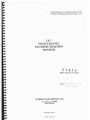
P Y4 AJ
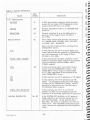
FABIO TEIXEIRA fl,li\G,\LHAFS
CE-7
MULTI- CHANNEL
FM COMMUNICATIONS
MONITOR
.r:.
APPLICABLE TO INSTRUMENTS WITH
SERIAL NUMBERS HIGHER THAN 261
CE . 7
lVIULTI.. CHANNEL
FM COMlVlUNICATIONS
MONITOR
PY4 AJ
_FABIO TElXElfiA MJGI\LHilF.,\;
'AR QUIV8
r ' c >"
.J
CUSHMAN ELECTRONICS, INC.
Sunnyvale, Cal. 94086
408·739·6760
Printed in U.S.A.
5601'-0015"1
'/''-:.:?
~:::C : ~TC,)
,I .
,',
....
11
.
•
~
0
;1'
•~
WARRANTY
CUSHMAN ELECTRONICS . INC. WARRANTS EACH OF THE II\lSTRUMENTS OF THEIR
MANUFACTURE TO BE FREE FROM DEFECTS IN MATERIAL AND WORKMANSHIP
FOR A PERIOD OF ONE YEAR FROM THE DATE OF ORIGINAL PURCHASE. THE
ANY
OTHER
WARRANTY.
EXPRESS,
IMPLIED
OR
FOREGOING
IS
IN
LIEU
OF
STATUTORY,
THE
COMPANY.
UNDER THEIR
LIBERAL WARRANTY . WILL
REPAIR
OR REPLACE ANY INSTRUMENT FOUND DEFECTIVE .
THIS WARRANTY MAY NOT APPLY TO INSTRUMENTS
OF THE COMPANY, HAVE BEEN ALTERED OR MISUSED.
WHICH .
IN
THE
OPINION
This manual is int end ed to give the user a com p rehensive knowledge of th e i nstrum ent and its
operation or rep air . In the event of troub le. study the manual carefully, Most instrument malfunctions
can be corrected by the user with a minimum of lost usa ge time .
For assist ance or information of any ki nd, contact the factory , Give full detail s of the nature of your
problem and include the model and serial number of the instrument ,
Should it app ea r that the i nst rument nee ds to be returned to the facto ry for service or recalibrat ion,
let us know . Shipping in struction s will be promptly given to you , There w ill be no charge for repair on
instruments w it hin t he one year warra nty other than tran sportat ion cost s after 90 days of ownersh ip.
Estimate s of charge s for non -warr anty or any oth er service will be sup plied by the facto ry upon requ est
before w o rk is begun and suc h work will be done on an actual co st basis only.
CLAIM FOR DAMAGE IN SHIPMENT
You r instr ument should be inspected and te sted as so on as it is received. The in st rum ent is insured
for safe delive ry. If the instrument is dam aged in any way o r fails to operate properly , file a cla im with t he
carrier or, if insured separately . with the insurance company.
We sincerely pledge our immediate and fullest cooperation
to all users of our precision electronic instruments,
PLEASE ADVISE US IF WE CAN ASSIST YOU IN ANY MANNER
CUSHl\1A~ ELECTRONICS, INC.
830 Stewarl Dr. 0 Sunnyvale, Cal. 94086 0 408--739-6760
iii/iv
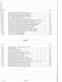
CONTENTS
Page
WARRANTY
SECTION 1
1-1
1. 1
1. 2
1-1
1-2
1-2
1-3
1-3
1-3
2.3
2.4
2.5
Unpacking and Inspection
Environmental . . . . .
2.2.1
Temperature
2.2.2
RF Fields
Power Requirements .
Warm-up Requirements
Preparation for Reshipment
2-1
2-1
2-1
2-1
2-1
2-1
2-1
3-1
3.1
3.2
3.3
3.4
3-1
3-1
3-1
3-5
3-5
3-6
3-6
3-7
3-7
3-8
3-8
3-8
Introduction
.
Controls and Indicators
Starting Procedure
Operating Procedures
3.4.1
Frequency and Deviation Measurement
3.4.2
CW-Signal Generation
3.4.3
FM-Signal Generation
.
3.4.4
IF-Signal Generation
.
3.4.5
Installation and Removal of IF-Oscillators
3.4.6
Antenna Installation
.
3.4.7
Installation and Removal of Crystals
Turn-Off Procedure
CIRCUIT DESCRIPTION
4. 1
4.2
4.3
4.4
4.5
4.6
4.7
4.8
5601"0015"1
2-1
..
OPERATING INSTRUCTIONS
3.5
SECTION 4
Introduction
.
Accessories
.
1. 2.1
Plug-In Units
1. 2.2
External Instruments
1. 2. 3
Auxiliary Items . . .
Specifications
INSTA LLATION
2.1
2.2
SECTION 3
iii
GENERAL DESCRIPTION
1. 3
SECTION 2
.
--
Introduction . . . .
Second IF and Discriminator Board
Power-Supply Board
.
Frequency Error Meter Board
Harmonic Generator Board
l\Iulti-Oscillator Board.
IF Oscillator Board . . .
Signal-Generator Mixer
v
4-1
4-1
4-2
4-7
4-8
4-8
4-10
4-12
4-12
Page
SECTION 5
MAINTENANCE
••••••••••••••••••••
!
•••••••••••
5-1
.
.
.
.
.
.
.
5-1
5-1
5-1
5-1
5-2
5-2
5-3
5-10
.
.
.
5-11
5-11
SCHEMA TICS, PARTS LISTS, AND PARTS PICTORIALS
.
6-1
6.1
6.2
.
.
.
6-1
6-3
6-3
6-7
5.1
5.2
5.3
5.4
5. 5
SECTION 6
.,
Introduction.
.
Access
Fuses
Adjustment Procedures and Check
5.4.1
Power-Supply Board, Voltage Adjustment
5.4.2
Crystal-Oscillator Adjustment
5.4.3
Frequency-Meter Adjustment
5.4.4
20-dB Fixed-Attenuator Loss Check
5.4.5
Signal-Generation-Output Level Adjustment
5.4.6
Signal-Generator-Mixer Input Level Check
Troubleshooting Procedures .,
Introduction
Schematics, Parts Lists, Parts Pictorials
6.2.1
Second IF and Discriminator Board
6.2.2
Power Supply Board
6.2.3
Frequency Error Meter Board
6.2.4
Harmonic Generator Board
6.2.5
Multi-Oscillator Board
6.2.6
IF Oscillator Board
6.2.7
IF Oscillator Board
6.2.8
Signal Generator Mixer
6.2.9
Crystal Oven Assembly .. ,
6.2.10 Main Chassis
6.2.11 Front Panel
6.2.12 Rear Panel
6.2.13 Covers and Carrying Cases
.
.. ,
.
.
.
.
.
.
.
.
.
.
.
.
5-13
6-11
6-13
6-17
6-21
6-23
6-25
6-27
6-31
6- 35
6-39
6-41
CUSTOMER-COMMENT CARDS
ILLUSTRATIONS
Figure
1-1.
3-1.
4-1.
4-2.
4-3.
4-4.
Page
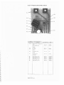
CE-7 Multi-Channel FM Communications' Monitor (Equipped)
Installation- Removal, IF-Oscillator Boards
CE-7, Block Diagram
Second IF and Discriminator Board, Block Diagram
Frequency-Meter Bridge, Simplified Schematic Diagram
and Waveforms
Audio-Output Filter, Simplified Schematic Diagram and
Waveforms
.
.
.
.
1-1
3-7
4-3
4-5
.
4-5
.
4-6
Page
-=-- .
-:- 7 .
- 2.
Power-Supply :Board, Block Diagram
.
Harmonic-Generator Board, Block Diagram
Mult i-e Osci llato r Board, Block Diagram . .
CE-7 Right Interior View Without P lug-In .
.
CE -7 Bottom Interior View
CE-7 Left Interior View Without Plug-In . .
Second IF and Discriminator Boa rd (0054), Schematic Diagram.
Power Supply Board (0100) , Schematic Diagram
.
Frequency-Error-Meter Board (0101) , Schematic Diagram .
Harmonic -Generator Board (0102), Schematic Diagram
Multi-Oscillato r Board (0103) , Schematic Diagram .
IF Oscillator Board (0104), Schematic Diagram '" _. .
IF Oscillator Board (0105) , Schematic Diagram . .. ..
Signal Generator Mixer (CH-A3), Schematic Diagram .
Crystal Oven Assembly (CH-A4) , Schematic Diagram .
Main Chassis , Wiring Diagram . .
. . ....
Front Panel, Wiring Diagram ' "
Rear Panel , Wiring Diagram . . . . 4-7
4-9
4-11
5-2
5-4
5-8
6-5
6-9
6-11
6-15
6-19
6-21
6-23
6-25
6-29
6-33
6-37
6-39
TABLES
_ b e
1-1.
1-2.
3- 1.
4 - 1.
5- 1.
5- 2.
5-3.
5-4.
5-5.
5-6.
5-7.
5-8.
5-9.
5-10 .
5-1I.
6-1.
I" 001 5" 1
Page
Auxiliary Items Furnished with the CE -7
Specifications
.
Controls and Indicators
.
Channel Frequency Chart
.
Power Supply, Resistances to Ground
Power-Supply Boa rd , Voltage Adjustment .
Crystal -Oscillator Adjustment
.
Frequency-Meter Adjustment
.
20-dB Fixed-Attenuator Loss Check
.
Signal-Generation-Output Level Adjustment
Signal -Generator- Mixer- Input Level Check
Troubleshooting, Frequency- Devia tion-Measure (FDM) Mode
Troubleshooting, Signal-Generator Mode.
Troubleshooting, 1. F. -Generator Board .
Troubleshooting, Crystal-Oven Assembly
Reference Designators and Abbreviations
vii/viii
1-3
1- 4
3-2
4-1C!
5-3
5-4
5-5
5-9
5-10
5- 12
5- 13
5- 14
5- 16
5-17
5-1 8
6-2
SECTION 1
GENERAL DESCRIPTION
,
•
•
•
t
t
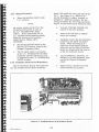
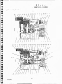
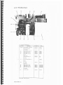
Figure I-I. CE-7 :\Iulli-Channel F:\I Communications Monitor (Equipped)
t
1.1
Introdu cti on
co mp romise d i f only one o r two cry stals
are in stall ed. Th e Cus hman Model MCO-6
Multi-Cha nnel Os c illa tor (accesso ry) offe r s
an additional 23 freque ncies should the need
for other c rystal freque nc ies a rise .
The Model CE-7 Multi-Channel Fi\I
Communications Monitor (Figure 1-1) is
designed to measure the frequency and
frequency-modulation deviation of trans
mitters and other s igna l sources . The
CE -7 is crystal controlled and can ope r
ate on any one of 23 fr eque nci e s between
20 MHz and 1150 MHz. Which fr equen ci e s
are as s ig ne d to t he 23 pos it io ns i s spe ci
fi ed by th e c usto me r . Any number of cry
stal s be tw ee n on e a nd 23 m ay be selected
and th e ope r ati on of the instrum ent is not
5601"0015
T he CE -7 can also ge ne rate F M and CW
signa ls wi thin th e fr equ ency limits s t ated
above . Th e ou tput level of th e ge ne rated
s ig na l m ay be adj us ted fr om 0.1 to 100
mi crovolts a nd provi de s t he capabil ity of
determining th e sens it iv ity of FM commu
nication r e ceiver s. Sign al ge ne r at ion of
up to ten optional cry stal- controlled IF
1-1
th e m onitoring fun c ti on for r ou tine tes ting ,
t ro ubl es hooting , d isplay ing Lissajous pat
t erns , etc. Th e Os cillos cop e can a lso be
us ed for r ec ei v e r I F- bandwidth m e a sure
ment a nd discriminator alignment.
frequ en ci e s is av ailabl e be tween 250 kHz
a nd 13. 5 MHz. The output lev e ls o f the IF
s igna Is are c on tinuo us ly variable.
The CE - 7 must operate with eithe r a
Mode l 301 Os cillos cope or a Mod e l 302 F M
De vi ation Meter in s erted into the left-hand
p lug- in cav ity , and a Mode l 303 Broadband
Mixe r or on e of th e RF plug-ins inserted
into th e right-hand plug-in cavity. The
co m bina tion ofth e plug-ins is at the discr e ti on of the customer.
The Model 302 Fl\I Devi ation Meter pro
vides three ranges: 0 to 2 . 5 kHz, 0 to 6 k Hz ,
a nd 0 to 2 5 k Hz . An instantaneous-peak
indicator light flashes when the a bso lute
peak deviation of th e incoming carri er ex
ceeds an amount pre set by the operator.
Operation and acc uracy of the peak indicator
are not affected by modulation frequ ency,
r epetition rate, or wav eform. A switch
permits selection and m easurement of either
plus or minus de vi ation peaks. A sco pe jack
is provided for s im ult a neo us meter indica
tions a nd oscillos cope obse rv a tions of devi a
t ion (a se parate osc i llo scope , nota Mode130 1 ,
must be us ed).
1.2 Accessories
Three types of acces s o r ies are av a ila b le
for us e with the CE- 7 : 1) units that plug
into th e m onitor a nd obta in operating power
from it ; 2) ex te rna l ins trum ents j a nd
3) a ux il ia ry it em s s uppli ed with the m oni
to r , but not in tegral parts of it.
NOT E
1.2.1
Plug-In Unit s
Remote dis play o f FM deviation
is possibl e only whe n th e Mod el
30 2 FM Devia ti on l\Ie te r is us ed.
A cavity a c c e s sible th ro ugh an opening in
th e left-hand part of th e monitor front panel
accepts eithe r th e Mode l 301 Osc i llosc ope or
th e Model 30 2 FM Deviation Meter. One o r
th e othe r of the s e must be us ed to provide
FM d eviation mea surements . A similar
c a vity in the right-hand part of the front
panel a c c epts a l\Iode13 03 Broadband Mi x er
o r a Model 304, 305, or 306 B RF Preselector.
The Mod el 303 Broadband Mixer op erate s
on all frequencies c over ed by th e CE-7.
Sens itiv ity is les s than 10 millivolt s, for
c l os e - in monitoring a nd in-shop m easure
ments. A crystal filt er in the broadband
mis er provides s ha r p s ele ctivity in areas
where many s t rong RF signals are pres ent.
The Model 301 Osc illosco pe permits
vi sual ex a m ina tion of exa c t modulation of
the tran smitter ca r r ier . Unb a la nced modu
lati on, power- s upply puls es, unusua l clip
ping, a nd othe r p roblems be come imm ed i
a te ly a ppa r ent so th at a pp ro p r ia te re pairs
can be m ad e. The Mode l 30 1 ha s a n a uto
m ati c s yn c c i rcu it , similar to that found
in the most ad vanc ed labo rato ry ins trum ents,
to lock on and precis ely di s pla y waveforms.
T he scope gra tic ule is ca li brat ed to show
de vation on a nyone of thr e e ranges:
±l. 5 kHz , ±5 kHz, and ±1 5 k Hz . Switch e s
.on th e front pan el p ermit us e of external
v ertical inputs whil e using the internal
s wee p. External s igna ls may a ls o be co n
ne cted to the horiz ontal input. This per
mits independent use of th e Model 301 of
5 6 01" 0 015"1
Three differ en t RF Pres el ector plug-ins
a re a vailabl e for use in th e C E- 7. Th e
Mode l 304 opera tes f ro m 25 MHz to 50 MHz ,
the Model 30 5 from H5 MHz to 175 MHz,
a nd theModel 306 B fr om 450 MHz to 520
MHz. The s e ns ltiv ity of these pre s e le ctors
is l es s than 20 mi crovolts a nd enables it to
monitor bas e s tations up to 50 m il es away .
The p r esclecto r s a lso have a crys tal filter
that permits s ha rp s el ectivity.
A telephone ja ck on th e front panel of th e
304 and 305 pres ele ctors pe r m its use of an
ex t e r na l meter for r eading the AGC voltage,
which is indicativ e of th e level of the in
co m ing signal.
1-2
C
r:
f
,
[f
I:f
r
f
r:
r:
rei•
•
,
I:
••
.
I:
-_._-
1.2.2
._. _ -
-
th e Remo te Meters p lugs into the accessory
receptacle on the back of the C E-7 . A
switch near the receptacle permits selec
tion of in te r nal or external mete rs .
Ext ernal Instrum ent s
Three accessory instruments , the Model
IVIC O- G :lVI ulti - Cha n ne l Oscillator, the Model
107 FlVI Deviation Calibrator , and the Model
309B Remote Meters can be connected to the
CE-7 . Th e Model MCO-6 Multi -C hannel
Osci llato r provi de s up to 23 additio nal
crysta l-cont ro l led freq ue nc ies . The multi
c ha nne l osci llato r is connected to the C RY
STAL OUT AUX. IN co nnector on the CE-7
fr ont panel by the RF cable s up plied insi d e
the f ro nt cover of the CE - 7.
1.2.3
Auxiliary It ems
Auxilia ry items (Table 1-1 ) s u pplied with
th e in s trum en t are : a 30 -inc h te lescoping
a nten na ; a 20 -dB fixed a tten ua to r with ada p
t er ca ble , whi ch must be us ed when the CE-7
is ope ra ted as a s igna l gene r a to r ; an A C
plug a da pte r (thr e e pron g/two prong); an
RF ca ble a ss embly for interface between
th e CE-7 a nd ex te rna l equi pm en t ; and a
s pa re fus e pa cka ge for r eplacing a defectiv e
fus e co ntained in the 20 -d B fi xed attenuato r,
In stallati on of the a ntenna is cov e r e d in Pa r a
g ra ph 3 .4 .6 , a nd operatio n of th e 20- d B fi x ed
atten uato r is desc ribed in Paragraph 3 .4 .2 ,
s t ep e .
The Model 10 7 F M Dev ia ti on Ca li b ra to r
provide s a mean s of ve rify ing th e ac cura cy
of th e FM deviati on r ang e s of th e Mo del 30 1
Osc i llos c op e and th e Model 302 F M Devi a
ti on Me te r . The ca lib rato r mus t be con
n ecte d to the CE- 7 by a cable to the auxi lia ry
eq uipment connector (C H- J 4) on the l e ft s ide
of the C E-7 , and mus t be us ed in con j unctio n
with a n ex te r na l osc illator w it h a freq ue ncy
r a ng e of 20 80 to 2100 Hz .
The Mode l 309B Re mote Mete rs cons ists
of a n F M DEV IA TI ON mete r a nd a FRE
QUENC Y me t er m oun t ed in a ca bine t th a t can
.b e lo cated at a distanc e o f up to seve ra l hun
d red fe e t from th e CE-7 . Th e ca ble from
1.3 Sp ecifi cation s
Ta bl e 1-2 li s t s the spec ificatio ns fo r the
C E-7 as well as those for the plug-in un it s
tha t can be us e d with the CE- 7 .
Tahle 1-1. Auxiliary It ems Furnish ed with th e CE-i
ITEM
DES CRIPTI ON
CUSHMA ~
ST OCK NO.
QUANTITY
1
Ante nna Assemb ly
7 040-001 9
1
2
20 -dB Atte n uato r/Ada pter
Ca ble
7040- 001 6
1
3
RF Cab le Assem b ly
7030 -00 14
1
4
A C Ada pte r Plug
(thre e pr on g/ two prong)
2535 -0001
1
5
RF Fus e, 1/ 32 Amp
1955- 0005
2
.:
6
Channel Freque ncy Char t
5500 -0006
1
7
Fr on t Cove r
2 180-0033
1
8
Eq ui pme nt Ma n ua l , CE -7
56 01- 0015
1
1-3
5601"0015··1
[
Table 1-2. Specifications
Model CE-7 Multi- Channel
FlVI Communications Monitor
Frequency Deviation Measure
Frequency Coverage
20 MHz to 1150 MHz (23 crystal-controlled channels)
Frequency Accuracy
±O. 0001 % (long term)
Frequency Error Ranges
±500 Hz, ±l. 5 kHz, ±5.0 kHz
Frequency Error Resolution
20 Hz
RF Signal Generation - CW and FM
Frequency Coverage
(calibrated in microvolts)
20 MHz to 1150 MHz
Output Level
0-1, 0-10, 10-100 JiV; ±2 dB into 50 ohms. Calibrated
in JiV and dB with external 20-dB fixed attenuator.
(100-1000 JiV without 20-dB fixed attenuator.)
Frequency Accuracy
±O. 0001% (long term)
Internal FM
1. 0 k Hz modulation frequency.
less than 2% distortion.
External FM Modulation
60 Hz to 20 kHz modulation frequency.
deviation, 500 p.V sensitivity.
0 to 25 kHz deviation,
0 to 25 kHz
IF Signal Generation
Frequency Coverage
250 k Hz to 13.5 MHz (10 crystal controlled channels)
Output Level s
0-1 V, 250 kHz to 900 kHz into 600 ohms; 0-0.5 V,
1. 0 MHz to 13.5 MHz into 600 ohms.
Power Requirements
115 or 230 vac ±10 %, 50 to 400 Hz, 175W during oven
warm up, 75W max. after warm up.
Dimensions
12-1/4 in. high, 13.0 in. wide, 16.0 in. deep
Operating Temperature
Oven Warm- Up Time
30 minutes
l\'et Weight
28 pounds less plug-ins, 35 pounds with plug-ins
5601"0015"1
1-4
[
Table 1-2. SpeCificlJtions (Continued)
Model 301 OsciLLos cope Plug-in
Deviation Measurement Accuracy
±5% full scale in three ranges:
±1.5kHz, 5.0kHz, 15.0kHz
External Input s
Vertical and Horizontal
External Verti cal Sensitivity
300 mv for full scal e
External Frequency Response (3 dB)
30 kHz
Model 302 Deviati on Meter Plug-in
Accuracy of Measurements
±4% full scale in three ranges:
0-2.5 kHz, 0-6 k Hz , 0-25 kHz
Model 303 Broadband Mixer Plug-in
Frequency Coverage
20 MHz to 11 50 MHz
Sensitivity
Less than 10 mv below 512 MHz
Input Impedance (nominal)
50 ohms
Receiver Bandwidth (3 d B}:
Broad
80 kHz
:\arrow
13.5 kHz
RF Presele ctor Plug-ins
Model 304
Model 305
Model 306B
Frequency Coverage
25-50 MHz
145-175 ?-IHz
450-520 T\IHz
Nominal Input Imped ance
50 ohms
50 ohm s
50 ohm s
Broad
80 kHz
80 kHz
80 k Hz
Nar ro w
20 kHz
20 k Hz
20 kHz
20 microvolts
20 microvolts
20 microvolts
Bandwidth (3 dB) :
Sensitivity: Less than
5601"0015"1
1-5/1-6
. .a--_. . -..-
..
SECTION 2
INSTALLATION
2.1
lin packing and In spection
NOT E
When unpa oki ng th e Model CE- 7 FM
Communi cations Monito r , i ns pe ct the pack
in g box a nd th e i ns tr ume nt fo r s igns of
pos s ible shippin g dam ag e a nd s ee if th e
auxili ary items li sted in T able 1-1 a nd
.sho w n in Fi gure 1--:1 a r e pr e sent. Verify
s ati sfactory performanc e as o ut li ne d in
th e Operating Instruction s (Section 3).
If the instrument is dam aged, fail s to
op erate properly, or if a ny o f the a LLxi
li ary it em s a r e mi s sing , fil e a clai m
wit h th e tran s port ati on age ncy or, if
insured separate ly , with the insuran ce
company .
2.2
2.2.1
2.3
Temperature
0
5601"0015
Warm-up Rcquircmcnts
Th e acc uracy of CE- 7 measurem ents
depends on maintaining a ll oscill ator cry
s tals at a cons t a nt temperature, so th at
a nyo ne of th em m ay be sel e ct e d as th e
"m a ster- o s cill ator" c rys tal at a ny ti me.
A th ermo stati call y c ont r oll e d oven which
r equire s a 30 - mi nute wa r m - up peri od
hou s e s up to 23 c ry sta ls. Ove n op er ation
i s in de pendent of th e VOLU ME PO\VER OFF
control ; it i s r ecomm ended that the in stru
m ent be in stall ed s uch th at it can be kept
plugged into its power s our ce and be r e ady
t o m ak e pre cise mea surem ents within sec
onds a fte r pow e r i s a pplied to m e a suring
a nd g e ne rat i ng circuit s.
NOTE
If th e instrument ha s been s to red at
a t em perature bel ow +32 0 F, add i
tion al warm-up time m ay be r equir e d.
R F Fields
Where extrem ely hi gh R F r adiation
fi eld s exist (such as wh en the CE-7 is used
near a transmitter ), th e tel escoping a nte nna
s hould be pu sh ed clown t o r educe pi ckup.
Whe re m any high- power tr an smitter s a re
i n us e, a djacent-channe l in terference m ay
be expe r ienced if the transmi tte rs a r e ope r
ati ng wi thin 90 kH z of each oth er. In su ch
cas e s , the SEL E CTI VIT Y sw itch on th e
Mode l 30 3 Broad band Mixer should be
pl a ced in th e SHARP po siti on.
Power R cquirements
Th e CE-7 op e rates from a 115- or 230
vo lt (±10%) ac so urce , 50 to 400 Hz. Powe r
cons umptio n is 75 watts .
2.4
Environm ental Hequiremcnts
Th e CE-7 i s desi gned to ope rate be
tw een + lOO F a nd +130° F (am bi ent). Es
pe ci ally in th e fiel d, th es e temperature s
can eas ily be exceeded if nor m al car e i s
not t ak en. ( For in s tan ce, th e i nterna l
te m perature of a clos ed a uto mobi le t r unk
may exce e d 150 F dur i ng s umme r dav
li ght ho urs. ) Avoid using th e instr um ent
outsid e in bright s unlig ht on a hot day.
Do not blo ck th e cabinet ve ntilat i ng louvers.
Ex ce edi ng th e upper or low er t emper ature
l imits for extended pe r iods m ay not r e sult
in noti ceabl e damage to t he instrum ent,
but may cause poo r performance o r
m alfunctio ning.
2.2.2
In th e SHAR P po s it io n, th e I F
ba ndw id th i s nar r owed t o th e ex
te nt that abso lute ac c u ruov of t he
de vi ati on di spl ay o n the O~cillo
scope o r th e meter reading on th e F 1\1
Devi ation m eter m ay be s lig htly
degr a de d. Th e SHARP po siti on
should, therefore, be us ed only
when a bsol utely neces sary .
2.5 Preparation for R cshipment
No spe ci al i nst r uct io ns a r e requi re d for
packi ng th e Mod el C E- 7 Mul ti - Cha nne l F M
Com m unications Monito r , if it be com e s
ne ce s s ary to r e tur n the i ns t r ument to t he ·
fa ctory for s e rvi ce o r r e pair, h owe ver, it
is re commend ed that the shipping box a nd
fo am pa ck a ging be kept for this purpos e .
2-1/2-2
_
_
_ _0_
.
SECTION 3
OPERATING INSTRUCTIONS
be varied from zero to 25 k Hz deviation.
The FM DEVIA TION mete ror the oscillo
. scopecan also be used to read the modula
tion of this generated signal. An internally
generated, I-kHz modulating frequency or
an external audio source can be used.
3.1 Iuu-oduction
Section 3 contains instructions for
operating the CE-7 Multi-Channel FM
Communications Monitor, and includes
f functional description of all controls
and indicators. Refer to Table 3-1.
In the 1. F. position of the function switch
the CE-7 operates as a generator of frequen
cies that are usually found as IF frequencies
in communications receivers. The desired
frequency is selected by means of the 1. F.
GENERA TOR SELECTOR switch. The gen
erated IF frequency is ava ilable at the 1. F.
GENERA TOR OUTPUT connector and its level
is varied by means of the 1. F. GENERA TOR
LEVEL control. When setting the SELECTOR
switch, refer to the Channel Frequency Chart
located inside the front cover of the CE-7 for
the position associated with the desired IF fre
quency. See Paragraph 3.4.5 for installation
and remova 1 of IF Oscillators.
The CE-7 can be operated on one of
three modes, depending on the position
of the black/red concentric control knob
located on the left side of the front panel
directly below the MULTI-CHANNEL
MONITOR.
NOTE
For the purpose of discussion
the 5-position, outer black knob
will be referred to as the "function
switch" throughout this manual.
In the FREQ. -DEV. MEASURE position
of the function switch the CE-7 operates
as a receiver-monitor. The incoming
signal is applied through the ANT. con
nector on the Broadband Mixer or
Preselector, either from an antenna or
other signal source. The received signal
frequen cy is measured by selecting the
assigned carrier fr-equency of the trans
mitter by means of the CARRIER FRE
QUENCY SELECTOR switch and reading
the frequency error on the FREQUENCY
meter. Simultaneous with the freq uency
error, modulation deviation is indicated
by the FM DEV IA TION meter on the
Model 302 FM Deviation Meter or on the
screen of the Model 301 Oscilloscope,
whichever is used. A built-in speaker
makes the modulation on the incoming
carrier audible.
3;2 Controls and Indicators
The Model CE-7 controls and indicators
are listed in Table 3-1. For all other equip
ment or accessories, refer to the applicable
equipment manuals.
3.3 Starting Procedure
a.
NOTE
The Crystal Oven "As s e m bly is
energized as soon as the CE-7
powereord is plugged in.
In the CAL. / C W or FM position of the
function switch the CE-7 operates as a
signal generator. The desired
signal
Vv, '
frequency is selected by means of the
CARRIER FREQUENCY SELECTOR
switch. The generated signal (CWor
FM) is available at the SIGNAL GENERA TOR
OUTPUTconn<?ctor. The "attenuator pro
vides caHbrated outputs of jLto...J, 0 to 10,
or 0 to 100 microvolts when the .2.Q.-_d B fixed
attenuator -is used. When FM has
selected (instead of CW) the modulation can
I ; '
.
heeii
5601"0015"1
Plug the power cord into an ac
power outlet (115 volts, 50 to
400 Hz) and energize the set by
means of the power switch on
the VOLUME POWER OFF
control.
3-1
b.
Ascertain that the channel pilot
light is on,
c.
Allow the CE-7 to warm up for ap
proximately 30 minutes. The
OVEN ON light will begin to cycle
on and off. If the CE-7 has been
stored at temperatures below 32 °F
additional warm-up time may be
required.
[
[
Table 3·}. Controls and Indicators
NAME
REF
DESIG.
~
FUNCTION
1. F. GENERATOR
[
[e"
OUTPUT
n
A BNC-type female connector which provides
access for the output of IF frequencies in the
range of from
250 k Hz to 13. 5 MHz.
,
/
LEVEL
R2
Permits adjustment of the 1. F. GENERA TOR
OUTPUT.
SELECTOR-
S4
Permits selection of up to ten different fre quencies in the range of from 250 kHz to
13. 5 l\IHz.
Sl
Outer black control knob permits selection of
CAL.lcw, FM,
or FREQ. - DEV. MEASURE.
Function Switch
1. F. HARM. AMP. TUNING,
[
Inner red control knob permits zeroing of the
FREQUENCY meter.
In this position, the CE-7 is an IF-signal gen 1. F.
erator and provides the capability of generating
up to ten freq uencies in the range of from
250 kHz to 13.5 MHz.
In this position the harmonic amplifier can be
tuned for maximum signal output of the selected
carrier frequency with the HARM. AMP.
TUNmG control.
HARM. AMP. TUNING
CAL.
R1
In this position the inner red control knob is
used to zero the FREQUENCY meter. The
FREQ0ENCY meter range is automatically
in ±O. 5 kHz regardless of the position of the
:::kHz (FREQUENCY lever).
CW
In this position, the CE-7 generates a CW signal.
FM
In this position, the CE-7 generates an FM
signal. The frequency of the generated signal
is shown on the FREQUENCY meter, and Fl\I
deviation is indicated by the Oscilloscope or
FlVI Deviation Meter plug-in.
FREQ.-DEV. MEASURE
In this position, the CE-7 is a receivermonitor and both carrier frequency and FM
deviation of an incoming signal can be measured.
VOLUME POWER OFF
5601"0015"1
S5, R3
In the POWER OFF position, no AC power is
being supplied to any circuits except the Cry
._ stal Oven Assembly. In any position other
than OFF, AC power is supplied to all circuits
of the CE-7. The VOLUME potentiometer pro
vides a means for adjusting the audio-amplifier
output.
3-2
Table 3-1. Conlrols and Indicators (Continued)
NAME
REF
DESIG.
FUNCTION
R4
R5
Black/red concentric controls used when the
function switch is in the FM position. The
outer black control knob, DEV .ADJ., permits
adjustment of the arri'ounr of deviation of the FM
signal generator output and the level of the in
ternally generated I-kHz output. The inner r ed
control kn09J FM CAL., permits adjustment of
the generated- Fl\'1 center frequency. The
FREQUENCY meter is automatically in the
±5.0 kHz range when the function switch is in
FM.
S6, J2
With the function switch in the FM position, the
FM MOD . switch permits selection of the modu
lation source. In EXT., an external modulation
signal can be applied through the BNC connector
just below the switch. In INT. I an external
I-kHz source is turned on. This same I-kHz
signal is available at the BNC connector for
external use.
CRYSTAL OUT
AUX. IN
J4
A ENC-type female connector which provides
the capability to monitor the crystal frequency
of the selected channel. (The output level should
be greater than 600 mv unterminated.) It also
provides a connection point for 23 additional
crystal-controlled frequencies from the l\Iodel
MCO-6 Multi-Channel Oscillator.
FREQUENCY BELOW
40 MHz - ABOV E 40 MHz
S3
Permits reversing the polarity of the FRE
QUENCY meter so any carrier-frequency
error measured will always be indicated in the
correct direction. This is also applicable to
the Model 301 Oscilloscope. (When operating
BELOW 40 l\'1Hz the CE-7 local-oscillator fre
quency is higher than the frequency to be
monitored. )
HARM. AMP. TUNING
C5
Permits tuning of the harmonic amplifiers for
the selected RF channel. Tuning is indicated
on the FREQUENCY meter. Refer to the
Channel Frequency Chart for approximate
settings associated with each channel listed.
R7
When set to the number listed with the desired
carrier frequency on the Channel Frequency
Chart, the signal-generator output level will be
as indicated by the MICROV OLTS (0. 1 to 1. 0
microvolts) and Xl, XlO, XIOO (Multiplier)
settings. The 20-dB fixed attenuator must be
used.
DEV. ADJ.
FM CAL.
FM MOD. INT.-EXT.
1 kHz OUT
SIGNAL GENERA TOR
LEVEL SET
MICROVOLTS
(Attenuator Vernier)
R8, R9
Xl, XlO, XIOO
(Multiplier)
S7
OUTPUT
J3
5601··0015··1
A ENC-type female connector which provides
signal generation output for the frequency
selected.
3-3
c:
Table 3-1. Controls and Indicators (Continued)
NAME
CARRIER FREQUENCY
SELECTOR
SIGNAL LEVEL
CHANNEL
OVEN ON
REF
DESIG.
SI (CH)
DSI
DSI (AI)
DS2
±kHz
(FREQUENCY lever)
S2
FREQUENCY (meter)
Ml
FUNCTION
Provides selection of anyone of 23 RF channels
for frequency error and FM deviation measure ment or signal generation. Channel numbers 1
through 23 are associated with specific carrier
frequencies as recorded on the Channel Fre quency Chart. The AUX. position permits con nection of additional crystals to the CRYSTAL
OUT AUX. IN connector on the front panel.
In FREQ. - DEV. MEASURE position, this lamp
will lightwhen a received signal is strong enough
for reliable frequency measurements. In CAL. /
CW or FM position, the lamp will always be on.
Indicates that the CE-7 is on.
Indicates that there is power to the Crystal
Oven Assembly. The oven will normally be on
for approximately 30 seconds and off for ap proximately 90 seconds after the operating temp erature of 76. 2°C has been reached . .
Permits selection of the three directly calibrated,
full scale FREQUENCY meter ranges of ±O. 5 kHz,
±1. 5 kHz, or ±5. 0 kHz.
Provides indication of received-signal frequency
error. This error, and whether it is above or
below the selected frequency, is directly indi cated in ±kHz. The meter is also used to indi cate the center frequency of the signal-generator
output. The meter is automatically in the
±5.0 kHz position when the function switch is
in FM.
METERS
INT.-EXT.
(rear panel)
Jl (RP)
SI (RP)
The 8-pin connector permits use of the Model
309B Remote Meters when the associated slide
switch is in the EXT. position.
FUSES
(rear panel)
F2 (RP)
Fl (RP)
Main AC-power to fuse (1. 0 amp slo-blo).
Provides protection (2/10 amp slo-blo) to the
Model 301 Oscilloscope.
.
Auxiliary Equipment
Connector (left side lower left corner of
instrument)
J4 (RP)
A 12-pin connector for the Model 107 FM
Deviation Calibrator.
NOTE
The Model 107 FM Deviation
Calibrator must be used in
conjunction with an external
oscillator with the capabilities
of 2080 to 2100 Hz.
5601"0015"1
3-4
r:
"
r",
r',
r:
r=
r.:
r."
r-•"
[:
C:
•
k:
g.
3.40 Operating Procedures
3.4.1
[:~~~!~~~]
Frequency and Deviation 'Ieasuremenl
It is assumed that the CE-7 is equipped
The signal level applied to the
ANT. connector should not ex
ceed 5 milliwatts or the plug-in
may be damaged.
with a Model 303 Broadband Xlixe r and either
the Model 301 Oscilloscope or the Model 302
FM Deviation Meter . For measurement of
frequency and deviation with one of the RF
Preselectors in-stead of the Model 303, the
same procedure is followed except that the
preselector frequency dial must be set to
the frequency selected with the CARRIER
'FREQUENCY SELECTOR.
a.
Connect the telescoping antenna, an
external antenna, 0 r other signal
source to the ANT. connector on the
Broadband Mixer or Preselector. If
the telescoping antenna is used, ex
tend it to its full length for meas
urements of signals below 30 MHz
to approximately 18 inches for VHF
measurements; use minimum length
for UHF measurements.
b.
Select the desired carrier frequency
with the CARRIER FREQUENCY
SELECTOR.
c.
Place the function switch in the HARM.
AMP. TUNIKGpositionand adjust the
HARM. AMP. TUNIKGcontrolforamaxi
mum reading on the FREQCENCY meter.
The HARM. A:'IP. TCNING control
should indicate the appropriate number
recorded on the Channel Frequency Chart.
d.
Turn the function switch to CAL. /
The SIG::\AL LEVEL lamp
should light.
C\\'.
e.
Adjust the inner red knob (concen
tric with the function switch) for a
zero (mid-scale) reading on the
FREQUENCY meter.
f.
If the Model 301 Oscilloscope is
being used, set the toggle switches
for horizontal and vertical inputs
to the INT. positions and adjust
the VERT. POS. control so that
the trace is on the zero reference
line while the deviation range switch
is in the ±l.;) position. Adjust the
scope INTEKSITY, FOCUS, and
ASTIGrvIATIS:'I controls for a sharp
trace on the screen.
5601"0015"1
Set the function switch to the FREQ.
DEV. MEASURE position.
3-5
h.
Key the transmitter or other signal
source to be monitored. The SIG
NAL LEVEL lamp should come on.
If it does not, increase the signal
level at the ANT. connector. Nor
mally, if the telescoping antenna
is used, measurements can be made
easily when the CE-7 is between
25 to 50 feet from the radiating
antenna. When a plug-in prese
lector is being used, measurements
can be made at distances up to 50
miles from the transmitter if an
adequate external antenna is used.
i ,
The difference between the measured
signal frequency and the CE-7 carrier
frequency is indicated on the FRE
QUENCY meter according to the posi
tion of the ±kHz (FREQUENCY lever).
j.
Modulate the transmitter or other
signal source to be monitored when
FM deviation is to be measured.
Select the appropriate full-scale
sensitivity with the range switch
(kHz) on the deviation plug-in being
used. When the oscilloscope is
used, positive modulation peaks
appear above and negative peaks
below the zero reference line;
the FM deviation meter will indi
cate either positive or negative
peaks depending on the setting of
the FM DEV. PEAKS switch. If
the DEVIA TION PEAKS indicator
on the FM Deviation Meter has
been calibrated (see Model 302 FM
Deviation Meter equipment manual)
all modulation peaks which exceed
a preset level will cause this indi
cator to light. The accuracy of
deviation measurement may be
affected by the position of the
SELECTIVITY switch on the
Broadband Mixer or Preselector.
(Refer to the applicable plug-in
operating instructions. )
'3.4.3
FM-Signal Generalion
3.4.2 CW.Signal Gcncration
a.
b.
c.
d.
Set the CARmER FREQUENCY
SELECTOR to the desired carrier
frequency.
Place the function switch in the
HARM. AMP. TUNING position
and adjust the HARM. AMP.
TUNING control for a maximum
reading on the FREQUENCY
meter. The HARM. AMP.
TUNING control should indicate
approximately the appropriate
number recorded on the Channel
Frequency Chart.
Place the function switch in the
CW position and zero (mid-scale)
the FREQUENCY meter with the
CAL. control (inner red knob).
a.
Adjust the LEVEL SET control
to the SIG. GEN. SET LEVEL
number listed on the Channel Fre
quency Chart for the desired car
rier frequency.
When the CE-7 is directly con
nected (via the 20-dB fixed at
tenuato r) to a transceiver, its
transmitter should NEVER be
keyed. Any input in excess of
2 watts will blow the fuse in the
20-dB fixed attenuator and may
damage the instrument.
e.
f.
3-6
5601"0015"1
-
Place the function switch in the
FM position.
c.
Set the DEV. ADJ. control fully
counterclockwise.
d.
Zero (mid-scale) the FREQUENCY
meter with the FM CAL. control
(inner red knob).
e.
Set the FM MOD. switch to INT.
or EXT. as desired. In the
INT. position the modulating
frequency will be 1 kHz; external modulation frequencies can
be applied through the BNC
connector when the switch is in
the EXT. position. When the
FM MOD. switch is in the INT.
position, the 1 kHz signal is avail
able at the 1 k Hz OUT connector.
The level of the 1 kHz OUT is
adjusted with the DEV. ADJ.
control, which is also used to set
the level of external modulation
applied to the EXT. connector.
The FREQUENCY meter will now
show the modulator center fre
quency and the FM Deviation l\leter
or Oscilloscope will now indicate
the amount of deviation of the gen erated modulation. The FM CAL.
control varies the center freq uency
ofthe FM signal and permits testing
of receivers for alignment and max imum sens itivity. The FREQUENCY
meter is automatically in the ±5. 0
kHz range when the function switch
is in the FM position, and it cannot
be changed by the ±kHz (FREQUENCY
lever) .
The desired frequency is now being
generated. The output level can be
adjusted by means of the Xl, XIO,
XIOO (Multiplier) and MICROV OLTS
(Attenuator Vernier) controls.
--
b.
NOTE
A coaxial cable with a 20-dB
fixed attenuator is stored inside
the instrument's front cover ;
connect the cable to the front
panel connector marked SIGNAL
GENERATOR OUTPUT. The
stgnat-generator attenuator set
tings are only valid if the 20-dB
fixed attenuator is used.
- - - _. -- - ._
Perform steps 3.4. 2a through f.
These steps calibrate the CE-7 in
preparation for FM signal generation .
1
4
" 4
I:
~
I -~
•
I:
I:
41!!
I~,
I:
~
[,
,
,
[~
[:
f!
[w
•
lW
•
[.
[w"
•
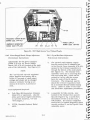
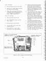
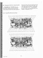
board 0103 inside the left- hand side of the
CE-7. See Figure 3-1. When an IF
crystal frequency is added, deleted, or
changed to a different position, the fol
lowing procedure for removing and instal
ling an IF Oscillator board should be used:
3.4.4 IF.Signal Generation
Place the function switch in the
position.
a.
r. F.
NOTE
On earlier models of the CE-7 the
IF position ON switch is part of
the r. F. GENERATOR LEVEL
control. If the instrument has an
1 F position on the function switch,
place the switch in that position
rather than in FREQ. - DEV .
MEASURE.
0
a.
Turn the VOLUME POWER OFF
control to the OFF position.
b.
Remove the left-hand L-shaped
cover (six screws).
c.
Carefully remove the IF-Oscillator
board from the Multi-Oscillator
board, When inserting an IFOsci ll ato r board ensure that the
guide pins on the Multi-Oscillator
board are aligned with the sleeves
on the IF-Oscillator board.
d.
Log any additions, deletions, or
changes in crv stal frequency po si
tron on the Channel Frequency
Chart.
e.
Replace the Le shaued cover and
secure with the six screws.
0
b.
Set the SELECTOR switch to the
desired IF frequency listed on the
Channel Frequency Chart.
c.
The IF signal output is available
at the r. F. GENERATOR OUTPUT
connector and the output level may
be adjusted by the I. r. GENERATOR
LEVEL control.
3.4.5 Installation and Removal of IF·Oscillators
The IF-Oscillator boards 0104 and 0105
are pin mounted on the Multi-Oscillator
Figure 3·1. Installation-Removal, IF·Oscillator Boards
5601"0015 001
3-7
d.
3.4.6 Antenna Installation
Remove the telescoping antenna from
the front cover of the C E-7. Insert
the telescoping antenna into the ANT.
connector on the RF plug-in used and
turn the connector collet until finger
tight.
NOTE
Be careful to install the proper frequency
crystal for the desired operating fre
quency. The correlation between cry
stal frequency and operating frequency
is shown on the box in which the crystal
is packed.
When removing the telescoping
antenna from the ANT. connec
tor DO NOT rotate the antenna
before loosening the connector,
otherwise damage will result.
3.4.7
Installation and Removal of Crystals
The following procedure should be
followed when field installation or re
moval of frequency-determining crystals,
inside the Crystal Oven Assembly, be
comes necessary.
NOTE
The CE-7 must be disconnected from
the AC outlet whenever the insulated
Crystal Oven Assembly cover is re
moved. The oven is energized when
ever power is present.
a.
Place the CE-7 on its rear panel
with the bottom cover toward the
operator.
b.
Remove the six bottom-cover
screws.
c.
Remove the four screws securing
the insulated Crystal Oven Assem
bly cover . DO NOT try to remove
the center screw.
5601"0015"1
Install the new cry stalts) in the
desired position.
e.
RECORD THE POSITION IN
WHICH EACH CRYSTAL IS IN STALLED ON THE CHANNEL
FREQUENCY CHART.
f.
Replace the insulated Crystal Oven
Assembly cover with the four screws.
g.
After the insulated Crystal Oven
Assembly cover has been replaced,
allow the oven to stabilize its temp
erature for approximately 30 minutes.
h.
Calibrate the crystal oscillator
according to the instructions con
tained in Paragraph 5.4.2 and
Table 5-3.
i.
Replace the bottom cover with the
six screws.
3.5 Tur-n-Off Procedure
To turn the CE-7 off, simply place the
VOLUME POWER OFF control in the OFF
position. If possible leave the AC plug
connected so that the Crystal Oven Assem
bly stays on . Unless the crystals in the
oven are kept at a constant temperature,
frequencies will vary and precise meas
urements cannot be made without a mini
mum warm-up period of 30 minutes.
3-8
SECTION 4
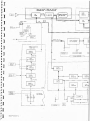
CIRCUIT DESCRIPTION
The 10- MHz signal (± frequency e r r or )
is fed to the Second IF and Discr irninutor
board where it is amplified a nd m ixed with
a 9.9-MHz signal from the Multi-Osc illator
board to form a second IF"and 100 k Hz
(± frequency error). This second-IF s ig
nal is amplified and applied to the frequency
error detector.
4.1 Introduction
The circuits of the Model CE-7 Multi
Channel Fl\1 Communications Monitor are
on five printed circuit boards: the Second
IF and Discriminator board (0054), the
Power Supply board (0100), the Frequency
Error Meter board (010 1), the Harmonic
Generator board (0102), and the Multi
Oscillator board (0103). Figure 4-1 is
the functional block diagram of the CE-7.
The 115-vac-supply fuse RP- F2, is on
the inside of the rear panel.
A squelch detector in the Broadband
Mixer or Preselector rectifies th e 10- i\IHz
signal. The resulting de voltage is ampli
fied and fed to the signal-level detector in
the CE-7. If the 10-l\IHz signal exceeds
a preset level, the SIG:-\AL LEVEL lamp
lights to indicate that a cc urate me asure
ments can be made and the frequencyerror detector is energized . The frequency
error detector is adjusted to give a zero
indication on the FREQUENCY meter when
the second IF signal is exactly 100 k Hz .
If the frequency of the monitored signal is
above or below the frequency selected with
the CARRIER FREQUEf\'CY SELECTOR,
the input to the frequency-error detector
will be exactly the same amount above or
below 100 k Hz . The detector output will
cause the FREQUE~CY meter to deflect
toward the plus (+) or minus (-) side, in
dicating the direction and a mount of fre
quency error.
The CE-7 is basically a multi-channel
superheterodyne receiver and a signal
generator. In the FREQ. - DEV. MEASURE
mode of operation the RF signal, the fre
quency and frequency deviation of which
are to be measured is applied through
the ANT. connector of the RF plug-in
that is being used (a Broadband Mixer
or one of the three Presel ectcr s) . The
RF signal is mixed in the RF plug-in
with the local-oscillator signal from the
Harmonic Generator board in the CE-7.
The local oscillator signal has a
frequency that results from mixing the
output of a selected crystal oscillator
(associated with the selected channel) with
the out put of a 10-MHz crystal oscillator.
When an R F signal must be measured for
carrier-frequency accuracy, the frequency
that has been assigned to the transmitter
of the RF signal is the same frequency
that is selected on the CE-7. Thus, the
CE-7 can only monitor a signal for which
it has a crystal of appropriate frequency.
If the monitored signal is frequency
modulated, the modulation will be present
in the output of the frequency-error detec
tor. This output is demodulated and a sig
nal representing the modulation is amplified
and fed to either the Model 302 FM Deviation
Meter or the Model 301 Oscilloscope. If
the Model 302 is used, its FM deviation
meter will indicate the peak deviation of
the FM signal. On the Model 301 Oscillo
scope, the amount of deviation and frequency
error will be shown on the CRT .
The incoming signal is mixed with the
internally generated "standard" or local
. oscillator signal. If the transmitter of
the incoming signal is on-frequency, the
result of this mixing will be an IF of
exactly 10-MHz. If the frequency of the
incoming signal is not correct, the IF
signal will be 10 MHz plus or minus the
frequency error.
5601"0015
The CE-7 can be used as a C\V- or FM
signal generator but its range i s limited to
the frequencies for which crystals are in
stalled (if the Model l\1CO-6 Oven-Oscillator
is used, the range is extended to include the
auxili ary crystals).
4-1
A signal generated with the CE-7 is
derived from the same sources as the LO.
signal with which an incoming signal is mixed
to form the first IF and to determine fre
quency error. Because there is always a
10- MHz difference between the sele cted
frequency and the LO. signal, this 10-MHz
difference must be removed before the LO.
signal can be used as a signal-generator
output of the selected frequency. The re
moval of this difference is accomplished
by mixing a 10-MHz signal originating on
the Multi-Oscillator board with the LO. sig
nal in the Signal Generator 'Mixe r : For
both CW and FM signals, this 10-MHz sig
nal is passed through a step attenuator be
fore being fed through the Signal Generator
Mixer . This attenuator permits control of
the signal-generator output level, but the
calibration is only valid if the 20-dB fixed
attenuator provided with the CE-7 is con
nected to the output connector.
In the following paragraphs reference
. will be made to two groups of figures. The
first group consists of figures numbered
4-1 through 4-7 which are interspersed
with the text; the second group consists of
schematics number 6-1 through 6-9
which are part of Section 6. Each schematic
in Section 6 is placed adjacent or in close
proximity to associated parts lists and
parts pictorials.
-1-. 2 Second IF and Discriminator Board
II
Figure 4-2 is a block diagram and
Figure 6-1 is the schematic diagram of
the Second IF and Discriminator board.
In the FREQ. -DEV. MEASURE mode the
first IF of 10 l\1Hz from the Broadband
Mixer or Preselector to the second IF
and Discriminator board is amplified by
IC1 and mixed in IC2 with a 9. 9-l\1Hz
second local oscillator signal from the
l\Iulti-Oscillator board buffered by Ql.
The resulting 100 kHz second-IF signal
is filtered and then amplified by Q2 and
Q3. The square wave out of Q3 is dif
ferentiated by R20 and C22 and sent to
pulse shaping network CR1 and CR2.
Only the positive alternations are used
to trigger Q-l:, the normally-off side of
the one-shot multivibrator; Q4 turns on
and Q.5 turns off. The multivibrator re
mains in this state for 5 microseconds
before reverting to its normal state.
This 5 microsecond period is constant
regardless of the frequency with which
the multivibrator is triggered and is
calibrated by adjusting the CAL. control.
If the incoming signal is on frequency,
and the second-IF signal is, therefore,
exactly 100 k Hz and if there is no modu
lation on the second-IF signal, the time
between triggers is 10 microseconds and
square waves result at the collectors of Q4
and Q5. Refer to Figure 4-3. When there
is an error or the second-IF signal is
modulated, then the time between triggers
will be longer '0 1' shorter than 10 micro
seconds. \\'hen the time between triggers
is longer than 10 microseconds, Q5 is
turned ON for a longer period than it is
turned OFF. Whent he time is less than
10 microseconds, Q5 will be OFF for a
An FM signal can be modulated by an
internally generated I-kHz signal or a
modulating signal from an external source
can be applied at the FM MOD.!l kHz bUT
connector.
The amount of peak FM deviation is
adjustable by the DEV. ADJ. control and
is read on the FM Deviation Meter or
Oscilloscope in the same manner as when
monitoring an incoming RF signal. When
the FM MOD. toggle switch is in the INT.
position, the I-kHz signal is available at
the FM MOD. /1 kHz OUT connector for
external use and the output level is ad
justable with the DEV. ADJ. control.
The CE-7 can be used as a generator
of frequencies that are usually encountered
in IF stages of commercial receivers if
crystal-controlled IF oscillators are ob
tained for installation on the Multi-Oscillator
board. Up to ten of these plug-in units can
be used at one time and crystals with any
frequency between 250 kHz and 13.5 MHz
can be made available. The desired fre
quency is selected and the signal level is
adj usted with front- panel control s . The
output is available at the 1. F. GENERATOR
OUTPUT cor.ne ctor .
5601"00)5
4-2
r~
@
["!
@I
r;
'"
r~
[.
[:
it
-.
L...
.,..
tJ
~I
MODEL 3l1) Pl~I1t
I!lll().l,DlWI) MIXER
tR
MODEL 30'. 305. 3Ol>6
PUJG.:IH PllESELECTOO .
~ I GNA L
.. I
: J
~J
r~ ]
.
"~J
LEVEL
DETECTOR
ANT.
:1
l~~-
.D V
LO
UNR EOULA TED
1 - - - - -- -
- 12 V ......
I
; uucn o ~: ~ '-' l T CH
I
lit
~
... ]
o
~
~]
GJ§] ~
MI CR OVO LT ~
.)
~ I G N AL
:J
10 MHZ
J
iJ
~
HARM. WP.
n lNING
.
IfJ ] '
I'
:.]
IiI
:1"d
_
~
~
~J
~ - ~
• ••
I
j
~ ' -J
.
1 --
it .
J
~
~
.
L
If'
~- ,'"
~ {~
I
~.
1...-"I
~
CRYS: \
].
it ;)!·
~ .
P/ O
1
5601"0015··1
~
-e-_
_
d
FM CAL.
~
~
12 DB
ATTENUATOR
GENERATOR
-I
2ND IF AND DI SCl1IMINATDR
BOAR D DD 5 ~
.
I----~I
.
V'
-0-
Moon 301
OSC1LLOSCOPE
PLUG-IN
I
~:~::~:":"====''':O~~~~''-'
;._: :~:,~-=~~.'~d~
_c. _
I
:1
il
I
,ilB'
~
SIGNAL
GEflERAF c
' II XER
"I ~-:~~, ' I -'~~~"'; r'' = :£' m
I
_ _--_ -
1
I
I
I
_
__
O
• I ~
~
MODEL 302
OCVIATION ""
PLUG-IN
WI
_ _ _ ___ __ _ _ _ _ __ _ _ _ __ _ _ _ _-,1 ; ~I ~O~L ;~~~ y
VOLI.ME
BOAR D
0>
-e-
0100
•
- ...J:.
'
~~·" ' iIii
_
I
I
FREQUENCY
-d
- -1-
Ir=
I CAL 1
I
I
I
I
,I:
:1:
~,.;
(I
LEGEND
1. ••• •••• ••• ••. INDI CATES SIGNA L PATH IN n-< E FRE" o-",c '
"'0
DEVI ATlm, /lEASU?MENT
~ O DE .
2 . - - - - I NDICATES SIGNAL PATti IN CALl C'J
LEVEL lOT
3.
,Ii
/I ? ~ ' .
It IDIC.TES SIGNAL ?A TH I N ," " ODE.
' !=
i i...~,
,!=
:1:
'Ji
I
Ii
Ii
MULTI - OSCILLATDR
BOARD 0103
'~;'M
I
I
r-
~ ~ N---
\
ASSEJo'BL y
--.----~------}- ~o~
'Y ;;;;;:z
I
r------:------------------------
- ,,
\ \~~~_L
CH-A~
-- -I'
I
~
,
I F OSCI LLATORS
IF AW'L1FIER
.
I
~
-i"
,,
,,
31
~b -6
b6 7
o
0
8
"
I
-1'--<
- _ ... 1
-- ~
~
d:J
10
+20 V
SELECTOR
I
Oi..1;r..t i
l
~L
Figure 4·1. CE·7 , Blo ck Dia gram
4-3/4-4
r---
-SECOND : ; ; E : - -
-,
f --
~QUEtIC~;-;;-ETECTOO-
-Il
-
I
I
~Z
10
FROM MODEL 303
BROADBAND MIXER OR
MODE L 30~. 305. 30bB
1
100 KHZ
I
ONE SHOT
MOLTIVIBRATOR
I
I
LOIIPASS FILTER
AND BRIDGE
PRESELECTOO
I
I
I
q.q
~Z
FROM
MULTI- OSCILLATOR
II
q.q
~Z
I
I
I TO~
EN,<5LE
GROUND
II
Al'IPLIFIER
SIGNAL
LEVEL
TO MaDEL 302
FM DEVIATI ON METER
OR MODEL 301
OSCI L LOSCOPE
I
1.0 V DC FROM
SQUELCH DETECTOR IN
BROADBAND ~II XER
OR PRESELECTOR
TO
I
SCH~lIn
TRIGGER
20 KHZ
LOIIPASS
FILTER
SWITCH
Figure 4-2. Second IF and Discriminator Board,
+20V
Block Diagram
FP-Rl-l
100
longer period than it is on. The resulting
rectangular waveshape at the collector of
Q4 will be high for a time longer or shorter
than 10 microseconds and the waveshape
at Q5 will be correspondingly low. These
push-pull signals are filtered and turned
into unbalanced de signals at the bridge
output. The FREQUENCY meter is
then driven negative or positive depending
on the magnitude and the direction of the
error.
lK
R22
IOUTPUTl
lK
x
1~~
IFREOUENCY I
T_
C2 5
.05
R31
27't
------------------------
-
~
lin=100 KHZ
INPUT TRIGGER
(O't BASE)
LJ....lJ
X
lJlJlJ1
POINT
Y
LB
<
~ .05
R23
357
COO\L
13:1)~---.J'YYY"\...~ ~~~
L7
C23
The output of the multivibrator is taken
from the collector of Q5 and is fed to the
base of emitter follower Q9. Q9 drives
the 20-kHz lowpass filter which removes
the 100 kHz content.
fin=100 KHZ
~~LL
-E-}
-=
f;~;lOO KHZ
"
III
-~
lJuuW
fLfL-fL
mrm
511SEC
POINT
The output of the 20-kHz lowpass filter
consists of the average de value of .the
square wave at the collector of Q5 with no
modulation. This value is 3.2 vdc with
the FREQUENCY meter at zero. See
Figure 4-4, detail A. During the positive
cycle of modulation, the 5-microsecond
pulse at the collector of Q5 occurs at
shorter intervals. Therefore, the voltage
at the output of the 20-kHz lowpass filter
5601"0015"1
R29
ICAL I
Y
nnnr
C23 VOLTAGE
OV-----------------------
C25 VOLTAGE
OV-----------------------
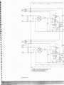
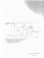
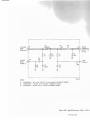
Figure 4-3. Frequency-Meter Bridge,
Simplified Schematic Diagram and Waveforms
4-5
[
09
2N3SbS
A
20 KHZ LOWPASS FILTER
1-------1
I
I
I
I
I L9 THROUGH Ll2
I
I
I
I
I
R'I-b
2.21 K
I
-
I
L
I
I
C29
ITHROUGH I
C32
I
_______
I
-1
r
B
10 FM DEVIATION
[
METER OR
OSCILLOSCOPE
AND SPEAKER
AMPLIFIER
[
AUDIO OUTPUT
[
INPUT TO FILTER ••••• POINT
A
OUTPUT OF FILTER •••••. POINT B
[
S \..lSEC
DETAIL A
-j
f
3.2 V D C - - - - - - - - -
NO MODULATION
AT 100 KHZ
OV---------
l
S \..lSEC
-l
[
[
S \..lSEC
DETAIL B
-j
>3. 2 V D C - - - - - - - - -
I
POSITIVE MODULATION
>100 KHZ
OV---------
-l f
< S \..lSEC
[
S \..lSEC
-l
f
DETAIL C
NEGATIVE MODULATION
<100 KHZ
-j
<3. 2 V D C - - - - - - - - -
OV---------
1
> S \..lSEC
NOTE:
L
1. PULSE AMPLITUDE IS CONSTANT
FOR ALL CONDITIONS.
r
r
[
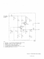
Figure 4-4. Audio-Output Filter, Simplified Schematic Diagram and Waveforms
5601"0015"1
4-6
[
- - ----=,---=-""= = =--=-- ---=-- - --
will be of a higher value. See Figure 4-4,
detail B. During the negative cycle of
modulation, the puls es occur a t longer in
tervals producing a lower voltage at the
output of the filter. See Figure 4-4, de
t ail C . The output of the filter follow s
the fr equency modul ation of th e IF signal.
The r esulting a udi o s i gn al i s fed to th e
VOL UME cont r ol a nd to the Oscilloscope
or FM Deviation Meter for a n indication of
the a mo unt of modul ation.
circuit. The front panel CA L . control
(FP- Rl-l) is for fine cali brati o n a nd co m
pletes the bridge cir cuit.
When th e CE- 7 is us ed a s a C\V- or FlVI
signal generator, the a ction of th e s econd
I F and discriminator circuit s is the sam e
as d e scribed for t he me asuring m od e. The
10- MHz input to the board , howev er ' o rtai
b
nate s on th e Mul ti - Os ci llator board a nd the
ou tput is amp li fie d in th e Broa db and Mi xer
or Pres elector (last tw o s ta g es). Afte r a m p l i
fi cation the s igna l i s fed to the second m ixe r
in the Second IF a nd Dis criminator board.
When the m onitored signal i s of suf
ficient a m pl itude , a de control vo ltage
from th e Broadband Mixer or Preselec
tor, turns on Schmitt trigger Q6 and Q7 . .
This re sults in s wit ch Q8 supplying a
ground to the one- shot multi vi br ato r a nd
the SIG NAL LEVEL l am p, turning them
on . T hus , reli abl e meas ure me nt s can
be m ade prov i di ng the s ignal is o f .suf
fi cient le vel.
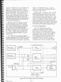
1.3 Power-Supply Board
The CE-7 co ntai ns three powe r
s upplies p roviding regulated outputs
of +5 vo lts , +2 0 vo lt s , a nd -12 volts .
Re fe r to Figure 4- 5 for th e blo ck diagram
a nd Figur e 6-2 for the s ch ematic di agram
of th e Power Supply board . A C power
is fed through power transformer s econd
a r y winding s to the +20- a nd -12-volt
r ectifiers. The 117 -volt AC line power
is fed directly to the ov e n co nt r ol circ ui t .
Two controls are provided to adjust
the zero re ading of the FREQUENCY meter.
Potentiometer R30 is for coar s e calibra
tion of the bridge a nd fr equency me asuring
'---I
IVOLUME I
2ND IF AND
DISCRIMINATOR
AUDIO
AN.P LI FI ER
I
I
~ :~ :I
I
I
I
I
~
MODEL 301
OSCILLOSCOPE
I
r
I" P-O-WE
- R- OF
- F' I:
115/230
V~ --......
50-'+00 ~
-
h
~
'~
I
~~----- --~
I
PO',,'ER
SUP PLY
(REGULATE D)
I
I
I
OVE N
CONTROL
I
I
I
I
[
- f - - - - - r - 01O0
_
1 ~~ENltr
CH A 5
Fi gure 4-5. Power-Supply Board, Block Diagram
5601"0015"1
4-7
+ 5 VDC
-12 VDC
I
I
.-/~+-t_---~-------1'------l
L
:
I
I
!
"C~>-~-+------4-----+----l
+ 20 VDC
+ 13 VDC
<UNREGULATED)
t
CRYSTAL
OVEN
ASSEMBLY
40 MHz s witch . The s witc h r ev erse s the
polarity o f the s igna ls to th e m e t er as th e
LO is a bove or below the des i r ed s igna l
to be monitored or generated. Th e signals
are th en r outed through th e functi on switch,
th e EXT. MET ERS switch located on the
r ear panel, th e ±kHz (F REQUE NCY le ver)
sw itch, and to the c a li bration pot entiom eter s.
Th e +20 -vo lt r e gulator c ons ists of:
br idge c onnec ted r ec tifi ers CRl , CR2 ,
CR3 , C R4; a filter capac ito r , CI; a con
stant c ur rent s ourc e, QI; serie s r egula
tors, Q3 and CH-QI; a referen ce e lem ent ,
C R6; differential a mplifiers, Q5 a nd Q6;
a de a mp li fie r , Q4; and a n ov er- current
pro tectio n c i rc uit, Q2 . Potenti ome t er R9
i s the co ntro l for a dj us ti ng th e +20 -vo lt
s upp ly to the prop er vo ltage.
In th e FREQ. -DE\'. l\l EAS URE pos ition
of th e fun cti on sw itch the r ange of ope ra tion
of th e m eter i s s ele c ta bl e by th e ±kHz
(FREQ GE NCY lever) sw itc h for ±O. 5 kHz,
±1. 5 k Hz or ±5. 0 k Hz , In the FM 0 1.' CAL . /
CW positions of the function switch, th e in
puts to th e m eter a r e th r ough specific r e
s is to r s to provide fi xed r anges of ±O. 5 kHz,
and ±5. 0 kHz, r e spe cti vel y. Diode s C Rl
a nd C R2 pr ovide me ter protec tio n in th e
event of overd rive .
Th e -1 2-volt supply is similar a nd th e
unregulated +1 3- vo lt s upply is s im ply th e
fused output of th e bridge rectifie r s for
the -12-v olt supply. P otentiometer R27 is
th e control for adjusting the -1 2-volt supply
the pr op er voltage . The +5- vo lt supply
is de r ived thro ugh m eans of zener diode C R7
fr om th e +20-volt supply.
,0
T he audi o input fr om the VOLUlV1E
contro l is amplifi e d by ICI and fe d to th e
speak er.
In th e HARl\I. Al\IP. TUNING position
\
The ov en- control circuit c ontr ols. the
AC pow er supplied to the heat windings
of the oven. Fast hea t is cont ro lled by
the snap-a ction th er mostat whi ch opens
a t 65 °C. Regular hea t is co ntrolled by
the m ercu r y co lum n thermo s tat whic h
dos es a t 76 . 2°C and s ho rts out gate Q13,
.vh ich s huts off th e t r iac a n d r emove s the
powe r fr om th e winding. When th e te m p
e ra tu r e drop s below 76. 2°C, th e colum n
op en s . Thi s permits the triac to be trig
ge r ed on the next tim e th e AC voltage go e s
through z e r o. The fr on t panel OVE N ON
lamp is en ergi zed whe neve r the re gular
hea t is on .
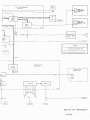
-1-.4 Frequency Error Meter Board
Fi gure 6-3 i s the s ch emati c di a gram
of the F r equ en cy Error Mete r board . Th e
pus h- p ul l dc outputs fr om the discrimina tor
-m d lowp as s filt er are r outed throu gh th e
F R EQU E NC Y BELOW 40 MHz - AB OVE
5601"0015"1
4-8
[:
~
r:
r:
II
[~
[;
of the fun cti on sw itc h, one sid e of th e m eter
is g ro und ed a nd the oth er side i s suppli ed
with the dc tuning volta ge c oming fr om the
Harmoni c Gene ra to r boa rd .
[~
4 .5 Harmonic Generator Board
[~
Fi gur e -1-6 is the block diagram and
Fi gu r e 6- -1 is th e s ch ema ti c diagra m of the
Har m oni c Gene r ato r boa r d . Dep en di ng on
cus to m e r r -equi r ements , up to 23 c ry sta ls
in a fr equ ency r ange of fr om 6.2 MHz to
9. 4 MHz can be install ed in the Cr y s ta l
Ove n As s embly. Any on e of the s e can be
s e lec ted by th e CARRIE R FREQlJ EN CY
SELE CTOR switch . The se lected c r ys ta l
i s capac iti vely co upled to th e modifed
Co lpit ts osc illator Q8, .a nd a m plified by Q7 .
T he out put of Q7 is fed to bo th li mite r Q5
and emi tte r follower Q6 ; th e latter fee ds
th e CRYSTAL OCT Al"X. IN co nnecto r .
This co nnec to r is a c onvenie nt monito r in g
point for m easuring the fr equenci es of th e
c rys ta ls and a l so se rv es as th e input co n
nector for in puts fr om exte r na l crystals
(Mode l l\ICO-6 Multl - Cha nn el Osc i llato r ).
Wheth er a n in t e rnal o r a n ex te r na l c ry stal is
us ed as a signa l s ou rce , the si gnal is pass ed
through limite r Q5, a nd capac itive ly coupled
to tun ed ampli fi e r s QI and Q2 . Th e 6 . 2 MHz
to 9.4 MHz si gna ls are m ultipli ed by QI and
tuned by Q2 to give a fr equen cy range of
Th e Crysta l Ove n As s embly (F igur e 6-9)
is prote cted a gainst ove r hea ti ng by the r m a l
fus e TF1. Any time the temperature in
s ide the oven exc eed s 81. I OC, th ermal fu s e
TFI will ope n and cause the ov en t o become
inoperative.
c
f!'
~
[
~
-~
[ .~
r~
t!"
[~
[e
---- ---:I
~---------
I NPUT
FROM CRYSTAL ... J 3
OVEN ASSEMllLY
/-J=
I
I
f---
~'\N N E L
OSCI LLATOR
'.10DI F I ED
COLP I TTS
OSCI LLATOr.
I
I
/ .J.
I
I
I
~ANNEL AMPLIFIER
b . 2-q . ~
• I
I
CHAN NEL
MHZ
b.2-q.~
" J2
L
•I•
EMI TTER
FOLLOWER
V
/.\HZ
I
l
TUNE D
A."P LIFIER
(X2 . X3)
TUNED
AMPLIFIER
( X2)
H-28 MHZ
II
-
-,-'- 1-'
I
,
,
"
I
-
- - -
--1-'-
I
/
I
I
HARMONI C
GENERATOR
I
~
"
LO QUTP UT TO
COAX I AL RELAY
FP-A2
TUNING VOLTAGE TO
I
I
Jl
- ------ ----~
I
I
,
r
I
I
28- Sb MHZ
:;¥
#:;¥
I
I
I FREQUENCY I ~\ETER
NOTE:
- L - - '- - - - - - - - - - - - -'
X2. X3 INDICATES A
MULTIPLI ER FACTOR.
Figure 4-6. Harmonic-Generator Board, Block Diagram
from 14 l\IHz to 28 l\IHz. This frequency
range is doubled by CRI a nd CR2 and amp
lified by tuned amplifier Q3, to achieve a
signal in the range of from 28 MHz to
56 MHz.
that the tuned amplifiers linearly follow
(track) the manual tuning.
This signal is matched by emitter
follower Q4 to the 10\\' imped ance of
ste p-recovery diode CR4. The step
recov ery diode conducts during the
po s it ive half of th e input-signal and stores
that charge. During the negative half it
i s quickly driven towards cutoff and snaps
back to form an extremely narrow pulse
that is rich in harmoni cs .
The fundament al frequency output is
28 MHz to 56 MHz and the harmonic's
are usable to 1150 MHz. These pulses
and the resulting harmonics form the
LO signal. See Table 4-1.
The board output feeds coaxi al relay
CH-K1. Diode CR3 rectifies a sample
of the fundamental frequency r an ge of
the harmonic gener ator th at is filtered
to form the dc tuning voltage which drives
the FREQUE NCY meter when the harmonic
a m plifi e r is being tuned by the variable
capacitors (C5). Th e ca pacitors are con
nected to the HARl\I. A!\IP. TUNING control.
Transformers Tl, T2, and T3, and the
trimmer capacitors (C6) a r e adjusted such
5601"0015"1
4-9
The Channel Frequency Chart (Table
4-1) provides a means to determine the
crystal frequency when the channel fre
quency is known. Locate the applicable
ch annel frequency range in the CHANNEL
FREQUENCY RANGE column. Add or
subtract 10 MHz as indicated in the ADD
OR SUBTRACT 10 MHz column to deter
mine the first LO frequency re
quired. Th e resultant frequenc y should
be within the range in the LO FREQUENCY
RANG E column. Divide the LO
frequency by the number given in the
DIVIDE BY column.
The resultant fre
quency is the crystal frequency required
and should be within the range in the
CRYSTAL FREQUENCY RANGE column.
Example:
153.123 MHz
10. 000 MHz
-
Assigned frequency
Subtract
143 .123 MHz
1st LO frequency
143.123 + 18
Divide by
7,951.277 kHz
Crystal frequency
Table 4-1. Channel-Frequency Charl
CHANNEL FREQUENCY
RA:\'GE
(i\IHz)
ADD OR
SUBTRACT
10 MHz
L.O. FREQUENCY
RANGE
(MHz)
DIVIDE
BY
CRYSTAL FREQUENCY
RANGE
(kHz)
18.0
to
27.4
Plus 10 MHz
28.0
to
37.4
4
7,000
to
9,350
27.4
to
40.0
Plus 10 MHz
37.4
to
50.0
6
6,233
to
8,333
40.0
to
47.4
Minus 10 MHz
30.0
to
37.4
4
7,500
to
9,350
47.4
to
66.0
Minus 10 MHz
37.4
to
56.0
6
6,233
to
9,333
66.0
to
84.8
Minus 10 MHz
56.0
to
74 .8
8
7,000
to
9,350
84.8
to
122.0
Minus 10 MHz
74.8
to
112 .0
12
6,233
to
9,333
[ --.
122
to
178
Minus 10 MHz
112
to
168
18
6,222
to
9,333
e
178
to
234
Minus 10 MHz
168
to
224
24
7,000
to
9,333
234
to
290
Minus 10 MHz
224
to
280
30
7,467
to
9,333
290
to
346
Minus 10 MHz
280
to
336
36
7,778
to
9,333
346
to
402
Minus 10 MHz
336
to
392
42
8,000
to
9,333
402
to
514
Minus 10 MHz
392
to
504
54
7,260
to
9,333
514
to
626
Minus 10 MHz
504
to
616
66
7,637
to
9,333
626
to
794
Minus 10 MHz
616
to
784
84
7,333
to
9,333
794
to
1018
Minus 10 MHz
784
to
1008
108
7,260
to
9,333
1018
to
1186
Minus 10 MHz
1008
to
1176
126
8,000
to
9,333
4.6 Mulri-Osctllator Board
Figure 4-7 is the block diagram and
Figure 6-5 is the schematic diagram of
the Multi-Oscillator board. The Multi
Oscillator board consists of: 10-MHz,
9.9-MHz and 1. O-kHz oscillators; an
amplifier for up to ten plug-in IF os
cillators; and a 10-MHz frequency
modulator.
oscillator is energized by +20 volts when
the function switch is in the CAL./cw
position. Its output is amplified by Q2
and fed to emitter follower Q3. The
signal is then fed through a 12-dB im
pedance matching circuit and emitter fol
lower Q9 to tuned amplifierQ10. The out
put of-Q10is fed to the Broadband Mixer or
Preselector and is used as a reference sig
nal to zero the FREQUEl\CY meter. It
is also fed to the Signal Generator Step
Attenuator.
Whenever a frequency is selected
(measuring mode as well as signal gen
erating modes) the crystal oscillator as
sociated with that frequency is activated.
As has been stated, the output of each
crystal oscillator is always mixed with
a 10- MHz signal to produce the LO sig
nal. This 10-MHz signal is generated
by transistor Ql in conjunction with a
10-MHz crystal which is located in the
Crystal Oven Assembly. The 10-MHz
5601"0015"1
To modify the LO signal so that it can
he used as a signal generator output, an
other 10- MHz signal must be mixed with
the LO signal. This 10- MHz signal is
generated by voltage-controlled oscillator
Q7, which is energized by +20 volts when
the function switch is in the FM position.
4-10
[,
[I
~
[~
~
[
J(l!!
[:...
[-
L:...
t'"
L::
[::...
l
, - - - - - - - - - - -- -- - - - --1
I
1I" 'l,,iT F' ~ Ofl
C;:l "'S r ~1.
OVEN
A :;' ~ E: ~ ~ l 'f
I
I
I
10 MHZ GEtlEflATOO
ATTE NUAT OO~
I
I
I
I
I.
,--,--I
I
10 nHZ
I
I
AFe
I
:
I
---'-_ _
I
I
S TEP AITt NUAToo
F'M 00 10 ,loI;HZ TO
MODEL )0 3
8R0AC8 AAD MI XEG
OR MODEl ) 0 '*. 30 ';.
30 bB P1=l ESELECTffi S
II
I
1 i(HZ A....P L! F'I ER
I
I
r:...., 00 10 .....HZ TO
S I GNAL ('( ~ERAT OO
[ B J -- - .
>----.<L .
, rr+.'71
I
_ ... ~
~
,
~
I
1--1 KHZ GEs ERATOR- - - l
I - --
- -- ' l . q 11HZ GENERATOO -
-
-
-
I~
I
,
,
-z:
----J
f --;--
1-- - - - - -
: I F'M MOO.!
-
- --
-
'l . CI MHZ TO
2ND Jr: ~ D
DIS CRI MI NATOR
I F OSCI l LATc+lS
:>------(
I SELECTOR I
IOUTPUTI
· 20 V
Figure 4-7. Multi-Oscillator Board, Block Diagram
Its frequency is set to 10 MHz with the
FM CAL. control FP-R5, which adjusts
the voltage to Varicap CR2 in the tuned
circuit of the oscillator. When adjusted
to exactly 10 MHz, the oscillator fre
quency is kept constant by the AFC volt
age from the frequency-error-detector
circuit in the Second IF and Discriminator
board which is also applied to Varicap CR2.
The internally-generated modulating
signal (for FM signal generation) is pro
duced by the I-kHz oscillator. Transistor
Q4 in this oscillator circuit is energized
when +20 volts is applied by turning the
FM MOD. switch to the INT. position. The
output of the oscillator is fed to the DEV.
5.601"0015 "1
ADJ . potentiometer, which provides ad
justment for the amount of signal being
delivered to Varicap CR2 of oscillator Q7
and via amplifier Q5 and emitter follower
Q6, to the I-kHz OUT connector. The
Varicap changes capacitance and thus
frequency-modulates the 10- MHz output
of Q7.
To produce a second-IF signalof 100
kHz, the first IF of 10 MHz is mixed with
a 9.9-MHz signal. This signal is pro
duced by crystal-controlled oscillator
Q13. The 9.9-1VIHz crystal is not
installed in the Crystal Oven Assembly but
ope ra tes at am bient tempera tures. Trans is
tor Q13 is always energized except when the
4-11
fun c ti on switch is in th e I. F . position.
Its output is amplifi ed by Q1 4 a nd Q15,
and fed to the buffer amplifi er in the
Se con d IF and Discriminator board wher e
it is mixed with the fir st IF s ign a l.
4 .8 Signal-Generator Mixer
Fi gure 6- 8 is the schem a t ic diagram
of the Signal Gene rator Mix e r . Th e LO
signal which r eaches th e Signal Generator
l\Iixer from the Harmonic Generator board
via th e coaxial r elay (CH- K1) consists of
narrow pulses with a fr equency between
28 MHz and 56 MHz . This LO signal is
mixed with a s ec ond input signal with a
10 MHz frequ ency fr om the Sign al Gen
erator Step Attenuator. The resultant
signals are coupled out to the SIGNAL
GENERA TOR OUTPUT connector.
4.7 IF Oscillator Board
Th e Multi-Oscillator board provides
10 r e ceptacles into which IF oscillator
boards may be inserted at th e option of
th e c us to me r . Refer to Figure 4-7.
The frequen cies that may be s el ected
for th ese crystal-controlled oscillators
lie in ranges of from 250 kHz to 900 kHz
(see Figure 6-6) and from 1 MHz to
13.5 MHz (see Figure 6-7). When the
fun ction switch is in the I. F. position,
th e I. F. GENERA TOR SELE CTOR m ay
be turned to one of its numbered posi
tions (1 through 10), thus a +20-volt
energizing voltage is a pplied to the cor
responding receptac leo Th e o ut put of
th e act iv ated o s c i llato r c i rc uit is amp
lifi ed by Ql1 and Q12, and is ava il a bl e
at th e I. F. GE NE RA TOR OUTP UT con
ne ctor. If a dditional IF freq ue nc i es a r e
needed or if it is desirable to cha nge the
frequ ency th at is av ailabl e in a parti cular
po sition of the SELE CT OR, r e fer to P ara
graph 3. 4.5 for installation a nd removal
of I F Oscillator boards.
5601"0015"1
If the desired signal output is below
40 MHz then th e Harmonic Generator out
put is high er th an the desired signal by
10 MHz and the lower s ide ba nd is used,
and vice-versa for the above. Th e
F REQUE NCY BELOW 40 MHz - ABOVE
40 MHz switch should be switched a c cord
ingly for proper r eadout.
The multi-turn LEV EL SET control
feeds a de voltage to mixer-diode CRl
and forward-bias e s it at diffe r en t cur
r ents for ca li bra t ing th e signal genera
tion output in th e differ ent co mmunica
t ion s fr equency ba nds .
4-12
[
[,
SECTI.ON 5
MAINTENA NCE
of th e CE-7 a nd pus hing in on thi s knob .
The Mode l 303 Broadband Mixe r and -Mo del s
304 , 305, or 306 B P r e s ele c tor are r e - .
moved by loos en in g t he LOC K k nob on the
fr ont pane l of t he plug-ins, a nd pus hing in
o n th e knob to dis e ng age th e pl ug- in con
necto r from th e CE- 7 recepta cl e .
5.1 Introduction
This section co ntains t he necessary
pro ced ures t o per form adj us tme nt s and
troub leshooti ng of the CE - 7 . If a dj ust
me nts ot he r th an th o s e de s cribed a re r e
quire d, it is reco m me nde d th at th e in stru
me nt or subass embly be r eturned to
Cus hman Ele ctroni cs , Cus to me r Service
Dep artment for cali bratio n a nd alignm ent.
5.3 Fuses
Th ere are three r egulat ed pow er s up
pli es within th e CE-7: +5 volt s, +20 volt s,
a nd -12 volts. The +5- vo lt s up ply is deriv ed
by m e ans of a z ene r cliode from th e +20 - vo lt
s up ply a nd doe s , th e r efore not hav e a sep
arate adj us t me nt or fu s e. Se parate fu s e s
a nd a dj ust me nts for t he -1 2- a nd +20 -vo lt
s up plies a re on Powe r Sup ply board 0100
lo cated on the right s ide of the ins tru
me nt. See Figure 5 -1 . Th e - 12- a nd
+20- vo lt suppli e s a re protect e d by 1. 0 amp
slo - b lo fu s e s . The uppe r -adjusting potenti
omete r a nd uppe r fus e a re for th e +20- vo lt
s upply . The lower- a djusting pot en tio mete r
a nd lowe r fus e are for the -12- vol t su pply .
If one of th e s e fuses blows, th e r e si s t a nc e
between the r egulator outp ut t erminal a nd
gro und shou ld be m e a sure d to m ak e s ure
th at ther e is not a s ho r t circ ui t. Tab le 5- 1
g ive s the a pprox i ma t e re s is ta nces to chass is
g r ound for each s uppl y (o r, in the case of
the plug-ins, for th e lo ad a cros s each s upp ly) .
It i s ass umed th at th e o pe r ator is
famili ar with th e oper ating proce dures
des cribed in Secti on 3 . Th e in strum ent
s ho ul d be war m ed up fo r a t l e ast 30 min
utes befor e a ny a dj ustme nt or troubl e
s hoo ti ng is a tte mpte d . For m ost of th e
tes ts a nd inte rnal a dj us tme nts, th e s ide
cove rs and botto m cover m ust be r e
moved . Th e te s t eq uipme nt req ui re d
for each adj ustme nt i s give n a fte r pr e
l imi nary ins t r uctio ns (Pa r a g r a ph s 5 .4 . 1
thr oug h 5 . 4. 6) . For ease of following
the adjus t m ent p roced ures o r c hecks ,
the steps are gi ven in tabula r form (Table s
5-2 th rough 5- 7) . T r oubl eshooting guid es a lso
in tabular form (Tabl es 5-8 through 5- 11 )
are prov i de d to ass ist t he ope rato r in lo
ca liz i ng malfuncti on s. Int erior vi ew s of
th e instrument a r e included t o ai d in lo
cati ng the vari ous test a nd adj u st m e nt
poi nt s .
Th ere are two s epa r ate AC fus e s lo
cated on the rea r pa nel of the CE -7 . A
1. 0 a mp s lo- blo fus e is for th e mai n
AC powe r to the ins t rum en t. The ot he r
is a 0.2 amp slo-blo fu s e that prov ides
p r otec tion to the Mode I 301 Os cillo s c ope,
wh ich ha s a regul a te d power s upply .
5.2 Ac cess
Co m ponents in th e top par t o f th e in stru
me nt can be r e a che d by r e m oving th e two
L -s haped s i de covers . Each cov e r is se
cure d to the chass is by s ix sc rews . Th e
speake r lea ds m ust be d isconnec ted be fo re
the r ig ht - hand cover can be remove d com
ple te ly . Co mpo ne nts in th e botto m par t o f .
the instr ume nt can be reached by setti ng
t he CE -7. on its r ear panel , wit h the botto m
fa cing forward . Th e botto m co v e r is se
cur e d to the chassis by s ix screws .
5.4 Adjustment Procedures a n d Ch eck
Th e foll owi ng pa r agraphs (5.4. 1
t h ro ug h 5 .4 .6) i nter s pe rs ed wit h the i r
re spective tables provide pre li m i nary
instructions a nd t es t eq uipm en t requir ed
for performanc e o f th e t e sts given to
maintain the CE-7.
Th e Model 302 F M Devi ation Meter
o r th e Model 301 Os c illo s cope is r emoved
by loos ening a sm all kn ob on th e r e ar pa ne l
5601"0015"1
5- 1
[~
,
[:
[::
Jb-1S
FREQUENCY ERROR METER
BOARD 0101 (FP-Al)
HARMONIC GENERATOR
BOARD 0102 (FP-A2)
R9
R27
CH-J7
F2 Fl
POWER SUPPLY
BOARD 0100 (CH-AS)
Figure 5·1. CE-7 Right Interior View Without Plug-In
5.4.1
5.4.2
Power-Supply Board, Voltage Adjustment
Preli rni nary Instructions:
Preliminary Instructions:
Adjustments for the power supplies
(Table 5-2) are on Power Supply
Board 0100 (CH-A5) located on the right
side of the instr ument , see Figure 5-1.
a.
The crystals and trimmer capaci
tors for each of the 23 channels are
in the Crystal Oven Assembly (C H- A4).
Access to the trimmer capacitors is
through the bottom of the instrument.
See Figure 5-2. The Crystal Oven
Assembly cover has a revolving disc
with one tuning hole, which can be
rotated to line up with the access
holes for each of the 23 crystal
trimmers. The tuning tool used to
adjust the trimmer capacitors must
be an insulated female-slotted tuning
driver. Refer to Table 5-3 for Cry
stal Oscillator Adjustment procedures.
b.
A separate 10-MHz crystal, also
located in the Crystal Oven Assem
bly (see Figure 5-2), is used when
the function switch is in the CAL. /
CW position. Its trimmer capacitor
access hole is located diagonally above
crystal position 21 on the Crystal Oven
Assembly cover.
NOTE
The -12-volt and +20-volt regulated
power supplie s are factory set to
within 0.5 percent of rated output
voltage and should not be changed
unless a voltmeter having an ac
curacy of at least 1. 0 percent is
used.
Test Equipment Required:
a.
Volt-Ohm-Milliammeter, Simpson
Model 270 or equivalent. (20,000
ohms-per-volt or higher sensitivity,
1. 0 percent accuracy, +5 V and
-50V ranges.)
b.
VTVM, Hewlett- Packard Model
400H.
5601"0015"1
Crystal-Gsclllator Adjustment
5-2
c.
Place the instrument on its rear
panel with the Crystal Oven
Assembly facing forward.
5.4.3
Frequency-Meter Adjustment
Prel i minary Instructions:
a.
Test Equipment Required:
a.
Frequency Counter, Hewlett- Packard
l\Iodel 5245 L , or equivalent.
b.
Tuning Tool, GC Electronics No. 8279.
c.
Signal Gene rator, Hewlett- Packard
Model 608 or 612.
Balancing the Second IF and Dis
criminator board 0054 (CH-A2) should
prec ede a dj us t m e nt of the FREQUENCY
meter. Perform the following CAL.
a nd FM CAL. centering adjustments.
NOTE
The SIGNAL LEVEL lamp must
be on before proper adjustments
can be performed.
Table 5-1. Power Supply, Resistances to Gro·md
+5V (green wir e)
-12V (orange wi re)
+ 20V (red wire)
lIIea sured
at
Re s.
(ohm s )
Measured
at
CE- 7 Monitor t
(le s s plu g-in s)
Pin 15 o f
Rf plu g-in
r eceptacle
75 0-170 0*
Pin 14 of
Rf plug-in
re ceptacle
40 0-450
Pin 17 of
RF plug-in
rec eptacle
50 0-550
:-lode l 30 1
Os c i llo sc ope
:\ot us ed
-
Pin 14 o f
con ne cto r
4.5 K-7. 5Kt t
Pin 13 of
connec to r
1. 5K-1. 8K*
Xlodel 302
Deviat io n
Xle te r
:\ot us ed
-
P in 14 of
co nne c to r
8. 2 K- 8. 5K*
Pin 13 of
co nnec to r
1.7K
Mode! 303
Broadban d
Pin 15 of
co nne cto r
3 .5 K*
Pin 14 o f
connector
500
Pin 16 of
c onnec tor
Pin 17 of
connec tor
1. 8-2.4K* t tt
Re s .
(oh ms )
Mixe r
Xlodel 304
Pre sele ct or
Xl o de l 30.5
Pre sel e r: tor
Model 3Cl6B
Prese lec to r
:\O T E:
Pi n 14 of
conn ector
Pi n 15 of
conne ct or
P in 15 of
co nnec to r
1. 25 K-50 K*
1. 2.5 K- 50 K*
5. 3K
Pi n 14 of
conn ec to r
Pin 14 of
co nnec to r
Pin 14 of
connector
265
265
500
Me asured
at
Res.
(oh ms)
10K*
Pin 16 of
co nnector
Pin 17 of
connec tor
80 0
Pin 16 of
co nnecto r
Pin 17 of
co nnecto r
3.8K
Pin 16 of
co nne ctor
Pin 17 of
co nnec to r
22 K-30 K*
24 K
3K
,
12K
All r e s i stance r e adings tak en with a Simps on 270 using RXI00 sc al e .
.--\ll re si stan ce re ading s of modul e s taken with mo dule r emoved fr om s e t.
* De pended
on oh m me t er test-l e ad po la r ity . The r e ading s m ay also vary depending upon oh m me t e r range .
t i\Ieasure r e si stance to chass is of s upp ly lin es.
tt Re si st an ce readings taken with " ve rn ie r" pot in mid pos it io n .
ttt Res is tanc e r eadings t ak en with se le ctiv ity s witch i n " nor m a l" .
5601"0015"1
. .1iiIIo
5-3
_
•
[
[
I
C
l
lO-1l1HZ
TRIMMER
KI-J3
CRYSTAL OVEN
COAXIAL RELAY
(CH-Kl>
ASSE~mLY
(CH-A~)
A3-J2
CARRIER
FREQUENCY
SELECTOR
SIGNAL GENERATOR
MIXER (CH-A3)
Figure 5-2 . CE-7 Bottom Interior View
Table 5·2. Power-Supply Bo ard, Volt age Adjustment
TEST POIKT OR
ADJ USTMENT
PERFORMANCE
STANDARD
Measure -Lz-volt supply to cha s s is
ground (s e e Figure 5-3 ).
TBI-3 (orange
wires)
-12 volts
IB
Adjust lower pot enti om e te r
(s ee Figure 5-1).
R27 (CH-A5)
-12 volts
2A
Measure +20-volt supply to cha s s is
ground (see Figure 5-3).
TB1-1 (red wires)
+20 volts
2B
Adjust upper potentiometer
(see Figure 5-1).
R9 (CH-A5)
+20 volts
3A
Measure +5-volt supply (s ee
Figure 5- 1).
CH-J6-15 (green
wires)
Between 4.8 and
5.2 volts.
4A
Measure -1 2- and +20-volt rippl e
at test points s pec ifi ed in steps
lA and 2A with vtvm.
STEP
Fl-NCTION
lA
5601"0015"1
Less than 1. 0
millivolt.
5-4
U
Table 5-3. Crystal-Oscillator Adjustment
TEST POINT OR
ADJUSTMENT
STEP
F UNCTION
lA
Connect input of the counter to the
CRYSTAL OUT/A UX. I N connector .
PERFOR IVIA i'\CE
STA i'\DARD
[:~~~!~~~=J
The level at this point is ap
proximately 20 0 millivolts into
50[2 (0.2 volts) . Ensure that
t he co unter can be us ed at t his
level.
lB
Set CARRIER FREQUENCY
SELECTOR to "I" .
lC
Align rotating oven disc to po st tion "1" .
lD
With the tuning tool , adjust trimmer
to th e c ry s ta l frequenc y listed
on the Channel Frequency Chart.
IE
Repeat steps lA through lD for
each of th e other 22 crystals .
The cry stal Ire
quency selected
sho uld be within
3 .0 Hz of the sp ec
ified frequency.
Appropriate
Trimmer
Capacitor.
NOT E
The following steps are to be
performed when installing new,
or changing c rystals .
2A
Connect th e output of t he signal
generator to the ANT . connector
of the RF plug-in being used .
2B
Set the s igna l generator to the ap
proximate frequency of the carri er
channel desir ed.
..
2C
Adju st the output level of the signal
generator to approximate ly 20
millivolts.
2D
Set the function switch to HARM .
AMP . TU l'\1NG and CHANNEL
FREQUENCY SELECTOR to the
carrier channel desired .
2E
Rot~eilieHARM .
AMP . TUMNG
contro l fully co unterclockwise .
5601"001 5"1
5-5
Crystal frequency
li sted for po sition
Ill" on Channel
Frequency Chart.
-
Table 5-3. Crystal-Oscillator Adjustment (Continued)
FUNCTION
STEP
2F
TEST POINT OR
ADJUSTMENT
PERFORMANCE
STANDARD
Rotate the HARM. AMP; TUNING
control slowly clockwise to the
first peak reading on the FRE
QUE NCY meter.
2G
Set the function switch to FREQ.
DEV. MEASURE and ensure that
the SELECTIVITY switch is in the
NORMAL position .
2H
Set the ±kHz (FREQUENCY lever)
to 5 and the FREQUENCY BELOW
40 MHz - ABOVE 40 MHz control
to the appropriate position.
2J
Vary the signal generator around
the channel frequency until the
SIGNAL LEVEL lamp lights.
f!!!
~
~
[;
~
KOTE
False responses may be en
countered when varying the sig
nal generator frequency too far
above or below the assigned
frequency.
2K
If the SIGNAL LEVEL lamp does
not light, the HARM. AMP.
TUWNG control may be tuned to
the wrong peak.
2L
Set the function switch to HARM.
AMP. TUl\lNG and rotate the
HARM. A1\IP. TUNING control
slowly clockwise to the next peak.
Repeat steps 2G through 2J.
2M
When the SIGNAL LEVELlamp lights
center FREQUE?\CY meter with
signal generator frequency control.
.
::\OTE
Ensure that the FREQUENCY
meter deflects towards the plus
(+) side when increasing the sig
nal generator frequency.
5601"0015"1
~
~
5-6
Tabl e 5-3. Crystal-Oscillator Adj us tm en t (Continued)
T E ST P OINT OR
ApJUSTMENT
STEP
FUNCTION
2N
Redu ce the outp ut lev el of the s igna l
generator until the SIGNAL L EVE L
lamp goes out.
2P
Slow ly increase t he s igna l ge nerato r
output le vel un til the SIGNA L L EV EL
lamp li gh ts.
,
-
PERFORi\IAI'\CE
.S TAI'\DA HD
Sens itiv ity les s
t ha n 5 m ill ivol ts
if ope ra ting below
500 MHz , le s s
tha n 10 mill ivolts
if ope ra ling abo ve
500 MHz (using a
Broacl ba nd Mixe r ).
NOTE
Whe n using one
of the RF Pre
s e le c tor s the
sens itivi ty should
be less than 20
m ic rovolts .
2Q
Rec ord the num ber in di ca t ed on the
HARM . AMP . TUNING control on
the Cha nne l F r equency Cha rt.
NOT E
The following steps a re to be
pe r form ed for the l O-MHz
ad ju stment.
3A
Dis conne ct coaxia l conn ec to r a to p
Signal Gene ra tor Mix er, whi ch is
a bove th e C rys ta l Oven Ass embly.
(S ee Fi gure 5- 2. )
CH-A 3-J2
3B
Co nnect th e coaxia l conn ecto r
(A3- J 2) to the in pu t of the co unte r
wit h a su itable adapte r .
3C
Set the functio n sw itch to CA L.jCW.
3D
Set the SIGNAL GENE Ri\ TOR at
tenuato r multip lier to Xl OO a nd
ve r nier co ntro l fo r maxim um
output.
3E
Adjust 10 -MHz tr imme r with tuning
to o l .
3F
Rec onnec t coax ia l co nnec to r to
Signa l Ge ne rato r Mix e r .
.
5- 7
5 60 1" 0 0 1 5 " 1
T r imme r
Capac itor .
10 .0 MHz ±10 . 0 Hz
a s indicated on
counte r .
.....
•
CAL. centering:
6.
CAL.lcw.
1.
Set the function switch to
2.
Set the CAL. control (inner red knob)
to a tw elve 0 I clock position.
3.
Adjust R30 on the Second IF and Dis
criminator Board 0054 (CH-A2) for a
zero reading on the FREQUENCY
meter. Refer to Figure 5-3.
b.
FM CAL. centering:
1.
Set the function switch to CWo
2.
Zero FREQUENCY meter with the
CAL. control.
3.
Set the function switch to FM.
4. · Turn the DEV. ADJ. control fully
counterclockwise.
5.
Set the FM CAL. control (inner
red knob) to a ten o'clock position.
SECOND IF AND DISCRIMINATOR
BOARD o05~ (CH-A2)
Adjust L5 on the Multi-Oscillator
Board 0103 (CH-A1) through the
access hole in the left frame of
the chassis (remove Fl\I Deviation
Meter or Oscilloscope) for a zero
reading on the FREQUENCY meter.
Refer to Figure 5-3.
The FREQUENCY meter ranges are
adjusted by means of an oscillator
which can be offset from 10 l\IHz
by exactly ±O. 5 kHz, ±1. 5 kHz,
and ±5. 0 kHz. Refer to Table 5-4.
The CE-7 first IF is 10 MHz and its
discriminator will detect and display
frequency error above or below this
frequency.
c.
The Model 303 Broadband Mixer
must be installed in the CE-7 before
any adjustments can be performed.
d.
On the Frequency Error Meter board
0101 (FP-A1) mounted on the back of
the FREQUENCY meter are three po
tentiometers. The top one (R2) is for
±0 . 5 kHz, the middle one (R4) for
±1. 5 kHz, and the bottom one (R6) for
±5.0 kHz. See Figure 5-3.
FREQUENCY ERROR METER
BOARD 0101 (FP-Al)
TBl-l
~=-- TB l - 3
R30------c
R2
R~
L5
Rb
MULTI-OSCILLATOR
BOARD 0103 (CH-Al)
Figure 5-3. CE·7 Left Interior View Without Plug-In
5601·'0015"1
5-8
.
[
""
[
[
tIf!lII
[~
[,..
....
[e
'!!'"
[ t!!'
-~
[~
[
~
~
Test Equipment Require d:
a.
Signal Generator, Hewlett- Packard
Model 606.
b.
Frequ ency Counter, Hewl ett-Pa ckard
Model 5245 L .
c.
Tuning Tool, JFD El e ctronics Co.,
No. 5284 .
Table 54. Frequency-:Het er_:4.djustment
TEST POINT OR
ADJUSTMENT
STEP
FUNCTION
lA
Set the function switch to CAL. / CW
and zero the FREQUE NCY meter
with the hiller r ed control knob.
Rl
1B
Set the FREQUENCY BELOW
40 MHz - ABOV E 40 MHz s wi tch
to ABOVE 40 MHz.
Set th e fu nction swit ch to FR EQ .
DEV. ME ASURE an d c onnect th e
output ofthe signa l ge ne r ator to bot h
the input of the Model 303 Broad ba nd
Mix er and i nput of th e counte r
(using a liT" adapte r ).
S3
lC
PERFORMANCE
STANDARD
NOTE
The SIGNAL LEVEL lamp
must be on before proc e eding
with s te ps lD through l G.
lD
Set the ±k Hz (FREQ UENCY lev er )
to .5.
IE
Adjust the signal ge ne r a to r to
10,000,500 Hz.
IF
Adjust th e to p (0. 5 k Hz) pot enti
om eter for full sca le .
1G
Repea t ste ps 1 D th roug h 1 F but
a dj us t th e signal ge ne rato r to
10, 001, 500 Hz wh en the =k Hz
(F R EQ UENC Y l ev e r ) is s et to
1. 5, a nd 10 , 00 5, 500 Hz when
the ±kHz (F REQ UEN"C Y l eve r )
· i s s e t to 5.
5601"0015
S2
0.5 kHz as
indicated on
FREQUENCY
meter.
R 2 (FP-A1)
R4 (F P - A l ) a nd
R6 (F P- A1)
5- 9
1. 5 kHz and
5 .0 kHz as in
dic a t ed on
FREQ UE NCY
m eter.
.......
~
f!!'
pur pose of the fixed a t te nua to r is to
prote ct the instrument wh en the CE-7
is dire ctly connected to a tr ansceiver
whi ch is ac ci de ntally k ey ed to trans
mit. Keying a tr ansmitter will
normally burn out th e RF fuse. But
before the fuse blow s, the r e sistors
in the fixed a tt e nuato r m ay have been
subjected to a transi ent ov erload
severe enough to damage them and
ch ange their values. Changed
ohmic values would cause cha nge d
attenuation .
5.4.4 20-dB Eixcd-Attcnuntor Loss Check
Preliminary Instructions:
a .
A 20-dB fixed attenuator is supplied
with the CE-7 and is stored inside
the front cover. The CE-7 attenuators
a r e calibrated in terms of signal volt
a ge at the output of the 20-dB fixed
attenuator. Refer to Table 5-5. The
fixed attenuator must therefore, al
way s be used if the output levels
indicated by the position of attenuator
knobs ar e to mean anything. The
[e
~
[~
[
Table 5-5. 20-dB Fixed-Attenuator Loss Ch eck
STEP
TEST POINT OR
ADJUSTMENT
FUNCTION
lA
Feed a 10-microvolt s igna l from
the s ig nal generator into the
r eceive r ,
lB
Note the receiver meter reading.
lC
Feed a 100-microvolt signal through
the attenuator into the receiver.
lD
:'\ote the two receiver meter
readings.
PERFOR TvIANCE
STANDARD
The two reading s
should be within
0. 5 dB of one
another.
NOTE
The 20-dB fixed attenuator loss
may be checked using an RF
Voltmeter such as the Boonton
9lD in place of the receiver.
Perform the following steps as
required.
2A
Connect the output of the signal
generator into the RF Voltmeter
through a 50S? termination using a
SOS! co axi al cabl e .
--
2B
Set the signal generator output level
to approximately 100 millivolts and
not e the reading on the voltmeter.
2C
In sert the 20- d B fixed attenuator
between the signal generator and
voltmeter, and note the difference
in reading s .
5601"0015"1
20 dB ±O. 5 dB
5-10
l
b.
Since it is ess en tia l th at the fixed
attenuation is precisely 20 dB, the
checks listed in Table 5-5 must be
performed if damage is suspected.
c.
When it becomes necessary to
repair the fixed attenuator, re
move the single screw and slide
the cover off. A decal on the side
of the fixed attenuator casting shows
the component values. The resis
tors are standard 5 percent values.
The fuse is a special RF fuse (Buss
man tf G F A 1/32A ) .
c .
set the signal gcnc rnto r to thi s
frequency by morutortnc it on the
CE-7.
.
b
NOTE
When using frequcn cics hig-her
than 100 MHz, the signal gcncruto r
must be tuned very slowly to a c
commodate the narrow bandwidth
of the CE-7. If a Pr e s c lc cto r is
being used, ensure that it s
SE LE CTIVITY switch is set to
l'\ORl\IAL.
Test Equipment Required:
Test Equipment Required:
a.
b.
c.
Signal Generator, Hewlett- Packard
Model 60 S.
a.
Model 6 OS.
Metered receiver with 50Q input
impedances capable of operating
a t the required frequencies.
b .
RF Voltmeter, Boonton Model 9lD,
or equivalent.
5.4.6
5.4.5
..
b.
Slgnal-Cenerator-vllxer Input Level Check
Preliminary Instructions:
The output levels are adjusted by
signal substitution. Refer to Table
5-6 . First, a signal from a cali
brated source is fed into a metered
receiver and the meter reading
noted. The CE-7 is then substituted
for the calibrated source and the
output LEVEL SET control of the
CE-7 is a djusted until the meter
reads the same as before. The
receiver should be metered at a
point where saturation is least __
likely to occur (for example, the
first and second IF stage) and the
HF input signal should be preferably
1. 0 microvolt.
Select a frequency at which the
adjustment is to be made. This
frequency must be within the cap
abilities of the external receiver,
the external signal generator, and
the CE-7 .
560 1" 0 0 15 "1
•
Metered receiver with 50Q input
impedances capable of operating
at the required frequencies .
Signal.Generation-Output Level Adjustment
Preli minary Instructions:
a.
Signal Generator, Hewlett- Packard
a.
The signal generator mixer may be
damaged in the same manner as noted
for the 20-dB fixed attenuator (Para
graph 5.4 .4) . When it becomes nec
essary to repair the signal generator
mixer, it will also be necessary to
readjust the signal generator output
lev el s (Table 5-6).
b.
The two inputs to the signal generator
mixer are: a 10-MHz signal from the
Multi-Os cillator via the Signal Genera
tor Step Attenuator, and a signal that
may contain frequencies of from
28 )'IHz to 1150 MHz from the Har
monic Generator via the coaxial relay.
Refer to Table 5-7 .
Test Equipment Required:
RF Voltmeter, Boonton Model 9lD .
5-11
Table 5-6. Signal-Gcneration-Output Level Adjustment
TEST
POINT
OR
ADJUST
MENT
FUNCTION
STEP
1A
Adjust the signal generator output
to 1. 0 mic revolt.
IB
Feed the signal generator output in
to the receiver and note the receiver
meter reading. (Be cautious of sig
nal generator frequency drift. )
1C
Set the function switch to CWo
Adjust the CE-7 to generate a
signal with a 1. O-microvolt
level.
ID
Disconnect the signal generator
from the receiver, and connect the
output of the CE-7 to the receiver.
Use the 20-dB fixed attenuator fur
nished with the instrument.
IE
[:
If the receiver meter does not read
the same as in step 1B, adjust the
10-turn LEVEL SET attenuator on
the CE-7 for the same meter reading
Record the new LEVEL SET number
on the Channel Frequency Chart.
[~
fill'
[~
,..
[e
~
[e
0
NOTE
Typical calibration frequencies
are as follows:
The LEVEL SET number for
various frequencies in the same
For this
band will be the same
reason, it is not necessary to
make the adjustments for every
channel frequency.
FREQUENCY
BA:\D
0
-
IF
Set the function switch to FM and
center the FREQUENCY meter with
the FM CAL. control. Turn the
DEV. ADJ. control fully
counterclockwise
0
5 6 0-1 " 0 0 1 5 .. 1
.
PERFORA~NCESTANDARD
5-12
20 to 80 MHz
120 to 180 AIHz
450 to 512 MHz
900 to 1000 MHz
NOMINAL FRE
QUEl'{CY for
CALIBRATION
35
155
460
960
MHz
MHz
MHz
MHz
Less than 1. 0 dB from CW
reference.
[~
[
[
[
[~
[,..
Tahl e 5-7. Signal.Gcncraior.;Uixer-Inpul Level Check
TEST P OINT OR
ADJUSTMENT
FUN CTION
STEP
PER FOR rvIA 0:CE
STANDARD
10 l\1Hz INP UT L EVEL CHECK
lA
Se t th e func ti on s wi tc h to CWo
IE
Di s connect th e coaxi a l ca ble fro m
th e EN C connector ato p the signal
generator mi xer (s ee Figure 5- 2).
lC
Terminate RF vo ltmeter in SOD.
ID
Me asure cabl e output voltage.
CH- A3-J2
--
20 0 millivolt
±2 . O dE (atten
uator controls
mu st be s e t at
maximum output).
COAXIAL RELAY LEVEL CHE CK
2A
Set the functi on switch to CW.
2E
Disconnect th e coaxial cabl e from
l eft s id e of the c oaxial relay (s e e
Figure 5- 2).
2C
Ter minate RF voltmeter in 50D.
2D
Set th e functi on switch to HARM.
AMP. T CNING.
2E
Sel ect a ny (used) channel with
CARRIE R FREQUE NCY SELE CT OR
switch.
2F
Tune HARM. AMP. TU:t\TI NG control
fo r m aximum re ading on FRE
QUE 0:CY m eter.
2G
Me asure cabl e output voltage
CH-KI-J3
At le a st 700
millivolt s.
5.5 Troubleshooting Procedures
li sted a r e not ne cess arily a ll of the problems
th a t m ay be encountered . For furthe r
information, contact Cushman E le ct ro ni cs ,
Custom er Se r vi ce De partm ent.
The following tabl e s (5-8 through 5- 11)
det ail t e sts r equir ed to loc alize malfunc
ti on s in the CE-7. Th e malfunction s
5601"0015"1
5- 13
- -
- - --- - -
Table 5-3. Troubl eshooting, Frequency-Deviation.:\leasure (FDi\I) :\Iode
~ORr.1AL
TROUBLE
CHECK
INDIC ATIO N
REFER TO
SELECTING PROPER CHANNEL
Pilot light out
Lamp
Front panel of CE-7 .
Output of -12V regulator
Fuse A5-F2
-12V ±O. IV.
-
Power Supply Board
0100 (Figure 6-2).
Power Suppl y Boa rd
0100 (F igur e 6-2 ).
Rea r panel of C E-7.
AC li ne fuse CH- Fl
HARM. AMP. TUNING
No meter movement
METERS INT. -EXT.
slide switch position.
Set in INT.
position.
Rear panel of CE-7.
Channel crystal .
(select another crystal
position and retune).
Greater than 0 .3
on fREQl"E:\CY
me te r .
Crystal Oven Assembly
(Figure 6-9).
Channel oscillator output
at CRYSTAL OUT AUX.
IN connector .
200 MV at f P- J 4 .
Harmonic Generator
board 0102 (Figure 6-4).
Harmoni c amplifi er out
put at SIGNAL GENERA
TOR OUTPUT connector .
700 MV at
CH-A2-Jl .
Harmonic Generator
board 0102 (Figure 6-4).
Wiring or loose contacts
on function switch .
Front Panel Wiring
diagram (Figure 6-11).
RF Plug-in
Applicable in struction
manual .
CAL./cw
No SIGNA L LEV E L light o r
FREQUENCY meter indication.
lO-I\IH z gene r ator.
(Try Fl\! pos ition
on functi o n swi tc hv )
200 xrv at
CH-Jl-14, R.
Multi-Oscillator board
0103 (Figure 6-5) .
+5V power supply.
- 5. 0\' =0. 2\'
at CH-J6-15.
Power Supply bo ard
0100 (Figure 6-2) .
Lamp on in
Front Panel Wiring
diagram (Figure 6-11).
No SIGNAL LEVEL light
indication. FREQ UE NCY
meter OK.
Lamp and conne cto r .
SIGNAL LEVEL light on , no
FREQUENCY meter deflection
in CAL. /cw.
METERS I!'''T.-EXT.
slide switch position.
CAL./cw
position.
Function switch or
FREQUENCY meter
movement,
(set function switch to
FM and adjust DEV.
ADJ. control for a
reading on FM DEVIA
TION meter) If nor
mal, check L7 and LB.
Other positions on
functi on switch.
5601"0015"1
5-14
Set in INT .
position.
Re ar panel of CE-7.
~nt Panel Wiring
ram (Figure 6-11).
Second IF and Dis
criminator board
0054 (Figure 6-1).
Front Panel Wiring
diagram (Figure 6-11).
[
[
[
[
Tahle 5·8. Trouble;;hooting, Frequency.Deviation-l\Ie~ sure (FDM) Mode (Conlinued)
CHECK
TROUBLE
SIGNAL LEVEL light on,
FREQUENCY meter r eads
off scale.
REFER TO
Output of -12V regulator
-12V ±O.lV
at CH-J6-14.
Power Supply board
0100 (Figure 6-2).
9.9 MHz generator.
80-100 MVat
CH-Jl-2. B .
Multi-Oscillator board
0103 (Figure 6-5).
NOTE
The preceding trouble
shoot ing procedures a lso
apply to the Signal Gen
erator mode of operat ion .
NORMAL
INDICATION
Q4, Q5
Second IF and Dis
criminator board 0054
(Figure 6-1).
.FREQ.-DEV. MEASURE
RF Plug-in or Broad
band Mixer . pin 7.
Greater than
600 MV.
Applicable instruction
manual.
Local oscillator connec
tor or coaxial relay
cable.
700 MV at CH-J7
Figure 5-1.
Coaxial relay CH-K1 or
Harmonic Generator
output. (Li sten for relay
operation while switching
function switch to dif
ferent positions.)
700 MV at
FP-A2-Jl.
Figure 5-2, and Har
monic Generator board
0102 (Figure 6-4).
No audio , SIGNAL LEVEL
Speaker connection.
light on. (Nor ma l ope ration
of FM Deviation Meter,
Model 302.)
Audible tone in
FM position.
Power Supply board
0100 (Figure 6-2).
Audio amplifier .
1. 0 audio at
CH-A5-17
output with
50 MV input.
Power Supply board
0100 (Figure 6-2).
Speaker.
3 . Of) dc
resi stance.
Right-hand side cover.
Inoperative in this position only .
FREQUE:\CY meter operative
but FM DEVIATIO~ meter on
Model 302 does not indicate or
no trace on Oscilloscope,
Model 301.
FM Deviation Meter or
Oscilloscope
Q9
Applicable instruction
manual.
3.2 vdc
Second IF and Dis
criminator board 0054
(Figure 6-1).
CARRIER FREQUE:\CY SELECTOR
Erratic FREQCE:\CY meter
action in on e or more of the
crystal positions.
Switch contacts on
CARRIER FREQUENCY
SELECTOR.
NOTE
This is also ch aracter
i stic of the Signal Gen
erator mode of o pe r atio n.
5601"0015"1
5-15
Figure 5-2 .
Table 5-9. Troubleshooting, Signal-Generator Mod e
TROUBLE
CHECK
CAL./CW operative as verified in
Table 5-4, but no output.
.
No modulation, No indi cation on
Model 302 FM Deviation Meter,
;
NORMAL
INDICATION
REFER TO
20-dB fixed attenua to r .
20-dB fixed attenuator.
Coax ial re lay C H- K1.
(Listen for re lay opera
tion while swit ching
funct ion sw it ch to dif
ferent positi ons .)
Figure 5-2 .
Harmonic am plifier
output at SIG:\AL
GENERATOR OUTPUT
connector.
Greater than
700 MV.
Front panel of CE-7 .
Signal Gen er ator Mixer;
local oscillator signal
from coaxi al relay
CH-Kl.
Greater than
700 MV at
CH-A3-J1.
Figure 5-2.
10-MHz signal from
attenuator. (Defe ct ive
function switch , att en
uator, o r wir ing.)
200 MVat
CH-A3-J2 .
Front Panel Wiring
diagram (Figure 6-11).
Or an ge/ white wi r e,
(-12V bias diode CRl).
LEVEL SET pote ntio
meter or Wir ing.
-12V wi t h
LEVEL SET
control s et to
zero.
Signal Generator Mixer
(Figure 6-8) .
FM MOD. IKT,-EXT.
1 kHz OUT SWitch .
Set to INT.
position.
Front panel of CE-7.
1 k Hz ge ne ra- o r .
(1 kHz OUT connector
with HI MOD. INT .
EXT. 1 kHz Ol'T swit ch
in INT. positi on.)
Greater than
l.OV at FP-J2.
Front panel of CE-7.
10-MHz FM Generat or.
Set FM MOD. I:\T,
EXT. switch to EXT.
with external so ur ce
of 1 kHz at 1. OV fed
to EXT. connector .
Control of
deviation with
DEV, ADJ.
control.
Model 302 H I
Deviation Met er.
[e'
[~
[
Multi-Oscillator board
0103 (Figure 6-5).
Applicable instruction
manual.
[
[
[
5601"0015"1
5- 16
.
Table 5-10. Troubleshooting, I.E-Generator Mode
TROUBLE
No output in all positions of the
the SELECTOR switch.
600 MV not present at pin P
on Multi-Oscillator board.
600 MV present at pin P on
Multi-Oscillator board.
No output in one position of the
SELECTOR switch, all other OK.
CHECK
NORMAL
INDICATION
REFER TO
IF Oscillator output.
600 MV at
CH-J1-P.
Multi-Oscillator board
0103 (Figure 6-5) .
+20V to the selected IF
Oscillator board position
on the Multi-Oscillator
board.
+20V ±O.lV.
IF Oscillator board
0104 (Figure 6-6) or
0105 (Figure 6-7).
Qll or Q12
Multi-Oscillator board
0103 (Figure 6-5).
Wiring of SELECTOR
switch.
Front Panel Wiring
diagram (Figure 6-11).
Attenuator potentio
meter and associated
wiring.
Front Panel Wiring
diagram (Figure 6-11).
+20V to selected IF
Oscillator board.
+20V ±O.lV.
IF Oscillator board
0104 (Figure 6-6) or
0105 (Figure 6-7).
+20V present from SELECTOR
switch.
Crystal or transistors.
IF Oscillator board
0104 (Figure 6-6) or
0105 (Figure 6-7).
+20V not present from
SELECTOR switch.
SELECTOR switch
wiring associated
with that position.
Front Panel Wiring
di agram (Figure 6- 11) .
-
5601"0015"1
5-17
-
c•
[~
Table 5-11. Troubleshooting, Crystal-Oven Ass embly .
TROUBLE
CHECK
NORMAL
INDICATION
II!
REFER TO
Excessive frequency error on all
channels.
OVEN ON light on c ontinuously.
Shorted triac 40529, Q13 .
Oven I ight on
for approx. 30
seconds and off
for approx . 90
seconds after
warm-up.
Power Supply board
0100 (Figure 6-2).
,
C
[:
,
[,
NOTE
•
Thermal fuse TF1
blows if triac shorts.
[:
Mercury column thermo
stat (regular heat).
OVEN O:-llight will not en ergize.
(Regular heat failure).
[~
Blown thermal fuse TFl.
Crystal Oven Assembly
(Figure 6-9).
Open triac 40529, Q13.
Power Supply board
0100 (Figure 6-2).
Snap-action thermostat
(fast he at).
Crystal Oven Assembly
(Figure 6-9).
Mercury column
thermostat .
Crystal Oven Assembly
(Figure 6-9).
OYEN ON lig ht
connector.
Front panel of CE-7 .
OVEN ON light s tay s o n for
more th an twenty minutes .
(Slow warm-up noticed, but
cycl es normally after warm-up.)
Ope n snap-action
thermostat .
Crystal Oven Assembly
(Figure 6-9).
OVEN 0 ;\ light cyc les no rmally.
Mercury column
thermostat.
e
[,
e
[~
@
[f!
[
-@
[~
~
Tem perature with
thermometer.
Crystal Oven Assembly
(Figure 6-9).
164 F .
0
[:
t'
[t!
~
[:
[.•
•
[
•
r-:
5601-'0015--1
5-18
[-•
Every effort has been made to ensure the accuracy
of this manual. . If an error is discovered please
notify us on the postpaid cards attached.
Please indicate where the error has been made.
To improve future manuals your comments are re
quested.
CUSHMAN ELECTRONICS
PUBLICATIONS DEPARTMENT
There is an error on page
manual;
/figure
of the
_
_
I would like to see these changes incorporated:
_
SIGNATURE
_
----:-
COMPANY
There is an error on page
manual;
/figure
I would like to see these changes incorporated:
SIGNATURE
COMPANY
of the
_
_
_
_
_
_
-----------------~.~--------
. .
i
..
,,
SECTION 6
.
.
SCHEMATICS, PARTS LISTS, AND PARTS PICTORIALS
6.1 Introduction
Section 6 contains schematic diagrams, wiring diagrams, parts lists, and parts pictorials for
the CE-7 Multi-Channel FM Communications Monitor. Table 6-1 lists the reference desig
nations and abbreviations used.
Paragraphs6.2.lthrough6.2.9 contain: 1) parts pictorials, 2) parts lists, and 3) schematics
for the various subassemblies in the order in which they were described in Section 4. Figures
6-10 through 6-12 are the main-chassis, front-panel, and rear-panel wiring diagrams and are
accompanied by the associated parts lists and parts pictorials.
P Y4 AJ
FABIO TEIXEIRA MAGALHAES
5601··0015
6-1
- - - - -----
T.able 6:1. Reference Designators and Abbreviations
REFERENCE DESIGNATORS
Deg
A
BM
B
DEV
ELECT.
ENCAP
C.
CH
Y
DS
CR
V
E
FL
FP
r '
HR
Hz
L
J
M
P
RP
K
assembly
balanced mixer
' board
capacitor
chassis
crystal .
device, indicating
diode
electron tube
electronic part, misc.
filter
front panel
ruse
heater
hertz
inductor, RF choke
jack
meter
plug
rear panel
II
R
SCR
LS
S
TB
TP
TF
RT
S
T
Q
WT
.
EXT
F
F
11M
FREQ
Ge
GRD
H
Harm
Hz
Ie
IF '.
INCD
IN.
INT
K
LIN
LO.
LOO.
LP
relay
resistor
silicon controlled
rectifier
speaker
switch
terminal .boa r d
test point
thermal fuse
thermistor
thermostat
transformer
transistor
wiring tiepoint
M
MEG
MFR
MINAT
MY
N
P
PC
pF
PlY
POS
POT.
PP
p/o
ABBREVIATIONS
AC
ADJ
AFC
AMP
AMPL
ANT.
AUX
BP
C.
CAL
CCW
CER
COAX.
COE'F
COM
COMP
CONN
CRT
· CW
CW
DB
DC
5601··0015
alternating current
adjust
automatic frequency
control
amperes
amplifier
antenna
RECT
REPL
RF
SB
SEC
Semicond
auxlliary
Ta
TGL
TOL
TRIM
TYP
Si
bandpass
centigrade
calibrate
counterclockwise
.ce r a mlc '
coaxial
coefficient
common
composition
connector
cathode-ray tube
clockwise
continuous wave
decibel
direct current
~
UHF
V
VAR
VDCW
VERT.~
VHF
W
WW
wi
w/o
6-2
degree
deviation
electrolytic
encapsulated .
external
fahrenheit
farad
frequency Tnoan\a\\tm
frequency
germanium
ground
henry
harmonic
. hertz
integrated circuit
intermediate frequency
incandescent
inch
internal
kilo (10 3 )
linear
local oscillator
logarithmic
lowpass .
milU (10- 3 j ,
mega (10 6 )
manufacture
miniature
mylar
nano (10- 9 )
peak
printed circuit
picofarad (10- 1 2 )
peak inverse voltage
position(s)
. potentiometer
peak-to-peak
part of
rectifier
replace
radio frequency
slo-blo
second
semi conductor
silicon
tantalum
toggle
tolerance
trimmer
typical
micro (10 6 )
ultra high frequency
volt
variable
dc working volts
vertical
very high frequency
watt
wire-wound
with
without
•
%
•
:
•
•
•
•
•
•
•
•
•
•
•
P Y 4 A J
ABlO TEIXEIRA flt t\ GALHA~
6.2.2 Po wer-Supply Board
-C3
Ob
C1~
C2
O~
os
Jl
02
C10
Cll
C8
C9
C7
0 1
I C1
Cb
CS
C~
CRa
R27
R2b
R2~
R28
R2S CR13 R23
R22
R19
CRS
R21
6-7
5601--0015
R20
CR12
R1
CR2
CR3
R29
R30
CRll
6 2 2 POWEn SU P P L Y BOAR 0 0 100
oct , REF.
e ll -AS
DESO(IPTION
el E STOCK NO.
_.
Boa rd Asse mb ly , Power Su pply
7001 -00 05
Cu shman
Boa r d , Print ed Ci rcu it
l780 -0 100
Cus h man
6 22
POWE R "'l'PP Lr BO\R O OIOO (Conti nued)
O<T. REF' .
10 14 -00 04
10 13 - 00 11
10 14- 0002
1005 - 00 14
1002 -0035
Spragu e
IC I
Sp r agu e
Wh al e
Er ie
El me nco
C6
C7
CB
C9
CIO
l\Uca. 470 er , ' 5%. 100 V
Ele c t. , 15 ~F, 25V
El e c t. , 100 IIF . 25V
Cer, 0 .05 p F -+S Ol · 20 1 , 25 V
El e c e., 250 " F, 16 V
1002- 003 5
10 13- 0005
10 13- 0003
1005- 0 014
1013 - 001 6
Sp ra g ue
Sp r-agu e
Er ie
Sp rague
CII
CI2
C I3
CH
C IS
Elect . , 100 J.lF, 25 V
Elect. , 2300 JlF , 50 V
El e ct. , 100 pF , 12\1
E lec !. , 500 p F, 25V
Po ly, 0 .22 pF. t IO!}• .tOOV
1013 -0003
10 14- 000 "
10 13- 0011
1011,- 000 2 1008 - 0 04 2
Spr a gu e
Sp ragu e
Sprague
" 'hale
Sp r ague
3705 - 0006
C lu2.
El monee
F use
JI
s.,
l N4002
51. I N-lOO:?
51. 11\'306-1
128 1· 00 23
128J - 00 23
1281- 0023
1281-0 023
1281 - 00 13
CR 6
51. Ze ne r , 6 .8\1. 1x·957
1281 - 00 07
Co n tl n eo~
C R7
CR8
C R9
C R IO
51. Zener , S, I V. 1.....-1733
1281 - 00 31
1281 - u0 23
128 1- 0023
1281 - 0023
) [ofo rol a
ITT
ITT
ITT
CR l l
CR I2
st . t N ~002
sr, I N3 06 .t
en i s
51, Z e ner, 6 .3 V , 1:"95 7
1281- 00 2 3
1281 - 0 01 3
1281-00 07
ITT
Sy lvania
Co ntt ne cie,
51. I N-lOO:?
51. I N-IOO2
--
IT T
ITT
ITT
ITT
Syl va ni a
DevIce e
51 . 1 ,,"ol 0 0 2
Si,
IN4 002
I X-l002
Device s-
POWER S UP P L Y BO ARD 0 100 (Co nti nue d)
ocr.
DESCRI PTI ON
REF' •
C/ E STOCK NO .
_.
PCh annel fET. 2H34 2
xP ,'". 2 :"3-116
NP~ . 2 :'\305 3
SI,
51.
s.,
1\'P~ .
2~3 565
os
Si , P:,\,P. 2 :"-1249
Q6
51. P ;-'; P, 2:\ -1249
P Chan nel F ET . 2::\'43U
Q7
QS
Q9
'1 10
QlJ
Q I2
q J3
st.
l\'P :'\. 2 \"3-1 16
Si, NP;-"- , 2:-"3053
Si , NP>: , 2 :\3-116
sr.
127 2-0027
127 1- 0006
127 2-0 0 11
1272- 0017
127 2- 0024
G. E.
RCA
Fa ir c hi lt'
Fai r chi ; ';
127 2- 0024
127 2 -0 0 27
1271 -0 006
1272 - 00 I I
1271 -0 006
Fai t-chile
G. E ,
RCA
G. E ,
P:":P. 2 :":-12-19
1 2 72 - 0 0 2~
51. P :-'; P. 2 :\-1249
127 2-0 0 24
127 2- 0029
T ri ac , 40:)26 o r
~O 529
2025 - 00 15
G . E.
2586 - 00 07
Key stone
Lll t lefuse
CIRCUlT
Ampt , Audio , P.\2? 2
PC Bc ar d. "lount ed Phone
.-
Come, 1, Sk!', ~ :) 'c, I / -IW
Co m p , ioor. ~ t . 1 / ~\\'
F ixe d , ww, i . co , ::31, 3W
Compo -I: 0f' . ~ ( , 1/ -1 w
Com p o 2 .2k:"". .:5 ~ . 1/~W
1066 - 1825
1066 - 10 15
1159 -000 1
1066-H 15
1066 - 2225
Att en-Br-ao tey
All en- Br-adley
Oh mt te
R6 ·
R7
R8
R9
R IO
Com p. ' . '10. . =.5 ~. I /~ w
Com p , l l k!"', .5 ~ . 1 /~\1,!
Comp, 39l"!". : 5 ~ , 1/-4W
\·.l r . WW. S (\(of", 2\\'
Comp , l ~, ~ 5 ::; , I '-IW
10 6 ti - ~ 725
1066 -1 035
1('1)6 - 391 5
12(1 0- 000 3
1066- 1025
Alle n - Bradl ey
All en- Bradle y
All e n- Br a d ley
CTS
AlI en- Br adle y
Co mp o EO\\!: . ~ ~ . 1/4\\1
Co mp o 22.\\!:, :..5 : . 1/4 \\'
=5 ~. ~ ' ~ \\'
Co mp o 1(": , =5 ~ . 1 '2\\'
Co mp , L~ , =5 ~ . I · ~ W
1066 -2235
1060-2 205
106> 1005
106";-1025
Al len -B r adley
All en - Br adle y
All en- Br-adley
Alle n-Br adl ey
Att en- Br a dley
1060- 1005
IOGo -1 005
1067- 6815
106'3-1 8 25
1060 - 10 IS
Alle n- Bradl ey
All e n-Br ad ley
Allen - Bradl ey
Allen-B r adt e y
..Ul e n-Br adle)·
°Rl1
R I2
R 13
R14
R15
Come.
RI6
R I7
RI8
R19
R2 0
Co m po
R21
R2 2
R23
R24
R25
F ixed, \\ '\\" . I. ('!1, · 31. 3\\'
Co mp. -17(1(.' , .:..O~ . I /-I W
Comp, :~Df'. ::...or. 1!4\V
Ccmp . ; . ; ~. :"'::, l '4W
Com po : <'~ , ::5 ~. 1 / ~ \\'
R2 6
R27
R2 8
R29
R30
Com po
;: (~.
Com p.
2. ';' ~ ,
Compo
33~ .
Come.
Compo
, .~
:'"'. -,
l / ~ \\ '
=,-, ~ . J '-4\\,
.:5 ~ . 1 /2\\'
Co mp o 1. ~ '<. : 0 :, 1/-1\\'
Co mp o I J~ \ :.5 ~. 1 '-1\ \ '
l' ~ .
5~ ( -:' .
Co m p , -It-:-:: , =..0::; , 1/ -4\\'
var. \\"7.,.. 5Mf' . 2\\'
T)p l C'3 .." al ue
.s >,
1 ' H\I
.:..0 ~ . I\\'
~:: .
~
.
IIV
..c w tr ,
10 6 6- 1 0 ~ 5
1159·0001
1060 - H 15
52 15
1t -:'; ·-\1 35
1(,'; 0)·103 5
Allen- B r adley
Allen- Bra dley
Ohm lt e
Alle n- Br adlej-
1 (' t)6 ~
Allen -Br adl ey
x tteo - Br ad le y
All en - Br adl ey
H,6.j ·-I7 15
12NJ-0003
1(,>505--171 5
1(;1; =· 2725
Allen- Br adley
CTS
Allen- Br adl ey
Allen - B r adl ey
Alle n-B radl ey
1 0 6~ · 33 3 5
~
,•
~
•
,•"
•
T R ANS ISTORS
QI
'12
Q3
Q4
Llute lus e
RI
R2
R3
R4
R;
Fac tory Sc.e c: .
6 . 2 .2
1955 ·0 006
1955-0006
R ESISTOR S
DIOD ES
C RI
CR2
C R3
C R4
C R5
_.
J ,\C K
C UP
s.,
3 .\t; . 1 amp . a tc - bto
3.\ G. I a mp. slo - blc
l ~ T E G R...\ T E O
Etect . • 2300 ~ F . 50 \'
El ec t. , ioo "F . 12 V
Ele c t . , 500 IJF . 25 V
C e r , O. OS J.l F .g O't -2 0~ , 25V
Mica , 4 70 pF, . 5'l. . 100V
C/ E >TOO< NO.
FL!SES
FI
F2
CAPAC ITO RS
CI
C2
C3
C.
C5
DESO(IPTI ON
Fai r chil c
Fai r c fuc
Fa rr c bt l c
F aJr chll ':
RCA
G
f
f
f
f
4
4
.;
«
4
c
4
f
f
560 1"00 15
6-8
6.2
Th e part s li st s a nd parts pictori als for th e
main ch a ssi s (CH), front panel (FP), and
r ear panel (RP) are shown in Paragraph s
6 .2 . 10 t hr ough 6. 2. 12. A parts list for
th e CE-7 covers and carrying c ases is in
cluded in P aragraph 6. 2. 13.
Schematics, Parts Lists, Parts Pictorials
Par agraphs 6 .2. 1 through 6 .2 .9 , on
the following pages, provide s chemat ics ,
parts lists, and parts pictori al s for the
various subassemblie s de s cribed in Section 4 .
6 .2.1
Second IF and Discriminat or Bo ard
C29
C31
C30 C32
C28
R%
5601"0015
Cl
C9 C21 C20
C27
C33 CR5 C2Q C2 3 CRb
RQ 5 RH
R23
C25 CR9 C2b
R2Q R25 R3 1 R29
Cll C13
R27 R2 8 R20
6- 3
C8
C3
TP1 Cq
C2
R lb R18 R17 RH
Cb
C7
R5
C1 7
C5
Rl
CH C1 2 CI0
C1 5
".r
",.
Q~
Q8
Q5
Q7
R21
Rl'\
Q3
R15
Q2
L~
LS
I C2
r
L3
r
r
.
"
.
.
r
r
-,
~
f!
r
r
Lll
QiD
Ll2
L7
R22
L8
Qb
R33
R3 7
Ll
L2
R3b
Ql
I Cl
f'
R8
"fr'
~
6 2 1 S ECO'-'D IF A I\"D
D ISCRI ~n'\ A TOR
C H-A 2
BOA R D 00 5-1
DESCRIPTION
O<T . REF.
6 2 1 SECON D I F A ' l) D1SC RJ\ [] \-.l, T O R BOARD 005 4 (C on ti n ue d)
c/s
"FR.
STOCK NO.
Board Assem bly, Second I f an d
Discr imina to r
7001 -000 -1
Cushr;. '=....1
Boar d. Pr i nt ed Ci rc u.it
li ~ r) - OO54
Cushm ::"--:l
1IJ13- 0005
10)3-0 0 11
}('(':)-OO 13
Sprague
on.
Ele c t. , 15 "F, 25 \'
Ele c t . , 100 "F, 121'
Ce r , 0 .01 IJ r ""6 0 ~ - 20 ; . Z ~\'
Ce r , 0 .0 5 p.F '"30'( - 2 0 ~ . 25\'
0 ,05 p F -+i) o1 - 2 0 ~ . 25\'
c- .
1(.(5 - 00 14
i«
5 - 0 0 14.
:: p ra.g''':~
En e
Erie
Erie
C6
C7
CS
C9
C I0
Ce r . 0,0 1 JlF ~ O ";- - 20-:', 25\'
Ce r , 0 ,0 1 IJF +80'1 - 2(,1 . 25\'
C e r , 0 .01 p F -f8(Jf. - ZO=(. 25 \ '
1(1 ;"- 00 13
Eri e
1((·5-00 13
En e
lOv5 -00 13
Ce r , 0 . 0 1 p F -t-O( I -~ - Z O ~, 25 V
Ce r, 0 , 0 I IJ F .ft3 0 =t -20 1. 25 V
l 'JO.'j- OO13
1005 -0 0 13
E r ie
Eri e
C ll
CI2
C I3
Cl'
Ce r , 0 .0 1 IJF '"'80~ -20':( . 2 5\'
",Uca , .J30 p f J:5=t. 1001'
1{'(;5-00 13
10(,2- 00 34.
10(·2- 0034
10 1~ -j - OO 11
c is
:\Iic:l, 4 30 p F ±5 ct . 100\'
Ce r , 3 .3 pF -o. 25 p r , 600 \'
Ce r , 2 .2 p F 1:0.25 p r , s oov
CI 6
C 17
C IS
C I9
C2 0
Ce r , 0.01
Ce r , 0, 05
:\flc a , 4,70
Ce r , 0,05
,"Uc a , -t70
C2 1
C22
Ce r , 0 , 05
:\li ca , 100
Ce r , 0 .05
:\1Jc a , 4 70
Ce r , 0. 05
C23
C2'
C25
£1me nco
El mencc
Eri~
p F -+£ 0 1 -2 0{ , 25\'
p F -+80 "t - 201, 25V
p F .t.5 ~ , 100Y
l.IF ..go1: ·20~ . 25V
p F J:S1 . 100 \ -
10 f)5 - 00 13
10',5 - 1'; 01-1
I O'JL- IJ035
Er ie
Erie
EI rnen c o
E rie
1002 -0035
El rne nco
p F -+tI O"; - 20 ~, 25V
p F ~ 5 1 , ioov
Jl F "60 "; -2 n1. 25 V
p F J: l~L 1 (~H"
pF ~ OC ~2 C. 7,. . 25 \'
100.1- 00 H
J(l02 -00 11
E rie
Et men cc
( rle
l Qr) j- QOH
1002 -00 H
1005 - 00 14
Elme nco
R F , 4i G ~ H t-5 :;
Choke. RF , 47 0 .. H t5 \
In <! :'; ;: ~ :J r • v a r , 0 . 5- 0 .7 5 JlH
ln duct or , v a r , 0 . 5-0 ,7 5 pH
Chok e. H F , 82 ...H t 5%
L6
L7
U
L9
LIO
Choke .
Choke.
Choke,
Cho ke ,
Chok e ,
L11
LI 2
Ele ct. • 15 "F. . 2 V
xuca, 017 0 pF t S%. 100 \'
El ect. , 100 " F, 25 V
Poly, 0 , 027 p F .dO=<, 100 \ '
. Poly . 0 ,027 J-lF t1 0 ~ , 100 \'
10 13 - 001 S
1002- 0035
10 13- (1 003
1003·0 032
10(J8-003 2
Spr -ague
Elrne nc o
C3 1
C3 2
C33
:\li ca , 2000 pF J:S~ , I OO\'
Po ly , 0 ,027 pF d 01, 100 \'
Ele c t. , 15 " F , 25 V
I f; (J2- (J077
10k- 0032
1013-0 005
( I menco
Sp r -ague
Sp r-ag ue
MFR.
158 5- 00 19
1$85 -00 19
1596-00 II
1596- 00 1 1
158 5- 0032
De le v an
Delev a n
T RW
TR W
Del e v an
RF . 8 2 ~ H ...5 1
22 Jo' H : :) "{.
a r, 22 " H t 5",t
RF, 2 , 2 J.lH .:: 5 ';
RF , 4 . 7 m H .1:;')'
158 5- 00 32
158 5 - 00 29
156.; - 0029
1585- 0030
158 5 - 00 06
De le van
De l e van
De Ie van
Del e van
Del e v an
C ho;';e , R F , 4 . 7 mH t5 %
Choke . R F , 2 .2 J...H t 5 %
1585 -0 006
1585- 0030
De le v an
Dele van
s.,
ar,
ce,
CR I
CR 2
CR 3
C R,
CR5
G<i33
G(>, G03J
1\"3064
So, 1\"3CJ6 -\
si , 1.'\306 -1
128 2- 0005
128 2- 0005
128 1- 0013
J 28 1- 00 13
128 1- 001 3
ITT
ITT
Sy tvanla
Sy lvania
Sy tva nla
CR 6
CR 7
C RS
CR9
CR IO
s..
si . 1:"3064
ce . G<i33
l S3{,li-\
ce . 0533
Si , lS306-1
128 1-00 13
128 2- 0005
128 1- 001 3
1282- 0005
1281- 0013
Syl va ni a
ITT
Sy lv a ni a
ITT
Sylv a ni a
IC I
IC2
Ampl, RF . CA 3 «~ 3 A
Am p l , RF . CAJ(,z 3A
2025 -00 12
20 25 -0 0 12
R CA
RC A
Rl
Come , S20fl, :::p' ,
Com p, 3 . 9 ~ , :. 5 ~ ,
Co mp , 3 . 9k.'/, ~~,
Co mp . 3.3k!t, :.5:'~.
Camp, 1 . 2 ~ , .1j .~ ,
1/4W
1067 - 8215
106 6- 39 25
1066 -3925
1066 · 3 32 5
1066-1225
All en All en Al l e nAl le nAll e n-
B r adley
Br adl ey
Br adley
Br ad le y
Br adl ey
Co m p, 2 , 2 ~ , :. 5 ~ , I / H V
Camp , S iD, ~ ; . 1/-I W
Ca mp, 22lY. l, ~ ~ ~ . I / H V
Camp , lk.~ , .1';: , I f -iW
Ca m p , 3.9 k!1, :..5~ , 1/ 4 W
1066 - 2225
1066- 51 05
10SS- 221 5
1066- 1025
1066-39 25
Afle n AJ le n Al t e nAl len Allen -
B r a dl e y
Br a dley
Bradley
Bradl e y
Bradl ey
CIR CUl TS
RESlSTOR S
Spr-agu e
R2
Sp rag ue
Spr agu e
IU
R'
R.5
Ro
R7
RS
R9
R IO
5601"0015
O. (. :;~' ,
I ~TE GRATE D
Eri e
C26
C27
C28
C2 9
C30
C1E STOCK NO.
DIODES
Erie
E rie
u)rJ~-O O H
LJ
L2
L3
L4
LS
En e
1 0 f l ~ - OO 1 7
OESOHPTI ON
COILS
CAPAC ITORS
CI
C2
C3
C'
C5
REF.
6-4
1/ 2 W
1/ 4 W
I/,W
I/ ' W
.,r.
..
•.
.
~
"
-
I~-
• I"
+20 V
~l
2 N) 05 't
+2 0 V
/CfI
FROM
RP- Tl-B
IN
+35 V
01
2N"+3'+ 2
FROM
O!
21
Rl
1.BI<
RP- Tl- 7
+13~ S
Cl
2300
V
02
2 N3'tl b
+1
R3
1. 0
- 0. 3 V
R5
2.2
]".4,1':
I)
CH-0 2
~
•
~
2N30S,
...D. b V
ou :
+13 V TO
CH-Kl-2
lN Cl!
FROM
.RP- Tl - b
Ol.
FROM
Rlq
RP_ 11-5
1. BY.
2N'
-b. 7 V
C12
~
23 00
-1 0.
~
~
R21
1. 0
- 12. 5 V
~
~
~
I
.-
L- __
+
NOTE:
1.
2.
3.
.....
S.
5601"0015"1
RES I STORS - 1/ '+\1' . S'- VAL UES IN ~ UNLESS OTHUN ISE NOTED..
C,6.PACITOR S - VALUE S IN ~F UNL ESS OTHERWISE NOTED .
I NDUCTOR S - VALUES IN IJ.H UNLESS OTHERWIS E NOTED.
-FACTORY SELECL
TYPI CAL VAl l£ SHO'IJN .
All VOLTAGES ARE DC UNLESS OTHER'Jr'ISE NOTED.
R23
U20
?I•• 3.
-12 V REGULA
1_.
· !":- "' =E: :v... Al ~
5 V---1
FRCI< VOL\J'£ CONTROL
AUOI O I NPUT
F"P_ R3- 2
. 20 V BUSS
TO CIl- T8 1- 1
f
RJ>
'f 10
c-
.i,
, 10Pl:::T' Rll '
R18
b80
l /Z 'W
l OOK
(Ilb
l NQS 7
I
C'I
. 05
l .r i
I
C3
500
.5 V
1
R12
22K
.
1
I
I
_I V
I CI
PA2Z2
5
.lca
~
l'
1
rr ..
22
-
," CS
C'l
HO "'
RS
2 . 2K
I
=10
'"
. S V TO
CH-J b- 15
'8 V
l~ I
C? ~
IS
t------q>-
I
!
RI b
10
~
Rl S
lK
1m
,
. l CI 0
- 'T' 250 - '1' 100
I
I N't 73 3
I
Rl '
10
l / ~'W
I
FROM" CHASS I S GRD
CH- 'W T- l
Jl
~
AUDI O
CONNECTOR
FOR SP EAKER
AC LIN E F IL TER
F" ROM, RP_ T8 l-S
Rzq
2. 1><
1..
TO lB 2- 1
CH- A ~
(Ill]
(15
R3 rJ
.2 2
33"
1"
AC LI NE F'l L TER
FROM RP- T8 1- J
AND t H- A"
lBl- l
R2b
'10
I NQS7
)
a ll
TO CIl- A'
rei -s
~ N 't Z 'tQ
R21
SOQ
.1 V
IOVE N ON I
C1'
, .'
lilt ..
1,'""
:
LV,
-1 0. 8 V
,)
j
&_
L
I
TO CIl- A'
lB l -'
TO CH- A't
lB2 -3
Hb
I~ I ~lE-l---~=====~~--L----L
•
I
J
R28
R23
820
2 V REGULATOR -
P O
-
- --
-
-
I
-
-
-
-
-
!
-
O'/ EN CONTROL
--j
-
-
-
- --
-12 V 8 USS
CH-TB l -3
•
0 10 0
CH- A5-JS
Figure 6·2. Power-Supply Board (0100)
6-9/6-10
6.2.3 Frequency-Err-or-Meter Board
Ml
CRl
CR2
R2
R~
Rl
Rb
R3
R7
.:' t!l '~ <'1J. ~
. •.
~
DSl
'E. A'll:·*f.AS'.:l' '.. ;!J
R5
6.2.3 FREQLTE\,CY ERROR il1ETER BOARD 0101
on. REF.
FP-AI
DESCRIPTION
C/E SIOO< NO.
MFR.
Board Assembly, Frequency Error
xrete r
700
]-(01)1,':;
Cushman
Board, Printed Circuit
17'3(I-ul"j
Cushman
12~ ]_ ( _!.'l l ,
1 ~'3I-( I " 1 q
Svfv.m!a
S). \~'::I ni a
z... ;:(! . h " J'::
G. E.
l-l( I;;- ",1.; 3
Cushm.m
j{JI)G-I l.:j ,.
Anen - Br ad.e.
Hr-Ht rt rn
Alle n- BrdClt:.
Hettt rrm
DIODES
CHI
CR2
sr.
OSI
Incandescent.
s.,
1\316
1:-"816
LA~1P
I
['
['
I'
I
I
r
~fl
Frequency Error
RESISTORS
HI
R2
R3
RJ
Comp, ]Okn, ~ ;) :r. , )/4\\
Pol., V,:W. l krl. 1' 2 \\
Comp, I.2kr-, t3 ';:, }/-lW
121. j-() I.l:':'
I () f) ,~ - ]I ' ~ -.
Allen-Br:H:! \02:"
V,:W, lOIC, I !2W
Como. 47!Q', -I:5i. ]!4\\"
12 J':' III d , '~
In GC·1i' J ~j
All en- I3r ,l Cl t
Comp, 1Okf', ....51
R6
R7
Pot.
I"
r
i
I'
I
r
r
f'
I
r
.~
ww. 5 \.;!":,
121.')-(,i)l-l
HJ6fJ-l..:::..:,
}/-1\\
Pol.
R5
I
r
r
r
OJ1820
~IETER
5601"0015··1
l / 2 \\"
.
ucttt rr m
,
\,
I
R3
R2
1 K
I
1.2 K
I
TO FP-S2-1
±O.S Kf'Z ADJ.
IFREQUENCyl
TO FP-Sl-E-3
RS
10 K
R't
Rl
10 K
S K
TO FP-S2-2
±l.S KHZ ADJ.
R7
't7 K
Rb
10 K
-A/IIIr
±S. D KHZ ADJ.
TO FP-Sl-E-'t
DSl
757
•
, 9
TO RP -~ l - S
CRl
lN81b
~
CR2
IN81b
I
:..:
L
--~
- - -
:':SISTORS - 1 / '+ ·v, S% VALUES IN OHMS UNLESS OTHERWISE t+:iTED.
ure
D--").
Frequcncy-Error-Yletcr Board (0 I 0 I)
6-11/6-12
6.2.4
Harmonic-Generator Board
C4
C7
C9
C8
Cll
Cl2
CD
C2
C2S
C3
Clb
-
Cl0
.
C18
C32
C~O
C27
C28
C2b
,.
.
~.
t
."
C2'1
C33
R5
Rb
R8
C31
R7
C30
R9
C29
RiO
C19
C21
Rll
Rl
R1S
R4---!:c~
Rl'I
R3
R12
~-- R 17
R2
R23
R13
R21
R27
5601··0015
R28
R30
R31
R3b
R32
6-13
R3't
C35
R33
R22
02
au
CR2
T2.
L2
03
Ii. ,
'
r...
I
:-1
...
:.,
I
r~
~
07
•-,
4
CRS
08
CR't
~
•
,,
i
G 2 .4 HAfDl 0 ::--.1 C GF: \'ER AT On n O \ R D 0 102
OESCRIPTION
CKT. REF'•
F P - A2
MFR.
C/E $ TOo< NO.
Bo a r d A ss e m bly, li a r m on i c
Ge ne r-ato r
70 01 -0 aOi
Cush ma n
Boa r d. Pri nt ed Cn-c ut t
17 8 0- 0 10 2
Cus h m a n
10 05 - 00 13
100 ,; - 001 3
10 05 - 0 0 13
Eri e
Er ie
Eri e
Er ie
100 0- 0006
TR W
C
C A PA CI T O R S
CS
ci
C2
C3
C4
C)
Cer , 0 .01 /.IF
~ fJ r - 20:;0,
Ce r , O. OJ j l r "'; fI ~ - 20 1, 2.5 V
Ca pccno r , VJ.r , 8, 1- 117, 5 pF,
3 s ec tio n, Ty pe B 1000 -0006 wi t h
1$ 0 · stop
Cap , var , P/O C5
.\li c a , 10 0 or. ~51 , IOOV
Ce r , 0.002 " F, ! 2 0 r , 6 00 \ '
Ce r , 0 . 00 2 " F. . 20 ";" GOOV
Ce r , 0 .0 1 #-IF 4) 0 ~ - 2 0" 25\1
100 2- 0011
100 5- 00 03
1005 - 0 003
1005 - 00 13
El m e nee
Eri e
Ene
Er ie
CII
C l2
CJ3
CH
C 15
Ce r , 0 .002 " F. <201 . GOOV
Mle a. 16 0 pr . ,5 1 . SOOV
Ce r , 0 . 002 " F. ;.2 0"';, 6 00V
Ce r , 0 . 0 02 " F , t2 0'\ ., 600 1/
Ce r , 0 .0 02 " F, :t20C:: , GOOV
1005- 0003
100 2- 0005
10 05 - 0003
1005 - 0003
1006 - 000 3
Er ie
El rne ncc
Eri e
Er ie
vuca,
xuca.
27 0 pF, 1:5 1 . 100V
39 p F, :.01 ( , I OOV
Ce r, 0 . 002 jJF, t. 20 '~ . 6 00\'
Ce r , 0 . 002 Jl.F, ~ O ':(" GOOV
xtica . 6 2 pF . ~ C . IOOV
1002- 003 1
1002- 0018
J0 05- 00 03
1005- 000.3
100 2- 0020
El m enco
C 21
C2 2
C23
C24
·C 25
Cer , 0 . 002 p F, L20 '1J . 6 00 \ '
Cer , v a r , 9 -3 5 p F
0 .002 " F. t 201 , GOOV
Ce r , 0 .0 02 " F, ~ ~O · l . GOO V
1005 -0003
1001· 0006
10 05-0 00 3
10 05 -0 00 3
J002- 00 11
Erie
Er ie
ce-,
vuca.
] 00
pr.
: ;j <:,
n n ,
6-14
100 V
C26
C 27
C2 1
C29
C30
Cer-. a . OI
Ce r , 0 . 0 1
Cer , 0 .0 1
ccr. 0 .0 1
xnca. 180
C3 1
xuca. 160 pF, t51. 50 0 \ '
Ce r , 0 .05 J1F +80"; - 20't 2 5V
Ce r , 0 ,05 ~F -+e Ot - 20 J . 25 V
I jF -.sO] ) - 20 1. 2:;V
Jl.f iS 01 - 2U; , 2 5 V
JJF +80 '1 - 20"1: . 25 V
Sly +SO',Yo - 20-;. 25V
pr , t 5,,!. 500V
fac tory s e le c t , Ty pic al va tu e sh own .
'1
E r ie
C 1G
' C l7
C 16
C I9
C 20
C33
r " ,
J O(l:' - OOOJ
C6
C7
C,
C9
C IO
cn
II:'
25V
Ce r , 0 . 002 IJ r ~ 2 0 ' ( 1 GOOv
Cc r , 0 , 01 /.IF -toS ti', - 200, 25 V
1005- 001 3
10 05- 0 01 3
1005- 001 3
1005-0 0 13
1002 -0 00 S
1002 - 0005
10 05- 0014
10 0 5 - 0 0H
r ime-nco
E rie
Erie
Elm en co
Er ie
Eri e
Elrn e nc c
Eri e
Er ie
Er ie
E rie
£ 1me- nco
El rnenco
Er ie
Er ie
~
,•
«
f
,
,«
~
f
4
«
«
«
«
4
4
6. %. 4 HARMomc G £ '[ RAT OR BOARD 0102 (Conllnued)
OESCRIP TION
Clf: STOO( NO.
rxr, R!F.
"
,,"".
ILb
82
CON NE CT OR
Jt
2536-0010
Fe m a le , KC 79 -35
KJ",
C3 2
05
1.
DIODES
CRt
CR2
CR3
C R<
CR:i
51,2800
51, 2.800
c«. 06 33
51,0138
51, ZeDe r , B,9Y , I N9 57
1283- 00 0 1
1283 - 000 1
1 282~0005
12.82-0006
12 81-000 7
HP A
HP A
IT T
HPA
Contine nt a l
Devices
R3s
10K
I NDUCT ORS
LI
L2
L3
U
L5
Ul
Cooke ,
Cbok e ,
Choke ,
Choke ,
Choke,
RF ,
RF ,
RF,
R F,
RF ,
12 ,:tH, t l O%
5 ,8 ;tH, tlO%
3,9 ;t H, 15%
5 ,6 ;t H, .d O%
0 , 1 ,:tH, .5%
Ch oke , RF , 6 2 ;tH , .t5%
15 85-0011
1585·0028
1511 5-0014
1585-0028
1~8S-0041
Dele v:ll'l
Dele:t:ll'l
Delev3Jl
Dele van
Dele van
CRYSTAL I NPlIT
FROM CK-A~-2
t
, . . . II.IIIII..
.6
~3
+3.1 V
1585 -0032
tetevae
2511 6 - 0007
2586 - 0007
Keystone
Keysto ne
1066 - 1015
1066-2725
1066 - 2235
106 6- 223 5
10&&- 1005
Allen- Bradl ey
Al le n-B ra d le y
All u- Bndley
Alle n-Bradle y
Al lell -B rlldle y
L:
J AC KS
J2
33
PC Board, D'I ounted, phone
PC Board, mourned, phone
RI
Com p , 1000 . ..,%, 1/ 4W
COD'lp, 2 .7kfl, 15%. l /iW
coree. 22kP , .tS%. 1/4 W
Comp, 22kD. 1:5 %, J/4 W
Comp, 100 , 15%. V~ \A,'
1
RESIST ORS
aa
RJ
R'
lIS
R'
R7
...
R9
RIO
Comp,
Co m p,
Comp,
Comp,
Comp,
1000, ~% , 1/ 4W
2.7kf' , .t5%, 1/4 W
22kf. , .S% , t/s w
22kP, 15%, 1/-IW
1. 8k:O, &5 %, 1/ 4 W
106 6- 10 15
1066 - 27 25
1006-2235
l C66-2235
1066 - 1825
·~
C30
Allen -.Br adl ey
Allen-B r adl ey
Al len - Bradley
Allen- Br ad ley
Allen- Brad ley
c31
1 180 PF
J2
'-
...J
~
111111
..
........ , . . ."
...,." ...,......,..... "
~
t
6 2 4 IIAR~!O~1C GENERATOR BOARD OJ 02 (Co n Unu e d)
O<T. P£F .
OU CAlPTIotol
Cf( STOQC, !'to.
Ll
12
WH .
RlI
RI2
RI3
RI4
RI5
Comp,
Comp,
Com p.
Comp,
Comp,
2. 7kfl , :t5't, I/ " W
5600 , t S,,", 1/4 W
3.3kP, .t.5%, 1/4W
IlXI, 15%, l /~W
8200, t 5%, II4 \\,'
RI6
R 17
RI 8
R19
Comp,
Comp,
Comp,
Comp,
Comp,
330(1, t S%, 1/4\\,'
6W . ~\, 1/2W
8ZD. &5%, 1/ 2W
lkll. 151" I f.&W
27kfl • .15%. 1f.&W
1066-2735
Comp,
Comp,
Comp ,
Com p,
Ccmp,
1001'), ~%, 1/ 4 W
1001'), t ~ %· , 1/4W
56C-n, ..,t, 1/4 W
68fl . .5%, 1/4W
l kl"'1 , 15%. If.4W
106 6-101 5
1066-1015
1066-5615
1066 -8805
1066-1025
Co mp,
Co mp ,
Comp,
Comp,
Comp,
10kn, .t!t%, 1/4 W
IOkl'f. 15 %, 1/ 4 W
SIP , .tS %. l/..W
2. 2kf', 1:5%, 1/ 4 W
1. 2id' , t.5t. l /-1W
106 6 - 10 35
1066- 1035
1 066-~ 105
1066-2 225
1006-1225
2700 . 15%. l/4 W
2 ,2k;f), IS%. 1/ 4W
1. 5kD• .t.5%. i/..W
2 .2kn, u't. I/ .. W
10k1'>. 15%. 1/4 W
1066-2715
1066 - 2225
1066 - 15 25
106 6-22 25
1066 - 10 35
Alien aB ud l ey
Allen - Bra dl _r
RJ,
RJ5
Comp,
Comp,
Com p,
Com p,
Com p,
RJ.
Comp,
roin.
1066- 1035
All e n - Br adl ey
7050 - 00 25
7050-0026
705 0-0027
CtUh m a n
Cl,u h m an
C'wIh m.an
21'0'35 63
sr, NPl'l , 2N38 66
SI, NP N, 21'0 583
1271-0003
1271 -0 003
1272-0022
1271·0005
1272-002 2
r .r.
r .t.
51, NPN , 2 ~'"J6-1 2
51, NPN, 2N3 M3
51. NP;i. 21'<3563
1272-0018
1272-0022
1272 - 00 22
FJJr d u ld
FJJr eh lld
farlehll d
·.,0
'"
.,2
.,3
RN
" 5
.,.
027
."
."
RJO
R31
RJ2
R33
~t ,
1/4 W
1 ~6 - 2 7 2 .5.
10M - S6 15
l C056-3-325
l C056-1CQ.5
1005 6-82 15
1066-331 5
106 7 ·6~03
1067 -82 ~
1066- 10~
Allen-Bra.dl e y
All e n-Sr&dt ey
AUen- Br a dt ey
Alt fll aBr ulley
AU..,, -B n dley
Allen -Bnd ler
All• .,,· Bnd!ey
Al le e -B nd ie y
AUu- S nd l ey
AlIl! o -Bradley
RF, Tun ab le , 1,0 JoH
RF , TUnable, 1.0 JoH
R F, 'runabt e . 0 . 25 ~ H
Rl
IJI ~n - Bl"3 d l ey
Rs
100
Al le n- Br a d le y
All en- Bra d ley
AII~n-Bradle)"
All en- Bradley
10
R2
R,
2. 7K
2;
A1le n-Bl"w:U.ey
AII~ n - B f1 d l e y
AlI en - Bndl lI')'
Ai le D-B ra dl ey
Alle n· B,a.cll ey
1.
C2
00 2
A t l en -Budt ~
Allen·Bra.dJey
Al l u -B r ~ " 1
TRA NS F OR ME RS
TI
T2
T3
+10 . 5
...... II
+12 V e us s
FROM CK-Tlll-3
~
L~
s.b
r·
C3
01
2 ----1~
..1 CI S
1. 1.
..lC21
00 2
00 2
I•
TRA :-:SISTORS
Q I
Q2
Q3
'"
Q5
Q5
'"
Qe
f ;i.cto r-y 5elecl.
SI, Pl'lP, TI S37
S1, P ;"' P , T IS37
sr, NP N,
Ty pIc al value IIho....n.
5601"0015"1
Fil r cb.ild
RCA
FJJrehlld
NOTE:
-
1.
2.
3.
~.
5.
RESI STORS - l/~W. S~. VALUES IN OHM S UNLES
CAPACIT ORS - VALUES I N ~F UNLESS OTH ERW IS ,
I NDUCTORS - VALUES IN VH UN LESS OTHERW ISE
"F ACTORY SELECT. TYPICAL VALUE SHOWN.
ALL VOLTAGES ARE DC UNLESS OTHERWISE NOTE
!
R33
1.5K
R2b
10K
R30
1.2K
R23
5bO
+13.5 V
~~""'''''''I:.
+b.3 V
CR5
08
2N35b3
IN~57
1",
.
.
.
:
F-1
C30:
80PF
:
R32
~.
•
:
~ j
_
180PF
·.. . .
f
~~
+2.17 V
1
+~.5
• . C28
:
.01
R3~
C31
2N3b~2
2N35b3
~.
R2q
2.2K
R31
270
-= 2.2 K
. !.
:~~I:~ ~
Ob
~
2N35b3
I
!
V,
E........·..
T
;; C27
~ .01
iC25'
100PF
R2 ~
:
b8
~
~ R28
~ 51
R27
10 K
r·
C2b
Ol
R25
lK
~
- •• 11, •••••••• ", •••• ,11 ••••••••••••••••••••• , ••••••• I •• I •••••••••••••••••••••• ,I~
1111
,1, •• ,11
1 •• ,1
I HARM.
.:
TUNING
I
/
/
ci
+10 .5 V
TI S37
U l ll . . . . . .
.......
oV
R5
10
/
;I"n.IIIIIII'
i
C7
100PF
"'a ...
CRl
........
oV
~I . . . . II . . I
~
:
:
II.......,p:
Rb
10 0
R3
22K
...........
02
TIS 37
+10.8 V
R7 '
2. 7K
R8
22 K
-+--''1/1/'....--+-----,
q~
22K
1.
C8
002
H - 28 MHZ AI,1PLIFIEP. ( X2 , X3)
1.
Cq
002
R~
22K
r
-5. 7 V
Cll
.002
an
2.7K
•I•
!.fiLES S OTHERWISE NOTEO.
~ I S E NOTED.
,. I SE NOTED.
OTED.
-~ -
~~~
:r
C13
. 002
I
CR3
Gb33
C1b
270PF
R13
3.3K
R2G"
27 K
r·
C23
002
R1~
1K
I HARM. NfoP. TUNING I
7
/
/
____ L/
~
/
/
/
/
RH
10
T3:l'~'
.25:
0 . 7- 1 .0 V AC
LO OUTPIJT
TO C»-I<1- J3
Rll
2.7K
0---------- 20-Sb I·~Z AMPLIFIER
R12
SbO
(X2l
J
C13
.002
CH
1.
002
R15
820
C1 ~
1.
0 02
- - - - - - - - - - - -•I Ir•- - - -- - - - - - - - HARMONIC
GENERATOR
_~,:J
FP-A2
Figure 64. Harmonic-Generator Board (0102)
6-15, 6-1 6
6.2.5
Multi·Oscillator Boa rd
C22
C21
C15
Clb
C17
C20
0 2
C31
C35
C%
C3Q
C7
C2Q
cn
C51
C12
C13
L3
CR2
C29
Cl l
C3D
C25
C2 8
C2 }
0 8
CQ 2
C3 3
Cb1
CQO
Lll
CQ}
C<;Q
C5b
C5
CR 1
CQ
c:
Ll
L5
C19
L9
C2 3
C55
C5 3
Ll D
C50
C5Q
C2b
5601"0015
LQ
L2
C57
6- 17
C58
CbO
Cb 3
Cb 2
C59
Ll2
::
R21
R27
R2G
R28
R32
R33
R37
R 3~
R10
R5
R3
R2b
R1
R2
R18
R~ O
R1G
R3b
R~~
R38
R't7
R13
R't5
•
•
•
'I
R%
"
R17
R31
R~8
R35
RS1
R'tG R50 R53 R52
R:; ~
•
~
R::7
~
05
R22
R25
R20
07
R30
08
R12
Rll
03
RG
,'"
,~
R7
,
,•,
~
Ob - -....,' J"\1
~
R2~
~
R't 2
R'tl
0 12
--~~ 1I
0 1:
011
-_-n,.,
R't3
5601"0015
R15
013
6- 18
Ol't
R55
R 5b
0 15
.
. ..,
~
\ IC LlI OSCI L LA TO R 8 0A RD 0 103
ccr ,
CI E
otSal l PTJON
RH .
Boar-d A';;h ·m b ly.
CH -.\!
~ f oJ lt l -OS(' l ll a l o r
SQ.o. rd . PTlrall.'d C lrtwt
~ T OCX
NO.
-
70 0 1-0 00 8
Cu , hm ~ra
I H O- OIOJ
Cushm"ra
CAP ACITORS
CI
C2
CO
C4
CO
Ce r. 0. 0 1 .. r ""3n'{- - 2 l1 ( .
CH , o.os "F" ..,01. - 2(1;' ,
c e c. 0, 0 .') "r "tIQl - I n ;,,
Ce r , c. o; .. r "'5 (1 1 - 20~ ,
~ li c J. . ,,170 p r o I ~ ,t , 100 \ '
C6
C1
CS
CS
Cto
Ccr.O 01 "F" ~ O ~ - 20 l , 2:jIJ
CII
CI2
CI3
CIl
Cl5
Pol y . 0 0~ 2 "r . 1101 . 100\'
Po ly. 0 . 2:
' IOlo. 10O\'
et ecr. . n ..F. 25 V
Po ly , 0 . 1 " F. t lOl . 100 \
er ecr . 1.0 .. r . 25 V
C16
CI7
CIS
CIS
C20
Ce r . 0 , (' : ...
C2l
2 5\ ·
Z5V
10r.:i-0013
101"5 - 00 03
.l5\'
1O , ; ~-0003
6 2.
~ ~fU L T I- OSClLLAT O R
REf
OIT ~
CJ6
001
COS
CJ9
C40
CH.O.O I
Ce r , 0.01
Ce r, 0.05
Ce r-, 0 .0 5
Ce r, 0.01
C<I
10 1 1 ~-0003
CD
CH
1002-0035
Elm encc
Ci ,;i
Ce r, O.Ol
C e r , 0.05
Ce r , 0.05
Cer, 0.05
cc-, 0,05
1002-0029
1002 - 00 18
100 5 ~00 13
1 00~ -00 13
lO13 - 0005
Et mencc
Elm encc
E r ie
r-te
Sp r ag c e
C"
ce-.
10( '1- 00 23
IOCrd -0028
10 13- 00<1 :>
1008 -00J I
10 13-0004
Sp ra g ue
Sp rague
Sp r ague
Sp r a gu e
CI2
C"
CM
CSI
2) \ '
Ce r. 0 . 0 1 ...r "'6('1. - 20 t , 25 \'
Po l)". C. tl2';' .. r . .10' • . ~ ," l' ''
Etec t , r. « ilL 2SV
:'o llc:.o. 1' ll p F. . j 't . 100\
100:;-0013
100 5- 00 13
100 8 -00 32
10 13-0004
1002 -0 005
Er ie
Er ie
Sprague
5prJg\lC
Elm e nco
1002 -0005
10 13· &0 I)i
I 013 -00 0J
IOQ5- 0u1 3
IOu5-0003
Elm o nc o
Sprague
Spr a g ue
Cd3
C25
ISO p r . .5 ':b. 100\'
I. ('I " F, 25V
15 .. t , 25V
cc r . 0.0 1 "r "'601 -20 ~ , 2~ '.'
Cer, 0 . 05 " r "'60"t -20 l, 25 V
C26
C21
C28
C28
COO
ce r . 0 . 05 ~ r -eot - 20 ; ,
xu ca. 22 er. .S~ . 100 \ '
xu co. ~ i"t or, .1%. 100 \ '
xuca. -t7c ;. F , 15l . 100 \ '
1O ( ' ~ -0007
I CC! :J· 0003
1002 - 00 23
1002 -0 035
1002 - 003 5
Ccn t r atab
25V
.\l le .. , 22(1 pF", ,:,1. 100 \'
.\l lc a, 39 p r o I ~ t . 100 \ '
ce r ,
El cc l
0 .0 1 .. r -ft O '~ - 20 '( . 25'
15 ~ r . 25V
,r.
t-- 2 {l ~ ,
r
~ (v
~ llca,
C22
El e cl ..
C2J
Ele CI ..
C21
ce r . 22
c r. .21"
SOO'", :-.-PO
25V
10 pr o .s t . 1': 0 ''
Ce r , 0 . 01 .. r ~ ll l - 2(':; . 2::'\ '
Cc r , 0 .01 .. r ,""Ol -2 t :. 2; \'
~ Uca , 27 pF. ....\ t . IMi\ '
~ lI c a , 330p F. ' ~ L I(t V
CJ!
~ 'jca ,
cn
CJ)
C04
C3j
Sp r;l~ ue
",f "'60't - 20'l. 25 V
jJ f -eo t - 20'":. 2\V
jJ f "60 1 -2 0'{. 2SV
,. f "'60 ': -20'L 2\V
JJF "6 01 - 201 . 2\V
I'f "'ii I) ~ - 20--;.
JJF "1lH -2 01 .
jJf '+tIO { - 20',"
I' F ttl !) \ -2 0 ~ ,
100S· t10IJ
100 .; - 00IJ
Er Ie
Er ie
l v (\ ~ -OO03
Erre
1005 - 000 3
10 0\ - 00l 3
Er ie
Ene
100 ' . 00'13
Erie
Eric
Erie
Eric
Eric
jJf
~ O { · 2 0 ~,
25V
2:)V
1 0 0 ~ - O OO 3
2\V
25 \1
.,15\'
100S - 000,l
100S- 01' 0 3
100 5 - 0U03
C<s
C<S
Cia
0.01 "F .g0 1- ,,201 . 2SV
Mica, 47 0 pF, ~5 {. 100 "
Pol y , 0 . 00 22 " F. 10< V
Mi ca. 1000 c r . In . )OOV
Cer , 0 .05 "F -eo t - 20 ; . 25\1
( 51
cc r .
cn
.....
CIE STOCX NO.
100':;·00 13
100 2 -003~
Ene
Elm e nco
1008 -0020
1002 - 00 15
100J-0003
Spr a g ue
O. OS "F -eoj - 201, 25 V
Cc r , O.OS p F '"SOl - 20l , 2~ V
Mica , 4 7 pr. ul , 100 V
Ele c t . , L O ,. f . 25 \ '
Ce r , O,O,;i pF "60l -20 1. 25V
1005 ·0003
1005 - 000 3
1002 - 00 12
10 13 - 00 ().f,
t00 5-000 3
E rs e
CS'
C51
CIS
C58
C80
c- -,
0 ,05 /I f ~ O l · 2 ;;J. . 25 V
Mic a . 10 pro ~ S { . IOG\ '
Mica, 2 7 c r . c:'; . I OOV
C e r , 0.05 "F '""'I1,q,
' -2 0l . 2SV
Mica . -110 cr . l ~ t. 100 V
100 5 - 000 3
100 2 - Ql)16
1002 - 00(J;
1005- 00 0 3
Elmer xo
El rr.e r.cc
Erie
1002- 0 0 ' ~
rr mencc
COl
C62
c r . 15 ~ , 10 0 V
-ec t -201, 25V
4.7 pF . • ~ I.. 600 V
Ce r , 0.01 JJF "fI Ot; -2 0 l, 2\V
Cer, 0.01 JJF "fI O-; - 201{. 2.'5 V
1002·002 7
1005- 01)0
Elmenco
Eric
Erie
Ene
Erie
Erse
COJ
Eri e
C65
Mica, 220
Ce r-, 0.05 "F
c«.
1005- 00 1 ~
1005 - COl J
/00 5 -0 0 13
E f men co
Erie
Elm e nco
Sp r-ague
En ('
Er'~
Et m e ncc
Te rminal P . C.
Oui de Pin
376S - 00 0~
Elco
3768- 00 0 )
r tee
I (;C::'- 00 13
U ,-::'- 00 13
E rie
Er Ie
Elrn encc
Elm en co
H;o 2 · CGG,
LI
L'
L3
"
LS
L7
u
LS
L IO
LII
LI2
.,
.,
Rl
1\2
R'
.,
R1
""
'13
ft
1 i~
° RI I
Ril
R13
Ril
R13
R ig
RI,
.lS
R !'
1110
DIODES
I f:l:Z- C'033
REI
C LI PS
Elm e nc o
Elmencc
El m c nc e
~lC l
oo ,
E rI C
Eri e
I ( C~-0 0 16
0, 2. 6
L'
Eri e
Erie
Eri e
E r ie
C42
BOARD 0 103 <Co rallnue d)
OOCA l PTION
A
CRl
s.,
Zene r , 6 .8 V, 1:-> 9 57
1281-000 ,
CR2
Vo lt a g e- \ ',u ia b le C. \ '33
128 1-0 0 10
Con1Hle nia i
1X\' l(' e5
P51
R2l
RZ:
H2 ~
RH
1l ~ 5
• t J. t ~ o ry
• . 5 ~IL' L TI )'C l LL\TOR
ext , RU .
n a "'R DOl03 /C o l'll'nu~d)
DE5CSH PTl1>O
R26
R27
Co mpo
Com p,
Co m )"
Com o.
Com p,
R2S
R29
RJ O
I. . ...'\
. :,> ~,
1 '4 U,
l C,t:.,".. r..I t , 1/ 4 \l.
3. 21<". •~ .:. , 1/4 \\'
8. 2k:: . ..!oJ;, 1.' 4\\
10k!'/ ~ ,l ~ , l /iU, '
Co m p, -toi;c, ..1 f., 1 /4\\ '
Comp, 2 ';' ~ ' . ~j ~ , I / ~ W
Co m p, 2 . ~ lC" . ..i ';" I l -t u,'
Comp, I , -~o{."'. ~ t , 1/ -\\\ '
Cornp. L ~ ,:' ••St.. 1/ 4 \1."
RJ l
P.J2
RJJ
RH
R.l.",
I
R41)
R4i
R {'j
R
"
R50
i\3 1
R~ 2
RU
""
lU S
.~
6 2 5 MUI T1 OSC I L LAT OR BO". R D 0103 (Co nt inued)
(IE :HOCX MO_
1 ('€ ~ - 1 8 2 5
1('H - h135
1(·'; ~ - S 22 5
- "3 225
1')61;- ]03:'
1 (· ~1j
1(:.;., - H 2::
1('';5 - 27(15
1 (' ''i o! ~222 :>
1( lj6- I S25
1( ':;0 - 41 2:'
MFR.
Alt en - Br adl ey
All e n - Br ad l ey
All e n- Br a dl ey
All en - Br adl ey
All en - Br a dl ey
AlI ~n· B r a dll! )·
Al len ·R ra d le y
All en - Bra .tl e}·
AIl~ n-BrJ.djey
Al len · S r .ildJe y
Co m po
Co m p o
Compo
Co m p,
Com po
5oj, tf':,
L 1/ ; \1."
l (·' f :• • 3 t. I f 4 \1,'
-\'; ( f., . :. L I f 4\\'
S . :!-:", .Yt . 1!4 \l.
2 .. &.) .. . I /~ W
1(.00 - :.06 1')
IQ6Ii- l (l15
J( ! 6 - 4 7 1::
1"I>" 22Il:'J
Al le n- Br ad le y
Al le n-B ra d le)'
Al len - Bradl e r
AII("n-Bra dle y
AUe n- Brl <:llc y
Co m po
Compo
Compo
Comp,
Com p,
H":;• •1 1:. 1/ -1 W
I .a.k: . ':' 1. I f -l""
2 . :2....'\ .~ l . I ·~ \l.
l k:":• • ~ ~ , 1/ 4\\'
I:!lo;;, . ~ ;. 1/4 W
1 ~1j 6 - I 03 5
!lllen ·Srad le v
Compo 2 2 r.~" :.:.1 . 1/-\ W
Co mp o lk~ . • 10 : . 1/ -1""
Comp, J(Jk'". ~ :i to I / -\\\,'
Com p, ~p);;:- , . 5 "!- , l /~ \\'
Comp , l 2k.,
"'. ' i: , 1/ .. u,·
1 ( ' ~ &:-8 2 2 :'
lC ''i6-18 3 ~
.~ l l f" :l-Br~dll:; '
lt~j6 - 22 2:'
A,;10:0 :'1- Sr .l , Il t! ~
All o:on - Sr:t, ! ~ey
l( 'j 6 - I 025
E 'i 'j - 12 15
lC '- :; - 22 1 ~
n.lj "\ ~ I (o :r S
l Colj 6 ~ ICJ S
H,r,'-'- 'J"i3j
W ;!) - 123\
sr.
sr.
~PN,
T . !.
r :.o i r chl101
Fair ctlJld
1272 - 0to;: :
121 2-0 o:n
1272 - 0022
1212 -0022
1272 -0 022
Fa.H tr.. l d
Farr c hrfd
f ;L\rcb ll d
ra..ir chJld
NPN,
51. PNP,
Q9
51. KPN .
QIO
51. ,....PN,
~II
SJ. K PN . 2 :-;356 3
sr, N PN . 21'13:;63
51. ;-.l P N, 2 ~35 " ,3
sr, :-;P N. 2 ~3 ':> 63
Sl . :-JP ~ . 2 NJ :;63
QI2
QlJ
QIl
Q1 5
.~ l l cn-B r :l. dle y
.~l l t'n - B U d l e y
It lill- 212 S
1("; '-'- 505)3
All en · Br adJ ey
Allen -D r ;ad lc y
Allera -B u d le y
Allen -Br.l.;1 le y
All n -B r Wle y
Com po l Jo..~ , ~,) ~ , I /-tw
Comp, .. . 'l ,c. • :;1 . 114\1.'
I(JI)6 - 102S
101)6 - -\72 5
All e ra- Bra dle y
All e n· Budle y
1212- 00 22
1212 -0022
1212- 00 2 2
1272 -001 i
1272 -00 17
FaJrclu l d
F .u r c h ll d
r l lr ch l l d
riUrchlld
f a lr c hl ld
T RA!' SISTO RS
QI
Q2
QJ
Q4
Q5
helo ry 5l::Jecl.
St .
SI ,
51.
51,
51.
f\ PS . 2::3 i l)3
;';P:-'. 2 :-' ~ ~ 6 J
SP ·• 2 ....
-..: ~ ~ :!
SP
2 ' :r . 6?
;.IP
2 ;\ :l~ ?}
Ty p!c aJ vaJUf,: 'ho ....n .
56 01"0 015"1
-
"
.....
127 2-0017
127 2-00 22
127 1·0003
1272·0022
1272 - 0018
QS
Q1
Ci t STOex NO.
2;-<1565
21'1356 3
TI S3 7
2:\':IS6 3
2N:l6 4 2
.~ l l e !'J -B ra d : (' \
l( t,6- 22n
1( Ij.<j · li J.';
n.
DESCRI PTI ON
REF .
Q<
,\: l e n -D r .ld ley
AIIl!'r!- Ar ad le )'
Al le n - Or ad le y
Com p, 2. J ,.,f\ .j 1;, 1 : ~\ 1,
Comp, I"k.: ~ L " _ . I /H\
Com po 2 . 2....
1, •.~ ;" I ' ~ '),
Compo 2 . 7 ~ , .at, IJ -tlJ,
Comp, S6(.-n, •.
1 /~\l, '
l (":i ~ - :: .!2 j
ccr ,
_ . _- - -----=--~--------------
Fnf r child
Fal r chrld
f iLlr ~ !'l J l c
~l
'-
l)(50lJPTI~
IlH.
NO.
ClE 5100<
.
>'fRo
"
:...
..~ R S
cr. •. a r. as ,H. L51
0.5 ,H
c.. r , a r. 82 ,H. ·n
c..:... e. er. 52 "H. ...s 1
'; t:,:- . ,j.
~~ ; ~~~ r .
•
,
I
Rr.
Rr.
Rr.
C ~;'; oe-.
var,
a r.
O. H~ -
r . ~)
:~
82 ,H .
'{
1 ~ :! \ · ti': J2
Delevan
] 5 ~ !:I - -('.(I O ~
Pul q· Eng r
Dell"·J.n
I H 5 ~ ( lJ2
1 ,'i ~; ~ r O J2
va r , 3.8-7.3 ,H
:::X• .:::D r , var , 0.50- ll .75
~ ...e .
82 ,H.
C~• •
52 ,H. . 5 '{
C:c..:if. Rf. 82 ,H . •:;.1
c -c-,e,
82 ,H. .5~
· - · : ~ ::>r.
~H
1:'-16- r {, h
1 ;j ~ '; ~ C V
E ~ ~ ~ r;. 0 2
J j ~ j ~ (.(:· n
I s -: ~ ~ r '(:J2
I "~
;;'-!
J · U :'l2
]j,~ 5- rl~i
Delevan
~~~;~-~
retevan
.1
1
I J ~ .i - C C' ) 2
15t.
C..:: ':'";:., I r,.;(~ i:
( : -:-;1. l Ckfl, 0') :
I. Sk!"',
1'''\\'
I/-\W
. j - .
C:::.-.;.., 2.2k1'.'. . :S;,
C: -:-;.. If .:. .'":'. In , I
c.:: = ;~
C
= ~.
C~= ~ ,
C, -
~ ~ :-
;c,
~l -':: .
':: : ~ , .
soo. <5" '"
1 5~ .
rceo. ..n.
]
] '...."rt. ~ "
I
~~ :
C~ :=;..
2. 2k"
r , ..·H ,
i ceo ,
reeo.
C~ : ::YC.
"
1.
...:. :.,
I ~ \~ .
.~
'.\
1 '~\l,
I
'"
I
f~ \\
I f~ \l,
. .! - , 1 ;~ \\
w "{, 1 /~W
~ ;\ t"' ,
051, I
";'X
1( '0;... - 1(,35
I\ltl.>;-](l).)
lC·i e - H ,2j
h~ ·; "' · :2 ~ 5
1(10', 05·]53 :'
l i..,; .,~2n ~)
t,,,;') - Z:, D
I r'; 0 ~ ~':
I:'
E:,."u:------
Del evan
Del ev.in
r..t even
~ 1 "' ~ a l',
Delevan
I
....l ten-Br adtev
....uen-Br ..,~ l e ·,
.-\I:en- Dr .:,,' I {' ~
....~ I (,,:l ~ Il eac I v
.\ ! ~ e ~- Br -l ~ l e ~
....lle n Br-udlev
....I l l· ~ ~ B r .. c : e~
,...l l er.- B r J.': le \
c
l( ·~ -:> < ,aj
.\ l l tn~Br . a:I ! .,. ;.
....: : e n -
H ';l, ·, , :"n :.
: r .;:: - I r ~ j
l[I6 '; - I'JI ':'
H'!i '; - 2 2 2Z,
If_ ~; 0 • 39 25
....tt en - g r ..cle v
B r .1 ~ l t:.
.-\:I t!!I. 8 r ...~ l~ ~
....l ;~l'1 ~ B r .d ~ ~ ,
....~ :(' n ~
.w:J ~_1
....uen- Br 1 d i e-~
a-
U ';d - ! 22 5
H;o' '; - lC' 35
l(·~ ci - V I5
.... : : t' ., ~ Bu. c:tol
l (ofi ~~ ;;
..l.,1loe- ;I-
U.i(;6 - l ~ ~ ~
....:! t:l · Br. C1i t' :,
.-\; : ~ !'I~ 9 tJ. ~J i' :,
e r ~d l " ~
.20 \I PlCfol
0<-",-,
: Z;.;.."";, ~ '.' ; '~',:;
lo....i'
.. . ':" , I '4\\
n ee
i r-is.
. ~~ . I
~:. ~ . I
1(,,0:;'; \ t .o; .:;·
If Oi ·: -
lu...
fl•
"
;" ;,.,': . ;:' ~M , .aJ .: ~
I
, ~. (.o
~
w
'"
~W
~ 25
~ : Ji
...~ ... ·
....: . e a- Ar...:= .t :.
A : . ~ ,,; · B r ...c .e .
...... ~ I' n- 13
r•c.to',
.; : j <' :l - i ,( ~ : ot :..
_ l"'",,'i}
:~---m-I~~'
m
- - ----- +
cs
l?OP
r
1
II.
rt
:~;.'.r- ;;:"".l _ _
...
.:
1i lC..A
Il'lI
Ill,
-e-l.l't<
l • .?W: -::
-_-_~-
:;.':'C-.
-= n:
I
1
--------"lI\}
_
-eo ""'"'
~>----------------------------
rllCl"! rl'l CAL.
-----@~
rp~~I-D_l0
I
rp..Jl~~
_
I
I
I
~:S~~12 -----0I
_lZ\lIlVSS
rllC»l. 04-Tbl-]
;~~~~IlC»l.
LJ
1.D~
D"·.1 .·.
r" !'"
I
~lI(
RH
'I
C ll'l'l1·•
lS1:-
II
0.5
-0 ••
f-------
'1
.l'C\lr~
_v r~e-.
.n\lr~.
rp_S_'
.~::;
''; rRO'l
rp_s._lo
.~: v rRO"
rp_s._'j
.2: ." r~(Jo.
FP_~.,~,
.~o
v
rll·:JIo.
FP~~'_J
• ~:' .,
~
rP~~. ~<'
Ro-o.
C18
'OZ1
CS
0'
Cl~
lSI·
-=
illS
-e-
].~
1 I(HZ GEI'f(RATOI'l -
'"
·~
-
'"1.0~_
Cl'
~·~ ..,
•..·,
•..•..•
•..,
,..• ·..-'
"-11
·'I
-'< l i
I~
I
- - -...
---$>------------------ --------------,
rp_~_<;
_~l~
leI(
l /<l ] s b 7 .. •a 'l 2 • .?W:
b
;~'1r~~~~-G-'i,-UJ--------------------------------,
rp_s._11
c, !
~~l~~~s
Ill~
Q'I
Cl2
Cll
I
.. -lO
u ,.
CIS
I
.. Z) 'I rllCl"!
rp_ ~'-10
~
! =:;~: l aa ,¥~
i
~<;
-=
[
1
I
~. :"
-::::=-
" "
-e-
...~..
:4 :
~
--..-"-1"'.... ";;I;...' !
:,:',."',:::::::, ----0
I
....L c .'l - BrJoClf":.
i,,;:r ~. ~ Br
:Ji
..!5
~.os
10K
-:.
TR\~
1( <:; '5- 2 2 2:'
-,:,
~~l
au
C'I
III
I
TflW
IllJ
_... ""'.
C~.:.
4'.\'
33011, :"::: 1 . 1I ~ \~
2 . 2lt.'"I,
i.9kf>.
_._-.
l'4\'\
151, I
.: ~.
..
..
' \\
2..2kf!. ...st. J '~\\.
t . 7k1" . .5":. l:~W
I
2Z0f'..
"-. 2.2.kD,
(( :- .;1 .
1 '~\~.
I '4W
"I."
I
?! ! : rrO RS
C ~ = :J .
co . , .::--
I - - ~- i '- --
._
..
(Cor.·:~i.l~)
' 1,;'L Tl oscc U .-OR. BO ...RD 0103
----.t
~
----:K
~
y
I ,~_ -~: '-,=':': : :
,
-4
--f0
,
----0---
•
1
[
1-'
r-
'T-
-r
T-r-'~
~
r-
-T-
",i
1:>" ~
U OICILLA'fO.1
I
r
~ ( ~ ; ~ ~ )" ;
~.
1.
S.
~ .
:I'D"
- 1/ ••. ~'J" '1.L .(~ I~ (>o~S u"'L f ~ S O f'o(R ~ l ~ E KITED.
~ \I .. ~ .t l 1'< "r ~ "L( S ~ O· wER.:~( ~TEO.
: .. :,,-:: ' oq ~ - \lAl. v E ~ I" .. ... ....... n ~ OT'1" EI:,oI;SE 1'/':;(0.
·' ...c I ::» ' ~ [ _ l ~ 1. " . p l : -lL 1 -lV A. SHQ.'l.
"-l.~ '1C.. l-l~ ~~ APE 0 : ..... l ( ! ; OT ~ r ;<'~ISE "OHO_
c...· : ~' >UJ. l r O~CllUToq (1.O-lJ.'i ,.....Zl 0I:l Ir OSCILLATOI:l
( i s-;: 1( .. 1, 2'l'J K~,l, 'SS '<HZ).
'JJ'.:IT::::O>~
r---1l
---~I-1
.,
DO AmI'o'llATeo:l------"
.l "
~ ."
3~" r::.l~---------LI----.:.- v
III
l'Jo:
----I
i>,.lS IoJ
.,
no
RIC
z .~
"';"
I
I
'"
100
I
L'
ae
I
I
I
J
I
I
I
._" !'"
.
1'"
I .O~
I
I
J
I
J
I
I
I
-'.1¥
:
-r.e v
·--H·--·9!'·ft
C) 'f
CJ J
l1Pf
.01
........_----
- ·-·-·-·- ·- ·- ·-·- ·- ·-·- ·- ·-·- ·-·-·-i~-!t·
IF OICILLATOI.
Figure 6-5 . IMu ll i·Osci Ua lo r Board (0103)
6-19/6-20
6.2.6 IF Oscillator Board
C~
CR I
C5
6 2 J
IF OSCILL H OR BOARD 0 10.
DESCRIPTI ON
0<7 . REF.
C H-A6
m,.
elE STOO< NO.
Bo ard A ssembl y . IF Osc tlla tor
7 0 0 l - 0 (j(j2
Cu shlT.a ~
Board. Pr i nt e d Ct r cuu
17 '3 G - O J ~' "
CUS~IT.an
O P ACITO R S
Pol)' , 0 . 06 3 _F , :. l Q~. 1':1 1; \'
vtrca , 27 p F, :51 , 1U4;\ '
:'Il ica , 10 or . =5 t . icov
:\Iica , 33 0 er . = 5~, J( ~ ';
:'I lica , 22 0 pF , =~ c. I C'j V
C l
C2
C3
C'
C5
t OO 8- 0fJ315
Sp r .. g'J e
IOO2 - 0Ct.,
I 002 · rj r.. : Ij
l OO2-t-t.';12
l OO2 - ()(J29
Elmencc
Elm enc c
376S- fJ(; f) ';
376 8 - f)(,';7
El eo
El co
Etrr.enco
Elmencc
C LIPS
Slee ve . GUide
Te rmin a l, Pr i nt ed Ci r CJH
CRYS TA L
Yl
...
', ' "
,
C rystal (Cust omer
.,
R e q lJ ~ S I )
---_.
Cush man
,
.
~
DIO DE
C RI
s.,
1:\"'3064
12 ~
1·rJfj1 3
S'; I"o'arJ .a.
RE SIST O n s
R l
R2
R3
R.
· R~
Com p,
Comp,
Co m po
Com p,
Comp ,
lk.n , ~ 5 ~ . 1 / 4\\ '
47 kr , :5~ ,
l Ok.lf , ~ ~ .
2.2i<J' . ,=5 ~ .
3. 31<', ~ ~.~ .
l /~ W
1/ 4 W
1 /4 \V
l '.;,W
1066 - lfJ2j
10G6- 473 5
1061;-1 035
106';- 2225
)066- 332 )
AlIe:1 - Brad ley
1272 · 00 22
f ai r child
Allen - Br adl e;.'
A ll en- Br adl ey
All en - Br adl e y
Allen - Br adtey
T RA~ S I S T O R
QI
Si. :\ P ' . 2:\3 563
• Fa ct or y Sel ec t . Typi cal val ue sh ow n.
5601"0015"1
I
r--
I
-
-
---- ---- ---- --- - -
+20 V FROM
IF GENERATOR ~>---"''V'I.--<i>--------------''''--------~
Rl
SELECTOR
lK
Cl
.Ob8
c::::.:::J Yl
~
I
GROUND
C3
10 PF
I
~
I
NOTE:
1. RESISTORS - 1/~~, 5% VAL UE S I N OHMS ~ L E S S OT4E R'. LSE NOTED.
2. CAPACITOR S - VA UES I 1'. ;.:F , ~; L E S S OTfi::R' I 5E 'OT::D.
ES S OT4ER.! SE t TEO.
3. I NDUCTORS - VALUES I N ~ ~
~.
.FACTORY SELECT. TYPI CAL
5. ALL VOLTAGES ARE DC UI E5S 0 -:::" .! S:: !,Oi :::;'.
b. CUSTOMER REQUE ST. 11. 0 ,"" HZ TO 13. 5 '"' HZ j .
Figure 6-6. IF·O scillator Board
6-21/ 6-22
6.2.7
IF-Oscillator Board
RS
Rll
C1
R1
01
02
CR1
.
Rb
C2---~
R10
R3
C3
RB
R2
C~
6 27 IF O SCI L LAT OR BOARD 0 10 5
OEsaUPTI ON
Cl< T. REF.
C H-,\7
CIE STOCK NO.
MFR.
Boar d A ssembl y . I F Oscill ato r
7(1(') - 0 0u 3
Cushman
Boa r d. Pr i nted Ci r cuit
17j {j-OlO5
Cushman
10()) - '; 013
1Of)':'. ( 'v 13
Erie
Erie
Er-ie
F.lmen co
C,\ pr\ CITOnS
CI
C2
C3
C4
c cr . 0 ,0 1
c e r. 0 ,0 1
&J
~
Ce r , 0.0 1
~
xnca.
F +SOt - 201.. 25 V
F +'3 (.1 1 ·20 :;;' 25 V
F "'dO'1- - 20 't:. 25 V
200 pF . t 5 0 , I OOV
1:.") 1 (10 1.1
9
I (J ( :! · ~ O ·U
C LI P S
Sle e ve . Gui de
37 :13-0006
Ter mi nal. Print ed Cir cuit
37 13 ~ - VOO7
[ l eo
[ leo
C R YST A L
YJ
C rys t al (Cu s tome r Re qu est )
Cu shman
DIO D E
CR I
Si,
J ~3 0 6 -1
1 ~ ;;) - O O1 3
Tr ans jt ron
RE SISTOR S
:5t . I/ H V
Co m po 21k P. t 51 . t /4W
Comp , l OOP ,
H~ ~-i-IO
15-
Allen- Br ad ley
Alle n - Br adley
Atte n - Br ad te y
RI
R2
RJ
R4
R5
Comp , 1.6 kP . t o c 1/ 4 W
Compo 2 70\1, 1-51 . l /~W
R6
R7
R6
R9
R IO
Co m po 41 00 . ~ ~ <;, 1/4W
Fa ct or)' Sel e ct (Cu st om er Requ e s t)
Comp , 1.5kr , : 5~ , J/ 4 W
Com p, 33P . t 5 ~ . 1!4W
Com p, 660\1. to c, 1/·1\\ '
15
Alle n-Brcdtey
\I)t;;j-l:j25
1(il)l)-330,j
l(lI)oj-69 15
All en - Br adley
Al len - Br a d le y
Allen-Bradle y
Com p, 15 kfl, 15 '( , I/ . W
1( 1)1)-1535
Allen-Br ad le y
1272 -00 17
1272-0023
Fair chtld
Ful r child
• R ll
Com p. 8 . 2k!\
.: 51.
1/ 4 \\ '
Ir)~ 1)-27 35
10,')1)- 9 2 2.')
1(·1)0)- 1 9 2 .~
If)l)oj- 2 71 5
Ir)l;;I)-~7
Allen - Bruutey
Allen -B r ad le y
T RA ~ S I S T O R S
QI
Q2
SI . NP:-:. 2N 3 56 5
sr. P ~P . 2N412 1
Fa c to r) Sel ect. . Typi c a l va lue she
5601"0015"1
" n.
Y1
~o
+20 V FROM -----? >---J'v"0v-........- - - -........------.------~
IF GENERATOR
SELECTOR
I
I :~1
R2
27 K
R8
1.5K
R'I
I
1.8 K
C3
.01
I
12V
r~GROUND
Q2
2N'I121
12V
3.7V
1- - - - -
3.9V
Q1
2N35b5
I
I
I
I
*R11
15 K
I
t---'W\r--t-----.---.j---Vll\r-<~
I
~C'I
*R7
R3
8.2 K
'T'
200PF
I
~~
L_
-
D
-.L
OUTPUT
I
-=
-
I-=
R10
b80
CR1
1N30b'l
C2
.01
Rb
'170
-=
L..--
NOTE:
1. RESISTORS - 1/'IW. 5% VALUES IN OHMS UNLESS OTHER~ISE NOTED.
2. CAPACITORS - VALUES IN ~F UNLtSS OTHERWISE NOTED.
3. INDUCTORS - VALUES IN ~H UNLESS OTHERWISE NOTED.
'I. *FACTORY SELECT. TYPICAL VALUE SHOWN.
5. ALL VOLTAGES ARE DC UNLESS OTHERWISE NOTED.
b. C'I. 200pF IS ADDED WHEN 250 KHZ OR 290 KHZ CRYSTAL IS USED.
7. CUSTOMER REQUEST. ( 250 KHZ TO 900 KHZ) •
c:::::::::J Yl
J~ ~
CH-A7
Figure 6-7. IF-Oscillator Board (0105)
6-23/6-24
6.2.8
Si gual-C en e r at or Mixer
~ ::
Jl
CRI
R2
C3
Ll
L2
C5
C'f
6 2 8 SIG NAL GEN ERATOR MlXER
DESCRIPTION
CX T. REF.
""".
C/E STOCK NO.
~Uxer
CIi - A3
Assem bly. Sign al Gen erator
Cl
C2
C3
C<
Ce r
Cer, Pe edt hru . 0 .0 0 I
C5
cer, 0. 0 5 Jl F +60% -2 0%. 25 V
7 00 1- 0009
Cushma n
1005 -0 0 13
1005- 00 <9
10 05- 000 3
E r ie
Eri e
Erie
10 05-0 008
100 5.- 0 0 14
E ri e
158 5- 0 031
1585- 00 3 1
Del evan
Delev an
2536-0006
25 36 - 00 06
25 36 -0 0 10
Srart r ont cs
128 3-0003
IiPA
106 6- 8 20 5
1066 - 1035
1066 -2 205
Alle n-Bradley
Al len - Br adtey
Alle n-Bradley
Al ton - Bra dl ey
CAPACITORS
0 . 0 1 p F <1060% - 20%. 7SV
Cer , Stand Off. 100 p F, G~1 V ,
ce e. 0 , 0 02 Jl F , <20%. 6 00V
soov
"F.
soov
<20%,
Eri e
COI LS
Ll
L2
Choke. RF , 0. 47 pH, t.20 ~
Chok e, HF . 0 . 47 J.l H, ' 20,
CONNECTORS
Jl
J2
J3
Connec tor , BNC
Connecto r , BNC
Connec tor, BNC
Sta rt ronics
KJng
DIODE
CR l
SI , HPA29 00
RESlST ORS
RI
R2
R3
R<
Comp, 8lD. tS1 . l/·U,\'
Comp , 101<11. -st. I / ",w
Ccrnp . 2.2P. *-5:(. 1/4 \ 1,,,
Com po 1200 . , S ~ . 1/';' W
•
5601"0015
1066 - J21 5
R3
I
I
10 MHZ
FROM
FP-R8-1
In
.'+7
Cl
.O~
C2
I100 pF
-
R3
22
SIGN'
GENERA
OUlP
FP-J3
RLt
120
L2
R2
10K
Ll
Rl
82
L-
C3
.002
CRl
HPA2'100
LO INPUT
FROM
CH-Jl-K2
,
.If 7
-
-
CLt T
.001
C5
05
1.
FROM:
FP-R7-l
-
NOTE:
1. RESISTORS - l/~W, 5% VALUE S I N OHMS UNLESS OTHERWISE NOTED.
2. CAPACITORS - V~LUES IN ~F UNLES S OTHERWISE NOTED.
3. INDUCTORS - VALUE S IN ~H UNLES S OTHERWISE NOTED.
~
CH-A3
Fi gure 6-8. SignaI-Generator Mix er ( CH-A3
6- 2 5 / 6- 2 6
6.2.9 Crystal-Oven Assembly
C2 ~
THRU C%
(TYP I CAll
51
C~7
C1 THRU C23
( TYP IC ALl
51
TF1
(
FRONT VIEW
•
5601"0015
6-27/6-28
:L~
-;
C?~ T ST A L
cc. = .
:E-.H
\
OVEX A SSE;\lB L \'
DESO U P Tl ON
I'FR.
C/E $T()Q( NO.
Cushman
Ass emb ly, Crys ta l Oven
76 0 1- 0011
As s e mb ly . OH n Bod}'
700 1-00 18
Cushm an
Assem bl y , Crys f:l l 8;l s('
7001- 001 9
Cushm an
Asse m bl y . lO-;"I Hz Crys t al Bracke t
7001-00 20
Cushm an
Assembl y , Ove n Cov e r
7001-0021
Cushma n
1002-0056
1002- 0056
1002-0 056
1002- 0056
1002- 0056
Elrn encc
1002- 0056
100 2- 0056
100 2- 00 56
100 2- 00 56
1002 - 0056
Elmenco
El me nco
Etm enco
El menco
El mencc
100 2- 0056
1002-0056
1002-0056
1002-0056
1002-0056
El me ncc
1002-0056
1002-0056
1002-0056
1002-0056
1002- 0056
Etmencc
Elm e nco
Elmen co
El mencc
Elme nco
1002- 0056
1002- 0056
1002 - 0056
100 1- 000 1
100 1- 000 I
Et menco
El menco
Elm en co
J . F. D.
J . F. D.
100 1-00 01
1001- 000 1
1001-0 001
1001-0001
1001-0001
J.
J.
J.
J.
J.
CAPACITOR S
xuca.
C:
c:
5 1 pF,
5 1 cr,
5 1 pF,
5 1 pF,
5 1 pF ,
.tl ~ , I DOl'
tl :",¢, I DOl'
C'
C
Ml ca.
Mi c a,
Mica .
r,Uca ,
"c:
.ti t'. IOOV
;\IIC3 , 5 1 p F• .t1 -:'. 100 \ '
0
Mi ca, 5 1 pr.
M i n, 5 1 pF.
Cl
tl ~ .
t11..
100' ·
I DOl'
t1 ~ . I DOl'
Mica . 5 1 p F•
cs
1>UC3 , 5 1
C
.:::
pr.
11 (., I OO\'
.tI:b. [OOV
tt l . 100 \ '
Mica , 5 1 pr. ,d 1 , I DOl'
Mica , 5 1 pF , 211 , 100 \ '
L:~
Cl,
C ·
Mic a, 5 1 pF , .tl1, 100\"
Mica, 51 pF, d 1, I DOl'
Mica, 51 p F, 211, 100 ' ·
C:.;
Mica, 5 1 pF,
C ,
C '
~Uca,
C;
5 1 p F,
d 1"
tIl,
I DOl'
100\'
Mic a, 51 pF , tr~ , 100' ·
:\lica, 5 1 pF , 2 1:::C, 100'·
Mica , 51 p F , 211 , I DOl"
C,
c; :
tI l .
~:
~U c a ,
C",
C,
Mica, 5 1 er. il l . 100 \'
5 1 p F,
100 \'
5 1 p F, t ]1. 100 \'
v a r , gl as s , "IS p F
v a r , gf a s s . ' , IS p F
~IlC 3 ,
C:,
C<
var , glass . I - IS p F
va r , gla s s , I-I S pF
C '
c,~ ~
var,
C j
var , gla s s , I-I S pF
var , gl as s , 1- 18 pF
CC
gt as s , I-I S pF
Et rne ncc
Elrne ncc
El rnencc
Elrn encc
Elme nco
Elme nco
Elm e nco
Elm e nco
F , D.
F. D.
F . D.
F . D.
F . D.
\
\
)
!---v../I,-_+
-
I~l
---14 } _ _-....J
I FAST
I
HEAT
L-
- -l{:21
I
\
OVEN ON
.\
6
\
([)
~" ~.~'"~
\
I
I
~
I
_
.
c-s
1...18
c 't ot
1- 19
~
I
_.
.; ~ 9 G Yl::;TAL OVE'\ ASSE' IBLY (Co nt inued
CXT.
~f .
r;~ !
C "
('": 3
( 1-1
C~ 5
OESaU PTIOH
va - , g-13SS . I-I S
v a r , glas s , 1-1 9
va r , gt as s . I - IS
v a r , gla s s , I - IS
v ar: gla s s , I - I S
pF
pF
pF
pF
pF
1'Fll.
C/ E $TOQ( NO.
100 1- 000 1
1001- 0001
100 1- 0001
1001 -0 00 1
1001- 0001
J . F. D.
J . F . D.
J . F. D.
J . F . D.
J . F . D.
J . F . D.
J . F. D.
J . F. D.
J . F . D.
J . F . D.
var , glass,
var , gl as s ,
Var, glas s ,
Var, gla s s ,
var . gl as s .
1-1 8 pF
1-1 8 pF
1001-0001
1001-0001
1001-0001
1001-0001
1001-000 I
C-I:'
var ,
v ar .
Va r,
Va r ,
var ,
1-1 8
1-1 8
1- l -S
1-1 8
1· 16
1001-0001
1001- 0001
100 1-000 1
1001- 0001
1001- 0001
J.
J.
J.
J.
J.
c;;
V3r. glas s ; ] -1 8 pF
1001 - 0001
1002- 0003
1002- 000S
100 1- 0 001
J. F . D.
C3S
C3,
C3j
C3,
CY J
C~
I
C-i 2
c·n
CH
· C~ '
· C{ ;
C4J.
glas s ,
glass ,
glas s ,
gla s s,
gla s s ,
I-I S p F
I -I S p F
I - IS p F
pF
pF
or
pf
pF
PoUca , 82 cr. t2l . 500 \"
J\.U ca. 27 cr. ,51. 1001'
v ar-, gl as s , 1- 18 pF
51
F . D.
F . D.
F . D.
F . D.
F . D.
C'"
1- 18
Etm enco
Elm en co
J . F . D.
CJq
1-18
CRYSTALS
Y I ihrcug b
Y23
Y 2.;
Crystal, (Custom e r Beqce s tj
Crystal, 10- ~fH z
H I
Therm al
2035-0005
Cush m an
Cush man
1955-0010
Mi c r o Devic es
197 1- 00 10
Dur vc n
1851 - 0028
03k
d=
FUSE
I i\'S l ' L AT JO:--;
Ove n Body
SU1 TC H
51
Rot a ry,
2~
pe s
HOlt :
1.
THER\I OSTAT S
51
'"
Fa ctc r'y select.
Switch , ' 3241 0- 0
Mercu ry Col, 4AOll 102
a,
134 5- 0002
1345-00 01
Fenw a l
_~
L
3.
CAP"' CIT ~:S
- VAU,JES
UNLESS OT\-£R'Jl'I5E
AL.l POSI TI ONS 5111 Ih"TUlCOHHECT
PINZ" .&.S~.
5601"0015
"
-r ACTC"lf a.LEC T. TYPICAL V.&..LL.{ ~.
'11 f)4:(O..r~ '12 3 PLUG-I N onSTA.LS. (~T~
REQ4..(Sl)
Pr-ln co
.. .
Typical val ue s hown,
I~
NO TED.
SI~
O:CfPT
,I
....c
LINE rIlTIR
FROM RP- m l -S
;~;'IN£ FILTER
RP- llU - 3
04-JS-"
CH- JS-2
cs- rs-;
CH-JS-b
___
I
CH- JS- S
I
c,,.
_ _ _ _~,
a2
(0
2
10 ~ti Z TO
CH-Jl-21 y
ve,
lD t'fol Z
e3'
1-1 8
Figure 6·9. Crystal-Oven Assembly (CH.A4)
6-29/6-30
~-------
~
rJI1II!I
.
~
•
...-r.
~
6. 2. 10
Main Chassis, Wiring Di agram
fIIIII!!J
~
~
Jb
'"1;~
-----.-.
_
- - -.' -~
IIIIII!t
-
--
-- -~ .
~
A
J7
~
~
~
..-.-
......
......
01
JS
,_
-
-
-
-
-
Tel
RIGHT SIDE
LEFT SIDE
5601"0015
6-31
-
-
02
4
4
•t
•
•
•
Kl
CRl
•
•
•
•
....
.
•
• •• •
• ••
••
• •
•
• • •
•
.1 •
' ~~.!
r- " .,-,i"
• •
•
•
...
."
• •
• • r.:{~W;:~r •• •
• ••
• •
•
•
• • • • •
(t~
.. ...
'
=--~ ~---
II
5601··0015
6- 32
·'
II!!'
II![IJ
,,..
I
1
~
~
.
T81
-e
8
..
+20 \
C1
.ns
.
0
!
-=
C2
.os
I
,~
CD
~
- 12 V
~
t
~
I
ro,
i
.....
•
....
I
LSI
TO fRONT
PANEL If PI .........-....--- - - - - -
WIRING
I
6 2 10
~:-.'
on.
CH
....
CH\ SSIS
DE 5 CR I P TI ~
REF.
CI E STOO< NO.
1 00 1- 001 1
Cush m Ul
As s e mbly. Right Angl e Dr ive
7040-0027
CU8hm3.I\
", s embly , Handl e
-1230-0004
PhliJ. Hml e
Co.
1005- 00 14
1005 - 001 -1
Eri e
Er ie
A ssem bly , Mal n Ch3SSlS
CA PA CITORS
Cl
C2
ce r . 0 . 05 ",H -oaOll - Z01,. 25 V
cce, 0.05
j.l
f -.eO% -2 01 , 25V
CO N :'-'ECT O RS
Jl
J2
JJ
Jl
J5
Q
r e mer e . H pin
f e mal e . 22 pin
f e mal e . Z ~ pi n
2:;35 - 00 23
Fem al e, 12 pi n
Fe mal e , 22 pin
J6
J7
Co nne c to r-,
CR I
51, 1 So4002
Fe m a l e, 2-1 pin
axe.
KC H - 43
Viki ng
25 35 - 00 18
vik in g
253 5 - 00 20
2535 -0 0 13
25 35 - 00 18
etnc:b-Jo!::u
A lTlpbeoo l
Viki ng
25 35 - 0020
253 6 - 000 3
Amphe ool
128 1-00 23
S'jlv anh .
1313 -0 003
Dow- Key
171 5 -00 03
Qu, m
178 0- 00 0'"
Cinch-J one s
127l·0001
1271-0001
RCA
RCA
KJ ,.
DIO DE
REL A'i
"'
SPEAKr:R
LSI
3 1n , ,,;5 In. Spe aker
Co .u !al . SlY,). 250W . Z'iV
T E R ~n SAL
T BI
'r ermtaat $t rip.
QI
Q2
sr. NPi' _ 2:-."'305'"
51, N P ;-:, 2:-'"'30 54
+2QV, - 12 V
TRA NSISTO RS
5601"0015"1
,[
CH-J7 -
J1
J'2
JJ
·MULTI -OSCIL LATOIl
SECOND IF AND
DI SCRIMINATOIl
FM DEVIATION METER
OIl OSCILLOSCOPE
FP- SI-G- b
A
FP-Sb-G-b
1---
FP-SI-G-S
B 1------ - CH-J2-21
CH-Jl-1 8V
CH-WT-l
RP-H-l
CH-J3-11
RP-Tl-2
13
l~
IS
CH-J2- 17
F P - S~- b
CH- J3 - 13
FP- S ~-7
CH- H- 12
51
CH-J S-2 1
~ .20 V
CH-Jb-17
FP-Al-S
5
D 1-+----
F P- S~ -I
E
FP-S~-2
F P - S ~- 8
FP-S~-3
F P- S~-q
FP-~~-~
FP-S~-lo
FP-S~-S·
K
FP-A2-2
FP- R7-2
FP-SI -A-2
CH-Jl-IS S
CH-J2-18
CH-J 3-H
FP- SI-H-7
-----{ l o
FP-R~-2
- - -....--111
M
Ib
17
CH-Jb-12
18
FP-Rl-l
20
IG
FP-Sb-G
F P-S~S
FP-Sb-l
FP-D SI-2
10
FP- Sb-7
FP-S~7
1I
FP-RS-2
FP-SI-B-12
12
FP-SI-D-I o
FP-R2-1
13
CH-Jb-l
CH-Jb-G
CH-Jb-3
H
CH- TBI-3
FP-RI-2
15
FP-S7-~
FP-DSI-I
CH- TBI - l
17
CH-H- I o
CH-JS-G
-12 V
FP-R3-I
CH- J b- H
CH-J2- 2
--+-
q
21
10
22
1I 23
12
2~
Ib
CH- TBl-l
CH-TBI-3
18
FP-S I-D-q
CH-Jb-7
IG
CH - A ~ - ~
CH- Jl - 2B
21
20
22
CH- WT- l
22
CH- WT- l
1I
I
-- --
POWER SUPPLY
02
l
r:HYS TAL
I---tH-- CH-A~ - TB2- 3
2N3 O S~
RP- TBl-S
t---/r-- - CH-A~-TBl-l
1--+1-- CH-A~-TBI-3
RP-TBI-3
F P-Al-~
FP-oS2-1
CH- J S- 8
FP-DS2-2
I
1 _ _ _-
OV E~I
lS1
t--tt-- - CH-A~-TB2-1
FP- SI -A- b
fu
4J
A4
JS
K1
COAXIAL RELAY
--
~
I
I
I
I
f----,H-- -
*
CH-A~ - TBl- ~
CH-K I -2
(0
0)
CD
8
FP-A2- J l
CH- TBI - 3
01
__
2N3OS~
AJ
()--\-- - - +---+- -- - - - - - - - --1
SIGNAL GENERATOIl MIXER
Y ~ 'p
FP-Il7-I
10
f----tl-+-- r.p- Tl-8
1I
RF- Tl-b
12
Ri'- Tl-S
13
Ri'- Tl - 7
H
,:'-- -'<-- - --1- -+ - - - - - - - - - - -; 15
FP-Il3-2
Ib
_ _>-+-_-{ 17
181-----CH-Jb-lS
FP-J3
' - - - j - - -- - -- - - - - - - j lq
'-- - + - - - - - -- - - - - - - i 20
FP-IlB-l
CH- TBl - l
------121
221-----CH-I/T-l
TB2
(0
0)
CD
0
ASSE-"t: _.
2
J4
J3
F .~
IF AND
U NATOR
DEVIATION METER
Oil OSCI LLOSCOPE
AUXILIARY EQUIPMENT CONNi;CTOR
RP-F 1- 1
13
CK-TBl -l
RP-TI-2
H
CH-TBI - 3
3
15
~
Ib
RP-SI- 9
17
RP- Sl- q
CH-IIT - l
/
0
1
2
0
1
5
)
9
10
11
19
lq
7
20
q
CH-J2- 2
-
3
1
-
CK-J b-I2
CK- J b- 15
0
b
RP- TI-~
FP-S3- 2
21
0
RP- Tl- 3
ID 22
11 23
12
/
CH- TBl - l
0
CH- TBI -3
2~
q
CK-IIT-l
12
FP-GRD
RP- TBl- b
RP-Jl -5
\IT
GROUND
'~.-----------
CK- JI -22Z
CH- J 2-1
CH- J 2- 22
CH- J 3 -2~
'1
C K-J~- 2
'2
CH- J S- 22
CH- J b - 2 ~
TO REAR
PANEL IRPI
WIRING
A4
' LY
r.RYSTAL
OVE ~I
ASSEMB LY
J7
L0 ItIPUT
r:
,.!.!l.
\I
0)
-
CK-A ~ - TBl -l
---+-1--
CK- A~- TBI-3
-
4
-
I
-+-\--CK-A ~ - TBl- ~
V
Ef
-
-
-
-
r.p_ TI - 9
RP- Tl- b
RP- Tl -S
RP- Tl - 7
-CK- J b-lS
er
CH - J S - ~
0
J6
0
0
-
OJ- JS - S
eRC.o.lleAllD MIXER
OR ' RESELECTOR
OJ-J5--b
CK- J I -HR
CK-J2-1 S
0)
CH- J 5--2
5
0
0
0
•
5
13
H
CK- TBI- 3
15
CH- JS - 19
Ib
CH-J't- b
17
FP-SI-D-ll
CK-TBl-l
19
CK- JS- l
lq
CK-J2-1 q
8
CH-J I-P
L-...J
-----CK-II T-l
1
2
.!!1,
2
CH-K I -Jl
q
20
21
22
~
FP-A2-J3
-
1
CK-J 2-b
CH-IIT- l
CH-H - 3
CK- Jl- 21Y
Figure 6·10. Main Chassis, Wiring Diagram
6-33
I
6-3 4
6.2.11 Front Pan el , Wiring Dia gram
D52
D51
52
H
51A
5S
53
R3
5b
R7
51
RB
R1
R'l
57
J3
J1
R13
5601"0015
R12
Rll
RiO
C1
C3
6- 35
J2
C2
Rb
R'l
RS
",
6 2 11 F RO NT PA NEL
on .
FP
6 2 Il
DESCRIPTION
REF.
As s embl y , Fron t pan el
7 00 1-0 0 10
Cus h ma n
-1560 - 0005
Cus hm a n
F RO -": T PA:\ EL (Co nnnoed j
on.
MFR.
C/ E SlOCK NO.
DESCRIPTION
C/ E SlOD<
NO.
M".
L AMPS
B E Z EL
DS I
DS2
F r ont
REF.
Incan de s cen t , ca r tridge. 10 V,
Neon, e ar t rtd ge
14~I A
28. 0- 00 10
Di.JI ,,(
290 0 ~ 000 7
[)J;JJc c
2~ O O -003 1
Cu£ r.:7,:..::
PA ~ EL
CA P ACI T ORS
cr
C2
C3
C4
, Fro nt
Ce r. 0. 00 2 "F , ~OO, 600\ '
75\'
Cer ,O.05 fl F ..;jOe - 2 0 ~ , 2S\'
Ce r , 0. 05 ~ F ""$0·1 -20.: . 25\·
Cer , 0. 1
t.l F+S (lt -3 U ~' ,
1005 - 0003
lOOS-OO19
J005 *001 -l
1005 - 0014
Eri e
Ce nt r at ab
Erie
Eri e
RES IST OR S
JI
J2
J3
J.
B ~C .
nx c,
Female . l' 6 - 10 9 ~ I t;
Pe rnale , L'6· 1094..' L'
B KC , Fe m ale , L'6 -109-1/ U
Bl"C, Fem a le , l'6-1094 I t"
2536- 0010
2536-00 10
2536-00 10
2536 -0 010
King
King
King
King
DIA L
Re ado ut
2750 -0012
R7
R8
51
51
52
Cont r ol
Com r ot
Con t r ol
Control
Corur ul
Co ntrol
Contro l
Conn- ct . Chasst s
Cont r ct
Cont r ol
2780 -0008
273 0-0009
2780-0 0 15
2780-0007
27 80·0009
ns
R6
R7
RS
R9
RI O
Co m p, 41 0kf), ~:l ~ , 1 /4 W
Pot . , 10 tu rn , lOKfl
Pot. ccrnp. lin . 3~ , 2IV
Po t. , co rnp. lin, SOf', 2W
M Film, 54 , 9r. , tI =(, I / I OW
p /ol~ (H· UU 04
R ll
R 12
R 13
~1
f ilm , 6 1. 911, 1:1 ~ , l/1 0 W
Fil m , ~ 9 9Q , 'fl -; , l /I OW
Fil m , 49 9r, .tl ~ , l / IOW
1075- 0007
1'); ; -'1008
!,' :"5· 0008
Kc rz -Ka sc h
Ku r z -Kaach
Cont r ct
55
Con t r o!
Co nt r c l
51
Com rc l
p/ o 1851-0040
1203 -0 0 19
p/o I 203 - 00 18
CT5
A l ll' : : -~ :- ..d:ey
All tr,<:-:-.l ley
p /O I 20 ~ -OO O3
Alk:-. -= ~ J.d l ey
p /01204 -0003
A l! e ~.-
H o6 - 4H5
l1 C) - ClO 29
p/ol :2v-I - OOO-I.
107 ; -UOO.;
3:- .l ~ l e y
A l l ez = :-.u:hl!y
A n ' ; . ~ i· '; :
;\ 1Ie-:- . =:-... d;er
:\ l!e :-.-:= . . .ldley
E le-r t r ;
~I
",
Ete ct r .:.
£ l ~ . : :- ,;.
[ I t ':-::",
S\\ l TCHfS
Kur z-Ka sch
27,'j0- OOIO
2750-00 15
2780- 0022
213 0 -0007
273 0-00 2 1
A mphenc l :
51
52
53
S<
Ku r z -Kaseh
55
Ku rz- Kasch
Ku rz- Knoc h
Oak
56
2780 -00 15
2780- 00 15
2790 - 00 15
27 50 - 0015
Kura-Kasch
Kur a- K asch
Kurz- Ka sch
Ku r a -Kasch
Kur z- Kasch
Ku r z-K3sc h
51
53
S<
1000 , 2 W
25((; , 2 W
lOld?, 2IV
l kl1, 2W
o.ssn, 2IV
Cus hm an
K ~O BS
C5
RI
R2
R.
R5
ccrn p. ti n,
conip, l in .
comp. li n,
cc m p, tog,
c omp , l in .
Pot.
Po t. ,
Pot , ,
Pol.
Po l. .
Rl
R2
R3
R'
CO ~ ~TCTORS
Rotarv . specr at
Lever , 2P3 pa s , r an ge
Rot a r y, -t Pz pcs .
Ro ta r y . 1PIO pas ,
2 P2 pa s , with pat " power o ff,
vol . co nt r ol
T ogg le , 3 P'2 pas .
n ota ry , I P3 pas.
1351 -0040
1 ~ ~ 1 4 (o 0 1 6
E 31 - C'02 2
1551 -0030
p / o12 (J 3~001 3
CT,5:
Ce ::: : .:...,;.:J
CE':-.::.:.. ~::>
Oak
Alie r - :::...a dl e y
~ ~ 1 (' · O O 0 7
Al ~· ;
135 1- 00 01
C II :'
'"
,
•.
~
•
5601"0015
6-36
51
52
IHNZI
1.5 1 . 5 5 I
[ill
- - CH-TIl1- 3
qo
80
FP- S3-Q .
FP-S2-12
Q<-KI-I
FP-AI -8
FP-S3-5
Q<-Jl-N
53
I FREQUEN CYI
FP-A2-1
o
o
o
0
qo
0
0
0
0
FP- AI-b
OSI
S I GNAL
LEVEL
OS2
IOVEN ON I
MAIN CHU515
WillING
lc?HI
CH- J2-8
RP- TIl I - ~
C.... J2 - lb
RP-TIlI- 3
U
2J
I POWER
OfF
CH-Jl-b
C.... JI-?
CH-J2-~
CH-J l-G-I
CH-J5 - 1?
CK- Jl -B
CH-Jl -O
C.... JI -E
CH-Jl--'
55
I
13"'
"
I
, 0]
/ ~<
IVOLl"'E I
56
I EXT. I
CH-JI - P
Q<- Jl-H
CH-Jl -J
CH- Jl-~
CH-Jl -5
-e-
54
ISELECTORI
IOVTT'UT I
I
5601" 0015
~
MOO.
Jl
IlEVEL I
z
FP-SI- E-5
_
FP-AI-b
~::
F P-AI-7
FP-AI- 8
5
,R EOU£NCY ERROR METE R
:c
B~
Al
A1
I
~
RP- 51-3
,P-SI
MI
I
ABOVE
~C "",,Z
I , REOUENcY I
I
CH-J 3-2 1
F P-SI- C- 3
CH- J2 - 11
CH- J2 -9
I
OSI
--------0
--------0-
CH-T!l1-3
CH- KI - Z
F"P- Sl- ....---5
CH-K I - J3
RP- 51 -Z
,P -51-C-b -
OU
I
.....,~_
IN81 b
~ ,J..t;iD
l
I
I
I
I
-0
I
1,.
CH- TllI - 3
OlZ
I N81 b
FP-SI- B- I C
, P- SI - E- b
RP- 51 -b
I CHANNEL I
I
,
F-1.-----0
•
I
I
~[ ~ ;(A T ()Q
=1,
rL
CH- J2 -lb
RZ
CH- J2 - IO
-------0-f:
,,
)
R3
IK
: C. 5 KHZ
I
, P-52 -1
1.2K
, P-5 1- E-3
6
CH-J5-5
II
II
-------0-7
CH- J5 -b
CH-I/T-l
R'
5K
:1 .5 KHZ
I
R5
1 0K
' P- 52- 2
Rb
10K
R'
15 .0 KHZ
' ]K
FP- 52- 3
'P -51 - E-'
I
L
__ _
RP-SI- S
TO MA IN C H A SS S
I ( H l OR RIAl ~l .. t'.
I R P) W , RI P;
~
CH- Jl-12
R9
SO
~
Rb
~ 7C K
CH- JI - il
~
I
R8 '>..-0:-_ _-'
RIO
3.
,. . 9
r io
CH- J l -M
Oil
CH- Jl - L
b1.9
17.
CH-Tll l - I
Oi -A 3-C"
CH- Jl - 9K
CH-Tll I -3
-<
_-J"~_ _
~
R7
10'
c;
i:!- .=-- - - -
C3
. os
. 05
0 ,- 4. ) -1 )
S7
J J
ILEva
SET
I
[ ."l Ol OVOLT"iJ
[lI GN4.l
GE N ERA T ~
F'icu rc 6-11. Fr on t P a n c l, \Yir i ll (! Diae
~
G-3 7/6 - 33
]
]
]
6. 2,12 Rear Pan el
]
I
Cl
Tl
~J
~
~J
C2
Ll
C~
Jl
C3
~
~J
:J
:]
...."'J
::J
...
....
TBl
L2
Fl
Pl
Xl
X2
F2
I
,-
...
...
,
]
]-
~J
..
62 . 1...-.. RE AR P.-.." ' E L
CESCRIPTIOO
CXT. REf .
RP
A sse m bly
Re ar Pane l
I
c/e
5TOO< NO.
MFR .
7 001- 0012
Cushm an
456 0 - 0005
Cu shma n
1005-0051
1005- 0003
Sp r agu e
Er ie
Er ie
Sp r ag ue
BEZ EL
Rea r
CA PACITO RS
ci
Ce r , 0 .0 1 jJ F . t.20 1-. l...iK V
C2
C3
C4
Ce r , 0 .002 jJ. F. :t 2 0 ~ , 600V
Cer, 0. 00 2 jJ.F, ± 2 0 ~, 60 0 V
Ce r , 0. 01 jJ. F , i.20 'l:. l.-lK V
lOO 5 ~ O OO 3
100 5 - 0051
COI LS
LI
L2
Choke . RF, 10 0 /J.H, .d O%. 600 \'
Chok e, RF , 100 I-IH, ~ I O % , 600 V
FI
F2
3,\ G, 1 am p. s to -b! c
153 5 - 0 0 4 0
~ 1 1l 1er
158 5 ~ O O 4 0
Mille r
195 5- 0 009
195:5-0006
Lu nefu se
1965 - 0004
1965 - 00 04
t.u ueru se
2535- 0003
Ci nch- J o nes
2800 -0032
Cush man
317 0- 0001
Beld en
185 0- 001 1
Swtrchcr a n
1760- 00 J3
Ci n ch - Jone s
157 5- 0008
Cush man
F l' SES
J.o\C M OL , 2/ 10 am p. sto -blo
Bu ssm an
F'l'S £ HOLD E RS
xt
\ "2
ru sehol de r
ru se ho lde r
Li ttle-f us e
: .'C K
JI
"J
.. ]
Female, 8 pin
PA NE L
Rea r
PLUG
PI
!-loul ded, 3 wt r e . 18 g au ge
,1
$\\l T C H
-
Si de , 3 P , D. T.
T ERMI NAL
TB I
~ r ip.
AC Fi lt e r
T R ANSF O R ~1 ER
Tl
J
Transfor mer , Po.... E'(
C.....J5- 13
i - - - - - - - - - - - - - - - - - - - - - - - -+\--
CH- J5- 1Q
CH- J' - B
C..... H -7
Cil- J 3-2
Cil- J3 - 1
Fl
2/1 0 A 58
CIl - JS- 12
CH- JS - l l
-
,
Ffl-S S -2
FP- SS- l
CH- JS - lf
0 1- J'J- )
CII- Io'T- l
TBI
C~
Ll
CI
. 01
C2
. 002
TO ",AIN O IASS l S
0'1 FRONT PANE L
. 01
100lJH
L2
100lJH
F2
-z:
1 A 5B
CH- Io' T- l
L~~LJ
I
5
b
f-- l -
8
"I
FP-AI -3
1
d
3
FP- Al - 1
~
5'L-..:..Y b
FP-AI-2
--..10
'"L......:J 'l
8
CH- J3-1"1
r
CH- J3 -1b
FP-AI -'l
L.--l..
§] ~
J 1
51
METERS
NOTE
TO USE REMOTE METERS , REMOVE
JUMPER
SW I TC H
W I RES
SOLDERED TO
THREE YELLOW
TH E INT - E XT
TERMINAL S .
Figure 6-12 . Rear Panel, Wiring Dia gram
6.2.13 CE-7 Co vers and Ca rrying Cases
~ .~
~"
. ~ . ~ ~ ; 7- .
~ .-
/~~RYI NG
PROTECTIVE
ZIPPER COVER
CASE
(3 PLUG-INS)
SHIPPING TRUNK
(Lj PLUG-INS)
? 2 13 CO \OERS A :\ O CA RRY I SG CA SES
on .RH .
DESCRIPTION
1"OC15
MFR.
70 0 1- 0 0 15
Cush m an
Cove r As s embly . Bott om
70 0 1- 0 0 16
Cushman
Coove r . Left -Side
7001 -001 3
Cush m an
Cove r , Right-Side
7 0 0 1-0014
Cushm an
O PT IONAL
56
elE STOCK NO.
Cove r A sse m bly , Front
I T E~IS
Cove r , Protecti ve Zip pe r
52 8 7 - 0 0 13
Cu shm an
Trunk . Slippi ng
52 8 7 -00 14
Cu sh m an
Car rying Cas e. Ptug- Ins
(hol d s 3 R F Plug-Ins)
5287 - 0 0 09
Cu s h ma n
Shi pping Trunk . Pl ug- In s
(ho l d s 3 R F Plug- in s plu s on e
deviation o r Os c il los cope plug -i n)
5 28 7 - 0 0 15
Cush man
6-41/ 6-4 2
6 2 I SECOND IF AND DISCRIMINATOR BOARD
D£SCAI PTJON
CKT . M r.
00 ~4
/ConUn ued)
C/E
""'.
srccc NO.
RII
RI2
RI3
RI4
RI5
Ca mp.
ce mp.
Co mp .
Co mp.
Comp.
1. 2kf1• .t5%, 1/4W
2. 2kP • ..s%, 1/4W
l.SkP. t 5%. 1/ 4 W
3. 31<11, .tS't. 1! 4W
3 . 3kP , .tS%, 1/ 4W
1066 -1225
1066 -2225
1066 -1 5 25
1066- 3315
1066 -3325
R16
R17
RI8
RIO
R20
Co mp,
Comp,
Comp,
Comp .
Com p,
2 . Zkn, A5%. I! 4w
220, A5%. 1/4.W
2. 2kf1, .t5%, l/ .w
3. 31d'l. t.5't. 1/4W
10kO. ~% , t / 4 W
1066 - 2225
1066 -22 05
1066 -2225
1066· 33 2.5
1066-) 035
Alle n- Bradley
Allen-Bradl ey
Allen - Ba dl ey
AJltn-Bradity
R2l '
R22
R23
R2'
R25
Ca mp, 12kS'l, .t5%. 1/ 4W
M Film. l kO, t.l %. IW
M FIlm, 3570, AI%. 3/4 W
Ca m p. 1.2kf1. ~%. 1/2W
Co mp, 00, is%, 1/ 4W
1066 -1235
1076 - 0001
1076 - 00 )2
1067-1225
1066 -10 25
Allen-Bradl ey
Ele ctra
Ele ct r-a
All en-Br adl ey
Alltn-B n dl ey
R"
R27
R28
R2'
R30
M Film , 14.7Icf1, tl%.1/2W
Com p, 4 .7kn, is%, 1/4 W
Co mp . 33 kO, .t5%, 1/4W
M FIlm, nn, t.l% . lW
PtlL , co rnp, 2000 , 1/4 W
1076 - 00 11
1066- 472.5
1066-3335
1076 - 0007
1200- 0016
Elt Clr.a
Allen-Bradl ey
A1lt n- Brui!ey
El ec tra
A1ltn - Br:l.dley
RJl
RJ2
R33
R34
R3S
Pot fllm , 2740. t.1%, 3/4 W
Ca mp . 5800, t.5'l. 1/ 4W
Ce mp, 00, t5% . 1/ 4 W
Comp, 4 . 7kf1, .t5%, 1/4.W
Compo 2. 2kn . ~%, 'l/4W
1076 - 00 13
1066 - 545 15
1066- 1025
1066 - 4725
1066 - 22 25
El ec t r a
AlItn-Br :l.dley
Al len-Br ad ley
Allen- Br adl ey
Al le n-B r ad ley
R36
R37
R38
RJ9
R40
Co mp.
Comp.
Co mpo
Co mp.
Co mp.
1066 -392 5
1066-1025
1066 - 2205
Al l ~n - Bradley
R4I
R42
R43
R"
R4S
R46
R47
R48
3 .9kP. ~%. l!4W
00 . .t5%, 1/ 4W
220 • ..s%, 1/ 4W
2. 2kP, A5%.1 /4 W
2.2kf1, '15 %. 1/4.W
1 066 - 2 2 ~
All en -Bradle y
All en-Bra dle y
A Il~ n- Bradley
A lIlln -Br a.dl ~y
I
.20 V ~S
r~OM cs-m-.
Allen -B u d l ey
AlIt n- Bndley
Co mp. 68P . "5 %. 1/4 W
Ca mp, 121<11• .t5%, 1/4.W
M Film. 2. 2 1kfl, tl%. 1/4W
M F il m. 10l<t1, A1%, 1/4W
M Film , 33Z:O. t.1%. I! 4W
1066 -6805
1066-J235
1075-001 0
1075 -00 09
1075-0024
AUen - Br :l.dle y
Alt tn - Bndley
Ele ct ra
Ete cu-a
Ele c tra
M Film, 2 .2lkn, tl%. I/"W
M Fil m, 4 7 ~, AI%, l/4W
Com p. 4700 . A5%, )/4 W
1075-0 010
1015 -00 23
Electra
E!t c tr<l
Alle n- Bra d tty
~.
' . ' ....
125 MV '"
c.- J.L "- ~
FOCI'<
" - OSCI LLATOO
6 . 2.1
..
SE COND IF AND DISCRIMI NATOR BOARD 005 4 Cont i nued
(XT. AU .
Dt SCRIPTIOH
C/ E
...
5 TOO: 1«) .
TRASST STORS
'II
'12
'13
Q4
51, P ~P, TI 537
51, NP S , 2~J 56S
51, SPS, 2 N4. 275
St. NPN, 21\4215
'IS
s.
Q6
51, NP N,
81, ;';P:-:.
51, NPN .
SI, NP N,
51. NPN.
Q7
'18
Q9
'110
NP:--', 2:"4 275
21'1356:;
2:-:3565
2N3567
2N356 5
2 ~ 565
I
----®-I
oJ
Allt n- Br<ldley
Allt n- Bra.dle y
1066 -222 5
1 ~ 6-47 1 5
I
Alle n-Br ad le y
Allen-Bradley
1%71-0003
1272 - 00 17
1272 -001 6
1272 - 0010
l Z72- 00 16
T. I.
127 2- 00 i t
1272-0(/17
1272-00.14
1272- 0017
127 2- 0017
F<l,H ch il d
h lrchil d
Talr c1lll d
T,ljrchlld
T&J r c hl\ rl
F'AOot ~A.SS IS
O1-Wi-l
Jf"'"
I
I
GR:)
f ,l,ir c hil d
f ::Li r c hil d
T,l,ir ch il d
f ai rc hil d
I
OR RF PLUG- I Jrj
01- . 1:.-]
--1
I
;~~V~~ l_]
~
£:;[;::.:
I
L
NOTE
I.
e.
,.3.
S,
-
56 01" 0015"1
_. _--- , - -~
.
.,
I
•I•
I
I
II
--r
"0
CI
OS
I S~-
I.ZK
I
, I
..;
.01
~~
O'.....
~Hq
3 . 31<
3 . 31<
I
........".
Cl't
"
·
3.)P'
~f
2N3SbS
..
~
. 01
~~
; ~ 'lI<
~
0'
::r: ". 01
'.31<
..
0"
0.
. 01
2.2K
~~31
· · · ·.· ·,·. · a
'=
I·
FIB
·z.~
'¥
-=
I
I
I
Cb3 3
-=
CIS
~·r:
CZI
~. OS
.
e 12
't]OP F
R 3S
;: .. '
. 1
2 .21<
0'
IK
CI O
. Ol ~
r---~-AI'I'v--r------~......
,
~
L3
0.S-0.75
R3b
R39
3.91<
2.~
0'0
2 .2lO;
0 10
3 .91<
CO'
-5}--------------------------+-----------------+----------...--'\M.-~.::.-l--l
I
I
~
"0
.CJ.1
~ . 01
- - --
~ E S I S TOR S - 1/ ...'01. St. V"ll..~ S IN Ot<i'lS l1I'lU:S S OTt-[ RVIS E HOTEO.
CAPACITORS _ VAL ~ S I N ., F liNl £SS OTk ( R"""IS £ ~ rro.
O~( Jr.' lS (
I·
~--- ------ - 5 I CNA l LEVEl OETECTQP
_
~ TE :
z,
/
Gb 3 ] •
L2
'."
1.
m ......' ..' ...
CR2
-e-
AI?
-
CJ
,"
AlO
10K
. ::·1.~ :"".1h.: . . .,. ,..
X .01
-
C22
1 l)OPf
: .... ·I~ ... ~
22
*
\
• I
RI S
1. 5Y.
CJ.)
.
---@--
I
:.;--®
Oil
" OP'
' . ZK
"
011
1.2K
01 2
2.2K
0'
CB
~
L'
0.S-0.7S
3.
r hOVCTORS - VAl llf.!:> I N ", ... lPR ES S
'.
S.
·F .... CTOIH' SHEeT . T'l'P ICAl VALUE SHQ'oIN .
ALI. VOL rAC(S AA £ DC l,;'hl.£S S Orl-<£R ',JI S( NorEO .
..., TED.
---
---
---
- -
-
----
- - - - -
-
-
-
_
..
.'
-I"
TO~-&LC'w'
'to Iot-il: S'W IT CH
FP-S3- 5
RU
IN
1"
1"
TO CAl .. FP-Rl-l
R15
3. ] 1<
.. V AC
0:'~1.:~.Z
0
:20
RI'
11QPF
3. 3K
elZ
l l}C;:-F
.... ...
~~
. .Th.~
i
.
; EQ=
02
:
CR1*
IN
1"
t
-e-
~------~"""-"""'-----1rm
R30
200
Gb33
CR'
RZS
3 12 75 {""""''''''''''
2N'
CRe?
....
i
Gbl ]
,
.0.' V:..
C21
I
~.05
111111111111 """111111
TO .A.MV[ - &LO'W'
' 0 l4-lZ S""1TOl
FP-Sl_ 1
~
an
~
-=
.
rrvn,
.
IN 30b't
lK
\,W
_
:
TO SIGNAl.
FP-DSl_l
L8
U
1"
~
0:
22
R,.
R27
'.71<
1~
~
;.....
RI ?
1't.7K
I/N
:
2N35bS
Rlb
1.2K
l/C?'W
Rc?O
l ox
I I
:
R2 't
_~--"1_ _~r_-H
. q.3+-1-1NIo(
30f-b_'.......---jf--.....
05
2N't215
0'
2 H't Z7S
R32
," 0
TO
Sl (;.~
L£VEI.
FP-CSl_2
CR10
IN10b't
..
k---.------J.
~~~R"
R, I
RJ5
2.2><
4
"'3
2.21 K
I"
~~~aP F
."
ION
1"
O'
I"
C27
't10 PFJ
R'b
2.21K
1"
I
':'"
r----------+------~~
R"
33 2
2 N] Sb1
5
'+10
"
22 0 0
Ll O
· ?OOI
1.
co."
021
UL..
n oD
J0021 1.
030
7
Lla
C32
D£T[ CTCP -
- -- - - - -. . .
.
m-Jb-1 2
.0 21
! 15 IOQ AI.CIO OUTPUT
""'EN Lt.rp • 0 . 32 V AC
,,,
R"
TO
not
OEVI ATI ON I4£TUl
OR a SCI llOSCOPE
1"
Q-I-J)-11
I
LEVH
100 KtU , 0.l5 v AC
OUTPUT TO ~O ADdAHO
Jll..IXER M RF" PLUG-IN
2 20 0
~
~
_+------ -- - - S I GNAL
Al.OIO ()lJll>;.iT TO
VOt.Lf'( COt"lTROl
O.3V"CTO
FP-R3-1
-I
I~l _- - - - - - - - - - AIA H O CIRCU IT S -----------I~
TO OlA S SI S GKD
OI-WT-1
~
04-AZ-J2
figure 6-1. Se cond IF and Di scriminator Board (0054)
6-5/6-6
,.