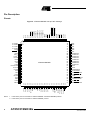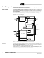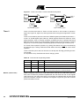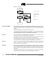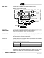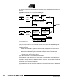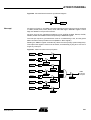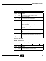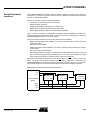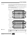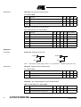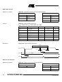
1
Features
• Audio Processor
•
•
•
•
•
•
•
•
•
•
•
•
– Proprietary Digital Signal Processor
– MP3 (Full MPEG I/II-Layer 3) Decoder (1)
– Windows Media ® Audio (WMA) Decoder (1)
– OGG (Vorbis) Decoder (2)
– WAV PCM Decoder/Encoder
– ADPCM Decoder/Encoder (G726: 40, 32, 24, 16 Kbps)
Audio Codec
– 16-bit Stereo D/A Converters (3)
– Headphone Amplifier with Analog Volume Control(3)
– Microphone Pre-Amplifier with Bias Control
– 16-bit Mono A/D Converter: Microphone or Line Inputs Recording
– Stereo Lines Input for FM Playback or Mono Recording
– Baseband Sound Processor with Digital Volume Control, Bass, Medium, and
Treble Control, Bass Boost and Virtual Surround Effects
Digital Audio DAC Interface
– PCM / I2S Format Compatible
USB Rev 2.0 Controller
– High Speed Mode (480 Mbps)
– Full Speed Mode (12 Mbps)
– On The Go Full Speed Mode
Data Flow Controller
– 16-bit Multimedia Bus with 2 DMA Channels for high speed transfer with USB
Nand Flash Controller
– Up to four Memories with Page Size: 512B, 1KB, 2KB or 4KB
– Built-in ECC and Hardware Write Protection
– xD-Picture Card™ and SmartMedia ® Card Interface
MultiMediaCard® Controller
– MultiMediaCard 1-bit / 4-bits Modes (V4.0 compatible)
– Secure Digital Card 1-bit / 4-bit Modes
Man Machine Interface
– Glueless Generic LCD Interface
– Keyboard Interface
Remote Controlled / Streaming
– PSI I80 Slave Interface (EBI Compatible) up to 6Mbyte/s
– SPI Master and Slave Modes
– Full Duplex UART with Baud Rate Generator up to 6 Mbit/s (Rx, Tx, RTS, CTS)
Control Processor
– Enhanced 8-bit MCU C51 Core (FMAX = 24 MHz)
– 64K Bytes of Internal RAM for application code and data
– Boot ROM Memory: Secured Nand Flash Boot Strap (standard), USB Boot Loader
– Two 16-bit Timers/Counters
– Hardware Watchdog Timer
Power Management
– 1.8V 40 mA Single AAA or AA Battery Powered (4)
– Direct USB VBUS Supply
– 3V - 50 mA Regulator Output
– 1.8V - 50 mA Regulator Output
– Battery Voltage Monitoring
– Power-on Reset
– Software Programmable MCU Clock
– Idle, Power-Down, Power-Off Modes
On Chip Debug
Operating Conditions
– Supply 0.9V to 5V
– 25 mA Typical Operating at 25°C (estimation to be confirmed)
– Temperature Range: -40°C to +85°C
Single-Chip
Digital Audio
Decoder Encoder with
USB 2.0
Interface
AT85C51SND3B1
AT85C51SND3B2
AT85C51SND3B3
Preliminary
7632A–MP3–03/06
1
• Packages
– LQFP100, BGA100, Dice
Notes:
1.
2.
3.
4.
See Ordering Information
Future product
AT85C51SND3B2 & AT85C51SND3B3 only
AT85C51SND3B3 only
Description
Digital Music Players, Mobile Phones need ready to use low-cost solutions for very fast
time to market. The AT85C51SND3Bx with associated firmware embeds in a single chip
all features, hardware and software, for Digital Music Players, Mobile Phones and Car
Audio Systems: MP3 decoder, WMA decoder, Display interface, serial interface, parallel
interface, USB high speed and USB host.
Close to a plug and play solution for most applications, the AT85C51SND3Bx drastically
reduces system development for the best time to market. The AT85C51SND3Bx handles full file system management with Nand Flash and Flash Cards, including full
detection and operation of a thumb drive. The AT85C51SND3A is used either as a master controller, or as a slave controller interfacing easily with most of the base-band or
host processors available on the market.
In addition to the MP3 and WMA format, the AT85C51SND3Bx associated firmware will
also later support, the OGG format, basic MIDI features for low cost mobile phones and
JPEG still pictures decoding. The AT85C51SND3B is ideally fitting mass production
markets.
The AT85C51SND3Bx includes Power Management with: 5V USB VBUS direct supply,
2.7V to 3.6V supply, 1.8V supply or alkaline battery supply (0.9V to 1.8V). External
Nand Flash or Flash Card can be supplied by the AT85C51SND3B at 1.8V or 3V.
The AT85C51SND3Bx supports many applications including: mobile phones, music
players, portable navigation, car audio, music in shopping centers, applications including MMC/SD Flash Cards in Industrial applications.
To facilitate custom applications with the AT85C51SND3Bx, a development kit
AT85DVK-07 is available with hardware and firmware database.
Key Features
•
•
•
•
2
Firmware to support
–
MP3
–
WMA
–
ADPCM/WAV voice or line recording
–
and coming soon OGG, MIDI and JPEG Decoder
Audio Codec
–
Internal DAC
–
FM inputs
Memory Support
–
Up to 4x Nand-Flash
–
SD/MMC cards
USB
–
High Speed, Full Speed
–
OTG (reduced Host)
AT85C51SND3Bx
7632A–MP3–03/06
AT85C51SND3Bx
Block Diagram
Figure 1. AT85C51SND3Bx Block Diagram
AT85C51SND3Bx
USB Controller
HS / FS
Device
Controller
Control Processor Unit
Host / OTG
Controller
Enhanced X2
C51 Core
Interrupt Controller
Memory Unit
LCD
Interface
Configurable 64 Kbytes
Code / Data RAM
Clock Controller
Oscillator
PLL
Clock
Generator
Timer Unit
Notes:
Memory Controllers
Nand Flash
SM / xD
Cards
MMC V4
SD
Cards
Audio Controller
2 x 16-bit Timers
3V
Regulator
Watchdog Timer
1.8V
DC-DC (1)
Parallel Slave Interface
Boot ROM
Power Management
Power Fail
Detector
Serial Peripheral Interface
Serial I/O Interface
MMI Controller
Keyboard
Interface
Remote Interfaces
1.8V
Regulator
16-bit Multimedia Bus
Debug Unit
Multimedia Bus Manager
On Chip Debug
Data Flow Controller
Audio DAC
Interface
Audio
Processor
Baseband
Processor
Audio Codec(2)
1. AT85C51SND3B3 only
2. AT85C51SND3B2 & AT85C51SND3B3 only
3
7632A–MP3–03/06
Application Information
The AT85C51SND3Bx allow design of 2 typical applications which differentiate by the
power supply voltage:
•
The Very Low Voltage System
The player operates at 1.8V and allows very low power consumption.
•
The Low Voltage System
The player operates at 3V and allows low power consumption.
Very Low Voltage 1.8V System
Figure 2. Typical Very Low Voltage 1.8V Application
AT85C51SND3B3
1.8V NF Memories
Write Protect
Battery
SD/MMC
LVDD
LCD
FM Module
PA
4
AT85C51SND3Bx
7632A–MP3–03/06
AT85C51SND3Bx
Low Voltage 3V System
Figure 3. Typical Low Voltage 3V Application
AT85C51SND3B2
3V NF Memories
Write Protect
Battery
SD/MMC
LCD
FM Module
3V DC-DC
HVDD
5
7632A–MP3–03/06
Pin Description
Pinouts
100
99
98
97
96
95
94
93
92
91
90
89
88
87
86
85
84
83
82
81
80
79
78
77
76
P1.4
P1.5
P1.6
P1.7
P2.0/SDINS
P2.1/SDLCK
P2.2/SDCMD
P2.3/SDCLK
P2.4/SDDAT0
P2.5/SDDAT1
P2.6/SDDAT2
P2.7/SDDAT3
IOVSS
IOVDD
NFWP
NFCE0
P4.4/NFCE1/SMLCK
P4.5/NFCE2/SMINS
P4.6/NFCE3/SMCE
NFCLE
NFALE
NFWE
NFRE
NFD0
NFD1
Figure 4. AT85C51SND3Bx 100-pin QFP Package
1
2
3
4
5
6
7
8
9
10
11
12
13
14
15
16
17
18
19
20
21
22
23
24
25
AT85C51SND3Bx
75
74
73
72
71
70
69
68
67
66
65
64
63
62
61
60
59
58
57
56
55
54
53
52
51
NFD2
NFD3
NFD4
NFD5
NFD6
NFD7
P0.0/SD0/LD0
P0.1/SD1/LD1
P0.2/SD2/LD2
P0.3/SD3/LD3
P0.4/SD4/LD4
P0.5/SD5/LD5
P0.6/SD6/LD6
P0.7/SD7/LD7
IOVSS
IOVDD
P3.0/RXD/MISO
P3.1/TXD/MOSI
P3.2/INT0/RTS/SCK
P3.3/INT1/CTS/SS
P3.4/T0
P5.3/SWR/LWR/LRW
P5.2/SA0/LA0/LRS
P5.1/SCS/LCS
P5.0/SRD/LRD/LDE
UPVDD
UPVSS
AVDD1
AVSS1
MICBIAS
MICIN
LINR
LINL
AVCM
AREF
OUTR(2)
OUTL(2)
AVDD2
AVSS2
APVSS
X1
X2
APVDD
OCDT/ISP
OCDR
P4.3/DSEL
P4.2/DDAT
P4.1/DCLK
P4.0/OCLK
RST
26
27
28
29
30
31
32
33
34
35
36
37
38
39
40
41
42
43
44
45
46
47
48
49
50
P1.3/KIN3
P1.2/KIN2
P1.1/KIN1
P1.0/KIN0
BVDD
DCPWR(1)
BVSS
DCLI(1)
LVDD(1)
RLVDD
HVDD
UVCC
VSS
CVSS
P3.6/UVCON
P3.7/UID
ULVDD
DMF
DPF
UVSS
UHVDD
DPH
DMH
UVSS
UBIAS
Notes:
6
1. Leave these pins unconnected for AT85C51SND3B1 & AT85C51SND3B2 products
2. Leave these pins unconnected for AT85C51SND3B1 product
AT85C51SND3Bx
7632A–MP3–03/06
AT85C51SND3Bx
Signals Description
System
Table 1. System Signal Description
Signal
Name
RST
Type
I/O
Description
Reset Input
Holding this pin low for 64 oscillator periods while the oscillator is
running resets the device. The Port pins are driven to their reset
conditions when a voltage lower than VIL is applied, whether or not the
oscillator is running.
This pin has an internal pull-up resistor (RRST) which allows the device
to be reset by connecting a capacitor between this pin and VSS.
Asserting RST when the chip is in Idle mode or Power-Down mode
returns the chip to normal operation.
Alternate
Function
-
In order to reset external components connected to the RST line a low
level 96-clock period pulse is generated when the watchdog timer
reaches its time-out period.
ISP
I
In System Programming
Assert this pin during reset phase to enter the in system programming
mode.
OCDT
Table 2. Ports Signal Description
Signal
Name
Type
P0.7:0
I/O
Port 0
P0 is an 8-bit bidirectional I/O port with internal pull-ups.
LD7:0
P1.7:0
I/O
Port 1
P1 is an 8-bit bidirectional I/O port with internal pull-ups.
KIN3:0
Port 2
P2 is an 8-bit bidirectional I/O port with internal pull-ups.
SDINS
SDLCK
SDCMD
SDCLK
SDDAT3:0
P2.7:0
I/O
Description
Alternate
Function
RXD
MISO
TXD
MOSI
P3.4:0
P3.7:6
I/O
Port 3
P3 is a 7-bit bidirectional I/O port with internal pull-ups.
INT0
RTS
SCK
INT1
CTS
SS
T0
UVCON
UID
7
7632A–MP3–03/06
Signal
Name
P4.6:0
Type
I/O
Alternate
Function
Description
OCLK
DCLK
DDAT
DSEL
Port 4
P4 is a 7-bit bidirectional I/O port with internal pull-ups.
NFCE1/SMLCK
NFCE2/SMINS
NFCE3/SMCE
LRD/LDE
SDR
P5.3:0
I/O
LCS
SCS
Port 5
P5 is a 4-bit bidirectional I/O port with internal pull-ups.
LA0/LRS
SA0
LWR/LRW
SWR
Table 3. Timer 0 and Timer 1 Signal Description
Signal
Name
Type
Alternate
Function
Description
Timer 0 Gate Input
INT0 serves as external run control for timer 0, when selected by
GATE0 bit in TCON register.
INT0
I
External Interrupt 0
INT0 input sets IE0 in the TCON register. If bit IT0 in this register is set,
bit IE0 is set by a falling edge on INT0. If bit IT0 is cleared, bit IE0 is set
by a low level on INT0.
Timer 1 Gate Input
INT1 serves as external run control for timer 1, when selected by
GATE1 bit in TCON register.
INT1
T0
8
I
I
External Interrupt 1
INT1 input sets IE1 in the TCON register. If bit IT1 in this register is set,
bit IE1 is set by a falling edge on INT1. If bit IT1 is cleared, bit IE1 is set
by a low level on INT1.
Timer 0 External Clock Input
When timer 0 operates as a counter, a falling edge on the T0 pin
increments the count.
P3.2
RTS
SCK
P3.3
CTS
SS
P3.4
AT85C51SND3Bx
7632A–MP3–03/06
AT85C51SND3Bx
Clock Controller
Table 4. Clock Signal Description
Signal
Name
Type
Description
Alternate
Function
Input of the on-chip inverting oscillator amplifier
X1
I
X2
O
UPVDD
PWR
UPVSS
GND
APVDD
PWR
APVSS
GND
To use the internal oscillator, a crystal/resonator circuit is connected to
this pin. If an external oscillator is used, its output is connected to this
pin. X1 is the clock source for internal timing.
-
Output of the on-chip inverting oscillator amplifier
Memory Controllers
To use the internal oscillator, a crystal/resonator circuit is connected to
this pin. If an external oscillator is used, leave X2 unconnected.
USB PLL Supply voltage
Connect this pin to LVDD pin.
USB PLL Circuit Ground
Connect this pin to LVSS pin.
Audio PLL Supply voltage
Connect this pin to LVDD pin.
Audio PLL Circuit Ground
Connect this pin to LVSS pin.
-
-
-
-
-
Table 5. Secure Digital Card / MutiMediaCard Controller Signal Description
Signal
Name
Type
SDCLK
O
SDCMD
I/O
SDDAT3:0
I/O
Description
SD/MMC Clock
Data or command clock transfer.
SD/MMC Command Line
Bidirectional command line used for commands and responses transfer.
Alternate
Function
P2.3
P2.2
SD/MMC Data Lines
Bidirectional data lines. In 1-bit mode configuration SDDAT0 is the DAT
signal and SDDAT3:1 are not used and can be reused as I/O ports.
P2.7:4
SD/MMC Card Insertion Signal
SDINS
I
SDINS is the card presence signal. A low level on this input indicates
the card is present in its slot.
Note:
P2.0
This signal is generated by the SD/MMC card connector.
SD Card Write Lock Signal
SDLCK
I
SDLCK is the SD Card write protected input. A low level on this pin
indicates the card is write protected.
Note:
P2.1
This signal is generated by the SD/MMC card connector.
Table 6. Nand Flash / SmartMedia Card Controller Signal Description
Signal
Name
Type
NFD7:0
I/O
NFALE
O
Description
Memory Data Bus
8-bit bidirectional data bus.
Address Latch Enable Signal
Asserted high during address write cycle.
Alternate
Function
-
-
9
7632A–MP3–03/06
Signal
Name
Type
Alternate
Function
NFCLE
O
NFRE
O
NFWE
O
NFCE0
O
NFCE0 is active low and is asserted by the nand flash controller each
time it makes access to the device 0.
NFCE1
O
Nand Flash 1 Chip Enable
Description
Command Latch Enable Signal
-
Asserted high during command write cycle.
Read Enable Signal
-
Read signal asserted low during NF/SMC read operation.
Write Enable Signal
-
Write signal asserted low during NF/SMC write operation.
Nand Flash 0 Chip Enable
-
NFCE1 is active low and is asserted by the nand flash controller each
time it makes access to the selected device.
SMLCK
I
SmartMediaCard/xD-Picture Card Write Lock Signal
P4.4
SMLCK is the card write protected input. A low level on this pin
indicates the card is write protected.
Note:
NFCE2
O
When used as SMLCK input, pad has internal pull-up.
Nand Flash 2 Chip Enable
NFCE2 is active low and is asserted by the nand flash controller each
time it makes access to the selected device.
SMINS
I
SmartMediaCard/xD-Picture Card Insertion Signal
P4.5
SMINS is the card presence signal. A low level on this input indicates
the card is present in its slot.
Note:
NFCE3
SMCE
When used as SMINS input, pad has internal pull-up.
Nand Flash 3 Chip Enable
O
NFCE3 is active low and is asserted by the nand flash controller each
time it makes access to the selected device.
SmartMediaCard/xD-Picture Card Chip Enable
P4.6
SMCE is active low and is asserted by the nand flash controller each
time it makes access to the card.
Write Protect Signal
NFWP
USB Controller
O
NFWP is the Nand Flash / SmartMediaCard/xD-Picture Card write
protect signal. This signal is active low and is set to low during reset in
order to protect the memory against parasitic writes.
-
Table 7. USB Controller Signal Description
Signal
Name
Type
Alternate
Function
DPF
I/O
USB Full Speed Positive Data Upstream Port
-
DMF
I/O
USB Full Speed Minus Data Upstream Port
-
DPH
I/O
USB High Speed Plus Data Upstream Port
-
DMH
I/O
USB High Speed Minus Data Upstream Port
-
UVCON
O
Description
USB VBUS Control line
UVCON is used to control the external VBUS power supply ON or OFF.
Note:
10
P3.6
This output is requested for OTG mode.
AT85C51SND3Bx
7632A–MP3–03/06
AT85C51SND3Bx
Signal
Name
Type
UID
I
Description
Alternate
Function
USB OTG Identifier Input
This pin monitors the function of the OTG device.
Note:
Audio Processor
UVCC
PWR
ULVDD
PWR
UHVDD
PWR
UVSS
GND
UBIAS
O
P3.7
This input is requested for OTG mode.
USB Supply Voltage
Connect this pin to USB VBUS power line.
USB Pad Low Voltage
Connect this pin to LVDD pin.
USB Pad High Voltage
Connect this pin to HVDD pin.
USB Ground
-
-
-
USB Bias
Connect this pin to external resistor and capacitor.
Table 8. I2S Output Description
Signal
Name
Type
OCLK
O
Over-sampling Clock Line
P4.0
DCLK
O
Data Clock Line
P4.1
DDAT
O
Data Lines
P4.2
DSEL
O
Data Channel Selection Line
P4.3
Description
Alternate
Function
Table 9. Audio Codec Description
Signal
Name
Type
LINR
I
Right Channel Analog Input
-
LINL
I
Left Channel Analog Input
-
MICIN
I
Electret Microphone Analog Input
-
MICBIAS
O
Electret Microphone Bias Output
-
OUTR
O
OUTL
O
AVCM
I
AREF
O
AVDD1
PWR
AVSS1
GND
Description
Right Channel Output
Do not connect on AT85C51SND3B1 product
Left Channel Output
Do not connect on AT85C51SND3B1 product
Analog Common Mode Voltage
Connect this pin to external decoupling capacitor.
Analog Reference Voltage
Connect this pin to external decoupling capacitor.
Analog Power Supply 1
Connect this pin to LVDD pin.
Analog Ground 1
Connect this pin to LVSS pin.
Alternate
Function
-
-
-
-
-
-
11
7632A–MP3–03/06
Signal
Name
Type
Alternate
Function
Description
AVDD2
Analog Power Supply 2
PWR Low Voltage system: connect this pin to LVDD pin.
High voltage system: connect this pin to external +3V power supply.
AVSS2
GND
-
Analog Ground 2
Parallel Slave Interface
Serial Interfaces
-
Low Voltage system: connect this pin to LVSS pin.
High voltage system: connect this pin to external +3V ground.
Table 10. PSI Signal Description
Signal
Name
Type
SD7:0
I/O
SRD
I
SWR
I
SCS
I
SA0
I
Alternate
Function
Description
Slave Data Bus
P0.7:0
8-bit bidirectional data bus.
LD7:0
Slave Read Signal
P5.0
Read signal asserted low during external host read operation.
LRD/LDE
Slave Write Signal
P5.3
Write signal asserted low during external host write operation.
LWR/LRW
Slave Chip Select
P5.1
Select signal asserted low during external host read or write operation.
LCS
Slave Address Bit 0
P5.2
Address signal asserted during external host read or write operation.
LA0/LRS
Table 11. SPI Controller Signal Description
Signal
Name
Type
MISO
I/O
MOSI
I/O
SCK
I/O
Alternate
Function
Description
SPI Master Input Slave Output Data Line
When in master mode, MISO receives data from the slave peripheral.
When in slave mode, MISO outputs data to the master controller.
SPI Master Output Slave Input Data Line
SS
I
When in master mode, MOSI outputs data to the slave peripheral.
When in slave mode, MOSI receives data from the master controller.
P3.0
RXD
P3.1
TXD
SPI Clock Line
P3.2
When in master mode, SCK outputs clock to the slave peripheral.
When in slave mode, SCK receives clock from the master controller.
INT0
RTS
P3.3
SPI Slave Select Line
INT1
When in controlled slave mode, SS enables the slave mode.
CTS
Table 12. SIO Signal Description
12
Signal
Name
Type
RXD
I/O
Alternate
Function
Description
Receive Serial Data
RXD sends and receives data in serial I/O mode 0 and receives data in
serial I/O modes 1, 2 and 3.
P3.0
MISO
AT85C51SND3Bx
7632A–MP3–03/06
AT85C51SND3Bx
Signal
Name
Type
TXD
O
RTS
O
CTS
MMI Interface
I
Description
Transmit Serial Data
TXD outputs the shift clock in serial I/O mode 0 and transmits data in
serial I/O modes 1, 2 and 3.
Request To Send Hardware Handshake Line
Asserted low by hardware when SIO is ready to receive data.
Clear To Send Hardware Handshake Line
Asserted low by external hardware when SIO is allowed to send data.
Alternate
Function
P3.1
MOSI
P3.2
INT0
SCK
P3.3
INT1
SS
Table 13. Keypad Controller Signal Description
Signal
Name
Type
KIN3:0
I
Description
Alternate
Function
Keypad Input lines
Holding one of these pins high or low for 24 oscillator periods triggers a
keypad interrupt.
P1.3:0
Table 14. LCD Interface Signal Description
Signal
Name
Type
LD7:0
I/O
LRD/LDE
O
Description
Alternate
Function
Display Data Bus
P0.7:0
8-bit bidirectional data bus.
SD7:0
Read Signal/Enable Signal
8080:
6800:
Read signal asserted low during display read access.
Enable signal asserted high during display access.
P5.0
SRD
Write Signal/Read Write Signal
Power Management
LWR/LRW
O
LCS
O
LA0/LRS
O
8080:
6800:
Write signal asserted low during display write access.
Read/Write signal asserted low/high during display read/write
access
P5.3
SWR
Display Chip Select
P5.1
Select signal asserted low during display access.
SCS
Display Address Bit 0/Register Select
P5.2
Address signal asserted during display access.
SA0
Table 15. Power Signal Description
Signal
Name
Type
DCPWR
I
DCLI
PWR
BVDD
PWR
Description
DC-DC Power ON Input
Connect DCPWR to VSS to start the DC-DC converter.
Alternate
Function
-
DC-DC Inductance Input
Connect low ESR inductance to DCLI and BVDD.
Battery Supply Voltage
Connect this pin to the positive pin of the battery.
-
13
7632A–MP3–03/06
Signal
Name
Type
BVSS
GND
LVDD
PWR
Alternate
Function
Description
Battery Ground
-
Connect this pin to the negative pin of the battery.
Low Voltage DC-DC Power Supply output
-
This pin outputs +1.8V typ. from internal DC-DC (battery powered).
Low Voltage Regulator Power Supply Output
OCD Interface
14
This pin outputs +1.8V typ. from internal regulator (USB powered or
+3V external power supply).
Connect this pin to LVDD incase of internal DC-DC usage.
RLVDD
PWR
HVDD
High Voltage Power Supply
PWR This pin outputs +3V typ. from internal regulator (USB powered).
Connect this pin to +3V external power supply.
VSS
GND
CVSS
GND
IOVDD
PWR
IOVSS
GND
Power Ground
Connect this pin to the system ground.
Core Ground
Connect this pin to VSS pin.
Input/Output Supply voltage
Connect this pin to LVDD or HVDD pin.
Input/Output Circuit Ground
Connect this pin to VSS pin.
-
-
-
-
-
-
Table 16. OCD Signal Description
Signal
Name
Type
OCDR
I
OCDT
I/O
Description
On Chip Debug Receive Input
OCDR receives data.
On Chip Debug Transmit Output
OCDT transmits data.
Alternate
Function
-
ISP
AT85C51SND3Bx
7632A–MP3–03/06
AT85C51SND3Bx
Internal Pin Structure
Table 17. Detailed Internal Pin Structure
Circuit (1)
Type
Pins
Input/Output
RST
RRST
IOVDD
N
IOVSS
2 osc
periods
IOVDD
Latch Output
IOVDD
Ps
Pm
IOVDD
Pw
Input/Output
N
P0.7:0
P1.7:0
P2.7:0
P3.5:0
P4.6:0
P5.3:0
OCDT
IOVSS
2 osc
periods
HVDD
HVDD
HVDD
Ps
Pm
Pw
Latch Output
Input/Output
P3.7:6
N
IOVSS
KIN3:0
SDINS
SDLCK
IOVDD
SMINS
SMLCK
IOVDD
TST
Pm
Pw
Input
ISP
UID
IOVSS
INT0
INT1
T0
RXD
OCDR
Input
SWR
SA0
SRD
SCS
SS
NFD7:0
IOVDD
SD7:0
P
LD7:0
Input/Output
N
IOVSS
SDCMD
SDDAT3:0
MISO
MOSI
15
7632A–MP3–03/06
Circuit (1)
Type
Pins
SDCLK
SCK
NFCE3:0
NFCLE
NFALE
NFWE
NFRE
NFWP
SMCE
IOVDD
P
Output
DSEL
DDAT
DCLK
OCLK
N
IOVSS
LWR/LE
LA0/LRS
LRD/LRW
LCS
UVCON
TXD
DPF
Input/Output
DPF
DMF
Input/Output
DPH
DMH
Input
DCPWR (2)
-
DCLI(2)
DMF
DPH
DMH
RDCP
BVDD
LVDD
P
N
CVSS
16
AT85C51SND3Bx
7632A–MP3–03/06
AT85C51SND3Bx
Circuit (1)
Type
Pins
Output
MICBIAS
Input
MICIN
LINR
LINL
Output
OUTR(2)
OUTL(2)
+
AVSS
AVSS
+
Notes:
1. For information on resistor value, input/output levels, and drive capability, refer to
Section “DC Characteristics”, page 241.
2. AT85C51SND3B3 only
3. AT85C51SND3B2 & AT85C51SND3B3 only
17
7632A–MP3–03/06
Power Management
The Power Management implements all the internal power circuitry (regulators, links…)
as well as power failure detector and reset circuitry.
Power Supply
The AT85C51SND3B3 embeds the regulators and a DC to DC step-up convertor to be
able to operate from either USB power supply (5V nominal) or from a single cell battery
such as AAA battery.
The AT85C51SND3B1 and AT85C51SND3B2 embed the regulators to be able to operate from either USB power supply (5V nominal) or from an external 3 volts supply.
Figure 5. Power Supply Diagram
PSTA.7
UVDET
UVCC
UVSS
HVDD
3V
Regulator
VSS
To Internal Core
RLVDD
PSTA.6
1.8 V
Regulator
HVDET
DCPBST
Optional
Connection(1)
PCON.5
DCPWR
DCEN
PCON.3
DCLI
1.8 V DC-DC
LVDD
BVDD
BVSS
Battery Monitor
Note:
Regulators
18
VBAT
1. External connection mandatory when 1.8V DC-DC is used.
The high voltage regulator supplies power to the external devices through HVDD power
pin. Its nominal voltage output is 3V.
The low voltage regulator supplies power to the internal device and external devices
through RLVDD power pin. Its nominal voltage output is 1.8V.
Figure 6 shows how to connect external components, capacitors value along with power
characteristics are specified in the section “DC characteristics”.
AT85C51SND3Bx
7632A–MP3–03/06
AT85C51SND3Bx
Schematic
Figure 6. Regulator Connection
HVDD
RLVDD
CLV(*)
CHV
VSS
Note:
VSS
Depending on power supply scheme, CLV may replace CDC capacitor (see Figure 8).
Low Voltage DC-DC in
AT85C51SND3B3
The low voltage output DC-DC converter supplies power to the internal device and
external devices through LVDD power pin. It operates from a single AAA battery. Its
nominal voltage output is 1.8V.
DC-DC Start-Up
DC-DC start-up is done by asserting the DCPWR input until the voltage reaches its
nominal value (see Section “Power Fail Detector”) and firmware starts execution and
sets the DCEN bit in PCON to maintain the DC-DC enabled. DCPWR input can then be
released. As shown in Figure 8 DCPWR input is asserted by pressing a key connected
to BVSS.
Figure 7. DC-DC Start-Up Phase
DCPWR
LVDD
DCEN
DC-DC
Off
DC-DC Shut-Down
Firmware
Start-Up
DC-DC
On
DC-DC shut-down is done by two different ways:
•
Clearing the DCEN bit while DCPWR pin is de-asserted
•
Detecting the presence of an internal or external 3V supply, e.g. when the device is
connected to USB, DC-DC is disabled to save battery power(1) .
Note:
DC-DC Connection
DC-DC
Start-Up
1. If DCEN bit is left set, the DC-DC will restart as soon as the USB power supply
disappears.
Figure 8 shows how to connect external components, inductance and components
value along with power characteristics are specified in the section “DC characteristics”.
Figure 8. Battery DC-DC Connection
Battery
BVDD
RLVDD
LDC
LVDD
DCLI
BVSS
CDC1(*)
CDC2
VSS
CVSS
DCPWR
Note:
Depending on power supply scheme, CDC1 may replace CLV capacitor (see Figure 6).
19
7632A–MP3–03/06
Battery Voltage Monitor
The battery voltage monitor is a 5-bit / 50 mV resolution A to D converter with fixed conversion range as detailed in Table 18.
Table 18. Battery Voltage Value
VB4:0
Battery Voltage (V)
00000
[0.9 - 0.95[
00001
[0.95 - 1.0[
00010
[1.0 - 1.05[
…
Conversion Management
…
01110
[1.6 - 1.65[
01111
[1.65 - 1.7[
10000
[1.7 - 1.75[
The battery voltage monitor is turned on by setting the VBPEN and VBCEN bits in
PCON (see Table 20). VBPEN bit is set first and VBCEN bit is set 1 ms later. An additional delay of 16 cycles is required before lauching any conversion.
Launching a conversion is done by setting VBEN bit in VBAT (see Table 22). VBEN is
automatically cleared at the end of the conversion which takes 34 clock periods. At this
step two cases occur:
•
Voltage is valid (inside conversion range)
VBERR is cleared and conversion value is set in VB4:0 according to Table 18.
•
Voltage is invalid (out of conversion range)
VBERR is set and value reported by VB4:0 is indeterminate.
Power Reduction Mode
Two power reduction modes are implemented in the AT85C51SND3B: the Idle mode
and the Power-down mode. These modes are detailed in the following sections. In addition to these power reduction modes, the clocks of the core and peripherals can be
dynamically divided by 2 using the X2 mode as detailed in Section “X2 Feature”,
page 30.
Lock Mode
In order to allow firmware to efficiently enter in idle mode and not to lose any events that
should come from one or more interrupts, power reduction modes entry are conditioned
to an hardware bit: PMLCK in PCON.
PMLCK is set by software in each ISR that needs to report an event to the system and
thus disables entry in power reduction mode and allows immediate processing of this
event. It is cleared by software after exiting power reduction mode.
As shown in Figure 9, when power reduction modes are disabled by setting PMLCK, IDL
and PD bits in PCON can not be set and idle or power down modes are not entered.
Figure 9. Power Reduction Controller Block Diagram
PMLCK
PCON.2
Write to IDL
Write to PD
20
IDL
System Idle
PCON.0
PD
System Power Down
PCON.1
AT85C51SND3Bx
7632A–MP3–03/06
AT85C51SND3Bx
Idle Mode
Idle mode is a power reduction mode that reduces the power consumption. In this mode,
program execution halts. Idle mode freezes the clock to the CPU at known states while
the peripherals continue to be clocked (refer to Section “System Clock Generator”,
page 29). The CPU status before entering Idle mode is preserved, i.e., the program
counter and program status word register retain their data for the duration of Idle mode.
The contents of the SFRs and RAM are also retained.
Entering Idle Mode
To enter Idle mode, the user must set the IDL bit in PCON register while PMLCK is
cleared. The AT85C51SND3B enters Idle mode upon execution of the instruction that
sets IDL bit. The instruction that sets IDL bit is the last instruction executed.
Note:
Exiting Idle Mode
If IDL bit and PD bit are set simultaneously, the AT85C51SND3B enter Power-down
mode. Then it does not go in Idle mode when exiting Power-down mode.
There are 2 ways to exit Idle mode:
1. Generate an enabled interrupt.
–
Hardware clears IDL bit in PCON register which restores the clock to the CPU.
Execution resumes with the interrupt service routine. Upon completion of the
interrupt service routine, program execution resumes with the instruction
immediately following the instruction that activated Idle mode. The generalpurpose flags (GF1 and GF0 in PCON register) may be used to indicate
whether an interrupt occurred during normal operation or during Idle mode.
When Idle mode is exited by an interrupt, the interrupt service routine may
examine GF1 and GF0.
2. Generate a reset.
–
A logic high on the RST pin clears IDL bit in PCON register directly and
asynchronously. This restores the clock to the CPU. Program execution
momentarily resumes with the instruction immediately following the instruction
that activated the Idle mode and may continue for a number of clock cycles
before the internal reset algorithm takes control. Reset initializes the
AT85C51SND3B and vectors the CPU to address 0000h.
Note:
During the time that execution resumes, the internal RAM cannot be accessed; however,
it is possible for the Port pins to be accessed. To avoid unexpected outputs at the Port
pins, the instruction immediately following the instruction that activated Idle mode should
not write to a Port pin or to the external RAM.
Power-down Mode
The Power-down mode places the AT85C51SND3B in a very low power state. Powerdown mode stops the oscillator and freezes all clocks at known states (refer to the
Section “Oscillator”, page 27). The CPU status prior to entering Power-down mode is
preserved, i.e., the program counter, program status word register retain their data for
the duration of Power-down mode. In addition, the SFRs and RAM contents are
preserved.
Entering Power-down Mode
To enter Power-down mode, set PD bit in PCON register while PMLCK is cleared. The
AT85C51SND3B enters the Power-down mode upon execution of the instruction that
sets PD bit. The instruction that sets PD bit is the last instruction executed.
Exiting Power-down Mode
There are 2 ways to exit the Power-down mode:
1. Generate an enabled external interrupt.
–
The AT85C51SND3B provides capability to exit from Power-down using INT0,
INT1, and KIN3:0 inputs. In addition, using KIN input provides high or low level
exit capability (see Section “Keyboard Interface”, page 239).
Hardware clears PD bit in PCON register which starts the oscillator and restores
21
7632A–MP3–03/06
the clocks to the CPU and peripherals. Using INTn input, execution resumes
when the input is released (see Figure 10) while using KINx input, execution
resumes after counting 1024 clock ensuring the oscillator is restarted properly
(see Figure 11). This behavior is necessary for decoding the key while it is still
pressed. In both cases, execution resumes with the interrupt service routine.
Upon completion of the interrupt service routine, program execution resumes
with the instruction immediately following the instruction that activated Powerdown mode.
Note:
1. The external interrupt used to exit Power-down mode must be configured as level
sensitive (INT0 and INT1) and must be assigned the highest priority. In addition, the
duration of the interrupt must be long enough to allow the oscillator to stabilize. The
execution will only resume when the interrupt is de-asserted.
2. Exit from power-down by external interrupt does not affect the SFRs nor the internal
RAM content.
Figure 10. Power-down Exit Waveform Using INT1:0
INT1:0
OSC
Active Phase
Power-down Phase
Oscillator Restart Phase
Active Phase
Figure 11. Power-down Exit Waveform Using KIN3:0
KIN3:0(1)
OSC
Active Phase
Note:
Power-down Phase
42000 clock count
Active Phase
1. KIN3:0 can be high or low-level triggered.
2. Generate a reset.
22
–
A logic high on the RST pin clears PD bit in PCON register directly and
asynchronously. This starts the oscillator and restores the clock to the CPU and
peripherals. Program execution momentarily resumes with the instruction
immediately following the instruction that activated Power-down mode and may
continue for a number of clock cycles before the internal reset algorithm takes
control. Reset initializes the AT85C51SND3B and vectors the CPU to address
0000h.
Notes:
1. During the time that execution resumes, the internal RAM cannot be accessed; however, it is possible for the Port pins to be accessed. To avoid unexpected outputs at
the Port pins, the instruction immediately following the instruction that activated the
Power-down mode should not write to a Port pin or to the external RAM.
2. Exit from power-down by reset redefines all the SFRs, but does not affect the internal
RAM content.
AT85C51SND3Bx
7632A–MP3–03/06
AT85C51SND3Bx
Reset
In order to secure the product functionality while in power-up or power-down phase or
while in running phase, a number of internal mechanisms have been implemented.
These mechanisms are listed below and detailed in the following paragraphs.
•
External RST input
•
Power Fail Detector (brown-out)
•
Watchdog timer
•
Pads control
Figure 12 details the internal reset circuitry.
Reset Source Reporting
In order for the firmware to take specific actions depending on the source which has currently reset the device, activated reset source is reported to the CPU by EXTRST,
WDTRST, and PFDRST flags in PSTA register.
Figure 12. Internal Reset Circuitry
IOVDD
RRST
RST
EXTRST
PSTA.1
1.8V
Reg
HVDD
WDT
WDTRST
TO
PSTA.2
SYSRST To
CPU Core
To Peripherals
To Pads Control
LVDD
DCPWR
ON/OFF
Pads Level Control
PFD
DC-DC
VBAT
PFDRST
OUT
PSTA.0
As soon as one reset source is asserted, the pads go to their reset value. This ensures
that pads level is steady during reset (e.g. NFWP set to low level and then protecting
Nand Flash against spurious writing).
The status of the Port pins during reset is detailed in Table 19.
Table 19. Pin State Under Reset Condition.
External RST Input
Port 0
Port 1
Port 2
Port 3
Port 4
Port 5
NFD7:0
NFWP
NFCE0
Float
H
H
H
H
H
Float
L
H
In order to start-up (cold reset) or to restart (warm reset) properly the microcontroller, a
low level has to be applied on the RST pin. A bad level leads to a wrong initialization of
the internal registers like SFRs, Program Counter… and to unpredictable behavior of
the microcontroller. A proper device reset initializes the AT85C51SND3B and vectors
the CPU to address 0000h. RST input has a pull-up resistor allowing power-on reset by
simply connecting an external capacitor to VSS as shown in Figure 13. A warm reset can
be applied either directly on the RST pin or indirectly by an internal reset source such as
the watchdog timer. Resistor value and input characteristics are discussed in the
Section “DC Characteristics”, page 241.
23
7632A–MP3–03/06
Figure 13. Reset Circuitry and Power-On Reset
IOVDD
RRST
RST
+
RST
To CPU Core
and Peripherals
N
From Internal
Reset Source
IOVSS
RST input circuitry
Cold Reset
IOVSS
Power-on Reset
2 conditions are required before enabling a CPU start-up:
•
VDD must reach the specified VDD range
•
The level on X1 input pin must be outside the specification (VIH, VIL)
If one of these 2 conditions are not met, the microcontroller does not start correctly and
can execute an instruction fetch from anywhere in the program space. An active level
applied on the RST pin must be asserted till both of the above conditions are met. A
reset is active when the level VIL is reached and when the pulse width covers the period
of time where VDD and the oscillator are not stabilized. 2 parameters have to be taken
into account to determine the reset pulse width:
•
VDD rise time,
•
Oscillator startup time.
To determine the capacitor value to implement, the highest value of these 2 parameters
has to be chosen.
Warm Reset
To achieve a valid reset, the reset signal must be maintained for at least 2 machine
cycles (24 oscillator clock periods) while the oscillator is running. The number of clock
periods is mode independent (X2 or X1).
Watchdog Timer Reset
As detailed in Section “Watchdog Timer”, page 75, the WDT generates a 96-clock
period pulse on the RST pin. In order to properly propagate this pulse to the rest of the
application in case of external capacitor or power-supply supervisor circuit, a 1 kΩ resistor must be added as shown in Figure 14.
Figure 14. Reset Circuitry for WDT Reset-out Usage
IOVDD
1K
RST
RRST
+
N
IOVSS
IOVSS
Power Fail Detector
24
To Other
On-board
Circuitry
To CPU Core
and Peripherals
From WDT
Reset Source
The Power Fail Detector (PFD) ensures that whole product is in reset when internal voltage is out of its limits specification. PFD limits are detailed in the Section “DC
Characteristics”, page 241.
AT85C51SND3Bx
7632A–MP3–03/06
AT85C51SND3Bx
Registers
Table 20. PCON Register
PCON (0.87h) – Power Control Register
7
6
5
4
3
2
1
0
VBCEN
VBPEN
DCPBST
GF0
DCEN
PMLCK
PD
IDL
Bit
Number
Bit
Mnemonic Description
Battery Monitor Clock Enable Bit
7
VBCEN
6
VBPEN
5
DCPBST
4
GF0
Set to enable the clock of the battery monitoring.
Clear to disable the clock of the battery monitoring.
Battery Monitor Power Enable Bit
Set to power the battery monitoring.
Clear to unpower the battery monitoring.
DC-DC Converter Power Boost Bit
Set to disable DC-DC high power boost mode.
Clear to enable DC-DC high power boost mode.
General-purpose flag 0
One use is to indicate whether an interrupt occurred during normal operation or
during Idle mode.
DC-DC Converter Enable Bit
3
DCEN
Set to start the DC-DC converter or maintain its activity while DCPWR pin is
asserted.
Clear to stop the DC-DC converter and shut off the device if not powered by an
external power supply.
Power Mode Lock Bit
2
PMLCK
Set to lock power-down or Idle mode entry by preventing PD or IDL bits from
being set by software.
Clear to unlock power-down or Idle mode entry.
Power-down Mode bit
1
PD
Cleared by hardware when an interrupt or reset occurs.
Set to activate the Power-down mode when PMLCK is cleared.
If IDL and PD are both set, PD takes precedence.
Idle Mode bit
0
IDL
Cleared by hardware when an interrupt or reset occurs.
Set to activate the Idle mode when PMLCK is cleared.
If IDL and PD are both set, PD takes precedence.
Reset Value = 00011 0000b
Table 21. PSTA Register
PSTA (0.86h) – Power Status Register
7
6
5
4
3
2
1
0
UVDET
HVDET
-
-
-
WDTRST
EXTRST
PFDRST
Bit
Number
Bit
Mnemonic Description
USB Voltage Detect Flag
7
UVDET
Set by hardware when 5V is detected on UVDD pin.
Cleared by hardware when 5V is not detected on UVDD pin.
25
7632A–MP3–03/06
Bit
Number
Bit
Mnemonic Description
High Voltage Detect Flag
6
HVDET
5-3
-
Set by hardware when 3V is detected on HVDD pin.
Cleared by hardware when 3V is not detected on HVDD pin.
Reserved
The value of these bits is always 0. Do not set these bits.
Watchdog Timer Reset Flag
2
WDTRST
1
EXTRST
Set by hardware when the watchdog timer has overflowed triggering and internal
reset.
Must be cleared by software at power-up.
External Reset Flag
Set by hardware when the external RST pin is asserted (warm reset).
Must be cleared by software at power-up.
Power Failure Detector Reset Flag
0
PFDRST
Set by hardware when the power voltage has been triggered outside its specified
value (cold reset).
Must be cleared by software at power-up.
Reset Value = XX00 0XXXb(1)
Note:
1. Reset value depends on the power supply presence and on the internal reset source.
Table 22. VBAT Register
VBAT (0.85h) – Battery Voltage Monitor Register
7
6
5
4
3
2
1
0
VBEN
VBERR
-
VB4
VB3
VB2
VB1
VB0
Bit
Number
Bit
Mnemonic Description
Battery Monitor Enable Bit
7
VBEN
6
VBERR
5
-
4-0
VB4:0
Set to enable the battery monitoring.
Cleared by hardware at the end of conversion
Battery Monitor Error Flag
Set by hardware when conversion is out of min/max values.
Reserved
The value read from this bit is always 0. Do not set this bit.
Battery Value
Refer to Table 18 for voltage value correspondence.
Reset Value = 0000 0000b
26
AT85C51SND3Bx
7632A–MP3–03/06
AT85C51SND3Bx
Clock Controller
The AT85C51SND3Bx clock controller is based on an on-chip oscillator feeding two onchip Phase Lock Loop (PLL) dedicated for the USB controller (see Section “USB Controller”, page 85) and the Audio Controller (see Section “Audio Controller”, page 149).
All internal clocks to the peripherals and CPU core are generated by this controller.
Oscillator
X1 and X2 pins of AT85C51SND3Bx are the input and the output of a frequency poweroptimized single-stage on-chip inverter (see Figure 15) that can be configured with offchip components such as a Pierce oscillator (see Figure 16). Value of capacitors and
crystal characteristics are detailed in the Section “DC Characteristics”, page 241.
Authorized frequency
In order to be able to be able to properly detect the oscillating frequency when in In System Programming mode and then generate the 480MHz requested for USB connection,
only the following frequencies are authorized:
12MHz, 13MHz, 16MHz, 19.2MHz, 19.5MHz, 20MHz, 24MHz and 26MHz.
Power Optimization
In order to optimize the power consumption, oscillator gain can be adjusted by software
depending on the crystal frequency. Such optimization is done after reset using
OSCF1:0 bits in CKCON register (see Table 31) according to Table 23. Moreover if
external frequency signal is input (X1 driven by a remote host) it is possible to switch off
the internal amplifier by setting the OSCAMP bit in CKCON register as shown in
Figure 15.
Table 23. Oscillator Frequency Configuration
OSCF1:0
Crystal Clock Frequency Range (FOSC)
00
22 - 26 MHz (default)
01
18 - 22 MHz
10
14 - 18 MHz.
11
10 - 14 MHz
The oscillator outputs a clock: the oscillator clock used to feed the clock generator and
the system clock generator.
The oscillator clock can be disabled by entering the power-down reduction mode as
detailed in the Section “Power Management”, page 18.
Figure 15. Oscillator Block Diagram and Symbol
Oscillator
Clock
X1
CKCON4:3
OSCF1:0
OSC
CLOCK
X2
Oscillator Clock Symbol
OSCAMP
PD
CKCON.5
PCON.1
27
7632A–MP3–03/06
Figure 16. Crystal Connection
X1
C1
Q
C2
APVSS
Clock Generator
X2
The clock generator provides the oscillator and higher frequency clocks to the System,
the DFC, the memory controllers: Nand Flash and MMC controllers, the USB and the
high speed Serial I/O port. It is based on a 480 MHz PLL namely the PLL clock followed
by a frequency divider giving a broad range of available clock frequency: the CLOCK
GEN clocks.
The clock generation is enabled by setting CKGENE bit in CKEN (see Table 32).
The PLL is enabled by setting PLLEN bit in CKEN and reports a filtered lock status by
the PLOCK Flag in CKEN.
As soon as the PLL is locked, the generated clocks can be used by the peripherals as
detailed in the following sections.
Figure 17. Clock Generator Block Diagram and Symbol
OSC
PLL Clock
OSC
CLOCK
480 MHz PLL
CKEN.4
CKGENE
CKEN.7
PLOCK
PLLEN
CKEN.6
CLOCK
GEN
Clock
Generator
Divider
120 MHz
60 MHz
48 MHz
40 MHz
30 MHz
24 MHz
20 MHz
16 MHz
Clock Generator Symbol
480 MHz PLL
28
The AT85C51SND3Bx PLL is based on a Phase Frequency Comparator and Lock
Detector block (PFLD) which makes the comparison between the reference clock coming from the 4-bit N divider (PLLN3:0 + 1 in PLLCLK) and the reverse clock coming from
either fixed frequencies or the 4-bit R divider (PLLR3:0 + 1 in PLLCLK) and generates
some pulses on the Up or Down signal depending on the edge position of the reverse
clock. These pulses feed the Charge Pump block (CHP) that generates a voltage reference to the 480 MHz Voltage Controlled Oscillator (VCO) by injecting or extracting
charges from an internal filter. The reverse clock selection mechanism is implemented
in order to support many oscillator frequencies and to minimize the PLL output jitter.
AT85C51SND3Bx
7632A–MP3–03/06
AT85C51SND3Bx
Figure 18. PLL Block Diagram and Symbol
Up
N Divider
PFLD
CHP
480 MHz
VCO
Down
PLLN3:0
PLLCLK.3:0
12 MHz
16 MHz
20 MHz
00
01
10
11
R Divider
PLLCKS1:0
PLLR3:0
CKSEL.4:3
PLLCLK.7:4
FREV
Primary
Divider
PLL
CLOCK
PLL Clock Symbol
Table 24. PLL Reverse Clock Selection
PLLCKS1:0
PLL Programming
Clock Selection (FREV)
00
12 MHz (default)
01
16 MHz
10
20 MHz
11
12 MHz ÷ (PLLR + 1)
The PLL is programmed depending on the oscillator clock frequency. In order to minimize the output jitter, FREV must be as higher as possible. Table 26 shows the PLL
programming values and reverse frequency depending on some oscillator frequency.
Table 25. PLL Programming Values versus Input Frequency
System Clock Generator
FOSC (MHz)
PLLCKS1:0
PLLN3:0 / N
PLLR3:0 / R
FREV (MHz)
12
00
0000
XXXX
12
13
11
1100 / 13
1011 / 12
1
16
01
0000
XXXX
16
19.2
11
0111 / 8
0100 / 5
2.4
19.5
11
1100 / 13
0111 / 8
1.5
20
10
0000
XXXX
20
24
00
0001 / 2
XXXX
12
26
11
1100 / 13
0101 / 6
2
In order to increase the system computation throughput, it is possible to switch the system clock to higher value when PLL is enabled. System clock generator block diagram
is shown in Figure 19 and is based on a frequency selector controlled by SYSCKS1:0
bits in CKSEL (see Table 34) according to Table 26.
The CPU clock can be disabled by entering the idle reduction mode as detailed in the
Section “Power Management”, page 18.
Note:
In order to prevent any incorrect operation while dynamically switching the system frequency, user must be aware that all peripherals using the peripheral clock as time
reference (timers, etc…) will have their time reference modified by this frequency
change.
29
7632A–MP3–03/06
Figure 19. System Clock Generator Block Diagram and Symbols
OSC
CLOCK
24 MHz
30 MHz
40 MHz
CLOCK
GEN
00
01
10
11
FSYS
Audio Controller
Clock
÷2
0
Peripheral
Clock
1
SYSCKS1:0
X2
CKSEL.1:0
CKCON.0
CPU Core
Clock
IDL
PCON.0
AUD
CLOCK
Audio Clock Symbol
PER
CLOCK
Peripheral Clock Symbol
CPU
CLOCK
CPU Core Clock Symbol
Table 26. System Clock Selection
SYSCKS1:0
X2 Feature
Clock Selection (FSYS)
00
FOSC (default)
01
24 MHz
10
30 MHz
11
40 MHz
Unlike standard C51 products that require 12 clock periods per machine cycle, the
AT85C51SND3Bx need only 6 clock periods per machine cycle. This feature called the
“ X2 fe a tu r e ” c a n b e e n a b le d u s in g th e X2 b it ( 1 ) in C KC O N a n d a llo ws t h e
AT85C51SND3Bx to operate in 6 or 12 clock periods per machine cycle. As shown in
Figure 19, both CPU and peripheral clocks are affected by this feature. Figure 20 shows
the X2 mode switching waveforms. After reset the standard mode is activated. In standard mode the CPU and peripheral clock frequency is the oscillator frequency divided by
2 while in X2 mode, it is the oscillator frequency.
Figure 20. Mode Switching Waveforms
FSYS
FSYS ÷ 2
X2 bit
Clock
STD Mode
DFC/NFC Clock
Generator
30
X2 Mode
STD Mode
In order to optimize the data transfer throughput between the DFC and the NFC, both
peripherals share the same clock frequency. The DFC and NFC clock generator block
diagram is shown in Figure 21 and is based on a frequency selector.
Frequency selection is done using DNFCKS2:0 bits in CKSEL (see Table 33) according
to Table 27.
Frequency is enabled by setting DNFCKEN bit in CKEN.
AT85C51SND3Bx
7632A–MP3–03/06
AT85C51SND3Bx
Figure 21. DFC/NFC Clock Generator Block Diagram and Symbol
CLOCK
GEN
OSC
60 MHz
48 MHz
40 MHz
30 MHz
24 MHz
20 MHz
16 MHz
000
001
010
011
100
101
110
111
CKEN.0
DNFCKEN
FS
DFC Clock
NFC Clock
DNFC
CLOCK
DNFCKS2:0
CKSEL.7:5
DFC/NFC Clock Symbol
Table 27. DFC/NFC Clock Selection
DNFCKS2:0
MMC Clock Generator
Clock Selection (FS)
000
FOSC (default)
001
60 MHz
010
48 MHz
011
40 MHz
100
30 MHz
101
24 MHz
110
20 MHz
111
16 MHz
The MMC clock generator block diagram is shown in Figure 22 and is based on a frequency selector followed by a frequency divider.
Frequency selection is done using MMCCKS2:0 bits in MMCCLK (see Table 35)
according to Table 28(1).
Frequency division is done using MMCDIV4:0 bits in MMCCLK according to Table 29.
Frequency configuration (selection and division) must be done prior to enable the MMC
clock generation by setting MMCKEN bit in CKEN.
Note:
1. To allow low frequency as low as 400 KHz (frequency needed in MMC identification
phase), FOSC selection can be divided by 2.
Figure 22. MMC Clock Generator Block Diagram and Symbol
CLOCK
GEN
OSC
60 MHz
48 MHz
30 MHz
24 MHz
20 MHz
16 MHz
OSC
÷2
000
001
010
011
100
101
110
111
CKEN.3
MMCKEN
FS
Clock
Divider
MMCDIV4:0
MMCCLK.4:0
MMCCKS2:0
MMCCLK.7:5
MMC Clock
MMC
CLOCK
MMC Clock Symbol
31
7632A–MP3–03/06
Table 28. MMC Clock Selection
MMCCKS2:0
Clock Selection (FS)
000
FOSC (default)
001
60 MHz
010
48 MHz
011
30 MHz
100
24 MHz
101
20 MHz
110
16 MHz
111
FOSC ÷ 2
Table 29. MMC Clock Divider
MMCDIV4:0
SIO Clock Generator
Clock Division
00000
Disabled (no clock out)
≥ 00001
FMMC = FS ÷ MMCDIV
As detailed in Figure 23, the SIO clock which feeds the internal SIO baud rate generator
can be programmed using SIOCKS bit in CKSEL register according to Table 30 to generate either the oscillator frequency or a very high frequency allowing very high baud
rate when PLL is enabled. SIO clock is enabled by SIOCKEN bit in CKEN register.
Figure 23. SIO Clock Generator Block Diagram and Symbol
CKEN.1
SIOCKEN
CLOCK
GEN
OSC
0
120 MHz
1
SIOCKS
CKSEL.2
FS
SIO Clock
SIO
CLOCK
SIO Clock Symbol
Table 30. SIO Clock Selection
SIOCKS
32
Clock Selection (FS)
0
FOSC
1
120 MHz
AT85C51SND3Bx
7632A–MP3–03/06
AT85C51SND3Bx
Registers
Table 31. CKCON Register
CKCON (0.8Fh) – Clock Control Register
7
6
5
4
3
2
1
0
-
WDX2
OSCAMP
OSCF1
OSCF0
T1X2
T0X2
X2
Bit
Number
7
Bit
Mnemonic Description
-
Reserved
The value read from this bit is always 0. Do not set this bit.
Watchdog Clock Control Bit
6
WDX2
Set to select the oscillator clock divided by 2 as watchdog clock input (X2
independent).
Clear to select the peripheral clock as watchdog clock input (X2 dependent).
Oscillator Amplifier Control Bit
5
OSCAMP
4-3
OSCF1:0
Set to optimize power consumption by disabling the oscillator amplifier when an
external clock is used.
Clear to enable the oscillator amplifier in case of crystal usage (default).
Oscillator Frequency Range Bits
Set this bits according to Table 23 to optimize power consumption.
Timer 1 Clock Control Bit
2
T1X2
Set to select the oscillator clock divided by 2 as timer 1 clock input (X2
independent).
Clear to select the peripheral clock as timer 1 clock input (X2 dependent).
Timer 0 Clock Control Bit
1
T0X2
Set to select the oscillator clock divided by 2 as timer 0 clock input (X2
independent).
Clear to select the peripheral clock as timer 0 clock input (X2 dependent).
System Clock Control Bit
0
X2
Clear to select 12 clock periods per machine cycle (STD mode, FCPU = FPER =
FOSC/2).
Set to select 6 clock periods per machine cycle (X2 mode, FCPU = FPER = FOSC).
Reset Value = 0000 0000b
33
7632A–MP3–03/06
Table 32. CKEN Register
CKEN (0.B9h) – Clock Enable Register
7
6
5
4
3
2
1
0
CKGENE
PLLEN
-
PLOCK
MMCKEN
-
SIOCKEN
DNFCKEN
Bit
Number
Bit
Mnemonic Description
Clock Generator Enable Bit
7
CKGENE
6
PLLEN
5
-
4
PLOCK
3
MMCKEN
2
-
1
SIOCKEN
0
DNFCKEN
Set to enable the clock generator.
Clear to disable the clock generators.
PLL Enable Bit
Set to enable the 480 MHz PLL.
Clear to disable the 480 MHz PLL.
Reserved
The value read from this bit is always 0. Do not set this bit.
PLL Lock Flag
Set by hardware when the PLL is locked.
Cleared by hardware when the PLL is not locked.
MMC Controller Clock Enable Bit
Set to enable the MMC controller Clock.
Clear to disable the MMC controller Clock.
Reserved
The value read from this bit is always 0. Do not set this bit.
SIO Controller Clock Enable Bit
Set to enable the SIO Clock.
Clear to disable the SIO Clock.
DF Controller / NF Controller Clock Enable Bit
Set to enable the DFC/NFC Clock.
Clear to disable the DFC/NFC Clock.
Reset Value = 0000 0000b
34
AT85C51SND3Bx
7632A–MP3–03/06
AT85C51SND3Bx
Table 33. CKSEL Register
CKSEL (0.BAh) – Clock Selection Register
7
6
5
4
3
2
1
0
DNFCKS2
DNFCKS1
DFCCKS0
PLLCKS1
PLLCKS0
SIOCKS
SYSCKS1
SYSCKS0
Bit
Number
Bit
Mnemonic Description
7-5
DNFCKS2:0
4-3
PLLCKS1:0
2
SIOCKS
1-0
SYSCKS1:0
DFC/NFC Clock Select Bits
Refer to Table 27 for information on selected clock value.
PLL Reverse Clock Select Bits
Refer to Table 24 for information on selected clock value.
SIO Clock Select Bit
Refer to Table 30 for information on divided clock value.
System Clock Select Bits
Refer to Table 26 for information on divided clock value.
Reset Value = 0000 0000b
Table 34. PLLCLK Register
PLLCLK (0.BCh) – PLL Clock Control Register
7
6
5
4
3
2
1
0
PLLR3
PLLR2
PLLR1
PLLR0
PLLN3
PLLN2
PLLN1
PLLN0
Bit
Number
Bit
Mnemonic Description
7-4
PLLR3:0
3-0
PLLN3:0
PLL R Divider Bits
4-bit R divider, R from 1 (PLLR3:0 = 0000) to 16 (PLLR3:0 = 1111).
PLL N Divider Bits
4-bit N divider, N from 1 (PLLN3:0 = 0000) to 16 (PLLN3:0 = 1111).
Reset Value = 0000 0000b
Table 35. MMCCLK Register
MMCCLK (0.BDh) – MMC Clock Control Register
7
6
5
4
3
2
1
0
MMCCKS2
MMCCKS1
MMCCKS0
MMCDIV4
MMCDIV3
MMCDIV2
MMCDIV1
MMCDIV0
Bit
Number
Bit
Mnemonic Description
7-5
MMCCKS2:0
4-0
MMCDIV4:0
MMC Clock Select Bits
Refer to Table 28 for information on selected clock value.
MMC Clock Divider Bits
Refer to Table 29 for information on divided clock value.
Reset Value = 0000 0000b
35
7632A–MP3–03/06
Special Function Registers
SFR Pagination
The AT85C51SND3Bx implement a SFR pagination mechanism which allows mapping
of high number of peripherals in the SFR space. As shown in Figure 24, four pages are
accessible through the PPCON (Peripheral Pagination Control) register (see Table 37).
The four bits of PPCON: PPS0 to PPS3 are used to select one page as detailed in Table
36. Setting one bit of PPCON using the setb instruction automatically clears the 7 others: e.g. if page 0 is selected, selecting page 3 is done by the instruction setb PPS3
which clears PPS0.
By default, after reset selected page is page 0.
The PPCON content is automatically saved in a specific stack at each interrupt service
routine entry during vectorization and restored at exit during reti execution.
PPS1
PPCON.1
PPS2
PPCON.2
PPS3
PPCON.3
0
SFR DECODER
PPS0
PPCON.0
4 to 2 ENCODER
Figure 24. SFR Pagination Block diagram
2
1
2
3
Table 36. Page Selection Truth Table
PPS3
PPS2
PPS1
PPS0
Selected Page
0
0
0
0
Page 0
X
X
X
1
Page 0
X
X
1
0
Page 1
X
1
0
0
Page 2
1
0
0
0
Page 3
Table 37. PPCON Register
PPCON (Y.C0h) – Peripheral Page Control Register
7
6
5
4
3
2
1
0
-
-
-
-
PPS3
PPS2
PPS1
PPS0
Bit
Number
Bit
Mnemonic Description
7-4
-
3-0
PPS3:0
Reserved
The value read from these bits is always 0. Do not set these bits.
Peripheral Page Select Bits
Refer to Table 36 for page decoding information.
Reset Value = 0000 0001b
36
AT85C51SND3Bx
7632A–MP3–03/06
AT85C51SND3Bx
SFR Registers
The Special Function Registers (SFRs) of the AT85C51SND3Bx fall into the categories
detailed in Table 39 to Table 58. Address is identified as “P.XXh” where P can take the
values detailed in Table 38 and XXh is the hexadecimal address from 80h to FFh
Table 38. Page Address Notation
P
Comment
Y
Register mapped in all pages
3-0
Register mapped in the corresponding page
The SFRs mapping within pages is provided together with SFR reset value in Table 58
to Table 58. In these tables, the bit-addressable registers are identified by Note 1.
Table 39. C51 Core SFRs
Mnemonic Add Name
ACC
Y.E0h Accumulator
B
Y.F0h B Register
PSW
Y.D0h Program Status Word
SP
Y.81h Stack Pointer
DPL
Y.82h Data Pointer Low Byte
DPH
Y.83h Data Pointer High Byte
PPCON
Y.C0h Peripheral Pagination
7
6
5
4
3
2
1
0
CY
AC
F0
RS1
RS0
OV
F1
P
-
-
-
-
7
6
5
4
3
2
1
0
PPS3:0
Table 40. Power and System Management
Mnemonic Add Name
PCON
0.87h Power Control
VBCEN
VBPEN
DCPBST
GF0
DCEN*
PMLCK
PD
IDL
PSTA
0.86h Power Status
UVDET
HVDET
-
-
-
WDTRST
EXTRST
PFDRST
AUXR1
0.A2h Auxiliary Register 1
-
-
-
-
GF3
0
-
DPS
VBAT
0.85h Battery Voltage Monitoring
VBEN
VBERR
-
SVERS
3.97h Silicon Version
2
1
0
T1X2
T0X2
X2
-
SIOCKEN
DFCKEN
Note:
VB4:0
SV7:0
Available in AT85C51SND3B3 only.
Table 41. Clock Management Unit SFRs
Mnemonic Add Name
7
6
5
CKCON
0.8Fh Clock Control
-
WDX2
-
CKEN
0.B9h Clock Enable
CKGENE
PLLEN
-
CKSEL
0.BAh Clock Selection
PLLCLK
0.BCh PLL Clock
MMCCLK
0.BDh MMC Clock
DNFCKS2:0
PLLR3:0
MMCCKS2:0
4
3
OSCF1:0
PLOCK
MMCKEN
PLLCKS1:0
SIOCKS
SYSCKS1:0
PLLN3:0
MMCDIV4:0
37
7632A–MP3–03/06
Table 42. Interrupt SFRs
Mnemonic Add Name
7
6
5
4
3
2
1
0
IEN0
0.A8h Interrupt Enable Control 0
EA
EAUP
EDFC
ES
ET1
EX1
ET0
EX0
IEN1
0.B1h Interrupt Enable Control 1
-
-
EMMC
ENFC
ESPI
EPSI
EKB
EUSB
IPH0
0.B7h Interrupt Priority Control High 0
-
IPHAUP
IPHDFC
IPHS
IPHT1
IPHX1
IPHT0
IPHX0
IPL0
0.B8h Interrupt Priority Control Low 0
-
IPLAUP
IPLDFC
IPLS
IPLT1
IPLX1
IPLT0
IPLX0
IPH1
0.B3h Interrupt Priority Control High 1
-
-
IPHMMC
IPHNFC
IPHSPI
IPHPSI
IPHKB
IPHUSB
IPL1
0.B2h Interrupt Priority Control Low 1
-
-
IPLMMC
IPLNFC
IPLSPI
IPLPSI
IPLKB
IPLUSB
7
6
5
4
3
2
1
0
7
6
5
4
3
2
1
0
Table 43. I/O Port SFRs
Mnemonic Add Name
P0
Y.80h 8-bit Port 0
P1
Y.90h 8-bit Port 1
P2
Y.A0h 8-bit Port 2
P3
Y.B0h 8-bit Port 3
P4
0.98h 8-bit Port 4
P5
0.C8h 4-bit Port 5
Table 44. Timer SFRs
Mnemonic Add Name
TCON
0.88h Timer/Counter 0 and 1 Control
TF1
TR1
TF0
TR0
IE1
IT1
IE0
IT0
TMOD
0.89h Timer/Counter 0 and 1 Modes
GATE1
C/T1#
M11
M01
GATE0
C/T0#
M10
M00
TL0
0.8Ah Timer/Counter 0 Low Byte
TH0
0.8Ch Timer/Counter 0 High Byte
TL1
0.8Bh Timer/Counter 1 Low Byte
TH1
0.8Dh Timer/Counter 1 High Byte
WDTRST
0.A6h Watchdog Timer Reset
WDTPRG
0.A7h Watchdog Timer Program
-
-
-
-
-
7
6
5
4
3
2
1
0
WTO2:0
Table 45. RAM Interface
Mnemonic Add Name
RDFCAL
1.FDh RAM DFC Low Address Byte
RA7
RA6
RA5
RA4
RA3
RA2
RA1
RA0
RDFCAM
1.FEh RAM DFC Medium Address Byte
RA15
RA14
RA13
RA12
RA11
RA10
RA9
RA8
RDFCAH
1.FFh RAM DFC Higher Address Byte
-
-
-
-
-
-
-
RA16
38
AT85C51SND3Bx
7632A–MP3–03/06
AT85C51SND3Bx
Table 46. Memory Management SFRs
Mnemonic Add Name
7
6
5
4
MEMCBAX 0.F2h Memory CODE Base Address
CBAX16:9
MEMDBAX 0.F3h Memory DATA Base Address
DBAX16:9
MEMXBAX 0.F4h Memory XDATA Base Address
XBAX16:9
MEMCSX
0.F5h Memory CODE Size
CSX7:0
MEMXSX
0.F6h Memory XDATA Size
XSX7:0
3
2
1
0
3
2
1
0
-
-
-
-
3
2
1
0
DFABTM
DFEN
Table 47. Scheduler SFRs
Mnemonic Add Name
7
SCHCLK
-
0.FEh Scheduler Clocks
6
5
4
SCHIDL2:0
SCHGPR3 Y.F9h 32-bit General Purpose Register
GPR31:24
SCHGPR2 Y.FAh 32-bit General Purpose Register
GPR23:16
SCHGPR1 Y.FBh 32-bit General Purpose Register
GPR15:8
SCHGPR0 Y.FCh 32-bit General Purpose Register
GPR7:0
Table 48. Data Flow Controller SFRs
Mnemonic Add Name
7
6
5
4
DFRES
-
DFCRCEN
DFCON
1.89h DFC Control
DFPRIO1:0
DFCSTA
1.88h DFC Channel Status
DRDY1
SRDY1
EOFI1
DFBSY1
DRDY0
SRDY0
EOFI0
DFBSY0
DFCCON
1.85h DFC Channel Control
DFABT1
EOFE1
EOFIA1
-
DFABT0
EOFE0
EOFIA0
-
DFD0
1.8Ah DFC Channel 0 Descriptor
DFD0D7:0
DFD1
1.8Bh DFC Channel 1 Descriptor
DFD1D7:0
DFCRC
1.8Ch DFC CRC16 Data
CRCD7:0
Table 49. USB Controller SFRs
Mnemonic Add Name
7
6
5
4
3
2
1
0
USB General Registers
USBCON
1.E1h USB General Control
USBE
HOST
FRZCLK
OTGPADE
-
-
IDTE
VBUSTE
USBSTA
1.E2h USB General Status
-
-
-
-
-
SPEED
ID
VBUS
USBINT
1.E3h USB General Interrupt
-
-
-
-
-
-
IDTI
VBUSTI
DPACC
-
-
-
-
UDPADDH 1.E4h USB DPRAM Direct Access High
UDPADDL 1.E5h USB DPRAM Direct Access Low
DPADD10:8
DPADD7:0
OTGCON
1.E6h USB OTG Control
-
-
HNPREQ
SRPREQ
SRPSEL VBUSHWC VBUSREQ VBUSRQC
OTGIEN
1.E7h USB OTG Interrupt Enable
-
-
STOE
HNPERRE ROLEEXE BCERRE
VBERRE
SRPE
OTGINT
1.D1h USB OTG Interrupt
-
-
STOI
HNPERRI ROLEEXI
VBERRI
SRPI
BCERRI
39
7632A–MP3–03/06
Table 49. USB Controller SFRs
Mnemonic Add Name
7
6
5
4
3
2
1
0
-
-
-
-
-
-
RMWKUP
DETACH
WAKEUPI
USB Device Registers (HOST cleared)
UDCON
1.D9h Device Global Control
UDINT
1.D8h
Device Global Interrupt
(bit addressable)
-
UPRSMI
EORSMI
EORSTI
SOFI
MSOFI
SUSPI
UDIEN
1.DAh Device Global Interrupt Enable
-
UPRSME
EORSME WAKEUPE EORSTE
SOFE
MSOFE
SUSPE
UDADDR
1.DBh Device Address
ADDEN
UDFNUMH 1.DCh Device Frame Number High
-
UADD6:0
-
-
-
UDFNUML 1.DDh Device Frame Number Low
-
FNUM10:8
-
MFNUM2:0
FNUM7:0
UDMFN
1.DEh Device Micro Frame Number
-
-
-
UDTST
1.DFh Device Test
-
-
-
-
-
-
HWUPI
HWUPE
FNCERR
OPMODE2 TSTPCKT
TSTK
TSTJ
SPDCONF
-
-
RESUME
RESET
SOFE
HSOFI
RXRSMI
RSMEDI
RSTI
DDISCI
DCONNI
HSOFE
RXRSME
RSMEDE
RSTE
DDISCE
DCONNE
USB Host Registers (HOST set)
UHCON
1.D9h USB Host General Control
UHINT
1.D8h
UHIEN
1.DAh USB Host General Interrupt En
-
UHADDR
1.DBh USB Host Address
-
UHFNUMH 1.DCh USB Host Frame Number High
-
USB Host General Interrupt
(bit addressable)
HADDR6:0
-
-
-
UHFNUML 1.DDh USB Host Frame Number Low
FNUM7:0
UHFLEN
FLEN7:0
1.DEh USB Host Frame Length
-
FNUM10:8
-
EPNUM2:0
USB Device Endpoint Registers (HOST cleared)
UENUM
1.C9h Endpoint Number Selection
-
UERST
1.CAh Endpoint Reset
-
UECONX
1.CBh Endpoint Control
-
-
-
-
EPRST6:0
-
UECFG0X 1.CCh Endpoint Configuration 1
EPTYPE1:0
UECFG1X 1.CDh Endpoint Configuration 0
-
STALLRQ STALLRQC
-
-
RSTDT
EPNUMS
DFCRDY
EPEN
ISOSW
AUTOSW
NYETDIS
EPDIR
ALLOC
-
EPSIZE2:0
EPBK1:0
UESTA0X
1.CEh Endpoint Status 0
CFGOK
OVERFI
UESTA1X
1.CFh Endpoint Status 1
-
-
-
-
-
CTRLDIR
UEINTX
1.C8h
Endpoint Interrupt
(bit addressable)
FIFOCON
NAKINI
RWAL
NAKOUTI
RXSTPI
RXOUTI
STALLI
TXINI
UEIENX
1.D2h Endpoint Interrupt Enable
FLERRE
NAKINE
-
NAKOUTE RXSTPE
RXOUTE
STALLE
TXINE
UEDATX
1.D3h Endpoint Data
UEBCHX
1.D4h Endpoint Byte Counter High
UEBCLX
1.D5h Endpoint Byte Counter Low
UEINT
1.D6h Endpoint Interrupt
40
UNDERFI ZLPSEEN
DTSEQ1:0
NBUSYBK1:0
CURRBK1:0
DAT7:0
-
-
-
-
-
BYCT10:8
BYCT7:0
-
EPINT6:0
AT85C51SND3Bx
7632A–MP3–03/06
AT85C51SND3Bx
Table 49. USB Controller SFRs
Mnemonic Add Name
7
6
5
4
3
-
-
-
-
2
1
0
USB Pipe Registers (HOST set)
UPNUM
1.C9h USB Host Pipe Number
-
UPRST
1.CAh USB Host Pipe Reset
-
UPCONX
1.CBh USB Pipe Control
-
UPCFG0X 1.CCh USB Pipe Configuration 0
UPCFG1X 1.CDh USB Pipe Configuration 1
PNUM2:0
PRST6:0
PFREEZE
PTYPE1:0
INMODE
AUTOSW
RSTDT
PNUMS
PTOKEN1:0
-
PEN
PEPNUM3:0
PSIZE2:0
UPCFG2X 1.CFh USB Pipe Configuration 2
DFCRDY
PBK1:0
ALLOC
-
INTFRQ7:0
UPSTAX
1.CEh USB Pipe Status
CFGOK
OVERFI
UPINRQX
1.DFh USB Pipe IN Request
UPERRX
1.D7h USB Pipe Error
UPINTX
1.C8h
USB Pipe Interrupt
(bit addressable)
FIFOCON
NAKEDI
UPIENX
1.D2h USB Pipe Interrupt Enable
FLERRE
NAKEDE
UPDATX
1.D3h USB Pipe Data
UPBCHX
1.D4h USB Pipe Byte Counter (high)
UPBCLX
1.D5h USB Pipe Byte Counter (low)
UPINT
1.D6h USB Pipe General Interrupt
UNDERFI
-
DTSEQ1:0
NBUSYBK1:0
INRQ7:0
-
COUNTER1:0
CRC16
TIMEOUT
PID
DATAPID
DATATGL
RWAL
PERRI
TXSTPI
TXOUTI
RXSTALLI
RXINI
-
PERRE
TXSTPE
TXOUTE RXSTALLE
RXINE
PDAT7:0
-
-
-
-
-
PBYCT10:8
PBYCT7:0
PINT7:0
Table 50. NFC SFRs
Mnemonic Add Name
7
6
5
4
3
2
1
0
WP
SPZEN
ECCEN
EN
NFCFG
1.99h NF Configuration (FIFO 8 B)
CFG7:0
NFLOG
1.9Ah NF Logical Value (2 B)
LOG7:0
NFCON
1.9Bh NF Control
NFERR
1.9Ch NF Error Information (FIFO 4 B)
ERR7:0
NFADR
1.9Dh NF Row Address
ADR7:0
NFADC
1.9Eh NF Column Address
ADC7:0
NFCMD
1.9Fh NF Command
CMD7:0
NFACT
1.A1h NF Action
NFDAT
1.A2h NF Data
NFDATF
1.A3h NF Data and Fetch Next
NFSTA
1.98h NF Controller Status
NFECC
1.A4h NF ECC 1 and 2 (FIFO 6 B)
NFINT
1.A5h NF Interrupt
-
-
-
SMCTI
ILGLI
ECCRDYI ECCERRI
STOPI
NFIEN
1.A6h NF Interrupt Enable
-
-
-
SMCTE
ILGLE
ECCRDYE ECCERRE
STOPE
NFUDAT
1.A7h NF User Data
-
-
-
-
TRS
-
RESET
EXT1:0
ACT2:0
DAT7:0
DATF7:0
SMCD
SMLCK
-
EOP
NECC2:0
RUN
ECC7:0
UDATA7:0
41
7632A–MP3–03/06
Table 50. NFC SFRs
Mnemonic Add Name
7
6
5
4
NFBPH
1.94h NF Byte Position (MSB)
BP15:8
NFBPL
1.95h NF Byte Position (LSB)
BP7:0
3
2
1
0
Table 51. MMC Controller SFRs
Mnemonic Add Name
7
6
5
4
3
2
1
0
MMCON0
1.B1h MMC Control 0
-
DPTRR
CRPTR
CTPTR
MBLOCK
DFMT
RFMT
CRCDIS
MMCON1
1.B2h MMC Control 1
DATDIR
DATEN
RXCEN
TXCEN
MMCON2
1.B3h MMC Control 2
MMBLP
1.B4h MMC Block Length
MMSTA
1.B5h MMC Status
MMDAT
1.B6h MMC Data
MD7:0
MMCMD
1.B7h MMC Command
MC7:0
MMINT
1.BEh MMC Interrupt
MMMSK
1.BFh MMC Interrupt Mask
BLEN11:8
FCK
DCR
CCR
DBSIZE1:0
DATD1:0
MMCEN
BLEN7:0
SDWP
CDET
CBUSY
CRC16S
DATFS
CRC7S
WFRS
HFRS
CDETI
EORI
EOCI
EOFI
WFRI
HFRI
EOBI
-
CDETM
EORM
EOCM
EOFM
WFRM
HFRM
EOBM
-
7
6
5
4
3
2
1
0
BPEN
VSURND
BBOOST
MIXEN
EQUDIS
-
-
ACCKEN
ABSPLIT
APLOAD
DAPEN
Table 52. Audio Controller SFRs
Mnemonic Add Name
AUCON
1.F1h Audio Controller Control
APCON0
1.F2h Audio Processor Control 0
0
APCON1
1.F3h Audio Processor Control 1
-
APSTA
1.EAh Audio Processor Status
APSTAT7:0
APDAT
1.EBh Audio Processor Data
APDAT7:0
APINT
1.F4h Audio Processor Interrupt
APGPI3
APGPI2
APGPI1
APGPI0
APEVTI
ACLIPI
APRDYI
APREQI
APIEN
1.E9h Audio Processor Interrupt Enable
APGPE3
APGPE2
APGPE1
APGPE0
APEVTE
ACLIPE
APRDYE
APREQE
APTIM0
2.C6h Audio Processor Timer 0
APT7:0
APTIM1
2.C7h Audio Processor Timer 1
APT15:8
APTIM2
2.C9h Audio Processor Timer 2
APT23:16
APCMD6:0
-
ABACC
ABWPR
ABRPR
APRDVOL 2.F1h
Audio Processor Right Channel
Digital Volume
-
-
-
DVR4:0
APLDVOL 2.F2h
Audio Processor Left Channel
Digital Volume
-
-
-
DVL4:0
APBDVOL 2.F3h
Audio Processor
Digital Volume
-
-
-
DVB4:0
APMDVOL 2.F4h
Audio Processor Medium Band
Digital Volume
-
-
-
DVM4:0
APTDVOL 2.F5h
Audio Processor Treble Band
Digital Volume
-
-
-
DVT4:0
42
Bass
Band
AT85C51SND3Bx
7632A–MP3–03/06
AT85C51SND3Bx
Table 52. Audio Controller SFRs
Mnemonic Add Name
Audio Processor Equalizer Band
Select
7
6
5
4
3
-
-
-
-
0
2
1
0
APEBS
2.F6h
APELEV
2.F7h Audio Processor Equalizer Level
-
-
-
ACCON
2.EAh Audio Codec Control
-
AMBSEL
AMBEN
AISSEL
AIEN
AODRV*
AOSSEL*
AOEN*
ACAUX
2.E4h Audio Codec Auxiliary
-
-
-
-
-
-
AODIS*
AOPRE*
ACORG*
2.EBh Audio Codec Right Output Gain
-
-
-
AORG4:0*
ACOLG*
2.ECh Audio Codec Left Output Gain
-
-
-
AOLG4:0*
ACIPG
2.EDh Audio Codec Input Preamp Gain
-
-
-
-
AILPG
ADICON0
2.EEh Audio DAC Interface Control 0
-
-
-
CSPOL
DSIZE
ADICON1
2.EFh Audio DAC Interface Control 1
-
-
-
Note:
EQBS2:0
EQLEV4:0
AIPG2:0
OVERS1:0
ADIEN
JUST4:0
Available in AT85C51SND3B2 & AT85C51SND3B3 only.
Table 53. Audio Stream Codec SFRs
Mnemonic Add Name
ASCON
2.E1h Audio Stream Control
ASSTA0
2.E2h Audio Stream Status 0
ASSTA1
2.E3h Audio Stream Status 1
ASSTA2
2.E9h Audio Stream Status 2
7
6
5
4
3
2
1
0
1
0
-
-
Depends on the audio codec firmware
Table 54. PSI Controller SFRs
Mnemonic Add Name
7
6
5
PSISTH
1.ACh PSI Status Host
PSICON
1.ADh PSI Control
PSEN
PSBSYE
PSRUNE
PSISTA
1.AEh PSI Status
PSEMPTY
PSBSY
PSRUN
PSIDAT
1.AFh PSI Data
4
3
PSHBSY
2
PSSTH6:0
PSWS2:0
PSRDY
-
-
-
-
PSD7:0
Table 55. SPI Controller SFRs
Mnemonic Add Name
7
6
5
4
3
2
1
0
SPCON
1.91h SPI Control
SPR2
SPEN
SSDIS
MSTR
CPOL
CPHA
SPR1
SPR0
SPSCR
1.92h SPI Status and Control
SPIF
-
OVR
MODF
SPTE
UARTM
SPTEIE
MODFIE
SPDAT
1.93h SPI Data
1
0
SPD7:0
Table 56. Serial I/O Port SFRs
Mnemonic Add Name
SCON
0.91h SIO Control
SFCON
0.95h SIO Flow Control
7
SIOEN
6
5
PMOD1:0
OVSF3:0
4
3
2
PBEN
STOP
DLEN
GBIT1:0
CTSEN
RTSEN
RTSTH1:0
43
7632A–MP3–03/06
Table 56. Serial I/O Port SFRs
Mnemonic Add Name
7
6
5
4
3
2
1
0
SINT
1.A8h SIO Interrupt
-
-
EOTI
OEI
PEI
FEI
TI
RI
SIEN
1.A9h SIO Interrupt Enable
-
-
EOTIE
OEIE
PEIE
FEIE
TIE
RIE
SBUF
1.AAh SIO Data Buffer
SIOD7:0
SBRG0
0.92h SIO Baud Rate Generator 0
CDIV7:0
SBRG1
0.93h SIO Baud Rate Generator 1
BDIV7:0
SBRG2
0.94h SIO Baud Rate Generator 2
ADIV7:0
Table 57. LCD Interface SFRs
Mnemonic Add Name
LCDCON0 1.96h LCD Control 0
7
6
5
4
3
2
1
0
BUINV
LCIFS
ADSUH1
ADSUH0
ACCW3
ACCW2
ACCW1
ACCW0
RSCMD
LCYCW
LCYCT
LCEN
LCRD
LCRS
-
-
-
-
-
LCBUSY
3
2
1
0
LCDCON1 1.8Eh LCD Control 1
LCDSTA
1.8Fh LCD Status
LCDDAT
1.97h LCD Data
LCDBUM
1.8Dh LCD Busy Mask
SLW1:0
-
-
LD7:0
BUM7:0
Table 58. Keyboard Interface SFRs
Mnemonic Add Name
KBCON
0.A3h Keyboard Control
KBSTA
0.A4h Keyboard Status
44
7
6
5
4
KINL3:0
KPDE
KDCPE
KDCPL
KINM3:0
-
KINF3:0
AT85C51SND3Bx
7632A–MP3–03/06
AT85C51SND3Bx
Table 59. SFR Page 0: Addresses and Reset Values
0/8
F8h
F0h
B(1)
0000 0000
1/9
2/A
3/B
4/C
SCHGPR3
0000 0000
SCHGPR2
0000 0000
SCHGPR1
0000 0000
SCHGPR0
0000 0000
MEMCON
0000 0001
MEMCBAX
0 0000 000
MEMDBAX
0 1111 111
MEMXBAX
0 1111 000
5/D
MEMCSX
1110 1111
6/E
7/F
SCHCLK
0000 0000
FFh
MEMXSX
0000 1110
F7h
E8h
E0h
EFh
ACC(1)
0000 0000
E7h
D8h
DFh
D0h
PSW(1)
0000 0000
D7h
C8h
P5(1)
1111 1111
CFh
C0h
PPCON(1)
0000 0001
C7h
B8h
IPL0(1)
X000 0000
CKEN
0000 0000
DFCCLK
0000 0000
B0h
P3(1)
1111 1111
IEN1
0000 0000
IPL1
0000 0000
A8h
IEN0(1)
0000 0000
A0h
P2(1)
1111 1111
98h
P4(1)
1111 1111
90h
P1(1)
1111 1111
SCON
0000 0000
SBRG0
0000 0000
SBRG1
0000 0000
SBRG2
0000 0000
SFCON
0000 0000
88h
TCON(1)
0000 0000
TMOD
0000 0000
TL0
0000 0000
TL1
0000 0000
TH0
0000 0000
TH1
0000 0000
80h
P0(1)
1111 1111
SP
0000 0111
DPL
0000 0000
DPH
0000 0000
0/8
1/9
2/A
3/B
Notes:
NFCCLK
0000 0000
MMCCLK
0000 0000
BFh
IPH1
0000 0000
IPH0
X000 0000
B7h
AFh
AUXR1
XXXX 00X0
KBCON
0000 1111
KBSTA
0010 0000
WDTRST
XXXX XXXX
WDTPRG
XXXX X000
A7h
9Fh
4/C
97h
CKCON
0000 0000
8Fh
87h
VBAT
0000 0000
PSTA
XX00 0XXX
PCON
0011 0000
5/D
6/E
7/F
1. SFR registers with least significant nibble address equal to 0 or 8 are bit-addressable.
45
7632A–MP3–03/06
Table 60. SFR Page 1: Addresses and Reset Values
0/8
1/9
2/A
3/B
4/C
5/D
6/E
7/F
SCHGPR3
0000 0000
SCHGPR2
0000 0000
SCHGPR1
0000 0000
SCHGPR0
0000 0000
RDFCAL
0000 0000
RDFCAM
0000 0000
RDFCAH
0000 0000
AUCON
0000 0000
APCON0
0000 0000
APCON1
0000 0000
APINT
0000 0000
APIEN
0000 0000
APSTA
0000 0000
APDAT
0000 0000
ACC(1)
0000 0000
USBCON
0010 0000
USBSTA
0000 00XX
USBINT
0000 000X
UDPADDH
0000 0000
UDPADDL
0000 0000
OTGCON
0000 0000
OTGIEN
0000 0000
UDINT(1)
0000 0000
UDCON
0000 0001
UDIEN
0000 0000
UDADDR
0000 0000
UDFNUMH
0000 0000
UDFNUML
0000 0000
UDMFN
0000 0000
UDTST
0000 0000
UHINT(1)
0000 0000
UHCON
0000 0000
UHIEN
0000 0000
UHADDR
0000 0000
UHFNUMH
0000 0000
UHFNUML
0000 0000
UHFLEN
0000 0000
UPINRQX
PSW(1)
0000 0000
OTGINT
0000 0000
UEIENX
0000 0000
UEDATX
0000 0000
UEBCHX
0000 0000
UEBCLX
0000 0000
UEINT
0000 0000
UPIENX
0000 0000
UPDATX
0000 0000
UPBCHX
0000 0000
UPBCLX
0000 0000
UPINT
0000 0000
UEINTX(1)
0000 0000
UENUM
0000 0000
UERST
0000 0000
UECONX
0000 0000
UECFG0X
0000 0000
UECFG1X
0000 0000
UESTA0X
0000 0000
UESTA1X
0000 0000
UPINTX(1)
0000 0000
UPNUM
0000 0000
UPRST
0000 0000
UPCONX
0000 0000
UPCFG0X
0000 0000
UPCFG1X
0000 0000
UPSTAX
0000 0100
UPCFG2X
0000 0000
F8h
F0h
B(1)
0000 0000
E8h
E0h
D8h
D0h
C8h
C0h
F7h
EFh
DFh
UPERRX
0000 0000
D7h
CFh
C7h
B0h
P3(1)
1111 1111
MMCON0
0000 0010
MMCON1
0000 0000
A8h
SINT(1)
0X10 0010
SIEN
0000 0000
SBUF
XXXX XXXX
A0h
P2(1)
1111 1111
NFACT
0000 0000
NFDAT
0000 0000
98h
NFSTA(1)
0000 0000
NFCFG
0000 0000
90h
P1(1)
1111 1111
88h
80h
46
E7h
0000 0000
PPCON(1)
0000 0001
B8h
Note:
FFh
MMCON2
0000 0000
MMINT
0000 0000
MMMSK
1111 1110
BFh
MMBLP
0000 0000
MMSTA
XX00 0000
MMDAT
1111 1111
MMCMD
1111 1111
B7h
PSITH
0000 0000
PSICON
0000 0000
PSISTA
1000 0000
PSIDAT
0000 0000
AFh
NFDATF
0000 0000
NFECC
0000 0000
NFINT
0000 0000
NFIEN
0000 0000
NFUDAT
XXXX XXXX
A7h
NFLOG
0000 0000
NFCON
0000 0000
NFERR
0000 0000
NFADR
0000 0000
NFADC
0000 0000
NFCMD
0000 0000
9Fh
SPCON
0001 0100
SPSCR
0000 1000
SPDAT
XXXX XXXX
NFBPH
0000 0000
NFBPL
0000 0000
LCDCON0
0000 0000
LCDDAT
0000 0000
97h
DFCSTA(1)
0000 0000
DFCON
0000 0000
DFD0
0000 0000
DFD1
0000 0000
DFCRC
0000 0000
LCDBUM
0000 0000
LCDCON1
0000 0000
LCDSTA
0000 0000
8Fh
P0(1)
1111 1111
SP
0000 0111
DPL
0000 0000
DPH
0000 0000
0/8
1/9
2/A
3/B
DFCCON
0000 0000
4/C
5/D
87h
6/E
7/F
1. SFR registers with least significant nibble address equal to 0 or 8 are bit-addressable.
AT85C51SND3Bx
7632A–MP3–03/06
AT85C51SND3Bx
Table 61. SFR Page 2: Addresses and Reset Values
0/8
F8h
F0h
B(1)
0000 0000
E8h
E0h
ACC(1)
0000 0000
1/9
2/A
3/B
4/C
5/D
SCHGPR3
0000 0000
SCHGPR2
0000 0000
SCHGPR1
0000 0000
SCHGPR0
0000 0000
APRDVOL
0000 0011
APLDVOL
0000 0011
APBDVOL
0001 1111
APMDVOL
0001 1111
APTDVOL
0001 1111
ASSTA2
0000 0000
ACCON
0000 0000
ACORG(1)
0000 0000
ACOLG(1)
0000 0000
ACIPG
0000 0000
ASCON
0000 0000
ASSTA0
0000 0000
ASSTA1
0000 0000
0000 0000
6/E
7/F
FFh
F7h
ADICON0
0000 0000
ADICON1
0000 0000
ACAUX
E7h
DFh
D8h
D0h
PSW(1)
0000 0000
D7h
APTIM2
0000 0000
C8h
C0h
CFh
PPCON(1)
0000 0001
APTIM0
0000 0000
APTIM1
0000 0000
P3(1)
1111 1111
B7h
AFh
A8h
A0h
P2(1)
1111 1111
A7h
98h
90h
9Fh
P1(1)
1111 1111
97h
8Fh
88h
80h
Notes:
C7h
BFh
B8h
B0h
EFh
P0(1)
1111 1111
SP
0000 0111
DPL
0000 0000
DPH
0000 0000
0/8
1/9
2/A
3/B
87h
4/C
5/D
6/E
7/F
1. SFR registers with least significant nibble address equal to 0 or 8 are bit-addressable.
2. Available in AT85C51SND3B2 & AT85C51SND3B3 only.
47
7632A–MP3–03/06
Table 62. SFR Page 3: Addresses and Reset Values
0/8
F8h
F0h
1/9
2/A
3/B
4/C
SCHGPR3
0000 0000
SCHGPR2
0000 0000
SCHGPR1
0000 0000
SCHGPR0
0000 0000
5/D
6/E
7/F
FFh
B(1)
0000 0000
F7h
E8h
E0h
EFh
ACC(1)
0000 0000
E7h
DFh
D8h
D0h
PSW(1)
0000 0000
D7h
CFh
C8h
C0h
PPCON(1)
0000 0001
C7h
B8h
B0h
BFh
P3(1)
1111 1111
B7h
AFh
A8h
A0h
P2(1)
1111 1111
A7h
9Fh
98h
90h
P1(1)
1111 1111
SVERS(2)
XXXX XXXX
88h
80h
Notes:
48
97h
8Fh
P0(1)
1111 1111
SP
0000 0111
DPL
0000 0000
DPH
0000 0000
0/8
1/9
2/A
3/B
87h
4/C
5/D
6/E
7/F
1. SFR registers with least significant nibble address equal to 0 or 8 are bit-addressable.
2. SVERS reset value depends on the silicon version 1111 1011 for AT85C51SND3B product.
AT85C51SND3Bx
7632A–MP3–03/06
AT85C51SND3Bx
Memory Space
The AT85C51SND3Bx provide an “all in one” 64K bytes of RAM split between the three
standard C51 memory segments:
•
CODE
•
DATA
•
XDATA
To satisfy application needs in term of CODE and XDATA sizes, size and base address
of XDATA and CODE segments and base address of DATA segment can be dynamically configured.
Figure 25 shows the memory space organization.
Figure 25. Memory Organization
CPU
Bus
DFC
Bus
Memory Controller
11FFFh
8K Bytes
Secured Boot ROM 10000h
FFFFh
64K Bytes RAM
CODE
DATA
XDATA
0000h
Memory Segments
CODE Segment
The AT85C51SND3Bx execute up to 64K Bytes of program/code memory.
The AT85C51SND3Bx implement an additional 4K Bytes of on-chip boot ROM memory.
This boot memory is delivered programmed with a boot strap software allowing loading
of the application code from the Nand Flash Memory to the internal RAM. It also contains a boot loader software allowing In-System Programming (ISP).
DATA Segment
Lower 128 Bytes
The DATA segment is mapped in two separate segments:
–
The lower 128 Bytes RAM segment
–
The upper 128 Bytes RAM segment
The lower 128 Bytes of RAM (see Figure 26) are accessible from address 00h to 7Fh
using direct or indirect addressing modes. The lowest 32 Bytes are grouped into 4
banks of 8 registers (R0 to R7). 2 bits RS0 and RS1 in PSW register (see Table 64)
select which bank is in use according to Table 63. This allows more efficient use of code
space, since register instructions are shorter than instructions that use direct addressing, and can be used for context switching in interrupt service routines.
49
7632A–MP3–03/06
Table 63. Register Bank Selection
RS1
RS0
Description
0
0
Register bank 0 from 00h to 07h
0
1
Register bank 1 from 08h to 0Fh
1
0
Register bank 2 from 10h to 17h
1
1
Register bank 3 from 18h to 1Fh
The next 16 Bytes above the register banks form a block of bit-addressable memory
space. The C51 instruction set includes a wide selection of single-bit instructions, and
the 128 bits in this area can be directly addressed by these instructions. The bit
addresses in this area are 00h to 7Fh.
Figure 26. Lower 128 Bytes Internal RAM Organization
7Fh
30h
2Fh
20h
18h
10h
08h
00h
Bit-Addressable Space
(Bit Addresses 0-7Fh)
1Fh
17h
0Fh
4 Banks of
8 Registers
R0-R7
07h
Upper 128 Bytes
The upper 128 Bytes of RAM are accessible from address 80h to FFh using only indirect
addressing mode. Using direct addressing mode within this address range selects the
Special Function Registers, SFRs. For information on this segment, refer to the
Section “Special Function Registers”, page 36.
XDATA Segment
The on-chip expanded RAM (XRAM) are accessible using indirect addressing mode
through MOVX instructions.
Memory Configuration
As shown in Figure 25, the 64KB addressing space of the C51 is artificially increased by
usage of logical address over a physical one. For example, the boot memory which contains the bootstrap software is implemented at physical address 10000h but is starting at
logical address code 0000h which means that the bootstrap is first executed when a
system reset occurs.
To achieve such logical mapping over the physical memory, some registers have been
implemented to give the base address of the memory segments and their size:
•
MEMCBAX (see Table 65) for the code segment base address.
•
MEMDBAX (see Table 66) for the data segment base address.
•
MEMXBAX (see Table 67) for the xdata segment base address.
•
MEMCSX (see Table 68) for the code segment size.
•
MEMXSX (see Table 69) for the code segment size.
The data segment is not programmable in size as it is a fixed 256-byte segment.
50
AT85C51SND3Bx
7632A–MP3–03/06
AT85C51SND3Bx
The Figure 27 shows the memory segments configuration after bootstrap execution
along with an example of user memory segments configuration done during firmware
start-up. In this figure italicized address are the logical address within segments.
Figure 27. Memory Segment Configuration
FFFFh
FF00h
FEFFh
FFh
256-byte DATA
00h
EFFh
MEMDBAX = 7Fh
FFFFh
FF00h
FEFFh
3840-byte XDATA MEMXSX = 0Eh
F000h
EFFFh
000h
EFFFh
60-Kbyte CODE
0000h
0000h
MEMXBAX = 78h
FFh
256-byte DATA
00h
1EFFh
7936-byte XDATA MEMXSX = 1Eh
E000h
DFFFh
000h
DFFFh
MEMCSX = EFh
MEMCBAX = 00h
MEMDBAX = 7Fh
56-Kbyte CODE
0000h
Default Configuration
0000h
MEMXBAX = 70h
MEMCSX = DFh
MEMCBAX = 00h
User Configuration Example
Registers
Table 64. PSW Register
PSW (S:8Eh) – Program Status Word Register
7
6
5
4
3
2
1
0
CY
AC
F0
RS1
RS0
OV
F1
P
Bit
Number
Bit
Mnemonic Description
7
CY
6
AC
5
F0
4-3
RS1:0
2
OV
1
F1
0
P
Carry Flag
Carry out from bit 1 of ALU operands.
Auxiliary Carry Flag
Carry out from bit 1 of addition operands.
User Definable Flag 0
Register Bank Select Bits
Refer to Table 63 for bits description.
Overflow Flag
Overflow set by arithmetic operations.
User Definable Flag 1
Parity Bit
Set when ACC contains an odd number of 1’s.
Cleared when ACC contains an even number of 1’s.
Reset Value = 0000 0000b
51
7632A–MP3–03/06
Table 65. MEMCBAX Register
MEMCBAX (0.F2h) – Memory Management CODE Base Address Register
7
6
5
4
3
2
1
0
CBAX16
CBAX15
CBAX14
CBAX13
CBAX12
CBAX11
CBAX10
CBAX9
Bit
Number
Bit
Mnemonic Description
CODE Base Address Most Significant Bits of Context MEMPID
7-0
CBAX16:9
17-bit CODE Base Address: X XXXX XXX0 0000 0000b.
512-byte alignment, no offset.
Reset Value MEMCBA0 = 0 0000 000b
Table 66. MEMDBAX Register
MEMDBAX (0.F3h) – Memory Management DATA Base Address Register
7
6
5
4
3
2
1
0
DBAX16
DBAX15
DBAX14
DBAX13
DBAX12
DBAX11
DBAX10
DBAX9
Bit
Number
Bit
Mnemonic Description
DATA Base Address Most Significant Bits of Context MEMPID
7-0
DBAX16:9
17-bit DATA Base Address: X XXXX XXX1 0000 0000b.
512-byte alignment with 256-byte offset.
Reset Value MEMDBAX = 0 1111 111b
Table 67. MEMXBAX Register
MEMXBAX (0.F4h) – Memory Management XDATA Base Address Registers
7
6
5
4
3
2
1
0
XBAX16
XBAX15
XBAX14
XBAX13
XBAX12
XBAX11
XBAX10
XBAX9
Bit
Number
Bit
Mnemonic Description
XDATA Base Address Most Significant Bits of Context MEMPID
7-0
XBAX16:9
17-bit CODE Base Address: X XXXX XXX0 0000 0000b.
512-byte alignment, no offset.
Reset Value MEMXBAX = 0 1111 000b
Table 68. MEMCSX Register
MEMCSX (0.F5h) – Memory Management CODE Size Register
52
7
6
5
4
3
2
1
0
CSX7
CSX6
CSX5
CSX4
CSX3
CSX2
CSX1
CSX0
AT85C51SND3Bx
7632A–MP3–03/06
AT85C51SND3Bx
Bit
Number
Bit
Mnemonic Description
CODE Size Bits of Context MEMPID
7-0
CSX7:0
Size is equals to (CSX+1) x 256 bytes.
CODE sizes available: from 256 bytes to 64 Kbytes, by 256-byte steps.
Reset Value MEMCSX = 1110 1111b
Table 69. MEMXSX Register
MEMXSX (0.F6h) – Memory Management XDATA Size Register
7
6
5
4
3
2
1
0
XSX7
XSX6
XSX5
XSX4
XSX3
XSX2
XSX1
XSX0
Bit
Number
Bit
Mnemonic Description
XDATA Size Bits of Context MEMPID
7-0
XSX7:0
Size is equals to (XSX+1) x 256 bytes.
XDATA sizes available: from 256 bytes to 64 Kbytes, by 256-byte steps.
Reset Value MEMXSX = 0000 1110b
53
7632A–MP3–03/06
54
AT85C51SND3Bx
7632A–MP3–03/06
AT85C51SND3Bx
Interrupt System
The AT85C51SND3Bx, like other control-oriented computer architectures, employ a
program interrupt method. This operation branches to a subroutine and performs some
service in response to the interrupt. When the subroutine completes, execution resumes
at the point where the interrupt occurred. Interrupts may occur as a result of internal
AT85C51SND3Bx activity (e.g., timer overflow) or at the initiation of electrical signals
external to the microcontroller (e.g., keyboard). In all cases, interrupt operation is programmed by the system designer, who determines priority of interrupt service relative to
normal code execution and other interrupt service routines. All of the interrupt sources
are enabled or disabled by the system designer and may be manipulated dynamically.
A typical interrupt event chain occurs as follows:
•
An internal or external device initiates an interrupt-request signal. The
AT85C51SND3Bx, latch this event into a flag buffer.
•
The priority of the flag is compared to the priority of other interrupts by the interrupt
handler. A high priority causes the handler to set an interrupt flag.
•
This signals the instruction execution unit to execute a context switch. This context
switch breaks the current flow of instruction sequences. The execution unit
completes the current instruction prior to a save of the program counter (PC) and
reloads the PC with the start address of a software service routine.
•
The software service routine executes assigned tasks and as a final activity
performs a RETI (return from interrupt) instruction. This instruction signals
completion of the interrupt, resets the interrupt-in-progress priority and reloads the
program counter. Program operation then continues from the original point of
interruption.
Six interrupt registers are used to control the interrupt system:
Interrupt System
Priorities
–
Two 8-bit registers are used to enable separately the interrupt sources: IEN0
and IEN1 registers (see Table 72 and Table 73).
–
Four 8-bit registers are used to establish the priority level of the different
sources: IPH0, IPL0, IPH1 and IPL1 registers (see Table 74 to Table 77).
Each interrupt sources of the AT85C51SND3Bx can be individually programmed to one
of four priority levels. This is accomplished by one bit in the Interrupt Priority High registers (IPH0 and IPH1) and one bit in the Interrupt Priority Low registers (IPL0 and IPL1).
This provides each interrupt source four possible priority levels according to Table 70.
Table 70. Priority Levels
IPHxx
IPLxx
Priority Level
0
0
0
0
1
1
1
0
2
1
1
3
Lowest
Highest
A low-priority interrupt is always interrupted by a higher priority interrupt but not by
another interrupt of lower or equal priority. Higher priority interrupts are serviced before
lower priority interrupts. The response to simultaneous occurrence of equal priority interrupts is determined by an internal hardware polling sequence detailed in Table 71.
Thus, within each priority level there is a second priority structure determined by the
polling sequence. The interrupt control system is shown in Interrupt Control System.
55
7632A–MP3–03/06
Table 71. Priority Within Same Level
Priority Number
Interrupt Address
Vectors
Interrupt Request Flag
Cleared by Hardware
(H) or by Software (S)
0 (Highest Priority)
C:0003h
H if edge, S if level
Timer 0
1
C:000Bh
H
INT1
2
C:0013h
H if edge, S if level
Timer 1
3
C:001Bh
H
Serial I/O Port
4
C:0023h
S
Data Flow Controller
5
C:002Bh
S
Audio Processor
6
C:0033h
S
USB Controller
7
C:003Bh
S
Keyboard
8
C:0043h
S
Parallel Slave Interface
9
C:004Bh
S
Serial Peripheral Interface
10
C:0053h
S
Nand Flash Controller
11
C:005Bh
S
MMC Controller
12
C:0063h
S
Reserved
13
C:006Bh
-
Reserved
14 (Lowest Priority)
C:0073h
-
Interrupt Name
INT0
56
AT85C51SND3Bx
7632A–MP3–03/06
AT85C51SND3Bx
Figure 28. Interrupt Control System
00
01
10
11
External
Interrupt 0
Highest
Priority
Interrupts
EX0
IEN0.0
00
01
10
11
Timer 0
ET0
IEN0.1
00
01
10
11
External
Interrupt 1
EX1
IEN0.2
00
01
10
11
Timer 1
ET1
IEN0.3
00
01
10
11
Serial I/O
Port
ES
IEN0.4
00
01
10
11
Data Flow
Controller
EDFC
IEN0.5
00
01
10
11
Audio
Processor
EAUP
IEN0.6
00
01
10
11
USB
Controller
EUSB
IEN1.0
00
01
10
11
Keyboard
EKB
IEN1.1
00
01
10
11
PSI
Interface
EPSI
IEN1.2
00
01
10
11
SPI
Interface
ESPI
IEN1.3
00
01
10
11
NF
Controller
ENFC
IEN1.4
00
01
10
11
MMC
Controller
EMMC
EA
IEN1.5
IEN0.7
Interrupt Enable
IPH/L
Priority Enable
Lowest Priority Interrupts
57
7632A–MP3–03/06
External Interrupts
INT1:0 Inputs
External interrupts INT0 and INT1 (INTn, n = 0 or 1) pins may each be programmed to
be level-triggered or edge-triggered, dependent upon bits IT0 and IT1 (ITn, n = 0 or 1) in
TCON register as shown in INT1:0 Input Circuitry. If ITn = 0, INTn is triggered by a low
level at the pin. If ITn = 1, INTn is negative-edge triggered. External interrupts are
enabled with bits EX0 and EX1 (EXn, n = 0 or 1) in IEN0. Events on INTn set the interrupt request flag IEn in TCON register. If the interrupt is edge-triggered, the request flag
is cleared by hardware when vectoring to the interrupt service routine. If the interrupt is
level-triggered, the interrupt service routine must clear the request flag and the interrupt
must be de-asserted before the end of the interrupt service routine.
INT0 and INT1 inputs provide both the capability to exit from Power-down mode on low
level signals as detailed in Section “Exiting Power-down Mode”, page 21.
Figure 29. INT1:0 Input Circuitry
INT0/1
Interrupt
Request
0
INT0/1
1
IE0/1
TCON.1/3
EX0/1
IEN0.0/2
IT0/1
TCON.0/2
KIN3:0 Inputs
External interrupts KIN0 to KIN3 provide the capability to connect a matrix keyboard. For
detailed information on these inputs, refer to Section “Keyboard Interface”, page 239.
Input Sampling
External interrupt pins (INT1:0 and KIN3:0) are sampled once per peripheral cycle (6
peripheral clock periods) (see Minimum Pulse Timings). A level-triggered interrupt pin
held low or high for more than 6 peripheral clock periods (12 oscillator in standard mode
or 6 oscillator clock periods in X2 mode) guarantees detection. Edge-triggered external
interrupts must hold the request pin low for at least 6 peripheral clock periods.
Figure 30. Minimum Pulse Timings
Level-Triggered Interrupt
> 1 Peripheral Cycle
1 cycle
Edge-Triggered Interrupt
> 1 Peripheral Cycle
1 cycle
58
1 cycle
AT85C51SND3Bx
7632A–MP3–03/06
AT85C51SND3Bx
Registers
Table 72. IEN0 Register
IEN0 (0.A8h) – Interrupt Enable Register 0
7
6
5
4
3
2
1
0
EA
EAUP
EDFC
ES
ET1
EX1
ET0
EX0
Bit
Number
Bit
Mnemonic Description
Enable All Interrupt Bit
7
EA
Set to enable all interrupts.
Clear to disable all interrupts.
If EA = 1, each interrupt source is individually enabled or disabled by setting or
clearing its interrupt enable bit.
AUP Interrupt Enable Bit
6
EAUP
5
EDFC
4
ES
3
ET1
2
EX1
1
ET0
0
EX0
Set to enable audio processor interrupt.
Clear to disable audio processor interrupt.
DFC Enable Bit
Set to enable data flow interrupt.
Clear to disable data flow interrupt.
SIO Interrupt Enable Bit
Set to enable serial port interrupt.
Clear to disable serial port interrupt.
T1 Overflow Interrupt Enable Bit
Set to enable timer 1 overflow interrupt.
Clear to disable timer 1 overflow interrupt.
EX1 Interrupt Enable bit
Set to enable external interrupt 1.
Clear to disable external interrupt 1.
T0 Overflow Interrupt Enable Bit
Set to enable timer 0 overflow interrupt.
Clear to disable timer 0 overflow interrupt.
EX0 Interrupt Enable Bit
Set to enable external interrupt 0.
Clear to disable external interrupt 0.
Reset Value = 0000 0000b
59
7632A–MP3–03/06
Table 73. IEN1 Register
IEN1 (0.B1h) – Interrupt Enable Register 1
7
6
5
4
3
2
1
0
-
-
EMMC
ENFC
ESPI
EPSI
EKB
EUSB
Bit
Number
Bit
Mnemonic Description
7-6
-
5
EMMC
4
ENFC
3
ESPI
2
EPSI
1
EKB
0
EUSB
Reserved
The value read from these bits is always 0. Do not set these bits.
MMC/SD Interrupt Enable Bit
Set to enable MMC/SD interrupt.
Clear to disable MMC/SD interrupt.
NFC Interrupt Enable Bit
Set to enable IDE interrupt.
Clear to disable IDE interrupt.
SPI Interrupt Enable Bit
Set to enable SPI interrupt.
Clear to disable SPI interrupt.
PSI Interrupt Enable Bit
Set to enable PSI interrupt.
Clear to disable PSI interrupt.
KBD Interrupt Enable Bit
Set to enable Keyboard interrupt.
Clear to disable Keyboard interrupt.
USB Interrupt Enable Bit
Set this bit to enable USB interrupt.
Clear this bit to disable USB interrupt.
Reset Value = 0000 0000b
60
AT85C51SND3Bx
7632A–MP3–03/06
AT85C51SND3Bx
Table 74. IPH0 Register
IPH0 (0.B7h) – Interrupt Priority High Register 0
7
6
5
4
3
2
1
0
-
IPHAUP
IPHDFC
IPHS
IPHT1
IPHX1
IPHT0
IPHX0
Bit
Number
Bit
Mnemonic Description
7
-
6
IPHAUP
5
IPHDFC
4
IPHS
3
IPHT1
2
IPHX1
1
IPHT0
0
IPHX0
Reserved
The value read from this bit is indeterminate. Do not set this bit.
AUP Interrupt Priority Level Msb
Refer to Table 70 for priority level description.
DFC Interrupt Priority Level Msb
Refer to Table 70 for priority level description.
SIO Interrupt Priority Level Msb
Refer to Table 70 for priority level description.
T1 Interrupt Priority Level Msb
Refer to Table 70 for priority level description.
EX1 Interrupt Priority Level Msb
Refer to Table 70 for priority level description.
T0 Interrupt Priority Level Msb
Refer to Table 70 for priority level description.
EX0 Interrupt Priority Level Msb
Refer to Table 70 for priority level description.
Reset Value = X000 0000b
61
7632A–MP3–03/06
Table 75. IPH1 Register
IPH1 (0.B3h) – Interrupt Priority High Register 1
7
6
5
4
3
2
1
0
-
-
IPHMMC
IPHNFC
IPHSPI
IPHSPI
IPHKB
IPHUSB
Bit
Number
Bit
Mnemonic Description
7-6
-
5
IPHMMC
4
IPHNFC
3
IPHSPI
2
IPHPSI
1
IPHKB
0
IPHUSB
Reserved
The value read from these bits is always 0. Do not set these bits.
MMC/SD Interrupt Priority Level Msb
Refer to Table 70 for priority level description.
NFC Interrupt Priority Level Msb
Refer to Table 70 for priority level description.
SPI Interrupt Priority Level Msb
Refer to Table 70 for priority level description.
PSI Interrupt Priority Level Msb
Refer to Table 70 for priority level description.
KBD Interrupt Priority Level Msb
Refer to Table 70 for priority level description.
USB Interrupt Priority Level Msb
Refer to Table 70 for priority level description.
Reset Value = 0000 0000b
62
AT85C51SND3Bx
7632A–MP3–03/06
AT85C51SND3Bx
Table 76. IPL0 Register
IPL0 (0.B8h) - Interrupt Priority Low Register 0
7
6
5
4
3
2
1
0
-
IPLAUP
IPLDFC
IPLS
IPLT1
IPLX1
IPLT0
IPLX0
Bit
Number
Bit
Mnemonic Description
7
-
6
IPLAUP
5
IPLDFC
4
IPLS
3
IPLT1
2
IPLX1
1
IPLT0
0
IPLX0
Reserved
The value read from this bit is indeterminate. Do not set this bit.
AUP Interrupt Priority Level Lsb
Refer to Table 70 for priority level description.
DFC Interrupt Priority Level Lsb
Refer to Table 70 for priority level description.
SIO Interrupt Priority Level Lsb
Refer to Table 70 for priority level description.
T1 Interrupt Priority Level Lsb
Refer to Table 70 for priority level description.
EX1 Interrupt Priority Level Lsb
Refer to Table 70 for priority level description.
T0 Interrupt Priority Level Lsb
Refer to Table 70 for priority level description.
EX0 Interrupt Priority Level Lsb
Refer to Table 70 for priority level description.
Reset Value = X000 0000b
63
7632A–MP3–03/06
Table 77. IPL1 Register
IPL1 (0.B2h) – Interrupt Priority Low Register 1
7
6
5
4
3
2
1
0
-
-
IPLMMC
IPLNFC
IPLSPI
IPLPSI
IPLKB
IPLUSB
Bit
Number
Bit
Mnemonic Description
7-6
-
5
IPLMMC
4
IPLNFC
3
IPLSPI
2
IPLPSI
1
IPLKB
0
IPLUSB
Reserved
The value read from these bits is always 0. Do not set these bits.
MMC/SD Interrupt Priority Level Lsb
Refer to Table 70 for priority level description.
NFC Interrupt Priority Level Lsb
Refer to Table 70 for priority level description.
SPI Interrupt Priority Level Lsb
Refer to Table 70 for priority level description.
PSI Interrupt Priority Level Lsb
Refer to Table 70 for priority level description.
KBD Interrupt Priority Level Lsb
Refer to Table 70 for priority level description.
USB Interrupt Priority Level Lsb
Refer to Table 70 for priority level description.
Reset Value = 0000 0000b
64
AT85C51SND3Bx
7632A–MP3–03/06
AT85C51SND3Bx
Timers/Counters
The AT85C51SND3Bx implement 2 general-purpose, 16-bit Timers/Counters. They are
identified as Timer 0 and Timer 1, and can be independently configured to operate in a
variety of modes as a Timer or as an event Counter. When operating as a Timer, the
Timer/Counter runs for a programmed length of time, then issues an interrupt request.
When operating as a Counter, the Timer/Counter counts negative transitions on an
external pin. After a preset number of counts, the Counter issues an interrupt request.
The various operating modes of each Timer/Counter are described in the following
sections.
Timer/Counter
Operations
For instance, a basic operation is Timer registers THx and TLx (x = 0, 1) connected in
cascade to form a 16-bit Timer. Setting the run control bit (TRx) in TCON register (see
Table 81) turns the Timer on by allowing the selected input to increment TLx. When TLx
overflows it increments THx; when THx overflows it sets the Timer overflow flag (TFx) in
TCON register. Setting the TRx does not clear the THx and TLx Timer registers. Timer
registers can be accessed to obtain the current count or to enter preset values. They
can be read at any time but TRx bit must be cleared to preset their values, otherwise,
the behavior of the Timer/Counter is unpredictable.
The C/Tx# control bit selects Timer operation or Counter operation by selecting the
divided-down peripheral clock or external pin Tx as the source for the counted signal.
TRx bit must be cleared when changing the mode of operation, otherwise the behavior
of the Timer/Counter is unpredictable.
For Timer operation (C/Tx# = 0), the Timer register counts the divided-down peripheral
clock. The Timer register is incremented once every peripheral cycle (6 peripheral clock
periods). The Timer clock rate is FPER/6, i.e., FOSC/12 in standard mode or FOSC/6 in X2
mode.
For Counter operation (C/Tx# = 1), the Timer register counts the negative transitions on
the Tx external input pin. The external input is sampled every peripheral cycles. When
the sample is high in one cycle and low in the next one, the Counter is incremented.
Since it takes 2 cycles (12 peripheral clock periods) to recognize a negative transition,
the maximum count rate is FPER/12, i.e., FOSC/24 in standard mode or FOSC/12 in X2
mode. There are no restrictions on the duty cycle of the external input signal, but to
ensure that a given level is sampled at least once before it changes, it should be held for
at least one full peripheral cycle.
Timer Clock Controller
As shown in Figure 31, the Timer 0 (FT0) and Timer 1 (FT1) clocks are derived from
either the peripheral clock (FPER) or the oscillator clock (FOSC) depending on the T0X2
and T1X2 bits in CKCON register. These clocks are issued from the Clock Controller
block as detailed in Section “Oscillator”, page 27. When T0X2 or T1X2 bit is set, the
Timer 0 or Timer 1 clock frequency is fixed and equal to the oscillator clock frequency
divided by 2. When cleared, the Timer clock frequency is equal to the oscillator clock frequency divided by 2 in standard mode or to the oscillator clock frequency in X2 mode.
65
7632A–MP3–03/06
Figure 31. Timer 0 and Timer 1 Clock Controller and Symbols
PER
CLOCK
0
Timer 0
Clock
1
OSC
CLOCK
PER
CLOCK
÷2
T0X2
T1X2
CKCON.1
CKCON.2
TIM0
CLOCK
TIM1
CLOCK
Timer 0 Clock Symbol
Timer 0
Timer 1
Clock
1
OSC
CLOCK
÷2
0
Timer 1 Clock Symbol
Timer 0 functions as either a Timer or event Counter in four modes of operation.
Figure 32, Figure 34, Figure 36, and Figure 38 show the logical configuration of each
mode.
Timer 0 is controlled by the four lower bits of TMOD register (see Table 82) and bits 0, 1,
4 and 5 of TCON register (see Table 81). TMOD register selects the method of Timer
gating (GATE0), Timer or Counter operation (C/T0#) and mode of operation (M10 and
M00) according to Table 78. TCON register provides Timer 0 control functions: overflow
flag (TF0), run control bit (TR0), interrupt flag (IE0) and interrupt type control bit (IT0).
For normal Timer operation (GATE0 = 0), setting TR0 allows TL0 to be incremented by
the selected input. Setting GATE0 and TR0 allows external pin INT0 to control Timer
operation.
Timer 0 overflow (count rolls over from all 1s to all 0s) sets TF0 flag generating an interrupt request.
It is important to stop Timer/Counter before changing mode.
Table 78. Timer/counter 0 Operating Modes
Mode 0 (13-bit Timer)
66
M10
M00
Mode
Operation
0
0
0
8-bit Timer/Counter (TH0) with 5-bit prescaler (TL0).
0
1
1
16-bit Timer/Counter.
1
0
2
8-bit auto-reload Timer/Counter (TL0).
1
1
3
TL0 is an 8-bit Timer/Counter.
TH0 is an 8-bit Timer using Timer 1’s TR0 and TF0 bits.
Mode 0 configures Timer 0 as a 13-bit Timer which is set up as an 8-bit Timer (TH0 register) with a modulo 32 prescaler implemented with the lower five bits of TL0 register
(see Figure 32). The upper three bits of TL0 register are indeterminate and should be
ignored. Prescaler overflow increments TH0 register. Figure 33 gives the overflow
period calculation formula.
AT85C51SND3Bx
7632A–MP3–03/06
AT85C51SND3Bx
Figure 32. Timer/Counter x (x = 0 or 1) in Mode 0
TIMx
CLOCK
÷6
0
THx
(8 bits)
1
TLx Overflow
(5 bits)
Tx
TFx
TCON Reg
Timer x
Interrupt
Request
C/Tx#
TMOD Reg
INTx
GATEx
TMOD Reg
TRx
TCON Reg
Figure 33. Mode 0 Overflow Period Formula
TFxPER=
Mode 1 (16-bit Timer)
6 ⋅ (16384 – (THx, TLx))
FTIMx
Mode 1 configures Timer 0 as a 16-bit Timer with TH0 and TL0 registers connected in
cascade (see Figure 34). The selected input increments TL0 register. Figure 35 gives
the overflow period calculation formula when in timer mode.
Figure 34. Timer/Counter x (x = 0 or 1) in Mode 1
TIMx
CLOCK
÷6
0
THx
(8 bits)
1
TLx Overflow
(8 bits)
Tx
TFx
TCON Reg
Timer x
Interrupt
Request
C/Tx#
TMOD Reg
INTx
GATEx
TMOD Reg
TRx
TCON Reg
Figure 35. Mode 1 Overflow Period Formula
TFxPER=
Mode 2 (8-bit Timer with AutoReload)
6 ⋅ (65536 – (THx, TLx))
FTIMx
Mode 2 configures Timer 0 as an 8-bit Timer (TL0 register) that automatically reloads
from TH0 register (see Figure 36). TL0 overflow sets TF0 flag in TCON register and
reloads TL0 with the contents of TH0, which is preset by software. When the interrupt
request is serviced, hardware clears TF0. The reload leaves TH0 unchanged. The next
reload value may be changed at any time by writing it to TH0 register. Figure 37 gives
the auto-reload period calculation formula when in timer mode.
67
7632A–MP3–03/06
Figure 36. Timer/Counter x (x = 0 or 1) in Mode 2
TIMx
CLOCK
÷6
0
Overflow
TLx
(8 bits)
1
TFx
TCON reg
Tx
Timer x
Interrupt
Request
C/Tx#
TMOD Reg
INTx
GATEx
THx
(8 bits)
TMOD Reg
TRx
TCON Reg
Figure 37. Mode 2 Auto-reload Period Formula
TFxPER=
Mode 3 (2 x 8-bit Timers)
6 ⋅ (256 – THx)
FTIMx
Mode 3 configures Timer 0 such that registers TL0 and TH0 operate as separate 8-bit
Timers (see Figure 38). This mode is provided for applications requiring an additional 8bit Timer or Counter. TL0 uses the Timer 0 control bits C/T0# and GATE0 in TMOD register, and TR0 and TF0 in TCON register in the normal manner. TH0 is locked into a
Timer function (counting FTF1/6) and takes over use of the Timer 1 interrupt (TF1) and
run control (TR1) bits. Thus, operation of Timer 1 is restricted when Timer 0 is in mode
3. Figure 39 gives the auto-reload period calculation formulas for both TF0 and TF1
flags.
Figure 38. Timer/Counter 0 in Mode 3: 2 8-bit Counters
TIM0
CLOCK
÷6
0
1
TL0
(8 bits)
Overflow
TH0
(8 bits)
Overflow
TF0
TCON.5
Tx
Timer 0
Interrupt
Request
C/T0#
TMOD.2
INTx
GATE0
TMOD.3
TR0
TCON.4
TIM0
CLOCK
÷6
TF1
TCON.7
Timer 1
Interrupt
Request
TR1
TCON.6
Figure 39. Mode 3 Overflow Period Formula
TF0PER =
68
6 ⋅ (256 – TL0)
FTIM0
TF1PER =
6 ⋅ (256 – TH0)
FTIM0
AT85C51SND3Bx
7632A–MP3–03/06
AT85C51SND3Bx
Timer 0 Enhanced Mode
Timer 0 overflow period can be increased in all modes by enabling a divider as detailed
in Figure 40. This mode is implemented to allow higher time periods as it can be used
for example as a scheduler time base with auto-reload (mode 2).
Timer 0 enhanced mode is enabled by programming T0ETB2:0 bits in SCHCLK (see
Table 87) to a value other than 000b and according to Table 79.
Figure 40. Timer/Counter 0 Enhanced Mode
÷ 2N
Timer 0 Overflow
TF0
TCON.5
Timer 0
Interrupt
Request
T0ETB2:0
SCHCLK.6:4
Table 79. Timer/counter 0 Enhanced Overflow Period
Timer 1
T0ETB2
T0ETB1
T0ETB0
New TF0 Overflow Period
0
0
0
TF0PER ÷ 1 (divider disable)
0
0
1
TF0PER ÷ 2
0
1
0
TF0PER ÷ 4
0
1
1
TF0PER ÷ 8
1
0
0
TF0PER ÷ 16
1
0
1
TF0PER ÷ 32
1
1
0
TF0PER ÷ 64
1
1
1
TF0PER ÷ 128
Timer 1 is identical to Timer 0 except for Mode 3 which is a hold-count mode and for the
enhanced mode which is not available. The following comments help to understand the
differences:
•
Timer 1 functions as either a Timer or event Counter in three modes of operation.
Figure 32, Figure 34, and Figure 36 show the logical configuration for modes 0, 1,
and 2. Timer 1’s mode 3 is a hold-count mode.
•
Timer 1 is controlled by the four high-order bits of TMOD register (see Table 82) and
bits 2, 3, 6 and 7 of TCON register (see Table 81). TMOD register selects the
method of Timer gating (GATE1), Timer or Counter operation (C/T1#) and mode of
operation (M11 and M01) according to Table 80. TCON register provides Timer 1
control functions: overflow flag (TF1), run control bit (TR1), interrupt flag (IE1) and
interrupt type control bit (IT1).
•
Timer 1 can serve as the Baud Rate Generator for the Serial Port. Mode 2 is best
suited for this purpose.
•
For normal Timer operation (GATE1 = 0), setting TR1 allows TL1 to be incremented
by the selected input. Setting GATE1 and TR1 allows external pin INT1 to control
Timer operation.
•
Timer 1 overflow (count rolls over from all 1s to all 0s) sets the TF1 flag generating
an interrupt request.
•
When Timer 0 is in mode 3, it uses Timer 1’s overflow flag (TF1) and run control bit
(TR1). For this situation, use Timer 1 only for applications that do not require an
interrupt (such as a Baud Rate Generator for the Serial Port) and switch Timer 1 in
and out of mode 3 to turn it off and on.
69
7632A–MP3–03/06
•
It is important to stop the Timer/Counter before changing modes.
Table 80. Timer/counter 1 Operating Modes
M11
M01
Mode
Operation
0
0
0
8-bit Timer/Counter (TH1) with 5-bit prescaler (TL1).
0
1
1
16-bit Timer/Counter.
1
0
2
8-bit auto-reload Timer/Counter (TL1).
1
1
3
Timer/Counter halted. Retains count.
Mode 0 (13-bit Timer)
Mode 0 configures Timer 1 as a 13-bit Timer, which is set up as an 8-bit Timer (TH1 register) with a modulo-32 prescaler implemented with the lower 5 bits of the TL1 register
(see Figure 32). The upper 3 bits of TL1 register are ignored. Prescaler overflow increments TH1 register.
Mode 1 (16-bit Timer)
Mode 1 configures Timer 1 as a 16-bit Timer with TH1 and TL1 registers connected in
cascade (see Figure 34). The selected input increments TL1 register.
Mode 2 (8-bit Timer with AutoReload)
Mode 2 configures Timer 1 as an 8-bit Timer (TL1 register) with automatic reload from
TH1 register on overflow (see Figure 36). TL1 overflow sets TF1 flag in TCON register
and reloads TL1 with the contents of TH1, which is preset by software. The reload
leaves TH1 unchanged.
Mode 3 (Halt)
Placing Timer 1 in mode 3 causes it to halt and hold its count. This can be used to halt
Timer 1 when TR1 run control bit is not available i.e. when Timer 0 is in mode 3.
Interrupt
Each Timer handles one interrupt source that is the timer overflow flag TF0 or TF1. This
flag is set every time an overflow occurs. Flags are cleared when vectoring to the Timer
interrupt routine. Interrupts are enabled by setting ETx bit in IEN0 register. This
assumes interrupts are globally enabled by setting EA bit in IEN0 register.
Figure 41. Timer Interrupt System
Timer 0
Interrupt Request
TF0
TCON.5
ET0
IEN0.1
Timer 1
Interrupt Request
TF1
TCON.7
ET1
IEN0.3
70
AT85C51SND3Bx
7632A–MP3–03/06
AT85C51SND3Bx
Registers
Table 81. TCON Register
TCON (0.88h) – Timer/Counter Control Register
7
6
5
4
3
2
1
0
TF1
TR1
TF0
TR0
IE1
IT1
IE0
IT0
Bit
Number
Bit
Mnemonic Description
Timer 1 Overflow Flag
7
TF1
6
TR1
5
TF0
4
TR0
3
IE1
2
IT1
1
IE0
0
IT0
Cleared by hardware when processor vectors to interrupt routine.
Set by hardware on Timer/Counter overflow, when Timer 1 register overflows.
Timer 1 Run Control Bit
Clear to turn off Timer/Counter 1.
Set to turn on Timer/Counter 1.
Timer 0 Overflow Flag
Cleared by hardware when processor vectors to interrupt routine.
Set by hardware on Timer/Counter overflow, when Timer 0 register overflows.
Timer 0 Run Control Bit
Clear to turn off Timer/Counter 0.
Set to turn on Timer/Counter 0.
Interrupt 1 Edge Flag
Cleared by hardware when interrupt is processed if edge-triggered (see IT1).
Set by hardware when external interrupt is detected on INT1 pin.
Interrupt 1 Type Control Bit
Clear to select low level active (level triggered) for external interrupt 1 (INT1).
Set to select falling edge active (edge triggered) for external interrupt 1.
Interrupt 0 Edge Flag
Cleared by hardware when interrupt is processed if edge-triggered (see IT0).
Set by hardware when external interrupt is detected on INT0 pin.
Interrupt 0 Type Control Bit
Clear to select low level active (level triggered) for external interrupt 0 (INT0).
Set to select falling edge active (edge triggered) for external interrupt 0.
Reset Value = 0000 0000b
71
7632A–MP3–03/06
Table 82. TMOD Register
TMOD (0.89h) – Timer/Counter Mode Control Register
7
6
5
4
3
2
1
0
GATE1
C/T1#
M11
M01
GATE0
C/T0#
M10
M00
Bit
Number
Bit
Mnemonic Description
Timer 1 Gating Control Bit
7
GATE1
6
C/T1#
5
M11
4
M01
3
GATE0
2
C/T0#
1
M10
0
M00
Clear to enable Timer 1 whenever TR1 bit is set.
Set to enable Timer 1 only while INT1 pin is high and TR1 bit is set.
Timer 1 Counter/Timer Select Bit
Clear for Timer operation: Timer 1 counts the divided-down system clock.
Set for Counter operation: Timer 1 counts negative transitions on external pin T1.
Timer 1 Mode Select Bits
Refer to Table 80 for Timer 1 operation.
Timer 0 Gating Control Bit
Clear to enable Timer 0 whenever TR0 bit is set.
Set to enable Timer/Counter 0 only while INT0 pin is high and TR0 bit is set.
Timer 0 Counter/Timer Select Bit
Clear for Timer operation: Timer 0 counts the divided-down system clock.
Set for Counter operation: Timer 0 counts negative transitions on external pin T0.
Timer 0 Mode Select Bit
Refer to Table 78 for Timer 0 operation.
Reset Value = 0000 0000b
Table 83. TH0 Register
TH0 (0.8Ch) – Timer 0 High Byte Register
7
6
5
4
3
2
1
0
-
-
-
-
-
-
-
-
Bit
Number
7-0
Bit
Mnemonic Description
High Byte of Timer 0
Reset Value = 0000 0000b
72
AT85C51SND3Bx
7632A–MP3–03/06
AT85C51SND3Bx
Table 84. TL0 Register
TL0 (0.8Ah) – Timer 0 Low Byte Register
7
6
5
4
3
2
1
0
-
-
-
-
-
-
-
-
Bit
Number
Bit
Mnemonic Description
7-0
Low Byte of Timer 0
Reset Value = 0000 0000b
Table 85. TH1 Register
TH1 (0.8Dh) – Timer 1 High Byte Register
7
6
5
4
3
2
1
0
-
-
-
-
-
-
-
-
Bit
Number
Bit
Mnemonic Description
7-0
High Byte of Timer 1
Reset Value = 0000 0000b
Table 86. TL1 Register
TL1 (0.8Bh) – Timer 1 Low Byte Register
7
6
5
4
3
2
1
0
-
-
-
-
-
-
-
-
Bit
Number
7-0
Bit
Mnemonic Description
Low Byte of Timer 1
Reset Value = 0000 0000b
73
7632A–MP3–03/06
Table 87. SCHCLK Register
SCHCLK (0.FEh) – Scheduler Clocks Register
7
6
5
4
3
2
1
0
-
T0ETB2
T0ETB1
T0ETB0
-
-
-
-
Bit
Number
Bit
Mnemonic Description
7
-
6-4
T0ETB2:0
3-0
-
Reserved
The value read from this bit is always 0. Do not set this bit.
Timer 0 Enhanced Time Base Bits
Refer to Table 79 for dividing values.
Reserved
The value read from these bits is always 0. Do not set these bits.
Reset Value = 0000 0000b
74
AT85C51SND3Bx
7632A–MP3–03/06
AT85C51SND3Bx
Watchdog Timer
The AT85C51SND3Bx implement a hardware Watchdog Timer (WDT) that automatically resets the chip if it is allowed to time out. The WDT provides a means of recovering
from routines that do not complete successfully due to software or hardware
malfunctions.
Description
The WDT consists of a 14-bit prescaler followed by a 7-bit programmable counter. As
shown in Figure 42, the 14-bit prescaler is fed by the WDT clock detailed in
Section “Clock Controller”.
The Watchdog Timer Reset register (WDTRST, see Table 89) provides control access
to the WDT, while the Watchdog Timer Program register (WDTPRG, see Figure 90) provides time-out period programming.
Three operations control the WDT:
•
Chip reset clears and disables the WDT.
•
Programming the time-out value to the WDTPRG register.
•
Writing a specific 2-Byte 1Eh-E1h sequence to the WDTRST register clears and
enables the WDT.
Figure 42. WDT Block Diagram
WDT
CLOCK
7-bit Counter
14-bit Prescaler
÷6
To internal
reset
OV
RST
RST
SET
WTO2:0
1Eh-E1h Decoder
System
Reset
RST
WDTPRG.2:0
EN
MATCH
OSC
CLOCK
Pulse Generator
RST
WDTRST
Clock Controller
As shown in Figure 43 the WDT clock (FWDT ) is derived from either the peripheral clock
(FPER) or the oscillator clock (FOSC) depending on the WTX2 bit in CKCON register.
T h e s e c lo c k s a r e i s s u e d f r o m t h e C l o c k C o n t r o l l e r b l o c k a s d e t a il e d i n
Section “Oscillator”, page 27. When WTX2 bit is set, the WDT clock frequency is fixed
and equal to the oscillator clock frequency divided by 2. When cleared, the WDT clock
frequency is equal to the oscillator clock frequency divided by 2 in standard mode or to
the oscillator clock frequency in X2 mode.
Figure 43. WDT Clock Controller and Symbol
PER
CLOCK
0
WDT Clock
1
OSC
CLOCK
÷2
WDT
CLOCK
WDT Clock Symbol
WTX2
CKCON.6
75
7632A–MP3–03/06
Operation
After reset, the WDT is disabled. The WDT is enabled by writing the sequence 1Eh and
E1h into the WDTRST register. As soon as it is enabled, there is no way except the chip
reset to disable it. If it is not cleared using the previous sequence, the WDT overflows
and forces a chip reset. This overflow generates a low level 96 oscillator periods pulse
on the RST pin to globally reset the application (refer to Section “Watchdog Timer
Reset”, page 24).
The WDT time-out period can be adjusted using WTO2:0 bits located in the WDTPRG
register accordingly to the formula shown in Figure 44. In this formula, WTOval represents the decimal value of WTO2:0 bits. Table 88 reports the time-out period depending
on the WDT frequency.
Figure 44. WDT Time-Out Formula
WDTTO =
6 ⋅ (214 ⋅ 2WTOval)
FWDT
Table 88. WDT Time-Out Computation
WDTTO (ms) / FWDT
WTO2 WTO1 WTO0
8 MHz(1)
10 MHz(1)
12 MHz
16 MHz(2)
20 MHz(2)
24 MHz(2)
0
0
0
16.38
12.28
9.83
8.19
6.14
4.92
4.1
0
0
1
32.77
24.57
19.66
16.38
12.28
9.83
8.19
0
1
0
65.54
49.14
39.32
32.77
24.57
19.66
16.36
0
1
1
131.07
98.28
78.64
65.54
49.14
39.32
32.77
1
0
0
262.14
196.56
157.29
131.07
98.28
78.64
65.54
1
0
1
524.29
393.1
314.57
262.14
196.56
157.29
131.07
1
1
0
1049
786.24
629.15
524.29
393.12
314.57
262.14
1
1
1
2097
1572
1258
1049
786.24
629.15
524.29
Notes:
Behavior during Idle and
Power-down Modes
6 MHz(1)
1. These frequencies are achieved in X1 mode or in X2 mode when WTX2 = 1:
FWDT = F OSC ÷ 2.
2. These frequencies are achieved in X2 mode when WTX2 = 0: FWDT = FOSC .
Operation of the WDT during power reduction modes deserves special attention.
The WDT continues to count while the CPU core is in Idle mode. This means that you
must dedicate some internal or external hardware to service the WDT during Idle mode.
One approach is to use a peripheral Timer to generate an interrupt request when the
Timer overflows. The interrupt service routine then clears the WDT, reloads the peripheral Timer for the next service period and puts the CPU core back into Idle mode.
The Power-down mode stops all phase clocks. This causes the WDT to stop counting
and to hold its count. The WDT resumes counting from where it left off if the Powerdown mode is terminated by INT0, INT1 or keyboard interrupt. To ensure that the WDT
does not overflow shortly after exiting the Power-down mode, it is recommended to clear
the WDT just before entering Power-down mode.
The WDT is cleared and disabled if the Power-down mode is terminated by a reset.
76
AT85C51SND3Bx
7632A–MP3–03/06
AT85C51SND3Bx
Registers
Table 89. WDTRST Register
WDTRST (0.A6h Write only) – Watchdog Timer Reset Register
7
6
5
4
3
2
1
0
-
-
-
-
-
-
-
-
Bit
Number
7-0
Bit
Mnemonic Description
-
Watchdog Control Value
Reset Value = XXXX XXXXb
Table 90. WDTPRG Register
WDTPRG (0.A7h) – Watchdog Timer Program Register
7
6
5
4
3
2
1
0
-
-
-
-
-
WTO2
WTO1
WTO0
Bit
Number
Bit
Mnemonic Description
7-3
-
2-0
WTO2:0
Reserved
The value read from these bits is indeterminate. Do not set these bits.
Watchdog Timer Time-Out Selection Bits
Refer to Table 88 for time-out periods.
Reset Value = XXXX X000b
77
7632A–MP3–03/06
Data Flow Controller
The Data Flow Controller (DFC) embedded in the AT85C51SND3Bx is the multimedia
data transfer manager. Up to two data transfers can be established through two physical
data channels between a source peripheral and a destination peripheral. Figure 45
shows which peripherals are connected to the internal bus which are: the CPU internal
bus, the multimedia data bus and the DFC control bus.
Figure 45. DFC Internal Architecture
RAM
CPU
USB
AUP
DFC
PSI
SPI
DFC
CLOCK
SIO
DFEN
DFCON.0
NFC
MMC
CPU
Internal Bus
DFC
Control Bus
Multimedia
Data Bus
CPU Interface
The DFC interfaces to the C51 core through the following special function registers:
DFCON the DFC control register, DFCSTA the channel status register, DFCCON the
channel control register, DFD0 and DFD1, the physical channel 0 and channel 1 data
flow descriptor registers and DFCRC the CRC data register.
Clock Unit
T h e D FC c lo c k is g e n e r a t e d b a se d o n th e c lo c k g e n e ra to r a s d e t a ile d i n
Section “DFC/NFC Clock Generator”, page 30. Depending on the power mode (USB
powered or battery powered) and the throughput desired, different clock values may be
selected to control the data transfer. The DFC does not receive its system clock until
DFEN bit in DFCON is set, i.e. DFC enabled.
Data Flow Descriptor
As shown in Table 91 the data flow is characterized by a 5-byte data flow descriptor: the
DFD composed of 4 fields. The data flow descriptor is written byte by byte to DFD0
(channel 0) or to DFD1 (channel 1). As soon as a DFD has been fully written, the channel is enabled and data flow transfer starts when both source and destination are ready
to send and receive data respectively.
78
AT85C51SND3Bx
7632A–MP3–03/06
AT85C51SND3Bx
Table 92 shows the different peripherals (source or destination) ID number. These numbers are used to program the SID and the DID in the DFD.
Table 91. Data Flow Descriptor Content
Byte
Number
Byte
Mnemonic Description
0
SID
1
DID
Source Identifier
See Table 92 for peripheral ID number.
Destination Identifier
See Table 92 for peripheral ID number.
Data Packet Size
Decimal value giving the packet size as 2 DPS. DPS takes value from 0 (1-byte
packet size) to 13 (8192-byte packet size).
Packet size is limited to 8192 bytes in case of DPS value greater than 13
2
DPS
3
DFSH
Data Flow Size
4
DFSL
16-bit wide data leading to data flow size from 1 to 216- 1 data packets.
Writing 0x0000 to this field enables continuous data flow.
Table 92. Peripheral ID Number
ID Number
Peripheral
0
C51 RAM
1
USB Controller
2
Audio Controller 1
3
Audio Controller 2
4
PSI Controller
5
SPI Controller
6
SIO Controller
7
Nand Flash Controller
8
MMC/SD Controller
9 ≤ n ≤ 14
15
CRC Processor
Null Device
In order to verify integrity of data transferred through the DFC, a CRC calculation can be
enabled using DFCRCEN bit in DFCON. It consists in a 16-bit CRC which is the remainder after transfer data (MSB first) is divided by G(X). Polynomial formula is: G(X) = X16 +
X15 + X2 + 1.
CRC16 operates on channel 0 only.
After an hardware reset, the CRC value is 0x0000 but can be set to any initial value by
writing two bytes(1) (MSB first) in the DFCRC register.
At the end of the data flow transfer(2), CRC is available to user by reading two bytes(1)
(MSB first) from the DFCRC register.
Notes:
Null Device
Reserved
1. This double write or read sequence can be reset by clearing the CRCEN bit.
2. The CRC value is not reset at start-up of a new data transfer.
The null device is used to allow CRC calculation on some data transfer (see
Section “CRC Processor”). When selected as destination, the null device is always
ready and simply acknowledges and discards data coming from the source. When
79
7632A–MP3–03/06
selected as source, the null device is always ready and sends the data (2 bytes) of the
initialized CRC value MSB first.
Channel Priority
The Data Flow Controller bandwidth is shared between Channel 0 and Channel 1. In
case both channels are ready to transfer data, bus bandwidth is shared on a byte by
byte basis.
In order to allocate maximum bandwidth to a specified channel, priority can be assigned
to channel 0 or to channel 1 by setting the DFPRIO1:0 bits in DFCON according to
Table 93.
DFPRIO1:0 can be modified at any time while transfer is on-going or not.
Table 93. Channel Priority Assignment
Data Flow Status
DFPRIO1
DFPRIO0
0
0
Assignment Description
No priority assigned: channel 0 & channel 1 have same priority.
0
1
Priority assigned to channel 0.
1
0
Priority assigned to channel 1.
1
1
Reserved, do not set both bits.
An on-going data flow transfer is reported to user using the bits DFBSY0 and DFBSY1
in DFCSTA. These bits are set as soon as the DFD has been fully written to the corresponding channel and cleared at the end of transfer or abort.
Source peripheral and destination peripheral status is dynamically reported by SRDY0,
DRDY0, SRDY1, DRDY1 ready flags in DFCSTA.
Data Flow Abort
The DFC allows asynchronous abort of any on-going flow. Abort is controlled by the
DFABT0, DFABT1, the Channel Data Flow Abort control bits in DFCCON and DFABTM
the Data Flow Abort Mode control bit in DFCON.
Setting DFABT0 or DFABT1 while a flow transfer is on-going triggers on the corresponding channel an immediate or delayed abort depending on the DFABTM value. DFABTM
cleared triggers an immediate abort where data flow transfer is stopped at the end of the
on-going byte transfer while DFABTM set triggers a delayed abort where data flow
transfer is stopped at the end of the on-going data packet transfer. Above abort modes
set the End of Flow interrupt flag of the corresponding channel.
Setting DFABT0 or DFABT1 while a DFD is under writing will reset the DFD content of
the corresponding channel. Such abort does not set the End of Flow interrupt flag of the
corresponding channel.
Abort Status
In case a data flow transfer is aborted, the remaining number of data packets to be
transmitted can be retrieved by reading two bytes with MSB first from the data flow
descriptor register DFD0 (channel 0) or to DFD1 (channel 1). This feature is of interest
in case of logical data flow management over a physical channel.
Note:
80
In case of immediate abort, returned value is not significant since part of the DP is
already transmitted.
AT85C51SND3Bx
7632A–MP3–03/06
AT85C51SND3Bx
Figure 46. Immediate Data Flow Abort Diagram
Data bus
DP
DFABTx
DFBSYx
Remaining DP N+2
N+1
N
Figure 47. Delayed Data Flow Abort Diagram
Data bus
DP
DP
N+1
N
DFABTx
DFBSYx
Remaining DP N+2
Data Flow Configuration
Prior to any operation, the DFC must be configured in term of clock source and channel
priority, then DFC can be enabled.
Each time a data flow must be established, a data flow descriptor must be written to the
DFC.
Interrupts
As shown in Figure 48, the DFC interrupt request is generated by 2 different sources:
the EOFI0 flag or EOFI1 flag in DFCSTA. Both sources can be enabled separately by
using the EOFE0 and EOFE1 bits in DFCCON. A global enable of the DFC interrupt is
provided by setting the EDFC bit in IENx register.
The interrupt is requested each time one of the 2 sources is asserted.
EOFI0 or EOFI1 flags are set:
•
at the end of a data flow on respective channel.
•
after an immediate abort command at the end of the byte transfer.
•
after a delayed abort at the end of the data packet transfer.
Note:
An abort command never sets flags while in the process of writing DFD.
EOFI0 and EOFI1 flags must be cleared by software by setting EOFIA0 and EOFIA1
bits in DFCCON, in order to acknowledge the interrupt. Setting these flags by software
has no effect.
Figure 48. DFC Interrupt System
EOFI0
DFCSTA.1
DFC
Interrupt
Request
EOFE0
DFCCON.2
EOFI1
EDFC
DFCSTA.5
IENx.y
EOFE1
DFCCON.6
81
7632A–MP3–03/06
Registers
Table 94. DFCON Register
DFCON (1.89h) – DFC Control Register
7
6
5
4
3
2
1
0
-
DFRES
-
DFCRCEN
DFPRIO1
DFPRIO0
DFABTM
DFEN
Bit
Number
Bit
Mnemonic Description
5
-
6
DFRES
5
-
4
Reserved
The value read from this bit is always 0. Do not set this bit.
Data Flow Controller Reset Bit
Set then clear this bit to reset the Data Flow Controller by software.
Reserved
The value read from this bit is always 0. Do not set this bit.
CRC Enable Bit
DFCRCEN Set to enable CRC calculation on channel 0.
Clear to disable CRC calculation.
3-2
DFPRIO1:0
1
DFABTM
0
DFEN
Data Flow Channel Priority Assignment Bits
Refer to Table 93 for channel priority assignment description.
Data Flow Abort Mode Bit
Set to trigger a delayed abort.
Clear to trigger an immediate abort.
Data Flow Controller Enable Bit
Set to enable the Data Flow Controller.
Clear to disable the Data Flow Controller.
Reset Value = 0000 0000b
Table 95. DFCSTA Register
DFCSTA (1.88h Bit Addressable) – DFC Channel Status Register
7
6
5
4
3
2
1
0
DRDY1
SRDY1
EOFI1
DFBSY1
DRDY0
SRDY0
EOFI0
DFBSY0
Bit
Number
Bit
Mnemonic Description
Channel 1 Destination Ready Flag
7
DRDY1
6
SRDY1
5
EOFI1
4
DFBSY1
Set by hardware when the destination peripheral of channel 1 is ready.
Cleared by hardware when the destination peripheral of channel 1 is not ready.
Channel 1 Source Ready Flag
Set by hardware when the source peripheral of channel 1 is ready.
Cleared by hardware when the source peripheral of channel 1 is not ready.
Channel 1 End Of Data Flow Interrupt Flag
Set by hardware at the end of a channel 1 data flow transfer.
Cleared by software by setting EOFIA1 in DFCCON. Can not be set by software.
Channel 1 Busy Flag
82
Set by hardware when a transfer is on-going on channel 1.
Cleared by hardware when no transfer is on-going on channel 1.
AT85C51SND3Bx
7632A–MP3–03/06
AT85C51SND3Bx
Bit
Number
Bit
Mnemonic Description
Channel 0 Destination Ready Flag
3
DRDY0
2
SRDY0
1
EOFI0
0
DFBSY0
Set by hardware when the source peripheral of channel 0 is ready.
Cleared by hardware when the source peripheral of channel 0 is not ready.
Channel 0 Source Ready Flag
Set by hardware when the destination peripheral of channel 0 is ready.
Cleared by hardware when the destination peripheral of channel 0 is not ready.
Channel 0 End Of Data Flow Interrupt Flag
Set by hardware at the end of a channel 0 data flow transfer.
Cleared by software by setting EOFIA0 in DFCCON. Can not be set by software.
Channel 0 Busy Flag
Set by hardware when a transfer is on-going on channel 0.
Cleared by hardware when no transfer is on-going on channel 0.
Reset Value = 0000 0000b
Table 96. DFCCON Register
DFCCON (1.85h) – DFC Channel Control Register
7
6
5
4
3
2
1
0
DFABT1
EOFE1
EOFIA1
-
DFABT0
EOFE0
EOFIA0
-
Bit
Number
Bit
Mnemonic Description
Channel 1 Abort Control Bit
7
DFABT1
6
EOFE1
Set to trigger an abort on channel 1.
This bit is cleared by hardware.
Channel 1 End Of Data Flow Interrupt Enable Bit
Set to enable channel 1 EOF interrupt.
Clear to disable channel 1 EOF interrupt.
Channel 1 End Of Flow Interrupt Acknowledge Bit
5
EOFIA1
4
-
3
DFABT0
2
EOFE0
Set to acknowledge the channel 1 EOF interrupt (clear EOFI1 flag).
Clearing this bit has no effect.
The value read from this bit is always 0.
Reserved
The value read from this bit is always 0. Do not set this bit.
Channel 0 Abort Control Bit
Set to trigger an abort on channel 0.
This bit is cleared by hardware.
Channel 0 End Of Data Flow Interrupt Enable Bit
Set to enable channel 0 EOF interrupt.
Clear to disable channel 0 EOF interrupt.
Channel 0 End Of Flow Interrupt Acknowledge Bit
1
EOFIA0
0
-
Set to acknowledge the channel 0 EOF interrupt (clear EOFI0 flag).
Clearing this bit has no effect.
The value read from this bit is always 0.
Reserved
The value read from this bit is always 0. Do not set this bit.
Reset Value = 0000 0000b
83
7632A–MP3–03/06
Table 97. DFD0 Register
DFD0 (1.8Ah) – DFC Channel 0 Data Flow Descriptor Register
7
6
5
4
3
2
1
0
DFD0D7
DFD0D6
DFD0D5
DFD0D4
DFD0D3
DFD0D2
DFD0D1
DFD0D0
Bit
Number
Bit
Mnemonic Description
Channel 0 Data Flow Descriptor Data
7-0
DFD0D7:0
Write data flow descriptor to this register as detailed in Table 91.
Read to get the remaining number of data packet after a delayed abort. MSB is
read first.
Reset Value = 0000 0000b
Table 98. DFD1 Register
DFD1 (1.8Bh) – DFC Channel 1 Data Flow Descriptor Register
7
6
5
4
3
2
1
0
DFD1D7
DFD1D6
DFD1D5
DFD1D4
DFD1D3
DFD1D2
DFD1D1
DFD1D0
Bit
Number
Bit
Mnemonic Description
Channel 1 Data Flow Descriptor Data
7-0
DFD1D7:0
Write data flow descriptor to this register as detailed in Table 91.
Read to get the remaining number of data packet after a delayed abort. MSB is
read first.
Reset Value = 0000 0000b
Table 99. DFCRC Register
DFCRC (1.8Ch) – DFC CRC Data Register
7
6
5
4
3
2
1
0
CRCD7
CRCD6
CRCD5
CRCD4
CRCD3
CRCD2
CRCD1
CRCD0
Bit
Number
Bit
Mnemonic Description
CRC 2-byte Data FIFO
7-0
CRCD7:0
First reading of DFCRC returns the MSB of the CRC16 data while second
reading returns the LSB.
First writing to DFCRC writes the MSB of the initial value of the CRC16 data
while second writing writes the LSB.
Reset Value = 0000 0000b
84
AT85C51SND3Bx
7632A–MP3–03/06
AT85C51SND3Bx
USB Controller
The AT85C51SND3Bx Implements a USB controller allowing the AT85C51SND3Bx to
act as a USB device or a USB host.
The main features of the USB controller:
Description
•
Full-speed and high-speed device.
•
Full-speed host with OTG compliance.
•
Automatic Data Flow Controller (DFC) transfer without CPU support.
•
2368 bytes of DPRAM.
•
Up to 7 endpoints/pipes
–
1 endpoint of 64 bytes (default control),
–
2 endpoints of 512 bytes max, (one or two banks),
–
4 endpoints of 64 bytes max, (one or two banks).
The C51 core interfaces with the USB Controller using a set of special function registers
detailed in Table 49, page 39.
As shown in Figure 49, the USB controller is based on seven functional blocks:
•
the PLL clock (see Section “Clock Generator”, page 28) which delivers 480 MHz
clock for USB high-speed mode support.
•
the USB HS/FS pad supporting speed negotiation, attach/detach and data transfer
•
the USB OTG pad supporting OTG negotiation
•
the device controller allowing AT85C51SND3B to act as a device
•
the host controller allowing AT85C51SND3B to act as a device
•
the 2368-byte dual port RAM for endpoints and pipes memory
•
the interrupt controller
Figure 49. USB Controller Block Diagram
PLL
CLOCK
Device Controller
UVCC
OTG
USB Pad
UVCON
UID
CPU
Bus
DFC
Bus
2368 Bytes
DPRAM
DMF
Full Speed
High Speed
USB Pad
Host Controller
USB Connection
Interrupt
Controller
USB
Interrupt
Request
DPF
DMH
DPH
UBIAS
Figure 50 shows the connection of the AT85C51SND3B to the USB connector and the
the connection of the RC filter to the UBIAS pin. DPF and DMF pins are connected
through 2 termination resistors.
Value of all discrete components is detailed in the Section “DC Characteristics”,
page 241.
85
7632A–MP3–03/06
Figure 50. USB Connection
UBIAS
RUB
UVCON
ON
UVCC
Out
CUB
OTG 5V
Generator
RUFT
DPF
RUFT
D+
DMF
D-
UVSS
DPH
UID
ID
VBUS
DMH
GND
VSS
General Operating Modes
Introduction
After a hardware reset, the USB controller is disabled.
When enabled, the USB controller has to run the Device Controller or the Host Controller. This is performed using the ID detection.
•
If the ID pin is not connected to ground, the ID bit is set by hardware (internal pull up
on the UID pad) and the USB Device controller is selected.
•
The ID bit is cleared by hardware when a low level has been detected on the ID pin.
The Device controller is then disabled and the Host controller enabled.
The software anyway has to select the mode (Host, Device) in order to access to the
Device controller registers or to the Host controller registers, which are multiplexed. For
example, even if the USB controller has detected a Device mode (pin ID high), the software shall select the device mode (bit HOST cleared), otherwise it will access to the
host registers. This is also true for the Host mode.
Power-On and Reset
Figure 51 shows the USB controller main states after power-on.
Figure 51. USB Controller Reset State Machine
Clockstopped
FRZCLK=1
Macrooff
USBE=0
Reset
USBE=1
ID=1
USBE=0
Dev ice
<any other
state>
HW
RESET
USBE=0
USBE=1
ID=0
USBE=0
Host
USB Controller state after an hardware reset is ‘Reset’. In this state:
86
•
USBE is not set,
•
the macro clock is stopped in order to minimize the power consumption
(FRZCLK=1),
•
the macro is disabled,
•
the pad is in the suspend mode,
•
the Host and Device USB controllers internal states are reset.
AT85C51SND3Bx
7632A–MP3–03/06
AT85C51SND3Bx
•
The DPACC bit and the DPADD10:0 field can be set by software. The DPRAM is not
cleared.
•
The SPDCONF bits can be set by software.
After setting USBE, the USB Controller enters in the Host or in the Device state (according to the UID pin level). The selected controller is ‘Idle’.
The USB Controller can at any time be ‘stopped’ by clearing USBE. In fact, clearing
USBE acts as an hardware reset.
Interrupts
As shown in Figure 52, the USB controller implements five main global interrupt
sources: the USB general and OTG interrupts detailed in Figure 53, the USB device and
endpoint interrupts detailed in Section “Interrupts”, page 113, and the USB host and
pipe interrupts detailed in Section “Interrupt”, page 134.
Figure 52. USB Interrupt System
USB General
& OTG Interrupt
USB Device
Interrupt
Endpoint
Interrupt
USB Controller
Interrupt Request
USB Host
Interrupt
EUSB
IEN1.0
Pipe
Interrupt
Figure 53. USB General and OTG Interrupt System
IDTI
USBINT.1
IDTE
USBCON.1
VBUSTI
USBINT.0
VBUSTE
USBCON.0
STOI
OTGINT.5
STOE
OTGIEN.5
HNPERRI
OTGINT.4
HNPERRE
OTGIEN.4
USB General
& OTG Interrupt
ROLEEXI
OTGINT.3
ROLEEXE
OTGIEN.3
BCERRI
OTGINT.2
BCERRE
OTGIEN.2
VBERRI
OTGINT.1
VBERRE
OTGIEN.1
SRPI
OTGINT.0
SRPE
OTGIEN.0
87
7632A–MP3–03/06
There are 2 kinds of interrupts: processing (i.e. their generation are part of the normal
processing) and exception (errors).
Processing interrupts are generated when the following events are triggered:
•
IDTI: ID Pad detection (insert, remove)
•
VBUSTI: VBUS plug-in detection (insert, remove)
•
SRPI: SRP detected
•
ROLEEXI: Role Exchanged
Exception Interrupts are generated when the following events are triggered:
•
VBERRI: Drop on VBUS Detected
•
BCERRI: Error during the B-Connection
•
HNPERRI: HNP Error
•
STOI: Time-out detected during Suspend mode
Power modes
Idle Mode
In this mode, the CPU core is halted (CPU clock stopped). The Idle mode is taken
regardless of the USB controller state (running or not). The CPU wakes up on any USB
interrupts.
Power Down
In this mode, the oscillator and PLL are stopped and the CPU and peripherals are frozen. The CPU “wakes up” when:
Freeze Clock
•
the WAKEUPI interrupt is triggered in the Peripheral mode (HOST cleared),
•
the RXRSMI or the SRPI interrupt is triggered in the Host mode (HOST set).
•
the IDTI interrupt is triggered
•
the VBUSTI interrupt is triggered
The firmware has the ability to reduce the power consumption by setting the FRZCLK
bit, which freezes the clock of USB controller. When FRZCLK is set, it is still possible to
have an access to the following registers:
•
USBCON, USBSTA, USBINT
•
DPRAM direct access (DPADD10:0, UxDATX)
•
UDCON (detach, …)
•
UDINT
•
UDIEN
•
UHCON
•
UHINT
•
UHIEN
Moreover, when FRZCLK is set, only the following interrupts may be triggered:
88
•
WAKEUPI
•
IDTI
•
VBUSTI
AT85C51SND3Bx
7632A–MP3–03/06
AT85C51SND3Bx
Speed Control
Device Mode
When the USB interface is configured in device mode, the speed selection (Full Speed
or High Speed) is performed automatically by the USB controller during the USB Reset.
A the end of the USB reset, the USB controller automatically enables or disables highspeed terminations and pull-up.
Note:
It is possible to force the speed of the protocol, through the SPDCONF1:0 bits. For normal operations, SPDCONF1:0 must be cleared.
For all other operations (e.g. running in Full-Speed only), SPDCONF1:0 shall be written
before enabling the controller (USBE set), in order to avoid any side effects. The following table summarizes all the possible configurations:
Table 100. Speed configuration
Mode
SPDCONF1:0
00
01
Peripheral
10
Host
Description
Normal Mode (default)
Use High-Speed pad in Full-Speed or High-Speed.
Full-Speed only mode (Full-Speed pad)
Shall be done before setting USBE.
High-Speed only mode (High-Speed pad)
Shall be used in debug mode.
11
Full-Speed only mode (High-Speed pad)
XX
Use Full-Speed pad
Clearing USBE resets SPDCONF1:0.
Host Mode
When the USB interface is configured in host mode, internal pull down resistors are activated on both DMF and DPF lines.
Memory Access
Capability
The CPU has the capability to directly access to the USB internal memory (DPRAM).
The memory access mode is performed using UDPADDH and UDPADDL registers.
To enter in this mode:
•
USBE bit must be cleared.
•
DPACC bit and the base address DPADD10:0 must be set.
The DPACC bit and DPADD10:0 field can be used by the firmware even if the USBE bit
is cleared.
Then, a read or a write in UEDATX (device mode) or in UPDATX (host mode) is performe d accord ing to D PADD10 :0 and the base a ddre ss DPADD10 :0 field is
automatically increased. The endpoint FIFO pointers and the value of the UxNUM registers are discarded in this mode.
The aim of this functionality is to use the DPRAM as extra-memory.
89
7632A–MP3–03/06
When using this mode, there is no influence over the USB controller.
Unused
[DPADDH – DPADDL]
Endpoint 1 to N
Endpoint 0
USB DPRAM
Memory Management
The controller only supports the following memory allocation management:
The reservation of a Pipe or an Endpoint can only be made in the growing order
(Pipe/Endpoint 0 to the last Pipe/Endpoint). The firmware shall thus configure them in
the same order.
The reservation of a Pipe or an Endpoint “ki” is done when its ALLOC bit is set. Then,
the hardware allocates the memory and insert it between the Pipe/Endpoints “ki-1” and
“ki+1”. The “k i+1” Pipe/Endpoint memory “slides” up and its data is lost. Note that the “ki+2”
and upper Pipe/Endpoint memory does not slide.
Clearing a Pipe enable (PEN) or an Endpoint enable (EPEN) does not clear neither its
ALLOC bit, nor its configuration (EPSIZE/PSIZE, EPBK/PBK). To free its memory, the
firmware should clear ALLOC. Then, the “k i+1” Pipe/Endpoint memory automatically
“slides” down. Note that the “ki+2” and upper Pipe/Endpoint memory does not slide.
The following figure illustrates the allocation and reorganization of the USB memory in a
typical example:
Figure 54. Allocation and reorganization USB memory flow
Free m em ory
Free m em ory
Free mem ory
5
5
5
Free m em ory
5
Conflict
4
4
4
Lost m em ory
3
EPEN =0
(ALLO C=1)
4
3 (bigger size)
2
2
2
2
1
1
1
1
0
0
0
0
Pipe/E ndpoints
activation
Pipe/E ndpoint
Disable
Free its m em ory
(A LLO C=0)
P ipe/Endpoint
A ctivatation
EPEN =1
ALLO C=1
90
AT85C51SND3Bx
7632A–MP3–03/06
AT85C51SND3Bx
•
First, Pipe/Endpoint 0 to Pipe/Endpoint 5 are configured, in the growing order. The
memory of each is reserved in the DPRAM.
•
Then, the Pipe/Endpoint 3 is disabled (EPEN=0), but its memory reservation is
internally kept by the controller.
•
Its ALLOC bit is cleared: the Pipe/Endpoint 4 “slides” down, but the Pipe/Endpoint 5
does not “slide”.
•
Finally, if the firmware chooses to reconfigure the Pipe/Endpoint 3, with a bigger
size. The controller reserved the memory after the endpoint 2 memory and
automatically “slide” the Pipe/Endpoint 4. The Pipe/Endpoint 5 does not move and a
memory conflict appear, in that both Pipe/Endpoint 4 and 5 use a common area.
The data of those endpoints are potentially lost.
Notes:
PAD suspend
1. the data of Pipe/Endpoint 0 are never lost whatever the activation or deactivation of
the higher Pipe/Endpoint. Its data is lost if it is deactivated.
2. Deactivate and reactivate the same Pipe/Endpoint with the same parameters does
not lead to a “slide” of the higher endpoints. For those endpoints, the data are
preserved.
3. CFGOK is set by hardware even in the case that there is a “conflict” in the memory
allocation.
Figure 55 and Figure 56 illustrate the pad behaviour:
•
In the “idle” mode, the pad is put in low power consumption mode.
•
In the “active” mode, the pad is working.
Figure 55. Pad Behaviour State Machine
Idle mode
USBE=0
| DETACH=1
| suspend
USBE=1
& DETACH=0
& suspend
Active mode
The SUSPI flag indicates that a suspend state has been detected on the USB bus. This
flag automatically puts the USB pad in Idle state. The detection of a non-idle event sets
the WAKEUPI flag and wakes-up the USB pad.
Figure 56. Pad Behavior Waveforms
Suspend detected
pad => Idle state
SUSPI
Clear Suspend by software
Resume detected
pad => Active state
WAKEUPI
Clear Resume by software
Pad Status
Active
Idle
Active
Moreover, the pad can also be put in the “idle” mode if the DETACH bit is set. It come
back in the active mode when the DETACH bit is cleared.
91
7632A–MP3–03/06
OTG Timers Customizing It is possible to refine some OTG timers thanks to the OTGTCON register (see
Table 108). This register is multiplexed with the OTGCON register. The timers are as
defined in the OTG specification:
•
AWaitVrise time-out. [OTG] chapter 6.6.5.1
•
VbBusPulsing. [OTG] chapter 5.3.4
•
PdTmOutCnt. [OTG] chapter 5.3.2
•
SRPDetTmOut. [OTG] chapter 5.3.3
Table 101. OTG Timer Configuration
PAGE1:0
VALUE2:0
Timing Parameter
00
AWaitVrise time-out = 20 ms.
01
AWaitVrise time-out = 50 ms.
10
AWaitVrise time-out = 70 ms.
11
AWaitVrise time-out = 100 ms.
00
VbBusPulsing = 15 ms.
01
VbBusPulsing = 23 ms.
10
VbBusPulsing = 31 ms.
11
VbBusPulsing = 40 ms.
00
PdTmOutCnt = 96 ms.
01
PdTmOutCnt = 105 ms.
10
PdTmOutCnt = 118 ms.
11
PdTmOutCnt = 131 ms.
00
SRPDetTmOut = 10 µs.
01
SRPDetTmOut = 100 µs.
10
SRPDetTmOut = 1 ms.
11
SRPDetTmOut = 11 ms.
00
01
10
11
Plug-in detection
The USB connection is detected by the VBUS pad, thanks to the following architecture:
Figure 57. Plug-in Detection Input Block Diagram
VDD
RPU
VBus_pulsing
UVCC
Session_valid
RPU
Va_Vbus_valid
Logic
VBUS
VBUSTI
USBSTA.0
USBINT.0
VBus_discharge
VSS
Pad logic
92
AT85C51SND3Bx
7632A–MP3–03/06
AT85C51SND3Bx
The control logic of the UVCC pad outputs 2 signals:
•
The “session_valid” signal is active high when the voltage on the UVCC pin is higher
or equal to 1.4V.
•
The “Va_Vbus_valid” signal is active high when the voltage on the UVCC pin is
higher or equal to 4.4V.
In the Host mode, the VBUS flag follows the next hysteresis rule:
•
VBUS is set when the voltage on the UVCC pin is higher or equal to 4.4 V.
•
VBUS is cleared when the voltage on the UVCC pin is lower than 1.4 V.
In the Peripheral mode, the VBUS flag follows the next rule:
•
VBUS is set when the voltage on the UVCC pin is higher or equal to 1.4 V.
•
VBUS is cleared when the voltage on the UVCC pin is lower than 1.4 V.
The VBUSTI interrupt is triggered at each transition of the VBUS flag.
93
7632A–MP3–03/06
ID Detection
The ID pin transition is detected thanks to the following architecture:
Figure 58. ID Detection Input Block Diagram
RPU
VDD
Internal Pull Up
UID
ID
IDTI
USBSTA.1
USBINT.1
By default, (no A-plug or B-plug), the macro is in the Peripheral mode (internal pull-up).
The IDTI interrupt is triggered when a A-plug (Host) is plugged or unplugged. The interrupt is not triggered when a B-plug (Peripheral) is plugged or unplugged.
The IDTI interrupt may be triggered even if the USB controller is disabled.
Registers
USB general registers
Table 102. USBCON Register
USBCON (1.E1h) – USB General Control Register
7
6
5
4
3
2
1
0
USBE
HOST
FRZCLK
OTGPADE
-
-
IDTE
VBUSTE
Bit
Number
Bit
Mnemonic Description
USB Controller Enable Bit
7
USBE
6
HOST
Set to enable the USB controller.
Clear to disable and reset the USB controller, to disable the USB transceiver and
to disable the USB controller clock inputs.
HOST Bit
Set to access to the Host registers.
Clear to access to the Device registers.
Freeze USB Clock Bit
5
FRZCLK
Set to disable the clock inputs (the “Resume Detection” is still active) and save
power consumption.
Clear to enable the clock inputs.
OTG Pad Enable
4
Set to enable the OTG pad.
OTGPADE Clear to disable the OTG pad.
Note that this bit can be set/cleared even if USBE= 0 (this allows the VBUS
detection even if the USB macro is disable).
3-2
-
1
IDTE
Reserved
The value read from these bits is always 0. Do not set these bits.
ID Transition Interrupt Enable Bit
94
Set this bit to enable the ID Transition interrupt generation.
Clear this bit to disable the ID Transition interrupt generation.
AT85C51SND3Bx
7632A–MP3–03/06
AT85C51SND3Bx
Bit
Number
Bit
Mnemonic Description
VBUS Transition Interrupt Enable Bit
0
VBUSTE
Set this bit to enable the VBUS Transition interrupt generation.
Clear this bit to disable the VBUS Transition interrupt generation.
Reset Value = 0010 0000b
Table 103. USBSTA Register
USBSTA (1.E2h) – USB General Status Register
7
6
5
4
3
2
1
0
-
-
-
-
-
SPEED
ID
VBUS
Bit
Number
Bit
Mnemonic Description
7-3
-
2
SPEED
1
ID
0
VBUS
Reserved
The value read from these bits is always 0. Do not set these bits.
Speed Status Flag
Set by hardware when the controller is in HIGH-SPEED mode.
Cleared by hardware when the controller is in FULL-SPEED mode.
IUD Pin Flag
Set / cleared by hardware and reflects the state of the UID pin.
VBus Flag
Set / cleared by hardware and reflects the level of the UVCC pin.
See Section “Plug-in detection” for more details.
Reset Value = 0000 0000b
Table 104. USBINT Register
USBINT (1.E3h) – USB Global Interrupt Register
7
6
5
4
3
2
1
0
-
-
-
-
-
-
IDTI
VBUSTI
Bit
Number
7-2
Bit
Mnemonic Description
-
Reserved
The value read from these bits is always 0. Do not set these bits.
ID Transition Interrupt Flag
1
IDTI
Set by hardware when a transition (high to low, low to high) has been detected
on the UID pin.
Shall be cleared by software.
VBUS Transition Interrupt Flag
0
VBUSTI
Set by hardware when a transition (high to low, low to high) has been detected
on the UVCC pin.
Shall be cleared by software.
Reset Value = 0000 0000b
95
7632A–MP3–03/06
Table 105. UDPADDH Register
UDPADDH (1.E4h) – USB Dual Port Ram Direct Access High Register
7
6
5
4
3
DPACC
-
-
-
-
Bit
Number
2
1
0
DPADD10:8
Bit
Mnemonic Description
DPRAM Direct Access Bit
7
DPACC
6-3
-
2-0
Set this bit to directly read the content the Dual-Port RAM (DPR) data through
the UEDATX or UPDATX registers. See Section “Memory Access Capability” for
more details.
Clear this bit for normal operation and access the DPR through the endpoint
FIFO.
Reserved
The value read from these bits is always 0. Do not set these bits.
DPRAM Address High Bit
DPADD10:8 DPADD10:8 is the most significant part of DPADD. The least significant part is
provided by the UDPADDL register.
Reset Value = 0000 0000b
Table 106. UDPADDL Register
UDPADDL (1.E5h) – USB Dual Port Ram Direct Access High Register
7
6
5
4
3
2
1
0
DPADD7:0
Bit
Number
Bit
Mnemonic Description
DPRAM Address Low Bit
7-0
DPADD7:0
DAPDD7:0 is the least significant part of DPADD. The most significant part is
provided by the UDPADDH register.
Reset Value = 0000 0000b
Table 107. OTGCON Register
OTGCON (1.E6h) – USB OTG Control Register
7
6
5
4
3
2
1
0
0
-
HNPREQ
SRPREQ
SRPSEL
VBUSHWC
VBUSREQ
VBUSRQC
Bit
Number
96
Bit
Mnemonic Description
7
0
6
-
OTGCON pagination
This bit must be cleared to access the OTGCON register.
Reserved
The value read from these bits is always 0. Do not set these bits.
AT85C51SND3Bx
7632A–MP3–03/06
AT85C51SND3Bx
Bit
Number
Bit
Mnemonic Description
HNP Request Bit
5
HNPREQ
4
SRPREQ
3
SRPSEL
Set to initiate the HNP when the controller is in the Device mode (B).
Set to accept the HNP when the controller is in the Host mode (A).
Cleared by hardware after the HNP completion.
SRP Request Bit
Set to initiate the SRP when the controller is in Device mode.
Cleared by hardware when the controller is initiating a SRP.
SRP Selection Bit
2
Set to choose VBUS pulsing as SRP method.
Clear to choose data line pulsing as SRP method.
VBus Hardware Control Bit
VBUSHWC Set to disable the hardware control over the UVCON pin.
Clear to enable the hardware control over the UVCON pin.
VBUS Request Bit
1
VBUSREQ
Set to assert the UVCON pin in order to enable the VBUS power supply
generation. This bit shall be used when the controller is in the Host mode.
Cleared by hardware when VBUSRQC is set.
VBUS Request Clear Bit
0
VBUSRQC
Set to deassert the UVCON pin in order to enable the VBUS power supply
generation. This bit shall be used when the controller is in the Host mode.
Cleared by hardware immediately after the set.
Reset Value = 0000 0000b
Table 108. OTGTCON Register
OTGTCON (1.E6h) – USB OTG Timer Control Register
7
6
5
1
PAGE1:0
Bit
Number
Bit
Mnemonic Description
7
1
6-5
PAGE1:0
4-3
-
2-0
VALUE2:0
4
3
-
-
2
1
0
VALUE2:0
OTGTCON Pagination
This bit must be set to access the OTGTCON register.
Timer Page Access Bit
Set/clear to access a special timer register.
See Section “OTG Timers Customizing” for more details.
Reserved
The value read from these bits is always 0. Do not set these bits.
Value Bit
Set to initialize the new value of the timer.
See Section “OTG Timers Customizing” for more details.
Reset Value = 0000 0000b
97
7632A–MP3–03/06
Table 109. OTGIEN Register
OTGIEN (1.E7h) – USB OTG Interrupt Enable Register
7
6
5
4
3
2
1
0
-
-
STOE
HNPERRE
ROLEEXE
BCERRE
VBERRE
SRPE
Bit
Number
Bit
Mnemonic Description
7-6
-
5
STOE
Reserved
The value read from these bits is always 0. Do not set these bits.
Suspend Time-out Error Interrupt Enable Bit
Set to enable the STOI interrupt.
Clear to disable the STOI interrupt.
4
HNP Error Interrupt Enable Bit
HNPERRE Set to enable the HNPERRI interrupt.
Clear to disable the HNPERRI interrupt.
3
ROLEEXE
2
BCERRE
1
VBERRE
0
SRPE
Role Exchange Interrupt Enable Bit
Set to enable the ROLEEXI interrupt.
Clear to disable the ROLEEXI interrupt.
B-Connection Error Interrupt Enable Bit
Set to enable the BCERRI interrupt.
Clear to disable the BCERRI interrupt.
VBus Error Interrupt Enable Bit
Set to enable the VBERRI interrupt.
Clear to disable the VBERRI interrupt.
SRP Interrupt Enable Bit
Set to enable the SRPI interrupt.
Clear to disable the SRPI interrupt.
Reset Value = 0000 0000b
Table 110. OTGINT Register
OTGINT (1.D1h) – USB Global Interrupt Register
7
6
5
4
3
2
1
0
-
-
STOI
HNPERRI
ROLEEXI
BCERRI
VBERRI
SRPI
Bit
Number
7-6
Bit
Mnemonic Description
-
Reserved
The value read from these bits is always 0. Do not set these bits.
Suspend Time-out Error Interrupt Flag
5
STOI
4
HNPERRI
Set by hardware when a time-out error (more than 150 ms) has been detected
after a suspend.
Shall be cleared by software. See for more details.
HNP Error Interrupt Flag
98
Set by hardware when an error has been detected during the protocol.
Shall be cleared by software. See for more details.
AT85C51SND3Bx
7632A–MP3–03/06
AT85C51SND3Bx
Bit
Number
Bit
Mnemonic Description
Role Exchange Interrupt Flag
3
ROLEEXI
2
BCERRI
1
VBERRI
Set by hardware when the USB controller has successfully swapped its mode,
due to an HNP negotiation: Host to Device or Device to Host.
Shall be cleared by software. See for more details.
B-Connection Error Interrupt Flag
Set by hardware when an error occur during the B-Connection.
Shall be cleared by software.
V-Bus Error Interrupt Flag
Set by hardware when a drop on VBus has been detected.
Shall be cleared by software.
SRP Interrupt Flag
0
SRPI
Set by hardware when a SRP has been detected. Shall be used in the Host
mode only.
Shall be cleared by software.
Reset Value = 0000 0000b
99
7632A–MP3–03/06
USB Software Operating modes
Depending on the USB operating mode, the software should perform some of the following operations:
Power On the USB interface
•
Power-On USB pads regulator
•
Wait USB pads regulator ready state
•
Configure PLL interface
•
Enable PLL
•
Check PLL lock
•
Enable USB interface
•
Configure USB interface (USB speed, Endpoints configuration...)
•
Wait for USB VBUS information connection
•
Attach USB device
Power Off the USB interface
•
Detach USB interface
•
Disable USB interface
•
Disable PLL
•
Disable USB pin regulator
Suspending the USB interface
•
Clear Suspend Bit
•
Set USB suspend clock
•
Disable PLL
•
Be sure to have interrupts enable to exit sleep mode
•
Make the MCU enter sleep mode
Resuming the USB interface
100
•
Enable PLL
•
Wait PLL lock
•
Clear USB suspend clock
•
Clear Resume information
AT85C51SND3Bx
7632A–MP3–03/06
AT85C51SND3Bx
USB Device Operating modes
Introduction
The USB device controller supports high speed and full speed data transfers. In addition
to the default control endpoint, it provides six other endpoints, which can be configured
in control, bulk, interrupt or isochronous modes:
•
Endpoint 0:
programmable size FIFO up to 64 bytes, default control endpoint.
•
Endpoints 1 and 2:
programmable size FIFO up to 512 bytes in ping-pong mode.
•
Endpoints 3 to 6:
programmable size FIFO up to 64 bytes in ping-pong mode.
The controller starts in the “idle” mode. In this mode, the pad consumption is reduced to
the minimum.
Power-On and Reset
Figure 59 shows the USB device controller main states after power-on.
Figure 59. USB Device Controller Reset State Machine
USBE=0
<any
other
state>
USBE=0
Reset
Idle
USBE=1
UID=1
HW
RESET
The reset state of the Device controller is:
•
the macro clock is stopped in order to minimize the power consumption (FRZCLK
set)
•
the USB device controller internal state is reset (all the registers are reset to their
default value. Note that DETACH is set.)
•
the endpoint banks are reset
•
the D+ or D- pull up are not activated (mode Detach)
The D+ or D- pull-up will be activated as soon as the DETACH bit is cleared and VBUS
is present.
The macro is in the ‘Idle’ state after reset with a minimum power consumption and does
not need to have the PLL activated to enter in this state.
The USB device controller can at any time be reset by clearing USBE.
Speed Identification
The high-speed reset is managed by the hardware. At the connection, the host makes a
reset that can be:
•
a classic reset (Full-speed) or
•
a High-speed reset (High-speed).
101
7632A–MP3–03/06
At the end of the reset process (Full or High), the end of reset interrupt (EORSTI) is generated. Then the CPU should read the SPEED bit to know the speed mode of the
device.
Note that the USB device controller starts in the Full-speed mode after power on.
Endpoint Reset
An endpoint can be reset at any time by setting in the UERST register the bit corresponding to the endpoint (EPRSTx). This resets:
•
the internal state machine on that endpoint,
•
the Rx and Tx banks are cleared and their internal pointers are restored,
•
the UEINTX, UESTA0X and UESTA1X are restored to their reset value.
The data toggle field remains unchanged.
The other registers remain unchanged.
The endpoint configuration remains active and the endpoint is still enabled.
The endpoint reset may be associated with a clear of the data toggle command (RSTDT
bit) as an answer to the CLEAR_FEATURE USB command.
USB Reset
Endpoint Selection
When an USB reset is detected on the USB line, the next operations are performed by
the controller:
•
all the endpoints are disabled, except the default control endpoint,
•
the default control endpoint is reset (see Section “Endpoint Reset” for more details).
•
The data toggle of the default control endpoint is cleared.
Prior to any operation performed by the CPU, the endpoint must first be selected. This is
done by:
•
Clearing EPNUMS.
•
Setting EPNUM with the endpoint number which will be managed by the CPU.
The CPU can then access to the various endpoint registers and data.
In the same manner, if the endpoint must be accessed by the DFC, it must first be
selected. This is done by:
•
Setting EPNUMS.
•
Setting EPNUM with the endpoint number which will be managed by the DFC.
•
Setting DFCRDY when the data-flow is ready to take place.
The DFC can then access to the banks (read / write).
The controller internally keeps in memory the EPNUM for the CPU and the EPNUM for
the DFC. In fact, there are 2 EPNUM registers multiplexed by the EPNUMS bit. Each of
them can be read or written by the CPU.
These two registers permits to easily switch from an endpoint under DFC data transfer
to the default control endpoint when a SETUP is received, without reprogramming the
EPNUM register:
102
–
Set EPNUMS,
–
EPNUM = endpointx
–
Set DFCRDY when the DFC transfer is ready to take place,
–
...<DFC transfer>...
–
SETUP received on endpoint 0 (EPINT0 set, RXSTPI set),
AT85C51SND3Bx
7632A–MP3–03/06
AT85C51SND3Bx
Endpoint Activation
–
Clear DFCRDY to freeze the DFC transfer,
–
If the CPU EPNUM has to be changed: EPNUMS cleared, EPNUM =
endpoint0
–
Read endpoint 0 data (UEDATX)
–
Set DFCRDY. This resumes the DFC transfer.
The endpoint is maintained under reset as long as the EPEN bit is not set.
The following flow must be respected in order to activate an endpoint:
Figure 60. Endpoint activation flow:
Endpoint
Activation
UENUM
Select the endpoint
EPNUM=x
EPEN=1
Activate the endpoint
UECFG0X
Configure:
- the endpoint direction
- the endpoint type
- the Not Yet Disable feature
EPDIR
EPTYPE
...
Configure:
- the endpoint size
- the bank parametrization
Allocation and reorganization of
the memory is made on-the-fly
UECFG1X
ALLOC
EPSIZE
EPBK
CFGOK=1
Test the correct endpoint
configuration
No
Yes
Endpoint activated
ERROR
As long as the endpoint is not correctly configured (CFGOK cleared), the hardware does
not acknowledge the packets sent by the host.
CFGOK is will not be sent if the Endpoint size parameter is bigger than the DPRAM
size.
A clear of EPEN acts as an endpoint reset (see Section “Endpoint Reset” for more
details). It also performs the next operation:
•
The configuration of the endpoint is kept (EPSIZE, EPBK, ALLOC kept)
•
It resets the data toggle field.
•
The DPRAM memory associated to the endpoint is still reserved.
See Section “Memory Management”, page 90 for more details about the memory
allocation/reorganization.
Address Setup
The USB device address is set up according to the USB protocol:
•
the USB device, after power-up, responds at address 0
103
7632A–MP3–03/06
•
the host sends a SETUP command (SET_ADDRESS(addr)),
•
the firmware records that address in UADD, but keep ADDEN cleared,
•
the USB device sends an IN command of 0 bytes (IN 0 Zero Length Packet),
•
then, the firmware can enable the USB device address by setting ADDEN. The only
accepted address by the controller is the one stored in UADD.
ADDEN and UADD shall not be written at the same time.
UADD contains the default address 00h after a power-up or USB reset.
ADDEN is cleared by hardware:
•
after a power-up reset,
•
when an USB reset is received,
•
or when the macro is disabled (USBE cleared)
When this bit is cleared, the default device address 00h is used.
Suspend, Wake-Up and
Resume
After a period of 3 ms during which the USB line was inactive, the controller switches to
the full-speed mode and triggers (if enabled) the SUSPI (suspend) interrupt. The firmware may then set the FRZCLK bit.
The CPU can also, depending on software architecture, enter in the idle mode to lower
again the power consumption.
There are two ways to recover from the “Suspend” mode:
•
First one is to clear the FRZCLK bit. This is possible if the CPU is not in the Idle
mode.
•
Second way, if the CPU is “idle”, is to enable the WAKEUPI interrupt (WAKEUPE
set). Then, as soon as an non-idle signal is seen by the controller, the WAKEUPI
interrupt is triggered. The firmware shall then clear the FRZCLK bit to restart the
transfer.
There are no relationship between the SUSPI interrupt and the WAKEUPI interrupt: the
WAKEUPI interrupt is triggered as soon as there are non-idle patterns on the data lines.
Thus, the WAKEUPI interrupt can occurs even if the controller is not in the “suspend”
mode.
When the WAKEUPI interrupt is triggered, if the SUSPI interrupt bit was already set, it is
cleared by hardware.
When the SUSPI interrupt is triggered, if the WAKEUPI interrupt bit was already set, it is
cleared by hardware.
Detach
The reset value of the DETACH bit is 1.
It is possible to re-enumerate a device, simply by setting and clearing the DETACH bit.
•
104
If the USB device controller is in full-speed mode, setting DETACH will disconnect
the pull-up on the D+ or D- pad (depending on full or low speed mode selected).
Then, clearing DETACH will connect the pull-up on the D+ or D- pad.
AT85C51SND3Bx
7632A–MP3–03/06
AT85C51SND3Bx
Figure 61. Detach a device in Full-speed:
UVREF
UVREF
D+
D+
D-
D-
EN=1
Remote Wake-Up
STALL Request
Detach, then
Attach
EN=1
The “Remote Wake-up” (or “upstream resume”) request is the only operation allowed to
be sent by the device on its own initiative. Anyway, to do that, the device should first
have received a DEVICE_REMOTE_WAKEUP request from the host.
•
First, the USB controller must have detected the “suspend” state of the line: the
remote wake-up can only be sent after a SUSPI interrupt has been triggered.
•
The firmware has then the ability to set RMWKUP to send the “upstream resume”
stream. This will automatically be done by the controller after 5ms of inactivity on the
USB line.
•
When the controller starts to send the “upstream resume”, the UPRSMI interrupt is
triggered (if enabled). If SUSPI was set, SUSPI is cleared by hardware.
•
RMWKUP is cleared by hardware at the end of the “upstream resume”.
•
If the controller detects a good “End Of Resume” signal from the host, an EORSMI
interrupt is triggered (if enabled).
For each endpoint, the STALL management is performed using 2 bits:
–
STALLRQ (enable stall request)
–
STALLRQC (disable stall request)
–
STALLI (stall sent interrupt)
To send a STALL handshake at the next request, the STALLRQ request bit has to be
set. All following requests will be handshak’ed with a STALL until the STALLRQC bit is
set.
Setting STALLRQC automatically clears the STALLRQ bit. The STALLRQC bit is also
immediately cleared by hardware after being set by software. Thus, the firmware will
never read this bit as set.
Each time the STALL handshake is sent, the STALLI flag is set by the USB controller
and the EPINTx interrupt will be triggered (if enabled).
The incoming packets will be discarded (RXOUTI and RWAL will not be set).
The host will then send a command to reset the STALL: the firmware just has to set the
STALLRQC bit and to reset the endpoint.
Special Consideration for
Control Endpoints
A SETUP request is always ACK’ed.
If a STALL request is set for a Control Endpoint and if a SETUP request occurs, the
SETUP request has to be ACK’ed and the STALLRQ request and STALLI sent flags are
automatically reset (RXSETUPI set, TXINI cleared, STALLI cleared, TXINI cleared...).
This management simplifies the enumeration process management. If a command is
not supported or contains an error, the firmware set the STALL request flag and can
return to the main task, waiting for the next SETUP request.
105
7632A–MP3–03/06
This function is compliant with the Chapter 8 test from PMTC that send extra status for a
GET_DESCRIPTOR. The firmware sets the STALL request just after receiving the status. All extra status will be automatically STALL’ed until the next SETUP request.
STALL Handshake and Retry
Mechanism
The Retry mechanism has priority over the STALL handshake. A STALL handshake is
sent if the STALLRQ request bit is set and if there is no retry required.
CONTROL Endpoint
Management
A SETUP request is always ACK’ed. When a new setup packet is received, the RXSTPI
interrupt is triggered (if enabled). The RXOUTI interrupt is not triggered.
The FIFOCON and RWAL fields are irrelevant with CONTROL endpoints. The firmware
shall thus never use them on that endpoints. When read, their value is always 0.
CONTROL endpoints are managed by the following bits:
•
RXSTPI is set when a new SETUP is received. It shall be cleared by firmware to
acknowledge the packet and to clear the endpoint bank.
•
RXOUTI is set when a new OUT data is received. It shall be cleared by firmware to
acknowledge the packet and to clear the endpoint bank.
•
TXINI is set when the bank is ready to accept a new IN packet. It shall be cleared by
firmware to send the packet and to clear the endpoint bank.
CONTROL endpoints should not be managed by interrupts, but only by polling the status bits.
Control Write
The next figure shows a control write transaction. During the status stage, the controller
will not necessary send a NAK at the first IN token:
•
If the firmware knows the exact number of descriptor bytes that must be read, it can
then anticipate on the status stage and send a ZLP for the next IN token,
•
or it can read the bytes and poll NAKINI, which tells that all the bytes have been
sent by the host, and the transaction is now in the status stage.
SETUP
USB line
RXSTPI
DATA
SETUP
OUT
OUT
IN
IN
NAK
HW
SW
RXOUTI
TXINI
106
STATUS
HW
SW
HW
SW
SW
AT85C51SND3Bx
7632A–MP3–03/06
AT85C51SND3Bx
Control Read
The next figure shows a control read transaction. The USB controller has to manage the
simultaneous write requests from the CPU and the USB host:
SETUP
USB line
RXSTPI
DATA
SETUP
IN
STATUS
IN
OUT
NAK
HW
SW
RXOUTI
TXINI
OUT
HW
SW
HW
SW
SW
Wr Enable
HOST
Wr Enable
CPU
A NAK handshake is always generated at the first status stage command.
When the controller detect the status stage, all the data written by the CPU are erased,
and clearing TXINI has no effects.
The firmware checks if the transmission is complete or if the reception is complete.
The OUT retry is always ack’ed. This reception:
- set the RXOUTI flag (received OUT data)
- set the TXINI flag (data sent, ready to accept new data)
software algorithm:
set transmit ready
wait (transmit complete OR Receive complete)
if receive complete, clear flag and return
if transmit complete, continue
Once the OUT status stage has been received, the USB controller waits for a SETUP
request. The SETUP request have priority over any other request and has to be
ACK’ed. This means that any other flag should be cleared and the fifo reset when a
SETUP is received.
WARNING: the byte counter is reset when the OUT Zero Length Packet is received.
The firmware has to take care of this.
OUT Endpoint
Management
OUT packets are sent by the host. All the data can be read by the CPU, which acknowledges or not the bank when it is empty.
Overview
The Endpoint must be configured first.
“Manual” Mode
Each time the current bank is full, the RXOUTI and the FIFOCON bits are set. This triggers an interrupt if the RXOUTE bit is set. The firmware can acknowledge the USB
interrupt by clearing the RXOUTI bit. The Firmware read the data and clear the FIFOCON bit in order to free the current bank. If the OUT Endpoint is composed of multiple
107
7632A–MP3–03/06
banks, clearing the FIFOCON bit will switch to the next bank. The RXOUTI and FIFOCON bits are then updated by hardware in accordance with the status of the new bank.
RXOUTI shall always be cleared before clearing FIFOCON.
The RWAL bit always reflects the state of the current bank. This bit is set if the firmware
can read data from the bank, and cleared by hardware when the bank is empty.
Example with 1 OUT data bank
OUT
DATA
(to bank 0)
NAK
ACK
OUT
DATA
(to bank 0)
ACK
HW
RXOUTI
HW
SW
SW
read data from CPU
BANK 0
FIFOCON
SW
read data from CPU
BANK 0
Example with 2 OUT data banks
OUT
DATA
(to bank 0)
ACK
OUT
DATA
(to bank 1)
HW
RXOUTI
HW
SW
SW
read data from CPU
BANK 0
FIFOCON
“Autoswitch” Mode
ACK
SW
read data from CPU
BANK 1
In this mode, the clear of the FIFOCON bit is performed automatically by hardware each
time the Endpoint bank is empty. The firmware has to check if the next bank is empty or
not before reading the next data. On RXOUTI interrupt, the firmware reads a complete
bank. A new interrupt will be generated each time the current bank contains data to
read.
The acknowledge of the RXOUTI interrupt is always performed by software.
Detailed Description
standard Mode Without
AUTOSW
108
In this mode (AUTOSW cleared), the data are read by the CPU, following the next flow:
•
When the bank is filled by the host, an endpoint interrupt (EPINTx) is triggered, if
enabled (RXOUTE set) and RXOUTI is set. The CPU can also poll RXOUTI or
FIFOCON, depending on the software architecture,
•
The CPU acknowledges the interrupt by clearing RXOUTI,
•
The CPU can read the number of byte (N) in the current bank (N=BYCT),
AT85C51SND3Bx
7632A–MP3–03/06
AT85C51SND3Bx
•
The CPU can read the data from the current bank (“N” read of UEDATX),
•
The CPU can free the bank by clearing FIFOCON when all the data is read, that is:
–
after “N” read of UEDATX,
–
as soon as RWAL is cleared by hardware.
If the endpoint uses 2 banks, the second one can be filled by the HOST while the current
one is being read by the CPU. Then, when the CPU clear FIFOCON, the next bank may
be already ready and RXOUTI is set immediately.
Standard Mode with AUTOSW
In this mode (AUTOSW set), the flow operation is the same as Section “standard Mode
Without AUTOSW”, page 108, with the exception that the CPU does not have to free the
bank (FIFOCON cleared): this will automatically be done when the CPU read the last
byte of the bank.
•
EPINTx (RXOUTE set, RXOUTI set) or polling on RXOUTI=1 or FIFOCON=1,
•
The CPU acknowledges the interrupt by clearing RXOUTI,
•
The CPU read the number of byte (N) in the current bank (N=BYCT) (or already
knows the number “N” of bytes at each packet),
•
The CPU can read the data from the current bank (“N” read of UEDATX, or can read
while RWAL is set).
A clear of FIFOCON does not have any effects in this mode.
Using the DFC with AUTOSW
In this mode (AUTOSW set, DFC programmed), the data are handled by the DFC without any intervention from the CPU. The flow is:
•
programming of the DFC,
•
poll End Of Transfer from the DFC.
The bank switching is automatically done: when a bank is emptied, it is freed and the
switch occurs. If the End Of Transfer occurs while the bank is not emptied, the CPU has
the responsibility to free it.
The CPU shall not use UEDATX or the byte counter BYCT in this mode. A clear of
FIFOCON does not have any effects in this mode.
If a ZLP is received, it will be filtered by the USB device controller, and the flag ZLPSEEN is set.
Using the DFC without
AUTOSW
In this mode (AUTOSW cleared, DFC programmed), the data are handled by the DFC
but the CPU have to acknowledge each bank read.
•
programming of the DFC,
•
EPINTx (RXOUTE set, RXOUTI set) or polling on RXOUTI=1 or FIFOCON=1,
•
The CPU acknowledges the interrupt by clearing RXOUTI,
•
poll the wait of the transfer: (while RWAL is set: wait),
•
Clear FIFOCON which frees the bank and switch to the next one.
IN Endpoint Management IN packets are sent by the USB device controller, upon an IN request from the host. All
the data can be written by the CPU, which acknowledge or not the bank when it is full.
Overview
The Endpoint must be configured first.
“Manual” Mode
The TXINI bit is set by hardware when the current bank becomes free. This triggers an
interrupt if the TXINE bit is set. The FIFOCON bit is set at the same time. The CPU
109
7632A–MP3–03/06
writes into the FIFO and clears the FIFOCON bit to allow the USB controller to send the
data. If the IN Endpoint is composed of multiple banks, this also switches to the next
data bank. The TXINI and FIFOCON bits are automatically updated by hardware
regarding the status of the next bank.
TXINI shall always be cleared before clearing FIFOCON.
The RWAL bit always reflects the state of the current bank. This bit is set if the firmware
can write data to the bank, and cleared by hardware when the bank is full.
Example with 1 IN data bank
NAK
DATA
(bank 0)
IN
ACK
IN
HW
TXINI
FIFOCON
SW
SW
write data from CPU
BANK 0
SW
SW
write data from CPU
BANK 0
Example with 2 IN data banks
DATA
(bank 0)
IN
ACK
IN
DATA
(bank 1)
ACK
HW
TXINI
FIFOCON
“Autoswitch” Mode
SW
SW
write data from CPU
BANK 0
SW
write data from CPU
BANK 1
SW
SW
write data from CPU
BANK0
In this mode, the clear of the FIFOCON bit is performed automatically by hardware each
time the Endpoint bank is full. The firmware has to check if the next bank is empty or not
before writing the next data. On TXINI interrupt, the firmware fills a complete bank. A
new interrupt will be generated each time the current bank becomes free.
Detailed Description
Standard Mode without
AUTOSW
110
In this mode (AUTOSW cleared), the data are written by the CPU, following the next
flow:
•
When the bank is empty, an endpoint interrupt (EPINTx) is triggered, if enabled
(TXINE set) and TXINI is set. The CPU can also poll TXINI or FIFOCON, depending
the software architecture choice,
•
The CPU acknowledges the interrupt by clearing TXINI,
•
The CPU can write the data into the current bank (write in UEDATX),
AT85C51SND3Bx
7632A–MP3–03/06
AT85C51SND3Bx
•
The CPU can free the bank by clearing FIFOCON when all the data are written, that
is:
–
after “N” write into UEDATX
–
as soon as RWAL is cleared by hardware.
If the endpoint uses 2 banks, the second one can be read by the HOST while the current
is being written by the CPU. Then, when the CPU clears FIFOCON, the next bank may
be already ready (free) and TXINI is set immediately.
Standard Mode with AUTOSW
In this mode (AUTOSW set), the flow operation is the same as Section “Standard Mode
without AUTOSW”, page 110, with the exception that the CPU does not have to free the
bank (FIFOCON cleared): this will automatically be done when the CPU fills the bank.
•
EPINTx (TXINE set, TXINI set) or polling on TXINI=1 or FIFOCON=1,
•
The CPU acknowledges the interrupt by clearing TXINI,
•
The CPU can write the data to the current bank (write in UEDATX) while RWAL is
set.
A clear of FIFOCON does not have any effects in this mode.
Using the DFC with AUTOSW
In this mode (AUTOSW set, DFC programmed), the data are handled by the DFC without any intervention from the CPU. The flow is:
•
programming of the DFC,
•
poll End Of Transfer from the DFC.
The bank switching is automatically done: when a bank is filled, it is freed and the switch
occurs. If the End Of Transfer occurs while the bank is not filled, the CPU has the
responsibility to free it.
The CPU shall not use UEDATX or the byte counter BYCT in this mode. A clear of
FIFOCON does not have any effects in this mode.
Using the DFC without
AUTOSW
Abort
In this mode (AUTOSW=0, DFC programmed), the data are handled by the DFC but the
CPU have to acknowledge each bank written:
•
programming of the DFC,
•
EPINTx (TXINE set, TXINI set) or polling on TXINI=1 or FIFOCON=1,
•
The CPU acknowledges the interrupt by clearing TXINI,
•
poll the wait of the transfer: (while RWAL is set: wait),
•
Clear FIFOCON which frees the bank and switch to the next one.
An “abort” stage can be produced by the host in some situations:
•
In a control transaction: ZLP data OUT received during a IN stage,
•
In an isochronous IN transaction: ZLP data OUT received on the OUT endpoint
during a IN stage on the IN endpoint
•
…
The KILLBK bit is used to kill the last “written” bank. The best way to manage this abort
is to perform the following operations:
111
7632A–MP3–03/06
Table 111. Abort flow
Endpoint
Abort
Clear
UEIENX.
TXINE
NBUSYBK
=0
Yes
Disable the TXINI interrupt.
Abort is based on the fact
that no banks are busy,
meaning that nothing has to
be sent.
No
Endpoint
reset
Yes
KILLBK=1
Kill the last written
bank.
KILLBK=1
Wait for the end of the
procedure.
No
Abort done
Isochronous Mode
For Isochronous IN endpoints, it is possible to automatically switch the banks on each
start of frame (SOF). This is done by setting ISOSW. The CPU has to fill the bank of the
endpoint; the bank switching will be automatic as soon as a SOF is seen by the
hardware.
A clear of FIFOCON does not have any effects in this mode.
In the case that a SOF is missing (noise on USB pad, …), the controller will automatically build internally a “pseudo” start of frame and the bank switching is made. The SOFI
interrupt is triggered and the frame number FNUM10:0 is increased.
Underflow
An underflow can occur during IN stage if the host attempts to read a bank which is
empty. In this situation, the UNDERFI interrupt is triggered.
An underflow can also occur during OUT stage if the host send a packet while the banks
are already full. Typically, he CPU is not fast enough. The packet is lost.
It is not possible to have underflow error during OUT stage, in the CPU side, since the
CPU should read only if the bank is ready to give data (RXOUTI=1 or RWAL=1)
CRC Error
A CRC error can occur during OUT stage if the USB controller detects a bad received
packet. In this situation, the STALLI interrupt is triggered. This does not prevent the
RXOUTI interrupt from being triggered.
Overflow
In Control, Isochronous, Bulk or Interrupt Endpoint, an overflow can occur during OUT
stage, if the host attempts to write in a bank that is too small for the packet. In this situation, the OVERFI interrupt is triggered (if enabled). The packet is acknowledged and the
RXOUTI interrupt is also triggered (if enabled). The bank is filled with the first bytes of
the packet.
It is not possible to have overflow error during IN stage, in the CPU side, since the CPU
should write only if the bank is ready to access data (TXINI=1 or RWAL=1).
112
AT85C51SND3Bx
7632A–MP3–03/06
AT85C51SND3Bx
Interrupts
Figure 62 shows all the device interrupts sources while Figure 63 details the endpoint
interrupt sources.
Figure 62. USB Device Controller Interrupt System
UPRSMI
UDINT.6
UPRSME
UDIEN.6
EORSMI
UDINT.5
EORSME
UDIEN.5
WAKEUPI
UDINT.4
WAKEUPE
UDIEN.4
EORSTI
UDINT.3
EORSTE
USB Device
Interrupt
UDIEN.3
SOFI
UDINT.2
SOFE
UDIEN.2
MSOFI
UDINT.1
MSOFE
UDIEN.1
SUSPI
UDINT.0
SUSPE
UDIEN.0
There are 2 kinds of interrupts: processing (i.e. their generation are part of the normal
processing) and exception (errors).
Processing interrupts are generated when the following events are triggered:
•
VBUSTI: VBUS plug-in detection (insert, remove)
•
UPRSMI: upstream resume
•
EORSMI: end of resume
•
WAKEUPI: Wake up
•
EORSTI: end of reset (Speed Initialization)
•
SOFI: start of frame (FNCERR= 0)
•
MSOFI: micro start of frame (FNCERR= 0)
•
SUSPI: suspend detected after 3 ms of inactivity
Exception Interrupts are generated when the following events are triggered:
•
SOFI: CRC error in frame number of SOF (FNCERR= 1)
•
MSOFI: CRC error in frame number of micro-SOF (FNCERR= 1)
113
7632A–MP3–03/06
Figure 63. USB Device Controller Endpoint Interrupt System
Endpoint n (n= 0-6)
OVERFI
UESTA0X.6
UNDERFI
UESTA0X.5
FLERRE
UEIENX.7
NAKINI
UEINTX.6
NAKINE
UEIENX.6
NAKOUTI
UEINTX.4
NAKOUTE
EPINTn
UEIENX.4
UEINT.n
Endpoints
Interrupt
RXSTPI
UEINTX.3
RXSTPE
UEIENX.3
RXOUTI
UEINTX.2
RXOUTE
UEIENX.2
STALLI
UEINTX.1
STALLE
UEIENX.1
TXINI
UEINTX.0
TXINE
UEIENX.0
Processing interrupts are generated when the following events are triggered:
•
TXINI: ready to accept IN data
•
RXOUTI: OUT data received
•
RXSTPI: SETUP received
Exception Interrupts are generated when the following events are triggered:
114
•
STALLI: stalled packet
•
STALLI: CRC error on OUT in isochronous mode
•
OVERFI: overflow in isochronous mode
•
UNDERFI: underflow in isochronous mode
•
NAKINI: NAK IN sent
•
NAKOUTI: NAK OUT sent
AT85C51SND3Bx
7632A–MP3–03/06
AT85C51SND3Bx
Registers
USB Device General Registers
Table 112. UDCON Register
UDCON (1.D9h) – USB Device General Control Register
7
6
5
4
3
2
1
0
-
-
-
-
-
-
RMWKUP
DETACH
Bit
Number
7-2
Bit
Mnemonic Description
-
Reserved
The value read from these bits is always 0. Do not set these bits.
Remote Wake-up Bit
1
RMWKUP
0
DETACH
Set to send an “upstream-resume” to the host for a remote wake-up.
Cleared by hardware. Clearing by software has no effect.
See Section “Remote Wake-Up” for more details.
Detach Bit
Set to physically detach de device.
Clear to reconnect the device. See Section “Detach” for more details.
Reset Value = 0000 0001b
Table 113. UDINT Register
UDINT (1.D8h) – USB Device Global Interrupt Register
7
6
5
4
3
2
1
0
-
UPRSMI
EORSMI
WAKEUPI
EORSTI
SOFI
MSOFI
SUSPI
Bit
Number
7
Bit
Mnemonic Description
-
Reserved
The value read from these bits is always 0. Do not set these bits.
Upstream Resume Interrupt Flag
6
UPRSMI
Set by hardware when the USB controller is sending a resume signal called
“Upstream Resume”. This triggers an USB interrupt if UPRSME is set.
Shall be cleared by software (USB clocks must be enabled before). Setting by
software has no effect.
End Of Resume Interrupt Flag
5
EORSMI
Set by hardware when the USB controller detects a good “End Of Resume”
signal initiated by the host. This triggers an USB interrupt if EORSME is set.
Shall be cleared by software. Setting by software has no effect.
Wake-up CPU Interrupt Flag
4
WAKEUPI
Set by hardware when the USB controller is re-activated by a filtered non-idle
signal from the lines (not by an upstream resume). This triggers an interrupt if
WAKEUPE is set.
Shall be cleared by software (USB clock inputs must be enabled before). Setting
by software has no effect.
See Section “Suspend, Wake-Up and Resume” for more details.
115
7632A–MP3–03/06
Bit
Number
Bit
Mnemonic Description
End Of Reset Interrupt Flag
3
EORSTI
2
SOFI
1
MSOFI
Set by hardware when an “End Of Reset” has been detected by the USB
controller. This triggers an USB interrupt if EORSTE is set.
Shall be cleared by software. Setting by software has no effect.
Start Of Frame Interrupt Flag
Set by hardware when an USB “Start Of Frame” PID (SOF) has been detected
(every 1 ms). This triggers an USB interrupt if SOFE is set.
Micro-Start Of Frame Interrupt Flag
Set by hardware when an USB “Micro-Start Of Frame” PID (µSOF) has been
detected (every 125 µs). This triggers an USB interrupt if MSOFE is set.
Suspend Interrupt Flag
0
SUSPI
Set by hardware when an USB “Suspend” ‘idle bus for 3 frame periods: a J state
for 3 ms) is detected. This triggers an USB interrupt if SUSPE is set.
Shall be cleared by software. Setting by software has no effect.
See Section “Suspend, Wake-Up and Resume” for more details.
Reset Value = 0000 0000b
Table 114. UDIEN Register
UDIEN (1.DAh) – USB Device Global Interrupt Enable Register
7
6
5
4
3
2
1
0
-
UPRSME
EORSME
WAKEUPE
EORSTE
SOFE
MSOFE
SUSPE
Bit
Number
Bit
Mnemonic Description
7
-
6
UPRSME
5
EORSME
Reserved
The value read from these bits is always 0. Do not set these bits.
Upstream Resume Interrupt Enable Bit
Set to enable the UPRSMI interrupt.
Clear to disable the UPRSMI interrupt.
End Of Resume Interrupt Enable Bit
4
Set to enable the EORSMI interrupt.
Clear to disable the EORSMI interrupt.
Wake-Up CPU Interrupt Enable Bit
WAKEUPE Set to enable the WAKEUPI interrupt.
Clear to disable the WAKEUPI interrupt.
End Of Reset Interrupt Enable Bit
3
EORSTE
2
SOFE
1
MSOFE
Set to enable the EORSTI interrupt. This bit is set after a reset.
Clear to disable the EORSTI interrupt.
Start Of Frame Interrupt Enable Bit
Set to enable the SOFI interrupt.
Clear to disable the SOFI interrupt.
Micro-Start Of Frame Interrupt Enable Bit
116
Set to enable the MSOFI interrupt.
Clear to disable the MSOFI interrupt.
AT85C51SND3Bx
7632A–MP3–03/06
AT85C51SND3Bx
Bit
Number
Bit
Mnemonic Description
Suspend Interrupt Enable Bit
0
SUSPE
Set to enable the SUSPI interrupt.
Clear to disable the SUSPI interrupt.
Reset Value = 0000 0000b
Table 115. UDADDR Register
UDADDR (1.DBh) – USB Device Address Register
7
6
5
4
3
2
1
0
ADDEN
UADD6
UADD5
UADD4
UADD3
UADD2
UADD1
UADD0
Bit
Number
Bit
Mnemonic Description
Address Enable Bit
7
ADDEN
6-0
UADD6:0
Set to activate the UADD (USB address).
Cleared by hardware. Clearing by software has no effect.
See Section “Address Setup” for more details.
USB Address Bits
Set to configure the device address.
Shall not be cleared.
Reset Value = 0000 0000b
Table 116. UDFNUMH Register
UDFNUMH (1.DCh) – USB Device Frame Number High Register
7
6
5
4
3
2
1
0
-
-
-
-
-
FNUM10
FNUM9
FNUM8
Bit
Number
7-3
Bit
Mnemonic Description
-
Reserved
The value read from these bits is always 0. Do not set these bits.
Frame Number Upper Flag
2-0
FNUM10:8
Set by hardware. These bits are the 3 MSB of the 11-bits Frame Number
information. They are provided in the last received SOF packet. FNUM is
updated if a corrupted SOF is received.
Reset Value = 0000 0000b
Table 117. UDFNUML Register
UDFNUML (1.DDh) – USB Device Frame Number Low Register
7
6
5
4
3
2
1
0
FNUM7
FNUM6
FNUM5
FNUM4
FNUM3
FNUM2
FNUM1
FNUM0
117
7632A–MP3–03/06
Bit
Number
Bit
Mnemonic Description
Frame Number Lower Flag
7-0
FNUM7:0
Set by hardware. These bits are the 8 LSB of the 11-bits Frame Number
information.
Reset Value = 0000 0000b
Table 118. UDMFN Register
UDMFN (1.DEh) – USB Device Frame Number Register
7
6
5
4
3
2
1
0
-
-
-
FNCERR
-
-
-
-
Bit
Number
7-5
Bit
Mnemonic Description
-
Reserved
The value read from these bits is always 0. Do not set these bits.
Frame Number CRC Error Flag
4
FNCERR
3-0
-
Set by hardware when a corrupted Frame Number in start of frame packet is
received.
This bit and the SOFI interrupt are updated at the same time.
Reserved
The value read from these bits is always 0. Do not set these bits.
Reset Value = 0000 0000b
USB Device Endpoint
Registers
Table 119. UENUM Register
UENUM (1.C9h) – USB Endpoint Number Selection Register
7
6
5
4
3
2
1
0
-
-
-
-
-
EPNUM2
EPNUM1
EPNUM0
Bit
Number
7-3
Bit
Mnemonic Description
-
Reserved
The value read from these bits is always 0. Do not set these bits.
Endpoint Number Bits
2-0
EPNUM2:0
Set to select the number of the endpoint which shall be accessed by the CPU.
See Section “Endpoint Selection” for more details.
EPNUM = 111b is forbidden.
Reset Value = 0000 0000b
Table 120. UERST Register
UERST (1.CAh) – USB Endpoint Reset Register
118
7
6
5
4
3
2
1
0
-
EPRST6
EPRST5
EPRST4
EPRST3
EPRST2
EPRST1
EPRST0
AT85C51SND3Bx
7632A–MP3–03/06
AT85C51SND3Bx
Bit
Number
7
Bit
Mnemonic Description
-
Reserved
The value read from these bits is always 0. Do not set these bits.
Endpoint FIFO Reset Bits
6-0
EPRST6:0
Set to reset the selected endpoint FIFO prior to any other operation, upon
hardware reset or when an USB bus reset has been received. See
Section “Endpoint Reset” for more information.
Then, cleared by software to complete the reset operation and start using the
FIFO.
Reset Value = 0000 0000b
Table 121. UECONX Register
UECONX (1.CBh) – USB Endpoint Control Register
7
6
5
4
3
2
1
0
-
-
STALLRQ
STALLRQC
RSTDT
EPNUMS
DFCRDY
EPEN
Bit
Number
7-6
Bit
Mnemonic Description
-
Reserved
The value read from these bits is always 0. Do not set these bits.
STALL Request Handshake Bit
5
STALLRQ
Set to request a STALL answer to the host for the next handshake.
Cleared by hardware when a new SETUP is received. Clearing by software has
no effect.
See Section “STALL Request” for more details.
STALL Request Clear Handshake Bit
4
Set to disable the STALL handshake mechanism.
STALLRQC Cleared by hardware immediately after the set. Clearing by software has no
effect.
See Section “STALL Request” for more details.
Reset Data Toggle Bit
3
RSTDT
2
EPNUMS
1
DFCRDY
Set to automatically clear the data toggle sequence:
For OUT endpoint: the next received packet will have the data toggle 0.
For IN endpoint: the next packet to be sent will have the data toggle 0.
Cleared by hardware instantaneously. The firmware does not have to wait that
the bit is cleared. Clearing by software has no effect.
Endpoint Number Select Bit
Set to configure the EPNUM used by the DFC.
Clear to select the EPNUM used by the CPU.
DFC Ready Bit
Set to resume/enable the DFC interface.
Clear to pause the DFC interface.
Endpoint Enable Bit
0
EPEN
Set to enable the endpoint according to the device configuration. Endpoint 0 shall
always be enabled after a hardware or USB reset and participate in the device
configuration.
Clear this bit to disable the endpoint. See Section “Endpoint Activation” for more
details.
Reset Value = 0000 0000b
119
7632A–MP3–03/06
Table 122. UECFG0X Register
UECFG0X (1.CCh) – USB Endpoint Configuration 1 Register
7
6
EPTYPE1:0
Bit
Number
5
4
3
2
1
0
-
-
ISOSW
AUTOSW
NYETDIS
EPDIR
Bit
Mnemonic Description
Endpoint Type Bits
7-6
EPTYPE1:0
5-4
-
Set this bit according to the endpoint configuration:
00b: Control10b: Bulk
01b: Isochronous11b: Interrupt
Reserved
The value read from these bits is always 0. Do not set these bits.
Isochronous Switch Bit
3
ISOSW
Set to automatically switch banks on each SOF.
Clear to disable the automatic bank switching on each SOF.
See Section “Isochronous Mode” for more details.
Automatic Switch Bit
2
AUTOSW
Set to automatically switch bank when it is ready.
Clear to disable the automatic bank switching.
See Section “OUT Endpoint Management” and
Management” for more details.
Section “IN
Endpoint
Not Yet Disable Bit
1
NYETDIS
Set to automatically send a “ACK” handshake instead of “Not Yet” handshake.
Thus, the host will not have to “ping” for the next packet.
Clear to automatically send “Not Yet” handshake. Thus, the host will have to
“ping” for the next packet.
Endpoint Direction Bit
0
EPDIR
Set to configure an IN direction for bulk, interrupt or isochronous endpoints.
Clear to configure an OUT direction for bulk, interrupt, isochronous or control
endpoints.
Reset Value = 0000 0000b
Table 123. UECFG1X Register
UECFG1X (1.CDh) – USB Endpoint Configuration 0 Register
7
6
5
4
3
2
1
0
-
EPSIZE2
EPSIZE1
EPSIZE0
EPBK1
EPBK
ALLOC
-
Bit
Number
7
Bit
Mnemonic Description
-
Reserved
The value read from these bits is always 0. Do not set these bits.
Endpoint Size Bits
6-4
120
EPSIZE2:0
Set this bit according to the endpoint size:
000b: 8 bytes100b: 128 bytes
001b: 16 bytes101b: 256 bytes
010b: 32 bytes110b: 512 bytes
011b: 64 bytes111b: Reserved. Do not use this configuration.
AT85C51SND3Bx
7632A–MP3–03/06
AT85C51SND3Bx
Bit
Number
Bit
Mnemonic Description
Endpoint Bank Bits
3-2
EPBK1:0
Set this field according to the endpoint size:
00b: Single bank
01b: Double bank
1xb: Reserved. Do not use this configuration.
Endpoint Allocation Bit
1
ALLOC
0
-
Set this bit to allocate the endpoint memory.
Clear to free the endpoint memory.
See Section “Endpoint Activation” for more details.
Reserved
The value read from these bits is always 0. Do not set these bits.
Reset Value = 0000 0000b
Table 124. UESTA0X Register
UESTA0X (1.CEh) – USB Endpoint Status 0 Register
7
6
5
4
3
2
CFGOK
OVERFI
UNDERFI
ZLPSEEN
DTSEQ1
DTSEQ0
Bit
Number
1
0
NBUSYBK1 NBUSYBK0
Bit
Mnemonic Description
Configuration Status Flag
7
CFGOK
Set by hardware when the endpoint X size parameter (EPSIZE) and the bank
parametrization (EPBK) are correct compared to the max FIFO capacity and the
max number of allowed bank. This bit is updated when the bit ALLOC is set.
If this bit is cleared, the user should reprogram the UECFG1X register with
correct EPSIZE and EPBK values.
Overflow Error Interrupt Flag
6
OVERFI
Set by hardware when an overflow error occurs in an isochronous endpoint. An
interrupt (EPINTx) is triggered (if enabled).
See Section “Isochronous Mode” for more details.
Shall be cleared by software. Setting by software has no effect.
Flow Error Interrupt Flag
5
UNDERFI
4
ZLPSEEN
Set by hardware when an underflow error occurs in an isochronous endpoint. An
interrupt (EPINTx) is triggered (if enabled).
See Section “Isochronous Mode” for more details.
Shall be cleared by software. Setting by software has no effect.
Zero Length Packet Seen (bit / Flag)
Set by hardware, as soon as a ZLP has been filtered during a transfer.
Shall be cleared by the software. Setting by software has no effect.
Data Toggle Sequencing Flag
3-2
Set by hardware to indicate the PID data of the current bank:
00b: Data0
01b: Data1
DTSEQ1:0 1xb: Reserved.
For OUT transfer, this value indicates the last data toggle received on the current
bank.
For IN transfer, it indicates the Toggle that will be used for the next packet to be
sent. This is not relative to the current bank.
121
7632A–MP3–03/06
Bit
Number
Bit
Mnemonic Description
Busy Bank Flag
1-0
Set by hardware to indicate the number of busy bank.
For IN endpoint, it indicates the number of busy bank(s), filled by the user, ready
for IN transfer.
NBUSYBK1: For OUT endpoint, it indicates the number of busy bank(s) filled by OUT
0
transaction from the host.
00b: All banks are free
01b: 1 busy bank
10b: 2 busy banks
11b: Reserved.
Reset Value = 0000 0000b
Table 125. UESTA1X Register
UESTA1X (1.CFh) – USB Endpoint Status 1 Register
7
6
5
4
3
2
1
0
-
-
-
-
-
CTRLDIR
CURRBK1
CURRBK0
Bit
Number
7-3
Bit
Mnemonic Description
-
Reserved
The value read from these bits is always 0. Do not set these bits.
Control Direction (Flag, and bit for debug purpose)
2
CTRLDIR
Set by hardware after a SETUP packet, and gives the direction of the following
packet:
- 1 for IN endpoint
- 0 for OUT endpoint.
Can not be set or cleared by software.
Current Bank (all endpoints except Control endpoint) Flag
1-0
Set by hardware to indicate the number of the current bank:
CURRBK1:0 00b: Bank0
01b: Bank1
1xb: Reserved.
Can not be set or cleared by software.
Reset Value = 0000 0000b
122
AT85C51SND3Bx
7632A–MP3–03/06
AT85C51SND3Bx
Table 126. UEINTX Register (bit addressable)
UEINTX (1.C8h) – USB Endpoint Interrupt Register
7
6
5
4
3
2
1
0
FIFOCON
NAKINI
RWAL
NAKOUTI
RXSTPI
RXOUTI
STALLI
TXINI
Bit
Number
Bit
Mnemonic Description
FIFO Control Bit
7
FIFOCON
For OUT and SETUP Endpoint:
Set by hardware when a new OUT message is stored in the current bank, at the
same time than RXOUT or RXSTP.
Clear to free the current bank and to switch to the following bank. Setting by
software has no effect.
For IN Endpoint:
Set by hardware when the current bank is free, at the same time than TXIN.
Clear to send the FIFO data and to switch the bank. Setting by software has no
effect.
NAK IN Received Interrupt Flag
6
NAKINI
Set by hardware when a NAK handshake has been sent in response of a IN
request from the host. This triggers an USB interrupt if NAKINE is sent.
Shall be cleared by software. Setting by software has no effect.
Read/Write Allowed Flag
5
RWAL
Set by hardware to signal:
- for an IN endpoint: the current bank is not full i.e. the firmware can push data
into the FIFO,
- for an OUT endpoint: the current bank is not empty, i.e. the firmware can read
data from the FIFO.
The bit is never set if STALLRQ is set, or in case of error.
Cleared by hardware otherwise.
This bit shall not be used for the control endpoint.
NAK OUT Received Interrupt Flag
4
NAKOUTI
Set by hardware when a NAK handshake has been sent in response of a
OUT/PING request from the host. This triggers an USB interrupt if NAKOUTE is
sent.
Shall be cleared by software. Setting by software has no effect.
Received SETUP Interrupt Flag
3
RXSTPI
Set by hardware to signal that the current bank contains a new valid SETUP
packet. An interrupt (EPINTx) is triggered (if enabled).
Shall be cleared by software to handshake the interrupt. Setting by software has
no effect.
This bit is inactive (cleared) if the endpoint is an IN endpoint.
Received OUT Data Interrupt Flag
2
RXOUTI /
KILLBK
Set by hardware to signal that the current bank contains a new packet. An
interrupt (EPINTx) is triggered (if enabled).
Shall be cleared by software to handshake the interrupt. Setting by software has
no effect.
Kill Bank IN Bit
Set this bit to kill the last written bank.
Cleared by hardware when the bank is killed. Clearing by software has no effect.
See Section “Abort” for more details on the Abort.
123
7632A–MP3–03/06
Bit
Number
Bit
Mnemonic Description
Stall Interrupt Flag
1
STALLI
Set by hardware to signal that a STALL handshake has been sent, or that a CRC
error has been detected in a OUT isochronous endpoint.
Shall be cleared by software. Setting by software has no effect.
Transmitter Ready Interrupt Flag
0
TXINI
Set by hardware to signal that the current bank is free and can be filled. An
interrupt (EPINTx) is triggered (if enabled).
Shall be cleared by software to handshake the interrupt. Setting by software has
no effect.
This bit is inactive (cleared) if the endpoint is an OUT endpoint.
Reset Value = 0000 0000b
Table 127. UEIENX Register
UEIENX (1.D2h) – USB Endpoint Interrupt Enable Register
7
6
5
4
3
2
1
0
FLERRE
NAKINE
-
NAKOUTE
RXSTPE
RXOUTE
STALLE
TXINE
Bit
Number
Bit
Mnemonic Description
Flow Error Interrupt Enable Flag
7
FLERRE
6
NAKINE
5
-
Set to enable an endpoint interrupt (EPINTx) when OVERFI or UNDERFI are
sent.
Clear to disable an endpoint interrupt (EPINTx) when OVERFI or UNDERFI are
sent.
NAK IN Interrupt Enable Bit
4
Set to enable an endpoint interrupt (EPINTx) when NAKINI is set.
Clear to disable an endpoint interrupt (EPINTx) when NAKINI is set.
Reserved
The value read from these bits is always 0. Do not set these bits.
NAK OUT Interrupt Enable Bit
NAKOUTE Set to enable an endpoint interrupt (EPINTx) when NAKOUTI is set.
Clear to disable an endpoint interrupt (EPINTx) when NAKOUTI is set.
Received SETUP Interrupt Enable Flag
3
RXSTPE
2
RXOUTE
1
STALLE
0
TXINE
Set to enable an endpoint interrupt (EPINTx) when RXSTPI is sent.
Clear to disable an endpoint interrupt (EPINTx) when RXSTPI is sent.
Received OUT Data Interrupt Enable Flag
Set to enable an endpoint interrupt (EPINTx) when RXOUTI is sent.
Clear to disable an endpoint interrupt (EPINTx) when RXOUTI is sent.
Stall Interrupt Enable Flag
Set to enable an endpoint interrupt (EPINTx) when STALLI is sent.
Clear to disable an endpoint interrupt (EPINTx) when STALLI is sent.
Transmitter Ready Interrupt Enable Flag
Set to enable an endpoint interrupt (EPINTx) when TXINI is sent.
Clear to disable an endpoint interrupt (EPINTx) when TXINI is sent.
Reset Value = 0000 0000b
124
AT85C51SND3Bx
7632A–MP3–03/06
AT85C51SND3Bx
Table 128. UEDATX Register
UEDATX (1.D3h) – USB Endpoint Data Register
7
6
5
4
3
2
1
0
DAT7
DAT6
DAT5
DAT4
DAT3
DAT2
DAT1
DAT0
Bit
Number
Bit
Mnemonic Description
Data Bits
7-0
DAT7:0
Set by the software to read/write a byte from/to the endpoint FIFO selected by
EPNUM.
Reset Value = 0000 0000b
Table 129. UEBCHX Register
UEBCHX (1.D4h) – USB Endpoint Byte Counter High Register
7
6
5
4
3
2
1
0
-
-
-
-
-
BYCT10
BYCT9
BYCT8
Bit
Number
Bit
Mnemonic Description
7-3
-
2-0
BYCT10:8
Reserved
The value read from these bits is always 0. Do not set these bits.
Byte count (high) Bits
Set by hardware. This field is the MSB of the byte count of the FIFO endpoint.
The LSB part is provided by the UEBCLX register.
Reset Value = 0000 0000b
Table 130. UEBCLX Register
UEBCLX (1.D5h) – USB Endpoint Byte Counter Low Register
7
6
5
4
3
2
1
0
BYCT7
BYCT6
BYCT5
BYCT4
BYCT3
BYCT2
BYCT1
BYCT0
Bit
Number
Bit
Mnemonic Description
Byte Count (low) Bits
7-0
BYCT7:0
Set by the hardware. BYCT10:0 is:
- (for IN endpoint) increased after each writing into the endpoint and
decremented after each byte sent,
- (for OUT endpoint) increased after each byte sent by the host, and
decremented after each byte read by the software.
Reset Value = 0000 0000b
125
7632A–MP3–03/06
Table 131. UEINT Register
UEINT (1.D6h) – USB Endpoint Interrupt Register
7
6
5
4
3
2
1
0
-
EPINT6
EPINT5
EPINT4
EPINT3
EPINT2
EPINT1
EPINT0
Bit
Number
7
Bit
Mnemonic Description
-
Reserved
The value read from these bits is always 0. Do not set these bits.
Endpoint Interrupts Bits
6-0
EPINT6:0
Set by hardware when an interrupt is triggered by the UEINTX register and if the
corresponding endpoint interrupt enable bit is set.
Cleared by hardware when the interrupt source is served.
Reset Value = 0000 0000b.
126
AT85C51SND3Bx
7632A–MP3–03/06
AT85C51SND3Bx
USB Host Operating Modes
Pipe Description
For the USB Host controller, the term of Pipe is used instead of Endpoint for the USB
Device controller (see Figure 64). A Host Pipe corresponds to a Device Endpoint, as
described in the USB specification.
Figure 64. Pipes and Endpoints in a USB system
In the USB host controller, a Pipe will be associated to a Device Endpoint, considering
the Device Configuration Descriptors.
Detach
The reset value of the DETACH bit is 1. Thus, the firmware has the responsibility of
clearing this bit before switching to the Host mode (HOST set).
Power-on and Reset
Figure 65 shows the USB host controller main states after power-on.
Figure 65. USB Host Controller Reset State Machine
Device
disconnection
Clock stopped
Macro off
<any
other
state>
Host
Idle
Device
connection
Device
disconnection
Host
Ready
SOFE=0
SOFE=1
Host
Suspend
USB host controller state after an hardware reset is ‘Reset’. When the USB controller is
enabled and the USB Host controller is selected, the USB controller is in ‘Idle’ state. In
this state, the USB Host controller waits for the Device connection, with a minimum
power consumption. The USB Pad should be in Idle mode. The macro does not need
to have the PLL activated to enter in ‘Host Ready’ state.
127
7632A–MP3–03/06
The Host controller enters in Suspend state when the USB bus is in Suspend state, i.e.
when the Host controller doesn’t generate the Start of Frame. In this state, the USB consumption is minimum. The Host controller exits to the Suspend state when starting to
generate the SOF over the USB line.
Device Detection
A Device is detected by the USB controller when the USB bus if different from D+ and
D- low. In other words, when the USB Host Controller detects the Device pull-up on the
D+ line. To enable this detection, the Host Controller has to provide the Vbus power
supply to the Device.
The Device Disconnection is detected by the USB Host controller when the USB Idle
correspond to D+ and D- low on the USB line.
Pipe Selection
Prior to any operation performed by the CPU, the Pipe must first be selected. This is
done by:
•
Clearing PNUMS.
•
Setting PNUM with the Pipe number which will be managed by the CPU.
The CPU can then access to the various Pipe registers and data.
In the same manner, if the Pipe must be accessed by the DFC, it must first be selected.
This is done by:
•
Setting PNUMS.
•
Setting PNUM with the Pipe number which will be managed by the DFC.
•
Setting DFCRDY when the data-flow is ready to take place.
The DFC can then access to the banks (read / write).
The controller internally keeps in memory the PNUM for the CPU and the PNUM for the
DFC. In fact, there are 2 PNUM registers multiplexed by the PNUMS bit. Each of them
can be read or written by the CPU.
These two registers permits to easily switch from a Pipe under DFC data transfer to the
default control Pipe when a SETUP has to be sent, without reprogramming the EPNUM
register:
128
–
Set PNUMS,
–
PNUM = Pipex
–
Set DFCRDY when the DFC transfer is ready to take place,
–
...<DFC transfer>...
–
SETUP required on Pipe0,
–
Clear DFCRDY to freeze the DFC transfer,
–
PNUMS cleared,
–
PNUM = Pipe0
–
Manage Pipe0 data
–
Set DFCRDY. This resumes the DFC transfer.
AT85C51SND3Bx
7632A–MP3–03/06
AT85C51SND3Bx
Pipe Configuration
The following flow must be respected in order to activate a Pipe:
Figure 66. Pipe activation flow:
Pipe
Activ ation
UPCONX
Enablethepipe
PENABLE=1
UPCFG0X
PTYPE
PTOKEN
PEPNUM
UPCFG1X
PSIZE
PBK
CFGMEM
CFGOK=1
Select thePipetype:
* T ype(Control, Bulk, Interrupt)
* T oken(IN, OUT ,SET UP)
* Endpointnumber
ConfigurethePipememory:
* Pipesize
* Numberof banks
No
Y es
UPCFG2X
INTFRQ
(interrupt only)
ERROR
Configurethepollinginterval
forInterruptpipe
Pipeactiv ated
and f reezed
Once the Pipe is activated (EPEN set) and, the hardware is ready to send requests to
the Device.
When configured (CFGOK = 1), only the Pipe Token (PTOKEN) and the polling interval
for Interrupt pipe can be modified.
A Control type pipe supports only 1 bank. Any other value will lead to a configuration
error (CFGOK = 0).
A clear of PEN will reset the configuration of the Pipe. All the corresponding Pipe registers are reset to there reset values. Please refers to the Memory Management chapter
for more details.
Note:
The firmware has to configure the Default Control Pipe with the following parameters:
•
Type: Control
•
Token: SETUP
•
Data bank: 1
•
Size: 64 Bytes
The firmware asks for 8 bytes of the Device Descriptor sending a GET_DESCRIPTOR
request. These bytes contains the MaxPacketSize of the Device default control endpoint
and the firmware re-configures the size of the Default Control Pipe with this size
parameter.
129
7632A–MP3–03/06
USB Reset
The USB controller sends a USB Reset when the firmware set the RESET bit. The RSTI
bit is set by hardware when the USB Reset has been sent. This triggers an interrupt if
the RSTE has been set.
When a USB Reset has been sent, all the Pipe configuration and the memory allocation
are reset. The General Host interrupt enable register is left unchanged.
If the bus was previously in suspend mode (SOFE = 0), the USB controller automatically
switches to the resume mode (HWUPI is set) and the SOFE bit is set by hardware in
order to generate SOF immediately after the USB Reset.
Address Setup
Once the Device has answer to the first Host requests with the default address (0), the
Host assigns a new address to the device. The Host controller has to send a USB reset
to the device and perform a SET ADDRESS control request, with the new address to be
used by the Device. This control request ended, the firmware write the new address into
the UHADDR register. All following requests, on every Pipes, will be performed using
this new address.
When the Host controller send a USB reset, the UHADDR register is reset by hardware
and the following Host requests will be performed using the default address (0).
Remote Wake-Up
Detection
The Host Controller enters in Suspend mode when clearing the SOFE bit. No more Start
Of Frame is sent on the USB bus and the USB Device enters in Suspend mode 3ms
later.
The Device awakes the Host Controller by sending an Upstream Resume (Remote
Wake-Up feature). The Host Controller detects a non-idle state on the USB bus and set
the HWUPI bit. If the non-Idle correspond to an Upstream Resume (K state), the
RXRSMI bit is set by hardware. The firmware has to generate a downstream resume
within 1ms and for at least 20ms by setting the RESUME bit.
Once the downstream Resume has been generated, the SOFE bit is automatically set
by hardware in order to generate SOF immediately after the USB resume.
Host
Ready
SOFE=0
SOFE=1
or HWUP=1
USB Pipe Reset
Host
Suspend
The firmware can reset a Pipe using the pipe reset register. The configuration of the
pipe and the data toggle remains unchanged. Only the bank management and the status bits are reset to their initial values.
To completely reset a Pipe, the firmware has to disable and then enable the pipe.
Pipe Data Access
In order to read or to write into the Pipe Fifo, the CPU selects the Pipe number with the
UPNUM register and performs read or write action on the UPDATX register.
Control Pipe
Management
A Control transaction is composed of 3 phases:
130
•
SETUP
•
Data (IN or OUT)
•
Status (OUT or IN)
AT85C51SND3Bx
7632A–MP3–03/06
AT85C51SND3Bx
The firmware has to change the Token for each phase.
The initial data toggle is set for the corresponding token (ONLY for Control Pipe):
OUT Pipe Management
•
SETUP: Data0
•
OUT: Data1
•
IN: Data1 (expected data toggle)
The Pipe must be configured and not frozen first.
Note: if the firmware decides to switch to suspend mode (clear SOFE) even if a bank is
ready to be sent, the USB controller will automatically exit from Suspend mode and the
bank will be sent.
131
7632A–MP3–03/06
“Manual” Mode
The TXOUT bit is set by hardware when the current bank becomes free. This triggers an
interrupt if the TXOUTE bit is set. The FIFOCON bit is set at the same time. The CPU
writes into the FIFO and clears the FIFOCON bit to allow the USB controller to send the
data. If the OUT Pipe is composed of multiple banks, this also switches to the next data
bank. The TXOUT and FIFOCON bits are automatically updated by hardware regarding
the status of the next bank.
Example with 1 OUT data bank
DATA
(bank 0)
OUT
ACK
OUT
HW
TXOUT
SW
FIFOCON
SW
SW
SW
write data from CPU
BANK 0
write data from CPU
BANK 0
Example with 2 OUT data banks
DATA
(bank 0)
OUT
ACK
OUT
DATA
(bank 1)
ACK
HW
TXOUT
SW
FIFOCON
SW
SW
SW
SW
write data from CPU
BANK 0
write data from CPU
BANK0
write data from CPU
BANK 1
Example with 2 OUT data banks
OUT
DATA
(bank 0)
ACK
OUT
DATA
(bank 1)
ACK
HW
TXOUT
SW
FIFOCON
SW
SW
write data from CPU
BANK 0
132
SW
write data from CPU
BANK 1
SW
write data from CPU
BANK0
AT85C51SND3Bx
7632A–MP3–03/06
AT85C51SND3Bx
“Autoswitch” Mode
In this mode, the clear of the FIFOCON bit is performed automatically by hardware each
time the Pipe bank is full. The firmware has to check if the next bank is empty or not
before writing the next data. On TXOUT interrupt, the firmware fills a complete bank. A
new interrupt will be generated each time the current bank becomes free.
IN Pipe management
The Pipe must be configured first.
“Manual” Mode
When the Host requires data from the device, the firmware has to determine first the IN
mode to use using the INMODE bit:
•
INMODE = 0. The INRQX register is taken in account. The Host controller will
perform (INRQX+1) IN requests on the selected Pipe before freezing the Pipe. This
mode avoids to have extra IN requests on a Pipe.
•
INMODE = 1. The USB controller will perform infinite IN request until the firmware
freezes the Pipe.
The IN request generation will start when the firmware clear the PFREEZE bit.
Each time the current bank is full, the RXIN and the FIFOCON bits are set. This triggers
an interrupt if the RXINE bit is set. The firmware can acknowledge the USB interrupt by
clearing the RXIN bit. The Firmware read the data and clear the FIFOCON bit in order to
free the current bank. If the IN Pipe is composed of multiple banks, clearing the FIFOCON bit will switch to the next bank. The RXIN and FIFOCON bits are then updated by
hardware in accordance with the status of the new bank.
Example with 1 IN data bank
IN
DATA
(to bank 0)
ACK
DATA
(to bank 0)
IN
HW
RXIN
ACK
HW
SW
FIFOCON
SW
read data from CPU
BANK 0
SW
read data from CPU
BANK 0
Example with 2 IN data banks
IN
DATA
(to bank 0)
ACK
IN
DATA
(to bank 1)
HW
RXIN
FIFOCON
ACK
HW
SW
read data from CPU
BANK 0
SW
SW
read data from CPU
BANK 1
133
7632A–MP3–03/06
“Autoswitch” Mode
In this mode, the clear of the FIFOCON bit is performed automatically by hardware each
time the Pipe bank is empty. The firmware has to check if the next bank is empty or not
before reading the next data. On RXIN interrupt, the firmware reads a complete bank. A
new interrupt will be generated each time the current bank contains data to read.
The acknowledge of the RXIN interrupt is always performed by software.
CRC Error (isochronous only)
A CRC error can occur during IN stage if the USB controller detects a bad received
packet. In this situation, the STALLEDI/CRCERRI interrupt is triggered. This does not
prevent the RXINI interrupt from being triggered.
Interrupt
Figure 67 shows all the host interrupts sources while Figure 68 details the pipe interrupt
sources.
Figure 67. USB Host Controller Interrupt System
HWUPI
UHINT.6
HWUPE
UHIEN.6
HSOFI
UHINT.5
HSOFE
UHIEN.5
RXRSMI
UHINT.4
RXRSME
UDIEN.4
RSMEDI
UHINT.3
RSMEDE
USB Host
Interrupt
UHIEN.3
RSTI
UHINT.2
RSTE
UHIEN.2
DDISCI
UHINT.1
DDISCE
UHIEN.1
DCONNI
UHINT.0
DCONNE
UHIEN.0
134
AT85C51SND3Bx
7632A–MP3–03/06
AT85C51SND3Bx
Figure 68. USB Host Controller Pipe Interrupt System
Pipe n (n= 0-6)
OVERFI
UPSTAX.6
UNDERFI
UEPSTAX.5
FLERRE
UPIENX.7
NAKEDI
UPINTX.6
NAKEDE
UPIENX.6
PERRI
UPINTX.4
PERRE
PINTn
UPIENX.4
UPINT.n
Pipes
Interrupt
TXSTPI
UPINTX.3
TXSTPE
UPIENX.3
TXOUTI
UPINTX.2
TXOUTE
UPIENX.2
RXSTALLI
UPINTX.1
RXSTALLE
UPIENX.1
RXINI
UPINTX.0
RXINE
UPIENX.0
135
7632A–MP3–03/06
Registers
General USB Host Registers
Table 132. UHCON Register
UHCON (1.D9h) – USB Host General Control Register
7
6
5
4
3
2
1
0
-
-
-
-
-
RESUME
RESET
SOFE
Bit
Number
7-3
Bit
Mnemonic Description
-
Reserved
The value read from these bits is always 0. Do not set these bits.
Send USB Resume
2
RESUME
Set this bit to generate a USB Resume on the USB bus.
Cleared by hardware when the USB Resume has been sent. Clearing by
software has no effect.
Send USB Reset
1
RESET
Set this bit to generate a USB Reset on the USB bus.
Cleared by hardware when the USB Reset has been sent. Clearing by software
has no effect.
Refer to the USB reset section for more details.
Start Of Frame Generation Enable
0
SOFE
Set this bit to generate SOF on the USB bus.
Clear this bit to disable the SOF generation and to leave the USB bus in Idle
state.
Reset Value = 0000 0000b
Table 133. UHINT Register
UHINT (1.D8h) – USB Host General Interrupt Register
7
6
5
4
3
2
1
0
-
HWUP
HSOF
RXRSMI
RSMEDI
RSTI
DDISCI
DCONNI
Bit
Number
7
Bit
Mnemonic Description
-
Reserved
The value read from this bit is always 0. Do not set this bit.
Host Wake-Up Interrupt
6
HWUP
Set by hardware when a non-idle state is detected on the USB bus.
Shall be clear by software to acknowledge the interrupt. Setting by software has
no effect.
Host Start Of Frame Interrupt
5
136
HSOFI
Set by hardware when a SOF is issued by the Host controller. This triggers a
USB interrupt when HSOFE is set.
Shall be cleared by software to acknowledge the interrupt. Setting by software
has no effect.
AT85C51SND3Bx
7632A–MP3–03/06
AT85C51SND3Bx
Bit
Number
Bit
Mnemonic Description
Upstream Resume Received Interrupt
4
RXRSMI
3
RSMEDI
2
RSTI
1
DDISCI
0
DCONNI
Set by hardware when an Upstream Resume has been received from the
Device.
Shall be cleared by software. Setting by software has no effect.
Downstream Resume Sent Interrupt
Set by hardware when a Downstream Resume has been sent to the Device.
Shall be cleared by software. Setting by software has no effect.
USB Reset Sent Interrupt
Set by hardware when a USB Reset has been sent to the Device.
Shall be cleared by software. Setting by software has no effect.
Device Disconnection Interrupt
Set by hardware when the device has been removed from the USB bus.
Shall be cleared by software. Setting by software has no effect.
Device Connection Interrupt
Set by hardware when a new device has been connected to the USB bus.
Shall be cleared by software. Setting by software has no effect.
Reset Value = 0000 0000b
Table 134. UHIEN Register
UHIEN (1.DAh) – USB Host General Interrupt Enable Register
7
6
5
4
3
2
1
0
-
HWUPE
HSOFE
RXRSME
RSMEDE
RSTE
DDISCE
DCONNE
Bit
Number
Bit
Mnemonic Description
7
-
6
HWUPE
5
HSOFE
4
RXRSME
3
RSMEDE
2
RSTE
1
DDISCE
Reserved
The value read from this bit is always 0. Do not set this bit.
Host Wake-Up Interrupt Enable
Set this bit to enable HWUP interrupt.
Clear this bit to disable HWUP interrupt.
Host Start Of frame Interrupt Enable
Set this bit to enable HSOF interrupt.
Clear this bit to disable HSOF interrupt.
Upstream Resume Received Interrupt Enable
Set this bit to enable the RXRSMI interrupt.
Clear this bit to disable the RXRSMI interrupt.
Downstream Resume Sent Interrupt Enable
Set this bit to enable the RSMEDI interrupt.
Clear this bit to disable the RSMEDI interrupt.
USB Reset Sent Interrupt Enable
Set this bit to enable the RSTI interrupt.
Clear this bit to disable the RSTI interrupt.
Device Disconnection Interrupt Enable
Set this bit to enable the DDISCI interrupt.
Clear this bit to disable the DDISCI interrupt.
137
7632A–MP3–03/06
Bit
Number
Bit
Mnemonic Description
Device Connection Interrupt Enable
0
DCONNE
Set this bit to enable the DCONNI interrupt.
Clear this bit to disable the DCONNI interrupt.
Reset Value = 0000 0000b
Table 135. UHADDR Register
UHADDR (1.DBh) – USB Host Address Register
7
6
5
4
3
2
1
0
-
HADDR6
HADDR5
HADDR4
HADDR3
HADDR2
HADDR1
HADDR0
Bit
Number
Bit
Mnemonic Description
7
-
6-0
HADDR6:0
Reserved
The value read from this bit is always 0. Do not set this bit.
USB Host Address
These bits contains the address of the USB Device.
Reset Value = 0000 0000b
Table 136. UHFNUMH Register
UHFNUMH (1.DCh) – USB Host Frame Number High Register
7
6
5
4
3
2
1
0
-
-
-
-
-
FNUM10
FNUM9
FNUM8
Bit
Number
7-4
3-0
Bit
Mnemonic Description
-
Reserved
The value read from these bits is always 0. Do not set these bits.
Frame Number
FNUM10:8 The value contained in tis register is the current SOF number.
This value can be modified by software.
Reset Value = 0000 0000b
138
AT85C51SND3Bx
7632A–MP3–03/06
AT85C51SND3Bx
Table 137. UHFNUML Register
UHFNUML (1.DDh) – USB Host Frame Number Low Register
7
6
5
4
3
2
1
0
FNUM7
FNUM6
FNUM5
FNUM4
FNUM3
FNUM2
FNUM1
FNUM0
Bit
Number
Bit
Mnemonic Description
Frame Number
7-0
FNUM7:0
The value contained in tis register is the current SOF number.
This value can be modified by software.
Reset Value = 0000 0000b
Table 138. UHFLEN Register
UHFLEN (1.DEh) – USB Host Frame Length Register
7
6
5
4
3
2
1
0
FLEN7
FLEN6
FLEN5
FLEN4
FLEN3
FLEN2
FLEN1
FLEN0
Bit
Number
7-0
Bit
Mnemonic Description
FLEN7:0
Frame Length
The value contained
Reset Value = 0000 0000b
USB Host Pipe Registers
Table 139. UPNUM Register
UPNUM (1.C9h) – USB Host Pipe Number Register
7
6
5
4
3
2
1
0
-
-
-
-
-
PNUM2
PNUM1
PNUM0
Bit
Number
7-3
Bit
Mnemonic Description
-
Reserved
The value read from these bits is always 0. Do not set these bits.
Pipe Number
2-0
PNUM2:0
Select the pipe using this register. The USB Host registers ended by a X
correspond then to this number.
This number is used for the USB controller following the value of the PNUMD bit.
Reset Value = 0000 0000b
139
7632A–MP3–03/06
Table 140. UPRST Register
UPRST (1.CAh) – USB Host Pipe Reset Register
7
6
5
4
3
2
1
0
-
P6RST
P5RST
P4RST
P3RST
P2RST
P1RST
P0RST
Bit
Number
Bit
Mnemonic Description
7
-
6
P6RST
5
P5RST
4
P4RST
3
P3RST
2
P2RST
1
P1RST
0
P0RST
Reserved
The value read from this bit is always 0. Do not set this bit.
Pipe 6 Reset
Set this bit to 1 and reset this bit to 0 to reset the Pipe 6.
Pipe 5 Reset
Set this bit to 1 and reset this bit to 0 to reset the Pipe 5.
Pipe 4 Reset
Set this bit to 1 and reset this bit to 0 to reset the Pipe 4.
Pipe 3 Reset
Set this bit to 1 and reset this bit to 0 to reset the Pipe 3.
Pipe 2 Reset
Set this bit to 1 and reset this bit to 0 to reset the Pipe 2.
Pipe 1 Reset
Set this bit to 1 and reset this bit to 0 to reset the Pipe 1.
Pipe 0 Reset
Set this bit to 1 and reset this bit to 0 to reset the Pipe 0.
Reset Value = 0000 0000b
Table 141. UPCONX Register
UPCONX (1.CBh) – USB Host Pipe Control Register
7
6
5
4
3
2
1
0
-
PFREEZE
INMODE
AUTOSW
RSTDT
PNUM
DFCRDY
PEN
Bit
Number
7
Bit
Mnemonic Description
-
Reserved
The value read from this bit is always 0. Do not set this bit.
Pipe Freeze
6
140
PFREEZE
Set this bit to Freeze the Pipe requests generation.
Clear this bit to enable the Pipe request generation.
This bit is set by hardware when:
- the pipe is not configured
- a STALL handshake has been received on this Pipe
- An error occurs on the Pipe (PERR = 1)
- (INRQ+1) In requests have been processed
This bit is set at 1 by hardware after a Pipe reset or a Pipe enable.
AT85C51SND3Bx
7632A–MP3–03/06
AT85C51SND3Bx
Bit
Number
Bit
Mnemonic Description
IN Request mode
5
INMODE
4
AUTOSW
3
RSTDT
2
PNUMS
1
DFCRDY
0
PEN
Set this bit to allow the USB controller to perform infinite IN requests when the
Pipe is not frozen.
Clear this bit to perform a pre-defined number of IN requests. This number is
stored in the UINRQX register.
Auto Switch Bank
Set this bit to allow the auto switch bank mode for this Pipe.
Clear this bit to otherwise.
Reset Data Toggle
Set this bit to reset the Data Toggle to its initial value for the current Pipe.
Cleared by hardware when proceed. Clearing by software has no effect.
Pipe Number Select Bit
Set to configure the PNUM used by the DFC.
Clear to configure the PNUM used by the CPU.
DFC Ready Bit
Set to resume/enable the DFC interface.
Clear to pause the DFC interface.
Pipe Enable
Set to enable the Pipe.
Clear to disable and reset the Pipe.
Reset Value = 0000 0000b
Table 142. UPCFG0X Register
UPCFG0X (1.CCh) – USB Pipe Configuration 0 Register
7
6
5
4
3
2
1
0
PTYPE1
PTYPE0
PTOKEN1
PTOKEN0
PEPNUM3
PEPNUM2
PEPNUM1
PEPNUM0
Bit
Number
Bit
Mnemonic Description
Pipe Type
7-6
PTYPE1:0
Select the type of the Pipe:
- 00: Control
- 01: Isochronous
- 10: Bulk
- 11: Interrupt
Pipe Token
5-4
3-0
Select the Token to associate to the Pipe:
PTOKEN1:0 - 00: SETUP
- 01: IN
- 10: OUT
- 11: reserved
Pipe Endpoint Number
PEPNUM3:0 Set this field according to the Pipe configuration. Set the number of the Endpoint
targeted by the Pipe. This value is from 0 and 15.
Reset Value = 0000 0000b
141
7632A–MP3–03/06
Table 143. UPCFG1X Register
UPCFG1X (1.CDh) – USB Pipe Configuration 1 Register
7
6
5
4
3
2
1
0
-
PSIZE2
PSIZE1
PSIZE0
PBK1
PBK0
ALLOC
-
Bit
Number
7
Bit
Mnemonic Description
-
Reserved
The value read from this bit is always 0. Do not set this bit.
Pipe Size
6-4
PSIZE2:0
Select the size of the Pipe:
- 000: 8
- 001: 16
- 010: 32
- 011: 64
- 100: 128
- 101: 256
- 110: 512
- 111: 1024
Pipe Bank
3-2
PBK1:0
Select the number of bank to declare for the current Pipe.
- 00: 1 bank
- 01: 2 banks
- 10: invalid
- 11: invalid
Configure Pipe Memory
1
ALLOC
0
-
Set to configure the pipe memory with the characteristics.
Clear to update the memory allocation. Refer to the Memory Management
chapter for more details.
Reserved
The value read from these bits is always 0. Do not set these bits.
Reset Value = 0000 0000b
Table 144. UPCFG2X Register
UPCFG2X (1.CFh) – USB Pipe Configuration 2 Register
7
6
5
4
3
2
1
0
INTFRQ7
INTFRQ6
INTFRQ5
INTFRQ4
INTFRQ3
INTFRQ2
INTFRQ1
INTFRQ0
Bit
Number
Bit
Mnemonic Description
Interrupt Pipe Request Frequency
7-0
INTFRQ7:0
These bits are the maximum value in millisecond of the pulling period for an
Interrupt Pipe.
This value has no effect for a non-Interrupt Pipe.
Reset Value = 0000 0000b
142
AT85C51SND3Bx
7632A–MP3–03/06
AT85C51SND3Bx
Table 145. UPSTAX Register
UPSTAX (1.CEh) – USB Pipe Status Register
7
6
5
4
3
2
CFGOK
OVERFI
UNDERFI
-
DTSEQ1
DTSEQ0
Bit
Number
1
0
NBUSYBK1 NBUSYBK0
Bit
Mnemonic Description
Configure Pipe Memory OK
7
CFGOK
Set by hardware if the required memory configuration has been successfully
performed.
Cleared by hardware when the pipe is disabled. The USB reset and the reset
pipe have no effect on the configuration of the pipe.
Overflow
6
OVERFI
Set by hardware when a the current Pipe has received more data than the
maximum length of the current Pipe. An interrupt is triggered if the FLERRE bit is
set.
Shall be cleared by software. Setting by software has no effect.
Underflow
5
UNDERFI
4
-
Set by hardware when a transaction underflow occurs in the current isochronous
or interrupt Pipe. The Pipe can’t send the data flow required by the device. A ZLP
will be sent instead. An interrupt is triggered if the FLERRE bit is set.
Shall be cleared by software. Setting by software has no effect.
Note: the Host controller has to send a OUT packet, but the bank is empty. A ZLP
will be sent and the UNDERFI bit is set
underflow for interrupt Pipe:
Reserved
The value read from this bit is always 0. Do not set this bit.
Toggle Sequencing Flag
3-2
Set by hardware to indicate the PID data of the current bank:
00bData0
01bData1
DTSEQ1:0 1xbReserved.
For OUT Pipe, this value indicates the next data toggle that will be sent. This is
not relative to the current bank.
For IN Pipe, this value indicates the last data toggle received on the current
bank.
Busy Bank Flag
1-0
Set by hardware to indicate the number of busy bank.
For OUT Pipe, it indicates the number of busy bank(s), filled by the user, ready
for OUT transfer.
NBUSYBK1: For IN Pipe, it indicates the number of busy bank(s) filled by IN transaction from
0
the Device.
00bAll banks are free
01b1 busy bank
10b2 busy banks
11bReserved.
Reset Value = 0000 0000b
143
7632A–MP3–03/06
Table 146. UPINRQX Register
UPINRQX (1.DFh) – USB Pipe IN Number Of Request Register
7
6
5
4
3
2
1
0
INRQ7
INRQ6
INRQ5
INRQ4
INRQ3
INRQ2
INRQ1
INRQ0
Bit
Number
Bit
Mnemonic Description
IN Request Number Before Freeze
7-0
INRQ7:0
Enter the number of IN transactions before the USB controller freezes the pipe.
The USB controller will perform (INRQ+1) IN requests before to freeze the Pipe.
This counter is automatically decreased by 1 each time a IN request has been
successfully performed.
Reset Value = 0000 0000b
Table 147. UPERRX Register
UPERRX (1.D7h) – USB Pipe Error Register
7
6
5
-
COUNTER1 COUNTER0
Bit
Number
Bit
Mnemonic Description
7-6
5
-
4
3
2
1
0
CRC16
TIMEOUT
PID
DATAPID
DATATGL
Reserved
The value read from these bits is always 0. Do not set these bits.
Error counter
COUNTER1: This counter is increased by the USB controller each time an error occurs on the
0
Pipe. When this value reaches 3, the Pipe is automatically frozen.
Clear these bits by software.
CRC16 Error
4
CRC16
3
TIMEOUT
2
PID
1
DATAPID
0
DATATGL
Set by hardware when a CRC16 error has been detected.
Shall be cleared by software. Setting by software has no effect.
Time-out Error
Set by hardware when a time-out error has been detected.
Shall be cleared by software. Setting by software has no effect.
PID Error
Set by hardware when a PID error has been detected.
Shall be cleared by software. Setting by software has no effect.
Data PID Error
Set by hardware when a data PID error has been detected.
Shall be cleared by software. Setting by software has no effect.
Bad Data Toggle
Set by hardware when a data toggle error has been detected.
Shall be cleared by software. Setting by software has no effect.
Reset Value = 0000 0000b
144
AT85C51SND3Bx
7632A–MP3–03/06
AT85C51SND3Bx
Table 148. UPINTX Register
UPINTX (1.C8h) – USB Pipe Interrupt Register
7
6
5
4
3
2
1
0
FIFOCON
NAKEDI
RWAL
PERRI
TXSTPI
TXOUTI
RXSTALLI
RXINI
Bit
Number
Bit
Mnemonic Description
FIFO Control
7
FIFOCON
For OUT and SETUP Pipe:
Set by hardware when the current bank is free, at the same time than TXOUT or
TXSTP.
Clear to send the FIFO data and to switch the bank. Setting by software has no
effect.
For IN Pipe:
Set by hardware when a new IN message is stored in the current bank, at the
same time than RXIN.
Clear to free the current bank and to switch to the following bank. Setting by
software has no effect.
NAK Handshake received
6
NAKEDI
Set by hardware when a NAK has been received on the current bank of the Pipe.
This triggers an interrupt if the NAKEDE bit is set in the UPIENX register.
Shall be clear to handshake the interrupt. Setting by software has no effect.
Read/Write Allowed
5
RWAL
OUT Pipe:
Set by hardware when the firmware can write a new data into the Pipe FIFO.
Cleared by hardware when the current Pipe FIFO is full.
IN Pipe:
Set by hardware when the firmware can read a new data into the Pipe FIFO.
Cleared by hardware when the current Pipe FIFO is empty.
This bit is also cleared by hardware when the RXSTALL or the PERR bit is set
PIPE Error
4
PERRI
Set by hardware when an error occurs on the current bank of the Pipe. This
triggers an interrupt if the PERRE bit is set in the UPIENX register. Refers to the
UPERRX register to determine the source of the error.
Automatically cleared by hardware when the error source bit is cleared.
SETUP Bank ready
3
TXSTPI
Set by hardware when the current SETUP bank is free and can be filled. This
triggers an interrupt if the TXSTPE bit is set in the UPIENX register.
Shall be cleared to handshake the interrupt. Setting by software has no effect.
OUT Bank ready
2
TXOUTI
Set by hardware when the current OUT bank is free and can be filled. This
triggers an interrupt if the TXOUTE bit is set in the UPIENX register.
Shall be cleared to handshake the interrupt. Setting by software has no effect.
STALL Received / Isochronous CRC Error
1
Set by hardware when a STALL handshake has been received on the current
bank of the Pipe. The Pipe is automatically frozen. This triggers an interrupt if the
RXSTALLE bit is set in the UPIENX register.
RXSTALLI / Shall be cleared to handshake the interrupt. Setting by software has no effect.
CRCERR
For Isochronous Pipe:
Set by hardware when a CRC error occurs on the current bank of the Pipe. This
triggers an interrupt if the TXSTPE bit is set in the UPIENX register.
Shall be cleared to handshake the interrupt. Setting by software has no effect.
145
7632A–MP3–03/06
Bit
Number
Bit
Mnemonic Description
IN Data received
0
RXINI
Set by hardware when a new USB message is stored in the current bank of the
Pipe. This triggers an interrupt if the RXINE bit is set in the UPIENX register.
Shall be cleared to handshake the interrupt. Setting by software has no effect.
Reset Value = 0000 0000b
Table 149. UPIENX Register
UPIENX (1.D2h) – USB Pipe Interrupt Enable Register
7
6
5
4
3
2
1
0
FLERRE
NAKEDE
-
PERRE
TXSTPE
TXOUTE
RXSTALLE
RXINE
Bit
Number
Bit
Mnemonic Description
Flow Error Interrupt enable
7
FLERRE
6
NAKEDE
5
-
4
PERRE
3
TXSTPE
2
TXOUTE
Set to enable the OVERFI and UNDERFI interrupts.
Clear to disable the OVERFI and UNDERFI interrupts.
NAK Handshake Received Interrupt Enable
Set to enable the NAKEDI interrupt.
Clear to disable the NAKEDI interrupt.
Reserved
The value read from this bit is always 0. Do not set this bit.
PIPE Error Interrupt Enable
Set to enable the PERRI interrupt.
Clear to disable the PERRI interrupt.
SETUP Bank ready Interrupt Enable
Set to enable the TXSTPI interrupt.
Clear to disable the TXSTPI interrupt.
OUT Bank ready Interrupt Enable
1
Set to enable the TXOUTI interrupt.
Clear to disable the TXOUTI interrupt.
STALL Received Interrupt Enable
RXSTALLE Set to enable the RXSTALLI interrupt.
Clear to disable the RXSTALLI interrupt.
IN Data received Interrupt Enable
0
RXINE
Set to enable the RXINI interrupt.
Clear to disable the RXINI interrupt.
Reset Value = 0000 0000b
Table 150. UPDATX Register
UPDATX (1.D3h) – USB Pipe Data Register
146
7
6
5
4
3
2
1
0
PDAT7
PDAT6
PDAT5
PDAT4
PDAT3
PDAT2
PDAT1
PDAT0
AT85C51SND3Bx
7632A–MP3–03/06
AT85C51SND3Bx
Bit
Number
Bit
Mnemonic Description
Pipe Data Bits
7-0
PDAT7:0
Set by the software to read/write a byte from/to the Pipe FIFO selected by
PNUM.
Reset Value = 0000 0000b
Table 151. UPBCHX Register
UPBCHX (1.D4h) – USB Pipe Data Counter High Register
7
6
5
4
3
2
1
0
-
-
-
-
-
PBYCT10
PBYCT9
PBYCT8
Bit
Number
7-3
2-0
Bit
Mnemonic Description
-
Reserved
The value read from these bits is always 0. Do not set these bits.
Byte count (high) Bits
PBYCT10:8 Set by hardware. This field is the MSB of the byte count of the FIFO endpoint.
The LSB part is provided by the UPBCLX register.
Reset Value = 0000 0000b
Table 152. UPBCLX Register
UPBCLX (1.D5h) – USB Pipe Data Counter Low Register
7
6
5
4
3
2
1
0
PBYCT7
PBYCT6
PBYCT5
PBYCT4
PBYCT3
PBYCT2
PBYCT1
PBYCT0
Bit
Number
Bit
Mnemonic Description
Byte Count (low) Bits
7-0
PBYCT7:0
Set by the hardware. PBYCT10:0 is:
- (for OUT Pipe) increased after each writing into the Pipe and decremented after
each byte sent,
- (for IN Pipe) increased after each byte received by the host, and decremented
after each byte read by the software.
Reset Value = 0000 0000b
147
7632A–MP3–03/06
Table 153. UPINT Register
UPINT (1.D6h) – USB Pipe IN Number Of Request Register
7
6
5
4
3
2
1
0
-
PINT6
PINT5
PINT4
PINT3
PINT2
PINT1
PINT0
Bit
Number
7
Bit
Mnemonic Description
-
Reserved
The value read from this bit is always 0. Do not set this bit.
Pipe Interrupts Bits
6-0
PINT6:0
Set by hardware when an interrupt is triggered by the UPINTX register and if the
corresponding endpoint interrupt enable bit is set.
Cleared by hardware when the interrupt source is served.
Reset Value = 0000 0000b
148
AT85C51SND3Bx
7632A–MP3–03/06
AT85C51SND3Bx
Audio Controller
The Audio Controller embedded in AT85C51SND3Bx is based on four functional blocks
detailed in the following sections:
•
The Clock Generator
•
The Audio Processor
•
The Audio Codec
•
The Audio DAC Interface
Figure 69. Audio Controller Block Diagram
OCLK
CPU
Bus
DFC
Bus
Audio DAC
Interface
Audio Processor
DCLK
DDAT
DSEL
MICBIAS
MICIN
Audio Codec
AUD
CLOCK
Clock
Generator
LINR
LINL
OUTR
OUTL
Clock Generator
The clock generator generates the audio controller clocks based on the audio clock
issued by the clock controller as detailed in Section “System Clock Generator”, page 29.
As shown in Figure 70, it contains an Audio Frequencies Generator able to generate the
audio sampling and over-sampling frequencies fed by a normalized clock. This generator is based on a PLL and is entirely controlled by the audio processor depending on the
encoded or decoded audio stream characteristics.
Figure 70. Audio Controller Clock Generator
AUD
CLOCK
Clock
Normalizing
Audio Frequencies
Generator
ACCKEN
AUCON.0
Audio Processor
The audio processor is based on three functional blocks as shown in Figure 71.
•
The Audio Buffer
•
The Digital Audio Processor
•
The Baseband Processor
149
7632A–MP3–03/06
Figure 71. Audio Processor Block Diagram
Audio Buffer
CPU
Digital Audio
Processor
Audio DAC
Interface
Baseband
Processor
CPU/DFC
Audio Codec
Audio Buffer
The audio buffer receives the audio data flow coming from DFC or the C51. It is based
on 1 Kbyte of dual-port RAM.
Buffer Description
The audio buffer can be accessed in read or write mode by both C51 and DFC. Access
selection is done by the ABACC bit in APCON1. Considering the DFC, two channels
can be established at the same time one in which the audio processor is the source and
one in which the audio processor is the destination. To achieve such scheme, the audio
buffer can be configured using ABSPLIT in APCON1 as one (see Figure 72a) or two
(see Figure 72b) buffers, each containing two data packets of 512 or 256 bytes size.
Figure 72. Audio Buffer Configuration
CPU (APDAT)
DFC
512-byte
512-byte
rd pointer
wr pointer
a. Single Buffer (ABSPLIT= 0)
CPU (APDAT)
DFC
256-byte
256-byte
wr pointer
CPU (APDAT)
DFC
256-byte
256-byte
rd pointer
b. Double Buffer (ABSPLIT= 1)
Internal read or write pointers can be reset at any time by setting respectively ABRPR
and ABWPR bits in APCON1. These bits are automatically reset by hardware.
Buffer Management
150
The C51 reads from or writes to the buffer through the APDAT register. Management is
controlled by a couple of flags informing the user that data can be written to the buffer or
read from the buffer depending on the current operation.
In case of write (audio stream decoding or codec firmware update) APREQI flag in
APINT is set every time a data packet (256 or 512 bytes) can be written to the buffer i.e.
buffer empty or half full. APREQI is cleared when the buffer becomes full.
In case of read (audio stream encoding) APRDYI flag in APINT is set every time a data
packet (256 or 512 bytes) can be retrieved from the buffer i.e. buffer full or half full.
APRDYI is cleared when the buffer becomes empty.
These flags can generate an interrupt when APREQE bit and APRDYE bit in APIEN are
respectively set (see Section “Interrupts”).
AT85C51SND3Bx
7632A–MP3–03/06
AT85C51SND3Bx
In order to avoid any spurious interrupts on the CPU side when a data transfer with the
data flow controller is established, APREQE and APRDYE must be left cleared.
Digital Audio Processor
The digital audio processor is based on a proprietary digital signal processor. It provides
capability to decode many digital audio formats like MP3, WMA, G726, RAW PCM…
and to encode some digital audio formats like G726, RAW PCM…
Processor Initialization
Prior to enable the digital audio processor by setting the DAPEN bit in APCON1(1) , the
C51 must load the processor codec firmware which is the stream decoder or encoder.
This can be achieved by setting APLOAD(2) bit in APCON1 and loading data using the
C51 (through APDAT) or the DFC as detailed in the Section “Audio Buffer”. As soon as
the codec firmware is fully loaded, the digital audio processor can be enabled with the
effect to start the codec execution. Then the audio stream type that can be decoded or
encoded depends on the codec firmware loaded.
Note:
1. Clearing DAPEN bit resets the code writing pointer address to 0000h.
2. Toggling APLOAD bit leaves the code writing pointer address unchanged.
Processor Interface
The C51 interfacing the processor through 3 registers: APCON0 by using APCMD6:0
bits, APSTA and APINT by using APEVTI bit. APCMD field is used to send commands
to the processor while APSTA and APEVTI are used by the processor to trigger an
event or give a status to the C51. Command and status relies on the processor codec
firmware and are beyond the scope of this document.
Play Time
In order to allow time stamping in case of synchronized lyrics (karaoke mode), a 24-bit
time stamp is provided by APTIM2:0 registers with APTIM2 being the MSB and APTIM0
being the LSB. Time unit is millisecond.
Getting the time value is done by reading first APTIM0, then APTIM1 and APTIM2. The
counter value is latched during read sequence, avoiding bad reading if increment
occurs.
Initializing the time value is done by writing first APTIM0, then APTIM1 and APTIM2.
The counter is updated after writing last time stamp byte APTIM2.
Time value is automatically updated by the audio processor in case of fast forward/rewind operating mode. Time value is reset when operating mode switches from
Stop to Play mode and frozen when in Pause mode.
Audio Stream Interface
Every codec firmwares (decoder or encoder) share a set of registers allowing to perform
configuration and control and to get status from the decoding or encoding process. This
set of registers is composed of ASCON, the audio stream control register and ASSTA0
ASSTA1 and ASSTA2, the audio stream status registers. The content of these registers
depends on the codec firmware loaded and are beyond the scope of this document.
Baseband Processor
Several digital baseband treatments can be applied to the digital audio signal immediately before internal or external D/A conversion:
•
Digital volume control
•
3-bands equalizer
•
Bass boost effect
•
Virtual surround effect
•
Mixing mode
The baseband processor is enabled by setting BPEN bit in AUCON. When disabled
(BPEN bit cleared) all of the above treatments are disabled.
151
7632A–MP3–03/06
Digital Volume Control
The digital volume is controlled separately on right and left channel by setting the
DVR4:0 and DVL4:0 bits respectively in APRDVOL and APLDVOL according to
Table 154.
Table 154. Digital Volume Control Gain
DVx4:0
DVx4:0
Gain Value
DVx4:0
Gain Value
00000
+6 dB
01011
-16dB
10110
-38 dB
00001
+4 dB
01100
-18 dB
10111
-40 dB
00010
+2 dB
01101
-20 dB
11000
-42 dB
00011
+0 dB
01110
-22 dB
11001
-44 dB
00100
-2 dB
01111
-24 dB
11010
-46 dB
00101
-4 dB
10000
-26 dB
11011
-48 dB
00110
-6 dB
10001
-28 dB
11100
-50 dB
00111
-8 dB
10010
-30 dB
11101
-52 dB
01000
-10 dB
10011
-32 dB
11110
-54 dB
01001
-12 dB
10100
-34 dB
11111
Mute(1)
01010
-14 dB
10101
-36 dB
Note:
Equalizer Volume Control
Gain Value
1. When DVR4:0 and DVL4:0 are set to mute, audio processor is still sending data to
the audio codec or the audio interface with data set to the corresponding 0 value.
A 3-band equalizer control is provided for tone adjustment or predefined tone shapes
like classic, jazz, rock…
The equalizer gain is controlled in each band by programing DVB4:0 in APBDVOL for
the bass band, DVM4:0 in APMDVOL for the medium band and DVT4:0 in APTDVOL
for the treble band according to Table 154. Cut frequencies are defined in Table 155.
In order to optimize the power consumption, the 3-band equalizer can be disabled by
setting EQUDIS in AUCON. In this case the band gain control is saved but no filtering is
applied.
Table 155. Equalizer Band Frequency
Band
Frequencies
Bass
F < 750 Hz
Medium
Treble
750 Hz < F < 3300 Hz
F > 3300 Hz
Bass Boost Effect
A bass boost effect can be established by setting BBOOST bit in AUCON. It consists in
a gain increase of +6 dB in the frequency range under 200 Hz.
Virtual surround Effect
A virtual surround effect can be established by setting VSURND bit in AUCON. It consists in applying a spatial effect to sound on both right and left channels.
Equalizer Bar-Graph
An 8-band bar-graph equalizer allows dynamic audio volume report inside 8 frequency
bands. To read the level of each band, first select the band by setting the EQBS2:0 bits
in APEBS from 000b (lowest frequency band) to 111b (highest frequency band) then get
the 5-bit band level by reading EQLEV4:0 bits in APELEV.
152
AT85C51SND3Bx
7632A–MP3–03/06
AT85C51SND3Bx
Mixing Mode
A mixing mode can be established by setting MIXEN bit in AUCON. It consists in mixing
the ADC output coming from microphone or line-in inputs with the output coming from
the audio processor before feeding the internal or external audio DAC.
Signal Clipping
When volume controls (global + equalizer + bass boost) leads to signal saturation, output signal is clipped and ACLIPI flag is set in APINT. In such case, strategy to reduce
volume is under user’s firmware responsibility. ACLIPI flag can generate an interrupt by
setting ACLIPE bit in APIEN.
Interrupts
As shown in Figure 73, the audio processor interrupt request is generated by 8 different
sources: the APREQI, APRDYI, ACLIPI and APGPI4:0 flags in APINT. Both sources
can be enabled separately by using the APREQE, APRDYE, ACLIPE and APGPE4:0
bits in APIEN. A global enable of the audio processor interrupt is provided by setting the
EAUP bit in IEN0 register.
The interrupt is requested each time one of the sources is asserted.
Figure 73. Audio Processor Interrupt System
APREQI
APINT.0
APREQE
APIEN.0
APRDYI
APINT.1
APRDYE
APIEN.1
ACLIPI
APINT.2
ACLIPE
APIEN.2
EAUP
Audio
Processor
Interrupt
Request
IEN0.6
APEVTI
APINT.3
APEVTE
APIEN.3
APGPI3:0
APINT.7:4
APGPE3:0
APIEN.7:4
153
7632A–MP3–03/06
Audio Codec
The audio codec is controlled by four registers as detailed in Figure 74:
Figure 74. Audio Codec Block Diagram
ACORG.4:0
AORG4:0
D
1
A
OUTR
0
From Audio
Processor
AODRV
D
ACCON.2
1
A
OUTL
0
AOLG4:0
ACOLG.4:0
AOSSEL
AILPG
ACCON.1
ACIPG.3
AT 8 5 C 5 1S N D 3 B 2
&
LINR
Σ
D
1
MICIN
MICBIAS
A
0
LINL
AISSEL
AIPG2:0
ACCON.4
ACIPG.2:0
To Audio
Processor
Bias
Generator
AMBEN
AMBVS
ACCON.5
ACCON.6
Audio Outputs
AT85C51SND3B2 &
AT85C51SND3B3
The audio output system of AT85C51SND3B2 & AT85C51SND3B3 is based on a pair of
sigma-delta D/A converter used to convert the audio data with high linearity and high
S/N. It is enabled by setting the AOEN bit in ACCON (see Table 177).
Audio input system features are detailed in the following sections.
Anti-Pop Circuitry
In order to avoid any noise when enabling the audio output system an anti-pop circuitry
has been implemented on the audio outputs (OUTR and OUTL). It consists in a discharge circuit controlled by AODIS bit in ACAUX (see Table 178) and a preload circuit
controlled by AOPRE bit in ACAUX. Prior to enable the audio output system, user must
take care to discharge then charge the audio outputs.
Output Sources
The audio output source can come from either the audio processor or the stereo lines
Inputs sources. The selection of the source is done by setting or clearing the AOSSEL
bit in ACCON according to Table 156.
Table 156. Audio Codec Output Source Selection
AOSSEL
Note:
Output Gain Control
154
Selection
0
Line Input (stereo)
1
Audio Processor (mono or stereo)(1)
1. Stereo or mono choice is done by the audio processor depending on the audio flow
under decoding.
Analog volume is controlled separately on both channel by setting the AORG4:0 bits in
ACORG for the right channel and the AOLG4:0 bits in ACOLG for the left channel.
Table 157 shows the gain value versus the programmed AORG or AOLG value.
AT85C51SND3Bx
7632A–MP3–03/06
AT85C51SND3Bx
Table 157. Audio Codec Output Gain
AORG4:0
AOLG4:0
Output Drive Control
Gain Value
AORG4:0
AOLG4:0
Gain Value
AORG4:0
AOLG4:0
Gain Value
00000
6 dB
00111
-8 dB
01110
-22 dB
00001
4 dB
01000
-10 dB
01111
-24 dB
00010
2 dB
01001
-12 dB
10000
-26 dB
00011
0 dB
01010
-14 dB
10001
-28 dB
00100
-2 dB
01011
-16 dB
10010
-30 dB
00101
-4 dB
01100
-18 dB
≥ 10011
00110
-6 dB
01101
-20 dB
Mute
Output buffers can operate in two modes depending on the power supply voltage. These
are low impedance or high impedance modes. The low impedance mode is only available in high power supply configuration and allows to drive a typical 32 Ω stereo
headphone, while the high impedance mode is available in low or high voltage power
supply configurations and allows to drive a typical 50 KΩ stereo amplifier. Control is
done by setting or clearing AODRV bit in ACCON according to Table 158.
Table 158. Audio Codec Output Drive Selection
AODRV
Drive Selection
0
Low/high voltage 50 KΩ drive
1
High voltage 32 Ω drive
Audio Inputs
The audio input system is based on a single sigma-delta A/D converter provided for
mono recording. It is enabled by setting the AIEN bit in ACCON.
Audio input system features are detailed in the following sections.
Inputs Sources
The audio input source can come from either an electret type microphone input or the
stereo lines inputs sources. The selection of the source is done by setting or clearing the
AISSEL bit in ACCON according to Table 159. When line inputs are selected as audio
input source, stereo channels are combined together in a mono signal prior to feed the
preamplifier.
Table 159. Audio Codec Input Source Selection
Audio Input Preamplifier Gain
AISSEL
Selection
0
Line Inputs
1
Microphone Input
The signals coming from audio inputs goes through a preamplifier to adapt levels prior
to feed the A/D converter.The preamplifier gain is controlled by AIPG2:0 bits in ACIPG
according to Table 160.
Table 160. Audio Codec Input Preamplifier Gain
AIPG2:0
000
Gain Value
0 dB
AIPG2:0
010
Gain Value
+12 dB
AIPG2:0
100
Gain Value
+24 dB
155
7632A–MP3–03/06
AIPG2:0
Gain Value
001
Line Inputs Preamplifier Gain
+6 dB
AIPG2:0
011
Gain Value
+18 dB
AIPG2:0
≥ 101
Gain Value
Reserved
In AT85C51SND3B2 & AT85C51SND3B3, when Line Inputs are selected as output
source (e.g. FM decoder playback) two preamplifier gain values can be applied by setting or clearing AILPG bit in ACIPG according to Table 161.
Table 161. Audio Codec Line Inputs Preamplifier Gain
AILPG
Microphone Bias
Gain Value
0
+6 dB
1
+12 dB
In addition, voltage supply function for an electret type microphone is integrated delivering High bias (1.5V) or low bias (2v) voltage. The high bias voltage output is only
available in high power supply configuration, while the low bias voltage output is available in low or high voltage power supply configurations. Bias voltage output is selected
by AMBSEL bit in ACCON according to Table 163 and is enabled by AMBEN bit in
ACCON according to Table 162.
Table 162. Audio Codec Microphone Bias Control
AMBEN
Control
0
Microphone bias output disabled
1
Microphone bias output enabled
Table 163. Audio Codec Microphone Bias Voltage Selection
AMBSEL
Audio DAC Interface
Voltage Selection
0
high bias voltage 2V output
1
Low bias voltage 1.5 V output
The C51 core interfaces to the audio DAC interface through two special function registers: ADICON0 and ADICON1, the Audio DAC Interface Control registers (see
Table 182 and Table 183).
Figure 75 shows the audio interface block diagram where blocks are detailed in the following sections.
156
AT85C51SND3Bx
7632A–MP3–03/06
AT85C51SND3Bx
Figure 75. Audio DAC Interface Block Diagram
OCLK
AUD
CLOCK
DCLK
Clock Controller
0
DSEL
ADIEN
1
ADICON0.0
OVERS1:0
DSIZE
ADICON0.2:1
ADICON0.3
CSPOL
ADICON0.4
Data
Converter
Audio Data From
Audio Processor
DDAT
JUST4:0
ADICON1.4:0
Clock Controller
As soon as audio DAC interface is enabled by setting ADIEN bit in ADICON0, the master clock generated by the clock generator (see Section “Clock Generator”) is output on
the OCLK pin which is the DAC over-sampling clock. The over-sampling ratio is defined
by OVERS1:0 bits in ADICON0 according to Table 164 and is selected depending on
the DAC capabilities.
Table 164. Audio DAC Interface Over-sampling Ratio
OVERS1:0
Over-sampling Ratio
00
Reserved
01
128 · FS
10
256 · FS
11
384 · FS
For DAC compatibility, the bit clock frequency is programmable for outputting 16 bits or
32 bits per channel using the DSIZE bit in ADICON0 (see Section "Data Converter",
page 157), and the word selection signal (DSEL) is programmable for outputting left
channel on low or high level according to CSPOL bit in ADICON0 as shown in
Figure 76.
Figure 76. DSEL Output Polarity
Data Converter
CSPOL = 0
Left Channel
Right Channel
CSPOL = 1
Left Channel
Right Channel
The data converter block converts the audio stream coming from the audio processor to
a serial format. For accepting all PCM formats and I2S format, JUST4:0 bits in ADICON1
register are used to shift the data output point. As shown in Figure 77, these bits allow
MSB justification by setting JUST4:0 = 00000, LSB justification by setting JUST4:0 =
10000, I2S Justification by setting JUST4:0 = 00001, and more than 16-bit LSB justification by filling the low significant bits with logic 0.
157
7632A–MP3–03/06
Figure 77. Audio Output Format
DSEL
DCLK
DDAT
Left Channel
1
2
3
Right Channel
13
14
15
LSB MSB B14
16
B1
1
2
3
13
14
15
LSB MSB B14
16
B1
I2S Format with DSIZE = 0 and JUST4:0 = 00001.
DSEL
DCLK
Left Channel
1
DDAT
2
Right Channel
3
17
MSB B14
LSB
18
32
1
2
3
17
MSB B14
18
32
LSB
I2S Format with DSIZE = 1 and JUST4:0 = 00001.
DSEL
DCLK
DDAT
Left Channel
1
2
3
Right Channel
13
14
15
MSB B14
B1
16
1
2
3
13
14
LSB MSB B15
15
B1
16
LSB
MSB/LSB Justified Format with DSIZE = 0 and JUST4:0 = 00000.
DSEL
DCLK
Left Channel
1
16
DDAT
17
Right Channel
18
31
MSB B14
B1
32
1
16
LSB
17
18
31
MSB B14
B1
32
LSB
16-bit LSB Justified Format with DSIZE = 1 and JUST4:0 = 10000.
DSEL
DCLK
Left Channel
1
15
DDAT
16
MSB B16
Right Channel
30
31
B2
B1
32
1
LSB
15
16
30
B2
MSB B16
31
B1
32
LSB
18-bit LSB Justified Format with DSIZE = 1 and JUST4:0 = 01110.
Registers
Table 165. AUCON Register
AUCON (1.F1h) – Audio Controller Control Register
7
6
5
4
3
2
1
0
BPEN
VSURND
BBOOST
MIXEN
EQUDIS
-
-
ACCKEN
Bit
Number
Bit
Mnemonic Description
Baseband Processor Enable Bit
7
BPEN
6
VSURND
5
BBOOST
4
MIXEN
3
EQUDIS
Set to enable the baseband processing.
Clear to bypass the baseband processing and disable the baseband features.
Virtual Surround Enable Bit
Set to enable the virtual surround effect.
Clear to disable the virtual surround effect.
Bass Boost Enable Bit
Set to enable the bass boost effect.
Clear to disable the bass boost effect.
Mixing Enable Bit
Set to enable mixing of ADC output with DAC output.
Clear to disable mixing of ADC output with DAC output.
Equalizer Disable Bit
158
Set to disable the 3-band equalizer.
Clear to enable the 3-band equalizer.
AT85C51SND3Bx
7632A–MP3–03/06
AT85C51SND3Bx
Bit
Number
Bit
Mnemonic Description
2-1
-
0
ACCKEN
Reserved
The value read from these bits is always 0. Do not set these bits.
Audio Controller Clock Enable Bit
Set to enable the Audio Controller Clock.
Clear to disable the Audio Controller Clock.
Reset Value = 0000 0000b
Table 166. APCON0 Register
APCON0 (1.F2h) – Audio Processor Control Register 0
7
6
5
4
3
2
1
0
0
APCMD6
APCMD5
APCMD4
APCMD3
APCMD2
APCMD1
APCMD0
Bit
Number
Bit
Mnemonic Description
7
0
6-0
APCMD6:0
Always 0
The value read from this bit is always 0. Can not be set by software.
Audio Processor Operating Command Bits
Codec firmware dependant.
Reset Value = 0000 0000b
Table 167. APCON1 Register
APCON1 (1.F3h) – Audio Processor Control Register 1
7
6
5
4
3
2
1
0
-
-
ABACC
ABWPR
ABRPR
ABSPLIT
APLOAD
DAPEN
Bit
Number
Bit
Mnemonic Description
7-5
-
5
ABACC
Reserved
The value read from these bits is always 0. Do not set these bits.
Audio Buffer Access Bit
Set to enable buffer access by C51 core.
Clear to enable buffer access by DFC.
Audio Buffer Write Pointer Reset Bit
4
ABWPR
Set to reset the audio buffer write pointer.
Cleared by hardware when write pointer is reset.
Can not be cleared by software.
Audio Buffer Read Pointer Reset Bit
3
ABRPR
2
ABSPLIT
Set to reset the audio buffer read pointer.
Cleared by hardware when read pointer is reset.
Can not be cleared by software.
Audio Buffer Split Bit
Set to configure the audio buffer as a double buffer.
Clear to configure the audio buffer as a single buffer.
159
7632A–MP3–03/06
Bit
Number
Bit
Mnemonic Description
Audio Processor Load Enable Bit
1
APLOAD
0
DAPEN
Set to enable audio processor codec code update.
Clear to disable audio processor codec code update.
Digital Audio Processor Enable Bit
Set to enable the digital audio processor.
Clear to disable the digital audio processor.
Reset Value = 0000 0000b
Table 168. APSTA Register
APSTA (1.EAh) – Audio Processor Status Register
7
6
5
4
3
2
1
0
APSTAT7
APSTAT6
APSTAT5
APSTAT4
APSTAT3
APSTAT2
APSTAT1
APSTAT0
Bit
Number
7-0
Bit
Mnemonic Description
APSTAT7:0
Audio Processor Status Byte
Codec firmware dependant.
Reset Value = 0000 0000b
Table 169. APINT Register
APINT (1.F4h) – Audio Processor Interrupt Register
7
6
5
4
3
2
1
0
APGPI3
APGPI2
APGPI1
APGPI0
APEVTI
ACLIPI
APRDYI
APREQI
Bit
Number
Bit
Mnemonic Description
Audio Processor General Purpose Interrupt Flag
7-4
APGPI3:0
3
APEVTI
Set by hardware to trigger a general purpose interrupt.
Cleared by hardware after writing APCON0.
Audio Processor Event Interrupt Flag
Set by hardware to signal an event from the audio processor.
Cleared by hardware after writing APCON0.
Audio Clipping Interrupt Flag
2
ACLIPI
Set by hardware when audio gain (digital volume or bass boost) leads to
saturation.
Cleared by hardware after writing APCON0.
Audio Packet Ready Interrupt Flag
1
APRDYI
Set by hardware when audio buffer has at least one data packet ready to be read
(512 or 256 bytes depending on buffer configuration).
Cleared by hardware when audio buffer is empty.
Audio Packet Request Interrupt Flag
0
APREQI
Set by hardware when audio buffer is able to receive one data packet (512 or
256 bytes depending on buffer configuration).
Cleared by hardware when audio buffer is full.
Reset Value = 0000 0000b
160
AT85C51SND3Bx
7632A–MP3–03/06
AT85C51SND3Bx
Table 170. APIEN Register
APIEN (1.E9h) – Audio Processor Interrupt Enable Register
7
6
5
4
3
2
1
0
APGPE3
APGPE2
APGPE1
APGPE0
APEVTE
ACLIPE
APRDYE
APREQE
Bit
Number
7-4
Bit
Mnemonic Description
Audio Processor General Purpose Interrupt Enable Bits
APGPE3:0 Set to enable the audio processor general purpose interrupt.
Clear to disable the audio processor general purpose interrupt.
Audio Processor Event Interrupt Enable Bit
3
APEVTE
2
ACLIPE
1
APRDYE
0
APREQE
Set to enable the audio processor event interrupt.
Clear to enable the audio processor event interrupt.
Audio Clipping Interrupt Enable Bit
Set to enable the audio clipping interrupt.
Clear to disable the audio clipping interrupt.
Audio Packet Ready Interrupt Enable Bit
Set to enable the audio packet ready interrupt.
Clear to disable the audio packet ready interrupt.
Audio Packet Request Interrupt Enable Bit
Set to enable the audio packet request interrupt.
Clear to disable the audio packet request interrupt.
Reset Value = 0000 0000b
Table 171. APTIM0 Register
APTIM0 (2.C6h) – Audio Processor Timer Register 0
7
6
5
4
3
2
1
0
APT7
APT6
APT5
APT4
APT3
APT2
APT1
APT0
Bit
Number
7-0
Bit
Mnemonic Description
APT7:0
Audio Processor Timer Least Significant Byte.
Reset Value = 0000 0000b
Table 172. APTIM1 Register
APTIM1 (2.C7h) – Audio Processor Timer Register 1
7
6
5
4
3
2
1
0
APT15
APT14
APT13
APT12
APT11
APT10
APT9
APT8
Bit
Number
7-0
Bit
Mnemonic Description
APT15:8
Audio Processor Timer Intermediate Significant Byte.
Reset Value = 0000 0000b
161
7632A–MP3–03/06
Table 173. APTIM2 Register
APTIM2 (2.C9h) – Audio Processor Timer Register 2
7
6
5
4
3
2
1
0
APT23
APT22
APT21
APT20
APT19
APT18
APT17
APT16
Bit
Number
7-0
Bit
Mnemonic Description
APT23:16
Audio Processor Timer Most Significant Byte.
Reset Value = 0000 0000b
Table 174. APRDVOL, APLDVOL, APBDVOL, APMDVOL, APTDVOL Registers
APRDVOL, APLDVOL, APBDVOL, APMDVOL, APTDVOL (2.F1h, 2.F2h, 2.F3h, 2.F4h,
2.F5h) – Audio Processor Right, Left, Bass, Medium, Treble Digital Volume Registers
7
6
5
4
3
2
1
0
-
-
-
ADVOL4
ADVOL3
ADVOL2
ADVOL1
ADVOL0
Bit
Number
Bit
Mnemonic Description
6-5
-
4-0
ADVOL4:0
Reserved
The value read from these bits is always 0. Do not set these bits.
Digital Volume
Refer to Table 154 for information on gain control values.
Reset Value = 0000 0000b
Table 175. APEBS Register
APEBS (2.F6h) - Audio Processor Equalizer Band Select Register
7
6
5
4
3
2
1
0
-
-
-
-
0
EQBS2
EQBS1
EQBS0
Bit
Number
162
Bit
Mnemonic Description
7-4
-
3
0
2-0
EQBS2:0
Reserved
The value read from these bits is always 0. Do not set these bits.
Always Cleared
This bit is permanently cleared by hardware to allow INC APEBS without
affecting bits 7-4.
Equalizer Band Selection
000b: lowest frequency band to 111b highest frequency band.
AT85C51SND3Bx
7632A–MP3–03/06
AT85C51SND3Bx
Table 176. APELEV Register
APELEV (2.F7h) - Audio Processor Equalizer Level Status Register
7
6
5
4
3
2
1
0
-
-
-
EQLEV4
EQLEV3
EQLEV2
EQLEV1
EQLEV0
Bit
Number
Bit
Mnemonic Description
7-5
-
4-0
EQLEV4:0
Reserved
The value read from these bits is always 0. Do not set these bits.
Equalizer Audio Level
00000b: min. level to 11111b: max. level.
Reset Value = 0000 0000b
Table 177. ACCON Register
ACCON (2.EAh) – Audio Codec Control Register
7
6
5
4
3
2
1
0
-
AMBSEL
AMBEN
AISSEL
AIEN
AODRV -
AOSSEL -
AOEN -
Bit
Number
Bit
Mnemonic Description
7
-
5
AMBSEL
5
AMBEN
4
AISSEL
3
AIEN
Reserved
The value read from this bit is always 0. Do not set this bit.
Microphone Bias Select Bit
Set to select 1.5V bias output voltage in high or low voltage configuration.
Clear to select 2V bias output voltage in high voltage configuration.
Microphone Bias Enable Bit
Set to enable the microphone bias output.
Clear to disable the microphone bias output.
Audio Input Source Select Bit
Set to select the microphone as input source.
Clear to select the line inputs as input source.
Audio Input Enable Bit
Set to enable the audio input system.
Clear to disable the audio input system.
AT85C51SND3B2 and AT85C51SND3B3: Audio Output Drive Select Bit
2
AODRV
-
Set to select the 32 Ω drive in high voltage configuration.
Clear to select the 50 KΩ drive in high or low voltage configuration.
AT85C51SND3B1: Reserved
The value read from this bit is always 0. Do not set this bit.
AT85C51SND3B2 and AT85C51SND3B3: Audio Output Source Select Bit
1
AOSSEL
-
Set to select the audio processor as output source.
Clear to select the line inputs as output source.
AT85C51SND3B1: Reserved
The value read from this bit is always 0. Do not set this bit.
163
7632A–MP3–03/06
Bit
Number
Bit
Mnemonic Description
AT85C51SND3B2 and AT85C51SND3B3: Audio Output Enable Bit
0
AOEN
-
Set to enable the audio output system.
Clear to disable the audio output system.
AT85C51SND3B1: Reserved
The value read from this bit is always 0. Do not set this bit.
Reset Value = 0000 0000b
Table 178. ACAUX Register (AT85C51SND3B2 and AT85C51SND3B3 only)
ACAUX (2.E4h) – Audio Codec Auxiliary Register
7
6
5
4
3
2
1
0
-
-
-
-
-
-
AODIS
AOPRE
Bit
Number
Bit
Mnemonic Description
7-2
-
1
AODIS
0
AOPRE
Reserved
The value read from these bits is always 0. Do not set these bits.
Audio Output Discharge Bit
Set to enable the audio output discharge mechanism.
Clear to disable the audio output discharge mechanism.
Audio Output Preload Bit
Set to enable the audio output preload mechanism.
Clear to disable the audio output preload mechanism.
Reset Value = 0000 0000b
Table 179. ACORG Register (AT85C51SND3B2 and AT85C51SND3B3 only)
ACORG (2.EBh) – Audio Codec Right Output Gain Register
7
6
5
4
3
2
1
0
-
-
-
AORG4
AORG3
AORG2
AORG1
AORG0
Bit
Number
Bit
Mnemonic Description
7-5
-
4-0
AORG4:0
Reserved
The value read from these bits is always 0. Do not set these bits.
Audio Output Right Gain
Refer to Table 157 for gain value.
Reset Value = 0000 0000b
164
AT85C51SND3Bx
7632A–MP3–03/06
AT85C51SND3Bx
Table 180. ACOLG Register (AT85C51SND3B2 and AT85C51SND3B3 only)
ACOLG (2.ECh) – Audio Codec Left Output Gain Register
7
6
5
4
3
2
1
0
-
-
-
AOLG4
AOLG3
AOLG2
AOLG1
AOLG0
Bit
Number
Bit
Mnemonic Description
7-5
-
4-0
AOLG4:0
Reserved
The value read from these bits is always 0. Do not set these bits.
Audio Output Left Gain
Refer to Table 157 for gain value.
Reset Value = 0000 0000b
Table 181. ACIPG Register
ACIPG (2.EDh) – Audio Codec Input Preamplifier Gain Register
7
6
5
4
3
2
1
0
-
-
-
-
AILPG -
AIPG2
AIPG1
AIPG0
Bit
Number
7-4
Bit
Mnemonic Description
-
Reserved
The value read from these bits is always 0. Do not set these bits.
AT85C51SND3B2 and AT85C51SND3B3: Audio Input Line Preamplifier Gain
3
AILPG
2-0
AIPG4:0
Refer to Table 161 for gain value.
AT85C51SND3B1: Reserved
The value read from this bit is always 0. Do not set this bit.
Audio Input Preamplifier Gain
Refer to Table 160 for gain value.
Reset Value = 0000 0000b
Table 182. ADICON0 Register
ADICON0 (2.EEh) – Audio DAC Interface Control Register 0
7
6
5
4
3
2
1
0
-
-
-
CSPOL
DSIZE
OVERS1
OVERS0
ADIEN
Bit
Number
Bit
Mnemonic Description
7-5
-
4
CSPOL
3
DSIZE
Reserved
The value read from these bits is always 0. Do not set these bits.
Channel Select DSEL Signal Output Polarity Bit
Set to output the left channel on high level of DSEL output (PCM mode).
Clear to output the left channel on the low level of DSEL output (I2S mode).
Audio Data Size Bit
Set to select 32-bit data output format.
Clear to select 16-bit data output format.
165
7632A–MP3–03/06
Bit
Number
Bit
Mnemonic Description
1-2
OVERS1:0
0
ADIEN
Audio Oversampling Ratio Bits
Refer to Table 164 for bits description.
Audio DAC Interface Enable Bit
Set to enable the audio DAC interface.
Clear to disable the audio DAC interface.
Reset Value = 0000 0000b
Table 183. ADICON1 Register
ADICON1 (2.EFh) – Audio DAC Interface Control Register 1
7
6
5
4
3
2
1
0
-
-
-
JUST4
JUST3
JUST2
JUST1
JUST0
Bit
Number
Bit
Mnemonic Description
7-5
-
4-0
JUST4:0
Reserved
The value read from these bits is always 0. Do not set these bits.
Audio Stream Justification Bits
Refer to Section “Audio DAC Interface” for bits description.
Reset Value = 0000 1000b
Table 184. ASCON Register
ASCON (2.E1h) – Audio Stream Control Register
7
6
5
4
3
2
1
0
ASC7
ASC6
ASC5
ASC4
ASC3
ASC2
ASC1
ASC0
Bit
Number
7-0
Bit
Mnemonic Description
ASC7:0
Audio Stream Control Byte
Bits content depends on the audio codec firmware.
Reset Value = 0000 0000b
Table 185. ASSTA0 Register
ASSTA0 (2.E2h) – Audio Stream Status Register 0
7
6
5
4
3
2
1
0
AS0S7
AS0S6
AS0S5
AS0S4
AS0S3
AS0S2
AS0S1
AS0S0
Bit
Number
7-0
Bit
Mnemonic Description
AS0S7:0
Audio Stream Status Byte 0
Bits content depends on the audio codec firmware.
Reset Value = 0000 0000b
166
AT85C51SND3Bx
7632A–MP3–03/06
AT85C51SND3Bx
Table 186. ASSTA1 Register
ASSTA1 (2.E3h) – Audio Stream Status Register 1
7
6
5
4
3
2
1
0
AS1S7
AS1S6
AS1S5
AS1S4
AS1S3
AS1S2
AS1S1
AS1S0
Bit
Number
7-0
Bit
Mnemonic Description
AS1S7:0
Audio Stream Status Byte 1
Bits content depends on the audio codec firmware.
Reset Value = 0000 0000b
Table 187. ASSTA2 Register
ASSTA2 (2.E9h) – Audio Stream Status Register 2
7
6
5
4
3
2
1
0
AS2S7
AS2S6
AS2S5
AS2S4
AS2S3
AS2S2
AS2S1
AS2S0
Bit
Number
7-0
Bit
Mnemonic Description
AS2S7:0
Audio Stream Status Byte 2
Bits content depends on the audio codec firmware.
Reset Value = 0000 0000b
167
7632A–MP3–03/06
Nand Flash
Controller
The AT85C51SND3Bx implement a hardware Nand Flash Controller (NFC) embedding
the following features:
•
Up to 4 Nand Flash (NF) memories
•
SMC/XD support with up to 3 NF memories
•
512-byte, 1024-byte, 2048-byte page size support (provision for up to 8192-byte
page size)
•
Hardware ECC support
•
High speed: up to 35 ns cycle time NF support
•
Functional overview
Two separated secured memory segments:
–
application segment for user codes, audio codec codes, fonts, screens…
–
mass storage segment for FAT formatting
•
Hardware write protection management for application code segment
•
Very high data transfer rate in read and write using DFC interface
•
Proprietary wear-levelling support with extremely reduced CPU load
As shown in Figure 78 the NFC architecture is based on six hardware units:
•
The Clock unit
•
The Control unit
•
The Data unit
•
The Security unit
•
The Card Unit
•
The Interrupt unit
These units are detailed in the following sections.
Figure 78. NFC Controller Block Diagram
NFCE3:0
NFCLE
NFALE
Control
Unit
NFWE
NFRE
Interrupt
Unit
CPU
Bus
DFC
Bus
Data
Unit
NFC
CLOCK
NFEN
NFCON.0
168
NFC
Interrupt
Request
NFD7:0
Security
Unit
NFWP
Card
Unit
SMINS
SMLCK
AT85C51SND3Bx
7632A–MP3–03/06
AT85C51SND3Bx
Figure 79. Nand Flash Connection
IOVDD
NFCLE
CLE
NFALE
ALE
NFWE
WE
NFRE
RE
NFD7:0
VDD
ALE
WP
RE
VSS
WP
0
NFCE3:0
WE
NF2
RE
D7:0
CE
VSS
WP
1
VDD
CLE
ALE
WE
NF1
D7:0
CE
VDD
CLE
ALE
WE
NF0
D7:0
NFWP
VDD
CLE
RE
NF3
SMC
D7:0
CE
VSS
2
WP
CE
VSS
3
IOVSS
Clock Unit
The NFC clock is generated based on the clock generator as detailed in Section
"DFC/NFC Clock Generator", page 30. As soon as NFEN bit in NFCON is set, the NFC
controller receives its system clock and can then be configured.
Control Unit
The Control unit configures the NFC and gives the user all the flexibility to interface the
NF devices. All the flash commands must be produced by the software, and the NFC
just sends to the Flash basic operations such as “read Id”, “write a byte”, “erase a
block”, …
Configuration Descriptor
Prior to any operation, the NFC must be configured with static information concerning
the NF devices connected to the product as well as other important information relevant
to the desired behavior. The configuration is done by writing a descriptor byte by byte in
the NFCFG register. The NF descriptor is composed of eight bytes (detailed in
Table 188). The first byte written is byte 0.
After writing a descriptor, a new one can be written to the NFC.
Table 188. Configuration Descriptor Content
Byte
Offset
Byte
Mnemonic
0
NFPGCFG
1
SMPGCFG
2
SCFG1
3
SCFG2
4
FPBH
NF Device First Protected Block Address Registers
5
FPBL
First address block of protected area. Refer to Section “Write Protection” for
detailed information.
Reset Value is 0000 0000b, 0000 0000b.
6
LPBH
NF Device Last Protected Block Address Registers
7
LPBL
First address block of protected area. Refer to Section “Write Protection” for
detailed information.
Reset Value is 0000 0000b, 0000 0000b.
Description
NF Device Page Configuration Register
Refer to Table 189 for register content organization.
SMC Device Page Configuration Register
Refer to Table 189 for register content organization.
Sub Configuration Register 1
Refer to Table 190 for register content organization.
Sub Configuration Register 2
Refer to Table 191 for register content organization.
169
7632A–MP3–03/06
Table 189. NFPGCFG / SMPGCFG Registers
NFPGCFG / SMPGCFG – NF / SMC Device Page Configuration Registers
7
6
5
4
3
2
1
0
NDB3
NDB2
NDB1
NDB0
NDB4
-
-
-
Bit
Number
Bit
Mnemonic Description
7-3
NDB4:0
2-0
-
Page Data Number
Number of data bytes in a page (unit is 512 bytes).
Reserved
The value read from these bits is always 0. Do not set these bits.
Reset Value = 0000 0000b
Table 190. SCFG1 Register
SCFG1 – Sub Configuration Register 1
7
6
5
4
3
2
1
0
-
NUMDEV1
NUMDEV0
PDEV3
PDEV2
PDEV1
PDEV0
SMCEN
Bit
Number
Bit
Mnemonic Description
7
-
6-5
NUMDEV1:0
4-1
PDEV3:0
0
SMCEN
Reserved
The value read from this bit is always 0. Do not set this bit.
Nand Flash Device Number
Write the number of devices connected (SMC/XD included) minus 1.
Protected Device Configuration Bits
Refer to Table 198 for more details.
SmartMedia/XD Card Enable Bit
Set to enable SMC support.
Clear to disable SMC support.
Reset Value = 0001 1110b
Table 191. SCFG2 Register
SCFG2 – Sub Configuration Register 2
7
6
5
4
3
2
1
0
-
-
-
-
-
-
BSIZE1
BSIZE0
Bit
Number
7-2
170
Bit
Mnemonic Description
-
Reserved
The value read from these bits is always 0. Do not set these bits.
AT85C51SND3Bx
7632A–MP3–03/06
AT85C51SND3Bx
Bit
Number
Bit
Mnemonic Description
Block Size Bits
1-0
BSIZE1:0
Write following value to specify the number of pages per block. This information
is needed by the controller for the block protection management.
0 0: 32 pages per block
0 1: 64 pages per block
1 0: 128 pages per block
1 1: 256 pages per block
Reset Value = 0000 0000b
Specific Action
As soon as the NFC is configured, the NFC is ‘idle’, i.e. ready for operation and its running status flag NFRUN in NFSTA is cleared. The controller is ready to accept events,
typically to prepare a page for read or write.
As long as the NFC remains in the running state (NFRUN flag set), any attempt to new
event will lead to an ILLEGAL interrupt.
Here is the list of the possible events:
Writing in the NFACT register as detailed in Table 192 launches a specific action:
•
select a device,
•
begin a read data transfer (thus the spare zone will be checked),
•
begin a write data transfer (thus the spare zone will be set),
•
stop a data transfer before the end of a page,
•
force CE low.
Table 192. Action Decoding
EXT1:0
x
ACT2:0
x
DEV
Device Selection
Launched Action
0
0
0
No action
0
0
1
Device selection.
The device number is selected by EXT.
x
x
0
1
0
Read session.
x
x
0
1
1
Write session.
x
CELOW
1
0
0
Selected NFCE signal assertion.
x
x
1
0
1
Data transfer stop.
A9
A8
1
1
0
Column address extension.
x
x
1
1
1
Reserved for future use.
This command selects the device which will receive the next incoming events. The
device number is memorized until a new device selection action is performed.
DEV is the device number. SMC shall always be connected on device 3. Table 193
summarizes the possible configurations: if DEV is a device that does not comply with
the configuration allowed, an illegal interrupt is triggered.
171
7632A–MP3–03/06
Table 193. Device Selection Allowed Configuration
SMCEN
NUMDEV
Allowed DEV
Comment
0
0
1
0, 1
2
0, 1, 2
3
0, 1, 2, 3
0
3 (SMC)
1
3 (SMC), 0
2
3 (SMC), 0, 1
The SMLCK signal can not be used in this configuration,
the SMLCK bit is irrelevant.
3
3 (SMC), 0, 1, 2
Neither SMLCK nor SMINS signals can be used in this
configuration. SMCD and SMLCK bits have an irrelevant
value. SMCTE shall be cleared.
0
1
No NF memory is selected
“Read” Session
A “read” session is launched and the DFC flow control is enabled. When processing the
spare zone, its information will be checked.
“Write” Session
A “write” session is launched and the DFC flow control is enabled. When processing the
spare zone, its information will be set.
NFCE Signal Force Low
The 512B-pages memories need to keep asserted the NFCE line during the access time
of a data. This can be done by setting the CELOW bit. In this case, the NFCEx signal
selected by the last ‘device select’ action is asserted (NFCE[DEV]= L).
If a new ‘device select’ action occurs while the CELOW bit is set, the NFCEx signal of
the old selected device is de-asserted (NFCE[OLD_DEV]= H), and the NFCEx signal of
the new one is asserted (NFCE[NEW_DEV]= L).
Clearing the CELOW bit does not force the NFCE signal high:
•
The NFCE signal is automatically asserted at the beginning of the execution of any
new commands.
•
The NFCE signal is automatically de-asserted at the completion of the commands.
Data Transfer Stop
This action stops the NFC when the data transfer is finished. In this case, the controller
state becomes “not running” (NFRUN bit cleared). This can also be used as an abort
signal in streaming mode.
Column Address Extension
The 512B-pages memories have different kind of read commands (00h, 01h, 50h)
depending the data zone that need to be processed (1st half, 2nd half or spare). The
column address given is relative to the zone chosen by the read command. The NFC
needs to have the absolute column address to stop automatically at the end of the page.
The column address extension is given thanks to that command. A9:8 holds the address
extension.
172
•
00h selects the 1st half zone, i.e. the 0-255 range in the data zone. This is the
default value. A read or a write in NFADC resets A9:8 to 00h.
•
01h selects the 2nd half zone, i.e. the 256-511 range in the data zone.
•
10h selects the spare zone, i.e. the 512-527 range in the data zone.
AT85C51SND3Bx
7632A–MP3–03/06
AT85C51SND3Bx
Note that it is not possible to reset A9:8 after each command (write in NFCMD): the
device status read command is used after opening a page (for read) to poll the busy
status.
Command Sending
Writing a command in NFCMD generates the following cycles:
Assembly code: mov direct, #
NFCLK / 2
NFCEx
NFCLE
NFALE
NFWE
NFRE
NFD[7:0]
Command
A write in that register re-initializes the ECC engine and the ECC FIFO. A read in that
register returns an unexpected value.
Address Sending
Writing an address in NFADC (column address) or NFADR (row address) generates the
following cycles:
Assembly code: mov direct, #
NFCLK / 2
NFCEx
NFCLE
NFALE
NFWE
NFRE
NFD[7:0]
Address
The NFADC register is used to select the column address. The NFC uses that information to build an internal byte counter in the page, thus allowing it to stop at the end of the
page. 512B NF memories (NDB= 1) have 1 column cycle. Other NF memories have 2
column cycles.
The NFADR register is used to select the raw address, i.e. the page address. The NFC
uses that information to verify if the block is protected or not.
Both kind of information are reset after a read of a write of the NFCMD register. A read
in NFADC or NFADR returns an unexpected value.
173
7632A–MP3–03/06
Data Reading/Writing
The NFDAT and NFDATF registers allow reading or writing of a byte without the use of
the DFC as detailed in the Section “Data Unit”. It launches an immediate read or write
NF cycle, depending if the software reads or writes in those registers.
Note:
•
The ECC is also computed when byte are read or written via NFDAT or NFDATF.
A write in NFDAT or NFDATF will produce an immediate “write cycle” (the NF
signals will be asserted accordingly) to store the byte given by the CPU.
Assembly code: mov direct, #
NFCLK / 2
NFCEx
NFCLE
NFALE
NFWE
NFRE
NFD[7:0]
Write data
•
A read of NFDATF or NFADC returns to the CPU the byte contained in that register
and launches in background a new “read cycle” (the NF signals will be asserted
accordingly). Once the “read cycle” is completed, the byte is held in the NFDAT and
NFDATF or NFADC registers. (The NFC stays in the running state (NFRUN set) as
long as the “read cycle” is not performed).
Note:
The NFADC register is particularly suitable to read and poll the nand flash(es) status
register.
Depending on the Nand Flash manufacturer, read cycle waveform may differ on the
NFRE pulse width parameter. In order to be compliant with all memories, NFRE read
pulse width can be programmed using TRS bit in NFCON according to Table 194.
Table 194. Read Cycle Configuration
TRS
0
1
174
Description
[1.5; 0.5] Cycle
NFRE asserted during 1.5 clock period and deasserted during 0.5 clock period.
[1.0;1.0] Cycle
NFRE asserted during 1 clock period and deasserted during 1 clock period.
AT85C51SND3Bx
7632A–MP3–03/06
AT85C51SND3Bx
Assembly code: mov #, direct
NFCLK / 2
NFCEx
NFCLE
NFALE
NFWE
NFRE
NFD[7:0]
Read data, TRS cleared
CPU: 40 ns setup, timing [1.5; 0.5]
[15;30] ns hold
NFCEx
NFCLE
NFALE
NFWE
NFRE
NFD[7:0]
Read data, TRS set
CPU: 40 ns setup Timing [1; 1]
[15;30] ns hold
•
A read of NFDAT returns to the CPU the byte contained in that register, but does not
launch an extra background “read cycle”.
Assembly code: mov #, direct
In all the previous examples, the NFCE line is asserted low and de-asserted at the end
of the cycle. This allows minimizing the power consumption.
Access Example
Figure 80 shows a read access in a 512B page. Note that the NFCE must be held low
during the access time for that kind of memory:
175
7632A–MP3–03/06
Figure 80. Nand Flash Read Example
manual
return in
dum
dum
OK
ACT
read mode
my
my
CMD NFD NFD CMD ADC ADR ADR CED ADR CMD NFD NFD NFD NFD NFD NFD NFD CMD CED ACT
ifc CPU Dev
70h ATF ATF 00h C R1 R2 =0 R3 70h ATF ATF ATF ATF ATF ATF ATF 00h =1 (R)
ACT
End of
page
OK
CED
Must be held low during Tr
Ready
RE
Tr
Data zone
Spare zone
(Check ECC; etc...)
BUSYD
auto
Check
Legend:
•
“ifc CPU” illustrates the commands given by the CPU to the NFC.
•
“auto” illustrates the actions automatically launched by the NFC.
•
“ready” is the flow control line between the DFC macro and the NFC interface.
•
“BUSY D” is the busy state of the device D.
•
“P” is the Polling action.
Data Unit
The Data Unit works closely to the DFC and is responsible of all the data transfer
between the NF memories and on-chip memories (USB, SRAM, …).
Data and Spare Zone
For management convenience, the controller is mapping a memory page as some data
and spare zones.
A ‘data zone’ is a data area composed of NDB contiguous bytes.
The ‘spare zone’ is located after the ‘data zone’ until the end of the page.
NDB is part of the configuration descriptor (see Table 189) and its use is described in
the following examples:
•
•
Spare Zone Content
176
SMC page, “512B” NF page, “512B” XD card
A page is composed of 512 contiguous data bytes (NDB= 1), followed by a spare
zone of 16 bytes.
Data zone
Spare
zone
512 B
16 B
“2kB” NF page
A page is composed of 1024 contiguous data bytes (NDB= 4), followed by a spare
zone of 64 bytes.
Data zone
Spare
zone
2048 B
64 B
The “16-byte” spare zone contains information as specified in Table 195.
AT85C51SND3Bx
7632A–MP3–03/06
AT85C51SND3Bx
Table 195. Spare Zone Content
Offset
0-1
Description
User Data Area. Shall be managed by software.
2
ECC Valid. Managed by NFC.
3
User Data Byte. Managed by NFC through NFUDAT register.
4
Data Status Flag. Shall be managed by software.
5
Block Status Flag. Shall be managed by software.
6-7
Logical Block Address. Managed by NFC through NFLOG register (see Section “Logical
Block Address”).
8-10
ECC Area-2. Managed by NFC.
11-12
Logical Block Address. Managed by NFC through NFLOG register (see Section “Logical
Block Address”).
13-15
ECC Area-1. Managed by NFC.
The bytes which are not managed by the NFC are written to FFh.
Write Session
The spare zone is processed after the ‘data zone’.
The NFC will initialize the byte at offset 3 with the byte contained in the NFUDAT register, and the ‘Logical Block Address’ (offsets 6-7, also duplicated at offsets 11-12) with
the 2-bytes-descriptor stored in NFLOG (see Table 197, page 179 for more details).
Then the ECC is written at position 13, 14 and 15 for the ECC group 1 (from data byte 0
to data byte 255), and at position 8, 9 and 10 for ECC group 2 (from data byte 256 to
data byte 511).
The ECC used can detects 2 wrong bits or more, and correct one bit.
Read Session
The NFC does only check (depending configuration explained in the next chapter) the
ECC (ECC-1 and ECC-2).
Spare Zone Management
The way the spare zone is handled depends on 3 bits: the SPZEN bit in NFCON which
is the automatic management enable bit, the ECCEN which is the ECC management
enable bit and the ECCRDYE bit which is the ECC ready interrupt enable bit. Table 196
summarizes the spare zone behavior according to those control bits. Following section
give detail on the management modes.
Table 196. Spare Zone Management Modes
SPZEN
ECCEN
ECCRDYE Description
0
0
X
1
1
0
Spare Zone Management Mode 1
The spare zone is not managed by the NFC.
Spare Zone Management Mode 2
The spare zone is entirely managed by the NFC.
Spare Zone Management Mode 3
X
1
1
The spare zone is not automatically managed by the NFC. However,
an interrupt is triggered when the ECC FIFO is full, so after each 512
bytes processed. The user must program/verify the spare zone.
177
7632A–MP3–03/06
Spare Zone Mode 1
SPZEN
ECCEN
ECCRDYE Description
0
1
0
1
0
X
Not Supported
This configuration is reserved and must not be programmed.
Not Supported
This configuration is reserved and must not be programmed.
The spare zone is not managed by the NFC. The data zone is contiguous.
The user sends the commands to prepare the page for read or write. The data flow
starts when the READ or WRITE bits are set by the user (write in NFACT). The NFC did
not manage the spare zone, and did not stop when the ECC FIFO is full. Thus, NFC
stops when it reaches the end of the data zone, or when it receives a STOP action.
Spare Zone Mode 2
The spare zone is entirely managed by the NFC. The ECC is computed when the data
flow starts. Each 256 bytes met, a 3-bytes ECC is built and stored in an ECC FIFO.
When the ECC FIFO is full, the NFC stops the flow control to the DFC, and process the
spare zone (ECC, logical value, parity... described later).
If the data flow stops before the end of the data zone, the user has the responsibility to
stop the NFC and to program the spare zone.
The NFC will stop (idle mode) when it meet the end of the page. In this case, according
to NECC, the controller will program/verify the appropriate spare zone(s). Let’s take an
example with 2kB memories:
•
if the flow starts from the beginning of the page, NECC is 4 and the 4 spare zones
will be verified or checked
•
if the flow starts at offset 512, NECC is 3 and the 3 last spare zones of the page be
verified or checked.
•
etc.
Note that;
•
For WRITE session, the byte at offset 2 is written to 0 (ECC valid) when the spare
zone is written.
•
For READ session, the ECC is verified only if the ECC is valid (byte at offset 2 is 0).
This mechanism ensures that the ECC is verified when it is valid.
This mode is particularly well suited for 512B and 2kB memories. For other kind of memories, mode 3 is preferable.
Spare Zone Mode 3
The spare zone is not automatically managed by the NFC. The ECC is computed and
stored in the ECC FIFO. When the ECC FIFO is full, the flow control is stopped and an
interrupt is sent. The NFC returns to the idle state.
For 512B memories, the ECCRDYI interrupt is always triggered after 512 data bytes
seen.
For 2kB memories and higher memories, the ECCRDYI interrupt is always triggered
after 2048 data bytes seen.
The ECC engine is reset after a write in the NFCMD register. NECC gives the number of
ECC in the FIFO.
Depending on the mapping of the page, the user have the possibility to:
•
178
send the right events to program/verify the spare zone (reading the ECC FIFO). The
READ or WRITE bits must be set (write in NFACT) to resume the data transfer, until
the end of the page or an STOP action. The firmware shall also re-initialize the ECC
FIFO by writing to NFECC.
AT85C51SND3Bx
7632A–MP3–03/06
AT85C51SND3Bx
•
Logical Block Address
read the ECC FIFO, (keeping the ECCs in memory), re-initialize it, resume the data
transfer, and to write all the ECC bytes at the end of the page.
In order to automatically and properly fill the spare zone, the logical block address must
be provided to the NFC. This is done by writing a 2-bytes descriptor byte by byte to the
NFLOG register according to Table 197. The first byte written is byte 0. The logical block
addresses must be updated each time the data flow reaches the beginning of new logical blocks.
Table 197. Logical Block Address descriptor Content
Byte
Offset
Byte
Mnemonic
0
LBAH
Logical Block Address (MSB).
1
LBAL
Logical Block Address (LSB).
Description
Reset Value = 0000 0000b for each byte.
In order to keep SMC compatibility, LBA will be organized as follow:
0 0 0 1
0 A A A
A A A A
A A A P
Header 00010b and parity “P” are handled by software. “A” represents the logical block
address.
End of Data Transfer
When the data transfer stops, an interrupt is sent by the DFC macro to the CPU. The
CPU has then to stop the NFC macro by sending a STOP action. This action can also
be considered as an abort signal in a streaming mode. A STOP action makes the NFC
return cleanly to the idle state (NFRUN cleared): it does not stop a spare area
processing.
End of Transfer Closing
When the NFC stops following a STOP action, in the case of a write session, the user
must properly stop the page programming by copying old sectors to the new page.
Moreover, the spare zone shall also be managed by the software.
To do this, the user needs to know where the NFC stopped: the NFBPH and NFBPL
registers contain the byte position of the next data to be read or written. For example, it
contains 0 after a reset, and 528 if the controller stops in a 512B page after the spare
zone processing.
This register is incremented each time a byte is read through NFDATF or written
through NFDAT or NFDATF, spare zone included.
A read of NFDAT or NFADC does not increment the NFBP counter.
The NFBP counter can be updated by software. Anyway, this shall be done in debug
mode, and only when the NFC is not running.
Moreover, the NECC counter is updated when the controller reaches the end of the
page. It gives the number of ECC that is ready to be written/updated. This feature shall
be used when the flow does not start from the beginning of a page. For example, it contains 3 if the flow starts at offset 512 till the end of the page. In this situation, the three
last ECC can be written/checked.
Security Unit
The Security Unit provides hardware mechanisms to protect NF content from any firmware crash and prevent data loss and provides data recovery capability through ECC
management.
179
7632A–MP3–03/06
Write Protection
The NFC provides a hardware mechanism to protect full or part of the memory against
any spurious writing. This is achieved by using the NFWP signal and connecting it to the
WP pins of the memories.
The NFWP signal is automatically asserted in the following conditions:
•
The internal voltage is out of specified value (brown-out detection)
•
An external reset has been applied to the device
•
A watchdog reset has been triggered (bad code execution)
•
A write or erase to the protected area has been triggered (bad code execution)
User Whole Memory Protection
The user has the possibility to protect all the flash devices (NF and SMC) by asserting
the external NFWP signal. This is achieved by setting the NFWP bit in NFCON. All the
memories are protected at the same time, i.e. NF and SMC if a SMC is present.
Hardware Protected Area
A user defined area in the memories (a certain amount of blocks) can be locked against
writing or erasing. This is done by giving to the controller the first protected block (FPB)
address, the last protected block address (LPB) and the device number to be locked
(PDEV). All this information is part of the Configuration Descriptor. Table 198 summarizes which device is locked or not.
The protected area is practically used for user firmwares, codec firmwares, fonts and
other configuration data.
Table 198. Protected Device versus PDEV Value
PDEV3
PDEV2 PDEV1 PDEV0 Description
0
0
0
0
No locked devices
x
x
x
1
The blocks [FPB; LPB] of NF device 0 are locked
x
x
1
x
The blocks [FPB; LPB] of NF device 1 are locked
x
1
x
x
The blocks [FPB; LPB] of NF device 2 are locked
1
x
x
x
The blocks [FPB; LPB] of NF device 3 (SMCEN=0) or of SMC
(SMCEN=1) are locked
Then, if a device is protected, the following policy is applied:
180
•
If FPB is lower than LPB, the protected area is a contiguous area starting from FPB
to LPB.
•
If FPB is higher than LPB, there are two protected areas: any block address that is
below LPB and any block address that is above FPB.
•
If FPB is equal to LPB, all the flash is protected.This is the default behavior.
AT85C51SND3Bx
7632A–MP3–03/06
AT85C51SND3Bx
Figure 81. Nand Flash Write Protection Scheme
Block 0
Block 0
FPB
LPB
Block 0
protected
FPB
protected
LPB
protected
LPB
FPB
protected
FPB < LPB
FPB > LPB
FPB = LPB
Default
Since the NFWP signal state is part of the device status, the user can detect a fault be
reading it.
ECC Error Management
When an ECC error is detected, the ECCERRI flag is set in NFINT and the 4-byte ECC
error FIFO is updated. The FIFO content is read byte by byte using the NFERR register
as detailed in Table 199.
First byte of the FIFO returns a status if the error can or can not be corrected. If it can no
be corrected other 3-byte FIFO are cleared, If it can be corrected, the following 3 bytes
return the address of the byte in error within the page (2 bytes) and the address of the
bit in error within the byte (1 byte).
For example, if the byte read at offset 1921 (starting from 0) in a 2K page is E3 (wrong)
instead of A3:
•
byte offset MSB will be 07h
•
byte offset LSB will be 81h
•
bit offset will be 06h
Table 199. ECC Error Descriptor
Offset
Description
Error Identification Byte
0
Refer to Table 200 for information on byte content.
First 256-byte group of the sector
1
Byte offset
Second 256-byte group of the sector
2
Byte offset
Bit offset in the byte
3
Refer to Table 200 for information on byte content.
Table 200. ECC Error Identification Byte
7
6
5
4
0
0
0
0
3
2
SHERRID1 SHERRID0
1
0
FHERRID1
FHERRID0
181
7632A–MP3–03/06
Bit
Number
7-0
Bit
Mnemonic Description
0
Reserved
The value read from these bits is always 0.
Second Half Error Id Flag
Id of the error in the second “256-byte” group of the sector.
SHERRID1-0 1: Correctable error.
2: Not correctable error.
3: Not correctable error in the ECC. Anyway, the data is good.
3-2
First Half Error Id Flag
Id of the error in the first “256-byte” group of the sector.
FHERRID1-0 1: Correctable error.
2: Not correctable error.
3: Not correctable error in the ECC. Anyway, the data is good.
1-0
Table 201. ECC ERror Identification Byte
7
6
5
4
3
2
1
0
0
0
SHFB2
SHFB1
SHFB0
FHFB2
FHFB1
FHFB0
Bit
Number
Bit
Mnemonic Description
Reserved
7-6
-
5-3
SHFB2:0
Second Half Fail Bit Flag
2-0
FHFB2:0
First Half Fail Bit Flag
The value read from these bits is always 0.
Card Unit
Enable
Smartmedia or XD card management is enabled by setting SMCEN bit in SCFG1 register as detailed in Section “Configuration Descriptor” where specific configuration must
also be set.
Card Detect Input
As shown in Figure 82 the SMINS (SMC/XD Card Detect) input implements an internal
pull-up, in order to provide static high level when card is not present in the socket.
SMINS level is reported by SMCD bit(1) in NFSTA.
As soon as SMC is enabled, all level modifications on SMINS input from H to L or from L
to H (card insertion or removal) set SMCTI, the SM Card Toggle Interrupt flag in NFINT.
Note:
1. SMCD bit is not relevant until SMC management is enabled.
Figure 82. Card Detection Input Block Diagram
IOVDD
RPU
SMINS
182
SMCD
SMCTI
NFSTA.7
NFINT.4
AT85C51SND3Bx
7632A–MP3–03/06
AT85C51SND3Bx
Card Lock Input
As shown in Figure 83 the SMLCK (SMC/XD Lock) input implements an internal pull-up,
in order to provide static high level when card is not present in the socket.
SMLCK level is reported by SMLCK bit(1) in NFSTA register.
Note:
1. SDWP bit is not relevant until SMC management is enabled and a card is present in
the socket (SMCD = 0).
Figure 83. Card Write Protection Input Block Diagram
IOVDD
RPU
SMLCK
SMLCK
NFSTA.6
Interrupt Unit
As shown in Figure 84, the NF controller implements five interrupt sources reported in
SMCTI, ILGLI, ECCRDYI, ECCERRI, STOPI flags in NFINT register. These flags must
be cleared by software when processing the interrupt service routine.
All these so urces are enable d separately using SMCTE, ILGLE, ECCRDYE,
ECCERRE, STOPE enable bits respectively in NFIEN register.
The interrupt request is generated each time an enabled flag is set, and the global NFC
controller interrupt enable bit is set (ENFC in IEN1 register).
Figure 84. NFC Controller Interrupt System
SMCTI
NFINT.4
SMCTE
NFIEN.4
ILGLI
NFINT.3
ILGLE
NFIEN.3
ECCRDYI
NFINT.2
NFC Controller
Interrupt Request
ECCRDYE
NFIEN.2
ECCERRI
ENFC
NFINT.1
IEN1.4
ECCERRI
NFIEN.1
STOPI
NFINT.0
STOPE
NFIEN.0
There are 2 kinds of interrupts: processing (i.e. their generation is part of the normal processing) and exception (i.e. their generation correspond to error cases).
Processing interrupts are generated when:
•
running to not running state transition (STOPI)
•
ECC ready for operation (ECCRDYI)
•
SMC insertion or removal (SMCTI)
Exception Interrupts are generated when the following events are met:
•
ECC error (ECCERRI)
183
7632A–MP3–03/06
•
or illegal operation (ILGLI)
–
Attempt to access a NF device which is not declared (e.g. DEV= 4 while
NUMDEV= 2)
–
Write of events (NFDATF, NFDAT, NFCMD, NFADC, NFADR) while NFC is
running (NFRUN= 1).
Note that writing in NFACT while NFC is running (RUN=1) does not lead to
an ILGLI interrupt.
As so on as an ena bled interrupt is triggered, the NFC becomes not running
(NFRUN= 0).
Registers
Table 202. NFCFG Register
NFCFG (1.99h) – Nand Flash Controller Configuration Register
7
6
5
4
3
2
1
0
NFGD7
NFGD6
NFGD5
NFGD4
NFGD3
NFGD2
NFGD1
NFGD0
Bit
Number
Bit
Mnemonic Description
Nand Flash Configuration 8-byte Data FIFO
7-0
NFGD7:0
Read Mode
Reading from this register resets the FIFO manager.
Write Mode
Write 8 bytes of data to update the NFC configuration registers according to
Table 188.
Reset Value = 0000 0000b
Table 203. NFLOG Register
NFLOG (1.9Ah) – Nand Flash Controller Logical Block Address Register
7
6
5
4
3
2
1
0
NFLAD7
NFLAD6
NFLAD5
NFLAD4
NFLAD3
NFLAD2
NFLAD1
NFLAD0
Bit
Number
Bit
Mnemonic Description
Nand Flash Logical Address 2-byte Data FIFO
7-0
NFLAD7:0
Read Mode
Reading from this register resets the FIFO manager logical block address.
Write Mode
Write 2 bytes of data (MSB first) to update the NFC logical block address
according to Table 197.
Reset Value = 0000 0000b
184
AT85C51SND3Bx
7632A–MP3–03/06
AT85C51SND3Bx
Table 204. NFCON Register
NFCON (1.9Bh) – Nand Flash Controller Control Register
7
6
5
4
3
2
1
0
-
-
-
TRS
NFWP
SPZEN
ECCEN
NFEN
Bit
Number
Bit
Mnemonic Description
7-5
-
4
TRS
3
NFWP
2
SPZEN
1
ECCEN
0
NFEN
Reserved
The value read from these bits is always 0. Do not set these bits.
Timing Read Select Bit
Set to use timing [1; 1] for read cycle.
Clear to use timing [1.5; 0.5] for read cycle.
Write Protect Bit
Set to unprotect the flash devices (NFWP signal de-asserted).
Clear to protect the flash devices (NFWP signal asserted).
Spare Zone management enable Bit
Set to enable the spare zone management
Clear to disable the spare zone management.
ECC management enable Bit
Set to enable the ECC calculation.
Clear to disable the ECC calculation.
General NFC Enable Bit
Set to enable the NF controller.
Clear to put the NFC is in the ‘suspend’ state.
Table 205. NFERR Register
NFERR (1.9Ch) – Nand Flash Controller ECC Error Information Register
7
6
5
4
3
2
1
0
ERR7
ERR6
ERR5
ERR4
ERR3
ERR2
ERR1
ERR0
Bit
Number
Bit
Mnemonic Description
Error Descriptor 4-byte Data FIFO
7-0
ERR7:0
Sequential reading returns the 4-byte ECC error descriptor (see Table 199).
This register is updated following an ECC error (ECCERRI set).
Reset Value = 0000 0000b
Table 206. NFADR Register
NFADR (1.9Dh) – Nand Flash Controller Row Address Register
7
6
5
4
3
2
1
0
NFRAD7
NFRAD6
NFRAD5
NFRAD4
NFRAD3
NFRAD2
NFRAD1
NFRAD0
Bit
Number
7-0
Bit
Mnemonic Description
NFRAD7:0 Row Address Byte
Reset Value = 0000 0000b
185
7632A–MP3–03/06
Table 207. NFADC Register
NFADC (1.9Eh) – Nand-Flash Controller Column Address Register
7
6
5
4
3
2
1
0
NFCAD7
NFCAD6
NFCAD5
NFCAD4
NFCAD3
NFCAD2
NFCAD1
NFCAD0
Bit
Number
7-0
Bit
Mnemonic Description
NFCAD7:0 Column Address Byte
Reset Value = 0000 0000b
A read of that register returns an unexpected value.
Table 208. NFCMD Register
NFCMD (1.9Fh) – Nand-Flash Controller Command Register
7
6
5
4
3
2
1
0
CMD7
CMD6
CMD5
CMD4
CMD3
CMD2
CMD1
CMD0
Bit
Number
7-0
Bit
Mnemonic Description
CMD7:0
Command Data Byte
Reset Value = 0000 0000b
Table 209. NFACT Register
NFACT (1.A1h) – Nand-Flash Controller Action Register
7
6
5
4
3
2
1
0
-
-
-
EXT1
EXT0
ACT2
ACT1
ACT0
Bit
Number
Bit
Mnemonic Description
7-5
-
4-3
EXT1:0
2-0
ACT2:0
Reserved
The value read from these bits is always 0. Do not set these bits.
Extension Bits
Refer to Table 192 for the bit description.
Action Bits
Refer to Table 192 for the bit description.
Reset Value = 0000 0000b
186
AT85C51SND3Bx
7632A–MP3–03/06
AT85C51SND3Bx
Table 210. NFDAT Register
NFDAT (1.A2h) – Nand-Flash Controller Data Access Register
7
6
5
4
3
2
1
0
DATD7
DATD6
DATD5
DATD4
DATD3
DATD2
DATD1
DATD0
Bit
Number
Bit
Mnemonic Description
Data Byte
7-0
DATD7:0
Writing data sends a data to the currently selected NF.
Reading data gets the data returned by the last read cycle.
Reset Value = 0000 0000b
Table 211. NFDATF Register
NFDATF (1.A3h) – Nand-Flash Controller Data Access and Fetch Next Data Register
7
6
5
4
3
2
1
0
DATFD7
DATFD6
DATFD5
DATFD4
DATFD3
DATFD2
DATFD1
DATFD0
Bit
Number
Bit
Mnemonic Description
Data Byte
7-0
DATFD7:0
Writing data sends a data to the currently selected NF.
Reading data gets the data returned by the last read cycle and relaunch a read
cycle on the currently selected NF.
Reset Value = 0000 0000b
Table 212. NFSTA Register
NFSTA (1.98h) – Nand Flash Controller Status Register
7
6
5
4
3
2
1
0
SMCD
SMLCK
-
NFEOP
NECC2
NECC1
NECC0
NFRUN
Bit
Number
Bit
Mnemonic Description
SmartMediaCard Detection Flag
7
SMCD
6
SMLCK
5
-
4
NFEOP
3-1
NECC2:0
Set by hardware when the SMINS input is High.
Cleared by hardware when the SMINS input is Low.
SmartMedia Card Lock Flag
Set by hardware when the SMC is write-protected.
Cleared by hardware when the SMC is not write-protected.
Reserved
The value read from this bit is always 0. Do not set this bit.
End Of Page Flag
Set by hardware when the controller stops at the end of the page.
clear by hardware if the controller did not reach the end of the page.
Number of ECC Bits
Set/clear by hardware. See Section “ECC Error Management” for more details.
187
7632A–MP3–03/06
Bit
Number
Bit
Mnemonic Description
Running Flag
0
NFRUN
Set by hardware to signal that it is currently running.
Cleared by hardware to signal it is not running.
Reset Value = 0000 0000b
Table 213. NFECC Register
NFECC (1.A4h) – Nand Flash Controller ECC 1 and ECC 2 Register
7
6
5
4
3
2
1
0
NFED7
NFED6
NFED5
NFED4
NFED3
NFED2
NFED1
NFED0
Bit
Number
Bit
Mnemonic Description
Nand Flash ECC 6-byte Data FIFO
7-0
NFED7:0
Read Mode
Sequential reading returns 2 ECC values of 3 bytes.
Write Mode
Writing any data resets the ECC engine and the FIFO manager.
Reset Value = 0000 0000b
Table 214. NFINT Register
NFINT (1.A5h) – Nand Flash Controller Interrupt Register
7
6
5
4
3
2
1
0
-
-
-
SMCTI
ILGLI
ECCRDYI
ECCERRI
STOPI
Bit
Number
Bit
Mnemonic Description
7-5
-
4
SMCTI
3
ILGLI
Reserved
The value read from these bits is always 0. Do not set these bits.
SmartMedia Card Transition Interrupt Flag
Set by hardware every time SMCD bit in NFSTA is toggling.
Shall be cleared by software.
ILLEGAL operation Interrupt Flag
Set by hardware when an illegal operation is performed.
Shall be cleared by software.
ECC Ready Interrupt Flag
2
ECCRDYI
1
ECCERRI
Set by hardware when the ECCs (6 bytes) are ready for operation.
This bit is set/clear even if the spare zone is automatically managed (ECCEN).
Shall be cleared by software.
ECC Error Interrupt Flag
Set by hardware when a bad ECC is seen.
Shall be cleared by software.
Stop Interrupt Flag
0
STOPI
Set by hardware when a running (NFRUN= 1) to not running (NFRUN= 0)
transition is met (end of page, end of data transfer, …)
Shall be cleared by software.
Reset Value = 0000 0000b
188
AT85C51SND3Bx
7632A–MP3–03/06
AT85C51SND3Bx
Table 215. NFIEN Register
NFIEN (1.A6h) – Nand Flash Controller Interrupt Enable Register
7
6
5
4
3
2
1
0
-
-
-
SMCTE
ILGLE
ECCRDYE
ECCERRE
STOPE
Bit
Number
Bit
Mnemonic Description
7-5
-
4
SMCTE
3
ILGLE
Reserved
The value read from these bits is always 0. Do not set these bits.
SMC Transition Interrupt Enable Bit
Set to enable the SMCTI interrupt.
Clear to disable the SMCTI interrupt.
Illegal Operation Interrupt Enable Bit
Set to enable the ILGLI interrupt.
Clear to disable the ILGLI interrupt.
2
ECC Ready Interrupt Enable Bit
ECCRDYE Set to enable the ECCRDYI interrupt.
Clear to disable the ECCRDYI interrupt.
1
ECC Error Interrupt Enable Bit
ECCERRE Set to enable the ECCERRI interrupt.
Clear to disable the ECCERRI interrupt.
Stop Interrupt Enable Bit
0
STOPE
Set to enable the STOPI interrupt.
Clear to disable the STOPI interruption.
Reset Value = 0000 0000b
Table 216. NFUDAT Register
NFUDAT (1.A7h) – Nand Flash Controller User Data Register
7
6
5
4
3
2
1
0
NFUD7
NFUD6
NFUD5
NFUD4
NFUD3
NFUD2
NFUD1
NFUD0
Bit
Number
7-0
Bit
Mnemonic Description
NFUD7:0
Nand Flash User Data Byte
User defined byte stored in byte position 3 of each spare zone.
Reset Value = 0000 0000b
189
7632A–MP3–03/06
Table 217. NFBPH Register
NFUDAT (1.94h) – Nand Flash Controller Byte Position (MSB) Register
7
6
5
4
3
2
1
0
BP15
BP14
BP13
BP12
BP11
BP10
BP9
BP8
Bit
Number
7-0
Bit
Mnemonic Description
BP15:8
Nand Flash Position High Byte
Most significant byte of the Byte Position counter.
Reset Value = 0000 0000b
Table 218. NFBPL Register
NFUDAT (1.95h) – Nand Flash Controller Byte Position (LSB) Register
7
6
5
4
3
2
1
0
BP7
BP6
BP5
BP4
BP3
BP2
BP1
BP0
Bit
Number
7-0
Bit
Mnemonic Description
BP7:0
Nand Flash Position Low Byte
Least significant byte of the Byte Position counter.
Reset Value = 0000 0000b
190
AT85C51SND3Bx
7632A–MP3–03/06
AT85C51SND3Bx
MMC/SD Controller
The AT85C51SND3Bx embed a MMC/SD controller allowing connecting of MMC and
SD cards in 1-bit or 4-bit modes. For MMC, 4-bit mode rely on the MMC Specification
V4.0.
The MMC/SD controller interfaces to the C51 core through the following special function
registers:
MMCON0, MMCON1, MMCON2, the three MMC control registers (see Table 221 to
Table 223); MMBLP, the MMC Block Length register (see Table 224); MMSTA, the
MMC status register (see Table 225); MMINT, the MMC interrupt register (see
Table 226); MMMSK, the MMC interrupt mask register (see Table 227); MMCMD, the
MMC command register (see Table 228); and MMDAT, the MMC data register (see
Table 229).
As shown in Figure 85, the MMC controller is based on four functional blocks: the clock
generator that handles the SDCLK (formally the MMC/SD CLK) output to the card, the
command line controller that handles the SDCMD (formally the MMC/SD CMD) line traffic to or from the card, the data line controller that handles the SDDAT (formally the
MMC/SD DAT) line traffic to or from the card, and the interrupt controller that handles
the MMC controller interrupt sources. These blocks are detailed in the following
sections.
Figure 86 shows the external components to add for connecting a MMC or a SD card to
the AT85C51SND3B. SDDAT0 and SDCMD signals are connected to pull-up resistors.
Value of these resistors is detailed in the Section “DC Characteristics”, page 241.
Figure 85. MMC Controller Block Diagram
SDCLK
MMC
CLOCK
Command Line
Controller
SDCMD
Interrupt
Controller
MMCEN
MMCON2.0
CPU
Bus
Data Line
Controller
MMC
Interrupt
Request
SDDAT3:0
DFC
Bus
Figure 86. MMC Connection
RDAT
IOVDD
RCMD
SDDAT0
SDCMD
Clock Generator
The MMC clock is generated based on the clock generator as detailed in Section "MMC
Clock Generator", page 31. As soon as MMCEN bit in MMCON2 is set, the MMC controller receives its system clock. The MMC command and data clock is generated on
SDCLK output and sent to the command line and data line controllers.
Command Line
Controller
As shown in Figure 87, the command line controller is divided in 2 channels: the command transmitter channel that handles the command transmission to the card through
the SDCMD line and the command receiver channel that handles the response recep-
191
7632A–MP3–03/06
tion from the card through the SDCMD line. These channels are detailed in the following
sections.
Figure 87. Command Line Controller Block Diagram
TX Pointer
CTPTR
MMCON0.4
17-Byte
FIFO
MMCMD
Write
Data Converter
// -> Serial
CRC7
Generator
TX COMMAND Line
Finished State Machine
MMINT.5
EOCI
TXCEN
Command Transmitter
RX Pointer
CRPTR
MMCON0.5
17-Byte
FIFO
MMCMD
Read
SDCMD
MMCON1.0
Data Converter
Serial -> //
MMSTA.2
MMSTA.1
CRC7S
RESPFS
CRC7 and Format
Checker
RX COMMAND Line
Finished State Machine
RXCEN
Command Receiver
Command Transmitter
RFMT
MMINT.6
EORI
CRCDIS
MMCON1.1 MMCON0.1 MMCON0.0
For sending a command to the card, the command index (1 Byte) and argument (4
Bytes) must be loaded in the command transmit FIFO using the MMCMD register.
Before starting transmission by setting the TXCEN bit in MMCON1 register, software
must first configure:
•
RXCEN bit in MMCON1 register to indicate whether a response is expected or not.
•
RFMT bit in MMCON0 register to indicate the response size expected.
•
CRCDIS bit in MMCON0 register to indicate whether the CRC7 included in the
response will be computed or not. In order to avoid CRC error, CRCDIS may be set
for response that do not include CRC7.
Figure 88 summarizes the command transmission flow.
The TXCEN flag is set until the end of transmission. The end of the command transmission is signalled by the EOCI flag in MMINT register becoming set. This flag may
generate an interrupt request as detailed in Section “Interrupt”. The end of the command
transmission also clears the TXCEN flag.
Command loading may be aborted by setting and clearing the CTPTR bit in MMCON0
register which resets the write pointer to the transmit FIFO.
192
AT85C51SND3Bx
7632A–MP3–03/06
AT85C51SND3Bx
Figure 88. Command Transmission Flow
Command
Transmission
Configure Response
RXCEN = X
RFMT = X
CRCDIS = X
Load Command in
Buffer
MMCMD = index
MMCMD = argument
Transmit Command
TXCEN = 1
Command Receiver
The end of the response reception is signalled by the EORI flag in MMINT register. This
flag may generate an interrupt request as detailed in Section “Interrupt”. When this flag
is set, 2 other flags (RXCEN in MMCON1 register and CRC7S in MMSTA register) give
a status on the response received. RXCEN is cleared when the response format is correct or not: the size is the one expected (48 bits or 136 bits) and a valid End bit has been
received, and CRC7S indicates if the CRC7 computation is correct or not. The Flag
CRC7S is cleared when a command is sent to the card and updated when the response
has been received.
Response reading may be aborted by setting and clearing the CRPTR bit in MMCON0
register which resets the read pointer to the receive FIFO.
According to the MMC specification delay between a command and a response (formally NCR parameter) can not exceed 64 MMC clock periods. To avoid any locking of
the MMC controller when card does not send its response (e.g. physically removed from
the bus), a time-out timer must be launched to recover from such situation. In case of
time-out the command controller and its internal state machine may be reset by setting
and clearing the CCR bit in MMCON2 register.
This time-out may be disarmed when receiving the response.
193
7632A–MP3–03/06
Data Line Controller
As shown in Figure 89, the data line controller is based on a 16-Byte FIFO used both by
the data transmitter channel and by the data receiver channel.
Data transfer can be handled in transmission or received by the Data Flow Controller
(see Section “Data Flow Controller”, page 78) or by the C51 using MMDAT register.
Figure 89. Data Line Controller Block Diagram
MMINT.3
MMSTA.1
MMSTA.3
MMSTA.4
WFRI
WFRS
DATFS
CRC16S
Data Converter
1-bit/4-bit -> //
CRC16 and Format
Checker
TX/RX Ptr
DPTRR
MMCON0.6
16-Byte
CBUSY
FIFO
DBSIZE1:0
MMSTA.5
MMCON2.4:3
Data Converter
// -> 1-bit/4-bit
CRC16
Generator
SDDAT3:0
MMDAT
MMINT.4
EOFI
DATA Line
Finished State Machine
MMINT.1
EOBI
Bus Width Control
HFRI
HFRS
MMINT.2
MMSTA.0
DFMT
MBLOCK
DATEN
DATDIR
BLEN11:0
MMCON0.2
MMCON0.3
MMCON1.2
MMCON1.3
MMCON1.7:4
MMBLP7:0
The data line controller supports the SD card and the new MMC 4.0 4-bit bus mode
allowing higher transfer rate. The 4-bit bus width is controlled by software by setting the
DBSIZE1:0 bits in MMCON2 register according to Table 219. In case of 1-bit bus width
(card default), SDDAT0 is used as SDDAT line and SDDAT3:1 lines are released as I/O
port.
Table 219. Data Bus Size
DBSIZE1:0
0
1-bit SDDAT0 data bus.
1
4-bit SDDAT3:0 data bus.
2-3
FIFO Implementation
194
Bus Size
Reserved for future use, do not program these values.
The 16-Byte FIFO is managed using 1 pointer and four flags indicating the status ready
of whole or half FIFO.
Pointer value is not accessible by software but can be reset at any time by setting and
clearing DPTRR bit in MMCON0 register. Resetting the pointer is equivalent to abort the
writing or reading of data.
FIFO flags indicate when FIFO is ready to be read in receive mode or to be written in
transmit mode. WFRI is set when 16 bytes are available in writing or reading. HFRI is
set when 8 bytes are available. These flags are cleared when read. These flags may
generate an interrupt request as detailed in Section “Interrupt”. WFRS and HFRS give
the status of the FIFO. They are set when respectively 16 bytes or 8 bytes are ready to
be read or written depending on the receive or transmit mode.
AT85C51SND3Bx
7632A–MP3–03/06
AT85C51SND3Bx
Data Configuration
Before sending or receiving any data, the data line controller must be configured according to the type of the data transfer considered. This is achieved using the Data Format
bit: DFMT in MMCON0 register. Clearing DFMT bit enables the data stream format
while setting DFMT bit enables the data block format. In data block format, the single or
multi-block mode must also be configured by clearing or setting the MBLOCK bit in
MMCON0 register and the block length in bytes using BLEN11:0 (1) bits in MMCON1 and
MMBLP according to Table 220. Figure 90 summarizes the data modes configuration
flows. BLEN can have any value between 1 to 2048.
Table 220. Block Length Programming
Register
MMBLP7:0
MMCON1.7:4
Note:
Description
Block Size LSB: BLEN11:8
Block Size MSB (LSN): BLEN7:0
1. BLEN = 1to 2048
Figure 90. Data Controller Configuration Flows
Data Stream
Configuration
Data Single Block
Configuration
Data Multi-Block
Configuration
Configure Format
DFMT = 0
Configure Format
DFMT = 1
MBLOCK = 0
BLEN11:0 = XXXh
Configure Format
DFMT = 1
MBLOCK = 1
BLEN11:0 = XXXh
Data Transmitter
Configuration
For transmitting data to the card the data controller must be configured in transmission
mode by setting the DATDIR bit in MMCON1 register.
Figure 91 summarizes the data stream transmission flows in both polling and interrupt
modes while Figure 92 summarizes the data block transmission flows in both polling
and interrupt modes, these flows assume that block length is greater than 16 Bytes.
DFC Data Loading
In case the data transfer is handled by the DFC, a DFC channel must be configured with
the MMC controller as destination peripheral. The programmed number of data is autonomously transferred from the source peripheral to the FIFO without any intervention
from the firmware.
In case both FIFO are empty (e.g. source peripheral busy), card clock is automatically
frozen stopping card data transfer thanks to the controller automatic flow control.
C51 Data Loading
In case the data transfer is handled by the C51(1), data is loaded byte by byte in the
FIFO by writing to MMDAT register. Number of data loaded may vary from 1 to 16
Bytes. Then if necessary (more than 16 Bytes to send) software must ensure that all
FIFO or half FIFO becomes empty (WFRS or HFRS set) before loading 16 or 8 new
data.
In case both FIFO are empty, card clock is automatically frozen stopping card data
transfer thanks to the controller automatic flow control.
Note:
1. An enabled DFC transfer always takes precedence on a C51 transfer, it is under software responsibility not to write to MMDAT register while a DFC transfer is enabled.
195
7632A–MP3–03/06
Data Transmission
Transmission is enabled by setting DATEN bit in MMCON1 register. FIFO must be filled
after this flag is set.
If at least the FIFO is half full, data is transmitted immediately when the response to the
write command has already been received, or is delayed after the reception of the
response if its status is correct. In both cases transmission is delayed if a card sends a
busy state on the data line until the end of this busy condition.
According to the MMC specification, the data transfer from the host to the card may not
start sooner than 2 MMC clock periods after the card response was received (formally
N WR parameter). To address all card types, this delay can be programmed using
DATD1:0 bits in MMCON2 register from 3 MMC clock periods when DATD1:0 bits are
cleared to 9 MMC clock periods when DATD1:0 bits are set, by step of 2 MMC clock
periods.
End of Transmission
In data stream mode, the end of a data frame transmission is signalled by the EOFI flag
in MMINT register. This flag may generate an interrupt request as detailed in
Section “Interrupt”. It is set, after reception of the End bit. This assumes that the STOP
command has previously been sent to the card, which is the only way to stop stream
transfer.
In data single block mode, the end of a data frame transmission is signalled by the EOFI
flag in MMINT register. This flag may generate an interrupt request as detailed in
Section “Interrupt”. It is set after the end of busy signal on SDDAT0 line.
After reception of the CRC status token, two other flags in MMSTA register: DATFS and
CRC16S report a status on the frame sent. DATFS indicates if the CRC status token format is correct or not, and CRC16S indicates if the card has found the CRC16 of the
block correct or not. CRC16S must by reset by software by setting DCR bit in MMCON2
register.
EOBI flag in MMINT register is also set at the same time as EOFI, and may generate an
interrupt request as detailed in Section “Interrupt”
In data multi block mode, the end of a data frame transmission is signalled by the EOFI
flag in MMINT register. This flag may generate an interrupt request as detailed in
Section “Interrupt”. It is set after the end of busy signal on SDDAT0 line.This assumes
that the STOP command has previously been sent to the card, which is the only way to
stop stream transfer.
The end of a block transmission is signalled by the EOBI flag in MMINT register. This
flag may generate an interrupt request as detailed in Section “Interrupt”. It is set after the
end of busy signal on SDDAT0 line.
After reception of the CRC status token of a block, two other flags in MMSTA register:
DATFS and CRC16S report a status on the frame sent. DATFS indicates if the CRC status token format is correct or not, and CRC16S indicates if the card has found the
CRC16 of the block correct or not. CRC16S must by reset by software by setting DCR
bit in MMCON2 register.
Busy Status
The card uses a busy token during a block write operation. This busy status is reported
by the CBUSY flag in MMSTA register.
The busy signal is set to 0 by the card after the CRC token. At the end of busy signal,
the flag DATEN is cleared and EOFI flag is set.
Note:
196
some cards do not respect MMC specification, and the busy status is reported too late on
the dat0 line, considering the Nst parameter. So CBUSY flag is not set. In this case, status of the card must be asked with a card command.
AT85C51SND3Bx
7632A–MP3–03/06
AT85C51SND3Bx
Figure 91. Data Stream Transmission Flows
Data Stream
Transmission
Data Stream
Initialization
Data Stream
Transmission ISR
Start Transmission
DATEN = 1
Start Transmission
DATEN = 1
FIFO Filling
write 16 data to MMDAT
Unmask FIFO Empty
HFRM = 0
FIFO Empty?
HFRI = 1?
FIFO Filling
write 8 data to MMDAT
FIFO Empty?
HFRS = 1?
FIFO Filling
write 16 data to MMDAT
No More Data
To Send?
FIFO Filling
write 8 data to MMDAT
No More Data
To Send?
Send
STOP Command
Mask FIFO Empty
HFRM = 1
Send
STOP Command
b. Interrupt mode
a. Polling mode
197
7632A–MP3–03/06
Figure 92. Data Block Transmission Flows
Data Block
Transmission
Data Block
Initialization
Data Block
Transmission ISR
Start Transmission
DATEN = 1
Start Transmission
DATEN = 1
FIFO Filling
write 16 data to MMDAT
Unmask FIFO Empty
HFRM = 0
FIFO Empty?
HFRI = 1?
FIFO Filling
write 8 data to MMDAT
FIFO Filling
write 16 data to MMDAT
FIFO Empty?
HFRS = 1?
No More Data
To Send?
FIFO Filling
write 8 data to MMDAT
No More Data
To Send?
Mask FIFO Empty
HFRM = 1
b. Interrupt mode
a. Polling mode
Data Receiver
Configuration
To receive data from the card the data controller must be configured in reception mode
by clearing the DATDIR bit in MMCON1 register.
Figure 93 summarizes the data stream reception flows in both polling and interrupt
modes while Figure 94 summarizes the data block reception flows in both polling and
interrupt modes, these flows assume that block length is greater than 16 Bytes.
Data Reception
Reception is enabled by setting DATEN bit in MMCON1 register. The end of a data
frame (block(s) or stream) reception is signalled by the EOFI flag in MMINT register. In
multiblock mode, OEBI flag signals the reception of one block. These flags may generate an interrupt request as detailed in Section “Interrupt”. When EOFI flag is set, 2 other
flags in MMSTA register: DATFS and CRC16S give a status on the frame received.
DATFS indicates if the frame format is correct or not: a valid End bit has been received,
and CRC16S indicates if the CRC16 computation is correct or not. CRC16S must by
reset by software by setting DCR bit in MMCON2 register. In case of data stream
CRC16S has no meaning and stays cleared. DATEN flag is cleared when EOFI is set.
According to the MMC specification data transmission from the card starts after the
access time delay (formally NAC parameter) beginning from the End bit of the read command. To avoid any locking of the MMC controller when card does not send its data
(e.g. physically removed from the bus), a time-out timer must be launched to recover
198
AT85C51SND3Bx
7632A–MP3–03/06
AT85C51SND3Bx
from such situation. In case of time-out, the data controller and its internal state machine
may be reset by setting and clearing the DCR bit in MMCON2 register.
This time-out may be disarmed after receiving 8 data (HFRS flag set) or after receiving
end of frame (EOFI flag set) in case of block length less than 8 data (1, 2 or 4).
DFC Data Reading
In case the data transfer is handled by the DFC, a DFC channel must be configured with
the MMC controller as source peripheral. The programmed number of data is autonomously transferred from the FIFO to the destination peripheral without any intervention
from the firmware.
In case both FIFO are full (e.g. destination peripheral busy), card clock is automatically
frozen stopping card data transfer thanks to the controller automatic flow control.
C51 Data Reading
In case the data transfer is handled by the C51(1), data is read byte by byte from the
FIFO by reading MMDAT register. Each time FIFO becomes full or half full (WFRI or
HFRI set), software is requested to flush this FIFO by reading 16 or 8data.
In case FIFO is full, card clock is automatically frozen stopping card data transfer thanks
to the controller automatic flow control.
Note:
1. An enabled DFC transfer always takes precedence on a C51 transfer, it is under software responsibility not to read from MMDAT register while a DFC transfer is enabled.
Figure 93. Data Stream Reception Flows
Data Stream
Reception
Data Stream
Initialization
Start Reception
DATEN = 1
Unmask FIFO Full
HFRM = 0
FIFO Full?
HFRS = 1?
Data Stream
Reception ISR
Start Reception
DATEN = 1
FIFO Full?
HFRI = 1?
FIFO Reading
read 8 data from MMDAT
No More Data
To Receive?
FIFO Reading
read 8 data from MMDAT
Mask FIFO Full
HFRM = 1
No More Data
To Receive?
Send
STOP Command
a. Polling mode
Send
STOP Command
b. Interrupt mode
199
7632A–MP3–03/06
Figure 94. Data Block Reception Flows
Data Block
Reception
Data Block
Initialization
Data Block
Reception ISR
Start Transmission
DATEN = 1
Unmask FIFO Full
HFRM = 0
Start Reception
DATEN = 1
FIFO Full?
HFRI = 1?
FIFO Reading
read 8 data from MMDAT
FIFO Full?
HFRS = 1?
No More Data
To Receive?
FIFO Reading
read 8 data from MMDAT
Mask FIFO Full
HFRM = 1
No More Data
To Receive?
a. Polling mode
b. Interrupt mode
Card Management
Card Detect Input
As shown in Figure 95 the SDINS (MMC/SD Card Detect) input implements an internal
pull-up, in order to provide static high level when card is not present in the socket.
SDINS level is reported by CDET bit(1) in MMSTA.
As soon as MMC controller is enabled, all level modifications on SDINS input from H to
L or from L to H (card insertion or removal) set CDETI, the Card Detect Interrupt flag in
MMINT (see Table 226).
Note:
1. CDET bit is not relevant until MMC controller is enabled (MMCEN = 1).
Figure 95. Card Detection Input Block Diagram
IOVDD
RPU
SDINS
Card Lock Input
CDET
CDETI
MMSTA.6
MMINT.7
As shown in Figure 96 the SDLCK (SD Lock) input implements an internal pull-up, in
order to provide static high level when card is not present in the socket.
SDLCK level is reported by SDWP bit(1) in MMSTA register.
Note:
200
1. SDWP bit is not relevant until MMC controller is enabled (MMCEN = 1) and a card is
present in the socket (CDET = 0).
AT85C51SND3Bx
7632A–MP3–03/06
AT85C51SND3Bx
Figure 96. SD Card Write Protection Input Block Diagram
IOVDD
RPU
SDLCK
SDWP
MMSTA.7
Interrupt
As shown in Figure 97, the MMC controller implements eight interrupt sources reported
in CDETI, EORI, EOCI, EOFI, WFRI, HFRI and EOBI flags in MMCINT register. These
flags are detailed in the previous sections.
All these sources are maskable separately using CDETM, EORM, EOCM, EOFM,
WFRM, HFRM and EOBM mask bits respectively in MMMSK register.
The interrupt request is generated each time an unmasked flag is set, and the global
MMC controller interrupt enable bit is set (EMMC in IEN1 register).
Reading the MMINT register automatically clears the interrupt flags (acknowledgment).
This implies that register content must be saved, and tested flag by flag to be sure not to
forget any interrupts.
Figure 97. MMC Controller Interrupt System
CDETI
MMINT.7
CDETM
MMMSK.7
EORI
MMINT.6
EORM
EOCI
MMMSK.6
MMINT.5
EOCM
MMMSK.5
EOFI
MMINT.4
MMC
Interrupt
Request
EOFM
WFRI
MMMSK.4
EMMC
MMINT.3
IEN1.5
WFRM
MMMSK.3
HFRI
MMINT.2
HFRM
EOBI
MMMSK.2
MMINT.1
EOBM
MMMSK.1
201
7632A–MP3–03/06
Registers
Table 221. MMCON0 Register
MMCON0 (1.B1h) – MMC Control Register 0
7
6
5
4
3
2
1
0
-
DPTRR
CRPTR
CTPTR
MBLOCK
DFMT
RFMT
CRCDIS
Bit
Number
Bit
Mnemonic Description
7
-
6
DPTRR
5
CRPTR
4
CTPTR
3
MBLOCK
2
DFMT
1
RFMT
0
CRCDIS
Reserved
The value read from this bit is always 0. do not set this bit
Data Pointer Reset Bit
Set to reset the read and write pointer of the data FIFO.
Cleared by hardware after pointer reset is achieved.
Command Receive Pointer Reset Bit
Set to reset the read pointer of the receive command FIFO.
Cleared by hardware after pointer reset is achieved.
Command Transmit Pointer Reset Bit
Set to reset the write pointer of the transmit command FIFO.
Cleared by hardware after pointer reset is achieved.
Multi-block Enable Bit
Set to select multi-block data format.
Clear to select single block data format.
Data Format Bit
Set to select the block-oriented data format.
Clear to select the stream data format.
Response Format Bit
Set to select the 48-bit response format.
Clear to select the 136-bit response format.
CRC7 Disable Bit
Set to disable the CRC7 computation when receiving a response.
Clear to enable the CRC7 computation when receiving a response.
Reset Value = 0000 0010b
Table 222. MMCON1 Register
MMCON1 (1.B2h) – MMC Control Register 1
7
6
5
4
3
2
1
0
BLEN3
BLEN2
BLEN1
BLEN0
DATDIR
DATEN
RESPEN
CMDEN
Bit
Number
Bit
Mnemonic Description
7-4
BLEN11:8
3
DATDIR
Block Length Bits
Refer to Table 220 for bits description.
Data Direction Bit
202
Set to select data transfer from host to card (write mode).
Clear to select data transfer from card to host (read mode).
AT85C51SND3Bx
7632A–MP3–03/06
AT85C51SND3Bx
Bit
Number
Bit
Mnemonic Description
Data Transfer Enable Bit
2
DATEN
1
RXCEN
0
TXCEN
Set to enable data transmission or reception immediately or after response has
been received.
Cleared by hardware after the CRC reception in reception mode or after the busy
status if any in transmission mode.
Response Command Enable Bit
Set to enable the reception of a response following a command transmission.
Cleared by hardware when response is received.
Command Transmission Enable Bit
Set to enable transmission of the command FIFO to the card.
Cleared by hardware when command is transmitted.
Reset Value = 0000 0000b
Table 223. MMCON2 Register
MMCON2 (1.B3h) – MMC Control Register 2
7
6
5
4
3
2
1
0
FCK
DCR
CCR
DBSIZE1
DBSIZE0
DATD1
DATD0
MMCEN
Bit
Number
Bit
Mnemonic Description
MMC Force Clock Bit
7
FCK
Set to enable the MCLK clock out permanently.
Clear to disable the MCLK clock and enable flow control.
Data Controller Reset Bit
6
DCR
5
CCR
4-3
DBSIZE1:0
Set to reset the data line controller in case of transfer abort, or to reset CRC16S
bit after an error occurs.
Cleared by hardware after the data line controller reset is achieved.
Command Controller Reset Bit
2-1
DATD1:0
0
MMCEN
Set to reset the command line controller in case of transfer abort.
Cleared by hardware after the data line controller reset is achieved.
Data Bus Size
Refer to Table 219 for bits description.
Data Transmission Delay Bits
Used to delay the data transmission after a response from 3 MMC clock periods
(all bits cleared) to 9 MMC clock periods (all bits set) by step of 2 MMC clock
periods.
MMC Clock Enable Bit
Set to enable the MMC clocks and activate the MMC controller.
Clear to disable the MMC clocks and freeze the MMC controller.
Reset Value = 0000 0000b
Table 224. MMBLP Register
MMCON2 (1.B4h) – MMC Block Length LSB Register
7
6
5
4
3
2
1
0
BLEN7
BLEN6
BLEN5
BLEN4
BLEN3
BLEN2
BLEN1
BLEN0
203
7632A–MP3–03/06
Bit
Number
7-0
Bit
Mnemonic Description
BLEN7:0
Block Length LSB
Refer to Table 220 for byte description
Reset Value = 0000 0000b
Table 225. MMSTA Register
MMSTA (1.B5h Read Only) – MMC Status Register
7
6
5
4
3
2
1
0
SDWP
CDET
CBUSY
CRC16S
DATFS
CRC7S
WFRS
HFRS
Bit
Number
Bit
Mnemonic Description
SD Card Write Protect Bit
7
SDWP
6
CDET
5
CBUSY
Set by hardware when the SD card socket WP switch is opened.
Cleared by hardware when the SD card socket WP switch is closed.
Card Detection Bit
Set by hardware when the SD card socket presence switch is opened.
Cleared by hardware when the SD card socket presence switch is closed.
Card Busy Flag
Set by hardware when the card sends a busy state on the data line.
Cleared by hardware when the card no more sends a busy state on the data line.
CRC16 Status Bit
4
CRC16S
Transmission mode
Set by hardware when the token response reports a bad CRC.
Cleared by software by setting DCR bit in MMCON2.
Reception mode
Set by hardware when the CRC16 received in the data block is not correct.
Cleared by software by setting DCR bit in MMCON2.
Data Format Status Bit
3
DATFS
Transmission mode
Set by hardware when the format of the token response is correct.
Cleared by hardware when the format of the token response is not correct.
Reception mode
Set by hardware when the format of the frame is correct.
Cleared by hardware when the format of the frame is not correct.
CRC7 Status Bit
2
CRC7S
Set by hardware when the CRC7 computed in the response is correct.
Cleared by hardware when the CRC7 computed in the response is not correct.
This bit is not relevant when CRCDIS is set.
Whole FIFO Ready Status Bit
1
WFRS
Set by hardware when 16 bytes can be read in receive mode or written in
transmit mode.
Cleared by hardware when FIFO is not ready.
Half FIFO Ready Status Bit
0
HFRS
Set by hardware when 8 bytes can be read in receive mode or written in transmit
mode.
Cleared by hardware when FIFO is not ready.
Reset Value = XX00 0000b, depends wether a card is present in the socket or not and if
it is locked or not.
204
AT85C51SND3Bx
7632A–MP3–03/06
AT85C51SND3Bx
Table 226. MMINT Register
MMINT (1.BEh Read Only) – MMC Interrupt Register
7
6
5
4
3
2
1
0
CDETI
EORI
EOCI
EOFI
WFRI
HFRI
EOBI
-
Bit
Number
Bit
Mnemonic Description
Card Detection Interrupt Flag
7
CDETI
6
EORI
5
EOCI
4
EOFI
Set by hardware every time CDET bit in MMSTA is toggling.
Cleared when reading MMINT.
End of Response Interrupt Flag
Set by hardware at the end of response reception.
Cleared when reading MMINT.
End of Command Interrupt Flag
Set by hardware at the end of command transmission.
Cleared when reading MMINT.
End of Frame Interrupt Flag
Set by hardware at the end of frame (stream, single block or multi block) transfer.
Clear when reading MMINT.
Whole FIFO Ready Interrupt Flag
3
WFRI
Set by hardware when 16 bytes can be read in receive mode or written in
transmit mode.
Cleared when reading MMINT.
Half FIFO Ready Interrupt Flag
2
HFRI
1
EOBI
0
-
Set by hardware when 8 bytes can be read in receive mode or written in transmit
mode.
Cleared when reading MMINT.
End of Block Interrupt Flag
Set by hardware at the end of block (single block or multi block) transfer.
Cleared when reading MMINT.
Reserved
The value read from this bit is always 0. Do not set this bit.
Reset Value = 0000 0000b
Table 227. MMMSK Register
MMMSK (1.BFh) – MMC Interrupt Mask Register
7
6
5
4
3
2
1
0
MCBM
EORM
EOCM
EOFM
WFRM
HFRM
EOBM
-
Bit
Number
Bit
Mnemonic Description
Card Detection Interrupt Mask Bit
7
CDETM
Set to prevent CDETI flag from generating an interrupt.
Clear to allow CDETI flag to generate an interrupt.
205
7632A–MP3–03/06
Bit
Number
Bit
Mnemonic Description
End Of Response Interrupt Mask Bit
6
EORM
5
EOCM
4
EOFM
3
WFRM
2
HFRM
1
EOBM
0
-
Set to prevent EORI flag from generating an interrupt.
Clear to allow EORI flag to generate an interrupt.
End Of Command Interrupt Mask Bit
Set to prevent EOCI flag from generating an interrupt.
Clear to allow EOCI flag to generate an interrupt.
End Of Frame Interrupt Mask Bit
Set to prevent EOFI flag from generating an interrupt.
Clear to allow EOFI flag to generate an interrupt.
Whole FIFO Ready Interrupt Mask Bit
Set to prevent WFRI flag from generating an interrupt.
Clear to allow WFRI flag to generate an interrupt.
Half FIFO Ready Full Interrupt Mask Bit
Set to prevent HFRI flag from generating an interrupt.
Clear to allow HFRI flag to generate an interrupt.
End Of Block Interrupt Mask Bit
Set to prevent EOBI flag from generating an interrupt.
Clear to allow EOBI flag to generate an interrupt.
Reserved
The value read from this bit is always 0. Do not set this bit.
Reset Value = 1111 1110b
Table 228. MMCMD Register
MMCMD (1.B7h) – MMC Command Register
7
6
5
4
3
2
1
0
MC7
MC6
MC5
MC4
MC3
MC2
MC1
MC0
Bit
Number
Bit
Mnemonic Description
MMC Command Receive Byte
7-0
MC7:0
Output (read) register of the response FIFO.
MMC Command Transmit Byte
Input (write) register of the command FIFO.
Reset Value = 1111 1111b
Table 229. MMDAT Register
MMDAT (1.B6h) – MMC Data Register
7
6
5
4
3
2
1
0
MD7
MD6
MD5
MD4
MD3
MD2
MD1
MD0
Bit
Number
7-0
Bit
Mnemonic Description
MD7:0
MMC Data Byte
Input (write) or output (read) register of the data FIFO.
Reset Value = 1111 1111b
206
AT85C51SND3Bx
7632A–MP3–03/06
AT85C51SND3Bx
Parallel Slave Interface
The AT85C51SND3Bx implement a Parallel Slave Interface (PSI) allowing parallel connection with a host for remote control and data transfer. By using this interface, the
AT85C51SND3Bx can be seen as a multimedia co-processor and be remotely controlled by the host.
The main features of the PSI Interface are:
•
ARM / I80 glueless interface capability
•
8-bit parallel data bus
•
1-bit address bus
•
16-byte FIFO with MCU interrupt capability
•
Bi-directional multimedia bus connection through one DFC Channel
Figure 98 shows a typical PSI host connection. Interface consists in a 8-bit data bus, a
1-bit address bus and read and write signals along with a chip select.
Figure 98. Typical PSI Host Connection
HOST
AT85C51SND3B
D7:0
SD7:0
RD
SRD
WR
SWR
A0
SA0
CSx
INTx
Note:
Description
SCS
(1)
Px.y
1. Optional signal for slave to host signaling.
The C51 core interfaces with the PSI using the following Special Function Registers:
PSICON (see Table 231) the control register, PSISTA (see Table 232) the status register, PSIDAT (see Table 233) the data register and PSISTH (see Table 234) the host
status register.
The PSI is enabled by setting the PSEN bit in PSICON.
As soon as the PSI is enabled, I/O ports are programmed in input and I/O pull-ups are
disabled.
Figure 99. PSI Block Diagram
PER
CLOCK
SWR
Control
Manager
16-byte FIFO
CPU
Bus
DFC
Bus
Interrupt
Controller
Data
Manager
Slave
Decoder
SRD
SCS
SA0
SD7:0
PSI
Interrupt
Request
207
7632A–MP3–03/06
PSI Addressing
The AT85C51SND3Bx are accessible by a host in read or write at two different address
locations by setting or clearing the SA0 address signal. The data management is
detailed in following sections and differs depending on SA0 level. Table 234 shows the
addressing truth table. Figure 100 and Figure 101 show the read and write host cycles.
Table 230. PSI Addressing Truth Table
SA0
SRD / SWR
Selection
1
Read
Host reads the PSISTH register to get PSI status from both hardware and
software.
1
Write
Host writes in the FIFO.
0
Read
0
Write
DFC transfer (PSI is destination)
Host reads data from the source peripheral through the FIFO.
CPU transfer
Host reads data from the FIFO.
DFC transfer (PSI is source)
Host writes data to the destination peripheral through the FIFO.
CPU transfer
Host writes data in the FIFO.
Figure 100. Host Read Waveforms
SCS
SRD
SA0
SD7:0
Read PSISTH
Read Data
Figure 101. Host Write Waveforms
SCS
SWR
SA0
SD7:0
Write Data Sampling
208
Data Write
Data Write
In order to be compliant with hosts depending on write cycle timing, a delay from SRW
signal assertion can be programmed for sampling data written by the host. This delay is
programmable from 0 to 7 peripheral clock periods using PSWS2:0 bits in PSICON. Figure 102 shows the write sampling delay waveform.
Depending on the system clock frequency, host may need to add wait states inside read
or write cycles.
AT85C51SND3Bx
7632A–MP3–03/06
AT85C51SND3Bx
Figure 102. Write Data Sampling Configuration
PER CLK
SCS
SWR
Write Data
SD7:0
Data Sampling
PSWS2:0
“SA0= H” Mode
0
1
2
3
4
5
6
7
The “SA0= H” mode is particularly fitting control management over a protocol.
Figure 103 shows a data cycle from host to device. Prior to send any data bytes, the
host must take care of the PSI state by reading the AT85C51SND3Bx with SA0 signal
set. This returns PSISTH: the host status register content. While PSHBSY bit in PSISTH
is set, the host must not start sending data.
As soon as PSHBSY bit is released, the host can send up to 16 bytes of data.
First data writing automatically sets PSBSY flag in PSISTA and consequently PSHBSY
bit so that host knows that system is now busy and processing. An interrupt can be generated when PSBSY flag is set by enabling PSBSYE bit in PSICON while global PSI
interrupt is enabled in IEN1 (see Figure 104).
The software can start reading and process the data after first byte reception. As soon
as data processing is done, PSBSY flag is cleared and consequently PSHBSY bit so
that host knows that system has finished processing. A software status can have been
previously written to PSISTH for reporting to the host.
Note:
If software reading is quicker than host writing, PSEMPTY bit must be polled before reading new data byte.
Figure 103. Data Management (SA0 = H)
Up to 16 bytes
Host Write
SA0 = H
CPU Read
PSBSY
Software Treatment
Clear PSBSY
PSEMPTY
“SA0= L” Mode
The “SA0= L” mode is particularly fitting data transfer with huge amount of data. Transfer can be done in read and write using the DFC for high throughput or the CPU. After
control processing (PSBSY cleared) and relying to the protocol, the host starts transferring data. In all cases the host which is the master controls the data transfer by reading
from or writing to the slave.
CPU Transfer
In case of transfer handled by the CPU, the data transfer is done byte by byte. As the
host runs usually quicker than the slave, a software handshake must be established to
avoid underrun or overrun condition.
DFC Transfer
In case of transfer handled by the DFC, the slave can acknowledge its control processing (PSBSY cleared) as soon as destination (host write) or source (host read) is ready.
209
7632A–MP3–03/06
Host can then read or write by burst an amount of data defined by the protocol (see
Section “Data Flow Controller”, page 78).
In order to avoid any underrun or overrun condition during burst transfer, host must be
slower than the DFC destination peripheral (host write) or the DFC source peripheral
(host read).
Overrun - Underrun Conditions
An overrun condition occurs when the hosts writes data quicker than the slave can consume it.
An underrun condition occurs when the host read data quicker than the slave can
deliver it.
As soon as one of these two conditions is triggered, the PSRUN flag in PSISTA is set.
An interrupt can be generated when PSRUN bit is set by enabling PSRUNE bit in PSICON while global PSI interrupt is enabled in IEN1 (see Figure 104).
Notes:
Interrupts
1. Overrun and underrun conditions may appear in both transfer modes (CPU or DFC).
2. In overrun condition, the data written by the host is discarded.
3. In underrun condition, the data read by the host is the same as the previous one.
As shown in Figure 104, the PSI implements two interrupt sources reported in PSBSY
and PSRUN flags in PSISTA. These flags are detailed in the previous sections.
These sources are enabled separately using PSBSYE, and PSRUNE enable bits
respectively in PSICON.
The interrupt request is generated each time an enabled flag is set, and the global PSI
interrupt enable bit is set (EPSI in IEN1 register).
Figure 104. PSI Controller Interrupt System
PSBSY
PSISTA.6
PSI
Interrupt
Request
PSBSYE
PSICON.6
EPSI
PSRUN
IEN1.2
PSISTA.5
PSRUNE
PSICON.5
210
AT85C51SND3Bx
7632A–MP3–03/06
AT85C51SND3Bx
Registers
Table 231. PSICON Register
PSICON (1.ADh) – PSI Control Register
7
6
5
4
3
2
1
0
PSEN
PSBSYE
PSRUNE
PSWS2
PSWS1
PSWS0
-
-
Bit
Number
Bit
Mnemonic Description
Interface Enable Bit
7
PSEN
6
PSBSYE
5
PSRUNE
4-2
PSWS2:0
1-0
-
Set to enable the PSI controller.
Clear to disable the PSI controller.
Busy Interrupt Enable Bit
Set to enable the busy interrupt.
Clear to disable the busy interrupt.
Overrun/Underrun Interrupt Enable Bit
Set to enable the overrun interrupt.
Clear to disable the overrun interrupt.
Write Sampling Bits
Data write sampling wait states after WR signal assertion from 1 clock up to 7
clock periods
Reserved
The value read from these bits is always 0. Do not set these bits.
Reset Value = 0000 0000b
Table 232. PSISTA Register
PSISTA (1.AEh) – PSI Status Register
7
6
5
4
3
2
1
0
PSEMPTY
PSBSY
PSOVR
PSRDY
-
-
-
-
Bit
Number
Bit
Mnemonic Description
FIFO Empty Flag
7
PSEMPTY
Set by hardware when the FIFO is empty.
Cleared by hardware when at least one data byte is present in the FIFO.
Busy Flag
6
PSBSY
Set by hardware when the FIFO becomes not empty (host has sent data with
SA0 = H).
Can be set or cleared by software.
Overrun/Underrun Flag
5
PSRUN
4
PSRDY
Overrun
Set by hardware when the host sends a data and the FIFO is full.
Clear by software to acknowledge the overrun condition.
Underrun
Set by hardware when the host reads a data and the FIFO is empty.
Clear by software to acknowledge the underrun condition.
Ready Flag
Set by hardware when a data is ready to be sent to the host.
Cleared by hardware at the end of a host read cycle.
211
7632A–MP3–03/06
Bit
Number
3-0
Bit
Mnemonic Description
-
Reserved
The value read from these bits is always 0. Do not set these bits.
Reset Value = 1000 0000b
Table 233. PSISTH Register
PSISTH (1.ACh) – PSI Host Status Register
7
6
5
4
3
2
1
0
PSHBSY
PSSTH6
PSSTH5
PSSTH4
PSSTH3
PSSTH2
PSSTH1
PSSTH0
Bit
Number
Bit
Mnemonic Description
Interface Busy Flag
7
PSHBSY
6-0
PSSTH6:0
Host Access (Read with SA0 = H)
Copy of the PSBSY flag.
Software Access
Always returned as logic 0.
Can not be written by software.
7-bit Host Status Data
Set by software to report status to the host.
Reset Value = 0000 0000b
Table 234. PSIDAT Register
PSIDAT (1.AFh) – PSI Data Register
7
6
5
4
3
2
1
0
PSD7
PSD6
PSD5
PSD4
PSD3
PSD2
PSD1
PSD0
Bit
Number
Bit
Mnemonic Description
Data Bits
7-0
PSD7:0
Reading this register returns the data written by the host in the FIFO.
Writing this register set data in the FIFO read later by the host.
Reset Value = 0000 0000b
212
AT85C51SND3Bx
7632A–MP3–03/06
AT85C51SND3Bx
Serial I/O Port
The AT85C51SND3Bx implement a Serial Input/Output Port (SIO) allowing serial communication. By using this interface, the AT85C51SND3B can be seen as a multimedia
co-processor and be remotely controlled by the host.
The main features of the SIO Interface are:
•
Asynchronous mode (UART: Rx, Tx)
•
Hardware flow control (CTS, RTS)
•
High speed baud rate generator
•
16-byte input buffer with MCU interrupt capability
•
Bi-directional multimedia bus connection through one DFC Channel
Figure 105 shows a typical SIO host connection. Interface consists in a 2-bit
receive/transmit bus and a 2-bit flow control bus.
Figure 105. Typical SIO Host Connection
HOST
AT85C51SND3B
TXD
TXD
RXD
RXD
CTS
CTS
RTS
RTS
Description
The C51 core interfaces with the SIO using the following Special Function Registers:
SCON, the SIO Control register (see Table 242); SFCON, the SIO Flow Control register
(see Table 243); SINT, the SIO Interrupt Source register (see Table 244); SIEN, the SIO
Interrupt Enable register (see Table 245); SBUF, the SIO Buffer register (see Table
246); SBRG0, SBRG1 and SBRG2, the SIO Baud Rate Generator registers (see Table
247 to Table 249). As shown in Figure 106 the SIO is based on three main functional
blocks detailed in the following sections: the baud rate generator that generates an oversampling clock for both receiver and transmitter, the receiver that handles the
characters reception and the transmitter that handles the characters transmission.
Data Transfer
The data transfers can be handled completely by the C51 in full duplex, i.e. C51 manages character transmission by writing data to SBUF register and character reception by
reading data from SBUF. It is obvious that using C51 for data transfer leads to low
throughput. In order to increase throughput and take advantage of high bit rates up to
8Mbit/s, a DFC channel can be associated to the SIO in read or write (see Section “Data
Flow Controller”, page 78). DFC can be used used for data reception (SIO considered
as source) or data transmission (SIO considered as destination). In both cases, the data
transfer is still full duplex since C51 continues to handle transmission or reception but at
lower throughput.
Table 235 summarizes the data transfer modes association. DFC usage is enabled as
soon as a DFC transfer is enabled by selecting SIO as source or destination.
Table 235. Data Transfer Modes
Transfer Modes
Reception Handling
Transmission Handling
High Throughput Reception
DFC (SIO is source)
C51
High Throughput Transmission
C51
DFC (SIO is destination)
Low Throughput Transfer (default)
C51
C51
213
7632A–MP3–03/06
Figure 106. SIO Block Diagram
Baud Rate
Generator
SIO
CLOCK
RXD
Receiver
CPU
Bus
DFC
Bus
Character Format
RTS
Interrupt
Controller
SIO Interrupt
Request
Transmitter
TXD
CTS
The character consists of five fields: start, data, parity, stop and guard fields.
Figure 107 shows a character example with 8 data bits, 1 parity bit, 2 stop bits and 2
guard bits.
Figure 107. Character Format Example
D0
D1
D2
D3
Start
D4
D5
Data
D6
D7
P
Parity Stop 1 Stop 2 2 Guard Bits
Char N
Inter-Char
Char N+1
Start Field
The start field is fixed and composed of 1 bit transmitted or received at low level.
Data Field
The data field is composed of 7 or 8 bits by programming DLEN bit in SCON according
to Table 236. The least significant bit is always first transmitted.
Table 236. Data Bit Number Selection
DLEN
Parity Field
Description
0
7-bit Data Length.
1
8-bit Data Length.
The parity field is optional and enabled by PBEN bit in SCON. This field is composed of
1 bit and its mode is programmable by PMOD1:0 bits in SCON according to Table 237.
Table 237. Parity Mode Selection
Stop Field
214
PMOD1
PMOD0
Description
0
0
MARK: high Level
0
1
SPACE: Low Level
1
0
EVEN: High Level if the number of bits at high level in the data field is even.
1
1
ODD: Low Level if the number of bits at high level in the data field is odd.
The stop field is composed of 1 or 2 bits transmitted or received at high level by programming STOP bit in SCON according to Table 238.
AT85C51SND3Bx
7632A–MP3–03/06
AT85C51SND3Bx
Table 238. Stop Bit Number Selection
STOP
Guard Field
Description
0
1 Stop Bit.
1
2 Stop Bits.
The guard field is not part of a character and is an optional inter-character spacing composed of 0 to 3 bits transmitted at high level by programming GBIT1:0 bits in SCON
according to Table 239. The guard field allows transmitter to be compliant with connected host (overrun avoiding) and is emitted after the last stop bit of a character.
Table 239. Guard Field Size Selection
GBIT1
GBIT0
Description
0
0
0 guard bit inserted (default).
0
1
1 guard bit inserted.
1
0
2 guard bits inserted.
1
1
3 guard bits inserted.
Baud Rate Generator
The Baud Rate Generator is fed by the SIO clock as detailed in Section “SIO Clock Generator”, page 32. The maximum baud rate can be achieved by selecting the high
frequency issued by a division of the PLL clock. The clock generated is an oversampling
clock. The oversampling factor is programmable using OVRSF3:0 bits in SFCON with
o ve rsampling facto r e qual to OVRSF3 :0 + 1 (e.g.: O VR SF3:0= 1 1 fo r a 12x
oversampling).
Baud Rate Calculation
As shown in Figure 109, the baud rate generator is composed of an integer divider followed by a fractional divider. The baud rate formula is given by Figure 108. In this
formula, variables must be chosen as followed:
–
OVRSF
The oversampling factor depends mainly on the frequency and the quality of
the medium transporting the data. In any case, OVSF3:0 must not be less
than 4 for proper majority vote in bit reception.
–
ADIV
Must be greater than BDIV and less than (K ⋅ OVRSF). K being the number
of bit in a character (from 9 to 11).
–
BDIV
Must be greater than 1/ε according to the tolerance on the real baud rate
BR R compare to the theoretical baud rate BRT.
ε being the error: ε= K ⋅ |1/BBT - 1/BRR|.
Table 240 shows some programming values depending on the SIO frequency and considering an oversampling factor of 12 (OVERSF3:0= 11).
Figure 108. Baud Rate Formula
Baud_Rate=
FSIO ⋅ BDIV
ADIV ⋅ CDIV ⋅ OVRSF
215
7632A–MP3–03/06
Figure 109. Baud Rate Generator Block Diagram
Integer
SIO
CLOCK
Fractional
÷C
Pre-Divider
To serial
Receiver &
Transmitter
A÷B
Post-Divider
CDIV7:0
ADIV7:0
BDIV7:0
SBRG0
SBRG1
SBRG2
SBRG
CLOCK
Table 240. Baud Rate Generator Value (12x oversampling)
Baud
Rate
FSIO = 16 MHz
B
C
ε%
125 6
5
0
110 99 125
0
19200 125 12
5
0
125 9
5
38400 125 24
5
0
125 18
57600 125 36
5
0
115200 125 72
5
0
FSIO = 120 MHz (1)
ε%
124 5
7 0.007 125 3
5
0
110 15 142 0.033
0
124 10
7 0.007 125 6
5
0
110 49 232 0.004
5
0
124 20
7 0.007 125 12
5
0
110 49 116 0.004
125 27
5
0
124 30
7 0.007 125 18
5
0
124 5
7 0.007
125 54
5
0
124 60
7 0.007 125 36
5
0
124 10
7 0.007
230400 115 53
2 0.016 125 108 5
0
120 83
5 0.067 125 72
5
0
217 5
1 0.007
460800 115 53
1 0.016 120 83
2 0.067 112 31
1 0.111 115 53
2 0.016 217 10
1 0.007
921600 115 106 1 0.016 120 83
1 0.067 112 62
1 0.111 115 53
1 0.016 118 87
8 0.002
1
0
115 69
1
0
110 55
1
0
120 12
1
0
110 99
1
0
112 84
1
0
120 18
1
0
A
B
A
B
C
A
A
B
C
ε%
1M
1
1
1
0
1.5M
-
-
-
-
-
-
-
-
2M
-
-
-
-
-
-
-
-
-
-
-
-
1
1
1
0
115 23
1
0
4M
-
-
-
-
-
-
-
-
-
-
-
-
-
-
-
-
115 46
1
0
8M
-
-
-
-
-
-
-
-
-
-
-
-
-
-
-
-
115 92
1
0
Note:
112 84
C
ε%
FSIO = 24 MHz
C
A
ε%
FSIO = 20 MHz
B
9600
216
FSIO = 12 MHz
1. This high frequency available through the clock generator requires PLL usage. It is
recommended to use it only for high baud rate that can not be achieved using oscillator frequency.
AT85C51SND3Bx
7632A–MP3–03/06
AT85C51SND3Bx
Receiver
As shown in Figure 110, the receiver is based on a character handler taking care of
character integrity check and feeding the reception shift register filling itself a 16-byte
data FIFO managed by the FIFO and flow controller.
Figure 110. Receiver Block Diagram
SBUF Rx
16-byte FIFO
FIFO & Flow Controller
RTS
RI
RTSEN
RTSTH1:0
SINT.0
SCON.2
SCON.1:0
Rx Shift Reg
Character Handler
BRG
CLOCK
RXD
OVERSF3:0
SFCON.7:4
Flow Control
OEI
PEI
FEI
SINT.4
SINT.3
SINT.2
The reception flow can be controlled by hardware using the RTS pin. The goal of the
flow control is to inform the external transmitter when the Rx FIFO is full of a certain
amount of data. Thus the transmitter can stop sending characters. RTS usage and so
associated flow control is enabled using RTSEN bit in SFCON.
To support transmitter that has stop latency, a threshold can be programmed to allow
characters reception after RTS has been deasserted. The threshold can be programmed using RTSTH1:0 in SFCON according to Table 241. As soon as enough data
has been read from the Rx FIFO, RTS is asserted again to allow transmitter to continue
transmission. To avoid any glitch on RTS signal, an hysteresis on 1 data is implemented.
Figure 111 shows a reception example using a threshold of 4 data and a host transmitter latency of 3 characters.
Figure 111. Reception Flow Control Waveform Example
FIFO
Index
0
1
2
3
4
5
6
7
8
9
10 11 12 13 14 15 14 13 12 11 10
11 12 13 14 15
CPU Read
C1 C2 C3 C4 C5 C6 C7 C8 C9 C10 C11 C12 C13 C14 C15
RXD
C16 C17 C18 C19 C20
Host Stop
Latency
Host Stop
Latency
RTS
Table 241. RTS Deassertion Threshold
RTSTH1
RTSTH0
Description
0
0
RTS deasserted when Rx FIFO is full.
0
1
RTS deasserted when 2 data can still be loaded in Rx FIFO.
1
0
RTS deasserted when 4 data can still be loaded in Rx FIFO.
1
1
RTS deasserted when 8 data can still be loaded in Rx FIFO.
217
7632A–MP3–03/06
Receiver Errors
There are three kinds of errors that can be set during character reception: the framing
error, the parity error, and the overrun error detailed in the following sections.
Framing Error
A framing error occurs when the stop field of a received character is not at high level.
Framing error is reported in FEI flag in SINT. Framing error condition is acknowledged
by clearing the FEI flag.
Parity Error
A parity error occurs when the parity field of a received character does not matches the
programmed one in PMOD1:0 bits. Parity error is reported in PEI flag in SINT. Parity
error condition is acknowledged by clearing the PEI flag.
Overrun Error
An overrun error occurs when a character is received while the Rx shift register is full
(Rx FIFO full). In this case, received character is discarded. Overrun error is reported in
OEI flag in SINT. Overrun error condition is acknowledged by clearing the OEI flag.
Note:
Transmitter
In case of data burst reception, the error flags report an error within the data burst. It is
obvious to discard the whole data burst and to handle the errors by the protocol (retry…).
As shown in Figure 112, the transmitter is based on a character handler taking care of
character transmission and fed by the transmission shift register filled itself by a 1-byte
data FIFO managed by the FIFO and flow controller.
Figure 112. Transmitter Block Diagram
SBUF Tx
1-byte FIFO
FIFO & Flow Controller
TI
EOTI
CTSEN
SINT.0
SINT.5
SCON.3
CTS
Tx Shift Reg
Character Handler
BRG
CLOCK
TXD
GBIT1:0
SCON.1:0
Flow Control
The transmission flow can be controlled by hardware using the CTS pin controlled by
the external receiver. The goal of the flow control is to stop transmission when the
receiver is full of data. CTS usage and so associated flow control is enabled using
CTSEN bit in SFCON.
The transmitter stop latency may vary from 0 to a maximum of 1 character, meaning that
transmission always stops at the end of the character under transmission if any.
Interrupts
As shown in Figure 113, the SIO implements five interrupt sources reported in RI, TI,
FEI, PEI, OEI and EOTI flags in SINT. These flags are detailed in the previous sections.
These sources are enabled separately using RIE, TIE, FEIE, PEIE, OEIE and EOTIE
enable bits respectively in SIEN.
The interrupt request is generated each time an enabled source flag is set, and the global SIO interrupt enable bit is set (ES in IEN0 register).
218
AT85C51SND3Bx
7632A–MP3–03/06
AT85C51SND3Bx
Figure 113. SIO Controller Interrupt System
RI
SINT.0
RIE
SIEN.0
TI
SINT.1
TIE
SIEN.1
FEI
SINT.2
SIO
Interrupt
Request
FEIE
SIEN.2
PEI
ES
SINT.3
IEN0.4
PEIE
SIEN.3
OEI
SINT.4
OEIE
SIEN.4
EOTI
SINT.5
EOTIE
SIEN.5
Registers
Table 242. SCON Register
SCON (0.91h) – SIO Control Register
7
6
5
4
3
2
1
0
SIOEN
PMOD1
PMOD0
PBEN
STOP
DLEN
GBIT1
GBIT0
Bit
Number
Bit
Mnemonic Description
SIO Enable Bit
7
SIOEN
6-5
PMOD1:0
4
PBEN
3
STOP
2
DLEN
1-0
GBIT1:0
Set to enable the Serial Input/Output port.
Clear to disable the Serial Input/Output port.
Parity Mode Bits
Refer to Table 237 for information on parity mode
Parity Bit Enable Bit
Set to enable parity generation according to PMOD1:0 bits.
Clear to disable parity generation.
Stop Bit Number
Set to enable generation of 2 stop bits.
Clear to enable generation of 1 stop bit.
Data Length Bit
Set to enable generation of 7 data bits.
Clear to enable generation of 8 data bits.
Guard Bit Number
Number of guard bits (from 0 to 3) transmitted after the last stop bit in
transmission mode.
Reset Value = 0000 0000b
219
7632A–MP3–03/06
Table 243. SFCON Register
SFCON (0.95h) – SIO Flow Control Register
7
6
5
4
3
2
1
0
OVRSF3
OVRSF2
OVRSF1
OVRSF0
CTSEN
RTSEN
RTSTH1
RTSTH0
Bit
Number
7-4
Bit
Mnemonic Description
Over Sampling Factor Bits
OVRSF3:0 Number of time a data bit is sampled for level determination.
Oversampling factor = OVRSF3:0 + 1.
Clear To send Enable Bit
3
CTSEN
2
RTSEN
1-0
RTSTH1:0
Set to enable transmission hardware flow control using CTS signal.
Clear to disable transmission hardware flow control.
Request To send Enable Bit
Set to enable reception hardware flow control using RTS signal.
Clear to disable reception hardware flow control.
Request To send Assertion Threshold
Refer to Table 241 for information on threshold values.
Reset Value = 0000 0000b
Table 244. SINT Register
SINT (1.A8h) – SIO Interrupt Source Register
7
6
5
4
3
2
1
0
-
-
EOTI
OEI
PEI
FEI
TI
RI
Bit
Number
Bit
Mnemonic Description
7
-
6
-
Reserved
The value read from this bit is always 0. Do not set this bit.
Reserved
The value read from this bit is indeterminate. Do not set this bit.
End Of Transmission Interrupt Flag
5
EOTI
Set by hardware when both Tx FIFO and Tx shift register are empty: actual end
of transmission.
Cleared by hardware when the Tx FIFO or Tx shift register are not empty.
Overrun Reception Error Interrupt Flag
4
OEI
3
PEI
2
FEI
Set by hardware when a character is received while the Rx shift register is full
(Rx FIFO full).
Clear by software to acknowledge interrupt.
Parity Reception Error Interrupt Flag
Set by hardware when a parity error occurs in a received character.
Clear by software to acknowledge interrupt.
Framing Reception Error Interrupt Flag
220
Set by hardware when a framing error occurs in a received character.
Clear by software to acknowledge interrupt.
AT85C51SND3Bx
7632A–MP3–03/06
AT85C51SND3Bx
Bit
Number
Bit
Mnemonic Description
Transmission Interrupt Flag
1
TI
Set by hardware when the Tx FIFO is not full: a character can be loaded through
SBUF.
Cleared by hardware when the Tx FIFO becomes full: no more character can be
loaded.
Reception Interrupt Flag
0
RI
Set by hardware when the Rx FIFO is not empty: character ready to be read
through SBUF.
Cleared by hardware when the Rx FIFO becomes empty: no more character to
be read.
Reset Value = 0X10 0010b
Table 245. SIEN Register
SIEN (1.A9h) – SIO Interrupt Enable Register
7
6
5
4
3
2
1
0
-
-
EOTIE
OEIE
PEIE
FEIE
TIE
RIE
Bit
Number
Bit
Mnemonic Description
7-6
-
5
EOTIE
4
OEIE
3
PEIE
2
FEIE
1
TIE
0
RIE
Reserved
The value read from these bits is always 0. Do not set these bits.
End Of Transmission Interrupt Enable Bit
Set to enable end of transmission interrupt generation.
Clear to disable end of transmission interrupt generation.
Overrun Error Interrupt Enable Bit
Set to enable overrun error interrupt generation.
Clear to disable overrun error interrupt generation.
Parity Error Interrupt Enable Bit
Set to enable parity error interrupt generation.
Clear to disable parity error interrupt generation.
Framing Error Interrupt Enable Bit
Set to enable framing error interrupt generation.
Clear to disable framing error interrupt generation.
Transmission Interrupt Enable Bit
Set to enable transmission interrupt generation.
Clear to disable transmission interrupt generation.
Reception Interrupt Enable Bit
Set to enable reception interrupt generation.
Clear to disable reception interrupt generation.
Reset Value = 0000 0000b
221
7632A–MP3–03/06
Table 246. SBUF Register
SBUF (1.AAh) – SIO Data Buffer Register
7
6
5
4
3
2
1
0
SIOD7
SIOD6
SIOD5
SIOD4
SIOD3
SIOD2
SIOD1
SIOD0
Bit
Number
7-0
Bit
Mnemonic Description
SIOD7:0
8-Bit data Buffer.
Reset Value = XXXX XXXXb
Table 247. SBRG0 Register
SBRG0 (0.92h) – SIO Baud Rate Generator Register 0
7
6
5
4
3
2
1
0
CDIV7
CDIV6
CDIV5
CDIV4
CDIV3
CDIV2
CDIV1
CDIV0
Bit
Number
7-0
Bit
Mnemonic Description
CDIV7:0
Baud Rate Generator 8-bit C divider.
Reset Value = 0000 0000b
Table 248. SBRG1 Register
SBRG1 (0.93h) – SIO Baud Rate Generator Register 1
7
6
5
4
3
2
1
0
ADIV7
ADIV6
ADIV5
ADIV4
ADIV3
ADIV2
ADIV1
ADIV0
Bit
Number
7-0
Bit
Mnemonic Description
ADIV7:0
Baud Rate Generator 8-bit A divider.
Reset Value = 0000 0000b
Table 249. SBRG2 Register
SBRG2 (0.94h) – SIO Baud Rate Generator Register 2
7
6
5
4
3
2
1
0
BDIV7
BDIV6
BDIV5
BDIV4
BDIV3
BDIV2
BDIV1
BDIV0
Bit
Number
7-0
Bit
Mnemonic Description
BDIV7:0
Baud Rate Generator 8-bit B divider.
Reset Value = 0000 0000b
222
AT85C51SND3Bx
7632A–MP3–03/06
AT85C51SND3Bx
Serial Peripheral
Interface
The AT85C51SND3Bx implement a Synchronous Peripheral Interface (SPI) allowing
full-duplex, synchronous, serial communication between the MCU and peripheral
devices, including other MCUs.
Features of the SPI module include the following:
•
Full-duplex, three-wire synchronous transfers
•
Master or Slave operation
•
Programmable Master clock rates in master mode
•
Serial clock with programmable polarity and phase
•
Master Mode fault error flag with MCU interrupt capability
Figure 114 shows a SPI bus configuration using the AT85C51SND3Bx as master connected to slave peripherals while Figure 115 shows a SPI bus configuration using the
AT85C51SND3Bx as slave of an other master.
The bus is made of three wires connecting all the devices together:
•
Master Output Slave Input (MOSI): it is used to transfer data in series from the
master to a slave.
It is driven by the master.
•
Master Input Slave Output (MISO): it is used to transfer data in series from a slave
to the master.
It is driven by the selected slave.
•
Serial Clock (SCK): it is used to synchronize the data transmission both in and out
the devices through their MOSI and MISO lines. It is driven by the master for eight
clock cycles which allows to exchange one byte on the serial lines.
Each slave peripheral is selected by one Slave Select pin (SS). If there is only one
slave, it may be continuously selected with SS tied to a low level. Otherwise, the
AT85C51SND3Bx may select each device by software through port pins (Pn.x). Special
care should be taken not to select 2 slaves at the same time to avoid bus conflicts.
Figure 114. Typical Master SPI Bus Configuration
Pn.z
Pn.y
Pn.x
AT85C51SND3B
Master
SS
SO
DataFlash 1
SI
SCK
SS
DataFlash 2
SO
SI
SCK
SS
SO
LCD
Controller
SI
SCK
MISO
MOSI
SCK
223
7632A–MP3–03/06
Figure 115. Typical Slave SPI Bus Configuration
SS
SSn
SS1
SS0
MASTER
SS
SO
SS
Slave 1
SI
SCK
SO
Slave 2
AT85C51SND3B
Slave
SI
MISO MOSI SCK
SCK
MISO
MOSI
SCK
Description
The SPI controller interfaces with the C51 core through three special function registers:
SPCON, the SPI control register (see Table 251); SPSCR, the SPI status and control
register (see Table 252); and SPDAT, the SPI data register (see Table 253).
Data flow transfer can be fully handled by the C51 by writing and reading SPDAT or partially by the C51 and the DFC. The SPI controller implements only one DFC channel,
meaning only reception flow or transmission flow can be handled by the DFC at a time.
The Figure 116 summarizes the different data flow configuration allowed.
Figure 116. SPI Data Flow Configurations
•
Data flow is fully handled by
the CPU.
CPU
IN
Per X
DFC
SPI
OUT
•
Peripheral X is configured as
source and SPI as destination
of a DFC channel. CPU is still
able to read incoming data
(usually status) at its own rate.
CPU
IN
Per X
DFC
SPI
OUT
•
Peripheral X is configured as
destination and SPI as source
of a DFC channel. CPU is still
able to output data (usually
status) at its own rate.
CPU
IN
Per X
DFC
SPI
OUT
Master Mode
The SPI operates in master mode when the MSTR bit in SPCON is set.
Note:
The SPI Module should be configured as a master before it is enabled (SPEN set). In a
system, the master SPI should be configured before the slave SPI device.
Figure 117 shows the SPI block diagram in master mode. Only a master SPI module
can initiate transmissions.
224
AT85C51SND3Bx
7632A–MP3–03/06
AT85C51SND3Bx
The transmission begins by writing to SPDAT through CPU or DFC. Writing to SPDAT
writes to an intermediate register which is automatically loaded to the shift register if no
transmission is in progress. Reading SPDAT through CPU or DFC reads an intermediate register updated at the end of each transfer.
The byte begins shifting out on the MOSI pin under the control of the bit rate generator.
This generator also controls the shift register of the slave peripheral through the SCK
output pin. As the byte shifts out, another byte shifts in from the slave peripheral on the
MISO pin. The byte is transmitted most significant bit (MSB) first when UARTM bit in
SPCR is cleared or least significant bit (LSB) first when UARTM bit in SPCR is set. The
end of transfer is signaled by SPIF being set.
In case SPI is the source of a DFC channel (slave device data read), SPDAT is first
loaded with a dummy byte (FFh value) to initiate the transfer. Then transfer continues by
transmitting the shift register content which is the last data received.
When the AT85C51SND3Bx is the only master on the bus, it can be useful not to use
SS pin and get it back to I/O functionality. This is achieved by setting SSDIS bit in
SPCON.
Figure 117. SPI Master Mode Block Diagram
MOSI/P3.1
SPDAT WR
MISO/P3.0
I
8-bit Shift Register
Q
SCK/P3.2
SS/P3.3
MODF
CPU or DFC Bus
SPSCR.2
UARTM
SPDAT RD
SPSCR.4
SSDIS
SPCON.5
PER
CLOCK
Bit Rate
Generator
Control
and
Clock Logic
OVR
SPSCR.6
SPIF
SPSCR.7
SPTE
SPEN
SPCON.6
SPSCR.3
SPR2:0
SPCON
Note:
Slave Mode
CPHA
CPOL
SPCON.2
SPCON.3
MSTR bit in SPCON is set to select master mode.
The SPI operates in slave mode when the MSTR bit in SPCON is cleared and data has
been loaded in SPDAT.
Note:
The SPI Module should be configured as a slave before it is enabled (SPEN set).
Figure 118 shows the SPI block diagram in slave mode. In slave mode, before a data
transmission occurs, the SS pin of the slave SPI must be asserted to low level. SS must
remain low until the transmission of the byte is complete. In the slave SPI module, data
enters the shift register through the MOSI pin under the control of the serial clock provided by the master SPI module on the SCK input pin. When the master starts a
transmission, the data in the shift register begins shifting out on the MISO pin. The end
of transfer is signaled by SPIF being set.
225
7632A–MP3–03/06
When the AT85C51SND3Bx is the only slave on the bus, it can be useful not to use SS
pin and get it back to I/O functionality. This is achieved by setting SSDIS bit in SPCON.
This bit has no effect when CPHA is cleared (see Section "SS Management",
page 227).
Figure 118. SPI Slave Mode Block Diagram
MISO/P3.0
SPDAT WR
MOSI/P3.1
I
SCK/P3.2
Q
8-bit Shift Register
MODF
CPU or DFC Bus
SPSCR.2
UARTM
SPDAT RD
SPSCR.4
OVR
Control
and
Clock Logic
SS/P3.3
SPSCR.6
SPIF
SPSCR.7
SSDIS
SPTE
SPCON.5
Note:
Bit Rate
SPSCR.3
CPHA
CPOL
SPCON.2
SPCON.3
MSTR bit in SPCON is cleared to select slave mode.
In master mode, the bit rate can be selected from seven predefined bit rates using the
SPR2, SPR1 and SPR0 control bits in SPCON according to Table 250. These bit rates
are derived from the peripheral clock (FPER) issued from the Clock Controller block as
detailed in Section "Clock Controller", page 27.
In slave mode, the maximum baud rate allowed on the SCK input is limited to FOSC ÷ 4.
Table 250. Serial Bit Rates
Bit Rate (kHz) Vs FPER (MHz)
SPR2 SPR1 SPR0
8(1)
10(1)
12(1)(2)
16(2)
20(2)
24(2)
FPER Divider
0
0
0
3000
4000
5000
6000
8000
10000
12000
2
0
0
1
1500
2000
2500
3000
4000
5000
6000
4
0
1
0
750
1000
1250
1500
2000
2500
3000
8
0
1
1
375
500
625
750
1000
1250
1500
16
1
0
0
187.5
250
312.5
375
500
625
750
32
1
0
1
93.75
125
156.25
187.5
250
312.5
375
64
1
1
0
46.875
62.5
78.125
93.75
125
156.25
187.5
128
1
1
1
-
-
-
-
-
-
-
Reserved
Notes:
226
6(1)
1. These frequencies are achieved in X1 mode, FPER = FOSC ÷ 2.
2. These frequencies are achieved in X2 mode, FPER = FOSC.
AT85C51SND3Bx
7632A–MP3–03/06
AT85C51SND3Bx
Data Transfer
The Clock Polarity bit (CPOL in SPCON) defines the default SCK line level in idle
state(1) while the Clock Phase bit (CPHA in SPCON) defines the edges on which the
input data are sampled and the edges on which the output data are shifted (see
Figure 119 and Figure 120).
For simplicity, Figure 119 and Figure 120 depict the SPI waveforms in idealized form
and do not provide precise timing information. For timing parameters refer to the
Section “AC Characteristics”, page 246.
Note:
1. When the peripheral is disabled (SPEN = 0), default SCK line is high level.
Figure 119. Data Transmission Format (CPHA = 0, UARTM = 0)
SCK Cycle Number
1
2
3
4
5
6
7
8
MSB
bit 6
bit 5
bit 4
bit 3
bit 2
bit 1
LSB
bit 6
bit 5
bit 4
bit 3
bit 2
bit 1
LSB
SPEN (Internal)
SCK (CPOL = 0)
SCK (CPOL = 1)
MOSI (From Master)
MISO (From Slave)
MSB
SS (to slave)
Capture point
Figure 120. Data Transmission Format (CPHA = 1, UARTM = 0)
1
2
3
4
5
6
7
8
MOSI (from master)
MSB
bit 6
bit 5
bit 4
bit 3
bit 2
bit 1
LSB
MISO (from slave)
MSB
bit 6
bit 5
bit 4
bit 3
bit 2
bit 1
SCK cycle number
SPEN (internal)
SCK (CPOL = 0)
SCK (CPOL = 1)
LSB
SS (to slave)
Capture point
SS Management
Figure 119 shows a SPI transmission with CPHA = 0, where the first SCK edge is the
MSB capture point. Therefore the slave starts to output its MSB as soon as it is
selected: SS asserted to low level. SS must then be de-asserted between each byte
transmission (see Figure 121). SPDAT must be loaded with a data before SS is
asserted again.
Note:
In master mode, SPI transmission with CPHA = 0 is not allowed in case of DFC transfer.
227
7632A–MP3–03/06
Figure 120 shows a SPI transmission with CPHA = 1, where the first SCK edge is used
by the slave as a start of transmission signal. Therefore, SS may remain asserted
between each byte transmission (see Figure 121). This format may be preferred in systems having only one master and only one slave driving the MISO data line.
Figure 121. SS Timing Diagram
Byte 1
SI/SO
Byte 2
Byte 3
SS (CPHA = 0)
SS (CPHA = 1)
Queuing Transmission
For a SPI configured in master or slave mode, a queued data byte must be transmitted/received immediately after the previous transmission has completed.
When a transmission is in progress a new data can be queued and sent as soon as
transmission has been completed. So it is possible to transmit bytes without latency,
useful in some applications.
The SPTE bit in SPSCR is set as long as the transmission buffer is free. It means that
the user application can write SPDAT with the next data to be transmitted until the SPTE
becomes cleared.
Figure 122 shows a queuing transmission in master mode. Once the Byte 1 is ready, it
is immediately sent on the bus. Meanwhile an other byte is prepared (and the SPTE is
cleared), it will be sent at the end of the current transmission. The next data must be
ready before the end of the current transmission.
Figure 122. Queuing Transmission In Master Mode
SCK
MOSI
MSB B6
B5
B4
B3
B2
B1
LSB MSB B6
B5
B4
B3
B2
B1
LSB
MISO
MSB B6
B5
B4
B3
B2
B1
LSB MSB B6
B5
B4
B3
B2
B1
LSB
Data
Byte 1
Byte 2
BYTE 1 under transmission
Byte 3
BYTE 2 under transmission
SPTE
In slave mode it is almost the same except it is the external master that starts the transmission. Also, in slave mode, if no new data is ready, the last value received will be the
next data byte transmitted.
Error Conditions
Mode Fault in Master Mode
228
The following flags in SPSCR register signal the SPI error conditions:
•
MODF signals a mode fault condition.
•
OVR signals an overrun condition.
MODF is set to warn that there may be a multi-master conflict for system control. In this
case, the SPI controller is affected in the following ways:
–
a SPI receiver/error CPU interrupt request is generated
–
the SPEN bit in SPCON is cleared. This disables the SPI
AT85C51SND3Bx
7632A–MP3–03/06
AT85C51SND3Bx
–
the MSTR bit in SPCON is cleared
Clearing the MODF bit is accomplished by reading SPSCR with MODF bit set, followed
by a write to SPCON. SPI controller may be re-enabled (SPEN = 1) after the MODF bit
is cleared.
Figure 123. Mode Fault Conditions in Master Mode (CPHA = 1 / CPOL = 0)
0
SCK Cycle Number
0
1
2
SCK (from master)
1
z
0
MOSI (from master)
1
z
0
MSB
B6
MISO (from slave)
1
z
0
MSB
B6
SPI enable
1
z
0
SS (master)
1
z
0
SS (slave)
1
z
0
MODF detected
Note:
Mode Fault in Slave Mode
3
0
B5
MODF detected
When SS is disabled (SSDIS set) it is not possible to detect a MODF error in master
mode because the SPI is internally unselected and the SS pin is a general purpose I/O.
MODF error is detected when SS goes high during a transmission.
A transmission begins when SS goes low and ends once the incoming SCK goes back
to its idle level following the shift of the eighth data bit.
A MODF error occurs if a slave is selected (SS is low) and later unselected (SS is high)
even if no SCK is sent to that slave.
At any time, a ‘1’ on the SS pin of a slave SPI puts the MISO pin in a high impedance
state and internal state counter is cleared. Also, the slave SPI ignores all incoming SCK
clocks, even if it was already in the middle of a transmission. A new transmission will be
performed as soon as SS pin returns low.
Figure 124. Mode Fault Conditions in Slave Mode
0
SCK Cycle Number
SCK (from master)
1
z
0
MOSI (from master)
1
z
0
MISO (from slave)
1
z
0
SS (slave)
1
z
0
0
MSB
MODF detected
Note:
1
2
3
4
MSB
B6
B5
B4
MSB
B6
MODF detected
when SS is disabled (SSDIS set) it is not possible to detect a MODF error in slave mode
because the SPI is internally selected. Also the SS pin becomes a general purpose I/O.
229
7632A–MP3–03/06
OverRun Condition
This error means that the speed is not adapted for the running application.
An OverRun condition occurs when a byte has been received whereas the previous one
has not been read by the application yet.
The last byte (which generate the overrun error) does not overwrite the unread data so
that it can still be read. Therefore, an overrun error always indicates the loss of data.
Interrupt
The SPI handles 3 interrupt sources that are the “end of transfer”, the “mode fault” and
the “transmit register empty” flags.
As shown in Figure 125, these flags are combined together to appear as a single interrupt source for the C51 core.
The SPIF flag is set at the end of an 8-bit shift in and out and is cleared by reading
SPSCR and then reading from or writing to SPDAT.
The MODF flag is set in case of mode fault error and is cleared by reading SPSCR and
then writing to SPCON.
The SPTE flag is set when the transmit register is empty and ready to receive new data.
When SPTE interrupt source is enabled, SPIF flag does not generate any interrupt.
The SPI interrupt is enabled by setting ESPI bit in IEN1 register. This assumes interrupts are globally enabled by setting EA bit in IEN0 register.
Figure 125. SPI Interrupt System
SPIF
SPSCR.7
SPI Controller
Interrupt Request
SPTE
SPSCR.3
SPTEIE
ESPI
SPSCR.1
IEN1.3
MODF
SPSCR.4
MODFIE
SPSCR.0
Registers
Table 251. SPCON Register
SPCON (1:91h) – SPI Control Register
7
6
5
4
3
2
1
0
SPR2
SPEN
SSDIS
MSTR
CPOL
CPHA
SPR1
SPR0
Bit
Number
Bit
Mnemonic Description
7
SPR2
6
SPEN
SPI Rate Bit 2
Refer to Table 250 for bit rate description.
SPI Enable Bit
Set to enable the SPI interface.
Clear to disable the SPI interface.
Slave Select Input Disable Bit
5
230
SSDIS
Set to disable SS in both master and slave modes. In slave mode this bit has no
effect if CPHA = 0.
Clear to enable SS in both master and slave modes.
AT85C51SND3Bx
7632A–MP3–03/06
AT85C51SND3Bx
Bit
Number
Bit
Mnemonic Description
Master Mode Select
4
MSTR
3
CPOL
2
CPHA
1-0
SPR1:0
Set to select the master mode.
Clear to select the slave mode.
SPI Clock Polarity Bit
Set to have the clock output set to high level in idle state.
Clear to have the clock output set to low level in idle state.
SPI Clock Phase Bit
Set to have the data sampled when the clock returns to idle state (see CPOL).
Clear to have the data sampled when the clock leaves the idle state (see CPOL).
SPI Rate Bits 0 and 1
Refer to Table 250 for bit rate description.
Reset Value = 0001 0100b
Table 252. SPSCR Register
SPSCR (1.92h) – SPI Status and Control Register
7
6
5
4
3
2
1
0
SPIF
-
OVR
MODF
SPTE
UARTM
SPTEIE
MODFIE
Bit
Number
Bit
Mnemonic Description
SPI Interrupt Flag
7
SPIF
6
-
Set by hardware when an 8-bit shift is completed.
Cleared by hardware to indicate data transfer is in progress or has been
acknowledged by a clearing sequence: reading or writing SPDAT after reading
SPSCR.
Reserved
The value read from this bit is indeterminate. Do not set this bit.
Overrun Error Flag
5
OVR
Set by hardware when a byte is received whereas SPIF is set (the previous
received data is not overwritten).
Cleared by hardware when reading SPSCR.
Mode Fault Interrupt Flag
4
MODF
Set by hardware to indicate that the SS pin is in inappropriate logic level.
Cleared by hardware when reading SPSCR
When MODF error occurred:
- In slave mode: SPI interface ignores all transmitted data while SS remains high.
A new transmission is perform as soon as SS returns low.
- In master mode: SPI interface is disabled (SPEN=0, see description for SPEN
bit in SPCON register).
Serial Peripheral Transmit register Empty Interrupt Flag
3
SPTE
2
UARTM
Set by hardware when transmit register is empty (if needed, SPDAT can be
loaded with another data).
Cleared by hardware when transmit register is full (no more data should be
loaded in SPDAT).
Serial Peripheral UART mode
Set to select UART mode: data is transmitted LSB first.
Clear to select SPI mode: data is transmitted MSB first.
231
7632A–MP3–03/06
Bit
Number
Bit
Mnemonic Description
SPTE Interrupt Enable Bit
1
SPTEIE
Set to enable SPTE interrupt generation.
Clear to disable SPTE interrupt generation.
MODF Interrupt Enable Bit
0
MODFIE
Set and cleared by software:
- Set to enable MODF interrupt generation
- Clear to disable MODF interrupt generation
Reset Value = 0000 1000b
Table 253. SPDAT Register
SPDAT (1:93h) – Synchronous Serial Data Register
7
6
5
4
3
2
1
0
SPD7
SPD6
SPD5
SPD4
SPD3
SPD2
SPD1
SPD0
Bit
Number
7-0
Bit
Mnemonic Description
SPD7:0
Synchronous Serial Data.
Reset Value = XXXX XXXXb
232
AT85C51SND3Bx
7632A–MP3–03/06
AT85C51SND3Bx
Display Interface
The AT85C51SND3Bx implement a display interface allowing glueless direct interfacing
(thanks to its highly configurable capability) to almost all of the LCD controllers found in
either graphic or text LCD display.
These LCD controllers interface is from either 6800 or 8080 compatible type with some
variant in the implementation.
The display interfaces to the C51 core through the following special function registers:
LCDCON0, LCDCON1, the LCD control registers (see Table 255 and Table 256); LCDSTA, the LCD status register (see Table 257); LCDBUM, the LCD busy mask register
(see Table 258); and LCDDAT, the LCD data register (see Table 259).
As shown in Figure 126, the Display Interface is divided in two major blocks: the Access
Cycle Generator which generates read or write cycles to the LCD controller, and the
Busy Check Processor which enables automatic busy checking after any read or write
cycles.
Figure 126. Display Interface Block Diagram
LCDCON1.1 LCDCON1.0 LCDCON1.7:6
OSC
CLOCK
LCRD
LCEN
LCDCON1.5
LCDCON1.2
SLW1:0
LCIFS
LWR/LRW
LCDCON0.6
LRD/LDE
LCYCT
RSCMD
LCRS
Access Cycle
Generator
LCDCON1.3
LA0/LRS
LCS
Busy Check
Processor
LD7:0
LCBUSY
LCDCSTA
BU7:0
BUINV
LCDBUM
LCDCON0.7
LCYCW
ADSUH1:0
ACCW3:0
LCDCON1.4 LCDCON0.5:4 LCDCON0.3:0
Configuration
Interface Enable
Setting LCEN bit in LCDCON1 enables the display interface. When this bit is cleared, all
signals to the controller are switch back to I/O port alternate function. Thus after reset,
all signals are set to high level.
Interface Selection
The display interface is programmed in 6800 type or 8080 type by setting or clearing the
LCIFS bit LCDCON0. Table 254 shows the pin configuration depending on the interface
selected.
Table 254. Pin Configuration vs. LCD Controller Interface Type (6800/8080)
Pin Name
8080 Type Controller
6800 Type Controller
LWR/LRW
WR
RW
LRD/LDE
RD
E
LA0/LRS
A0
RS
LCS
CS
CS
LD7:0
D7:0
D7:0
233
7632A–MP3–03/06
Access Cycles
The AT85C51SND3Bx enables connection of LCD controller with normalized 6800 and
8080 interface as shown in Figure 127 and Figure 128, but also enables connection of
LCD controller with non normalized 6800 and 8080 interface as shown in Figure 129
and Figure 130.
This is achieved by setting or clearing CYCT bit in LCDCON1 for selecting non normalized or normalized access type.
Figure 127. 6800 Normalized Type Access Cycle
CS, RW, RS
E
ADSUH
ACCW
ADSUH
Figure 128. 8080 Normalized Type Access Cycle
CS, A0
RD, WR
ADSUH
ACCW
ADSUH
ACCW
ADSUH
ACCW
ADSUH
Figure 129. 6800 Special Type Access Cycle
E, RW, RS
CS
ADSUH
Figure 130. 8080 Special Type Access Cycle
A0
CS, RD, WR
ADSUH
Timings Configuration
As detailed in Figure 131, access cycle timing can be configured to comply with the LCD
controller specification. These timing parameters are:
•
Address set-up time
•
Access width time
•
Address hold time
•
Sleep Wait time
Address Set-Up and Hold Time
The address set-up and hold time can be programmed by ADSUH1:0 bits in LCDCON0
from 1 oscillator clock period up to 4 oscillator clock periods. These timing are not dissociated and must be programmed to the highest time value of the set-up and hold time
parameters.
Access Width Time
The access width time can be programmed by ACCW3:0 bits in LCDCON0 from 1 oscillator clock period up to 16 oscillator clock period.
234
AT85C51SND3Bx
7632A–MP3–03/06
AT85C51SND3Bx
Sleep Wait Time
The sleep wait time is the time between two consecutive access cycle. It can be programmed by SLW1:0 bits in LCDCON1 from 1 oscillator clock period up to 4 oscillator
clock periods
Full Access Cycle Time
The full access cycle time can be computed by adding the address set-up time, the
access width time, the address hold time and the sleep wait time. However, some LCD
controller may require that the inactive state of the selection signal being equal to the
access width time. In such case, LCYCW bit in LCDCON1 must be set.
Figure 131. Full Access Cycle Timing
Address
Select
Enable
ADSUH
ADSUH
ACCW
Automatic Busy Process
SLW
ADSUH
ACCW (LCYCW = 1)
An automatic busy check process can be enabled after any read or write access to the
LCD controller to verify this one is ready to execute next instruction.
Busy check configuration uses BUINV bit in LCDCON0, BUM7:0 data in LCDBUM and
RSCMD bit in LCDCON1.
RSCMD is used to program the address of the status register (L or H depending on the
LCD controller) during the status read cycle.
The busy process performs reads of the LCD controller status register until all relevant
busy bits are deasserted (i.e. controller ready). Relevant bits are selected by the
BUM7:0 bits set. And busy asserted level is programmed by BUINV, set this bit when
busy bit(s) are asserted low, clear it otherwise.
When LCDBUM is reset (i.e. all bits cleared), no busy check is performed.
Busy Report
The busy state report is done by the LCBUSY flag in LCDSTA. LCBUSY is set at the
beginning of any read or write cycles and cleared at the end of any access cycle (after
the sleep wait time) when the automatic busy check process is disabled or at the end of
the first LCD controller ready status read cycle (after the sleep wait time) when the automatic busy check process is enabled.
LCBUSY flag must be checked before performing any read or write cycle to the LCD
controller.
Read / Write Operation
LCD controllers have two registers, the display data register and instruction/status register. To determine which register will be accessed, LCRS bit in LCDCON1 must be
configured according to the LCD controller.
Write Access
While the display interface is enabled, writing a data to LCDDAT launches a write cycle
to the LCD controller according to the programmed configuration.
Read Access
While the display interface is enabled, setting LCRD bit in LCDCON1 launches a read
cycle to the LCD controller according to the programmed configuration. At the end of the
read cycle, including busy time, data can be retrieved by reading LCDAT. Reading
LCDAT automatically relaunches a new read cycle to the LCD controller allowing continuous read of data.
235
7632A–MP3–03/06
Registers
Table 255. LCDCON0 Register
LCDCON0 (1.96h) – LCD Control Register 0
7
6
5
4
3
2
1
0
BUINV
LCIFS
ADSUH1
ADSUH0
ACCW3
ACCW2
ACCW1
ACCW0
Bit
Number
Bit
Mnemonic Description
Busy Invert Active
7
BUINV
6
LCIFS
5-4
ADSUH1:0
Set to check busy bits selected in LCDBUM as active low.
Clear to check busy bits selected in LCDBUM as active high.
Interface Select Bit
Set to select 6800 interface type.
Clear to select 8080 interface type.
Address Setup/Hold
Address Setup and hold length in clock periods (from 1 to 4 clock periods).
Access Cycle Width
3-0
ACCW3:0
Access width in clock periods (from 1 to 16 clock periods).
In 8080 mode, corresponds to WR or RD low state.
In 6800 mode, corresponds to E high state.
Reset Value= 0000 0000b
Table 256. LCDCON1 Register
LCDCON1 (1.8Eh) – LCD Control Register 1
7
6
5
4
3
2
1
0
SLW1
SLW0
RSCMD
LCYCW
LCYCT
LCEN
LCRD
LCRS
Bit
Number
Bit
Mnemonic Description
Sleep Wait States
7-6
SLW1:0
Busy check process enabled
Number of wait states between a read or write access and a busy check process
(from 1 to 4 clock periods).
Busy check process disabled
Number of wait states between two read or write accesses (from 1 to 4 clock
periods).
RS Command/Status
5
RSCMD
Set to output high level on LA0/LRS pin during busy check process.
Clear to output low level on LA0/LRS pin during busy check process.
This value depends on the LCD controller.
Deassertion Cycle Width
4
236
LCYCW
Set to program E or RD/WR signals deassertion time to the number of clock set
in ACCW3:0 bits.
Clear to let E or RD/WR signals deassertion time to the number of clock set in
ADSUH1:0 + SLW1:0.
AT85C51SND3Bx
7632A–MP3–03/06
AT85C51SND3Bx
Bit
Number
Bit
Mnemonic Description
Cycle Type Selection
3
LCYCT
2
LCEN
1
LCRD
Set to select non normalized access cycles (6800 or 8080 interface).
Clear to select normalized access cycles (6800 or 8080 interface).
LCD Interface Enable
Set to enable the LCD Interface.
Clear to disable the LCD Interface.
LCD Read Command
Set to initiate a read data or status register from LCD controller.
Cleared by hardware at the end of read.
LCD Register Select
0
LCRS
Set to output high level on LA0/LRS pin during next read or write access.
Clear to output low level on LA0/LRS pin during next read or write access.
This value depends on the LCD controller.
Reset Value= 0000 0000b
Table 257. LCDSTA Register
LCDSTA (1.8Fh) – LCD Status Register
7
6
5
4
3
2
1
0
-
-
-
-
-
-
-
LCBUSY
Bit
Number
Bit
Mnemonic Description
7:1
-
0
LCBUSY
Reserved
The value read from these bits is always 0. Do not set these bits.
Busy Flag
Set by hardware during any access to the LCD controller and while LCD
controller is busy if busy check process is enabled.
Reset Value= 0000 0000b
Table 258. LCDBUM Register
LCDBUM (1.8Dh) – LCD Busy Mask Register
7
6
5
4
3
2
1
0
BUM7
BUM6
BUM5
BUM4
BUM3
BUM2
BUM1
BUM0
Bit
Number
Bit
Mnemonic Description
Busy Mask
7:0
BUM7:0
Set bits to be checked during the busy check process and thus enable the busy
check process.
Clear all bits to disable the busy check process.
Reset Value= 0000 0000b
237
7632A–MP3–03/06
Table 259. LCDDAT Register
LCDDAT (1.97h) – LCD Data Register
7
6
5
4
3
2
1
0
LD7
LD6
LD5
LD4
LD3
LD2
LD1
LD0
Bit
Number
7:0
Bit
Mnemonic Description
LD7:0
LCD Data Byte
Reading a data automatically initiates a new read cycle to the LCD controller.
Reset Value= 0000 0000b
238
AT85C51SND3Bx
7632A–MP3–03/06
AT85C51SND3Bx
Keyboard Interface
The AT85C51SND3Bx implement a keyboard interface allowing the connection of a
4 x n matrix keyboard. It is based on 4 inputs with programmable interrupt capability on
both high or low level. These inputs are available as alternate function of P1.3:0 and
allow exit from idle and power down modes.
Description
The keyboard interfaces with the C51 core through 2 special function registers: KBCON,
the keyboard control register (see Table 260); and KBSTA, the keyboard control and
status register (see Table 261).
The keyboard inputs are considered as 4 independent interrupt sources sharing the
same interrupt vector. An interrupt enable bit (EKB in IEN1 register) allows global
enable or disable of the keyboard interrupt (see Figure 132). As detailed in Figure 133
each keyboard input has the capability to detect a programmable level according to
KINL3:0 bit value in KBCON register. Level detection is then reported in interrupt flags
KINF3:0 in KBSTA register.
A keyboard interrupt is requested each time one of the four flags is set, i.e. the input
level matches the programmed one. Each of these four flags can be masked by software using KINM3:0 bits in KBCON register and is cleared by reading KBSTA register.
This structure allows keyboard arrangement from 1 by n to 4 by n matrix and allows
usage of KIN inputs for any other purposes.
Figure 132. Keyboard Interface Block Diagram
KIN3
Input Circuitry
KIN2
Input Circuitry
KIN1
Input Circuitry
Keyboard Interface
Interrupt Request
EKB
KIN0
DCPWR
IEN1.1
Input Circuitry
KDCPL
KBSTA.5
KDCPE
KBSTA.6
Figure 133. Keyboard Input Circuitry
0
KINF3:0
1
KBSTA.3:0
KINM3:0
KINL3:0
KBCON.3:0
KBCON.7:4
Power Reduction Modes
KIN3:0 inputs allow exit from idle and power-down modes as detailed in Section “Power
Reduction Mode”, page 20. To enable power-down mode exit, KPDE bit in KBSTA register must be set.
Due to the asynchronous keypad detection in power down mode (all clocks are
stopped), exit may happen on parasitic key press. In this case, no key is detected and
software returns to power down again.
239
7632A–MP3–03/06
Registers
Table 260. KBCON Register
KBCON (0.A3h) – Keyboard Control Register
7
6
5
4
3
2
1
0
KINL3
KINL2
KINL1
KINL0
KINM3
KINM2
KINM1
KINM0
Bit
Number
Bit
Mnemonic Description
Keyboard Input Level Bit
7-4
KINL3:0
3-0
KINM3:0
Set to enable a high level detection on the respective KIN3:0 input.
Clear to enable a low level detection on the respective KIN3:0 input.
Keyboard Input Mask Bit
Set to prevent the respective KINF3:0 flag from generating a keyboard interrupt.
Clear to allow the respective KINF3:0 flag to generate a keyboard interrupt.
Reset Value = 0000 1111b
Table 261. KBSTA Register
KBSTA (0.A4h) – Keyboard Control and Status Register
7
6
5
4
3
2
1
0
KPDE
KDCPE
KDCPL
-
KINF3
KINF2
KINF1
KINF0
Bit
Number
Bit
Mnemonic Description
Keyboard Power Down Enable Bit
7
KPDE
6
KDCPE
5
KDCPL
4
-
3-0
KINF3:0
Set to enable exit of power down mode by the keyboard interrupt.
Clear to disable exit of power down mode by the keyboard interrupt.
Keyboard DCPWR Pin Enable
Set to connect DCPWR pin on KIN0 input.
Clear to isolate DCPWR pin from KIN0 input.
Keyboard DCPWR Pin Line
Set by hardware and represent the level on DCPWR input.
Reserved
The value read from this bit is always 0. Do not set this bit.
Keyboard Input Interrupt Flag
Set by hardware when the respective KIN3:0 input detects a programmed level.
Cleared when reading KBSTA.
Reset Value = 0010 0000b
240
AT85C51SND3Bx
7632A–MP3–03/06
Electrical Characteristics
Absolute Maximum Rating
Storage Temperature ......................................... -65 to +150°C
Voltage on any other Pin to V SS
.................................... -0.3
*NOTICE:
Stressing the device beyond the “Absolute Maximum Ratings” may cause permanent damage.
These are stress ratings only. Operation beyond
the “operating conditions” is not recommended
and extended exposure beyond the “Operating
Conditions” may affect device reliability.
to +4.0 V
IOL per I/O Pin ................................................................. 5 mA
Power Dissipation ............................................................. 1 W
Operating Conditions
Ambient Temperature Under Bias........................ -40 to +85°C
VDD ................................................................................................................... TBD V
DC Characteristics
Digital Logic
Table 257. Digital DC Characteristics
IOVDD = 1.65 to 3.6 V; TA = -40 to +85°C
Symbol Parameter
Typ(1)
Max
Units
-0.5
0.25·IOVDD
V
Test Conditions
VIL
Input Low Voltage
VIH1
Input High Voltage (except X1)
0.65·IOVDD
IOVDD+0.5
V
VIH2
Input High Voltage ( X1)
0.7·IOVDD
IOVDD+0.5
V
VOL
Output Low Voltage
0.4
V
IOL= 3 mA
VOH1
Output High Voltage
(P0, P1, P2, P3, P4, P5)
IOVDD-0.7
V
IOH= -30 µA
VOH2
Output High Voltage
(NFD7:0,
NFALE,
NFCLE,
NFRE, NFWE, NFCE3:0, LD7:0,
SDCMD, SDLCK, SDDAT3:0,
RXD, TXD, MISO, MOSI, RTS, IOVDD-0.7
LCS,
LA0/LRS,
LRD/LDE,
LWR/LRW, SCS, SRD, SWR,
SA0, OCLK, DCLK, DDAT,
DSEL)
V
IOH= -3 mA
IIL
Logical 0 Input Current
(P0, P1, P2, P3, P4, P5)
-50
μA
VIN= 0.4 V
ILI
Input Leakage Current
(NFD7:0,
NFALE,
NFCLE,
NFRE, NFWE, NFCE0)
10
μA
0 < VIN< VDD
ITL
Logical 1 to 0 Transition Current
(P0, P1, P2, P3, P4 and P5)
-650
μA
VIN= 1.0 V
VIN= 2.0 V
21
kΩ
RRST
CIO
Notes:
4
Min
RST Pull-Up Resistor
Pin Capacitance
10
16
10
pF
TA= 25°C
1. Typical values are obtained at TA= 25°C. They are not tested and there is no guarantee on these values.
AT85C51SND3Bx
7632A–MP3–03/06
AT85C51SND3Bx
Oscillator & Crystal
Schematic
Figure 134. Crystal Connection
X1
C1
Q
C2
APVSS
Note:
Parameters
X2
For operation with most standard crystals, no external components are needed on X1
and X2. It may be necessary to add external capacitors on X1 and X2 to ground in special cases (max 10 pF).
Table 258. Oscillator & Crystal Characteristics
VDD = 1.65 to 3.6 V; TA = -40 to +85°C
Symbol
Parameter
Min
Typ
Max
Unit
CX1
Internal Capacitance (X1 - VSS)
10
pF
CX2
Internal Capacitance (X2 - VSS)
10
pF
CL
Equivalent Load Capacitance (X1 - X2)
5
pF
DL
Drive Level
F
(1)
Crystal Frequency
12
50
μW
24
MHz
RS
Crystal Series Resistance
40
Ω
CS
Crystal Shunt Capacitance
6
pF
Notes:
1. Authorized crystal frequencies are 12, 16, 20 and 24 MHz
2. Authorised input frequencies are 12, 13, 16, 19.2, 19.5, 20, 24 and 26MHz
DC to DC Convertor
Schematic
Figure 135. Battery DC-DC Connection
Battery
BVDD
(1)
LVDD
LDC
CDC1(2)
DCLI
CDC2
VSS
BVSS
Notes:
RLVDD
CVSS
1. Mandatory connection if DC-DC is used.
2. Depending on power supply scheme, CDC1 may replace CLV capacitor (see Figure
136).
5
7632A–MP3–03/06
Parameters
Table 259. DC-DC Filter Characteristics
TA = -40 to +85°C
Symbol Parameter
Min
Typ
Max
Unit
LDC
DC-DC Inductance
10
µH
CDC1
Low ESR Decoupling Capacitor
20
µF
CDC2
Low ESR Decoupling Capacitor
100
nF
Table 260. DC-DC Power Characteristics
VBAT = 0.9 to 3.6 V; TA = -40 to +85°C
Symbol Parameter
Min
VBAT
DC-DC Input Voltage
0.9
VDC
DC-DC Output Voltage
1.6
IDC
DC-DC Output Current
HMAX
Maximum Efficiency
1.75
Max
Unit
3.6
V
IDC = 40 mA
1.9
V
IDC = 40 mA
40
mA
VBAT = 1.0 V
%
VBAT = 1.5 V
92
FSWITCH Switching Frequency
RDCP
Typ
0.5
DCPWR Input Pull-Up Resistor
1.5
3
Test Conditions
MHz
KΩ
30
Regulators
Schematic
Figure 136. Regulator Connection
HVDD
RLVDD
CLV(*)
CHV
VSS
Note:
Parameters
VSS
Depending on power supply scheme, CLV may replace CDC1 capacitor (see Figure 135).
Table 261. Regulator Filter Characteristics
TA = -40 to +85°C
Symbol Parameter
Min
Typ
Max
Unit
CHV
Decoupling Capacitor
10
µF
CLV
Decoupling Capacitor
20
µF
Table 262. High Voltage Regulator Power Characteristics
UVCC = 4.4 to 5.5 V; TA = -40 to +85°C
Symbol Parameter
6
VHV
High Voltage Regulator Output Voltage
IHV
High Voltage Regulator Output Current
Min
Typ
Max
Unit
3.1
3.3
3.5
V
50
mA
Test Conditions
IDC = 50 mA
AT85C51SND3Bx
7632A–MP3–03/06
AT85C51SND3Bx
Table 263. Low Voltage Regulator Power Characteristics
HVDD = 3 to 3.6 V; TA = -40 to +85°C
Symbol Parameter
VLV
Low Voltage Regulator Output Voltage
ILV
Low Voltage Regulator Output Current
Min
Typ
Max
Unit
1.7
1.8
1.9
V
50
mA
Test Conditions
IDC = 50 mA
USB
Schematic
Figure 137. USB Connection
RUB
UVCC
VBUS
UBIAS
RUFT
D+
CUB
RUFT
DPF
DMF
D-
DPH
UID
ID
UVSS
DMH
GND
VSS
Parameters
Table 264. USB Component Characteristics
TA = -40 to +85°C
Symbol
Parameter
Min
Typ
Max
Unit
39
Ω
USB Bias Filter Resistor
6810
Ω
USB Bias Filter Capacitor
10
pF
RUFT
USB Full Speed Termination Resistor
RUB
CUB
Audio Codec
Schematic
Figure 138. Audio Codec Connection
CINM
MICIN
CINL
COUT
LINL
OUTL
CINL
LINR
AVCM
CVCM
AVSS1
AVSS2
AREF
CAREF
AVSS1
MICBIAS
COUT
OUTR
CMB
AVSS1
7
7632A–MP3–03/06
Parameters
Table 265. Audio Codec Components Characteristics
TA = -40 to +85°C
Symbol
Parameter
Min
Typ
Max
Unit
(1)
100
0.1(2)
µF
LINR/LINL DC-Decoupling Capacitor
1
µF
CINM
MICIN DC-Decoupling Capacitor
1
µF
CVCM
AVCM Filter Capacitor
100
nF
CAREF
AREF Filter Capacitor
1
µF
MICBIAS Filter Capacitor
10
nF
COUT
OUTR/OUTL DC-Decoupling Capacitor
CINL
CMB
Notes:
1. Value in low impedance mode (Headphone mode when AODRV = 1)
2. Value in high impedance mode (Line out mode when AODRV = 0)
MMC Controller
Schematic
Figure 139. MMC Connection
RDAT
IOVDD
Parameters
RCMD
SDDAT0
SDCMD
Table 266. MMC Components Characteristics
TA = -40 to +85°C
Symbol
8
Parameter
Min
Typ
Max
Unit
RCMD
MMC/SD Command Line Pull-Up Resistor
100
KΩ
RDAT
MMC/SD Data Line Pull-Up Resistor
10
KΩ
AT85C51SND3Bx
7632A–MP3–03/06
AT85C51SND3Bx
AC Characteristics
NFC Interface
Definition of Symbols
Table 1. NFC Interface Timing Symbol Definitions
Signals
Timings
Conditions
D
NFD7:0 In
H
High
O
NFD7:0 Out
L
Low
R
NFRE
V
Valid
W
NFWE
X
No Longer Valid
E
NFCEn
Z
Floating
A
NFALE
C
NFCLE
Table 267. NFC Interface AC timings
VDD = 1.65 to 3.6 V; TA = -40 to +85°C, CL ≤ 40pF (4 NF)
Symbol
Parameter
Min
Max
Unit
TELWH
NFCEn Write Setup Time
3·TNFC-??
ns
TWHEH
NFCEn Write Hold Time
1·TNFC-??
ns
TCHWH
NFCLE Setup Time
3·TNFC-??
ns
TWHCL
NFCLE Hold Time
1·TNFC-??
ns
TAHWH
NFALE Setup Time
3·TNFC-??
ns
TWHAL
NFALE Hold Time
1·TNFC-??
ns
TWLWH
NFWE Pulse Width
2·TNFC-??
ns
TOVWH
Data Setup Time
2·TNFC-??
ns
TWHOX
Data Hold Time
1·TNFC-??
ns
TELDV
NFCEn Access Time
TRLRH
NFRE Pulse Width
TRLDV
NFRE Access Time
TRHDX
Data Hold Time
TRHDZ
Data Float after NFRE High
??
ns
TEHDZ
Data Float after NFCEn High
??
ns
Note:
??
2·TNFC-??
3·TNFC-??
ns
ns(1)
??
??
ns
ns
1. Refer to TRS bit in NFCON register.
9
7632A–MP3–03/06
Waveforms
Figure 140. NFC Command Latch Cycle Waveforms
TELWH
TWHEH
TCHWH
TWHCL
NFCEn
NFCLE
TWLWH
NFWE
NFALE
TOVWH
NFD7:0
TWHOX
Command
Figure 141. NFC Address Latch Cycle Waveforms
TELWH
TWHEH
NFCEn
NFCLE
TWLWH
NFWE
TAHWH
TWHAL
NFALE
TOVWH
NFD7:0
TWHOX
Col Add
Figure 142. NFC Read Cycle Waveforms
TEHDZ
NFCEn
NFCLE
NFALE
TRLRH
NFRE
TRLDV
TELDV
NFD7:0
10
TRHDZ
TRHDX
Data
AT85C51SND3Bx
7632A–MP3–03/06
AT85C51SND3Bx
Figure 143. NFC Write Cycle Waveforms
TELWH
TWHEH
NFCEn
NFCLE
NFALE
TWLWH
NFWE
TOVWH
NFD7:0
TWHOX
Data
MMC Interface
Definition of symbols
Table 268. MMC Interface Timing Symbol Definitions
Signals
Timings
Conditions
C
Clock
H
High
D
Data In
L
Low
O
Data Out
V
Valid
X
No Longer Valid
Table 269. MMC Interface AC timings
VDD = 1.65 to 3.6 V; TA = -40 to +85°C, CL ≤ 40pF (4 cards)
Symbol
Parameter
Min
Max
Unit
TCHCH
Clock Period
40
ns
TCHCX
Clock High Time
10
ns
TCLCX
Clock Low Time
10
ns
TCLCH
Clock Rise Time
10
ns
TCHCL
Clock Fall Time
10
ns
TDVCH
Input Data Valid to Clock High
3
ns
TCHDX
Input Data Hold after Clock High
3
ns
TCHOX
Output Data Hold after Clock High
5
ns
TOVCH
Output Data Valid to Clock High
5
ns
11
7632A–MP3–03/06
Waveforms
Figure 144. MMC Input-Output Waveforms
TCHCH
TCHCX
TCLCX
MCLK
TCHCL
TCLCH
TCHIX
TIVCH
MCMD Input
MDAT Input
TCHOX
TOVCH
MCMD Output
MDAT Output
LCD Interface
To be defined
Definition of Symbols
Timings
Waveforms
SIO Interface
To be defined
Definition of Symbols
Timings
Waveforms
SPI Interface
Definition of Symbols
Table 270. SPI Interface Timing Symbol Definitions
Signals
Timings
12
Conditions
C
Clock
H
High
I
Data In
L
Low
O
Data Out
V
Valid
X
No Longer Valid
Z
Floating
Test conditions: capacitive load on all pins= 50 pF.
AT85C51SND3Bx
7632A–MP3–03/06
AT85C51SND3Bx
Table 271. SPI Interface Master AC Timing
VDD = 1.65 to 3.6 V; TA = -40 to +85°C
Symbol
Parameter
Min
Max
Unit
Slave Mode
TCHCH
Clock Period
2
TPER
TCHCX
Clock High Time
0.8
TPER
TCLCX
Clock Low Time
0.8
TPER
TSLCH, TSLCL
SS Low to Clock edge
100
ns
TIVCL, TIVCH
Input Data Valid to Clock Edge
40
ns
TCLIX, TCHIX
Input Data Hold after Clock Edge
40
ns
TCLOV, TCHOV
Output Data Valid after Clock Edge
TCLOX, TCHOX
Output Data Hold Time after Clock Edge
0
ns
TCLSH, TCHSH
SS High after Clock Edge
0
ns
TSLOV
SS Low to Output Data Valid
TSHOX
Output Data Hold after SS High
40
ns
50
ns
50
ns
(1)
TSHSL
SS High to SS Low
TILIH
Input Rise Time
2
μs
TIHIL
Input Fall Time
2
μs
TOLOH
Output Rise time
100
ns
TOHOL
Output Fall Time
100
ns
Master Mode
TCHCH
Clock Period
2
TPER
TCHCX
Clock High Time
0.8
TPER
TCLCX
Clock Low Time
0.8
TPER
TIVCL, TIVCH
Input Data Valid to Clock Edge
20
ns
TCLIX, TCHIX
Input Data Hold after Clock Edge
20
ns
TCLOV, TCHOV
Output Data Valid after Clock Edge
TCLOX, TCHOX
Output Data Hold Time after Clock Edge
TILIH
Input Data Rise Time
2
μs
TIHIL
Input Data Fall Time
2
μs
TOLOH
Output Data Rise time
50
ns
TOHOL
Output Data Fall Time
50
ns
Note:
40
0
ns
ns
1. Value of this parameter depends on software.
13
7632A–MP3–03/06
Waveforms
Figure 145. SPI Slave Waveforms (SSCPHA= 0)
SS
(input)
TSLCH
TSLCL
SCK
(SSCPOL= 0)
(input)
TCHCH
TCHCX
TCLSH
TCHSH
TCLCH
TSHSL
TCLCX
TCHCL
SCK
(SSCPOL= 1)
(input)
MISO
(output)
TCLOX
TCHOX
TCLOV
TCHOV
TSLOV
SLAVE MSB OUT
BIT 6
TSHOX
SLAVE LSB OUT
(1)
TIVCH TCHIX
TIVCL TCLIX
MOSI
(input)
Note:
MSB IN
BIT 6
LSB IN
1. Not Defined but generally the MSB of the character which has just been received.
Figure 146. SPI Slave Waveforms (SSCPHA= 1)
SS
(input)
TSLCH
TSLCL
SCK
(SSCPOL= 0)
(input)
TCHCH
TCHCX
TCLCH
TCLSH
TCHSH
TSHSL
TCLCX
TCHCL
SCK
(SSCPOL= 1)
(input)
TCHOV
TCLOV
TSLOV
MISO
(output)
(1)
SLAVE MSB OUT
BIT 6
TCHOX
TCLOX
TSHOX
SLAVE LSB OUT
TIVCH TCHIX
TIVCL TCLIX
MOSI
(input)
Note:
14
MSB IN
BIT 6
LSB IN
1. Not Defined but generally the LSB of the character which has just been received.
AT85C51SND3Bx
7632A–MP3–03/06
AT85C51SND3Bx
Figure 147. SPI Master Waveforms (SSCPHA= 0)
SS
(output)
TCHCH
SCK
(SSCPOL= 0)
(output)
TCHCX
TCLCH
TCLCX
TCHCL
SCK
(SSCPOL= 1)
(output)
TIVCH TCHIX
TIVCL TCLIX
MOSI
(input)
MSB IN
BIT 6
LSB IN
TCLOX
TCHOX
TCLOV
TCHOV
MISO
(output)
Note:
Port Data
MSB OUT
BIT 6
LSB OUT
Port Data
SS handled by software using general purpose port pin.
Figure 148. SPI Master Waveforms (SSCPHA= 1)
SS(1)
(output)
TCHCH
SCK
(SSCPOL= 0)
(output)
TCHCX
TIVCH TCHIX
TIVCL TCLIX
MOSI
(input)
Note:
TCLCX
TCHCL
SCK
(SSCPOL= 1)
(output)
MISO
(output)
TCLCH
Port Data
MSB IN
BIT 6
TCLOV
TCHOV
TCLOX
TCHOX
MSB OUT
LSB IN
BIT 6
LSB OUT
Port Data
SS handled by software using general purpose port pin.
15
7632A–MP3–03/06
Audio DAC Interface
Definition of symbols
Table 272. Audio DAC Interface Timing Symbol Definitions
Signals
Conditions
C
Clock
H
High
O
Data Out
L
Low
S
Data Select
V
Valid
X
No Longer Valid
Table 273. Audio Interface AC timings
Timings
VDD = 1.65 to 3.6 V; TA = -40 to +85°C, CL ≤ 30pF
Symbol
Min
Max
Unit
(1)
TCHCH
Clock Period
TCHCX
Clock High Time
30
ns
TCLCX
Clock Low Time
30
ns
TCLCH
Clock Rise Time
10
ns
TCHCL
Clock Fall Time
10
ns
TCLSV
Clock Low to Select Valid
10
ns
TCLOV
Clock Low to Data Valid
10
ns
Note:
Waveforms
Parameter
325.5
ns
1. 32-bit format with Fs= 48 KHz.
Figure 149. Audio Interface Waveforms
TCHCH
TCHCX
TCLCX
DCLK
TCHCL
TCLCH
TCLSV
DSEL
Right
Left
TCLOV
DDAT
External Clock Interface
Definition of symbols
Table 274. External Clock Timing Symbol Definitions
Signals
C
16
Clock
Conditions
H
High
L
Low
X
No Longer Valid
AT85C51SND3Bx
7632A–MP3–03/06
AT85C51SND3Bx
Timings
Table 275. External Clock AC Timings
VDD = 1.65 to 3.6 V; TA = -40 to +85°C
Symbol
Parameter
Max
Unit
TCLCL
Clock Period
38
ns
TCHCX
High Time
10
ns
TCLCX
Low Time
10
ns
TCLCH
Rise Time
3
ns
TCHCL
Fall Time
3
ns
Cyclic Ratio in X2 mode
40
TCR
Waveforms
Min
60
%
Figure 150. External Clock Waveform
TCLCH
VIH1
TCHCX
TCLCX
VIL
TCHCL
TCLCL
17
7632A–MP3–03/06
AT85C51SND3Bx
Ordering Information
Table 280. Ordering Information
Part Number
Temp. Range
Package
Packing
Product Marking
85C51SND3B1n -RTTUL
Industrial & Green
LQFP100
Tray
85C51SND3B1n (1)-UL
85C51SND3B1n(1)-7FTUL
Industrial & Green
CTBGA100(2)
Tray
85C51SND3B1n (1)-UL
85C51SND3B2n (1)-RTTUL
Industrial & Green
LQFP100
Tray
85C51SND3B2n (1)-UL
85C51SND3B2n(1)-7FTUL
Industrial & Green
CTBGA100(2)
Tray
85C51SND3B2n (1)-UL
85C51SND3B3n (1)-RTTUL
Industrial & Green
LQFP100
Tray
85C51SND3B3n (1)-UL
85C51SND3B3n(1)-7FTUL
Industrial & Green
CTBGA100(2)
Tray
85C51SND3B3n (1)-UL
(1)
Notes:
1. Codec option, see Table 281 below.
2. Contact sales office for availability.
Table 281. Part Number Codec Option
Part Number
MP3
WMA
85C51SND3Bx00
No
No
85C51SND3Bx01
Yes
No
85C51SND3Bx02
No
Yes
85C51SND3Bx03
Yes
Yes
1.8V DC-DC
Audio Codec
85C51SND3B1
No
No
85C51SND3B2
No
Yes
85C51SND3B3
Yes
Yes
Table 282. Part Number Information
Part Number
253
7632A–MP3–03/06
Package Information
LQFP 100
254
AT85C51SND3Bx
7632A–MP3–03/06
AT85C51SND3Bx
CTBGA 100
255
7632A–MP3–03/06
Table of Contents
Features ................................................................................................. 1
Description ............................................................................................ 2
Key Features ......................................................................................... 2
Block Diagram ...................................................................................... 3
Application Information ....................................................................... 4
Very Low Voltage 1.8V System ............................................................................ 4
Low Voltage 3V System........................................................................................ 5
Pin Description ..................................................................................... 6
Pinouts.................................................................................................................. 6
Signals Description ............................................................................................... 7
Internal Pin Structure ...........................................................................................15
Power Management ............................................................................ 18
Power Supply...................................................................................................... 18
Power Reduction Mode ...................................................................................... 20
Reset .................................................................................................................. 23
Registers..............................................................................................................25
Clock Controller .................................................................................. 27
Oscillator.............................................................................................................
Clock Generator..................................................................................................
System Clock Generator.....................................................................................
DFC/NFC Clock Generator.................................................................................
MMC Clock Generator ........................................................................................
SIO Clock Generator ..........................................................................................
Registers.............................................................................................................
27
28
29
30
31
32
33
Special Function Registers ............................................................... 36
SFR Pagination................................................................................................... 36
SFR Registers .................................................................................................... 37
Memory Space .................................................................................... 49
Memory Segments.............................................................................................. 49
Memory Configuration ........................................................................................ 50
Registers............................................................................................................. 51
Interrupt System ................................................................................. 55
Interrupt System Priorities .................................................................................. 55
External Interrupts .............................................................................................. 58
1
AT85C51SND3A
7632A–MP3–03/06
Registers..............................................................................................................59
Timers/Counters ................................................................................. 65
Timer/Counter Operations .................................................................................. 65
Timer Clock Controller ........................................................................................ 65
Timer 0................................................................................................................ 66
Timer 1................................................................................................................ 69
Interrupt .............................................................................................................. 70
Registers..............................................................................................................71
Watchdog Timer ................................................................................. 75
Description.......................................................................................................... 75
Clock Controller .................................................................................................. 75
Operation ............................................................................................................ 76
Registers..............................................................................................................77
Data Flow Controller .......................................................................... 78
CPU Interface .....................................................................................................
Clock Unit ...........................................................................................................
Data Flow Descriptor ..........................................................................................
CRC Processor...................................................................................................
Null Device..........................................................................................................
Channel Priority ..................................................................................................
Data Flow Status ................................................................................................
Data Flow Abort ..................................................................................................
Data Flow Configuration .....................................................................................
Interrupts.............................................................................................................
Registers.............................................................................................................
78
78
78
79
79
80
80
80
81
81
82
USB Controller.................................................................................... 85
Description.......................................................................................................... 85
General Operating Modes .................................................................................. 86
Interrupts............................................................................................................. 87
Power modes...................................................................................................... 88
Speed Control..................................................................................................... 89
Memory Access Capability ................................................................................. 89
Memory Management......................................................................................... 90
PAD suspend...................................................................................................... 91
OTG Timers Customizing ................................................................................... 92
Plug-in detection ................................................................................................. 92
ID Detection ........................................................................................................ 94
Registers............................................................................................................. 94
USB Software Operating modes....................................................................... 100
USB Device Operating modes......................................................... 101
Introduction ....................................................................................................... 101
2
AT85C51SND3A
7632A–MP3–03/06
AT85C51SND3A
Power-On and Reset ........................................................................................ 101
Speed Identification .......................................................................................... 101
Endpoint Reset ................................................................................................. 102
USB Reset ........................................................................................................ 102
Endpoint Selection............................................................................................ 102
Endpoint Activation ........................................................................................... 103
Address Setup .................................................................................................. 103
Suspend, Wake-Up and Resume ..................................................................... 104
Detach .............................................................................................................. 104
Remote Wake-Up ............................................................................................. 105
STALL Request ................................................................................................ 105
CONTROL Endpoint Management ................................................................... 106
OUT Endpoint Management ............................................................................. 107
IN Endpoint Management ................................................................................. 109
Isochronous Mode ............................................................................................ 112
Overflow............................................................................................................ 112
Interrupts........................................................................................................... 113
Registers............................................................................................................115
USB Host Operating Modes............................................................. 127
Pipe Description................................................................................................ 127
Detach .............................................................................................................. 127
Power-on and Reset ......................................................................................... 127
Device Detection............................................................................................... 128
Pipe Selection................................................................................................... 128
Pipe Configuration ............................................................................................. 129
USB Reset ........................................................................................................ 130
Address Setup .................................................................................................. 130
Remote Wake-Up Detection ............................................................................. 130
USB Pipe Reset................................................................................................ 130
Pipe Data Access ............................................................................................. 130
Control Pipe Management ................................................................................ 130
OUT Pipe Management .................................................................................... 131
IN Pipe management ........................................................................................ 133
Interrupt ............................................................................................................ 134
Registers............................................................................................................136
Audio Controller ............................................................................... 149
Clock Generator................................................................................................ 149
Audio Processor ............................................................................................... 149
Audio Codec ......................................................................................................154
Audio DAC Interface ......................................................................................... 156
Registers........................................................................................................... 158
Nand Flash Controller ...................................................................... 168
Functional overview .......................................................................................... 168
3
7632A–MP3–03/06
Clock Unit .........................................................................................................
Control Unit.......................................................................................................
Data Unit...........................................................................................................
End of Data Transfer ........................................................................................
Security Unit .....................................................................................................
Card Unit...........................................................................................................
Interrupt Unit .....................................................................................................
Registers...........................................................................................................
169
169
176
179
179
182
183
184
MMC/SD Controller........................................................................... 191
Clock Generator................................................................................................ 191
Command Line Controller................................................................................. 191
Data Line Controller........................................................................................... 194
Card Management ............................................................................................ 200
Interrupt ............................................................................................................ 201
Registers............................................................................................................202
Parallel Slave Interface .................................................................... 207
Description........................................................................................................ 207
Interrupts........................................................................................................... 210
Registers............................................................................................................211
Serial I/O Port.................................................................................... 213
Description........................................................................................................
Baud Rate Generator........................................................................................
Receiver............................................................................................................
Transmitter........................................................................................................
Interrupts...........................................................................................................
Registers...........................................................................................................
213
215
217
218
218
219
Serial Peripheral Interface ............................................................... 223
Description........................................................................................................ 224
Interrupt ............................................................................................................ 230
Registers........................................................................................................... 230
Display Interface............................................................................... 233
Configuration .................................................................................................... 233
Registers............................................................................................................236
Keyboard Interface ........................................................................... 239
Description........................................................................................................ 239
Registers........................................................................................................... 240
Electrical Characteristics ................................................................. 241
Absolute Maximum Rating................................................................................ 241
DC Characteristics............................................................................................ 241
4
AT85C51SND3A
7632A–MP3–03/06
AT85C51SND3A
AC Characteristics ............................................................................................. 246
Ordering Information........................................................................ 253
Package Information ........................................................................ 254
LQFP 100 ......................................................................................................... 254
CTBGA 100 .......................................................................................................255
5
7632A–MP3–03/06
Atmel Corporation
2325 Orchard Parkway
San Jose, CA 95131, USA
Tel: 1(408) 441-0311
Fax: 1(408) 487-2600
Regional Headquarters
Europe
Atmel Sarl
Route des Arsenaux 41
Case Postale 80
CH-1705 Fribourg
Switzerland
Tel: (41) 26-426-5555
Fax: (41) 26-426-5500
Asia
Room 1219
Chinachem Golden Plaza
77 Mody Road Tsimshatsui
East Kowloon
Hong Kong
Tel: (852) 2721-9778
Fax: (852) 2722-1369
Japan
9F, Tonetsu Shinkawa Bldg.
1-24-8 Shinkawa
Chuo-ku, Tokyo 104-0033
Japan
Tel: (81) 3-3523-3551
Fax: (81) 3-3523-7581
Atmel Operations
Memory
2325 Orchard Parkway
San Jose, CA 95131, USA
Tel: 1(408) 441-0311
Fax: 1(408) 436-4314
Microcontrollers
2325 Orchard Parkway
San Jose, CA 95131, USA
Tel: 1(408) 441-0311
Fax: 1(408) 436-4314
La Chantrerie
BP 70602
44306 Nantes Cedex 3, France
Tel: (33) 2-40-18-18-18
Fax: (33) 2-40-18-19-60
ASIC/ASSP/Smart Cards
RF/Automotive
Theresienstrasse 2
Postfach 3535
74025 Heilbronn, Germany
Tel: (49) 71-31-67-0
Fax: (49) 71-31-67-2340
1150 East Cheyenne Mtn. Blvd.
Colorado Springs, CO 80906, USA
Tel: 1(719) 576-3300
Fax: 1(719) 540-1759
Biometrics/Imaging/Hi-Rel MPU/
High Speed Converters/RF Datacom
Avenue de Rochepleine
BP 123
38521 Saint-Egreve Cedex, France
Tel: (33) 4-76-58-30-00
Fax: (33) 4-76-58-34-80
Zone Industrielle
13106 Rousset Cedex, France
Tel: (33) 4-42-53-60-00
Fax: (33) 4-42-53-60-01
1150 East Cheyenne Mtn. Blvd.
Colorado Springs, CO 80906, USA
Tel: 1(719) 576-3300
Fax: 1(719) 540-1759
Scottish Enterprise Technology Park
Maxwell Building
East Kilbride G75 0QR, Scotland
Tel: (44) 1355-803-000
Fax: (44) 1355-242-743
Literature Requests
www.atmel.com/literature
Disclaimer: The information in this document is provided in connection with Atmel products. No license, express or implied, by estoppel or otherwise, to any
intellectual property right is granted by this document or in connection with the sale of Atmel products. EXCEPT AS SET FORTH IN ATMEL’S TERMS AND CONDITIONS OF SALE LOCATED ON ATMEL’S WEB SITE, ATMEL ASSUMES NO LIABILITY WHATSOEVER AND DISCLAIMS ANY EXPRESS, IMPLIED OR STATUTORY
WARRANTY RELATING TO ITS PRODUCTS INCLUDING, BUT NOT LIMITED TO, THE IMPLIED WARRANTY OF MERCHANTABILITY, FITNESS FOR A PARTICULAR
PURPOSE, OR NON-INFRINGEMENT. IN NO EVENT SHALL ATMEL BE LIABLE FOR ANY DIRECT, INDIRECT, CONSEQUENTIAL, PUNITIVE, SPECIAL OR INCIDENTAL DAMAGES (INCLUDING, WITHOUT LIMITATION, DAMAGES FOR LOSS OF PROFITS, BUSINESS INTERRUPTION, OR LOSS OF INFORMATION) ARISING OUT
OF THE USE OR INABILITY TO USE THIS DOCUMENT, EVEN IF ATMEL HAS BEEN ADVISED OF THE POSSIBILITY OF SUCH DAMAGES. Atmel makes no
representations or warranties with respect to the accuracy or completeness of the contents of this document and reserves the right to make changes to specifications
and product descriptions at any time without notice. Atmel does not make any commitment to update the information contained herein. Unless specifically providedotherwise, Atmel products are not suitable for, and shall not be used in, automotive applications. Atmel’s products are not intended, authorized, or warranted for use as components in applications intended to support or sustain life.
© Atmel Corporation 2006. All rights reserved. Atmel ®, logo and combinations thereof, are registered trademarks, and Everywhere You Are®
are the trademarks of Atmel Corporation or its subsidiaries. Other terms and product names may be trademarks of others.
Printed on recycled paper.
7632A–MP3–03/06