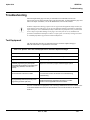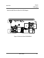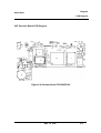
1
SERVICE MANUAL
ALPHA GOLD
6881020B80
GENERAL
ALPHA GOLD
578 and 584
1GENERAL
1GENERAL
6881020B80
GENERAL
Contents
About This Publication . . . . . . . . . . . . . . . . . . . . . . . . . . . . . . . . . . . . . . . . . . . . . . . . . . . . . . . . . . . . . . . . . . . . . . . . . . . . . . 1-1
Audience . . . . . . . . . . . . . . . . . . . . . . . . . . . . . . . . . . . . . . . . . . . . . . . . . . . . . . . . . . . . . . . . . . . . . . . . . . . . . . . . . . . . . . . . . . . . 1-1
Finding Information . . . . . . . . . . . . . . . . . . . . . . . . . . . . . . . . . . . . . . . . . . . . . . . . . . . . . . . . . . . . . . . . . . . . . . . . . . . . . . . . . . . . 1-1
Conventions . . . . . . . . . . . . . . . . . . . . . . . . . . . . . . . . . . . . . . . . . . . . . . . . . . . . . . . . . . . . . . . . . . . . . . . . . . . . . . . . . . . . . . . . . . 1-2
Revisions . . . . . . . . . . . . . . . . . . . . . . . . . . . . . . . . . . . . . . . . . . . . . . . . . . . . . . . . . . . . . . . . . . . . . . . . . . . . . . . . . . . . . . . . . . . . 1-2
Specifications . . . . . . . . . . . . . . . . . . . . . . . . . . . . . . . . . . . . . . . . . . . . . . . . . . . . . . . . . . . . . . . . . . . . . . . . . . . . . . . . . . . . . 1-3
Product Overview . . . . . . . . . . . . . . . . . . . . . . . . . . . . . . . . . . . . . . . . . . . . . . . . . . . . . . . . . . . . . . . . . . . . . . . . . . . . . . . . . . 1-4
Product Names . . . . . . . . . . . . . . . . . . . . . . . . . . . . . . . . . . . . . . . . . . . . . . . . . . . . . . . . . . . . . . . . . . . . . . . . . . . . . . . . . . . . . . . . 1-4
Display . . . . . . . . . . . . . . . . . . . . . . . . . . . . . . . . . . . . . . . . . . . . . . . . . . . . . . . . . . . . . . . . . . . . . . . . . . . . . . . . . . . . . . . . . . . . . . 1-4
Housing . . . . . . . . . . . . . . . . . . . . . . . . . . . . . . . . . . . . . . . . . . . . . . . . . . . . . . . . . . . . . . . . . . . . . . . . . . . . . . . . . . . . . . . . . . . . . 1-4
Features . . . . . . . . . . . . . . . . . . . . . . . . . . . . . . . . . . . . . . . . . . . . . . . . . . . . . . . . . . . . . . . . . . . . . . . . . . . . . . . . . . . . . . . . . . . . . 1-4
Addressing . . . . . . . . . . . . . . . . . . . . . . . . . . . . . . . . . . . . . . . . . . . . . . . . . . . . . . . . . . . . . . . . . . . . . . . . . . . . . . . . . . . . . . . . . . . 1-5
Controls and Indicators . . . . . . . . . . . . . . . . . . . . . . . . . . . . . . . . . . . . . . . . . . . . . . . . . . . . . . . . . . . . . . . . . . . . . . . . . . . . . . . . . 1-5
Paging Operation . . . . . . . . . . . . . . . . . . . . . . . . . . . . . . . . . . . . . . . . . . . . . . . . . . . . . . . . . . . . . . . . . . . . . . . . . . . . . . . . . . . . . 1-11
Features and Options . . . . . . . . . . . . . . . . . . . . . . . . . . . . . . . . . . . . . . . . . . . . . . . . . . . . . . . . . . . . . . . . . . . . . . . . . . . . . . . . . . 1-11
Operating Instructions . . . . . . . . . . . . . . . . . . . . . . . . . . . . . . . . . . . . . . . . . . . . . . . . . . . . . . . . . . . . . . . . . . . . . . . . . . . . . . . . . 1-21
Theory of Operation . . . . . . . . . . . . . . . . . . . . . . . . . . . . . . . . . . . . . . . . . . . . . . . . . . . . . . . . . . . . . . . . . . . . . . . . . . . . . . . 1-24
Operating Power . . . . . . . . . . . . . . . . . . . . . . . . . . . . . . . . . . . . . . . . . . . . . . . . . . . . . . . . . . . . . . . . . . . . . . . . . . . . . . . . . . . . . 1-24
General Circuit Description of Dual Conversion POCSAG Pagers . . . . . . . . . . . . . . . . . . . . . . . . . . . . . . . . . . . . . . . . . . . . . . 1-25
Maintenance . . . . . . . . . . . . . . . . . . . . . . . . . . . . . . . . . . . . . . . . . . . . . . . . . . . . . . . . . . . . . . . . . . . . . . . . . . . . . . . . . . . . . 1-27
Removing the Battery . . . . . . . . . . . . . . . . . . . . . . . . . . . . . . . . . . . . . . . . . . . . . . . . . . . . . . . . . . . . . . . . . . . . . . . . . . . . . . . . . 1-27
Replacing the Battery . . . . . . . . . . . . . . . . . . . . . . . . . . . . . . . . . . . . . . . . . . . . . . . . . . . . . . . . . . . . . . . . . . . . . . . . . . . . . . . . . . 1-28
Removing the Back Cover . . . . . . . . . . . . . . . . . . . . . . . . . . . . . . . . . . . . . . . . . . . . . . . . . . . . . . . . . . . . . . . . . . . . . . . . . . . . . . 1-28
Removing the Receiver Board . . . . . . . . . . . . . . . . . . . . . . . . . . . . . . . . . . . . . . . . . . . . . . . . . . . . . . . . . . . . . . . . . . . . . . . . . . . 1-30
Removing the Snubber Pad . .. . . . . . . . . . . . . . . . . . . . . . . . . . . . . . . . . . . . . . . . . . . . . . . . . . . . . . . . . . . . . . . . . . . . . . . . . . . 1-31
Removing the Decoder Board . . . . . . . . . . . . . . . . . . . . . . . . . . . . . . . . . . . . . . . . . . . . . . . . . . . . . . . . . . . . . . . . . . . . . . . . . . . 1-32
Removing the Vibrator Motor . . . . . . . . . . . . . . . . . . . . . . . . . . . . . . . . . . . . . . . . . . . . . . . . . . . . . . . . . . . . . . . . . . . . . . . . . . . 1-32
LCD Module Removal . . . . . . . . . . . . . . . . . . . . . . . . . . . . . . . . . . . . . . . . . . . . . . . . . . . . . . . . . . . . . . . . . . . . . . . . . . . . . . . . . 1-33
LCD Module Replacement . . . . . . . . . . . . . . . . . . . . . . . . . . . . . . . . . . . . . . . . . . . . . . . . . . . . . . . . . . . . . . . . . . . . . . . . . . . . . 1-34
Troubleshooting . . . . . . . . . . . . . . . . . . . . . . . . . . . . . . . . . . . . . . . . . . . . . . . . . . . . . . . . . . . . . . . . . . . . . . . . . . . . . . . . . . 1-37
Test Equipment . . . . . . . . . . . . . . . . . . . . . . . . . . . . . . . . . . . . . . . . . . . . . . . . . . . . . . . . . . . . . . . . . . . . . . . . . . . . . . . . . . . . . . 1-37
Preliminary Checklist . . . . . . . . . . . . . . . . . . . . . . . . . . . . . . . . . . . . . . . . . . . . . . . . . . . . . . . . . . . . . . . . . . . . . . . . . . . . . . . . . . 1-38
Self-Diagnostic Feature . . . . . . . . . . . . . . . . . . . . . . . . . . . . . . . . . . . . . . . . . . . . . . . . . . . . . . . . . . . . . . . . . . . . . . . . . . . . . . . . 1-39
RF Trouble Shooting . . . . . . . . . . . . . . . . . . . . . . . . . . . . . . . . . . . . . . . . . . . . . . . . . . . . . . . . . . . . . . . . . . . . . . . . . . . . . . . . . 1-47
MAY 16, 2005
1-i
578 and 584
6881020B80
1GENERAL
1GENERAL
ALPHA GOLD
GENERAL
About This Publication
About This Publication
Using this service manual and the many suggestions contained in it assures proper installation,
operation, and maintenance of Unication Alpha Gold pager. Refer any questions about this
manual to the nearest Customer Service Representative.
Audience
This Service Manual is provided to assist service personal in the test and repair of Unication
Alpha Gold pager. Service personal should be familiar with electronic assembly test methods,
troubleshooting, operation and the use of associated test equipment.
Finding Information
This manual provides descriptive data and service information for Unication Alpha Gold
pager. A pager’s product family is identified by the first three digits of the pager serial
number, unless the pager is covered by an extended warranty. Extended warranty pagers
have two alphabetic characters in place of the first two digits of the product family code. The
first digit is following the alphabetic code indicates the number of years the warranty period is
in effect.
Where information in this publication is specific to a type of pager, it is indicated; otherwise,
information is pertinent to all Alpha Gold pager. In this publication, pager types are
identified as:
• POCSAG
•
POCSAG 1
•
POCSAG 2
A pager type is determined by locating the pager model number in a model number chart and
referring to the pager type specified in the chart title.
Schematic diagrams, parts lists, and printed circuit board layouts are contained in supplementary
manuals.
This Service Manual consists of the following sections:
• General - Describes the product families, their features and options, and theory of
operation. Also, provided are procedures for disassembling, troubleshooting, and repairing
Unication Alpha Gold pager.
• Decoder - Provides decoder-specific circuit descriptions and troubleshooting flowcharts.
• Receivers - By frequency band, provides receiver-specific circuit descriptions, alignment
procedures, troubleshooting flowcharts, and model number charts.
Schematic diagrams, parts lists, and printed circuit board layouts are contained in supplementary
manuals.
MAY 16, 2005
1-1
GENERAL
Alpha Gold
About This Publication
Conventions
Special characters and typefaces, listed and described below, are used in this
publication to emphasize certain types of information.
Q234
This typeface is used to emphasize circuit board component reference
designators.
OFF
This typeface represents text displayed on the pager LCD.
G
E
Note: Emphasizes additional information pertinent to the subject matter.
Caution: Emphasizes information about actions that may result in equipment
damage.
Warning: Emphasizes information about actions that may result in personal
injury.
Revisions
Any changes that occur after manuals are printed are described in Publication
Manual Revision (PMR) bulletins. These bulletins can include a listing of new parts,
changes to schematic diagrams and printed-circuit board layouts, and so on.
1-2
MAY 16, 2005
GENERAL
Alpha Gold
Specifications
Specifications
Paging Sensitivity:
Refer to specific receiver information.
Spurious & Image Rejection: Refer to specific receiver information.
Frequency Stability:
Refer to specific receiver information.
EIA Selectivity:
Refer to specific receiver information.
Memory Capacity:
Refer to Table 1-2.
Alert Tone Frequency:
3200 Hz standard alert with user selectable alerts
Alert Tone Duration:
2 or 12 seconds programmable
Alert Tone Loudness:
78 dB minimum, at 30 cm (12 inches)
Power Consumption:
Refer to specific receiver information.
Battery:
One 1.5V, AA-size alkaline
Battery Life:
Refer to specific receiver information.
Weight (with battery):
87 grams (approximate)
Size:
81.0 x 55.0 x 18.5 mm
POCSAG 1 and 2:
Code Format:
31/21 POCSAG Code (CCIR Code
#1), 512, 1200, and 2400 bps
Channel Spacing:
25 kHz
Frequency Deviation:
±4.5 kHz
SPECIFICATIONS SUBJECT TO CHANGE WITHOUT NOTICE
MAY 16, 2005
1-3
GENERAL
Product Overview
Product Overview
The Unication Alpha Gold pager are miniature, microcomputer-controlled FM receivers with
graphic liquid crystal display (LCD). They are powered by a single AA-size battery.
These pagers use either Post Office Code Standardization Advisory Group (POCSAG) or FLEX
paging format. Refer to the applicable receiver section in this manual for information about
which format is used with each frequency range.
Product Names
Product name is on the front cover.
Product names are subject to change without notice. Some product names, as well as some
frequency bands, are available only in certain markets.
Display
The pagers’ large LCD displays:
• 80 alphanumeric characters in dot-matrix patterns of 5 columns by 7 rows
• 14 ideographic Simplified and Traditional Chinese characters, in dot-matrix patterns of 15
columns by 16 rows
• 28 ideographic Thai characters, in dot-matrix patterns of 8 columns by 16 rows
Housing
The pager is housed in an impact-resistant plastic case that offers excellent protection against
dust intrusion, vibration, and shock. Small in size and lightweight, the unit can be clipped to
your belt or fit comfortably in a shirt or jacket pocket.
Features
These pagers use the most advanced custom integrated circuits to perform the complex functions
for radio paging. Aside from the space and weight advantage, microcircuits enhance basic pager
reliability, simplify maintenance, and provide a wide variety of operational functions.
The following features are standard in the Alpha Gold pagers:
•
•
•
•
•
•
•
•
•
Non-volatile message memory with time and date stamp
•
Single AA-size battery
User-selectable alert screen with seven pleasing alert tones, chirp alert, standard alert, and
no alert
Intelligent function menu selections with prompts, icon s or both
•
Zoom in , Zoom out
•
1-4
Attractive, miniature styling
High-contrast, graphic dot-matrix liquid crystal display. POCSAG 2 pager
have a holographic LCD.
High-visibility backlighting (automatic in low-light conditions)
Microcomputer control with advanced software algorithms
PrivateTime
Low battery indicator
Real-time clock with time, date and alarm
MAY 16, 2005
578 and 584
6881020B80
1GENERAL
1GENERAL
Alpha Gold
GENERAL
Product Overview
Addressing
Each pager can be programmed for multiple personal, group, or maildrop addresses by using the
appropriate PPS and Pager Mechanical Interface.
Unication Alpha Gold pager respond to modulation consisting of a sequence of binary
digital “words.” When the transmission matches the address information stored in the codeplug,
the pager responds with an audible tone alert or a vibrating alert, depending on the programmed
options and the user-selected mode of operation. In addition to the tone or vibrating alert, the
pager also displays a message.
Controls and Indicators
The pager controls are the six buttons located on the front of the pager (refer to Figure below).
Indicators, in the form of icons, are displayed on the LCD. The following paragraphs describe
the controls and indicators.
The location and size of the Unication logo may vary for different models of the pager.
Liquid Crystal Display (LCD)
The four-line LCD provides a high contrast dot-matrix display for easy readability. The LCD
also features a high visibility backlight for reading the display in low-light conditions.
In the alphanumeric mode, a 4-line by 20-character dot-matrix format is used to display up to
80 characters per screen.
In the ideographic mode, a 2-line by 7-character dot-matrix format is used to display up to 14
Chinese or a 2-line by 14-character dot-matrix format is used to display up to 28 Thai characters
per screen.
MAY 16, 2005
1-5
GENERAL
Alpha Gold
Product Overview
Table 1-1 lists the indicators, their uses, and their meanings. Certain indicators, annunciators,
are displayed at the far left of the screen during pager power-up and whenever the pager is not
displaying messages or menus. Other indicators are displayed on various screens as described
in the following table and paragraphs.
Table 0-1. Indicators
Display Location and Meaning
Icon
Annunciator
Power On
Message/Status
Function Menu
Other
Unread Message
Flashing
Turn Pager Off
Private Time
Function is set to
On
Enter Private Time
Menu
Private Time
Enabled in Private
Time Screen
Private Time
Disabled in Private
Time Screen
Go to Status
Screen
Set Audible Alert
Set Silent Alert
Set No Message
Alert in Choose
Alert screen
Choose Alert Mode
Audible Alert mode
is turned on
Alarmed Message
Set Message Alarm
Cursor on Alarmed
Message
Alarm Enabled in
Set Time or Set
Message Alarm
Screen
Disable Alarm in
Set Time or Set
Message Alarm
Screen
1-6
MAY 16, 2005
578 and 584
6881020B80
1GENERAL
1GENERAL
Alpha Gold
GENERAL
Product Overview
Table 0-1. Indicators
Display Location and Meaning
Icon
Annunciator
Message/Status
Function Menu
Other
Set Time or Set
Alarm Selector
Set Time and
Alarm
Locked Message
Lock Message
Cursor on Locked
Message
Unlock Message
Maildrop Message
with Alert Enabled
Maildrop Alert On
Set Chirp Alert in
Choose Alert
Screen
Cursor on Maildrop
Message with Alert
Enabled
Maildrop Alert Off
Maildrop Message
with Alert Disabled
Cursor on Maildrop
Message with Alert
Disabled
Notebook
Message(s)
Add to Notebook
Cursor on
Notebook Message
Message in
Memory
Cursor on
Message, or New
Message when
flashing
Memory Full
Delete Message
MAY 16, 2005
1-7
GENERAL
Alpha Gold
Product Overview
Table 0-1. Indicators
Display Location and Meaning
Icon
Annunciator
Message/Status
Function Menu
Other
Delete All
Messages
Print Message
Print All Messages
Truncated
Non-Ideographic
Message
Non-Ideographic
Message
Continued
Alphanumeric
Missing Fragment
Indicator
Long Numeric
Missing Fragment
Indicator
24 Hour Time
AM Time
PM Time
Full Battery
3/4 Full Battery
1/2 Full Battery
1/4 Full Battery
Low Battery
Out of Range
1-8
MAY 16, 2005
Alpha Gold
GENERAL
Product Overview
Read Button (J)
The Read button is used to turn the pager on and read messages stored in memory. When the
pager is off, a single push of the Read button turns the pager on (refer to Figure 1-1).
As the pager is turned on, it displays the Power-up screen and generates the Power-up alert (refer
to Figure 1-2).
N
P
Figure 1-2. Power-up
Screen
When the pager is on, the Read button is used to display the Message/Status screen (refer to
Figure
ommmmmm
j
12:00x 01/01/00
Figure 1-3. Message/Status
Screen
After eight seconds of no pager activity, the display changes to the Standby screen (refer to
Figure 1-4).
N
P
Figure 1-4. Standby Screen
When the Read button is pressed to read a message, the first screen of the message
is displayed until the freeze time expires or a key is pressed (refer to Figure 1-5). A
Message Continued indicator (t) indicates the message is continued. This indicator
toggles with the last character of the display. If there is no character in the last
character location, the indicator flashes.
01:PLEASE COME TO
MY OFFICE TO DISCUSS
THE COMPLETED
FINANCIAL ANALYSIS t
Figure 1-5. First Screen of a
Message
MAY 16, 2005
1-9
GENERAL
Alpha Gold
Product Overview
When a message is displayed, each press of the Read button advances the display to the next
four lines. The date and time a message was received is displayed at the end of the message as
shown in (refer to Figure 1-6).
BRING CURRENT FY
BUDGET SHEETS
12:00x 01/01/00
Figure 1-6. Last Screen of a
Message
Pressing and holding the Read button causes a fast scroll through the message. The freeze and
fast scroll times are programmable with the PPS.
When the Read button is pressed while a Function menu or a Set Function screen is displayed,
the pager displays the Message/Status screen (refer to Figure 1-3) without saving any changes.
Function Button (K)
The Function button is used to activate the special functions. When the Function button is
pressed, the Function menu icons and prompts are displayed on the bottom two lines of the
display. The icon corresponding to the active function blinks and the appropriate prompt is
displayed above it (refer to Figure 1-7). The Function button also operates the display
backlighting when pressed and held for 2 seconds.
om
j
ESCAPE
l v L r q a A C g d u Y Z
Figure 1-7. Function Menu
Left Button (H)
The Left directional button is used to scroll to the first screen of the previous
message while reading a message or to move the cursor to the left.
Right Button (I)
The Right directional button is used to scroll to the first screen of the next message
while reading a message or to move the cursor to the right.
Up Button (F)
The Up directional button is used to scroll to the first screen of the current message
while reading a message or to move the cursor up. It is also used to increment the
time in the Set Time and Alarm screen. When pressed and held, the Up button
causes a continuous increment.
1-10
MAY 16, 2005
GENERAL
Alpha Gold
Product Overview
Down Button (G)
The Down directional button is used to scroll down through a message one line at a time. It is
also used to decrement the time in the Set Time and Alarm screen. When pressed and held, the
Down button causes a continuous decrement.
Paging Operation
Unication Alhpa Gold pager can be configured to accept alphanumericdisplay, ideographic-display pages, numeric-display, and tone-only pages. When a
message is received, the pager emits a 2 or 12 second alert depending on pager
programming. A new message is indicated by a flashing arrow (o). After the message
is stored and 8 seconds of no pager activity lapses, the display changes to the
Standby screen. Also, the On annunciator icon (N) in the upper left-hand corner of
the display flashes. Reading any part of the message removes the unread message
indication (the On icon no longer flashes).
Features and Options
The following information describes features and options of the Unication Alpha Gold pager.
Some pager features are programmable using the PPS. The PPS User’s Guide listed in
“Specifications” provides additional information about programmable features.
MAY 16, 2005
1-11
GENERAL
Alpha Gold
Product Overview
Table 0-2. Standard Features
Pager
Type
Message Storage
Description
POCSAG
Paging Feature
Personal Messages are located on the first line; older messages are located to
the left. The last message received is always the farthest right message (except
for duplicate messages). When the farthest right message slot is full and a new
message arrives, all messages are shifted as far left as possible, filling in all
gaps with the newest message placed to the right.
Maildrop Messages are stored in a designated slot on the second line of the
display. A maildrop message sent on address or source 1 is stored in slot 1, a
message sent to address or source 2 is stored in slot 2, and so on.
Personal Message
Notebook
Up to 255 personal messages can be stored in the Personal Message
Notebook. The Personal Message Notebook is represented by
on the first
line of the display.
Maildrop Message
Notebook
Up to 255 maildrop messages can be stored in the Maildrop Message
Notebook. The Maildrop Message Notebook is represented by
on the
second line of the display.
Automatic Message
Deletion - Personal
Messages
When all personal message slots are occupied or there is insufficient unused
personal message memory, the oldest unprotected read message is deleted to
make room for the new message. If all messages are unread, the oldest
unprotected, unread message is deleted.
Automatic Message
Deletion - Maildrop
Messages
An existing message at a particular maildrop address is deleted when a new
message for that address is received (except when the new message does not
contain data). However, if there is insufficient unused maildrop memory, the
existing message is deleted to make room for the new message, even if the new
message is to be discarded. The order of deletion is:
1. Existing message on the current maildrop address
2. Right-most read maildrop address
3. Right-most unread maildrop address
Message Management
When the Message Locking option is selected, the user can lock up to 10
personal messages. When the Manual Delete option is selected, the user can
delete unlocked, unalarmed messages.
Alarms can be set on up to 5 messages.
1-12
Message Status
Icons on the Message/Status screen indicate the status of all messages. Refer
to Table 1-1 for descriptions of status indicators.
Retain Errored NonNumeric Message
When this option is selected, the pager alerts normally if errors are detected in
an alphanumeric or ideographic message. If this option is not selected, the
pager does not alert, and the message is not stored.
MAY 16, 2005
GENERAL
Alpha Gold
Product Overview
Table 0-2. Standard Features
Pager
Type
Description
POCSAG
Paging Feature
Real-Time Clock and
Alarm Clock
Displays the time and date, time-and-date stamps all messages, and gives an
alarm indication at a preset time.
The time can be changed to indicate either 24-hour or AM/PM time. If 24-hour is
selected, all time stamps and alarm times are displayed in 24-hour time. If
AM/PM is selected, all time stamps and alarm times are displayed in AM/PM
time.The alarm can be set for a daily alarm or a one-time-only alarm. When an
alarm expires, the pager either vibrates or produces an audible alert depending
on the selected mode.
Time-Stamping
Displays the time and date a message was received at the end of that message.
A screen with a typical time stamp (in U.S. format) is shown in Figure 1-6.
Individual Message
Alarm
Allows an alarm to be attached to a particular personal message. Alarms can be
set on up to 5 messages. If an individual message alarm is set on a message,
that message is denoted by
on the Message/Status screen. The
annunciator is also displayed, even when the pager is turned off.
When an individual message alarm expires, the cursor moves to the message,
the s icon blinks, and the pager either vibrates or produces an audible alert,
depending on the selected mode.
International Date
Allows the pager to be programmed to display the date in either US or
international format. For example, March 30, 1997 can be displayed as 03/30/97
(U.S.) or 30/03/97 (International).
Auto Alarm Turn On
This feature causes the pager to automatically turn on and give an alarm alert
when any type of alarm expires. The pager stays on after the alarm alert has
ended.
Key Click
Produces an audible click when a button is pressed if the Key Click option is
selected.
Battery Removed
If the battery is removed, the pager turns off immediately. When the battery is
replaced, the pager powers up after a 2-second pause.
Battery Gauge
Displays a battery gauge indicator (see Table 1-1) on the third line of the display.
The battery condition percentages are programmable values and vary with
battery type.
Low Battery Indication
). If the Low Battery Alert
Displays a battery warning indicator (
or
option is selected, the pager will also alert. The following takes place while the
low battery condition exists:
1. Manual or 12-second audible or vibration alerts are reduced to 2 seconds.
2. Two-second audible or vibration alerts are reduced to 1 second.
3. Backlight cannot be turned on.
Chirp alerts are unaffected by the low battery condition.
MAY 16, 2005
1-13
GENERAL
Alpha Gold
Product Overview
Table 0-2. Standard Features
Pager
Type
Memory Retention
Description
POCSAG
Paging Feature
If the Non-Volatile Memory option is selected, all messages and pager settings
remain in memory when the pager is turned off. If the option is not selected,
messages and settings are lost when the pager is turned off.
To ensure proper memory retention, turn the pager off before removing the
battery. Immediately replace the old battery with a new battery.
Automatic Alert Reset
Alerts are typically stopped by a button press or by timing out. If the Manual
Alert Reset option is selected (see Table 0-5), the message alert does not stop
automatically, but waits for a key-press to stop. The Manual Alert Reset option
applies only to personal and priority alerts while the pager is in the audible
mode. It does not apply to maildrop, alarms, reminder alerts or when the pager
is in the vibrate mode.
Battery Saver
Three battery-saving techniques are used by the pager:
1. The microcomputer activates the receiver circuitry for only a short period of
time to search for an incoming page and then turns the receiver off for a set
duration.
2. Part of the display is turned off after 8 seconds of no pager activity. During
this time, only the annunciator icons are displayed. See Table 1-1 for
information about the annunciator icons.
3. The microcomputer clock rate is slowed when there is no pager activity.
Displays
when there are too few character spaces available in the pager’s
personal message memory or when all personal message slots are occupied. If
the next incoming personal message has more characters than the number of
available spaces in pager memory, the new message overwrites the oldest
message.
The Memory Full Prompt is a programmable option.
Memory Full Indication
Displays
1-14
when there are fewer than 135 character spaces available.
User Selectable Alerts
Allows the user to choose a standard alert or one of seven pleasing alerts via
the Choose Alerts screen. The last pleasing alert listed in the Choose Alert
screen is a programmable pleasing alert. Refer to Table 0-5 for more
information about programmable pleasing alerts. The standard or pleasing alert
selected on the Choose Alerts screen applies to incoming non-priority personal
messages and the power-up alert. The Choose Alerts screen also allows the
user to select a Chirping Alert or No Alert for non-priority personal messages. If
Chirping Alert or No Alert is selected, the Standard Alert is used for the powerup alert.
International Character
Sets
Various languages are supported by re-mapping the ASCII characters to
language-specific characters. APPENDIX A provides information about the
alphanumeric prompts and special character set. APPENDIX B provides
information about the ideographic prompts.
MAY 16, 2005
GENERAL
Alpha Gold
Product Overview
Table 0-3. Ideographic Features
Pager
Type
Description
POCSAG
Paging Feature
If the Errored Data Indication programmable option is selected and the pager
receives a message with errored data, the display alternates
Errored Message
Character Symbol
between the errored data and a checkerboard pattern ( ).
Table 0-4. Optional Memory Features
Pager
Type
Description
POCSAG
Paging Feature
Maildrop messages are placed in the slot corresponding to the address number.
For example, address number two message goes into the second maildrop slot.
Each new maildrop message to a particular address replaces the message (if
any) at that address.
Maildrop messages cannot be locked, alarmed, or placed in the Personal
Message Notebook.
Maildrop
Maildrop messages can be stored in the Maildrop Message Notebook.
A duplication check is not performed on maildrop messages.
Maildrop History
Retain Better Maildrop
Message
Enable Maildrop Alert
Stores up to 4 history files for each of one or more maildrop addresses. An
existing maildrop message is moved to the address-specific history file when a
new maildrop message is received. The oldest history file is deleted if an
address has 4 history files when a new message is received.
Causes a new maildrop message to replace an existing maildrop message only
if the new message contains the same number or more good (non-errored)
characters than the existing maildrop message.
Displays the Maildrop Alert On icon ( ) or the Maildrop Alert Off icon ( ) on
the Function menu when the cursor is placed on a maildrop message. Each
maildrop source can be individually set to Maildrop Alert On or Maildrop Alert
Off. When Maildrop Alert On is selected, the pager produces an audible chirp or
short vibration on receipt of a new maildrop message.
MAY 16, 2005
1-15
GENERAL
Alpha Gold
Product Overview
Table 0-4. Optional Memory Features
Pager
Type
Description
POCSAG
Paging Feature
Erases all previously read, unprotected personal messages; all read maildrop
messages; and all maildrop history files when the Delete All Messages icon ( )
is selected from the Function menu. Any unread or protected messages (locked,
alarmed, or personal notebook) are retained in memory.
Memory Cleanup
A character-by-character duplication check is performed on messages meeting
certain criteria. Errored characters are ignored during the check. If all nonerrored characters in two messages match, the messages are duplicated. The
message with the fewest errors is kept and the other message is discarded. If
both messages contain the same number of errors, the new message is
discarded and the old message is flagged as a duplicate. A message flagged as
a duplicate is marked as unread, and when read,
is
displayed before the first line of the message.
Duplicate Message
Detection
Checks all personal messages of the same type (numeric, alphanumeric, or
ideographic) and source as the incoming message.
If the Address (Source) Independent option is selected, duplicate checks are
performed on messages from different sources.
Allows duplicated messages sent within the specified time-out period to be
treated as if only one message was received. Receiving new messages during
the sequential lockout period extends the lockout period for both (or all) lockedout messages. Does not apply to maildrop messages.
Sequential Lockout
Requires the Duplicate Message Detection option be selected. If the sequential
lockout period is set to none, a duplicate message is detected immediately.
Table 0-5. Optional Alert Features
Pager
Type
1-16
Description
POCSAG
Paging Feature
User-Changeable Alert
Mode
Allows user-selection of either the audio or vibrate alert mode from the Function
menu.
User-Selectable Alerts
Allows user-selection of a standard alert, one of seven pleasing alerts, chirp
alert, or no alert (incoming pages only) from the Choose Alert screen.
MAY 16, 2005
GENERAL
Alpha Gold
Product Overview
Table 0-5. Optional Alert Features
Pager
Type
Description
POCSAG
Paging Feature
Programmable
Pleasing Alert
When this programmable option is set to custom, a menu in the Pager
Programming Software is used to create a pleasing alert.
Vibrator
The alert mode can be set to silent so the pager vibrates when a message is
received.
Silent Pager Operating
Mode
Audible alerts are disabled when the pager is programmed for the Silent Alert
option. The User Changeable Alert, User Selectable Alert, and Programmable
Pleasing Alert options are automatically disabled when this option is set.
Disable All Alerts
Audible and vibrator alerts are not available when this programmable option is
selected. This option overrides all other alert options and does not allow alerts
to be changed with the Set Alerts function.
Retain Errored
Numeric Message
Allows the pager to alert as normal if errors are detected in a numeric message.
Without this option selected, the pager does not alert on errored data and the
errored message is not stored.
Manual Alert Reset
If this programmable option is selected and the pager is in audible mode, the
user must manually turn off all individual, group, and priority page alerts by
pressing any button on the pager. If Chirping Alert is selected from the Choose
Alert screen, the pager emits a single chirp. If No Alert is selected from the Set
Alerts screen, the received message is indicated in the Message/Status screen
without an alert.
Reminder Alert Interval
and Time-out
When these programmable options are selected and there are unread
messages in memory, the pager generates a chirp or vibration based on the
programmed time interval. However, the Reminder Alert stops after the
programmed time-out period is reached.
Alert Frequency
The standard alert frequency can be selected when programming the pager with
the Pager Programming Software.
Alert Duration
Non-priority personal alerts can be programmed for either 2 seconds or 12
seconds.
MAY 16, 2005
1-17
GENERAL
Alpha Gold
Product Overview
Table 0-6. Time Function Options
Pager
Type
Description
POCSAG
Paging Feature
Private Time
Used to set daily times at which the pager automatically turns on and off. When
selected,
is displayed in the top left corner of the LCD.
Read and Fast Scroll
Time-outs
Causes the pager to display the Message/Status screen when the
programmable freeze time period elapses. Pressing and holding the Read
button ( ) while reading a message results in a fast scroll. The fast scroll rate
is programmable.
Alternate Prompts
The power-up prompt and all source prompts can be customized and alternate prompts can be
programmed for the following functions:
• Choose Alert
• Lock Message
• Standard Alert
• Pager Disabled
• Pleasing Alert
• Set Private Time
• Chirping Alert
• Memory Full
• Set Audible Alert
• Set Time
• Delete All Messages
• Set Alarm
• Delete Message
• Set Time and Alarm
• Escape
• Unlock Message
• Set Silent Alert
• Go To Status Screen
• Turn Pager Off
• Duplicate Message
• No Message Alert
• Maildrop Alert On
• Add to Notebook
• Maildrop Alert Off
• Print One Message
• Print All Messages
• Notebook
• On
• Set Message Alarm
• Off
• Tone Only
• Group
The alternate prompts can be in alphanumeric format Alphanumeric prompts and
characters are listed in Appendix A.
1-18
MAY 16, 2005
GENERAL
Alpha Gold
Product Overview
Table 0-7. Display Options
Pager
Type
Auto Backlight
Show Source
Description
POCSAG
Paging Feature
Causes any button press to turn on the display backlighting in low-light
environments.
Displays source information at the end of a message.
Out-of-Range
Indication
Displays the Out-of-Range indicator (
,
or
) on the Message/Status
screen when the pager does not detect a synchronization codeword from the
paging terminal within the programmed time period. The indicator is displayed
until the pager is no longer out of range. If the Out-of-Range Alert option is also
selected, the pager alerts when it goes out of range.
Function Menu Display
Selects the type of Function menu display.
1. Ideographic mode: prompts or icons.
2. Alphanumeric mode: prompts, icons, or both.
Auto-Contrast
Adjustment
Automatically adjusts the LCD contrast voltage at power-up according to the
programmed value.
Errored Data Indication
Causes the pager to display a special non-transmittable error character ( ) to
represent an error or bad data. The display alternates between the
errored data and a checkerboard pattern ( ).
Zoom in:The pager shall display the messae 2 line mode
Zoom out:The pager shall display the message 4 line mode
Zoom
Message Preview
Status screen. The user can scroll left or right to display the first line of adjacent
messages.
MAY 16, 2005
1-19
GENERAL
Alpha Gold
Product Overview
Table 0-8. Printing Options
Pager
Type
Description
POCSAG
Paging Feature
Manual Printing
If enabled, messages can be printed by selecting the Print icon while the pager
is installed in a mechanical interface connected to a Universal Programming
Interface configured for printing.
Data Inversion
If enabled, messages are automatically printed if the pager is installed in a
Pager Mechanical Interface connected to a Universal Programming Interface
configured for printing.
Table 0-9. RF Options
Pager
Type
Data Inversion
Description
POCSAG
Paging Feature
High-side or low-side injection is selected with this programmable option.
Programmable for a signaling rate of 512, 1200, or 2400 baud.
Signaling Rate
Selection
POCSAG Any Frame
1-20
Supports a maximum of 4 pager codes. A code can be located in any frame.
Frequency
The pager’s carrier frequency must be programmed to ensure proper radio
frequency (RF) performance of the pager.
Receiver IC Type
Set at the factory according to receiver frequency, but can be reset in the field if
the receiver type is changed. Refer to the applicable PPS User’s Guide listed in
the “Related Publications” section to change this setting.
MAY 16, 2005
GENERAL
Alpha Gold
Product Overview
Table 0-10. Over-the-Air Download Options
Pager
Type
Description
POCSAG
Paging Feature
Disables over-the-air (OTA) programming. Pagers with this option set to YES
must be programmed using the Pager Mechanical Interface and the Pager
Programming Software.
OTA Programming
Disabled
Disables the audible reset after OTA programming.
Silent OTA
Programming
Download Security
Level
Programming security level is set to none or maximum. When set to maximum,
a password is required to program the pager using a Pager Mechanical
Interface (a password is always required to program the pager via OTA).
Dead Pager
Disables the pager if the download procedure is attempted incorrectly eight
times and requires the microcomputer be replaced. One successful download
(with the proper password) before the pager is “dead” resets the download
counter.
Operating Instructions
This section provides information about operating the advanced functions of the
Unication Alpha Gold pager. Refer to the applicable operating instructions listed
in “Specifications” for further information.
Moving a Message into a Message Notebook
Messages can be stored in notebooks. Personal messages can be moved into the
Personal Message Notebook and maildrop messages can be moved into the Maildrop
Message Notebook.
A message is moved into a notebook by:
1. Selecting the desired message on the Message/Status screen.
2. Pressing the Function (K) button.
3. Scrolling to the u icon.
4. Pressing the Function (K) button again.
Setting the Time and Alarm
The time and/or the alarm is changed by:
1. Selecting the Clock icon (v) in the Function menu. The Set Time /Alarm screen
is displayed.
2. When the Set Time/Alarm function is first selected, the Set Time function is
active. The active function is indicated by blinking circles at the beginning and
the end of the first line and the prompt displayed on the third line (refer to
Figure 1-8).
MAY 16, 2005
1-21
GENERAL
Alpha Gold
Product Overview
a.
b.
When the circles are blinking:
• Use the Up and Down buttons (F and G) to toggle between the set time
and set alarm functions.
• Use the Left and Right buttons (H and I) to move across the fields of
the active function.
When the circles are not blinking:
• Use the Up and Down buttons (F and G) to change values within the
selected field.
• Use the Left and Right buttons (H and I) to move across the fields.
• Pressing and holding the Up or Down button (F or G) scrolls through
the values appropriate to the field.
v3:32y06/08/94
Kc4:00y--/--/--K
SET ALARM
Figure 1-8. Set Time and
Alarm Screen with Set
Alarm Function Active
3.
When the desired time is displayed, press the Function button (K) to store the
new time and date. If the Read button (J) is pressed before the Function button
is pressed, the time change is not stored.
Set Alarm
The alarm can be set for a daily alarm (indicated by --/--/-- in the Set Alarm
screen) or a one-time-only alarm by modifying the date field to contain a specific
date. When the desired alarm time is displayed, the Function button (K) is pressed
to store the new alarm time and date. If the Read button (J) is pressed before the
Function button is pressed, the alarm time change is not stored.
To activate or deactivate the alarm, the cursor must be positioned on the Alarm
icon in the Set Alarm screen. The Up or Down button (F or G) is used to set the alarm
on ( c) or off (e). When the alarm is activated, the icon is displayed on the standby
screen (refer to Figure 1-9).
N
Q
Figure 1-9. Standby Screen
with Alarm Annunciator
1-22
MAY 16, 2005
GENERAL
Alpha Gold
Product Overview
Using the Private Time Function
Select the Private Time (L) in the Function menu to display the Set Private
Time screen (see Figure 1-10).
Use the Left and Right buttons (H and I) to move the cursor left or right
through the time fields. Use the Up and Down buttons (F and G) to modify the
individual fields.
•
The first field shows the Private Time icon that indicates the function is
set to either On (L) or Off ( M).
•
The second field specifies the time the pager is to turn on, and the third
field specifies the time the pager is to turn off.
1.
2.
•
At the end of each time field, y or w (or x) is displayed, indicating the
time is displayed in either 24-hour or 12-hour clock notation, respectively.
ON
OFF
M 0:00y
0:00y
Figure 1-10. Private Time
Setting Screen
This function is not enabled if the Private On time is the same as the private Off time.
When the Private Time programmable option is selected and set to On in the Private Time
screen, the Private Time icon is displayed in the top left corner of the LCD
(refer to Figure 1-11). The Private Time icon is displayed even if the pager is
turned off.
L
N
Figure 1-11. Standby
Screen with Private Time
Annunciator
If the programmable Private Time Alert option is selected, the pager chirps or
vibrates when the Private Time function turns the pager on or off.
MAY 16, 2005
1-23
GENERAL
Alpha Gold
Theory of Operation
Theory of Operation
The Unication Alpha Gold pager consist of a radio frequency (RF) receiver section and a
microcomputer-controlled decoder section. A message is received via an RF carrier that is
frequency modulated by a coded binary sequence.
There are two types of receivers available for these pagers: the standard receiver and the Zero
Intermediate Frequency (ZIF) receiver. The circuitry in the standard receiver performs the RFto-IF conversion and the frequency demodulation. The circuitry in the ZIF receiver performs the
RF-to-ZIF conversion and the frequency demodulation.
The decoder section processes the coded data using digital techniques, and controls the message
memory, LCD, and alert tones depending on the pager model and type of message received. For
more information regarding paging code formats, see the “Pager Maintenance Reference
Manual.” (Refer to the list of related publications in the Part Numbers section of this manual to
obtain the number for this manual.)
Block diagrams are provided to show the typical functions of a:
• Dual Conversion POCSAG pager
None of the diagrams illustrate a pager with a synthesized receiver.
Operating Power
Operating power for both the receiver and decoder boards is obtained from the battery. On the
receiver board, a 1-volt regulator supplies the RF circuitry with power.
The decoder board generates 3 volts dc through the linear support module. This voltage is
supplied to the microcomputer, linear support module, the character ROM, external RAM, and
the display driver integrated circuit (IC). The display driver IC generates an internal 9 volts
supply to correctly bias the LCD.
1-24
MAY 16, 2005
GENERAL
Alpha Gold
Theory of Operation
General Circuit Description of Dual Conversion POCSAG Pagers
The following information describes the general theory of operation for the Unication Alpha
Gold dual conversion POCSAG pagers. Figure 0-1 displays a typical functional block diagram
for a dual conversion POCSAG pager.
RF Board Block Diagram
ANT
Logic Board Block Diagram
IF IC
LCD Module
LNA
BAND
PASS
FILTER
Addr. &data Bus
120 x32 pixel
1st MIXER
1st IF
Filter
2 nd
MIXER
2nd IF
Filter
DET
A
RAM SRAM
128K bytes
Control Bus
=>4 Icon
LCD Data & Control Bus
Beep
Key Button
MCU
Vibrator
EL Module
OSC
Regulator
Multiplier
Battery
Detector
OSC2
32768 Hz
Photo-transistor
20.95MHz
Vbat
Vbias
RF Interface
H/W
Decoder
VCO
Flex or pocsag
Control Bus
OSC1
4.19 MHz
Control Bus
Programmer
RS232
EEPROM
2K bytes
Control Bus
Vbat
DC-DC
Converter
Vcc
Figure 0-1. Typical Dual Conversion POCSAG Pager
MAY 16, 2005
1-25
GENERAL
Alpha Gold
Theory of Operation
Decoder
The decoder consists of the microcomputer, Display module, external memory
The Microcomputer performs the following:
• Controls the receiver circuits, powering them up and down at the proper time intervals.
• Decodes the binary information received.
• Stores messages in external RAM
• Generates the alert tones and patterns
• Processes user inputs from the keypad
• Controls and writes to the Display module
The Linear Support module performs the following:
• Provides boosted dc voltage to all circuits.
• Monitors battery conditions.
• Drives the lamp, speaker, and vibrator motor.
• Monitors boosted dc voltage.
External Memory
The external memory consists of the following:
• 32k x 8 static performance storage.
The Display module performs the following:
• Provides LCD bias.
• Displays data from the microcomputer.
1-26
MAY 16, 2005
GENERAL
Alpha Gold
Maintenance
Maintenance
This section provides instructions for the disassembly of Unication Alpha Gold pager.
Special tools are listed at the end of this section. An additional list of tools used in maintaining
a pager is in the Pager Maintenance Reference Manual (refer to the Related Publications list in
the Part Numbers section of this manual for the manual number).
This product contains static-sensitive devices. Use anti-static handling procedures to prevent
electrostatic discharge and component damage.
Removing the Battery
1.
2.
Ensure the pager is turned off.
Locate the ribbed battery-door lock on the back of the pager as shown in Figure below. To
unlock the battery door, slide the lock away from the battery door as far as it can go.
3.
While pressing on the battery door, slide the door in the direction of the arrow on the door
as shown in Figure.
Lift the end of the door and remove it completely.
Remove the battery by prying the positive end up with a disassembly tool.
4.
5.
MAY 16, 2005
1-27
GENERAL
Alpha Gold
Maintenance
Replacing the Battery
1.
Position the new AA-size battery so the “+” and “−” markings on the battery match the
polarity diagram in the battery compartment.
Putting the battery in the wrong way (incorrect battery polarity) causes all messages to be
erased.
2.
3.
4.
5.
6.
Insert the new battery, pressing it against the negative contact until the positive end is
seated.
Check the battery-door lock and ensure it is in the fully open position.
Place the battery door over the battery so the latches on the door are inserted in their
respective latch slots.
Slide the door closed. (Best results occur with the battery door laying flat on the battery.)
An audible click indicates the door is properly seated.
Lock the door in place by sliding the ribbed battery-door lock toward the battery door.
Removing the Back Cover
1.
2.
3.
1-28
Remove the battery door and battery as described in the earlier procedures.
Turn the pager so its back is facing up.
Remove the 4 screws by using the T6 (star head) screw driver.
MAY 16, 2005
GENERAL
Alpha Gold
Maintenance
4.
Use the disassembly tool to disengage the first locking tab in the battery compartment by
carefully prying outward (refer to Figure below).
TION
MAY 16, 2005
1-29
GENERAL
Alpha Gold
Maintenance
5.
After step 4 you can easily remove the back cover.
Removing the Receiver Board
1.
1-30
Remove the battery door, battery, and back cover as described in the earlier procedures.
MAY 16, 2005
GENERAL
Alpha Gold
Maintenance
2.
Hold the decoder board down and gently pry the receiver circuit board up and away from
the decoder circuit board at a point near the interconnect socket. When the pins of the
interconnect socket are disengaged, the board can be lifted away.
Removing the Snubber Pad
1.
2.
Remove the battery door, battery, back cover and receiver board as described in early
precedures.
Hold the snubber pad and remove it from the decoder board.
MAY 16, 2005
1-31
GENERAL
Alpha Gold
Maintenance
Removing the Decoder Board
1.
2.
Remove the battery door, battery, back cover, receiver board and snubber pad as described
in the earlier procedures.
Hold the decoder board and remove it from the the top cover.
Removing the Vibrator Motor
1-32
1.
Turn the back cover so the vibrator PCB is facing up.
2.
Remove the 3 screws from the vibrator PCB.
3.
Hold the vibrator PCB and remove it from the back cover.
MAY 16, 2005
GENERAL
Alpha Gold
Maintenance
LCD Module Removal
1.
2.
3.
Remove the battery, battery door, latch band, back cover, receiver board, shock pad, and
decoder board as described in the earlier procedures.
Disengage the LCD module light-diffuser catches by using the pointed end of the disassembly tool.
Position the Heat Seal Connector (HSC) repair fixture facing you with the pull handle for
PCB retention/removal on the right. Place the decoder and LCD module in the fixture (refer
to Figure below).
HSC FIXTURE
LCD LEADS
MAY 16, 2005
1-33
GENERAL
Alpha Gold
Maintenance
4.
5.
Carefully lift the front edge of the LCD module to expose the leads.
Apply heat with a soldering iron or hot air machine to the leads across both solder areas
until the whole LCD module is detached from the decoder board. Be careful not to overheat
and burn the decoder board (refer to Figure below).
LCD Module Replacement
1.
2.
3.
4.
1-34
Clean the solder pads with an appropriate cleaner and allow to air dry.
Apply a thin, even layer of flux on the solder pads and use a soldering iron to dispense
solder on the solder pads (pre-tin). (Ensure there is no bridging of the solder between the
pads).
Clean the pre-tinned solder pads and allow to air dry.
Position the new LCD module on the decoder board with the leads over the pads.
MAY 16, 2005
GENERAL
Alpha Gold
Maintenance
5.
Place the LCD module in the fixture (refer to Figure below).
HEAT
SHIELD
0162
486C
01
EXPOSED
LEADS
PULL
HANDLE
6.
7.
8.
9.
Slide the heat shield from left to right and from front to back to expose the leads and pads
on the decoder.
Align the leads with the pads and tack solder one end of the leads and pads.
Start from the unsoldered end of the flex circuit and heat with a soldering iron or hot air
machine.
Gently push the leads down onto the solder pads using the disassembly tool (refer to Figure
below). Use a gentle downward motion onto the decoder and not a sweeping sideways
motion, which tends to cause solder bridging between the pads.
HEAT
SHIELD
LCD
MODULE
EXPOSED
LEADS
10. Clean the solder pads and leads and allow to air dry.
11. Remove the protective paper from the adhesive strip on the light diffuser frame.
MAY 16, 2005
1-35
GENERAL
Alpha Gold
Maintenance
12. Connect the module switch pad to the frame locating pin by gently pressing them together.
13. Engage the light diffuser catches with the two slots on the edge of the decoder board.
14. Replace the decoder board, shock pad, receiver board, back cover, latch band, battery, and
battery door as described in the earlier procedures.
1-36
MAY 16, 2005
GENERAL
Alpha Gold
Troubleshooting
Troubleshooting
Unication Alpha Gold pager's circuitry is contained in two individual sections. One
section is the receiver board, and the other is the decoder board. To disassemble the pager and
remove the major assemblies, refer to the Maintenance section of this manual.
Leadless-component technology requires the use of specialized equipment and procedures for
repair and servicing of this pager. If you are not sufficiently familiar with leadless-component
repair techniques, it is recommended you defer maintenance to qualified service personnel and
service shops. Irreparable damage to the pager can result from service by unauthorized
personnel. Unauthorized attempts to remove or repair parts can void any existing warranties
or extended performance agreements with the manufacturer.
Test Equipment
The following table lists the test equipment unique to Unication Alpha Gold pager.
Either the listed items or equivalents are to be used.
Table 1-12. Specific Tools and Test Equipment for Unication Alpha Gold Pager
EQUIPMENT TYPE
APPLICATION
HSC Repair Fixture
Used to hold LCD in place when soldering to decoder.
Alignment back cover
Required for alignment
POCSAG programming kit (584-specific
Pager Mechanical Interface, POCSAG Pager
Programming Software, and instruction
manual)
Required to read and/or program POCSAG pager options
Receiver/decoder interconnect cable
To connect the receiver and decoder circuit boards during
troubleshooting
PC programming interface (120 Vac) or PC
programming interface (220 Vac)
Interface between the programmer and the PC. Includes
interface unit and applicable transformer/cables.
For a list of additional test equipment, refer to the Pager Maintenance Reference Manual (refer
to the Related Publications list in the Part Numbers section of this manual for the manual
number).
MAY 16, 2005
1-37
GENERAL
Alpha Gold
Troubleshooting
Preliminary Checklist
Use the following table as a quick reference guide to determine the probable cause of some
common pager problems and where to find more details.
Table 1-13. Preliminary Troubleshooting Checklist
Malfunction
General pager functions
Paging Sensitivity
Probable Cause
Check all pager functions using selfdiagnostic test and check
Components are bad
Details
General Section - Troubleshooting
Test Procedures = Pager Maintenance
Reference Manual
Expected values = Receiver Sections
Pager does not power up
No display or partially active
display
No page/inactive data port
a) Battery voltage low or incorrect polarity
b) 4.19 MHzclock not present
a) Broken LCD
b) Damaged display contacts
Poor connection receiver board socket
Decoder Section
Decoder Section
Receiver Sections
No alerts on power up
Improper or no voltage: requires check of
system voltage, clock, reset, and transducer
Decoder Section
Can not page
a) Codeplug and encoder improperly coded
b) Decoder and receiver sockets not solder
properly at joints
Decoder Section
Switch pad or switch and contacts dirty
Decoder Section
Low cell
Decoder Section
a) Wires and solder joints not making contact
with PCB
b) PPS options not programmed
Decoder Section
Transducer contacts corrupted
Decoder Section
Buttons do not respond
No Backlighting
No vibrator alerts
No audible alerts
Circuit checks provide wrong
readings
Components are bad
Procedure = Pager Maintenance
Reference Manual
Expected values = Receiver Sections
10 dB rise failure
Pager is improperly aligned. Realign
according to procedure
10 dB rise procedure = Pager
Maintenance Reference Manual
Alignment procedure = Receiver
Sections
Improper Gain measurements
Components are bad
Gain measurement procedures =
Pager Maintenance Reference Manual
Expected values = Receiver Sections
1-38
MAY 16, 2005
GENERAL
Alpha Gold
Troubleshooting
Self-Diagnostic Feature
Placing the pager in self-diagnostic mode erases ALL messages from memory.
POCSAG Pagers
1.
2.
Ensure the pager is turned off.
Press the following sequence of buttons in rapid succession: Left H, Right I, Function K,
and Left H.
a. The LCD displays pager-specific information when first entering the self-diagnostic
mode. The first LCD line displays:
P169xxx - Ryyyy
b.
xxx represents ITL for international models, and yyyyy denotes the software version.
The second LCD line displays:
POCSAG
zzzz mm
3.
zzzz is the baud of the pager and mm is the memory size.
Press the Read button ( ) to enter self-diagnostic mode 1 (display test pattern 1). The
following is displayed:
4.
Press the Read button (
following is displayed:
) to enter self-diagnostic mode 2 (pixel test pattern 2). The
5.
Press the Read button ( ) to enter self-diagnostic mode 3 (audio alert test). The alert
sounds and the following is displayed:
MAY 16, 2005
1-39
GENERAL
Alpha Gold
Troubleshooting
6.
7.
Press the Read button ( ) to stop the alert.
Press the Read button ( ) to enter self-diagnostic mode 4 (vibrator test). The pager
vibrates and the following is displayed:
8.
9.
Press the Read button ( ) to stop the vibrator.
Press the Read button ( ) to enter self-diagnostic mode 5 (receiver on and chirp test). The
pager produces an audible chirp and the following is displayed:
10. Press the Read button (
) to enter self-diagnostic mode 6 (quick page test).
Quick page is used for factory testing purposes. Do not use for troubleshooting
purposes.
The pager produces an audible chirp and the following is displayed:
11. Press the Read button ( ) to enter self-diagnostic mode 7 (display backlighting test). The
display backlighting turns on and the following is displayed:
12. Press the Read button ( ) to enter self-diagnostic mode 8 (RAM test). This mode tests
the external RAM and the integrity of the data and address lines connecting the microcomputer to the external RAM. This is accomplished by writing data to the external RAM and
reading it back to the microcomputer. If the data read back from the external RAM is the
same as that which was written, a
is displayed. If the data is not the same, an
is
1-40
MAY 16, 2005
GENERAL
Alpha Gold
Troubleshooting
displayed. The or
is displayed on the first line within 10 seconds of entering this test
mode. The following is displayed upon successful test completion:
13. Press the Read button (
) to exit the self-diagnostic mode.
MAY 16, 2005
1-41
GENERAL
Alpha Gold
Troubleshooting
Failure analysis of RF board can be divide into following reasons
• Sensitivity bad
• Center frequency deviation
• Local oscillator fail
• Power circuit abnormal
• No data or wave distortion
Alignment Procedure
Synthesized receivers are tuned to the middle of the bandsplit at the factory for
optimal performance across the band. To ensure optimal performance is
m a in tain ed ,e xe c ute the tu nin g d o w n lo a d fro m the P P S to p u t the pa g e r in the
m id d le of th e b an d . T h is freq u e nc y is ca lle d the “ tun in g fre qu e n cy ” an d is
d iffe re nt fo r e ve ry b a n d sp lit.
The Unication Alpha Gold pager is aligned at the factory to provide peak performance
over a long period of time. If alignment is ever required, use the following procedure
1. Turn on the RF circuit: To turn on the RF circuit, short the EC by soldering a
wire to both pads.
2. Ensure a battery with a minimum output of 1.5 volts is installed in the pager.
3. Connect the test equipment.
4. Align the pager according to the alignment procedure described below..
1-42
MAY 16, 2005
GENERAL
Alpha Gold
Troubleshooting
Sensitivity bad
RF board sensitivity bad is the issue which often happened in pager, the issue might
be happen with antenna matching, pre-amplifier, filter, Mixer, Oscillator fail. In
th is section , w e d iscu ss sen sitivity ba d ca u sed b y a n ten n a m atch cir cu it an d
pre-amplifier circuit. Following is the simple estimative rule.
B a sic S ettin g :
Put probe of scope on TP4, scope AMPL is set in 10mv/DIV. Set time base in
1us/DIV, adjust signal from load antenna directly, increase or decrease SG output
level, let the wave (of trace) on scope around +/- 20mV.
T r ou ble sh ootin g:
Rotate VC1 by ceramic tooling tool, check TRACE which is shown on scope, if
there are two time to reach a pick.
YES: Antenna is norm al, adjust TRACE to the highest, then check next stage.
NO: Check Loop antenna LA which is cold solder or not, check VC1 which is
d a m a g ed or n ot, ch eck C 1 , C 2, C 3, C 4 fa il or n ot.
Center frequency deviation
Center deviation is one of the reason for sensitivity bad, when TP20 is produced,error
of receiving frequency is within +/-50Hz (25℃ ).Because of temperature change,
violent vibration when transport or pager is fall down when user careless will cause center
frequency of receiver deviation. When TP20 is designed, the issue has been concerned
so it can receive frequency normally. When local oscillator frequency +/- 1KHz,
sensitivity decrease around 2dB. Frequency deviation means environment temperature
is 25℃ , error of frequency is over +/- 50Hz, when in above condition,
it should be have trouble shooting.
MAY 16, 2005
1-43
GENERAL
Alpha Gold
Troubleshooting
Basic setting:
Connect probe of scope with frequency counter, put probe on TP4, adjust SG to center frequency and out
put signal from normal Load antenna, then increase signal until 450KHz value is shown on frequency
counter, indication of GATE on frequency counter will be glitter continuously.
Trouble shooting:
Check frequency counter value which is 450KHz +/-50Hz or not. (When environment temperature is 25℃.
YES: Local oscillator frequency is normal.
NO: Adjust VC5, make frequency counter value is 455KHz +/-50Hz, if it can not be adjusted to 450KHa
signal, to check X1, C36, C37, VC5. If any parts fail, please replace it, then adjusted it after temperature
turn to normal temperature.
Local oscillator abnormal
There are two reasons for sensitivity bad or 450KHz signal no exist. First is antenna matching circuit,
pre-amplifier fail, second is local oscillator abnormal. If bias of antenna matching, pre-amplifier circuit is
normal, and no parts is damaged, it might be caused by Local Oscillator abnormal.
Trouble shooting:
Measure voltage of TP9 by Multi-meter, rotate VC4 by ceramic tuning tool to check it can be adjust to DC
1.5V or not.
YES: PLL circuit, LPF circuit ( U2, R20, R21,C33,C32, C31, C38, C39, C40, R16, R17, R10,C41…etc),
VCO circuit ( D1, C20, C21, VC4,C22, C23, Q5, R13, C27, C25, C26, C19, R12, R11, L4…etc ) is normal,
check parts of frequency multiplier, as Q6, L6, C29, C30 …etc, replace any fail parts and readjust.
NO: Check 20.95MHz oscillator is normal or not, or check CLK (PIN11), PLLD (PIN12), LE (PIN13)
of U2 which input from Decoder is normal or not.
1-44
MAY 16, 2005
GENERAL
Alpha Gold
Troubleshooting
Power circuit is abnormal
Measure the voltage of TP3 by multi-meter, the value should be 1.2 ~ 1.5V, if it is
abnormal, to check battery voltage of Decoder board is normal or not. If it is normal,
to check power of RF board is short or not.
If battery power is normal, and TP2 ≒ 2.8V, then VBB ≒ 1V for RF Board
regulated power supply.
B ia s of tr an sistor s is:
Q 1 V B E ≒ 0.7 3 V , Q 2 V B E ≒ 0.7 3 V , Q 3 V B E ≒ 0 .7 V
Q 6 V B E ≒ 0.7 3 V , Q 5 V B E ≒ 0 .7 V
No data or wave distortion
When wave is distortion, to check baud rate of filter
(R34, R35, R36, C49, C50,
C51...etc), and replace fail parts.
MAY 16, 2005
1-45
DECODER
Alpha Gold
6881020B80
578 and 584
2DECODER
2DECODER
DECODER
Contents
Contents
Operating Modes . . . . . . . . . . . . . . . . . . . . . . . . . . . . . . . . . . . . . . . . . . . . . . . . . . . . . . . . . . . . . . . . . . . . . . . . . . . . . . . . . . . 2-1
Power-up Mode . . . . . . . . . . . . . . . . . . . . . . . . . . . . . . . . . . . . . . . . . . . . . . . . . . . . . . . . . . . . . . . . . . . . . . . . . . . . . 2-1
Page Search Mode . . . . . . . . . . . . . . . . . . . . . . . . . . . . . . . . . . . . . . . . . . . . . . . . . . . . . . . . . . . . . . . . . . . . . . . . . . .2-1
Page Alert/Display Mode . . . . . . . . . . . . . . . . . . . . . . . . . . . . . . . . . . . . . . . . . . . . . . . . . . . . . . . . . . . . . . . . . . . . . 2-2
Off/Memory Retention Mode . . . . . . . . . . . . . . . . . . . . . . . . . . . . . . . . . . . . . . . . . . . . . . . . . . . . . . . . . . . . . . . . . . 2-3
CircuitDescription . . . . . . . . . . . . . . . . . . . . . . . . . . . . . . . . . . . . . . . .. . . . . . . . . . . . . . . . . . . . . . . . . . . . . . . . . . . . . . . . . . . 2-3
Power . . . . . . . .. . . . . . . . . . . . . . . . . . . . . . . . . . . . . . . . . . . . . . . . . . . . . . . . . . . . . . . . . . . . . . . . . . . . . . . . . . . . .2-3
Linear Support Module . . . . . . . .. . . . . . . . . . . . . . . . . . . . . . . . . . . . . . . . . . . . . . . . . . . . . . . . . . . . . . . . . . . . . . . . 2-3
Microcomputer Module . . . . . . . . . . . . . . . . . . . . . . . . . . . . . . . . . . . . . . . . . . . . . . . . . . . . . . . . . . . . . . . . . . . . . . . 2-3
External RAM, Character ROM and Display Modules . . . . . . . . . . . . . . . . . . . . . . . . . . . . . . . . . . . . . . . . . . . . . . . 2-4
Troubleshooting. . . . . . . . . . . . . . . . . . . . . . . . . .. . . . . . . . . . . . . .. . . . . . . . . . . . . .. . . . . . . . . . . . . . . . . . . . . . . . . . . . . . . . . . 2-5
No Alerts on Power-up. . . . . . . . . . . . . . . . . . . . . . . . . . . . . . . . . . . . . . . . . . . . . . . . . . . . . . . . . . . . . . . . . . . . . . . . 2-5
Good Power-up Alert, But No Display . . . . . . . . . . . . . . . . . . . . . . . . . . . . . . . . . . . . . . . . . . . . . . . . . . . . . . . . . . . . . 2-7
Good Power-up Alert, But Cannot Page . . . . . . . . . . . . . . . . . . . . . . . . . . . . . . . . . . . . . . . . . . . . . . . . . . . . . . . . . . 2-8
Buttons Do Not Respond . . . . . . . . . . . . . . . . . . . . . . . . . . . . . . . . . . . . . . . . . . . . . . . . . . . . . . . . . . . . . . . . . . . . 2-9
No Backlighting . . . . . . . . . . . . . . . . . . . . . . . . . . . . . . . . . . . . . . . . . . . . . . . . . . . . . . . . . . . . . .. . . . . . . . . . . . . . . . 2-9
Messages Lost When Pager Is Turned Off or the Primary Battery Is Removed . . . . . . . . . . . . . . . . . . . . . . . . . . . . .2-10
No Vibrator Alerts . . . . . . . . . . . . . . . . . . . . . . . . . . . . . . . . . . . . . . . . . . . . . . . . . . . . . . . .. . . . . . . . . . . . . . . . . . . . . .2-11
No Audible Alerts . . . . . . . . . . . . . . . . . . . . . . . . . . . . . . . . . . . . . . . . . . . . . . . . . . . . . . . . . . . . . . . . . . . . . . . . . . . . . . . . .2-11
6881020B80
MAY 16, 2005
2-i
578 and 584
6881020B80
2DECODER
2DECODER
Alpha Gold
DECODER
Operating Modes
Operating Modes
There are four basic modes of operation for the Unication Alpha Gold pager decoders: power-up,
page search, page alert/display and off/memory retention.
Power-up Mode
Unication Alpha Gold decoders operate in one of two power-up modes, depending on the
condition (at or below minimum voltage) of the primary battery.
Primary Battery At or Above Minimum Voltage
A normal power-up occurs in one of two ways: insert a battery with at least 1.24 volts, or press
(Read) after the pager has been turned off.
The linear support module boosts the primary battery voltage to generate the 3. Vdc VCC supply
for the decoder, and the microcomputer executes its initialization code. With the peripheral
circuits initialized, a power-up alert is issued and the pager proceeds to enter the page search
mode. The primary battery voltage must exceed 1.24 Vdc for the pager to power-up in this mode.
Primary Battery Below Minimum Voltage
If a primary battery with a voltage below 1.24 Vdc but greater than 1.00 Vdc is inserted in a
pager, the pager powers up and gives a low battery alert. Paging performance with a low battery
is poor.
If the primary battery is below 1.00 Vdc, the pager does not power up. It remains in the Off/
Memory Retention mode.
Page Search Mode
Page search is the main operating mode of Alpha Gold pagers. Page search mode operation
is divided into battery-saver and data-decoding intervals. The pager software determines
when the pager shifts from battery-saver mode to data-decoding mode and back again through
the use of one of the microcomputer internal timers.
Page search operation varies the POCSAG pagers as follows:
Battery-saver Interval
POCSAG pagers utilize battery-saver intervals. During battery-saver intervals, the
microcomputer generally is in a low-speed, low-power mode and the decoder is operating at a
clock frequency pocsag 32768 Hz for approximately 80% of the time (low-speed clock rate).
When the pager is not in a battery-saver interval, the microcomputer internal frequency
synthesizer boosts the external crystal frequency of 4.19 MHz
Data-decoding Interval - POCSAG Pager
In the data-decoding mode, the receiver circuitry is powered on by asserting the proper signal
levels on port lines PG5, PG4, PG3, and PG2 (TP16, TP15, TP14, and TP13 respectively). If a
preamble, sync, or address codeword is not detected, the decoder turns off the receiver circuitry
and reverts to the battery-saver mode until the next data-decoding interval.
MAY 16, 2005
2-1
DECODER
Alpha Gold
Operating Modes
Page Alert/Display Mode
A button press or an incoming message changes the operating mode from page search to page
alert/display.
Button Press
If a button is pressed, an interrupt is generated in the microcomputer and the software determines
which button was pressed and the correct response. The microcomputer turns on the voltage
multiplier that is internal to the LCD module causing the respective LCD pixels pattern to
display.
Incoming Message
If the display mode is entered due to an incoming message, the incoming message is stored in
the external RAM (U4) and the pager generates the required alert pattern output through port
line U10 PIN26 to the associated transducer circuitry: Q1, R2, and SPEAKER. If the silent mode
is selected, the microcomputer sets port line U10 PIN3 to a logic 0, turning on the vibrator driver.
The microcomputer looks at the message data stored in U4 and retrieves the appropriate character
data from either the internal ROM . It then writes the display data to the display module and
turns on the display. Certain messages such as the time, date, and function prompts are stored
within the microcomputer itself.
Off/Memory Retention Mode
The pager is turned off by selecting the Turn Pager Off option from the Function menu. When
the pager is off, the microcomputer disables the display, the receiver circuitry, transducers, A/
D converter, and the SCI port used for programming and reverts to the low-speed clock rate.
While the pager is off, the linear support module continues to boost the battery voltage to 3 Vdc,
and the pager retains all messages and time/date information in memory. The microcomputer
remains inactive until the Read button is pressed, turning the pager on or until the pager is placed
in self-diagnostic mode.
When the primary battery is removed, U10 pin 24 toggles low to alert the microcomputer and
the microcomputer shuts down all circuitry except the crystal oscillator. The back-up battery
(BAT1) supplies the operating voltage for the entire decoder.
If the programmable Memory Retention option is set to yes, protection circuitry prevents loss
of messages if the primary battery is removed without turning the pager off. However, it is highly
recommended the pager be turned off first. If the primary battery is returned within 2 seconds,
the pager reverts to the Standby (blank) screen without issuing an alert. If more than 2 seconds
elapse without the primary battery, the pager powers up and issues an alert when the primary
battery is re-inserted (refer to “Power-up Mode”).
2-2
MAY 16, 2005
Alpha Gold
DECODER
Circuit Description
Circuit Description
The decoder consists of the following main functional blocks:
The linear support module (U9)
The microcomputer module (U10)
The RAM module (U4)
Signal Processor (U11 in POCSAG only)
The display module
•
•
•
•
•
Refer to “Theory of Operation” in the GENERAL section for a functional block diagram.
Power
Like the receiver, the operating power is obtained from the battery. However, unlike the receiver
which has a 1-volt regulator, the decoder uses the power from the battery and generates 3 volts
through the Linear Support module. This voltage is supplied to the microcomputer, external
RAM, and the display driver IC. The display driver IC generates an internal supply to correctly
bias the LCD.
The memory backup battery (BAT1) is used to preserve the real-time clock information and the
contents of the message memory during primary battery changes. If the backup battery is fully
charged, all memory and time data is retained in the pager for at least five minutes after the
primary battery is removed. A new primary battery must be installed for at least 24 hours to fully
recharge the backup battery. The pager does not power up without a primary battery. The
circuitry present in the pager prevents loss of memory provided the pager is off at the time the
primary battery is removed.
Linear Support Module
The linear support module (U9) generates a boosted dc voltage for the microcomputer, RAMand
display. It can terminate the microcomputer operation by generating a reset signal when the
operating voltage for the decoder drops below 2.63V. Other circuitry included on the linear
support module are:
• A circuit that alerts the microcomputer when the battery is removed or in a low cell state
• A transducer driver, vibrator driver and EL driver
• Backup battery circuitry
Microcomputer Module
The microcomputer (U10 ) controls the overall operation of the decoder.All data transfers to and
from the microcomputer are done across the eight-bit data bus. The microcomputer sends data
to and retrieves data from the external RAM and sends commands to the display module via this
bus.
The functional blocks of the microcomputer are listed below.
POCSAG microcomputer
• Microprocessor
• Microcomputer ROM
• Microcomputer RAM
MAY 16, 2005
2-3
DECODER
Alpha Gold
Circuit Description
POCSAG microcomputer
• Analog/Digital (A/D)
Converter
• Bit Synchronizer
• Phase Lock Loop Clock
Synthesizer
• Two Serial Communications
Interfaces (SCI)
• Two Serial Peripheral
Interfaces (SPI)
• Keypad Decoder
• I/O lines
The program in microcomputer ROM controls the receiver circuits, powering them up and down
at the proper time intervals (microcomputer2 also decodes the receiver audio data). The
microcomputer ROM program also decodes the binary information received, stores the received
message in external RAM module U4, generates the alert tones, processes user inputs from the
keypad, and generates the display screen.
The microcomputer contains a crystal oscillator circuit that operates with an external 4.19 MHz
crystal oscillator. This oscillator provides the clock for the microcomputer. However, during
data decoding periods or when the display is turned on, the internal frequency synthesizer boosts
the external crystal oscillator frequency to the higher frequency required to perform those
operations.
One SCI (U10) is used by the pager to communicate with the Pager Programming Software when
setting or changing software options of the pager.
The A/D converter(U10) is used to read an input voltage from the phototransistor circuit to
determine when to turn on the display backlighting.
External RAM and Display Modules
The external RAM (U004) is either 32k x 8 static random access memory. Message data from
the microcomputer is first written to the external RAM when the pager’s address is detected and
is then read from the external RAM by the microcomputer to display the message.
The display module receives data for display from the microcomputer . The data is stored in the
RAM circuitry on the display driver IC prior to its output to the LCD.
The display driver IC has an internal voltage generator that boosts VCC to the appropriate voltage
for the LCD glass. It also contains temperature compensation circuitry to maintain an acceptable
display contrast over temperature extremes.
2-4
MAY 16, 2005
Alpha Gold
DECODER
Troubleshooting
Troubleshooting
This section contains the following common conditions requiring troubleshooting of the decoder
board:
• No alerts on power-up
• Good power-up alert, no display
• Good power-up alert, but cannot page
• Buttons do not respond
• No backlighting
• Messages lost when pager is turned off
• Messages lost when primary battery is removed
• No vibrator alerts
• No audible alerts
Refer to the trouble shooting charts in the following paragraphs and the diagnostic waveforms
on the schematic diagram in the appropriate supplement as a guide to troubleshooting the decoder
board.
No Alerts on Power-up
Use the following instructions and Figure 2-1 to troubleshoot this problem.
1. System Voltage Checks − Ensure a battery with a minimum output of 1.3 volts is installed
in the pager. Also, ensure good contact is made with the decoder board. VCC must be at
least 3 volts.
2. Clock Checks − Check the microcomputer side of resistor R7 for a sinusoidal frequency
of 4.19 MHz with an amplitude swing between VCC and ground.
3. Reset Checks − Check pin 1 of U6 to ensure the line remains high (within 100 mV of
VCC). This line pulses low periodically if there is a problem with the microcomputer or
U6, otherwise it remains high. An oscilloscope is needed to monitor this line. If this line
is low, check the voltage at U6, pin 1. If the voltage is high, replace U10; if the voltage is
low, replace U6
4. Audible Alerts Check − Check the waveform at the transducer when powering up. If the
waveform is okay, replace the transducer. Check for a 3 V peak-to-peak, 3.2 kHz waveform
(with standard alert) at the base of Q1. If the correct waveform is present, replace Q1;
otherwise, replace U10.
MAY 16, 2005
2-5
2-6
MAY 16, 2005
REPAIR CONTACTS.
FAIL
CHECK TRANSDUCER
CONTACTS.
OK
VERIFY codeplug IS NOT UNPROGRAMMED.
OK
CHECK THE VOLTAGE ON
U6, PIN 1> 3.0 V.
OK
CHECK WAVEFORM AT MICROCOMPUTER SIDE OF
R7.
OK
CHECK FOR VCC at 3 V.
> 2.9 Vdc
OK
CHECK FOR VCC AT U9 PINS
2 (1.3 V).
START
OK
FAIL
FAIL
FAIL
FAIL
FAIL
REPLACE TRANSDUCER.
OK
VERIFY WAVEFORM AT
TRANSDUCER.
REPROGRAM codeplug TO
DESIRED CONFIGURATION.
REPAIR OR REPLACE.
FAIL
CHECK COMPONENTS
U6.
REPLACE CRYSTAL.
FAIL
VERIFY WAVEFORM AT
THE CRYSTAL.
REPAIR OR REPLACE
AND TEST.
FAIL
CHECK FOR OPENS OR
SHORTS ON VCC.
REPAIR VCC CONTACTS.
FAIL
CHECK VCC CONTACTS.
FAIL
OK
OK
OK
OK
OK
OK
OK
Figure 2-1. No Power-up
REPLACE U10.
FAIL
VERIFY WAVEFORM AT
BASE OF Q1.
REPLACE U6.
FAIL
REMOVE U6 AND CHECK VOLTAGE
ON U9 PIN 1 > 3.0 V.
REPAIR OR REPLACE
AND TEST.
FAIL
CHECK COMPONENTS R7,
C29, C30.
REPLACE D3.
FAIL
CHECK D3.
OK
OK
OK
REPLACE Q1.
REPLACE U10.
FAIL
VERIFY NO SOLDER SHORTS/
OPENS AT U10 LEADS.
REPLACE U10.
REPAIR OR REPLACE
L2.
FAIL
CHECK L2 CONTACTS AND
WAVEFORM.
REPAIR OR REPLACE
AND TEST.
FAIL
CHECK FOR SOLDER
SHORTS ON VCC SUPPLY.
REPLACE U9.
REPLACE C1, C12.
FAIL
CHECK C1, C12.
REPLACE THE DECODER
CIRCUIT BOARD.
OK
DECODER
Alpha Gold
Troubleshooting
Alpha Gold
DECODER
Troubleshooting
Good Power-up Alert, But No Display
Refer to the flowchart in Figure 2-2 and the following instructions to troubleshoot this condition.
1. Verify the codeplug variable, LCD Control, is set correctly to the default value of 15. (The
codeplug settings can be read with the Read a Pager function of the Pager Programming
Software.)
2. Check the solder connection between the circuit board and the tab connector of the display
module.
Use care when inspecting the tab connector. Excessive bending of the tab connector can cause
it to peel away from the circuit board and/or break at the circuit board or glass edge joint.
3.
4.
With the display turned on, check the following components for the specified square
waveforms:
R16
Switching waveform from 0 V to 3 V at 31.25 kHz, typical
C20
Switching waveform from 3 V to 9 V at 17.30 kHz, typical
C19
Switching waveform from 3 V to 8 V at 4.95 kHz, typical
Check the voltage across C28. With the display turned on, the voltage should be <7 and
< 9 V.
START
VERIFY codeplug LCD CONTROL
VARIABLE IS SET CORRECTLY.
OK
VERIFY GOOD SOLDER CONNECTION BETWEEN LCD TAB
AND DECODER PCB.
FAIL
REATTACH DISPLAY MODULE
OR REPLACE WITH NEW
MODULE.
OK
CHECK WAVEFORM
AT C20 C19 AND R16.
FAIL
CHECK C20, C19 AND
R16.
FAIL
REPLACE C20, C19 AND
R16.
OK
REPLACE DISPLAY
MODULE.
OK
CHECK VOLTAGE AT
C28 IS 7 - 9 Vdc.
OK
REPLACE DISPLAY
MODULE.
FAIL
CHECK R14 R13, AND
C28.
OK
REPLACE DISPLAY
MODULE.
FAIL
REPLACE FAULTY R14, R13,
AND C28.
Figure 2-2. Good Power-up Alert But No Display
MAY 16, 2005
2-7
DECODER
Alpha Gold
Troubleshooting
Good Power-up Alert, But Cannot Page
Refer to the flowchart in Figure 2-3 and the following instructions to troubleshoot this condition.
1. Ensure the codeplug and encoder have proper code and data polarity.
2. Verify the pager’s receiver is working correctly by paging it with a known good decoder
board.
3. Check the decoder and receiver sockets and their solder joints.
START
ENSURE THE codeplug AND
ENCODER HAVE PROPER
CODE AND DATA POLARITY.
FAIL
PROGRAM THE codeplug OR ENCODER.
OK
CHECK DECODER AND
RECEIVER SOCKET AND
SOLDER JOINTS.
FAIL
REPLACE THE
FAULTY SOCKET.
FAIL
TROUBLESHOOT THE
RECEIVER.
OK
VERIFY RECEIVER WITH A
GOOD DECODER.
OK
REPLACE THE DECODER.
Figure 2-3. Good Power-up Alert But Cannot Page
2-8
MAY 16, 2005
Alpha Gold
DECODER
Troubleshooting
Buttons Do Not Respond
Refer to the flowchart in Figure 2-4 and the following instructions to troubleshoot this condition.
1. Verify the switch pad is clean and free of debris. Clean it if necessary.
2. Ensure the switch and the circuit contacts are also clean.
3. Test to ensure the corresponding test points (see schematic) drop to 0.1 V when the correct
button is pressed.
4. Make sure the switch pad is correctly oriented and not interfering with the pager housing
when reassembled.
START
SWITCH PAD IS CLEAN AND
CLEAR OF DEBRIS?
NO
CLEAN THE SWITCH PAD
WITH A BRUSH.
YES
CHECK SWITCH PAD
CONTACTS.
FAIL
REPLACE SWITCH PAD.
OK
VOLTAGE AT TEST POINTS
S1 - S6 < 0.1 V WHEN
PRESSED.
FAIL
REPLACE U10.
Figure 2-4. Buttons Do Not Respond
No Backlighting
Use the following instructions and the flowchart in Figure 2-5 to troubleshoot this condition.
1. Make sure the low battery indicator is not activated. If it is, change the primary battery.
Always ensure a battery with a minimum charge of 1.3 volts is used when testing the
backlight feature.
MAY 16, 2005
2-9
DECODER
Alpha Gold
Troubleshooting
2.
Verify the backlighting is activated correctly by pressing the Function button (K) for more
than 1 second, then releasing. .
START
ENSURE FUNCTION SWITCH
PRESSED > 1 SECOND
WHILE IN THE DISPLAY MODE.
CHECK U2 pin5, 3V.
OK
REPLACE EL.
FAIL
REPLACE U10.
Figure 2-5. No Backlighting
Messages Lost When Pager Is Turned Off or the Primary Battery Is Removed
Refer to the flowchart in Figure 2-6 and the following instructions to troubleshoot this condition.
1. Check the memory options and ensure they provide the desired operation.
2. Check the back-up battery voltage after ensuring a fresh primary battery is installed in the
pager for at least 12 hours. The back-up battery must measure at least 2.8 V. If not, replace
the back-up battery.
START
ENSURE codeplug IS PROGRAMMED FOR THE CORRECT
MEMORY OPTIONS.
CHECK BACKUP BATTERY.
FAIL
REPLACE BACKUP
BATTERY.
OK
REPLACE U9.
Figure 2-6. Lost Messages
2-10
MAY 16, 2005
Alpha Gold
DECODER
Troubleshooting
No Vibrator Alerts
Use the following instructions and the flowchart in Figure 2-7 to troubleshoot this condition.
1. Ensure the pager is in silent mode.
2. Activate the Set Alerts screen. Make sure No Alerts is not selected in the Set Alerts screen.
3. Check the options set with the Pager Programming Software to ensure vibrator alerts are
enabled and the power-up and alarm alert frequencies are correctly set.
4. Check the springs and the spring contacts to ensure they are in good condition and making
contact with the printed circuit board.
5. Verify there is no flux or other residue on either the circuit board or vibrator contacts.
6. Check the operation of the vibrator by placing 1.3 Vdc across the terminals.
START
PROGRAM PAGER codeplug
FOR VIBRATOR.
CHECK SPRING CONTACTS.
FAIL
REPAIR SPRING CONTACTS.
OK
CHECK THE VIBRATOR
SPRINGS.
FAIL
REPLACE SPRINGS.
OK
CHECK PC BOARD CONTACTS FOR CLEANLINESS.
FAIL
CLEAN PC BOARD
CONTACTS.
OK
FAIL
CHECK VIBRATOR.
REPLACE VIBRATOR.
OK
DURING ALERT, VOLTAGE
U10, PIN 3 < 02. V.
FAIL
REPLACE U10
OK
REPLACE Q2.
Figure 2-7. No Vibrator Alerts
No Audible Alerts
Use the following instructions and the flowchart in Figure 2-8 to troubleshoot this condition.
1. Verify the pager is in the audio mode and not the silent alert mode (check for the Speaker
icon, s).
2. Activate the Set Alerts screen. Make sure No Alerts is not selected in the Set Alerts screen.
MAY 16, 2005
2-11
DECODER
Alpha Gold
Troubleshooting
3.
4.
5.
Check the options set with the PPS to ensure vibrator alerts are enabled and the power-up
and alarm alert frequencies are correctly set.
Verify the transducer contacts are okay.
Monitor the waveform at the transducer with an oscilloscope while alerting. If the
waveform is accurate, replace the transducer. If it is not, check for a square wave signal at
the base of Q1. If the signal is present, replace Q1; otherwise, replace U10.
START
PROGRAM PAGER codeplug
FOR ALERT.
ENSURE PAGER IS IN
AUDIO MODE.
CHECK TRANSDUCER
CONTACTS.
FAIL
REPAIR CONTACTS.
OK
VERIFY WAVEFORM AT
TRANSDUCER PIN 1.
FAIL
REPLACE TRANSDUCER.
OK
VERIFY WAVEFORM AT
BASE OF Q1.
FAIL
REPLACE U10.
OK
REPLACE Q1.
Figure 2-8. No Audible Alerts
2-12
MAY 16, 2005
VHF RECEIVER
Alpha Gold
578 and 584
6881020B80
3VHF RECEIVER
VHF RECEIVER
Contents
3VHF RECEIVER
Contents
Specifications . . . . . . . . . . . . . . . . . . . . . . . . . . . . . . . . . . . . . . . . . . . . . . . . . . . . . . . . . . . . . . . . . . . . . . . . . . . . . . . . . . . . . 3-1
Circuit Description . . . . . . . . . . . . . . . . . . . . . . . . . . . . . . . . . . . . . . . . . . . . . . . . . . . . . . . . . . . . . . . . . . . . . . . . . . . . . . . . . 3-2
Antenna and RF Amplifier . . . . . . . . . . . . . . . . . . . . . . . . . . . . . . . . .. . . . . . . . . . . . . . . . . . . . . . . . . . . . . . . . . . . . 3-2
Mixer Circuit . . . . . . . . . . . . . . . . . . . . . . . . . . . . . . . . . . . . . . . . . . . . . . . . . . . .. . . . . . . . . . . . . . . . . . . . . . . . . 3-3
Tuning . . . . . . . . . . . . . . . . . . . . . . . . . . . . . . . . . . . . . . . . . . . . .. . . . . . . . . . . . . . . . . . . . . . . . . . . . . . . . . . . . . 3-3
O s c i l l a t o r F r e q u e n c i e s . . . . . . . . . . . . . . . . . . . . . . . .. . . . . . . . . . . . . . . . . . . . . . . . . . . . . . . . . . . . . . . . . . . 3-4
MAY 16, 2005
3-i
578 and 584
6881020B80
3VHF RECEIVER
3VHF RECEIVER
Alpha Gold
VHF RECEIVER
Specifications
Specifications
AARD406/7X Receivers
Frequency Stability:
(-10°C to +50°C with +25°C
reference)
15 ppm of reference
frequency
Spurious and Image
Rejection:
55 dB below carrier
EIA Selectivity:
60 dB at ±25 kHz
512
Baud
1200
Baud
2400
Baud
Paging Sensitivity
(µV per meter)
5.7
8
10.3
Power Consumption (mA
average):
1.00
1.15
1.35
Battery Life:
(days at 0.15 pages per hour
and full-capacity alkaline
battery)
≈ 85
≈ 80
≈ 65
Battery Life:
(at 2 pages per day, fullcapacity alkaline battery,
with a collapse of 4)
Not Applicable
SPECIFICATIONS SUBJECT TO CHANGE WITHOUT NOTICE
MAY 16, 2005
3-1
VHF RECEIVER
Alpha Gold
Circuit Description
The following information describes the circuitry specific to the Unication Product Family Alpha Gold pager
with a synthesizer receiver board. RF circuit structure of Alpha Gold is as RF diagram. RF signal is
received by antenna circuit, then get into RF-amplifier circuit which is low noise and high gain, signal is
amplified about 20dB, afterwards pass through band pass filter to filter out noise. After that, to mix oscillator
signal (L01) which characteristic is excellent, it will filter out noise and send IF1 signal to IF IC, then restore
receiving data to connect DECODER circuit.
Antenna Circuit
Alpha Gold uses Loop Antenna, add matching circuit L0, C1, C2, C3, C4, VC1, R19, D2 … etc, it makes
amplifier circuit can work in low noise condition, and resonate to receiving frequency.
RF-amplifier & Filter Circuit
• RF-amplifier Circuit:It amplifies signal which is received by antenna circuit on needed strength in best
noise figure. RF-amplifier Circuit of Alpha Gold uses series connection which composed of Q1 and Q2 to
amplify structure. The structure can gain the circuit to the max, and improve sensitivity.
• Filter Circuit:It filter out all signal except carrier, makes receiver to have good sensitivity and image
rejection. Circuit components for the part includes bias with R1, R2, C5 and C6, load and filter circuit with
L1, L2, C9, C8, C7, C7_1, VC2, D4, R18. C11 will couple RF signal to mixer circuit.
Oscillator Circuit
Feature of Alpha Gold receiving circuit is stable and frequency can be changed any time. It uses feedback
and temperature compensation circuit which composed of PLL IC (U2), low-pass filter circuit, Colpitts
oscillators circuit and frequency multiplier circuit to resonate stable oscillator frequency.
• PLL IC (U2) Circuit:PLL IC is a integrated circuit which handle frequency compound specially,
DECODER board provides data of oscillator frequency to PIN11 (CLK), PIN12 (Data), PIN13 (LE) of PLL
IC ,PIN1 and PIN2 of PLL IC connect to 20.95 MHz Crystal oscillator (X1, C36, C37, VC5) for offering
sequence. PIN5 of PLL IC output to low-pass filter which composed of C38, R16, C39, R17, C40, C41, R10
and filter out high frequency noise for offering a stable voltage to VCO Oscillator circuit.
• VCO Oscillator Circuit:The circuit changes D1 capacitance through voltage which provide by LPF,
resonate programming frequency. Components are composed of D1, C20, C21, VC4, C22, C23, Q5, R13,
C27, C25, C26, C19, R12, R11, L4 provide bias circuit C24 provides a feed back circuit to PLL IC.
• Frequency Multiplier Circuit:Oscillator signal is multiplied by Q6, then take out triple multiplier through
L6, C29. It couples to Mixer by C30 which are components of power and bias for offering low noise power.
3-2
MAY 16, 2005
VHF RECEIVER
Alpha Gold
Mixer Circuit
Mixer is to mix RF signal (Fr) and first local oscillator signal (Flo), and it will bring the first intermediate
frequency which is lower frequency (21.4MHz), the circuit composed of Q3, C12, R4, L3, C13, R6, R5 is
bias. L3, C13 are Tank circuit. Q3 mixes Fr and Flo, then take out 21.4MHz first intermediate signal (IF1) by
L3 and C13. IF1 = Fr – Flo. IF1 signal will couple to Crystal filter by through F1.
IF IC Circuit:IF IC is an integrated circuit for dealing with intermediate frequency only. The function as
following.
• Second Local Oscillator(LO2):Colpitts crystal composed of PIN1 which oscillating frequency is
20.95MHz.
• Mixer:Mixer of the IC is double balance type, the first intermediate signal which is 21.4MHz input
through PIN20, after correct circuit by matching, IF1 will output with 450KHz second intermediate
frequency, which is produced by local oscillating signal mixer. And it will output through PIN3.
• Limiter:Signal of IF2(450KHz) output from PIN3, it is usually received into ceramic filter for filtering out
noise which is out the channel, signal will back to inner IC through PIN5, it is amplified about 100dB and
limited the voltage amplitude for dealing with detector.
• Detector:It is composed of quadrature type detector. Discriminator connects F3 to PIN8 in IC and R31.
The phase of the modulated FSK signal is shifted.
• Baud Rate Filter:Before data outputs to Decoder, for avoiding interference of noise to cause incorrect
message rate too high. Noise of data which is detected should be filter out. Circuit is composed of OP
amplifier which is inner IC, and match by R34, R35, R36, C49, C50, C51.It will become a Butterworth
low-pass filter. Signal will be input from PIN11, then the internal part amplify to PIN12, take out data signal
of NRZ through FSK comparing circuit from PIN15, finaly connect PIN3 of J1.
• Regulating and stabling circuit:For avoiding characteristic abnormal this is caused by changing of RF
circuit. PIN18 of IFIC offers 1.0 regulating and stabling power. The power offers Alpha Gold bias of the
first local oscillator, mixer, PLL circuit and VCO circuit.
Power Saving Circuit
Power saving control is a control signal EC which sent by PIN13 of CONNECTOR J1.Turn it on when it
connect to IFIC PIN13 ”H”, RF circuit will start to receive message right away. Turn it off when it is “L”,
and RF circuit won’t work. At standby mode, it can save power.
MAY 16, 2005
3-3
VHF RECEIVER
Alpha Gold
Tuning
Synthesized receivers are tuned to the middle of the bandsplit at the factory for optimal performance across
the band. To ensure optimal performance is maintained,execute the tuning download from the PPS to put the
pager in the middle of the band. This frequency is called the “ tuning frequency” and is different for every
band split.
Alignment Procedure
Unication Alpha Gold pagers is aligned at the factory to provide peak performance over a long period of time.
If alignment is ever required, use the following procedure
1. Turn on the RF circuit: To turn on the RF circuit, short the EC by soldering a wire to both pads.
2. Ensure a battery with a minimum output of 1.5 volts is installed in the pager.
3. Connect the test equipment.
4. Align the pager according to the alignment procedure described below.
Signal generator setup
Frequency = Center frequency of each band
Amplitude signal output = -30dbm
FM encoder = 4.5KHz deviation
Tuning VCO voltage
Measure voltage of TP9 by Multi-meter, rotate VC4 by ceramic tuning tool to make the voltage measured on
TP9 is 1.5V
Tuning center frequency deviation
Connect probe of scope with frequency counter, put probe on TP4, adjust SG to center frequency and out put
signal from normal Load antenna, then increase signal until 450KHz value is shown on frequency counter,
indication of GATE on frequency counter will be glitter continuously. Adjust VC5, make frequency counter
value is 450KHz +/-50Hz.
Tuning RF-amplifier
Connect probe of scope with frequency counter, put probe on TP4, adjust SG to center frequency and out put
signal from normal Load antenna, then increase signal until 450KHz value is shown on frequency counter,
indication of GATE on frequency counter will be glitter continuously. Adjust VC2, make frequency counter
value 450KHz has maximal amplitude.
Tuning Antenna
Connect probe of scope with frequency counter, put probe on TP4, adjust SG to center frequency and out put
signal from normal Load antenna, then increase signal until 450KHz value is shown on frequency counter,
indication of GATE on frequency counter will be glitter continuously. Adjust VC1, make frequency counter
value 450KHz has maximal amplitude.
3-4
MAY 16, 2005
VHF RECEIVER
Alpha Gold
Oscillator Frequencies - POCSAG Pager
Oscillator Frequencies - POCSAG Pager
Table 3-1. First and Second Oscillator Frequencies for VHF
CARRIER FREQ.
(MHz)
1ST OSC. FREQ.
RANGE (MHz)
2ND OSC. FREQ.
(MHz)
143.0000-153.0000
60.8-65.8
20.95
153.0000-163.0000
65.8-70.8
20.95
163.0000-174.0000
70.8-76.3
20.95
fc = 2fo + 21.4 MHz (143.000-174.000 MHz)
MAY 16, 2005
3-5
UHF RECEIVER
Alpha Gold
578 and 584
6881020B80
8UHF RECEIVER
8UHF RECEIVER
UHF RECEIVER
Contents
Contents
Specifications . . . . . . . . . . . . . . . . . . . . . . . . . . . . . . . . . . . . . . . . . . . . . . . . . . . . . . . . . . . . . . . . . . . . . . . . . . . . . . . . . . . . .
Circuit Description . . . . . . . . . . . . . . . . . . . . . . . . . . . . . . . . . . . . . . . . . . . . . . . . . . . . . . . . . . . . . . . . . . . . . . . . . . . . . . . . .
Antenna and RF Amplifier . . . . . . . . . . . . . . . . . . . . . . . . . . . . . . . . . . . . . . . . . . . . . . . . . . . . . . . . . . . . . . . . . . .
Mixer Circuit . . . . . . . . . . . . . . . . . . . . . . . . . . . . . . . . . . . . . . . . . . . . . . . . . . . . . . . . . . . . . .. . . . . . . . . . . . . . . . .
Power Saving Circuit . . . . . . . . . . . . . . . . . . . . . . . . . . . . . . . . . . . . . . . . . . . . . . . . . . . . . . . . . . . . . . . . . . . . .
Tuning . . . . . . . . . . . . . . . . . . . . . . . . . . . . . . . . . . . . . . . . . . . . . . . . . . . . . . . . . . . . . . . . . . . . . . . . . . . . . . . . . . . . .
OscillatorFrequencies . . . . . . . . . . . . . . . . . . . . . . . . . . . . . . . . . . . . . . . . . . . . . . . . . . . . . . . . . . . . . . . . . . . . . . . . . . . .
MAY 16, 2005
4-i
4-1
4-2
4 -2
4-3
4-3
4-4
4-5
578 and 584
6881020B80
8UHF RECEIVER
8UHF RECEIVER
Alpha Gold
UHF RECEIVER
Specifications
Specifications
AARE Receivers
Frequency Stability:
5 ppm of reference frequency from -10°C to
+50°C with +25°C reference
Spurious and Image
Rejection:
50 dB below carrier
EIA Selectivity:
55 dB at ±25 kHz
512 Baud
1200 Baud
2400 Baud
6
8
10.3
Power Consumption (mA
average):
1.00
1.15
1.35
Battery Life:
(days at 0.15 pages per hour
and full-capacity alkaline
battery)
≈ 85
≈ 80
≈ 65
Paging Sensitivity
µV per meter
(typical/maximum)
SPECIFICATIONS SUBJECT TO CHANGE WITHOUT NOTICE
MAY 16, 2005
4-1
UHF RECEIVER
Alpha Gold
Specifications
Circuit Description
The following information describes the circuitry specific to the Alpha Gold Product Family Alpha Gold
pager with a synthesizer receiver board. RF circuit structure of Alpha Gold is as RF diagram. RF signal is
received by antenna circuit, then get into RF-amplifier circuit which is low noise and high gain, signal is
amplified about 20dB, afterwards pass through band pass filter to filter out noise. After that, to mix oscillator
signal (L01) which characteristic is excellent, it will filter out noise and send IF1 signal to IF IC, then restore
receiving data to connect DECODER circuit.
Antenna Circuit
Alpha Gold uses Loop Antenna, add matching circuit L0 L0_1, C1, C2, C3, C4, C1_1, C1_2 VC1, R19,
D2 … etc, it makes amplifier circuit can work in low noise condition, and resonate to receiving frequency.
RF-amplifier & Filter Circuit
• RF-amplifier Circuit:It amplifies signal which is received by antenna circuit on needed strength in best
noise figure. RF-amplifier Circuit of Alpha Gold uses series connection which composed of Q1 and Q2 to
amplify structure. The structure can gain the circuit to the max, and improve sensitivity.
• Filter Circuit:It filter out all signal except carrier, makes receiver to have good sensitivity and image
rejection. Circuit components for the part includes bias with R1, R2, C5 and C6, load and filter circuit with
L1, L2, C9, C8, C7, C7_1, VC2, D4, R18. C11 will couple RF signal to mixer circuit.
Oscillator Circuit
Feature of Alpha Gold receiving circuit is stable and frequency can be changed any time. It uses feedback
and temperature compensation circuit which composed of PLL IC (U2), low-pass filter circuit, Colpitts
oscillators circuit and frequency multiplier circuit to resonate stable oscillator frequency.
• PLL IC (U2) Circuit:PLL IC is a integrated circuit which handle frequency compound specially,
DECODER board provides data of oscillator frequency to PIN11 (CLK), PIN12 (Data), PIN13 (LE) of PLL
IC ,PIN1 and PIN2 of PLL IC connect to 20.95 MHz Crystal oscillator (X1, C36, C37, VC5) for offering
sequence. PIN5 of PLL IC output to low-pass filter which composed of C38, R16, C39, R17, C40, C41, R10
and filter out high frequency noise for offering a stable voltage to VCO Oscillator circuit.
• VCO Oscillator Circuit:The circuit changes D1 capacitance through voltage which provide by LPF,
resonate programming frequency. Components are composed of D1, C20, C21, VC4, C22, C23, Q5, R13,
C27, C25, C26, C19, R12, R11, L4 provide bias circuit C24 provides a feed back circuit to PLL IC.
• Frequency Multiplier Circuit:Oscillator signal is multiplied by Q6, then take out triple multiplier through
L6, C29. It couples to Mixer by C30 which are components of power and bias for offering low noise power.
4-2
MAY 16, 2005
UHF RECEIVER
Alpha Gold
Specifications
Mixer Circuit
Mixer is to mix RF signal (Fr) and first local oscillator signal (Flo), and it will bring the first intermediate
frequency which is lower frequency (21.4MHz), the circuit composed of Q3, C12, R4, L3, C13, R6, R5 is
bias. L3, C13 are Tank circuit. Q3 mixes Fr and Flo, then take out 21.4MHz first intermediate signal (IF1) by
L3 and C13. IF1 = Fr – Flo. IF1 signal will couple to Crystal filter by through F1.
IF IC Circuit:IF IC is an integrated circuit for dealing with intermediate frequency only. The function as
following.
• Second Local Oscillator(LO2):Colpitts crystal composed of PIN1 which oscillating frequency is
20.95MHz.
• Mixer:Mixer of the IC is double balance type, the first intermediate signal which is 21.4MHz input
through PIN20, after correct circuit by matching, IF1 will output with 450KHz second intermediate
frequency, which is produced by local oscillating signal mixer. And it will output through PIN3.
• Limiter:Signal of IF2(450KHz) output from PIN3, it is usually received into ceramic filter for filtering out
noise which is out the channel, signal will back to inner IC through PIN5, it is amplified about 100dB and
limited the voltage amplitude for dealing with detector.
• Detector:It is composed of quadrature type detector. Discriminator connects F3 to PIN8 in IC and R31.
The phase of the modulated FSK signal is shifted.
• Baud Rate Filter:Before data outputs to Decoder, for avoiding interference of noise to cause incorrect
message rate too high. Noise of data which is detected should be filter out. Circuit is composed of OP
amplifier which is inner IC, and match by R34, R35, R36, C49, C50, C51.It will become a Butterworth
low-pass filter. Signal will be input from PIN11, then the internal part amplify to PIN12, take out data signal
of NRZ through FSK comparing circuit from PIN15, finaly connect PIN3 of J1.
• Regulating and stabling circuit:For avoiding characteristic abnormal this is caused by changing of RF
circuit. PIN18 of IFIC offers 1.0 regulating and stabling power. The power offers Alpha Gold bias of the
first local oscillator, mixer, PLL circuit and VCO circuit.
Power Saving Circuit
Power saving control is a control signal EC which sent by PIN13 of CONNECTOR J1.Turn it on when it
connect to IFIC PIN13 ”H”, RF circuit will start to receive message right away. Turn it off when it is “L”,
and RF circuit won’t work. At standby mode, it can save power.
MAY 16, 2005
4-3
UHF RECEIVER
Alpha Gold
Specifications
Tuning
Synthesized receivers are tuned to the middle of the bandsplit at the factory for optimal performance across
the band. To ensure optimal performance is maintained,execute the tuning download from the PPS to put the
pager in the middle of the band. This frequency is called the “ tuning frequency” and is different for every
band split.
Alignment Procedure
The Alpha Gold pagers is aligned at the factory to provide peak performance over a long period of time.
If alignment is ever required, use the following procedure
1. Turn on the RF circuit: To turn on the RF circuit, short the EC by soldering a wire to both pads.
2. Ensure a battery with a minimum output of 1.5 volts is installed in the pager.
3. Connect the test equipment.
4. Align the pager according to the alignment procedure described below.
Signal generator setup
Frequency = Center frequency of each band
Amplitude signal output = -30dbm
FM encoder = 4.5KHz deviation
Tuning VCO voltage
Measure voltage of TP9 by Multi-meter, rotate VC4 by ceramic tuning tool to make the voltage measured on
TP9 is 1.5V
Tuning center frequency deviation
Connect probe of scope with frequency counter, put probe on TP4, adjust SG to center frequency and out put
signal from normal Load antenna, then increase signal until 450KHz value is shown on frequency counter,
indication of GATE on frequency counter will be glitter continuously. Adjust VC5, make frequency counter
value is 450KHz +/-50Hz.
Tuning RF-amplifier
Connect probe of scope with frequency counter, put probe on TP4, adjust SG to center frequency and out put
signal from normal Load antenna, then increase signal until 450KHz value is shown on frequency counter,
indication of GATE on frequency counter will be glitter continuously. Adjust VC2, make frequency counter
value 450KHz has maximal amplitude.
Tuning Antenna
Connect probe of scope with frequency counter, put probe on TP4, adjust SG to center frequency and out put
signal from normal Load antenna, then increase signal until 450KHz value is shown on frequency counter,
indication of GATE on frequency counter will be glitter continuously. Adjust VC1, make frequency counter
value 450KHz has maximal amplitude.
4-4
MAY 16, 2005
UHF RECEIVER
Alpha Gold
Oscillator Frequencies
Oscillator Frequencies
Table 8-1. First and Second Oscillator Frequencies
for UHF
CARRIER FREQ. (MHz)
1ST OSC. FREQ. RANGE
(MHz)
2ND OSC. FREQ.
(MHz)
450.0000-460.0000
107.15-109.65
20.95
460.0000-470.0000
109.65-112.15
20.95
Frequencies not listed use 44.545 MHz for 2nd oscillator
fc = 4fo + 21.4 MHz (450–470 MHz)
MAY 16, 2005
4-5
Diagram
Alpha Gold
578 and 584
6881020B80
8UHF RECEIVER
8UHF RECEIVER
UHF RECEIVER
Contents
Contents
PCB Diagram. . . . . . . . . . . . . . . . . . . . . . . . . . . . . . . . . . . . . . . . . . . . . . . . . . . . . . . . . . . . . . . . . . . . . . . . . . . . . . . . . . . . . . 5-1
Receiver Board PCB Diagram (VHF). . . . . . . . . . . . . . . . . . . . . . . . . . . . . . . . . . . . . . . . . . . . . . . . . . . . . . . . . . . . 5-1
Receiver Board PCB Diagram (UHF). . . . . . . . . . . . . . . . . . . . . . . . . . . . . . . . . . . . . . . . . . . . . . . . . . . . . . . . . . . . . . . 5-1
Decoder Board PCB Diagram. . . . . . . . . . . . . . . . . . . . . . . . . . . . . . . . . . . . . . . . . . . . . . . . . . . . . . . . . . . . . . . . . 5-9
Schematic Diagram . . . . . . . . . . . . . . . . . . . . . . . . . . . . . . . . . . . . . . . . . . . . . . . . . . . . . . . . . . . . . . . . . . . . . . . . . . . . . . . . 5-16
Receiver Board Schematic Diagram (UHF) . . . . . . . . . . . . . . . . . . . . . . . . . . . . . . . . . . . . . . . . . . . . . . . . . . . . 5-16
Receiver Board Schematic Diagram (VHF) . . . . . . . . . . . . . . . . . . . . . . . . . . . . . . . . . . . . . . . . . . . . . . . . . . . . . . .5-17
Decoder Board Schematic Diagram (UHF) . . . . . . . . . . . . . . . . . . . . . . . . . . . . . . . . . . . . . . . . . . . . . . . . . . . . . . . 5-18
MAY 16, 2005
5-i
Diagram
Alpha Gold
PCB Diagram
Alpha Gold VHF Receiver Board V1.4 PCB diagram
Figure 5-1 Receiver Board TOPOVERLAY
MAY 16, 2005
5-1
Diagram
Alpha Gold
PCB Diagram
Figure 5-2 Receiver Board TOPOVERLAY
5-2
MAY 16, 2005
Diagram
Alpha Gold
PCB Diagram
Figure 5-3 Receiver Board BOTTOMOVERLAY
MAY 16, 2005
5-3
Diagram
Alpha Gold
PCB Diagram
Figure 5-4 Receiver Board BOTTOMOVERLAY
5-4
MAY 16, 2005
Diagram
Alpha Gold
PCB Diagram
Alpha Gold UHF Receiver Board V1.6 PCB diagram
Figure 5-51 Receiver Board TOPOVERLAY
MAY 16, 2005
5-5
Diagram
Alpha Gold
PCB Diagram
Figure 5-6 Receiver Board TOPOVERLAY
5-6
MAY 16, 2005
Diagram
Alpha Gold
PCB Diagram
Figure 5-7 Receiver Board BOTTOMOVERLAY
MAY 16, 2005
5-7
Diagram
Alpha Gold
PCB Diagram
Figure 5-8 Receiver Board BOTTOMOVERLAY
5-8
MAY 16, 2005
Diagram
Alpha Gold
PCB Diagram
VHF Decoder Board PCB Diagram
Figure 5-9 Decoder Board TOPOVERLAY
MAY 16, 2005
5-9
Diagram
Alpha Gold
PCB Diagram
Figure 5-10 Decoder Board TOPOVERLAY
5-10
MAY 16, 2005
Diagram
Alpha Gold
PCB Diagram
Figure 5-11 Decoder Board BOTTOMOVERLAY
MAY 16, 2005
5-11
Diagram
Alpha Gold
PCB Diagram
Figure 5-12 Decoder Board BOTTOMOVERLAY
5-12
MAY 16, 2005
Diagram
Alpha Gold
PCB Diagram
Figure 5-13 Decoder Board GNDLAYER
MAY 16, 2005
5-13
Diagram
Alpha Gold
PCB Diagram
Figure 5-14 Decoder Board HILAYER
5-14
MAY 16, 2005
Diagram
Alpha Gold
PCB Diagram
Figure 5-15 Decoder Board LOWLAYER
MAY 16, 2005
5-15
Diagram
Alpha Gold
PCB Diagram
Figure 5-16 Decoder Board POWERLAYER
5-16
MAY 16, 2005
Diagram
Alpha Gold
Schematic Diagram
.
Receiver board VHF Schematic Diagram
1
2
3
4
5
6
VBB
R3
100R
R5
100R
C54
1U
R2
560R
D
C6
100N
C5
10N
C10
10N
L1
68N
VC2
3-10P
R1
22K
C12
100N
C9
*.*
C7
*.*
L0
L2
*.*
R4
56K
D
L3
1U
C13
56P
R6
10P
C2
*.*
C3
*.*
D3
BAV70
VC1
3-10P
C7_1
*.*
Q1
2SC5226
R18
22K
VCC
C11
0.5P
220N
Q3
BFT25
*.*
D4
1SV270
1
2
C30
*.*
F2
450KHz
5
2
D2
1SV270
R19
22K
C43 100N6
4
R15
560R
C45
22P
R11
C15
1N
C14
1N
1K5
C19
10N
C26
10U
L4
*.*
C25
10N
R14
100K
C28
10N
C29
*.*
L6
*.*
D1
1SV270
F3
450KHz
TP3
39P
C21
20P
C41
1N
VC4
3-10P
C22
*.*
C23
*.*
Q5
BFT25
R13
560R
C24
10P
B
C36
20P
3
4
R16
TP9
5
4K7
6
C38
10N
7
8
C40
100N
ALM
FSKOUT
FSKREF
QC
IFOUT
BS
QUAD
LPOUT
AFOUT
LPFIN
C32
10N
19
C53
18
OPEN
17
16
14
C
13
12
11
KA8513BD
R35
33K
R31
3K3
C51
10N
R36
33K
R39
100K
R37
12K
EC
C50
560P
C49
3N3
XIN
XOUT
VDD
NC
TEST
FR
OPA
LE
DOP
DATA
VSS
CLK
FIN
LD
VCC
NC
+
16
15
B
TP6 TP7 TP8
14
J1
PLE
PDATA
PCLK
TX
13
12
14
13
12
11
10
9
8
7
6
5
4
3
2
1
11
VBAT
10
R21
9
C33
1U
FS8107
3R3
C52
33U
22R
TP0
VBB
TP1
R20
C31
33U +
TP2
R38
100K
TP5
15
R32
1
C37 33P
C39
10N
REGCONT
U2
2
R17
6K8
C46
100N
VCC
IFIN
20 12K
C42
10P
X1
20.950MHZ
VC5
3-10P
VCC
C47
47N
Q6
2SC5226
C27
*.*
9
10
R34
33K
C20
R10
22K
7
8
R12
100R
REGOUT
DEC
+
C44
10U
5
3
VBB
C
GND
OSC2
MIXOUT
4
1
RFIN
OSC1
3
TP4
Q9
3906
R41
U1
3
Q2
2SC5226
R22
3K3
C55
C8
C4
*.*
C56
10P
L5
3U9
2
1
ANT
C1
*.*
R30
68K
F1
21.4MHz
ALM
QC
FSKOUT
EC
VDD
3K3
C34
10N
Female
A
A
Title
ADII RF BOARD VHF *.* PCB V1.4 BOM 03-07-30
Size
Number
Revision
1.4
B
Date:
File:
1
2
3
4
5
30-Jul-2003
Sheet of
F:\ADII\PCB\RF BOARD\sch\90ADII.DDBDrawn By:
Mingo_Hsu
6
Figure 5-17 Alpha Gold VHF Receiver Board Schematic Diagram
MAY 16, 2005
5-17
Alpha Gold
Diagram
Schematic Diagram
Receiver board UHF Schematic Diagram
1
2
3
4
6
5
VBB
R3
100R
R5
100R
C54
1U
R2
560R
D
C6
100N
C5
180P
R1
22K
C1_2
3-10P
6P
L0_1
ANT
C1
C2
8P2
*.*
L2
12N
C12
100N
C9
VC2
3-10P
C7
N/A
3P3
R4
56K
D
L3
1U
R6
10P
C13
56P
F1
21.4MHz
Q2
2SC5226
Q1
2SC5226
C3
15P
D3
BAV70
C1_1
7P
VCC
C11
C8
220N
0.2P
Q3
BFQ67
*.*
1
D4
ISV270
OSC1
F2
450KHz
2
VCC
5
D2
1SV270
C43 100N 6
C14
1N
C15
1N
C45
22P
C19
C26
10U
L4
100N
C25
10N
C28
10N
R14
5K6
C29
L6
12N
*.*
F3
450KHz
R10
22K
TP3
C21
*.*
C41
1N
VC4
3-10P
C22
15P
C23
*.*
Q5
BFQ67
R13
1K5
C24
10P
B
1
2
C37 33P
3
4
R16
R17
8K2
TP9
5
4K7
C39
10N
6
C38
10N
7
8
C40
100N
C32
10N
BS
QUAD
LPOUT
AFOUT
XIN
TEST
XOUT
VDD
FR
OPA
NC
LE
DOP
DATA
VSS
CLK
FIN
VCC
TP2
14
C
13
12
11
LPFIN
KA8513BD
R35
33K
R31
3K3
C51
10N
R36
33K
C49
3N3
R39
100K
R37
12K
R40
12K
C50
560P
LD
NC
+
16
15
EC
B
TP6 TP7TP8
14
J1
PLE
PDATA
PCLK
TX
13
12
14
13
12
11
10
9
8
7
6
5
4
3
2
1
11
VBAT
10
R21
9
C33
1U
FS8107
3R3
C52
33U
22R
TP0
VBB
TP1
R20
C31
33U +
R38
100K
TP5
15
R32
U2
C36
20P
C46
100N
16
QC
IFOUT
C42
10P
X1
20.950MHZ
VC5
3-10P
VCC
C47
47N
Q6
2SC5226
C27
*.*
FSKREF
9
10
R34
33K
C20
8P2
5
R15
390R
1K5
7
8
R11
100N
D1
1SV270
C44
10U
+
R12
100R
4
3
VBB
C
ALM
FSKOUT
OPEN
17
REGCONT
DEC
C53
18
REGOUT
IFIN
12K
19
GND
MIXOUT
4
1
20
RFIN
OSC2
3
TP4
Q9
3906
R41
U1
C7_1
3P3
C30
0.5P
R19
22K
R22
3K3
2
2
R18
22K
C56
10P
C55
1
C4
*.*
L5
3U9
R30
68K
3
L0
ANT
VC1
C10
180P
L1
12N
ALM
QC
FSKOUT
EC
VDD
3K3
C34
10N
Female
A
A
Title
90ADII RF BOARD UHF *.* PCB V1.6 BOM 03-07-30
Size
Number
Revision
1.6
B
Date:
File:
1
2
3
4
Figure 5-18 Alpha Gold UHF Receiver Board Schematic Diagram
5-18
MAY 16, 2005
5
4-Aug-2003
Sheet of
F:\ADII\PCB\RF BOARD\sch\90ADII.DDBDrawn By:
6
Mingo_Hsu
Diagram
Alpha Gold
Schematic Diagram
Decoder board Schematic Diagram
C24
100N
75 LCD-D3
74 LCD-D4
73 LCD-D5
72 LCD-D6
71 LCD-D7
70 A0
69 A1
68 A2
67 A3
66 A4
65 A5
64 A6
63 A7
62
61 A8
60
59 A9
58 A10
57 A11
56 A12
55 A13
54 A14
53
52 HD_FILSW/ FD_FILSW
51
VCPU
1
1
C27
100N
2
R7
2M2
2
1
R10
1M
Y1
4.19MHz
2
C600
1N5
CON1
14PIN
1
1
HD_RE/ FD_BS 2
2
HD_DIN/FD_NRZ 3
3
HD_QC/ FD_QC 4
4
5
FD_LEVEL
5
6
BAT_LOW
6
VBAT1
7
7
8
8
9
C601
C603
9
10
1N5
10N
10
11
HD_FILSW/ FD_FILSW
11
EE_SK/ PLL_CLK 12
12
EE_DI/PLL_DATA13
13
C702 C701 PLL_LE
14
14
270P 270P C700
270P
C29
22P
C30
22P
C201
100N
TSP3
R23
OUT
IN
VSS
1
TSP4
L2
SSB 0503
0805
0R
C4
*
BAT2
BATTERY
+
C40
270P
C2
100N
22P
R8
2M2
Y2
76.8KHz
25
26
27
28
29
30
31
32
NC
*READY
*SS
SCK
VSS
MOSI
MISO
CLKOUT
2
C3
10N
C34
47u(B-CASE)
LX
OUT
L_RES
L_RW
L_CS
LCD-D 0
LCD-D 1
LCD-D 2
LCD-D 3
LCD-D 4
LCD-D 5
LCD-D 6
Q5
R21
1M
76.8K IN
1
22P
76.8K OUT
2
R24
VCC
*
HD_QC/ FD_QC
D2
1N4148
R6
5.6K
2
R25
10R
0
C12
47u(B-CASE)
TSP10
+
3
4
5
HD_DIN/FD_NRZ6
7
TSP2
8
C1
47u(B-CASE)
1
GJ9522P
OSCOUT
CLK
RE2
DATA
RE1
TEST
MADR
SYNC/BUSY
SEC_30
CLK_REF
VSS
ON
2
C35
100N
16
3
4
15
HD_CLK/ FD_CLK
14
HD_DATA/FD_MISO
13
HD_MADR
R700
OUT1
VSS
VDD
OSC
ENA
7
6
5
L3 AMB1608D601NT
L4 AMB1608D601NT
VCC
EL
C10
100N
R1
150K
1M
12
8
CHV OUT2
LDR
VCC
HD_SYNC/FD_READY
U5
76.8K OUT
11
10
9
HD_CLK_REF/FD_CLK_REF
C37
56p
C36
100N
HD_ON/ FD_RESET
EL2
C401
100P
C400
100P
C26
2N2
2
L1
120uH(TDK)
EL1
VBAT
D1
1N4148
VDD
RF_DI
U3
EL
R22
10M
U2
SM8141B
+
C8
100N
Q4
2N2222A
FD_MOSI
HD_DATA/FD_MISO
HD_CLK_REF/FD_CLK_REF
C7
100N
OSCIN
RE
Photo-transistor
PHOTO_IN
HD_SYNC/FD_READY
FD_SS
HD_CLK/ FD_CLK
VCC
U11
C32
0805
U9
AIC1642
3
LCD-D 7
PHOTO_EN
U13A
CIC92800
VSS
VSS
EXTAL
XTAL
VSS
VDD
OSCPD
NC
C31
R801
VBAT1
R800
2
TSP5
3
HD_QC/ FD_QC
HD_RE/ FD_BS
HD_ON/ FD_RESET
S6
S7
SYMCLK
VDD
EXTS0
EXTS1
LOBAT
NC
C11
100N
MOTOR
TSP1
VCPU
D3
BAT54
VBAT
RC2
100N
8
7
6
5
4
3
2
1
M1
MOTOR SERVO
D6
BAT54
BC807
L_CS
L_RW
L_DC
L_CE
LCD-D7
LCD-D6
LCD-D5
LCD-D4
LCD-D3
LCD-D2
LCD-D1
LCD-D0
16
15
14
13
12
11
10
9
FD_LEVEL
HD_DIN/FD_NRZ
BAT_LOW
R18
1M
A
VCC
U6
G690C263T71
*
DVSS
OSC1
AVSS
VR
VF
VCC
CC+
DUM2
OSC2
DUM1
VLL6
VLL5
VLL4
VLL3
VLL2
C2N
C2P
C1N
C1P
AVDD
DVSS
CE
D7
D6
D5
D4
D3
D2
D1
D0
DVSS
CS(CLK)
R/W
D/C
DVSS
RES
DVDD
R303
0
R3
1K
SPEAKER
R4
0
1
R5
*
C9
HD_FILSW/ FD_FILSW
VCC
1M
RESET
1
2
3
4
5
6
7
8
9
10
11
12
13
14
15
16
17
18
19
20
21
22
23
24
25
26
27
28
29
30
31
32
33
34
35
36
37
38
VCC
NC(PE*)
ORG
GND
93C86
Q2
BC807
+
C39
*
1
R300
1M
CS
SK
DI
DO
Q3
VCC
RC3
*
RC1
100N
TSP6
BAT_REMOVE
VCC
C602
10N
R13
220K
*
-
S6 DOMP
VCC
BAT54
C202
100N
S5 LEFT
2
C33
560P
+
R304
D5
TSP11
R16
1M
VCC
EE_CS
EE_SK/ PLL_CLK
EE_DI/PLL_DATA
EE_DO
2
1
BAT_REMOVE
HD_MADR
HD_SYNC/FD_READY
EE_CS
PLL_LE
EE_SK/ PLL_CLK
HD_ON/ FD_RESET
EE_DI/PLL_DATA
100K
R20
76.8K OUT_1
BP1
VCC VBAT1
1M
F_CNVSS
100N 100N
76.8K OUT
76.8K IN
S2 RIGHT
1
S3 UP
K3
S4 FUNCTION
2
100N
C22
100N
C38
*
HD_RE/ FD_BS
1
R17
VCC
RC4
*
VBAT
Q1
BC807
C20 C18
C21
100N
VCC
R2
1K
BP
C19
R14 750K
C28
1U
U1
TP14
CON2
VCPU
R27100K
K2
R28100K
2
D2
D1
D0
A0
A1
A2
VCC
VSS
1
R301
1M
TSP13
D4
5.6V
A10
CS
I/O7
I/O6
I/O5
I/O4
I/O3
Vss
I/O2
I/O1
I/O0
A0
A1
A2
A10
RAMCS
D7
D6
D5
D4
D3
VCC
TSP12
1
S1 READ
K1
HD_CLK_REF/FD_CLK_REF
RESET
R26100K
D8
BAT54
1.8K 1M
OE
A11
A9
A8
A13
WE
Vcc
A14
A12
A7
A6
A5
A4
A3
28
27
26
25
24
23
22
21
20
19
18
17
16
15
17
18
19
20
21
22
23
24
1.8K
1
2
3
4
5
6
7
8
9
10
11
12
13
14
15
16
17
18
19
20
21
22
23
24
25
L_CS
L_DC
D7
BAT54
A14
A12
A7
A6
A5
A4
A3
2
U10
M30600M8-XXXGP
MOTOR
VCC
1
2
3
4
5
6
7
8
9
10
11
12
13
14
OE
A11
A9
A8
A13
WE
NC
S5
S4
S3
S2
S1
S0
*RESET
50 BAT_LOW
49 HD_RE/FD_BS
48
VCC
47
46 RAMCS
F_CE
45
44 WE
C5
43
42 OE
VCPU 100N
41
F_EPM
40
R11 1M
39
38
R12 1M
37
36 FD_SS
35 HD_CLK/ FD_CLK
34 HD_DATA/FD_MISO
33 FD_MOSI
F_BUSY F_RXD
32
31 76.8K OUT_1
VCC
F_CLK
30 RXD
29 TXD
F_TXD
28
27 EE_DO
R9
R19 R15
26 BP
P42/A18
P43/A19
P44/*CS0
P45/*CS1
P46/*CS2
P47/*CS3
P50/*WRL/*WR
P51/*WRH/*BHE
P52/*RD
P53/BCLK
P54/*HLDA
P55/*HOLD
P56/ALE
P57/*RDY/CLKOUT
P60/*CTSO/*RTS0
P61/CLK0
P62/RXD0
P63/TXD0
P64/*CTS1/*CTS0/*RTS1/CLKS1
P65/CLK1
P66/RXD1
P67/TXD1
P70/TA0OUT
P71/TA0IN
P72/TA1OUT
R900
1M
U4
32K*8
1
P12/D10
P11/D9
P10/D8
P07/D7
P06/D6
P05/D5
P04/D4
P03/D3
P02/D2
P01/D1
P00/D0
P107/AN7/*K13
P106/AN6/*K12
P105/AN5/*K11
P104/AN4/*K10
P103/AN3
P102/AN2
P101/AN1
AVSS
P100/AN0
VREF
AVCC
P97/*ADTRG
P96/ANEX1
P95/ANEX0
CS0 - 30000 - F0000
CS2 - 08000 - 27FFF
P94/DA1
P93/DA0
P92/TB2I N
P91/TB1I N
P90/TB0I N
BYTE
CNVSS
P87/XCIN
P86/XCOUT
*RESET
XOUT
VSS
XI N
VCC
P85/*NM I
P84/*I NT2
P83/*I NT1
P82/*I NT0
P81/TA 4I N
P80/TA 4OUT
P77/TA 3I N
P76/TA 3OUT
P75/TA 2I N
P74/TA 2OUT
P73/TA 1I N
C25
100N
AP-90 LCD
VCC
P13/D11
P14/D12
P15/D13
P16/D14
P17/D15
P20/A0( /D0/- )
P21/A1( /D1/D0)
P22/A2( /D2/D1)
P23/A3( /D3/D2)
P24/A4( /D4/D3)
P25/A5( /D5/D4)
P26/A6( /D6/D5)
P27/A7( /D7/D6)
VSS
P30/A8( /- /D7)
VCC
P31/A9
P32/A10
P33/A11
P34/A12
P35/A13
P36/A14
P37/A15
P40/A16
P41/A17
76
77
78
79
80
81
82
83
84
85
86
87
K1
88
K2
89
K3
90
PHOTO_IN 91
92
EL
PHOTO_EN 93
94
95
VBAT1
96
97
98
L_RW
99
L_CE
L_RES 100
LCD-D2
LCD-D1
LCD-D0
D7
D6
D5
D4
D3
D2
D1
D0
VCPU
U7
MC141803T
C15
10N
76.8K OUT_1
NAND
Title
BAT1
BATTERY
ADII Logic circuit (M30600M8)
TSP14
* 修改RE-->RE2
Size
Number
Revision
1.4
A4
Date:
13-May-2003
Sheet of
1
Figure 5-19 Alpha Gold Decoder Board Schematic Diagram
MAY 16, 2005
5-19