1
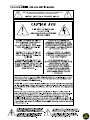
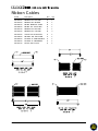
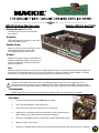
Service Bulletins HDR 24/96 Hard Disk Recorder SERVICE MANUAL 2001 MACKIE DESIGNS, INC. SERVICE ON THIS EQUIPMENT IS TO BE PERFORMED BY EXPERIENCED REPAIR TECHNICIANS ONLY 2 WARNING Service on the HDR 24/96 must only be undertaken by experienced service technicians. ! SMD ! ! ESD ! The HDR 24/96 makes extensive use of surface mount components. Servicing technicians should have the tools, experience and patience to perform surface mount rework. The HDR 24/96 contains components that may be damaged by elecrostatic discharge. All standard ESD precautions must be taken when servicing. Warning!: Before applying power to the HDR24/96, make sure that the Voltage Selector switch next to the AC inlet jack on the rear panel is set to the line voltage used in your region. Powering-on the HDR24/96 with the Voltage Selector switch set incorrectly will cause an electrical and fire hazard that may result in irreparable damage to the unit. Additional Safety Information The following notice concerns the lithium battery located on the motherboard inside the HDR 24/96 chassis. CAUTION: DANGER OF EXPLOSION IF BATTERY IS INCORRECTLY REPLACED. REPLACE ONLY WITH THE SAME OR EQUIVALENT TYPE RECOMMENDED BY THE MANUFACTURER. DISPOSE OF USED BATTERIES ACCORDING TO THE MANUFACTURER’S INSTRUCTIONS. ATTENTION: IL Y A DANGER D’EXPLOSION S’IL Y A REMPLACEMENT INCORRECT DE LA BATTERIE, REMPLACER UNIQUEMENT AVEC UNE BATTERIE DU MEME TYPE OU D’UN TYPE ÉQUIVALENT RECOMMANDÉ PAR LE CONSTRUCTEUR. METTRE AU REBUT LES BATTERIES USAGÉES CONFORMÉMENT AUX INSTRUCTIONS DU FABRICANT. 3 CONTENTS Click on any item to go to that page Safety ............................................................................. 2, 3 Introduction ...................................................................... 5 Ribbon Cables .................................................................. 6 Connectors ........................................................................ 8 Acuma board notes ...................................................... 20 Small Remote Self-Test ................................................... 21 BIOS Settings ................................................................... 22 Motherboard layout ...................................................... 25 Quick Parts ...................................................................... 26 Parts ................................................................................ A-1 Internal Views ................................................................ B-1 Exploded Views ............................................................. C-1 Wiring Diagram ..........................................................WD-1 Schematics and PCB layouts I/O Cards ..............................................................119-1 Click on any Front Panel ............................................................178-1 item to open Backplane ............................................................. 179-1 up the guide Brain .......................................................................180-1 page G4 Remote I/O ...........................................................268-1 Small Remote ........................................................ 291-1 Poststamp .............................................................359-1 Acuma .................................................................. 367-1 Service Bulletins 4 Introduction This manual contains service information for the HDR 24/96 Hard Disk Recorder. To service the HDR 24/96, technicians should be familiar with op-amp based and discrete analog circuitry, digital troubleshooting, microprocessors, digital audio, DSP, ESD, ESP, and the operation/application of Hard Disk Recorders. Presentation of this manual does not constitute endorsement of qualifications by Mackie Designs. This manual is available in Adobe© Portable Document Format (PDF), as part of Mackie Designs’ Digital Service CD-ROM (part# 820-163-00). This is available to all Service centers authorized to repair the HDR 24/96. Also included on the CD-ROM are the schematics, PCB layouts, parts lists, assembly drawings, and the owner’s manual. It is essential that you become familiar with the owner’s manual as it will be a great help for you to verify customers complaints, and to check for correct operation. SERVICE TECHNICAL ASSISTANCE Mackie Designs, Service Technical Assistance, is available 8AM - 5PM PST, Monday through Friday for Authorized Mackie Service Centers, at 1-800-258-6883. Feel free to call with any questions and speak with a carefully-calibrated technician. If one is not available, leave a detailed message and a qualified Mackoid will return your call asap. DISCLAIMER The information contained in this manual is proprietary to Mackie Designs, Inc. The entire manual is protected under copyright and may not be reproduced by any means without express written permission from Mackie Designs Inc. GETTING STARTED Think of the HDR 24/96 as a standard PC with extra Mackie boards inside. Standard PC troubleshooting techniques and commercially available diagnostic DOS software can be applied to repair the HDR 24/96. A preliminary inspection will often reveal a simple problem, such as a bad connection somewhere, perhaps a loose cable, a bad switch or control, bad EEPROM or the CPU’s CMOS settings may need to be reset. Check out the service bulletins, there is one which explains how to replace the EEPROM. Our technical support team are available to discuss any problems and offer solutions. 5 Ribbon Cables 6 Part# Description Rev Qty 040-383-00 040-384-00 RIB 28GA 10C 14.0 PLZD A 1 RIB 28GA 26C 4IN PLZD B 1 040-385-00 RIB 28G TRANS 34C 18.5IN B 1 040-386-00 RIB 28G 26C .100 14.50IN B 1 040-387-00 RIB 28GA 14C 16.0 PLZD A 1 040-390-00 RIB 28GA 10C 7.00 PLZD B 2 040-393-00 CBL ASY 22G 4C/6P 9.0IN A 1 040-438-00 RIB 28GA 16P .100 15.50IN A 1 040-489-00 DIS 18GA 4C 4.5IN PWR/MOL A 1 040-496-00 DIS 18GA 4C 14IN PWR EX A 1 040-497-00 DIS 22G 1007 2C/12P A 1 7 Connectors This table shows each connector and the boards they connect to. The following pages show each connector in detail, including the labeling and designation on each pin of the connectors. J# Pins From To Description Cable Page J2 ..... 26 ..... Front Panel .......... J2 Brain board ................... Clock, Latch, Data .................................................... 9 J2 ..... 4 ....... Backplane ........... J1 ..... 10 ..... Backplane ........... J3 ..... 34 ..... Backplane ........... J4 ..... 26 ..... Backplane ........... J18 ... 62 ..... Backplane ........... J19 ... 62 ..... Backplane ........... J20 ... 62 ..... Backplane ........... J2 Post Stamp ................... DC Power ................................. 040-489-00 ........... 10 J1 Brain board ................... Mute, Reset, IO TX, IO RX ........ 040-383-00 ........... 10 J3 Acuma board ............... CLK, DT data transmit ............. 040-385-00 ........... 10 J4 Acuma board ............... DR data receive ..................... 040-386-00 ........... 10 Card Connector ................ various ....................................................................... 11 Card Connector ................ various ....................................................................... 11 Card Connector ................ various ....................................................................... 11 J9 ..... 4 ....... Brain board ......... Power Supply ..................... DC Power .................................................................. 12 J5 ..... 14 ..... Brain board ......... J5 Remote I/O board ....... COM1, COM2, Punch .............. 040-387-00 ........... 12 J7 ..... 16 ..... Brain board ......... VFD ...................................... Display data ............................ 040-438-00 ........... 12 J3 ..... 2 ....... Brain board ......... Motherboard ..................... Flasher, +5V .............................................................. 12 J2 ..... 26 ..... Brain board ......... J2 Front Panel board ........ Clock, latch, data ................... 040-384-00 ........... 13 J8 ..... 2 ....... Brain board ......... VFD Display .............................................................................................................. 13 J1 ..... 10 ..... Brain board ......... J1 Backplane ..................... Mute, Reset, IO RX, IO TX ........ 040-383-00 ........... 13 J2 ..... 4 ....... Remote I/O ......... Power Supply ..................... DC Power .................................................................. 14 J9 ..... 10 ..... Remote I/O ......... Serial 2 Mother board ...... COM2 ........................................ 040-390-00 ........... 14 J10 ... 10 ..... Remote I/O ......... Serial 1 Mother board ...... COM1 ........................................ 040-390-00 ........... 14 J5 ..... 14 ..... Remote I/O ......... J5 Brain board ................... COM1, COM2, Punch .............. 040-387-00 ........... 15 J4 ..... 3 ....... Remote I/O ......... 1/4” TRS jack ...................... Punch ......................................................................... 15 J3 ..... 9 ....... Remote I/O ......... Mouse ................................. Mouse data .............................................................. 15 J6 ..... 6 ....... Remote I/O ......... Motherbrd Mouseport ..... Mouse data ............................. 040-393-00 ........... 15 J1 ..... 12 ..... Remote I/O ......... Small Remote .................... Remote data ............................................................ 15 J1 ..... 4 ....... Post Stamp .......... Power Supply ..................... DC Power .................................................................. 16 J2 ..... 4 ....... Post Stamp .......... J2 Backplane ..................... DC Power .................................................................. 16 J3 ..... 34 ..... Acuma board ..... J3 Backplane ..................... Mackie Bus Output ................. 040-385-00 ........... 17 J4 ..... 26 ..... Acuma board ..... J4 Backplane ..................... Mackie Bus Input ..................... 040-386-00 ........... 17 J5 ..... 6 ....... Acuma board ..... SMPTE 1/4” Jack ................ SMPTE ......................................................................... 18 J2 ..... 2 ....... Acuma board ..... CLK IN BNC Jack ............... CLK IN ......................................................................... 18 J1 ..... 2 ....... Acuma board ..... CLK OUT BNC Jack ............ CLK OUT ..................................................................... 18 PCI ... 124 ... Acuma board ..... PCI Connector ................... PCI data .................................................................... 19 8 Front Panel Connector This connects to J2 of the Brain board, see page 13 9 BackPlane Connectors Power from J2 of poststamp board, see page 16 This connects to J1 of the Brain board, see page 13 This connects to J4 of the Acuma board, see page 17 This connects to J3 of the Acuma board, see page 17 10 BackPlane Connectors 11 Brain Board Connectors This connects to J5 of the remote board, see page 15 This connects to power supply 12 This connects to the VFD Brain Board Connectors This connects to J2 of the front panel board, see page 9 This connects to J1 of the backplane board, see page 10 13 Remote Board Connectors This connects to Serial 2 of the motherboard This connects to Serial 1 of the motherboard 14 Remote Board Connectors J5 connects to J5 of the brain board, see page 12 J6 connects to the Mouseport of the motherboard 15 Post Stamp Board Connectors This connects to power supply This connects to J2 of the backplane board, see page 10 16 Acuma Board Connectors This connects to J3 of the Backplane, see page 10 This connects to J4 of the Motherboard, see page 10 17 Acuma Board Connectors SMPTE (TRS 1/4”) CLK IN (BNC) CLK OUT (BNC) 18 Acuma Board Connectors PCI connector 19 Acuma Board notes The Acuma board is used to transfer audio from the converter card cage to the PC via the PCI bus. It is also where the SMPTE and Word Clock connection comes into the PC. Physically, it is a card which fits into the PCI bus of the PC, and connects via 2 ribbon cables to the card cage. It has jacks which extend out the back of the unit for WCLK in (BNC), WCLK out (BNC), and SMPTE (1/4"). There is also a pushbutton for selecting termination impedance. J3(output) U17 J4(input) U9 FPGA U3 SMPTE Term switch in DSP U1 out U10 U16 U8 TP2 All the audio data comes over the ribbon cables from the card cages to the Acuma card. This data is in digital format. If channels are dead, the ribbon cable connectors are a good place to start looking since they are readily accessible. For instance, for HDR input channels, look at the signals on J4. If you see activity on here, then the problem is on the Acuma card (check U9). If no activity is visible, the problem is within the card cage - possibly a bad I/O card. For output channels, look on J3. These signals ‘flow’ the other way, so if no activity is visible, the problem is on the Acuma card. A failure in the SMPTE transmit or sync capability could be related to a bad component or faulty joint in the SMPTE circuit. A small amount of analog circuitry (around U17) is used to buffer incoming signals or generate outgoing signals, and then these are converted to digital signals (U16) and fed into the FPGA (U3). Tracing from the FPGA to the jacks might help to spot a problem. The card contains a PLL for generating WCLK. If WCLK out capabilities are defective, this circuit could be the culprit. Chip U8 is the ‘guts’ of this. The FPGA (U3) generates signals (FIN_A and FIN_B) which are smoothed out by the PLL, visible at TP2. This circuit is extremely sensitive, and bad performance may be caused by a poor joint or ‘worn out’ passive component around U8. WCLK sync capability is fairly simple. Incoming signals are buffered (U10) and then fed to the FPGA (U3) . Again, tracing from the FPGA back to the jack is a good way to start. A lot of the “complicated stuff” is handled within the DSP (U1) or FPGA (U3). If either of these components fail, rework is not possible and the card will need replacement. 20 Small Remote Self-Test There is a self-test for the small remote which will help you verify that it is working correctly. Follow the steps below to enter the self-test mode: 1. Connect the small remote to the back of the HDR24/96. 2. Put a floppy in the HDR to keep it from booting up (so it will provide power for the small remote without resetting it). 3. On the small remote, hold down Rec Arm 1+2 while powering up the HDR24/96. 4. All leds should light, the firmware version will be displayed on the 7-segment displays (such as 1.03). In this TEST MODE: • Pressing any button will extinguish the associated LED • The INC / DEC buttons control the 7-seg displays and VU meter • The footswitch controls the (minutes) LED HDR24/96 Troubleshooting Tips The following tips come from one of our fearless Mackie service technician heroes. These tips were given of his own free will, in order to help out fellow service techs wherever they may be. We would like to state that he was not harmed, threatened, intimidated, or blackmailed very much. If you see “No boot” or Video Error 43: • With the power off, try reseating the Processor IC or the ROM. • Try removing the Sync/Audio PCI card and see if the error changes. This may show if the card is bad. • Check cables and connections, and the DC supply connections to the motherboard. • Possible bad motherboard. May boot, but won’t load software: • Possible bad hard drive. External Drive not seen: • Check cables and connections. • Possible bad drive bay. If you see memory extraction error: • CMOS settings not correct. • Possible bad hard drive. Also, we have seen a few bad LEDs on the front panel, not many, but it does happen. Check the EPROM version. Look at the service bulletin at the end of this manual. 21 BIOS Settings: Standard CMOS Setup: Date (mm:dd:yy) : Current Date Time (hh:mm:ss) : Current Time Hard Disks: Type: Size: Cyls: Head: Precomp: Landz: Sector: Mode: PrimaryMaster Primary Slave Sec Master Sec Slave Auto None Auto None 0 0 0 0 0 0 0 0 0 0 0 0 0 0 0 0 0 0 0 0 0 0 0 0 Auto ——— Auto ——— Drive A: 1.44M, 3.5 in. Drive B: None Video: EGA/VGA Halt On: All, But Keyboard Base Memory: Extended Memory: Other Memory: Total Memory: 640K 130048K 384K 131072K NOTE: DO NOT use the IDE HDD AUTO DETECTION utility located in the main BIOS screen to mount IDE hard drives. Instead, set the “Type” field for the Primary Master and Secondary Master drives in the drive setup menu above to “Auto.” This will cause the BIOS to automatically detect any changes in drive status each time the HDR boots up. BIOS Features Setup: Virus Warning : Disabled CPU L1 Cache : Enabled CPU L2 Cache : Enabled CPU L2 Cache ECC Checking: Enabled Quick Power On Self Test : Enabled Boot Sequence : A,C,SCSI Swap Floppy Drive : Disabled Boot Up Floppy Seek : Disabled Boot Up NumLock Status : On Typematic Rate Setting : Disabled Typematic Rate (Chars/Sec) : 6 Typematic Delay (Msec) : 250 Security Option : Setup PCI/VGA Palette Snoop : Disabled OS Select For DRAM > 64MB : Non-OS2 HDD S.M.A.R.T. Capability : Disabled 22 Chipset Features Setup: SDRAM RAS-to-CAS Delay SDRAM RAS Precharge Time SDRAM CAS Latency Time SDRAM Precharge Control DRAM Data Integrity Mode System BIOS Cacheable Video BIOS Cacheable Video RAM Cacheable 8 Bit I/O Recovery Time 16 Bit I/O Recovery Time Memory Hole At 15M-16M PCI 2.1 Compliance AGP Aperture Size (MB) CPU/PCI Clock (MHz) Spread Spectrum :3 :3 :3 : Disabled : Non-ECC : Disabled : Disabled : Disabled :1 :1 : Disabled : Enabled : 64 : Default : Enabled Power Management Setup: ACPI Function Power Management PM Control By APM Video Off Method Video Off After MODEM Use IRQ Standby Mode Suspend Mode HDD Power Down PCI/VGA Act-Monitor Soft-Off by PWR-BTTN PWR Lost Resume State Resume on Ring Resume on LAN Resume on Alarm : Disabled : User Define : Yes : DPMS : Suspend : NA : Disabled : Disabled : Disabled : Disabled : Instant-Off : Keep Off : Disabled : Disabled : Disabled continued.... 23 PCI/PNP Configuration: Resources Controlled By Reset Configuration Data Assign IRQ for VGA Assign IRQ for USB PCI Slot 1 Use IRQ PCI Slot 2 Use IRQ PCI Slot 3 Use IRQ PCI Slot 4 Use IRQ : Manual : Disabled : Disabled : Disabled : Auto : Auto : Auto : Auto Used MEM Base Address: N/A IRQ-3 IRQ-4 IRQ-5 IRQ-7 IRQ-9 IRQ-10 IRQ-11 IRQ-12 IRQ-14 IRQ-15 DMA-0 DMA-1 DMA-3 DMA-5 DMA-6 DMA-7 Assigned to Assigned to Assigned to Assigned to Assigned to Assigned to Assigned to Assigned to Assigned to Assigned to Assigned to Assigned to Assigned to Assigned to Assigned to Assigned to : PCI/ISA PnP : PCI/ISA PnP : PCI/ISA PnP : PCI/ISA PnP : PCI/ISA PnP : Legacy ISA : PCI/ISA PnP : PCI/ISA PnP : PCI/ISA PnP : PCI/ISA PnP : PCI/ISA PnP : PCI/ISA PnP : PCI/ISA PnP : PCI/ISA PnP : PCI/ISA PnP : PCI/ISA PnP Integrated Peripherals Setup: IDE HDD Block Mode IDE Primary Master PIO IDE Primary Slave PIO IDE Secondary Master PIO IDE Secondary Slave PIO IDE Primary Master UDMA IDE Primary Slave UDMA IDE Secondary Master UDMA IDE Secondary Slave UDMA On-Chip Primary PCI IDE On-Chip Secondary PCI IDE USB Keyboard Support Init Display First KBC Input Clock Onboard FDC Controller Onboard Serial Port 1 Onboard Serial Port 2 UART2 Mode Select Onboard Parallel Port Keyboard/Mouse Power On : Enabled : Auto : Auto : Auto : Auto : Auto : Auto : Auto : Auto : Enabled : Enabled : Disabled : AGP : 8 MHz : Enabled : 3F8/IRQ4 : 2F8/IRQ3 : Normal : Disabled* : Disabled *NOTE: Be sure that the Onboard Parallel Port is Disabled in this setup. 24 Motherboard layout J5 JP3 COM2 2 9 10 JP4 COM1 PRINTER JP5 J6 O1 2 3 4 N 1 I/O CHIP IrDA J11 USB PS/2 K/B AT K/B AGP FAN J2 PS/2 MOUSE JP1 PLATX1:ATX POWER PLAT1:AT POWER J1 CPU FAN JP2 SW 1 PCI 1 PCI 2 PCI 3 PCI 4 IAGP 1 ISA 1 ISA 2 J13 SBLINK 1 2 56 PIN 1 82371EB (PIIX4) INTEL 443BX J14 WAKE-ON LAN BIOS DIMM 3 DIMM 2 DIMM 1 CLEAR CMOS J10 JP6 BATTERY J12 FDD J7 SECONDARY IDE J8 PRIMARY IDE J9 SPEAKER G-SW G-LED ATX-LED RESET ATX-SW HD-LED KEYLOCK CHASSIS FAN SQUARE PIN = PIN 1 TO J8 OF BRAIN BOARD J14 O1 2 3 4 N SW 1 SET SW1: 1=OFF 2=ON 3=OFF 4=ON NO JUMPER WAKE-ON LAN JP6 J13 JP2 SBLINK 1 2 NO JUMPER 56 JP1 JUMPER PINS 2 AND 3 JUMPER PINS 1 AND 2 JUMPER PINS 1 AND 2 25 Quick Parts 550-318-00 Screened Front Panel 550-314-00 Top Cover 551-087-00 Rack ears 780-047-00 Lexan Meter Window 480-041-00 Drive Frame 480-029-00 Floppy Drive 760-175-02 Transport Button Bezel 760-159-01 Power Switch Bezel 750-001-0 Bumpon Feet 055-178-00-01 Front Panel PCB assembly 640-001-00 LineCord 120VAC 080-180-00 VFD Subassembly 304-025-00 LED Array (1 for each channel) 760-168-00 Small Round Buttons 500-033-02 Switch SPST 760-158-02 Power Switch Cap 500-028-00 Switch 12mm 760-155-01 760-155-03 760-155-04 760-155-05 500-062-00 Button, Rewind/ Fast Frwrd Button, Stop Button, PLay Button, Record Transport Switch 760-131-02 Button, Round, Arrow 500-028-00 Switch 12mm 26 304-081-02 LED Red, Error, TC, Clock 304-082-02 LED Green, 6-Bit, 24-Bit, 44.1K, 48K, 96K, VARI 304-081-02 LED RED Channel LEDs (x24) 304-093-02 LED Red, Tower 304-001-00 LED Red, Power 080-247-00 055-178-00-01 055-179-00-01 055-180-00-01 055-268-00-01 055-359-00-01 480-039-00 329-088-03 480-043-00 480-062-00 SA POWER SUPPLY PCB ASSY FRONT PANEL PCB ASSY BACKPLANE PCB ASSY BRAIN PCB ASSY RMT I/O PCB ASSY HDR179 POSTSTAMP MOTHERBOARD CB50-BX MICROPROC CELERON 433MHZ OEM FAN MICROPROC SDRAM 128MB 2MX8 DIMM MOD 304-035-00 7 Segment Display 304-001-00 LED Red, Record 304-003-00 LED Yellow, FF, Stop, RW 304-004-00 LED Green, Play 480-045-00 480-046-00 480-053-00 055-367-00-01 VIDEO CARD ETHERNET CARD MIDI CARD ACUMA CARD 27 HDR 24/96 EPROM Replacement Models affected: If you are working on an HDR 24/96 hard disk recorder before serial number CD11218, please update the EPROM to Revision 1.2 or higher. Changing the EPROM may be one fix for the "system error 43" message. Note: If the EPROM is before Rev 1.2, the initial front panel message “loading..please wait” is all lower case letters. If the EPROM is Rev 1.2, then the initial front panel message “Loading..Please Wait,” has some upper case letters. HDR 24/96 front panel display just after turn-on Safety Warning: Caution! These instructions are for use by qualified personnel only. To avoid electric shock, do not perform any servicing unless you are qualified to do so. Refer all service to qualified personnel. ESD Warning: Caution! The HDR 24/96 should be treated with respect and repaired using all standard ESD precautions. Tools Required: Phillips screwdriver, ESD wriststrap and workstation Parts Required: EPROM (revision 1.2 or higher) 080-174-00 Overview remove The EPROM replacement is not a major job, so fear not. The EPROM is fitted to a socket on the Brain board in front of the internal hard drive. Procedure: 1. Turn off the power to the HDR 24/96. 2. Remove all cords (including the power cable and cables) from the HDR 24/96. 3. Place the HDR 24/96 on a soft surface. 4. Undo the three screws on each of the rack brackets, just enough to give a little slack when removing the top cover. 5. Remove the top cover by undoing the other screws shown. remove slacken (both sides) remove from both sides HDR 24/96 EPROM replacement, SSE Jan 2001 HDR Eprom.pdf, page 1 of 2 THE MACKIE FIXER MACKIE DESIGNS SERVICE NEWS Procedure continued: 6. Remove the four side screws and two bottom screws securing the internal hard drive assembly to the chassis. This gives a little bit more access to the Brain board, as the hard drive assembly can move backwards a small distance. remove from the left side You can also remove the hard drive assembly if you prefer. Make a note of all the connections and the exact cable routing for when you put it back in. remove from the bottom panel 7. Undo the connectors at J1, J5 and J2 on the Brain board. Move them out of the way so you can reach the EPROM U5. 8. Slide the hard drive assembly backwards to give you some room, and then use a small screwdriver to remove the existing EPROM from its socket. 9. You should first bend the legs of the EPROM to make sure they are straight down. Then carefully and securely put in the new EPROM, making sure that each pin is in its socket. The notched end of the EPROM should point upwards. 10. Replace the six hard drive screws. 11. Replace the top cover and secure all the screws, including the rack bracket screws. 12. Perform a complete specification test before returning the HDR 24/96 to the customer. 13. The old EPROM may be saved and recycled as a unique earring, bound to break the ice at service technician parties. J1 J5 J2 U5 HDR 24/96 EPROM replacement, SSE Jan 2001 HDR Eprom.pdf, page 2 of 2 HDR 24/96 Hard Disk Recorder Bulletin: HDR 1st April 2001 Models affected: HDR 24/96 Add this as part of your normal repair procedures. Symptom: HDR 24/96 does not power up, and yet it tastes surprisingly good. Possible Cause: Due to a mix up in documentation, some HDR 24/96 hard disk recorders were accidentally made of chocolate. Solution: Replace all circuit boards, creme-filled ICs, marzipan transistors, truffle capacitors, all candy chassis work, screws and liquorice ribbon connectors. Note: Not all models are affected. If you receive an HDR 24/96 for repair, it is recommended that you nibble the front panel. If it tastes good and chocolaty, then follow the repair procedure outlined below. If it tastes metallic and you break a few teeth in the process, there may be another cause. Safety Warning: Caution! These instructions are for use by qualified personnel only. To avoid overeating, do not perform any servicing unless you are qualified to do so. Refer all service to qualified, hungry service personnel, who are specially trained to deal with chocolate, glazed donuts, pizza and other hazards. Tools Required: Phillips screwdriver, Torx and Allen drivers, safety glasses, knife, fork, safety bib and overalls. Procedure: 1. Turn the power off and remove all external cables. 2. Place the HDR 24/96 on a soft dry surface. 3. Take off the top cover and inspect the circuit boards. 4. Using service tools (knife and fork), eat all the circuit boards one at a time, taking care to share with your service colleagues. 5. Eat all the chassiswork, ribbon connectors until the HDR 24/96 is gone. 6. Replace with a new model. 7. Perform a complete specification and taste test before returning the new unit to the customer.