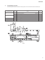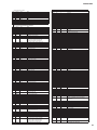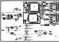
1
PROFESSIONAL SAMPLER
SERVICE MANUAL
CONTENTS
SPECIFICATIONS ................................................................................3
PANEL LAYOUT ..................................................................................4
CIRCUIT BOARD LAYOUT ...................................................................5
BLOCK DIAGRAM ............................................................................... 6
DISASSEMBLY PROCEDURE ............................................................7
LSI PIN DESCRIPTION ...................................................................... 10
IC BLOCK DIAGRAM ......................................................................... 16
TEST PROGRAM ............................................................................. 19
ERROR MASSAGE ........................................................................... 31
MIDI DATA FORMAT .......................................................................... 32
MIDI IMPLEMENTATION CHART ........................................................ 43
PARTS LIST
OVERALL CIRCUIT DIAGRAM
CIRCUIT BOARDS
SY 011491
A5000 19991210-229000
A4000 19991210-149000
HAMAMATSU,JAPAN
1.57K-859 I Printed in Japan2000.01
A5000/A4000
IMPORTANT NOTICE
This manual has been provided for the use of authorized Yamaha Retailers and their service personnel. It has been
assumed that basic service procedures inherent to the industry, and more specifically Yamaha Products, are
already known and understood by the users, and have therefore not been restated.
WARNING:
Failure to follow appropriate service and safety procedures when servicing this product may
result in personal injury, destruction of expensive components and failure of the product to per
form as specified. For these reasons, we advise all Yamaha product owners that all service
required should be performed by an authorized Yamaha Retailer or the appointed service
repre sentative.
IMPORTANT:
This presentation or sale of this manual to any individual or firm does not constitute authorization, certification, recognition of any applicable technical capabilities, or establish a principalagent relationship of any form.
The data provided is believed to be accurate and applicable to the unit(s) indicated on the cover. The research
engineering, and service departments of Yamaha are continually striving to improve Yamaha products. Modifications are, therefor, inevitable and changes in specification sre subject to change without notice or obligation to
retrofit. Should any discrepancy appear to exist, please contact the distributor's Service Division.
WARNING:
Static discharges can destroy expensive components. Discharge any static electricity your
body may have accumulated by grounding yourself to the ground buss in the unit (heavy gauge
black wires connect to this buss).
IMPORTANT:
Turn the unit OFF during disassembly and parts replacement. Recheck all work before you
apply power to the unit.
WARNING: CHEMICAL CONTENT NOTICE!
The solder used in the production of this product contains LEAD. In addition, other electrical / electronic and / or
plastic (where applicable) components may also contain traces of chemicals found by the California Health and
Welfare Agency (and possibly other entities) to cause cancer and / or birth defects or other reproductive harm.
DO NOT PLACE SOLDER, ELECTRICAL / ELECTRONIC OR PLASTIC COMPONENTS IN YOUR MOUTH FOR ANY
REASON WHAT SO EVER!
Avoid prolonged, unprotected contact between solder and your skin! When soldering, do not inhale solder fumes or
expose eyes to solder / flux vapor!
If you come in contact with solder or components located inside the enclosure of this product, wash your hands
before handling food.
WARNING
Components having special characteristics are marked
originally installed.
and must be replaced with parts having specification equal to those
A5000/A4000
SPECIFICATION
Function buttons (six buttons)
Tone generation method
AWM2 tone generator
COMMAND/EXIT button
ASSIGNABLE button
Maximum Polyphony
126 notes (64 notes on the A4000), 32 multi-timbre parts (16 parts on the A4000)
AUDITION button
LCD (320 x 80 dot, LED backlight)
A/D conversion
20 bit 64-times oversampling
LCD contrast control
3.5" 2HD/2DD dual mode floppy disk drive
D/A conversion
24 bit 8-times oversampling
Rear panel
Digital I/O (only when AIEB1 I/O expansion board is installed)
Input/output
STEREO OUT L/MONO, R (phone jack x 2)
DIGITAL connectors
S/P-DIF (coaxial)
ASSIGNABLE OUT L, R
OPTICAL connectors
S/P-DIF (optical)
MIDI IN-A/B, OUT, THRU-A/B (IN, OUT, THRU on the A4000)
Input frequency
48 kHz, 44.1 kHz, 32 kHz
SCSI (half-pitch, 50-pin)
Output frequency
44.1 kHz
Expansion board slot
Sampling frequency
Analog input
44.1, 22.05, 11.025 kHz, 5.5125 kHz (mono and stereo)
Digital input (only when AIEB1 I/O expansion board is installed)
(phone jack x 2)
Power supply connector (AC inlet)
Fan
Dimensions
48 kHz, 44.1 kHz, 32 kHz external synchronized recording
Two-space rackmount unit
(stereo only)
W 480 mm x D 461 mm x H 90 mm (18-7/8” x 18-1/8” x 3-9/16”)
1/2, 1/4 and 1/8 undersampling is supported
Internal sample memory capacity
Standard
4 Mbytes (installed on-board)
Maximum
128 Mbytes
(When four 32 Mbyte 72 pin SIMM modules are installed. The onboard 4 Mbytes are unused only if memory has been expanded to the
maximum.)
Sampling time
Weight
8.0 kg (17l bs 10 oz)
Included items
Power cable
x1
CD-ROM set
(See the separate “Guide for the Accompanying Disks” booklet)
FD
x4
Power Cable for Internal Hard Disk (long)
x1
32 Mbytes monaural
Power Cable for ZIP Drive (short)
x1
64 Mbytes stereo
SCSI Cable for Internal Hard Disk
x1
IDE Cable for Internal Hard Disk
x1
Owner’s manual
x1
Maximum sample length
Maximum sampling time (mono or stereo)
6 minutes 20 seconds (44.1 kHz)
12 minutes 40 seconds (22.05 kHz)
Options (made by Yamaha)
25 minutes 21 seconds (11.025 kHz)
AIEB1: I/O expansion board
50 minutes 43 seconds (5.5125 kHz)
Effects
6 effect blocks (3 on the A4000)
Internal expansion devices (made by other manufacturers)
Expansion memory
(use a pair of identical-size 72pin SIMM modules of the following types)
Total equalizer (4 bands)
Access time
70 ns or less
Sample equalizer
Bit Width
x 32 (no parity) or x 36 bit (parity)
Program
128 program
Sequencer
Real-time recording and playback
Fast Page or EDO, JEDEC standard.
Capacity
Interface
Power supply
Front panel
POWER switch
INPUT L,R jacks (phone x 2)
REC VOLUME (L& R shared)
MASTER VOLUME (L&R shared, STEREO OUT & PHONES shared)
4 megabyte/8 megabyte/16 megabyte/32 megabyte
Internal hard disk drive (3.5 inch) performance requirements
50-pin SCSI or 40-pin IDE
+5 V
maximum 840 mA
+12 V
maximum 2400 mA
Internal ZIP Drive
Interface
40-pin IDE (ATAPI)
Power supply
+5 V
0.8 A
PHONES OUTPUT jack
Knobs (1 - 5)
Mode buttons (PLAY, EDIT, REC, DISK, UTILITY)
3
A5000/A4000
PANEL LAYOUT
Front Panel
1
Master Vol [Master Volume]
2
Rec Vol [Recording Volume]
3
Phones jack
4
Input L, Input R jacks
5
LCD Contrast
6
Display
7
Knobs 1-5
8
Mode buttons
9
Function buttons [F1]-[F6]
10
Command Exit button
11
Assignable button
12
Audition button
13
Floppy Disk Drive
14
Power switch
Rear Panel
1
2
AC inlet
Midi In-A, In-B, Out, Thru-A, Thru-B (A5000)
connectors / Midi In, Out, Thru (A4000) connectors
3
4
Assignable Out L, R jacks
4
Stereo Out L/Mono, R jacks
5
SCSI connector
6
Optical In, Out connectors
7
Digital In, Out connectors
8
Assignable Out jacks 1-6
A5000/A4000
CIRCUIT BOARD LAYOUT
5
A5000/A4000
28CA1-8815099
BLOCK DIAGRAM
6
A5000/A4000
DISASSEMBLY PROCEDURE
1.
Top Cover
1-1
Remove the sixteen (16) screws marked [510] and slide the Top Cover to the back side. The top cover can be then
removed.
(Fig.1)
2.
Circuit Boards and Unit
After removing the top cover, remove the following screws. Each circuit board can then be removed.
Circuit Boards and Unit
HDD Bracket
1
DM*
3
FDD Bracket*
PS Cover Ass'y
4
PS*
Fan Ass’y*
Note:
4
*1
*2
*3
*4
Ref.No.
Screw
Qty
[220]
Bind Head Tapping Screw-B 3.0X6 MFZN2Y
(EP600130) (fig.2)
4
[120]
Bind Head Tapping Screw-B 3.0X6 MFZN2Y
(EP600130) (fig.3)
13
[130]
Bonding Head Screw-B 3.0X10 MFZN2BL
(VQ049800)(fig.3)
2
[140]
Bind Head Tapping Screw-P 3.0X8 MFZN2BL
(EP630220) (fig.3)
4(2)* 2
[150]
Pan Head Screw 2.5X6 SUS
(VV342700)(fig.3)
2
[190]
Bind Head Tapping Screw-B 3.0X6 MFZN2Y
(EP600130) (fig.2)
4
Bonding Head Screw-B 3.0X10 MFZN2BL
(VQ049800)(fig.2)
3
[100]
Bind Head Tapping Screw-B 4.0X8 MFZN2BL
(EG340190) (fig.2)
2
[30]
Bind Head Tapping Screw-B 3.0X6 MFZN2Y
(EP600130) (fig.3)
7
[50]
Bind Head Tapping Screw-P 3.0X8 MFZN2BL
(EP630220) (fig.2)
2
[60]
Bind Head Tapping Screw-B 4.0X8 MFZN2BL
(EG340190) (fig.3)
1
[L40]
Flat Head Screw 3.0X25 MFN133
(V4814400) (fig.3)
4
[L50]
Hexagonal Nut 3.0 MFZN2Y
(VA211900) (fig.3)
4
[90]
Before removing the DM, remove the HDD Ass'y.
Two for A4000.
Before removing the FDD Ass'y and the PS cover Ass'y, remove the Push Rod.
Before removing the PS and Fan Ass’y, remove the PS cover Ass’y.
7
A5000/A4000
(Fig.2)
(Fig.3)
3.
Front Panel
3-1
3-2
Remove the knob marked [440], [450], [460].
Remove the three (3) screws marked [410]. And remove the Front Panel from the Lower Case Assembly.
(Fig.4)
8
A5000/A4000
4.
Circuit Boards and Unit
After removing the front panel, remove the following screws. Each circuit board can then be removed.(Fig.5)
Circuit Boards and Unit
JK
RE
Ref.No.
Screw
Qty
[S230]
Hexagonal Nut 14X2 M12
(ES200210)
3
[L170]
Bind Head Tapping-B 3.0X6 MFZN2Y
(EP600130)
2
-
Washer
-
Nut
5
5
[L170]
Bind Head Tapping-B 3.0X6 MFZN2Y
(EP600130)
2
VR
[S140]
PNA
[S70]
Bind Head Tapping-B 3.0X6 MFZN2Y
(EP600130)
4
Cup Tapping Screw-B 3.0X6 MFZN2Y
(V2644100)
4
LCD
[S110]
Bind Head Tapping-B 3.0X6 MFZN2Y
(EP600130)
4
(Fig.5)
9
A5000/A4000
LSI PIN DESCRIPTION
TC203C760HF-002 (XS725A00) SWP30B (AW M Tone Generator coped with MEG) Standard W ave Processor
10
PIN
N O.
NAME
I/O
1
2
3
4
5
6
7
8
9
10
11
12
13
14
15
16
17
18
19
20
21
22
23
24
25
26
27
28
29
30
31
32
33
34
35
36
37
38
39
40
41
42
43
44
45
46
47
48
49
50
51
52
53
54
55
56
57
58
59
60
61
62
63
64
65
66
67
68
69
70
71
72
73
74
75
76
77
78
79
80
81
82
83
84
85
86
87
88
89
90
91
92
93
94
95
96
97
98
99
100
101
102
103
104
105
106
107
108
109
110
111
112
113
114
115
116
117
118
119
120
Vss
CA0
CA1
CA2
CA3
CA4
CA5
CA6
CA7
CA8
CA9
CA10
CA11
VSS
CD0
CD1
CD2
CD3
CD4
CD5
CD6
CD7
CD8
CD9
CD10
CD11
CD12
CD13
CD14
VDD
VSS
CD15
CSN
W RN
RDN
VDD
SYSH0
SYSH1
SYSH2
SYSH3
SYSH4
SYSH5
SYSH6
SYSH7
KONO0
KONO1
KONO2
KONO3
VSS
SYSL0
SYSL1
SYSL2
SYSL3
SYSL4
SYSL5
SYSL6
SYSL7
KONI0
KONI1
VDD
VSS
KONI2
KONI3
DAC0
DAC1
W CLK
MELO 0
MELO 1
MELO 2
MELO 3
MELO 4
MELO 5
MELO 6
MELO 7
VDD
ADLR
MELI0
MELI1
MELI2
MELI3
MELI4
MELI5
MELI6
MELI7
VSS
RCASN
RA8
RA7
RA6
VDD
VSS
RA5
RA4
RA3
RA2
RA1
RA0
RRASN
RW EN
VSS
RD7
RD6
RD5
RD4
RD3
RD2
RD1
RD0
VSS
RD17
RD16
RD15
RD14
RD13
RD12
RD11
RD10
RD9
RD8
VDD
I
I
I
I
I
I
I
I
I
I
I
I
I/O
I/O
I/O
I/O
I/O
I/O
I/O
I/O
I/O
I/O
I/O
I/O
I/O
I/O
I/O
I/O
I
I
I
O
O
O
O
O
O
O
O
O
O
O
O
I/O
I/O
I/O
I/O
I/O
I/O
I/O
I/O
I
I
I
I
O
O
O
O
O
O
O
O
O
O
O
O
I
I
I
I
I
I
I
I
O
O
O
O
O
O
O
O
O
O
O
O
I/O
I/O
I/O
I/O
I/O
I/O
I/O
I/O
I/O
I/O
I/O
I/O
I/O
I/O
I/O
I/O
I/O
I/O
-
FUN CTION
(Gr ound)
Address bus of inter nal register
(Gr ound)
Data bus of internal register
(Power supply)
(Gr ound)
Chip select
W rite strobe
Read strobe
(Power supply)
NSYS/LNSYS upper 16 bits output
Key on data
(Gr ound)
NSYS input/LNSYS output lower 8 bits
Key on data input
(Power supply)
(Gr ound)
DAC output
DAC0/DAC1 word clock
MEL wave data output
(Power supply)
ADC word clock
MEL wave data input
(Gr ound)
DRAM column address strobe (RAS signal)
(Power supply)
(Gr ound)
DRAM address bus
DRAM row address strobe (RAS signal)
DARM write enable
(Gr ound)
(Gr ound)
DRAM data bus
(Power supply)
PIN
N O.
NAME
I/O
121
122
123
124
125
126
127
128
129
130
131
132
133
134
135
136
137
138
139
140
141
142
143
144
145
146
147
148
149
150
151
152
153
154
155
156
157
158
159
160
161
162
163
164
165
166
167
168
169
170
171
172
173
174
175
176
177
178
179
180
181
182
183
184
185
186
187
188
189
190
191
192
193
194
195
196
197
198
199
200
201
202
203
204
205
206
207
208
209
210
211
212
213
214
215
216
217
218
219
220
221
222
223
224
225
226
227
228
229
230
231
232
233
234
235
236
237
238
239
240
VSS
HMD0
HMD1
HMD2
HMD3
HMD4
HMD5
HMD6
HMD7
HMD8
HMD9
HMD10
HMD11
HMD12
HMD13
HMD14
HMD15
VSS
HMA0
HMA1
HMA2
HMA3
HMA4
HMA5
HMA6
HMA7
HMA8
HMA9
HMA10
VDD
VSS
HMA11
HMA12
HMA13
HMA14
HMA15
HMA16
HMA17
HMA18
HMA19
HMA20
HMA21
HMA22
HMA23
HMA24
VSS
MRASN
MCASN
MOEN
MW EN
VSS
LMD0
LMD1
LMD2
LMD3
LMD4
LMD5
LMD6
LMD7
VDD
VSS
LMD8
LMD9
LMD10
LMD11
LMD12
LMD13
LMD14
LMD15
VSS
LMA0
LMA1
LMA2
LMA3
LMA4
LMA5
LMA6
LMA7
LMA8
LMA9
LMA10
LMA11
VSS
LMA12
LMA13
LMA14
LMA15
LMA16
LMA17
VDD
VSS
LMA18
LMA19
LMA20
LMA21
LMA22
LMA23
LMA24
VSS
SYO
SYOD
QCLK
HCLK
CK256
SYSCLK
VDD
SYI
MCLKI
MCLKO
VDD
XIN
XOUT
VSS
ICN
CHIP2
SLAVE
TEST ON
ACIN
DCT EST
VDD
I/O
I/O
I/O
I/O
I/O
I/O
I/O
I/O
I/O
I/O
I/O
I/O
I/O
I/O
I/O
I/O
O
O
O
O
O
O
O
O
O
O
O
O
O
O
O
O
O
O
O
O
O
O
O
O
O
O
O
O
O
I/O
I/O
I/O
I/O
I/O
I/O
I/O
I/O
I/O
I/O
I/O
I/O
I/O
I/O
I/O
I/O
O
O
O
O
O
O
O
O
O
O
O
O
O
O
O
O
O
O
O
O
O
O
O
O
O
O
O
O
O
O
O
I
I
O
I
O
I
I
I
I
I
I
-
(IC507)
FUN CTION
(Gr ound)
W ave memor y data bus (Upper 16 bits)
(Gr ound)
(Power supply)
(Gr ound)
W ave memor y address bus
(Gr ound)
RAS when DRAM(s) is co nnected t o wave mem ory
CAS when DRAM(s) is co nnected t o wave mem ory
W ave memor y output enable
W ave memor y write enable
(Gr ound)
W ave memor y data bus (Lower 16 bits)
(Power supply)
(Gr ound)
(Gr ound)
(Gr ound)
W ave memor y address bus (Lower data memory)
(Power supply)
(Gr ound)
(Gr ound)
Sync. signal for master clock
Sync. signal for HCLK/Q CLK
1/12 master clock (64F s)
1/6 master clock (128F s)
1/3 master clock (256F s)
1/2 master clock (384F s)
(Power supply)
Sync. clock
Master clock input
Master clock output
(Power supply)
Crystal osc. input
Crystal osc. output
(Gr ound)
Initial clear
2 chips mode enable
Master/Slave select when 2 chips mode
Test pin
(Power supply)
A5000/A4000
D65621GF-028-3B9 (XS370A00) SMI
PIN
NO.
1
2
3
4
5
6
7
8
9
10
11
12
13
14
15
16
17
18
19
20
21
22
23
24
25
26
27
28
29
30
31
32
33
34
35
36
37
38
39
40
NAME
LMA24
LMA23
LMA22
LMA21
LMA20
LMA19
LMA18
HMA24
HMA23
HMA22
HMA21
GND
HMA20
HMA19
HMA18
RASN
H0RAS0
H0RAS1
GND
H0RAS2
H0RAS3
GND
VDD
L0RAS0
L0RAS1
GND
L0RAS2
L0RAS3
GND
VDD
H1RAS0
H1RAS1
GND
VDD
H1RAS2
H1RAS3
GND
L1RAS0
L1RAS1
GND
I/O
I
I
I
I
I
I
I
I
I
I
I
I
I
I
I
O
O
O
O
O
O
O
O
O
O
O
O
O
O
-
FUNCTION
Low Memory Address
High Memory Address
Ground
High Memory Address
Row Address Strobe
RAS0 for HiMem SIMM 0
RAS1 for HiMem SIMM 0
Ground
RAS2 for HiMem SIMM 0
RAS3 for HiMem SIMM 0
Ground
Power Supply
RAS0 for LoMem SIMM 0
RAS1 for LoMem SIMM 0
Ground
RAS2 for LoMem SIMM 0
RAS3 for LoMem SIMM 0
Ground
Power Supply
RAS0 for HiMem SIMM 1
RAS1 for HiMem SIMM 1
Ground
Power Supply
RAS2 for HiMem SIMM 1
RAS3 for HiMem SIMM 1
Ground
RAS0 for LoMem SIMM 1
RAS1 for LoMem SIMM 1
Ground
(IC516)
PIN
NO.
41
42
43
44
45
46
47
48
49
50
51
52
53
54
55
56
57
58
59
60
61
62
63
64
65
66
67
68
69
70
71
72
73
74
75
76
77
78
79
80
NAME
VDD
L1RAS2
L1RAS3
GND
HDRAS0
HDRAS1
GND
VDD
LDRAS0
LDRAS1
LMA1
LMA0
GND
LMA1X
LMA0X
GND
VDD
HMA1
HMA0
HMA1X
HMA0X
D0
D1
GND
D2
D3
D4
D5
A2
WRN
GND
VDD
CSN
A0
A1
MCLK
SYI
HBANK
LBANK
REFRN
I/O
O
O
O
O
O
O
I
I
O
O
I
I
O
O
I
I
I
I
I
I
I
I
I
I
I
I
I
O
O
O
FUNCTION
Power Supply
RAS2 for LoMem SIMM 1
RAS3 for LoMem SIMM 1
Ground
RAS for HiMem DRAM 0
RAS for HiMem DRAM 1
Ground
Power Supply
RAS for LoMem DRAM 0
RAS for LoMem DRAM 1
Low Memory Address
No.53
Low Memory Address Exchanged
Ground
Power Supply
High Memory Address
High Memory Address Exchanged
Data Input
Ground
Data Input
Address
Write
Ground
Power Supply
Chip Select
Address
Clock (37MHz)
Sync Clock (48kHz)
HiMem Bank Select 01/23
LoMem Bank Select 01/23
Refresh Timing
D65611GB-039-3B (XS323A00) ENI
PIN
NO.
1
2
3
4
5
6
7
8
9
10
11
12
13
14
15
16
17
18
19
20
21
22
NAME
CLRN
E1A
E1B
E2A
E2B
E3A
E3B
E4A
E4B
E5A
E5B
E6A
E6B
E7A
E7B
VDD
GND
E8A
E8B
P0
P1
P2
I/O
I
I
I
I
I
I
I
I
I
I
I
I
I
I
I
I
I
I/O
I/O
I/O
FUNCTION
Clear Status
Rotary Encoder 1 Input A
Rotary Encoder 1 Input B
Rotary Encoder 2 Input A
Rotary Encoder 2 Input B
Rotary Encoder 3 Input A
Rotary Encoder 3 Input B
Rotary Encoder 4 Input A
Rotary Encoder 4 Input B
Rotary Encoder 5 Input A
Rotary Encoder 5 Input B
Rotary Encoder 6 Input A
Rotary Encoder 6 Input B
Rotary Encoder 7 Input A
Rotary Encoder 7 Input B
Power Supply
Ground
Rotary Encoder 8 Input A
Rotary Encoder 8 Input B
I/O Port
(IC11)
PIN
NO.
23
24
25
26
27
28
29
30
31
32
33
34
35
36
37
38
39
40
41
42
43
44
NAME
P3
P4
P5
P6
P7
D0
D1
GND
D2
D3
D4
GND
D5
D6
D7
GND
VDD
A0
A1
WRN
RDN
CSN
I/O
I/O
I/O
I/O
I/O
I/O
I/O
I/O
I/O
I/O
I/O
I/O
I/O
I/O
I
I
I
I
I
FUNCTION
I/O Port
Ground
CPU Data Bus
Ground
CPU Data Bus
Ground
Power Supply
Address Bus
Address Bus
Write Enable
Read Enable
Chip Select
11
A5000/A4000
D65636GF-104-3B9 (XS369A00) SPF
PIN
NO.
1
2
3
4
5
6
7
8
9
10
11
12
13
14
15
16
17
18
19
20
21
22
23
24
25
26
27
28
29
30
31
32
33
34
35
36
37
38
39
40
NAME
ICN
VDD
GND
D0
D1
GND
D2
D3
GND
VDD
D4
D5
GND
D6
D7
A4
CSN
WRN
RDN
DREQN
DACKN
GND
VDD
D8
D9
GND
D10
D11
GND
VDD
D12
D13
GND
D14
D15
A1
A2
A3
CK256IO
BCKIO
I/O
I
I/O
I/O
I/O
I/O
I/O
I/O
I/O
I/O
I
I
I
I
O
I
I/O
I/O
I/O
I/O
I/O
I/O
I/O
I/O
I
I
I
I
I
FUNCTION
Initial Clear
Power Supply
Ground
Data Bus
Ground
Data Bus
Ground
Power Supply
Data Bus
Ground
Data Bus
Address
Chip Select
Write
Read
DMA Request
DMA Acknowledge
Ground
Power Supply
Data Bus
Ground
Data Bus
Ground
Power Supply
Data Bus
Ground
Data Bus
Address
Serial Input0 256fs Clock(12.8MHz)
Serial Input0 Bit Clock(3.2MHz)
(IC11)
PIN
NO.
41
42
43
44
45
46
47
48
49
50
51
52
53
54
55
56
57
58
59
60
61
62
63
64
65
66
67
68
69
70
71
72
73
74
75
76
77
78
79
80
NAME
SYNIO
VDD
GND
DIN0
CK256I1
BCKI1
SYNI1
DIN1
DAC256O
DAC64O
DACWCKO
DACDTI
DACDTO
VDD
GND
MONMELO
DIT128O
DITWCKO
MUTEI
MUTENO
ERRI
GND
VDD
ERRIRQN
TGRESN
P7
P6
P5
P4
P3
P2
P1
P0
OCSN
ODACKN
ODDIR
OBOEN
OBDIR
CSOUTN
ASSIGN
I/O
I
I
I
I
I
I
O
O
O
I
O
O
O
O
I
O
I
O
O
I/O
I/O
I/O
I/O
I/O
I/O
I/O
I/O
I
I
I
O
O
O
O
PCM1800 (XU770A00) A/D Converter
PIN
NO.
1
2
3
4
5
6
7
8
9
10
11
12
12
NAME
VINL
VREF1
REFCOM
VREF2
VINR
RSTB
BYPAS
FMT0
FMT1
MODE0
MODE1
FSYNC
I/O
I
I
I
I
I
I
I
I
I/O
FUNCTION
Analog input (L ch.)
Reference 1 decoupling cap.
Reference decoupling common
Reference 2 decoupling cap.
Analog input (R ch.)
Reset input active “L”
LCF bypass control
Audio data format 0
Audio data format 1
Master/ Slave mode selection 0
Master/ Slave mode selection 1
Frame sync. Input/ output
FUNCTION
Serial Input0 Sync Clock(48kHz)
Power Supply
Ground
Serial Input0 Data Input(1.6MHz)
Serial Input1 256fs Clock(12.8MHz)
Serial Input1 Bit Clock(3.2MHz)
Serial Input1 Sync Clock(48kHz)
Serial Input1 Data Input(1.6MHz)
256fs Clock for DAC(12.8MHz)
256fs Clock for DAC(3.2MHz)
Word Clock for DAC(48kHz)
DAC Data Input(1.6MHz)
DAC Data Output(1.6MHz)
Power Supply
Ground
Monitor MEL Output(1.6MHz)
128fs Clock for DIT(6.4MHz)
Word Clock for DIT(48kHz)
Mute Request Input(from CPU)
Mute Request Output(to DAC&DIT)
PLL Error Input(from DIR)
Ground
Power Supply
PLL Error IRQ
TG Reset Signal
I/O Port
Option Chip Select0
Option DMA Acknowledge
Option DMA Direction
Option Bus Buffer Output Enable
Option Bus Buffer Direction
Chip Select Out at A4=1, A3=1
Write Pulse Out at A4=1, A3=0, WR=0
(IC807)
PIN
NO.
13
14
15
16
17
18
19
20
21
22
23
24
NAME
LRCK
BCK
DOUT
SYSCK
DGND
VDD
CINNR
CINPR
CINNL
CINPL
VCC
AGND
I/O
I/O
I/O
O
I
FUNCTION
Sampling clock input/ output
Bit clock input/ output
Audio data output
System clock input
Digital ground
Power supply +5V
Anti-aliasing filter cap. (-) R ch.
Anti-aliasing filter cap. (+) R ch.
Anti-aliasing filter cap. (-) L ch.
Anti-aliasing filter cap. (+) L ch.
Analog power supply
Analog Ground
A5000/A4000
HD63266F (XI939A00) FDC (Floppy Disk Controller)
PIN
NO.
1
2
3
4
5
6
7
8
9
10
11
12
13
14
15
16
17
18
19
20
21
22
23
24
25
26
27
28
29
30
31
32
NAME
8"//5"
XTALSET
/RESET
E//RD
RW//WR
/CS
/DACK
RS0
RS1
VSS1
VSS2
D0
D1
D2
D3
D4
D5
D6
D7
/DREQ
/IRQ
/DEND
VSS3
1/2 EX1
VCC1
NUM1
NUM3
IFS
SFORM
/INP
/READY
/WPRT
I/O
I
I
I
I
I
I
I
I
I
I/O
I/O
I/O
I/O
I/O
I/O
I/O
I/O
O
O
I
I
I
I
I
I
I
I
FUNCTION
Data transmission speed
Clock select
Rest
Enable/Read
Read/write/Write
Chip select
DMA acknowledge
Register select
Ground
Data bus
DMA request
Interrupt request
Data end
Ground
Power supply
Host interface select
Format data
Index pulse
Ready from FDD
Write control signal
PIN
NO.
33
34
35
36
37
38
39
40
41
42
43
44
45
46
47
48
49
50
51
52
53
54
55
56
57
58
59
60
61
62
63
64
(IC8)
NAME
/TRKO
/INDEX
/RDATA
XTAL2
EXTAL2
NC
XTAL1
EXTAL1
VSS4
VSS5
NC
VCC2
VCC3
VCC4
/WGATE
/WDATA
VSS6
/STEP
/HDIR
/HLOAD
/HSEL
VSS7
/DS0
/DS1
/DS2
/DS3
VSS8
/MON0
/MON1
/MON2
/MON3
VSS9
I/O
I
I
I
FUNCTION
Track 00 signal
Index signal
Read data input from FDD
Clock
Clock
O
O
O
O
O
O
O
O
O
O
O
O
O
O
-
Ground
Power supply
Write control
Write data to FDD
Ground
Step signal to control head of FDD
Direction
Head load
Head select
Ground
Drive select
Ground
Motor on
Ground
SED1335F0B (XQ595A00) LCDC (LCD Controller)
PIN
NO.
1
2
3
4
5
6
7
8
9
10
11
12
13
14
15
16
17
18
19
20
21
22
23
24
25
26
27
28
29
30
NAME
VA5
VA4
VA3
VA2
VA1
VA0
VR/W
/VCE
NC
/RES
NC
NC
/RD
/WR
SEL2
SEL1
OSC1
OSC2
/CS
A0
VDD
D0
D1
D2
D3
D4
D5
D6
D7
XD3
I/O
O
O
O
O
O
O
O
O
I
I
I
I
I
I
O
I
I
I/O
I/O
I/O
I/O
I/O
I/O
I/O
I/O
O
FUNCTION
VRAM address bus
VRAM write strobe
VRAM chip enable
Reset
80: Read strobe, 68: E clock
80: Write strobe, 68: Read/Write
CPU 80/68 bus select
Clock
Chip select
Data bus signal discrimination
Power supply
Data bus
X driver data bus
PIN
NO.
31
32
33
34
35
36
37
38
39
40
41
42
43
44
45
46
47
48
49
50
51
52
53
54
55
56
57
58
59
60
(IC9)
NAME
XD2
XD1
XD0
XECL
XSCL
VSS
LP
WF
YDIS
YD
YSCL
VD7
VD6
VD5
VD4
VD3
VD2
VD1
VD0
VA15
VA14
VA13
VA12
VA11
VA10
VA9
VA8
VA7
VA6
NC
I/O
O
O
O
O
O
O
O
O
O
O
I/O
I/O
I/O
I/O
I/O
I/O
I/O
I/O
O
O
O
O
O
O
O
O
O
O
-
FUNCTION
X driver data bus
X driver enable chain clock
X driver shift clock
Ground
Latch pulse
Frame signal
LCD power down
Scan start pulse
Scan shift clock
VRAM data bus
VRAM address bus
13
A5000/A4000
HD6437043AE00F (XW795A00) CPU
PIN
NO.
1
2
3
4
5
6
7
8
9
10
11
12
13
14
15
16
17
18
19
20
21
22
23
24
25
26
27
28
29
30
31
32
33
34
35
36
37
38
39
40
41
42
43
44
45
46
47
48
49
50
51
52
53
54
55
56
57
58
59
60
61
62
63
64
65
66
67
68
69
70
71
72
14
NAME
I/O
/WRHH
DACK0
PA22
/CASHH
PE15
VSS
A0
A1
A2
A3
A4
VCC
A5
VSS
A6
A7
A8
A9
A10
A11
A12
A13
A14
A15
A16
VCC
A17
VSS
/CASHL
PA19
/RAS
/CASL
PA18
/CASH
VSS
RDWR
A18
A19
A20
VCC
A21
VSS
/RD
/WDTOVF
D31
D30
/WRH
/WRL
/CS1
/CS0
/IRQ3
/IRQ2
/CS3
/CS2
VSS
D29
D28
D27
D26
D25
VSS
D24
VCC
D23
D22
D21
D20
D19
D18
D17
VSS
D16
O
O
O
O
I/O
O
O
O
O
O
O
O
O
O
O
O
O
O
O
O
O
O
O
O
I/O
O
O
I/O
O
O
O
O
O
I
O
I
O
O
I/O
I/O
O
O
O
O
I
I
O
O
I/O
I/O
I/O
I/O
I/O
I/O
I/O
I/O
I/O
I/O
I/O
I/O
I/O
I/O
FUNCTION
HH write
DMA transfer strobe
Port A
HH Column address strobe
Port E
Ground
Address bus
Power supply
Address bus
Ground
Address bus
Power supply
Address bus
Ground
HL Column address strobe
Port A
Row address strobe
Column address strobe (low)
Port A
Column address strobe (high)
Ground
DRAM read/write
Address bus
Power supply
Address bus
Ground
Read
Watch dog timer overflow
Data bus
High write
Low write
Chip select 1
Chip select 0
Interrupt request 3
Interrupt request 2
Chip select 3
Chip select 2
Ground
Data bus
Ground
Data bus
Power supply
Data bus
Ground
Data bus
(IC1)
PIN
NO.
73
74
75
76
77
78
79
80
81
82
83
84
85
86
87
88
89
90
91
92
93
94
95
96
97
98
99
100
101
102
103
104
105
106
107
108
109
110
111
112
113
114
115
116
117
118
119
120
121
122
123
124
125
126
127
128
129
130
131
132
133
134
135
136
137
138
139
140
141
142
143
144
NAME
I/O
D15
D14
D13
D12
VCC
D11
VSS
D10
D9
D8
D7
D6
VCC
D5
VSS
D4
D3
D2
D1
D0
VSS
XTAL
MD3
EXTAL
MD2
NMI
VCC
PA16
/WAIT
MD1
MD0
PLLVCC
PLLCAP
PLLVSS
CK
/RES
/DREQ0
DRAK0
/DREQ1
VCC
PE3
PE4
PE5
PE6
VSS
PF0
PF1
PF2
PF3
PF4
PF5
AVSS
PF6
PF7
AVREF
AVCC
VSS
RxDO
PA1
/IRQ0
RxD1
TXD1
VCC
IRQ1
PE7
PE8
PE9
PE10
VSS
PE11
PE12
PE13
I/O
I/O
I/O
I/O
I
I/O
I
I/O
I/O
I/O
I/O
I/O
I
I/O
I/O
I/O
I/O
I/O
I/O
I
I
I
I
I
I
I/O
I/O
I
I
I
I
I
I/O
I
I
I/O
I/O
I
I/O
I/O
I/O
I/O
I/O
I/O
I/O
I/O
I/O
I/O
I
I/O
I/O
I
I
I/O
I
I
I/O
I/O
I/O
I/O
I/O
I/O
I/O
I/O
I/O
FUNCTION
Data bus
Power supply
Data bus
Ground
Data bus
Power supply
Data bus
Ground
Data bus
Ground
Crystal oscillator
Mode select 3
Crystal oscillator
Mode select 2
Non-maskable interrupt
Power supply
Port A
Wait
Mode select 1
Mode select 0
PLL power supply
PLL capacitor
PLL ground
Clock
Reset
DMA transfer request
DMA transfer strobe
DMA transfer request 1
Power supply
Port E
Ground
Port F
Analog ground
Port F
Analog reference voltage
Analog power supply
Ground
Receive data
Part A
Interrupt request 0
Receive data
Transmit data
Power supply
Interrupt request 1
Port E
Ground
Port E
A5000/A4000
MB87034PF (XK851A00) SPC (SCSI Protocol Controller)
PIN
NO.
1
2
3
4
5
6
7
8
9
10
11
12
13
14
15
16
17
18
19
20
21
22
23
24
25
26
27
28
29
30
31
32
33
34
35
36
37
38
39
40
NAME
/RESET
VSS
NC
NC
NC
/DBP
VSS
/DB7
/DB6
/DB5
VDD
VSS
VSS
/DB4
/DB3
/DB2
/DB1
VSS
/DB0
NC
NC
TEST
VSS
DRESP
DREQ
HIN
HDB0
HDB1
HDB2
HDB3
HDB4
HDB5
VDD
HDB6
HDB7
HDBP
A0
A1
A2
A3
I/O
I
I/O
I/O
I/O
I/O
I/O
I/O
I/O
I/O
I/O
I
O
I
I/O
I/O
I/O
I/O
I/O
I/O
I/O
I/O
I/O
I
I
I
I
FUNCTION
PIN
NO.
Reset
Ground
41
42
43
44
45
46
47
48
49
50
51
52
53
54
55
56
57
58
59
60
61
62
63
64
65
66
67
68
69
70
71
72
73
74
75
76
77
78
79
80
SCSI data bus
Ground
SCSI data bus
Power supply
Ground
SCSI data bus
Ground
SCSI data bus
Ground
Response signal for DREQ
Data transfer request
Output control of HDB0-7,HDBP
Data bus
(MB87034 <->data memory)
Power supply
Data bus
Resistor select
(IC52)
NAME
/CLK
VSS
NC
NC
NC
/I/O
VSS
/REQ
/C/D
/SEL
VDD
VSS
VSS
/MSG
/RST
/ACK
/BSY
VSS
/ATN
NC
NC
INT2
VSS
/CS
/WT
/WTG
/RD
/RDG
D0
D1
D2
D3
VDD
D4
D5
D6
D7
DP
DP0
INTR
I/O
I
I/O
I/O
I/O
I/O
I/O
I/O
I/O
I/O
I/O
O
I
I
I
I
I
I/O
I/O
I/O
I/O
I/O
I/O
I/O
I/O
I/O
O
O
FUNCTION
Clock
Ground
Data direction
Ground
Request
Command/Data
Select
Power supply
Ground
Message
Reset
Acknowledge for REQ
Busy
Ground
Attention condition
Non-maskable interrupt request
Ground
Chip select
Write strobe
Data bus write control (to HDB0-7,HDBP)
Read strobe
Output control for D0-7,DP
Data bus
(MB87034 <->internal register)
Power supply
Data bus
Odd number parity of data bus
Interrupt request
PCM1716E (XU829A00) DAC (Digital to Analog Converter)
PIN
NO.
1
2
3
4
5
6
7
8
9
10
NAME
LRCK
DATA
BCK
CLKO
XTI
XTO
DGND
VDD
Vcc2R
AGND2R
I/O
I
I
I
O
I
O
-
11
12
13
14
EXTR
NC
VOUTR
AGND1
O
O
-
FUNCTION
Data input
Bit clock
Clock input
Clock input
Clock out
Digital ground
Digital power supply (+5V)
Analog power supply (+5V)
Analog ground
Rch, analog output
Rch, analog voltage output
Analog ground
PIN
NO.
(IC805)
15
16
17
18
19
20
21
22
23
24
NAME
Vcc1
VOUTL
NC
EXTL
AGND2L
Vcc2L
/ZERO
/RST
/CS/IWO
MODE
I/O
O
O
O
I
I
I
25
26
27
28
/MUTE
MD/DM0
MC/DM1
ML/IIS
I
I
I
I
FUNCTION
Analog power supply (+5V)
Lch, analog voltage output
Lch, analog output
Analog ground
Analog power supply (+5V)
Zero data flag
Reset
Chip select
Mode control select
(H: Software, L: Hardware)
Mute control
Mode control data/ De-emphasis select1
Mode control BCK/ De-emphasis select2
Mode control Latch/ input format select
15
A5000/A4000
IC BLOCK DIAGRAM
16
A5000/A4000
17
A5000/A4000
18
A5000/A4000
TEST PROGRAM
TEST No.
TEST
TEST RESULTS
00
MIDI
OK/NG
01
LCD
ALL DOTS ON/OFF
02
LED/SWITCH
LIT, OK/NG
03
ENCODER
OK/NG
04
CPU (DRAM/EEPROM/DPRAM)
OK/NG
05
WAVE MEMORY
OK/NG
06
SIMM
Displayed CAPACITY/NG ADDRESS (SIMM)
07
DRIVE 1SECTOR/DMA (SCSI)
OK/NG
08
DRIVE 1SECTOR (IDE)
OK/NG
09
FD INSERT/VERIFY
OK/NG
10
128 (64)TONE/DSPRAM
Listning (via DSP RAM)
11
STEREO OUT-L
1 kHz +/- 1 Hz, less than 2.0% distortion, -1 +/- 3 dBm
12
STEREO OUT-R
1 kHz +/- 1 Hz, less than 2.0% distortion, -1 +/- 3 dBm
13
ASSIGNABLE OUT-L
1 kHz +/- 1 Hz, less than 2.5% distortion, -1 +/- 3 dBm
14
ASSIGNABLE OUT-R
1 kHz +/- 1 Hz, less than 2.5% distortion, -1 +/- 3 dBm
15
REC IN (MIC)/SPF
1 kHz +/- 1.5 Hz, less than 3.0% distortion, -1 +/- 4 dBm
16
REC IN (LINE)/SPF
1 kHz +/- 1.5 Hz, less than 2.5% distortion, -1 +/- 4 dBm
17
MUTE
Listning
18
ASSIGNABLE OUT-1
1 kHz +/- 1 Hz, less than 0.5% distortion, 0 +/- 3 dBm
19
ASSIGNABLE OUT-2
1 kHz +/- 1 Hz, less than 0.5% distortion, 0 +/- 3 dBm
20
ASSIGNABLE OUT-3
1 kHz +/- 1 Hz, less than 0.5% distortion, 0 +/- 3 dBm
21
ASSIGNABLE OUT-4
1 kHz +/- 1 Hz, less than 0.5% distortion, 0 +/- 3 dBm
22
ASSIGNABLE OUT-5
1 kHz +/- 1 Hz, less than 0.5% distortion, 0 +/- 3 dBm
23
ASSIGNABLE OUT-6
1 kHz +/- 1 Hz, less than 0.5% distortion, 0 +/- 3 dBm
24
DIGITAL & OPTICAL OUT
Lintning, measuring
25
DIGITAL IN
1 kHz +/- 5 Hz, less than 0.2% distortion, 17 +/- 4 dBm
26
OPTICAL IN
1 kHz +/- 5 Hz, less than 0.2% distortion, 17 +/- 4 dBm
27
mLAN I/F (26pin)
28
mLAN I/F (50pin)
50
CPU (DRAM/DPRAM) ALL
OK/NG
51
WAVE MEMORY ALL
Displayed CAPACITY/NG ADDRESS
52
SIMM ALL
Displayed CAPACITY/NG ADDRESS
53
DRIVE 100MB VERIFY (SCSI)
OK/NG
54
DRIVE 100MB VERIFY (IDE)
OK/NG
55
DIGITAL I/O
OK/NG
56
OPTICAL I/O
OK/NG
90
SCSI TERM POWER
Displayed CAPACITY +4.4 ~ 5.1 V
91
SCSI TERM SW
Displayed CAPACITY SW ON: 2.85 +/- 0.5 V OFF: 0 +/- 0.5 V
92
REMAIN NOISE
less than -70 dBm, PHONES: less than -62 dBm
93
POWER SUPPLY VOLTAGE
5.00 +/- 0.25 V
94
POWER ON MUTE
less than 200 mVp-p, PHONES: less than 500 mVp-p
98
FACTORY SET
99
EXIT
19
A5000/A4000
Measuring instruments:
Jigs:
oscilloscope, level meter(with a JIS-C
filter), distortion meter, AD converter,
oscillator
MIDI cable, optional extension board
A. TEST ENTRY
B.
PROCEEDING THROUGH THE TEST
MANUAL MODE
If the test mode is entered, the following screen is displayed.
00: MIDI
The test program can be entered in either of the two ways.
1.Turn on the A5000/A4000 power switch while pressing the [F1]
and the [COMMAND] switches.
2.After turning on the A5000/A4000 power switch, wait a few
miniutes and while simultaneously pressing the [F1] and the [COMMAND] switches, press the [F6] switch.
Displayed Test Version
Displayed Program Version
A5000 TEST PROGRAM VER x.xx
MST : V x.xx SLV : x.xx BOOT : x x x x xx
TESTMODE = MANUAL
Item Test
00 : MIDI
DESTRUCTIVE!
ENC1
ENC2
Displayed
Mode
ENC3
AUTO
MANUAL
ENC4
ENC5
Displayed Attention and
Excutive button
If the [ENC4] AUTO switch is pressed, the auto test can be started.
If the [ENC5] MANUAL switch is pressed, the manual test can be
started.
When the test mode is finished, execute the EXIT or stop the power
switch.
< Attention to the destroyed data >
According to the item 04, 07, 08, 09, 50, 53, 54, there’s a danger to
destroy and initialize the media (Memory and Disk) data placed in
the test. Save the back-up and execute.
EEPROM to be tested at the item 04 is memorized the institution of
the Master body but this cannnot be saved back-up to the media.If
the test is normally finished, the institution is kept. But if NG is on,
the institution isn’t guaranted.
These test are displayed the “DESTRUCTIVE!” at the selected screen.
AUTO
MANUAL
The test is proceeded to use the [ENC4], [ENC5], [COMMAND]
and [ASSIGNABLE].
If the [ASSIGNABLE] switch is pushed, the next test (of the selected present test) is selected and the item test is displayed.
If the [COMMAND] switch is pushed, the last test (of the selected
present test) is selected and the item test is displayed.
(If the [ENC1] switch is turned, the item test is selected.)
If the [ENC5] GO switch is pushed, the selected present test is
executed.
While executing, the next letters is displayed.
NOW EXCUTING ...
If the test showed the [ENC5] STOP while the execution of the test,
the test is stopped.
If the [ENC4] AUTO is pushed, the test is automatically executed in
order of the test number.
If the test showed [ENC5] STOP while the execution of the test is
pushed, the test is stopped.
If the error is happened, the error is displayed and the test is stopped.
AUTO MODE
If the auto test is executed at the [ENC4] AUTO the test is executed
in order of the number.
If the test showed the [ENC5] STOP while the execution of the test
is pushed, the test is stopped.
If the error is happened, the error is displayed and the test is stopped.
If the [ENC5] GO switch is pushed, only the stopped item test is
executed.
Proceeding through the test when the NG is judged
According to each of the test, if the NG is judged, proceed the following tests.
If the [ENC5] switch is pushed, the selected present test is executed
again.
If the [ASSIGNABLE] switch is pushed, the next test (of the selected present test) is selected and the item test is displayed.
If the [COMMAND] switch is pushed, the last test (of the selected
presetnt test) is selected and the item test is displayed.
20
A5000/A4000
C.
TEST
02: LED/SW
Push: < ******** >
This test program is explained about the manual mode.
00
MIDI
RESULT OF THE TEST
00: MIDI
AUTO
MANUAL
MIDI cable is joined the following and the test will be executed.
MIDI-A-OUT === MIDI-A-IN (A4000,A5000)
MIDI-A-THRU === MIDI-B-IN (A5000)
OK :
NG :
RESULT OF THE TEST
OK :
00: MIDI
AUTO
NG :
OK
MANUAL
00: MIDI
NG
NG
STOP
END OF THE TEST
After pressing the [ENC5] STOP, the test will be finished.
01
02: LED/SW
OK
AUTO
02: LED/SW
NG SW # : < ****** >
AUTO
END OF THE TEST
After displaying, the test will be finished.
In this switch test , the test can not be exited along the way. So , if the
test needs to be executed from the beginning once more, press any
switch 19 times in maximum. Then the test can be finished.
03
LCD
ENCODER
03: ENCODER
01: LCD
AUTO
MANUAL
The three patterns are: all dots light, all dots go out and the [STOP]
is displayed. This pattern rotates in internals of one second. Check
all dots is on and off on the LCD.
RESULT OF THE TEST
MANUAL
Rotate the [ENC1] Knob clockwise to more than 10 count and rotate
it counter clock wise to more than 10 count. Progressively check the
knobs [ENC2], [ENC3], [ENC4] and [ENC5]. Check that OK is
displayed.
03: ENCODER
---
--
--
(STOP)
--
03: ENCODER
OK
OK
OK
OK
(STOP)
OK
03: ENCODER
OK
NG
OK
OK
(STOP)
OK
RESULT OF THE TEST
01: LCD
AUTO
OK
MANUAL
NG : No display
OK :
NG :
END OF THE TEST
After pressing the [ENC5] STOP, the test will be displayed and finished.
02
NG
MANUAL
# = the number of the NG switches
AUTO
OK :
OK
MANUAL
LED/SWITCH
02: LED/SW
AUTO
MANUAL
Execute the test. As the required switch name is displayed on the
LCD, push the switch. If the switch check is OK, the LED of the next
switch will light and the name of the switch will be displayed on the
LCD.
If the switch check is NG since the ON signal can not be detected,
press another switch. Then the condition will be changed to waiting
for the next switch check.
The order of the check switch :
[KNOB1], [KNOB2], [KNOB3], [KNOB4], [KNOB5],
[PLAY], [EDIT], [REC], [DISK], [UTILITY],
[F1], [F2], [F3], [F4], [F5], [F6],
[COMMAND/EXIT], [ASSIGNABLE], [AUDITION]
In case of the [ENC2] is NG
END OF THE TEST
Press the [ENC5] STOP. If the test is finished, the result of the test
will be displayed the following screen.
Press the [ENC5] STOP. If the test is halfway, the test will be
finished.
In case of all OK encoders
03: ENCODER
OK
AUTO
OK
MANUAL
AUTO
NG
MANUAL
In case of the NG ENC2
03: ENCODER
O K / NG / O K / O K / O K
21
A5000/A4000
04
RESULT OF THE TEST
CPU (DRAM/EEPROM/DPRAM/FLASH)
04: C P U ( D R A M / E E P R O M / D P R A M / F L A S H )
DESTRUCTIVE!
AUTO MANUAL
OK :
Perform the read/write test of DRAM / EEPROM / Dual Port RAM
/ Flash ROM. Check that OK is displayed.
04: C P U ( D R A M / E E P R O M / D P R A M / F L A S H )
OK
AUTO MANUAL
NG :
AUTO
OK
MANUAL
516, 517, 518, 519: CN number
In case of OK
RESULT OF THE TEST
OK :
06: S I M M
5 1 6 : ** 5 1 7 : ** 5 1 8 : ** 5 1 9 : **
**: the capacity (MByte) of the understanding
DRAM
In case of R/W error **: NG
NG :
04: C P U ( D R A M / E E P R O M / D P R A M / F L A S H )
NG
DRAM Read error
AUTO MANUAL
06: S I M M
SWP access error
AUTO
NG
MANUAL
In case of SWP30 access error
read error of DRAM
NG :
04: CPU (DRAM/EEPROM/DPRAM/FLASH)
NG
Refresh error
AUTO MANUAL
END OF THE TEST
After displaying the result, the test will be finihsed.
Or push the [ENC5] STOP and cancel.
refresh error of DRAM
NG :
04: C P U ( D R A M / E E P R O M / D P R A M / F L A S H )
NG
EEPROM Read error
AUTO MANUAL
07
07: DRIVE 1SECTOR / DMA (SCSI)
DESTRUCTIVE! ID 4
AUTO
read error of EEPROM
WAVE RAM
The data on the SCSI DRIVE may be destroyed, so execute this test
after saving the back-up data.
05: WAVE RAM
AUTO
MANUAL
Perform the read/write test of WAVE RAM (the DRAM for wave
form stuck the circuit board). Check that OK is displayed.
RESULT OF THE TEST
OK :
RESULT OF THE TEST
OK :
NG :
OK
AUTO
MANUAL
NG
AUTO
MANUAL
END OF THE TEST
After displaying the result, the test will be finished.
OK
n
***
+++
###
NG :
06
MANUAL
Connect the HDD to the SCSI Bus and execute by pressing the
[ENC5] MANUAL.
The SCSI ID of the drive testing on the [ENC3] can be selected. (The
default ID can be set by pressing the [ENC3] ID4.)
END OF TEST
After displaying, the test will be finished.
05
DRIVE 1SECTOR / DMA (SCSI)
n / *** / ++++ / #####
:
:
:
:
SCSI ID (0 - 7)
Production Company Name
Type
Version
NG SCSI device bad condition
Access error
NG :
SIMM
N G SCSI device read error
Read error
NG :
06: S I M M
AUTO
MANUAL
Perform the read/write test of SWP30 register and WAVE MEMORY
(SIMM). Check that OK is displayed.
NG SCSI device write error
Write error
NG :
N G D ATA c o m p a r e e r r o r
Verify error
END OF THE TEST
After displaying the result of the test, the test will be finished. Or
push on the [ENC5] STOP.
22
A5000/A4000
08
DRIVE 1SECTOR (IDE)
08: DRIVE 1SECTOR (IDE)
DESTRUCTIVE! ID 4
AUTO
MANUAL
Connect the HDD to the IDE Bus and execute by pressing the [ENC5]
MANUAL.The MASTER (0) / SLAVE (1) of the drive testing on the
[ENC3] can be selected.
The MASTER (0) / SLAVE (1) of the drive testing on the [ENC3] can
be selected. (The default ID can be set by pressing the [ENC3] ID4.)
The data on the SCSI DRIVE may be destroyed, so execute this test
after saving the back-up data.
RESULT OF THE TEST
OK :
NG :
10
128 (64)TONE / DSP RAM
In case of A5000
10: 128 TONE / DSP RAM
AUTO
MANUAL
AUTO
MANUAL
In case of A4000
10: 64 TONE / DSP RAM
OK
NG
END OF THE TEST
After displaying the result of the test, the test will be finished. Or
push on the [ENC5] STOP.
09
OTHERS
Please use a 2HD (1.44MB) or 2DD (720KB) blank disk that was
formated by A5000/A4000 or formated for MS-DOS. Be sure that
the write protect of the prepared blank disk is OFF. Please use a
correctly formated disk. An imperfectly formated disk (In case of
taken the disk out on ther way to the formatted.) or an old and wasted
disk tends to make the result NG.
If the test is executed, the sine wave of the C3 - the C4 for about 0.2
seconds is generated in intervals. Check by listening that the notes are
generated correctly.
While sounding, the LCD shows the sound channel.
Output on CH nn
nn : the sound channel
FD INSERT/VERIFY
RESULT OF THE TEST
09: F D I N S E R T / V E R I F Y
Please insert disk!
STOP
After the formatted disk is inserted, execute the test. Execute the
insert test and the read/write test. Check that OK is displayed.
OK :
NG :
OK
AUTO
MANUAL
NG SWP access error
AUTO
MANUAL
AUTO
MANUAL
Screen on the test
09: FD INSERT/VERIFY
verify : C79 : H1
STOP
RESULT OF THE TEST
OK :
NG :
11
09: F D I N S E R T / V E R I F Y
09: F D I N S E R T / V E R I F Y
DRIVE not ready
AUTO
OK
MANUAL
AUTO
NG
MANUAL
AUTO
NG
MANUAL
DRIVE NOT READY
NG :
09: F D I N S E R T / V E R I F Y
N G n n n n n n : C y y : Hx
END OF THE TEST
Nothing (finish autmatically)
(x: SIDE number, yy: TRUCK number)
(nnnnnn: condition of error)
END OF THE TEST
After displaying the result of the test, the test will be finished. Or
push on the [ENC5] STOP.
1 kHz STEREO OUT-L
11 : S T E R E O O U T - L
Insert the appropriate phone plugs into the STEREO OUT-L, R,
ASSIGNABLE OUT-L, R, PHONES terminals. Check the output
waveform and the output level of each output by using an oscilloscope, an AC voltmeter (with JIS-C filter) and a distortion factor
meter. The MASTER VOLUME control must be set at maximum for
these checks.
STEREO OUT-L: 1 kHz +/- 1 Hz, sine wave, less than 0.2% distortion
-1 +/- 3 dBm (10 k ohm load)
STEREO OUT-R: less than -75 dBm (10 k ohm load)
PHONES (L):
sine wave, less than 3% distortion, +7 +/- 3 dBm
(33 ohm load)
PHONES (R):
less than -60 dBm (33 ohm load)
While sounding, the LCD shows as belows.
Output on
23
A5000/A4000
While sounding, the LCD shows as belows.
RESULT OF THE TEST
OK :
NG :
OK
AUTO
MANUAL
NG SWP access error
AUTO
MANUAL
Output on
RESULT OF THE TEST
No display
END OF THE TEST
After pushing the [ENC5] STOP, the test will be finished.
END OF THE TEST
After displaying the [ENC5] STOP, the test will be finished.
12
14
1 kHz STEREO OUT-R
12: STEREO OUT-R
1 kHz ASSIGNABLE OUT-R
14: A S S I G N A B L E O U T - R
AUTO
MANUAL
Insert the appropriate phone plugs into the STEREO OUT-L, R,
ASSIGNABLE OUT-L, R, PHONES terminals. Check the output
by using an oscilloscope, an AC voltmeter (with JIS-C filter) and a
distortion factor meter. The REC GAIN and the MASTER VOLUME control must be set at maxium for these checks.
STEREO OUT-L: less than -75 dBm (10 k ohm load)
STEREO OUT-R: 1 kHz +/- 1 Hz, sine wave, less than 2.0% distortion
-1 +/- 3 dBm (10 k ohm load)
PHONES (L):
less than -60 dBm (33 ohm load)
PHONES (R):
sine wave, less than 3% distortion
+7 +/- 3 dBm (33 ohm load)
AUTO
MANUAL
Insert the appropriate phone plugs into the STEREO OUT-L, R,
ASSIGNABLE OUT-L, R terminals. Check the output wave form
and the output level of each output by using an oscilloscope, an AC
voltmeter (with JIS-C filter) and a distorition factor meter.The
MASTER VOLUME control must be set at maximum for these
checks.
ASSIGNABLE OUT-L: less than -70 dBm (10 k ohm load)
ASSIGNABLE OUT-R: 1 kHz +/- 1 Hz, sine wave, less than 2.5%
distortion
-1 +/- 3 dBm (10 k ohm load)
While sounding, the LCD shows as below.
While sounding, the LCD shows as belows.
Output on
Output on
RESULT OF THE TEST
No display
RESULT OF THE TEST
OK :
NG :
OK
AUTO
MANUAL
NG SWP access error
AUTO
MANUAL
END OF THE TEST
After pushing the [ENC5] STOP, the test will be finished.
15
END OF THE TEST
After pushing the [ENC5] STOP, the test will be finished.
13
1 kHz ASSIGNABLE OUT-L
13: A S S I G N A B L E O U T - L
AUTO
MANUAL
Insert the appropriate phone plugs into the STEREO OUT-L, R,
ASSIGNABLE OUT-L, R terminals. Check the output wave form
and the output level of each output by using an oscilloscope, an AC
voltmeter (with JIS-C filter) and a distortion factor meter. The
MASTER VOLUME control must be set at maximum for these
checks.
ASSIGNABLE OUT-L: 1 kHz +/- 1 Hz, sine wave, less than 2.5%
distortion
-1 +/- 3 dBm (10 k ohm load)
ASSIGNABLE OUT-R: less than -70 dBm (10 k ohm load)
24
REC IN (MIC) / SPF
15: REC IN (MIC) / SPF
AUTO
MANUAL
Insert the appropriate phone plugs into the STEREO OUT-L, R
terminals. Check the output wave form and the output level of each
output by using an oscilloscope, an AC voltmeter (with JIS-C filter)
and a distortion factor meter. The REC GAIN and the MASTER
VOLUME control must be set at maximum for these checks.
Input sine wave signal : -50 dBm, 1 kHz +/- 1 Hz, less than 0.005%
distortion
impedance 600 ohm
When inserting in the REC IN-L
STEREO OUT-L: 1 kHz +/- 1.5 Hz, sine wave, less than 3.0% distortion
-1 +/- 4 dBm (10 k ohm load)
STEREO OUT-R: less than -55 dBm
A5000/A4000
When inserting in the REC IN-R
STEREO OUT-L: less than -55 dBm
STEREO OUT-R: 1 kHz +/- 1.5 Hz, sine wave, less than 3.0% distortion
-1 +/- 4 dBm (10 k ohm load)
RESULT OF THE TEST
No display
RESULT OF THE TEST
OK / NG
END OF THE TEST
After displaying the result, the test will be finished.
18
END OF THE TEST
After pushing the [ENC5] STOP, the test will be finished.
ASSIGNABLE OUT-1
18: ASSIGNABLE OUT-1
AUTO
16
REC IN (LINE) / SPF
16: REC IN (LINE) / SPF
AUTO
MANUAL
Insert the appropriate phone plugs into the STEREO OUT-L, R
terminals. Check the output wave form and the output level of each
output by using an oscilloscope, an AC voltmeter (with JIS-C filter)
and a distortion factor meter. The REC GAIN and the MASTER
VOLUME control must be set at maximum for these checks.
Input sine wave signal : -17 dBm, 1 kHz +/- 1 Hz, less than 0.005%
distortion
impedance 600 ohm
MANUAL
Insert the appropriate phone plugs into the ASSIGNABLE OUT-1
terminal. Check the output wave form and the output level of each
output by using an oscilloscope, an AC voltmeter (with JIS-C filter)
and a distortion factor meter. Check that the followiing signal is
output.
ASSIGNABLE OUT-1: 1 kHz +/- 1 Hz, sine wave, less than 0.5%
distortion
0 +/- 3 dBm (10 k ohm load)
ASSIGNABLE OUT-2: less than -70 dBm (10 k ohm load)
While sounding, the LCD shows as below.
Output on
When inserting in the REC IN-L
STEREO OUT-L: 1 kHz +/- 1.5 Hz, sine wave, less than 2.5% distortion
-1 +/- 4 dBm (10 k ohm load)
STEREO OUT-R: less than -65 dBm
When inserting in the REC IN-R
STEREO OUT-L: less than -65 dBm
STEREO OUT-R: 1 kHz +/- 1.5 Hz, sine wave, less than 2.5% distortion
1 +/- 4 dBm (10 k ohm load)
RESULT OF THE TEST
No display
END OF THE TEST
After pressing the [ENC5] STOP, the test will be finished.
19
ASSIGNABLE OUT-2
19: ASSIGNABLE OUT-2
AUTO
RESULT OF THE TEST
No display
END OF THE TEST
After pushing the [ENC5] STOP, the test will be finished.
17
MANUAL
Insert the appropriate phone plugs into the ASSIGNABLE OUT-2
terminal. Check the output wave form and the output level of each
output by using an oscilloscope, an AC voltmeter (with JIS-C filter)
and a distortion factor meter. Check that the followiing signal is
output.
MUTE
17: MUTE
AUTO
MANUAL
If the test is executed, a 1 second sound and a 1 second mute are
repeated alternately twice. Check by listening that the output from
the STEREO OUT-R terminal will not sound while muting.
While executing, the LCD will show the following test condition.
While sounding
Mute Off
While muting
ASSIGNABLE OUT-1: less than -70 dBm (10 k ohm load)
ASSIGNABLE OUT-2: 1 kHz +/- 1 Hz, sine wave, less than 0.5%
distortion
0 +/- 3 dBm (10 k ohm load)
While sounding, the LCD shows as below.
Output on
RESULT OF THE TEST
No display
END OF THE TEST
After pressing the [ENC5] STOP, the test will be finished.
Muting
25
A5000/A4000
20
ASSIGNABLE OUT-3
20: ASSIGNABLE OUT-3
AUTO
MANUAL
Insert the appropriate phone plugs into the ASSIGNABLE OUT-3
terminal. Check the output wave form and the output level of each
output by using an oscilloscope, an AC voltmeter (with JIS-C filter)
and a distortion factor meter.
ASSIGNABLE OUT-3: 1 kHz +/- 1 Hz, sine wave, less than 0.5%
distortion
0 +/- 3 dBm (10 k ohm load)
ASSIGNABLE OUT-4: less than -70 dBm (10 k ohm load)
While sounding, the LCD shows as below.
ASSIGNABLE OUT-5: 1 kHz +/- 1 Hz, sine wave, less than 0.5%
distortion
0 +/- 3 dBm (10 k ohm load)
ASSIGNABLE OUT-6: less than -70 dBm (10 k ohm load)
While sounding, the LCD shows as below.
Output on
RESULT OF THE TEST
No display
END OF THE TEST
After pressing the [ENC5] STOP, the test will be finished.
23
Output on
23: ASSIGNABLE OUT-6
AUTO
RESULT OF THE TEST
No display
END OF THE TEST
After pressing the [ENC5] STOP, the test will be finished.
21
ASSIGNABLE OUT-6
ASSIGNABLE OUT-4
21: ASSIGNABLE OUT-4
AUTO
MANUAL
Insert the appropriate phone plugs into the ASSIGNABLE OUT-4
terminal. Check the output wave form and the output level of each
output by using an oscilloscope, an AC voltmeter (with JIS-C filter)
and a distortion factor meter.
ASSIGNABLE OUT-3: less than -70 dBm (10 k ohm load)
ASSIGNABLE OUT-4: 1 kHz +/- 1 Hz, sine wave, less than 0.5%
distortion
0 +/- 3 dBm (10 k ohm load)
While sounding, the LCD shows as below.
Insert the appropriate phone plugs into the ASSIGNABLE OUT-6
terminal. Check the output wave form and the output level of each
output by using an oscilloscope, an AC voltmeter (with JIS-C filter)
and a distortion factor meter.
ASSIGNABLE OUT-5: less than -70 dBm (10 k ohm load)
ASSIGNABLE OUT-6: 1kHz +/- 1Hz, sine wave, less than 0.5%
distortion
less than -70 dBm (10 k ohm load)
While sounding, the LCD shows as below.
Output on
RESULT OF THE TEST
No display
END OF THE TEST
After pressing the [ENC5] STOP, the test will be finished.
24
Output on
DIGITAL & OPTICAL OUT
2 4 : D I G I TA L & O P T I C A L O U T
AUTO
RESULT OF THE TEST
No display
END OF THE TEST
After pressing the [ENC5] STOP, the test will be finished.
22
MANUAL
Connect the D/A converter in the DIGITAL OUT and OPTICAL
OUT terminals. Check each output wave form and each output level
of each output by using an oscilloscope. Check the sine wave is
output by listening
While sounding, the LCD shows as below.
ASSIGNABLE OUT-5
Output on
22: ASSIGNABLE OUT-5
AUTO
MANUAL
Insert the appropriate phone plugs into the ASSIGNABLE OUT-5
terminal. Check the output wave form and the output level of each
output by using an oscilloscope, an AC voltmeter (with JIS-C filter)
and a distortion factor meter.
26
MANUAL
RESULT OF THE TEST
No display
END OF THE TEST
After pressing the [ENC5] STOP, the test will be finished.
A5000/A4000
25
RESULT OF THE TEST
DIGITAL IN
2 5 : D I G I TA L I N
OK:
AUTO
MANUAL
Insert the appropriate phone plugs into the STEREO OUT-L terminal. Input the signal to the DIGITAL IN terminal. Check the output
wave form and the output level of each output by using an oscilloscope, an AC voltmeter (with JIS-C filter) and a distortion factor
meter. Check that the following signal is output. And while executing
the test, check the error isn’t displayed. If the test is performed again
, push the STOP and execute the test again. The REC GAIN and the
MASTER VOLUME control must be set at maximum for these
checks.
Input sine wave signal : 0 dBm, 1 kHz +/- 5 Hz, less than 0.005%
distortion
impedance 600 ohm
STEREO OUT-L: 1 kHz +/- 5 Hz, sine wave, less than 0.2% distortion
+17 +/- 4 dBm (10 k ohm load)
RESULT OF THE TEST
OK :
NG :
2 5 : D I G I TA L I N
OK
AUTO
OK
MANUAL
2 5 : D I G I TA L I N
ERROR
STOP
END OF THE TEST
After pressing the [ENC5] STOP, the test will be finished.
26
OPTICAL IN
26: OPTICAL IN
AUTO
MANUAL
Insert the appropriate phone plugs into the STEREO OUT-L terminal. Input the signal to the OPTICAL IN terminal. Check the output
wave form and the output level of each output by using an oscilloscope, an AC voltmeter (with JIS-C filter) and a distortion factor
meter. Check that the following signal is output. And while executing
the test, check the error isn’t displayed. If the test is performed again
, push the STOP and execute the test again. The REC GAIN and the
MASTER VOLUME control must be set at maximum for these
checks.
Input sine wave signal : 0 dBm, 1 kHz +/- 5 Hz, less than 0.005%
distortion
impedance 600 ohm
STEREO OUT-L: 1 kHz +/- 5 Hz, sine wave, less than 0.2% distortion
+17 +/- 4 dBm (10 k ohm load)
NG :
26: OPTICAL IN
OK
AUTO
OK
MANUAL
26: OPTICAL IN
ERROR
STOP
END OF THE TEST
After pressing the [ENC5] STOP, the test will be finished.
27
mLAN I/F (26pin)
27: mLAN I/F (26pin)
AUTO
MANUAL
Execute the test. Command to execute to the mLAN circuit board.and
automatically perform the following items in serial order. Insert the
appropriate phone plugs into the STEREO OUT-L, R terminal. Check
by listening that the notes of each output are generated by using a
speaker.
1) Test of connecting board Find the mLAN board is in or out.
2) Board test entry
Command to execute the test to the
mLAN board.
3) MEL output test
Execute the output (4 system) test from
the body to the mLAN board. Concretely, output the sine wave in order
for the mLAN board from the body and
check the signal of the mLAN board is
the appointed level.
4) MEL input test
Execute the input (1 system) test from
the mLAN board to the body.
Concretely output the sine wave for
the mLAN and the mLAN board outputs the signal to the MEL insert of the
body.
And the body outputs the signal to the
STEREO OUT changing the D/A.
5) Inside clock test
Execute the test by using the quartz
crystal oscillator built-in the sound
clock.
6) mLAN clock test
Change the sound clock from the mLAN
to the clock and execute the sound test.
7) Board reset
Initialize the mLAN board.
According to the 4), 5), 6), check by listening the sine wave is generated. According to the 1), 2), 3), 7), the mLAN circuit board and the
body are automatically judged and check the test result on the LCD.
4) When executing the MEL insert test, the display is as below.
27: mLAN I/F (26pin)
EXTERNAL MEL CHECK
CONT
STOP
5) When executing the inside clock test, the display is as below.
27: mLAN I/F (26pin)
USING INTERNAL CLOCK
CONT
STOP
27
A5000/A4000
6) When executing the mLAN clock test, the display is as below.
27: mLAN I/F (26pin)
USING MLANBOARD CLOCK
CONT
STOP
RESULT OF THE TEST
OK :
NG :
27: mLAN I/F (26pin)
AUTO
OK
MANUAL
AUTO
NG
MANUAL
27: mLAN I/F (26pin)
RESULT OF THE TEST
OK :
OK
AUTO
MANUAL
NG :
NG
AUTO
MANUAL
END OF THE TEST
After displaying the result, the test will be finished.
52
END OF THE TEST
After pressing the [ENC5] STOP, the test will be finished.
28
52: S I M M A L L
AUTO
* Only use in the company
RESULT OF THE TEST
50
OK :
CPU (DRAM/EEPROM) ALL
AUTO
MANUAL
The all read/write test of the DRAM and the EEPROM is performed. Check that OK is displayed.
50: CPU (DRAM/EEPROM) ALL
AUTO
NG :
50: CPU (DRAM/EEPROM) ALL
DRAM Read error
AUTO
NG :
50: CPU (DRAM/EEPROM) ALL
Refresh error
AUTO
NG :
50: CPU (DRAM/EEPROM) ALL
EEPROM Read error
AUTO
NG
MANUAL
read error of EEPROM
END OF THE TEST
After displaying the result, the test will be finished.
51
52: S I M M A L L
SWP access error
AUTO
MANUAL
Connect the HDD to the SCSI Bus and execute the read/write test of
the 100MB. Execute by pressing the [ENC5] MANUAL and check
that OK is displayed.
The SCSI ID of the drive can be selected by testing on the [ENC3].
(The default ID is the ID4.)
The data on the SCSI DRIVE may be destroyed, so execute this test
after saving the back-up data.
WAVE MEMORY ALL
RESULT OF THE TEST
51: WAV E M E M O RY A L L
AUTO
NG
MANUAL
DRIVE 100MB VERIFY (SCSI)
53: DRIVE 100MB VERIFY (SCSI)
DESTRUCTIVE! ID 4
AUTO
NG
MANUAL
refresh error of DRAM
OK
MANUAL
END OF THE TEST
After displaying the result, the test will be finished.
After pressing the [ENC5] STOP, the test will be finished.
53
read error of DRAM
AUTO
In case of the SWP30 access error
OK
MANUAL
NG
MANUAL
52: S I M M A L L
5 1 6 : ** 5 1 7 : ** 5 1 8 : ** 5 1 9 : **
516, 517, 518, 519: CN number
In case of OK
**: the capacity (MByte) of the understanding
DRAM
In case of R/W error **: NG
NG :
RESULT OF THE TEST
OK :
MANUAL
The all read/write test of the WAVE MEMORY (SIMM) is performed. Check that OK is displayed.
mLAN I/F (50pin)
50: CPU (DRAM/EEPROM) ALL
DESTRUCTIVE!
MANUAL
The all read/write test of the WAVE RAM (the DRAM for wave
form stuck the circuit board) is performed. Check that OK is displayed.
28
SIMM ALL
OK :
OK
n/***/++++/#####
n : SCSI ID(0 - 7)
***: Production Company Name
+++: Type
###: Version
A5000/A4000
NG :
END OF THE TEST
After displaying the result, the test will be finished.
NG SCSI device bad condition
Access Error
NG :
56
NG SCSI device read error
OPTICAL I/O
56: O P T I C A L I / O
Read Error
NG :
AUTO
Connect the DIGITAL IN terminal and the DIGITAL OUT terminal
and execute the test. Check the test result on the LCD.
NG SCSI device write error
Write Error
NG :
RESULT OF THE TEST
N G D ATA c o m p a r e e r r o r
Verify Error
OK :
END OF THE TEST
After displaying the result, the test will be finished.
After pressing the [ENC5] STOP, the test will be finished.
54
DRIVE 100MB VERIFY (IDE)
54: DRIVE 1SECTOR (IDE)
DESTRUCTIVE! ID 4
NG :
56: O P T I C A L I / O
OK
AUTO
OK
MANUAL
56: O P T I C A L I / O
NG
AUTO
NG
MANUAL
END OF THE TEST
After displaying the result, the test will be finished.
AUTO
MANUAL
Connect the HDD to the IDE Bus and execute the read/write test of
the 100MB. Execute by pressing the [ENC5] MANUAL and check
that OK is displayed. The MASTER (0)/SLAVE (1) of the drive can
be selected by testing on the [ENC3]. ( The default ID is the ID4.)
The data on the IDE DRIVE may be destroyed, so execute this test
after saving the back up data.
98
FACTORY SET
98: FACTORY SET
AUTO
RESULT OF THE TEST
Execute the factory set and display the following screen.
98: FACTORY SET
AUTO
NG :
OK
AUTO
MANUAL
NG
AUTO
MANUAL
55
DIGITAL I/O
OK
MANUAL
END OF THE TEST
After displaying the result, the test will be finished.
99
END OF THE TEST
After displaying the result, the test will be finished.
After pressing the [ENC5] STOP, the test will be finished.
MANUAL
Set the A5000/A4000 in the factory shipping data.
RESULT OF THE TEST
OK :
MANUAL
EXIT
99: EXIT
AUTO
MANUAL
Execute the EXIT and finish the test.
D.
OTHERS
90
SCSI TERM POWER
55: D I G I TA L I / O
AUTO
MANUAL
Connect the DIGITAL IN terminal and the DIGITAL OUT terminal
and execute the test. Check the test result on the LCD.
RESULT OF THE TEST
OK :
NG :
55: D I G I TA L I / O
OK
AUTO
OK
MANUAL
55: D I G I TA L I / O
NG
AUTO
NG
MANUAL
Turning on the A5000/A4000 power switch, test can start after more
than 5 seconds. The voltage can be measured the SCSI connector for
the internal cannnot and the DM circuit board of the CN9-26 pin (the
line of the SCSI term power). Check the voltage is over 4.4 V and
under 5.1 V.
When executing this test, the SCSI TERM SW is possible to be on or
off.
29
A5000/A4000
91
SCSI TERM SW
Turning on the A5000/A4000 power switch, the test can start after
more than 5 seconds. The voltage can be measured the SCSI connector for the internal connect and the DM circuit board of the CN9-2
pin (the SCSI signal line). Check the voltage of the switch fills the
following.
TERM SW ON:
TERM SW OFF:
92
2.85 +/- 0.5 V
0.00 +/- 0.5 V
REMAIN NOISE
Insert the appropriate phone plugs into the STEREO OUT L, R,
ASSIGNABLE OUT-L, R, PHONES terminals. Check each output
by using an oscilloscope, an AC voltmeter (with JIS-C filter) and a
distortion factor meter.
The MASTER VOLUME control must be set at maximum for these
checks.
STEREO OUT-L: Remain Noise less than -70 dBm (10 k ohm load)
STEREO OUT-R: Remain Noise less than -70 dBm (10 k ohm load)
ASSIGNABLE OUT-L: Remain Noise less than -70 dBm (10 k ohm load)
ASSIGNABLE OUT-R: Remain Noise less than -70 dBm (10 k ohm load)
PHONES (L): Remain Noise less than -62 dBm (33 ohm load)
PHONES (R): Remain Noise less than -62 dBm (33 ohm load)
93
POWER SUPPLY VOLTAGE
Turning on the A5000/A4000 power switch, test can start after more
than 5 seconds. The voltage can be measured the both terminals of the
capacitor [C36] on the DM circuit board. Check the voltage of the
switch fills the following
Voltage: 5.00 +/- 0.25 V
94
POWER ON/OFF MUTE
Turning on and off check the output of the STEREO OUT-L, R,
PHONES,ASSGNABLE OUT-L, R, ASSIGNABLE OUT1-6 terminals by an oscilloscope.
The MASTER VOLUME control must be set at maximum for these
checks.
30
Body :
STEREO OUT-L
:
STEREO OUT-R
:
ASSIGNABLE OUT-L :
ASSIGNABLE OUT-R :
PHONES (L)
:
PHONES (R)
:
less than 200 m Vp-p (10 k ohm load)
less than 200 m Vp-p (10 k ohm load)
less than 200 m Vp-p (10 k ohm load)
less than 200 m Vp-p (10 k ohm load)
less than 500 m Vp-p (33 ohm load)
less than 500 m Vp-p (33 ohm load)
IO circuit board
ASSIGNABLE OUT-1
ASSIGNABLE OUT-2
ASSIGNABLE OUT-3
ASSIGNABLE OUT-4
ASSIGNABLE OUT-5
ASSIGNABLE OUT-6
less than 200 m Vp-p (10 k ohm load)
less than 200 m Vp-p (10 k ohm load)
less than 200 m Vp-p (10 k ohm load)
less than 200 m Vp-p (10 k ohm load)
less than 200 m Vp-p (10 k ohm load)
less than 200 m Vp-p (10 k ohm load)
:
:
:
:
:
:
A5000/A4000
ERROR MESSAGES
Here is a list of the error messages that will appear when an incorrect operation is performed or when a setting is incorrect.
Audio CD is required. ....................................... An audio CD is not loaded into the external CD-ROM drive.
Audition requires more memory. ................... There is not enough wave memory available to use the AUDITION function.Direct playback
from the disk is not possible.
Bulk data error. ................................................. Processing of a bulk dump failed.
Bulk protect switch is ON. .............................. Bulk data or a SCSI message was received when the bulk protect switch was “on.”
Cannot copy Volume to FD. ........................... Cannot copy a volume unit to a floppy disk.
Cannot create sample (>16MW). .................. An attempt was made to cteate a sample larger than 16 Mwords (32 megabytes).
Cannot find associated file. ............................ The voice file associated with the voice data could not be located.
Cannot find disk. .............................................. Not ready for disk operation.
Cannot find CD-R. ........................................... Cannot prepare the CD-ROM drive for operation.
Cannot find file. ............................................... The specified file does not exist.
Cannot find SCSI or IDE disk. ........................ SCSI or IDE disk could not be found.
Cannot revert this sample. ............................. The revert function cannot be used with newly created samples which have no been saved or
imported samples.
Cannot write to this disk. ............................... An attempt has been made to write to an unwriteable CD-ROM or other disk.
CD-R size overflow. ......................................... The data to be written exceeds the capaity of the CD-R disk.
DIG or OPT signal input is required. ............. No digital signal is present at the DIGTAL IN or OPTICAL IN terminal.
Disk drive is not ready. .................................... The disk is not ready for saving or loading.
Disk is duplicated in list. ................................. Duplicate backup source disks have been specified.
Disk is not formatted. ..................................... The disk is not formatted for the A5000/A4000.
Disk is write protected. ................................... The disk is write protected, and writing could not be performed.
Disk read/write error. ....................................... An error occurred while reading or writing to/from disk.
File is being accessed. ....................................... You attempted to access a file which was undergoing some type of processing.
MIDI buffer is full. ........................................... The A5000/A4000’s processing was not able to keep up with MIDI input.
MIDI is busy. .................................................... You attempted to execute a bulk dump from the front panel while a bulk dump or parameter
change etc. was being processed.
MIDI receive error. .......................................... A MIDI receive error occurred.
Name already exists. ........................................ A file on disk or in memory with the specified name already exists.
Non-existent track or index. .......................... The audio CD loaded into the external CD-ROM drive does not have the specified track number
or index number.
Not enough disk area or too many items. .... There is not enough disk space to complete the operation, or the total number of samples/sample
banks which can be saved to disk has been exeeded.
Param memory full or too many samples. ... The operation cannot be completed because not enough parameter memory is available, or the
number of samples, sample banks, etc., which can be retained in memory has been exceeded.
Please set device number. ................................ Transmission or reception of bulk data was attempted with the device number turned off.
Sample Bank is selected in list. ...................... Sample banks cannot be written to an audio CD.
Sample processing failed. ................................ When executing a waveform processing command, the specified command could not be executed
due to insufficient free space in the work area of wave memory, or for some other reason.
SIMM configuration error. .............................. The A5000/A4000 was not able to start up, due to the fact that expansion SIMM’s are not
installed in pairs, or because the usage order of the expansion slots is incorrect etc.
SCSI terminator or device error. .................... A SCSI error has occurred. Check terminators and connections and try again.
Some samples are copy protected. ................ You have attempted to export or write copy-protected samples to an audio CD.
Too many samples. .......................................... The operation cannot be completed because the number of target samples is too great. Up to 128
samples can be arranged at one time, and maximum number of samples that can be contained in a
sample bank is 127.
Too many takes. .............................................. The sample could not be created, either because the maximum number of 64 was exceeded when
consecutively recording with New+, or because an identically-named sample already exists.
Try physical format. ....................................... Logical formatting failed. Try physical formatting.
Unknown disk or file format. ......................... Either the contents of the file have been damaged, or it is the wrong format.
Unsupported file format. ................................ The file is corrupted, or has an unsupported format.
Unsupported file name. ................................... The file name could not be detected by the A5000/A4000.
Unsupported sampling frequency. .................. Sample that do not have a 44.1 kHz sampling rate cannot be written to an audio CD.
Verification error. ............................................. A verification error occurred while writing to disk.
Wave memory error. ....................................... An error occurred in wave memory.
Wave memory full. .......................................... The specified command could not be executed due to insufficient free space in wave memory.
31
A5000/A4000
MIDI DATA FORMAT
1. MIDI reception/transmission conditions block diagram
< MIDI reception conditions > 1/3
n .............MIDI receive channel
SW .........disable SW.
Program LFO Sync
< SW >
Manual/MIDI
(*2)
MIDI
(*1)
$F8 Timing Clock
$FA Start
Control Change
< SW >
enable/disable
MIDI
(*1)
< MIDI reception conditions > 3/3
SW..........BULK protect SW.
nn............Device Number
Bulk Protect
< SW >
enable/
disable
Dump Header
$F0,$7E,$nn,$02
Data Packet
$FB Continue
$F0,$7E,$nn,$03
Dump Request
$FC Stop
$F0,$7E,$nn,$7C
Wait
$FE Active Sensing
$F0,$7E,$nn,$7D
Cancel
$8n Note Off
$F0,$7E,$nn,$7E
NAK
$9n Note On/Off
$F0,$7E,$nn,$7F
ACK
$F0,$7E,$nn,$05,$01
Loop Point Transmission
$F0,$7E,$nn,$05,$02
Loop Points Request
$F0,$7E,$nn,$06,$01
Identity Request
$F0,$7E,$nn,$06,$02
Identity Reply
$Bn,$00 Control Change
$Bn,$78
Program Change
< SW >
enable/disable
$F0,$7E,$nn,$01
$Cn,$00 Program Change
(*1) For the A5000 one of the A/B inputs can be selected.
$Cn,$7F
< MIDI transmission conditions >
After Touch
< SW >
enable/disable
Pitch Bend
< SW >
enable/disable
Note Off
$Dn After Touch
Note On/Off
$En Pitch Bend
Control Change
Program Change
(*1) For the A5000 the same applies to both A/B inputs
(*2) For the A5000 one of the A/B inputs can be selected.
After Touch
Pitch Bend
< MIDI reception conditions > 2/3
Dump Header
SW..........BULK protect SW.
n..............Device Number
MIDI
(*1)
$F0,$43,$10,$58,$7F,$00,$00,$F7
Bulk Protect
< SW >
enable/disable
Test Entry
ACK
$F0,$43,$1n,$58,$00
Paramter Change
(object select)
NAK
$F0,$43,$1n,$58,$01
Paramter Change
(object edit)
$F0,$43,$1n,$58,$02
Paramter Change
(system parameter)
$F0,$43,$1n,$58,$03
Paramter Change
(switch remote)
$F0,$43,$1n,$58,$04
Paramter Change
(object link)
$F0,$43,$3n,$58,$01
Paramter Value Request
(object)
$F0,$43,$3n,$58,$02
Paramter Value Request
(system parameter)
$F0,$43,$3n,$58,$04
Paramter Value Request
(object link)
$F0,$43,$2n,$7A
Dump Request
$F0,$43,$0n,$7A
(LM__0474SY) (*2)
System Parameter Bulk
$F0,$43,$0n,$7A
(LM__0474PG) (*2)
Program Bulk
$F0,$43,$0n,$7A
(LM__0474SB) (*2)
Sample Bank Bulk
$F0,$43,$0n,$7A
(LM__0474SP) (*2)
Sample Bulk
$F0,$43,$0n,$7A
(LM__0474WD) (*2)
Wave Data Bulk
$F0,$43,$0n,$7A
(LM__0474SQ) (*2)
Sequence Bulk
(*1) For the A5000 one of the A/B inputs can be selected.
(*2) For the A5000 each is LM 0475**.
32
Dump Packet
Cancel
Wait
Loop Point Transmission
Identity Reply
System Parameter Bulk
Program Bulk
Sample Bank Bulk
Sample Bulk
Wave Data Bulk
Sequence Bulk
Object List Bulk
Parameter Change
<Device Number>
1-16; in the case of All, 1
MIDI
A5000/A4000
Parameters which function for each MIDI channel of a program
2. Channel messages
Channel messages are received as follows.
When Program Mode = Single and Omni SW is on, The Note ON/OFF, Control Change,
Pitch Bend, After Touch, and Program Change channels have no meaning.
When Program Change SW is enabled and Program Mode = Single the Basic Receive
Channel is used; when Program Mode = Multi the Part 1 receive channel is used. No
program change occurs when off. However, when a program change is received during
internal MIDI sequencer recording, the program change is not recorded even if the Program Change SW is off.
Transmission is performed when the internal MIDI sequencer is playing, and when the
KNOB Control function and FKey Play function are being used.
When the MIDI sequencer is playing, the MIDI events that are played back are transmitted
to the internal tone generator, and also simultaneously transmitted via MIDI OUT.When
Knob control used, a value related to the number of rotations is transmitted for the selected
Ch and Control#.
When the FKey Play function is used, Note On/Off messages will be transmitted on the
specified channel with the specified note number and velocity. The velocity used when
transmitting a Note Off message is fixed. Note Off messages will have a velocity of 0 if the
form $8n is used, and if the form $9n is used the velocity will be determined case by case.
2.1. Reception
2.1.1. Note off
Note range
Velocity range
=
=
C-2-G8
ignored
=
=
C-2-G8
0-127
2.1.2. Note on/off
Note range
Velocity range
2.1.3. Polyphonic aftertouch
Not received.
2.1.4. Control changes
The following parameters can be controlled.
Parameters which function for each program.
cntrl#
5
0-120
0-120
0-120
0-120
0-120
0-120
0-120
0-120
0-120
0-120
0-120
0-120
0-120
0-120
0-120
0-120
0-120
0-120
0-120
0-120
0-120
0-120
0-120
0-120
0-120
0-120
0-120
0-120
0-120
0-120
0-120
0-120
0-120
0-120
0-120
0-120
0-120
0-120
parameter
Program Portamento Time
Program Portamento Rate/Time
LFO S/H Speed
AD Input Pan
AD Input Level
AD Input L Pan
AD Input R Pan
AD Input L Level
AD Input R Level
Program Level
EF1 Level
EF1 Pan
EF1 Width
EF1 Parameter 1 - 16
EF2 Level
EF2 Pan
EF2 Width
EF2 Parameter 1 - 16
EF3 Level
EF3 Pan
EF3 Width
EF3 Parameter 1 - 16
EF4 Level
EF4 Pan
EF4 Width
EF4 Parameter 1 - 16
EF5 Level
EF5 Pan
EF5 Width
EF5 Parameter 1 - 16
EF6 Level
EF6 Pan
EF6 Width
EF6 Parameter 1 - 16
Program LFO Depth
Control 1 Range
Control 2 Range
Control 3 Range
Control 4 Range
data range
0 - 127
0 - 127
0 - 127
0 - 127
0 - 127
0 - 127
0 - 127
0 - 127
0 - 127
0 - 127
0 - 127
0 - 127
0 - 127
0 - 127
0 - 127
0 - 127
0 - 127
0 - 127
0 - 127
0 - 127
0 - 127
0 - 127
0 - 127
0 - 127
0 - 127
0 - 127
0 - 127
0 - 127
0 - 127
0 - 127
0 - 127
0 - 127
0 - 127
0 - 127
0 - 127
0 - 127
0 - 127
0 - 127
0 - 127
*
*
*
*
*
*
*
*
*
*
*
*
*
*
*
*
*
*
*
*
*
* (A5000 only)
* (A5000 only)
* (A5000 only)
* (A5000 only)
* (A5000 only)
* (A5000 only)
* (A5000 only)
* (A5000 only)
* (A5000 only)
* (A5000 only)
* (A5000 only)
* (A5000 only)
*
*
*
*
*
Parameters marked by "*" depend on the Program Control settings.
cntrl#
7
10
64
65
66
parameter
Volume (Level)
Pan
Sustain
Portament ON/OFF
Sostenute
data range
0 - 127
0 - 127
0 - 127
0 - 127
0 - 127
Parameters which function for samples or sample banks
cntrl#
0-120
0-120
0-120
0-120
0-120
0-120
0-120
0-120
0-120
0-120
0-120
0-120
0-120
0-120
0-120
0-120
0-120
0-120
0-120
0-120
0-120
0-120
0-120
0-120
0-120
0-120
0-120
0-120
0-120
0-120
0-120
0-120
0-120
0-120
0-120
0-120
parameter
Pitch Mod Depth
Amp Mod Depth
Cutoff Mod Depth
Cutoff Bias
Filter Q/Width
Pan Bias
Pitch Bias
Sample Level
LFO Speed
LFO Delay
AEG Attack
AEG Decay
AEG Sustain Level
AEG Release
PEG Attack
PEG Decay
PEG Release
PEG Init Level
PEG Sustain Level
FEG Attack
FEG Decay
FEG Release
FEG Init Level
FEG Sustain Level
FEG Level
Pitch Bend
Wave Start Address
Cutoff Distance
Filter Gain
Sample Portamento Rate/Time
Sample Control 1 Range
Sample Control 2 Range
Sample Control 3 Range
Sample Control 4 Range
Sample Control 5 Range
Sample Control 6 Range
data range
0 - 127
0 - 127
0 - 127
0 - 127
0 - 127
0 - 127
0 - 127
0 - 127
0 - 127
0 - 127
0 - 127
0 - 127
0 - 127
0 - 127
0 - 127
0 - 127
0 - 127
0 - 127
0 - 127
0 - 127
0 - 127
0 - 127
0 - 127
0 - 127
0 - 127
0 - 127
0 - 127
0 - 127
0 - 127
0 - 127
0 - 127
0 - 127
0 - 127
0 - 127
0 - 127
0 - 127
*
*
*
*
*
*
*
*
*
*
*
*
*
*
*
*
*
*
*
*
*
*
*
*
*
*
*
*
*
*
*
*
*
*
*
*
Parameters marked by "*" depend on the Sample Control settings
2.1.5. Mode messages
Messages which function always
cntrl#
120
121
123
parameter
All sound off
Reset all controllers
All notes off
data range
0 - 127
0 - 127
0 - 127
Messages which function for samples or sample banks
cntrl#
126
127
parameter
mono mode
poly mode
data range
0 - 127
0 - 127
2.1.6. Program changes
When a program change message is received, the corresponding program is selected for
playbackand editing. Nothing occurs if the Program Change SW is disabled (even when
internal sequencer recording is off). If Program Mode = Single, program change is received via the Basic Receive Channel (any receive channel when Omni is on). When
Program Mode = Multi the Part 1 receive channel is used.
2.1.7. Pitch bend
The 7 bits of the MSB are used.
For functions marked"* indicates Program (or Sample) control" in "Control Change" of
3.1.4, pitch bend can be used for ctrl#.
2.1.8. Channel aftertouch
Received.
For functions marked "* indicates Program (or Sample) control" in "Control Change" of
2.1.4, channel aftertouch can be used for ctrl#
33
A5000/A4000
3. Realtime messages
3.1. Reception
4.1.6. Dump Header
3.1.1. Active sensing
Once active sensing is received, monitoring will begin, and if no MIDI input appears for
an interval longer than approximately 400 msec, the MIDI receive buffer will be cleared,
and the tone generator will be damped.
3.1.2 Timing Clock, Start, Continue, Stop
When Program LFO Sync is set to MIDI, the LFO frequency and phase, the frequency of
tempo-synchronized effects, and other time settings can be controlled via reception of
Timing Clock ($F8), Start ($FA), CONTINUE ($FB) and STOP ($FC) messages.
4. UNIVERSAL SYSTEM EXCLUSIVE
4.1. SAMPLE DUMP STANDARD
Transmission occurs when sample bulk dump is carried out using Format=SDS#nnnn or a
Sample Dump Request is received.
The A5000/A4000 will automatically detect whether the MIDI connections are an open
loop or a closed loop, and will automatically switch to use or not use hand shaking.
When the channel number and device number matches for each message that message is
effective. The message is processed regardless of the device number when the received
channel number is $7F.
The sample number is in the range of 0-1024 (displayed as 1-1025), and samples will
automatically be assigned to sample objects. For transmission, these numbers or the specified number will be used. For reception, sample numbers in the range of 0-16383 will be
recognized, and the sample will be kept as "MIDI nnnnn" where sample number nnnnn is
added to the name.
4.1.1. Dump Request
0
1
2
3
4
5
6
11110000
01111110
0nnnnnnn
00000011
0sssssss
0sssssss
01110111
$F0
$7E
nnnnnnn = Channel Number
$03
sssssss = Sample number (LSB first)
sssssss =
$F7
When this message is received, the A5000/A4000 will search for the correspondinglynumbered sample, and if that sample exists, a dump header will be transmitted. If the
corresponding sample does not exist, processing will be terminated.
This message is not transmitted.
4.1.2. ACK
0
1
2
3
4
5
01110000
01111110
0nnnnnnn
01111111
0ppppppp
01110111
$F0
$7E
nnnnnnn = Channel Number
$7F
ppppppp = Packet number
$F7
0
1
2
3
4
5
6
7
8
9
10
11
12
13
14
15
16
17
18
19
20
11110000
01111110
0nnnnnnn
00000001
0sssssss
0sssssss
0eeeeeee
0fffffff
0fffffff
0fffffff
0ggggggg
0ggggggg
0ggggggg
0hhhhhhh
0hhhhhhh
0hhhhhhh
0iiiiiii
0iiiiiii
0iiiiiii
0ppppppp
11110111
$F0
$7E
nnnnnnn = Channel Number
$01
sssssss = Sample number (LSB first)
sssssss =
eeeeeee = Sample format
fffffff = Sample period (LSB first)
fffffff =
fffffff =
ggggggg = Sample length (LSB first)
ggggggg =
ggggggg =
hhhhhhh = Sustain loop start point (LSB first)
hhhhhhh =
hhhhhhh =
iiiiiii = Sustain loop end point (LSB first)
iiiiiii =
iiiiiii =
ppppppp = Loop type
$F7
This is the header portion of a dump.
Name
Sample format
Sample period
Sample length
Sustain Loop start point
Sustain Loop end point
Loop type
Range
Contents
8 -28
Number of bits in one sample word
0 -2097151
Sample rate (nSec units)
0 -2097151
Amount of data (word units)
0 -2097151
Loop start address (word units)
0 -2097151
Loop end address (word units)
$00/$01/$7F
Loop type
$00=forward only,
$01=backward/forward,
$7F=Loop off
This message is transmitted and received.
4.1.7. Data Packet
0
1
2
3
4
5
11110000
01111110
0nnnnnnn
00000010
0ppppppp
0ddddddd
$F0
$7E
nnnnnnn =
$02
ppppppp =
ddddddd
124
125
126
0ddddddd
01111111
11110111
ddddddd
1111111 =
$F7
4.2. MULTIPLE LOOP POINT MESSAGES
4.1.3. NAK
0
1
2
3
4
5
6
7
8
9
10
11
12
13
14
15
16
01110000
01111110
0nnnnnnn
01111110
0ppppppp
01110111
$F0
$7E
nnnnnnn = Channel Number
$7E
ppppppp = Packet number
$F7
This message indicates that the receiving device received a packet incorrectly. "Packet
number" indicates the number of the packet which was received incorrectly.
This message is transmitted and received.
4.1.4. Cancel
0
1
2
3
4
5
01110000
01111110
0nnnnnnn
01111101
0ppppppp
01110111
$F0
$7E
nnnnnnn = Channel Number
$7D
ppppppp = Packet number
$F7
This message indicates that a dump is to be terminated. "Packet number" indicates the
packet which was terminated.
This message is transmitted and received.
01110000
01111110
0nnnnnnn
01111100
0ppppppp
01110111
$F0
$7E
nnnnnnn = Channel Number
$7C
ppppppp = Packet number
$F7
This message indicates a pause during a dump.
This message is transmitted and received.
34
Checksum
4.2.1. Loop Point Transmission
01110000
01111110
0nnnnnnn
00000101
00000001
0sssssss
0sssssss
0bbbbbbb
0bbbbbbb
0ccccccc
0ttttttt
0ttttttt
0ttttttt
0eeeeeee
0eeeeeee
0eeeeeee
11110111
$F0
$7E
nnnnnnn =
$05
$01
sssssss =
sssssss =
bbbbbbb =
bbbbbbb =
ccccccc =
ttttttt =
ttttttt =
ttttttt =
eeeeeee =
eeeeeee =
eeeeeee =
$F7
Channel Number
Sample number (LSB first)
Loop number (LSB first)
Loop type
Loop start address (LSB first)
Loop end address (LSB first)
This is loop point data.
Name
Loop number
Range
0 -16383
Loop type
4.1.5. Wait
0
1
2
3
4
5
Packet number
Sample data (120byte)
This is the data portion of a dump.
This message is transmitted and received.
This message indicates that the receiving device correctly received a packet. "Packet
number"
indicates the number of the packet which was received correctly.
This message is transmitted and received.
0
1
2
3
4
5
Channel Number
Loop start address
Loop end address
0 -2097151
0 -2097151
Contents
Loop number
16383 ($7F, $7F) means to delete all
loops
$00/$01/$7F Loop type
$00=forward only,
$01=backward/forward,
$7F=Loop off
Loop start address (word units)
Loop end address (word units)
A5000/A4000
If the sample contains a release loop, this message is transmitted after the sample dump.
Alternatively, this message is transmitted in reply to a Loop Point Request message.
4.2.2. Loop Point Request
0
1
2
3
4
5
6
7
8
9
01110000
01111110
0nnnnnnn
00000101
00000010
0sssssss
0sssssss
0bbbbbbb
0bbbbbbb
01110111
$F0
$7E
nnnnnnn = Channel Number
$05
$02
sssssss = Sample number (LSB first)
sssssss =
bbbbbbb = Loop number (LSB first)
bbbbbbb =
$F7
This message requests loop points.
Name
Loop number
Range
0 — 16383
Contents
Loop number
16383 ($7F,$7F) Loop number
16383 ($7F, $7F) requests all loops
This message is only received.
4.3. INQUIRY MESSAGE
4.3.1. Identity Request
0
1
2
3
4
5
01110000
01111110
0nnnnnnn
00000110
00000001
01110111
$F0
$7E
nnnnnnn = Channel Number
$06
$01
$F7
This message requests device-specific information.
This message is only received.
4.3.2. Identity Reply
0
1
2
3
4
5
6
7
8
9
10
11110000
01111110
0nnnnnnn
00000110
00000010
01000011
0fffffff
0fffffff
0ddddddd
0ddddddd
0vvvvvvv
11
12
13
14
0vvvvvvv
0vvvvvvv
0vvvvvvv
11110111
$F0
$7E
nnnnnnn = Channel Number
$06
$02
$43 = Manufacturers System Exclusive ID code
fffffff = Device family code (LSB first)
fffffff =
ddddddd = Device family number code (LSB first)
ddddddd =
vvvvvvv = Software revision level.
Format device specific
vvvvvvv = (LSB first)
vvvvvvv =
vvvvvvv =
$F7
This message is returned in response to an Identity Request message asking for devicespecific information.
Name
Range
Contents
Device family code
$0041
LM
Device family number code $01DA
#0474 (*1)
Software revision level
$nnnn
A5000/A4000 software version
(*1) For the A5000 the range is $01DB, and the content is #0475.
This message is only transmitted in response to an Identity Request message.
5. YAMAHA SYSTEM EXCLUSIVE
16
0ccccccc
31
32
0ccccccc
0ddddddd
object name (ASCII 16byte)
ddddddd = data
0sssssss
sssssss = check_sum
11110111
$F7
(*1) 00110101 $35(ASCII”5”) for the A5000.
The data format name ending in bytes 14 and 15 specifies the type of bulk data, as follows.
mm
Data type
“SY”
System parameter bulk dump
“PG”
Program bulk dump
“SB”
Sample bank bulk dump
“SP”
Sample bulk dump
“WD”
Wave data bulk dump
“SQ”
Sequence bulk dump
“OL”
Object list bulk dump
Note) mm is ASCII code
object name is a 16-character name for each object. Program object names are the program number of each program (example: “001
“). System parameters and object lists
are always “SystemParameters” and “Object List “, respectively.
The data section is divided into byte 1, which is the upper nibble, and byte 2, which is the
lower nibble. See chart 1 for details.
The byte is all data between the byte count and checksum.
The checksum is the exclusive-or value of all bytes between the byte count and checksum.
For each bulk dump, the number of transmitted bytes between the byte count and checksum
is less than 4096. When the amount of data to be transmitted is greater than this, it is divided
into 4096 byte blocks transmitted between byte count and checksum data. F7 is transmitted
when all data has been transmitted. From the second block onward the header from byte
6 to byte 31 is not included.
5.2. Dump request
Bulk dump transmission is performed when a dump request is received.
0
1
2
3
4
5
6
7
8
9
10
11
12
13
14
01110000
01000011
0010nnnn
01111010
01001100
01001101
00100000
00100000
00110000
00110100
00110111
00110100
0mmmmmmm
0mmmmmmm
0ccccccc
29
30
0ccccccc
11110111
$F0
$43
nnnn = Device Number
$7A
$4C (ASCII”L”)
$4D (ASCII”M”)
$20 (ASCII” “)
$20 (ASCII” “)
$30 (ASCII”0")
$34 (ASCII”4")
$37 (ASCII”7")
$34 (ASCII”4") (*1)
mmmmmmm = data format name ending
mmmmmmm = data format name ending
object name (ASCII 16byte)
$F7
(*1) 00110101 $35(ASCII”5”) for the A5000.
The data format name ending in bytes 12 and 13 specifies the type of transmitted data, as
follows.
mm Data type
“SY”
System parameter bulk dump
“PG”
Program bulk dump
“SB”
Sample bank bulk dump
“SP”
Sample bulk dump
“WD”
Wave data bulk dump
“SQ”
Sequence bulk dump
“OL”
Object list bulk dump
Note) mm is ASCII code
5.1. Bulk dump
Transmission occurs when a bulk dump transmit command is executed or a dump request
is received.
This message can be received if bulk protect is off.
object name is a 16-character name for each object. Program object names are the program number of each program (example: “001
“). System parameters and object lists
do not have an object name, and are recognized by their data format name.
5.3. Parameter change
Data format
0
1
2
3
4
5
6
7
8
9
10
11
12
13
14
15
01110000
01000011
0000nnnn
01111010
0bbbbbbb
0bbbbbbb
01001100
01001101
00100000
00100000
00110000
00110100
00110111
00110100
0mmmmmmm
0mmmmmmm
$F0
$43
nnnn = Device Number
$7A
byte count
For changes to the value of an object parameter, first the object is selected via parameter
change (object select) reception, then the value is changed via parameter change (object
edit) reception. The object selection remains effective until the next object select is received, thus a number of changes to the value of the same object can be carried through
successive object edit reception.
Transmitted when a parameter value request is received.
$4C(ASCII”L”)
$4D(ASCII”M”)
$20(ASCII” “)
$20(ASCII” “)
$30(ASCII”0")
$34(ASCII”4")
$37(ASCII”7")
$34(ASCII”4") (*1)
mmmmmmm = data format name ending
mmmmmmm = data format name ending
35
A5000/A4000
5.3.1. Parameter change (object select)
5.3.5. Parameter request (object)
0
1
2
3
4
5
01110000
01000011
0001nnnn
01011000
00000000
0ccccccc
0
1
2
3
4
5
11110000
01000011
0011nnnn
01011000
00000001
0ppppppp
20
22
21
0ccccccc
0ttttttt
11110111
10
11
0ppppppp
11110111
$F0
$43
nnnn = Device Number
$58 g=22,h=0
$00
object name (ASCII 16byte)
object type
$F7
Functions as an object select message.
This message specifies the object.
object name is a 16-character name for each object. Program object names are the program number of each program (example: “001
“).
$F0
$43
nnnn = Device Number
$58 g=22,h=0
$01
parameter number P1-P6 (6byte)
$F7
This message requests transmission of the parameter of the specified object as a parameter
change.
The parameters comply with P1, P2 — P6 in chart 2.
This message is received only.
5.3.6. Parameter request (system parameter)
The object type is shown in the following table.
t
20($14)
17($11)
16($10)
2($02)
19($13)
Data type
Program
Sample Bank
Sample
Wave data
Sequence
5.3.2. Parameter change (object edit)
0
1
2
3
4
5
11110000
01000011
0001nnnn
01011000
00000001
0ppppppp
10
11
0ppppppp
0ddddddd
0ddddddd
11110111
$F0
$43
nnnn = Device Number
$58 g=22,h=0
$01
parameter number P1-P6 (6byte)
data
$F7
Changes the value of the object parameter specified by object select.
The parameters comply with P1, P2 — P6 in chart 2.
The number of data bytes depends on the parameter. The data section is divided into byte
1, which is the upper nibble, and byte 2, which is the lower nibble. See chart 2 for details.
5.3.3. Parameter change (system parameter)
0
1
2
3
4
5
11110000
01000011
0001nnnn
01011000
00000010
0ppppppp
10
11
0ppppppp
0ddddddd
0ddddddd
01110111
$F0
$43
nnnn = Device Number
$58 g=22,h=0
$02
parameter number P1-P6 (6byte)
data
$F7
This message is a parameter change for system parameters.
The parameters comply with P1, P2 — P6 in chart 2.
The number of data bytes depends on the parameter. The data section is divided into byte
1, which is the upper nibble, and byte 2, which is the lower nibble. See chart 2 for details.
5.3.4. Parameter change (switch remote)
0
1
2
3
4
5
6
11110000
01000011
0001nnnn
01011000
00000011
0ppppppp
00000000
$F0
$43
nnnn = Device Number
$58 g=22,h=0
$03
switch number
$00
10
11
27
00000000
0ddddddd
11110111
$00
data
$F7
This message performs remote control of switches.
For the switch numbers, refer to table 2.
With the exception of switch numbers 123-127, data of $00-$3F turns the switch off, and
data of $40-$7F turns the switch on.
For switch numbers 123-127 (knob encoders), a value of 64 less than the data specifies the
number of pulses which correspond to rotation (30 pulses per rotation). Positive numbers
are rotation toward the right, and negative numbers are rotation toward the left.
This message is received only.
36
0
1
2
3
4
5
11110000
01000011
0011nnnn
01011000
00000010
0ppppppp
10
11
0ppppppp
11110111
$F0
$43
nnnn = Device Number
$58 g=22,h=0
$02
parameter number P1-P6 (6byte)
$F7
This message requests transmission of a system parameter as a parameter change.
The parameters comply with P1, P2 — P6 in chart 2.
This message is received only.
5.3.7. Object Link Change
0
1
2
3
4
5
11110000
01000011
0001nnnn
01011000
00000100
0ccccccc
20
21
22
0ccccccc
0ttttttt
0ccccccc
37
38
39
40
0ccccccc
0ttttttt
0ddddddd
11110111
$F0
$43
nnnn = Device Number
$58 g=22,h=0
$04
upper object name (ASCII 16byte)
upper object type
lower object name (ASCII 16byte)
lower object type
data (0:link off, 1:link on)
$F7
Changes the link condition between specified objects (between Program and Sample/
Sample Bank Program is upper, and between Sample Bank and Sample is upper). Nothing
occurs when an object is selected which is not changeable, or which requires samples to
be copied.
object name is a 16-character name for each object. Program object names are the program number of each program (example: “001
“).
The object type is shown in the following table.
t
20($14)
17($11)
16($10)
Data type
Program
Sample Bank
Sample
5.3.8. Object Link Request
0
1
2
3
4
5
11110000
01000011
0011nnnn
01011000
00000100
0ccccccc
20
21
22
0ccccccc
0ttttttt
0ccccccc
37
38
39
40
0ccccccc
0ttttttt
0ddddddd
11110111
$F0
$43
nnnn = Device Number
$58 g=22,h=0
$04
upper object name (ASCII 16byte)
upper object type
lower object name (ASCII 16byte)
lower object type
data (0:link off, 1:link on)
$F7
When received the link condition between specified objects (between Program and Sample/
Sample Bank Program is upper, and between Sample Bank and Sample is upper) is transmitted in object link change format. This message is receive only.
The object type is shown in the following table.
t
20($14)
17($11)
16($10)
Data type
Program
Sample Bank
Sample
A5000/A4000
Table1 Bulk Dump
Item
offset
Type
decimal
UC
Description
1st
Address offset
1 byte (unsigned 8 bit)
b7-b0
1 byte (signed 8 bit, 2’s
sign,b6-b0
complement)
2 byte (unsigned 16 bit)
b15-b8
2 byte (signed 16 bit, 2’s
sign,b14-b8
complement)
4 byte (unsigned 32 bit)
b31-b24
4 byte (signed 32 bit, 2’s sign,b30-b24
complement)
wn bytes of each data type
All displayable ASCII
codes except Y
Bitmap type
Refer to the name column
for bit position
Unused or internal use
only (0 not appropriate)
Parameter block
Refer to each parameter
block for details
SC
US
data
size
SS
UL
SL
*n
c
value
b
—
name
1.1.2 Sample Bank Bulk Dump 312+20*(number of samples)byte
[ ]
data byte
2nd
—
—
—
3rd
4th
—
—
—
—
b7-b0
b7-b0
—
—
—
—
b23-16
b15-b8
b7-b0
b23-16
b15-b8
b7-b0
—
—
—
—
—
Each data byte is divided into the upper and lower 4 bits and received/transmitted as 2 bytes
of MIDI data.
original data byte
MIDI
1st byte
data
2nd byte
b7,b6,b5,b4,b3,b2,b1,b0
0,0,0,0,b7,b6,b5,b4
0,0,0,0,b3,b2,b1,b0
offset
0000
0064
0288
0292
0296
0300
0304
0305
0312
data size
64byte
224byte
UL
UL
UL
UL
UC
UC*7
20*n byte
value
b
b
b
—
0-127
—
name
[Common]
[Sample Parameter]
sample bank value enable (*1)
sample bank value enable (*2)
sample bank value enable (*3)
reserved
number of assigned samples
reserved
[Sample Bank Member]*(number of samples)
(*1) b31(MSB) — b0(LSB):P2=31 — 0
(*2) b31(MSB) — b0(LSB):P2=63 — 32
(*3) b31(MSB) — b0(LSB):P2=95 — 64
P2, above, applies to P2 = 0-88 of the “Sample Parameter” block of “2.1.4 Parameter
Block.”
1.1.3 Sample Bulk Dump 336byte
offset
0000
0064
0080
0096
0104
0112
data size value
64byte
UC*16
c
UC*16
c
UL*2
—
UL*2
—
224byte
name
[Common]
linked wave object name L (*1)
linked wave object name R (*1)
reserved
reserved
[Sample Parameter]
(*1) No assignment when the first byte is $00
1.1.4 Wave Data Bulk Dump 72+2*(wave data word size)byte
1.1 Voice Parameter Bulk Dump
1.1.1 Program Bulk Dump 408+56*(number of samples)byte
offset
0000
0064
0072
data size value
64byte
UC*8
c
UC
b
0073
UC
b
0074
US
b
0076
US
b
0078
0079
0080
0081
0082
0083
0084
0085
0086
0087
0088
0089
0090
0091
0092
0093
0094
0096
0216
0232
0352
0368
SC
UC
UC
UC
UC
UC
SC
SC
SC
SC
UC
UC
UC
UC
UC
SC
US
120byte
16byte
120byte
16byte
US
+/-63
—
—
—
—
0-127
—
—
+/-127
-2,-1,0-32
0-3
0-127
0-127
0-127
25-250
-1,0-127
0-999
0370
US
b
0372
0373
0374
0375
0376
0377
0378
0379
0380
0381
0382
0398
0399
0408
UC
UC
UC
UC
UC
SC
UC
UC
UC
UC
UC*16
UC
9byte
56*n byte
b
0-12
0-127
0-12
0-127
+/-63
0-12
0-127
0-12
0-127
0-127
b
—
—
b
name
[Common]
program name
b0:AD in on, b2-1:AD in source,
b5-3:effect1-3 connection, b7-6:program LFO sync
b2-0:program LFO cycle, b5-3:program LFO wave,
b7-6:program LFO initial phase
b0:MIDI channelA01 controller reset...
b15:MIDI channelA16 controller reset
b0:MIDI channelA01 note on normal/toggle...
b15:MIDI channelA16 note on normal/toggle
AD in (L) pan
reserved
reserved
reserved
reserved
program level
reserved
reserved
program transpose
program LFO reset MIDI channel (*2)
program portamento type
program portamento rate
program portamento time
S/H speed
program LFO tempo
program LFO reset note (*2)
number of assigned samples (*1)
[Effect Parameter]*3 (effect1-3)
reserved
[Effect Parameter]*3 (effect4-6) (A5000 only)
[Control]*4 (program control1-4)
b0:MIDI channel B01 controller reset...
b15:MIDI channel B16 controller reset (A5000 only)
b0:MIDI channel B01 note on normal/toggle...
b15:MIDI channel B16 note on normal/toggle
(A5000 only)
b2-0:effect4-6 connection (A5000 only)
AD in (L) output1 (*4)
AD in (L) level1
AD in (L) output2 (*4)
AD in (L) level2
AD in R pan
AD in R output1 (*4)
AD in R level1
AD in R output2 (*4)
AD in R level2
program LFO step wave value1-16
b2-0:total steps of step wave, b4-3:step wave slope
reserved
[Easy Edit Parameter]*(number of samples)
offset
0000
0064
0066
0068
0070
0072
data size
64byte
SS
US
US
US
US*n
value
—
—
—
—
name
[Common]
reserved
reserved
reserved
reserved
wave data (n='size' in [Common])
1.1.5 Sequence Bulk Dump 72+(sequence data byte size)byte
offset
0000
0064
0066
0068
0070
0072
data size
64byte
US
US
US
US
UC*n
value
50-250
—
—
—
name
[Common]
original tempo
reserved
reserved
reserved
sequence data (n='size' in [Common])
1.1.6 Object List Bulk Dump 17*(number of all objects)byte
offset data size value
name
0000
UC
object type (*1)
0001
UC*16
c
name
:
Repeat for all objects saved in memory, from obj type to name.
:
(*1) sample:16, sample bank:17, sequence:19, program:20"
1.1.7 Parameter Block
[Common] 64byte
offset data size value
name
0000
UC
object type (*1)
0001
UC
—
reserved
0002
UC*16
c
name
0018
UC*2
—
reserved
0020
UL
size (*2)
0024
UC*16
—
reserved
0040
UC*16
—
reserved
0056
UC
—
reserved
0057
UC*3
—
reserved
0060
UL
—
reserved
(*1) sample:16, sample bank:17, sequence:19, program:20
(*2) wave data word size for wave data bulk dump,
sequence data word size for sequence bulk dump,
0 in all other cases.
(*1) Number of samples/sample banks for which ToPgm is on.
(*2) -2:off, -1:AUDITION, 0-15:A01-16, 16:basic receive channel, 17-32:B01-16(A5000 only)
(*3) -1:all
(*4) Refer to *8 of “2.1.1 Program Parameters”.
37
A5000/A4000
[Control] 4byte
offset
0000
0001
0002
0003
data size value
UC
0-126
UC
0-m
UC
0-3
SC
+/-63
name
control device
control function (*1)
control type
control range
(*1) program:m=71(A4000),128(A5000), sample:m=36
Refer to *9 or “2.1.1. Program Parameters,” *11 of “2.1.4 Parametere Block.”
[Sample Parameter] 224byte
38
offset
0000
0024
0028
0032
0036
0040
data size value
24byte
—
UL
b
UL
b
UL
b
UL
b
UC
b
0041
UC
b
0042
0043
0044
0045
0046
0047
0048
0050
0052
0053
0054
0058
0059
0060
0061
0062
0064
0068
0072
0076
0080
0084
0088
0092
0096
0097
0098
0099
0100
0101
0102
0103
0104
0105
0106
0107
0108
0109
0110
0111
0112
0113
0114
0115
0116
0117
0118
0119
0120
0121
0122
0123
0124
0125
0126
0127
0128
0129
0130
0131
0132
0133
0134
0135
0136
0137
0138
0139
0140
0141
0142
0143
0144
0145
UC
UC
UC
SC
UC
UC
US
US
SC
SC
SS*2
UC
SC
UC
UC
US
UL
UL
UL
UL
UL
UL
UL
UL
SC
UC
UC
UC
UC
UC
SC
SC
SC
SC
SC
SC
SC
UC
UC
SC
UC
UC
UC
UC
UC
UC
UC
UC
SC
UC
UC
SC
UC
SC
UC
UC
UC
SC
SC
SC
SC
SC
SC
SC
SC
UC
UC
UC
SC
SC
SC
SC
SC
SC
0-32
0-13
0-24
+/-127
0-127
0-127
1-65535
1-65535
+/-63
+/-63
—
0-127,128
-1,0-127
—
0-5
8000-15999
0-16777215
0-16777215
0-16777215
0-16777215
0-16777215
0-16777215
0-16777215
0-16777215
+/-63
0-16
0-127
0-127
0-127
0-127
+/-127
+/-127
+/-63,64-68
+/-63,64-68
+/-7
+/-63
+/-63
0-63
0-127
-64, +/-63
0-127
+/-127
0-127
0-127
0-127
0-127
0-127
0-127
+/-127
0-16
4-58
52-76
10-120
+/-63
0-127
0-127
0-127
+/-127
+/-127
+/-127
+/-127
+/-7
+/-63
+/-63
+/-63
0-127
0-127
0-127
+/-127
+/-127
+/-127
+/-127
+/-7
+/-63
name
reserved
b0:linked to program001 — b31:program032
b0:linked to program033 — b31:program064
b0:linked to program065 — b31:program096
b0:linked to program097 — b31:program128
b0:sample bank member (*8), b1:mono sample,
b2:expanded (*1)
b0:reserved, b1:mono mode,
b2:key x-fade on, b3:reserved,
b4:fixed pitch on, b7-6:EQ type
MIDI receive channel (*5)
pitch bend type
pitch bend range
coarse tune
original key L
original key R (*7)
sampling frequency L
sampling frequency R (*7)
fine tune L
fine tune R (*7)
reserved
key range high ( >=low) (*2)
key range low ( <=high) (*3)
reserved
loop mode
loop tempo 80.00-159.99
wave start address L
wave start address R (*7)
wave length L
wave length R (*7)
loop start address L
loop start address R (*7)
loop length L (end - start +1)
loop length R (end - start +1) (*7)
start address velocity sensitivity
filter type (*9)
filter cutoff frequency
filter Q/width
cutoff key scaling break point 1 ( <=2)
cutoff key scaling break point 2 ( >=1)
cutoff key scaling level 1
cutoff key scaling level 2
cutoff velocity sensitivity (*4)
Q/width velocity sensitivity (*4)
detune
dephase
expand width
random pitch
sample level
pan (*10)
velocity low limit
velocity offset
velocity range high ( >=low)
velocity range low ( <=high)
level key scaling break point 1 ( <=2)
level key scaling break point 2 ( >=1)
level key scaling level 1
level key scaling level 2
velocity sensitivity
alternate group number
EQ frequency
EQ gain
EQ width
cutoff distance
FEG attack rate
FEG decay rate
FEG release rate
FEG init level
FEG attack level
FEG sustain level
FEG release level
FEG rate key scaling
FEG rate velocity sensitivity
FEG attack level velocity sensitivity
FEG level velocity sensitivity
PEG attack rate
PEG decay rate
PEG release rate
PEG init level
PEG attack level
PEG sustain level
PEG release level
PEG rate key scaling
PEG rate velocity sensitivity
0146
0147
0148
0149
0150
0151
0153
0154
0155
0156
0157
0158
0159
0160
0161
SC
UC
UC
UC
UC
UC*2
UC
UC
UC
SC
SC
UC
UC
UC
UC
+/-63
+/-63
0-127
0-127
0-127
—
0-127
—
0-2
+/-7
+/-63
0-3
0-127
0-127
b
0162
0163
0164
0165
0169
0170
0180
0184
0188
0212
0213
0214
0215
0216
0217
0218
0219
0220
0221
UC
UC
UC
UC*4
SC
US*5
UL
UL
24byte
UC
UC
UC
UC
UC
UC
UC
UC
UC
UC*3
0-127
0-127
0-127
—
+/-31
—
0-16777215
0-16777215
0-127
0-127
0-12
0-127
0-12
0-127
0-5
0-127
0-127
—
PEG level velocity sensitivity
PEG range
AEG attack rate
AEG decay rate
AEG release rate
reserved
AEG sustain level
reserved
AEG attack mode
AEG rate key scaling
AEG rate velocity sensitivity
LFO wave
LFO speed
LFO delay time
b0:LFO sync on, b1:cutoff mod phase invert on,
b2:pitch mod phase invert on
cutoff mod depth
pitch mod depth
amplitude mod depth
reserved
filter gain
reserved
wave end address
loop end address
[Control]*6 (sample control1-6)
velocity x-fade high
velocity x-fade low
output1
output1 level
output2
output2 level
sample portamento type
sample portamento rate
sample portamento time
reserved
(*1) 1 for mono samples when detune or dephase is not +/-0
(*2) 128:”=Orig”
(*3) -1:”=Orig”
(*4) 64-68:”Rnd1"-”Rnd5"
(*5) 0-15:A01-16, 16:basic receive channel, 17-32:B01-16(A5000 only)
(*6) -64:”Rnd”
(*7) R=L
(*8) 1: depends on any sample bank.
(*9) Refer to *7 or “2.1.4 Parameter Block.”
[Sample Bank Member] 20byte
offset
0000
0016
data size value
UC*16
c
UL
—
name
assigned sample name
reserved
[Easy Edit Parameter] 56byte
offset
0000
0016
0020
0021
0022
0023
0024
0025
0026
0027
0028
0029
0030
0031
0032
0033
0034
0035
data size
UC*16
UL
UC
SC
SC
SC
SC
SC
SC
SC
SC
SC
UC
UC
SC
UC
UC
UC
value
c
—
0036
0037
0038
0039
0040
0041
0042
0043
0044
0045
0046
0047
0048
0049
0050
0051
0052
0053
SC
SC
SC
SC
SC
SC
SC
SC
SC
SC
SC
SC
SC
SC
SC
UC
UC
UC*3
-1,0-16
+/-127
+/-127
+/-127
-1,0-12
+/-127
+/-63
+/-31
+/-127
—
—
+/-127
—
—
+/-127
0-1
—
—
-1,0-32
+/-127
+/-127
+/-127
+/-127
+/-127
+/-127
+/-127
-1,0-12
0-127
0-127
+/-127
0-127
0-127
b
name
assigned sample(bank) name
reserved
assigned object type (*1)
MIDI receive channel assign (*4)
level offset
velocity sensitivity
pan offset
velocity x-fade high offset
fine tune offset
velocity x-fade low offset
coarse tune offset
output1 (*5)
key limit high ( >=low)
key limit low ( <=high)
key range shift
velocity limit high ( >=low)
velocity limit low ( <=high)
b0:portamento, b2:mono mode, b4:key x-fade on,
b6:reserved (*3)
alternate group number (*2)
AEG attack rate offset
AEG decay rate offset
AEG release rate offset
output2 (*5)
filter cutoff offset
filter gain offset
filter Q/width offset
cutoff distance offset
reserved
reserved
output1 level offset
reserved
reserved
output2 level offset
MIDI control on
reserved
reserved
(*1) sample:16, sample bank:17
(*2) -1:”=sample” (*3) Each bn and bn+1 is 1:”=sample”.
(*4) -1:”=sample”, 0-15:A01-A16, 16:basic receive channel, 17-32:B01-16(A5000 only)
(*5) -1:”=sample”, Refer to *8 of “2.1.1 Program Parameters”.
A5000/A4000
[Effect Parameter] 40byte
offset data size value
name
0000
UC
0-1
bypass
0001
UC
0-127
input level
0002
UC
0-127
output level
0003
SC
+/-63
output pan
0004
UC
0-5
output
0005
SC
-126-0
width
0006
UC
0-96
effect type
0007
UC
—
reserved
0008
US*16
effect parameter1-16
1.2. System Parameter Bulk Dump
1.2.1 System Parameter Bulk Dump 4064byte
offset data size value
name
0000
UC*16
—
reserved
----------------------------------------------------------------------0016
SC
+/-63
master fine tune
0017
SC
+/-127
master coarse tune
0018
SC
+/-127
master transpose
0019
UC
0-17
velocity curve
0020
UC
0-31
MIDI basic receive channel
0021
UC
0-5
stereo to assignable out
0022
UC
b
b0:omni on, b1:program change enable,
b2:wave address auto length lock, b3:auto zero,
b4:auto snap, b5:audition with easy edit,
b6:audition with effect, b7:play&load
0023
UC
-1,0-32
knob2 control MIDI transmit channel (*3)
0024
UC
-1,0-32
knob3 control MIDI transmit channel (*3)
0025
UC
-1,0-32
knob4 control MIDI transmit channel (*3)
0026
UC
-1,0-32
knob5 control MIDI transmit channel (*3)
0027
UC
0-120
knob2 control device
0028
UC
0-120
knob3 control device
0029
UC
0-120
knob4 control device
0030
UC
0-120
knob5 control device
0030
UC
0-32
fkey1 play MIDI transmit channel
0032
UC
0-32
fkey2 play MIDI transmit channel
0033
UC
0-32
fkey3 play MIDI transmit channel
0034
UC
0-32
fkey4 play MIDI transmit channel
0035
UC
0-32
fkey5 play MIDI transmit channel
0036
UC
0-32
fkey6 play MIDI transmit channel
0037
UC
0-127
fkey1 play note number
0038
UC
0-127
fkey2 play note number
0039
UC
0-127
fkey3 play note number
0040
UC
0-127
fkey4 play note number
0041
UC
0-127
fkey5 play note number
0042
UC
0-127
fkey6 play note number
0043
UC
1-127
fkey1 play velocity
0044
UC
1-127
fkey2 play velocity
0045
UC
1-127
fkey3 play velocity
0046
UC
1-127
fkey4 play velocity
0047
UC
1-127
fkey5 play velocity
0048
UC
1-127
fkey6 play velocity
0049
UC
0-4
stereo output level offset
0050
UC
4-40
total EQ low boost frequency
0051
UC
52-76
total EQ low boost gain
0052
UC
b
b3-0:loop remix variation, b7-4:loop remix type
0053
UC
4-40
total EQ low frequency
0054
UC
52-76
total EQ low gain
0055
UC
10-120
total EQ low width
0056
UC
4-58
total EQ mid frequency
0057
UC
52-76
total EQ mid gain
0058
UC
10-120
total EQ mid width
0059
UC
28-58
total EQ high frequency
0060
UC
52-76
total EQ high gain
0061
UC
10-120
total EQ high width
0062
UC
0-1
program mode
0063
UC
b
b0:loop remix auto audition, b1:knob control MIDI out,
b2:fkey play MIDI out
0064
UC*32
0-127
multi part A01-B16 program number1-128
0096
360byte
loop remix registered data
0456
UC
0-7
loop remix zone start point
0457
UC
1-8
loop remix zone end point ( >start)
0458
UC
0-4
assignable L&R output level offset
0459
UC
0-4
assignable 1&2 output level offset
0460
UC
0-4
assignable 3&4 output level offset
0461
UC
0-4
assignable 5&6 output level offset
0462
UC
0-4
DIG&OPT output level offset
0463
UC
—
reserved
----------------------------------------------------------------------0464
UC
0-7
self SCSI ID
0465
UC*3
—
reserved
0468
UL
b
b9:IDE save mount on
b8:IDE master mount on
b7-0:SCSI ID7-0 mount on
0472
UL
—
reserved
0473
UC
0-98
top partition 1-99
0474
UC*6
—
reserved
----------------------------------------------------------------------0480
US
—
reserved
0482
US
b
b15-12:effect type1 favorite parameter1
b11-8:effect type1 favorite parameter2
b7-4:effect type1 favorite parameter3
b3-0:effect type1 favorite parameter4
0484
US*95
b
effect type2-96 favorite parameters
0674
US*31
—
reserved
----------------------------------------------------------------------0736
UC
—
reserved
0737
UC
0-1
effect edit type
0738
UC
0-4
knob2 control type
0739
UC
0-4
knob3 control type
0740
UC
0-4
knob4 control type
0741
UC
0-4
knob5 control type
0742
UC
0-5
assignable key function
0743
UC
0-1
audition key function
0744
UC
0-1
page mode at mode change
0745
UC
0-1
page mode at function change
0746
UC
0-1
note display type
0747
UC*4
—
reserved
0751
UC
0-3
end address display type
0752
UC
0-3
import view
0753
UC
0-1
knob1 type
0754
UC*4
—
reserved
0758
UC
0-2
sort type at sample select page
0759
UC
0-2
sort type at tree view page
0760
UC
0-2
sort type at samplebank page
0761
UC
0-7
CD-R SCSI ID
0762
UC
0-4
CD-R write speed
0763
UC*37
—
reserved
0800
120byte
[Effect Parameter]*3 (rec effect1-3)
0920
UC
0-3
record type
0921
UC
0-1
record sample mono/stereo
0922
UC
0-4
record input
0923
UC
0-3
record frequency (*1)
0924
UC
0-5
pre trigger time
0925
UC
0-1
start trigger type
0926
UC
0-1
stop trigger type
0927
UC
0-63
start edge level
0928
UC
0-63
stop edge level
0929
SC
0-2
record map to
0930
UC
-1,0-127
record key range low (*4)
0931
UC
0-127,128
record key range high (*5)
0932
SC
0-127
record original key
0933
UC
0-1
auto normalize on
0934
SC
-1,0-7
external control SCSI ID (*2)
0935
UC
1-99
external control start track
0936
UC
1-99
external control start index
0937
UC
0-5
monitor output
0938
UC
0-127
monitor level
0939
UC
0-127
click level
0940
US
8000-15999
click tempo 80.00-159.99
0942
UC
1-15
click beat
0943
UC
0-1
monitor on
0944
UC
0-1
record map manual/auto
0945
UC
0-127
record map auto original key
0946
UC
0-1
record map key white/all
0947
UC*8
—
reserved
0955
UC*16
—
reserved
0971
UC
0-1
AD input gain line/mic
0972
UC*3
—
reserved
0975
UC*5
—
reserved
----------------------------------------------------------------------0980
UC*8
—
reserved
----------------------------------------------------------------------0988
UC*2
—
reserved
0990
UC
0-1
bulk protect
0991
UC
0-1
after touch disable
0992
UC
0-1
control change disable
0993
UC
0-1
pitch bend disable
0994
UC
—
reserved
0995
UC
0-17
MIDI device number
0996
UC
0-1
SysEx receive port (reserved in A4000)
0997
UC*7
—
reserved
------Regist. Parameters--------------------1004
224byte
[Sample Parameter]
1228
120byte
[Effect Parameter]*3 (effect1-3)
1348
16byte
reserved
1364
120byte
[Effect Parameter]*3 (effect4-6) (A5000 only)
1484
16byte
[Control]*4 (program control1-4)
500
US
b
b0:MIDI channel B01 controller reset...
b15:MIDI channel B16 controller reset (A5000 only)
1502
US
b
b0:MIDI channel B01 note on normal/toggle...
b15:MIDI channel B16 note on normal/toggle
(A5000 only)
1504
UC
b
b2-0:effect connect (effect4-6)
1505
UC
0-12
AD in (L) output1
1506
UC
0-127
AD in (L) level1
1507
UC
0-12
AD in (L) output2
1508
UC
0-127
AD in (L) level2
1509
SC
+/ - 63
AD in R pan
1510
UC
0-12
AD in R output1
1511
UC
0-127
AD in R level1
1512
UC
0-12
AD in R output2
1513
UC
0-127
AD in R level2
1514
UC*16
0-127
program LFO step wave value1-16
1530
UC
b
b2-0: step wave total steps, b4-3:step wave slope
1531
UC*9
—
reserved
1540
UC*8
—
reserved
1548
UC
b
b0:AD in on, b2-1:AD in source,
b5-3:effect connection(effect1-3), b7-6:program LFO
sync
1549
UC
b
b2-0:program LFO cycle, b5-3:program LFO wave,
b7-6:program LFO initial phase
39
A5000/A4000
1550
US
b
b0:MIDI channel A01 controller reset...
b15:MIDI channel A16 controller reset
1552
US
b
b0:MIDI channel A01 note on normal/toggle...
b15:MIDI channel A16 note on normal/toggle
1554
SC
+/-63
AD in (L) pan
1555
UC
—
reserved
1556
UC
—
reserved
1557
UC
—
reserved
1558
UC
—
reserved
1559
UC
0-127
program level
1560
SC
—
reserved
1561
SC
—
reserved
1562
SC
+/-127
program transpose
1563
SC
-2,-1,0-32
program LFO reset MIDI channel (*6)
1564
UC
0-3
program portamento type
1565
UC
0-127
program portamento rate
1566
UC
0-127
program portamento time
1567
UC
0-127
S/H speed
1568
UC
25-250
program LFO tempo
1569
SC
-1,0-127
program LFO reset note (*7)
1570
UC*10
—
reserved
----------------------------------------------------------1580
UC
0-1
sequence MIDI port B/A
1581
UC*15
—
reserved
1596
UC
0-1
DIG&OPT output 20bit/24bit
1597
UC*2467 —
reserved
(*1) In relation to 44.1 kHz for analog in, for digital in the rates are 0:x1, 1:x1/2, 2:x1/4, 3:x1/8.
(*2) -1:off
(*3) -1:AUDITION
(*4) 128:”=Orig”
(*5) -1:”=Orig”
(*6) -2:off, -1:AUDITION, 0-15:A01-A16, 16:basic receive channel, 17-32:B01-16 (A5000 only)
(*7) -1:all
Table 2 Parameter Change
Item
P1— P6
Type
decimal
—
UC
SC
data size
US
SS
UL
SL
*n
c
value
b
—
name
[ ]
data byte
Description
1st
2nd
Parameter Number
—
don’t care
—
1 byte (unsigned 8 bit)
b7-b0
—
1 byte (signed 8 bit,
sign,b6-b0
—
2’s complement)
2 byte (unsigned 16 bit)
b15-b8
b7-b0
2 byte (signed 16 bit,
sign,b14-b8 b7-b0
2’s complement)
4 byte (unsigned 32 bit)
b31-b24
b23-16
4 byte (signed 32 bit,
sign,b30-b24 b23-16
2’s complement)
n bytes of each data type
—
All displayable ASCII
—
codes except Y
Bitmap type
Refer to the name column
—
for bit position
Unused or internal use
—
only (0 not appropriate)
Parameter block
Refer to each parameter
—
block for details
3rd
4th
—
—
—
—
—
—
—
—
b15-b8
b7-b0
b15-b8
b7-b0
2.1 Object Edit
Each data byte is divided into the upper and lower 4 bits and received/transmitted as 2 bytes
of MIDI data.
original data byte
MIDI
1st byte
data
2nd byte
b7,b6,b5,b4,b3,b2,b1,b0
0,0,0,0,b7,b6,b5,b4
0,0,0,0,b3,b2,b1,b0
2.1.1 Program Parameter
40
P1
P2
P3
P4
P5
P6
data value
0
1
1
data
size
0
1
—
0-31
—
—
—
—
—
—
UC*8
UC
c
0,1
1
2
0-31
—
—
—
UC
0,1
1
1
1
1
1
1
1
1
1
1
1
1
1
1
1
1
1
1
3
4
5
6
7
8
9
10
11
12
13
14
15
16
17
18
19
20
—
—
—
—
—
—
—
—
—
—
—
—
—
—
—
—
—
—
—
—
—
—
—
—
—
—
—
—
—
—
—
—
—
—
—
—
—
—
—
—
—
—
—
—
—
—
—
—
—
—
—
—
—
—
—
—
—
—
—
—
—
—
—
—
—
—
—
—
—
—
—
—
UC
UC
SC
UC
UC
UC
UC
UC
UC
UC
SC
UC
UC
UC
UC
UC
UC
US
0,1
0-2
+/-63
0-12
0-127
0-12
0-127
0-127
0-6
0,1
+/-127
25-250
0-6
0-3
1-127
1-127
0-127
0-999
name
[Common]
program name (read only)
controller reset for MIDI ch
A01-B16 (*5)
note on normal/toggle for
MIDI ch A01-B16 (*5)
AD in on
AD in source
AD in (L) pan
AD in (L) output1 (*8)
AD in (L) output1 level
AD in (L) output2 (*8)
AD in (L) output2 level
program level
program LFO cycle
program LFO sync
program transpose
program LFO tempo
program LFO wave
program portamento type
program portamento rate
program portamento time
S/H speed
number of assigned samples
1
1
1
1
1
1
1
1
1
1
21
21
21
21
21
21
21
21
22
22
0-5
0-5
0-5
0-5
0-5
0-5
0-5
0-5
0-3
0-3
0
1
2
3
4
5
6
7
0
1
—
—
—
—
—
0-15
—
—
—
—
—
—
—
—
—
—
—
—
—
—
UC
UC
UC
SC
UC
SS
UC
SC
UC
UC
0,1
0-127
0-127
+/-63
0-87
—
0-5
-126-0
0-126
0-128
1
1
1
1
1
22
22
23
24
25
0-3
0-3
—
—
—
2
3
—
—
—
—
—
—
—
—
—
—
—
—
—
UC
SC
UC
UC
UC
0-3
+/-63
0-4
0-3
-2,-1,0-32
1
1
1
1
1
1
1
26
27
28
29
30
31
32
—
—
—
—
—
—
—
—
—
—
—
—
—
—
—
—
—
—
—
—
—
—
—
—
—
—
—
—
UC
SC
UC
UC
UC
UC
UC
-1,0-127
+/-63
0-12
0-127
0-12
0-127
0-4
1
33
—
—
—
—
UC
0-6
1
1
34
35
—
0-15
—
—
—
—
—
—
UC
UC
0-3
0-127
effect1-6 bypass (*6)
effect1-6 input level (*6)
effect1-6 output level (*6)
effect1-6 output pan (*6)
effect1-6 type (*6)
effect1-6parameter1-16 (*6)
effect1-6 output (*6)
effect1-6 width (*6)
program control device 1-4
progam control function 1-4
(*9)
program control type 1-4
program control range 1-4
effect1-3 connection
program LFO initial phase
program LFO reset MIDI
channel (*2)
program LFO reset note (*3)
AD in R pan
AD in R output1 (*8)
AD in R output1 level
AD in R output2 (*8)
AD in R output2 level
effect4-6 connection
(A5000 only)
total steps of program LFO
step wave
program LFO step wave slope
program LFO step wave
value1-16
Easy Edit Parameters
P2 x 100 + P3 is the number of the sample (bank) assigned to the program.
P3 = 0-98 only when P2 = 9.
2 0-9 0-99
0
— —
UC
c
assigned sample(bank) name
*16
(read only) (*10)
2 0-9 0-99
1
— —
—
—
reserved
2 0-9 0-99
2
— —
SC
-1,0-32
MIDI receive channel assign
(*7)
2 0-9 0-99
3
0
—
SC
+/-127
level offset
2 0-9 0-99
4
0
—
SC
+/-127
pan offset
2 0-9 0-99
5
0
—
SC
+/-127
fine tune offset
2 0-9 0-99
6
0
—
SC
+/-127
coarse tune offset
2 0-9 0-99
7
— —
UC
0-127
key limit high ( >=low)
2 0-9 0-99
8
— —
UC
0-127
key limit low ( <=high)
2 0-9 0-99
9
— —
UC
+/-127
key range shift
2 0-9 0-99 10 — —
UC
0-127
velocity limit high ( >=low)
2 0-9 0-99 11 — —
UC
0-127
velocity limit low ( <=high)
2 0-9 0-99 12 — —
SC
-1,0,1
portamento (*4)
2 0-9 0-99 13 — —
SC
-1,0,1
mono mode (*1)
2 0-9 0-99 14 — —
SC
-1,0,1
key x-fade on (*1)
2 0-9 0-99 15 — —
—
—
reserved
2 0-9 0-99 16 — —
SC
-1,0-16
alternate group number (*1)
2 0-9 0-99 17
0
—
SC
+/-127
AEG attack rate offset
2 0-9 0-99 18
0
—
SC
+/-127
AEG release rate offset
2 0-9 0-99 19
0
—
SC
+/-127
filter cutoff offset
2 0-9 0-99 20
0
—
SC
+/-31
filter Q/width offset
2 0-9 0-99 21 — —
SC
-1,0-12
output1 (*8)
2 0-9 0-99 22
0
—
SC
+/-127
output1 level offset
2 0-9 0-99 23 — —
SC
-1,0-12
output2 (*8)
2 0-9 0-99 24
0
—
SC
+/-127
output2 level offset
2 0-9 0-99 25 — —
UC
0,1
MIDI control on
2 0-9 0-99 26 — —
—
—
reserved
2 0-9 0-99 27
0
—
SC
+/-127
AEG decay rate offset
2 0-9 0-99 28
0
—
SC
+/-63
filter gain offset
2 0-9 0-99 29
0
—
SC
+/-127
cutoff distance offset
2 0-9 0-99 30
0
—
SC
+/-127
velocity x-fade low offset
2 0-9 0-99 31
0
—
SC
+/-127
velocity x-fade high offset
2 0-9 0-99 32
0
—
SC
+/-127
velocity sensitivity
2 0-9 0-99 33 — —
UC
—
reserved
(*1) -1:”=sample”
(*2) -2:off, -1:AUDITION, 0-15:A01-16, 16:basic receive channel, 17-32:B01-16 (A5000 only)
(*3) -1:all
(*4) -1:”=sample”, 0:off, 1:”=program”
(*5) A4000, P3=0-15
(*6) A4000, P3=0-2
(*7) -1:”=sample”, 0-15:A01-A16, 16:basic receive channel, 17-32:B01-16 (A5000 only)
(*8)
value
-1
0
1
2
3
4
5
6
7
8
9
10
11
12
(*9)
output1
=sample
off
stereo out
effect1
effect2
effect3
assignL&R
assign1&2
assign3&4
assign5&6
DIG&OPT
effect4
effect5
effect6
output2
=sample
off
assignL&R
assign1&2
assign3&4
assign5&6
DIG&OPT
stereo out
effect1
effect2
effect3
effect4
effect5
effect6
(Easy Edit only)
(A5000 only)
(A5000 only)
(A5000 only)
A5000/A4000
value
0
1
2
3
4
5
6
7
8
...
23
24
25
26
...
41
42
43
44
...
59
60
61
62
63
64
65
66
67
68
...
71
72
...
87
88
89
90
91
...
106
107
108
109
110
...
125
126
127
function
off
portamento rate/time
LFO S/H speed
AD in L&R pan
AD in L&R level
program level
effect1 output level
effect1 pan
effect1-parameter1
...
effect1-parameter16
effect2 output level
effect2 pan
effect2-parameter1
...
effect2-parameter16
effect3 output level
effect3 pan
effect3-parameter1
...
effect3-parameter16
effect1 width
effect2 width
effect3 width
program LFO depth
AD in L pan
AD in R pan
AD in L level
AD in R level
program control1 range
...
program control4 range
effect4-parameter1
...
effect4-parameter16
effect4 output level
effect4 pan
effect4 width
effect5-parameter1
...
effect5-parameter16
effect5 output level
effect5 pan
effect5 width
effect6-parameter1
...
effect6-parameter16
effect6 output level
effect6 pan
P1
2
(A5000 only)
(A5000 only)
(A5000 only)
(A5000 only)
(A5000 only)
(A5000 only)
(A5000 only)
(A5000 only)
(A5000 only)
(A5000 only)
(A5000 only)
(A5000 only)
(A5000 only)
(A5000 only)
(A5000 only)
(A5000 only)
(A5000 only)
(*10) No assignment when the first byte is $00
2.1.2 Sample Bank Parameter
P1
0
1
1
1
P2
P3
P4
P5
P6 data size
data value
0
1
2
—
—
0-126
—
—
—
—
—
—
— UL*4
— UC
— UC*16
—
0-127
c
1
1
2
3
4
0-126
0-88
—
—
—
—
— UL
— UC
—
0,1
name
[Common]
reserved
number of assigned samples
assigned sample name
(read only)(*2)
reserved
sample bank value enable (*1)
[Sample Parameter]
(*1) 0-88 of P3 refers to P2 of the “Sample Parameter” block.
(*2) No assignment when the first byte is $00.
2.1.3 Sample Parameter
P1
0
1
P2
P3
P4
P5
P6 data size
data value
0
0-1
—
—
— UC*16
c
1
1
2
1
2
0-1
0-1
—
—
—
—
— UL
— UL
—
—
name
[Common]
linked wave object name L,R
(read only) (*1)
reserved
reserved
[Sample Parameter]
(*1) No assignment when the first byte is $00.
2.1.4 Parameter Block
[Common]
P1
0
0
0
0
0
P2
0
1
2
3
4
P3
—
—
—
—
—
P4
—
—
—
—
—
P5
—
—
—
—
—
P6
—
—
—
—
—
data size
UC
UC
UC*16
UC
UL
data value
16,17,20
—
c
—
—
(*1) sample:16, sample bank:17, program:20
name
object type (*1) (read only)
reserved
name (read only)
reserved
reserved
[Sample Parameter]
P2
P3
P4 P5
0 0-127 — —
P6 data size
— UC
data value
0,1
0,1
2
1
—
—
—
— UC
2
2
—
—
—
— UC
0-2
2
2
2
2
2
2
2
2
2
2
2
2
2
2
2
2
2
2
2
2
2
2
3
4
5
6
7
8
9
10
11
12
13
14
15
16
17
18
19
20
21
22
23
24
—
—
—
0-1
0-1
0-1
—
—
—
—
—
0
—
—
0
—
—
—
—
—
—
0-1
—
—
—
—
—
—
—
—
—
—
—
—
—
—
—
—
—
—
—
—
—
—
—
—
—
—
—
—
—
—
—
—
—
—
—
—
—
—
—
—
—
—
—
—
—
—
—
—
—
—
—
—
—
—
—
—
—
—
—
—
—
—
—
—
—
—
UC
UC
UC
UC
US
SC
SC
UC
SC
UC
UL
UL
UL
UL
UL
UL
SC
US
UC
UC
UC
SC
0-32
0-13
0-24
0-127
1-65535
+/-63
+/-127
0-127,128
-1,0-127
0-5
0-16777215
0-16777215
0-16777215
0-16777215
0-16777215
0-16777215
+/-63
8000-15999
0-16
0-127
0-31
0-127
2
2
2
2
2
2
2
2
2
2
2
2
2
2
2
25
26
27
28
29
30
31
32
33
34
35
36
37
38
39
0-1
—
—
—
—
—
—
—
—
—
—
—
—
—
0-1
—
—
—
—
—
—
—
—
—
—
—
—
—
—
—
—
—
—
—
—
—
—
—
—
—
—
—
—
—
—
—
—
—
—
—
—
—
—
—
—
—
—
—
—
—
SC
SC
SC
UC
SC
SC
SC
UC
UC
SC
UC
SC
UC
UC
UC
0 +/-127
+/-63,64-68
+/-63,64-68
0,1
+/-7
+/-63
+/-63
0-63
0-127
-64,+/-63
0-127
+/-127
0-127
0-127
0-127
2
2
2
2
2
2
2
2
2
2
2
2
2
2
2
40
41
42
43
44
45
46
47
48
49
50
51
52
53
54
0-1
—
—
—
—
—
—
—
—
—
—
—
—
0-2
0-3
—
—
—
—
—
—
—
—
—
—
—
—
—
—
—
—
—
—
—
—
—
—
—
—
—
—
—
—
—
—
—
—
—
—
—
—
—
—
—
—
—
—
—
—
—
UC
SC
UC
UC
UC
—
UC
UC
UC
UC
SC
UC
SC
UC
SC
0-127
+/-127
0-5
0,1
0,1
—
0-127
0-127
0-16
4-58
52-76
10-120
+/-63
0-127
+/-127
2
2
2
55
56
57
—
—
—
—
—
—
—
—
—
— SC
— SC
— SC
+/-7
+/-63
+/-63
2
2
2
58
59
60
—
0-2
0-3
—
—
—
—
—
—
— SC
— UC
— SC
+/-63
0-127
+/-127
2
2
2
2
2
2
2
2
2
2
2
2
2
2
2
2
2
2
2
2
2
2
2
2
2
2
61
62
63
64
65
66
66
67
68
69
70
71
72
73
74
75
76
77
78
79
80
81
82
83
83
83
—
—
—
—
0-2
0-1
3
—
—
—
—
—
—
—
—
—
—
—
—
—
—
—
—
0-5
0-5
0-5
—
—
—
—
—
—
—
—
—
—
—
—
—
—
—
—
—
—
—
—
—
—
—
0
1
2
—
—
—
—
—
—
—
—
—
—
—
—
—
—
—
—
—
—
—
—
—
—
—
—
—
—
—
—
—
—
—
—
—
—
—
—
—
—
—
—
—
—
—
—
—
—
—
—
—
—
—
—
+/-7
+/-63
+/-63
+/-63
0-127
0-127
—
+/-7
+/-63
0-2
0-3
0-127
0-127
0,1
0,1
0,1
0-127
0-127
0-127
0-12
0-127
0-12
0-127
0-126
0-36
0-3
SC
SC
SC
SC
UC
UC
—
SC
SC
UC
UC
UC
UC
UC
UC
UC
UC
UC
UC
UC
UC
UC
UC
UC
UC
UC
name
linked to program1-128 (read
only)
sample bank member (*5)
(read only)
0:stereo,1:mono,2:expanded
(*1) (read only)
MIDI receive channel (*6)
pitch bend type
pitch bend range
original key L,R
sampling frequency L,R (Hz)
fine tune L,R
coarse tune
key range high ( >=low)(*2)
key range low ( <=high)(*3)
loop mode
wave start address
wave length (end - start +1)
wave end address ( > start)
loop start address
loop length (end -start +1)
loop end address ( > start)
start address velocity sensitivity
loop tempo 80.00-159.99
filter type (*7)
filter cutoff frequency
filter Q/width
cutoff key scaling break point
1,2 (1<=2)
cutoff key scaling level 1,2
cutoff velocity sensitivity (*4)
Q/width velocity sensitivity (*4)
fixed pitch on
detune
dephase
expand width
random pitch
sample level
pan (*10)
velocity low limit
velocity offset
velocity range high ( >=low)
velocity range low ( <=high)
level key scaling break point 1,2
(1<=2)
level key scaling level 1,2
velocity sensitivity
sample portamento type
mono mode
key x-fade on
reserved
velocity x-fade low
velocity x-fade high
alternate group number (*8)
EQ frequency
EQ gain
EQ width
cutoff distance
FEG rate attack,decay, release
FEG level init,attack,
sustain,release
FEG rate key scaling
FEG rate velocity sensitivity
FEG attack level velocity.
sensitivity
FEG level velocity sensitivity
PEG rate attack,decay, release
PEG level init,attack,
sustain,release
PEG rate key scaling
PEG rate velocity sensitivity
PEG level velocity sensitivity
PEG range
AEG rate attack,decay, release
AEG sustain level
reserved
AEG rate key scaling
AEG rate velocity sensitivity
AEG attack mode
LFO wave
LFO speed
LFO delay time
LFO sync on
LFO pitch mod phase invert on
LFO cutoff mod phase invert on
cutoff mod depth
pitch mod depth
amplitude mod depth
output1 (*9)
output1 level
output2 (*9)
output2 level
control device 1-6
control function 1-6 (*11)
control type 1-6
41
A5000/A4000
2
2
2
2
2
2
83
0-5
3
— — SC
+/-63
control range 1-6
84
—
— — — SC
+/-31
filter gain
85
—
— — — UC
0-2
EQ Type
86
—
— — — —
—
reserved
87
—
— — — UC
1-127
sample portamento rate
88
—
— — — UC
1-127
sample portamento time
(*1) mono samples for which 2:detune or dephase is not +/-0.
(*2) 128:”=Orig”
(*3) -1:”=Orig”
(*4) 64-68:”Rnd1"-”Rnd5"
(*5) 1: depends on any sample bank.
(*6) 0-15:A01-16, 16:basic receive channel, 17-32:B01-16 (A5000 only)
(*7)
value
0
1
2
3
4
5
6
7
8
9
10
11
12
13
14
15
16
filter type
Bypass
LowPass1
LowPass2
HiPass1
HiPass2
BandPass
BandElim
LowPass3
Peak1
Peak2
2Peaks
2Dips
DualLPFs
LPF+Peak
DualHPFs
HPF+Peak
LPF+HP
(Note 8) 0:off
(Note 9)
value
0
1
2
3
4
5
6
7
8
9
10
11
12
output1
off
stereo out
effect1
effect2
effect3
assignL&R
assign1&2
assign3&4
assign5&6
DIG&OPT
effect4
effect5
effect6
output2
off
assignL&R
assign1&2
assign3&4
assign5&6
DIG&OPT
stereo out
effect1
effect2
effect3
effect4
effect5
effect6
(A5000 only)
(A5000 only)
(A5000 only)
(Note 10) -64:”Rnd”
(Note 11)
value
0
1
2
3
4
5
6
7
8
9
10
11
12
13
14
15
16
17
18
19
20
21
22
23
24
25
26
27
28
29
30
31
...
36
function
off
pitch mod depth
amp mod depth
cutoff mod depth
cutoff bias
filter Q/width
pan bias
pitch bias
level
LFO speed
LFO delay
AEG attack rate
AEG release rate
PEG attack rate
PEG release rate
FEG attck rate
FEG release rate
pitch bend
start address
FEG level
cutoff distance
filter gain
portamento rate/time
AEG decay rate
AEG sustain level
FEG decay rate
FEG init level
FEG sustain level
PEG decay rate
PEG init level
PEG sustain level
sample control1 range
...
sample control6 range
2.2 System Parameter
Each data byte is divided into the upper and lower 4 bits and received/transmitted as 2 bytes
of MIDI data.
originaldata byte
MIDI
1st byte
data
2nd byte
42
b7,b6,b5,b4,b3,b2,b1,b0
0,0,0,0,b7,b6,b5,b4
0,0,0,0,b3,b2,b1,b0
2.2.1 System Parameter
P1
1
1
1
1
1
P2
1
1
1
1
1
P3
0
1
2
3
4
P4
—
—
—
—
—
P5
—
—
—
—
—
P6
—
—
—
—
—
data size
SC
SC
SC
UC
UC
data value
+/-63
+/-127
+/-127
0-17
0-31
1
1
1
1
5
6
—
—
—
—
—
—
UC
UC
0,1
0,1
1
1
7
0-3
—
—
UC
-1,0-32
1
1
1
1
8
9
0-3
0-5
—
—
—
—
UC
UC
0-120
0-32
1
1
1
1
1
1
1
1
1
1
1
1
1
1
1
1
1
1
1
1
1
1
1
1
1
1
1
1
1
1
10
11
12
13
14
15
16
17
18
19
20
21
22
23
24
0-5
0-5
—
—
—
—
—
—
—
—
—
—
—
—
—
—
—
—
—
—
—
—
—
—
—
—
—
—
—
—
—
—
—
—
—
—
—
—
—
—
—
—
—
—
—
UC
UC
SC
UC
SC
UC
UC
SC
UC
UC
SC
UC
UC
UC
UC
0-127
0-127
52-76
4-40
52-76
4-40
10-120
52-76
4-58
10-120
52-76
28-58
10-120
0-5
0,1
1
1
1
1
1
1
1
1
1
1
1
1
1
1
1
1
1
1
1
1
25 —
26 —
27 —
28 —
29 —
30 —
31 —
32 —
33 —
34 0-31
—
—
—
—
—
—
—
—
—
—
—
—
—
—
—
—
—
—
—
—
UC
UC
UC
UC
UC
UC
UC
UC
UC
UC
0,1
0,1
0-4
0,1
0,1
0-9
0-7
0,1
0,1
0-127
1
1
1
1
1
1
35
36
37
—
—
—
—
—
—
—
—
—
UC
UC
UC
1
1
38
0-4
—
—
UC
0,1
0-7
1-8
( >start)
0-4
1
1
1
1
39
40
—
—
—
—
—
—
UC
UC
0,1
0,1
name
master fine tune
master coarse tune
master transpose
velocity curve
MIDI basic receive channel
(*3)
MIDI basic channel omni on
MIDI program change
receive enable
knob2-5 control MIDI transmit
channel (*1)
knob2-5 control device
fkey1-6 play MIDI transmit
channel (*4)
fkey1-6 play note number
fkey1-6 play velocity
total EQ low boost gain
total EQ low boost frequency
total EQ low gain
total EQ low frequency
total EQ low width
total EQ mid gain
total EQ mid frequency
total EQ mid width
total EQ high gain
total EQ high frequency
total EQ high width
stereo to assignable out
wave address auto length lock
(*2)
wave address auto zero (*2)
wave address auto snap (*2)
stereo output level offset
audition with easy edit
audition with effect
loop remix type
loop remix variation
play&load
progam mode
multi part A01-B16 program
number1-128 (*5)
loop remix auto audition
loop remix zone start point
loop remix zone end point
assignable output level offset
(*6)
knob control MIDI out
fkey play MIDI out
(*1) -1:AUDIRION, 0-15:A01-16, 16:basic receive channel, 17-32:B01-16(A5000 only)
(*2) Of the three, several will not sound simultaneously.
(*3) 0-15:A01-A16, 16-31:B01-B16 (A5000 only)
(*4) 0-15:A01-A16, 16:basic receive channel, 17-32:B01-16(A5000 only)
(*5) A4000, P4=0-15
(*6) 4000, P4=0-1
2.3 Switch Remote
Data bytes are not divided, but are received as 1 byte of MIDI data.
2.3.1 Switch Remote
P1
0
1
2
3
4
5
6
7
8
9
10
11
12
13
14
15
16
17
18
20
P2
0
0
0
0
0
0
0
0
0
0
0
0
0
0
0
0
0
0
0
0
P3
0
0
0
0
0
0
0
0
0
0
0
0
0
0
0
0
0
0
0
0
P4
0
0
0
0
0
0
0
0
0
0
0
0
0
0
0
0
0
0
0
0
P5
0
0
0
0
0
0
0
0
0
0
0
0
0
0
0
0
0
0
0
0
P6
0
0
0
0
0
0
0
0
0
0
0
0
0
0
0
0
0
0
0
0
data size
UC
UC
UC
UC
UC
UC
UC
UC
UC
UC
UC
UC
UC
UC
UC
UC
UC
UC
UC
UC
data value
0-127
0-127
0-127
0-127
0-127
0-127
0-127
0-127
0-127
0-127
0-127
0-127
0-127
0-127
0-127
0-127
0-127
0-127
0-127
0-127
21
0
0
0
0
0
UC
0-127
123
124
125
126
127
0
0
0
0
0
0
0
0
0
0
0
0
0
0
0
0
0
0
0
0
0
0
0
0
0
UC
UC
UC
UC
UC
0-127
0-127
0-127
0-127
0-127
(Note 1) 0-63: Switch off, 64-127: Switch on
name
FKEY1 (*1)
FKEY2 (*1)
FKEY3 (*1)
FKEY4 (*1)
FKEY5 (*1)
FKEY6 (*1)
[COMMAND/EXIT] (*1)
[ASSIGNABLE] (*1)
[AUDITION] (*1)
[PLAY] (*1)
[EDIT] (*1)
[REC] (*1)
[DISK] (*1)
[UTILITY] (*1)
KNOB1 SW (*1)
KNOB2 SW (*1)
KNOB3 SW (*1)
KNOB4 SW (*1)
KNOB5 SW (*1)
[COMMAND/EXIT]+
[ASSIGNABLE] (*1)
[COMMAND/EXIT]+
[AUDITION] (*1)
KNOB1 ENCODER
KNOB2 ENCODER
KNOB3 ENCODER
KNOB4 ENCODER
KNOB5 ENCODER
A5000/A4000
MIDI IMPLEMENTATION CHART
43
A5000/A4000
PARTS LIST
CONTENTS
OVERALL ASSEMBLY ......................................... 2
ELECTRICAL PARTS........................................... 5
Note) DESTINATION ABBREVIATIONS
A:
B:
C:
D:
E:
F:
H:
I:
J:
Australian model
British model
Canadian model
German model
European model
French model
North European model
Indonesian model
Japanese model
WARNING
Components having special characteristics are marked
specifications equal to those originally installed.
M:
O:
Q:
T:
U:
V:
W:
N,X:
Y:
South African model
Chinese model
South-east Asia model
Taiwan model
U.S.A. model
General export model (110V)
General export model (220V)
General export model
Export model
and must be replaced with parts having
The numbers in “QTY” shows quantities for each unit.
The parts with “– –” in “Part No.” are not available as spare parts.
The second letter of the shaded (
) parts number is I, not one.
The second letter of the shaded (
) parts number is O, not zero.
1
A5000/A4000
OVERALL ASSEMBLY
2
A5000/A4000
REF NO.
*
*
*
*
*
*
*
*
*
*
*
*
*
*
PART NO.
DESCRIPTION
10
10
20
20
30
40
50
60
70
80
90
100
105
110
110
120
130
140
150
160
170
180
190
200
210
215
220
230
240
250
260
300
310
320
330
370
400
400
410
420
430
440
440
450
460
500
510
----------EP600130
CB502030
EP630220
EG340190
CB069250
-VQ049800
EG340190
-V4312000
V4312100
EP600130
VQ049800
EP630220
VV342700
CB502030
V3075300
-EP600130
EG330020
-V5536600
EP600130
-EP600130
VU931300
V2134800
--V4537100
VV332200
CB069250
V4811700
V4811800
EP600130
VM825700
VF888700
VU931600
V5424000
VP826500
VP826800
V4717100
V2134800
OVERALL ASSEMBLY
Overall Assembly
Overall Assembly
Overall Assembly
Overall Assembly
Overall Assembly
Overall Assembly
Lower Case Assembly
Lower Case Assembly
Circuit Board Assembly
Circuit Board Assembly
Bind Head Tapping Screw-B
Cord Binder
Bind Head Tapping Screw-P
Bind Head Tapping Screw-B
Cord Holder
PS Cover Assembly
Bonding Tapping Screw-B
Bind Head Tapping Screw-B
Adhesive Tape
Circuit Board
Circuit Board
Bind Head Tapping Screw-B
Bonding Tapping Screw-B
Bind Head Tapping Screw-P
Pan Head Screw
Cord Binder
Floppy Disk Drive
FDD Bracket
Bind Head Tapping Screw-B
Bind Head Screw
FDD Angle
Cushion Tape
Bind Head Tapping Screw-B
HDD Bracket
Bind Head Tapping Screw-B
I/O Cover
Bonding Screw-S
Connector Assembly
Connector Assembly
Connector Assembly
Connector Assembly
Cord Holder
Front Panel Assembly
Front Panel Assembly
Bind Head Tapping Screw-B
Mode Button
Push Rod
Knob
Knob
Knob
Knob
Top Cover
Bonding Screw-S
L10
L10
L10a
L10a
L10b
L20
L30
L40
L50
L60
L70
L90
L100
L150
L160
L170
--V5069500
V5069700
--V4346500
V4773000
-V4814400
VA211900
-EP600130
VV487100
V5069300
VC362700
CB069250
EP600130
Lower Case Assembly
Lower Case Assembly
Bottom Assembly
Bottom Assembly
Bottom Cover
Bottom Cover
Foot
Fan Assembly
Fan Guard
Flat Head Screw
Hexagonal Nut
Sub Panel Assembly
Bind Head Tapping Screw-B
Angle Bracket, Rack
Flat Head Tapping Screw-S
Ferrite Core
Cord Holder
Bind Head Tapping Screw-B
-*: New Parts
Circuit Board Assembly
REMARKS
J
U
E
PS
PS
3.0X6 MFZN2Y
S-75B
3.0X8 MFZN2BL
4.0X8 MFZN2BL
BK-1
A5000,A4000
A5000J
A5000U
A5000EB
A4000J
A4000U
A4000EB
A5000
A4000
J, U
E, B
QTY RANK
(V480850)
(V480860)
(V480870)
(V480880)
(V480890)
(V480900)
(V481190)
(V481200)
(V481220)
(V481230)
7
2
01
01
01
01
01
(V481210)
3.0X10 MFZN2BL
4.0X8 MFZN2BL
12X50m
DM
DM
3.0X6 MFZN2Y
3.0X10 MFZN2BL
3.0X8 MFZN2BL
2.5X6 SUS
S-75B
MF355F-3252MG F
(VP83460)
3
2
2
01
01
13
2
4
2
3
01
01
01
4
4
2
2
4
01
4
01
06
A5000
A4000
01
16
(V477100)
3.0X6 MFZN2Y
3.0X4
(V471690)
3.0X6 MFZN2Y
01
(V481250)
3.0X6 MFZN2Y
3
3.0X8 MFZN2BL
DM(D)-PS 5P
DM(A)-PS 4P
FDD-PS 2P
MAIN-FD 34P
BK-1
(V453690)
(V453700)
01
A5000
A4000
3.0X6 MFZN2Y
ENCODER
ENCODER
(small)
(small)
PLAY,EDIT,REC,DISK,UTILITY
POWER ON/OFF
A5000 1,2,3,4,5
A4000 1,2,3,4,5
REC VOLUME
MASTER VOLUME
3
5
5
5
01
03
03
03
03
03
16
3.0X8 MFZN2BL
A5000
A4000
A5000
A4000
A5000
A4000
(V481190)
(V481200)
(V471560)
(V471570)
FF-008
4
02
4
4
01
(V506250)
3.0X25 MFNI33
3.0 MFZN2Y
(V481240)
5
2
8
2
2
4
3.0X6 MFZN2Y
4.0X6 MFZN2BL
BK-1
3.0X6 MFZN2Y
PS
J, U
01
06
04
01
01
(V481220)
RANK: Japan only
3
A5000/A4000
REF NO.
*
*
*
*
*
*
*
*
*
*
*
*
*
*
*
*
PART NO.
-P10 V3612600
P10 V3612700
P20 V4537900
P20a VL785200
P30 CB069250
C10
C20
C30
C40
C40a
C50
C60
C70
----V4538000
VP184000
V2134800
VQ049800
CB069250
PS Cover Assembly
PS Cover
Fan Cover
PSW Cover
Connector Assembly
Push Switch
Bonding Screw-S
Bonding Tapping Screw-B
Cord Holder
S10
S20
S30
S40
S50
S60
---EP600130
VV331600
VT810300
VT839000
Sub Panel Assembly
Sub Panel
RE Angle
Bind Head Tapping Screw-B
Circuit Board
Push Button
Push Button
S70
S80
S100
S105
S110
S120
S130
S140
S150
S160
S170
S180
S190
S220
S230
S240
V2644100
-V2557100
VV319500
EP600130
-V4457400
EP600130
---V4457200
-V4457300
ES200210
--
Cup Tapping Screw-B
Connector Assembly
LCD
LCD Spacer
Bind Head Tapping Screw-B
FFC Cable
Circuit Board
Bind Head Tapping Screw-B
Connector Assembly
Connector Assembly
Connector Assembly
Circuit Board
Connector Assembly
Circuit Board
Hexagonal Nut
Connector Assembly
VT119800
VB927800
VB928000
VP204400
VQ240200
V5314800
V5314900
V4537200
V4537300
-XY008A00
--------XY302A00
XY303A00
XY304A00
XY305A00
ACCESSORISE
AC Cord
AC Cord
AC Cord
AC Cord
Adapter, AC Cord
Connector Assembly
Connector Assembly
Connector Assembly
Connector Assembly
CD-ROM
CD-ROM
CD-ROM
CD-ROM
CD-ROM
CD-ROM
CD-ROM
CD-ROM
CD-ROM
CD-ROM
Floppy Disk
Floppy Disk
Floppy Disk
Floppy Disk
*: New Parts
4
DESCRIPTION
Circuit Board Assembly
Power Supply Unit
Power Supply Unit
Connector Assembly
AC-IN Connector
Cord Holder
REMARKS
PS
E, B
J, U
E, B
QTY RANK
(V481230)
ACIN-PS
AC-P01CR02
BK-1
03
01
(V481210)
(V471730)
(V471740)
(V471750)
PSW-PS 2P
SDDLB1
3.0X8 MFZN2BL
3.0X10 MFZN2BL
BK-1
03
2
5
2
01
01
(V481240)
(V471640)
(V471680)
3.0X6 MFZN2Y
PNA
PRO R3
PRO R3
F1-F6
COMMAND/EXIT
ASSIGNABLE,AUDITION
3.0X6 MFZN2Y
PNA-DM 30P
LCD
4
01
2
4
24
03
01
4
01
3
01
(V531500)
3.0X6 MFZN2Y
P=1.25-K-14-280
VR
3.0X6 MFZN2Y
3P-250 KRD-KRD
VR-JK 8P
VR-DM 8P-540
RE
13P-150 KRD-KRD
JK
12.0 14X2 MFNI33
JK-DM 14P-390
J 7A 125V 3P 2.5M
CSA
VDE
BS 3P
KPR-24
DM-IDE-IDE
DM-SCSI
50P
ZIP(IDE)-PS 4P
HDD-PS 4P
74 min.
12cm
74 min.
12cm
74 min.
12cm
74 min.
12cm
74 min.
12cm
74 min.
12cm
74 min.
12cm
74 min.
12cm
74 min.
12cm
74 min.
12cm
DEMO1
3.5 1.
DEMO2
3.5 1.
DEMO3
3.5 1.
DEMO4
3.5 1.
6
3
01
13
03
03
7
(V481420)
(VK10360)
(V453760)
(V453740)
(VK10180)
(V453750)
A5000,A4000
J
U
E
B
J
06
08
08
10
06
(XY007A0)
(XY009A0)
(XY010A0)
(XY011A0)
(XY012A0)
(XY013A0)
(XY014A0)
(XY015A0)
(XY016A0)
RANK: Japan only
A5000/A4000
ELECTRICAL PARTS
REF NO.
*
*
*
*
*
*
*
*
*
*
CN1
CN2
CN3
CN4
CN5
CN6
CN9
CN14
CN16
CN508
CN516
-519
CN521
CN800
CN801
CN802
CN803
CN804
D1
D2
D3
D10
-15
D101
-136
D500
D501
D800
-807
EM500
-502
EM800
-810
EM811
IC1
IC2
IC3
IC6
IC7
IC8
IC9
IC10
IC10
IC11
IC13
IC14
IC15
IC16
IC17
IC20
IC21
IC22
IC23
IC24
IC25
IC26
-28
IC30
IC31
IC32
IC33
-37
IC38
IC39
IC40
PART NO.
DESCRIPTION
V4312000
V4312100
V4457300
VV331600
V4457200
V4457400
ELECTRICAL PARTS
Circuit Board
Circuit Board
Circuit Board
Circuit Board
Circuit Board
Circuit Board
V4312000
VU931500
VN394900
VF283100
VK270200
VK270300
VH343800
VL536600
VL536600
VV331100
VB389900
LB932050
VV345900
VV345900
-VF283100
VB390400
LB918040
VK270300
VM673300
VT332900
VT332900
VS597600
VT332900
VT332900
VT332900
VT332900
VS201100
VS201100
VT332900
VT332900
VV345800
VV345800
VV345800
VV345800
VD542700
XW795A00
XV932A00
XV932A00
XW988B00
XW800B00
XI939A00
XQ595A00
XV377A00
XY229A00
XS323A00
XJ013A00
XV411A00
VN686000
VN686000
XL122A00
XT015A00
XT015A00
XH225A00
XH225A00
XH223A00
XH223A00
XV794A00
XV794A00
XN967A00
XT487A00
XN969A00
XT487A00
XT487A00
XS720A00
XD657A00
XM332A00
Circuit Board
Holder, Jack
Connector, FFC
Connector Base Post
Straight Header
Straight Header
Connector Header
Connector Header
Connector Header
Connector
Connector Base Post
Base Post Connector
SIMM Socket
SIMM Socket
Jumper Header
Connector Base Post
Connector Base Post
Base Post Connector
Straight Header
Header
Diode
Diode
Diode
Diode
Diode
Diode
Diode
Diode
Diode
Diode
Diode
Filter (chip)
Filter (chip)
Filter (chip)
Filter (chip)
LC Filter
IC
IC
IC
IC
IC
IC
IC
IC
IC
IC
IC
IC
Photo Coupler
Photo Coupler
IC
IC
IC
IC
IC
IC
IC
IC
IC
IC
IC
IC
IC
IC
IC
IC
IC
*: New Parts
REMARKS
DM
DM
JK
PNA
RE
VR
DM
52045
14P TE
PH-14P TE
HIF3FC30PA-2.54DSA
HIF3FC40PA-2.54DSA
HIF3FC-34PA2.54DSA
HIF3FC-50PA2.54DSA
HIF3FC-50PA2.54DSA
FCN-235D050-L/L#0G
PH- 3P TE
VH- 5P TE
SX3LB-72S-1.27DSA
SX3LB-72S-1.27DSA
RF
6P TE
PH-13P TE
PH- 8P TE
XH
4P TE
HIF3FC40PA-2.54DSA
HIF3FC26PA-2.54DSA
1SS355 TE-17
1SS355 TE-17
RB160L-40 TE25
1SS355 TE-17
1SS355 TE-17
1SS355 TE-17
1SS355 TE-17
D1F60
D1F60
1SS355 TE-17
1SS355 TE-17
NFM61R00T361
NFM61R00T361
NFM61R00T361
NFM61R00T361
DSS306-93F223Z1
HD6437043AE00F
MSM5118160D-60J
MSM5118160D-60J
28F800B5
28F800B5
HD63266F
SED1335F0B
24LC32A-I/SN
AT24C32-10SI
D65611GB-039-3B
TC74HC126AF
W24258S-70LE-EL10
PC410T
PC410T
PST572CMT-R
TC74VHC138F
TC74VHC138F
SN74HC574NSR
SN74HC574NSR
SN74HC273NSR
SN74HC273NSR
TC74VHC153F
TC74VHC153F
TC74VHC164F
TC74VHC245F
TC74VHC244F
TC74VHC245F
TC74VHC245F
TC74HC245AF
TC74HC14AF-TP1
TC74VHC04F
A5000,A4000
A5000
A4000
A5000
QTY RANK
(XW129C0)
(XW129C0)
(XW531B0)
(XS547A0)
(XW473B0)
(XW573B0)
13
(XW129C0)
03
01
01
04
05
03
03
03
05
01
01
04
04
SCSI
(VG51850)
CPU
DRAM 16M
DRAM 16M
FLASH ROM L 475BV100
FLASH ROM H 475AV100
FDC
LCDC
01
01
01
05
03
01
01
01
01
01
01
01
01
01
01
01
02
02
02
02
01
11
12
12
09
08
EEPROM 32K
GATE ARRAY
BUS BUFFER
SRAM 256K
SYSTEM RESET
DECODER
DECODER
D-FF
D-FF
D-FF
D-FF
MULTIPLEXER
MULTIPLEXER
SHIFT REGISTER
TRANSCEIVER
BUS BUFFER
TRANSCEIVER
TRANSCEIVER
TRANSCEIVER
INVERTER
INVERTER
05
03
07
04
04
02
02
02
03
03
01
01
03
03
03
03
03
03
02
01
RANK: Japan only
5
A5000/A4000
REF NO.
*
*
*
*
*
*
*
*
*
*
*
*
*
*
*
*
*
IC42
IC43
IC44
IC45
IC46
IC49
IC50
IC51
IC52
IC53
IC54
IC56
IC58
IC61
IC62
IC63
IC64
IC65
IC66
IC69
IC70
IC72
IC73
IC75
IC76
IC77
IC78
IC79
IC80
-82
IC84
IC86
IC87
IC88
IC89
-91
IC92
IC93
IC94
IC96
IC97
IC98
IC503
IC504
IC505
IC506
IC507
IC508
IC509
IC515
IC516
IC519
IC520
IC522
IC524
IC526
-533
IC534
IC535
IC536
IC538
IC539
-541
IC802
IC803
IC804
IC805
IC806
IC807
IC808
IC809
IC810
IC811
IC812
-814
PART NO.
XR337A00
XR337A00
XN883A00
XT812A00
XR337A00
XY363A00
XW948A00
XH223A00
XK851A00
XN972A00
XN972A00
XN964A00
XN967A00
XY107B00
XY106B00
XV733A00
XV733A00
XV932A00
XV932A00
XS775A00
XT015A00
XN964A00
XR337A00
XW795A00
XU042A00
XS720A00
XS775A00
XW946A00
XS775A00
XS775A00
XS775A00
XR337A00
XN964A00
XS775A00
XR680A00
XR680A00
XW948A00
XW948A00
XR337A00
XY363A00
XY363A00
XS775A00
XS369A00
XV077A00
XV077A00
XS725A00
XS725A00
XW148A00
XS516A00
XS775A00
XS370A00
XS516A00
XW148A00
XW148A00
XW148A00
XW148A00
XW148A00
XV932A00
XV932A00
XY110A00
XS720A00
XV865A00
XV865A00
XN964A00
XV763A00
XU829A00
XU829A00
XV763A00
XU770A00
XV763A00
XV763A00
XQ138A00
XR339A00
XT487A00
XT487A00
*: New Parts
6
DESCRIPTION
IC
IC
IC
IC
IC
IC
IC
IC
IC
IC
IC
IC
IC
IC
IC
IC
IC
IC
IC
IC
IC
IC
IC
IC
IC
IC
IC
IC
IC
IC
IC
IC
IC
IC
IC
IC
IC
IC
IC
IC
IC
IC
IC
IC
IC
IC
IC
IC
IC
IC
IC
IC
IC
IC
IC
IC
IC
IC
IC
IC
IC
IC
IC
IC
IC
IC
IC
IC
IC
IC
IC
IC
IC
IC
IC
REMARKS
TC74VHC32F-TEL
TC74VHC32F-TEL
TC7W14FU
TC74VHC11F(EL)
TC74VHC32F-TEL
TC7WH04FU
TC7WH08FU
SN74HC273NSR
MB87034PF
TC74VHC374F
TC74VHC374F
TC74VHC74F
TC74VHC164F
28F800B5
28F800B5
CY7C136-55NC
CY7C136-55NC
MSM5118160D-60J
MSM5118160D-60J
TC7SH04FU
TC74VHC138F
TC74VHC74F
TC74VHC32F-TEL
HD6437043AE00F
AN8612NSB-E1
TC74HC245AF
TC7SH04FU
TC7WH00FU
TC7SH04FU
TC7SH04FU
TC7SH04FU
TC74VHC32F-TEL
TC74VHC74F
TC7SH04FU
TC7SH08FU
TC7SH08FU
TC7WH08FU
TC7WH08FU
TC74VHC32F-TEL
TC7WH04FU
TC7WH04FU
TC7SH04FU
D65636GF-104-3B9
MSM514260C-60JS
MSM514260C-60JS
TC203C760HF-002
TC203C760HF-002
HD74LVC245A
UPC2933T-E1
TC7SH04FU
D65621GF-028-3B9
UPC2933T-E1
HD74LVC245A
HD74LVC245A
HD74LVC245A
HD74LVC245A
HD74LVC245A
MSM5118160D-60J
MSM5118160D-60J
XC9536-10VQ44C
TC74HC245AF
TC7WH157FU
TC7WH157FU
TC74VHC74F
OP275GSR
PCM1716E
PCM1716E
OP275GSR
PCM1800E/2K
OP275GSR
OP275GSR
NJM4556AMT1
TC9246F-TEL
TC74VHC245F
TC74VHC245F
OR
OR
INVERTER
INVERTER
OR
INVERTER
AND
D-FF
SPC
D-FF
D-FF
D-FF
SHIFT REGISTER
FLASH ROM 475DV100
FLASH ROM 475CV100
DPRAM
DPRAM
DRAM 16M
DRAM 16M
INVERTER
DECORDER
D-FF
OR
CPU
SCSI TERMINATOR
TRANSCEIVER
INVERTER
NAND
INVERTER
INVERTER
INVERTER
OR
D-FF
INVERTER
AND
AND
AND
AND
OR
INVERTER
INVERTER
INVERTER
SPF
DRAM 4M
DRAM 4M
SWP30B
SWP30B
TRANSCEIVER
REGULATOR +3.3V
INVERTER
GATE ARRAY
REGULATOR +3.3V
TRANSCEIVER
TRANSCEIVER
TRANSCEIVER
TRANSCEIVER
TRANSCEIVER
DRAM 16M
DRAM 16M
CPLD
TRANSCEIVER
MULTIPLEXER
MULTIPLEXER
D-FF
OP AMP
DAC
DAC
OP AMP
A/D CONVERTER
OP AMP
OP AMP
OP AMP
PLL
TRANSCEIVER
TRANSCEIVER
QTY RANK
01
01
02
01
01
01
12
03
03
02
03
10
10
12
12
01
02
02
01
11
03
01
01
01
01
01
02
01
01
01
07
07
07
19
19
03
01
06
03
12
12
03
02
02
02
05
06
06
05
07
05
05
03
04
03
03
RANK: Japan only
A5000/A4000
REF NO.
*
*
*
*
*
IC815
IC816
IC821
IC822
IC823
J99
J100
JK1
JK2
JK800
JK801
JK802
JK803
L2
L11
-31
L52
L802
L807
-826
L827
L828
RA1
-3
RA4
-6
RA7
-10
RA11
-14
RA15
RA16
-36
RA37
-53
RA61
-66
RA67
-72
RA74
-84
RA85
-95
RA500
RA502
RA506
RA511
RA512
RA515
RA516
RA519
RA520
RA523
-538
RA539
RA800
RA801
SW1
TH1
TR1
TR2
-12
TR800
TR802
X1
X2
X3
X4
X5
X500
ZD1
-3
PART NO.
XS534A00
XS775A00
XT487A00
XW357A00
XY618A00
VG518300
VG518300
VI466400
VK519000
VB312600
VB312600
VB312600
VB312600
VS740100
VS740100
VS740100
VS740100
VQ724900
VR579900
VR579900
VA078900
VA078900
RE047100
RE047100
RE046470
RE046470
RE045100
RE045100
RE046330
RE046330
RE045100
RE047100
RE047100
RE044470
RE044470
RE047100
RE047100
RE044470
RE044470
RE044470
RE044470
RE047100
RE047100
RE047100
RE047100
RE044680
RE044680
RE044680
RE044680
RE044680
RE044680
RE044680
RE044680
RE044680
RE047100
RE047100
RE047100
KA401270
V2429100
VJ927100
VD303700
VD303700
VJ927200
VJ927200
VV762900
VR870700
VP864900
V4332300
VV762900
VV345500
VU304700
VU304700
UR829100
UU137470
UU138470
*: New Parts
DESCRIPTION
IC
IC
IC
IC
IC
Jumper Header
Jumper Header
DIN Connector
DIN Connector
Phone Jack
Phone Jack
Phone Jack
Phone Jack
Chip Inductance
Chip Inductance
Chip Inductance
Chip Inductance
Chip Inductance
Chip Inductance
Chip Inductance
Jumper Wire
Jumper Wire
Resistor Array
Resistor Array
Resistor Array
Resistor Array
Resistor Array
Resistor Array
Resistor Array
Resistor Array
Resistor Array
Resistor Array
Resistor Array
Resistor Array
Resistor Array
Resistor Array
Resistor Array
Resistor Array
Resistor Array
Resistor Array
Resistor Array
Resistor Array
Resistor Array
Resistor Array
Resistor Array
Resistor Array
Resistor Array
Resistor Array
Resistor Array
Resistor Array
Resistor Array
Resistor Array
Resistor Array
Resistor Array
Resistor Array
Resistor Array
Resistor Array
Slide Switch
Protector Switch
Transistor
Transistor
Transistor
Transistor
Transistor
Quartz Crystal Unit
Quartz Crystal Unit
Quartz Crystal Unit
Quartz Crystal Unit
Quartz Crystal Unit
Quartz Crystal Unit
Zener Diode
Zener Diode
Electrolytic Cap.
Electrolytic Cap.-FW
Electrolytic Cap.-FW
REMARKS
NJM78M05DLA
TC7SH04FU
TC74VHC245F
DS90C402M
TC7SH32F
RF
2P TE
RF
2P TE
3 DIN YKF51-5046
5P3 YKF51-50
YKB21-5012
YKB21-5012
YKB21-5012
YKB21-5012
BLM21B751S 2125
BLM21B751S 2125
BLM21B751S 2125
BLM21B751S 2125
BK2125HM601-T
BK2125HS601-T
BK2125HS601-T
0.55
0.55
10KX4
10KX4
4.7KX4
4.7KX4
100X4
100X4
3.3KX4
3.3KX4
100X4
10KX4
10KX4
47X4
47X4
10KX4
10KX4
47X4
47X4
47X4
47X4
10KX4
10KX4
10KX4
10KX4
68X4
68X4
68X4
68X4
68X4
68X4
68X4
68X4
68X4
10KX4
10KX4
10KX4
SSS212
MINI SMDC100-02
2SC2712 Y
2SC3326 A,B TE85R
2SC3326 A,B TE85R
2SA1162 O,Y
2SA1162 O,Y
7M SMD-49
10M SMD-49
16M SMD-49
8M DOC-49S1
7M SMD-49
DOC-49S5
PTZ 6.2ATE25 6.2V
PTZ 6.2ATE25 6.2V
1000 10.0V
47.00 16.0V
470.00 16.0V
REGULATOR +5V
INVERTER
TRANSCEIVER
LINE RECEIVER
OR
MIDI IN/OUT/THRU
MIDI IN/THRU
ASSIGN OUT-L
ASSIGN OUT-R
STEREO OUT L/MONO
STEREO OUT R
SCSI TERMINATOR
QTY RANK
02
01
03
07
01
01
04
04
02
02
02
02
03
03
03
03
01
01
01
05
05
01
01
01
01
01
01
01
01
01
01
01
01
01
01
01
01
01
01
01
01
01
01
01
01
01
01
01
01
01
01
01
01
01
01
01
03
01
01
01
01
01
03
04
04
03
05
C:550
C:899,900,941-946
C:882,883
01
01
RANK: Japan only
7
A5000/A4000
REF NO.
*
PART NO.
REMARKS
47.00 50.0V
VV546700
VY844800
UE046470
UE066100
UF027220
UF027330
UF027470
UF028100
47 10V M
22 16V
4.7 25V RV2
1 50V RV2
22 10V
33 10V
47 10V
100 10V
Tantalum Capacitor (chip)
Capacitor (chip)
Electrolytic Cap. (chip)
Electrolytic Cap. (chip)
Electrolytic Cap. (chip)
Electrolytic Cap. (chip)
Electrolytic Cap. (chip)
Electrolytic Cap. (chip)
UF037100 Electrolytic Cap. (chip)
10 16V
UF037100
UF037470
UF038100
UF047220
UF138220
UF148100
UF157470
UF167470
VR326200
Electrolytic Cap. (chip)
Electrolytic Cap. (chip)
Electrolytic Cap. (chip)
Electrolytic Cap. (chip)
Electrolytic Cap. (chip)
Electrolytic Cap. (chip)
Electrolytic Cap. (chip)
Electrolytic Cap. (chip)
Mylar Capacitor (chip)
10 16V
47 16V
100 16V
22 25V
220 16V UUR1C2
100 25V UUR1E1
47 35V UUR1V4
47 50V UUR1H4
0.01 16V J
VR327500
VY846100
VI192500
VI193200
VI194500
VI194900
VI195400
VI195700
VI196600
VI197400
Mylar Capacitor (chip)
Mylar Capacitor (chip)
Carbon Resistor (chip)
Carbon Resistor (chip)
Carbon Resistor (chip)
Carbon Resistor (chip)
Carbon Resistor (chip)
Carbon Resistor (chip)
Carbon Resistor (chip)
Carbon Resistor (chip)
0.0001 50V J
0.47 16V J
100.0 1/10 D
200.0 1/10 D
680 1/10 D
1.0K 1/10 D
1.6K 1/10 D
2.2K 1/10 D
4.7K 1/10 D
10.0K 1/10 D
VI198100
VI199000
VI200000
UB012470
UB044100
Carbon Resistor (chip)
Carbon Resistor (chip)
Carbon Resistor (chip)
Monolithic Ceramic Cap.
Monolithic Ceramic Cap.
20.0K 1/10 D
47.0K 1/10 D
100.0K 1/10 D
B 470P 50V K
F 0.01 50V Z
UB051100
UB051150
UB051220
UB052330
UB245100
Monolithic Ceramic Cap.
Monolithic Ceramic Cap.
Monolithic Ceramic Cap.
Monolithic Ceramic Cap.
Monolithic Ceramic Cap.
SL 10P 50V D
SL 15P 50V J
SL 22P 50V J
SL 330P 50V J
F 0.1 25V Z
UB245100
VJ899000
VJ899200
RD155100
RD155470
RD250000
Monolithic Ceramic Cap.
Monolithic Ceramic Cap.
Monolithic Ceramic Cap.
Carbon Resistor (chip)
Carbon Resistor (chip)
Carbon Resistor (chip)
F 0.1 25V Z
CH 5P 50V C
CH 7P 50V D
100.0 1/4 J
470.0 1/4 J
0.0 0.0 J
RD254100 Carbon Resistor (chip)
RD254470 Carbon Resistor (chip)
10.0 0.1 J
47.0 0.1 J
RD254680 Carbon Resistor (chip)
RD255100 Carbon Resistor (chip)
68.0 0.1 J
100.0 0.1 J
*: New Parts
8
DESCRIPTION
UU167470 Electrolytic Cap.-FW
QTY RANK
C:801,802,807,808,831,832,842
843,851,852,860,861,868,869
889,890,902,906
C:613,614
C:856,872
C:62
C:105
C:839,840
C:812,813,821,823,824,826
C:35,36,114,115
C:47,511,513,549,557,590,592
594,596,887
C:6,9,12,15,20,73,74,120,121
142,145,148,150,161-164
C:816,818,822,825
C:870,871,913,917,918
C:848,877,912
C:850
C:609
C:849
C:891
C:611
C:622-625,809,814,833-836,841
847,853,857-859,866,867,875
924-932,947-956,961,962
C:853,862,863
C:874
R:824,825,962,963
R:812-815
R:844,845
R:832,833,852,853,862,863
R:834,835,844,845
R:842,843
R:854,855
R:836,837,846,847,883-886,919
920
R:848,849
R:838-841,850,851,856,857
R:818,819
C:3,42,139,844,845
C:23,24,151-160,543,620,621
805
C:40,41
C:873
C:1,2,16,17,137,138,864,865
C:837,838,854,855
C:4,5,7,8,10,11,14,18,19,21,22
25-34,37,39,43,46,48-50,5261,63,69-72,75-77,82,83,8589,91-95,97-104,106-109,111113,116-119,122-125,129,131
133,134,136,140,141,143,144
146,147,149,165,167-174,176179,500-506,510,512,514-521
523-537,540,542,546,551-553
556,558,560,562,566-572,577585,587,589,591,593,595,606608,610,612,615-618,626,803
804,806,876,884-886,888,892
914,915,919,940
C:911,939
C:45
C:44
R:864-867,948,949
R:826,827
R:75,76,82,84,86,153,167,185
199,530,531,539,543,556,558
577,876-879,894,895,956959,973,974,978
R:966
R:43,71,72,155,156,220,532
545-549,564,804
R:211-218,506,508,550-555
R:193,200,210,221-243,246,522
,559-563,871,943,964,965
01
03
01
01
01
01
01
01
01
01
01
01
01
01
01
01
01
01
01
02
01
01
01
01
01
01
01
01
01
01
01
01
01
01
01
01
01
01
01
01
01
01
01
01
01
01
RANK: Japan only
A5000/A4000
REF NO.
*
*
*
*
*
*
CN1
CN2
CN3
CN4
CN5
CN6
CN9
CN14
CN16
CN508
CN516
-519
CN521
CN800
CN801
CN802
CN803
CN804
D2
D3
D10
-13
D101
-136
D500
D800
-803
D804
-806
D807
EM500
-502
EM800
-810
EM811
IC1
IC2
IC3
IC6
IC7
IC8
IC9
IC10
IC10
IC11
IC13
PART NO.
DESCRIPTION
REMARKS
RD255220
RD255510
RD255560
RD256100
RD256120
RD256150
RD256330
RD256470
RD256560
RD256820
RD257100
Carbon Resistor (chip)
Carbon Resistor (chip)
Carbon Resistor (chip)
Carbon Resistor (chip)
Carbon Resistor (chip)
Carbon Resistor (chip)
Carbon Resistor (chip)
Carbon Resistor (chip)
Carbon Resistor (chip)
Carbon Resistor (chip)
Carbon Resistor (chip)
220.0 0.1 J
510.0 0.1 J
560.0 0.1 J
1.0K 0.1 J
1.2K 0.1 J
1.5K 0.1 J
3.3K 0.1 J
4.7K 0.1 J
5.6K 0.1 J
8.2K 0.1 J
10.0K 0.1 J
RD258100
RD258220
V4808300
VU977200
HF757100
Carbon Resistor (chip)
Carbon Resistor (chip)
Carbon Resistor (chip)
Carbon Resistor (chip)
Carbon Resistor
100.0K 0.1 J
220.0K 0.1 J
1.0K 1/2 J
100.0 1/0 J
10.0K 1/4 J
V4312100
VU931500
VN394900
VF283100
VK270200
VK270300
VH343800
VL536600
VL536600
VV331100
VB389900
LB932050
VV345900
VV345900
-VF283100
VB390400
LB918040
VK270300
VM673300
VT332900
VS597600
VT332900
VT332900
VT332900
VT332900
VS201100
VT332900
VT332900
VV220700
VV220700
VT332900
VV345800
VV345800
VV345800
VV345800
VD542700
XW795A00
XV932A00
XV932A00
XW988B00
XW800B00
XI939A00
XQ595A00
XV377A00
XY229A00
XS323A00
XJ013A00
Circuit Board
Holder, Jack
Connector, FFC
Connector Base Post
Straight Header
Straight Header
Connector Header
Connector Header
Connector Header
Connector
Connector Base Post
Base Post Connector
SIMM Socket
SIMM Socket
Jumper Header
Connector Base Post
Connector Base Post
Base Post Connector
Straight Header
Header
Diode
Diode
Diode
Diode
Diode
Diode
Diode
Diode
Diode
Diode
Diode
Diode
Filter (chip)
Filter (chip)
Filter (chip)
Filter (chip)
LC Filter
IC
IC
IC
IC
IC
IC
IC
IC
IC
IC
IC
DM
4
52045
14P TE
PH-13P TE
HIF3FC30PA-2.54DSA
HIF3FC40PA-2.54DSA
HIF3FC-34PA2.54DSA
HIF3FC-50PA2.54DSA
HIF3FC-50PA2.54DSA
FCN-235D050-L/L#0G
PH- 3P TE
VH- 5P TE
SX3LB-72S-1.27DSA
SX3LB-72S-1.27DSA
RF
6P TE
PH-13P TE
PH- 8P TE
XH
4P TE
HIF3FC40PA-2.54DSA
HIF3FC26PA-2.54DSA
1SS355 TE-17
RB160L-40 TE25
1SS355 TE-17
1SS355 TE-17
1SS355 TE-17
1SS355 TE-17
D1F60
1SS355 TE-17
1SS355 TE-17
RB501V-40
RB501V-40
1SS355 TE-17
NFM61R00T361
NFM61R00T361
NFM61R00T361
NFM61R00T361
DSS306-93F223Z1
HD6437043AE00F
MSM5118160D-60J
MSM5118160D-60J
28F800B5
28F800B5
HD63266F
SED1335F0B
24LC32A-I/SN
AT24C32-10SI
D65611GB-039-3B
TC74HC126AF
*: New Parts
QTY RANK
976
R:6,8-15,162
R:67
R:28-32
R:1,16,17,37-41,157,953,975
R:19-27
R:872
R:7,163
R:44,523-525,528
R:35,36
R:48
R:3,4,18,45,46,49,55-61,63,68
69,73,74,78,87-91,93-96,98100,111,112,121-128,130-152
154,159,160,164-166,172-178
180,181,184,186-191,194,197
202,204,219,244,245,507,514
-516,519,520,526,527,566-573
578,579,805,809,821,829-831
858-861,868,869,880-882,887
891-893,954,955,960,961,977
R:808,828,889,890,971,972
R:870,888
R:195,196
R:92
R:247
A4000
01
01
01
01
01
01
01
01
01
01
01
01
01
01
01
(XW129C0)
03
01
01
04
05
03
03
03
05
01
01
04
04
SCSI
(VG51850)
CPU
DRAM 16M
DRAM 16M
FLASH ROM L 475BV100
FLASH ROM H 475AV100
FDC
LCDC
01
01
01
05
03
01
01
01
01
01
01
01
01
01
01
01
01
02
02
02
02
01
11
12
12
09
08
EEPROM 32K
GATE ARRAY
BUS BUFFER
05
03
RANK: Japan only
9
A5000/A4000
REF NO.
*
*
*
*
*
*
*
*
*
*
*
*
*
*
*
IC14
IC15
IC17
IC20
IC21
IC22
IC23
IC24
IC25
IC26
-28
IC30
IC31
IC32
IC33
-37
IC38
IC39
IC40
IC42
IC43
IC45
IC46
IC49
IC50
IC51
IC52
IC53
IC54
IC56
IC58
IC72
IC76
IC77
IC78
IC79
IC80
-82
IC84
IC86
IC87
IC88
IC89
-91
IC92
IC94
IC96
IC97
IC98
IC503
IC505
IC507
IC508
IC509
IC515
IC516
IC520
IC522
IC524
IC526
-533
IC534
IC535
IC536
IC538
IC539
-541
IC802
IC803
IC804
IC805
IC806
IC807
IC808
IC809
PART NO.
XV411A00
VN686000
XL122A00
XT015A00
XT015A00
XH225A00
XH225A00
XH223A00
XH223A00
XV794A00
XV794A00
XN967A00
XT487A00
XN969A00
XT487A00
XT487A00
XS720A00
XD657A00
XM332A00
XR337A00
XR337A00
XT812A00
XR337A00
XY363A00
XW948A00
XH223A00
XK851A00
XN972A00
XN972A00
XN964A00
XN967A00
XW875A00
XU042A00
XS720A00
XS775A00
XW946A00
XS775A00
XS775A00
XS775A00
XR337A00
XN964A00
XS775A00
XR680A00
XR680A00
XW948A00
XR337A00
XY363A00
XY363A00
XS775A00
XS369A00
XV077A00
XS725A00
XW148A00
XS516A00
XS775A00
XS370A00
XW148A00
XW148A00
XW148A00
XW148A00
XW148A00
XV932A00
XV932A00
XY110A00
XS720A00
XV865A00
XV865A00
XN964A00
XV763A00
XU829A00
XU829A00
XV763A00
XU770A00
XV763A00
XV763A00
*: New Parts
10
DESCRIPTION
IC
Photo Coupler
IC
IC
IC
IC
IC
IC
IC
IC
IC
IC
IC
IC
IC
IC
IC
IC
IC
IC
IC
IC
IC
IC
IC
IC
IC
IC
IC
IC
IC
IC
IC
IC
IC
IC
IC
IC
IC
IC
IC
IC
IC
IC
IC
IC
IC
IC
IC
IC
IC
IC
IC
IC
IC
IC
IC
IC
IC
IC
IC
IC
IC
IC
IC
IC
IC
IC
IC
IC
IC
IC
IC
IC
IC
REMARKS
W24258S-70LE-EL10
PC410T
PST572CMT-R
TC74VHC138F
TC74VHC138F
SN74HC574NSR
SN74HC574NSR
SN74HC273NSR
SN74HC273NSR
TC74VHC153F
TC74VHC153F
TC74VHC164F
TC74VHC245F
TC74VHC244F
TC74VHC245F
TC74VHC245F
TC74HC245AF
TC74HC14AF-TP1
TC74VHC04F
TC74VHC32F-TEL
TC74VHC32F-TEL
TC74VHC11F(EL)
TC74VHC32F-TEL
TC7WH04FU
TC7WH08FU
SN74HC273NSR
MB87034PF
TC74VHC374F
TC74VHC374F
TC74VHC74F
TC74VHC164F
TC74VHC74F-EL
AN8612NSB-E1
TC74HC245AF
TC7SH04FU
TC7WH00FU
TC7SH04FU
TC7SH04FU
TC7SH04FU
TC74VHC32F-TEL
TC74VHC74F
TC7SH04FU
TC7SH08FU
TC7SH08FU
TC7WH08FU
TC74VHC32F-TEL
TC7WH04FU
TC7WH04FU
TC7SH04FU
D65636GF-104-3B9
MSM514260C-60JS
TC203C760HF-002
HD74LVC245A
UPC2933T-E1
TC7SH04FU
D65621GF-028-3B9
HD74LVC245A
HD74LVC245A
HD74LVC245A
HD74LVC245A
HD74LVC245A
MSM5118160D-60J
MSM5118160D-60J
XC9536-10VQ44C
TC74HC245AF
TC7WH157FU
TC7WH157FU
TC74VHC74F
OP275GSR
PCM1716E
PCM1716E
OP275GSR
PCM1800E/2K
OP275GSR
OP275GSR
SRAM 256K
SYSTEM RESET
DECODER
DECODER
D-FF
D-FF
D-FF
D-FF
MULTIPLEXER
MULTIPLEXER
SHIFT REGISTER
TRANSCEIVER
BUS BUFFER
TRANSCEIVER
TRANSCEIVER
TRANSCEIVER
INVERTER
INVERTER
OR
OR
INVERTER
OR
INVERTER
AND
D-FF
SPC
D-FF
D-FF
D-FF
SHIFT REGISTER
D-FF
SCSI TERMINATOR
TRANSCEIVER
INVERTER
NAND
INVERTER
INVERTER
INVERTER
OR
D-FF
INVERTER
AND
AND
AND
OR
INVERTER
INVERTER
INVERTER
SPF
DRAM 4M
SWP30B
TRANSCEIVER
REGULATOR +3.3V
INVERTER
GATE ARRAY
TRANSCEIVER
TRANSCEIVER
TRANSCEIVER
TRANSCEIVER
TRANSCEIVER
DRAM 16M
DRAM 16M
CPLD
TRANSCEIVER
MULTIPLEXER
MULTIPLEXER
D-FF
OP AMP
DAC
DAC
OP AMP
A/D CONVERTER
OP AMP
OP AMP
QTY RANK
07
04
02
02
02
03
03
01
01
03
03
03
03
03
03
02
01
01
01
01
01
01
12
03
03
02
03
03
01
01
01
01
01
02
01
01
01
07
07
19
03
01
06
12
12
03
02
02
02
05
06
06
05
07
05
05
RANK: Japan only
A5000/A4000
REF NO.
*
*
*
*
*
IC810
IC811
IC812
-814
IC815
IC816
IC821
IC822
IC823
J99
JK1
JK800
JK801
JK802
JK803
L2
L11
-19
L26
-31
L802
L807
-826
L827
L828
RA1
-3
RA4
-6
RA7
-10
RA11
-14
RA15
RA16
-36
RA37
-53
RA95
RA500
RA502
RA511
RA512
RA515
RA516
RA519
RA520
RA523
-538
RA539
RA800
RA801
SW1
TH1
TR1
TR2
-12
TR800
TR802
X1
X2
X3
X4
X500
ZD1
-3
PART NO.
XQ138A00
XR339A00
XT487A00
XT487A00
XS534A00
XS775A00
XT487A00
XW357A00
XY618A00
VG518300
VI466400
VB312600
VB312600
VB312600
VB312600
VS740100
VS740100
VS740100
VS740100
VS740100
VQ724900
VR579900
VR579900
VA078900
VA078900
RE047100
RE047100
RE046470
RE046470
RE045100
RE045100
RE046330
RE046330
RE045100
RE047100
RE047100
RE044470
RE044470
RE047100
RE047100
RE047100
RE044680
RE044680
RE044680
RE044680
RE044680
RE044680
RE044680
RE044680
RE047100
RE047100
RE047100
KA401270
V2429100
VJ927100
VD303700
VD303700
VJ927200
VJ927200
VV762900
VR870700
VP864900
V4332300
VV345500
VU304700
VU304700
UR829100
UU137470
UU138470
UU167470
DESCRIPTION
IC
IC
IC
IC
IC
IC
IC
IC
IC
Jumper Header
DIN Connector
Phone Jack
Phone Jack
Phone Jack
Phone Jack
Chip Inductance
Chip Inductance
Chip Inductance
Chip Inductance
Chip Inductance
Chip Inductance
Chip Inductance
Chip Inductance
Jumper Wire
Jumper Wire
Resistor Array
Resistor Array
Resistor Array
Resistor Array
Resistor Array
Resistor Array
Resistor Array
Resistor Array
Resistor Array
Resistor Array
Resistor Array
Resistor Array
Resistor Array
Resistor Array
Resistor Array
Resistor Array
Resistor Array
Resistor Array
Resistor Array
Resistor Array
Resistor Array
Resistor Array
Resistor Array
Resistor Array
Resistor Array
Resistor Array
Resistor Array
Slide Switch
Protector Switch
Transistor
Transistor
Transistor
Transistor
Transistor
Quartz Crystal Unit
Quartz Crystal Unit
Quartz Crystal Unit
Quartz Crystal Unit
Quartz Crystal Unit
Zener Diode
Zener Diode
Electrolytic Cap.
Electrolytic Cap.-FW
Electrolytic Cap.-FW
Electrolytic Cap.-FW
VV546700 Tantalum Capacitor (chip)
VY844800 MUSE Capacitor (chip)
UE046470 Electrolytic Cap. (chip)
*: New Parts
REMARKS
NJM4556AMT1
TC9246F-TEL
TC74VHC245F
TC74VHC245F
NJM78M05DLA
TC7SH04FU
TC74VHC245F
DS90C402M
TC7SH32F
RF
2P TE
3 DIN YKF51-5046
YKB21-5012
YKB21-5012
YKB21-5012
YKB21-5012
BLM21B751S 2125
BLM21B751S 2125
BLM21B751S 2125
BLM21B751S 2125
BLM21B751S 2125
BK2125HM601-T
BK2125HS601-T
BK2125HS601-T
0.55
0.55
10KX4
10KX4
4.7KX4
4.7KX4
100X4
100X4
3.3KX4
3.3KX4
100X4
10KX4
10KX4
47X4
47X4
10KX4
10KX4
10KX4
68X4
68X4
68X4
68X4
68X4
68X4
68X4
68X4
10KX4
10KX4
10KX4
SSS212
MINI SMDC100-02
2SC2712 Y
2SC3326 A,B TE85R
2SC3326 A,B TE85R
2SA1162 O,Y
2SA1162 O,Y
7M SMD-49
10M SMD-49
16M SMD-49
8M DOC-49S1
DOC-49S5
PTZ 6.2ATE25 6.2V
PTZ 6.2ATE25 6.2V
1000 10.0V
47.00 16.0V
470.00 16.0V
47.00 50.0V
47 10V M
22 16V
4.7 25V RV2
QTY RANK
03
04
03
03
02
01
03
07
OP AMP
PLL
TRANSCEIVER
TRANSCEIVER
REGULATOR +5V
INVERTER
TRANSCEIVER
LINE RECEIVER
OR
01
04
02
02
02
02
03
03
03
03
03
01
01
01
MIDI IN/OUT/THRU
ASSIGN OUT-L
ASSIGN OUT-R
STEREO OUT L/MONO
STEREO OUT R
01
01
01
01
01
01
01
01
01
01
01
01
01
01
01
01
01
01
01
01
01
01
01
01
01
01
01
03
SCSI TERMINATOR
01
01
01
01
01
03
04
04
05
C:550
C:899,900,941-946
C:882,883
C:801,802,807,808,831,832,842
843,851,852,860,861,868,869
889,890,902,906
C:613,614
C:856,872
C:62
01
01
01
01
03
01
01
RANK: Japan only
11
A5000/A4000
REF NO.
*
PART NO.
UE066100
UF027220
UF027330
UF027470
UF028100
Cap.
Cap.
Cap.
Cap.
Cap.
REMARKS
(chip)
(chip)
(chip)
(chip)
(chip)
1 50V RV2
22 10V
33 10V
47 10V
100 10V
UF037100 Electrolytic Cap. (chip)
10 16V
UF037470
UF038100
UF047220
UF138220
UF148100
UF157470
UF167470
VR326200
Electrolytic Cap. (chip)
Electrolytic Cap. (chip)
Electrolytic Cap. (chip)
Electrolytic Cap. (chip)
Electrolytic Cap. (chip)
Electrolytic Cap. (chip)
Electrolytic Cap. (chip)
Mylar Capacitor (chip)
47 16V
100 16V
22 25V
220 16V UUR1C2
100 25V UUR1E1
47 35V UUR1V4
47 50V UUR1H4
0.01 16V J
VY846100
VI192500
VI193200
VI194500
VI194900
VI195400
VI195700
VI196600
VI197400
Mylar Capacitor (chip)
Carbon Resistor (chip)
Carbon Resistor (chip)
Carbon Resistor (chip)
Carbon Resistor (chip)
Carbon Resistor (chip)
Carbon Resistor (chip)
Carbon Resistor (chip)
Carbon Resistor (chip)
0.47 16V J
100.0 1/10 D
200.0 1/10 D
680 1/10 D
1.0K 1/10 D
1.6K 1/10 D
2.2K 1/10 D
4.7K 1/10 D
10.0K 1/10 D
VI198100
VI199000
VI200000
UB012470
UB044100
UB051100
UB051150
UB051220
UB052330
UB245100
Carbon Resistor (chip)
Carbon Resistor (chip)
Carbon Resistor (chip)
Monolithic Ceramic Cap.
Monolithic Ceramic Cap.
Monolithic Ceramic Cap.
Monolithic Ceramic Cap.
Monolithic Ceramic Cap.
Monolithic Ceramic Cap.
Monolithic Ceramic Cap.
20.0K 1/10 D
47.0K 1/10 D
100.0K 1/10 D
B 470P 50V K
F 0.01 50V Z
SL 10P 50V D
SL 15P 50V J
SL 22P 50V J
SL 330P 50V J
F 0.1 25V Z
VJ899200
RD155100
RD155470
RD250000
Monolithic Ceramic Cap.
Carbon Resistor (chip)
Carbon Resistor (chip)
Carbon Resistor (chip)
CH 7P 50V D
100.0 1/4 J
470.0 1/4 J
0.0 0.0 J
RD254100
RD254470
RD254680
RD255100
Carbon Resistor (chip)
Carbon Resistor (chip)
Carbon Resistor (chip)
Carbon Resistor (chip)
10.0 0.1 J
47.0 0.1 J
68.0 0.1 J
100.0 0.1 J
RD255220
RD255510
RD255560
RD256100
RD256120
RD256150
RD256330
RD256470
RD256560
RD256820
RD257100
Carbon Resistor (chip)
Carbon Resistor (chip)
Carbon Resistor (chip)
Carbon Resistor (chip)
Carbon Resistor (chip)
Carbon Resistor (chip)
Carbon Resistor (chip)
Carbon Resistor (chip)
Carbon Resistor (chip)
Carbon Resistor (chip)
Carbon Resistor (chip)
220.0 0.1 J
510.0 0.1 J
560.0 0.1 J
1.0K 0.1 J
1.2K 0.1 J
1.5K 0.1 J
3.3K 0.1 J
4.7K 0.1 J
5.6K 0.1 J
8.2K 0.1 J
10.0K 0.1 J
*: New Parts
12
DESCRIPTION
Electrolytic
Electrolytic
Electrolytic
Electrolytic
Electrolytic
QTY RANK
C:105
C:839,840
C:812,813,821,823,824,826
C:35,36
C:47,513,549,590,592,594,596
887
C:6,9,12,15,20,73,74,161,162
816,818,822,825
C:870,871,913,917,918
C:848,877,912
C:850
C:609
C:849
C:891
C:611,
C:622-625,809,814,833-836,841
847,853,857-859,866,867,875
924-932,947-956,961,962
C:874
R:824,825,962,963
R:812-815
R:844,845
R:832,833,852,853,862,863
R:834,835
R:842,843
R:854,855
R:836,837,846,847,883-886,919
920
R:848,849
R:838-841,850,851,856,857
R:818,819
C:3,42,844,845
C:23,151-160,543,620,621,805
C:40,41
C:873
C:1,2,16,17,864,865
C:837,838,854,855
C:4,5,7,8,10,11,14,18,19,21,22
26-34,37,39,43,46,48-50,5256,58-61,63,69-72,75-77,82,
83,85,86,88,89,91-95,97-104
106-109,129,131,134,165,167
-174,176,178,179,500-506,
512,514-521,523-525,540,542
546,551-552,558,560,562,566
-572,577-585,587,589,591,593
595,607-608,610,612,615-618
626,803,804,806,876-881,884
-886,888,892,911,914,915
919,920,939,940
C:44,45
R:864-867,948,949
R:826,827
R:75,76,80,82,84,86,185,199,530
531,539,543,577,873-875,879
894,895,956-959,973,974,978
R:966
R:43,71,72,220,532,545-549,564
R:211-218,508,550-552
R:221-240,243,246,522,529
559-563,578,579,871,943
964,965,976
R:6,11-15
R:67
R:28-32
R:1,16,37-41,953,975
R:19-27
R:872
R:7
R:44,523-525,528
R:35,36
R:48
R:3,4,18,45,46,49,55-61,63,68
69,73,74,87-91,93-96,98-100
174,175,178,180181,184,186-
01
01
01
01
01
01
01
01
01
01
01
01
01
02
01
01
01
01
01
01
01
01
01
01
01
01
01
01
01
01
01
01
01
01
01
01
01
01
01
01
01
01
01
01
01
01
01
01
01
01
RANK: Japan only
A5000/A4000
REF NO.
47.0K 0.1 J
100.0K 0.1 J
220.0K 0.1 J
1.0K 1/2 J
100.0 1/0 J
V4457300
VB390400
VE352600
FZ007050
FZ007050
XW487A00
XW487A00
VA078900
VY961000
V5114100
V5114100
VA078900
VA078900
VB835000
VB835000
IC287820
IC287820
UU167470
UU137470
UA354100
UA352100
VF611200
VC323900
VC328800
VC331200
HF458220
HF456470
Circuit Board
Connector Base Post
Connector Base Post
LC Filter EMI
LC Filter EMI
IC
IC
Jumper Wire
Phone Jack
Phone Jack
Phone Jack
Jumper Wire
Jumper Wire
Coil
Coil
Transistor
Transistor
Electrolytic Cap.-FW
Electrolytic Cap.-FW
Mylar Capacitor
Mylar Capacitor
Monolithic Ceramic Cap.
Metal Film Resistor
Metal Film Resistor
Metal Film Resistor
Carbon Resistor
Carbon Resistor
JK
PH- 8P TE
PH-14P TE
MT-B271KB
MT-B271KB
OP275GP
OP275GP
0.55
YKB21-5257
HLJ4416 JACK
HLJ4416 JACK
0.55
0.55
FL5R200QNT
FL5R200QNT
2SC2878 A,B
2SC2878 A,B
47.00 50.0V
47.00 16.0V
0.01 50V J
100P 50V J
0.1 50V Z
100.0K 1/4 F
10.0K 1/4 F
100.0K 1/4 F
220.0K 1/4 J
4.7K 1/4 J
VV331600
UJ838100
VK701100
VK701100
VU420200
VU420200
VK270200
VR492000
VR492000
VT838500
VT838500
VB187300
VE331200
Circuit Board
Electrolytic Cap.
Push Switch
Push Switch
Push Switch
Push Switch
Straight Header
Diode
Diode
LED
LED
Resistor Array
Resistor Array
PNA
100.00 16.0V
SKHQFN GREEN
SKHQFN GREEN
EVQ PJH 05K
EVQ PJH 05K
HIF3FC30PA-2.54DSA
1SS133
1SS133
SLZ-135B-08-T1 RE
SLZ-135B-08-T1 RE
EXB-F9E472J5
RGLD8X472J
V4457200
VA078900
-VF283100
VB941200
VB941200
V4441800
V4441800
HF456470
Circuit Board
Jumper Wire
Connector Assembly
Connector Base Post
Diode
Diode
Rotary Encoder
Rotary Encoder
Carbon Resistor
RE
0.55
RE-DM
PH-13P TE
1SS133,1SS176
1SS133,1SS176
EC11B1524209
EC11B1524209
4.7K 1/4 J
CN1
CN2
CN3
VR1
VR2
VR3
V4457400
VB858700
VB858700
VB858200
VZ037000
VZ037000
V3820700
Circuit Board
Connector Base Post
Connector Base Post
Connector Base Post
Rotary Variable Resistor
Rotary Variable Resistor
Rotary Variable Resistor
VR
PH- 8P SE
PH- 8P SE
PH- 3P SE
A 20.0K RK14K12C
A 20.0K RK14K12C
B 10K RK09K1130A5R
10
10
40a
V3612600 Power Supply Unit
V3612700 Power Supply Unit
VP184000 Push Switch
CN1
CN2
EMI3
EMI4
IC1
IC2
J1
JK1
JK2
JK3
L1
L2
L3
L4
TR1
TR2
C1
SW10
-14
SW1
-9
RA1
D1
-14
LED1
-9
RA1
RA1
*
*
*
4
5
CN1
D1
-5
EC1
-5
*
*
*
REMARKS
Carbon Resistor (chip)
Carbon Resistor (chip)
Carbon Resistor (chip)
Carbon Resistor (chip)
Carbon Resistor (chip)
*
*
*
*
DESCRIPTION
RD257470
RD258100
RD258220
V4808300
VU977200
*
*
*
PART NO.
*: New Parts
QTY RANK
190,194,197,202,219,244
245,247,507,514,515,519,520
526,527,566-573,801,805,809
821,829-831,858-861,868,869
880-882,887,891-893,954,955
960,961,977
R:804
R:808,828,889,890,971,972
R:870,888
R:195,196
R:92,200,210
01
01
01
01
(XW531B0)
01
01
OP AMP
OP AMP
PHONE
INPUT L
INPUT R
01
01
01
01
01
01
01
01
02
01
01
01
01
01
C:3,4,7,8,13,14,17,18
C:9,12
C:1,2,20,23
C:5,6
C:10,11,15,16
R:1,2,5,7,
R:3,4,6,8-10
R:15,16
R:11
R:13,14
(XS547A0)
PLAY,EDIT,REC,DISK
UTILITY
F1-F6,COMMAND/EXIT,
ASSIGNABLE,AUDITION
13
01
02
02
01
01
04
01
01
01
01
01
01
(XW473B0)
(V518450)
01
01
01
F1-F5
01
R:1-5
(XW573B0)
MASTER VOLUME
REC VOLUME
contrast
01
01
01
03
03
01
J, U
E, B
SDDLB1
03
RANK: Japan only
13
A5000/A4000
REF NO.
*
PART NO.
REMARKS
VT119800
VB927800
VB928000
VP204400
AC Cord
AC Cord
AC Cord
AC Cord
J 7A 125V 3P 2.5M
CSA
VDE
BS 3P
170
L20
S100
A90
V3075300
V477300
V2557100
VQ240200
Floppy Disk Drive
Fan Assembly
LCD
Adapter,AC Cord
MF355F-3252MG F
*: New Parts
14
DESCRIPTION
80
80
80
80
LCD
KPR-24
J
U
E
B
QTY RANK
06
08
08
10
16
J
24
06
RANK: Japan only
A
B
C
D
E
F
G
H
I
J
K
L
M
N
O
P
Q
A5000/A4000
OVERALL CIRCUIT DIAGRAM 1/ 3 (DM 1/ 2)
1
1
2
2
3
3
4
4
5
5
6
6
7
7
8
8
9
9
10
10
: Mylar Capacitor
: Ceramic Capacitor
: Tantalum Capacitor
11
11
Note : See parts list for details of circuit board component parts.
28CC1-8815101
12
A5000/A4000
A
3
A5000/A4000
B
C
D
E
F
G
H
I
J
K
L
M
N
O
P
Q
12
A
B
C
D
E
F
G
H
I
J
K
L
M
N
O
P
Q
A5000/A4000
OVERALL CIRCUIT DIAGRAM 2/ 3 (DM 2/ 2)
1
1
2
2
3
3
4
4
5
5
6
6
7
7
8
8
9
9
10
10
: Mylar Capacitor
: Ceramic Capacitor
: Tantalum Capacitor
11
11
Note : See parts list for details of circuit board component parts.
28CC1-8815101
12
A5000/A4000
A
3
A5000/A4000
B
C
D
E
F
G
H
I
J
K
L
M
N
O
P
Q
12
A
B
C
D
E
F
G
H
I
J
K
L
M
N
O
P
Q
A5000/A4000
OVERALL CIRCUIT DIAGRAM 3/ 3 (JK, RE, VR)
1
1
2
2
3
3
4
4
5
5
6
6
7
7
8
8
9
9
10
10
: Mylar Capacitor
: Ceramic Capacitor
: Tantalum Capacitor
11
11
Note : See parts list for details of circuit board component parts.
JK : 28CC1-8815102
RE : 28CC1-8815103
VR : 28CC1-8815104
12
A5000/A4000
A
0
1
0
A5000/A4000
B
C
D
E
F
G
H
I
J
K
L
M
N
O
P
Q
12
A
B
C
D
E
F
G
H
I
J
K
L
M
N
O
P
Q
A5000/A4000
CIRCUIT BOARDS
1
1
PNA CIRCUIT BOARD
F1
F2
F3
F4
F5
F6
PLAY
EDIT
2
RE CIRCUIT BOARD
VR CIRCUIT BOARD
2
JK CIRCUIT BOARD
REC
ENC 5
DISK
ENC 4
ENC 3
ENC 2
ENC 1
UTILITY
INPUT-R
Component side
COMMAND
/ EXIT
ASSIGNABLE
3
AUDITION
3
INPUT-L
PHONES
MASTER
VOL
Component side
REC VOL
CONT
Component side
Component side
4
4
Pattern side
5
DM CIRCUIT BOARD
5
L/MONO
STEREO OUT
R
6
6
L
ASSIGNABLE OUT
R
7
7
IN-A
mLAN
OUT
I/O
THRU-A
8
8
to LCD-CN1
IN-B
9
9
THRU-B
SCSI
10
to IDE-40P
11
to FDD-34P
Pattern side
SCSI
10
Component side
11
to mLAN-CN1
to PS-CN3
Note : See parts list for details of circuit board component parts.
12
DM : 2NA-V431200
PNA : 2NA-V431210
RE : 2NA-V431220
JK : 2NA-V431230
VR : 2NZ-V431240
A5000/A4000
A
1
0
1
5
1
A5000/A4000
B
C
D
E
F
G
H
I
J
K
L
M
N
O
P
Q
12