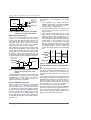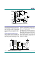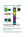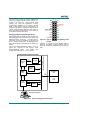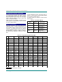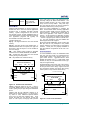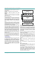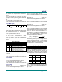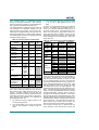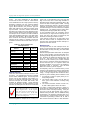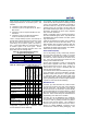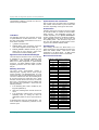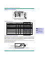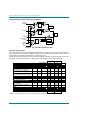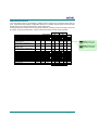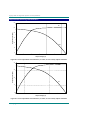
1
Zylogic ZE5 Configurable
System-on-Chip Platform
®
March, 2004 (Version 1.10)
Product Description
other 8051-and 8052-based devices
- 4 cycles per instruction byte provides up to 10
MIPS performance at 40 MHz
- Configurable, extendable architecture supports user-designed or library-provided peripherals
- Two-channel DMA controller supporting single-clock transfers
- Programmable wait-state capability
- Dual 16-bit data pointers
- Three programmable 16-bit timer/counters
- Programmable, full duplex asynchronous serial communications port
- 256-byte scratchpad RAM
- Protected programmable watchdog timer
- Programmable power-down modes, including
individual PIO options
- Separate 64K address spaces for code and
data
- 12 interrupt sources with three priority levels
Industry’s first complete Configurable
System-on-Chip (CSoC) platform
- High-performance, industry-standard
8051/52-compatible microcontroller (10 MIPS
at 40 MHz)
- Up to 64Kbytes of on-chip, dedicated system
RAM (XDATA RAM)
- Up to 3,200 Configurable System Logic (CSL)
cells (roughly 40,000 gates)
- High-performance dedicated internal bus
- Advanced system debug capability
- Stand-alone operation from a single external
memory (code + configuration)
- Advanced four-layer metal, 0.35µ CMOS
process technology, 3.3 volt with 5 volttolerant I/O
Enhanced, high-performance, 8032-based
"Turbo" microcontroller
- Binary- and instruction-set compatible with
To external memory
for initialization and
code storage
Clock and
Crystal
Oscillator
Control
Memory
Interface Unit
Selector
PIO
Selector
PIO
Selector
PIO
Selector Configurable PIO
System Logic
Selector
PIO
(CSL)
PIO
matrix
Selector
PIO
8032 "Turbo" MCU
CPU
256x8
RAM
Power-On
Reset
Timer 1
USART
Bus
Arbiter
Watchdog
Timer
Timer 2
Interrupt
Unit
Address
Mappers
Data Bus
Timer 0
PIO
Address Bus
Power
Control
Configurable System
Interconnect bus
socket
Two-channel
DMA Controller
Byte-wide
System RAM
JTAG Interface
Hardware
Breakpoint Unit
Configurable System
Interconnect (CSI) bus
Figure 1. Zylogic ZE5 Configurable System-on-Chip (CSoC) block diagram.
© 1998-2000 by Zylogic Corporation. All rights reserved.
Subject to change. Visit www.Zylogic.com for the latest revision of this document.
Comments, questions, or suggestions on this document? Please send them to [email protected].
Patents pending.
Zylogic ZE5 Configurable System-on-Chip Platform
Device
ZE502
Table 1. Zylogic ZE5 Configurable System-on-Chip Family
Configurable
Embedded
System
CSI
Processor
Dedicated
System Logic (CSL)
Address
Core
Resources
RAM
Cells
Selectors
High-speed
internal
bus
8Kx8
256
16
8032 "Turbo"
ZE520
(3) 16-bit counters
USART
Watchdog timer
Memory interface unit
2-channel DMA controller
Power management
Power-on reset
Hardware breakpoint unit
ZE532
Interrupt controller
JTAG port
ZE505
ZE512
PIO*
Pins
(Max)
92
16Kx8
512
32
124
32Kx8
1,152
72
188
40Kx8
2,048
128
252
64Kx8
3,200
200
316
* Maximum PIO on each base device, actual PIO count depends on package style and initialization mode. See Table 45.
- Optional power-down operation, individually
selectable on every pin
- Input, output and output enable flip-flops for
optimal set-up and clock-to-output performance
- 5 volt tolerant inputs while operating at 3.3
volts
- Embedded debugging capabilities
Embedded Configurable System Logic (CSL)
matrix
- Fast, flexible CSL logic cells support combinatorial logic, arithmetic, memory, sequential,
and bus functions
- Up to 3,200 CSL cells per device
- Easy, synchronous access to and from the
system bus
- Programmable intercommunications network
between system bus, CSL cells, and programmable I/O (PIO) pins
- Contention-free bi-directional bussing
Memory interface unit (MIU) for flexible,
glue-less interface to external memory
- Direct connect interface to an external
256Kx8 memory for initialization and code
storage
- Expandable from 18 up to 32 address lines
- Variable-speed read/write timing simplifies interface design
- Access external peripherals by sharing MIU
data and address pins
High-performance, dedicated Configurable
System Interconnect (CSI) system bus
- 8-bit read and write data, 32-bit address
- Up to 40 Mbytes/sec transfer rates
- Simple, synchronous interface to CSL peripherals, seamless connection to the microcontroller
- Multi-master bus with round-robin arbitration
- Expandable to off-chip function through memory interface unit (MIU)
- Flexible on-chip address decoders provide
easy access to CSL functions
- Programmable wait-state support
- Open standard
- Forward compatible with future Zylogic configurable system-on-chip devices
Two-channel advanced DMA controller
-
Programmable power-down modes
Enhanced programmable input/output (PIO)
ports
- Selectively disable function during powerdown
- Typically consumes less that 50 µA in full
power-down mode
On-chip oscillator, crystal oscillator amplifier, and clock distribution circuitry
- Up to 315 user-programmable I/O per device
- Inputs, outputs, or bi-directional ports for the
microcontroller, dedicated peripherals, or programmable logic peripherals
- Selectable output drive from 4 mA to 12 mA
- BusMinder™ circuit provides pull-up, pulldown, or weak-follower capability
- Optional input hysteresis
www.Zylogic.com.cn
Proxy bus masters for CSL “soft modules”
Up to 40 Mbytes/s transfer rate (1 byte/cycle)
Auto-initialization of channels
Multiple addressing modes
Software-initiated DMA requests
Optional interrupt at end of a transfer
Block data transfers
CRC checking
DMA channel request and acknowledge signals distributed to the CSL matrix
2
- Via JTAG using internal system RAM to store
program code
- 'Stealth'-mode operation from internal RAM
during battery-backed operation
Four-pin IEEE 1149.1 JTAG interface port for
download and debugging
- Supports SAMPLE/PRELOAD, EXTEST, INTEST, BYPASS, and IDCODE instructions
- 8032 reset and CSoC reset
- Full access to the CSI system bus and all addressable locations
Dedicated in-system debugging, hardware
breakpoint unit
- Two breakpoint units monitor system address,
data, control, and processor instruction type
Multiple in-system programming modes
- Breakpoint indicator and control from Config-
- Unlimited, in-system programmability
- Byte-wide using standard FLASH, EPROM, or
SRAM memories
- Serially using serial sequential-access PROM
memories (SPROMs)
urable System Logic (CSL)
Overview
The embedded high-performance 8032-based
"Turbo" microcontroller is instruction-compatible
with other industry-standard 8032/52-based devices, leveraging the vast software library for the
8032 architecture. While the instruction cycle for
the original 8032 microcontroller is 12 clock cycles,
the 8032 "Turbo" microcontroller provides better
performance because each instruction cycle is
only four clock cycles. The result is improved performance at the same clock frequency.
The Zylogic ZE5 configurable system-on-chip integrates, on a single device, a performanceenhanced 8032 “Turbo” embedded microcontroller,
a large block of SRAM, a high-speed dedicated
system bus, and configurable logic, intimately connected to the processor and system bus. The ZE5
family is a highly integrated, fully static single-chip
system optimized for embedded systems applications. Each member of the ZE5 family contains an
identical microcontroller and set of dedicated resources, as shown in Figure 1. However, the size
of the dedicated system RAM, the number of programmable I/O (PIO) pins, and the amount of configurable system logic grows with the larger members of the family, as shown in Table 1.
The 8032 "Turbo" core offers other advantages
over the original 8032. The 8032 "Turbo" MCU
provides a protected watchdog timer plus an additional data pointer, easing data transfer routines.
"Soft" modules
implemented in the
Configurable System Logic
(CSL) matrix
8-bit UART
with parity
generation/
detection
Pulse-Width
Modulator
SPI
Serial
Interface
CSI Bus Sockets
Configurable System Interconnect (CSI) Bus
Configurable System-on-Chip
System Resources
Figure 2. "Soft" modules are built from Configurable System Logic (CSL) resources. Modules
connect to the configurable system-on-chip system via a Configurable System Interconnect (CSI) bus socket, providing easy “drag-and-drop” customization.
3
www.Zylogic.com
Zylogic ZE5 Configurable System-on-Chip Platform
JTAG Connector
16
+3.3V
GND
TMS
TDI
TDO
TCK
TMS
TDI
TDO
PIO
VCC
PIO
PIO
SLAVEVSYS
Triscend
Configurable
System-on-Chip
(CSoC)
PIO
+3.3V
PIO
XTAL
PIO
PIO
RST-
28
PIO
PIO
XTALIN
GND
PIO
PIO
Up to 125 PIO pins in
208-pin PQFP package
+3.3V
TCK
PIO
GND
CE- WE- OE- D[7:0] A[17:0]
8
18
CE- WE- OE- D[7:0] A[17:0]
Flash ROM
256Kx8
VCC
GND
+3.3V
GND
Figure 3. A complete Zylogic ZE520 Configurable System-on-Chip (CSoC) design.
Multiple masters arbitrate for bus access. Potential bus masters include the 8032 "Turbo" microcontroller, the JTAG interface, the read and write
channels of each DMA channel, and the memory
interface unit (MIU) in some modes of operation.
Functions implemented in the CSL matrix can use
a DMA channel as a "proxy" master, re-using the
control logic already contained in the DMA channels to become a master on the CSI bus.
The embedded SRAM-based Configurable System
Logic (CSL) matrix provides "derivative on demand" system customization.
The highperformance configurable logic architecture consists of a highly interconnected matrix of CSL cells.
Resources within the matrix provide easy, seamless access to and from the internal system bus.
Each CSL cell performs various potential functions,
including combinatorial and sequential logic. The
combinatorial portion performs Boolean logic operations, arithmetic functions, and memory. The
sequential element performs independently or in
tandem with the combinatorial function.
A memory interface unit (MIU) connects the Zylogic ZE5 configurable system-on-chip to external
memory. The MIU typically connects to an external FLASH-memory device that holds the ZE5's
initialization program plus the user's code. The
MIU interface is reusable for connections to other
external components. The external read, write
control, and chip-select signals are programmable
providing flexible set-up, strobe, and hold timing.
The abundant programmable input/output blocks
(PIOs) provide the interface between external functions and the internal system bus or configurable
system logic. Each PIO offers advanced I/O options including selectable output drive current, optional input hysteresis, and programmable lowpower functionality during power-down mode.
The two-channel DMA controller provides highbandwidth communication between functions, up
to 40 Mbytes per second. Its easy-to-use handshake simplifies interface and control logic. Functions from within the CSL matrix can request DMA
transfers, the DMA controller providing "proxy" bus
mastering capabilities.
A high-performance internal system bus—called
the Configurable System Interconnect (CSI) bus—
interconnects the microcontroller, its peripherals,
and the CSL matrix. The bus provides eight bits of
read data, eight bits of write data, and a 32-bit address.
Address mapping logic translates the
8032's 16-bit address to the 32-bit address used
by the internal system bus.
www.Zylogic.com.cn
A large block of fast, byte-wide SRAM provides
internal storage for temporary data storage or for
code. Though typically used for data, code can be
4
executed from internal RAM, offering faster access
plus security in battery-backed applications.
debugging, the JTAG port also sets up the internal
hardware breakpoint unit.
The majority of the system, including the microcontroller, operates from a single bus-clock signal.
Optional sources for the bus clock include driving it
directly from an off-chip signal, connecting an external crystal or ceramic oscillator between the
dedicated crystal-oscillator amplifier pins, or using
the internal ring oscillator. Six other global buffers
provide high-fanout signals to CSL functions. The
bus clock and the global buffers can optionally be
stopped upon a breakpoint event and shut off during power-down mode.
The hardware breakpoint unit contains two functions that monitor the 8-bit read or write data bus,
the 32-bit internal address bus, control signals and
the type of processor instruction (code or data access). Upon a predefined set of conditions, the
breakpoint unit halts execution of the application
program. Via JTAG control, the user can singlestep instruction execution of the processor.
Together, the 8032 "turbo" microcontroller, its dedicated peripherals, the on-chip RAM, the internal
CSI system bus, and the CSL matrix and PIOs
form a powerful, integrated configurable system.
Power management control provides selectable
power-down options over internal functions. Furthermore, each PIO provides pin-by-pin powerdown settings.
8032 "Turbo" Microcontroller
The Zylogic ZE5 8032-based configurable systemon-chip is fully instruction set compatible with other
industry-standard 8032/8051 microcontrollers. It
includes the resources of the standard 8032 including three 16-bit timer/counters; a full-duplex
serial port and twelve interrupt sources with three
priority levels.
The ZE5 configurable system-on-chip, like other
advanced processors, is built from leading-edge
static CMOS technology. The ZE5 device is infinitely in-system programmable. A power-on reset
circuit guarantees proper start-up operation after
power is asserted. There are various initialization
(bootstrapping) modes to support different application requirements. The ZE5 can load itself automatically after power-on from an external, bytewide boot memory. Optionally, the ZE5's configuration data is stored in a serial sequential-access
PROM. In serial mode, the user's code is copied
to and executed from the internal SRAM. Serial
mode frees a number of device pins so that they
can be used as user-defined PIO pins.
The ZE5 features a performance-enhanced 8-bit
CPU with a redesigned core processor, reducing
unnecessary clock and memory cycles. The instruction cycle of a standard 8032 is twelve clock
cycles while the Zylogic ZE5 reduces this to four
clock cycles for the majority of instructions, thereby
improving performance by an average of 1.5 to 3
times.
This naturally speeds up the execution of the instructions. Consequently, the ZE5 offers more
processing power compared to the original 8032,
even using the same frequency crystal. For a
given throughput, the ZE5 can be operated from a
lower-frequency clock than the original 8032, reducing power consumption.
In security-conscious applications, the user's program is stored in internal RAM and battery-backed
using external circuitry. If the ZE5 configurable
system-on-chip is in ‘stealth’ mode, it boots from
internal RAM when VCC is re-applied after battery
back up. Stealth mode optionally disables the
JTAG interface port and disables external fetches
via the MIU.
The ZE5 also provides dual Data Pointers (DPTRs)
to boost block data memory transfers.
An internal initialization boot ROM controls the
start of initialization during power-on after the RSTpin is released. The primary purpose of the initialization boot ROM is to find the user's initialization
data and code stored in the secondary boot code,
usually held in PROM.
Programmable I/O Ports
The original 8032 offers up to four 8-bit ports, a
total up to 32 lines. In the ZE5, the 8032 processor core is embedded with other functions. The
processor optionally connects to as many PIO pins
as required by the application.
Initialization programs can also be downloaded
directly to internal SRAM through the JTAG port.
Likewise, initialization programs can be written to
external flash via JTAG through the MIU interface.
UART
The Zylogic ZE5's UART is a superset of the
UART in the original 8032 family, though offers
timing compatibility.
The UART provides enhanced features such as automatic address recognition and frame error detection.
Besides downloading initialization programs, the
JTAG port offers nearly full access to the microcontroller, peripherals, and CSL functions to aid in
debugging. The JTAG interface can become a bus
master on the internal CSI bus. During system
5
www.zylogic.com.cn
Zylogic ZE5 Configurable System-on-Chip Platform
Bus Request/Grant
Bus Request/Grant
DMA Channel 0
DMA Channel 1
Control Logic
Pending
Requests
Counter
Transfer
Counter
Address
Counter
FIFO
FIFO
FIFO
FIFO
CRC
Data Read Bus
Address Bus and Data Write Bus
Figure 4. Block diagram of the embedded two-channel DMA controller.
Pow er Management
Like the original 80C31, the ZE5 provides Idle and
Power-Down modes of operation. Idle mode stops
the MCU while the timers, serial port and interrupt
block continues to operate. Power-Down mode
optionally stops all the clocks and completely halts
chip operation, the lowest power-consumption
state.
Timers
The ZE5's 8032-based microcontroller has three
16-bit timers that are functionally similar to the timers of the original 8032 family. When used as timers, they optionally operate at either 4 clocks or 12
clocks per count, thus providing a mode that emulates the timing of the original 8032.
The ZE5 also features a protected watchdog timer.
This timer is used as a system monitor or to time a
very long period.
Pow er-On reset
The Zylogic configurable system-on-chip has an
on-chip Power-On Reset facility. This eliminates
the external capacitor-resistor network required in
original 8032 designs.
Interrupts
The Interrupt structure in the Zylogic configurable
system-on-chip is slightly different from that of the
original 8032. Due to the presence of additional
features and peripherals, the number of interrupt
sources and vectors is increased.
DMA Controller
The Zylogic ZE5's direct memory access (DMA)
controller contains two independent channels.
Each channel is autonomous from the 8032 microcontroller, freeing the processor from mundane,
performance-stealing, data transfer operations.
Each channel is designed to transfer a byte of data
on each clock cycle, maximizing the data transfer
bandwidth. Several different data transfer modes
are available including those between memory and
a device, in any direction. A device associates
Data Pointers
The original 8032 had only one 16-bit Data Pointer
(DPL, DPH). In the ZE5, there is an additional 16bit Data Pointer (DPL1, DPH1). This new Data
Pointer inhabits two previously unused SFR locations in the original 8032.
www.Zylogic.com.cn
6
the DMA controller services the request. Software
can detect that a transfer has been initiated when
the INIT bit is cleared. The next transfer parameters can be updated and the INIT bit set.
itself with a particular channel through a DMA control register (DMACTRL), which contains a request
and acknowledge signal pair. The two DMA channels can also be paired to perform memory-tomemory operations.
Requests are processed on a cycle basis. Requests lasting more than one clock cycle are interpreted as multiple requests. If the DMA cannot
process all the incoming requests, a Pending Request Counter keeps track of such requests. A
total of 64K pending requests are possible. If the
EN is cleared in the middle of a block transfer, any
subsequent requests are ignored by the DMA and
by the pending request counter. The counters can
be read through software until it is reset. The
counters are initialized either by the CLR bit or by
enabling the DMA channel.
The main features of the DMA controller unit are:
Two independent channels for device or memory transfers
Transfer rates up to 40 Mbytes/sec
Auto-initialization of channels
Programmable transfer parameters
Multiple addressing modes
In case a DMA channel is not responding properly,
it is possible to reset it through the CLR bit in the
control register. Once the CLR bit is set, the DMA
channel is in a reset state. It exits this state only
after the CLR bit is cleared. After a power-on reset
or other system-wide reset, CLR is set.
Interrupt capabilities
Memory-to-memory transfers capabilities
Block transfers
Software-initiated DMA requests
A block transfer normally completes when the
transfer counter reaches zero. At that point, depending on the mode, the DMA transfer either
stops or continues. The DMA continues with the
next block transfer if the INIT bit is set, or if continuous mode is enabled. Resetting the DMA channel also terminates a block transfer. The latter
method should be used very carefully.
Four-byte FIFO
Asynchronous request/acknowledge handshake
CRC on DMA data stream
Functional Description
The DMA unit is composed of two channels as
shown in Figure 4. A set of parameters defines the
operation for a specific DMA channel, including the
memory starting address and starting transfer
count, the direction of the transfer, and a variety of
other transfer characteristics. Each channel has
its own register set. The control logic block contains the address counter, the current transfer
count, the pending requests counter and channel
control logic. The data FIFO serves as a temporary buffer between the I/O device and memory.
The CSI bus arbiter treats each channel as independent bus masters.
Aborting a DMA transfer
Software can cleanly abort an operation in the middle of a DMA transfer. Once the user detects that
the current DMA transfer can be aborted, the DMA
channel can be disabled cleanly by clearing the EN
bit. The next step is to reset the DMA channel
logic, accomplished by setting the CLR bit. Only
one clock cycle is necessary to reset the DMA
channel logic. Once the CLR is cleared, the DMA
channel is again ready to use. Except for a few
important control bits (refer to the reset values of
each field of the DMA registers), the rest of the
configuration registers will have kept their previously programmed values. By writing a few command bits to the control register, the previous
transfer could be repeated.
DMA Initialization and Termination
The DMA channels are initialized through their programmable registers. Once the transfer parameters have been programmed, the DMA channel
must first be enabled and the transfer initialized.
Setting the EN bit in the respective DMA_CTRLx_0
register enables the DMA channel. Once enabled,
the DMA channel accepts requests. At that point,
the DMA accept requests but cannot service them.
A transfer is initialized by setting the INIT bit.
Upon initialization, the first DMA request loads the
start address and start count into their respective
counters. The INIT bit is reset by hardware and
Transfer handshaking
The DMA controller always does the read transfer
first and stores the data into its temporary FIFO.
Then it performs the write transfer.
Transfer Modes
This section describes the basic DMA transfer
types and features. Some of these transfer modes
7
www.zylogic.com.cn
Zylogic ZE5 Configurable System-on-Chip Platform
can be combined to form more complex and powerful operations.
PAIR bit in the control register of both channels
enables this mode. Transfers are initiated using
the master's control register. However, the slave
channel must be enabled and its transfer parameters set correctly.
Single Transfer Mode
In this mode, the DMA initiates a single byte transfer for each request. If the requests are asserted
during every cycle, then the DMA controller attempts to service the requests as fast as it can.
The DMA services requests until the transfer count
reaches zero. At that point, the transfer is completed. This is the default mode.
Linked transfers
Linked transfers are possible using a singleinitialization, software block transfer. The parameters of the first block transfers are programmed
into the appropriate control registers and the transfer is initiated through the INIT bit and the
SFTREQ bit. Once the INIT bit is cleared by hardware—meaning the DMA channel has initiated the
transfer—software loads the address and transfer
count parameters of the next block of data. After
loading the parameters, software sets the INIT and
SFTREQ bits. Upon completion of the first block
transfer, the DMA channel loads the new parameters and initiates the new transfer. Software repeats the previous steps until it reaches the end of
the linked list.
Block Transfer Mode
In this mode, a single request initiates a transfer of
an entire block of data. Upon receiving the request,
the DMA controller starts transferring data until the
transfer count reaches zero. If a request is received at any time during the block transfer, the
request is recorded in the Pending Requests
Counter. The new request is serviced at the end
of the current block transfer.
Software Request
When this mode is active, the DMA controller responds to a DMA request initiated from software.
Setting the SFTREQ bit in the DMA channel control register enables this mode. Software can then
request a DMA transfer. Software requests that
cannot currently be served are recorded in the
pending request counter. A software request is
cleared by hardware on the cycle following the set
operation. If the software request is set while the
DMA channel is disabled, then the request is ignored.
Bus Address Generation
Each DMA channel generates a memory address
for every request. The first address of a block
transfer is the starting address, held in starting address control register. This address value is then
loaded into the current address counter upon the
first request of a block transfer. Once the address
is broadcast to memory, it is updated for the next
request. The addressing option is configured
through two of the DMA channel's control register
bits, as shown in Table 2.
For debug purposes, the current address of a
block transfer as well as the current count are visible to software.
Single Initialization
Setting the INIT bit initializes a transfer. Upon receiving the first request, the INIT bit is reset by
hardware and the single, software or block transfer
continues until the transfer count reaches zero. At
that point, the DMA controller waits for a new initialization command.
Data FIFO
The data FIFO serves as a temporary buffer between the requesting I/O device and memory. Because of the CSI bus structure and the multimaster handshaking, four locations are required.
Continuous Auto-Initialization
Setting the CONT initiates a transfer similar to the
INIT bit, but upon completion of the current transfer,
the DMA controller automatically reinitializes as if
the INIT bit were set again. Automatic refresh of
some external display is one potential application
of this mode.
CRC Feature
A cyclic redundancy check (CRC) can be performed on a single DMA stream. The CRC logic
monitors the Data Read bus as it enters the DMA's
FIFOs. The CRC logic is shared between the two
DMA channels and is enabled for either one of the
channels by setting the CRC_EN bit in the corresponding DMA channel control register. A 0-to-1
transition on CRC_EN resets the CRC shiftregister to zero. Once enabled, the CRC logic is
activated any time a byte of data is written into a
FIFO. Once a transfer is completed, the output of
the CRC register can be read by software, and the
Memory-to-Memory Transfer
By pairing the channels together, the DMA controller supports memory-to-memory transfers. The
channel that reads the data from memory, is the
master, and the other channel, which writes the
data back into memory, is the slave. Setting the
www.Zylogic.com.cn
8
CRC signature can be compared with the expected
value.
Mnemonic: DMASADR0_0
Address: FF20h
DMA Source Address Channel 0 (A[15:8])
The CRC logic uses a CRC-CCITT 16-bit divisor
polynomial, as shown in the equation below. The
algorithm is capable of detecting any one, two or
an even number of bits in error as well as a large
number of burst errors.
7
6
5
4
3
2
1
0
A15
A14
A13
A12
A11
A10
A9
A8
Mnemonic: DMASADR0_1
Address: FF21h
DMA Source Address Channel 0 (A[23:16])
X16 + X12 + X5 + 1
Interrupts Generation
The DMA controller can generate interrupts upon
the following three events.
7
6
5
4
3
2
1
0
A23
A22
A21
A20
A19
A18
A17
A16
Mnemonic: DMASADR0_2
Transfer terminal count: This event is generated
when a block transfer is complete (when the transfer counter reaches its terminal count of 0).
Address: FF22h
DMA Source Address Channel 0 (A[31:24])
Transfer Initialization: This event is generated
upon the first request of block transfer if the INIT
bit is set.
7
6
5
4
3
2
1
0
A31
A30
A29
A28
A27
A26
A25
A24
Mnemonic: DMASADR0_3
Address: FF23h
Channel 1:
Pending Request Overflow: This event is generated when the pending request counter overflows,
indicating that the DMA controller cannot keep up
with the number of incoming requests.
DMA Source Address Channel 1 (A[7:0])
The status of these events is recorded in the interrupt status register, independent of their corresponding interrupt-enable bits. The status bits are
reset by software by writing a one into them. Writing a zero does not affect the state of any status
bits. Some of the status bits are also cleared by
some hardware action (refer to "DMA Interrupt
Register").
7
6
5
4
3
2
1
0
A7
A6
A5
A4
A3
A2
A1
A0
Mnemonic: DMASADR1_0
Address: FF34h
DMA Source Address Channel 1 (A[15:8])
7
6
5
4
3
2
1
0
A15
A14
A13
A12
A11
A10
A9
A8
Mnemonic: DMASADR1_1
Address: FF35h
DMA Source Address Channel 1 (A[23:16])
Configuration Registers
Each channel has a set of 21 bytes of control and
status registers. Some registers are used to program a specific DMA channel or to query its status.
7
6
5
4
3
2
1
0
A23
A22
A21
A20
A19
A18
A17
A16
Mnemonic: DMASADR1_2
Address: FF36h
DMA Source Address Channel 1 (A[31:24])
DMA Start Address Register (one per channel)
This set of registers defines the start address of
the DMA transfer. The register values are loaded
into the Address Counter at the beginning of a
transfer.
7
6
5
4
3
2
1
0
A31
A30
A29
A28
A27
A26
A25
A24
Mnemonic: DMASADR1_3
Address: FF37h
DMA Transfer Count Register (one per channel)
This field specifies the byte length of the DMA
transfer. The actual value is the number of
bytes transfer minus one. This value is loaded
into the transfer counter before the transfer starts.
The DMA controller operates on 32-bit physical
address values, whereas the microcontroller operates on 16-bit logical address values. The physical
address for a memory location is typically assigned
automatically by the Zylogic FastChip development
system and included in a header file for the user.
The values are read/writeable.
The values are read/writeable.
Channel 0:
Channel 0:
DMA Transfer Count Channel 0 (CNT[7:0])
DMA Source Address Channel 0 (A[7:0])
7
6
5
4
3
2
1
0
A7
A6
A5
A4
A3
A2
A1
A0
7
6
5
4
3
2
1
0
CNT7
CNT6
CNT5
CNT4
CNT3
CNT2
CNT1
CNT0
Mnemonic: DMASCNT0_0
9
Address: FF24h
www.zylogic.com.cn
Zylogic ZE5 Configurable System-on-Chip Platform
DMA Transfer Count Channel 0 (CNT[15:8])
7
6
5
4
3
2
1
0
CNT15
CNT15
CNT13
CNT12
CNT11
CNT10
CNT9
CNT8
6
5
4
3
2
1
0
CNT23
CNT22
CNT21
CNT20
CNT19
CNT18
CNT17
CNT16
6
5
4
3
2
1
0
A22
A21
A20
A19
A18
A17
A16
Mnemonic: DMACADR0_2
Mnemonic: DMASCNT0_1
Address: FF25h
DMA Transfer Count Channel 0 (CNT[23:16])
7
7
A23
Address: FF2Dh
DMA Current Address Channel 0 (A[31:24])
7
6
5
4
3
2
1
0
A31
A30
A29
A28
A27
A26
A25
A24
Mnemonic: DMACADR0_3
Mnemonic: DMASCNT0_2
Address: FF2Eh
Address: FF26h
Channel 1:
Channel 1:
DMA Current Address Channel 1 (A[7:0])
DMA Transfer Count Channel 1 (CNT[7:0])
7
6
5
4
3
2
1
0
CNT7
CNT6
CNT5
CNT4
CNT3
CNT2
CNT1
CNT0
7
6
5
4
3
2
1
0
A7
A6
A5
A4
A3
A2
A1
A0
Mnemonic: DMACADR1_0
Mnemonic: DMASCNT1_0
Address: FF38h
DMA Transfer Count Channel 1 (CNT[15:8])
7
6
5
4
3
2
1
0
CNT15
CNT15
CNT13
CNT12
CNT11
CNT10
CNT9
CNT8
Address: FF3Fh
DMA Current Address Channel 1 (A[15:8])
7
6
5
4
3
2
1
0
A15
A14
A13
A12
A11
A10
A9
A8
Mnemonic: DMACADR1_1
Mnemonic: DMASCNT1_1
Address: FF39h
DMA Current Address Channel 1 (A[23:16])
DMA Transfer Count Channel 1 (CNT[23:16])
7
6
5
4
3
2
1
0
CNT23
CNT22
CNT21
CNT20
CNT19
CNT18
CNT17
CNT16
Address: FF40h
7
6
5
4
3
2
1
0
A23
A22
A21
A20
A19
A18
A17
A16
Mnemonic: DMACADR1_2
Mnemonic: DMASCNT1_2
Address: FF40h
Address: FF41h
DMA Current Address Channel 1 (A[31:24])
DMA Current Address Register (one per channel)
This register and Current Count register are used
to monitor the current state of a particular DMA
channel or for debugging. This register contains
the output of the transfer address counter. This
register is loaded at the beginning of a transfer and
is incremented or decremented at every transfer,
controlled by the address mode bits ADRM1 and
ADRM0.
7
6
5
4
3
2
1
0
A31
A30
A29
A28
A27
A26
A25
A24
Mnemonic: DMACADR1_3
Address: FF42h
DMA Current Count Register (one per channel)
This is the output of the transfer count counter. It
indicates how many bytes are left in the current
transfer.
The values are read-only.
The values are read-only.
Channel 0:
Channel 0:
DMA Current Count Channel 0 (CNT[7:0])
DMA Current Address Channel 0 (A[7:0])
7
6
5
4
3
2
1
0
A7
A6
A5
A4
A3
A2
A1
A0
Mnemonic: DMACADR0_0
5
4
3
2
1
0
A15
A14
A13
A12
A11
A10
A9
A8
Mnemonic: DMACADR0_1
4
3
2
1
0
CNT4
CNT3
CNT2
CNT1
CNT0
Address: FF2Fh
7
6
5
4
3
2
1
0
CNT15
CNT15
CNT13
CNT12
CNT11
CNT10
CNT9
CNT8
Mnemonic: DMACCNT0_1
Address: FF2Ch
Address: FF30h
DMA Current Count Channel 0 (CNT[23:16])
DMA Current Address Channel 0 (A[23:16])
www.Zylogic.com.cn
5
CNT5
DMA Current Count Channel 0 (CNT[15:8])
DMA Current Address Channel 0 (A[15:8])
6
6
CNT6
Mnemonic: DMACCNT0_0
Address: FF2Bh
7
7
CNT7
10
7
6
5
4
3
2
1
0
CNT23
CNT22
CNT21
CNT20
CNT19
CNT18
CNT17
CNT16
Mnemonic: DMACCNT0_2
INIT, when set, initializes a DMA transfer. An initialization is associated with the transfer of each
block transfer. When this bit is set, the starting
operation values are loaded into their corresponding counters at the beginning of a transfer. Once
the transfer has started, the bit is cleared by hardware. Software can set it again during the current
block transfer to prepare the DMA channel for the
next block. When cleared, the DMA stops after the
current transfer. Cleared by reset.
Address: FF31h
Channel 1:
DMA Current Count Channel 1 (CNT[7:0])
7
6
5
4
3
2
1
0
CNT7
CNT6
CNT5
CNT4
CNT3
CNT2
CNT1
CNT0
Mnemonic: DMACCNT1_0
CONT, when set, indicates continuous initialization
mode. When set, the DMA transfer on the current
block continues until this bit is cleared. Cleared by
reset.
Address: FF43h
DMA Current Count Channel 1 (CNT[15:8])
7
6
5
4
3
2
1
0
CNT15
CNT15
CNT13
CNT12
CNT11
CNT10
CNT9
CNT8
Mnemonic: DMACCNT1_1
SFTREQ, when set, requests a software-initiated
DMA transfer. This bit is cleared by hardware on
the following clock cycle.
BLOCK, when set, indicates block request mode.
When set, a complete block transfer is performed
by the DMA upon receiving a single request from a
device. Unaffected by reset.
Address: FF44h
DMA Current Count Channel 1 (CNT[23:16])
7
6
5
4
3
2
1
0
CNT23
CNT22
CNT21
CNT20
CNT19
CNT18
CNT17
CNT16
Mnemonic: DMACCNT1_2
PAIR, when set in both channels, couples the two
DMA channels to perform memory-to-memory
transfers. Unaffected by reset.
Address: FF45h
W/R- indicates the direction of the DMA transfer.
When set, the DMA performs a memory-to-I/O
transfer (DMA Write). When clear, the DMA performs an I/O-to-memory transfer (DMA Read).
Unaffected by reset.
DMA Control Register (one per channel)
Channel 0:
7
6
W/R-
PAIR
5
4
BLOCK SFTREQ
3
2
1
0
CONT
INIT
EN
CLR
Mnemonic: DMACTRL0_0
7
6
5
ADRM1 and ADRM0 define the transfer address
mode as shown below. Unaffected by reset.
Address: FF27h
4
3
Reserved
2
1
CRC_EN ADRM1
Mnemonic: DMACTRL0_1
0
Table 2. DMA Address Mode Settings.
ADRM0
Mode
Increment address by one
0
0
after each byte transfer
Decrement address by one
1
0
after each byte transfer
Single address transfer
x
1
(address remains constant)
ADRM0
ADRM1
Address: FF28h
Channel 1:
7
6
W/R-
PAIR
5
4
BLOCK SFTREQ
3
2
1
0
CONT
INIT
EN
CLR
Mnemonic: DMACTRL1_0
7
6
5
4
Address: FF3Bh
3
Reserved
Mnemonic: DMACTRL1_1
2
1
CRC_EN ADRM1
0
ADRM0
CRC_EN enables CRC checking. When set, this
bit activates the CRC logic. A 0-to-1 transition on
this bit resets the CRC logic to 0.
Address: FF3Ch
All values are read/writeable.
Cleared by a power-on reset or other device-wide
reset.
CLR, when set, disables the DMA channel and
clears the transfer counter and pending requests
counter. Clearing the bit indicates that the DMA
channel is ready to operate. Cleared by reset.
DMA Pending Requests (one per channel)
This field indicates the number of DMA requests
yet to be serviced. Up to 64K requests can be received ahead of their corresponding acknowledge.
EN, when set, enables the DMA request for the
channel. When this bit is set, the pending requests
counter is cleared and the DMA channel is ready
to accept requests. When this bit is cleared, incoming requests are ignored. Cleared by reset.
Cleared by a power-on reset or other device-wide
reset.
The values are read-only.
11
www.zylogic.com.cn
Zylogic ZE5 Configurable System-on-Chip Platform
DMA Status Register (one per channel)
Channel 0:
Channel 0:
DMA Pending Requests Channel 0 (REQ[7:0])
7
6
5
4
3
2
1
0
REQ7
REQ6
REQ5
REQ4
REQ3
REQ2
REQ1
REQ0
Mnemonic: DMAPREQ0_0
7
Address: FF32h
7
6
5
4
3
2
1
0
REQ14
REQ13
REQ12
REQ11
REQ10
REQ9
REQ8
Mnemonic: DMAPREQ0_1
7
6
5
4
3
2
1
0
REQ5
REQ4
REQ3
REQ2
REQ1
REQ0
Mnemonic: DMAPREQ1_0
6
5
4
3
2
1
0
REQ14
REQ13
REQ12
REQ11
REQ10
REQ9
REQ8
Mnemonic: DMAPREQ1_1
Channel 0:
6
NOTE:
5
4
3
Reserved
2
1
Address: FF29h
Channel 1:
6
5
4
3
Reserved
Mnemonic: DMAEINT1
2
1
5
4
2
1
0
OVR
INIT
TC
Address: FF3Eh
Cleared by a power-on reset or other device-wide
reset.
0
OVR_EN INIT_EN TC_EN
DMA Unit CRC Output Register
Once a transfer is completed, the output of the
CRC register can be read by software, and the
signature can be compared with the expected
value.
Address: FF3Dh
All values are read/writeable.
TC_EN, when set, enables the DMA interrupt to
indicate that the transfer counter reached its terminal count (TC).
DMA CRC Register (CRC[7:0])
INIT_EN, when set, enables the DMA interrupt
upon initialization.
OVR_EN, when set, enables the DMA interrupt to
indicate that the pending requests counter exceeded 64K.
7
6
5
4
3
2
1
0
CRC7
CRC6
CRC5
CRC4
CRC3
CRC2
CRC1
CRC0
Mnemonic: DMACRC_0
Address: FF48h
DMA CRC Register (CRC[15:8])
Cleared by a power-on reset or other device-wide
reset.
7
6
5
4
3
2
1
0
CRC15
CRC14
CRC13
CRC12
CRC11
CRC10
CRC9
CRC8
Mnemonic: DMACRC_1
www.Zylogic.com.cn
3
The OVR, INIT, and TC bits in the DMA
Status Register are cleared by writing a
‘1’ to their respective bit location. Writing a zero has no effect.
0
OVR_EN INIT_EN TC_EN
Mnemonic: DMAEINT0
7
6
Address: FF2Ah
OVR, when set, indicates that the pending requests counter has overflowed. This bit is set by
hardware and cleared by software by writing a one.
Writing a zero has no effect. This bit is also
cleared when the corresponding channel's pending
requests counter is cleared. Used in conjunction
with OVR_EN to flag an interrupt.
Address: FF47h
DMA Interrupt Enable Register (one per channel)
The DMA interrupt register enables individual interrupt events for each channel.
7
0
TC
INIT, when set, indicates that initialization has occurred. This bit is set by hardware and cleared by
software by writing a one. Writing a zero has no
effect. This bit is also cleared when software sets
the INIT bit in the corresponding channel's DMA
control register. Used in conjunction with INIT_EN
to flag an interrupt.
Address: FF46h
7
1
INIT
TC, when set, indicates that the transfer counter
reached terminal count. This bit is cleared when
the INIT bit is set. This bit is set by hardware and
is cleared by software by writing a one. Writing a
zero has no effect. Used in conjunction with
TC_EN to flag an interrupt.
DMA Pending Requests Channel 1 (REQ[15:8])
REQ15
2
OVR
Mnemonic: DMAINT1
DMA Pending Requests Channel 1 (REQ[7:0])
REQ6
3
Reserved
Channel 1:
7
4
Mnemonic: DMAINT0
Channel 1:
Address: FF33h
REQ7
5
Reserved
DMA Pending Requests Channel 0 (REQ[15:8])
REQ15
6
12
Address: FF49h
Cleared by a power-on reset or other device-wide
reset.
trol registers cover individual DMA read and write
operations from both channels 0 and 1. Another
DMA control register can be enabled via software
after first disabling the active control register.
Interfacing CSL Peripherals to the DMA Controller
Distributed DMA Control Register
This register is shared by both DMA channels.
Configurable
System Logic
REQSEL
ACKSEL
DMA Control Register
"Soft" modules implemented in the Configurable
System Logic matrix have full access to DMA services. Access is provided via distributed DMA control registers that steer DMA requests from peripherals to the appropriate DMA channel and steer
the appropriate DMA channel acknowledge signal
back to the peripheral, as shown in Figure 5.
Request
Acknowledge
Request
Acknowledge
7
6
5
4
3
2
1
0
-
-
SEL
ENBL
-
-
SEL
ENBL
Write both nibbles with duplicate data.
Read register and OR bits from each nibble.
Mnemonic: User-Defined
DMA
Channel 1
Address: User Defined
Undefined bit locations are reserved and return 0
when read.
NOTE:
DMA
Channel 0
Figure 5. DMA Control Registers steer control
signals from CSL “soft” modules to
the DMA channels.
DMA control registers share the same programmable address selector functions also used for
address decoding and chip selects. See Table 3
for the number of selectors available in each device.
The distributed DMA Control registers
only connect to either the high nibble or
the low nibble of the CSI data bus. Consequently, application code should write
duplicate copies of the high and low nibble. When reading, only the high or the
low nibble will contain valid data. The
high and low nibbles should be ORed
together to determine the actual settings.
SEL steers control signals to and from the DMA
controller. If SEL is cleared, the REQSEL input
and ACKSEL output signals are steered to DMA
channel 0. If SEL is set, then the signals are
steered to DMA channel 1. The SEL control bit
must be written to both bits 5 and 1. When read,
both bits must be ORed together.
The address for a DMA control register is programmable, similar to any function using a Selector. A symbolic address name for the specific
DMA control register is provided during design.
The actual address assignment is usually left to
the Zylogic FastChip development system. All
DMA control registers are single-byte registers and
must be located within data or SFR memory
spaces.
ENBL, when set, allows the CSL “soft” module to
access the DMA controller through the REQSEL
input and ACKSEL output associated with DMA
Control register. When ENBL is cleared, the DMA
controller ignores any requests from the CSL module and the CSL module ignores any DMA acknowledges. The ENBL control bit must be written
to both bits 4 and 0. When read, both bits must be
ORed together.
An individual DMA control register controls a unidirectional DMA transfer, i.e., a memory-to-I/O
(DMA write) or an I/O-to-memory (DMA read)
transaction. However, a DMA control register is
associated with a specific DMA channel by changing the SEL bit within the control register. Two
DMA control registers are required for DMA read
and DMA write operations from the same peripheral.
A DMA control register is reset to 00h by a reset.
There is unrestricted read/write access to this register.
DMA Request Steering
To request a DMA transfer, the CSL “soft” module
function asserts the REQSEL input on the DMA
control register, as shown in Figure 6. If enabled
(ENBL=1), the REQSEL signal is forwarded to appropriate DMA channel request, depending on the
SEL value. If SEL=0, then REQSEL requests
channel 0, else REQSEL requests channel 1. If
disabled (ENBL=0), the request is blocked.
A DMA control register is enabled for DMA access
by setting the ENBL bits. Until enabled, all DMA
requests (REQSEL) from a DMA control register
are ignored.
In standard use, only one DMA control register
should be enabled per channel, per direction at
any time, for a maximum of four. These four con-
13
www.zylogic.com.cn
Zylogic ZE5 Configurable System-on-Chip Platform
Request to
DMA Controller
Configurable
System Logic
The remainder of the transaction is as shown
Figure 8.
DMA1 REQ
1. The requesting “soft” module asserts its
REQSEL DMA request signal. Within the DMA
control register, this incoming request is
steered to the proper DMA channel.
REQSEL
DMA0 REQ
SEL
2. The DMA channel requests the CSI bus from
the bus arbiter. This process may require multiple clock cycles.
ENBL
DMA Select Register
Figure 6. A DMA Control Register steers DMA
requests to the appropriate channel.
3. Once the bus arbiter grants the bus to the
DMA controller, the DMA presents the transfer
address, the write data, and asserts its acknowledge signal. Within the DMA control register, the DMA channel's acknowledge signal is
steered back to the requesting CSL “soft”
module function. Consequently, the ACKSEL
signal is asserted, signaling the “soft” module
that data is available. The “soft” module uses
the ACKSEL signal to enable a register and
capture the value presented on the Data Write
bus.
DMA Acknowledge Steering
Once a “soft” module requests a DMA transfer,
control over the transaction shifts to the DMA
channel. The DMA channel requests the CSI bus.
Once granted, the DMA channel asserts is acknowledge signal, which is steered back to the
requesting CSL “soft” module via the ACKSEL
output. The control logic is shown in Figure 7.
When ACKSEL is asserted High, the CSL module
should respond appropriately. During a DMA read
(I/O-to-memory transfer), the CSL module should
present data on the Data Read bus when ACKSEL
is asserted. During a DMA write (memory-to-I/O
transfer), the CSL module should accept the data
on the Data Write bus when ACKSEL is asserted.
Acknowledge from
DMA Controller
ReqSel
Data Write
[7:0]
AckSel
Configurable
System Logic
DMA1 ACK
1
DMA0 ACK
0
Bus Clock
D
Q
ACKSEL
Figure 8. Example DMA Write operation.
BUSCLK
SEL
DATA
Using the DMA Controller as a Proxy Bus Master
“Soft” modules implemented in the CSL matrix are
bus slaves, unable to request and control the bus
by themselves. However, a CSL module can use
the dedicated DMA controller as a "proxy" bus
master.
ENBL
DMA Select Register
Figure 7. DMA acknowledge signals are steered
back to the requesting CSL “soft”
module.
The requesting device must be ready to accept the
ACKSEL signal in a single cycle, since wait state
capabilities are reserved strictly for memorymapped operations. The DMA controller is designed to maximize bus bandwidth.
Example DMA Write Transaction
Figure 8 shows the waveform for a typical DMA
write operation, i.e., a memory-to-I/O transfer.
Prior to the first request, one of the DMA channels
is configured for a DMA write operation and the
proper values loaded into its configuration registers.
Likewise, a DMA control register—part of a CSL
“soft” module function—is enabled (ENBL=1) and
the channel select bit is set to steer signals to the
proper DMA channel (SEL=0 for channel 0, SEL=1
for channel 1).
www.Zylogic.com.cn
14
A bus master requires interaction with the bus arbiter, registers and counters to track addresses, and
state machines to handle the bus transfer protocol.
Such logic would consume CSL logic resources, if
direct bus mastering were supported. A more efficient approach is to re-use the dedicated resources already built into the DMA controller.
The DMA controller contains the logic to arbitrate
for the bus, track address, and control transfers. A
CSL “soft” module uses the DMA controller as a
"proxy" master, causing the DMA controller to arbitrate for and control the bus transaction.
Side-band Signals
Hardware
Breakpoint Unit
Figure 9.
Data Read
Address
Bus Clock
DMA Request/
Acknowledge
Wait-State
Control
Breakpoint
Control
Configurable System Logic (CSL) Matrix
2-Channel
DMA Controller
Data Write
Selectors
8032
"Turbo"
Microcontroller
Configurable System Interconnect (CSI) Bus
CSI Socket Interface
The Configurable System Interconnect (CSI) bus and the socket interface to "soft"
modules in the CSL matrix.
Configurable System Interconnect (CSI) Bus
optionally steer DMA request and acknowledge
signals to and from the CSL matrix.
The Configurable System Interconnect (CSI) bus,
shown in Figure 9, bridges the microcontroller to its
peripherals and functions implemented in the Configurable System Logic (CSL) matrix. The CSI bus
provides a processor-independent migration path
to future generations of configurable system-onchip devices. User-defined and library-provided
“soft” modules can be moved to future Zylogic configurable system-on-chip families with little or no
modification
The bus clock.
Wait-state control and monitor signals.
Hardware breakpoint control and monitor signals.
Data Read Bus
Data is presented to the 8-bit read bus when the
selected CSL logic function or "soft" module asserts its read enable signal. The read data values
from all functions are logically OR-ed together.
Consequently, all unselected CSL functions drive
the read bus with zeroes. Only the selected function presents ones. Read data can be presented
during every active bus cycle.
The CSI bus socket provides a simple, synchronous interface to functions implemented in the CSL
matrix, as shown in Figure 10. The CSI bus interface socket consists of the following signals.
An 8-bit write data port
An 8-bit read data port, including a read enable
signal to enable the read data back onto the
CSI system bus.
Data Write Bus
The eight data write bits are presented on the CSI
socket. Write data may be presented during every
active bus cycle.
A 32-bit address port.
A set of address selector (chip select) functions.
The number of selectors varies according to
device size as shown in Table 3. The selectors
15
www.zylogic.com.cn
Zylogic ZE5 Configurable System-on-Chip Platform
Data Write
Data Read
8
8
Address
32
Selector Decode
DMA Acknowledge
CSL Logic
Function
Read Enable
DMA ReqSel
Bus Waited
Wait Next Cycle
Force Breakpoint
Breakpoint Event
Bus Clock
Synchronous Interface
Figure 10. The CSI bus socket represents a simple-to-use, synchronous interface to custom logic
functions implemented in the CSL logic matrix.
with the increasing size of the CSL matrix. There
is one selector for every sixteen CSL cells, as
shown in Table 3.
Address Bus
All 32 address bits are presented via the CSI interface socket. Typically, only a few, if any, of the
address signals are used by functions in the CSL
matrix. Typically, the actual decoding of the address bus is performed using the address selector
resources.
Table 3. Number of selectors by device.
Device Selectors
ZE502
16
ZE505
32
ZE512
72
ZE520
128
ZE532
200
Address Selectors
The CSI socket interface practically eliminates the
need to use any CSL matrix resources to decode
bus transactions. One of the more important elements in the CSI socket interface is the programmable address decoder function, generically called
a selector. A selector performs functions much like
a chip select unit or an address decoder built in a
PAL-type device.
Functionally, each selector is similar to diagram
shown in Figure 11. Each selector contains two
32-bit registers that define the target address. The
MATCH0 register defines which address bits
match when the individual bit is Low.
The
MATCH1 register defines which address bits
match when the bit is High. If the same bit location
is set in both registers, then the corresponding address bit is a "don't care."
Address Selector Operation
A selector detects a transaction to a specified
range of CSI bus addresses, including the particular address space. A selector decodes the full 32bit address bus. If a transaction is to its target address range, the selector asserts one of its outputs
on the same clock edge that the system provides
write data and address, synchronized to the system clock. This approach dramatically simplifies
the logic used to access CSL “soft” modules.
If each address bit matches with values defined in
the MATCH0 and MATCH1 register, then the selector further decodes read or write operations. If
the address matches, and there is a read transfer
to this location, then the selector asserts its
RDSEL output. Likewise, if the transfer is a write,
then the selector asserts its WRSEL output.
The number of available selectors depends on the
particular device. The number of selectors grows
www.Zylogic.com.cn
16
FastChip also defines the values initially loaded
into the address mapper registers.
Address Specification
The MATCH0 and MATCH1 register values are
automatically defined by the Zylogic FastChip development system at design time. These register
values are not changed by application software.
Address Selector Modes
An address selector performs one of three potential functions as shown in Table 4.
The addresses loaded into MATCH0 and MATCH1
are symbolically defined by the user during hardware design. The user specifies
The size of the addressed range, which must
be a power of two, ranging from ‘1’ indicating a
single byte to ‘16M’ indicating a 16M byte region.
Table 4. Address Selector Types.
Select
Modes
Ports
Function
RDSEL
Read decode
Selector
WRSEL
Write decode
RDSEL
R/W- control
Chip Select
SEL
Chip select
REQSEL DMA request
DMA Control
ACKSEL DMA acknowledge
The address space or spaces to which the selector should respond. In conjunction with the
address mapper, a selector detects transactions to a specific address space. The ZE5,
based on a standard 8032 microcontroller, supports the following address spaces.
Selector
A selector separately decodes read and write operations to the target address range, as shown in
Figure 11. The RDSEL output indicates a read
operation, the WRSEL output indicates a write operation.
DATA, which corresponds to the 8032's
XDATA memory space
A selector function is called SELECT in the design
library.
SFR (Special Function Register), which is
a 128-byte region unique to the 8032 architecture.
Chip Select
A selector in the chip select mode decodes any
read or write transaction to the target address
range, read or write. Figure 12 shows a functional
drawing of a chip select function. The SEL performs like a chip select function. The RDSEL output is asserted only during read operations.
The symbolic name for the address range.
This is the name used in application software to
refer to the target address range.
The Zylogic FastChip development system examines these settings from all of the address selectors defined in the hardware design. It then allocates physical addresses to each selector. The
corresponding 8032 logical addresses are defined
and specified in a header file, used with the user’s
application code.
A selector function is called CHIPSEL in the design
library.
The MATCH0 and MATCH1 values, defined by the
Zylogic FastChip development system, are loaded
into the selectors during the initialization process.
A2
A1
A0
A31
CSI Bus Address
Match0: Addr. Bit = Low
READ
RDSEL
WRITE
WRSEL
Match1: Addr. Bit = High
BCLK
Figure 11.
The distributed address selector functions decode read and write transactions to a
target address range. The selectors eliminate the need to build decoding logic using
CSL resources.
17
www.zylogic.com.cn
Zylogic ZE5 Configurable System-on-Chip Platform
A2
A1
A0
A31
CSI Bus Address
READ
Match0: Addr. Bit = Low
RDSEL
Match1: Addr. Bit = High
SEL
WRITE
BCLK
In chip select mode, an address selector decodes any read or write transaction to the
target address range.
DMA Control
A selector provides a relocatable control register
for CSL “soft” modules requiring DMA access. The
DMA control register enables requests and steers
the request and acknowledge signals to the selected DMA channel. DMA control register. See
the "DMA Controller" section for more information.
External Access through MIU
A “soft” module can access an external device using PIO pins or by re-using the pins on the memory
interface unit (MIU). A special selector mode allows a CSL function to access and handle a transaction through the MIU, as shown in Figure 13.
WAITNEXT (input to bus socket)
Some CSL “soft” modules require wait-states if the
they are too slow to respond in a single bus cycle.
If any wait-states are required, the initial wait-state
must be asserted using an address selector.
If a “soft” module requires more than one waitstate, it must assert the WAITNEXT signal before
the next rising clock edge on Bus Clock. When
asserted, the WAITNEXT signal causes a waitstate on the next bus cycle.
Wait-State Monitor and Control Signals
The CSI socket interface includes signals to monitor and control wait-states on the internal system
bus.
Initial Wait-State Insertion
Some “soft” modules implemented in the CSL ma-
WAITED (output from bus socket)
Triscend
E5
CSoC
The WAITED signal indicates that a wait-state was
asserted during the previous bus cycle. This signal is typically used in control logic for functions
such as FIFOs and dual-port memory.
A[17:0]
A[17:0]
D[7:0]
D[7:0]
OE-
OE-
WE-
WE-
CE-
CE-
Flash
Figure 12.
A[n:0]
D[7:0]
OEWECE-
Additional
Device
CSL_CE-
Figure 13. Other external devices share the ZE5's Memory Interface Unit (MIU) signals. The chip
enable for the Flash connects directly to the ZE5's CE- pin. All other devices use a separate Chip
Select function, located in the CSL matrix.
www.Zylogic.com.cn
18
WRSEL signal. The CSL “soft” module uses
WRSEL to enable a register and capture the write
data.
trix may require wait-states, either because the
“soft” module handshakes with another asynchronous device or if the “soft” module is too slow to
respond in a single bus cycle.
If a “soft” module requires any wait-states, a selector must assert the first wait-state. The selector
will only assert a wait-state if the system is accessing the selector's target address space.
Bus Clock
Data Write
[7:0]
DATA
WrSel
Should a “soft” module require additional waitstates beyond the initial wait-state asserted by the
selector, then the “soft” module indicates additional
wait-states by asserting the WAITNEXT signal on
the CSI socket interface.
Figure 14. A single-cycle write transaction to a
CSL “soft” module.
Figure 15 demonstrates a similar transaction, except that the CSL “soft” module requires two clock
cycles to capture the write data. The CSL “soft”
module's selector is configured to assert the initial
wait-state. When the selector detects that the system is addressing its target address range, it asserts its WRSEL signal and automatically asserts
an initial wait-state.
Breakpoint Event Monitor and Control Signals
The CSI socket interface includes signals to monitor and control hardware breakpoint events. These
signals can be used to aid system-level debugging.
BREAK (input to bus socket)
CSL functions can force a hardware breakpoint
event by asserting the BREAK signal. The hardware breakpoint unit typically only monitors transactions on the CSI bus. The BREAK signal allows
CSL functions to interact with the hardware breakpoint unit.
Seeing a wait-state during the first bus cycle, the
system holds its Data Write and Address values.
Correspondingly, the selector continues to assert
its WRSEL output. Because the CSL “soft” module
will capture the write data during the second bus
cycle, the “soft” module does not assert its
WAITNEXT signal to insert additional wait-states.
The system, seeing no wait-states during the second bus cycle, continues on to the next bus transaction. Consequently, the selector de-asserts its
WRSEL output after the second bus cycle.
For example, a CSL function could be monitoring a
serial communications stream that rarely interacts
with the system bus. Upon detecting a particular
pattern, the CSL function could force a breakpoint
event, stopping the system. The state of the system or CSL functions could then be monitored
through the JTAG port.
Bus Clock
EVENT (output from bus socket)
CSL functions can monitor hardware breakpoint
events using the EVENT signal. When EVENT is
asserted, a hardware breakpoint event has occurred, either caused by the hardware breakpoint
event or by another function in the CSL matrix.
Data Write
[7:0]
DATA
WrSel
Waited
CSI Bus Transactions
The following section describes example CSI bus
transactions, demonstrating the interaction of a
CSL “soft” module and the CSI bus socket.
By
Selector
Figure 15. A two-cycle write transaction to a
CSL “soft” module.
Data Read Transactions
During a data read transaction, the system receives data from a CSL “soft” module. The system
presents both the read address and waits for the
read data.
Data Write Transactions
During a data write transaction, the system sends
data to a CSL “soft” module. The system presents
both write data and address.
Figure 16 shows a single-cycle read transaction
from a CSL “soft” module. The read address is
presented on the CSI socket interface. The address is decoded using one the selector functions.
If the transaction is to its targeted address range,
then the selector asserts its RDSEL signal. The
CSL “soft” module uses RDSEL to enable data
Figure 14 shows a single-cycle write transaction to
a CSL “soft” module. Write data and address are
presented on the CSI socket interface. The address is decoded using one the selector functions.
If the transaction is to the address selector's targeted address range, then the selector asserts its
19
www.zylogic.com.cn
Zylogic ZE5 Configurable System-on-Chip Platform
state and the “soft” module must assert the
WAITNEXT signal to insert additional waitstates.
onto the Data Read output bus, part of the CSI
socket.
Figure 18 shows an example transaction where the
selected “soft” module uses the WAITNEXT signal
to insert wait-states. During the first bus cycle, the
addressed “soft” module's selector asserts it
RDSEL output. In this example, the “soft” module
always requires at least one wait-state, so the selector inserts the initial wait-state. The “soft” module is not ready to respond in the first bus cycle, so
the “soft” module asserts WAITNEXT, causing a
wait state during the next bus cycle
Bus Clock
RdSel
Data Read
[7:0]
DATA
Figure 16. A single-cycle read transaction from
a CSL “soft” module.
Figure 17 demonstrates a similar transaction, except that the CSL “soft” module requires two clock
cycles to provide the read data. The CSL “soft”
module's selector asserts the initial wait-state.
When the selector detects that the system is addressing its target address range, it asserts its
RDSEL signal and automatically asserts an initial
wait-state.
During the second bus cycle, the system continues
providing address. The selector continues asserting RDSEL. The “soft” module determines that it
unable to respond during this cycle and continues
asserting WAITNEXT.
Finally, during the third bus cycle, the “soft” module
is ready to respond. The “soft” module provides
data on the Read Data signals on the CSI socket.
The “soft” module also de-asserts WAITNEXT,
indicating that it is ready to supply data.
Seeing a wait-state during the first bus cycle, the
system holds its Address values. Correspondingly,
the selector continues to assert its RDSEL output.
Because the CSL “soft” module can present data
during the second bus cycle, it does not assert its
WAITNEXT signal. The system, seeing no waitstates during the second bus cycle, continues on
to the next transaction. Consequently, the selector
de-asserts its RDSEL output after the second bus
cycle.
Bus Clock
RdSel
WaitNext
Bus Clock
Waited
RdSel
Data Read
[7:0]
Waited
Data Read
[7:0]
By
Selector
By CSL
DATA
Figure 18. A multi-cycle transaction using
WAITNEXT to insert wait-states.
DATA
Side-band Signals
All of the signals on the CSI socket interface are
designed to be processor independent. “Soft”
modules designed using this interface can be reused with future Zylogic configurable system-onchip families.
Figure 17. A two-cycle read transaction from a
CSL “soft” module.
Using WAITNEXT during a transaction
There are three general rules for asserting a waitstate during a bus transaction to a CSL “soft” module, depending on the “soft” module's response
time.
However, some signals are processor specific.
The signals are called "side-band" signals. For the
Zylogic ZE5 family, these side-band signals include 8032-specific functions.
1. If the “soft” module can respond within a single
bus cycle, no wait-states are inserted.
2. If the “soft” module can responds by the second bus cycle, the address selector is configured to insert a single wait-state.
Table 5. ZE5 Family Side-band Signals.
ZE5 Function
8032 Signal
Timer 0 external input
T0
3. If three or more bus cycles are required before
the “soft” module can respond, an address selector is configured to insert the initial wait-
www.Zylogic.com.cn
By
Selector
20
Timer 1 external input
External I/O for Timer 2
Timer/Counter 2 capture/reload
trigger or an additional external
interrupt source if Timer 2 baudrate generator unused
External Interrupt 0
External Interrupt 1
High-Priority Interrupt
Serial port receive data input.
Used in modes 1, 2, and 3.
Serial port receiver output.
Used in serial port mode 0 for
shift clock.
Serial port transmit data
Application reset from CSL matrix (RSTC), inverted polarity
from the original 8032
Signal from the 8032 to the CSL
matrix (CPURST). Indicates
that the 8032 was reset for any
reason, including the watchdog
timer.
Output of the crystal oscillator
amplifier, distributed only to
CSL functions.
T1
T2
T2EX
INTR0
INTR1
HPINT
RXDIN
RXDOUT
TXD
RST-
(no 8032
equivalent
signal)
XTAL
On a traditional 8032, some of the microcontroller's
PIO pins have shared functionality. For example,
the Timer 0 External Input, T0, typically shares a
PIO pin on Port 3 (P3.4). On the ZE5, however,
these processor-specific signals can connect to
any PIO pin and even to functions implemented
entirely within the Configurable System Logic (CSL)
matrix.
The side-band signals for the ZE5 CSoC device
family are shown in Table 5.
21
www.zylogic.com.cn
Zylogic ZE5 Configurable System-on-Chip Platform
TE532 (5x5)
TE520 (4x4)
TE512 (3x3)
TE505 (2x2)
TE502 (2x1)
Figure 19. The five member of the ZE5 CSoC devic family range in density from two CSL banks
(256 CSL cells) up to 25 CSL banks (3,200 CSL cells).
Sideband Interface
CSL
Bank
CSL
Bank
CSL
Bank
CSL
Bank
CSL
Bank
CSL
Bank
CSL
Bank
CSL
Bank
CSL
Bank
Vertical Breakers
Horizontal Breakers
Figure 20.
Vertical and horizontal breakers separate the individual CSL banks with Configurable
System Interconnect (CSI) bus resources.
Configurable System Logic (CSL)
The number of CSL banks varies by part number.
The highest-density ZE5 family device, the ZE532,
contains 25 CSL banks, arranged in a 5x5 array as
shown in Figure 19 and Table 6. The smallest
member, the ZE502, has just two CSL banks, arranged in a 2x1 array.
The Configurable System Logic (CSL) matrix provides flexible, programmable resources to build
almost any digital function. Because it is intimately
connected to the CSI bus, the CSL matrix is ideal
for building any “soft” module functions required by
the MCU. The matrix consists of multiple CSL
banks. Each bank is a rectangular array of individual CSL cells.
www.Zylogic.com.cn
22
Selectors
Vertical
Breaker
CSL Bank
Adjacent
CSL Cells
Figure 21. A CSL bank consists of 8 columns by 16 rows of CSL cells, a 128 in total.
Table 6. CSL Banks by Device.
Part
CSL Banks
Number Columns Rows
Total
ZE502
2
1
2
ZE505
2
2
4
ZE512
3
3
9
ZE520
4
4
16
ZE532
5
5
25
Signals from one CSL bank can cross into other
banks via the breakers, though crossing a breaker
adds delay to the signal.
Total
Cells
256
512
1,152
2,048
3,200
Sideband signals originate and terminate in resources along the top edge of the device.
Bank Resources
Each CSL bank consists of 8 columns by 16 rows
of CSL cells, totaling 128 CSL cells per bank.
Figure 21 shows the basic layout of the cells within
a bank. Pairs of adjacent CSL cells share resources to build more complex cell functions. The
address selectors, located in the vertical breaker
above the bank, distribute any decoded address.
There is one address selector per column of 16
CSL cells.
Vertical and horizontal breakers separate the individual CSL banks on a device, as shown in Figure
20. Vertical breakers appear at the top of every
CSL bank. Horizontal breakers appear between
adjacent columns of CSL banks. The breakers
contain Configurable System Interconnect (CSI)
bus resources. The horizontal breakers distribute
CSI bus address signals to the CSL banks. The
vertical breakers distribute the Selector input and
output signals, breakpoint control signals, the
global buffer signals, and the wait-state control
signals. The CSI read data return path is also located in the vertical breakers.
Programmable interconnect surrounds the CSL
cells. These programmable "wires" allow a signal
originating from one CSL to communicate with one
or more CSL cells, even those in other CSL banks.
Likewise, signals to and from the CSI bus are distributed to and from individual CSL cells.
23
www.zylogic.com.cn
Zylogic ZE5 Configurable System-on-Chip Platform
Selector outputs
from vertical breaker
Selector outputs
from vertical breaker
4 Clock/Global Buffer
Carry,
cascaded
wide function
path
8 Short Segments
CSL Cell
8 Long Lines
CSL Cell
8 Short Segments
Routing
Matrix
8 Short Segments
4 Clock/Global Buffers
8 Long Lines
4 Clock/Global Buffers
Address outputs
from horizontal breaker
Routing
Matrix
8 Long Lines
Routing
Matrix
Routing
Matrix
8 Short Segments
Carry,
cascaded
wide function
path
Figure 22. The general-purpose interconnect surrounds a pair of adjacent CSL cells.
4 Clock/Global Buffer
8 Short Segments
CSI Data Write
8 Long Lines
CSL Cell
4 Clock/Global Buffers
OR
CSI Data Read
CSL Cell
8 Short Segments
CSI Data Write
Routing
Matrix
8 Short Segments
4 Mux Chains
8 Long Lines
4 Clock/Global Buffers
Routing
Matrix
8 Long Lines
Routing
Matrix
8 Short Segments
4 Mux Chains
Routing
Matrix
OR
Figure 23. CSI bus write data is available at each routing matrix. Read data returns to the CSI bus.
www.Zylogic.com.cn
24
4 Multiplexer Chains for distributing bidirectional data across a CSL bank. The multiplexer
chains behave much like a bidirectional, threestate bus but avoids the potential datacontention problems and associated power
consumption of a three-state bus because all
signals are unidirectional.
General-purpose Interconnect
The general-purpose interconnect, shown in
Figure 22, distributes signals within a CSL bank.
Metal lines of various lengths and purposes connect to individual CSL cells, to the horizontal and
vertical breakers, and to the distributed array of
routing matrices. Each routing matrix provides
connections between the various lines entering or
exiting the segment. The various interconnect resources are described below.
CSI Read Data paths gather the values of individual data lines from throughout the device.
Ultimately, all the signal return to the CSI bus.
The signals from individual bit lines are gathered via an OR-chain.
8 Short Segment lines in each vertical and
horizontal channel.
8 Long Lines in each vertical and horizontal
channel. These long lines traverse the width or
breadth of the CSL bank. The vertical long
lines optionally distribute the outputs from the
Selectors located in the vertical breaker. The
horizontal long lines optionally distribute address signals from CSI bus.
Carry, cascade
Selector decodes
Clocks
Bus clock and 3 of 6 global buffer signal
lines in every vertical channel. The bus clock
signal is distributed globally to all resources on
an ZE5 CSoC device. Within a CSL bank, any
three of the six global buffer signals are available.
Enables, Control
Signal-Flow Directional Preferences
Though the interconnect was designed to minimize
any directional signal-flow preferences, there are
few biases inspired by the architecture, as shown
in Figure 25.
CSI Address
Data
BCLK
BBUF0
BBUF1
BBUF2
BBUF3
Figure 25. The interconnect architecture inspires a few signal-flow biases.
Clock signals prefer the vertical channels, either to
take advantage of the four clock buffers available
within a CSL bank or the direct connections between the CSL cell's clock input and the vertical
long lines.
GBUF0
GBUF1
GBUF2
GBUF3
GBUF4
Likewise, other control signals and enable signals
prefer vertical channels. Addresses decoded using Selectors also prefer vertical channels because
vertical long lines distribute these signals from the
vertical breakers.
Wide arithmetic functions or wide logic functions
benefit from the built-in carry/wide interconnect,
which prefers a vertical orientation, from bottom to
top. Other orientations are possible, though with
decreased performance.
GBUF5
Figure 24. The bus clock signal and any 3 of
the 6 global buffer signals are available within a CSL bank.
A carry/cascade signal between adjacent
pairs of CSL cells, for faster arithmetic functions
and for wide logic functions.
Individual CSI bus address signals are distributed
using the horizontal long lines and consequently
prefer horizontal channels.
CSI Bus Read and Write Data Distribution
Beyond the general-purpose signals, the programmable interconnect also distributed data
signals to and from the CSI bus.
The multiplexer chains, designed to distribute bidirectional data, traverse a CSL bank horizontally.
As a result, data flow prefers the horizontal channels.
CSI Write Data is accessible at every routing
matrix, distributed throughout the CSL bank.
25
www.zylogic.com.cn
CO
Zylogic ZE5 Configurable System-on-Chip Platform
O
DI
LUT
I3
I3
I2
I2
I1
I1
I0
I0
Flip-Flop
D
O
Q
Q
EN
CARRY/
WIDE
S/R
EN
CK
ASYNC
CI
Programmed by
initialization data
Figure 26. A basic CSL cell of both combinatorial and sequential logic.
possible function of five inputs. Two CSL cells
also implement some functions of between six to
nine inputs, with limitations. A sequence of four- or
five-input functions, chained together, create wide
gate functions of practically any width. The performance of various logic functions is shown in
Table 7
CSL Cell Capabilities
A CSL cell, as shown in Figure 26, consists of a
flip-flop plus combinatorial functions capable of
performing various logic, arithmetic, or memory
operations. Both these resources operate independently or in tandem, depending on the specific
function implemented. An individual CSL cell is
capable of implementing the following types of
functions.
Logic
Table 7. Example logic functions and
their performance.
CSL
PerformFunction
Cells
ance
Four-input XNOR
1
< 5 ns
Compare two 16-bit
values for equality
8
< 20 ns
(X=Y)
Arithmetic
Memory
Bus
Sequential
Arithmetic Functions
In arithmetic mode, a CSL cell performs simple
arithmetic functions such as add, subtract, or multiply. Various functions, as shown in Table 10, provide common structures for building adders, subtracters, comparators, accumulators, incrementers,
decrementers, binary counters, multipliers, and
other arithmetic-based operations. Table 8 shows
the performance of various arithmetic functions.
Most logic functions are implemented using the
CSL cell's four-input look-up table (LUT4). Any
four-input, single-output function fits within a single
four-input LUT, regardless of it logical complexity.
A special mode allows two adjacent CSL to implement a five-input LUT (LUT5) and some logic functions of up to nine inputs.
The shaded multiplexers in Figure 26 represent
data flow options, defined by the initialization data
loaded into the device at power-on or after asserting the RST- pin.
Table 8. Example arithmetic functions and
their performance.
CSL
PerformFunction
Cells
ance
16-bit binary, loadable
16
> 40 MHz
up counter
16-bit ad16
< 25 ns
der/subtracter (X-Y)
16-bit comparator
16
< 25 ns
Logic Functions
In logic mode, an individual CSL cell performs a
variety of combinatorial functions of the available
inputs, as shown in Table 9. A single CSL cell performs any possible combinatorial function of four or
less inputs, regardless of complexity. Likewise,
two CSL cells working in tandem implement any
www.Zylogic.com.cn
26
(X≥Y)
27
www.zylogic.com.cn
Zylogic ZE5 Configurable System-on-Chip Platform
Table 9. Logic functions implemented in a CSL cell.
CSL
Function
Cells
Application
f(4)
Any combinatorial logic function with four or
Any
1
less inputs. Includes any mixture of AND,
4-input
logic
NAND, OR, NOR, XOR, XNOR, and INVERT.
Class
function
f(5)
Any
5-input
logic
function
Logic
Some
functions
of 6 to 9
inputs
Class
2
Any combinatorial logic function with five inputs. Includes any mixture of AND, NAND,
OR, NOR, XOR, XNOR, and INVERT.
2
Some combinatorial logic functions of between six to nine inputs. Includes a mixture of
AND, NAND, OR, NOR, XOR, XNOR, and
INVERT.
Table 10. Arithmetic functions implemented in a CSL cell.
CSL
Function
Cells
Application
ADD
CO
DI
1
A one-bit full adder where SUM=X+Y. The
output of the adder can be multiplexed with
another input via the load (LD) input. Useful
for building adders, incrementers, accumulators, and binary up counters.
1
A one-bit full subtracter where SUM=X-Y.
The output of the subtracter can be multiplexed with another input via the load (LD)
input. Useful for building subtracters, decrementers, comparators, and binary down
counters.
1
A one-bit full adder/subtracter where
SUM=X±Y, depending on the SUB control.
The SUB input controls whether the function is
X+Y or X-Y. Useful for building adder/subtracters, incrementer/decrementers,
and binary up/down counters.
1
A one-bit multiply function. By combining
MULT functions with ADD functions, large
multipliers can be created.
1
0
X
+
Y
+
LD
CI
SUB
CO
DI
1
0
X
Arithmetic
+
Y
-
LD
CI
ADDSUB
CO
X
+
Y
±
SUB
CI
MULT
CO
X
Y
PS
CI
www.Zylogic.com.cn
28
Class
Table 11. Memory functions implemented in a CSL cell.
CSL
Function
Cells
Application
RAM16x1
DI
WE
CK
16x1
RAM
A3
A2
A1
A0
1
A 16-deep by one-bit wide, clocked write, random-access memory (RAM).
2
A 32-deep by one-bit wide, clocked write, random-access memory (RAM).
2
A 16-deep by one-bit wide, clocked write,
dual-port RAM supporting simultaneous read
and write operations from both ports. Also
includes write contention circuitry to detect
simultaneous write operations to the same
location with different data.
1
A 16-deep by one-bit wide read-only memory
(ROM).
2
A 32-deep by one-bit wide read-only memory
(ROM).
1
An 8-bit serial-in/serial-out shift register with
selectable output tap and shift/load control.
RAM32x1
DI
WE
CK
32x1
RAM
A4
A3
A2
A1
A0
RAMDUAL
DA
WEA
A3
A2
A1
A0
CK
Memory
DB
WEB
B3
B2
B1
B0
16x1
Dual-Port
RAM
Contention
Detection
ROM16x1
A3
A2
A1
A0
16x1
ROM
ROM32x1
A4
A3
A2
A1
A0
32x1
ROM
SHIFT8
SDO
DI
SH
EN
CK
A2
A1
A0
SDI
Memory Functions
larger quantities of RAM be required, the ZE5’s
large system RAM block provides fast and efficient
storage.
In memory mode, a CSL cell performs various
memory functions, including single- and dualported RAM, read-only memory (ROM), and an 8bit serial-in/serial-out shift register. The small
amount of RAM inside each CSL cell is ideal for
building small register files and FIFOs. Should
29
www.zylogic.com.cn
Zylogic ZE5 Configurable System-on-Chip Platform
A 16x1 ROM consumes a single CSL cell while a
32x1 requires two CSL cells operating in tandem.
Single-Port RAM (RAM16X1, RAM32X1)
As a single-port RAM, a CSL cell provides
The ROM's initial contents are specified in the
user's design, loaded during initialization, and cannot be changed during operation.
Four address inputs for a 16x1 RAM block, five
address inputs for a 32x1 block.
A data input
8-bit Shift Register (SHIFT8)
Another operating mode offered by a CSL cell is
an 8-bit, serial-in/serial-out shift register. Serial
data arrives on the SDI input. When Low, the
shift/load signal, SH, loads data on DI into the shift
register location specified by the address lines,
A[2:0]. All other shifting halts.
An active-High write enable input
An invertible write clock input
The initial contents of the RAM can be pre-defined
and loaded at power-up during initialization. All
write operations are synchronized to the clock input, simplifying the timing relationship of the data,
address, and write-enable signal. Also, there are
no hold time requirements for any of the RAM inputs after the active clock edge.
When SH is High, the SDI data is shifted in the first
register location. Likewise, all subsequent register
values are shifted one position toward the mostsignificant location (Location 7). The value in location 7 appears on the SDO output. The address
lines, A[2:0] select the register location presented
on the asynchronous output, O.
Read operations are asynchronous and depend
only on the address inputs.
Dual-Port RAM (RAMDUAL)
In dual-port RAM mode, two CSL cells provide true
dual-port capabilities, supporting simultaneous
read and write operations from both ports. As a
dual-port RAM, two CSL cells offer
The enable signal, EN, disables all shifting and
loading operations when Low.
Sequential Functions
Each CSL cell contains a ‘D’-type flip-flop. The
flip-flop provides the following controls
Two, four-input address input ports
Two data input ports
An optional active-High clock enable input
Two active-High write enable input ports
An invertible, edge-triggered clock input
A single shared, invertible write clock input
An optional asynchronous input to preload the
flip-flop to set or clear the flip-flop, defined in
the user’s design.
A daisy-chained error monitor that detects simultaneous write operations to the same address with different data
During the initialization process, each flip-flop is
loaded with a ‘1’ or ‘0’ as defined in the design.
This value is protected against potential spurious
writes until the end of the initialization process.
The initial contents of the RAM can be pre-defined
and loaded at power-up during initialization. All
write operations are synchronized to the clock input, simplifying the timing relationship of the data,
address, and write-enable signal. Also, there are
no hold time requirements for any of the RAM inputs after the active clock edge.
Table 12. Sequential Functionality.
D
EN
CK
ASYNC
Q
During
INITV
initialization
X
X
X
1
ASYNCV
X
0
X
0*
Q
D
1*
0*
D
Read operations are asynchronous and depend
only on the address inputs.
ROM (ROM16X1, ROM32X1)
The ROM function is available in two versions; a
16-deep by 1-bit wide ROM (ROM16X1) and a 32deep by 1-bit ROM (ROM32X1)
INITV = Initial value, loaded during initialization,
defined in user's design.
A 16-deep ROM provides four address lines to
address the 16 memory locations. Likewise, a 32deep ROM provides five address lines. The value
on the address lines directly affects the output
value.
0* = Active Low, default value if left unconnected
www.Zylogic.com.cn
ASYNCV = Asynchronous preload value, defined
in user's design.
1* = Active High, default value if left unconnected
30
Output
Enable
D Q
EN
Drive
Strength
Output
D Q
EN
PAD
Input
Flip-Flop/
Latch
Registered
Input
Q D
EN
Input
Hysteresis
Delay
Zero Hold
Time
Clock
Enable
BusMinder™
Clock
Figure 27. Programmable Input/Output block (PIO).
Programmable Input/Output (PIO) Pins
Connecting a group of PIOs to the processor requires CSI socket resources, including connections to the Data Read and Data Write busses,
plus one or two address selectors.
Programmable input/output blocks (PIOs) interface
external package pins to internal functions such as
the microcontroller, its peripherals, and the CSL
matrix. Each PIO connects to a bonding pad,
which may or may not attach to an external package pin. Each PIO can be configured an input, an
output, or a bi-directional signal, as shown in
Figure 27.
The original 8032 has up to four byte-wide programmable I/O ports. The external memory interface typically consumes two of the 8032's ports
(Ports 0 and 2), leaving just two byte-wide ports or
16 individual signals. Furthermore, some port signals have shared functionality. For example, the
Timer 1 external input (T1) shares a Port 3 pin
(P3.5) on the original 8032. Compared to other
microcontrollers, the Zylogic ZE5 offers nearly unparalleled I/O capabilities.
Creating a PIO Port for the Microcontroller
Unlike the original 8032, the Zylogic ZE5 offers
nearly unparalleled I/O flexibility. Each of the configurable system-on-chip's PIO pins optionally connects to the processor via the CSI bus or works
independently in unassociated CSL logic functions.
+5V
+5V
5.0
TTL
TTL
0.8
0.4
VOH
VIH
Triscend
E5 CSoC
VIL
VOL
2.4
2.0
0.8
0.4
VIL
TTL
2.0
CMOS
5-volt Device
VIH
2.4
VOL
3.5
5-volt Device
+3.3V?.3V
3.8
VOH
CMOS
CMOS
5.0
1.0
Figure 28. Zylogic ZE5 CSoC devices interface directly with nearly all 5-volt devices, even though
the ZE5 is powered from a 3.3 volt supply.
31
www.zylogic.com.cn
Zylogic ZE5 Configurable System-on-Chip Platform
First, the ZE5 has a dedicated external memory
interface, separate from the programmable I/O
ports. Furthermore, there are no shared PIO pins,
unless so specified in the users design. Consequently, an ZE5 design may have as many as 315
PIO pins, depending on the device and package
offering. The user determines the number of ports
addressable by the processor.
manently enabled or selectively enabled using the
common clock-enable input.
Table 13. Flip-Flop/Input Latch Operation
(no optional inversions).
Mode
D
ClkEna
Clock
Q
0
1
0
X
INITV
Value
D
Q
Q
D
Q
During initialization
Process and design technologies have advanced
significantly since the introduction of the original
8032. Consequently, the Zylogic configurable system-on-chip family offers advanced I/O capabilities
not found in the original 8032. These features include, power-down operation, selectable drive
strength, optional input hysteresis, programmable
three-state operation, and low-voltage operation.
Flip-flop
Input Latch
Both
D
X
X
D
X
1*
X
1*
1*
0
X = don’t care
1* = logic High (default value)
5-Volt Tolerant I/Os
The PIOs on the Zylogic ZE5 are fully 5-volt tolerant even though the I/O supply voltage is 3.3 volts.
This allows 5 volt signals to connect directly to the
ZE5 inputs without damage, as shown in Figure 28.
In addition, the 3.3-volt VCC can be applied before
or after 5 volt signals are applied to the I/Os. This
makes the ZE5 immune to power supply sequencing problems.
= rising clock edge (no clock inversions)
INITV = preloaded initialization value defined in
user’s design
The polarity of the common clock signal is individual controlled for each flip-flop within a PIO.
A user-defined initial value of a register is loaded
during the configuration process.
PIO Input Side
The ZE5 CSoC device accepts either TTL or
CMOS inputs from a 5-volt device. Built-in overvoltage protection prevents any latch up or potential device damage caused by applying a 5-volt
signal to a 3.3-volt device.
Input signals flow into the device through two possible paths. The input path is a direct logical input
while the other is a registered input programmed
as either an edge-triggered flip-flop or a levelsensitive latch.
Likewise, the ZE5 device outputs drive valid TTL
levels for a 5-volt device. The majority of 5-volt
devices, including 5-volt CMOS parts, have TTLcompatible inputs.
Optional Input Switching Hysteresis
Each PIO input has optional input hysteresis.
When enabled, there is about ±150mV of hysteresis, centered around the input switching voltage,
based on the I/O supply voltage (VIO).
The only potential voltage-standard mismatch occurs when the ZE5 drives a pure 5-volt CMOS device with CMOS-only inputs. However, CMOS devices with CMOS-only inputs are typically used for
lower power applications. Switching to a 3.3-volt
CMOS device cuts power consumption nearly in
half and eliminates any potential voltage-standard
mismatch.
Registered Input
QA is the registered input. Unlike the other storage elements, the input register can be configured
either as an edge-triggered flip-flop or as a levelsensitive latch as shown in Table 13.
Guaranteed Zero Hold Time on Input Register
The data input to the input register can optionally
be delayed by several nanoseconds. With the delay enabled, the setup time of the input flip-flop is
increased to negate the clock distribution delay.
This guarantees that the input register hold time is
always zero or negative, never a positive hold time.
A positive hold time requirement could lead to unreliable, temperature- or processing-dependent
operation.
Storage Elements
There are three storage elements in each PIO:
1. An input flip-flop/latch
2. An output flip-flop
3. An output-enable flip-flop
The functionality of each storage element is defined in Table 13. Note that only the input register
can be used as a latch. Each is a 'D'-type element
and all share a common clock-enable and clock
control input. An individual flip-flop is either per-
www.Zylogic.com.cn
The delay guarantees a zero hold time with respect to the clock provides by the bus clock buffer.
32
PIO Output Side
Output signals can be optionally inverted within the
PIO, and can pass directly to the pad or be stored
in an edge-triggered output flip-flop.
left floating. An unused input might float unless
tied to High or Low. In addition, an input connected to a bi-directional bus might float if the bus
is three-stated (high impedance).
A logical Low on the Output-Enable signal forces
the output into a high-impedance state. Consequently, a PIO functions as a three-state output or
bi-directional I/O. Conversely, a logical High enables the output buffer. Under configuration control, the Output and Output-Enable signals can be
inverted. The polarity of these signals is independently configured for each PIO. In addition,
each can be tied High or Low independently.
The BusMinder’s programmable pull-up/pull-down
resistor and weak follower are useful for tying unused or floating pins High or Low to minimize
power consumption and reduce noise sensitivity.
The configurable pull-up resistor is a p-channel
transistor that pulls to VCC. The configurable pulldown resistor is an n-channel transistor that pulls
to Ground. The value of these resistors is 50 kΩ to
100 kΩ. This high value makes them unsuitable
as wired-AND pull-up resistors.
The outputs on each PIO are full CMOS outputs.
The switching threshold is a product of the I/O
supply voltage (VIO).
Although the ZE5’s output supply is 3.3 volts, each
output is capable of driving a standard 5-volt TTL
output levels. Most 5-volt CMOS devices recognize HCT (TTL level) inputs.
The pull-up resistors for PIOs are active during the
initialization process.
This pulls all as-yetunprogrammed PIOs High, preventing them from
floating. Devices connected to the PIO see a logical One. Other devices driving into the PIO can
easily overdrive the weak pull-up resistor.
An output can be configured as open-drain (opencollector) by tying the output path to ground and
driving the output-enabled signal, OE. However,
the voltage applied to the pin should never exceed
the values defined for VIO.
After initialization, voltage levels of unused pads,
bonded or unbonded, must be valid logic levels, to
reduce noise sensitivity and avoid excess current.
Therefore, by default, unused pads are configured
with the internal pull-up resistor active.
The weak follower is used on PIOs that connect to
a bi-directional bus. Instead of pulling the floating
input High or Low, the weak follower remembers
the last value that appeared on the bus before the
bus signal was three-stated.
Selectable Output Drive Current
Each PIO has selectable output drive current, capable of sinking either 4 mA or 12 mA, as shown in
Table 14. Reduced drive current results in lower
power consumption, lower EMI emissions and
lower ground bounce.
Low-Pow er Mode
The Zylogic ZE5 device can be placed into powerdown mode by setting the PD bit (PCON.1) in the
Power Control register. While in power-down
mode, each PIO pin can optionally be configured
for low-power operation. The PIO bit (PWDSEL.5)
bit must be set before entering power-down mode
to enable low-power mode.
Table 14. Output Drive Current Options.
Output Current Units
Mode
IOL
IOH
Low drive (default)
-4.0
+2.0
mA
High drive
-12.0
+6.0
mA
Other PIO Options
There are a number of other programmable options available for PIO blocks.
Output Options
If enabled for low-power operation, a PIO output is
disabled during power-down mode. A disabled
PIO output is forced into a high-impedance state.
The BusMinder function switches to weak follower
mode, regardless if configured for a pull-up or pulldown resistor or left floating. The weak follower
function keeps the PIO at the voltage level last applied to the pin. This helps to reduce overall power
consumption.
BusMinder™
The BusMinder feature allows each PIO to have an
optional
Pull-up resistor (pulls undriven inputs High)
Pull-down resistor (pulls undriven inputs Low)
Weak follower (forces undriven inputs to the
last value that appeared on the bus)
Input Options
Likewise, a PIO input can be enabled for lowpower operation. A PIO input is optionally forced
Low during power-down mode.
Zylogic ZE5 configurable system-on-chip devices
are fabricated on leading-edge CMOS processes.
Like all CMOS devices, input pins should never be
33
www.zylogic.com.cn
Zylogic ZE5 Configurable System-on-Chip Platform
JTAG Support
Embedded logic attached to the PIOs contains test
structures compatible with IEEE Standard 1149.1
for boundary-scan testing, permitting easy chip
and board-level testing.
Default, Configured State
All unused but configured PIO blocks are programmed as inputs with the soft BusMinder’s pullup resistor enabled. This prevents unused PIO
pins from floating.
Default, Unconfigured State
Before configuration, all PIO pins function via the
JTAG interface but with the following default conditions:
Electro-static Discharge (ESD) Protection
Each PIO has built-in ESD protection capable of
protecting against a minimum discharge of 2,000
volts, using the human body model.
The input hysteresis is turned on
The output drive is lowest output current mode
The BusMinder is a pull-up resistor
Memory Interface Unit
As shown in Figure 29, the MIU provides a direct
connection between the 8032 microcontroller and
the external memory. By bypassing the internal
CSI bus, the Zylogic ZE5 maintains timing compatibility with the original 8032 implementation.
The Memory Interface Unit (MIU) provides a flexible, glueless interface between the ZE5 configurable system-on-chip and external memory, as
shown in Figure 29. The MIU primarily provides
access to an external memory device—typically a
256Kx8 Flash PROM—which contains the ZE5's
initialization data and the user's program code.
Other types of memory, such as static RAM or
EPROM, can substitute for the Flash PROM because the control signals are identical.
The external memory timing is variable allowing
the ZE5 to optimize or slow down accesses to fit
the particular AC characteristics of different memory devices. The MIU can also interface with an
external serial sequential-access PROM memory,
similar to those used to configure SRAM-based
field-programmable gate arrays.
The MIU serves two purposes. First, it replaces
the original 8032's multiplexed address and data
ports that consumed the 8032's port 0 and port 2.
Instead, the MIU provides a more flexible demultiplexed address and data bus. Second, it provides
a convenient port for accessing external functions
from other peripheral functions, including the Configurable System Logic (CSL) matrix.
Bypass
8032
"Turbo"
Microcontroller
The address, data, and control pins of the MIU are
also controllable from other peripheral functions,
including the Configurable System Logic (CSL)
matrix, allowing access to external peripherals or
memory devices. The MIU requires minimal handshaking logic from within the CSL matrix.
Memory
Interface
OEUnit
WE(MIU)
Other
Peripheral
Functions
Data Read
CSI Bus
Data Write
Address
Figure 29.
CED[7:0]
External
Memory
(FLASH)
A[17:0]
The Memory Interface Unit (MIU) provides a glueless interface between the microcontroller, its peripheral functions, and external memory.
www.Zylogic.com.cn
34
The main features of the memory interface unit are:
Support for a standard 256Kx8 external memory interface
grammable to between 25 ns and 550 ns with a
granularity of 25 ns, using a 40MHz bus clock.
The following timing diagrams illustrate the options
described earlier.
Support for expansion up to 4Gx8 of external
memory through PIOs
BUSCLK
Programmable read and write timing control
CE-
Bypass mode to support direct access by the
8032 core
OE-
External serial memory support
Multi-chip expansion capabilities
WE-
Functional Description
The MIU provides the interface between the internal CSI bus and external memory. The MIU monitors the internal bus to determine when external
memory is accessed. During an external access,
the MIU controls external memory and generates
the appropriate read, write, and enable strobe signals.
SETUP
ACTIVE PART
OF CYCLE
Figure 30. Generalized read cycle using MIU.
BUSCLK
CE-
The MIU interface timing is programmable. Three
bits define the timing of each portion of external
cycles. Read cycles are split into two sections, a
setup and an active portion, as shown in Figure 30.
In order to support one cycle reads, the minimum
setup and width values are respectively 0 and 1.
The leading edge of OE- is generated off the falling
edge of the clock. The trailing edge of OE- is generated from the rising edge of the clock. In a one
cycle read, depending on the clock duty cycle, the
setup and width of OE- are roughly half a clock
cycle each. Extra clock cycles can be added to
either the setup or the strobe width. The minimum
setup is ½ clocks and it can be extended to 7½
clocks. Similarly, the pulse width of OE- can take
a minimum of ½ clocks up to 7½ clocks. To summarize, a read cycle is programmable to between
25 ns and 375 ns with a granularity of 25 ns, using
a 40 MHz system clock.
OE-
WESETUP ACTIVE PART
OF CYCLE
Figure 31. One-cycle read operation using MIU.
BUSCLK
CE-
OE-
WE-
Write cycles are partitioned into three sections: a
setup, a write pulse and a hold portion, as shown
in Figure 32. The hold portion is optional. The
setup and width are similar to the read case described above. Extra hold cycles can be added
after the trailing edge of the WE- signal to guarantee various hold conditions. The fastest write access is performed in one clock cycle, with ½ clock
for setup and ½ clock for write-pulse width. Additional clock cycles can be added to any portion of
the write cycle through the MIU configuration register. Setup and pulse width can vary from ½ clock
to 7 ½ clocks. The hold portion varies from zero to
7 clocks. To summarize, a write cycle is pro-
D[7:0]
VALID
SETUP
STROBE
HOLD
Figure 32. Generalized write cycle using MIU.
35
www.zylogic.com.cn
Zylogic ZE5 Configurable System-on-Chip Platform
erated through the MIU. The OE- and WE- signals
behave similar to the general case. Their leading
edges are generated of the falling edge of the
clock, and their trailing edges are generated of the
rising edge of the clock. Therefore, one cycle
reads or writes are possible.
Using the
WAITNEXT signal, the MIU knows if it has to extend the external command (OE- or WE-) or if it
should end the current cycle and generate a new
one.
BUSCLK
CE-
OE-
WE-
D[7:0]
VALID
For write cycles, the setup time is always ½ clock.
However, to improve margin at high clock rate, the
setup time can be extended by one full clock cycle.
The hold time however is only guaranteed by the
delay on the address and data lines, requiring external memory with 0ns hold time requirements. If
different timing is required by the application, then
the OE- and WE- signals can be generated from
within the CSL matrix. These signals would then
connect to external memory via a PIO pin.
VALID
SETUP STROBE
Figure 33. One-cycle write operation
using MIU.
Wait-state Generation
Generally, a wait signal is generated for every external memory read access, except for a read from
a fast external memory, with access time within
one clock cycle.
Initialization of the MIU
After a power-on reset or other device-wide reset,
the MIU begins operation as a master on the CSI
bus. The MIU is then ready to receive commands
via the external memory bus. This is useful for
slave-mode initialization. If the SLAVE- pin is held
High, then the MIU becomes a CSI bus slave during the initialization process.
Memory writes operate differently. Because write
data and addresses are held in buffers, the MIU
does not need to stall the CSI bus. A wait is generated only if another memory access is requested
while the previous write is in progress.
Wait-states are also generated when the 8032 microcontroller directly accesses external memory,
bypassing the internal bus. These wait-states occur because every bypass transaction is replicated
on the internal bus for debugging purposes. The
wait signal is synchronized correctly with the replicated transaction on the bus.
During a power-on reset or other device-wide reset,
the CE- signal is held High via an internal pull-up
to prevent spurious writes.
MIU Register Description
The MIU and its different modes are programmed
through 4 bytes of registers.
Requests Arbitration
Three potential sources use the MIU as an internal
system slave.
MIU Mode Register
The MIU configuration register defines the current
operating mode of the MIU.
1. Any master can access the MIU via the CSI
bus.
7
5
4
3
2
1
0
DMA_WR DMA_RD SER_WR SER_RD MASTER SLAVE
Mnemonic: MIUMODE
3. The programmable address selectors can
generate external memory requests.
Address: FE30h
SLAVE, when set, indicates that the MIU is a slave
on the CSI bus. For most stand-alone applications,
this is the mode used after configuration. Cleared
by a Power-On or System Reset event.
External Memory Request Mode
“Soft” modules implemented in the Configurable
System Logic (CSL) matrix can borrow MIU resources to access external devices. Functions in
the CSL matrix can re-use the MIU's address and
data signals plus some control via the OE- and
WE- pins. The CSL matrix can request a memory
cycle by using a special mode of a Selector to generate the chip enable (CE-) to the external device.
The WE-, OE-, address and data signals are gen-
www.Zylogic.com.cn
6
Reserved
2. The microcontroller can bypass the CSI bus
and directly access the MIU.
MASTER, when set, indicates that the MIU is a
master on the internal system bus. This is the initial state of the MIU upon power-up. Set by a
Power-On or System Reset event.
SER_RD, when set, indicates that the MIU is configured to read configuration data from an external
serial sequential-access PROM. Cleared by a
power-on reset or other device-wide reset.
36
SER_WR is used to program a FLASH- or
EEPROM-based external serial sequential-access
PROM. Cleared by a power-on reset or other device-wide reset.
Table 16. Write Pulse-Width Time.
Bus Clock
WPW2 WPW1 WPW0
Cycles
0
0
0
0.5
0
0
1
1.5
0
1
0
2.5
0
1
1
3.5
1
0
0
4.5
1
0
1
5.5
1
1
0
6.5
7.5
1
1
1
(default)
DMA_RD is a reserved MIU mode used during
manufacturing. Leave this bit cleared. Cleared by
a power-on reset or other device-wide reset.
DMA_WR is a reserved MIU mode used during
manufacturing. Leave this bit cleared. Cleared by
a power-on reset or other device-wide reset.
The MIU control registers are part of the
ZE5’s “hidden” control register set. The
BLOCKSIZE bit in the DMAP3_CTL
register must be set in order to access the
MIU control registers. The MIU registers are normally not modified by user
application code.
NOTE:
MIU Timing Control Registers
The MIU timing control register defines the timing
of read and write control strobes issued by the MIU.
The write hold time value WHT[2:0] field spans the
two control bytes.
7
6
5
4
3
2
1
0
WHT1
WHT0
WPW2
WPW1
WPW0
WSU2
WSU1
WSU0
Mnemonic: MIUCTRL0
WHT[2:0] field specifies the width of the hold portion of a write cycle.
The actual hold width is
WHT[2:0] * (system clock period). These three bits
are set to all ones by a power-on reset or other
device-wide reset, defaulting to the slowest setting.
NOTE: The WHT2 bit is part of the MIUCTRL1
byte.
Table 17. Write Hold Time.
Bus Clock
WHT2
WHT1
WHT0
Cycles
0
0
0
0
0
0
1
1
0
1
0
2
0
1
1
3
1
0
0
4
1
0
1
5
1
1
0
6
7
1
1
1
(default)
Address: FE31h
WSU[2:0] specifies the WE- setup time during a
memory write cycle. It specifies the additional
number of clock cycles added to the minimum
setup time of ½ clock when generating a memory
write cycle. The actual setup width is (WSU[2:0] +
½) * (system clock period). These three bits are
set to all ones by a power-on reset or other devicewide reset, defaulting to the slowest setting.
7
6
5
4
3
2
1
0
XMSU
RPW2
RPW1
RPW0
RSU2
RSU1
RSU0
WHT2
Mnemonic: MIUCTRL1
Table 15. Write Setup Time.
Bus Clock
WSU2
WSU1
WSU0
Cycles
0
0
0
0.5
0
0
1
1.5
0
1
0
2.5
0
1
1
3.5
1
0
0
4.5
1
0
1
5.5
1
1
0
6.5
7.5
1
1
1
(default)
Address: FE32h
RSU[2:0] specifies the additional number of clock
cycles to add to the minimum setup time of a read
cycle. The actual setup width is (RSU[2:0] + ½) *
(bus clock period). These three bits are set to all
ones by a power-on reset or other device-wide
reset, defaulting to the slowest setting.
Table 18. Read Setup Time.
Bus Clock
RSU2
RSU1
RSU0
Cycles
0
0
0
0.5
0
0
1
1.5
0
1
0
2.5
0
1
1
3.5
1
0
0
4.5
1
0
1
5.5
1
1
0
6.5
7.5
1
1
1
(default)
WPW[2:0] specifies the pulse width of WE- during
a memory write sequence. The actual pulse width
is (WPW[2:0] + ½) * (system clock period). These
three bits are set to all ones by a power-on reset or
other device-wide reset, defaulting to the slowest
setting.
37
www.zylogic.com.cn
Zylogic ZE5 Configurable System-on-Chip Platform
mable, external, serial PROM.
reset.
RPW[2:0] specifies the pulse width of OE- during a
memory read sequence. The actual pulse width is
(RPW[2:0] + ½) * (system clock period). These
three bits are set to all ones by a power-on reset or
other device-wide reset, defaulting to the slowest
setting.
SDOUT_EN- is the external serial memory write
data output enable. In serial write mode, this bit
provides direct control over the three-state enable
line of the output data buffers. Cleared by a
power-on reset or other device-wide reset.
Table 19. Read Pulse-Width Time.
Bus Clock
RPW2
RPW1
RPW0
Cycles
0
0
0
0.5
0
0
1
1.5
0
1
0
2.5
0
1
1
3.5
1
0
0
4.5
1
0
1
5.5
1
1
0
6.5
7.5
1
1
1
(default)
CLKDIV controls the speed of the serial clock in
serial read mode only. When cleared, SCLK =
BUSCLK/4. When set, SCLK=BUSCLK/64. This
bit is set by default by a power-on reset or other
device-wide reset. The default is the slower mode.
SDIN is the serial memory read data. This bit is
read-only.
Address Mappers
The address mappers translate the 8032 microcontroller’s accesses to data, program or SFR address spaces into addresses for the Zylogic CSI
bus. Because of its architecture, an 8032 microcontroller supports multiple address spaces, as
shown in Figure 34.
XMSU enables an additional clock cycle for setup
in expansion cycles. This bit is cleared by a
power-on reset or other device-wide reset.
MIU Serial Mode Control Register
This register provides control over serial-mode
initialization and over device programming for an
external, FLASH- or EEPROM-based, sequentialaccess serial PROM.
7
6
5
4
3
2
1
0
SDIN
CLKDIV
SDOUT_
EN-
SDOUT
CLK
CE-
SER_EN-
RESET_
OE-
Mnemonic: MIUSCTL
The 8032 microcontrollers has two separate, external 64K bytes address spaces: program and
data. Program memory holds instructions and arguments used during code fetching while data
memory stores variables and other data for applications.
The shaded blocks Figure 34—external program
memory, external data memory and user-selected
SFR registers—can be directed onto the Zylogic
ZE5’s CSI bus. The MCU’s indirect and direct internal RAM spaces can not be mapped outside the
8032 microcontroller. The internally implemented
SFRs—ACC, B register, power, timers, serial
channel control, etc.—are not mapped outside the
8032 MCU to avoid software incompatibilities.
Address: FE33 h
RESET_OE- drives the RESET/OE- enable pin of
the external serial memory via the MIU's OE- pin.
This bit is set by a power-on reset or other devicewide reset.
SER_EN- drives the write-enable input of an external FLASH- or EEPROM-based serial PROM for
programming. This bit is set by a power-on reset
or other device-wide reset.
Address mappers translate the microcontroller’s 8or 16-bit logical address to a 32-bit physical address on the CSI bus. Each mapper monitors microcontroller accesses to a particular type of address space such as program, data or external
SFR address space.
CE- drives the chip-enable input of the external
serial PROM. This bit is set by a power-on reset or
other device-wide reset.
SDOUT is the external serial memory data. Only
used when programming an in-system program-
www.Zylogic.com.cn
Unaffected by a
38
0xFFFF
External
8032 Logical
Memory
Spaces
Program
Memory
code
priority, top to bottom
0xFFFF
0
User Code
0xFF
0
32-bit
External
Physical
Data
Memory
Memory 0xFF_FFFF Init. Code,
Data, +
Mappers shown
by
(XDATA)
Header
Indirect
ExampleInternal
memory map
after initialization
Code
0 Mappers
CMAP1 points to
CMAP2
the MIU if operating
from Flash. Else
CMAP1
points to internal
RAM.
0xFFCMAP0
CMAP2Internal
available
for user applications
and0x80_0000
Exported 0x7F_FFFF
SFRs
RAM
0x80
0x7F
0xFF
CSL-based
"Soft"
Module
Registers
decoded via
Selectors
0x80
Direct
sfr
Internal
RAM
SFRs
SFR Export
Mapper
XMAP
0x800
FastChip able to export some
SFR locations
User Code
Memory Interface Unit
0xFFFF
Initialization code, data, and
header always in last 256
Kbytes, aligned to 16K
boundary
External
Memory
0x3_FFFF Initialization
Code, Data, +
Header
User Code
0
Single code-bank
applications fit in a 256Kx8
memory. Initialization code
always appears at the top of
memory, code at the bottom.
0x10_0000
0x9_FFFF
Figure 34. 8032 microcontroller address
spaces.
Reserved
0x8_0000
0x7_FFFF
Mappers shown by
priority, top to bottom
xdata
0xFFFF
CRU
"Soft"
Modules
XDATA RAM
0
Example memory map
after initialization
Data Mappers
DMAP3
DMAP5
DMAP4
DMAP2
DMAP1
DMAP0
Initialization
Memory
0x4_0000
0x3_FFFF
0x3_0000
0x2_FFFF
DMAP5 available
for user applications
0x2_0000
0x1_FFFF
0x1_0000
0xFFFF
0
Similar to original
8051/52
Figure 35.
Secondary initialization
program copies initialization
data from external memory into
initialization memory within E5,
after power-on or RST-
CPU Debug
Registers
Config. Reg.
Unit (CRU)
Internal
RAM
Primary
Initialization
Code ROM
Primary initialization
code is only visible
after power-on or RST-
Physical memory map automatically created by FastChip
The Zylogic FastChip development system uses the internal code and data mappers
to automatically create a 16M-byte memory map.
When an address match occurs between an 8032
address and an address mapper zone, the MCU‘s
logical address is translated to a physical CSI bus
address.
Mappers respond to accesses within a selectable
zone of logical addresses. The zones refer to a
range of addresses. The zone size is a power of
two with a minimum size of 256 bytes and a maximum of 64K bytes. A zone starts on any logical
address boundary that is a multiple of its size.
39
www.zylogic.com.cn
Zylogic ZE5 Configurable System-on-Chip Platform
BLOCK_SIZE value. If the mapper is enabled and
the two addresses compare, then the mapper presents the translated address on the CSI bus. The
lower physical address bits consists of the masked
bits from the logical address, A[15:0]. Because all
zones are 256 bytes or larger, the lower-byte of the
logic address, A[7:0], always maps directly to the
translated address. The upper bits of the translated address are the unmasked values from the
mapper’s 24-bit target address value.
8032 Logical Address
A[15:8]
A[7:0]
ZONE
Mask = 2
BLOCK_SIZE
-1
Generated Mask
BLOCK SIZE
=
Translate
ENABLE
If the logical address does not match the mappers
target zone, then the next-highest priority mapper
examines the logical address. This process repeats among other mappers of the same type—i.e.
code or data—until a match is found. The lowestpriority mapper is always guaranteed to match.
Target Address[23:0]
A[31:0]
CSI Bus Physical Address
The dedicated resources on the CSI bus only decode 24 address lines, A[23:0]. The higher order
address lines, A[31:24] can carry diagnostics information for debugging purposes.
Figure 36. Address mapper conceptual block
diagram.
Figure 36 shows a generalized block diagram of
how an address mapper translates an 8032 logic
address into a physical address displayed on the
CSI bus.
When the MCU presents an address, the appropriate mapper tracks the type of operation. A code
mapper only responds to code accesses, a data
mapper only responds to data accesses, and so
on. The block size defines how many lower address bits are ignored when comparing the MCU’s
logic address and the target address zone. Because all zones must be equal to 256 bytes or larger, the lower eight bits of the generated mask can
be ignored during the comparison. The mapper
then compares the upper 8 bits of the logical address with the 8 bits of the zone target address
and masks off any locations indicated with the
www.Zylogic.com.cn
The mapper values are defined in the configuration
registers. In general, each mapper has
8 bits of zone address, the value to match
against the expected logical value on A[15:8]
5 bits for block size, specified as the log base
two of zone size in bytes
24 bits, which form the upper bits of the CSI
physical address values. When a match occurs,
this value is placed on the CSI physical address
lines A[31:8]
one enable bit.
40
CSI physical
address space
0 – 0xFFFF
0x1_0000 –
0x1_FFFF
0x2_0000 –
0x02_FFFF
0x3_0000 –
0x7_FFFF
Table 20. Addresses Allocated to System Resources.
8032
Address
zone (bytes)
Description
Notes
1K
Internal ROM
Accessible following a system reset
ZE502=8K, ZE505=16K,
Depends on
Internal XDATA RAM
ZE512=32K, ZE520=40K,
device
ZE532=64K
256 or
CRU – system configuration
4K
registers
N.A.
Reserved
0x10_0000 –
0x7F_FFFF
User-defined
(*)
CSL “soft” modules, external
devices, external memories,
and exported SFRs.
0x80_0000 –
0xFF_FFFF
<= 64K
External Memory
The block size results in a mask used during address matching. The block size is specified as the
log base two of the desired address zone size, in
bytes. The mask is a result of the following calculation.
Debugger access only
External devices or memories other
than the one connected to CE- output pin should use this address
space also.
Connected via the MIU port
C0 – ROM code mapper
The C0 mapper has the lowest priority. The internal ROM is always accessible by the microcontroller following a System Reset event. The ROM size
is fixed at 1K byte, implemented with 64 copies
that are available in the program space. The copies are repeated at every 1K byte boundary in
code space.
Mask = 2 Block _ Size − 1
The lower 8 bits of the logical address are not part
of the comparison. A block size must be in the
range between 256 and 64K. Consequently, the
block size value must be between 8 and 16, inclusive.
At the end of the initialization program, the other
two code mappers, C1 and C2, can be programmed to override the ROM code mapper.
Various system resources occupy non-contiguous
address spaces in the 4G-byte address space
available through the CSI bus. The Zylogic FastChip development system automatically creates a
16M-byte memory map as shown in Table 20 and
Figure 35. The memory map is 16M bytes instead
of the full 4G bytes because the upper eight bits of
the physical address are assigned to the values
shown in Table 23 to aid in debugging.
The C0 mapper has two programmable registers:
CMAP0_TAR and CMAP0_ALT, both residing in
the CRU. During a C0 address-matching event,
the content of the CMAP0_TAR or CMAP0_ALT
register is placed on the A[31:24] physical CSI bus
address lines whenever an operand or an op-code
fetch occurs, respectively. This feature is useful in
debugging sessions to discriminate between opcode or operand fetches. C0 is always enabled.
Code mappers
C0 Operand Target Address (ROM mapper)
Code mappers perform address translations on
code fetches. There are three code mappers, including a dedicated code mapper for the initialization program stored in on-chip ROM plus two fully
programmable code mappers. The code mappers
are listed in Table 21.
7
6
5
4
3
2
1
0
A31
A30
A29
A28
A27
A26
A25
A24
Mnemonic: CMAP0_TAR
Address: FF00h
C0 Op-Code Target Address (ROM Mapper)
Table 21. Code Mappers.
Mapper
Priority
Enable
C2
1
Optional
C1
2
Optional
C0 (ROM)
3
Always Enabled
7
6
5
4
3
2
1
0
A31
A30
A29
A28
A27
A26
A25
A24
Mnemonic: CMAP0_ALT
41
Address: FF01h
www.zylogic.com.cn
Zylogic ZE5 Configurable System-on-Chip Platform
C2 Operand Target Address
C1, C2 – Fully programmable code mappers
Code mapper C2 has the highest priority in case of
an address overlap with other code mappers. C1
and C2 can be individually enabled. Following a
system reset, mappers C1 and C2 are disabled.
Mapper C0 is always enabled. The Zylogic initialization program assigns application dependent values to these mappers. The user can modify these
assignments by writing different values to the corresponding mapper registers.
6
5
4
3
2
1
0
A15
A14
A13
A12
A11
A10
A9
A8
Mnemonic: CMAP1_TAR_0
6
5
4
3
2
1
0
A22
A21
A20
A19
A18
A17
A16
Mnemonic: CMAP1_TAR_1
5
4
3
2
1
0
A31
A30
A29
A28
A27
A26
A25
A24
Mnemonic: CMAP1_TAR_2
6
5
4
3
2
1
0
A30
A29
A28
A27
A26
A25
A24
Mnemonic: CMAP1_ALT
6
5
4
3
2
1
0
A14
A13
A12
A11
A10
A9
A8
Mnemonic: CMAP1_SRC
C 1 C ont r ol
6
5
4
3
2
1
0
-
-
ENBL
SIZE4
SIZE3
SIZE2
SIZE1
SIZE0
Mnemonic: CMAP1_CTL
C2 Target Address (Low Byte)
7
6
5
4
3
2
1
0
A14
A13
A12
A11
A10
A9
A8
Mnemonic: CMAP2_TAR_0
C2 Target Address (Mid Byte)
7
6
5
4
3
2
1
0
A22
A21
A20
A19
A18
A17
A16
Mnemonic: CMAP2_TAR_1
www.Zylogic.com.cn
4
3
2
1
0
A28
A27
A26
A25
A24
Address: FF0Dh
7
6
5
4
3
2
1
0
A15
A14
A13
A12
A11
A10
A9
A8
Address: FF0Bh
7
6
5
4
3
2
1
0
-
-
ENBL
SIZE4
SIZE3
SIZE2
SIZE1
SIZE0
Address: FF0Ch
For example, the RAM in the ZE520 has a fixed
size of 40K bytes. The bottom 32K bytes reside in
data locations 0000h – 7FFFh. Four copies of the
top 8K bytes appear at data locations 8000h,
A000h, C000h and E000h, unless another data
mapper is enabled and re-uses these locations.
Address: FF08h
A23
5
A29
D0 – RAM data mapper
The D0 has the lowest data mapping priority. The
internal system RAM is always accessible by the
microcontroller in data space following a System
Reset. The size and configuration of the internal
system RAM is device dependent.
Address: FF06h
A15
6
A30
Table 22. Data Mappers.
Mapper
Priority
Enable
D3 (CRU)
1
Always Enabled
D5
2
Optional
D4
3
Optional
D2
4
Optional
D1
5
Optional
D0 (RAM)
6
Always Enabled
Address: FF05h
7
7
A31
Data mappers perform address translations on
data access instructions. There are six data mappers as shown in Table 22. D0 maps accesses to
the internal system SRAM. D1, D2, D4, and D5
are fully programmable and D3 maps the CRU
configuration registers.
C1 Zone Source Address
7
Address: FF0Ah
Data mappers
Address: FF07h
A15
0
A24
Mnemonic: CMAP2_CTL
C1 Op-Code Target Address
7
1
A25
C 2 C ont r ol
Address: FF04h
A31
2
A26
Mnemonic: CMAP2_SRC
C1 Operand Target Address
6
3
A27
C2 Zone Source Address
Address: FF03h
7
4
A28
Mnemonic: CMAP2_ALT
C1 Target Address (Mid Byte)
7
5
A29
C2 Op-Code Target Address
Address: FF02h
A23
6
A30
Mnemonic: CMAP2_TAR_2
C1 Target Address (Low Byte)
7
7
A31
If enabled, data mappers D1 and D2 override RAM
data space. The D3 mapper, used to access the
configuration registers (CRU) always overrides the
other mappers, as explained below.
Address: FF09h
42
The D0 mapper has one programmable CRU register, DMAP0_TAR. The content of DMAP0_TAR
is placed on the A[31:24] physical CSI bus address
lines when a D0 matching event occurs. D0 is always enabled.
Mnemonic: DMAP2_TAR_1
D0 Target Address (RAM mapper)
D2 Target Address (High Byte)
D2 Target Address (Mid Byte)
7
6
5
4
3
2
1
0
A23
A22
A21
A20
A19
A18
A17
A16
Address: FF15h
7
6
5
4
3
2
1
0
7
6
5
4
3
2
1
0
A31
A30
A29
A28
A27
A26
A25
A24
A31
A30
A29
A28
A27
A26
A25
A24
Mnemonic: DMAP0_TAR
Address: FF0Eh
Mnemonic: DMAP2_TAR_2
D1, D2, D4, D5 – Fully programmable data mappers
Data mapper D5 has higher priority in case of an
address overlap with D4, D2, D1 or D0. Mappers
D5, D4, D2, and D1 can be individually enabled
and are disabled after a System Reset event. The
Zylogic initialization program assigns application
dependent values to these mappers. The user can
modify these assignments by writing different values to the corresponding mapper registers.
Address: FF16h
D2 Zone Source Address
7
6
5
4
3
2
1
0
A15
A14
A13
A12
A11
A10
A9
A8
Mnemonic: DMAP2_SRC
Address: FF17h
D 2 C ont r ol
7
6
5
4
3
2
1
0
-
-
ENBL
SIZE4
SIZE3
SIZE2
SIZE1
SIZE0
Mnemonic: DMAP2_CTL
Address: FF18h
D1 Target Address (Low Byte)
7
6
5
4
3
2
1
0
A15
A14
A13
A12
A11
A10
A9
A8
Mnemonic: DMAP1_TAR_0
D4 Target Address (Low Byte)
7
6
5
4
3
2
1
0
A15
A14
A13
A12
A11
A10
A9
A8
Address: FF0Fh
Mnemonic: DMAP4_TAR_0
Address: FF80h
D1 Target Address (Mid Byte)
7
6
5
4
3
2
1
0
A23
A22
A21
A20
A19
A18
A17
A16
Mnemonic: DMAP1_TAR_1
D4 Target Address (Mid Byte)
7
6
5
4
3
2
1
0
A23
A22
A21
A20
A19
A18
A17
A16
Address: FF10h
Mnemonic: DMAP4_TAR_1
Address: FF81h
D1 Target Address (High Byte)
7
6
5
4
3
2
1
0
A31
A30
A29
A28
A27
A26
A25
A24
Mnemonic: DMAP1_TAR_2
D4 Target Address (High Byte)
7
6
5
4
3
2
1
0
A31
A30
A29
A28
A27
A26
A25
A24
Address: FF11h
Mnemonic: DMAP4_TAR_2
Address: FF82h
D1 Zone Source Address
7
6
5
4
3
2
1
0
A15
A14
A13
A12
A11
A10
A9
A8
Mnemonic: DMAP1_SRC
D4 Zone Source Address
7
6
5
4
3
2
1
0
A15
A14
A13
A12
A11
A10
A9
A8
Address: FF12h
Mnemonic: DMAP4_SRC
Address: FF83h
D 1 C ont r ol
7
6
5
4
3
2
1
0
-
-
ENBL
SIZE4
SIZE3
SIZE2
SIZE1
SIZE0
Mnemonic: DMAP1_CTL
D 4 C ont r ol
7
6
5
4
3
2
1
0
-
-
ENBL
SIZE4
SIZE3
SIZE2
SIZE1
SIZE0
Address: FF13h
Mnemonic: DMAP4_CTL
Address: FF84h
D2 Target Address (Low Byte)
7
6
5
4
3
2
1
0
A15
A14
A13
A12
A11
A10
A9
A8
Mnemonic: DMAP2_TAR_0
D5 Target Address (Low Byte)
7
6
5
4
3
2
1
0
A15
A14
A13
A12
A11
A10
A9
A8
Address: FF14h
Mnemonic: DMAP5_TAR_0
43
Address: FF85h
www.zylogic.com.cn
Zylogic ZE5 Configurable System-on-Chip Platform
automatically at power-up. When cleared, the
block size is reduced to 256 bytes.
D5 Target Address (Mid Byte)
7
6
5
4
3
2
1
0
A23
A22
A21
A20
A19
A18
A17
A16
Mnemonic: DMAP5_TAR_1
SFR export mapper
A Zylogic configurable system-on-chip user can
create custom microcontroller “soft” modules using
the on-chip Configurable System Logic (CSL) matrix. These “soft” modules can be mapped into the
8032’s external data memory (XDATA) or into SFR
space. If a CSL “soft” module is mapped into SFR
space, then any control registers implemented in
the CSL replace locations within the 8032’s SFR
memory. The fully programmable SFR export
mapper supplies a 32-bit address on the CSI bus
whenever an external SFR access is detected.
Following a System Reset event, this mapper is
disabled. The SFR export mapper has a special
programmable register called XMAP_ALT. The
content of XMAP_ALT or XMAP_TAR_2 is placed
on the A31-A24 CSI bus address lines when a
latch or a pin instruction occurs, respectively, during an external SFR access event. This feature
can be useful in debugging sessions to discriminate between various SFR instructions.
Address: FF86h
D5 Target Address (High Byte)
7
6
5
4
3
2
1
0
A31
A30
A29
A28
A27
A26
A25
A24
Mnemonic: DMAP5_TAR_2
Address: FF87h
D5 Zone Source Address
7
6
5
4
3
2
1
0
A15
A14
A13
A12
A11
A10
A9
A8
Mnemonic: DMAP5_SRC
Address: FF88h
D 5 C ont r ol
7
6
5
4
3
2
1
0
-
-
ENBL
SIZE4
SIZE3
SIZE2
SIZE1
SIZE0
Mnemonic: DMAP5_CTL
Address: FF89h
D3 – CRU data mapper
Data mapper D3 has the highest data mapping
priority. The configuration registers (CRU) are always accessible by the microcontroller. D3 has
two selectable sizes of 4K and 256 bytes. Following a system reset, the D3 block size is set to 4K
bytes and occupies the upper 4K bytes of the logical data space, between addresses F000h and
FFFFh, inclusive. At the end of the initialization
program, the D3 data mapper zone is reduced to
256 bytes to conserve address space.
Overall, there are 128 SFR-addressable locations
in an 8032 microcontroller. Table 30 describes the
SFRs within the MCU's scratchpad RAM. The Zylogic FastChip development software prevents attempts to place CSL “soft” modules on internal
SFR addresses already used by the MCU.
The translated address, when accessing an exported SFRs, consists of the XMAP_TAR_2 or
XMAP_ALT register, the XMAP_TAR_1 register,
and the XMAP_TAR_0 register appended to the
A[7:0] address from the 8032 MCU.
D3 start address must be aligned to 4K address
boundaries. All mapper registers are accessible
through D3. The D3 mapper is always enabled.
“Soft” modules with exported SFR registers can
also be accessed via 8032 external-memory references, using the values loaded into the data mappers. Placing “soft” module registers in the 8032’s
SFR address space allows faster and simpler access using direct reference instructions. This
method also enables the application code to use
bit-manipulating instructions on these registers.
D3 Target Address
7
6
5
4
3
2
1
0
A31
A30
A29
A28
A27
A26
A25
A24
Mnemonic: DMAP3_TAR
Address: FF19h
Application code usually never modifies the SFR
export mapper registers. The register values are
set during initialization.
D3 Zone Source Address
7
6
5
4
3
2
1
0
-
-
-
-
A15
A14
A13
A12
SFR Export Target Address (Low Byte)
Mnemonic: DMAP3_SRC
Address: FF1Ah
D 3 C ont r ol
7
6
5
4
3
2
1
0
-
-
-
-
-
-
-
BLOCK
SIZE
Mnemonic: DMAP3_CTL
6
5
4
3
2
1
0
A14
A13
A12
A11
A10
A9
A8
Mnemonic: XMAP_TAR_0
Address: FE20h
SFR Export Target Address (Mid Byte)
Address: FF1Bh
When set, BLOCKSIZE defines the D3 mapper
block size to 4K bytes. The BLOCKSIZE bit is set
www.Zylogic.com.cn
7
A15
44
7
6
5
4
3
2
1
0
A23
A22
A21
A20
A19
A18
A17
A16
Mnemonic: XMAP_TAR_1
Address: FE21h
Fetch
C1 Op-Code
Fetch
C0 Operand
Fetch
(Init. ROM)
C0 Op-Code
Fetch
(Init. ROM)
D3 Data
(CRU Registers)
D5 Data
D4 Data
D2 Data
D1 Data
D0 Data
SFR Latch
SFR Pin
SFR Export Target Address (Latch Instruction)
7
6
5
4
3
2
1
0
A31
A30
A29
A28
A27
A26
A25
A24
Mnemonic: XMAP_TAR_2
Address: FE22h
SFR Export Target Address (Pin Instruction)
7
6
5
4
3
2
1
0
A31
A30
A29
A28
A27
A26
A25
A24
Mnemonic: XMAP_ALT
Address: FE24h
Default Values for Higher-Order Address Mappers
Table 23 shows the default assignment for higher
address bits in each of the mappers. These values
are loaded into the mapper registers during the
initialization process.
CMAP1_ALT
48h
CMAP0_TAR_2
20h
CMAP0_ALT
40h
DMAP3_TAR_2
98h
DMAP5_TAR_2
DMAP4_TAR_2
DMAP2_TAR_2
DMAP1_TAR_2
DMAP0_TAR_2
XMAP_ALT
XMAP_TAR_2
A8h
A0h
90h
88h
80h
E0h
C0h
The mapper values are also used during debugging allowing the hardware breakpoint unit to distinguish between operand and op-code fetches
The Zylogic FastChip development system uses
these default values when assigning the 32-bit
physical addresses for the CSL address selectors.
These values and the mapper registers themselves allow CSL address selectors to selectively
respond to different instruction types.
The distinction between SFR pin and SFR latch
transactions is required only if the designer selects
8032-compatible PIO ports from Zylogic "soft"
module library. The 8032 microcontroller has instructions that treat 8032 PIO ports differently than
their respective SFR. In applications, there is no
need for CSL address selectors to distinguish between SFR latch and SFR pin instructions.
For example, if a Flash memory device is connected to the MIU, some addresses can be accessed as code or data segments. During normal
operation, the Flash segment is typically used to
store code. However, during a programming session, the Flash memory is regarded as a data
segment. This differentiation between code and
data using high order address lines distinguishes
between code and data accesses to the same
physical address.
System Debugger
On-Chip Debugging Support
A PC acting as an external tester or debugger can
interface with the Zylogic ZE5 configurable systemon-chip via its JTAG port, using a cable connected
between the PC parallel port and the target board,
as shown in Figure 37.
In another example, assume that an address selector is used to enable off-chip ROM for external
code storage. Code mapper C1 might point the
ROM. The selector would need to respond to both
operand and op-code fetches.
Because
CMAP1_TAR_2 = 00101000b and CMAP1_ALT =
000010000b, FastChip will program the upper byte
of the selector's MASK register with 0010000,
making the selector respond to both operands and
op-code fetches.
The JTAG unit can access all addressable system
resources by becoming the bus master on the internal CSI bus. Serving as a bus master, the
JTAG unit converts serial bitstreams into parallel
registers whose contents are placed on the address, data and command buses to emulate CSI
bus transactions. A JTAG master also directly accesses internal MCU registers and CSL configuration data with visibility to functions not accessible
from application programs.
Table 23. Default Values for Higher-Order Address Mapper Registers.
Default
Value
Transaction
Type
Register Name A[31:24]
C2 Operand
CMAP2_TAR_2
30h
Fetch
C2 Op-Code
CMAP2_ALT
50h
Fetch
C1 Operand
CMAP1_TAR_2
28h
Furthermore, the JTAG unit can hold the MCU in
reset by asserting the J_RESET command or hold
the entire system in reset using the FORCE_BRST
and FORCE_NOBRST. The JTAG unit also interacts with the MCU using an interrupt handshake
45
www.zylogic.com.cn
Zylogic ZE5 Configurable System-on-Chip Platform
Once a breakpoint condition occurs, then depending on its current configuration, the MCU freezes at
the end of the current instruction or receives a
breakpoint interrupt and branches to execute debugger interrupt routines. Following a breakpoint
freeze, CSL clocks or global signals can be
blocked to aid system debugging. The Zylogic
FastChip software enables the user to specify
which CSL clocks or global signals are affected
following a breakpoint freeze.
mechanism (J_INTR). For additional details, refer
to the “Reset Conditions” section.
The JTAG unit serves as a bus slave when interacting with the DMA controller. It first becomes
master on the CSI bus, programs the DMA unit to
transfer data to or from the JTAG unit, and then
relinquishes the CSI bus to the DMA controller.
After configuring the DMA, the JTAG unit interfaces with the DMA controller as a slave device
using the DMA's request and acknowledge signals.
There is considerably less overhead in this type of
data transactions since the JTAG unit does not
need to provide address or control information during DMA operations.
During a CPU freeze period, the JTAG unit can
poll any addressable location residing inside or
outside the CSoC and send all requested information to the host PC for further display and analysis.
At the end of the debugging session, JTAG clears
the breakpoint “freeze MCU” condition and the
8032 “Turbo” microcontroller resumes code execution from where it left off. Alternatively, the JTAG
unit can restart code execution from 0000h by issuing a J_RESET command to the MCU.
Serving as a bus master, the JTAG unit is able to
set breakpoint events within the breakpoint unit,
which is also a slave connected on the CSI bus.
The breakpoint unit supports two independent
breakpoint conditions. The breakpoint unit monitors user-specified combinations of address, data,
control or DMA signals as breakpoint events. The
user can also count logic conditions occurring inside the CSL as breakpoint events. A breakpoint
specification can count up to 64K-1 incidents as
the matching condition for a break event.
www.Zylogic.com.cn
At any point in time, the JTAG unit can instruct the
MCU to enter a single-step operation and send
pertinent display information to the host PC.
46
(Top View)
The JTAG port can also be used to initialize the
CSoC or to update external memory devices connected to the MIU port. Using external Flash
memory, the JTAG unit downloads a Flashprogramming algorithm to the CSoC’s internal
RAM. It then interacts with the internal MCU, allowing the processor to control the actual program
/ erase / verify algorithms while the JTAG port supplies new data for programming or new series of
commands required by the MCU.
TDO
1
2
N.C.
TDI
3
4
N.C.
5
6
N.C.
+3.3 VDC Out
TCK
7
8
N.C.
(indicator only)
TMS 9 10 N.C.
System Reset 11 12 GND
(open collector)
N.C. 13 14 N.C.
N.C. 15 16 GND
Debugging Support System Requirements
Unlike debuggers for traditional 8051 designs, the
ZE5 debugging environment does not require any
additional system resources. The ZE5 environment does not use any additional code space nor
does it consume a serial port. All debugging interaction is through the dedicated four-pin JTAG connection.
N.C. 17 18 N.C.
+5 VDC Out 19 20 GND
Figure 38. Zylogic ZE5 Download/Debug Cable
Header.
Likewise, no special in-circuit emulator (ICE) is
required. The ZE5's on-chip breakpoint unit provides the capabilities available in most ICE systems.
The recommended debugging header, shown in
Figure 38, connects to the Zylogic JTAG
Download/Debug cable.
The header uses
through-hole stake-pins on 0.1 inch centers.
Clock
Disables
CSI BUS
(addess,data,control,arbitration)
Configurable System-on-Chip
CSL Logic
Freeze
Interrupt
Breakpoint
Logic
Internal
SRAM
8032
"Turbo"
MCU
Initialization
Data
Reset
Interrupt
MIU
User
Code
Bus Reset
JTAG
Controller
DMA Req
External Memory
DMA
Controller
Interface
JTAG
DMA Ack
Debug Host System
Figure 37. System debugging block diagram.
47
www.zylogic.com.cn
Zylogic ZE5 Configurable System-on-Chip Platform
Configuration Register Unit (CRU)
In active initialization modes, the Zylogic ZE5 provides the control signals, directing data transfers
and controlling external devices.
The Configuration Register Unit (CRU) contains
the control registers for functions within the Zylogic
ZE5 configurable system-on-chip. For most applications, the CRU registers occupy the upper 256
bytes of external data space.
In passive modes, an external controller directs
data transfers.
Table 24 shows the functions controlled by the
CRU registers. Unused locations have no function
and are not RAM locations.
Table 25. Initialization Modes.
Initialization
Mode
Method
Data Source
Byte-wide parallel
Parallel
Active
memory (FLASH)
Sequential-access
Serial
Active
serial PROM
Battery-backed inSecure
Active
ternal SRAM
Downloaded by inJTAG
Passive telligent host
through JTAG port
System Initialization
Like most processors, the Zylogic ZE5 requires
initialization data to configure programmable options available within the device before it becomes
functional. The Zylogic ZE5 offers four different
system initialization options to best fit various target applications, as shown in Table 25. Both active and passive initialization methods are available.
Table 24. Configuration Register Unit (CRU).
FF88h
DMAP5_SRC
DMAP5_CTL
FF80h
DMAP4_TAR_0
[7:0]
DMAP4_TAR_1
[15:8]
DMAP4_TAR_2
[23:16]
DMAP4_SRC
PROTECT
SECURITY
PWDSEL
PORCTRL
DMACRC_0
[7:0]
DMACADR1_1
[15:8]
DMASCNT1_0
[7:0]
DMACCNT0_1
[15:8]
DMACTRL0_1
[15:8]
DMASADR0_0
[7:0]
DMACRC_1
[15:8]
DMACADR1_2
[23:16]
DMASCNT1_1
[15:8]
DMACCNT0_2
[23:16]
DMACADR1_3
[31:24]
DMASCNT1_2
[23:16]
DMAPREQ0_0
[7:0]
DMAP4_CTL
DMAP5_TAR_0
[7:0]
DMAP5_TAR_1
[15:8]
DMAP5_TAR_2
[23:16]
DMACCNT1_2
[23:16]
DMAPREQ1_0
[7:0]
DMAPREQ1_1
[15:8]
DMACADR1_0
[7:0]
DMASADR1_3
[31:24]
DMACCNT0_0
[7:0]
DMACTRL0_0
[7:0]
FF78h
FF70h
FF68h
FF60h
FF58h
FF50h
FF48h
FF40h
FF38h
FF30h
FF28h
FF20h
FF18h
FF10h
FF08h
FF00h
DMAEINT0
DMAINT0
DMASADR0_1
[15:8]
DMASADR0_2
[23:16]
DMACCNT1_0
[7:0]
DMACTRL1_0
[7:0]
DMAPREQ0_1
[15:8]
DMACADR0_0
[7:0]
DMASADR0_3
[31:24]
DMAP3_SRC
DMAP3_CTL
DMAP1_SRC
DMAP1_CTL
DMAP2_TAR_0
[7:0]
DMAP2_TAR_1
[15:8]
DMAP2_TAR_2
[23:16]
DMAP2_SRC
CMAP2_SRC
CMAP2_CTL
CMAP2_ALT
DMAP0_TAR
DMAP1_TAR_0
[7:0]
CMAP1_TAR_1
[15:8]
CMAP1_TAR_2
[23:16]
CMAP1_SRC
CMAP1_CTL
CMAP1_ALT
DMAP2_CTL
DMAP3_TAR
DMAP1_TAR_1
[15:8]
CMAP2_TAR_0
[7:0]
DMAP1_TAR_2
[23:16]
CMAP2_TAR_1
[15:8]
CMAP0_TAR
CMAP0_ALT
CMAP2_TAR_2
[23:16]
CMAP1_TAR_0
[7:0]
Unused location, not RAM.
www.Zylogic.com.cn
48
DMACCNT1_1
[15:8]
DMACTRL1_1
[15:8]
DMASADR1_0
[7:0]
DMACADR0_1
[15:8]
DMASCNT0_0
[7:0]
DMAEINT1
DMAINT1
DMASADR1_1
[15:8]
DMACADR0_2
[23:16]
DMASCNT0_1
[15:8]
DMASADR1_2
[23:16]
DMACADR0_3
[31:24]
DMASCNT0_2
[23:16]
Passive
Parallel Mode
Once the system initialization is complete, the
8032 microcontroller starts executing application
code from location 0000h, which is mapped to the
external memory. Parallel mode requires that at
least some application code reside in external
memory. At the beginning of application program
execution, code mapper C1 maps locations 0000H
– 7FFFH of program space into the external memory. The user application code must initialize the
data mappers and code mappers.
Parallel mode initialization, as shown in Figure 39,
enables the user to store and execute application
programs from a standard, byte-wide external
memory. System configuration is also stored in
the external memory. System initialization time is
much faster relative to serial configuration because
user application programs are typically not
downloaded to internal system RAM.
The MIU signals are:
D[7:0] – the eight-bit data bus from the external
memory.
During the parallel initialization phase, all PIO and
MIU pins that do not participate in the parallel
memory interface, are pulled High by weak pull-up
resistors. These pins are properly initialized to
their user-defined configurations at the end of initialization.
A[17:0] – the lower 18 bits of the address bus. If
additional address bits are required, the upper address lines—A18 and beyond—can be enabled in
the user’s design.
WE- - write enable signal provided to writeable
memories such as Flash, EEPROM, and SRAM
Serial Initialization
In serial initialization mode, the initialization data
and user code are stored in a sequential-access
serial PROM, similar to the devices used to program FPGA devices. Sequential-access serial
PROMs are distinct from I2C- or SPI-format serial
PROMs, as they are not addressable and are typically much higher density.
OE- - enables the data output from the external
memory during a read operation.
CE- - chip enable to the external memory.
External Parallel Memory
A[17:0]
WE-
OE-
CE-
D[7:0]
WE-
OE-
CE-
Serial initialization mode frees most of the memory
interface unit (MIU) pins so that they can be used
as PIO pins in the user's design. Figure 40 shows
the connections between the Zylogic ZE5 configurable system-on-chip and the serial memory.
Memory Interface Unit (MIU)
A[x:18]
VCC
(optional)
CE-
D[7:0]
SLAVEPMOD
to cascade serial PROMs
Triscend E5
CSoC
VSYS
VCC
Application Dependent
Upper Address
(optional)
A[x:0]
CEO-
VPP
External Sequential-Access
Serial PROM
CECLK
Figure 39. Parallel-mode initialization.
DATA
A0/SCLK D0/SDIN
OE-/
RESET
CE-
OE-
CE-
Memory Interface Unit (MIU)
PMOD is optionally pulled up to VCC. If left unconnected, PMOD powers on with a weak pull-up
resistor, pulling the pin High during the initialization
phase.
VCC
SLAVE-
Address lines A[17:0] sufficiently address up to
256K bytes of external memory. If a larger memory device is used, additional optional address
lines serve as high-order address lines. Even
though the 8032 can only directly access 64K
bytes of code space, the Zylogic ZE5 provides
PMOD
Triscend E5
CSoC
VSYS
Application Dependent
Slave
more code space by using code mappers that dynamically change the 8032’s base address. The
external parallel memory can also contain data
arrays such as look-up tables. Using data mappers, the external memory can also be mapped to
the external data memory of the processor.
Downloaded by
other controller
through bus interface.
Figure 40. Serial-mode initialization.
49
www.zylogic.com.cn
Zylogic ZE5 Configurable System-on-Chip Platform
The serial memory interface requires only four interface signals.
External Parallel Memory
(Optional)
CE-
D0/SDIN - serial data bit from the serial PROM.
A[x:0]
Upper Address
(optional)
OE-/SRST - resets the serial memory to its starting
location when High and enables the serial data
output when Low.
CE- - serial chip enable.
A[17:0]
WE-
OE-
CE-
D[7:0]
WE-
OE-
CE-
Memory Interface Unit (MIU)
A[x:18]
VCC
The PMOD input pin must tied Low, indicating Serial Mode initialization. Tying the SLAVE- pin High
ensures that the system starts up in a single chip
mode, configuring itself rather than relying on another intelligent controller to provide initialization
data.
D[7:0]
SLAVE-
Triscend E5
CSoC
PMOD
VSYS
JTAG Unit
TDI
Following a power-on reset or a system reset, the
CSoC detects Serial Mode and starts downloading
initialization bitstream into the CSL. After the system initialization phase, the application program is
serially loaded into the internal RAM.
TDO
TMS
TCK
Application Dependent
A0/SCLK - serial-clock supplied to the serial
PROM.
External Tester or
Host PC
Figure 41. A JTAG interface to the Zylogic ZE5.
Serial mode requires that application code reside
in the internal RAM. Once the user program is
resident in the system RAM, the 8032 "Turbo" microcontroller starts executing user code from location 0000h, which is mapped to the internal system
RAM. At the beginning of user program execution,
code mapper C1 maps the entire 64K bytes of program space into the internal system RAM. However, the data mapper values must be handled by
application code.
External memories are not required in JTAG configuration mode. The JTAG link can directly initialize the CSL matrix, download the necessary application code into the internal RAM, assign values to
the data and code mappers and direct the 8032
microcontroller to execute code from the internal
system RAM.
Since the JTAG unit can serve as a system debugger in this operating mode, any type of external
memory device is allowed.
During the serial download phase, all PIO and MIU
pins not active during the serial initialization process are pulled High by weak pull-up resistors. After initialization, these pins perform as described in
the logic design.
Figure 41 depicts a typical JTAG interface to a Zylogic ZE5. In the figure, the CSoC is already connected to an external parallel memory. The JTAG
port is compliant with IEEE standard 1149.1. The
four JTAG pins are dedicated only to the JTAG
function.
JTAG Initialization
The JTAG mode initializes the Zylogic ZE5 using
an external tester, personal computer (PC), or
other intelligent host. The JTAG port is also useful
for debugging application code or to program external memory devices via the MIU port. When a
PC acts as a host, the JTAG unit is controlled by a
series of commands entered from the Zylogic
FastChip development system or third-party hardware debugger.
TCK – Test clock input. If unused should be tied
high.
TMS – Test mode select input. If unused should
be tied high.
TDI – Test data input. If unused should be tied
high.
TDO – Test data output.
The JTAG unit also serves as a master on the CSI
bus and can read and write every addressable entity in the system.
The JTAG port optionally controls the 8032 "Turbo"
microcontroller by setting breakpoint events that
freeze the MCU. Once the processor is frozen, the
JTAG unit can single-step the processor, examine
the internal registers of the processor, and then
resume the processor operation.
www.Zylogic.com.cn
50
With the help of the microcontroller, the JTAG port
can also program an external Flash memory. In
the Flash programming mode, the JTAG unit
downloads program / erase / verify algorithms into
the internal RAM. The new Flash programming
data can also be stored in the internal RAM. After
the code and data mappers are properly defined
via the JTAG port, the 8032 microcontroller can
execute the program / erase / verify algorithms
required to write new data into an external Flash
memory device. The processor interacts with the
JTAG unit through flags and shared variables or
via interrupts.
'Stealth' Mode
The CSoC has a security register allowing users to
block external accesses through the MIU port or to
prevent JTAG from executing CSI transactions.
This mode is most useful when the CSoC's internal
contents are battery-backed when power is removed. In this mode, the initialization data is first
downloaded into the CSoC and the application
code stored and executed from internal system
RAM. Then the security bit is set, making the
CSoC's operation invisible to external probes.
When power is re-applied after the CSoC was in
secure mode and its contents battery backed, then
the CSoC begins executing from internal SRAM.
Slave Mode
In slave mode, the initialization data is downloaded
into the CSoC via a byte-wide, memory-mapped
interface, as shown in Figure 42. An external controller, microprocessor, or a master Zylogic ZE5
device selects the slave CSoC by asserting the
CE- signal. Up to 18 address inputs are required
to initialize a single device. The address bus is
expandable up to 32 bits if required by the application. The external controller presents address and
data, then strobes the WE- signal.
Blocking MIU accesses forces the 8032 "Turbo"
microcontroller to execute code only from the internal RAM. The executed program is prevented
from fetching external code or data through the
MIU port. Hackers cannot track the program flow
since the MIU port is disabled.
Blocking JTAG transactions on the CSI bus is essential to prevent an external tester from reading
configuration and code stored inside the CSoC.
When JTAG security is set, boundary scan operations are still functional but bus transactions
through the JTAG unit are not functional. However,
the security status bit can be read through the
JTAG port.
The master controller and the slave CSoC should
operate from the same external clock signal.
Once initialized, the master controller removes the
slave's internal reset by setting the SRST_DIS bit
in the slave's MISC configuration register. The
8032 microcontroller within the slave then begins
operation. However, a slave microcontroller is not
allowed to perform external code fetches. However, it can execute instructions downloaded by
the master controller into the slave's internal system RAM.
(optional)
CE-
A[x:0]
D[7:0]
WE-
OE-
CE-
A[17:0]
D[7:0]
WE-
OE-
CE-
Secure Mode Timed Access
Mnemonic: PROTECT
Memory Interface Unit (MIU)
A[x:18]
VCC
Once set, these security bits can only be cleared
by turning off the power. If the MIU security bit is
set, the VSYS system voltage monitor level is ignored and the CSoC will not access an external
memory via the MIU port.
SLAVEPMOD
Triscend E5
CSoC
(Slave Mode)
VSYS
Address: FF60h
The Secure Mode Timed Access (PROTECT) register controls the access to the ZE5's secure mode
bits. A separate timed access register (TA) controls the protected bits within the 8032 "Turbo" microcontroller. To access protected bits, the user
must first write AAh to the PROTECT register.
This must be immediately followed by a write of
55h to PROTECT. This opens a window for three
machine cycles, during which time software can
write to these protected bits.
Application Dependent
(optional)
Upper Address
External Controller or
Master E5 CSoC
System Reset events have no effect on the CSoC
once it has been secured. However, the application reset sideband signal, RSTC, remains fully
functional in a secured CSoC. Following a RSTC
pulse, the CPU restarts its operation from program
location 0000H regardless of the security mode.
All MCU Reset events remain functional.
Figure 42. A slave mode interface to a Zylogic
ZE5 CSoC.
The PROTECT returns FFh when read, but this
register is rarely read.
51
www.zylogic.com.cn
Zylogic ZE5 Configurable System-on-Chip Platform
There is unrestricted write access to this register, a
read is not required.
Parallel Mode Secondary Initialization Program
The secondary initialization program loads an ZE5
device with the initialization data. The initialization
program consists of 8032 instructions. The total
size of the secondary initialization data image for
parallel mode operation consists of
Secure Mode Control
7
6
5
4
3
2
1
0
-
-
-
-
-
-
MIU
JTAG
Mnemonic: SECURITY
967 bytes of 8032 instruction code to load the
initialization data into the ZE5 device
Address: FF61h
SECURITY.7-2 are reserved bits and return a 0
when read.
19 bytes of initialization data header and footer
information
MIU, when set, prevents any access through the
MIU port, including any microcontroller code fetch
to external memory. Once set, this bit can only be
cleared by turning off the power.
the initialization data file from Table 26
94 bytes of 8032 instruction code to set up the
data and code mappers after loading the initialization data.
JTAG, when set, prevents any access through the
JTAG port. Once set, this bit can only be cleared
by turning off the power.
Because the secondary initialization program always resides within the top 256 Kbytes of external
memory, aligned to a 16K boundary, the absolute
size of the data is larger than actual data file.
Table 27 shows the total size of the secondary
initialization data, including the initialization program, and the memory requirements once the initialization data is aligned to a 16 Kbyte boundary.
A write cycle to the security register must be preceded by two data-specific, back-to-back write operations to the Protect register. A write operation
to the Protect register with a data pattern of AAh
must be followed by a write operation to the Protect register with a data value of 55h. Any write
cycle directed at a different CSI location or containing a different data pattern would reset the write
protect mechanism. After both write cycles are detected in the right order and match the abovespecified data patterns, a write to the Security register is enabled for a single write cycle.
Table 27. Parallel Mode Memory Requirements.
Secondary Init. Total Memory
Device
Data Size
Requirements
ZE502
13,320
16K
ZE505
22,296
32K
ZE512
43,704
48K
ZE520
72,504
80K
ZE532
108,696
112K
The JTAG secure and MIU secure bits are active
high. Once set they can only be cleared by turning
off the power. The 8032 microcontroller can always read the security register to determine or
verify that the part is secured.
Time to Initialize an ZE5 CSoC Device
Size of Initialization Data
The size of the initialization data file depends on
which ZE5 family device is used in the application
and the initialization method used.
Parallel Initialization
The time to initialize an ZE5 device depends on
the device used and the frequency of the bus clock.
After power-on or after RST- is asserted, the ZE5
device begins initialization clocked from the internal ring oscillator. The frequency of the internal
ring oscillator is minimum of 5 MHz and a maximum of 20 MHz. During the initialization process,
the bus clock source can be switched over to an
external clock source or to the crystal oscillator
amplifier, both of which operate up to 25 or 40
MHz, depending on the speed grade.
Initialization Data Size
Each device has a predefined number of rows and
columns of initialization information as shown in
Table 26. The total data size is the product of the
number of rows and columns.
Table 26. Initialization Data Size.
Device Columns Rows Total Bytes
ZE502
102
120
12,240
ZE505
102
208
21,216
ZE512
144
296
42,624
ZE520
186
384
71,424
ZE532
228
472
107,616
www.Zylogic.com.cn
Table 28 shows the initialization time using various
frequency bus clock inputs. If bus clock is clocked
from the crystal oscillator amplifier, allow an additional 5 ms for crystal settling time. If using the
special 32 kHz mode for the crystal oscillator amplifier, allow 200 ms settling time.
52
is distributed globally to the CSL matrix and to the
PIO pins.
Table 28. Estimated Parallel Initialization
Times at Various Bus Clock Frequencies.
Bus Clock Frequency
Device 1 MHz
5 MHz
25 MHz 40 MHz
ZE502
94 ms 19 ms
4.5 ms 3.1 ms
ZE505 112 ms 23 ms
5.2 ms 3.6 ms
ZE512 181 ms 37 ms
8.0 ms 5.3 ms
ZE520 265 ms 54 ms
11.4 ms 7.4 ms
ZE532 364 ms 73 ms
15.3 ms 9.9 ms
There are three potential user-defined sources for
BCLK.
1. An internal ring oscillator operates at frequencies ranging between 5 MHz to 20 MHz, as
shown in Figure 43. The ring oscillator frequency is temperature, voltage, and process
dependent. The internal ring oscillator can be
shut off during power-down mode by setting
the OSC bit (PWDSEL.3).
Internal Ring
Oscillator
(~5 - 20 MHz)
VSYS Control
A power-on reset or other device-wide reset
causes the Zylogic ZE5 to start the initialization
process as shown in Table 39. The VSYS input
pin directs the system initialization state machine
how to behave should the initialization process fail
to find valid external initialization data.
BCLK
OSC
PWDSEL.3
Leave
unconnected
If the VSYS pin is held High through the initialization phase and no valid configuration pattern is
found, then the CSoC automatically powers down
to conserve power. Another Power-On Reset or
System Reset event is required to restart the initialization process.
XTALIN
Figure 43. Internal ring oscillator.
2. A crystal oscillator amplifier—connected internally between the BCLK/XTAL and XTALOUT
pins—supports 32 kHz operation and frequencies from 2 MHz up to 40 MHz, as shown in
Figure 44. A crystal and the external circuitry
listed in Table 29 generate the desired frequency. The crystal oscillator amplifier also
supports ceramic resonators. The crystal oscillator output can be turned off during powerdown mode by setting the XTAL bit
(PWDSEL.4). Frequencies above 24 MHz require the crystal to operate in the third overtone. The crystal operates in its fundamental
mode at lower frequencies. The internal feedback resistor should also be enabled using the
FastChip development system.
However, if VSYS is sampled Low during the initialization process, the CSoC will attempt to restart the initialization process following a failed initialization attempt.
The initialization mode,
whether serial or parallel, is determined from the
PMOD pin. If VSYS is tied to GND, the CSoC will
attempt reconfiguring itself indefinitely until it finds
valid initialization data. This option might be useful
when the system operates in noisy environments.
In applications using a system supervisory chip, a
“VCC good” output from the supervisory device
can connect to VSYS, ensuring that initialization
only takes place when VCC is within the proper
operating voltage range.
Table 29. Crystal Oscillator External
Component Values.
External
Suggested
Crystal
Capacitor
External
Frequency
Resistor (R1) (C1 and C2)
Range
32 kHz
10 pF
10 MΩ
2 MHz—24 MHz
10 pF
1 MΩ
(fundamental)
24 MHz—40 MHz
10 pF
4.7 kΩ
(third overtone)
If the MIU security bit is set, the VSYS level is ignored and the CSoC will not access an external
memory via the MIU port.
Clocking and Global Signal Distribution
The Zylogic ZE5 configurable system-on-chip provides powerful, flexible clocking resources. A system-wide bus clock (BCLK) provides clocking to
most of the ZE5 device. In addition, six global
buffers supply additional clocks or high-fanout signals for the CSL matrix.
System clock select (BCLK)
The system clock, called BCLK, supplies the clock
to the 8032 “Turbo” microcontroller, its dedicated
resources, and to the CSI bus. Additionally, BCLK
53
www.zylogic.com.cn
Zylogic ZE5 Configurable System-on-Chip Platform
C1
BCLK/XTAL
XTAL
BCLKSEL, when set, selects the crystal oscillator
or an incoming, external clock source on the XTAL
input pin. When cleared, then the internal ring oscillator provides the system clock. When the
SLAVE- pin is Low, the BCLKSEL bit is forced to 1.
BCLK
R1
XTAL
PWDSEL.4
Six Global Buffers
In addition to system clock, there are six global
signals available from within the CSL matrix. The
six signals, GBUF[5:0], are buffered and provide a
high-speed, low skew distribution path for additional clocks or high-fanout signals.
XTALIN
C2
Figure 44. Crystal oscillator input.
3. A user-provided logic signal supplies the operating clock frequency when applied to the
XTAL input pin. The XTALOUT pin should be
left unconnected, as shown in Figure 45.
Clock input signal
Clock and Global Signal Stopping
The system clock and the outputs from the six
global buffers can be optionally stopped during
power-down and debugging sessions.
BCLK/XTAL
Leave
unconnected
Bus Clock Stopping and Single-Stepping
When stopped by a breakpoint event, the MCU
completes the current instructions before stopping
the bus clock, BCLK.
XTALIN
Figure 45. Clock input from external system.
Global Buffer Stop Value
The six global buffers have a selectable value
when stopped. During design, each global buffer
is optionally configured to one of the following
functions.
The device always powers up using the internal
oscillator, which serves as the system clock during
the system initialization phase.
The system
switches over to the user selected clock source
sometime before the MCU starts executing the
application program. In most applications, the
user-defined clock source is the crystal-oscillator
clock (XTAL).
1. Actively drive the global buffer, regardless of a
stop event.
Two copies of the selected clock source propagate
in the CSoC. The BCLK signal is shared by all
dedicated resources connected to the CSI bus,
including the MCU, DMA, mappers, programmable
system decoders, etc. The CSL_BCLK propagates into the CSL matrix and optionally connects
to programmable CSL “soft” modules and PIO pins.
Usually, the system clock source is selected at
design time and unchanged by software. However,
application code may need to modify the selection
if the crystal oscillator is turned off during powerdown mode. See "Power-On Reset Control" for
more information.
System Clock Select Register
7
-
6
-
5
-
4
-
Mnemonic: MISC
3
-
2
1
0
-
SCPU_
ENA
BCLK
SEL
3. Force the buffer output Low.
8032 “Turbo” Microcontroller
Architecture
The 8032 "Turbo" microcontroller, embedded in
the Zylogic ZE5, is based on the standard 8032
device. The ZE5 is built around an 8-bit ALU that
uses internal registers for temporary storage and
to control peripheral devices. It executes the standard 8032 instruction set. A brief description of the
internal blocks follows.
A LU
The ALU is the heart of the 8032 microcontroller
and performs arithmetic and logical functions. It
also makes decisions for jump instructions, and
calculates jump addresses. The ALU is not directly user accessible, but the instruction decoder
reads the op-code, decodes it, and sequences the
data through the ALU and its associated registers
to generate the required result. The ALU primarily
uses the ACC, which is a Special Function Register (SFR) on the chip. Another SFR, the B Regis-
Address: FE81h
MISC.7-2 are reserved locations that return 0
when read.
SCPU_ENA, when set, releases the CPU reset
caused when the SLAVE- input is Low. Used only
in Slave mode applications.
www.Zylogic.com.cn
2. Latch the last state of the global buffer and
drive the resulting value.
54
ter, is also used in Multiply and Divide instructions.
The ALU generates several status signals that are
stored in the Program Status Word register (PSW).
Serial Port
The 8032 microcontroller provides one serial I/O
port that operates in both synchronous and asynchronous modes. The serial port inhabits several
SFR locations.
Accumulator
The Accumulator (ACC) is the primary register
used in arithmetic, logical and data transfer operations in the configurable system-on-chip. Since the
Accumulator is directly accessible by the microcontroller, most of the high-speed instructions use the
ACC as one argument.
Memory Organization
The 8032, a classic Harvard architecture device,
separates the memory into two sections, the program memory and the data memory. The program
memory stores the instruction op-codes, while the
data memory stores data values or accesses
memory-mapped devices.
B Register
This 8-bit register is used as the second argument
in the MUL and DIV instructions. For all other instructions, it is simply a general-purpose register.
Program Memory
The 8032 supports up to 64K bytes of program
memory. This memory space is either stored externally—typically in FLASH memory—or internally
using the ZE5’s internal system RAM. All instructions are fetched for execution from this memory
area. The MOVC instruction also accesses this
memory region.
Program Status Word
This is an 8-bit SFR that stores the status bits of
the ALU. It holds the Carry flag, the Auxiliary
Carry flag, General purpose flags, the Register
Bank Select, the Overflow flag, and the Parity flag.
Data Pointers
MOVX instructions use the Data Pointers to transfer data to and from Data locations. These pointers hold the address of the memory location to
which data is transferred. Because data can be
moved to and from external memory, the configurable system-on-chip provides two separate Data
Pointers. The user can switch between either of
the two Data Pointers with minimum software
overhead, greatly increasing system throughput.
Data Memory
The 8032 supports up to 64K bytes of data memory. This memory region is accessed by the
MOVX instructions. In addition, the 8032 microcontroller has 256 bytes of scratchpad RAM, plus
can access an additional 8K bytes to 64K bytes of
internal system RAM—the memory size depends
on the specific device. Scratchpad RAM locations
are accessed either by direct addressing or by indirect addressing. The microcontroller’s Special
Function Registers (SFRs) can only be accessed
by direct addressing.
Scratch-pad RAM
The 8032 has a 256-byte scratchpad RAM within
the microcontroller. Scratchpad RAM is useful for
temporary storage during program execution. Certain sections of this RAM are bit addressable, and
directly addressed by the 8032’s powerful Boolean
instructions.
Register Map
The 8032 has separate program and data memory
areas. The on-chip 256-byte scratchpad RAM is in
addition to the on-chip system RAM and any external memory. There are also several SFRs accessed by software. The SFRs are only accessible through direct addressing, while the on-chip
scratchpad RAM is accessible through either direct
or indirect addressing.
Stack Pointer
The 8032 has an 8-bit Stack Pointer that points to
the top of the Stack. The stack resides in the
scratchpad RAM in the processor. Consequently,
the size of the stack is limited by the size of this
RAM.
Since the scratchpad RAM, shown in Figure 46, is
only 256 bytes deep, it can be used only when
data contents are small. Larger amounts of data
should be stored either in the internal system RAM
or in external data memory. However, on-chip system RAM has faster access times than external
RAM. There are several other special-purpose
areas within the scratchpad RAM. These are described as follows.
Timers/Counters
The configurable system-on-chip has three 16-bit
Timer/Counters. Each timer inhabits two SFR locations that software can read or write. Other SFR
locations, associated with the timers, control their
mode and operation.
55
www.zylogic.com.cn
Zylogic ZE5 Configurable System-on-Chip Platform
FFh
Scratchpad RAM (Indirect Only)
80h
7Fh
SFR (Direct Only)
Direct RAM
30h
2Fh
2Eh
2Dh
2Ch
2Bh
2Ah
29h
28h
27h
26h
25h
24h
23h
22h
21h
20h
1Fh
7F
77
6F
67
5F
57
4F
47
3F
37
2F
27
1F
17
0F
07
7E
76
6E
66
5E
56
4E
46
3E
36
2E
26
1E
16
0E
06
7D
75
6D
65
5D
55
4D
45
3D
35
2D
25
1D
15
0D
05
7C
74
6C
64
5C
54
4C
44
3C
34
2C
24
1C
14
0C
04
7B
73
6B
63
5B
53
4B
43
3B
33
2B
23
1B
13
0B
03
7A
72
6A
62
5A
52
4A
42
3A
32
2A
22
1A
12
0A
02
79
71
69
61
59
51
49
41
39
31
29
21
19
11
09
01
78
70
68
60
58
50
48
40
38
30
28
20
18
10
08
00
Bank 3
18h
17h
Bank 2
10h
0Fh
Bank 1
08h
07h
Bank 0
00h
Figure 46. Scratchpad Register Addressing.
decoder is able to distinguish a bit access from a
byte access by the type of the instruction itself. An
SFR whose address ends in a 0 or 8 is bit addressable.
Working Registers
There are four sets of working registers, each consisting of eight 8-bit registers. These are named
Banks 0, 1, 2, and 3. Individual registers within
these banks are directly accessed by separate
instructions. These individual registers are named
as R0, R1, R2, R3, R4, R5, R6 and R7. However,
the 8032 operates with only one particular bank at
a time. One of the four banks is selected by setting the RS1-RS0 bits in the PSW. The R0 and R1
registers store the address for indirect accessing.
Stack
The scratchpad RAM can be used for the stack.
This area is selected using the Stack Pointer (SP),
which stores the address of the top of the stack.
Whenever a jump, call, or interrupt is invoked, the
return address is placed on the stack. There is no
restriction as to where the stack can begin in the
RAM. By default however, the Stack Pointer contains 07h at reset, though the user can change this
to any desired value. The SP points to the last
used location. Therefore, the SP is incremented
and then address pushed onto the stack. Conversely, while popping from the stack, the contents
are first read, and then the SP is decremented.
Bit Addressable Locations
The scratchpad RAM area from location 20h to
2Fh is both byte- and bit-addressable. A bit within
this region is individually addressed using the appropriate instruction. In addition, some of the
SFRs are also bit addressable. The instruction
www.Zylogic.com.cn
56
Special Function Registers
The 8032 uses Special Function Registers (SFRs)
to control and monitor peripherals and their modes.
Data Pointer (Low Byte)
The SFRs reside in the locations 80-FFh and are
accessed by direct addressing only. Some of the
SFRs are bit addressable. This allows a program
to modify a particular bit without changing the others. The bit-addressable SFRs are those with addresses that end in 0 or 8. The 8032 "Turbo" microcontroller contains all the SFRs present in the
original 8032. However some previously unused
SFRs locations are added. The list of the SFRs is
shown in Table 30 with eight locations per row.
Empty locations indicate that these are no SFR
registers at these locations. When a bit or register
is not implemented, it returns a High when read.
7
6
5
4
3
2
1
0
DPL.7
DPL.6
DPL.5
DPL.4
DPL.3
DPL.2
DPL.1
DPL.0
Mnemonic: DPL
Address: 82h
This is the low byte of the standard 8032 16-bit
data pointer. The DPL is reset to 00h by a reset.
There is unrestricted read/write access to this SFR.
Data Pointer (High Byte)
7
6
5
4
3
2
1
0
DPH.7
DPH.6
DPH.5
DPH.4
DPH.3
DPH.2
DPH.1
DPH.0
Mnemonic: DPH
Address: 83h
This is the high byte of the standard 8032 16-bit
data pointer.
A brief description of the SFRs now follows.
The DPH SFR is reset to 00h by a reset.
There is unrestricted read/write access to this SFR.
Stack Pointer
7
6
5
4
3
2
1
0
SP.7
SP.6
SP.5
SP.4
SP.3
SP.2
SP.1
SP.0
Mnemonic: SP
Second Data Pointer (Low Byte)
Address: 81h
The Stack Pointer points to the current top of the
stack, located in the scratchpad RAM.
7
6
5
4
3
2
1
0
DPL1.7
DPL1.6
DPL1.5
DPL1.4
DPL1.3
DPL1.2
DPL1.1
DPL1.0
Mnemonic: DPL1
The SP SFR is set to 07h on any reset.
There is unrestricted read/write access to this SFR.
Address: 84h
This is the low byte of the additional 16-bit data
pointer added to the Zylogic configurable systemon-chip. The user can switch between DPL/DPH
and DPL1/DPH1 simply by setting the DPS bit
(DPS.0) in the Data Pointer Select register. The
Table 30. Special Function Register (SFR) Locations.
F8h
F0h
E8h
E0h
D8h
D0h
C8h
EIP
B
EIE
ACC
WDCON
PSW
T2CON
T2MOD
RCAP2L
RCAP2H
TL2
TH2
TA
C0h
B8h
B0h
A8h
A0h
98h
90h
88h
80h
IP
P3*
IE
P2*
SCON
P1*
TCON
P0*
SADEN
SADDR
SBUF
TMOD
SP
TL0
DPL
TL1
DPH
TH0
DPL1
TH1
DPH1
CKCON
DPS
PCON
indicates a bit-addressable location.
indicates an unused SFR register location, available for use by a “soft” module
Px* — the PIO ports P0 through P3 are implemented in CSL logic. Their SFR locations are exported. There are
special precautions when exporting the P2 port (see Register Indirect Addressing section).
57
www.zylogic.com.cn
Zylogic ZE5 Configurable System-on-Chip Platform
instructions using DPTR will then access DPL1
and DPH1 in place of DPL and DPH. If
DPL1/DPH1 are not used, then they can be used
an conventional register locations.
cution is halted. While in power-down mode, additional low-power options are enabled, controlled by
the PWDSEL. See "Clocking and Global Signal
Distribution" for more details.
The DPL1 SFR is reset to 00h by a reset.
Setting the IDL bit causes the 8032 "Turbo" microcontroller to go into the IDLE mode. In this mode,
the clock to the microcontroller is stopped, halting
program execution. However, the clock to the serial, timer and interrupt blocks is not stopped, and
these blocks continue operating unhindered.
There is unrestricted read/write access to this SFR.
Second Data Pointer (High Byte)
7
DPH1.7
6
5
DPH1.6 DPH1.5
4
DPH1.4
3
2
DPH1.3 DPH1.2
1
0
DPH1.1
DPH1.0
The PCON SFR is reset to 00110000b by a reset.
Mnemonic: DPH1
Address: 85h
There is unrestricted read/write access to this SFR.
This is the high byte of the additional 16-bit data
pointer added to the Zylogic configurable systemon-chip. The user can switch between DPL/DPH
and DPL1/DPH1 simply by setting DPS = 1. The
instructions using DPTR will then access DPL1
and DPH1 in place of DPL and DPH. If
DPL1/DPH1 are not used as a data pointer, then
they can be used as conventional register locations.
Timer Control
7
6
5
4
3
2
1
0
TF1
TR1
TF0
TR0
IE1
IT1
IE0
IT0
Mnemonic: TCON
Address: 88h
There is unrestricted read/write access to this SFR.
TF1 is the Timer 1 overflow flag. This bit is set
when Timer 1 overflows and is cleared automatically when the program executes a Timer 1 interrupt service routine. Software can also set or clear
this bit.
Data Pointer Select
TR1 is the Timer 1 run control bit. This bit is set or
cleared by software to turn Timer 1 on or off.
The DPH1 SFR is reset to 00h by a reset.
7
6
5
4
3
RESERVED (Reads
2
1
= 0)
0
TF0 is the Timer 0 overflow flag. This bit is set
when Timer 0 overflows and is cleared automatically when the program executes a timer 0 interrupt service routine. Software can also set or clear
this bit.
DPS.0
Mnemonic: DPS
Address: 86h
DPS.0 selects either the DPL/DPH pair or the
DPL1/DPH1 pair as the active Data Pointer. When
set to 1, DPL1/DPH1 is selected, else DPL/DPH is
selected.
TR0 is the Timer 0 run control bit. This bit is set or
cleared by software to turn Timer 0 on or off.
DPS.1-7 are reserved but will read 0.
The DPS SFR is reset to 00h by a reset and selects the standard DPTR by default.
There is unrestricted read/write access to this SFR.
Power Control
7
6
5
4
3
2
1
0
SMOD
SMOD0
-
-
GF1
GF0
PD
IDL
Mnemonic: PCON
NOTE:
Address: 87h
SMOD, when set, doubles the serial baud rate
when the serial port is in Modes 1, 2, and 3.
SMOD0 is the Framing Error Detection Enable.
When SMOD0 is set to 1, then SCON.7 indicates a
Frame Error and acts as the FE flag. When
SMOD0 is 0, then SCON.7 behaves as a standard
8032 function.
The polarity of the external interrupt signals, INTR0 and INTR1, are opposite that
of the original 8032. In the original
8032, these signals are falling-edge triggered or active-Low level. In the ZE5
family, these signals are rising-edge triggered or active-High level.
IT1 is the Interrupt 1 type control bit. It is set by
software to specify a rising-edge trigger, cleared to
specify an active-High level-triggered external input.
GF1-0 are two general-purpose user flag bits.
IE0 is the Interrupt 0 edge-detect flag. It is set by
hardware when an edge/level is detected on the
INTR0 sideband signal. This bit is cleared by hardware when the service routine is vectored to only if
Setting the PD bit causes the configurable systemon-chip to go into the power-down mode. In this
mode, all the clocks are stopped and program exe-
www.Zylogic.com.cn
IE1 is the Interrupt 1 edge-detect flag. It is set by
hardware when an edge/level is detected on the
INTR1 sideband signal. This bit is cleared by hardware when the service routine is vectored to only if
the interrupt was edge triggered. Otherwise, it
tracks the value that appears on the INIT1 sideband signal.
58
the interrupt was edge triggered. Otherwise, it
tracks the value that appears the INIT0 sideband
signal.
The TL1 SFR is set to 00h on any reset.
IT0 is the Interrupt 0 type control bit. It is set by
software to specify a rising-edge trigger, cleared to
specify an active-High level-triggered external input.
Timer 0 MSB
Mnemonic: TH0
There is unrestricted read/write access to this SFR.
TH0.7-0 is the most-significant byte of Timer 0.
The TH0 SFR is set to 00h on any reset.
The TCON SFR is reset to 00h by a reset.
There is unrestricted read/write access to this SFR.
7
6
5
4
3
2
1
0
GATE
C/T
M1
M0
GATE
C/T
M1
M0
The TH1 SFR is set to 00h on any reset.
There is unrestricted read/write access to this SFR.
Address: 89h
GATE is the Gating control bit. When this bit is set,
Timer/counter x is enabled only while INTRx pin is
high and TRx control bit is set. When GATE is
cleared, the TRx bit (TR0 for Timer 0, TR1 for
Timer 1) enables the timer when set.
C/T is the Timer or Counter Select bit. When
cleared, the timer increments on internal clocks.
When set, the timer counts high-to-low edges of
the Tx (T0 for Timer 0, T1 for Timer 1) sideband
signal.
M1
0
1
1
0
1
1
⎞
⎟⎟
⎠
Clock Control
7
6
5
4
3
2
1
0
WD1
WD0
T2M
T1M
T0M
-
-
-
Mnemonic: CKCON
Address: 8Eh
WD1-0 are the Watchdog timer mode select bits.
These bits determine the time-out period for the
watchdog timer. For all four of the time-out options,
the reset time-out is 512 clocks after the interrupt
time-out period, as shown in Table 32.
M1 and M0 are the Mode Select bits. They control
the operation of the Timer/Counter as defined in
Table 31.
The TMOD is reset to 00h by a reset.
There is unrestricted read/write access to this SFR.
Address: 8Ah
Table 32. Watchdog Timer Modes.
Interrupt
Reset
WD1 WD0
time-out
time-out
0
0
217
217 + 512
0
TL0.7-0 is the least-significant byte of Timer 0.
1
The TL0 SFR is set to 00h on any reset.
1
There is unrestricted read/write access to this SFR.
Timer 1 LSB
Mnemonic: TL1
The equation for controlling the baud rate is shown
below, where SMOD is PCON.7, F is the bus clock
frequency, and Baud is the desired rate.
The resulting value may be a non-integer. Round
the value up or down, whichever most closely
matches the desired baud rate. In some instances,
selecting a different bus clock frequency will result
in a value closer to the desired baud rate.
Mode 0: 8-bits with 5-bit pre-scaler.
Mode 1: 16-bits, no pre-scaler.
Mode 2: 8-bits with auto-reload from
THx
Mode 3: (Timer 0) TL0 is an 8-bit
timer/counter controlled by the Timer 0
control bits. TH0 is a 8-bit timer only
controlled by Timer 1 control bits.
(Timer 1) Timer/counter is stopped.
Timer 0 LSB
Mnemonic: TL0
TH1 potentially also controls the baud for the 8032'
serial port, when the serial port operates in variable baud rate mode, i.e., Mode 1 or Mode 3.
⎛
2SMOD • Fbusclock
{TH1} = ROUND⎜⎜ 256 −
384 • Baud
⎝
Table 31. Timer 0 and Timer 1
Mode Select Bits.
M0
Mode
0
0
Address: 8Dh
TH1.7-0 is the most-significant byte of Timer 1.
Timer 0
Mnemonic: TMOD
There is unrestricted read/write access to this SFR.
Timer 1 MSB
Mnemonic: TH1
Timer Mode Control
Timer 1
Address: 8Ch
Address: 8Bh
TL1.7-0 is the least-significant byte of Timer 1.
59
1
220
220 + 512
0
2
23
223 + 512
2
26
226 + 512
1
T2M is the Timer 2 clock select bit. When T2M is
set to 1, Timer 2 uses a divide-by-4 clock. When
set to 0, Timer 2 uses an 8032-compatible divideby-12 clock.
www.zylogic.com.cn
Zylogic ZE5 Configurable System-on-Chip Platform
RB8 is the received 9th data bit in Modes 2 and 3.
In mode 1, if SM2 = 0, RB8 is the received stop bit
value. In Mode 0, it has no function.
T1M is the Timer 1 clock select bit. When T1M is
set to 1, Timer 1 uses a divide-by-4 clock. When
set to 0, Timer 1 uses an 8032-compatible divideby-12 clock.
TI is the Transmit interrupt flag. This flag is set by
hardware at the end of the 8th bit time in mode 0,
or at the beginning of the stop bit in all other
modes during serial transmission. This bit must be
cleared by software.
T0M is the Timer 0 clock select bit. When T0M is
set to 1, Timer 0 uses a divide-by-4 clock. When
set to 0, Timer 0 uses an 8032-compatible divideby-12 clock.
CKCON.2-0 are reserved.
The CKCON SFR is set to 00h on any reset.
There is unrestricted read/write access to this SFR.
Serial Port Control
7
6
5
4
3
2
1
0
SM0/FE
SM1
SM2
REN
TB8
RB8
TI
RI
RI is the Receive interrupt flag. This flag is set by
hardware at the end of the 8th bit time in mode 0,
or halfway through the stop bits time in the other
modes during serial reception. However, the restriction on SM2 applies on this bit. This bit can be
cleared only by software
The SCON SFR is set to 00h by a reset.
There is unrestricted read/write access to this SFR.
Mnemonic: SCON
Address: 98h
Serial Data Buffer
Mnemonic: SBUF
SM0/FE performs as either Serial port, Mode 0 bit
or as the Framing Error Flag. The SMOD0 bit in
PCON SFR determines whether this bit acts as
SM0 or as FE. The operation of SM0 is described
in Table 33.
When used as FE, this bit is set to indicate an invalid stop bit. Software must clear the FE condition.
SM1 is the Serial port Mode bit 1.
SM2 is the Serial port Mode bit 2, which controls
multiple MCU communication. Setting this bit enables the multiprocessor communication feature in
Mode 2 and 3. In Mode 2 or 3, if SM2 is set, then
RI is not activated if the received 9th data bit (RB8)
is 0. In Mode 1, if SM2 = 1, then RI is only activated if a valid stop bit is received. In Mode 0, the
SM2 bit controls the serial port clock. If cleared,
then the serial port runs at 1/12 the system clock
frequency, providing compatibility with the standard 8032. When set, the serial clock is 1/4 the
system clock frequency, resulting in faster synchronous serial communication.
SM1
Mode
Description
Length
Any read access gathers data from the receive
data buffer, while write transfers are to the transmit
data buffer.
The SBUF SFR is set to 00h by a reset.
There is unrestricted read/write access to this SFR.
Interrupt Enable
7
6
5
4
3
2
1
0
EA
-
ET2
ES
ET1
EX1
ET0
EX0
Mnemonic: IE
Address: A8h
EA, when set, is the global enable bit and enables
all interrupts. When cleared, this bit disables all
interrupts, except for HPINT.
IE.6 is an un-implemented bit. It returns a High
when read.
Table 33. Serial Mode Control Values.
SM0
Address: 99h
SBUF.7-0 is the serial data, read from or written to
this location. It actually consists of two separate 8bit registers. One is the receive register and the
other is the transmit buffer.
Baud rate
ET2, when set, enables the Timer 2 interrupt.
BUSCLK
ES, when set, enables the Serial interrupt.
÷4/÷12
variable
ET1, when set, enables the Timer 1 interrupt.
0
0
0
Synch.
8
0
1
1
Asynch.
10
1
0
2
Asynch.
11
BUSCLK
÷64/÷32
1
1
3
Asynch.
11
variable
EX1, when set, enables External interrupt 1.
ET0, when set, enables the Timer 0 interrupt.
EX0, when set, enables External interrupt 0.
REN is the Receiver enable bit. Setting this bit to
1 enables serial reception, else reception is disabled.
The IE SFR is set to 01000000b by a reset.
TB8 is the 9th bit to be transmitted in Modes 2 and
3. This bit is set and cleared by software as desired.
Slave Address
Mnemonic: SADDR
www.Zylogic.com.cn
There is unrestricted read/write access to this SFR.
60
Address: A9h
must be immediately followed by a write of 55h to
TA. This opens a window for three machine cycles,
during which time software can write to these protected bits.
SADDR is used only during multiple MCU operations involving the serial port.
SADDR is loaded with the given or broadcast address for the serial port if the ZE5 is used as a
slave processor during multiprocessor communications.
The TA returns FFh when read.
The SADDR SFR is set to 00h by a reset.
There is unrestricted write access to this SFR, a
read is not required.
There is unrestricted read/write access to this SFR.
Example:
Interrupt Priority
MOV TA, 0AAH ; Write ‘AA’ followed by ‘55’ to open
; window
7
6
5
4
3
2
1
0
-
-
PT2
PS
PT1
PX1
PT0
PX0
Mnemonic: IP
MOV TA, 055H ; Window now open for three machine
; cycles
Address: B8h
The IP.7-6 bits are un-implemented and return a
High when read.
Timer 2 Control
PT2, when set, defines the Timer 2 interrupt as a
higher priority interrupt.
6
5
4
3
2
1
0
EXF2
RCLK
TCLK
EXEN2
TR2
C/T2
CP/RL2
Address: C8h
TF2 is the Timer 2 overflow flag. This bit is set
when Timer 2 overflows. It is also set when the
count equals the capture register value while in
down count mode. It can be set only if RCLK and
TCLK are both 0. It is only cleared by software.
Software can also set or clear this bit.
PT1, when set, defines the Timer 1 interrupt as a
higher-priority interrupt.
PX1, when set, defines the External Interrupt 1 as
a higher-priority interrupt.
PT0, when set, defines the Timer 0 interrupt as a
higher-priority interrupt.
PX0, when set, defines External Interrupt 0 as a
higher-priority interrupt.
The IP SFR is set to 11000000b by a reset.
There is unrestricted read/write access to this SFR.
EXF2 is the Timer 2 External Flag. A falling-edge
transition on the T2EX sideband signal or a Timer
2 underflow/overflow condition sets this flag based
on the CP/RL2, EXEN2 and DCEN bits. If set by a
falling-edge transition, this flag must be cleared by
software. Setting this bit in software or a detected
falling-edge transition on T2EX pin forces a timer
interrupt, if enabled.
RCLK is the Receive clock flag. This bit determines the serial port timebase when receiving data
in serial modes 1 or 3. If this bit is 0, then Timer 1
overflow is used for baud rate generation, else
Timer 2 overflow is used. Setting this bit forces
Timer 2 into baud-rate generator mode.
Address: B9h
The SADEN register enables the Automatic Address Recognition feature of the Serial port. When
a bit in the SADEN is set to 1, the same bit location
in SADDR is compared with the incoming serial
port data. When SADEN is 0, then the bit becomes
a don’t-care in the comparison. When all the bits
of SADEN are 0, an interrupt occurs for any incoming address.
The SADEN SFR is set to 00h by a reset.
There is unrestricted read/write access to this SFR.
Timed Access
Mnemonic: TA
7
TF2
Mnemonic: T2CON
PS, when set, defines the Serial port interrupt as a
higher priority interrupt.
Slave Address Mask Enable
Mnemonic: SADEN
; Reset watchdog timer
SETB RWT
TCLK is the Transmit clock flag. This bit determines the serial port timebase when transmitting
data in serial modes 1 and 3. If it is set to 0, the
Timer 1 overflow is used to generate the baud rate
clock, else Timer 2 overflow is used. Setting this
bit forces Timer 2 into baud-rate generator mode.
EXEN2 is the Timer 2 External Enable bit. This bit
enables the capture/reload function on the T2EX
sideband signal if Timer 2 is not generating baud
clocks for the serial port. If this bit is 0, then the
T2EX sideband signal is ignored, else a fallingedge transition detected on the T2EX sideband
signal results in capture or reload.
Address: C7h
The Timed Access (TA) register controls the access to protected Watchdog controller bits in the
8032 microcontroller. A separate timed access
register (PROTECT) supports the secure initialization mode. To access protected bits, application
software must first write AAh to the TA SFR. This
TR2 is the Timer 2 Run Control bit. This bit enables/disables the operation of Timer 2. Halting
61
www.zylogic.com.cn
Zylogic ZE5 Configurable System-on-Chip Platform
The equation for controlling the baud rate is shown
below, where {RCAP2H,RCAP2L} represent a 16bit binary value, F is the bus clock frequency, and
Baud is the desired rate.
Timer 2 by clearing this bit preserves the current
count value in TH2, TL2.
C/T2 is the Counter/Timer select bit. This bit determines whether Timer 2 functions as a timer
(counting clock cycles) or as a counter. Independent of this bit, the timer runs at 2 clocks per tick
when used in baud rate generator mode. If it is set
to 0, then Timer 2 operates as a timer at a speed
depending on T2M bit (CKCON.5). Otherwise, it
counts falling edges on the T2 sideband signal.
F
⎛
⎞
{RCAP2H, RCAP2L} = ROUND⎜ 65536 − busclock ⎟
32 • Baud ⎠
⎝
The resulting value may be a non-integer. Round
the value up or down, whichever most closely
matches the desired baud rate. In some instances,
selecting a different bus clock frequency will result
in a value closer to the desired baud rate.
CP/RL2 is the Capture/Reload Select bit. This bit
determines whether the capture or reload function
is used for Timer 2. If either RCLK or TCLK is set,
this bit will not function and the timer will function in
an auto-reload mode following each overflow. If
the bit is 0, then auto-reload occurs whenever
Timer 2 overflows or a falling edge is detected on
T2EX if EXEN2 = 1. If this bit is 1, Then Timer 2
captures happen whenever a falling edge is detected on T2EX if EXEN2 = 1.
Timer 2 Capture MSB
Mnemonic: RCAP2H
Address: CBh
RCAP2H is the least-significant byte of the Timer 2
capture register. This register is used to capture
the TH2 value when a Timer 2 is configured in capture mode. RCAP2H is also used as the mostsignificant byte of a 16-bit reload value when Timer
2 is configured in auto-reload mode.
The T2CON is reset to 00h by a reset.
There is unrestricted read/write access to this SFR.
The RCAP2H SFR is set to 00h on any reset.
There is unrestricted read/write access to this SFR.
Timer 2 Mode Control
7
6
5
4
3
2
1
0
-
-
-
-
-
-
-
DCEN
Mnemonic: T2MOD
Registers RCAP2H and RCAP2L potentially also
control the baud for the 8032's serial port, when
the serial port operates in variable baud rate mode,
i.e., Mode 1 or Mode 3. See description for Timer
2 Capture LSB.
Address: C9h
DCEN is the Down Count Enable bit. This bit, in
conjunction with the T2EX sideband signal controls
the direction that Timer 2 counts in 16-bit autoreload mode.
Timer 2 LSB
Mnemonic: TL2
Address: CCh
TL2 is the least-significant byte of Timer 2.
When DCEN is set, Timer 2 counts up or down,
controlled by the T2EX sideband signal. When
High, T2EX causes Timer 2 to increment. When
Low, Timer 2 decrements. When DCEN=0, Timer
2 only counts up.
The TL2 SFR is set to 00h on any reset.
There is unrestricted read/write access to this SFR.
The T2MOD is reset to FEh by a reset.
Timer 2 MSB
Mnemonic: TH2
There is unrestricted read/write access to this SFR.
TH2 is the most-significant byte of Timer 2.
Address: CDh
The TH2 SFR is set to 00h on any reset.
Timer 2 Capture LSB
Mnemonic: RCAP2L
There is unrestricted read/write access to this SFR.
Address: CAh
Program Status Word
RCAP2L is the least-significant byte of the Timer 2
capture register. This register is used to capture
the TL2 value when a Timer 2 is configured in capture mode. RCAP2L is also used as the leastsignificant byte of a 16-bit reload value when Timer
2 is configured in auto-reload mode.
6
5
4
3
2
1
0
AC
F0
RS1
RS0
OV
F1
P
Mnemonic: PSW
The RCAP2L SFR is set to 00h on any reset.
There is unrestricted read/write access to this SFR.
Registers RCAP2H and RCAP2L potentially also
control the baud for the 8032's serial port, when
the serial port operates in variable baud rate mode,
i.e., Mode 1 or Mode 3.
www.Zylogic.com.cn
7
CY
62
Address: D0h
CY is the Carry flag. This bit is set by arithmetic
operations that generate a carry in the ALU. It is
also used as the accumulator for the bit operations.
AC is the Auxiliary carry bit. This bit is Set when
the previous operation resulted in a carry during an
addition operation or resulted in a borrow during a
subtraction from the high order nibble.
F0 is User flag 0, a general-purpose flag that can
be set or cleared by the user by software.
cannot be accidentally overwritten by an
errant program. Before attempting to
change the RWT, EWT, WDIF, or POR
bits, you must write the proper sequence
to the Timed Access (TA) register.
RS.1-0 select the active Register bank as shown in
Table 34.
WDIF is the Watchdog Timer Interrupt Flag. If the
watchdog interrupt is enabled, hardware sets this
bit to indicate that a watchdog interrupt occurred.
If the interrupt is not enabled, then this bit indicates
that the time-out period has elapsed.
Table 34. Register Bank Select.
Register
RS1 RS0
bank
Address
0
0
0
00-07h
0
1
1
08-0Fh
1
0
2
10-17h
1
1
3
18-1Fh
WTRF is the Watchdog Timer Reset Flag. Hardware sets this bit whenever the watchdog timer
causes a reset. Software must clear this bit. A
Power-On or System Reset event also clears the
bit. This bit helps software to determine the cause
of a reset. If EWT = 0, the watchdog timer has no
affect on this bit.
OV is the Overflow flag. Set by arithmetic operations. Indicates that two most significant accumulator bits are different. Used primarily with signed
or twos-compliment data to indicate that the arithmetic operation overflowed the accuracy of the
accumulator.
EWT is the Enable Watchdog Timer reset. Setting
this bit enables the Watchdog Timer Reset function.
F1 is User Flag 1, a general-purpose flag that can
be set or cleared by the user by software
P is the Parity flag. This bit is set or cleared by
hardware to indicate odd/even number of 1’s in the
accumulator.
The PSW SFR is set to 00h by a reset.
There is unrestricted read/write access to this SFR.
Watchdog Control
7
6
5
4
3
2
1
0
-
POR
EHPI
HPI
WDIF
WTRF
EWT
RWT
The WDCON SFR is set to a 1x0x0xx0b on an external reset, an 'x' indicating a bit unaffected by
reset. WTRF is set to a 1 on a Watchdog timer
reset, but to a 0 on power on/down resets. WTRF
is not altered by an external reset. POR is set to 1
by a power-on reset. EWT is set to 0 on a Poweron reset and unaffected by other resets.
Write protected by Timed-Access (TA) register
Mnemonic: WDCON
Address: D8h
WDCON.7 is un-implemented and returns a High
when read.
POR is the Power-On Reset flag. Hardware sets
this flag on a power-up condition. This flag can be
read or written by software. A write by software is
the only way to clear this bit once it is set.
All the bits in this SFR have unrestricted read access. POR, EWT, WDIF and RWT require timed
access write. The remaining bits have unrestricted
write accesses.
EHPI is the Enable High-Priority Interrupt bit.
When set to 1, this bit enables the High-Priority
Interrupt. If cleared, then the high-priority sideband signal (HPINT) is ignored.
Accumulator
Mnemonic: ACC
Address: E0h
ACC.7-0, the A or ACC register, is the standard
8032 accumulator
HPI is the High-Priority Interrupt flag. This flag is
set by hardware whenever the high-priority sideband signal (HPINT) is asserted. Software must
clear this bit. Writing a 1 to this bit forces an interrupt if the EHPI bit is also set.
NOTE:
RWT is the Reset Watchdog Timer bit. This bit
forces the watchdog timer into a known state. Setting this bit via software resets the watchdog timer,
usually before a watchdog time-out occurs. If the
RWT bit is not set before a watchdog time-out
happens, then two possible subsequent events
occur. If a watchdog time-out occurs while the
EWDI (EIE.4) interrupt enable bit is set, then a
watchdog interrupt results. If a watchdog time-out
occurs, then 512 clock cycles later, the Watchdog
Timer resets the MCU if EWT is set. Setting RWT
during this 512 clock period resets the Watchdog
Timer, avoiding the MCU reset. This bit is selfclearing.
The ACC is reset to 00h on any reset
This SFR has unrestricted read/write access.
Some of the bits in the Watchdog Control
register (WDCON) are protected. They
63
www.zylogic.com.cn
Zylogic ZE5 Configurable System-on-Chip Platform
to the number of operands required by the instruction. Jumps and calls require an additional cycle to
calculate the new address. Overall, the 8032
"Turbo" microcontroller reduces the number of
dummy fetches and wasted cycles, thereby improving efficiency compared to the original 8032.
Extended Interrupt Enable
7
6
5
4
3
2
1
0
-
-
-
EWDI
-
-
-
-
Mnemonic: EIE
Address: E8h
EIE.7-5 are reserved bits and return a High when
read.
EIE.3-0 are reserved bits and return a High when
read.
Addressing Modes
The 8032 microcontroller uses eight different addressing modes. These modes are as follows, with
detailed descriptions below.
The EIE SFR is set to 11101111b on any reset.
1. Register addressing
This SFR has unrestricted read/write access.
2. Direct addressing
EWDI enables the Watchdog timer interrupt.
3. Register Indirect addressing
B Register
Mnemonic: B
4. Immediate addressing
Address: F0h
5. Base register plus Index register Indirect addressing
The B register is used during multiply and divide
operations. For other instructions, it can be treated
as another scratch pad register.
6. Relative addressing
The B register is reset to 00h on any reset
7. Absolute addressing
This SFR has unrestricted read/write access.
8. Long addressing
The EIP SFR is set to 11101111b on any reset.
Register Addressing
Register addressing uses the eight working registers (R0-R7) of the current register bank located in
the scratchpad RAM. The last three bits in the instruction op-code indicate the selected register.
The current register bank is one of four register
banks residing in the scratchpad RAM. The two
bits RS1-RS0 in the Program Status Word (PSW)
select the working bank. Consequently, the same
instruction can access different registers simply by
switching between banks. ACC, B, the current
DPTR determined by DPS.0, and CY can also be
addressed as registers.
This SFR has unrestricted read/write access.
Example:
Extended Interrupt Priority
7
6
5
4
3
2
1
0
-
-
-
PWDI
-
-
-
-
Mnemonic: EIP
Address: F8h
EIP.7-5 are reserved bits and return a High when
read.
PWDI, when set, defines the Watchdog timer as a
higher-priority interrupt.
EIP.3-0 are reserved bits and return a High when
read.
ADDC A, R2
; Add Accumulator to register R2 with carry.
Instruction Set
DEC R7
; Decrement contents of register R7
The Zylogic configurable system-on-chip executes
all the instructions of the standard 8032 family.
The operation of these instructions, their effect on
the flag bits and the status bits is exactly the same.
However, timing of these instructions is different.
There are two reasons for the timing differences.
CLR A
; Clear the Accumulator
SETB C
; Set the Carry flag (Boolean Processor
; Accumulator)
Direct Addressing
Direct addressing is the only method to refer to the
Special Function Registers (SFRs). This mode
accesses the entire lower 128 bytes of the
Scratchpad RAM.
First, each 8032 “Turbo” microcontroller machine
cycle takes 4 clock periods, while in the original
8032 requires 12 clock periods. Second, the
“Turbo” microcontroller only performs one fetch per
machine cycle, i.e. 4 clocks per fetch. The standard 8032 can require two fetches per machine
cycle, or 6 clocks per fetch.
Direct addressing also applies to bit operations.
The Scratchpad RAM area from 20h to 2Fh is bitaddressable. The bits in this area have their own
unique bit addresses from 00h to 7Fh. These bits
may be addressed by directly specifying the bit
address. Several SFRs are also bit addressable.
The 8032 "Turbo" microcontroller's advantage is
that there is only one fetch per machine cycle. In
most cases, the number of machine cycles is equal
www.Zylogic.com.cn
64
The bits in these SFRs are addressed by adding
the bit position to the SFR address.
MOVX @R0, A ; Moves the Accumulator contents to the
; external Data Memory locations pointed to
; by R0 in the page pointed to by the P2
; SFR.
MOVX A, @DPTR ; Move data from the Data Memory pointed
: to by the selected Data Pointer, into the
: Accumulator.
Immediate Addressing
Immediate addressing is used when part of the opcode instruction is a constant. This method is most
commonly used to initialize registers and SFRs or
to perform mask operations.
Example:
MOV 20h, 21h ; Move contents of RAM location 20h to
; RAM location 21h
MOV P1, P3
; Move data at Port 1 Pins to Port 3 latch
SETB 7Fh
; Set bit 7Fh in Scratchpad RAM. This is
; actually MSB of the RAM location 2Fh.
MOV TR1, C
; Move carry flag contents to TR1 flag in
; TCON SFR
Example:
MOV A, #40h
; Mov 40h to Accumulator
XRL SCON, #FFh
; Xor SCON SFR with FFh, thereby
; complementing its contents
Register Indirect Addressing
Register Indirect addressing mode uses the R0
and R1 registers to store the address of the selected Scratchpad RAM location. By changing the
contents of R0 or R1, the same instruction will address different RAM locations. However, this addressing mode is limited to the 128 bytes of
Scratchpad RAM only (the upper 128 bytes). Special Function Registers (SFRs) cannot be addressed by this method.
Base Register plus Index Register Indirect Addressing
This addressing mode provides access to a byte
from the 8032's program memory—separate from
data memory—via an indirect move. The address
of the move location is the sum of the base register
(PC or DPTR/DPTR1) and an index register (ACC).
The result is always written to the ACC, overwriting
the index value that previously resided there.
Example:
Example:
MOV R0, #20h
; Load register R0 with 20h
MOV DPTR, #1234h ; Data Pointer is loaded with constant
MOV A, @R0
; Move contents of RAM location 20h to
; the Accumulator
MOV A, #23h
; Accumulator is loaded with index
; value 23h
MOVC A, @A+DPTR
; Accumulator is loaded with byte from
; the Program Memory at location
; 1234h + 23h = 1257h
; 1234h
Stack operations are also examples of Register
Indirect addressing. In this case, the SFR Stack
Pointer (SP) stores the address rather than the
working registers R0 and R1. Instructions like
PUSH and POP use this mode of addressing.
Relative Addressing
Relative Addressing is used to specify the destination address for jumps within 128 bytes of the current program counter, common is short looping
functions.
Example:
PUSH TCON
; Save the contents of SFR TCON onto the
; stack
POP DPL
; Loads the SFR DPL with the data at the
; top of the stack
The destination address is given in the form of a
two’s complement address offset that is added to
the PC. The relative address is one byte long, and
so the offset will vary from -128 to +127.
Data Memory may also be accessed using Register Indirect Addressing mode. The MOVX instructions are used for this purpose. The registers R0,
R1, DPTR or DPTR1 can be used as pointers for
this purpose. When using R0 and R1 as pointers,
the lower 8-bits of the address are the contents of
R0 or R1, while the upper 8-bits of the address are
supplied by the P2 SFR. The P2 SFR must therefore be set to the correct value before using this
instruction. When using DPTR or DPTR1 as the
pointer, then the entire 16-bit address is taken from
the selected Data Pointer.
Example:
SJMP 20h
; Jump to a location 20h bytes after the current
; instruction. If the SJMP instruction is at
; 1010h, then the jump will be to location
; 1010h + 2h + 20h = 1032h
JZ FEh
; If the Accumulator is zero, then jump to the
; same instruction ; If the JZ instruction is at
; 2359h, then the jump will be to location
; 2359h + 2h + FEh = 2359h + 2h - 2h = 2359h
Example:
65
www.zylogic.com.cn
Zylogic ZE5 Configurable System-on-Chip Platform
The Timer 2 interrupt is generated by a logical OR
of the TF2 and the EXF2 flags. These flags are
set by overflow/underflow or capture/reload events
in the Timer 2 operation. The hardware does not
clear these flags when a Timer 2 interrupt is executed. Software has to resolve the cause of the
interrupt between TF2 and EXF2 and clear the appropriate flag.
Absolute Addressing
Absolute addressing is used to specify the destination address in ACALL and AJMP instructions.
The operand is an 11-bit address within the current
2K block of program memory.
In this mode of addressing, the 16-bit address is
generated by taking the five highest order bits of
the next instruction (PC + 2) and concatenating the
lowest order 11 bit field contained in the current
instruction. The resulting addressed location lies
within the 2K page of the Program Memory, relative to the first byte of the instruction following the
current instruction.
The Watchdog timer can be used as a system
monitor or a simple timer. In either case, the
Watchdog timer interrupt flag WDIF (WDCON.3) is
set when the time-out count is reached. If the interrupt is enabled by the enable bit EIE.4, then an
interrupt occurs.
Example:
The serial port also generates interrupts on data
reception or transmission. However, there is only
one interrupt source from the Serial block, the logic
OR of the RI and TI bits in the SCON SFR. These
bits are not automatically cleared by the hardware
and the software must clear these bits.
ACALL 0200h ; If the current instruction is at location
; 7FFFh, then a call will be made to the
; location 8200h
Long Addressing
Long addressing specifies the full 16-bit address
anywhere within the 64K program memory for the
LJMP and LCALL instructions.
The High-Priority Interrupt flag, HPI, (WDCON.4) is
set when the HPINT sideband signal is asserted.
If this interrupt is enabled then an interrupt occurs.
The high-priority interrupt has the highest priority
over all the interrupts. The user cannot alter its
priority but it can be enabled or disabled via software. The EHPI bit enables the high-priority interrupt. This bit is not controlled by the global interrupt enable EA.
Example:
LJMP 8000h
; Jump to location 8000h in program memory.
Interrupts
The Zylogic ZE5 has a three priority level interrupt
structure with 12 interrupt sources. Each of the
interrupt sources has an individual flag, interrupt
vector and enable bit. The standard 8032 microcontroller interrupts have individual priority bits.
Furthermore, the interrupts—with the exception of
the High-Priority Interrupt—can be globally enabled or disabled.
The standard 8032 interrupt flags that generate
interrupts can be set or reset by writing to the appropriate registers. Consequently, software can
generate interrupts. The addition ZE5 interrupts
(DMA, JTAG, software and hardware breakpoint)
can only by reset by software. Individual interrupts
can be enabled or disabled by setting or clearing a
bit in the IE or the EIE SFR. IE also has a global
enable/disable bit, EA, which is cleared to disable
all the interrupts at once, except for the highpriority interrupt (HPI), which is unaffected by EA.
Interrupt Sources
The external interrupt sideband signals, INTR0 and
INTR1, are either edge triggered or level triggered,
depending on bits IT0 and IT1 in the TCON register. The flag bits IE0 and IE1 in the TCON register
generate the interrupt and indicate which interrupt
has occurred. When an external interrupt input
generates an interrupt, the appropriated flag bit is
cleared upon entering the Interrupt Service routine,
but only if the interrupt type is edge triggered. In
level activated mode, the external requesting
source controls the interrupt flag bit rather than the
on-chip hardware. For level-triggered interrupts,
the IE0 and IE1 flags are not cleared by hardware
and must be cleared by the software.
Priority Level Structure
There are three priority levels for the interrupts,
highest, high and low. The high-priority interrupt
HPI has the highest priority. No other interrupt can
have this priority. Naturally, a higher priority interrupt cannot be interrupted by a lower priority interrupt. However there is a predefined hierarchy
among the interrupts themselves. This hierarchy
helps the interrupt controller to resolve simultaneous requests having the same priority level.
There are three priority levels for the interrupts,
highest, high and low. The high-priority interrupt
HPI has the highest priority. No other interrupt can
have this priority. Naturally, a higher priority interrupt cannot be interrupted by a lower priority inter-
The TF0 and TF1 flags generate the Timer 0 and 1
Interrupts. These flags are set when Timer 0 and
Timer 1 overflow, respectively. Hardware automatically clears the TF0 and TF1 flags when the
timer interrupt is serviced.
www.Zylogic.com.cn
66
3. The current instruction does not involve a write
to IP, IE, EIP or EIE registers and is not a
RETI.
rupt. However there is a predefined hierarchy
among the interrupts themselves. This hierarchy
helps the interrupt controller to resolve simultaneous requests having the same priority level.
The default hierarchy is defined as shown Table 35.
The interrupts are numbered starting from the
highest priority to the lowest. Some of the interrupts have an individual priority bit that, when set,
places those interrupts in a higher-priority category.
The default priority remains for interrupts placed in
the higher-priority category.
Table 35. Priority structure of interrupts.
Priority Priority
Source
Flag
Level
Bit
1
High-Priority
HPI
Table 36. Interrupt Sources and Reset Method.
Interrupt
Cleared by Cleared by
Source
Flag
Hardware
Software
HPINT
HPI
EdgeLevelINTR0
IE0
triggered
triggered
Timer 0
TF0
EdgeLevelINTR1
IE1
triggered
triggered
Timer 1
TF1
Serial
SI
Port
TI
TF2
Timer 2
EXF2
OVR0
INIT0
DMA
TC0
Controller OVR1
INIT1
TC1
Watchdog WDIF
(highest)
External
Interrupt 0
Timer 0
Overflow
External
Interrupt 1
Timer 1
Overflow
Serial Port
Timer 2
Overflow
DMA
Hardware
Breakpoint
JTAG
Software Breakpoint (A5 instruction)
Watchdog Timer
IE0
2
TF0
3
IE1
4
TF1
5
RI
TI
TF2
EXF2
OVR0
INIT0
TC0
OVR1
INIT1
TC1
BP0I
BP1I
JTAGI
10
EA5
11
WDIF
An LCALL is only generated if all of the conditions
are met. The polling cycle is repeated every machine cycle, with the interrupts sampled in C2 of
the same machine cycle. If an interrupt flag is active in one cycle but not responded to, and is not
active when the above conditions are met, the denied interrupt will not be serviced. This means that
active interrupts are not remembered. Every polling cycle is new.
6
7
8
The processor responds to a valid interrupt by executing an LCALL instruction to the appropriate service routine. Hardware may or may not clear the
flag that caused the interrupt, as shown in Table
36. For Timer interrupts, the TF0 or TF1 flags are
cleared by hardware whenever the processor vectors to the appropriate timer service routine. With
External interrupts, INTR0 and INTR1, the flags
are cleared only if they are edge triggered. For
Serial interrupts, the flags are not cleared by hardware. The ISR must poll to determine if the transmitter or receiver generated the interrupt and clear
the appropriate flags. With the Timer 2 interrupt,
the flag is not cleared by hardware. The PowerFail Interrupt flag (PFI) and Watchdog timer interrupt flag (WDIF) must be cleared by software. The
hardware LCALL behaves exactly like the software
LCALL instruction. This instruction saves the Program Counter (PC) contents onto the Stack, but
does not save the Program Status Word (PSW).
9
12
(lowest)
The interrupt flags are sampled in C2 of every machine cycle. In the same machine cycle, the sampled interrupts are polled and their priority is resolved. If certain conditions are met, then the
hardware executes an internally generated LCALL
instruction that vectors the process to the appropriate interrupt vector address. The conditions for
generating the LCALL are
1. An interrupt of equal or higher priority is not
currently being serviced.
2. The current polling cycle is the last machine
cycle of the instruction currently being executed.
The Program Counter (PC) is reloaded with the
vector address of the interrupt that caused the
67
www.zylogic.com.cn
Zylogic ZE5 Configurable System-on-Chip Platform
LCALL. The vector addresses for the different
sources are as shown in Table 37 Note that the
vector addresses are not evenly spaced in memory.
Execution continues from the vectored address
until an RETI instruction is executed. On executing the RETI instruction, the processor pops the
Stack and loads the PC with the contents at the
top of the stack. The user’s software must restore
the stack to its values prior to the hardware LCALL
when execution returns to the interrupted program.
All interrupt service routines end with the Return
From Interrupt (RETI) instruction. Note that a RET
instruction performs like a RETI instruction, but it
does not inform the Interrupt Controller when the
interrupt service routine is complete, leaving the
controller to think that the service routine is in progress.
In level activated mode, the requesting source
must hold the pin High until the interrupt is serviced. The IE0 or IE1 flag is not cleared by the
hardware on entering the service routine.
If the interrupt continues to be held High—even
after the service routine is completed—then the
processor may acknowledge another interrupt request from the same source.
Table 37. Vector locations for
interrupt sources.
Vector
Keil
Source
Address
Intr. #
High-Priority
0x0033
6
Interrupt
External Interrupt 0
0x0003
0
Timer 0 Overflow
0x000B
1
External Interrupt 1
0x0013
2
Timer 1 Overflow
0x001B
3
Serial Port
0x0023
4
Timer 2 Interrupt
0x002B
5
DMA
0x003B
7
Hardware
0x0043
8
Breakpoint
JTAG
0x004B
9
Software Breakpoint
0x0053
10
Watchdog Timer
0x0063
12
Response Time
The response time for each interrupt source depends on several factors like nature of the interrupt,
the instruction currently executing, and wait-states
on the CSI bus.
External interrupts INTR0 and INTR1 are sampled
at C3 of every machine cycle and then their corresponding interrupt flags IE0 and IE1 are set or reset. Similarly, the Serial port flags RI and TI are
set in C3. The Timer 0 and 1 overflow flags are
set at C3 of the machine cycle in which overflow
has occurred. These flag values are polled only in
the next machine cycle. If a request is active and
all three conditions are met, then the hardwaregenerated LCALL is executed. This call itself
takes four machine cycles to complete.
External Interrupts
There are three external interrupt sources in this
processor. The High-Priority Interrupt is supplied
via the HPINT sideband signal. This interrupt has
priority over all other interrupts and typically connects to an external power-fail signal. The other
external interrupts are INTR0 and INTR1, also
available as sideband signals. These interrupts
can be programmed to be edge triggered or level
activated, by setting bits IT0 and IT1 in TCON SFR.
NOTE:
The polarity of the external interrupt signals, INTR0 and INTR1, are opposite that
of the original 8032. In the original
8032, these signals are falling-edge triggered or active-Low level. In the ZE5
family, these signals are rising-edge triggered or active-High level.
Consequently, there is a minimum latency of five
machine cycles between the time the interrupt flag
is set and the interrupt service routine begins executing. A longer response time should be anticipated if any of the following three conditions is met.
1. An interrupt of equal or higher priority is currently being serviced.
2. The current polling cycle is not the last machine cycle of the instruction currently being
executed.
3. The current instruction involves a write to IP,
IE, EIP or EIE registers and is not a RETI.
If a higher or equal priority interrupt is being serviced, then the interrupt latency time depends on
the service routine currently executing. If the polling cycle is not the last machine cycle of the instruction being executed, then an additional delay
is introduced. The maximum response time—if no
other interrupt is currently being serviced—occurs
if the 8032 is performing a write to IE, IP, EIE or
EIP and then executes a MUL or DIV instruction.
In the edge-triggered mode, the INTR0 and INTR1
sideband signals are sampled at C4 in every ma-
www.Zylogic.com.cn
chine cycle. If the sample is Low in one cycle and
High in the next, then a low-to-high transition is
detected and the interrupts request flag IE0 or IE1
is set in the timer control register, TCON. The flag
bit then requests the interrupt. Because external
interrupts are sampled every machine cycle, they
must be held High or Low for at least one complete
machine cycle. The interrupt service routine automatically clears the appropriate IE0 or IE1 flag.
68
For example, a Power-On Reset (POR) condition
resets all of the device functions including the 8032
“Turbo” microcontroller, peripherals connected to
the internal CSI bus, many of the internal system
registers (CRU), the clock logic, and the JTAG unit.
From the time an interrupt source is activated, the
longest response time is 12 machine cycles. This
includes
1 machine cycle to detect the interrupt
2 machine cycles to complete the IE, IP, EIE or
EIP access
By contrast, asserting the RST- pin resets most of
the device, but leaves the clock control registers
and JTAG unit unaffected.
5 machine cycles to complete the MUL or DIV
instruction
Finally, a watchdog reset or asserting the application reset sideband signal, RSTC, only affects the
embedded 8032 microcontroller. All other system
logic is unaffected.
4 machine cycles to complete the hardware
LCALL to the interrupt vector location.
Thus in a single-interrupt system, the interrupt response time is always more than 5 machine cycles
but not more than 12 machine cycles. The maximum latency of 12 machine cycles is 48 clock cycles. In the original 8051, the maximum latency is
8 machine cycles or 96 clock cycles. Consequently, the ZE5’s interrupt response time is two
times faster than an average 8051.
Table 39 summarizes the various reset conditions
and the system resources that each affects. The
table indicates how the device behaves after the
reset. Some reset conditions cause the device to
re-initialize and restart code execution from 0000h.
Others merely restart code execution.
Pow er-On Reset (POR)
Table 38. Interrupt Response Latency
(Single-Interrupt System).
Minimum Maximum
Machine Cycles
5
12
Clock Cycles
20
48
The on-chip analog circuitry continuously monitors
the VCC levels and detects a power on or power
fail condition. As long as VCC is below the threshold VRST, the device remains in the reset condition. Once VCC goes above the VRST level, the
analog circuit releases the reset.
Reset Conditions
Table 39. Reset Types and Affected Resources.
RST- Pin
JTAG Command
(FORCE_BRST)
Application
Reset (RSTC)
Watchdog Timer
Reset
JTAG Command
(J_RESET)
Power-On Reset
RESET CONDITION
On-chip logic generates a power-on reset (POR)
when power is applied to the device, resetting all
device resources that can be reset. POR is released after a clock source is available (after the
first two rising clock edges).
The software should clear the POR flag after reading it, otherwise it will not be possible to correctly
determine future reset sources. If the power fails,
i.e. falls below VRST, then the device again goes
into the reset state. When the power returns to the
proper operating levels, the device again performs
a power on reset and sets the POR flag.
Device Resources Affected
8032 “Turbo” MCU
DMA Controller
Memory
Interface Unit (MIU)
Configuration
Registers (CRU)
Clock control
registers
JTAG Unit
Post-Reset Behavior
(Re-) Initialize
Device
Begin Executing
Code from 0000h
RST- Device Pin
The RST- pin, when asserted Low, resets all internal resources except for the clock control registers
and the JTAG unit. The assertion of the reset is
asynchronous but its de-assertion is automatically
synchronized with bus clock signal, BCLK. A glitch
filter prevents glitches on the RST- pin lasting less
than 2ns. RST- should always be asserted with a
signal lasting more than 8 ns in duration.
The RST- pin can be disabled by two conditions.
First, the RST- pin is ignored if the CSoC is placed
in Secure mode by setting the MIU bit (SECURITY.0) in the Security register. This condition is
cleared once power is removed from the device.
Second, a FORCE_NOBRST command can be
issued via the JTAG unit during debugging. This
Several possible conditions reset the Zylogic ZE5
configurable system-on-chip.
Different reset
sources affect the device differently.
69
www.zylogic.com.cn
Zylogic ZE5 Configurable System-on-Chip Platform
JTAG-initiated condition is cleared once the command is no longer asserted.
System Behavior after a Reset Event
After a reset event, the system either re-initializes
and re-starts code execution or just re-starts code
execution, depending on the type of reset event.
Re-Initialization
Following some types of resets, as shown in Table
39, the CSoC starts or re-starts the device initialization process. The initialization process, described separately in the "System Initialization"
section, typically lasts tens to hundreds of milliseconds, depending on the CSoC clock source and
the operating mode. After the ZE5 is fully initialized, the user application program begins executing from microcontroller address 0000h.
JTAG Reset
For debugging purposes, the JTAG unit can force
a System Reset or an MCU Reset event. There
are three reset-related commands that can be issued via the JTAG unit.
1. J_RESET resets the MCU.
After MCU Reset
After resetting the MCU, the MCU starts or restarts executing the user application program from
8032 code location 0000h. There are no other
implications of an MCU Reset. An MCU Reset
event does not cause the device to re-initialize.
2. FORCE_BRST resets everything except the
clock control registers and the JTAG unit.
3. FORCE_NOBRST disables the RST- pin, preventing the pin from causing a reset event.
This function overrides FORCE_BRST.
Application Reset via RSTC Sideband Signal
The reset input to the 8032 “Turbo” microcontroller
is supplied via an active-High sideband signal
called RSTC. When asserted, RSTC resets the
MCU but no other peripherals or system-related
resources. The RSTC sideband signal is usually
supplied by functions in the CSL matrix or from a
PIO pin.
Microcontroller Reset State
Watchdog Timer Reset
The 8032 “Turbo” microcontroller contains a
watchdog timer, typically used to insure proper
system operation. The Watchdog timer is a free
running timer with programmable time-out intervals.
The user’s software can clear the watchdog timer
at any time causing it to restart the count. When
the timer reaches its time-out interval, an interrupt
flag is set. If the Watchdog reset is enabled then
the watchdog timer generates a reset under the
following condition.
1. If the watchdog timer reset is enabled by setting EWT (WDCON.1).
2. When the watchdog timer reaches its time-out
count.
3. If the application software does not reset the
Watchdog timer by setting the RWT bit
(WDCON.0) within 512 clock cycles after timeout.
A watchdog timer reset only resets the MCU. The
reset condition is maintained by hardware for two
machine cycles.
www.Zylogic.com.cn
70
Table 40. SFR Reset Conditions.
SFR Name
Reset Value
ACC
00000000b
B
00000000b
CKCON
00000001b
DPH
00000000b
DPH1
00000000b
DPL
00000000b
DPL1
00000000b
DPS
00000000b
EIE
11101111b
EIP
11101111b
IE
01000000b
IP
11000000b
P0
11111111b
P1
11111111b
P2
11111111b
P3
11111111b
PC
0000h
PCON
00110000b
PSW
00000000b
RCAP2H
00000000b
RCAP2L
00000000b
SADDR
00000000b
SADEN
00000000b
SBUF
11111111b
SCON
00000000b
SP
00000111b
T2CON
00000000b
T2MOD
11111110b
TA
11111111b
SFR Name
TCON
TH0
TH1
TH2
TL0
TL1
TL2
TMOD
Pow er Management
The Zylogic ZE5 configurable system-on-chip has
a built-in power-on reset system. This ensures
that if the power levels are below the VRST level,
the device is forced into the reset state. When
power is turned on—such as during a cold reset—
the device is reset automatically and remains so as
long as VCC is less that VRST. Similarly, when
power falls below VRST, the device is automatically reset. This eliminates the need for any external reset circuitry.
Reset Value
00000000b
00000000b
00000000b
00000000b
00000000b
00000000b
00000000b
00000000b
Most of the SFRs and registers on the device are
cleared by reset. The Program Counter is forced
to 0000h and is held there as long as the reset
condition is applied. The reset state however does
not affect the on-chip RAM. The data in the RAM
is preserved during the reset. However, the stack
pointer is reset to 07h, and therefore the stack contents are lost. However, the RAM contents will be
lost if the Vcc falls below approximately 2V, as this
is the minimum voltage level required for the RAM
to operate normally. Therefore, after a first-time
power on reset, the RAM contents are indeterminate. During a power fail condition, if the power
falls below 2V, the RAM contents are lost. After a
power on/fail reset, POR = 1, the RAM contents
should be assumed lost.
Pow er Saving
The Zylogic ZE5 has two power saving modes of
operation, the Power Down mode and the Idle
mode. These two modes are possible because the
ZE5 is implemented in fully static CMOS logic.
This permits the device to reduce the clock speed
to DC. In the most aggressive power down state,
where subsystems are properly shut down or
blocked, the overall current can be reduced to a
typical value of less than 50 µA.
Idle Mode
The Idle mode is primarily provided for compatibility with the original 8032 microcontroller. The device is placed in Idle mode by setting the IDL bit
(PCON.0). The instruction that sets the idle bit is
the last instruction executed before the device
goes into Idle mode.
When reset, most SFRs are cleared, as shown in
Table 40. Interrupts and Timers are disabled.
The Watchdog timer is disabled by a Power-On
Reset (POR). The WDCON SFR bits are set or
cleared in reset condition depending on the source
of the reset, as shown in Table 41.
In the Idle mode, the MCU clock is disabled. However, the interrupt controllers, timers, watchdog
timer, and serial port continue to operate. Idle
mode freezes the MCU state including the Program Counter, the Stack Pointer, the Program
Status Word, and the Accumulator. The other registers retain their contents.
Table 41. Watchdog Timer Reset Values.
External Watchdog Power-on
Reset
Reset
Reset
WDCON 1x0x0xx0b 1x0x01x0b 11000000b
There are two ways to exit Idle mode. Because
the interrupt controller remains active, asserting
any enabled interrupt wakes up the processor.
This automatically clears the Idle bit, terminates
the Idle mode, and executes the appropriate interrupt service routine (ISR). After the ISR, the program continues to execute from the instruction following the instruction that placed device into Idle
mode.
An 'x' indicates that the reset does not change the
bit. The POR bit WDCON.6 is set only by the
power on reset. The PFI bit WDCON.4 is set when
the power fail condition occurs. However a poweron reset clears this bit if Vcc> Vpfw following the
crystal start-up time. The WTRF bit WDCON.2 is
set when the Watchdog timer causes a reset. A
power-on reset also clears this bit. The EWT bit
WDCON.1 is cleared by power-on resets. This disables the Watchdog timer resets. A watchdog or
external reset does not affect the EWT bit.
An alternate method to exit the Idle mode is by
forcing a reset condition. The device is reset by
either applying a Low on the external RST- pin, a
Power on/fail reset condition, a Watchdog timer
reset, or asserting an application reset using the
RSTC sideband signal. Some reset conditions
cause the Zylogic ZE5 device to re-initialize before
re-starting code execution from 0000h. See the
"System Initialization" section for more information.
Power Management
The Zylogic ZE5 configurable system-on-chip has
several features that reduce power consumption,
including two power saving modes, Power-Down
and Idle. A power-on/power-fail reset guarantees
proper start-up or restart operation.
71
www.zylogic.com.cn
Zylogic ZE5 Configurable System-on-Chip Platform
GBUF, when set, signals the six global buffers
when a power-down event occurs. Each global
buffer has individual control bits that define its behavior during a power down or breakpoint event.
After a reset condition, the program counter is reset to 0000h and all the SFRs are set to the reset
condition. Because the clock is already running,
there is no delay and execution starts immediately.
In the Idle mode, the Watchdog timer continues to
run, and if enabled, a time-out will cause a watchdog timer interrupt, which will wake up the device.
The software must reset the Watchdog timer in
order to preempt the reset, which will occur 512
clock periods after the time-out. When the MCU
exits from the Idle mode with a reset, the instruction following the one which put the device into Idle
mode is not executed.
CSL_BCLK, when set, blocks the bus clock into
the configurable system logic (CSL) matrix during
power-down mode.
BCLK, when set, blocks the bus clock during
power-down mode.
Power down mode is initiated by writing a “1” to the
power down bit in the microcontroller’s PCON SFR.
Depending on what portions of the device are selected for shut down or blocking, the effect is immediate. However, special attention is required
when exiting power down mode after shutting off
the crystal oscillator.
Power-Down Mode
The device is placed into power-down mode by
setting the PCON.1 bit. The instruction that sets
this bit is the last instruction executed before the
device goes into power-down mode. In powerdown mode, all clocks are optionally stopped and
internal functions optionally disabled. All activity is
completely stopped and the power consumption is
reduced to the lowest possible value.
Power-On Reset Control
5
4
3
2
1
0
PIO
XTAL
OSC
GBUF
CSL
BCLK
BCLK
Mnemonic: PWDSEL
Address: FF62h
PIO, when set, signals all of the PIO pins when a
power-down event occurs. Within each PIO, userdefined values configure the PIO to optionally
block inputs by driving a Low value. In addition,
the output driver is optionally three-stated, turning
on the weak-follower feature. The individual PIO
controls are loaded during device initialization.
2
1
0
-
-
-
PORCT
Address: FF63h
Restarting the Crystal Oscillator after Exiting
Pow er-Dow n Mode
If the crystal oscillator is disabled during power
down, then the internal ring oscillator becomes the
clock source for the bus clock, BCLK.
XTAL, when set, blocks the external oscillator during power down mode. BCLK is frozen in its High
state. Note that the memory interface unit (MIU)
must be set up correctly to properly exit power
down mode, as described later.
Before switching back to the crystal oscillator, the
user program must wait for the crystal oscillator to
stabilize. This can be accomplished either by a
software timing loop or by using one of the MCU
timers. Once the necessary time has elapsed, the
user program must switch back to the external
OSC, when set, shuts off the internal oscillator during power down mode.
www.Zylogic.com.cn
3
-
Shutting Dow n the Crystal Oscillator
If the external crystal is selected to drive the internal system clock (BCLK), it can be shut down during power-down by setting the XTAL bit. However,
if the crystal oscillator is shut down, the device
automatically selects the internal ring oscillator as
the default clock source upon exiting power down
mode. Consequently, if the user program fetches
instructions via the MIU when leaving power
down—the usual case—potential timing problems
could occur if the frequency of the internal ring oscillator is greater than the frequency of the external
crystal. Before entering power down mode, the
user application code must properly configure the
MIU’s external memory timing with values that are
more conservative. See Table 42 for more details.
Power Down Select
-
4
-
Power down mode is initiated by writing a “1” to the
power down bit in the microcontroller’s PCON SFR.
Prior to entering a power down state, the application program configures PWDSEL with settings
that best fits the particular application.
6
5
-
PORCT, when set, disables the Power-On Reset
(POR) circuitry during power-down mode. Clearing this bit keeps the POR circuitry active.
The MCU is powered down following the execution
of an instruction that set the PD flag inside its
PCON register. The MCU exits power down by a
reset pulse or by responding to an external interrupt, as described later.
-
6
-
Mnemonic: PORCTRL
The power down control logic optionally prevents
the global clock signals from toggling when the
MCU powers down. The PWDSEL defines the
system behavior when the system enters the
power down mode.
7
7
72
ured as a level-sensitive interrupt. An external reset causes the device to exit the Power down state.
The Low on RST- pin terminates the Power Down
mode, and restarts the clock. In the Power down
mode, all clocks are stopped, so the Watchdog
timer cannot be used to provide the reset to exit
Power down mode. The Power on/fail reset, however, provides reset if power falls below the threshold level of VRST.
crystal and set the MIU read timing parameters to
the pre-power-down values.
Table 42 summarizes the sequence for entering
and exiting power down mode, when turning off the
crystal oscillator during power-down mode. The
method used depends on the crystal frequency.
With the crystal shut off, the device wakes from
power-down mode using the internal ring oscillator.
The sequences in Table 42 represent the cases
where the crystal is faster and slower than the internal ring oscillator.
Three different events cause the device to exit
power down mode.
The registers accessed in Table 42 are MIUCTRL
and MISC. MIUCTRL controls the MIU timing and
MISC contains the clock select bit. These registers are configuration register (CRU) bits. The
CRU block size must be set to 4K bytes in order to
enable access to these registers by clearing the
DMAP3_CTL.0 bit.
1. Apply a reset pulse on the RST- pin.
2. Assert the application-reset signal, RSTC.
3. Interrupt the MCU using one of the external
interrupt sideband signals, INTR0 or INTR1
and hold the signal for at least two machine
cycles.
Reset Pulse on RSTApplying a reset pulse on the external RST- pin
causes the Zylogic ZE5 to exit power-down mode.
When asserted, the RST- pulse resets the entire
system, including MCU and its PCON SFR. The
internal ring oscillator becomes the default system
clock source and the device begins the initialization process. The clock source selection for bus
clock happens during initialization. At the end of
initialization, the CPU begins executing the user’s
application program. This method of exiting power
down mode might be too slow for some applications.
Table 42. MIU Timing Considerations for
Powering Down the Crystal Oscillator.
XTAL
Power Down
Exit power
Freq.
Sequence
down sequence
Add more cycles
to MIU read timing in order to
work with a
20MHz clock
< 20MHz
Set power down
mode.
Set power down
mode
> 20MHz
Wait desired time
for crystal to stabilize
Switch clock
source to external
crystal
Optimize MIU read
timing back to
XTAL frequency
value.
Asserting Application Reset (RSTC)
Another method to exit power down mode is to
assert the application reset sideband signal, RSTC,
from within the CSL matrix. The MCU re-starts
executing the application program from 0000h. If
the crystal oscillator was blocked during power
down, then default clock source is the internal oscillator. Before switching back to the crystal oscillator, the user program must wait for the crystal
oscillator to stabilize.
Wait desired time
for crystal to stabilize
Optimize MIU read
timing back to
XTAL frequency
value.
Switch clock
source to external
crystal
The MIUCTRL register (external data default location FE33h) is described in the MIU section.
External Interrupt via Sideband Signal
The ZE5 wakes from the Power Down mode by
asserting the INTR0 or INTR1 interrupt sideband
signals. The corresponding interrupt must be enabled, the global interrupt enable bit must be set
and the INTR0 and INTR1 sideband signals configured in level-sensitive mode. If these conditions
are met, then asserting the external pin re-enables
the on-chip oscillator. The INTR0 or INTR1 sideband signal should be asserted long enough for
the internal oscillator to start and stabilize. The
power down mode is finally exited when the external interrupt is released. The device then executes
The MISC register is located at the external default
address location FE81h. The clock select bit is in
bit location 0. When cleared, the default value, the
internal ring oscillator becomes the bus clock
source. If set, then the external clock oscillator
drives the bus clock.
Exiting Power-Down Mode
The Zylogic ZE5 configurable system-on-chip exits
power down mode either from a reset or by asserting either INTR0 or INTR1 sideband signal config-
73
www.zylogic.com.cn
Zylogic ZE5 Configurable System-on-Chip Platform
1. Life support devices or systems are devices
which (a) are intended for surgical implant into
the body or (b) support or sustain life and
whose failure to perform, when properly used
in accordance with instructions for use provided in the labeling, can be reasonably expected to result in significant injury to the user.
an interrupt service routine (ISR) for the corresponding external interrupt. After the interrupt service routine is completed, the program execution
returns to the instruction after the one that put the
device into Power Down mode and continues from
there.
Upon receiving an interrupt, the PCON SFR power
down bit (PDBIT) is asynchronously reset to “0”. In
turn, it re-enables all the circuits that were selected
for power down blocking. Again, if the crystal oscillator was blocked during power down, the interrupt routine must switch back from the internal ring
oscillator to the crystal oscillator.
2. Critical component in any component of a life
support device or system whose failure to perform can be reasonably expected to cause the
failure of the life support device system, or affect its safety or effectiveness.
Revision List
Glossary
Version 1.03 to 1.04
CSoC - Configurable System-on-Chip. A configurable device containing a dedicated processor, configurable logic, on-chip RAM, and a dedicated internal bus.
Added Zylogic ZE5 Switching Characteristic
Guidelines section.
Removed 208-pin PQFP as a package option for the
ZE502. Affects Table 45, 208-pin Plastic Quad Flat
Pack, top view (Package Code=Q) drawing, 208-pin
PQFP (Package Code=Q) Package Pinout Tables,
and 208-pin PQFP Pins by Type.
CRU - Configuration Register Unit. Registers that
define special functions on the Zylogic ZE5 device.
CSL - Configurable System Logic. The peripheral
configurable
logic
matrix
providing
userprogrammable functions to the microcontroller and
its peripherals.
Added information on 484-ball BGA package.
Added notes 2 through 7 to Electrical and Timing
Characteristics page.
CSI - Configurable System Interconnect. The onchip bus that bridges the Configurable System
Logic (CSL) matrix, the 8032 "Turbo" microcontroller, the dedicated peripherals, and the Memory
Interface Unit (MIU).
Added TTL output current specifications to
Recommended Operating Conditions/DC Characteristics.
Added 128-pin LQFP and 208-pin PQFP Land
Pattern Dimensions.
DMA - Direct Memory Access. A controller that
offloads memory and I/O transfers from the microcontroller.
Provided additional details on output drive current.
See Table 14.
Added additional description to VSYS pin.
JTAG - Joint Test Action Group. A general name
given to the four-wire serial interface described in
IEEE 1149.1.
Version 1.02 to 1.03
Corrected the address for the MISC register in text.
The correct location is 0xfe81.
MCU - Microcontroller Unit. The 8032 "Turbo" microcontroller embedded within the Zylogic ZE5
configurable system-on-chip.
Corrected a typo in the zip code for Zylogic's mailing
address.
Updated hyper-links to Zylogic sales office and international representatives.
MIU - Memory Interface Unit. Connects the microcontroller, its peripherals, and the internal system
bus to external memory resources.
Updated the E-mail address for Zylogic.
PIO - Programmable Input/Output.
Version 1.00 to 1.02
SFR - Special Function Register. An 8032-based
term for registers that control the microcontrollers
peripheral functions.
Updated specification for ZE512 device to reflect
SRAM size change from 16K bytes to 32K bytes.
Change affects Table 1, Table 20, chart under
Ordering Information, and the 128-pin and 208-pin
package pinout drawings.
Life Support Policy
Corrected polarity of input signals during power-down.
Correct value is Low. Affects description of PIO bit in
the Power Down Select register and Input Options
for the PIO low-power mode.
Zylogic's products are not authorized for use as
critical components in life support devices or systems unless a specific written agreement pertaining to such intended use is executed between the
manufacturer and the President of Zylogic.
www.Zylogic.com.cn
Added a register description for the 8032's B register
SFR. See B Register.
74
Added information about pin directionality during
initialization to Pin Description.
Added additional information on the VSYS and
SLAVE- pins to Pin Description.
Added information on using TH1 to control the baud
rate for the serial port. See Timer 1 MSB.
Added information on using RCAP2H and RCAP2L
to control the baud rate for the serial port. See
Timer 2 Capture LSB and Timer 2 Capture MSB.
Added details to 5-volt tolerant PIO support. See 5Volt Tolerant I/Os.
Updated PIO drawing to reflect proper location of
inversion multiplexer on output and output-enable
signal paths, as shown in Figure 27.
Added additional detail on how the CSI bus resources operate. See Configurable System Interconnect (CSI) Bus.
Added information on how a Selector can address an
external peripheral connected to the MIU bus. See
Figure 13 and External Memory Request Mode.
Added debugging support requirements.
Debugging Support System Requirements.
See
Added phrase about using the internal feedback resistor when using the internal crystal oscillator amplified. See System clock select (BCLK).
Corrected the direction of the inverting buffer for the
crystal oscillator amplified in Figure 44.
The largest ball-grid array packaged changed to a
484-ball BGA package. Affects Table 44, Table 45,
Ordering Information, and the previous BGA pinout
diagrams and pinout tables were removed from this
version.
Renamed sideband signals INT0, INT1 to INTR0,
INTR1 to be consistent with FastChip naming.
75
www.zylogic.com.cn
Zylogic ZE5 Configurable System-on-Chip Platform
Pin Description
Table 43 describes the pins available on an ZE5 configurable system-on-chip device. The directionality
of each pin is described for parallel, serial, and slave mode initialization. O=output. I=input. I (pullup)=input pin with soft pull-up during initialization—pin appears to float High.
Table 43. Pins available on an ZE5 configurable system-on-chip and their function.
Pin Name
Pin Description
Parallel
Serial
Slave
Address bus bit 0 from the MIU in parallel mode.
Serial clock output to serial PROM in serial mode.
O
A0/SCLK
O
I (pull-up)
In slave mode, this pin has an internal high-impedance
pull-up resistor that is active until initialization is complete.
A17/PIO
A16/PIO
A15/PIO
A14/PIO
A13/PIO
A12/PIO
A11/PIO
A10/PIO
A9/PIO
A8/PIO
A7/PIO
A6/PIO
A5/PIO
A4/PIO
A3/PIO
A2/PIO
A1/PIO
BCLK/XTAL
CE-
Address bus bit in parallel mode.
In other modes, this pin may be used as a PIO. Until
initialization is complete, this pin has an internal highimpedance pull-up resistor.
Bus clock input from an external clock source or the output from the internal crystal oscillator amplifier. Connect
to one side of the external crystal or ceramic resonator
or to an external clock source.
Active-Low chip-enable signal. An output when the configurable system-on-chip accesses external memory during initialization in either parallel or serial modes.
O
I (pull-up) I (pull-up)
O
O
O
O
O
I
I
I
I (pull-up)
An input while in slave mode.
Data bus bit 0 in parallel mode.
Serial data input (SDIN) in serial mode.
D0/SDIN
In slave mode, this pin has an internal high-impedance
pull-up resistor that is active until initialization is complete.
D7/PIO
D6/PIO
D5/PIO
D4/PIO
D3/PIO
D2/PIO
D1/PIO
GND
Data bus bit in parallel mode.
In other modes, this pin may be used as a PIO. Until
initialization is complete, this pin has an internal highimpedance pull-up resistor.
Ground connection for internal logic; connect to ground
for I/O functions. All must be connected.
www.Zylogic.com.cn
76
I
I
I (pull-up) I (pull-up)
I
I
Pin Name
Pin Description
Parallel
Ground connection for I/O functions; connect to ground
GNDIO
I
for internal logic. All must be connected.
N.C.
No connect. There is no function on this pin.
N.C.
Active-Low output-enable signal. An output when the
configurable system-on-chip accesses external memory
OE-/SRST
O
during initialization in parallel or serial modes. An input
while in slave mode.
General-purpose input, output, or bi-directional signal pin
after initialization is complete. Before initialization is
PIO
I (pull-up)
complete, these pins have internal high-impedance pullup resistors that pull the signal pin to a High logic level.
PIO/A18
PIO/A19
PIO/A20
PIO/A21
Typically, a general-purpose input, output, or biPIO/A22
directional signal pin after initialization is complete. BePIO/A23
fore initialization is complete, this pin has an internal
PIO/A24
I (pull-up)
high-impedance pull-up resistor that pulls the signal pin
PIO/A25
to a High logic level. Also used in multi-chip mode to
PIO/A26
expand the upper address bits for external accesses.
PIO/A27
PIO/A28
PIO/A29
PIO/A30
PIO/GBUF5
Global buffer input. Typically, a general-purpose input,
PIO/GBUF4
output, or bi-directional signal pin after initialization is
PIO/GBUF3
complete. Before initialization is complete, this pin has I (pull-up)
PIO/GBUF2
an internal high-impedance pull-up resistor that pull the
PIO/GBUF1
signal pin to a High
PIO/GBUF0
External data transfer done signal. Typically, a generalpurpose input, output, or bi-directional signal pin after
initialization is complete. Before initialization is comPIO/XDONE plete, this pin has an internal high-impedance pull-up I (pull-up)
resistor that pulls the signal pin to a High logic level.
Also used in multi-chip mode to for inter-device transfer
handshaking.
Tied Low during initialization to indicate serial mode.
Left floating or pulled High during initialization for parallel
mode. Also a potential general-purpose input, output, or
bi-directional signal pin after initialization is complete but
PMOD/PIO/
with the restrictions described above. Before initializa- I (pull-up)
A31
tion is complete, this pin has an internal high-impedance
pull-up resistor that pulls the signal pin to a High logic
level. Also used in multi-chip mode to expand the upper
address bits for external accesses.
RSTDevice reset input. Active Low.
I
Slave mode input. Active Low. Tie High for most applications indicating that the CSoC device initializes itself
from an external PROM, either parallel or serial. Tie
I
SLAVELow if another processor initializes the CSoC device via
the MIU interface. This pin must be connected. Do not
allow it to float.
TCK
JTAG Test Clock input. Tie High if unused.
I
TDI
JTAG Test Data Input. Tie High if unused.
I
TDO
JTAG Test Data Output.
O
77
Serial
Slave
I
I
N.C.
N.C.
O
I
I (pull-up) I (pull-up)
I (pull-up) I (pull-up)
I (pull-up) I (pull-up)
I (pull-up) I (pull-up)
I (pull-up) I (pull-up)
I
I
I
I
I
I
O
I
I
O
www.zylogic.com.cn
Zylogic ZE5 Configurable System-on-Chip Platform
Pin Name
TMS
Pin Description
JTAG Test Mode Select input. Tie High if unused.
www.Zylogic.com.cn
78
Parallel
I
Serial
I
Slave
I
Pin Name
VCC
VCCIO
VSYS
WE-/SEN-
XTALIN
Pin Description
Parallel
Supply voltage for internal logic functions, separate from
I/O. Connect to a +3.3 volt supply. All must be conI
nected and each must be decoupled with a 0.01 to 0.1
µF capacitor to ground.
Supply voltage for I/O functions, separate from internal
logic. Connect to a +3.3 volt supply. All must be conI
nected and each must be decoupled with a 0.01 to 0.1
µF capacitor to ground.
External 'system voltage-good' indicator input. Indicates
when external devices have sufficient operating voltage.
In most applications, connect VSYS to VCCIO supply
source or to a "Power Good" output from the system
power supply. If VSYS is High during initialization and
I
no valid configuration is found, the CSoC device automatically powers down to conserve power. If VSYS is
Low, the CSoC device attempts to initialize itself until it
finds valid initialization data. This pin must be connected. Do not allow it to float.
Active-Low write-enable signal typically used to program
external FLASH-based devices. An output when the
O
ZE5 accesses external memory during initialization in
parallel or serial modes. An input while in slave mode.
The input from the external crystal into the internal crystal oscillator amplifier. Connect to one side of the exterI
nal crystal or ceramic resonator. Leave unconnected if
not using an external crystal or resonator.
Serial
Slave
I
I
I
I
I
I
O
I
I
I
Pinout Diagrams and Tables
Available Packages and Package Codes
Available PIOs by Package
Each Zylogic ZE5 family member is available in
different packages. Each ordering code contains a
letter defining the package style, as shown in
Table 44.
The number of user-configurable PIO pins depends on the base device type and the package in
which it is packaged. Table 45 shows the available PIOs by package style. Two values are indicated for each device type, one for parallel mode
and one for serial mode configuration. Both cases
assume that the upper address bits, A[31:18] are
used as PIOs, which is the default case.
Table 44. Package Codes.
Package
Package
Code
Type
L
128-pin PQFP
Q
208-pin PQFP
B
484-ball BGA
Table 45. Available PIOs by Package
Device
Mode
LQ128
PQ208 BG484
Parallel
52
ZE502
Serial
76
Parallel
60
100
ZE505
Serial
84
124
Parallel
60
126
ZE512
Serial
84
150
Parallel
126
228
ZE520
Serial
150
252
Parallel
126
292
ZE532
Serial
150
316
Footprint-Compatibility
Each Zylogic ZE5 configurable system-on-chip is
designed to be footprint compatibly with other ZE5
family members available in the same package,
providing additional design and manufacturing
flexibility. A designer can easily select a larger or
more cost-effective ZE5 device that fits a preexisting printed circuit board (PCB) design.
Though the Zylogic ZE5 and A7 families are available in similar package options, the ZE5 and A7
families are not pin compatible with one another.
79
www.zylogic.com.cn
Zylogic ZE5 Configurable System-on-Chip Platform
97
98
99
100
101
102
103
104
105
106
107
108
109
110
111
112
113
114
115
116
117
118
119
120
121
122
123
124
125
126
1
96
2
95
3
94
4
93
5
92
6
91
7
90
8
89
9
88
10
87
TE502S08L
11
12
86
85
13
84
14
83
15
82
TE505S16L
16
17
81
80
18
79
19
78
20
77
21
76
TE512S32L
22
23
75
74
64
63
62
61
60
59
58
57
56
55
54
53
52
51
50
49
48
47
46
45
44
GNDIO
PIO
PIO
PIO
PIO/GBUF5
GNDIO
PIO
PIO
PIO
PIO/GBUF4
PIO
PIO
VCC
GND
PIO
PIO/GBUF3
GNDIO
PIO/GBUF2
PIO
VCCIO
PIO
PIO
PIO
PIO/GBUF1
GNDIO
PIO
PIO
PIO
PIO/GBUF0
PIO
PIO
VCCIO
43
65
42
66
32
41
67
31
40
68
30
39
69
29
38
70
28
37
71
27
36
72
26
35
73
25
34
24
33
GNDIO
XTALIN
BCLK/XTAL
TDI
TDO
TCK
TMS
PIO/A18
PIO/A19
GNDIO
PIO
PIO
PIO/A20
PIO/A21
(N.C.) PIO
(N.C.) PIO
VCCIO
GNDIO
PIO/A22
PIO/A23
PIO/A24
PIO/A25
PIO/A26
PIO/A27
GNDIO
(N.C.) PIO
(N.C.) PIO
PIO/A28
PIO/A29
PIO/A30
PMOD/PIO/A31
VCCIO
127
128
VCCIO
A17/PIO
A16/PIO
A15/PIO
A14/PIO
PIO
PIO
GNDIO
A13/PIO
A12/PIO
PIO
PIO
VCCIO
A11/PIO
A10/PIO
A9/PIO
A8/PIO
GND
VCC
GNDIO
PIO
PIO
A7/PIO
A6/PIO
A5/PIO
A4/PIO
GNDIO
A3/PIO
A2/PIO
A1/PIO
A0/SCLK
GNDIO
128-pin Thin Plastic Quad Flat Pack, top view (Package Code=L)
(N.C.) indicates a pin that is not connected on the ZE502S08L device in this package.
www.Zylogic.com.cn
80
VCCIO
VSYS
RSTCEOE-/SRST
SLAVEWE-/SENGNDIO
PIO/XDONE
PIO
PIO (N.C.)
PIO (N.C.)
D7/PIO
D6/PIO
GNDIO
VCCIO
D5/PIO
D4/PIO
GND
VCC
D3/PIO
D2/PIO
PIO (N.C.)
PIO (N.C.)
GNDIO
PIO
PIO
PIO
PIO
D1/PIO
D0/SDIN
GNDIO
128-pin thin PQFP (Package Code=L) Package Pinout Tables
Shaded cells represent a pin that is not connected on the ZE502 device but is a PIO pin for all other devices.
Pin
1
2
3
4
5
6
7
8
9
10
11
12
13
14
15
16
17
18
19
20
21
22
23
24
25
26
27
28
29
30
31
32
33
34
35
36
37
38
39
40
41
42
43
44
45
46
47
ZE502
GNDIO
XTALIN
BCLK/XTAL
TDI
TDO
TCK
TMS
PIO/A18
PIO/A19
GNDIO
PIO
PIO
PIO/A20
PIO/A21
N.C.
N.C.
VCCIO
GNDIO
PIO/A22
PIO/A23
PIO/A24
PIO/A25
PIO/A26
PIO/A27
GNDIO
N.C.
N.C.
PIO/A28
PIO/A29
PIO/A30
PMOD/PIO/
A31
VCCIO
GNDIO
PIO
PIO
PIO
PIO/GBUF5
GNDIO
PIO
PIO
PIO
PIO/GBUF4
PIO
PIO
VCC
GND
PIO
ZE505
ZE512
GNDIO
XTALIN
BCLK/XTAL
TDI
TDO
TCK
TMS
PIO/A18
PIO/A19
GNDIO
PIO
PIO
PIO/A20
PIO/A21
PIO
PIO
VCCIO
GNDIO
PIO/A22
PIO/A23
PIO/A24
PIO/A25
PIO/A26
PIO/A27
GNDIO
PIO
PIO
PIO/A28
PIO/A29
PIO/A30
PMOD/PIO/
A31
VCCIO
GNDIO
PIO
PIO
PIO
PIO/GBUF5
GNDIO
PIO
PIO
PIO
PIO/GBUF4
PIO
PIO
VCC
GND
PIO
Pin
48
49
50
51
52
53
54
55
56
57
58
59
60
61
62
63
64
65
66
67
68
69
70
71
72
73
74
75
76
77
78
79
80
81
82
83
84
85
86
87
88
89
90
91
92
93
94
95
ZE502
PIO/GBUF3
GNDIO
PIO/GBUF2
PIO
VCCIO
PIO
PIO
PIO
PIO/GBUF1
GNDIO
PIO
PIO
PIO
PIO/GBUF0
PIO
PIO
VCCIO
GNDIO
D0/SDIN
D1/PIO
PIO
PIO
PIO
PIO
GNDIO
N.C.
N.C.
D2/PIO
D3/PIO
VCC
GND
D4/PIO
D5/PIO
VCCIO
GNDIO
D6/PIO
D7/PIO
N.C.
N.C.
PIO
PIO/XDONE
GNDIO
WE-/SENSLAVEOE-/SRST
CERSTVSYS
81
ZE505
ZE512
PIO/GBUF3
GNDIO
PIO/GBUF2
PIO
VCCIO
PIO
PIO
PIO
PIO/GBUF1
GNDIO
PIO
PIO
PIO
PIO/GBUF0
PIO
PIO
VCCIO
GNDIO
D0/SDIN
D1/PIO
PIO
PIO
PIO
PIO
GNDIO
PIO
PIO
D2/PIO
D3/PIO
VCC
GND
D4/PIO
D5/PIO
VCCIO
GNDIO
D6/PIO
D7/PIO
PIO
PIO
PIO
PIO/XDONE
GNDIO
WE-/SENSLAVEOE-/SRST
CERSTVSYS
Pin
96
97
98
99
100
101
102
103
104
105
106
107
108
109
110
111
112
113
114
115
116
117
118
119
120
121
122
123
124
125
126
127
128
ZE502
VCCIO
GNDIO
A0/SCLK
A1/PIO
A2/PIO
A3/PIO
GNDIO
A4/PIO
A5/PIO
A6/PIO
A7/PIO
PIO
PIO
GNDIO
VCC
GND
A8/PIO
A9/PIO
A10/PIO
A11/PIO
VCCIO
PIO
PIO
A12/PIO
A13/PIO
GNDIO
PIO
PIO
A14/PIO
A15/PIO
A16/PIO
A17/PIO
VCCIO
ZE505
ZE512
VCCIO
GNDIO
A0/SCLK
A1/PIO
A2/PIO
A3/PIO
GNDIO
A4/PIO
A5/PIO
A6/PIO
A7/PIO
PIO
PIO
GNDIO
VCC
GND
A8/PIO
A9/PIO
A10/PIO
A11/PIO
VCCIO
PIO
PIO
A12/PIO
A13/PIO
GNDIO
PIO
PIO
A14/PIO
A15/PIO
A16/PIO
A17/PIO
VCCIO
www.zylogic.com.cn
Zylogic ZE5 Configurable System-on-Chip Platform
128-Pin LQFP Pins by Type
Parallel Mode
Type
PIO*
VCC
VCCIO
GND
GNDIO
D[7:0]
A[17:0]
JTAG
N.C.
Others
ZE502
52
3
8
3
16
8
18
4
8
8
Serial Mode
ZE505
ZE512
60
3
8
3
16
8
18
4
0
8
Type
PIO*
VCC
VCCIO
GND
GNDIO
SDIN
SCLK
JTAG
N.C.
Others
ZE502
ZE505
ZE512
76
3
8
3
16
1
1
4
8
8
84
3
8
3
16
1
1
4
0
8
PIO* includes pure PIO pins and
those with alternate functions
www.Zylogic.com.cn
82
128-pin thin PQFP (Package Code=L) Package Mechanical Draw ing
D
D1
128
97
1
θ1
96
θ2
Pin 1
Identifier
Top View
E1
E
c
θ
32
65
33
b
e
64
S
θ3
L
L1
Detail 'A'
A A2
See Detail 'A'
A1
Symbol
A
A1
A2
b
c
D
D1
E
E1
e
L
L1
S
θ
θ1
θ2
θ3
Millimeters
Nom.
Max.
—
1.60
—
—
1.40
1.45
0.18
0.23
—
0.20
16.00 16.15
14.00 14.10
16.00 16.15
14.00 14.10
0.40 BSC
0.45
0.60
0.75
1.00 REF
0.20
—
—
0º
3.5º
7º
0º
—
—
12º TYP
12º TYP
Min.
—
0.05
1.35
0.13
0.09
15.85
13.90
15.85
13.90
1. All dimensions and tolerances conform to ASME Y14.5M-1994.
2. All dimensions are in millimeters.
3. Dimensions D1 and E1 do not include mold protrusion. Allowable mold protrusion shall not exceed 0.25 mm per side.
4. Package top dimensions may be smaller than bottom dimensions.
JEDEC Reference Drawing:
JEDEC File Location:
Land Pattern Dimensions:
Assembly Vendor Drawing:
MS-026C
http://www.jedec.org/DOWNLOAD/pub95/MS-026c.pdf
See 128-pin LQFP and 208-pin PQFP Land Pattern Dimensions
SPIL, D128-SW1-A
83
www.zylogic.com.cn
Zylogic ZE5 Configurable System-on-Chip Platform
GNDIO
XTALIN
BCLK/XTAL
TDI
TDO
TCK
TMS
PIO/A18
PIO/A19
GNDIO
PIO
PIO
PIO/A20
PIO/A21
(N.C.) PIO
(N.C.) PIO
(N.C.) PIO
VCCIO
GNDIO
PIO/A22
PIO/A23
(N.C.) PIO
(N.C.) PIO
VCC
GND
PIO/A24
PIO/A25
GNDIO
PIO/A26
PIO/A27
(N.C.) PIO
(N.C.) PIO
(N.C.) PIO
(N.C.) PIO
(N.C.) PIO
(N.C.) PIO
VCCIO
GNDIO
PIO/
A28
PIO/
A29
(N.C.) PIO
(N.C.) PIO
(N.C.) PIO
(N.C.) PIO
GNDIO
PIO/A30
157
158
159
160
161
162
163
164
165
166
167
168
169
170
171
172
173
174
175
176
177
178
179
180
181
182
183
184
185
186
187
188
189
190
191
192
193
194
195
196
197
198
199
200
201
202
203
204
205
206
207
208
VCCIO
PIO
PIO
PIO
PIO
A17/PIO
A16/PIO
GNDIO
PIO
PIO
A15/PIO
A14/PIO
PIO (N.C.)
PIO (N.C.)
PIO
PIO
GNDIO
VCCIO
PIO
PIO
A13/PIO
A12/PIO
PIO
PIO
A11/PIO
A10/PIO
GNDIO
PIO (N.C.)
PIO (N.C.)
A9/PIO
A8/PIO
GND
VCC
PIO (N.C.)
PIO (N.C.)
GNDIO
VCCIO
PIO (N.C.)
PIO (N.C.)
PIO
PIO
A7/PIO
A6/PIO
A5/PIO
A4/PIO
GNDIO
PIO (N.C.)
A3/PIO
A2/PIO
A1/PIO
A0/SCLK
GNDIO
208-pin Plastic Quad Flat Pack, top view (Package Code=Q)
1
156
2
155
3
154
4
153
5
152
6
151
7
150
8
149
9
148
10
147
11
146
12
145
13
144
14
143
TE505S16Q
15
16
17
142
141
140
18
139
19
138
20
137
21
136
TE512S32Q
22
23
24
135
134
133
25
132
26
131
27
130
28
129
29
128
TE520S40Q
30
31
32
127
126
125
33
124
34
123
35
122
36
121
TE532S64Q
37
38
39
120
119
118
40
117
41
116
42
115
43
114
44
113
45
112
46
111
PMOD/PIO/A31 47
110
104
103
102
101
100
99
98
97
96
95
94
93
92
91
90
89
88
87
86
85
84
83
82
81
80
79
78
77
76
75
74
73
72
71
70
69
68
67
66
65
64
63
62
61
60
GNDIO
PIO
PIO
PIO
PIO/GBUF5
(N.C.) PIO
GNDIO
PIO
PIO
PIO
PIO/GBUF4
PIO
PIO
(N.C.) PIO
(N.C.) PIO
VCCIO
GNDIO
(N.C.) PIO
(N.C.) PIO
VCC
GND
PIO
PIO/GBUF3
(N.C.) PIO
(N.C.) PIO
GNDIO
PIO/GBUF2
PIO
PIO
PIO
PIO
PIO/GBUF1
PIO
PIO
VCCIO
GNDIO
PIO
PIO
(N.C.) PIO
(N.C.) PIO
PIO
PIO/GBUF0
PIO
PIO
GNDIO
PIO
PIO
PIO
PIO
PIO
PIO
VCCIO
59
105
58
106
52
57
107
51
56
108
50
55
109
49
54
48
53
(N.C.) PIO
(N.C.) PIO
(N.C.) PIO
(N.C.) PIO
VCCIO
(N.C.) indicates a pin that is not connected on the ZE505S16Q device in this package.
www.Zylogic.com.cn
84
VCCIO
VSYS
RSTCEOE-/SRST
SLAVEWE-/SENGNDIO
PIO/XDONE
PIO
PIO (N.C.)
PIO (N.C.)
PIO (N.C.)
PIO (N.C.)
D7/PIO
D6/PIO
GNDIO
VCCIO
D5/PIO
D4/PIO
PIO (N.C.)
PIO (N.C.)
GND
VCC
D3/PIO
D2/PIO
GNDIO
PIO (N.C.)
PIO (N.C.)
PIO (N.C.)
PIO (N.C.)
PIO (N.C.)
PIO (N.C.)
PIO
PIO
GNDIO
VCCIO
PIO
PIO
PIO (N.C.)
PIO (N.C.)
PIO (N.C.)
PIO (N.C.)
PIO (N.C.)
GNDIO
D1/PIO
D0/SDIN
PIO (N.C.)
PIO (N.C.)
PIO (N.C.)
PIO (N.C.)
GNDIO
208-pin PQFP (Package Code=Q) Package Pinout Tables
Shaded cells represent a pin that is not connected on the ZE505 device but is connected on all other devices.
ZE512
ZE520
Pin
ZE505
ZE532
GNDIO
1 GNDIO
XTALIN
2 XTALIN
BCLK/
BCLK/
3
XTAL
XTAL
TDI
4 TDI
TDO
5 TDO
TCK
6 TCK
TMS
7 TMS
8 PIO/A18
PIO/A18
9 PIO/A19
PIO/A19
GNDIO
10 GNDIO
11 PIO
PIO
12 PIO
PIO
13 PIO/A20
PIO/A20
14 PIO/A21
PIO/A21
15 N.C.
PIO
16 PIO
PIO
17 PIO
PIO
VCCIO
18 VCCIO
GNDIO
19 GNDIO
20 PIO/A22
PIO/A22
21 PIO/A23
PIO/A23
22 N.C.
PIO
23 N.C.
PIO
VCC
24 VCC
GND
25 GND
26 PIO/A24
PIO/A24
27 PIO/A25
PIO/A25
GNDIO
28 GNDIO
29 PIO/A26
PIO/A26
30 PIO/A27
PIO/A27
31 PIO
PIO
32 PIO
PIO
33 PIO
PIO
34 PIO
PIO
35 PIO
PIO
36 PIO
PIO
VCCIO
37 VCCIO
GNDIO
38 GNDIO
39 PIO/A28
PIO/A28
40 PIO/A29
PIO/A29
41 PIO
PIO
42 PIO
PIO
43 PIO
PIO
44 PIO
PIO
GNDIO
45 GNDIO
46 PIO/A30
PIO/A30
PMOD/PIO/ PMOD/PIO/
47
A31
A31
48 PIO
PIO
49 PIO
PIO
50 PIO
PIO
51 PIO
PIO
Pin
52
53
54
55
56
57
58
59
60
61
62
63
64
65
66
67
68
69
70
71
72
73
74
75
76
77
78
79
80
81
82
83
84
85
86
87
88
89
90
91
92
93
94
95
96
97
98
ZE505
VCCIO
GNDIO
PIO
PIO
PIO
PIO/
GBUF5
N.C.
GNDIO
PIO
PIO
PIO
PIO/
GBUF4
PIO
PIO
N.C.
N.C.
VCCIO
GNDIO
N.C.
N.C.
VCC
GND
PIO
PIO/
GBUF3
N.C.
N.C.
GNDIO
PIO/
GBUF2
PIO
PIO
PIO
PIO
PIO/
GBUF1
PIO
PIO
VCCIO
GNDIO
PIO
PIO
N.C.
N.C.
PIO
PIO/
GBUF0
PIO
PIO
GNDIO
PIO
85
ZE512
ZE520
ZE532
VCCIO
GNDIO
PIO
PIO
PIO
PIO/
GBUF5
PIO
GNDIO
PIO
PIO
PIO
PIO/
GBUF4
PIO
PIO
PIO
PIO
VCCIO
GNDIO
PIO
PIO
VCC
GND
PIO
PIO/
GBUF3
PIO
PIO
GNDIO
PIO/
GBUF2
PIO
PIO
PIO
PIO
PIO/
GBUF1
PIO
PIO
VCCIO
GNDIO
PIO
PIO
PIO
PIO
PIO
PIO/
GBUF0
PIO
PIO
GNDIO
PIO
Pin
99
100
101
102
103
104
105
106
107
108
109
110
111
112
113
114
115
116
117
118
119
120
121
122
123
124
125
126
127
128
129
130
131
132
133
g
135
136
137
138
139
140
141
142
143
144
145
146
147
ZE505
PIO
PIO
PIO
PIO
PIO
VCCIO
GNDIO
PIO
PIO
PIO
PIO
D0/SDIN
D1/PIO
GNDIO
PIO
PIO
PIO
PIO
N.C.
PIO
PIO
VCCIO
GNDIO
PIO
PIO
PIO
PIO
PIO
PIO
PIO
PIO
GNDIO
D2/PIO
D3/PIO
VCC
GND
N.C.
N.C.
D4/PIO
D5/PIO
VCCIO
GNDIO
D6/PIO
D7/PIO
N.C.
N.C.
PIO
PIO
PIO
PIO/
148
XDONE
149 GNDIO
150 WE-/SEN-
ZE512
ZE520
ZE532
PIO
PIO
PIO
PIO
PIO
VCCIO
GNDIO
PIO
PIO
PIO
PIO
D0/SDIN
D1/PIO
GNDIO
PIO
PIO
PIO
PIO
PIO
PIO
PIO
VCCIO
GNDIO
PIO
PIO
PIO
PIO
PIO
PIO
PIO
PIO
GNDIO
D2/PIO
D3/PIO
VCC
GND
PIO
PIO
D4/PIO
D5/PIO
VCCIO
GNDIO
D6/PIO
D7/PIO
PIO
PIO
PIO
PIO
PIO
PIO/
XDONE
GNDIO
WE-/SEN-
www.zylogic.com.cn
Zylogic ZE5 Configurable System-on-Chip Platform
ZE512
ZE520
Pin
ZE505
ZE532
SLAVE151 SLAVE152 OE-/SRST OE-/SRST
CE153 CERST154 RSTVSYS
155 VSYS
VCCIO
156 VCCIO
GNDIO
157 GNDIO
158 A0/SCLK
A0/SCLK
159 A1/PIO
A1/PIO
160 A2/PIO
A2/PIO
161 A3/PIO
A3/PIO
162 N.C.
PIO
GNDIO
163 GNDIO
164 A4/PIO
A4/PIO
165 A5/PIO
A5/PIO
166 A6/PIO
A6/PIO
167 A7/PIO
A7/PIO
168 PIO
PIO
169 PIO
PIO
170 N.C.
PIO
171 N.C.
PIO
VCCIO
172 VCCIO
GNDIO
173 GNDIO
174 N.C.
PIO
175 N.C.
PIO
VCC
176 VCC
GND
177 GND
178 A8/PIO
A8/PIO
179 A9/PIO
A9/PIO
180 N.C.
PIO
181 N.C.
PIO
GNDIO
182 GNDIO
183 A10/PIO
A10/PIO
184 A11/PIO
A11/PIO
185 PIO
PIO
186 PIO
PIO
187 A12/PIO
A12/PIO
188 A13/PIO
A13/PIO
189 PIO
PIO
190 PIO
PIO
VCCIO
191 VCCIO
GNDIO
192 GNDIO
193 PIO
PIO
194 PIO
PIO
195 N.C.
PIO
196 N.C.
PIO
197 A14/PIO
A14/PIO
198 A15/PIO
A15/PIO
199 PIO
PIO
200 PIO
PIO
GNDIO
201 GNDIO
202 A16/PIO
A16/PIO
203 A17/PIO
A17/PIO
204 PIO
PIO
www.Zylogic.com.cn
Pin
205
206
207
208
ZE505
PIO
PIO
PIO
VCCIO
ZE512
ZE520
ZE532
PIO
PIO
PIO
VCCIO
208-pin PQFP Pins by Type
Parallel Mode
Type
PIO*
VCC
VCCIO
GND
GNDIO
D[7:0]
A[17:0]
JTAG
N.C.
Others
ZE505
100
4
12
4
24
8
18
4
26
8
ZE512
ZE520
ZE532
126
4
12
4
24
8
18
4
0
8
ZE505
124
4
12
4
24
1
1
4
26
8
ZE512
ZE520
ZE532
150
4
12
4
24
1
1
4
0
8
Serial Mode
Type
PIO*
VCC
VCCIO
GND
GNDIO
SDIN
SCLK
JTAG
N.C.
Others
PIO* includes pure PIO pins and
those with alternate functions.
86
208-pin PQFP (Package Code=Q) Package Mechanical Draw ing
D
D1
208
157
156
1
Pin 1
Identifier
θ1
Top View
E1
E
θ2
c
θ
105
52
S
53
e
104
b
θ3
L
L1
Detail 'A'
A A2
A1
See Detail 'A'
Symbol
A
A1
A2
b
c
D
D1
E
E1
e
L
L1
S
θ
θ1
θ2
θ3
Millimeters
Nom.
Max.
—
4.07
—
—
3.23
3.30
—
0.28
—
0.23
30.60 30.85
28.00 28.10
30.60 30.85
28.00 28.10
0.50 BSC
0.35
0.50
0.65
1.30 REF
0.20
—
—
0º
—
7º
0º
—
—
12º TYP
12º TYP
Min.
3.92
0.25
3.15
0.18
0.13
30.35
27.90
30.35
27.90
1. All dimensions and tolerances conform to ASME Y14.5M-1994.
2. All dimensions are in millimeters.
3. Dimensions D1 and E1 do not include mold protrusion. Allowable mold protrusion shall not exceed 0.25 mm per side.
4. Package top dimensions may be smaller than bottom dimensions.
JEDEC Reference Drawing:
JEDEC File Location:
Land Pattern Dimensions:
Assembly Vendor Drawing:
MS-029A-FA-1
http://www.jedec.org/DOWNLOAD/pub95/ms-029a.pdf
See 128-pin LQFP and 208-pin PQFP Land Pattern Dimensions
SPIL, Q208-SW2-C
87
www.zylogic.com.cn
Zylogic ZE5 Configurable System-on-Chip Platform
128-pin LQFP and 208-pin PQFP Land Pattern Dimensions
C
Y
E
X
Full radius
optional
D
Grid placement
courtyard
Symbol
Z
G
X
Y
C
D
E
www.Zylogic.com.cn
G
Z
D
128-pin LQFP (Code=L)
Min
Ref
Max
—
—
16.8
13.6
—
—
—
—
0.25
—
1.6
—
—
15.2
—
—
12.4
—
—
0.4
—
88
208-pin PQFP (Code=Q)
Min
Ref
Max
—
—
30.8
27.6
—
—
—
—
0.3
—
1.6
—
—
29.2
—
—
25.5
—
—
0.5
—
Units
mm
484-ball Ball-Grid Array Package, top view through top of package (Package Code=B)
1
2
3
4
5
6
7
8
9
10
11
12
13
14
15
16
17
18
19
20
21
22
23
24
25
26
A
GNDIO
A16/
PIO
PIO
PIO
N.C.
PIO
PIO
A12/
PIO
PIO
PIO
A10/
PIO
PIO
N.C.
A9/
PIO
A8/
PIO
PIO
PIO
PIO
PIO
PIO
PIO
PIO
PIO
A0/
CE-
WE-/
B
XTAL
IN
PIO
A15/ A14/
PIO PIO
PIO
N.C.
PIO
N.C. N.C.
PIO
A11/
PIO
PIO
N.C. N.C. N.C.
PIO
PIO
PIO
PIO
A7/
PIO
A5/
PIO
PIO
A1/
RSTPIO
C
BCLK/
XTAL
PIO
PIO
PIO
PIO
PIO
N.C.
PIO
A13/
PIO
PIO
PIO
PIO
VSYS
D
TDI
TCK
PIO
PIO
VCCIO
A17/
PIO
PIO
N.C. N.C. N.C.
PIO
GNDIO
PIO
PIO/
TMS TDO
A19
PIO
PIO
PIO
PIO/
A18
VCCIO
VCCIO
G PIO
PIO
PIO
PIO
VCCIO
PIO/ PIO/
A21 A20
PIO
PIO
VCCIO
E
F
H
VCCIO VCCIO VCCIO VCCIO VCCIO GNDIO GNDIO GNDIO
PIO
N.C. N.C. N.C.
VCC GND
VCC GND
GNDIO
N.C.
SEN-
SLAVE-
PIO
N.C.
PIO
PIO
PIO
PIO
PIO
PIO
PIO
PIO
PIO
PIO
PIO
D7/
PIO
VCCIO
PIO
PIO
D6/
PIO
PIO
VCCIO
PIO
PIO
PIO
D4/
PIO
N.C.
PIO
D3/
PIO
PIO
PIO
PIO
PIO
PIO
A2/
PIO
PIO
PIO
A6/
PIO
A4/
PIO
A3/
PIO
VCCIO
GNDIO GNDIO GNDIO GNDIO VCCIO VCCIO VCCIO VCCIO
TE520S40B
SCLK
OE-/
SRST
PIO/
XDONE
J
PIO
PIO
PIO
PIO
VCCIO
(this device has N.C. pins)
VCCIO
PIO
D5/
PIO
K
PIO
PIO
PIO
PIO
GNDIO
GNDIO GNDIO GNDIO GNDIO GNDIO GNDIO GNDIO GNDIO
GNDIO
N.C.
PIO
N.C.
L
PIO/ PIO/
A23 A22
PIO
PIO
GNDIO
GNDIO GNDIO GNDIO GNDIO GNDIO GNDIO GNDIO GNDIO
GNDIO
N.C.
D2/
PIO
N.C. N.C.
M PIO
N.C. N.C.
GNDIO GNDIO
GNDIO GNDIO GNDIO GNDIO GNDIO GNDIO GNDIO GNDIO
GNDIO GNDIO
N.C. N.C.
PIO
N
GND GND
PIO
PIO
PIO
N.C. N.C. VCC VCC
GNDIO GNDIO GNDIO GNDIO GNDIO GNDIO GNDIO GNDIO
PIO/ PIO/
P
N.C. GND GND
A24 A25
PIO
GNDIO GNDIO GNDIO GNDIO GNDIO GNDIO GNDIO GNDIO
VCC VCC
PIO
PIO
PIO
R N.C. N.C. N.C.
GNDIO GNDIO GNDIO GNDIO GNDIO GNDIO GNDIO GNDIO
GNDIO GNDIO
PIO
PIO
PIO
PIO
PIO
PIO
PIO/
A26
GNDIO
GNDIO GNDIO GNDIO GNDIO GNDIO GNDIO GNDIO GNDIO
GNDIO
N.C. N.C.
PIO
PIO
U
PIO
PIO/
A27
PIO
PIO
GNDIO
GNDIO GNDIO GNDIO GNDIO GNDIO GNDIO GNDIO GNDIO
GNDIO
N.C. N.C.
PIO
PIO
V
PIO
PIO
PIO
PIO
GNDIO
GNDIO
N.C.
PIO
PIO
PIO
W PIO
VCCIO
T
GNDIO GNDIO
N.C.
PIO
PIO
VCCIO
PIO
N.C. N.C.
PIO
Y N.C. N.C.
PIO
N.C.
VCCIO
VCCIO
PIO
PIO
PIO
N.C.
A
N.C.
A
N.C.
PIO
VCCIO
VCCIO
PIO
PIO
PIO
PIO
PIO
A
B
PIO
PIO
N.C.
PIO
PIO
VCCIO VCCIO VCCIO VCCIO VCCIO GNDIO GNDIO GNDIO
A
PIO/
N.C.
C
A29
PIO
PIO
VCCIO
PIO
PIO
PIO
PIO
PIO
A PIO/
D A28
PIO
PIO
PIO
PIO
PIO
PIO
PIO
PIO
A
E
PMOD/
PIO/
A31
PIO
A PIO/
F A30
N.C.
PIO
PIO
PIO
PIO
PIO/
GBUF5
PIO
PIO
PIO
VCCIO
PIO
PIO
PIO
D0/
SDIN
VCC GND
GNDIO GNDIO GNDIO GNDIO VCCIO VCCIO VCCIO VCCIO
PIO
GNDIO
VCC GND
GNDIO
PIO
N.C.
PIO
N.C. N.C.
PIO
PIO
PIO
PIO
PIO
PIO
PIO/ N.C.
N.C. N.C. GBUF3
PIO
PIO/
PIO
PIO
PIO
PIO
GBUF4
PIO
D1/
PIO
N.C.
PIO
N.C.
PIO
PIO/
N.C. GBUF0
N.C.
PIO
N.C.
PIO
PIO
PIO
PIO
PIO
PIO
PIO
PIO
PIO/
PIO
N.C.
PIO
PIO
PIO
PIO
PIO
PIO
PIO
N.C.
PIO
N.C.
PIO
PIO
PIO
PIO
PIO
N.C. N.C.
PIO
PIO
PIO
PIO
PIO/
GBUF2
PIO
GBUF1
PIO
indicates that this is a 'no connect' on the TE520S40B device. May connect to a PIO location on a larger device.
89
www.zylogic.com.cn
Zylogic ZE5 Configurable System-on-Chip Platform
484-ball Ball-Grid Array (Package Code=B) Package Pinout Tables
Shaded cells represent a pin that is a no connect for the ZE520 but may be a PIO pin for larger devices.
Ball
A1
A2
A3
A4
A5
A6
A7
A8
A9
A10
A11
A12
A13
A14
A15
A16
A17
A18
A19
A20
A21
A22
A23
A24
A25
A26
B1
B2
B3
B4
B5
B6
B7
B8
B9
B10
B11
B12
B13
B14
B15
B16
B17
B18
B19
B20
B21
B22
B23
B24
B25
B26
C1
C2
C3
Pin Name
GNDIO
A16/PIO
PIO
PIO
N.C.
PIO
PIO
A12/PIO
PIO
PIO
A10/PIO
PIO
N.C.
A9/PIO
A8/PIO
PIO
PIO
PIO
PIO
PIO
PIO
PIO
PIO
A0/SCLK
CEWE-/SENXTALIN
PIO
A15/PIO
A14/PIO
PIO
N.C.
PIO
N.C.
N.C.
PIO
A11/PIO
PIO
N.C.
N.C.
N.C.
PIO
PIO
PIO
PIO
A7/PIO
A5/PIO
PIO
A1/PIO
RSTSLAVEPIO
BCLK/XTAL
PIO
PIO
www.Zylogic.com.cn
Ball
C4
C5
C6
C7
C8
C9
C10
C11
C12
C13
C14
C15
C16
C17
C18
C19
C20
C21
C22
C23
C24
C25
C26
D1
D2
D3
D4
D5
D6
D7
D8
D9
D10
D11
D12
D13
D14
D15
D16
D17
D18
D19
D20
D21
D22
D23
D24
D25
D26
E1
E2
E3
E4
E5
E6
Pin Name
PIO
PIO
PIO
N.C.
PIO
A13/PIO
PIO
PIO
PIO
PIO
N.C.
N.C.
N.C.
PIO
PIO
PIO
PIO
PIO
A2/PIO
VSYS
N.C.
PIO
PIO
TDI
TCK
PIO
PIO
VCCIO
A17/PIO
PIO
N.C.
N.C.
N.C.
PIO
GNDIO
VCC
GND
GNDIO
N.C.
PIO
PIO
A6/PIO
A4/PIO
A3/PIO
VCCIO
OE-/SRST
PIO
PIO
PIO
PIO
PIO/A19
TMS
TDO
VCCIO
VCCIO
Ball
E7
E8
E9
E10
E11
E12
E13
E14
E15
E16
E17
E18
E19
E20
E21
E22
E23
E24
E25
E26
F1
F2
F3
F4
F5
F22
F23
F24
F25
F26
G1
G2
G3
G4
G5
G22
G23
G24
G25
G26
H1
H2
H3
H4
H5
H22
H23
H24
H25
H26
J1
J2
J3
J4
90
Pin Name
VCCIO
VCCIO
VCCIO
GNDIO
GNDIO
GNDIO
VCC
GND
GNDIO
GNDIO
GNDIO
GNDIO
VCCIO
VCCIO
VCCIO
VCCIO
PIO/XDONE
PIO
PIO
PIO
PIO
PIO
PIO
PIO/A18
VCCIO
VCCIO
PIO
PIO
PIO
D7/PIO
PIO
PIO
PIO
PIO
VCCIO
VCCIO
PIO
PIO
D6/PIO
PIO
PIO/A21
PIO/A20
PIO
PIO
VCCIO
VCCIO
PIO
PIO
PIO
D4/PIO
PIO
PIO
PIO
PIO
Ball
J5
J22
J23
J24
J25
J26
K1
K2
K3
K4
K5
K10
K11
K12
K13
K14
K15
K16
K17
K22
K23
K24
K25
K26
L1
L2
L3
L4
L5
L10
L11
L12
L13
L14
L15
L16
L17
L22
L23
L24
L25
L26
M1
M2
M3
M4
M5
M10
M11
M12
M13
M14
M15
M16
Pin Name
VCCIO
VCCIO
PIO
D5/PIO
N.C.
PIO
PIO
PIO
PIO
PIO
GNDIO
GNDIO
GNDIO
GNDIO
GNDIO
GNDIO
GNDIO
GNDIO
GNDIO
GNDIO
N.C.
PIO
N.C.
D3/PIO
PIO/A23
PIO/A22
PIO
PIO
GNDIO
GNDIO
GNDIO
GNDIO
GNDIO
GNDIO
GNDIO
GNDIO
GNDIO
GNDIO
N.C.
D2/PIO
N.C.
N.C.
PIO
N.C.
N.C.
GNDIO
GNDIO
GNDIO
GNDIO
GNDIO
GNDIO
GNDIO
GNDIO
GNDIO
Ball
M17
M22
M23
M24
M25
M26
N1
N2
N3
N4
N5
N10
N11
N12
N13
N14
N15
N16
N17
N22
N23
N24
N25
N26
P1
P2
P3
P4
P5
P10
P11
P12
P13
P14
P15
P16
P17
P22
P23
P24
P25
P26
R1
R2
R3
R4
R5
R10
R11
R12
R13
R14
R15
R16
R17
R22
R23
R24
Pin Name
GNDIO
GNDIO
GNDIO
N.C.
N.C.
PIO
PIO
N.C.
N.C.
VCC
VCC
GNDIO
GNDIO
GNDIO
GNDIO
GNDIO
GNDIO
GNDIO
GNDIO
GND
GND
PIO
PIO
PIO
PIO/A24
PIO/A25
N.C.
GND
GND
GNDIO
GNDIO
GNDIO
GNDIO
GNDIO
GNDIO
GNDIO
GNDIO
VCC
VCC
PIO
PIO
PIO
N.C.
N.C.
N.C.
GNDIO
GNDIO
GNDIO
GNDIO
GNDIO
GNDIO
GNDIO
GNDIO
GNDIO
GNDIO
GNDIO
GNDIO
PIO
Ball
R25
R26
T1
T2
T3
T4
T5
T10
T11
T12
T13
T14
T15
T16
T17
T22
T23
T24
T25
T26
U1
U2
U3
U4
U5
U10
U11
U12
U13
U14
U15
U16
U17
U22
U23
U24
U25
U26
V1
V2
V3
V4
V5
V22
V23
V24
V25
V26
W1
W2
W3
W4
W5
W22
W23
W24
W25
W26
Pin Name
PIO
PIO
PIO
PIO
PIO
PIO/A26
GNDIO
GNDIO
GNDIO
GNDIO
GNDIO
GNDIO
GNDIO
GNDIO
GNDIO
GNDIO
N.C.
N.C.
PIO
PIO
PIO
PIO/A27
PIO
PIO
GNDIO
GNDIO
GNDIO
GNDIO
GNDIO
GNDIO
GNDIO
GNDIO
GNDIO
GNDIO
N.C.
N.C.
PIO
PIO
PIO
PIO
PIO
PIO
GNDIO
GNDIO
N.C.
PIO
PIO
PIO
PIO
N.C.
PIO
PIO
VCCIO
VCCIO
PIO
N.C.
N.C.
PIO
Ball
Y1
Y2
Y3
Y4
Y5
Y22
Y23
Y24
Y25
Y26
AA1
AA2
AA3
AA4
AA5
AA22
AA23
AA24
AA25
AA26
AB1
AB2
AB3
AB4
AB5
AB6
AB7
AB8
AB9
AB10
AB11
AB12
AB13
AB14
AB15
AB16
AB17
AB18
AB19
AB20
AB21
AB22
AB23
AB24
AB25
AB26
AC1
AC2
AC3
AC4
AC5
AC6
AC7
AC8
AC9
AC10
AC11
AC12
91
Pin Name
N.C.
N.C.
PIO
N.C.
VCCIO
VCCIO
PIO
PIO
PIO
N.C.
N.C.
PIO
N.C.
PIO
VCCIO
VCCIO
PIO
PIO
PIO
PIO
PIO
N.C.
PIO
PIO
VCCIO
VCCIO
VCCIO
VCCIO
VCCIO
GNDIO
GNDIO
GNDIO
VCC
GND
GNDIO
GNDIO
GNDIO
GNDIO
VCCIO
VCCIO
VCCIO
VCCIO
PIO
PIO
D1/PIO
PIO
N.C.
PIO/A29
PIO
PIO
VCCIO
PIO
PIO
PIO
PIO
PIO
PIO
GNDIO
Ball
AC13
AC14
AC15
AC16
AC17
AC18
AC19
AC20
AC21
AC22
AC23
AC24
AC25
AC26
AD1
AD2
AD3
AD4
AD5
AD6
AD7
AD8
AD9
AD10
AD11
AD12
AD13
AD14
AD15
AD16
AD17
AD18
AD19
AD20
AD21
AD22
AD23
AD24
AD25
AD26
AE1
AE2
AE3
AE4
AE5
AE6
AE7
AE8
AE9
AE10
AE11
AE12
AE13
AE14
AE15
AE16
AE17
AE18
Pin Name
VCC
GND
GNDIO
PIO
N.C.
N.C.
PIO
N.C.
PIO/GBUF0
VCCIO
PIO
PIO
PIO
D0/SDIN
PIO/A28
PIO
PIO
PIO
PIO
PIO
PIO
PIO
PIO
PIO
N.C.
PIO
N.C.
N.C.
PIO
PIO
PIO
N.C.
PIO
N.C.
PIO
PIO
PIO
PIO
PIO
PIO
PIO
PMOD/PIO/
A31
PIO
PIO
PIO
PIO
PIO
PIO
PIO
PIO
N.C.
N.C.
PIO/GBUF3
N.C.
PIO
PIO/GBUF2
PIO
PIO
www.zylogic.com.cn
Zylogic ZE5 Configurable System-on-Chip Platform
Ball
AE19
AE20
AE21
AE22
AE23
AE24
AE25
AE26
AF1
AF2
AF3
AF4
AF5
AF6
AF7
AF8
AF9
AF10
AF11
AF12
AF13
AF14
AF15
AF16
AF17
AF18
AF19
AF20
AF21
AF22
AF23
AF24
AF25
AF26
Pin Name
PIO/GBUF1
PIO
N.C.
PIO
PIO
PIO
PIO
PIO
PIO/A30
PIO
PIO
PIO/GBUF5
PIO
PIO
PIO/GBUF4
PIO
PIO
PIO
PIO
N.C.
PIO
N.C.
PIO
PIO
PIO
PIO
PIO
N.C.
PIO
N.C.
PIO
PIO
PIO
PIO
484-pin BGA Balls by
Type
Parallel Mode
Type
PIO*
VCC
VCCIO
GND
GNDIO
D[7:0]
A[17:0]
JTAG
N.C.
Others
ZE520
228
8
36
8
101
8
18
4
65
8
Serial Mode
Type
PIO*
VCC
VCCIO
GND
GNDIO
SDIN
SCLK
JTAG
N.C.
Others
ZE520
252
8
36
8
101
1
1
4
65
8
PIO* includes pure PIO
pins and those with
alternate functions.
Legend
N.C. This ball is not
connected on
this device but
may be used as
a PIO in a future
device.
www.Zylogic.com.cn
92
A1 Corner Index
484-pin BGA (Package Code=B) Package Mechanical Drawing
Top View
b
E3
E2
E
Detail 'A'
ddd
c
D3
D2
Detail 'B'
D
A
e
AF
AE
AD
AC
AB
AA
Y
W
V
U
T
R
P
N
M
L
K
J
H
G
F
E
D
C
B
A
A1
Bottom View
See Detail 'A'
E1
1
2
3
4
5
6
7
8
9
10
11
12
13
14
15
16
17
18
19
20
21
22
23
24
25
26
See Detail 'B'
A2
D1
Symbol
A
A1
A2
b
c
D
D1
D2
Min.
2.03
0.40
1.12
0.50
0.51
26.80
—
23.80
Millimeters
Nom.
Max.
2.23
2.43
0.50
0.60
1.17
1.22
0.60
0.70
0.56
0.61
27.00
27.20
25.00
—
24.00
24.20
Symbol
D3
E
E1
E2
E3
e
ddd
Min.
17.95
26.80
—
23.80
17.95
—
—
Millimeters
Nom.
18.00
27.00
25.00
24.00
18.00
1.00
—
1.
All dimensions are in millimeters.
2.
There shall be a minimum clearance of 0.25 mm between the edge of the solder ball and the body edge.
JEDEC Reference Drawing:
JEDEC File Location:
Assembly Vendor Drawing:
Max.
18.05
27.20
—
24.20
18.05
—
0.15
Original MO-151, AAL-1 rescinded. Covered by MS-034, AAL-1.
http://www.jedec.org/DOWNLOAD/pub95/ms-034a.pdf
SPIL, B484-SW2
93
www.zylogic.com.cn
Zylogic ZE5 Configurable System-on-Chip Platform
Electrical and Timing Characteristics
Absolute Maximum Ratings
Symbol
VCC
VIN
VTS
TSTG
TSOL
TJ
Parameter
Supply voltage relative to GND
Input voltage relative to GND [1]
Voltage applied to three-state output [1]
Storage temperature (ambient)
Maximum soldering temperature (10 s at 1/16 in. = 1.5
mm)
Junction temperature, plastic packages
Min
-0.5
-0.5
-0.5
-60
Max
4.0
6.5
5.5
+150
Units
V
V
V
°C
+260
°C
+125
°C
Max
3.6
+85
+100
200
30% VCC
5.5
20% VCC
2.4
90% VCC
Units
V
°C
°C
ms
V
V
V
V
ns
V
V
V
V
2.5
V
Recommended Operating Conditions/DC Characteristics
Symbol
VCC
TJ
VCCR
VIL
VIH
VS
VESD
TIN
VOL
VOH
VDR
IOL
IOH
IIL
CIO
LIO
Note 1:
Note 2:
Note 3:
Parameter
Supply voltage relative to GND
Operating junction temperature, commercial [3]
Operating junction temperature, industrial [3]
Longest supply voltage rise time from 1V to 3V [4]
Input Low voltage
Input High voltage
Schmitt Hysteresis, hysteresis mode
Electro-static discharge protection, human body model
Input signal transition time
Output Low voltage, IOL = -12 mA, VCC min (TTL) [5]
Output Low voltage, IOL = -1.5 mA, VCC min (LVCMOS)
Output High voltage, IOH = 6 mA, VCC min (TTL) [5]
Output High voltage, IOH = 0.5 mA, VCC min (LVCMOS)
Data retention supply voltage (below which initialization
data may be lost)
Output Low current, output in highest drive strength
mode (TTL), VOL max, VCC min
Output Low current, output in lowest current drive mode
(TTL), VOL max, VCC min
Output Low current (LVCMOS), VOL max, VCC min
Output High current, output in highest drive strength
mode (TTL), VOH min, VCC min
Output High current, output in lowest drive strength
mode (TTL), VOH min, VCC min
Output High current (LVCMOS), VOH min, VCC min
Input leakage current
Pin capacitance [7]
Pin inductance [7]
Min
3.0
0
-40
-0.5
50% VCC
5% VCC
2 000
250
0.4
10% VCC
-10
-12.0
mA
-4.0
mA
-1.5
mA
+6.0
mA
+2.0
mA
+0.5
+10
10
20
mA
µA
pF
nH
Maximum DC overshoot above VCC or undershoot below GND must be limited to either 0.5 V or 10 mA,
whichever is easier to achieve. During transitions, device pins may undershoot to -2.0 V or overshoot to
+5.0 V, provided this condition lasts less than 20 ns and with less than 100 mA forcing current.
Stresses beyond those listed under Absolute Maximum Ratings may cause permanent device damage.
The values listed are stress ratings only. Functional operation of the device at these or any conditions
exceeding those listed under Recommended Operating Conditions is not implied. Exposure to Absolute
Maximum Ratings conditions for extended periods may affect device reliability.
Typical ambient operating conditions are between 0 to +70° C for commercial applications and
-40 to +85° C, depending on the application's power consumption, package style, and airflow.
Note 4:
Ramp rate can be extended by asserting RST- until VCC reaches the minimum specified value.
Note 5:
Output in highest drive strength mode.
Note 6:
Continuous static loads must fall within the IOH, IOL limits in this section.
www.Zylogic.com.cn
94
Note 7:
Capacitance and inductance is sample-tested only.
Zylogic ZE5 Switching Characteristic Guidelines
All Zylogic devices are 100% functionally tested. These parameters are modeled after the testing methods described by MIL-M-38510/605. The values listed below are representative, guideline values extracted from measured internal test patterns. Actual values may depend on application-specific use. The
FastChip development system reports specific, worst-case guaranteed values in the Timing
Analysis section of the project report.
All timing values shown assume worst-case operating conditions, including process technology, power
supply voltage, and junction temperature.
Product Status Definitions
These specifications include a status designation as defined below.
Preview:
Preliminary:
Final or
Unmarked:
Guideline:
Initial estimates based on simulation or extrapolated data from other speed grades,
devices, families, or process technologies. These values are subject to change without notice. These values are estimates and should not be used for production.
Based on preliminary or partial device characterization. Though further changes are
not expected, these values are subject to change without notice. These values are
safe for producing prototypes but should not be used for high-volume production.
Specifications are final. These specifications may be used for volume production.
Values cannot change without notice.
A worst-case value or a range of worst-case values based on example applications
under a variety of conditions. Actual worst-case values are reported for the specific
use within an application by the FastChip development system in the Timing Analysis
section of the project report. The value reported by FastChip may not match the values shown herein. The value reported by FastChip supercedes any value shown below.
General ZE5 Timing Characteristics
Description
Bus Clock frequency
Bus Clock high time
Bs Clock low time
Bus Clock rise time
Bus Clock fall time
32 kHz crystal start-up time
2–24 MHz Crystal start-up time
Internal ring oscillator frequency
RST- pulse width
Power-on reset delay after power valid
Speed Grade
Symbol
Device
FBCLK
All
TBCH
All
TBCL
All
TBCRT
All
TBCFT
All
T32STU
All
TXSTU
All
FROSC
All
TRSTW
All
TRSTW
All
95
All
Min
0
12.0
12.0
5.0
20.0
13
Final
-25
Max
25.0
-40
Max
40.0
5.0
5.0
200.0
5.0
20.0
5.0
5.0
200.0
5.0
20.0
52
Final
52
Units
MHz
ns
ns
ns
ns
ms
ms
MHz
ns
µs
www.zylogic.com.cn
批注 [SKK1]: Needs SPICE
simulation
批注 [SKK2]: Assuming 260
clock cycles using internal
ring oscillator.
Zylogic ZE5 Configurable System-on-Chip Platform
JTAG Interface Timing Characteristics
TJBSN
TJBUS
TJCH
TJCL
TCK
TJMH
TJMSU
TMS
TJDH
TJDSU
TDI
TJCKO
TDO
Figure 47. JTAG timing diagram.
JTAG Timing Characteristics
Description
TCK frequency, boundary scan
TCK boundary scan cycle time
TCK frequency, bus access
TCK bus access cycle time
TCK High time
TCK Low time
TCK rise time
TCK fall time
TDI setup time before TCK rising
edge
TDI hold time after TCK rising edge
TMS setup time before TCK rising
edge
TMS hold time after TCK rising
edge
TDO valid after TCK falling edge
Symbol
FJBSN
TJBSN
FJBUS
TJBUS
TJCH
TJCL
TJCRT
TJCFT
Speed Grade
Fig.
Device
1
All
1
All
1
All
1
All
1
All
1
All
1
All
1
All
Final
-25
Min Max
0
10.0
100
∞
0
25.0
40.0
∞
11.0
11.0
5.0
5.0
Final
-40
Min Max
0
10.0
100
∞
0
40.0
25.0
∞
11.0
11.0
5.0
5.0
Units
MHz
ns
MHz
ns
ns
ns
ns
ns
TJDSU
1
All
5.0
5.0
ns
TJDH
1
All
2.0
2.0
ns
TJMSU
1
All
5.0
5.0
ns
TJMH
1
All
2.0
2.0
ns
TJCKO
1
All
1.0
15.7
Final
1.0
11.5
Final
ns
Pin-to-Pin Guaranteed Timing Specifications
All Zylogic devices are 100% functionally tested. These parameters are modeled after the testing methods described by MIL-M-38510/605. Pin-to-pin timing parameters are derived by measuring external and
internal test patterns. The values listed below are representative for worst-case pin locations and clock
loading. Actual values may depend on application-specific use. FastChip reports specific, worst-case
guaranteed values in the Timing Analysis section of the project report.
All timing values shown assume worst-case operating conditions, including process technology, power
supply voltage, and junction temperature.
Bus Clock Input to Output Delay
OUTFF
BusClock
12 mA
PIO
35 pF
BCLK/XTAL
Figure 48. Bus Clock to Output from output flip-flop, 12 mA driver.
www.Zylogic.com.cn
96
批注 [SKK3]: SPICE
批注 [SKK4]: Real number
was 3.0 for setup, 1.0 for
hold. Adding padding to
allow for loading plus this
shouldn’t be an application
problem.
Description
Symbol
Bus Clock Input (BCLK/XTAL) pad to output
delay using output flip-flop.
TBPCO
Speed Grade
All
-25
-40
Device
Min [1]
Max
Max
ZE502
2.0
24.0
17.5
ZE505
2.0
24.0
17.5
ZE512
2.0
24.0
17.5
2.0
24.0
17.5
ZE520
Preliminary
Units
ns
ns
ns
ns
Note 1: Not tested. Guaranteed by design.
Bus Clock Input to Output Enable Delay
OEFF
PIO
BusClock
BCLK/XTAL
12 mA
35 pF
Figure 49. Bus Clock to Output from output flip-flop, 12 mA driver.
Description
Symbol
Bus Clock Input (BCLK/XTAL) pad to output
valid using output-enable flip-flop.
TBPEO
Bus Clock Input (BCLK/XTAL) pad to output
high-impedance (hi-Z) using output-enable
flip-flop.
TBPEZ
Speed Grade
All
-25
-40
Device
Min [1]
Max
Max
ZE502
2.0
20.0
15.0
ZE505
2.0
20.0
15.0
ZE512
2.0
20.0
15.0
2.0
20.0
15.0
ZE520
ZE502
2.0
32.0
22.0
ZE505
2.0
32.0
22.0
ZE512
2.0
32.0
22.0
ZE520
2.0
32.0
22.0
Preliminary
Units
ns
ns
ns
ns
ns
ns
ns
ns
Note 1: Not tested. Guaranteed by design.
Bus Clock, Input Set-Up and Hold
INFF
PIO
BusClock
BCLK/XTAL
Figure 50. PIO setup to input flip-flop before Bus Clock.
Description
Set-Up: Delayed Input
Data set-up time before active clock edge to input
flip-flop or latch using the Bus Clock Input as clock,
delayed input path.
Set-Up: No Delayed Input
Data set-up time before active clock edge to input
flip-flop or latch using the Bus Clock Input as clock,
no delayed input path.
Hold: Delayed Input
Data hold time after active clock edge to input flipflop or latch using the Bus Clock Input as clock,
delayed input path.
Set-Up: No Delayed Input
Symbol
TBPSU
TBPSN
TBPHT
Speed Grade
Device
ZE502
ZE505
ZE512
ZE520
ZE502
ZE505
ZE512
ZE520
ZE502
ZE505
ZE512
ZE520
ZE502
-25
Min
4.5
4.5
4.5
4.5
0
0
0
0
0
0
0
0
4.5
-40
Min
6.0
6.0
6.0
6.0
0
0
0
0
0
0
0
0
6.0
Units
ns
ns
ns
ns
ns
ns
ns
ns
ns
ns
ns
ns
ns
TBPHN
97
www.zylogic.com.cn
Zylogic ZE5 Configurable System-on-Chip Platform
flop or latch using the Bus Clock Input as clock,
delayed input path.
ZE505
ZE512
ZE520
4.5
6.0
4.5
6.0
4.5
6.0
Preliminary
ns
ns
ns
Global Buffer Input to Output Delay
OUTFF
Global
Buffer
12 mA
PIO
35 pF
GBUFx
Figure 51. Global Buffer clock to Output from output flip-flop, 12 mA driver.
Description
Symbol
Global Buffer (GBUFx) pad to output delay
using output flip-flop.
TGPCO
Speed Grade
All
-25
-40
Device
Min [1]
Max
Max
ZE505
2.0
23.0
17.0
ZE505
2.0
23.0
17.0
ZE512
2.0
23.0
17.0
ZE520
2.0
23.0
17.0
Preliminary
Units
ns
ns
ns
ns
Note 1: Not tested. Guaranteed by design.
Bus Clock Input to Output Enable Delay
OEFF
Global
Buffer
PIO
GBUFx
12 mA
35 pF
Figure 52. Bus Clock to Output from output flip-flop, 12 mA driver.
Description
Symbol
Bus Clock Input (BCLK/XTAL) pad to output
valid using output-enable flip-flop.
TGPEO
Bus Clock Input (BCLK/XTAL) pad to output
high-impedance (hi-Z) using output-enable
flip-flop.
TGPEZ
Note 1: Not tested. Guaranteed by design.
www.Zylogic.com.cn
98
Speed Grade
All
-25
-40
Device
Min [1]
Max
Max
ZE502
2.0
18.0
13.5
ZE505
2.0
18.0
13.5
ZE512
2.0
18.0
13.5
ZE520
2.0
18.0
13.5
ZE502
2.0
25.5
19.5
ZE505
2.0
25.5
19.5
ZE512
2.0
25.5
19.5
ZE520
2.0
25.5
19.5
Preliminary
Units
ns
ns
ns
ns
ns
ns
ns
ns
Global Buffer, Input Set-Up and Hold
INFF
PIO
Global
Buffer
GBUFx
Figure 53. PIO setup to input flip-flop before Global Buffer clock.
Description
Set-Up: Delayed Input
Data set-up time before active clock edge to input
flip-flop or latch using a Global Buffer as clock, delayed input path.
Set-Up: No Delayed Input
Data set-up time before active clock edge to input
flip-flop or latch using a Global Buffer as clock, no
delayed input path.
Hold: Delayed Input
Data hold time after active clock edge to input flipflop or latch a Global Buffer as clock, delayed input
path.
Hold: No Delayed Input
Data hold time after active clock edge to input flipflop or latch a Global Buffer as clock, delayed input
path.
Symbol
TGPSU
TGPSN
TGPHT
TGPHN
Speed Grade
Device
ZE502
ZE505
ZE512
ZE520
ZE502
ZE505
ZE512
ZE520
ZE502
ZE505
ZE512
ZE520
ZE502
ZE505
ZE512
ZE520
-25
-40
Min
Min
7.0
5.5
7.0
5.5
7.0
5.5
7.0
5.5
0
0
0
0
0
0
0
0
0
0
0
0
0
0
0
0
3.5
3.0
3.5
3.0
3.5
3.0
3.5
3.0
Preliminary
Units
ns
ns
ns
ns
ns
ns
ns
ns
ns
ns
ns
ns
ns
ns
ns
ns
Memory Interface Unit (MIU) Timing Characteristics
The Memory Interface Unit on the ZE5 has user-defined control timing. Various control registers define
the setup, strobe width, and hold time for output-enable, write-enable, and chip-enable signals. These
registers are configured from within the FastChip development system.
Memory Interface Unit (MIU) Functional Diagram
Triscend E5
OEWECED[7:0]
BCLK
External
Byte-wide
Memory
A[17:0]
Figure 54. Memory Interface Unit.
99
www.zylogic.com.cn
Zylogic ZE5 Configurable System-on-Chip Platform
Example Memory Interface Unit (MIU) Waveforms
Additional wait-states, if required
when using slower memories,
extend processor cycle C4
8032 internal
processor cycles TC1
BCYC
C2
C3
TBCH
C4
TBCL
C4
C1
BCLK
TMOEA
TMCEA
TMCED
TMCER
CETMCEO
TMOED
TMOEP
OETMRAC
WE-
TMCAD
TMDOE
TMADC
TMAH
TMAA
ADDRESS
A[17:0]
TMDSU
TMDRZ
DATA
D[7:0]
RSU
Read Setup Time
RPW
Read Pulse Width
TMZOE
Figure 55. 8032 instruction-fetch (read) from external memory via Memory Interface Unit (MIU). In
the figure, the read setup time is 1.5 Bus Clock cycles (RSU=1) and the read strobe
pulse width is asserted for 2.5 Bus Clock cycles (RPW=2). Note that the MIU extends
the microcontroller's C4 instruction cycle if the ZE5 is connected to a slow external
memory.
TBCYC
TBCH
TBCL
BCLK
TMCEA
TMCED
TMCEW
CE-
OETMCWE
TMWEA
TMWEC
TMWEP
WE-
TMWED
TMCAD
TMADC
TMAH
TMAA
ADDRESS
A[17:0]
TMDWA
TMDWH
DATA
D[7:0]
TMDWE
WSU
WPW
Write Setup Time
Write Pulse Width
TMDHW
WHT
Write Hold Time
Figure 56. MIU write cycle to external memory. In the figure, the write setup time is 1.5 Bus Clock
cycles (WSU=1), the write strobe pulse width is asserted for 1.5 Bus Clock cycles
(WPW=1), and the write data hold time is 1.0 Bus Clock cycles (WHT=1).
www.Zylogic.com.cn
100
Memory Interface Unit (MIU) Timing Characteristic Guidelines, Stand-alone Operation (SLAVE- =
High)
All Zylogic devices are 100% functionally tested. These parameters are modeled after the testing methods described by MIL-M-38510/605. Pin-to-pin timing parameters are derived by measuring external and
internal test patterns. The values listed below are representative for typical pin locations and normal
clock loading. For these tests, Bus Clock is supplied externally via the BCLK pin. Actual values may depend on application-specific use. FastChip reports specific, worst-case guaranteed values in the Timing
Analysis section of the project report.
All timing values shown assume worst-case operating conditions, including process technology, power
supply voltage, and junction temperature.
Description
Bus Clock
Bus Clock frequency
Bus Clock cycle period
Bus Clock High time
Bus Clock Low Time
Enables
Bus Clock rising edge to CE- asserted
Bus Clock rising edge to CE- de-asserted
Bus Clock falling edge to OE- asserted
Bus Clock to rising edge OE- de-asserted
Bus Clock falling edge to WE- asserted
Bus Clock rising edge to WE- de-asserted
Data during Read Operation
Setup time on Data before Bus Clock, read
operation
Data float time (high impedance) after read,
relative to Bus Clock
Data during Write Operation
Data valid after Bus Clock, write operation
Address
Address valid after Bus Clock
Value
RSU
RPW
WSU
WPW
WHT
Speed Grade
Fig.
Device
Symbol
Preliminary Preliminary
-25
-40
Min Max Min Max
Units
0
40.0
12.0
12.0
40.0
∞
MHz
ns
ns
ns
18.0
16.5
16.5
15.0
16.0
14.5
ns
ns
ns
ns
ns
ns
FBCLK
TBCYC
TBCH
TBCL
8,9,10
8,9,10
8,9,10
8,9,10
All
All
All
All
25.0
∞
TMCEA
TMCED
TMOEA
TMOED
TMWEA
TMWED
8,9,10
8,9,10
8,9
8,9
8,10
8,10
All
All
All
All
All
All
TMDSU
8,9
All
TMDRZ
8,9
All
13.0
10.0
ns
TMDWA
8,10
All
22.5
16.0
ns
TMAA
8,9,10
All
25.0
18.0
ns
24.0
22.0
22.0
20.0
22.0
20.0
3.0
2.0
Table 46. MIU Control Values.
Description
Read Setup. Controlled by bits MIUCTRL1[3:1] in the MIU control register.
Read Pulse Width. Controlled by bits MIUCTRL1[6:4] in the MIU control
register.
Write Setup. Controlled by bits MIUCTRL0[2:0] in the MIU control register.
Write Pulse Width. Controlled by bits MIUCTRL0[5:3] in the MIU control
register.
Write Hold Time. Controlled by bits MIUCTRL1[0] and MIUCTRL0[7:6] in
the MIU control register.
101
0
25.0
12.0
12.0
ns
Legal Values
0, 1, 2, 3, 4, 5, 6, 7
0, 1, 2, 3, 4, 5, 6, 7
0, 1, 2, 3, 4, 5, 6, 7
0, 1, 2, 3, 4, 5, 6, 7
0, 1, 2, 3, 4, 5, 6, 7
www.zylogic.com.cn
Zylogic ZE5 Configurable System-on-Chip Platform
Asynchronous Memory Interface Timing
The following values are derived from MIU tests where Bus Clock is provided via an external source.
While using the internal crystal oscillator amplifier or the internal ring oscillator, Bus Clock may not be
externally visible. The following values provide relative timing referencing only signals available on the
MIU. The timing of the MIU control signals is determined by the bit settings in the MIU control register, as
shown in
Table 46.
For supported memory devices, FastChip automatically configures the proper pulse width and strobe settings based on the speed of the selected device and the frequency of Bus Clock.
Preliminary Preliminary
Speed Grade
Start Here
Description
Symbol
Address valid after CETMCAD
asserted
Address hold time after CETMADC
de-asserted
Read Timing
8032 fetch (read) access time
TMRAC
[2]
Device
Variable Timing [1]
8,9,10
All
N/A
0
2.0
0
2.0
ns
8,9,10
All
N/A
0
3.0
0
1.5
ns
8,9
All
8,9
All
OE- asserted after CEasserted, read [3]
TMCOE
8,9
All
OE- pulse width, read [3]
TMOEP
8,9
All
TMDOE
8,9
All
N/A
TMOEC
8,9
All
N/A
TMZOE
8,9
All
N/A
CE- pulse width, write
TMCEW
8,10
All
WE- asserted after CEasserted, write [3]
TMCWE
8,10
All
WE- pulse width, write [3]
TMWEP
8,10
All
TMDWE
8,10
All
TMDHW
8,10
All
TMWEC
8,10
All
Min Max Min Max Units
[(RSU+RPW+1)• TBCYC]
-20.0
-28.0
+ Min
[(RSU+RPW+1)• TBCYC]
-2.0
-1.5
+ Max
(RSU• TBCYC) + TBCH
-1.5
-2.0
+ Min
(RPW• TBCYC) + TBCL
-2.0
-1.5
+ Max
TMCER
Write data valid on D[7:0]
after WE-asserted
Write data hold time after
WE- de-asserted
CE- de-asserted after WEde-asserted
-40
Fig.
CE- pulse width, read
Read data on D[7:0] setup
time before OE- de-asserted
CE- de-asserted after OEde-asserted
Data float time after OEde-asserted
Write Timing
-25
Add Min
or Max
23.0
2.0
0
[(WSU+WPW+WHT+1)•
TBCYC]+ Max
(WSU• TBCYC) + TBCH
-2.5
+ Min
(WPW• TBCYC) + TBCL
+ Max
NA
(WHT• TBCYC)
+ Min or Max
(WHT• TBCYC)
+ Max or Max
17.0
7.0
0
批注 [SKK5]: (TMAATMCED)
ns
ns
ns
批注 [SKK6]: (RSU+RPW+
1)•TBCYC - (TMCEATMCED)
ns
批注 [SKK7]: RSU•TBCYC
+TBCH - (TMCEA-TMOEA)
ns
批注 [SKK8]: RPW•TBCYC
+ TBCL-(TMOEA-TMOED)
1.5
ns
5.0
ns
批注 [SKK9]: TMDSU+TM
OED
批注 [SKK10]: | TMOEDMCED |
-2.0
-1.5
-1.5
-2.0
ns
ns
-1.5
ns
0
2.0
0
2.0
ns
0
+2.5
0
+1.5
ns
0
+2.0
0
+2.0
ns
Preliminary Preliminary
批注 [SKK11]: | TMDRZTMOED |
批注 [SKK12]: (WSU+WPW
+WHT+1)•TBCYC (TMCEA-TMCED)
批注 [SKK13]: WSU•TBCY
C +TBCH - (TMCEATMWEA)
批注 [SKK14]: WPW•TBCY
C + TBCL - (TMWEATMWED)
Note 1: The MIU control register controls the timing for the read setup time (RSU), the read pulse width (RPW),
the write setup time (WSU), the write pulse width (WPW), and the write hold time (WHT).
Table 46 shows the legal values for each parameter. The MIU control register timings do not affect external accesses controlled by Selectors in the CSL matrix.
批注 [SKK15]: | TMDWATMWEA |
Note 2: The 8032 microcontroller operates at maximum performance—i.e., no wait-states—when RSU=0 and
RPW=2, resulting in a 3 clock-cycle read strobe.
批注 [SKK17]: WHT•TBCY
C - (TMWED-TMCED)
Note 3: If the source for Bus Clock is an external clock driver with known characteristics, use the actual minimum
clock High and clock Low times for the clock source. In all other cases, assume the minimum times, TBCH
and TBCH.
www.Zylogic.com.cn
102
批注 [SKK16]: WHT•TBCY
C - (TMWED-TMDWA)
Configurable System Interconnect (CSI) Socket Timing Guidelines
The Zylogic Configurable System Interconnect (CSI) bus socket provides a family-independent interface
between the processor, its peripherals, and the Configurable System Logic (CSL) matrix. The following
values provide a typical range of worst-case delays based on test designs. The actual values depend on
a variety of factors including how the CSL logic cells connect to the CSI bus in the application, the utilization of the CSL matrix, and the number of modules in the design. The tables also show how much additional logic delay, or slack time, is allowed in each type of logic path while operating at the maximum bus
clock frequency, FBCLK.
CSI Socket Functional Diagram
Data Read
Data Write
Data
Enable 8
8
Address
Address
32
Selector RdSel
Selector
Selector WrSel
ChipSel RdSel
ChipSel
ChipSel Sel
DMA ReqSel
DMACtrl
DMA AckSel
WaitNext
WaitCtrl
Waited
Break
BrkPnt
BusClk
Event
Bus Clock
Figure 57. Configurable System Interconnect (CSI) bus socket.
CSI Socket Timing Benchmark Circuits
Byte-Wide
Data Register
CSI Bus
Socket
Data Write
D
CSI Bus
Socket
Q
16x8 RAM
Data Write
8
DI
O
8
Address
WrSel, Sel, AckSel
EN
WrSel, Sel, AckSel
Bus Clock
A
4
WE
Bus Clock
Figure 58. CSI bus write to byte-wide register.
Figure 59. CSI bus write to 16x8 RAM.
Byte-Wide
Data Register
16x8 RAM
D
Q
DI
Data Read
O
Address
RdSel, Sel, AckSel
EN
Data Read
8
8
Enable
RdSel, Sel, AckSel
A
4
WE
Enable
CSI Bus
Socket
CSI Bus
Socket
Figure 60. CSI bus read from byte-wide register.
Figure 61. CSI bus read from 16x8 RAM.
103
www.zylogic.com.cn
Zylogic ZE5 Configurable System-on-Chip Platform
WrSel, RdSel, Sel
Waited
LUT4
D Q
WaitNext
Bus Clock
CSI Bus
Socket
Figure 62. Wait-state control circuit.
WrSel, RdSel, Sel
Event
LUT4
D Q
Break
Bus Clock
CSI Bus
Socket
Figure 63. CSL Breakpoint control circuit.
PIO
D Q
ReqSel
AckSel
Bus Clock
CSI Bus
Socket
Figure 64. CSL DMA request/acknowledge circuit.
www.Zylogic.com.cn
104
CSI Socket Timing Characteristic Guidelines
The values listed below are representative, guideline values extracted from measured internal test patterns. Actual values may depend on application-specific use. FastChip reports specific, worst-case guaranteed values in the Timing Analysis section of the project report.
Description
Bus Write Operations
Data Write valid, distributed and setup before
writing to byte-wide register, through 4-input LUT
Additional logic and interconnect delay allowed
in Data Write path to byte-wide register, through
4-input LUT, operating at maximum clock frequency, FBCLK
Data Write valid, distributed and setup to 16x8
RAM
Additional logic and interconnect delay allowed
in Data Write path to 16x8 RAM, operating at
maximum clock frequency, FBCLK
Selector output valid (WrSel, Sel, or AckSel),
distributed and setup before writing to byte-wide
register
Additional logic and interconnect delay allowed
in Selector path to byte-wide register, operating
at maximum clock frequency, FBCLK
Selector output valid (WrSel, Sel, or AckSel),
distributed and setup before writing to 16x8 RAM
Additional logic and interconnect delay allowed
in Selector path to 16x8 RAM, operating at
maximum clock frequency, FBCLK
Address valid, distributed and setup before writing to 16x8 RAM
Additional logic and interconnect delay allowed
in Address path to 16x8 RAM, operating at
maximum clock frequency, FBCLK
Bus Read Operations
Data output Q valid on byte-wide register, distributed and setup before read operation
Additional logic and interconnect delay allowed
in Data Read path from Q output on byte-wide
register, operating at maximum clock frequency,
FBCLK
Data output O valid on 16x8 RAM, distributed
and setup before read operation
Additional logic and interconnect delay allowed
in Data Read path from O output on 16x8 RAM,
operating at maximum clock frequency, FBCLK
Selector output valid (RdSel, Sel, or AckSel),
distributed and setup before read operation
Additional logic and interconnect delay allowed
in Data Read, Selector output to Enable, operating at maximum clock frequency, FBCLK
Address valid, distributed to 16x8 RAM, data
output O valid, distributed and setup before read
operation
Additional logic and interconnect delay allowed
in Data Read, Address through 16x8 output O,
operating at maximum clock frequency, FBCLK
Symbol
Speed Grade
Fig.
Device
Guideline
-25
Typical
Guideline
-40
Typical
Units
TCDWD
12
All
8.0
16.0
6.0
12.0
ns
TBCYC TCDWD
12
All
24.0
32.0 13.0
19.0
ns
TCDWR
13
All
8.0
16.0
6.0
12.0
ns
TBCYC TCDWR
13
All
24.0
32.0 13.0
19.0
ns
TCDWS
12
All
12.0
28.0
7.0
15.0
ns
TBCYC TCDWS
12
All
12.0
28.0 10.0
18.0
ns
TCDWE
13
All
12.0
28.0
7.0
15.0
ns
TBCYC TCDWE
13
All
12.0
28.0 10.0
18.0
ns
TCDWA
13
All
15.0
19.0
8.0
12.0
ns
TBCYC TCDWA
13
All
11.0
25.0 13.0
17.0
ns
TCDRD
14
All
5.0
10.0
5.0
10.0
ns
TBCYC TCDRD
14
All
15.0
20.0 15.0
20.0
ns
TCDRR
15
All
9.0
19.0
7.0
14.0
ns
TBCYC TCDRR
15
All
11.0
21.0 11.0
18.0
ns
TCDRS
14,
15
All
12.0
28.0
9.0
14.0
ns
TBCYC TCDRS
14,
15
All
12.0
28.0
11.0
16.0
ns
TCDRC
15
All
20.0
30.0 15.0
17.0
ns
TBCYC TCDRC
15
All
10.0
20.0
10.0
ns
Guideline
105
8.0
Guideline
www.zylogic.com.cn
Zylogic ZE5 Configurable System-on-Chip Platform
Description
Wait-State Control
Selector output valid (WrSel, RdSel, or Sel),
through LUT4, distributed and setup to WaitNext
Additional logic and interconnect delay allowed
in Selector path before WaitNext, operating at
maximum clock frequency, FBCLK
CSL flip-flop output Q valid, through LUT4, distributed and setup to WaitNext
Additional logic and interconnect delay allowed
in CSL flip-flop Q output path before WaitNext,
operating at maximum clock frequency, FBCLK
Waited output valid, through LUT4, distributed
and setup to CSL flip-flop
Additional logic and interconnect delay allowed
in Waited path before CSL flip-flop, operating at
maximum clock frequency, FBCLK
Breakpoint Control
Selector output valid (WrSel, RdSel, or Sel),
through LUT4, distributed and setup to Break
Additional logic and interconnect delay allowed
in Selector path before Break, operating at
maximum clock frequency, FBCLK
CSL flip-flop output Q valid, through LUT4, distributed and setup to Break
Additional logic and interconnect delay allowed
in CSL flip-flop Q output path before Break, operating at maximum clock frequency, FBCLK
Event output valid, through LUT4, distributed
and setup to CSL flip-flop
Additional logic and interconnect delay allowed
in Event path before CSL flip-flop, operating at
maximum clock frequency, FBCLK
DMA Request/Acknowledge
PIO input valid, through LUT4, distributed and
setup to ReqSel
Additional logic and interconnect delay allowed
in PIO request path before ReqSel, operating at
maximum clock frequency, FBCLK
CSL flip-flop output Q valid, through LUT4, distributed and setup to ReqSel
Additional logic and interconnect delay allowed
in CSL flip-flop Q output path before ReqSel,
operating at maximum clock frequency, FBCLK
AckSel output valid, through LUT4, distributed
and setup to CSL flip-flop
Additional logic and interconnect delay allowed
in AckSel path before CSL flip-flop, operating at
maximum clock frequency, FBCLK
Symbol
Speed Grade
Fig.
Device
Guideline
-25
Typical
Units
TCWNS
16
All
12.0
28.0
9.0
16.0
ns
TBCYC TCWNS
16
All
12.0
28.0
9.0
16.0
ns
TCWNQ
16
All
16.0
20.0
9.0
15.0
ns
TBCYC TCWNQ
16
All
20.0
24.0 10.0
16.0
ns
TCWTD
16
All
12.0
28.0
7.0
15.0
ns
TBCYC TCWTD
16
All
12.0
28.0 10.0
18.0
ns
TCBPS
17
All
12.0
28.0
9.0
16.0
ns
TBCYC TCBPS
17
All
12.0
28.0
9.0
16.0
ns
TCBPQ
17
All
16.0
20.0
9.0
15.0
ns
TBCYC TCBPQ
17
All
20.0
24.0 10.0
16.0
ns
TCEVT
17
All
12.0
28.0
7.0
15.0
ns
TBCYC TCEVT
17
All
12.0
28.0 10.0
18.0
ns
TCRSP
18
All
17.0
25.0 10.0
15.0
ns
TBCYC TCRSP
18
All
15.0
23.0 10.0
15.0
ns
TCRSQ
18
All
16.0
20.0
TBCYC TCRSQ
18
All
20.0
24.0 10.0
16.0
ns
TCACK
18
All
12.0
28.0
7.0
15.0
ns
TBCYC TCACK
18
All
12.0
28.0 10.0
18.0
ns
Guideline
www.Zylogic.com.cn
Guideline
-40
Typical
106
9.0
15.0
Guideline
ns
Sideband Signal Timing Characteristics
The sideband signals are controls to and from the embedded 8032 "Turbo" microcontroller, unique to the
Zylogic ZE5 family. Each signal is associated with a specific dedicated resource inside the 8032 microcontroller.
The values below indicate the number of Bus Clock cycles required for the signal to be recognized by the
microcontroller.
Sideband Signal Functional Diagram
T0
T1
T2
T2EX
Timer 0
Timer 1
Timer 2
HPINT
INT0
Interrupt
Controller
INT1
RXDIN
RSTC
RXDOUT
UART
TXD
Reset
Crystal Osc.
CPU Reset
XTAL
Figure 65. Embedded 8032 "Turbo" microcontroller sideband signals.
Sideband Signal Timing Characteristic Guidelines
Description
Timer 0
T0 pulse width
Timer 1
T1 pulse width
Timer 2
T2 pulse width
T2EX pulse width
Interrupts
HPINT pulse width
INT0 pulse width
INT1 pulse width
Resets
Reset input to 8032, RSTC pulse
width
Symbol
Speed Grade
Fig.
Device
Final
-25
Min Max
Final
-40
Min Max
Units
TST0P
19
All
5
5
TBCYC
TST1P
19
All
5
5
TBCYC
TST2P
TST2XP
19
19
All
All
5
5
5
5
TBCYC
TBCYC
TSHPP
TSIT0P
TSIT1P
19
19
19
All
All
All
5
5
5
5
5
5
TBCYC
TBCYC
TBCYC
TSRSTC
19
All
2
2
TBCYC
Final
107
Final
www.zylogic.com.cn
Zylogic ZE5 Configurable System-on-Chip Platform
Configurable System Logic (CSL) Cell (Combinatorial Logic Mode, Sequential Mode)
In combinatorial mode, a single CSL cell implements any possible logic function of zero to four inputs.
Likewise, a single CSL cell behaves like a 16x1 read-only memory (ROM). The contents of the ROM are
loaded during initialization.
Two CSL cells operating in tandem implement any possible logic function of zero to five inputs. Likewise,
two CSL cells in tandem behave like a 32x1 read-only memory (ROM). The contents of the ROM are
loaded during initialization.
Two CSL cells operating in tandem also implement a limited number of logic functions of between six to
nine inputs.
Special logic allows the logic functions to be cascaded into wider functions.
In sequential mode, each CSL provides a 'D'-type, edge-triggered flip-flop with clock-enable control and
an asynchronous set or clear control.
CSL Combinatorial Logic and Sequential Mode Functional Diagrams
CO
CO
WIDE5
WIDE4
I3
I2
I1
I0
I4
I3
I2
I1
I0
O
D
Q
EN
ASY
Flip-flop
4-input
LUT or
16x1 ROM CI
O
D
5-input CI
LUT or
32x1 ROM
Q
ASY
EN
Flip-flop
Figure 67. Five-input logic function, requires
two CSL cells in tandem..
Figure 66. Four-input logic function.
I8
I5
I4
I3
I2
I1
I0
O
Flip-flop
D
Q
D
EN
ASY
Flip-flop
EN
6- to 9-input
logic function
ASY
Figure 69. CSL cell flip-flop.
Figure 68. Six- to nine- input logic function,
requires two CSL cells in tandem.
www.Zylogic.com.cn
Q
108
CSL Combinatorial Logic and Sequential Mode Timing Characteristic Guidelines
The values listed below are representative, guideline values extracted from measured internal test patterns. Actual values may depend on application-specific use. FastChip reports specific, worst-case guaranteed values in the Timing Analysis section of the project report.
All timing values shown assume worst-case operating conditions, including process technology, power
supply voltage, and junction temperature.
Description
Combinatorial Functions
Four-input logic function or 16x1 ROM,
inputs I3 - I0 to O output, no output driver
delay [1]
Four-input logic function or 16x1 ROM,
inputs I3 - I0 to O output [2]
Five-input logic function or 32x1 ROM,
inputs I4 - I0 to O output [2]
Six- to nine-input logic function, inputs I8 I0 to O output [2]
Cascaded, Wide Functions
Cascaded four-input logic function or 16x1
ROM, inputs I3 - I0 to CO output [2, 3]
Cascaded logic function WIDE4, input CI
to CO output [2, 3]
Cascaded five-input logic function or 32x1
ROM, inputs I4 - I0 to CO output [2, 3]
Cascaded logic function WIDE5, input CI
to CO output [2, 3]
Sequential Delays
CSL cell clock input CK to flip-flop output
Q [2]
Setup Time before CSL Cell Clock CK
LUT4 or 16x1 ROM inputs I3 - I0 to flipflop D input
LUT5 or 32x1 ROM inputs I4 - I0 to flipflop D input
Logic inputs I8 - I0 to flip-flop D input
Cascade input, CI
Direct input, DI, bypassing LUT
Clock enable input CE
Hold Time after CSL Cell Clock
All hold times
CSL Cell Clock
Clock High time, internally generated
Clock Low time, internally generated
Asynchronous Control Input
Pulse width (High)
Delay from Asynchronous input asserted
to Q
CSL Toggle Frequency
Toggle frequency, Q output through local
interconnect, through LUT4, to setup on
flip-flop [4]
Symbol
Speed Grade
Fig. Device
Guideline
-25
Min
Max
Guideline
-40
Min
Max
Units
TILO
20
All
3.1
2.4
ns
TLUT4
20
All
4.5
3.1
ns
TLUT5
21
All
5.5
4.0
ns
TLOG9
22
All
5.5
4.0
ns
TLCO4
20
All
6.9
4.0
ns
TCCO4
20
All
4.3
2.9
ns
TLCO5
21
All
5.5
4.0
ns
TCCO5
21
All
4.1
3.4
ns
TCKO
14
All
4.0
2.9
ns
TLIK4
20
All
5.1
4.0
ns
TLIK5
21
All
6.1
4.8
ns
TLIK9
TCIIK
TDIK
TCEK
22
23
23
All
All
All
All
6.1
4.9
2.0
1.1
4.8
3.7
1.5
0.9
ns
ns
ns
ns
TCQH
23
All
TCHC
TCLC
23
23
All
All
2.5
2.5
2.0
2.2
ns
ns
TAPW
23
All
0.7
0.5
ns
TAQ
23
All
1.9
1.5
ns
FTGL
20
All
0
123.7
Guideline
0
158.8
ns
MHz
Guideline
Note 1: Calculated using methods similar to other programmable logic vendors
Note 2: Includes output delay driving onto a single interconnect segment, TZIP
Note 3: If CO output drives CI of adjacent block, subtract output delay, TZIP, 1.4 ns for -25, 0.7 ns for -40
Note 4: Derived from FastChip test design
109
www.zylogic.com.cn
批注 [SKK18]: Using clock
High time from PIO provided
by Ed
批注 [SKK19]: Using clock
Low time from PIO provided
by Ed
Zylogic ZE5 Configurable System-on-Chip Platform
Configurable System Logic (CSL) Cell (Arithmetic Mode)
In arithmetic mode, a CSL implements a single bit preloadable adder or subtracter. Alternatively, a CSL
implements a single-bit adder/subtracter with a separate add/subtract control. As a single-bit multiplier, a
CSL cell has a partial-sum input from the previous multiplier stage.
As with combinatorial logic, the outputs from an arithmetic function can be stored in the CSL cell's flip-flop.
CSL Arithmetic Mode Functional Diagrams
CO
DI
CO
DI
1
0
1
0
X
+
X
+
Y
+
Y
-
LD
LD
CI
CI
Figure 70. Preloadable Adder.
Figure 71. Preloadable Subtracter.
CO
X
+
X
Y
±
Y
SUB
CO
PS
CI
CI
Figure 72. Adder/Subtracter.
Figure 73. Multiplier.
CSL Arithmetic Mode Timing Characteristic Guidelines
The values listed below are representative, guideline values extracted from measured internal test patterns. Actual values may depend on application-specific use. FastChip reports specific, worst-case guaranteed values in the Timing Analysis section of the project report.
All timing values shown assume worst-case operating conditions, including process technology, power
supply voltage, and junction temperature.
Description
All Arithmetic Functions
Operands X, Y to SUM output [1]
CI input to SUM output [1]
Operands X, Y to CO output [1,2]
CI input to CO output [1,2]
Adder or Subtracter Only
DI data input to SUM output [1]
DI data input to CO output [1,2]
LD load input to SUM output [1]
LD load input to CO output [1,2]
Adder/Subtracter Only
SUB add/subtract input to SUM output [1]
SUB add/subtract input to CO output [1,2]
Multiplier Only
PS partial sum input to SUM output [1]
PS partial sum input to CO output [1,2]
Symbol
Speed Grade
Fig.
Device
Guideline
-25
Min Max
Guideline
-40
Min Max
TOPS
TCIS
TOPC
TCCOA
24-27
24-27
24-27
24-27
All
All
All
All
4.5
4.9
5.5
4.2
3.1
3.3
3.8
1.6
ns
ns
ns
ns
TDIS
TDICO
TLDS
TLDCO
24,25
24,25
24,25
24,25
All
All
All
All
3.9
6.3
3.3
6.3
2.6
3.6
2.3
3.4
ns
ns
ns
ns
TSUS
TSCO
26
26
All
All
3.3
5.6
2.3
3.4
ns
ns
TPS
TPCO
27
27
All
All
4.5
5.5
Guideline
3.0
3.3
Guideline
ns
ns
Note 1: Includes output delay driving onto a single interconnect segment, TZIP
Note 2: If CO output drives CI of adjacent block, subtract output delay, TZIP, 1.4 ns for -25, 0.7 ns for -40
www.Zylogic.com.cn
Units
110
Configurable System Logic (CSL) Cell (Memory Mode, Single-Port RAM)
In memory mode, a single CSL cell implements a 16x1, edge-triggered, single-port random-access memory (RAM). Two CSL cells in tandem operate as a 32x1, edge-triggered RAM. The outputs can be captured in the CSL cell's flip-flop.
CSL Memory Mode, Single-Port RAM Functional Diagrams
16x1 RAM
32x1 RAM
DI
WE
CK
DI
WE
CK
O
O
A4
A3
A2
A1
A0
A3
A2
A1
A0
Figure 74. 16x1 single-port RAM.
Figure 75. 32x1 single-port RAM.
CSL Memory Mode, Single-Port RAM Timing Characteristic Guidelines
The values listed below are representative, guideline values extracted from measured internal test patterns. Actual values may depend on application-specific use. FastChip reports specific, worst-case guaranteed values in the Timing Analysis section of the project report.
All timing values shown assume worst-case operating conditions, including process technology, power
supply voltage, and junction temperature. Values include delay driving one interconnect segment.
Description
Write Operation
Address write cycle time (clock period)
CK clock pulse width (active edge)
Address setup time before CK
Address hold time after CK
DIN setup time before CK
DIN hold time after CK
WE setup time before CK
WE hold time after CK
Data valid at O after CK [1]
Symbol
Speed Grade
Fig.
Size
Guideline
-25
Min Max
Guideline
-40
Min Max
4.1
4.1
2.7
2.7
0.6
0.6
TWC16
TWC32
TWP16
TWP32
TAS16
TAS32
TAH16
TAH32
TDS16
TDS32
TDH16
TDH32
TWS16
TWS32
TWH16
TWH32
TWO16
TWO32
28,30
29,30
28,30
29,30
28,30
29,30
28,30
29,30
28,30
29,30
28,30
29,30
28,30
29,30
28,30
29,30
28,30
29,30
16x1
32x1
16x1
32x1
16x1
32x1
16x1
32x1
16x1
32x1
16x1
32x1
16x1
32x1
16x1
32x1
16x1
32x1
5.6
5.6
3.5
3.5
0.8
0.8
TRC16
TRC32
TAO16
TAO32
28,30
29,30
28,30
29,30
16x1
32x1
16x1
32x1
10.5
11.5
7.5
8.4
4.5
5.5
Guideline
3.0
4.0
Guideline
0
0
0.9
0.9
ns
ns
ns
0
0
0.7
0.7
0
0
1.6
1.6
ns
ns
0
0
1.2
1.2
0
0
7.0
8.0
Units
ns
ns
0
0
5.2
6.3
ns
ns
Read Operation
Address read cycle time
Data valid after address change (no
Write Enable) [1]
ns
ns
Note 1: Includes output delay driving onto a single interconnect segment, TZIP
111
www.zylogic.com.cn
批注 [SKK20]: Actual data
shows 0.4 ns hold time. To
compensate for positive
hold time, this value shows
the total active window
(Hold-Setup).
批注 [SKK21]: DIN setup
time = 0.1, DIN hold time =
+0.6, total window = 0.7 ns.
–25 is 1.3 x (0.7)
批注 [SKK22]: Hold time
actually measured as –0.5
ns.
Zylogic ZE5 Configurable System-on-Chip Platform
TWP16,32
CK
TWS16,32
TWH16,32
TDS16,32
TDH16,32
TAS16,32
TAH16,32
WE
DI
A[n:0]
TWO16,32
TAO16,32
OLD
O
TAO16,32
NEW
Figure 76. Single-port RAM timing diagram.
TWPDP
CK
TWSDP
TWHDP
TDSDP
TDHDP
TASDP
TAHDP
WEA
WEB
DA
DB
A[n:0]
B[n:0]
OA
OB
TWODP
TAODP
TAODP
OLD
NEW
ERRIN
TEIEO
TEIEO
TCKEO
ERROUT
Figure 77. Dual-port RAM timing diagram.
www.Zylogic.com.cn
112
TEODA
Configurable System Logic (CSL) Cell (Memory Mode, Dual-Port RAM)
In memory mode, two CSL cell in tandem implement a 16x1, edge-triggered, dual-port random-access
memory (RAM). The outputs can be captured in a flip-flop. Built-in circuitry flags an error when writing
both ports with different data, at the same address.
CSL Memory Mode, Dual-Port RAM Functional Diagram
16x1
dual-port RAM
DA
OA
WEA
A3
A2
A1
A0
CK
OB
DB
WEB
B3
B2
B1
B0
ERROUT
ERRIN
Figure 78. 16x1 dual-port RAM.
CSL Memory Mode, Dual-Port RAM Timing Characteristic Guidelines
The values listed below are representative, guideline values extracted from measured internal test patterns. Actual values may depend on application-specific use. FastChip reports specific, worst-case guaranteed values in the Timing Analysis section of the project report.
All timing values shown assume worst-case operating conditions, including process technology, power
supply voltage, and junction temperature. Values include delay driving one interconnect segment.
Description
Address write cycle time (clock period)
CK clock pulse width (active edge)
Address setup time before CK
Address hold time after CK
DA, DB setup time before CK
DA, DB hold time after CK
WEA, WEB setup time before CK
WEA, WEB hold time after CK
Data valid on OA, OB after CK [1]
Data valid after address change (no
Write Enable) [1]
ERRIN to ERROUT valid [1,2]
ERROUT valid after write data conflict after CK [1,2]
Symbol
Speed Grade
Fig.
Size
Guideline
-25
Min Max
Guideline
-40
Min Max
Units
TWCDP
31,32
16x1
9.6
7.4
ns
TWPDP
TASDP
TAHDP
TDSDP
TDHDP
TWSDP
TWHDP
TWODP
31,32
31,32
31,32
31,32
31,32
31,32
31,32
31,32
16x1
16x1
16x1
16x1
16x1
16x1
16x1
16x1
8.1
0.8
6.2
0.6
0
7.0
0
5.2
ns
ns
ns
ns
ns
ns
ns
ns
0
0.9
0
0.7
0
1.6
0
1.2
TAODP
31,32
16x1
5.5
3.0
ns
TEIEO
31,32
16x1
5.1
3.5
ns
TCKEO
31,32
16x1
8.9
5.8
ns
Guideline
Guideline
Note 1: Includes output delay driving onto a single interconnect segment, TZIP
Note 2: If ERROUT output drives ERRIN of adjacent block, subtract output delay, TZIP, 1.4 ns for -25,
0.7 ns for -40
113
www.zylogic.com.cn
批注 [SKK23]: Value includes 0.4 ns of hold time,
adjusted to show zero hold.
批注 [SKK24]: Setup time is
–0.1 ns, hold time is +0.6 ns.
Total window is 0.7 ns.
Adjusted to show zero hold.
批注 [SKK25]: Actual hold
time is –0.5 ns
Zylogic ZE5 Configurable System-on-Chip Platform
Configurable System Logic (CSL) Cell (Memory Mode, 8-bit Shift Register)
In memory mode, a CSL cell implements an 8-bit, serial-in/serial-out, preloadable shift register with clockenable control and tap select control.
CSL Memory Mode, 8-bit Shift Register Functional Diagram
8-bit Shift
Register
SDO
DI
SH
EN
CK
O
A2
A1
A0
SDI
Figure 79. 8-bit Shift Register.
CSL Memory Mode, 8-bit Shift Register Timing Characteristic Guidelines
The values listed below are representative, guideline values extracted from measured internal test patterns. Actual values may depend on application-specific use. FastChip reports specific, worst-case guaranteed values in the Timing Analysis section of the project report.
All timing parameters assume worst-case operating conditions, including process technology, power supply voltage, and junction temperature. Values include delay driving one interconnect segment.
Description
Combinatorial Delays
Data valid on output O after address
change (no load operation, SH=High) [1]
Sequential Delays
CSL cell clock input CK to output O [1]
CSL cell clock input CK to serial data
output SDO [1,2]
Setup Time before CSL Cell Clock CK
Data input DI
Shift/load input SH
Clock enable input CE
Address inputs A2 - A0
Serial data input SDI
Hold Time after CSL Cell Clock
All hold times
CSL Cell Clock
Clock High time
Clock Low time
Symbol
Speed Grade
Fig.
Device
Guideline
-25
Min Max
Guideline
-40
Min Max
TAOSR
33
All
4.5
3.0
ns
TCOSR
33
All
7.0
5.3
ns
TCSDSR
33
All
6.4
5.9
ns
TDSSR
TSSSR
TCSSR
TASSR
TISSR
33
33
33
33
33
All
All
All
All
All
THSR
33
All
TCH
TCL
33
33
All
All
0.9
0.5
0.5
0.8
1.2
0.7
0.4
0.4
0.6
0.9
0
2.5
2.5
Guideline
2.0
2.2
Guideline
Note 2: If SDO output drives SDI of adjacent block, subtract output delay, TZIP, 1.4 ns for -25,
0.7 ns for -40
114
ns
ns
ns
ns
ns
0
Note 1: Includes output delay driving onto a single interconnect segment, TZIP
www.Zylogic.com.cn
Units
ns
ns
ns
批注 [SKK26]: Setup is –
0.1 ns, hold is +0.6 ns, window is 0.7 ns, adjusted to
zero hold time
批注 [SKK27]: Setup time is
+0.1 ns, hold is +0.3 ns,
window is 0.4 ns, adjusted
to zero hold time
批注 [SKK28]: Hold time is
+0.4ns
批注 [SKK29]: Hold time is
–0.6 ns
批注 [SKK30]: Setup time is
0.8 ns, hold is 0.1ns, total
window is 0.9 ns.
Bus Clock and Global Buffers
Bus Clock and Global Buffers Functional Diagram
BCLK/XTAL PAD
GBUFx PAD
BusClock
GBufx
Figure 80. Bus Clock and Global Buffers.
Bus Clock and Global Buffers Timing Characteristic Guidelines
The values listed below are representative, guideline values extracted from measured internal test patterns. Actual values may depend on application-specific use. FastChip reports specific, worst-case guaranteed values in the Timing Analysis section of the project report.
All timing parameters assume worst-case operating conditions, including process technology, power supply voltage, and junction temperature.
Description
Symbol
Speed Grade
Fig.
Device
Guideline
-25
Maximum
Guideline
-40
Maximum
Units
Bus Clock
From BCLK/XTAL input through bus
clock buffer to any CSL or PIO clock
input CK [1]
TBCLK
34
ZE502
ZE505
ZE512
ZE520
5.7
5.7
5.7
5.7
4.3
4.3
4.3
4.3
ns
ns
ns
ns
34
ZE502
ZE505
ZE512
ZE520
7.1
7.1
7.1
7.1
Guideline
5.5
5.5
5.5
5.5
Guideline
ns
ns
ns
ns
Global Buffers
From GBUFx input through associated
global buffer to any CSL or PIO input
[2]
TGBUF
Note 1: Values for all devices based on data measured on a ZE520. The delays for the ZE502, ZE505, and
ZE512 are expected to be less than the ZE520.
115
www.zylogic.com.cn
批注 [SKK31]: All –25
numbers are –40 times 1.3
Zylogic ZE5 Configurable System-on-Chip Platform
Programmable Input/Output (PIO) Timing Guidelines
Output
Enable
D Q
EN
Drive
Strength
Output
D Q
EN
PAD
Input
Flip-Flop/
Latch
Registered
Input
Q D
EN
Delay
Zero Hold
Time
Clock
Enable
Input
Hysteresis
BusMinder™
Clock
Figure 81. Programmable Input/Output (PIO).
Input Path Characteristics
The values listed below are representative, guideline values extracted from measured internal test patterns. Actual values may depend on application-specific use. FastChip reports specific, worst-case guaranteed values in the Timing Analysis section of the project report.
All timing parameters assume worst-case operating conditions, including process technology, power supply voltage, and junction temperature. Values include delay driving one interconnect segment.
Description
Propagation Delays
Pad to input [1]
Pad to registered input via transparent input latch, no delay [1]
PIO clock input on to registered
input IQ, flip-flop mode [1]
PIO clock input on to registered
input IQ, transparent latch mode [1]
Setup Time before PIO clock CK
Clock enable
Pad, zero hold time delay inserted
Pad, no delay inserted
Hold Time after PIO clock CK
Pad or clock enable, zero hold time
delay inserted
Pad or clock enable, no delay inserted
PIO Clock
Clock High time
Clock Low time
Symbol
Speed Grade
Fig.
Device
Guideline
-25
Min Max
Guideline
-40
Min Max
TPID
36
All
4.2
2.5
ns
TPIL
36
All
4.5
3.5
ns
TPICQ
36
All
4.5
2.9
ns
TPICL
36
All
4.4
2.9
ns
TPENS
TPPS
TPPSN
36
36
36
All
All
All
TPENH
36
All
0
0
ns
TPNHN
36
All
3.1
2.3
ns
TPCH
TPCL
36
36
All
All
2.5
7.8
Guideline
1.8
5.7
Guideline
ns
ns
2.0
2.0
0
Note 1: Includes output delay driving onto a single interconnect segment, TZIP
www.Zylogic.com.cn
Units
116
1.5
1.5
0
ns
ns
ns
Output Path Characteristics
The values listed below are representative, guideline values extracted from measured internal test patterns. Actual values may depend on application-specific use. FastChip reports specific, worst-case guaranteed values in the Timing Analysis section of the project report.
All timing parameters assume worst-case operating conditions, including process technology, power supply voltage, and junction temperature. Values include delay driving one interconnect segment.
Description
Propagation Delays
Output to Pad
Output-enable to Pad highimpedance (Hi-Z)
Output-enable to Pad active and
valid
PIO clock input on output register
(OREG) to Pad
PIO clock input on output-enable
register (OEREG) to Pad
Setup Time before PIO clock CK
Output
Output-enable
Clock enable
Hold Time after PIO clock CK
All hold times
PIO Clock
Clock High time
Clock Low time
Symbol
Speed Grade
Fig.
Device
Guideline
-25
Min Max
Guideline
-40
Min Max
Units
TOP
36
All
8.7
5.5
ns
TOPZ
36
All
12.2
8.5
ns
TOE
36
All
9.6
6.4
ns
TKO
36
All
9.4
6.3
ns
TKZ
36
All
15.1
9.9
ns
TPOSU
TPOOE
TPOEN
36
36
36
All
All
All
TPQH
36
All
TCHIO
TCLIO
36
36
All
All
117
1.9
1.9
2.0
1.5
1.5
1.5
0
2.5
2.5
Guideline
ns
ns
ns
0
2.5
2.5
Guideline
ns
ns
ns
www.zylogic.com.cn
批注 [SK32]: Used 8.7 output to pad delay and added
3.5 ns
批注 [SK33]: Used 5.5 output to pad delay and added
3.0 ns
Zylogic ZE5 Configurable System-on-Chip Platform
Output Buffer Switching Characteristics
60
IOL
Output Current (mA)
50
40
30
20
IOH
10
0
0.0
0.5
1.0
1.5
2.0
2.5
3.0
Output Voltage (V)
Figure 82. 12 mA output buffer characteristics (TJ= 25ºC, VCCIO=3.3 Volts), HSpice simulation.
40
IOL
Output Current (mA)
30
20
IOH
10
0
0.0
0.5
1.0
1.5
2.0
2.5
3.0
Output Voltage (V)
Figure 83. 12 mA output buffer characteristics (TJ= 85ºC, VCCIO=3.0 Volts), HSpice simulation.
www.Zylogic.com.cn
118
Ordering Information
Device Type
TE502S08
TE505S16
TE512S32
TE520S40
TE532S64
TE5 20 S 40 - 40 Q C
Triscend E5
Configurable
System-on-Chip
Family
Temperature Range
C = Commercial
I = Industrial
Package Style
Configurable
System Logic
(CSL) Cells x 100
L = 128-pin Plastic Quad Flat Pack
Q = 208-pin Plastic Quad Flat Pack
B = 484-pin Ball-Grid Array
(approximate)
Maximum processor
and CSI bus frequency
Memory Size
(K bytes)
(MHz)
Sales Offices
Zylogic Semiconductor Corporation
1460 NewCentury Hotel Building
No. 6 Southern Capital Road
Haidian, Beijing 100044
Tel: 010-6849-2999
Fax: 010-6849-1737
E-mail: [email protected]
Web: www.Zylogic.com.cn
Zylogic Semiconductor Corporation does not assume liability resulting from the application or use of any product
described herein. No circuit patent licenses are implied. Zylogic Semiconductor Corporation reserves the right to
make changes without notice to any product herein to improve reliability, function, or design.
119
www.zylogic.com.cn
®
Zylogic ZE5 Configurable System-on-Chip Family
CONTENTS
OVERVIEW ...............................................................3
8032 "TURBO" MICROCONTROLLER .........................5
Programmable I/O Ports.....................................5
UART ..................................................................5
Timers.................................................................6
Interrupts ............................................................6
Data Pointers......................................................6
Power Management ...........................................6
Power-On reset ..................................................6
DMA CONTROLLER ..................................................6
Functional Description........................................7
DMA Initialization and Termination.....................7
Transfer Modes ..................................................7
Bus Address Generation ....................................8
Data FIFO...........................................................8
CRC Feature ......................................................8
Interrupts Generation .........................................9
Configuration Registers......................................9
Interfacing CSL Peripherals to the DMA
Controller ..........................................................13
CONFIGURABLE SYSTEM INTERCONNECT (CSI) BUS 15
Data Read Bus .................................................15
Data Write Bus .................................................15
Address Bus .....................................................16
Address Selectors ............................................16
Address Selector Operation .............................16
Address Specification.......................................17
Address Selector Modes ..................................17
Wait-State Monitor and Control Signals ...........18
Breakpoint Event Monitor and Control Signals 19
CSI Bus Transactions.......................................19
Side-band Signals ............................................20
CONFIGURABLE SYSTEM LOGIC (CSL)....................22
Bank Resources ...............................................23
CSL Cell Capabilities........................................26
Logic Functions ................................................26
Arithmetic Functions .........................................26
Memory Functions ............................................29
Sequential Functions ........................................30
PROGRAMMABLE INPUT/OUTPUT (PIO) PINS ........... 31
Creating a PIO Port for the Microcontroller...... 31
5-Volt Tolerant I/Os .......................................... 32
Storage Elements............................................. 32
PIO Input Side.................................................. 32
PIO Output Side ............................................... 33
Other PIO Options............................................ 33
Low-Power Mode ............................................. 33
JTAG Support .................................................. 34
Default, Unconfigured State............................. 34
Default, Configured State................................. 34
Electro-static Discharge (ESD) Protection....... 34
MEMORY INTERFACE UNIT ...................................... 34
Functional Description ..................................... 35
Initialization of the MIU..................................... 36
MIU Register Description ................................. 36
ADDRESS MAPPERS ............................................... 38
Code mappers.................................................. 41
C1, C2 – Fully programmable code mappers .. 42
Data mappers................................................... 42
SFR export mapper.......................................... 44
Default Values for Higher-Order Address
Mappers ........................................................... 45
SYSTEM DEBUGGER ............................................... 45
On-Chip Debugging Support............................ 45
Debugging Support System Requirements ..... 47
CONFIGURATION REGISTER UNIT (CRU)................. 48
SYSTEM INITIALIZATION .......................................... 48
Parallel Mode ................................................... 49
Serial Initialization ............................................ 49
JTAG Initialization ............................................ 50
Slave Mode ...................................................... 51
'Stealth' Mode................................................... 51
Size of Initialization Data.................................. 52
Time to Initialize an ZE5 CSoC Device............ 52
VSYS Control ................................................... 53
CLOCKING AND GLOBAL SIGNAL DISTRIBUTION ....... 53
System clock select (BCLK)............................. 53
Zylogic ZE5 Configurable System-on-Chip Platform
Six Global Buffers.............................................54
Clock and Global Signal Stopping....................54
PINOUT DIAGRAMS AND TABLES ............................. 79
Available Packages and Package Codes ........ 79
Footprint-Compatibility ..................................... 79
Available PIOs by Package.............................. 79
128-pin Thin Plastic Quad Flat Pack, top view
(Package Code=L) ........................................... 80
128-pin thin PQFP (Package Code=L) Package
Pinout Tables ................................................... 81
128-Pin LQFP Pins by Type ............................ 82
128-pin thin PQFP (Package Code=L) Package
Mechanical Drawing......................................... 83
208-pin Plastic Quad Flat Pack, top view
(Package Code=Q) .......................................... 84
208-pin PQFP (Package Code=Q) Package
Pinout Tables ................................................... 85
208-pin PQFP Pins by Type ............................ 86
208-pin PQFP (Package Code=Q) Package
Mechanical Drawing......................................... 87
128-pin LQFP and 208-pin PQFP Land Pattern
Dimensions ...................................................... 88
484-ball Ball-Grid Array Package, top view
through top of package (Package Code=B) .... 89
484-ball Ball-Grid Array (Package Code=B)
Package Pinout Tables .................................... 90
484-pin BGA Balls by Type.............................. 92
484-pin PQFP (Package Code=B) Package
Mechanical Drawing......................................... 93
8032 “TURBO” MICROCONTROLLER ARCHITECTURE
.............................................................................54
ALU...................................................................54
Accumulator......................................................55
B Register.........................................................55
Program Status Word .......................................55
Data Pointers....................................................55
Scratch-pad RAM .............................................55
Stack Pointer ....................................................55
Timers/Counters ...............................................55
Memory Organization .......................................55
Special Function Registers...............................57
INSTRUCTION SET...................................................64
Addressing Modes............................................64
Immediate Addressing......................................65
INTERRUPTS ...........................................................66
Interrupt Sources ..............................................66
Priority Level Structure .....................................66
External Interrupts ............................................68
Response Time ................................................68
RESET CONDITIONS ................................................69
Power-On Reset (POR)....................................69
RST- Device Pin ...............................................69
JTAG Reset ......................................................70
Application Reset via RSTC Sideband Signal..70
Watchdog Timer Reset.....................................70
System Behavior after a Reset Event ..............70
Microcontroller Reset State ..............................70
ELECTRICAL AND TIMING CHARACTERISTICS ........... 94
Absolute Maximum Ratings ............................. 94
Recommended Operating Conditions/DC
Characteristics ................................................. 94
POWER MANAGEMENT ............................................71
Power Management .........................................71
Power Saving ...................................................71
Shutting Down the Crystal Oscillator................72
Restarting the Crystal Oscillator after Exiting
Power-Down Mode ...........................................72
Exiting Power-Down Mode ...............................73
GLOSSARY .............................................................74
LIFE SUPPORT POLICY ...........................................74
REVISION LIST........................................................74
PIN DESCRIPTION ...................................................76
ii
ZYLOGIC ZE5 SWITCHING CHARACTERISTIC
GUIDELINES ...........................................................95
ORDERING INFORMATION...................................... 119
SALES OFFICES ................................................... 119
General ZE5 Timing Characteristics ................95
JTAG Interface Timing Characteristics ............96
Pin-to-Pin Guaranteed Timing Specifications ..96
Memory Interface Unit (MIU) Timing
Characteristics..................................................99
Asynchronous Memory Interface Timing........102
Configurable System Interconnect (CSI) Socket
Timing Guidelines...........................................103
Sideband Signal Timing Characteristics ........107
Configurable System Logic (CSL) Cell
(Combinatorial Logic Mode, Sequential Mode)
........................................................................108
Configurable System Logic (CSL) Cell
(Arithmetic Mode) ...........................................110
Configurable System Logic (CSL) Cell (Memory
Mode, Single-Port RAM) ................................111
Configurable System Logic (CSL) Cell (Memory
Mode, Dual-Port RAM) ...................................113
Configurable System Logic (CSL) Cell (Memory
Mode, 8-bit Shift Register)..............................114
Bus Clock and Global Buffers ........................115
Programmable Input/Output (PIO) Timing
Guidelines.......................................................116
Headquarters ...................... 错误!未定义书签。
Sales Representatives ........ 错误!未定义书签。
U.S. Distribution .................. 错误!未定义书签。
Japan .................................. 错误!未定义书签。
Europe/Middle-East............. 错误!未定义书签。
Israel....................................错误!未定义书签。
Asia-Pacific ......................... 错误!未定义书签。
OUTPUT BUFFER SWITCHING CHARACTERISTICS ...118
iii