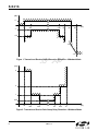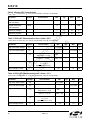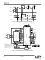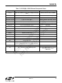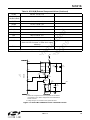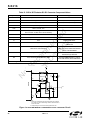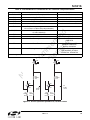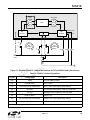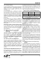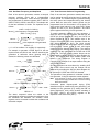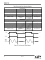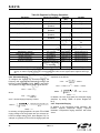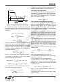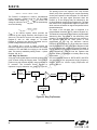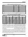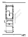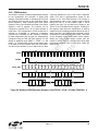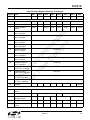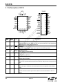
1
Si3216 P RO SLIC ® P R O GRA MM A B LE W IDEBAND SLIC/C ODEC W I T H R INGING / B A TT E R Y V OLTA GE G ENERATION Features Software-programmable features and parameters: Ringing frequency, amplitude, cadence, and waveshape 2-wire ac impedance and hybrid Constant current feed (20 to 41 mA) Loop closure and ring trip thresholds Software programmable signal generation and audio processing: Ordering Information See page 114. µ-law/A-law companding (caller ID) generation Dual audio tone generators Smooth and abrupt polarity reversal 100% software-configurable global solution Audio loopback, dc, and GR-909 subscriber line diagnostic capabilities Lead-free and RoHS-compliant packages available FSK Pin Assignments Si3216 QFN DRX PCLK INT CS SCLK SDI SDO Dual-mode wideband (50 Hz to 7 kHz)/ narrowband (200 Hz to 3.4 kHz) codec with 16-bit 16 kHz sampling for enhanced audio quality Performs all BORSCHT functions Ideal for customer premise equipment applications Software-programmable internal ringing up to 90 VPK Integrated battery supply with dynamic voltage output On-chip dc-dc converter continuously minimizes power in all operating modes Entire solution can be powered from a single 3.3 V or 5 V supply 3.3 V to 35 V dc input range Dynamic 0 V to –94.5 V output Low-cost inductor and high-efficiency transformer versions supported N ot fo R r N ec e w om m D e e s nd ig e ns d Applications Voice-over-broadband systems: DSL, cable, wireless PBX/IP-PBX/key telephone systems Terminal adapters: ISDN, Ethernet, USB Description The Si3216 ProSLIC® is a low-voltage CMOS device that provides a complete analog telephone interface supporting both wideband (50 Hz to 7.0 kHz) and narrowband (200 Hz to 3.4 kHz) audio codec modes for enhanced voice quality in Voice-over-IP (VoIP) applications. The ProSLIC integrates subscriber line interface circuit (SLIC), wideband voice codec, and battery generation functionality into a single fullyprogrammable device for global operation using only one hardware solution. The Si3216’s wideband codec provides expanded audio band (50 Hz to 7 kHz), 16 kHz sampling rate, and increased dynamic range for improved audio quality over traditional telephony codecs. The integrated battery supply continuously adapts its output voltage to minimize power and enables the entire solution to be powered from a single 3.3 V (Si3216M only) or 5 V supply. Si3216 features include software-configurable 5 REN internal ringing up to 90 VPK, DTMF and caller ID generation, and a comprehensive set of telephony signaling capabilities including expanded support of Japan and China country requirements. The ProSLIC is packaged in a 38-pin QFN and TSSOP, and the Si3201 high-voltage line interface device is packaged in a thermally-enhanced 16-pin SOIC. DTX FSYNC RESET SDCH SDCL VDDA1 IREF CAPP QGND CAPM STIPDC SRINGDC 1 38 37 36 35 34 33 32 31 2 30 3 4 29 5 27 26 6 7 28 25 8 9 24 23 10 22 21 11 12 13 14 15 16 17 18 19 20 SDITHRU DCDRV DCFF TEST GNDD VDDD ITIPN ITIPP VDDA2 IRINGP IRINGN IGMP STIPE SVBAT SRINGE STIPAC RINGAC IGMN GNDA U.S. Patent #6,567,521 U.S. Patent #6,812,744 Other patents pending Functional Block Diagram INT RESET Si3216 Line Status SDI DTX DRX PCM Interface FSYNC TIP Tone Generation Expansion SDO Control Interface Compression CS SCLK Dual-Mode Wideband/ Narrowband Codec Prog. Hybrid Linefeed Control RING ZS DC-DC Converter Controller PCLK Rev. 1.0 12/08 PLL Linefeed Interface Discrete Components Copyright © 2008 by Silicon Laboratories Si3216 N ot fo R r N ec e w om m D e e s nd ig e ns d Si3216 2 Rev. 1.0 Si3216 TABLE O F C ONTENTS Section Page N ot fo R r N ec e w om m D e e s nd ig e ns d 1. Electrical Specifications . . . . . . . . . . . . . . . . . . . . . . . . . . . . . . . . . . . . . . . . . . . . . . . . . . .4 2. Functional Description . . . . . . . . . . . . . . . . . . . . . . . . . . . . . . . . . . . . . . . . . . . . . . . . . . . 27 2.1. Linefeed Interface . . . . . . . . . . . . . . . . . . . . . . . . . . . . . . . . . . . . . . . . . . . . . . . . . . . 27 2.2. Battery Voltage Generation and Switching . . . . . . . . . . . . . . . . . . . . . . . . . . . . . . . . 33 2.3. Tone Generation . . . . . . . . . . . . . . . . . . . . . . . . . . . . . . . . . . . . . . . . . . . . . . . . . . . . 36 2.4. Ringing Generation . . . . . . . . . . . . . . . . . . . . . . . . . . . . . . . . . . . . . . . . . . . . . . . . . . 39 2.5. Audio Path . . . . . . . . . . . . . . . . . . . . . . . . . . . . . . . . . . . . . . . . . . . . . . . . . . . . . . . . . 43 2.6. Two-Wire Impedance Matching . . . . . . . . . . . . . . . . . . . . . . . . . . . . . . . . . . . . . . . . 45 2.7. Clock Generation . . . . . . . . . . . . . . . . . . . . . . . . . . . . . . . . . . . . . . . . . . . . . . . . . . . 46 2.8. Interrupt Logic . . . . . . . . . . . . . . . . . . . . . . . . . . . . . . . . . . . . . . . . . . . . . . . . . . . . . . 46 2.9. Serial Peripheral Interface . . . . . . . . . . . . . . . . . . . . . . . . . . . . . . . . . . . . . . . . . . . . . 46 2.10. PCM Interface . . . . . . . . . . . . . . . . . . . . . . . . . . . . . . . . . . . . . . . . . . . . . . . . . . . . . 49 3. Control Registers . . . . . . . . . . . . . . . . . . . . . . . . . . . . . . . . . . . . . . . . . . . . . . . . . . . . . . . .52 4. Indirect Registers . . . . . . . . . . . . . . . . . . . . . . . . . . . . . . . . . . . . . . . . . . . . . . . . . . . . . . .104 4.1. Oscillators . . . . . . . . . . . . . . . . . . . . . . . . . . . . . . . . . . . . . . . . . . . . . . . . . . . . . . . . 104 4.2. Digital Programmable Gain/Attenuation . . . . . . . . . . . . . . . . . . . . . . . . . . . . . . . . . 105 4.3. SLIC Control . . . . . . . . . . . . . . . . . . . . . . . . . . . . . . . . . . . . . . . . . . . . . . . . . . . . . . 107 4.4. FSK Control . . . . . . . . . . . . . . . . . . . . . . . . . . . . . . . . . . . . . . . . . . . . . . . . . . . . . . .109 5. Pin Descriptions: Si3216 . . . . . . . . . . . . . . . . . . . . . . . . . . . . . . . . . . . . . . . . . . . . . . . . . 110 6. Pin Descriptions: Si3201 . . . . . . . . . . . . . . . . . . . . . . . . . . . . . . . . . . . . . . . . . . . . . . . . . 113 7. Ordering Guides . . . . . . . . . . . . . . . . . . . . . . . . . . . . . . . . . . . . . . . . . . . . . . . . . . . . . . . . 114 8. Package Outline: 38-Pin QFN . . . . . . . . . . . . . . . . . . . . . . . . . . . . . . . . . . . . . . . . . . . . . 116 9. Package Outline: 38-Pin TSSOP . . . . . . . . . . . . . . . . . . . . . . . . . . . . . . . . . . . . . . . . . . . 117 10. Package Outline: 16-Pin ESOIC . . . . . . . . . . . . . . . . . . . . . . . . . . . . . . . . . . . . . . . . . . 118 11. Silicon Labs Si3216 Support Documentation . . . . . . . . . . . . . . . . . . . . . . . . . . . . . . . 119 Document Change List . . . . . . . . . . . . . . . . . . . . . . . . . . . . . . . . . . . . . . . . . . . . . . . . . . . . 120 Contact Information . . . . . . . . . . . . . . . . . . . . . . . . . . . . . . . . . . . . . . . . . . . . . . . . . . . . . . .122 Rev. 1.0 3 Si3216 1. Electrical Specifications Table 1. Absolute Maximum Ratings and Thermal Information1 Parameter Symbol Value Unit VDDD, VDDA1, VDDA2 –0.5 to 6.0 V IIN ±10 mA VIND –0.3 to (VDDD + 0.3) V Si3216 DC Supply Voltage Input Current, Digital Input Pins Digital Input Voltage N ot fo R r N ec e w om m D e e s nd ig e ns d Operating Temperature Range2 TA –40 to 100 C TSTG –40 to 150 C TSSOP-38 Thermal Resistance, Typical JA 70 C/W QFN-38 Thermal Resistance, Typical JA 35 C/W Continuous Power Dissipation2 PD 0.7 W DC Supply Voltage VDD –0.5 to 6.0 V Battery Supply Voltage VBAT –104 V Input Voltage: TIP, RING, SRINGE, STIPE pins VINHV (VBAT – 0.3) to (VDD + 0.3) V Input Voltage: ITIPP, ITIPN, IRINGP, IRINGN pins VIN –0.3 to (VDD + 0.3) V Operating Temperature Range2 TA –40 to 100 C TSTG –40 to 150 C JA 55 C/W PD 0.8 at 70 ºC W Storage Temperature Range Si3201 Storage Temperature Range SOIC-16 Thermal Resistance, Typical3 Continuous Power Dissipation 2 0.6 at 85 ºC Notes: 1. Permanent device damage may occur if the absolute maximum ratings are exceeded. Functional operation should be restricted to the conditions as specified in the operational sections of this data sheet. Exposure to absolute maximum rating conditions for extended periods may affect device reliability. 2. Operation above 125 ºC junction temperature may degrade device reliability. 3. Thermal resistance assumes a multi-layer PCB with the exposed pad soldered to a topside PCB pad. 4 Rev. 1.0 Si3216 Table 2. Recommended Operating Conditions Symbol Test Condition Min* Typ Max* Unit Ambient Temperature TA K-grade 0 25 70 oC Ambient Temperature TA B-grade –40 25 85 o Si3216 Supply Voltage VDDD,VDDA1, VDDA2 3.13 3.3/5.0 5.25 V Si3201 Supply Voltage VDD 3.13 3.3/5.0 5.25 V Si3201 Battery Voltage VBAT –96 — –10 V VBATH = VBAT C N ot fo R r N ec e w om m D e e s nd ig e ns d Parameter *Note: All minimum and maximum specifications are guaranteed and apply across the recommended operating conditions. Typical values apply at nominal supply voltages and an operating temperature of 25 ºC unless otherwise stated. Product specifications are only guaranteed when the typical application circuit (including component tolerances) is used. Rev. 1.0 5 Si3216 Table 3. AC Characteristics—Wideband Audio Mode: Si3216 (VDDA, VDDD = 3.13 to 5.25 V, TA = 0 to 70 °C for K-Grade, –40 to 85 °C for B-Grade) Parameter Test Condition Min Typ Max Unit TX/RX Performance—Wideband Audio Mode Overload Level Single Frequency Distortion 1 2.5 — — VPK 2-wire – PCM or PCM – 2-wire: 50 Hz–7.0 kHz — — –45 dB 50 Hz–7.0 kHz D/A or A/D 16-bit Active off-hook and OHT, Zac = 600 TBD — — 0 dBm0, Active off-hook and OHT, Zac = 600 45 — — dB — — –41 dB 2-wire to PCM, 1014 Hz Zac = 600 –0.5 0 0.5 dB PCM to 2-wire, 1014 Hz Zac = 600 –0.5 0 0.5 dB Zac = 600 Figure 1,2 — — — — — N ot fo R r N ec e w om m D e e s nd ig e ns d Signal-to-(Noise + Distortion) Ratio2 THD = 1.5% Audio Tone Generator Signal-to-Distortion Ratio2 Intermodulation Distortion 2 Gain Accuracy Gain Accuracy Over Frequency Group Delay Over Frequency Gain Tracking 1014 Hz sine wave, reference level –10 dBm signal level: — 3 dB to –37 dB –0.25 — 0.25 dB –37 dB to –50 dB –0.5 — 0.5 dB –50 dB to –60 dB –1.0 — 1.0 dB at 1000 Hz — 1100 — s –6 dB to 6 dB –0.017 — 0.017 dB All gain settings –0.25 — 0.25 dB VDDA = VDDA = 3.3/5 V ±5% –0.1 — 0.1 dB 2-Wire Return Loss 50 Hz–7.0 kHz Zac = 600 20 25 — dB Transhybrid Balance 50 Hz–7.0 kHz Zac = 600 20 — — dB Round-Trip Group Delay Gain Step Accuracy Gain Variation with Temperature Gain Variation with Supply Notes: 1. The input signal level should be 0 dBm0 for frequencies greater than 100 Hz. For 100 Hz and below, the level should be –10 dBm0. The output signal magnitude at any other frequency will be smaller than the maximum value specified. 2. Analog signal measured as VTIP – VRING. Assumes ideal line impedance matching. 3. The level of any unwanted tones within the bandwidth of 0 to 8 kHz does not exceed –55 dBm. 4. Assumes normal distribution of betas. 6 Rev. 1.0 Si3216 Table 3. AC Characteristics—Wideband Audio Mode: Si3216 (Continued) (VDDA, VDDD = 3.13 to 5.25 V, TA = 0 to 70 °C for K-Grade, –40 to 85 °C for B-Grade) Parameter Test Condition Min Typ Max Unit Noise Performance—Wideband Audio Mode 3 7 kHz flat — — 23 dBrn PSRR from VDDA RX and TX, DC to 7 kHz 40 — — dB PSRR from VDDD RX and TX, DC to 7 kHz 40 — — dB PSRR from VBAT RX and TX, DC to 7 kHz 40 — — dB Idle Channel Noise N ot fo R r N ec e w om m D e e s nd ig e ns d Longitudinal Performance—Wideband Audio Mode Longitudinal to Metallic or PCM Balance 50 Hz–7.0 kHz, Q1,Q2 150, 1% mismatch — 60 — dB Q1,Q2 60 to 2404 — 60 — dB Q1,Q2 300 to 800 — 60 — dB 50 Hz–7.0 kHz 40 — — dB — — — 33 17 17 — — — — — — 4 8 8 — — — mA mA mA 4 Metallic to Longitudinal Balance Longitudinal Impedance 50 Hz–7.0 kHz at TIP or RING Register selectable ETBO/ETBA 00 01 10 Longitudinal Current per Pin Active off-hook 50 Hz–7.0 kHz Register selectable ETBO/ETBA 00 01 10 Notes: 1. The input signal level should be 0 dBm0 for frequencies greater than 100 Hz. For 100 Hz and below, the level should be –10 dBm0. The output signal magnitude at any other frequency will be smaller than the maximum value specified. 2. Analog signal measured as VTIP – VRING. Assumes ideal line impedance matching. 3. The level of any unwanted tones within the bandwidth of 0 to 8 kHz does not exceed –55 dBm. 4. Assumes normal distribution of betas. Rev. 1.0 7 Si3216 (dB) +1 –4.5 100 6.4k 7k 8k 9k (Hz) N ot fo R r N ec e w om m D e e s nd ig e ns d 50 –1 –25 –45 Figure 1. Transmit and Receive Path Attenuation Distortion—Wideband Mode (ms) 4 2 1 0.25 50 100 300 4k 6.4k 7k (Hz) Figure 2. Transmit and Receive Path Group Delay Distortion—Wideband Mode 8 Rev. 1.0 Si3216 Table 4. AC Characteristics—Narrowband Audio Mode (VDDA, VDDD = 3.13 to 5.25 V, TA = 0 to 70 °C for K-Grade, –40 to 85 °C for B-Grade) Parameter Test Condition Min Typ Max Unit TX/RX Performance—Narrowband Audio Mode Overload Level THD = 1.5% 2.5 — — VPK 2-wire – PCM or PCM – 2-wire: 200 Hz–3.4 kHz — — –45 dB 200 Hz–3.4 kHz D/A or A/D 16-bit Active off-hook and OHT, any Zac Figure 3 — — 0 dBm0, Active off-hook and OHT, any Zac 45 — — dB — — –41 dB 2-wire to PCM, 1014 Hz –0.5 0 0.5 dB PCM to 2-wire, 1014 Hz –0.5 0 0.5 dB Gain Accuracy Over Frequency Figure 5,6 — — Group Delay Over Frequency Figure 7,8 — — 3 dB to –37 dB –0.25 — 0.25 dB –37 dB to –50 dB –0.5 — 0.5 dB –50 dB to –60 dB –1.0 — 1.0 dB at 1000 Hz — 1100 — µs –6 dB to 6 dB –0.017 — 0.017 dB All gain settings –0.25 — 0.25 dB VDDA = VDDA = 3.3/5 V ±5% –0.1 — 0.1 dB 2-Wire Return Loss 200 Hz–3.4 kHz 30 35 — dB Transhybrid Balance 200 Hz–3.4 kHz 30 — — dB Single Frequency Distortion 1 N ot fo R r N ec e w om m D e e s nd ig e ns d Signal-to-(Noise + Distortion) Ratio2 Audio Tone Generator Signal-to-Distortion Ratio2 Intermodulation Distortion Gain Accuracy2 3 Gain Tracking Round-Trip Group Delay Gain Step Accuracy Gain Variation with Temperature Gain Variation with Supply 1014 Hz sine wave, reference level –10 dBm signal level: Notes: 1. The input signal level should be 0 dBm0 for frequencies greater than 100 Hz. For 100 Hz and below, the level should be –10 dBm0. The output signal magnitude at any other frequency will be smaller than the maximum value specified. 2. Analog signal measured as VTIP – VRING. Assumes ideal line impedance matching. 3. The quantization errors inherent in the µ/A-law companding process can generate slightly worse gain tracking performance in the signal range of 3 dB to –37 dB for signal frequencies that are integer divisors of the 8 kHz PCM sampling rate. 4. The level of any unwanted tones within the bandwidth of 0 to 4 kHz does not exceed –55 dBm. 5. Assumes normal distribution of betas. Rev. 1.0 9 Si3216 Table 4. AC Characteristics—Narrowband Audio Mode (Continued) (VDDA, VDDD = 3.13 to 5.25 V, TA = 0 to 70 °C for K-Grade, –40 to 85 °C for B-Grade) Parameter Test Condition Min Typ Max Unit Noise Performance—Narrowband Audio Mode C-Message Weighted — — 15 dBrnC Psophometric Weighted — — –75 dBmP 3 kHz flat — — 18 dBrn PSRR from VDDA RX and TX, DC to 3.4 kHz 40 — — dB PSRR from VDDD RX and TX, DC to 3.4 kHz 40 — — dB — — dB N ot fo R r N ec e w om m D e e s nd ig e ns d Idle Channel Noise 4 RX and TX, DC to 3.4 kHz PSRR from VBAT 40 Longitudinal Performance—Narrowband Audio Mode Longitudinal to Metallic or PCM Balance 200 Hz–3.4 kHz, Q1,Q2 150, 1% mismatch — 60 — dB Q1,Q2 60 to 2405 — 60 — dB Q1,Q2 300 to 800 — 60 — dB Using Si3201 — 60 — dB 200 Hz–3.4 kHz 40 — — dB — — — 33 17 17 — — — — — — 4 8 8 — — — mA mA mA 5 Metallic to Longitudinal Balance Longitudinal Impedance 200 Hz–3.4 kHz at TIP or RING Register selectable ETBO/ETBA 00 01 10 Longitudinal Current per Pin Active off-hook 200 Hz–3.4 kHz Register selectable ETBO/ETBA 00 01 10 Notes: 1. The input signal level should be 0 dBm0 for frequencies greater than 100 Hz. For 100 Hz and below, the level should be –10 dBm0. The output signal magnitude at any other frequency will be smaller than the maximum value specified. 2. Analog signal measured as VTIP – VRING. Assumes ideal line impedance matching. 3. The quantization errors inherent in the µ/A-law companding process can generate slightly worse gain tracking performance in the signal range of 3 dB to –37 dB for signal frequencies that are integer divisors of the 8 kHz PCM sampling rate. 4. The level of any unwanted tones within the bandwidth of 0 to 4 kHz does not exceed –55 dBm. 5. Assumes normal distribution of betas. 10 Rev. 1.0 N ot fo R r N ec e w om m D e e s nd ig e ns d Si3216 Figure 3. Transmit and Receive Path SNDR—Narrowband Mode 9 8 7 6 Fundamental Output Power 5 (dBm0) Acceptable Region 4 3 2.6 2 1 0 1 2 3 4 5 6 7 8 9 Fundamental Input Power (dBm0) Figure 4. Overload Compression Performance Rev. 1.0 11 Si3216 N ot fo R r N ec e w om m D e e s nd ig e ns d Typical Response Typical Response Figure 5. Transmit Path Frequency Response—Narrowband Mode 12 Rev. 1.0 N ot fo R r N ec e w om m D e e s nd ig e ns d Si3216 Figure 6. Receive Path Frequency Response—Narrowband Mode Rev. 1.0 13 N ot fo R r N ec e w om m D e e s nd ig e ns d Si3216 Figure 7. Transmit Group Delay Distortion—Narrowband Mode Figure 8. Receive Group Delay Distortion—Narrowband Mode 14 Rev. 1.0 Si3216 Table 5. Linefeed Characteristics (VDDA, VDDD = 3.13 to 5.25 V, TA = 0 to 70 °C for K-Grade, –40 to 85 °C for B-Grade) Parameter Loop Resistance Range Symbol Test Condition Min Typ Max Unit RLOOP See Note 0 — 160 ILIM = 29 mA, ETBA = 4 mA –10 — 10 % Active Mode; VOC = 48 V, VTIP – VRING –4 — 4 V ILOOP < ILIM — 160 — DC Loop Current Accuracy DC Open Circuit Voltage Accuracy RDO N ot fo R r N ec e w om m D e e s nd ig e ns d DC Differential Output Resistance DC Open Circuit Voltage— Ground Start VOCTO IRING<ILIM; VRING wrt ground VOC = 48 V –4 — 4 V DC Output Resistance— Ground Start RROTO IRING<ILIM; RING to ground — 160 — DC Output Resistance— Ground Start RTOTO TIP to ground 150 — — k Loop Closure/Ring Ground Detect Threshold Accuracy ITHR = 11.43 mA –20 — 20 % Ring Trip Threshold Accuracy RTHR = 1100 –20 — 20 % User Programmable Register 70 and Indirect Register 23 — — — Ring Trip Response Time Ring Amplitude VTR 5 REN load; sine wave; RLOOP = 160 VBAT = –75 V 44 — — Vrms Ring DC Offset ROS Programmable in Indirect Register 6 0 — — V Crest factor = 1.3 –.05 — .05 1.35 — 1.45 f = 20 Hz –1 — 1 % Accuracy of ON/OFF Times –50 — 50 ms CAL to CAL Bit — — 600 ms At Power Threshold = 300 mW –25 — 25 % Trapezoidal Ring Crest Factor Accuracy Sinusoidal Ring Crest Factor Ringing Frequency Accuracy Ringing Cadence Accuracy Calibration Time Power Alarm Threshold Accuracy RCF Note: DC resistance round trip; 160 corresponds to 2 kft 26 gauge AWG. Rev. 1.0 15 Si3216 Table 6. Monitor ADC Characteristics (VDDA, VDDD = 3.13 to 5.25 V, TA = 0 to 70 °C for K-Grade, –40 to 85 °C for B-Grade) Parameter Symbol Test Condition Min Typ Max Unit Differential Nonlinearity (6-bit resolution) DNLE –1/2 — 1/2 LSB Integral Nonlinearity (6-bit resolution) INLE –1 — 1 LSB — — 10 % 20 % N ot fo R r N ec e w om m D e e s nd ig e ns d Gain Error (voltage) Gain Error (current) — — Table 7. Si321x DC Characteristics, VDDA = VDDD = 5.0 V (VDDA, VDDD = 4.75 to 5.25 V, TA = 0 to 70 °C for K-Grade, –40 to 85 °C for B-Grade) Parameter Symbol Test Condition Min Typ Max Unit High Level Input Voltage VIH 0.7 x VDDD — — V Low Level Input Voltage VIL — — 0.3 x VDDD V High Level Output Voltage VOH DIO1,DIO2,SDITHRU:IO = –4 mA SDO, DTX:IO = –8 mA VDDD – 0.6 — — V DOUT: IO = –40 mA VDDD – 0.8 — — V DIO1,DIO2,DOUT,SDITHRU: IO = 4 mA SDO,INT,DTX:IO = 8 mA — — 0.4 V –10 — 10 µA Min Typ Max Unit Low Level Output Voltage Input Leakage Current VOL IL Table 8. Si321x DC Characteristics, VDDA = VDDD = 3.3 V (VDDA, VDDD = 3.13 to 3.47 V, TA = 0 to 70 °C for K-Grade, –40 to 85 °C for B-Grade) Parameter Symbol Test Condition High Level Input Voltage VIH 0.7 x VDDD — — V Low Level Input Voltage VIL — — 0.3 x VDDD V High Level Output Voltage VOH DIO1,DIO2,SDITHRU:IO = –2 mA SDO, DTX:IO = –4 mA VDDD – 0.6 — — V DOUT: IO = –40 mA VDDD – 0.8 — — V DIO1,DIO2,DOUT,SDITHRU: IO = 2 mA SDO,INT,DTX:IO = 4 mA — — 0.4 V –10 — 10 A Low Level Output Voltage Input Leakage Current 16 VOL IL Rev. 1.0 Si3216 Table 9. Power Supply Characteristics (VDDA,VDDD = 3.13 to 5.25 V, TA = 0 to 70 °C for K-Grade, –40 to 85 °C for B-Grade) Parameter Power Supply Current, Analog and Digital Symbol Test Condition Typ1 Typ2 Max Unit IA + ID Sleep (RESET = 0) 0.1 0.13 0.3 mA Open 33 42.8 49 mA 37 53 68 mA 83 mA Active on-hook ETBO = 4 mA, codec and Gm amplifier powered down N ot fo R r N ec e w om m D e e s nd ig e ns d Active OHT ETBO = 4 mA Active off-hook ETBA = 4 mA, ILIM = 20 mA VDD Supply Current (Si3201) VBAT Supply Current3 IVDD IBAT 72 mA 73 88 99 Ground-start 36 47 55 mA Ringing Sinewave, REN = 1, VPK = 56 V 45 55 65 mA Sleep mode, RESET = 0 — 100 — µA Open (high impedance) — 100 — µA Active on-hook standby — 110 — µA Forward/reverse active off-hook, no ILOOP, ETBO = 4 mA, VBAT = –24 V — 1 — mA Forward/reverse OHT, ETBO = 4 mA, VBAT = –70 V — 1 — mA Sleep (RESET = 0) — 0 — mA Open (DCOF = 1) — 0 — mA Active on-hook VOC = 48 V, ETBO = 4 mA — 3 — mA Active OHT ETBO = 4 mA — 11 — mA Active off-hook ETBA = 4 mA, ILIM = 20 mA — 30 — mA — 2 — mA — 5.5 — mA — — 10 V/µs Ground-start Ringing VPK_RING = 56 VPK, sinewave ringing, REN = 1 VBAT Supply Slew Rate 57 When using Si3201 Notes: 1. VDDD, VDDA = 3.3 V. 2. VDDD, VDDA = 5.25 V. 3. IBAT = current from VBAT (the large negative supply). For a switched-mode power supply regulator efficiency of 71%, the user can calculate the regulator current consumption as IBAT x VBAT/(0.71 x VDC). Rev. 1.0 17 Si3216 Table 10. Switching Characteristics—General Inputs VDDA = VDDA = 3.13 to 5.25 V, TA = 0 to 70 °C for K-Grade, –40 to 85 °C for B-Grade, CL = 20 pF) Parameter Symbol Min Typ Max Unit Rise Time, RESET tr — — 20 ns RESET Pulse Width trl 100 — — ns Note: All timing (except Rise and Fall time) is referenced to the 50% level of the waveform. Input test levels are VIH = VD – 0.4 V, VIL = 0.4 V. Rise and Fall times are referenced to the 20% and 80% levels of the waveform. N ot fo R r N ec e w om m D e e s nd ig e ns d Table 11. Switching Characteristics—SPI VDDA = VDDA = 3.13 to 5.25 V, TA = 0 to 70 °C for K-Grade, –40 to 85 °C for B-Grade, CL = 20 pF Parameter Symbol Test Conditions Min Typ Max Unit Cycle Time SCLK tc 0.062 — — s Rise Time, SCLK tr — — 25 ns Fall Time, SCLK tf — — 25 ns Delay Time, SCLK Fall to SDO Active td1 — — 20 ns Delay Time, SCLK Fall to SDO Transition td2 — — 20 ns Delay Time, CS Rise to SDO Tri-state td3 — — 20 ns Setup Time, CS to SCLK Fall tsu1 25 — — ns Hold Time, CS to SCLK Rise th1 20 — — ns Setup Time, SDI to SCLK Rise tsu2 25 — — ns Hold Time, SDI to SCLK Rise th2 20 — — ns Delay Time between Chip Selects (Continuous SCLK) tcs 440 — — ns Delay Time between Chip Selects (Non-continuous SCLK) tcs 220 — — ns SDI to SDITHRU Propagation Delay td4 — 4 10 ns Note: All timing is referenced to the 50% level of the waveform. Input test levels are VIH = VDDD –0.4 V, VIL = 0.4 V 18 Rev. 1.0 Si3216 tthru tr tr tc SCLK tsu1 th1 CS tcs th2 N ot fo R r N ec e w om m D e e s nd ig e ns d tsu2 SDI td1 td2 td3 SDO Figure 9. SPI Timing Diagram Table 12. Switching Characteristics—PCM Highway Serial Interface VD = 3.13 to 5.25 V, TA = 0 to 70 °C for K-Grade, –40 to 85 °C for B-Grade, CL = 20 pF Parameter Symbol Test Conditions Min 1 Typ 1 Max 1 Units MHz MHz MHz MHz MHz MHz MHz MHz % PCLK Frequency 1/tc — — — — — — — — 0.256 0.512 0.768 1.024 1.536 2.048 4.096 8.192 PCLK Duty Cycle Tolerance PCLK Period Jitter Tolerance tdty tjitter 40 50 — — — — — — — — 60 –120 — 120 ns Rise Time, PCLK tr — — 25 ns Fall Time, PCLK tf — — 25 ns Delay Time, PCLK Rise to DTX Active td1 — — 20 ns Delay Time, PCLK Rise to DTX Transition td2 — — 20 ns Delay Time, PCLK Rise to DTX Tri-state2 td3 — — 20 ns Setup Time, FSYNC to PCLK Fall tsu1 25 — — ns Hold Time, FSYNC to PCLK Fall th1 20 — — ns Setup Time, DRX to PCLK Fall tsu2 25 — — ns Hold Time, DRX to PCLK Fall th2 20 — — ns Notes: 1. All timing is referenced to the 50% level of the waveform. Input test levels are VIH – VI/O –0.4 V, VIL = 0.4 V. 2. Spec applies to PCLK fall to DTX tri-state when that mode is selected (TRI = 0). Rev. 1.0 19 Si3216 tr tc tf PCLK th1 tsu1 FSYNC tsu2 th2 N ot fo R r N ec e w om m D e e s nd ig e ns d DRX td2 td1 td3 DTX Figure 10. PCM Highway Interface Timing Diagram VCC C3 220 nF STIPAC 27 30 VDDD 10 23 GNDD VDDA2 STIPDC 20 VDDA1 15 GNDA TEST R1 200k C24 0.1 F 31 32 VCC 38 SCLK SDI R8 4.7K IRINGN 13 25 IRINGN ITIPP 16 28 ITIPP 14 26 IRINGP 17 STIPE 19 SRINGE R4 196k SRINGE 10 R291 2 Note 2 7 R26 2 40.2k 24 R15 243 IREF 11 CAPP 12 C2 10 F DC-DC Converter Circuit C3 1 1 0 F 10 V VDC VDC Figure 11. Si3216(M) Application Circuit Using Si3201 20 Rev. 1.0 R14 40.2k L2 V DDA1 V DDA 2 4 7 H Note 1 VBAT C1 10 F 13 DCFF SDCL 9 VCC R281 QGND 33 SRINGDC DCDRV 16 CAPM 14 SDCH SRINGAC 8 21 DCFF R21 15 VCC 5 IGMN 22 GND Q9 2N2222 PCM Bus SVBAT R3 200k C26 0.1 F INT RESET IGMP 34 R9 4.7K 4 R322 10k R5 200k C4 220 nF 4 5 Notes: 1. Values and configurations for these components can be derived from Table 18 or from App Note 45. 2. Only one component per system needed. 3. All circuit ground should have a single-point connection to the ground plane. 4. Si3201 bottom-side exposed pad should be electrically and thermally connected to bulk ground plane. DTX R6 4.02k 18 VBAT VBATH R7 4.02k DRX SDCH RING R2 196k ITIPN SDCL RING 29 STIPE 11 3 PCLK ITIPN 15 IRINGP 6 FSYNC DCDRV C6 22nF C19 4.7 F Si3216(M) Si3201 Protection Circuit 1 7 GND 8 VDD TIP C5 22nF 3 C18 4.7 F 4 1 SPI Bus 36 SDO CS TIP 37 C1 5 0 .1 F C1 6 C1 7 0 .1 F 0. 1 F V DDD C3 0 10 F Si3216 Table 13. Si3216(M) + Si3201 External Component Values Value Supplier C1,C2 10 µF, 6 V Ceramic or 16 V Low Leakage Electrolytic, ±20% Murata, Nichicon URL1C100MD C3,C4 220 nF, 100 V, X7R, ±20% Murata, Johanson, Novacap, Venkel C5,C6 22 nF, 100 V, X7R, ±20% Murata, Johanson, Novacap, Venkel C15,C16,C17,C24 0.1 µF, 6 V, Y5V, ±20% Murata, Johanson, Novacap, Venkel C18,C19 4.7 µF Ceramic, 6 V, X7R, ±20% Murata, Johanson, Novacap, Venkel C26 N ot fo R r N ec e w om m D e e s nd ig e ns d Component (s) 0.1 µF, 100 V, X7R, ±20% Murata, Johanson, Novacap, Venkel C30, C31 10 µF, 6 V, Electrolytic, ±20% Panasonic L2 47 µH, 150 A Coilcraft R1,R3,R5 200 k, 1/10 W, ±1% R2,R4 196 k, 1/10 W, ±1% R6,R7 R8,R9 4.02 k, 1/10 W, ±1% 4.7 k, 1/10 W, ±1% R14,R26* 40.2 k, 1/10 W, ±1% R15 243 , 1/10 W, ±1% R21 15 , 1/4 W, ±5% R28,R29 1/10 W, 1% (See “AN45: Design Guide for The Si3210 DC-DC Converter” or Table 18 for value selection) R32* 10 k, 1/10 W, ±5% Q9 60 V, General Purpose Switching NPN ON Semi MMBT2222ALT1; Central Semi CMPT2222A; Zetex FMMT2222 *Note: Only one component is necessary on each signal in the system. Rev. 1.0 21 Si3216 32 31 23 10 27 30 TEST GNDA VDDA1 VDDA2 VDDD GND GNDD VCC R1 200k 15 GND 20 29 Q6 5551 C5 22nF C324 0.1 µF C8 220nF R13 5.1k PCLK ITIPN DRX STIPE R2 100k R6 80.6 DTX 37 SPI Bus 36 1 6 3 4 PCM Bus 5 VCC R322 10k 18 R104 (100k) R7 80.6 C4 220nF R9 4.7k 21 16 C26 0.1uF R21 15 SVBAT SRINGAC SRINGDC R3 200k GND IGMP 9 Q9 2N2222 SDCL VCC R291 R281 7 Note 2 R262 40.2k 24 IGMN 22 IREF 11 CAPP 12 CAPM 14 QGND 13 DCFF R5 100k C33 4 0.1 µF SRINGE 2 R15 243 C2 10uF C1 10uF R14 40.2k L2 V DDA1 V DDA 2 4 7 H 33 R12 5.1k INT RESET C3 1 VDC 1 0 F 10 V DCFF C7 220nF Notes: 1. Values and configurations for these components can be derived from Table 18 or from “AN45: Design Guide for the Si3210/15/16 DC-DC Converter”. 2. Only one component per system needed. 3. All circuit grounds should have a singlepoint connection to the ground plane. 4. Optional components to improve idle channel noise. 19 R104 (100k) DCDRV Q5 5551 IRINGN 34 R4 100k C34 4 0.1 µF DCDRV R11 10 IRINGP SDCH 25 8 Q3 5401 SDCH 26 Q2 5401 SDCL C6 22nF RING 17 R102 (100k) FSYNC ITIPP 38 N ot fo R r N ec e w om m D e e s nd ig e ns d Protection Circuit CS 28 R10 10 TIP SDO STIPAC R8 4.7k Q4 5401 Q1 5401 SDI Si3216(M) C3 220nF SCLK STIPDC C1 5 0 .1 F V DDD C1 6 C1 7 0 .1 F 0. 1 F C3 0 10 F Note 1 VBAT DC-DC Converter Circuit VDC Figure 12. Si3216(M) Typical Application Circuit Using Discrete Line Interface Circuit Table 14. Si3216(M) External Component Values Component Value Supplier/Part Number C1,C2 10 µF, 6 V Ceramic/Tantalum or 16 V Low Leakage Electrolytic, 20% Murata, Panasonic, Nichicon URL1C100MD 220 nF, 100 V, X7R, 20% Murata, Johanson, Novacap, Venkel 22 nF, 100 V, X7R, 20% Murata, Johanson, Novacap, Venkel 220 nF, 50 V, X7R, 20% Murata, Johanson, Novacap, Venkel C15,C16,C17 0.1 µF, 6 V, Y5V, 20% Murata, Johanson, Novacap, Venkel C26 0.1 µF, 100 V, X7R, 20% Murata, Johanson, Novacap, Venkel C30, C31 10 µF, 16 V, Electrolytic, 20% Panasonic L2 47 µH, 150 A Coilcraft Q1,Q2,Q3,Q4 120 V, PNP, BJT Central Semi CMPT5401; ON Semi MMBT5401LT1, 2N5401; Zetex FMMT5401; Fairchild 2N5401; Samsung 2N5401 Q5,Q6 120 V, NPN, BJT Central Semi CZT5551, ON Semi 2N5551; Fairchild 2N5551; Phillips 2N5551 Q9 NPN General Purpose BJT ON Semi MMBT2222ALT1; Central Semi CMPT2222A; Zetex FMMT2222 C3,C4 C5,C6 C7,C8 22 Rev. 1.0 Si3216 Table 14. Si3216(M) External Component Values (Continued) 200 k, 1/10 W, 1% R2,R4,R5, R102,R104,R105 100 k, 1/10 W, 1% R6,R7 80.6 , 1/4 W, 1% R8,R9 4.7 k, 1/10 W, 1% R10,R11 10 , 1/10 W, 5% R12,R13 5.1 k, 1/10 W, 5% R14,R26* 40.2 k, 1/10 W, 1% R15 243 , 1/10 W, 1% R21 N ot fo R r N ec e w om m D e e s nd ig e ns d R1,R3 15 , 1/4 W, 1% R28,R29 1/10 W, 1% (See “AN45: Design Guide for The Si3210 DC-DC Converter” or Table 18 for value selection) R32* 10 k, 1/10 W, 5% *Note: Only one component is necessary on each signal in the system. VDC F1 SDCH R191 Note 1 C142 0.1 µF R201 SDCL C10 0.1 µF Si321x C252 10 µF R181 R16 200 Q7 FZT953 DCFF Q8 2N2222 D1 ES1D VBAT C9 10 µF R17 L1 DCDRV Note 1 GND Notes: 1. Values and configurations for these components can be derived from Table 20 or from “AN45: Design Guide for the Si3210/15/16 DC-DC Converter”. 2. Voltage rating for C14 and C25 must be greater than VDC. Figure 13. Si321x BJT/Inductor DC-DC Converter Circuit Rev. 1.0 23 Si3216 Table 15. Si321x BJT/Inductor DC-DC Converter Component Values Value Supplier C9 10 µF, 100 V, Electrolytic, ±20% Panasonic C10* 0.1 µF, X7R, ±20% Murata, Johanson, Novacap, Venkel C14* 0.1 µF, X7R, ±20% Murata, Johanson, Novacap, Venkel C25* 10 F, Electrolytic, ±20% Panasonic R16 200 , 1/10 W, ±5% R17 1/10 W, ±5% (See “AN45: Design Guide for The Si3210 DCDC Converter” or Table 20 for value selection) R18 R19,R20 F1 D1 L1 Q7 Q8 N ot fo R r N ec e w om m D e e s nd ig e ns d Component(s) 1/4 W, ±5% (See AN45 or Table 20 for value selection) 1/10 W, ±1% (See AN45 or Table 20 for value selection) Fuse Belfuse SSQ Series Ultra Fast Recovery 200 V, 1 A Rectifier General Semi ES1D; Central Semi CMR1U-02 1A, Shielded Inductor (See AN45 or Table 20 for value selection) API Delevan SPD127 series, Sumida CDRH127 series, Datatronics DR340-1 series, Coilcraft DS5022 120 V, High Current Switching PNP Zetex FZT953, FZT955, ZTX953, ZTX955; Sanyo 2SA1552 60 V, General Purpose Switching NPN ON Semi MMBT2222ALT1; Central Semi CMPT2222A; Zetex FMMT2222 *Note: Voltage rating of this device must be greater than VDC. VDC F1 SDCH R191 C252 10 µF Note 1 R181 R201 SDCL Si321xM C142 0.1 µF 1 C27 470 pF R22 22 2 3 DCFF M1 IRLL014N D1 ES1D 6 4 10 T11 VBAT C9 10 µF Note 1 R17 200 k DCDRV NC GND Notes: 1. Values and configurations for these components can be derived from Table 19 or from “AN45: Design Guide for the Si3210/15/16 DC-DC Converter”. 2. Voltage rating for C14 and C25 must be greater than VDC. Figure 14. Si321xM MOSFET/Transformer DC-DC Converter Circuit 24 Rev. 1.0 Si3216 Table 16. Si321xM MOSFET/Transformer DC-DC Converter Component Values Component (s) Value Supplier C9 10 µF, 100 V, Electrolytic, ±20% Panasonic C14* 0.1 µF, X7R, ±20% Murata, Johanson, Novacap, Venkel C25* 10 µF, Electrolytic, ±20% Panasonic C27 470 pF, 100 V, X7R, ±20% Murata, Johanson, Novacap, Venkel 200 k, 1/10 W, ±5% R18 1/4 W, ±5% (See “AN45: Design Guide for the Si3210 DCDC Converter” or Table 19 for value selection) R19,R20 1/10 W, ±1% (See AN45 or Table 19 for value selection) R22 F1 D1 T1 M1 N ot fo R r N ec e w om m D e e s nd ig e ns d R17 22 , 1/10 W, ±5% Fuse Belfuse SSQ Series Ultra Fast Recovery 200 V, 1A Rectifier General Semi ES1D; Central Semi CMR1U-02 Power Transformer Coiltronic CTX01-15275; Datatronics SM76315; Midcom 31353R-02 100 V, Logic Level Input MOSFET Intl Rect. IRLL014N; Intersil HUF76609D3S; ST Micro STD5NE10L, STN2NE10L *Note: Voltage rating of this device must be greater than VDC. QTDN QRDN Q4 Q3 5401 5401 R23 RRBN0 3.0k R24 RTBN0 3.0k QRP QTN Q5 Q6 5551 R7 RRE 80.6 R12 RRBN 5.1k C7 CRBN 100 nF 5551 R6 RTE 80.6 C8 CTBN 100 nF R13 RTBN 5.1k Figure 15. Si321x Optional Equivalent Q5, Q6 Bias Circuit Rev. 1.0 25 Si3216 Table 17. Si321x Optional Bias Component Values Component Value Supplier/Part Number C7,C8 100 nF, 100 V, X7R, 20% Murata, Johanson, Venkel R23,R24 3.0 k, 1/10 W, 5% The subcircuit above can be substituted into any of the ProSLIC solutions as an optional bias circuit for Q5, Q6. For this optional subcircuit, C7 and C8 are different in voltage and capacitance to the standard circuit. R23 and R24 are additional components. N ot fo R r N ec e w om m D e e s nd ig e ns d Table 18. Component Value Selection for Si321x/Si321xM Component Value Comments R28 1/10 W, 1% resistor For VDD = 3.3 V: 26.1 k For VDD = 5.0 V: 37.4 k R28 = (VDD + VBE)/148 µA where VBE is the nominal VBE for Q9 R29 1/10 W, 1% resistor For VCLAMP = 80 V: 541 k For VCLAMP = 85 V: 574 k For VCLAMP = 100 V: 676 k R29 = VCLAMP/148 µA where VCLAMP is the clamping voltage for VBAT Table 19. Component Value Selection Examples for Si321xM MOSFET/Transformer DC-DC Converter VDC 3.3 V 5.0 V 12 V 24 V Ringing Load/Loop Resistance Transformer Ratio R18 R19, R20 3 REN/117 1:2 0.06 7.15 k 5 REN/117 1:2 0.10 16.5 k 5 REN/117 1:3 0.68 56.2 k 5 REN/117 1:4 2.20 121 k Note: There are other system and software conditions that influence component value selection; so, please refer to “AN45: Design Guide for the Si3210 DC-DC Converter” for detailed guidance. Table 20. Component Value Selection Examples for Si321x BJT/Inductor DC-DC Converter VDC Ringing Load/Loop Length L1 R17 R18 R19, R20 5V 3 REN/117 33 µH 100 0.12 16.5 k 12 V 5 REN/117 150 µH 162 0.56 56.2k 24 V 5 REN/117 560 µH 274 2.2 121 k Note: There are other system and software conditions that influence component value selection, so please refer to “AN45: Design Guide for the Si3210 DC-DC Converter” for detailed guidance. 26 Rev. 1.0 Si3216 2. Functional Description 2.1.1. DC Feed Characteristics The ProSLIC has programmable constant voltage and constant current zones as depicted in Figure 16. Open circuit TIP-to-RING voltage (VOC) defines the constant voltage zone and is programmable from 0 V to 94.5 V in 1.5 V steps. The loop current limit (ILIM) defines the constant current zone and is programmable from 20 mA to 41 mA in 3 mA steps. The ProSLIC has an inherent dc output resistance (RO) of 160 . V (TIP-RING ) (V) N ot fo R r N ec e w om m D e e s nd ig e ns d The ProSLIC is a single, low-voltage CMOS device that provides all SLIC, codec, DTMF detection, and signal generation functions needed for a complete analog telephone interface. The ProSLIC performs all battery, overvoltage, ringing, supervision, codec, hybrid, and test (BORSCHT) functions. The Si3216 supports wideband (50 Hz–7 kHz) and narrowband (200 Hz– 3.4 kHz) audio codec modes to provide an expanded audio band at a 16 kHz sample rate for enhanced audio quality as well as standard telephony audio compatibility. The Si3216 is ideal for Customer Premise Equipment (CPE) where enhanced audio quality is required. Unlike most monolithic SLICs, the ProSLIC does not require externally-supplied, high-voltage battery supplies. Instead, it generates all necessary battery voltages from a positive dc supply using its own dc-dc converter controller. Two fully-programmable tone generators can produce DTMF tones, phase continuous FSK (caller ID) signaling, and call progress tones. Pulse metering signal generation is also integrated. The Si3201 linefeed interface IC performs all high-voltage functions. As an option, the Si3201 can be replaced with low-cost discrete components. The linefeed provides programmable on-hook voltage, programmable off-hook loop current, reverse battery operation, loop or ground start operation, and on-hook transmission ringing voltage. Loop current and voltage are continuously monitored using an integrated A/D converter. Balanced 5 REN ringing with or without a programmable dc offset is integrated. The available offset, frequency, waveshape, and cadence options are designed to ring the widest variety of terminal devices and to reduce external controller requirements. VOC R O =160 I LIM The ProSLIC’s linefeed interface offers a rich set of features and programmable flexibility to meet the broadest application requirements. The dc linefeed characteristics are software programmable; key current, voltage, and power measurements are acquired in real time and provided in software registers. Constant Current Zone I LO O P (m A) Figure 16. Simplified DC Current/Voltage Linefeed Characteristic The TIP-to-RING voltage (VOC) is offset from ground by a programmable voltage (VCM) to provide voltage headroom to the positive-most terminal (TIP in forward polarity states and RING in reverse polarity states) for carrying audio signals. Table 21 summarizes the parameters to be initialized before entering an Active state. Table 21. Programmable Ranges of DC Linefeed Characteristics Parameter Programmable Range Default Value Register Bits Location* ILIM 20 to 41 mA 20 mA ILIM[2:0] Direct Register 71 VOC 0 to 94.5 V 48 V VOC[5:0] Direct Register 72 VCM 0 to 94.5 V 3V VCM[5:0] Direct Register 73 A complete audio transmit and receive path is integrated, including ac impedance and hybrid gain. These features are software-programmable, allowing for a single hardware design to meet global requirements. Digital voice data transfer occurs over a standard PCM bus. Control data is transferred using a standard SPI. The device is available in a 38-pin QFN or TSSOP. 2.1. Linefeed Interface Constant Voltage Zone *Note: The ProSLIC uses registers that are both directly and indirectly mapped. A “direct” register is one that is mapped directly. Rev. 1.0 27 Si3216 2.1.2. Linefeed Architecture The ProSLIC is a low-voltage CMOS device that uses either an Si3201 linefeed interface IC or low-cost external components to control the high voltages required for subscriber line interfaces. Figure 17 is a simplified illustration of the linefeed control loop circuit for TIP or RING and the external components used. N ot fo R r N ec e w om m D e e s nd ig e ns d The ProSLIC uses both voltage and current sensing to control TIP and RING. DC and ac line voltages on TIP and RING are measured through sense resistors RDC and RAC, respectively. The ProSLIC uses linefeed transistors QP and QN to drive TIP and RING. QDN isolates the high-voltage base of QN from the ProSLIC. registers. An internal A/D converter samples the measured voltages and currents from the analog sense circuitry and translates them into the digital domain. The A/D updates the samples at an 800 Hz rate. Two derived values are also reported—loop voltage and loop current. The loop voltage, VTIP – VRING, is reported as a 1-bit sign, 6-bit magnitude format. For ground start operation, the reported value is the RING voltage. The loop current, (IQ1 – IQ2 + IQ5 –IQ6)/2, is reported in a 1bit sign, 6-bit magnitude format. In RING open and TIP Open states, the loop current is reported as (IQ1 – IQ2) + (IQ5 –IQ6). The ProSLIC measures voltage at various nodes in order to monitor the linefeed current. RDC, RSE, and RBAT provide access to these measuring points. The sense circuitry is calibrated on-chip to guarantee measurement accuracy with standard external component tolerances. See 2.1.9."Linefeed Calibration" on page 33 for details. 2.1.3. Linefeed Operation States The ProSLIC linefeed has eight states of operation as shown in Table 22. The state of operation is controlled using the Linefeed Control register (direct Register 64). The Open state turns off all currents into the external bipolar transistors and can be used in the presence of fault conditions on the line and to generate Open Switch Intervals (OSIs). TIP and RING are tri-stated with a dc output impedance of about 150 k. The ProSLIC can also automatically enter the Open state if it detects excessive power being consumed in the external bipolar transistors. See 2.1.5."Power Monitoring and Line Fault Detection" on page 30 for more details. In the Forward Active and Reverse Active states, linefeed circuitry is on, and the audio signal paths are disabled. In the forward and reverse on-hook transmission states, audio signal paths are enabled to provide data transmission during an on-hook loop condition. The TIP Open state turns off all control currents to the external bipolar devices connected to TIP and provides an active linefeed on RING for ground start operation. The RING Open state provides similar operation with the RING drivers off and TIP active. The Ringing state drives waveforms onto the line. programmable ringing 2.1.4. Loop Voltage and Current Monitoring The ProSLIC continuously monitors the TIP and RING voltages and external BJT currents. These values are available in registers 78–89. Table 23 on page 30 lists the values that are measured and their associated 28 Rev. 1.0 Si3216 Audio Codec M onitor A/D A/D A/D DSP D/A D/A SLIC DAC DC Control N ot fo R r N ec e w om m D e e s nd ig e ns d External Com ponents On-Chip Battery Sense AC Control AC Sense Em itter Sense DC Sense R AC C AC AC Control Loop QP Q DN R BP TIP or RING DC Control Loop R DC R SE R BAT QN RE V BAT Figure 17. Simplified ProSLIC Linefeed Architecture for TIP and RING Leads (One Shown) Table 22. ProSLIC Linefeed Operations LF[2:0]* 000 Linefeed State Open 001 Forward Active 010 Forward On-Hook Transmission 011 TIP Open 100 Ringing 101 Reverse Active 110 Reverse On-Hook Transmission 111 Ring Open Description TIP and RING tri-stated VTIP > VRING VTIP > VRING; audio signal paths enabled TIP tri-stated, RING active; used for ground start Ringing waveform applied to TIP and RING VRING > VTIP VRING > VTIP; audio signal paths enabled RING tri-stated, TIP active *Note: The Linefeed register (LF) is located in direct Register 64. Rev. 1.0 29 Si3216 Table 23. Measured Real Time Linefeed Interface Characteristics Measurement Range Resolution Register Bits Location* Loop Voltage Sense (VTIP – VRING) –94.5 to +94.5 V 1.5 V LVSP, LVS[6:0] Direct Register 78 Loop Current Sense –80 to +80 mA 1.27 mA LCSP, LCS[5:0] Direct Register 79 TIP Voltage Sense 0 to –95.88 V 0.376 V VTIP[7:0] Direct Register 80 N ot fo R r N ec e w om m D e e s nd ig e ns d Parameter RING Voltage Sense 0 to –95.88 V 0.376 V VRING[7:0] Direct Register 81 Battery Voltage Sense 1 (VBAT) 0 to –95.88 V 0.376 V VBATS1[7:0] Direct Register 82 Battery Voltage Sense 2 (VBAT) 0 to –95.88 V 0.376 V VBATS2[7:0] Direct Register 83 Transistor 1 Current Sense 0 to 81.35 mA 0.319 mA IQ1[7:0] Direct Register 84 Transistor 2 Current Sense 0 to 81.35 mA 0.319 mA IQ2[7:0] Direct Register 85 Transistor 3 Current Sense 0 to 9.59 mA 37.6 µA IQ3[7:0] Direct Register 86 Transistor 4 Current Sense 0 to 9.59 mA 37.6 µA IQ4[7:0] Direct Register 87 Transistor 5 Current Sense 0 to 80.58 mA 0.316 mA IQ5[7:0] Direct Register 88 Transistor 6 Current Sense 0 to 80.58 mA 0.316 mA IQ6[7:0] Direct Register 89 *Note: The ProSLIC uses registers that are both directly and indirectly mapped. A direct register is one that is mapped directly. 2.1.5. Power Monitoring and Line Fault Detection the type of fault condition present on the line. In addition to reporting voltages and currents, the ProSLIC continuously monitors the power dissipated in each external bipolar transistor. Real time output power of any one of the six linefeed transistors can be read by setting the Power Monitor Pointer (direct Register 76) to point to the desired transistor and then reading the Line Power Output Monitor (direct Register 77). The value of each thermal low-pass filter pole is set according to the following equation: The real time power measurements are low-pass filtered and compared to a maximum power threshold. Maximum power thresholds and filter time constants are software-programmable and should be set for each transistor pair based on the characteristics of the transistors used. Table 24 describes the registers associated with this function. If the power in any external transistor exceeds the programmed threshold, a power alarm event is triggered. The ProSLIC sets the Power Alarm register bit, generates an interrupt (if enabled), and automatically enters the Open state (if AOPN = 1). This feature protects the external transistors from fault conditions and, combined with the loop voltage and current monitors, allows diagnosis of 30 4096 3 thermal LPF register = ------------------ 2 800 where is the thermal time constant of the transistor package; 4096 is the full range of the 12-bit register, and 800 is the sample rate in Hertz. Generally = 3 seconds for SOT223 packages and 0.16 seconds for SOT23, but check with the manufacturer for the thermal time constant of a specific device. For example, the power alarm threshold and low-pass filter values for Q5 and Q6 using an SOT223 package transistor are computed as follows: P MAX 1.28 7 7 PPT56 = ------------------------------- 2 = ------------------ 2 = 5389 = 150Dh 0.0304 Resolution Thus, indirect Register 34 should be set to 150Dh. Note: The power monitor resolution for Q3 and Q4 is different from that of Q1, Q2, Q5, and Q6. Rev. 1.0 Si3216 Table 24. Associated Power Monitoring and Power Fault Registers Description/ Range Resolution Power Monitor Pointer 0 to 5 points to Q1 to Q6, respectively N/A 30.4 mW Line Power Monitor Output 0 to 7.8 W for Q1, Q2, Q5, Q6 0 to 0.9 W for Q3, Q4 Power Alarm Threshold, Q1 & Q2 0 to 7.8 W 30.4 mW PPT12[7:0] Indirect Register 19 Power Alarm Threshold, Q3 & Q4 0 to 0.9 W 3.62 mW PPT34[7:0] Indirect Register 20 Power Alarm Threshold, Q5 & Q6 0 to 7.8 W 30.4 mW PPT56[7:0] Indirect Register 21 3.62 mW Register Bits Location* PWRMP[2:0] Direct Register 76 PWROM[7:0] Direct Register 77 N ot fo R r N ec e w om m D e e s nd ig e ns d Parameter Thermal LPF Pole, Q1 & Q2 See equation in “2.1.5. Power Monitoring and Line Fault Detection” NQ12[7:0] Indirect Register 24 Thermal LPF Pole, Q3 & Q4 See equation in “2.1.5. Power Monitoring and Line Fault Detection” NQ34[7:0] Indirect Register 25 Thermal LPF Pole, Q5 & Q6 See equation in “2.1.5. Power Monitoring and Line Fault Detection” NQ56[7:0] Indirect Register 26 Power Alarm Interrupt Pending Bits 2 to 7 correspond to Q1 to Q6, respectively N/A QnAP[n+1], where n = 1 to 6 Direct Register 19 Power Alarm Interrupt Enable Bits 2 to 7 correspond to Q1 to Q6, respectively N/A QnAE[n+1], where n = 1 to 6 Direct Register 22 Power Alarm Automatic/Manual Detect 0 = manual mode 1 = enter Open state upon power alarm N/A AOPN Direct Register 67 *Note: The ProSLIC device uses registers that are both directly and indirectly mapped. A “direct” register is one that is mapped directly. An “indirect” register is one that is accessed using the indirect access registers (direct registers 28 through 31). Rev. 1.0 31 Si3216 LCS LVS Input Signal Processor ISP_OUT Digital LPF + Debounce Filter LCR Interrupt Logic LCIP – NCLR LCDI LFS LCVE LCIE Loop Closure Threshold N ot fo R r N ec e w om m D e e s nd ig e ns d HYSTEN LCRT LCRTL Figure 18. Loop Closure Detection 2.1.6. Loop Closure Detection 2.1.8. Voltage-Based Loop Closure Detection A loop closure event signals that the terminal equipment has gone off-hook during On-Hook Transmission or OnHook Active states. The ProSLIC performs loop closure detection digitally using its on-chip monitor A/D converter. The functional blocks required to implement loop closure detection are shown in Figure 18. The primary input to the system is the Loop Current Sense value provided in the LCS register (direct Register 79). The LCS value is processed in the Input Signal Processor when the ProSLIC is in the On-Hook Transmission or On-Hook Active Linefeed state, as indicated by the Linefeed Shadow register, LFS[2:0] (direct Register 64). The data then feeds into a programmable digital low-pass filter, which removes unwanted ac signal components before threshold detection. An optional voltage-based loop closure detection mode is enabled by setting LCVE = 1 (direct Register 108, bit 2). In this mode, the loop voltage is compared to the loop closure threshold register (LCRT), which represents a minimum voltage threshold instead of a maximum current threshold. If hysteresis is also enabled, then LCRT represents the upper voltage boundary and LCRTL represents the lower voltage boundary for hysteresis. Although voltage-based loop closure detection is an option, the default current-based loop closure detection is recommended. The output of the low-pass filter is compared to a programmable threshold, LCRT (indirect Register 15). The threshold comparator output feeds a programmable debouncing filter. The output of the debouncing filter remains in its present state unless the input remains in the opposite state for the entire period of time programmed by the loop closure debounce interval, LCDI (direct Register 69). If the debounce interval has been satisfied, the LCR bit will be set to indicate that a valid loop closure has occurred. A loop closure interrupt is generated if enabled by the LCIE bit (direct Register 22). Table 25 lists the registers that must be written or monitored to correctly detect a loop closure condition. 2.1.7. Loop Closure Threshold Hysteresis Table 25. Register Set for Loop Closure Detection Parameter Register Location Loop Closure Interrupt Pending LCIP Direct Reg.19 Loop Closure Interrupt Enable LCIE Direct Reg. 22 Loop Closure Threshold LCRT[5:0] Indirect Reg.15 Loop Closure Threshold—Lower LCRTL[5:0] Indirect Reg. 66 Loop Closure Filter Coefficient NCLR[12:0] Indirect Reg. 22 Loop Closure Detect Status (monitor only) LCR Direct Reg. 68 Loop Closure Detect Debounce Interval LCDI[6:0] Direct Reg. 69 HYSTEN Direct Reg. 108 LCVE Direct Reg. 108 Programmable hysteresis to the loop closure threshold can be enabled by setting HYSTEN = 1 (direct Hysteresis Enable Register 108, bit 0). The hysteresis is defined by LCRT Voltage-Based Loop (indirect Register 15) and LCRTL (indirect Register 66), Closure which set the upper and lower bounds, respectively. 32 Rev. 1.0 Si3216 2.1.9. Linefeed Calibration An internal calibration algorithm corrects for internal and external component errors. The calibration is initiated by setting the CAL bit in direct Register 96. Upon completion of the calibration cycle, this bit is automatically reset. Table 26. Si321x and Si321xM Differences Device DCFF Signal Polarity Si321x = DCDRV = DCDRV Si321xM DCPOL 0 1 Notes: 1. DCFF signal polarity with respect to DCDRV signal. 2. Direct Register 93, bit 5; This is a read-only bit. N ot fo R r N ec e w om m D e e s nd ig e ns d It is recommended that a calibration be executed following system powerup. Upon release of the chip reset, the ProSLIC is in the Open state. After powering up the dc-dc converter and allowing it to settle for time (TSETTLE) the calibration can be initiated. Additional calibrations may be performed, but only one calibration should be necessary as long as the system remains powered up. only difference between the two versions is the polarity of the DCFF pin with respect to the DCDRV pin. For the Si321x, DCDRV and DCFF are opposite polarity. For the Si321xM, DCDRV and DCFF are the same polarity. Table 26 summarizes these differences. During calibration, VBAT, VTIP, and VRING voltages are controlled by the calibration engine to provide the correct external voltage conditions for the algorithm. Calibration should be performed in the On-Hook state. RING or TIP must not be connected to ground during the calibration. When using the Si3201, automatic calibration routines for RING gain mismatch and TIP gain mismatch should not be performed. Instead of running these two calibrations automatically, consult “AN35: Si321x User’s Quick Reference Guide”, and follow the instructions for manual calibration. 2.2. Battery Voltage Generation and Switching The ProSLIC integrates a dc-dc converter controller that dynamically regulates a single output voltage. This mode eliminates the need to supply large external battery voltages. Instead, it converts a single positive input voltage into the real-time battery voltage needed for any given state according to programmed linefeed parameters. 2.2.1. DC-DC Converter General Description The dc-dc converter dynamically generates the large negative voltages required to operate the linefeed interface. The ProSLIC acts as the controller for a buckboost dc-dc converter that converts a positive dc voltage into the desired negative battery voltage. In addition to eliminating external power supplies, this allows the ProSLIC to dynamically control the battery voltage to the minimum required for any given mode of operation. Two different dc-dc circuit options are offered: a BJT/ inductor version and a MOSFET/transformer version. Due to the differences on the driving circuits, there are two different versions of the ProSLIC. The Si321x supports the BJT/inductor circuit option, and the Si321xM version supports the MOSFET solution. The Extensive design guidance on each of these circuits can be obtained from “AN45: Design Guide for the Si3210 DC-DC Converter” and from an interactive dc-dc converter design spreadsheet. Both of these documents are available on the Silicon Laboratories website (www.silabs.com). 2.2.2. BJT/Inductor Circuit Option Using Si321x The BJT/Inductor circuit option, as defined in Figure 13 on page 23, offers a flexible, low-cost solution. Depending on selected L1 inductance value and the switching frequency, the input voltage (VDC) can range from 5 V to 30 V. By nature of a dc-dc converter’s operation, peak and average input currents can become large with small input voltages. Consider this when selecting the appropriate input voltage and power rating for the VDC power supply. For this solution, a PNP power BJT (Q7) switches the current flow through low ESR inductor L1. The Si3216 uses the DCDRV and DCFF pins to switch Q7 on and off. DCDRV controls Q7 through NPN BJT Q8. DCFF is ac-coupled to Q7 through capacitor C10 to assist R16 in turning off Q7. Therefore, DCFF must have opposite polarity to DCDRV, and the Si321x (not Si321xM) must be used. 2.2.3. MOSFET/Transformer Circuit Option Using Si321xM The MOSFET/transformer circuit option, as defined in Figure 14 on page 24, offers higher power efficiencies across a larger input voltage range. Depending on the transformer’s primary inductor value and the switching frequency, the input voltage (VDC) can range from 3.3 V to 35 V. Therefore, it is possible to power the entire ProSLIC solution from a single 3.3 V or 5 V power supply. By nature of a dc-dc converter’s operation, peak and average input currents can become large with small input voltages. Consider this when selecting the appropriate input voltage and power rating for the VDC Rev. 1.0 33 Si3216 power supply (number of REN supported). Because the ProSLIC dynamically regulates its own battery supply voltage using the dc-dc converter controller, the battery voltage (VBAT) is offset from the negative-most terminal by a programmable voltage (VOV) to allow voltage headroom for carrying audio signals. As mentioned previously, the ProSLIC dynamically adjusts VBAT to suit the particular circuit requirement. To illustrate this, the behavior of VBAT in the Active state is shown in Figure 19. In the Active state, the TIP-to-RING open circuit voltage is kept at VOC in the constant voltage region while the regulator output voltage, VBAT = VCM + VOC + VOV. N ot fo R r N ec e w om m D e e s nd ig e ns d For this solution, an n-channel power MOSFET (M1) switches the current flow through a power transformer T1. T1 is specified in “AN45: Design Guide for the Si3210/15/16 DC-DC Converter” and includes several taps on the primary side to facilitate a wide range of input voltages. The “M” version of the ProSLIC must be used for the application circuit depicted in Figure 14 on page 24 because the DCFF pin is used to drive M1 directly and, therefore, must be the same polarity as DCDRV. DCDRV is not used in this circuit option; connecting DCFF and DCDRV together is not recommended. the register settings to prevent component damage. These inputs should be calibrated by writing the DCCAL bit (bit 7) of the dc-dc Converter Switching Delay register, direct Register 93, after the dc-dc converter has been turned on. 2.2.4. DC-DC Converter Architecture The control logic for a pulse-width modulated (PWM) dc-dc converter is incorporated in the ProSLIC. Output pins DCDRV and DCFF are used to switch a bipolar transistor or MOSFET. The polarity of DCFF is opposite that of DCDRV. The dc-dc converter circuit is powered on when the DCOF bit in the powerdown register (direct Register 14, bit 4) is cleared to 0. The switching regulator circuit within the ProSLIC is a high-performance, pulse-width modulation controller. The control pins are driven by the PWM controller logic in the ProSLIC. The regulated output voltage (VBAT) is sensed by the SVBAT pin and used to detect whether the output voltage is above or below an internal reference for the desired battery voltage. The dc monitor pins SDCH and SDCL monitor input current and voltage to the dc-dc converter external circuitry. If an overload condition is detected, the PWM controller will turn off the switching transistor for the remainder of a PWM period to prevent damage to external components. It is important that the proper value of R18 be selected to ensure safe operation. Guidance is given in “AN45: Design Guide for the Si3210/15/16 DC-DC Converter”. The PWM controller operates at a frequency set by the dc-dc Converter PWM register (direct Register 92). During a PWM period the outputs of the control pins DCDRV and DCFF are asserted for a time given by the read-only PWM Pulse Width register (direct Register 94). The dc-dc converter must be off for some time in each cycle to allow the inductor or transformer to transfer its stored energy to the output capacitor, C9. This minimum off time can be set through the dc-dc Converter Switching Delay register, (direct Register 93). The number of 16.384 MHz clock cycles that the controller is off is equal to DCTOF (bits 0 through 4) plus 4. If the dc monitor pins detect an overload condition, the dc-dc converter interrupts its conversion cycles regardless of 34 When the loop current attempts to exceed ILIM, the dc line driver circuit enters constant current mode allowing the TIP to RING voltage to track RLOOP. As the TIP terminal is kept at a constant voltage, it is the RING terminal voltage that tracks RLOOP and, as a result, the |VBAT| voltage will also track RLOOP. In this state, |VBAT| = ILIM x RLOOP + VCM + VOV. As RLOOP decreases below the VOC/ILIM mark, the regulator output voltage can continue to track RLOOP (TRACK = 1), or the RLOOP tracking mechanism is stopped when |VBAT| = |VBATL| (TRACK = 0). The former case is the more common application and provides the maximum power dissipation savings. In principle, the regulator output voltage can go as low as |VBAT| = VCM+ VOV, offering significant power savings. When TRACK = 0, |VBAT| does not decrease below VBATL. The RING terminal voltage, however, continues to decrease with decreasing RLOOP. The power dissipation on the NPN bipolar transistor driving the RING terminal can become large and may require a higher power rating device. The non-tracking mode of operation is required by specific terminal equipment which, in order to initiate certain data transmission modes, goes briefly on-hook to measure the line voltage to determine whether there is any other off-hook terminal equipment on the same line. TRACK = 0 mode is desired since the regulator output voltage has long settling time constants (tens of milliseconds) and cannot change rapidly for TRACK = 1 mode. Therefore, the brief on-hook voltage measurement would yield approximately the same voltage as the off-hook line voltage and would cause the terminal equipment to incorrectly sense another off-hook terminal. Rev. 1.0 Si3216 VOC ILIM Constant I Region Constant V Region RLOOP VCM VTIP VBATL CK =1 VOC |VTIP - VRING| N ot fo R r N ec e w om m D e e s nd ig e ns d TR A TRACK=0 VOV VRING VOV V VBAT Figure 19. VTIP, VRING, and VBAT in the Forward Active State Table 27. Associated Relevant DC-DC Converter Registers Parameter Range Resolution Register Bit Location DC-DC Converter Power-Off Control N/A N/A DCOF Direct Register 14 DC-DC Converter Calibration Enable/Status N/A N/A DCCAL Direct Register 93 DC-DC Converter PWM Period 0 to 15.564 µs 61.035 ns DCN[7:0] Direct Register 92 DC-DC Converter Min. Off Time (0 to 1.892 µs) + 4 ns 61.035 ns DCTOF[4:0] Direct Register 93 High Battery Voltage—VBATH 0 to –94.5 V 1.5 V VBATH[5:0] Direct Register 74 Low Battery Voltage—VBATL 0 to –94.5 V 1.5 V VBATL[5:0] Direct Register 75 VOV 0 to –9 V or 0 to –13.5 V 1.5 V VMIND[3:0] VOV Indirect Register 64 Direct Register 66 Note: The ProSLIC uses registers that are both directly and indirectly mapped. A “direct” register is one that is mapped directly. An “indirect” register is one that is accessed using the indirect access registers (direct registers 28 through 31). Rev. 1.0 35 Si3216 2.2.5. DC-DC Converter Enhancements described above. The ProSLIC supports two selectable enhancements to the dc-dc converter. The first is a multi-threshold error control algorithm that enables the dc-dc converter to adjust more quickly to voltage changes. This option is enabled by setting DCSU = 1 (direct Register 108, bit 5). The second enhancement is an audio band filter that removes audio band noise from the dc-dc converter control loop. This option is enabled by setting DCFIL = 1 (direct Register 108, bit 1). 2.3. Tone Generation 2.2.6. DC-DC Converter During Ringing 2.3.1. Tone Generator Architecture N ot fo R r N ec e w om m D e e s nd ig e ns d When the ProSLIC enters the Ringing state, it requires voltages well above those used in the active mode. The voltage to be generated and regulated by the dc-dc converter during a ringing burst is set using the VBATH register (direct Register 74). VBATH can be set between 0 and –94.5 V in 1.5 V steps. To avoid clipping the ringing signal, VBATH must be set larger than the ringing amplitude. At the end of each ringing burst the dc-dc converter adjusts back to active state regulation as Two digital tone generators are provided in the ProSLIC. They allow the generation of a wide variety of single or dual tone frequency and amplitude combinations and spare the user the effort of generating the required POTS signaling tones on the PCM highway. DTMF, FSK (caller ID), call progress, and other tones can all be generated on-chip. The tones can be sent to either the receive or transmit paths. (See Figure 24 on page 44.) 8 kHz Clock A simplified diagram of the tone generator architecture is shown in Figure 20. The oscillator, active/inactive timers, interrupt block, and signal routing block are connected to give the user flexibility in creating audio signals. Control and status register bits are placed in the figure to indicate their association with the tone generator architecture. These registers are described in more detail in Table 28 on page 38. 16 kHz Clock OZn Zero Cross OnE 16-Bit Modulo Counter OAT Expire Zero Cross Logic OSSn Load Logic OIT Expire Two-Pole Resonance Register Oscillator Signal Routing Load to RX Path OSCn OATn OATnE INT Logic OITn OnIP REL* OSCnX OnIE OITnE INT Logic OnAP OSCnY OnAE *Tone Generator 1 Only n = "1" or "2" for Tone Generator 1 and 2, respectively Figure 20. Simplified Tone Generator Diagram 36 to TX Path Enable Rev. 1.0 OnSO Si3216 2.3.2. Oscillator Frequency and Amplitude 2.3.3. Tone Generator Cadence Programming Each of the two-tone generators contains a two-pole resonant oscillator circuit with a programmable frequency and amplitude. These two-tone generators are programmed via indirect registers OSC1, OSC1X, OSC1Y, OSC2, OSC2X, and OSC2Y. The sample rate for the two oscillators is 16 kHz. The equations are as follows: Each of the two-tone generators contains two timers, one for setting the active period and one for setting the inactive period. The oscillator signal is generated during the active period and suspended during the inactive period. Both the active and inactive periods can be programmed from 0 to 8 seconds in 125 µs steps. The active period time interval is set using OAT1 (direct registers 36 and 37) for tone generator 1 and OAT2 (direct registers 40 and 41) for tone generator 2. coeffn = cos(2fn/16 kHz), where fn is the frequency to be generated; To enable automatic cadence for tone generator 1, define the OAT1 and OIT1 registers and then set the O1TAE bit (direct Register 32, bit 4) and O1TIE bit (direct Register 32, bit 3). This enables each of the timers to control the state of the Oscillator Enable bit, O1E (direct Register 32, bit 2). The 16-bit counter begins counting until the active timer expires, at which time the 16-bit counter resets to zero and begins counting until the inactive timer expires. The cadence continues until the user clears the O1TAE and O1TIE control bits. The zero crossing detect feature can be implemented by setting the OZ1 bit (direct Register 32, bit 5). This ensures that each oscillator pulse ends without a dc component. The timing diagram in Figure 21 is an example of an output cadence using the zero crossing feature. N ot fo R r N ec e w om m D e e s nd ig e ns d OSCn = coeffn x (215); Desired V rms 1 1 – coeff- 2 15 – 1 -----------------------------------OSCnX = --- ----------------------1.11 V rms 4 1 + coeff where desired Vrms is the amplitude to be generated; OSCnY = 0, n = 1 or 2 for oscillator 1 or oscillator 2, respectively. For example, to generate a DTMF digit of 8, the two required tones are 852 Hz and 1336 Hz. Assuming the generation of half-scale values (ignoring twist) is desired, the following values are calculated: 2852 coeff 1 = cos ----------------- = 0.94455 16000 One-shot oscillation can be achieved by enabling O1E and O1TAE. Direct control over the cadence can be achieved by controlling the O1E bit (direct Register 32, bit 2) directly if O1TAE and O1TIE are disabled. 15 OSC1 = 0.94455 2 = 30951 = 78E6h 1 .05545- 2 15 – 1 0.5 = 692 = 2B3h OSC1X = --- -------------------4 1.94455 OSC1Y = 0 The operation of tone generator 2 is identical to that of tone generator 1 using its respective control registers. 21336 coeff2 = cos -------------------- = 0.86550 16000 Note: Tone Generator 2 should not be enabled simultaneously with the ringing oscillator due to resource sharing within the hardware. OSC2 = 0.86550 (215) = 28361 = 6EC8h 1 15 OSC2X = --- 0.13450 --------------------- 2 – 1 0.5 = 1098 = 44Bh 4 1.86550 OSC2Y = 0 The above computed values are written to the corresponding registers to initialize the oscillators. Once the oscillators are initialized, the oscillator control registers can be accessed to enable the oscillators and direct their outputs. Continuous phase frequency-shift keying (FSK) waveforms may be created using tone generator 1 (not available on tone generator 2) by setting the REL bit (direct Register 32, bit 6), which enables reloading of the OSC1, OSC1X, and OSC1Y registers at the expiration of the active timer (OAT1). Rev. 1.0 37 Si3216 Table 28. Associated Tone Generator Registers Tone Generator 1 Description/Range Register Bits Location Oscillator 1 Frequency Coefficient Sets oscillator frequency OSC1[15:0] Indirect Register 0 Oscillator 1 Amplitude Coefficient Sets oscillator amplitude OSC1X[15:0] Indirect Register 1 Oscillator 1 initial phase coefficient Sets initial phase OSC1Y[15:0] Indirect Register 2 Oscillator 1 Active Timer 0 to 8 s OAT1[15:0] Direct Registers 36 & 37 Oscillator 1 Inactive Timer 0 to 8 s OIT1[15:0] Direct Registers 38 & 39 N ot fo R r N ec e w om m D e e s nd ig e ns d Parameter Oscillator 1 Control Status and control registers OSS1, REL, OZ1, O1TAE, O1TIE, O1E, O1SO[1:0] Direct Register 32 Tone Generator 2 Parameter Description/Range Register Location Oscillator 2 Frequency Coefficient Sets oscillator frequency OSC2[15:0] Indirect Register 3 Oscillator 2 Amplitude Coefficient Sets oscillator amplitude OSC2X[15:0] Indirect Register 4 Oscillator 2 initial phase coefficient Sets initial phase OSC2Y[15:0] Indirect Register 5 Oscillator 2 Active Timer 0 to 8 s OAT2[15:0] Direct Registers 40 & 41 Oscillator 2 Inactive Timer 0 to 8 s OIT2[15:0] Direct Registers 42 & 43 Oscillator 2 Control Status and control registers OSS2, OZ2, O2TAE, O2TIE, O2E, O2SO[1:0] Direct Register 33 O1E OSS1 Tone Gen. 1 Signal Output 0,1 ... ... , OAT1 0,1 ... ... , OIT1 0,1 ... ... , OAT1 0,1 ... Figure 21. Tone Generator Timing Diagram 38 Rev. 1.0 ... ... Si3216 2.3.4. Enhanced FSK Waveform Generation 2.4.1. Ringing Architecture Enhanced FSK generation capabilities can be enabled by setting FSKEN = 1 (direct Register 108, bit 6) and REN = 1 (direct Register 32, bit 6). In this mode, the user can define mark (1) and space (0) attributes once during initialization by defining indirect Registers 69–74. The user need only indicate 0-to-1 and 1-to-0 transitions in the information stream. By writing to FSKDAT (direct Register 52), this mode applies a 24 kHz sample rate to tone generator 1 to give additional resolution to timers and frequency generation. “AN32: Si321x Frequency Shift Keying (FSK) Modulation” gives detailed instructions on how to implement FSK in this mode. Additionally, sample source code is available from Silicon Laboratories upon request. The ringing generator architecture is nearly identical to that of the tone generator. The sinusoid ringing waveform is generated using an internal two-pole resonance oscillator circuit with programmable frequency and amplitude. However, since ringing frequencies are very low compared to the audio band signaling frequencies, the ringing waveform is generated at a 1 kHz rate instead of 8 kHz. N ot fo R r N ec e w om m D e e s nd ig e ns d The ringing generator has two timers that function the same as for the tone generator timers. They allow on/off cadence settings up to 8 seconds on/ 8 seconds off. In addition to controlling ringing cadence, these timers control the transition into and out of the Ringing state. Table 29 summarizes the list of registers used for ringing generation. 2.3.5. Tone Generator Interrupts Both the active and inactive timers can generate their own interrupt to signal “on/off” transitions to the software. The timer interrupts for tone generator 1 can be individually enabled by setting the O1AE and O1IE bits (direct Register 21, bits 0 and 1, respectively). Timer interrupts for tone generator 2 are O2AE and O2IE (direct Register 21, bits 2 and 3, respectively). A pending interrupt for each of the timers is determined by reading the O1AP, O1IP, O2AP, and O2IP bits in the Interrupt Status 1 register (direct Register 18, bits 0 through 3, respectively). 2.4. Ringing Generation Note: Tone generator 2 should not be enabled concurrently with the ringing generator due to resource sharing within the hardware. When the Ringing state is invoked by writing LF[2:0] = 100 (direct Register 64), the ProSLIC goes into the Ringing state and starts the first ring. At the expiration of RAT, the ProSLIC turns off the ringing waveform and goes to the on-hook transmission state. Upon expiration of RIT, ringing again initiates. This process continues as long as the two timers are enabled and the Linefeed Control register is set to the Ringing state. The ProSLIC provides fully-programmable internal balanced ringing with or without a dc offset to ring a wide variety of terminal devices. All parameters associated with ringing are software-programmable: ringing frequency, waveform, amplitude, dc offset, and ringing cadence. Both sinusoidal and trapezoidal ringing waveforms are supported, and the trapezoidal crest factor is programmable. Ringing signals of up to 90 V peak or more can be generated, enabling the ProSLIC to drive a 5 REN (1380 + 40 µF) ringer load across loop lengths of 2000 feet (160 ) or more. Rev. 1.0 39 Si3216 Table 29. Registers for Ringing Generation Parameter Range/ Description Ringing Waveform Ringing Voltage Offset Enable ROE Direct Register 34 Ringing Oscillator Active Timer Sine/Trapezoid Enabled/ Disabled Enabled/ Disabled Enabled/ Disabled Enabled/ Disabled 0 to 8 s RAT[15:0] Ringing Oscillator Inactive Timer 0 to 8 s RIT[15:0] Linefeed Control (Initiates Ringing State) Ringing State = 100b LF[2:0] Direct Registers 48 and 49 Direct Registers 50 and 51 Direct Register 64 High Battery Voltage Ringing dc voltage offset Ringing frequency Ringing amplitude Ringing initial phase 0 to –94.5 V 0 to 94.5 V 15 to 100 Hz 0 to 94.5 V Sets initial phase for sinewave and period for trapezoid 0 to 22.5 V VBATH[5:0] ROFF[15:0] RCO[15:0] RNGX[15:0] RNGY[15:0] Direct Register 74 Indirect Register 6 Indirect Register 7 Indirect Register 8 Indirect Register 9 VCMR[3:0] Indirect Register 27 Ringing Active Timer Enable Location Direct Register 34 Direct Register 34 RTAE Direct Register 34 RTIE Direct Register 34 N ot fo R r N ec e w om m D e e s nd ig e ns d Ringing Inactive Timer Enable Register Bits TSWS RVO Ringing Oscillator Enable Common Mode Bias Adjust During Ringing Note: The ProSLIC uses registers that are both directly and indirectly mapped. A “direct” register is one that is mapped directly. An “indirect” register is one that is accessed using the indirect access registers (direct registers 28 through 31). equations are as follows: 2.4.2. Sinusoidal Ringing To configure the ProSLIC for sinusoidal ringing, the frequency and amplitude are initialized by writing to the following indirect registers: RCO, RNGX, and RNGY. The equations for RCO, RNGX, RNGY are as follows: 2 20 coeff = cos ----------------------- = 0.99211 1000 Hz 15 RCO = 0.99211 2 = 32509 = 7EFDh 15 RCO = coeff 2 1 15 70 RNGX = --- 0.00789 --------------------- 2 ------ = 376 = 0177h 4 1.99211 96 where RNGY = 0 2f coeff = cos ----------------------- 1000 Hz and f = desired ringing frequency in hertz. V PK 0 to 94.5 V 1 1 – coeff- 2 15 Desired RNGX = --- ---------------------- -----------------------------------------------------------------------4 1 + coeff 96 V RNGY = 0 In selecting a ringing amplitude, the peak TIP-to-RING ringing voltage must be greater than the selected onhook line voltage setting (VOC, direct Register 72). For example, to generate a 70 VPK 20 Hz ringing signal, the 40 In addition, the user must select the sinusoidal ringing waveform by writing TSWS = 0 (direct Register 34, bit 0). 2.4.3. Trapezoidal Ringing In addition to the sinusoidal ringing waveform, the ProSLIC supports trapezoidal ringing. Figure 22 illustrates a trapezoidal ringing waveform with offset VROFF. Rev. 1.0 Si3216 In addition, the user must select the trapezoidal ringing waveform by writing TSWS = 1 in direct Register 34. VTIP-RING 2.4.4. Ringing DC Voltage Offset A dc offset can be added to the ac ringing waveform by defining the offset voltage in ROFF (indirect Register 6). The offset, VROFF, is added to the ringing signal when RVO is set to 1 (direct Register 34, bit 1). The value of ROFF is calculated as follows: VROFF T=1/freq time 2.4.5. Linefeed Considerations During Ringing N ot fo R r N ec e w om m D e e s nd ig e ns d t RISE V ROFF 15 ROFF = ------------------ 2 96 Figure 22. Trapezoidal Ringing Waveform To configure the ProSLIC for trapezoidal ringing, the user should follow the same basic procedure as in the Sinusoidal Ringing section, but using the following equations: 1 RNGY = --- Period 8000 2 Desired V PK 15 RNGX = ----------------------------------- 2 96 V 2 RNGX RCO = -------------------------------t RISE 8000 RCO is a value which is added or subtracted from the waveform to ramp the signal up or down in a linear fashion. This value is a function of rise time, period, and amplitude, where rise time and period are related through the following equation for the crest factor of a trapezoidal waveform. 3 1 t RISE = --- T 1 – ----------- 2 4 CF Care must be taken to keep the generated ringing signal within the ringing voltage rails (GNDA and VBAT) to maintains proper biasing of the external bipolar transistors. If the ringing signal nears the rails, a distorted ringing signal and excessive power dissipation in the external transistors will result. To prevent this invalid operation, set the VBATH value (direct Register 74) to a value higher than the maximum peak ringing voltage. The discussion below outlines the considerations and equations that govern the selection of the VBATH setting for a particular desired peak ringing voltage. First, the required amount of ringing overhead voltage, VOVR, is calculated based on the maximum value of current through the load, ILOAD,PK, the minimum current gain of Q5 and Q6, and a reasonable voltage required to keep Q5 and Q6 out of saturation. For ringing signals up to VPK = 87 V, VOVR = 7.5 V is a safe value. However, to determine VOVR for a specific case, use the equations below. V AC,PK N REN -+I I LOAD,PK = ------------------ + I OS = V AC,PK ----------------R LOAD 6.9 k OS where: where T = ringing period, and CF = desired crest factor. For example, to generate a 71 VPK, 20 Hz ringing signal, the equations are as follows: 1 1 RNGY 20 Hz = --- ---------------- 8000 = 200 = C8h 2 20 Hz NREN is the ringing REN load (max value = 5), IOS is the offset current flowing in the line driver circuit (max value = 2 mA), and VAC,PK = amplitude of the ac ringing waveform. It is good practice to provide a buffer of a few more milliamperes for ILOAD,PK to account for possible line leakages, etc. The total ILOAD,PK current should be smaller than 80 mA. 71 15 RNGX 71 V PK = ------ 2 = 24235 = 5EABh 96 For a crest factor of 1.3 and a period of 0.05 s (20 Hz), the rise time requirement is 0.0153 s. RCO 20 Hz, 1.3 crest factor 2 24235 = -------------------------------------- = 396 = 018Ch 0.0153 8000 +1 V OVR = I LOAD,PK ------------- 80.6 + 1 V where is the minimum expected current gain of transistors Q5 and Q6. The minimum value for VBATH is, therefore, given by the following equation: Rev. 1.0 41 Si3216 V BATH = V AC,PK + V ROFF + V OVR The ProSLIC is designed to create a fully-balanced ringing waveform, meaning that the TIP and RING common mode voltage, (VTIP + VRING)/2, is fixed. This voltage is referred to as VCM_RING and is automatically set to the following: V BATH – V CMR V CM_RING = -------------------------------------2 The ProSLIC has a mode to briefly increase the maximum differential current limit between the voltage transition of TIP and RING from ringing to a dc linefeed state. This mode is enabled by setting ILIMEN = 1 (direct Register 108, bit 7). 2.4.6. Ring Trip Detection A ring trip event signals that the terminal equipment has gone off-hook during the Ringing state. The ProSLIC performs ring trip detection digitally using its on-chip A/ D converter. The functional blocks required to implement ring trip detection are shown in Figure 23. LCS The output of the low-pass filter is compared to a programmable threshold, RPTP (indirect Register 16). The threshold comparator output feeds a programmable debouncing filter. The output of the debouncing filter remains in its present state unless the input remains in the opposite state for the entire period of time programmed by the ring trip debounce interval, RTDI[6:0] (direct Register 70). If the debounce interval has been satisfied, the RTP bit of direct Register 68 will be set to indicate that a valid ring trip has occurred. A ring trip interrupt is generated if enabled by the RTIE bit (direct Register 22). Table 30 lists the registers that must be written or monitored to correctly detect a ring trip condition. N ot fo R r N ec e w om m D e e s nd ig e ns d VCMR is an indirect register, which provides the headroom by the ringing waveform with respect to the VBATH rail. The value is set as a 4-bit setting in indirect Register 27 with an LSB voltage of 1.5 V/LSB. Register 27 should be set with the calculated VOVR to provide voltage headroom during ringing. The primary input to the system is the Loop Current Sense (LCS) value provided by the current monitoring circuitry and reported in direct Register 79. LCS data is processed by the input signal processor when the ProSLIC is in the Ringing state as indicated by the Linefeed Shadow register (direct Register 64). The data then feeds into a programmable digital low pass filter, which removes unwanted ac signal components before threshold detection. Input Signal Processor ISP_OUT Digital LPF + The recommended values for RPTP, NRTP, and RTDI vary according to the programmed ringing frequency. Register values for various ringing frequencies are given in Table 31. DBIRAW Debounce Filter RTP Interrupt Logic – NRTP RTDI LFS Ring Trip Threshold RPTP Figure 23. Ring Trip Detector 42 Rev. 1.0 RTIE RTIP Si3216 Table 30. Associated Registers for Ring Trip Detection Register Location Ring Trip Interrupt Pending RTIP Direct Register 19 Ring Trip Interrupt Enable RTIE Direct Register 22 Ring Trip Detect Debounce Interval RTDI[6:0] Direct Register 70 Ring Trip Threshold RPTP[5:0] Indirect Register 16 Ring Trip Filter Coefficient NRTP[12:0] Indirect Register 23 RTP Direct Register 68 N ot fo R r N ec e w om m D e e s nd ig e ns d Parameter Ring Trip Detect Status (monitor only) Note: The ProSLIC uses registers that are both directly and indirectly mapped. A “direct” register is one that is mapped directly. An “indirect” register is one that is accessed using the indirect access registers (direct registers 28 through 31). Table 31. Recommended Ring Trip Values for Ringing Ringing Frequency Hz 16.667 20 30 40 50 60 NRTP RPTP RTDI decimal hex decimal hex decimal hex 64 0200 34 mA 3600 15.4 ms 0F 100 0320 34 mA 3600 12.3 ms 0B 112 0380 34 mA 3600 8.96 ms 09 128 0400 34 mA 3600 7.5 ms 07 213 06A8 34 mA 3600 5 ms 05 256 0800 34 mA 3600 4.8 ms 05 2.5. Audio Path Unlike traditional SLICs, the codec function is integrated into the ProSLIC. The 16-bit codec offers softwareselectable 200 Hz to 3.4 kHz narrowband and 50 Hz to 7 kHz (Si3216 only) wideband audio modes, programmable gain/attenuation blocks, and several loop-back modes. The signal path block diagram is shown in Figure 24. 2.5.1. Transmit Path In the transmit path, the analog signal fed by the external ac coupling capacitors is amplified by the analog transmit amplifier, ATX, prior to the A/D converter. ATX has the following gain options: mute, –3.5, 0, and 3.5 dB. The main role of ATX is to coarsely adjust the signal swing to be as close as possible to the full-scale input of the A/D converter to maximize the signal-to- noise ratio of the transmit path. After passing through an anti-aliasing filter, the analog signal is processed by the A/D converter, producing a 16-bit wide, linear PCM data stream. The standard requirements for transmit path attenuation for signal frequencies above the audio band are implemented as part of the combined decimation filter characteristic of the A/D converter. An additional filter, THPF, implements the high-pass attenuation requirements for signals below 50 Hz. The linear PCM data stream output from THPF is amplified by the transmit-path programmable gain amplifier, ADCG, which can be programmed from – dB to 6 dB. The final step in the transmit path signal processing is the userselectable A-law or µ-law compression block. In narrowband mode, µ-law or A-law compression can be selected to reduce the data stream word width to 8 bits. Rev. 1.0 43 TIP RING 44 Ibuf Off Chip Gm On Chip RAC XAC – + THPF ADCG ARX D/A ALM1 Interpolation Filter DLM Digital Loopback RHPF DACG Dual Tone Generator Figure 24. AC Signal Path Block Diagram HYBA H Analog Loopback A/D Decimation Filter + Mute + RXM Mute TXM u/A-law Compressor u/A-law Expander N ot fo R r N ec e w om m D e e s nd ig e ns d +– ATX Transmit Path ALM2 Serial Input Full Analog Loopback Serial Output Digital RX Digital TX Si3216 Rev. 1.0 Si3216 2.5.2. Receive Path 2.5.5. Loopback Testing In the receive path, digital voice is expanded from µ/Alaw if enabled. DACG is the receive path programmable gain amplifier which can be programmed from – dB to 6 dB. A 16-bit signal is then provided to a D/A converter. The resulting analog signal is amplified by the analog receive amplifier, ARX, which has the following gain options: mute, –3.5, 0, and 3.5 dB. It is then applied at the input of the transconductance amplifier (Gm), which drives the off-chip current buffer (IBUF). Four loopback test options are available in the ProSLIC: Both µ-law and A-law speech encoding allow the audio codec to transfer and process audio signals larger than 0 dBm0 without clipping. The maximum PCM code is generated for a µ-law encoded sine wave of 3.17 dBm0 or an A-law encoded sine wave of 3.14 dBm0. The ProSLIC overload clipping limits are driven by the PCM encoding process. Figure 4 on page 11 shows the acceptable limits for the analog-to-analog fundamental power transfer function, which bounds the behavior of ProSLIC. The full analog loopback (ALM2) tests almost all the circuitry of both the transmit and receive paths. The transmit data stream is fed back serially to the input of the receive path expander. (See Figure 24.) The signal path starts with the analog signal at the input of the transmit path and ends with an analog signal at the output of the receive path. An additional analog loopback (ALM1) takes the digital stream at the output of the A/D converter and feeds it back to the D/A converter. (See Figure 24.) The signal path starts with the analog signal at the input of the transmit path and ends with an analog signal at the output of the receive path. This loopback option allows testing of the analog signal processing circuitry of the ProSLIC completely independently of any activity in the DSP. The full digital loopback tests almost all the circuitry of both the transmit and receive paths. The analog signal at the output of the receive path is fed back to the input of the transmit path by way of the hybrid filter path. (See Figure 24.) The signal path starts with PCM data input to the receive path and ends with PCM data at the output of the transmit path. An additional digital loopback (DLM) takes the digital stream at the input of the D/A converter in the receive path and feeds it back to the transmit A/D digital filter. The signal path starts with PCM data input to the receive path and ends with PCM data at the output of the transmit path. This loopback option allows testing of the ProSLIC digital signal processing circuitry completely independently of any analog signal processing activity. 2.5.4. Transhybrid Balance 2.6. Two-Wire Impedance Matching The ProSLIC provides programmable transhybrid balance with gain block H. (See Figure 24.) In the ideal case where the synthesized SLIC impedance exactly matches the subscriber loop impedance, the transhybrid balance should be set to subtract a –6 dB level from the transmit path signal. The transhybrid balance gain can be adjusted from –2.77 dB to +4.08 dB around the ideal setting of –6 dB by programming the HYBA[2:0] bits of the Hybrid Control register (direct Register 11). Adjusting any of the analog or digital gain blocks does not require any modification of the transhybrid balance gain block, as the transhybrid gain is subtracted from the transmit path signal prior to any gain adjustment stages. The transhybrid balance can also be disabled, if desired, using the appropriate register setting. The ProSLIC provides on-chip programmable two-wire impedance settings to meet a wide variety of worldwide two-wire return loss requirements. The two-wire impedance is programmed by loading one of the eight available impedance values into the TISS[2:0] bits of the Two-Wire Impedance Synthesis Control register (direct Register 10). If direct Register 10 is not user-defined, the default setting of 600 will be loaded into the TISS register. 2.5.3. Companding N ot fo R r N ec e w om m D e e s nd ig e ns d The ProSLIC supports both µ-255 law and A-law companding formats when narrowband mode is selected. µ-255 law is more commonly used in North America and Japan, while A-law is used primarily in Europe. Data format is selected using the PCMF register. Tables 32 and 33 define µ-law and A-law formats, respectively. The dominant source of distortion and noise in both the transmit and receive paths is the quantization noise introduced by the µ-law or the A-law compression process. Figure 3 on page 11 specifies the minimum signal-to-noise and distortion ratio for either path for a sine wave input of 200 Hz to 3400 Hz. Real and complex two-wire impedances are realized by internal feedback of a programmable amplifier (RAC), a switched capacitor network (XAC), and a transconductance amplifier (Gm) (See Figure 24.) RAC creates the real portion, and XAC creates the imaginary portion of the ac impedance. Gm then creates a current that models the desired impedance value to the subscriber loop. The differential ac current is fed to the Rev. 1.0 45 Si3216 subscriber loop via the ITIPP and IRINGP pins through an off-chip current buffer (IBUF), which is implemented using transistors Q1 and Q2 (see Figure on page 22). Gm is referenced to an off-chip resistor (R15). The ProSLIC also provides a means of compensating for degraded subscriber loop conditions involving excessive line capacitance (leakage). The CLC[1:0] bits of direct Register 10 increase the ac signal magnitude to compensate for the additional loss at the high end of the audio frequency range. The default setting of CLC[2:0] assumes no line capacitance. C3 to TIP R8 STIPAC RZREF Si3216 SRINGAC to RING C4 R9 For 600 + 1 F, RZREF = 12 k and C3, C4 = 100 nF For 900 + 2.16 F, RZREF = 18 k and C3, C4 = 220 nF Figure 25. RZREF External Resistor Placement 2.7. Clock Generation The ProSLIC generates the necessary internal clock frequencies from the PCLK input. PCLK must be synchronous to the 8 kHz FSYNC clock and run at one of the following rates: 256 kHz, 512 kHz, 768 kHz, 1.024 MHz, 1.536 MHz, 2.048 MHz, 4.096 MHz, or 8.192 MHz. The ratio of the PCLK rate to the FSYNC rate is determined via a counter clocked by PCLK. The three-bit ratio information is automatically transferred into an internal register, PLL_MULT, following a reset of the ProSLIC. The internal PLL_MULT register is used to control the internal PLL, which multiplies PCLK as needed to generate the 16.384 MHz rate needed to run the internal filters and other circuitry. The PLL clock synthesizer settles very quickly following powerup. However, the settling time depends on the PCLK frequency and it can be approximately predicted by the following equation: 64 T SETTLE = ---------------F PCLK 46 The ProSLIC is capable of generating interrupts for the following events: Loop current/ring ground detected Ring trip detected Power alarm Active timer 1 expired Inactive timer 1 expired Active timer 2 expired Inactive timer 2 expired Ringing active timer expired Ringing inactive timer expired Indirect register access complete The interface to the interrupt logic consists of six registers. Three interrupt status registers contain 1 bit for each of the above interrupt functions. These bits are set when an interrupt is pending for the associated resource. Three interrupt enable registers also contain 1 bit for each interrupt function. In the case of the interrupt enable registers, the bits are active high. Refer to the appropriate functional description section for operational details of the interrupt functions. N ot fo R r N ec e w om m D e e s nd ig e ns d When 600 + 1 µF or 900 + 2.16 µF impedances are selected, an internal reference resistor is removed from the impedance synthesis circuit to accommodate an external resistor, RZREF, inserted into the application circuit as shown in Figure 25. 2.8. Interrupt Logic When a resource reaches an interrupt condition, it signals an interrupt to the interrupt control block. The interrupt control block then sets the associated bit in the interrupt status register if the enable bit for that interrupt is set. The INT pin is an open-drain output and a NOR of the bits of the interrupt status registers. Therefore, if a bit in the interrupt status registers is asserted, IRQ asserts low. Upon receiving the interrupt, the interrupt handler should read interrupt status registers to determine which resource is requesting service. To clear a pending interrupt, write the desired bit in the appropriate interrupt status register to 1. Writing a 0 has no effect. This provides a mechanism for clearing individual bits when multiple interrupts occur simultaneously. While the interrupt status registers are non-zero, the INT pin will remain asserted. 2.9. Serial Peripheral Interface The control interface to the ProSLIC is a 4-wire interface modeled after commonly-available microcontroller and serial peripheral devices. The interface consists of a clock (SCLK), chip select (CS), serial data input (SDI), and serial data output (SDO). Data is transferred a byte at a time with each register access consisting of a pair of byte transfers. Figures 26 and 27 illustrate read and write operation in the SPI bus. The first byte of the pair is the command/address byte. The MSB of this byte indicates a register read when 1 and a register write when 0. The remaining seven bits of Rev. 1.0 Si3216 There are a number of variations of usage on this fourwire interface: Continuous clocking. During continuous clocking, the data transfers are controlled by the assertion of the CS pin. CS must assert before the falling edge of SCLK on which the first bit of data is expected during a read cycle and must remain low for the duration of Don't Care SCLK CS the 8 bit transfer (command/address or data). SDI/SDO wired operation. Independent of the clocking options described, SDI and SDO can be treated as two separate lines or wired together if the master is capable of tristating its output during the data byte transfer of a read operation. Daisy chain mode. This mode allows communication with banks of up to eight ProSLIC devices using one chip select signal. When the SPIDC bit in the SPI Mode Select register is set, data transfer mode changes to a 3-byte operation: a chip select byte, an address/control byte, and a data byte. Using the circuit shown in Figure 28, a single device may select from the bank of devices by setting the appropriate chip select bit to “1”. Each device uses the LSB of the chip select byte, shifts the data right by one bit, and passes the chip select byte using the SDITHRU pin to the next device in the chain. Address/control and data bytes are unaltered. N ot fo R r N ec e w om m D e e s nd ig e ns d the command/address byte indicate the address of the register to be accessed. The second byte of the pair is the data byte. During a read operation, the SDO becomes active, and the 8-bit contents of the register are driven out MSB first. The SDO will be high impedence on either the falling edge of SCLK following the LSB or the rising edge of CS, whichever comes first. SDI is a “don’t care” during the data portion of read operations. During write operations, data is driven into the ProSLIC via the SDI pin MSB first. The SDO pin remains high-impedance during write operations. Data always transitions with the falling edge of the clock and is latched on the rising edge. The clock should return to a logic high when no transfer is in progress. SDI 0 a6 a5 a4 a3 a2 a1 a0 d7 d6 d5 d4 d3 d2 d1 d0 d2 d1 d0 SDO High Impedance Figure 26. Serial Write 8-Bit Mode Don't Care SCLK CS SDI 1 a6 a5 a4 a3 a2 a1 Don't Care a0 SDO d7 High Impedance d6 d5 d4 d3 Figure 27. Serial Read 8-Bit Mode Rev. 1.0 47 Si3216 SDO CPU CS SDI0 SDI CS SDO SDI SDITHRU SDI1 SDI N ot fo R r N ec e w om m D e e s nd ig e ns d CS SDO SDITHRU SDI2 SDI CS SDO SDITHRU SDI3 SDI CS SDO SDITHRU Chip Select Byte SCLK Address Byte Data Byte SDI0 C7 C6 C5 C4 C3 C2 C1 C0 R/W A6 A5 A4 A3 A2 A1 A0 D7 D6 D5 D4 D3 D2 D1 D0 SDI1 – C7 C6 C5 C4 C3 C2 C1 R/W A6 A5 A4 A3 A2 A1 A0 D7 D6 D5 D4 D3 D2 D1 D0 SDI2 – – C7 C6 C5 C4 C3 C2 R/W A6 A5 A4 A3 A2 A1 A0 D7 D6 D5 D4 D3 D2 D1 D0 SDI3 – – – C7 C6 C5 C4 C3 R/W A6 A5 A4 A3 A2 A1 A0 D7 D6 D5 D4 D3 D2 D1 D0 Note: During chip select byte, SDITHRU = SDI delayed by one SCLK. Each device daisy-chained looks at the LSB of the chip select byte for its chip select. Figure 28. SPI Daisy Chain Mode 48 Rev. 1.0 Si3216 2.10. PCM Interface Figure 29 illustrates the use of the PCM in wideband mode. DTX data is high-impedance except for the duration of the 16-bit PCM transmit. DTX returns to high-impedance either on the negative edge of PCLK during the LSB or on the positive edge of PCLK following the LSB. This is based on the setting of the TRI bit of the PCM Mode Select register. Tristating on the negative edge allows the transmission of data by multiple sources in adjacent timeslots without the risk of driver contention. GCI timing is also supported in which the duration of a data bit is two PCLK cycles. This mode is also activated via the PCM Mode Select register. Setting the TXS or RXS register greater than the number of PCLK cycles in a sample period stops data transmission because TXS or RXS never equals the PCLK count. N ot fo R r N ec e w om m D e e s nd ig e ns d The ProSLIC contains a flexible programmable interface for the transmission and reception of digital PCM samples. PCM data transfer is controlled via the PCLK and FSYNC inputs as well as the PCM Mode Select (direct Register 1), PCM Transmit Start Count (direct registers 2 and 3), and PCM Receive Start Count (direct registers 4 and 5) registers. The interface can be configured to support from 2 to 64 16-bit timeslots in each frame. This corresponds to PCLK frequencies of 256 kHz to 8.192 MHz in power-of-2 increments. (768 kHz and 1.536 MHz are also available.) Timeslots for data transmission and reception are independently configured using the TXS and RXS registers. For the Si3216 in wideband mode (WBE = 1, PCMF = 11, and PCMT = 1), TXS and RXS set the correct starting point of the data for the first timeslot within the 8 kHz frame, and the second timeslot is set to follow 62.5 µs later. PCLK FSYNC PCLK_CNT DRX 0 1 2 3 Bit 15 Bit 14 16 Bit 1 MSB DTX HI-Z Bit 15 MSB 17 18 33 Bit 0 34 35 48 49 Bit 15 Bit 14 Bit 1 Bit 0 Bit 15 Bit 14 Bit 1 Bit 0 63 0 1 LSB Bit 14 Bit 1 Bit 0 HI-Z LSB MSB HI-Z LSB Figure 29. Wideband PCM Operation Example, Short FSYNC, PCLK = 512 kHz (TXS/RXS = 1) Rev. 1.0 49 Si3216 Table 32. µ-Law Encode-Decode Characteristics1,2 8 7 6 5 4 3 2 #Intervals X Interval Size 16 X 256 Value at Segment Endpoints Digital Code Decode Level 8159 . . . 4319 4063 10000000b 8031 10001111b 4191 N ot fo R r N ec e w om m D e e s nd ig e ns d Segment Number 16 X 128 16 X 64 16 X 32 16 X 16 16 X 8 16 X 4 15 X 2 1 __________________ 1 X 1 . . . 2143 2015 10011111b 2079 . . . 1055 991 10101111b 1023 . . . 511 479 10111111b 495 . . . 239 223 11001111b 231 . . . 103 95 11011111b 99 . . . 35 31 11101111b 33 . . . 3 1 0 11111110b 11111111b 2 0 Notes: 1. Characteristics are symmetrical about analog zero with sign bit = 0 for negative analog values. 2. Digital code includes inversion of all magnitude bits. 50 Rev. 1.0 Si3216 Table 33. A-Law Encode-Decode Characteristics1,2 7 6 5 4 3 2 1 #intervals X interval size 16 X 128 Value at segment endpoints 4096 3968 . . 2176 2048 Digital Code Decode Level 10101010b 4032 10100101b 2112 N ot fo R r N ec e w om m D e e s nd ig e ns d Segment Number 16 X 64 16 X 32 16 X 16 16 X 8 16 X 4 32 X 2 . . . 1088 1024 10110101b 1056 . . . 544 512 10000101b 528 . . . 272 256 10010101b 264 . . . 136 128 11100101b 132 . . . 68 64 11110101b 66 . . . 2 0 11010101b 1 Notes: 1. Characteristics are symmetrical about analog zero with sign bit = 0 for negative values. 2. Digital code includes inversion of all even numbered bits. Rev. 1.0 51 Si3216 3. Control Registers Note: Any register not listed here is reserved and must not be written. Table 34. Direct Register Summary Register Name Bit 7 Bit 6 Bit 5 Bit 4 Bit 3 Bit 2 Bit 1 Bit 0 Setup SPI Mode Select 1 PCM Mode Select 2 PCM Transmit Start Count—Low Byte 3 PCM Transmit Start Count—High Byte 4 PCM Receive Start Count—Low Byte 5 PCM Receive Start Count—High Byte 6 Part Number Identification SPIDC SPIM PNI2 WBE PNI[1:0] PCME RNI[3:0] PCMF[1:0] PCMT GCI TRI TXS[7:0] N ot fo R r N ec e w om m D e e s nd ig e ns d 0 TXS[9:8] RXS[7:0] RXS[9:8] PNI[2:0] Audio 8 Audio Path Loopback Control 9 Audio Gain Control 10 Two-Wire Impedance Synthesis Control 11 Hybrid Control ALM2 RXHP TXHP TXM RXM CLC[1:0] ATX[1:0] TISE HYBP[2:0] DLM ALM1 ARX[1:0] TISS[2:0] HYBA[2:0] Powerdown 14 Powerdown Control 1 15 Powerdown Control 2 DCOF PFR ADCON DACM DACON GMM GMON RGIP RGAP O2IP O2AP O1IP O1AP Q4AP Q3AP Q2AP Q1AP LCIP RTIP ADCM BIASOF SLICOF Interrupts 18 Interrupt Status 1 19 Interrupt Status 2 20 Interrupt Status 3 21 Interrupt Enable 1 22 Interrupt Enable 2 23 Interrupt Enable 3 Q6AP Q5AP INDP Q6AE Q5AE RGIE RGAE O2IE O2AE O1IE O1AE Q4AE Q3AE Q2AE Q1AE LCIE RTIE INDE Indirect Register Access 52 28 Indirect Data Access— Low Byte IDA[7:0] 29 Indirect Data Access— High Byte IDA[15:8] 30 Indirect Address IAA[7:0] Rev. 1.0 Si3216 Table 34. Direct Register Summary (Continued) Register Name 31 Bit 7 Bit 6 Bit 5 Bit 4 Bit 3 Bit 2 Bit 1 Indirect Address Status Bit 0 IAS Oscillators Oscillator 1 Control OSS1 REL OZ1 O1TAE O1TIE O1E O1SO[1:0] 33 Oscillator 2 Control OSS2 OZ2 O2TAE O2TIE O2E O2SO[1:0] 34 Ringing Oscillator Control RSS RDAC RTAE RTIE ROE 36 Oscillator 1 Active Timer—Low Byte OAT1[7:0] 37 Oscillator 1 Active Timer—High Byte OAT1[15:8] 38 Oscillator 1 Inactive Timer—Low Byte OIT1[7:0] 39 Oscillator 1 Inactive Timer—High Byte OIT1[15:8] 40 Oscillator 2 Active Timer—Low Byte OAT2[7:0] 41 Oscillator 2 Active Timer—High Byte OAT2[15:8] 42 Oscillator 2 Inactive Timer—Low Byte OIT2[7:0] 43 Oscillator 2 Inactive Timer—High Byte OIT2[15:8] 48 Ringing Oscillator Active Timer—Low Byte RAT[7:0] 49 Ringing Oscillator Active Timer—High Byte RAT[15:8] 50 Ringing Oscillator Inactive Timer—Low Byte RIT[7:0] 51 Ringing Oscillator Inactive Timer—High Byte RIT[15:8] 52 FSK Data RVO TSWS N ot fo R r N ec e w om m D e e s nd ig e ns d 32 FSKDAT SLIC 63 Loop Closure Debounce Interval 64 Linefeed Control 65 External Bipolar Transistor Control 66 Battery Feed Control 67 Automatic/Manual Control LCD[7:0] LFS[2:0] SQH CBY LF[2:0] ETBE VOV MNCM MNDIF Rev. 1.0 SPDS ETBO[1:0] ETBA[1:0] FVBAT TRACK AORD AOLD AOPN 53 Si3216 Table 34. Direct Register Summary (Continued) Register Name 54 Bit 7 Bit 6 Bit 5 Bit 4 Bit 3 Bit 2 Bit 1 Bit 0 DBIRAW RTP LCR 68 Loop Closure/Ring Trip Detect Status 69 Loop Closure Debounce Interval LCDI[6:0] 70 Ring Trip Detect Debounce Interval RTDI[6:0] 71 Loop Current Limit 72 On-Hook Line Voltage 73 Common Mode Voltage 74 High Battery Voltage VBATH[5:0] 75 Low Battery Voltage VBATL[5:0] 76 Power Monitor Pointer 77 Line Power Output Monitor 78 Loop Voltage Sense LVSP LVS[5:0] 79 Loop Current Sense LCSP LCS[5:0] 80 TIP Voltage Sense 81 RING Voltage Sense 82 Battery Voltage Sense 1 VBATS1[7:0] 83 Battery Voltage Sense 2 VBATS2[7:0] 84 Transistor 1 Current Sense IQ1[7:0] 85 Transistor 2 Current Sense IQ2[7:0] 86 Transistor 3 Current Sense IQ3[7:0] 87 Transistor 4 Current Sense IQ4[7:0] 88 Transistor 5 Current Sense IQ5[7:0] 89 Transistor 6 Current Sense IQ6[7:0] 92 DC-DC Converter PWM Period DCN[7:0] 93 DC-DC Converter Switching Delay 94 DC-DC Converter PWM Pulse Width 95 Reserved ILIM[2:0] VOC[5:0] N ot fo R r N ec e w om m D e e s nd ig e ns d VSGN VCM[5:0] PWRMP[2:0] PWROM[7:0] VTIP[7:0] VRING[7:0] DCCAL DCPOL DCTOF[4:0] DCPW[7:0] Rev. 1.0 Si3216 Table 34. Direct Register Summary (Continued) Register Name Bit 7 Bit 6 Bit 5 Bit 4 Bit 3 Bit 2 Bit 1 Bit 0 CAL CALSP CALR CALT CALD CALC CALIL CALM1 CALM2 CALDAC CALADC Calibration Control/ Status Register 1 97 Calibration Control/ Status Register 2 98 RING Gain Mismatch Calibration Result CALGMR[4:0] 99 TIP Gain Mismatch Calibration Result CALGMT[4:0] 100 Differential Loop Current Gain Calibration Result CALGD[4:0] 101 Common Mode Loop Current Gain Calibration Result CALGC[4:0] 102 Current Limit Calibration Result 103 Monitor ADC Offset Calibration Result 104 Analog DAC/ADC Offset 105 DAC Offset Calibration Result 107 DC Peak Current Monitor Calibration Result 108 Enhancement Enable N ot fo R r N ec e w om m D e e s nd ig e ns d 96 CALGIL[3:0] CALMG1[3:0] CALMG2[3:0] DACP DACN ADCP ADCN DACOF[7:0] CMDCPK[3:0] ILIMEN FSKEN DCSU Rev. 1.0 LCVE DCFIL HYSTEN 55 Si3216 Register 0. SPI Mode Select Bit D7 D6 D5 D4 D3 D2 D1 Name SPIDC SPIM PNI[1:0] RNI[3:0] Type R/W R/W R R Reset settings = 00xx_xxxx Name 7 SPIDC 6 SPIM 5:4 PNI[1:0] Function N ot fo R r N ec e w om m D e e s nd ig e ns d Bit SPI Daisy Chain Mode Enable. 0 = Disable SPI daisy chain mode. 1 = Enable SPI daisy chain mode. SPI Mode. 0 = Causes SDO to tri-state on rising edge of SCLK of LSB. 1 = Normal operation; SDO tri-states on rising edge of CS. Part Number Identification. Note: PNI[2:0] can be read in direct register 6. 00 = Si3216 01 = Reserved 10 = Reserved 11 = Si3216M 3:0 56 RNI[3:0] Revision Number Identification. 0001 = Revision A, 0010 = Revision B, 0011 = Revision C, etc. Rev. 1.0 D0 Si3216 Register 1. PCM Mode Select Bit D7 D6 D5 Name PNI2 WBE PCME Type R R/W R/W D4 D3 D2 D1 D0 PCMF[1:0] PCMT GCI TRI R/W R/W R/W R/W Reset settings = 1000_1000 Name 7 PNI2 Function N ot fo R r N ec e w om m D e e s nd ig e ns d Bit Part Number Identification 2. Note: PNI[2:0] can be read in direct Register 6. 0 = Si3210, Si3211 family. 1 = Si3216 family. 6 WBE 5 PCME 4:3 PCMF[1:0] 2 PCMT 1 GCI GCI Clock Format. 0 = 1 PCLK per data bit. 1 = 2 PCLKs per data bit. 0 TRI Tri-state Bit 0. 0 = Tri-state bit 0 on positive edge of PCLK. 1 = Tri-state bit 0 on negative edge of PCLK. Wideband Enable. 0 = Narrowband (200 Hz–3.4 kHz) audio filtering at 8 kHz sample rate. 1 = Wideband (50 Hz–7 kHz) audio filtering at 16 kHz sample rate when PCMF = 11 and PCMT = 1. PCM Enable. 0 = Disable PCM transfers. 1 = Enable PCM transfers. PCM Format. 00 = A-Law 01 = µ-Law 10 = Reserved 11 = Linear PCM Transfer Size. 0 = 8-bit transfer. 1 = 16-bit transfer. Rev. 1.0 57 Si3216 Register 2. PCM Transmit Start Count—Low Byte Bit D7 D6 D5 D4 D3 Name TXS[7:0] Type R/W D2 D1 D0 Reset settings = 0000_0000 Name 7:0 TXS[7:0] Function N ot fo R r N ec e w om m D e e s nd ig e ns d Bit PCM Transmit Start Count. PCM transmit start count equals the number of PCLKs following FSYNC before data transmission begins. See Figure 29 on page 49. Register 3. PCM Transmit Start Count—High Byte Bit Name Type D7 D6 D5 D4 D3 D2 D1 D0 TXS[9:8] R/W Reset settings = 0000_0000 Bit Name Function 7:2 Reserved Read returns zero. 1:0 TXS[9:8] PCM Transmit Start Count. PCM transmit start count equals the number of PCLKs following FSYNC before data transmission begins. See Figure 29 on page 49. Register 4. PCM Receive Start Count—Low Byte Bit D7 D6 D5 D4 D3 Name RXS[7:0] Type R/W D2 D1 D0 Reset settings = 0000_0000 Bit Name 7:0 RXS[7:0] 58 Function PCM Receive Start Count. PCM receive start count equals the number of PCLKs following FSYNC before data reception begins. See Figure 29 on page 49. Rev. 1.0 Si3216 Register 5. PCM Receive Start Count—High Byte Bit D7 D6 D5 D4 D3 D2 D1 D0 Name RXS[9:8] Type R/W Reset settings = 0000_0000 Name Function 7:2 Reserved Read returns zero. 1:0 RXS[9:8] PCM Receive Start Count. PCM receive start count equals the number of PCLKs following FSYNC before data reception begins. See Figure 29 on page 49. N ot fo R r N ec e w om m D e e s nd ig e ns d Bit Register 6. Part Number Identification Bit Name Type D7 D6 D5 D4 D3 D2 D1 D0 PNI[2:0] R Reset settings = 0xx0_0000 Bit Name 7:5 PNI[2:0] Function Part Number Identification. Note: PNI[2] can be read in direct Register 1. PNI[1:0] can be read in direct Register 0. 000 = Reserved 001 = Reserved 010 = Reserved 011 = Reserved 4:0 Reserved 100 = Si3216 101 = Reserved 110 = Reserved 111 = Si3216M Read returns zero. Rev. 1.0 59 Si3216 Register 8. Audio Path Loopback Control Bit D7 D6 D5 D4 D3 D2 D1 D0 Name ALM2 DLM ALM1 Type R/W R/W R/W Reset settings = 0000_0010 Name 7:3 Reserved 2 ALM2 Analog Loopback Mode 2. (See Figure 24 on page 44.) 0 = Full analog loopback mode disabled. 1 = Full analog loopback mode enabled. 1 DLM Digital Loopback Mode. (See Figure 24 on page 44.) 0 = Digital loopback disabled. 1 = Digital loopback enabled. 0 ALM1 Analog Loopback Mode 1. (See Figure 24 on page 44.) 0 = Analog loopback disabled. 1 = Analog loopback enabled. 60 Function N ot fo R r N ec e w om m D e e s nd ig e ns d Bit Read returns zero. Rev. 1.0 Si3216 Register 9. Audio Gain Control Bit D7 D6 D5 D4 D3 D2 D1 D0 Name RXHP TXHP TXM RXM ATX[1:0] ARX[1:0] Type R/W R/W R/W R/W R/W R/W Reset settings = 0000_0000 Name Function 7 RXHP Receive Path High Pass Filter Disable. 0 = HPF enabled in receive path, RHDF. 1 = HPF bypassed in receive path, RHDF. 6 TXHP Transmit Path High Pass Filter Disable. 0 = HPF enabled in transmit path, THPF. 1 = HPF bypassed in transmit path, THPF. 5 TXM Transmit Path Mute. Refer to position of digital mute in Figure 24 on page 44. 0 = Transmit signal passed. 1 = Transmit signal muted. 4 RXM Receive Path Mute. Refer to position of digital mute in Figure 24 on page 44. 0 = Receive signal passed. 1 = Receive signal muted. 3:2 ATX[1:0] Analog Transmit Path Gain. 00 = 0 dB 01 = –3.5 dB 10 = 3.5 dB 11 = ATX gain = 0 dB; analog transmit path muted. 1:0 ARX[1:0] Analog Receive Path Gain. 00 = 0 dB 01 = –3.5 dB 10 = 3.5 dB 11 = Analog receive path muted. N ot fo R r N ec e w om m D e e s nd ig e ns d Bit Rev. 1.0 61 Si3216 Register 10. Two-Wire Impedance Synthesis Control Bit D7 D6 D5 D4 D3 D2 D1 Name CLC[1:0] TISE TISS[2:0] Type R/W R/W R/W D0 Reset settings = 0000_1000 Name 7:6 Reserved Read returns zero. 5:4 CLC[1:0] Line Capacitance Compensation. 00 = Off 01 = 4.7 nF 10 = 10 nF 11 = Reserved 3 TISE 2:0 TISS[2:0] 62 Function N ot fo R r N ec e w om m D e e s nd ig e ns d Bit Two-Wire Impedance Synthesis Enable. 0 = Two-wire impedance synthesis disabled. 1 = Two-wire impedance synthesis enabled. Two-Wire Impedance Synthesis Selection. 000 = 600 001 = 900 010 = Japan (600 + 1 µF); requires external resistor RZREF = 12 k and C3, C4 = 100 nF. 011 = 900 + 2.16 µF; requires external resistor RZREF = 18 k and C3, C4 = 220 nF. 100 = CTR21 (270 + 750 || 150 nF). 101 = Australia/New Zealand #1 (220 + 820 || 120 nF). 110 = Slovakia/Slovenia/South Africa (220 + 820 || 115 nF). 111 = China (200 + 680 || 100 nF). Rev. 1.0 Si3216 Register 11. Hybrid Control Bit D7 D6 D5 D4 D3 D2 D1 Name HYBP[2:0] HYBA[2:0] Type R/W R/W D0 Reset settings = 0011_0011 Name Function 7 Reserved Read returns zero. 6:4 HYBP[2:0] Pulse Metering Hybrid Adjustment. 000 = 4.08 dB 001 = 2.5 dB 010 = 1.16 dB 011 = 0 dB 100 = –1.02 dB 101 = –1.94 dB 110 = –2.77 dB 111 = Off 3 Reserved Read returns zero. 2:0 HYBA[2:0] Audio Hybrid Adjustment. 000 = 4.08 dB 001 = 2.5 dB 010 = 1.16 dB 011 = 0 dB 100 = –1.02 dB 101 = –1.94 dB 110 = –2.77 dB 111 = Off N ot fo R r N ec e w om m D e e s nd ig e ns d Bit Rev. 1.0 63 Si3216 Register 14. Powerdown Control 1 Bit D7 D6 D5 D4 D3 Name DCOF Type R/W D2 D1 D0 PFR BIASOF SLICOF R/W R/W R/W Reset settings = 0001_0000 Name 7:5 Reserved 4 DCOF 3 PFR 2 Reserved 1 BIASOF DC Bias Power-Off Control. 0 = Automatic power control. 1 = Override automatic control and force dc bias circuitry off. 0 SLICOF SLIC Power-Off Control. 0 = Automatic power control. 1 = Override automatic control and force SLIC circuitry off. 64 Function N ot fo R r N ec e w om m D e e s nd ig e ns d Bit Read returns zero. DC-DC Converter Power-Off Control. 0 = Automatic power control. 1 = Override automatic control and force dc-dc circuitry off. PLL Free-Run Control. 0 = Automatic free-run control. 1 = Override automatic control and force PLL into free-run state. Read returns zero. Rev. 1.0 Si3216 Register 15. Powerdown Control 2 Bit D7 D6 D5 D4 D3 D2 D1 D0 Name ADCM ADCON DACM DACON GMM GMON Type R/W R/W R/W R/W R/W R/W Reset settings = 0000_0000 Name 7:6 Reserved 5 ADCM 4 ADCON 3 DACM 2 DACON 1 GMM 0 GMON Function N ot fo R r N ec e w om m D e e s nd ig e ns d Bit Read returns zero. Analog to Digital Converter Manual/Automatic Power Control. 0 = Automatic power control. 1 = Manual power control; ADCON controls on/off state. Analog to Digital Converter On/Off Power Control. When ADCM = 1: 0 = Analog to digital converter powered off. 1 = Analog to digital converter powered on. ADCON has no effect when ADCM = 0. Digital to Analog Converter Manual/Automatic Power Control. 0 = Automatic power control. 1 = Manual power control; DACON controls on/off state. Digital to Analog Converter On/Off Power Control. When DACM = 1: 0 = Digital to analog converter powered off. 1 = Digital to analog converter powered on. DACON has no effect when DACM = 0. Transconductance Amplifier Manual/Automatic Power Control. 0 = Automatic power control. 1 = Manual power control; GMON controls on/off state. Transconductance Amplifier On/Off Power Control. When GMM = 1: 0 = Analog to digital converter powered off. 1 = Analog to digital converter powered on. GMON has no effect when GMM = 0. Rev. 1.0 65 Si3216 Register 18. Interrupt Status 1 Bit D7 D6 D5 D4 D3 D2 D1 D0 Name RGIP RGAP O2IP O2AP O1IP O1AP Type R/W R/W R/W R/W R/W R/W Reset settings = 0000_0000 Name 7:6 Reserved 5 RGIP Ringing Inactive Timer Interrupt Pending. Writing 1 to this bit clears a pending interrupt. 0 = No interrupt pending. 1 = Interrupt pending. 4 RGAP Ringing Active Timer Interrupt Pending. Writing 1 to this bit clears a pending interrupt. 0 = No interrupt pending. 1 = Interrupt pending. 3 O2IP Oscillator 2 Inactive Timer Interrupt Pending. Writing 1 to this bit clears a pending interrupt. 0 = No interrupt pending. 1 = Interrupt pending. 2 O2AP Oscillator 2 Active Timer Interrupt Pending. Writing 1 to this bit clears a pending interrupt. 0 = No interrupt pending. 1 = Interrupt pending. 1 O1IP Oscillator 1 Inactive Timer Interrupt Pending. Writing 1 to this bit clears a pending interrupt. 0 = No interrupt pending. 1 = Interrupt pending. 0 O1AP Oscillator 1 Active Timer Interrupt Pending. Writing 1 to this bit clears a pending interrupt. 0 = No interrupt pending. 1 = Interrupt pending. 66 Function N ot fo R r N ec e w om m D e e s nd ig e ns d Bit Read returns zero. Rev. 1.0 Si3216 Register 19. Interrupt Status 2 Bit D7 D6 D5 D4 D3 D2 D1 D0 Name Q6AP Q5AP Q4AP Q3AP Q2AP Q1AP LCIP RTIP Type R/W R/W R/W R/W R/W R/W R/W R/W Reset settings = 0000_0000 Name Function 7 Q6AP Power Alarm Q6 Interrupt Pending. Writing 1 to this bit clears a pending interrupt. 0 = No interrupt pending. 1 = Interrupt pending. 6 Q5AP Power Alarm Q5 Interrupt Pending. Writing 1 to this bit clears a pending interrupt. 0 = No interrupt pending. 1 = Interrupt pending. 5 Q4AP Power Alarm Q4 Interrupt Pending. Writing 1 to this bit clears a pending interrupt. 0 = No interrupt pending. 1 = Interrupt pending. 4 Q3AP Power Alarm Q3 Interrupt Pending. Writing 1 to this bit clears a pending interrupt. 0 = No interrupt pending. 1 = Interrupt pending. 3 Q2AP Power Alarm Q2 Interrupt Pending. Writing 1 to this bit clears a pending interrupt. 0 = No interrupt pending. 1 = Interrupt pending. 2 Q1AP Power Alarm Q1 Interrupt Pending. Writing 1 to this bit clears a pending interrupt. 0 = No interrupt pending. 1 = Interrupt pending. 1 LCIP Loop Closure Transition Interrupt Pending. Writing 1 to this bit clears a pending interrupt. 0 = No interrupt pending. 1 = Interrupt pending. 0 RTIP Ring Trip Interrupt Pending. Writing 1 to this bit clears a pending interrupt. 0 = No interrupt pending. 1 = Interrupt pending. N ot fo R r N ec e w om m D e e s nd ig e ns d Bit Rev. 1.0 67 Si3216 Register 20. Interrupt Status 3 Bit D7 D6 D5 D4 D3 D2 D1 Name INDP Type R/W D0 Reset settings = 0000_0000 Name 7:2 Reserved 1 INDP 0 Reserved 68 Function N ot fo R r N ec e w om m D e e s nd ig e ns d Bit Read returns zero. Indirect Register Access Serviced Interrupt. This bit is set once a pending indirect register service request has been completed. Writing 1 to this bit clears a pending interrupt. 0 = No interrupt pending. 1 = Interrupt pending. Read returns zero. Rev. 1.0 Si3216 Register 21. Interrupt Enable 1 Bit D7 D6 D5 D4 D3 D2 D1 D0 Name RGIE RGAE O2IE O2AE O1IE O1AE Type R/W R/W R/W R/W R/W R/W Reset settings = 0000_0000 Name Function 7:6 Reserved 5 RGIE Ringing Inactive Timer Interrupt Enable. 0 = Interrupt masked. 1 = Interrupt enabled. 4 RGAE Ringing Active Timer Interrupt Enable. 0 = Interrupt masked. 1 = Interrupt enabled. 3 O2IE Oscillator 2 Inactive Timer Interrupt Enable. 0 = Interrupt masked. 1 = Interrupt enabled. 2 O2AE Oscillator 2 Active Timer Interrupt Enable. 0 = Interrupt masked. 1 = Interrupt enabled. 1 O1IE Oscillator 1 Inactive Timer Interrupt Enable. 0 = Interrupt masked. 1 = Interrupt enabled. 0 O1AE Oscillator 1 Active Timer Interrupt Enable. 0 = Interrupt masked. 1 = Interrupt enabled. N ot fo R r N ec e w om m D e e s nd ig e ns d Bit Read/write bit with no function. Rev. 1.0 69 Si3216 Register 22. Interrupt Enable 2 Bit D7 D6 D5 D4 D3 D2 D1 D0 Name Q6AE Q5AE Q4AE Q3AE Q2AE Q1AE LCIE RTIE Type R/W R/W R/W R/W R/W R/W R/W R/W Reset settings = 0000_0000 Name 7 Q6AE Power Alarm Q6 Interrupt Enable. 0 = Interrupt masked. 1 = Interrupt enabled. 6 Q5AE Power Alarm Q5 Interrupt Enable. 0 = Interrupt masked. 1 = Interrupt enabled. 5 Q4AE Power Alarm Q4 Interrupt Enable. 0 = Interrupt masked. 1 = Interrupt enabled. 4 Q3AE Power Alarm Q3 Interrupt Enable. 0 = Interrupt masked. 1 = Interrupt enabled. 3 Q2AE Power Alarm Q2 Interrupt Enable. 0 = Interrupt masked. 1 = Interrupt enabled. 2 Q1AE Power Alarm Q1 Interrupt Enable. 0 = Interrupt masked. 1 = Interrupt enabled. 1 LCIE Loop Closure Transition Interrupt Enable. 0 = Interrupt masked. 1 = Interrupt enabled. 0 RTIE Ring Trip Interrupt Enable. 0 = Interrupt masked. 1 = Interrupt enabled. 70 Function N ot fo R r N ec e w om m D e e s nd ig e ns d Bit Rev. 1.0 Si3216 Register 23. Interrupt Enable 3 Bit D7 D6 D5 D4 D3 D2 D1 Name INDE Type R/W D0 Reset settings = 0000_0000 Name 7:2 Reserved 1 INDE 0 Reserved Function N ot fo R r N ec e w om m D e e s nd ig e ns d Bit Read returns zero. Indirect Register Access Serviced Interrupt Enable. 0 = Interrupt masked. 1 = Interrupt enabled. Read/write bit with no function. Rev. 1.0 71 Si3216 Register 28. Indirect Data Access—Low Byte Bit D7 D6 D5 D4 D3 Name IDA[7:0] Type R/W D2 D1 D0 Reset settings = 0000_0000 Name 7:0 IDA[7:0] Function N ot fo R r N ec e w om m D e e s nd ig e ns d Bit Indirect Data Access—Low Byte. A write to IDA followed by a write to IAA will place the contents of IDA into an indirect register at the location referenced by IAA at the next indirect register update (16 kHz update rate—a write operation). Writing IAA only will load IDA with the value stored at IAA at the next indirect memory update (a read operation). Register 29. Indirect Data Access—High Byte Bit Name Type D7 D6 D5 D4 D3 D2 D1 D0 IDA[15:8] R/W Reset settings = 0000_0000 Bit Name 7:0 IDA[15:8] 72 Function Indirect Data Access—High Byte. A write to IDA followed by a write to IAA will place the contents of IDA into an indirect register at the location referenced by IAA at the next indirect register update (16 kHz update rate—a write operation). Writing IAA only will load IDA with the value stored at IAA at the next indirect memory update (a read operation). Rev. 1.0 Si3216 Register 30. Indirect Address Bit D7 D6 D5 D4 D3 Name IAA[7:0] Type R/W D2 D1 D0 Reset settings = xxxx_xxxx Name 7:0 IAA[7:0] Function N ot fo R r N ec e w om m D e e s nd ig e ns d Bit Indirect Address Access. A write to IDA followed by a write to IAA will place the contents of IDA into an indirect register at the location referenced by IAA at the next indirect register update (16 kHz update rate—a write operation). Writing IAA only will load IDA with the value stored at IAA at the next indirect memory update (a read operation). Register 31. Indirect Address Status Bit Name Type D7 D6 D5 D4 D3 D2 D1 D0 IAS R Reset settings = 0000_0000 Bit Name 7:1 Reserved 0 IAS Function Read returns zero. Indirect Access Status. 0 = No indirect memory access pending. 1 = Indirect memory access pending. Rev. 1.0 73 Si3216 Register 32. Oscillator 1 Control Bit D7 D6 D5 D4 D3 D2 D1 D0 Name OSS1 REL OZ1 O1TAE O1TIE O1E O1SO[1:0] Type R R/W R/W R/W R/W R/W R/W Reset settings = 0000_0000 Name 7 OSS1 6 REL Oscillator 1 Automatic Register Reload. This bit should be set for FSK signaling. 0 = Oscillator 1 will stop signaling after inactive timer expires. 1 = Oscillator 1 will continue to read register parameters and output signals. 5 OZ1 Oscillator 1 Zero Cross Enable. 0 = Signal terminates after active timer expires. 1 = Signal terminates at zero crossing after active timer expires. 4 O1TAE Oscillator 1 Active Timer Enable. 0 = Disable timer. 1 = Enable timer. 3 O1TIE Oscillator 1 Inactive Timer Enable. 0 = Disable timer. 1 = Enable timer. 2 O1E 1:0 O1SO[1:0] 74 Function N ot fo R r N ec e w om m D e e s nd ig e ns d Bit Oscillator 1 Signal Status. 0 = Output signal inactive. 1 = Output signal active. Oscillator 1 Enable. 0 = Disable oscillator. 1 = Enable oscillator. Oscillator 1 Signal Output Routing. 00 = Unassigned path (output not connected). 01 = Assign to transmit path. 10 = Assign to receive path. 11 = Assign to both paths. Rev. 1.0 Si3216 Register 33. Oscillator 2 Control Bit D7 Name Type D6 D5 D4 D3 D2 D1 D0 OSS2 OZ2 O2TAE O2TIE O2E O2SO[1:0] R R/W R/W R/W R/W R/W Reset settings = 0000_0000 Name Function 7 OSS2 6 Reserved 5 OZ2 4 O2TAE Oscillator 2 Active Timer Enable. 0 = Disable timer. 1 = Enable timer. 3 O2TIE Oscillator 2 Inactive Timer Enable. 0 = Disable timer. 1 = Enable timer. 2 O2E 1:0 O2SO[1:0] N ot fo R r N ec e w om m D e e s nd ig e ns d Bit Oscillator 2 Signal Status. 0 = Output signal inactive. 1 = Output signal active. Read returns zero. Oscillator 2 Zero Cross Enable. 0 = Signal terminates after active timer expires. 1 = Signal terminates at zero crossing. Oscillator 2 Enable. 0 = Disable oscillator. 1 = Enable oscillator. Oscillator 2 Signal Output Routing. 00 = Unassigned path (output not connected). 01 = Assign to transmit path. 10 = Assign to receive path. 11 = Assign to both paths. Rev. 1.0 75 Si3216 Register 34. Ringing Oscillator Control Bit D7 Name Type D6 D5 D4 D3 D2 D1 D0 RSS RDAC RTAE RTIE ROE RVO TSWS R R R/W R/W R R/W R/W Reset settings = 0000_0000 Name 7 RSS 6 Reserved 5 RDAC Ringing Signal DAC/Linefeed Cross Indicator. For ringing signal start and stop, output to TIP and RING is suspended to ensure continuity with dc linefeed voltages. RDAC indicates that ringing signal is actually present at TIP and RING. 0 = Ringing signal not present at TIP and RING. 1 = Ringing signal present at TIP and RING. 4 RTAE Ringing Active Timer Enable. 0 = Disable timer. 1 = Enable timer. 3 RTIE Ringing Inactive Timer Enable. 0 = Disable timer. 1 = Enable timer. 2 ROE Ringing Oscillator Enable. 0 = Ringing oscillator disabled. 1 = Ringing oscillator enabled. 1 RVO Ringing Voltage Offset. 0 = No dc offset added to ringing signal. 1 = DC offset added to ringing signal. 0 TSWS 76 Function N ot fo R r N ec e w om m D e e s nd ig e ns d Bit Ringing Signal Status. 0 = Ringing oscillator output signal inactive. 1 = Ringing oscillator output signal active. Read returns zero. Trapezoid/Sinusoid Waveshape Select. 0 = Sinusoid. 1 = Trapezoid. Rev. 1.0 Si3216 Register 36. Oscillator 1 Active Timer—Low Byte Bit D7 D6 D5 D4 D3 Name OAT1[7:0] Type R/W D2 D1 D0 Reset settings = 0000_0000 Name 7:0 OAT1[7:0] Function N ot fo R r N ec e w om m D e e s nd ig e ns d Bit Oscillator 1 Active Timer. LSB = 125 µs Register 37. Oscillator 1 Active Timer—High Byte Bit Name Type D7 D6 D5 D4 D3 D2 D1 D0 D1 D0 OAT1[15:8] R/W Reset settings = 0000_0000 Bit Name 7:0 OAT1[15:8] Function Oscillator 1 Active Timer. Register 38. Oscillator 1 Inactive Timer—Low Byte Bit Name Type D7 D6 D5 D4 D3 D2 OIT1[7:0] R/W Reset settings = 0000_0000 Bit Name 7:0 OIT1[7:0] Function Oscillator 1 Inactive Timer. LSB = 125 µs Rev. 1.0 77 Si3216 Register 39. Oscillator 1 Inactive Timer—High Byte Bit D7 D6 D5 D4 D3 Name OIT1[15:8] Type R/W D2 D1 D0 Reset settings = 0000_0000 Name 7:0 OIT1[15:8] Function N ot fo R r N ec e w om m D e e s nd ig e ns d Bit Oscillator 1 Inactive Timer. Register 40. Oscillator 2 Active Timer—Low Byte Bit Name Type D7 D6 D5 D4 D3 D2 D1 D0 D1 D0 OAT2[7:0] R/W Reset settings = 0000_0000 Bit Name 7:0 OAT2[7:0] Function Oscillator 2 Active Timer. LSB = 125 µs Register 41. Oscillator 2 Active Timer—High Byte Bit Name Type D7 D6 D5 D4 D3 D2 OAT2[15:8] R/W Reset settings = 0000_0000 Bit Name 7:0 OAT2[15:8] 78 Function Oscillator 2 Active Timer. Rev. 1.0 Si3216 Register 42. Oscillator 2 Inactive Timer—Low Byte Bit D7 D6 D5 D4 D3 Name OIT2[7:0] Type R/W D2 D1 D0 Reset settings = 0000_0000 Name 7:0 OIT2[7:0] Function N ot fo R r N ec e w om m D e e s nd ig e ns d Bit Oscillator 2 Inactive Timer. LSB = 125 µs Register 43. Oscillator 2 Inactive Timer—High Byte Bit Name Type D7 D6 D5 D4 D3 D2 D1 D0 D1 D0 OIT2[15:8] R/W Reset settings = 0000_0000 Bit Name 7:0 OIT2[15:8] Function Oscillator 2 Inactive Timer. Register 48. Ringing Oscillator Active Timer—Low Byte Bit Name Type D7 D6 D5 D4 D3 D2 RAT[7:0] R/W Reset settings = 0000_0000 Bit Name 7:0 RAT[7:0] Function Ringing Active Timer. LSB = 125 µs Rev. 1.0 79 Si3216 Register 49. Ringing Oscillator Active Timer—High Byte Bit D7 D6 D5 D4 D3 Name RAT[15:8] Type R/W D2 D1 D0 Reset settings = 0000_0000 Name 7:0 RAT[15:8] Function N ot fo R r N ec e w om m D e e s nd ig e ns d Bit Ringing Active Timer. Register 50. Ringing Oscillator Inactive Timer—Low Byte Bit Name Type D7 D6 D5 D4 D3 D2 D1 D0 D1 D0 RIT[7:0] R/W Reset settings = 0000_0000 Bit Name 7:0 RIT[7:0] Function Ringing Inactive Timer. LSB = 125 µs Register 51. Ringing Oscillator Inactive Timer—High Byte Bit Name Type D7 D6 D5 D4 D3 D2 RIT[15:8] R/W Reset settings = 0000_0000 Bit Name 7:0 RIT[15:8] 80 Function Ringing Inactive Timer. Rev. 1.0 Si3216 Register 52. FSK Data Bit D7 D6 D5 D4 D3 D2 D1 D0 Name FSKDAT Type R/W Reset settings = 0000_0000 Name Function 7:1 Reserved Read returns zero. 0 FSKDAT FSK Data. When FSKEN = 1 (direct Register 108, bit 6) and REL = 1 (direct Register 32, bit 6), this bit serves as the buffered input for FSK generation bit stream data. N ot fo R r N ec e w om m D e e s nd ig e ns d Bit Register 63. Loop Closure Debounce Interval Bit Name Type D7 D6 D5 D4 D3 D2 D1 D0 LCD[7:0] Reset settings = 0101_0100 Bit Name 7:0 LCD[7:0] Function Loop Closure Debounce Interval for Automatic Ringing. This register sets the loop closure debounce interval for the ringing silent period when using automatic ringing cadences. The value may be set between 0 ms (0x00) and 159 ms (0x7F) in 1.25 ms steps. Rev. 1.0 81 Si3216 Register 64. Linefeed Control Bit D7 D6 D5 D4 D3 D2 D1 Name LFS[2:0] LF[2:0] Type R R/W D0 Reset settings = 0000_0000 Name 7 Reserved Read returns zero. 6:4 LFS[2:0] Linefeed Shadow. This register reflects the actual real time linefeed state. Automatic operations may cause actual linefeed state to deviate from the state defined by linefeed register (e.g., when linefeed equals Ringing state, LFS will equal on-hook transmission state during ringing silent period and Ringing state during ring burst). 000 = Open 001 = Forward active 010 = Forward on-hook transmission 011 = TIP open 100 = Ringing 101 = Reverse active 110 = Reverse on-hook transmission 111 = RING open 3 Reserved Read returns zero. 2:0 LF[2:0] 82 Function N ot fo R r N ec e w om m D e e s nd ig e ns d Bit Linefeed. Writing to this register sets the linefeed state. 000 = Open 001 = Forward active 010 = Forward on-hook transmission 011 = TIP open 100 = Ringing 101 = Reverse active 110 = Reverse on-hook transmission 111 = RING open Rev. 1.0 Si3216 Register 65. External Bipolar Transistor Control Bit D7 D6 D5 D4 D3 D2 D1 D0 Name SQH CBY ETBE ETBO[1:0] ETBA[1:0] Type R/W R/W R/W R/W R/W Reset settings = 0110_0001 Name Function 7 Reserved 6 SQH Audio Squelch. 0 = No squelch. 1 = STIPAC and SRINGAC pins squelched. 5 CBY Capacitor Bypass. 0 = Capacitors CP (C1) and CM (C2) in circuit. 1 = Capacitors CP (C1) and CM (C2) bypassed. 4 ETBE External Transistor Bias Enable. 0 = Bias disabled. 1 = Bias enabled. 3:2 ETBO[1:0] External Transistor Bias Levels—On-Hook Transmission State. DC bias current which flows through external BJTs in the on-hook transmission state. Increasing this value increases the compliance of the ac longitudinal balance circuit. 00 = 4 mA 01 = 8 mA 10 = 12 mA 11 = Reserved 1:0 ETBA[1:0] External Transistor Bias Levels—Active Off-Hook State. DC bias current which flows through external BJTs in the active off-hook state. Increasing this value increases the compliance of the ac longitudinal balance circuit. 00 = 4 mA 01 = 8 mA 10 = 12 mA 11 = Reserved N ot fo R r N ec e w om m D e e s nd ig e ns d Bit Read returns zero. Rev. 1.0 83 Si3216 Register 66. Battery Feed Control Bit D7 D6 D5 D4 D3 D2 D1 D0 Name VOV FVBAT TRACK Type R/W R/W R/W Reset settings = 0000_0011 Name 7:5 Reserved 4 VOV 3 FVBAT Function N ot fo R r N ec e w om m D e e s nd ig e ns d Bit Read returns zero. Overhead Voltage Range Increase. (See Figure 19 on page 35.) This bit selects the programmable range for VOV, which is defined in indirect Register 41. 0 = VOV = 0 V to 9 V 1 = VOV = 0 V to 13.5 V VBAT Manual Setting. 0 = Normal operation. 1 = VBAT tracks VBATH register. 2:1 Reserved 0 TRACK 84 Read returns zero. DC-DC Converter Tracking Mode. 0 = |VBAT| will not decrease below VBATL. 1 = VBAT tracks VRING. Rev. 1.0 Si3216 Register 67. Automatic/Manual Control Bit D7 D6 D5 D4 Name MNCM MNDIF Type R/W R/W D3 D2 D1 D0 SPDS AORD AOLD AOPN R/W R/W R/W R/W Reset settings = 0001_1111 Name Function 7 Reserved 6 MNCM Common Mode Manual/Automatic Select. 0 = Automatic control. 1 = Manual control, in which TIP (forward) or RING (reverse) forces voltage to follow VCM value. 5 MNDIF Differential Mode Manual/Automatic Select. 0 = Automatic control. 1 = Manual control (forces differential voltage to follow VOC value). 4 SPDS Speed-Up Mode Enable. 0 = Speed-up disabled. 1 = Automatic speed-up. 3 Reserved 2 AORD Automatic/Manual Ring Trip Detect. 0 = Manual mode. 1 = Enter off-hook Active state automatically upon ring trip detect. 1 AOLD Automatic/Manual Loop Closure Detect. 0 = Manual mode. 1 = Enter off-hook Active state automatically upon loop closure detect. 0 AOPN Power Alarm Automatic/Manual Detect. 0 = Manual mode. 1 = Enter Open state automatically upon power alarm. N ot fo R r N ec e w om m D e e s nd ig e ns d Bit Read returns zero. Read returns zero. Rev. 1.0 85 Si3216 Register 68. Loop Closure/Ring Trip Detect Status Bit D7 D6 D5 D4 D3 D2 D1 D0 Name DBIRAW RTP LCR Type R R R Reset settings = 0000_0000 Name Function 7:3 Reserved Read returns zero. 2 DBIRAW Ring Trip/Loop Closure Unfiltered Output. The state of this bit reflects the real time output of ring trip and loop closure detect circuits before debouncing. 0 = Ring trip/loop closure threshold exceeded. 1 = Ring trip/loop closure threshold not exceeded. 1 RTP Ring Trip Detect Indicator (Filtered Output). 0 = Ring trip detect has not occurred. 1 = Ring trip detect occurred. 0 LCR Loop Closure Detect Indicator (Filtered Output). 0 = Loop closure detect has not occurred. 1 = Loop closure detect has occurred. N ot fo R r N ec e w om m D e e s nd ig e ns d Bit Register 69. Loop Closure Debounce Interval Bit Name Type D7 D6 D5 D4 D3 D2 D1 D0 LCDI[6:0] R/W Reset settings = 0000_1010 Bit Name 7 Reserved Read returns zero. 6:0 LCDI[6:0] Loop Closure Debounce Interval. The value written to this register defines the minimum steady state debounce time. Value may be set between 0 ms (0x00) to 159 ms (0x7F) in 1.25 ms steps. Default value = 12.5 ms. 86 Function Rev. 1.0 Si3216 Register 70. Ring Trip Detect Debounce Interval Bit D7 D6 D5 D4 D3 D2 Name RTDI[6:0] Type R/W D1 D0 Reset settings = 0000_1010 Name Function 7 Reserved Read returns zero. 6:0 RTDI[6:0] Ring Trip Detect Debounce Interval. The value written to this register defines the minimum steady state debounce time. The value may be set between 0 ms (0x00) to 159 ms (0x7F) in 1.25 ms steps. Default value = 12.5 ms. N ot fo R r N ec e w om m D e e s nd ig e ns d Bit Register 71. Loop Current Limit Bit Name Type D7 D6 D5 D4 D3 D2 D1 D0 ILIM[2:0] R/W Reset settings = 0000_0000 Bit Name Function 7:3 Reserved Read returns zero. 2:0 ILIM[2:0] Loop Current Limit. The value written to this register sets the constant loop current. The value may be set between 20 mA (0x00) and 41 mA (0x07) in 3 mA steps. Rev. 1.0 87 Si3216 Register 72. On-Hook Line Voltage Bit D7 D6 D5 D4 D3 D2 Name VSGN VOC[5:0] Type R/W R/W D1 D0 Reset settings = 0010_0000 Name 7 Reserved 6 VSGN 5:0 VOC[5:0] Function N ot fo R r N ec e w om m D e e s nd ig e ns d Bit Read returns zero. On-Hook Line Voltage. The value written to this bit sets the on-hook line voltage polarity (VTIP–VRING). 0 = VTIP–VRINGis positive. 1 = VTIP–VRING is negative. On-Hook Line Voltage. The value written to this register sets the on-hook line voltage (VTIP–VRING). Value may be set between 0 V (0x00) and 94.5 V (0x3F) in 1.5 V steps. Default value = 48 V. Register 73. Common Mode Voltage Bit Name Type D7 D6 D5 D4 D3 D2 D1 D0 VCM[5:0] R/W Reset settings = 0000_0010 Bit Name 7:6 Reserved Read returns zero. 5:0 VCM[5:0] Common Mode Voltage. The value written to this register sets VTIP for forward active and forward on-hook transmission states and VRING for reverse active and reverse on-hook transmission states. The value may be set between 0 V (0x00) and –94.5 V (0x3F) in 1.5 V steps. Default value = –3 V. 88 Function Rev. 1.0 Si3216 Register 74. High Battery Voltage Bit D7 D6 D5 D4 D3 D2 Name VBATH[5:0] Type R/W D1 D0 Reset settings = 0011_0010 Name 7:6 Reserved 5:0 VBATH[5:0] Function N ot fo R r N ec e w om m D e e s nd ig e ns d Bit Read returns zero. High Battery Voltage. The value written to this register sets high battery voltage. VBATH must be greater than or equal to VBATL. The value may be set between 0 V (0x00) and –94.5 V (0x3F) in 1.5 V steps. Default value = –75 V. Register 75. Low Battery Voltage Bit Name Type D7 D6 D5 D4 D3 D2 D1 D0 VBATL[5:0] R/W Reset settings = 0001_0000 Bit Name 7:6 Reserved 5:0 VBATL[5:0] Function Read returns zero. Low Battery Voltage. The value written to this register sets low battery voltage. VBATH must be greater than or equal to VBATL. The value may be set between 0 V (0x00) and –94.5 V (0x3F) in 1.5 V steps. Default value = –24 V. Rev. 1.0 89 Si3216 Register 76. Power Monitor Pointer Bit D7 D6 D5 D4 D3 D2 D1 Name PWRMP[2:0] Type R/W D0 Reset settings = 0000_0000 Name 7:3 Reserved 2:0 PWRMP[2:0] Function N ot fo R r N ec e w om m D e e s nd ig e ns d Bit Read returns zero. Power Monitor Pointer. Selects the external transistor from which to read power output. The power of the selected transistor is read in the PWROM register. 000 = Q1 001 = Q2 010 = Q3 011 = Q4 100 = Q5 101 = Q6 110 = Undefined 111 = Undefined Register 77. Line Power Output Monitor Bit Name Type D7 D6 D5 D4 D3 D2 D1 D0 PWROM[7:0] R Reset settings = 0000_0000 Bit Name Function 7:0 PWROM[7:0] Line Power Output Monitor. This register reports the real time power output of the transistor selected using PWRMP. The range is 0 W (0x00) to 7.8 W (0xFF) in 30.4 mW steps for Q1, Q2, Q5, and Q6. The range is 0 W (0x00) to 0.9 W (0xFF) in 3.62 mW steps for Q3 and Q4. 90 Rev. 1.0 Si3216 Register 78. Loop Voltage Sense Bit D7 D6 D5 D4 D3 D2 Name LVSP LVS[5:0] Type R R D1 D0 Reset settings = 0000_0000 Name 7 Reserved 6 LVSP 5:0 LVS[5:0] Function N ot fo R r N ec e w om m D e e s nd ig e ns d Bit Read returns zero. Loop Voltage Sense Polarity. This register reports the polarity of the differential loop voltage (VTIP – VRING). 0 = Positive loop voltage (VTIP > VRING). 1 = Negative loop voltage (VTIP < VRING). Loop Voltage Sense Magnitude. This register reports the magnitude of the differential loop voltage (VTIP – VRING). The range is 0 V to 94.5 V in 1.5 V steps. Register 79. Loop Current Sense Bit Name Type D7 D6 D5 D4 D3 D2 LCSP LCS[5:0] R R D1 D0 Reset settings = 0000_0000 Bit Name 7 Reserved 6 LCSP 5:0 LCS[5:0] Function Read returns zero. Loop Current Sense Polarity. This register reports the polarity of the loop current. 0 = Positive loop current (forward direction). 1 = Negative loop current (reverse direction). Loop Current Sense Magnitude. This register reports the magnitude of the loop current. The range is 0 mA to 78.75 mA in 1.25 mA steps. Rev. 1.0 91 Si3216 Register 80. TIP Voltage Sense Bit D7 D6 D5 D4 D3 Name VTIP[7:0] Type R D2 D1 D0 Reset settings = 0000_0000 Name 7:0 VTIP[7:0] Function N ot fo R r N ec e w om m D e e s nd ig e ns d Bit TIP Voltage Sense. This register reports the real time voltage at TIP with respect to ground. The range is 0 V (0x00) to –95.88 V (0xFF) in. 376 V steps. Register 81. RING Voltage Sense Bit Name Type D7 D6 D5 D4 D3 D2 D1 D0 VRING[7:0] R Reset settings = 0000_0000 Bit Name 7:0 VRING[7:0] Function RING Voltage Sense. This register reports the real time voltage at RING with respect to ground. The range is 0 V (0x00) to –95.88 V (0xFF) in .376 V steps. Register 82. Battery Voltage Sense 1 Bit D7 D6 D5 D4 D3 Name VBATS1[7:0] Type R D2 D1 D0 Reset settings = 0000_0000 Bit Name Function 7:0 VBATS1[7:0] Battery Voltage Sense 1. This register is one of two registers that reports the real time voltage at VBAT with respect to ground. The range is 0 V (0x00) to –95.88 V (0xFF) in .376 V steps. 92 Rev. 1.0 Si3216 Register 83. Battery Voltage Sense 2 Bit D7 D6 D5 D4 D3 Name VBATS2[7:0] Type R D2 D1 D0 Reset settings = 0000_0000 Name 7:0 VBATS2[7:0] Function N ot fo R r N ec e w om m D e e s nd ig e ns d Bit Battery Voltage Sense 2. This register is one of two registers that reports the real time voltage at VBAT with respect to ground. The range is 0 V (0x00) to –95.88 V (0xFF) in .376 V steps. Register 84. Transistor 1 Current Sense Bit Name Type D7 D6 D5 D4 D3 D2 D1 D0 IQ1[7:0] R Reset settings = xxxx_xxxx Bit Name Function 7:0 IQ1[7:0] Transistor 1 Current Sense. This register reports the real time current through Q1. The range is 0 A (0x00) to 81.35 mA (0xFF) in .319 mA steps. If ETBE = 1, the reported value does not include the additional ETBO/A current. Register 85. Transistor 2 Current Sense Bit D7 D6 D5 D4 D3 Name IQ2[7:0] Type R D2 D1 D0 Reset settings = xxxx_xxxx Bit Name Function 7:0 IQ2[7:0] Transistor 2 Current Sense. This register reports the real time current through Q2. The range is 0 A (0x00) to 81.35 mA (0xFF) in .319 mA steps. If ETBE = 1, the reported value does not include the additional ETBO/A current. Rev. 1.0 93 Si3216 Register 86. Transistor 3 Current Sense Bit D7 D6 D5 D4 D3 Name IQ3[7:0] Type R D2 D1 D0 Reset settings = xxxx_xxxx Name 7:0 IQ3[7:0] Function N ot fo R r N ec e w om m D e e s nd ig e ns d Bit Transistor 3 Current Sense. This register reports the real time current through Q3. The range is 0 A (0x00) to 9.59 mA (0xFF) in 37.6 µA steps. Register 87. Transistor 4 Current Sense Bit Name Type D7 D6 D5 D4 D3 D2 D1 D0 IQ4[7:0] R Reset settings = xxxx_xxxx Bit Name 7:0 IQ4[7:0] Function Transistor 4 Current Sense. This register reports the real time current through Q4. The range is 0 A (0x00) to 9.59 mA (0xFF) in 37.6 µA steps. Register 88. Transistor 5 Current Sense Bit D7 D6 D5 D4 D3 Name IQ5[7:0] Type R D2 D1 D0 Reset settings = xxxx_xxxx Bit Name 7:0 IQ5[7:0] 94 Function Transistor 5 Current Sense. This register reports the real time current through Q5. The range is 0 A (0x00) to 80.58 mA (0xFF) in .316 mA steps. Rev. 1.0 Si3216 Register 89. Transistor 6 Current Sense Bit D7 D6 D5 D4 D3 Name IQ6[7:0] Type R D2 D1 D0 Reset settings = xxxx_xxxx Name 7:0 IQ6[7:0] Function N ot fo R r N ec e w om m D e e s nd ig e ns d Bit Transistor 6 Current Sense. This register reports the real time current through Q6. The range is 0 A (0x00) to 80.58 mA (0xFF) in .316 mA steps. Register 92. DC-DC Converter PWM Period Bit D7 D6 D5 D4 D3 D2 Name DCN[7] 1 DCN[5:0] Type R/W R R/W D1 D0 Reset settings = 1111_1111 Bit Name Function 7:0 DCN[7:0] DC-DC Converter Period. This register sets the PWM period for the dc-dc converter. The range is 3.906 µs (0x40) to 15.564 µs (0xFF) in 61.035 ns steps. Bit 6 is fixed to one and read-only, so there are two ranges of operation: 3.906–7.751 µs, used for MOSFET transistor switching (Si3216M). 11.719–15.564 µs, used for BJT transistor switching (Si3216). Rev. 1.0 95 Si3216 Register 93. DC-DC Converter Switching Delay Bit D7 D6 D5 D4 D3 D2 Name DCCAL DCPOL DCTOF[4:0] Type R/W R R/W D1 D0 Reset settings = 0001_0100 (Si3216) N ot fo R r N ec e w om m D e e s nd ig e ns d Reset settings = 0011_0100 (Si3216M) Bit Name 7 DCCAL 6 Reserved 5 DCPOL 4:0 DCTOF[4:0] Function DC-DC Converter Peak Current Monitor Calibration Status. Writing a one to this bit starts the dc-dc converter peak current monitor calibration routine. 0 = Normal operation. 1 = Calibration being performed. Read returns zero. DC-DC Converter Feed Forward Pin (DCFF) Polarity. This read-only register bit indicates the polarity relationship of the DCFF pin to the DCDRV pin. Two versions of the Si3216 are offered to support the two relationships. 0 = DCFF pin polarity is opposite of DCDRV pin (Si3216). 1 = DCFF pin polarity is same as DCDRV pin (Si3216M). DC-DC Converter Minimum Off Time. This register sets the minimum off time for the pulse width modulated dc-dc converter control. TOFF = (DCTOF + 4) x 61.035 ns. Register 94. DC-DC Converter PWM Pulse Width Bit Name D7 D6 D5 D4 D3 D2 D1 D0 DCPW[7:0] R Type Reset settings = 0000_0000 Bit Name 7:0 DCPW[7:0] 96 Function DC-DC Converter Pulse Width. Pulse width of DCDRV is given by PW = (DCPW – DCTOF – 4) x 61.035 ns. Rev. 1.0 Si3216 Register 96. Calibration Control/Status Register 1 Bit D7 D6 D5 D4 D3 D2 D1 D0 Name CAL CALSP CALR CALT CALD CALC CALIL Type R/W R/W R/W R/W R/W R/W R/W Reset settings = 0001_1111 Name Function 7 Reserved 6 CAL 5 CALSP 4 CALR RING Gain Mismatch Calibration. For use with discrete solution only. When using the Si3201, consult “AN35: Si321x User’s Quick Reference Guide” and follow the instructions for manual calibration. 0 = Normal operation or calibration complete. 1 = Calibration enabled or in progress. 3 CALT TIP Gain Mismatch Calibration. For use with discrete solution only. When using the Si3201, consult “AN35: Si321x User’s Quick Reference Guide” and follow the instructions for manual calibration. 0 = Normal operation or calibration complete. 1 = Calibration enabled or in progress. 2 CALD Differential DAC Gain Calibration. 0 = Normal operation or calibration complete. 1 = Calibration enabled or in progress. 1 CALC Common Mode DAC Gain Calibration. 0 = Normal operation or calibration complete. 1 = Calibration enabled or in progress. 0 CALIL ILIM Calibration. N ot fo R r N ec e w om m D e e s nd ig e ns d Bit Read returns zero. Calibration Control/Status Bit. Setting this bit begins calibration of the entire system. 0 = Normal operation or calibration complete. 1 = Calibration in progress. Calibration Speedup. Setting this bit shortens the time allotted for VBAT settling at the beginning of the calibration cycle. 0 = 300 ms 1 = 30 ms 0 = Normal operation or calibration complete. 1 = Calibration enabled or in progress. Rev. 1.0 97 Si3216 Register 97. Calibration Control/Status Register 2 Bit D7 D6 D5 D4 D3 D2 D1 Name CALM1 CALM2 CALDAC CALADC Type R/W R/W R/W R/W Reset settings = 0001_1110 Name 7:5 Reserved 4 CALM1 Monitor ADC Calibration 1. 0 = Normal operation or calibration complete. 1 = Calibration enabled or in progress. 3 CALM2 Monitor ADC Calibration 2. 0 = Normal operation or calibration complete. 1 = Calibration enabled or in progress. 2 CALDAC DAC Calibration. Setting this bit begins calibration of the audio DAC offset. 0 = Normal operation or calibration complete. 1 = Calibration enabled or in progress. 1 CALADC ADC Calibration. Setting this bit begins calibration of the audio ADC offset. 0 = Normal operation or calibration complete. 1 = Calibration enabled or in progress. 0 Reserved Read returns zero. 98 Function N ot fo R r N ec e w om m D e e s nd ig e ns d Bit Read returns zero. Rev. 1.0 D0 Si3216 Register 98. RING Gain Mismatch Calibration Result Bit D7 D6 D5 D4 D3 D2 Name CALGMR[4:0] Type R/W D1 D0 Reset settings = 0001_0000 Name 7:5 Reserved 4:0 CALGMR[4:0] Function N ot fo R r N ec e w om m D e e s nd ig e ns d Bit Read returns zero. Gain Mismatch of IE Tracking Loop for RING Current. Register 99. TIP Gain Mismatch Calibration Result Bit Name Type D7 D6 D5 D4 D3 D2 D1 D0 D1 D0 CALGMT[4:0] R/W Reset settings = 0001_0000 Bit Name 7:5 Reserved 4:0 CALGMT[4:0] Function Read returns zero. Gain Mismatch of IE Tracking Loop for TIP Current. Register 100. Differential Loop Current Gain Calibration Result Bit Name D7 D6 D5 D4 D3 D2 CALGD[4:0] R/W Type Reset settings = 0001_0001 Bit Name 7:5 Reserved 4:0 CALGD[4:0] Function Read returns zero. Differential DAC Gain Calibration Result. Rev. 1.0 99 Si3216 Register 101. Common Mode Loop Current Gain Calibration Result Bit D7 D6 D5 D4 D3 D2 D1 Name CALGC[4:0] Type R/W D0 Reset settings = 0001_0001 Name 7:5 Reserved 4:0 CALGC[4:0] Function N ot fo R r N ec e w om m D e e s nd ig e ns d Bit Read returns zero. Common Mode DAC Gain Calibration Result. Register 102. Current Limit Calibration Result Bit Name Type D7 D6 D5 D4 D3 D2 D1 D0 CALGIL[3:0] R/W Reset settings = 0000_1000 Bit Name 7:4 Reserved 3:0 CALGIL[3:0] Function Read returns zero. Current Limit Calibration Result. Register 103. Monitor ADC Offset Calibration Result Bit Name D7 D6 D5 D4 D3 D2 CALMG1[3:0] CALMG2[3:0] R/W R/W Type Reset settings = 1000_1000 Bit Name 7:4 CALMG1[3:0] Monitor ADC Offset Calibration Result 1. 3:0 CALMG2[3:0] Monitor ADC Offset Calibration Result 2. 100 D1 Function Rev. 1.0 D0 Si3216 Register 104. Analog DAC/ADC Offset Bit D7 D6 D5 D4 D3 D2 D1 D0 Name DACP DACN ADCP ADCN Type R/W R/W R/W R/W Reset settings = 0000_0000 Name Function 7:4 Reserved 3 DACP Positive Analog DAC Offset. 2 DACN Negative Analog DAC Offset. 1 ADCP Positive Analog ADC Offset. 0 ADCN Negative Analog ADC Offset. N ot fo R r N ec e w om m D e e s nd ig e ns d Bit Read returns zero. Register 105. DAC Offset Calibration Result Bit Name Type D7 D6 D5 D4 D3 D2 D1 D0 D1 D0 DACOF[7:0] R/W Reset settings = 0000_0000 Bit Name 7:0 DACOF[7:0] Function DAC Offset Calibration Result. Register 107. DC Peak Current Monitor Calibration Result Bit D7 D6 D5 D4 D3 D2 Name CMDCPK[3:0] Type R/W Reset settings = 0000_1000 Bit Name 7:4 Reserved 3:0 CMDCPK[3:0] Function Read returns zero. DC Peak Current Monitor Calibration Result. Rev. 1.0 101 Si3216 Register 108. Enhancement Enable Bit D7 D6 D5 Name ILIMEN FSKEN Type R/W R/W D4 D3 D2 D1 D0 DCSU LCVE DCFIL HYSTEN R/W R/W R/W R/W Reset settings = 0000_0000 Name 7 ILIMEN Current Limit Increase. When enabled, this bit temporarily increases the maximum differential current limit at the end of a ring burst to enable a faster settling time to a dc linefeed state. 0 = The value programmed in ILIM (direct Register 71) is used. 1 = The maximum differential loop current limit is temporarily increased to 41 mA. 6 FSKEN FSK Generation Enhancement. When enabled, this bit will increase the clocking rate of tone generator 1 to 24 kHz only when the REL bit (direct Register 32, bit 6) is set. Also, dedicated oscillator registers are used for FSK generation (indirect registers 99–104). Audio tones are generated using this new higher frequency, and oscillator 1 active and inactive timers have a finer bit resolution of 41.67 µs. This provides greater resolution during FSK caller ID signal generation. 0 = Tone generator always clocked at 8 kHz; OSC1, OSC1X., and OSC1Y are always used. 1 = Tone generator module clocked at 24 kHz and dedicated FSK registers used only when REL = 1; otherwise clocked at 8 kHz. 5 DCSU DC-DC Converter Control Speedup. When enabled, this bit invokes a multi-threshold error control algorithm which allows the dc-dc converter to adjust more quickly to voltage changes. 0 = Normal control algorithm used. 1 = Multi-threshold error control algorithm used. 4 Reserved Write has no effect. 3 Reserved Read returns zero. 2 LCVE 102 Function N ot fo R r N ec e w om m D e e s nd ig e ns d Bit Voltage-Based Loop Closure. Enables loop closure to be determined by the TIP-to-RING voltage rather than loop current. 0 = Loop closure determined by loop current. 1 = Loop closure determined by TIP-to-RING voltage. Rev. 1.0 Si3216 Name Function 1 DCFIL DC-DC Converter Squelch. When enabled, this bit squelches noise in the audio band from the dc-dc converter control loop. 0 = Voice band squelch disabled. 1 = Voice band squelch enabled. 0 HYSTEN Loop Closure Hysteresis Enable. When enabled, this bit allows hysteresis to the loop closure calculation. The upper and lower hysteresis thresholds are defined by Indirect Registers 28 and 43, respectively. 0 = Loop closure hysteresis disabled. 1 = Loop closure hysteresis enabled. N ot fo R r N ec e w om m D e e s nd ig e ns d Bit Rev. 1.0 103 Si3216 4. Indirect Registers Indirect registers are not directly mapped into memory but are accessible through the IDA and IAA registers. A write to IDA followed by a write to IAA is interpreted as a write request to an indirect register. In this case, the contents of IDA are written to indirect memory at the location referenced by IAA at the next indirect register update. A write to IAA without first writing to IDA is interpreted as a read request from an indirect register. In this case, the value located at IAA is written to IDA at the next indirect register update. Indirect registers are updated at a rate of 16 kHz. For pending indirect register transfers, IAS (direct Register 31) will be one until serviced. In addition, an interrupt, IND (Register 20), can be generated upon completion of the indirect transfer. The indirect memory map is different from what is described in the data sheet. The indirect memory map is as follows: Si3210 Indirect Register 13 14 15 16 17 18 19 20 21 22 26 N ot fo R r N ec e w om m D e e s nd ig e ns d Table 35. Si3210 to Si3216 Indirect Register Cross Reference Si3216 Indirect Register Indirect Register Name Si3210 Indirect Register Si3216 Indirect Register Indirect Register Name Si3210 Indirect Register Si3216 Indirect Register Indirect Register Name 0 OSC1 27 14 ADCG 38 25 NQ34 1 OSC1X 28 15 LCRT 39 26 NQ56 2 OSC1Y 29 16 RPTP 40 27 VCMR 3 OSC2 30 17 CML 41 64 VMIND 4 OSC2X 31 18 CMH 43 66 LCRTL 5 OSC2Y 32 19 PPT12 99 69 FSK0X 6 ROFF 33 20 PPT34 100 70 FSK0 7 RCO 34 21 PPT56 101 71 FSK1X 8 RNGX 35 22 NCLR 102 72 FSK1 9 RNGY 36 23 NRTP 103 73 FSK01 13 DACG 37 24 NQ12 104 74 FSK10 4.1. Oscillators See functional description sections of tone generation, ringing, and pulse metering for guidelines on computing register values. All values are represented in 2s-complement format. Note: The values of all indirect registers are undefined following the reset state. Shaded areas denote bits that can be read and written but should be written to zeroes. Table 36. Oscillator Indirect Registers Summary Addr. D15 D14 D13 D12 D11 D10 D9 D8 D7 0 OSC1[15:0] 1 OSC1X[15:0] 2 OSC1Y[15:0] 3 OSC2[15:0] 4 OSC2X[15:0] 5 OSC2Y[15:0] 6 104 ROFF[5:0] Rev. 1.0 D6 D5 D4 D3 D2 D1 D0 Si3216 Table 36. Oscillator Indirect Registers Summary (Continued) Addr. D15 D14 D13 D12 D11 D10 D9 D8 D7 7 RCO[15:0] 8 RNGX[15:0] 9 RNGY[15:0] D6 D5 D4 D3 D2 D1 D0 Table 37. Oscillator Indirect Registers Description Description Reference Page N ot fo R r N ec e w om m D e e s nd ig e ns d Addr. 0 Oscillator 1 Frequency Coefficient. Sets tone generator 1 frequency. 37 1 Oscillator 1 Amplitude Register. Sets tone generator 1 signal amplitude. 37 2 Oscillator 1 Initial Phase Register. Sets initial phase of tone generator 1 signal. 37 3 Oscillator 2 Frequency Coefficient. Sets tone generator 2 frequency. 37 4 Oscillator 2 Amplitude Register. Sets tone generator 2 signal amplitude. 37 5 Oscillator 2 Initial Phase Register. Sets initial phase of tone generator 2 signal. 37 6 Ringing Oscillator DC Offset. Sets dc offset component (VTIP–VRING) to ringing waveform. The range is 0 to 94.5 V in 1.5 V increments. 39 7 Ringing Oscillator Frequency Coefficient. Sets ringing generator frequency. 39 8 Ringing Oscillator Amplitude Register. Sets ringing generator signal amplitude. 39 9 Ringing Oscillator Initial Phase Register. Sets initial phase of ringing generator signal. 39 4.2. Digital Programmable Gain/Attenuation See functional description sections of digital programmable gain/attenuation for guidelines on computing register values. All values are represented in 2s-complement format. Note: The values of all indirect registers are undefined following the reset state. Shaded areas denote bits that can be read and written but should be written to zeros. Table 38. Digital Programmable Gain/Attenuation Indirect Registers Summary Addr. D15 D14 D13 D12 D11 D10 D9 D8 13 DACG[11:0] 14 ADCG[11:0] Rev. 1.0 D7 D6 D5 D4 D3 D2 D1 D0 105 Si3216 Table 39. Digital Programmable Gain/Attenuation Indirect Registers Description Description Reference Page 13 Receive Path Digital to Analog Converter Gain/Attenuation. This register sets gain/attenuation for the receive path. The digitized signal is effectively multiplied by DACG to achieve gain/attenuation. A value of 0x00 corresponds to – dB gain (mute). A value of 0x400 corresponds to unity gain. A value of 0x7FF corresponds to a gain of 6 dB. 43 14 Transmit Path Analog to Digital Converter Gain/Attenuation. This register sets gain/attenuation for the transmit path. The digitized signal is effectively multiplied by ADCG to achieve gain/attenuation. A value of 0x00 corresponds to – dB gain (mute). A value of 0x400 corresponds to unity gain. A value of 0x7FF corresponds to a gain of 6 dB. 43 N ot fo R r N ec e w om m D e e s nd ig e ns d Addr. 106 Rev. 1.0 Si3216 4.3. SLIC Control See descriptions of linefeed interface and power monitoring for guidelines on computing register values. All values are represented in 2s-complement format. Note: The values of all indirect registers are undefined following the reset state. Shaded areas denote bits that can be read and written but should be written to zeroes. Table 40. SLIC Control Indirect Registers Summary Addr. D15 D14 D13 D12 D11 LCRT[5:0] 16 RPTP[5:0] 17 18 19 20 21 22 23 24 25 26 27 64 66 D9 D8 D7 D6 D5 D4 D3 N ot fo R r N ec e w om m D e e s nd ig e ns d 15 D10 D2 D1 D0 CML[5:0] CMH[5:0] PPT12[7:0] PPT34[7:0] PPT56[7:0] NCLR[12:0] NRTP[12:0] NQ12[12:0] NQ34[12:0] NQ56[12:0] VCMR[3:0] VMIND[3:0] LCRTL[5:0] Table 41. SLIC Control Indirect Registers Description Addr. Description Reference Page 15 Loop Closure Threshold. Loop closure detection threshold. This register defines the upper bounds threshold if hysteresis is enabled (direct Register 108, bit 0). The range is 0–80 mA in 1.27 mA steps. 32 16 Ring Trip Threshold. Ring trip detection threshold during ringing. 42 17 Common Mode Minimum Threshold for Speed-Up. This register defines the negative common mode voltage threshold. Exceeding this threshold enables a wider bandwidth of dc linefeed control for faster settling times. The range is 0–23.625 V in 0.375 V steps. 18 Common Mode Maximum Threshold for Speed-Up. This register defines the positive common mode voltage threshold. Exceeding this threshold enables a wider bandwidth of dc linefeed control for faster settling times. The range is 0–23.625 V in 0.375 V steps. Rev. 1.0 107 Si3216 Table 41. SLIC Control Indirect Registers Description (Continued) Addr. Description Reference Page Power Alarm Threshold for Transistors Q1 and Q2. 30 20 Power Alarm Threshold for Transistors Q3 and Q4. 30 21 Power Alarm Threshold for Transistors Q5 and Q6. 30 22 Loop Closure Filter Coefficient. 32 23 Ring Trip Filter Coefficient. 42 24 Thermal Low Pass Filter Pole for Transistors Q1 and Q2. 30 25 Thermal Low Pass Filter Pole for Transistors Q3 and Q4. 30 26 Thermal Low Pass Filter Pole for Transistors Q5 and Q6. 30 27 Common Mode Bias Adjust During Ringing. Recommended value of 0 decimal. 39 DC-DC Converter VOV Voltage. 33 64 66 108 N ot fo R r N ec e w om m D e e s nd ig e ns d 19 This register sets the overhead voltage, VOV, to be supplied by the dc-dc converter. When the VOV bit = 0 (direct Register 66, bit 4), VOV should be set between 0 and 9 V (VMIND = 0 to 6h). When the VOV bit = 1, VOV should be set between 0 and 13.5 V (VMIND = 0 to 9h). Loop Closure Threshold—Lower Bound. This register defines the lower threshold for loop closure hysteresis, which is enabled in bit 0 of direct Register 108. The range is 0–80 mA in 1.27 mA steps. Rev. 1.0 32 Si3216 4.4. FSK Control For detailed instructions on FSK signal generation, refer to “Application Note 32: FSK Generation” (AN32). These registers support enhanced FSK generation mode, which is enabled by setting FSKEN = 1 (direct Register 108, bit 6) and REL = 1 (direct Register 32, bit 6). Table 42. FSK Control Indirect Registers Summary Addr. D15 D14 D13 D12 D11 D10 D9 D8 D7 FSK0X[15:0] 70 FSK0[15:0] 71 FSK1X[15:0] 72 73 74 D5 D4 D3 N ot fo R r N ec e w om m D e e s nd ig e ns d 69 D6 D2 D1 D0 FSK1[15:0] FSK01[15:0] FSK10[15:0] Table 43. FSK Control Indirect Registers Description Addr. Description Reference Page 69 FSK Amplitude Coefficient for Space. When FSKEN = 1 and REL = 1, this register sets the amplitude to be used when generating a space or 0. When the active timer (OAT1) expires, the value of this register is loaded into oscillator 1 instead of OSC1X. 39 and AN32 70 FSK Frequency Coefficient for Space. When FSKEN = 1 and REL = 1, this register sets the frequency to be used when generating a space or 0. When the active timer (OAT1) expires, the value of this register is loaded into oscillator 1 instead of OSC1. 39 and AN32 71 FSK Amplitude Coefficient for Mark. When FSKEN = 1 and REL = 1, this register sets the amplitude to be used when generating a mark or 1. When the active timer (OAT1) expires, the value of this register is loaded into oscillator 1 instead of OSC1X. 39 and AN32 72 FSK Frequency Coefficient for Mark. When FSKEN = 1 and REL = 1, this register sets the frequency to be used when generating a mark or 1. When the active timer (OAT1) expires, the value of this register is loaded into oscillator 1 instead of OSC1. 39 and AN32 73 FSK Transition Parameter from 0 to 1. When FSKEN = 1 and REL = 1, this register defines a gain correction factor that is applied to signal amplitude when transitioning from a space (0) to a mark (1). 39 and AN32 74 FSK Transition Parameter from 1 to 0. When FSKEN = 1 and REL = 1, this register defines a gain correction factor that is applied to signal amplitude when transitioning from a mark (1) to a space (0). 39 and AN32 Rev. 1.0 109 Si3216 5. Pin Descriptions: Si3216 TSSOP DRX PCLK INT CS SCLK SDI SDO QFN 1 38 37 36 35 34 33 32 31 30 2 3 4 29 5 27 26 28 6 7 SDITHRU DCDRV DCFF TEST GNDD VDDD ITIPN ITIPP VDDA2 IRINGP IRINGN IGMP 1 2 3 4 5 6 7 8 9 10 11 12 13 14 15 16 17 18 19 38 37 36 35 34 33 32 31 30 29 28 27 26 25 24 23 22 21 20 SCLK SDI SDO SDITHRU DCDRV DCFF TEST GNDD VDDD ITIPN ITIPP VDDA2 IRINGP IRINGN IGMP GNDA IGMN SRINGAC STIPAC N ot fo R r N ec e w om m D e e s nd ig e ns d DTX FSYNC RESET SDCH SDCL VDDA1 IREF CAPP QGND CAPM STIPDC SRINGDC CS INT PCLK DRX DTX FSYNC RESET SDCH SDCL VDDA1 IREF CAPP QGND CAPM STIPDC SRINGDC STIPE SVBAT SRINGE 25 8 9 24 23 10 22 21 11 STIPE SVBAT SRINGE STIPAC SRINGAC IGMN GNDA 12 13 14 15 16 17 18 19 20 Pin # QFN Pin # TSSOP Name Description 35 1 CS Chip Select. Active low. When inactive, SCLK and SDI are ignored and SDO is high-impedance. When active, the serial port is operational. 36 2 INT Interrupt. Maskable interrupt output. Open drain output for wire-ORed operation. 37 3 PCLK PCM Bus Clock. Clock input for PCM bus timing. 38 4 DRX Receive PCM Data. Input data from PCM bus. 1 5 DTX Transmit PCM Data. Output data to PCM bus. 2 6 FSYNC Frame Synch. 8 kHz frame synchronization signal for the PCM bus. May be short or long pulse format. 3 7 RESET Reset. Active low input. Hardware reset used to place all control registers in the default state. 4 8 SDCH DC Monitor. DC-DC converter monitor input used to detect overcurrent situations in the converter. 110 Rev. 1.0 Si3216 Pin # QFN Pin # TSSOP Name 5 9 SDCL Description DC Monitor. DC-DC converter monitor input used to detect overcurrent situations in the converter. 6 10 VDDA1 Analog Supply Voltage. Analog power supply for internal analog circuitry. 7 11 IREF Current Reference. 8 N ot fo R r N ec e w om m D e e s nd ig e ns d Connects to an external resistor used to provide a high accuracy reference current. 12 CAPP SLIC Stabilization Capacitor. Capacitor used in low pass filter to stabilize SLIC feedback loops. 9 13 QGND Component Reference Ground. 10 14 CAPM SLIC Stabilization Capacitor. Capacitor used in low pass filter to stabilize SLIC feedback loops. 11 15 STIPDC TIP Sense. Analog current input used to sense voltage on the TIP lead. 12 16 SRINGDC RING Sense. Analog current input used to sense voltage on the RING lead. 13 17 STIPE TIP Emitter Sense. Analog current input used to sense voltage on the Q6 emitter lead. 14 18 SVBAT VBAT Sense. Analog current input used to sense voltage on dc-dc converter output voltage lead. 15 19 SRINGE RING Emitter Sense. Analog current input used to sense voltage on the Q5 emitter lead. 16 20 STIPAC TIP Transmit Input. Analog ac input used to detect voltage on the TIP lead. 17 21 SRINGAC RING Transmit Input. Analog ac input used to detect voltage on the RING lead. 18 22 IGMN Transconductance Amplifier External Resistor. Negative connection for transconductance gain setting resistor. 19 23 GNDA Analog Ground. Ground connection for internal analog circuitry. 20 24 IGMP Transconductance Amplifier External Resistor. Positive connection for transconductance gain setting resistor. 21 25 IRINGN Negative Ring Current Control. Analog current output driving Q3. 22 26 IRINGP Positive Ring Current Control. Analog current output driving Q2. 23 27 VDDA2 Analog Supply Voltage. Analog power supply for internal analog circuitry. Rev. 1.0 111 Si3216 Pin # QFN Pin # TSSOP Name 24 28 ITIPP Description Positive TIP Current Control. Analog current output driving Q1. 25 29 ITIPN Negative TIP Current Control. Analog current output driving Q4. 26 30 VDDD Digital Supply Voltage. Digital power supply for internal digital circuitry. 31 GNDD Digital Ground. N ot fo R r N ec e w om m D e e s nd ig e ns d 27 Ground connection for internal digital circuitry. 28 32 TEST Test. Enables test modes for Silicon Labs internal testing. This pin should always be tied to ground for normal operation. 29 33 DCFF DC Feed-Forward/High Current General Purpose Output. Feed-forward drive of external bipolar transistors to improve dc-dc converter efficiency. 30 34 DCDRV DC Drive/Battery Switch. DC-DC converter control signal output which drives external bipolar transistor. 31 35 SDITHRU SDI Passthrough. Cascaded SDI output signal for daisy-chain mode. 32 36 SDO Serial Port Data Out. Serial port control data output. 33 37 SDI Serial Port Data In. Serial port control data input. 34 38 SCLK Serial Port Bit Clock Input. Serial port clock input. Controls the serial data on SDO and latches the data on SDI. 112 Rev. 1.0 Si3216 6. Pin Descriptions: Si3201 1 2, 6, 9, 12 3 4 5 7 8 10 1 16 ITIPP NC 2 15 RING 3 14 ITIPN IRINGP VBAT VBATH 4 13 IRINGN 5 12 NC NC 6 11 STIPE GND 7 10 SRINGE VDD 8 9 NC N ot fo R r N ec e w om m D e e s nd ig e ns d Pin # TIP Name Input/ Output TIP I/O TIP Output—Connect to the TIP lead of the subscriber loop. No Internal Connection—Do not connect to any electrical signal. NC RING Description I/O RING Output—Connect to the RING lead of the subscriber loop. Operating Battery Voltage—Connect to the battery supply. VBAT High Battery Voltage—This pin is internally connected to VBAT. VBATH GND Ground—Connect to a low impedance ground plane. VDD Supply Voltage—Main power supply for all internal circuitry. Connect to a 3.3 V or 5 V supply. Decouple locally with a 0.1 F/6 V capacitor. SRINGE O RING Emitter Sense Output—Connect to the SRINGE pin of the Si321x pin. STIPE O TIP Emitter Sense Output—Connect to the STIPE pin of the Si321x pin. IRINGN I Negative RING Current Control—Connect to the IRINGN lead of the Si321x. IRINGP I Positive RING Current Drive—Connect to the IRINGP lead of the Si321x. 15 ITIPN I Negative TIP Current Control—Connect to the ITIPN lead of the Si321x. 16 ITIPP I Positive TIP Current Control—Connect to the ITIPP lead of the Si321x. 11 13 14 Bottom-Side Exposed Pad Exposed Thermal Pad—Connect to the bulk ground plane. Rev. 1.0 113 Si3216 7. Ordering Guides Table 44. Device Ordering Guide Device Description Wideband Codec DCFF Pin Output Package Lead-Free and RoHS-Compliant Temperature ProSLIC DCDRV QFN-38 Yes 0 to 70 °C Si3216-C-GM ProSLIC DCDRV QFN-38 Yes –40 to 85 °C Si3216M-C-FM ProSLIC DCDRV QFN-38 Yes 0 to 70 °C N ot fo R r N ec e w om m D e e s nd ig e ns d Si3216-C-FM Si3216M-C-GM ProSLIC DCDRV QFN-38 Yes –40 to 85 °C Si3216-KT ProSLIC DCDRV TSSOP-38 No 0 to 70 °C Si3216-BT ProSLIC DCDRV TSSOP-38 No –40 to 85 °C Si3216-FT ProSLIC DCDRV TSSOP-38 Yes 0 to 70 °C Si3216-GT ProSLIC DCDRV TSSOP-38 Yes –40 to 85 °C Si3216M-KT ProSLIC DCDRV TSSOP-38 No 0 to 70 °C Si3216M-BT ProSLIC DCDRV TSSOP-38 No –40 to 85 °C Si3216M-FT ProSLIC DCDRV TSSOP-38 Yes 0 to 70 °C Si3216M-GT ProSLIC DCDRV TSSOP-38 Yes –40 to 85 °C Si3201-KS Linefeed Interface N/A SOIC-16 No 0 to 70 °C Si3201-BS Linefeed Interface N/A SOIC-16 No –40 to 85 °C Si3201-FS Linefeed Interface N/A SOIC-16 Yes 0 to 70 °C Si3201-GS Linefeed Interface N/A SOIC-16 Yes –40 to 85 °C Note: Add an “R” at the end of the device to denote tape and reel option; 2500 quantity per reel. 114 Rev. 1.0 Si3216 Table 45. Evaluation Kit Ordering Guide Supported ProSLIC Description Linefeed Interface Si3216PPQX-EVB Si3216-QFN Eval Board, Daughter Card Discrete Si3216PPQ1-EVB Si3216-QFN Eval Board, Daughter Card Si3201 Si3216DCQX-EVB Si3216-QFN Daughter Card Only Discrete Si3216DCQ1-EVB Si3216-QFN Daughter Card Only Si3201 N ot fo R r N ec e w om m D e e s nd ig e ns d Item Si3216MPPQX-EVB Si3216M-QFN Eval Board, Daughter Card Discrete Si3216MPPQ1-EVB Si3216M-QFN Eval Board, Daughter Card Si3201 Si3216MDCQ1-EVB Si3216M-QFN Daughter Card Only Si3201 Si3216MDCQX-EVB Si3216M-QFN Daughter Card Only Discrete Si3216PPTX-EVB Si3216-TSSOP Eval Board, Daughter Card Discrete Si3216PPT1-EVB Si3216-TSSOP Eval Board, Daughter Card Si3201 Si3216DCX-EVB Si3216-TSSOP Daughter Card Only Discrete Si3216DC1-EVB Si3216-TSSOP Daughter Card Only Si3201 Rev. 1.0 115 Si3216 8. Package Outline: 38-Pin QFN N ot fo R r N ec e w om m D e e s nd ig e ns d Figure 30 illustrates the package details for the Si321x. Table 46 lists the values for the dimensions shown in the illustration. Figure 30. 38-Pin Quad Flat No-Lead Package (QFN) Table 46. Package Diagram Dimensions1,2,3 Millimeters Symbol Min Nom Max A 0.75 0.85 0.95 A1 0.00 0.01 0.05 b 0.18 0.23 0.30 D D2 5.00 BSC. 3.10 3.20 e 0.50 BSC. E 7.00 BSC. 3.30 E2 5.10 5.20 5.30 L 0.35 0.45 0.55 L1 0.03 0.05 0.08 aaa — — 0.10 bbb — — 0.10 ccc — — 0.08 ddd — — 0.10 Notes: 1. All dimensions shown are in millimeters (mm) unless otherwise noted. 2. Dimensioning and Tolerancing per ANSI Y14.5M-1982. 3. Recommended card reflow profile is per the JEDEC/IPC J-STD-020C specification for Small Body Components. 116 Rev. 1.0 Si3216 9. Package Outline: 38-Pin TSSOP Figure 31 illustrates the package details for the Si321x. Table 47 lists the values for the dimensions shown in the illustration. B 2x E/2 E1 N ot fo R r N ec e w om m D e e s nd ig e ns d E L ddd C B A e 2x ccc A D aaa C A Seating Plane b A1 38x C bbb M C B A C Approximate device weight is 115.7 mg Figure 31. 38-Pin Thin Shrink Small Outline Package (TSSOP) Table 47. Package Diagram Dimensions Millimeters Symbol Min Nom Max A — — 1.20 A1 0.05 — 0.15 b 0.17 — 0.27 c 0.09 — 0.20 D 9.60 9.70 9.80 e 0.50 BSC E 6.40 BSC E1 4.30 4.40 4.50 L 0.45 0.60 0.75 0° — 8° aaa 0.10 bbb 0.08 ccc 0.05 ddd 0.20 Rev. 1.0 117 Si3216 10. Package Outline: 16-Pin ESOIC Figure 32 illustrates the package details for the Si3201. Table 48 lists the values for the dimensions shown in the illustration. 16 9 h E H –B– x45° .25 M B M 1 8 L Bottom Side Exposed Pad 2.3 x 3.6 mm N ot fo R r N ec e w om m D e e s nd ig e ns d B .25 M C A M B S –A– Detail F D C A –C– e Seating Plane See Detail F A1 Weight: Approximate device weight is 0.15 grams. Figure 32. 16-Pin Thermal Enhanced Small Outline Integrated Circuit (ESOIC) Package Table 48. Package Diagram Dimensions Millimeters Symbol Min Max A 1.35 1.75 A1 0 0.15 B .33 .51 C .19 .25 D 9.80 10.00 E 3.80 4.00 e 118 1.27 BSC H 5.80 6.20 h .25 .50 L .40 1.27 — 0.10 0º 8º Rev. 1.0 Si3216 11. Silicon Labs Si3216 Support Documentation AN32: Si321x Frequency Shift Keying (FSK) Modulation AN33: Si321x Neon Flashing AN34: Si321x Hardware Reference Guide AN35: Si321x User’s Quick Reference Guide AN39: Connecting the ProSLIC to the W & G PCM-4 AN45: Design Guide for the Si321x DC-DC Converter AN46: Demonstration Software Guide for the Si3210 DC-DC Converter AN47: Si321x Linefeed Power Monitoring and Protection Si321xPPT-EVB: Evaluation board data sheet N ot fo R r N ec e w om m D e e s nd ig e ns d Note: Refer to www.silabs.com for a current list of support documents for this chipset. Rev. 1.0 119 Si3216 DOCUMENT CHANGE LIST Revision 0.61 to Revision 0.9 Separated the Si3216/15 document into two data sheets. Added Quad Flat No-Lead (QFN) package. Removed references to Si3215. Updated Figure 11 on page 20. Changed Changed C10 from 22 nF to 0.1 µF. Updated Table 11 on page 18. Changed 440 ns delay time between chip selects, tcs, from 220 ns to Updated Table 41 on page 107. Changed recommended values for Indirect Register 27 from 6 to 0. C18, C19 from 1.0 µF to 4.7 µF. Updated Figure 13 on page 23. N ot fo R r N ec e w om m D e e s nd ig e ns d Updated 7."Ordering Guides" on page 114. Revision 0.9 to Revision 0.91 Figure 12 on page 22. Added optional components to application schematic to improve idle channel noise. Table 14 on page 22. Added TO-92 transistor suppliers to BOM. Table 45, “Evaluation Kit Ordering Guide,” on page 115. Updated to include Si3216M-QFN daughter card. Table 48, “Package Diagram Dimensions,” on page 118. Changed A1 from 0.10 to 0.15. 7."Ordering Guides" on page 114. Updated table to include product revision designator. Rev. C Si3216 Silicon: Register 14. Powerdown Control 1 on page 64. Changed Bit 3 from “Monitor ADC Power-Off Control” to “PLL Free-Run Control” Revision 0.91 to Revision 1.0 Added chamfered Pin 1 identifier option to Package Outline: 38-Pin QFN. Clarified Ordering Guide Replaced "X" with revision letter "C" in all ordering codes requiring a revision letter. Removed Note 2 from Ordering Guide 120 Rev. 1.0 N ot fo R r N ec e w om m D e e s nd ig e ns d Si3216 NOTES: Rev. 1.0 121 Si3216 CONTACT INFORMATION Silicon Laboratories Inc. 400 West Cesar Chavez Austin, TX 78701 Tel: 1+(512) 416-8500 Fax: 1+(512) 416-9669 Toll Free: 1+(877) 444-3032 N ot fo R r N ec e w om m D e e s nd ig e ns d Email: [email protected] Internet: www.silabs.com The information in this document is believed to be accurate in all respects at the time of publication but is subject to change without notice. Silicon Laboratories assumes no responsibility for errors and omissions, and disclaims responsibility for any consequences resulting from the use of information included herein. Additionally, Silicon Laboratories assumes no responsibility for the functioning of undescribed features or parameters. Silicon Laboratories reserves the right to make changes without further notice. Silicon Laboratories makes no warranty, representation or guarantee regarding the suitability of its products for any particular purpose, nor does Silicon Laboratories assume any liability arising out of the application or use of any product or circuit, and specifically disclaims any and all liability, including without limitation consequential or incidental damages. Silicon Laboratories products are not designed, intended, or authorized for use in applications intended to support or sustain life, or for any other application in which the failure of the Silicon Laboratories product could create a situation where personal injury or death may occur. Should Buyer purchase or use Silicon Laboratories products for any such unintended or unauthorized application, Buyer shall indemnify and hold Silicon Laboratories harmless against all claims and damages. Silicon Laboratories, Silicon Labs, and ProSLIC are registered trademarks of Silicon Laboratories Inc. Other products or brandnames mentioned herein are trademarks or registered trademarks of their respective holders. 122 Rev. 1.0 Mouser Electronics Authorized Distributor Click to View Pricing, Inventory, Delivery & Lifecycle Information: Silicon Laboratories: Si3216MPPQX-EB