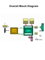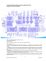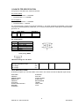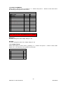
1
AK53 (D.O.C)
SERVICE MANUAL
RELEASE DATE:
22.03.2004
PREPARED BY:
VESTEL ELECTRONICS
Overall Block Diagram
TABLE OF CONTENTS
1.INTRODUCTION.......................................................................................................................... 1
2.TUNER SPECIFICATION............................................................................................................. 1
3.IF/AUDIO&VIDEO SWITCHING/AD CONVERTER PART .............................................................. 2
(PNX3000 (CALLED AS MPIF)) ...................................................................................................... 2
4.DIGITAL TV PROCESSOR (PNX300X (CALLED AS ADOC))........................................................ 3
5.SOUND OUTPUT STAGE WITH TDA7480L ................................................................................. 4
6.VERTICAL OUTPUT STAGE WITH STV9379FA& TDA8177F....................................................... 4
7.VIDEO OUTPUT AMPLIFIER TDA6108JF .................................................................................... 4
8.POWER SUPPLY PART .............................................................................................................. 4
9.SERIAL ACCESS 64K EEPROM.................................................................................................. 5
10.HEADPHONE AMPLIFIER STAGE............................................................................................. 5
11.SAW FILTER SPECIFICATION .................................................................................................. 6
12.IC DESCRIPTIONS .................................................................................................................... 6
12.1.TDA6108JF (IC900)............................................................................................................. 7
12.1.1.General Description ....................................................................................................... 7
12.1.2.Features ........................................................................................................................ 7
12.1.3.Pinning .......................................................................................................................... 7
12.2.HT48RA0A.......................................................................................................................... 8
12.2.1.General Description ....................................................................................................... 8
12.2.2.Features ........................................................................................................................ 8
12.2.3.Pin Descriptions ............................................................................................................. 8
12.3.PNX3000 (IC400) ................................................................................................................. 9
12.3.1.General Description ....................................................................................................... 9
12.3.2.Features ........................................................................................................................ 9
12.4.CS51033 (IC 104) ...............................................................................................................13
12.4.1.General Description ......................................................................................................13
12.4.2.Features .......................................................................................................................13
12.4.3.Pin Description .............................................................................................................13
12.5.SDRAM 64MBIT (IC315) .....................................................................................................14
12.5.1.General Description ......................................................................................................14
12.5.2.Features .......................................................................................................................14
12.5.3.Pin Description .............................................................................................................14
12.6.FLASH (IC 314) ..................................................................................................................15
12.6.1.General Description ......................................................................................................15
12.6.2.Features .......................................................................................................................15
12.6.3.Pin/Ball Descriptions .....................................................................................................16
12.7.NE56610-29 (RESET IC) (IC 316)........................................................................................18
12.7.1.General Description ......................................................................................................18
12.7.2.Features .......................................................................................................................18
12.7.3.Pin Description .............................................................................................................18
12.8.STS5PF30L (IC105) ............................................................................................................19
12.8.1.Description ...................................................................................................................19
12.8.2.Features .......................................................................................................................19
12.9.PNX300X (IC313)................................................................................................................20
12.9.1.General Description of the Digital One Chip System........................................................20
12.9.2.Features of the ADOC Processor...................................................................................21
12.10.M24C64WBN6 (IC309) ......................................................................................................26
12.10.1.Features .....................................................................................................................26
12.10.2.Description .................................................................................................................26
12.11.TDA7480L (IC401,IC402) ..................................................................................................27
12.11.1.Description .................................................................................................................27
12.11.2.Features .....................................................................................................................27
12.11.3.Pin Functions ..............................................................................................................27
12.12.LM7808 (IC803) ................................................................................................................27
12.12.1.Description .................................................................................................................27
12.12.2.Features .....................................................................................................................27
12.13.TDA8177F & STV9379FA (IC100) .....................................................................................28
i
AK53 D.O.C. Service Manual
22/03/2004
12.13.1.Description .................................................................................................................28
12.13.2.Features .....................................................................................................................28
12.13.3.Pin connections...........................................................................................................28
12.13.4.Block Diagram ............................................................................................................28
12.14.TCET1102G (IC801)..........................................................................................................29
12.14.1.Description .................................................................................................................29
12.14.2.Applications ................................................................................................................29
12.14.3.Features .....................................................................................................................29
12.15.MC44608 (IC804) ..............................................................................................................30
12.15.1.Description .................................................................................................................30
12.15.2.General Features ........................................................................................................30
12.15.3.Pin Connections ..........................................................................................................30
12.16.TL431 (Q816) ...................................................................................................................32
12.16.1.Description .................................................................................................................32
12.16.2.Features .....................................................................................................................32
12.16.3.Pin Configurations .......................................................................................................32
12.17.TFMS5360 ........................................................................................................................32
12.17.1.Description .................................................................................................................32
12.17.2.Features .....................................................................................................................32
13.AK53 CHASSIS MANUAL ADJUSTMENTS PROCEDURE ........................................................33
13.1.PRELIMINARY ...................................................................................................................33
13.2.SYSTEM VOLTAGE ADJUSTMENTS..................................................................................33
13.3.AFC ADJUSTMENTS .........................................................................................................33
13.4.FOCUS ADJUSTMENTS.....................................................................................................33
13.5.SCREEN ADJUSTMENT (VG2 ALIGNMENT) ......................................................................33
13.6.AGC (AUTOMATIC GAIN CONTROL).................................................................................33
14.AK53 CHASSIS PRODUCTION SERVICE MODE ADJUSTMENTS ............................................34
14.1.OPTIONS ...........................................................................................................................34
14.2.GEOMETRY .......................................................................................................................36
14.2.1.EW ALIGNMENT..........................................................................................................36
14.3.VIDEO ALIGNMENTS .........................................................................................................44
14.3.1.VIDEO ADJUST............................................................................................................44
14.3.1.1.WHITE DRIVE ........................................................................................................45
14.3.1.2.MIN BRIGHTNESS .................................................................................................45
14.3.1.3.MIN CONTRAST ....................................................................................................45
14.3.2.COLOR ADJUSTMENT.................................................................................................46
14.3.2.1.Y DEL SEC BG, Y DEL SEC DK, Y DEL SEC L, Y DEL SEC AV:.............................46
14.3.2.2.Y DEL PAL BG, Y DEL PAL DK, Y DEL PAL I, Y DEL PAL M, Y DEL PAL AV : .......46
14.3.2.3.VIDDEC QTHR, VIDDEC STHR ..............................................................................46
14.4.SOUND RELATED OPTIONS ..............................................................................................47
14.5.FACTORY SETTINGS ........................................................................................................48
15.MENU LANGUAGES ................................................................................................................49
16.BLOCK DIAGRAM ....................................................................................................................50
17.CIRCUIT DIAGRAMS................................................................................................................51
ii
AK53 D.O.C. Service Manual
22/03/2004
1.INTRODUCTION
11AK53 is a 100Hz color television DIGITAL ONE CHIP SYSTEM (DOC) capable of driving 28”4:3/16:9
SF/RF, 29”4:3 real flat, 32” 16:9 SF/RF, 33”4:3 and 34‘ 4:3 real flat picture tubes.
The chassis is capable of operation in PAL, SECAM, NTSC (playback) color standards and multiple
transmission standards as B/G, D/K, I/I’, and L/L´.
Sound system output is supplying 2x10W (10%THD) for left and right outputs of 8ohm speakers.
TV supports the level 1.5 teletext standard. It is possible to decode transmissions including high
graphical data.
The chassis is equipped with two full EuroScarts, one SCART for AV input/output, one front-AV input,
one back-AV input, one headphone output, one SVHS input (via SCART and SVHS connector), two
external speaker outputs (left and right), one audio line output.
2.TUNER SPECIFICATION
The hardware and software of the TV is suitable for tuners, supplied by different companies, which are
selected from the Service Menu. These tuners can be combined VHF, UHF tuners suitable for CCIR
2
systems B/G, H, L, L´, I/I´, and D/K. The tuning is available through the digitally controlled I C bus
(PLL). Below you will find info on one of the Tuners in use.
General description of UV1316 MK3(Philips) /CTF55XX (Thomson):
UV1316 MK3 (Philips) /CTF55XX (Thomson) tuners, which are designed to meet a wide range of
applications are PLL tuners; It is a combined VHF, UHF tuner suitable for CCIR systems B/G, H, L, L’, I
and I’. The low IF output impedance has been designed for direct drive of a wide variety of SAW filters
with sufficient suppression of triple transient.
Features of Tuner:
1. Those tuners are small sized UHF/VHF tuners
2. Systems CCIR: B/G, H, L, L’, I and I’; OIRT: D/K
2
3. Digitally controlled (PLL) tuning via I C-bus
4. Off-air channels, S-cable channels and Hyperband
5. World standardized mechanical dimensions and world standard pinning
6. Compact size
7. Complies to “CENELEC EN55020” and “EN55013”
Pinning:
1.
Gain control voltage (AGC)
2.
Tuning voltage
3.
I²C-bus address select
4.
I²C-bus serial clock
5.
I²C-bus serial data
6.
Not connected
7.
PLL supply voltage
8.
ADC input
9.
Tuner supply voltage*
10.
Symmetrical IF output 1
11.
Symmetrical IF output 2
:
4.0V, Max: 4.5V
:
:
:
Max: 5.5V
Min:-0.3V, Max: 5.5V
Min:-0.3V, Max: 5.5V
:
5.0V, Min: 4.75V, Max: 5.5V
:
33V, Min: 30V, Max: 35V
*33V is obtained from FBT of large signal board.
1
AK53 D.O.C. Service Manual
22/03/2004
3.IF/AUDIO&VIDEO SWITCHING/AD CONVERTER PART
(PNX3000 (CALLED AS MPIF))
MPIF IC consists of following OVERALL blocks;
(1)-Video/Audio switching
(2)-IF processing
(3)-A/D conversion for digital TV (DTV) processor (ADOC-PNX300X)
Main building blocks:
_ Vision PLL-IF, auto-calibrated, selectable IF frequency, 4 selectable AGC time constants, built-in
sound trap and selectable group delay. The demodulated CVBS signal is fed outside for use with
SCART.
_ Synthesizer mode, meant for down mixing of DTV signals to a suitable 2nd IF which can be handled
by a digital DTV decoder. Using a suitable SAW filter at the input the synthesizer mode can also be
used to downmix FM radio frequencies from the Tuner to a suitable 2nd IF frequency for the FM
demodulator.
_ Two Video IF inputs, selectable by internal switch to enable use of optimized SAW filters
_ Sound QSS IF, demodulated 2nd SIF can be either from SIF input (QSS) or Video IF (intercarrier).
The Sound IF also contains an AM demodulator for SECAM L/L'
_ CVBS and Y/C crossbar switch, with 2 video outputs for further processing in the Digital TV Signal
Processor after A/D conversion and 2 selectable video outputs which are available on output pins for
external connections
2
AK53 D.O.C. Service Manual
22/03/2004
_ Two YUV / RGB inputs, which can handle also YPrPb and sync on Y for DVD players Also 2Fh YUV /
RGB signals can be handled by the A/D converters.
_ An audio stereo crossbar switch with two outputs (one stereo, one stereo or mono) for further
processing in the processor after A/D conversion and three stereo outputs for external connections.
Extra inputs are provided to enable also the selection of demodulated RF sound (mono, NICAM, 2CS)
from the Digital TV Signal Processor for use on external connections.
_ Low pass filtering and A/D conversion. The audio and video sampling clocks use the same reference
so it is possible to interleave video and audio data into one serial data stream.
_ For control, I 2 C control is built-in with a selectable address.
_ Auxiliary building blocks which perform some functions which have typical better performance in
analogue design environment than in digital and are used by the Digital TV Signal Processor:
- Reference voltage for vertical deflection and audio ADC's
- Voltage to current conversion of the E/W
The set-up with an analogue and a digital part has the following advantages:
_ High frequent parts (IF) can be included in the concept
_ Less A/D and D/A converters needed for source switching
_ Better performance for AD converters (realized in analogue design environment, more accurate, less
tolerance)
_ Critical items like reference voltages can be realized in the analogue environment
4.DIGITAL TV PROCESSOR (PNX300X (CALLED AS ADOC))
The DOC system serves the TV functionality for small signal processing of audio, video, VBI services,
graphics and control. This chip implements all TV functions in digital technology. PNX300X is the digital
TV processor which consists of;
? TV video processor
? TV deflection processor
? TV audio processor
? TV microcontroller
As it is shown in the below block diagram ADOC gets the digital signal which is converted by MPIF and
processed in its own blocks and controls the overall system by I2C and the software programme is
downloaded into a flash memory which tells microcontroller within ADOC about the software
management and the output of ADOC turns into RGB, Main/Headphone audio right/left.
Then RGB output of ADOC is processed into a RGB preamplifier circuit to get enough gain for the video
output amplifier TDA6108JF (in CRT board)
Highlight points of ADOC:
(1)-Digital (I2D) data link is connected from MPIF to ADOC with a swing of about 300mV. The data rate
is 594Mbit/s.
(2)-Only one crystal is used in overall system which is 13.5MHZ.
3
AK53 D.O.C. Service Manual
22/03/2004
Functional block diagram of ADOC:
5.SOUND OUTPUT STAGE WITH TDA7480L
The TDA7480L is an audio class-D amplifier assembled in Power DIP package specially designed for
high efficiency applications mainly for TV and Home Stereo sets.
Mute stand-by function of the audio amplifier can be described as the following; the pin 12
(MUTE/STAND-BY) controls the amplifier status by two different thresholds, referred to ground. When
Vpin 12 voltage is lower than 0.7V the amplifier is in Stand-by mode and the final stage generators are
off. When Vpin 12 is higher than 4V, the amplifier is in play mode.
The TDA7480L is a 10W+10W stereo sound amplifier with mute/stand-by facility. MUTE control signal
coming from microcontroller (when it is at high level) activates the mute function. IC is muted when
mute pin is at low level (pin12). MUTE pin can also be activated via an external pop-noise circuitry in
order to eliminate pop noise when TV is turned off. Just after the TV is turned off, this circuit switches
the IC to stand-by mode by pulling the mute pin voltage to ground.
6.VERTICAL OUTPUT STAGE WITH STV9379FA& TDA8177F
The IC STV9379FA& TDA8177F is the vertical deflection booster circuit. Two supply voltages, +14V
and –14V are needed to scan the inputs VERT+ and VERT-, respectively. And a third supply voltage,
+60V for the flyback limiting is needed. The vertical deflection coil is connected in series between the
output and feedback to the input.
7.VIDEO OUTPUT AMPLIFIER TDA6108JF
The TDA6108JF includes three video output amplifiers is intended to drive the three cathodes of a color
picture tube.
8.POWER SUPPLY PART
In Large Signal Board
The DC voltages required at various parts of the chassis are provided by an SMPS transformer
controlled by the IC MC44608, which is designed for driving, controlling and protecting switching
transistor of SMPS. The transformer generates 135V for FBT input, +/-14V for audio amplifier, 8V, 12V,
V8Stby ( needed for step down converted for small signal board) and 5V supplies for other different
parts of the chassis.
4
AK53 D.O.C. Service Manual
22/03/2004
An optocoupler is used to control the regulation of line voltage and stand-by power consumption. There
is a regulation circuit in secondary side. This circuit produces a control voltage according to the
changes in 135V DC voltage, via an optocoupler (TCET 1102G) to pin3 of the IC.
During the switch on period of the transistor, energy is stored in the transformer. During the switch off
period energy is fed to the load via secondary winding. By varying switch-on time of the power
transistor, it controls each portion of energy transferred to the second side such that the output voltage
remains nearly independent of load variations.
In Small Signal Board
V8Stby and +5V is switched by a discrete circuit to make power consumption effective.
? When supply switch port of ADOC IC is HIGH +5V ? 3.3V via IC103 regulator
? When supply switch port of ADOC IC is LOW V8Stby ? 3.3V via IC103 regulator
V8Stby is used to get +5V, which is available in Stby.
Supply Voltages Available/Not-Available In Stand-by, IC Requirement, Supply Location
Supply
135V (B+)
In Stby available? Where?
For Which ?
NO
large signal board FBT
NOTE
depends on
CRT
14V-A
NO
(-)14V -A
NO
14V
8V
NO
NO
5V
V8stby
1.8V
3.3V
NO
YES
YES
YES
12V
5V
Vert Sup+ (14V)
Vert Sup- (14V)
33V
NO
YES
NO
NO
large signal board IC401,IC402(Audio
amplifier)
large signal board IC401,IC402(Audio
amplifier)
large signal board Horizontal drive transistor
small signal board
IC400 (MPIF)/Headphone discrete
circuit/RGB pre amplifiers/audio saw
filter(Z401)
small signal board
IC400 (MPIF),Tuner(TU200,TU850)
large signal board Step down IC and for s+5V
small signal board IC313 (ADOC)
small signal board
IC313
(ADOC),IC309(EEPROM),IC316(Reset IC)
small signal board CRT board (IC900)
small signal board LED/IR
large signal board Vertical IC (IC100)
large signal board Vertical IC (IC100)
NO
large signal board Tuner (TU200,TU850)
Important Microcontroller Ports For Supplying
Port
On/Off
On/Off
State
low
high
Function
normal operation
stand by mode
9.SERIAL ACCESS 64K EEPROM
M24C64WBN6, is the 64Kbit electrically erasable programmable memory. The memory is compatible
2
with the I C standard, two wire serial interface, which uses a bi-directional data bus and serial clock.
10.HEADPHONE AMPLIFIER STAGE
This stage is designed with discrete components (no IC is used for this purpose)
5
AK53 D.O.C. Service Manual
22/03/2004
11.SAW FILTER SPECIFICATION
Two groups of saw filters are used from EPCOS
For picture (Z400)
? Pal Secam BG DK L L’?K3953M
? Pal Secam BG I I’ ?K3953M
For sound(Z401)
? Pal Secam BG DK L L’?K9656M
? Pal Secam BG I I’ ?K9356
For sound saw filter it needs to be switched between L’ and other standards for K3953M, a port signal
coming from PNX300X(ADOC) called SEL_L/L’ is used for this purpose to make pin2 of audio saw filter
ground or not.
port
state Q404
SEL_L/L' High Shorted to
ground
SEL_L/L' Low open
Standard
L'
BG,DK,I,L
Pin Configuration
Pin No
1
2
3
4
5
Definition
Input
Input - ground
Chip carrier - ground
Output
Output
Maximum ratings for saw filters
Operable temperature range
Storage temperature range
DC voltage
AC voltage
TA
Tstg
VDC
Vpp
–25/+65
°C
12.IC DESCRIPTIONS
In following chapters you can find details of ICs used in the chassis and the SS B(Small signal board)
TDA6108JF
PNX3000
SDRAM 64MBIT
NE56610-29
PNX300X
TDA7480L
TDA8177&STV9379FA
MC44608
TFMS5360
HT48RA0A
CS51033
FLASH 32 MBIT
STS5PF30L
M24C64WBN6
LM7808
TCET1102G
TL431
6
AK53 D.O.C. Service Manual
22/03/2004
12.1.TDA6108JF (IC900)
12.1.1.General Description
The TDA6108JF includes three video output amplifiers in one plastic DIL-bent-SIL 9-pin medium power
(DBS9MPF) package (SOT111-1), using high-voltage DMOS technology, and is intended to drive the three
cathodes of a color CRT directly. To obtain maximum performance, the amplifier should be used with blackcurrent control.
12.1.2.Features
• Typical bandwidth of 9.0 MHz for an output signal of 60 V (p-p)
• High slew rate of 1850 V/ms
• No external components required
• Very simple application
• Single supply voltage of 200 V
• Internal reference voltage of 2.5 V
• Fixed gain of 51
• Black-Current Stabilization (BCS) circuit
• Thermal protection
12.1.3.Pinning
SYMBOL
Vi(1)
Vi(2)
Vi(3)
GND
Iom
VDD
Voc(3)
Voc(2)
Voc(1)
PIN
1
2
3
4
5
6
7
8
9
DESCRIPTION
inverting input 1
inverting input 2
inverting input 3
ground (fin)
black current measurement output
supply voltage
cathode output 3
cathode output 2
cathode output 1
7
AK53 D.O.C. Service Manual
22/03/2004
12.2.HT48RA0A
12.2.1.General Description
The HT48RA0A is an 8-bit high performance RISC-like microcontroller specifically designed for multiple
I/O product applications. The device is particularly suitable for use in products such as infrared remote
controllers and various subsystem controllers. A HALT feature is included to reduce power
consumption.
12.2.2.Features
• Operating voltage: 2.2V~3.6V
• Ten bidirectional I/O lines
• Six Schmitt trigger input lines
• One carrier output (1/2 or 1/3 duty)
• On-chip crystal and RC oscillator
• Watchdog Timer
• 1K_14 program EPROM
• 32_8 data RAM
• HALT function and wake-up feature reduce power consumption
• 62 powerful instructions
• Up to 1_s instruction cycle with 4MHz system clock
• All instructions in 1 or 2 machine cycles
• 14-bit table read instructions
• One-level subroutine nesting
• Bit manipulation instructions
• 20-pin/24-pin SOP package
12.2.3.Pin Descriptions
Pin Name
PB0, PB1
I/O
I/O
Code Option
Wake-up
or None
PC0/REM
O
Level or
Carrier
VDD
OSC2
OSC1
I/O
Crystal
or RC
VSS
RES
PB2~PB7
I
I
PA0~PA7
I/O
Wake-up
or None
-
Description
2-bit bidirectional input/output lines with pull-high resistors.
Each bit can be determined as NMOS output or Schmitt
trigger input by software instructions. Each bit can also be
configured as wake-up input by code option.
Level or carrier output pin
PC0 can be set as CMOS output pin or carrier output pin by
code option.
Positive power supply
OSC1, OSC2 are connected to an RC network or a crystal
(determined by code option) for the internal system clock. In
the case of RC operation, OSC2 is the output terminal for
1/4 system clock
(NMOS open drain output).
Negative power supply, ground
Schmitt trigger reset input. Active low.
6-bit Schmitt trigger input lines with pull-high resistors. Each
bit can be configured as a wake-up input by code option.
Bidirectional 8-bit input/output port with pull-high resistors.
Each bit can be determined as NMOS output or Schmitt
trigger input by software instructions.
8
AK53 D.O.C. Service Manual
22/03/2004
12.3.PNX3000 (IC400)
12.3.1.General Description
The PNX3000 is an analog front end for digital video processors. It contains an IF circuit for both analog
and digital broadcast signals, and input selectors and A to D converters for analog video and audio
signals. The digital output signals are made available via three serial data links.
The IC has a supply voltage of 5V. The supply voltage of the analog audio part can be 5V or 8V,
depending on the maximum signal amplitudes that are required.
12.3.2.Features
• Multi-standard vision IF circuit with alignment-free PLL demodulator without external components
• Internal (switchable) time-constant for the IF-AGC circuit
• DTV IF circuit for gain control of digital broadcast TV signals.
• Sound IF amplifier with separate AGC circuit for quasi split sound
• IF circuit can also be used for intercarrier sound
• Analog demodulator for AM sound
• Integrated sound trap and group delay correction
• Video ident function detects the presence of a video signal
• Video source selector with 4 external CVBS or YC inputs and 2 analog CVBS outputs with
independent source selection for each output
• Two linear inputs for 1fH or 2fH RGB signals with source selector. The RGB signals are converted to
YUV before A to D conversion. Both inputs can also be used as YPB PR input for DVD or set top box
• Integrated anti-alias filters for video A to D converters
• Four 10-bit video A to D converters for the conversion of CVBS, YC, YUV and down mixed sound IF
signals
• Up to three different A to D converted video channels are simultaneous available (e.g. CVBS and YC
and YUV)
• Audio source selector with 5 stereo inputs for analog audio and two microphone inputs
• Two microphone amplifiers with adjustable gain
• Three analog audio outputs for SCART and Line out with independent source selection for each
output
• Four 1-bit audio sigma delta A to D converters for the conversion of audio and microphone signals
• Three serial data link transmitters for interfacing with the digital video processor. The bit rate is 594
Mbits/sec per data link
• Voltage to current converter for driving of external East-West power amplifier
2
• I C-bus transceiver with selectable slave address and maskable interrupt output
9
AK53 D.O.C. Service Manual
22/03/2004
SYMBOL
PIN
DESCRIPTION
CVBS2
VAUDO
VAUDS
CVBS/Y3
C3
GND_VSW
BGDEC
CVBS/Y4
C4
fuse
GND_FILT
CVBS_DTV
RREF
VCC_FILT
YCOMB
CCOMB
AMEXT
TESTPIN3
CVBSOUTA
VDEFLO
VDEFLS
CVBSOUTB
fuse
TESTPIN2
R1/PR1 /V1
G1/Y1/Y1
B1/PB1 /U1
VCC_RGB
GND_RGB
R2/PR2 /V2
G2/Y2/Y2
B2/PB2 /U2
fuse
GND_VADC
VCC_VADC
EWVIN
EWIOUT
REW
ADR
XREF
fuse
IRQ
SDA
SCL
HV_SEC
HV_PRIM
VD2V5
GND_DIG
VCC_DIG
STROBE3N
STROBE3P
DATA3N
DATA3P
fuse
STROBE2N
STROBE2P
DATA2N
1
2
3
4
5
6
7
8
9
CVBS2 input
DC output voltage for supply of audio DACs in digital decoder
sense voltage for audio DACs supply
external CVBS/Y3 input
external CHROMA3 input
ground video switch
bandgap decoupling
external CVBS/Y3 input
external CHROMA3 input
fused lead
ground filters
input for CVBS encoded signal from DTV decoder
reference current input
supply voltage filters (5V)
Y signal from 3D Comb filter
C signal from 3D Comb filter
external AM mono input
test pin 3 (leave open)
CVBS or Y+CHROMA output A
DC output voltage for supply of deflection DACs in digital decoder
sense voltage for deflection DACs supply
CVBS or Y+CHROMA output B
fused lead
test pin 2 (connect to ground)
R1/PR1 /V1 input
G1/Y1/Y1 input
B1/PB1 /U1 input
supply voltage RGB matrix (5V)
ground RGB matrix
R2/PR2 /V2 input
G2/Y2/Y2 input
B2/PB2 /U2 input
fused lead
ground video ADCs
supply voltage video ADCs (5V)
East-West input voltage
East-West output current
East-West voltage to current conversion resistor
I2C address selection
XTAL reference frequency input
fused lead
interrupt request output
I2C serial data input/output
I2C serial clock input
horizontal and vertical sync input for secondary video channel
horizontal and vertical sync input for primary video channel
decoupling of internal digital supply voltage
digital ground
digital supply voltage (5V)
strobex negative datalink3
strobex positive datalink3
data positive datalink3
data positive datalink3
fused lead
strobex negative datalink2
strobex positive datalink2
data positive datalink2
10
11
12
13
14
15
16
17
18
19
20
21
22
23
24
25
26
27
28
29
30
31
32
33
34
35
36
37
38
39
40
41
42
43
44
45
46
47
48
49
50
51
52
53
54
55
56
57
10
AK53 D.O.C. Service Manual
22/03/2004
DATA2P
GND_I2D
STROBE1N
STROBE1P
DATA1N
DATA1P
VCC_I2D
SCART2R
SCART2L
LINER
LINEL
SCART1R
SCART1L
fuse
DSNDR2
DSNDL2
DSNDR1
DSNDL1
GND_AADC
VCC_AADC
fuse
R4
L4
R3
L3
R2
L2
R1
L1
GND2_ASW
VCC2_ASW
VAADCREF
VAADCN
VAADCP
MIC2N
MIC2P
MIC1N
MIC1P
fuse
GND1_ASW
VCC1_ASW
SIFINP
SIFINN
SIFAGC
DTVIFAGC
DTVIFINP
DTVIFINN
TUNERAGC
fuse
VIFINP
VIFINN
DTVIFPLL
VCC_IF
VIFPLL
GND1_IF
2NDSIFEXT
2NDSIFAGC
GND2_IF
DTVOUTP
58
59
60
61
62
63
64
65
66
67
68
69
70
71
72
73
74
75
76
77
78
79
80
81
82
83
84
85
86
87
88
89
90
91
92
93
94
95
96
97
98
99
100
101
102
103
104
105
106
107
108
109
110
111
112
113
114
115
116
data positive datalink2
ground datalinks
strobex negative datalink1
strobex positive datalink1
data negative datalink1
data positive datalink1
supply voltage datalinks (5V)
audio output for SCART 2 right
audio output for SCART 2 left
audio line output right
audio line output left
audio output for SCART1 right
audio output for SCART1 left
fused lead
audio signal from digital decoder right 2
audio signal from digital decoder left 2
audio signal from digital decoder right 1
audio signal from digital decoder left 1
ground audio ADCs
supply voltage audio ADCs (5V)
fused lead
right input audio 4
left input audio 4
right input audio 3
left input audio 3
right input audio 2
left input audio 2
right input audio 1
left input audio 1
ground audio switch
supply voltage audio switch (audio output buffers, 5V or 8V)
decoupling of reference voltage for audio ADCs
0V reference voltage for audio ADCs (GND)
full scale reference voltage for audio ADCs (5V)
microphone input 2 neg
microphone input 2 pos
microphone input 1 neg
microphone input 1 pos
fused lead
ground audio switch
supply voltage audio switch (audio input buffers, 5V or 8V)
sound IF input positive
sound IF input negative
control voltage for SIF AGC
control voltage for DTV IF AGC
DTV IF input positive
DTV IF input negative
tuner AGC output
fused lead
vision IF input positive
vision IF input negative
loop filter DTVIF PLL demodulator
supply voltage IF circuit (5V)
loop filter VIF PLL demodulator
ground IF circuit
2ndSIF input
2ndSIF AGC capacitor
ground IF circuit
DTV output positive
11
AK53 D.O.C. Service Manual
22/03/2004
DTVOUTN
VCC_SUP
fuse
CVBSOUTIF
GND_SUP
VCC1_VSW
CVBS0
TESTPIN1
VCC2_VSW
CVBS1
R5
L5
117
118
119
120
121
122
123
124
125
126
127
128
DTV output negative
supply of supply circuit (5V)
fused lead
CVBS output of IF circuit
ground of supply circuit
supply of video switch (5V)
CVBS0 input (to be used for CVBS from IF part)
test pin 1 (connect to ground)
supply of video switch (5V)
CVBS1 input
right input audio 5
left input audio 5
Important pins need to be checked in case of troubleshooting
Signal
CVBS/RGB Input voltage
CVBS Output voltage
Maximum input audio voltage
Maximum output audio voltage
Measure
Input pins
Output pins
Input pins
Output pins
Value
1Vpk-pk
2 Vpk-pk
2 Vrms
2 Vrms
12
AK53 D.O.C. Service Manual
22/03/2004
12.4.CS51033 (IC 104)
12.4.1.General Description
The CS51033 is a switching controller for use in dc–dc converters. It can be used in the buck topology
with a minimum number of external components. The CS51033 consists of a 1.0 A power driver for
controlling the gate of a discrete P–channel transistor, fixed frequency oscillator, short circuit protection
timer, programmable Soft Start, precision reference, fast output voltage monitoring comparator, and
output stage driver logic with latch.
The high frequency oscillator allows the use of small inductors and output capacitors, minimizing PC
board area and systems cost. The programmable Soft Start reduces current surges at start up. The
short circuit protection timer significantly reduces the PFET duty cycle to approximately 1/30 of its
normal cycle during short circuit conditions.
The CS51033 is available in an 8–Lead SO package.
12.4.2.Features
• 1.0 A Totem Pole Output Driver
• High Speed Oscillator (700 kHz max)
• No Stability Compensation Required
• Lossless Short Circuit Protection
• 2.0% Precision Reference
• Programmable Soft Start
• Wide Ambient Temperature Range:
Industrial Grade: –40°C to 85°C
Commercial Grade: 0°C to 70°C
12.4.3.Pin Description
PIN NUMBER
1
2
3
4
5
6
7
8
PIN SYMBOL
VGATE
PGND
COSC
GND
VFB
VCC
CS
VC
FUNCTION
Driver pin to gate of external PFET.
Output power stage ground connection.
Oscillator frequency programming capacitor.
Logic ground.
Feedback voltage input.
Logic supply voltage.
Soft Start and fault timing capacitor.
Driver supply voltage.
13
AK53 D.O.C. Service Manual
22/03/2004
12.5.SDRAM 64MBIT (IC315)
12.5.1.General Description
Please note that in the following explanation one of the SDRAM alternative is used.
The K4S641632D is 67,108,864 bits synchronous high data rate Dynamic RAM organized as 4 x
1,048,576 words by 16 bits, fabricated with SAMSUNG¢s high performance CMOS technology.
Synchronous design allows precise cycle control with the use of system clock I/O transactions are
possible on every clock cycle. Range of operating frequencies, programmable burst length and
programmable latencies allow the same device to be useful for a variety of high bandwidth, high
performance memory system applications.
12.5.2.Features
• JEDEC standard 3.3V power supply
• LVTTL compatible with multiplexed address
• Four banks operation
• MRS cycle with address key programs
-. CAS latency (2 & 3)
-. Burst length (1, 2, 4, 8 & Full page)
-. Burst type (Sequential & Interleave)
• All inputs are sampled at the positive going edge of the system clock
• Burst read single-bit write operation
• DQM for masking
• Auto & self refresh
• 64ms refresh period (4K cycle)
12.5.3.Pin Description
PIN
CLK
CS
NAME
System clock
Chip select
CKE
Clock enable
A0 ~ A11
Address
BA0 ~ BA1
Bank select address
RAS
Row address strobe
CAS
Column address strobe
WE
Write enable
L(U)DQM
Data input/output mask
DQ0 ~ 15
VDD/VSS
VDDQ/VSSQ
Data input/output
Power supply/ground
Data output power/ground
N.C/RFU
No connection
/reserved for future use
INPUT FUNCTION
Active on the positive going edge to sample all inputs.
Disables or enables device operation by masking or enabling all
inputs except CLK, CKE and L(U)DQM
Masks system clock to freeze operation from the next clock
cycle.
CKE should be enabled at least one cycle prior to new
command.
Disable input buffers for power down in standby.
Row/column addresses are multiplexed on the same pins.
Row address : RA0 ~ RA11, Column address : CA0 ~ CA7
Selects bank to be activated during row address latch time.
Selects bank for read/write during column address latch time.
Latches row addresses on the positive going edge of the CLK
with RAS low.
Enables row access & precharge.
Latches column addresses on the positive going edge of the
CLK with CAS low.
Enables column access.
Enables write operation and row precharge.
Latches data in starting from CAS, WE active.
Makes data output Hi-Z, tSHZ after the clock and masks the
output.
Blocks data input when L(U)DQM active.
Data inputs/outputs are multiplexed on the same pins.
Power and ground for the input buffers and the core logic.
Isolated power supply and ground for the output buffers to
provide improved noise immunity.
This pin is recommended to be left No Connection on the device.
14
AK53 D.O.C. Service Manual
22/03/2004
12.6.FLASH (IC 314)
12.6.1.General Description
The MT28F128J3 is a nonvolatile, electrically block-erasable (Flash), programmable memory
containing 134,217,728 bits organized as 16,777,218 bytes (8 bits) or 8,388,608 words (16 bits). This
128Mb device is organized as one hundred twenty-eight 128KB erase blocks.
The MT28F640J3 contains 67,108,864 bits organized as 8,388,608 bytes (8 bits) or 4,194,304 words
(16 bits). This 64Mb device is organized as sixty-four 128KB erase blocks.
Similarly, the MT28F320J3 contains 33,554,432 bits organized as 4,194,304 bytes (8 bits) or 2,097,152
words (16 bits). This 32Mb device is organized as thirty-two 128KB erase blocks.
These three devices feature in-system block locking. They also have common Flash interface (CFI) that
permits software algorithms to be used for entire families of devices. The software is deviceindependent, JEDEC ID-independent with forward and backward compatibility.
Additionally, the scalable command set (SCS) allows a single, simple software driver in all host systems
to work with all SCS-compliant Flash memory devices. The SCS provides the fastest system/device
data transfer rates and minimizes the device and system-level implementation costs.
To optimize the processor-memory interface, the device accommodates VPEN, which is switchable
during block erase, program, or lock bit configuration, or hard-wired to VCC, depending on the
application. VPEN is treated as an input pin to enable erasing, programming, and block locking. When
VPEN is lower than the VCC lockout voltage (VLKO), all program functions are disabled. Block erase
suspend mode enables the user to stop block erase to read data from or program data to any other
blocks. Similarly, program suspend mode enables the user to suspend programming to read data or
execute code from any unsuspended blocks.
VPEN serves as an input with 2.7V, 3.3V, or 5V for application programming. VPEN in this Q-Flash _
family can provide data protection when connected to ground. This pin also enables program or erase
lockout during power transition.
Micron’s even-sectored Q-Flash devices offer individual block locking that can lock and unlock a block
using the sector lock bits command sequence.
Status (STS) is a logic signal output that gives an additional indicator of the internal state machine
(ISM) activity by providing a hardware signal of both status and status masking. This status indicator
minimizes central processing unit (CPU) overhead and system power consumption. In the default
mode, STS acts as an RY/BY# pin. When LOW, STS indicates that the ISM is performing a block
erase, program, or lock bit configuration. When HIGH, STS indicates that the ISM is ready for a new
command.
Three chip enable (CE) pins are used for enabling and disabling the device by activating the device’s
control logic, input buffer, decoders, and sense amplifiers.
BYTE# enables the device to be used in x8 or x16 read/write mode; BYTE# = 0 selects an 8-bit mode,
with address A0 selecting between the LOW and HIGH byte, while BYTE# = 1 selects a 16-bit mode.
When BYTE# = 1, A1 becomes the lowest-order address line with A0 being a no connect.
RP# is used to reset the device. When the device is disabled and RP# is at Vcc, the standby mode is
enabled. A reset time (t RWH) is required after RP# switches HIGH until outputs are valid. Likewise, the
device has a wake time (t RS) from RP# high until writes to the command user interface (CUI) are
recognized. When RP# is at GND, it provides write protection, resets the ISM, and clears the status
register.
A variant of the MT28F320J3 also supports the new security block lock feature for additional code
security. This feature provides an OTP function for the device. (Contact factory for availability.)
The MT28F320J3 and the MT28F640J3 are manufactured using the 0.18µm process technology, and
the MT28F128J3 is manufactured using the 0.15µm process technology.
12.6.2.Features
• x8/x16 organization
• One hundred twenty-eight 128KB erase blocks (128Mb)
Sixty-four 128KB erase blocks (64Mb)
Thirty-two 128KB erase blocks (32Mb)
•VCC, VCCQ, and VPEN voltages:
2.7V to 3.6V VCC operation
2.7V to 3.6V, or 5V VPEN application programming
• Interface Asynchronous Page Mode Reads:
150ns/25ns or 120ns/25ns read access time (128Mb)
120ns/25ns or 115ns/25ns read access time (64Mb)
110ns/25ns read access time (32Mb)
• Manufacturing ID (ManID)
Intel® (0x89h)
15
AK53 D.O.C. Service Manual
22/03/2004
Micron® (0x2Ch)
• Industry-standard pinout
• Inputs and outputs are fully TTL-compatible
• Common Flash Interface (CFI) and Scalable
Command Set
• Automatic write and erase algorithm
• 5.6µs-per-byte effective programming time using write buffer
• 128-bit protection register
64-bit unique device identifier
64-bit user-programmable OTP cells
• Enhanced data protection feature with VPEN = VSS
Flexible sector locking
Sector erase/program lockout during power transition
•Security OTP block f feature
Permanent block locking (Contact factory for availability)
• 100,000 ERASE cycles per block
• Automatic suspend options:
Block Erase Suspend-to-Read
Block Erase Suspend-to-Program
Program Suspend-to-Read
12.6.3.Pin/Ball Descriptions
56-PIN TSOP
NUMBERS
55
64-BALL FBGA
NUMBERS
G8
14, 2, 29
SYMBOL
TYPE
WE#
Input
B4, B8, H1
CE0, CE1,
CE2
Input
16
D4
RP#
Input
54
F8
OE#
Input
32, 28, 27, 26,
25, 24, 23, 22,
20, 19, 18, 17,
13, 12, 11, 10,
8, 7, 6, 5, 4, 3,
1, 30
31
G2, A1, B1, C1,
D1, D2, A2, C2,
A3, B3, C3, D3,
C4, A5, B5, C5,
D7, D8, A7, B7,
C7, C8, A8, G1
F1
A0 _ A21/
(A22)
(A23)
Input
BYTE#
Input
15
A4
VPEN
Input
DESCRIPTION
Write Enable: Determines if a given cycle is a WRITE
cycle. If WE# is LOW, the cycle is either a WRITE to the
command execution logic (CEL) or to the memory array.
Addresses and data are latched on the rising edge of the
WE# pulse.
Chip Enable: Three CE pins enable the use of multiple
Flash devices in the system without requiring additional
logic. The device can be configured to use a single CE
signal by tying CE1 and CE2 to ground and then using
CE0 as CE. Device selection occurs with the first edge of
CE0, CE1, or CE2 (CEx) that enables the device. Device
deselection occurs with the first edge of CEx that disables
the device (see Table 4 on page 14).
Reset/Power-Down: When LOW, RP# clears the status
register, sets the ISM to the array read mode, and places
the device in deep power-down mode. All inputs, including
CEx, are “Don’t Care,” and all outputs are High-Z. RP#
must be held at VIH during all other modes of operation.
Output Enables: Enables data output buffers when LOW.
When OE# is HIGH, the output buffers are disabled.
Address inputs during READ and WRITE operations. A0 is
only used in x8 mode and will be a NC in x16 mode (the
input buffer is turned off when BYTE = HIGH). A22 (pin 1,
ball A8) is only available on the 64Mb and 128Mb devices.
A23 (pin 30, ball G1) is only available on the 128Mb
device.
BYTE# low places the device in the x8 mode. BYTE# high
places the device in the x16 mode and turns off the A0
input buffer. Address A1 becomes the lowest order
address in x16 mode.
Necessary voltage for erasing blocks, programming data,
or configuring lock bits. Typically, VPEN is connected to
VCC. When VPEN _ VPENLK, this pin enables hardware write
protect.
16
AK53 D.O.C. Service Manual
22/03/2004
33, 35, 38,
44, 46, 49,
34, 36, 39,
45, 49, 51,
36, 39, 41,
47, 50, 52
53
40,
51,
41,
34,
45,
F2, E2, G3, E4,
E5, G5, G6, H7,
E1, E3, F3, F4,
F5, H5, G7, E7
DQ0–
DQ15
Input/
Output
Data I/O: Data output pins during any READ operation or
data input pins during a WRITE. DQ8–DQ15 are not used
in byte mode (BYTE = LOW).
E8
STS
Output
43
G4
V CCQ
Supply
9, 37
21, 42, 48
56
H3, A6
B2, H4, H6
H8
V CC
V SS
NC
Supply
Supply
—
—
B6, C6, D5, D6,
E6, F6, F7, H2
DNU
—
Status: Indicates the status of the ISM. When configured in
level mode (default), STS acts as a RY/BY# pin. When
configured in its pulse mode, it can pulse to indicate
program and/or erase completion. Tie STS to V CCQ
through a pull-up resistor.
V CCQ controls the output voltages. To obtain output voltage
compatible with system data bus voltages, connect VCCQ
to the system supply voltage.
Power Supply: 2.7V to 3.6V.
Ground.
No Connect: These may be driven or left unconnected. Pin
1 and ball A8 are NCs on the 32Mb device. Pin 30 and ball
G1 are NCs on the 32Mb and 64Mb devices.
Do Not Use: Must float to minimize noise.
17
AK53 D.O.C. Service Manual
22/03/2004
12.7.NE56610-29 (RESET IC) (IC 316)
12.7.1.General Description
The NE56610-29 is a family of devices designed to generate a reset signal for a variety of
microprocessor and logic systems. Accurate reset signals are generated during momentary power
interruptions or when ever power supply voltages sag to intolerable levels. The NE56610-29
incorporates an internal timer to provide reset delay and ensure proper operating voltage has been
attained. An Open Collector output topology provides adaptability for a wide variety of logic and
microprocessor systems.
SOT23-5 surface mount package is used.
12.7.2.Features
• 3.3V operating voltage (VDDE)
• SOT23-5 surface mount package
• Offered in reset thresholds 2.9 V DC
• Internal reset delay timer is 50ms
12.7.3.Pin Description
PIN NUMBER
1
2
3
4
5
SYMBOL
M/R
DESCRIPTION
Manual Reset input.
Connect to ground when not using.
SUB
GND
VOUT
Vcc
Substrate pin. Connect to ground.
Ground
Reset HIGH output pin
Positive power supply input
18
AK53 D.O.C. Service Manual
22/03/2004
12.8.STS5PF30L (IC105)
12.8.1.Description
STS5PF30L is a Power MOSFET.
12.8.2.Features
• TYPICAL RDS(on) = 0.070 ? ?
• STANDARD OUTLINE FOR EASY
AUTOMATED SURFACE MOUNT ASSEMBLY
• LOW THRESHOLD DRIVE
TYPE
STS5PF30L
VDSS
30V
RDS(on)
<0.080 O
ID
5A
19
AK53 D.O.C. Service Manual
22/03/2004
12.9.PNX300X (IC313)
This IC is the heart of the TV set for small signal processing.
12.9.1.General Description of the Digital One Chip System
DOC Hardware
The Digital One Chip System (DOC) is a system concept based on a digital processor for double-scan
TV receivers. It is a global, multi-standard system primarily designed for the reception and processing
of analog broadcast signals. The DOC system serves the TV functionality for small signal processing of
audio, video, VBI services, graphics and control. An integrated MIPS 1910 processor runs the
DOCware software stack. The Digital One Chip DOCware software is stored in a non-volatile external
memory, normally flash memory. The following figure shows the hardware system architecture of a TV
chassis based on the DOC system.
The dual stream architecture of the DOC system allows audio and video processing of two A/V sources
simultaneously. The two video streams can be displayed in several programmable ways (main screen,
PIP or DW). The two audio streams are audible via the TV loudspeakers and/or the headphones. If two
TV broadcast signals have to be processed simultaneously, an external IF processor and a PIP Mono
Sound Demodulator/Decoder is needed.
For the memory-based features in the DOC system (like scan rate conversion, dynamic noise reduction
and PIP/DW applications) external SDRAM is needed. The memory size requirements are directly
related to which memory-based features have to be supported. The amount of SDRAM required varies
per feature but also varies with combination of features.
The DOC system also has 128kByte of internal SRAM memory. This memory is used to run low
latency, timing critical parts of the software. Under these circumstances no external SDRAM is needed.
The DOC system is built around the ADOC IC. This chip implements all TV functions in digital
technology. Only a few functions (like AD-conversion, IF processing and source select) are
implemented in an analog companion IC, the MPIF.
The MPIF is meant as an analog video and audio pre-processing unit for the TV processor ADOC. It
contains the high frequent IF part and all the analog video and audio source switching for external inand outputs. MPIF can handle CVBS, Y/C, RGB (1Fh/2Fh) and YPrPb (1Fh/2Fh) video signals as well
as stereo Left/Right and Second Sound IF (low-IF 5-6MHz, 10.7Mhz) audio signals. MPIF converts the
selected video and audio streams from the analog to the digital domain. Via three high-speed serial
data links the digitized audio and video signals are streamed to the ADOC IC for further processing.
ADOC is a fully integrated, digitally implemented TV processor for audio, video, VBI services, graphics
and control.
The split-up between an analog (MPIF) and a digital part (ADOC) has the following advantages:
• High frequency IF part can be included in the concept
• Less A/D and D/A converters needed for source switching
• Better performance for AD converters (realized in analog design environment, more accurate, less
tolerance)
• Critical items like reference voltages can be realized in the analog environment
20
AK53 D.O.C. Service Manual
22/03/2004
• Integrated SCART buffers
The DOC system is designed to facilitate a very cost effective TV chassis. Some of the measures taken
are:
• One crystal design. Only one reference crystal is required for the MPIF and ADOC,
• The advanced geometry corrections in the DOP result in a simple horizontal deflection circuitry.
Linearity coils are not required
12.9.2.Features of the ADOC Processor
Color Decoder and Sync Processing
• Multi standard color decoder supporting PAL-B, G, D, H, I, N, Combination-PAL N, PAL M, NTSC M,
NTSC-Japan, NTSC 4.43 and SECAM
• Automatic color standard recognition and selection (PAL/SECAM/NTSC)
• Fully programmable static or Automatic Gain Control (AGC) for all analogue video base band signals.
• Resolution of CVBS or Y/C signal after AGC: 9 bits (including sync)
• AGC for chrominance (PAL and NTSC only) for CVBS and Y/C sources
• Programmable clamp window for selected video base band signal(s)
• Horizontal (including 3-level sync for 2Fh) and vertical sync detection.
• Adaptive 2/4-line delay Comb filter for two dimensional chrominance/luminance separation
• PAL delay line for correcting PAL phase errors
• Maskable interrupt generation to MIPS notifying any change of signal conditions
• Compliant with and detection of Macrovision up to version 7.1.
• Possibility of Fast Blank SCART RGB insertion in CVBS input mode, not in Y/C.
• Second multi standard color decoder for low-cost PIP
– Supports CVBS standards as listed above
– No comb filter
– No Y/C performance (Y and C are being summed before decoding)
– No fast blanking with Component inputs
VBI Data Capture
• Two independent data capture units (DCU1 and DCU2) for standard data rate streams
• Multi-standard data capture. Both DCUs can always execute the following services:
– Line 21 Data Services (Closed Caption)
– European Wide Screen Signalling (WSS line23)
– PDC A & B (VPS and TeleText packet 8/30)
– World Standard TeleText.
• Services performed by TeleText application:
– Data Broadcast (packets X/30, X/31)
– Channel Identification (packet 8/30)
• Data type selectable on line-by-line basis independently for odd and even fields
• Multi-page acquisition during VBI
• Single page acquisition during full field
• DMA of packets and status bits to memory (embedded SRAM)
• Automatic identification of VBI data standard supported
Teletext storage
• Error correction and decoding performed by DOCware software
• Page management performed by DOCware software
• Storage of up to 8 pages of TeleText internally
• Storage of more than 8 TeleText pages requires external memory (SDRAM)
Picture measurements
• Noise measurement in active video
• Black Bar detection
• Sharpness measurement
Picture Improvements
• Field based noise reduction (on main only)
• Horizontal Dynamic Peaking/ Luminance Transient Improvement (LTI)
• SCAn VElocity Modulation (SCAVEM or SVM) and Dynamic Contrast Control (DCC)
• Dynamic Color Transient Improvement (DCTI)
• Dynamic Skin Tone control
21
AK53 D.O.C. Service Manual
22/03/2004
•
•
•
•
•
Blue Stretch
Green Enhancement
Black Stretch
32-bins histogram
Electrical Local Doming Protection
Picture in Picture / Double window
• Requires external memory to be connected to SDRAM interface
• Second input through second color decoder. Can be selected to be either main or sub.
• YCrCb storage in 4:2:2 format. 8 bits per component. Dithering adopted to have 9 bits effectively.
• No joint line/crossover errors
• Supporting Double Window displaying both a PAL (50 Hz) and an NTSC (60 Hz) signal.
• Double window text. Displaying a TeleText page next to a TV broadcast. This feature is functional without
the external Memory in 50 Hz mode.
• For proper aspect ratio of Double Window display on 4/3 screen vertical scaling by deflection can be
adopted
Scan Rate Conversion
• This requires external memory connected to SDRAM interface
• Line flicker reduction
• Full interlaced performance (provided sufficient memory)
Video H/V Scaling
• Horizontal Panorama/customer defined Scaling in video path (not affecting graphics)
• Vertical Scaling by vertical deflection
Audio Base band Switching and Interfaces
• 5x Analogue outputs (Left, Right, Subwoofer, Centre and Surround speaker)
• 1x Left and Right Head Phones output
Sound Demodulator/Decoder
• Two FM/AM Demodulator channels with programmable mixer frequencies and four different filter
bandwidths:
– Multi-standard FM demodulation (B/G, D/K, I, M and N standard)
– Optional AM demodulation (L/L’ standard)
– FM pilot carrier present detector (for A2 sound systems)
• FM-A2 Decoder:
– Detection of ID signal for second carrier
– Decoding for three analog multi-channel systems (A2, A2+ and A2*) and satellite sound
– Identification A2 systems (B/G, D/K and M standard)
– Supporting Korean 2SC standard
• BTSC Stereo/SAP Decoder:
– M/BTSC and N standards supported
– Processing of MTS/MPX signal
– Detection of pilot carrier with pilot lock indicator
– AM demodulation of stereo sub-carrier
– Detection of SAP sub carrier
– SAP decoder
– FM demodulation of SAP carrier (without dbx®) simultaneously with stereo decoding, or mono plus
SAP with dbx®
– dbx® noise reduction on either (L-R) or SAP signal
• Japan MTS Decoder:
– Processing of MPX signal
– Detection of the Identification signal
– FM demodulation of sub-carrier for stereo or bilingual reproduction
• NICAM demodulator and decoder (B/G, I and L/L’ standard):
– DQPSK demodulation for different standards, simultaneously with 1-channel FM demodulation
– NICAM decoding
• Auto Standard Detection Mode (ASD)
• Demodulator Decoder Easy Programming (DDEP)
• FM-Radio decoder
• Identification circuit for all standards
22
AK53 D.O.C. Service Manual
22/03/2004
• Decoding and adaptive de-emphasis for satellite FM (ASTRA)
• Monitor selection for FM/AM DC values and signals, with peak detection option
• Soft-mute for DEMDEC outputs DEC, MONO and SAP
• Sample rate conversion (SRC) for up to three demodulated terrestrial audio signals. It is possible to
process SCART signals together with demodulated terrestrial signals. Up to five signals (stereo
counting for 2) can be processed at a time.
Audio Processing
• Virtual Dolby® (‘422’ mode and ‘423’ mode) (3)
• Bass management
• Dynamic Bass Boost (4)
Automatic volume levelling (AVL)
• Programmable Level Adjust at inputs of switch matrix
• Volume control:
– Separate volume control on headphone
• Balance control on left/right speaker and on left/right headphone by use of trim control
• 5-band graphic equalizer or treble/bass control
• Notch filter for acoustic compensation
• Soft mute on all outputs
• Beeper
• Pseudo Hall/Matrix:
– Pseudo Hall provides (L+R)/2 on Centre and (L+R)/2 with 30ms delay on Surround
– Pseudo Matrix provides (L+R)/2 on Centre and (L-R)/2 with 30ms delay on Surround
Character Based Graphics
• Characters Based Display:
– 1440 pixels per line of which 5% in over-scan.
• Level 1.5 WST TeleText compliant
• Double Window TeleText display:
– Display of two 40 character wide Level 1.5 TeleText pages side by side.
– Display of 40 character wide Level 1.5 TeleText and Video side by side.
• Line 21 Data Services compliant
• Supports OSD with up to 8 colors out of a palette of 4096 colors
• Selectable character size
• Dynamically Redefinable Characters (DRCs)
– Internal memory up to 64 characters
RGB Processing
• Fully programmable YCrCb to RGB matrix
• Saturation control done using matrix
• Contrast and brightness control with 8 bits resolution
• D/A converters for RGB and Scan Velocity Modulation:
– Clock frequency 81MHz (fixed)
– Sample Rate Conversion to convert from orthogonal pixels
– 10 bits resolution (11 bits virtual using dithering of LSB)
– 2160 interpolated pixels per line
• 1440 pixels per line (of which 5% in over scan) at graphics blender (clock frequency 54 MHz)
• Forced super blanking during start-up or fault conditions
• Programmable horizontal and vertical retrace blanking via line and pixel number
• Separate beam current control on video and graphics
• Peak White limiter for video path
• Soft clipping for video path
• Hard clipping for graphics path
• Advanced Scan Velocity Processing:
– Scan Velocity modulation working on both Video and Graphics
– Dynamic contrast
• Continuous Cathode Calibration (=cut off control):
– System allows both for one-point and two-point calibration
• Graphics/video blender with mixture level (0% to 100% in 16 steps)
23
AK53 D.O.C. Service Manual
22/03/2004
AD Converters for Display Functions
• 3x Sigma Delta ADC for Black Current, EHT, Beam Current Limiting measurement Clock frequency
54MHz
Deflection & Geometry
• Horizontal time base for display based on digital PLL
• Very good jitter performance of about. +/- 300 ps of the horizontal drive pulse
• Low power start-up mode from standby
• Slow start/stop
• Fixed beam-current switch-off
• Vertical and horizontal geometry processing. Special features of the horizontal geometry processor
are:
– inner-pincushion correction
– horizontal non-linearity correction
• Auxiliary output
– can be used to generate waveform with frequency of vertical deflection (for example quadrupole
correction for flat picture tubes)
• Vertical guard input
• Flash detection input
• EHT overvoltage protection (X-Ray) input
• Horizontal drive output
Microprocessor
• TV control by embedded 32 bit RISC processor
– Philips MIPS PR1910, 54MHz
• Cache Structure
– Unified 8Kbyte Instruction/Data Cache
• Co-Processor:
– 2x 32bit system clock Count/Compare (Timer1,2) Registers
– 1x 32bit system clock Count/Compare (Timer3) configurable as Watchdog Timer
• Debug Support:
– MIPS JTAG compliant
– Software / Hardware Breakpoint
– Single Stepping
– Real Time Trace
TV Control Peripherals
• General Purpose IO (GPIO):
– 32 total GPIO pins, 28 with secondary functions stated bellow (4 GPIO free pins)
• Two I 2 C Interface units
• Two General Purpose Counter/Compare (Timer) units
• Universal Asynchronous Receiver Transmitter (UART)
• Eight external interrupts
• Analogue to Digital converter:
– 6 multiplexed inputs
– Programmable resolution of up to 10 bits
• Remote Control Receiver and Transmitter
Reset
• Reset via external input
Internal Memory for SW Code /Data
• Data/ Code memory up to 128 Kbytes (SRAM)
Memory at SDRAM Interface
• Addressable space up to 32Mbyte (SDRAM only, no SRAM, no DDRAM)
– 16Mbit (1M x 16) Single data rate SDRAM
• Memory Functions:
– PIP/DW, DNR, Scan Conversion, requiring at least 13Mbit
– PIP replay, scalable size
24
AK53 D.O.C. Service Manual
22/03/2004
Memory at EBIU Interface for SW Code/Data
• Addressable space up to 8Mbyte
• Memories supported
– 16bit Standard asynchronous ROM, SRAM, FLASH
– 16bit Page mode Flash support (AMD, Intel and ST)
• Memory Functions
– Code memory up to 8Mbyte (FLASH/ROM/RAM)
– Data memory up to 8Mbyte (RAM)
2
Memory at I C Interface
2
• Software support of external non-volatile memory connected to I C interface
Important pins need to be checked in case of troubleshooting
Port
On/Off
On/Off
Mute
Degauss
Reset
Protection
LED
LED
Supply_switch
Supply_switch
Measure
pin33 of PL402
pin33 of PL402
pin7 of PL402
pin31 of PL402
pin1 of IC316
Base of Q719
pin
pin
pin
pin
State
low
high
low
low
High
low
high
low
high
low
Function
normal operation
stand by mode
Audio amplifier is muted
Degaussing is done
Resets ADOC
TV set goes to stby mode
LED light as red (stby)
LED light as green (on)
5V is selected via Q106
V8Stby is selected via
Q106
25
AK53 D.O.C. Service Manual
22/03/2004
12.10.M24C64WBN6 (IC309)
12.10.1.Features
• Two Wire I 2 C Serial Interface
Supports 400 kHz Protocol
• 3.3V Supply Voltage
• Write Control Input
• BYTE and PAGE WRITE (up to 32 Bytes)
• RANDOM and SEQUENTIAL READ Modes
• Self-Timed Programming Cycle
• Automatic Address Incrementing
• Enhanced ESD/Latch-Up Behavior
• More than 1M Erase/Write Cycles
• More than 40 Year Data Retention
12.10.2.Description
These I2C -compatible electrically erasable programmable memory (EEPROM) devices are organized
as 8192 x 8 (M24C64) .These devices are compatible with the I2C memory protocol. This is a two wire
serial interface that uses a bi-directional data bus and serial clock. The devices carry a built-in 4-bit
Device Type Identifier code (1010) in accordance with the I2C bus definition.
2
The device behaves as a slave in the I C protocol, with all memory operations synchronized by the
serial clock. Read and Write operations are initiated by a Start condition, generated by the bus master.
The Start condition is followed by a Device Select Code and RW bit, terminated by an acknowledge bit.
th
When writing data to the memory, the device inserts an acknowledge bit during the 9 bit time,
following the bus master’s 8-bit transmission. When data is read by the bus master, the bus master
acknowledges the receipt of the data byte in the same way. Data transfers are terminated by a Stop
condition after an Ack for Write, and after a NoAck for Read.
SIGNAL NAMES
E0, E1, E2
Chip Enable
SDA
Serial Data
SCL
Serial Clock
WC
Write Control
VCC
Supply Voltage
VSS
Ground
26
AK53 D.O.C. Service Manual
22/03/2004
12.11.TDA7480L (IC401,IC402)
12.11.1.Description
The TDA7480L is an audio class-D amplifier assembled in Power DIP package specially de-signed for
high efficiency applications mainly for TV and Home Stereo sets.
12.11.2.Features
10W Output Power: RL = 8? /4? ; THD = 10%
High Frequency
No Heatsink
Split Supply
Overvoltage Protection
St-By And Mute Features
Short Circuit Protection
Thermal Overload Protection
12.11.3.Pin Functions
-Vcc=-14.5V
+Vcc=+14.5V
Number
1
2
3
4
5
6
7
8
9
10
11
12
13
14
15
16
17
18
19
20
Name
-VCC
-VCC
-VCC
OUT
BOOTDIODE
BOOT
NC
FEEDCAP
FREQUENCY
SGN-GND
IN
ST-BY-MUTE
NC
+VCC SIGN
VREG
+VCC POW
-VCC
-VCC
-VCC
-VCC
Function
NEGATIVE SUPPLY.
NEGATIVE SUPPLY.
NEGATIVE SUPPLY.
PWM OUTPUT
BOOTSTRAP DIODE ANODE
BOOTSTRAP CAPACITOR
NOT CONNECTED
FEEDBACK INTEGRATING CAPACITANCE
SETTING FREQUENCY RESISTOR
SIGNAL GROUND
INPUT
ST-BY/ MUTE CONTROL PIN
NOT CONNECTED
POSITIVE SIGNAL SUPPLY
10V INTERNAL REGULATOR
POSITIVE POWER SUPPLY
NEGATIVE SUPPLY (TO BE CONNECTED TO PIN 16 VIA C5)
NEGATIVE SUPPLY
NEGATIVE SUPPLY
NEGATIVE SUPPLY
12.12.LM7808 (IC803)
12.12.1.Description
The L7800 series of three-terminal positive regulator. These regulators can provide local on-card
regulation, eliminating the distribution problems associated with single point regulation. Each type
employs internal current limiting, thermal shutdown and safe area protection, making it essentially
indestructible. If adequate heat sinking is provided, they can deliver over 1A output current. Although
designed primarily as fixed voltage regulators, these devices can be used with external components to
obtain adjustable voltages and currents.
12.12.2.Features
Output Current Up To 1.5 A
Output Voltages of 8V
Thermal Over load protection
Short Circuit Protection
Output Transition SOA Protection
27
AK53 D.O.C. Service Manual
22/03/2004
12.13.TDA8177F & STV9379FA (IC100)
12.13.1.Description
Designed for monitors and high performance TVs, the STV9379FA&TDA8177F vertical deflection
booster can handle flyback voltage up to 70V. More than this it is possible to have a flyback voltage,
which is more than the double of the supply (Pin 2). This allows to decrease the power consumption or
to decrease the flyback time for a given supply voltage. The TDA8177F operates with supplies up to
35V and provides up to 3APP output current to drive the yoke.
12.13.2.Features
Power Amplifier
Thermal Protection
Output Current Up To 3.0APP
Flyback Voltage Up To 70V (on Pin 5)
Suitable For Dc Coupling Application
External Flyback Supply
12.13.3.Pin connections
12.13.4.Block Diagram
28
AK53 D.O.C. Service Manual
22/03/2004
12.14.TCET1102G (IC801)
12.14.1.Description
The TCET110/ TCET2100/ TCET4100 consists of a phototransistor optically coupled to a gallium
arsenide infrared-emitting diode in a 4-lead up to 16-lead plastic dual inline package. The elements are
mounted on one lead frame using a coplanar technique, providing a fixed distance between input and
output for highest safety requirements.
12.14.2.Applications
Circuits for safe protective separation against electrical shock according to safety class II (reinforced
isolation):
For appl. class I – IV at mains voltage =300 V
For appl. class I – III at mains voltage =600 V
According to VDE 0884, table 2, suitable for: Switch-mode power supplies, line receiver, computer
peripheral interface, microprocessor system interface.
12.14.3.Features
VDE 0884 related features:
Rated impulse voltage (transient overvoltage) V IOTM = 8 kV peak
Isolation test voltage (partial discharge test voltage) V pd = 1.6 kV
Rated isolation voltage (RMS includes DC) V IOWM = 600 V RMS (848 V peak)
Rated recurring peak voltage (repetitive) V IORM = 600 V RMS
General features:
CTR offered in 9 groups
Isolation materials according to UL94-VO
Pollution degree 2 (DIN/VDE 0110 / resp. IEC 664)
Climatic classification 55/100/21 (IEC 68 part 1)
Special construction: Therefore, extra low coupling capacity of typical 0.2pF, high Common Mode
Rejection
Low temperature coefficient of CTR
G = Leadform 10.16 mm; provides creepage distance > 8 mm, for TCET2100/ TCET4100 optional;
suffix letter ‘G’ is not marked on the optocoupler
Coupling System U
29
AK53 D.O.C. Service Manual
22/03/2004
12.15.MC44608 (IC804)
12.15.1.Description
The MC44608 is a high performance voltage mode controller designed for off–line converters. This high
voltage circuit that integrates the start–up current source and the oscillator capacitor, requires few
external components while offering a high flexibility and reliability. The device also features a very high
efficiency stand–by management consisting of an effective Pulsed Mode operation. This technique
enables the reduction of the stand–by power consumption to approximately 1W while delivering 300mW
in a 150W SMPS.
• Integrated Start–Up Current Source
• Lossless Off–Line Start–Up
• Direct Off–Line Operation
• Fast Start–Up
12.15.2.General Features
• Flexibility
• Duty Cycle Control
• Under voltage Lockout with Hysteresis
• On Chip Oscillator Switching Frequency 40, or 75kHz
• Secondary Control with Few External Components
Protections
• Maximum Duty Cycle Limitation
• Cycle by Cycle Current Limitation
• Demagnetization (Zero Current Detection) Protection
• “Over VCC Protection” Against Open Loop
• Programmable Low Inertia Over Voltage Protection Against Open Loop
• Internal Thermal Protection
TM
GreenLine Controller
• Pulsed Mode Techniques for a Very High Efficiency Low Power Mode
• Lossless Startup
• Low dV/dT for Low EMI Radiations
12.15.3.Pin Connections
30
AK53 D.O.C. Service Manual
22/03/2004
12.15.4.Pin Function description
PIN
1
NAME
Demag
2
ISENSE
3
Control
Input
4
5
Ground
Driver
6
VCC
7
8
Vi
DESCRIPTION
The Demag pin offers 3 different functions: Zero voltage crossing detection
(50mV), 24mA current detection and 120mA current detection. The 24mA level
is used to detect the secondary reconfiguration status and the 120mA level to
detect an Over Voltage status called Quick OVP.
The Current Sense pin senses the voltage developed on the series resistor
inserted in the source of the power MOSFET. When I sense reaches 1V, the
Driver output (pin 5) is disabled. This is known as the Over Current Protection
function. A 200mA current source is flowing out of the pin 3 during the start–up
phase and during the switching phase in case of the Pulsed Mode of
operation. A resistor can be inserted between the sense resistor and the pin 3;
thus a programmable peak current detection can be performed during the
SMPS stand–by mode.
A feedback current from the secondary side of the SMPS via the opto–coupler
is injected into this pin. A resistor can be connected between this pin and GND
to allow the programming of the Burst duty cycle during the Stand–by mode.
This pin is the ground of the primary side of the SMPS.
The current and slew rate capability of this pin are suited to drive Power
MOSFETs.
This pin is the positive supply of the IC. The driver output gets disabled when
the voltage becomes higher than 15V and the operating range is between 6.6V
and 13V. An intermediate voltage level of 10V creates a disabling condition
called Latched Off phase.
This pin is to provide isolation between the Vi pin 8 and the VCC pin 6.
This pin can be directly connected to a 500V voltage source for start–up
function of the IC. During the Start–up phase a 9 mA current source is
internally delivered to the VCC pin 6 allowing a rapid charge of the VCC
capacitor. As soon as the IC starts–up, this current source is disabled.
31
AK53 D.O.C. Service Manual
22/03/2004
12.16.TL431 (Q816)
12.16.1.Description
The TL431 is a 3-terminal adjustable shunt voltage regulator providing a highly accurate 1 % band gap
reference. TL431 acts as an open-loop error amplifier with a 2.5V temperature compensation reference.
The TL431 thermal stability, wide operating current (150mA) and temperature range (0.to 105.makes it
suitable for all variety of application that are looking for a low cost solution with high performance. The
output voltage may be adjusted to any value between VREF and 36 volts with two external resistors.
The TL431 is operating in full industrial temperature range of 0°C to 105°C.
12.16.2.Features
• Trimmed Band gap to 1%
• Wide Operating Current
• Extended Temperature Range
1mA to 150mA
0 °C to 105°C
12.16.3.Pin Configurations
bottom view
12.17.TFMS5360
Is located on front boards (keyboards) of the TV set
12.17.1.Description
The TFMS5360 is a miniature receiver for infrared remote control systems.
12.17.2.Features
• Photo detector and preamplifier in one.
• 36 KHZ
• Pin diode and preamp
• IR filter.
32
AK53 D.O.C. Service Manual
22/03/2004
13.AK53 CHASSIS MANUAL ADJUSTMENTS PROCEDURE
13.1.PRELIMINARY
Before starting with the alignment procedure, make sure that all the potentiometers on the chassis and
also screen and focus pots are in the medium position.
13.2.SYSTEM VOLTAGE ADJUSTMENTS
Inputs
AC power (220V 50Hz)
PAL B/G test pattern via RF
(PAL I test pattern for PAL I TV’s, SECAM D/K pattern, SECAM L/L’/K’ TVs.)
Outputs
Digital voltmeter to anode of D805
Display
System voltage
Action
Apply power. Check that the stand-by Led lights.
Select TV mode and tune to the applied test pattern via local test keyboard.
Chassis should start normally.
Adjust all analog controls (volume, bass, treble, brightness, contrast, colour) to minimum
settings.
Adjust VR801 according to the following different type of CRTs.
SYSTEM VOLTAGE(B+)
TYPE OF CRT
135V±0.5V
THOMSON 28’ 4:3 SF A66EHJ13X12
measured @anode of D805
13.3.AFC ADJUSTMENTS
AFC is automatically adjusted from software .
13.4.FOCUS ADJUSTMENTS
Inputs
AC power
PAL B/G test pattern via RF input.
Outputs
Picture tube drive.
Display
Picture
Action
Select TV mode and tune to the signal.
Adjust focus potantiometer (the upper pot on the rear side of the FBT transformer) for
optimum focusing drive.
13.5.SCREEN ADJUSTMENT (VG2 ALIGNMENT)
To adjust the screen of the TV set please follow the following steps;
Step1: Go to service menu by ;
-Press MENU button from remote controller
-Enter 4,7,2,5 from digit keys of remote controller
-You will see 7 items of SERVICE MAIN MENU
Step2:Go to VG2 STATUS item by ?/? buttons and press OK button from remote controller
Step3:In that case screen will be blanked and you will see one of four items as remark on the screen
UNKNOWN,INCREASE,DECREASE and OK.
Step4:If you see UNKNOWN, INCREASE, DECREASE then rotate the screen port of FBT until you see
OK indication on the screen that means that Screen of TV set properly.
13.6.AGC (AUTOMATIC GAIN CONTROL)
In order to do AGC adjustment, enter a 60µdBV RF signal level from channel A-12 (205.25 MHz)
Select AGC EXT parameter from service menu. Set AGC parameter to zero. Note the tuner AGC
voltage level. Increase AGC value until tuner AGC voltage goes 1V below noted voltage level. Check
that picture is normal at 90dBµV signal level.
Min. Value:
Max. Value:
000
063
33
AK53 D.O.C. Service Manual
22/03/2004
14.AK53 CHASSIS PRODUCTION SERVICE MODE ADJUSTMENTS
All system, geometry and white balance alignments are performed in production service mode. Before
starting the production mode alignments, make sure that all manual adjustments are done correctly. To
start production mode alignments enter the MAIN MENU and then press the digits 4, 7, 2 and 5
respectively. The following first menu appears on the screen. The entire service menu parameters of
AK53 CHASSIS are listed below.
SERVICE MENU
1
VG2 STATUS
2
OPTIONS
3
GEOMETRY
4
VIDEO
5
SOUND
6
FACTORY
You can go to the items in Service Menu by pressing “? /? ” buttons. Selected parameter will be
highlighted. In order to enter the selected parameter except VG2 STATUS, press “? ” button. VG2
STATUS is entered by pressing “OK” button. In order to change the selected parameter, use “? /? ”
buttons. To exit the service menu press “M” button.
14.1.OPTIONS
Select Options in Service menu by pressing “? /? ” buttons and press “? ” button to enter Options
menu. The following menu appears on the screen.
OPTIONS
1 TILT OPTION
2 S-VHS
3 FRONT AV
4 EXT-3
5 BG
6 DK
7 L-LP
8I
9M
10 TXT LAST PAGE
11 CRT
12 AUTOSTORE
13 P. SMART OPTION
14 POWER ON
ON/OFF
ON/OFF
ON/OFF
ON/OFF
ON/OFF
ON/OFF
ON/OFF
ON/OFF
ON/OFF
ON/OFF
4:3/16:9
ON/OFF
1/2
DIRECT/ST-BY
TILT OPTION
It is used for rotation adjustments of Real Flat (RF) tubes. If it is set to ON TILT option is seen in Picture
menu. It is set to OFF for Super Flat (SF) tubes.
S-VHS
If S-VHS is set as ON this string is seen as AV source and also in user menu items.
FRONT-AV
If FRONT-AV is set as ON this string is seen as AV source and also in user menu items.
EXT-3
If EXT-3 is set as ON this string is seen as AV source and also in user menu items.
BG
For standard BG, select ON other case select OFF.
34
AK53 D.O.C. Service Manual
22/03/2004
DK
For standard DK, select ON other case select OFF.
L-LP
For standard L-LP, select ON other case select OFF.
I
For standard I, select ON other case select OFF.
M
For standard M, select ON other case select OFF. Set to OFF.
TXT LAST PAGE
Text last page can be changed to ON or OFF. If this parameter is selected as ON, while teletext page is
exited and entered again in the same TV channel, last visited teletext page comes to the screen. Set to
ON.
CRT
CRT option can be changed as 4:3 or 16:9 according to picture tube.
AUTOSTORE
Autostore option can be set to ON or OFF. If it is set to ON, Volume level and picture modes are stored
automatically. Set to OFF for MEDION.
P.SMART OPTION
Picture Smart option can be set as 1 or 2. It will be set to 1 for MEDION.
POWER ON
It can be change between DIRECT or ST-BY. If DIRECT is selected TV starts directly whenever it
switched off, if ST-BY is selected TV always waits in stand-by mode until RC or front panel keys are
pressed. It will be set to ST-BY for MEDION.
35
AK53 D.O.C. Service Manual
22/03/2004
14.2.GEOMETRY
Select Geometry in Service main menu by pressing “? /? ” buttons and press “? ” button to enter
Geometry menu. The following menu appears on the screen.
GEOMETRY
1 EW ALIGNMENT
2 V_SHIFT
3 SERVICE BLANK
4 VERT_AMP
5 UPPER LIN.
6 LOWER LIN.
7 VERT_S_CORR.
8 HOR SHIFT
9 HOR LINEARITY
10 HOR S CORR
11 HOR INNER PINC
12 HOR PAR
13 HOR BOW
14 TILT
15 PIP POSITIONS
28” 4:3 SF
?
34
OFF
28
33
94
72
94
141
49
32
62
64
?
32” 16:9 SF
?
41
OFF
34
33
94
72
116
153
69
33
60
60
?
.
14.2.1.EW ALIGNMENT
Select Ew Alignment in Geometry menu by pressing “? /? ” buttons and press “? ” button to enter Ew
Alignment menu. The following menu appears on the screen.
EW ALIGNMENT
1 EW_WIDTH
2 EW PARABOLA
3 EW TRAPEZIUM
4 EW UPPER CORNER
5 EW LOWER CORNER
6 EW_WAVE_1
7 EW_WAVE_2
8 EW_WAVE_3
9 EW_WAVE_4
10 EW_WAVE_5
11 EW_WAVE_6
12 EW_WAVE_7
13 EW_WAVE_8
14 EW_WAVE_9
15 EW_WAVE_10
28” 4:3 SF 32” 16:9 SF
226
190
57
108
24
20
24
45
24
45
95
110
141
153
176
192
199
221
210
236
207
234
191
215
163
184
126
140
82
100
To make East-West corrections first use;
-EW_WIDTH
-EW PARABOLA
-EW TRAPEZIUM
-EW UPPER CORNER
-EW LOWER CORNER
Then still needs to be a fine tuning use EW_WAVE_1…10.
EW_WIDTH
It can be adjusted between 0 … 254.
36
AK53 D.O.C. Service Manual
22/03/2004
EW PARABOLA
It can be adjusted between 0 … 127.
EW TRAPEZIUM
It can be adjusted between 0 … 48.
EW UPPER CORNER
It can be adjusted between 0 … 48.
EW LOWER CORNER
It can be adjusted between 0 … 48.
*Following 10 EW adjustment parameters make geometry corrections if fine tuning is necessary in
geometry, each one of 10 parameter is responsible for each different dedicated area as seen below.
EW_WAVE_1
EW_WAVE_2
EW_WAVE_3
EW_WAVE_4
EW_WAVE_5
EW_WAVE_6
EW_WAVE_7
EW_WAVE_8
EW_WAVE_9
EW_WAVE_10
EW_WAVE_1
It can be adjusted between 0 … 255.
EW_WAVE_2
It can be adjusted between 0 … 255.
EW_WAVE_3
It can be adjusted between 0 … 255.
EW_WAVE_4
It can be adjusted between 0 … 255.
EW_WAVE_5
It can be adjusted between 0 … 255.
EW_WAVE_6
It can be adjusted between 0 … 255.
EW_WAVE_7
It can be adjusted between 0 … 255.
EW_WAVE_8
It can be adjusted between 0 … 255.
EW_WAVE_9
It can be adjusted between 0 … 255.
EW_WAVE_10
It can be adjusted between 0 … 255.
37
AK53 D.O.C. Service Manual
22/03/2004
PICTURE FORMATS
4:3 TV MODES
4:3 MODE
MEDION
16:9 MODE
MEDION
38
AK53 D.O.C. Service Manual
22/03/2004
16:9 TV MODES
NORMAL MODE:
1d
1d
u
u
1d
MEDION
1d
14:9 MODE:
1d
1d
a
a
1d
MEDION
1d
SUBTITLE MODE:
1
d
1/2
d
1d
MEDION
1d
39
AK53 D.O.C. Service Manual
22/03/2004
CINEMA MODE:
1
d
1/3
d
1/3
d
MEDION
1d
FULL MODE:
1
d
1d
1d
MEDION
1d
40
AK53 D.O.C. Service Manual
22/03/2004
PANORAMA MODE:
1d
1/2
d sq
1/2
d sq
MEDION
1d
ZOOM MODE:
41
AK53 D.O.C. Service Manual
22/03/2004
V_SHIFT
Apply a circle test pattern via RF, change Vertical Shift by pressing “? /? ” buttons till the test pattern is
vertically centered. Horizontal line at the center of the test pattern is in equal distance both to upper and
lower side of the picture tube. Check and readjust V_SHIFT item if the adjustment becomes improper
after some other geometric adjustments are done.
It can be adjusted between 0 … 63.
SERVICE BLANK
It is set ON to make vertical shift correctly centered. After adjustment of vertical shift, it is set as OFF to
unblank half screen of the picture.
VERT_AMP
Apply a circle test pattern via RF, change Vertical Amplitude by pressing “? /? ” buttons till horizontal
black lines on both the upper and lower part of the test pattern become very close to the upper and
lower horizontal sides of picture tube and nearly about to disappear. Check and readjust VERT_AMP
item if the adjustment becomes improper after some other geometric adjustments are done.
It can be adjusted between 0 … 63.
UPPER LIN.
Change Upper Linearity by pressing “? /? ” buttons till all the size of squares of the test pattern become
in equal size from the top of the screen to its bottom of the whole screen. Check and readjust UPPER
LIN. item if the adjustment becomes improper after some other geometric adjustments are done.
(especially after than VERT_S_CORR. adjustment)
It can be adjusted between 0 … 126.
LOWER LIN.
Change Lower Linearity by pressing “? /? ” buttons till all the size of squares of the test pattern become
in equal size from the top of the screen to its bottom of the whole screen. Check and readjust LOWER
LIN. item if the adjustment becomes improper after some other geometric adjustments are done. It can
be adjusted between 0 …126.
VERT_S_CORR.
Change Vertical S-Correction by pressing “? /? ” buttons till the size of squares on both the upper and
lower part of test pattern become equal to the squares laying on the vertical center of the test pattern.
Check and readjust VERT_S_CORR. item if the adjustment becomes improper after some other
geometric adjustments are done.
It can be adjusted between 0 … 126.
HOR SHIFT
Change Horizontal Shift by pressing “? /? ” buttons till the the test pattern is horizontally in equal
distance both to right and left sides of the picture tube. Check and readjust HOR SHIFT item if the
adjustment becomes improper after some other geometric adjustments are done.
It can be adjusted between 0 … 255.
HOR LINEARITY
Change Horizontal Linearity by pressing “? /? ” buttons till all the size of squares of the test pattern
become in equal size from the top of the screen to its bottom of the whole screen. Check and readjust
HOR LINEARITY item if the adjustment becomes improper after some other geometric adjustments are
done. (especially after than HOR S CORR adjustment)
It can be adjusted between 0 … 255.
HOR S CORR
Change Horizontal S Correction by pressing Left/Right buttons till the size of squares on both the upper
and lower part of test pattern become equal to the squares laying on the vertical center of the test
pattern. Check and readjust HOR S CORR item if the adjustment becomes improper after some other
geometric adjustments are done.
It can be adjusted between 0 … 127.
42
AK53 D.O.C. Service Manual
22/03/2004
HOR INNER PINC
Apply cross hatch pattern; try to improve bendings towards tube as straight by changing this parameter
(Horizontal pincushion).
It can be adjusted between 0 … 32.
HOR PAR
Change Horizontal Parabola by pressing “? /? ” buttons till vertical lines close to the both sides of the
picture frame become parallel to vertical sides of picture tube without any bending to left or to right side
of the screen. Check and readjust HOR PAR item if the adjustment becomes improper after some other
geometric adjustments are done.
It can be adjusted between 0 … 126.
HOR BOW
Change Horizontal Bow by pressing “? /? ” buttons till the vertical lines especially ones close to the left
and right sides will of equal and symmetrical bending, i.e. they together will neither be towards left side
nor right side. Check and readjust HOR BOW item if the adjustment becomes improper after some
other geometric adjustments are done. It can be adjusted between 0 …126.
TILT
Apply cross hatch pattern and look carefully top and button of the screen and try to make in parallel to
tube with the lines by playing this parameter (This feature is given most of the time with real flat tubes)
PIP POSITIONS
PIP POSITIONS
1 PIP POS X1
2 PIP POS X2
3 PIP POS Y1
4 PIP POS Y2
029
159
035
142
The values of X1, X2, Y1, Y2 coordinates the PIP position.
X1
X2
Y1
(X1, Y1)
(X2, Y1)
Y2
(X1, Y2)
(X2, Y2)
43
AK53 D.O.C. Service Manual
22/03/2004
14.3.VIDEO ALIGNMENTS
Select Video in Service menu by pressing “? /? ” buttons and press “? ” button to enter Video menu.
The following menu appears on the screen.
VIDEO
1 MAIN AGC
2 PIP AGC
3 VIDEO ADJUST
4 COLOR ADJUSTMENT
5 IF_PLL_F_F
6 IF_PLL_OFF_NEG
7 IF_PLL_OFF_POS
8 OSD CONTRAST
9 TELETEXT CONTRAST
10 TXT HOR SHIFT
11 PAT HOR SHIFT
12 FLASH PROTECT
28” 4:3 SF
34
16
?
?
NORMAL
36
36
80
70
5
5
OFF
32” 16:9 SF
26
16
?
?
NORMAL
36
36
80
70
3
3
OFF
RED ONES ARE NOT RECOMMENDED TO CHANGE
MAIN AGC:
Is used to change the AGC voltage. Range 0…63
PIP AGC:
nd
Is used to change the AGC of 2 voltage. Range 0…63
14.3.1.VIDEO ADJUST
Select Video adjust in Video menu by pressing “? /? ” buttons and press “? ” button to enter Video
Adjust menu. The following menu appears on the screen.
VIDEO ADJUST
1 WHITE DRIVE
2 MIN BRIGHTNESS
3 MIN CONTRAST
4 WHITE POINT R
5 WHITE POINT G
6 WHITE POINT B
?
0
25
128
128
128
44
AK53 D.O.C. Service Manual
22/03/2004
14.3.1.1.WHITE DRIVE
Select White Drive in Video Adjust menu by pressing “? /? ” buttons and press “? ” button to enter
White Drive menu. The following menu appears on the screen.
WHITE DRIVE
1 NORMAL
2 WARM
3 COOL
?
?
?
14.3.1.1.1.NORMAL
Select Normal in White Drive menu by pressing “? /? ” buttons and press “? ” button to enter Normal
menu. The following menu appears on the screen.
NORMAL
28” 4:3 SF 32” 16:9 SF
1 RED NORMAL
156
176
2 GREEN NORMAL 152
165
3 BLUE NORMAL
150
155
14.3.1.1.2.WARM
Select Warm in White Drive menu by pressing “? /? ” buttons and press “? ” button to enter Warm
menu. The following menu appears on the screen.
WARM
1 RED WARM
2 GREEN WARM
3 BLUE WARM
28” 4:3 SF 32” 16:9 SF
171
194
152
165
150
155
14.3.1.1.3.COOL
Select Cool in White Drive menu by pressing “? /? ” buttons and press “? ” button to enter Cool menu.
The following menu appears on the screen.
COOL
1 RED COOL
2 GREEN COOL
3 BLUE COOL
28” 4:3 SF 32” 16:9 SF
152
180
145
164
160
170
14.3.1.2.MIN BRIGHTNESS
It is not recommended to change.
14.3.1.3.MIN CONTRAST
It is not recommended to change.
14.3.1.4.WHITE BALANCE ADJUSTMENT
Apply WHITE test pattern via RF. Adjust brightness, contrast to maximum from picture menu. And then
set the tint from picture menu according to which white drive adjustment is going to be done and then
try to reach specified values by changing Normal/Cool or Warm. (has range 0…255)
45
AK53 D.O.C. Service Manual
22/03/2004
14.3.2.COLOR ADJUSTMENT
Select Color Adjustment in Video menu by pressing “? /? ” buttons and press “? ” button to enter Color
Adjustment menu. The following menu appears on the screen.
COLOR ADJUSTMENT
1 Y DEL SEC BG
2 Y DEL SEC DK
3 Y DEL SEC L
4 Y DEL SEC AV
5 Y DEL PAL BG
6 Y DEL PAL DK
7 Y DEL PAL I
8 Y DEL PAL M
9 Y DEL PAL AV
10 VIDDEC QTHR
11 VIDDEC STHR
4
4
4
4
0
0
0
0
0
9
9
14.3.2.1.Y DEL SEC BG, Y DEL SEC DK, Y DEL SEC L, Y DEL SEC AV:
They are used to adjust Y-Delay for Secam till the color transients on the color bar of the pattern
become as sharper and colors between transients do not mix with each other as possible.
For other standards no need to adjust is done automatically within SW.
14.3.2.2.Y DEL PAL BG, Y DEL PAL DK, Y DEL PAL I, Y DEL PAL M, Y DEL PAL AV :
They are used to adjust Y-Delay for Pal till the color transients on the color bar of the pattern become
as sharper and colors between transients do not mix with each other as possible.
For other standards no need to adjust is done automatically within SW.
14.3.2.3.VIDDEC QTHR, VIDDEC STHR
They are not recommended to change.
IF_PLL_F_F, IF_PLL_OFF_NEG, IF_PLL_OFF_POS
They are not recommended to change.
OSD CONTRAST, TELETEXT CONTRAST
They are not recommended to change.
TXT HOR SHIFT, PAT HOR SHIFT, FLASH PROTECT
They are not recommended to change.
46
AK53 D.O.C. Service Manual
22/03/2004
14.4.SOUND RELATED OPTIONS
Select Sound in Service main menu by pressing “? /? ” buttons and press “? ” button to enter Sound
menu. The following menu appears on the screen.
SOUND
1 NICAM I PRESCALE
2 SUBWOOFER
3 HEADPHONE
4 LINE OUTPUT
LOUDNESS
31
ON/OFF
ON/OFF
ON/OFF
ON/OFF
NICAM I PRESCALE
Is used to adjust power outputs for NICAM I standards, for other standards and scart no prescale value
is needed, those are automatically adjusted within SW.
SUBWOOFER
If in the product subwoofer feature is available select as ON. Otherwise select as OFF.
HEADPHONE
If it is selected as ON, headphone menu appears in the Sound menu, otherwise does not.
LINE OUTPUT
If Line Output is supported by TV set then set this item as ON. Otherwise OFF is selected. (This feature
is used to use external audio power amplifiers.)
LOUDNESS
If Loudness is supported by TV set then set this item as ON. Otherwise OFF is selected.
47
AK53 D.O.C. Service Manual
22/03/2004
14.5.FACTORY SETTINGS
Select Factory in Service main menu by pressing “? /? ” buttons and press “? ” button to enter Factory
menu. The following menu appears on the screen.
FACTORY
1 BRIGHTNESS
2 CONTRAST
3 COLOR
4 SHARPNESS
5 VOLUME
6 HP VOLUME
7 AVL
8 SUBWOOFER
9 BLUE SCREEN
10 TURBO SOUND
11 PICTURE SMART
12 WHITE DRIVE
13 DNR
14 LANGUAGE
15 COUNTRY
16 TXT LANGUAGE
17 EXT2 OUTPUT
18 LINE OUTPUT
19 RC STANDARD
20 RC SHARP
21 RC TOSHIBA
22 APS
50
75
40
63
10
50
OFF
OFF
OFF
OFF
PERSONAL
NORMAL
MEDIUM
GERMAN
DENMARK
WEST EUROPE
TV
TV
ON
OFF
OFF
OFF
These values may change upon customer request.
48
AK53 D.O.C. Service Manual
22/03/2004
15.MENU LANGUAGES
MENU LANGUAGES
ENGLISHFRANÇAIS
DEUTSCH
GREEK--? ? ? ? ? ?? ?
HUNGARIAN--MAGYAR
SWEDISH--SVENSKA
SPANISH--ESPA?OL
SLOVENIAN--SLOVENSKI
RUSSIAN--? ? ? ? ? ? ?
ROMENIAN--ROMÂN
PORTUGUESE--PORTUGUÊS
POLISH--POLSKI
ITALIANO--ITALIANO
NORVEGIAN--NORSK
FINNISH--SUOMI
DANISH--DANSK
SLOVAKIAN--SLOVENSKÝ
UKRAINIAN--?? ? ? ? ? ? ?
TURKISH--TÜRKÇE
CZECH--C? ? ? Y
CROATIAN--HRVATSKI
BULGARIAN--? ? ? ? ? ? ?
DUTCH--NEDERLANDS
APS COUNTRY
BELGIUM
DENMARK
FINLAND
FRANCE
GERMANY
GREECE
IRELAND
ITALY
NETHERLANDS
NORWAY
PORTUGAL
SLOVENIA
SPAIN
SWEDEN
SWITZERLAND
UK
ROMANIA
TEXT LANGUAGE GROUPS
ENGLISH
FRENCH
SCAND--SWEDISH--FINNISH--DANISH
CZECH--SLOVAK
GERMAN--DUTCH--FLEMISH
SPANISH--PORTUGUESE
ITALIAN
ARABIC
HUNGARIAN
POLISH
TURKISH
GREEK
ICELANDIC
RUSSIAN
BYELO--RUSSIAN
SLOVENIAN
LITHUANIAN
LETTISH
UKRANIAN
RUMANIAN
NORWEGIAN
BULGARIAN
CORATIAN
HEBREW
PICTURE MODES
4:3 CRT
AUTO
4/3
16/9
16:9 CRT
AUTO
NORMAL
FULL
14:9
CINEMA
PANORAMA
SUBTITLE
WEST
EURPOE
X
X
X
X
X
X
X
EAST
EUROPE
X
X
X
X
X
X
X
X
X
GREEKTURKEY
X
X
X
X
X
X
RUSSIAN
X
X
X
X
X
X
X
X
X
X
X
X
X
X
X
X
49
AK53 D.O.C. Service Manual
22/03/2004
16.BLOCK DIAGRAM
50
AK53 DOC Service Manual
22/03/2004
17.CIRCUIT DIAGRAMS
11AK53-1 (SMALL SIGNAL)
51
AK53 DOC Service Manual
22/03/2004
11AK53-2 (SMPS)
52
AK53 DOC Service Manual
22/03/2004
11AK53-3 (DEFLECTION)
53
AK53 DOC Service Manual
22/03/2004
11AK53-4 (AUDIO POWER AMPLIFIER)
54
AK53 DOC Service Manual
22/03/2004
11FB53-1 (STEP-DOWN CONVERTER PLUS SUPPLY)
55
AK53 DOC Service Manual
22/03/2004
11FB53-2 (AUDIO/VIDEO SWITCHING + IF)
56
AK53 DOC Service Manual
22/03/2004
11FB53-3 (VIDEO/AUDIO/DEFLECTION/MICRO PROCESSING)
57
AK53 DOC Service Manual
22/03/2004
11TP53
58
AK53 DOC Service Manual
22/03/2004