1
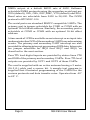
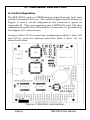
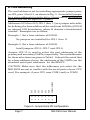
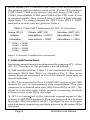
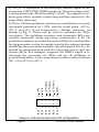
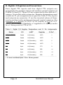
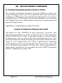
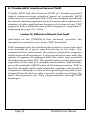
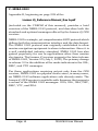
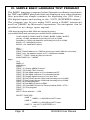
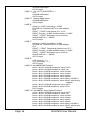
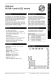
MSI-P602 Trimble Lassen iQ GPS & Digital I/O Card Revision 2 User Manual PC/104 Embedded Industrial Analog I/O Series Microcomputer Systems, Inc. 1814 Ryder Drive ¨ Baton Rouge, LA 70808 Ph (225) 769-2154 ¨ Fax (225) 769-2155 Email: [email protected] http://www.microcomputersystems.com CONTENTS I. INTRODUCTION 4 II.HARDWARE DESCRIPTION 6 A. Card Configuration B. Card Addressing 6 C. Interrupt Connections D. Digital I/O Registers and Connections 8 10 E. 3.0V Battery 11 III. GPS SOFTWARE COMMANDS 7 12 A. Trimble Standard Interface Protocol (TSIP) 12 B. Trimble ASCII Interface Protocol (TAIP) C. NMEA 0183 13 14 IV. SAMPLE BASIC LANGUAGE TEST PROGRAM 15 V. SPECIFICATIONS 19 APPENDIX Schematic Diagrams of the MSI-P602 21 BLANK PAGE I. INTRODUCTION The MSI-P602 is a low cost, high performance global positioning system which uses the Trimble Lassen iQ module. It provides 12-channel GPS functionality that is fully compatible with Trimble’s popular Lassen SQ module using Trimble’s FirstGPS® architecture which delivers complete position, velocity and time (PVT) solutions for the host application. It features two GPS signal sensitivity modes: Standard and Enhanced. With Enhanced mode enabled, the module automatically switches to higher sensitivity when satellite signals are weak. The module also supports TSIP download of critical startup information for fast acquisition. This aided GPS (A-GPS) startup provides hot start performance for each power-up. The module supports the four most popular protocols: DGPS (RTCM), TSIP (Trimble Standard Interface Protocol), TAIP (Trimble ASCII Interface Protocol) and NMEA 0183 with an MTBF (mean time between failures) figure of 60 years. The card provides two serial ports for processing the GPS data. The primary port gives TSIP input and output data at a default BAUD rate of 9600. This port is also selectable for the TAIP protocol. The secondary port provides DGPS (RTCM) input and PC/104 16-BIT STACKTHROUGH CONNECTOR ADDRESS JUMPERS PC/104 BUS INTERFACE NETWORK 3.0V BATTERY UART 1 TSIP GPS DATA I/O TRIMBLE iQ GPS MODULE POWER CONVERTER & ANTENNA MSI-P602 PC/104 BUS INTERRUPT NETWORK UART 2 TAIP/NMEA GPS CONTROL DIGITAL I/O 4 TTL INPUTS 4 TTL OUTPUTS INTERRUPT JUMPERS Figure 1. Block Diagram of the MSI-P602. Page 4 MSI-P602 User Manual BLOCK DIAGRAM NMEA output at a default BAUD rate of 4800. Software selectable NMEA protocols using the secondary serial port are GGA (default), GLL, GSA, GSV, RMC, VTG (default) and ZDA. Baud rates are selectable from 2400 to 38,400. The DGPS protocol is RTCM SC-104. The serial ports are standard IBM PC compatible UARTs. The primary port is jumper selectable for COM1 or COM3 with an optional 16-bit offset address. Similarly, the secondary port is selectable at COM2 or COM4 with an optional 16-bit offset address. A time mark of 1 PPS is available as an interrupt or as input into modem status line DCD of the secondary UART for synchronizing events. The primary and secondary UART interrupt are also provided for allowing interrupt processing of GPS data. Interrupts are jumper selectable for IRQ3 thru IRQ7 and IRQ9, as described in the next section. Four TTL level digital inputs are provided by status lines CTS and DSR of the primary and secondary UARTs. Four TTL level outputs are provided by OUT1 and OUT2 of these UARTs. The card is supplied with an active antenna having a 5 meter (16.5 ft.) cable and a spacer kit. A sample test program is supplied that illustrates programming of the UARTs for the various protocols and data transfer rates. Operates from -40° to 85° C. Page 5 MSI-P602 User Manual II. HARDWARE DESCRIPTION A. Card Configuration The MSI-P602 card is a CMOS design using through-hole and surface-mounted devices. The card configuration is shown in Figure 2 and a circuit diagram of the network is given in Appendix B. The card contains two UARTS (U4 and U5) that commnucate with the GPS module. Connector J1 provides for the digital I/O connections. Jumper block JP1 for interrupt configuration (Pins 1 thru 12) and JP2 is used for address selection (Pins 1 thru 14), as described below. Figure 2. MSI-P602 card outline. Page 6 MSI-P602 User Manual B. Card Addressing The card address is set by installing appropriate jumper pairs on JP2, pins 1 thru 13, as shown in Fig. 3. An installed jumper for a given address bit sets the bit to 1 (true) and an uninstalled jumper sets the bit equal to 0 (false). Addresses A15 thru A10 (JP2-1 thru 11) are jumper selectable for defining the base address of the card from 0000H to FC00H on integral 10H boundaries, where H denotes a hexadecimal number. Examples are as follow: Example 1. Set a base address of 0000H. No jumpers are installed for JP2-1 thru 11. Example 2. Set a base address of 3800H. Intall jumpers JP2-5, JP2-7 and JP2-9. Jumper JP2-13 is used to select the port addresses of the primary and secondary UARTs, respectively. The card addresses for these selections are given in Table I. It should be noted that for a base address of zero, the addresses of the UARTs are the standard serial port addresses for the IBM PC. A14 A13 A12 A11 A10 COM1/COM2 o o o o o o o o o o o o o 3 5 7 9 11 13 A15 o 1 CAUTION: Make sure that the addresses you select for the MSI-P602 are not in conflict with the serial ports of your CPU card. For example, if your CPU uses COM1 and/or COM2, Figure 3. Jumper block JP2 configuration. Page 7 MSI-P602 User Manual do not install JP2-13 so that COM3 and COM4 are selected for the primary and secondary serial ports. If your CPU contains COM1 thru COM4 ports and you are only using COM1 and COM2, then disable COM3 and COM4 of the CPU card. If this is not permissible, then you will have to select a base address other than 0 by using jumpers for JP2-1 thru JP2-11. UART addresses in this case are given in Table 1. Table 1. Card UART Addresses for JP2-13 Selection. Jumper JP2-13 Primary UART (U4) Secondary UART (U5) Installed base address + COM1** base address + COM2 Uninstalled base address + COM3 base address + COM4 ** COM1 = 3F8H COM2 = 2F8H COM3 = 3E8H COM4 = 2E8H where H denotes hexadecimal notational. C. Interrupt Connections Interrupt connections are implemented by jumpers JP1-1 thru JP1-12. The steps in the procedure are as follows. 1) Odd numbered pins 1 thru 11 are connected to processor interrupts IRQ9 thru IRQ3, as shown in Fig. 4. Wire-wrap connections are necessary to select the desired interrupts as described below. 2) JP1-2 is connected to the 1 PULSE/SEC output of the GPS module for use in sychronizing data acquisitions. This can jumpered to a desired interrupt, IRQ4 thru IRQ9, of JP1. The signal is a tri-state gate which permits connecting multiple sources to the same IRQx interrupt. 3) JP1-4 is connected to the interrupt request signal of the primary UART (TSIP protocol). This can jumpered to a desired interrupt, IRQ4 thru IRQ9, of JP1. The signal is a tri-state gate which permits connecting multiple sources to the same IRQx interrupt. Page 8 MSI-P602 User Manual 4) JP1-12 is connected to the interrupt request signal of the secondary UART (TAIP/NMEA protocol). This can jumpered to a desired interrupt, IRQ4 thru IRQ9, of JP1. The signal is a tristate gate which permits connecting multiple sources to the same IRQx interrupt. 1PPS TSIP 1K Pulldown 1K Pulldown 1K Pulldown NMEA 2 4 6 8 10 12 o o o o o o o o o o o o IRQ9 1 IRQ7 3 IRQ6 5 IRQ5 7 IRQ4 9 IRQ3 11 5) Three 1 KOhm pulldown resistors are available for use with interrupts generated by 1 PPS and the serial ports. JP1-6, JP1-8 and JP1-10 are connected to 1 KOhm resistors, as shown in Fig. 4. These can be used to pulldown the IRQx interrupts. The pulldown resistors and interrupts IRQx are usually connected using wire-wrap connections. If no 1K pulldown resistor is provided for a given IRQx to be used (either by the processor card or by another card in the system sharing this IRQx), then one of the available 1K pulldowns of JP1-6 , etc. should be interconnected with the interrupt source and the chosen IRQx. For example, suppose the NMEA signal is to interrupt the processor via IRQ5 and no 1K pulldown is provided elsewhere. A wire-wrap chain could be connected from JP1-12 to JP1-8 to JP1-7. Figure 4. Interrupt jumper block JP1 configuration. Page 9 MSI-P602 User Manual D. Digital I/O Registers and Connections. Four digital TTL inputs and four digital TTL outputs are provided by the modem status and modem control registers of UARTs U4 and U5. These I/O are connected to the card via J1 using a 16-pin flat cable connector. Register designations and connector J1 pin assignments are given in Table 2. The inputs and outputs on connector J1 are the inverted values of those read or written in the modem status and control registers. For example, a 1 written to OUT1 of U4 results in a 0 at J1-1 (OUT1_BUFFERED). Similarly, a 1 applied to J1-9 (IN1) results in a 0 being read in CTS of U4. Table 2. Digital I/O Register Designations and J1 Pin Assignments. −−−−−−−−−−−−−−−−−−−−−−−−−−−−−−−−−−−−−−−−−−−−−−−−−−−−−−−−− Name I/O UART Register J1 Pin* −−−−−−−−−−−−−−−−−−−−−−−−−−−−−−−−−−−−−−−−−−−−−−−−−−−−− OUT1_BUFFERED Output U4 (Primary) OUT1 1 OUT2 Output U4 (Primary) OUT2 3 OUT3 Output U5 (Secondary) OUT1 5 OUT4 Output U5 (Secondary) OUT2 7 IN1 Input U4 (Primary) CTS 9 IN2 Input U4 (Primary) DSR 11 IN3 Input U5 (Secondary) CTS 13 IN4 Input U5 (Secondary) DSR 15 −−−−−−−−−−−−−−−−−−−−−−−−−−−−−−−−−−−−−−−−−−−−−−−−−−−−−−−−−−− * J1 even numbered pins 2 thru 16 are ground. Page 10 MSI-P602 User Manual E. 3.0V Battery A socketed 3.0V battery is included for enhancing GPS data acquisition time by maintaining memory during no power periods. The battery is enabled to the module when jumper JP4 is in the ON position. The unit is shipped with this jumper in the OFF position to conserve battery power. Page 11 MSI-P602 User Manual III. GPS SOFTWARE COMMANDS A. Trimble Standard Interface Protocol (TSIP) The Trimble Standard Interface Protocol (TSIP) provides the system designer with over 20 commands that may be used to configure a GPS receiver for optimum performance in a variety of applications. TSIP enables the system designer to customize the configuration of a GPS module to meet the requirements of a specific application. Appendix A, beginning on page 85 of the Lassen iQ_Reference Manual_Rev b.pdf (included on the CDROM of this manual), provides the information needed to make judicious use of the powerful features TSIP has to offer, to greatly enhance overall system performance, and to reduce the total development time. The provided reference tables will help you determine which packets apply to your application. For those applications requiring customization see Customizing Receiver Operations, page 89 for a detailed description of the key setup parameters. Application guidelines are provided for each TSIP Command Packet, beginning on page 102. Page 12 MSI-P602 User Manual B. Trimble ASCII Interface Protocol (TAIP) C Trimble ASCII Interface Protocol (TAIP) is a Trimble-specified digital communication interface based on printable ASCII characters over a serial data link. TAIP was designed specifically for vehicle tracking applications but has become common in a number of other applications because of its ease of use. TAIP supports both scheduled and polled responses. Appendix C, beginning on page 167 of the Lassen iQ_Reference Manual_Rev b.pdf (included on the CDROM of this manual), provides the information needed to use of the TAIP functions. TAIP messages may be scheduled for output at a user specified rate starting on a given epoch from top of the hour. For communication robustness, the protocol optionally supports checksums on all messages. It also provides the user with the option of tagging all messages with the unit’s user specified identification number (ID). This greatly enhances the functional capability of the unit in a network environment. Additionally, given the printable ASCII format of all communication, TAIP is ideal for use with mobile data terminals, modems, and portable computers. Although, receivers incorporating this protocol are shipped from the factory with a specific serial port setting, the port characteristics are fully programmable through TAIP messages. Page 13 MSI-P602 User Manual C. NMEA 0183 E Appendix E, beginning on page 209 of the Lassen iQ_Reference Manual_Rev b.pdf (included on the CDROM of this manual), provides a brief overview of the NMEA 0183 protocol, and describes both the standard and optional messages offered by the Lassen iQ GPS receiver. NMEA 0183 is a simple, yet comprehensive ASCII protocol which defines both the communication interface and the data format. The NMEA 0183 protocol was originally established to allow marine navigation equipment to share information. Since it is a well established industry standard, NMEA 0183 has also gained popularity for use in applications other than marine electronics. The Lassen iQ receiver supports the latest release of NMEA 0183, Version 3.0 (July 1, 2000). The primary change in release 3.0 is the addition of the mode indicators in the GLL, RMC, and VTG messages. For those applications requiring output only from the GPS receiver, NMEA 0183 is a popular choice since, in many cases, an NMEA 0183 software application code already exists. The Lassen iQ GPS receiver is available with firmware that supports a subset of the NMEA 0183 messages: GGA, GLL, GSA, GSV, RMC, VTC, and ZDA. Page 14 MSI-P602 User Manual IV. SAMPLE BASIC LANGUAGE TEST PROGRAM The BASIC language program below illustrates software sequences for TSIP and NMEA protocols that are displayed on a video monitor. Also provided are simple routines for inputting the /IN1 thru / IN4 digital inputs and writing to the /OUT1_BUFFERED output. The program can be run under DOS using a BASIC interpreter such as QBASIC by Microsoft Corporation. An interpreter can be provided at no charge upon request. ‘GPS terminal program for MSI-P602 with Lassen iQ primary ‘port at 9600 BAUD and secondary port at 4800 BAUD (default mode) COM1 = &H3F8: COM2 = &H2F8: COM3 = &H3E8: COM4 = &H2E8 primary = COM3 ‘set default for primary port (U4) to COM3 secondary = COM4 ‘set default for secondary port (U5) to COM4 BAUD = 12 ‘9600 BAUD divisor BAUD1 = 24 ‘4800 BAUD divisor CLS PRINT “” PRINT “Default address is COM3 for primary port and COM4 for secondary” PRINT “port. No address jumper for JP1 should be installed.” PRINT “”: PRINT “Strike any key to continue!” WHILE INKEY$ = “”: WEND begin: CLS NMEA = 1 GOSUB init PRINT “” PRINT “(1) Display NMEA Protocol.” PRINT “(2) Display TSIP Protocol.” PRINT “(3) Set digital outputs of J1 to hexadecimal 55.” PRINT “(4) Set digital outputs of J1 to hexadecimal AA.” PRINT “(5) Display digital inputs of J1 /IN1 thru /IN4.” PRINT “(6) Set Primary port to COM1 and Secodary port to COM2.” PRINT “(7) Set Primary port to COM3 and Secodary port to COM4.” PRINT “(8) Enable Interrupts.” PRINT “(9) Set NMEA Protocol to RMC.” PRINT “(10) Set NMEA Protocol to Factory Default (GGA + VTG).” PRINT “(11) Exit program” PRINT “” INPUT “Enter selection - “, GP$ SELECT CASE GP$ CASE “1” NMEA = 1: GOSUB init: GOTO start CASE “2” NMEA = 0: GOSUB init: GOTO start CASE “3” ‘set /OUT1_BUFFERED = 0 z=0 Page 15 MSI-P602 User Manual GOSUB setDOutput GOTO begin CASE “4” ‘set /OUT1_BUFFERED = 1 z=1 GOSUB setDOutput GOTO begin CASE “5” ‘display digital inputs GOSUB getDInputs GOTO begin CASE “6” primary = COM1: secondary = COM2 GOSUB init ‘Initialize UARTs for new address. CLS PRINT “”: PRINT “Intall jumper JP1-13,14.” PRINT “Primary = COM1 and Secondary = COM2.” PRINT “”: PRINT “Strike any key to continue.” WHILE INKEY$ = “”: WEND GOTO begin CASE “7” primary = COM3: secondary = COM4 GOSUB init ‘Initialize UARTs for new address. CLS PRINT “”: PRINT “Remove all jumpers from JP1.” PRINT “Primary = COM3 and Secondary = COM4.” PRINT “”: PRINT “Strike any key to continue.” WHILE INKEY$ = “”: WEND GOTO begin CASE “8” OUT primary + 1, 1 OUT secondary + 1, 1 GOTO begin CASE “9” ‘Set NMEA RMC Protocol pchar = &H10: GOSUB sendpchar ‘send <DLE> pchar = &H7A: GOSUB sendpchar ‘send <id> pchar = &H0: GOSUB sendpchar ‘send <byte0> pchar = &H1: GOSUB sendpchar ‘send <byte1> pchar = &H0: GOSUB sendpchar ‘send <byte2> pchar = &H0: GOSUB sendpchar ‘send <byte3> pchar = &H1: GOSUB sendpchar ‘send <byte4, set RMC > pchar = &H0: GOSUB sendpchar ‘send <byte5, sets factory ‘ default> pchar = &H10: GOSUB sendpchar ‘send <DLE> pchar = &H3: GOSUB sendpchar ‘send <ETX> GOTO begin CASE “10” ‘Set NMEA Factory Default Protocol pchar = &H10: GOSUB sendpchar ‘send <DLE> pchar = &H7A: GOSUB sendpchar ‘send <id> pchar = &H0: GOSUB sendpchar ‘send <byte0> pchar = &H1: GOSUB sendpchar ‘send <byte1> pchar = &H0: GOSUB sendpchar ‘send <byte2> pchar = &H0: GOSUB sendpchar ‘send <byte3> pchar = &H0: GOSUB sendpchar ‘send <byte4, set RMC > pchar = &H5: GOSUB sendpchar ‘send <byte5, sets factory ‘ default> Page 16 MSI-P602 User Manual pchar = &H10: GOSUB sendpchar ‘send <DLE> pchar = &H3: GOSUB sendpchar ‘send <ETX> GOTO begin CASE “11” END CASE ELSE GOTO begin END SELECT start: CLS repeat: C$ = INKEY$ IF C$ <> “” THEN GOTO begin ‘goto begin on keyboard entry IF NMEA = 1 THEN GOSUB getsecondarychar ELSE GOSUB getprimarychar GOTO repeat init: ‘init MSI-P602 port of U4 cr$ = CHR$(13) OUT primary + 3, &H80 OUT primary, BAUD OUT primary + 1, 0 OUT primary + 3, 11’3 x = INP(primary) ‘dummy read x = INP(primary) ‘dummy read ‘init MSI-P602 port of U5 cr$ = CHR$(13) OUT secondary + 3, &H80 OUT secondary, BAUD1 OUT secondary + 1, 0 OUT secondary + 3, 3 x = INP(secondary) ‘dummy read x = INP(secondary) ‘dummy read RETURN sendpchar: ‘Send character pchar to primarry port WHILE (INP(primary + 5) AND &H40) = 0: WEND OUT primary, pchar RETURN getprimarychar: IF (INP(primary + 5) AND 1) = 1 THEN z = INP(primary) IF NMEA = 1 THEN PRINT CHR$(z); ELSE PRINT CHR$(&H30 + z / 16); PRINT CHR$(&H30 OR (z AND 15)); END IF END IF RETURN Page 17 MSI-P602 User Manual getsecondarychar: IF (INP(secondary + 5) AND 1) = 1 THEN z = INP(secondary) IF NMEA = 1 THEN PRINT CHR$(z); ELSE PRINT CHR$(&H30 + z / 16); PRINT CHR$(&H30 OR (z AND 15)); END IF END IF RETURN setDOutput: ‘set OUT1_BUFFERED (J1) &h55 or &haa IF z = 1 THEN ‘set OUT1_BUFFERED (J1-1,3) = 0,1 z = INP(primary + 4) ‘get MODEM control register contents z = z OR 4 ‘set corresponding OUT1 bit in z z = z AND (NOT 8) OUT primary + 4, z ‘output to Modem control register z = INP(secondary + 4) ‘get MODEM control register contents z = z OR 4 ‘set corresponding OUT1 bit in z z = z AND (NOT 8) OUT secondary + 4, z ‘output to Modem control register ELSEIF z = 0 THEN ‘set OUT1_BUFFERED (J1-1,3) = 1,0 z = INP(primary + 4) ‘get MODEM control register contents z = z AND NOT 4 ‘reset corresponding OUT1 bit in z z = z OR 8 OUT primary + 4, z ‘output to Modem control register z = INP(secondary + 4) ‘get MODEM control register contents z = z AND NOT 4 ‘reset corresponding OUT1 bit in z z = z OR 8 OUT secondary + 4, z ‘output to Modem control register END IF RETURN getDInputs: ‘get digital inputs from /CTS & /DSR of UARTS z = INP(primary + 6) AND &H30 ‘get CTS & DTR of primary UART z1 = INP(secondary + 6) AND &H30 ‘get CTS & DTR of secondary UART CLS ‘clear screen PRINT “”: PRINT “Digital Inputs from J1”: PRINT “” IF ((z AND &H10) / &H10) > 0 THEN q = 0 ELSE q = 1 ‘invert CTS bit PRINT “/IN1 (J1-9) = “; q ‘display /IN1 IF ((z AND &H20) / &H20) > 0 THEN q = 0 ELSE q = 1 ‘invert DSR bit PRINT “/IN2 (J1-11) = “; q ‘display /IN2 IF ((z1 AND &H10) / &H10) > 0 THEN q = 0 ELSE q = 1 ‘invert /CTS bit PRINT “/IN3 (J1-13) = “; q ‘display /IN3 IF ((z1 AND &H20) / &H20) > 0 THEN q = 0 ELSE q = 1 ‘invert /CTS bit PRINT “/IN4 (J1-15) = “; q ‘display /IN4 WHILE INKEY$ = “”: WEND ‘delay until keyboard character entry RETURN Page 18 MSI-P602 User Manual V. SPECIFICATIONS PC/104 16-bit, stackthrough GPS Receiver Frequency L1, 1575.42 MHz C/A Code Channels 12, continuous tracking GPS Accuracy Horizontal < 5 meters (50%), < 8 meters (90%) Altitude < 10 meters (50%), < 16 meters (90%) Velocity 0.06 meters/sec PPS (static) +/- 50 nanoseconds GPS Acquisition Rate Autonomous Operation in Standard Sensitivity Mode Re-acquisition < 2 seconds (90%) Hot Start < 10 seconds (50%), < 13 seconds (90%) Warm Start < 38 seconds (50%), < 42 seconds (90%) Cold Start < 50 seconds (50%), < 84 seconds (90%) Cold Start requires no initialization. Warm start implies last position, time and almanac are saved by backup power. Hot start implies ephemeris also saved. GPS Dynamic Condition Altitude 18,000 m (60,000 ft.) max Velocity 515 m/sec (1000 knots) max Either limit may be exceeded, but not both. GPS Protocols TSIP TAIP NMEA 0183 v3.0 GGA, VTG, GLL, ZDA, GSA, GSV and RMC RTCM SC-104 Page 25 MSI-P602 User Manual GPS Antenna Active with 5m (16.5 ft) cable Model Compact Magnetic Mount Digital I/O Port 4 Input TTL level (Inverted) 4 Output TTL level (Inverted) Serial Ports Primary TSIP bi-directional (jumper selectable as COM1, COM3 or offset) Secondary NMEA 0183 Output RTCM SC-104 V2.1 Input (jumper selectable as COM2, COM4 or offset) Interrupts Sources 1 PPS, primary and secondary UARTs using tristate drivers IRQs IRQ3 thru IRQ7 and IRQ9 1KOhm Pulldowns 3 wire-wrap selectable Option Jumpers .025" square posts, 0.1" grid Digital I/O Connector 3M 30316-5002 Electrical & Environmental +5V @ 70 mA typical, continuous mode +5V @ 45 mA typical, power save mode -40° to 80° C Page 26 MSI-P602 User Manual APPENDIX Schematic Diagrams of the MSI-P602 1) P602-1.sch - Schematic sheet 1 of 2. See p602r2-1.pdf 2) P602-2.sch - Schematic sheet 2 of 2. See p602r2-2.pdf Page 27 MSI-P602 User Manual