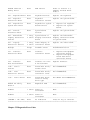
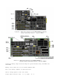
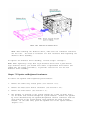
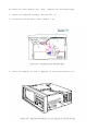
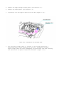
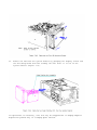
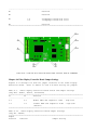
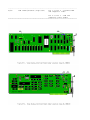
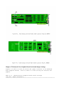
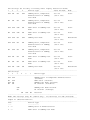
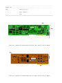
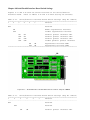
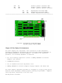
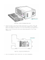
1
Thank you for purchasing this Factory Service
Manual CD/DVD from servicemanuals4u.com.
Please check out our eBay auctions for more great
deals on Factory Service Manuals:
servicemanuals4u
Foreword
Notice
The information in this guide is subject to change without notice.
Compaq Computer Corporation shall not be liable for technical or editorial
errors or omissions contained herein; nor for incidental or consequential
damages resulting from the furnishing, performance, or use of this material.
This guide contains information protected by copyright. No part of this
guide may be photocopied or reproduced in any form without prior written
consent from Compaq Computer Corporation.
1986, 1990 Compaq Computer Corporation.
All rights reserved. Printed in the USA.
COMPAQ, DESKPRO, SYSTEMPRO, FASTART, Registered United States Patent and
Trademark Office.
The software described in this guide is furnished under a license agreement
or nondisclosure agreement. The software may be used or copied only in
accordance with the terms of the agreement.
Product names mentioned herein are for identification purposes only and may
be trademarks and/or registered trademarks of their respective companies.
COMPAQ PORTABLE II PERSONAL COMPUTER
MAINTENANCE AND SERVICE GUIDE
Second Edition (December 1990)
First Edition (February 1986)
Manual Assy No. 101206-002
Text PN 104208-002
Binder PN 104207-001
Preface
This publication is intended as a reference for technicians trained to repair
the COMPAQ PORTABLE II Personal Computer.
Summary of Text
This guide contains the following eight chapters:
Chapter 1, "Operating and Performance Specifications," provides physical,
environmental, and performance specifications for the COMPAQ PORTABLE II
Personal Computer.
Chapter 2, "Power On Self Test," describes the internal system diagnostic
programs that execute automatically when the system is turned on. It also
includes a quick reference for identifying and correcting problems that could
occur during the Power On Self Test procedure.
Chapters 3 and 4: Please see the SUPPORT SOFTWARE MAINTENANCE AND SERVICE
GUIDE for information on the SETUP and ADVANCED DIAGNOSTICS programs.
Chapter 5, "Error Messages and Codes," lists the Power On Self Test (POST) and
DIAGNOSTICS Error Codes and provides the course of action necessary to
resolve the problem.
Chapter 6, "Illustrated Parts Catalog," provides an illustrated reference for
COMPAQ PORTABLE II Personal Computer spare parts.
Chapter 7, "Removal and Replacement Procedures," describes how to remove and
replace field replaceable subassemblies.
Chapter 8, "Jumper Settings, Switch Settings, and Adjustments," provides
detailed information for setting jumpers and switches and performing monitor
adjustments.
Tools and Supplies
The following tools and supplies are required to service the COMPAQ PORTABLE
II Personal Computer:
o
o
o
o
o
o
o
o
Torx screwdrivers, sizes T-15 and T-10
Slotted blade screwdriver, 1/4 inch
Needlenosed pliers
25 pin printer loopback plug
25 pin serial loopback plug
9 pin serial loopback plug
DIAGNOSTICS diskette
Formatted diskette
Optional Tools
o
o
o
o
o
Memory chip insertion tool
Memory chip removal tool
Diskette drive signal extension cable (PN 100546-001)
Diskette drive power extension cable (PN 100545-001)
Socket/Torx tool kit (PN 101089-001)
- Torx screwdrivers, sizes T-15 and T-10
- Adjustable socket tool with hex sockets and one Torx socket (T-10)
>>>>>>>>>>>>>>>>>>>>>>>>>>>>>>>>>>>>>>><<<<<<<<<<<<<<<<<<<<<<<<<<<<<<<<<<<<<<<
CAUTION
Only trained technicians should attempt to repair this equipment.
troubleshooting and repair procedures are detailed to allow
subassembly/module level repair only.
All
Because of the complexity of the individual boards and subassemblies, no one
should attempt to make repairs at the component level or make modifications
to any printed wiring board. Improper repairs may create a safety hazard.
Indications of component replacement or printed wiring board modifications
may void any warranty or exchange allowances.
>>>>>>>>>>>>>>>>>>>>>>>>>>>>>>>>>>>>>>><<<<<<<<<<<<<<<<<<<<<<<<<<<<<<<<<<<<<<<
Additional Reference Information
The following support documentation is available for the COMPAQ PORTABLE II
Personal Computer.
o
o
o
o
o
o
o
Operations Guide
MS-DOS VERSION 3 REFERENCE GUIDE
Technical Reference Guide
HOW TO DO BUSINESS WITH COMPAQ SERVICE
COMPAQ SERVICE QUICK REFERENCE GUIDE
COMPAQ Service Advisories and Bulletins
COMPAQ QuickFind Support Reference Library
>>>>>>>>>>>>>>>>>>>>>>>>>>>>>>>>>>>>>>><<<<<<<<<<<<<<<<<<<<<<<<<<<<<<<<<<<<<<<
WARNING
The computer is designed to be electrically grounded. To ensure proper
operation of the computer, plug the AC power cord only into a properly
grounded AC outlet.
>>>>>>>>>>>>>>>>>>>>>>>>>>>>>>>>>>>>>>><<<<<<<<<<<<<<<<<<<<<<<<<<<<<<<<<<<<<<<
Compaq Computer Corporation requires all peripheral devices be connected to
this computer via shielded cables with metal RFI/EMI connector hoods.
WIRE TYPE: Multipaired, overall shielded; Belden #98XX; Alpha #54XX; or
equivalent.
CONNECTOR HOOD: RFI/EMI metal shield; AMP #7451 7X-X; or equivalent.
It is important that the chassis ground of any peripheral device be connected
to the computer chassis. An Alpha #1221 flat braid strap is sufficient.
This strap is not necessary if the shielded cable connects the two chassis.
Chapter 1. Operating and Performance Specifications
Chapter 1.0 Introduction
This chapter contains operating and performance specifications for the COMPAQ
PORTABLE II Personal Computer.
Chapter 1.1 System Unit
Table 1-1. Electrical and Mechanical Specifications
==============================================================================
Dimensions:
Height
7.5 in. (19.0 cm)
Depth
13.9 in. (35.3 cm)
Width
17.7 in. (45.0 cm)
-----------------------------------------------------------------------------Weight
Model 1 23.6 lb (10.7 kg)
Model 2 25.6 lb (11.6 kg)
Model 3 26.2 lb (11.9 kg)
Model 4 26.3 lb (12.2 kg)
-----------------------------------------------------------------------------Power Requirements:
Voltage
120 VAC
220 - 240 VAC
Frequency
60 Hz
50 Hz
Current
3A
2.5A
-----------------------------------------------------------------------------AC Power Cable:
Length
79 in. (2 m)
Gauge
18 AWG
-----------------------------------------------------------------------------Environmental Requirements:
Temperature:
Operating
10oC to 40oC (50oF to 104oF)
Nonoperating
10oC to 60oC (50oF to 140oF)
Shipping
-30oC to 60oC (-22oF to 140oF)
Humidity:
Operating
Nonoperating
20% to 80% (noncondensing)
5% to 90% (noncondensing
Shock:
Operating
Nonoperating
5 g, 11 ms, half sine
35 g, 11 ms, half sine
Vibration:
Operating
Nonoperating
0.5 g, 5 - 550 Hz
1.0 g, 5 - 550 Hz
Heat Dissipation:
Delivered
Total Watts
410 BTU/hr at 120W
615 BTU/hr at 180W
Maximum Unpressurized Altitude:
Operating
Nonoperating
10,000 ft (3048 m)
30,000 ft (9144 m)
==============================================================================
Chapter 1.2 Keyboard
Table 1-2. Keyboard Specifications
==============================================================================
Dimensions:
Height
1.3 in. (3.30 cm)
Depth
7.0 in. (17.78 cm)
Width
17.1 in. (43.43 cm)
Number of Keys
84
Keyboard:
Cable Length
60.00 in. (152.4 cm)
Coil Diameter
0.75 in. (1.9 cm)
Coil Length
11.00 in. (27.94 cm)
==============================================================================
Chapter 1.3 Video Display Unit
Table 1-3. Video Display Unit Specifications
==============================================================================
Display
9 in. diagonal
90 degree deflection
High persistence green phosphor
Etched surface to reduce glare
Display Size
80 character by 25 line screen
40 character by 25 line screen
Graphic Resolution
640 x 200 dot resolution
320 x 200 dot resolution
Text Resolution
720 x 350 dot resolution
==============================================================================
Chapter 1.4 10 Megabyte Fixed Disk Drive
Table 1-4. 10 Megabyte Fixed Disk Drive Specifications
==============================================================================
Dimensions:
Height
1.7 in. (4.32 cm)
Depth
5.80 in. (14.73 cm)
Width
3.75 in. (9.54 cm)
Weight
2.2 lb (1.0 kg)
Media:
Number of Data Heads
Number of Cylinders
Average Access Time
1 Platter
4
306
105 ms
Data Transfer Rate
5.0 Mb/s
Type
1
==============================================================================
Chapter 1.5 20 Megabyte Fixed Disk Drive
Table 1-5. 20 Megabyte Fixed Disk Drive Specifications
==============================================================================
Dimensions:
Height
1.7 in. (4.32 cm)
Depth
4.1 in. (10.41 cm)
Width
5.75 in. (14.61 cm)
Weight
1.8 lb (0.8 kg)
Media:
2 Platter
Number of Data Heads
4
Number of Cylinders
615
Average Access Time
105 ms
Data Transfer Rate
5.0 Mb/s
Type
2
==============================================================================
Chapter 1.6 360 KByte Diskette Drive
Table 1-6. 360 Kbyte Diskette Drive Specifications
==============================================================================
Dimensions:
Height
1.1 in. (2.85 cm)
Depth
7.9 in. (20.3 cm)
Width
5.9 in. (15.0 cm)
Weight
1.98 lb (0.9 kg)
Media:
Tracks per inch
48
Number of Tracks
40 (when formatted with MS-DOS)
Data Transfer Rate
250 Kb/s
==============================================================================
Chapter 1.7 1.2 Megabyte Diskette Drive
Table 1-7. 1.2 Megabyte Diskette Drive Specifications
==============================================================================
Dimensions:
Height
1.1 in. (2.8 cm)
Depth
8.0 in. (20.3 cm)
Width
5.8 in. (14.6 cm)
Weight
Media:
1.9 lb (0.9 kg)
Tracks per Inch
96 (1.2 megabyte format)
48 (360 Kbyte format)
Number of Tracks
80 (1.2 megabyte format)
40 (360 Kbyte format)
Data Transfer Rate
500 Kb/s (1.2 megabyte format)
300 Kb/s (360 Kbyte format)
==============================================================================
Chapter 1.8 1.44 Megabyte Diskette Drive Specifications
Table 1-8. 1.44 Megabyte Diskette Drive Specifications
==============================================================================
Dimensions:
Height
0.90 in. (2.3 cm)
Depth
6.47 in. (16.42 cm)
Width
5.95 in. (11.1 cm)
Weight
1.98 lb (0.9 kg)
Media:
Tracks per Inch
Number of Tracks
Data Transfer Rate
135
80
500 Kb/s (high density)
250 Kb/s (low density)
==============================================================================
Chapter 1.9 Power Supply
Table 1-9. Power Supply Specifications
==============================================================================
Input Requirements:
Line Voltage
102 to 132 VAC. single phase
180 to 264 VAC. single phase
3.0A fuse, 125 VAC for 120 VAC operations
2.5A fuse, 150 VAC for 220/240 VAC operation
Line Frequency
47 - 62 Hz
Cooling
Forced air provided by internal 12 VDC fan
-----------------------------------------------------------------------------Volts Direct Current Output
Nominal
Maximum
Nominal
Current
Continuous
Peak
Regulation
Voltage
Amperes
Current
Current
Tolerance
(VDC)
Minimum
(Amperes) Maximum * (Amperes)
Percentage
-----------------------------------------------------------------------------+5.0
3.0
13.9
13.9
ñ2
-5.0
0.0
0.5
0.5
ñ5
+12.2
1.0
4.0
7.0
ñ2
-12.0
0.0
0.5
0.5
ñ5
-----------------------------------------------------------------------------* These values are maximum values based on nominal operating conditions for
temperature, line voltage, frequency and altitude. Also, a minimum load on
l2 VDC must be maintained for proper power supply operation.
==============================================================================
Chapter 2. Power On Self Test/Problem Isolation
2.1 Power On Self Test
The Power On Self Test (POST) is a series of diagnostic tests performed
automatically when the system is turned on. These tests verify that the
computer system is operating properly. If a subassembly fails POST, an error
code appears on the screen.
To start POST, follow these steps.
1.
Turn off the computer.
2.
Disconnect the signal cables of any peripheral devices (printers, modems,
and so on) from the computer.
3.
Remove the outer access casing to expose the system LED located on the
system board (see Chapter 7 for this procedure).
4.
Install a loopback plug connector at each location from which a
peripheral signal cable was removed.
NOTE: To test your printer during the printer test or to log errors to a
printer, reconnect the printer now.
5.
Verify that the AC power cable is connected to a usable, grounded, three
pronged AC power outlet.
6.
Insert the DIAGNOSTICS diskette into drive A.
7.
Turn on the computer. The system automatically runs POST. See
Section 2.2, "System Problem Isolation," for information on handling
system problems.
Chapter 2.2 System Problem Isolation
This section contains problem isolation procedures for identifying and
correcting system related problems.
To isolate system problems, perform the following steps:
1.
Verify that the AC power switch is on.
2.
Listen for the sound of the fan.
Did you hear the fan?
YES: Proceed to step 3.
NO: Turn off the computer and check the condition of the AC power fuse.
Is the fuse good?
YES: Return the AC power fuse to its fuse holder and turn on the system.
Proceed to step 3.
NO: Replace the AC power fuse (refer to Chapter 7 in this guide
for AC power fuse removal and replacement information). Repeat
steps 1 and 2.
3.
Did you hear an audible beep or see an error code on the screen?
YES: See Chapter 5, "Error Messages and Codes" for information on how to
identify and correct either audible or error code related problems.
NO: Proceed to step 4.
4.
Check the system LED on the system board.
YES: Proceed to step 5.
Is it lit?
If you did not hear the fan, replace it now.
NO: Replace the power supply subassembly chassis and repeat the problem
isolation procedures.
If the problem continues, replace the system board and repeat the problem
isolation procedures.
If the problem has not been corrected, test each controller or option board
by turning off the system, removing a board and turning the power back on.
If the LED is still not on, test each video and storage device by turning off
the system, disconnecting the device power cable and then turning on the
system.
When the system LED lights, power off the system and replace the defective
subassembly.
NOTE: For removal and replacement procedures, refer to Chapter 7.
5.
Check the screen for a blinking cursor.
screen?
Do you see a cursor on the
YES: Proceed to step 6.
NO: Listen for an audible tone (beep) from the system speaker.
If you hear one or two short beeps, POST is complete. The system now boots
the DIAGNOSTICS program. If the screen remains blank, adjust the brightness
knob.
If the display screen remains blank after adjusting the brightness knob, the
video display unit subsystem is not functioning properly.
o
If a color graphics or composite video monitor is available, connect
either device to the correct video outputs on the video display controller
board. Using the CTRL + ALT + < command, change the display mode to the
graphics mode.
If the first screen of the DIAGNOSTICS program appears on the external
monitor, replace the internal video display unit.
If the screen on the external monitor is blank, replace the video display
controller board.
o
If a color graphics or composite video monitor is not available, replace
the video display controller board.
o
If a color graphics or composite video monitor is not available and
replacing the video display controller board does not solve the problem,
replace the internal video display unit.
If you do not hear a beep, replace the system board. If you hear any other
audible sounds, refer to Chapter 5 for more information on POST related error
messages.
6.
Did the cursor disappear from the screen, replaced by the number of Kbytes
(shown in increments) on the display screen?
YES: This indicates the memory self test portion of POST.
step 7.
NO: Replace the system board.
procedures.
7.
Proceed to
Restart the system problem isolation
Did the LEDs on the mass storage device flash, followed by one or two
short beeps?
YES: This indicates that POST and the SETUP utility have completed
successfully. The DIAGNOSTICS program should then boot and the
DIAGNOSTICS menu should appear on the display screen.
Refer to Chapter 4 for additional information on the COMPAQ
DIAGNOSTICS program.
NO: If the cursor reappears and remains on the screen, replace
the system board.
If one audible tone is heard and an error message appears, the SETUP
function was not completed on the system. Press the F1 key and
proceed to Chapter 3 in this guide for information on the SETUP
function.
Chapter 3. Setup
Please consult the SUPPORT SOFTWARE MAINTENANCE AND SERVICE GUIDE for current
information on SETUP.
Chapter 4. Diagnostic Procedures
Please consult the SUPPORT SOFTWARE MAINTENANCE AND SERVICE GUIDE for current
information on DIAGNOSTICS.
Chapter 5. Error Messages and Codes
5.0 Introduction
This section contains Power On Self Test (POST) messages, DIAGNOSTIC error
codes, and memory error codes. The messages and codes are given in tables
that list the message or error code, a description of the error, the probable
cause of the error, and the action required to resolve the error condition.
Chapter 5.1 Power On Self Test Messages
An error message results if a problem is encountered during the Power On Self
Test. This utility runs automatically when the system is turned on.
Table 5-1 lists the message, audible (beep) message, probable cause, and the
recommended action.
Table 5-1. Power On Self Test Error Messages
==============================================================================
Message
Beeps
Probable Cause
Recommended Action
-----------------------------------------------------------------------------101 - I/O ROM Error
1 Long, Option ROM
1. Inspect ROM placement.
1 Short
2. Verify correct ROM
location.
101 - ROM Error
1 Long, System ROM
3. Replace the ROM.
1 Short
-----------------------------------------------------------------------------102 - System Board
None
System board
The following recommended
action applies to error
110 - System Failure None
Timer failure
codes 102 through 115:
111 - System Failure
None
Memory refresh
failure
112 - System Failure
None
CMOS failure
113 - System Failure
None
DMA failure
114 - System Failure
None
Timer interrupt
failure
115 - System Failure
None
Replace the system board.
Protected mode
failure
-----------------------------------------------------------------------------Message
Beeps
Probable Cause
Recommended Action
-----------------------------------------------------------------------------162 - System Options 2 Short SETUP utility
Run SETUP
Error
incorrect
-----------------------------------------------------------------------------163 - Time and Date
2 Short Invalid time or
Run SETUP
Not Set
date
-----------------------------------------------------------------------------164 - Memory Size
2 Short System
Check the memory
Error Discrepancy
configuration
configuration and run SETUP
incorrect
------------------------------------------------------------------------------
XX000B YYZZ 201 Memory Error
None
RAM failure
Refer to Section 5.3,
"Memory Related Error
Codes."
-----------------------------------------------------------------------------301 - Keyboard Error None
Keyboard failure
Replace the keyboard.
-----------------------------------------------------------------------------303 - Keyboard
None
Keyboard
Replace the system board.
Controller Error
controller failure
-----------------------------------------------------------------------------304 - Keyboard or
None
Keyboard or system 1. Replace the keyboard.
System Unit Error
board failure
2. Replace the system
board.
-----------------------------------------------------------------------------401 - Printer
None
System board
Replace the system board.
Interface Error
failure
-----------------------------------------------------------------------------402 - Monochrome
1 Long, System board or
Replace the monochrome
Display Controller
2 Short display controller display controller board
Failure
board
or system board.
-----------------------------------------------------------------------------501 - Display
1 Long, Video display or
Replace the video board.
Controller Failure
2 Short controller board
-----------------------------------------------------------------------------Message
Beeps
Probable Cause
Recommended Action
-----------------------------------------------------------------------------601 - Diskette
None
Diskette
1. Replace multipurpose
Controller Error
controller board
controller board.
2. Replace multipurpose
fixed disk drive
controller board.
-----------------------------------------------------------------------------602 - Diskette
None
Diskette in Drive
Replace diskette.
Boot Record Error
A not bootable
-----------------------------------------------------------------------------1780 - Disk 0
None
Fixed disk drive/
Run DIAGNOSTICS.
Failure
format error
-----------------------------------------------------------------------------1782 - Disk
None
Fixed disk drive/
Run DIAGNOSTICS.
Controller failure
controller error
-----------------------------------------------------------------------------1790 - Disk 0 Error
None
Fixed disk drive
Run SETUP and DIAGNOSTICS.
error or wrong
drive type
-----------------------------------------------------------------------------XX000Y ZZ Parity
None
Expansion RAM
Run DIAGNOSTICS.
Check 2
-----------------------------------------------------------------------------Audible
1 Short Power on
None
successful
-----------------------------------------------------------------------------Audible
2 Short Power on
None
successful
-----------------------------------------------------------------------------(RESUME = "F1" KEY)
None
As indicated
Press F1 key to continue
==============================================================================
Chapter 5.2 Diagnostics Error Codes
DIAGNOSTICS error codes occur if the system recognizes a problem while
running the DIAGNOSTICS program. These error codes help identify possible
defective subassemblies.
Table 5-2 through 5-12 list possible error codes, a description of the error
condition, and the action required to correct the condition.
In each case, the Recommended Action column lists steps necessary to correct
the problem. After completing each step, run the DIAGNOSTICS program to
verify that the error condition has been corrected. If the error code
reappears, perform the next step, then run the DIAGNOSTICS program. Continue
until the DIAGNOSTICS program no longer detects an error condition.
The error codes are
test or action that
error code 603 - 07
failed because of a
in the form of AYY - XX or AAYY - XX, A or AA denotes the
failed. XX denotes a specific problem. For example,
indicated that the diskette drive write/read/compare test
fatal error while writing.
For assistance in the removal and replacement of a particular subassembly,
see Chapter 7, " Removal and Replacement Procedures."
Table 5-2. Processor Test Error Codes
==============================================================================
Error
Codes
Error Description
Recommended Action
-----------------------------------------------------------------------------101 - 01 CPU test failed
Replace the system board and
retest for error codes
101 - 01 through 101 - 94
-----------------------------------------------------------------------------102 - 01 Numeric coprocessor initial
The following steps apply
status word incorrect
to error codes 102 - 01
through 102 - 15:
102 - 02 Numeric coprocessor initial
control word incorrect
1. Replace the numeric
coprocessor and retest.
2. Replace the system
102 - 03 Numeric coprocessor tag word
board and retest.
not all ones
102 - 04
Numeric coprocessor tag word
not all zeros
102 - 05
Numeric coprocessor exchange
command failed
102 - 06
Numeric coprocessor masked
exception incorrectly handled
102 - 07
Numeric coprocessor unmasked
exception incorrectly handled
102 - 08
Numeric coprocessor wrong mask
bit set in status register
102 - 09
Numeric coprocessor unable to
store real number
-----------------------------------------------------------------------------Error
Codes
Error Description
Recommended Action
-----------------------------------------------------------------------------102 - 10 Numeric coprocessor real
The following steps apply
number calculation test failed
to error codes 102 - 01
through 102 - 15:
102 - 11 Numeric coprocessor speed test
failed
1. Replace the numeric
coprocessor and retest.
102 - 12 Numeric coprocessor pattern
2. Replace the system
test failed
board and retest.
102 - 15
Numeric coprocessor inoperative
or socket unoccupied
-----------------------------------------------------------------------------103 - 01 DMA page registers test failed
Replace the system board
and retest for error codes
103 - 02 DMA byte controller test failed
103 - 01 through 113 - 01.
103 - 03
DMA word controller test failed
104 - 01
Interrupt controller master test
failed
104 - 02
Interrupt controller slave test
failed
104 - 03
Interrupt controller software RTC
inoperative
-----------------------------------------------------------------------------Error
Codes
Error Description
Recommended Action
-----------------------------------------------------------------------------105 - 01 Port 61 bit 6 not at zero
Replace the system board
and retest for error codes
105 - 02 Port 61 bit 5 not at zero
103 - 01 through 113 - 01.
105 - 03
Port 61 bit 3 not at zero
105 - 04
Port 61 bit 1 not at zero
105 - 05
Port 61 bit 0 not at zero
105 - 06
Port 61 bit 5 not at one
105 - 07
Port 61 bit 3 not at one
105 - 08
Port 61 bit 1 not at one
105 - 09
Port 61 bit 0 not at one
105 - 10
Port 61 I/O test failed
105 - 11
Port 61 bit 7 not at zero
105 - 12
Port 61 bit 2 not at zero
106 - 01
Keyboard controller self test failed
107 - 01
CMOS RAM test failed
108 - 02 CMOS interrupt test failed
-----------------------------------------------------------------------------Error
Codes
Error Description
Recommended Action
-----------------------------------------------------------------------------108 - 03 CMOS interrupt test, CMOS not
Replace the system board
properly initialized
and retest for error codes
103 - 01 through 113 - 01.
109 - 01 CMOS clock load data test failed.
109 - 02
CMOS clock rollover test failed
109 - 03
CMOS clock test, CMOS not properly
initialized
110 - 01
Programmable timer load data test
failed
110 - 02
Programmable timer dynamic test
failed
111 - 01
Refresh detect test failed
112 - 01
Speed test slow mode out of range
112 - 02
Speed test mixed mode out of range
112 - 03
Speed test fast mode out of range
112 - 04
Speed test unable to enter slow mode
112 - 05
Speed test unable to enter mixed mode
112 - 06 Speed test unable to enter fast mode
-----------------------------------------------------------------------------Error
Codes
Error Description
Recommended Action
-----------------------------------------------------------------------------112 - 07 Speed test system error
Replace the system board
and retest for error codes
112 - 08 Speed test unable to enter AUTO mode
103 - 01 through 113 - 01.
112 - 09
Speed test unable to enter HIGH mode
112 - 10
Speed test HIGH mode out of range
112 - 11
Speed test AUTO mode out of range
113 - 01 Protected mode test failed
------------------------------------------------------------------------------
114 - 01
Speaker test failed
1.
Verify speaker
connection.
2. Replace the speaker and
retest.
3. Replace the system
board and retest.
==============================================================================
Table 5-3. Memory Test Error Codes
==============================================================================
Error
Codes
Error Description
Recommended Action
-----------------------------------------------------------------------------201 - 01 Memory machine ID test failed
The following steps apply
to error codes 201 - 01
201 - 02 Memory machine type test failed
through 202 - 03:
201 - 03
Memory machine ID and type tests
failed
202 - 01
Memory system ROM checksum failed
202 - 02
Failed RAM/ROM map test
1.
2.
3.
Replace VDU controller
board and retest.
Replace the system ROM
and retest.
Replace the system
board and retest.
202 - 03 Failed RAM/ROM protect test
-----------------------------------------------------------------------------203 - 01 Memory write/read test failed
The following steps apply
to error codes 203 -01
203 - 02 Error during saving program memory
through 211 - 03:
write/read test
1. Replace the defective
203 - 03 Error during restore of program memory
memory chip (or
in write/read test
option memory if
installed, error
204 - 01 Memory address test failed
code 208) if an error
code is accompanied
204 - 02 Error during saving program memory in
by an XX000 BYYZZ
address test
code and retest.
2. Replace the system
204 - 03 Error during restore of program memory
memory board or the
in address test
system board.
204 - 04
A20 address test failed
205 - 01
Walking I/O test failed
205 - 02
Error during saving program memory in
walking I/O test
205 - 03
Error during restore of program memory
in walking I/O test
205 - 04 Insufficient memory to perform test
-----------------------------------------------------------------------------Error
Codes
Error Description
Recommended Action
-----------------------------------------------------------------------------208 - 01 Memory refresh test failed
The following steps apply
208 - 02
Error during saving program memory in
refresh test
208 - 03
Error during restore program memory
in refresh test
210 - xx
Incrementing pattern test failed
(expanded memory test)
210 - 01
Data read from block did not match
data written
to error codes 203 - 01
through 211 - 03:
1.
210 - 02
Scan of test block prior to testing
210 - 03
Error while restoring block under test
210 - 05
Inverted pattern compare, but RAM was
correct
210 - 06
Error while restoring block under test
210 - 07
Main memory update failure
211 - xx
Random data pattern test
211 - 01
Memory random pattern test failed
211 - 02
Error during saving program memory and
random pattern in write/read test
2.
Replace the defective
memory chip (or
option memory if
installed, error code
208) if an error code is
accompanied by an
XX000 BYYZZ code and
retest.
Replace the system
memory board or the
system board.
211 - 03
Error during restore of program memory
and random pattern in write/read test
==============================================================================
Table 5-4. Keyboard Test Error Code
==============================================================================
Error
Codes
Error Description
Recommended Action
-----------------------------------------------------------------------------301 - 01 Keyboard short test, 8042 self test
The following steps apply
failed
to error codes 301 - 01
through 304 - 06:
301 - 02 Keyboard short test. interface test
failed
1. Check the keyboard
cable connector. If
301 - 03 Keyboard short test. echo test
disconnected, turn
failed
off computer and
connect keyboard.
301 - 04 Keyboard short test failed
2. Check internal keyboard
connections to system
302 - 01 Keyboard long test failed
board.
3. Replace the keyboard
303 - 01 Keyboard LED test, 8042 self test
and retest.
failed
4. Replace the system
board and retest.
303 - 02
Keyboard LED test, reset test failed
303 - 03
Keyboard LED test, reset test failed
303 - 04
Keyboard LED test, LED command test
failed
303 - 05
Keyboard LED test, LED command test
failed
303 - 06
Keyboard LED test, LED command test
failed
303 - 07
Keyboard LED test, LED command test
failed
-----------------------------------------------------------------------------Error
Codes
Error Description
Recommended Action
-----------------------------------------------------------------------------303 - 08 Keyboard LED test, command byte
The following steps apply
restore test failed
to error codes 301 - 01
through 304 - 06:
303 - 09 Keyboard LED test, LEDs failed to
light
1. Check the keyboard
cable connector. If
304 - 01 Keyboard typematic test failed
disconnected, turn
off computer and
304 - 02 Unable to enter mode 3
connect keyboard.
2. Check internal keyboard
304 - 03 Incorrect scan code from keyboard
connections to system
board.
304 - 04 No keyboard make code observed
3. Replace the keyboard
and retest.
304 - 05 Unable to disable typematic feature
4. Replace the system
board and retest.
304 - 06 Unable to return to normal mode
==============================================================================
Table 5-5. Parallel Printer Interface Test Error Codes
==============================================================================
Error
Codes
Error Description
Recommended Action
-----------------------------------------------------------------------------401 - 01 Printer failed or not connected
The following steps apply
to error codes 401 - 01
402 - 01 Printer data register failed
through 498 - 00:
402 - 02
Printer control register failed
402 - 03
Printer data and control register
failed
402 - 04
Printer loopback failed
402 - 05
Printer loopback and data failed
402 - 06
Printer loopback and control registers
failed
1.
2.
If a printer is
connected, be sure it
is turned on and in the
online mode.
Check the switch
settings on the
multipurpose fixed disk
drive controller board
or the multipurpose
controller board (see
Chapter 8, "Jumper
402 - 07
Printer loopback, data, and control
registers failed
402 - 08
Printer interrupt test failed
402 - 09
Printer interrupt and data register
failed
402 - 10
Printer interrupt and control register
failed
402 - 11
Printer interrupt, data, and control
register failed
402 - 12
Printer interrupt and loopback failed
402 - 13
Printer interrupt, loopback and data
register failed
402 - 14
Printer interrupt, loopback and control
register failed
402 - 15
Printer interrupt, loopback, data, and
control register failed
402 - 16
Printer unexpected interrupt received
403 - 01
Printer pattern test failed
3.
4.
5.
Positions and Switch
Settings and
Adjustments").
Replace the printer
and/or the printer
cable and retest.
Replace the multipurpose
fixed disk drive
controller board or the
multipurpose controller
board and retest.
Replace the system board
and retest.
498 - 00 Printer failed or not connected
==============================================================================
Table 5-6. Video Display Unit Test Error Codes
==============================================================================
Error
Codes
Error Description
Recommended Action
-----------------------------------------------------------------------------501 - 01 Video controller test failed
The following steps apply
to error codes 501 - 01
502 - 01 Video memory test failed
through 516 - 01:
503 - 01
Video attribute test failed
1.
504 - 01
Video character set test failed
505 - 01
Video 80 x 25 mode 9 x 14 character
cell test failed
3.
Video 80 x 25 mode 8 x 8 character
cell test failed
4.
2.
506 - 01
507 - 01
Video 40 x 25 mode test failed
508 - 01
Video 320 x 200 mode color set 0 test
failed
Replace the video
display controller
board and retest.
Replace the monitor and
retest.
Check the VDU fuse on
the system board and
retest.
Replace the system
board and retest.
509 - 01
Video 320 x 200 mode color set 1 test
failed
510 - 01
Video 640 x 200 mode test failed
511 - 01
Video screen memory page test failed
512 - 01
Video gray scale test failed
514 - 0l
Video white screen test failed
516 - 01 Video noise pattern test failed
-----------------------------------------------------------------------------517 - 01 Lightpen text mode test failed - no
The following steps apply
response
to error codes 517 - 01
through 517 - 04:
517 - 02 Lightpen text mode test failed invalid response
1. Replace the lightpen
and retest.
517 - 03 Lightpen medium resolution mode test
2. Replace the display
failed - no response
controller board
and retest.
517 - 04 Lightpen medium resolution modes test
3. Replace the system
failed - invalid response
board and retest.
==============================================================================
Table 5-7. Diskette Drive Test Error Codes
==============================================================================
Error
Codes
Error Description
Recommended Action
-----------------------------------------------------------------------------600 - xx Diskette ID drive types test failed
The following steps apply
to error codes 600 - xx
601 - xx Diskette format failed
through 614 - xx:
602 - xx
Diskette read test failed
603 - xx
Diskette write/read/compare test
failed
NOTE: If the COMPAQ
Enhanced Color Graphics
Board is installed, check
the interrupt setting.
604 - xx
Diskette random seek test failed
1.
605 - xx
Diskette ID media failed
2.
606 - xx
Diskette speed test failed
607 - xx
Diskette wrap test failed
608 - xx
Diskette write protect test failed
609 - xx
Diskette reset controller failed
610 - xx
Diskette change line test failed
614 - xx
Diskette drive file write test
614 - 01
Exceeded maximum soft error limit
3.
4.
5.
Replace the diskette
and retest.
Check the switch and
jumper settings on the
multipurpose fixed disk
drive controller board
or the multipurpose
controller board.
Replace the diskette
power and signal cables
and retest.
Replace the multipurpose
fixed disk drive
controller board or
multipurpose controller
board and retest.
Replace the diskette
614 - 02
Exceeded maximum hard error limit
614 - 03
Previously exceeded maximum soft error
limit
6.
drive and retest.
Replace the system
board and retest.
614 - 04
Previously exceeded maximum hard error
limit
-----------------------------------------------------------------------------Error
Codes
Error Description
Recommended Action
-----------------------------------------------------------------------------614 - 05 Failed to reset controller
The following steps apply to
error codes 600 - xx through
614 - 06 Fatal error while reading
614 - xx:
614 - 07
Fatal error while writing
614 - 08
Failed compare of write/read buffers
614 - 09
Failed to format a track
614 - 10
Failed sector wrap test
614 - 20
Failed to get drive type
614 - 21
Failed to get change line status
614 - 22
Failed to clear change line status
614 - 23
Failed to set drive type in ID media
614 - 24
Failed to read diskette media
614 - 25
Failed to verify diskette media
614 - 26
Failed to read media in speed test
614 - 27
Failed speed limits
614 - 28
Failed write protect test
614 - 29
Failed to read media in file write
test
NOTE: If the COMPAQ
Enhanced Color Graphics
Board is installed, check
the interrupt setting.
1.
2.
3.
4.
5.
6.
Replace the diskette and
retest.
Check the switch and
jumper settings on the
multipurpose fixed disk
drive controller board
or the multipurpose
controller board.
Replace the diskette
power and signal cables
and retest.
Replace the multipurpose
fixed disk drive
controller board or
multipurpose controller
board and retest.
Replace the diskette
drive and retest.
Replace the system
board and retest.
614 - 40 Cylinder 0 error
-----------------------------------------------------------------------------Error
Codes
Error Description
Recommended Action
-----------------------------------------------------------------------------694 - 00 Pin 34 is not cut on 360 KB diskette
See Service Bulletin 25,
drive
Modification of 360 Kbyte
Diskette Drives.
697 - 00 Diskette type error
1. Replace the diskette
698 - 00 Diskette drive speed not within
and retest.
limits
2. Check the switch and
jumper settings on the
multipurpose fixed disk
drive controller board
or the multipurpose
controller board.
3. Replace the diskette
power and signal cables
and retest.
4. Replace the
multipurpose fixed disk
drive controller board
or multipurpose
controller board and
retest.
5. Replace the diskette
drive and retest
6. Replace the system
board and retest.
-----------------------------------------------------------------------------699 - 00 Diskette drive/media ID error
Rerun the SETUP program.
==============================================================================
Table 5-8. Serial Interface Test Error Codes
==============================================================================
Error
Codes
Error Description
Recommended Action
-----------------------------------------------------------------------------1101 - 01 Serial port test, UART DLAB bit
The following steps apply
failure
to error codes 101 - 01
through 1101 - 14;
1101 - 02 Serial port test, line input or UART
fault
1. Check jumper and switch
settings on the
1101 - 03 Serial port test, address line fault
serial/parallel
interface board,
1101 - 04 Serial port test, data line fault
multipurpose fixed disk
drive controller board,
1101 - 05 Serial port test, UART control signal
or the multipurpose
failure
controller board and
retest.
1101 - 06 Serial port test, UART THRE bit
2. Replace the
failure
serial/parallel
interface board,
1101 - 07 Serial port test, UART DATA READY
multipurpose fixed disk
bit failure
drive controller board
or multipurpose
1101 - 08 Serial port test, UART TX/RX buffer
controller board and
failure
retest.
1101 - 09
Serial port test, INTERRUPT circuit
failure
1101 - 10
Serial port test, COM1 set to invalid
interrupt
1101 - 11
Serial port test, COM2 set to invalid
interrupt
1101 - 12
Serial port test, DRIVER/RECEIVER
control signal failure
1101 - 13
Serial port test, UART control signal
interrupt failure
1101 - 14
Serial port test, DRIVER/RECEIVER data
failure
-----------------------------------------------------------------------------1102 - 58 Serial Port COM1 set to INTR 3
1102 - 60
Serial Port COM2 set to INTR 4
1102 - 64
Serial Port data compare error
1102 - 72
Serial Port no TX RDY
1102 - 88 Serial Port no RX RDY
==============================================================================
Table 5-9. Modem Communications Test Error Codes
==============================================================================
Error
Codes
Error Description
Recommended Action
-----------------------------------------------------------------------------1201 - xx Modem Internal Loopback test
The following apply to
error codes 120l - xx
1201 - 01 UART DLAB bit failure
through 1210 - xx:
1201 - 02
Line input or UART failure
1201 - 03
Address line fault
1201 - 04
Data line fault
1201 - 05
UART control signal failure
1201 - 07
UART DATA READY bit failure
1201 - 08
UART TX/RX buffer failure
1201 - 09
INTERRUPT circuit failure
1201 - 10
COM1 set to invalid interrupt
1201 - 11
COM2 set to invalid interrupt
1201 - 12
DRIVER/RECEIVER control signal
failure
1201 - 13
UART control signal interrupt failure
1.
2.
3.
Refer to modem
documentation for
correct setup
procedures.
Check the modem line.
Replace the modem and
retest.
1201 - 14 DRIVER/RECEIVER data failure
-----------------------------------------------------------------------------Error
Codes
Error Description
Recommended Action
-----------------------------------------------------------------------------1201 - 15 Modem detection failure
The following apply to
error codes 120l - xx
1201 - 16
Modem ROM, checksum failure
through 1210 - xx:
1201 - 17
Tone detection failure
1.
1202 - xx
Modem Internal Loopback test
1202 - 01
Timed out waiting for SYNC
(local loopback mode)
1202 - 02
Timed out waiting for modem response
(local loopback mode)
1202 - 03
Exceeded data block retry limit
(local loopback mode)
1202 - 11
Timed out waiting for SYNC
(analog loopback originate mode)
1202 - 12
Timed out waiting for modem response
(analog loopback originate mode)
1202 - 13
Exceeded data block retry limit
(analog loopback originate mode)
1202 - 21
Timed out waiting for SYNC
(analog loopback answer mode)
1202 - 22
Timed out waiting for modem response
(analog loopback answer mode)
2.
3.
Refer to modem
documentation for
correct setup
procedures.
Check the modem line.
Replace the modem and
retest.
1202 - 23
Exceeded data block retry limit
(analog loopback answer mode)
-----------------------------------------------------------------------------Error
Codes
Error Description
Recommended Action
-----------------------------------------------------------------------------1203 - xx Modem External Termination test
The following apply to
error codes 1201 - xx
1203 - 01 Modem external TIP/RING failure
through 1210 - xx:
1203 - 02
Modem external DATA TIP/RING failure
1203 - 03
Modem line termination failure
1204 - xx
Modem auto originate test
1205 - xx
Modem auto answer test
1206 - xx
Dial multifrequency tone test
1210 - xx
Modem direct connect test
1210 - 01
Modem timed out waiting for SYNC
1210 - 02
Modem timed out waiting for response
1210 - 03
Modem exceeded data block retry limit
1210 - 04
RCV exceeded carrier lost limit
1.
2.
3.
Refer to modem
documentation for
correct setup
procedures.
Check the modem line.
Replace the modem and
retest.
1210 - 05
XMIT exceeded carrier lost limit
1210 - 06
Timed out waiting for dial tone
1210 - 07 Dial number string too long
-----------------------------------------------------------------------------Error
Codes
Error Description
Recommended Action
-----------------------------------------------------------------------------1210 - 08 Modem timed out waiting for remote
The following apply to
response
error codes 1201 - xx
through 1210 - xx:
1210 - 09 Modem exceeded maximum redial limit
1. Refer to modem
1210 - 10 Line quality prevented remote
documentation for
connection
correct setup
procedures.
1210 - 11 Modem timed out waiting for remote
2. Check the modem line.
connection
3. Replace the modem and
retest.
1210 - 12 Modem timed out waiting for modem
response (analog loopback originate
mode)
1210 - 13
Modem exceeded data block retry limit
(analog loopback originate mode)
1210 - 14
DRIVER/RECEIVER data failure
1210 - 15
Modem detection failure
1210 - 16
Modem ROM, checksum failed
1210 - 17
Tone detection failure
1210 - 21
Modem timed out waiting SYNC
(analog loopback answer mode)
1210 - 23
Modem exceeded data block for retry
limit (analog loopback answer mode)
==============================================================================
Table 5-10. Fixed Disk Drive Test Error Codes
==============================================================================
Error
Codes
Error Description
Recommended Action
-----------------------------------------------------------------------------1700 - xx Fixed disk ID drive types test failed The following steps apply
to error codes 1700 - xx
1701 - xx Fixed disk drive format test failed
through 1716 - xx.
1702 - xx
Fixed disk drive read test failed
1703 - xx
Fixed disk drive write/read/compare
test failed
1.
Check switch and jumper
settings on the fixed
disk drive controller
board, multipurpose
fixed disk drive
1704 - xx
Fixed disk drive random seek test
failed
1705 - xx
Fixed disk drive controller test
failed
2.
1706 - xx
Fixed disk drive ready test failed
3.
1707 - xx
Fixed disk drive recalibrate test
failed
1708 - xx
Fixed disk drive format bad track
test failed
1709 - xx
Fixed disk drive reset controller
test failed
1710 - xx
Fixed disk drive park head test
failed
1714 - xx
Fixed disk drive file write test
failed
1715 - xx
Fixed disk drive head select test
failed
4.
5.
controller board, or
multipurpose controller
board and retest.
Replace the fixed disk
drive signal and power
cables and retest.
Replace the fixed disk
drive controller
board, multipurpose
fixed disk drive
controller board, or
multipurpose controller
controller board and
retest.
Replace the fixed disk
drive and retest.
Replace the system
board and retest.
1716 - xx
Fixed disk drive conditional format
test failed
-----------------------------------------------------------------------------Error
Codes
Error Description
Recommended Action
-----------------------------------------------------------------------------17yy - xx Invalid fixed disk drive type failed
The following steps apply
to error codes 1700 - xx
17yy - 01 Exceeded maximum soft error limit
through 1716 - xx.
17yy - 02
Exceeded maximum hard error limit
17yy - 03
Previously exceeded maximum soft error
limit
17yy - 04
Previously exceeded maximum hard error
limit
17yy - 05
Failed to reset controller
17yy - 06
Fatal error while reading
17yy - 07
Fatal error while writing
17yy - 08
Failed compare of write/read/compare
17yy - 09
Failed to format a track
17yy - 10
Failed sector wrap test
17yy - 19
Controller failed to deallocate bad
sector
1.
2.
3.
4.
17yy - 40
Failed cylinder 0
5.
Check switch and jumper
settings on the fixed
disk drive controller
board, multipurpose
fixed disk drive
controller board, or
multipurpose controller
board and retest.
Replace the fixed disk
drive signal and power
cables and retest.
Replace the fixed disk
drive controller
board, multipurpose
fixed disk drive
controller board, or
multipurpose controller
controller board and
retest.
Replace the fixed disk
drive and retest.
Replace the system
board and retest.
17yy - 4l
Drive not ready
17yy - 42 Recalibration failed
-----------------------------------------------------------------------------Error
Codes
Error Description
Recommended Action
-----------------------------------------------------------------------------17yy - 43 Failed to format bad track
The following steps apply
to error codes 1700 - xx
17yy - 44 Failed fixed disk drive controller
through 1716 - xx:
board diagnostics
1. Check switch and jumper
17yy - 45 Failed to get drive parameters from
settings on the fixed
ROM
disk drive controller
board, multipurpose
17yy - 46 Invalid drive parameters found in ROM
fixed disk drive
controller board, or
17yy - 47 Failed to park heads
multipurpose controller
board and retest.
17yy - 48 Failed to move disk table to RAM
2. Replace the fixed disk
drive signal and power
17yy - 49 Failed to read media in file write
cables and retest.
test
3. Replace the fixed disk
drive controller
17yy - 50 Failed file I/O write test
board, multipurpose
fixed disk drive
17yy - 5l Failed file I/O read test
controller board, or
multipurpose controller
17yy - 52 Failed file I/O compare test
board and retest.
4. Replace the fixed disk
drive and retest.
5. Replace the system
board and retest.
17yy - 53
Failed drive/head register test
17yy - 54 Failed digital input register test
-----------------------------------------------------------------------------Error
Codes
Error Description
Recommended Action
-----------------------------------------------------------------------------17yy - 55 Failed cylinder 1 test
The following steps apply
to error codes 1700 - xx
17yy - 56 Fixed disk drive controller board
through 1716 - xx:
RAM diagnostics failed
1. Check switch and jumper
17yy - 57 Fixed disk drive controller board
settings on the fixed
to drive test failed
disk drive controller
board, multipurpose
17yy - 58 Failed to write sector buffer
fixed disk drive
controller board, or
17yy - 59 Failed to read sector buffer
multipurpose controller
board and retest.
17yy - 60 Failed to compare sector buffer
2. Replace the fixed disk
drive signal and power
17yy - 63
Failed soft error rate
3.
17yy - 65
Exceeded maximum bad sector per track
17yy - 66
Failed initial drive parameter
17yy - 67
Failed to write long
17yy - 68
Failed to read long
4.
17yy - 69
Failed to read drive size from
controller
5.
17yy - 70
Failed translate mode
17yy - 71
Failed nontranslated mode
17yy - 72
Bad track limit exceeded
cables and retest.
Replace the fixed disk
drive controller
board, multipurpose
fixed disk drive
controller board, or
multipurpose controller
board and retest.
Replace the fixed disk
drive and retest.
Replace the system
board and retest.
17yy - 73 Previously exceeded bad track limit
==============================================================================
Table 5-11. Enhanced Color Graphics Test Error Codes
==============================================================================
Error
Codes
Error Description
Recommended Action
----------------------------------------------------------------------------2402 - 01 Video memory test failed
The following steps apply
to error codes 2402 - 01
2403 - 01 Video attribute test failed
through 2416 - 01:
2404 - 01
Video character set test failed
1.
2405 - 01
Video 80 x 25 mode 9 x 14 character
cell test failed
2.
2406 - 01
Video 80 x 25 mode 8 x 8 character
cell test failed
3.
2407 - 01
Video 40 x 25 mode test failed
4.
2408 - 01
Video 320 x 200 mode color set 0 test
failed
2409 - 01
Video 320 x 200 mode color set 1 test
failed
2410 - 01
Video 640 x 200 mode test failed
2411 - 01
Video screen memory page test failed
2412 - 01
Video gray scale test failed
2414 - 01
Video white screen test failed
2416 - 01
Video noise pattern test failed
Verify the switch
settings.
Replace the COMPAQ
Enhanced Color Graphics
Board ROM and retest.
Replace the COMPAQ
Enhanced Color Graphics
Board and retest.
Replace the system
board and retest.
-----------------------------------------------------------------------------Error
Codes
Error Description
Recommended Action
-----------------------------------------------------------------------------2417 - 01 Lightpen text mode failed - no
The following steps apply
response
to error codes 2417 - 01
through 2417 - 04:
2417 - 02 Lightpen text mode test failed invalid response
1. Replace the lightpen
and retest.
2417 - 03 Lightpen medium resolution mode test
2. Replace the COMPAQ
failed - no response
Enhanced Color Graphics
Board ROM and retest.
2417 - 04 Lightpen medium resolution mode test
3. Replace the COMPAQ
failed - invalid response
Enhanced Color Graphics
Board and retest.
4. Replace the system
board and retest.
-----------------------------------------------------------------------------2418 - 01 ECG memory test failed
The following steps apply
to error codes 2418 - 01
2418 - 02 ECG shadow RAM test failed
through 2425 - 01:
2419 - 01
ECG ROM checksum test failed
1.
2.
2420 - 01
ECG attribute test failed
2421 - 01
ECG 640 x 200 graphics mode test
failed
3.
2422 - 01
ECG 640 x 350 16 Color Set test
failed
4.
2423 - 01
ECG 640 x 350 64 Color Set test failed
2424 - 01
ECG Monochrome Text Mode test failed
Verify switch settings.
Replace the COMPAQ
Enhanced Color Graphics
Board ROM.
Replace the COMPAQ
Enhanced Color Graphics
Board and retest.
Replace the system
board and retest.
2425 - 01
ECG Monochrome Graphics Mode test
failed
==============================================================================
Table 5-12. Pointing Device Interface Test Error Codes
==============================================================================
Error
Codes
Error Description
Recommended Action
-----------------------------------------------------------------------------8601 - xx Pointing device test
l. Verify switch settings
on Multipurpose
8601 - 02 Left button is inoperative
Controller Board,
Multipurpose Fixed Disk
8601 - 03 Left button is stuck closed
Drive Controller Board,
or Serial/Parallel
8601 - 04 Right button is inoperative
Interface Board.
2. Replace the pointing
8601 - 05 Right button is stuck closed
device with a working
pointing device and
8601 - 06 Left block not selected
retest.
3.
Replace the
Multipurpose Controller
Board, Multipurpose
8601 - 08 Timeout occurred
Fixed Disk Drive
Controller Board, or
8601 - 10 Pointing device inoperative
Serial/Parallel
Interface Board and
retest.
4. Replace the system
board and retest.
==============================================================================
8601 - 07
Right block not selected
Chapter 5.3 Memory Related Error Codes
Memory error codes result when the system detects a memory fault during the
Power On Self Test or diagnostic test. The Test programs attempt to isolate
the memory fault to a specific chip, then generate a memory error code that
identifies the defective memory chip.
In some cases, replacing the memory chip will not solve the problem because:
o
The system may not be able to accurately determine which chip or chips are
at fault.
o
The problem may be caused by to a failure in the memory support circuitry,
not the memory.
The memory error code points to a specific memory address. The physical
location of the memory address depends on the type of system, the number and
type of memory boards installed, and the type of memory device used
(64K x 1 Bit RAMs or 256K x 1 Bit RAMs).
Tables 5-14 through 5-17 identify which memory device to replace when the
system shows a memory error. Table 5-13 indicates the table to reference to
locate the defective chip.
Table 5-13. Memory Configurations
==============================================================================
System Board
Error Code
Memory Device
RAM Type
XX Value
Configuration
Tables
-----------------------------------------------------------------------------64K
00 to 02
System Board
5-14, 5-15
(0 - 256 Kbyte)
-----------------------------------------------------------------------------10 to 26
System Memory Board
5-17
(1 - 2.5 megabyte) (512/1536 Kbyte)
-----------------------------------------------------------------------------256K
00 to 08
System Board
5-16
(0 - 640 Kbyte)
-----------------------------------------------------------------------------NOTE: XX codes 0A to 0F represent the memory space for the video memory and
system ROMs. Errors in the video memory or system ROM space are not reported
in the XX000B YYZZ error message format.
==============================================================================
Defective Memory Chip Isolation Map for System Boards using 64K RAMs and
256K RAMs
Memory error codes are in the format XX000B YYZZ.
XX is the memory segment of detected error.
000 is always equal to 000 (not used)
B Byte bank location (Low:
B = 0, High:
B = 1)
YY Bit location of the low byte (B = 0)
ZZ Bit location of the high byte (B =1)
For example, for the Version 1 system board, memory error message
"02000 10010" specifies chip U47.
Use Tables 5-14 through 5-17 to locate the defective chip and determine the
required action.
NOTE: If XX or YY is not documented in the following tables, this may mean
that more than one area contributed to the error condition. If this is the
case, the system adds the values of the failed data bits and displays the sum
in the XX or YY location.
Figures 5-1 and 5-2 show the memory chip locations for the COMPAQ PORTABLE II
Personal Computer System Boards - Version 1 and 2. For information on
removing and replacing memory chips contained on the system board, refer to
Chapter 7 in this guide.
Table 5-14. Version 1 System Board using 64K RAMs (0 - 256 Kbytes)
==============================================================================
XX = 00 (Bank 0)
-----------------------------------------------------------------------------Data Bit
B = 0
B = 1
YY or ZZ
Low
High
Required Action
----------------------------------------------------------------------------00
U37
U38
Replace memory chip
01
U30
U31
Replace memory chip
02
U25
U26
Replace memory chip
04
U21
U22
Replace memory chip
08
U16
U17
Replace memory chip
10
U14
U15
Replace memory chip
20
U9
U10
Replace memory chip
40
U5
U6
Replace memory chip
80
U1
U2
Replace memory chip
-----------------------------------------------------------------------------XX = 02 (Bank 1)
-----------------------------------------------------------------------------Data Bit
B = 0
B = 1
YY or ZZ
Low
High
Required Action
-----------------------------------------------------------------------------00
U41
U42
Replace system board
01
U51
U52
Replace system board
02
U51
U52
Replace system board
04
U51
U52
Replace system board
08
U51
U52
Replace system board
10
U46
U47
Replace system board
20
U46
U47
Replace system board
40
U46
U47
Replace system board
80
U46
U47
Replace system board
==============================================================================
Table 5-15. Version 2 System Board using 64K RAMs (0 - 256 Kbytes)
==============================================================================
XX = 00 (Bank 0)
-----------------------------------------------------------------------------Data Bit
B = 0
B = 1
YY or ZZ
Low
High
Required Action
----------------------------------------------------------------------------00
U32
U35
Replace memory chip
01
U24
U27
Replace memory chip
02
U17
U20
Replace memory chip
04
U9
U12
Replace memory chip
08
U41
U42
Replace memory chip
10
U33
U34
Replace memory chip
20
U25
U26
Replace memory chip
40
U18
U19
Replace memory chip
80
U10
U11
Replace memory chip
-----------------------------------------------------------------------------XX = 02 (Bank 1)
-----------------------------------------------------------------------------Data Bit
B = 0
B = 1
YY or ZZ
Low
High
Required Action
-----------------------------------------------------------------------------00
U40
U43
Replace system board
01
U31
U16
Replace system board
02
U31
U16
Replace system board
04
U31
U16
Replace system board
08
U31
U16
Replace system board
10
U23
U8
Replace system board
20
U23
U8
Replace system board
40
U23
U8
Replace system board
80
U23
U8
Replace system board
==============================================================================
Table 5-16.
Version 1 System Board using 256K RAMs (0 - 640 Kbytes)
==============================================================================
XX = 00, 02, 04, 06 (Bank 0)
-----------------------------------------------------------------------------Data Bit
B = 0
B = 1
YY or ZZ
Low
High
Required Action
-----------------------------------------------------------------------------00
U37
U38
Replace memory chip
01
U30
U31
Replace memory chip
02
U25
U26
Replace memory chip
04
U21
U22
Replace memory chip
08
U16
U17
Replace memory chip
10
U14
U15
Replace memory chip
20
U9
U10
Replace memory chip
40
U5
U6
Replace memory chip
80
U1
U2
Replace memory chip
-----------------------------------------------------------------------------XX = 08 (Bank 1)
-----------------------------------------------------------------------------Data Bit
B = 0
B = 1
YY or ZZ
Low
High
Required Action
-----------------------------------------------------------------------------00
U41
U42
Replace system board
01
U51
U52
Replace system board
02
U51
U52
Replace system board
04
U51
U52
Replace system board
08
U51
U52
Replace system board
10
U46
U47
Replace system board
20
U46
U47
Replace system board
40
U46
U47
Replace system board
80
U46
U47
Replace system board
==============================================================================
Table 5-17. Version 2 System Board using 256K RAMs (0 - 640 Kbytes)
==============================================================================
XX = 00, 02, 04, 06 (Bank 0)
-----------------------------------------------------------------------------Data Bit
B = 0
B = 1
YY or ZZ
Low
High
Required Action
-----------------------------------------------------------------------------00
U32
U35
Replace memory chip
01
U24
U27
Replace memory chip
02
U17
U20
Replace memory chip
04
U9
U12
Replace memory chip
08
U41
U42
Replace memory chip
10
U33
U34
Replace memory chip
20
U25
U26
Replace memory chip
40
U18
U19
Replace memory chip
80
U10
U11
Replace memory chip
-----------------------------------------------------------------------------XX = 08 (Bank 1)
-----------------------------------------------------------------------------Data Bit
B = 0
B = 1
YY or ZZ
Low
High
Required Action
-----------------------------------------------------------------------------00
U40
U43
Replace system board
01
U31
U16
Replace system board
02
U31
U16
Replace system board
04
U31
U16
Replace system board
08
U31
U16
Replace system board
10
U23
U8
Replace system board
20
U23
U8
Replace system board
40
U23
U8
Replace system board
80
U23
U8
Replace system board
==============================================================================
Defective Memory Chip Isolation Map for the 512/1536 Kbyte System Memory
Board Mapped into the 1 to 2.5 Megabyte Memory Space (256K x 1 Bit RAMs)
NOTE: This isolation map is valid for a system memory board that uses
256K x 1 bit RAMs.
Memory error codes are in the format XX000B YYZZ.
XX equals the 128 Kbyte memory segment where an error is detected.
000 is always equal to 000 (not used).
B Byte bank location (Low: B = 0, High: B = 1)
YY Bit location of the low byte (B = 0)
ZZ Bit location of the high byte (B = 1)
Use the following table to locate the defective memory chip and the required
action. Figure 5-3 shows the memory chip locations for the COMPAQ
PORTABLE II Personal Computer System Memory Board (512/1536 Kbyte). For
information on removing and replacing memory chips contained on this board,
refer to Chapter 7.
Table 5-18. Memory Locations/Required Action for 512/1536 Kbyte System Memory
Board Mapped to the 1 to 2.5 Megabyte Memory Space (256K x 1 Bit RAMs)
==============================================================================
XX = 10, 12, 14, 16 (Bank 2)
-----------------------------------------------------------------------------Data Bit
B = 0
B = 1
YY or ZZ
Low
High
Required Action
-----------------------------------------------------------------------------00
U47
U23
Replace system memory board
01
U31
U7
Replace system memory board
02
U32
U8
Replace system memory board
04
U54
U51
Replace system memory board
08
U39
U15
Replace system memory board
10
U40
U16
Replace system memory board
20
U53
U50
Replace system memory board
40
U48
U24
Replace system memory board
80
U52
U49
Replace system memory board
-----------------------------------------------------------------------------XX = 18, 1A, 1C, 1E, (Bank 3)
-----------------------------------------------------------------------------Data Bit
B = 0
B = 1
YY or ZZ
Low
High
Required Action
-----------------------------------------------------------------------------00
U44
U20
Replace memory chip
01
U28
U4
Replace memory chip
02
U29
U5
Replace memory chip
04
U30
U6
Replace memory chip
08
U36
U12
Replace memory chip
10
U37
U13
Replace memory chip
20
U38
U14
Replace memory chip
40
U45
U21
Replace memory chip
80
U46
U22
Replace memory chip
-----------------------------------------------------------------------------XX = 20, 22, 24, 26 (Bank 4)
-----------------------------------------------------------------------------Data Bit
B = 0
B = 1
YY or ZZ
Low
High
Required Action
-----------------------------------------------------------------------------00
U41
U17
Replace memory chip
01
U25
U1
Replace memory chip
02
U26
U2
Replace memory chip
04
U27
U3
Replace memory chip
08
U33
U9
Replace memory chip
10
U34
U10
Replace memory chip
20
U35
U11
Replace memory chip
40
U42
U18
Replace memory chip
80
U43
U19
Replace memory chip
==============================================================================
Chapter 6. Illustrated Parts Catalog
6.0 Introduction
This section provides a spare parts reference for the COMPAQ PORTABLE II
Personal Computer.
Each table in this section contains the following information:
o
Item - reference number keyed to an illustration.
o
Part Number - to be used when ordering parts from Compaq Computer
Corporation.
o
Description - name of the particular part or parts kit.
NOTE: When several parts have the same part number, the parts are available
only as part of a kit.
Chapter 6.1 Compaq Portable II Personal Computer
Table 6-1. COMPAQ PORTABLE II Personal Computer
==============================================================================
Item
Part Number
Description
-----------------------------------------------------------------------------1
107899-001 **
Chassis Cover
2
104179-001 **
Keyboard Assembly
107678-001
Spanish Enhanced Keyboard
Assembly
--------------------------------------------------------------------------** Part number no longer available.
==============================================================================
Chapter 6.2 Chassis
Table 6-2. COMPAQ PORTABLE II Personal Computer Chassis
==============================================================================
Item
Part Number
Description
-----------------------------------------------------------------------------1
107899-001 **
Chassis Cover
2
104081-001 **
Chassis Assembly
3
104198-001 **
Front Bezel
4
104059-001 **
Drive Bezel
5
104050-001
Blank Drive Bezel (third height)
6
*
Brightness Knob Assembly
7
101155-001
AC Power Cord
8
102930-001
3-A AC Line Fuse (Quantity = 40)
100228-002 **
3-A AC Line Fuse (Quantity = 1)
-----------------------------------------------------------------------------* Contained in the Miscellaneous Hardware Kit (Spare PN 104270-001 **).
See Table 6-7.
** Part number no longer available.
==============================================================================
Chapter 6.3 Common Chassis
Table 6-3. COMPAQ PORTABLE II Personal Computer Common Chassis
==============================================================================
Item
Part Number
Description
-----------------------------------------------------------------------------1
104180-001 **
Power Supply Chassis
2
104178-001 **
Fan Assembly
3
104273-001 **
Automatic Power Switching (APS) Board
4
106886-001
Serial/Parallel Interface Board
5
104174-001
102705-001 **
Multipurpose Fixed Disk Drive Controller Board
Multipurpose Controller Board
6
109196-001 **
106686-001
Enhanced Color Graphics Board
Enhanced Color Graphics ROM
7
101340-001 **
Video Display Controller Board
8
105033-001 **
512/2048 Kbyte Memory Expansion Board
9
100025-001 **
Handle
10
104067-001 **
Handle Underlay
11
112693-001
(replaced by
197458-001)
2400 Baud Internal Modem
12
104081-001 **
Chassis Assembly
13
*
Torx 6-32 x 3/8 Screw
14
104185-001 **
Speaker/Brightness Potentiometer Assembly
15
*
Brightness Knob
-----------------------------------------------------------------------------* Contained in the Miscellaneous Hardware Kit (Spare PN 104270-001 **).
See Table 6-7.
** Part number no longer available.
-----------------------------------------------------------------------------Item
Part Number
Description
-----------------------------------------------------------------------------16
104183-001 **
10 Megabyte Fixed Disk Drive
104405-001 ***
20 Megabyte Fixed Disk Drive
17
104093-001
Fixed Disk Drive Signal Cable
18
104182-001
19
104007-001
20
*
Brightness Knob
21
104081-001 **
Chassis Assembly
22
104175-001 **
System Board (Assy No. 000318)
104444-001 **
System Board (Assy No. 000324)
**
**
**
Monitor Assembly
Video Display Signal Cable
23
104176-001 **
512/1536 Kbyte System Memory Board
24
104186-001 **
Battery
25
104008-002
26
104185-001 **
Speaker/Brightness Potentiometer Assembly
27
*
Drive Shoulder Bolt
28
*
Vibration Isolators
**
Diskette Drive Signal Cable
29
104048-001 **
Storage Device Enclosure
-----------------------------------------------------------------------------* Contained in the Miscellaneous Hardware Kit (Spare PN 104270-001 **).
See Table 6-7.
Contained in the Cable Kit, Spare PN 104191-001 **.
See Table 6-6.
** Part number no longer available.
*** Part number 104405-001 was replaced by 142365-001.
-----------------------------------------------------------------------------Item
Part Number
Description
-----------------------------------------------------------------------------30
104092-002
** Mass Storage Power Cable (Fixed Disk Drive)
104006-001
** Mass Storage Power Cable (Diskette Drive)
101741-001
Mass Storage Power Cable (Diskette Drive C, 6 Inch)
31
104184-001 **
107360-001
104479-001 **
107359-001
109595-001
360 Kbyte (flip door) Diskette Drive ‰
360 Kbyte (push button) Diskette Drive
1.2 Megabyte (flip door) Diskette Drive
1.2 Megabyte (push button) Diskette Drive
1.44 Megabyte Diskette Drive ****
106558-001
Weitek 287 Coprocessor (8 MHz)
105151-001 **
150 ns DRAM Chips (256K x 1)
105152-001 **
150 ns DRAM Chips (64K x 1)
105035-001
System ROM
-----------------------------------------------------------------------------Contained in the Cable Kit, Spare PN 104191-001 **. See Table 6-6.
‰
When replacing a flip door style diskette drive with a push button
style diskette drive, order a replacement drive bezel
(PN 104059-001 **) for a better fit.
**** Requires system ROM N3 or later for use with MS-DOS and ROM P.1 or later
for use with MS OS/2 Version 1.1.
Requires MS-DOS Version 3.31 Revision A if installed as Drive B, and
MS-DOS Version 3.31 Revision B if installed as Drive A.
**
Part number no longer available.
==============================================================================
Chapter 6.4 Mechanical Chassis
Table 6-4. COMPAQ PORTABLE II Personal Computer Mechanical Chassis
==============================================================================
Item
Part Number
Description
-----------------------------------------------------------------------------1
104052-001 **
High Voltage Device Access Plate
2
104079-001 **
Mass Storage Device Access Plate
3
*
Torx 4-40 x 1/4 Screw
4
130770-001 **
Board Slots Access Plate
5
104081-001 **
Chassis Assembly
6
104098-001 **
Memory Expansion Access Plate
7
104099-001 **
Cable Tray Access Plate
-----------------------------------------------------------------------------* Contained in Miscellaneous Hardware Kit, Spare PN 104270-001 **.
** Part number no longer available.
==============================================================================
Chapter 6.5 Monitor
Table 6-5. COMPAQ PORTABLE II Personal Computer Monitor
==============================================================================
Item
Part Number
Description
-----------------------------------------------------------------------------1
104182-001
(No longer
available)
Monitor Assembly
2
3
104007-001 *
(No longer
available)
Video Display Signal Cable
**
Mounting Screws (4)
4
106568-001
Color Monitor (external)
-----------------------------------------------------------------------------*
Included in the Cable Kit. See Table 6.6.
** Included in the Miscellaneous Hardware Kit, Spare PN 104270-001 (No
longer available). Refer to Table 6-7.
==============================================================================
Chapter 6.6 Cable Kit
Table 6-6. COMPAQ PORTABLE II Personal Computer Cable Kit (PN 104191-001
(No longer available))
==============================================================================
Description
Quantity
-----------------------------------------------------------------------------1. Diskette Drive Power Cable
1
2.
Video Display Signal Cable
1
3.
Fixed Disk Drive Controller Signal Cable
1
4.
Speaker/Potentiometer Cable
1
5.
Diskette Drive Signal Cable
1
6. Fixed Disk Drive Power Cable
1
==============================================================================
Chapter 6.7 Miscellaneous Hardware Kit
Table 6-7. COMPAQ PORTABLE II Personal Computer Miscellaneous Hardware Kit
(PN 104270-001 (No longer available))
==============================================================================
Description
Quantity
-----------------------------------------------------------------------------Monitor/Drive Enclosure Screw
25
Screw Covers
25
Drive Shoulder Bolt
10
Drive Vibration Isolators
5
Ty-Wrap, 3/4 in. wide, 3 7/8 in. long, #18
100
PCB Board Guide
5
Fixed Disk Drive LED Cable
2
Brightness Knob
5
PCB Board Retainers
2
Push Mount Fasteners
5
Fan Well Nuts
5
High Voltage Monitor Grommet
2
System Board Connector Grommet
5
Keyboard Rubber Foot
10
Option Board Locking Standoffs
5
Monitor Sweep Board Standoffs
5
T-15 8/32 x 5/16 Screw
10
6-32 x 9/16 Screw
10
Power Grommet
2
==============================================================================
Chapter 7. Removal and Replacement Procedures
7.1 Preparation
Before beginning the procedures in this section, complete the following steps:
1.
Turn off the computer.
2.
Close the keyboard and secure it by sliding the latches to the LOCK
position (Figure 7-1) and folding the keyboard feet in place.
3.
Disconnect any peripheral devices (printers, monitors, and so on) from the
computer.
4.
Disconnect the AC power cord from the AC outlet and from the computer
(Figure 7-2).
Chapter 7.2 AC Power Fuse
To remove the AC power fuse, complete the following steps:
1.
Complete the preparation procedures (see Section 7.1).
2.
Slide open the AC power compartment to expose the line filter ON/OFF
switch (Figure 7-3).
3.
Insert a flat bladed screwdriver along the bottom edge of the fuse box.
Lift outward with enough pressure to force the fuse box out of the casing
(Figure 7-4).
4.
When the fuse box is removed, locate the spare fuse provided in the
holding area in the fuse box (Figure 7-5). Lift the fuse out and replace
it with the spare fuse.
5.
Slide the fuse box back into place.
snap into place.
Press the cover in until you feel it
NOTE: Use only a fuse with a 3 Ampere current rating.
Chapter 7.3 Outer Access Casing
To remove the outer access casing from the computer, complete the following
steps:
1.
Complete the preparation procedure (see Section 7.1).
2.
Place the computer keyboard side down on a level work surface. Slide open
the AC power access panel and the peripheral connector access panels.
Using a Torx screwdriver, remove the mounting screws from the AC power
and peripheral connector access areas (Figures 7-6 and 7-7).
3.
Remove the outer access casing by grasping it close to the AC power and
peripheral connector access panels and sliding the cover towards you.
Slide it completely off the system chassis (Figure 7-8) and set it aside.
NOTE: The outer access casing is flexible and will bend as needed.
To replace the outer access casing, reverse steps 2 and 3.
Chapter 7.4 Keyboard Assembly
To remove the keyboard assembly, complete the following steps:
1.
Remove the cable tray access plate (see Section 7.13).
2.
Disconnect the keyboard cable connector from the J116 socket connector on
the system board (Figure 7-9).
3.
Lower the rear portion of the computer so that it rests flatly against the
work surface (Figure 7-10).
4.
Unlock the keyboard latches and gently slide the keyboard cable from
inside the computer system chassis (Figure 7-11). Remove the keyboard
from the computer system chassis.
To replace the keyboard assembly, reverse steps 1 through 4.
Chapter 7.5 Front Bezel
To remove the front bezel, complete the following steps:
1.
Remove the keyboard assembly (see Section 7.4).
2.
Remove the brightness control knob by gently pulling it from the front
bezel (Figure 7-12).
3.
Lift the rear portion of the computer so that it rests firmly on the front
bezel (Figure 7-13).
4.
Using a Torx screwdriver, remove the six screws that secure the front
bezel to the system chassis (Figure 7-14).
5.
Lower the system chassis and gently pull the front bezel from the system
chassis (Figure 7-15).
To replace the front bezel, reverse steps 1 through 5.
Chapter 7.6 Power Supply Subassembly Chassis
The power supply subassembly chassis consists of the following assemblies:
o
o
o
Line filter ON/OFF switch assembly
Power supply assembly board
Power supply insulating paper
To remove the power supply subassembly chassis, complete the following steps:
1.
Remove the outer access casing (see Section 7.3).
2.
Place the computer on its side (see Figure 7-16).
3.
Using a Torx screwdriver, loosen (DO NOT REMOVE) the nine mounting screws
that secure the power supply chassis to the system chassis (Figure 7-17).
4.
Remove only the two screws indicated in Figure 7-18.
5.
Remove the power supply subassembly chassis by lifting the rear portion of
the chassis upward. As this end is raised, lift the front portion of the
chassis until the entire power supply chassis is free of the system
chassis (Figure 7-19).
NOTE: Because the power supply connects directly to the system board, be
careful when removing the power supply subassembly chassis.
6.
To completely remove the power supply subassembly chassis from the
computer system chassis, disconnect the fan assembly and the automatic
power switching board (Figure 7-20).
7.
Gently lift and remove the power supply subassembly from the system
chassis.
To replace the power supply subassembly chassis, reverse steps 1 through 6.
Chapter 7.7 Fan Assembly
To remove the fan assembly, complete the following steps:
1.
Remove the power supply subassembly chassis (see Section 7.6).
2.
Cut the two cable ties that secure the fan assembly power cable to the
system chassis.
3.
Using a Phillips screwdriver, remove the two mounting screws and lift the
fan assembly from the system chassis (Figure 7-21).
To replace the fan assembly, reverse steps 1 through 3.
Chapter 7.8 Automatic Power Switching Board (APS)
1.
Remove the power supply subassembly chassis (see Section 7.6).
NOTE: Carefully remove all three connections to the APS board when
removing the power supply chassis. Refer to Figure 7-22 for an
illustration of the APS board.
2.
To remove the APS board, which is secured to the system chassis by four
PCB standoffs, press the top of each PCB standoff together, one at a time.
At the same time, carefully lift that portion of the APS board from the
system chassis.
Repeat this procedure until all board standoffs have been disconnected
from the APS board, then lift and remove the APS board from the system
chassis (Figure 7-23).
To replace the APS Board, complete the following steps:
1.
Slide the APS Board into place on the system
2.
Press the four PCB standoffs into the holes in the board.
3.
Hold the power supply subassembly at a 30 to 45 degree angle as shown in
Figure 7-24, and tie the three wire harnesses together with a ty-wrap.
>>>>>>>>>>>>>>>>>>>>>>>>>>>>>>>>>>>>>>><<<<<<<<<<<<<<<<<<<<<<<<<<<<<<<<<<<<<<<
CAUTION
When reassembling the APS board, be sure to reconnect the fan. Do not "pinch"
the harness wires between the power supply subassembly and the chassis; this
could interfere with the cooling system and result in overheating.
>>>>>>>>>>>>>>>>>>>>>>>>>>>>>>>>>>>>>>><<<<<<<<<<<<<<<<<<<<<<<<<<<<<<<<<<<<<<<
4.
Reinstall the power supply subassembly chassis (see Section 7-6).
Chapter 7.9 High Voltage Access Plate
The high voltage access plate is located just above the video monitor and
power supply assemblies.
To remove the high voltage access plate, complete the following steps:
1.
Remove the outer access casing (see Section 7.3).
2.
Using a Torx screwdriver, loosen (DO NOT REMOVE) the 11 mounting screws
that secure the high voltage monitor access plate to the system chassis.
Remove only the three mounting screws indicated in Figure 7-25.
3.
Gently slide the high voltage access plate towards the power supply
chassis assembly and lift it up and away from the system chassis.
To replace the high voltage access plate, reverse steps 1 through 3.
Chapter 7.10 Board Slots Access Plate
The board slots access plate is located at the rear of the computer and covers
all installed controller and option boards.
To remove the board slots access plate, complete the following steps:
1.
Remove the outer access casing (see Section 7.3).
2.
Using a Torx screwdriver, loosen (DO NOT REMOVE) the seven mounting screws
that secure the board slots access plate to the system chassis. Remove
only the one screw indicated in Figure 7-26.
3.
Gently slide the board slots access plate to the right of the computer and
lift it up and away from the system chassis.
To replace the board slots access plate, reverse steps 1 through 3.
Chapter 7.11 Mass Storage Device Access Plate
The mass storage device access plate is located at the front of the system
chassis and covers all installed mass storage devices.
To remove the mass storage device access plate, complete the following steps:
1.
Remove the outer access cover (See Section 7.3).
NOTE: It is not necessary to remove the mass storage device access plate
before removing the mass storage device enclosure.
2.
Using a Torx screwdriver, remove the eight mounting screws that secure the
mass storage device access plate to the system chassis and the mass
storage device enclosure (Figure 7-27).
3.
Carefully lift the mass storage device access plate away from the system
chassis.
To replace the mass storage device access plate, reverse steps 1 through 3.
Chapter 7.12 System Memory Board Access Plate
To remove the system memory board access plate, complete the following steps:
1.
Remove the outer access casing (see Section 7.3).
2.
Turn over the system chassis as illustrated in Figure 7-28.
3.
Using a Torx screwdriver, loosen (DO NOT REMOVE) the seven mounting screws
that secure the system memory board access plate to the system chassis.
Remove only the one mounting screw indicated in Figure 7-29.
4.
Carefully lift and remove the system memory board access plate from the
system chassis (Figure 7-29).
To replace the system memory board access plate, reverse steps 1 through 4.
Chapter 7.13 Cable Tray Access Plate
To remove the cable tray access plate, complete the following steps:
1.
Remove the outer access casing (see Section 7.3).
2.
Remove the system memory board access plate (see Section 7.12).
3.
Turn over the system chassis as illustrated in Figure 7-30.
4.
Using a Torx screwdriver, loosen (DO NOT REMOVE) the seven Torx screws
that secure the cable tray access plate to the system chassis. Remove
only the two mounting screws noted in Figure 7-31.
5.
Carefully lift and remove the cable tray access plate from the system
chassis.
To replace the cable tray access plate, reverse steps 1 through 5.
Chapter 7.14 Multipurpose Controller Board
The Multipurpose Controller Board is located in slot J104 on the system board
(Figure 7-32). To remove the multipurpose controller board, complete the
following steps.
1.
Remove the board slots access plate (see Section 7.10).
2.
Disconnect the mass storage device signal cable(s) as shown in
Figure 7-33.
NOTE: If a fixed disk drive is installed in the system chassis, you must
disconnect two signal cables.
3.
Using a Torx screwdriver, remove the board retaining screw.
Carefully
lift the controller board up and out of the system board (Figure 7-34).
To replace the Multipurpose Controller Board, reverse steps 1 through 3.
Chapter 7.15 Video Display Controller Board
The Video Display Controller Board is located in slot J103 on the system board
(Figure 7-35).
To remove the Video Display Controller Board, complete the following steps:
1.
Remove the board slots access plate (see Section 7.10).
2.
Remove the retaining screw that secures the Video Display Controller
Board. Then disconnect the video display signal cable (Figure 7-36).
3.
Carefully lift the board up and out of its J103 connector location on the
system board (Figure 7-37).
To replace the Video Display Controller Board, reverse steps 1 through 3.
Chapter 7.16 512/2048 KByte Memory Expansion Board
The COMPAQ PORTABLE II Personal Computer may contain up to two option boards.
Option boards are always installed in the back two slots of the system
chassis. To remove a COMPAQ 512/2048 Kbyte Memory Expansion Board or any
other option board installed in the computer, complete the following steps:
1.
Remove the outer access casing (See Section 7.3).
2.
Disconnect any signal cables connected to the board.
3.
Remove the retaining screw that secures the board to the system chassis.
4.
Carefully lift the board up and out of its connector on the system board
(Figure 7-38).
To replace the 512/2048 Kbyte Memory Expansion Board or other option boards,
reverse steps 1 through 4.
Chapter 7.17 Handle
To remove the handle from the computer, complete the following steps:
1.
Remove the outer access casing (see Section 7.3).
2.
Remove the board slots access plate (see Section 7.10).
3.
Remove all controller and option boards installed (see Sections 7.14
through 7.16).
4.
Using a Torx screwdriver, remove the two mounting screws that secure the
handle to the system chassis, and remove the handle system chassis
(Figure 7-39).
To replace the handle, reverse steps 1 through 4.
Chapter 7.18 System Board
There are two versions of the system board for the COMPAQ PORTABLE II:
version 1 (Assy No. 000318) and version 2 (Assy No. 000324). The two system
boards differ in shape, memory chip locations, and jumper locations
(Figures 7-40 and 7-41).
Functionally both versions are identical; however, the version 2 system board
contains three gate array devices that consolidate the functions of several
devices from the earlier version making a smaller system board possible.
To remove either system board, complete the following steps:
1.
Remove the power supply subassembly chassis (see Section 7.6).
2.
Remove the board slots access plate (see Section 7.10).
3.
Remove all controller and option boards installed (see Sections 7.14
through 7.16).
4.
Using Figure 7-42 as a reference, disconnect the mass storage
device power cable.
5.
Remove the system memory board access plate (see Section 7.12).
6.
Remove the cable tray access plate (see Section 7.13).
7.
Using Figure 7-43 as a reference, disconnect the keyboard power cable,
the video display unit power cable, and the speaker/brightness control
cable.
8.
Using a Torx screwdriver, remove the eight mounting screws that secure
the system board to the system chassis.
9. Carefully lift the system board from the System chassis (Figure 7-44).
To replace the system board, reverse steps 1 through 9.
If replacing a Version 1 board with a Version 2 board, the
speaker/brightness potentiometer assembly (PN 104185-001 no longer
available) should be replaced with an assembly containing a longer wiring
harness. Spare part kits containing version 2 boards include a
speaker/brightness potentiometer assembly.
NOTE: Be sure to pay special attention to the system board guide/clamp at the
rear of the chassis.
Chapter 7.19 Battery
>>>>>>>>>>>>>>>>>>>>>>>>>>>>>>>>>>>>>>><<<<<<<<<<<<<<<<<<<<<<<<<<<<<<<<<<<<<<<
WARNING
The lithium battery may explode if mishandled or stored improperly. Do not
abuse, disassemble, or incinerate. Use only replacement batteries supplied by
Compaq Computer Corporation (PN 104186-001).
>>>>>>>>>>>>>>>>>>>>>>>>>>>>>>>>>>>>>>><<<<<<<<<<<<<<<<<<<<<<<<<<<<<<<<<<<<<<<
To remove the battery, complete the following steps:
1.
Remove the 512/1536 Kbyte System Memory Board access plate (see
Section 7.12).
2.
The battery is secured to the bottom of the system board by a snap in
connector and cable tie. Remove the battery by first cutting the
cable tie then lifting the battery from its snap in connector
(Figure 7-45).
>>>>>>>>>>>>>>>>>>>>>>>>>>>>>>>>>>>>>>><<<<<<<<<<<<<<<<<<<<<<<<<<<<<<<<<<<<<<<
CAUTION
Make sure the polarity is correct when replacing the battery.
installation of the battery can cause damage to the computer.
Improper
>>>>>>>>>>>>>>>>>>>>>>>>>>>>>>>>>>>>>>><<<<<<<<<<<<<<<<<<<<<<<<<<<<<<<<<<<<<<<
To replace the battery, complete the following steps:
1.
Replace the battery in the snap in connector.
2.
Replace the cable tie.
3.
Replace the 512/1536 Kbyte System Memory Board access plate (see
Section 7.12).
Chapter 7.20 512/1536 KByte System Memory Board
To remove the 512/1536 Kbyte System Memory Board, complete the following
steps:
1.
Remove the outer access casing (see Section 7.3).
2.
Remove the Memory Expansion Board access plate (see Section 7.12).
3.
The memory board is secured to the system board by six PCB standoffs. To
remove the memory board from the system board, press the top of each PCB
stand off together, one at a time. At the same time, gently lift that
portion of the memory board from the stand off. Repeat this procedure
until all PCB standoffs have been disconnected from the system memory
board.
4.
Lift the disconnected memory board from the system board (Figure 7-46).
To replace the memory board, reverse steps 1 through 4.
Chapter 7.21 Memory Option
COMPAQ PORTABLE II Personal Computer memory chips can be installed on the
system board, the 512/2048 Kbyte Memory Expansion Board, or the 512/1536 Kbyte
System Memory Board.
To remove a memory chip, complete the following steps:
1.
Remove the board that contains the memory chip to be replaced.
removal procedures, refer to one of the following sections.
o
For board
For the 512/2048 Kbyte Memory Expansion Board removal and replacement
procedure refer to Section 7.16.
o
For the system board removal and replacement procedure refer to
Section 7.18.
o
For the 512/1536 Kbyte System Memory Board removal and replacement
procedure, refer to Section 7.20.
NOTE: The RAM and ROM chip locations on the system boards differ from
those on the memory boards (See Figures 7-47 through 7-50).
2.
Using an IC removal tool, remove the defective RAM or ROM chip(s)
(Figure 7-51).
3.
Using a special IC insertion tool, replace the defective RAM or ROM
chip(s) (Figure 7-52).
4.
Replace the memory board.
NOTE: After replacing the defective component, run DIAGNOSTICS to verify
proper operation of the computer. (Please consult the SUPPORT SOFTWARE
MAINTENANCE AND SERVICE GUIDE for current information on DIAGNOSTICS.)
Chapter 7.22 Mass Storage Device Subassembly
Mass storage device subassemblies for the COMPAQ PORTABLE II Personal
Computer consist of fixed disk drives and diskette drives. Refer to
Figure 7-53 for the location of each type of mass storage device subassembly.
Mass Storage Device Subassembly Enclosure
To remove the mass storage device subassembly enclosure, complete the
following steps:
1.
Remove the outer access casing (see Section 7.3).
2.
Remove all installed controller and option boards (see
Sections 7.14 through 7.16).
3.
Using a screwdriver, gently pry the drive bezel from the front bezel
(Figure 7-54). This exposes the installed mass storage devices.
4.
Using a Torx screwdriver, remove the two screws on the right side of the
system chassis and the four screws on the top of the mass storage device
enclosure. These screws secure the mass storage device subassembly
enclosure to the system chassis (Figure 7-55).
5.
Slide the mass storage device subassembly enclosure forward a few inches
by reaching into the open system chassis area and pushing the enclosure
forward. This action will expose the mass storage power cables
(Figure 7-56).
6.
Disconnect the diskette drive and fixed disk drive power cable from the
system board (Figure 7-57).
7.
Grasp the sides of the mass storage device subassembly enclosure firmly
and slide the enclosure out of the system chassis (Figure 7-58).
To replace the mass storage device subassembly enclosure, reverse
steps 1 through 7.
Fixed Disk Drive
To remove the fixed disk drive assembly:
1.
Remove the mass storage device subassembly enclosure (see
Section 7.22).
2.
Using a Torx screwdriver, remove the two shoulder bolts and vibration
isolators from either side of the mass storage device subassembly
enclosure. Slide the fixed disk drive assembly enclosure out of the mass
storage device subassembly (Figure 7-59).
NOTE: The fixed disk drive is mounted above the diskette drive.
To replace the fixed disk drive assembly, reverse steps 1 and 2.
Diskette Drive
To remove the diskette drive assembly, complete the following steps:
1.
Remove the mass storage device subassembly enclosure (see
Section 7.22).
2.
Using a Torx screwdriver, remove the two shoulder bolts that secure the
diskette disk drive assembly from either side of the mass storage device
subassembly enclosure (Figure 7-60).
3.
Slide the diskette drive assembly out of the mass storage device
subassembly enclosure (Figure 7-60).
NOTE: When removing the diskette drive, make sure the vibration isolators
are not lost. You need to reinstall all four isolators when replacing the
diskette drive assembly.
To replace the diskette drive assembly, reverse steps 1 through 3.
NOTE: When replacing a flip door style diskette drive with a push button
style diskette drive, you should also order a replacement drive bezel (PN
104059-001 (No longer available)) to provide a better fit for the new
diskette drive assembly.
Chapter 7.23 Speaker and Brightness Potentiometer
To remove the speaker and brightness potentiometer:
1.
Remove the cable tray access plate (see Section 7.13).
2.
Remove the mass store device enclosure (see Section 7.22).
3.
Remove the front bezel (see Section 7.5).
4.
The speaker is secured to the system chassis by a snap in mount and a
toe in mount that extend through the system chassis. Remove the speaker
by first disconnecting the speaker/brightness control connector from the
J114 position on the system board, then pressing the snap in mount
inward. At the same time, push the speaker out of the system chassis
(Figure 7-61).
5.
Remove the brightness potentiometer by first unscrewing the nut that
secures it to the system chassis, then push the brightness potentiometer
out of the system chassis (Figure 7-62).
To replace the speaker and the brightness potentiometer, reverse
steps 1 through 5.
Chapter 7.24 Video Display Unit
To remove the video display unit (VDU), complete the following steps:
1.
Remove the keyboard assembly (see Section 7.4).
2.
Disconnect the VDU power cable (Figure 7-63).
3.
Lower the computer so that it appears as illustrated Figure 7-64.
4.
Remove the high voltage access plate (see Section 7.9).
5.
Remove the front bezel (see Section 7.5)
6.
Disconnect the VDU signal cable from the VDU (Figure 7-65).
7.
The VDU high voltage cable is secured to the system chassis by a
push mount with a snap connector at the end. Disconnect the VDU
high voltage cable by first unsnapping the push mount and then removing
the cable from its place inside the connector (Figure 7-66).
8.
The VDU sweep board is secured to the system chassis by five PCB stand off
mounts and one screw. Using a Torx screwdriver, remove the grounding
screw in the upper left corner of the VDU sweep board. To remove the VDU
sweep, grasp the board and gently slide it upward until the standoffs
clear the mounting holes. Once the VDU sweep board clears all standoffs,
slide the board out of the mounting holes and let it come to rest on the
side of the VDU (Figure 7-67).
9.
Remove the four screws from the front of the video display unit (Figure 7-68).
10.
Remove the VDU from the system chassis by grasping the display screen and
the VDU sweep board and then sliding the unit until it is out of the
system chassis (Figure 7-69).
If replacement is necessary, this unit may be shipped back to Compaq Computer
Corporation packed only in a Compaq Spare VDU box.
To replace the video display unit, reverse steps 1 through 10.
NOTE: When replacing the VDU assembly, replace the two top front mounting
screws first. This helps align the screen correctly.
>>>>>>>>>>>>>>>>>>>>>>>>>>>>>>>>>>>>>>><<<<<<<<<<<<<<<<<<<<<<<<<<<<<<<<<<<<<<<
CAUTION
The video display unit is fragile; be careful when handling it. Be careful
not to disturb the VDU adjustment potentiometers on the VDU sweep board and
not to break the display tube.
>>>>>>>>>>>>>>>>>>>>>>>>>>>>>>>>>>>>>>><<<<<<<<<<<<<<<<<<<<<<<<<<<<<<<<<<<<<<<
Chapter 8. Jumper Settings, Switch Settings, and Adjustments
8.1 System Board Jumper Settings
Figure 8-1 shows the jumper locations on the COMPAQ PORTABLE II Version 1
system board. Refer to Table 8-1 when setting the jumpers on this board.
Figure 8-2 shows the jumper locations on the COMPAQ PORTABLE II Version 2
system board. Refer to Table 8-1 when setting the jumpers on this board.
Table 8-1. System Board Jumper Settings
==============================================================================
Jumper
Jumper
Location
Function
Setting
-----------------------------------------------------------------------------ED
Video Display
Pins 1-2
Third party monochrome monitor
Unit selection
(MDA) installed
Pins 2-3
COMPAQ VDU, EGA, or RGBI installed
(default)
-----------------------------------------------------------------------------ES
Speed selection
Pins 1-2
Primary or fast speed, 8 MHz
(default)
Pins 2-3
Secondary or common speed, 6 MHz
-----------------------------------------------------------------------------EM
Reserved
DO NOT CHANGE SETTINGS
-----------------------------------------------------------------------------MS1, MS2
System board
MS1 = G
disable memory and ROM
memory selection
MS2 = G
MS1 = V
MS2 = G
256 Kbyte memory installed
MS1 = G
MS2 = V
512 Kbyte memory installed
MS1 = V
640 Kbyte memory installed (default)
MS2 = V
-----------------------------------------------------------------------------MS3
Memory Board
MS3 = 1.0 1 Megabyte memory recognized
or V
512/1536 Kbyte
MS3 = 1.5 1.5 Megabytes memory recognized
memory selection
or G
(default)
==============================================================================
Chapter 8.2 512/2048 KByte Memory Expansion Board Jumper Settings
The jumper settings on the 512/2048 Kbyte Memory Expansion Board correspond
to the amount of random access memory installed in the four banks on the
option board. There are four possible memory configurations that expand the
memory address range from 1.0 megabyte to 3.0 megabytes. Figure 8-3 shows
the component layout for the 512/2048 Kbyte Memory Expansion Board.
Refer to Tables 8-2 and 8-3 when setting the jumpers on the 512/2048 Kbyte
Memory Expansion Board.
Table 8-2. 512/2048 Kbyte Memory Expansion Board Jumper Settings
==============================================================================
Settings
Address Range *
-----------------------------------------------------------------------------E1 to E2, E5 to E6
1 to 3 megabyte
E1 to E2, E4 to E5
2.5 to 4.5 megabyte
-----------------------------------------------------------------------------* Memory address range is dependent on system memory board configuration.
==============================================================================
Table 8-3. 512/2048 Kbyte Memory Expansion Board Memory Configuration for
Jumper Settings
==============================================================================
Banks Installed
Resulting Expansion Memory
-----------------------------------------------------------------------------Bank 1
512 Kbytes
Banks 1 and 2
1024 Kbytes
Banks 1,2 and 3
1536 Kbytes
Banks 1, 2, 3, and 4
2048 Kbytes
==============================================================================
Chapter 8.3 360 KByte Diskette Drive Switch Settings
Figure 8-4 shows the COMPAQ PORTABLE II 360 Kbyte Diskette Drive. This
diskette drive contains an 8 position switch. Refer to Table 8-4 when
setting switch positions.
Table 8-4. 360 Kbyte Diskette Drive Switch Settings
==============================================================================
Switch Position
Function
Switch Setting
-----------------------------------------------------------------------------1
Reserved
ON
2
Reserved
OFF
3
Reserved
ON
4
Reserved
OFF
5
Reserved
OFF
6
Reserved
OFF
7
Reserved
OFF
8
Reserved
ON
==============================================================================
Chapter 8.4 Multipurpose Controller Board Switch Settings
Figures 8-5 through 8-9 show the switch and jumper locations on the
Multipurpose Controller Boards and the Multipurpose Fixed Disk Drive
Controller Boards. Refer to Tables 8-5 through 8-7 when setting the switches
and jumpers.
Table 8-5. Multipurpose Controller Board Switch and Jumper Settings
==============================================================================
Jumper
Pin 1 to Pin 2
Pin 2 to Pin 3
==============================================================================
J1
Secondary diskette controller address
Primary diskette controller
address (default)
J2 *
Serial interface COM1
Serial interface COM2
J4 *
Serial interface IRQ4
Serial interface IRQ3
J3
Disable parallel interface
Enable parallel interface
-----------------------------------------------------------------------------* J2 and J4 must be changed together.
==============================================================================
Table 8-6.
Multipurpose Fixed Disk Drive Controller Board Switch and Jumper
Settings (Assy Nos. 000181-001, 000181-021, 000336-001, and 000336-021)
==============================================================================
Jumper/Switch Setting
Function
----------------------------------------------------------------------------J1
Open connectors on left
Serial interface COM1 IRQ4 (default)
Open connectors on right Serial interface COM2 IRQ3
J2
Open connectors on left
Open connectors on right
Primary diskette controller address
(default)
Secondary diskette controller address
SW1-1 *
ON
OFF
Enable fixed disk drive
Disable fixed disk drive
SW1-2
ON
OFF
Enable parallel interface (default)
Disable parallel interface
SW1-3 **
ON
OFF
Enable serial interface (default)
Disable serial interface
SW1-4
OFF
Reserved
-----------------------------------------------------------------------------* SW1-1 reserved on Assy No. 000181 boards.
** SW1-3 reserved on Assy No. 000181-001 (all Revisions) and
Assy No. 000336-001 Revision P or earlier boards.
==============================================================================
Table 8-7. Multipurpose Fixed Disk Drive Controller Boards Switch and Jumper
Settings (Assy Nos. 000519 and 000815)
==============================================================================
Switch
Setting
Function
-----------------------------------------------------------------------------SW500-1
OFF
Primary diskette and fixed disk drive address select
(default)
ON
Secondary diskette and fixed disk drive address select
SW500-2
OFF
ON
Disable high speed transfer rates for systems without
1.2 megabyte diskette drive
Enable high speed transfer rates for systems with
1.2 megabyte diskette drive (default)
SW500-3
OFF
ON
Enable fixed disk drive (default)
Disable fixed disk drive
SW500-4
OFF
ON
Serial interface COM1 IRQ4 (default)
Serial interface COM2 IRQ3
SW500-5
OFF
ON
Enable serial interface (default)
Disable serial interface
SW500-6
OFF
Enable printer interface (default)
ON
Disable printer interface
==============================================================================
Chapter 8.5 Fixed Disk Drive Controller Board
Figure 8-10 shows the jumper locations for the Fixed Disk Drive Controller
Board (Assy No. WD1003IWH). Refer to Table 8-8 when setting the jumpers.
Table 8-8. Fixed Disk Drive Controller Board Jumper Settings
(Assy No. WD1003IWH)
==============================================================================
Jumper
Pin
Function
-----------------------------------------------------------------------------W1
Reserved
W2
Reserved
W3
1-2
2-3
20 Megabyte Fixed Disk Drive
10 Megabyte Fixed Disk Drive
W4
Reserved
==============================================================================
Chapter 8.6 Video Display Controller Board Jumper Settings
Figures 8-11 through 8-14 show the jumper locations on the Video Display
Controller Board. Refer to Tables 8-9 and 8-10 when setting the jumpers.
Table 8-9. Video Display Controller Board Switch and Jumper Settings
(Assy Nos. 000031, 000160, and 000345)
==============================================================================
J3
J5
Function
-----------------------------------------------------------------------------2-3
2-3
Enable RGBI and composite video - high scan
1-2
1-2
Disable RGBI and composite video - high scan
(default)
==============================================================================
Table 8-10. Video Display Controller Board Jumper Settings
(Assy No. 000525)
==============================================================================
Jumper
Location
Function
Jumper Setting
-----------------------------------------------------------------------------J3/J5
RGB enable/disable (high scan)
Pin 1 to Pin 2 - Disables RGB
and composite video
Pin 2 to Pin 3 - RGB and
composite video enable
==============================================================================
Chapter 8.7 Enhanced Color Graphics Board Switch and Jumper Settings
Figures 8-15 and 8-16 show the switch and jumper locations on the Enhanced
Color Graphics Boards. Refer to Table 8-11 when setting the switches and
jumpers.
Table 8-11. Enhanced Color Graphics Board Switch Settings
(Assy Nos. 000410 and 000471)
==============================================================================
SW1 Settings (As the Only or Primary Video Display Controller Board)
1
2
3
4
Monitor Type
Power On Mode
Mode
-----------------------------------------------------------------------------OFF ON
ON
OFF
COMPAQ Color, Compatible
80 x 25
Color
Enhanced Color or COMPAQ
(640 x 350)
Dual Mode
ON
ON
ON
OFF
COMPAQ Color, Compatible
Enhanced Color or COMPAQ
Dual Mode
80 x 25
(640 x 200)
Color
OFF
OFF
OFF
ON
RGBI Color or COMPAQ Dual
Mode
80 x 25
(640 x 200)
Color
ON
OFF
OFF
ON
RGBI Color or COMPAQ Dual
Mode
40 x 25
(320 x 200)
Color
OFF
OFF
ON
OFF
COMPAQ Dual Mode
80 x 25
(720 x 350)
Monochrome
OFF
OFF
ON
ON
COMPAQ Color, Compatible
Enhanced Color or COMPAQ
Dual Mode
80 x 25
(640 x 350)
Color
ON
OFF
ON
ON
COMPAQ Color, Compatible
Enhanced Color or COMPAQ
Dual Mode
80 x 25
(640 x 200)
Color
OFF
ON
ON
ON
RGBI Color or COMPAQ Dual
Mode
80 x 25
(640 x 200)
Color
ON
ON
ON
ON
RGBI Color or COMPAQ Dual
Mode
40 x 25
(320 x 200)
Color
OFF
ON
OFF
ON
COMPAQ Dual Mode
80 x 25
Monochrome
(720 x 350)
-----------------------------------------------------------------------------SW2 Settings
1
2
3
4
5
6
Monitor Type
-----------------------------------------------------------------------------OFF OFF
COMPAQ Color or Compatible Enhanced Color
(external)
ON
OFF
RGBI Color (external)
OFF ON
COMPAQ Dual Mode (external)
ON
ON
No external (Portables)
OFF
ON
COMPAQ Dual Mode internal
No internal (Desktops)
ON
OFF ON
Reserved
-----------------------------------------------------------------------------NOTE: SW3 Settings (Assy No. 000410 only): If installed, all OFF (Reserved)
-----------------------------------------------------------------------------Jumper P1 (External Monitor)
-----------------------------------------------------------------------------Pins
Monitor Type
--------------1 - 2
COMPAQ Color or Enhanced Color
2 - 3
RGBI Color or COMPAQ Dual Mode
-----------------------------------------------------------------------------Jumper JP3
-----------------------------------------------------------------------------Pins
Address Select
----------------1 - 2
3xxh (default)
2 - 3
2xxh
==============================================================================
Chapter 8.8 Serial/Parallel Interface Board Switch Settings
Figures 8-17 and 8-18 show the switch locations on the Serial/Parallel
Interface Board. Refer to Tables 8-12 and 8-13 when setting the switches.
Table 8-12. Serial/Parallel Interface Board Switch Settings (Assy No. 000570)
==============================================================================
1
2
3
4
5
6
Function
-----------------------------------------------------------------------------OFF
Reserved
ON
OFF
Enable asynchronous interface
Disable asynchronous interface
ON
OFF
ON
OFF
ON
ON
OFF
OFF
Parallel printer
Parallel printer
Parallel printer
Disable parallel
interface LPT1
interface LPT2
interface LPT3
printer interface
ON
ON
Asynchronous interface COM1
OFF
ON
Asynchronous interface COM2
==============================================================================
Table 8-13. Serial/Parallel Interface Board Switch Settings (Assy No. 000990)
==============================================================================
1
2
3
4
5
6
Function
-----------------------------------------------------------------------------OFF
Reserved
OFF
Reserved
ON
ON
Parallel printer interface LPT1
OFF
ON
OFF
ON
OFF
OFF
Parallel printer interface LPT2
Parallel printer interface LPT3
Disable parallel printer interface
ON
ON
Asynchronous interface COM1
OFF
ON
Asynchronous interface COM2
OFF
OFF
Disable asynchronous interface
==============================================================================
Chapter 8.9 Video Display Unit Adjustments
The video display unit adjustment (also referred to as CRT adjustment)
provides the method for performing any required video display adjustment on
your COMPAQ PORTABLE II Personal Computer. To complete the adjustment
procedure, the following equipment is required:
o
All tools normally required to service a COMPAQ PORTABLE II Personal
Computer (see Preface)
o
DIAGNOSTICS diskette
o
Set of standard television adjustment tools
o
COMPAQ PORTABLE II Personal Computer display template (PN 100686-003)
The video display adjustment procedure is arranged in a step by step outline.
Read the entire procedure carefully before starting the procedure. Complete
each step before continuing to the next step.
CRT Adjustment Procedure:
1.
Remove the outer access casing.
procedure.
See Chapter 7 in this guide for the
2.
Place your COMPAQ PORTABLE II Personal Computer in a standard working
position with the outer access casing removed (Figure 8-19).
3.
Insert the DIAGNOSTICS diskette in the COMPAQ PORTABLE II Personal
Computer and load the DIAGNOSTICS program. (Refer to Chapter 4 in this
guide for more information on the COMPAQ PORTABLE II Personal Computer
DIAGNOSTICS program.)
4.
Select the video display alignment procedure from the video display unit
test menu and press ENTER.
After you select the video display adjustment procedure, the screen will
appear completely blank. This is normal program operation.
5.
Turn the external brightness knob (located on the front bezel) fully
clockwise (Figure 8-20.)
6.
Using the label on the high voltage access plate as a guide, locate and
adjust the BRITE control until the screen raster appears on the display.
Check this display to make sure it is not tilted in any way (Figure 8-21.)
NOTE: Do not use excessive force when making adjustments on the video
display unit.
7.
Turn the brightness control knob until the raster disappears.
8.
Using the VDU adjustment procedure contained in the DIAGNOSTICS program,
fill the display screen with a character (refer to Chapter 4 in this
guide for more information on the VDU alignment test screen).
9.
Using a plastic adjustment tool, turn the WIDTH adjustment potentiometer
until the left and right edges of the display screen fall within the
range specified on the adjustment template. Width may change between
high and low resolution mode and should be adjusted appropriately
(Figure 8-22).
NOTE: When making adjustments on the video display unit do not use
excessive force.
10.
If the characters on your display are not sharp and clear, a focus
adjustment is necessary. Using a plastic adjustment tool, adjust the
potentiometer labeled FOCUS until all characters are clear and sharp
(Figure 8-23).
NOTE: Do not use excessive force when making adjustments on the video
display unit.
11.
If the characters on your display appear too short or too tall, adjust
the character height. Using the VDU adjustment DIAGNOSTIC program, fill
the screen with capital Es (Figure 8-24). See Chapter 4 in this guide
for more information on the VDU adjustment program.
12.
Two adjustments control the character height. The first is the master
height control potentiometer, which controls the height of characters in
both the high and low resolution modes. The second is the high scan
height control potentiometer, which controls the height of characters
only while the computer is in a high resolution text mode. (Refer to
Figure 8-25 for the location of both control potentiometers.)
NOTE: Do not use excessive force when making adjustments on the video
display unit.
13.
Use the CTRL + ALT + < command to place the display in the low
resolution graphics mode. Press and hold the CTRL and ALT keys while
pressing the less than (<) key. Then release all three keys. Using the
adjustment tool, adjust the master height control potentiometer so that
all characters appear at the desired height.
NOTE: Do not use excessive force when making adjustments on the video
display unit.
14.
Use the CTRL + ALT + > command to place the display in the high
resolution mode. Press and hold the CTRL and ALT keys while pressing
the greater than (>) key. Then release all three keys. Using the
adjustment tool, adjust the high scan height control potentiometer so
that all characters appear at the desired height.
15.
If characters near the top of the display appear taller or shorter than
those near the bottom of the display, a linearity adjustment is
necessary. Using the VDU adjustment DIAGNOSTIC program, fill the
screen with capital Es (Figure 8-24 above). See Chapter 4 in this guide
for more information on the VDU adjustment program.
16.
Using a plastic adjustment tool, turn the vertical linearity control
potentiometer until all characters appear equal in height.
NOTE:
o
This adjustment may affect the character height enough to warrant a
readjustment for character height.
17.
o
If the vertical linearity control does not exist on your video display
unit, it is preset and controlled by the video display unit.
o
Step 13 and 14 should be repeated after each adjustment until the
character height are equal.
If your display is shifted to the right or left, a horizontal display
centering adjustment is necessary. Two potentiometers control the
centering of the display. One is the master video center potentiometer,
which shifts the display in both a high and low resolution mode. The
other one is the high scan video center potentiometer, which affects the
display in high resolution mode. (Refer to Figure 8-26 for the locations
of both the master video center and high scan video center control
potentiometers.)
NOTE: Do not use excessive force when making adjustments on the video
display unit.
18.
Use the CTRL + ALT + < command to place the display in the low
resolution graphics mode. Use the adjustment tool, and adjust the master
video center control potentiometer so that the display is in the center
of the screen.
19.
Use the CTRL + ALT + > command to place the display in the high
resolution mode. Using the adjustment tool, adjust the high scan video
center control potentiometer so that the display is in the center of the
screen.
If your display experiences a problem other than those covered in the
previous 19 steps, replace the video display unit.
For video display unit removal and replacement procedures, refer to Chapter 7
in this guide.